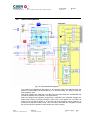
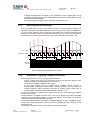
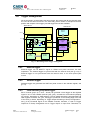
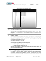
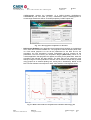
1
Technical Information Manual Revision n. 13 20 September 2011 MOD. V1740 64 CHANNEL 12 BIT 65 MS/S DIGITIZER MANUAL REV.13 NPO: 00118/07:V1740x.MUTx/13 CAEN will repair or replace any product within the guarantee period if the Guarantor declares that the product is defective due to workmanship or materials and has not been caused by mishandling, negligence on behalf of the User, accident or any abnormal conditions or operations. CAEN declines all responsibility for damages or injuries caused by an improper use of the Modules due to negligence on behalf of the User. It is strongly recommended to read thoroughly the CAEN User's Manual before any kind of operation. CAEN reserves the right to change partially or entirely the contents of this Manual at any time and without giving any notice. Disposal of the Product The product must never be dumped in the Municipal Waste. Please check your local regulations for disposal of electronics products. MADE IN ITALY : We stress the fact that all the boards are made in Italy because in this globalized world, where getting the lowest possible price for products sometimes translates into poor pay and working conditions for the people who make them, at least you know that who made your board was reasonably paid and worked in a safe environment. (this obviously applies only to the boards marked "MADE IN ITALY", we can not attest to the manufacturing process of "third party" boards). Document type: User's Manual (MUT) Title: Mod. V1740 64 Channel 12bit - 65MS/s Digitizer Revision date: 20/09/2011 Revision: 13 TABLE OF CONTENTS 1. 2. GENERAL DESCRIPTION................................................................................................................... 8 1.1. OVERVIEW ........................................................................................................................................ 8 1.2. BLOCK DIAGRAM ............................................................................................................................... 9 TECHNICAL SPECIFICATIONS....................................................................................................... 10 2.1. PACKAGING AND COMPLIANCY ........................................................................................................ 10 2.2. POWER REQUIREMENTS .................................................................................................................... 10 2.3. FRONT PANEL .................................................................................................................................. 11 2.4. EXTERNAL CONNECTORS .................................................................................................................. 12 2.4.1. ANALOG INPUT connectors ................................................................................................... 12 2.4.2. CONTROL connectors ............................................................................................................. 12 2.4.3. ADC REFERENCE CLOCK connectors................................................................................... 13 2.4.4. Digital I/O connectors ............................................................................................................. 13 2.4.5. Optical LINK connector........................................................................................................... 14 2.5. OTHER FRONT PANEL COMPONENTS .................................................................................................. 14 2.5.1. Displays .................................................................................................................................. 14 3. 2.6. INTERNAL COMPONENTS .................................................................................................................. 14 2.7. TECHNICAL SPECIFICATIONS TABLE .................................................................................................. 16 FUNCTIONAL DESCRIPTION .......................................................................................................... 17 3.1. ANALOG INPUT ................................................................................................................................ 17 3.2. CLOCK DISTRIBUTION ...................................................................................................................... 18 3.2.1. Direct Drive Mode................................................................................................................... 19 3.2.2. PLL Mode................................................................................................................................ 19 3.2.3. Trigger Clock .......................................................................................................................... 19 3.2.4. Output Clock ........................................................................................................................... 19 3.2.5. AD9510 programming ............................................................................................................. 19 3.2.6. PLL programming ................................................................................................................... 20 3.2.7. Direct Drive BYPASS programming......................................................................................... 20 3.2.8. Configuration file .................................................................................................................... 20 3.2.9. Multi-board synchronization.................................................................................................... 20 3.3. ACQUISITION MODES ....................................................................................................................... 21 3.3.1. Acquisition run/stop................................................................................................................. 21 3.3.2. Data acquisition and storage ................................................................................................... 22 3.3.3. Acquisition Triggering: Samples and Events............................................................................. 22 3.3.3.1. 3.3.4. 3.3.4.1. Header ............................................................................................................................................... 23 3.3.4.2. Samples ............................................................................................................................................. 24 3.3.4.3. 3.3.5. 3.4. Custom size events ............................................................................................................................. 23 Event structure ........................................................................................................................ 23 Event format examples ....................................................................................................................... 24 Memory FULL management..................................................................................................... 25 TRIGGER MANAGEMENT ................................................................................................................... 26 NPO: 00118/07:V1740x.MUTx/13 Filename: V1740_REV13.DOC Number of pages: 55 Page: 3 Document type: User's Manual (MUT) 3.4.1. 3.4.2. 3.4.3. Title: Mod. V1740 64 Channel 12bit - 65MS/s Digitizer Revision date: 20/09/2011 Revision: 13 External trigger ....................................................................................................................... 26 Software trigger....................................................................................................................... 26 Local channel group auto-trigger............................................................................................. 26 3.4.3.1. 3.4.4. Trigger coincidence level.................................................................................................................... 27 Trigger distribution ................................................................................................................. 28 3.5. FRONT PANEL I/OS .......................................................................................................................... 29 3.6. TEST PATTERN GENERATOR .............................................................................................................. 30 3.7. ANALOG MONITOR .......................................................................................................................... 30 3.7.1. Trigger Majority Mode (Monitor Mode = 0) ............................................................................ 30 3.7.2. Test Mode (Monitor Mode = 1)................................................................................................ 31 3.7.3. Buffer Occupancy Mode (Monitor Mode = 3)........................................................................... 31 3.7.4. Voltage Level Mode (Monitor Mode = 4) ................................................................................. 31 3.8. RESET, CLEAR AND DEFAULT CONFIGURATION ................................................................................. 31 3.8.1. Global Reset ............................................................................................................................ 31 3.8.2. Memory Reset.......................................................................................................................... 32 3.8.3. Timer Reset ............................................................................................................................. 32 3.9. VMEBUS INTERFACE ....................................................................................................................... 32 3.9.1. Addressing capabilities............................................................................................................ 32 3.9.1.1. Base address ...................................................................................................................................... 32 3.9.1.2. CR/CSR address................................................................................................................................. 33 3.9.1.3. Address relocation.............................................................................................................................. 33 3.10. DATA TRANSFER CAPABILITIES ..................................................................................................... 33 3.11. EVENTS READOUT ........................................................................................................................ 33 3.11.1. Sequential readout................................................................................................................... 33 3.11.1.1. SINGLE D32 ................................................................................................................................. 34 3.11.1.2. BLOCK TRANSFER D32/D64, 2eVME ........................................................................................ 34 3.11.1.3. CHAINED BLOCK TRANSFER D32/D64 .................................................................................... 35 3.11.2. 3.12. Event Polling........................................................................................................................... 35 OPTICAL LINK.............................................................................................................................. 35 4. SOFTWARE TOOLS ........................................................................................................................... 36 5. VME INTERFACE............................................................................................................................... 39 5.1. REGISTERS ADDRESS MAP ................................................................................................................. 39 5.2. CONFIGURATION ROM (0XF000-0XF084; R) .................................................................................... 40 5.3. GROUP N THRESHOLD (0X1N80; R/W) ............................................................................................... 41 5.4. GROUP N STATUS (0X1N88; R).......................................................................................................... 41 5.5. GROUP N AMC FPGA FIRMWARE (0X1N8C; R) ................................................................................ 42 5.6. GROUP N BUFFER OCCUPANCY (0X1N94; R)...................................................................................... 42 5.7. GROUP N DAC (0X1M98; R/W) ......................................................................................................... 42 5.8. GROUP N ADC CONFIGURATION (0X1N9C; R/W)............................................................................... 42 5.9. GROUP N CHANNEL TRIGGER MASK (0X1NA8; R/W) ......................................................................... 42 NPO: 00118/07:V1740x.MUTx/13 Filename: V1740_REV13.DOC Number of pages: 55 Page: 4 Document type: User's Manual (MUT) 6. Title: Mod. V1740 64 Channel 12bit - 65MS/s Digitizer Revision date: 20/09/2011 Revision: 13 5.10. GROUP CONFIGURATION (0X8000; R/W)........................................................................................ 43 5.11. GROUP CONFIGURATION BIT SET (0X8004; W) .............................................................................. 43 5.12. GROUP CONFIGURATION BIT CLEAR (0X8008; W).......................................................................... 43 5.13. BUFFER ORGANIZATION (0X800C; R/W)........................................................................................ 43 5.14. CUSTOM SIZE (0X8020; R/W) ........................................................................................................ 44 5.15. ACQUISITION CONTROL (0X8100; R/W) ......................................................................................... 44 5.16. ACQUISITION STATUS (0X8104; R) ................................................................................................ 45 5.17. SOFTWARE TRIGGER (0X8108; W)................................................................................................. 45 5.18. TRIGGER SOURCE ENABLE MASK (0X810C; R/W) .......................................................................... 46 5.19. FRONT PANEL TRIGGER OUT ENABLE MASK (0X8110; R/W) .......................................................... 46 5.20. POST TRIGGER SETTING (0X8114; R/W)......................................................................................... 47 5.21. FRONT PANEL I/O DATA (0X8118; R/W) ........................................................................................ 47 5.22. FRONT PANEL I/O CONTROL (0X811C; R/W) ................................................................................. 47 5.23. GROUP ENABLE MASK (0X8120; R/W)........................................................................................... 48 5.24. ROC FPGA FIRMWARE REVISION (0X8124; R).............................................................................. 48 5.25. EVENT STORED (0X812C; R)......................................................................................................... 49 5.26. SET MONITOR DAC (0X8138; R/W)............................................................................................... 49 5.27. BOARD INFO (0X8140; R) ............................................................................................................. 49 5.28. MONITOR MODE (0X8144; R/W).................................................................................................... 49 5.29. EVENT SIZE (0X814C; R) .............................................................................................................. 49 5.30. VME CONTROL (0XEF00; R/W) .................................................................................................... 49 5.31. VME STATUS (0XEF04; R) ........................................................................................................... 50 5.32. BOARD ID (0XEF08; R/W) ............................................................................................................ 50 5.33. MCST BASE ADDRESS AND CONTROL (0XEF0C; R/W) .................................................................. 50 5.34. RELOCATION ADDRESS (0XEF10; R/W) ......................................................................................... 51 5.35. INTERRUPT STATUS ID (0XEF14; R/W).......................................................................................... 51 5.36. INTERRUPT EVENT NUMBER (0XEF18; R/W).................................................................................. 51 5.37. BLT E VENT NUMBER (0XEF1C; R/W) ........................................................................................... 51 5.38. SCRATCH (0XEF20; R/W).............................................................................................................. 51 5.39. SOFTWARE RESET (0XEF24; W) .................................................................................................... 51 5.40. SOFTWARE CLEAR (0XEF28; W) ................................................................................................... 51 5.41. FLASH ENABLE (0XEF2C; R/W) .................................................................................................... 52 5.42. FLASH DATA (0XEF30; R/W) ........................................................................................................ 52 5.43. CONFIGURATION RELOAD (0XEF34; W) ........................................................................................ 52 INSTALLATION.................................................................................................................................. 53 NPO: 00118/07:V1740x.MUTx/13 Filename: V1740_REV13.DOC Number of pages: 55 Page: 5 Document type: User's Manual (MUT) Title: Mod. V1740 64 Channel 12bit - 65MS/s Digitizer Revision date: 20/09/2011 Revision: 13 6.1. POWER ON SEQUENCE ..................................................................................................................... 53 6.2. POWER ON STATUS .......................................................................................................................... 53 6.3. FIRMWARE UPGRADE ....................................................................................................................... 53 6.3.1. V1740 Upgrade files description .............................................................................................. 54 LIST OF FIGURES FIG. 1.1: MOD. V1740 BLOCK DIAGRAM ............................................................................................................ 9 FIG. 2.1: MOD. V1740 FRONT PANEL ................................................................................................................ 11 FIG. 2.2: ERNI SMC CONNECTORS .................................................................................................................. 12 FIG. 2.3: AMP CLK IN/OUT CONNECTOR ....................................................................................................... 13 FIG. 2.4: PROGRAMMABLE IN/OUT CONNECTOR ............................................................................................. 13 FIG. 2.5: LC OPTICAL CONNECTOR .................................................................................................................. 14 FIG. 2.6: ROTARY AND DIP SWITCHES LOCATION ............................................................................................... 15 FIG. 3.1: INPUT DIAGRAM ................................................................................................................................ 17 FIG. 3.2: CLOCK DISTRIBUTION DIAGRAM ......................................................................................................... 18 FIG. 3.3: SAMPLING CLOCK PHASE SHIFT .......................................................................................................... 20 FIG. 3.4: DATA STORAGE (UNDERSCORED = STORED)........................................................................................ 22 FIG. 3.5: TRIGGER OVERLAP ............................................................................................................................ 23 FIG. 3.6: EVENT ORGANIZATION ...................................................................................................................... 25 FIG. 3.7: BLOCK DIAGRAM OF TRIGGER MANAGEMENT ..................................................................................... 26 FIG. 3.8: LOCAL TRIGGER GENERATION ............................................................................................................ 27 FIG. 3.9: LOCAL TRIGGER RELATIONSHIP WITH COINCIDENCE LEVEL ................................................................. 28 FIG. 3.10: TRIGGER INTEGRATION .................................................................................................................... 29 FIG. 3.11: MAJORITY LOGIC (2 TRIGGERING GROUPS; “POLARITY” BIT[6] OF GR. CONFIG. REG. =0).................... 31 FIG. 3.12: A24 ADDRESSING ............................................................................................................................ 32 FIG. 3.13: A32 ADDRESSING ............................................................................................................................ 32 FIG. 3.14: CR/CSR ADDRESSING ...................................................................................................................... 33 FIG. 3.15: SOFTWARE RELOCATION OF BASE ADDRESS ...................................................................................... 33 FIG. 3.16: EXAMPLE OF BLT READOUT ............................................................................................................ 34 FIG. 4.1: BLOCK DIAGRAM OF THE SOFTWARE LAYERS ...................................................................................... 36 FIG. 4.2: WAVEDUMP OUTPUT WAVEFORMS ..................................................................................................... 37 FIG. 4.3: CAENSCOPE OSCILLOSCOPE TAB ....................................................................................................... 37 FIG. 4.4: CAENUPGRADER GRAPHICAL USER INTERFACE ................................................................................ 38 FIG. 4.5: DPP CONTROL SOFTWARE GRAPHICAL USER INTERFACE AND ENERGY PLOT ...................................... 38 NPO: 00118/07:V1740x.MUTx/13 Filename: V1740_REV13.DOC Number of pages: 55 Page: 6 Document type: User's Manual (MUT) Title: Mod. V1740 64 Channel 12bit - 65MS/s Digitizer Revision date: 20/09/2011 Revision: 13 LIST OF TABLES TABLE 1.1: MOD. V1740 VERSIONS.................................................................................................................... 9 TABLE 2.1: MODEL V1740 POWER REQUIREMENTS ........................................................................................... 10 TABLE 2.2 : FRONT PANEL LEDS ..................................................................................................................... 14 TABLE 2.3 : MOD. V1740 TECHNICAL SPECIFICATIONS...................................................................................... 16 TABLE 3.1 : FRONT PANEL I/OS DEFAULT SETTING ........................................................................................... 30 TABLE 5.1: ADDRESS MAP FOR THE MODEL V1740.......................................................................................... 39 TABLE 5.2: ROM ADDRESS MAP FOR THE MODEL V1740................................................................................. 41 TABLE 5.3: OUTPUT BUFFER MEMORY BLOCK DIVISION ................................................................................... 44 NPO: 00118/07:V1740x.MUTx/13 Filename: V1740_REV13.DOC Number of pages: 55 Page: 7 Document type: User's Manual (MUT) Title: Mod. V1740 64 Channel 12bit - 65MS/s Digitizer Revision date: 20/09/2011 Revision: 13 1. General description 1.1. Overview The Mod. V1740 is a 1-unit wide VME 6U module housing a 64 Channel 12 bit 65 MS/s Flash ADC Waveform Digitizer with threshold Auto-Trigger capabilities. Maximum sampling frequency is 65 MS/s using an external clock and 62.5 MS/s using the internal source. The high channel density is allowed by the AD9222 Octal 12-bit 65 MSPS Analog-toDigital Converter; therefore most channel settings are performed over “groups” of 8 channels (one group per ADC chip). The single ended analog input signal has a dynamic range of 2 Vpp (10 Vpp available on request). The DC offset of the input signal can be adjusted (for group of 8 channels) by a programmable 16bit DAC. The modules feature a front panel clock/reference In/Out and a PLL for clock synthesis from internal/external references. This allows multi board phase synchronizations to an external clock reference or to a clock Digitizer master board. The data stream is continuously written in a circular memory buffer. When the trigger occurs, the FPGA writes further N samples for the post trigger and freezes the buffer that can be read either via VME or via Optical Link. The acquisition can continue without dead time in a new buffer. VME and Optical Link accesses take place on independent paths and are handled by the on-board controller, therefore when accessed through Optical Link the board can be operated outside the VME Crate (see § 2.1). Each Group has a SRAM memory (see Table below) with independent read-write access divided in buffers (1 ÷ 1024) of programmable size. The trigger signal can be provided via the front panel input as well as via the VMEbus, but it can also be generated internally. The trigger from one board can be propagated to the other boards through the front panel Trigger Output. An Analog Output allows to reproduce the sum of the input signals as well as the majority of the buffer occupancy. The Modules VME interface is VME64X compliant and the data readout can be performed in Single Data Transfer (D32), 32/64 bit Block Transfer (BLT, MBLT, 2eVME, 2eSST) and 32/64 bit Chained Block Transfer (CBLT). The built-in daisy chainable Optical Link is able to transfer data at 80 MB/s, thus it is possible to connect up to eight ADC boards (512 ADC channels) to a single Optical Link Controller (Mod. A2818). Optical Link and VME access are internally arbitrated.. The board is available with different input range, memory and connector configuration, as summarized by the following table: NPO: 00118/07:V1740x.MUTx/13 Filename: V1740_REV13.DOC Number of pages: 55 Page: 8 Document type: User's Manual (MUT) Title: Mod. V1740 64 Channel 12bit - 65MS/s Digitizer Revision date: 20/09/2011 Revision: 13 Table 1.1: Mod. V1740 versions Model V1740 V1740B VX1740 VX1740B Input type Single ended Single ended Single ended Single ended SRAM Memory 192Ksamples / ch 1.5Msamples / ch 192 Ksamples / ch 1.5Msamples / ch Optical link Yes Yes Yes Yes AMC FPGA EP3C16 EP3C16 EP3C16 EP3C16 Form factor 6U-VME64 6U-VME64 6U-VME64X 6U-VME64X 1.2. Block Diagram FRONT PANEL x64 channels CLK IN CLK OUT MUX OSC CLOCK MANAGER (AD9510) VCXO 500MHz LOCAL BUS BUFFERS VME DAC AMC [FPGA] ADC & MEMORY CONTROLLER TRIGGERS & SYNC ADC INPUTS TRG IN TRG OUT ROC [FPGA] S IN MON DIGITAL I/Os DAC - Readout control - VME interface control - Optical link control - Trigger control - External interface control OPTICAL LINK Fig. 1.1: Mod. V1740 Block Diagram The function of each block will be explained in detail in the subsequent sections. NPO: 00118/07:V1740x.MUTx/13 Filename: V1740_REV13.DOC Number of pages: 55 Page: 9 Document type: User's Manual (MUT) Title: Mod. V1740 64 Channel 12bit - 65MS/s Digitizer Revision date: 20/09/2011 Revision: 13 2. Technical specifications 2.1. Packaging and Compliancy The module is housed in a 6U-high, 1U-wide VME unit. The board hosts the VME P1, and P2 connectors and fits into both VME/VME64 standard and V430 backplanes. VX1740 versions fit VME64X compliant crates. In all cases only well ventilated crates must be used. The V1740 cannot be operated with CAEN crates VME8001/8002/8004/8004A 2.2. Power requirements The power requirements of the module are as follows: Table 2.1: Model V1740 power requirements NPO: 00118/07:V1740x.MUTx/13 +5 V 5.5 A +12 V 0.8 A -12 V 0.9 A Filename: V1740_REV13.DOC Number of pages: 55 Page: 10 Document type: User's Manual (MUT) Title: Mod. V1740 64 Channel 12bit - 65MS/s Digitizer Revision date: 20/09/2011 Revision: 13 2.3. Front Panel Mod. V560E Mod. V1740 EXTERNAL CLOCK IN INTERNAL CLOCK OUT LOCAL TRIGGER OUT EXTERNAL TRIGGER IN SYNC/SAMPLE START ANALOG INPUT ANALOG MONITOR OUTPUT DIGITAL I/O's SCALER 64 CH 12 BIT 65 MS/S DIGITIZER Fig. 2.1: Mod. V1740 front panel NPO: 00118/07:V1740x.MUTx/13 Filename: V1740_REV13.DOC Number of pages: 55 Page: 11 Document type: User's Manual (MUT) Title: Mod. V1740 64 Channel 12bit - 65MS/s Digitizer Revision date: 20/09/2011 Revision: 13 2.4. External connectors 2.4.1. ANALOG INPUT connectors GND CH31in CH30in GND CH63in CH62in CH3in CH2in CH1in CH0in GND CH35in CH34in CH33in CH32in GND Fig. 2.2: ERNI SMC Connectors Function: Analog input, single ended, input dynamics: 2Vpp Zin=50(on request: 10Vpp Zin=1K) Mechanical specifications: Two ERNI SMC-114805 Dual Row 68pin connectors N.B.: absolute max analog input voltage = 6Vpp (with Vrail max to +6V or -6V) for any DAC offset value. Ensure that alignment is correct during insertion/extraction operations; incorrect alignment may lead to connector damage. 2.4.2. CONTROL connectors Function: TRG OUT: Local trigger output (NIM/TTL, on Rt = 50Ω) TRG IN: External trigger input (NIM/TTL, Zin= 50Ω) SYNC/SAMPLE/START (S_IN): Sample front panel input (NIM/TTL, Zin=50Ω) MON/Σ: DAC output 1Vpp on Rt=50Ω Mechanical specifications: 00-type LEMO connectors NPO: 00118/07:V1740x.MUTx/13 Filename: V1740_REV13.DOC Number of pages: 55 Page: 12 Document type: User's Manual (MUT) 2.4.3. Title: Mod. V1740 64 Channel 12bit - 65MS/s Digitizer Revision date: 20/09/2011 Revision: 13 ADC REFERENCE CLOCK connectors GND CLKCLK+ Fig. 2.3: AMP CLK IN/OUT Connector CLK_IN Function: CLK IN: External clock/Reference input, AC coupled (diff. LVDS, ECL, PECL, LVPECL, CML), Zdiff= 110. Mechanical specifications: AMP 3-102203-4 connector CLK_OUT Function: CLOCK OUT: Clock output, DC coupled (diff. LVDS), Zdiff= 110. Mechanical specifications: AMP 3-102203-4 connector 2.4.4. Digital I/O connectors Fig. 2.4: Programmable IN/OUT Connector Function: N.16 programmable differential LVDS I/O signals, Zdiff_in= 110 Ohm. Four Independent signal group 03, 47, 811, 1215, In / Out direction control; Lowest couple: 0; highest couple: not connected. See also § 3.5. Mechanical specifications: 3M-7634-5002- 34 pin Header Connector NPO: 00118/07:V1740x.MUTx/13 Filename: V1740_REV13.DOC Number of pages: 55 Page: 13 Document type: User's Manual (MUT) 2.4.5. Title: Mod. V1740 64 Channel 12bit - 65MS/s Digitizer Revision date: 20/09/2011 Revision: 13 Optical LINK connector Fig. 2.5: LC Optical Connector Mechanical specifications: LC type connector; to be used with Multimode 62.5/125µm cable with LC connectors on both sides (see also § 3.12); CAEN provides optical fiber cables with a duplex connector on the A2818 side and two simplex connectors on the board side; the simplex connector with the black wrap is for the RX line (lower) and the one with the red wrap is for the TX (higher). Electrical specifications: Optical link for data readout and slow control with transfer rate up to 80MB/s; TX/RX, daisy chainable. 2.5. Other front panel components 2.5.1. Displays The front panel hosts the following LEDs: Table 2.2 : Front panel LEDs Name: Colour: Function: DTACK green VME read/write access to the board CLK_IN green External clock enabled. NIM green Standard selection for CLK I/O, TRG OUT, TRG IN, S IN. TTL green Standard selection for CLK I/O, TRG OUT, TRG IN, S IN. LINK green/yellow Network present; Data transfer activity PLL _LOCK green The PLL is locked to the reference clock PLL _BYPS green The reference clock drives directly ADC clocks; the PLL circuit is switched off and the RUN green RUN bit set (see § 5.16) TRG green Trigger accepted DRDY green Event/data (depending on acquisition mode) are present in the Output Buffer BUSY red All the buffers are full OUT_LVDS green Signal group OUT direction enabled. PLL_LOCK LED is turned off. 2.6. Internal components SW2,4,5,6 “Base Addr. [31:16]”: Type: 4 rotary switches Function: Set the VME base address of the module. SW3 “CLOCK SOURCE”: NPO: 00118/07:V1740x.MUTx/13 Filename: V1740_REV13.DOC Type Dip Switch Function: Select clock source (External or Internal) Number of pages: 55 Page: 14 Document type: User's Manual (MUT) Title: Mod. V1740 64 Channel 12bit - 65MS/s Digitizer SW1 “FW”: Revision date: 20/09/2011 Revision: 13 Type: Dip Switch. Function: it allows to select whether the “Standard” (STD) or the “Back up” (BKP) firmware must be loaded at power on; (default position: STD). Fig. 2.6: Rotary and dip switches location NPO: 00118/07:V1740x.MUTx/13 Filename: V1740_REV13.DOC Number of pages: 55 Page: 15 Document type: User's Manual (MUT) Title: Mod. V1740 64 Channel 12bit - 65MS/s Digitizer Revision date: 20/09/2011 Revision: 13 2.7. Technical specifications table Table 2.3 : Mod. V1740 technical specifications Package 1-unit wide VME 6U module Analog Input 64 channels, single-ended; 2 Vpp (10Vpp on request) input range, positive or negative; 30MHz Bandwidth, 2nd order linear phase anti-aliasing low-pass filter ADC sampling clock generator: PLL MODE - internal reference (50MHz local oscillator) PLL MODE - external reference on CLK_IN (100ppm tolerance) Connector: ERNI SMC, (for high density flat cable: conductor spacing: 0.635 mm / 0.025") Programmable DAC for Offset Adjust (one for 8 channels). Digital Conversion Resolution: 12 bit Sampling rate: up to 65 MS/s simultaneously on each channel Multi board synchronization (one board can act as clock master). External Gate Clock capability (NIM / TTL) by S_IN input connector, for burst or single sampling mode. ADC Sampling Clock generation sampling clock generation supports three operating modes: - PLL mode - internal reference (62.5 MHz local oscillator) - PLL mode - external reference on CLK_IN (Jitter<100ppm). - PLL Bypass mode: External clock on CLK_IN drives directly ADC clocks. External clock Frequency from 10 to 65 MHz. CLK_IN AC coupled differential input clock LVDS, ECL, PECL, LVPECL, CML (single ended NIM/TTL available using CAEN A654 cable). CLK_OUT DC coupled differential LVDS output clock, locked to ADC sampling clock. Freq.: 10 ÷ 50MHz. Memory Buffer 192K sample/ch or 1.5M sample/ch; Multi Event Buffer with independent read and write access. Programmable event size and pre-post trigger. Divisible into 1 ÷ 1024 buffers. Trigger Common External TRGIN (NIM or TTL) and VME Command. Individual channel auto trigger (time over/under threshold) TRGOUT (NIM or TTL) for the trigger propagation to other V1740 boards. Trigger Time Stamp 32bit (LSB: 8ns; FSR: 17s). Sync input for Time Stamp alignment. ADC and Memory controller FPGA Altera Cyclone EP3C16 for 16 channels Optical Link Data readout and slow control with transfer rate up to 80 MB/s, to be used instead of VME bus. Daisy chainable: one A2818 PCI card can control and read eight V1740 boards in a chain. VME interface VME64X compliant D32, BLT32, MBLT64, CBLT32/64, 2eVME, 2eSST, Multi Cast Cycles Transfer rate: 60MB/s (MBLT64), 100MB/s (2eVME), 160MB/s (2eSST) Sequential access to the data of the Multi Event Buffer The Chained readout allows to read one event from all the boards in a VME crate with a BLT access Upgrade V1740 firmware can be upgraded via VME Software General purpose C Libraries and Demo Programs (CAENScope). LVDS I/O 16 general purpose LVDS I/O controlled by the FPGA Busy, Data Ready, Memory full, Trig-Out flag and other function can be programmed An Input Pattern from the LVDS I/O can be associated to each trigger as an event marker NPO: 00118/07:V1740x.MUTx/13 Filename: V1740_REV13.DOC Number of pages: 55 Page: 16 Document type: User's Manual (MUT) Title: Mod. V1740 64 Channel 12bit - 65MS/s Digitizer Revision date: 20/09/2011 Revision: 13 3. Functional description 3.1. Analog Input Input dynamic is 2Vpp (Zin= 50 ). 10Vpp (Zin= 1K dynamic is available on request. A 16bit DAC allow to add up to ±1V (±5V with high-range input) DC offset in order to preserve the full dynamic range also with uni-polar positive or negative input signals. The input bandwidth ranges from DC to 30 MHz (with 2nd order linear phase anti-aliasing low pass filter). Input Dynamic Range: 1 Vpp Input : Rin ADC OpAmp +2 12 bit Positive Unipolar DAC = FSR +1 FPGA Vref DAC 16 bit 0 -1 -2 Negative Unipolar DAC = 0 Bipolar DAC = FSR/2 Fig. 3.1: Input diagram NPO: 00118/07:V1740x.MUTx/13 Filename: V1740_REV13.DOC Number of pages: 55 Page: 17 Document type: User's Manual (MUT) Title: Mod. V1740 64 Channel 12bit - 65MS/s Digitizer Revision date: 20/09/2011 Revision: 13 3.2. Clock Distribution Fig. 3.2: Clock distribution diagram The module clock distribution takes place on two domains: OSC-CLK and REF-CLK; the former is a fixed 50MHz clock provided by an on board oscillator, the latter provides the ADC sampling clock. OSC-CLK handles both VME and Local Bus (communication between motherboard and mezzanine boards; see red traces in the figure above). REF-CLK handles ADC sampling, trigger logic, acquisition logic (samples storage into RAM, buffer freezing on trigger) through a clock chain. Such domain can use either an external (via front panel signal) or an internal (via local oscillator) source (selection is performed via dip switch SW1, see § 2.6); in the latter case OSC-CLK and REF-CLK will be synchronous (the operation mode remains the same anyway). NPO: 00118/07:V1740x.MUTx/13 Filename: V1740_REV13.DOC Number of pages: 55 Page: 18 Document type: User's Manual (MUT) Title: Mod. V1740 64 Channel 12bit - 65MS/s Digitizer Revision date: 20/09/2011 Revision: 13 REF-CLK is processed by AD9510 device, which delivers 6 clock out signals; 4 signals are sent to ADCs, one to the trigger logic and one to drive CLK-OUT output (refer to AD9510 data sheet for more details: http://www.analog.com/UploadedFiles/Data_Sheets/AD9510.pdf ); two operating modes are foreseen: Direct Drive Mode and PLL Mode 3.2.1. Direct Drive Mode The aim of this mode is to drive externally the ADCs' Sampling Clock; generally this is necessary when the required sampling frequency is not a VCXO frequency submultiple. The only requirement over the SAMP-CLK is to remain within the ADCs' range. It is important to say that Direct Drive is the only way to achieve the full ADC 65 MS/s sampling frequency, since PLL dividers allow a maximum 62.5 MS/s one. 3.2.2. PLL Mode The AD9510 features an internal Phase Detector which allows to couple REF-CLK with VCXO (500 MHz frequency); for this purpose it is necessary that REF-CLK is a submultiple of 500 MHz. AD9510 default setting foresees the board internal clock (50MHz) as clock source of REF-CLK. This configuration leads to Ndiv = 100, Rdiv = 5, thus obtaining 10MHz at the Phase Detector input and CLK-INT = 500 MHz. The required Sampling Clock (62.5MHz max) is obtained by processing CLK-INT through Sdiv dividers. When an external clock source is used, if it has 62.5MHz frequency, then AD9510 programming is not necessary, otherwise Ndiv and Rdiv have to be modified in order to achieve PLL lock. A REF-CLK frequency stability better than 100ppm is mandatory. 3.2.3. Trigger Clock TRG-CLK signal has a frequency equal to ½ of SAMP-CLK; therefore a 2 samples “uncertainty” occurs over the acquisition window. 3.2.4. Output Clock Front panel Clock Output is User programmable. Odiv and Odel parameters allows to obtain a signal with the desired frequency and phase shift (in order to recover cable line delay) and therefore to synchronize daisy chained boards. CLK-OUT default setting is OFF, it is necessary to enable the AD9510 output buffer to enable it. 3.2.5. AD9510 programming CAEN has developed a software tool which allows to handle easily the clock parameters, the CAENupgrader; see www.caen.it path: Products / Front End / VME / Controller (VME) NPO: 00118/07:V1740x.MUTx/13 Filename: V1740_REV13.DOC Number of pages: 55 Page: 19 Document type: User's Manual (MUT) 3.2.6. Title: Mod. V1740 64 Channel 12bit - 65MS/s Digitizer Revision date: 20/09/2011 Revision: 13 PLL programming In PLL mode the User has to enter the divider for input clock frequency (input clock PLL mode via CAENupgrader); since the VCXO frequency is 500 MHz, in order to use, for example, a 50MHz ExtClk, the divider to be entered is 20. Then it is necessary to set the parameters for sampling clock and CLK_OUT (enable, frequency and delay in Output Clock field via CAENupgrader); the tool refuses wrong settings for such parameters. 3.2.7. Direct Drive BYPASS programming In BYPASS mode, the User can directly set the input frequency (Input Clock field, real values are allowed). Given an input frequency, it is possible to set the parameters in order to provide the required signals. 3.2.8. Configuration file Once all parameters are set, the tool allows to save the configuration file which includes all the AD9510 device settings (see CAENupgrader documentation). It is also possible to browse and load into the AD9510 device a pre existing configuration file (see CAENupgrader documentation). For this purpose it is not necessary the board power cycle. 3.2.9. Multi-board synchronization In order to allow several V1740s to work synchronously (same sampling clock for all channels) it is necessary to use the external clock. For such purpose, two solutions are possible a daisy chain where the clock is propagated from one board to another, with the first board used as a “clock master” (whose source could be either the internal clock or an external reference managed by the User), a tree structure, with an equalized clock distributor (fan-out unit with “low skew” outputs and constant cables length). In both cases, the goal is to have all REF-CLK signals with the same phase. Since the PLL aligns the phase of VCXO output signal to REF-CLK, the result of synchronization is that all V1740s have the 500MHz VCXO output signals perfectly aligned in phase. However, despite the V1740s having all the same 500MHz reference, it is not guaranteed that the sampling clock is in its turn aligned. In fact the use of clock dividers to produce the sampling clock, may lead such signals to have different phases, as shown in the following picture, where two 250MHz (divider = 2, see § 3.2.2) are obtained from a 500MHz VCXO output. Fig. 3.3: Sampling clock phase shift NPO: 00118/07:V1740x.MUTx/13 Filename: V1740_REV13.DOC Number of pages: 55 Page: 20 Document type: User's Manual (MUT) Title: Mod. V1740 64 Channel 12bit - 65MS/s Digitizer Revision date: 20/09/2011 Revision: 13 In order to keep all dividers outputs aligned, the AD9510 is provided with a SYNCB input (see § 3.2); all dividers are put in phase on a SYNCB edge. This is done automatically within a board at any board reset, therefore it is guaranteed that one board has the same sampling clock for all channels. However if it is necessary to synchronize sampling clock on more V1740s, then SYNCB signals have to be synchronized in their turn as well. On modules with printed board Rev.2 (or greater), synchronization is achieved by piloting SYNCB through a D-Edge Triggered Flip Flop receiving EXT_CLK as clock input. In this way it is ensured that the SYNCBs of all modules have the same phase. On modules with printed board Rev.1, however, the synchronization SYNCB can be obtained through the S-IN signal. In fact on S-IN leading edge, when the board is properly programmed (see § 3.3.1), the ROC FPGA sends a pulse on SYNCB. In order to avoid “uncertainty”, it is necessary that S-IN is sent to all the modules in phase with EXT-CLK: this will allow all V1740s to receive it with the same clock period. After the synchronization of sampling clock signals, the modules will be also in phase with each other and all samples will be written into memory all at the same time. However, in order to ensure that the windows of acquisition related to the external trigger signal are also perfectly aligned, it is also necessary that the TRG-IN signal is sent to all modules synchronously with EXT-CLK and in accordance with the setup time related to its leading edge. In fact, if EXT-TRG is not correlated with EXT-CLK, a board might sense the trigger in a certain period of the clock while another might sense it in the subsequent. Therefore an uncertainty of 1 EXT-CLK period would occur (and then 1 SAMP-CLK hit) on the position of the acquired stored buffer with respect to the trigger arrival time. The distribution of trigger can be simplified through the use of a daisy-chain: the external trigger signal is sent to the first board in the chain, and this, in coincidence with the TRG-IN received, gets triggered and generates a TRG-OUT which is in turn fed to the adjacent board TRG-IN and so on. There is a fixed latency of few clock hits between TRG-IN and TRG-OUT, the value of this latency depends on the loaded firmware version; this latency, which spreads from board to board, can be easily rejected by acting on the value of the Post Trigger (see § 3.3.3) in order to have acquisition windows of all modules perfectly aligned. If the external trigger entering the first board is asynchronous, then a one sample uncertainty occurs, as described above; when this uncertainty is resolved on the first board, all the other ones will be aligned to it. If a precise temporal relationship between trigger and samples is required (such as repeated acquisitions where a jitter on the position of the signal in the acquisition window is a major issue), it is suggested to use one input channel (among all the V1740s in the chain) to sample the trigger signal itself: this will allow to reconstruct off-line the trigger edge position in the acquisition window, with a resolution smaller than the sampling period (through interpolation). 3.3. Acquisition Modes 3.3.1. Acquisition run/stop The acquisition can be started in two ways, according to Acquisition Control register Bits [1:0] setting (see § 5.14): setting the RUN/STOP bit (bit[2]) in the Acquisition Control register (bits [1:0] of Acquisition Control must be set to REGISTER-CONTROLLED RUN MODE or S-IN CONTROLLED RUN MODE) driving S_IN signal high (bits [1:0] of Acquisition Control must be set to 01) Therefore acquisition is stopped either: NPO: 00118/07:V1740x.MUTx/13 Filename: V1740_REV13.DOC Number of pages: 55 Page: 21 Document type: User's Manual (MUT) Title: Mod. V1740 64 Channel 12bit - 65MS/s Digitizer Revision date: 20/09/2011 Revision: 13 resetting the RUN/STOP bit (bit[2]) in the Acquisition Control register (bits [1:0] of Acquisition Control must be set to REGISTER-CONTROLLED RUN MODE or S-IN CONTROLLED RUN MODE) driving S_IN signal low (bits [1:0] of Acquisition Control set to 01) 3.3.2. Data acquisition and storage D0 D1 S3C0-S3C7 S1C0-S1C7 S0C0-S0C7 ADC DATA S2C0-S2C7 The S_IN signal (see § 2.4.2) can be used as “gate” to enable samples storage. The samples produced by the 65MHz ADC are stored in memory only if they are validated by the S_IN signal, otherwise they are rejected; one sample per channel is stored at each clock hit in coincidence with S_IN (see data format at § 3.3.4). The values sampled as the S-IN signal is active (high) are stored; SxCy means “Sample x of Channel y” etc. D2 D3 D4 D5 D6 D7 D8 D9 1 D 10 0 1 D 11 1 1 D 12 2 D2 D2 D3 D2 D3 D4 D2 D3 D4 D5 D2 D3 D4 D5 D6 D2 D3 D4 D5 D6 D2 D3 D4 D5 D6 D2 D3 D4 D5 D6 D9 D2 D3 D4 D5 D6 D9 D2 D3 D4 D5 D6 D9 D2 D3 D4 D5 D6 D9 SAMPLING CLOCK S- IN MEMORY BUFFER Fig. 3.4: Data Storage (underscored = stored) 3.3.3. Acquisition Triggering: Samples and Events When the acquisition is running, a trigger signal allows to: store a Trigger Time Tag (TTT): the value of a 32 bit counter which steps on with 125 MHz frequency and represents a time reference increment the EVENT COUNTER (see § 5.25) fill the active buffer with the pre/post-trigger samples, whose number is programmable (Acquisition window width, § 5.20), freezing then the buffer for readout purposes, while acquisition continues on another buffer; buffer size is programmable, see Buffer Organization (0x800C) register, § 5.13. An event is therefore composed by the trigger time tag, pre- and post-trigger samples and the event counter. Overlap between “acquisition windows” may occur (a new trigger occurs while the board is still storing the samples related to the previous trigger); this overlap can be either rejected or accepted (programmable via VME). If the board is programmed to accept the overlapped triggers, as the “overlapping” trigger arrives, the current active buffer is filled up, then the samples storage continues on the subsequent one. In this case events will not have all the same size (see figure below). NPO: 00118/07:V1740x.MUTx/13 Filename: V1740_REV13.DOC Number of pages: 55 Page: 22 Document type: User's Manual (MUT) Title: Mod. V1740 64 Channel 12bit - 65MS/s Digitizer EVENT n EVENT n+1 Revision date: 20/09/2011 Revision: 13 EVENT n+2 Recorded Not Recorded TRIGGER PRE POST ACQUISITION WINDOW Overlapping Triggers Fig. 3.5: Trigger Overlap A trigger can be refused for the following causes: acquisition is not active memory is FULL and therefore there are no available buffers the required number of samples for building the pre-trigger of the event is not reached yet; this happens typically as the trigger occurs too early either with respect to the RUN_ACQUISITION command (see § 3.3.1) or with respect to a buffer emptying after a MEMORY_FULL status the trigger overlaps the previous one and the board is not enabled for accepting overlapped triggers As a trigger is refused, the current buffer is not frozen and the acquisition continues writing on it. The Event Counter can be programmed in order to be either incremented or not. If this function is enabled, the Event Counter value identifies the number of the triggers sent (but the event number sequence is lost); if the function is not enabled, the Event Counter value coincides with the sequence of buffers saved and readout. 3.3.3.1. Custom size events It is possible to make events with a number of Samples per block, which depends on Buffer Organization register setting (see § 5.13), smaller than the default value. Such “Custom Size” events can be programmed through Custom Size (0x8020) register, § 5.14. 3.3.4. Event structure An event is structured as follows: Header (four 32-bit words) Data (variable size and format) The event can be readout either via VME or Optical Link; data format is 32 bit word. 3.3.4.1. Header It is composed by four words, namely: Size of the event (number of 32 bit words) NPO: 00118/07:V1740x.MUTx/13 Filename: V1740_REV13.DOC Number of pages: 55 Page: 23 Document type: User's Manual (MUT) Title: Mod. V1740 64 Channel 12bit - 65MS/s Digitizer Revision date: 20/09/2011 Revision: 13 Board ID (GEO); 16 bit pattern, latched on the LVDS I/O as one trigger arrives; Group Mask (=1: Groups participating to event; ex GR5 and GR7 participating → Gr_Mask: 0xA0, this information must be used by the software to acknowledge what Group the samples are coming from; the first event contains the samples from the Group with the lowest number) Event Counter: It is the trigger counter; it can count either accepted triggers only, or all triggers (see § 5.14). Trigger Time Tag: It is a 32 bit counter (31 bit count + 1 overflow bit), which is reset either as acquisition starts or via front panel Reset signal (see § 3.6), and is incremented at each sampling clock hit. It is the trigger time reference. 3.3.4.2. Samples Stored samples; data from masked channels are not read. 3.3.4.3. Event format examples An event is structured as follows: identifier (Trigger Time Tag, Event Counter) samples caught in the acquisition windows The event can be stored in the board memories (and can be readout via VME/Optical Link), data format is 32 bit word (SxCy means “Sample x of Channel y” etc.). The event format is therefore the following: N.B.: data transfer starts from Channel 0 of Group 0; once all the data from one Group are transferred, data transfer from the subsequent Group (from 0 to 7) begins. NPO: 00118/07:V1740x.MUTx/13 Filename: V1740_REV13.DOC Number of pages: 55 Page: 24 Document type: User's Manual (MUT) Title: Mod. V1740 64 Channel 12bit - 65MS/s Digitizer Revision date: 20/09/2011 Revision: 13 Fig. 3.6: Event Organization 3.3.5. Memory FULL management Bit5 of Acquisition Control register (see § 5.14), allows to select Memory FULL management mode: In Normal Mode the board becomes full, whenever all buffers are full (see § 5.13); otherwise (“Always one buffer free” mode) it is possible to always keep one buffer free: board becomes full, whenever N-1buffers are full; with N = nr. of blocks (see § 5.13). In Normal Mode, the board waits until one buffer is filled since FULL status is exited (whether the trigger is overlapped or not). The board exits FULL status at the moment which the last datum from the last channel participating to the event is read. In “Always one buffer free” mode, one buffer cannot be used (therefore it is NOT POSSIBLE, with this mode, to set Buffer Code to 0000; see § 5.13), but this allows to eliminate dead time when FULL status is exited. NPO: 00118/07:V1740x.MUTx/13 Filename: V1740_REV13.DOC Number of pages: 55 Page: 25 Document type: User's Manual (MUT) Title: Mod. V1740 64 Channel 12bit - 65MS/s Digitizer Revision date: 20/09/2011 Revision: 13 3.4. Trigger management All the channels in a board share the same trigger: this means that all the channels store an event at the same time and in the same way (same number of samples and same position with respect to the trigger); several trigger sources are available. Mother Board Mezzanines Memory Buffers TRG OUT TRG IN D Q Acquisition Logic TRIGGER ADC 8 x8 SCLK 8 LOCAL TRG 8 Enable Mask Digital Thresholds SW TRG VME Interface Local Bus Interface Fig. 3.7: Block diagram of Trigger management 3.4.1. External trigger External trigger can be NIM/TTL signal on LEMO front panel connector, 50 Ohm impedance. The external trigger is synchronized with the internal clock (see § 3.2.3); if External trigger is not synchronized with the internal clock, a one clock period jitter occurs. 3.4.2. Software trigger Software trigger are generated via VME bus (write access in the relevant register, see § 5.17). 3.4.3. Local channel group auto-trigger Each “channel group” (0÷7, 8÷15,…56÷63) can generate a local trigger as the digitized signal on one of the enabled channels (see § 5.9), exceeds the Vth threshold (ramping up or down, depending on VME settings). The Vth digital threshold is programmable via VME register accesses, see § 5.3; the trigger is produced on the leading edge of the OR of the Over (or Under, depending on Trigger Output bit setting of Group Configuration – see § 5.10) Threshold signal of the enabled channels; therefore, in case of Trigger Output bit of Group Configuration set to Trigger Output on Input Over Threshold, if a NPO: 00118/07:V1740x.MUTx/13 Filename: V1740_REV13.DOC Number of pages: 55 Page: 26 Document type: User's Manual (MUT) Title: Mod. V1740 64 Channel 12bit - 65MS/s Digitizer Revision date: 20/09/2011 Revision: 13 channel is always over threshold, its “over threshold flag” is always set to 1, and does not produce the trigger. N.B.: the local trigger signal does not start directly the event acquisition on the ”group” that generated it; such signal is propagated to the central logic which produces the global trigger, which is distributed to all groups (see § 3.4.4). THRESHOLD GR0_CHx IN Local Trigger Group0 (Group Configuration register <6> =0) Local Trigger Group0 (Group Configuration register <6> =1) Fig. 3.8: Local trigger generation 3.4.3.1. Trigger coincidence level It is possible to set the minimum number of groups with at least one channel that must be over threshold (beyond the triggering group), in order to actually generate the “Local channel group auto-trigger” signal. If, for example, Trigger Source Enable Mask (see § 5.18) bits[7:0]=FF (all groups enabled) and Local trigger coincidence level = 1 (bits [26:24]), whenever an enabled channel exceeds the threshold, the trigger will be generated only if at least another enabled channel in another group is over threshold at that moment. Local trigger coincidence level must be smaller than the number of channels enabled via bit[7:0] mask. The following figure shows examples with Local trigger coincidence level = 1 and = 0. NPO: 00118/07:V1740x.MUTx/13 Filename: V1740_REV13.DOC Number of pages: 55 Page: 27 Document type: User's Manual (MUT) Title: Mod. V1740 64 Channel 12bit - 65MS/s Digitizer Revision date: 20/09/2011 Revision: 13 Fig. 3.9: Local trigger relationship with Coincidence level 3.4.4. Trigger distribution The OR of all the enabled trigger sources, after being synchronized with the internal clock, becomes the global trigger of the board and is fed in parallel to all the channels, which store an event. A Trigger Out is also generated on the relevant front panel TRG_OUT connector (NIM or TTL), and allows to extend the trigger signal to other boards. For example, in order to start the acquisition on all the channels in the crate, as one of the channels ramps over threshold, the Local Trigger must be enabled as Trigger Out, the Trigger Out must then be fed to a Fan Out unit; the obtained signal has to be fed to the External Trigger Input of all the boards in the crate (including the board which generated the Trigger Out signal); see also the following figure. NPO: 00118/07:V1740x.MUTx/13 Filename: V1740_REV13.DOC Number of pages: 55 Page: 28 Document type: User's Manual (MUT) Title: Mod. V1740 64 Channel 12bit - 65MS/s Digitizer Revision date: 20/09/2011 Revision: 13 Fig. 3.10: Trigger integration 3.5. Front Panel I/Os The V1740 is provided with 16 programmable general purpose LVDS I/O signals. Signals can be programmed via VME (see § 5.21 and § 5.22). Default configuration is: NPO: 00118/07:V1740x.MUTx/13 Filename: V1740_REV13.DOC Number of pages: 55 Page: 29 Document type: User's Manual (MUT) Title: Mod. V1740 64 Channel 12bit - 65MS/s Digitizer Revision date: 20/09/2011 Revision: 13 Table 3.1 : Front Panel I/Os default setting Nr. Direction Description 0 out Group 0 Trigger Request 1 out Group 1 Trigger Request 2 out Group 2 Trigger Request 3 out Group 3 Trigger Request 4 out Group 4 Trigger Request 5 out Group 5 Trigger Request 6 out Group 6 Trigger Request 7 out Group 7 Trigger Request 8 out Memory Full 9 out Event Data Ready 10 out Channels Trigger 11 out RUN Status 12 in Trigger Time Tag Reset (active low) 13 in Memory Clear (active low) 14 - RESERVED 15 - RESERVED 3.6. Test pattern generator The FPGA AMC can emulate the ADC and write into memory a ramp (0, 1, 2, 3,…3FFF, 3FFF, 3FFE.., 0) for test purposes. It can be enabled via Channel Configuration register, see § 5.9. 3.7. Analog Monitor The board houses a 12bit (100MHz) DAC with 0÷1 V dynamics on a 50 Ohm load (see Fig. 1.1), whose input is controlled by the ROC FPGA and the signal output (driving 50 Ohm) is available on the MON/Σ output connector. MON output of more boards can be summed by an external Linear Fan In. This output is delivered by a 12 bit DAC. The DAC control logic implements four operating modes: - Trigger Majority Mode ( Monitor Mode = 0) - Test Mode (Monitor Mode = 1) - Buffer Occupancy Mode (Monitor Mode = 3) - Voltage Level Mode (Monitor Mode = 4) Operating mode is selected via Monitor Mode register (see § 5.28); Monitor Mode = 2 is reserved for future implementation. 3.7.1. Trigger Majority Mode (Monitor Mode = 0) It is possible to generate a Majority signal with the DAC: the MON output provides a signal whose amplitude is proportional to the number of “triggering groups” (the groups enabled to generate the local trigger, where at least one of the enabled channels in the NPO: 00118/07:V1740x.MUTx/13 Filename: V1740_REV13.DOC Number of pages: 55 Page: 30 Document type: User's Manual (MUT) Title: Mod. V1740 64 Channel 12bit - 65MS/s Digitizer Revision date: 20/09/2011 Revision: 13 group has exceeded the programmed threshold; see § 5.3, § 5.9 and § 5.18), 1 step = 1.25mV. This allows, via an external discriminator, to produce a global trigger signal, as the resulting “majority” has exceeded a particular threshold. THRESHOLD GR0 IN THRESHOLD GR1 IN 2.5mV 1.25mV MAJORITY Fig. 3.11: Majority logic (2 triggering groups; “polarity” bit[6] of Gr. Config. Reg. =0) 3.7.2. Test Mode (Monitor Mode = 1) In this mode the MON output provides a sawtooth signal with 1 V amplitude and 30.518 Hz frequency. 3.7.3. Buffer Occupancy Mode (Monitor Mode = 3) In this mode, MON out provides a voltage value proportional to the number of buffers filled with events; step: 1 buffer = 0.976 mV. . This mode allows to test the readout efficiency: in fact if the average event readout throughput is as fast as trigger rate, then MON out value remains constant; otherwise if MON out value grows in time, this means that readout rate is slower than trigger rate. 3.7.4. Voltage Level Mode (Monitor Mode = 4) In this mode, MON out provides a voltage value programmable via the 'N' parameter written in the SET MONITOR DAC register, with: Vmon = 1/4096*N (Volt). 3.8. Reset, Clear and Default Configuration 3.8.1. Global Reset Global Reset is performed at Power ON of the module or via a VME RESET (SYS_RES), see § 5.39. It allows to clear the data off the Output Buffer, the event counter and NPO: 00118/07:V1740x.MUTx/13 Filename: V1740_REV13.DOC Number of pages: 55 Page: 31 Document type: User's Manual (MUT) Title: Mod. V1740 64 Channel 12bit - 65MS/s Digitizer Revision date: 20/09/2011 Revision: 13 performs a FPGAs global reset, which restores the FPGAs to the default configuration. It initializes all counters to their initial state and clears all detected error conditions. 3.8.2. Memory Reset The Memory Reset clears the data off the Output Buffer. The Memory Reset can be forwarded via either a write access to Software Clear Register (see § 5.40) or with a pulse sent to the front panel Memory Clear input (see § 3.5). 3.8.3. Timer Reset The Timer Reset allows to initialize the timer which allows to tag an event. The Timer Reset can be forwarded with a pulse sent to Trigger Time Tag Reset input (see § 3.5). 3.9. VMEBus interface The module is provided with a fully compliant VME64/VME64X interface (see § 1.1), whose main features are: EUROCARD 9U Format J1/P1 and J2/P2 with either 160 pins (5 rows) or 96 (3 rows) connectors A24, A32 and CR-CSR address modes D32, BLT/MBLT, 2eVME, 2eSST data modes MCST write capability CBLT data transfers RORA interrupter Configuration ROM 3.9.1. Addressing capabilities 3.9.1.1. Base address The module works in A24/A32 mode. The Base Address of the module can be fixed through four rotary switches (see § 2.6) and is written into a word of 24 or 32 bit. The Base Address can be selected in the range: 0x0000000xFF0000 31 A24 mode 24 23 16 15 0 OFFSET 45 23 0 F 1 E 2 789 BCD BCD F 0 6 A A 3 45 SW5 789 E SW4 6 1 Fig. 3.12: A24 addressing 0x000000000xFFFF0000 A32 mode 31 24 23 16 15 0 OFFSET F 1 3 45 3 45 E 3 45 E 2 2 1 2 789 BCD 0 6 A F 1 E 3 45 SW5 78 9 BCD 0 6 A BCD 2 SW4 789 A BCD F 0 6 0 F SW3 78 9 A 6 E SW2 1 Fig. 3.13: A32 addressing NPO: 00118/07:V1740x.MUTx/13 Filename: V1740_REV13.DOC Number of pages: 55 Page: 32 Document type: User's Manual (MUT) Title: Mod. V1740 64 Channel 12bit - 65MS/s Digitizer Revision date: 20/09/2011 Revision: 13 The Base Address of the module is selected through four rotary switches (see § 2.6), then it is validated only with either a Power ON cycle or a System Reset (see § 3.6). 3.9.1.2. CR/CSR address GEO address is picked up from relevant backplane lines and written onto bit 23..19 of CR/CSR space, indicating the slot number in the crate; the recognized Address Modifier for this cycle is 2F. This feature is implemented only on versions with 160pin connectors. 24 23 19 18 16 15 31 GEO 0 OFFSET Fig. 3.14: CR/CSR addressing 3.9.1.3. Address relocation Relocation Address register (see § 5.34) allows to set via software the board Base Address (valid values ≠ 0). Such register allows to overwrite the rotary switches settings; its setting is enabled via VME Control Register (see § 5.26). The used addresses are: 31 24 23 16 15 0 A32 OFFSET ADER H 24 23 software relocation 16 15 0 OFFSET A24 31 ADER L ADER L software relocation Fig. 3.15: Software relocation of base address 3.10. Data transfer capabilities The board supports D32 single data readout, Block Transfer BLT32 and MBLT64, 2eVME and 2eSST cycles. Sustained readout rate is up to 60 MB/s with MBLT64, up to 100 MB/s with 2eVME and up to 160 MB/s with 2eSST. 3.11. Events readout 3.11.1. Sequential readout The events, once written in the SRAMs (Memory Event Buffers), become available for readout via VME. During the memory readout, the board can continue to store more events (independently from the readout) on the free buffers. The acquisition process is therefore “deadtimeless”, until the memory becomes full. Although the memories are SRAMs, VMEBus does not handle directly the addresses, but takes them from a FIFO. Therefore, data are read from the memories sequentially, according to the selected Readout Logic, from a memory space mapped on 4Kbytes (0x0000÷0x0FFC). The events are readout sequentially and completely, starting from the Header of the first available event, followed by the Trigger Time Tag, the Event Counter and all the samples of the channels (from 0 to 7). Once an event is completed, the relevant memory buffer NPO: 00118/07:V1740x.MUTx/13 Filename: V1740_REV13.DOC Number of pages: 55 Page: 33 Document type: User's Manual (MUT) Title: Mod. V1740 64 Channel 12bit - 65MS/s Digitizer Revision date: 20/09/2011 Revision: 13 becomes free and ready to be written again (old data are lost). After the last word in an event, the first word (Header) of the subsequent event is readout. It is not possible to readout an event partially. 3.11.1.1. SINGLE D32 This mode allows to readout a word per time, from the header (actually 4 words) of the first available event, followed by all the words until the end of the event, then the second event is transferred. The exact sequence of the transferred words is shown in § 3.3.4. We suggest, after the 1st word is transferred, to check the Event Size information and then do as many D32 cycles as necessary (actually Event Size -1) in order to read completely the event. 3.11.1.2. BLOCK TRANSFER D32/D64, 2eVME BLT32 allows, via a single channel access, to read N events in sequence, N is set via the BLT Event Number register (see § 5.37). The event size depends on the Buffer Organization Register setting (§ 5.13); namely: [Event Size] = [8*(Block Size)] + [16 bytes] Smaller event size can be achieved via Custom Size setting (see § 5.14). Then it is necessary to perform as many cycles as required in order to readout the programmed number of events. We suggest to enable BERR signal during BLT32 cycles, in order to end the cycle avoiding filler readout. The last BLT32 cycle will not be completed, it will be ended by BERR after the #N event in memory is transferred (see example in the figure below). Block size = 1024 bytes BERR = enabled BLT size = 16384 bytes N = 4 Fig. 3.16: Example of BLT readout Since some 64 bit CPU’s cut off the last 32 bit word of a transferred block, if the number of words composing such block is odd, it is necessary to add a dummy word (which has then to be removed via software) in order to avoid data loss. This can be achieved by setting the ALIGN64 bit in the VME Control register (see § 5.26). MBLT64 cycle is similar to the BLT32 cycle, except that the address and data lines are multiplexed to form 64 bit address and data buses. The 2eVME allows to achieve higher transfer rates thanks to the requirement of only two edges of the two control signals (DS and DTACK) to complete a data cycle. NPO: 00118/07:V1740x.MUTx/13 Filename: V1740_REV13.DOC Number of pages: 55 Page: 34 Document type: User's Manual (MUT) Title: Mod. V1740 64 Channel 12bit - 65MS/s Digitizer 3.11.1.3. Revision date: 20/09/2011 Revision: 13 CHAINED BLOCK TRANSFER D32/D64 The V1740 allows to readout events from more daisy chained boards (Chained Block Transfer mode). The technique which handles the CBLT is based on the passing of a token between the boards; it is necessary to verify that the used VME crate supports such cycles. Several contiguous boards, in order to be daisy chained, must be configured as “first”, “intermediate” or “last” via MCST Base Address and Control Register (see § 5.33). A common Base Address is then defined via the same register; when a BLT cycle is executed at the address CBLT_Base + 0x0000 ÷ 0x0FFC, the “first” board starts to transfer its data, driving DTACK properly; once the transfer is completed, the token is passed to the second board via the IACKIN-IACKOUT lines of the crate, and so on until the “last” board, which completes the data transfer and asserts BERR (which has to be enabled): the Master then ends the cycle and the slave boards are rearmed for a new acquisition. If the size of the BLT cycle is smaller than the events size, the board which has the token waits for another BLT cycle to begin (from the point where the previous cycle has ended). 3.11.2. Event Polling A read access to Event Size register (see § 5.28) allows “polling” the number of 32 bit words composing the next event to be read: this permits to perform a properly sized (according to the Event Size information) BLT readout from the Memory Event Buffer. 3.12. Optical Link The board houses a daisy chainable Optical Link (communication path which uses optical fiber cables as physical transmission line) able to transfer data at 80 MB/s, therefore it is possible to connect up to eight V1740 to a single Optical Link Controller: for more information, see www.caen.it (path: Products / Front End / PCI/PCIe / Optical Controller) The parameters for read/write accesses via optical link are the same used by VME cycles (Address Modifier, Base Address, data Width, etc); wrong parameter settings cause Bus Error. VME Control Register bit 3 allows to enable the module to broadcast an interrupt request on the Optical Link; the enabled Optical Link Controllers propagate the interrupt on the PCI bus as a request from the Optical Link is sensed. VME and Optical Link accesses take place on independent paths and are handled by board internal controller, with VME having higher priority; anyway it is better to avoid accessing the board via VME and Optical Link simultaneously. NPO: 00118/07:V1740x.MUTx/13 Filename: V1740_REV13.DOC Number of pages: 55 Page: 35 Document type: User's Manual (MUT) Title: Mod. V1740 64 Channel 12bit - 65MS/s Digitizer Revision date: 20/09/2011 Revision: 13 4. Software tools Fig. 4.1: Block diagram of the software layers CAEN provides drivers for both the physical communication channels (the proprietary CONET Optical Link managed by the A2818 PCI card or A3818 PCIe cards and the VME bus accessed by the V1718 and V2718 bridges), a set of C and LabView libraries, demo applications and utilities. Windows and Linux are both supported. The available software is the following: - CAENComm library contains the basic functions for access to hardware; the aim of this library is to provide a unique interface to the higher layers regardless the type of physical communication channel. Note: for VME access, CAENcomm is based on CAEN’s VME bridges V1718 (USB to VME) and V2718 (PCI/PCIe to VME). In the case of third-part bridges or SBCs, the user must provide the functions contained in the CAENcomm library for the relevant platform. The CAENComm requires the CAENVMELib library to be installed even in the cases where the VME is not used. - CAENDigitizer is a library of functions designed specifically for the digitizer family and it supports also the boards running special DPP (Digital Pulse Processing) firmware. The purpose of this library is to allow the user to open the digitizer, program it and manage the data acquisition in an easy way: with few lines of code the user can make a simple readout program without the necessity to know the details of the registers and the event data format. The CAENDigitizer library implements a common interface to the higher software layers, masking the details of the physical channel and its protocol, thus making the libraries and applications that rely on the CAENDigitizer independent from the physical layer. The library is based on the CAENComm library that manages the communication at low level (read and write access). CAENVMELib and CAENComm libraries must be already installed on the host PC before installing the CAENDigitizer; however, both CAENVMELib and CAENComm libraries are completely transparent to the user. - WaveDump is a Console application that allows to program the digitizer (according to a text configuration file that contains a list of parameters and instructions), to start the acquisition, read the data, display the readout and trigger rate, apply some post processing (such as FFT and amplitude histogram), save data to a file and also plot NPO: 00118/07:V1740x.MUTx/13 Filename: V1740_REV13.DOC Number of pages: 55 Page: 36 Document type: User's Manual (MUT) Title: Mod. V1740 64 Channel 12bit - 65MS/s Digitizer Revision date: 20/09/2011 Revision: 13 the waveforms using the external plotting tool “gnuplot”, available on internet for free. This program is quite basic and has no graphics but it is an excellent example of C code that demonstrates the use of libraries and methods for an efficient readout and data analysis. The users who intend to write the software on their own are suggested to start with this demo and modify it according to their needs. For more details please see the WaveDump User Manual and Quick Start Guide (Doc nr.: UM2091, GD2084 ). Fig. 4.2: WaveDump output waveforms - CAENScope is a fully graphical program that implements a simple oscilloscope: it allows to see the waveforms, set the trigger thresholds, change the scales of time and amplitude, perform simple mathematical operations between the channels, save data to file and other operations. CAENscope is provided as an executable file; the source codes are not distributed. NOTE: CAENScope does not work with digitizers running DPP firmware. For more details please see the CAENScope Quick Start Guide GD2484. Fig. 4.3: CAENScope oscilloscope tab - CAENUpgrader is a software composed of command line tools together with a Java Graphical User Interface (for Windows and Linux OS). CAENUpgrader allows in few easy steps to upload different firmware versions on CAEN boards, to upgrade the VME digitizers PLL, to get board information and to manage the firmware license. NPO: 00118/07:V1740x.MUTx/13 Filename: V1740_REV13.DOC Number of pages: 55 Page: 37 Document type: User's Manual (MUT) Title: Mod. V1740 64 Channel 12bit - 65MS/s Digitizer Revision date: 20/09/2011 Revision: 13 CAENUpgrader requires the installation of 2 CAEN libraries (CAENComm, CAENVMELib) and Java SE6 (or later). CAENComm allows CAENUpgrader to access target boards via USB or via CAEN proprietary CONET optical link. Fig. 4.4: CAENUpgrader Graphical User Interface - DPP Control Software is an application that manages the acquisition in the digitizers which have DPP firmware installed on it. The program is made of different parts: there is a GUI whose purpose is to set all the parameters for the DPP and for the acquisition; the GUI generates a textual configuration file that contains all the parameters. This file is read by the Acquisition Engine (DPPrunner), which is a C console application that programs the digitizer according to the parameters, starts the acquisition and manage the data readout. The data, that can be waveforms, time stamps, energies or other quantities of interest, can be saved to output files or plotted using gnuplot as an external plotting tool, exactly like in WaveDump. NOTE: so far DPP Control Software is developed for Mod. x724 and Mod. x720 digitizer series. Fig. 4.5: DPP Control Software Graphical User Interface and Energy plot NPO: 00118/07:V1740x.MUTx/13 Filename: V1740_REV13.DOC Number of pages: 55 Page: 38 Document type: User's Manual (MUT) Title: Mod. V1740 64 Channel 12bit - 65MS/s Digitizer Revision date: 20/09/2011 Revision: 13 5. VME Interface The following sections will describe in detail the board’s VME-accessible registers content. N.B.: bit fields that are not described in the register bit map are reserved and must not be over written by the User. 5.1. Registers address map Table 5.1: Address Map for the Model V1740 REGISTER NAME ADDRESS ASIZE DSIZE MODE H_RES S_RES CLR EVENT READOUT BUFFER 0x0000-0x0FFC A24/A32/A64 D32 R X X Group n THRESHOLD 0x1n80 Reserved 0x1n84 Group n STATUS A24/A32 D32 R/W X X 0x1n88 A24/A32 D32 R X X Group n AMC FPGA FIRMWARE REVISION 0x1n8C A24/A32 D32 R Group n BUFFER OCCUPANCY 0x1n94 A24/A32 D32 R X X Group n DAC 0x1n98 A24/A32 D32 R/W X X Group n ADC CONFIGURATION 0x1n9C A24/A32 D32 R/W X X Group n CHANNEL TRIGGER ENABLE MASK 0x1nA8 A24/A32 D32 R/W X X Group CONFIGURATION 0x8000 A24/A32 D32 R/W X X Group CONFIGURATION BIT SET 0x8004 A24/A32 D32 W X X Group CONFIGURATION BIT CLEAR 0x8008 A24/A32 D32 W X X BUFFER ORGANIZATION 0x800C A24/A32 D32 R/W X X CUSTOM SIZE 0x8020 A24/A32 D32 R/W X X ACQUISITION CONTROL 0x8100 A24/A32 D32 R/W X X ACQUISITION STATUS 0x8104 A24/A32 D32 R SW TRIGGER 0x8108 A24/A32 D32 W TRIGGER SOURCE ENABLE MASK 0x810C A24/A32 D32 R/W X X FRONT PANEL TRIGGER OUT ENABLE MASK 0x8110 A24/A32 D32 R/W X X POST TRIGGER SETTING 0x8114 A24/A32 D32 R/W X X FRONT PANEL I/O DATA 0x8118 A24/A32 D32 R/W X X FRONT PANEL I/O CONTROL 0x811C A24/A32 D32 R/W X X Group ENABLE MASK 0x8120 A24/A32 D32 R/W X X NPO: 00118/07:V1740x.MUTx/13 Filename: V1740_REV13.DOC Number of pages: 55 X X Page: 39 Document type: User's Manual (MUT) Title: Mod. V1740 64 Channel 12bit - 65MS/s Digitizer Revision date: 20/09/2011 Revision: 13 REGISTER NAME ADDRESS ASIZE DSIZE MODE H_RES S_RES CLR ROC FPGA FIRMWARE REVISION 0x8124 A24/A32 D32 R EVENT STORED 0x812C A24/A32 D32 R X X SET MONITOR DAC 0x8138 A24/A32 D32 R/W X X BOARD INFO 0x8140 A24/A32 D32 R MONITOR MODE 0x8144 A24/A32 D32 R/W X X EVENT SIZE 0x814C A24/A32 D32 R X X VME CONTROL 0xEF00 A24/A32 D32 R/W X VME STATUS 0xEF04 A24/A32 D32 R BOARD ID 0xEF08 A24/A32 D32 R/W X MULTICAST BASE ADDRESS & CONTROL 0xEF0C A24/A32 D32 R/W X RELOCATION ADDRESS 0xEF10 A24/A32 D32 R/W X INTERRUPT STATUS ID 0xEF14 A24/A32 D32 R/W X INTERRUPT EVENT NUMBER 0xEF18 A24/A32 D32 R/W X X BLT EVENT NUMBER 0xEF1C A24/A32 D32 R/W X X SCRATCH 0xEF20 A24/A32 D32 R/W X X SW RESET 0xEF24 A24/A32 D32 W SW CLEAR 0xEF28 A24/A32 D32 W FLASH ENABLE 0xEF2C A24/A32 D32 R/W X FLASH DATA 0xEF30 A24/A32 D32 R/W X CONFIGURATION RELOAD 0xEF34 A24/A32 D32 W CONFIGURATION ROM 0xF000-0xF3FC A24/A32 D32 R 5.2. X X X Configuration ROM (0xF000-0xF084; r) The following registers contain some module’s information, they are D32 accessible (read only): ▪ OUI: manufacturer identifier (IEEE OUI) ▪ Version: purchased version ▪ Board ID: Board identifier ▪ Revision: hardware revision identifier ▪ Serial MSB: serial number (MSB) ▪ Serial LSB: serial number (LSB) NPO: 00118/07:V1740x.MUTx/13 Filename: V1740_REV13.DOC Number of pages: 55 Page: 40 Document type: User's Manual (MUT) Title: Mod. V1740 64 Channel 12bit - 65MS/s Digitizer Revision date: 20/09/2011 Revision: 13 Table 5.2: ROM Address Map for the Model V1740 Description checksum checksum_length2 checksum_length1 checksum_length0 constant2 constant1 constant0 c_code r_code oui2 oui1 oui0 Address 0xF000 0xF004 0xF008 0xF00C 0xF010 0xF014 0xF018 0xF01C 0xF020 0xF024 0xF028 0xF02C vers 0xF030 board2 0xF034 board1 board0 revis3 revis2 revis1 revis0 sernum1 sernum0 0xF038 0xF03C 0xF040 0xF044 0xF048 0xF04C 0xF080 0xF084 Content 0xA4 0x00 0x00 0x20 0x83 0x84 0x01 0x43 0x52 0x00 0x40 0xE6 V1740, VX1740: 0x11 V1740B, VX1740B: 0x40 V1740: 0x00 VX1740: 0x01 0x06 0xCC 0x00 0x00 0x00 0x01 0x00 0x16 These data are written into one Flash page; at Power ON the Flash content is loaded into the Configuration RAM, where it is available for readout. 5.3. Group n Threshold (0x1n80; r/w) Bit [11:0] Function Threshold Value for Trigger Generation Each Group of channels (Group 0 = Ch0..7, Group 1 = Ch8..15, etc.) can generate a local trigger as the digitized signal exceeds the Vth threshold. This register allows to set Vth (LSB=input range/12bit); see also § 3.4.3. 5.4. Group n Status (0x1n88; r) Bit [5] [4] [3] [2] [1] [0] NPO: 00118/07:V1740x.MUTx/13 Function Buffer free error: 1 = trying to free a number of buffers too large GROUPn+1 enabled GROUPn enabled GROUPn DAC (see § 5.7) Busy 1 = Busy 0 = DC offset updated Memory empty Memory full Filename: V1740_REV13.DOC Number of pages: 55 Page: 41 Document type: User's Manual (MUT) Title: Mod. V1740 64 Channel 12bit - 65MS/s Digitizer Revision date: 20/09/2011 Revision: 13 5.5. Group n AMC FPGA Firmware (0x1n8C; r) Bit Function [31:16] Revision date in Y/M/DD format [15:8] Firmware Revision (X) [7:0] Firmware Revision (Y) Bits [31:16] contain the Revision date in Y/M/DD format. Bits [15:0] contain the firmware revision number coded on 16 bit (X.Y format). Example: revision 1.3 of 12th June 2007 is: 0x760C0103 5.6. Group n Buffer Occupancy (0x1n94; r) Bit [10:0] Function Occupied buffers (0..1024) 5.7. Group n DAC (0x1m98; r/w) Bit [15:0] Function DAC Data Bits [15:0] allow to define a DC offset to be added the input signal in the ±1V range (low range) or in the ±5V range (high range), see also § 3.1. There is a DAC serving eight 8-channel groups. Group 0 = Ch0..7, Group 1 =Ch8..15, etc. When Group n Status bit 2 is set to 0, DC offset is updated (see § 5.4). 5.8. Group n ADC Configuration (0x1n9C; r/w) Bit [31:0] Function Reserved 5.9. Group n Channel Trigger Mask (0x1nA8; r/w) Bit [7] [6] [5] [4] [3] [2] [1] [0] NPO: 00118/07:V1740x.MUTx/13 0 = Channel 1 = Channel 0 = Channel 1 = Channel 0 = Channel 1 = Channel 0 = Channel 1 = Channel 0 = Channel 1 = Channel 0 = Channel 1 = Channel 0 = Channel 1 = Channel 0 = Channel 1 = Channel Function 7 trigger disabled 7 trigger enabled 6 trigger disabled 6 trigger enabled 5 trigger disabled 5 trigger enabled 4 trigger disabled 4 trigger enabled 3 trigger disabled 3 trigger enabled 2 trigger disabled 2 trigger enabled 1 trigger disabled 1 trigger enabled 0 trigger disabled 0 trigger enabled Filename: V1740_REV13.DOC Number of pages: 55 Page: 42 Document type: User's Manual (MUT) Title: Mod. V1740 64 Channel 12bit - 65MS/s Digitizer Revision date: 20/09/2011 Revision: 13 This register bits[0,7] enable the channels, within Group n, to generate a local trigger as the digitized signal of one enabled channel in the group exceeds the Vth threshold (see § 3.4.3). Bit0 enables Ch0 to generate the trigger, bit1 enables Ch1 to generate the trigger and so on. In order to generate the trigger, the Group n itself must be enabled via Group Trigger Source Enable Mask (see § 5.18). 5.10. Group Configuration (0x8000; r/w) Bit [7] [6] [5] [4] [3] [2] [1] [0] Function reserved 0 = Trigger Output on Input Over Threshold 1 = Trigger Output on Input Under Threshold allows to generate local trigger either on channel over or under threshold (see § 5.3 and § 3.4) reserved reserved (MUST ALWAYS BE SET TO 1) 0 = Test Pattern Generation Disabled 1 = Test Pattern Generation Enabled reserved 0 = Trigger Overlapping Not Enabled 1 = Trigger Overlapping Enabled Allows to handle trigger overlap (see § 3.3.3) 0 = "Window" Gate 1 = "Single Shot" Gate Allows to handle samples validation (see § 3.3.1) This register allows to perform settings which apply to all groups. It is possible to perform selective set/clear of the Group Configuration register bits writing to 1 the corresponding set and clear bit at address 0x8004 (set) or 0x8008 (clear) see the following § 5.11 and § 5.12. Default value is 0x10. 5.11. Group Configuration Bit Set (0x8004; w) Bit [7..0] Function Bits set to 1 means that the corresponding bits in the Group Configuration register are set to 1. 5.12. Group Configuration Bit Clear (0x8008; w) Bit [7..0] Function Bits set to 1 means that the corresponding bits in the Group Configuration register are set to 0. 5.13. Buffer Organization (0x800C; r/w) Bit Function [3:0] BUFFER CODE The BUFFER CODE allows to divide the available Output Buffer Memory into a certain number of blocks, according to the following table: NPO: 00118/07:V1740x.MUTx/13 Filename: V1740_REV13.DOC Number of pages: 55 Page: 43 Document type: User's Manual (MUT) Title: Mod. V1740 64 Channel 12bit - 65MS/s Digitizer Revision date: 20/09/2011 Revision: 13 Table 5.3: Output Buffer Memory block division CODE 0000 0001 0010 0011 0100 0101 0110 0111 1000 1001 1010 Nr. of blocks 1 2 4 8 16 32 64 128 256 512 1024 Samples per Block (1 ch.) 192K 96K 48K 24K 12K 6K 3K 1536 768 384 192 A write access to this register causes a Software Clear, see § 3.7. This register must not be written while acquisition is running. In order to obtain a number of Samples per Block (from one channel) different from the Table above, it is necessary to use the Custom Size register (0x8020); in this case, the CODE must be set larger than the Custom Size, corresponding to the smallest possible value (for example, set 0111 code, if the desired number of Samples per Block is 900). 5.14. Custom Size (0x8020; r/w) Bit [31:0] Function 0= Custom Size disabled Ncus (0) = Allows to set a “Custom” Number of Samples per Block (from one channel); relationship is Ncus = NSAMPLES * (2/3), therefore if the desired number of Samples per Block is 900, this register must be set to 0x258 (only values multiple of 3 are allowed) This register must not be written while acquisition is running (see § 3.3.3.1). 5.15. Acquisition Control (0x8100; r/w) Bit [5] [4] [3] [2] [1:0] Function 0 = Normal Mode (default): board becomes full, whenever all buffers are full (see § 5.13) 1 = Always keep one buffer free: board becomes full, whenever N-1buffers are full; N = nr. of blocks (see § 5.13) reserved 0 = COUNT ACCEPTED TRIGGERS 1 = COUNT ALL TRIGGERS allows to reject overlapping triggers (see § 3.3.3) 0 = Acquisition STOP 1 = Acquisition RUN allows to RUN/STOP Acquisition 00 = REGISTER-CONTROLLED RUN MODE 01 = S-IN CONTROLLED RUN MODE 10 = S-IN GATE MODE 11 = MULTI-BOARD SYNC MODE Bit [2] allows to Run and Stop data acquisition; when such bit is set to 1 the board enters Run mode and a Memory Reset (see § 3.8.2) is automatically performed. When bit [2] is reset to 0 the stored data are kept available for readout. In Stop Mode all triggers are neglected. Bits [1:0] descritpion: NPO: 00118/07:V1740x.MUTx/13 Filename: V1740_REV13.DOC Number of pages: 55 Page: 44 Document type: User's Manual (MUT) Title: Mod. V1740 64 Channel 12bit - 65MS/s Digitizer Revision date: 20/09/2011 Revision: 13 00 = REGISTER-CONTROLLED RUN MODE: multiboard synchronization via S_IN front panel signal RUN control: start/stop via set/clear of bit[2] GATE always active (Continuous Gate Mode) Continuous Gate Mode can be used only if Gate mode (see § 5.9) is set in Window Mode 01 = S-IN CONTROLLED RUN MODE: Multiboard synchronization via S-IN front panel signal S-IN works both as SYNC and RUN_START command GATE always active (Continuous Gate Mode): Continuous Gate Mode: Gate always active; to be used only if Gate Mode (GROUP Configuration Register) is set to Window Mode 10 = S-IN GATE MODE Multiboard synchronization is disabled S-IN works as Gate signal set/clear of RUN/STOP bit 11 = MULTI-BOARD SYNC MODE Used only for Multiboard synchronization 5.16. Acquisition Status (0x8104; r) Bit [8] [7] [6] [5] [4] [3] [2] [1:0] Function Board ready for acquisition (PLL and ADCs are synchronized correctly) 0 = not ready 1 = ready This bit should be checked after software reset to ensure that the board will enter immediatly run mode after RUN mode setting; otherwise a latency between RUN mode setting and Acquisition start might occur. PLL Status Flag (see § 2.5.1): 0 = PLL loss of lock 1 = no PLL loss of lock NOTE: flag can be restored to 1 via read access to Status Register (see § 5.31) PLL Bypass mode (see § 2.5.1): 0 = No bypass mode 1 = Bypass mode Clock source (see § 2.6): 0 = Internal 1 = External EVENT FULL: it is set to 1 as the maximum nr. of events to be read is reached EVENT READY: it is set to 1 as at least one event is available to readout 0 = RUN off 1 = RUN on reserved 5.17. Software Trigger (0x8108; w) Bit [31:0] NPO: 00118/07:V1740x.MUTx/13 Function A write access to this location generates a trigger via software Filename: V1740_REV13.DOC Number of pages: 55 Page: 45 Document type: User's Manual (MUT) Title: Mod. V1740 64 Channel 12bit - 65MS/s Digitizer Revision date: 20/09/2011 Revision: 13 5.18. Trigger Source Enable Mask (0x810C; r/w) Bit Function 0 = Software Trigger Disabled [31] 1 = Software Trigger Enabled 0 = External Trigger Disabled [30] 1 = External Trigger Enabled [29:27] reserved [26:24] Local trigger coincidence level (default = 0) [23:8] reserved 0 = Group 7 trigger disabled [7] 1 = Group 7 trigger enabled 0 = Group 6 trigger disabled [6] 1 = Group 6 trigger enabled 0 = Group 5 trigger disabled [5] 1 = Group 5 trigger enabled 0 = Group 4 trigger disabled [4] 1 = Group 4 trigger enabled 0 = Group 3 trigger disabled [3] 1 = Group 3 trigger enabled 0 = Group 2 trigger disabled [2] 1 = Group 2 trigger enabled 0 = Group 1 trigger disabled [1] 1 = Group 1 trigger enabled 0 = Group 0 trigger disabled [0] 1 = Group 0 trigger enabled This register bits[0,7] enable the groups to generate a local trigger as the digitized signal of the channels enabled via Group n Channel Trigger Mask, see § 5.9, exceeds the Vth threshold (see § 3.4.3). Bit0 enables Group0 to generate the trigger, bit1 enables Group1 to generate the trigger and so on. Bits [26:24] allows to set minimum number of groups with at least one enabled channel over threshold, beyond the triggering group, in order to actually generate the local trigger signal; for example if bit[7:0]=FF (all groups enabled) and Local trigger coincidence level = 1, whenever at least one channel in a group exceeds the threshold, the trigger will be generated only if at least another enabled channel in another group is over threshold at that moment. Local trigger coincidence level must be smaller than the number of groups enabled via bit[7:0] mask. EXTERNAL TRIGGER ENABLE (bit30) enables the board to sense TRG-IN signals SW TRIGGER ENABLE (bit 31) enables the board to sense software trigger (see § 5.17). 5.19. Front Panel Trigger Out Enable Mask (0x8110; r/w) Bit [31] [30] [7] [6] [5] [4] NPO: 00118/07:V1740x.MUTx/13 Function 0 = Software Trigger Disabled 1 = Software Trigger Enabled 0 = External Trigger Disabled 1 = External Trigger Enabled 0 = Group 7 trigger disabled 1 = Group 7 trigger enabled 0 = Group 6 trigger disabled 1 = Group 6 trigger enabled 0 = Group 5 trigger disabled 1 = Group 5 trigger enabled 0 = Group 4 trigger disabled 1 = Group 4 trigger enabled Filename: V1740_REV13.DOC Number of pages: 55 Page: 46 Document type: User's Manual (MUT) Title: Mod. V1740 64 Channel 12bit - 65MS/s Digitizer Bit [3] [2] [1] [0] Revision date: 20/09/2011 Revision: 13 Function 0 = Group 3 trigger disabled 1 = Group 3 trigger enabled 0 = Group 2 trigger disabled 1 = Group 2 trigger enabled 0 = Group 1 trigger disabled 1 = Group 1 trigger enabled 0 = Group 0 trigger disabled 1 = Group 0 trigger enabled This register bits[0,7] enable the groups to generate a TRG_OUT front panel signal as the digitized signal of one of the channel in the enabled group exceeds the Vth threshold (see § 3.4.3). Bit0 enables Group0 to generate the TRG_OUT, bit1 enables Group1 to generate the TRG_OUT and so on. EXTERNAL TRIGGER ENABLE (bit30) enables the board to generate the TRG_OUT SW TRIGGER ENABLE (bit 31) enables the board to generate TRG_OUT (see § 5.17). 5.20. Post Trigger Setting (0x8114; r/w) Bit [31:0] Function Post trigger value The register value sets the number of post trigger samples. The number of post trigger samples is : Npost = PostTriggerValue + ConstantLatency where: Npost = number of post trigger samples. PostTriggerValue = Content of this register (this is NOT the actual number of post trigger samples) ConstantLatency = constant number of samples added due to the latency associated to the trigger processing logic in the ROC FPGA. This value is constant, but the exact value may change between different firmware revisions. 5.21. Front Panel I/O Data (0x8118; r/w) Bit [15:0] Function Front Panel I/O Data Allows to Readout the logic level of LVDS I/Os and set the logic level of LVDS Outputs. 5.22. Front Panel I/O Control (0x811C; r/w) Bit [15] [14] [9] NPO: 00118/07:V1740x.MUTx/13 Function 0 = I/O Normal operations: TRG-OUT signals outside trigger presence (trigger are generated according to Front Panel Trigger Out Enable Mask setting, see § 5.19) 1= I/O Test Mode: TRG-OUT is a logic level set via bit 14 1= TRG-OUT Test Mode set to 1 0 = TRG-OUT Test Mode set to 0 PATTERN_LATCH_MODE = 0: PATTERN field into event headers is the status of 16 LVDS Front Panel Inputs latched with board internal trigger (if a post trigger Filename: V1740_REV13.DOC Number of pages: 55 Page: 47 Document type: User's Manual (MUT) Title: Mod. V1740 64 Channel 12bit - 65MS/s Digitizer Bit [7:6] [5] [4] [3] [2] [1] [0] Revision date: 20/09/2011 Revision: 13 Function value is set, the internal trigger is delayed respect to external one). = 1: PATTERN field into event headers is the status of 16 LVDS Front Panel Inputs latched with external trigger rising edge. 00 = General Purpose I/O 01 = Programmed I/O 10 = Pattern mode: LVDS signals are input and their value is written into header PATTERN field (see § 3.3.4.1) 0 = LVDS I/O 15..12 are inputs 1 = LVDS I/O 15..12 are outputs 0 = LVDS I/O 11..8 are inputs 1 = LVDS I/O 11..8 are outputs 0 = LVDS I/O 7..4 are inputs 1 = LVDS I/O 7..4 are outputs 0 = LVDS I/O 3..0 are inputs 1 = LVDS I/O 3..0 are outputs 0= panel output signals (TRG-OUT/CLKOUT) enabled 1= panel output signals (TRG-OUT/CLKOUT) enabled in high impedance 0 = TRG/CLK are NIM I/O Levels 1 = TRG/CLK are TTL I/O Levels Bits [5:2] are meaningful for General Purpose I/O use only 5.23. Group Enable Mask (0x8120; r/w) Bit [7] [6] [5] [4] [3] [2] [1] [0] Function 0 = Group 7 1 = Group 7 0 = Group 6 1 = Group 6 0 = Group 5 1 = Group 5 0 = Group 4 1 = Group 4 0 = Group 3 1 = Group 3 0 = Group 2 1 = Group 2 0 = Group 1 1 = Group 1 0 = Group 0 1 = Group 0 disabled enabled disabled enabled disabled enabled disabled enabled disabled enabled disabled enabled disabled enabled disabled enabled Enabled groups provide the samples which are stored into the events (and not erased). The mask cannot be changed while acquisition is running. 5.24. ROC FPGA Firmware Revision (0x8124; r) Bit Function [31:16] Revision date in Y/M/DD format [15:8] Firmware Revision (X) [7:0] Firmware Revision (Y) Bits [31:16] contain the Revision date in Y/M/DD format. Bits [15:0] contain the firmware revision number coded on 16 bit (X.Y format). NPO: 00118/07:V1740x.MUTx/13 Filename: V1740_REV13.DOC Number of pages: 55 Page: 48 Document type: User's Manual (MUT) Title: Mod. V1740 64 Channel 12bit - 65MS/s Digitizer Revision date: 20/09/2011 Revision: 13 5.25. Event Stored (0x812C; r) Bit [31:0] Function This register contains the number of events currently stored in the Output Buffer This register value cannot exceed the maximum number of available buffers according to setting of buffer size register. 5.26. Set Monitor DAC (0x8138; r/w) Bit [11:0] Function This register allows to set the DAC value (12bit) This register allows to set the DAC value in Voltage level mode (see § 2.7). LSB = 0.244 mV, terminated on 50 Ohm. 5.27. Board Info (0x8140; r) Bit [15:8] [7:0] Function Memory size (Mbyte/Group) Board Type: 0 = V1740 5.28. Monitor Mode (0x8144; r/w) Bit [2:0] Function This register allows to encode the Analog Monitor (see § 3.7) operation: 000 = majority 001 = waveform generator (saw tooth ramp) 010 = reserved 011 = buffer occupancy 100 = voltage level 5.29. Event Size (0x814C; r) Bit [31:0] Function Nr. of 32 bit words in the next event 5.30. VME Control (0xEF00; r/w) Bit [7] [6] [5] NPO: 00118/07:V1740x.MUTx/13 Function 0 = Release On Register Access (RORA) Interrupt mode (default) 1 = Release On AcKnowledge (ROAK) Interrupt mode 0 = RELOC Disabled (BA is selected via Rotary Switch; see § 2.6) 1 = RELOC Enabled (BA is selected via RELOC register; see § 5.34) 0 = ALIGN64 Disabled Filename: V1740_REV13.DOC Number of pages: 55 Page: 49 Document type: User's Manual (MUT) Title: Mod. V1740 64 Channel 12bit - 65MS/s Digitizer Revision date: 20/09/2011 Revision: 13 1 = ALIGN64 Enabled (see § 3.11.1.2) 0 = BERR Not Enabled; the module sends a DTACK signal until the CPU inquires the module [4] 1 = BERR Enabled; the module is enabled either to generate a Bus error to finish a block transfer or during the empty buffer read out in D32 0 = Optical Link interrupt disabled [3] 1 = Optical Link interrupt enabled [2 :0] Interrupt level (0= interrupt disabled) Bit [7]: this setting is valid only for interrupts broadcasted on VMEbus; interrupts broadcasted on optical link feature RORA mode only. In RORA mode, interrupt status can be removed by accessing VME Control register (see § 5.30) and disabling the active interrupt level. In ROAK mode, interrupt status is automatically removed via an interrupt acknowledge cycle. Interrupt generation is restored by setting an Interrupt level > 0 via VME Control register. 5.31. VME Status (0xEF04; r) Bit [3] [2] [1] [0] Function 0 = VME FIFO not empty; 1 = VME FIFO empty 0 = BERR FLAG: no Bus Error has occurred 1 = BERR FLAG: a Bus Error has occurred (this bit is re-set after a status register read out) Reserved 0 = No Data Ready; 1 = Event Ready 5.32. Board ID (0xEF08; r/w) Bit [4 :0] Function GEO VME64X versions: this register can be accessed in read mode only and contains the GEO address of the module picked from the backplane connectors; when CBLT is performed, the GEO address will be contained in the EVENT HEADER Board ID field (see § 3.3.4.1). Other versions: this register can be accessed both in read and write mode; it allows to write the correct GEO address (default setting = 0) of the module before CBLT operation. GEO address will be contained in the EVENT HEADER Board ID field. 5.33. MCST Base Address and Control (0xEF0C; r/w) Bit [7:0] [9:8] NPO: 00118/07:V1740x.MUTx/13 Function These bits contain the most significant bits of the MCST/CBLT address of the module set via VME, i.e. the address used in MCST/CBLT operations. Allows to set up the board for daisy chaining: 00 = disabled board 01 = last board 10 = first board 11 = intermediate Filename: V1740_REV13.DOC Number of pages: 55 Page: 50 Document type: User's Manual (MUT) Title: Mod. V1740 64 Channel 12bit - 65MS/s Digitizer Revision date: 20/09/2011 Revision: 13 5.34. Relocation Address (0xEF10; r/w) Bit [15..0] Function These bits contains the A31...A16 bits of the address of the module: it can be set via VME for a relocation of the Base Address of the module. 5.35. Interrupt Status ID (0xEF14; r/w) Bit [31..0] Function This register contains the STATUS/ID that the module places on the VME data bus during the Interrupt Acknowledge cycle 5.36. Interrupt Event Number (0xEF18; r/w) Bit [9..0] Function INTERRUPT EVENT NUMBER If interrupts are enabled, the module generates a request whenever it has stored in memory a Number of events > INTERRUPT EVENT NUMBER 5.37. BLT Event Number (0xEF1C; r/w) Bit [7:0] Function This register contains the number of complete events which has to be transferred via BLT/CBLT (see § 3.11.1.2). 5.38. Scratch (0xEF20; r/w) Bit [31:0] Function Scratch (to be used to write/read words for VME test purposes) 5.39. Software Reset (0xEF24; w) Bit [31:0] Function A write access to this location allows to perform a software reset 5.40. Software Clear (0xEF28; w) Bit [31:0] NPO: 00118/07:V1740x.MUTx/13 Function A write access to this location clears all the memories Filename: V1740_REV13.DOC Number of pages: 55 Page: 51 Document type: User's Manual (MUT) Title: Mod. V1740 64 Channel 12bit - 65MS/s Digitizer Revision date: 20/09/2011 Revision: 13 5.41. Flash Enable (0xEF2C; r/w) Bit 0 Function 0 = Flash write ENABLED 1 = Flash write DISABLED This register is handled by the Firmware upgrade tool. 5.42. Flash Data (0xEF30; r/w) Bit [7:0] Function Data to be serialized towards the SPI On board Flash This register is handled by the Firmware upgrade tool. 5.43. Configuration Reload (0xEF34; w) Bit [31:0] NPO: 00118/07:V1740x.MUTx/13 Function A write access to this register causes a software reset (see § 3.6), a reload of Configuration ROM parameters and a PLL reconfiguration. Filename: V1740_REV13.DOC Number of pages: 55 Page: 52 Document type: User's Manual (MUT) Title: Mod. V1740 64 Channel 12bit - 65MS/s Digitizer Revision date: 20/09/2011 Revision: 13 6. Installation The Mod. V1740 fits into 6U VME crates. The V1740 cannot be operated with CAEN crates VME8001/8002/8004/8004A VX1740 versions require VME64X compliant crates Use only crates with forced cooling air flow Turn the crate OFF before board insertion/removal Remove all cables connected to the front panel before board insertion/removal CAUTION USE ONLY CRATES WITH FORCED COOLING AIR FLOW SINCE OVERHEAT MAY DAMAGE THE MODULE! CAUTION ALL CABLES MUST BE REMOVED FROM THE FRONT PANEL BEFORE EXTRACTING THE BOARD FROM THE CRATE! 6.1. Power ON sequence To power ON the board follow this procedure: 1. insert the V1740 board into the crate 2. power up the crate 6.2. Power ON status At power ON the module is in the following status: the Output Buffer is cleared; registers are set to their default configuration (see § 3.12) 6.3. Firmware upgrade The board can store two firmware versions, called STD and BKP respectively; at Power On, a microcontroller reads the Flash Memory and programs the module with the firmware version selected via the JP2 jumper (see § 2.6), which can be placed either on the STD position (left), or in the BKP position (right). It is possible to upgrade the board NPO: 00118/07:V1740x.MUTx/13 Filename: V1740_REV13.DOC Number of pages: 55 Page: 53 Document type: User's Manual (MUT) Title: Mod. V1740 64 Channel 12bit - 65MS/s Digitizer Revision date: 20/09/2011 Revision: 13 firmware via VME, by writing the Flash; for this purpose, download the software package available at www.caen.it/ website The package includes the new firmware release file: v1740_revX.Y_W.Z..rbf and the V1740 firmware upgrade tool: CVUpgrade.exe (windows executable) CVUpgrade tool (source code and VC++ project) For upgrading the firmware, utilizing CVUpgrade.exe, open a DOS shell, then launch CVUpgrade FileName BaseAdd [image] [/fast] [/nover] where: FileName is the RBF file BaseAdd is the Base Address (Hex 32 bit) of the V1740 image is '/standard' (default) or '/backup' '/fast' enables fast programming (MultiRead/Write with CAEN Bridge) '/nover' disables programming check N.B.: it is strongly suggested to upgrade ONLY one of the stored firmware revisions (generally the STD one): if both revision are simultaneously updated, and a failure occurs, it will not be possible to upload the firmware via VME again! 6.3.1. V1740 Upgrade files description The board hosts one FPGA on the mainboard and one FPGA for each of the eight “channel groups”. The channel group FPGAs firmware is identical. A unique file is provided that will updated all the FPGA at the same time. ROC FPGA MAINBOARD FPGA (Readout Controller + VME interface) FPGA Altera Cyclone EP1C20. AMC FPGA GROUP FPGA (ADC readout/Memory Controller): FPGA Altera Cyclone EP3C16 All FPGAs can be upgraded via VMEBUS; CVUpgrade utility program must be used for this purpose. The programming file has the extension RBF and its name follows this general scheme: v1740_ revX.Y_W.Z.RBF where: X.Y is the major/minor revision number of the mainboard FPGA W.Z is the major/minor revision number of the channel group FPGA WARNING: the previous FW revision can be restored in case there is a failure when the upgrading program runs. There is a jumper on the mainboard that allows to select the NPO: 00118/07:V1740x.MUTx/13 Filename: V1740_REV13.DOC Number of pages: 55 Page: 54 Document type: User's Manual (MUT) Title: Mod. V1740 64 Channel 12bit - 65MS/s Digitizer Revision date: 20/09/2011 Revision: 13 "backup" copy of the firmware. All the FPGAs must be upgraded and the revisions kept aligned; it is not guaranteed that the latest revision of one FPGA is compatible with an older revision. Upgrade examples: 1) Upgrade to Rev 1.0(main FPGA)/Rev 0.2 (channel group FPGA) of the standard page of the V1740: CVUpgrade v1740_rev1.0_0.2.rbf 32100000 /standard 2) Upgrade to Rev 1.0(main FPGA)/Rev 0.2 (channel group FPGA) of the backup page of the V1740: CVUpgrade v1740_rev1.0_0.2.rbf 32100000 /backup 3) Upgrade to Rev 1.0(main FPGA)/Rev 1.1 (channel group FPGA) of the standard page of the V1740: CVUpgrade v1740 _rev1.0_1.1.rbf 32100000 /standard NPO: 00118/07:V1740x.MUTx/13 Filename: V1740_REV13.DOC Number of pages: 55 Page: 55