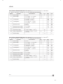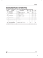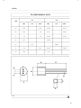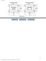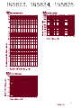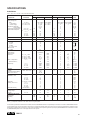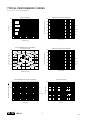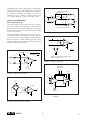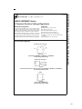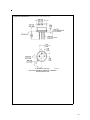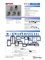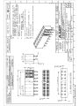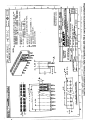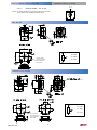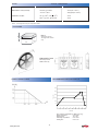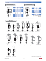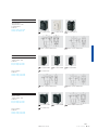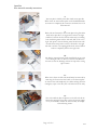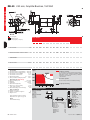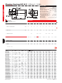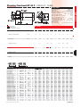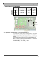
1
Project MedTech - PART II: Appendices By Alex Kuryatko-Mihai Anja Bottinga Christian Larsson Johan Edman Lars Hansson Per Hedebring Petter Pettersson Ulrika Aronsson ([email protected]) ([email protected]) ([email protected] ) ([email protected]) ([email protected]) ([email protected]) ([email protected]) ([email protected]) Supervisor: Mats Hansson Wednesday, June 04, 2008 KTH - Royal Institute of Technology Department of Machine Design MF2003 – Advanced Course In Mechatronics TABLE OF CONTENTS APPENDIX A PROJECT RISK ANALYSIS 1 APPENDIX B PROJECT SUMMARIZING OF LVSF 5 APPENDIX C KRAVSPECIFIKATION VERSION 1 17 APPENDIX D ELECTRICAL SCHEDULES AND LAYOUTS 19 APPENDIX E ELECTRICAL COMPONENTS AND DATASHEETS 29 APPENDIX F MECHANICAL DRAWINGS 149 APPENDIX G TECHNICAL REPORT 165 APPENDIX H RISK MANAGEMENT FILE 171 APPENDIX I PROJECT MEDTECH PLANNING AND SCHEDULES 189 APPENDIX J USER MANUAL 199 APPENDIX K MOTOR, ENCODER & SERVOAMPLIFIER 217 APPENDIX L TEST PROTOCOLS 239 APPENDIX M ELECTRICAL SOLUTION ONE 273 APPENDIX N GUI DETAILED OVERVIEW 295 APPENDIX O GUI FUNCTION DESCRIPTION 299 MedTech–MF2003 20080513 1 PROJECT RISK ANALYSIS Probability and impact are valued on a scale 1-4, explained below. A total 8 are given a plan so that the project members can prevent the risk from happening. Probability Impact 1 – Minimal risk 1 – Neglectable 2 – Less probable 2 – Noticeable 3 – Probably 3 – Serious 4 – Highly probable 4 – Catastrophic Risk Probability Unique components (long 3 Impact Total Prevention 3 9 Examine the suppliers. Use delivery time) standard products as far as possible. Illness among the group 2 2 4 1 1 1 phase 2 2 4 1 4 4 Long production time (wait time 3 2 6 3 12 members (high absence) Loss of group member (1) Absence at final (presentation, report etc) Loss of data (report, code etc) for workshop) Loss of (overheating components 4 components, Caution. If components are cheap, order some extra. motors etc) 2 Construction faults (play in 2 4 8 components etc) Critical examination of the design prior to construction. Keep design simple, use prototypes and tests. Consult competent people. Design faults 2 3 6 of 1 3 3 Personal injuries (during project 1 2 2 2 6 Constrained by choice software work) Lack of information (hard to 3 reach key competence and resources) Financial resources run out 1 3 3 Violation of Medical regulations 1 4 4 Can’t meet requirements for 4 1 4 3 3 quality certification (CE) Conditions during 1 change project (defined by assigner, authorities) Corporate partners back out 1 3 3 Sponsor or supervisor back out 1 2 2 Premises 1 2 2 Software and computers 3 3 9 Problems with development environment Use resources from many available computers. Only licensed software. Lack of motivation (nice spring) 2 2 4 Problem with group dynamics 2 3 6 of 2 3 6 1 3 3 Bad organization (use resources) AWAL 3 Miss project deadline 1 3 3 Miss phase deadlines 3 2 6 Strong recession (hard to find 1 3 3 3 6 2 6 components and investors) Components disappears from 2 the lab Lack of competence within the 3 group Too low goals 1 1 1 Too high goals 3 2 6 product 3 2 6 2 2 Overdesigned (unnecessary functions, adding to much) Increase of material and 1 component prices 4 ʹͲͲ͵ǣͳͳ MedTech–MF2003 20080513 5 PROJECT SUMMARIZING OF LVSF2003:11 SAMMANFATTNING AV FÖRESKRIFTER FRÅN LVSF2003:11 Nedan följer ett utdrag av de mest intressanta föreskrifterna från LVSF2003:11 för producerandet av SpastiFlex. De består av allmänna krav, krav på konstruktion och tillämpning, klassificeringsbestämmelser samt lag angående användandet av vissa måttenheter, eftersom den refereras i 10.3. I. ALLMÄNNA KRAV 1. Produkterna skall konstrueras och tillverkas på ett sådant sätt att de inte äventyrar patienternas kliniska tillstånd eller säkerhet, användarnas eller i förekommande fall andra personers hälsa och säkerhet, när de används under avsedda förhållanden och för sitt avsedda ändamål. Riskerna med att använda produkterna skall vara acceptabla med tanke på fördelarna för patienten och förenliga med en hög hälso- och säkerhetsnivå. 2. De lösningar som tillverkaren väljer för konstruktionen och tillverkningen av produkten skall överensstämma med säkerhetsprinciper och ta hänsyn till det allmänt erkända tekniska utvecklingsstadiet. För att komma fram till de lämpligaste lösningarna skall tillverkaren tillämpa nedanstående principer i följande ordning: 1. Riskerna skall elimineras eller minskas så mycket som möjligt (inbyggd säkerhet skall integreras i konstruktion och tillverkning). 2. I de fall riskerna inte kan elimineras, skall tillräckliga skyddsåtgärder vidtas, t.ex. larm om sådana behövs. 3. Användarna skall upplysas om kvarvarande risker som beror på att de vidtagna säkerhetsåtgärderna inte är tillräckliga. 3. Produkterna skall, i enlighet med tillverkarens specifikation, uppnå de prestanda som tillverkaren har angivit och vara konstruerade, tillverkade och förpackade på ett sådant sätt att de är lämpliga för en eller flera av de funktioner som avses i 2 § lagen (1993:584) om medicintekniska produkter. 4. De egenskaper och prestanda som anges i punkterna 1, 2 och 3 skall inte kunna påverkas i en sådan utsträckning att patienternas kliniska tillstånd och säkerhet, eller i förekommande fall andra personers hälsa och säkerhet, äventyras under den av tillverkaren avsedda livslängden för produkten. Detta gäller när produkten utsätts för sådana påfrestningar som kan uppstå under normala 6 användningsförhållanden. 5. Produkterna skall konstrueras, tillverkas och förpackas på ett sådant sätt att deras egenskaper och prestanda vid avsedd användning inte påverkas negativt under de lagrings- och transportförhållanden som tillverkaren har föreskrivit. 6. Oönskade bieffekter får endast utgöra acceptabla risker när de vägs mot avsedda prestanda. II. KRAV PÅ KONSTRUKTION OCH TILLVERKNING KEMISKA, FYSIKALISKA OCH BIOLOGISKA EGENSKAPER 7.1 Produkterna skall konstrueras och tillverkas på ett sådant sätt att de egenskaper och prestanda som anges under rubriken I. Allmänna krav säkerställs. Särskild uppmärksamhet skall ges åt x x valet av material, särskilt vad gäller toxiciteten och i förekommande fallbrandfarligheten, de använda materialens kompatibilitet med biologiska vävnader, celler och kroppsvätskor beroende på det avsedda ändamålet med produkten. 7.2 Produkterna skall med hänsyn till det avsedda ändamålet konstrueras, tillverkas och förpackas på ett sådant sätt att de risker som föroreningar och restsubstanser utgör minimeras för patienterna och för de personer som transporterar, lagrar och använder produkten. Särskild hänsyn skall tas till utsatta vävnader och till hur länge och ofta de är utsatta. 7.3 Produkterna skall konstrueras och tillverkas på ett sådant sätt att de utan risk kan användas med de material, ämnen och gaser som de kommer i kontakt med när de används på avsett sätt eller under rutinförfaranden. Om produkterna är avsedda att administrera läkemedel, skall de konstrueras och tillverkas så att de är kompatibla med de aktuella läkemedlen, i enlighet med de bestämmelser och begränsningar som reglerar dessa produkter, och så att deras prestanda bibehålls i enlighet med deras avsedda ändamål. 7.4 När en produkt som en integrerad del innehåller ett ämne som härrör från blod från människa skall det anmälda organet begära ett vetenskapligt utlåtande av Europeiska läkemedelsmyndigheten (EMEA) om ämnets kvalitet och säkerhet med beaktande av relevanta gemenskapsbestämmelser och särskilt i analogi med bestämmelserna i direktiven 75/318/EEG och 89/381/EEG. Detta ämnes användbarhet som en integrerad del av den medicintekniska produkten skall kontrolleras med hänsyn till produktens avsedda ändamål. I enlighet med artikel 4.3 i direktiv 89/381/EEG skall ett prov från varje sats av bulkvaran och/eller den färdiga produkten av ämnet som härrör från blod från människa kontrolleras av ett statligt laboratorium eller av ett laboratorium som har utsetts av en medlemsstat för detta ändamål. 7.5 Produkterna skall konstrueras och tillverkas på ett sådant sätt att riskerna med ämnen som läcker ur produkterna blir så små som möjligt. 7 7.6 Produkterna skall konstrueras och tillverkas på ett sådant sätt att riskerna med ämnen som oavsiktligt tränger in i dem blir så små som möjligt med tanke på den miljö som de är avsedda att användas i. KRAV PÅ TILLVERKNING OCH MILJÖ 9.1 Om produkten är avsedd att användas tillsammans med andra produkter eller utrustningar, skall hela kombinationen, inklusive det sammanlänkande systemet, vara säker och inte försämra produkternas angivna prestanda. Begränsningar i användningen skall framgå av märkningen eller bruksanvisningen. 9.2 Produkterna skall vara konstruerade och tillverkade på ett sådant sätt att följande risker elimineras eller blir så små som möjligt: 1 Risken för skada i samband med produkternas fysiska egenskaper inklusive volym/tryckförhållande, mått och i förekommande fall ergonomiska egenskaper. 2 Risker i samband med miljöförhållanden som rimligen kan förutses som magnetfält, yttre elektrisk påverkan, elektrostatisk urladdning, tryck, temperatur eller variationer i tryck och acceleration. 3 Risker för ömsesidig interferens med andra produkter som normalt används vid undersökningarna eller vid den aktuella behandlingen. 4 Risker som kan uppstå då det är omöjligt att underhålla och kalibrera produkterna (som vid implantat), vid åldrande av det använda materialet eller minskad noggrannhet hos någon mät- eller kontrollmekanism. 9.3 Produkterna skall konstrueras och tillverkas på ett sådant sätt att riskerna för brand eller explosion blir så små som möjligt vid normal användning och vid ett första fel. Särskild uppmärksamhet skall riktas mot produkter i vars avsedda användning ingår att utsättas för lättantändliga ämnen eller för ämnen som kan orsaka brand. 10. PRODUKTER MED MÄTFUNKTION 10.1 Produkter som har en mätfunktion skall vara konstruerade och tillverkade på ett sådant sätt att mätresultaten blir tillräckligt noggranna och tillförlitliga och inom toleranser som är rimliga med tanke på produktens avsedda ändamål. Toleranser avseende noggrannhet anges av tillverkaren. 10.2 Mät-, övervaknings- och presentationsskalorna skall vara konstruerade enligt ergonomiska principer och med hänsyn tagen till produktens avsedda ändamål. 10.3 De mätningar som görs med produkter som har en mätfunktion skall uttryckas i författningsenliga enheter i enlighet med bestämmelserna i lagen (1992:1514) om måttenheter, mätningar och mätdon. 8 12. KRAV PÅ MEDICINTEKNISKA PRODUKTER SOM ÄR KOPPLADE TILL ELLER ÄR UTRUSTADE MED EN ENERGIKÄLLA 12.1 Produkter som innefattar elektroniska programmerbara system skall konstrueras så att systemens repeterbarhet, tillförlitlighet och prestanda i förhållande till det avsedda ändamålet säkerställs. Vid ett första fel (i systemet) skall detta förhindra eller minimera ytterligare risker. 12.2 Om patientens säkerhet är beroende av en intern energikälla i produkten, skall produkten vara utrustad med möjlighet att kontrollera den interna energikällans tillstånd. 12.3 Om patientens säkerhet är beroende av en extern energikälla, skall produkten vara utrustad med larmsystem som signalerar strömavbrott. 12.4 Produkter som är avsedda att övervaka en eller flera kliniska parametrar hos en patient skall vara utrustade med lämpliga larmsystem som gör användaren uppmärksam på situationer som kan leda till patientens död eller en allvarlig försämring av patientens hälsotillstånd. 12.5 Produkter skall konstrueras och tillverkas så att risken för störningar orsakade av deras elektromagnetiska fält på andra produkter eller utrustningar under användning i den normala omgivningen blir så liten som möjligt. 12.6Skyddmotriskeravelektrisknatur Produkterna skall konstrueras och tillverkas på ett sådant sätt att risken för oavsiktliga elektriska chocker vid normal användning och vid ett första fel blir så liten som möjligt, under förutsättning att produkterna har installerats på rätt sätt. 12.7Skyddmotriskeravmekaniskochtermisknatur 12.7.1 Produkterna skall konstrueras och tillverkas på ett sådant sätt att patienterna och användarna skyddas mot risker av mekanisk natur såsom hållfasthet, stabilitet och rörliga delar. 12.7.2 Produkterna skall konstrueras och tillverkas på ett sådant sätt att de risker som uppstår i samband med produkternas vibrationer blir så små som möjligt, såvida inte vibrationerna är en del av den angivna funktionen. Hänsyn skall tas till den tekniska utvecklingen och de till buds stående möjligheterna att dämpa vibrationer. 12.7.3 Produkterna skall konstrueras och tillverkas på ett sådant sätt att de risker som uppstår i samband med buller blir så små som möjligt, såvida inte bullret är en del av den angivna funktionen. Hänsyn skall tas till den tekniska utvecklingen och de till buds stående möjligheterna att dämpa buller. 12.7.4 Terminaler och anslutningsdon till elektrisk, gasformig eller hydraulisk och pneumatisk energitillförsel, som användaren skall hantera, skall vara konstruerade och tillverkade på ett sådant att tänkbara risker minimeras. 9 12.7.5 Åtkomliga delar av produkterna (utom delar eller områden som är avsedda för att avge värme eller nå avsedda temperaturer) och omgivningen får inte uppnå potentiellt skadliga temperaturer vid normal användning. 12.8Skyddförpatientermotriskervidtillförselavenergiellerämnen 12.8.1 De produkter som är avsedda att tillföra patienten energi eller ämnen skall vara konstruerade och tillverkade på ett sådant sätt att flödet kan fastställas och bibehållas tillräckligt noggrant för att patientens och användarens säkerhet skall kunna garanteras. 12.8.2 Produkterna skall ha en funktion som kan förhindra och/eller visa ett otillräckligt flöde, vilket kan utgöra en fara. Produkterna skall ha en funktion som i största möjliga utsträckning förhindrar att farliga mängder oavsiktligt avges från en ämnes- eller energikälla. 12.9 Kontrollernas och indikatorernas funktioner skall tydligt anges på produkterna. Om det finns en bruksanvisning på produkten eller om bruks- eller anpassningsvariabler markeras på produkten med ett visuellt system, skall anvisningarna vara förståeliga för användaren och i förekommande fall för patienten. III. KLASSIFICERING 1. ICKE INVASIVA PRODUKTER 1.1Regel1 Alla icke invasiva produkter tillhör klass I om inte någon av de regler som anges nedan är tillämplig. 1.2Regel2 Alla icke invasiva produkter som är avsedda att leda eller lagra blod, kroppsvätskor eller vävnader, vätskor eller gaser inför en infusion, dosering eller införsel i kroppen tillhör klass IIa i följande fall: Om de får kopplas till en aktiv medicinteknisk produkt i klass IIa eller i en högre klass. Om de är avsedda att användas för att lagra eller leda blod eller andra kroppsvätskor eller för att lagra organ, delar av organ eller kroppsvävnader. I alla andra fall tillhör de klass I. 1.3Regel3 Alla icke invasiva produkter som är avsedda att ändra den biologiska eller kemiska sammansättningen av blod, andra kroppsvätskor eller andra vätskor som är avsedda för infusion i kroppen tillhör klass IIb. Om emellertid behandlingen består av filtrering, centrifugering eller utbyte av gaser eller värme tillhör produkterna klass IIa. 10 1.4Regel4 Alla icke invasiva produkter som kommer i kontakt med skadad hud 5 6 7 tillhör klass I om de är avsedda att användas som en mekanisk barriär, som tryck eller för absorption av exsudat, tillhör klass IIb om de huvudsakligen är avsedda att användas för sår som har penetrerat huden och bara kan läka efter ytterligare åtgärder, tillhör klass IIa i alla andra fall, även produkter som huvudsakligen är avsedda att reglera sårets bakterieflora. 2. INVASIVA PRODUKTER 2.1Regel5 Alla invasiva produkter att användas i kroppsöppningar, utom kirurgiska invasiva produkter och sådana som inte är avsedda att kopplas till en aktiv medicinteknisk produkt, 1. tillhör klass I om de är avsedda för tillfällig användning, 2. tillhör klass IIa om de är avsedda för kortvarig användning, utom om de används i munhålan så långt som till svalget, i en hörselgång fram till trumhinnan eller i en näshåla – de tillhör då klass I, 3. tillhör klass IIb om de är avsedda för långvarig användning, utom om de används i munhålan så långt som till svalget, i en hörselgång fram till trumhinnan eller i en näshåla och inte sugs upp av slemhinnan – de tillhör då klass IIa. Alla invasiva produkter att användas i kroppsöppningar, utom kirurgiska invasiva produkter, som är avsedda att kopplas till en aktiv medicinteknisk produkt i klass IIa eller i en högre klass, tillhör klass IIa. 2.2Regel6 Alla kirurgiska invasiva produkter som är avsedda för tillfällig användning tillhör klass IIa om de inte 1. särskilt är avsedda för att diagnosticera, övervaka eller korrigera ett hjärtfeleller fel i centrala cirkulationssystemet genom direkt kontakt med dessa kroppsdelar – de tillhör då klass III, 2. är kirurgiska flergångsinstrument – de tillhör då klass I, 3. är avsedda att avge energi i form av joniserande strålning – de tillhör då klass IIb, 4. är avsedda att ha en biologisk verkan eller att helt och hållet eller till största delen absorberas – de tillhör då klass IIb, 5. är avsedda att administrera läkemedel genom ett doseringssystem, om detta görs på ett potentiellt farligt sätt med tanke på tillämpningssättet – de tillhör då klass IIb. 2.3Regel7 Alla kirurgiska invasiva produkter som är avsedda för kortvarig användning tillhör klass IIa om de inte är 6. antingen särskilt avsedda att diagnosticera, övervaka eller korrigera ett hjärtfel eller ett fel i centrala cirkulationssystemet genom direkt kontakt med dessa delar av kroppen – de tillhör då klass III eller 7. särskilt avsedda att användas i direkt kontakt med centrala nervsystemet – de tillhör då klass III eller 11 8. avsedda att avge energi i form av joniserande strålning – de tillhör då klass IIb eller 9. avsedda att ha en biologisk verkan eller att helt och hållet eller till största delen absorberas – de tillhör då klass III eller 10. avsedda att genomgå en kemisk förändring i kroppen, utom om produkterna sätts in i tänderna, eller för att administrera läkemedel – de tillhör då klass IIb. 2.4Regel8 Bröstimplantat tillhör klass III. Alla övriga implantat och kirurgiska invasiva produkter som är avsedda för långvarig användning tillhör klass IIb, om de inte är avsedda 11. att sättas in i tänderna – de tillhör då klass IIa, 12. att användas i direkt kontakt med hjärtat, centrala cirkulationssystemet eller centrala nervsystemet – de tillhör då klass III, 13. att ha en biologisk verkan eller att helt eller till största delen absorberas – de tillhör då klass III eller 14. att genomgå en kemisk förändring i kroppen, utom om produkterna sätts in i tänderna, eller att administrera läkemedel – de tillhör då klass III. 3. YTTERLIGARE BESTÄMMELSER FÖR AKTIVA PRODUKTER 3.1Regel9 Alla aktiva terapeutiska produkter som är avsedda att tillföra eller utbyta energi tillhör klass IIa, om de inte har sådana egenskaper att de kan tillföra energi till eller utbyta energi med människokroppen på ett potentiellt farligt sätt, med tanke på energins egenskaper, täthet och platsen där energin skall användas – de tillhör då klass IIb. Alla aktiva produkter som är avsedda att styra och/eller övervaka prestanda hos aktiva terapeutiska produkter i klass IIb eller är avsedda att direkt påverka sådana produkters prestanda tillhör klass IIb. 3.2Regel10 Aktiva produkter avsedda för diagnostik tillhör klass IIa 15. om de är avsedda att avge energi som kommer att absorberas av människokroppen, med undantag av produkter som används för att belysa patientens kropp i det synliga spektret. 16. om de är avsedda att avbilda spridningen av radiofarmaka i kroppen. 17. om de är avsedda att möjliggöra direkt diagnos eller övervakning av vitala fysiologiska processer, om produkterna inte är särskilt avsedda för att övervaka vitala fysiologiska variabler, vars variationer är sådana att de skulle kunna resultera i omedelbar fara för patienten, t. ex. variationer i hjärtverksamhet, andning eller det centrala nervsystemets aktivitet – de tillhör då klass IIb. Aktiva produkter som är avsedda att avge joniserande strålning och avsedda för diagnostik och behandlande interventionell radiologi, inklusive produkter som styr och/eller övervakar sådana produkter eller som direkt påverkar deras prestanda, tillhör klass IIb. 12 Regel11 Alla aktiva produkter som är avsedda att administrera eller avlägsna läkemedel, kroppsvätskor eller andra ämnen till eller från kroppen tillhör klass IIa, om det inte görs på ett sätt som är potentiellt skadligt med tanke på de aktuella ämnenas egenskaper, den kroppsdel och det användningssätt det är fråga om – de tillhör då klass IIb. 3.3Regel12 Alla andra aktiva produkter tillhör klass I. 4. SÄRSKILDA REGLER 4.1Regel13 Alla produkter i vilka ett ämne är integrerat, som om det används separat, kan betraktas som ett läkemedel enligt definitionen i 1 § läkemedelslagen (1992:859) och som kan ha en verkan på människokroppen som understödjer produkten, tillhör klass III. Alla produkter vilka som en integrerad del innehåller ett ämne som härrör från blod från människa tillhör klass III. 4.2Regel14 Alla produkter som används som preventivmedel eller för att förhindra spridningen av sexuellt överförbara sjukdomar tillhör klass IIb, om de inte är implantat eller invasiva produkter för långvarig användning – de tillhör då klass III. 4.3Regel15 Alla produkter som är särskilt avsedda för att desinficera medicintekniska produkter tillhör klass IIa. Alla produkter som är särskilt avsedda för att desinficera, rengöra, skölja eller i förekommande fall för att hydratisera kontaktlinser tillhör klass IIb. Denna regel gäller inte produkter som är avsedda för att genom en fysisk insats rengöra andra medicintekniska produkter än kontaktlinser. 4.4Regel16 Icke aktiva produkter som är särskilt avsedda att lagra diagnostiska röntgenbilder tillhör klass IIa. 4.5Regel17 Alla produkter som tillverkas med hjälp av icke viabla djurvävnader eller produkter som kommer av sådana vävnader tillhör klass III, utom när sådana produkter är avsedda att bara komma i kontakt med intakt hud. 5Regel18 Blodpåsar tillhör klass IIb. 13 LAG (1992:1514) OM MÅTTENHETER, MÄTNINGAR & MÄTDON SFS nr: 1992:1514 Departement/myndighet: Näringsdepartementet Utfärdad: 1992-12-17 Ändrad: t.o.m. SFS 1995:1726 ANVÄNDNING AV VISSA MÅTTENHETER 1§ För att uppfylla Sveriges åtaganden enligt avtalet om Europeiska ekonomiska samarbetsområdet (EESavtalet) skall vad som sägs i denna paragraf gälla vid mätningar, som görs i ekonomiskt, hälsovårdande, skyddande eller administrativt syfte. Vid mätningar som avses i första stycket skall mätdonen, enligt närmare föreskrifter av regeringen eller den myndighet som regeringen bestämmer, vara graderade i och mätresultaten uttryckta i 1. måttenheter, som ingår i det internationella måttenhetssystem (SI-systemet) som har antagits av Allmänna konferensen för mått och vikt, 1. måttenheter, som har tillåtits för bruk tillsammans med SI-enheter enligt beslut av Internationella kommittén för mått och vikt, eller 2. andra särskilda måttenheter, som får användas enligt Sveriges åtaganden enligt EES-avtalet. Regeringen eller den myndighet som regeringen bestämmer får i fråga om kommunikationer föreskriva om undantag från andra stycket, om det är förenligt med Sveriges åtaganden enligt EES-avtalet. BEMYNDIGANDEN ATT MEDDELA FÖRESKRIFTER OM MÄTNINGAR M. M. 2§ För att uppfylla Sveriges internationella överenskommelser eller om det är befogat från konsumentsynpunkt får regeringen eller den myndighet som regeringen bestämmer meddela föreskrifter om x x krav på mätningar och mättekniska metoder, och krav på och kontroll av mätdon, om föreskriften avser skydd för liv, personlig säkerhet eller hälsa, kommunikationer eller näringsverksamhet. Lag (1993:1380). 3§ Regeringen eller den myndighet som regeringen bestämmer får också meddela föreskrifter om 14 x x krav på och kontroll av förpackningsstorlek och kontroll av mängduppgifter på färdigförpackade varor samt krav i fråga om särskild kundvåg i detaljhandeln. TILLSYN 4§ Tillsyn över efterlevnaden av denna lag och föreskrifter meddelade med stöd av lagen utövas för visst område av den myndighet som regeringen bestämmer. 5§ Tillsynsmyndigheten har rätt att få tillträde till områden och lokaler där mätdon finns eller varor förpackas, förvaras eller säljs. Detsamma gäller den som svarar för kontroll som avses i 3 §. Den hos vilken kontroll eller tillsyn sker är skyldig att underlätta tillsynsmyndighetens arbete. Tillsynsmyndigheten eller den som svarar för kontroll enligt 3 § har rätt att få handräckning av kronofogdemyndigheten för att genomföra åtgärd som avses i första stycket. 6§ En tillsynsmyndighet får meddela de förelägganden och förbud som behövs i en skilda fall för att denna lag eller föreskrifter meddelade med stöd av lagen skall efterlevas. Ett sådant föreläggande eller förbud får förenas med vite. ÖVERKLAGANDE 7§ En tillsynsmyndighets beslut enligt denna lag eller enligt föreskrifter som har meddelats med stöd av lagen får överklagas hos allmän förvaltningsdomstol. Prövningstillstånd krävs vid överklagande till kammarrätten. Lag (1995:1726). ÖVERGÅNGSBESTÄMMELSER 1995:1726 Denna lag träder i kraft den 1 maj 1996 men tillämpas inte i de fall där det första beslutet i ärendet fattats dessförinnan. 15 16 ͳ MedTech–MF2003 20080513 17 KRAVSPECIFIKATION VERSION 1 This specification of demands is written and handed out by Anders Fagergren. SKALL-KRAV Apparaten skall vrida handen uppåt 50 grader. Två hastigheter 5°/s samt 240°/s skall användas. Hastighetens stigtid skall vara <10 ms under normal belastning. Apparaten ska kunna utföra vridningen ett valbart antal gånger i följd med en vilotid i extenderat läge på 1 s innan den återgår till startläge. Apparaten ska ha ett justerbart rörelseomfång inom ±40° från ett läge där handen är parallell med underarmen. Apparaten ska mäta moment, hastighet och tid under hela rörelsen. Samplingsfrekvens på minst 100Hz för 236°/s och minst 10Hz för 5°/s, för hela rörelsen inklusive vilotiden. Det första samplet får ej innehålla rörelse, detta för att kunna användas som offsetvärde. Momentet ska mätas i ett område 0-10 Nm med en noggrannhet på 0,05 Nm. Apparaten ska räkna ut och presentera värdena på peak 1 och peak 2 samt peak 3. Apparaten ska kunna göra mätningar på vuxna individer i sittande ställning. Apparaten ska vara utformad så att mätningar är möjliga på både höger och vänster hand. Handen och underarmen ska fästas proximalt och distalt i apparaten. Maskinoperatören ska kunna se underarmen på patienten. Apparaten ska vara bärbar. Apparaten ska konstrueras enligt gällande normer för sjukhusutrustning och patientsäkerhet. Apparatens mjukvara ska kunna uppdateras. Apparaten ska kunna föra över mätdata till extern Windows-PC för presentation och vidare bearbetning. Windows-programmet skall kunna uppdateras (källkod och utv. miljö). Data skall sparas i text-filer så att kolumnerna är Tid, Moment och Hastighet, och raderna är sampel. BÖR-KRAV Apparaten bör klara fler hastigheter än 5°/s och 240°/s. Apparaten bör klara mätningar på barn. Apparatens uppdateringsprogramvara bör ha ett grafiskt användargränssnitt. Apparaten skall vara billig att producera, mindre än 5000:- i komponenter + material. 18 ǡǯƬ MedTech–MF2003 20080513 19 ELECTRICAL SCHEMATICS, BOM’S & PCB LAYOUTS BILL OF MATERIAL – BOM SENSOR BOARD Part C1 C2 C3 C4 C5 C6 C7 C8 D1 D2 D3 D4 IC2 IC3 INA111AP R1 R3 R4 R5 R6 R7 R8 R9 R10 R11 R12 SV1 SV2 SV3 SV4 SV5 Value 100nF 100nF 100nF 330nF 1uF 1uF 100nF 100nF 1N5400 1N5400 1N5400 1N5400 LM324P 7805T AD620 182ohm 2,6k 10k 10k 1M 1M 2,6k 2,6k 120ohm 120ohm Device C5/2.5 C5/2.5 C5/2.5 C5/2.5 C5/2.5 C5/2.5 C5/2.5 C5/2.5 1N5400 1N5400 1N5400 1N5400 LM324P 7805T AD620 R-EU_0411/12 R-EU_0411/12 R-EU_0411/12 R-EU_0411/12 R-EU_0411/12 R-EU_0411/12 R-EU_0411/12 R-EU_0411/12 TRIM_EU-PT10 R-EU_0411/12 R-EU_0411/12 MA04-1 MA03-1 MA05-2 MA05-2 MA03-1 Package C5B2.5 C5B2.5 C5B2.5 C5B2.5 C5B2.5 C5B2.5 C5B2.5 C5B2.5 DO201-15 DO201-15 DO201-15 DO201-15 DIL14 TO220H DIL8 0411/12 0411/12 0411/12 0411/12 0411/12 0411/12 0411/12 0411/12 PT-10 0411/12 0411/12 MA04-1 MA03-1 MA05-2 MA05-2 MA03-1 Library capacitor-wima capacitor-wima capacitor-wima capacitor-wima capacitor-wima capacitor-wima capacitor-wima capacitor-wima diode diode diode diode lm324 linear ad620 rcl rcl rcl rcl rcl rcl rcl rcl pot rcl rcl con-lstb con-lstb con-lstb con-lstb con-lstb 20 12V POWER SUPPLY BOARD Part 2KBP01 2KBP02 7912T C1 C2 C3 C4 C5 C6 EI542B FUSE IC2 J1 SV2 X1 Value Device 2KBP 2KBP 7912T C5/5 C5/3 C5/3 C5/3 C5/3 C5/5 EI54-2B SH32 7812T DCJ0202 MA03-1 AK300/2 1000uF 330nF 330nF 100nF 100nF 1000uF 7812T DCJ0202 Package 2KBP 2KBP TO220H C5B5 C5B3 C5B3 C5B3 C5B3 C5B5 EI54-2B SH32 TO220H DCJ0202 MA03-1 AK300/2 Library rectifier rectifier linear capacitor-wima capacitor-wima capacitor-wima capacitor-wima capacitor-wima capacitor-wima trafo fuse linear con-jack con-lstb con-ptr500 SIGNAL LEVEL REGULATOR BOARD Part R1 R2 R3 R4 SV1 SV2 Value 4.7k 3.3k 4.7k 3.3k Device R-EU_0207/10 R-EU_0207/10 R-EU_0207/10 R-EU_0207/10 MA04-1 MA04-1 Package 0207/10 0207/10 0207/10 0207/10 MA04-1 MA04-1 Library rcl rcl rcl rcl con-lstb con-lstb AMPLIFIER BOARD Part C1 C2 IC1 IC2 R2 R3 R4 R7 R8 R9 R10 R11 R13 R14 Value 1u .22u LM324N LM324N 30K 10K 10K 78K 1K 1K 1K 78K 10K 1K Device C5/3 C5/3 LM324N LM324N R-EU_0204/5 R-EU_0204/5 R-EU_0204/5 R-EU_0204/5 R-EU_0204/5 R-EU_0204/5 R-EU_0204/5 R-EU_0204/5 R-EU_0204/5 R-EU_0204/5 Package C5B3 C5B3 DIL14 DIL14 0204/5 0204/5 0204/5 0204/5 0204/5 0204/5 0204/5 0204/5 0204/5 0204/5 Library capacitor-wima capacitor-wima linear linear rcl rcl rcl rcl rcl rcl rcl rcl rcl rcl 21 AMPLIFIER BOARD 22 SIGNAL LEVEL REGULATOR BOARD TOP LAYER BOTTOM LAYER 23 12V POWER SUPPLY BOARD SCHEMATICS TOP LAYER 24 BOTTOM LAYER 25 SENSOR BOARD 26 TOP LAYER 27 BOTTOM LAYER 28 Ƭ MedTech–MF2003 20080514 29 30 ͳʹ MedTech–MF2003 20080513 31 2002-03-26 PRODUKTINFORMATION Vi reserverar oss mot fel samt förbehåller oss rätten till ändringar utan föregående meddelande ELFA artikelnr 70-362-70 2KBP01 brygga 100V 2.0A 70-362-88 2KBP02 brygga 200V 2.0A 70-362-96 2KBP04 brygga 400V 2.0A 70-363-04 2KBP06 brygga 600V 2.0A 70-363-12 2KBP08 brygga 800V 2.0A 70-363-20 2KBP10 brygga 1000V 2.0A 32 33 34 35 Datum 980914 PRODUKTINFORMATION TEKNISK INFORMATION 020-75 80 20 ORDERTEL 020-75 80 00 ORDERFAX 020-75 80 10 TECHNICAL INFORMATION +46 8 580 941 15 ORDERPHONE +46 8 580 941 01 ORDERFAX +46 8 580 941 11 Vi reserverar oss mot fel samt förbehåller oss rätten till ändringar utan föregående meddelande ELFA artikelnr. 73-264-08 78L05ACZ 5V 0,1 Sp reg 73-264-16 78L06ACZ 6V 0,1 Sp reg 73-264-24 78L08ACZ 8V 0,1 Sp reg 73-264-32 78L09ACZ 9V 0,1 Sp reg 73-264-40 73-264-57 73-264-65 73-264-73 Antal sidor: 18 78L12ACZ 12V 0,1 Sp reg 78L15ACZ 15V 0,1 Sp reg 78L18ACZ 18V 0,1 Sp reg 78L24ACZ 24V 0,1 Sp reg 36 L78L00 SERIES POSITIVE VOLTAGE REGULATORS ■ ■ ■ ■ ■ ■ OUTPUT CURRENT UP TO 100 mA OUTPUT VOLTAGES OF 3.3; 5; 6; 8; 9; 12; 15; 18; 24V THERMAL OVERLOAD PROTECTION SHORT CIRCUIT PROTECTION NO EXTERNAL COMPONENTS ARE REQUIRED AVAILABLE IN EITHER ± 5% (AC) OR ± 10% (C) SELECTION DESCRIPTION The L78L00 series of three-terminal positive regulators employ internal current limiting and thermal shutdown, making them essentially indestructible. If adequate heatsink is provided, they can deliver up to 100 mA output current. They are intended as fixed voltage regulators in a wide range of applications including local or on-card regulation for elimination of noise and distribution problems associated with single-point regulation. In addition, they can be used with power pass elements to make high-current voltage regulators. The L78L00 series used as Zener diode/resistor combination replacement, offers an effective SO-8 TO-92 output impedance improvement of typically two orders of magnetude, along with lower quiescent current and lower noise. BLOCK DIAGRAM March 1998 1/17 37 L78L00 ABSOLUTE MAXIMUM RATING Symbol Vi Parameter DC Input Voltage Value Unit Vo = 3.3 V to 9 V 30 V Vo = 12 V to 15 V 35 V Vo = 18 V to 24 V Io Output Current Pt ot Power Dissipation T stg Storage Temperature Range To p Operating Junction Temperature RangeFor L78L00C, L78L00AC For L78L00AB 40 V 100 mA Internally limited (*) - 40 to 150 o C 0 to 125 - 40 to 125 o C C o (*) Our SO-8 package used for Voltage Regulators is modified internally to have pins 2, 3, 6 and 7 electrically commoned to the die attach flag. This particular frame decreases the total thermal resistance of the package and increases its ability to dissipate power when an appropriate area of copper on the printed circuit board is available for heatsinking. The external dimensions are the same as for the standard SO-8 TEST CIRCUITS 2/17 38 L78L00 CONNECTION DIAGRAM AND ORDERING NUMBERS (top view) BOTTOM VIEW pin 1 = OUT pin 2 = GND pin 3 = IN SO-8 TO-92 ORDERING NUMBERS Type L78L33AC L78L33AB L78L05C L78L05AC L78L05AB L78L06C L78L06AC L78L06AB L78L08C L78L08AC L78L08AB L78L09C L78L09AC L78L09AB L78L12C L78L12AC L78L12AB L78L15C L78L15AC L78L15AB L78L18C L78L18AC L78L18AB L78L24C L78L24AC L78L24AB SO-8 L78L33ACD L78L33ABD L78L05CD L78L05ACD L78L05ABD L78L06CD L78L06ACD L78L06ABD L78L08CD L78L08ACD L78L08ABD L78L09CD L78L09ACD L78L09ABD L78L12CD L78L12ACD L78L12ABD L78L15CD L78L15ACD L78L15ABD L78L18CD L78L18ACD L78L18ABD L78L24CD L78L24ACD L78L24ABD TO-92 L78L33ACZ L78L33ABZ L78L05CZ L78L05ACZ L78L05ABZ L78L06CZ L78L06ACZ L78L06ABZ L78L08CZ L78L08ACZ L78L08ABZ L78L09CZ L78L09ACZ L78L09ABZ L78L12CZ L78L12ACZ L78L12ABZ L78L15CZ L78L15ACZ L78L15ABZ L78L18CZ L78L18ACZ L78L18ABZ L78L24CZ L78L24ACZ L78L24ABZ Output Voltage 3.3 V 3.3 V 5 V 5 V 5 V 6 V 6 V 6 V 8 V 8 V 8 V 9 V 9 V 9 V 12 V 12 V 12 V 15 V 15 V 15 V 18 V 18 V 18 V 24 V 24 V 24 V 3/17 39 L78L00 ELECTRICAL CHARACTERISTICS FOR L78L05 (refer to the test circuits, Tj = 0 to 125 oC, Vi = 10V, Io = 40 mA, Ci = 0.33 μF, Co = 0.1 μF unless otherwise specified) Symbol Parameter Test Conditions o Vo Output Voltage Tj = 25 C Vo Output Voltage Io = 1 to 40 mA Io = 1 to 70 mA ΔV o Line Regulation Vi = 7 to 20 V Vi = 8 to 20 V ΔV o Load Regulation Io = 1 to 100 mA Io = 1 to 40 mA Quiescent Current Tj = 25 oC o Tj = 125 C Id Min. Typ. Max. Unit 4.6 5 5.4 V 5.5 5.5 V V 200 150 mV mV 60 30 mV mV 6 5.5 mA mA 4.5 4.5 Vi = 7 to 20 V Vi = 10 V o Tj = 25 C Tj = 25 oC Tj = 25 oC o Tj = 25 C ΔI d Quiescent Current Change Io = 1 to 40 mA 0.2 mA ΔI d Quiescent Current Change Vi = 8 to 20 V 1.5 mA eN Output Noise Voltage B = 10Hz to 100KHz Tj = 25 oC Supply Voltage Rejection Io = 40 mA f = 120 Hz Tj = 25 oC Vi = 8 to 18 V SVR Vd 40 Dropout Voltage 40 μV 49 dB 1.7 V ELECTRICAL CHARACTERISTICS FOR L78L06 (refer to the test circuits, Tj = 0 to 125 oC, Vi = 12V, Io = 40 mA, Ci = 0.33 μF, Co = 0.1 μF unless otherwise specified) Symbol Parameter Test Conditions Min. Typ. Max. Unit 5.52 6 6.48 V 6.6 6.6 V V 200 150 mV mV 60 30 mV mV Tj = 25 C Tj = 125 oC o 6 5.5 mA mA Quiescent Current Change Io = 1 to 40 mA 0.2 mA ΔI d Quiescent Current Change Vi = 8 to 20 V 1.5 mA eN Output Noise Voltage B = 10Hz to 100KHz Tj = 25 oC o Vo Output Voltage Tj = 25 C Vo Output Voltage Io = 1 to 40 mA Io = 1 to 70 mA ΔV o Line Regulation Vi = 8.5 to 20 V Tj = 25 C o Vi = 9 to 20 V Tj = 25 C ΔV o Load Regulation Io = 1 to 100 mA Io = 1 to 40 mA Quiescent Current ΔI d Id SVR Vd Supply Voltage Rejection Dropout Voltage Vi = 8.5 to 20 V Vi = 12 V 5.4 5.4 o o Tj = 25 C o Tj = 25 C o Io = 40 mA f = 120 Hz Tj = 25 C Vi = 9 to 20 V 38 50 μV 46 dB 1.7 V 4/17 40 L78L00 ELECTRICAL CHARACTERISTICS FOR L78L08 (refer to the test circuits, Tj = 0 to 125 oC, Vi = 14V, Io = 40 mA, Ci = 0.33 μF, Co = 0.1 μF unless otherwise specified) Symbol Parameter Test Conditions o Min. Typ. Max. Unit 7.36 8 8.64 V 8.8 8.8 V V 200 150 mV mV 80 40 mV mV Vo Output Voltage Tj = 25 C Vo Output Voltage Io = 1 to 40 mA Io = 1 to 70 mA ΔV o Line Regulation Vi = 10.5 to 23 V Tj = 25 C Tj = 25 oC Vi = 11 to 23 V ΔV o Load Regulation Io = 1 to 100 mA Io = 1 to 40 mA Quiescent Current Tj = 25 oC o Tj = 125 C 6 5.5 mA mA ΔI d Quiescent Current Change Io = 1 to 40 mA 0.2 mA ΔI d Quiescent Current Change Vi = 11 to 23 V 1.5 mA Id eN SVR Vd Vi = 10.5 to 23 V Vi = 14 V 7.2 7.2 o Tj = 25 oC o Tj = 25 C o Output Noise Voltage B = 10Hz to 100KHz Tj = 25 C Supply Voltage Rejection Io = 40 mA f = 120 Hz Tj = 25 oC Vi = 12 to 23 V 36 Dropout Voltage 60 μV 45 dB 1.7 V ELECTRICAL CHARACTERISTICS FOR L78L09 (refer to the test circuits, Tj = 0 to 125 oC, Vi = 15V, Io = 40 mA, Ci = 0.33 μF, Co = 0.1 μF unless otherwise specified) Symbol Parameter Test Conditions Min. Typ. Max. Unit 8.28 9 9.72 V 9.9 9.9 V V 250 200 mV mV 80 40 mV mV Tj = 25 C Tj = 125 oC o 6 5.5 mA mA Quiescent Current Change Io = 1 to 40 mA 0.2 mA ΔI d Quiescent Current Change Vi = 12 to 23 V 1.5 mA eN Output Noise Voltage B = 10Hz to 100KHz Tj = 25 oC o Vo Output Voltage Tj = 25 C Vo Output Voltage Io = 1 to 40 mA Io = 1 to 70 mA ΔV o Line Regulation Vi = 11.5 to 23 V Tj = 25 C o Vi = 12 to 23 V Tj = 25 C ΔV o Load Regulation Io = 1 to 100 mA Io = 1 to 40 mA Quiescent Current ΔI d Id SVR Vd Supply Voltage Rejection Dropout Voltage Vi = 11.5 to 23 V Vi = 15 V 8.1 8.1 o o Tj = 25 C o Tj = 25 C o Io = 40 mA f = 120 Hz Tj = 25 C Vi = 12 to 23 V 36 70 μV 44 dB 1.7 V 5/17 41 L78L00 ELECTRICAL CHARACTERISTICS FOR L78L12 (refer to the test circuits, Tj = 0 to 125 oC, Vi = 19V, Io = 40 mA, Ci = 0.33 μF, Co = 0.1 μF unless otherwise specified) Symbol Parameter Test Conditions o Min. Typ. Max. Unit 11.1 12 12.9 V 13.2 13.2 V V 250 200 mV mV 100 50 mV mV Vo Output Voltage Tj = 25 C Vo Output Voltage Io = 1 to 40 mA Io = 1 to 70 mA ΔV o Line Regulation Vi = 14.5 to 27 V Tj = 25 C Vi = 16 to 27 V Tj = 25 oC ΔV o Load Regulation Io = 1 to 100 mA Io = 1 to 40 mA Quiescent Current Tj = 25 oC o Tj = 125 C 6.5 6 mA mA ΔI d Quiescent Current Change Io = 1 to 40 mA 0.2 mA ΔI d Quiescent Current Change Vi = 16 to 27 V 1.5 mA Id eN SVR Vd Vi = 14.5 to 27 V Vi = 19 V 10.8 10.8 o Tj = 25 oC o Tj = 25 C o Output Noise Voltage B = 10Hz to 100KHz Tj = 25 C Supply Voltage Rejection Io = 40 mA f = 120 Hz Tj = 25 oC Vi = 15 to 25 V 36 Dropout Voltage 80 μV 42 dB 1.7 V ELECTRICAL CHARACTERISTICS FOR L78L15 (refer to the test circuits, Tj = 0 to 125 oC, Vi = 23V, Io = 40 mA, Ci = 0.33 μF, Co = 0.1 μF unless otherwise specified) Symbol Parameter Test Conditions Min. Typ. Max. Unit 13.8 15 16.2 V 16.5 16.5 V V 300 250 mV mV 150 75 mV mV Tj = 25 C Tj = 125 oC o 6.5 6 mA mA Quiescent Current Change Io = 1 to 40 mA 0.2 mA ΔI d Quiescent Current Change Vi = 20 to 30 V 1.5 mA eN Output Noise Voltage B = 10Hz to 100KHz Tj = 25 oC o Vo Output Voltage Tj = 25 C Vo Output Voltage Io = 1 to 40 mA Io = 1 to 70 mA ΔV o Line Regulation Vi = 17.5 to 30 V Tj = 25 C o Vi = 20 to 30 V Tj = 25 C ΔV o Load Regulation Io = 1 to 100 mA Io = 1 to 40 mA Quiescent Current ΔI d Id SVR Vd Supply Voltage Rejection Dropout Voltage Vi = 17.5 to 30 V Vi = 23 V 13.5 13.5 o o Tj = 25 C o Tj = 25 C o Io = 40 mA f = 120 Hz Tj = 25 C Vi = 18.5 to 28.5 V 33 90 μV 39 dB 1.7 V 6/17 42 L78L00 ELECTRICAL CHARACTERISTICS FOR L78L18 (refer to the test circuits, Tj = 0 to 125 oC, Vi = 27V, Io = 40 mA, Ci = 0.33 μF, Co = 0.1 μF unless otherwise specified) Symbol Parameter Test Conditions Min. Typ. Max. Unit 16.6 18 19.4 V 19.8 19.8 V V o 320 270 mV mV Tj = 25 oC o Tj = 25 C 170 85 mV mV o Vo Output Voltage Tj = 25 C Vo Output Voltage Io = 1 to 40 mA Io = 1 to 70 mA ΔV o Line Regulation Vi = 22 to 33 V Vi = 22 to 33 V ΔV o Load Regulation Io = 1 to 100 mA Io = 1 to 40 mA Quiescent Current Tj = 25 oC o Tj = 125 C 6.5 6 mA mA ΔI d Quiescent Current Change Io = 1 to 40 mA 0.2 mA ΔI d Quiescent Current Change Vi = 23 to 33 V 1.5 mA Id eN SVR Vd Vi = 22 to 33 V Vi = 27 V 16.2 16.2 Tj = 25 C Tj = 25 oC o Output Noise Voltage B = 10Hz to 100KHz Tj = 25 C Supply Voltage Rejection Io = 40 mA f = 120 Hz Tj = 25 oC Vi = 23 to 33 V 32 Dropout Voltage 120 μV 38 dB 1.7 V ELECTRICAL CHARACTERISTICS FOR L78L24 (refer to the test circuits, Tj = 0 to 125 oC, Vi = 33V, Io = 40 mA, Ci = 0.33 μF, Co = 0.1 μF unless otherwise specified) Symbol Parameter Test Conditions Min. Typ. Max. Unit 22.1 24 25.9 V 26.4 26.4 V V 350 300 mV mV 200 100 mV mV Tj = 25 C Tj = 125 oC o 6.5 6 mA mA Quiescent Current Change Io = 1 to 40 mA 0.2 mA ΔI d Quiescent Current Change Vi = 28 to 38 V 1.5 mA eN Output Noise Voltage B = 10Hz to 100KHz Tj = 25 oC o Vo Output Voltage Tj = 25 C Vo Output Voltage Io = 1 to 40 mA Io = 1 to 70 mA ΔV o Line Regulation Vi = 27 to 38 V Vi = 28 to 38 V ΔV o Load Regulation Io = 1 to 100 mA Io = 1 to 40 mA Quiescent Current ΔI d Id SVR Vd Supply Voltage Rejection Dropout Voltage Vi = 27 to 38 V Vi = 33 V 21.6 21.6 o Tj = 25 C o Tj = 25 C o Tj = 25 C o Tj = 25 C o Io = 40 mA f = 120 Hz Tj = 25 C Vi = 29 to 35 V 30 200 μV 37 dB 1.7 V 7/17 43 L78L00 ELECTRICAL CHARACTERISTICS FOR L78L33AB AND L78L33AC (refer to the test circuits, Vi = 8.3V, Io = 40 mA, Ci = 0.33 μF, Co = 0.1 μF, Tj = 0 to 125 oC for L78L33AC, Tj = -40 to 125 oC for L78L33AB, unless otherwise specified) Symbol Parameter Test Conditions o Vo Output Voltage Tj = 25 C Vo Output Voltage Io = 1 to 40 mA Io = 1 to 70 mA Vi = 5.3 to 20 V Vi = 8.3 V ΔV o Line Regulation Vi = 5.3 to 20 V Vi = 6.3 to 20 V Tj = 25 oC o Tj = 25 C ΔV o Load Regulation Io = 1 to 100 mA Io = 1 to 40 mA Quiescent Current ΔI d ΔI d Id eN SVR Vd Min. Typ. 3.168 3.3 Max. Unit 3.432 V 3.465 3.465 V V 150 100 mV mV 60 30 mV mV Tj = 25 oC o Tj = 125 C 6 5.5 mA mA Quiescent Current Change Io = 1 to 40 mA 0.1 mA Quiescent Current Change Vi = 6.3 to 20 V 1.5 mA 3.135 3.135 o Tj = 25 C o Tj = 25 C o Output Noise Voltage B = 10Hz to 100KHz Tj = 25 C Supply Voltage Rejection Io = 40 mA f = 120 Hz Tj = 25 C Vi = 6.3 to 16.3 V o 41 Dropout Voltage 40 μV 49 dB 1.7 V ELECTRICAL CHARACTERISTICS FOR L78L05AB AND L78L05AC (refer to the test circuits, Vi = 10V, Io = 40 mA, Ci = 0.33 μF, Co = 0.1 μF, Tj = 0 to 125 oC for L78L05AC, Tj = -40 to 125 oC for L78L05AB, unless otherwise specified) Symbol Parameter Test Conditions o Vo Output Voltage Tj = 25 C Vo Output Voltage Io = 1 to 40 mA Io = 1 to 70 mA ΔV o Line Regulation Vi = 7 to 20 V Vi = 8 to 20 V ΔV o Load Regulation Io = 1 to 100 mA Io = 1 to 40 mA Quiescent Current ΔI d Min. Typ. 4.8 5 Max. Unit 5.2 V 5.25 5.25 V V 150 100 mV mV 60 30 mV mV Tj = 25 C o Tj = 125 C o 6 5.5 mA mA Quiescent Current Change Io = 1 to 40 mA 0.1 mA ΔI d Quiescent Current Change Vi = 8 to 20 V 1.5 mA eN Output Noise Voltage B = 10Hz to 100KHz Tj = 25 C Id SVR Vd Supply Voltage Rejection Dropout Voltage 4.75 4.75 Vi = 7 to 20 V Vi = 10 V o Tj = 25 C o Tj = 25 C o Tj = 25 C o Tj = 25 C o o Io = 40 mA f = 120 Hz Tj = 25 C Vi = 8 to 18 V 41 40 μV 49 dB 1.7 V 8/17 44 L78L00 ELECTRICAL CHARACTERISTICS FOR L78L06AB AND L78L06AC (refer to the test circuits, Vi = 12V, Io = 40 mA, Ci = 0.33 μF, Co = 0.1 μF, Tj = 0 to 125 oC for L78L06AC, Tj = -40 to 125 oC for L78L06AB, unless otherwise specified) Symbol Parameter Test Conditions o Min. Typ. Max. Unit 5.76 6 6.24 V 6.3 6.3 V V 150 100 mV mV 60 30 mV mV Vo Output Voltage Tj = 25 C Vo Output Voltage Io = 1 to 40 mA Io = 1 to 70 mA ΔV o Line Regulation Vi = 8.5 to 20 V Tj = 25 oC o Vi = 9 to 20 V Tj = 25 C ΔV o Load Regulation Io = 1 to 100 mA Io = 1 to 40 mA Quiescent Current Tj = 25 oC o Tj = 125 C 6 5.5 mA mA ΔI d Quiescent Current Change Io = 1 to 40 mA 0.1 mA ΔI d Quiescent Current Change Vi = 9 to 20 V 1.5 mA Id eN SVR Vd Vi = 8.5 to 20 V Vi = 12 V 5.7 5.7 o Tj = 25 C o Tj = 25 C o Output Noise Voltage B = 10Hz to 100KHz Tj = 25 C Supply Voltage Rejection Io = 40 mA f = 120 Hz Tj = 25 C Vi = 9 to 20 V o 39 Dropout Voltage 50 μV 46 dB 1.7 V ELECTRICAL CHARACTERISTICS FOR L78L12AB AND L78L12AC (refer to the test circuits, Vi = 19V, Io = 40 mA, Ci = 0.33 μF, Co = 0.1 μF, Tj = 0 to 125 oC for L78L12AC, Tj = -40 to 125 oC for L78L12AB, unless otherwise specified) Symbol Parameter Test Conditions o Min. Typ. Max. Unit 11.5 12 12.5 V 12.6 12.6 V V 250 200 mV mV 100 50 mV mV Vo Output Voltage Tj = 25 C Vo Output Voltage Io = 1 to 40 mA Io = 1 to 70 mA ΔV o Line Regulation Vi = 14.5 to 27 V Tj = 25 C o Vi = 16 to 27 V Tj = 25 C ΔV o Load Regulation Io = 1 to 100 mA Io = 1 to 40 mA Quiescent Current Tj = 25 C o Tj = 125 C o 6.5 6 mA mA ΔI d Quiescent Current Change Io = 1 to 40 mA 0.1 mA ΔI d Quiescent Current Change Vi = 16 to 27 V 1.5 mA eN Output Noise Voltage B = 10Hz to 100KHz Tj = 25 C Id SVR Vd Supply Voltage Rejection Dropout Voltage Vi = 14.5 to 27 V Vi = 19 V 11.4 11.4 o o Tj = 25 C o Tj = 25 C o o Io = 40 mA f = 120 Hz Tj = 25 C Vi = 15 to 25 V 37 80 μV 42 dB 1.7 V 9/17 45 L78L00 ELECTRICAL CHARACTERISTICS FOR L78L15AB AND L78L15AC (refer to the test circuits, Vi = 23V, Io = 40 mA, Ci = 0.33 μF, Co = 0.1 μF, Tj = 0 to 125 oC for L78L15AC, Tj = -40 to 125 oC for L78L15AB, unless otherwise specified) Symbol Parameter Test Conditions o Vo Output Voltage Tj = 25 C Vo Output Voltage Io = 1 to 40 mA Io = 1 to 70 mA ΔV o Line Regulation Vi = 17.5 to 30 V Tj = 25 oC o Vi = 20 to 30 V Tj = 25 C ΔV o Load Regulation Io = 1 to 100 mA Io = 1 to 40 mA Quiescent Current ΔI d ΔI d Id eN SVR Vd Min. Typ. 14.4 15 Max. Unit 15.6 V 15.75 15.75 V V 300 250 mV mV 150 75 mV mV Tj = 25 oC o Tj = 125 C 6.5 6 mA mA Quiescent Current Change Io = 1 to 40 mA 0.1 mA Quiescent Current Change Vi = 20 to 30 V 1.5 mA Vi = 17.5 to 30 V Vi = 23 V 14.25 14.25 o Tj = 25 C o Tj = 25 C o Output Noise Voltage B = 10Hz to 100KHz Tj = 25 C Supply Voltage Rejection Io = 40 mA f = 120 Hz Tj = 25 C Vi = 18.5 to 28.5 V o 34 Dropout Voltage 90 μV 39 dB 1.7 V ELECTRICAL CHARACTERISTICS FOR L78L18AB AND L78L18AC (refer to the test circuits, Vi = 27V, Io = 40 mA, Ci = 0.33 μF, Co = 0.1 μF, Tj = 0 to 125 oC for L78L18AC, Tj = -40 to 125 oC for L78L18AB, unless otherwise specified) Symbol Parameter Test Conditions o Min. Typ. Max. Unit 17.3 18 18.7 V 18.9 18.9 V V 320 270 mV mV 170 85 mV mV Vo Output Voltage Tj = 25 C Vo Output Voltage Io = 1 to 40 mA Io = 1 to 70 mA ΔV o Line Regulation Vi = 22 to 33 V Vi = 22 to 33 V ΔV o Load Regulation Io = 1 to 100 mA Io = 1 to 40 mA Quiescent Current Tj = 25 C o Tj = 125 C o 6.5 6 mA mA ΔI d Quiescent Current Change Io = 1 to 40 mA 0.1 mA ΔI d Quiescent Current Change Vi = 23 to 33 V 1.5 mA eN Output Noise Voltage B = 10Hz to 100KHz Tj = 25 C Id SVR Vd Supply Voltage Rejection Dropout Voltage Vi = 22 to 33 V Vi = 27 V 17.1 17.1 o Tj = 25 C o Tj = 25 C o Tj = 25 C o Tj = 25 C o o Io = 40 mA f = 120 Hz Tj = 25 C Vi = 23 to 33 V 33 120 μV 38 dB 1.7 V 10/17 46 L78L00 ELECTRICAL CHARACTERISTICS FOR L78L24AB AND L78L24AC (refer to the test circuits, Vi = 33V, Io = 40 mA, Ci = 0.33 μF, Co = 0.1 μF, Tj = 0 to 125 oC for L78L24AC, Tj = -40 to 125 oC for L78L24AB, unless otherwise specified) Symbol Parameter Test Conditions o Vo Output Voltage Tj = 25 C Vo Output Voltage Io = 1 to 40 mA Io = 1 to 70 mA ΔV o Line Regulation Vi = 27 to 38 V Vi = 28 to 38 V ΔV o Load Regulation Io = 1 to 100 mA Io = 1 to 40 mA Quiescent Current ΔI d ΔI d Id eN SVR Vd Min. Typ. 23 24 Max. Unit 25 V 25.2 25.2 V V 350 300 mV mV 200 100 mV mV Tj = 25 oC o Tj = 125 C 6.5 6 mA mA Quiescent Current Change Io = 1 to 40 mA 0.1 mA Quiescent Current Change Vi = 28 to 38 V 1.5 mA Vi = 27 to 38 V Vi = 33 V Tj = 25 oC o Tj = 25 C o Tj = 25 C o Tj = 25 C o Output Noise Voltage B = 10Hz to 100KHz Tj = 25 C Supply Voltage Rejection Io = 40 mA f = 120 Hz Tj = 25 C Vi = 29 to 35 V Dropout Voltage 22.8 22.8 o 31 200 μV 37 dB 1.7 V 11/17 47 L78L00 Figure 1: L78L05/12 Output Voltage vs Ambient Temperature Figure 2 : L78L05/12/24Load Characteristics. Figure 3 : L78L05/12/24Thermal Shutdown. Figure 4 : L78L05/12 Quiescent Current vs Output Current Figure 5 : L78L05 Quiescent Current vs Input Voltage. Figure 6 : L78L05/12/24 Output Characteristics. 12/17 48 L78L00 Figure 7 : L78L05/12/24Ripple Rejection. Figure 8 : L78L05 Dropout Characteristics. Figure 9 : L78L00 Series Short Circuit Output Current. TYPICAL APPLICATIONS: Figure 10: High Output Current Short Circuit Protected 13/17 49 L78L00 Figure 11 : Output Boost Circuit. Figure 12 : Current Regulator. Figure 13: Adjustable Output Regulator 14/17 50 L78L00 SO-8 MECHANICAL DATA mm DIM. MIN. TYP. A a1 inch MAX. MIN. TYP. 1.75 0.1 0.068 0.25 a2 MAX. 0.003 0.009 1.65 0.064 a3 0.65 0.85 0.025 0.033 b 0.35 0.48 0.013 0.018 b1 0.19 0.25 0.007 0.010 C 0.25 0.5 0.010 0.019 5.0 0.188 0.196 6.2 0.228 c1 45 (typ.) D 4.8 E 5.8 0.244 e 1.27 0.050 e3 3.81 0.150 F 3.8 4.0 0.14 0.157 L 0.4 1.27 0.015 0.050 M S 0.6 0.023 8 (max.) 0016023 15/17 51 L78L00 TO-92 MECHANICAL DATA mm inch DIM. MIN. TYP. MAX. MIN. TYP. MAX. A 4.58 5.33 0.180 0.210 B 4.45 5.2 0.175 0.204 C 3.2 4.2 0.126 0.165 D 12.7 E 0.500 1.27 F 0.4 G 0.35 0.050 0.51 0.016 0.020 0.14 16/17 52 L78L00 Information furnished is believed to be accurate and reliable. However, SGS-THOMSON Microelectronics assumes no responsability for the consequences of use of such information nor for any infringement of patents or other rights of third parties which may results from its use. No license is granted by implication or otherwise under any patent or patent rights of SGS-THOMSON Microelectronics. Specifications mentioned in this publication are subject to change without notice. This publication supersedes and replaces all information previously supplied. SGS-THOMSON Microelectronics products are not authorized for use as critical components in life support devices or systems without express written approval of SGS-THOMSON Microelectonics. © 1998 SGS-THOMSON Microelectronics - Printed in Italy - All Rights Reserved SGS-THOMSON Microelectronics GROUP OF COMPANIES Australia - Brazil - Canada - China - France - Germany - Hong Kong - Italy - Japan - Korea - Malaysia - Malta - Morocco - The Netherlands Singapore - Spain - Sweden - Switzerland - Taiwan - Thailand - United Kingdom - U.S.A . 17/17 53 L79xxC Negative voltage regulators Features ■ Output current up to 1.5 A ■ Output voltages of -5; -8; -12; -15; -20 V ■ Thermal overload protection ■ Short circuit protection ■ Output transition SOA protection TO-220 TO-220FP Description The L79XXC series of three-terminal negative regulators is available in TO-220, TO-220FP and D2PAK packages and several fixed output voltages, making it useful in a wide range of applications. These regulators can provide local on-card regulation, eliminating the distribution problems associated with single point regulation; furthermore, having the same voltage option as the L78XX positive standard series, they are particularly suited for split power supplies. If adequate heat sinking is provided, they can deliver over 1.5 A output current. D2PAK Although designed primarily as fixed voltage regulators, these devices can be used with external components to obtain adjustable voltages and currents. Table 1. Device summary Order codes Part numbers 2PAK TO-220FP D L7905CV L7908C L7908CV L7912C L7912CV L7912CD2T-TR L7912CP -12 V L7915C L7915CV L7915CD2T-TR L7915CP -15 V L7920CV L7905CD2T-TR L7905CP Output voltages L7905C L7920C 1. TO-220 (A type) -5 V -8 V L7920CD2T-TR (1) -20 V Available on request. February 2008 Rev 15 1/21 www.st.com 54 21 Contents L79xxC Contents 1 Diagram . . . . . . . . . . . . . . . . . . . . . . . . . . . . . . . . . . . . . . . . . . . . . . . . . . . 3 2 Pin configuration . . . . . . . . . . . . . . . . . . . . . . . . . . . . . . . . . . . . . . . . . . . 4 3 Maximum ratings . . . . . . . . . . . . . . . . . . . . . . . . . . . . . . . . . . . . . . . . . . . . 5 4 Test circuit 5 Electrical characteristics . . . . . . . . . . . . . . . . . . . . . . . . . . . . . . . . . . . . . 7 6 Application information . . . . . . . . . . . . . . . . . . . . . . . . . . . . . . . . . . . . . 10 7 Package mechanical data . . . . . . . . . . . . . . . . . . . . . . . . . . . . . . . . . . . . 12 8 Revision history . . . . . . . . . . . . . . . . . . . . . . . . . . . . . . . . . . . . . . . . . . . 20 ................................................ 6 2/21 55 L79xxC Diagram 1 Diagram Figure 1. Schematic diagram 3/21 56 Pin configuration L79xxC 2 Pin configuration Figure 2. Pin connections (top view) TO-220 TO220FP D2PAK (any type) 4/21 57 L79xxC Maximum ratings 3 Maximum ratings Table 2. Absolute maximum ratings Symbol Parameter Value for VO= 5 to 18V -35 for VO= 20, 24V -40 VI DC input voltage IO Output current Internally limited PD Power dissipation Internally limited TSTG Storage temperature range TOP Operating junction temperature range Unit V -65 to 150 °C 0 to 150 °C Note: Absolute maximum ratings are those values beyond which damage to the device may occur. Functional operation under these condition is not implied Table 3. Thermal data Symbol Parameter RthJC Thermal resistance junction-case RthJA Thermal resistance junction-ambient D2PAK TO-220 TO-220FP Unit 3 3 5 °C/W 62.5 50 60 °C/W 5/21 58 Test circuit L79xxC 4 Test circuit Figure 3. Test circuit 6/21 59 L79xxC Electrical characteristics 5 Electrical characteristics Table 4. Electrical characteristics of L7905C (refer to the test circuits, TJ = 0 to 125 °C, VI = -10 V, IO = 500 mA, CI = 2.2 μF, CO = 1 μF unless otherwise specified) Symbol Parameter Test conditions Min. Typ. Max. Unit VO Output voltage TJ = 25°C -4.8 -5 -5.2 V VO Output voltage IO = -5 mA to -1 A, PO ≤15 W VI = -8 to -20 V -4.75 -5 -5.25 V ΔVO(1) Line regulation ΔVO(1) Load regulation Id ΔId ΔVO/ΔT Quiescent current Quiescent current change VI = -7 to -25 V, TJ = 25°C 100 VI = -8 to -12 V, TJ = 25°C 50 IO = 5 mA to 1.5 A, TJ = 25°C 100 IO = 250 to 750 mA, TJ = 25°C 50 TJ = 25°C 3 mV mV IO = 5 mA to 1 A 0.5 VI = -8 to -25 V 1.3 mA mA Output voltage drift IO = 5 mA -0.4 mV/°C Output noise voltage B = 10Hz to 100kHz, TJ = 25°C 100 μV Supply voltage rejection ΔVI = 10 V, f = 120Hz 60 dB Vd Dropout voltage IO = 1 A, TJ = 25°C, ΔVO = 100 mV 1.4 V Isc Short circuit current 2.1 A eN SVR 54 1. Load and line regulation are specified at constant junction temperature. Changes in VO due to heating effects must be taken into account separately. Pulse testing with low duty cycle is used. 7/21 60 Electrical characteristics Table 5. Symbol L79xxC Electrical characteristics of L7908C (refer to the test circuits, TJ = 0 to 125 °C, VI = -14 V, IO = 500 mA, CI = 2.2 μF, CO = 1 μF unless otherwise specified) Parameter Test conditions Min. Typ. Max. Unit VO Output voltage TJ = 25°C -7.7 -8 -8.3 V VO Output voltage IO = -5 mA to -1 A, PO ≤15 W VI = -11.5 to -23 V -7.6 -8 -8.4 V ΔVO(1) Line regulation ΔVO(1) Load regulation Id ΔId ΔVO/ΔT Quiescent current Quiescent current change VI = -10.5 to -25 V, TJ = 25°C 160 VI = -11 to -17 V, TJ = 25°C 80 IO = 5 mA to 1.5 A, TJ = 25°C 160 IO = 250 to 750 mA, TJ = 25°C 80 TJ = 25°C 3 mV mV IO = 5 mA to 1 A mA 0.5 mA VI = -11.5 to -25 V 1 Output voltage drift IO = 5 mA -0.6 mV/°C Output noise voltage B = 10Hz to 100kHz, TJ = 25°C 175 μV Supply voltage rejection ΔVI = 10 V, f = 120Hz 60 dB Vd Dropout voltage IO = 1 A, TJ = 25°C, ΔVO = 100 mV 1.1 V Isc Short circuit current 1.5 A eN SVR 54 1. Load and line regulation are specified at constant junction temperature. Changes in VO due to heating effects must be taken into account separately. Pulse testing with low duty cycle is used. Table 6. Symbol Electrical characteristics of L7912C (refer to the test circuits, TJ = 0 to 125 °C, VI = -19 V, IO = 500 mA, CI = 2.2 μF, CO = 1 μF unless otherwise specified) Parameter Test conditions Min. Typ. Max. Unit VO Output voltage TJ = 25°C -11.5 -12 -12.5 V VO Output voltage IO = -5 mA to -1 A, PO ≤15 W VI = -15.5 to -27 V -11.4 -12 -12.6 V ΔVO(1) Line regulation ΔVO(1) Load regulation Id ΔId ΔVO/ΔT Quiescent current Quiescent current change VI = -14.5 to -30 V, TJ = 25°C 240 VI = -16 to -22 V, TJ = 25°C 120 IO = 5 mA to 1.5 A, TJ = 25°C 240 IO = 250 to 750 mA, TJ = 25°C 120 mV mV TJ = 25°C 3 IO = 5 mA to 1 A 0.5 VI = -15 to -30 V 1 mA mA Output voltage drift IO = 5 mA -0.8 mV/°C Output noise voltage B = 10Hz to 100kHz, TJ = 25°C 200 μV Supply voltage rejection ΔVI = 10 V, f = 120Hz 60 dB Vd Dropout voltage IO = 1 A, TJ = 25°C, ΔVO = 100 mV 1.1 V Isc Short circuit current 1.5 A eN SVR 54 1. Load and line regulation are specified at constant junction temperature. Changes in VO due to heating effects must be taken into account separately. Pulse testing with low duty cycle is used. 8/21 61 L79xxC Electrical characteristics Table 7. Electrical characteristics of L7915C (refer to the test circuits, TJ = 0 to 125 °C, VI = -23 V, IO = 500 mA, CI = 2.2 μF, CO = 1 μF unless otherwise specified) Symbol Parameter Test conditions Min. Typ. Max. Unit VO Output voltage TJ = 25°C -14.4 -15 -15.6 V VO Output voltage IO = -5 mA to -1 A, PO ≤15 W VI = -18.5 to -30 V -14.3 -15 -15.7 V ΔVO(1) Line regulation ΔVO(1) Load regulation Id ΔId ΔVO/ΔT Quiescent current Quiescent current change VI = -17.5 to -30 V, TJ = 25°C 300 VI = -20 to -26 V, TJ = 25°C 150 IO = 5 mA to 1.5 A, TJ = 25°C 300 IO = 250 to 750 mA, TJ = 25°C 150 mV mV TJ = 25°C 3 IO = 5 mA to 1 A mA 0.5 mA VI = -18.5 to -30 V 1 Output voltage drift IO = 5 mA -0.9 mV/°C Output noise voltage B = 10Hz to 100kHz, TJ = 25°C 250 μV Supply voltage rejection ΔVI = 10 V, f = 120Hz 60 dB Vd Dropout voltage IO = 1 A, TJ = 25°C, ΔVO = 100 mV 1.1 V Isc Short circuit current 1.3 A eN SVR 54 1. Load and line regulation are specified at constant junction temperature. Changes in VO due to heating effects must be taken into account separately. Pulse testing with low duty cycle is used. Table 8. Symbol Electrical characteristics of L7920C (refer to the test circuits, TJ = 0 to 125 °C, VI = -29 V, IO = 500 mA, CI = 2.2 μF, CO = 1 μF unless otherwise specified) Parameter Test conditions VO Output voltage TJ = 25°C VO Output voltage IO = -5 mA to -1 A, PO ≤15 W VI = -24 to -35 V ΔVO(1) Line regulation ΔVO(1) Load regulation Id ΔId ΔVO/ΔT Quiescent current Quiescent current change Min. Typ. Max. Unit -19.2 -20 -20.8 V -19 -20 -21 V VI = -23 to -35 V, TJ = 25°C 400 VI = -26 to -32 V, TJ = 25°C 200 IO = 5 mA to 1.5 A, TJ = 25°C 400 IO = 250 to 750 mA, TJ = 25°C 200 mV mV TJ = 25°C 3 IO = 5 mA to 1 A 0.5 VI = -24 to -35 V 1 mA mA Output voltage drift IO = 5 mA -1.1 mV/°C Output noise voltage B = 10Hz to 100kHz, TJ = 25°C 350 μV Supply voltage rejection ΔVI = 10 V, f = 120Hz 60 dB Vd Dropout voltage IO = 1 A, TJ = 25°C, ΔVO = 100 mV 1.1 V Isc Short circuit current 0.9 A eN SVR 54 1. Load and line regulation are specified at constant junction temperature. Changes in VO due to heating effects must be taken into account separately. Pulse testing with low duty cycle is used. 9/21 62 Application information 6 Application information Figure 4. Fixed output regulator L79xxC 1. To specify an output voltage, substitute voltage value for "XX". 2. Required for stability. For value given, capacitor must be solid tantalum. If aluminium electrolytic are used, at least ten times value should be selected. C1 is required if regulator is located an appreciable distance from power supply filter. 3. To improve transient response. If large capacitors are used, a high current diode from input to output (1N4001 or similar) should be introduced to protect the device from momentary input short circuit. Figure 5. Split power supply (± 15 V - 1 A) (*) Against potential latch-up problems. 10/21 63 L79xxC Figure 6. Application information Circuit for increasing output voltage VO=VXX(R1+R2)/R2 VXX/R2 > 3Id GND IN OUT C3 Optional for improved transient response and ripple rejection. Figure 7. High current negative regulator (-5 V / 4 A with 5 A current limiting) IN OUT GND 11/21 64 Package mechanical data 7 L79xxC Package mechanical data In order to meet environmental requirements, ST offers these devices in ECOPACK® packages. These packages have a lead-free second level interconnect. The category of second Level Interconnect is marked on the package and on the inner box label, in compliance with JEDEC Standard JESD97. The maximum ratings related to soldering conditions are also marked on the inner box label. ECOPACK is an ST trademark. ECOPACK specifications are available at: www.st.com. 12/21 65 L79xxC Package mechanical data TO-220 (A type) mechanical data Dim. mm. Min. Typ. inch. Max. Min. Typ. Max. A 4.40 4.60 0.173 0.181 b 0.61 0.88 0.024 0.035 b1 1.15 1.70 0.045 0.067 c 0.49 0.70 0.019 0.028 D 15.25 15.75 0.600 0.620 E 10.0 10.40 0.394 0.409 e 2.4 2.7 0.094 0.106 e1 4.95 5.15 0.195 0.203 F 1.23 1.32 0.048 0.052 H1 6.2 6.6 0.244 0.260 J1 2.40 2.72 0.094 0.107 L 13.0 14.0 0.512 0.551 L1 3.5 3.93 0.138 0.155 L20 16.4 0.646 L30 28.9 1.138 φP 3.75 3.85 0.148 0.152 Q 2.65 2.95 0.104 0.116 0015988/N 13/21 66 Package mechanical data L79xxC TO-220FP mechanical data Dim. mm. Min. A 4.40 Typ inch. Max. Min. Typ. Max. 4.60 0.173 0.181 B 2.5 2.7 0.098 0.106 D 2.5 2.75 0.098 0.108 E 0.45 0.70 0.017 0.027 F 0.75 1 0.030 0.039 F1 1.15 1.50 0.045 0.059 F2 1.15 1.50 0.045 0.059 G 4.95 5.2 0.194 0.204 G1 2.4 2.7 0.094 0.106 H 10.0 10.40 0.393 0.409 L2 16 0.630 L3 28.6 30.6 1.126 1.204 L4 9.8 10.6 0.385 0.417 L5 2.9 3.6 0.114 0.142 L6 15.9 16.4 0.626 0.645 L7 9 9.3 0.354 0.366 DIA. 3 3.2 0.118 0.126 7012510A-H 14/21 67 L79xxC Figure 8. Package mechanical data Drawing dimension D2PAK (type STD-ST) 0079457/L 15/21 68 Package mechanical data Figure 9. L79xxC Drawing dimension D2PAK (type WOOSEOK-subcon.) 0079457/L 16/21 69 L79xxC Table 9. Package mechanical data D2PAK mechanical data Dim. Min. Type WOOSEOK-subcon. mm. mm. Typ. Max. Min. Typ. Max. A 4.40 4.60 4.30 4.70 A1 0.03 0.23 0 0.20 b 0.70 0.93 0.70 0.90 b2 1.14 1.70 1.17 1.37 c 0.45 0.60 0.45 0.50 0.60 c2 1.23 1.36 1.25 1.30 1.40 D 8.95 9.35 9 9.20 9.40 D1 7.50 E 10 E1 8.50 e 7.50 10.40 9.80 10.20 7.50 2.54 2.54 e1 4.88 5.28 H 15 15.85 15 J1 2.49 2.69 2.20 2.60 L 2.29 2.79 1.79 2.79 L1 1.27 1.40 1 1.40 L2 1.30 1.75 1.20 1.60 R V2 Note: Type STD-ST 5.08 0.4 0° 15.30 15.60 0.30 8° 0° 3° The D2PAK package coming from the subcontractor WOOSEOK is fully compatible with the ST's package suggested footprint. 17/21 70 Package mechanical data L79xxC Figure 10. D2PAK footprint recommended data Table 10. Footprint data Values Dim. mm. inch. A 12.20 0.480 B 9.75 0.384 C 16.90 0.665 D 3.50 0.138 E 1.60 0.063 F 2.54 0.100 G 5.08 0.200 18/21 71 L79xxC Package mechanical data Tape & reel D2PAK-P2PAK-D2PAK/A-P2PAK/A mechanical data mm. inch. Dim. Min. Typ. A Max. Min. Typ. 180 13.0 7.086 C 12.8 D 20.2 0.795 N 60 2.362 T 13.2 Max. 0.504 0.512 14.4 0.519 0.567 Ao 10.50 10.6 10.70 0.413 0.417 0.421 Bo 15.70 15.80 15.90 0.618 0.622 0.626 Ko 4.80 4.90 5.00 0.189 0.193 0.197 Po 3.9 4.0 4.1 0.153 0.157 0.161 P 11.9 12.0 12.1 0.468 0.472 0.476 19/21 72 Revision history L79xxC 8 Revision history Table 11. Document revision history Date Revision Changes 22-Jun-2004 9 Order Codes updated Table 3, pag. 3. 31-Aug-2005 10 Add new order codes (TO-220 E Type) on Table 3, pag. 3. 19-Jan-2007 11 D2PAK mechanical data has been updated, add footprint data and the document reformatted. 06-Jun-2007 12 Order codes updated. 25-Oct-2007 13 Modified: Figure 3, Figure 4, Figure 6 and Figure 7. 05-Dec-2007 14 Modified: Table 1. 18-Feb-2008 15 Modified: Table 1 on page 1. 20/21 73 L79xxC Please Read Carefully: Information in this document is provided solely in connection with ST products. STMicroelectronics NV and its subsidiaries (“ST”) reserve the right to make changes, corrections, modifications or improvements, to this document, and the products and services described herein at any time, without notice. All ST products are sold pursuant to ST’s terms and conditions of sale. Purchasers are solely responsible for the choice, selection and use of the ST products and services described herein, and ST assumes no liability whatsoever relating to the choice, selection or use of the ST products and services described herein. No license, express or implied, by estoppel or otherwise, to any intellectual property rights is granted under this document. If any part of this document refers to any third party products or services it shall not be deemed a license grant by ST for the use of such third party products or services, or any intellectual property contained therein or considered as a warranty covering the use in any manner whatsoever of such third party products or services or any intellectual property contained therein. UNLESS OTHERWISE SET FORTH IN ST’S TERMS AND CONDITIONS OF SALE ST DISCLAIMS ANY EXPRESS OR IMPLIED WARRANTY WITH RESPECT TO THE USE AND/OR SALE OF ST PRODUCTS INCLUDING WITHOUT LIMITATION IMPLIED WARRANTIES OF MERCHANTABILITY, FITNESS FOR A PARTICULAR PURPOSE (AND THEIR EQUIVALENTS UNDER THE LAWS OF ANY JURISDICTION), OR INFRINGEMENT OF ANY PATENT, COPYRIGHT OR OTHER INTELLECTUAL PROPERTY RIGHT. UNLESS EXPRESSLY APPROVED IN WRITING BY AN AUTHORIZED ST REPRESENTATIVE, ST PRODUCTS ARE NOT RECOMMENDED, AUTHORIZED OR WARRANTED FOR USE IN MILITARY, AIR CRAFT, SPACE, LIFE SAVING, OR LIFE SUSTAINING APPLICATIONS, NOR IN PRODUCTS OR SYSTEMS WHERE FAILURE OR MALFUNCTION MAY RESULT IN PERSONAL INJURY, DEATH, OR SEVERE PROPERTY OR ENVIRONMENTAL DAMAGE. ST PRODUCTS WHICH ARE NOT SPECIFIED AS "AUTOMOTIVE GRADE" MAY ONLY BE USED IN AUTOMOTIVE APPLICATIONS AT USER’S OWN RISK. Resale of ST products with provisions different from the statements and/or technical features set forth in this document shall immediately void any warranty granted by ST for the ST product or service described herein and shall not create or extend in any manner whatsoever, any liability of ST. ST and the ST logo are trademarks or registered trademarks of ST in various countries. Information in this document supersedes and replaces all information previously supplied. The ST logo is a registered trademark of STMicroelectronics. All other names are the property of their respective owners. © 2008 STMicroelectronics - All rights reserved STMicroelectronics group of companies Australia - Belgium - Brazil - Canada - China - Czech Republic - Finland - France - Germany - Hong Kong - India - Israel - Italy - Japan Malaysia - Malta - Morocco - Singapore - Spain - Sweden - Switzerland - United Kingdom - United States of America www.st.com 21/21 74 Kretskortstransformator 16 VA Page 1 of 1 Kretskortstransformator 16 VA Fabr Hahn Vakuumingjuten transformator för kretskortsmontage. Med enkel eller dubbel sekundärlindning som kan serie- eller parallellkopplas. Externt överbelastningsskydd i form av säkring eller PTC-motstånd erfordras. Primärspänning: 230 V~ ±10 % 50–60 Hz Max primärström: 130 mA vid full last Sekundärspänning, rms: Se resp tabell Avvikelse från nominell sekundärspänning: ±5 % Temperaturklass: T70/B Tillverkningsnorm: EN61558 Isolation primär-sekundär: >4 kV Isolation sekundärsekundär: 500 V Överbelastningsskydd: Yttre säkring eller PTC-motstånd (medföljer ej) Godkännanden: ENEC, UL Ingjutningsmassa: Epoxiharts Lödstift: 0,5×1,0×5,7 mm Bygghöjd: 38,8 mm Fästhål: 4,2 mm Vikt: 400 g 75 http://www.elfa.se/elfa-bin/dyndok.pl?lang=se&dok=2014315.htm?_56_179_31 2008-04-14 Produktbild 76 http://www.elfa.se/se/hires-pic-frameset.html2008-04-14 14:25:38 MedTech–MF2003 20080513 77 78 79 This datasheet has been download from: www.datasheetcatalog.com Datasheets for electronics components. 80 2002-06-13 PRODUKTINFORMATION Vi reserverar oss mot fel samt förbehåller oss rätten till ändringar utan föregående meddelande ELFA artikelnr 73-386-68 INA111AP instrum op DIP8 73-386-76 INA111AU instrum op SO16W 81 INA1 ® INA111 11 INA1 11 High Speed FET-Input INSTRUMENTATION AMPLIFIER FEATURES DESCRIPTION ● FET INPUT: IB = 20pA max The INA111 is a high speed, FET-input instrumentation amplifier offering excellent performance. ● LOW OFFSET VOLTAGE: 500μV max ● LOW OFFSET VOLTAGE DRIFT: 5μV/°C max The INA111 uses a current-feedback topology providing extended bandwidth (2MHz at G = 10) and fast settling time (4μs to 0.01% at G = 100). A single external resistor sets any gain from 1 to over 1000. ● HIGH SPEED: TS = 4μs (G = 100, 0.01%) ● HIGH COMMON-MODE REJECTION: 106dB min Offset voltage and drift are laser trimmed for excellent DC accuracy. The INA111’s FET inputs reduce input bias current to under 20pA, simplifying input filtering and limiting circuitry. ● 8-PIN PLASTIC DIP, SOL-16 SOIC The INA111 is available in 8-pin plastic DIP, and SOL-16 surface-mount packages, specified for the –40°C to +85°C temperature range. APPLICATIONS ● MEDICAL INSTRUMENTATION ● DATA ACQUISITION V+ 7 (13) INA111 – VIN 2 (4) Feedback A1 10kΩ 1 10kΩ A3 RG 8 VIN 6 (11) VO G=1+ 25kΩ (15) 3 DIP Connected Internally 25kΩ (2) + (12) 5 A2 10kΩ (5) 10kΩ (10) 50kΩ RG Ref 4 (7) DIP (SOIC) V– International Airport Industrial Park • Mailing Address: PO Box 11400, Tucson, AZ 85734 • Street Address: 6730 S. Tucson Blvd., Tucson, AZ 85706 • Tel: (520) 746-1111 • Twx: 910-952-1111 Internet: http://www.burr-brown.com/ • FAXLine: (800) 548-6133 (US/Canada Only) • Cable: BBRCORP • Telex: 066-6491 • FAX: (520) 889-1510 • Immediate Product Info: (800) 548-6132 ® © SBOS015 1992 Burr-Brown Corporation PDS-1143E 1 INA111 Printed in U.S.A. March, 1998 82 SPECIFICATIONS ELECTRICAL At TA = +25°C, VS = ±15V, RL = 2kΩ, unless otherwise noted. INA111BP, BU PARAMETER CONDITIONS INPUT Offset Voltage, RTI Initial TA = +25°C vs Temperature TA = TMIN to TMAX vs Power Supply VS = ±6V to ±18V Impedance, Differential Common-Mode Input Common-Mode Range VDIFF = 0V Common-Mode Rejection VCM = ±10V, ΔRS = 1kΩ G=1 G = 10 G = 100 G = 1000 TYP MAX ±500 ± 2000/G ±5 ± 100/G 30 + 100/G ±10 ±100 ± 500/G ±2 ± 10/G 2 +10/G 1012 || 6 1012 || 3 ±12 80 96 106 106 90 110 115 115 BIAS CURRENT OFFSET CURRENT ±1000 ± 5000/G ±10 ± 100/G ✻ ✻ ±200 ± 500/G ±2 ± 20/G ✻ ✻ ✻ ✻ μV μV/°C μV/V Ω || pF Ω || pF V 75 90 100 100 ✻ ✻ ✻ ✻ ✻ ✻ pA ✻ ✻ pA 13 10 10 1 ✻ ✻ ✻ ✻ nV/√Hz nV/√Hz nV/√Hz μVp-p 0.8 ✻ fA/√Hz ±0.01 ±0.1 ±0.15 ±0.25 ±1 ±25 G=1 G = 10 G = 100 G = 1000 ±0.0005 ±0.001 ±0.001 ±0.005 ±0.005 ±0.005 ±0.005 ±0.02 IO = 5mA, TMIN to TMAX Overload Recovery POWER SUPPLY Voltage Range Current VIN = 0V ±11 TEMPERATURE RANGE Specification Operating θJA ±12.7 1000 +30/–25 ✻ ✻ 2 2 450 50 17 2 2 4 30 1 ±6 dB dB dB dB ±20 G = 1, RL = 10kΩ G = 10, RL = 10kΩ G = 100, RL = 10kΩ G = 1000, RL = 10kΩ G=1 G=1 G = 10 G = 100 G = 1000 VO = ±10V, G = 2 to 100 G=1 G = 10 G = 100 G = 1000 50% Overdrive Slew Rate Settling Time, 0.01% UNITS ±10 10000 ±0.02 ±0.5 ±0.5 ±1 ±10 ±100 Nonlinearity FREQUENCY RESPONSE Bandwidth, –3dB MAX ±2 1 + (50kΩ/RG) OUTPUT Voltage Load Capacitance Stability Short Circuit Current TYP ±0.1 1 Gain vs Temperature 50kΩ Resistance(1) MIN G = 1000, RS = 0Ω NOISE VOLTAGE, RTI f = 100Hz f = 1kHz f = 10kHz fB = 0.1Hz to 10Hz Noise Current f = 10kHz GAIN Gain Equation Range of Gain Gain Error INA111AP, AU MIN ±15 ±3.3 –40 –40 100 ±18 ±4.5 ✻ 85 125 ✻ ✻ ✻ ✻ ✻ ✻ ✻ ✻ ✻ ✻ 0.05 ✻ ±0.7 ±2 ✻ ✻ ✻ ✻ ✻ ✻ ✻ ±0.01 ±0.01 ±0.04 V/V V/V % % % % ppm/°C ppm/°C % % % % of of of of FSR FSR FSR FSR ✻ ✻ ✻ V pF mA ✻ ✻ ✻ ✻ ✻ ✻ ✻ ✻ ✻ ✻ MHz MHz kHz kHz V/μs μs μs μs μs μs ✻ ✻ ✻ ✻ ✻ V mA ✻ ✻ °C °C °C/W ✻ Specification same as INA111BP. NOTE: (1) Temperature coefficient of the “50kΩ” term in the gain equation. The information provided herein is believed to be reliable; however, BURR-BROWN assumes no responsibility for inaccuracies or omissions. BURR-BROWN assumes no responsibility for the use of this information, and all use of such information shall be entirely at the user’s own risk. Prices and specifications are subject to change without notice. No patent rights or licenses to any of the circuits described herein are implied or granted to any third party. BURR-BROWN does not authorize or warrant any BURR-BROWN product for use in life support devices and/or systems. ® INA111 2 83 ELECTROSTATIC DISCHARGE SENSITIVITY PIN CONFIGURATIONS Top View DIP RG 1 8 RG V–IN 2 7 V+ + IN 3 6 VO V– 4 5 Ref V Top View This integrated circuit can be damaged by ESD. Burr-Brown recommends that all integrated circuits be handled with appropriate precautions. Failure to observe proper handling and installation procedures can cause damage. ESD damage can range from subtle performance degradation to complete device failure. Precision integrated circuits may be more susceptible to damage because very small parametric changes could cause the device not to meet its published specifications. SOL-16 Surface Mount NC 1 16 NC RG 2 15 RG NC 3 14 NC V–IN 4 13 V+ V+IN 5 12 Feedback NC 6 11 VO V– 7 10 Ref NC 8 9 ORDERING INFORMATION PRODUCT PACKAGE INA111AP INA111BP INA111AU INA111BU 8-Pin Plastic DIP 8-Pin Plastic DIP SOL-16 Surface-Mount SOL-16 Surface-Mount TEMPERATURE RANGE –40°C –40°C –40°C –40°C to to to to +85°C +85°C +85°C +85°C PACKAGE INFORMATION NC PRODUCT INA111AP INA111BP INA111AU INA111BU ABSOLUTE MAXIMUM RATINGS(1) PACKAGE 8-Pin Plastic 8-Pin Plastic 16-Pin Surface 16-Pin Surface PACKAGE DRAWING NUMBER(1) DIP DIP Mount Mount 006 006 211 211 NOTE: (1) For detailed drawing and dimension table, please see end of data sheet, or Appendix C of Burr-Brown IC Data Book. Supply Voltage .................................................................................. ±18V Input Voltage Range .......................................... (V–) –0.7V to (V+) +15V Output Short-Circuit (to ground) .............................................. Continuous Operating Temperature ................................................. –40°C to +125°C Storage Temperature ..................................................... –40°C to +125°C Junction Temperature .................................................................... +150°C Lead Temperature (soldering, 10s) ............................................... +300°C NOTE: Stresses above these ratings may cause permanent damage. ® 3 INA111 84 TYPICAL PERFORMANCE CURVES At TA = +25°C, VS = ±15V, unless otherwise noted. GAIN vs FREQUENCY COMMON-MODE REJECTION vs FREQUENCY 10k 120 Common-Mode Rejection (dB) G = 1k Gain (V/V) 1k G = 100 100 G = 10 10 G=1 1 100 80 G = 1k 60 G = 100 40 G = 10 20 G=1 0 0.1 1k 10k 100k 1M 10 10M 100 1k INPUT COMMON-MODE VOLTAGE RANGE vs OUTPUT VOLTAGE 1M 120 y A1 ed b Limit ut Swing tp + Ou VD/2 10 5 – VO + – VD/2 0 Limit + Ou ed by A tput Swin2 g Power Supply Rejection (dB) Common-Mode Voltage (V) 100k POWER SUPPLY REJECTION vs FREQUENCY 15 + VCM (Any Gain) A3 – Output Swing Limit –5 A3 + Output Swing Limit Lim it – O ed by utpu A t Sw 2 ing –10 –15 –15 by A 1 g in ited Lim put Sw t u O – 100 80 G = 1k 60 G = 100 40 G = 10 G=1 20 0 –10 –5 0 5 10 10 15 100 1k 10k 100k 1M Frequency (Hz) Output Voltage (V) INPUT-REFERRED NOISE VOLTAGE vs FREQUENCY SETTLING TIME vs GAIN 1k 100 100 G=1 G = 10 G = 100, 1k 10 Settling Time (µs) Input-Referred Noise Voltage (nV/√Hz) 10k Frequency (Hz) Frequency (Hz) 0.01% 10 0.1% 1 1 1 10 100 1k 10k 1 10 100 1000 Gain (V/V) Frequency (Hz) ® INA111 4 85 TYPICAL PERFORMANCE CURVES (CONT) At TA = +25°C, VS = ±15V, unless otherwise noted. INPUT BIAS CURRENT vs TEMPERATURE 50 200 25 100 0 0 G ≥ 10 –100 –25 G=1 –200 –50 10n 0 1 –10m 2 3 4 –75 –25 0 25 50 75 100 Temperature (°C) INPUT BIAS CURRENT vs DIFFERENTIAL INPUT VOLTAGE INPUT BIAS CURRENT vs COMMON-MODE INPUT VOLTAGE 125 –10m –15.7V Input Bias Current (A) –10µ G = 10 G = 100 G = 1k +1p G=1 G = 10 +10p G = 1k –5 0 –100µ –10µ +1p +15.7V +15.7V –10 –1m G = 100 +100p 5 10 15 +10p 20 –20 –15 Differential Overload Voltage (V) NOTE: One input grounded. –10 –5 0 5 10 15 20 Common-Mode Voltage (V) OUTPUT CURRENT LIMIT vs TEMPERATURE MAXIMUM OUTPUT VOLTAGE SWING vs FREQUENCY 50 30 25 Short-Circuit Current (mA) Peak-to-Peak Amplitude (V) Input Bias Current (A) –50 Time From Power Supply Turn-On (Minutes) –100µ –15 1p 0.01p –1m –20 10p 5 –15.7V G=1 IOS 100p 0.1p –300 –75 Ib 1n Input Bias Current (A) 300 Referred-to-Input VOS Change (µV) Referred-to-Input VOS Change (µV) OFFSET VOLTAGE WARM-UP vs TIME 75 20 15 10 5 0 40 30 +ICL –ICL 20 10 0 1k 10k 100k 1M –75 10M –50 –25 0 25 50 75 100 125 Temperature (°C) Frequency (Hz) ® 5 INA111 86 TYPICAL PERFORMANCE CURVES (CONT) At TA = +25°C, VS = ±15V, unless otherwise noted. TOTAL HARMONIC DISTORTION + NOISE vs FREQUENCY QUIESCENT CURRENT vs TEMPERATURE 1 3.5 3.4 G = 1k 0.1 THD + N (%) Quiescent Current (mA) VO = 3Vrms, RL = 2kΩ Measurement BW = 80kHz 3.3 3.2 Single-Ended Drive G = 1 G = 100 0.01 G = 10 0.001 Differential Drive G = 1 3.1 0.0001 3.0 –75 –50 –25 0 25 50 75 100 20 125 100 1k 10k 20k Frequency (Hz) Temperature (°C) LARGE SIGNAL RESPONSE, G = 100 SMALL SIGNAL RESPONSE, G = 1 +10 +0.1 0 0 –0.1 –10 0 10 0 20 10 Time (μs) Time (μs) LARGE SIGNAL RESPONSE, G = 100 SMALL SIGNAL RESPONSE, G = 1 +10 +0.1 0 0 –10 –0.1 0 10 20 0 Time (μs) 10 20 20 Time (μs) ® INA111 6 87 APPLICATION INFORMATION The 50kΩ term in equation 1 comes from the sum of the two internal feedback resistors. These are on-chip metal film resistors which are laser trimmed to accurate absolute values. The accuracy and temperature coefficient of these resistors are included in the gain accuracy and drift specifications of the INA111. Figure 1 shows the basic connections required for operation of the INA111. Applications with noisy or high impedance power supplies may require decoupling capacitors close to the device pins as shown. The output is referred to the output reference (Ref) terminal which is normally grounded. This must be a low-impedance connection to assure good common-mode rejection. A resistance of 2Ω in series with the Ref pin will cause a typical device with 90dB CMR to degrade to approximately 80dB CMR (G = 1). The stability and temperature drift of the external gain setting resistor, RG, also affects gain. RG’s contribution to gain accuracy and drift can be directly inferred from the gain equation (1). Low resistor values required for high gain can make wiring resistance important. Sockets add to the wiring resistance, which will contribute additional gain error (possibly an unstable gain error) in gains of approximately 100 or greater. SETTING THE GAIN Gain of the INA111 is set by connecting a single external resistor, RG: G = 1 + 5 0kΩ RG DYNAMIC PERFORMANCE The typical performance curve “Gain vs Frequency” shows that the INA111 achieves wide bandwidth over a wide range of gain. This is due to the current-feedback topology of the INA111. Settling time also remains excellent over wide gains. (1) Commonly used gains and resistor values are shown in Figure 1. V+ 0.1µF Pin numbers are for DIP package. – VIN 7 INA111 2 A1 10kΩ 1 + – ) VO = G • (VIN – VIN 10kΩ 50kΩ G=1+ RG 25kΩ 6 A3 RG + 8 25kΩ Load VO – + VIN 3 5 A2 10kΩ 4 DESIRED GAIN 1 2 5 10 20 50 100 200 500 1000 2000 5000 10000 RG (Ω) NEAREST 1% RG (Ω) No Connection 50.00k 12.50k 5.556k 2.632k 1.02k 505.1 251.3 100.2 50.05 25.01 10.00 5.001 No Connection 49.9k 12.4k 5.62k 2.61k 1.02k 511 249 100 49.9 24.9 10 4.99 Ref 10kΩ 0.1µF Also drawn in simplified form: V– – VIN RG + VIN INA111 VO Ref FIGURE 1. Basic Connections ® 7 INA111 88 INPUT BIAS CURRENT RETURN PATH The INA111 exhibits approximately 6dB rise in gain at 2MHz in unity gain. This is a result of its current-feedback topology and is not an indication of instability. Unlike an op amp with poor phase margin, the rise in response is a predictable +6dB/octave due to a response zero. A simple pole at 700kHz or lower will produce a flat passband response (see Input Filtering). The input impedance of the INA111 is extremely high— approximately 1012Ω. However, a path must be provided for the input bias current of both inputs. This input bias current is typically less than 10pA. High input impedance means that this input bias current changes very little with varying input voltage. The INA111 provides excellent rejection of high frequency common-mode signals. The typical performance curve, “Common-Mode Rejection vs Frequency” shows this behavior. If the inputs are not properly balanced, however, common-mode signals can be converted to differential sig– + nals. Run the VIN and VIN connections directly adjacent each other, from the source signal all the way to the input pins. If possible use a ground plane under both input traces. Avoid running other potentially noisy lines near the inputs. Input circuitry must provide a path for this input bias current if the INA111 is to operate properly. Figure 3 shows various provisions for an input bias current path. Without a bias current return path, the inputs will float to a potential which exceeds the common-mode range of the INA111 and the input amplifiers will saturate. If the differential source resistance is low, the bias current return path can be connected to one input (see the thermocouple example in Figure 3). With higher source impedance, using two resistors provides a balanced input with possible advantages of lower input offset voltage due to bias current and better high-frequency common-mode rejection. NOISE AND ACCURACY PERFORMANCE The INA111’s FET input circuitry provides low input bias current and high speed. It achieves lower noise and higher accuracy with high impedance sources. With source impedances of 2kΩ to 50kΩ the INA114 may provide lower offset voltage and drift. For very low source impedance (≤1kΩ), the INA103 may provide improved accuracy and lower noise. Crystal or Ceramic Transducer OFFSET TRIMMING INA111 1MΩ The INA111 is laser trimmed for low offset voltage and drift. Most applications require no external offset adjustment. Figure 2 shows an optional circuit for trimming the output offset voltage. The voltage applied to Ref terminal is summed at the output. Low impedance must be maintained at this node to assure good common-mode rejection. The op amp shown maintains low output impedance at high frequency. Trim circuits with higher source impedance should be buffered with an op amp follower circuit to assure low impedance on the Ref pin. 1MΩ Thermocouple INA111 10kΩ INA111 – VIN V+ VO RG INA111 + VIN 100µA 1/2 REF200 Ref OPA177 ±10mV Adjustment Range Center-tap provides bias current return. 100Ω(1) 10kΩ FIGURE 3. Providing an Input Common-Mode Current Path. (1) INPUT COMMON-MODE RANGE 100Ω(1) The linear common-mode range of the input op amps of the INA111 is approximately ±12V (or 3V from the power supplies). As the output voltage increases, however, the linear input range will be limited by the output voltage swing of the input amplifiers, A1 and A2. The common-mode range is related to the output voltage of the complete amplifier— see performance curve “Input Common-Mode Range vs Output Voltage”. 100µA 1/2 REF200 NOTE: (1) For wider trim range required in high gains, scale resistor values larger V– FIGURE 2. Optional Trimming of Output Offset Voltage. ® INA111 8 89 the 1N4148 may have leakage currents far greater than the input bias current of the INA111 and are usually sensitive to light. A combination of common-mode and differential input voltage can cause the output of A1 or A2 to saturate. Figure 4 shows the output voltage swing of A1 and A2 expressed in terms of a common-mode and differential input voltages. For applications where input common-mode range must be maximized, limit the output voltage swing by connecting the INA111 in a lower gain (see performance curve “Input Common-Mode Voltage Range vs Output Voltage”). If necessary, add gain after the INA111 to increase the voltage swing. INPUT FILTERING The INA111’s FET input allows use of an R/C input filter without creating large offsets due to input bias current. Figure 6 shows proper implementation of this input filter to preserve the INA111’s excellent high frequency commonmode rejection. Mismatch of the common-mode input capacitance (C1 and C2), either from stray capacitance or Input-overload often produces an output voltage that appears normal. For example, consider an input voltage of +14V on one input and +15V on the other input will obviously exceed the linear common-mode range of both input amplifiers. Since both input amplifiers are saturated to the nearly the same output voltage limit, the difference voltage measured by the output amplifier will be near zero. The output of the INA111 will be near 0V even though both inputs are overloaded. V+ D1 D2 – VIN R1 INPUT PROTECTION Inputs of the INA111 are protected for input voltages from 0.7V below the negative supply to 15V above the positive power supply voltages. If the input current is limited to less than 1mA, clamp diodes are not required; internal junctions will clamp the input voltage to safe levels. If the input source can supply more than 1mA, use external clamp diodes as shown in Figure 5. The source current can be limited with series resistors R1 and R2 as shown. Resistor values greater than 10kΩ will contribute noise to the circuit. + VIN INA111 RG R2 D3 VO D4 V+ Diodes: 2N4117A 1pA Leakage = A diode formed with a 2N4117A transistor as shown in Figure 5 assures low leakage. Common signal diodes such as FIGURE 5. Input Protection Voltage Clamp. VCM – V+ G • VD 2 INA111 A1 10kΩ VD 2 10kΩ 25kΩ A3 RG G=1+ 50kΩ RG VO = G • VD 25kΩ VD 2 A2 10kΩ VCM VCM + G • VD 2 10kΩ V– FIGURE 4. Voltage Swing of A1 and A2. ® 9 INA111 90 mismatched values, causes a high frequency common-mode signal to be converted to a differential signal. This degrades common-mode rejection. The differential input capacitor, C3, reduces the bandwidth and mitigates the effects of mismatch in C1 and C2. Make C3 much larger than C1 and C2. If properly matched, C1 and C2 also improve CMR. Surface-mount package version only. – VIN RG OUTPUT VOLTAGE SENSE (SOL-16 Package Only) INA111 Ref + VIN The surface-mount version of the INA111 has a separate output sense feedback connection (pin 12). Pin 12 must be connected, usually to the output terminal, pin 11, for proper operation. (This connection is made internally on the DIP version of the INA111.) C1 1000pF Feedback Load Equal resistance here preserves good common-mode rejection. FIGURE 8. Remote Load and Ground Sensing. The output feedback connection can be used to sense the output voltage directly at the load for best accuracy. Figure 8 shows how to drive a load through series interconnection resistance. Remotely located feedback paths may cause instability. This can be generally be eliminated with a high frequency feedback path through C1. C1 VO INA111 RG C2 Ref R1 f−3 d B = C1 – R1 1 C ⎞ ⎛ 4 π R1 ⎜⎝ C 3 + 1 ⎟⎠ 2 VO INA111 C3 R2 fc = 1 2πR1C1 NOTE: To preserve good low frequency CMR, make R1 = R2 and C1 = C2. VIN + VIN R2 FIGURE 9. High-Pass Input Filter. Ref C2 R1 = R2 C1 = C2 C3 ≈ 10C1 ±6V to ±18V Isolated Power V+ V– ±15V FIGURE 6. Input Low-Pass Filter. – VIN INA111 ISO122 VO +10V + VIN Ref G = 500 Bridge RG 100Ω VO INA111 Isolated Common Ref FIGURE 10. Galvanically Isolated Instrumentation Amplifier. FIGURE 7. Bridge Transducer Amplifier. ® INA111 10 91 VIN OPA177 – VIN + RG C1 50nF VO INA111 Ref R1 1MΩ C1 0.1µF R1 10kΩ RG INA111 1 f–3dB = 2πR1C1 OPA602 R2 Ref IL = = 1.59Hz Load Make G ≤ 10 where G = 1 + 50k RG FIGURE 11. AC-Coupled Instrumentation Amplifier. VIN G • R2 FIGURE 12. Voltage Controlled Current Source. – VIN 22.1kΩ 22.1kΩ + VIN 511Ω VO INA111 Ref 100Ω NOTE: Driving the shield minimizes CMR degradation due to unequally distributed capacitance on the input line. The shield is driven at approximately 1V below the common-mode input voltage. For G = 100 RG = 511Ω // 2(22.1kΩ) effective RG = 505Ω OPA602 FIGURE 13. Shield Driver Circuit. +5V Channel 1 VIN + – MPC800 MUX Channel 8 VIN INA111 RG + – ADS574 12 Bits Out Ref FIGURE 14. Multiplexed-Input Data Acquisition System. ® 11 INA111 92 IMPORTANT NOTICE Texas Instruments and its subsidiaries (TI) reserve the right to make changes to their products or to discontinue any product or service without notice, and advise customers to obtain the latest version of relevant information to verify, before placing orders, that information being relied on is current and complete. All products are sold subject to the terms and conditions of sale supplied at the time of order acknowledgment, including those pertaining to warranty, patent infringement, and limitation of liability. TI warrants performance of its semiconductor products to the specifications applicable at the time of sale in accordance with TI’s standard warranty. Testing and other quality control techniques are utilized to the extent TI deems necessary to support this warranty. Specific testing of all parameters of each device is not necessarily performed, except those mandated by government requirements. Customers are responsible for their applications using TI components. In order to minimize risks associated with the customer’s applications, adequate design and operating safeguards must be provided by the customer to minimize inherent or procedural hazards. TI assumes no liability for applications assistance or customer product design. TI does not warrant or represent that any license, either express or implied, is granted under any patent right, copyright, mask work right, or other intellectual property right of TI covering or relating to any combination, machine, or process in which such semiconductor products or services might be or are used. TI’s publication of information regarding any third party’s products or services does not constitute TI’s approval, warranty or endorsement thereof. Copyright © 2000, Texas Instruments Incorporated 93 2002-06-14 PRODUKTINFORMATION Vi reserverar oss mot fel samt förbehåller oss rätten till ändringar utan föregående meddelande ELFA artikelnr 73-016-82 LM324N quad op-amp DIL14 73-016-90 LM224N quad op-amp DIL14 73-462-24 LM224D op-amp SO14 73-462-32 LM324D op-amp SO14 94 LM124 LM224 - LM324 LOW POWER QUAD OPERATIONAL AMPLIFIERS ■ WIDE GAIN BANDWIDTH : 1.3MHz ■ INPUT COMMON-MODE VOLTAGE RANGE INCLUDES GROUND ■ LARGE VOLTAGE GAIN : 100dB N DIP14 (Plastic Package) ■ VERY LOW SUPPLY CURRENT/AMPLI : 375μA ■ LOW INPUT BIAS CURRENT : 20nA ■ LOW INPUT OFFSET VOLTAGE : 5mV max. (for more accurate applications, use the equivalent parts LM124A-LM224A-LM324A which feature 3mV max.) ■ LOW INPUT OFFSET CURRENT : 2nA D SO14 (Plastic Micropackage) ■ WIDE POWER SUPPLY RANGE : SINGLE SUPPLY : +3V TO +30V DUAL SUPPLIES : ±1.5V TO ±15V DESCRIPTION These circuits consist of four independent, high gain, internally frequency compensated operational amplifiers. They operate from a single power supply over a wide range of voltages. Operation from split power supplies is also possible and the low power supply current drain is independent of the magnitude of the power supply voltage. Temperature Range LM124 -55°C, +125°C LM224 -40°C, +105°C LM324 0°C, +70°C Example : LM224N PIN CONNECTIONS (top view) Output 1 1 ORDER CODE Part Number P TSSOP14 (Thin Shrink Small Outline Package) Inverting Input 1 2 Package N D P • • • • • • • • • Non-inverting Input 1 3 14 Output 4 - - 13 Inverting Input 4 + + 12 Non-inverting Input 4 11 VCC - VCC + 4 Non-inverting Input 2 5 Inverting Input 2 6 Output 2 7 + + - - 10 Non-inverting Input 3 9 Inverting Input 3 8 Output 3 N = Dual in Line Package (DIP) D = Small Outline Package (SO) - also available in Tape & Reel (DT) P = Thin Shrink Small Outline Package (TSSOP) - only available in Tape &Reel (PT) December 2001 1/13 95 LM124-LM224-LM324 SCHEMATIC DIAGRAM (1/4 LM124) ABSOLUTE MAXIMUM RATINGS Symbol VCC Vi Vid Ptot Parameter LM124 ±16 or 32 V -0.3 to +32 V Differential Input Voltage Power Dissipation 1) +32 N Suffix D Suffix Input Current 3) Opearting Free-air Temperature Range Tstg Storage Temperature Range 3. Unit Input Voltage Toper 1. 2. LM324 Supply voltage 500 Output Short-circuit Duration 2) Iin LM224 500 400 V 500 400 mW mW Infinite 50 50 50 mA -55 to +125 -40 to +105 0 to +70 °C -65 to +150 °C Either or both input voltages must not exceed the magnitude of V CC+ or VCC- . Short-circuits from the output to VCC can cause excessive heating if VCC > 15V. The maximum output current is approximately 40mA independent of the magnitude of V CC. Destructive dissipation can result from simultaneous short-circuit on all amplifiers. This input current only exists when the voltage at any of the input leads is driven negative. It is due to the collector-base junction of the input PNP transistor becoming forward biased and thereby acting as input diodes clamps. In addition to this diode action, there is also NPN parasitic action on the IC chip. this transistor action can cause the output voltages of the Op-amps to go to the VCC voltage level (or to ground for a large overdrive) for the time duration than an input is driven negative. This is not destructive and normal output will set up again for input voltage higher than -0.3V. 2/13 96 LM124-LM224-LM324 ELECTRICAL CHARACTERISTICS VCC+ = +5V, VCC-= Ground, Vo = 1.4V, Tamb = +25°C (unless otherwise specified) Symbol Vio Parameter Input Offset Voltage - note Tamb = +25°C Min. Typ. Max. 2 5 7 7 9 Unit 1) LM324 Tmin ≤ Tamb ≤ Tmax LM324 mV Iio Input Offset Current Tamb = +25°C Tmin ≤ Tamb ≤ Tmax 2 30 100 nA Iib Input Bias Current - note 2) Tamb = +25°C Tmin ≤ Tamb ≤ Tmax 20 150 300 nA Avd Large Signal Voltage Gain VCC+ = +15V, R L = 2kΩ, Vo = 1.4V to 11.4V Tamb = +25°C Tmin ≤ Tamb ≤ T max 50 25 100 65 65 110 V/mV Supply Voltage Rejection Ratio (Rs ≤ 10kΩ) SVR VCC+ = 5V to 30V Tamb = +25°C Tmin ≤ Tamb ≤ Tmax Supply Current, all Amp, no load Tamb = +25°C ICC T min ≤ Tamb ≤ Tmax VCC = +5V VCC = +30V VCC = +5V VCC = +30V 0.7 1.5 0.8 1.5 Vicm Input Common Mode Voltage Range VCC = +30V - note 3) Tamb = +25°C Tmin ≤ Tamb ≤ Tmax 0 0 CMR Common Mode Rejection Ratio (Rs ≤ 10kΩ) Tamb = +25°C Tmin ≤ T amb ≤ Tmax 70 60 80 Isource Output Current Source (Vid = +1V) VCC = +15V, Vo = +2V 20 40 Isink Output Sink Current (Vid = -1V) VCC = +15V, Vo = +2V VCC = +15V, Vo = +0.2V 10 12 20 50 V OH High Level Output Voltage VCC = +30V Tamb = +25°C Tmin ≤ Tamb ≤ Tmax Tamb = +25°C Tmin ≤ Tamb ≤ Tmax VCC = +5V, R L = 2kΩ Tamb = +25°C Tmin ≤ Tamb ≤ Tmax dB 1.2 3 1.2 3 VCC -1.5 V CC -2 mA V dB 70 mA mA μA V R L = 2kΩ RL = 10kΩ 26 26 27 27 27 28 3.5 3 3/13 97 LM124-LM224-LM324 Symbol Parameter Min. Typ. Max. Unit 5 20 20 mV VOL Low Level Output Voltage (R L = 10kΩ) Tamb = +25°C Tmin ≤ T amb ≤ Tmax SR Slew Rate VCC = 15V, Vi = 0.5 to 3V, R L = 2kΩ, C L = 100pF, unity Gain 0.4 GBP Gain Bandwidth Product VCC = 30V, f =100kHz,Vin = 10mV, R L = 2kΩ, CL = 100pF 1.3 THD Total Harmonic Distortion f = 1kHz, Av = 20dB, RL = 2kΩ, Vo = 2Vpp, CL = 100pF, VCC = 30V V/μs MHz % 0.015 nV -----------Hz Equivalent Input Noise Voltage f = 1kHz, Rs = 100Ω, VCC = 30V 40 DVio Input Offset Voltage Drift 7 30 μV/°C DIIio Input Offset Current Drift 10 200 pA/°C en Vo1/Vo2 Channel Separation - note 1kHz ≤ f ≤ 20kHZ 1. 2. 3. 4. + 4) 120 dB V CC+ V o = 1.4V, R s = 0Ω, 5V < VCC < 30V, 0 < Vic < - 1.5V The direction of the input current is out of the IC. This current is essentially constant, independent of the state of the output so no loading change exists on the input lines. The input common-mode voltage of either input signal voltage should not be allowed to go negative by more than 0.3V. The upper end of the common-mode voltage range is VCC + - 1.5V, but either or both inputs can go to +32V without damage. Due to the proximity of external components insure that coupling is not originating via stray capacitance between these external parts. This typically can be detected as this type of capacitance increases at higher frequences. 4/13 98 LM124-LM224-LM324 5/13 99 LM124-LM224-LM324 6/13 100 LM124-LM224-LM324 TYPICAL SINGLE - SUPPLY APPLICATIONS AC COUPLED INVERTING AMPLIFIER Rf 100k Ω CI R1 10kΩ 1/4 LM124 eI ~ VCC R2 100kΩ C1 10μF RB 6.2k Ω R3 100k Ω AC COUPLED NON INVERTING AMPLIFIER R1 100k Ω R A V= - f R1 (as shown AV = -10) Co e o0 R2 1MΩ A V= 1 + R2 R1 (as shown AV = 11) C1 0.1μF 2VPP Co 1/4 LM124 CI RL 10kΩ e o0 RB 6.2kΩ eI ~ R3 1MΩ 2VPP RL 10kΩ R4 100kΩ VCC C2 10 μF R5 100kΩ 7/13 101 LM124-LM224-LM324 TYPICAL SINGLE - SUPPLY APPLICATIONS DC SUMMING AMPLIFIER NON-INVERTING DC GAIN 100kΩ e1 A V = 1 + R2 R1 10kΩ 100kΩ (As shown A V = 101) R2 1MΩ +5V e2 100kΩ e3 100kΩ 100kΩ e O R1 10k Ω eO (V) 1/4 LM124 eO 1/4 LM124 100kΩ e4 0 e I (mV) e0 = e1 +e2 -e 3 -e 4 Where (e1 +e2) ≥ (e 3 +e4 ) to keep e0 ≥ 0V LOW DRIFT PEAK DETECTOR HIGH INPUT Z ADJUSTABLE GAIN DC INSTRUMENTATION AMPLIFIER R1 100kΩ 1/4 LM124 e1 R3 100kΩ R4 100kΩ IB 1/4 LM124 R2 2kΩ eO R5 100kΩ IB 1/4 LM124 Gain adjust eI C 1 μF * ZI 1/4 LM124 R6 100kΩ e2 R7 100kΩ R 1MΩ 0.001μF IB 3R 3MΩ IB if R1 = R5 and R3 = R4 = R6 = R7 2R 1 e0 = 1 + ----------R2 eo Zo 2IB 2N 929 2IB 1/4 LM124 1/4 LM124 Input current compensation * Polycarbonate or polyethylene (e 2 -e 1) As shown e0 = 101 (e2 - e1). 8/13 102 LM124-LM224-LM324 TYPICAL SINGLE - SUPPLY APPLICATIONS ACTIVER BANDPASS FILTER HIGH INPUT Z, DC DIFFERENTIAL AMPLIFIER R1 100kΩ R R 4 1 For ------- = ------R R 3 2 C1 330pF 1/4 LM124 R5 470k Ω R4 10M Ω e1 (CMRR depends on this resistor ratio match) 1/4 LM124 C2 330pF R3 10kΩ R4 100kΩ R2 100kΩ R6 470kΩ R1 100kΩ eO 1/4 LM124 R7 100kΩ 1/4 LM124 V CC +V1 +V2 C3 10μF R8 100kΩ R3 100kΩ Fo = 1kHz e0 Q = 50 Av = 100 (40dB) ⎛ 1 + R-------4⎞ ⎝ R3⎠ 1/4 LM124 Vo (e 2 - e1) As shown e0 = (e2 - e1) USING SYMETRICAL AMPLIFIERS TO REDUCE INPUT CURRENT (GENERAL CONCEPT) II eI IB IB 1/4 LM124 eo 2N 929 0.001μF IB IB 3MΩ 1.5MΩ IB 1/4 LM124 Aux. amplifier for input current compensation 9/13 103 LM124-LM224-LM324 MACROMODEL ** Standard Linear Ics Macromodels, 1993. VIN 17 5 0.000000e+00 ** CONNECTIONS : VIP 4 18 2.000000E+00 * 1 INVERTING INPUT FCP 4 5 VOFP 3.400000E+01 * 2 NON-INVERTING INPUT FCN 5 4 VOFN 3.400000E+01 * 3 OUTPUT FIBP 2 5 VOFN 2.000000E-03 * 4 POSITIVE POWER SUPPLY FIBN 5 1 VOFP 2.000000E-03 * 5 NEGATIVE POWER SUPPLY * AMPLIFYING STAGE DINR 15 18 MDTH 400E-12 FIP 5 19 VOFP 3.600000E+02 .SUBCKT LM124 1 3 2 4 5 (analog) FIN 5 19 VOFN 3.600000E+02 **************** *************** ********** ********** **** RG1 19 5 3.652997E+06 .MODEL MDTH D IS=1E-8 KF=3.104131E-15 CJO=10F RG2 19 4 3.652997E+06 * INPUT STAGE CC 19 5 6.000000E-09 DOPM 19 22 MDTH 400E-12 CIP 2 5 1.000000E-12 DONM 21 19 MDTH 400E-12 CIN 1 5 1.000000E-12 HOPM 22 28 VOUT 7.500000E+03 EIP 10 5 2 5 1 VIPM 28 4 1.500000E+02 EIN 16 5 1 5 1 HONM 21 27 VOUT 7.500000E+03 RIP 10 11 2.600000E+01 VINM 5 27 1.500000E+02 RIN 15 16 2.600000E+01 EOUT 26 23 19 5 1 RIS 11 15 2.003862E+02 VOUT 23 5 0 DIP 11 12 MDTH 400E-12 ROUT 26 3 20 DIN 15 14 MDTH 400E-12 COUT 3 5 1.000000E-12 VOFP 12 13 DC 0 DOP 19 25 MDTH 400E-12 VOFN 13 14 DC 0 VOP 4 25 2.242230E+00 IPOL 13 5 1.000000E-05 DON 24 19 MDTH 400E-12 CPS 11 15 3.783376E-09 VON 24 5 7.922301E-01 DINN 17 13 MDTH 400E-12 .ENDS ELECTRICAL CHARACTERISTICS Vcc+ = +15V, Vcc- = 0V, Tamb = 25°C (unless otherwise specified) Symbol Conditi ons Vio Value Unit 0 mV Avd RL = 2kΩ 100 V/mV Icc No load, per amplifier 350 μA -15 to +13.5 V +13.5 V Vicm VOH RL = 2kΩ (VCC+=15V) VOL RL = 10kΩ 5 mV Ios Vo = +2V, VCC = +15V +40 mA GBP RL = 2kΩ, CL = 100pF 1.3 MHz SR RL = 2kΩ, CL = 100pF 0.4 V/μs 10/13 104 LM124-LM224-LM324 PACKAGE MECHANICAL DATA 14 PINS - PLASTIC DIP Millimeters Inches Dimensions Min. a1 B b b1 D E e e3 F i L 0.51 1.39 Z 1.27 Typ. Max. Min. 1.65 0.020 0.055 0.5 0.25 Typ. Max. 0.065 0.020 0.010 20 0.787 8.5 2.54 15.24 0.335 0.100 0.600 7.1 5.1 0.280 0.201 3.3 0.130 2.54 0.050 0.100 11/13 105 LM124-LM224-LM324 PACKAGE MECHANICAL DATA 14 PINS - PLASTIC MICROPACKAGE (SO) G c1 s e3 b1 e a1 b A a2 C L E D M 8 1 7 F 14 Millimeters Inches Dimensions Min. A a1 a2 b b1 C c1 D (1) E e e3 F (1) G L M S Typ. Max. Min. 1.75 0.2 1.6 0.46 0.25 0.1 0.35 0.19 Typ. 0.069 0.008 0.063 0.018 0.010 0.004 0.014 0.007 0.5 Max. 0.020 45° (typ.) 8.55 5.8 8.75 6.2 0.336 0.228 1.27 7.62 3.8 4.6 0.5 0.344 0.244 0.050 0.300 4.0 5.3 1.27 0.68 0.150 0.181 0.020 0.157 0.208 0.050 0.027 8° (max.) Note : (1) D and F do not include mold flash or protrusions - Mold flash or protrusions shall not exceed 0.15mm (.066 inc) ONLY FOR DATA BOOK. 12/13 106 LM124-LM224-LM324 PACKAGE MECHANICAL DATA 14 PINS - THIN SHRINK SMALL OUTLINE PACKAGE (TSSOP) k c C SEATING PLANE E1 L1 L 0,25 mm .010 inch GAGE PLANE E A A2 7 aaa C D 8 e b A1 14 1 PIN 1 IDENTIFICATION Millimeters Inches Dimensions Min. A A1 A2 b c D E E1 e k L L1 aaa 0.05 0.80 0.19 0.09 4.90 4.30 0° 0.450 Typ. 1.00 5.00 6.40 4.40 0.65 0.600 1.00 Max. Min. 1.20 0.15 1.05 0.30 0.20 5.10 0.01 0.031 0.007 0.003 0.192 4.50 0.169 8° 0.750 0° 0.018 0.100 Typ. 0.039 0.196 0.252 0.173 0.025 0.024 0.039 Max. 0.05 0.006 0.041 0.15 0.012 0.20 0.177 8° 0.030 0.004 Information furnished is believed to be accurate and reliable. However, STMicroelectronics assumes no responsibil ity for the consequences of use of such information nor for any infring ement of patents or other righ ts of third parties which may result from its use. No license is granted by implication or otherwise under any patent or patent rights of STMicroelectronics. Specifications mentioned in this publication are subject to change witho ut notice. This publ ication supersedes and replaces all information previously supplied. STMicroelectronics products are not authorized for use as critical components in life suppo rt devices or systems withou t express written approval of STMicroelectronics. © The ST logo is a registered trademark of STMicroelectronics © 2001 STMicroelectronics - Printed in Italy - All Rights Reserved STMicroelectronics GROUP OF COMPANIES Australia - Brazil - Canada - China - Finland - France - Germany - Hong Kong - India - Israel - Italy - Japan - Malaysia Malta - Morocco - Singapore - Spain - Sweden - Swit zerland - United Kingdom - United States © http://www. st.com 13/13 107 LM341/LM78MXX Series 3-Terminal Positive Voltage Regulators General Description Features The LM341 and LM78MXX series of three-terminal positive voltage regulators employ built-in current limiting, thermal shutdown, and safe-operating area protection which makes them virtually immune to damage from output overloads. With adequate heatsinking, they can deliver in excess of 0.5A output current. Typical applications would include local (on-card) regulators which can eliminate the noise and degraded performance associated with single-point regulation. n n n n n n Output current in excess of 0.5A No external components Internal thermal overload protection Internal short circuit current-limiting Output transistor safe-area compensation Available in TO-220, TO-39, and TO-252 D-PAK packages n Output voltages of 5V, 12V, and 15V Connection Diagrams TO-39 Metal Can Package (H) DS010484-5 Bottom View Order Number LM78M05CH, LM78M12CH or LM78M15CH See NS Package Number H03A TO-220 Power Package (T) DS010484-6 LM341/LM78MXX Series 3-Terminal Positive Voltage Regulators July 1999 Top View Order Number LM341T-5.0, LM341T-12, LM341T-15, LM78M05CT, LM78M12CT or LM78M15CT See NS Package Number T03B TO-252 DS010484-19 Top View Order Number LM78M05CDT See NS Package Number TD03B © 1999 National Semiconductor Corporation DS010484 www.national.com 108 Absolute Maximum Ratings (Note 1) Storage Temperature Range Operating Junction Temperature Range Power Dissipation (Note 2) Input Voltage 5V ≤ VO ≤ 15V ESD Susceptibility If Military/Aerospace specified devices are required, please contact the National Semiconductor Sales Office/ Distributors for availability and specifications. Lead Temperature (Soldering, 10 seconds) TO-39 Package (H) TO-220 Package (T) 300˚C 260˚C −65˚C to +150˚C −40˚C to +125˚C Internally Limited 35V TBD Electrical Characteristics Limits in standard typeface are for TJ = 25˚C, and limits in boldface type apply over the −40˚C to +125˚C operating temperature range. Limits are guaranteed by production testing or correlation techniques using standard Statistical Quality Control (SQC) methods. LM341-5.0, LM78M05C Unless otherwise specified: VIN = 10V, CIN = 0.33 µF, CO = 0.1 µF Symbol VO VR LINE Parameter Output Voltage Line Regulation Min Typ Max Units IL = 500 mA Conditions 4.8 5.0 5.2 V 5 mA ≤ IL ≤ 500 mA 4.75 5.0 5.25 PD ≤ 7.5W, 7.5V ≤ VIN ≤ 20V IL = 100 mA IL = 500 mA 7.2V ≤ VIN ≤ 25V VR LOAD Load Regulation IQ Quiescent Current 5 mA ≤ IL ≤ 500 mA IL = 500 mA ΔIQ Quiescent Current Change 5 mA ≤ IL ≤ 500 mA Vn Output Noise Voltage 7.5V ≤ VIN ≤ 25V, IL = 500 mA f = 10 Hz to 100 kHz f = 120 Hz, IL = 500 mA Ripple Rejection VIN Input Voltage Required IL = 500 mA 50 mV 100 100 4 10.0 mA 0.5 1.0 40 µV 78 dB 7.2 V to Maintain Line Regulation ΔVO www.national.com Long Term Stability IL = 500 mA 20 mV/khrs 2 109 Electrical Characteristics Limits in standard typeface are for TJ = 25˚C, and limits in boldface type apply over the −40˚C to +125˚C operating temperature range. Limits are guaranteed by production testing or correlation techniques using standard Statistical Quality Control (SQC) methods. (Continued) LM341-12, LM78M12C Unless otherwise specified: VIN = 19V, CIN = 0.33 µF, CO = 0.1 µF Symbol Parameter Output Voltage VO VR LINE Line Regulation Min Typ Max Units IL = 500 mA Conditions 11.5 12 12.5 V 5 mA ≤ IL ≤ 500 mA 11.4 12 12.6 PD ≤ 7.5W, 14.8V ≤ VIN ≤ 27V IL = 100 mA IL = 500 mA 14.5V ≤ VIN ≤ 30V VR LOAD Load Regulation IQ Quiescent Current 5 mA ≤ IL ≤ 500 mA IL = 500 mA ΔIQ Quiescent Current Change 5 mA ≤ IL ≤ 500 mA Vn Output Noise Voltage 14.8V ≤ VIN ≤ 30V, IL = 500 mA f = 10 Hz to 100 kHz f = 120 Hz, IL = 500 mA Ripple Rejection Input Voltage Required VIN IL = 500 mA 120 mV 240 240 4 10.0 mA 0.5 1.0 75 µV 71 dB 14.5 V to Maintain Line Regulation ΔVO Long Term Stability IL = 500 mA 48 mV/khrs LM341-15, LM78M15C Unless otherwise specified: VIN = 23V, CIN = 0.33 µF, CO = 0.1 µF Symbol Parameter Output Voltage VO VR LINE Line Regulation Min Typ Max Units IL = 500 mA Conditions 14.4 15 15.6 V 5 mA ≤ IL ≤ 500 mA 14.25 15 15.75 PD ≤ 7.5W, 18V ≤ VIN ≤ 30V 17.6V ≤ VIN ≤ 30V IL = 100 mA IL = 500 mA VR LOAD Load Regulation IQ Quiescent Current 5 mA ≤ IL ≤ 500 mA IL = 500 mA ΔIQ Quiescent Current Change 5 mA ≤ IL ≤ 500 mA Vn Output Noise Voltage 18V ≤ VIN ≤ 30V, IL = 500 mA f = 10 Hz to 100 kHz Ripple Rejection f = 120 Hz, IL = 500 mA VIN Input Voltage Required IL = 500 mA 150 mV 300 300 4 10.0 mA 0.5 1.0 90 µV 69 dB 17.6 V to Maintain Line Regulation ΔVO Long Term Stability IL = 500 mA 60 mV/khrs Note 1: Absolute maximum ratings indicate limits beyond which damage to the component may occur. Electrical specifications do not apply when operating the device outside of its rated operating conditions. Note 2: The typical thermal resistance of the three package types is: T (TO-220) package: θ(JA) = 60 ˚C/W, θ(JC) = 5 ˚C/W H (TO-39) package: θ(JA) = 120 ˚C/W, θ(JC) = 18 ˚C/W DT (TO-252) package: θ(JA) = 92 ˚C/W, θ(JC) = 10 ˚C/W 3 www.national.com 110 Schematic Diagram DS010484-1 www.national.com 4 111 Typical Performance Characteristics Peak Output Current Ripple Rejection DS010484-10 Ripple Rejection DS010484-11 Dropout Voltage DS010484-12 Output Voltage (Normalized to 1V at TJ = 25˚C) DS010484-13 Quiescent Current DS010484-15 DS010484-14 5 www.national.com 112 Typical Performance Characteristics (Continued) Quiescent Current Output Impedance DS010484-16 Line Transient Response DS010484-17 Load Transient Response DS010484-7 DS010484-8 device junction flows through the die to the die attach pad, through the lead frame to the surrounding case material, to the printed circuit board, and eventually to the ambient environment. Below is a list of variables that may affect the thermal resistance and in turn the need for a heatsink. Design Considerations The LM78MXX/LM341XX fixed voltage regulator series has built-in thermal overload protection which prevents the device from being damaged due to excessive junction temperature. The regulators also contain internal short-circuit protection which limits the maximum output current, and safe-area protection for the pass transistor which reduces the short-circuit current as the voltage across the pass transistor is increased. Although the internal power dissipation is automatically limited, the maximum junction temperature of the device must be kept below +125˚C in order to meet data sheet specifications. An adequate heatsink should be provided to assure this limit is not exceeded under worst-case operating conditions (maximum input voltage and load current) if reliable performance is to be obtained). 1.0 Heatsink Considerations When an integrated circuit operates with appreciable current, its junction temperature is elevated. It is important to quantify its thermal limits in order to achieve acceptable performance and reliability. This limit is determined by summing the individual parts consisting of a series of temperature rises from the semiconductor junction to the operating environment. A one-dimension steady-state model of conduction heat transfer is demonstrated in The heat generated at the www.national.com RθJC(Component Variables) RθCA(Application Variables) Leadframe Size & Material Mounting Pad Size, Material, & Location No. of Conduction Pins Placement of Mounting Pad Die Size PCB Size & Material Die Attach Material Traces Length & Width Molding Compound Size and Adjacent Heat Sources Material Volume of Air Air Flow Ambient Temperature Shape of Mounting Pad 6 113 Design Considerations (Continued) DS010484-23 DS010484-24 FIGURE 1. Cross-sectional view of Integrated Circuit Mounted on a printed circuit board. Note that the case temperature is measured at the point where the leads contact with the mounting pad surface FIGURE 2. Power Dissipation Diagram The next parameter which must be calculated is the maximum allowable temperature rise, TR(max): θJA = TR (max)/PD The LM78MXX/LM341XX regulators have internal thermal shutdown to protect the device from over-heating. Under all possible operating conditions, the junction temperature of the LM78MXX/LM341XX must be within the range of 0˚C to 125˚C. A heatsink may be required depending on the maximum power dissipation and maximum ambient temperature of the application. To determine if a heatsink is needed, the power dissipated by the regulator, PD, must be calculated: IIN = IL + IG PD = (VIN−VOUT) IL + VINIG shows the voltages and currents which are present in the circuit. If the maximum allowable value for θJA˚C/w is found to be ≥60˚C/W for TO-220 package or ≥92˚C/W for TO-252 package, no heatsink is needed since the package alone will dissipate enough heat to satisfy these requirements. If the calculated value for θJA fall below these limits, a heatsink is required. As a design aid, Table 1 shows the value of the θJA of TO-252 for different heatsink area. The copper patterns that we used to measure these θJA are shown at the end of the Application Note Section. reflects the same test results as what are in the Table 1 shows the maximum allowable power dissipation vs. ambient temperature for theTO-252 device. shows the maximum allowable power dissipation vs. copper area (in2) for the TO-252 device. Please see AN1028 for power enhancement techniques to be used with TO-252 package. TABLE 1. θJA Different Heatsink Area Layout Copper Area Thermal Resistance Top Sice (in2)* Bottom Side (in2) (θJA, ˚C/W) TO-252 1 0.0123 0 103 2 0.066 0 87 3 0.3 0 60 4 0.53 0 54 5 0.76 0 52 6 1 0 47 7 0 0.2 84 8 0 0.4 70 9 0 0.6 63 10 0 0.8 57 11 0 1 57 12 0.066 0.066 89 13 0.175 0.175 72 14 0.284 0.284 61 15 0.392 0.392 55 16 0.5 0.5 53 *Tab of device attached to topside copper 7 www.national.com 114 Design Considerations (Continued) DS010484-21 FIGURE 5. Maximum Allowable Power Dissipation vs. 2oz. Copper Area for TO-252 DS010484-20 FIGURE 3. θJA vs. 2oz Copper Area for TO-252 Typical Application DS010484-9 DS010484-22 *Required if regulator input is more than 4 inches from input filter capacitor (or if no input filter capacitor is used). **Optional for improved transient response. FIGURE 4. Maximum Allowable Power Dissipation vs. Ambient Temperature for TO-252 www.national.com 8 115 Physical Dimensions inches (millimeters) unless otherwise noted TO-39 Metal Can Package (H) Order Number LM78M05CH, LM78M12CH or LM78M15CH NS Package Number H03A 9 www.national.com 116 Physical Dimensions inches (millimeters) unless otherwise noted (Continued) TO-220 Power Package (T) Order Number LM341T-5.0, LM341T-12, LM341T-15, LM78M05CT, LM78M12CT or LM78M15CT NS Package Number T03B www.national.com 10 117 LM341/LM78MXX Series 3-Terminal Positive Voltage Regulators Physical Dimensions inches (millimeters) unless otherwise noted (Continued) TO-252 Order Number LM78M05CDT NS Package Number TD03B LIFE SUPPORT POLICY NATIONAL’S PRODUCTS ARE NOT AUTHORIZED FOR USE AS CRITICAL COMPONENTS IN LIFE SUPPORT DEVICES OR SYSTEMS WITHOUT THE EXPRESS WRITTEN APPROVAL OF THE PRESIDENT AND GENERAL COUNSEL OF NATIONAL SEMICONDUCTOR CORPORATION. As used herein: 1. Life support devices or systems are devices or systems which, (a) are intended for surgical implant into the body, or (b) support or sustain life, and whose failure to perform when properly used in accordance with instructions for use provided in the labeling, can be reasonably expected to result in a significant injury to the user. National Semiconductor Corporation Americas Tel: 1-800-272-9959 Fax: 1-800-737-7018 Email: [email protected] www.national.com National Semiconductor Europe Fax: +49 (0) 1 80-530 85 86 Email: [email protected] Deutsch Tel: +49 (0) 1 80-530 85 85 English Tel: +49 (0) 1 80-532 78 32 Français Tel: +49 (0) 1 80-532 93 58 Italiano Tel: +49 (0) 1 80-534 16 80 2. A critical component is any component of a life support device or system whose failure to perform can be reasonably expected to cause the failure of the life support device or system, or to affect its safety or effectiveness. National Semiconductor Asia Pacific Customer Response Group Tel: 65-2544466 Fax: 65-2504466 Email: [email protected] National Semiconductor Japan Ltd. Tel: 81-3-5639-7560 Fax: 81-3-5639-7507 National does not assume any responsibility for use of any circuitry described, no circuit patent licenses are implied and National reserves the right at any time without notice to change said circuitry and specifications. 118 Subminiature Load dgv Cell VZ247S 5 kg – 2 tonne Special features Miniature load cell, designed for use in limited space Stainless steel (10; 20 kg aluminium) Protection to IP66 Max. Capacities: 5 kg¡ to 2 tonne Dimensions (in mm; 1mm = 0.03937 inches) Application examples(in diagram form) Vetek AB Box 79, Industrivagen 3 760 40 Vaddo, Sweden Tel +46-176 208 920 Fax +46-176 208 929 Datasheet VZ247S Rev01.2007 Printed 2007-07-31 www.vetek.net e-mail [email protected] 119 1 dgv Type VZ247S Accuracy class 0.5 Maximal Capacity(Emax) Weight (G), approx. Sensitivity (Cn) Material Zero balance Temperature effect on sensitivity (TKc) * Temperature effect on zero balance (TKo) Non-linearity (dlin) * Repeatability (drep) * Hysteresis error (dhy) * Creep (dDR)in 30 min. Input resistance (RLC) [Red(+)-white(-)] Output resistance (RO) [blue(+)-green(-)] Reference excitation voltage (Uref) Maximal excitation voltage Insulation resistance (Ris) Nominal temperature range Service temperature range Storage temperature range Safe load limit (EL) Breaking load (Ed) kg kg mV/V mV/V % of Cn/k % of Cn/k % % % % ohm ohm V(DC/AC) V(DC/AC) G ohm ºC ºC ºC % of Cn % of Cn Protection class (IP) acc. to IEC529 10;20 0.04 1 ±20% Aluminium 50;100;200;500;1000;2000 0.08 1,5 ±20% Stainless steel 17-4PH <±0,5 <±0.02 <±0.02 <±0.5 <±0.3 <±0.5 <±0.5 350 ±20 350 ±3 0.5 - 6 12 >2 [50 VDC] -10 to + 40 -30 to + 70 -50 to + 85 150 300 IP66 Vetek AB Box 79, Industrivagen 3 760 40 Vaddo, Sweden Tel +46-176 208 920 Fax +46-176 208 929 Datasheet VZ247S Rev01.2007 Printed 2007-07-31 www.vetek.net e-mail [email protected] 120 2 2001-02-06 PRODUKTINFORMATION Vi reserverar oss mot fel samt förbehåller oss rätten till ändringar utan föregående meddelande ELFA artikelnr 64-351-01 64-351-19 64-351-27 64-351-35 64-351-43 64-351-50 64-351-68 64-351-76 64-351-84 64-351-92 64-352-00 64-352-18 64-352-26 64-352-34 64-352-42 64-355-07 64-355-15 64-355-23 64-355-31 64-355-49 64-355-56 64-355-64 64-355-72 64-355-80 64-355-98 64-356-06 64-356-14 64-356-22 64-356-30 64-356-48 64-360-00 64-360-34 64-360-67 64-360-91 64-361-25 64-361-58 64-361-82 Trimpot PT10MV10 100ohm Trimpot PT10MV10 220ohm Trimpot PT10MV10 470ohm Trimpot PT10MV10 1,0kohm Trimpot PT10MV10 2,2kohm Trimpot PT10MV10 4,7kohm Trimpot PT10MV10 10kohm Trimpot PT10MV10 22kohm Trimpot PT10MV10 47kohm Trimpot PT10MV10 100kohm Trimpot PT10MV10 220kohm Trimpot PT10MV10 470kohm Trimpot PT10MV10 1,0Mohm Trimpot PT10MV10 2,2Mohm Trimpot PT10MV10 4,7Mohm Trimpot PT10MH01 100ohm Trimpot PT10MH01 220ohm Trimpot PT10MH01 470ohm Trimpot PT10MH01 1,0kohm Trimpot PT10MH01 2,2kohm Trimpot PT10MH01 4,7kohm Trimpot PT10MH01 10kohm Trimpot PT10MH01 22kohm Trimpot PT10MH01 47kohm Trimpot PT10MH01 100kohm Trimpot PT10MH01 220kohm Trimpot PT10MH01 470kohm Trimpot PT10MH01 1,0Mohm Trimpot PT10MH01 2,2Mohm Trimpot PT10MH01 4,7Mohm Trimpot PT10LV 100ohm Trimpot PT10LV 250ohm Trimpot PT10LV 470ohm Trimpot PT10LV 1kohm Trimpot PT10LV 2,2kohm Trimpot PT10LV 4,7kohm Trimpot PT10LV 10kohm 64-362-16 64-362-40 64-362-73 64-363-07 64-363-31 64-363-64 64-363-98 64-364-22 64-365-05 64-365-39 64-365-62 64-365-96 64-366-20 64-366-53 64-366-87 64-367-11 64-367-45 64-367-78 64-368-02 64-368-36 64-368-69 64-368-93 64-369-27 64-380-14 64-380-22 64-380-48 64-380-55 64-380-71 64-380-89 64-381-05 64-381-13 64-381-39 64-381-47 64-381-62 64-381-70 Trimpot PT10LV 22kohm Trimpot PT10LV 47kohm Trimpot PT10LV 100kohm Trimpot PT10LV 220kohm Trimpot PT10LV 470kohm Trimpot PT10LV 1Mohm Trimpot PT10LV 2,2Mohm Trimpot PT10LV 4,7Mohm Trimpot PT10LH 100ohm Trimpot PT10LH 220ohm Trimpot PT10LH 470ohm Trimpot PT10LH 1kohm Trimpot PT10LH 2,5kohm Trimpot PT10LH 4,7kohm Trimpot PT10LH 10kohm Trimpot PT10LH 22kohm Trimpot PT10LH 47kohm Trimpot PT10LH 100kohm Trimpot PT10LH 220kohm Trimpot PT10LH 470kohm Trimpot PT10LH 1Mohm Trimpot PT10LH 2,2Mohm Trimpot PT10LH 4,7Mohm Tumhjul PT10 sexkant svart Tumhjul PT10 sexkant röd Tumhjul PT10 sexkant grön Tumhjul PT10 sexkant blå Tumhjul PT10 sexkant vit Tumhjul PT10 sexkant gul Axel PT10M svart L=10mm Axel PT10M röd L=10mm Axel PT10M grön L=10mm Axel PT10M blå L=10mm Axel PT10M vit L=10mm Axel PT10M gul L=10mm 121 PT-10 10 mm Carbon Potentiometer FEATURES – – – – MECHANICAL SPECIFICATIONS Carbon resistive element Dust proof enclosure Polyester substrate Also upon request: Wiper positioned at 50% or fully clockwise. Supplied in magazines for automatic insertion. Long life model for low cost control potentiometer applications Self extinguishable plastic UL 94V-0 Cut track option Special tapers Mechanical detents Low & extra low torque versions ELECTRICAL SPECIFICATIONS – Range of values (*) – Mechanical rotation angle: 235° ± 5° – Electrical rotation angle: 220° ± 20° – Torque: 0.4 to 2 Ncm. (0.6 to 2.7 in-oz) – Stop torque: > 5 Ncm. ( >7 in-oz) – Tolerance (*): ± 20% ± 30% – Max. Voltage: 200 VDC (lin) 100 VDC (no lin) – Nominal Power 50°C (122°F) (see power rating curve) 0.15 W (lin) 0.07 W (no lin) – Taper (*) (Log. & Alog. only Rn > 1K) Lin ; Log; Alog. – Residual resistance: – Equivalent Noise Resistance: – Operating temperature**: -25°C + 70°C (-13°F + 158°F) (*) Others upon request ** Up to 85°C depending on application HOW TO ORDER STANDARD PT 10 L H01 PT-10 H01 H05 H02 H10 V05 V10 V11 V13 Rotors G L M K X W Y Z H2.5 H5 H2.5P H5P V5 V VP VJ A 2020 Life Taper A = Lin. B = Log. C = Alog. E= Long life (See note 5) Value 101 = 100 504 = 500 K 505 = 5 M (4) (5) (6) (7) (8) (9) Shaft/Thum. Shaft/rotor colour See PT's with detents data sheet 01 = Fig. 1 02 = Fig. 2 Tolerance 2020 = ± 20% 3030 = ± 30% RO = Red NE = Black VE = Green AM = Yellow AZ = Blue MA = Brown GR = Grey NA = Orange CR = Cream Torque – = Standard L= Low Torque X = Extra Low Torque (See note 9) (See note 8) (See note 4) (See note 3) (1) (2) (3) Detent 17 = Fig. 17 (See note 2) (See note 1) NOTES: 101 Code Mounting Method Series OPTIONAL EXTRAS Cut track Magazine Flammability Wiper position PCI = Initial PCF = Final T I = Non flammable PM = 50% PF = Final (See note 6) (See note 7) "Z" adjustment only available on "H" versions Terminals styles: "P" & "J" are crimped terminals Value Example: Code: 10 1 Numb of zeros First two digits of the value. Non standard tolerance, upon request. Example: +7% Code: 07 05 -5% negative tolerance Standard 500 cycles Life positive tolerance Long life 10000 cycles Magazines: not available with the H10, V05 and V13 models, nor with adjustment types X, W, Y, Z. Non flammable: housing, rotor and shaft. Potentiometer with shaft: only shaft Potentiometer without shaft: only rotor Colour shaft/rotor: Cream colour only available in standard plastic. Low Torque: 0.25 to 1 Ncm (per pot.) Extra Low Torque: 0.1 to 0.4 Ncm (per pot.) No detent option available for low and extra low torque models NOTE: The information contained here in may be changed without prior notice. 122 QS 9000 ISO 14001 Certificate Nº 72037 Certificate Nº 65663 23 HOW TO ORDER CUSTOM DRAWING PT-10 LH 01 + STANDARD OPTIONS Mechanical Life Cut track Detents Packing Non flammable Rotor colour Shaft colour Wiper position Torque DRAWING NUMBER (Max. 16 characters) This way of ordering should be used for options which are not included in the "How to order" standard and optional extras. 500 cycles No None Bulk No White Natural Initial Standard ROTORS 2.2 ±0.05 ±0.05 With shaft 0.7 +0.1 2 2 ±0 .05 2.1 -0.1 2.2 0.8 ±0.05 +0.1 Without shaft L = Screwdriver M = Hexagonal G = Hexagonal thru hole thru hole Wipers positioned at 50% thru hole K = Cross slot L L thru hole X = Adjustable from collector side W = Adjustable from terminal side With thumbwheel 6.2 6.2 0.8 3.5 3.5 7 7 3 3 0.8 1.95 Y = Adjustable from terminal side 3.45 Z = Adjustable from collector side MOUNTING METHODS h = vertical mount – horizontal adjust v = horizontal mount – vertical adjust 1.3 S 4.5 +0.1 2.5 5 7 E E A 5 3.5 2.5 + 1 0.1 2.5 2.5 S +0.1 1.3 3.5 3.5 6 +0.1 +0.2 5 5 10 10 5 5 5 10.3 4 A +0.2 +0.2 12.1 +0.2 4.5 +0.1 10.3 +0.2 + 1 0.1 4.5 +0.1 3.5 5 v (5) +0.1 10.3 +0.2 2.5 2.5 5 5 3 + 6 0.2 5 1.3 5 3.5 2.5 1 E = Final 5 1.3 S = Wiper +0.2 +0.1 2.5 10.3 A = Initial 7 + 4.5 0.2 h (2.5) E = Final +0.1 2.5 + 1 0.1 5 +0.1 3.5 S = Wiper 12.1 +0.2 A = Initial 2.5 v (10) h (5) NOTE = Please note relative terminal positions when ordering non linear tapers. Crimped terminals Detail 1.6 +0.1 A +0.2 +0.2 6 9.3 9.3 Mod. J Mod. P 6 www.piher.net 24 -0.1 0.9 123 OPTIONS Positioning P.M. 50% +20º P.F. INITIAL CCW Std. Position = CCW CUT TRACK CCW on-off (A) A FINAL CW E A S E A = Initial CW on-off (E) A S E = Final A E E S = Wiper TAPERS POWER RATING CURVE Standard W (%) Special taper example 100% Rn A = Linear B = Log. C = Alog. 100 % C R 2 + 5% A B 40 % 50 70 C NOTE = Please note relative terminal positions when ordering non linear tapers. TESTS TYPICAL VARIATIONS ELECTRICAL LIFE 1.000 h. @ 50°C; 0.15 W ±5 % MECHANICAL LIFE (CYCLES) 500 @ 10 CPM ...15 CPM ±3 % (Rn < 1 M ) TEMPERATURE COEFFICIENT –25°C; +70°C ±300 ppm (Rn <100 K) THERMAL CYCLING 16 h. @ 85°C; 2h. @ – 25°C ±2.5 % DAMP HEAT 500 h. @ 40°C @ 95% HR ±5 % VIBRATION 2 h. @ 20 g. @ 10 Hz. ... 50 Hz. ±2 % NOTE: Out of range values may not comply these results. PACKAGING BOXES 540 +1.5 Units Without shaft 500 (40 x 85 x 185 mm.) With thumbwheel 400 (40 x 85 x 185 mm.) With shaft 200 (40 x 85 x 185 mm.) Magazines for PT-10 h 2.5; h 5 18.9 Model 7.6 Also crimped term. h 2.5 P 540 +1.5 AUTOMATIC INSERTION Units per magazine P T- 1 0 H & P T- 1 0 V 50 Pieces Magazines for PT-10 V 13.5 Magazines Also crimped term. VP 12 www.piher.net 25 124 SHAFTS 3.1 5 8.1 5 2.6 3.7 8.4 34 10.4 10 3 Fig. 2 / Ref. 5053 4.9 Fig. 6 / Ref. 5035 8.1 4.9 2.6 25.5 25.5 Fig. 4 / Ref. 6053 12.5 4.9 15.2 4.9 Fig. 3 / Ref. 5012 6.75 Fig. 1 / Ref. 5016 Fig. 7 / Ref. 5115 Fig. 8 / Ref. 5116 Fig. 9 / Ref. 5119 Fig. 10 / Ref. 5120 Fig. 11 / Ref. 5027 4.9 2- GANG Plastic Knob/ Plastic Shaft* 25 4.5 8.1 3.3 Ø6 6.75 15.2 13 5 Ø1.3 2.5 5 Fig. 12 / Ref. 6052 Fig. 13 / Ref. 5121 Fig. 18 / Ref. 6064 Fig. 14 / Ref. 5055 * Delivered unassembled (For assembled contact your nearest PIHER supplier) THUMBWHEELS 12 1.5 9.5 21 1 1 5 11.5 Fig. 5 / Ref. 5034 www.piher.net Fig. 15 / Ref. 6008 Fig. 16 / Ref. 5039 26 Fig. 17 / Ref. 5062 125 126 Ƭ MedTech–MF2003 20080513 127 128 129 130 H HH H HHH HHHH FEATURES H H HH HHH HHHH H ST I OM SA HHH CU R TIO N SMD or Through-hole Mount Endless Rotation (360º) HH FO Conceived and designed for customisation H HHH H HHHH HH HH N-15 15mm Carbon Position Sensor/ Potentiometer Wide Electrical Angle (340º ± 10º) HH Extended Mechanical Life (100k cycles) Working Temperature Range (-40ºC to +120ºC) Low Profile (4.4 mm) Linearity ± 3% (standard) Embossed Tape or Bulk packaging Reflow Soldering capability Shaft insertable from both sides Polarised "T" rotor (European Home Appliance standard) All PT/ PTC 15 shafts compatible TYPICAL APPLICATIONS STANDARD SPECIFICATIONS Resistance values(*): 5k, 10k, 100k The N15 series offers an SMD and Through Hole mount Tolerance: ± 30% solution for the majority of Position/Rotary Sensor and Nominal Power: 0.15 W @ 50ºC multi-purpose Control applications such as: Linearity (absolute): ± 3% - Automotive HVAC, Seat, Rear-view mirror actuator Taper: Linear Mechanical Life: 100,000 cycles Temperature Range: -40ºC to +120ºC feedback sensors and HVAC Controls Radiators, Conventional and Microwave Ovens, Freezers... - Timer & Function/Programme Select for Washing Mechanical Angle: 360º Electrical Angle: 340º ± 10º Machines, Dishwashers and all White Goods in general. - Size and Position detectors 20 mN.m Rotational Torque: Max. Voltage: -Temperature Control for Boilers, Wall Heaters, Showers, 250 VDC (*) Others upon request HOW TO ORDER N-15 T S 103 A 3030 Series Rotors Mounting Method Value Taper Tolerance N-15 T V =Through Hole 502 = 5 K A = Lin. 3030 = ± 30% S = SMD 103 = 10 K (See note 2) (See note 3) (See note 1) 104 = 100 K NOTES: (1) (2) A wide variety of custom substrates available Availability of a wide range of customised tapers and step curves (3) Optional precision laser-trimmed voltage divider calibration Shafts are not available mounted to the potentiometer and should be ordered separately NOTE: The information contained here should be used for reference purposes only. QS 9000 ISO 14001 Certificate Nº 72037 Certificate Nº 65663 -7- 131 HOW TO ORDER CUSTOM DRAWING STANDARD WIPER POSITION Wiper positioned at 50 % of the electrical angle. N-15 T S + DRAWING NUMBER 50% ±10° (Max. 16 digits) This way of ordering should be used for options which are not included in the "How to order" standard and optional extras. SMD MOUNT E A = Initial S = Wiper S Recommended PCB hole diameter when using listed Piher shafts E = Final A THROUGH HOLE MOUNT E A = Initial S S = Wiper E = Final A Recommended PCB hole diameter when using listed Piher shafts www.piher.net -8- 132 TESTS TYPICAL VARIATIONS ELECTRICAL LIFE 1.000 h. @ 50 o C; 0.15 W ±40 % MECHANICAL LIFE (CYCLES) 100,000 @ 20 CPM ±40 % (Rn < 100 K ) TEMPERATURE COEFFICIENT –40 o C to +120 o C ±300 ppm (Rn <100 K) THERMAL CYCLING 10h. @ 120 o C; 10h. @ -40 o C ±40 % o 500 h. @ 40 C @ 95% HR DAMP HEAT ±40 % NOTE : Out of range values may not comply these results. PACKAGING 42 BULK 200 Units per box. Through hole version only 86 185 24 ,4 EMBOSSED TAPE 500 Units per Reel SMD version only Ø33 0 RECOMMENDED REFLOW PROFILE POWER RATING CURVE W (%) 300 250 Temp. (°C) 200 150 100 ºC 50 0 20 40 60 80 100 120 140 160 180 Time (sec) Flow soldering (applicable for SMD type only): Solder temperature: max. 240ºC Soldering time: 10 ±1 sec. Preheating Temperature: max. 150ºC Heating time: max. 2 min. www.piher.net -9- 133 SHAFTS Hollow model shafts Solid model shafts Ref. 1 12 9 8 6 5272 2 19 9 15 6 5214 5 9.5 6.5 5.5 6 5208 9 35 9 15 6 5216 10 37.8 9 33.8 6 5218 11 35 25 15 6 5209 13 7.8 4.8 3.8 6 5265 1 3.7 +0.05 3.7 B D 1.2 FIG. A B D Ref. 6 15 9 6 5219 7 16.8 9 6 5220 8 25.3 9 6 5207 12 46 5 6 5227 A C +0.05 3.7 B A B A C FIG. 1.4 D D Slot (1 x 1.4) perpendicular to wiper position. Fig. 12 slot is on line with wiper position. 5 A = Length (FRS); B=Knurling length; C=Hollow depth; D=Shaft diameter; FRS=From rotor surface Other shafts Ø4 Ø 5.9 Ø6 Ø4 Ø4 28.7 11.3 12 23.1 8 11.5 12 33.8 10.7 Ø4 4,1 3 5º Fig. 3 / Ref. 5372 Fig. 14 / Ref. 5248 Ø6 Fig. 15 / Ref. 5217 Fig. 16 / Ref. 5262* Ø6 Fig. 17 / Ref. 5210 Fig. 18 / Ref. 5271 Fig. 19 / Ref. 6032* Ø4 Ø6 Ø6 36 6 4. 4. 6 o 42 o 40 o 26 22.4 12 13.8 37,8 28 15 Ø6 6 4, Fig. 20 / Ref. 5369* Fig. 21 / Ref. 6031* Fig. 22 / Ref. 6029 Fig. 23 / Ref. 6022 Fig. 24 / Ref. 6058 Fig. 25 / Ref. 6059 Fig. 27 / Ref. 5268* www.piher.net 9.5 41.5 Ø6 * Fig. 28 / Ref. 6055 -10- Not available in self extinguishable plastic 134 2002-12-10 PRODUKTINFORMATION Vi reserverar oss mot fel samt förbehåller oss rätten till ändringar utan föregående meddelande ELFA artikelnr 37-317-00 Relä UF3 24 VDC 37-318-09 Relä UF3 48 VDC 37-323-02 Relä UF3 24 VAC 37-323-28 Relä UF3 110 VAC 37-326-09 Relä UF3 230 VAC 135 l rsa ive Un UF3 - 24V DC N Relay Universal UF Relay Universal UF2/UF3 • Standard type / • Twin contacts for high contact making reliability • With LED and protection diode on request l rsa ive Un UF3 - 24 VDC N Order Code Order code U Type of relay U F 3 – 24 V DC N Model F Plug in type for socket, international 8-pole socket or 11pole socket resp. F Contact arrangement 2 C/O 2 3 C/O 3 Contact material, type of contact - Single contact AgNi (no code letter) - B Single contact AgNi gold-plated B F Twin contacts AgNi F G Twin contacts AgNi gold-plated G Nominal operation coil voltage (see coil data) 24 V 24 V Coil current type DC Direct current DC AC Alternating current 50 / 60 Hz AC Version N With position indicator, with manual override, without override lever N 1 With position indicator, with manual override, with override lever 1 Extensions Kuhnke - None (no code letter) - F Protection diode (on request) F L Luminous indicator (on request) L 1 136 Relay Catalogue l rsa ive Un UF3 - 24V DC N Relay Universal UF Contact Data UF2 / UF3 Contact arrangement 2 or 3 C/O Type of contact Single contact Contact material AgNi Nominal contact current AgNi gold-plated 10 A 4A ≤ 10 A 250 VAC / DC 250 VAC Max. switching capacity (resistive) Min. switching capacity AgNi ≤ 20 A Inrush current Nominal contact voltage Twin contact AgNi gold-plated 3000 VA 50 mA / 20 VDC 1000 VA 1 mA /100 mVDC 20 mA / 10 VDC 1 mA /100 mVDC 35.5 Dimensions, Connection Diagram(s) 59 37 72 12 4 14 21 32 5 3 6 22 5 6 34 7 24 12 4 8 32 3 (+) 1 11 A1 + (-) Viewed on connector pins UF2 / UF3 3 34 2 8 31 9 14 7 A2 A1 2 10 1 11 11 31 A2 - Viewed on connector pins UF2 UF3 General Data UF2 / UF3 Pull-in-time approx.12 ms Drop-out time approx.10 ms Bounce time approx. 5 ms > 20 x 106 switching cycles Mechanical service life Test voltage Coil - contact 2500 VAC (C/O) - (C/O) 2500 VAC Contact - contact 1500 VAC Insulation group VDE 0110b/2.79 b/2.79 C250, B380 Ambient temperature -25 °C to +60 °C DC -25 °C to +40 °C AC Vibration resistance (30 - 100 Hz) >4g Weight Operating range approx. 90 g DC Class 1 (0.8 – 1.1 UN) AC 50 Hz Class 1 (0.8 – 1.1 UN) AC 60 Hz Class 2 (0.85 – 1.1 UN) Pull-in after coil excitation with UN at TU Drop-out Kuhnke 20 °C 20 °C 20 °C > 0.05 UN > 0.15 UN > 0.15 UN 2 137 Relay Catalogue l rsa ive Un UF3 - 24V DC N Relay Universal UF Coil Data Coil voltage DC UF2 / UF3 Nom. operation coil power approx. 1.2 W Inrush current approx. 0.6 W Nominal voltage (V) Coil voltage AC Nominal resistance (Ω) Nominal current (mA) Nominal voltage (V) 12 96 125 24 384 63 60 2400 110 220 UF2/UF3 Nom. operation coil power approx. 2.2 / 2.0 VA Inrush current approx. 1.5 x Nominal current Nominal resistance (Ω) Nominal current 50 Hz (mA) Nominal current 60 Hz (mA) 24 74 107 91 60 474 43 36 25 115 1710 23 19 7660 14 230 7500 17 10 30630 7.2 Electrical Service Life Electrical Service Life AC 90 % operating resistive load Single contacts inductive load Single contacts resistive load Twin contacts inductive load Twin contacts cos ϕ = 0.4 ... 0.7 7 10 7 8 5 Switching current in A Service life of contact 5 2 10 Switching capacity DC Below limiting characteristic: service life of contacts 1 x 10⁶ switching cycles (90 % operating) resistive load 1 contact 2 contacts in series 3 contacts in series 6 5 2 1 0.5 2 10 5 5 10 2 5 100 2 5 1000 2 5000 0.2 0.1 0 20 Switching capacityy in VA Kuhnke 40 60 80 100 120 140 160 180 200 220 Switching voltage in V 3 138 Relay Catalogue l rsa ive Un UF3 - 24V DC N Relay Universal UF Universal Standard dard Types in Stock available from stock in packets of 10 pcs each DC AC UF2-12VDC1 UF3-12VDC1 UF2G-24VDC1 UF2-24VAC1 UF3-12VAC1 UF3B-230VACN UF2-24VDC1 UF3-12VDCN UF3B-24VDC1 UF2-24VAC1L UF3-24VAC1 UF3F-24VACN UF2-24VDC1FL UF3-24VDC1 UF3B-24VDC1FL UF2-24VACN UF3-24VAC1L UF3F-230VAC1 UF2-24VDCN UF3-24VDC1FL UF3B-24VDC1L UF2-110VAC1 UF3-24VACN UF3F-230VACN UF2-110VDCN UF3-24VDC1L UF3B-24VDCN UF2-120VAC1 UF3-48VAC1 UF3G-110VAC1 UF3-24VDCN UF3F-24VDC1 UF2-230VAC1 UF3-110VAC1 UF3G-230VAC1 UF3-24VDCNF UF3F-24VDCN UF2-230VAC1L UF3-110VACN UF3G-230VACN UF3-24VDCNFL UF3F-24VDCNF UF2-230VACN UF3-115VAC1L UF3-24VDCNL UF3F-60VDCN UF3-120VAC1 UF3-48VDC1 UF3F-110VDCN UF3-230VAC1 UF3-48VDCN UF3G-24VDC1 UF3-230VAC1L UF3-60VDCN UF3G-24VDC1FL UF3-230VACN UF3-110VDC1 UF3G-24VDCN UF3-230VACNL UF3-110VDC1FL UF3G-24VDCNL UF3-110VDCN UF3G-60VDCN UF3-125VDCN UF3G-110VDCN UF3-220VDC1 UF3-220VDCN Order Specifications for Accessories UF UF2 UF3 Z392 / Z434 Z395 Z345 / Z441 Z393 / Z434 Z396 Socket for Screw connection with quick-action fastening / retaining clip Screw connection with quick-action fastening and protection diode Z345.12 / Z441 Screw connection with quick-action fastening and RC combination Z345.32 / Z441 Modules for socket Z396 / Z395 Protection diode for 6 - 220 VDC Z396.50 Z396.50 Protection / luminous diode for 24 VDC Z396.52 Z396.52 RC combination for 110 / 230 VAC Z396.53 Z396.53 Protection module with varistor for 24 VAC Z396.54 Z396.54 Protection module with varistor for 230 VAC Z396.55 Z396.55 Luminous indicator 230 VAC Z396.58 Z396.58 Multi-function time module Z396.64 Z396.64 Z441 / Z434 Z441 / Z434 Retaining clip Kuhnke 4 139 Relay Catalogue SECTION 6 MINIATURE SWITCHES 67 CSM3510A or C or D lever CSM3520A or C or D lever CSM3530A or C or D lever lever CSM3550A or C or D roller CSM3560A or C or D lever CSM3570A or C or D lever CSM3580A or C or D lever CSM3590A or C or D lever Lever 030 Lever 040 Roller 050 Lever Lever 060 070 Lever 080 Operating force max (g) 150 42 27 40 42 42 36 42 15 Release force max (g) 75 12 5 8 8 10 5 10 1.0 Pre travel max (mm) 0.6 2.6 4.2±1.2 2.8 2.6 2.6 2.9 2.2 7.5 Movement differential (mm) 0.1 0.6 0.9 0.6 0.6 0.6 0.7 0.5 1.7 Over travel min (mm) 1.0 1.6 1.0 1.0 1.0 1.2 1.0 5.0 0.5 CSM3500 CSM3510 CSM3520 CSM3530 CSM3540 CSM3550 CSM3560 CSM3570 CSM3580 ENCLOSURES CSM3540A or C or D Lever 020 INTERFACE MODULES & SUPPORTS button Button Lever 000 010 MINIATURE SWITCHES Style CSM3500A or C or D Actuator specification LED’s Type No. 5A 250V AC (10A to order) 100mΩ max 100MΩ min/1.5kVac 3x10⁶ operations min 1x10⁶ operations min -20˚C to +70˚C PBT PA 66 Stainless steel Silver Silver plated brass ø1.6mm NEW CSM3500 Series BATTERIES Specification Rating: Contact resistance: Insulation resistance: Life mechanical: Life electrical: Temperature range: Materials body: Materials button: Materials actuators: Contact: Terminals: PCB mounting hole: FUSES & FUSEHOLDERS Features ■ Rating 5A switching S.P.D.T. (10A to order) ■ Long life coil spring mechanism ■ PC, 90˚pc or solder terminals standard ■ 2.8mm quick connect to order ■ Button, lever or roller actuators ■ UL/CSA approval pending ■ Anti Solder Wicking ■ High Quality ■ Competitive pricing PCB TERMINAL BLOCKS V4 Type Sub Miniature Microswitch Suffix A = Solder terminal (standard) IC & PLCC SOCKETS Suffix B = 2.8mm quick connect Suffix C = PC terminal (standard) Suffix D = 90˚ PC Types of Terminal B RELAY BASES A CSM3590 D CONTROL PRODUCTS C Tel: +44 (0)1727 864437 Fax: +44 (0)1727 855400 E-mail: [email protected] Website: www.camden-electronics.co.uk Because we operate a constant improvement policy, our products are subject to change without notice. 140 FM28614 BS EN ISO 9002: 1994 SERIES 1830 - SINGLE POLE AND DOUBLE POLE ROCKER SWITCHES UP TO 20 (4) A 250 V~ PRODUCT ADVANTAGES ◆ Switching principle with long life endurance due to a low friction contact system (ball), proven a 100 million times over ◆ Attractive rocker switches with a silk matt surface and an abrasionproof marking ◆ High electrical ratings up to 20 (4) A 250 V~ and inrush current peaks up to 120 A ◆ Suitable for ambient temperatures up to T 105/55 ◆ Excellent actuation characteristic ◆ Simple snap-on assembly for appliance panel thickness of 0.75 ... 3.00 mm ◆ Tight fit in appliance cut-out due to tolerance compensation ribs on the switch housing ◆ Locked terminals for safe plugging of the connectors SWITCHING FUNCTIONS ◆ Single throw (ST) switches ◆ ST-switches with indicator lamp ◆ Double throw (DT) switches ◆ DT-switches with centre-OFF ◆ Switches with momentary function ◆ Pilot lights TERMINAL VERSIONS Standard version and appliance cut-out ◆ Quick-connect terminal 4.8 mm ◆ Quick-connect terminal 6.3 mm ◆ Solder terminal ◆ Straight PCB-terminal ◆ Angled PCB-terminal VERSIONS ON REQUEST single pole double pole X = panel thickness X = panel tcickness ◆ Flammability according to UL 94 V-0 ◆ Double pole switches with integrated dust protection (see page 2.17) ◆ With cutting contacts for applications in a dusty environment ◆ With gold contacts for low voltages ◆ Additional colours and markings ACCESSORIES ◆ Protection caps against dust and splash water for double pole switches (Page 2.48) 141 2.12 Electrical rating (depending on version) Inrush current ST-switches Mechanical life endurance ST / DT DT with centre-OFF 5E4 Contact resistance (new state) Insulation resistance (new state) High voltage resistance (new state) Resistance to tracking Contact gap Insulation spacing Protection type Ambient temperature Terminal side switch not illuminated Terminal side switch illuminated Actuating side Storage temperature Actuating force Flammability Heat and fire-resistance Material housing and rocker rocker illuminated Contacts Terminals Temperature rise at the terminals (according to life endurance) Solderability of terminals Push-on force of connectors Approval marks Suitable for appliances of protection class II 20 (4) A 250 V~ 10 (8) A 250 V~ 5E4 16 A 125 - 250 V AC 1/3 HP 125 V AC 1 HP 250 V AC 120 A capacitive 104 operations 1E5 < 100 m1 (12 V, 1A DC) > 100 M1 (500 V DC between the open contacts) 1250 V eff. (between the open contacts) 3750 V eff. (reinforced insulation) PTI 250 * 3 mm * 8 mm IP 40 -20 ... +105 °C no condensation -20 ... +85 °C no condensation -20 ... +55 °C no condensation -40 ... +80 °C 3-8 N (depending on the switching function ) UL 94 V-2 850 °C (category D) PA PC Ag silver-plated max. 30 K (UL 1054) max. 55 K (EN 61058-1) max. 350 °C, 3 sec. (without pressure on the terminals when soldering by hand!) ) 80 N or � � The test conditions comply with EN 610581-1 and UL 1054 INSTALLATION EXAMPLE FOR front panel single pole switches of the series 1830 with design frame mounting plate double pole 142 2.13 SERIES 1830 - HIGH INRUSH SINGLE POLE AND DOUBLE POLE ROCKER SWITCHES UP TO 20 (4) A 250 V~ SINGLE POLE ST-SWITCHES illuminated 20 (4) A 250 V~ 10 (8) A 250 V~ 5E4 5/120 A 250 V~ T 85/55 16 A (1 HP) 250 V AC 6.3 1830.3111 6.3 1830.3112* 6.3 1830.3118* 6.3 1830.8112* Switches for 125 V AC on request quick-connect terminal 6.3 quick-connect terminal 6.3 6.3 1835.3114 6.3 1835.3111 6.3 1835.3118* 6.3 1831.3933* 1831.0114* 6.3 1831.8112* DOUBLE POLE ST-SWITCHES illuminated 20 (4) A 250 V~ 10 (8) A 250 V~ 5E4 5/120 A 250 V~ T 85/55 16 A (1 HP) 250 V AC 6.3 1835.3112* Switches for 125 V AC or 400 V AC on request quick-connect terminal 6.3 SINGLE POLE ST-SWITCHES 20 (4) A 250 V~ 10 (8) A 250 V~ 5E4 5/120 A 250 V~ T 105/55 16 A (1/3 HP) 125 V AC 16 A (1 HP) 250 V AC 6.3 1831.3312* 6.3 1831.3313* 4.8 1831.1113 1831.0115 quick-connect terminal 6.3 2.14 quick-connect terminal 6.3 143 DOUBLE POLE ST-SWITCHES 20 (4) A 250 V~ 10 (8) A 250 V~ 5E4 5/120 A 250 V~ T 105/55 16 A (1/3 HP) 125 V AC 16 A (1 HP) 250 V AC 6.3 1832.3312* 6.3 1832.3311* 6.3 1832.8112* quick-connect terminal 6.3 quick-connect terminal 6.3 6.3 1833.3302* 6.3 1833.8102 SINGLE POLE DT-SWITCHES 10 (4) A 250 V~ 6 (4) A 250 V~ 5E4 T 105/55 6 A (1/4 HP) 125 V AC 6 A (1/2 HP) 250 V AC 16 (4) A 250 V~ T 105/55 16 A (1/3 HP) 125 V AC 16 A (1/2 HP) 250 V AC 6.3 1833.3305* 6.3 1833.3312 quick-connect terminal 6.3 quick-connect terminal 6.3 6.3 1834.3302* quick-connect terminal 6.3 DOUBLE POLE DT-SWITCHES 10 (4) A 250 V~ 6 (4) A 250 V~ 5E4 T 105/55 6 A (1/4 HP) 125 V AC 6 A (1/2 HP) 250 V AC 16 (4) A 250 V~ T 105/55 16 A (1/3 HP) 125 V AC 16 A (1/2 HP) 250 V AC 6.3 1834.3309* 6.3 1834.3312 144 * Version on stock 2.15 SERIES 1830 - HIGH INRUSH SINGLE POLE AND DOUBLE POLE ROCKER SWITCHES UP TO 20 (4) A 250 V~ SINGLE POLE DT-SWITCHES with centre-OFF 6 (4) A 250 V~ T 105/55 6 A (1/8 HP) 125-250 V AC without momentary 6.3 1838.3502* 4.8 1838.1502* 16 (4) A 250 V~ T 105/55 16 A (1/3 HP) 125 V AC 16 A (1/2 HP) 250 V AC 6.3 1838.3512 momentary on both sides without momentary 6.3 1838.3402* 4.8 1838.1402* 4.8 1838.1509* 6.3 1838.3412 Momentary function on one side on request quick-connect terminal 6.3 quick-connect terminal 4.8 DOUBLE POLE DT-SWITCHES with centre-OFF 6 (4) A 250 V~ T 105/55 6 A (1/8 HP) 125-250 V AC without momentary 6.3 1839.3502* 4.8 1839.1502 16 (4) A 250 V~ T 105/55 16 A (1/3 HP) 125 V AC 16 A (1/2 HP) 250 V AC 6.3 1839.3512 momentary on both sides momentary on both sides 6.3 1839.3402* 4.8 1839.1402* 4.8 1839.1407* 6.3 1839.3412 Momentary function on one side on request quick-connect terminal 6.3 quick-connect terminal 4.8 SWITCHES WITH MOMENTARY FUNCTION 4 (2) A 250 V~ T 105/55 6 A (1/10 HP) 125 V AC 4 A (1/10 HP) 250 V AC normally open 6.3 1831.3402 DT momentary 6.3 1833.3402 quick-connect terminal 6.3 145 2.16 * Version on stock DOUBLE POLE WITH MOMENTARY FUNCTION 4 (2) A 250 V~ T 105/55 6 A (1/10 HP) 125 V AC 4 A (1/10 HP) 250 V AC normally open 6.3 1832.3407 DT momentary 6.3 1834.3402* quick-connect terminal 6.3 PILOT LIGHTS Pilot lights with neon lamp and resistor for 230 V~ Pilot light for 125 V AC according to UL and other colours on request. 6.3 1837.3102* 6.3 1837.8102* quick-connect terminal 6.3 resp. 4.8 6.3 1837.8108 quick-connect terminal 6.3 SERIES 1830 - ROCKER SWITCHES WITH INTEGRATED DUST PROTECTION ISeveral double pole versions with integrated dust protection are available in the 1830 series. The diagram opposite shows how the seal in the switch protects the contact system against dust penetration. We will gladly supply the switch versions with this dust protection on request. dust protection 146 * Version on stock 2.17 Connector System for Universal Serial Bus (USB) Product Facts ■ Plug and Play capability ■ Hot pluggable, permits attaching or detaching peripherals without power down or reboot ■ Single 4-position connector, polarized for proper orientation ■ Complete family of boardmount receptacles, including right-angle, thru-hole, thru-hole type B, side-byside, and stacked ■ Cable mount overmold plug kits for both standard and type B applications ■ Consolidates serial parallel, keyboard, mouse and game ports ■ Compatible with asynchronous and isochronous data transfer methods The Tyco Electronics Connector System will accommodate the two differentially driven data wires that provide bi-directional, simultaneous signals for full speed 12Mbps or for low speed 1.5Mbps used in Universal Series Bus (USB) Systems. The Tyco Electronics USB System is a complete inter- consists of a single 4-position boardmount receptacle and mating cable mount overmolded plug. Boardmount receptacles are available in standard, Type B, stacked and side-by-side configurations, adding to the system’s versatility to meet all USB applications. connection technology for I/O devices, including: keyboards, mice, game port, serial port devices, digital audio, printers, scanners, modems, joy sticks, and other telecommunication devices. Designed for outside-of-box, user friendly applications, the Tyco Electronics system Part Matrix Table of Contents Standard USB Series A Receptacle Assemblies . . . . . . . . . . . 2-10 Series B Receptacle Assemblies . . . . . . . . . . 11-12 Cable Assemblies. . . . . . . . . 13 Mini USB Connectors . . . . . . . . . . . 14-16 Plugs . . . . . . . . . . . . . . . . . . 17 Cable Assembly . . . . . . . . . . 18 RJ45 Over USB . . . . . . . . . . . . 19 MAG45 Modular Jacks with Integrated Magnetics . . . . . 20 Product Series Header A Header A Header Header Header Header A A A A Plug A Plug Kit Header Header Header Plug Shell Plug Housing A B B B B B Part Number 787616-1 440260-1 353929-1 353928-1 787617-1 440448-1 1470007-2 1364428-1 1470697-1 1470695-1 1364978-1 787780-1 787834-1 1734346-1 796007-2 796006-4 RoHS Compliant 202303-1 292336-1 5353929-1 1734038-1 5787617-1 1-1734181-2 1-1734383-2 1734366-1 1734080-1 1734028-1 1734372-1 292304-1 5787834-1 1734346 796007-3 5796006-4 Orientation Right-Angle Right-Angle Panel Mount, RA Panel Mount, RA Double Stack, RA Triple Stack, RA Quad Stack, RA Vertical Edge Mount Edge Mount Cable Appl. Right-Angle Vertical Right-Angle Cable Appl. Cable Appl. SMT/ Thru-Hole Thru-Hole Thru-Hole SMT SMT Thru-Hole Thru-Hole Thru-Hole Thru-Hole SMT SMT Thru-Hole Thru-Hole SMT Page Number 2 2 3 4 5 6 7 8 9 9 10 11 11 12 12 12 USB/IEEE Combo. . . . . . . . . . . 21 1 2 3 4 ©2006 by Tyco Electronics Corporation. All Rights Reserved. AMP, MAG45 and Tyco are trademarks. Other products, logos, and company names mentioned herein may be trademarks of their respective owners. Series A Series B 1 Catalog 7-1773442-0 Issued 03-06 www.tycoelectronics.com Dimensions are in millimeters and inches unless otherwise specified. Values in brackets are standard equivalents. Dimensions are shown for reference purposes only. Specifications subject to change. USA: 1-800-522-6752 Canada: 1-905-470-4425 Mexico: 01-800-733-8926 C. America: 52-55-5-729-0425 South America: 55-11-3611-1514 Hong Kong: 852-2735-1628 Japan: 81-44-844-8013 147 UK: 44-141-810-8967 Connector System for Universal Serial Bus (USB) Series A Receptacle Assemblies Right-Angle, Thru-Hole Part Number 202303-1 Loose Piece 14.00 [.551] Solder Tail Length — 2.84 [.112] Recommended PCB Thickness — 1.57 [.062] Performance Data USB Connector System Voltage Rating — 30VAC (rms) Current Rating — Signal application only, 1 amp per contact Temperature Rating — –55 to 85˚C (unless limited by cable or overmold) Termination Resistance — 30mq, max. Insulation Resistance — 1,000 Mq, min. Dielectric Withstanding Voltage — 750VAC Capacitance — 2pf max. Durability — 1,500 cycles Mating Force — 35N per contact, max. Unmating Force — 10N per contact, max. Universal Series Bus Speed — 12 Mb/s Max. No. of Peripherals — 63 Max. Distance — 5m max. Data Transfer — Asynchronous Product Specification 108-1586 13.13 [.517] 12.50 ± 0.10 [.492 ± .004] 1.07 [.042] 5.75 [.226] Ø 0.92 ± 0.08 [.036 ± .003] 4 Plcs. 2.50 2 Plcs. [.098] 2.00 [.079] Ø 2.30 ± 0.08 [.091 ± .003] 2 Plcs. 7.01 [.276] 3.61 [.142] 2.84 [.112] 1 2 3 2.50 [.098] 10.28 [.405] 7.00 [.276] 5.12 ± 0.10 [.202 ± .004] 4 2.00 [.079] 2.71 [.107] 3.07 [.121] 13.14 [.517] Recommended PCB Layout Right-Angle, Thru-Hole, Flag Ø 0.92 ± 0.08 [.036 ± .003] 4 Plcs. Part Number 292336-1 Ø 1.35 ± 0.05 [.053 ± .002] 4 Plcs. 2.00 [.079] 7.00 [.276] 0.27 [.011] Loose Piece Solder Tail Length — 2.29 [.090] Recommended PCB Thickness — 1.57 [.062] Product Specification 108-1586 0.73 [.029] 2.72 [.107] 1.00 [.039] 5.44 [.214] 11.76 [.463] Recommended PCB Layout 5.76 [.227] 5.12 ± 0.10 [.202 ± .004] 19.29 [.759] 1.00 [.039] 12.50 ± 0.10 [.492 ± .004] 13.83 [.544] 8.88 [.350] 3.60 2.29 [.090] [.142] 2 Catalog 7-1773442-0 Issued 03-06 www.tycoelectronics.com Dimensions are in millimeters and inches unless otherwise specified. Values in brackets are standard equivalents. Dimensions are shown for reference purposes only. Specifications subject to change. USA: 1-800-522-6752 Canada: 1-905-470-4425 Mexico: 01-800-733-8926 C. America: 52-55-5-729-0425 South America: 55-11-3611-1514 Hong Kong: 852-2735-1628 Japan: 81-44-844-8013 148 UK: 44-141-810-8967 MedTech–MF2003 20080514 149 # $!'( ! 1 (% 1 $ (' */ 0 /. / 1 -. - - +++2 *+ , - . , & *+ - - . , 1 " 4 $ 1 $$'& 3. 5 6 . 2 "& ) $ ('$ %%'( %#'% ! 1 %#'# $& %&"' %"%'& ! $"& $#' % 1 1 1 :3 & 94: 74: "C% C( $# 7489 : :7 :9; 4<< ; 4<< =9:** > :8?*: *<:?@?:7 7?:9*?>9* 4: ?9 ??::* 49;:* AB2B) % < AB2BB < AB2BBB 1 ! " !# !" & :3?*?>9 ?*>F 7:*?<?>9 %$!' 74: @?: 94: /E 2 *4: 8:?; * :: $ >@ $& UGS - The PLM Company :3 4<<>3:7 SOLID EDGE *?D: 78; 9> ?: %#'$# %(#' 4 3. 4+/ +/ &// 2 ! # ) $('# $%$'" $ ) #& #& % 4 $# 4 4 4 & 4 & %(#'" 150 %(#' %#'% % 1 1 1 1 ! $"& $#' */ 0 /. / 1 -. - - +++2 *+ , - . , & *+ . - . , $# & %&"' %"%'& %#' 1 ! 3. 5 6 . 2 #& #& (' (% 1 :3 1 1 94: ! 74: "C% C( 1 @?: 94: /E 2 *4: 8:?; * :: % >@ $& :3 4<<>3:7 UGS - The PLM Company 74: SOLID EDGE *?D: 78; 9> ?: # :3?*?>9 ?*>F 7:*?<?>9 7489 : :7 :9; 4<< ; 4<< =9:** > :8?*: *<:?@?:7 7?:9*?>9* 4: ?9 ??::* 49;:* AB2B) % < AB2BB < AB2BBB $ ! $& $& ! " !# !" $$'& 4 $# 4 4 & "& ) % $ ('$ %$!' $!'! 3. 2 4+/ +/ &// 2 $ ) 151 4 ! "H . ' H '& + && %" && ! % && ! && # & & . ' (H % + 7 0 0 . . &2 7 + 0 - 0 . 2 7 /0 6 0 -. - - +++ + 0 2 " " ! " !# !" $ :3 74: "C% C( @?: 94: /E 2 *4: 8:?; * :: >@ $& :3 4<<>3:7 UGS - The PLM Company *?D: 78; 9> ?: 74: SOLID EDGE :3?*?>9 ?*>F 7:*?<?>9 7489 : :7 :9; 4<< ; 4<< =9:** > :8?*: *<:?@?:7 7?:9*?>9* 4: ?9 ??::* 49;:* AB2B) % < AB2BB < AB2BBB 94: $($'& % $#('& % $$ %# G 4+/ +/ $// 2 '& 152 $ $ $ '& $ '& " #) %%'& %H' . "&'( & & %'( & $& %& 4 & % %& $# $& $&&'%& " "H' . ('& $! 4$ % ! " !# !" :3 94: 74: "C% C( @?: 94: /E 2 *4: 8:?; * :: " >@ $& :3 4<<>3:7 UGS - The PLM Company 74: SOLID EDGE *?D: 78; 9> ?: #H' . % + :3?*?>9 ?*>F 7:*?<?>9 7489 : :7 :9; 4<< ; 4<< =9:** > :8?*: *<:?@?:7 7?:9*?>9* 4: ?9 ??::* 49;:* AB2B) % < AB2BB < AB2BBB $" $& G 4+/ +/ &// 2 %& #'& %& #& #& $ !' &'( 153 4 % $ &) # #'& #'& 7:4? 4 G $& && 7:4? G %%'& $'& $ (& % * * % %& :3 94: 4 * * 74: "C% C( '&$'&$ $ @?: 94: /E 2 *4: 8:?; * :: & >@ $& :3 4<<>3:7 UGS - The PLM Company *?D: 78; 9> ?: 74: SOLID EDGE :3?*?>9 ?*>F 7:*?<?>9 7489 : :7 :9; 4<< ; 4<< =9:** > :8?*: *<:?@?:7 7?:9*?>9* 4: ?9 ??::* 49;:* AB2B) % < AB2BB < AB2BBB $!& ! " !# !" 4 ( % % ( " % 4 ( $ $#'%& $$'%& ' $'% ' % 7 / 0 154 % $ + - 0 +. +. 2 $ :3 94: $& 74: "C% C( "H' . $& + @?: 94: /E 2 *4: 8:?; * :: # >@ $& :3 4<<>3:7 UGS - The PLM Company *?D: 78; 9> ?: & 74: SOLID EDGE " :3?*?>9 ?*>F 7:*?<?>9 7489 : :7 :9; 4<< ; 4<< =9:** > :8?*: *<:?@?:7 7?:9*?>9* 4: ?9 ??::* 49;:* AB2B) % < AB2BB < AB2BBB ! ! " !# !" & " %'& 4+/ +/ &// 155 . %H $$# $%&'& $ ('( $("' '! $%! $$!' $" 4 $# $& %'& :3 94: 74: "C% C( & & @?: 94: /E 2 *4: 8:?; * :: >@ $& :3 4<<>3:7 UGS - The PLM Company *?D: 78; 9> ?: 4 -. %H 74: SOLID EDGE & </ . ' % 4+/ +/ &// :3?*?>9 ?*>F 7:*?<?>9 7489 : :7 :9; 4<< ; 4<< =9:** > :8?*: *<:?@?:7 7?:9*?>9* 4: ?9 ??::* 49;:* AB2B) % < AB2BB < AB2BBB 4 -. %H 7 0 +' . 2 7 .' . 0 0 / 0 0 -. 2 $%'" $& ' $(( $( ( $#' ! " !# !" $$!'% $$'! %$' </ 4+/ +/ &// & #!' $ & %'" $& $ & $ & $'$ 156 ( $" %// + "H $ & :3 94: 74: "C% C( @?: 94: /E 2 *4: 8:?; * :: ( >@ $& :3 4<<>3:7 UGS - The PLM Company *?D: 78; 9> ?: 74: SOLID EDGE :3?*?>9 ?*>F 7:*?<?>9 7489 : :7 :9; 4<< ; 4<< =9:** > :8?*: *<:?@?:7 7?:9*?>9* 4: ?9 ??::* 49;:* AB2B) % < AB2BB < AB2BBB ! " !# !" >/ +/ +/ 5 0 0 , + // ' . 02 4 +/ +/2 % $# </ / 4+/ +/ 0 $// 157 & & . %H " & & + &// %H %& : . &2 : + / &//2 & & ! " !# !" & & :3 & 94: & 74: "C% C( @?: 94: /E 2 *4: 8:?; * :: ! >@ $& :3 4<<>3:7 UGS - The PLM Company & 74: SOLID EDGE *?D: 78; 9> ?: $& $# :3?*?>9 ?*>F 7:*?<?>9 7489 : :7 :9; 4<< ; 4<< =9:** > :8?*: *<:?@?:7 7?:9*?>9* 4: ?9 ??::* 49;:* AB2B) % < AB2BB < AB2BBB %& & $ $& $ & % & & / 4+/ +/ &// 158 # %$ $% 7 0 . - + + /- -2 % . ' %// + H "& " & ! " !# !" :3 94: 74: "C% C( @?: 94: /E 2 *4: 8:?; * :: $ >@ $& :3 4<<>3:7 UGS - The PLM Company *?D: 78; 9> ?: 74: SOLID EDGE :3?*?>9 ?*>F 7:*?<?>9 7489 : :7 :9; 4<< ; 4<< =9:** > :8?*: *<:?@?:7 7?:9*?>9* 4: ?9 ??::* 49;:* AB2B) % < AB2BB < AB2BBB $"& 4/0 .' % 4+/ +/ &// 159 %'& % 4 -. #H % %'& "& 94: :3 74: "C% C( @?: 94: /E 2 *4: 8:?; * :: $$ >@ $& :3 4<<>3:7 UGS - The PLM Company 74: SOLID EDGE *?D: 78; 9> ?: :3?*?>9 ?*>F 7:*?<?>9 7489 : :7 :9; 4<< ; 4<< =9:** > :8?*: *<:?@?:7 7?:9*?>9* 4: ?9 ??::* 49;:* AB2B) % < AB2BB < AB2BBB ! " !# !" & 4/0 4+/ +/ %// 160 # % 0 0 0 . + 0 ?*> %"!$ H . 2 7:4? :3 74: 94: 74: "C% C( @?: 94: /E 2 *4: 8:?; * :: $% >@ $& UGS - The PLM Company *?D: 78; 9> ?: :3 4<<>3:7 SOLID EDGE - +0 H 0 .H0 ++ 0 :3?*?>9 ?*>F 7:*?<?>9 7489 : :7 :9; 4<< ; 4<< =9:** > :8?*: *<:?@?:7 7?:9*?>9* 4: ?9 ??::* 49;:* AB2B) % < AB2BB < AB2BBB ! " !# !" 0 ++ - /H 161 7 . . / .// -+ /-2 7.- &/+ . 0 . I0 0 0 0 . J2 ! 4&// & /+ 0 % % ! " !# !" :3 ( 74: "C% C( @?: 94: /E 2 *4: 8:?; * :: $ >@ $& :3 4<<>3:7 UGS - The PLM Company *?D: 78; 9> ?: 74: SOLID EDGE :3?*?>9 ?*>F 7:*?<?>9 7489 : :7 :9; 4<< ; 4<< =9:** > :8?*: *<:?@?:7 7?:9*?>9* 4: ?9 ??::* 49;:* AB2B) % < AB2BB < AB2BBB 94: $" : 0 .' % 4+/ +/ %// 162 %# ! " !# !" % :3 94: 74: "C% C( @?: 94: /E 2 *4: 8:?; * :: $" >@ $& :3 4<<>3:7 UGS - The PLM Company *?D: 78; 9> ?: 74: SOLID EDGE :3?*?>9 ?*>F 7:*?<?>9 7489 : :7 :9; 4<< ; 4<< =9:** > :8?*: *<:?@?:7 7?:9*?>9* 4: ?9 ??::* 49;:* AB2B) % < AB2BB < AB2BBB $! : 0 4+/ +/ %// 163 & & :3 94: 74: "C% C( @?: 94: /E 2 *4: 8:?; * :: $& >@ $& :3 4<<>3:7 UGS - The PLM Company *?D: 78; 9> ?: 74: SOLID EDGE :3?*?>9 ?*>F 7:*?<?>9 7489 : :7 :9; 4<< ; 4<< =9:** > :8?*: *<:?@?:7 7?:9*?>9* 4: ?9 ??::* 49;:* AB2B) % < AB2BB < AB2BBB ! " !# !" $"& : 0 4+/ +/ & // 164 MedTech–MF2003 20080513 165 1 INTRODUCTION The purpose of this rapport is to clarify requirements on hardware and calculations in software. Its main focus is on sensors, velocity control and the need to accumulate data. 2 MEASUREMENTS 2.1 ACCURACY The required range of measurements is specified to 0-10 Nm with a margin of error of 0.05 Nm. Because of the requirement on absolute accuracy of 0.05Nm, the tolerance will not be linear throughout the range of measurements. The maximum deviation in percent is calculated at the point where the applied torque reaches 10 Nm [EQ1]. 0.05Nm 10Nm 0.005 0.5% (1) 2.2 RESOLUTION The resolution on the analog to digital conversion will further diminish the accuracy of the measured torque. If a converter with 10 bits resolution is used, the maximum error will be 0.0049 Nm [EQ2]. 10 Nm 1024 * 2 0.0049 Nm (2) 2.3 ABSOLUTE ERROR The accuracy on the sensor together with the resolution on the converter in the above setup yields a total maximum error of 0.0549 Nm. This is not is not sufficient according to the specifications. To fulfill the requirements on this point a sensor with better accuracy then 0.5 % must be purchased which, if it exists, would be very costly. In addition, the possible error would only exceed 0.005 Nm in the very end of the range. After discussing this with Anders Fagergren it was agreed that the above accuracy would be sufficient. 166 3 PERFORMANCE 3.1 VELOCITY 3.1.1 CONTROLLER Rise time is specified to be 10ms so this is the guideline when deciding the sampling time. To be able to reach a steady velocity within this timeframe there is a need to perform at least 4 samples. The sample time for the regulator is set to 1ms. 3.1.2 MOTOR A motor that is able to deliver the torque needed to accelerate the load within the specified rise time must be chosen. Calculations show that in a worse case there is a need for approximately 16 Nm [EQ3]. Last year’s project group put a lot of energy in choosing a motor. The datasheets on their motor was examined, and it was found that the Maxon DC motor RE40 is able to deliver a stall torque of 2.5 Nm. Since the motor power is shifted with a gear ratio of 43:1 it was found to be good enough, even with a 20% power loss due to gear friction. a c _ max I c M h g d d Forceapplied | 16 Nm (3) where ac _ max is the maximum acceleration of the cogs, I c is the inertia of the cogs, M h is the mass of a very heavy hand, g is the gravitational constant, d is the distance between the rotational axis (i. e. the wrist) and the hand’s centre of gravity and Forceapplied is the force applied from the patient onto the handlebar. 3.1.3 POWER SUPPLY The system (including a patient and the mechanical dynamics) was modeled in Matlab Simulink and the current was monitored. The result from the simulations showed that the peaks in current are below 12 A, see Figure 1. 167 Figure 1 Simulations results 3.2 MICROCONTROLLER 3.2.1 CPU POWER The sampling period is the key when deciding on clock speed for the CPU. Code for calculating the control law in the regulator consists of simple arithmetic’s involving integers and is most certain executed in no more than 100 operations. To maintain good control, care must be taken to make sure that the sampling jitter (the delay from sampling to actuating) is not a considerable part of the sampling period. With a clock speed of 70 MIPS these calculations are performed in less than 1.4 Ps which is a but a small fraction of the sampling period of 1ms. [EQ4] 100i | 1.4 Ps 70mips (4) 168 3.2.2 MEMORY During normal operation sampling will be performed every ms, the speed will be approximately 240 degrees per second and the rotational distance will be 50 degrees. The duration of the kinematic operation is calculated in [EQ5]. 50 Deg | 0.21s 240 Deg / s (5) After the movement is stopped there is a static period of 1s under which measurements are performed with the same frequency. That yields a total time period of 1.21s and with a sampling frequency of 1 kHz. Therefore, 1210 samples will be accumulated. There are two interesting values to be saved, torque and velocity. Since each value is 4 bytes on a 32-bit processor the required memory for these two vectors alone is 9680 bytes [EQ6]. 1210 * 2 * 4 | 9680 (6) 169 170 MedTech–MF2003 20080513 171 INFORMATION FOR RISK ASSESSMENT FOR SPASTIFLEX PRODUCT 1.1 USER SPECIFICATIONS x x x The SpastiFlex is in its current state a product allowed only for usage in a specific hospital research environment and on patients who have signed on their permission. All other kind of usage is today forbidden. The product is only developed for the European market, specifically for Sweden. Usage outside Europe is forbidden. This is due to the power supply. It’s forbidden to use any other power supply than 230V. The SpastiFlex measures a patient’s spasticity in the hand and arm. When using the product, he patient should be in a sitting position. The SpastiFlex can do measurements on either the left or the right arm and hand. The arm is positioned on the armrest and the hook-loop fasteners fasten the arm at two points and also fasten the upper and lower parts of the hand to the hand cradle. W hen handling the product, the user must take certain risks in consideration. The product may only be used for the specific purpose, which is measuring the spasticity of the hand and arm. If an emergency situation would occur, the emergency stop should be pressed by the user or operator. This action will immediately stop the movement. 1.2 ANTICIPATED MEDICAL DEVICE SPECIFICATIONS 1.2.1 VARIOUS PHASES OF THE WHOLE LIFE CYCLE The life cycle of the SpastiFlex can be consolidated to six various stages, including design, development, testing, reconstruction, implementation and final usage by Karolinska Institute. 1.2.2 DESIGN DRAWINGS See Appendix F – Mechanical Drawings. 1.2.3 REQUIRED ENERGY SOURCES AND HOW THEY ARE SUPPLIED The SpastiFlex needs a power supply of 230V to run. It’s supplied via a cord from a wall socket into an appliance inlet. 172 1.2.4 DOCUMENTATION ON PREVIOUS DESIGNS OF SIMILAR MACHINERY See last years report: Andersson, Tor & Bennwik, Arvid Et al. (2007) REFLEX - ett medicinsktekniskt utvecklingsprojekt Stockholm : KTH, Institution Machine design 1.2.5 INFORMATION FOR USE OF MACHINERY, AS AVAILABLE See Appendix J - User Manual 1.3 RELATED TO REGULATIONS, STANDARDS AND OTHER APPLICABLE DOCUMENTS 1.3.1 APPLICABLE REGULATIONS This product is regulated by EU regulatory. 1.3.2 RELEVANT STANDARDS The considered standard is IEC-60601. 1.3.3 RELEVANT TECHNICAL SPECIFICATIONS See Appendix E – Electrical Components & Sensors Datasheet 1.3.4 SAFETY DATA SHEETS See Appendix J - User Manual 1.4 RELATED TO EXPERIENCE OF USE 1.4.1 ANY ACCIDENT, INCIDENT OR MALFUNCTION HISTORY OF THE ACTUAL OR SIMILAR MACHINERY There have been no reports of injury or malfunction of the actual machinery. 1.4.2 HISTORY OF DAMAGE TO HEALTH RESULTING FROM EMISSIONS, CHEMICALS USED OR MATERIALS PROCESSED BY THE MACHINERY No incidents of damage to health resulting from emissions, chemicals used or materials processed by the machinery have been reported. 173 1.4.3 RELEVANT ERGONOMIC PRINCIPLES The product has been designed to fit all users, both young and old. The armrest is designed to be adjustable for this very reason. The hand cradle has a rounded shape on the upper side, to give a comfortable feeling when the hand is strapped to the hand cradle. The hand cradle can also be adjusted in horizontal position to fit all users. All edges on the frame have been rounded to prevent any cutting injuries. A plastic barrier has been formed to cover the gears and to prevent anyone to get hurt by getting caught in the gears or in other moving parts. 2 DETERMINATION OF LIMITS OF THE MEDICAL DEVICE 2.1 USE LIMITS 2.1.1 DIFFERENT MACHINE OPERATING MODES AND THE DIFFERENT INTERVENTION PROCEDURES FOR THE USERS The SpastiFlex has an adjustable interface. The range of movement, start and stop, can be adjusted from the GUI to match the physical capabilities of the patient. There is also possibility to adjust the angular velocity if wanted. The GUI is divided into three parts, one simple mode for adjusting velocity and angular parameters, one advance mode for control parameters and an analysis mode where graphs are visualized. 2.1.2 THE USE OF MACHINERY BY PERSON IDENTIFIED BY SEX, AGE, DOMINANT HAND USAGE, OR LIMITING PSYCHICAL ABILITIES The SpastiFlex is designed to fit everyone, in disregard of sex, age or psychical abilities. The product can be used for both the right and the left arm and hand. 2.1.3 THE ANTICIPATED LEVELS OF TRAINING, EXPERIENCE OR ABILITY OF USERS SUCH AS OPERATOR, MAINTENANCE PERSONNEL, TRAINEES, GENERAL PUBLIC Training is only needed for the operator and should include reading of the User Manual and testing of the functions of the product to become familiar with the GUI, before using it on a patient. 174 2.1.4 EXPOSURE OF OTHER PERSONS ASSOCIATED WITH MACHINERY; OPERATOR WORKING IN THE VICINITY, NON-OPERATOR EMPLOYEES IN THE VICINITY, NON EMPLOYEES LIKE VISITORS There is no radiation or other disturbances that affect people in the vicinity. 3 SPACE LIMITS 3.1.1 RANGE OF MOVEMENT The range of movement is from -90 degrees to +90 degrees. The range can thereafter be adapted to the physical limits of current user. 3.1.2 SPACE REQUIREMENT FOR PERSONS TO INTERACT WITH MACHINE Space required for usage is a table of minimum 50x40 cm, which also allows fastening of the device via two clamps, and a regular chair, that needs to be placed right beside the table. On this table, room has to be given to the emergency stop, so that it has an easy access for both user and operator. A small space is also needed for the operator and the pc that is being used for running the interface. 3.1.3 HUMAN INTERACTION To interact with the product a pc and a USB-cable are needed. In its current state of development, the SpastiFlex can not be run without a pc and the GUI developed for the usage of the device. 3.1.4 MACHINE-POWER SUPPLY INTERFACE A power cord from the wall socket into SpastiFlex is needed. To power it up, an on/off button is placed on the back of the device. 4 TIME LIMITS 4.1.1 THE LIFE LIMIT OF THE MACHINERY The life limit of the machinery has been estimated to approximately 5 years. 4.1.2 RECOMMENDED SERVICE INTERVALS Every second year an over-all service of the SpastiFlex is recommended. Critical areas are the gear box in the engine and all jointed parts. 175 5 OTHER LIMITS 5.1.1 ENVIRONMENTAL The SpastiFlex should not be exposed to any kind of fluids. An exception is for use of fluids for sterilization with a dampened tissue. 5.1.2 SANITIZATION, LEVEL OF CLEANLINESS The materials used in SpastiFlex are chosen to allow sanitization with regular hospital cleaning detergents (maximum blend of 70% alcohol). The electronic box is not designed to be waterproof and therefore all sanitization should be performed with a dampened tissue or cloth. 5.1.3 PROPERTIES OF THE MATERIALS TO BE PROCESSED The materials used in the SpastiFlex are aluminum, steel and plastic. The steel consists of stainless steel, and is conductive. The aluminum is conductive and corrosive. The plastic consists of a POM-C which is a semicrystalline thermoplastic and is characterized by a low coefficient of friction and good wear properties, unaffected by wet environments. POM offers good resistance to a wide range of chemicals including many solvents. All parts can be recycled at a recycling station. 176 Jonas Ferngren 1.0 2008-04-15 1 Risk Evaluation Action Evaluation of residual risk Avoidence Occurance Exposure Protective Measures and/or validated tests Sevirity Risk Estimation Avoidence Probabillity Sevirity Potential Consequences Orgin Phase/Task/ No Function If Red or Yellow Residual Risk Due Date Risk Estimation Responsible Failure Identification Failure scenarios Group of hazard Phases of the machines life cycle Analyst Current Version Date Page SpastiFlex Initial riskassessment See phase Check lists ISO 14171-1 Hazardeous events or situation Machine Sources Extent Method 1 Transportation and storage 1.1 1 1 1 2 2 Installation 2.1 3 Preparation 2 1 1 3 1 0 1 1 Pinching hazard Pinching hazard 1 1 2 Fan grate 2 2 2 Pinching hazard 1 2 4 A barrier for accelerations; a shell The plain bearing. Should not go below the 3 edge of the table Pinching hazard 1 2 3 A gap maximum of 5mm Pinching hazard Pinching hazard Pinching hazard 1 1 2 Cords should be mounted inside the arms 2 2 4 A shell and a position fail safe solution. 1 1 Risk of chafes from the hook-and-loop fasteners Pinching hazard Risk of getting caught between the load sensor Pinching hazard and the sleigh Influence of vibrations on other instruments Vibrations The device is dropped on the foot during Stability transportation The device doesn't stay at the table Stability The device falls down while the patient is Stability strapped to it 1 1 2 A gap maximum of 5mm Look at used solutions for athletic 2 protection 2 2 4 A distance of 20mm, a transparent plastic 2 1 3 Mouse-pad material for friction damping 1 1 3 1 The noise level Sound Materials Materials 1 1 1 1 2 Bar clamps and information Information in the manual. A hold in the 4 table Recommended level 55dB. Check IEC2 60601. Isolate the shell. 2 Stainless steel. Check IEC-60601 1 1 Thermical Thermical 2 1 2 1 2 Look-up the materials Themal conductivity. Fire Hazard 3 classification 3 IEC-60601 provides tests for this Thermical 2 1 3 5 Operation Risk of getting caught in the fan Hand whip on a third part Risk of getting caught between the steel arms and the base plate Risk of getting caught between the armrest and the walls Risk of getting caught in the cords of the load sensor Risk of getting caught between the gears Risk of getting caught in the bearings Risk of rust on the metal parts Nickel allergy The plastic barrier gets overheated The windings get overheated Burn due to burning komponents while strapped to the device Chemicals allowed on the product Chemicals Risk of spilling fluids over the device Chemicals Chemicals User Difficulty of sterilization of all parts Bends the hand too hard - whip A product requirement Usage of ethanol 20% and 70%. Information in the manual IP classification 2 4 (dust and water). Gortex filter Rounded shapes Maximum torque. Dead man's grip. Inform in the manual. Check the range of movement. Barriers. Graphical illustration in the GUI Stoppage. Tools needed to remove the cables. Check IEC-60601 Safety earthing. Correct choice of cable covering. The plastic shell shall not be conductive. Too large range of movement User Electrical cords might come loose during execution Electronics Conductive Electronics 60601-2 provides tests for this. There are 5 tests, provided by among others Semco. EMC Electronics Connect 230 V without being certified ESD Certified power supply net Transformator not approved for 110V Fire hazard Armrest can be conductive Gear teeth’s breaks and are propelled Emergency stop is blocked Cleaning and 6 Sanitazion Electronics Electronics Electronics Electronics Electronics Electronics Mechanical Mechanical 1 1 Inform in the manual. Check with an authorized electrician 2 Choice of materials. ESD-safe plastic NEC70 (USA). UL-safe and EN-safe Fire Hazard classified PCBs 2 1 3 Earthing. 1 1 2 Safety shell. Switch. Dead man's grip. 2 emergency stops or 1 meter cord. No pinching hazard. 0 7 Troubleshooting 0 8 Maintenance 0 9 Decommissioning recycling 0 10 Marking and Information 177 Risk assessment; Reference guide between MD 98/37/EC and Harmonised Standards The MD text are copied into the comments Reference guide for the Wave Bioreactor conformance to the Machinery Directive Essential Health and Safety Requirements General remarks 1.1.1 Definitions Danger Zone Exposed Person Operator 1.1.2 Principles of safety integration 1 3 3 3 3 5 1.1.3 Materials and products 4,8 1.1.4 Lighting 1.1.5 Design of machinery to facilitate its handling 1.2 Controls 1.2.1 Safety and reliability of control systems 5 EM C Other relevant standards EN 61326-1 1.1 EN 61010-1 Heading LVD EN 12100-2 sub clauses # MD EN 12100-1 sub clauses Machinery Directive 98/37/EC LVD EM C 3 x 1 4 5 6 4 5,5,5 14 4,11 4,11,1 ISO 13849-1 4,11,9 1.2.2 Control devices 1.2.3 Starting 4,11,1 4,11,2 6.10 4,11,3 1.2.4 Stopping device NORMAL emergency stop 1.2.5 Mode selection 1.2.6 Failure of power supply 4,11,3 6.11 5,5,2 6.11 4,11,4 6.5 ISO 13850, IEC 954 178 1.2.7 Failure of the control circuit 1.2.8 Software 1.3 1.3.1 Protection against mechanical hazards 4,1 4,11,5 4,11,7, 2 4,11,7, 3 4,11,7, 4 4,2 4,8 6.11,14. 9 IEC 61508 IEC 61508-3 7 Stability 4,6 7.3 5,2,6 1.3.2 Risk of break-up during operation 1.3.3 Risks due to falling of ejected objects 1.3.4 Risks due to surfaces, edges or angles 1.3.5 Risks related to combined machinery 1.3.6 Risks relating to variations in the rotational speed of tools 1.3.7 Prevention of risks related to moving parts 1.3.8 Choice of protection against risks related to moving parts 4,3 8 ISO 13852, 13853, 13854 4,2,1 4,2,2 1.4 1.4.1 1.4.2 Required characteristics of guards and protections devices General requirements Special requirements for guards 4,2,2 7.2 5,2,5 5,3 7.2 5 5,2,5 5,3 1.4.2. 1 Fixed guards 1.4.2. 2 Movable guards 1.4.2. 3 Adjustable guards restricting access 1.4.3 Special requirements for protection devices 1.5 Protection against other hazards 1.5.1 Electrical supply 5,3,2,2 4,3 5,3,2,3 ISO 14119 5,3,2,4 5,3,2,5 ISO 14119 4,9 6 179 1.5.2 Static electricity 1.5.3 Energy supply other than electricity 1.5.4 4,3 X ISO 14118:2000 CH 5 4,1 Errors of fitting 1.5.5 Extreme temperatures 1.5.6 Fire 4,4 4,4 10 9 1.5.7 Explosion 4,4 9.4 1.5.8 Noise 5,4,2 12.5 4,6 4,7 5,4,3 5,4,5 12.1 X EN 1299 IEC 61326-1 4,7 5,4,5 12.1, 12.3 X IEC 61326-1 4,7 5,4,5 12.6 9.4 1.5.9 Vibration 1.5.1 0 Radiation 1.5.1 1 1.5.1 2 External radiation 1.5.1 3 Emission of dust, gases, etc. 4,8 5,4,4 1.5.1 4 Risk of being trapped in a machine 4,1 5,5,3 1.5.1 5 Risk of slipping, tripping or falling 4,11 1.6 Maintenance 4,8 4,7 4,7 5,5,6 Laser equipment 1.6.1 Machinery maintenance 1.6.2 Access to operating position and servicing points 1.6.3 Isolation of energy sources ISO 14123-1 ISO 14118:2000 CH5 5,5,4 1.6.4 ISO 15667, ISO 14163 4,5 Operator intervention 5,5,6 4,15 1.6.5 Cleaning of internal parts 1.7 Indicators 1.7.0 Information devices 1.7.1 Warning devices 1.7.2 Warning of residual risks ISO 14122 SERIES 4,11,9 6 6,2 6,3 IEC 62079 IEC 62079, ISO 7000 6,1,1 IEC 62079 1.7.3 Marking 6,4 1.7.4 Instructions 6,5 2.1 Agri-foodstuffs machinery 5 5,1 5,2 5,3 5,4 ISO 2972, ISO 7000 IEC 62079 180 Sanitary design for the Bioprocessing Industry Terms and definition Harm Hazard Hazard zone Hazardeous events Hazardeous situation Intended use of the machinery Machinery Malfunction Protective measures Reasonable forseable misuse Residual risk risk risk analysis risk assessment risk estimation risk evaluation task psysical injury or damage to health Potential source of har any space within and/or around the machineryin which a person may be exposed to a hazard Event that can cause harm circumstances were a person is exposed to at least one hazard failure of a machine to perform an intended function measures intended to achieve risk reduction Use of a machine in a way not intended by the designer, but which may result from readily predictable human behaviour Risk remaining after protective measures have been taken Combination of the probability of occurence of harm and the sevirity of that harm combination of the specification of the limits of the machine, hazard identification and risk estimation Overall process comprising a risk analysis and a risk evaluation definition of likely sevirity of harm and probability of its occurence Judgement of the basis of risk analysis, of whether the risk reduction objectives have been achieved Specific activity performed by one or more persons on or its vicinity of the machine during its life cycle Risk assessment Quantification according to ISO 14171 Consequences Class Catastrophic Critical Serious Minor Negliable Severity 5 4 3 2 1 Probabillity Frequent Probable Occasional Remote Improbable Avoidence 5 4 3 2 1 Impossible Rarely Possible 5 3 1 181 No 1 Phases during the machines life Tasks identification cycle Transport Setting Assembly Installation Testing teaching/ programming Process/ Tool changeover 2 Commissioning Start up All modes of operation 3 4 Use Feeding machine Preparation, Operation, post-run activities, maintenance Removal of product from the machine De-commissioning Stopping the machine Dismantling Stopping the machine in an emergency Disposal Recovery of operation from jam Re-start after unshedueled stop Faultfinding/ Trouble-shooting (Operator intervention) Cleaning and housekeeping Preventive maintenance Corrective maintenance No Phases during the machines life Tasks identification cycle 1 Transport Lifting Loading Packing Transportation Unloading Unpacking 2 Assembly and installation Commissioning Adjustment of the machine and its components Assembly of the machine Connecting to disposal system Connecting to power supply Demonstration 182 Feeding, filling, loading of ancillary fluids (lubricant, grease, glue) Fencing Fixing and anchoring Preparations for the installation Running the machine without load Testing Trials with loads or maximum load 3 Setting Teaching/ Programming Process change over . Adjustment and setting of protective devices and other components Adjustment and setting or verification of functional parameters of the machine (speed, pressure, force, travelling limits) Clamping/ fastening the workpiece Feeding, filling, loading of raw material Functional test trials Mounting or changing tools, tools setting Programming verification Verification of the final product . 4 Operation Clamping/ fastening the workpiece Control/ inspection Driving the machine Feeding, filling, loading of raw material Manual loading/ unloading Minor adjustment and setting of functional parameters of the machine (speed, pressure, force, travel limits Minor interventions during operation (removing waste material, eliminating jams, local cleaning Operating manual controls Restarting the machine after stopping/ interuption Supervision Verification of the final product 5 Cleaning Maintenance Adjustment Cleaning, disinfection Dismantling/ removal of parts, components, devices of the machine Housekeeping Isolation and energy dissipation Lubrication Replacement of tools Replacement of worn parts Resetting Restoring fluid levels 183 Verification of parts, components, devices of the machine 6 Fault finding/ Troubleshooting Adjustments Dismantling/ removal of parts, components, devices of the machine Faultfinding Isolation and energy dissipation Recovering from control and protective devices failure Recovering from jam Repairing Replacement of parts, components, devices of the machine Rescue of trapped persons Resetting Verification of parts, components, devices of the machine 7 Decommissioning Dismantling Disconnection and energy dissipation Dismantling/ removal of parts, components, devices of the machine Lifting Loading Packing Transportation Unloading 184 No 1 Type or group Mechanical hazards Orgin Acceleration, decleration Angular parts Approach of a moving element to fixed part Cutting parts Elastic elements Falling objects Gravity Height from the ground High pressure Machinery mobility Moving elements Rotating elements Rough, slippery surface Sharp edges Stability Vacuum 2 Electrical hazards Potential consequences Being run over Being thrown Live parts ISO 12100-2 Terms & definitions Inherently safe design measures Safeguarding and complementary protective measures Info. for use 4,2,1 4,2,2 4,2,1 4,2,2 5,1 5,2 6,1 6,3 4,1 4,3 a 5,3 6,4 4,3 b 5,5,2 4,6 4,10 5,5,4 5,5,5 Chrushing Cutting or severing Drawing in or trapping Entanglement Friction or abrasion 5,5,6 Impact Injection Shearing Shipping, tripping and falling Stabbing or puncture Suffocation Arc Electromagnetic phenomena Electrostatic pheomena ISO121001 4,3 Burn Chemical effects Effects on medical implants Not enough distance to live parts under high voltage Electrocution Overload Falling, being thrown 4,9 5,2 6,4 5,3,2 6,5 5,5,4 185 Parts which have become live under fault conditions Thermal radiation Projection of molten particles Shock Explosion Burn Flame Objects or materials with a high or low temperature Radiation from heat sources Dehydration Short cicuit 3 Thermal hazards Fire 4,4 4,4 b 4,8,4 5,2,7 5,3,2,1 Discomfort 5,4,5 Frostbite Injuries by radiation of heat sources Scald 4 5 Noice hazards Vibration hazards Cavitation phenomena Discomfort Exhausting system Loss of awareness Gas leaking at high speed Manufacturing process Moving parts Scraping Surfaces Unbalanced rotating parts Permanent hearing loss Stress Tinnitus Whistling pneumatics Any other as a consequence of an interface with speech communication or with acoustic signals Worn parts Cavitation phenomena Misalignment of moving parts Mobile equipment Scraping surfaces Unbalanced rotating parts 4,5 Loss of balance 4,2,2 5,1 4,3 c 5,3,2,1 4,4 5,4,2 6,3 6,5,1 c 4,8,4 Tiredness Discomfort Low-back morbidity Neurogical disorder Osteo-articular disorder Trauma of the spine 4,6 4,2,2 5,3,2,1 4,3,c 5,4,3 6,5,1 c 4,8,4 186 6 Radiation hazards Vibrating equipment Worn parts Ionising radiation source Vascular disorder Burn Low frequency electromagnetic radiation Damage to eyes and skin Optical radiation (Infrared, visible and ultra violet), including laser Effects on reproductive capability Radio frequency electromagnetic radiation Generic mutation 4,7 4,2,2 5,3,2,1 4,3 c 5,4,5 4,2,2 5,1 4,3 b 4,3 c 5,3,2,1 5,4,4 6,5,1 c Headache, insomnia 7 Material/ Substance hazards Aerosol Biological and microbiological (viral or bacterial) agent Combustible Dust Explosive Fibre Flammable Fluid Fume Gas Mist Oxidizer 8 Ergonomic hazards Breathing difficulties, suffoation Cancer Corrosion Effects on reproductive capability Discomfort Design or location of indicators and visual display units Fatigue Musculoskeletal disorder Stress Any other as a consequence of human error 6,5,1 c 6,5,1 g 4,4 a on reproductive capability Explosion Fire Infection Mutation Poisoning Sensitization Access Design, location or identification of control devices Effort Flicker, dazzling, shadow, stroboscopic effect Local lighting 4,8 4,4 b 4,9 4,2,1 5,2 4,7 5,3,2,1 4,8 4,11,8 187 Mental overload/underload Posture Repetitive activity Visibility 9 Hazards associated with environment in which the machine is used Dust and fog Burn 4,12 Electromagnetic disturbances Lightning Moisture Pollution 10 Combination of hazards Snow Temperature Water Wind Lack of oxygen E.g. repetitive activity+ effort +high environmental temperature Slight disease 4,6 5,2,1 6,5,1 b 4,11,11 Slipping, falling Suffocation Any other as a consequence of the effect caused by the sources of the hazards on the machine or parts of the machine E.g. dehydration, loss of awareness, heat stroke 4,11 188 Ƭ MedTech–MF2003 20080513 189 190 Project: MedTech Project Plan Date: Mon 08-06-02 Finish Baseline Milestone Milestone Summary Progress Summary Task Split Task Progress Page 1 Baseline Split Critical Progress Thu 08-02-21 Thu 08-05-29 Thu 08-02-21 Thu 08-02-21 Thu 08-02-28 Thu 08-02-28 Thu 08-03-06 Thu 08-03-06 Thu 08-03-13 Thu 08-03-13 Thu 08-03-20 Thu 08-03-20 Thu 08-03-27 Thu 08-03-27 Thu 08-04-03 Thu 08-04-03 Thu 08-04-10 Thu 08-04-10 Thu 08-04-17 Thu 08-04-17 Thu 08-04-24 Thu 08-04-24 Thu 08-05-01 Thu 08-05-01 Thu 08-05-08 Thu 08-05-08 Thu 08-05-15 Thu 08-05-15 Thu 08-05-22 Thu 08-05-22 Thu 08-05-29 Thu 08-05-29 Thu 08-01-24 Thu 08-05-22 Thu 08-01-24 Thu 08-01-24 Thu 08-02-14 Thu 08-02-14 Thu 08-03-27 Thu 08-03-27 Thu 08-04-24 Thu 08-04-24 Thu 08-05-22 Thu 08-05-22 Tue 08-01-22 Thu 08-04-17 Tue 08-01-22 Tue 08-01-22 Tue 08-01-22 Tue 08-01-22 Thu 08-03-27 Thu 08-04-17 Thu 08-03-27 Thu 08-04-17 Tue 08-01-22 Wed 08-02-06 Tue 08-01-22 Fri 08-02-01 Tue 08-01-22 Fri 08-02-01 Tue 08-01-22 Fri 08-02-01 Tue 08-01-22 Mon 08-02-04 Thu 08-01-31 Mon 08-02-04 Critical Split 73,25 days 0 days 0 days 0 days 0 days 0 days 0 days 0 days 0 days 0 days 0 days 0 days 0 days 0 days 0 days 0 days 92,19 days 1 day 2 hrs 1 day 1 day 1 day 66,81 days? 1 day? 1 day? 16 days 16 days 13,63 days 10 days 10 days 10 days 11 days 3 days Start Baseline Telemöte Anders Telemöte Anders 5 Telemöte Anders 6 Telemöte Anders 7 Telemöte Anders 8 Telemöte Anders 9 Telemöte Anders 10 Telemöte Anders 11 Telemöte Anders 12 Telemöte Anders 13 Telemöte Anders 14 Telemöte Anders 15 Telemöte Anders 16 Telemöte Anders 17 Telemöte Anders 18 Telemöte Anders 19 Månadsmöte 1 2 3 4 5 Inköp Mekanik Verkstad Elektronik Nätagg Fas 0 Projektdefinition klar Produktspecifikation klar Förstudie/bakgrund Val av utvecklingsplatform Idésammanställning 1 2 3 4 5 6 7 8 9 10 11 12 13 14 15 16 17 18 19 20 21 22 23 24 25 26 27 28 29 30 31 32 33 Duration Critical Task Name ID 0% 0% 0% 0% F S S '08 Jan 28 M T W T Deadline External Milestone External Tasks Project Summary '08 Jan 21 M T W T F 100% 100% 100% S S 100% 100% F 100% '08 Feb 04 M T W T S S '08 Feb 11 M T W 191 Project: MedTech Project Plan Date: Mon 08-06-02 Finish Baseline Milestone Milestone Summary Progress Summary Critical Progress Task Split Task Progress Page 2 Baseline Split Critical Split Tue 08-02-05 Wed 08-02-06 Fri 08-02-08 Sun 08-02-10 Mon 08-03-10 Thu 08-02-07 Thu 08-02-14 Thu 08-02-14 Fri 08-03-07 Thu 08-02-07 Thu 08-02-07 Mon 08-03-10 Mon 08-03-10 Wed 08-03-12 Fri 08-05-30 Fri 08-03-14 Mon 08-03-24 Fri 08-04-18 Fri 08-02-29 Fri 08-05-30 Tue 08-04-29 Fri 08-04-18 Fri 08-04-25 Thu 08-04-24 Tue 08-04-08 Wed 08-04-16 Tue 08-04-22 Thu 08-04-24 Wed 08-04-16 Wed 08-04-02 Wed 08-04-09 Wed 08-04-16 Fri 08-04-25 Baseline Tue 08-02-05 Tue 08-02-05 Thu 08-02-07 Fri 08-02-08 Wed 08-02-06 Thu 08-02-07 Mon 08-02-11 Thu 08-02-14 Fri 08-02-15 Wed 08-02-06 Wed 08-02-06 Mon 08-03-10 Mon 08-03-10 Tue 08-03-11 Thu 08-02-28 Mon 08-03-10 Mon 08-03-17 Thu 08-04-17 Thu 08-02-28 Mon 08-05-26 Mon 08-03-31 Fri 08-04-18 Mon 08-03-31 Tue 08-04-08 Tue 08-04-08 Wed 08-04-16 Tue 08-04-22 Thu 08-04-24 Wed 08-04-02 Wed 08-04-02 Wed 08-04-09 Wed 08-04-16 Mon 08-04-07 Start Critical RISK-analys dokumenterad 1 day Produktdefinition klar 1 day Progressrapport 2 days Produktdef godkänd 2 days Fas 1 25,5 days? Beslut om vilken/vilka prototyper som går vidare. 0,5 days Bygga prototyper - Pappersversioner 4 days Beslut om vilken prototyp som går vidare 0 days Arbeta med prototyp 16 days Liten teknisk rapport 1 day? Mekaniska beräkningar 1 day? Val av konstruktion och komponenter. (Beställa) 0,5 days Dokumentera motiveringarna över val av mekanisk respek 0,5 days Progressrapport 2 days Tenta/Lov/Ledighet 69,75 days Tentavecka 1 5 days Påsk 4 days Laban Ledig 2 days Christian Ledig 2 days Tentavecka 2 5 days Fas 2 24,13 days? All beställd hårdvara på plats 1 day Integration av Mekanik- Elektronik 21 days Mekanikritningar färdiga 13,81 days Delritningar klara - Väggar och botten 0 days Delritningar klara - Drivarm och plattarm 0 days Delritningar klara - Armstödet + Elektroniklåda + Bord 0 days Samtliga ritningar klara 0 days Elektronikritningar färdiga 9,56 days Layout på PCB klar 0 days Etsning + montering 0 days Kretskorten fungerar 0 days Mjukvara 5,94 days? 34 35 36 37 38 39 40 41 42 43 44 45 46 47 48 49 50 51 52 53 54 55 56 57 58 59 60 61 62 63 64 65 66 Duration Task Name ID F S S '08 Jan 28 M T W T Deadline External Milestone External Tasks Project Summary '08 Jan 21 M T W T F S S 0% 0% S 0% 100% '08 Feb 04 M T W T F 100% 100% S 100% '08 Feb 11 M T W 192 Project: MedTech Project Plan Date: Mon 08-06-02 Finish Baseline Milestone Milestone Summary Progress Summary Critical Progress Task Split Task Progress Page 3 Baseline Split Critical Split Fri 08-04-11 Fri 08-04-18 Fri 08-04-18 Fri 08-04-25 Fri 08-04-25 Fri 08-04-11 Wed 08-04-16 Wed 08-04-16 Wed 08-04-16 Fri 08-04-25 Thu 08-04-24 Tue 08-04-29 Fri 08-05-30 Wed 08-04-30 Wed 08-04-30 Thu 08-05-08 Tue 08-05-27 Thu 08-05-29 Fri 08-05-30 Tue 08-05-27 Thu 08-05-29 Baseline Mon 08-04-07 Mon 08-04-07 Mon 08-04-14 Mon 08-04-21 Mon 08-04-07 Mon 08-04-07 Mon 08-04-14 Wed 08-04-16 Wed 08-04-16 Mon 08-04-21 Thu 08-04-24 Mon 08-04-28 Wed 08-04-30 Wed 08-04-30 Wed 08-04-30 Thu 08-05-08 Tue 08-05-27 Thu 08-05-29 Fri 08-05-30 Tue 08-05-27 Thu 08-05-29 Start Critical Fungerande seriell överföring 5 days Förundersökning av GUI klar 10,63 days Grundläggande funktioner fungerande (graf, knappar 5,31 days? Fungerande GUI färdigställs 5,31 days? AVR32-programmering 5,94 days? Kommunikation till dator 5,31 days? Tidsinterrupt 3,19 days? AD-omvandling av positionssignal 1,06 days? Reglerberäkning 1,06 days? Färdigställd AVR-programmering 5,31 days? Design av produkt klar 1 day Progressrapport 2 days Fas 3 24,38 days Acceptans-Testspecifikation tas fram utifrån krav och prod 1 day Användargränssnitt bestäms 1 day Integrationstest PC-produkt 1 day Acceptanstest godkända 1 day Projektbokslut 1 day Projektrapport 1 day Intern presentation för uppdragsgivare / slutfest för gruppe 0 days Presentation 0 days 67 68 69 70 71 72 73 74 75 76 77 78 79 80 81 82 83 84 85 86 87 Duration Task Name ID F S S '08 Jan 28 M T W T Deadline External Milestone External Tasks Project Summary '08 Jan 21 M T W T F S S '08 Feb 04 M T W T F S S '08 Feb 11 M T W 193 0% 0% F S S F 02-21 '08 Feb 18 M T W T Project: MedTech Project Plan Date: Mon 08-06-02 T S S F F Summary Progress Summary Split Task Progress Page 4 Milestone Task F 03-13 '08 Mar 10 M T W T Baseline Milestone S Baseline Split S Critical Progress 03-06 '08 Mar 03 M T W T Critical Split S Baseline S Critical 02-28 '08 Feb 25 M T W T S S F S S Deadline External Milestone External Tasks Project Summary 03-20 '08 Mar 17 M T W T F 0% 0% 03-27 '08 Mar 24 M T W T S S F 04-03 '08 Mar 31 M T W T S S '08 Apr M T 194 S 100% 02-14 F S '08 Feb 18 M T W T Project: MedTech Project Plan Date: Mon 08-06-02 T F S S S Summary Progress Summary Task Progress F 100% Page 5 Milestone Split 100% 100% 23% '08 Mar 10 M T W T Task S Baseline Milestone 0% S Baseline Split F Critical Progress '08 Mar 03 M T W T Critical Split 100% S Baseline F Critical '08 Feb 25 M T W T 0% S S F S S Deadline External Milestone External Tasks Project Summary '08 Mar 17 M T W T 0% '08 Mar 24 M T W T F S S F 04-02 '08 Mar 31 M T W T S S 0 '08 Apr M T 195 F S S '08 Feb 18 M T W T Project: MedTech Project Plan Date: Mon 08-06-02 T F S S Summary Progress Summary Task Progress Page 6 Milestone '08 Mar 10 M T W T Split S Task S Baseline Milestone F Baseline Split '08 Mar 03 M T W T Critical Progress S Critical Split S Baseline F Critical '08 Feb 25 M T W T F S S F S S Deadline External Milestone External Tasks Project Summary '08 Mar 17 M T W T '08 Mar 24 M T W T F S S '08 Mar 31 M T W T F S S '08 Apr M T F S S F S 0% 0% 0% 04-17 '08 Apr 14 M T W T Project: MedTech Project Plan Date: Mon 08-06-02 04-10 07 W T 196 F F Summary Progress Summary Task Progress Page 7 Milestone Split F 05-08 '08 May 05 M T W T Task S Baseline Milestone S Baseline Split 05-01 '08 Apr 28 M T W T Critical Progress S Critical Split S Baseline 0% 0% 04-24 '08 Apr 21 M T W T Critical S S S F S Deadline External Milestone External Tasks Project Summary 05-15 '08 May 12 M T W T S F 0% 0% 05-22 '08 May 19 M T W T S S F 05-29 '08 May 26 M T W T S S '08 M 04-09 F S S 04-16 100% 04-16 '08 Apr 14 M T W T Project: MedTech Project Plan Date: Mon 08-06-02 4-08 07 W T 197 F S S S Summary Progress Summary Task Progress Page 8 Milestone Split '08 May 05 M T W T Task S Baseline Milestone S Baseline Split F Critical Progress 100% '08 Apr 28 M T W T Critical Split 100% 04-24 100% 100% F Baseline 04-22 '08 Apr 21 M T W T Critical 100% 0% S F S S F S Deadline External Milestone External Tasks Project Summary '08 May 12 M T W T S '08 May 19 M T W T F S S '08 May 26 M T W T F 0% 11% S S '08 M F 100% S S 100% F 100% 100% 100% '08 Apr 14 M T W T Project: MedTech Project Plan Date: Mon 08-06-02 07 W T 198 S S 100% 100% S F Summary Progress Summary Split Task Progress Page 9 Milestone Task '08 May 05 M T W T Baseline Milestone S Baseline Split S Critical Progress 100% 100% 100% '08 Apr 28 M T W T Critical Split 100% 100% F Baseline '08 Apr 21 M T W T Critical 100% 100% S S 100% F S F S Deadline External Milestone External Tasks Project Summary '08 May 12 M T W T S '08 May 19 M T W T F S S 05-27 S 100% S 100% 100% F 05-29 100% '08 May 26 M T W T '08 M MedTech–MF2003 20080513 199 Ƭ 200 Ƭ Introduction ___________________________________________________________ 3 Safety – read this first ___________________________________________________ 4 1. Parts and connectors __________________________________________________ 5 2. SpastiFlex Software ___________________________________________________ 6 2.1. Installing the SpastiFlex software __________________________________________ 6 2.2. Uninstalling the SpastiFlex software ________________________________________ 7 2.3. Using the SpastiFlex software______________________________________________ 8 2.2.1. Running the SpastiFlex________________________________________________________ 8 2.2.2. Analyzing the results _________________________________________________________ 9 2.2.3. The Advanced-tab___________________________________________________________ 10 2.2.4. The files (for advanced users)__________________________________________________ 11 3. The mechanics of SpastiFlex___________________________________________ 12 3.1. Cleaning the SpastiFlex__________________________________________________ 12 3.2. Assembly and disassembly _______________________________________________ 12 3.2.1. Important – read this first _____________________________________________________ 12 3.2.2. How to assemble/disassemble the SpastiFlex ______________________________________ 13 2.3. Exploded view _________________________________________________________ 16 Page 2 of 16 201 Ƭ Welcome to the world of SpastiFlex, a new way of making diagnosis. This is the user manual for a prototype named SpastiFlex. This prototype was made by a student group at the Royal Institute of Technology in Stockholm, Sweden, during the spring of 2008. With the Karolinska Institute as assigner a prototype for making diagnosis on patients with spasticity was to be developed. If the reader wants deeper understanding and more information about any part of the software or mechanics, we recommend reading that part of the project report. That should cover all of the development that has been done. Page 3 of 16 202 Ƭ Ȃ When using the SpastiFlex, there are a number of safety aspects that any patient or operator should be aware of. Read through all of these points before using the SpastiFlex. 1. 2. 3. 4. 5. 6. 7. 8. 9. 10. 11. 12. 13. The SpastiFlex can only be used in countries with the mains set to 230V AC 50Hz. The SpastiFlex can be carried by one person but it must be lifted in the bottom plate. It can NOT be lifted in the plastic parts or the armholder etc. When placing the SpastiFlex on a surface, ensure that the surface is flat and can withstand the weight of the SpastiFlex. When using the SpastiFlex, make sure that air can circulate freely around the SpastiFlex. Especially around the fan at the rear plate. Before using the SpastiFlex, ensure that it is rigidly mounted to the table using clamps or screws. When not using the SpastiFlex, make sure that the power switch is turned off. When leaving the SpastiFlex unused for longer periods of time, disconnect the mains. During lightning storms, disconnect the SpastiFlex from the mains. Do not keep vessels with water nearby the SpastiFlex. Spilling water into the SpastiFlex can result in an electric shock. If water has come in contact with the SpastiFlex, directly disconnect it from the mains at the wall socket outlet and do not operate it. A patient strapped to the SpastiFlex can not be left alone, an operator must always be nearby ready with the emergency stop. When using the SpastiFlex, always make sure that the emergency stop is easily reachable for the operator. Before doing any maintenance or adjustments to this prototype, make sure that it is switched off and disconnected from the mains. When cleaning the SpastiFlex, make sure that it is switched off and disconnected from the mains. Page 4 of 16 203 Ƭ ͳǤ 1. Connector for main power cord. Only 240V AC 50Hz allowed. 2. Connector for USB to computer. Insert the plug with the USB-logotype facing upwards. 3. Power switch. When the switch is light, the SpastiFlex is turned on. 4. Emergency stop and flexible cord. This should always be reachable for the operator. A. Arm holder B. Screws for adjustment of arm holder height C. Hand pad D. Screws for adjustment of distance between hand pad and center of rotation E. Plastic sidewalls for shielding F. Fan outlet G. Electronics box Page 5 of 16 204 Ƭ ʹǤ This section covers the procedures for installing/uninstalling the SpastiFlex software and also instructions for the operator that will use it. The software comes in a neat package with everything included, just to install and run. It requires the .NET-framework but if that is not installed on the computer the installer will download and install it. ʹǤͳǤ This is a step by step instruction for installing the SpastiFlex software on a PC computer with Microsoft Windows XP. 1. Locate and execute the file setup.exe. 2. The installer will automatically check whether the computer meets the requirements or not. For example, if .NETframework is not installed on the computer, the installer will do it for you. 3. After that the installer for the SpastiFlex software will start and install all necessary files. You do not have to make any settings such as install path. 4. When the installation has finished, the SpastiFlex GUI will appear on the screen and it is ready to use. 5. The software can later be started by opening the Startmenu and under “All programs” locating KTH -> SpastiFlex. Page 6 of 16 205 Ƭ ʹǤʹǤ Uninstalling the SpastiFlex software is easy. Just follow these steps. 1. Open the Start-menu and click on “Control Panel”. Choose “Add or remove programs”. 2. SpastiFlex can be found in the list of installed programs that appear. Click on the “Change/Remove”-button. 3. Choose “OK” and the SpastiFlex software will be removed from the computer. It can later simply be installed again. Page 7 of 16 206 Ƭ ʹǤ͵Ǥ First of all, make sure that the SpastiFlex is connected to the computer using a high quality USB cable. Start the program found in “Start menu -> All programs -> KTH -> Spastiflex”. You will see three tabs at the top of the program, these are explained below. 2.2.1.RunningtheSpastiFlex 1. In the Control tab, choose or create a patient folder (should be unique for each patient) by clicking “Open patient folder”. Any previous analysis made with that patient will appear in the list at the bottom left corner of the window. 2. Set angles, velocity and pause time for the run by inserting the values in the corresponding boxes or, to set default values, click “Slow Mode”, “Fast Mode” or “Custom”. To save modes suitable for a specific patient click “Save Slow”, “Save Fast” or “Save Custom”. These values will be saved in the patient folder and will be loaded the next time you push “Slow Mode”, “Fast Mode” or “Custom” with that patient folder selected. 3. Check the values and the visualization of the angles. 4. Press “Ready”. Spastiflex will slowly go to the starting angle. Press “Cancel” if you want to interrupt the process. 5. Whenever you and the patient are ready to run the analysis, press “Run”. If you want to interrupt the run, press “Stop” in the window that appears. A preview of the run will be shown in the graph window. Page 8 of 16 207 Ƭ 2.2.2.Analyzingtheresults In the Analysis tab choose the colors you want for drawing the force and the speed curves and what runs you want to visualize. When you have selected if you want to show the mean value of the runs or each run separately the graphs are shown. You can add curves by repeating the previous selections. The option “Clear graph” clears all the graphs from the graph pane. x If you want to display P1 and P2, or P3, mark their respective checkboxes. x To put standard y-axis values, press “Default Zoom”. x To auto scale the axes press “Auto Zoom”. x To zoom in the graph, use the scroll wheel or draw a box. x To pan in the graph, hold down the center mouse button and drag or hold down Ctrl + left mouse button and drag. x To undo the last zoom/pan made in the graph right click and choose “Un-Zoom”/”UnPan”. x To display the values when you drag the mouse along the curve, right click in the graph and activate the option “Show Point Values”. To stop displaying inactivate that option. x To copy the view to the clipboard, right click in the graph and select “Copy”. x To save the view as an image, right click in the graph and choose “Save Image As…”. x To print the view, right click in the graph and select “Print…”. Page 9 of 16 208 Ƭ 2.2.3.TheAdvancedtab Most of the options under the Advanced-tab are for changing the parameters for the motor controller in the SpastiFlex. This is however not implemented in this prototype but the possibility is there for future improvements. The “Reset Device”-button is not implemented either, the best way to reset the SpastiFlex is to reset its power via the switch. The only active button under the Advanced-tab today is the button for reconnecting the device. This is used if contact via USB is lost (for example, someone unplugs the cable to the SpastiFlex). Page 10 of 16 209 Ƭ 2.2.4.Thefiles(foradvancedusers) In the patient folders the runs are saved in the format “<starting angle>to<final angle>at<velocity>on<date><time>.tst” In each patient folder there are also three files saved with information about the running modes, these are named “CustomMode.txt”, “FastMode.txt” and “SlowMode.txt”. Only delete these if you want to reset the modes used for that patient to default. In the program folder there are three files with corresponding names, do NOT delete these, edit them only if you want to change the default saved modes. They are configured as follows: <Starting angle> <Final angle> <Velocity> <Pause time> In the program directory there is also a file “Parameters.txt” with parameter values for the motor control. These are not implemented in this prototype. Page 11 of 16 210 Ƭ ͵Ǥ Before any operator or user should attempt to do maintenance on the SpastiFlex, cleaning or making adjustments, make sure that everything under “Safety – read this first” is read and understood. ͵ǤͳǤ When doing routine cleaning of the SpastiFlex, between patients and when it has been unused for a longer period of time, there are a number of things that are good to know. 1. 2. 3. 4. 5. Before doing any cleaning of the SpastiFlex, make sure that the switch is off and that it is disconnected from the mains. All metal parts can be cleaned with alcohol with no problem The painted surfaces (the arm holder and hand pad) are more sensitive to different chemicals but have been tested with a mix of 70% alcohol and 30% water with no problem. Never use excessive amounts of cleaning solutions on the SpastiFlex; no fluids are allowed inside the SpastiFlex. Severe injuries can occur if fluids enter the electronics box. If any fluid has entered the SpastiFlex, do not connect it to the mains or operate it. ͵ǤʹǤ This section covers the comprehensive procedure for assembly and disassembly of the SpastiFlex prototype. This is included with the purpose that the future user should be able to make simpler adjustments to the prototype. 3.2.1.Important–readthisfirst Since this is a prototype there are some things that anyone attempting to do adjustments to the SpastiFlex should know. 1. All surfaces are sensitive to scratches, especially the painted surfaces such as the arm holder and the hand pad. 2. All threads are easily permanently damaged through tightening the screws too hard. This is especially true for the screws holding the arm holder and the hand pad. Most screws that are holding the metal parts together have simple threads in aluminum making them very sensitive. Unnecessary disassembly should be avoided. 3. No violence should be needed for assembly or disassembly. If something seems stuck, check again for screws holding those parts together. There are no parts that are permanently fastened to each other. 4. The ball bearings are extra sensitive to loads from wrong directions. Be careful when assembling or disassembling the arm for the hand pad. Page 12 of 16 211 Ƭ 3.2.2.Howtoassemble/disassembletheSpastiFlex This instruction is for disassembling the SpastiFlex prototype from a complete prototype to all parts separated except for the electronics that still are attached to the bottom plate. The assembly is the reversal of the disassembly. The only tools necessary for the disassembly are ‘+’- and ‘-‘-screwdrivers and the following sizes of allen keys: 0.5, 1, 2, 2.5, 3, 4 mm. 1. This is what the prototype looks like complete. 2. Start with unscrewing the two screws that are for adjusting the height of the arm holder. When these are removed the arm holder can be lifted straight up and removed. 3. This step is only necessary if you want to make adjustments to the hand pad. Removal of the hand pad is done by removing the two aluminum stops at the end of the handle arm. If nothing is to be done to the hand pad it can be left in its rail. Page 13 of 16 212 Ƭ 4. Remove the top of the electronics box. This is done by unscrewing the eight screws visible from above that are placed in two rows along the sides. (Do not unscrew the four screws in between the two rows!) Carefully lift the top and the transparent plastic front plate off the prototype. 5. Carefully unscrew the two bigger screws that hold the plastic sides to the aluminum walls. These are reached from the inside of the walls; a short screwdriver is necessary. There are two screws per side, when these are loosened the sides can be lifted off. 6. Remove the two gear wheels. Both of these are fastened to the shafts using 3mm allen head screws reached in through the holes in the gear wheels. Loosen the screws and gently pull the gear wheels off the shafts. 7. Remove the motor. The motor is primarily held by two screws from the left outer aluminum wall. When these are loosened it will still be held by two metal straps to the motor plate. The motor plate is held to the side walls using two allen head screws per side. Remove these and the motor with the motor plate can be removed from the prototype. The motor can than be removed from the motor plate. Page 14 of 16 213 Ƭ 8. The rear plate is held by three allen head screws per side. When these are removed the plate can be slided backwards. To remove it completely all connectors and wires has to be disconnected. 9. Both sides are fastened to the bottom plate using four allen head screws per side. It is suggested to remove the right side first. Unscrew the four screws and slowly, by holding both the driving arms and the side wall, slide it out to the right. The point is that the driving arms should come with the wall. Since the position sensor is fastened to the right wall that cord has to be unplugged from the sensor PCB in order to completely remove the right wall. 10. The driving arms with their shafts should slide out as easily out of the right wall as it did out of the left wall. Remove the arms so that the bearings will not be exposed to wrong type of stress. 11. When this is done the left side should easily be removed by removing the four screws that hold it to the bottom plate. To remove the side completely, the cables running from the emergency stops to the relay has to be removed at the relay. 12. Now it should look like the picture on the left with all the electronics exposed. If any parts such as the power supply or any of the PCB’s needs to be removed they are simply fastened using screws. Page 15 of 16 214 Ƭ ʹǤ͵Ǥ Page 16 of 16 215 216 ǡƬ MedTech–MF2003 20080513 217 maxon DC motor RE 40 Æ40 mm, Graphite Brushes, 150 Watt M 1:2 Stock program Standard program Special program (on request) Order Number 148866 148867 148877 218008 218009 218010 218011 218012 218013 218014 218015 Motor Data 1 2 3 4 5 6 7 8 9 10 11 12 13 14 15 16 Values at nominal voltage Nominal voltage V 12.0 24.0 48.0 48.0 48.0 No load speed rpm 6920 7580 7580 6420 5560 No load current mA 241 137 68.6 53.7 43.7 Nominal speed rpm 6370 6930 7000 5810 4920 Nominal torque (max. continuous torque) mNm 94.9 170 184 183 177 Nominal current (max. continuous current) A 6.00 5.77 3.12 2.62 2.20 Stall torque mNm 1680 2280 2500 1990 1580 Starting current A 102 75.7 41.4 28.0 19.2 Max. efficiency % 88 91 92 91 91 Characteristics Terminal resistance W 0.117 0.317 1.16 1.72 2.50 Terminal inductance mH 0.0245 0.0823 0.329 0.460 0.612 Torque constant mNm / A 16.4 30.2 60.3 71.3 82.2 Speed constant rpm / V 581 317 158 134 116 Speed / torque gradient rpm / mNm 4.15 3.33 3.04 3.23 3.53 Mechanical time constant ms 6.03 4.81 4.39 4.36 4.35 Rotor inertia gcm2 139 138 138 129 118 Specifications 17 18 19 20 21 22 Operating Range Thermal data n [rpm] Thermal resistance housing-ambient 4.65 K / W Thermal resistance winding-housing 1.93 K / W Thermal time constant winding 41.6 s Thermal time constant motor 1120 s Ambient temperature -30 ... +100°C Max. permissible winding temperature +155°C 48.0 3330 21.9 2700 187 1.38 995 7.26 89 48.0 2690 16.7 2050 187 1.12 796 4.68 88 48.0 48.0 48.0 48.0 2130 1710 1420 987 12.5 9.67 7.77 5.16 1500 1080 774 339 189 189 188 188 0.898 0.721 0.593 0.413 641 512 415 289 3.00 1.92 1.29 0.627 87 86 85 83 6.61 1.70 137 69.7 3.36 4.31 123 10.2 2.62 170 56.2 3.39 4.31 121 16.0 4.14 214 44.7 3.35 4.31 123 24.9 6.40 266 35.9 3.37 4.31 122 37.1 9.31 321 29.8 3.44 4.32 120 Comments Continuous operation In observation of above listed thermal resistance (lines 17 and 18) the maximum permissible winding temperature will be reached during continuous operation at 25°C ambient. = Thermal limit. Short term operation The motor may be briefly overloaded (recurring). Mechanical data (ball bearings) Max. permissible speed 12000 rpm Axial play 0.05 - 0.15 mm Radial play 0.025 mm Max. axial load (dynamic) 5.6 N Max. force for press fits (static) 110 N (static, shaft supported) 1200 N 28 Max. radial loading, 5 mm from flange 28 N 23 24 25 26 27 Assigned power rating Overview on page 16 - 21 maxon Modular System Other specifications 29 Number of pole pairs 30 Number of commutator segments 31 Weight of motor Values listed in the table are nominal. Explanation of the figures on page 49. Option Preloaded ball bearings 1 Planetary Gearhead Æ42 mm 13 3 - 15 Nm 480 g Page 244 Planetary Gearhead Æ52 mm 4 - 30 Nm Page 247 Recommended Electronics: ADS 50/5 Page 276 ADS 50/10 277 ADS_E 50/5 277 ADS_E 50/10 277 EPOS 24/5 294 EPOS2 50/5 295 EPOS 70/10 295 EPOS P 24/5 297 Notes 18 84 maxon DC motor 76.6 19.2 461 20.7 3.45 4.33 120 Encoder MR 256 - 1024 CPT, 3 channels Page 259 Encoder HED_ 5540 500 CPT, 3 channels Page 262 / 264 Brake AB 28 Æ45 mm 24 VDC, 0.4 Nm Page 308 Industrial Version Encoder HEDL 9140 Page 267 Brake AB 28 Page 309 218 May 2008 edition / subject to change Planetary Gearhead GP 42 C Æ42 mm, 3 - 15 Nm Ceramic Version maxon gear Technical Data M 1:2 Stock program Standard program Special program (on request) Planetary Gearhead straight teeth Output shaft stainless steel Bearing at output preloaded ball bearings Radial play, 12 mm from flange max. 0.06 mm Axial play at axial load <5N 0 mm >5N max. 0.3 mm Max. permissible axial load 150 N Max. permissible force for press fits 300 N Sense of rotation, drive to output = Recommended input speed < 8000 rpm Recommended temperature range -20 ... +100°C Extended area as option -35 ... +100°C Number of stages 1 2 3 4 Max. radial load, 12 mm from flange 120 N 150 N 150 N 150 N Order Number 203113 203115 203119 203120 3.5 : 1 7/ 2 14 10 203114 4.3 : 1 13/ 3 9.1 8 26 : 1 26 9.1 8 1 3.0 4.5 90 260 0.3 40.9 12 : 1 49/ 4 15 10 203116 15 : 1 91/ 6 15 10 203117 19 : 1 169/ 9 9.4 8 203118 21 : 1 21 14 10 2 7.5 11.3 81 360 0.4 55.4 43 : 1 343/ 8 15 10 203121 53 : 1 637/ 12 15 10 203122 66 : 1 1183/ 18 15 10 203123 74 : 1 147/ 2 15 10 3 15.0 22.5 72 460 0.5 69.9 111.9 123.3 132.9 130.0 148.0 112.2 123.6 133.2 130.3 112.0 123.4 132.7 166.1 148.1 156.1 165.2 176.6 111.0 129.4 137.6 141.8 152.2 167.8 152.2 159.6 176.6 53.9 58.8 72.8 75.0 77.8 80.0 126.4 137.8 147.4 144.5 162.5 126.7 138.1 147.7 144.8 126.5 137.9 147.2 180.6 162.6 170.6 179.7 191.1 125.5 143.9 152.1 156.3 166.7 182.3 166.7 174.1 191.1 68.4 73.3 87.3 89.5 92.3 94.5 203124 203129 203128 81 : 1 156 : 1 156 9.1 8 150 : 1 2401/ 16 15 10 203130 186 : 1 4459/ 24 15 10 203131 230 : 1 8281/ 36 15 10 203132 257 : 1 1029/ 4 15 10 4 15.0 22.5 64 560 0.5 84.4 203133 203137 203141 285 : 1 441 : 1 441 14 10 203138 488 : 1 4394/ 9 9.4 8 203139 546 : 1 546 14 10 203140 676 : 1 676 9.1 8 4 15.0 22.5 64 560 0.5 84.4 756 : 1 756 14 10 203142 936 : 1 936 9.1 8 155.4 166.8 176.4 173.5 191.5 155.7 167.1 176.7 173.8 155.5 166.9 176.2 209.6 191.6 199.6 208.7 220.1 154.5 172.9 181.1 185.3 195.7 211.3 195.7 203.1 220.1 97.4 102.3 116.3 118.5 121.3 123.5 155.4 166.8 176.4 173.5 191.5 155.7 167.1 176.7 173.8 155.5 166.9 176.2 209.6 191.6 199.6 208.7 220.1 154.5 172.9 181.1 185.3 195.7 211.3 195.7 203.1 220.1 97.4 102.3 116.3 118.5 121.3 123.5 Gearhead Data 1 2 3 4 1 2 3 4 1 2 3 4 1 2 3 4 5 6 7 8 9 10 11 Reduction Reduction absolute Mass inertia Max. motor shaft diameter Order Number Reduction Reduction absolute Mass inertia Max. motor shaft diameter Order Number Reduction Reduction absolute Mass inertia Max. motor shaft diameter Order Number Reduction Reduction absolute Mass inertia Max. motor shaft diameter Number of stages Max. continuous torque Intermittently permissible torque at gear output Max. efficiency Weight Average backlash no load Gearhead length L1* *for EC 45 flat is L1 - 3.5 mm gcm2 mm gcm2 mm gcm2 mm gcm2 mm Nm Nm % g ° mm 2 7.5 11.3 81 360 0.4 55.4 2197/ 27 9.4 8 203125 91 : 1 91 15 10 203126 113 : 1 338/ 3 9.4 8 203127 126 : 1 126 14 10 3 15.0 22.5 72 460 0.5 69.9 3 15.0 22.5 72 460 0.5 69.9 15379/ 54 15 10 203134 319 : 1 637/ 2 15 10 203135 353 :1 28561/ 81 9.4 8 203136 394 : 1 1183/ 3 15 10 4 15.0 22.5 64 560 0.5 84.4 4 15.0 22.5 64 560 0.5 84.4 Combination + Motor RE 35, 90 W RE 35, 90 W RE 35, 90 W RE 35, 90 W RE 35, 90 W RE 36, 70 W RE 36, 70 W RE 36, 70 W RE 36, 70 W RE 40, 150 W RE 40, 150 W RE 40, 150 W RE 40, 150 W RE 40, 150 W RE 40, 150 W RE 40, 150 W RE 40, 150 W EC 40, 120 W EC 40, 120 W EC 40, 120 W EC 40, 120 W EC 45, 150 W EC 45, 150 W EC 45, 150 W EC 45, 150 W EC 45, 150 W EC 45 flat, 30 W EC 45 flat, 50 W EC 45 fl, IE, IP 00 EC 45 fl, IE, IP 40 EC 45 fl, IE, IP 00 EC 45 fl, IE, IP 40 244 maxon gear Page 82 82 82 82 82 83 83 83 83 84 84 84 84 84 84 84 84 165 165 165 165 166 166 166 166 166 202 203 204 204 205 205 + Tacho MR HED_ 5540 DCT 22 Page + Brake Page 259 262/264 271 AB 28 308 308 309 308 309 MR HED_ 5540 DCT 22 259 262/264 271 MR HED_ 5540 HEDL 9140 259 262/264 267 HED_ 5540 HEDL 9140 AB 28 AB 28 262/264 AB 28 267 AB 28 HED_ 5540 Res 26 263/265 272 HEDL 9140 Res 26 267 272 HEDL 9140 267 AB 28 308 AB 28 AB 28 309 309 = Motor length + gearhead length + (tacho / brake) + assembly parts 126.4 137.8 147.4 144.5 162.5 126.7 138.1 147.7 144.8 126.5 137.9 147.2 180.6 162.6 170.6 179.7 191.1 125.5 143.9 152.1 156.3 166.7 182.3 166.7 174.1 191.1 68.4 73.3 87.3 89.5 92.3 94.5 140.9 152.3 161.9 159.0 177.0 141.2 152.6 162.2 159.3 141.0 152.4 161.7 195.1 177.1 185.1 194.2 205.6 140.0 158.4 166.6 170.8 181.2 196.8 181.2 188.6 205.6 82.9 87.8 101.8 104.0 106.8 109.0 140.9 152.3 161.9 159.0 177.0 141.2 152.6 162.2 159.3 141.0 152.4 161.7 195.1 177.1 185.1 194.2 205.6 140.0 158.4 166.6 170.8 181.2 196.8 181.2 188.6 205.6 82.9 87.8 101.8 104.0 106.8 109.0 140.9 152.3 161.9 159.0 177.0 141.2 152.6 162.2 159.3 141.0 152.4 161.7 195.1 177.1 185.1 194.2 205.6 140.0 158.4 166.6 170.8 181.2 196.8 181.2 188.6 205.6 82.9 87.8 101.8 104.0 106.8 109.0 155.4 166.8 176.4 173.5 191.5 155.7 167.1 176.7 173.8 155.5 166.9 176.2 209.6 191.6 199.6 208.7 220.1 154.5 172.9 181.1 185.3 195.7 211.3 195.7 203.1 220.1 97.4 102.3 116.3 118.5 121.3 123.5 155.4 166.8 176.4 173.5 191.5 155.7 167.1 176.7 173.8 155.5 166.9 176.2 209.6 191.6 199.6 208.7 220.1 154.5 172.9 181.1 185.3 195.7 211.3 195.7 203.1 220.1 97.4 102.3 116.3 118.5 121.3 123.5 219 May 2008 edition / subject to change Planetary Gearhead GP 42 C Æ42 mm, 3 - 15 Nm Ceramic Version M 1:2 Stock program Standard program Special program (on request) Order Number 203113 203115 203119 203120 3.5 : 1 7/ 2 14 10 203114 4.3 : 1 13/ 3 9.1 8 26 : 1 26 9.1 8 1 3.0 4.5 90 260 0.3 40.9 12 : 1 49/ 4 15 10 203116 15 : 1 91/ 6 15 10 203117 19 : 1 169/ 9 9.4 8 203118 21 : 1 21 14 10 2 7.5 11.3 81 360 0.4 55.4 43 : 1 343/ 8 15 10 203121 53 : 1 637/ 12 15 10 203122 66 : 1 1183/ 18 15 10 203123 74 : 1 147/ 2 15 10 3 15.0 22.5 72 460 0.5 69.9 185.0 200.6 185.0 192.4 209.4 105.0 117.2 125.6 140.6 164.6 99.0 114.9 122.4 139.0 162.4 88.0 100.2 108.6 124.2 145.0 105.0 117.2 125.6 141.2 162.0 161.0 161.0 199.5 215.1 199.5 206.9 223.9 119.5 131.7 140.1 155.1 179.1 113.5 129.4 136.9 153.5 176.9 102.5 114.7 123.1 138.7 159.5 119.5 131.7 140.1 155.7 176.5 175.5 175.5 203124 203129 203128 81 : 1 156 : 1 156 9.1 8 150 : 1 2401/ 16 15 10 203130 186 : 1 4459/ 24 15 10 203131 230 : 1 8281/ 36 15 10 203132 257 : 1 1029/ 4 15 10 4 15.0 22.5 64 560 0.5 84.4 203133 203137 203141 285 : 1 441 : 1 441 14 10 203138 488 : 1 4394/ 9 9.4 8 203139 546 : 1 546 14 10 203140 676 : 1 676 9.1 8 4 15.0 22.5 64 560 0.5 84.4 756 : 1 756 14 10 203142 936 : 1 936 9.1 8 228.5 244.1 228.5 235.9 252.9 148.5 160.7 169.1 184.1 208.1 142.5 158.4 165.9 182.5 205.9 131.5 143.7 152.1 167.7 188.5 148.5 160.7 169.1 184.7 205.5 204.5 204.5 228.5 244.1 228.5 235.9 252.9 148.5 160.7 169.1 184.1 208.1 142.5 158.4 165.9 182.5 205.9 131.5 143.7 152.1 167.7 188.5 148.5 160.7 169.1 184.7 205.5 204.5 204.5 Gearhead Data 1 2 3 4 1 2 3 4 1 2 3 4 1 2 3 4 5 6 7 8 9 10 11 Reduction Reduction absolute Mass inertia Max. motor shaft diameter Order Number Reduction Reduction absolute Mass inertia Max. motor shaft diameter Order Number Reduction Reduction absolute Mass inertia Max. motor shaft diameter Order Number Reduction Reduction absolute Mass inertia Max. motor shaft diameter Number of stages Max. continuous torque Intermittently permissible torque at gear output Max. efficiency Weight Average backlash no load Gearhead length L1 gcm2 mm gcm2 mm gcm2 mm gcm2 mm Nm Nm % g ° mm 2 7.5 11.3 81 360 0.4 55.4 2197/ 27 9.4 8 203125 91 : 1 91 15 10 203126 113 : 1 338/ 3 9.4 8 203127 126 : 1 126 14 10 3 15.0 22.5 72 460 0.5 69.9 3 15.0 22.5 72 460 0.5 69.9 15379/ 54 15 10 203134 319 : 1 637/ 2 15 10 203135 353 :1 28561/ 81 9.4 8 203136 394 : 1 1183/ 3 15 10 4 15.0 22.5 64 560 0.5 84.4 4 15.0 22.5 64 560 0.5 84.4 overall length overall length Combination + Motor EC 45, 250 W EC 45, 250 W EC 45, 250 W EC 45, 250 W EC 45, 250 W EC-max 30, 60 W EC-max 30, 60 W EC-max 30, 60 W EC-max 30, 60 W EC-max 30, 60 W EC-max 40, 70 W EC-max 40, 70 W EC-max 40, 70 W EC-max 40, 70 W EC-max 40, 70 W EC-power 30, 100 W EC-power 30, 100 W EC-power 30, 100 W EC-power 30, 100 W EC-power 30, 100 W EC-power 30, 200 W EC-power 30, 200 W EC-power 30, 200 W EC-power 30, 200 W EC-power 30, 200 W MCD EPOS, 60 W MCD EPOS P, 60 W Page 167 167 167 167 167 179 179 179 179 179 180 180 180 180 180 187 187 187 187 187 188 188 188 188 188 303 303 May 2008 edition / subject to change + Tacho Page + Brake Page HEDL 9140 267 Res 26 272 HEDL 9140 267 AB 28 AB 28 309 309 AB 20 AB 20 306 306 AB 28 AB 28 307 307 AB 20 AB 20 306 306 AB 20 AB 20 306 306 MR 258 HEDL 5540 266 HEDL 5540 266 MR 259 HEDL 5540 266 HEDL 5540 266 MR 259 HEDL 5540 266 HEDL 5540 266 MR 259 HEDL 5540 266 HEDL 5540 266 = Motor length + gearhead length + (tacho / brake) + assembly parts 199.5 215.1 199.5 206.9 223.9 119.5 131.7 140.1 155.1 179.1 113.5 129.4 136.9 153.5 176.9 102.5 114.7 123.1 138.7 159.5 119.5 131.7 140.1 155.7 176.5 175.5 175.5 214.0 229.6 214.0 221.4 238.4 134.0 146.2 154.6 169.6 193.6 128.0 143.9 151.4 168.0 191.4 117.0 129.2 137.6 153.2 174.0 134.0 146.2 154.6 170.2 191.0 190.0 190.0 214.0 229.6 214.0 221.4 238.4 134.0 146.2 154.6 169.6 193.6 128.0 143.9 151.4 168.0 191.4 117.0 129.2 137.6 153.2 174.0 134.0 146.2 154.6 170.2 191.0 190.0 190.0 214.0 229.6 214.0 221.4 238.4 134.0 146.2 154.6 169.6 193.6 128.0 143.9 151.4 168.0 191.4 117.0 129.2 137.6 153.2 174.0 134.0 146.2 154.6 170.2 191.0 190.0 190.0 228.5 244.1 228.5 235.9 252.9 148.5 160.7 169.1 184.1 208.1 142.5 158.4 165.9 182.5 205.9 131.5 143.7 152.1 167.7 188.5 148.5 160.7 169.1 184.7 205.5 204.5 204.5 228.5 244.1 228.5 235.9 252.9 148.5 160.7 169.1 184.1 208.1 142.5 158.4 165.9 182.5 205.9 131.5 143.7 152.1 167.7 188.5 148.5 160.7 169.1 184.7 205.5 204.5 204.5 maxon220 gear 245 maxon gear Technical Data Planetary Gearhead straight teeth Output shaft stainless steel Bearing at output preloaded ball bearings Radial play, 12 mm from flange max. 0.06 mm Axial play at axial load <5N 0 mm >5N max. 0.3 mm Max. permissible axial load 150 N Max. permissible force for press fits 300 N Sense of rotation, drive to output = Recommended input speed < 8000 rpm Recommended temperature range -20 ... +100°C Extended area as option -35 ... +100°C Number of stages 1 2 3 4 Max. radial load, 12 mm from flange 120 N 150 N 150 N 150 N 500 Counts per turn, 3 Channels maxon tacho Encoder Stock program Standard program Special program (on request) Order Number 110511 110513 110515 500 3 100 3 500 3 100 4 500 3 100 6 Type Counts per turn Number of channels Max. operating frequency (kHz) Shaft diameter (mm) overall length overall length Combination + Motor RE 25, 10 W RE 25, 10 W RE 25, 10 W RE 25, 10 W RE 25, 20 W RE 25, 20 W RE 25, 20 W RE 25, 20 W RE 25, 20 W RE 25, 20 W RE 25, 20 W RE 25, 20 W RE 26, 18 W RE 26, 18 W RE 26, 18 W RE 26, 18 W RE 35, 90 W RE 35, 90 W RE 35, 90 W RE 35, 90 W RE 35, 90 W RE 35, 90 W RE 35, 90 W RE 36, 70 W RE 36, 70 W RE 36, 70 W RE 36, 70 W RE 40, 150 W RE 40, 150 W RE 40, 150 W RE 40, 150 W RE 40, 150 W RE 40, 150 W Page 77 77 77 77 79 79 79 79 79 79 79 79 80 80 80 80 82 82 82 82 82 82 82 83 83 83 83 84 84 84 84 84 84 + Gearhead Page + Brake GP 26, 0.5 - 2.0 Nm GP 32, 0.4 - 2.0 Nm GP 32, 0.75 - 6.0 Nm 235 237 238/240 Page Overall length [mm] / 75.3 see: + Gearhead ● ● ● 75.3 ● GP 26, 0.5 - 2.0 Nm GP 32, 0.4 - 2.0 Nm GP 32, 0.75 - 6.0 Nm 235 237 238/240 GP 26, 0.5 - 2.0 Nm GP 32, 0.4 - 2.0 Nm GP 32, 0.75 - 6.0 Nm AB 28 235 AB 28 237 AB 28 238/240 AB 28 ● ● 308 308 308 308 105.7 ● ● ● 77.2 ● GP 26, 0.5 - 2.0 Nm GP 32, 0.4 - 2.0 Nm GP 32, 0.75 - 6.0 Nm 235 237 238/240 GP 32, 0.75 - 6.0 Nm GP 32, 8 Nm GP 42, 3.0 - 15 Nm 239/240 242 244 GP 32, 0.75 - 6.0 Nm GP 42, 3.0 - 15 Nm AB 28 239/240 AB 28 244 AB 28 GP 32, 0.4 - 2.0 Nm GP 32, 0.75 - 6.0 Nm GP 42, 3.0 - 15 Nm 237 239/240 244 ● ● 91.9 ● ● ● 308 308 308 124.1 ● ● 92.2 ● ● ● 91.7 GP 42, 3.0 - 15 Nm GP 52, 4.0 - 30 Nm GP 42, 3.0 - 15 Nm GP 52, 4.0 - 30 Nm ● 244 247 244 247 Technical Data Supply voltage 5 V ± 10 % Output signal TTL compatible Phase shift F (nominal) 90°e ± 45°e Signal rise time 180 ns (typical at CL = 25 pF, RL = 2.7 kW, 25°C) Signal fall time 40 ns (typical at CL = 25 pF, RL = 2.7 kW, 25°C) Index pulse width (nominal) 90°e Operating temperature range -40 ... +100°C Moment of inertia of code wheel £ 0.6 gcm2 Max. angular acceleration 250 000 rad s-2 Output current per channel min. -1 mA, max. 5 mA ● AB 28 AB 28 AB 28 308 308 308 124.2 ● ● Pin Allocation Connection example Encoder Description Pin Pin Pin Pin Pin Channel B VCC Channel A Channel I GND 5 4 3 2 1 Pin no. from 3409.506 1 2 3 4 5 Channel A Pin 3 Pin 5 Channel B Rpull-up 3.3 kW Cable with plug: maxon Art. No. 3409.506 The plug (Harting 09185066803) can be fixed in the required position. Cable with plug: (compatible with Encoder HEDS5010) maxon Art. No. 3409.504 The plug (3M 89110-0101) can be fixed in the required position. TTL Channel I Pin 2 VCC 5 VDC Pin 4 Pin 1 GND Ambient temperature range dU = 25°C 262 maxon tacho 221 May 2008 edition / subject to change maxon tacho Encoder HEDS 5540, 500 Counts per turn, 3 Channels Stock program Standard program Special program (on request) Order Number 110511 110513 110515 110517 500 3 100 3 500 3 100 4 500 3 100 6 500 3 100 8 Type Counts per turn Number of channels Max. operating frequency (kHz) Shaft diameter (mm) overall length overall length Combination + Motor RE 65, 250 W RE 65, 250 W RE 75, 250 W RE 75, 250 W RE 75, 250 W RE 75, 250 W F 2260, 40 W F 2260, 40 W F 2260, 80 W F 2260, 80 W A-max 26 A-max 26 A-max 26 A-max 26 A-max 26 A-max 26 A-max 32 A-max 32 A-max 32 EC 32, 80 W EC 32, 80 W EC 40, 120 W EC 40, 120 W EC 40, 120 W Page + Gearhead 85 85 GP 81, 20 - 120 Nm 86 86 GP 81, 20 - 120 Nm 86 86 GP 81, 20 - 120 Nm 97 97 GP 62, 8.0 - 50 Nm 98 98 GP 62, 8.0 - 50 Nm 116-122 116-122 GP 26, 0.5 - 2.0 Nm 116-122 GS 30, 0.07 - 0.2 Nm 116-122 GP 32, 0.4 - 2.0 Nm 116-122 GP 32, 0.75 - 6.0 Nm 116-122 GS 38, 0.1 - 0.6 Nm 124/126 124/126 GP 32, 0.75 - 6.0 Nm 124/126 GS 38, 0.1 - 0.6 Nm 164 164 GP 32, 0.75 - 6.0 Nm 165 165 GP 42, 3.0 - 15 Nm 165 GP 52, 4.0 - 30 Nm Page Page see: + Gearhead 157.3 ● 250 241.5 ● 250 AB 75 AB 75 250 311 311 281.4 ● 111.9 ● 249 147.4 ● 249 63.5 ● 235 236 237 238/241 243 ● ● ● ● 82.3 ● 239/241 243 ● 78.4 ● 239/241 88.4 ● 244 247 Technical Data Supply voltage 5 V ± 10 % Output signal TTL compatible Phase shift F (nominal) 90°e ± 45°e Signal rise time 180 ns (typical at CL = 25 pF, RL = 2.7 kW, 25°C) Signal fall time 40 ns (typical at CL = 25 pF, RL = 2.7 kW, 25°C) Index pulse width (nominal) 90°e Operating temperature range -40 ... +100°C Moment of inertia of code wheel £ 0.6 gcm2 Max. angular acceleration 250 000 rad s-2 Output current per channel min. -1 mA, max. 5 mA May 2008 edition / subject to change + Brake ● Pin Allocation Connection example Encoder Description Pin Pin Pin Pin Pin Channel B VCC Channel A Channel I GND 5 4 3 2 1 Pin no. from 3409.506 1 2 3 4 5 Channel A Pin 3 Pin 5 Pin 2 Channel B TTL Channel I Rpull-up 3.3 kW Cable with plug: maxon Art. Nr. 3409.506 The plug (Harting 918.906.6803) can be fixed in the required position. Cable with plug: (compatible with Encoder HEDS5010) maxon Art. No. 3409.504 The plug (3M 891100101) can be fixed in the required position. VCC 5 VDC Pin 4 Pin 1 GND Ambient temperature range dU = 25°C 222 maxon tacho 263 223 maxon motor maxon motor control Operating Instructions 4-Q-DC Servoamplifier ADS 50/10 Order number 201583 April 2006 Edition The ADS 50/10 is a powerful servoamplifier for driving permanent magnet DC motors from 80 Watts up to 500 Watts. Four modes can be selected by DIP switches on the board: x Speed control using tacho signals x Speed control using encoder signals x IxR compensated speed control x Torque or current control The ADS 50/10 is protected against excess current, excess temperature and short circuit on the motor winding. With the FET power transistors incorporated in the servoamplifier, an efficiency of up to 95 % is achieved. A built in motor choke combined with the high PWM frequency of 50 kHz allows the connection of motors with a very low inductivity. In most cases an external choke can be omitted. Thanks to the wide input power supply range of 12 - 50 VDC, the ADS 50/10 is very versatile and can be used with various power supplies. The aluminium housing makes installation simple, with terminal markings for easy connection. Table of Contents 1 2 3 4 5 6 7 8 9 10 11 Safety Instructions ........................................................................................................................................... 2 Performance Data............................................................................................................................................ 3 Minimum External Wiring for Different Modes of Operation ............................................................................ 4 Operating Instructions...................................................................................................................................... 5 Functions ......................................................................................................................................................... 7 Additional Possible Adjustments.................................................................................................................... 10 Operating Status Display ............................................................................................................................... 12 Error Handling................................................................................................................................................ 13 EMC-compliant installation ............................................................................................................................ 13 Block Diagram................................................................................................................................................ 14 Dimension Drawing........................................................................................................................................ 14 The latest edition of these operating instructions may be downloaded from the internet as a PDF-file under www.maxonmotor.com, category “Service & Downloads”, Order number 201583. 224 maxon motor 4-Q-DC Servoamplifier ADS 50/10 1 Operating Instructions Safety Instructions Skilled Personnel Installation and starting of the equipment shall only be performed by experienced, skilled personnel. Statutory Regulations The user must ensure that the servoamplifier and the components belonging to it are assembled and connected according to local statutory regulations. Load Disconnected For primary operation the motor should be free running, i.e. with the load disconnected. Additional Safety Equipment An electronic apparatus is not fail-safe in principle. Machines and apparatus must there-fore be fitted with independent monitoring and safety equipment. If the equipment breaks down, if it is operated incorrectly, if the control unit breaks down or if the cables break, etc., it must be ensured that the drive or the complete apparatus is kept in a safe operating mode. Repairs Repairs may be made by authorised personnel only or by the manufacturer. It is dangerous for the user to open the unit or make repairs to it. Danger Do ensure that during the installation of the ADS 50/10 no apparatus is connected to the electrical supply. After switching on, do not touch any live parts. Max. Supply Voltage Make sure that the supply voltage is between 12 and 50 VDC. Voltages higher than 53 VDC or wrong polarity will destroy the unit. Short circuit and earth fault The ADS 50/10 amplifier is not protected against winding short circuits against ground safety earth or Gnd! Motor choke The built in motor choke allows operation with almost all maxon DC motors with an output power higher than 80 Watt. If necessary the motor continuous current must be slightly reduced. Generally the following applies: VCC >V @ L >mH @ Lextern >mH @ t 0.075 >mH @ Motor 3 ª1 º 0.15 « » I D >mA@ s ¬ ¼ x Supply voltage VCC [V] x Nominal current (Max. continuous output current) ID [mA] x Terminal inductance LMotor [mH] Sought value: x Additional required external inductance so that the continuous current only reduces by max. 10% as a result of warming. Electrostatic Sensitive Device (ESD) 2 maxon motor control April 2006 Edition / subject to change 225 maxon motor Operating Instructions 2 4-Q-DC Servoamplifier ADS 50/10 Performance Data 2.1 Electrical data Supply voltage VCC (Ripple < 5%) .............................................................................. 12 - 50 VDC Max. output voltage ..........................................................................................................0.9 · VCC Max. output current Imax .......................................................................................................... 20 A Continuous output current Icont ................................................................................................ 10 A Switching frequency ........................................................................................................... 50 kHz Efficiency ............................................................................................................................... 95 % Band width current controller ............................................................................................. 2.5 kHz Built-in motor choke....................................................................................................75 PH / 10 A 2.2 Inputs Set value .............................................................................................. -10 ... +10 V (Ri = 20 k:) Enable ............................................................................................. +4 ... + 50 VDC (Ri = 15 k:) Input voltage DC tacho “Tacho Input”............................. min. 2 VDC, max. 50 VDC (Ri = 14 k:) Encoder signals “Channel A, A\, B, B\”.................................................... max. 100 kHz, TTL level 2.3 Outputs Current monitor “Monitor I”, short-circuit protected ......................... -10 ...+10 VDC (RO = 100 :) Speed monitor “Monitor n”, short-circuit protected.......................... -10 ...+10 VDC (RO = 100 :) Status reading “READY” Open collector, short-circuit protected ................................................ max. 30 VDC (IL d 20 mA) 2.4 Voltage outputs Aux. voltage, short-circuit protected ...................... +12 VDC, -12 VDC, max. 12 mA (RO = 1 k:) Encoder supply voltage ................................................................................ +5 VDC, max. 80 mA 2.5 Trim potentiometers IxR compensation Offset nmax Imax gain 2.6 LED indicator Bi-colour LED .................................................................................................... READY / ERROR green = ok, red = error 2.7 Ambient temperature- / Humidity range Operating................................................................................................................... -10 ... +45°C Storage ...................................................................................................................... -40 ... +85°C Non condensating......................................................................................................... 20 ... 80 % 2.8 Mechanical data Weight ............................................................................................................................. ca. 400 g Dimensions................................................................................................ see dimension drawing Mounting plate ......................................................................................................... for M4 screws 2.9 Terminal PCB-clamps..............................................................................Power (5 poles), Signal (12 poles) Pitch............................................................................................................................3.81 mm 2 suitable for wire cross section ......................................0.14 - 1 mm multiple-stranded wire or 2 ........................................................................................................ 0.14 - 1.5 mm single wire Encoder ................................................................................................................. Plug DIN41651 for flat cable, pitch 1.27 mm, AWG 28 April 2006 Edition / subject to change maxon motor control 3 226 maxon motor 4-Q-DC Servoamplifier ADS 50/10 3 Operating Instructions Minimum External Wiring for Different Modes of Operation 4 maxon motor control April 2006 Edition / subject to change 227 maxon motor Operating Instructions 4 4-Q-DC Servoamplifier ADS 50/10 Operating Instructions 4.1 Determine power supply requirements You may make use of any available power supply, as long as it meets the minimal requirements spelled out below. During set up and adjustment phases, we recommend separating the motor mechanically from the machine to prevent damage due to uncontrolled motion. Power supply requirements Output voltage VCC min. 12 VDC; max. 50 VDC Ripple <5% Output current depending on load, continuous 10 A (short-time 20 A) The required voltage can be calculated as follows: Known values Ö Operating torque MB [mNm] Ö Operating speed nB [rpm] Ö Nominal motor voltage UN [Volt] Ö Motor no-load speed at UN, n0 [rpm] Ö Speed/torque gradient of the motor 'n/'M [rpm/mNm] Sought values Ö Supply voltage VCC [Volt] Solution VCC UN § 'n · 1 ¨ nB MB ¸ 2 >V @ n0 © 'M ¹ 0.9 Choose a power supply capable of supplying this calculated voltage under load. The formula takes into account a max. PWM cycle of 90 % and a 2 volt max. voltage drop. Consider: The power supply must be able to buffer the back-fed energy from brake operation e.g. in a condenser. With electronically stabilized power supply units it is to ensure, that the over current protection responds in no operating condition. 4.2 Function of the potentiometers Potentiometer April 2006 Edition / subject to change Function P1 IxR IxR compensation P2 Offset P3 nmax P4 Imax current limit P5 gain amplification Adjustment n = 0 / I = 0 at set value 0 V max. speed at 10 V set value Turn to the left right weak compensation motor turns CCW speed slower lower min. 0.5 A lower strong compensation motor turns CW speed faster higher max. 20 A higher maxon motor control 5 228 maxon motor 4-Q-DC Servoamplifier ADS 50/10 Operating Instructions 4.3 Adjustment of the Potentiometers 4.3.1 Pre-adjustment With the pre-adjustment, the potentiometers are set in a preferred position. ADS units in original packing are already pre-adjusted. Pre-adjustment of potentiometers 4.3.2 Adjustment Encoder mode DC-Tacho mode IxR compensation Current controller mode P1 IxR 0% P2 Offset 50 % P3 nmax 50 % P4 Imax 50 % P5 gain 10 % 1. Adjust set value to maximum (e.g. 10 V) and turn potentiometer P3 nmax so far that the required speed is achieved. 2. Set potentiometer P4 Imax at the limiting value desired. Maximum current in the 0 ... 20 A range can be adjusted in linear fashion with potentiometer P4. Important: The limiting value lmax should be below the nominal current (max. continuous current) as shown on the motor data sheet and may not exceed 10 A continuously. 3. Increase potentiometer P5 gain slowly until the amplification is set large enough. Caution: If the motor vibrates or becomes loud, the amplification is adjusted too high. 4. Adjust set value to 0 V, e.g. by short circuiting the set value. Then set the motor speed to 0 rpm with the potentiometer P2 Offset. In addition, only in the case of lxR compensation: 5. Slowly increase potentiometer P1 IxR until the compensation is set large enough so that in the case of high motor load the motor speed remains the same or decreases only slightly. Caution: If the motor vibrates or becomes loud, the amplification is adjusted too high. 1. 2. Set potentiometer P4 lmax at the limiting value desired. Maximum current in the 0 ... 20 A range can be adjusted in linear fashion with potentiometer P4. Important: The limiting value lmax should be below the nominal current (max. continuous current) as shown in the motor data sheet and may not exceed 10 A continuously. Adjust set value to 0 V. Then set the motor current to 0 A with the potentiometer P2 Offset. Note x A set value in the -10 ... +10 V range is equal to a current range of approx. +Imax ... -Imax x Configured as a current controller, P1, P3 and P5 are not activated. 6 maxon motor control April 2006 Edition / subject to change 229 maxon motor Operating Instructions 5 4-Q-DC Servoamplifier ADS 50/10 Functions 5.1 Inputs 5.1.1 Set value The set value input is wired as a differential amplifier. Input voltage range Input circuit Input resistance Positive set value Negative set value 5.1.2 -10 ... +10 V differential 20 k: (differential) ( + Set Value) ! ( - Set Value) negative motor voltage or current motor shaft turns CCW ( + Set Value) ( - Set Value) positive motor voltage or current motor shaft turns CW Enable If a voltage is given at “Enable”, the servoamplifier switches the motor voltage to the winding connections. If the “Enable” input is not switched on or is connected to the Gnd, the power stage will be highly resistant and will be disabled. The “Enable” input is short-circuit protected. 5.1.3 Enable Minimum input voltage Maximum input voltage Input resistance Switching time + 4.0 VDC + 50 VDC 15 k: typ 500 Ps (by 5 V) Disable Minimum input voltage Maximum input voltage Input resistance Switching time 0 VDC + 2.5 VDC 15 k: typ 100 Ps (by 0 V) Minimum input voltage Maximum input voltage Input resistance 2.0 V 50 V 14 k: DC Tacho Speed control range: The speed range is set using Potentiometer P3 nmax (max. speed at maximum set value). For full speed control with ± 10 V, the tacho input voltage range must be at least ±2 V. Example for DC-Tacho with 0.52 V / 1000 rpm: 2.0 V tacho voltage is equivalent to a speed of approx. 3850 rpm. If the full set value range has been used, the lowest adjustable speed with the nmax potentiometer is 3850 rpm. Lower speed ranges can be reached through a reduced set value range or by using a DC tacho with a higher output voltage, such as 5 V / 1000 rpm. April 2006 Edition / subject to change maxon motor control 7 230 maxon motor 4-Q-DC Servoamplifier ADS 50/10 5.1.4 Operating Instructions Encoder Encoder supply voltage Maximum encoder frequency Voltage value + 5 VDC max. 80 mA DIP switch S5 ON: DIP switch S5 OFF: TTL low max. 0.8 V high min. 2.0 V 10 kHz 100 kHz It is strongly recommended that the encoder be used with a built-in line driver. If the encoder is used without a line driver (without ChA\ and ChB\), speed breakdowns and max. speed limits must be expected because of the slower switching slope. The servoamplifier does not need any home impulse I and I\. Male header (front view) Pin configuration at “Encoder” input: 1 2 3 4 5 6 7 8 9 10 n.c. +5 V Gnd n.c. A\ A B\ B n.c. n.c. Not connected + 5 VDC max. 80 mA Ground Not connected Inverted Channel A Channel A Inverted Channel B Channel B Not connected Not connected This pin configuration is compatible with the flat cable plugs in Encoder HEDL 55xx (with Linedriver) and the MR encoders with line driver, type ML and L. 8 maxon motor control April 2006 Edition / subject to change 231 maxon motor Operating Instructions 4-Q-DC Servoamplifier ADS 50/10 5.2 Outputs 5.2.1 Current monitor “Monitor I” The servoamplifier makes a current actual value available for monitoring purposes. The signal is proportional to the motor current. The “Monitor I” output is short-circuit protected. Output voltage range -10 ... +10 VDC Output resistance 100 : Gradient approx. 0.4 V/A positive voltage on current monitor corresponds to a negative motor output current negative voltage on current monitor corresponds to a positive motor output current 5.2.2 Speed monitor “Monitor n” The speed monitor is primarily intended for the qualitative estimation of the dynamics. The absolute speed is determined by the properties of the speed sensors and by the setting of the nmax potentiometer. The output voltage of the speed monitor is proportional to the number of revolutions. The output voltage of the speed monitor is 10 V when the maximum number of revolutions set by the nmax potentiometer has been reached. The “Monitor n” output is short-circuit protected. Output voltage range Output resistance Example: 5.2.3 -10 V 0V +10 V -10 ... +10 VDC 100 : corresponding speed corresponding speed corresponding speed -nmax (CCW) 0 rpm +nmax (CW) Status reading “Ready” The “Ready” signal can be used to report the state of operational readiness or a fault condition on a master control unit. The “Open Collector” output is, in normal cases, i.e., no faults, switched to Gnd. In the case of a fault due to excess temperature, excess current, voltage progressing error or too high encoder input frequency, the output transistor is disabled. An external additional voltage is required: Input voltage range max. 30 VDC Load current d 20 mA The fault condition is stored. In order to reset the fault condition, the servoamplifier must be re-released (Enable). If the cause of the fault situation cannot be removed, the output transistor will immediately change to the not conducting state again. April 2006 Edition / subject to change maxon motor control 9 232 maxon motor 4-Q-DC Servoamplifier ADS 50/10 6 Operating Instructions Additional Possible Adjustments Potentiometer Function Position left right P6 ngain speed gain low high P7 Igain current gain low high P8 Icont continuous current limit lower higher P8 I cont P7 I gain P6 n gain 6.1 Adjustments potentiometer P6 ngain and potentiometer P7 Igain In most applications, regulation setting is completely satisfactory using potentiometers P1 to P5. In special cases the transient response can be optimized by setting the P6 “speed regulation gain” potentiometer. The P7 “current regulator gain” potentiometer can, in addition, be adapted to the dynamics of the current regulator. It is recommend that the success of changes to the settings of P6 ngain and P7 Igain be checked by measuring the transient response with an oscilloscope at the “Monitor n” and “Monitor I” outputs. Pre-adjustment P6 ngain = 25 % and P7 Igain = 40 %. 10 maxon motor control April 2006 Edition / subject to change 233 maxon motor Operating Instructions 4-Q-DC Servoamplifier ADS 50/10 6.2 Adjustments potentiometer P8 Icont and current limit mode DIP switch S6 It is standard that a maximum current limiter is activated (DIP switch S6 OFF). In this way the motor current is limited to the value set on potentiometer P4 Imax (0.5 ... 20 A). If DIP switch S6 is turned to ON, a cyclical current limiter is also activated. This current limiter method makes a certain level of motor protection against thermal overload possible. For 0.1 seconds the motor current is limited to the value set on potentiometer P4 Imax (0.5 ... 20 A) and then for 0.9 seconds current is limited to the value set on potentiometer P8 Icont (0.5 ... 20 A). After one second the cycle will repeat itself. Pre-adjustment P8 Icont = 50%. DIP switch S6 ON n cyclical current limiter active DIP switch S6 OFF p maximum current limit active 6.3 Maximal encoder frequency DIP switch S5 DIP switch S5 permits selection of the maximum encoder input frequency. A max. encoder frequency of 100 kHz is standard. DIP switch S5 ON n Max. Input frequency is 10 kHz Encoder pulse maximum per turn motor speed 16 37 500 rpm 32 18 750 rpm 64 9 375 rpm 128 4 688 rpm 256 2 344 rpm 500 1 200 rpm 512 1 721 rpm 1000 600 rpm 1024 586 rpm DIP switch S5 OFF p Max. Input frequency is 100 kHz Encoder pulse maximum per turn motor speed 128 256 500 512 1000 1024 46 875 rpm 23 438 rpm 12 000 rpm 11 719 rpm 6 000 rpm 5 859 rpm Note To achieve good control characteristics, encoders with low impulse counts per turn should be run with the DIP switch S5 ON n. April 2006 Edition / subject to change maxon motor control 11 234 maxon motor 4-Q-DC Servoamplifier ADS 50/10 7 Operating Instructions Operating Status Display A two coloured red/green LED shows the operating mode. 7.1 No LED Reason: x No supply voltage x Fuse fault x Wrong polarity of supply voltage x Short circuit of the +5 V output 7.2 LED shines green Blink pattern (green LED) Operating Conditions Amplifier is activated (Enable) Disable function active 7.3 LED shines red According to the blink pattern the following error messages can be identified: Blink pattern (red LED) c d e f Operating Conditions If the power stage temperature exceeds a limit of approx. 90°C, the power stage is switches off (disable status). If a motor current of more than approx. +/- 25 A is detected at the current actual value, the power stage will be switched off (disable status). If the internal supply voltage cannot be set-up as expected the power amplifier is switched off (disable status). If the input frequency at the encoder input is > 150 kHz, the power amplifier is switched off. The fault condition is stored. In order to reset the fault condition, the servoamplifier must be re-released (Enable). If the cause of the fault condition cannot be eliminated, the error output will be disabled again immediately. Reason: x x x x 12 maxon motor control High ambient temperature (blink pattern c) max. continuous current > 10 A (blink pattern c) bad convection (blink pattern c) Short circuit on the motor winding (blink pattern d) April 2006 Edition / subject to change 235 maxon motor Operating Instructions 8 4-Q-DC Servoamplifier ADS 50/10 Error Handling Defect Possible source of defect Measures Shaft does not rotate Supply voltage <12 VDC check power plug pin 4 Enable not activated check signal plug pin 3 Set value is 0 V check signal plug pin 1 and pin 2 Current limit too low check adjustment pot. P4 Imax Wrong operational mode check DIP switch settings Bad contacts check wiring Wrong wiring check wiring Encoder mode: encoder signals check plug encoder DC-Tacho mode: tacho signals check plug signal pin 5 and 6 (polarity) IxR mode: compensation wrong check adjustment pot. P1 Speed is not controlled 9 EMC-compliant installation Power supply (+VCC - Power Gnd) x No shielding normally required. x Star point-shaped wiring if several amplifiers are supplied by the same power supply. Motor cable x Shielded cable highly recommended. x Connect shielding on both sides: ADS 50/10 side: Terminal 3 “Ground Safety Earth” and/or bottom of housing. Motor side: Motor housing or with motor housing mechanical design with low resistive connection. x Use separate cable. Encoder cable x Although the ADS 50/10 can also be operated without a line driver, using an encoder with a line driver is recommended as this improves interference resistance. x No shielding normally required. x Use separate cable. Analogue signals (Set value, Tacho, Monitor) x No shielding normally required. x Use cable shielding with analogue signals with small signal level and electromagnetically harsh environment. x Normally connect shielding on both sides. Place shielding on one side if there are 50/60 Hz interference problems. Digital signals (Enable, Ready) x No shielding necessary See also block diagram in chapter 10. In practical terms, only the complete equipment, comprising all individual components (motor, amplifier, power supply unit, EMC filter, cabling etc.) can undergo an EMC test to ensure interference-free CE-approved operation. April 2006 Edition / subject to change maxon motor control 13 236 maxon motor 4-Q-DC Servoamplifier ADS 50/10 Operating Instructions 10 Block Diagram -12V OUT +12V OUT DIP5 +5V/80mA Gnd Encoder A Encoder A\ Encoder B Encoder B\ Enable Polyfuse +5V 1K +12V 1K -12V Ready +5V +12V -12V Case Ground Safety 3 Earth Supply earth optional F/V Converter PTC 4 +Vcc 12-50VDC DIP6 5 Power Gnd +12V Current limit P8 I cont DIP1 -Set value +Set value P7 I gain P5 gain DIP4 PWM, Control & Protection Logic P6 n gain P3 n max P4 Imax LED P1 IxR +Motor 2 -Motor MOSFET Full-Bridge -Tacho Input DIP2 1 3 Current Detector Voltage Detector DIP3 +12V -12V P2 Offset Monitor n Monitor I 11 Dimension Drawing Dimensions in [mm] 14 maxon motor control April 2006 Edition / subject to change 237 238 MedTech–MF2003 20080513 239 TABLE OF CONTENTS UC01: EVK1101 Test - LED and push buttons ............................................................................................... 1 UC02: EVK1101 Test - PWM signal ................................................................................................................... 2 UC03: EVK1101 Test - Counter .......................................................................................................................... 3 UC04: EVK1101 Test - Internal interrupt .......................................................................................................... 4 UC05: EVK1101 Test – Velocity control and velocity logging....................................................................... 5 UC06: EVK1101 Test – Position ADC value .................................................................................................... 6 EL01: Amplifier Board Test – PWM and ADC signal levels .......................................................................... 7 EL02: Sensor Board Test – Signals sent by sensors .......................................................................................... 8 EL04: Complete PCB Test – Test of all boards interacting with each other .............................................. 10 EL05: 48V Power Line Test – The encased power supply provides correct voltage. ............................... 11 ME01: Mechanical Test – Parts in contact with patient move smoothly .................................................... 12 ME02: Resistance to Chemical Fluids Test....................................................................................................... 13 ME03: Fastening of the patient .......................................................................................................................... 14 ME04: Fall Test of Product ................................................................................................................................. 15 ME05: Displacement In the Drive Line ............................................................................................................ 16 ME06: Acceptable Sound Level During Tests ................................................................................................. 17 ME07: Driven Arm Moves Without Friction................................................................................................... 18 ME08: Risk of Pinning Patient ........................................................................................................................... 19 SF01: Mechanical Safety Stop Test - .................................................................................................................. 20 SF02: Electrical Safety Stop Test ........................................................................................................................ 21 SF03: Software Safety Stop Test ......................................................................................................................... 22 COM01: Communication Test – USB Connection to the SpastiFlex .......................................................... 23 GUI01: GUI Test – Receiving commands from the user .............................................................................. 24 GUI02: GUI Test - Receiving and saving data ................................................................................................ 25 i 240 GUI03: GUI Test – Plotting graphs for multiple runs ................................................................................... 26 GUI04: GUI Test – Plotting graphs for mean of runs ................................................................................... 27 GUI05: GUI Test – User friendliness ............................................................................................................... 28 GUI06: GUI Test – Installing the program ...................................................................................................... 29 ii 241 ABBREVIATIONS: UC Microcontroller EL Electronic ME Mechanical SF Safety Stops COM Communication GUI Graphical User Interface iii 242 UC01: EVK1101 TEST - LED AND PUSH BUTTONS GOAL Each of the numbered push buttons will be mapped to a LED: x Pressing down push button 0 will make LED 0 light up. x Pressing down push button 1 will make LED 1 light up. VERIFICATION METHOD The goals can be verified with the naked eye. GOAL VERIFICATION LED 0 lights up when push button 0 is pressed down. LED 1 lights up when push button 2 is pressed down. ………. ……………………………… Date Signature 1 243 UC02: EVK1101 TEST - PWM SIGNAL GOAL A pulse width modulation signal with a frequency of 2 kHz and user controlled duty cycle is to be generated. The duty cycle shall be 0 % when no push button is pushed, 50 % when push button 0 is pressed down and 75% when push button 1 is pressed down. VERIFICATION METHOD Verification of the goal requires the usage of an oscilloscope or similar device that presents the actual frequency and duty cycle. Maximum tolerance is 0.4 %. GOAL VERIFICATION The specified signal is generated when no push button is pressed down. The specified signal is generated when push button 0 is pressed down. The specified signal is generated when push button 1 is pressed down. ………. ……………………………… Date Signature 2 244 UC03: EVK1101 TEST - COUNTER GOAL A signal generator will produce a square wave with rising and falling edges at a set frequency. The processor is to count these edges accurately. VERIFICATION METHOD As well as a defined counter register, an internal clock is also required. After a set number of edges have been detected, the internal clock register will be read. If the clock register’s and counter’s respective values correspond to the number of edges generated by the signal generator within that timeframe, the goal is verified. GOAL VERIFICATION The edges are read correctly ………. ……………………………… Date Signature 3 245 UC04: EVK1101 TEST - INTERNAL INTERRUPT GOAL The microcontroller is to generate an internal timer interrupt every 1 ms. VERIFICATION METHOD Verification of the goal requires the use of an oscilloscope. Every time an interrupt is triggered, have the microcontroller toggle an output pin, thereby creating a square wave with a frequency of 1 kHz. Also use debugging to verify that an interrupt does, in fact, trigger. GOAL VERIFICATION The interrupt is triggered and the expected signal is generated. ………. ……………………………… Date Signature 4 246 UC05: EVK1101 TEST – VELOCITY CONTROL AND VELOCITY LOGGING GOAL The microcontroller controls the velocity of the motor with the PWM by being given a desired velocity in degrees/s. It also logs the velocity from the motor. VERIFICATION METHOD Firstly, verify that the motor velocity is the same as the desired velocity by using a tachometer. Secondly, check if the logged ADC value corresponds to the velocity of the motor. GOAL VERIFICATION The desired velocity is the velocity of the motor. The logged ADC value corresponds to the velocity of the motor ………. ……………………………… Date Signature 5 247 UC06: EVK1101 TEST – POSITION ADC VALUE GOAL The signal received from the position potentiometer is not linear. The goal is to find the actual angle for every ADC value. VERIFICATION METHOD Calculate the expression needed to convert degrees into ADC value. Move the driving arm, while it is connected to the position sensor, and continuously print out the ADC value on the HyperTerminal. Measure the angle and verify that the ADC value corresponds to that angle. GOAL VERIFICATION The ADC value corresponds to the current angle. ………. ……………………………… Date Signature 6 248 EL01: AMPLIFIER BOARD TEST – PWM AND ADC SIGNAL LEVELS GOAL The purpose of the Amplifier board is to convert one PWM signal to a -10-+10V signal, one -10-+10V signal to a 0-3.3 signal. Noise is also filtered out. VERIFICATION METHOD x PWM o x Generate different PWM signals and analyze signal levels with a oscilloscope Analog conversion o Run motor in different velocities and analyze converted signal with a oscilloscope GOAL VERIFICATION The command “full speed ahead” translates to a stable to +10V signal The command “no speed” translates to a stable 0V signal The command “full speed backwards” translates to a stable -10V signal The command “full speed ahead” generates a stable 3.3V signal on ADC pin The command “no speed” generates a stable 0V signal on ADC ………. ……………………………… Date Signature 7 249 EL02: SENSOR BOARD TEST – SIGNALS SENT BY SENSORS GOAL All sensors, position, load and encoders should all be functional and send signals that are usable for each sensors purpose. VERIFICATION METHOD x Load sensor; press on the load sensor to see that there is a change in voltage. Use an multimeter to measure: o Between + and – on connector to get a value. o On the amplifier between OUT and REF to get a value. x Position sensor; measure with a multimeter between signal to the AVR and GND, rotate the sensor to see a fluctuation in voltage. x Encoder; use an oscilloscope to measure between GND and channel A or B, and analyze the square wave. GOAL VERIFICATION When pressing the load sensor there is a fluctuation in voltage between + and 1 at a level of 0-10mV When pressing the load sensor there is a fluctuation in amplifier between OUT and REF between 0-3V. When rotating the position sensor there is a fluctuation in voltage between 0-3 V. A stable square wave and the amplitude are above 2.5 V. ………. ……………………………… Date Signature 8 250 EL03: 12V Voltage Board Test – Voltage conversion GOAL The output voltage on this board is a stable ±12 VAC from a 230 VDC input. VERIFICATION METHOD x Measure the voltage with a multimeter on the connector for the EVK1101. x Measure the voltage with a multimeter that the connector for the Sensor Board. GOAL VERIFICATION EVK1101 connector has a +12 VAC Sensor Board connector has a + and – 12 VAC ………. ……………………………… Date Signature 9 251 EL04: COMPLETE PCB TEST – TEST OF ALL BOARDS INTERACTING WITH EACH OTHER GOAL To get all the boards connected via cords to interact with each other. VERIFICATION METHOD x 12V Power Supply Board gets it power from the appliance inlet, measure this on connector (SV2). x Sensor Board should be powered up via the 12 V Power Supply Board. Measure this with a multimeter on the connector (SV2). x The EVK1101 should be powered up via the 12V Power Supply Board. This will light a LED (PWRLED) on the EVK that you can see without any tools and just an eye. x Send a PWM from the EVK1101, i.e. from the AVR32, and measure the photocoupler, PC817 out pin to see that the PWM signal is a stable square wave. x Plug in the encased powers supply into the Motor Logic Board and measure the connector IN (X4) and validate that there is ~40 V. Then measure that the connector to the H-Bridge (X1) has a voltage of ~37 V. GOAL VERIFICATION Power Line 12 has a ±12 VAC. Connector (SV2) has a value of +12 VAC between pin 2 and 3 EVK1101 lights the PWRLED, located on the EVK1101 board Motor Logic Boards photocoupler, PC817, has a PWM signal. Power Line 48 feeds ~37V to the motor ………. ……………………………… Date Signature 10 252 EL05: 48V POWER LINE TEST – THE ENCASED POWER SUPPLY PROVIDES CORRECT VOLTAGE. GOAL The output on this line should be ~37 V. VERIFICATION METHOD x Measure with a multimeter the voltage output on the encased power supply. x Measure with a multimeter the output voltage on the H-Bridge connector to the motor (A and B). GOAL VERIFICATION The encased power supply feeds ~40 V. The connector (A and B) on the H-Bridge is ~37 V. ………. ……………………………… Date Signature 11 253 ME01: MECHANICAL TEST – PARTS IN CONTACT WITH PATIENT MOVE SMOOTHLY GOAL The two parts in contact with the patient, the arm holder and hand pad, should be able to be adjusted smoothly with a patient attached to the prototype. VERIFICATION METHOD x Fasten a person in the prototype and loosen the screws that hold the arm holder in place. The person should then with no problem be able to lift the arm holder to correct position. x The user of the prototype should without a person fastened in the machine be able to adjust the height of the arm holder. This is done through loosening both screws and adjusting the height with one hand while tightening one of the screws with the other hand. Then the other screw can be tightened. x Fasten a person in the prototype and loosen both nuts that hold the arm pad in place. Check that the arm pad moves freely in its rail. GOAL VERIFICATION The arm holder slides freely vertically with both screws loosened The arm holder stays in position even if only one screw is tightened The hand pad slides freely along its rail with the two nuts loosened ………. ……………………………… Date Signature 12 254 ME02: RESISTANCE TO CHEMICAL FLUIDS TEST GOAL The exterior parts of the SpastiFlex should be cleanable with the sort of cleaning fluids that are used in hospital environments. VERIFICATION METHOD The exterior parts are wiped off with a cloth moistened with 70% alcohol. Verify that the surface and paint are not affected. GOAL VERIFICATION The color of the painted surfaces does not become affected by the cleaning The plastic parts do not change color or is affected in any other way by the cleaning method. ………. ……………………………… Date Signature 13 255 ME03: FASTENING OF THE PATIENT GOAL All types of patients should be rigidly fastened, independent of forearm size. This is important in order to make good measurements. VERIFICATION METHOD At least two persons are needed for this test, one with a thin forearm and one with a thicker forearm. These people are fastened using two or three straps on the forearm. Let the person strapped to the machine try to move his arm GOAL VERIFICATION The fore arm does not move along its axis when subjected to forces from different directions. ………. ……………………………… Date Signature 14 256 ME04: FALL TEST OF PRODUCT GOAL The hospitals are a rough environment for any electronic equipment. It has to withstand falls from normal table height. For example someone might trip on the power cable and drag the product off the table. VERIFICATION METHOD The product should be tipped off a table in at least four different directions with different corners first to the floor. It should also be dropped horizontally while being carried. GOAL VERIFICATION The product is working after each fall. All the mechanics is intact and the unit responds to commands and is able to make an execution with correct measurement data. ………. ……………………………… Date Signature 15 257 ME05: DISPLACEMENT IN THE DRIVE LINE GOAL The goal is to give accurate measurements so almost no displacement in the drive line can be accepted. Any displacement could affect the measurement if the patient, for example, has strong reflexes. The displacement that is critical is between the driving arm and the motor. That consists of displacement between the arm and the shaft, displacement between the gear wheels and the shafts and displacement in the motors gear box. VERIFICATION METHOD The measurement of displacement is done through letting the motor hold a fixed position and then moving the driving arm. The displacement is measured in degrees, as the distance the driving arm can be moved without the motor rotating. The motor position can be read using the encoder. GOAL VERIFICATION The driving arm cannot be rotated more than 1 degree without rotating the motor shaft. ………. ……………………………… Date Signature 16 258 ME06: ACCEPTABLE SOUND LEVEL DURING TESTS GOAL It is important for all medical equipment to give a good impression to the patients. If the motor and gear wheels make too much sound, the product will not give the impression of being safe. VERIFICATION METHOD x It is sufficient to use one person testing the machine. x Do five tests with different speeds (5, 50, 120, 200 and 236 degrees/s) when the person is relaxed. Do the same five tests when the person is trying to counteract the products motion. GOAL VERIFICATION Normal speech is not drowned out by the sound of the machine while executing a test. The machine is quiet (except for sound from fans etc) while standing still. ………. ……………………………… Date Signature 17 259 ME07: DRIVEN ARM MOVES WITHOUT FRICTION GOAL A patient’s opposing force is measured between the driving arm and the driven arm. Therefore it’s important that the driven arm moves without friction relative the driving arm. This is done using ball bearings on the shafts, but these have to be perfectly aligned to move freely. VERIFICATION METHOD The motor can be used to hold the driving arm still. The driven arm is unhooked from the load cell and can then be rotated by the person performing the test. Rotate the arm and listen for sounds from the bearings. The rotation should be smooth. GOAL VERIFICATION There are no sounds from the bearings and the rotation of the driven arm is smooth. ………. ……………………………… Date Signature 18 260 ME08: RISK OF PINNING PATIENT GOAL There’s always a risk for pinning a patient since this is a product with moving parts. The operator is assumed to have an understanding for what areas of the product are safe and what areas are not. The patient however might be using the product for the first time without knowing exactly what will happen. VERIFICATION METHOD x Use two persons for this test. One with a small hand and one with a large hand. x Fasten their forearm and hand correctly in the machine and let them try to move their fingers and hand. Check whether they can reach areas where there’s a risk for getting pinned. These areas are for example between the driving and driven arm, between the driven arm and the load cell and between the driven arm and the side walls. GOAL VERIFICATION A person correctly strapped to the machine could not reach any areas where risk for getting pinned exists. ………. ……………………………… Date Signature 19 261 SF01: MECHANICAL SAFETY STOP TEST GOAL Ensure that the mechanical safety stops correctly limit the span the motor can rotate the patients wrist. VERIFICATION METHOD Rotate the cogs directly or by pulling the driving arm. GOAL VERIFICATION The mechanical safety stops successfully stop the rotation. ………. ……………………………… Date Signature 20 262 SF02: ELECTRICAL SAFETY STOP TEST GOAL Ensure that the three electrical safety stops are working properly so the SpastiFlex is safe for patients and operators to use. VERIFICATION METHOD Run the motor with the on/off button on the SpastiFlex and manually press: x Emergency Stop x Lower position end switches placed on the side of the device. x Upper position end switches placed on the side of the device. GOAL VERIFICATION When pressing the emergency stop the motor stops running. When pressing the lower end switch the motor stops running. When pressing the upper end switch the motor stops running. ………. ……………………………… Date Signature 21 263 SF03: SOFTWARE SAFETY STOP TEST GOAL The goal is to hinder the cog from rotating above or below a set span using software logic. When the driven arm is outside the span the desired velocity is set to zero and the device cannot receive any new commands until it is reset. VERIFICATION METHOD Since both the GUI and the AVR application do not allow the user to set the angles outside the maximum span the easiest way to verify the goal is to start the device with the driven arm being outside of the span. If outside the span, the device will be set the velocity to zero and be completely unresponsive until reset. GOAL VERIFICATION The device keeps the driving arm completely still and cannot receive any commands when the driven arm is out of the maximum span. ………. ……………………………… Date Signature 22 264 COM01: COMMUNICATION TEST – USB CONNECTION TO THE SPASTIFLEX GOAL When connecting the USB cord to receive patient data into the PC there is not going to be any problem for the PC to find the device. VERIFICATION METHOD Connect the USB cord from the PC to the device. No power up is needed to get this to work. GOAL VERIFICATION A verification on the PC screen appears and says it has found a new device ………. ……………………………… Date Signature 23 265 GUI01: GUI TEST – RECEIVING COMMANDS FROM THE USER GOAL The program is capable of receiving input from the user and on appropriate events call the USB-driver to send them. VERIFICATION METHOD Put a debugging breakpoint on the call to the USB-driver. Run the debugging device, input angles and speed, give a run command. GOAL VERIFICATION The correct variables are set in the call to the USB-driver. ………. ……………………………… Date Signature 24 266 GUI02: GUI TEST - RECEIVING AND SAVING DATA GOAL The program saves data corresponding to those received. VERIFICATION METHOD Write a function that generates data of the same type the one received from the USB-drivers. Put breakpoints after relevant operations made on the data. Start the debugging device. Give the user input that triggers the program to call the data generating function. Check the generated file and import it to some external program for data handling, e.g. Excel. GOAL VERIFICATION On the breakpoints, the data is of the correct format and, in some random fields in the data array, has the expected values. The data is of the correct format and, in some random fields in the generated file, has the expected values. When plotting the data in an external program it has the expected appearance. ………. ……………………………… Date Signature 25 267 GUI03: GUI TEST – PLOTTING GRAPHS FOR MULTIPLE RUNS GOAL The program is able to plot the data read from files. VERIFICATION METHOD Put breakpoints after relevant operations made on the data from files before plotting. Start the debugging device. Trigger it to draw some graphs. Check that the program does the expected operations. Trigger the program to show P1, P2 and P3. GOAL VERIFICATION On the breakpoints, the data is of the correct format and has the expected values in some random fields in the data array. The graphs and the values of P1, P2 and P3 look as expected and have expected values on some random points. The files read from are unaltered. ………. ……………………………… Date Signature 26 268 GUI04: GUI TEST – PLOTTING GRAPHS FOR MEAN OF RUNS GOAL The program is able calculate the mean values of the data read from files and plot them. VERIFICATION METHOD Put breakpoints after relevant operations made on the data from files before plotting. Start the debugging device. Trigger it to draw some mean values and some separate graphs. Check that the program does the expected operations. Trigger the program to show P1, P2 and P3. GOAL VERIFICATION On the breakpoints, the data is of the correct format and has the expected values in some random fields in the data array. The graphs and the values of P1, P2 and P3 looks as expected and, on some random points, have expected values. The files read from are unaltered. ………. ……………………………… Date Signature 27 269 GUI05: GUI TEST – USER FRIENDLINESS GOAL The program is understandable and behaves as predicted VERIFICATION METHOD Start the program. Check if it is behaving as expected for different operations, even those not thought of as the standard way of doing things. Ask some external persons to run the program and ask them if they understand how the program works and what they would expect from the program. GOAL VERIFICATION The program behaves as expected. The reference persons does not react to any weird behavior The reference persons does not have decided or common suggestions for improvements. ………. ……………………………… Date Signature 28 270 GUI06: GUI TEST – INSTALLING THE PROGRAM GOAL The program is installable on multiple Windows versions and is easy to install. VERIFICATION METHOD Start the installation and follow the instructions on some PCs that have not used the program before and that has a Windows environment and internet connection. Start the program and do some operations, including opening a new patient folder and doing a run with the machine, to check that it works. GOAL VERIFICATION The program is, after installation, executable on a PC never used for the program before. The program is, after installation, executable in Windows XP and Windows Vista. ………. ……………………………… Date Signature 29 271 272 MedTech–MF2003 20080513 273 1 POWER LINE 48 – SOLUTION ONE This power line is only to support the engine. The engine is designed for 48VDC and has a peek current of ~12A, the chosen H-Bridge has a limitation of 40VDC and a maximum current of 30A so a combination of them is what sets the maximum voltage and current allowed on this power line. To solve the transformation from 230VAC to 48VDC an encased powers supply from Traco Power is used. Its characteristics is 48VDC output, its power is 600W and a maximum current of 12.5A (typical current is at no load to full load range is between 80mA to 3.10A). See Appendix E – Section Others. The encased power supply has an output voltage adjustment range of ±10%, this will give 40.3V when it’s lowered to its minimum. So a further reduction of voltage is then needed and is made on the PCB for the motor logic, see chapter 2 for more details about the PCB. P UI (41V - 37V) 12.5A 50W (1) The maximum current peak will last for around 5ms±1ms and the average current when the motor is running at a constant speed is ~3.0A. That gives a need for a high current diode with a capacity of 6A and around 50V and has a drop of 1V. The reduction is made via three serial connected high current diodes that each gives a reduction with ~1V and after that feeds the H-Bridge. It’s from the motor logic PCB the DC-motor finally will get its power along with the EVK1101 that contains the MCU that provides the motor with the needed PWM signal. Figure 1 Illustration of Net Supply 274 2 MOTOR LOGIC BOARD The motor logic board, Figure 2, has two photocouplers, resistors and capacitors mounted on it. One of the photocouplers is for the PWM signal from the AVR and the other for diagnoses sent back to the AVR. On this board the H-Bridge is placed, Figure 3, and cords drawn from it to the motor and on to it from the PCB. Three high current diodes are used for reducing the voltage from ~40V to ~37V, for the motor and 10 diodes that has a forward drop of approximately 0.7V to reduce the voltage to the voltage regulator which supplies VCC to the logic components. See Appendix D – Section Motor Logic Board for the electronic schematics and PCB layout, Appendix E for Bill of Material and datasheets for used components. Figure 2 Motor Logic Board Figure 3 Motor Logic Board with mounted HBridge 3 H-BRIDGE The H-bridge is an electronic circuit which enables DC electric motors to be run forwards or backwards. To connect the MCU to the motor can be done via an H-Bridge, in this case a readymade board is used, model MCR 02, see Figure 41 and Appendix K for its datasheets. On this board an HBridge2 is mounted along 1 2 http://www.hobbytronik.se/product_info.php/cPath/30/products_id/105 Available: 2008-03-07 http://www.st.com/stonline/products/literature/ds/12688/vnh3sp30-e.pdf Available: 2008-03-07 Requires Adobe Reader. 275 with connectors and an N-channel MOSFET3. The MOSFET is there to protect the H-Bridge from erroneous polarity so that the H-Bridge is not damaged if this happens. The downside is that the total resistance will increase between the motor and the power supply. To avoid this from problem the MOSFET can be disconnected by connecting the bypass pin to ground. The H-Bridge is used to control the direction of the motors rotation by opening and closing the transistors HSx and LSx in Figure 5. The outgoing voltage, and thereby the motor speed, can be regulated by a PWM signal sent from the MCU. This sets the duty-cycle, the time the transistors are opened and closed. Are they opened half of the time per period, the outgoing voltage to the motor will be half of the supply voltage. Characteristics of the H-Bridge: Size: 38 x 30 mm Voltage motor: up to 40 V Current logic: 5 V Rds: 34 m Max current: 30 A PWM: Up to 10 kHz Figure 4 H-Bridge 3 An N-type semiconductor (N for Negative) is obtained by carrying out a process of doping, that is, by adding an impurity of valence-five elements to a valence-four semiconductor in order to increase the number of free (in this case negative) charge carriers. http://en.wikipedia.org/wiki/N-type_semiconductor Available: 2008-03-25 276 Figure 5 Typical application circuit for DC to 10 kHz PWM operation short circuit 4 CONTROL SYSTEM DESIGN To be able to fulfill the requirements regarding rise time and the ability to hold a constant velocity despite of outside disturbances, see Appendix C - Kravspecifikation, a PI-controller with low-pass filter is the best choice. The PI-controller is implemented like Figure 6, both as an error feedback part (S/R) and as a feed-forward part (T/R). The process that is controlled is labeled (B/A). Figure 6 The control design 4.1 CONTROLLER DESIGN The controller is designed with a method called pole-placement design. It’s a design based on the targeted process to be able to create the controller parameters.4 4 Ref till Benkes papper 277 It starts by choosing a structure of the feedback controller (S/R), in this case a PI with LP-filter for velocity control: S R s1 s + s0 s (s + r0) (2) Were s is the Laplace-transformation and s0, s1, r0 are parameters that depends on the chosen poles and characteristics of the system. Then the closed loop polynomial, Acl, is calculated like Acl AR BS (3) To choose were the poles are to be located, selecting a desired polynomial, Ad, of the same degree as Acl. Ad Am A0 (4) When the error feedback part is designed, the feed-forward part (T/R) is created: T t 0 A0 (5) Were t0 is a static gain that gives a dc gain of one and to calculate it use Gyuc G yuc BT AR BS BT Acl Bt 0 A0 Am A0 Bt 0 Am (6) 4.2 DISCRETIZATION The controller is designed for continuous time control, but in the implementation on a microprocessor you will need a discrete controller that works with the defined sample interval. To achieve this, Tustin’s approximation (6) is applied on the respective controller parts and thus changing from the continuous time Laplace-transform (s) to the discrete z-transform. 278 s 2( z 1) Ts ( z 1) (7) Here Ts is the sample time. 4.3 THE CONTROL LAW To calculate the voltage needed to obtain and keep the desired velocity use the control law: R( z ) u ( z ) T ( z) uc ( z) S ( z) y( z) (8) And with the discrete controller parts that is approximated by using Tustin’s approximation. Then multiply with the shift operator, z-2, which shifts all values that depends on z two samples back in time. In this new shifted control law, all values that is multiplied with z representing the current values (n); z1 represents values saved one sample ago(n-1) and z-2 two samples ago(n-2). un § 8 u n 1 - (4 - 2 r0 Ts) u n 2 ¨ ¨ ( t0 (2 Ts + alfa Ts 2 )) u c n (2 t0 alfa Ts 2 ) u c n 1 1 ¨ 4 + 2 Ts r0 ¨ (t0 (-2 Ts + alfa Ts 2 )) u c n 2 - (2 s1 Ts + s0 Ts 2 ) y n ¨ (2 s0 Ts 2 ) y n 1 - (-2 s1 Ts + s0 Ts 2 ) y n 2 © · ¸ ¸ ¸ -¸ ¸ ¹ (9) From this shifted control law (10) you can get the voltage, u(n), that’s going to be fed to the motor during the current sample from old samples and parameters from the system. 279 5 TEST PROTOCOL - EL01: MOTOR LOGIC BOARD TEST – PWM SIGNAL ON THE PHOTOCOUPLERS GOAL The photocoupler, PC817, will have a PWM signal received from the AVR on the output pin that sends the signal to the H-Bridge. VERIFICATION METHOD x Use an oscilloscope to measure and visualize the signal, set the duty cycle at 50% via the MCU. GOAL VERIFICATION PWM signal forwarded to the photocoupler, PC817, is signal in = signal out At a duty cycle of 50% the output should be approximately Ymax = 2.5V. ………. ……………………………… Date Signature 280 6 SCHEMATICS & PCB LAYOUT MOTOR CONTROL BOARD 281 TOP LAYER 282 BOTTOM LAYER 283 7 BILL OF MATERIAL - BOM MOTOR LOGIC BOARD Part Value Device Package Library C1 C2 C3 D1 D2 D3 D4 D5 D6 D7 D8 D9 D10 D11 D12 D13 IC1 PC817 PC817_1 R1 R2 R3 R4 R5 R6 R7 R8 R9 R10 R11 R12 SV1 SV3 X1 X2 X4 100nF 100nF 330nF 5KPXX 5KPXX 5KPXX 1N4004 1N4004 1N4004 1N4004 1N4004 1N4004 1N4004 1N4004 1N4004 1N4004 7805T C5/2.5 C5/2.5 C5/2.5 5KPXX 5KPXX 5KPXX 1N4004 1N4004 1N4004 1N4004 1N4004 1N4004 1N4004 1N4004 1N4004 1N4004 7805T DIL16 DIL16 R-EU_0207/10 R-EU_0207/10 R-EU_0207/10 R-EU_0207/10 R-EU_0207/10 R-EU_0207/10 R-EU_0207/10 R-EU_0207/10 R-EU_0207/10 R-EU_0207/10 R-EU_0207/10 R-EU_0207/10 MA08-1 MA05-2 AK300/2 AK300/2 AK300/2 C5B2.5 C5B2.5 C5B2.5 P6T15 P6T15 P6T15 DO41-10 DO41-10 DO41-10 DO41-10 DO41-10 DO41-10 DO41-10 DO41-10 DO41-10 DO41-10 TO220H DIL16 DIL16 0207/10 0207/10 0207/10 0207/10 0207/10 0207/10 0207/10 0207/10 0207/10 0207/10 0207/10 0207/10 MA08-1 MA05-2 AK300/2 AK300/2 AK300/2 capacitor-wima capacitor-wima capacitor-wima diode diode diode diode diode diode diode diode diode diode diode diode diode linear ic-package ic-package rcl rcl rcl rcl rcl rcl rcl rcl rcl rcl rcl rcl con-lstb con-lstb con-ptr500 con-ptr500 con-ptr500 120 120 500 500 3.3k 3.3k 120 1k 1k 800k 1k 1k 284 8 MATLAB FILE %************************************************************************ ** % Program computing control parameters for motion control in project % MedTech written by Lars Hansson & Johan Edman % % Project executed during spring 2008 %************************************************************************ ** clc, close all, clear all, format short g %------------------------------------------------------------------------% System Dynamics %------------------------------------------------------------------------% Misc. s = lever = g = Parameters tf('s'); 0.05; 9.82; enable_demo = 0; % Define Transferfunction % Leverarm [m] % Gravitation constant [kgm/s^2] % Use real patient data on system % used in simulink model % Powerlimitations Vmax = 38; Vmin = -Vmax; Imax = 12.5; % Motor Kt = Ra = L = Jm = Kemf = dm = % f T A % n Jg 60.3e-3; 1.16; 0.33e-3; 1.34e-5; (1/158)*((2*pi)/60); 3.8e-5; % % % % % % Torque constant [Nm/A] Terminal resistant [ohm] Terminal inductance [H] Rotor inertia [kgNm^2] 1/ speed constant [V/(rad/s)] friction in brushes TESTPARAMETER Switchbridge parameters = 10*10^3; % Switchfrequency = 1/f; % Period = 38; % Voltage amplitude Gears = 43; = 0.0039; % Patient parameters m = 0.3; dp = 2.13; [Nms/rad] kp = 4.5; % Transmition Ratio % Inertia of wheels % Mass of hand [kg] % Muscular Viscosity Constant 285 offs = 0; % Deg BpScale = [ 0 0.5 2 4 6 % Jtot c1 c2 % Strain offset [Nm] Factor 3; 11/4; 7/4; 5/4; 1;]; % Used to simulate inconsistencies % in Muscular Viscosity Constant % (which isn't constante) Aggregations = Jm+Jg/n^2; = Kt/(Ra*Jtot); = c1*Kemf+(dm)/Jtot; % Reference Values ref = 240; ref = ref*n; pos = 50; Reference pos = pos*n; % A B % Desired Velocity Reference % Desired Position Displacement Derived System dynamics (polynomials) = s + c2; = c1; %------------------------------------------------------------------------% PI-contoller with LP (continious) %------------------------------------------------------------------------% Desired Poles omega = 400; Zeta = 0.9; alfa = 400; % 300, 0.9, 300 OK in 240 deg/s % Positioning gain (PI-reg) gain_p = 4; % Not implemented but can be used if regulate on int_p = 1; % ref.vel = 0 does not work acc_error = 0; % Use when reseting integrator before switching % regulator % r0 s0 s1 Control Parameters = 2*omega*Zeta+alfa-c2; = omega^2*alfa/c1; = (omega^2+2*omega*Zeta*alfa-2*c2*omega*Zeta-c2*alfa+c2^2)/c1; % S R Error Feedback = s1*s+s0; = s*(s+r0); % Am A0 DIO-polynomials = s^2+2*omega*Zeta*s+omega^2; = s+alfa; 286 % t0 T Feed Forward = omega^2/B; = t0*A0; % % % % Closed loop transferfunction BT ------AR+BS %Am,B (s=0) Gyuff = B*T/(A*R+B*S); %step (Gyuff); %------------------------------------------------------------------------% PI-contoller with LP (discrete) %------------------------------------------------------------------------- Ts = 1e-3; % Sample Time tics = 1000; R_disc = c2d(R,Ts,'tustin'); S_disc = c2d(S,Ts,'tustin'); T_disc = c2d(T,Ts,'tustin'); Gyuff_disc = c2d(Gyuff,Ts,'tustin'); %------------------------------------------------------------------------% Simulation %------------------------------------------------------------------------load demoPatient1.txt; % Patient data recieved from Anders Fagergren response = demoPatient1(:,1); time = [0:Ts:(length(response)-1)*Ts]'; response = [time,response]; % % Create linear respons from BpScale (using fixed time parameters, not degrees as breakpoints numOfIntervals = 4; BpMatrix = [0]; for i = 1:numOfIntervals array = BpScale(i,2):-((BpScale(i,2)BpScale(i+1,2)))/100:BpScale(i+1,2); BpMatrix = [BpMatrix,array]; end 287 time2 = [0:0.03/length(BpMatrix):0.03-0.03/length(BpMatrix)]'; BpMatrix = BpMatrix'; ViscoVariations = [time2,BpMatrix]; %------------------------------------------------------------------------% Control Law %------------------------------------------------------------------------- % Original (4+2*r0*Ts)*u = +8*u/z-(4-2*r0*Ts)*u/z^2 + t0*(2*Ts+alfa*Ts^2)*uc-(2*s1*Ts+s0*Ts^2)*y+(2*t0*alfa*Ts^2*uc2*s0*Ts^2*y)/z+(t0*(-2*Ts+alfa*Ts^2)*uc-(-2*s1*Ts+s0*Ts^2)*y)/z^2 % u(n-1) u(n-2) uc(n) y(n) uc(n-1) y(n-1) uc(n-2) y(n-2) % Printouts disp(' When you have modified the parameters and have placed your poles,'); disp(' use these parameters when implementing the regulator in a uC:'); u = 1000*(1/(4+2*r0*Ts))*[8, -(4-2*r0*Ts), t0*(2*Ts+alfa*Ts^2), (2*s1*Ts+s0*Ts^2), (2*t0*alfa*Ts^2), -2*s0*Ts^2, t0*(-2*Ts+alfa*Ts^2), (-2*s1*Ts+s0*Ts^2)] disp(' Are the coefficients for: u(n-1), u(n-2), uc(n), y(n), uc(n-1), y(n-1), uc(n-2), y(n-2) respectively'); disp(' '); disp(' Y(n) corresponds to the actuall signal measured at this sample, '); disp(' Y(n-1) corresponds to the signal measured at the previous sample and so on'); disp(' '); disp(' Good Luck / MedTech group, Mechatronics HK 2008') 288 9 TEST PATIENT 11.66562 25.66419 2.398644 -.142256 28.68795 11.21922 4.698958 .1660927 27.34062 11.36154 6.802102 .4981609 24.87600 11.83592 9.726788 .8539484 22.31279 12.52378 12.12569 1.043702 19.48669 13.16419 14.75462 1.328332 16.06908 13.51998 17.02207 1.968749 13.30871 13.63858 18.50084 2.561728 10.48261 13.82833 20.53826 2.988673 8.872385 14.01808 22.08276 2.917515 7.492197 14.27899 24.02160 2.964954 6.407763 14.68222 26.71625 3.747686 5.684807 15.13288 28.98370 4.672733 4.666096 15.84446 31.11971 5.597781 3.713109 16.50860 32.03984 6.072164 2.825845 17.43364 32.79565 6.380513 2.135751 18.64332 33.84723 6.356794 1.741411 19.82928 34.57018 6.167041 1.905719 21.37102 34.66877 6.333075 2.661537 22.65186 33.97867 6.878615 3.910279 23.79038 33.02568 7.542752 5.750530 24.43080 31.87553 8.372923 7.590782 24.69171 30.95540 9.060778 9.266725 24.90518 30.19958 9.867230 9.956819 25.00006 30.10100 10.43649 10.54833 25.11865 29.80524 10.91087 11.13984 25.35584 13.40729 26.54180 15.70760 27.72776 18.53370 28.91372 21.45839 29.36438 23.52867 29.50670 25.46751 30.38430 26.02616 31.68886 26.35477 33.39664 26.78197 35.36533 27.07773 36.90707 27.89927 38.85205 28.91798 40.20404 30.00241 41.43743 30.75823 42.26760 31.11971 42.74199 31.21829 43.57216 30.92254 44.54464 30.52820 45.54085 30.29817 46.25242 30.19958 46.72681 30.33103 47.55698 30.69251 48.50574 31.11971 49.43079 31.25116 49.78658 31.28402 49.92889 31.25116 50.87766 289 31.15257 52.46684 37.69204 73.00764 38.44785 73.55318 31.15257 53.96115 39.03936 74.78658 31.34974 54.05603 39.63087 75.90138 31.67836 53.74768 40.12380 76.06741 32.20414 54.57785 40.45241 75.83022 32.66421 56.04844 41.04392 75.66418 33.18999 58.06457 41.60257 75.66418 33.58433 59.93838 42.32553 75.99625 33.78150 61.36153 42.98276 76.99246 33.94581 63.11675 43.60713 78.10726 33.97867 64.32643 44.33009 79.00859 34.01153 65.20403 44.88873 79.24578 34.17584 64.53990 45.48024 79.60157 34.37301 63.54369 45.94031 80.28942 34.76735 63.82832 46.33465 81.07215 35.12883 65.27519 46.92615 82.35299 35.55603 67.03041 47.48480 83.61010 36.01609 67.78942 48.10917 84.72490 36.31185 68.05033 48.66782 84.79606 36.24612 68.61959 49.12788 84.58259 35.75320 69.21257 49.55508 84.98582 35.26028 69.82927 49.68653 85.88714 35.06311 70.49341 49.81798 86.81219 35.09597 71.01523 49.81798 87.04938 35.42458 71.91656 49.85084 87.12054 35.88465 72.77045 50.11373 87.59492 36.44329 73.45830 50.50807 88.25906 37.13339 73.36343 51.00100 89.08923 51.46106 89.82452 51.82254 90.34635 52.18402 90.86817 52.34832 91.03420 52.57835 91.27139 52.77552 91.79321 53.00556 92.19644 53.49848 92.36247 54.08999 92.14900 54.81295 91.84065 55.50304 91.48487 56.06169 91.31883 56.58747 91.65090 56.91609 92.36247 57.31043 93.45356 57.80335 94.63951 58.29628 95.73060 58.95351 96.70308 59.57788 97.29606 60.33370 97.91276 61.05666 98.62433 61.61530 99.14615 62.00964 99.24103 62.07537 98.88524 62.17395 98.48202 62.30540 98.57689 62.50257 98.79037 63.06122 98.76665 63.71845 98.57689 290 84.09266 107.2818 64.53999 98.48202 74.13559 112.5712 84.91420 107.6376 65.03291 98.76665 73.93842 112.4763 85.90005 108.0883 65.42725 99.16987 74.06986 112.3814 86.75445 108.4203 66.11735 99.66798 74.75996 112.3103 87.57599 108.7999 66.70886 100.0000 76.07442 112.3103 88.59470 109.6300 67.56326 100.4744 77.58606 112.3577 89.31766 110.5314 68.35194 100.9014 79.32772 112.5238 90.23778 111.3141 69.07489 101.3046 80.77363 112.7372 91.09219 111.4090 82.21955 112.9981 70.02788 102.0873 91.88087 111.2192 82.97536 113.2116 70.71798 102.8463 92.96530 110.8397 71.63810 103.6054 83.43543 113.3777 93.81970 110.3416 72.52537 103.7240 84.22411 113.5911 94.67410 110.2942 85.01279 113.7809 73.28118 103.6291 95.39706 111.2904 85.70288 113.9469 74.16845 103.6291 95.85712 112.5238 85.90005 113.9469 74.79282 103.7240 95.72568 113.3777 85.90005 113.8758 75.45005 103.8900 95.10131 113.6148 86.09722 113.7809 76.00870 104.0797 93.85256 113.6386 86.39297 113.6386 76.46876 104.3407 92.17662 113.5200 86.62301 113.5437 77.12599 104.8388 90.50068 113.3065 86.49156 113.6386 77.68464 105.3369 87.90461 113.0219 86.29439 113.7097 78.34187 105.8824 85.63716 112.7372 86.19580 113.6860 78.96624 106.3331 83.30398 112.5000 86.26153 113.5674 79.55775 106.6651 82.15382 112.4289 86.32725 113.4488 80.34643 106.8786 81.36514 112.4052 86.39297 113.5674 81.00367 106.9023 79.45917 112.4763 86.49156 113.7097 81.75948 106.9260 77.45461 112.5949 86.88590 113.7334 82.48244 106.9498 75.45005 112.7135 87.31310 113.6623 83.17253 107.0209 74.49706 112.6424 291 87.97033 113.5437 88.72615 113.4488 89.81058 112.2629 89.74486 112.2154 89.41624 113.3777 89.67914 112.2629 90.20492 113.4488 89.64628 112.3103 90.63212 113.6148 89.67914 112.3103 91.25650 113.7572 89.77772 112.2866 91.94659 113.6860 89.90917 112.2154 92.50524 113.5911 89.94203 112.1443 93.12961 113.5437 89.97489 112.0731 93.49109 113.5200 90.07348 112.0257 93.85256 113.4488 90.10634 112.0257 94.21404 113.2591 90.17206 112.0494 94.41121 113.0693 90.23778 112.0494 94.47693 112.9033 90.27065 112.0494 94.34549 112.8558 90.27065 112.0494 94.08260 112.7847 90.20492 112.0494 93.68826 112.7847 90.13920 112.0494 93.26105 112.7847 90.20492 112.0494 92.70241 112.8321 90.23778 112.0494 92.27521 112.8558 90.30351 112.0257 91.84800 112.9033 91.48653 112.8795 91.22363 112.8321 90.89502 112.7135 90.66499 112.5475 90.36923 112.4052 90.17206 112.3577 89.97489 112.3577 89.84344 112.2866 292 10 SIMULINK MODEL 293 294 Step Reference switch (when desired pos) Reference Velocity deg/s (motor ) Manual Switch Gain -K- In2 Signal Generator ??? LTI System Velocity Feed Forward ??? -C- Position In1 ??? Velocity Feedback Current Dyn Response VoltageDemo Response Position rad (motor ) ??? Encoder Pos Out1 Velocity LTI System1 Velocity rad /s (motor ) System In Motor fi * Ström v Simulink Model d In1 Out1 n Pos. deg (patiernt ) Vel. deg/s (patiernt) Conv rad-deg1 n Conv rad-deg2 Conv rad-deg -K- -K- Conv rad-deg Disc vel. and pos fi * Ström1 Arm[deg/s] To Workspace2 Velocity To Workspace1 Response To Workspace Current MedTech–MF2003 20080528 295 1 THE CONTROL FUNCTIONS 296 2 THE ANALYSIS FUNCTIONS Thick arrows would represent multiple calls. 297 298 MedTech–MF2003 20080528 299 1 FUNCTIONS OF FORM1.CS Form1() Initiates and defines a set of variables, check Form1_Load(object sender, EventArgs that the USB is connected, calls e) LoadMode(Mode1Filename) AngleSettings_ValueChanged(object Disables ReadyButton if angle is to small, sender, EventArgs e) and calls AnglePic.Invalidate() to trigger the AnglePic_Paint-event ReadyButton_Click(object sender, Sends USB-report and enables ”Cancel” and EventArgs e) ”Run” buttons RunButton_Click(object sender, Sends start command to the USB, shows EventArgs e) Form2, if run is ok, it obtains the data by calling USBRead(), writes the data to a file and calls UpdateFilelist() otherwise it displays an error CancelButton2_Click(object sender, Sends a stop-command to the USB, EventArgs e) enables/disables the appropriate controls and displays an error message TabSLoad1_Click(object sender, Calls LoadMode() with the appropriate input EventArgs e) and calls AnglePic.Invalidate() to TabSLoad2_Click(object sender, trigger the AnglePic_Paint-event EventArgs e) TabSLoad3_Click(object sender, EventArgs e) TabSSave1_Click(object sender, Calls SaveMode() with the appropriate input EventArgs e) TabSSave2_Click(object sender, EventArgs e) TabSSave3_Click(object sender, EventArgs e) LoadMode(string ModeFileName) Loads a mode-file and puts the loaded values in the appropriate numeric boxes SaveMode(string ModeFileName) Writes the values of the numeric boxes to a mode-file private float[][] USBRead() Regenerates a time vector from the set velocity 300 of the run, obtains and converts a velocity vector and a torque vector and returns the data dataGridView1_RowEnter(object Reads the length from the .tst-file selected, calls sender, DataGridViewCellEventArgs ReadFile() to read the data, and calls e) DrawGraph() to draw the data to zedGraphControl1 ResetButton_Click(object sender, Sends a reset command to the USB EventArgs e) ReconnectButton_Click(object Tries to reconnect to the USB device sender, EventArgs e) TabCSave_Click(object sender, Saves and puts parameter values EventArgs e) TabCReset_Click(object sender, Saves and puts default parameter values EventArgs e) P1P2CheckBox_CheckedChanged(object Makes the graph objects with the tag "P1P2" sender, EventArgs e) visible if checked, else invisible P3CheckBox_CheckedChanged(object Makes the graph objects with the tag "P3" sender, EventArgs e) visible if checked, else invisible VelocityColorButton_Click(object Shows a dialog box for choosing colors and, if sender, EventArgs e) the results are OK, changes the value of color2 to the selected color and visualizes it ForceColorButton_Click(object Shows a dialog box for choosing colors and, if sender, EventArgs e) the results are OK, changes the value of color1 to the selected color and visualizes it AutozoomButton_Click(object sender, Sets the properties of the axes in EventArgs e) zedGraphControl2 to autoscale DefaultButton_Click(object sender, Sets the properties of the axes in EventArgs e) zedGraphControl2 to certain values ClearButton_Click(object sender, Clears all curves and graph objects from EventArgs e) zedGraphControl2 SeparateButton_Click(object sender, Calls ReadFile() to read all the files EventArgs e) selected in dataGridView2. Calls CalculateP1(),CalculateP2() and CalculateP3() to obtain points to use as input to call PutPoints() for each of the 301 files read. Calls DrawGraph() to draw the results. Calls P1P2CheckBox_CheckedChanged() and P3CheckBox_CheckedChanged() MeanButton_Click(object sender, Calls ReadFile() to read all the files EventArgs e) selected in dataGridView2. Calls CalculateP1(),CalculateP2() and CalculateP3() to obtain points. Calculates the means of the points to use as input to call PutPoints(). Calculates the mean of the data and the data. Calls DrawGraph() to draw the results. Calls P1P2CheckBox_CheckedChanged() and P3CheckBox_CheckedChanged() AnglePic_Paint(object sender, An event-function that is run whenever PaintEventArgs e) windows needs to repaint the AnglePic and when AnglePic.Invalidate() is called. Draws a pie-chart representing the angles Form1_FormClosing(object sender, Saves the patient folder name between runs to FormClosingEventArgs e) be selected when the folder browser dialog is shown zedGraphControl1_MouseEnter(object Makes graph active for zooming upon mouse sender, EventArgs e) enter zedGraphControl2_MouseEnter(object sender, EventArgs e) dataGridView1_MouseEnter(object Makes list active for panning upon mouse enter sender, EventArgs e) dataGridView2_MouseEnter(object sender, EventArgs e) UsbError() Enables/disables the appropriate controls and displays an error message for USB-connection unavailable OpenDirectoryButton_Click(object Shows a folder browser dialog and, if the sender, EventArgs e) results are OK, saves the path to PatientDirectory, copies the mode-files 302 to it and calls UpdateFilelist() UpdateFilelist() Updates the file lists with all the .tst-files from the directory path PatientDirectory, shows the last run in zedGraphControl2, sets the titles of the graphs to the directory name float[][] ReadFile(string FileName) Reads a run-file and returns the data DrawGraph(float[][][] Data, int[] Generate point pair lists from the data, draws length, ZedGraphControl surf, the curves to surf with the thickness DataGridView TheGrid, int LineThickness, names the legends LineThickness) according to date and time if LineThickness==1 otherwise names them “mean” PointPair CalculateP1(float[][] Calculates and returns point pairs according to data) data PointPair CalculateP2(float[][] data) PointPair CalculateP3(float[][] data) PutPoints(PointPair p1, PointPair Generates text objects according to p1, p2 p2, PointPair p3, int thickness) and p3 with appropriate tags and with bold if thickness=2. Adds the text objects to the graph object list of zedGraphControl2 ShowLegendCheckbox_CheckedChanged(o Shows the legend of zedGraphControl2 if bject sender, EventArgs e) checked otherwise not 2 FUNCTIONS OF FORM2.CS stopButton_Click(object sender, Sends a stop-command to the USB and closes EventArgs e) the form with result Abort timer1_Tick(object sender, Playing with fancy effects EventArgs e) Form2_Activated(object sender, EventArgs e) CloseWithOK() Closes the form with result OK 303 304