1
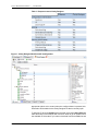
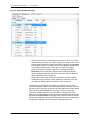
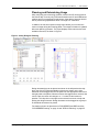
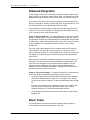
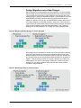
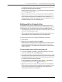
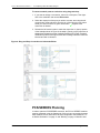
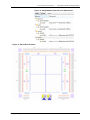
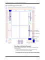
CLARITY DESIGNER USER MANUAL : Tool Overview Clarity Designer User Manual Tool Overview Improving design entry has been a goal for many generations of software tools. Early tools used only designer entered source and very small basic cell library blocks. Later tools expanded the area for pre-made or generated blocks. But these tools only provide single-block generation. As multiple complex blocks are used in devices, resource allocation problems often occur. These issues require blocks to be planned together and potentially can even require blocks to be generated with certain options to allow maximum utilization. To solve these problems tools that can provide capabilities beyond simple module generation are required. Clarity Designer Benefits and Features Clarity Designer is a tool within the Lattice Diamond software environment that addresses the need to be able to generate and plan multiple blocks together. Clarity Designer is used for configuration of blocks, building the connections between blocks, and planning the resources used by the PCS and DDR blocks in the design. For device families supported by Clarity Designer, IPexpress functionality is accomplished along with functionality for building and planning. The IPexpress tool is disabled when using a device family supported by Clarity Designer. Device families that are not supported yet by Clarity Designer still require the use of IPexpress. Clarity Designer is currently only available for the ECP5 device family. A comparison chart between IPexpress and Clarity Designer features is shown in Table 1. Configuration and Importing Clarity Designer produces design (.sbx) files that can be used in the design project like an HDL file or an IPexpress generated (.ipx) file. A key difference compared to IPexpress generated files is that Clarity Designer files can contain multiple modules or IP blocks, not just a single block and can represent a subsystem. With IPexpress, the process is to generate a module or IP. This is one step since an IPexpress file can only contain one module or IP. For Clarity Designer, the saving of a file is a separate step. Modules or IP are configured and then more modules or IP can optionally be added within the same file. Additionally, since building and planning can also be done, saving the file and generating the blocks needs to be done as a later step. Configuring modules is done by going to the Catalog tab, selecting the Lattice IP tab at the bottom of the window, and selecting a module or IP and then double-clicking. A separate dialog box will open that allows the Entering the Design 1 CLARITY DESIGNER USER MANUAL : Tool Overview Table 1: IPexpress versus Clarity Designer Figure 1: Clarity Designer Module and IP Configuration appropriate options to be set and, when the configure button is pressed, this information will be added to the Clarity Designer file that is currently open. To add new IP, when the Catalog tab is selected, select the Lattice IP Server tab at the bottom of the window, and click the IP folder to get an updated list of the available IP. Select the IP you want to download from the available list and 2 Entering the Design CLARITY DESIGNER USER MANUAL : Tool Overview click the Download or Install button. Once the IP is installed, it can be configured as explained above. If an existing project is being migrated to Clarity Designer from IPexpress, existing IPexpress files in the design must be imported and saved as Clarity Designer files. To import existing .ipx files, in the Catalog tab, select the Import IP tab at the bottom of the window. In the window you can now select the existing file and include the name of the converted module for use in Clarity Designer. After completing the necessary fields, press the Import button to complete the process. Each existing IPexpress file must be imported individually. A unique feature in Clarity Designer compared to IPexpress is the ability to use an RTL module within the design as a block within the Clarity Designer file. This is the same as instantiating a block within an HDL module. It is important to understand that RTL modules are imported into Clarity Designer are not automatically updated when the RTL is changed. The tool must be manually refreshed if the RTL is updated. To import an RTL module, the HDL source code must already be in the Diamond project and showing in the file list. Then from the Catalog tab, select the Diamond tab at the bottom of the window. This will show an elaborated view of the design hierarchy. Doubleclick the instance that should be imported. The imported module will be available in the Builder tab for connecting to the rest of the design. Building Once one or more modules or IP have been configured, then any connections between them or to the top of the subsystem (file) can be set. Each Clarity Designer file is the equivalent of a subsystem like an HDL module. Information in the file can be self-contained within the subsystem or connected to the top where it can connect to a higher level of the design hierarchy. The Builder function allows blocks to be connected to each other or to the top of the design file (equivalent to an HDL module description of the blocks and connections). The Builder tab provides two ways to approach this task. See Figure 2. In the Components view, there are columns showing the components used, connections, connection type, and a column named “Export.” The Export column is for connecting a signal to the top of the Clarity Design file. Checking this column for a signal means that signal connects to the top of the file so it can be used at a higher level in the hierarchy. By default the Export column is checked when a module is created in order to mimic the behavior with IPexpress for creating a file with a single module. The Export column should be unchecked for signals that are connections between modules. The Schematic view provides a schematic of the Clarity Designer module including a block for each module that you’ve added, external ports, and wires connecting them all. Ports can be connected to each other or to the top of the Clarity Designer module in one of two ways in the Schematic view: Entering the Design 3 CLARITY DESIGNER USER MANUAL : Tool Overview Figure 2: Clarity Designer Building Selecting them and then choosing from the right-click menu. To connect signals between modules, select the first signal, then Control-click on the second signal. Right-click on either signal name and then select Connect from the popup menu to complete the connection. Multiple signals can be connected by selecting them in this manner. To disconnect signal connections between modules, right-click on the signal and select Disconnect in the popup menu. Signals can be renamed by doubleclicking the signal name and typing in the new name. Refer to “Building with the Schematic View” on page 15. Using right-click and drag- and-drop functionality to connect available components, ports, and pins to other available components, ports, and pins. Refer to “Building with the Schematic View” on page 15. The primary use of the builder functionality is to improve ease of use for connecting multiple modules. To connect signals between modules, select the first signal, then Control-click on the second signal. Right-click on either signal name and then select Connect from the popup menu to complete the connection. Multiple signals can be connected by selecting them in this manner. To disconnect signal connections between modules, right-click on the signal and select Disconnect in the popup menu. Signals can be renamed in the Property and Design tabs by double-clicking the signal name and typing in the new name. Signals cannot be renamed in the Schematic View. 4 Entering the Design CLARITY DESIGNER USER MANUAL : Tool Overview Planning and Determining Usage After configuring and connecting modules, modules and IP can be placed in the Planner tab. Currently only PCS-based modules and IP, and DDR-based modules and IP are supported for placement. Other design elements should still be placed using Spreadsheet View or through LPF constraints. In addition, the real-time resource usage report allows you to monitor the resource usage during the Planning phase. The usage information is updated after each planning operation. The report displays used resources and total available resources, as shown in Figure 3. Figure 3: Clarity Designer Planning Design elements that can be placed are shown in the left panel and a chiplevel view of the FPGA and available resources are shown on the right. Elements can be dragged from the left panel onto the appropriate resource on the right panel to be placed. When an element is dragged onto a resource that can be used, the cursor will change to a “+” to show a valid solution is possible. The chip view on the right can be zoomed in and out to help with placing the design elements. Design elements can be dragged as a group or as individual elements to be placed. For details on how to do placement on PCS/SERDES and DDR modules, “PCS/SERDES Planning” on page 16 and “DDR I/O Planning” on page 22. Entering the Design 5 CLARITY DESIGNER USER MANUAL : Tool Overview Diamond Integration Clarity Designer outputs source files that are used in a Diamond project like other source file types such as VHDL, Verilog, EDIF, or IPexpress files. Clarity Designer files must be added to the file list in order to be used for a project. To be added to the file list, the file must be generated. This should be done after the configuration, building, and planning steps. To generate the file, click the Generate button in the Clarity Designer window toolbar. Currently Diamond projects support using Clarity Designer files either as a module for a level of hierarchy within a design project using HDL as the top level or as the top level of the design project. Usage 1—Used as a Module If a Clarity Designer file is used as a module within an existing design, it must be instantiated within an HDL file, similar to how IPexpress modules are instantiated within an existing HDL design. Within an HDL design, multiple Clarity Designer files can be used. However, within a Clarity Designer file, an instantiated module cannot be another Clarity Designer file. Currently, using Clarity Designer files as modules within an HDL design is recommended. This allows the current hierarchy of a design to be used without significant changes. If a Clarity Designer file is used as the top-level of the design, the design hierarchy must meet the requirements specified for top-level use. Note that when instantiating generated subsystems in an HDL module, it is important to use the instance template generated by Clarity Designer. Toplevel I/Os in the subsystem use port names based on instance and port names by default. Additionally, the instance needs an HDL attribute to indicate it is a Clarity Designer instantiation. Templates can be found in the directory in which the .sbx file was saved. Usage 2—Top-Level of Design If a Clarity Designer file is used as the toplevel of the design, the following requirements must be followed. All modules and IP must be directly instantiated within this file. Modules cannot be instantiated within an HDL file. For example, a PLL module must be in the top-level Clarity file. It cannot be instantiated within an HDL file. Any HDL in the design must be imported into the file as a module. HDL files can contain a hierarchy of other HDL modules, but no Clarity Designer modules or IP can be instantiated within the HDL. Clarity Designer files cannot be used as modules within another Clarity Designer file. Basic Tasks Tool usage falls into two primary methods: migrating existing designs in Clarity Designer and starting new designs in the tool. 6 Entering the Design CLARITY DESIGNER USER MANUAL : Tool Overview Design Migration versus New Designs When migrating an existing design into Clarity Designer, it is recommended that the design hierarchy should be unchanged and each existing IPexpress (.ipx) file should be imported into Clarity Designer and replaced with a new Clarity Designer (.sbx) file as illustrated in Figure 4. The exceptions to this are PCS/SERDES and DDR modules and IP. Since these should be placed together for efficient resource use, the PCS/SERDES modules need to be in one Clarity Designer file and DDR modules in another file. This means one module should be imported and then the existing Clarity Designer file should have the other modules copied and instantiated within it. See “Importing Existing PCS or DDR Modules or IP” on page 9 on steps needed for this. Figure 4: Migrating Existing Designs in Clarity Designer New designs can be optimized for efficient use in Clarity Designer. Modules that have a high amount of interconnection should be placed in the same Clarity Designer file. Modules at the same hierarchy level even though they are not interconnected can also be placed within the same file, as shown in Figure 5. This will reduce the effort to configure, generate, and save them independently. The goal for new designs should be to use the tools most efficiently for your design structure rather than follow the same method needed for using IPexpress. Figure 5: New Design Entry in Clarity Designer Entering the Design 7 CLARITY DESIGNER USER MANUAL : Tool Overview Getting Started To open Clarity Designer, launch the tool from either the Lattice Diamond toolbar or Tools menu. The project device must be set to a device from a supported family for the Clarity Designer tool to be available. The tool can also be launched by choosing File > New > File to create a new Clarity Designer file. Double-clicking an existing Clarity Designer file in the File List view will launch the tool. Only one Clarity Designer file can be open at a time. Once Clarity Designer is open, the following tasks can be done. Configure modules and IP from the Catalog tab. Download and install new IP from the Catalog tab. Import IPexpress (.ipx) files from an existing project and convert them into Clarity Designer format. Import HDL modules from the project for use as modules within Clarity Designer. Connect modules from the Builder tab. Place PCS/SERDES and DDR elements into FPGA resources from the Planner tab. For details on these tasks refer to “Accomplishing Tasks with Clarity Designer” on page 11. Importing Existing Modules and IP from an Existing Design Modules and IP that were generated with IPexpress and are in the project can be imported into Clarity Designer. They must be imported and configured, and the file generated and saved in the file list. Once the Clarity Designer (.sbx) file is saved in the file list, the existing IPexpress files must be deleted from the file list in order to successfully implement the design. The steps are shown below. To import an IPexpress module: 1. Open Clarity Design using the toolbar, Tools menu, or by creating a new file. 2. In Clarity Designer, click the Catalog tab. 3. Click the Import IP tab (at the bottom of the view). 4. Click Browse. 5. In the Open IPX File dialog box, browse to the .ipx or .lpc file of the module. Use the .ipx if it is available. 6. Click Open. Most of the Import IP view is filled in. 7. Type in a name for Target Instance. This is the name that will be used for the configured module in the Clarity Designer project. 8 Entering the Design CLARITY DESIGNER USER MANUAL : Tool Overview 8. In the Target area, choose a Core Version. Usually you will leave it with the latest version. 9. Click Import. The module’s dialog box opens. 10. In the dialog box, choose desired options. To get information about the options, click Help. Also, check the About tab in the Lattice IP view for links to technical notes and user guides. Downloaded IP may come with additional information. As the options change, the schematic diagram of the module changes to show the ports and the device resources the module needs. 11. Click Configure. 12. Click the Generate Log tab to check for warnings and error messages. 13. Click Close. 14. Click Generate in the Clarity Designer toolbar and import the Clarity Designer file into the File List view. 15. Delete the original IPexpress file from the File List view. The module or IP is now configured and is available in the Builder tab for connections. It is recommended that the Clarity Designer file be saved and the process repeated for each existing IPexpress file. This will allow the original design hierarchy to be reused without changes. However, if any of the modules or IP use PCS/SERDES or DDR resources, use the procedure below. Importing Existing PCS or DDR Modules or IP Modules and IP that were generated with IPexpress and are in the project can be imported into Clarity Designer. They must be imported and configured, the file generated and saved in the file list. Once the Clarity Designer (.sbx) file is saved in the file list, the existing IPexpress files must be deleted from the file list in order to successfully implement the design. The steps are shown below for when an existing module or IP uses PCS/SERDES or DDR resources. This procedure is different because PCS modules or DDR modules should be in the same Clarity Designer file to allow proper planning of the resources in the FPGA. To import a PCS or DDR module: 1. Open Clarity Design using the toolbar, Tools menu, or by creating a new file. 2. In Clarity Designer, click the Catalog tab. 3. Click the Import IP tab (at the bottom of the view). 4. Click Browse. 5. In the Open IPX File dialog box, browse to the .ipx or .lpc file of the module. Use the .ipx if it is available. 6. Click Open. Entering the Design 9 CLARITY DESIGNER USER MANUAL : Tool Overview Most of the Import IP view is filled in. 7. Type in a name for Target Instance. This is the name that will be used for the configured module in the Clarity Designer project. 8. In the Target area, choose a Core Version. Usually you will leave it with the latest version. 9. Click Import. The module’s dialog box opens. 10. In the dialog box, choose desired options. To get information about the options, click Help. Also, check the About tab in the Lattice IP view for links to technical notes and user guides. Downloaded IP may come with additional information. As the options change, the schematic diagram of the module changes to show the ports and the device resources the module needs. 11. Click Configure. 12. Click the Generate Log tab to check for warnings and error messages. 13. Click Close. 14. Repeat steps 2 - 13 for each existing module using the same resources (all PCS/SERDES modules should be in one Clarity Designer file and all DDR modules in another Clarity Designer file). 15. Click Generate in the Clarity Designer toolbar and import the Clarity Designer file into the File List view. 16. Delete the original IPexpress file from the File List view. The modules or IP are now configured and are available in the Builder tab for connections. They will also show in the Planner tab to allow those resources to be placed. Consolidating multiple modules within a single hierarchy level in a Clarity Designer file may require the original design hierarchy to be modified. This will vary for different designs on a case by case basis. Although this may cause design changes, there is a benefit to doing this. By putting the DDR modules, for example, in the same file these resources can now be planned together and feedback given on whether a valid placement is possible. Previously, constraints would need to be entered and if the solution was not valid, later implementation engine stages would generate errors. This new methodology is a faster and easier solution to placing resources within an FPGA and getting feedback if the solution is possible. Current Restrictions Clarity Designer contains several restrictions in this release. The list below lists the general usage restrictions. Restrictions within each module or IP are dependent upon the FPGA target and the use of that module or IP. Using Clarity Designer file as the top level of a design 10 All modules and IP must be directly instantiated within this file. Modules cannot be instantiated within an HDL file. Entering the Design CLARITY DESIGNER USER MANUAL : Accomplishing Tasks with Clarity Designer Any HDL in the design must be imported into the file as a module. HDL files can contain a hierarchy of other HDL modules, but no Clarity Designer modules or IP can be instantiated within the HDL. Clarity Designer files cannot be used as modules within another Clarity Designer file. Builder tab connections Cannot set HDL parameters of user modules. Cannot tie ports with constants. Cannot connect ports to logic equations. Implementation process No IPexpress (.ipx) files are allowed in the File List view. Clarity Designer (.sbx) files must be generated before they can be put into the File List view. Clarity Designer files must be in the File List view in order to correctly implement the design. Accomplishing Tasks with Clarity Designer IP or Module Generation IP or Module configuration is accomplished in the Catalog tab. Existing modules and installed IPs are listed in the Lattice IP sub-tab in the Catalog tab. Downloading Additional IP All available modules are installed with the Lattice Diamond software installation. Additional IP are downloaded from a Lattice IP site within the Clarity Designer tool. To add additional IP, the Lattice IP Server tab is used to download and install them. To download Lattice IP: 1. If you are working on Linux and this is the first IP you have ever installed, go to your home directory and, with a text editor, create an empty file named ipsetting_l.lst. Enter no text: the file must be empty and must have this name. If you find you already have a file with this name, do not change it. This is a text file listing your IP and their path names. 2. In Clarity Designer, click the Catalog tab. 3. Click the Lattice IP Server sub-tab, located at the bottom of the tool. 4. Click IP in the left pane. The software connects to the Lattice Semiconductor Web site. Entering the Design 11 CLARITY DESIGNER USER MANUAL : Accomplishing Tasks with Clarity Designer 5. Expand the folder tree and select the IP you want to download. Information about the IP appears in the right pane including links for additional information. 6. Do one of the following: To download and install the IP, right-click the IP and choose in the pop-up menu. To just download the IP for later installation, right-click the IP and choose Install Download in the pop-up menu. 7. Follow the on-screen instructions. Installing a Downloaded IP After downloading an IP, you must install it to make it available in Clarity Designer. Installing on Windows To install the IP: 1. If Clarity Designer is open, close it. 2. Go to the location where you saved the IP. 3. Double-click the executable file (.exe). The Lattice Semiconductor Setup program opens. 4. Follow the on-screen instructions. 5. Open Clarity Designer to see the installed IP. Click the Catalog tab and then the Lattice IP tab. Then expand the IP folder tree. Installing on Linux To install an IP that you downloaded earlier on Linux, the process depends on whether the download is a tar file (.tar.gz) or a shell file (.sh). To install the IP from a tar file: 1. If this is the first IP you have ever installed, go to your home directory and, with a text editor, create an empty file named ipsetting_l.lst. Enter no text: the file must be empty and must have this name. If you find you already have a file with this name, do not change it. This is a text file listing your IP and their path names. 2. Go to the location where you saved the IP. 3. Enter the following in a command line: tar -zxvf <filename>.tar.gz 4. In Clarity Designer, click the Import User Configurable IP button. 5. In the dialog box, browse to the installation directory for the IP and select nodeinfo.cfg. 6. Click Open. 12 Entering the Design CLARITY DESIGNER USER MANUAL : Accomplishing Tasks with Clarity Designer 7. To see the installed IP, click the Catalog tab and then the Lattice IP tab. Then expand the IP folder tree. To install the IP from a shell file: 1. Go to the location where you saved the IP. 2. Enter the following in a command line: sh <filename>.sh <Diamond install path>/bin/lin [<destination path>] The <destination path> is the full path name of where you want the IP to be installed. If not included, the IP will be installed in the current directory. The first time you install an IP, the installer creates a file, ipsetting_l.lst, in your home directory. This is a text file listing your IP and their path names. 3. To see the installed IP, click the Catalog tab and then the Lattice IP tab. Then expand the IP folder tree. Configuring Modules or IP To customize a module or IP with Clarity Designer, go to the Catalog tab. After the module or IP has been configured, it will be available in the Builder tab and, if it uses PCS/SERDES or DDR resources, the Planner tab. To configure a module or IP: 1. In the Catalog tab, double-click the IP that you want to configure. A dialog box opens with some general information about the IP. To get more information about the IP, see the About tab to the right in Clarity Designer. 2. In the dialog box, specify the Instance Name. Instance Name is the base name for the module’s files (that is, with no extension). 3. Choose from the Module Output menu. This is how the IP will be coded. 4. Click Customize. The IP’s dialog box opens. 5. In the dialog box, choose desired options. To get information about the options, click Help. Also, check the About tab in Clarity Designer for links to technical notes and user guides. Downloaded IP may come with additional information. As the options change, the schematic diagram of the module changes to show the ports and the device resources the IP needs. 6. Click Configure. 7. Click the Generate Log tab to check for warnings and error messages. 8. Click Close. The IP is added to the Builder tab and, if it uses PCS/SERDES or DDR resources, to the Planner tab. Entering the Design 13 CLARITY DESIGNER USER MANUAL : Accomplishing Tasks with Clarity Designer Building After configuring modules and IP, they need to be connected to each other and to the top of the Clarity Designer subsystem. The Builder tab provides two ways to approach this task: The Components view provides a spreadsheet listing all of the modules and their ports. The columns show how the ports are connected. The Schematic view provides a schematic drawing of the modules and their ports. You can drag the parts to see how they fit together. Click the tab at the bottom of the Builder view to select the mode that you want to start with. You can change mode anytime you want. Once building is complete, the subsystem can be planned or generated and saved if no planning is required. Once the subsystem has been generated, the design can be implemented with the design flow in the Lattice Diamond software. Building with the Components View The Components view lists all of the modules in the Clarity Designer project along with all of their ports. For each port there are three fields: Connection is the name of the connecting net that you will define in Builder. Type is how the port was connected: “un-connected” indicates the signal has not been connected yet. “fabric” indicates a user-defined connection. “internal” indicates a connection made in the Planner tab. “pad-pin” indicates a connection to the I/O of the FPGA. Export is checked when the signal is connected to the top of the subsystem. To connect a port to the top of the Clarity Designer subsystem: Select the check box in the Export column. The default name of the connecting net appears in the Connection column for the selected port. This will also be the name of the port in the Clarity Designer subsystem. The default name is based on the module and port names of the port. You can change the name by double-clicking it and typing over it. To connect module ports to each other: 1. If you want to change a connection, right-click one of the ports and choose Disconnect. 2. Select the ports that you want to connect together. You can select several input ports if they will all use the same source. There can be no more than 14 Entering the Design CLARITY DESIGNER USER MANUAL : Accomplishing Tasks with Clarity Designer one output port selected. There can be zero output ports selected if one of the input ports has its Export box selected. Output ports have yellow arrows blue arrows that point right. that point left. Input ports have dark 3. Right-click the name of one of the selected ports and choose Connect. The default name of the connecting net appears in the Connection column for each of the selected ports. The default net name is based on the module and port names of the output port. You can change the net name by double-clicking it in any row and typing over it. Building with the Schematic View The Schematic view provides a schematic of the Clarity Designer module including a block for each module that you’ve added, external ports, and wires connecting them all. The Schematic view also has two additional panes: The Design pane provides a nested list of all modules, their ports, and the ports of the Clarity Designer module. The Property pane provides information about the selected object (in the General tab) and a list of related wires (in the Connections tab). To connect a port to the top of the Clarity Designer subsystem: 1. Select the port. 2. Right-click in the schematic and choose Export. The default name of the connecting net appears in the Connections tab of the Property pane. This will also be the name of the port in the Clarity Designer subsystem. The default name is based on the module and port names of the port. To connect module ports to each other using right-click: 1. If you want to change a connection, select one of the ports. Then rightclick in the schematic and choose Disconnect. 2. Select the ports that you want to connect together. You can select several input ports if they will all use the same source. There can be no more than one output port selected. There can be zero output ports selected if one of the input ports has its Export box selected. In the Design pane, output ports have yellow arrows Input ports have dark blue arrows that point right. that point left. 3. Right-click the name of one of the selected ports and choose Connect. The default name of the connecting net appears in the Connection column for each of the selected ports. The default net name is based on the module and port names of the output port. Entering the Design 15 CLARITY DESIGNER USER MANUAL : Accomplishing Tasks with Clarity Designer To connect module ports to each other using drag-and-drop: 1. If you want to change a connection, select one of the ports. Then rightclick in the schematic and choose Disconnect. 2. Select the output pin of the port you wish to connect, and using the left mouse button, drag-and-drop it onto the pin of the input port you wish to which you wish to connect. A green check mark appears if the connection is allowed. 3. Release the left mouse button to make the connection. In the top portion of the example shown in Figure 6, the adder1_Result_Im[15] output bus is dragged and dropped onto the available DataA-Im[15:0] input of adder2. The bottom portion of the figure shows the resulting connection when the left mouse button is released. Figure 6: Drag and Drop Connections in Schematic Editor PCS/SERDES Planning In order to plan the PCS/SERDES resources, the PCS or SERDES modules must be generated using the Catalog tab. If there is any connectivity between these modules, these connections must be completed in the Builder tab. “IP or Module Generation” on page 11 and “Building” on page 14 describe how 16 Entering the Design CLARITY DESIGNER USER MANUAL : Accomplishing Tasks with Clarity Designer these tasks can be accomplished. Once the modules are generated, the placement of the PCS or SERDES modules can be planned in the Planner tab. PCS Configuration An example for creating the SERDES Eye Demo using ECP5 is shown in Figure 7. For this application both the Extref and PCS modules must be selected and configured from the Catalog tab. Figure 7: PCS Configuration Example Each module must be configured independently. Once both modules have been configured, they will appear in the Builder tab. They can then be connected to other modules in the subsystem or exported to the level above for connection in RTL code to the rest of the design. See “IP or Module Generation” on page 11 and “Building” on page 14 for details on module configuration and building. PCS Planning To place the generated PCS module and the Extref modules, they can be dragged and dropped from the Resource listing on the left side of the Planner tab to the resources in the chip view on the right. The PCS-related resources are shown in the bottom section of the chip view as show in Figure 8. By placing the PCS module and the Extref, Clarity Designer will incorporate the placement of PCS module and the Extref block to the location automatically without any additional constraints or editor preferences. Entering the Design 17 CLARITY DESIGNER USER MANUAL : Accomplishing Tasks with Clarity Designer Figure 8: PCS-Related Resources Once all PCS related resources are placed, then the DRC can be used to check that there are no DRC errors and use the generate button to complete the Clarify Designer subsystem and incorporate it into the Diamond project design flow. Using Multiple PCS Modules in a Single DCU To place multiple PCS channels in the same DCU, proper care must be taken to ensure that the two PCS blocks used in the design should be using the same external reference clock frequency and TXPLL settings for both the channels in the same DCU. For example, a PCI Express x1 at 2.5 Gbps and a Gigabit Ethernet channel can share the same DCU using the half-rate option on the Gigabit Ethernet channel. When a DCU shares a PCI Express x1 channel with a non-PCI Express channel, the reference clock for the DCU must be compatible with all protocols within the DCU. The placed DCU channels will be displayed as shown in Figure 10. 18 Entering the Design CLARITY DESIGNER USER MANUAL : Accomplishing Tasks with Clarity Designer Figure 9: Using Multiple PCS Modules in a Single DCU Figure 10: Placed DCU Channels Entering the Design 19 CLARITY DESIGNER USER MANUAL : Accomplishing Tasks with Clarity Designer DCU Settings In order to choose the TX and RX settings for the DCU, double-click the placed channel of the DCU and choose the input clock to the TXPLL inside and the reference clock for the RX side of the DCU as shown below: Figure 11: Setting DCU Clocks If there are multiple protocols that use the same reference clock or one protocol with a single reference clock frequency, choose the input to the TX and RX input clocks (TXPLL and RX setting clock) on the DCU. Either the Primary Clock input from the FPGA logic or a clock input from Extref components of DCU0 can be used. Multiple Protocols on the Same Device If multiple protocols have to be supported using a single ECP5 device that has different reference clocks, then the same DCU cannot be supported. A different DCU has to be implemented with its own external reference clock and Tx PLL settings with a PCS block to support multiple protocols as shown in Figure 12. The placed DCU channels will be displayed as shown in Figure 13. DCU Settings with Multiple Protocols In order to choose the TX and RX settings for the DCU, double-click the placed channel of the DCU and choose the input clock to the TXPLL inside and the reference clock for the RX side of the DCU as shown in Figure 14 on page 22. If there are multiple protocols, choose the input to the TX and RX input clocks (TXPLL and RX setting clock) on the second DCU. Use either the Primary Clock input from the FPGA logic or inputs from the Extref components of DCU0 or DCU1. 20 Entering the Design CLARITY DESIGNER USER MANUAL : Accomplishing Tasks with Clarity Designer Figure 12: Using Multiple Protocols in the Same Device Figure 13: Placed DCU Channels Entering the Design 21 CLARITY DESIGNER USER MANUAL : Accomplishing Tasks with Clarity Designer Figure 14: Setting DCU Clocks DDR I/O Planning In order to plan the DDR I/Os, the DDR modules must be generated using the Catalog tab. If there is any connectivity between these modules, these connections must be completed in the Builder tab. “IP or Module Generation” on page 11 and “Building” on page 14 describe how these tasks can be accomplished. Once the modules are generated, you can plan the placement of the DDR modules in the Planner tab. Planner View for DDR Modules Once DDR modules are generated, they are listed in the Planner. The resources required by each of the DDR modules are listed next to the module name. This includes the number of I/O required, number of PLLs used, and number of DLLs used by that module. Each DDR module, when expanded, will show the clock groups under that module. The ports and primitives in each of the DDR modules is grouped based on the clocking requirement. All ports and elements clocked by the same clock are listed in a given clock group. This clock group could be a high speed “ECLK” (edge clock) group for interfaces that use a gearbox (x2 or x4) or a slower speed “SCLK” (primary clock) group for interfaces that do not use a gearbox (x1). Each clock group will include: Port list Primitive list ECLK and ECLKBRIDGE resources (if used by that module) Once a port is placed, the Placement column shows pin numbers next to each of the ports and the ECLK resources shows the ECLK that was used for that interface. 22 Entering the Design CLARITY DESIGNER USER MANUAL : Accomplishing Tasks with Clarity Designer The figure below shows how an interface will look when listed in the Planner tab. This interface is used for an example to show the clock grouping and port list. This Interface has two ECLK groups. Each group lists the ports clocked by that ECLK, the primitives that are clocked by that clock, and the ECLK resources. Note that in this release, the ECLK resource section lists all the ECLKs and ECLKBRIDGEs available on the device even though only one ECLK is used in the clock group. Once the interface is assigned it will only show placement information for the ECLK that is used by that interface. Figure 15: DDR Modules in the Planner View Entering the Design 23 CLARITY DESIGNER USER MANUAL : Accomplishing Tasks with Clarity Designer Reconfiguration of an Interface An interface can be reconfigured by right-clicking and selecting Config. This will allow you to change the interface parameters by opening the dialog box for that module. Placing a DDR Interface The following steps should be used to place any of the generated DDR interfaces. 1. Select the clock group under a given interface and then drag and drop onto the chip view. A valid location is indicated by a “+” symbol. Once the location is selected, the interface pins will be placed in a counterclockwise direction. The following also happens: The pins used are displayed in the chip view. The corresponding IOLOGIC cell will be highlighted. If the group is an ECLK group, the ECLK tree used will be displayed. The left pane will also display the locations of the Ports, ECLKs, and Primitives. 2. Drag and drop of a clock group will only place the data pins of that interface. The clock input pins in that interface will have to be placed manually. Expand the clock group and select the clock input pin. Drag it onto the dedicated clock pin. Right-click in the chip view to get the option to filter out all the dedicated clock pins. The following happens: Once the clock pin is placed, the PLL, DLL, CLKDIV, and ECLKBRIDGE used by the DDR module will be displayed in the chip view. The left pane will also display the locations of these modules. If an interface cannot be placed in the location when the ports are dropped due to architectural limitations, all the data ports will be placed in the next available location. If it is a clock input port, Planner will not place the port and will issue a DRC message in the Output view. DDR Interface Planning Guidelines Here are some general rules to follow when placing DDR modules. Refer to the “High Speed Interface” technical note for the device for details on placement of each type of DDR interface using Clarity. 24 On DDR interfaces, the data ports have to be placed before placing the clock input ports. Once the data ports are placed, manually drag and drop the CLKIN port to the desired location. The PLL, DLL, and CLKDIV used with the clock are not placed until the input CLK port is placed. This also applies to REFCLK input ports of PLL modules when generated with the DDR modules. Entering the Design CLARITY DESIGNER USER MANUAL : Accomplishing Tasks with Clarity Designer On drag-and-drop of any interface, only data pins are placed. You have to manually place the clock input to any of the GDDRX interfaces as explained in “Placing a DDR Interface” on page 24. When placing the data ports, Planner does not use the dedicated clock sites on the device. These are reserved for the clock inputs. You must try to place all the data and clock ports of a given interface on one side. If there is a requirement to go around the corner to the other side, Planner uses the ECLKBRIDGE if it is available on that device. You must enable the ECLKBRIDGE when configuring the IP. Refer to the “High Speed I/O Interfaces” technical note for the device for details on how to use Planner to plan an interface with an ECLKBRIDGE. There are only a limited number of high speed clock (PLL, DLL, and ECLK) and I/O logic elements on each device. Planner does not allow interfaces to be placed if it runs out of resources. Planner always places the pins in a counterclockwise direction. You must drag and drop interfaces at the optimum location so that pins are not lost during planning. For example, if you require that all pins be placed in a single bank, the interface should be dropped at the first valid location of that bank counting counterclockwise so pins do not overflow to the next bank. Similarly, if all pins need to be on the same side, you must drag and drop at the first valid pin of the side. If you drag it into the edge of the side, the ports will automatically overflow to the other side, which forces Planner to use an ECLKBRIDGE when it is not required. When placing a GDDRX or DDR_MEM module that requires a PLL module, you can either choose to generate a PLL with the interface module or use a stand-alone module. If you choose to generate a PLL with the DDR interface, you must also choose the input buffer standard for the CLKI input of the PLL. This is required for Planner to correctly place the PLL. This will apply for GDDR.TX “centered” and DDR Memory modules. If planning the DDR Memory IP Cores, refer to the IP Core user manual for guidelines on placement of each IP module. The chip view after placement of interfaces is shown in Figure 16. This figure highlights some of the DDR resources that get used for an interface. For more details on the DDR resources, refer to the “High Speed I/O Interface” technical note for the device. Viewing Interface Placement Once an interface has been placed, you can view the placement by: Entering the Design Clicking on the port in the left pane to locate it in the chip view. The location of this port is highlighted in the chip view. Clicking on the placed pin in the chip view, which will highlight the port in the left pane. 25 CLARITY DESIGNER USER MANUAL : Accomplishing Tasks with Clarity Designer Figure 16: DDR Resources in the Planner View Resetting or Modifying Placement Once the interface has been placed, it can be reset or modified using the following methods: 26 If the entire interface placement has to be reset, right-click on the Interface name in the left pane and choose Reset. If the assignments for one of the clock groups under the interface have to be reset, right-click on the clock group in the left pane and choose Reset. Entering the Design CLARITY DESIGNER USER MANUAL : Accomplishing Tasks with Clarity Designer If placement for a signal port has to be modified, choose the port in the left pane and drag and drop it to its new location. Note that in the this release, you cannot reset placement of an individual port. Clarity also does not support multiple select on ports. The workaround is to modify placement of each port or modify placement of the entire clock group. Filtering Pin Types You can get to the filter by either right-clicking on the chip view or on the toolbar. Planner allows filtering of dedicated PCLK pins, PLL/DLL clock pins, True LVDS pins, VREF pins, and so on. These will vary for each device. Refer to the “High Speed Interface” technical note for the device to see the options available. Design Rule Check Once all the interfaces are placed, you can click the list of warning and error messages. DRC in the toolbar to see Current Restrictions Entering the Design Planner does not see the signal connectivity in Builder. The workaround is to export the ports to the SBX file and make the connectivity outside of the SBX module. So any clock sharing between different DDR modules has to be external to the SBX. Stand-alone PLL are not available in Planner for placement or connection. Any connections to stand-alone PLL have to be done externally to the SBX. 27 CLARITY DESIGNER USER MANUAL 28 : Accomplishing Tasks with Clarity Designer Entering the Design