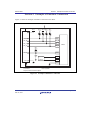
1
User’s Manual
E8a Emulator
Additional Document for User's Manual
Notes on Connecting the H8/300H Super Low Power Series
R0E00008AKCE00EP63
Supported Devices:
H8 Family / H8/300H Super Low Power Series
H8/38076RF, H8/38086RF, H8/38776F, H8/38602RF, H8/38606F,
H8/38099F, H8/38799F, H8/38524F, H8/38537F, and H8/38704F
All information contained in these materials, including products and product specifications,
represents information on the product at the time of publication and is subject to change by
Renesas Electronics Corporation without notice. Please review the latest information published
by Renesas Electronics Corporation through various means, including the Renesas Electronics
Corporation website (http://www.renesas.com).
www.renesas.com
Rev. 3.00
Mar. 2012
Notice
1.
2.
3.
4.
5.
6.
7.
All information included in this document is current as of the date this document is issued. Such information, however, is
subject to change without any prior notice. Before purchasing or using any Renesas Electronics products listed herein, please
confirm the latest product information with a Renesas Electronics sales office. Also, please pay regular and careful attention to
additional and different information to be disclosed by Renesas Electronics such as that disclosed through our website.
Renesas Electronics does not assume any liability for infringement of patents, copyrights, or other intellectual property rights
of third parties by or arising from the use of Renesas Electronics products or technical information described in this document.
No license, express, implied or otherwise, is granted hereby under any patents, copyrights or other intellectual property rights
of Renesas Electronics or others.
You should not alter, modify, copy, or otherwise misappropriate any Renesas Electronics product, whether in whole or in part.
Descriptions of circuits, software and other related information in this document are provided only to illustrate the operation of
semiconductor products and application examples. You are fully responsible for the incorporation of these circuits, software,
and information in the design of your equipment. Renesas Electronics assumes no responsibility for any losses incurred by
you or third parties arising from the use of these circuits, software, or information.
When exporting the products or technology described in this document, you should comply with the applicable export control
laws and regulations and follow the procedures required by such laws and regulations. You should not use Renesas
Electronics products or the technology described in this document for any purpose relating to military applications or use by
the military, including but not limited to the development of weapons of mass destruction. Renesas Electronics products and
technology may not be used for or incorporated into any products or systems whose manufacture, use, or sale is prohibited
under any applicable domestic or foreign laws or regulations.
Renesas Electronics has used reasonable care in preparing the information included in this document, but Renesas Electronics
does not warrant that such information is error free. Renesas Electronics assumes no liability whatsoever for any damages
incurred by you resulting from errors in or omissions from the information included herein.
Renesas Electronics products are classified according to the following three quality grades: “Standard”, “High Quality”, and
“Specific”. The recommended applications for each Renesas Electronics product depends on the product’s quality grade, as
indicated below. You must check the quality grade of each Renesas Electronics product before using it in a particular
application. You may not use any Renesas Electronics product for any application categorized as “Specific” without the prior
written consent of Renesas Electronics. Further, you may not use any Renesas Electronics product for any application for
which it is not intended without the prior written consent of Renesas Electronics. Renesas Electronics shall not be in any way
liable for any damages or losses incurred by you or third parties arising from the use of any Renesas Electronics product for an
application categorized as “Specific” or for which the product is not intended where you have failed to obtain the prior written
consent of Renesas Electronics. The quality grade of each Renesas Electronics product is “Standard” unless otherwise
expressly specified in a Renesas Electronics data sheets or data books, etc.
“Standard”:
Computers; office equipment; communications equipment; test and measurement equipment; audio and visual
equipment; home electronic appliances; machine tools; personal electronic equipment; and industrial robots.
“High Quality”: Transportation equipment (automobiles, trains, ships, etc.); traffic control systems; anti-disaster systems; anticrime systems; safety equipment; and medical equipment not specifically designed for life support.
“Specific”:
Aircraft; aerospace equipment; submersible repeaters; nuclear reactor control systems; medical equipment or
systems for life support (e.g. artificial life support devices or systems), surgical implantations, or healthcare
intervention (e.g. excision, etc.), and any other applications or purposes that pose a direct threat to human life.
8.
You should use the Renesas Electronics products described in this document within the range specified by Renesas Electronics,
especially with respect to the maximum rating, operating supply voltage range, movement power voltage range, heat radiation
characteristics, installation and other product characteristics. Renesas Electronics shall have no liability for malfunctions or
damages arising out of the use of Renesas Electronics products beyond such specified ranges.
9.
Although Renesas Electronics endeavors to improve the quality and reliability of its products, semiconductor products have
specific characteristics such as the occurrence of failure at a certain rate and malfunctions under certain use conditions. Further,
Renesas Electronics products are not subject to radiation resistance design. Please be sure to implement safety measures to
guard them against the possibility of physical injury, and injury or damage caused by fire in the event of the failure of a
Renesas Electronics product, such as safety design for hardware and software including but not limited to redundancy, fire
control and malfunction prevention, appropriate treatment for aging degradation or any other appropriate measures. Because
the evaluation of microcomputer software alone is very difficult, please evaluate the safety of the final products or system
manufactured by you.
10. Please contact a Renesas Electronics sales office for details as to environmental matters such as the environmental
compatibility of each Renesas Electronics product. Please use Renesas Electronics products in compliance with all applicable
laws and regulations that regulate the inclusion or use of controlled substances, including without limitation, the EU RoHS
Directive. Renesas Electronics assumes no liability for damages or losses occurring as a result of your noncompliance with
applicable laws and regulations.
11. This document may not be reproduced or duplicated, in any form, in whole or in part, without prior written consent of Renesas
Electronics.
12. Please contact a Renesas Electronics sales office if you have any questions regarding the information contained in this
document or Renesas Electronics products, or if you have any other inquiries.
(Note 1) “Renesas Electronics” as used in this document means Renesas Electronics Corporation and also includes its majorityowned subsidiaries.
(Note 2) “Renesas Electronics product(s)” means any product developed or manufactured by or for Renesas Electronics.
Regulatory Compliance Notices
European Union regulatory notices
This product complies with the following EU Directives. (These directives are only valid in the European Union.)
CE Certifications:
• Electromagnetic Compatibility (EMC) Directive 2004/108/EC
EN 55022 Class A
WARNING: This is a Class A product. In a domestic environment this product may
cause radio interference in which case the user may be required to take adequate
measures.
EN 55024
• Information for traceability
• Authorised representative
Name:
Renesas Electronics Corporation
Address:
1753, Shimonumabe, Nakahara-ku, Kawasaki, Kanagawa, 211-8668, Japan
• Manufacturer
Name:
Renesas Solutions Corp.
Address:
Nippon Bldg., 2-6-2, Ote-machi, Chiyoda-ku, Tokyo 100-0004, Japan
• Person responsible for placing on the market
Name:
Renesas Electronics Europe Limited
Address:
Dukes Meadow, Millboard Road, Bourne End, Buckinghamshire, SL8 5FH, U.K.
Environmental Compliance and Certifications:
• Waste Electrical and Electronic Equipment (WEEE) Directive 2002/96/EC
WEEE Marking Notice (European Union Only)
Renesas development tools and products are directly covered by the European Union's Waste
Electrical and Electronic Equipment, (WEEE), Directive 2002/96/EC. As a result, this equipment,
including all accessories, must not be disposed of as household waste but through your locally
recognized recycling or disposal schemes. As part of our commitment to environmental
responsibility Renesas also offers to take back the equipment and has implemented a Tools Product
Recycling Program for customers in Europe. This allows you to return equipment to Renesas for
disposal through our approved Producer Compliance Scheme. To register for the program, click
here “http://www.renesas.com/weee".
United States Regulatory notices on Electromagnetic compatibility
FCC Certifications (United States Only):
This equipment has been tested and found to comply with the limits for a Class A digital device, pursuant to Part
15 of the FCC Rules. These limits are designed to provide reasonable protection against harmful interference
when the equipment is operated in a commercial environment. This equipment generates, uses, and can radiate
radio frequency energy and, if not installed and used in accordance with the instruction manual, may cause
harmful interference to radio communications. Operation of this equipment in a residential area is likely to cause
harmful interference in which case the user will be required to correct the interference at his own expense.
CAUTION:
Changes or modifications not expressly approved by the party responsible for
compliance could void the user's authority to operate the equipment.
Table of Contents
Notes on Connecting the H8/38076RF, H8/38086RF, and H8/38776F ................................................ 1
Section 1
Inside the E8a Emulator User’s Manual ........................................................................... 3
Section 2
Connecting the Emulator with the User System ............................................................... 5
Section 3
Pin Assignments of the E8a Connector ............................................................................ 7
Section 4
Example of Emulator Connection.....................................................................................9
Section 5
Differences between the MCUs (H8/38076RF, H8/38086RF, and H8/38776F)
and the Emulator .............................................................................................................. 15
Notes on Connecting the H8/38602RF and H8/38606F ........................................................................ 1
Section 1
Inside the E8a Emulator User’s Manual ........................................................................... 3
Section 2
Connecting the Emulator with the User System ............................................................... 5
Section 3
Pin Assignments of the E8a Connector ............................................................................ 7
Section 4
Example of Emulator Connection.....................................................................................9
Section 5
Differences between the MCUs (H8/38602RF and H8/38606F) and the Emulator ....... 15
Notes on Connecting the H8/38099F and H8/38799F........................................................................... 1
Section 1
Inside the E8a Emulator User’s Manual ........................................................................... 3
Section 2
Connecting the Emulator with the User System ............................................................... 5
Section 3
Pin Assignments of the E8a Connector ............................................................................ 7
Section 4
Example of Emulator Connection.....................................................................................9
Section 5
Differences between the MCUs (H8/38099F and H8/38799F) and the Emulator.......... 15
Notes on Connecting the H8/38524F..................................................................................................... 1
Section 1
Inside the E8a Emulator User’s Manual ........................................................................... 3
Section 2
Connecting the Emulator with the User System ............................................................... 5
Section 3
Pin Assignments of the E8a Connector ............................................................................ 7
Section 4
Example of Emulator Connection.....................................................................................9
Section 5
Differences between the MCU (H8/38524F) and the Emulator ..................................... 15
Notes on Connecting the H8/38537F..................................................................................................... 1
Section 1
Inside the E8a Emulator User’s Manual ........................................................................... 3
Section 2
Connecting the Emulator with the User System ............................................................... 5
Section 3
Pin Assignments of the E8a Connector ............................................................................ 7
Section 4
Example of Emulator Connection.....................................................................................9
Section 5
Differences between the MCU (H8/38537F) and the Emulator ..................................... 13
Notes on Connecting the H8/38704F..................................................................................................... 1
Section 1
Inside the E8a Emulator User’s Manual ........................................................................... 3
Section 2
Connecting the Emulator with the User System ............................................................... 5
Section 3
Pin Assignments of the E8a Connector ............................................................................ 7
Section 4
Example of Emulator Connection.....................................................................................9
Section 5
Differences between the MCU (H8/38704F) and the Emulator ..................................... 13
Note: This manual applies to the following product versions of the E8a emulator software.
Table
E8a Emulator Software
E8a Emulator V.1.05 Release 00 or later
(H8 Tiny/Super Low Power E8a Emulator V.1.03.00 or later)*
Note: This is a revision of the debugger.
E8a Emulator
Notes on Connecting the H8/38076RF, H8/38086RF, and H8/38776F
Notes on Connecting the H8/38076RF, H8/38086RF, and H8/38776F
R20UT0637EJ0300 Rev.3.00
Mar 14, 2012
Page 1 of 26
E8a Emulator
R20UT0637EJ0300 Rev.3.00
Mar 14, 2012
Notes on Connecting the H8/38076RF, H8/38086RF, and H8/38776F
Page 2 of 26
E8a Emulator
Section 1 Inside the E8a Emulator User’s Manual
Section 1 Inside the E8a Emulator User’s Manual
The E8a emulator (hereafter referred to as E8a in this document) manual consists of two
documents: the E8a User’s Manual and the E8a Additional Document for User’s Manual (this
document). Be sure to read BOTH documents before using the E8a emulator.
(1) E8a Emulator User’s Manual
The E8a Emulator User’s Manual describes the hardware specifications and how to use the
emulator debugger.
⎯ E8a emulator hardware specifications
⎯ Connecting the E8a emulator to the host computer or user system
⎯ Operating the E8a emulator debugger
⎯ Tutorial: From starting up the E8a emulator debugger to debugging
(2) E8a Additional Document for User’s Manual
The E8a Additional Document for User’s Manual describes content dependent on the MCUs
and precautionary notes.
⎯ Example of the E8a emulator connection or interface circuit necessary for designing the
hardware
⎯ Notes on using the E8a emulator
⎯ Setting the E8a emulator debugger during startup
R20UT0637EJ0300 Rev.3.00
Mar 14, 2012
Page 3 of 26
E8a Emulator
R20UT0637EJ0300 Rev.3.00
Mar 14, 2012
Section 1 Inside the E8a Emulator User’s Manual
Page 4 of 26
E8a Emulator
Section 2 Connecting the Emulator with the User System
Section 2 Connecting the Emulator with the User System
Before connecting an E8a emulator (hereafter referred to as emulator) with the user system, a
connector must be installed in the user system so that a user system interface cable can be
connected. When designing the user system, refer to the connector and recommended circuits
shown in this manual.
Before designing the user system, be sure to read the E8a emulator user’s manual and the
hardware manual for related MCUs.
Table 2.1 shows the recommended connector for the emulator.
Table 2.1 Recommended Connector
Type Number
Manufacturer
Specifications
2514-6002
3M Limited
14-pin straight type
Connect pins 2, 4, 6, 10, 12, and 14 of the user system connector to GND firmly on the PCB.
These pins are used as electrical GND and to monitor the connection of the user system
connector. Note the pin assignments of the user system connector.
User system interface cable
User system connector
User system
Pin 2
Pin 1
Figure 2.1 Connecting the User System Interface Cable to the User System
R20UT0637EJ0300 Rev.3.00
Mar 14, 2012
Page 5 of 26
E8a Emulator
Notes:
Section 2 Connecting the Emulator with the User System
1.
The pin number assignments of the 14-pin connector differ from those of the
E10A-USB emulator; however, the physical location is the same.
2.
Do not place any components within 3 mm of the connector.
3.
When the emulator is used in the [Program Flash] mode, connect the emulator
similarly to the user system.
R20UT0637EJ0300 Rev.3.00
Mar 14, 2012
Page 6 of 26
E8a Emulator
Section 3 Pin Assignments of the E8a Connector
Section 3 Pin Assignments of the E8a Connector
Figure 3.1 shows the pin assignments of the connector.
Pin 1 mark
Connector
Pin 14
Pin 13
Pin 2
Pin 1
Top view
Pin 1 mark
Pin No.
MCU Signal
1
P16
2
Vss
3
N.C. *2
4
Vss
5
P37
6
Vss
7
NMI# *1
8
Vcc
9
N.C. *2
10
Vss
11
P36
12
Vss
13
RES# *1
14
Vss
Notes:
1. The symbol (#) means that the signal is active-low.
2. These pins are not used in the H8/300H Super Low Power series.
Do not connect anything to these pins.
Figure 3.1 Pin Assignments of the Connector
R20UT0637EJ0300 Rev.3.00
Mar 14, 2012
Page 7 of 26
E8a Emulator
R20UT0637EJ0300 Rev.3.00
Mar 14, 2012
Section 3 Pin Assignments of the E8a Connector
Page 8 of 26
E8a Emulator
Section 4 Example of Emulator Connection
Section 4 Example of Emulator Connection
Figure 4.1 shows an example of emulator connection to the MCU.
Pulled-up at 4.7 kΩ or more
Vcc
Vcc Vcc Vcc Vcc
Vcc
NMI#
NMI#
P16
P16
P36
P36
MCU
P37
P37
Vcc
RES#
RES#
TEST
Vss
User system
Connector
14 pins with a 2.54-mm pitch
Figure 4.1 Example of Emulator Connection
R20UT0637EJ0300 Rev.3.00
Mar 14, 2012
Page 9 of 26
E8a Emulator
Section 4 Example of Emulator Connection
Notes: 1. P16, P36, and P37 pins are used by the emulator. Pull up and connect the emulator
and MCU pins.
MCU
User system
connector
Vcc
4.7 kΩ
Pins 1, 5, and 11
P16, P36, and P37
Figure 4.2 Connection of Emulator and P16, P36, and P37 Pins
2.
The NMI# signal is used for forced break control by the emulator. Connect the
emulator and MCU pins directly. In debugging without forced break control, change
the mode with the High-performance Embedded Workshop. Then, when the user
logic is connected with the open-collector output buffer, the NMI# pin can be used in
the user system (however, at power-on, the NMI# pin is used by the emulator).
When connected directly:
MCU
User system
connector
Vcc
4.7 kΩ
NMI# pin
Pin 7
When the NMI# pin is used (forced break cannot be used):
MCU
Vcc
User system
connector
User logic
*
4.7 kΩ
NMI# pin
Pin 7
*Open-collector
output buffer
Figure 4.3 Connection of Emulator and NMI# Pin
R20UT0637EJ0300 Rev.3.00
Mar 14, 2012
Page 10 of 26
E8a Emulator
3.
Section 4 Example of Emulator Connection
The RES# pin is used by the emulator. Create the following circuit so that reset input
can be accepted from the emulator.
User system
connector
Vcc
MCU
Pin 13
RES# pin
*
Note: For the recommended capacitance of the capacitor that is connected to the RES# pin,
refer to the hardware manual.
Figure 4.4 Example of a Reset Circuit
4.
Connect Vss and Vcc with the Vss and Vcc of the MCU, respectively (within the
guaranteed range of the microcomputer).
When the power-supply mode is used, the power is supplied to the user system. Check
that the power consumption or voltage of the user system is within the available range
of E8a and avoid a problem such as closing of the power-supply circuit.
5.
Connect nothing with N.C.
6.
When the emulator is connected to the user system, ground the TEST pin of the MCU.
MCU
TEST
Figure 4.5 Emulator and the TEST Pin
Note: When the emulator is connected, ADTRG#, which is also used as the TEST pin, cannot be
used.
R20UT0637EJ0300 Rev.3.00
Mar 14, 2012
Page 11 of 26
E8a Emulator
Section 4 Example of Emulator Connection
WARNING
In the power-supply mode, connect the emulator after
checking that the power-supply circuit on the user system is
not closed or the pin number assignments of the user system
connector is correct.
Failure to do so will result in a FIRE HAZARD and will
damage the host computer, the emulator, and the user
system.
7.
When the MCU in use is connected to the emulator, the pin functions listed below are
not available.
Table 4.1 Pin Functions Not Available
H8/38076RF, H8/38086RF, and H8/38776F
P16, P36, and P37
NMI# (normal)
ADTRG#
8.
Figure 4.6 shows the interface circuit in the E8a emulators. Use this figure as a
reference when determining the pull-up resistance value.
R20UT0637EJ0300 Rev.3.00
Mar 14, 2012
Page 12 of 26
E8a Emulator
Section 4 Example of Emulator Connection
User system connector
Power-supply circuit
(only used for the power-supply
mode)
Vcc
100 kΩ
x3
Emulator control circuit
1 MΩ
8
100 kΩ
22 Ω
P16
1
74LVC125B
22 Ω
P36
11
74LVC125B
22 Ω
NMI#
7
74LVC125B
Vcc
3.3 V
SN74LVC2T45
Vcc
3.3 V
22 Ω
P37
5
SN74LVC2T45
3.3 V
Vcc
22 Ω
RES#
13
SN74LVC2T45
3.3 V
10 kΩ
2CS2462
10 kΩ
Notes: 1. This figure omits the test circuits and pin numbers 3, 4, 9, and 14 for the user connector that are not used
when H8/Tiny series is connected.
2. The power of 74LVC125B is supplied from Vcc in the user connector (or in the power-supply circuit during
power-supply mode).
Figure 4.6 Interface Circuit in the E8a Emulator (Reference)
R20UT0637EJ0300 Rev.3.00
Mar 14, 2012
Page 13 of 26
E8a Emulator
R20UT0637EJ0300 Rev.3.00
Mar 14, 2012
Section 4 Example of Emulator Connection
Page 14 of 26
Section 5 Differences between the MCUs (H8/38076RF,
H8/38086RF, and H8/38776F) and the Emulator
E8a Emulator
Section 5 Differences between the MCUs (H8/38076RF,
H8/38086RF, and H8/38776F) and the Emulator
This section describes the differences between the emulator and MCU operations.
1. [Emulator Setting] Dialog Box
The [Emulator Setting] dialog box is provided for setting the items that need to be set when
the emulator starts up (settings are saved in the session).
Figure 5.1 [Emulator Setting] Dialog Box
R20UT0637EJ0300 Rev.3.00
Mar 14, 2012
Page 15 of 26
E8a Emulator
Section 5 Differences between the MCUs (H8/38076RF,
H8/38086RF, and H8/38776F) and the Emulator
To keep the [Emulator Setting] dialog box closed next time the emulator is started, check "Do
not show this dialog box again." at the bottom of the [Emulator Setting] dialog box. You can
open the [Emulator Setting] dialog box using either one of the following methods:
⎯ After the emulator gets started, select Menu - [Setup] -> [Emulator] -> [Emulator
Setting...].
⎯ Start the emulator while holding down the Ctrl key.
⎯ After the emulator gets started and an error occurred, restart the emulator.
When you check "Do not show this dialog box again.", the emulator doesn't supply power to
the user system. To use this check box, start the emulator after turning on the power.
2. Emulator Mode
The selection of the device, the specification of the mode, and the setting of the power supply
are done in the [Emulator mode] page of the [Emulator Setting] dialog box.
⎯ Device
Select the device name in use from the [Device] combo box. The following items are
selected in the [Mode] group box.
⎯ Modes
• Erase Flash and Connect
This mode is used when there is no emulator program in the flash memory of the target
device. In this mode, data of the flash memory of the target device is erased when the
emulator is activated. Select this item when the emulator is firstly activated, the version
of the emulator’s software is updated, or the ID code is changed.
• Keep Flash and Connect
This mode is used when there is an emulator program in the flash memory of the target
device. Enter the ID code specified above (‘Erase Flash and Connect’). If an incorrect
code is entered, all the programs on the flash memory will be erased.
Note: When the emulator gets started in this mode after selecting "Do not show this dialog box
again.", the initial values of the ID code is ‘0E8a’ for the E8a emulator. If you use the ID
code other than the initial value, do not use "Do not show this dialog box again.".
R20UT0637EJ0300 Rev.3.00
Mar 14, 2012
Page 16 of 26
Section 5 Differences between the MCUs (H8/38076RF,
H8/38086RF, and H8/38776F) and the Emulator
E8a Emulator
• Program Flash
This mode is used when the emulator is used for programming the flash memory.
Debugging the program is disabled. To download the load module, register it in the
workspace.
Note: In the H8/Tiny or H8/Super Low Power device, the ID code is not entered in the Program
Flash mode.
⎯ Power Supply
When [Power Target from emulator. (MAX 300mA)] is checked, power will be supplied to
the user system up to 300 mA. Then select 3.3 V or 5.0 V according to the power voltage
of the user system.
3. Emulator Activation and ID Code
In the H8/Tiny- or H8/Super Low Power-series MCU, the [System Clock] and [ID Code]
dialog boxes are set when the emulator is activated.
⎯ Setting the system clock
Enter the clock value input to the board in use. The initial value differs in each MCU.
Figure 5.2 [System Clock] Dialog Box
⎯ Setting the ID code
When the emulator is activated in the [Erase Flash and Connect] mode, enter any
hexadecimal four-digit ID code to be set (except for H'FFFF). The initial value is H’0E8A.
When the emulator is activated in the [Keep Flash and Connect] mode, enter the correct ID
code. If an incorrect ID code is entered, all the contents of the flash memory will be erased.
In this case, restart the emulator in the [Erase Flash and Connect] mode.
R20UT0637EJ0300 Rev.3.00
Mar 14, 2012
Page 17 of 26
Section 5 Differences between the MCUs (H8/38076RF,
H8/38086RF, and H8/38776F) and the Emulator
E8a Emulator
Figure 5.3 [ID Code] Dialog Box
4. When the emulator system is initiated, it initializes the general registers and part of the control
registers as shown in table 5.1.
Table 5.1 Register Initial Values at Emulator Power-On
Register
Initial Value
PC
Reset vector value in the vector address table
ER0 to ER6
H’0000
ER7
H'FF80
CCR
H’80
5. Low-Power Mode
During a user program break, the CPU operating frequency is forced to a system clock (φ) for
high-speed operation.
6. RES# Signal
The RES# signal is only valid during user program execution started with clicking the GO or
STEP-type button. During a user program break, the RES# signal is not sent to the MCUs.
Note: Do not start user program execution or access the memory while control input signal
(RES#) is being low. A TIMEOUT error will occur.
R20UT0637EJ0300 Rev.3.00
Mar 14, 2012
Page 18 of 26
E8a Emulator
Section 5 Differences between the MCUs (H8/38076RF,
H8/38086RF, and H8/38776F) and the Emulator
7. System Control Register
In the emulator, the internal I/O registers can be accessed from the [IO] window. However, be
careful when accessing the system control register. The emulator saves the register value of
the system control register at a break and returns the value when the user program is executed.
Since this is done during a break, do not rewrite the system control register in the [IO] window.
8. Memory Access during Emulation
If the memory contents are referenced or modified during emulation, realtime emulation
cannot be performed because the user program is temporarily halted.
9. The emulator communicates with the MCUs by using the NMI#, RES#, P16, P36, and P37
pins. These pins cannot be used, however, the NMI# pin can be used by changing the setting
of the [NMI signal] group box in the [Configuration] dialog box.
10. Sum Data Displayed in the Program Flash Mode
Sum data, which is displayed in the ‘Program Flash’ mode, is a value that data in the whole
ROM areas has been added by byte (including data in the dedicated ROM area for the
emulator).
11. Note on Executing the User Program
The set value is rewritten since the emulator uses flash memory and watchdog timer registers
during programming (Go, Step In, Step Out, or Step Over) of the flash memory.
12. The power consumed by the MCU can reach several milliamperes. This is because the user
power supply drives ICs to make the communication signal level match the user-system
power-supply voltage. The power consumed rises little during user program execution since
the emulator does not perform communication; it rises more during a break.
13. Program Area for the Emulator
Do not access a part of areas in the flash memory or the internal RAM since the emulator
program uses these areas. If the contents of the program area for the emulator are changed, the
emulator will not operate normally. In this case, restart the emulator with the Erase Flash and
Connect mode.
R20UT0637EJ0300 Rev.3.00
Mar 14, 2012
Page 19 of 26
Section 5 Differences between the MCUs (H8/38076RF,
H8/38086RF, and H8/38776F) and the Emulator
E8a Emulator
Table 5.2 Program Area for the E8a Emulator
MCU Name
Program Area
H8/38076RF
Emulator ROM: H’C000 to H’CFFF
H8/38086RF
Internal RAM: H’F380 to H’F77F
H8/38776F
Vector, etc.: H’0002 to H’0009, H’CFF8 to H’CFF9
14. The emulator uses a two-word stack pointer for values stored on a user program break.
Therefore, the stack area must accept two-word addresses.
15. Do not use an MCU that has been used for debugging.
If the flash memory is rewritten many times, data may be lost due to retention problems after
the emulator has been left for a few days and the data will be erased. If an error message is
displayed, exchange the MCU for a new one.
16. Forced Break Function
When the NMI# signal is used for a forced break in the emulator, the vector address of NMI#
is rewritten by the emulator program. An error will occur if a file in the host computer and the
flash memory contents are verified. Do not use the flash memory contents as the ROM data
for the mask ROM after it has been saved.
17. Setting the Usage of the NMI# Signal
In the [Configuration] dialog box, when the NMI# signal is changed as it is used in the user
program, the vector address of NMI# is not recovered. Reload the user program.
18. Address Break Release Function
In the [Configuration] dialog box, when the address break is changed as it is used in the user
program, Break Condition 2 is disabled in this emulator.
19. Hardware Break Functions
• In the H8/38076RF, H8/38086RF, H8/38776F E8a emulator, conditions of Break
Condition 1,2 can be set. Table 5.3 lists the items that can be specified.
Note: When the address break is used in the user program, Break Condition 2 is disabled.
R20UT0637EJ0300 Rev.3.00
Mar 14, 2012
Page 20 of 26
Section 5 Differences between the MCUs (H8/38076RF,
H8/38086RF, and H8/38776F) and the Emulator
E8a Emulator
Table 5.3 Hardware Break Condition Specification Items
Items
Description
Address bus condition
Breaks when the MCU address bus value matches the
specified value.
Data bus condition
Breaks when the MCU data bus value matches the specified
value. High or low byte or word can be specified as the
access data size.
Read or write condition
Breaks in the read or write cycle.
Table 5.4 lists the combinations of conditions that can be set in the [Break condition]
dialog box.
Table 5.4 Conditions Set in [Break condition] Dialog Box
Condition
Dialog Box
Address Bus
Condition
O
O
[Break condition 1]
[Break condition 2]
Data Condition
O
O
Read or Write
Condition
O
O
Note: O: Can be set by checking the radio button in the dialog box.
Table 5.5 lists the combinations of conditions that can be set by the BREAKCONDITION_
SET command.
Table 5.5 Conditions Set by BREAKCONDITION_SET Command
Condition
Channel
Address Bus
Condition
(<addropt> option)
Break condition 1
Break condition 2
O
O
Data Condition
(<dataopt> option)
O
O
Read or Write
Condition
(<r/wopt> option)
O
O
Note: O: Can be set by the BREAKCONDITION_SET command.
R20UT0637EJ0300 Rev.3.00
Mar 14, 2012
Page 21 of 26
E8a Emulator
Section 5 Differences between the MCUs (H8/38076RF,
H8/38086RF, and H8/38776F) and the Emulator
• Notes on Setting the Break Condition
1. When [Step In], [Step Over], or [Step Out] is selected, the settings of Break Condition are
disabled.
2. The settings of Break Condition are disabled when an instruction to which a
BREAKPOINT has been set is executed.
3. When step over function is used, the settings of BREAKPOINT and Break Condition are
disabled.
4. Do not make any setting that satisfies both Break Condition 2 and the BREAKPOINT or
Break Condition 1. Otherwise, the break cause of Break Condition 2 is retained and a break
will occur by executing no instruction when the user program execution is resumed.
5. When Break Condition 2 is satisfied, the emulator uses the latest one branch of the branch
trace information.
6. Break Condition 2 causes no break when it has a conflict with a reset.
R20UT0637EJ0300 Rev.3.00
Mar 14, 2012
Page 22 of 26
Section 5 Differences between the MCUs (H8/38076RF,
H8/38086RF, and H8/38776F) and the Emulator
E8a Emulator
20. Items Set in the [Configuration] Dialog Box
The emulator operation conditions are set in the [Configuration] dialog box.
Figure 5.4 [Configuration] Dialog Box ([System] Page)
R20UT0637EJ0300 Rev.3.00
Mar 14, 2012
Page 23 of 26
E8a Emulator
Section 5 Differences between the MCUs (H8/38076RF,
H8/38086RF, and H8/38776F) and the Emulator
Items that can be displayed in this dialog box are listed below.
[Device] combo box
Displays the MCU name.
[Emulation mode] combo box
Selects the emulation mode at user program execution.
Select Normal to perform normal emulation.
Select No break to disable PC breakpoint or break condition
settings during emulation.
[Step option] combo box
Sets the step interrupt option.
Disable interrupts during single step execution: Disables
*1
interrupts during step execution.
Enable interrupts during single step execution: Enables
*1
interrupts during step execution.
[NMI signal] group box
Sets the use of the NMI# signal.
When used as a forced break in the emulator, select Emulator. In
this case, the NMI# signal cannot be used. The contents of the
NMI# vector address are rewritten by the emulator program.
When used in the user program, select User. In this case, the
forced break cannot be used. Before user program execution, set
the breakpoints or break conditions for the exception processing
and generate exceptions to halt the program.
[User interface clock] combo
box
Displays the transfer clock of the user interface.
[Breakcondition mode]
group box
Sets the address break release function.
When the address break function is not used in the user
program, select Emulator. In this case, the hardware break and
step functions can be used. The contents of the vector address
are rewritten by the emulator program to satisfy the break
conditions.
When the address break is used in the user program, select User.
In this case, the hardware break function (Break Condition 2)
cannot be used.
[Flash memory synchronization]
combo box
Selects whether or not the contents of the flash memory are
acquired by the emulator when the user program is stopped or
the position where the PC break is set is put back as the original
code.
When the flash memory is not programmed by the user
program, its contents need not be acquired by the emulator.
R20UT0637EJ0300 Rev.3.00
Mar 14, 2012
Page 24 of 26
E8a Emulator
Section 5 Differences between the MCUs (H8/38076RF,
H8/38086RF, and H8/38776F) and the Emulator
If there is no problem with the state that the program in the
flash memory has been replaced as the PC break code, the
position where the PC break is set needs not be put back as the
original code.
Disable: Read or program is not performed for the flash
memory except when the emulator is activated, the
flash memory area is modified, and the settings of the
PC break to the flash memory area are changed.
PC to flash memory: When the user program is stopped, the
specified PC break code is replaced as
the original instruction. Select this
option if there is a problem with the state
that the program in the flash memory has
been replaced as the PC break code.
Flash memory to PC: When the user program is stopped, the
contents of the flash memory are read by
the emulator. Select this option if the
flash memory is reprogrammed by the
user program.
PC to flash memory, Flash memory to PC:
When the user program is stopped, the contents of the
flash memory are read by the emulator and the specified
PC break code is replaced as the original instruction.
Select this option if the flash memory is reprogrammed
by the user program and there is a problem with the state
that the program in the flash memory has been replaced
as the PC break code.
[Step Over option] combo box
Enables or disables programming of the flash memory while
executing step operation.
Programming of the flash memory: Uses a software break for
step operation (e.g. Step Over) and enables programming of
the flash memory.
No Programming of the flash memory: Uses Break Condition
for step operation (e.g. Step Over) and disables programming
of the flash memory*2.
[Flash memory write after
download] group box
Enables or disables programming of the flash memory after
downloading the program.
Disable: Disables programming of the flash memory after
downloading the program.
Enable: Enables programming of the flash memory after
downloading the program.
R20UT0637EJ0300 Rev.3.00
Mar 14, 2012
Page 25 of 26
Section 5 Differences between the MCUs (H8/38076RF,
H8/38086RF, and H8/38776F) and the Emulator
E8a Emulator
Notes: 1. Includes interrupts in a break.
2. When Step Over is performed after selecting [No Programming of the flash memory]
for [Step Over option], the instruction that follows a JSR, BSR, or TRAPA instruction
will also be executed. If there are consecutive JSR, BSR, or TRAPA instructions,
execution proceeds until it reaches an instruction that is not JSR, BSR, or TRAPA.
(When there are consecutive function calls in C language, the program steps all of
these functions.)
21. Initializing the Internal I/O Register with the Reset_CPU Function
Be sure to initialize the internal I/O registers shown below by the user program since they are
not initialized by selecting [Debug] – [Reset CPU] or using the RESET command.
Table 5.6 Registers Not Initialized
MCU Name
Register Not Initialized
H8/38076RF
H8/38086RF
H8/38776F
SYSCR1, SYSCR2, IEGR, INTM, IENR2, IENR1, IRR1, IRR2, IWPR,
CKSTPR1, CKSTPR2
R20UT0637EJ0300 Rev.3.00
Mar 14, 2012
Page 26 of 26
E8a Emulator
Notes on Connecting the H8/38602RF and H8/38606F
Notes on Connecting the H8/38602RF and H8/38606F
R20UT0637EJ0300 Rev.3.00
Mar 14, 2012
Page 1 of 26
E8a Emulator
R20UT0637EJ0300 Rev.3.00
Mar 14, 2012
Notes on Connecting the H8/38602RF and H8/38606F
Page 2 of 26
E8a Emulator
Section 1 Inside the E8a Emulator User’s Manual
Section 1 Inside the E8a Emulator User’s Manual
The E8a emulator (hereafter referred to as E8a in this document) manual consists of two
documents: the E8a User’s Manual and the E8a Additional Document for User’s Manual (this
document). Be sure to read BOTH documents before using the E8a emulator.
(1) E8a Emulator User’s Manual
The E8a Emulator User’s Manual describes the hardware specifications and how to use the
emulator debugger.
⎯ E8a emulator hardware specifications
⎯ Connecting the E8a emulator to the host computer or user system
⎯ Operating the E8a emulator debugger
⎯ Tutorial: From starting up the E8a emulator debugger to debugging
(2) E8a Additional Document for User’s Manual
The E8a Additional Document for User’s Manual describes content dependent on the MCUs
and precautionary notes.
⎯ Example of the E8a emulator connection or interface circuit necessary for designing the
hardware
⎯ Notes on using the E8a emulator
⎯ Setting the E8a emulator debugger during startup
R20UT0637EJ0300 Rev.3.00
Mar 14, 2012
Page 3 of 26
E8a Emulator
R20UT0637EJ0300 Rev.3.00
Mar 14, 2012
Section 1 Inside the E8a Emulator User’s Manual
Page 4 of 26
E8a Emulator
Section 2 Connecting the Emulator with the User System
Section 2 Connecting the Emulator with the User System
Before connecting an E8a emulator (hereafter referred to as emulator) with the user system, a
connector must be installed in the user system so that a user system interface cable can be
connected. When designing the user system, refer to the connector and recommended circuits
shown in this manual.
Before designing the user system, be sure to read the E8a emulator user’s manual and the
hardware manual for related MCUs.
Table 2.1 shows the recommended connector for the emulator.
Table 2.1 Recommended Connector
Type Number
Manufacturer
Specifications
2514-6002
3M Limited
14-pin straight type
Connect pins 2, 4, 6, 10, 12, and 14 of the user system connector to GND firmly on the PCB.
These pins are used as electrical GND and to monitor the connection of the user system connector.
Note the pin assignments of the user system connector.
User system interface cable
User system connector
User system
Pin 2
Pin 1
Figure 2.1 Connecting the User System Interface Cable to the User System
R20UT0637EJ0300 Rev.3.00
Mar 14, 2012
Page 5 of 26
E8a Emulator
Notes:
Section 2 Connecting the Emulator with the User System
1.
The pin number assignments of the 14-pin connector differ from those of the
E10A-USB emulator; however, the physical location is the same.
2.
Do not place any components within 3 mm of the connector.
3.
When the emulator is used in the [Program Flash] mode, connect the emulator
similarly to the user system.
R20UT0637EJ0300 Rev.3.00
Mar 14, 2012
Page 6 of 26
E8a Emulator
Section 3 Pin Assignments of the E8a Connector
Section 3 Pin Assignments of the E8a Connector
Figure 3.1 shows the pin assignments of the connector.
Pin 1 mark
Connector
Pin 14
Pin 13
Pin 2
Pin 1
Top view
Pin 1 mark
Pin No.
MCU Signal
1
E7_2
2
Vss
3
N.C. *2
4
Vss
5
E7_1
6
Vss
7
NMI# *1
8
Vcc
9
N.C. *2
10
Vss
11
E7_0
12
Vss
13
RES# *1
14
Vss
Notes:
1. The symbol (#) means that the signal is active-low.
2. These pins are not used in the H8/300H Super Low Power series.
Do not connect anything to these pins.
Figure 3.1 Pin Assignments of the Connector
R20UT0637EJ0300 Rev.3.00
Mar 14, 2012
Page 7 of 26
E8a Emulator
R20UT0637EJ0300 Rev.3.00
Mar 14, 2012
Section 3 Pin Assignments of the E8a Connector
Page 8 of 26
E8a Emulator
Section 4 Example of Emulator Connection
Section 4 Example of Emulator Connection
Figure 4.1 shows an example of emulator connection to the MCU.
Pulled-up at 4.7 kΩ or more
Vcc
Vcc Vcc Vcc Vcc
Vcc
NMI#
NMI#
E7_0
E7_0
E7_1
E7_1
E7_2
E7_2
MCU
Vcc
RES#
RES#
Resonator
or
oscillator
Vss
OSC1
OSC2
TEST
User system
Connector
14 pins with a 2.54-mm pitch
Figure 4.1 Example of Emulator Connection
R20UT0637EJ0300 Rev.3.00
Mar 14, 2012
Page 9 of 26
E8a Emulator
Section 4 Example of Emulator Connection
Notes: 1. E7_0 to E7_2 pins are used by the emulator. Pull up and connect the emulator and
MCU pins.
MCU
User system
connector
Vcc
4.7 kΩ
E7_0 to E7_2
Pins 1, 5, and 11
Figure 4.2 Connection of Emulator and E7_0 to E7_2 Pins
2. The NMI# signal is used for forced break control by the emulator. Connect the
emulator and MCU pins directly. In debugging without forced break control, change
the mode with the High-performance Embedded Workshop. Then, when the user logic
is connected with the open-collector output buffer, the NMI# pin can be used in the
user system (however, at power-on, the NMI# pin is used by the emulator).
When connected directly:
MCU
User system
connector
Vcc
4.7 kΩ
NMI# pin
Pin 7
When the NMI# pin is used (forced break cannot be used):
MCU
Vcc
User system
connector
User logic
*
4.7 kΩ
NMI# pin
Pin 7
*Open-collector
output buffer
Figure 4.3 Connection of Emulator and NMI# Pin
R20UT0637EJ0300 Rev.3.00
Mar 14, 2012
Page 10 of 26
E8a Emulator
3.
Section 4 Example of Emulator Connection
The RES# pin is used by the emulator. Create the following circuit so that reset input
can be accepted from the emulator.
User system
connector
Vcc
MCU
Pin 13
RES# pin
*
Note: For the recommended capacitance of the capacitor that is connected to the RES# pin,
refer to the hardware manual.
Figure 4.4 Example of a Reset Circuit
4.
Connect Vss and Vcc with the Vss and Vcc of the MCU, respectively (within the
guaranteed range of the microcomputer).
When the power-supply mode is used, the power is supplied to the user system. Check
that the power consumption or voltage of the user system is within the available range
of E8a and avoid a problem such as closing of the power-supply circuit.
5.
Connect nothing with N.C.
6.
Use of the internal oscillator circuit is available in the H8/38602RF or H8/38606F.
However, a resonator or an oscillator must be connected to OSC1 and OSC2 pins when
the emulator is connected.
7.
When the emulator is connected to the user system, ground the TEST pin of the MCU.
MCU
TEST
Figure 4.5 Emulator and the TEST Pin
Note: When the emulator is connected, ADTRG#, which is also used as the TEST pin, cannot be
used.
R20UT0637EJ0300 Rev.3.00
Mar 14, 2012
Page 11 of 26
E8a Emulator
Section 4 Example of Emulator Connection
WARNING
In the power-supply mode, connect the emulator after
checking that the power-supply circuit on the user system is
not closed or the pin number assignments of the user system
connector is correct.
Failure to do so will result in a FIRE HAZARD and will
damage the host computer, the emulator, and the user
system.
8.
When the MCU in use is connected to the emulator, the pin functions listed below are
not available.
Table 4.1 Pin Functions Not Available
H8/38602RF and H8/38606F
NMI# (normal)
ADTRG#
9.
Figure 4.6 shows the interface circuit in the E8a emulator. Use this figure as a
reference when determining the pull-up resistance value.
R20UT0637EJ0300 Rev.3.00
Mar 14, 2012
Page 12 of 26
E8a Emulator
Section 4 Example of Emulator Connection
User system connector
Power-supply circuit
(only used for the power-supply
mode)
Vcc
100 kΩ
x3
Emulator control circuit
1 MΩ
8
100 kΩ
22 Ω
E7_2
1
74LVC125B
22 Ω
E7_0
11
74LVC125B
22 Ω
NMI#
7
74LVC125B
Vcc
3.3 V
SN74LVC2T45
Vcc
3.3 V
22 Ω
E7_1
5
SN74LVC2T45
3.3 V
Vcc
22 Ω
RES#
13
SN74LVC2T45
3.3 V
10 kΩ
2CS2462
10 kΩ
Notes: 1. This figure omits the test circuits and pin numbers 3, 4, 9, and 14 for the user connector that are not used
when H8/Tiny series is connected.
2. The power of 74LVC125B is supplied from Vcc in the user connector (or in the power-supply circuit during
power-supply mode).
Figure 4.6 Interface Circuit in the E8a Emulator (Reference)
R20UT0637EJ0300 Rev.3.00
Mar 14, 2012
Page 13 of 26
E8a Emulator
R20UT0637EJ0300 Rev.3.00
Mar 14, 2012
Section 4 Example of Emulator Connection
Page 14 of 26
Section 5 Differences between the MCUs (H8/38602RF
and H8/38606F) and the Emulator
E8a Emulator
Section 5 Differences between the MCUs (H8/38602RF
and H8/38606F) and the Emulator
This section describes the differences between the emulator and MCU operations.
1. [Emulator Setting] Dialog Box
The [Emulator Setting] dialog box is provided for setting the items that need to be set when
the emulator starts up (settings are saved in the session).
Figure 5.1 [Emulator Setting] Dialog Box
R20UT0637EJ0300 Rev.3.00
Mar 14, 2012
Page 15 of 26
E8a Emulator
Section 5 Differences between the MCUs (H8/38602RF
and H8/38606F) and the Emulator
To keep the [Emulator Setting] dialog box closed next time the emulator is started, check "Do
not show this dialog box again." at the bottom of the [Emulator Setting] dialog box. You can
open the [Emulator Setting] dialog box using either one of the following methods:
⎯ After the emulator gets started, select Menu - [Setup] -> [Emulator] -> [Emulator
Setting...].
⎯ Start the emulator while holding down the Ctrl key.
⎯ After the emulator gets started and an error occurred, restart the emulator.
When you check "Do not show this dialog box again.", the emulator doesn't supply power to
the user system. To use this check box, start the emulator after turning on the power.
2. Emulator Mode
The selection of the device, the specification of the mode, and the setting of the power supply
are done in the [Emulator mode] page of the [Emulator Setting] dialog box.
⎯ Device
Select the device name in use from the [Device] combo box. The following items are
selected in the [Mode] group box.
⎯ Modes
• Erase Flash and Connect
This mode is used when there is no emulator program in the flash memory of the target
device. In this mode, data of the flash memory of the target device is erased when the
emulator is activated. Select this item when the emulator is firstly activated, the version
of the emulator’s software is updated, or the ID code is changed.
• Keep Flash and Connect
This mode is used when there is an emulator program in the flash memory of the target
device. Enter the ID code specified above (‘Erase Flash and Connect’). If an incorrect
code is entered, all the programs on the flash memory will be erased.
Note: When the emulator gets started in this mode after selecting "Do not show this dialog box
again.", the initial values of the ID code is ‘0E8a’ for the E8a emulator. If you use the ID
code other than the initial value, do not use "Do not show this dialog box again.".
R20UT0637EJ0300 Rev.3.00
Mar 14, 2012
Page 16 of 26
Section 5 Differences between the MCUs (H8/38602RF
and H8/38606F) and the Emulator
E8a Emulator
• Program Flash
This mode is used when the emulator is used for programming the flash memory.
Debugging the program is disabled. To download the load module, register it in the
workspace.
Note: In the H8/Tiny or H8/Super Low Power device, the ID code is not entered in the Program
Flash mode.
⎯ Power Supply
When [Power Target from emulator. (MAX 300mA)] is checked, power will be supplied to
the user system up to 300 mA. Then select 3.3 V or 5.0 V according to the power voltage
of the user system.
3. Emulator Activation and ID Code
In the H8/Tiny- or H8/Super Low Power-series MCU, the [System Clock] and [ID Code]
dialog boxes are set when the emulator is activated.
⎯ Setting the system clock
Enter the clock value input to the board in use. The initial value differs in each MCU.
Figure 5.2 [System Clock] Dialog Box
⎯ Setting the ID code
When the emulator is activated in the [Erase Flash and Connect] mode, enter any
hexadecimal four-digit ID code to be set (except for H'FFFF). The initial value is H’0E8A.
When the emulator is activated in the [Keep Flash and Connect] mode, enter the correct ID
code. If an incorrect ID code is entered, all the contents of the flash memory will be erased.
In this case, restart the emulator in the [Erase Flash and Connect] mode.
R20UT0637EJ0300 Rev.3.00
Mar 14, 2012
Page 17 of 26
Section 5 Differences between the MCUs (H8/38602RF
and H8/38606F) and the Emulator
E8a Emulator
Figure 5.3 [ID Code] Dialog Box
4. When the emulator system is initiated, it initializes the general registers and part of the control
registers as shown in table 5.1.
Table 5.1 Register Initial Values at Emulator Power-On
Register
Initial Value
PC
Reset vector value in the vector address table
ER0 to ER6
H’0000
ER7 (SP)
H'FF80
CCR
H’80
5. Low-Power Mode
During a user program break, the CPU operating frequency is forced to a system clock (φ) for
high-speed operation.
6. RES# Signal
The RES# signal is only valid during user program execution started with clicking the GO or
STEP-type button. During a user program break, the RES# signal is not sent to the MCU.
Note: Do not start user program execution or access the memory while control input signal
(RES#) is being low. A TIMEOUT error will occur.
R20UT0637EJ0300 Rev.3.00
Mar 14, 2012
Page 18 of 26
E8a Emulator
Section 5 Differences between the MCUs (H8/38602RF
and H8/38606F) and the Emulator
7. System Control Register
In the emulator, the internal I/O registers can be accessed from the [IO] window. However, be
careful when accessing the system control register. The emulator saves the register value of
the system control register at a break and returns the value when the user program is executed.
Since this is done during a break, do not rewrite the system control register in the [IO] window.
8. Memory Access during Emulation
If the memory contents are referenced or modified during emulation, realtime emulation
cannot be performed because the user program is temporarily halted.
9. The emulator communicates with the MCUs by using the NMI#, RES#, and E7_2 to E7_0
pins. These pins cannot be used, however, the NMI# pin can be used by changing the setting
of the [NMI signal] group box in the [Configuration] dialog box.
10. Sum Data Displayed in the Program Flash Mode
Sum data, which is displayed in the ‘Program Flash’ mode, is a value that data in the whole
ROM areas has been added by byte (including data in the dedicated ROM area for the
emulator).
11. Note on Executing the User Program
The set value is rewritten since the emulator uses flash memory and watchdog timer registers
during programming (Go, Step In, Step Out, or Step Over) of the flash memory.
12. The power consumed by the MCU can reach several milliamperes. This is because the user
power supply drives ICs to make the communication signal level match the user-system
power-supply voltage. The power consumed rises little during user program execution since
the emulator does not perform communication; it rises more during a break.
13. Program Area for the Emulator
Do not access a part of areas in the flash memory or the internal RAM since the emulator
program uses these areas. If the contents of the program area for the emulator are changed, the
emulator will not operate normally. In this case, restart the emulator with the Erase Flash and
Connect mode.
R20UT0637EJ0300 Rev.3.00
Mar 14, 2012
Page 19 of 26
Section 5 Differences between the MCUs (H8/38602RF
and H8/38606F) and the Emulator
E8a Emulator
Table 5.2 Program Area for the E8a Emulator
MCU Name
Program Area
H8/38602RF
Emulator ROM: H’4000 to H’4FFF
Internal RAM: H’F780 to H’FB7F
Vector, etc.: H’0002 to H’000F, H’4FF8 to H’4FF9
H8/38606F
Emulator ROM: H’C000 to H’CFFF
Internal RAM: H’F380 to H’F77F
Vector, etc.: H’0002 to H’000F, H’CFF8 to H’CFF9
14. The emulator uses a two-word stack pointer for values stored on a user program break.
Therefore, the stack area must accept two-word addresses.
15. Do not use an MCU that has been used for debugging.
If the flash memory is rewritten many times, data may be lost due to retention problems after
the emulator has been left for a few days and the data will be erased. If an error message is
displayed, exchange the MCU for a new one.
16. Forced Break Function
When the NMI# signal is used for a forced break in the emulator, the vector address of NMI#
is rewritten by the emulator program. An error will occur if a file in the host computer and the
flash memory contents are verified. Do not use the flash memory contents as the ROM data
for the mask ROM after it has been saved.
17. Setting the Usage of the NMI# Signal
In the [Configuration] dialog box, when the NMI# signal is changed as it is used in the user
program, the vector address of NMI# is not recovered. Reload the user program.
18. Address Break Release Function
When the address break function is not released for users, the vector address of address break
is rewritten by the emulator program. An error will occur if a file in the host computer and the
flash memory contents are verified. Do not use the flash memory contents as the ROM data
for the mask ROM after it has been saved.
19. Initializing the Internal I/O Register with the Reset_CPU Function
Be sure to initialize the internal I/O registers shown below by the user program since they are
not initialized by selecting [Debug] – [Reset CPU] or using the RESET command.
R20UT0637EJ0300 Rev.3.00
Mar 14, 2012
Page 20 of 26
Section 5 Differences between the MCUs (H8/38602RF
and H8/38606F) and the Emulator
E8a Emulator
Table 5.3 Registers Not Initialized
MCU Name
Register Not Initialized
H8/38602RF
SYSCR1, SYSCR2, IEGR1, IENR1, IENR2, OSCCR, IRR1, IRR2, IWPR,
CKSTPR1, CKSTPR2
H8/38606F
20. Step Execution of the SLEEP Instruction
When the interrupt mask bit (I) in the condition code register (CCR) is 1, do not perform step
execution of the SLEEP instruction. If the step execution is performed and not finished
correctly, restart the emulator.
21. Use of the internal oscillator circuit is available in the H8/38602RF or H8/38606F. However, a
resonator or an oscillator must be connected to OSC1 and OSC2 pins when the emulator is
connected.
22. Processing When Booting up the Emulator
When the emulator is booted up, the watchdog timer (WDT) is not active, so the operation of
the emulator differs in this way from that of an MCU when the emulator is not in use. When
the MCU is initialized by a reset or in some other way after the emulator is booted up, the
WDT becomes active. If you intend to use the WDT, set the WDT up as required from the
initializing routine, while if you do not intend to use the WDT, stop activation of the WDT
from the initializing routine.
23. Hardware Break Functions
• In the H8/38602RF, H8/38606F E8a emulator, conditions of Break Condition 1,2 can be
set. Table 5.4 lists the items that can be specified.
Table 5.4 Hardware Break Condition Specification Items
Items
Description
Address bus condition
Breaks when the MCU address bus value matches the
specified value.
Data bus condition
Breaks when the MCU data bus value matches the specified
value. High or low byte or word can be specified as the
access data size.
Read or write condition
Breaks in the read or write cycle.
R20UT0637EJ0300 Rev.3.00
Mar 14, 2012
Page 21 of 26
Section 5 Differences between the MCUs (H8/38602RF
and H8/38606F) and the Emulator
E8a Emulator
Table 5.5 lists the combinations of conditions that can be set in the [Break condition]
dialog box.
Table 5.5 Conditions Set in [Break condition] Dialog Box
Condition
Dialog Box
Address Bus
Condition
O
O
[Break condition 1]
[Break condition 2]
Data Condition
Read or Write
Condition
O
X
O
X
Note: O: Can be set by checking the radio button in the dialog box.
Table 5.6 lists the combinations of conditions that can be set by the BREAKCONDITION_
SET command.
Table 5.6 Conditions Set by BREAKCONDITION_SET Command
Condition
Channel
Address Bus
Condition
(<addropt> option)
Break condition 1
Break condition 2
O
O
Data Condition
(<dataopt> option)
Read or Write
Condition
(<r/wopt> option)
O
X
O
X
Note: O: Can be set by the BREAKCONDITION_SET command.
• Notes on Setting the Break Condition
1. When [Step In], [Step Over], or [Step Out] is selected, the settings of Break Condition are
disabled.
2. The settings of Break Condition are disabled when an instruction to which a
BREAKPOINT has been set is executed.
3. When step over function is used, the settings of BREAKPOINT and Break Condition are
disabled.
4. Do not satisfy Break Condition 2 and another break source (BREAKPOINT or Break
Condition 1) simultaneously. A break will occur with an illegal value.
R20UT0637EJ0300 Rev.3.00
Mar 14, 2012
Page 22 of 26
Section 5 Differences between the MCUs (H8/38602RF
and H8/38606F) and the Emulator
E8a Emulator
24. Items Set in the [Configuration] Dialog Box
The emulator operation conditions are set in the [Configuration] dialog box.
Figure 5.4 [Configuration] Dialog Box ([System] Page)
R20UT0637EJ0300 Rev.3.00
Mar 14, 2012
Page 23 of 26
E8a Emulator
Section 5 Differences between the MCUs (H8/38602RF
and H8/38606F) and the Emulator
Items that can be displayed in this dialog box are listed below.
[Device] combo box
Displays the MCU name.
[Emulation mode] combo box
Selects the emulation mode at user program execution.
Select Normal to perform normal emulation.
Select No break to disable PC breakpoint or break condition
settings during emulation.
[Step option] combo box
Sets the step interrupt option.
Disable interrupts during single step execution: Disables
*1
interrupts during step execution.
Enable interrupts during single step execution: Enables
*1
interrupts during step execution.
[NMI signal] group box
Sets the use of the NMI# signal.
When used as a forced break in the emulator, select Emulator.
In this case, the NMI# signal cannot be used. The contents of
the NMI# vector address are rewritten by the emulator program.
When used in the user program, select User. In this case, the
forced break cannot be used. Before user program execution,
set the breakpoints or break conditions for the exception
processing and generate exceptions to halt the program.
[User interface clock] combo box
Displays the transfer clock of the user interface.
[Breakcondition mode]
group box
Sets the address break release function.
When the address break function is not used in the user
program, select Emulator. In this case, the hardware break and
step functions can be used. The contents of the vector address
are rewritten by the emulator program to satisfy the break
conditions.
When the address break is used in the user program, select
User. In this case, the hardware break function (Break Condition
2) cannot be used.
[Flash memory synchronization]
combo box
Selects whether or not the contents of the flash memory are
acquired by the emulator when the user program is stopped or
the position where the PC break is set is put back as the original
code.
When the flash memory is not programmed by the user program,
its contents need not be acquired by the emulator.
R20UT0637EJ0300 Rev.3.00
Mar 14, 2012
Page 24 of 26
E8a Emulator
Section 5 Differences between the MCUs (H8/38602RF
and H8/38606F) and the Emulator
If there is no problem with the state that the program in the
flash memory has been replaced as the PC break code, the
position where the PC break is set needs not be put back as
the original code.
Disable: Read or program is not performed for the flash
memory except when the emulator is activated, the flash
memory area is modified, and the settings of the PC break to
the flash memory area are changed.
PC to flash memory: When the user program is stopped, the
specified PC break code is replaced as the original instruction.
Select this option if there is a problem with the state that the
program in the flash memory has been replaced as the PC
break code.
Flash memory to PC: When the user program is stopped, the
contents of the flash memory are read by the emulator. Select
this option if the flash memory is reprogrammed by the user
program.
PC to flash memory, Flash memory to PC:
When the user program is stopped, the contents of the flash
memory are read by the emulator and the specified PC break
code is replaced as the original instruction. Select this option if
the flash memory is reprogrammed by the user program and
there is a problem with the state that the program in the flash
memory has been replaced as the PC break code.
[Step Over option] combo box
Enables or disables programming of the flash memory while
executing step operation.
Programming of the flash memory: Uses a software break for
step operation (e.g. Step Over) and enables programming of
the flash memory.
No Programming of the flash memory: Uses Break Condition for
step operation (e.g. Step Over) and disables programming of
*2
the flash memory .
[Flash memory write after
download] group box
Enables or disables programming of the flash memory after
downloading the program.
Disable: Disables programming of the flash memory after
downloading the program.
Enable: Enables programming of the flash memory after
downloading the program.
R20UT0637EJ0300 Rev.3.00
Mar 14, 2012
Page 25 of 26
E8a Emulator
Section 5 Differences between the MCUs (H8/38602RF
and H8/38606F) and the Emulator
Notes: 1. Includes interrupts in a break.
2. When Step Over is performed after selecting [No Programming of the flash memory]
for [Step Over option], the instruction that follows a JSR, BSR, or TRAPA instruction
will also be executed. If there are consecutive JSR, BSR, or TRAPA instructions,
execution proceeds until it reaches an instruction that is not JSR, BSR, or TRAPA.
(When there are consecutive function calls in C language, the program steps all of
these functions.)
R20UT0637EJ0300 Rev.3.00
Mar 14, 2012
Page 26 of 26
E8a Emulator
Notes on Connecting the H8/38099F and H8/38799F
Notes on Connecting the H8/38099F and H8/38799F
R20UT0637EJ0300 Rev.3.00
Mar 14, 2012
Page 1 of 26
E8a Emulator
R20UT0637EJ0300 Rev.3.00
Mar 14, 2012
Notes on Connecting the H8/38099F and H8/38799F
Page 2 of 26
E8a Emulator
Section 1 Inside the E8a Emulator User’s Manual
Section 1 Inside the E8a Emulator User’s Manual
The E8a emulator (hereafter referred to as E8a emulator in this document) manual consists of two
documents: the E8a User’s Manual and the E8a Additional Document for User’s Manual (this
document). Be sure to read BOTH documents before using the E8a emulator.
(1) E8a Emulator User’s Manual
The E8a Emulator User’s Manual describes the hardware specifications and how to use the
emulator debugger.
⎯ E8a emulator hardware specifications
⎯ Connecting the E8a emulator to the host computer or user system
⎯ Operating the E8a emulator debugger
⎯ Tutorial: From starting up the E8a emulator debugger to debugging
(2) E8a Additional Document for User’s Manual
The E8a Additional Document for User’s Manual describes content dependent on the MCUs
and precautionary notes.
⎯ Example of the E8a emulator connection or interface circuit necessary for designing the
hardware
⎯ Notes on using the E8a emulator
⎯ Setting the E8a emulator debugger during startup
R20UT0637EJ0300 Rev.3.00
Mar 14, 2012
Page 3 of 26
E8a Emulator
R20UT0637EJ0300 Rev.3.00
Mar 14, 2012
Section 1 Inside the E8a Emulator User’s Manual
Page 4 of 26
E8a Emulator
Section 2 Connecting the Emulator with the User System
Section 2 Connecting the Emulator with the User System
Before connecting an E8a emulator (hereafter referred to as emulator) with the user system, a
connector must be installed in the user system so that an user system interface cable can be
connected. When designing the user system, refer to the connector and recommended circuits
shown in this manual.
Before designing the user system, be sure to read the E8a emulator user’s manual and the
hardware manual for related MCUs.
Table 2.1 shows the recommended connector for the emulator.
Table 2.1 Recommended Connector
Type Number
Manufacturer
Specifications
2514-6002
3M Limited
14-pin straight type
Connect pins 2, 4, 6, 10, 12, and 14 of the user system connector to GND firmly on the PCB.
These pins are used as electrical GND and to monitor the connection of the user system connector.
Note the pin assignments of the user system connector.
User system interface cable
User system connector
User system
Pin 2
Pin 1
Figure 2.1 Connecting the User System Interface Cable to the User System
R20UT0637EJ0300 Rev.3.00
Mar 14, 2012
Page 5 of 26
E8a Emulator
Section 2 Connecting the Emulator with the User System
Notes: 1. The pin number assignments of the 14-pin connector differ from those of the E10AUSB emulator; however, the physical location is the same.
2. Do not place any components within 3 mm of the connector.
When the emulator is used in the [Program Flash] mode, connect the emulator
similarly to the user system.
R20UT0637EJ0300 Rev.3.00
Mar 14, 2012
Page 6 of 26
E8a Emulator
Section 3 Pin Assignments of the E8a Connector
Section 3 Pin Assignments of the E8a Connector
Figure 3.1 shows the pin assignments of the emulator′s connector.
Pin 1 mark
Connector
Pin 14
Pin 13
Pin 2
Pin 1
Top view
Pin 1 mark
Pin No.
MCU Signal
1
P16
2
Vss
3
N.C. *2
4
Vss
5
P37
6
Vss
7
NMI# *1
8
Vcc
9
N.C. *2
10
Vss
11
P36
12
Vss
13
RES# *1
14
Vss
Notes:
1. The symbol (#) means that the signal is active-low.
2. These pins are not used in the H8/300H Super Low Power series.
Do not connect anything to these pins.
Figure 3.1 Pin Assignments of the Emulator′s Connector
R20UT0637EJ0300 Rev.3.00
Mar 14, 2012
Page 7 of 26
E8a Emulator
R20UT0637EJ0300 Rev.3.00
Mar 14, 2012
Section 3 Pin Assignments of the E8a Connector
Page 8 of 26
E8a Emulator
Section 4 Example of Emulator Connection
Section 4 Example of Emulator Connection
Figure 4.1 shows an example of emulator connection to the MCU.
Pulled-up at 4.7 kΩ or more
Vcc
Vcc Vcc Vcc Vcc
Vcc
NMI#
NMI#
P16
P16
P36
P36
MCU
P37
P37
Vcc
RES#
RES#
TEST
Vss
User system
Connector
14 pins with a 2.54-mm pitch
Figure 4.1 Example of Emulator Connection
R20UT0637EJ0300 Rev.3.00
Mar 14, 2012
Page 9 of 26
E8a Emulator
Section 4 Example of Emulator Connection
Notes: 1. P16, P36, and P37 pins are used by the emulator. Pull up and connect the emulator
and MCU pins.
MCU
User system
connector
Vcc
4.7 kΩ
Pins 1, 5, and 11
P16, P36, and P37
Figure 4.2 Connection of Emulator and P16, P36, and P37 Pins
2.
The NMI# signal is used for forced break control by the emulator. Connect the
emulator and MCU pins directly. In debugging without forced break control, change
the mode with the High-performance Embedded Workshop. Then, when the user
logic is connected with the open-collector output buffer, the NMI# pin can be used in
the user system (however, at power-on, the NMI# pin is used by the emulator).
When connected directly:
MCU
User system
connector
Vcc
4.7 kΩ
NMI# pin
Pin 7
When the NMI# pin is used (forced break cannot be used):
MCU
Vcc
User system
connector
User logic
*
4.7 kΩ
NMI# pin
Pin 7
*Open-collector
output buffer
Figure 4.3 Connection of Emulator and NMI# Pin
R20UT0637EJ0300 Rev.3.00
Mar 14, 2012
Page 10 of 26
E8a Emulator
3.
Section 4 Example of Emulator Connection
The RES# pin is used by the emulator. Create the following circuit so that reset input
can be accepted from the emulator.
User system
connector
Vcc
MCU
Pin 13
RES# pin
*
Note: For the recommended capacitance of the capacitor that is connected to the RES# pin,
refer to the hardware manual.
Figure 4.4 Example of a Reset Circuit
4.
Connect Vss and Vcc with the Vss and Vcc of the MCU, respectively (within the
guaranteed range of the microcomputer).
When the power-supply mode is used, the power is supplied to the user system. Check
that the power consumption or voltage of the user system is within the available range
of E8a and avoid a problem such as closing of the power-supply circuit.
5.
Connect nothing with N.C.
6.
When the emulator is connected to the user system, ground the TEST pin of the MCU.
MCU
TEST
Figure 4.5 Emulator and the TEST Pin
Note: When the emulator is connected, ADTRG#, which is also used as the TEST pin, cannot be
used.
R20UT0637EJ0300 Rev.3.00
Mar 14, 2012
Page 11 of 26
E8a Emulator
Section 4 Example of Emulator Connection
WARNING
In the power-supply mode, connect the emulator after
checking that the power-supply circuit on the user system is
not closed or the pin number assignments of the user system
connector is correct.
Failure to do so will result in a FIRE HAZARD and will
damage the host computer, the emulator, and the user
system.
7.
When the MCU in use is connected to the emulator, the pin functions listed below are
not available.
Table 4.1 Pin Functions Not Available
H8/38099F and H8/38799F
P16, P36, and P37
NMI# (normal)
ADTRG#
8.
Figure 4.6 shows the interface circuit in the E8a emulator. Use this figure as a
reference when determining the pull-up resistance value.
R20UT0637EJ0300 Rev.3.00
Mar 14, 2012
Page 12 of 26
E8a Emulator
Section 4 Example of Emulator Connection
User system connector
Power-supply circuit
(only used for the power-supply
mode)
Vcc
100 kΩ
x3
Emulator control circuit
1 MΩ
8
100 kΩ
22 Ω
P16
1
74LVC125B
22 Ω
P36
11
74LVC125B
22 Ω
NMI#
7
74LVC125B
Vcc
3.3 V
SN74LVC2T45
Vcc
3.3 V
22 Ω
P37
5
SN74LVC2T45
3.3 V
Vcc
22 Ω
RES#
13
SN74LVC2T45
3.3 V
10 kΩ
2CS2462
10 kΩ
Notes: 1. This figure omits the test circuits and pin numbers 2, 3, 4, 6, 9, 10, 12, and 14 for the user connector that are
not used when H8/Tiny or H8/Super Low Power series is connected.
2. The power of 74LVC125B is supplied from Vcc in the user connector (or in the power-supply circuit during
power-supply mode).
Figure 4.6 Interface Circuit in the E8a Emulator (Reference)
R20UT0637EJ0300 Rev.3.00
Mar 14, 2012
Page 13 of 26
E8a Emulator
R20UT0637EJ0300 Rev.3.00
Mar 14, 2012
Section 4 Example of Emulator Connection
Page 14 of 26
Section 5 Differences between the MCUs (H8/38099F
and H8/38799F) and the Emulator
E8a Emulator
Section 5 Differences between the MCUs (H8/38099F and
H8/38799F) and the Emulator
This section describes the differences between the emulator and MCU operations.
1. [Emulator Setting] Dialog Box
The [Emulator Setting] dialog box is provided for setting the items that need to be set when
the emulator starts up (settings are saved in the session).
Figure 5.1 [Emulator Setting] Dialog Box
R20UT0637EJ0300 Rev.3.00
Mar 14, 2012
Page 15 of 26
E8a Emulator
Section 5 Differences between the MCUs (H8/38099F
and H8/38799F) and the Emulator
To keep the [Emulator Setting] dialog box closed next time the emulator is started, check "Do
not show this dialog box again." at the bottom of the [Emulator Setting] dialog box. You can
open the [Emulator Setting] dialog box using either one of the following methods:
⎯ After the emulator gets started, select Menu - [Setup] -> [Emulator] -> [Emulator
Setting...].
⎯ Start the emulator while holding down the Ctrl key.
⎯ After the emulator gets started and an error occurred, restart the emulator.
When you check "Do not show this dialog box again.", the emulator doesn't supply power to
the user system. To use this check box, start the emulator after turning on the power.
2. Emulator Mode
The selection of the device, the specification of the mode, and the setting of the power supply
are done in the [Emulator mode] page of the [Emulator Setting] dialog box.
⎯ Device
Select the device name in use from the [Device] combo box. The following items are
selected in the [Mode] group box.
⎯ Modes
• Erase Flash and Connect
This mode is used when there is no emulator program in the flash memory of the target
device. In this mode, data of the flash memory of the target device is erased when the
emulator is activated. Select this item when the emulator is firstly activated, the version
of the emulator’s software is updated, or the ID code is changed.
• Keep Flash and Connect
This mode is used when there is an emulator program in the flash memory of the target
device. Enter the ID code specified above (‘Erase Flash and Connect’). If an incorrect
code is entered, all the programs on the flash memory will be erased.
Note: When the emulator gets started in this mode after selecting "Do not show this dialog box
again.", the initial value of the ID code is ‘0E8a’. If you use the ID code other than the
initial value, do not use "Do not show this dialog box again.".
R20UT0637EJ0300 Rev.3.00
Mar 14, 2012
Page 16 of 26
Section 5 Differences between the MCUs (H8/38099F
and H8/38799F) and the Emulator
E8a Emulator
• Program Flash
This mode is used when the emulator is used for programming the flash memory.
Debugging the program is disabled. To download the load module, register it in the
workspace.
Note: In the H8/Tiny or H8/Super Low Power device, the ID code is not entered in the Program
Flash mode.
⎯ Power Supply
When [Power Target from emulator. (MAX 300mA)] is checked, power will be supplied to
the user system up to 300 mA. Then select 3.3 V or 5.0 V according to the power voltage
of the user system.
3. Emulator Activation and ID Code
In the H8/Tiny- or H8/Super Low Power-series MCU, the [System Clock] and [ID Code]
dialog boxes are set when the emulator is activated.
⎯ Setting the system clock
Enter the clock value input to the board in use. The initial value differs in each MCU.
Figure 5.2 [System Clock] Dialog Box
⎯ Setting the ID code
When the emulator is activated in the [Erase Flash and Connect] mode, enter any
hexadecimal four-digit ID code to be set (except for H'FFFF). The initial value is H’0E8A.
When the emulator is activated in the [Keep Flash and Connect] mode, enter the correct ID
code. If an incorrect ID code is entered, all the contents of the flash memory will be erased.
In this case, restart the emulator in the [Erase Flash and Connect] mode.
R20UT0637EJ0300 Rev.3.00
Mar 14, 2012
Page 17 of 26
Section 5 Differences between the MCUs (H8/38099F
and H8/38799F) and the Emulator
E8a Emulator
Figure 5.3 [ID Code] Dialog Box
4. When the emulator system is initiated, it initializes the general registers and part of the control
registers as shown in table 5.1.
Table 5.1 Register Initial Values at Emulator Power-On
Register
Initial Value
PC
Reset vector value in the vector address table
ER0 to ER6
H’000000
ER7
H'FFFF80
CCR
H’80
5. Low-Power Mode
During a user program break, the CPU operating frequency is forced to a system clock (φ) for
high-speed operation.
6. RES# Signal
The RES# signal is only valid during user program execution started with clicking the GO or
STEP-type button. During a user program break, the RES# signal is not sent to the MCUs.
Note: Do not start user program execution or access the memory while control input signal
(RES#) is being low. A TIMEOUT error will occur.
R20UT0637EJ0300 Rev.3.00
Mar 14, 2012
Page 18 of 26
E8a Emulator
Section 5 Differences between the MCUs (H8/38099F
and H8/38799F) and the Emulator
7. System Control Register
In the emulator, the internal I/O registers can be accessed from the [IO] window. However, be
careful when accessing the system control register. The emulator saves the register value of
the system control register at a break and returns the value when the user program is executed.
Since this is done during a break, do not rewrite the system control register in the [IO] window.
8. Memory Access during Emulation
If the memory contents are referenced or modified during emulation, realtime emulation
cannot be performed because the user program is temporarily halted.
9. The emulator communicates with the MCUs by using the NMI#, RES#, P16, P36, and P37
pins. These pins cannot be used, however, the NMI# pin can be used by changing the setting
of the [NMI signal] group box in the [Configuration] dialog box.
10. Sum Data Displayed in the Program Flash Mode
Sum data, which is displayed in the ‘Program Flash’ mode, is a value that data in the whole
ROM areas has been added by byte (including data in the dedicated ROM area for the
emulator).
11. Note on Executing the User Program
The set value is rewritten since the emulator uses flash memory and watchdog timer registers
during programming (Go, Step In, Step Out, or Step Over) of the flash memory.
12. The power consumed by the MCU can reach several milliamperes. This is because the user
power supply drives ICs to make the communication signal level match the user-system
power-supply voltage. The power consumed rises little during user program execution since
the emulator does not perform communication; it rises more during a break.
13. Program Area for the Emulator
Do not access a part of areas in the flash memory or the internal RAM since the emulator
program uses these areas. If the contents of the program area for the emulator are changed, the
emulator will not operate normally. In this case, restart the emulator with the Erase Flash and
Connect mode.
R20UT0637EJ0300 Rev.3.00
Mar 14, 2012
Page 19 of 26
Section 5 Differences between the MCUs (H8/38099F
and H8/38799F) and the Emulator
E8a Emulator
Table 5.2 Program Area for the Emulator
MCU Name
Program Area
H8/38099F
Emulator ROM: H’020000 to H’020FFF
H8/38799F
Internal RAM: H’FFA000 to H’FFA7FF
Vector, etc.: H’000004 to H’000017, H’20FF8 to H’20FFF
14. The emulator uses a two-word stack pointer for values stored on a user program break.
Therefore, the stack area must accept two-word addresses.
15. Do not use an MCU that has been used for debugging.
If the flash memory is rewritten many times, data may be lost due to retention problems after
the emulator has been left for a few days and the data will be erased. If an error message is
displayed, exchange the MCU for a new one.
16. Forced Break Function
When the NMI# signal is used for a forced break in the emulator, the vector address of NMI#
is rewritten by the emulator program. An error will occur if a file in the host computer and the
flash memory contents are verified. Do not use the flash memory contents as the ROM data
for the mask ROM after it has been saved.
17. Setting the Usage of the NMI# Signal
In the [Configuration] dialog box, when the NMI# signal is changed as it is used in the user
program, the vector address of NMI# is not recovered. Reload the user program.
18. Address Break Release Function
In the [Configuration] dialog box, when the address break is changed as it is used in the user
program, Break Condition 2 is disabled in this emulator.
19. For the H8/38099F or H8/38799F, the internal resonator for the system clock is available;
however, when the emulator is used, the oscillator or resonator must be connected to the OSC1
and OSC2 pins.
20. Hardware Break Functions
• In the H8/38099F or H8/38799F E8a emulator, conditions of Break Condition 1,2,3,4 can
be set. Table 5.3 lists the items that can be specified.
Note: When the address break is used in the user program, Break Condition 2 is disabled.
R20UT0637EJ0300 Rev.3.00
Mar 14, 2012
Page 20 of 26
Section 5 Differences between the MCUs (H8/38099F
and H8/38799F) and the Emulator
E8a Emulator
Table 5.3 Hardware Break Condition Specification Items
Items
Description
Address bus condition
Breaks when the MCU address bus value matches the
specified value.
Data bus condition
Breaks when the MCU data bus value matches the specified
value. High or low byte or word can be specified as the
access data size.
Read or write condition
Breaks in the read or write cycle.
Table 5.4 lists the combinations of conditions that can be set in the [Break condition]
dialog box.
Table 5.4 Conditions Set in [Break condition] Dialog Box
Condition
Dialog Box
Address Bus
Condition
[Break condition 1]
Data Condition
Read or Write
Condition
O
O
O
[Break condition 2]
O
O
O
[Break condition 3]
O
X
X
[Break condition 4]
O
X
X
Note: O: Can be set by checking the radio button in the dialog box.
Table 5.5 lists the combinations of conditions that can be set by the BREAKCONDITION_
SET command.
R20UT0637EJ0300 Rev.3.00
Mar 14, 2012
Page 21 of 26
Section 5 Differences between the MCUs (H8/38099F
and H8/38799F) and the Emulator
E8a Emulator
Table 5.5 Conditions Set by BREAKCONDITION_SET Command
Condition
Channel
Address Bus
Condition
(<addropt> option)
Data Condition
(<dataopt> option)
Read or Write
Condition
(<r/wopt> option)
Break condition 1
O
O
O
Break condition 2
O
O
O
Break condition 3
O
X
X
Break condition 4
O
X
X
Note: O: Can be set by the BREAKCONDITION_SET command.
• Notes on Setting the Break Condition
1. When [Step In], [Step Over], or [Step Out] is selected, the settings of Break Condition are
disabled.
2. The settings of Break Condition are disabled when an instruction to which a
BREAKPOINT has been set is executed.
3. When step over function is used, the settings of BREAKPOINT and Break Condition are
disabled.
4. Do not make any setting that satisfies both Break Condition 2 and the BREAKPOINT or
Break Condition 1,3,4. Otherwise, the break cause of Break Condition 2 is retained and a
break will occur by executing no instruction when the user program execution is resumed.
5. When Break Condition 2 is satisfied, the emulator uses the latest one branch of the branch
trace information.
6. Break Condition 2 causes no break when it has a conflict with a reset.
R20UT0637EJ0300 Rev.3.00
Mar 14, 2012
Page 22 of 26
Section 5 Differences between the MCUs (H8/38099F
and H8/38799F) and the Emulator
E8a Emulator
21. Items Set in the [Configuration] Dialog Box
The emulator operation conditions are set in the [Configuration] dialog box.
Figure 5.4 [Configuration] Dialog Box ([System] Page)
Items that can be displayed in this dialog box are listed below.
R20UT0637EJ0300 Rev.3.00
Mar 14, 2012
Page 23 of 26
E8a Emulator
Section 5 Differences between the MCUs (H8/38099F
and H8/38799F) and the Emulator
[Device] combo box
Displays the MCU name.
[Emulation mode] combo box
Selects the emulation mode at user program execution.
Select Normal to perform normal emulation.
Select No break to disable PC breakpoint or break condition
settings during emulation.
[Step option] combo box
Sets the step interrupt option.
Disable interrupts during single step execution: Disables
*1
interrupts during step execution.
Enable interrupts during single step execution: Enables
*1
interrupts during step execution.
[NMI signal] group box
Sets the use of the NMI# signal.
When used as a forced break in the emulator, select Emulator. In
this case, the NMI# signal cannot be used. The contents of the
NMI# vector address are rewritten by the emulator program.
When used in the user program, select User. In this case, the
forced break cannot be used. Before user program execution, set
the breakpoints or break conditions for the exception processing
and generate exceptions to halt the program.
[User interface clock] combo
box
Displays the transfer clock of the user interface.
[Breakcondition mode]
group box
Sets the address break release function.
When the address break function is not used in the user
program, select Emulator. In this case, the hardware break and
step functions can be used. The contents of the vector address
are rewritten by the emulator program to satisfy the break
conditions.
When the address break is used in the user program, select User.
In this case, the hardware break function (Break Condition 2)
cannot be used.
[Flash memory synchronization]
combo box
Selects whether or not the contents of the flash memory are
acquired by the emulator when the user program is stopped or
the position where the PC break is set is put back as the original
code.
When the flash memory is not programmed by the user
program, its contents need not be acquired by the emulator.
R20UT0637EJ0300 Rev.3.00
Mar 14, 2012
Page 24 of 26
E8a Emulator
Section 5 Differences between the MCUs (H8/38099F
and H8/38799F) and the Emulator
If there is no problem with the state that the program in the
flash memory has been replaced as the PC break code, the
position where the PC break is set needs not be put back as the
original code.
Disable: Read or program is not performed for the flash
memory except when the emulator is activated, the
flash memory area is modified, and the settings of
the PC break to the flash memory area are changed.
PC to flash memory: When the user program is stopped, the
specified PC break code is replaced as
the original instruction. Select this
option if there is a problem with the
state that the program in the flash
memory has been replaced as the PC
break code.
Flash memory to PC: When the user program is stopped, the
contents of the flash memory are read by
the emulator. Select this option if the
flash memory is reprogrammed by the
user program.
PC to flash memory, Flash memory to PC:
When the user program is stopped, the contents of the
flash memory are read by the emulator and the specified
PC break code is replaced as the original instruction.
Select this option if the flash memory is reprogrammed
by the user program and there is a problem with the state
that the program in the flash memory has been replaced
as the PC break code.
[Step Over option] combo box
Enables or disables programming of the flash memory while
executing step operation.
Programming of the flash memory: Uses a software break for
step operation (e.g. Step Over) and enables programming of
the flash memory.
No Programming of the flash memory: Uses Break Condition
for step operation (e.g. Step Over) and disables programming
of the flash memory*2.
[Flash memory write after
download] group box
Enables or disables programming of the flash memory after
downloading the program.
Disable: Disables programming of the flash memory after
downloading the program.
Enable: Enables programming of the flash memory after
downloading the program.
R20UT0637EJ0300 Rev.3.00
Mar 14, 2012
Page 25 of 26
Section 5 Differences between the MCUs (H8/38099F
and H8/38799F) and the Emulator
E8a Emulator
Notes: 1. Includes interrupts in a break.
2. When Step Over is performed after selecting [No Programming of the flash memory]
for [Step Over option], the instruction that follows a JSR, BSR, or TRAPA instruction
will also be executed. If there are consecutive JSR, BSR, or TRAPA instructions,
execution proceeds until it reaches an instruction that is not JSR, BSR, or TRAPA.
(When there are consecutive function calls in C language, the program steps all of
these functions.)
22. Initializing the Internal I/O Register with the Reset_CPU Function
Be sure to initialize the internal I/O registers shown below by the user program since they are
not initialized by selecting [Debug] – [Reset CPU] or using the RESET command.
Table 5.6 Registers Not Initialized
MCU Name
Register Not Initialized
H8/38099F
H8/38799F
IEGR, IENR1, IENR2, INTM, IRR1, IRR2, IWPR, CKSTPR1, CKSTPR2, CKSTPR3
23. Updating the I/O Register Window and Memory Window during Debugging
Registers such as the ICDRR of the IIC Bus Interface Controller 2 (IIC2) and the RDR of
Serial Communications Interface 3 (SCI3) are affected by the generation of read cycles.
Displaying the contents of such peripheral function registers in the I/O register window or the
memory window can lead to malfunctions of the peripheral function.
R20UT0637EJ0300 Rev.3.00
Mar 14, 2012
Page 26 of 26
E8a Emulator
Notes on Connecting the H8/38524F
Notes on Connecting the H8/38524F
R20UT0637EJ0300 Rev.3.00
Mar 14, 2012
Page 1 of 24
E8a Emulator
R20UT0637EJ0300 Rev.3.00
Mar 14, 2012
Notes on Connecting the H8/38524F
Page 2 of 24
E8a Emulator
Section 1 Inside the E8a Emulator User’s Manual
Section 1 Inside the E8a Emulator User’s Manual
The E8a emulator (hereafter referred to as E8a in this document) manual consists of two
documents: the E8a User’s Manual and the E8a Additional Document for User’s Manual (this
document). Be sure to read BOTH documents before using the E8a emulator.
(1) E8a Emulator User’s Manual
The E8a Emulator User’s Manual describes the hardware specifications and how to use the
emulator debugger.
⎯ E8a emulator hardware specifications
⎯ Connecting the E8a emulator to the host computer or user system
⎯ Operating the E8a emulator debugger
⎯ Tutorial: From starting up the E8a emulator debugger to debugging
(2) E8a Additional Document for User’s Manual
The E8a Additional Document for User’s Manual describes content dependent on the MCUs
and precautionary notes.
⎯ Example of the E8a emulator connection or interface circuit necessary for designing the
hardware
⎯ Notes on using the E8a emulator
⎯ Setting the E8a emulator debugger during startup
R20UT0637EJ0300 Rev.3.00
Mar 14, 2012
Page 3 of 24
E8a Emulator
R20UT0637EJ0300 Rev.3.00
Mar 14, 2012
Section 1 Inside the E8a Emulator User’s Manual
Page 4 of 24
E8a Emulator
Section 2 Connecting the Emulator with the User System
Section 2 Connecting the Emulator with the User System
Before connecting an E8a emulator (hereafter referred to as emulator) with the user system, a
connector must be installed in the user system so that an user system interface cable can be
connected. When designing the user system, refer to the connector and recommended circuits
shown in this manual.
Before designing the user system, be sure to read the E8a emulator user’s manual and the
hardware manual for related MCUs.
Table 2.1 shows the recommended connector for the emulator.
Table 2.1 Recommended Connector
Type Number
Manufacturer
Specifications
2514-6002
3M Limited
14-pin straight type
Connect pins 2, 4, 6, 10, 12, and 14 of the user system connector to GND firmly on the PCB.
These pins are used as electrical GND and to monitor the connection of the user system connector.
Note the pin assignments of the user system connector.
User system interface cable
User system connector
User system
Pin 2
Pin 1
Figure 2.1 Connecting the User System Interface Cable to the User System
R20UT0637EJ0300 Rev.3.00
Mar 14, 2012
Page 5 of 24
E8a Emulator
Section 2 Connecting the Emulator with the User System
Notes: 1. The pin number assignments of the 14-pin connector differ from those of the E10AUSB emulator; however, the physical location is the same.
2. Do not place any components within 3 mm of the connector.
3. When the emulator is used in the [Program Flash] mode, connect the emulator similarly
to the user system.
R20UT0637EJ0300 Rev.3.00
Mar 14, 2012
Page 6 of 24
E8a Emulator
Section 3 Pin Assignments of the E8a Connector
Section 3 Pin Assignments of the E8a Connector
Figure 3.1 shows the pin assignments of the connector.
Pin 1 mark
Connector
Pin 14
Pin 13
Pin 2
Pin 1
Top view
Pin 1 mark
Pin No.
MCU Signal
1
P33
2
Vss
3
N.C. *2
4
Vss
5
P35
6
Vss
7
P95
8
Vcc
9
N.C. *2
10
Vss
11
P34
12
Vss
13
RES# *1
14
Vss
Notes:
1. The symbol # means that the signal is active-low.
Use of the internal oscillator circuit is available in the
H8/38524F. However, an external
clock input from pin OSC1 or OSC2 is necessary
when the emulator is connected.
2. These pins are not used in the H8/300L Super Low
Power series. Do not connect anything to these pins.
Figure 3.1 Pin Assignments of the Connector
R20UT0637EJ0300 Rev.3.00
Mar 14, 2012
Page 7 of 24
E8a Emulator
R20UT0637EJ0300 Rev.3.00
Mar 14, 2012
Section 3 Pin Assignments of the E8a Connector
Page 8 of 24
E8a Emulator
Section 4 Example of Emulator Connection
Section 4 Example of Emulator Connection
The figures shown below are examples of connecting the user system to the emulator. The
H8/38524F incorporates a power-on reset circuit (hereafter referred to as POR). See figure 4.1
when you use the POR function or figure 4.2 when you do not use the POR function, respectively.
Pulled-up at 4.7 kΩ or more
Vcc
Vcc Vcc Vcc Vcc
Vcc
P95
P95
P34
P34
P35
P35
P33
P33
MCU
Vcc
RES#
Vss
RES#
Resonator
or
oscillator
OSC1
OSC2
User system
Connector
14 pins with a 2.54-mm pitch
Figure 4.1 Example of Emulator Connection (when a POR is in Use)
R20UT0637EJ0300 Rev.3.00
Mar 14, 2012
Page 9 of 24
E8a Emulator
Section 4 Example of Emulator Connection
Pulled-up at 4.7 kΩ or more
Vcc
Vcc Vcc Vcc Vcc
Vcc
P95
P95
P34
P34
P35
P35
P33
P33
Vcc
User
logic
RES#
Vss
MCU
*
RES#
Resonator
or
oscillator
User system
OSC1
OSC2
*: Open-collector buffer
Connector
14 pins with a 2.54-mm pitch
Figure 4.2 Example of Emulator Connection (when a POR is not in Use)
R20UT0637EJ0300 Rev.3.00
Mar 14, 2012
Page 10 of 24
E8a Emulator
Section 4 Example of Emulator Connection
Notes: 1. Pins P33 to P35 are used by the emulator. Pull up and connect the emulator and MCU
pins.
MCU
User system
connector
Vcc
4.7 kΩ
P33 to P35
Pins 1, 5, and 11
Figure 4.3 Connection of Emulator and Pins P33 to P35
2.
Pin P95 is used for forced break control by the emulator. Connect the emulator and
MCU pins directly.
MCU
User system
connector
Vcc
4.7 kΩ
P95
Pin 7
Figure 4.4 Connection of Emulator and Pin P95
R20UT0637EJ0300 Rev.3.00
Mar 14, 2012
Page 11 of 24
E8a Emulator
3.
Section 4 Example of Emulator Connection
The RES# pin is used by the emulator. Create the following circuit by connecting the
open-collector output buffer so that a reset input from the emulator can be accepted:
When a POR is in use
Vcc
User system
connector
MCU
RES# pin
Pin 13
When a POR is not in use
User system
connector
MCU
Vcc
User logic
*
4.7 kΩ
RES# pin
Pin 13
*Open-collector
output buffer
Figure 4.5 Examples of Reset Circuits
4.
Connect Vss and Vcc with the Vss and Vcc of the MCU, respectively (within the
guaranteed range of the microcomputer).
When the power-supply mode is used, the power is supplied to the user system. Check
that the power consumption or voltage of the user system is within the available range
of E8a and avoid a problem such as closing of the power-supply circuit.
5.
Connect nothing with N.C.
6.
Refer to the hardware manual for the recommended capacitance of the capacitor that
is connected to the RES# pin.
7.
Use of the internal oscillator circuit is available in the H8S/38524F. However, an
external clock input from pin OSC1 or OSC2 is necessary when the emulator is
connected.
R20UT0637EJ0300 Rev.3.00
Mar 14, 2012
Page 12 of 24
E8a Emulator
Section 4 Example of Emulator Connection
WARNING
In the power-supply mode, connect the emulator after
checking that the power-supply circuit on the user system is
not closed or the pin number assignments of the user system
connector is correct.
Failure to do so will result in a FIRE HAZARD and will
damage the host computer, the emulator, and the user
system.
7.
When the MCU in use is connected to the emulator, the pin functions listed below are
not available.
Table 4.1 Pin Functions Not Available
H8/38524F
P33 to P35 and P95
8.
Figure 4.6 shows the interface circuit in the E8a emulator. Use this figure as a
reference when determining the pull-up resistance value.
R20UT0637EJ0300 Rev.3.00
Mar 14, 2012
Page 13 of 24
E8a Emulator
Section 4 Example of Emulator Connection
User system connector
Power-supply circuit
(only used for the power-supply
mode)
Vcc
100 kΩ
x3
Emulator control circuit
1 MΩ
8
100 kΩ
22 Ω
P33
1
74LVC125B
22 Ω
P34
11
74LVC125B
22 Ω
P95
7
74LVC125B
Vcc
3.3 V
SN74LVC2T45
Vcc
3.3 V
22 Ω
P35
5
SN74LVC2T45
3.3 V
Vcc
22 Ω
RES#
13
SN74LVC2T45
3.3 V
10 kΩ
2CS2462
10 kΩ
Notes: 1. This figure omits the test circuits and pin numbers 3, 4, 9, and 14 for the user connector that are not used
when H8/Tiny series is connected.
2. The power of 74LVC125B is supplied from Vcc in the user connector (or in the power-supply circuit during
power-supply mode).
Figure 4.6 Interface Circuit in the E8a Emulator (Reference)
R20UT0637EJ0300 Rev.3.00
Mar 14, 2012
Page 14 of 24
Section 5 Differences between the MCU (H8/38524F)
and the Emulator
E8a Emulator
Section 5 Differences between the MCU (H8/38524F) and
the Emulator
This section describes the differences between the emulator and MCU operations.
1. [Emulator Setting] Dialog Box
The [Emulator Setting] dialog box is provided for setting the items that need to be set when
the emulator starts up (settings are saved in the session).
Figure 5.1 [Emulator Setting] Dialog Box
R20UT0637EJ0300 Rev.3.00
Mar 14, 2012
Page 15 of 24
E8a Emulator
Section 5 Differences between the MCU (H8/38524F)
and the Emulator
To keep the [Emulator Setting] dialog box closed next time the emulator is started, check "Do
not show this dialog box again." at the bottom of the [Emulator Setting] dialog box. You can
open the [Emulator Setting] dialog box using either one of the following methods:
⎯ After the emulator gets started, select Menu - [Setup] -> [Emulator] -> [Emulator
Setting...].
⎯ Start the emulator while holding down the Ctrl key.
⎯ After the emulator gets started and an error occurred, restart the emulator.
When you check "Do not show this dialog box again.", the emulator doesn't supply power to
the user system. To use this check box, start the emulator after turning on the power.
2. Emulator Mode
The selection of the device, the specification of the mode, and the setting of the power supply
are done in the [Emulator mode] page of the [Emulator Setting] dialog box.
⎯ Device
Select the device name in use from the [Device] combo box. The following items are
selected in the [Mode] group box.
⎯ Modes
• Erase Flash and Connect
This mode is used when there is no emulator program in the flash memory of the target
device. In this mode, data of the flash memory of the target device is erased when the
emulator is activated. Select this item when the emulator is firstly activated, the version
of the emulator’s software is updated, or the ID code is changed.
• Keep Flash and Connect
This mode is used when there is an emulator program in the flash memory of the target
device. Enter the ID code specified above (‘Erase Flash and Connect’). If an incorrect
code is entered, all the programs on the flash memory will be erased.
Note: When the emulator gets started in this mode after selecting "Do not show this dialog box
again.", the initial values of the ID code is ‘0E8a’ for the E8a emulator. If you use the ID
code other than the initial value, do not use "Do not show this dialog box again.".
R20UT0637EJ0300 Rev.3.00
Mar 14, 2012
Page 16 of 24
Section 5 Differences between the MCU (H8/38524F)
and the Emulator
E8a Emulator
• Program Flash
This mode is used when the emulator is used for programming the flash memory.
Debugging the program is disabled. To download the load module, register it in the
workspace.
Note: In the H8/Tiny or H8/Super Low Power device, the ID code is not entered in the Program
Flash mode.
⎯ Power Supply
When [Power Target from emulator. (MAX 300mA)] is checked, power will be supplied to
the user system up to 300 mA. Then select 3.3 V or 5.0 V according to the power voltage
of the user system.
3. Emulator Activation and ID Code
In the H8/Tiny- or H8/Super Low Power-series MCU, the [System Clock] and [ID Code]
dialog boxes are set when the emulator is activated.
⎯ Setting the system clock
Enter the clock value input to the board in use. The initial value differs in each MCU.
Figure 5.2 [System Clock] Dialog Box
⎯ Setting the ID code
When the emulator is activated in the [Erase Flash and Connect] mode, enter any
hexadecimal four-digit ID code to be set (except for H'FFFF). The initial value is H’0E8A.
When the emulator is activated in the [Keep Flash and Connect] mode, enter the correct ID
code. If an incorrect ID code is entered, all the contents of the flash memory will be erased.
In this case, restart the emulator in the [Erase Flash and Connect] mode.
R20UT0637EJ0300 Rev.3.00
Mar 14, 2012
Page 17 of 24
Section 5 Differences between the MCU (H8/38524F)
and the Emulator
E8a Emulator
Figure 5.3 [ID Code] Dialog Box
4. When the emulator system is initiated, it initializes the general registers and part of the control
registers as shown in table 5.1.
Table 5.1 Register Initial Values at Emulator Power-On
Register
Initial Value
PC
Reset vector value in the vector address table
ER0 to ER6
H’0000
ER7
H'FF80
CCR
H’80
5. Low-power Mode
During a user program break, the CPU operating frequency is forced to a system clock (φ) for
high-speed operation.
6. RES# Signal
The RES# signal is only valid during user program execution started with clicking the GO or
STEP-type button. During a user program break, the RES# signal is not sent to the MCUs.
Note: Do not start user program execution or access the memory while control input signal
(RES#) is being low. A TIMEOUT error will occur.
7. System Control Register
In the emulator, the internal I/O registers can be accessed from the [IO] window. However, be
careful when accessing the system control register. The emulator saves the register value of
the system control register at a break and returns the value when the user program is executed.
Since this is done during a break, do not rewrite the system control register in the [IO]
window.
R20UT0637EJ0300 Rev.3.00
Mar 14, 2012
Page 18 of 24
Section 5 Differences between the MCU (H8/38524F)
and the Emulator
E8a Emulator
8. Memory Access during Emulation
If the memory contents are referenced or modified during emulation, realtime emulation
cannot be performed because the user program is temporarily halted.
9. The emulator communicates with the MCUs by using the RES#, P33 to P35, and P95 pins.
These pins except for RES# cannot be used.
10. Sum Data Displayed in the Program Flash Mode
Sum data, which is displayed in the ‘Program Flash’ mode, is a value that data in the whole
ROM areas has been added by byte (including data in the dedicated ROM area for the
emulator).
11. Note on Executing the User Program
The set value is rewritten since the emulator uses flash memory and watchdog timer registers
during programming (Go, Step In, Step Out, or Step Over) of the flash memory.
12. The power consumed by the MCU can reach several milliamperes. This is because the user
power supply drives ICs to make the communication signal level match the user-system
power-supply voltage. The power consumed rises little during user program execution since
the emulator does not perform communication; it rises more during a break.
13. Program Area for the Emulator
Do not access a part of areas in the flash memory or the internal RAM since the emulator
program uses these areas. If the contents of the program area for the emulator are changed, the
emulator will not operate normally. In this case, restart the emulator with the Erase Flash and
Connect mode.
Table 5.2 Program Area for the E8a Emulator
MCU Name
Program Area
H8/38524F
Flash memory: H’7000 to H’7FFF
Internal RAM: H’F780 to H’FB7F
Vector, etc.: H’0002 to H’0007, H’0014 to H’0015, H’7FF8 to H’7FF9
14. The emulator uses a two-word stack pointer for values stored on a user program break.
Therefore, the stack area must accept two-word addresses.
R20UT0637EJ0300 Rev.3.00
Mar 14, 2012
Page 19 of 24
Section 5 Differences between the MCU (H8/38524F)
and the Emulator
E8a Emulator
15. Do not use an MCU that has been used for debugging.
If the flash memory is rewritten many times, data may be lost due to retention problems after
the emulator has been left for a few days and the data will be erased. If an error message is
displayed, exchange the MCU for a new one.
16. Use of the internal oscillator circuit is available in the H8S/38524F. However, an external
clock input from pin OSC1 or OSC2 is necessary when the emulator is connected.
17. Items Set in the [Configuration] Dialog Box
The emulator operation conditions are set in the [Configuration] dialog box.
Figure 5.4 [Configuration] Dialog Box ([System] Page)
R20UT0637EJ0300 Rev.3.00
Mar 14, 2012
Page 20 of 24
E8a Emulator
Section 5 Differences between the MCU (H8/38524F)
and the Emulator
Items that can be displayed in this dialog box are listed below.
[Device] combo box
Displays the MCU name.
[Emulation mode] combo box
Selects the emulation mode at user program execution.
Select Normal to perform normal emulation.
Select No break to disable PC breakpoint or break condition
settings during emulation.
[Step option] combo box
Sets the step interrupt option.
Disable interrupts during single step execution: Disables
*1
interrupts during step execution.
Enable interrupts during single step execution: Enables
*1
interrupts during step execution.
[User interface clock] combo
box
Displays the transfer clock of the user interface.
[Flash memory synchronization]
combo box
Selects whether or not the contents of the flash memory are
acquired by the emulator when the user program is stopped or
the position where the PC break is set is put back as the
original code.
When the flash memory is not programmed by the user
program, its contents need not be acquired by the emulator.
R20UT0637EJ0300 Rev.3.00
Mar 14, 2012
Page 21 of 24
E8a Emulator
Section 5 Differences between the MCU (H8/38524F)
and the Emulator
If there is no problem with the state that the program in the
flash memory has been replaced as the PC break code, the
position where the PC break is set needs not be put back as the
original code.
Disable: Read or program is not performed for the flash
memory except when the emulator is activated, the
flash memory area is modified, and the settings of
the PC break to the flash memory area are changed.
PC to flash memory: When the user program is stopped, the
specified PC break code is replaced as
the original instruction. Select this
option if there is a problem with the
state that the program in the flash
memory has been replaced as the PC
break code.
Flash memory to PC: When the user program is stopped, the
contents of the flash memory are read by
the emulator. Select this option if the
flash memory is reprogrammed by the
user program.
PC to flash memory, Flash memory to PC:
When the user program is stopped, the contents of the
flash memory are read by the emulator and the specified
PC break code is replaced as the original instruction.
Select this option if the flash memory is reprogrammed
by the user program and there is a problem with the state
that the program in the flash memory has been replaced
as the PC break code.
[Step Over option] combo box
Enables or disables programming of the flash memory while
executing step operation.
Programming of the flash memory: Uses a software break for
step operation (e.g. Step Over) and enables programming of
the flash memory.
No Programming of the flash memory: Uses Break Condition
for step operation (e.g. Step Over) and disables programming
of the flash memory*2.
[Flash memory write after
download] group box
Enables or disables programming of the flash memory after
downloading the program.
Disable: Disables programming of the flash memory after
downloading the program.
Enable: Enables programming of the flash memory after
downloading the program.
R20UT0637EJ0300 Rev.3.00
Mar 14, 2012
Page 22 of 24
Section 5 Differences between the MCU (H8/38524F)
and the Emulator
E8a Emulator
Notes: 1. Includes interrupts in a break.
2. When Step Over is performed after selecting [No Programming of the flash memory]
for [Step Over option], the instruction that follows a JSR, BSR, or TRAPA instruction
will also be executed. If there are consecutive JSR, BSR, or TRAPA instructions,
execution proceeds until it reaches an instruction that is not JSR, BSR, or TRAPA.
(When there are consecutive function calls in C language, the program steps all of
these functions.)
18. Initializing the Internal I/O Register with the Reset_CPU Function
Be sure to initialize the internal I/O registers shown below by the user program since they are
not initialized by selecting [Debug] – [Reset CPU] or using the RESET command.
Table 5.3 Registers Not Initialized
MCU Name
Register Not Initialized
H8/38524F
SYSCR1, SYSCR2, IEGR1, IENR2, IENR1, IRR1, IRR2, IWPR, TMW, CKSTPR1,
CKSTPR2
R20UT0637EJ0300 Rev.3.00
Mar 14, 2012
Page 23 of 24
E8a Emulator
R20UT0637EJ0300 Rev.3.00
Mar 14, 2012
Section 5 Differences between the MCU (H8/38524F)
and the Emulator
Page 24 of 24
E8a Emulator
Notes on Connecting the H8/38537F
Notes on Connecting the H8/38537F
R20UT0637EJ0300 Rev.3.00
Mar 14, 2012
Page 1 of 22
E8a Emulator
R20UT0637EJ0300 Rev.3.00
Mar 14, 2012
Notes on Connecting the H8/38537F
Page 2 of 22
E8a Emulator
Section 1 Inside the E8a Emulator User's Manual
Section 1 Inside the E8a Emulator User’s Manual
The E8a emulator (hereafter referred to as E8a emulator in this document) manual consists of two
documents: the E8a User’s Manual and the E8a Additional Document for User’s Manual (this
document). Be sure to read BOTH documents before using the E8a emulator.
(1) E8a Emulator User’s Manual
The E8a Emulator User’s Manual describes the hardware specifications and how to use the
emulator debugger.
⎯ E8a emulator hardware specifications
⎯ Connecting the E8a emulator to the host computer or user system
⎯ Operating the E8a emulator debugger
⎯ Tutorial: From starting up the E8a emulator debugger to debugging
(2) E8a Additional Document for User’s Manual
The E8a Additional Document for User’s Manual describes content dependent on the MCUs
and precautionary notes.
⎯ Example of the E8a emulator connection or interface circuit necessary for designing the
hardware
⎯ Notes on using the E8a emulator
⎯ Setting the E8a emulator debugger during startup
R20UT0637EJ0300 Rev.3.00
Mar 14, 2012
Page 3 of 22
E8a Emulator
R20UT0637EJ0300 Rev.3.00
Mar 14, 2012
Section 1 Inside the E8a Emulator User's Manual
Page 4 of 22
E8a Emulator
Section 2 Connecting the Emulator with the User System
Section 2 Connecting the Emulator with the User System
Before connecting an E8a emulator (hereafter referred to as emulator) with the user system, a
connector must be installed in the user system so that an user system interface cable can be
connected. When designing the user system, refer to the connector and recommended circuits
shown in this manual.
Before designing the user system, be sure to read the E8a emulator user’s manual and the
hardware manual for related MCUs.
Table 2.1 shows the recommended connector for the emulator.
Table 2.1 Recommended Connector
Type Number
Manufacturer
Specifications
2514-6002
3M Limited
14-pin straight type
Connect pins 2, 4, 6, 10, 12, and 14 of the user system connector to GND firmly on the PCB.
These pins are used as electrical GND and to monitor the connection of the user system connector.
Note the pin assignments of the user system connector.
User system interface cable
User system connector
User system
Pin 2
Pin 1
Figure 2.1 Connecting the User System Interface Cable to the User System
R20UT0637EJ0300 Rev.3.00
Mar 14, 2012
Page 5 of 22
E8a Emulator
Section 2 Connecting the Emulator with the User System
Notes: 1. The pin number assignments of the 14-pin connector differ from those of the E10AUSB emulator; however, the physical location is the same.
2. Do not place any components within 3 mm of the connector.
3. When the emulator is used in the [Program Flash] mode, connect the emulator
similarly to the user system.
R20UT0637EJ0300 Rev.3.00
Mar 14, 2012
Page 6 of 22
E8a Emulator
Section 3 Pin Assignments of the E8a Connector
Section 3 Pin Assignments of the E8a Connector
Figure 3.1 shows the pin assignments of the emulator’s connector.
Signal Name
Pin 1 mark
Connector
Pin 14
Pin 13
Pin 2
Pin 1
Top view
Pin 1 mark
Pin No.
H8/38537F
1
P85
2
Vss
3
N.C.*2
4
Vss
5
P87
6
Vss
7
P32
8
Vcc
9
N.C.*2
10
Vss
11
P86
12
Vss
13
RES#*1
14
Vss
Notes: 1. The symbol (#) means that the signal is active-low.
2. These pins are not used in the H8/300H Super Low Power series.
Do not connect anything to these pins.
Figure 3.1 Pin Assignments of the Emulator’s Connector
R20UT0637EJ0300 Rev.3.00
Mar 14, 2012
Page 7 of 22
E8a Emulator
R20UT0637EJ0300 Rev.3.00
Mar 14, 2012
Section 3 Pin Assignments of the E8a Connector
Page 8 of 22
E8a Emulator
Section 4 Example of Emulator Connection
Section 4 Example of Emulator Connection
Figure 4.1 shows an example of emulator connection to the MCU.
Pulled up at 4.7 kΩ or more
Vcc
Vcc Vcc Vcc Vcc
Vcc
P32
P32
P86
P86
P87
P87 H8/38537F
P85
P85
Vcc
User
logic
*
RES#
RES#
Pulled up at 4.7 kΩ or more
TEST
Vss
User system
*: Open-collector buffer
Connector
14 pins with a 2.54-mm pitch
Figure 4.1 Example of Emulator Connection (H8/38537F)
R20UT0637EJ0300 Rev.3.00
Mar 14, 2012
Page 9 of 22
E8a Emulator
Section 4 Example of Emulator Connection
Notes: 1. P85 to P87 pins are used by the emulator. Pull up and connect the emulator and MCU
pins.
H8/38537F
User system
connector
Vcc
4.7 kΩ
P85 to P87
Pins 1, 5, and 11
Figure 4.2 Connection of Emulator and P85 to P87 Pins
2. The P32 pin is used for forced break control by the emulator. Connect the emulator
and MCU pins directly.
H8/38537F
User system
connector
Vcc
4.7 kΩ
P32
Pin 7
Figure 4.3 Connection of Emulator and P32 Pin
3. The RES# pin is used by the emulator. Create the following circuit by connecting the
open-collector output buffer so that reset input can be accepted from the emulator.
Example of reset circuit
User system
connector
H8/38537F
Vcc
User logic
*
4.7 kΩ
RES# pin
Pin 13
*Open-collector
output buffer
Figure 4.4 Example of a Reset Circuit
R20UT0637EJ0300 Rev.3.00
Mar 14, 2012
Page 10 of 22
E8a Emulator
Section 4 Example of Emulator Connection
4. Connect Vss and Vcc with the Vss and Vcc of the MCU, respectively.
The input voltage, Vcc, must be connected to the user system Vcc (power supply).
The amount of voltage permitted to input to Vcc must be within the guaranteed range
of the microcomputer.
5. Connect nothing with N.C.
WARNING
In the power-supply mode, connect the emulator after
checking that the power-supply circuit on the user system is
not closed or the pin number assignments of the user system
connector is correct.
Failure to do so will result in a FIRE HAZARD and will
damage the host computer, the emulator, and the user
system.
6. When the MCU in use is connected to the emulator, the pin functions listed below are
not available.
Table 4.1 Pin Functions Not Available
H8/38537F
P85 to P87 and P32
SEG30 to SEG32
7. Figure 4.5 shows the interface circuit in the E8a emulator. Use this figure as a
reference when determining the pull-up resistance value.
R20UT0637EJ0300 Rev.3.00
Mar 14, 2012
Page 11 of 22
E8a Emulator
Section 4 Example of Emulator Connection
User system connector
Power-supply circuit
(only used for the power-supply
mode)
Vcc
100 kΩ
x3
Emulator control circuit
1 MΩ
8
100 kΩ
22 Ω
P85
1
74LVC125B
22 Ω
P86
11
74LVC125B
22 Ω
P32
7
74LVC125B
Vcc
3.3 V
SN74LVC2T45
Vcc
3.3 V
22 Ω
P87
5
SN74LVC2T45
3.3 V
Vcc
22 Ω
RES#
13
SN74LVC2T45
3.3 V
10 kΩ
2CS2462
10 kΩ
Notes: 1. This figure omits the test circuits and pin numbers 2, 3, 4, 6, 9, 10, 12, and 14 for the user connector that are
not used when H8/300H Super Low Power series is connected.
2. The power of 74LVC125B is supplied from Vcc in the user connector (or in the power-supply circuit during
power-supply mode).
Figure 4.5 Interface Circuit in the E8a Emulator (Reference)
R20UT0637EJ0300 Rev.3.00
Mar 14, 2012
Page 12 of 22
E8a Emulator
Section 5 Differences between the MCU (H8/38537F) and the Emulator
Section 5 Differences between the MCU (H8/38537F) and
the Emulator
This section describes the differences between the emulator and MCU operations.
1. [Emulator Setting] Dialog Box
The [Emulator Setting] dialog box is provided for setting the items that need to be set when
the emulator starts up (settings are saved in the session).
Figure 5.1 [Emulator Setting] Dialog Box
R20UT0637EJ0300 Rev.3.00
Mar 14, 2012
Page 13 of 22
E8a Emulator
Section 5 Differences between the MCU (H8/38537F) and the Emulator
To keep the [Emulator Setting] dialog box closed next time the emulator is started, check "Do
not show this dialog box again." at the bottom of the [Emulator Setting] dialog box. You can
open the [Emulator Setting] dialog box using either one of the following methods:
⎯ After the emulator gets started, select Menu - [Setup] -> [Emulator] -> [Emulator
Setting...].
⎯ Start the emulator while holding down the Ctrl key.
⎯ After the emulator gets started and an error occurred, restart the emulator.
When you check "Do not show this dialog box again.", the emulator doesn't supply power to
the user system. To use this check box, start the emulator after turning on the power.
2. Emulator Mode
The selection of the device, the specification of the mode, and the setting of the power supply
are done in the [Emulator mode] page of the [Emulator Setting] dialog box.
⎯ Device
Select the device name in use from the [Device] combo box. The following items are
selected in the [Mode] group box.
⎯ Modes
• Erase Flash and Connect
This mode is used when there is no emulator program in the flash memory of the target
device. In this mode, data of the flash memory of the target device is erased when the
emulator is activated. Select this item when the emulator is firstly activated, the version
of the emulator’s software is updated, or the ID code is changed.
• Keep Flash and Connect
This mode is used when there is an emulator program in the flash memory of the target
device. Enter the ID code specified above (‘Erase Flash and Connect’). If an incorrect
code is entered, all the programs on the flash memory will be erased.
Note: When the emulator gets started in this mode after selecting "Do not show this dialog box
again.", the initial values of the ID code is ‘0E8a’ for the E8a emulator. If you use the ID
code other than the initial value, do not use "Do not show this dialog box again.".
R20UT0637EJ0300 Rev.3.00
Mar 14, 2012
Page 14 of 22
E8a Emulator
Section 5 Differences between the MCU (H8/38537F) and the Emulator
• Program Flash
This mode is used when the emulator is used for programming the flash memory.
Debugging the program is disabled. To download the load module, register it in the
workspace.
Note: In the H8/Tiny or H8/Super Low Power device, the ID code is not entered in the Program
Flash mode.
⎯ Power Supply
When [Power Target from emulator. (MAX 300mA)] is checked, power will be supplied to
the user system up to 300 mA. Then select 3.3 V or 5.0 V according to the power voltage
of the user system.
3. Emulator Activation and ID Code
In the H8/Tiny- or H8/Super Low Power-series MCU, the [System Clock] and [ID Code]
dialog boxes are set when the emulator is activated.
⎯ Setting the system clock
Enter the clock value input to the board in use. The initial value differs in each MCU.
Figure 5.2 [System Clock] Dialog Box
⎯ Setting the ID code
When the emulator is activated in the [Erase Flash and Connect] mode, enter any
hexadecimal four-digit ID code to be set (except for H'FFFF). The initial value is H’0E8A.
When the emulator is activated in the [Keep Flash and Connect] mode, enter the correct ID
code. If an incorrect ID code is entered, all the contents of the flash memory will be erased.
In this case, restart the emulator in the [Erase Flash and Connect] mode.
R20UT0637EJ0300 Rev.3.00
Mar 14, 2012
Page 15 of 22
E8a Emulator
Section 5 Differences between the MCU (H8/38537F) and the Emulator
Figure 5.3 [ID Code] Dialog Box
4. When the emulator system is initiated, it initializes the general registers and part of the control
registers as shown in table 5.1.
Table 5.1 Register Initial Values at Emulator Power-On
Register
Initial Value
PC
Reset vector value in the vector address table
R0 to R6
H’0000
R7
H'FF80
CCR
H’80
5. Low-power Mode
During a user program break, the CPU operating frequency is forced to a system clock (φ) for
high-speed operation.
6. RES# Signal
The RES# signal is only valid during user program execution started with clicking the GO or
STEP-type button. During a user program break, the RES# signal is not sent to the MCUs.
Note: Do not start user program execution or access the memory while control input signal
(RES#) is being low. A TIMEOUT error will occur.
7. System Control Register
In the emulator, the internal I/O registers can be accessed from the [IO] window. However, be
careful when accessing the system control register. The emulator saves the register value of
the system control register at a break and returns the value when the user program is executed.
Since this is done during a break, do not rewrite the system control register in the [IO]
window.
R20UT0637EJ0300 Rev.3.00
Mar 14, 2012
Page 16 of 22
E8a Emulator
Section 5 Differences between the MCU (H8/38537F) and the Emulator
8. Memory Access during Emulation
If the memory contents are referenced or modified during emulation, realtime emulation
cannot be performed because the user program is temporarily halted.
9. The emulator communicates with the MCUs by using the P85 to P87 and P32, and RES# pins.
These pins except for RES# cannot be used.
10. Sum Data Displayed in the Program Flash Mode
Sum data, which is displayed in the ‘Program Flash’ mode, is a value that data in the whole
ROM areas has been added by byte (including data in the dedicated ROM area for the
emulator).
11. Note on Executing the User Program
The set value is rewritten since the emulator uses flash memory and watchdog timer registers
during programming (Go, Step In, Step Out, or Step Over) of the flash memory.
12. The power consumed by the MCU can reach several milliamperes. This is because the user
power supply drives ICs to make the communication signal level match the user-system
power-supply voltage. The power consumed rises little during user program execution since
the emulator does not perform communication; it rises more during a break.
13. Program Area for the Emulator
Do not access a part of areas in the flash memory or the internal RAM since the emulator
program uses these areas. If the contents of the program area for the emulator are changed, the
emulator will not operate normally. In this case, restart the emulator with the Erase Flash and
Connect mode.
Table 5.2 Program Area for the E8a Emulator
MCU Name
Program Area
H8/38537F
Flash memory: H’E000 to H’EFFF
Internal RAM: H’F300 to H’F6FF
Vector, etc.: H’0002 to H’0007, H’EFF8 to H’EFF9
14. The emulator uses a two-word stack pointer for values stored on a user program break.
Therefore, the stack area must accept two-word addresses.
15. Do not use an MCU that has been used for debugging.
If the flash memory is rewritten many times, data may be lost due to retention problems after
the emulator has been left for a few days and the data will be erased. If an error message is
displayed, exchange the MCU for a new one.
R20UT0637EJ0300 Rev.3.00
Mar 14, 2012
Page 17 of 22
E8a Emulator
Section 5 Differences between the MCU (H8/38537F) and the Emulator
16. Debugging of the emulator will not be normally performed if bit 2 of PCR3 and bit 2 of PDR3
are rewritten in the user program or the BSET.B and BCLR.B instructions are issued to other
than bit 2 in each register.
17. Items Set in the [Configuration] Dialog Box
The emulator operation conditions are set in the [Configuration] dialog box.
Figure 5.4 [Configuration] Dialog Box ([System] Page)
R20UT0637EJ0300 Rev.3.00
Mar 14, 2012
Page 18 of 22
E8a Emulator
Section 5 Differences between the MCU (H8/38537F) and the Emulator
Items that can be displayed in this dialog box are listed below.
[Device] combo box
Displays the MCU name.
[Emulation mode] combo box
Selects the emulation mode at user program execution.
Select Normal to perform normal emulation.
Select No break to disable PC breakpoint or break condition
settings during emulation.
[Step option] combo box
Sets the step interrupt option.
Disable interrupts during single step execution: Disables
*1
interrupts during step execution.
Enable interrupts during single step execution: Enables
*1
interrupts during step execution.
[User interface clock] combo
box
Displays the transfer clock of the user interface.
[Flash memory synchronization]
combo box
Selects whether or not the contents of the flash memory are
acquired by the emulator when the user program is stopped or
the position where the PC break is set is put back as the
original code.
When the flash memory is not programmed by the user
program, its contents need not be acquired by the emulator.
R20UT0637EJ0300 Rev.3.00
Mar 14, 2012
Page 19 of 22
E8a Emulator
Section 5 Differences between the MCU (H8/38537F) and the Emulator
If there is no problem with the state that the program in the
flash memory has been replaced as the PC break code, the
position where the PC break is set needs not be put back as the
original code.
Disable: Read or program is not performed for the flash
memory except when the emulator is activated, the
flash memory area is modified, and the settings of
the PC break to the flash memory area are changed.
PC to flash memory: When the user program is stopped, the
specified PC break code is replaced as
the original instruction. Select this
option if there is a problem with the
state that the program in the flash
memory has been replaced as the PC
break code.
Flash memory to PC: When the user program is stopped, the
contents of the flash memory are read by
the emulator. Select this option if the
flash memory is reprogrammed by the
user program.
PC to flash memory, Flash memory to PC:
When the user program is stopped, the contents of the
flash memory are read by the emulator and the specified
PC break code is replaced as the original instruction.
Select this option if the flash memory is reprogrammed
by the user program and there is a problem with the state
that the program in the flash memory has been replaced
as the PC break code.
[Step Over option] combo box
Enables or disables programming of the flash memory while
executing step operation.
Programming of the flash memory: Uses a software break for
step operation (e.g. Step Over) and enables programming of
the flash memory.
No Programming of the flash memory: Uses Break Condition
for step operation (e.g. Step Over) and disables programming
*2
of the flash memory .
R20UT0637EJ0300 Rev.3.00
Mar 14, 2012
Page 20 of 22
E8a Emulator
Section 5 Differences between the MCU (H8/38537F) and the Emulator
[Flash memory write after
download] group box
Enables or disables programming of the flash memory after
downloading the program.
Disable: Disables programming of the flash memory after
downloading the program.
Enable: Enables programming of the flash memory after
downloading the program.
Notes: 1. Includes interrupts in a break.
2. When Step Over is performed after selecting [No Programming of the flash memory]
for [Step Over option], the instruction that follows a JSR, BSR, or TRAPA instruction
will also be executed. If there are consecutive JSR, BSR, or TRAPA instructions,
execution proceeds until it reaches an instruction that is not JSR, BSR, or TRAPA.
(When there are consecutive function calls in C language, the program steps all of
these functions).
18. Initializing the Internal I/O Register with the Reset_CPU Function
Be sure to initialize the internal I/O registers shown below by the user program since they are
not initialized by selecting [Debug] – [Reset CPU] or using the RESET command.
Table 5.3 Registers Not Initialized
MCU Name
Register Not Initialized
H8/38537F
SYSCR1, SYSCR2, IEGR, IENR2, IENR1, IRR1, IRR2, IWPR, CKSTPR1, CKSTPR2
19. Available MCUs for E8a Emulator
The H8/38534F is also available for the emulator. When the emulator is activated, set the
MCU to be selected as shown in table 5.4. Note that, however, an error will not be displayed
even if a program which is larger than the internal ROM capacity is downloaded.
Table 5.4 List of Available MCUs
MCU to be Used
MCU to be Selected
H8/38534F
H8/38537F
20. Restriction on Software Write Enable (SWE) Bit
If the SWE bit is set to 1 during execution of the user program, a communication timeout error
will occur. Do not set this bit to 1.
R20UT0637EJ0300 Rev.3.00
Mar 14, 2012
Page 21 of 22
E8a Emulator
R20UT0637EJ0300 Rev.3.00
Mar 14, 2012
Section 5 Differences between the MCU (H8/38537F) and the Emulator
Page 22 of 22
E8a Emulator
Notes on Connecting the H8/38704F
Notes on Connecting the H8/38704F
R20UT0637EJ0300 Rev.3.00
Mar 14, 2012
Page 1 of 22
E8a Emulator
R20UT0637EJ0300 Rev.3.00
Mar 14, 2012
Notes on Connecting the H8/38704F
Page 2 of 22
E8a Emulator
Section 1 Inside the E8a Emulator User′s Manual
Section 1 Inside the E8a Emulator User’s Manual
The E8a emulator (hereafter referred to as E8a in this document) manual consists of two
documents: the E8a User’s Manual and the E8a Additional Document for User’s Manual (this
document). Be sure to read BOTH documents before using the E8a emulator.
(1) E8a Emulator User’s Manual
The E8a Emulator User’s Manual describes the hardware specifications and how to use the
emulator debugger.
⎯ E8a emulator hardware specifications
⎯ Connecting the E8a emulator to the host computer or user system
⎯ Operating the E8a emulator debugger
⎯ Tutorial: From starting up the E8a emulator debugger to debugging
(2) E8a Additional Document for User’s Manual
The E8a Additional Document for User’s Manual describes content dependent on the MCUs
and precautionary notes.
⎯ Example of the E8a emulator connection or interface circuit necessary for designing the
hardware
⎯ Notes on using the E8a emulator
⎯ Setting the E8a emulator debugger during startup
R20UT0637EJ0300 Rev.3.00
Mar 14, 2012
Page 3 of 22
E8a Emulator
R20UT0637EJ0300 Rev.3.00
Mar 14, 2012
Section 1 Inside the E8a Emulator User′s Manual
Page 4 of 22
E8a Emulator
Section 2 Connecting the Emulator with the User System
Section 2 Connecting the Emulator with the User System
Before connecting an E8a emulator (hereafter referred to as emulator) with the user system, a
connector must be installed in the user system so that a user system interface cable can be
connected. When designing the user system, refer to the connector and recommended circuits
shown in this manual.
Before designing the user system, be sure to read the E8a emulator user’s manual and the
hardware manual for related MCUs.
Table 2.1 shows the recommended connector for the emulator.
Table 2.1 Recommended Connector
Type Number
Manufacturer
Specifications
2514-6002
3M Limited
14-pin straight type
Connect pins 2, 4, 6, 10, 12, and 14 of the user system connector to GND firmly on the PCB.
These pins are used as electrical GND and to monitor the connection of the user system connector.
Note the pin assignments of the user system connector.
User system interface cable
User system connector
User system
Pin 2
Pin 1
Figure 2.1 Connecting the User System Interface Cable to the User System
R20UT0637EJ0300 Rev.3.00
Mar 14, 2012
Page 5 of 22
E8a Emulator
Notes:
Section 2 Connecting the Emulator with the User System
1.
The pin number assignments of the 14-pin connector differ from those of the
E10A-USB emulator; however, the physical location is the same.
2.
Do not place any components within 3 mm of the connector.
3.
When the emulator is used in the [Program Flash] mode, connect the emulator
similarly to the user system.
R20UT0637EJ0300 Rev.3.00
Mar 14, 2012
Page 6 of 22
E8a Emulator
Section 3 Pin Assignments of the E8a Connector
Section 3 Pin Assignments of the E8a Connector
Figure 3.1 shows the pin assignments of the connector.
Pin 1 mark
Connector
Pin 14
Pin 13
Pin 2
Pin 1
Top view
Pin 1 mark
Pin No.
MCU Signal
1
P33
2
Vss
3
N.C. *2
4
Vss
5
P35
6
Vss
7
P95
8
Vcc
9
N.C. *2
10
Vss
11
P34
12
Vss
13
RES# *1
14
Vss
Notes:
1. The symbol (#) means that the signal is active-low.
2. These pins are not used in the H8/300H Super Low
Power series. Do not connect anything to these pins.
Figure 3.1 Pin Assignments of the Connector
R20UT0637EJ0300 Rev.3.00
Mar 14, 2012
Page 7 of 22
E8a Emulator
R20UT0637EJ0300 Rev.3.00
Mar 14, 2012
Section 3 Pin Assignments of the E8a Connector
Page 8 of 22
E8a Emulator
Section 4 Example of Emulator Connection
Section 4 Example of Emulator Connection
Figure 4.1 shows an example of emulator connection to the MCU.
Pulled up at 4.7 kΩ or more
Vcc
Vcc Vcc Vcc Vcc
Vcc
P95
P95
P34
P34
P35
P35
P33
MCU
P33
Vcc
User
logic
*
RES#
RES#
Pulled up at 4.7 kΩ or more
Vss
User system
*: Open-collector buffer
Connector
14 pins with a 2.54-mm pitch
Figure 4.1 Example of Emulator Connection
R20UT0637EJ0300 Rev.3.00
Mar 14, 2012
Page 9 of 22
E8a Emulator
Section 4 Example of Emulator Connection
Notes: 1. P33 to P35 pins are used by the emulator. Pull up and connect the emulator and MCU
pins.
MCU
User system
connector
Vcc
4.7 kΩ
Pins 1, 5, and 11
P33 to P35
Figure 4.2 Connection of Emulator and P33 to P35 Pins
2. The P95 pin is used for forced break control by the emulator. Connect the emulator
and MCU pins directly.
MCU
User system
connector
Vcc
4.7 kΩ
P95
Pin 7
Figure 4.3 Connection of Emulator and P95 Pin
3. The RES# pin is used by the emulator. Create the following circuit by connecting the
open-collector output buffer so that reset input can be accepted from the emulator.
Example of reset circuit
User system
connector
MCU
Vcc
User logic
*
4.7 kΩ
RES# pin
Pin 13
*Open-collector
output buffer
Figure 4.4 Example of a Reset Circuit
R20UT0637EJ0300 Rev.3.00
Mar 14, 2012
Page 10 of 22
E8a Emulator
Section 4 Example of Emulator Connection
4. Connect Vss and Vcc with the Vss and Vcc of the MCU, respectively (within the
guaranteed range of the microcomputer).
When the power-supply mode is used, the power is supplied to the user system. Check
that the power consumption or voltage of the user system is within the available range
of E8a and avoid a problem such as closing of the power-supply circuit.
5. Connect nothing with N.C.
WARNING
In the power-supply mode, connect the emulator after
checking that the power-supply circuit on the user system is
not closed or the pin number assignments of the user system
connector is correct.
Failure to do so will result in a FIRE HAZARD and will
damage the host computer, the emulator, and the user
system.
6. When the MCU in use is connected to the emulator, the pin functions listed below are
not available.
Table 4.1 Pin Functions Not Available
H8/38704F
P33 to P35 and P95
7. Figure 4.5 shows the interface circuit in the E8a emulator. Use this figure as a
reference when determining the pull-up resistance value.
R20UT0637EJ0300 Rev.3.00
Mar 14, 2012
Page 11 of 22
E8a Emulator
Section 4 Example of Emulator Connection
User system connector
Power-supply circuit
(only used for the power-supply
mode)
Vcc
100 kΩ
x3
Emulator control circuit
1 MΩ
8
100 kΩ
22 Ω
P33
1
74LVC125B
22 Ω
P34
11
74LVC125B
22 Ω
P95
7
74LVC125B
Vcc
3.3 V
SN74LVC2T45
Vcc
3.3 V
22 Ω
P35
5
SN74LVC2T45
3.3 V
Vcc
22 Ω
RES#
13
SN74LVC2T45
3.3 V
10 kΩ
2CS2462
10 kΩ
Notes: 1. This figure omits the test circuits and pin numbers 3, 4, 9, and 14 for the user connector that are not used
when H8/Tiny series is connected.
2. The power of 74LVC125B is supplied from Vcc in the user connector (or in the power-supply circuit during
power-supply mode).
Figure 4.5 Interface Circuit in the E8a Emulator (Reference)
R20UT0637EJ0300 Rev.3.00
Mar 14, 2012
Page 12 of 22
E8a Emulator
Section 5 Differences between the MCU (H8/38704F) and the Emulator
Section 5 Differences between the MCU (H8/38704F) and
the Emulator
This section describes the differences between the emulator and MCU operations.
1. [Emulator Setting] Dialog Box
The [Emulator Setting] dialog box is provided for setting the items that need to be set when
the emulator starts up (settings are saved in the session).
Figure 5.1 [Emulator Setting] Dialog Box
R20UT0637EJ0300 Rev.3.00
Mar 14, 2012
Page 13 of 22
E8a Emulator
Section 5 Differences between the MCU (H8/38704F) and the Emulator
To keep the [Emulator Setting] dialog box closed next time the emulator is started, check "Do
not show this dialog box again." at the bottom of the [Emulator Setting] dialog box. You can
open the [Emulator Setting] dialog box using either one of the following methods:
⎯ After the emulator gets started, select Menu - [Setup] -> [Emulator] -> [Emulator
Setting...].
⎯ Start the emulator while holding down the Ctrl key.
⎯ After the emulator gets started and an error occurred, restart the emulator.
When you check "Do not show this dialog box again.", the emulator doesn't supply power to
the user system. To use this check box, start the emulator after turning on the power.
2. Emulator Mode
The selection of the device, the specification of the mode, and the setting of the power supply
are done in the [Emulator mode] page of the [Emulator Setting] dialog box.
⎯ Device
Select the device name in use from the [Device] combo box. The following items are
selected in the [Mode] group box.
⎯ Modes
• Erase Flash and Connect
This mode is used when there is no emulator program in the flash memory of the target
device. In this mode, data of the flash memory of the target device is erased when the
emulator is activated. Select this item when the emulator is firstly activated, the version
of the emulator’s software is updated, or the ID code is changed.
• Keep Flash and Connect
This mode is used when there is an emulator program in the flash memory of the target
device. Enter the ID code specified above (‘Erase Flash and Connect’). If an incorrect
code is entered, all the programs on the flash memory will be erased.
Note: When the emulator gets started in this mode after selecting "Do not show this dialog box
again.", the initial value of the ID code is ‘0E8A’. If you use the ID code other than the
initial value, do not use "Do not show this dialog box again.".
R20UT0637EJ0300 Rev.3.00
Mar 14, 2012
Page 14 of 22
E8a Emulator
Section 5 Differences between the MCU (H8/38704F) and the Emulator
• Program Flash
This mode is used when the emulator is used for programming the flash memory.
Debugging the program is disabled. To download the load module, register it in the
workspace.
Note: In the H8/Tiny or H8/Super Low Power device, the ID code is not entered in the Program
Flash mode.
⎯ Power Supply
When [Power Target from emulator. (MAX 300mA)] is checked, power will be supplied to
the user system up to 300 mA. Then select 3.3 V or 5.0 V according to the power voltage
of the user system.
3. Emulator Activation and ID Code
In the H8/Tiny- or H8/Super Low Power-series MCU, the [System Clock] and [ID Code]
dialog boxes are set when the emulator is activated.
⎯ Setting the system clock
Enter the clock value input to the board in use. The initial value differs in each MCU.
Figure 5.2 [System Clock] Dialog Box
⎯ Setting the ID code
When the emulator is activated in the [Erase Flash and Connect] mode, enter any
hexadecimal four-digit ID code to be set (except for H'FFFF). The initial value is H’0E8A.
When the emulator is activated in the [Keep Flash and Connect] mode, enter the correct ID
code. If an incorrect ID code is entered, all the contents of the flash memory will be erased.
In this case, restart the emulator in the [Erase Flash and Connect] mode.
R20UT0637EJ0300 Rev.3.00
Mar 14, 2012
Page 15 of 22
E8a Emulator
Section 5 Differences between the MCU (H8/38704F) and the Emulator
Figure 5.3 [ID Code] Dialog Box
4. When the emulator system is initiated, it initializes the general registers and part of the control
registers as shown in table 5.1.
Table 5.1 Register Initial Values at Emulator Power-On
Register
Initial Value
PC
Reset vector value in the vector address table
ER0 to ER6
H’0000
ER7
H'FF80
CCR
H’80
5. Low-Power Mode
During a user program break, the CPU operating frequency is forced to a system clock (φ) for
high-speed operation.
6. RES# Signal
The RES# signal is only valid during user program execution started with clicking the GO or
STEP-type button. During a user program break, the RES# signal is not sent to the MCUs.
Note: Do not start user program execution or access the memory while control input signal
(RES#) is being low. A TIMEOUT error will occur.
7. System Control Register
In the emulator, the internal I/O registers can be accessed from the [IO] window. However, be
careful when accessing the system control register. The emulator saves the register value of
the system control register at a break and returns the value when the user program is executed.
Since this is done during a break, do not rewrite the system control register in the [IO] window.
R20UT0637EJ0300 Rev.3.00
Mar 14, 2012
Page 16 of 22
E8a Emulator
Section 5 Differences between the MCU (H8/38704F) and the Emulator
8. Memory Access during Emulation
If the memory contents are referenced or modified during emulation, realtime emulation
cannot be performed because the user program is temporarily halted.
9. The emulator communicates with the MCUs by using the RES#, P33 to P35, and P95 pins.
These pins except for RES# cannot be used.
10. Sum Data Displayed in the Program Flash Mode
Sum data, which is displayed in the ‘Program Flash’ mode, is a value that data in the whole
ROM areas has been added by byte (including data in the dedicated ROM area for the
emulator).
11. Note on Executing the User Program
The set value is rewritten since the emulator uses flash memory and watchdog timer registers
during programming (Go, Step In, Step Out, or Step Over) of the flash memory.
12. The power consumed by the MCU can reach several milliamperes. This is because the user
power supply drives ICs to make the communication signal level match the user-system
power-supply voltage. The power consumed rises little during user program execution since
the emulator does not perform communication; it rises more during a break.
13. Program Area for the Emulator
Do not access a part of areas in the flash memory or the internal RAM since the emulator
program uses these areas. If the contents of the program area for the emulator are changed, the
emulator will not operate normally. In this case, restart the emulator with the Erase Flash and
Connect mode.
Table 5.2 Program Area for the Emulator
MCU Name
Program Area
H8/38704F
Flash memory: H’7000 to H’7FFF
Internal RAM: H’F780 to H’FB7F
Vector, etc.: H’0002 to H’0007, H’0014 to H’0015, H’7FF8 to H’7FF9
14. The emulator uses a two-word stack pointer for values stored on a user program break.
Therefore, the stack area must accept two-word addresses.
15. Do not use an MCU that has been used for debugging.
If the flash memory is rewritten many times, data may be lost due to retention problems after
the emulator has been left for a few days and the data will be erased. If an error message is
displayed, exchange the MCU for a new one.
R20UT0637EJ0300 Rev.3.00
Mar 14, 2012
Page 17 of 22
E8a Emulator
Section 5 Differences between the MCU (H8/38704F) and the Emulator
16. Items Set in the [Configuration] Dialog Box
The emulator operation conditions are set in the [Configuration] dialog box.
Figure 5.4 [Configuration] Dialog Box ([Emulator System] Page)
R20UT0637EJ0300 Rev.3.00
Mar 14, 2012
Page 18 of 22
E8a Emulator
Section 5 Differences between the MCU (H8/38704F) and the Emulator
Items that can be displayed in this dialog box are listed below.
[Device] combo box
Displays the MCU name.
[Emulation mode] combo box
Selects the emulation mode at user program execution.
Select Normal to perform normal emulation.
Select No break to disable PC breakpoint or break condition
settings during emulation.
[Step option] combo box
Sets the step interrupt option.
Disable interrupts during single step execution: Disables
*1
interrupts during step execution.
Enable interrupts during single step execution: Enables
*1
interrupts during step execution.
[User interface clock] combo
box
Displays the transfer clock of the user interface.
[Flash memory synchronization]
combo box
Selects whether or not the contents of the flash memory are
acquired by the emulator when the user program is stopped or
the position where the PC break is set is put back as the
original code.
When the flash memory is not programmed by the user
program, its contents need not be acquired by the emulator.
R20UT0637EJ0300 Rev.3.00
Mar 14, 2012
Page 19 of 22
E8a Emulator
Section 5 Differences between the MCU (H8/38704F) and the Emulator
If there is no problem with the state that the program in the
flash memory has been replaced as the PC break code, the
position where the PC break is set needs not be put back as the
original code.
Disable: Read or program is not performed for the flash
memory except when the emulator is activated, the
flash memory area is modified, and the settings of the
PC break to the flash memory area are changed.
PC to flash memory: When the user program is stopped, the
specified PC break code is replaced as
the original instruction. Select this option
if there is a problem with the state that
the program in the flash memory has
been replaced as the PC break code.
Flash memory to PC: When the user program is stopped, the
contents of the flash memory are read by
the emulator. Select this option if the
flash memory is reprogrammed by the
user program.
PC to flash memory, Flash memory to PC:
When the user program is stopped, the contents of the
flash memory are read by the emulator and the specified
PC break code is replaced as the original instruction.
Select this option if the flash memory is reprogrammed
by the user program and there is a problem with the state
that the program in the flash memory has been replaced
as the PC break code.
[Step Over option] combo box
Enables or disables programming of the flash memory while
executing step operation.
Programming of the flash memory: Uses a software break for
step operation (e.g. Step Over) and enables programming of the
flash memory.
No Programming of the flash memory: Uses Break Condition
for step operation (e.g. Step Over) and disables programming
of the flash memory*2.
[Flash memory write after
download] group box
Enables or disables programming of the flash memory after
downloading the program.
Disable: Disables programming of the flash memory after
downloading the program.
Enable: Enables programming of the flash memory after
downloading the program.
R20UT0637EJ0300 Rev.3.00
Mar 14, 2012
Page 20 of 22
E8a Emulator
Section 5 Differences between the MCU (H8/38704F) and the Emulator
[Short break] group box
Enables or disables memory access during user program
execution.
Disable: Disables memory access during user program
execution.
Enable: Enables memory access during user program
execution.
Notes: 1. Includes interrupts in a break.
2. When Step Over is performed after selecting [No Programming of the flash memory]
for [Step Over option], the instruction that follows a JSR, BSR, or TRAPA instruction
will also be executed. If there are consecutive JSR, BSR, or TRAPA instructions,
execution proceeds until it reaches an instruction that is not JSR, BSR, or TRAPA.
(When there are consecutive function calls in C language, the program steps all of
these functions.)
17. Initializing the Internal I/O Register with the Reset_CPU Function
Be sure to initialize the internal I/O registers shown below by the user program since they are
not initialized by selecting [Debug] – [Reset CPU] or using the RESET command.
Table 5.3 Registers Not Initialized
MCU Name
Register Not Initialized
H8/38704F
SYSCR1, SYSCR2, IEGR, IENR2, IENR1, IRR1, IWPR, CKSTPR1, CKSTPR2
R20UT0637EJ0300 Rev.3.00
Mar 14, 2012
Page 21 of 22
E8a Emulator
R20UT0637EJ0300 Rev.3.00
Mar 14, 2012
Section 5 Differences between the MCU (H8/38704F) and the Emulator
Page 22 of 22
E8a Emulator
Additional Document for User's Manual
Notes on Connecting the H8/300H Super Low Power Series
Publication Date:
Published by:
Rev.1.00 August 3, 2009
Rev.3.00 March 14, 2012
Renesas Electronics Corporation
http://www.renesas.com
SALES OFFICES
Refer to "http://www.renesas.com/" for the latest and detailed information.
Renesas Electronics America Inc.
2880 Scott Boulevard Santa Clara, CA 95050-2554, U.S.A.
Tel: +1-408-588-6000, Fax: +1-408-588-6130
Renesas Electronics Canada Limited
1101 Nicholson Road, Newmarket, Ontario L3Y 9C3, Canada
Tel: +1-905-898-5441, Fax: +1-905-898-3220
Renesas Electronics Europe Limited
Dukes Meadow, Millboard Road, Bourne End, Buckinghamshire, SL8 5FH, U.K
Tel: +44-1628-585-100, Fax: +44-1628-585-900
Renesas Electronics Europe GmbH
Arcadiastrasse 10, 40472 Düsseldorf, Germany
Tel: +49-211-65030, Fax: +49-211-6503-1327
Renesas Electronics (China) Co., Ltd.
7th Floor, Quantum Plaza, No.27 ZhiChunLu Haidian District, Beijing 100083, P.R.China
Tel: +86-10-8235-1155, Fax: +86-10-8235-7679
Renesas Electronics (Shanghai) Co., Ltd.
Unit 204, 205, AZIA Center, No.1233 Lujiazui Ring Rd., Pudong District, Shanghai 200120, China
Tel: +86-21-5877-1818, Fax: +86-21-6887-7858 / -7898
Renesas Electronics Hong Kong Limited
Unit 1601-1613, 16/F., Tower 2, Grand Century Place, 193 Prince Edward Road West, Mongkok, Kowloon, Hong Kong
Tel: +852-2886-9318, Fax: +852 2886-9022/9044
Renesas Electronics Taiwan Co., Ltd.
13F, No. 363, Fu Shing North Road, Taipei, Taiwan
Tel: +886-2-8175-9600, Fax: +886 2-8175-9670
Renesas Electronics Singapore Pte. Ltd.
1 harbourFront Avenue, #06-10, keppel Bay Tower, Singapore 098632
Tel: +65-6213-0200, Fax: +65-6278-8001
Renesas Electronics Malaysia Sdn.Bhd.
Unit 906, Block B, Menara Amcorp, Amcorp Trade Centre, No. 18, Jln Persiaran Barat, 46050 Petaling Jaya, Selangor Darul Ehsan, Malaysia
Tel: +60-3-7955-9390, Fax: +60-3-7955-9510
Renesas Electronics Korea Co., Ltd.
11F., Samik Lavied' or Bldg., 720-2 Yeoksam-Dong, Kangnam-Ku, Seoul 135-080, Korea
Tel: +82-2-558-3737, Fax: +82-2-558-5141
© 2012 Renesas Electronics Corporation and Renesas Solutions Corp. All rights reserved.
Colophon 1.1
E8a Emulator
Additional Document for User's Manual
Notes on Connecting the H8/300H Super Low Power Series
R20UT0637EJ0300