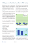
1
Date: April 3, 2014
RENESAS TECHNICAL UPDATE
1753, Shimonumabe, Nakahara-ku, Kawasaki-shi, Kanagawa 211-8668 Japan
Renesas Electronics Corporation
Product
Category
Title
MPU/MCU
Document
No.
TN-RX*-091A/E
Corrections to the RX111 Group User’s Manual:
Hardware regarding Communication Protocol of the
Flash Memory
Information
Category
Technical Notification
Reference
Document
RX111 Group User's Manual:
Hardware Rev.1.00
(R01UH0365EJ0100)
Lot No.
Applicable
Product
RX111 Group
All
Rev.
1.00
This document describes corrections to descriptions for communication protocol of the flash memory in RX111 Group User’s
Manual: Hardware.
1. Corrections
Page 1116 of 1209
Descriptions in 35.9.3, Boot Mode Status Inquiry are corrected as follows:
Before correction
Command
4Fh
Response
5Fh
Size
Status
Error
Size (1 byte): Total bytes of “Status” and “Error” (the value is always 2)
Status (1 byte): MCU status (see Table 35.13)
Error (1 byte): Information about the error occurred in the MCU (see Table 35.14)
After correction
Command
4Fh
Response
5Fh
Size
Status
Error
SUM
Size (1 byte): Total bytes of “Status” and “Error” (the value is always 2)
Status (1 byte): MCU status (see Table 35.13)
Error (1 byte): Information about the error occurred in the MCU (see Table 35.14)
SUM (1 byte): Value that is calculated so the sum of response data is 00h
(c) 2014. Renesas Electronics Corporation. All rights reserved.
Page 1 of 10
RENESAS TECHNICAL UPDATE TN-5;*-A/E'ate: April 3, 2014
Page 1117 of 1209
Descriptions in 35.9.4.1, Supported Device Inquiry are corrected as follows:
Before correction
Command
20h
Response
30h
Number of
characters
Number of
characters
Size
Number of
devices
Device code for little endian
Series name for little endian
Device code for big endian
Series name for big endian
SUM
Size (1 byte): Total bytes of Number of Devices, Characters, Device code, and Series name
Number of devices (1 byte): Number of devices supported by the boot program
Number of characters (1 byte): Number of characters for the device code and device name
Device code (4 bytes): Identification code indicating the device
Series name (n bytes): ASCII code of the series name of the supported device
SUM (1 byte): Value that is calculated so the sum of response data is 00h
After correction
Command
20h
Response
30h
Number of
characters
Number of
characters
Size
Number of
devices
Device code for little endian
Series name for little endian
Device code for big endian
Series name for big endian
SUM
Size (1 byte): Total bytes of Number of Devices, Characters, Device code, and Series name
Number of devices (1 byte): Number of endian types of program data (the value is always 02h)
Number of characters (1 byte): Number of characters for the device code and device name
Device code (4 bytes): Identification code indicating the endian of program data
Series name (n bytes): ASCII code of the series name of the supported device
SUM (1 byte): Value that is calculated so the sum of response data is 00h
Page 2 of 10
Date: April 3, 2014
RENESAS TECHNICAL UPDATE TN-5;A/E
Page 1120 of 1209
Descriptions in 35.9.5.1, Device Select are corrected as follows:
Before correction
Command
10h
Size
Device code
SUM
Size (1 byte): Number of characters of the device code (the value is always 04h)
Device code (4 bytes): Identification code indicating the device
(code in the response to the support device inquiry command)
SUM (1 byte): Value that is calculated so the sum of command data is 00h
After correction
Command
10h
Size
Device code
SUM
Size (1 byte): Number of characters of the device code (the value is always 04h)
Device code (4 bytes): Identification code for selecting the endian of program data
(code in the response to the support device inquiry command)
SUM (1 byte): Value that is calculated so the sum of command data is 00h
Page 3 of 10
Date: April 3, 2014
RENESAS TECHNICAL UPDATE TN-5;A/E
Page 1121 of 1209
Descriptions in 35.9.6, Operating Frequency Select are corrected as follows:
Before correction
Response
06h
Error Response
BFh
Error
Error (1 byte): Error code
11h: SUM error
24h: Bit rate selection error
Communication
Confirmation
06h
Response
06h
Error Response
FFh
After correction
Response
06h
Error Response
BFh
Error
Error (1 byte): Error code
11h: SUM error
24h: Bit rate selection error
Command
(communication
confirmation data)
06h
Response
06h
Error Response
FFh
Page 4 of 10
Date: April 3, 2014
RENESAS TECHNICAL UPDATE TN-5;A/E
Page 1133 of 1209
Descriptions in 35.9.10.1, Bit Rate Automatic Adjustment Procedure are corrected as follows:
Before correction
After starting up in boot mode, wait for 400 ms and then send 00h to the MCU from the programmer. When the bit rate
adjustment is completed, the MCU sends 00h to the programmer. When the programmer receives 00h, send 55h to the
MCU from the programmer. When the programmer fails to receive 00h, restart the MCU in boot mode, and adjust the bit
rate again. The programmer can send 00h to the MCU up to 30 times.
After correction
After starting up in boot mode, wait for 400 ms and then send 00h to the MCU from the programmer. The programmer
can send 00h to the MCU up to 30 times. When the bit rate adjustment is completed, the MCU sends 00h to the
programmer. When the programmer receives 00h, send 55h to the MCU from the programmer. When the programmer
fails to receive 00h, restart the MCU in boot mode, and adjust the bit rate again.
Page 1133 of 1209
Figure 35.13 Data Format for Bit Rate Automatic Adjustment is corrected as follows:
Before correction
START
BIT
D0
D1
D2
D3
D4
D5
D6
D7
STOP
BIT
At least 1 bit
of high width
Measure 9 bits of low width (data 00h)
After correction
Command transmission interval of at least 1 ms
Transmission to the
MCU
"00h"
"00h"
"00h"
"00h"
(1)
(2)
(3)
*1
Reception from the
MCU
"55h"
"00h"
Note 1. Up to 30 times
Page 5 of 10
RENESAS TECHNICAL UPDATE TN-5;A/E
Date: April 3, 2014
Page 1135 of 1209
Descriptions in 35.9.10.3, Procedure to Select the Device and Change the Bit Rate are corrected as
follows:
Before correction
(1) Send the device select command (10h) to select the device to connect with the programmer and the endian of data
that is programmed. When the program data is little endian, select the same device code as that for little endian in
the response to the support device inquiry command. When the program data is big endian, select the same device
code as that for big endian in the response to the support device inquiry command. When the device is selected
successfully, the MCU sends a response (06h). When the MCU fails to receive, the MCU sends an error response
(90h).
(2) Send the operating frequency select command (3Fh) to change the bit rate for communication. When the bit rate is
set successfully, the MCU sends a response (06h). When the bit rate cannot be changed, or when the MCU fails to
receive, the MCU sends an error response (BFh).
(3) When the MCU receives a response (06h), the MCU waits for 1-bit period at the bit rate for sending the operating
frequency select command, and then set the bit rate of the programmer to the changed value. After that, the MCU
sends communication confirmation data (06h) at the changed bit rate. When the MCU receives the command
successfully, the MCU sends a response (06h) of the communication confirmation data.
After correction
(1) Send the device select command (10h) to select the device to connect with the programmer and the endian of data
that is programmed. When the program data is little endian, select the same device code as that for little endian in
the response to the support device inquiry command. When the program data is big endian, select the same device
code as that for big endian in the response to the support device inquiry command. When the device is selected
successfully, the MCU sends a response (46h). When the MCU fails to receive, the MCU sends an error response
(90h).
(2) Send the operating frequency select command (3Fh) to change the bit rate for communication. When the bit rate is
set successfully, the MCU sends a response (06h). When the bit rate cannot be changed, or when the MCU fails to
receive, the MCU sends an error response (BFh).
(3) When the programmer receives a response (06h), the MCU waits for 1-bit period at the bit rate for sending the
operating frequency select command, and then set the bit rate of the programmer to the changed value. After that,
the MCU sends communication confirmation data (06h) at the changed bit rate. When the MCU receives the
command successfully, the MCU sends a response (06h) of the communication confirmation data.
Page 6 of 10
Date: April 3, 2014
RENESAS TECHNICAL UPDATE TN-5;A/E
Page 1135 of 1209
Figure 35.16 Procedure to Select the Device and Change the Bit Rate is corrected as follows:
Before correction
MCU
Programmer
10h (device select command)
(1)
06h (ACK)
90h, XXh (error code)
3Fh (operating frequency select command)
(2)
06h (ACK)
BFh, XXh (error code)
Wait for 1-bit period
Set the new bit rate
06h (check)
(3)
06h (ACK)
After correction
MCU
Programmer
10h (device select command)
46h (ACK)
(1)
90h, XXh (error code)
3Fh (operating frequency select command)
(2)
06h (ACK)
BFh, XXh (error code)
Wait for 1-bit period
Set the new bit rate
06h (communication confirmation data)
06h (ACK)
(3)
Page 7 of 10
RENESAS TECHNICAL UPDATE TN-5;A/E
Date: April 3, 2014
Page 1138 of 1209
Descriptions in 35.9.10.6, Erase Ready Operation are corrected as follows:
Before correction
(1) Send the erase preparation command (48h) to place the MCU in the erase wait state. The MCU enters the erase wait
state and sends a response (06h).
(2) Send a block erase command (59h) to erase blocks in the MCU. When blocks are erased successfully, the MCU
sends a response (06h). When the MCU fails to receive, the MCU sends an error response (D9h).
Send a block erase command repeatedly until block erase commands for all blocks are sent. When the operation
ends before all the block erase commands are sent, a command error may occur even when a correct command is
sent in the program/erase state.
(3) In order to place the MCU in the program/erase state, send a block erase command for end of erase (59h 04h FFh
FFh FFh FFh A7h). The MCU enters the program/erase state and sends a response (06h).
After correction
(1) Send the erase preparation command (48h) to place the MCU in the erase wait state. The MCU enters the erase wait
state and sends a response (06h).
(2) Send a block erase command (59h) to erase blocks in the MCU. When blocks are erased successfully, the MCU
sends a response (06h). When the MCU fails to receive, the MCU sends an error response (D9h).
Send block erase commands repeatedly until a block erase command has been sent for the total number of blocks.
The total number of blocks is the sum of the user area blocks and data area blocks that are obtained in advance using
the block information inquiry command. If the operation ends before all the block erase commands are sent, a
command error may occur even when a correct command is sent in the program/erase state.
(3) Send a block erase command for end of erase (59h 04h FFh FFh FFh FFh A7h). The MCU sends a response (06h).
(4) To confirm whether erase ready operation has ended, send a boot mode status inquiry command (4Fh). When the
erase ready operation has ended, the MCU returns the result of the boot mode status inquiry. When the erase ready
operation has not ended, the MCU sends an error response (80h 4Fh). When an error response is received, restart the
MCU in boot mode and perform the procedure again from section 35.9.10.1, Bit Rate Automatic Adjustment Procedure.
Page 8 of 10
Date: April 3, 2014
RENESAS TECHNICAL UPDATE TN-5;A/E
Page 1138 of 1209
Figure 35.19 Procedure to Send Commands in Erase Ready Operation is corrected as follows:
Before correction
MCU
Programmer
48h (erase preparation command)
(1)
06h (ACK)
Repeat until all blocks are
erased.
- Repeat 136 times for a
128-Kbyte product
(128 times for the user
area and eight times for
the data area).
59h (block erase command)
Erase
(2)
06h (ACK)
D9h, XXh (error code)
59h (block erase command for end of erase)
(3)
06h (ACK)
After correction
MCU
Programmer
48h (erase preparation command)
(1)
06h (ACK)
59h (block erase command)
Erase
Repeat until all blocks are
erased.
(2)
06h (ACK)
D9h, XXh (error code)
59h (block erase command for end of erase)
(3)
06h (ACK)
4Fh (boot mode status inquiry command)
Response to the boot mode status inquiry command
(4)
80h, 4Fh (error response)
Page 9 of 10
RENESAS TECHNICAL UPDATE TN-5;A/E
Date: April 3, 2014
Page 1143 of 1209
Descriptions in 35.9.10.11, Set the Access Window in the User Area are corrected as follows:
Before correction
(1) When setting the access window, set 00h in the access window, set the start address of the area that can be
programmed the by self-programming library in the access window start address LH and access window start
address HL, and set the end address of the area that can be programmed by the self-programming library in the
access window end address LH and access window end address HL.
When clearing the access window settings, set FFh in the access window, access window start address LH, access
window start address HL, the access window end address LH, and the access window end address HL.
When the MCU writes the addresses, the MCU sends a response (06h). If the MCU fails to receive, the MCU sends
an error response (F4h).
After correction
(1) Send the access window program command (74h) to set the access window or clear the access window settings.
When setting the access window, set 00h in the access window, set the start address of the area that can be
programmed by the self-programming in the access window start address LH and access window start
address HL, and set the end address of the area that can be programmed by the self-programming in the
access window end address LH and access window end address HL.
When clearing the access window settings, set FFh in the access window, access window start address LH, access
window start address HL, the access window end address LH, and the access window end address HL.
When the MCU writes the addresses, the MCU sends a response (06h). If the MCU fails to receive, the MCU sends
an error response (F4h).
Page 10 of 10