1
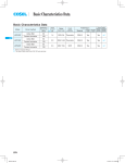
Whitepaper 2: The Rules of Low Power MCU Design
Abstract
Market and Government demands for a greener environment
and better use of resources such as making batteries last
longer means that the need for low power operation and
standby is increasing. Conversely the demands for more
performance and functionality are also on the rise, a
combination not usually recognised for lowering power.
Introduction
This paper is the second in a series four whitepapers that
examining the various considerations for low power
design and operation. In this paper we look at the many
“tricks” (techniques) that allow designers to combine both
performance and low power consumption in their
applications. Specific examples and references included
are based on the 16-bit RL78 and the 32-bit RX100 families
outlined in the first whitepaper (powering your system from
a lemon!). It should be noted that while specific devices are
used for reference (RL78/L12 and RX111) the principles
can apply equally to the other RL78 and RX MCU families.
“Tricks” to Lower Power Consumption
As outlined in whitepaper 1, the MCU is a significant factor
in the power used by applications, but it is not always the
only area for consideration and while application requirements
differ there is a general set of topics that contribute to the
power used that we will examine in this whitepaper.
(RTC, UART and Timer etc.). The premise here is the main
clock is speed is reduced or stopped completely and that
any operation is based on a low speed clock such as 32 KHz
or internal oscillator.
Obviously the optimum is where the system is completely
stopped and all clock sources are halted and the MCU
powered at or above the minimum supply voltage where
the MCU will be held in a static state.
Examples of our featured products showing the reduction
in power consumption are shown in figures 1 and 2 below.
Here the HALT/SLEEP modes are using a low speed 32 KHz
clock and STOP/SW Standby is with all clocks stopped.
RL78
Notes
1: At NOP instruction
2: Active RTC + LVD function
3: Active WDT + LVD function
4: All stopped, RAM retained
0.38 µA2
32 KHz
with
RTC + LVD
0.3 µA
32 KHz
0.53 µA3
With
WDT + LVD
Stop Mode
Halt Mode
1.MCU Standby modes
2.MCU Operating clock speed
3.MCU Clock Source Selection
4.MCU Peripheral Operation
5.MCU I/O Pin use
6.System Integration
7.Power Supply options
0.23 µA4
Figure 1 – RL78 Standby Current Consumption
RX100
2.5
These topics are reviewed in detail below and please refer
to the other papers in the series as they will cover some
more of the background and specific topic associated with
low power design. The other papers in the series are listed
at the end of this paper for reference.
MCU Standby Modes
Standby modes used during idle or stop periods of the
system operation are generally considered as the main
method of reducing the average power consumption in any
battery powered system. Many MCU families offer a number
of low power options because applications require different
scenarios where some peripherals still have to operate
32 KHz
2
Stop
1.5
1
0.5
0
µA
Sleep
Deep Sleep
SW Standby
Figure 2 – RX100 Standby Current Consumption
As outlined in whitepaper 1 (lemon demonstration), the
two low power modes of the RL78, HALT and STOP (see
2015.05
1
Whitepaper 2: The Rules of Low Power MCU Design
figure 1 on page 1) offers significant power reduction in
either mode, plus the SNOOZE mode (linked to STOP mode)
which decreases the number of times that the CPU needs
to be woken until a valid wake up condition occurs, reduces
the average STOP mode current even further. For example
analysing a heating controller based on the RL78 in
“SNOOZE” mode, measures the temperature (ADC
conversion), checks the result and reports to the HVAC
unit controller only if the temperature is out of range (see
figure 3). By only using “STOP” an average current of 880 nA
can be achieved, but by using “SNOOZE” operation as well
the average current is reduced to 680 nA, a 25% reduction
which can be directly translated into the battery lasting 25%
longer.
For the RX100 MCU family the three standby modes SLEEP,
DEEP SLEEP and SOFTWARE STANDBY as shown in
figure 2 on page 1 and outlined in paper 1 are understandably
not quite as low as the RL78 but still offer major power
savings for a highly integrated high performance MCU family.
One last factor is not to ignore any external analogue
function or digital peripheral, so that during standby it is
important that these can be “turned off” as some analogue
functions can consume as much power as the MCU. I believe
it is clear that by employing MCU standby modes and total
system shut down as part of the design, very low average
currents can be achieved thus maximising battery life.
scenario for the RX111, at full speed current consumption
is around 10 mA (32 MHz @ 3.6 V) whereas at 1 MHz
consumption is reduced by 90% to around 1 mA and at
32 KHz it is 11.5 µA. So a similar picture can be seen for
our two MCU families.
Operating with a slower system clock is of course somewhat
of a trade off as foreground processing takes longer
impacting average current, so an analysis of the average
current at different clock speeds is recommended.
Average current consumption can generally be calculated
with the following equation
MCU Operating Clock Speed
A simple and perhaps obvious way to reduce power
consumption that should not be overlooked is to operate
the MCU and any external peripherals at a lower clock
frequency, either permanently or during the idle periods.
Reducing the system clock frequency from the maximum
available will reduce the operating current with results
dependant on the product. For example the system clock
from the RL78 internal high speed oscillator can be reduced
by a number of steps from 32 MHz down to 1 MHz with
each reduction in frequency lowering the operating current
by around 22%. So selecting a lower system operating
frequency can have an impact on the power calculations.
During periods when the system does not have to perform
any main processing many MCU’s allow the CPU clock to
be changed by software to a lower main frequency or even
a low speed clock (internal or external). Using the RL78/L12
as discussed in paper 1 (lemon demonstration) as an
example, full speed operation using the internal oscillator
consumes around 3 mA (24 MHz @ 3 V), whereas at 1 MHz
current consumption is reduced by at least 30% to less
than 1 mA and at 32 KHz is down to 3.6 µA. It is a similar
** If only one active time exists then simply remove this
from the equation and if additional active times exist then
add these as necessary to the equation.
An example of the calculation above is based on the
operation example shown in figure 3 below.
2
Iave = ((AC1 * AT1) + (AC2 * AT2) + (IC * IT)) / P
Where
Active Current 1 (AC1) Current consumption during the
1st active period
Active Current 2 (AC2) Current consumption during a 2nd
active period **
Active Time 1 (AT1) Time taken for the 1st active period
Active Time 2 (AT2)
Time taken for the 2nd active period
Inactive Current (IC) Inactive current i.e. time spent in
idle/standby
Inactive Time (IT)
Inactive time Total period time
– total active times
Time Period (P)
Total time of repeating period
Figure 3 – RL78 average consumption example
www.renesas.eu
Whitepaper 2: The Rules of Low Power MCU Design
Iave = ((AC1 * AT1) + (AC2 * AT2) + (IC * IT)) / P
Iave = ((5.2 mA * 42.8 µs) + (4.7mA * 8 µs) + (0.56 µA *
949.2 µs)) / 1
Iave = ((222.56 nA) + (37.6 nA) + (53.2 nA)) / 1
Iave = 313.36 nA
Note: Sending temperature and time event does not occur
often so was not included in the calculation above.
When this event occurs a further 31.5 µA (4.7 mA * 6.7 ms)
will be used during this time.
If the period of operation occurred every 5 minutes (5000
seconds) the average current of this additional event
would be 6.9 nA (31.5 µA / 5000).
While some MCU’s allow the main clock to be changed by
software, it should be remembered that dynamically
changing the main clock may affect peripheral operation
so should be considered carefully to ensure that any external
devices are not impacted and that if employed during
standby that time is allowed to restore the normal operation
settings. While running the MCU at lower frequencies has
a marked effect on lowering the power used, the main
method of reducing the average system power would be
to use dynamic or lower clock frequencies in conjunction
with the standby modes discussed above.
power crystal or resonator possible that is compatible to
the MCU manufacturer. Remember that the CPU and other
peripheral do not have to operate at this frequency and can
still be run slower.
A simple comparison between the different currents required
by the main system clock source by using internal or external
clock source based on our example products compares the
maximum clock frequency available and assumes normal
operation.
Internal
External
3.3 mA @ 24 MHz (3 V)
3.0mA @ 20 MHz (3 V)
Table – 1 RL78/L12 Clock power consumption comparison
The maximum external crystal for the RL78 is 20 MHz so
rationalising both clock sources the internal oscillator uses
137.5 µA/MHz whereas the external is 150 µA/MHz. So for
comparison if both clocks were operated at 16 MHz then
the internal would consume 2.2 mA and the external crystal
would be 2.4 mA. While 200 µA is not a huge difference it
all add up when looking to make the battery last longer.
Internal
External
10.5 mA @ 32 MHz (3 V)
10.6 mA @ 32 MHz (3 V+PLL)
Table 2 – Rx111 Clock power consumption comparison
MCU Clock Source Selection
Selection of the type of main clock and sub clock (if used)
refers to not only setting the clock speed as discussed
above, but also the type of the clock source as the choice
will impact the current consumption.
It is now common for MCU manufacturers to provide
internal clock oscillators so that in many applications the
need for an external crystal/resonator is removed not only
saving power but cost.
Internal clock oscillators generally fall into two categories,
high speed system clock (i.e. main clock) and low speed
subsystem clocks.
Internal main system oscillators have now become accurate
enough for most applications (≤ 1%) and can include a “trim”
function allowing the oscillator to be profiled and adjusted
to maintain accuracy over temperature. Internal low speed
clocks are generally not as accurate so it may still be
necessary to use an external 32 KHz crystal or resonator
for example where a RTC time stamp is required. While it
is preferable to use internal oscillators especially for main
system clock source there may still be occasions when a
specific frequency is required or where the better accuracy
is needed to drive an interface such as USB or Ethernet.
Here there is little option other than choose the lowest
Analysing the same scenario for the RX111 (table 2), then
the difference here is around 100 µA. Again not a large
difference but it is still 100 µA that will not be taken from
the battery. One point to highlight is that using an external
crystal on the RX111 it is necessary to use the PLL when
considering system clock speeds above 20 MHz.
While using internal main oscillators saves current another
important factor is that internal oscillators have faster start
times than crystals or resonators which means that less
time (and power) is wasted during wake up from standby
where the clock has been stopped. Typically crystal/resonator
start times are around 2 ms whereas the internal high speed
oscillator has a wake up time of only 40 µs (RX111), 50 times
faster saving 50 times the start-up power used.
Low speed or “sub” clocks can also require the use of an
external crystal/resonator if the internal clock is the wrong
frequency or not sufficiently accurate for the application.
The choice of crystal/resonator can make a big difference
especially where a choice of power options on the oscillator
cell is available.
It is important to check the compatibility of a crystal
resonator with the MCU manufacturer to ensure correct
operation especially when using an ultra-low power oscillator
3
Whitepaper 2: The Rules of Low Power MCU Design
(ULP) mode. For example the comparison between the
RL78 normal and “ultra” low power sub clock is that the
“ULP” current consumption is less than half that of the
normal oscillator setting (Normal = 380 nA and ULP =
180 nA). While this does not seem a lot, when you consider
that standby currents can be in the region of 560 nA
(depending on settings and what is operating), then 200 nA
is 36%, so 36% more current can be saved.
MCU Peripheral Operation
Peripheral operation is another area considered as “obvious”
in that any unused peripherals should be turned off to avoid
wasting power. It is fair to say “OFF” is usually the peripheral
default state, but worth checking the data sheet to make
sure. It is important that to achieve very low standby
currents where the sub-clock is running, any peripherals
not required in the idle state should be stopped as unless
configured to operate from a sub clock (15 KHz or 32 KHz)
will not operate correctly and still consume power. Extra
software processing on standby entry and exit will be
necessary, so should be planned carefully as disabling
some peripherals may reset their configuration settings.
This requires more time to execute and consumes power
during execution so it is possible that overall the peripheral(s)
should not turned off while in standby. This should be
analysed during the design phase to determine the best
option. Obviously if all clocks are stopped then it is not a
problem as the MCU and all peripherals will be frozen in a
static state with the current register states maintained.
Some advanced peripherals such as USB may require a
separate external clock which may continue to operate
during standby modes. Not ideal so the user manual should
be checked to see if this can be stopped.
Care should also be taken if the system is using a
“watchdog” safety function as many of these still operate
during standby modes. Without the required “service”
access, the watchdog can overflow and cause and interrupt
or hardware reset, so a careful review of the user manual
should be made of the watchdog operation during standby.
Use of HALT or WAIT modes can usually be configured so
that the watchdog is serviced on entry and exit from the
low power mode thus avoiding a premature reset.
It is difficult to quantify the exact effect on current
consumption as all applications are different in operation
and standby, although any “analogue” function (ADC, DAC,
LCD, Temperature sensor etc.) will consume more power
than most digital functions, as these include static power
drains (resistors, references etc.) that are independent of
clock rate. For the optimum low power the suggested
4
technique is to turn them on, use them quickly, and then
turn them off. However due to the longer stabilisation time
of many analogue peripherals, it is prudent to determine
the best time they should be enabled and disabled to
ensure it is ready when it is needed and if possible, use
the stabilization time to perform other CPU tasks.
Finally we have considered “internal” peripherals, but
sometimes it will be necessary to use external functions
especially analogue devices such as sensors. It is
recommended that all external peripherals can also be
turned “OFF” or disabled when not in use.
MCU I/O Pin use
This section is just a few reminders to avoid unnecessary
and unexpected current consumption.
Try and avoid low impedance drives as this will increase
the switching currents in the output driver.
Ensure that there are no floating pins as this can increase
leakage currents in the design and can set indeterminate
levels that may activate a valid input state on an input pin.
Pull up or pull down resistors (internal or external) should
be avoided unless absolutely necessary. If using an external
resistor try and set the value sufficiently high to reduce
current during operation, but low enough to ensure correct
operation of the function. For example internal pull up
resistors can have a value as high as 100 kW, so any
external can be also be this value, whereas for an open
drain (typically used for the I2C interface) will need to be
considerably lower (can as low as 1 KW) to maintain
correct rise and fall times to the specifications.
Most MCU’s include pin programmable internal pull up
resistors so that they can be used only where needed.
During standby operation try and ensure that any driven
pin is set to the level of the pull up/down (i.e. logic 0 for
pull down and logic 1 for pull up) usually the inactive state.
To avoid the use of pull up/down resistors any unused I/O
pin can be set to an “output” as this will always set a
defined level and does not require any pull up/down resistor.
A side benefit that it offers low impedance to the outside
world helping with noise immunity.
System Integration
One of the factors in larger systems are interfaces to
external peripherals as all of these require control and data
signals so all of these I/O pins will consume switching
current defined by the equation
½ C * V2 * f (Load Capacitance * Switching Voltage2 *
Switching frequency).
www.renesas.eu
Whitepaper 2: The Rules of Low Power MCU Design
By integration we refer to an MCU family that has some or
all peripherals integrated on chip, including functions such as
USB, Ethernet and E2ROM (using Data Flash) plus increasing
numbers of analogue functions such as temperature sensor,
analogue comparator and programmable gain amplifier etc.
The benefits of providing peripherals on-chip apart from the
cost saving, is that while the peripheral will still consume
power (when used) the data and control interfaces use much
lower switching currents (lower voltage (V2) and lower
capacitance(C)) with no high current I/O pins used and the
functions can easily be switched off when not required.
Power Supply Options
The choice of the power supply may seem to be a simple
choice, “the lower the voltage the lower the power” and
to some extent this is true, but not necessarily as you might
think. Many MCU’s now include an internal regulator lowering
the internal operating voltage and offering consistent power
consumption over most of the operating voltage range, so
that running the device at 3 V or 5 V (in some cases down
to 1.8 V) can make no difference to the MCU consumption.
Obviously running a complete system at 3 V can make a
difference to the total power used, but this is a choice of
the designer and the interfaces outside the MCU.
However many devices now operate down at very low
voltages, for example the RL78/L12 can operate down to
1.6 V and the RX111 down to 1.8 V, making low voltage
operation possible. With such a wide voltage range possible
this extends the battery life before requiring charging or
replacing. Just a note that the maximum clock frequencies
are often reduced when operating at very low voltages, so
care should be taken when setting the clock frequency
over a supply range of say 3 V down to 1.8 V to ensure that
the main clock frequency is suitable for the power supply
range. The RL78/L12 internal high speed oscillator frequency
at 1.6 V can be up to 4 MHz, the RX111 maximum internal
oscillator frequency at 1.8 V is 8 MHz.
It may be possible to reduce the power supply during standby
times where the minimum voltage is used to maintain
register settings and RAM contents. However this can be
quite a complicated procedure and care should be taken to
sequence the “power down” and “power up” of the system
so as not to affect any external peripherals connected to
the MCU. This is also likely to extend the time taken for
the “power down” and “wake up” of the system.
Conclusion
The theme of this paper was to look at the “tricks” that
help to reduce power consumption. While the sections
above provide an overview each application can have
different requirements, so it recommended that a “Power
Use Profile” is used for the design to analyse the actual
consumption and highlight areas not meeting their design
targets or where there is unexpected consumption and
allows the implementation to be analysed and adjusted to
meet the target battery life.
For further information it is recommended to read the other
whitepapers in this series which are highlighted below for
reference and please visit the Renesas design resources
centre.
Whitepaper 1: Lemon Powered Design
An example of what can be achieved with the right
product and modes of operation
Whitepaper 3: De-Clocking vs MCU Standby for Low
Power Design
Reducing MCU clock speeds during operating and idle
times and effects of combining with standby
Whitepaper 4: Maximise Your Battery Life
Analysis of systems that are designed to spend long
periods in standby operation
Written by: David Parsons - Consultant to Renesas Electronics (Europe) GmbH
David can be contacted at DCP Electronics and Software Services.
Before purchasing or using any Renesas Electronics products listed herein, please refer to the latest product manual and/or data sheet in advance.
© 2015 Renesas Electronics Europe.
All rights reserved. Printed in Germany.
Document No. R01PF0079ED0200
5