1
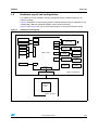
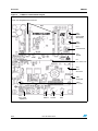
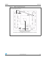
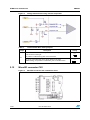
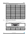
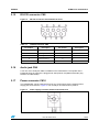
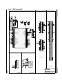
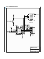
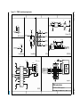
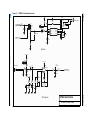
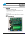
UM0629
User Manual
STM8L101-EVAL
evaluation board
Introduction
The STM8L101-EVAL is composed of two boards:
■
An STM8L1/L2 motherboard called MB709 which includes all peripherals which are
connected to the MCU on the daughterboard. The motherboard connects to the
daughterboard via two 36-pin connectors.
■
An STM8L1 daughterboard called MB710 which has an STM8L101 MCU.
The motherboard and daughterboard are a complete development platform for
STMicroelectronic's STM8L101 microcontroller with comparator, I2C, SPI, USART and
SWIM debugging support.
The full range of hardware features on the STM8L101-EVAL helps you to evaluate all
peripherals (MicroSD cardTM, USART, EEPROM, LCD, for example) and develop your own
applications.
Figure 1.
November 2009
STM8L101-EVAL board
Doc ID 15312 Rev 2
1/26
www.st.com
Contents
UM0629
Contents
1
2
3
4
2/26
Overview . . . . . . . . . . . . . . . . . . . . . . . . . . . . . . . . . . . . . . . . . . . . . . . . . . 4
1.1
Features . . . . . . . . . . . . . . . . . . . . . . . . . . . . . . . . . . . . . . . . . . . . . . . . . . . 4
1.2
Demonstration software . . . . . . . . . . . . . . . . . . . . . . . . . . . . . . . . . . . . . . . 4
1.3
Order code . . . . . . . . . . . . . . . . . . . . . . . . . . . . . . . . . . . . . . . . . . . . . . . . . 4
1.4
Hardware layout and configuration . . . . . . . . . . . . . . . . . . . . . . . . . . . . . . . 5
STM8L1/L2 motherboard . . . . . . . . . . . . . . . . . . . . . . . . . . . . . . . . . . . . . 8
2.1
Power supply . . . . . . . . . . . . . . . . . . . . . . . . . . . . . . . . . . . . . . . . . . . . . . . 8
2.2
Reset source . . . . . . . . . . . . . . . . . . . . . . . . . . . . . . . . . . . . . . . . . . . . . . . 9
2.3
Audio . . . . . . . . . . . . . . . . . . . . . . . . . . . . . . . . . . . . . . . . . . . . . . . . . . . . . 9
2.4
I2C EEPROM . . . . . . . . . . . . . . . . . . . . . . . . . . . . . . . . . . . . . . . . . . . . . . 10
2.5
RS-232 . . . . . . . . . . . . . . . . . . . . . . . . . . . . . . . . . . . . . . . . . . . . . . . . . . . 10
2.6
MicroSD card . . . . . . . . . . . . . . . . . . . . . . . . . . . . . . . . . . . . . . . . . . . . . . 10
2.7
Analog input . . . . . . . . . . . . . . . . . . . . . . . . . . . . . . . . . . . . . . . . . . . . . . . 10
2.8
Development and debug support CN5 and CN6 . . . . . . . . . . . . . . . . . . . 10
2.9
Display and input devices . . . . . . . . . . . . . . . . . . . . . . . . . . . . . . . . . . . . . 11
2.10
Bi-color LED . . . . . . . . . . . . . . . . . . . . . . . . . . . . . . . . . . . . . . . . . . . . . . . 11
2.11
Economic measurement and potentiometer RV1 . . . . . . . . . . . . . . . . . . . 11
2.12
MicroSD connector CN1 . . . . . . . . . . . . . . . . . . . . . . . . . . . . . . . . . . . . . . 12
2.13
Daughterboard extension connectors CN3 and CN4 . . . . . . . . . . . . . . . . 13
2.14
SWIM connectors CN5 and CN6 . . . . . . . . . . . . . . . . . . . . . . . . . . . . . . . 14
2.15
RS-232 connector CN8 . . . . . . . . . . . . . . . . . . . . . . . . . . . . . . . . . . . . . . 15
2.16
Audio jack CN9 . . . . . . . . . . . . . . . . . . . . . . . . . . . . . . . . . . . . . . . . . . . . . 15
2.17
Power connector CN10 . . . . . . . . . . . . . . . . . . . . . . . . . . . . . . . . . . . . . . 15
STM8L1 daughterboard . . . . . . . . . . . . . . . . . . . . . . . . . . . . . . . . . . . . . 16
3.1
Power . . . . . . . . . . . . . . . . . . . . . . . . . . . . . . . . . . . . . . . . . . . . . . . . . . . . 16
3.2
Extension connector CN1 and CN2 . . . . . . . . . . . . . . . . . . . . . . . . . . . . . 16
Schematics . . . . . . . . . . . . . . . . . . . . . . . . . . . . . . . . . . . . . . . . . . . . . . . 17
4.1
STM8L1/L2 motherboard . . . . . . . . . . . . . . . . . . . . . . . . . . . . . . . . . . . . . 17
4.2
STM8L1-DB daughterboard schematic . . . . . . . . . . . . . . . . . . . . . . . . . . 23
Doc ID 15312 Rev 2
UM0629
Contents
Appendix A STM8L101-EVAL I/O assignment . . . . . . . . . . . . . . . . . . . . . . . . . . . 24
5
Revision history . . . . . . . . . . . . . . . . . . . . . . . . . . . . . . . . . . . . . . . . . . . 25
Doc ID 15312 Rev 2
3/26
Overview
UM0629
1
Overview
1.1
Features
1.2
■
5 V power jack supply
■
Audio play
■
MicroSD cardTM
■
64 Kbit I2C EEPROM
■
One channel of RS-232 communication
■
Bi-color LED
■
Economic analog voltage measurement based on comparator
■
SWIM debug support
■
122 x 32 dot-matrix serial interface LCD module
■
Joystick with 4-direction control and selector
■
Reset and User button
■
3 LEDs
■
Extension connector for daughterboard
■
One 10 K potentiometer
■
RoHS compliant
Demonstration software
Demonstration software is preloaded in the board’s Flash memory for easy demonstration of
device peripherals in stand-alone mode. For more information and to download the latest
version available, refer to STM8L101-EVAL demonstration firmware available on web:
www.st.com/mcu.
1.3
Order code
To order the STM8L101K3 evaluation board, use the order code STM8L101-EVAL.
4/26
Doc ID 15312 Rev 2
UM0629
1.4
Overview
Hardware layout and configuration
The STM8L101-EVAL evaluation board is designed around the STM8L101K3T6 in an
LQFP32 package.
Figure 2 illustrates the connections between the daughterboard and the peripherals on the
motherboard (LCD, I2C EEPROM, USART, audio and MicroSD card).
Figure 3 and Figure 4 help you to locate these features on the actual evaluation board.
Figure 2.
Hardware block diagram
I2C EEPROM
I2C
SWIM connector
SWIM
ADC
PWM
Audio circuit
BEEP
Bi-color LED
Joystick
GPIO’s
LED’s
USART
STM8L1/L2-MB
SPI
RS232
transceiver
Level
translator
RS232
connector
MicroSD card
LCD
Push button
Compa
rator
BNC connector
Economic
Measurement
5V power
jack
ADC
Potentiometer
STice connector
CMP
1.8 to 3.3V
regulator
3.3V
regulator
GPIO’s
Extension connector
STM8L1/L2-MB (MB709)
STM8L101
STM8L1-DB
MCU
STM8L1-DB (MB710)
Doc ID 15312 Rev 2
5/26
Overview
Figure 3.
UM0629
STM8L1/L2 motherboard layout
CN3, CN4 daughterboard connectors
CN6
SWIM
(ERNI cable
alternative)
CN5
SWIM
RV1
Potentiometer
CN8
USART
U2
Dot-matrix LCD
CN1
Micro
SD card™
CN9
Audio jack
CN10
5V power
RV4
MCU_VDD
adjustment
6/26
B1
RESET
U7
Joystick
Doc ID 15312 Rev 2
B2
KEY
UM0629
Overview
Figure 4.
STM8L1 daughterboard layout
CN1, CN2 motherboard connector
STM8L101 MCU in LQFP32 package
soldered directly onto the board
and footprint for socket (ref ENPLAS OTQ-32-0.8-02) is present on the board
Doc ID 15312 Rev 2
7/26
STM8L1/L2 motherboard
2
UM0629
STM8L1/L2 motherboard
This motherboard is designed to work with an STM8L1 daughterboard.
2.1
Power supply
The motherboard is designed to be powered by a 5 V DC power supply and to be protected
from a wrong power plug-in event by PolyZen Inc. (auto rearmable fuse) U13. It is possible
to configure the evaluation board to provide 5 V power to the daughterboard through the
daughterboard connector.
●
The motherboard is powered by a 5 V DC power adapter connected to CN10, the
power jack on the board (PSU on silk screen for power supply unit).
●
5 V DC power is provided to the daughterboard through an extension connector and
can be set by jumper JP12 (DTB for daughterboard on silk-screen).
●
MCU_VDD can be selected by setting jumper JP11 and is connected to the
daughterboard directly through the daughterboard connector.
The power supply is configured by setting the jumpers JP11 and JP12 as described in
Table 1.
The LED LD6 is lit when the motherboard is powered correctly. JP3 is no longer used.
Table 1.
Jumper
Power related jumpers
Description
Setting
PSU
DTB
5 V power from power supply jack (CN10) is connected to the motherboard
when JP12 is set as shown to the right:
(default setting).
JP12
MCU_VDD is powered by a fixed 3.3 V power supply when JP11 is set as
shown to the right:
(default setting).
PSU
DTB
5 V power from power supply jack (CN10) is connected to the daughterboard
when JP12 is set as shown to the right:
In this case the motherboard and daughterboard are powered by a 5 V power
supply.
1
JP11
MCU_VDD is powered by a variable power supply from 1.8 V to 3.3 V,
adjusted by potentiometer RV4 (bottom left of the board), when JP11 is set as
shown to the right:
8/26
Doc ID 15312 Rev 2
1
UM0629
2.2
STM8L1/L2 motherboard
Reset source
The reset signal of the motherboard is low active. Reset sources include:
●
Reset button B1.
●
Debugging tools from connectors CN5, CN6.
The reset pin PA1 of the STM8L101 is either connected to the reset button B1 or to GND by
the setting of jumper JP1:
Table 2.
Jumper
Reset related jumpers
Description
PA1 is connected to GND when JP1 is set as shown to the right:
This configuration is reserved for internal use only.
Setting
1 2 3
JP1
PA1 is connected to Reset button when JP1 is set as shown to the right:
(default setting).
This jumper position is called Alone on the silk-screen.
2.3
1 2 3
Audio
The motherboard supports both audio recording and playback, but audio recording
components (U11 microphone and U12 amplifier) cannot be used with the STM8L101.
The speaker can be disabled or enabled by the setting of jumper JP10.
Audio volume can be adjusted using the potentiometer RV2.
Table 3.
Jumper
Audio related jumpers
Description
JP10
Audio power amplifier TS4871 is forced on standby mode when JP10 is
not fitted.
Default setting: fitted.
JP9
Either beeper or PWM output can be selected as a source of speaker
by setting jumper JP9.
The beeper is connected to speaker when JP9 is set as shown to the
right: (Beep position on the silk-screen).
The PWM output is connected to speaker when JP9 is set as shown to
the right: (PSW position on the silk-screen) (default setting).
Doc ID 15312 Rev 2
Setting
1 2 3
1 2 3
9/26
STM8L1/L2 motherboard
2.4
UM0629
I2C EEPROM
A 64 Kbit I2C EEPROM is connected to the I2C port of the STM8L101.
Write protection can be enabled by the setting of jumper JP8.
Table 4.
I2C EEPROM related jumpers
Jumper
JP8
2.5
Description
I2C EEPROM U6 is protected from write operation when JP8 is not fitted.
Default setting: Fitted
RS-232
One D-type 9-pin RS-232 connector CN8 is available on the motherboard.
RS-232 interface behavior is not guaranteed when the MCU is powered by an adjustable
voltage lower than 3 V.
Note:
To communicate with an RS-232 port on a PC, a 9-pin straight RS-232 cable (direct pin to
pin connection) is needed because:
●
On CN8 the RX signal is connected on pin2 and the TX data on pin 3,
●
On the PC side the RX signal is generally on pin 3 and the TX signal on pin 2.
This standard 9-pin straight RS-232 cable is not provided with the board. Refer to
Section 2.15 for details on RS-232 connector pinout.
2.6
MicroSD card
The 1GByte (or more) MicroSD card connected to the SPI of the STM8L101 through a
voltage level translator U1 (shared with LCD) is available on the board. MicroSD card chip
select is managed by standard I/O port PB4.
2.7
Analog input
The BNC connector footprint present on the board (CN7) cannot be used as it is not
connected to the MCU.
2.8
Development and debug support CN5 and CN6
The two debug connectors are available on the motherboard.
10/26
●
CN5, ERNI 4-pin connector (reference 284697 or 214017) for SWIM debugging. It fits
with ERNI connectors provided with standard tools.
●
CN6, 2.54 mm pitch low-cost 4-pin connector for SWIM debugging.
Doc ID 15312 Rev 2
UM0629
2.9
STM8L1/L2 motherboard
Display and input devices
Display devices available are:
●
122x32 dot-matrix serial interface LCD (U2)
●
4 general purpose LED's (LD2,3,4,5)
Input devices available are:
●
4-direction joystick
●
selection key
●
general purpose button (B2)
Table 5.
2.10
122x32 dot matrix LCD U13
Pin on U2
Description
Pin connection
1
Vss
GND
2
Vcc
+3V3
3
VO
-
4
CLK
PB5
5
SID
PB6
6
CS
PD1
7
A
+5V
8
K
GND
Bi-color LED
A bi-color LED is connected to PB0 through a voltage translator which guarantees that the
bi-color LED works when the STM8L101 is powered by an adjustable voltage from 1.8 V to
3.3 V.
2.11
Economic measurement and potentiometer RV1
The economic measurement solution is demonstrated based on the internal comparator
inside the STM8L101 and potentiometer RV1.
As shown in Figure 5, the voltage divided by resister bridge R10 and R11 can be measured
by using an internal comparator of the STM8L1, with Vref connected to channel 2 of the
comparator and an RC charge circuit connected to the COM channel of the comparator.
To measure the voltage Vin from the potentiometer:
1.
Compare Vref with the voltage on C8 which is charged by a series of pulses generated
by PC4.
2.
Record pulse number PN_Vref when the voltage on C8 reaches voltage reference Vref.
3.
Another charge pulse PN_Vin can be obtained with voltage connected to CH1 also like
PN_Vref.
4.
The voltage Vin can be calculated based on both numbers PN_Vref and PN_Vin.
Doc ID 15312 Rev 2
11/26
STM8L1/L2 motherboard
UM0629
Figure 5.
Voltage measurement using internal comparator
Table 6.
Potentiometer RV1 related jumpers
Jumper
JP2
2.12
Setting
RV1 is connected to PD2 as one input of the internal comparator when JP2
is set as shown to the right:
JP2 position is called Comp_PD2 on the silk-screen.
1 2 3
RV1 is not connected when JP2 is set as shown to the right:
(default setting). JP2 position is called ADC_PE0 on the silk-screen.
1 2 3
MicroSD connector CN1
Figure 6.
12/26
Description
MicroSD connector CN1 viewed from front
Doc ID 15312 Rev 2
UM0629
STM8L1/L2 motherboard
Table 7.
2.13
MicroSD connector CN1
Pin number
Description
Pin number
Description
1
Reserved
5
SCLK/PB5
2
CS/PB4
6
Vss/GND
3
DI/PB6
7
DO/PB7
4
VDD
8
Reserved
9
GND
10
Not used
Daughterboard extension connectors CN3 and CN4
Two 36-pin male headers CN3 and CN4 can be used to connect the daughterboard to the
motherboard. All GPI/Os are available on it. Please refer to Table 8 and Table 9 for pin-out
definition.
Table 8.
Daughterboard extension connector CN3
Pin number
Description
Pin number
Description
1
GND
2
PC4
3
PC5
4
PC6
5
Reserved
6
Reserved
7
Reserved
8
Reserved
9
PA0
10
GND
11
PA1
12
PA2
13
Reserved
14
PA3
15
Reserved
16
Reserved
17
PA4
18
Reserved
19
GND
20
PA5
21
Reserved
22
PA6
23
Reserved
24
Reserved
25
PD0
26
Reserved
27
PD2
28
PD1
29
PD3
30
GND
31
NC
32
NC
33
PB0
34
PB1
35
PB2
36
PB3
Doc ID 15312 Rev 2
13/26
STM8L1/L2 motherboard
Table 9.
2.14
UM0629
Daughterboard extension connector CN4
Pin number
Description
Pin number
Description
1
GND
2
PC3
3
PC2
4
PC1
5
PC0
6
Reserved
7
Reserved
8
Reserved
9
Reserved
10
GND
11
RESET#
12
Reserved
13
Reserved
14
Reserved
15
PD7
16
Reserved
17
PD5
18
PD6
19
D5V
20
PD4
21
NC
22
PB7
23
NC
24
MCU_VDD
25
PB6
26
PB5
27
PB4
28
Reserved
29
Reserved
30
GND
31
Reserved
32
Reserved
33
Reserved
34
Reserved
35
Reserved
36
Reserved
SWIM connectors CN5 and CN6
CN6 is a low cost 2.54 mm pitch connector to be used by customers who do not have the
ERNI cable.
14/26
Figure 7.
SWIM debugging connector CN5 viewed from above PCB
Table 10.
SWIM debugging connectors CN5 and CN6
Pin number
Description
Pin number
Description
1
VDD
2
PA0
3
GND
4
RESET#
Doc ID 15312 Rev 2
UM0629
2.15
STM8L1/L2 motherboard
RS-232 connector CN8
Figure 8.
RS-232 connector CN8 viewed from front
Table 11.
RS-232 connector CN8
Pin number
2.16
Description
Pin number
Description
1
NC
6
Connect to Pin 4
2
USART_RXD/PC2
7
Connect to Pin 8
3
USART_TXD/PC3
8
Connect to Pin 7
4
Connect to Pin 6
9
NC
5
GND
Audio jack CN9
A 3.5 mm mono audio jack CN9 is available on the motherboard. The speaker U9 is
bypassed when an earphone is plugged into CN9 (CN9 is compatible with audio plug
NYS231 from NEUTRIK).
2.17
Power connector CN10
The motherboard can be powered from a DC 5 V power supply via the external power
supply jack CN10 shown in Figure 9. The central pin of CN10 must be positive.
Figure 9.
Power supply connector CN10 viewed from front
Doc ID 15312 Rev 2
15/26
STM8L1 daughterboard
UM0629
3
STM8L1 daughterboard
3.1
Power
The STM8L101 MCU is powered by MCU_VDD from the motherboard through an extension
connector on the board. It is enabled by setting the jumper JP1 as described in Table 12.
Table 12.
Power related jumper*
Jumper
JP1
3.2
Description
Enables consumption measurement of VDD when the jumper is removed and replaced by
an ammeter.
Default setting: Fitted.
Extension connector CN1 and CN2
The 36-pin connectors CN1 and CN2 are designed to be connected to the motherboard.
The pin-out definition is the same as CN3 and CN4 on the motherboard which is described
in Section 2.13.
Warning:
16/26
On MB710 PCB rev B, CN2 (pin 26) silk-screen PB5 is missing
Doc ID 15312 Rev 2
Schematics
4.1
STM8L1/L2 motherboard
UM0629
4
Figure 10. STM8L1 motherboard schematic
U_Audio
Audio.SchDoc
U_MCU
MCU.SchDoc
MIC_OUT
Audio_PWM
BEEP
MIC_OUT
Audio_PWM
BEEP
Doc ID 15312 Rev 2
U_LCD_MicroSD
LCD_MicroSD.SchDoc
SPI_MISO
SPI_MOSI
SPI_SCK
MicroSD_CS
LCD_CS
SDcard_detect
U_Power
Power.SchDoc
SPI_MISO
SPI_MOSI
SPI_SCK
MicroSD_CS
LCD_CS
SDcard_detect
U_Peripherals
Peripherals.SchDoc
I2C_SLK
I2C_SDA
LED4
LED3
LED2
LED1
BiD_LED
USART_RX
USART_TX
User_Button
JOY_UP
JOY_RIGHT
JOY_LEFT
JOY_DOWN
JOY_SEL
Potentiometer
BNC
I2C_SLK
I2C_SDA
LED4
LED3
LED2
LED1
BiD_LED
USART_RX
USART_TX
User_Button
JOY_UP
JOY_RIGHT
JOY_LEFT
JOY_DOWN
JOY_SEL
Potentiometer
BNC
17/26
Title:
STM8L1/L2-MB
Number:MB709
Rev: A.1(PCB.SCH)
Date: 1/21/2009
Sheet 1 of
6
Schematics
STMicroelectronics
Schematics
18/26
Figure 11. STM8L1 motherboard MCU
MCU_VDD
R15
JP1
10K
RESET# 1
2
3
VDDA
L1
JP3
Not Fitted
BEAD
C11
10uF
CN3
VDD
C6
100nF
C12
10nF
EX_PC5
PC7
PH1
PA0
PA1
PG4
PG6
PA4
C7
100nF
U4
R17
JOY_DOWN
User_Button
Doc ID 15312 Rev 2
VDD
VDDA
BNC
MIC_OUT
Audio_PWM
LCD_CS
BiD_LED
JOY_LEFT
JOY_RIGHT
JOY_UP
PA1
PA2
60 PA3
PG4
PG5
PG6
PG7
PA4
PA5
PA6
PG0
PG1
PG2
PG3
PD0
PD1
PD2
PD3
PB0
PB1
PB2
PB3
PE0
PE1
PE2
PE3
PE4
PE5
1
2
3
4
5
6
7
8
9
10
11
12
13
14
15
16
17
18
19
20
21
22
23
24
25
26
27
28
29
30
31
32
PA1/NRST
PA2/HSE_IN
PA3/HSE_OUT
PG4
PG5
PG6
PG7
PA4/ADC_IN15/TIM2_BKIN
PA5/ADC_IN14/TIM3_BKIN
PA6/ADC_IN13/COMP_REF
VSSA
VSS
VDD
VDDA
PG0/REF+
PG1/REFPG2/ADC_IN12
PG3/ADC_IN11
PD0/TIM3_CH2/COMP1_CH3
PD1/TIM3_TRIG/COMP1_CH4
PD2/COMP2_CH3
PD3/COMP2_CH4
PB0/TIM2_CH1/COMP1_CH1
PB1/TIM3_CH1/COMP1_CH2
PB2/ TIM2_CH2/COMP2_CH1
PB3/TIM2_TRIG/COMP2_CH2
PE0/ADC_IN2
PE1/ADC_IN1
PE2/ADC_IN0
PE3
PE4
PE5
PA0/SWIM/BEEP/IR_TIM
PH2
PH1
PH0
PC7
PC6/LSE_OUT
PC5/LSE_IN
PC4/USART_CK/CCO
PC3/USART_TX
PC2/USART_RX
PC1/I2C_SCL
PC0/I2C_SDA
PF7
PF6
PF5
PF4
PF3
PF2
PF1
PF0
PD7
PD6
PD5
PD4
VDD
VSS
PB7/SPI_MISO
PB6/SPI_MOSI
PB5/SPI_SCK
PB4/SPI_NSS
PE7
PE6
PA0
PH2
PH1
PH0
PC7
PC6
PC5
PC4
PC3
PC2
PC1
PC0
PF7
PF6
PF5
PF4
PF3
PF2
PF1
PF0
PD7
PD6
PD5
PD4
64
63
62
61
60
59
58
57
56
55
54
53
52
51
50
49
48
47
46
45
44
43
42
41
40
39
38
37
36
35
34
33
JP7
solder bridge
1
BEEP
2
PG0
PG2
PD0
PD2
PD3
EX_PC6
EX_PC5
3
JP6
C13
3
PB0
PB2
2
USART_TX
USART_RX
I2C_SLK
I2C_SDA
1
solder bridge
X2
Not Fitted
10pF
1
3
5
7
9
11
13
15
17
19
21
23
25
27
29
31
33
35
2
4
6
8
10
12
14
16
18
20
22
24
26
28
30
32
34
36
RESET#
PA3
PG5
PG7
PA5
PC4
EX_PC6
PH0
PH2
JP4
PG5
PG7
PA5
PA6
PG1
PG3
PD1
PA2
PA3
JP5
PB1
PB3
VDD
PG0
PG2
PD0
PD2
PB0
PB2
PE0
PE2
PE4
PE6
PB4
PB6
PD4
PD6
PF0
PF2
PF4
PF6
PC0
PC2
PC4
1
C5
100nF
4
1
CN2
VDD
MCU_VDD
B1
RESET
Not Fitted
2
3
2
X1
Header 18X2 on the left
4
C10
20pF
3
C9
20pF
C14
10pF
CN4
SDcard_detect
LED4
JOY_SEL
LED3
LED2
LED1
VDD
PB7
PB6
PB5
PB4
PE7
PE6
PC2
PC0
PF6
PF4
RESET#
R18
SPI_MISO
SPI_MOSI
SPI_SCK
MicroSD_CS
820 PF1
PD7
PD5
D5V
PB6
PB4
PE6
PE4
PE2
PE0
Not Fitted
1
3
5
7
9
11
13
15
17
19
21
23
25
27
29
31
33
35
2
4
6
8
10
12
14
16
18
20
22
24
26
28
30
32
34
36
EX_PC6
PH0
PH2
PC3
PC1
PF7
PF5
PF3
PF2
PF0
PD6
PD4
PB7
PB5
PE7
MCU_VDD
PE5
PE3
PE1
MCU
Header 18X2 on the right
Exension connector
1
Potentiometer
MCU_VDD CN5
1
2
3
4
214017
SWIM connector
CN6
PA0
RESET# R9
0
1
2
3
4
PE0
2
3
1
3
5
7
9
11
13
15
17
19
21
23
25
27
29
31
33
35
37
39
41
43
45
47
49
51
53
55
57
59
61
63
65
67
69
71
73
75
77
79
81
83
85
87
89
91
93
95
97
99
101
103
105
107
109
111
113
115
117
119
2
4
6
8
10
12
14
16
18
20
22
24
26
28
30
32
34
36
38
40
42
44
46
48
50
52
54
56
58
60
62
64
66
68
70
72
74
76
78
80
82
84
86
88
90
92
94
96
98
100
102
104
106
108
110
112
114
116
118
120
G1
G1
G2
G2
G4
G4
G3
G3
PA2
PG4
PG6
PA4
PA6
PG1
PG3
PD1
PD3
PB1
PB3
PE1
PE3
PE5
PE7
PB5
PB7
PD5
PD7
PF1
PF3
PF5
PF7
PC1
PC3
VDDA
VDD
EX_PC5
PC7
PH1
PA0
+3V3
JP2
R11
R12
29K
PD3
R13
4K
PC4
R10
25K
PD2
Not Fitted
8K
R14
10K
PA6
C8
100nF
STice connector
Comparator
STMicroelectronics
Title:
SWIM connector
Economic measurement
STM8L1/L2-MB MCU
Number:MB709
Rev: A.1(PCB.SCH) Date: 10/12/2009
Sheet 2
of
6
UM0629
609-1306-ND(2. 54mm)
SWIM connector
UM0629
Figure 12. STM8L1 motherboard LCD and SD
CN1
+3V3
R7
4K7
3
+3V3
R54
MicroSD_CS
T1
9013
2
8
7
6
5
4
3
2
1
SW1
SW2
10
9
SDcard_detect
PJS008-2000 (SMS064FF or SMS128FF)
1K
1
MicroSD card
+3V3
Doc ID 15312 Rev 2
MCU_VDD C1
100nF
C2 +3V3
100nF
R1
R2
do not fit do not fit
MCU_VDD
C3 +3V3
100nF
U2
1
2
3
4
5
6
7
8
U1
R6
do not fit
LCD_CS
SPI_MISO
R3
R5
0
0
SPI_SCK
SPI_MOSI
1
2
3
4
5
6
7
VL
VCC
IOVL_1
IOVCC_1
IOVL_2
IOVCC_2
IOVL_3
IOVCC_3
IOVL_4
IOVCC_4
NC
NC
GND THREE_STATE
MAX3378EEUD
14
13
12
11
10
9
8
R55
do not fit
R69
0
R4
0
Vss
Vcc
VO
CLK
SID
CS
A
K
HXM122032-GB1
LCD
+5V
MCU_VDD
Title:
19/26
STM8L1/L2-MB LCD&SD
Number:MB709
Rev: A.1(PCB.SCH)
Date: 1/21/2009
Schematics
STMicroelectronics
1
2
3
4
+5V
LD1
MCU_VDD U3
1
VCCA VCCB
2
GND
DIR
3
BiD_LED
A
B
CN7
R19
10K
1
2
3
4
5
BNC
MCU_VDD
+3V3
R41
4K7
VB334 (do not fit)
3
User_Button
3
100
2
R16
300
SN74LVC1T45DCKT
Bi-color LED
R38
LED2
600
R39
2
100nF
8
7
6
5
U6
R40
MCU_VDD
C16
LED3
600
1
2
3
4
LED4
600
User Button
E0
E1
E2
VSS
VCC
WC
SCL
SDA
R35
10K
JP8
LEDs
9
6
C26
0.1uF
R1in
T2in
T2out
R2out
R2in
V-
GND
R30
10K
R31
10K
R32
10K
R33
10K
R34
10K
Selection
3
1
4
6
100nF
R1out
14
0
0
0
0
0
100nF
T1out
4
R24
R25
R26
R27
R28
JOY_SEL
JOY_DOWN
JOY_LEFT
JOY_RIGHT
JOY_UP
C22
C2+
T1in
C24
0.1uF
100nF
10K 10
C1-
5
C21
R8
12
C2-
C20
0
C1+
16
100nF
USART_RX
R29
VCC
COMMON
2
1
6
2
7
3
8
4
9
5
100nF
11
USART_TX
V+
do not fit
R46
MCU_VDD
C19
3
I2C_SLK
I2C_SDA
U7
5
100
C18
C25
0.1uF
0
0
EEPROM
CN8
DB9-male USART1
C17
100nF
U8
1
R42 R43
4K7 4K7
R22
R23
R45
MCU_VDD
2
2
M24C64-RMN6
Potentiometer
C23
0.1uF
R36
300
1
LED1
600
RV1
10K
0
MCU_VDD
MCU_VDD
R37
1
Doc ID 15312 Rev 2
R21
LD4
Orange
1
2
LD5
Blue
1
R44
MCU_VDD
Potentiometer
C15
100nF
4
1
B2
USER
6
5
4
L-317EGW-SS
2
LD3
Green
1
2
0
2
BNC connector
R20
LD2
Red
1
+5V
Schematics
20/26
Figure 13. STM8L1 motherboard peripherals
DWON
LEFT
RIGHT
UP
MT008-A
13
7
8
Joystick
15
STMicroelectronics
ST3232ECTR
Title:
STM8L1/L2-MB Peripherals
Number:MB709
1
2
3
Rev: A.1(PCB.SCH)
Date: 1/21/2009
4
Sheet 4 of
6
UM0629
RS232
+3V3
C30
Speaker-
R50
10K
TP1
Audio
3
RV2
50K
JP9
2
R53
1
ST-613
Speaker+
U10
C34
1
4
3
2
R57
2.2uF
R58
0(don't solder)
3
C31
33nF
33K
Standby
VinVin+
Bypass
Uout1
Vout2
VCC
GND
5
8
6
7
+3V3
C27
100nF
TS4871IST
BEEP
U9
KDMG15008-03
1
10
2
47K
JP10
2
1.2K
2
1
CN9
470pF
R52
1
Audio_PWM
UM0629
Figure 14. STM8L1/L2 motherboard audio
C36
100uF
C35
2.2uF
R47
0
Speaker
C29
R56
1K
U11
KECG2740TBL
2
1
10uF
R51
100
R59
2.2K
C37
47pF
C28
5
MCU_VDD
TP3
MIC+
3
100nF
U12
TS461CLT
1
TP2
MIC_OUT
R48
0
R49
0
MIC_OUT
4
2
Doc ID 15312 Rev 2
MCU_VDD
1
MCU_VDD
C38
do not fit
RV3
do not fit
C39
C40
4.7uF
15K
R61
100K
R62
18K
R63
680
2
3
R60
100K
R64
C42
2.2uF
180pF
R65
82K
C41
4.7uF
STMicroelectronics
21/26
Title:
STM8L1/L2-MB Audio
Number:MB709
Rev: A.1(PCB.SCH)
Date: 1/21/2009
Sheet
Schematics
Microphone
Schematics
U13
ZEN056V130A24LS
2
Z1
SMAJ5.0A-TR
2
DC-10B
Doc ID 15312 Rev 2
D5V
E5V
SV
TP6
5V
JP12
1
3
C43
100nF
2
4
Header 2X2
+5V
R66
CV
SG CG1
CG2
CG3
3
4
5
6
3
C44
10uF
Vin
C47
470uF
+3V3
1
2
Vout
GND
1
MCU_VDD
2
C45
10uF
C48
100nF
3
JP11
1
3
BNX002-01
LD6
red
1
TP7
Ground
TP5
VCC_ADJ
U16
LD1086D2M
+5V
3
Vin
VCC_ADJ
Vout
ADJ
1
2
1K
2
R67
165
C49
100nF
1
1
2
3
TP4
+3V3
U14
LD1086D2M33
+5V
C46
10uF
R68
75
3
CN10
E5V
U15
2
RV4
3314J-201
1
22/26
Figure 15. STM8L1 motherboard power
Title:
STM8L1/L2-MB Power
Number:MB709
Rev: A.1(PCB.SCH)
Date: 9/23/2009
UM0629
STMicroelectronics
STM8L1-DB daughterboard schematic
UM0629
4.2
Figure 16. Daughterboard schematic
U1
PA1
PA2
PA3
PA4
PA5
PA6
VDD
JP1
C3
100nF
Doc ID 15312 Rev 2
PD0
PD1
PD2
PD3
PB0
PB1
PB2
PB3
PA1/NRST
PA2
PA3
PA4/TIM2_BKIN
PA5/TIM3_BKIN
PA6/COMP_REF
VSS
VDD
PD0/TIM3_CH2/COMP1_CH3
PD1/TIM3_TRIG/COMP1_CH4
PD2/COMP2_CH3
PD3/COMP2_CH4
PB0/TIM2_CH1/COMP1_CH1
PB1/TIM3_CH1/COMP1_CH2
PB2/ TIM2_CH2/COMP2_CH1
PB3/TIM2_TRIG/COMP2_CH2
PA0/SWIM/BEEP/IR_TIM
PC6
PC5
PC4/USART_CK/CCO
PC3/USART_TX
PC2/USART_RX
PC1/I2C_SCL
PC0/I2C_SDA
PD7
PD6
PD5
PD4
PB7/SPI_MISO
PB6/SPI_MOSI
PB5/SPI_SCK
PB4/SPI_NSS
32
31
30
29
28
27
26
25
24
23
22
21
20
19
18
17
PA0
PC6
PC5
PC4
PC3
PC2
PC1
PC0
PD7
PD6
PD5
PD4
PB7
PB6
PB5
PB4
CN3
QTH-030-01-L-D-A
RESET#
PA3
PA5
PD0
PD2
PB0
PB2
PB4
PB6
PD4
PD6
PC0
PC2
PC4
PC6
STM8L101K3T
QFP32 and OTQ-32-0.8-02 double footprint
PC5
PA0
PA1
PA4
PD0
PD2
PD3
PB0
PB2
1
3
5
7
9
11
13
15
17
19
21
23
25
27
29
31
33
35
CN2
Right
2
4
6
8
10
12
14
16
18
20
22
24
26
28
30
32
34
36
PC4
PC6
PC2
PC0
PA2
PA3
RESET#
R2
820
PD7
PD5
PA5
PA6
D5V
PB6
PB4
PD1
PB1
PB3
SSQ-118-03-G-D
1
3
5
7
9
11
13
15
17
19
21
23
25
27
29
31
33
35
2
4
6
8
10
12
14
16
18
20
22
24
26
28
30
32
34
36
PC3
PC1
PD6
PD4
PB7
PB5
PD1
PD3
PB1
PB3
PB5
PB7
PD5
PD7
PC1
PC3
PC5
PA0
VDD
MCU_VDD
60-pins Connector for STICE
SSQ-118-03-G-D
23/26
Title:
STM8L1-DB
Number:MB710
2
3
Rev: B.1(PCB.SCH)
Date: 10/12/2009
4
Sheet 1 of
1
Schematics
STMicroelectronics
Extension connector
1
PA2
PA4
PA6
2
4
6
8
10
12
14
16
18
20
22
24
26
28
30
32
34
36
38
40
42
44
46
48
50
52
54
56
58
60
GND
GND
GND
GND
CN1
Left
1
3
5
7
9
11
13
15
17
19
21
23
25
27
29
31
33
35
37
39
41
43
45
47
49
51
53
55
57
59
61
62
63
64
MCU_VDD
1
2
3
4
5
6
7
8
9
10
11
12
13
14
15
16
STM8L101-EVAL I/O assignment
Appendix A
Table 13.
STM8L101
pin number
24/26
UM0629
STM8L101-EVAL I/O assignment
STM8L101-EVAL input and output assignment
Pin name
STM8L101-EVAL pin
assignment
STM8L101
pin number
Pin name
STM8L101-EVAL pin
assignment
1
PA1 - NRESET RESET
17
PB4
SD_card_CS
2
PA2
Unused
18
PB5
SPI_SCK
3
PA3
Unused
19
PB6
SPI_MOSI
4
PA4
Joystick down
20
PB7
SPI_MISO
5
PA5
User button
21
PD4
LED 1
6
PA6
COMP_REF
22
PD5
LED 2
7
VSS
GND
23
PD6
LED 3
8
VDD
VDD
24
PD7
Joystick select
9
PD0
Audio PWM_out
25
PC0
I²C_SDA_E2P
10
PD1
LCD_CS
26
PC1
I²C_SCL_E2P
11
PD2
CMP2_Potentiometer
27
PC2
USART_RX
12
PD3
CMP2_VREF
28
PC3
USART_TX
13
PB0
Bi-color LED
29
PC4
VREF_CTRL
14
PB1
Joystick left
30
15
PB2
Joystick right
31
16
PB3
Joystick up
32
PA0
SWIM / Beep
Doc ID 15312 Rev 2
UM0629
5
Revision history
Revision history
Table 14.
Document revision history
Date
Revision
Changes
29-Jan-2009
1
Initial release.
06-Nov-2009
2
Removed STice and IrDA functionality. Modified , Section 2.5,
Section 2.6 Table 2, Table 3, Table 6, Table 12, Table 13, Figure 2,
Figure 3, Figure 4 all schematics and Appendix A.
Doc ID 15312 Rev 2
25/26
UM0629
Please Read Carefully:
Information in this document is provided solely in connection with ST products. STMicroelectronics NV and its subsidiaries (“ST”) reserve the
right to make changes, corrections, modifications or improvements, to this document, and the products and services described herein at any
time, without notice.
All ST products are sold pursuant to ST’s terms and conditions of sale.
Purchasers are solely responsible for the choice, selection and use of the ST products and services described herein, and ST assumes no
liability whatsoever relating to the choice, selection or use of the ST products and services described herein.
No license, express or implied, by estoppel or otherwise, to any intellectual property rights is granted under this document. If any part of this
document refers to any third party products or services it shall not be deemed a license grant by ST for the use of such third party products
or services, or any intellectual property contained therein or considered as a warranty covering the use in any manner whatsoever of such
third party products or services or any intellectual property contained therein.
UNLESS OTHERWISE SET FORTH IN ST’S TERMS AND CONDITIONS OF SALE ST DISCLAIMS ANY EXPRESS OR IMPLIED
WARRANTY WITH RESPECT TO THE USE AND/OR SALE OF ST PRODUCTS INCLUDING WITHOUT LIMITATION IMPLIED
WARRANTIES OF MERCHANTABILITY, FITNESS FOR A PARTICULAR PURPOSE (AND THEIR EQUIVALENTS UNDER THE LAWS
OF ANY JURISDICTION), OR INFRINGEMENT OF ANY PATENT, COPYRIGHT OR OTHER INTELLECTUAL PROPERTY RIGHT.
UNLESS EXPRESSLY APPROVED IN WRITING BY AN AUTHORIZED ST REPRESENTATIVE, ST PRODUCTS ARE NOT
RECOMMENDED, AUTHORIZED OR WARRANTED FOR USE IN MILITARY, AIR CRAFT, SPACE, LIFE SAVING, OR LIFE SUSTAINING
APPLICATIONS, NOR IN PRODUCTS OR SYSTEMS WHERE FAILURE OR MALFUNCTION MAY RESULT IN PERSONAL INJURY,
DEATH, OR SEVERE PROPERTY OR ENVIRONMENTAL DAMAGE. ST PRODUCTS WHICH ARE NOT SPECIFIED AS "AUTOMOTIVE
GRADE" MAY ONLY BE USED IN AUTOMOTIVE APPLICATIONS AT USER’S OWN RISK.
Resale of ST products with provisions different from the statements and/or technical features set forth in this document shall immediately void
any warranty granted by ST for the ST product or service described herein and shall not create or extend in any manner whatsoever, any
liability of ST.
ST and the ST logo are trademarks or registered trademarks of ST in various countries.
Information in this document supersedes and replaces all information previously supplied.
The ST logo is a registered trademark of STMicroelectronics. All other names are the property of their respective owners.
© 2009 STMicroelectronics - All rights reserved
STMicroelectronics group of companies
Australia - Belgium - Brazil - Canada - China - Czech Republic - Finland - France - Germany - Hong Kong - India - Israel - Italy - Japan Malaysia - Malta - Morocco - Philippines - Singapore - Spain - Sweden - Switzerland - United Kingdom - United States of America
www.st.com
26/26
Doc ID 15312 Rev 2