1
PAGE: 41
•
th~
extra work well worth the effort!
I have made certain important changes in the program & design
that make the board easier to live with. Namely the 63 instruction
(N0 + Nl) is now used to strobe data to the board.
This prevents
. the usual 64 output instruction from falsly strobing a D & A. I am
including specific details about the board in the event you may
pUblish or modify the design.
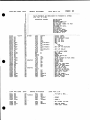
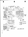
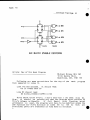
The 4515 decoder was chosen so that the extra 7 output lines
could be used to select notes if a 50240 chromatic tone generator is
added. I have an idea how to use the Hexkeypad for 8 octave note
selection by direct entry, no conversion charts necessary, but more
about that some other time.
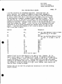
The 4042 Q outputs were selected so that during a program loop
that decrements a register the successive data will result in an
increasing frequency. Note that 50 toggles faster than 5F.
This
can be inverted by replacing the 4049 buffer with a non-inverting
4050 type but be wure to switch to Q outputs on DD # 1 & 2 for
active High logic.
•
The active High outputs of N0, Nl & TPB are combined through a
diode "and gate"~ iriverted and applied to the 4515 decoder to
provide the data accept strobe pulse for the 4042 latches •
1 M ohm range trim pots may be added to the common leads of the
D & A outputs which also presents a minimum value when all outputs
are active High.
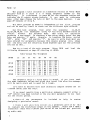
Two D & A's may be combined to form a single 256 step unit if
the resistor matrix is changed but each D & A must be addressed by
separate program bytes (5F + 67 = step 247 or 15 X 16 + ') 7).
Once the logic & parameters have been set for the SN76477 the
only thing needed is the q output trigger pulse to activate the
sound. This facilitates a wide variety of user programs since once
the parameters have been latched all that is needed to produce sound
is the Q trigger. As you see, one doesn't really need the 1802 at
all~
it mearly adds speed and variety to the sounds one wishes to
produce. A few switches and a push button could do as well but much
slower.
The little gadget wired to pin 11 of the SN7fi477 is a homemade
optoisolator. Just take an LED & a photoresistor, put them together
using a bit of heat shrink tubing to exclude outside lignt and that
makes a voltage dependent resistor. I use it to modulate the output
level by varing Q duty cycle but it could also be used to alter some
other parameter as well. Fairly fast attack/decay periods can be
implememted using the optoisolator under program control.
•
Radio Shack supplies an excellent data sheet on the SN76477 and
I have tried to design around their parameters.