1
Processor IP
Reference Guide
August 2004
R
Processor IP Reference Guide
www.xilinx.com
1-800-255-7778
August 2004
R
“Xilinx” and the Xilinx logo shown above are registered trademarks of Xilinx, Inc. Any rights not expressly granted herein are reserved.
CoolRunner, RocketChips, Rocket IP, Spartan, StateBENCH, StateCAD, Virtex, XACT, XC2064, XC3090, XC4005, and XC5210 are
registered trademarks of Xilinx, Inc.
The shadow X shown above is a trademark of Xilinx, Inc.
ACE Controller, ACE Flash, A.K.A. Speed, Alliance Series, AllianceCORE, Bencher, ChipScope, Configurable Logic Cell, CORE Generator,
CoreLINX, Dual Block, EZTag, Fast CLK, Fast CONNECT, Fast FLASH, FastMap, Fast Zero Power, Foundation, Gigabit Speeds...and
Beyond!, HardWire, HDL Bencher, IRL, J Drive, JBits, LCA, LogiBLOX, Logic Cell, LogiCORE, LogicProfessor, MicroBlaze, MicroVia,
MultiLINX, NanoBlaze, PicoBlaze, PLUSASM, PowerGuide, PowerMaze, QPro, Real-PCI, RocketIO, SelectIO, SelectRAM, SelectRAM+,
Silicon Xpresso, Smartguide, Smart-IP, SmartSearch, SMARTswitch, System ACE, Testbench In A Minute, TrueMap, UIM, VectorMaze,
VersaBlock, VersaRing, Virtex-II Pro, Virtex-II EasyPath, Wave Table, WebFITTER, WebPACK, WebPOWERED, XABEL, XACTFloorplanner, XACT-Performance, XACTstep Advanced, XACTstep Foundry, XAM, XAPP, X-BLOX +, XC designated products, XChecker,
XDM, XEPLD, Xilinx Foundation Series, Xilinx XDTV, Xinfo, XSI, XtremeDSP and ZERO+ are trademarks of Xilinx, Inc.
The Programmable Logic Company is a service mark of Xilinx, Inc.
All other trademarks are the property of their respective owners.
Xilinx, Inc. does not assume any liability arising out of the application or use of any product described or shown herein; nor does it convey
any license under its patents, copyrights, or maskwork rights or any rights of others. Xilinx, Inc. reserves the right to make changes, at any
time, in order to improve reliability, function or design and to supply the best product possible. Xilinx, Inc. will not assume responsibility for
the use of any circuitry described herein other than circuitry entirely embodied in its products. Xilinx provides any design, code, or
information shown or described herein "as is." By providing the design, code, or information as one possible implementation of a feature,
application, or standard, Xilinx makes no representation that such implementation is free from any claims of infringement. You are
responsible for obtaining any rights you may require for your implementation. Xilinx expressly disclaims any warranty whatsoever with
respect to the adequacy of any such implementation, including but not limited to any warranties or representations that the implementation
is free from claims of infringement, as well as any implied warranties of merchantability or fitness for a particular purpose. Xilinx, Inc. devices
and products are protected under U.S. Patents. Other U.S. and foreign patents pending. Xilinx, Inc. does not represent that devices shown
or products described herein are free from patent infringement or from any other third party right. Xilinx, Inc. assumes no obligation to
correct any errors contained herein or to advise any user of this text of any correction if such be made. Xilinx, Inc. will not assume any liability
for the accuracy or correctness of any engineering or software support or assistance provided to a user.
Xilinx products are not intended for use in life support appliances, devices, or systems. Use of a Xilinx product in such applications without
the written consent of the appropriate Xilinx officer is prohibited.
The contents of this manual are owned and copyrighted by Xilinx. Copyright 1994-2004 Xilinx, Inc. All Rights Reserved. Except as stated
herein, none of the material may be copied, reproduced, distributed, republished, downloaded, displayed, posted, or transmitted in any form
or by any means including, but not limited to, electronic, mechanical, photocopying, recording, or otherwise, without the prior written consent
of Xilinx. Any unauthorized use of any material contained in this manual may violate copyright laws, trademark laws, the laws of privacy and
publicity, and communications regulations and statutes.
August 2004
www.xilinx.com
1-800-255-7778
Processor IP Reference Guide
Processor IP Reference Guide
August 2004
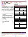
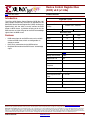
The following table shows the revision history for this document..
Version
Revision
August
2002
1.0
Initial Xilinx release for EDK 3.1
October
2002
1.1
Add memory and peripheral cores
November
2002
1.2
Release for EDK 3.1 Service Pack 2
January
2003
1.3
Release for EDK 3.1 Service Pack 3
March
2003
1.4
Release for EDK 3.2
June
2003
1.5
Release for EDK 3.2 Service Pack 2
August
2003
1.6
Release for EDK 6.1
September
2003
1.7
Release for EDK 6.1 Service Pack 1
November
2003
1.8
Release for EDK 6.1 Service Pack 2
January
2004
1.9
Release for EDK 6.2 Service Pack 2
March 2004
2.0
Release for EDK 6.2 Service Pack 2 Gms1
June 2004
2.1
Release for EDK 6.2.2
August
2004
3.0
Release for EDK 6.3
Processor IP Reference Guide
www.xilinx.com
1-800-255-7778
August 2004
R
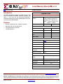
Contents
The Processor IP Reference Guide supports the Embedded Systems Design Kit (EDK) for
MicroBlaze™ and Virtex-II Pro™. For additional information, see the Embedded Software
Tools Guide and the PowerPC 405 Processor Reference Guide.
Part I: Embedded Processor IP
Chapter 1: OPB Usage in Xilinx FPGAs
Chapter 2: PLB Usage in Xilinx FPGAs
Chapter 3: Processor Cores
• MicroBlaze (v2.10a)
• MicroBlaze (v3.00a)
• PPC405 Top (Wrapper) (v2.00b)
• PPC405 (Wrapper) (v2.00c)
• PPC405 Virtex-4 (Wrapper) (v1.00a)
Chapter 4: Bus, Bridge, and Arbiter Infrastructure Cores
• On-Chip Peripheral Bus v2.0 with OPB Arbiter (v1.10a)
• On-Chip Peripheral Bus v2.0 with OPB Arbiter (v1.10b)
• OPB PCI Arbiter
• OPB to PLB Bridge (v1.00c)
• OPB to OPB Bridge (Lite Version)
• OPB to DCR Bridge
• Processor Local Bus (PLB) v3.4
• Processor Local Bus (PLB) v3.4 (v1.02a)
• PLB to OPB Bridge (v1.00b)
• PLB to OPB Bridge (v1.01a)
• Device Control Register Bus (DCR) v2.9 (v1.00a)
• Processor System Reset Module
• Local Memory Bus (LMB) v1.0
• OPB Arbiter (v1.02c)
• Fast Simplex Link Channel (v1.00b)
• Fast Simplex Link (FSL) Bus (v2.00a)
Processor IP Reference Guide
August 2004
www.xilinx.com
1-800-255-7778
v
R
• Digital Clock Manager (DCM) Module (v1.00a)
• Data Side OCM Bus V1.0 (v1.00b)
• Data Side OCM Bus (v2.00a)
• Instruction Side OCM Bus v1.0 (v1.00b)
• Instruction Side OCM Bus v1.0 (v2.00a)
Chapter 5: IPIF
• OPB IPIF Architecture (v1.23e)
- OPB IPIF Interrupt (v1.23e)
- OPB IPIF Packet FIFO (v1.23e)
- Direct Memory Access and Scatter Gather (v1.23e) (v1.23e)
• OPB IPIF (v2.00h)
• OPB IPIF (v3.01a)
• PLB IPIF (v1.00e)
• PLB IPIF (v2.00a)
• PLB IPIF (v2.01a)
• Channelized Direct Memory Access and Scatter Gather
Chapter 6: Memory Interface Cores
• LMB Block RAM (BRAM) Interface Controller
• OPB External Memory Controller (EMC) (v1.10b)
• OPB Synchronous DRAM (SDRAM) Controller (v1.00c)
• OPB Synchronous DRAM (SDRAM) Controller (v1.00d)
• OPB Block RAM (BRAM) Interface Controller (v1.00a)
• OPB Double Data Rate (DDR) Synchronous DRAM (SDRAM) Controller
(v1.00b)
• OPB Double Data Rate (DDR) Synchronous DRAM (SDRAM) Controller
(v1.10a)
• OPB SYSACE (System ACE) Interface Controller (v1.00b)
• PLB External Memory Controller (EMC) (v1.10b)
• PLB External Memory Controller (EMC) (v2.00.a)
• PLB Synchronous DRAM (SDRAM) Controller (v1.00c)
• PLB Synchronous DRAM (SDRAM) Controller (v1.00d)
• PLB Block RAM (BRAM) Interface Controller (v1.00a)
• PLB Block RAM (BRAM) Interface Controller (v1.00b)
• PLB Double Data Rate (DDR) Synchronous DRAM (SDRAM) Controller
(v1.00c)
• PLB Double Data Rate (DDR) Synchronous DRAM (SDRAM) Controller
(v1.10a)
• PLB Double Data Rate (DDR) Synchronous DRAM (SDRAM) Controller
(v1.11a)
• Data Side Block RAM (DSBRAM) Interface Controller (v2.00a)
Processor IP Reference Guide
August 2004
www.xilinx.com
1-800-255-7778
vi
R
• Data-Side BRAM Interface Controller (v3.00a)
• Instruction Side Block RAM (ISBRAM) Interface Controller (v2.00a)
• Instruction Side Block RAM (ISBRAM) Interface Controller (v3.00a)
• Block RAM (BRAM) Block (v1.00a)
Chapter 7: Peripheral Cores
• OPB Interrupt Controller (v1.00c)
• OPB 16550 UART
• OPB 16450 UART
• OPB UART Lite
• OPB JTAG_UART
• OPB IIC Bus Interface (v1.01b)
• OPB IIC Bus Interface (v1.01c)
• OPB Serial Peripheral Interface (SPI)
• OPB IPIF/LogiCore v3 PCI Core Bridge (v1.00b)
• OPB IPIF/LogiCore v3 PCI Core Bridge (v1.00c)
• OPB Ethernet Media Access Controller (EMAC) (v1.00m)
• OPB Ethernet Media Access Controller (EMAC) (v1.01a)
• OPB Ethernet Lite Media Access Controller (v1.00a)
• OPB Ethernet Lite Media Access Controller (v1.01a)
• OPB Asynchronous Transfer Mode Controller (OPB_ATMC) (v1.00b)
• OPB Asynchronous Transfer Mode Controller (OPB_ATMC) (v2.00a)
• OPB Single Channel HDLC Interface (v1.00b)
• OPB Multi Channel HDLC Interface (v2.00a) (v2.00a)
• OPB Multi Channel HDLC Interface (v2.01a)
• OPB Timebase WDT (v1.00a)
• OPB Timer/Counter
• OPB General Purpose Input/Output (GPIO) (v1.00a)
• OPB General Purpose Input/Output (GPIO) (v2.00a)
• OPB General Purpose Input/Output (GPIO) (v3.01a)
• OPB Central DMA Controller (v1.00a)
• OPB Central DMA Controller (v1.00b)
• OPB Central DMA Controller (v1.00c)
• OPB Delta-Sigma Digital to Analog Converter (DAC) (v1.00a)
• OPB Delta-Sigma Analog to Digital Converter (ADC) (v1.00a)
• OPB System Monitor/ADC (v1.00.a)
• Channel FIFO (v1.00a)
• Fixed Interval Timer (FIT)
• MII to RMII (v1.00a)
• MII to RMII (v1.00b)
Processor IP Reference Guide
August 2004
www.xilinx.com
1-800-255-7778
vii
R
• PLB 1-Gigabit Ethernet Media Access Controller (MAC) with DMA
(v1.00b)
• PLB 1-Gigabit Ethernet Media Access Controller (MAC) with DMA
(v1.01a)
• PLB Ethernet Media Access Controller (PLB_EMAC) (v1.00a)
• PLB Ethernet Media Access Controller (PLB_EMAC) (v1.01a)
• PLB 16550 UART (v1.00c)
• PLB 16450 UART (v1.00c)
• PLB RapidIO LVDS (v1.00a) (v1.00a)
• PLB RapidIO LVDS (v1.00c)
• PLB Asynchronous Transfer Mode Controller (PLB_ATMC) (v1.00a)
• PLB General Purpose Input/Output (GPIO) (v1.00b)
• DCR Interrupt Controller (v1.00b)
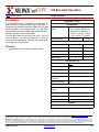
Chapter 8: Utility Peripherals
• Util Bus Split Operation
• Util Flip-Flop
• Util Reduced Logic (v1.00a)
• Util Vector Logic
Chapter 9: Debug and Verification
• Chipscope ICON
• Chipscope OPB IBA (Bus Analyzer) (v1.00a)
• Chipscope PLB IBA (Bus Analyzer) (v1.00a)
• Chipscope VIO (Virtual IO) (v1.00a)
• Chipscope Integrated Logic Analyzer (ILA) (v1.00a)
• OPB HWICAP
• Microprocessor Debug Module (MDM) (v1.00c)
• Microprocessor Debug Module (v2.00a)
• JTAG PPC Controller (v1.00b)
• JTAGPPC Controller (v2.00a)
Part II: Software
Chapter 10: Device Driver Programmer Guide
Chapter 11: Tornado 2.x BSP User Guide
Chapter 12: Device Driver Summary
Chapter 13: Automatic Generation of Tornado 2.x (VxWorks 5.x) Board Support
Packages
Processor IP Reference Guide
August 2004
www.xilinx.com
1-800-255-7778
viii
R
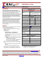
Part I: Embedded Processor IP
Part I of the Processor IP Reference Guide includes the following chapters:
Chapter 1, “OPB Usage in Xilinx FPGAs”
Chapter 2, “PLB Usage in Xilinx FPGAs”
Chapter 3 , “Processor Cores”
Chapter 4, “Bus, Bridge, and Arbiter Infrastructure Cores”
Chapter 5, “IPIF”
Chapter 6, “Memory Interface Cores”
Chapter 7, “Peripheral Cores”
Chapter 8, “Utility Peripherals”
Chapter 9, “Debug and Verification”
Processor IP Reference Guide
August 2004
www.xilinx.com
1-800-255-7778
1
R
Chapter 1
OPB Usage in Xilinx FPGAs
Overview
This chapter includes the following sections:
Xilinx OPB Usage
Legacy OPB Devices
OPB Usage Notes
OPB Comparison
For detailed information about the IBM OPB, you may register for the IBM CoreConnect
Lounge on the Xilinx web site to get access the the IBM CoreConnect documentation, or
you may view the CoreConnect content on the IBM web site.
The OPB is one element of IBM’s CoreConnect architecture, and is a general-purpose
synchronous bus designed for easy connection of on-chip peripheral devices. The OPB
includes the following features:
•
32-bit or 64-bit data bus
•
Up to 64-bit address
•
Supports 8-bit, 16-bit, 32-bit, and 64-bit slaves
•
Supports 32-bit and 64-bit masters
•
Dynamic bus sizing with byte, halfword, fullword, and doubleword transfers
•
Optional Byte Enable support
•
Distributed multiplexer bus instead of 3-state drivers
•
Single cycle transfers between OPB master and OPB slaves (not including arbitration)
•
Support for sequential address protocol
•
16-cycle bus time-out (provided by arbiter)
•
Slave time-out suppress capability
•
Support for multiple OPB bus masters
•
Support for bus parking
•
Support for bus locking
•
Support for slave-requested retry
•
Bus arbitration overlapped with last cycle of bus transfers
The OPB is a full-featured bus architecture with many features that increase bus
performance. You can use most of these features effectively in the FPGA architecture.
However, some features can result in the inefficient use of FPGA resources or can lower
system clock rates. Consequently, Xilinx uses an efficient subset of the OPB for Xilinxdeveloped OPB devices. However, because of the flexible nature of FPGAs, you can also
implement systems utilizing OPB devices that are fully OPB V2.1 compliant.
Processor IP Reference Guide
August 2004
www.xilinx.com
1-800-255-7778
2
R
Xilinx OPB Usage
Xilinx OPB Usage
OPB Options
Legacy Devices
Previous to OPB V2.0, there was a single signaling protocol for OPB data transfers. This
protocol (which is also present in OPB V2.0 and later specifications) supports dynamic bus
sizing through the use of transfer qualifiers and acknowledge signals. The transfer
qualifiers denote the size of the transfer initiated by the master, and the acknowledge
signals indicate the size of the transfer from the slave. Devices that support this type of
dynamic bus sizing are called legacy devices.
Byte-enable Devices
Starting with OPB V2.0, IBM introduced an optional, alternate transfer protocol based on
Byte Enables. In the byte-enable architecture, each byte lane of the data bus has an
associated byte enable signal. For each transfer, the byte enable signals indicate which byte
lanes have valid data. This eliminates the need for separate transfer qualifiers that indicate
the transfer size since all size information is contained in the byte enable signals. The byteenable architecture does not permit dynamic bus sizing, since there is only one
acknowledge signal for each transfer. The OPB V2.0 specification (and later) allows you to
build systems that are legacy-only, byte-enable only, or mixed. Devices that only support
the byte-enable signaling are called byte-enable devices.
OPB V2.0 Devices
Devices that support both byte-enable signaling and legacy signaling are called OPB V2.0
devices. Systems that have both legacy signaling and byte-enable signaling can perform
dynamic bus sizing. Note that legacy devices do not support byte-enable transfers.
Xilinx OPB Devices
These various transfer protocols have several implications for Xilinx OPB device
implementations.
Conversion Cycles
Dynamic bus sizing (as supported by legacy devices) results in conversion cycles, which are
extra transfer cycles that re-transfer data when the master-initiated transfer is larger than
the slave response. For example, in a legacy system, if a master writes a 32-bit word to a
slave, and the 8-bit device slave responds that it only accepted 8-bits of the transfer, then
the master must perform three additional conversion cycles to transfer all of the data to the
slave. Generating conversion cycles requires more logic, increases the complexity of the
master, and is not an efficient use of FPGA resources. The byte-enable architecture
provides a simple alternative to this problem, and is easier to implement in an FPGA.
Write Mirroring and Read Steering
Another consequence of supporting devices smaller than the bus size is write mirroring and
read steering. In the OPB specification, devices smaller than the bus size are always leftjustified (aligned toward the most significant side of the bus) so that the byte lanes
associated with the smaller devices are easily determined. For example, a byte-wide
peripheral is always located on the most-significant byte of the bus. The peripheral writes
and reads data using this byte-lane. You can simplify the design of OPB masters by using
a byte-enable only, no-write-mirroring architecture. A small degree of added complexity is
required for peripherals that are smaller than the bus size if OPB masters do not mirror
data.
Processor IP Reference Guide
August 2004
www.xilinx.com
1-800-255-7778
3
R
Xilinx OPB Usage
Ideal FPGA Implementation of OPB-based System
The ideal FPGA implementation of an OPB-based system has the following features:
•
Requires no conversion cycles
•
Uses only the byte-enable architecture as specified in the OPB specification
•
Does not require masters to mirror write data
These characteristics help determine how Xilinx-developed OPB devices are implemented.
The detailed specifications that describe how the OPB is used in Xilinx intellectual
property are provided in the next section.
Specifications for OPB Usage in Xilinx-developed OPB Devices
Xilinx-developed OPB devices adhere to the following OPB usage rules:
•
The width of the OPB data buses and address buses is 32 bits. Note that some
peripherals may parameterize these widths, but currently only 32-bit buses are
supported. Peripherals that are smaller than 32-bits can be attached to the OPB with a
corresponding restriction in addressing. For example, an 8-bit peripheral at base
address A can be attached to byte lane 0, but can only be addressed at A, A+4, A+8,
and so on.
•
All OPB devices (masters and slaves) are byte-enable devices. These devices do not
support the legacy data transfer signals and therefore do not support dynamic bus
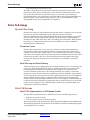
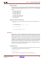
sizing. OPB masters do not mirror data to unused byte lanes. See Figure 1-1 for the
byte lane usage for aligned transfers.
•
All OPB devices (masters and slaves) are required to output logic zero when they are
inactive. This eliminates the need for the Mn_DBusEn and Sln_DBusEn signals
external to the master or slave. The enable function is still implemented within the
device.
•
To obtain better timing in the FPGA implementation of the OPB, the OPB_timeout
signal is registered. This means that all slaves must assert Sl_xferAck or Sl_retry on or
before the rising edge of the 16th clock cycle after the assertion of OPB_select. If an
OPB slave wishes to assert Sl_toutSup, Sl_toutSup must be asserted on or before the
rising edge of the 15th clock after the assertion of OPB_select.
Processor IP Reference Guide
August 2004
www.xilinx.com
1-800-255-7778
4
R
Xilinx OPB Usage
Data Bus
0:7
0:7
0:7
0:7
16:23
24:31
8:15
16:23
24:31
16:23
24:31
24:31
halfword transfer
halfword transfer
byte transfer
Mn_ABus(30:31) = "00",
Mn_BE = "1100"
Mn_ABus(30:31) = "10",
Mn_BE = "0011"
Mn_ABus(30:31) = "00",
Mn_BE = "1000"
Data Bus
0:7
0:7
0:7
8:15
16:23
24:31
8:15
16:23
Slave
Data Bus
Master
Data Bus
Slave
Master
n_ABus(30:31) = "00",
Mn_BE = "1111"
8:15
24:31
8:15
16:23
Slave
word transfer
Slave
8:15
Master
16:23
Slave
8:15
Master
Data Bus
Master
Data Bus
Master
Data Bus
24:31
byte transfer
byte transfer
byte transfer
Mn_ABus(30:31) = "01",
Mn_BE = "0100"
Mn_ABus(30:31) = "10",
Mn_BE = "0010"
Mn_ABus(30:31) = "11",
Mn_BE = "0001"
Figure 1-1:
•
Slave
The byte-enables and the least-significant address bits are driven by all masters and
contain consistent information. Examples of byte lane usage for aligned transfers are
shown in the following figure:
Slave
Master
•
Byte lane usage for aligned transfers
All OPB slave devices that require a continuous address space (use of all byte lanes)
will implement an attachment to the OPB bus that is as wide as the OPB data width,
regardless of device width. This eliminates the need for left justification on the OPB
bus and eliminates the need for masters to mirror write data.
As an example, consider an 8-bit memory device that must be addressed at
consecutive byte addresses being attached to a 32-bit OPB. The 8-bit memory device
must implement a 32-bit wide attachment to the OPB; in the bus attachment, data is
steered from the proper byte lane into the 8-bit device for writes, and from the 8-bit
device onto the proper byte lane for reads.
The simplest way to accomplish this is with a multiplexer for steering the writes, and
a connection from the 8-bit device to all byte lanes (essentially mirroring to all byte
lanes) for reads.
•
By convention, registers in all OPB slave devices are aligned to word boundaries
(lowest two address bits are "00"), regardless of the size of the data in the register or
the size of the peripheral.
•
Master and Slave I/O: OPB masters adhere to the signal set shown in Table 1-1. OPB
slaves adhere to the signal set shown in Table 1-2. Devices that are both master and
slave adhere to the signal set shown in Table 1-3. Page numbers referenced in the
tables apply to both the OPB V2.0 specification and the OPB V2.1 specification, both
from IBM. All signals shown must be present, except for the one signal shown as
optional (<Master>_DBus[0:31] for devices that are both master and slave). No
additional signals for OPB interconnection may be added. The naming convention is
as follows: <Master> represents a master name or acronym that starts with an uppercase letter, <Slave> represents a slave name or acronym that starts with an upper-case
letter. <nOPB> represents an OPB identifier (for masters or slaves with more than
OPB attachment) and must start with an uppercase letter and end with upper-case
Processor IP Reference Guide
August 2004
www.xilinx.com
1-800-255-7778
5
R
Xilinx OPB Usage
"OPB". For devices with a single OPB attachment, the <nOPB> identifier should
default to "OPB" (for example, OPB_ABus). All other parts of the signal name must be
referenced exactly as shown (including case).
Table 1-1:
Summary of OPB master-only I/O
Signal
I/O
Description
Page
(in Ref. 1)
<nOPB>_Clk
I
OPB Clock
<nOPB>_Rst
I
OPB Reset
<Master>_ABus[0:31]
O
Master address bus
OPB-11
<Master>_BE[0:3]
O
Master byte enables
OPB-16
<Master>_busLock
O
Master buslock
OPB-9
<Master>_DBus[0:31]
O
Master write data bus
OPB-13
<Master>_request
O
Master bus request
OPB-8
<Master>_RNW
O
Master read, not write
OPB-12
<Master>_select
O
Master select
OPB-12
<Master>_seqAddr
O
Master sequential address
OPB-13
<nOPB>_DBus[0:31]
I
OPB read data bus
OPB-13
<nOPB>_errAck
I
OPB error acknowledge
OPB-15
<nOPB>_MGrant
I
OPB bus grant
OPB-9
<nOPB>_retry
I
OPB bus cycle retry
OPB-10
<nOPB>_timeout
I
OPB timeout error
OPB-10
<nOPB>_xferAck
I
OPB transfer acknowledge
OPB-14
Table 1-2:
Summary of OPB Slave-only I/O
Signal
I/O
Description
Page
(in Ref. 1)
<nOPB>_Clk
I
OPB Clock
<nOPB>_Rst
I
OPB Reset
<Slave>_DBus[0:31]
O
Slave data bus
OPB-11
<Slave>_errAck
O
Slave error acknowledge
OPB-15
<Slave>_retry
O
Slave retry
OPB-10
<Slave>_toutSup
O
Slave timeout suppress
OPB-15
<Slave>_xferAck
O
Slave transfer acknowledge
OPB-14
<nOPB>_ABus[0:31]
I
OPB address bus
OPB-11
<nOPB>_BE
I
OPB byte enable
OPB-16
<nOPB>_DBus[0:31]
I
OPB data bus
OPB-13
Processor IP Reference Guide
August 2004
www.xilinx.com
1-800-255-7778
6
R
Xilinx OPB Usage
Table 1-2:
Summary of OPB Slave-only I/O (Continued)
Signal
I/O
Description
Page
(in Ref. 1)
<nOPB>_RNW
I
OPB read/not write
OPB-12
<nOPB>_select
I
OPB select
OPB-12
<nOPB>_seqAddr
I
OPB sequential address
OPB-13
Table 1-3:
Summary of OPB Master/Slave Device I/O
Signal
I/O
Description
Page
(in Ref. 1)
<nOPB>_Clk
I
OPB Clock
<nOPB>_Rst
I
OPB Reset
<Master>_ABus[0:31]
O
Master address bus
OPB-11
<Master>_BE[0:3]
O
Master byte enables
OPB-16
<Master>_busLock
O
Master buslock
OPB-9
<Master>_DBus[0:31]
O
Master write data bus (optional)
OPB-13
<Master>_request
O
Master bus request
OPB-8
<Master>_RNW
O
Master read, not write
OPB-12
<Master>_select
O
Master select
OPB-12
<Master>_seqAddr
O
Master sequential address
OPB-13
<nOPB>_DBus[0:31]
I
OPB read data bus
OPB-13
<nOPB>_errAck
I
OPB error acknowledge
OPB-15
<nOPB>_MGrant
I
OPB bus grant
OPB-9
<nOPB>_retry
I
OPB bus cycle retry
OPB-10
<nOPB>_timeout
I
OPB timeout error
OPB-10
<nOPB>_xferAck
I
OPB transfer acknowledge
OPB-14
<Slave>_DBus[0:31]
O
Slave data bus (may optionally function as
master write data bus if <Master>_DBus
not present)
OPB-11
<Slave>_errAck
O
Slave error acknowledge
OPB-15
<Slave>_retry
O
Slave retry
OPB-10
<Slave>_toutSup
O
Slave timeout suppress
OPB-15
<Slave>_xferAck
O
Slave transfer acknowledge
OPB-14
<nOPB>_ABus[0:31]
I
OPB address bus
OPB-11
<nOPB>_BE
I
OPB byte enable
OPB-16
<nOPB>_RNW
I
OPB read/not write
OPB-12
<nOPB>_select
I
OPB select
OPB-12
<nOPB>_seqAddr
I
OPB sequential address
OPB-13
Processor IP Reference Guide
August 2004
www.xilinx.com
1-800-255-7778
7
R
Legacy OPB Devices
Additional Notes on Signal Sets
•
Xilinx-developed OPB devices do not support dynamic bus sizing and consequently
do not use the following legacy signals: Mn_dwXfer, Mn_fwXfer, Mn_hwXfer,
Sln_dwAck, Sln_fwAck, and Sln_hwAck.
•
Since Xilinx-developed OPB devices are byte-enable only, the Mn_beXfer and
Sln_beAck signals are not required and so are not used.
•
The signals required for masters and slaves are separate from the signals present in
the OPB interconnect. The OPB interconnect (the OR gates and other logic required to
connect OPB devices) supports the full OPB V2.1 specification (i.e. all signals are
present). Thus the OPB interconnect does not limit a design to byte-enable devices
and supports designs in which a mix of byte-enable, legacy, and OPB V2.0 devices are
present. The bus interconnect does not limit the use of any feature of the V2.1
specification.
Legacy OPB Devices
Although byte-enable devices are the preferred and most efficient OPB devices in Xilinx
devices, some designs may also use legacy OPB devices or fully V2.0 compliant devices.
However, a legacy device cannot communicate directly with a byte-enable device because
they use different signal sets. An interface layer between the byte-enable device and the
legacy device is required. This interface is called the Byte Enable Interface (BEIF) device.
Processor IP Reference Guide
August 2004
www.xilinx.com
1-800-255-7778
8
R
Legacy OPB Devices
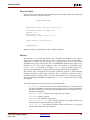
Mixed Systems
The system shown in the following figure represents a design with a mix of byte-enable,
legacy, and OPB V2.0 devices. The BEIF device converts the legacy-type signals to byteenable-type signals and vice versa.
OPB V2.0
Master
OPB V2.0
Slave
Legacy
Master
Legacy
Slave
OPB Bus
Monitor or BFM
(test only)
BEIF
BEIF
BEIF
BEIF
BEIF
OPB Arbiter
OPB
Byte-Enable
Master1
Byte-Enable
Master2
Figure 1-2:
Byte-Enable
Slave1
Byte-Enable
Slave2
PLB-to-OPB
Bridge
OPB Interconnect with Mixed Device Types
The BEIF device contains the following logic, not all of which must be used in all
situations:
•
Signal translation for byte-enable device to legacy device transfers: <Master>_BE is
translated to the appropriate <Master>_hwXfer, <Master>_fwXfer, and
<Master>_dwXfer. <nOPB>_BE is translated to the appropriate <nOPB>_hwXfer,
<nOPB>_fwXfer, and <nOPB>_dwXfer. <Slave>_hwXfer, <Slave>_fwXfer, and
<Slave>_dwXfer
are
translated
to
<Slave>_xferAck.
<nOPB>_hwXfer,
<nOPB>_fwXfer, and <nOPB>_dwXfer are translated to <nOPB>_xferAck. The
correct lower address bits are also generated.
•
Signal translation for legacy device to byte-enable device transfers: <Master>_hwXfer,
<Master>_fwXfer, and <Master>_dwXfer are translated to <Master>_BE .
<nOPB>_hwXfer, <nOPB>_fwXfer, and <nOPB>_dwXfer are translated to
<nOPB>_BE . <Slave>_xferAck is translated to <Slave>_hwXfer, <Slave>_fwXfer,
and <Slave>_dwXfer. <nOPB>_xferAck is translated to <nOPB>_hwXfer,
<nOPB>_fwXfer, and <nOPB>_dwXfer.
•
Mirroring and steering logic.
•
Conversion cycle generator for byte-enable device to legacy device transfers.
With this architecture, systems that do not require full V2.1 features (for example, systems
that contain only Xilinx IP) do not need to instantiate the BEIF and hence optimally use the
available FPGA resources. Systems that require legacy or OPB V2.0 devices must
instantiate the BEIF, although the most costly part of the BEIF (the conversion cycle
generator) only needs to be instantiated if conversion cycles are possible (not all slaves will
cause generation of conversion cycles).
Processor IP Reference Guide
August 2004
www.xilinx.com
1-800-255-7778
9
R
OPB Usage Notes
OPB Usage Notes
The following are general notes on OPB usage that apply primarily to mixed systems:
•
Conversion cycles are only required when a master generates a transfer request to a
slave that is larger than the slave’s width and the slave is capable of indicating that it
accepted a smaller transfer than the master requested hence requiring with a
conversion cycle.
•
Byte-enable masters cannot directly generate conversion cycles. They require a
conversion cycle generator in the Byte Enable Interface (BEIF) device. This is because
byte-enable masters do not receive any size information in the acknowledge from the
slave.
•
Byte-enable slaves cannot cause generation of conversion cycles. A consequence of
this is that any master accessing a byte-enable slave can only transfer data up to the
size of the slave. Transfers larger than the slave size will result in either 1) no response
from the slave (time-out), 2) an errAck from the slave, or 3) lost data; the actual result
depends on how the decode and acknowledge logic is implemented in the slave.
•
Conversion cycle generator logic in the BEIF is required only for byte-enable device to
legacy/OPB V2.0 device transfers.
•
Write mirroring and read steering in the V2.1 specification is based on left-justified
peripherals. A more complex slave attachment can be used instead of left justification.
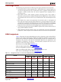
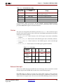
OPB Comparison
Table 1-4 illustrates the major embedded processor bus architectures used in Xilinx FPGAs
and lists some of their characteristics. Each bus has different capabilities in terms of data
transfer rates, multi-master capability, and data bursting. The use of a particular bus is
dictated by the processor used, the data bandwidth required in the application, and
availability of peripherals. The OPB is a general-purpose peripheral bus that can be
effectively used in many design situations.
PLB - Processor Local Bus (IBM). PLB Reference
OPB - On-chip Peripheral Bus (IBM). OPB Reference
OCM - On-chip Memory interface (IBM). OCM Reference
LMB - Local Memory Bus (Xilinx). MicroBlaze Processor Reference Guide
DCR - Device Control Register bus (IBM). DCR Reference
Table 1-4:
Comparison of buses used in Xilinx Embedded Processor Systems
Feature
Processor family
CoreConnect Buses
PLB
PPC405
Other Buses
OPB
DCR
OCM
LMB
PPC405,
PPC405
PPC405
MicroBlaze
MicroBlaze
Data bus width
64
32
32
32
32
Address bus width
32
32
10
32
32
Clock rate, MHz (max)1
100
125
125
375
125
Masters (max)
16
16
1
1
1
Masters (typical)
2-8
2-8
1
1
1
Slaves (max)2
16
16
16
1
1
Slaves (typical)
2-6
2-8
1-8
1
1
1600 MB/s
500 MB/s
500 MB/s
500 MB/s
500 MB/s
Data rate (peak)3
Processor IP Reference Guide
August 2004
www.xilinx.com
1-800-255-7778
10
R
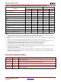
Document Revision History
Table 1-4:
Comparison of buses used in Xilinx Embedded Processor Systems (Continued)
CoreConnect Buses
Feature
Other Buses
PLB
OPB
DCR
OCM
LMB
533 MB/s5
167 MB/s6
100 MB/s8
333 MB/s7
333 MB/s8
Concurrent read/write
Yes
No
No
No
No
Address pipelining
Yes
No
No
No
No
Bus locking
Yes
Yes
No
No
No
Retry
Yes
Yes
No
No
No
Timeout
Yes
Yes
No
No
No
Fixed burst
Yes
No
No
No
No
Variable burst
Yes
No
No
No
No
Cache fill
Yes
No
No
No
No
Target word first
Yes
No
No
No
No
High
Medium
Low
Low
Low
Yes
Yes
No
Yes
Yes
Data rate (typical)4
FPGA resource usage
Compiler support for load/store
Notes:
1. Maximum clock rates are estimates and are presented for comparison only. The actual maximum clock rate for each bus
is dependent on device family, device speed grade, design complexity, and other factors.
2. Max value set by maximum allowed parameter value specified in the core. Actual bus specification does not limit this
value.
3. Peak data rate is the maximum theoretical data transfer rate at the clock rate shown for each bus.
4. The typical data rates are intended to illustrate data rates that are representative of actual system configurations. The
typical data is highly dependent on the application software and system hardware configuration.
5. Assumes primarily cache-line fills, minimal read/write concurrency (66.7% bus utilization).
6. Assumes minimal use of sequential address capabilities and 3 clock cycles per OPB transfer.
7. The OCM controller operates at the PPC405 core clock rate, but its data transfer rate is limited by the access time of the
on-chip memory. The typical data rate assumes 66.7% bus utilization.
8. Assumes 66.7% bus utilization.
9. Assumes DCR operates at same clock rate as PLB and each DCR access requires 5 clock cycles. The number of clock
cycles per DCR transfer is dependent on how many DCR devices are present in the system. Each additional DCR device
adds latency to all DCR transfers.
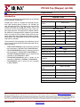
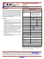
Document Revision History
Date
Version
10/17/01
1.0
Initial Xilinx version.
10/19/01
1.1
Minor editorial changes. Added links to bus references.
12/10/01
1.2
Changed Figure 2 and other minor edits.
3/20/02
1.3
Updated for MDK 2.2
01/26/04
1.4
Updated copyright.
Processor IP Reference Guide
August 2004
Revision
www.xilinx.com
1-800-255-7778
11
R
Chapter 2
PLB Usage in Xilinx FPGAs
Summary
This chapter describes how to use the IBM Processor Local Bus (PLB) in Xilinx FPGAs, and
provides guidelines and simplifications for efficient FPGA implementations, and the set of
signals used in Xilinx-developed PLB devices. The following sections are included:
This chapter includes the following sections:
Xilinx PLB Usage
PLB Comparison
Overview
For detailed information on the IBM PLB, you may register for the IBM CoreConnect
Lounge on the Xilinx web site to get access the the IBM CoreConnect documentation, or
you may view the CoreConnect content on the IBM web site.
The PLB is one element of IBM’s CoreConnect architecture, and is a high-performance
synchronous bus designed for connection of processors to high-performance peripheral
devices. The PLB includes the following features (from 64-bit Processor Local Bus,
Architecture Specifications):
•
Overlapping of read and write transfers allows two data transfers per clock cycle for
maximum bus utilization.
•
Decoupled address and data buses support split-bus transaction capability for
improved bandwidth.
•
Address pipelining reduces overall bus latency by allowing the latency associated
with a new request to be overlapped with an ongoing data transfer in the same
direction.
•
Late master request abort capability reduces latency associated with aborted requests.
•
Hidden (overlapped) bus request/grant protocol reduces arbitration latency.
•
Bus architecture supports sixteen masters and any number of slave devices.
•
Four levels of request priority for each master allow PLB implementations with
various arbitration schemes.
•
Bus arbitration-locking mechanism allows for master-driven atomic operations.
•
Support for 16-, 32-, and 64-byte line data transfers.
•
Read word address capability allows slave devices to fetch line data in any order (that
is, target word-first or sequential).
•
Sequential burst protocol allows byte, halfword, and word burst data transfers in
either direction.
•
Guarded and unguarded memory transfers allow a slave device to enable or disable
Processor IP Reference Guide
August 2004
www.xilinx.com
1-800-255-7778
12
R
Xilinx PLB Usage
the pre-fetching of instructions or data.
The PLB is a full-featured bus architecture with many features that increase bus
performance. Most of these features map well to the FPGA architecture, however, some
can result in the inefficient use of FPGA resources or can lower system clock rates.
Consequently, Xilinx uses an efficient subset of the PLB for Xilinx-developed PLB devices.
However, because of the flexible nature of FPGAs, you can also implement systems
utilizing PLB devices that are fully PLB V3.5 compliant.
Xilinx PLB Usage
Dynamic Bus Sizing
Dynamic bus sizing is a PLB architectural feature that allows a designer to mix 32 and 64bit devices on the same 64-bit PLB. A master provides a master size signal,
<Master>_MSize[0:1], that describes the data width of the master initiating a transaction.
Slaves provide a similar signal, Sl_Mn_SSize(0:1), with the address acknowledge that
describes the data width of the slave that is responding to the transaction. While dynamic
bus sizing is a useful architectural feature, its use in FPGAs can result in inefficient
implementations of PLB masters.
Conversion Cycles
Dynamic bus sizing results in conversion cycles, which are extra transfer cycles that retransfer data when the master-initiated transfer is larger than the slave response. For
example, if a master writes a 64-bit word to a slave, and the 32-bit device slave responds
with a slave size of 32-bits, then the master must perform an additional conversion cycle to
transfer all of the data to the slave. Generating conversion cycles requires more logic,
increases the complexity of the master, and is typically not an efficient use of FPGA
resources.
Write Mirroring and Read Steering
Another consequence of supporting devices smaller than the bus size is write mirroring and
read steering. In the PLB specification, devices smaller than the bus size are always leftjustified (aligned toward the most significant side of the bus) so that the byte lanes
associated with the smaller devices are easily determined. For example, a word-wide
peripheral is always located on the most-significant word of the 64-bit bus. The peripheral
writes and reads data using only the four most significant byte lanes. You can simplify the
design of PLB masters by using an architecture that requires no write mirroring and
transfers data based on which byte enables are active. A small degree of added complexity
is required in the bus attachment for peripherals that are smaller than the bus size if PLB
masters do not mirror data. This additional logic is built into the parameterizable slave
attachment in each Xilinx peripheral.
Xilinx PLB Devices
Ideal FPGA Implementation of PLB-based System
The ideal FPGA implementation of a PLB-based system has the following features:
•
Requires no conversion cycles
•
Does not require masters to mirror write data
These characteristics help determine how Xilinx-developed PLB devices are implemented.
The detailed specifications that describe how the PLB is used in Xilinx intellectual property
are provided in the next section.
Processor IP Reference Guide
August 2004
www.xilinx.com
1-800-255-7778
13
R
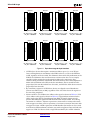
Xilinx PLB Usage
Specifications for PLB Usage in Xilinx-developed PLB Devices
Xilinx-developed PLB devices adhere to the following PLB usage rules:
•
PLB masters are not required to support dynamic bus sizing. PLB masters are not
required to mirror data to unused byte lanes. See Figure 2-1 and Figure 2-2 for the
byte lane usage for aligned transfers. PLB Masters are required to correctly drive the
<Master>_MSize[0:1] signals. PLB slaves are required to correctly drive the
<Slave>_SSize[0:1] signals for PLB masters that do provide conversion cycles (such as
the PowerPC 405).
•
All PLB slaves are required to output logic zero when they are inactive.
•
The byte-enables and the least-significant address bits are driven by all masters and
contain consistent information. Examples of byte lane usage for aligned transfers are
shown in Figure 2-1 and Figure 2-2.
0:7
8:15
8:15
16:23
16:23
16:23
24:31
32:39
24:31
32:39
24:31
32:39
word transfer
word transfer
Mn_ABus(29:31) = "000",
Mn_BE = "11111111"
Mn_ABus(29:31) = "000",
Mn_BE = "11110000"
Mn_ABus(29:31) = "100",
Mn_BE = "00001111"
Data Bus
Data Bus
Data Bus
Data Bus
0:7
0:7
0:7
0:7
8:15
8:15
8:15
8:15
16:23
16:23
16:23
16:23
24:31
32:39
24:31
32:39
24:31
32:39
Master
doubleword transfer
Slave
56:63
Master
56:63
Slave
48:55
56:63
Master
40:47
48:55
Slave
40:47
48:55
Master
40:47
24:31
32:39
40:47
40:47
40:47
40:47
48:55
48:55
48:55
48:55
56:63
56:63
56:63
56:63
Slave
0:7
8:15
Master
0:7
Slave
Data Bus
Master
Data Bus
Slave
Data Bus
Slave
The width of the PLB data buses is 64 bits and the width of address buses is 32 bits.
Note that some peripherals may parameterize these widths, but currently only 64-bit
data buses are supported. Peripherals that are smaller than 64-bits can be attached to
the PLB with a corresponding restriction in addressing. For example, a 32-bit
peripheral at base address A can be attached to byte lanes 0 – 4, but word-wide
accesses can only be addressed at A, A+8, A+16, etc.
Master
•
halfword transfer
halfword transfer
halfword transfer
halfword transfer
Mn_ABus(29:31) = "000",
Mn_BE = "11000000"
Mn_ABus(29:31) = "010",
Mn_BE = "00110000"
Mn_ABus(29:31) = "100",
Mn_BE = "00001100"
Mn_ABus(29:31) = "110",
Mn_BE = "00000011"
Figure 2-1:
Processor IP Reference Guide
August 2004
Byte lane usage for aligned doubleword, word, and halfword transfers
www.xilinx.com
1-800-255-7778
14
R
0:7
0:7
8:15
8:15
8:15
16:23
16:23
16:23
16:23
24:31
32:39
24:31
32:39
24:31
32:39
24:31
32:39
Slave
0:7
8:15
Master
0:7
Slave
Data Bus
Master
Data Bus
Slave
Data Bus
Master
Data Bus
Slave
Master
Xilinx PLB Usage
40:47
40:47
40:47
40:47
48:55
48:55
48:55
48:55
56:63
56:63
56:63
56:63
byte transfer
Data Bus
Data Bus
Data Bus
Data Bus
0:7
0:7
0:7
0:7
8:15
8:15
8:15
8:15
16:23
16:23
16:23
16:23
32:39
Slave
24:31
24:31
32:39
24:31
32:39
24:31
32:39
40:47
40:47
40:47
40:47
48:55
48:55
48:55
48:55
56:63
56:63
56:63
56:63
Slave
Mn_ABus(29:31) = "011",
Mn_BE = "00010000"
Master
Mn_ABus(29:31) = "010",
Mn_BE = "00100000"
Slave
Mn_ABus(29:31) = "001",
Mn_BE = "01000000"
Master
Mn_ABus(29:31) = "000",
Mn_BE = "10000000"
Slave
byte transfer
Master
byte transfer
Master
byte transfer
byte transfer
byte transfer
byte transfer
byte transfer
Mn_ABus(29:31) = "100",
Mn_BE = "00001000"
Mn_ABus(29:31) = "101",
Mn_BE = "00000100"
Mn_ABus(29:31) = "110",
Mn_BE = "00000010"
Mn_ABus(29:31) = "111",
Mn_BE = "00000001"
Figure 2-2:
Byte lane usage for byte transfers
•
All PLB slave devices that require a continuous address space (i.e. use of all byte
lanes) will implement an attachment to the PLB bus that is as wide as the PLB data
width, regardless of device width. This eliminates the need for left justification on the
PLB bus and eliminates the need for masters to mirror write data. As an example,
consider a 32-bit memory device that must be addressed at consecutive byte
addresses being attached to a 64-bit PLB. The 32-bit memory device must implement a
64-bit wide attachment to the PLB; in the bus attachment, data is steered from the
proper byte lanes into the 32-bit device for writes, and from the 32-bit device onto the
proper byte lanes for reads.
•
By convention, registers in all PLB slave devices are aligned to word boundaries
(lowest two address bits are "00"), regardless of the size of the data in the register or
the size of the peripheral.
•
Master and Slave I/O: PLB masters adhere to the signal set shown in Table 2-1. PLB
slaves adhere to the signal set shown in Table 2-2. Page numbers referenced in the
tables apply to the PLB V3.5 specification from IBM. All signals shown must be
present. No additional signals for PLB interconnection may be added. The naming
convention is as follows: <Master> represents a master name or acronym that starts
with an upper-case letter, <Slave> represents a slave name or acronym that starts with
an upper-case letter. <nPLB> represents an PLB identifier (for masters or slaves with
more than one PLB attachment) and must start with an uppercase letter and end with
upper-case "PLB". For devices with a single PLB attachment, the <nPLB> identifier
Processor IP Reference Guide
August 2004
www.xilinx.com
1-800-255-7778
15
R
Xilinx PLB Usage
should default to "PLB" (for example, PLB_ABus). All other parts of the signal name
must be referenced exactly as shown (including case).
Table 2-1:
Summary of PLB Master-only I/O
Signal
I/O
Description
Page
(in Ref. 1)
<nPLB>_Clk
I
PLB Clock (SYS_plbClk)
PLB-11
<nPLB>_Rst
I
PLB Reset (SYS_plbReset)
PLB-11
<Master>_abort
O
Master abort bus request indicator
PLB-19
<Master>_ABus[0:31]
O
Master address bus
PLB-27
<Master>_BE[0:7]
O
Master byte enables
PLB-21
<Master>_busLock
O
Master buslock
PLB-13
<Master>_compress
O
Master compressed data transfer
indicator
PLB-25
<Master>_guarded
O
Master guarded transfer indicator
PLB-26
<Master>_lockErr
O
Master lock error indicator
PLB-27
<Master>_MSize[0:1]
O
Master data bus size
PLB-40
<Master>_ordered
O
Master synchronize transfer
indicator
PLB-26
<Master>_priority[0:1]
O
Master request priority
PLB-12
<Master>_rdBurst
O
Master burst read transfer
indicator
PLB-34
<Master>_request
O
Master request
PLB-12
<Master>_RNW
O
Master read/not write
PLB-21
<Master>_size[0:3]
O
Master transfer size
PLB-24
<Master>_type[0:2]
O
Master transfer type
PLB-25
<Master>_wrBurst
O
Master burst write transfer
indicator
PLB-29
<Master>_wrDBus[0:63]
O
Master write data bus
PLB-28
<nPLB>_<Master>_Busy
I
PLB master slave busy indicator
PLB-36
<nPLB>_<Master>_Err
I
PLB master slave error indicator
PLB-37
<nPLB>_<Master>_WrBTerm
I
PLB master terminate write burst
indicator
PLB-30
<nPLB>_<Master>_WrDAck
I
PLB master write data
acknowledge
PLB-29
<nPLB>_<Master>AddrAck
I
PLB master address acknowledge
PLB-18
<nPLB>_<Master>RdBTerm
I
PLB master terminate read burst
indicator
PLB-36
<nPLB>_<Master>RdDAck
I
PLB master read data
acknowledge
PLB-33
Processor IP Reference Guide
August 2004
www.xilinx.com
1-800-255-7778
16
R
Xilinx PLB Usage
Table 2-1:
Summary of PLB Master-only I/O (Continued)
Signal
Table 2-2:
I/O
Description
Page
(in Ref. 1)
<nPLB>_<Master>RdDBus[0:63]
I
PLB master read data bus
PLB-31
<nPLB>_<Master>RdWdAddr[0:3]
I
PLB master read word address
PLB-32
<nPLB>_<Master>Rearbitrate
I
PLB master bus re-arbitrate
indicator
PLB-19
<nPLB>_<Master>SSize[0:1]
I
PLB slave data bus size
PLB-40
Summary of PLB Slave-only I/O
Signal
I/O
Description
Page
(in Ref. 1)
<nPLB>_Clk
I
PLB Clock (SYS_plbClk)
PLB-11
<nPLB>_Reset
I
PLB Reset (SYS_plbReset)
PLB-11
<Slave>_addrAck
O
Slave address acknowledge
PLB-18
<Slave>_MBusy[0:N-1](1)
O
Slave busy indicator
PLB-36
<Slave>_MErr[0:N-1](1)
O
Slave error indicator
PLB-37
<Slave>_rdBTerm
O
Slave terminate read burst transfer
PLB-36
<Slave>_rdComp
O
Slave read transfer complete
indicator
PLB-34
<Slave>_rdDAck
O
Slave read data acknowledge
PLB-33
<Slave>_rdDBus[0:63]
O
Slave read data bus
PLB-31
<Slave>_rdWdAddr[0:3]
O
Slave read word address
PLB-32
<Slave>_rearbitrate
O
Slave re-arbitrate bus indicator
PLB-19
<Slave>_SSize[0:1]
O
Slave data bus size
PLB-40
<Slave>_wait
O
Slave wait indicator
PLB-18
<Slave>_wrBTerm
O
Slave terminate write burst transfer
PLB-30
<Slave>_wrComp
O
Slave write transfer complete
indicator
PLB-29
<Slave>_wrDAck
O
Slave write data acknowledge
PLB-29
<nPLB>_abort
I
PLB abort request indicator
PLB-19
<nPLB>_ABus[0:31]
I
PLB address bus
PLB-27
<nPLB>_BE[0:7]
I
PLB byte enables
PLB-21
<nPLB>_busLock
I
PLB bus lock
PLB-13
<nPLB>_compress
I
PLB compressed data transfer
indicator
PLB-25
<nPLB>_guarded
I
PLB guarded transfer indicator
PLB-26
<nPLB>_lockErr
I
PLB lock error indicator
PLB-27
<nPLB>_masterID[0:log2(N-1)](1)
I
PLB current master identifier
PLB-20
Processor IP Reference Guide
August 2004
www.xilinx.com
1-800-255-7778
17
R
PLB Comparison
Table 2-2:
Summary of PLB Slave-only I/O (Continued)
Signal
I/O
Description
Page
(in Ref. 1)
<nPLB>_MSize[0:1]
I
PLB master data bus size
PLB-40
<nPLB>_ordered
I
PLB synchronize transfer indicator
PLB-26
<nPLB>_PAValid
I
PLB primary address valid indicator
PLB-13
<nPLB>_pendPri[0:1]
I
PLB pending request priority
PLB-20
<nPLB>_pendReq
I
PLB pending bus request indicator
PLB-20
<nPLB>_rdBurst
I
PLB burst read transfer indicator
PLB-34
<nPLB>_rdPrim
I
PLB secondary to primary read
request indicator
PLB-36
<nPLB>_reqPri[0:1]
I
PLB current request priority
PLB-20
<nPLB>_RNW
I
PLB read/not write
PLB-21
<nPLB>_SAValid
I
PLB secondary address valid
indicator
PLB-16
<nPLB>_size[0:3]
I
PLB transfer size
PLB-24
<nPLB>_type[0:2]
I
PLB transfer type
PLB-25
<nPLB>_wrBurst
I
PLB burst write transfer indicator
PLB-29
<nPLB>_wrDBus[0:63]
I
PLB write data bus
PLB-28
<nPLB>_wrPrim
I
PLB secondary to primary write
request indicator
PLB-31
Notes:
1. N= number of PLB Masters
PLB Comparison
Table 2-3 illustrates the major embedded processor bus architectures used in Xilinx FPGAs
and lists some of their characteristics. Each bus has different capabilities in terms of data
transfer rates, multi-master capability, and data bursting. The use of a particular bus is
dictated by the processor used, the data bandwidth required in the application, and
availability of peripherals. The PLB is a high-performance local bus that can be effectively
used in many design situations.
PLB - Processor Local Bus (IBM). PLB Reference
OPB - On-chip Peripheral Bus (IBM). OPB Reference
OCM - On-chip Memory interface (IBM). OCM Reference
DCR - Device Control Register bus (IBM). DCR Reference
Processor IP Reference Guide
August 2004
www.xilinx.com
1-800-255-7778
18
R
PLB Comparison
Table 2-3:
Comparison of buses used in Xilinx embedded processor systems
CoreConnect Buses
Other Buses
Feature
PLB
Processor family
PPC405
OPB
DCR
OCM
LMB
PPC405,
PPC405
PPC405
MicroBlaze
MicroBlaze
Data bus width
64
32
32
32
32
Address bus width
32
32
10
32
32
Clock rate, MHz (max)1
100
125
125
375
125
Masters (max)
16
16
1
1
1
Masters (typical)
2-8
2-8
1
1
1
Slaves (max)2
16
16
16
1
1
Slaves (typical)
2-6
2-8
1-8
1
1
Data rate (MB/s, peak)3
1600
500
500
500
500
Data rate (MB/s, typical)4
5335
1676
1009
3337
3338
Concurrent read/write
Yes
No
No
No
No
Address pipelining
Yes
No
No
No
No
Bus locking
Yes
Yes
No
No
No
Retry
Yes
Yes
No
No
No
Timeout
Yes
Yes
No
No
No
Fixed burst
Yes
No
No
No
No
Variable burst
Yes
No
No
No
No
Cache fill
Yes
No
No
No
No
Target word first
Yes
No
No
No
No
High
Medium
Low
Low
Low
Yes
Yes
No
Yes
Yes
FPGA resource usage
Compiler support for load/store
Notes:
1. Maximum clock rates are estimates and are presented for comparison only. The actual maximum clock rate for each bus is
dependent on device family, device speed grade, design complexity, and other factors.
2. Max value set by maximum allowed parameter value specified in the core. Actual bus specification does not limit this
value.
3. Peak data rate is the maximum theoretical data transfer rate at the clock rate shown for each bus.
4. The typical data rates are intended to illustrate data rates that are representative of actual system configurations. The
typical data is highly dependent on the application software and system hardware configuration.
5. Assumes primarily cache-line fills, minimal read/write concurrency (66.7% bus utilization).
6. Assumes minimal use of sequential address capabilities and 3 clock cycles per OPB transfer.
7. The OCM controller operates at the PPC405 core clock rate, but its data transfer rate is limited by the access time of the onchip memory. The typical data rate assumes 66.7% bus utilization.
8. Assumes 66.7% bus utilization.
9. Assumes DCR operates at same clock rate as PLB and each DCR access requires 5 clock cycles. The number of clock cycles
per DCR transfer is dependent on how many DCR devices are present in the system. Each additional DCR device adds
latency to all DCR transfers.
Processor IP Reference Guide
August 2004
www.xilinx.com
1-800-255-7778
19
R
Document Revision History
Document Revision History
Date
Version
5/8/02
1.0
Processor IP Reference Guide
August 2004
Revision
Initial Xilinx version.
www.xilinx.com
1-800-255-7778
20
R
Chapter 3
Processor Cores
This section of the Processor IP Reference Guide includes the following topics:
• MicroBlaze (v2.10a) v2.10a
• MicroBlaze (v3.00a)
• PPC405 Top (Wrapper) (v2.00b)
• PPC405 (Wrapper) (v2.00c)
• PPC405 Virtex-4 (Wrapper) (v1.00a)
Processor IP User Guide
August 2004
www.xilinx.com
1-800-255-7778
21
0
MicroBlaze (v2.10a)
View this data sheet
0
0
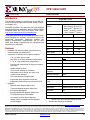
Product Overview
Introduction
LogiCORE™ Facts
The MicroBlaze 32-bit RISC soft processor is a true 32-bit
processor that supports 32-bit bus widths. The core is a
RISC-based engine with a 32-bit LUT RAM-based register
file with separate instructions for data and memory access.
The MicroBlaze processor supports both on-chip
Block-RAM and/or external memory. All peripherals use the
same CoreConnect OPB bus as the IBM PowerPC, making
the processor peripherals compatible with PowerPC on Virtex-II Pro devices.
Core Specifics
QPro™-R Virtex-II™,
QPro Virtex-II, Virtex-II Pro™,
Virtex™, Virtex-II, Virtex-4™, Virtex-E,
Spartan-II™, Spartan-IIE™,
Spartan-3™
Supported Device
Family
Version
microblaze
v2.10a
Resources Used
Features
Min
Max
•
Thirty-two 32-bit general-purpose registers
Slices
731
N/A
•
32-bit instruction word with three operands and two
addressing modes
LUTs
923
TBD
•
Separate 32-bit instruction and data buses that
conform to IBM’s OPB (On-chip Peripheral Bus)
specification
FFs
552
TBD
0
0
•
Block RAMs
Separate 32-bit instruction and data buses with direct
connection to on-chip block RAM through a LMB (Local
Memory Bus)
Provided with Core
Documentation
View this data sheet
Design File Formats
VHDL
Constraints File
N/A
Verification
N/A
•
32-bit address bus
•
Single issue pipeline
•
Instruction and data cache
•
Hardware debug logic
Instantiation Template
N/A
•
FSL (Fast Simplex Link) support
Reference Designs
N/A
•
Hardware multiplier (in Virtex-II and subsequent
devices)
Design Tool Requirements
Xilinx Implementation
Tools
ISE 6.2i or higher
Verification
N/A
Simulation
ModelSim SE/EE 5.6e or higher
Synthesis
XST
Support
Provided by Xilinx, Inc.
© 2004 Xilinx, Inc. All rights reserved. All Xilinx trademarks, registered trademarks, patents, and further disclaimers are as listed at http://www.xilinx.com/legal.htm. All other
trademarks and registered trademarks are the property of their respective owners. All specifications are subject to change without notice.
NOTICE OF DISCLAIMER: Xilinx is providing this design, code, or information "as is." By providing the design, code, or information as one possible implementation of this feature, application, or standard, Xilinx makes no representation that this implementation is free from any claims of infringement. You are responsible for obtaining any rights you
may require for your implementation. Xilinx expressly disclaims any warranty whatsoever with respect to the adequacy of the implementation, including but not limited to any warranties or representations that this implementation is free from claims of infringement and any implied warranties of merchantability or fitness for a particular purpose.
Product Overview
www.xilinx.com
1-800-255-7778
22
0
MicroBlaze (v3.00a)
View this data sheet
0
0
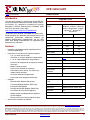
Product Overview
Introduction
LogiCORE™ Facts
The MicroBlaze 32-bit RISC soft processor is a true 32-bit
processor that supports 32-bit bus widths. The core is a
RISC-based engine with a 32-bit LUT RAM-based register
file with separate instructions for data and memory access.
The MicroBlaze processor supports both on-chip
Block-RAM and/or external memory. All peripherals use the
same CoreConnect OPB bus as the IBM PowerPC, making
the processor peripherals compatible with PowerPC on Virtex-II Pro devices.
Core Specifics
QPro™-R Virtex-II™,
QPro Virtex-II, Virtex-II Pro™,
Virtex™, Virtex-II, Virtex-4™, Virtex-E,
Spartan-II™, Spartan-IIE™,
Spartan-3™
Supported Device
Family
Version
microblaze
v3.00a
Resources Used
Features
Min
Max
•
Thirty-two 32-bit general-purpose registers
Slices
731
N/A
•
32-bit instruction word with three operands and two
addressing modes
LUTs
923
TBD
•
Separate 32-bit instruction and data buses that
conform to IBM’s OPB (On-chip Peripheral Bus)
specification
FFs
552
TBD
0
0
•
Block RAMs
Separate 32-bit instruction and data buses with direct
connection to on-chip block RAM through a LMB (Local
Memory Bus)
Provided with Core
Documentation
View this data sheet
Design File Formats
VHDL
Constraints File
N/A
Verification
N/A
•
32-bit address bus
•
Single issue pipeline
•
Instruction and data cache
•
Hardware debug logic
Instantiation Template
N/A
•
FSL (Fast Simplex Link) support
Reference Designs
N/A
•
Hardware multiplier (in Virtex-II and subsequent
devices)
Design Tool Requirements
Xilinx Implementation
Tools
ISE 6.2i or higher
Verification
N/A
Simulation
ModelSim SE/EE 5.6e or higher
Synthesis
XST
Support
Provided by Xilinx, Inc.
© 2004 Xilinx, Inc. All rights reserved. All Xilinx trademarks, registered trademarks, patents, and further disclaimers are as listed at http://www.xilinx.com/legal.htm. All other
trademarks and registered trademarks are the property of their respective owners. All specifications are subject to change without notice.
NOTICE OF DISCLAIMER: Xilinx is providing this design, code, or information "as is." By providing the design, code, or information as one possible implementation of this feature, application, or standard, Xilinx makes no representation that this implementation is free from any claims of infringement. You are responsible for obtaining any rights you
may require for your implementation. Xilinx expressly disclaims any warranty whatsoever with respect to the adequacy of the implementation, including but not limited to any warranties or representations that this implementation is free from claims of infringement and any implied warranties of merchantability or fitness for a particular purpose.
Product Overview
www.xilinx.com
1-800-255-7778
23
0
PPC405 Top (Wrapper) (v2.00b)
View this data sheet
0
0
Product Overview
Introduction
LogiCORE™ Facts
This document describes the specifications for the PPC405
top level wrapper, PPC405 Top.
PPC405 Top is used as a wrapper to instantiate the PowerPC 405 Processor Block primitive. The PPC405_Top
core delivered with EDK is designed to be used with the
Platform Generator to manage the memory map in the
same style as the PLB and OPB memory maps, and to support future expansion. A Microprocessor Peripheral Definition (MPD) file associated with this module is also included.
Users can utilize the Xilinx Platform Studio (XPS) to incorporate this module into a Microprocessor Hardware Specification (MHS). This module does not contain any other logic
aside from the PPC405.
Core Specifics
Supported Device
Family
Virtex-II Pro™
Version of Core
ppc405_top
v2.00b
Resources Used
Min
Max
Slices
0
0
LUTs
0
0
FFs
0
0
The functionality and input/output signal definitions are the
same as for the PowerPC 405 Processor Block with the following exceptions:
Block RAMs
0
0
•
TIEDSOCMDCRADDR[0:7] input is driven by the first 8
bits of parameter C_DSOCM_DCR_BASEADDR[0:9]
Documentation
•
TIEISOCMDCRADDR[0:7] input is driven by the first 8
bits of parameter C_ISOCM_DCR_BASEADDR[0:9]
•
TIEC405DETERMINISTICMULT input is driven by the
parameter C_DETERMINISTIC_MULT
•
TIEC405DISOPERANDFWD input is driven by the
parameter C_DISABLE_OPERAND_FORWARDING
•
TIEC405MMUEN input is driven by the parameter
C_MMU_ENABLE
Provided with Core
View this data sheet
Design File Formats
VHDL
Constraints File
N/A
Verification
N/A
Instantiation
Template
N/A
Reference Designs
None
Design Tool Requirements
Xilinx Implementation
Tools
ISE 6.1i or higher
Verification
N/A
Simulation
ModelSim SE/EE 5.6e or later
Synthesis
XST
Support
Support provided by Xilinx, Inc.
© 2004 Xilinx, Inc. All rights reserved. All Xilinx trademarks, registered trademarks, patents, and further disclaimers are as listed at http://www.xilinx.com/legal.htm. All other
trademarks and registered trademarks are the property of their respective owners. All specifications are subject to change without notice.
NOTICE OF DISCLAIMER: Xilinx is providing this design, code, or information "as is." By providing the design, code, or information as one possible implementation of this feature, application, or standard, Xilinx makes no representation that this implementation is free from any claims of infringement. You are responsible for obtaining any rights you
may require for your implementation. Xilinx expressly disclaims any warranty whatsoever with respect to the adequacy of the implementation, including but not limited to any warranties or representations that this implementation is free from claims of infringement and any implied warranties of merchantability or fitness for a particular purpose.
Product Overview
www.xilinx.com
1-800-255-7778
24
0
PPC405 (Wrapper) (v2.00c)
View this data sheet
0
0
Product Overview
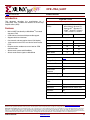
Introduction
LogiCORE™ Facts
This document describes the specifications for the PPC405
top level wrapper.
Core Specifics
Features
Supported Device
Family
•
Instantiate PowerPC™ 405 Processor Block primitive
Version
•
Parameter controlled TIE ports
•
Parameter controlled DCR interface resynchronization
Virtex-II Pro™
ppc405
v2.00c
Resources Used
Min
Max
Slices
N/A
N/A
LUTs
0
0
FFs
0
77
Block RAMs
0
0
Provided with Core
Documentation
View this data sheet
Design File Formats
VHDL
Constraints File
N/A
Verification
N/A
Instantiation Template
N/A
Reference Designs
N/A
Design Tool Requirements
Xilinx Implementation
Tools
ISE 6.2i or higher
Verification
N/A
Simulation
ModelSim SE/EE 5.6e or higher
Synthesis
XST
Support
Provided by Xilinx, Inc.
© 2004 Xilinx, Inc. All rights reserved. All Xilinx trademarks, registered trademarks, patents, and further disclaimers are as listed at http://www.xilinx.com/legal.htm. All other
trademarks and registered trademarks are the property of their respective owners. All specifications are subject to change without notice.
NOTICE OF DISCLAIMER: Xilinx is providing this design, code, or information "as is." By providing the design, code, or information as one possible implementation of this feature, application, or standard, Xilinx makes no representation that this implementation is free from any claims of infringement. You are responsible for obtaining any rights you
may require for your implementation. Xilinx expressly disclaims any warranty whatsoever with respect to the adequacy of the implementation, including but not limited to any warranties or representations that this implementation is free from claims of infringement and any implied warranties of merchantability or fitness for a particular purpose.
Product Overview
www.xilinx.com
1-800-255-7778
25
0
PPC405 Virtex-4 (Wrapper)
(v1.00a)
View this data sheet
0
0
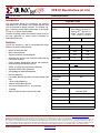
Product Overview
Introduction
LogiCORE™ Facts
The PPC405_Virtex4 is a wrapper around the Virtex-4
PowerPC™ 405 Processor Block primitive. For details
about the PowerPC 405, see the PowerPC 405 Processor
Block Reference Guide.
Supported Device
Family
This core contains no logic.
Version of Core
Core Specifics
Virtex-4™
ppc405_virtex4
v1.00a
Resources Used
Features
•
PowerPC 405 Auxiliary Processor Unit (APU) controller
interface exposed
•
Built in resynchronization of Device Control Register
(DCR) bus control interface
•
Debug read-access to Instruction-Side
Memory (ISOCM) via DCR
•
Read data valid handshake added to the Data-Side
On-Chip Memory (DSOCM) controller
On-Chip
•
New synchronization mode for the Processor Local
Bus interface.
•
Easy configuration of User-Defined Instructions (UDI)
Min
Max
Slices
0
0
LUTs
0
0
FFs
0
0
Block RAMs
0
0
Provided with Core
Documentation
View this data sheet
Design File Formats
VHDL
Constraints File
N/A
Verification
N/A
Instantiation
Template
N/A
Reference Designs
N/A
Design Tool Requirements
Xilinx Implementation
Tools
ISE 6.2i or higher
Verification
N/A
Simulation
ModelSim SE/PE 5.7f or higher
Synthesis
XST
Support
Support provided by Xilinx, Inc.
© 2004 Xilinx, Inc. All rights reserved. All Xilinx trademarks, registered trademarks, patents, and further disclaimers are as listed at http://www.xilinx.com/legal.htm. All other
trademarks and registered trademarks are the property of their respective owners. All specifications are subject to change without notice.
NOTICE OF DISCLAIMER: Xilinx is providing this design, code, or information "as is." By providing the design, code, or information as one possible implementation of this feature, application, or standard, Xilinx makes no representation that this implementation is free from any claims of infringement. You are responsible for obtaining any rights you may
require for your implementation. Xilinx expressly disclaims any warranty whatsoever with respect to the adequacy of the implementation, including but not limited to any warranties or representations that this implementation is free from claims of infringement and any implied warranties of merchantability or fitness for a particular purpose.
Product Overview
www.xilinx.com
1-800-255-7778
26
R
Chapter 4
Bus, Bridge, and Arbiter
Infrastructure Cores
This section of the Processor IP Reference Guide includes the following topics:
• On-Chip Peripheral Bus v2.0 with OPB Arbiter (v1.10a)
• On-Chip Peripheral Bus v2.0 with OPB Arbiter (v1.10b)
• OPB PCI Arbiter
• OPB to PLB Bridge (v1.00c)
• OPB to OPB Bridge (Lite Version)
• OPB to DCR Bridge
• Processor Local Bus (PLB) v3.4
• Processor Local Bus (PLB) v3.4 (v1.02a)
• PLB to OPB Bridge (v1.00b)
• PLB to OPB Bridge (v1.01a)
• Device Control Register Bus (DCR) v2.9 (v1.00a)
• Processor System Reset Module
• Local Memory Bus (LMB) v1.0
• OPB Arbiter (v1.02c)
• Fast Simplex Link Channel (v1.00b)
• Fast Simplex Link (FSL) Bus (v2.00a)
• Digital Clock Manager (DCM) Module (v1.00a)
• Data Side OCM Bus V1.0 (v1.00b)
• Data Side OCM Bus (v2.00a)
• Instruction Side OCM Bus v1.0 (v1.00b)
• Instruction Side OCM Bus v1.0 (v2.00a)
Processor IP User Guide
August 2004
www.xilinx.com
1-800-255-7778
27
0
On-Chip Peripheral Bus v2.0 with
OPB Arbiter (v1.10a)
View this data sheet
0
0
Product Overview
Introduction
LogiCORE™ Facts
The OPB_V20 module is used as the OPB interconnect for
Xilinx FPGA based embedded processor systems. The bus
interconnect in the OPB v2.0 specification is a distributed
multiplexer implemented as an AND function in the master
or slave driving the bus, and as an OR function to combine
the drivers into a single bus.
Core Specifics
Virtex-II Pro™, Virtex-II™,
Virtex™, Virtex-E, Spartan-II™,
Spartan-IIE™, Spartan-3™
Supported Device
Family
Version of Core
opb_v20
The OPB_V20 module assumes the AND (or enable function) is within the master or slave and provides the OR function to combine the various bus signals.
v1.10a
Resources Used
Min
Max
Features
I/O
46
432
•
Includes parameterized OPB Arbiter
LUTs
80
666
•
Includes parameterized I/O signals to support and
number of masters or slaves
FFs
5
145
•
Includes all signals present in the OPB v2.0
Specification except the DMA handshake signals
Block RAMs
0
0
•
Provided with Core
The OR structure can be implemented using only LUTs
or a combination of LUTs and fast carry to reduce the
number of LUTs in the OR interconnect
Documentation
View this data sheet
Design File Formats
VHDL
•
Includes a 16-clock Power-on OPB Bus Reset and
parameter for high or low external bus reset
Constraints File
N/A
•
Includes input for reset from Watchdog Timer
Verification
N/A
•
Option to split the read and write OPB date busses for
optimal FPGA routing and resource utilization.
Instantiation
Template
N/A
Reference Designs
None
The OPB_V20 includes an OPB Arbiter that incorporates
the features contained in the IBM On-chip Peripheral Bus
Arbiter Core manual (version 1.5) for 32-bit implementation.
This manual is referenced throughout this document and is
considered the authoritative specification. Any differences
between the IBM OPB Arbiter implementation and the Xilinx
OPB Arbiter implementation are explained in the Specification Exceptions section of the data sheet.
The Xilinx OPB Arbiter design allows tailoring the OPB Arbiter to suit an application by setting certain parameters to
enable/disable features.
In some cases, setting these parameters may cause the Xilinx OPB Arbiter design to deviate slightly from the IBM OPB
Arbiter specification. These parameters are described in the
OPB_V20 Design Parameters section of the datasheet.
Design Tool Requirements
Xilinx Implementation
Tools
5.1i or later
Verification
N/A
Simulation
ModelSim SE/EE 5.6e or later
Synthesis
XST
Support
Provided by Xilinx, Inc.
© 2004 Xilinx, Inc. All rights reserved. All Xilinx trademarks, registered trademarks, patents, and further disclaimers are as listed at http://www.xilinx.com/legal.htm. All other
trademarks and registered trademarks are the property of their respective owners. All specifications are subject to change without notice.
NOTICE OF DISCLAIMER: Xilinx is providing this design, code, or information "as is." By providing the design, code, or information as one possible implementation of this feature, application, or standard, Xilinx makes no representation that this implementation is free from any claims of infringement. You are responsible for obtaining any rights you
may require for your implementation. Xilinx expressly disclaims any warranty whatsoever with respect to the adequacy of the implementation, including but not limited to any warranties or representations that this implementation is free from claims of infringement and any implied warranties of merchantability or fitness for a particular purpose.
Product Overview
www.xilinx.com
1-800-255-7778
28
0
On-Chip Peripheral Bus v2.0 with
OPB Arbiter (v1.10b)
View this data sheet
0
0
Product Overview
Introduction
LogiCORE™ Facts
The OPB_V20 module is used as the OPB interconnect for
Xilinx FPGA based embedded processor systems. The bus
interconnect in the OPB v2.0 specification is a distributed
multiplexer implemented as an AND function in the master
or slave driving the bus, and as an OR function to combine
the drivers into a single bus.
Supported Device
Family
The OPB_V20 module assumes the AND (enable function)
is within the master or slave and provides the OR function to
combine the various bus signals.
Virtex-II Pro™, Virtex™,
Virtex-II™, Virtex-4™, QPro™-R
Virtex-II, QPro Virtex-II, Virtex-E,
Spartan-II™, Spartan-IIE™,
Spartan-3™
Version of Core
opb_v20
Core Specifics
v1.10b
Resources Used
Features
Min
Max
•
Includes parameterized OPB Arbiter
Slices
46
436
•
Includes parameterized I/O signals to support and
number of masters or slaves
LUTs
81
668
•
Includes all signals present in the OPB v2.0
Specification except the DMA handshake signals
FFs
5
145
•
The OR structure can be implemented using only LUTs
or a combination of LUTs and fast carry to reduce the
number of LUTs in the OR interconnect
Block RAMs
0
0
Provided with Core
Documentation
View this data sheet
•
Includes a 16-clock Power-on OPB Bus Reset and
parameter for high or low external bus reset
Design File Formats
VHDL
•
Includes input for reset from Watchdog Timer
Constraints File
N/A
•
Option to split the read and write OPB date busses for
optimal FPGA routing and resource utilization.
Verification
N/A
Instantiation
Template
N/A
Reference Designs
None
The OPB_V20 includes an OPB Arbiter that incorporates
the features contained in the IBM On-chip Peripheral Bus
Arbiter Core manual (version 1.5) for 32-bit implementation.
This manual is referenced throughout this document and is
considered the authoritative specification. Any differences
between the IBM OPB Arbiter implementation and the Xilinx
OPB Arbiter implementation are explained in the Specification Exceptions section of the datasheet.
The Xilinx OPB Arbiter design allows tailoring the OPB Arbiter to suit an application by setting certain parameters to
enable/disable features.
In some cases, setting these parameters may cause the Xilinx OPB Arbiter design to deviate slightly from the IBM OPB
Arbiter specification. These parameters are described in the
OPB_V20 Design Parameters section of the datasheet.
Design Tool Requirements
Xilinx Implementation
Tools
5.1i or later
Verification
N/A
Simulation
ModelSim SE/EE 5.6e or later
Synthesis
XST
Support
Provided by Xilinx, Inc.
© 2004 Xilinx, Inc. All rights reserved. All Xilinx trademarks, registered trademarks, patents, and further disclaimers are as listed at http://www.xilinx.com/legal.htm. All other
trademarks and registered trademarks are the property of their respective owners. All specifications are subject to change without notice.
NOTICE OF DISCLAIMER: Xilinx is providing this design, code, or information "as is." By providing the design, code, or information as one possible implementation of this feature,
application, or standard, Xilinx makes no representation that this implementation is free from any claims of infringement. You are responsible for obtaining any rights you may
require for your implementation. Xilinx expressly disclaims any warranty whatsoever with respect to the adequacy of the implementation, including but not limited to any warranties
or representations that this implementation is free from claims of infringement and any implied warranties of merchantability or fitness for a particular purpose.
Product Overview
www.xilinx.com
1-800-255-7778
29
0
OPB PCI Arbiter
View this data sheet
0
0
Product Overview
Introduction
LogiCORE™ Facts
The OPB PCI Arbiter provides arbitration among several
PCI Master devices. Parametric selection determines the
number of masters competing for PCI bus control. Both
fixed and rotating arbitration schemes may be selected by
programing a control register. Bus parking occurs in the
case that no master requests PCI control. The particular
master designated for parking is selected either with a programed register or by parametric selection. Register programming is accomplished through a slave interface to the
OPB using the OPB_IPIF.
An alternate use mode provides a PCI arbiter without an
OPB interface. Achieved through appropriate parameter
settings, this mode completely removes the program registers and the OPB_IPIF leaving open the outputs to the OPB
and connecting inputs from the OPB to logic zero. Without
an OPB interface the PCI arbiter operates with rotating arbitration and the park master is set directly by parameter
selection.
Core Specifics
Supported Device Family
Virtex-II Pro™, Virtex-II™,
Virtex™, Virtex-E, Virtex-4™,
QPro™-R Virtex-II, QPro
Virtex-II, Spartan-II™,
Spartan-IIE™, and Spartan-3™
Version
opb_pci_arbiter
Resources Used
Min
Max
4+2*
C_NUM_PCI_M
STRS
114 + 2 *
C_NUM_PCI_
MSTRS
LUTs
23
205
FFs
19
132
Block RAMs
0
0
I/O
Features
•
v1.00a
Provided with Core
Variable number of PCI masters set by parameter
Documentation
View this data sheet
•
Fixed arbitration
Design File Formats
VHDL
•
Rotating arbitration
Constraints File
N/A
•
Control bit selection of arbitration scheme
•
Bus parking
Verification
N/A
•
Park master program register
Instantiation Template
N/A
•
Alternative park master set by parameter
N/A
•
Control bit selection of park master
Reference Designs &
application notes
•
Removable processor interface, OPB_IPIF
Additional Items
None
•
Removable pipeline registers for PCI requests
•
Removable pipeline registers for PCI grants
•
OPB interface for register reads and writes
Design Tool Requirements
Xilinx Implementation
Tools
ISE 6.1.01i or later
Verification
N/A
Simulation
ModelSim SE/EE 5.6e or later
Synthesis
XST
Support
Provided by Xilinx, Inc.
© 2004 Xilinx, Inc. All rights reserved. All Xilinx trademarks, registered trademarks, patents, and further disclaimers are as listed at http://www.xilinx.com/legal.htm. All other
trademarks and registered trademarks are the property of their respective owners. All specifications are subject to change without notice.
NOTICE OF DISCLAIMER: Xilinx is providing this design, code, or information "as is." By providing the design, code, or information as one possible implementation of this feature, application, or standard, Xilinx makes no representation that this implementation is free from any claims of infringement. You are responsible for obtaining any rights you
may require for your implementation. Xilinx expressly disclaims any warranty whatsoever with respect to the adequacy of the implementation, including but not limited to any warranties or representations that this implementation is free from claims of infringement and any implied warranties of merchantability or fitness for a particular purpose.
Product Overview
www.xilinx.com
1-800-255-7778
30
0
OPB to PLB Bridge (v1.00c)
View this data sheet
0
0
Product Overview
Introduction
LogiCORE™ Facts
The On-Chip Peripheral Bus (OPB) to Processor Local Bus
(PLB) Bridge module translates OPB transactions into PLB
transactions. It functions as a slave on the OPB side and a
master on the PLB side. Access to the control register and
bus error status registers is user selectable from either the
OPB or an optional DCR interface. The OPB to PLB Bridge
is necessary in systems where an OPB master device, such
as a DMA engine or an OPB based coprocessor, that
requires access to PLB devices (that is, high speed memory
devices, and so forth.).
Core Specifics
Supported Device
Family
Version of Core
Max
I/O
390
390
LUTs
467
898
FFs
630
720
0
0
Provided with Core
Features
Documentation
View this data sheet
Design File Formats
VHDL
Constraints File
N/A
Verification
N/A
Instantiation
Template
N/A
Reference Designs
None
Design Tool Requirements
64-bit PLB Master interface
-
Communicates with 32- or 64-bit PLB slaves
-
Non-burst transfers of 1 to 8 bytes
-
Burst transfers, including word and double-word
bursts of fixed lengths, up to 16 words of data
-
Cacheline transactions of 4, 8, and 16 words
Translates OPB sequential accesses (bursts) to either
cacheline or fixed length PLB burst transfers
-
v1.00c
Min
Block RAMs
In subsequent sections, the OPB to PLB Bridge, when convenient, is referred to as the Bridge In (BGI), and the PLB to
OPB Bridge is referred to as the Bridge Out (BGO). This terminology reflects a PLB centric convention of data flowing in
from and out to the peripheral bus, respectively. However,
this is only a naming convention and in no way restricts the
use of these bridges in alternative processor / bus configurations.
•
opb2plb_bridge
Resources Used
The Xilinx OPB to PLB Bridge design allows customers to
tailor the bridge to suit their application by setting certain
parameters to enable / disable features. The parameterizable features of the design are discussed in the full data
sheet. Differences between the IBM OPB to PLB Bridge
implementation and the Xilinx OPB to PLB Bridge implementation are also highlighted and explained.
•
Virtex-II Pro™, Virtex-4™
Xilinx
Implementation Tools
5.1i or later
Verification
N/A
Simulation
ModelSim SE/EE 5.6e or later
Synthesis
XST
Support
Performing only single beat and cacheline
transactions reduces system logic utilization and
improves timing through PLB slave IP simplification
·
Target word first order supported when cacheline transactions selected
Provided by Xilinx, Inc.
-
•
PLB burst transfers yield better bus cycle efficiency
but may increase logic utilization and degrade
timing in the system
32-bit OPB Slave interface with byte enable transfer
Note: Does not support dynamic bus sizing or non-byte
© 2004 Xilinx, Inc. All rights reserved. All Xilinx trademarks, registered trademarks, patents, and further disclaimers are as listed at http://www.xilinx.com/legal.htm. All other
trademarks and registered trademarks are the property of their respective owners. All specifications are subject to change without notice.
NOTICE OF DISCLAIMER: Xilinx is providing this design, code, or information "as is." By providing the design, code, or information as one possible implementation of this feature,
application, or standard, Xilinx makes no representation that this implementation is free from any claims of infringement. You are responsible for obtaining any rights you may
require for your implementation. Xilinx expressly disclaims any warranty whatsoever with respect to the adequacy of the implementation, including but not limited to any warranties
or representations that this implementation is free from claims of infringement and any implied warranties of merchantability or fitness for a particular purpose.
Product Overview
www.xilinx.com
1-800-255-7778
31
OPB to PLB Bridge (v1.00c)
enable transactions
- Decodes up to four separate address ranges
•
-
PLB and OPB clocks can have a 1:1, 2:1, 3:1, or 4:1 synchronous relationship (OPB clock frequency must be less
than or equal to the PLB clock frequency)
-
Asserts BGI_opbRetry if bridge is busy with a PLB transaction and a new OPB request is received.
Bus Error Status Register (BESR) and Bus Error Address Register (BEAR) provide bus error status, and Bridge
Control Register (BCR) provides bridge control functions
-
Parameterizable selection between DCR or OPB Slave interface, which provides access to BESR, BEAR, and
BCR
•
Posted write buffer and read prefetch buffer 16 words deep
•
Edge-type interrupt generated when bus error detected
Product Overview
www.xilinx.com
1-800-255-7778
32
0
OPB to OPB Bridge (Lite Version)
View this data sheet
0
0
Product Overview
Introduction
LogiCORE™ Facts
This document provides the design specification for the
OPB to OPB Lite Bridge. The OPB to OPB Lite Bridge is
used to connect two OPB buses. The bridge has one master port and one slave port. Two bridges may be used
together to support full bus mastership in both directions.
Core Specifics
Supported Device
Family
QPro™-R Virtex-II™, QPro
Virtex-II, Spartan-II™,
Spartan-IIE™, Spartan-3™,
Virtex™, Virtex-II™, Virtex-II Pro™,
Virtex-E, and Virtex-4
Features
•
Provides a bridge between two OPB V2.0 buses
•
Connections for one master-side bus and one
slave-side bus
•
Parameterized data bus widths
•
Simple transaction forwarding reduces LUT count
•
•
Version of Core
opb_opb_lite
v1.00a
Resources Used
Min
Max
Slices
21
26
Requires the two OPB buses to be on the same clock
and the same size
LUTs
22
30
No support for data buffering or posted writes.
FFs
27
27
Block RAMs
0
0
Provided with Core
Documentation
View this data sheet
Design File Formats
VHDL
Constraints File
N/A
Verification
N/A
Instantiation
Template
N/A
Reference Designs
None
Design Tool Requirements
Xilinx Implementation
Tools
5.1i or later
Verification
N/A
Simulation
ModelSim SE/EE 5.6e or later
Synthesis
XST
Support
Provided by Xilinx, Inc.
© 2004 Xilinx, Inc. All rights reserved. All Xilinx trademarks, registered trademarks, patents, and further disclaimers are as listed at http://www.xilinx.com/legal.htm. All other
trademarks and registered trademarks are the property of their respective owners. All specifications are subject to change without notice.
NOTICE OF DISCLAIMER: Xilinx is providing this design, code, or information "as is." By providing the design, code, or information as one possible implementation of this feature,
application, or standard, Xilinx makes no representation that this implementation is free from any claims of infringement. You are responsible for obtaining any rights you may
require for your implementation. Xilinx expressly disclaims any warranty whatsoever with respect to the adequacy of the implementation, including but not limited to any warranties
or representations that this implementation is free from claims of infringement and any implied warranties of merchantability or fitness for a particular purpose.
Product Overview
www.xilinx.com
1-800-255-7778
33
0
OPB to DCR Bridge
View this data sheet
0
0
Product Overview
Introduction
LogiCORE™ Facts
The OPB to DCR Bridge translates transactions received on
its OPB slave interface into DCR master operations. Its
design utilizes an Intellectual Property InterFace (IPIF)
module to abstract OPB transactions into a simple SRAM
style protocol that is easier to design with.
Core Specifics
QPro™-R Virtex-II™,
QPro Virtex-II, Virrtex-II Pro™
Supported Device
Family
Version of Core
opb2dcr_bridge
The main advantage of using the bridge instead of the CPU
to control the DCR bus is that it provides a memory mapped
interface that may be preferable to the use of special move
to/move from DCR instructions.
Since the bridge typically runs at a slower clock frequency
than the CPU, its timing requirements are also less stringent. The OPB to DCR Bridge implements a simple and
flexible method for communicating with DCR devices.
Resources Used
Min
Max
Slices
87
89
LUTs
42
44
FFs
131
131
0
0
Block RAMs
Features
•
32-bit DCR master with a 10-bit DCR address bus
•
Memory-mapped interface from OPB to DCR, no
special instructions required
•
Increased timing flexibility in typical systems where the
OPB clock is slower than the CPU clock
•
Allows master devices other than the CPU to access
the DCR bus
•
Provides a mechanism where CoreConnect systems
without a CPU can support DCR devices
v1.00a
Provided with Core
Documentation
View this data sheet
Design File Formats
VHDL
Constraints File
N/A
Verification
N/A
Instantiation
Template
N/A
Reference Designs
None
Design Tool Requirements
Xilinx Implementation
Tools
5.1i or later
Verification
N/A
Simulation
ModelSim SE/EE 5.6e or later
Synthesis
XST
Support
Provided by Xilinx, Inc.
© 2004 Xilinx, Inc. All rights reserved. All Xilinx trademarks, registered trademarks, patents, and further disclaimers are as listed at http://www.xilinx.com/legal.htm. All other
trademarks and registered trademarks are the property of their respective owners. All specifications are subject to change without notice.
NOTICE OF DISCLAIMER: Xilinx is providing this design, code, or information "as is." By providing the design, code, or information as one possible implementation of this feature,
application, or standard, Xilinx makes no representation that this implementation is free from any claims of infringement. You are responsible for obtaining any rights you may
require for your implementation. Xilinx expressly disclaims any warranty whatsoever with respect to the adequacy of the implementation, including but not limited to any warranties
or representations that this implementation is free from claims of infringement and any implied warranties of merchantability or fitness for a particular purpose.
Product Overview
www.xilinx.com
1-800-255-7778
34
0
Processor Local Bus (PLB) v3.4
View this data sheet
0
0
Product Overview
Introduction
LogiCORE™ Facts
The Xilinx 64-bit Processor Local Bus (PLB) consists of a
bus control unit, a watchdog timer, and separate address,
write, and read data path units with a a three-cylcle only
arbitration feature. It contains a DCR slave interface to provide access to its bus error status registers. It also contains
a power-up reset circuit to ensure a PLB reset is generated
if no external reset has been provided.
The IBM Processor Local Bus (PLB) 64-Bit Architecture
Specification and the IBM Processor Local Bus (PLB) 64-Bit
Arbiter Core User’s Manual are referenced throughout this
document. Differences between the IBM PLB Arbiter and
the Xilinx PLB are highlighted and explained in Specification Exceptions.
Features
•
Version of Core
Number of PLB masters is configurable via a
design parameter
PLB address and data steering support for up to 16
masters
64-bit and/or 32-bit support for masters and slaves
•
PLB address pipelining
•
Three-cycle arbitration
•
Four levels of dynamic master request priority
•
PLB watchdog timer
•
PLB architecture compliant
•
Complete PLB Bus structure provided
Up to 16 slaves supported (Number of PLB slaves
configurable via a design parameter)
-
No external or gates required for PLB slave input
signals
PLB Reset circuit
-
v1.01a
Resources Used
Min
Max
Slice
194
1616
LUTs
263
2533
FFs
57
482
Block RAMs
0
0
Documentation
View this data sheet
Design File Formats
VHDL
Constraints File
N/A
Verification
N/A
Instantiation
Template
N/A
Reference Designs
None
Design Tool Requirements
-
-
plb_v34
Provided with Core
•
•
Virtex-II Pro™, Virtex-4™
Supported Device
Family
PLB arbitration support for up to 16 masters
-
•
Core Specifics
PLB Reset generated synchronously to the PLB
clock upon power up if no external reset is
provided
Xilinx Implementation
Tools
5.1i or later
Verification
N/A
Simulation
ModelSim SE/EE 5.6e or later
Synthesis
XST
Support
Provided by Xilinx, Inc.
PLB Reset generated synchronously from external
reset when external reset provided
·
Active state of external reset selectable via a
design parameter
© 2004 Xilinx, Inc. All rights reserved. All Xilinx trademarks, registered trademarks, patents, and further disclaimers are as listed at http://www.xilinx.com/legal.htm. All other
trademarks and registered trademarks are the property of their respective owners. All specifications are subject to change without notice.
NOTICE OF DISCLAIMER: Xilinx is providing this design, code, or information "as is." By providing the design, code, or information as one possible implementation of this feature,
application, or standard, Xilinx makes no representation that this implementation is free from any claims of infringement. You are responsible for obtaining any rights you may
require for your implementation. Xilinx expressly disclaims any warranty whatsoever with respect to the adequacy of the implementation, including but not limited to any warranties
or representations that this implementation is free from claims of infringement and any implied warranties of merchantability or fitness for a particular purpose.
Product Overview
www.xilinx.com
1-800-255-7778
35
0
Processor Local Bus (PLB) v3.4
(v1.02a)
View this data sheet
0
0
Product Specification
Introduction
LogiCORE™ Facts
The Xilinx 64-bit Processor Local Bus (PLB) consists of a
bus control unit, a watchdog timer, and separate address,
write, and read data path units with a a three-cylcle only
arbitration feature. It contains a DCR slave interface to provide access to its bus error status registers and a power-up
reset circuit to ensure a PLB reset is generated if no external reset has been provided. The IBM Processor Local Bus
(PLB) 64-Bit Architecture Specification and the IBM Processor Local Bus (PLB) 64-Bit Arbiter Core User’s Manual are
referenced throughout this document. The differences
between IBM PLB Arbiter and Xilinx PLB are highlighted
and explained in the Specification Exceptions section.
Features
•
Core Specifics
Supported Device
Family
Version of Core
plb_v34
v1.02a
Resources Used
Min
Max
Slice
223
1645
LUTs
270
2540
FFs
59
484
Block RAMs
0
0
PLB arbitration support for up to 16 masters
-
Virtex-II Pro™, Virtex-4™
Provided with Core
Number of PLB masters is configurable via a
design parameter
•
PLB address and data steering support for up to 16
masters
•
64-bit and/or 32-bit support for masters and slaves
•
Documentation
View this data sheet
Design File Formats
VHDL
Constraints File
N/A
PLB address pipelining
Verification
N/A
•
Three-cycle arbitration
Four levels of dynamic master request priority
Instantiation
Template
N/A
•
•
PLB watchdog timer
Reference Designs
•
PLB architecture compliant
•
Complete PLB Bus structure provided
-
•
Design Tool Requirements
Up to 16 slaves supported
·
Number of PLB slaves configurable via a design
parameter
No external or gates required for PLB slave input
signals
PLB Reset circuit
-
None
PLB Reset generated synchronously to the PLB
clock upon power up if no external reset is
provided
-
PLB Reset generated synchronously from external
reset when external reset provided
-
Active state of external reset selectable via a
design parameter
Xilinx Implementation
Tools
5.1i or later
Verification
N/A
Simulation
ModelSim SE/EE 5.6e or later
Synthesis
XST
Support
Support provided by Xilinx, Inc.
-
System
compatibility
with
Xilinx’s
OPB
Master/Slave IPIF architecture when utilized with
PLB2OPB bridge core version 1.01a
© 2004 Xilinx, Inc. All rights reserved. All Xilinx trademarks, registered trademarks, patents, and further disclaimers are as listed at http://www.xilinx.com/legal.htm. All other
trademarks and registered trademarks are the property of their respective owners. All specifications are subject to change without notice.
NOTICE OF DISCLAIMER: Xilinx is providing this design, code, or information "as is." By providing the design, code, or information as one possible implementation of this feature, application, or standard, Xilinx makes no representation that this implementation is free from any claims of infringement. You are responsible for obtaining any rights you
may require for your implementation. Xilinx expressly disclaims any warranty whatsoever with respect to the adequacy of the implementation, including but not limited to any warranties or representations that this implementation is free from claims of infringement and any implied warranties of merchantability or fitness for a particular purpose.
Product Specification
www.xilinx.com
1-800-255-7778
36
0
PLB to OPB Bridge (v1.00b)
View this data sheet
0
0
Product Overview
Introduction
LogiCORE™ Facts
The Processor Local Bus (PLB) to On-chip Peripheral Bus
(OPB) Bridge translates PLB transactions into OPB transactions. It functions as a slave on the PLB side and a master on the OPB side. It contains a DCR slave interface to
provide access to its bus error status registers. The PLB to
OPB bridge is necessary in systems where a PLB master
device requires access to OPB peripherals.
Core Specifics
Supported Device
Family
Virtex-II Pro™, Virtex-4™
Version of Core
plb2opb_bridge v1.00b
Resources Used
The Xilinx PLB to OPB Bridge design allows customers to
tailor the bridge to suit their application by setting certain
parameters to enable/disable features.
Min
Max
Slices
412
662
LUTs
499
787
The parameterizable features of the design are discussed
in the datasheet. Differences between the IBM PLB to OPB
Bridge implementation and the Xilinx PLB to OPB Bridge
implementation are also highlighted and explained.
FFs
355
620
0
0
Features
Documentation
View this data sheet
Design File Formats
VHDL
•
Provided with Core
PLB Slave interface
-
32-bit or 64-bit PLB (configurable via the
C_PLB_DWIDTH design parameter)
Constraints File
N/A
Verification
N/A
-
PLB slave width same as PLB bus width
Instantiation Template N/A
-
Decodes up to four separate address ranges
Reference Designs
-
Programmable lower and upper address
boundaries for each range
-
Communicates with 32- or 64-bit PLB masters
-
Non-burst transfers of 1-8 bytes
-
Burst transfers, including word and double-word
bursts of fixed or variable lengths, up to depth of
burst buffer (16)
None
Design Tool Requirements
-
Limited support for byte, half-word, quad-word and
octal-word bursts to maintain PLB compliance
-
Cacheline transactions of 4, 8, and 16 words
-
Support for burst transactions can be eliminated
via a design parameter
·
Save device resources by only supporting single beat, 4, 8, or 16 word line transfers
•
Block RAMs
Xilinx Implementation
Tools
5.1i or later
Verification
N/A
Simulation
ModelSim SE/EE 5.6e or later
Synthesis
XST
Support
Provided by Xilinx, Inc.
•
Supports up to 16 PLB masters (number of PLB
masters configurable via a design parameter)
OPB Master interface with byte enable transfers
Note:Does not support dynamic bus sizing without additional
Bus Error Address Registers (BEAR) and Bus Error
Status Registers (BESR) to report errors
-
DCR Slave interface provides access to
BEAR/BESR
-
BEAR, BESR, and DCR interface can be removed
from the design via a design parameter
glue logic
•
16-deep posted write buffer and read pre-fetch buffer
-
•
Edge-type interrupt generated when bus error detected
Data width configurable via a design parameter
© 2004 Xilinx, Inc. All rights reserved. All Xilinx trademarks, registered trademarks, patents, and further disclaimers are as listed at http://www.xilinx.com/legal.htm. All other
trademarks and registered trademarks are the property of their respective owners. All specifications are subject to change without notice.
NOTICE OF DISCLAIMER: Xilinx is providing this design, code, or information "as is." By providing the design, code, or information as one possible implementation of this feature,
application, or standard, Xilinx makes no representation that this implementation is free from any claims of infringement. You are responsible for obtaining any rights you may
require for your implementation. Xilinx expressly disclaims any warranty whatsoever with respect to the adequacy of the implementation, including but not limited to any warranties
or representations that this implementation is free from claims of infringement and any implied warranties of merchantability or fitness for a particular purpose.
Product Overview
www.xilinx.com
1-800-255-7778
37
0
PLB to OPB Bridge (v1.01a)
View this data sheet
0
0
Product Overview
Introduction
LogiCORE™ Facts
The Processor Local Bus (PLB) to On-chip Peripheral Bus
(OPB) Bridge translates PLB transactions into OPB transactions. It functions as a slave on the PLB side and a master on the OPB side and contains a DCR slave interface to
provide access to its bus error status registers. The PLB to
OPB bridge is necessary in systems where a PLB master
device requires access to OPB peripherals. The Xilinx PLB
to OPB Bridge design allows customers to tailor the bridge
to suit their application by setting certain parameters to
enable/disable features. The parameterizable features of
the design are discussed in the PLB to OPB Bridge Design
Parameters section. The differences between the IBM PLB
to OPB Bridge implementation and the Xilinx PLB to OPB
Bridge implementation are also highlighted and explained.
Core Specifics
Supported Device
Family
Virtex-II Pro™, Virtex-4™
Version of Core
plb2opb_bridge
v1.01a
Resources Used
Min
Max
Slices
595
836
LUTs
535
823
FFs
547
812
0
0
Block RAMs
Provided with Core
Features
•
PLB Slave interface
View this data sheet
Design File Formats
-
32-bit or 64-bit PLB (configurable
C_PLB_DWIDTH design parameter)
-
PLB slave width same as PLB bus width
-
via
the
VHDL
Constraints File
N/A
Verification
N/A
Decodes up to four separate address ranges
Instantiation Template
N/A
-
Programmable lower and
boundaries for each range
Reference Designs
-
Communicates with 32- or 64-bit PLB masters
-
Non-burst transfers of 1-8 bytes
-
Burst transfers, including word and double-word
bursts of fixed or variable lengths, up to depth of
burst buffer (16)
Verification
N/A
Simulation
ModelSim SE/EE 5.6e or later
-
Limited support for byte, half-word, quad-word and
octal-word bursts to maintain PLB compliance
Synthesis
XST
-
Cacheline transactions of 4, 8, and 16 words
-
Support for burst transactions can be eliminated
via a design parameter
·
save device resources by only supporting single
beat, 4, 8, or 16 word line transfers
Supports up to 16 PLB masters (number of PLB
masters configurable via a design parameter)
•
Documentation
upper
address
Design Tool Requirements
Xilinx Implementation
Tools
5.1i or later
Support
Support provided by Xilinx, Inc.
•
PLB and OPB clocks can have a 1:1, 1:2, 1:3, 1:4
synchronous relationship
•
Bus Error Address Registers (BEAR) and Bus Error
Status Registers (BESR) to report errors
OPB Master interface with byte enable transfers
Note:Does not support dynamic bus sizing without additional
-
DCR Slave
BEAR/BESR
-
BEAR, BESR, and DCR interface can be removed
from design via a design parameter
glue logic
-
None
Data width configurable via a design parameter
•
interface
provides
access
to
16-deep posted write buffer and read pre-fetch buffer
© 2004 Xilinx, Inc. All rights reserved. All Xilinx trademarks, registered trademarks, patents, and further disclaimers are as listed at http://www.xilinx.com/legal.htm. All other
trademarks and registered trademarks are the property of their respective owners. All specifications are subject to change without notice.
NOTICE OF DISCLAIMER: Xilinx is providing this design, code, or information "as is." By providing the design, code, or information as one possible implementation of this feature, application, or standard, Xilinx makes no representation that this implementation is free from any claims of infringement. You are responsible for obtaining any rights you
may require for your implementation. Xilinx expressly disclaims any warranty whatsoever with respect to the adequacy of the implementation, including but not limited to any warranties or representations that this implementation is free from claims of infringement and any implied warranties of merchantability or fitness for a particular purpose.
Product Overview
www.xilinx.com
1-800-255-7778
38
0
Device Control Register Bus
(DCR) v2.9 (v1.00a)
View this data sheet
0
0
Product Overview
Introduction
LogiCORE™ Facts
The Xilinx 32-Bit Device Control Register (DCR) Bus soft
core provides the DCR bus structure (as described in the
IBM 32-Bit Device Control Register Bus (DCR) Architecture
Specification) with the ability to easily connect the DCR
Master to DCR slaves. It provides the daisy-chain for the
DCR data bus and the OR gate for the DCR acknowledge
signals from the DCR slaves.
Core Specifics
Supported Device
Family
Virtex-II Pro™, Virtex-4™
Version of Core
dcr_v29
v1.00a
Resources Used
Features
Min
Max
DCR connections for one DCR master and a variable
number of DCR slaves, which are configurable via
design parameter
Slices
0
4
LUTs
0
5
•
Daisy-chain connections for the DCR data bus
FFs
0
0
•
Required OR function of the DCR slaves’ acknowledge
signal
Block RAMs
0
0
•
Provided with Core
Documentation
View this data sheet
Design File Formats
VHDL
Constraints File
N/A
Verification
N/A
Instantiation
Template
N/A
Reference Designs
None
Design Tool Requirements
Xilinx Implementation
Tools
5.1i or later
Verification
N/A
Simulation
ModelSim SE/EE 5.6e or later
Synthesis
XST
Support
Provided by Xilinx, Inc.
© 2004 Xilinx, Inc. All rights reserved. All Xilinx trademarks, registered trademarks, patents, and further disclaimers are as listed at http://www.xilinx.com/legal.htm. All other
trademarks and registered trademarks are the property of their respective owners. All specifications are subject to change without notice.
NOTICE OF DISCLAIMER: Xilinx is providing this design, code, or information "as is." By providing the design, code, or information as one possible implementation of this feature,
application, or standard, Xilinx makes no representation that this implementation is free from any claims of infringement. You are responsible for obtaining any rights you may
require for your implementation. Xilinx expressly disclaims any warranty whatsoever with respect to the adequacy of the implementation, including but not limited to any warranties
or representations that this implementation is free from claims of infringement and any implied warranties of merchantability or fitness for a particular purpose.
Product Overview
www.xilinx.com
1-800-255-7778
39
0
Processor System Reset Module
View this data sheet
0
0
Product Overview
Introduction
LogiCORE™ Facts
The Xilinx Processor System Reset Module lets users
customize their application by setting parameters to
enable/disable specific features. The parameterizable
features of the design are discussed in the affiliated
datashheet.
Core Specifics
Supported Device
Family
Virtex-II Pro™, Virtex™, Virtex-II™,
Virtex-4™, QPro™-R Virtex-II,
QPro Virtex-II, Virtex-E,
Spartan-II™, Spartan-IIE™,
Spartan-3™
Version of Core
proc_sys_reset
Features
•
Asynchronous external reset input is synchronized with
clock
•
Asynchronous auxiliary external reset input is
synchronized with clock
v1.00a
Resources Used
Min
Max
•
Both the external and auxiliary reset inputs are
selectable active high or active low
I/O
1
2
•
Selectable minimum pulse width for reset inputs to be
recognized
LUTs
37
57
FFs
52
82
Block RAMs
0
0
•
Selectable load equalizing
•
DCM Locked input
•
Power On Reset generation
•
Sequencing of reset signals coming out of reset:
Documentation
View this data sheet
-
First: Bus structures come out of reset
·
PLB and OPB Arbiter and bridges, for example
Design File Formats
VHDL
-
Second: Peripheral(s) come out of reset 16 clocks
later
·
UART, SPI, IIC for example
Constraints File
N/A
Verification
N/A
Instantiation
Template
N/A
Reference Designs
None
-
Provided with Core
Third: CPU(s) come out of reset 16 clocks after the
peripherals
Design Tool Requirements
Xilinx Implementation
Tools
Alliance Tool Suite
Verification
N/A
Simulation
N/A
Synthesis
XST
Support
Provided by Xilinx, Inc.
© 2004 Xilinx, Inc. All rights reserved. All Xilinx trademarks, registered trademarks, patents, and further disclaimers are as listed at http://www.xilinx.com/legal.htm. All other
trademarks and registered trademarks are the property of their respective owners. All specifications are subject to change without notice.
NOTICE OF DISCLAIMER: Xilinx is providing this design, code, or information "as is." By providing the design, code, or information as one possible implementation of this feature, application, or standard, Xilinx makes no representation that this implementation is free from any claims of infringement. You are responsible for obtaining any rights you
may require for your implementation. Xilinx expressly disclaims any warranty whatsoever with respect to the adequacy of the implementation, including but not limited to any warranties or representations that this implementation is free from claims of infringement and any implied warranties of merchantability or fitness for a particular purpose.
Product Overview
www.xilinx.com
1-800-255-7778
40
0
Local Memory Bus (LMB) v1.0
View this data sheet
0
0
Product Overview
Introduction
LogiCORE™ Facts
The LMB_V10 module is used as the LMB interconnect for
Xilinx FPGA-based embedded processor systems. The
LMB is a fast, local bus for connecting MicroBlaze™
instruction and data ports to high-speed peripherals, primarily on-chip block RAM (BRAM).
Core Specifics
Supported Device
Family
QPro™-R Virtex-II™,
QPro Virtex-II, Spartan-II™,
Spartan-IIE™, Spartan-3™,
Virtex™, Virtex-II, Virtex-II Pro™,
Virtex-4™, Virtex-E
Features
•
Efficient, single master bus (requires no arbiter)
•
Separate read and write data buses
•
Low FPGA resource utilization
•
125 MHz operation
Version of Core
lmb_v10
v1.00a
Resources Used
I/O
Min
Max
N/A
N/A
LUTs
FFs
Block RAMs
Provided with Core
Documentation
View this data sheet
Design File Formats
VHDL
Constraints File
N/A
Verification
N/A
Instantiation
Template
N/A
Reference Designs
None
Design Tool Requirements
Xilinx Implementation
Tools
ISE 6.3i or higher
Verification
N/A
Simulation
ModelSim SE/PE 5.7b or later
Synthesis
XST
Support
Provided by Xilinx, Inc.
© 2004 Xilinx, Inc. All rights reserved. All Xilinx trademarks, registered trademarks, patents, and further disclaimers are as listed at http://www.xilinx.com/legal.htm. All other
trademarks and registered trademarks are the property of their respective owners. All specifications are subject to change without notice.
NOTICE OF DISCLAIMER: Xilinx is providing this design, code, or information "as is." By providing the design, code, or information as one possible implementation of this feature,
application, or standard, Xilinx makes no representation that this implementation is free from any claims of infringement. You are responsible for obtaining any rights you may
require for your implementation. Xilinx expressly disclaims any warranty whatsoever with respect to the adequacy of the implementation, including but not limited to any warranties
or representations that this implementation is free from claims of infringement and any implied warranties of merchantability or fitness for a particular purpose.
Product Overview
www.xilinx.com
1-800-255-7778
41
0
OPB Arbiter (v1.02c)
View this data sheet
0
0
Product Overview
Introduction
LogiCORE™ Facts
The On-Chip Peripheral Bus (OPB) Arbiter design
described in this document incorporates the features contained in the IBM On-chip Peripheral Bus Arbiter Core manual (version 1.5) for 32-bit implementation, which is
referenced throughout this document and is considered the
authoritative specification. Any differences between the IBM
OPB Arbiter implementation and the Xilinx OPB Arbiter
implementation are defined in the Specification Exceptions
section of the datasheet.
Core Specifics
Supported Device
Family
Version of Core
v1.02c
Min
Max
I/O
4
904
LUTs
6
252
FFs
4
1477
Block RAMs
0
0
Provided with Core
Features
The OPB Arbiter is a soft IP core designed for Xilinx FPGAs
and contains the following features:
•
Optional OPB slave interface (included in design via a
design parameter)
•
OPB Arbitration
•
opb_arbiter
Resources Used
The Xilinx OPB Arbiter design lets you tailor the OPB Arbiter to suit your application by setting certain parameters to
enable/disable features. In some cases, setting these
parameters may cause the Xilinx OPB Arbiter design to
deviate slightly from the IBM OPB Arbiter specification.
These parameters are described in the OPB Arbiter Design
Parameters section.
•
Spartan-II™, Spartan-IIE™,
Spartan-3™, Virtex™, Virtex-II™,
Virtex-II Pro™, Virtex-E
Documentation
View this data sheet
Design File Formats
VHDL
Constraints File
N/A
Verification
N/A
-
Arbitrates between 1–16 OPB Masters (the
number of masters is parameterizable)
Instantiation
Template
N/A
-
Arbitration priorities among masters programmable
via register write
Reference Designs
None
-
Priority arbitration mode configurable via a design
parameter
·
Fixed priority arbitration with processor access
to read/write Priority Registers
·
Dynamic priority arbitration implementing a
true least recent used (LRU) algorithm
Design Tool Requirements
Two bus parking modes selectable via Control Register
write:
-
park on selected OPB master (specified in Control
Register)
-
park on last OPB master granted OPB access
Watchdog timer asserts the OPB time-out signal if a
slave response is not detected within 16 clock cycles
Xilinx Implementation
Tools
5.1i or later
Verification
N/A
Simulation
ModelSim SE/EE 5.6e or later
Synthesis
XST
Support
Provided by Xilinx, Inc.
•
Registered or combinational Grant outputs
configurable via a design parameter
© 2004 Xilinx, Inc. All rights reserved. All Xilinx trademarks, registered trademarks, patents, and further disclaimers are as listed at http://www.xilinx.com/legal.htm. All other
trademarks and registered trademarks are the property of their respective owners. All specifications are subject to change without notice.
NOTICE OF DISCLAIMER: Xilinx is providing this design, code, or information "as is." By providing the design, code, or information as one possible implementation of this feature, application, or standard, Xilinx makes no representation that this implementation is free from any claims of infringement. You are responsible for obtaining any rights you
may require for your implementation. Xilinx expressly disclaims any warranty whatsoever with respect to the adequacy of the implementation, including but not limited to any warranties or representations that this implementation is free from claims of infringement and any implied warranties of merchantability or fitness for a particular purpose.
Product Overview
www.xilinx.com
1-800-255-7778
42
0
Fast Simplex Link Channel
(v1.00b)
View this data sheet
0
0
Product Overview
Introduction
LogiCORE™ Facts
This document provides the design specification for the
Fast Simplex Link (FSL) Channel. The FSL_V20 module is
used as the FSL interconnect for Xilinx FPGA based
embedded processor systems. The FSL is a fast uni-directional point-to-point communication channel.
Features
Core Specifics
Supported Device
Family
Spartan-II™, Spartan-IIE™,
Spartan-3™, Virtex™, Virtex-II™,
Virtex-II Pro™, Virtex-E™
Version of Core
fsl_v20
v1.00.b
Resources Used
•
Uni-directional point-to-point communication
•
Unshared non-arbitrated communication mechanism
•
Control and Data communication support FIFO based
communication
•
Configurable depth FIFO
•
•
Min
Max
Slices
26
26
LUTs
43
43
Configurable data path size
FFs
6
6
600 MHz standalone operation
Block RAMs
0
0
Provided with Core
Documentation
View this data sheet
Design File Formats
VHDL
Constraints File
N/A
Verification
N/A
Instantiation
Template
N/A
Reference Designs
N/A
Design Tool Requirements
Xilinx Implementation
Tools
ISE 6.1i or higher
Verification
N/A
Simulation
ModelSim SE/EE 5.6e or higher
Synthesis
XST
Support
Provided by Xilinx, Inc.
© 2004 Xilinx, Inc. All rights reserved. All Xilinx trademarks, registered trademarks, patents, and further disclaimers are as listed at http://www.xilinx.com/legal.htm. All other
trademarks and registered trademarks are the property of their respective owners. All specifications are subject to change without notice.
NOTICE OF DISCLAIMER: Xilinx is providing this design, code, or information "as is." By providing the design, code, or information as one possible implementation of this feature,
application, or standard, Xilinx makes no representation that this implementation is free from any claims of infringement. You are responsible for obtaining any rights you may
require for your implementation. Xilinx expressly disclaims any warranty whatsoever with respect to the adequacy of the implementation, including but not limited to any warranties
or representations that this implementation is free from claims of infringement and any implied warranties of merchantability or fitness for a particular purpose.
Product Overview
www.xilinx.com
1-800-255-7778
43
0
Fast Simplex Link (FSL) Bus
(v2.00a)
View this data sheet
0
0
Product Overview
Introduction
LogiCORE™ Facts
FSL_V20 is a uni-directional point-to-point communication
channel. This bus is used to perform fast communication
between any two design elements on the FPGA that implement an interface to the FSL bus. Up to 8 master and slave
FSL interfaces are available on the Xilinx MicroBlaze™ soft
processor. The interfaces could be used to transfer data in
2 clock cycles to and from the register file on the processor
to hardware running on the FPGA.
Core Specifics
QPro™-R Virtex-II™,
QPro Virtex-II, Spartan-II™,
Spartan-IIE™, Spartan-3™,
Virtex™, Virtex-II™, Virtex-E™
Virtex-II Pro™, Virtex-4™
Supported Device
Family
Version of Core
fsl_v20
Features
Resources Used
•
Implements a uni-directional point to point FIFO-based
communication
•
Provides mechanism for unshared and non-arbitrated
communication mechanism that can be used for fast
transfer of data words between master and slave
implementing the FSL interface
•
Provides an extra control bit for annotating data being
tranmitted. The control bit can be used by the slave
side interface for multiple purposes, for example, to
decode the word being tranmitted as a control word or
to indicate start or end of transmission of a frame.
•
FIFO depths as low as 1 or as high as 8K
•
Supports synchronous and asynchronous FIFO modes
to allow the master and slave side of the FSL to clock
at different rates 1
•
v2.00a
Supports SRL16 and dual port LutRam or Block RAM
based FIFO implementation.
Min
Max
Slices
21
451
LUTs
3
362
FFs
36
34
Block RAMs
0
17
Provided with Core
Documentation
View this data sheet
Design File Formats
VHDL
Constraints File
N/A
Verification
N/A
Instantiation Template
N/A
Reference Designs
N/A
Design Tool Requirements
Xilinx Implementation
Tools
ISE 6.2i or higher
Verification
N/A
Simulation
ModelSim SE/EE 5.6e or higher
Synthesis
XST
Support
Support provided by Xilinx, Inc.
1. Maximum size in slices, FFs and LUTs is obtained using parameter options
C_ASYNC_FIFO=1, C_FSL_DEPTH=128, and C_USE_CONTROL =1. Maximum
BRAM size is obtained for parameter options C_SYNC_FIFO =1,
C_FSL_DEPTH=8192, and C_USE_CONTROL=1.
© 2004 Xilinx, Inc. All rights reserved. All Xilinx trademarks, registered trademarks, patents, and further disclaimers are as listed at http://www.xilinx.com/legal.htm. All other
trademarks and registered trademarks are the property of their respective owners. All specifications are subject to change without notice.
NOTICE OF DISCLAIMER: Xilinx is providing this design, code, or information "as is." By providing the design, code, or information as one possible implementation of this feature, application, or standard, Xilinx makes no representation that this implementation is free from any claims of infringement. You are responsible for obtaining any rights you
may require for your implementation. Xilinx expressly disclaims any warranty whatsoever with respect to the adequacy of the implementation, including but not limited to any warranties or representations that this implementation is free from claims of infringement and any implied warranties of merchantability or fitness for a particular purpose.
Product Overview
www.xilinx.com
1-800-255-7778
44
0
Digital Clock Manager (DCM)
Module (v1.00a)
View this data sheet
0
0
Product Overview
Introduction
LogiCORE™ Facts
The DCM Module is designed to be used with Platform
Generator to perform simple logical operations. An Microprocessor Peripheral Definition (MPD) file associated with
this module is also included. Users can utilize Xilinx Platform Studio (XPS) to incorporate this module into Microprocessor Hardware Specification (MHS). This module can
serve as glue logic among peripherals and is not associated
with any system bus
The Digital Clock Manager in Xilinx FPGAs provides multiple functions. It can implement a clock delay locked loop, a
digital frequency synthesizer, digital phase shifter and a digital spread spectrum. This DCM Module provides a very
basic, simple template in order to utilize the DCM feature in
Xilinx FPGAs Users can also refer to this template to create
custom-made, precise clock management, or multiple DCM
instantiation for specific applications, manually or use Architecture Wizard for DCM in ISE tools.
For more information regarding DCM features, please refer
to the Data Sheet and Users Guides for various FPGA
device families at http://support.xilinx.com.
Features
The DCM Module has the following features
•
All DCM I/Os are accessible from MPD port list
•
All DCM attributes are accessible from MPD
parameters
•
Support both active high and active low reset
•
Configurable BUFG insertion
Core Specifics
Supported Device
Family
QPro™-R Virtex-II™,
QPro Virtex-II, Spartan-3™,
Virtex-II, Virtex-II Pro™,
Virtex-4™
Version of Core
dcm_module
v1.00a
Resources Used
N/A
N/A
Slices
88
108
LUTs
48
57
FFs
0
0
N/A
N/A
Block RAMs
Provided with Core
Documentation
View this data sheet
Design File Formats
VHDL
Constraints File
N/A
Verification
N/A
Instantiation
Template
N/A
Reference Designs
N/A
Design Tool Requirements
Xilinx Implementation
Tools
ISE 6.1i or higher
Verification
N/A
Simulation
ModelSim SE/EE 5.6e or higher
Synthesis
XST
Support
Provided by Xilinx, Inc.
© 2004 Xilinx, Inc. All rights reserved. All Xilinx trademarks, registered trademarks, patents, and further disclaimers are as listed at http://www.xilinx.com/legal.htm. All other
trademarks and registered trademarks are the property of their respective owners. All specifications are subject to change without notice.
NOTICE OF DISCLAIMER: Xilinx is providing this design, code, or information "as is." By providing the design, code, or information as one possible implementation of this feature, application, or standard, Xilinx makes no representation that this implementation is free from any claims of infringement. You are responsible for obtaining any rights you
may require for your implementation. Xilinx expressly disclaims any warranty whatsoever with respect to the adequacy of the implementation, including but not limited to any warranties or representations that this implementation is free from claims of infringement and any implied warranties of merchantability or fitness for a particular purpose.
Product Overview
www.xilinx.com
1-800-255-7778
45
0
Data Side OCM Bus V1.0 (v1.00b)
View this data sheet
0
0
Product Overview
Introduction
LogiCORE™ Facts
The DSOCM_V10 Bus is used as the instruction side OCM
Bus interconnect for Virtex-II Pro PowerPC™ 405 based
embedded systems. A typical usage is to connect
PowerPC405 and DSBRAM_IF_CNTRL modules (both can
be found in EDK Infrastructure Library) to the DSOCM_V10
Bus. For more information regarding the OCM (On-Chip
Memory) controller interface in PowerPC 405 Processor,
please refer to PowerPC 405 Processor Block Reference
Guide.
This DSOCM_V10 Bus in EDK Infrastructure Library is
designed to be used with Platform Generator to manage
memory map with consistent style as managing PLB and
OPB memory map and to support future expansion. An
Microprocessor Peripheral Definition (MPD) file associated
with this module is also included. Users can utilize Xilinx
Platform Studio (XPS) to incorporate this module into Microprocessor Hardware Specification (MHS). This module
does not contain any logic.
Features
•
•
Used in conjunction with dsbram_if_cntrl peripheral to
provide a deterministic DSBRAM memory solution for
PowerPC405
This module does not contain logic
Core Specifics
Supported Device
Family
Virtex-II Pro™
Version of Core
dsocm_v10
v1.00b
Resources Used
Min
Max
Slices
0
0
LUTs
0
0
FFs
0
0
Block RAMs
0
0
Provided with Core
Documentation
View this data sheet
Design File Formats
VHDL
Constraints File
N/A
Verification
N/A
Instantiation
Template
N/A
Reference Designs
N/A
Design Tool Requirements
Xilinx Implementation
Tools
ISE 6.1i or higher
Verification
N/A
Simulation
ModelSim SE/EE 5.6e or higher
Synthesis
XST
Support
Provided by Xilinx, Inc.
© 2004 Xilinx, Inc. All rights reserved. All Xilinx trademarks, registered trademarks, patents, and further disclaimers are as listed at http://www.xilinx.com/legal.htm. All other
trademarks and registered trademarks are the property of their respective owners. All specifications are subject to change without notice.
NOTICE OF DISCLAIMER: Xilinx is providing this design, code, or information "as is." By providing the design, code, or information as one possible implementation of this feature, application, or standard, Xilinx makes no representation that this implementation is free from any claims of infringement. You are responsible for obtaining any rights you
may require for your implementation. Xilinx expressly disclaims any warranty whatsoever with respect to the adequacy of the implementation, including but not limited to any warranties or representations that this implementation is free from claims of infringement and any implied warranties of merchantability or fitness for a particular purpose.
Product Overview
www.xilinx.com
1-800-255-7778
46
0
Data Side OCM Bus (v2.00a)
View this data sheet
0
0
Product Overview
Introduction
LogiCORE™ Facts
DSOCM_V10 is a data-side On-Chip Memory (OCM) bus
interconnect core. The core connects the PowerPC 405
data-side OCM interface to OCM peripherals, e.g data-side
BRAM controllers (DSBRAM_IF_CNTRL). For information
about the PowerPC 405 OCM controller interface, see the
PowerPC 405 Processor Block Reference Guide.
Core Specifics
Supported Device
Family
Virtex-II Pro™, Virtex-4™
Version of Core
dsocm_v10
Resources Used
Features
•
v2.00a
Designed for use with the DSBRAM_IF_CNTRL
peripheral to provide a deterministic data-side BRAM
memory solution for PowerPC 405 based embedded
systems
Min
Max
Slices
N/A
N/A
LUTs
0
641
•
Single master - no bus arbitration logic
FFs
0
0
•
Configurable multiple slave capability - contains
read-data multiplexing when used with 2 or more
slaves
Block RAMs
0
0
Provided with Core
Documentation
View this data sheet
Design File Formats
VHDL
Constraints File
N/A
Verification
N/A
Instantiation
Template
N/A
Reference Designs
N/A
Design Tool Requirements
Xilinx Implementation
Tools
ISE 6.2i or higher
Verification
N/A
Simulation
ModelSim SE/PE 5.7f or higher
Synthesis
XST
Support
Support provided by Xilinx, Inc.
1.Example for 3 slaves. Size increases with number of slaves
© 2004 Xilinx, Inc. All rights reserved. All Xilinx trademarks, registered trademarks, patents, and further disclaimers are as listed at http://www.xilinx.com/legal.htm. All other
trademarks and registered trademarks are the property of their respective owners. All specifications are subject to change without notice.
NOTICE OF DISCLAIMER: Xilinx is providing this design, code, or information "as is." By providing the design, code, or information as one possible implementation of this feature, application, or standard, Xilinx makes no representation that this implementation is free from any claims of infringement. You are responsible for obtaining any rights you
may require for your implementation. Xilinx expressly disclaims any warranty whatsoever with respect to the adequacy of the implementation, including but not limited to any warranties or representations that this implementation is free from claims of infringement and any implied warranties of merchantability or fitness for a particular purpose.
Product Overview
www.xilinx.com
1-800-255-7778
47
0
Instruction Side OCM Bus v1.0
(v1.00b)
View this data sheet
0
0
Product Overview
Introduction
LogiCORE™ Facts
The ISOCM_V10 Bus is used as the instruction side OCM
Bus interconnect for Virtex-II Pro PowerPC™ 405 based
embedded systems. A typical usage is to connect
PowerPC405 and ISBRAM_IF_CNTRL modules (both can
be found in EDK Infrastructure Library) to the ISOCM_V10
Bus. For more information regarding the OCM (On-Chip
Memory) controller interface in PowerPC 405 Processor,
please refer to PowerPC 405 Processor Block Reference
Guide.
This ISOCM_V10 Bus in EDK Infrastructure Library is
designed to be used with Platform Generator to manage
memory map with consistent style as managing PLB and
OPB memory map and to support future expansion. An
Microprocessor Peripheral Definition (MPD) file associated
with this module is also included. Users can utilize Xilinx
Platform Studio (XPS) to incorporate this module into Microprocessor Hardware Specification (MHS). This module
does not contain any logic.
Features
•
•
Used in conjunction with isbram_if_cntrl peripheral to
provide a deterministic ISBRAM memory solution for
PowerPC405.
This module does not contain logic
Core Specifics
Supported Device
Family
Virtex-II Pro™
Version of Core
isocm_v10
v1.00b
Resources Used
Min
Max
Slices
TBD
TBD
LUTs
TBD
TBD
FFs
TBD
TBD
0
0
Block RAMs
Provided with Core
Documentation
View this data sheet
Design File Formats
VHDL
Constraints File
N/A
Verification
N/A
Instantiation
Template
N/A
Reference Designs
N/A
Design Tool Requirements
Xilinx Implementation
Tools
ISE 6.1i or higher
Verification
N/A
Simulation
ModelSim SE/EE 5.6e or higher
Synthesis
XST
Support
Provided by Xilinx, Inc.
© 2004 Xilinx, Inc. All rights reserved. All Xilinx trademarks, registered trademarks, patents, and further disclaimers are as listed at http://www.xilinx.com/legal.htm. All other
trademarks and registered trademarks are the property of their respective owners. All specifications are subject to change without notice.
NOTICE OF DISCLAIMER: Xilinx is providing this design, code, or information "as is." By providing the design, code, or information as one possible implementation of this feature, application, or standard, Xilinx makes no representation that this implementation is free from any claims of infringement. You are responsible for obtaining any rights you
may require for your implementation. Xilinx expressly disclaims any warranty whatsoever with respect to the adequacy of the implementation, including but not limited to any warranties or representations that this implementation is free from claims of infringement and any implied warranties of merchantability or fitness for a particular purpose.
Product Overview
www.xilinx.com
1-800-255-7778
48
0
Instruction Side OCM Bus v1.0
(v2.00a)
View this data sheet
0
0
Product Overview
Introduction
LogiCORE™ Facts
ISOCM_V10 is an instruction-side On-Chip Memory (OCM)
bus interconnect core. The core connects the PowerPC405
instruction-side OCM interface to OCM peripherals, such as
the instruction-side BRAM controller
(ISBRAM_IF_CNTRL). For information about the
PowerPC405 OCM controller interface, see the PowerPC
405 Processor Block Reference Guide.
Core Specifics
Supported Device
Family
Virtex-II Pro™, Virtex-4™
Version of Core
isocm_v10
v2.00a
Resources Used
Features
Min
Max
Designed for use with the ISBRAM_IF_CNTRL
peripheral to provide a deterministic instruction-side
BRAM memory solution for PowerPC405 based
embedded systems
Slices
N/A
N/A
LUTs
0
641
FFs
0
0
•
Single master - no bus arbitration logic
Block RAMs
0
0
•
Configurable multiple slave capability - contains
read-data multiplexing when used with 2 or more
slaves
•
Provided with Core
Documentation
View this data sheet
Design File Formats
VHDL
Constraints File
N/A
Verification
N/A
Instantiation
Template
N/A
Reference Designs
N/A
Design Tool Requirements
Xilinx Implementation
Tools
ISE 6.2i or higher
Verification
N/A
Simulation
ModelSim SE/PE 5.7f or higher
Synthesis
XST
Support
Support provided by Xilinx, Inc.
1.Example for 2 slaves. Size increases with number of slaves
© 2004 Xilinx, Inc. All rights reserved. All Xilinx trademarks, registered trademarks, patents, and further disclaimers are as listed at http://www.xilinx.com/legal.htm. All other
trademarks and registered trademarks are the property of their respective owners. All specifications are subject to change without notice.
NOTICE OF DISCLAIMER: Xilinx is providing this design, code, or information "as is." By providing the design, code, or information as one possible implementation of this feature, application, or standard, Xilinx makes no representation that this implementation is free from any claims of infringement. You are responsible for obtaining any rights you may
require for your implementation. Xilinx expressly disclaims any warranty whatsoever with respect to the adequacy of the implementation, including but not limited to any warranties or representations that this implementation is free from claims of infringement and any implied warranties of merchantability or fitness for a particular purpose.
Product Overview
www.xilinx.com
1-800-255-7778
49
R
Chapter 5
IPIF
This section of the Processor IP Reference Guide includes the following topics:
• OPB IPIF Architecture (v1.23e)
- OPB IPIF Interrupt (v1.23e)
- OPB IPIF Packet FIFO (v1.23e)
- Direct Memory Access and Scatter Gather (v1.23e) (v1.23e)
• OPB IPIF (v2.00h)
• OPB IPIF (v3.01a)
• PLB IPIF (v1.00e)
• PLB IPIF (v2.00a)
• PLB IPIF (v2.01a)
• Channelized Direct Memory Access and Scatter Gather
Processor IP User Guide
August 2004
www.xilinx.com
1-800-255-7778
50
0
OPB IPIF Architecture
View this data sheet
0
0
Product Overview
Introduction
LogiCORE™ Facts
This document provides the architecture for the OPB IPIF, a
module that facilitates the connection of Xilinx or customer
IP modules to the IBM On-Chip Peripheral Bus (OPB). The
OPB is part of IBM’s CoreConnectTM family of data buses
and associated infrastructure. CoreConnect is intended for
use in system-on-a-chip environments, including Xilinx Virtex™-II Pro FPGAs with embedded PowerPC hard processors and FPGAs using the MicroBlaze soft processor.
An Intellectual Property solution, referred to herein as an IP,
is a function targeted for implementation in a Xilinx FPGA.
The interface seen by the IP is called the IP Interconnect
(IPIC for short). The combination of the IPIF and the IP is
called a device (or in some circles, a peripheral).
Core Specifics
Supported Device
Family
Virtex-II Pro™, Virtex™,
Virtex-II™, Virtex-E, Spartan-II™,
Spartan-IIE™, Spartan-3™
Version of Core
opb_ipif_arch
v1.23e
Resources Used
Min
Max
I/O
N/A
N/A
LUTs
N/A
N/A
In addition to facilitating OPB attachment, the IPIF provides
additional optional services. These services, FIFOs, DMA,
Scatter Gather (automated DMA), software reset, interrupt
support and OPB bus-master access, are placed in the IPIF
to standardize functionality that is common to many IPs and
to reduce IP development effort. Figure 1 is a device which
uses all IPIF protocols and services.
FFs
N/A
N/A
Block RAMs
N/A
N/A
Design File Formats
N/A
In most of the IPIF modules, the Read and Write FIFOs,
DMA/SG, Interrupt Control and the Reset block, attach to
the IPIC inside the IPIF and utilize the register and/or SRAM
interfaces and take advantage of the centralized address
decoding.
Constraints File
N/A
Verification
N/A
Instantiation
Template
N/A
Reference Designs
N/A
These modules are essentially on the same footing as the
IP in terms of how they are interfaced to the OPB. The
“glue” in the figure represents a small number of non-IPIC
connections between modules.
Features
The IPIF is a parametric soft IP core designed for Xilinx
FPGAs and contains the capabilities and features summarized below.
•
Synchronous operation
•
Hardware and optional software reset
Provided with Core
Documentation
View this data sheet
Design Tool Requirements
Xilinx Implementation
Tools
N/A
Verification
N/A
Simulation
N/A
Synthesis
N/A
Support
Freeze signal (requests graceful stop of IP and IPIF to facilitate debug under serious system failure; keeps interrupts
from “piling up”)
Provided by Xilinx, Inc.
© 2004 Xilinx, Inc. All rights reserved. All Xilinx trademarks, registered trademarks, patents, and further disclaimers are as listed at http://www.xilinx.com/legal.htm. All other
trademarks and registered trademarks are the property of their respective owners. All specifications are subject to change without notice.
NOTICE OF DISCLAIMER: Xilinx is providing this design, code, or information "as is." By providing the design, code, or information as one possible implementation of this feature, application, or standard, Xilinx makes no representation that this implementation is free from any claims of infringement. You are responsible for obtaining any rights you
may require for your implementation. Xilinx expressly disclaims any warranty whatsoever with respect to the adequacy of the implementation, including but not limited to any warranties or representations that this implementation is free from claims of infringement and any implied warranties of merchantability or fitness for a particular purpose.
Product Overview
www.xilinx.com
1-800-255-7778
51
OPB IPIF Architecture
•
•
•
•
Slave Interface:
-
FPGA friendly protocol meeting requirements of most new and legacy IP
·
Separate Address, Data-In, and Data-Out Buses
·
Transaction Qualification: Read Req, Write Req, Byte Enable, Burst
·
Transaction Response: Read Ack, Write Ack, Error, Retry, Timeout Suppression
-
Register Interface (optional)
·
Per register address decodes
·
Separate read and write enables for decoded register addresses
·
Doesn’t need the address
-
SRAM Interface—for IP with SRAM-like interface (optional)
·
Block-address decode
·
Single enable (read or write) for the decoded block address
·
Uses the address
-
Support for burst transactions (optional)
Interrupt Support (optional):
-
Parameterizeable: Select the required features
-
Captures up to 32 interrupt events from the IP
-
Device Interrupt Source Controller (ISC) in the IPIF is at top of a hierarchy of ISCs
·
Optional
·
Hierarchical structure can be eliminated by user parameter when all interrupt events are from the IP, leaving
only the device-global interrupt enable function of the device ISC
-
IP ISC
·
IP may pass in one or more interrupt events which are latched, enabled, and cleared in the IP ISC, which
passes its interrupt-active condition to the device ISC
-
IP Interrupt condition option
·
When the IPIF is configured without interrupt support, the IP may latch, enable and clear interrupts itself and
pass the interrupt condition directly to the system interrupt controller
-
IPIF ISCs, as needed, feed additional interrupt-active conditions to the device ISC
·
E.g., one ISC for each DMA channel
Master Interface (optional):
-
Parameterizeable: Select the required features
-
Bus Address
-
Local Address (allows master general access to local resources)
·
In lieu of dedicated in and out master data paths, the local address allows the slave-mode data paths and
address decoding to be leveraged for master operations
·
Advantageous for devices with addresses that are accessed by remote OPB masters and by a local master
·
Cooperation between the Slave Attachment and the Master Attachment used to complete master operations
-
Single and burst transactions
-
Transaction Qualification: Read Req, Write Req, Byte Enable, Burst, Bus Lock
-
Transaction Response: separate Read and Write Acks, Transaction ack, Error, Retry, Timeout
Write Packet FIFO (optional)
-
Parameterizeable: Select the required features
-
BRAM based
-
Packet support: Data reads by IP can be provisional until explicitly committed:
·
Mark command sets a a reference point for uncommitted reads
·
Restore command discards uncommitted reads; data is reread starting at the mark
·
Release command commits uncommitted reads
·
Useful, for example, in protocols that require retransmission
·
Interrupt when uncommitted reads empty the entire contents of the FIFO (indicates that the FIFO is too small
for the application)
-
Written from the OPB via IPIF-internal connection to the IPIC
Product Overview
www.xilinx.com
1-800-255-7778
52
OPB IPIF Architecture
•
•
-
Status can be read from the OPB
-
Read by IP via request/acknowledge protocol
-
Dedicated Data Path to the IP
-
IP Status flags: Empty, Almost Empty (one occupied), Occupancy Count
-
Optional Module Identification Register
Read FIFO (optional):
-
Parameterizeable: Select the required features
-
BRAM based
-
Packet support: Data writes by IP can be provisional until explicitly committed:
·
Mark command sets a a reference point for uncommitted writes
·
Restore command discards uncommitted writes; data is re-written starting at the mark
·
Release command commits uncommitted writes
·
Useful, for example, in protocols that discard data on error conditions or address misses
·
Interrupt when uncommitted writes fill the entire contents of the FIFO (indicates that the FIFO is too small for
the application)
-
Read from the OPB via IPIF-internal connection to the IPIC
-
Status can be read from the OPB
-
Written by IP via request/acknowledge protocol
-
Dedicated Data Path from the IP
-
IP Status flags: Full, Almost Full (one vacant), Vacancy Count
·
Mark command sets a a reference point for uncommitted writes
·
Restore command discards uncommitted writes; data is re-written starting at the mark
·
Release command commits uncommitted writes
·
Useful, for example, in protocols that discard data on error conditions or address misses
·
Interrupt when uncommitted writes fill the entire contents of the FIFO (indicates that the FIFO is too small for
the application)
-
Optional Module Identification Register
DMA/Scatter Gather (optional):
-
Parameterizeable: Select the required features
-
Up to Two DMA channels may be included
-
Optional scatter gather capability for channels
-
Optional packet capability for SG channels
-
Optional interrupt coalescing for packet SG channels (number of packets per interrupt is software selectable; time
wait bound gives packets guaranteed timely visibility)
-
Optional Module Identification Register
-
Attaches to IPIC internal to the IPIF
-
Uses an IPIF-internal master interface
Product Overview
www.xilinx.com
1-800-255-7778
53
0
OPB IPIF Interrupt
View this data sheet
0
0
Product Overview
Introduction
LogiCORE™ Facts
The OPB IPIF function has a requirement to collect all internal interrupts within a peripheral device and coalesce those
interrupts through masking and ’ORing’ into a single interrupt output that is sent to the microprocessor system Interrupt Controller (ITNC).
The IPIF Interrupt module, therefore, provides interrupt support logic for a user IP (connected to the IPIF) and internal
IPIF interrupt source functions (DMA/SG, PFIFOs, etc.).
Core Specifics
Supported Device
Family
Virtex-II Pro™, Virtex™,
Virtex-II™, Virtex-E, Spartan-II™,
Spartan-IIE™, Spartan-3™
Version of Core
opb_ipif_interrupt
v1.23e
Resources Used
Min
Max
I/O
N/A
N/A
LUTs
N/A
N/A
Features
FFs
N/A
N/A
The IPIF Interrupt module is incorporated in the standard
OPB IPIF block designed for Xilinx FPGAs and contains
these features:
Block RAMs
N/A
N/A
The IPIF Interrupt module incorporates two main functions:
the Device Interrupt Source Controller (ISC) and the IP ISC.
Each ISC function collects multiple interrupt inputs and outputs a single interrupt.
•
•
IP Interrupt Source Controller Function
Provided with Core
Documentation
View this data sheet
-
Parameterized number of interrupts needed by IP
Design File Formats
N/A
-
Provides both Interrupt Status Register (ISR) and
Interrupt Enable Register (IER) functions for the
user IP connecting to the IPIF
·
Registers are OPB accessible via the IPIF
Local Bus Interface
Constraints File
N/A
Verification
N/A
Instantiation
Template
N/A
Reference Designs
N/A
Device Interrupt Source Controller Function
-
Device ISC omission through input parameter
programming
-
Parameterized number of local IPIF generated
interrupt sources
-
Provides both Interrupt Status Register (ISR) and
Interrupt Enable Register (IER) functions for the
Device level interrupts
·
Registers are OPB accessible via the IPIF
Local Bus Interface.
-
Selectable Priority Encoder function on asserted
and enabled interrupts
·
Global Enable/Disable for final interrupt output
to the System Interrupt Controller.
Design Tool Requirements
Xilinx Implementation
Tools
N/A
Verification
N/A
Simulation
N/A
Synthesis
N/A
Support
Provided by Xilinx, Inc.
© 2004 Xilinx, Inc. All rights reserved. All Xilinx trademarks, registered trademarks, patents, and further disclaimers are as listed at http://www.xilinx.com/legal.htm. All other
trademarks and registered trademarks are the property of their respective owners. All specifications are subject to change without notice.
NOTICE OF DISCLAIMER: Xilinx is providing this design, code, or information "as is." By providing the design, code, or information as one possible implementation of this feature,
application, or standard, Xilinx makes no representation that this implementation is free from any claims of infringement. You are responsible for obtaining any rights you may
require for your implementation. Xilinx expressly disclaims any warranty whatsoever with respect to the adequacy of the implementation, including but not limited to any warranties
or representations that this implementation is free from claims of infringement and any implied warranties of merchantability or fitness for a particular purpose.
Product Overview
www.xilinx.com
1-800-255-7778
54
0
OPB IPIF Packet FIFO
View this data sheet
0
0
Product Overview
Introduction
LogiCORE™ Facts
This specification defines the First In First Out memory
design incorporating packet data support (PFIFO). The
PFIFO resides within the Xilinx Intellectual Property Interface (IPIF) module which interfaces to a host bus structure
such as the IBM OPB. The FIFOs primarily utilize Virtex
BRAM elements as the basic data storage medium.
FIFO depths of 16 words or less may optionally utilize
SRL16 elements as the memory medium. The memory is
coupled with surrounding counters and logic that are necessary for the functional requirements.
These requirements include interfaces to the IP, interfaces
to the Direct Memory Access/ Scatter Gather (DMA/SG)
interface, and to the IPIF Local Bus protocol.
The PFIFO is used as a data buffering agent between the IP
function and a Bus Master such as a DMA/SG Engine. The
basic operation of the module is a FIFO buffer. Data can be
shuttled in and out of the module without the need for the
accessing agent to provide successive memory addresses.
Data is stored and read in a First In First Out (FIFO)
sequence. However, the PFIFO to IP interface has been
enhanced with additional packet management controls that
facilitate packet retransmission or receive packet discard
functionality necessary for efficient operation of some IP
protocols (such as Ethernet).
The IPIF accesses the PFIFO module as a simple memory
mapped "FIFO" interface and memory mapped registers.
A PFIFO module is instantiated within the IPIF framework
and consists of two different types: a Write PFIFO
(WrPFIFO) and a Read PFIFO (RdPFIFO). The WrPFIFO is
the intermediate storage medium for data from the Host Bus
to the IP.
The RdPFIFO is used to buffer data from the IP that needs
to be sent to the Host Bus. Both Packet FIFO designs utilize
a single synchronous clock domain for the input and output
sides of the modules. This simplifies the design and
reduces LUT count as compared to an asynchronous dual
clock implementation.
Core Specifics
Virtex-II Pro™, Virtex™,
Virtex-II™, Virtex-E, Spartan-II™,
Spartan-IIE™, Spartan-3™
Supported Device
Family
Version of Core
opb_pfifo
v1.23e
Resources Used
Min
Max
I/O
N/A
N/A
LUTs
N/A
N/A
FFs
N/A
N/A
Block RAMs
N/A
N/A
Provided with Core
Documentation
View this data sheet
Design File Formats
N/A
Constraints File
N/A
Verification
N/A
Instantiation
Template
N/A
Reference Designs
N/A
Design Tool Requirements
Xilinx Implementation
Tools
N/A
Verification
N/A
Simulation
N/A
Synthesis
N/A
Support
Provided by Xilinx, Inc.
© 2004 Xilinx, Inc. All rights reserved. All Xilinx trademarks, registered trademarks, patents, and further disclaimers are as listed at http://www.xilinx.com/legal.htm. All other
trademarks and registered trademarks are the property of their respective owners. All specifications are subject to change without notice.
NOTICE OF DISCLAIMER: Xilinx is providing this design, code, or information "as is." By providing the design, code, or information as one possible implementation of this feature, application, or standard, Xilinx makes no representation that this implementation is free from any claims of infringement. You are responsible for obtaining any rights you
may require for your implementation. Xilinx expressly disclaims any warranty whatsoever with respect to the adequacy of the implementation, including but not limited to any warranties or representations that this implementation is free from claims of infringement and any implied warranties of merchantability or fitness for a particular purpose.
Product Overview
www.xilinx.com
1-800-255-7778
55
Features
•
Two independent functions are provided: the Read PFIFO (for host bus receive data buffering) and the Write PFIFO (for
host bus transmit data buffering).
•
The PFIFO design adheres to IPSPEC035 OPB IPIF Architectural Specification.
•
User controlled features that include parameters for:
-
Setting FIFO data width
-
Setting FIFO data depth (words)
-
Inclusion/Omission of Packet mode support
-
Setting IPIF Data Bus width
-
Inclusion/Omission of Vacancy calculation for write port
-
Selecting Target FPGA family type
-
Inclusion/Omission of Module Identification Register
•
"FIFO like" status outputs of AlmostFull, Full, AlmostEmpty, and Empty in addition to true ’Occupancy’ and ’Vacancy’
outputs. Host bus interface provides applicable status as a read accessible Status Register
•
Write and Read Ports synchronized to a common clock source (synchronous operation)
•
IPIF Local Bus Read access to Occupancy count on the Read PFIFO and the Vacancy count of the Write FIFO
The PFIFO modules can be reset from either an external reset input signal or a software initiated write to the Reset Register
port.
Product Overview
www.xilinx.com
1-800-255-7778
56
0
Direct Memory Access and
Scatter Gather (v1.23e)
View this data sheet
0
0
Product Overview
Introduction
LogiCORE™s Facts
Many soft IP input/output peripheral devices in Xilinx products with embedded or attached processors require the
automation facilities of Direct Memory Access and Scatter
Gather. This is a specification for such facilities.
Supported Device
Family
Virtex-II Pro™, Virtex™,
Virtex-II™, Virtex-E, Spartan-II™,
Spartan-IIE™, Spartan-3™
DMA[SG] Controller Overview
Version of Core
opb_ipif_dma_sg
Core Specifics
Definitions
v1.23e
Resources Used
Direct memory access (DMA) allows for a bounded number
of sequential data transfers to take place between regions
in the address space (typically between memory and an I/O
device) without processor management of individual transfers. The processor sets up the DMA operation by specifying the number accesses and the source and destination
addresses.
Scatter gather (SG) allows a sequence of DMA operations
to be pre-specified by software and performed automatically without further processor intervention. The processor
prepares the DMA operations in a system of buffers and
their associated Buffer Descriptors. The SG automation
hardware processes the Buffer Descriptors and performs
the DMA operations specified therein through activation of
the DMA hardware.
Often it is useful to consider that one or more DMA operations combine to compose a higher-level unit of data. An
example of such a unit is a packet or frame1 of data in a
communications protocol. This specification addresses
issues associated with the handling of packets and allows
packets to be distributed across one or more buffers.
Min
Max
I/O
N/A
N/A
LUTs
N/A
N/A
FFs
N/A
N/A
Block RAMs
N/A
N/A
Provided with Core
Documentation
View this data sheet
Design File Formats
N/A
Constraints File
N/A
Verification
N/A
Instantiation
Template
N/A
Reference Designs
N/A
Design Tool Requirements
Xilinx Implementation
Tools
N/A
Verification
N/A
Simulation
N/A
Synthesis
N/A
Support
Provided by Xilinx, Inc.
© 2004 Xilinx, Inc. All rights reserved. All Xilinx trademarks, registered trademarks, patents, and further disclaimers are as listed at http://www.xilinx.com/legal.htm. All other
trademarks and registered trademarks are the property of their respective owners. All specifications are subject to change without notice.
NOTICE OF DISCLAIMER: Xilinx is providing this design, code, or information "as is." By providing the design, code, or information as one possible implementation of this feature, application, or standard, Xilinx makes no representation that this implementation is free from any claims of infringement. You are responsible for obtaining any rights you
may require for your implementation. Xilinx expressly disclaims any warranty whatsoever with respect to the adequacy of the implementation, including but not limited to any warranties or representations that this implementation is free from claims of infringement and any implied warranties of merchantability or fitness for a particular purpose.
Product Overview
www.xilinx.com
1-800-255-7778
57
0
OPB IPIF (v2.00h)
View this data sheet
0
0
Product Overview
Introduction
LogiCORE™ Facts
The OPB IPIF is a continuation of the Xilinx family of IBM
CoreConnect compatible LogiCORE products. It provides a
bi-directional interface between a User IP core and the OPB
32-bit bus standard. The OPB is a peripheral bus for the
Embedded PPC405 processor featured in the Xilinx Virtex-II Pro product line and for the MicroBlaze™ processor, a
soft core that can be implemented in many Xilinx FPGA
families.
Core Specifics
Supported Device
Family
Spartan-II™, Spartan-IIE™,
Spartan-3™, Virtex™, Virtex-II™,
Virtex-II Pro™, Virtex-E
Version of Core
opb_ipif
v2.00h
Resources Used
Min
Features
•
Compatible with IBM CoreConnect 32-bit OPB.
Slices
•
Supports User IP data widths from 8 bits to 32 bits with
automatic byte steering.
LUTs
•
Extensive User customizing support via HDL
parameterization. User optioned services include:
-
Local IP Interrupt collection with User S/W
programmable enables/disables.
-
User S/W triggered reset generator for localized
reset of User’s core.
-
Burst transfer support.
-
DMA function
mechanization.
with
optional
Scatter/Gather
Max
FFs
Block RAMs
Provided with Core
Documentation
View this data sheet
Design File Formats
VHDL
Constraints File
None
Verification
EDK Simulation Support
-
User configured WrFIFO with optional IP packet
support.
Instantiation
Template
N/A
-
User configured RdFIFO with optional IP packet
support.
Reference Designs
N/A
Design Tool Requirements
Xilinx
Implementation
Tools
Xilinx EDK 6.1 SP2
Xilinx ISE 6.1
Verification
ModelSim SE 5.6d or later
Simulation
ModelSim SE 5.6d or later
© 2004 Xilinx, Inc. All rights reserved. All Xilinx trademarks, registered trademarks, patents, and further disclaimers are as listed at http://www.xilinx.com/legal.htm. All other
trademarks and registered trademarks are the property of their respective owners. All specifications are subject to change without notice.
NOTICE OF DISCLAIMER: Xilinx is providing this design, code, or information "as is." By providing the design, code, or information as one possible implementation of this feature, application, or standard, Xilinx makes no representation that this implementation is free from any claims of infringement. You are responsible for obtaining any rights you
may require for your implementation. Xilinx expressly disclaims any warranty whatsoever with respect to the adequacy of the implementation, including but not limited to any warranties or representations that this implementation is free from claims of infringement and any implied warranties of merchantability or fitness for a particular purpose.
Product Overview
www.xilinx.com
1-800-255-7778
58
0
OPB IPIF (v3.01a)
View this data sheet
0
0
Product Overview
Introduction
LogiCORE™ Facts
The OPB IPIF is a continuation of the Xilinx family of IBM
CoreConnect™ compatible LogiCORE™ products. It provides a bidirectional interface between a user IP core and
the OPB 32-bit bus standard. The Xilinx OPB IPIF is available for use with various FPGA device families that support
embedded hard or soft processors.
Core Specifics
Supported Device
Family
Spartan-II™, Spartan-IIE™,
Spartan-3™, Virtex™, Virtex-II™,
Virtex-II Pro™, Virtex-E
Version of Core
opb_ipif
Features
v3.01a
Resources Used
•
Compatible with IBM CoreConnect 32-bit OPB
•
Supports User IP data widths from 8 bits to 32 bits with
automatic byte steering
•
Extensive User customizing support via HDL
parameterization. User optioned services include:
-
Local IP Interrupt collection with User S/W
programmable enables/disables
-
User S/W triggered reset generator for localized
reset of User’s core
-
Sequential-Address transfer support
-
User configured WrFIFO with optional IP packet
support
-
User configured RdFIFO with optional IP packet
support
Min
Max
Slices
20
567
LUTs
31
817
FFs
10
511
Block RAMs
0
4
Provided with Core
Documentation
View this data sheet
Design File Formats
VHDL
Constraints File
None
Verification
EDK Simulation Support
Instantiation
Template
N/A
Reference Designs
N/A
Design Tool Requirements
Xilinx
Implementation
Tools
Xilinx EDK 6.1 SP2
Xilinx ISE 6.1
Verification
ModelSim SE 5.6d or later
Simulation
ModelSim SE 5.6d or later
© 2004 Xilinx, Inc. All rights reserved. All Xilinx trademarks, registered trademarks, patents, and further disclaimers are as listed at http://www.xilinx.com/legal.htm. All other
trademarks and registered trademarks are the property of their respective owners. All specifications are subject to change without notice.
NOTICE OF DISCLAIMER: Xilinx is providing this design, code, or information "as is." By providing the design, code, or information as one possible implementation of this feature, application, or standard, Xilinx makes no representation that this implementation is free from any claims of infringement. You are responsible for obtaining any rights you
may require for your implementation. Xilinx expressly disclaims any warranty whatsoever with respect to the adequacy of the implementation, including but not limited to any warranties or representations that this implementation is free from claims of infringement and any implied warranties of merchantability or fitness for a particular purpose.
Product Overview
www.xilinx.com
1-800-255-7778
59
0
PLB IPIF (v1.00e)
View this data sheet
0
0
Product Overview
Introduction
LogiCORE™ Facts
The PLB IPIF V1_00_e is a continuation of Xilinx’s family of
IBM CoreConnect compatible LogiCORE™ products. It provides a bi-directional interface between a User IP core and
the PLB 64-bit bus standard. The PLB is the local bus for
the Embedded PPC405 processor featured in the Xilinx Virtex-II Pro™ product line. This version of the PLB IPIF has
been optimized for PLB Slave operation. It does not provide
support for DMA and IP Master Services.
Core Specifics
Supported Device
Family
Virtex-II Pro
Version of Core
plb_ipif
v1.00e
Resources Used
Min
Max
Features
Slices
161
763
•
Compatible with IBM CoreConnect 64-bit PLB.
LUTs
62
1255
•
Supports User IP data widths from 8 bits to 64 bits with
automatic byte steering.
FFs
259
828
•
Extensive User customizing support via HDL
parameterization. User optioned services include:
0
128
-
Local IP Interrupt Service with User S/W
programmable enables/disables.
-
User S/W triggered reset generator for localized
reset of User’s core.
-
PLB Single, Cacheline, Fixed Length Burst, and
Indeterminate Length Burst support.
-
Optional WrFIFO Service with optional IP packet
support.
-
Optional RdFIFO Service with optional IP packet
support.
-
Block RAMs
Provided with Core
Documentation
View this data sheet
Design File Formats
VHDL
Constraints File
None
Verification
EDK Simulation Support
Instantiation
Template
Provided by EDK IP Wizard tool
Reference Designs
EDK PLB IPIF Template
Reference Designs
Optional PLB SESR/SEAR Service.
Design Tool Requirements
Xilinx
Implementation
Tools
Xilinx EDK 6.x
Verification
ModelSim SE 5.6d or later
Simulation
ModelSim SE 5.6d or later
Xilinx ISE 6.x
Support
Provided by Xilinx, Inc.
© 2004 Xilinx, Inc. All rights reserved. All Xilinx trademarks, registered trademarks, patents, and further disclaimers are as listed at http://www.xilinx.com/legal.htm. All other
trademarks and registered trademarks are the property of their respective owners. All specifications are subject to change without notice.
NOTICE OF DISCLAIMER: Xilinx is providing this design, code, or information "as is." By providing the design, code, or information as one possible implementation of this feature,
application, or standard, Xilinx makes no representation that this implementation is free from any claims of infringement. You are responsible for obtaining any rights you may
require for your implementation. Xilinx expressly disclaims any warranty whatsoever with respect to the adequacy of the implementation, including but not limited to any warranties
or representations that this implementation is free from claims of infringement and any implied warranties of merchantability or fitness for a particular purpose.
Product Overview
www.xilinx.com
1-800-255-7778
60
0
PLB IPIF (v2.00a)
View this data sheet
0
0
Product Overview
Introduction
LogiCORE™ Facts
The PLB IPIF is a continuation of Xilinx’s family of IBM
CoreConnect™ compatible LogiCORE products. It provides
a bi-directional interface between a User IP core and the
PLB 64-bit bus standard. The PLB is the local bus for the
Embedded PPC405 processor featured in the Xilinx
Virtex-II Pro product line.
Core Specifics
Supported Device
Family
Virtex-II Pro™
Version of Core
V2.00a
Resources Used
Features
Min
Max
Slices
176
2487
LUTs
138
3947
FFss
286
1947
0
128
•
Compatible with IBM CoreConnect 64-bit PLB.
•
Supports User IP data widths from 8 bits to 64 bits with
automatic byte steering.
•
Extensive User customizing support via HDL
parameterization. User optioned services include:
-
Local IP Interrupt collection with User S/W
programmable enables/disables
Block RAMs
-
User S/W triggered reset generator for localized
reset of User’s core
Documentation
View this data sheet
-
PLB Fixed Length Burst transfer support.
Design File Formats
VHDL
-
DMA function with optional Scatter/Gather
mechanization
Constraints File
None
-
User configured WrFIFO with optional IP packet
support
Verification
EDK Simulation Support
User configured RdFIFO with optional IP packet
support
Instantiation
Template
EDK PLB IPIF User Templates
-
PLB SESR/SEAR support
Reference Designs
EDK PLB IPIF Template
Reference Designs
Provided with Core
Design Tool Requirements
Xilinx
Implementation
Tools
Xilinx EDK 3.2 SP3
Verification
ModelSim SE 5.6d or later
Simulation
ModelSim SE 5.6d or later
Xilinx ISE 5.2
Support
Provided by Xilinx, Inc.
© 2004 Xilinx, Inc. All rights reserved. All Xilinx trademarks, registered trademarks, patents, and further disclaimers are as listed at http://www.xilinx.com/legal.htm. All other
trademarks and registered trademarks are the property of their respective owners. All specifications are subject to change without notice.
NOTICE OF DISCLAIMER: Xilinx is providing this design, code, or information "as is." By providing the design, code, or information as one possible implementation of this feature,
application, or standard, Xilinx makes no representation that this implementation is free from any claims of infringement. You are responsible for obtaining any rights you may
require for your implementation. Xilinx expressly disclaims any warranty whatsoever with respect to the adequacy of the implementation, including but not limited to any warranties
or representations that this implementation is free from claims of infringement and any implied warranties of merchantability or fitness for a particular purpose.
Product Overview
www.xilinx.com
1-800-255-7778
61
0
PLB IPIF (v2.01a)
View this data sheet
0
0
Product Overview
Introduction
LogiCORE™ Facts
The PLB IPIF is a continuation of the Xilinx family of IBM
CoreConnect compatible LogiCORE™ products. It provides
a bi-directional interface between a User IP core and the
PLB 64-bit bus standard. The PLB is the local bus for the
Embedded PPC405 processor featured in the Xilinx Virtex-II Pro™ product line.
Core Specifics
Supported Device
Family
Virtex-II Pro™
Version of Core
plb_ipif
v2.01a
Resources Used
Features
Min
Max
Slices
180
2593
LUTs
135
4546
FFs
287
2211
0
128
•
Compatible with IBM CoreConnect 64-bit PLB.
•
Supports User IP data widths from 8 bits to 64 bits with
automatic byte steering.
•
Extensive User customizing support via HDL
parameterization. User optioned services include:
-
Local IP Interrupt collection with User S/W
programmable enables/disables.
Block RAMs
-
User S/W triggered reset generator for localized
reset of User’s core.
Documentation
-
PLB Fixed Length Burst transfer support.
Design File Formats
VHDL
-
User configured WrFIFO with optional IP packet
support.
Constraints File
None
· WrFIFO frontend is now enhanced with a Data
Realignment Engine(Patent Applied For) which
improves DMA throughput when source data
buffers are unaligned with 64-bit addressing.
Verification
EDK Simulation Support
Instantiation
Template
None
Reference Designs
None
Provided with Core
-
User configured RdFIFO with optional IP packet
support.
-
DMA function with optional Scatter/Gather
mechanization.
· Now enhanced to Leverage the WrFIFO Data
Realignment Engine technology.
-
PLB SESR/SEAR support.
-
PLB Master support.
View this data sheet
Design Tool Requirements
Xilinx
Implementation
Tools
Xilinx EDK
Xilinx ISE
Verification
ModelSim SE 5.6d or later
Simulation
ModelSim SE 5.6d or later
© 2004 Xilinx, Inc. All rights reserved. All Xilinx trademarks, registered trademarks, patents, and further disclaimers are as listed at http://www.xilinx.com/legal.htm. All other
trademarks and registered trademarks are the property of their respective owners. All specifications are subject to change without notice.
NOTICE OF DISCLAIMER: Xilinx is providing this design, code, or information "as is." By providing the design, code, or information as one possible implementation of this feature, application, or standard, Xilinx makes no representation that this implementation is free from any claims of infringement. You are responsible for obtaining any rights you
may require for your implementation. Xilinx expressly disclaims any warranty whatsoever with respect to the adequacy of the implementation, including but not limited to any warranties or representations that this implementation is free from claims of infringement and any implied warranties of merchantability or fitness for a particular purpose.
Product Overview
www.xilinx.com
1-800-255-7778
62
0
Channelized Direct Memory
Access and Scatter Gather
View this data sheet
0
0
Product Overview
Introduction
LogiCORE™ Facts
This specification is for a DMA Scatter Gather controller
which can scale up to a relatively large number of channels
(hundreds). Many concepts from an earlier Xilinx™ DMA
Scatter Gather controller are retained and some are
dropped or altered to cater to the needs of a channelized
implementation and the use of BRAM to store channel
state.
Core Specifics
Supported Device
Family
QPro™-R Virtex-II™, QPro
Virtex-II, Spartan-II™,
Spartan-IIE™, Spartan-3™,
Virtex™, Virtex-II, Virtex-II Pro™,
Virtex-4™, Virtex-E
An example of a communications controller that needs a
high number of DMASG channels is an HDLC controller
with multiple physical channels and multiple TDM (time-division multiplexed) sub-channels per physical channel. The
present DMASG controller is specified with such a system,
or similar, in mind.
Version of Core
chan_dma_sg
The Channelized Direct Memory Access and Scatter
Gather controller is packaged as a service within a Xilinx
IPIF bus-connection block.
Resources Used
Min
Max
I/O
N/A
N/A
LUTs
830
960
FFs
330
370
1
8
Block RAMs
Features
v1.00a
Provided with Core
•
Available as a service in selected IPIFs
•
Supports up to 16 physical channels
•
Supports up to 64 subchannels per physical channel
Design File Formats
•
BRAM implementation limits resource usage as
number of channels scales up
Constraints File
•
Supports packet SG, simple SG and simple DMA
•
Status FIFO interface for
communications controller
•
Event FIFO for reporting interrupts
•
Supports optional Interrupt coalescing.
synchronization
Documentation
with
View this data sheet
VHDL
UCF
Verification
VHDL Test bench
Instantiation
Template
VHDL Wrapper
Reference Designs
N/A
Design Tool Requirements
Xilinx Implementation
Tools
ISE 5.1 or later
Verification
ModelSim PE 5.6d
Simulation
ModelSim PE 5.6d
Synthesis
XST
Support
Support provided by Xilinx, Inc.
© 2004 Xilinx, Inc. All rights reserved. All Xilinx trademarks, registered trademarks, patents, and further disclaimers are as listed at http://www.xilinx.com/legal.htm. All other
trademarks and registered trademarks are the property of their respective owners. All specifications are subject to change without notice.
NOTICE OF DISCLAIMER: Xilinx is providing this design, code, or information "as is." By providing the design, code, or information as one possible implementation of this feature, application, or standard, Xilinx makes no representation that this implementation is free from any claims of infringement. You are responsible for obtaining any rights you
may require for your implementation. Xilinx expressly disclaims any warranty whatsoever with respect to the adequacy of the implementation, including but not limited to any warranties or representations that this implementation is free from claims of infringement and any implied warranties of merchantability or fitness for a particular purpose.
Product Overview
www.xilinx.com
1-800-255-7778
63
R
Chapter 6
Memory Interface Cores
This section of the Processor IP Reference Guide includes the following topics:
• LMB Block RAM (BRAM) Interface Controller
• OPB External Memory Controller (EMC) (v1.10b)
• OPB Synchronous DRAM (SDRAM) Controller (v1.00c)
• OPB Synchronous DRAM (SDRAM) Controller (v1.00d)
• OPB Block RAM (BRAM) Interface Controller (v1.00a)
• OPB Double Data Rate (DDR) Synchronous DRAM (SDRAM) Controller (v1.10a)
• OPB SYSACE (System ACE) Interface Controller (v1.00b)
• PLB External Memory Controller (EMC) (v1.10b)
• PLB External Memory Controller (EMC) (v2.00.a)
• PLB Synchronous DRAM (SDRAM) Controller (v1.00c)
• PLB Synchronous DRAM (SDRAM) Controller (v1.00d)
• PLB Block RAM (BRAM) Interface Controller (v1.00a)
• PLB Block RAM (BRAM) Interface Controller (v1.00b)
• PLB Double Data Rate (DDR) Synchronous DRAM (SDRAM) Controller (v1.00c)
• PLB Double Data Rate (DDR) Synchronous DRAM (SDRAM) Controller (v1.10a)
• PLB Double Data Rate (DDR) Synchronous DRAM (SDRAM) Controller (v1.11a)
• Data Side Block RAM (DSBRAM) Interface Controller (v2.00a)
• Data-Side BRAM Interface Controller (v3.00a)
• Instruction Side Block RAM (ISBRAM) Interface Controller (v2.00a)
• Instruction Side Block RAM (ISBRAM) Interface Controller (v3.00a)
• Block RAM (BRAM) Block (v1.00a)
Processor IP User Guide
August 2004
www.xilinx.com
1-800-255-7778
64
0
LMB Block RAM (BRAM)
Interface Controller
View this data sheet
0
0
Product Overview
Introduction
LogiCORE™ Facts
This document provides the design specification for the
Local Memory Bus (LMB) Block Ram (BRAM) Interface
Controller, a module that attaches to one LMB.
This controller supports the LMB v1.0 bus protocol and
byte-enable architecture. Any access size up to the width of
the LMB data bus is permitted. The LMB BRAM Interface
Controller is the interface between the LMB and the
bram_block peripheral. A BRAM memory subsystem consists of the controller along with the actual BRAM components that are included in the bram_block peripheral.
Features
•
LMB v1.0 bus interfaces with byte enable support
•
Used in conjunction with bram_block peripheral to
provide fast BRAM memory solution for MicroBlaze™
ILMB and DLMB ports.
•
Supports byte, half-word, and word transfers.
Core Specifics
Supported Device
Family
QPro™-R Virtex-II™,
QPro Virtex-II, Spartan-II™,
Spartan-IIE™, Spartan-3™,
Virtex™, Virtex-II™, Virtex-II
Pro™, Virtex-4™, Virtex-E
Version of Core
lmb_bram_if_cntlr
v1.00b
Resources Used
Min
Max
Slices
N/A
N/A
LUTs
6
6
FFs
2
2
Block RAMs
0
0
Provided with Core
Documentation
View this data sheet
Design File Formats
VHDL
Constraints File
N/A
Verification
N/A
Instantiation
Template
N/A
Reference Designs
None
Design Tool Requirements
Xilinx Implementation
Tools
ISE 6.3i or higher
Verification
N/A
Simulation
ModelSim SE/PE 5.7b or later
Synthesis
XST
Support
Provided by Xilinx, Inc.
© 2004 Xilinx, Inc. All rights reserved. All Xilinx trademarks, registered trademarks, patents, and further disclaimers are as listed at http://www.xilinx.com/legal.htm. All other
trademarks and registered trademarks are the property of their respective owners. All specifications are subject to change without notice.
NOTICE OF DISCLAIMER: Xilinx is providing this design, code, or information "as is." By providing the design, code, or information as one possible implementation of this feature,
application, or standard, Xilinx makes no representation that this implementation is free from any claims of infringement. You are responsible for obtaining any rights you may
require for your implementation. Xilinx expressly disclaims any warranty whatsoever with respect to the adequacy of the implementation, including but not limited to any warranties
or representations that this implementation is free from claims of infringement and any implied warranties of merchantability or fitness for a particular purpose.
Product Overview
www.xilinx.com
1-800-255-7778
65
0
OPB External Memory Controller
(EMC) (v1.10b)
View this data sheet
0
0
Product Overview
Introduction
LogiCORE™ Facts
This specification defines the architecture and interface
requirements for the EMC module, which supports data
transfers between the On-Chip Peripheral Bus (OPB) and
external synchronous and asynchronous memory devices.
Example synchronous devices for use with this controller
are the synchronous Integrated Device Technology, Inc.
IDT71V546 SRAM with ZBT™ Feature. Example asynchronous devices include the IDT71V416S SRAM and Intel
28F128J3A StrataFlash Memory.
The Xilinx EMC design allows the customer to tailor the
EMC to suit their application by setting certain parameters
to enable/disable features.
Core Specifics
QPro™-R Virtex-II™,
QPro Virtex-II, Spartan-II™,
Spartan-IIE™, Spartan-3™,
Virtex™, Virtex-II, Virtex-II Pro™,
Virtex-4™, Virtex-E
Supported Device
Family
Version of Core
opb_emc
v1.10b
Resources Used
Min
Max
Slices
163
310
Features
LUTs
157
254
The EMC is a soft IP core designed for Xilinx FPGAs:
FFs
215
445
0
0
•
Parameterized for up to a total of eight memory
(Synchronous/Asynchronous) banks
-
Block RAMs
Separate base addresses and address range for
each bank of memory
Provided with Core
Documentation
View this data sheet
•
Separate Control Register for each bank of memory to
control memory mode
Design File Formats
VHDL
•
OPB V2.0 bus interface with byte-enable support
Constraints File
N/A
•
Memory width is independent of OPB bus width
(memory width must be less than or equal to OPB bus
width)
Verification
N/A
Instantiation
Template
N/A
Reference Designs
None
•
-
Supports memory widths of 32 bits, 16 bits, or 8
bits
-
Memory width can vary by bank
Parameterizable memory data-width/bus data-width
matching
-
•
Multiple memory cycles will be performed when the
memory width is less than the OPB bus width to
provide full utilization of the OPB bus
Data-width matching can be enabled separately for
each memory bank
Configurable wait states for read, write, read in page,
read recovery before write, and write recovery before
read
-
Design Tool Requirements
Xilinx Implementation
Tools
5.1i or later
Verification
N/A
Simulation
ModelSim SE/EE 5.6e or later
Synthesis
XST
Support
Provided by Xilinx, Inc.
Optional faster access for in-page read accesses
(page size 8 bytes)
© 2004 Xilinx, Inc. All rights reserved. All Xilinx trademarks, registered trademarks, patents, and further disclaimers are as listed at http://www.xilinx.com/legal.htm. All other
trademarks and registered trademarks are the property of their respective owners. All specifications are subject to change without notice.
NOTICE OF DISCLAIMER: Xilinx is providing this design, code, or information "as is." By providing the design, code, or information as one possible implementation of this feature,
application, or standard, Xilinx makes no representation that this implementation is free from any claims of infringement. You are responsible for obtaining any rights you may
require for your implementation. Xilinx expressly disclaims any warranty whatsoever with respect to the adequacy of the implementation, including but not limited to any warranties
or representations that this implementation is free from claims of infringement and any implied warranties of merchantability or fitness for a particular purpose.
Product Overview
www.xilinx.com
1-800-255-7778
66
0
OPB Synchronous DRAM
(SDRAM) Controller (v1.00c)
View this data sheet
0
0
Product Overview
Introduction
LogiCORE™ Facts
The Xilinx OPB SDRAM controller soft IP core provides a
SDRAM controller that connects to the OPB bus and provides the control interface for SDRAMs. It is assumed that
the reader is familiar with SDRAMs and the IBM PowerPC™.
Core Specifics
Virtex-II Pro™, Virtex™,
Virtex-II™, Virtex-E, Spartan-II™,
Spartan-IIE™, Spartan-3™
Supported Device
Family
Version of Core
Features
SDRAM
v1.00c
Resources Used
•
OPB interface
•
Performs device initialization sequence upon power-up
and reset conditions
•
Performs auto-refresh cycles
•
Min
Max
Slices
228
252
Supports single-beat and burst transactions
LUTs
246
285
•
Supports target-word first cache-line transactions
FFs
214
287
•
Supports cacheline latencies of 2 or 3 set by a design
parameter
Block RAMs
0
0
•
Supports various SDRAM data widths set by a design
parameter
Provided with Core
Documentation
View this data sheet
Design File Formats
VHDL
Constraints File
N/A
Verification
N/A
Instantiation
Template
N/A
Reference Designs
None
Design Tool Requirements
Xilinx Implementation
Tools
5.1i or later
Verification
N/A
Simulation
ModelSim SE/EE 5.6e or later
Synthesis
XST
Support
Provided by Xilinx, Inc.
© 2004 Xilinx, Inc. All rights reserved. All Xilinx trademarks, registered trademarks, patents, and further disclaimers are as listed at http://www.xilinx.com/legal.htm. All other
trademarks and registered trademarks are the property of their respective owners. All specifications are subject to change without notice.
NOTICE OF DISCLAIMER: Xilinx is providing this design, code, or information "as is." By providing the design, code, or information as one possible implementation of this feature, application, or standard, Xilinx makes no representation that this implementation is free from any claims of infringement. You are responsible for obtaining any rights you
may require for your implementation. Xilinx expressly disclaims any warranty whatsoever with respect to the adequacy of the implementation, including but not limited to any warranties or representations that this implementation is free from claims of infringement and any implied warranties of merchantability or fitness for a particular purpose.
Product Overview
www.xilinx.com
1-800-255-7778
67
0
OPB Synchronous DRAM
(SDRAM) Controller (v1.00d)
View this data sheet
0
0
Product Overview
Introduction
LogiCORE™ Facts
The Xilinx OPB SDRAM Controller provides a SDRAM Controller that connects to the OPB and provides the control
interface for SDRAMs. It is assumed that the reader is familiar with SDRAMs and the IBM PowerPC™.
Core Specifics
Supported Device
Family
QPro™-R Virtex-II™,
QPro Virtex-II, Spartan-II™,
Spartan-IIE™, Spartan-3™,
Virtex™, Virtex-II, Virtex-II Pro™,
Virtex-4™, Virtex-E
Features
The OPB SDRAM Controller is a soft IP core designed for
Xilinx FPGAs and contains the following features:
•
OPB interface
•
Performs device initialization sequence upon power-up
and reset conditions
•
Performs auto-refresh cycles
•
Version of Core
SDRAM
v1.00d
Resources Used
Min
Max
Slices
207
370
Supports single-beat and burst transactions
LUTs
223
475
•
Supports various SDRAM data widths (8, 16 and 32
bits) set by a design parameter
FFs
207
345
•
Operating frequency >=100MHz
Block RAMs
N/A
N/A
Provided with Core
Documentation
View this data sheet
Design File Formats
VHDL
Constraints File
N/A
Verification
N/A
Instantiation
Template
N/A
Reference Designs
None
Design Tool Requirements
Xilinx
Implementation
Tools
ISE 6.1i or later
Verification
N/A
Simulation
ModelSim SE/EE 5.8e or later
Synthesis
XST/Synplify Pro 7.5 or later
Support
Support provided by Xilinx, Inc.
© 2004 Xilinx, Inc. All rights reserved. All Xilinx trademarks, registered trademarks, patents, and further disclaimers are as listed at http://www.xilinx.com/legal.htm. All other
trademarks and registered trademarks are the property of their respective owners. All specifications are subject to change without notice.
NOTICE OF DISCLAIMER: Xilinx is providing this design, code, or information "as is." By providing the design, code, or information as one possible implementation of this feature, application, or standard, Xilinx makes no representation that this implementation is free from any claims of infringement. You are responsible for obtaining any rights you
may require for your implementation. Xilinx expressly disclaims any warranty whatsoever with respect to the adequacy of the implementation, including but not limited to any warranties or representations that this implementation is free from claims of infringement and any implied warranties of merchantability or fitness for a particular purpose.
Product Overview
www.xilinx.com
1-800-255-7778
68
0
OPB Block RAM (BRAM)
Interface Controller (v1.00a)
View this data sheet
0
0
Product Overview
Introduction
LogiCORE™ Facts
The OPB BRAM Interface Controller module attaches to the
OPB (On-chip Peripheral Bus) and supports the OPB v2.0
byte enable architecture. Any access size up to the width of
the OPB data bus is permitted. The OPB BRAM Interface
Controller is the interface between the OPB and the
bram_block peripheral. A BRAM memory subsystem consists of the controller along with the actual BRAM components that are included in the bram_block peripheral.
System Generator for Processors automatically adds the
bram_block when a bram interface controller is instantiated.
If the text-based Microprocessor Hardware Specification
(MHS) file is used for design entry, then the bram controller
and bram_block must both be explicitly instantiated.
Core Specifics
Supported Device
Family
QPro™-R Virtex-II™,
QPro Virtex-II, Spartan-II™,
Spartan-IIE™, Spartan-3™,
Virtex™, Virtex-II, Virtex-II Pro™,
Virtex-4™, Virtex-E
Version of Core
opb_bram_if_cntlr
v1.00a
Resources Used
Min
Max
Slices
25
34
Features
LUTs
16
30
•
OPB v2.0 bus interface with byte-enable support
FFs
33
55
•
Used in conjunction with bram_block peripheral to
provide total BRAM memory solution
Block RAMs
0
0
•
Supports a wide rangebbb of memory sizes
•
Handles byte, half-word, word and double word
transfers
-
Single cacheline bursts
Provided with Core
Documentation
View this data sheet
Design File Formats
VHDL
Constraints File
N/A
Verification
N/A
Instantiation
Template
N/A
Reference Designs
None
Design Tool Requirements
Xilinx Implementation
Tools
5.1i or later
Verification
N/A
Simulation
ModelSim SE/EE 5.6e or later
Synthesis
XST
Support
Provided by Xilinx, Inc.
© 2004 Xilinx, Inc. All rights reserved. All Xilinx trademarks, registered trademarks, patents, and further disclaimers are as listed at http://www.xilinx.com/legal.htm. All other
trademarks and registered trademarks are the property of their respective owners. All specifications are subject to change without notice.
NOTICE OF DISCLAIMER: Xilinx is providing this design, code, or information "as is." By providing the design, code, or information as one possible implementation of this feature, application, or standard, Xilinx makes no representation that this implementation is free from any claims of infringement. You are responsible for obtaining any rights you
may require for your implementation. Xilinx expressly disclaims any warranty whatsoever with respect to the adequacy of the implementation, including but not limited to any warranties or representations that this implementation is free from claims of infringement and any implied warranties of merchantability or fitness for a particular purpose.
Product Overview
www.xilinx.com
1-800-255-7778
69
0
View this data sheet
0
OPB Double Data Rate (DDR)
Synchronous DRAM (SDRAM)
Controller (v1.00b)
0
Product Overview
Introduction
LogiCORE™ Facts
The Xilinx OPB DDR SDRAM controller for Virtex-II™ and
Virtex-II Pro™ FPGAs provides a DDR SDRAM controller
thta connects to the OPB bus and provides the control interface for DDR SDRAMs. It is assumed that the reader is
familiar with DDR SDRAMs and the IBM PowerPC™.
Core Specifics
Supported Device
Family
Virtex-II Pro™, Virtex-II™,
Spartan-3™
Version of Core
DDR
Features
v1.00b
Resources Used
The Xilinx DDR SDRAM Controller is a soft IP core
designed for Xilinx FPGAs and contains the following features:
•
•
•
Performs auto-refresh cycles
Block RAMs
•
Supports single-beat and burst transactions
•
Supports target-word first cache-line transactions
Documentation
View this data sheet
•
Supports cacheline latencies of 2 or 3 set by a design
parameter
Design File Formats
VHDL
•
Supports various DDR data widths set by a design
parameter
Constraints File
N/A
Verification
N/A
Instantiation
Template
N/A
Reference Designs
None
Min
Max
Slices
278
314
OPB interface
LUTs
352
371
Performs device initialization sequence upon power-up
and reset conditions
FFs
250
307
0
0
Provided with Core
Design Tool Requirements
Xilinx Implementation
Tools
5.1i or later
Verification
N/A
Simulation
ModelSim SE/EE 5.6e or later
Synthesis
XST
Support
Provided by Xilinx, Inc.
© 2004 Xilinx, Inc. All rights reserved. All Xilinx trademarks, registered trademarks, patents, and further disclaimers are as listed at http://www.xilinx.com/legal.htm. All other
trademarks and registered trademarks are the property of their respective owners. All specifications are subject to change without notice.
NOTICE OF DISCLAIMER: Xilinx is providing this design, code, or information "as is." By providing the design, code, or information as one possible implementation of this feature, application, or standard, Xilinx makes no representation that this implementation is free from any claims of infringement. You are responsible for obtaining any rights you
may require for your implementation. Xilinx expressly disclaims any warranty whatsoever with respect to the adequacy of the implementation, including but not limited to any warranties or representations that this implementation is free from claims of infringement and any implied warranties of merchantability or fitness for a particular purpose.
Product Overview
www.xilinx.com
1-800-255-7778
70
0
View this data sheet
0
OPB Double Data Rate (DDR)
Synchronous DRAM (SDRAM)
Controller (v1.10a)
0
Product Overview
Introduction
LogiCORE™ Facts
The Xilinx On-Chip Peripheral Bus Double Data Rate (OPB
DDR) Synchronous DRAM (SDRAM) controller for Xilinx
FPGAs provides a DDR SDRAM controller which connects
to the OPB bus and provides the control interface for DDR
SDRAMs. It is assumed that the reader is familiar with DDR
SDRAMs and the IBM PowerPC.
Core Specifics
Supported Device
Family
QPro™-R Virtex-II™,
QPro Virtex-II, Spartan-3™,
Virtex-II, Virtex-II Pro™, Virtex-4™
Version of Core
opb_ddr
Features
v1.10a
Resources Used
The Xilinx DDR SDRAM Controller is a soft IP core
designed for Xilinx FPGAs with the following features:
•
OPB interface
•
Performs device initialization sequence upon power-up
and reset conditions for ~200uS
•
Performs auto-refresh cycles
•
Supports CAS latencies of 2 or 3 set by a design
parameter
Min
Max
Slices
332
563
LUTs
353
637
FFs
314
444
0
0
Block RAMs
Provided with Core
•
Supports various DDR data widths set by a design
parameter
Documentation
•
Provides big-endian connections to memory devices.
See the Connecting to Memory section in this
document for details on memory connections
Design File Formats
Constraints File
N/A
Supports multiple (up to 4) DDR memory banks
Verification
N/A
Instantiation
Template
N/A
•
View this data sheet
VHDL
Reference Designs
None
Design Tool Requirements
Xilinx Implementation
Tools
5.1i or later
Verification
N/A
Simulation
ModelSim SE/EE 5.6e or later
Synthesis
XST
Support
Support provided by Xilinx, Inc.
© 2004 Xilinx, Inc. All rights reserved. All Xilinx trademarks, registered trademarks, patents, and further disclaimers are as listed at http://www.xilinx.com/legal.htm. All other
trademarks and registered trademarks are the property of their respective owners. All specifications are subject to change without notice.
NOTICE OF DISCLAIMER: Xilinx is providing this design, code, or information "as is." By providing the design, code, or information as one possible implementation of this feature, application, or standard, Xilinx makes no representation that this implementation is free from any claims of infringement. You are responsible for obtaining any rights you
may require for your implementation. Xilinx expressly disclaims any warranty whatsoever with respect to the adequacy of the implementation, including but not limited to any warranties or representations that this implementation is free from claims of infringement and any implied warranties of merchantability or fitness for a particular purpose.
Product Overview
www.xilinx.com
1-800-255-7778
71
0
OPB SYSACE (System ACE)
Interface Controller (v1.00b)
View this data sheet
0
0
Product Overview
Introduction
LogiCORE™ Facts
The OPB System ACE™ Interface Controller is a module
that attaches to the OPB (On-chip Peripheral Bus).
This controller supports the OPB v2.0 byte enable architecture. Any access size up to the width of the OPB data bus is
permitted. The OPB System ACE Interface Controller is the
interface between the OPB and the System ACE CompactFlash solution peripheral.
OPB v2.0 bus interface with byte-enable support
•
Used in conjunction with System ACE CompactFlash
Solution to provide a System ACE memory solution
•
System ACE Microprocessor Interface (MPU)
opb_sysace
v1.00b
Min
Max
Slices
83
90
LUTs
70
78
112
135
0
0
-
Read/Write from or to a CompactFlash device
-
MPU provides a clock for proper synchronization
FFs
-
Must comply with System ACE timing
Block RAMs
ACE Flash (Xilinx-supplied Flash Cards)
Provided with Core
-
Densities of 128 MBits and 256 MBits
-
CompactFlash Type 1 form factor
·
Supports any standard CompactFlash module,
or IBM mIcrodrives up to 8 Gbits, all with the
same form factor.
Handles byte, half-word, and word transfers
QPro™-R Virtex-II™,
QPro Virtex-II, Spartan-II™,
Spartan-IIE™, Spartan-3™,
Virtex™, Virtex-II, Virtex-II Pro™,
Virtex-4™, Virtex-E
Resources Used
•
•
Supported Device
Family
Version of Core
Features
•
Core Specifics
Documentation
View this data sheet
Design File Formats
VHDL
Constraints File
N/A
Verification
N/A
Instantiation
Template
N/A
Reference Designs
None
Design Tool Requirements
Xilinx Implementation
Tools
5.1i or later
Verification
N/A
Simulation
ModelSim SE/EE 5.6e or later
Synthesis
XST
Support
Provided by Xilinx, Inc.
© 2004 Xilinx, Inc. All rights reserved. All Xilinx trademarks, registered trademarks, patents, and further disclaimers are as listed at http://www.xilinx.com/legal.htm. All other
trademarks and registered trademarks are the property of their respective owners. All specifications are subject to change without notice.
NOTICE OF DISCLAIMER: Xilinx is providing this design, code, or information "as is." By providing the design, code, or information as one possible implementation of this feature, application, or standard, Xilinx makes no representation that this implementation is free from any claims of infringement. You are responsible for obtaining any rights you
may require for your implementation. Xilinx expressly disclaims any warranty whatsoever with respect to the adequacy of the implementation, including but not limited to any warranties or representations that this implementation is free from claims of infringement and any implied warranties of merchantability or fitness for a particular purpose.
Product Overview
www.xilinx.com
1-800-255-7778
72
0
PLB External Memory Controller
(EMC) (v1.10b)
View this data sheet
0
0
Product Overview
Introduction
LogiCORE™ Facts
This specification defines the architecture and interface
requirements for the EMC module, which supports data
transfers between the Processor Local Bus (PLB) and
external synchronous and asynchronous memory devices.
Example synchronous devices for use with this controller
are the synchronous Integrated Device Technology, Inc.
IDT71V546 SRAM with ZBT™ Feature. Example asynchronous devices include the IDT71V416S SRAM and Intel
28F128J3A StrataFlash Memory. The Xilinx EMC design
allows the customer to tailor the EMC to suit their application by setting certain parameters to enable/disable features.
Features
Core Specifics
Supported Device
Family
Version of Core
Max
Slices
322
718
LUTs
337
823
FFs
389
898
0
0
Provided with Core
Parameterized for up to a total of eight memory
(Synchronous/Asynchronous) banks
Documentation
View this data sheet
-
Design File Formats
VHDL
Constraints File
N/A
Verification
N/A
Separate base addresses and address range for
each bank of memory
Separate Control Register for each bank of memory to
control memory mode
•
Supports the following PLB transactions:
Single beat read/write transfers
Instantiation
Template
N/A
-
In-line burst for 4,8,16 word cacheline read/write
transfers
Reference Designs
None
Memory width independent of PLB bus width (memory
width must be less than or equal to PLB bus width)
-
•
•
Supports memory widths of 64 bits, 32 bits, 16 bits,
or 8 bits, which can vary by bank
Parameterizable memory data-width/bus data-width
matching
-
v1.10b
Min
Block RAMs
•
•
plb_emc
Resources Used
The EMC is a soft IP core designed for Xilinx FPGAs:
•
Virtex-II Pro™
Multiple memory cycles are performed when the
memory width is less than thePLB bus width to
provide full utilization of the PLB bus
Data-width matching can be enabled separately for
each memory bank
Design Tool Requirements
Xilinx Implementation
Tools
5.1i or later
Verification
N/A
Simulation
ModelSim SE/EE 5.6e or later
Synthesis
XST
Support
Provided by Xilinx, Inc.
Configurable wait states for read, write, read in page,
read recovery before write, and write recovery before
read
-
Optional faster access for in-page read accesses
(page size 8 bytes)
© 2004 Xilinx, Inc. All rights reserved. All Xilinx trademarks, registered trademarks, patents, and further disclaimers are as listed at http://www.xilinx.com/legal.htm. All other
trademarks and registered trademarks are the property of their respective owners. All specifications are subject to change without notice.
NOTICE OF DISCLAIMER: Xilinx is providing this design, code, or information "as is." By providing the design, code, or information as one possible implementation of this feature, application, or standard, Xilinx makes no representation that this implementation is free from any claims of infringement. You are responsible for obtaining any rights you
may require for your implementation. Xilinx expressly disclaims any warranty whatsoever with respect to the adequacy of the implementation, including but not limited to any warranties or representations that this implementation is free from claims of infringement and any implied warranties of merchantability or fitness for a particular purpose.
Product Overview
www.xilinx.com
1-800-255-7778
73
0
PLB External Memory Controller
(EMC) (v2.00.a)
View this data sheet
0
0
Product Overview
Introduction
LogiCORE™ Facts
This specification defines the architecture and interface
requirements for the EMC. This module supports data
transfers between the Processor Local Bus (PLB) and
external synchronous and asynchronous memory devices.
Example synchronous devices for use with this controller
are the synchronous Integrated Device Technology, Inc.
IDT71V546 SRAM with ZBT™ feature. Example asynchronous devices include the IDT71V416S SRAM and Intel
28F128J3A StrataFlash Memory.
The Xilinx EMC design allows the customer to tailor the
EMC to suit their application by setting certain parameters
to enable/disable features.
Features
Core Specifics
Supported Device
Family
Version of Core
Separate base addresses and address range for
each bank of memory
Max
Slices
307
850
LUTs
275
1163
FFs
393
858
0
0
Provided with Core
Documentation
N/A
Verification
N/A
N/A
•
Supports the following PLB transactions:
Instantiation
Template
-
single beat read/write transfers
Reference Designs
-
In-line burst for 4,8,16 word cacheline read/write
transfers
-
Determinate/Indeterminate burst
•
-
Supports memory widths of 64 bits, 32 bits, 16 bits,
or 8 bits
-
Memory width can vary by bank
Parameterizable memory data-width/bus data-width
matching
-
Multiple memory cycles will be performed when the
memory width is less than the PLB bus width to
provide full utilization of the PLB bus
VHDL
Constraints File
Separate Control Register for each bank of memory to
control memory mode
Memory width is independent of PLB bus width
(memory width must be less than or equal to PLB bus
width)
View this data sheet
Design File Formats
•
•
v2.00a
Min
Block RAMs
Parameterized for up to a total of four memory
(Synchronous/Asynchronous) banks
-
plb_emc
Resources Used
The EMC is a soft IP core designed for Xilinx FPGAs and
has the following features:
•
Virtex-II Pro™, Virtex-4™
None
Design Tool Requirements
Xilinx Implementation
Tools
5.1i or later
Verification
N/A
Simulation
ModelSim SE/EE 5.6e or later
Synthesis
XST
Support
Support provided by Xilinx, Inc.
-
Data-width matching can be enabled separately for
each memory bank
© 2004 Xilinx, Inc. All rights reserved. All Xilinx trademarks, registered trademarks, patents, and further disclaimers are as listed at http://www.xilinx.com/legal.htm. All other
trademarks and registered trademarks are the property of their respective owners. All specifications are subject to change without notice.
NOTICE OF DISCLAIMER: Xilinx is providing this design, code, or information "as is." By providing the design, code, or information as one possible implementation of this feature, application, or standard, Xilinx makes no representation that this implementation is free from any claims of infringement. You are responsible for obtaining any rights you
may require for your implementation. Xilinx expressly disclaims any warranty whatsoever with respect to the adequacy of the implementation, including but not limited to any warranties or representations that this implementation is free from claims of infringement and any implied warranties of merchantability or fitness for a particular purpose.
Product Overview
www.xilinx.com
1-800-255-7778
74
0
PLB Synchronous DRAM
(SDRAM) Controller (v1.00c)
View this data sheet
0
0
Product Overview
Introduction
LogiCORE™ Facts
The Xilinx PLB SDRAM controller provides a SDRAM controller which connects to the PLB bus and provides the control interface for SDRAMs. It is assumed that the reader is
familiar with SDRAMs and the IBM PowerPC™.
Core Specifics
Supported Device
Family
Virtex-II Pro™
Version of Core
Features
SDRAM
Resources Used
The Xilinx SDRAM Controller is a soft IP core designed for
Xilinx FPGAs and contains the following features:
•
PLB interface
•
Performs device initialization sequence upon power-up
and reset conditions
•
Performs auto-refresh cycles
•
Supports single-beat and burst transactions
•
Supports target-word first cache-line transactions
•
Supports cacheline latencies of 2 or 3 set by a design
parameter
•
Supports various SDRAM data widths set by a design
parameter
v1.00c
Min
Max
Slices
375
620
LUTs
338
671
FFs
416
659
0
0
Block RAMs
Provided with Core
Documentation
View this data sheet
Design File Formats
VHDL
Constraints File
N/A
Verification
N/A
Instantiation
Template
N/A
Reference Designs
None
Design Tool Requirements
Xilinx Implementation
Tools
5.1i or later
Verification
N/a
Simulation
ModelSim SE/EE 5.6e or later
Synthesis
XST
Support
Provided by Xilinx, Inc.
© 2004 Xilinx, Inc. All rights reserved. All Xilinx trademarks, registered trademarks, patents, and further disclaimers are as listed at http://www.xilinx.com/legal.htm. All other
trademarks and registered trademarks are the property of their respective owners. All specifications are subject to change without notice.
NOTICE OF DISCLAIMER: Xilinx is providing this design, code, or information "as is." By providing the design, code, or information as one possible implementation of this feature, application, or standard, Xilinx makes no representation that this implementation is free from any claims of infringement. You are responsible for obtaining any rights you
may require for your implementation. Xilinx expressly disclaims any warranty whatsoever with respect to the adequacy of the implementation, including but not limited to any warranties or representations that this implementation is free from claims of infringement and any implied warranties of merchantability or fitness for a particular purpose.
Product Overview
www.xilinx.com
1-800-255-7778
75
0
PLB Synchronous DRAM
(SDRAM) Controller (v1.00d)
View this data sheet
0
0
Product Overview
Introduction
LogiCORE™ Facts
The Xilinx PLB SDRAM controller provides a SDRAM controller that connects to the PLB bus and provides the control
interface for SDRAMs. It is assumed that the reader is familiar with SDRAMs and the IBM PowerPC™.
Core Specifics
Supported Device
Family
Virtex-II Pro™, Virtex-4™
Version of Core
Features
SDRAM
v1.00d
Resources Used
The Xilinx SDRAM Controller is a soft IP core designed for
Xilinx FPGAs and contains the following features:
Min
Max
•
PLB interface
Slices
384
597
•
Performs device initialization sequence upon power-up
and reset conditions
LUTs
390
696
•
Performs auto-refresh cycles
FFs
423
567
•
Supports single-beat and burst transactions
0
0
•
Supports target-word first cache-line transactions
•
Supports cacheline latencies of 2 or 3 set by a design
parameter
•
Supports various SDRAM data widths set by a design
parameter
Block RAMs
SDRAM Controller Design Parameters
To allow the user to obtain a SDRAM Controller that is
uniquely tailored for their system, certain features are
parameterizable in the Xilinx SDRAM Controller design.
This allows the user to have a design that only utilizes the
resources required by their system and runs at the best
possible performance. The features that are parameterizable in the Xilinx SDRAM Controller are shown in Table 1.
Provided with Core
Documentation
View this data sheet
Design File Formats
VHDL
Constraints File
N/A
Verification
N/A
Instantiation
Template
N/A
Reference Designs
None
Design Tool Requirements
Xilinx Implementation
Tools
5.1i or later
Verification
N/A
Simulation
ModelSim SE/EE 5.6e or later
Synthesis
XST
Support
Support provided by Xilinx, Inc.
© 2004 Xilinx, Inc. All rights reserved. All Xilinx trademarks, registered trademarks, patents, and further disclaimers are as listed at http://www.xilinx.com/legal.htm. All other
trademarks and registered trademarks are the property of their respective owners. All specifications are subject to change without notice.
NOTICE OF DISCLAIMER: Xilinx is providing this design, code, or information "as is." By providing the design, code, or information as one possible implementation of this feature, application, or standard, Xilinx makes no representation that this implementation is free from any claims of infringement. You are responsible for obtaining any rights you
may require for your implementation. Xilinx expressly disclaims any warranty whatsoever with respect to the adequacy of the implementation, including but not limited to any warranties or representations that this implementation is free from claims of infringement and any implied warranties of merchantability or fitness for a particular purpose.
Product Overview
www.xilinx.com
1-800-255-7778
76
0
PLB Block RAM (BRAM)
Interface Controller (v1.00a)
View this data sheet
0
0
Product Overview
Introduction
LogiCORE™ Facts
The PLB BRAM Interface Controller module attaches to the
PLB (Processor Local Bus) and supports the PLB v3.4 byte
enable architecture. Any access size up to the width of the
PLB data bus is permitted. The PLB BRAM Interface Controller is the interface between the PLB and the bram_block
peripheral. A BRAM memory subsystem consists of the
controller along with the actual BRAM components that are
included in the bram_block peripheral. System Generator
for Processors automatically adds the bram_block when a
bram interface controller is instantiated. If the text-based
Microprocessor Hardware Specification (MHS) file is used
for design entry, then the bram controller and bram_block
must both be explicitly instantiated.
Features
Core Specifics
Supported Device
Family
Virtex-II Pro™
Version of Core
plb_bram_if_cntlr
Resources Used
Min
Max
Slices
139
265
LUTs
182
347
FFs
150
261
0
0
Block RAMs
•
PLB v3.4 bus interface with byte_enable support
•
Used in conjunction with bram_block peripheral to
provide total BRAM memory solution
Documentation
View this data sheet
•
Supports a wide range of memory sizes
Design File Formats
VHDL
•
Handles byte, half-word, word and double word
transfers
Constraints File
N/A
Verification
N/A
Instantiation
Template
N/A
Reference Designs
None
-
Single cacheline bursts
v1.00a
Provided with Core
Design Tool Requirements
Xilinx Implementation
Tools
5.1i or later
Verification
N/A
Simulation
ModelSim SE/EE 5.6e or later
Synthesis
XST
Support
Provided by Xilinx, Inc.
© 2004 Xilinx, Inc. All rights reserved. All Xilinx trademarks, registered trademarks, patents, and further disclaimers are as listed at http://www.xilinx.com/legal.htm. All other
trademarks and registered trademarks are the property of their respective owners. All specifications are subject to change without notice.
NOTICE OF DISCLAIMER: Xilinx is providing this design, code, or information "as is." By providing the design, code, or information as one possible implementation of this feature,
application, or standard, Xilinx makes no representation that this implementation is free from any claims of infringement. You are responsible for obtaining any rights you may
require for your implementation. Xilinx expressly disclaims any warranty whatsoever with respect to the adequacy of the implementation, including but not limited to any warranties
or representations that this implementation is free from claims of infringement and any implied warranties of merchantability or fitness for a particular purpose.
Product Overview
www.xilinx.com
1-800-255-7778
77
0
PLB Block RAM (BRAM)
Interface Controller (v1.00b)
View this data sheet
0
0
Product Overview
Introduction
LogiCORE™ Facts
The PLB BRAM Interface Controller is a module that
attaches to the PLB (Processor Local Bus).
This controller supports the PLB V3.4 byte enable architecture. Any access size up to the width of the PLB data bus is
permitted. The PLB BRAM Interface Controller is the interface between the PLB and the bram_block peripheral. A
BRAM memory subsystem consists of the controller along
with the actual BRAM components that are included in the
bram_block peripheral. If the text-based Microprocessor
Hardware Specification (MHS) file is used for design entry,
then the bram controller and bram_block must both be
explicitly instantiated.
Features
Core Specifics
Supported Device
Family
Virtex-II Pro™, Virtex-4™
Version of Core
opb_bram_if_cntlr
v1.00b
Resources Used
Min
Max
Slices
119
171
LUTs
148
234
FFs
106
133
0
0
Block RAMs
•
PLB V3.4 bus interface with byte_enable support
•
Used in conjunction with bram_block peripheral to
provide total BRAM memory solution
•
Supports a wide range of memory sizes
•
Handles Virtex, Virtex-E, Spartan-II, Virtex-II and
Virtex-II Pro BRAM
Constraints File
N/A
•
Handles byte, half-word, word and double word single
transfers
Verification
N/A
•
Burst and cacheline support enabled by a design
parameter
Instantiation
Template
N/A
Provided with Core
Documentation
View this data sheet
Design File Formats
VHDL
Reference Designs
None
Design Tool Requirements
Xilinx Implementation
Tools
5.1i or later
Verification
N/A
Simulation
ModelSim SE/EE 5.6e or later
Synthesis
XST
Support
Support provided by Xilinx, Inc.
© 2004 Xilinx, Inc. All rights reserved. All Xilinx trademarks, registered trademarks, patents, and further disclaimers are as listed at http://www.xilinx.com/legal.htm. All other
trademarks and registered trademarks are the property of their respective owners. All specifications are subject to change without notice.
NOTICE OF DISCLAIMER: Xilinx is providing this design, code, or information "as is." By providing the design, code, or information as one possible implementation of this feature, application, or standard, Xilinx makes no representation that this implementation is free from any claims of infringement. You are responsible for obtaining any rights you
may require for your implementation. Xilinx expressly disclaims any warranty whatsoever with respect to the adequacy of the implementation, including but not limited to any warranties or representations that this implementation is free from claims of infringement and any implied warranties of merchantability or fitness for a particular purpose.
Product Overview
www.xilinx.com
1-800-255-7778
78
0
View this data sheet
0
PLB Double Data Rate (DDR)
Synchronous DRAM (SDRAM)
Controller
0
Product Overview
Introduction
LogiCORE™ Facts
The Xilinx PLB DDR SDRAM controller for Virtex-II Pro™
FPGAs provides a DDR SDRAM controller that connects to
the PLB bus and provides the control interface for DDR
SDRAMs. It is assumed that the reader is familiar with DDR
SDRAMs and the IBM PowerPC™.
Core Specifics
Supported Device
Family
Virtex-II Pro™
Version of Core
DDR
Features
v1.00c
Resources Used
he Xilinx DDR SDRAM Controller is a soft IP core designed
for Xilinx FPGAs and contains the following features:
•
PLB interface
•
Performs device initialization sequence upon power-up
and reset conditions
•
Performs auto-refresh cycles
•
Supports single-beat and burst transactions
•
Supports target-word first cache-line transactions
•
Supports cacheline latencies of 2 or 3 set by a design
parameter
Min
Max
Slices
509
861
LUTs
602
977
FFs
477
919
0
0
Block RAMs
Provided with Core
Documentation
View this data sheet
Design File Formats
VHDL
Constraints File
N/A
Verification
N/A
Instantiation
Template
N/A
Reference Designs
None
Design Tool Requirements
Xilinx Implementation
Tools
5.1i or later
Verification
N/A
Simulation
ModelSim SE/EE 5.6e or later
Synthesis
XST
Support
Provided by Xilinx, Inc.
© 2004 Xilinx, Inc. All rights reserved. All Xilinx trademarks, registered trademarks, patents, and further disclaimers are as listed at http://www.xilinx.com/legal.htm. All other
trademarks and registered trademarks are the property of their respective owners. All specifications are subject to change without notice.
NOTICE OF DISCLAIMER: Xilinx is providing this design, code, or information "as is." By providing the design, code, or information as one possible implementation of this feature,
application, or standard, Xilinx makes no representation that this implementation is free from any claims of infringement. You are responsible for obtaining any rights you may
require for your implementation. Xilinx expressly disclaims any warranty whatsoever with respect to the adequacy of the implementation, including but not limited to any warranties
or representations that this implementation is free from claims of infringement and any implied warranties of merchantability or fitness for a particular purpose.
Product Overview
www.xilinx.com
1-800-255-7778
79
0
View this data sheet
0
PLB Double Data Rate (DDR)
Synchronous DRAM (SDRAM)
Controller (v1.10a)
0
Product Overview
Introduction
LogiCORE™ Facts
The Xilinx Processor Local Bus Double Data Rate (PLB
DDR) Synchronous DRAM (SDRAM) controller for Virtex-II
and Virtex-II Pro FPGAs provides a DDR SDRAM controller which connects to the PLBbus and provides the control
interface for DDR SDRAMs. It is assumed that the reader is
familiar with DDR SDRAMs and the IBM PowerPC™.
Core Specifics
Supported Device
Family
Virtex-II Pro™, Virtex-4™
Version of Core
plb_ddr
v1.10a
Resources Used
Features
The Xilinx DDR SDRAM Controller is a soft IP core
designed for Xilinx FPGAs and contains the following features:
•
PLB interface
•
Performs device initialization sequence upon power-up
and reset conditions for ~200uS. Provides a parameter
to adjust this time for simulation purposes only.
Min
Max
Slices
733
1943
LUTs
672
2531
FFs
847
2049
0
0
Block RAMs
Provided with Core
•
Performs auto-refresh cycles
•
Supports single-beat and burst transactions
Documentation
•
Supports target-word first cache-line transactions
Design File Formats
•
Supports CAS latencies of 2 or 3 set by a design
parameter
Constraints File
N/A
•
Supports various DDR data widths set by a design
parameter
Verification
N/A
Provides big-endian connections to memory devices.
Instantiation
Template
N/A
•
•
Supports an error correction code (ECC) set by design
parameters
•
Supports multiple (up to 4) DDR memory banks
View this data sheet
VHDL
Reference Designs
None
Design Tool Requirements
Xilinx Implementation
Tools
5.1i or later
Verification
N/A
Simulation
ModelSim SE/EE 5.6e or later
Synthesis
XST
Support
Support provided by Xilinx, Inc.
© 2004 Xilinx, Inc. All rights reserved. All Xilinx trademarks, registered trademarks, patents, and further disclaimers are as listed at http://www.xilinx.com/legal.htm. All other
trademarks and registered trademarks are the property of their respective owners. All specifications are subject to change without notice.
NOTICE OF DISCLAIMER: Xilinx is providing this design, code, or information "as is." By providing the design, code, or information as one possible implementation of this feature, application, or standard, Xilinx makes no representation that this implementation is free from any claims of infringement. You are responsible for obtaining any rights you
may require for your implementation. Xilinx expressly disclaims any warranty whatsoever with respect to the adequacy of the implementation, including but not limited to any warranties or representations that this implementation is free from claims of infringement and any implied warranties of merchantability or fitness for a particular purpose.
Product Overview
www.xilinx.com
1-800-255-7778
80
0
View this data sheet
0
PLB Double Data Rate (DDR)
Synchronous DRAM (SDRAM)
Controller (v1.11a)
0
Product Overview
Introduction
LogiCORE™ Facts
The Xilinx Processor Local Bus Double Data Rate (PLB
DDR) Synchronous DRAM (SDRAM) controller for Virtex-II
Pro and Virtex-4 FPGAs provides a DDR SDRAM controller
which connects to the PLB and provides the control
interface for DDR SDRAMs. It is assumed that the reader is
familiar with DDR SDRAMs and the IBM PowerPC.
Core Specifics
Supported Device
Family
Virtex-II Pro™, Virtex-4™
Version of Core
plb_ddr
v1.11a
Resources Used
Features
The Xilinx PLB DDR SDRAM Controller is a soft IP core
designed for Xilinx FPGAs and contains the following
features:
•
PLB interface
•
Performs device initialization sequence upon power-up
and reset conditions for ~200uS. Provides a parameter
to adjust this time for simulation purposes only
Min
Max
Slices
712
1970
LUTs
507
2261
FFs
651
1841
Block RAMs
Provided with Core
•
Performs auto-refresh cycles
•
Supports single-beat and burst transactions
Documentation
•
Supports target-word first cache-line transactions
Design File Formats
•
Supports CAS latencies of 2 or 3 set by a design
parameter
Constraints File
N/A
•
Supports 32 and 64 DDR data widths set by a design
parameter
Verification
N/A
Supports indeterminate burst length
Instantiation
Template
N/A
•
•
Provides big-endian connections to memory devices.
See the Connecting to Memory section for details on
memory connections
Reference Designs
•
Supports an error correction code (ECC) for 32 bit DDR
data width only, set by design parameters
•
Supports multiple (up to 4) DDR memory banks
Xilinx
Implementation
Tools
View this data sheet
VHDL
None
Design Tool Requirements
ISE 6.1i or later
Verification
N/A
Simulation
ModelSim SE/EE 5.8 or later
Synthesis
XST, Synplify Pro 7.5 or later
Support
Support provided by Xilinx, Inc.
© 2004 Xilinx, Inc. All rights reserved. All Xilinx trademarks, registered trademarks, patents, and further disclaimers are as listed at http://www.xilinx.com/legal.htm. All other
trademarks and registered trademarks are the property of their respective owners. All specifications are subject to change without notice.
NOTICE OF DISCLAIMER: Xilinx is providing this design, code, or information "as is." By providing the design, code, or information as one possible implementation of this feature, application, or standard, Xilinx makes no representation that this implementation is free from any claims of infringement. You are responsible for obtaining any rights you
may require for your implementation. Xilinx expressly disclaims any warranty whatsoever with respect to the adequacy of the implementation, including but not limited to any warranties or representations that this implementation is free from claims of infringement and any implied warranties of merchantability or fitness for a particular purpose.
Product Overview
www.xilinx.com
1-800-255-7778
81
0
Data Side Block RAM (DSBRAM)
Interface Controller (v2.00a)
View this data sheet
0
0
Introduction
Product Overview
Core Facts
The DSBRAM_IF_CNTLR is a module that connects the
BRAM_Block to the DSOCM V10 Bus for Virtex-II Pro PowerPC 405 based embedded systems. For more information
regarding the OCM (On-Chip Memory) controller interface
in PowerPC 405 Processor, please refer to PowerPC 405
Processor Block Reference Guide.
This v2.00a DSBRAM_IF_CNTRL module in EDK Infrastructure Library should be used in conjunction with the
DSOCM_V10 Bus (also available in EDK Infrastructure
Library) as well as BRAM_Block in order to manage OCM
memory map with consistent style as managing PLB and
OPB space by Platform Generator. An Microprocessor
Peripheral Definition (MPD) file associated with this module
is also included. Users can utilize Xilinx Platform Studio
(XPS) to incorporate this module into Microprocessor Hardware Specification (MHS). This module does not contain
any logic
Core Specifics
Supported Device
Family
Virtex-II Pro™
Version of Core
dsbram_if_cntlr
Resources Used
Min
Max
Slices
TBD
TBD
LUTs
TBD
TBD
FFs
TBD
TBD
0
0
Block RAMs
Provided with Core
Documentation
Features
•
•
Utilizes dual port features of BRAM.
•
Supports byte, half-word, and word transfers.
•
Supports Virtex-II PRO BRAM
View this data sheet
Design File Formats
Used in conjunction with bram_block peripheral to
provide a deterministic DSBRAM memory solution for
PowerPC 405.
v.200a
VHDL
Constraints File
N/A
Verification
N/A
Instantiation
Template
N/A
Reference Designs
N/A
Design Tool Requirements
Xilinx Implementation
Tools
ISE 6.1i or higher
Verification
N/A
Simulation
ModelSim SE/EE 5.6e or higher
Synthesis
XST
Support
Support provided by Xilinx, Inc.
© 2004 Xilinx, Inc. All rights reserved. All Xilinx trademarks, registered trademarks, patents, and further disclaimers are as listed at http://www.xilinx.com/legal.htm. All other
trademarks and registered trademarks are the property of their respective owners. All specifications are subject to change without notice.
NOTICE OF DISCLAIMER: Xilinx is providing this design, code, or information "as is." By providing the design, code, or information as one possible implementation of this feature, application, or standard, Xilinx makes no representation that this implementation is free from any claims of infringement. You are responsible for obtaining any rights you
may require for your implementation. Xilinx expressly disclaims any warranty whatsoever with respect to the adequacy of the implementation, including but not limited to any warranties or representations that this implementation is free from claims of infringement and any implied warranties of merchantability or fitness for a particular purpose.
Product Overview
www.xilinx.com
1-800-255-7778
82
0
Data-Side BRAM Interface
Controller (v3.00a)
View this data sheet
0
0
Product Overview
Introduction
LogiCORE™ Facts
The DSBRAM_IF_CNTLR connects a BRAM_Block to the
data-side on-chip memory (DSOCM) bus in PowerPC™
405 based embedded systems. For information about the
DSOCM controller interface, see the PowerPC 405 Processor Block Reference Guide.
Core Specifics
Supported Device
Family
Virtex-II Pro™, Virtex-4™
Version of Core
dsbram_if_cntlr
The v3.00a DSBRAM_IF_CNTRL core is used with the
v2.00a DSOCM_V10 bus.
Features
•
Used with bram_block peripheral to provide a
deterministic DSBRAM memory solution for
PowerPC405
•
Utilizes dual port features of BRAM
•
Supports byte, half-word, and word transfers
•
Configurable address decoding for use on multi-slave
DSOCM busses
•
Configurable permanent BRAM enable for improved
performance
v3.00a
Resources Used
Min
Max
Slices
N.A.
N.A.
LUTs
0
91
FFs
0
0
Block RAMs
0
0
Provided with Core
Documentation
View this data sheet
Design File Formats
VHDL
Constraints File
N/A
Verification
N/A
Instantiation
Template
N/A
Reference Designs
N/A
Design Tool Requirements
Xilinx Implementation
Tools
ISE 6.2i or higher
Verification
N/A
Simulation
ModelSim SE/PE 5.7for higher
Synthesis
XST
Support
Support provided by Xilinx, Inc.
1.Address decoding logic when configured for multi-slave use. Less logic
required for larger address range
© 2004 Xilinx, Inc. All rights reserved. All Xilinx trademarks, registered trademarks, patents, and further disclaimers are as listed at http://www.xilinx.com/legal.htm. All other
trademarks and registered trademarks are the property of their respective owners. All specifications are subject to change without notice.
NOTICE OF DISCLAIMER: Xilinx is providing this design, code, or information "as is." By providing the design, code, or information as one possible implementation of this feature, application, or standard, Xilinx makes no representation that this implementation is free from any claims of infringement. You are responsible for obtaining any rights you may
require for your implementation. Xilinx expressly disclaims any warranty whatsoever with respect to the adequacy of the implementation, including but not limited to any warranties or representations that this implementation is free from claims of infringement and any implied warranties of merchantability or fitness for a particular purpose.
Product Overview
www.xilinx.com
1-800-255-7778
83
0
View this data sheet
0
Instruction Side Block RAM
(ISBRAM) Interface Controller
(v2.00a)
0
Introduction
Product Overview
Core Facts
The
ISBRAM_IF_CNTLR
module
connects
the
BRAM_Block to the ISOCM V10 Bus for Virtex-II Pro PowerPC™ 405-based embedded systems. For information on
the OCM (On-Chip Memory) controller interface in the PowerPC 405 Processor, see the PowerPC 405 Processor
Block Reference Guide.
This v2.00a ISBRAM_IF_CNTRL module inshould be used
in conjunction with the ISOCM_V10 Bus, as well as the
BRAM_Block to manage the OCM memory map with the
consistent style as PLB and OPB space by Platform Generator is managed. A Microprocessor Peripheral Definition
(MPD) file associated with this module is included. Users
can use the Xilinx Platform Studio (XPS) to incorporate this
module into the Microprocessor Hardware Specification
(MHS). This module does not contain any logic
Core Specifics
Supported Device
Family
Virtex-II Pro™
Version of Core
isbram_if_cntlr
v2.00a
Resources Used
Min
Max
Slices
TBD
TBD
LUTs
TBD
TBD
FFs
TBD
TBD
0
0
Block RAMs
Provided with Core
Features
•
Used in conjunction with bram_block peripheral to
provide a deterministic ISBRAM memory solution for
PowerPC405.
•
Utilizes dual port features of BRAM.
•
Supports double-word instruction fetch.
•
Supports Virtex-II PRO BRAM
Documentation
View this data sheet
Design File Formats
VHDL
Constraints File
N/A
Verification
N/A
Instantiation
Template
N/A
Reference Designs
N/A
Design Tool Requirements
Xilinx Implementation
Tools
ISE 6.1i or higher
Verification
N/A
Simulation
ModelSim SE/EE 5.6e or higher
Synthesis
XST
Support
Provided by Xilinx, Inc.
© 2004 Xilinx, Inc. All rights reserved. All Xilinx trademarks, registered trademarks, patents, and further disclaimers are as listed at http://www.xilinx.com/legal.htm. All other
trademarks and registered trademarks are the property of their respective owners. All specifications are subject to change without notice.
NOTICE OF DISCLAIMER: Xilinx is providing this design, code, or information "as is." By providing the design, code, or information as one possible implementation of this feature, application, or standard, Xilinx makes no representation that this implementation is free from any claims of infringement. You are responsible for obtaining any rights you
may require for your implementation. Xilinx expressly disclaims any warranty whatsoever with respect to the adequacy of the implementation, including but not limited to any warranties or representations that this implementation is free from claims of infringement and any implied warranties of merchantability or fitness for a particular purpose.
Product Overview
www.xilinx.com
1-800-255-7778
84
0
View this data sheet
0
Instruction Side Block RAM
(ISBRAM) Interface Controller
(v3.00a)
0
Product Overview
Introduction
LogiCORE Facts
The ISBRAM_IF_CNTLR is a module that connects the
BRAM_Block to the ISOCM V10 Bus for PowerPC™ 405
based embedded systems. For information about the OCM
(On-Chip Memory) controller interface in PowerPC 405 Processor, see the PowerPC 405 Processor Block Reference
Guide.
Core Specifics
Supported Device
Family
Virtex-II Pro™, Virtex-4™
Version of Core
isbram_if_cntlr
v3.00a
Resources Used
Features
•
Used with bram_block peripheral to provide a
deterministic ISBRAM memory solution for
PowerPC405
•
Utilizes dual port features of BRAM
•
Debug access via DCR
•
Configurable permanent BRAM enable for improved
performance
Min
Max
Slices
N/A
N/A
LUTs
0
91
FFs
0
0
Block RAMs
0
0
Provided with Core
Documentation
View this data sheet
Design File Formats
VHDL
Constraints File
N/A
Verification
N/A
Instantiation
Template
N/A
Reference Designs
N/A
Design Tool Requirements
Xilinx Implementation
Tools
ISE 6.2i or higher
Verification
N/A
Simulation
ModelSim SE/PE 5.7f or higher
Synthesis
XST
Support
Support provided by Xilinx, Inc.
1.Address decoding logic when configured for multi-slave use. Less logic
required for larger address range
© 2004 Xilinx, Inc. All rights reserved. All Xilinx trademarks, registered trademarks, patents, and further disclaimers are as listed at http://www.xilinx.com/legal.htm. All other
trademarks and registered trademarks are the property of their respective owners. All specifications are subject to change without notice.
NOTICE OF DISCLAIMER: Xilinx is providing this design, code, or information "as is." By providing the design, code, or information as one possible implementation of this feature, application, or standard, Xilinx makes no representation that this implementation is free from any claims of infringement. You are responsible for obtaining any rights you
may require for your implementation. Xilinx expressly disclaims any warranty whatsoever with respect to the adequacy of the implementation, including but not limited to any warranties or representations that this implementation is free from claims of infringement and any implied warranties of merchantability or fitness for a particular purpose.
Product Overview
www.xilinx.com
1-800-255-7778
85
0
Block RAM (BRAM) Block
(v1.00a)
View this data sheet
0
0
Product Overview
Introduction
LogiCORE™ Facts
The BRAM Block is a parameterizable memory module that
attaches to a variety of BRAM Interface Controllers.
Supported Device
Family
Features
•
Fully automated generation and configuration of HDL
through EDK Platgen/Simgen tools.
•
Number of BRAM primitives utilized is a function of the
configuration parameters for: memory address range,
number of byte-write enables, the data width, and the
targeted architecture
•
•
Core Specifics
Both Port A and Port B of the memory block can be
connected to independent BRAM Interface Controllers:
LMB (Local Memory Bus), OPB (On-chip Peripheral
Bus), PLB (Processor Local Bus), and OCM (On-Chip
Memory).
Supports byte, half-word, word, and doubleword
transfers provided the correct number of byte-write
enables have been configured
QPro™-R Virtex-II™,
QPro Virtex-II, Spartan-II™,
Spartan-IIE™, Spartan-3™,
Virtex™, Virtex-II™, Virtex-II
Pro™, Virtex-4™, Virtex-E
Version of Core
bram_block
v1.00a
Resources Used
Min
Max
N/A
N/A
LUTs
0
0
FFs
0
0
Block RAMs
1
64
I/O
Provided with Core
Documentation
View this data sheet
Design File Formats
VHDL
Constraints File
N/A
Verification
N/A
Instantiation
Template
N/A
Reference Designs
None
Design Tool Requirements
Xilinx Implementation
Tools
5.1i or later
Verification
N/A
Simulation
ModelSim SE/EE 5.6e or later
Synthesis
XST
Support
Provided by Xilinx, Inc.
© 2004 Xilinx, Inc. All rights reserved. All Xilinx trademarks, registered trademarks, patents, and further disclaimers are as listed at http://www.xilinx.com/legal.htm. All other
trademarks and registered trademarks are the property of their respective owners. All specifications are subject to change without notice.
NOTICE OF DISCLAIMER: Xilinx is providing this design, code, or information "as is." By providing the design, code, or information as one possible implementation of this feature, application, or standard, Xilinx makes no representation that this implementation is free from any claims of infringement. You are responsible for obtaining any rights you
may require for your implementation. Xilinx expressly disclaims any warranty whatsoever with respect to the adequacy of the implementation, including but not limited to any warranties or representations that this implementation is free from claims of infringement and any implied warranties of merchantability or fitness for a particular purpose.
Product Overview
www.xilinx.com
1-800-255-7778
86
R
Chapter 7
Peripheral Cores
This section of the Processor IP Reference Guide includes the following topics:
• OPB Interrupt Controller (v1.00c)
• OPB 16550 UART
• OPB 16450 UART
• OPB UART Lite
• OPB JTAG_UART
• OPB IIC Bus Interface (v1.01b)
• OPB IIC Bus Interface (v1.01c)
• OPB Serial Peripheral Interface (SPI)
• OPB IPIF/LogiCore v3 PCI Core Bridge (v1.00b)
• OPB IPIF/LogiCore v3 PCI Core Bridge (v1.00c)
• OPB Ethernet Media Access Controller (EMAC) (v1.00m)
• OPB Ethernet Media Access Controller (EMAC) (v1.01a)
• OPB Ethernet Lite Media Access Controller (v1.00a)
• OPB Ethernet Lite Media Access Controller (v1.01a)
• OPB Asynchronous Transfer Mode Controller (OPB_ATMC) (v1.00b)
• OPB Asynchronous Transfer Mode Controller (OPB_ATMC) (v2.00a)
• OPB Single Channel HDLC Interface (v1.00b)
• OPB Multi Channel HDLC Interface (v2.00a) (2.00a)
• OPB Multi Channel HDLC Interface (v2.01a)
• OPB Timebase WDT (v1.00a)
• OPB Timer/Counter
• OPB General Purpose Input/Output (GPIO) (v1.00a)
• OPB General Purpose Input/Output (GPIO) (v2.00a)
• OPB General Purpose Input/Output (GPIO) (v3.01a)
• OPB Central DMA Controller (v1.00a)
• OPB Central DMA Controller (v1.00b)
• OPB Central DMA Controller (v1.00c)
• OPB Delta-Sigma Digital to Analog Converter (DAC) (v1.00a)
• OPB Delta-Sigma Analog to Digital Converter (ADC) (v1.00a)
Processor IP Reference Guide
August 2004
www.xilinx.com
1-800-255-7778
87
R
• OPB System Monitor/ADC (v1.00.a)
• Channel FIFO (v1.00a)
• Fixed Interval Timer (FIT)
• MII to RMII (v1.00a)
• MII to RMII (v1.00b)
• PLB 1-Gigabit Ethernet Media Access Controller (MAC) with DMA (v1.00b)
• PLB 1-Gigabit Ethernet Media Access Controller (MAC) with DMA (v1.01a)
• PLB Ethernet Media Access Controller (PLB_EMAC) (v1.00a)
• PLB Ethernet Media Access Controller (PLB_EMAC) (v1.01a)
• PLB 16550 UART (v1.00c)
• PLB 16450 UART (v1.00c)
• PLB RapidIO LVDS (v1.00a) (v1.00a)
• PLB RapidIO LVDS (v1.00c)
• PLB Asynchronous Transfer Mode Controller (PLB_ATMC) (v1.00a)
• PLB General Purpose Input/Output (GPIO) (v1.00b)
• DCR Interrupt Controller (v1.00b)
Processor IP Reference Guide
August 2004
www.xilinx.com
1-800-255-7778
88
0
OPB Interrupt Controller (v1.00c)
View this data sheet
0
0
Product Overview
Introduction
LogiCORE™ Facts
An Interrupt Controller is composed of a bus-centric wrapper containing the IntC core and a bus interface. The IntC
core is a simple, parameterized interrupt controller that,
along with the appropriate bus interface, attaches to either
the OPB (On-chip Peripheral Bus) or DCR (Device Control
Register) Bus. It can be used in embedded PowerPC systems, and in MicroBlaze™ soft processor systems. There
are two versions of the Simple Interrupt Controller:
•
OPB IntC (OPB interface)
•
DCR IntC (DCR interface)
Supported Device
Family
QPro™-R Virtex-II™,
QPro Virtex-II, Spartan-II™,
Spartan-IIE™, Spartan-3™,
Virtex™, Virtex-II™, Virtex-II
Pro™, Virtex-4™, Virtex-E
Version of Core
opb_intc
Features
Modular design provides a core interrupt controller
functionality instantiated within a bus interface design
(currently OPB and DCR buses are supported)
Min
Max
I/O
55
116
LUTs
42
395
FFs
63
342
Block RAMs
0
0
Provided with Core
Documentation
View this data sheet
OPB v2.0 bus interface with byte-enable support (IBM
SA-14-2528-01 64-bit On-chip Peripheral Bus
Architecture Specifications, Version 2.0)
Design File Formats
VHDL
Constraints File
N/A
•
Supports data bus widths of 8-bits, 16-bits, or 32-bits
for OPB interface
Verification
N/A
•
Number of interrupt inputs configurable up to the width
of data bus
Instantiation
Template
N/A
•
Easily cascaded to provide additional interrupt inputs
Reference Designs
None
•
Interrupt Enable Register for selectively disabling
individual interrupt inputs
•
Master Enable Register for disabling interrupt request
output
•
Each input is configurable for edge or level sensitivity;
edge sensitivity can be configured for rising or falling;
level sensitivity can be active-high or -low
•
v1.00c
Resources Used
In this document, IntC and Simple IntC are used interchangeably to refer to functionality or interface signals common to all variations of the Simple Interrupt Controller.
However, when it is necessary to make a distinction, the
interrupt controller is referred to as OPB IntC or DCR IntC.
•
Core Specifics
Design Tool Requirements
•
Automatic edge synchronization when inputs are
configured for edge sensitivity
•
Output interrupt request pin is configurable for edge or
level generation — edge generation configurable for
rising or falling; level generation configurable for
active-high or -low
Xilinx Implementation
Tools
5.1i or later
Verification
N/A
Simulation
ModelSim SE/EE 5.6e or later
Synthesis
XST
Support
Provided by Xilinx, Inc.
© 2004 Xilinx, Inc. All rights reserved. All Xilinx trademarks, registered trademarks, patents, and further disclaimers are as listed at http://www.xilinx.com/legal.htm. All other
trademarks and registered trademarks are the property of their respective owners. All specifications are subject to change without notice.
NOTICE OF DISCLAIMER: Xilinx is providing this design, code, or information "as is." By providing the design, code, or information as one possible implementation of this feature,
application, or standard, Xilinx makes no representation that this implementation is free from any claims of infringement. You are responsible for obtaining any rights you may
require for your implementation. Xilinx expressly disclaims any warranty whatsoever with respect to the adequacy of the implementation, including but not limited to any warranties
or representations that this implementation is free from claims of infringement and any implied warranties of merchantability or fitness for a particular purpose.
Product Overview
www.xilinx.com
1-800-255-7778
89
0
OPB 16550 UART
View this data sheet
0
0
Product Overview
Introduction
LogiCORE™ Facts
This document provides the specification for the OPB Universal Asynchronous Receiver/Transmitter (UART) Intellectual Property (IP).
Core Specifics
Supported Device
Family
The UART described in this document has been designed
incorporating features described in National Semiconductor
PC16550D UART with FIFOs data sheet (June, 1995),
(http://www.national.com/pf/PC/PC16550D.html).
Version of Core
The National Semiconductor PC16550D data sheet is referenced throughout this document and should be used as the
authoritative specification. Differences between the
National Semiconductor implementation and the OPB
UART Point Design implementation are highlighted and
explained in the datasheet.
Hardware and software register compatible with all
standard 16450 and 16550 UARTs
•
Implements all standard serial interface protocols
•
opb_uart16550
Min
Max
Slices
442
442
LUTs
534
534
FFs
401
401
0
0
Block RAMs
Provided with Core
-
5, 6, 7, or 8 bits per character
-
Odd, Even, or no parity detection and generation
-
1, 1.5, or 2 stop bit detection and generation
-
Internal baud rate generator and separate receiver
clock input
-
Modem control functions
-
Documentation
View this data sheet
Design File Formats
VHDL
Constraints File
N/A
Verification
N/A
False start bit detection and recovery
Instantiation
Template
N/A
-
Prioritized transmit, receive, line status, and
modem control interrupts
Reference Designs
None
-
Line break detection and generation
-
Internal loop back diagnostic functionality
-
Independent 16 word transmit and receive FIFOs
Design Tool Requirements
Registers
-
Receiver Buffer Register (Read Only)
-
Transmitter Holding Register (Write Only)
-
Interrupt Enable Register
-
Interrupt Identification Register (Read Only)
-
FIFO Control Register (Read/Write)
-
Line Control and Line Status Registers
-
Modem Control and Modem Status Registers
-
Scratch Register
v1.00c
Resources Used
Features
•
QPro™-R Virtex-II™,
QPro Virtex-II, Spartan-II™,
Spartan-IIE™, Spartan-3™,
Virtex™, Virtex-II™, Virtex-II
Pro™, Virtex-4™, Virtex-E
Xilinx Implementation
Tools
5.1i or later
Verification
N/A
Simulation
ModelSim SE/EE 5.6e or later
Synthesis
XST
Support
Provided by Xilinx, Inc.
•
Divisor Latch (least and more significant byte)
System clock frequency of 100 MHz
© 2004 Xilinx, Inc. All rights reserved. All Xilinx trademarks, registered trademarks, patents, and further disclaimers are as listed at http://www.xilinx.com/legal.htm. All other
trademarks and registered trademarks are the property of their respective owners. All specifications are subject to change without notice.
NOTICE OF DISCLAIMER: Xilinx is providing this design, code, or information "as is." By providing the design, code, or information as one possible implementation of this feature,
application, or standard, Xilinx makes no representation that this implementation is free from any claims of infringement. You are responsible for obtaining any rights you may
require for your implementation. Xilinx expressly disclaims any warranty whatsoever with respect to the adequacy of the implementation, including but not limited to any warranties
or representations that this implementation is free from claims of infringement and any implied warranties of merchantability or fitness for a particular purpose.
Product Overview
www.xilinx.com
1-800-255-7778
90
0
OPB 16450 UART
View this data sheet
0
0
Product Overview
Introduction
LogiCORE™ Facts
This document provides the specification for the OPB Universal Asynchronous Receiver/Transmitter (UART) Intellectual Property (IP), designed to incorporate the features
described in National Semiconductor PC16550D UART
with FIFOs data sheet (June, 1995),
Core Specifics
Supported Device
Family
Virtex-II Pro™, Virtex™,
Virtex-II™, Virtex-4™, QPro™-R
Virtex-II, QPro Virtex-II, Virtex-E,
Spartan-II™, Spartan-IIE™,
Spartan-3™
Version of Core
opb_uart16450
(http://www.national.com/pf/PC/PC16550D.html).
The National Semiconductor PC16550D data sheet is referenced throughout this document and should be used as the
authoritative specification. Differences between the
National Semiconductor implementation and the OPB
UART Point Design implementation are highlighted and
explained in the datasheet.
v1.00c
Resources Used
Min
Max
Slices
341
341
Features
LUTs
357
357
•
Hardware and software register compatible with all
standard 16450 UARTs
FFs
347
347
•
Implements all standard serial interface protocols
0
0
•
•
Block RAMs
Provided with Core
-
5, 6, 7, or 8 bits per character
-
Odd, Even, or no parity detection and generation
Documentation
View this data sheet
-
1, 1.5, or 2 stop bit detection and generation
Design File Formats
VHDL
-
Internal baud rate generator and separate receiver
clock input
Constraints File
N/A
-
Modem control functions
Verification
N/A
-
False start bit detection and recovery
Prioritized transmit, receive, line status, and
modem control interrupts
Instantiation
Template
N/A
-
Line break detection and generation
Reference Designs
None
-
Internal loop back diagnostic functionality
Design Tool Requirements
Registers
Receiver Buffer Register (Read Only)
Xilinx Implementation
Tools
5.1i or later
-
Transmitter Holding Register (Write Only)
Verification
N/A
-
Interrupt Enable Register
-
Interrupt Identification Register (Read Only)
Simulation
ModelSim SE/EE 5.6e or later
-
Line Control and Line Status Registers
Synthesis
XST
-
Modem Control and Modem Status Registers
-
Scratch Register
-
Divisor Latch (least and more significant byte)
Support
Provided by Xilinx, Inc.
System clock frequency of 100 MHz
© 2004 Xilinx, Inc. All rights reserved. All Xilinx trademarks, registered trademarks, patents, and further disclaimers are as listed at http://www.xilinx.com/legal.htm. All other
trademarks and registered trademarks are the property of their respective owners. All specifications are subject to change without notice.
NOTICE OF DISCLAIMER: Xilinx is providing this design, code, or information "as is." By providing the design, code, or information as one possible implementation of this feature, application, or standard, Xilinx makes no representation that this implementation is free from any claims of infringement. You are responsible for obtaining any rights you
may require for your implementation. Xilinx expressly disclaims any warranty whatsoever with respect to the adequacy of the implementation, including but not limited to any warranties or representations that this implementation is free from claims of infringement and any implied warranties of merchantability or fitness for a particular purpose.
Product Overview
www.xilinx.com
1-800-255-7778
91
0
OPB UART Lite
View this data sheet
0
0
Product Overview
Introduction
LogiCORE™ Facts
This document describes the specifications for a UART
core, a module that attaches to the On-Chip Peripheral Bus
(OPB).
Core Specifics
Virtex-II Pro™, Virtex™,
Virtex-II™, Virtex-4™, QPro™-R
Virtex-II, QPro Virtex-II, Virtex-E,
Spartan-II™, Spartan-IIE™,
Spartan-3™
Supported Device
Family
Features
•
OPB v2.0 bus interface with byte-enable support
•
Supports 8-bit bus interfaces
•
One transmit and one receive channel (full duplex)
•
16-character transmit FIFO and 16-character receive
FIFO
•
Number of databits in a character is configurable (5-8)
•
Parity; can be configured for odd or even
•
Configurable baud rate
Version of Core
opb_uartlite
v1.00b
Resources Used
Min
Max
Slices
N/A
N/A
LUTs
88
108
FFs
48
57
Block RAMs
0
0
Provided with Core
Documentation
View this data sheet
Design File Formats
VHDL
Constraints File
N/A
Verification
N/A
Instantiation
Template
N/A
Reference Designs
None
Design Tool Requirements
Xilinx Implementation
Tools
5.1i or later
Verification
N/A
Simulation
ModelSim SE/EE 5.6e or later
Synthesis
XST
Support
Provided by Xilinx, Inc.
© 2004 Xilinx, Inc. All rights reserved. All Xilinx trademarks, registered trademarks, patents, and further disclaimers are as listed at http://www.xilinx.com/legal.htm. All other
trademarks and registered trademarks are the property of their respective owners. All specifications are subject to change without notice.
NOTICE OF DISCLAIMER: Xilinx is providing this design, code, or information "as is." By providing the design, code, or information as one possible implementation of this feature, application, or standard, Xilinx makes no representation that this implementation is free from any claims of infringement. You are responsible for obtaining any rights you
may require for your implementation. Xilinx expressly disclaims any warranty whatsoever with respect to the adequacy of the implementation, including but not limited to any warranties or representations that this implementation is free from claims of infringement and any implied warranties of merchantability or fitness for a particular purpose.
Product Overview
www.xilinx.com
1-800-255-7778
92
0
OPB JTAG_UART
View this data sheet
0
0
Product Overview
Introduction
LogiCORE™ Facts
This document describes the specifications for a
JTAG_UART core, a module that attaches to the On-Chip
Peripheral Bus (OPB).
Core Specifics
Supported Device
Family
QPro™-R Virtex-II™,
QPro Virtex-II, Spartan-II™,
Spartan-IIE™, Spartan-3™,
Virtex™, Virtex-II™, Virtex-II
Pro™, Virtex-4™, Virtex-E
Features
•
Mimics UART functionality to MicroBlaze™ but sends
data over JTAG
•
OPB v2.0 bus interface with byte-enable support
•
Supports 8-bit bus interfaces
•
One transmit and one receive channel (full duplex)
•
16-character transmit FIFO and 16-character receive
FIFO
•
Requires xmd or xmdterm to run on host for JTAG
communication
•
Able to reset system and MicroBlaze
•
Able to assert break signals to MicroBlaze
Version of Core
opb_jtag_uart
v1.00b
Resources Used
Min
Max
Slices
57
57
LUTs
86
86
FFs
70
70
Block RAMs
0
0
Provided with Core
Documentation
View this data sheet
Design File Formats
VHDL
Constraints File
N/A
Verification
N/A
Instantiation
Template
N/A
Reference Designs
None
Design Tool Requirements
Xilinx Implementation
Tools
5.1i or later
Verification
N/A
Simulation
ModelSim SE/EE 5.6e or later
Synthesis
XST
Support
Provided by Xilinx, Inc.
© 2004 Xilinx, Inc. All rights reserved. All Xilinx trademarks, registered trademarks, patents, and further disclaimers are as listed at http://www.xilinx.com/legal.htm. All other
trademarks and registered trademarks are the property of their respective owners. All specifications are subject to change without notice.
NOTICE OF DISCLAIMER: Xilinx is providing this design, code, or information "as is." By providing the design, code, or information as one possible implementation of this feature,
application, or standard, Xilinx makes no representation that this implementation is free from any claims of infringement. You are responsible for obtaining any rights you may
require for your implementation. Xilinx expressly disclaims any warranty whatsoever with respect to the adequacy of the implementation, including but not limited to any warranties
or representations that this implementation is free from claims of infringement and any implied warranties of merchantability or fitness for a particular purpose.
Product Overview
www.xilinx.com
1-800-255-7778
93
0
OPB IIC Bus Interface (v1.01b)
View this data sheet
0
0
Product Overview
Introduction
LogiCORE™ Facts
This specification defines the architecture and interface
requirements for this module, which include registers that
must be initialized for proper operation. This module supports all features, except high speed mode, of the Philips
I2C bus, v2.1, release January 2000.
The Xilinx IIC design lets customers tailor the IIC for their
application by setting parameters to enable/disable specific
features.
Core Specifics
Virtex-II Pro™, Virtex-II™,
Virtex™, Virtex-E, Spartan-II™,
Spartan-IIE™, Spartan-3™
Supported Device
Family
Version of Core
opb_iic
v1.01b
Resources Used
Features
Min
Max
2
2
I/O
•
Master or Slave operation
•
Multi-master operation
LUTs
376
398
•
Software selectable acknowledge bit
FFs
220
229
•
Arbitration lost interrupt with automatic mode switching
from Master to Slave
Block RAMs
0
0
•
Calling address identification interrupt with automatic
mode switching from Master to Slave
•
START and STOP signal generation/detection
•
Repeated START signal generation
•
Acknowledge bit generation/detection
•
Provided with Core
Documentation
View this data sheet
Design File Formats
VHDL
Bus busy detection
Constraints File
N/A
•
Fast Mode 400 KHz operation or Standard Mode 100
KHz
Verification
N/A
•
7 Bit or 10 Bit addressing
N/A
•
General Call Enable or Disable
Instantiation
Template
•
Transmit and Receive FIFOs - 16 bytes deep
Reference Designs
N/A
•
Throttling
•
General Purpose Output, zero to 8 bits wide
Design Tool Requirements
Xilinx Implementation
Tools
ISE 6.1 or later
Verification
ModelSim SE 5.7d
Simulation
ModelSim SE 5.7d
Synthesis
XST - ISE 6.1
with latest EDK
Support
Provided by Xilinx, Inc.
© 2004 Xilinx, Inc. All rights reserved. All Xilinx trademarks, registered trademarks, patents, and further disclaimers are as listed at http://www.xilinx.com/legal.htm. All other
trademarks and registered trademarks are the property of their respective owners. All specifications are subject to change without notice.
NOTICE OF DISCLAIMER: Xilinx is providing this design, code, or information "as is." By providing the design, code, or information as one possible implementation of this feature,
application, or standard, Xilinx makes no representation that this implementation is free from any claims of infringement. You are responsible for obtaining any rights you may
require for your implementation. Xilinx expressly disclaims any warranty whatsoever with respect to the adequacy of the implementation, including but not limited to any warranties
or representations that this implementation is free from claims of infringement and any implied warranties of merchantability or fitness for a particular purpose.
Product Overview
www.xilinx.com
1-800-255-7778
94
0
OPB IIC Bus Interface (v1.01c)
View this data sheet
0
0
Product Specification
Introduction
LogiCORE™ Facts
This specification defines the architecture and interface
requirements for this module. This includes registers that
must be initialized for proper operation. This module supports all features, except high speed mode, of the Philips
I2C bus, v2.1, release January 2000.
The Xilinx IIC design allows the customer to tailor the IIC to
suit their application by setting certain parameters to
enable/disable features.
Core Specifics
Supported Device
Family
QPro™-R Virtex-II™,
QPro Virtex-II, Spartan-II™,
Spartan-IIE™, Spartan-3™,
Virtex™, Virtex-II™, Virtex-II
Pro™, Virtex-4™, Virtex-E
Version of Core
opb_iic
v1.01c
Resources Used
Features
The IIC bus interface is a soft IP core designed for Xilinx
FPGAs and contains these features:
Min
Max
2
2
LUTs
376
398
220
229
0
0
I/O
•
Master or Slave operation
•
Multi-master operation
•
Software selectable acknowledge bit
FFs
•
Arbitration lost interrupt with automatic mode switching
from Master to Slave
Block RAMs
•
Calling address identification interrupt with automatic
mode switching from Master to Slave
Documentation
•
START and STOP signal generation/detection
Design File Formats
•
Repeated START signal generation
•
Acknowledge bit generation/detection
•
Provided with Core
View this data sheet
VHDL
Constraints File
N/A
Bus busy detection
Verification
N/A
•
Fast Mode 400 KHz operation or Standard Mode 100
KHz
Instantiation
Template
N/A
•
7 Bit or 10 Bit addressing
Reference Designs
N/A
•
General Call Enable or Disable
•
Transmit and Receive FIFOs - 16 bytes deep
•
Throttling
•
General Purpose Output, zero to 8 bits wide
Design Tool Requirements
Xilinx Implementation
Tools
ISE 6.1 or later
with latest EDK
Verification
ModelSim SE 5.7d
Simulation
ModelSim SE 5.7d
Synthesis
XST - ISE 6.1
Support
Support provided by Xilinx, Inc.
© 2004 Xilinx, Inc. All rights reserved. All Xilinx trademarks, registered trademarks, patents, and further disclaimers are as listed at http://www.xilinx.com/legal.htm. All other
trademarks and registered trademarks are the property of their respective owners. All specifications are subject to change without notice.
NOTICE OF DISCLAIMER: Xilinx is providing this design, code, or information "as is." By providing the design, code, or information as one possible implementation of this feature, application, or standard, Xilinx makes no representation that this implementation is free from any claims of infringement. You are responsible for obtaining any rights you
may require for your implementation. Xilinx expressly disclaims any warranty whatsoever with respect to the adequacy of the implementation, including but not limited to any warranties or representations that this implementation is free from claims of infringement and any implied warranties of merchantability or fitness for a particular purpose.
Product Specification
www.xilinx.com
1-800-255-7778
95
0
OPB Serial Peripheral Interface
(SPI)
View this data sheet
0
0
Product Overview
Introduction
LogiCORE™ Facts
This document presents specifications for the VHDL implementation of the Motorola Serial Peripheral Interface (SPI)
in a Xilinx FPGA. The original specifications closely followed the Motorola M68HC11-Rev. 4.0 Reference Manual,
and this document emphasizes the M68HC-11 specifications. The design, however, was enhanced with a number
of exceptions and enhancements as described in this document. The default mode of operation has been changed to a
manual slave select operation (not included in the
M68HC11 specification).
The Serial Peripheral Interface (SPI) is a full-duplex, synchronous channel that supports a four-wire interface
(receive, transmit, clock, and slave select) between one
master and one slave. The original specifications followed
closely Motorola’s M68HC11-Rev. 4.0 Reference Manual.
There are differences from the 68HC11 specification that
should be reviewed when utilizing this SPI Assembly, see
the Specification Exceptions section of the datasheet.
The v1.00b specification has extended functionality, including a manual slave select mode, which lets you manually
control the slave select line directly by the data written to the
slave select register.
This allows transfers of an arbitrary number of bytes without
toggling the slave select line until all bytes are transferred.
In this mode, you must toggle the slave select by writing the
appropriate data to the slave select register. The manual
slave select mode is the default mode of operation.
This parameterized module permits additional slaves with
automatic generation of the required decoding of the individual slave select outputs by the master. Additional masters can be added as well; however, means to detect all
possible conflicts are not implemented with this interface
standard, but rather require the software to arbitrate bus
control in order to eliminate conflicts.
At this time only SPI slave devices are allowed off-chip. This
is an artifact of software master control arbitration which
can not be guaranteed if off-chip masters were allowed and
is due to issues with asynchronous external clocks as well.
Essentially any number of internal slave and master SPI
devices is allowed. The actual number is limited by the performance that is desired.
Core Specifics
Supported Device
Family
QPro™-R Virtex-II™,
QPro Virtex-II, Spartan-II™,
Spartan-IIE™, Spartan-3™,
Virtex™, Virtex-II™, Virtex-II
Pro™, Virtex-4™, Virtex-E
Version of Core
opb_spi
v1.00b
Resources Used
Min
Max
I/O
N/A
N/A
LUTs
N/A
N/A
FFs
N/A
N/A
Block RAMs
N/A
N/A
Provided with Core
Documentation
View this data sheet
Design File Formats
VHDL
Constraints File
None
Verification
N/A
Instantiation
Template
N/A
Reference Designs
None
Design Tool Requirements
Xilinx Implementation
Tools
5.1i or later
Verification
N/A
Simulation
ModelSim SE/EE 5.6e or later
Synthesis
XST
Support
Provided by Xilinx, Inc.
© 2004 Xilinx, Inc. All rights reserved. All Xilinx trademarks, registered trademarks, patents, and further disclaimers are as listed at http://www.xilinx.com/legal.htm. All other
trademarks and registered trademarks are the property of their respective owners. All specifications are subject to change without notice.
NOTICE OF DISCLAIMER: Xilinx is providing this design, code, or information "as is." By providing the design, code, or information as one possible implementation of this feature,
application, or standard, Xilinx makes no representation that this implementation is free from any claims of infringement. You are responsible for obtaining any rights you may
require for your implementation. Xilinx expressly disclaims any warranty whatsoever with respect to the adequacy of the implementation, including but not limited to any warranties
or representations that this implementation is free from claims of infringement and any implied warranties of merchantability or fitness for a particular purpose.
Product Overview
www.xilinx.com
1-800-255-7778
96
OPB Serial Peripheral Interface (SPI)
Features
•
Four signal interface (MOSI, MISO, SCK, and SS)-- SS bit for each slave on the SPI bus
•
Three signal in/out (in, out, 3-state) for implementing 3-state SPI device in/outs to support multi-master configuration
within the FPGA
•
Full-duplex operation
•
Works with N times 8-bit data characters in default configuration. The default mode implements manual control of the
SS output via data written to the slave select register which appears directly on the SS output when the master is
enabled. This mode can be used only with external slave devices. In addition, an optional operation where the SS
output is toggled automatically with each 8-bit character transfer by the master device internal state machine can be
selected via a bit in the command register for SPI master devices.
•
Supports back-to-back character transmission and reception
•
Master and slave SPI modes supported
•
Multi-master environment supported (implemented with 3-state drivers and requires software arbitration for possible
conflict)
•
Multi-slave environment supported (automatic generation of additional master slave select signals)
•
Continuous transfer mode for automatic scanning of a peripheral
•
Supports maximum clock rates of up to one-half the OPB clock rate in both master and slave modes when both SPI
devices are in the same FPGA part (routing constraints of SPI bus signals must be incorporated in map/par process).
In anticipation of remote master operation, slaves operation supports one-fourth the OPB clock rate (artifact of
asynchronous SCK clock relative to the OPB clock which requires clock synchronization).
•
Parameterizable baud rate generator
•
Programmable clock phase and polarity
•
External ports (selected via a parameter) for off-chip slave interconnects (off-chip masters not supported)
•
Optional transmit and receive FIFOs (implemented as a pair only)
•
Local loopback capability for testing
The Xilinx SPI design allows you to tailor the SPI Assembly to suit your application by setting certain parameters to enable
or disable features. The parameterizable features of the design are discussed in the SPI Configuration Parameters section
of the datasheet.
The basic SPI device consists of a register module and the SPI module. Optional FIFOs and support are discussed in a later
section. The register block includes all memory mapped registers (as shown in Figure 1) and resides on the Xilinx OPB.
As shown in Figure 3, the SPI module consists of transmitter and receiver sections, a parameterized baud rate generator
(BRG) and a control unit. The registers are an 8-bit status register, an 8-bit control register, an N-bit slave select register and
a pair of 8-bit transmit/receiver registers.
In the 68HC11 implementation, the transmit register is transparent to the shift register and the receive register is double buffered with the shift register. In this implementation without FIFOs, both the transmit and receive register are double buffered.
Hardware prevents data transfer from the transmit buffer to the shift register while an SPI transfer is in progress, consequently, the write collision error described in the MC68HC11 Reference Manual can not occur and the WCOL flag is not supported.
All registers are accessed directly from the Xilinx OPB which is a subset of IBM’s 64-bit OPB utilizing byte enables (see
IBM’s 64-Bit On-Chip Peripheral Bus document for details). As shown in Figure 1, optional FIFOs can be implemented on
both receive and transmit paths.
Product Overview
www.xilinx.com
1-800-255-7778
97
0
OPB IPIF/LogiCore v3 PCI Core
Bridge
View this data sheet
0
0
Product Overview
Introduction
LogiCORE™ Facts
The OPB IPIF/LogiCORE PCI64 v3.0 bridge design
described in this document bridges between the OPB IPIF
(On-Chip Peripheral Bus Intellectual Property InterFace)
and the Xilinx LogiCORE PCI64 Interface v3.0 core to provide full bridge functionality between the Xilinx 32-bit OPB
and a 32-bit V2.2 compliant PCI (Peripheral Component
Interconnect) bus. This bridge is referred to as the IPIF/V3
bridge in this document.
Core Specifics
Spartan-II™, Spartan-IIE™,
Spartan-3™, Virtex™, Virtex-II™,
Virtex-II Pro™, Virtex-E
Supported Device
Family
Version of Core
opb_pci
Resources Used
The Xilinx OPB is a 32-bit bus that is a subset of the IBM
OPB that is described in 64-Bit On-Chip Peripheral Bus
Architecture Specifications v2.0. Details on the Xilinx OPB,
the OPB IPIF, including DMA operation, can be found in the
Processor IP Reference Guide. This guide can be accessed
via EDK help or the Xilinx website under documents.
Virtex-II
Min
Max
I/O
47
49
LUTs
925
4200
FFs
675
2000
0
2
Block RAMs
Details of bridging between a PCI bus and the V3 protocol
that interfaces with the OPB IPIF/V3 bridge described
herein is described in detail in the LogiCORE PCI64 Interface v3.0 Interface Data Sheet and Xilinx The Real-PCI
Design Guide v3.0.
Provided with Core
Documentation
View this data sheet
Design File Formats
VDHL
Host bridge functionality (often called North bridge) is implemented in this release. Configuration read and write PCI
commands can be performed from the OPB-side of the
bridge. the OPB IPIF/V3PCI core bridge will only support
the 32-bit PCI bus.
Constraints File
example UCF-file
Verification
N/A
Instantiation
Template
N/A
Not all commands supported by the v3 core are supported.
Details of exceptions are explained in the Features section,
Full Bridge Functionality.
Reference Designs
None
Design Tool Requirements
The Xilinx IPIF/V3 PCI core bridge design has parameters
that allow customers to configure the IPIF/V3 PCI core
bridge to suit their application. The parameterizable features of the design are discussed in the datasheet.
Features
•
OPB and PCI clocks required to be a global buffer
•
33/66 MHz, 32-bit PCI buses
•
Utilizes the SRAM interface of the OPB IPIF for PCI
data transfers
•
Includes a master IP module for PCI initiator
transactions, which follows the protocol for interfacing
with the master attachmentt
v1.00b
Xilinx Implementation
Tools
6.1i or later
Verification
N/A
Simulation
ModelSim SE/EE 5.6e or later
Synthesis
XST & Synplify (state machines)
Support
Provided by Xilinx, Inc.
•
Full bridge functionality
-
OPB Master read and write of a remote PCI target
(both single and burst)Full bridge functionality
-
PCI Initiator read and write to a remote OPB slave
(both single and multiple) Supports all PCI
© 2004 Xilinx, Inc. All rights reserved. All Xilinx trademarks, registered trademarks, patents, and further disclaimers are as listed at http://www.xilinx.com/legal.htm. All other
trademarks and registered trademarks are the property of their respective owners. All specifications are subject to change without notice.
NOTICE OF DISCLAIMER: Xilinx is providing this design, code, or information "as is." By providing the design, code, or information as one possible implementation of this feature, application, or standard, Xilinx makes no representation that this implementation is free from any claims of infringement. You are responsible for obtaining any rights you
may require for your implementation. Xilinx expressly disclaims any warranty whatsoever with respect to the adequacy of the implementation, including but not limited to any warranties or representations that this implementation is free from claims of infringement and any implied warranties of merchantability or fitness for a particular purpose.
Product Overview
www.xilinx.com
1-800-255-7778
98
OPB IPIF/LogiCore v3 PCI Core Bridge
commands supported by the v3 core with the following exceptions:
-
The interrupt acknowledge command will be supported in future releases of the core and will be only for OPB
masters to execute the command while being ignored when executed by a remote PCI agent.
-
The special cycle command will be supported in future releases of the core.
-
I/O read and I/O write commands are supported only for OPB master read and writes of PCI I/O space as
designated by its associated memory designator bits of the generics. All memory space on the OPB-side is
designated as memory space in the PCI sense, hence, I/O commands can not be used to access memory on the
OPB-side.
-
Configuration read and writes are supported (including self-configuration transactions) only when upper word
address lines are utilized for IDSel lines. The configuration read and write commands are automatically executed
by writing to the configuration data port register. Data in the configuration address port register and the
configuration bus number/subordinate bus number register is used in execution of the configuration transaction per
PCI 2.2 specification.
-
Memory read line command is not supported mainly because the OPB does not have direct support of this type of
line wrapping.
-
Memory write invalidate is not supported where the v3 core is a target because the low utility of having memory on
the OPB side with a cached counterpart and memory controller on the PCI side of the bridge. The v3 core does not
support this command when it is an initiator.
•
Programmable enabling of the bridge feature to inhibit one or any number of the four transfer types when an error is
detected.
•
Supports up to 6 OPB devices with unique memory OPB memory space
-
•
Supports up to 3 PCI devices with unique memory PCI memory space. The v3 core supports up to 3 PCI BAR.
-
•
Each device has the following generics: OPB BAR, length, prefetchability, Big Endian to Little Endian translate, and
offset for mapping OPB address space to PCI address space.
Each device has the following generics: PCI BAR, length, prefetchability, memory designator, Little Endian to Big
Endian translate, and offset for mapping PCI address space to OPB address space
Registers include
-
Interrupt and interrupt enable registers at different hierarchal levels
-
Reset
-
Prefetch override
-
Bridge and v3 Core Transaction Status
-
Inhibit Transfers on Error
-
OPB Mst Address Definition
-
OPB Mst Read and Write Addresses
•
Address range decode for supported BAR, length, and prefetch operation
•
OPB-side Interrupts include
-
OPB Master Read SERR and PERR
-
OPB Master Read Target Abort
-
OPB Master Write SERR and PERR
-
OPB Master Write Target Abort
-
OPB Master Abort Write
-
OPB Master Write Retry and Retry Disconnect
-
OPB Master Write Retry Timeout
-
OPB Master Write Range
-
PCI Initiator Read and Write SERR
•
Asynchronous FIFOs with backup capability
•
Synchronization circuits for signals that cross time-domain boundaries
•
PCI and OPB clocks can be totally independent
Product Overview
www.xilinx.com
1-800-255-7778
99
OPB IPIF/LogiCore v3 PCI Core Bridge
•
Responding to the PCI latency timer
•
Completing posted operations prior to initiating new operations
Product Overview
www.xilinx.com
1-800-255-7778
100
0
OPB IPIF/LogiCore v3 PCI Core
Bridge (v1.00c)
View this data sheet
0
0
Product Overview
Introduction
LogiCORE™ Facts
The OPB IPIF/LogiCORE PCI64 v3.0 bridge design
described in this document bridges between the OPB IPIF
(On-Chip Peripheral Bus Intellectual Property InterFace)
and the Xilinx LogiCORE PCI64 Interface v3.0 core to provide full bridge functionality between the Xilinx 32-bit OPB
and a 32-bit V2.2 compliant PCI (Peripheral Component
Interconnect) bus. This bridge is referred to as the IPIF/V3
bridge in this document.
Core Specifics
Supported Device
Family
QPro™-R Virtex-II™,
QPro Virtex-II, Spartan-II™,
Spartan-IIE™, Spartan-3™,
Virtex™, Virtex-II™, Virtex-II
Pro™, Virtex-4™, Virtex-E
Version of Core
The Xilinx OPB is a 32-bit bus that is a subset of the IBM
OPB that is described in 64-Bit On-Chip Peripheral Bus
Architecture Specifications v2.0. Details on the Xilinx OPB,
the OPB IPIF, including DMA operation, can be found in the
Processor IP Reference Guide. This guide can be accessed
via EDK help or the Xilinx website under documents.
opb_pci
v1.00c
Resources Used
Virtex™II
Min
Max
I/O (PCI)
47
50
I/O (OPB-related)
153
155
Details of bridging between a PCI bus and the V3 protocol
that interfaces with the OPB IPIF/V3 bridge described
herein is described in detail in the LogiCORE PCI64 Interface v3.0 Interface Data Sheet and Xilinx The Real-PCI
Design Guide v3.0.
LUTs
925
4200
FFs
675
2000
0
2 or more
Host bridge functionality (often called North bridge) is implemented in this release. Configuration read and write PCI
commands can be performed from the OPB-side of the
bridge. the OPB IPIF/V3PCI core bridge will only support
the 32-bit PCI bus.
Documentation
Block RAMs
Provided with Core
Not all commands supported by the v3 core are supported.
Details of exceptions are explained in the Features section,
Full Bridge Functionality.
The Xilinx IPIF/V3 PCI core bridge design has parameters
that allow customers to configure the IPIF/V3 PCI core
bridge to suit their application. The parameterizable features of the design are discussed in the full datasheet.
OPB and PCI clocks are required to be a global buffer
•
33/66 MHz, 32-bit PCI buses
•
Utilizes the SRAM interface of the OPB IPIF for PCI
data transfers
•
Includes a master IP module for PCI initiator
transactions, which follows the protocol for interfacing
with the master attachment
Design File Formats
VDHL
Constraints File
example UCF-file
Verification
N/A
Instantiation
Template
N/A
Reference Designs
None
Design Tool Requirements
Features
•
View this data sheet
Xilinx Implementation
Tools
6.1i or later
Verification
N/A
Simulation
ModelSim SE/EE 5.6e or later
Synthesis
XST & Synplify (state machines)
Support
Provided by Xilinx, Inc.
•
Full bridge functionality
-
OPB Master read and write of a remote PCI target
(both single and burst))
© 2004 Xilinx, Inc. All rights reserved. All Xilinx trademarks, registered trademarks, patents, and further disclaimers are as listed at http://www.xilinx.com/legal.htm. All other
trademarks and registered trademarks are the property of their respective owners. All specifications are subject to change without notice.
NOTICE OF DISCLAIMER: Xilinx is providing this design, code, or information "as is." By providing the design, code, or information as one possible implementation of this feature, application, or standard, Xilinx makes no representation that this implementation is free from any claims of infringement. You are responsible for obtaining any rights you
may require for your implementation. Xilinx expressly disclaims any warranty whatsoever with respect to the adequacy of the implementation, including but not limited to any warranties or representations that this implementation is free from claims of infringement and any implied warranties of merchantability or fitness for a particular purpose.
Product Overview
www.xilinx.com
1-800-255-7778
101
OPB IPIF/LogiCore v3 PCI Core Bridge (v1.00c)
-
PCI Initiator read and write to a remote OPB slave (both single and multiple) Supports all PCI commands
supported by the v3 core with the following exceptions:
-
The interrupt acknowledge command will be supported in future releases of the core and will be only for OPB
masters to execute the command while being ignored when executed by a remote PCI agent.
-
The special cycle command will be supported in future releases of the core.
-
I/O read and I/O write commands are supported only for OPB master read and writes of PCI I/O space as
designated by its associated memory designator bits of the generics. All memory space on the OPB-side is
designated as memory space in the PCI sense, hence, I/O commands can not be used to access memory on the
OPB-side.
-
Configuration read and writes are supported (including self-configuration transactions) only when upper word
address lines are utilized for IDSel lines. The configuration read and write commands are automatically executed
by writing to the configuration data port register. Data in the configuration address port register and the
configuration bus number/subordinate bus number register are used in execution of the configuration transaction
per PCI 2.2 specification.
-
Memory read line command is not supported mainly because the OPB does not have direct support of this type of
line wrapping.
-
Memory write invalidate is not supported where the v3 core is a target because the low utility of having memory on
the OPB side with a cached counterpart and memory controller on the PCI side of the bridge. The v3 core does not
support this command when it is an initiator.
•
Programmable enabling of the bridge feature to inhibit one or any number of the four transfer types when an error is
detected.
•
Supports up to 6 OPB devices with unique memory OPB memory space
-
•
Supports up to 3 PCI devices with unique memory PCI memory space. The v3 core supports up to 3 PCI BAR.
-
•
Each device has the following generics: OPB BAR, length, prefetchability, Big Endian to Little Endian translate, and
offset for mapping OPB address space to PCI address space. Byte addressing integrity is maintained by default in
all transfers.
Each device has the following generics: PCI BAR, length, prefetchability, memory designator, Little Endian to Big
Endian translate, and offset for mapping PCI address space to OPB address space Byte addressing integrity is
maintained by default in all transfers.
Registers that can be included are
-
Interrupt and interrupt enable registers at different hierarchal levels (with FIFOs only)
-
Reset
-
OPB Mst Address Definition (with FIFOs only)
-
OPB Mst Read and Write Addresses (with FIFOs only)
•
Address range decode for supported BAR, length, and prefetch operation
•
OPB-side Interrupts (with FIFOs only) include
•
-
OPB Master Read SERR and PERR
-
OPB Master Read Target Abort
-
OPB Master Write SERR and PERR
-
OPB Master Write Target Abort
-
OPB Master Abort Write
-
OPB Master Write Retry and Retry Disconnect
-
OPB Master Write Retry Timeout
-
OPB Master Write Range
-
PCI Initiator Read and Write SERR
Parameterized with or without FIFOs
-
Without FIFOs yields lower resource utilization, but low data-throuhput due to performing only single transfers
independent of type of transfer requested.
Product Overview
www.xilinx.com
1-800-255-7778
102
OPB IPIF/LogiCore v3 PCI Core Bridge (v1.00c)
-
With FIFOs includes asynchronous FIFOs with burst transfer support and backup capability for retrying transfers
as needed.
•
Synchronization circuits for signals that cross time-domain boundaries
•
PCI and OPB clocks can be totally independent
•
Responding to the PCI latency timer
•
Completing posted write operations prior to initiating new operations
•
Signal set required for integrating a PCI bus arbiter in the FPGA with the PLB/PCI bridge is available at the top-level of
the PLB/PCI bridge module. The signal set includes PCLK, RST_N, FRAME_I and IRDY_I.
•
Supports PCI clock generated in FPGA
•
Parameterized control of IO-buffer insertion of INTR_A and REQ_N IO-buffers
•
Supports all PCI commands supported by the v3 core with the following exceptions:
-
The interrupt acknowledge command will be supported in future releases of the core and will be only for OPB
masters to execute the command while being ignored when executed by a remote PCI agent.
-
The special cycle command will be supported in future releases of the core.
-
I/O read and I/O write commands are supported only for OPB master read and writes of PCI I/O space as
designated by its associated memory designator bits of the generics. All memory space on the OPB-side is
designated as memory space in the PCI sense, hence, I/O commands can not be used to access memory on the
OPB-side.
-
Configuration read and writes are supported (including self-configuration transactions) only when upper word
address lines are utilized for IDSel lines. The configuration read and write commands are automatically executed
by writing to the configuration data port register. Data in the configuration address port register and the
configuration bus number/subordinate bus number register is used in execution of the configuration transaction per
PCI 2.2 specification.
-
Memory read line command is not supported mainly because the OPB does not have direct support of this type of
line wrapping.
-
Memory write invalidate is not supported where the v3 core is a target because the low utility of having memory on
the OPB side with a cached counterpart and memory controller on the PCI side of the bridge. The v3 core does not
support this command when it is an initiator.
•
Programmable enabling of the bridge feature to inhibit one or any number of the four transfer types when an error is
detected.
•
Supports up to 6 OPB devices with unique memory OPB memory space
-
•
Supports up to 3 PCI devices with unique memory PCI memory space. The v3 core supports up to 3 PCI BAR.
-
•
Each device has the following generics: OPB BAR, length, prefetchability, Big Endian to Little Endian translate, and
offset for mapping OPB address space to PCI address space.
Each device has the following generics: PCI BAR, length, prefetchability, memory designator, Little Endian to Big
Endian translate, and offset for mapping PCI address space to OPB address space
Registers include
-
Interrupt and interrupt enable registers at different hierarchal levels
-
Reset
-
Prefetch override
-
Bridge and v3 Core Transaction Status
-
Inhibit Transfers on Error
-
OPB Mst Address Definition
-
OPB Mst Read and Write Addresses
•
Address range decode for supported BAR, length, and prefetch operation
•
OPB-side Interrupts include
-
OPB Master Read SERR and PERR
-
OPB Master Read Target Abort
-
OPB Master Write SERR and PERR
Product Overview
www.xilinx.com
1-800-255-7778
103
OPB IPIF/LogiCore v3 PCI Core Bridge (v1.00c)
-
OPB Master Write Target Abort
-
OPB Master Abort Write
-
OPB Master Write Retry and Retry Disconnect
-
OPB Master Write Retry Timeout
-
OPB Master Write Range
-
PCI Initiator Read and Write SERR
•
Asynchronous FIFOs with backup capability
•
Synchronization circuits for signals that cross time-domain boundaries
•
PCI and OPB clocks can be totally independent
•
Responding to the PCI latency timer
•
Completing posted operations prior to initiating new operations
Product Overview
www.xilinx.com
1-800-255-7778
104
0
OPB Ethernet Media Access
Controller (EMAC) (v1.00m)
View this data sheet
0
0
Product Overview
Introduction
LogiCORE™ Facts
This document provides the design specification for the
10/100 Mbs Ethernet Media Access Controller (EMAC).
The EMAC incorporates the applicable features described
in IEEE Std. 802.3 MII interface specification. The IEEE
Std. 802.3 MII interface specification is referenced throughout this document and should be used as the authoritative
specification. Differences between the IEEE Std. 802.3 MII
interface specification and the Xilinx EMAC implementation
are highlighted and explained in the Specification Exceptions section of the full datasheet.
Core Specifics
Supported Device
Family
Virtex-II Pro, Virtex, Virtex-II,
Virtex-E, Spartan-II,
Spartan-IIE, Spartan-3
Version of Core
opb_ethernet
v1.00m
Resources Used
Min
Max
The EMAC Interface design is a soft intellectual property
(IP) core designed for implementation in a Virtex-II Pro™,
Virtex™, Virtex-II™, Virtex-E, Spartan-II™, Spartan-IIE™,
Spartan-3™ FPGA. It supports the IEEE Std. 802.3 Media
Independent Interface (MII) to industry standard Physical
Layer (PHY) devices and communicates to a processor via
an IBM On-Chip Peripheral Bus (OPB) interface. The
design provides a 10 Megabits per second (Mbps) and 100
Mbps (also known as Fast Ethernet) EMAC Interface. This
design includes many of the functions and the flexibility
found in dedicated Ethernet controller devices currently on
the market.
Total Core I/Os
181
181
Core FPGA IOBs
13
19
LUTs
2018
3688
FFs
1557
2228
2
16
Block RAMs
Provided with Core
Documentation
View this data sheet
Design File Formats
VHDL
The Xilinx EMAC design allows the customer to tailor the
EMAC to suit their application by setting certain parameters
to enable/disable features. The parameterizable features of
the design are discussed in EMAC Design Parameters.
Constraints File
N/A
Verification
N/A
Instantiation Template
N/A
The EMAC is comprised of two IP blocks: The IP Interface
(IPIF) block is a subset of OPB bus interface features chosen from the full set of IPIF features to most efficiently couple the second block, the EMAC core, to the OPB processor
bus for this packet1 based interface (this combined entity is
referred to as a device). Although there are separate specifications for the IPIF design, this specification addresses
the specific implementation required for the EMAC design.
Reference Designs
None
EMAC Endianess
Please note that the EMAC is designed as a big endian
device (bit 0 is the most significant bit and is shown on the
left of a group of bits).
Design Tool Requirements
Xilinx Implementation
Tools
5.1i or later
Verification
N/A
Simulation
ModelSim SE/EE 5.6e or later
Synthesis
XST
Support
Provided by Xilinx, Inc.
1. IEEE Std. 802.3 uses the terms Frame and Packet interchangeably when referring to the Ethernet unit of transmission;
this specification does likewise
© 2004 Xilinx, Inc. All rights reserved. All Xilinx trademarks, registered trademarks, patents, and further disclaimers are as listed at http://www.xilinx.com/legal.htm. All other
trademarks and registered trademarks are the property of their respective owners. All specifications are subject to change without notice.
NOTICE OF DISCLAIMER: Xilinx is providing this design, code, or information "as is." By providing the design, code, or information as one possible implementation of this feature, application, or standard, Xilinx makes no representation that this implementation is free from any claims of infringement. You are responsible for obtaining any rights you
may require for your implementation. Xilinx expressly disclaims any warranty whatsoever with respect to the adequacy of the implementation, including but not limited to any warranties or representations that this implementation is free from claims of infringement and any implied warranties of merchantability or fitness for a particular purpose.
Product Overview
www.xilinx.com
1-800-255-7778
105
OPB Ethernet Media Access Controller (EMAC) (v1.00m)
The 4-bit transmit and receive data interface to the external PHY is little endian (bit 3 is the most significant bit and appears
on the left of the bus). The MII management interface to the PHY is serial with the most significant bit of a field being transmitted first.
Features
The EMAC is a soft IP core designed for Xilinx FPGAs and contains the following features:
•
32-bit OPB master and slave interfaces1
•
Memory mapped direct I/O interface to registers and FIFOs as well as simple DMA and Scatter/Gather DMA
capabilities for low processor and bus utilization
•
Media Independent Interface (MII) for connection to external 10/100 Mbps PHY transceivers
-
IEEE 802.3-compliant MII
-
Supports auto-negotiable and non auto-negotiable PHYs
-
Supports 10BASE-T and 100BASE-TX/FX IEEE 802.3 compliant MII PHYs at full or half duplex
•
Independent internal 2K, 4K, 8K, 16K, or 32K byte TX and RX FIFOs for holding data for more than one packet. 2K
byte depth is sufficient for normal 1518 maximum byte packets but 4K byte depth provides better throughput.
•
16, 32, or 64 entry deep FIFOs for the Transmit Length, Receive Length, and Transmit Status registers to support
multiple packet operation.
•
CSMA/CD compliant operation at 10 Mbps and 100 Mbps in half duplex mode
•
Programmable PHY reset signal
•
Internal loop-back capability
•
Supports unicast, multicast, and broadcast transmit and receive modes as well as promiscuous address receive mode
•
Supports a "Freeze" (graceful halt) mode based on input signal assertion to assist with emulator based software
development
•
Provides auto or manual source address field insertion or overwrite for transmission
•
Provides auto or manual pad and Frame Check Sequence (FCS) field insertion
•
Provides auto pad and FCS field stripping on receive
•
Processes received pause packets
•
Supports reception of longer VLAN type frames
•
Supports MII management control writes and reads with MII PHYs
•
Programmable interframe gap
•
Provides counters and interrupts for many error conditions
1. The master interface is only used if either simple or scatter gather DMA is included in the core at build time. The core always includes
a slave interface.
106
www.xilinx.com
1-800-255-7778
Product Overview
0
OPB Ethernet Media Access
Controller (EMAC) (v1.01a)
View this data sheet
0
0
Product Overview
Introduction
LogiCORE™ Facts
This document provides the design specification for the
10/100 Mbs Ethernet Media Access Controller (EMAC).
The EMAC incorporates the applicable features described
in IEEE Std. 802.3 MII interface specification. The IEEE
Std. 802.3 MII interface specification is referenced throughout this document and should be used as the authoritative
specification. Differences between IEEE Std. 802.3 MII
interface specification and the Xilinx EMAC implementation
are highlighted and explained in the Specification Exceptions section of the full data sheet.
The EMAC Interface design is a soft intellectual property
(IP) core designed for implementation in a Virtex-II Pro™,
Virtex™, Virtex-II™, Virtex-4™, QPro™-R Virtex-II, QPro Virtex-II, Virtex-E, Spartan-II™, Spartan-IIE™, Spartan-3™
FPGA. It supports the IEEE Std. 802.3 Media Independent
Interface (MII) to industry standard Physical Layer (PHY)
devices and communicates to a processor via an IBM
On-Chip Peripheral Bus (OPB) interface. The design provides a 10 Megabits per second (Mbps) and 100 Mbps (also
known as Fast Ethernet) EMAC Interface. This design
includes many of the functions and the flexibility found in
dedicated Ethernet controller devices currently on the market.
Core Specifics
Supported Device
Family
Virtex-II Pro, Virtex, Virtex-II,
Virtex-4, QPro-R Virtex-II, QPro
Virtex-II, Virtex-E, Spartan-II,
Spartan-IIE, Spartan-3
Version of Core
opb_ethernet
v1.01a
Resources Used
Min
Max
Total Core I/Os
181
181
Core FPGA IOBs
13
19
LUTs
2018
3688
FFs
1557
2228
2
16
Block RAMs
Provided with Core
Documentation
View this data sheet
Design File Formats
NGC netlist and VHDL wrapper
The Xilinx EMAC design allows the customer to tailor the
EMAC to suit their application by setting certain parameters
to enable/disable features. The parameterizable features of
the design are discussed in EMAC Design Parameters.
Constraints File
N/A
Verification
N/A
Instantiation Template
N/A
The EMAC is comprised of two IP blocks (see the full data
sheet for illustration). The IP Interface (IPIF) block is a subset of OPB bus interface features chosen from the full set of
IPIF features to most efficiently couple the second block,
the EMAC core, to the OPB processor bus for this packet1
based interface (this combined entity is referred to as a
device). Although there are separate specifications for the
IPIF design, this specification addresses the specific implementation required for the EMAC design.
Reference Designs
None
Design Tool Requirements
Xilinx Implementation
Tools
5.1i or later
Verification
N/A
Simulation
ModelSim SE/EE 5.6e or later
Synthesis
XST
Support
Support provided by Xilinx, Inc.
1. IEEE Std. 802.3 uses the terms Frame and Packet interchangeably when referring to the Ethernet unit of transmission; this specification does likewise.
© 2004 Xilinx, Inc. All rights reserved. All Xilinx trademarks, registered trademarks, patents, and further disclaimers are as listed at http://www.xilinx.com/legal.htm. All other
trademarks and registered trademarks are the property of their respective owners. All specifications are subject to change without notice.
NOTICE OF DISCLAIMER: Xilinx is providing this design, code, or information "as is." By providing the design, code, or information as one possible implementation of this feature, application, or standard, Xilinx makes no representation that this implementation is free from any claims of infringement. You are responsible for obtaining any rights you
may require for your implementation. Xilinx expressly disclaims any warranty whatsoever with respect to the adequacy of the implementation, including but not limited to any warranties or representations that this implementation is free from claims of infringement and any implied warranties of merchantability or fitness for a particular purpose.
Product Overview
www.xilinx.com
1-800-255-7778
107
0
OPB Ethernet Lite Media Access
Controller (v1.00a)
View this data sheet
0
0
Product Overview
Introduction
LogiCORE™ Facts
The Ethernet Lite MAC described in this document
designed incorporating the applicable features described in
IEEE Std. 802.3 MII interface specification, which should be
used as the authoritative specification. Differences between
the IEEE Std. 802.3 MII interface specification and the Xilinx EMAC Lite implementation are highlighted and
explained in the Specification Exceptions section.
Core Specifics
Version of Core
The EMAC Lite supports the IEEE Std. 802.3 Media Independent Interface (MII) to industry standard Physical Layer
(PHY) devices and communicates to a processor via an
IBM On-Chip Peripheral Bus (OPB) interface. The design
provides a 10 Megabits per second (Mbps) and 100 Mbps
(also known as Fast Ethernet) Interface. The goal is to provide the minimal functions necessary to provide an Ethernet
interface with the least resources used.
Max
I/O
124
124
LUTs
494
610
FFs
293
362
2
8
Provided with Core
Documentation
View this data sheet
Design File Formats
N/A
Constraints File
N/A
Verification
N/A
Instantiation Template
N/A
Reference Designs
N/A
Design Tool Requirements
Although there are separate specifications for the IPIF
design, this specification addresses the implementation
required for the Ethernet Lite MAC design.
Features
•
v1.00a
Min
Block RAMs
The Ethernet Lite MAC is comprised of two IP blocks: The
IP Interface (IPIF) block is a subset of OPB bus interface
features chosen from the full set of IPIF features to most
efficiently couple the second block, the Ethernet Lite MAC
core, to the OPB processor bus for this packet based interface (this combined entity is referred to as a device).
•
opb_ethernetlite
Resources Used
The EMAC Interface design is a soft intellectual property
(IP) core designed for implementation in selected Xilinx Virtex family and Spartan family FPGAs.
•
•
Spartan-II™, Spartan-IIE™,
Spartan-3™, Virtex™, Virtex-II™,
Virtex-II Pro™, Virtex-E
Supported Device
Family
Xilinx Implementation
Tools
5.1i or later
Verification
N/A
Simulation
ModelSim SE/EE 5.6e or later
Synthesis
XST
Support
32-bit OPB slave interface
Memory mapped direct I/O interface to the transmit and
receive data dual port memory
Media Independent Interface (MII) for connection to
external 10/100 Mbps PHY transceivers
- IEEE 802.3-compliant MII
- Supports auto-negotiable and non auto-negotiable
PHYs
- Supports 10BASE-T and 100BASE-TX/FX IEEE
802.3 compliant MII PHYs at full or half duplex
Independent internal 2K byte TX and RX dual port
memory for holding data for one packet each
Provided by Xilinx, Inc.
•
•
•
•
CSMA/CD compliant operation at 10 Mbps and 100
Mbps in half duplex mode
Supports unicast, and broadcast transmit and receive
modes
Provides auto Frame Check Sequence (FCS) field
insertion on transmit and validation on receive
Receive and Transmit Interrupts
- Individual interrupts enable for Receive and
Transmit
- Global Device interrupt enable
© 2004 Xilinx, Inc. All rights reserved. All Xilinx trademarks, registered trademarks, patents, and further disclaimers are as listed at http://www.xilinx.com/legal.htm. All other
trademarks and registered trademarks are the property of their respective owners. All specifications are subject to change without notice.
NOTICE OF DISCLAIMER: Xilinx is providing this design, code, or information "as is." By providing the design, code, or information as one possible implementation of this feature,
application, or standard, Xilinx makes no representation that this implementation is free from any claims of infringement. You are responsible for obtaining any rights you may
require for your implementation. Xilinx expressly disclaims any warranty whatsoever with respect to the adequacy of the implementation, including but not limited to any warranties
or representations that this implementation is free from claims of infringement and any implied warranties of merchantability or fitness for a particular purpose.
Product Overview
www.xilinx.com
1-800-255-7778
108
0
OPB Ethernet Lite Media Access
Controller (v1.01a)
View this data sheet
0
0
Product Specification
Introduction
LogiCORE™ Facts
Ethernet Lite MAC is designed to incorporate the applicable
features described in IEEE Std. 802.3 MII interface specification, which should be used as the definitive specification.
Differences between the IEEE Std. 802.3 MII interface
specification and the Xilinx EMAC Lite implementation are
highlighted and explained in the Specification Exceptions
section.
Core Specifics
Supported Device
Family
Version of Core
The EMAC Interface design is a soft intellectual property
(IP) core designed for implementation in selected Xilinx Virtex and Spartan family FPGAs.
•
I/O
124
124
LUTs
582
760
FFs
320
383
2
8
Documentation
Design File Formats
N/A
Constraints File
N/A
Verification
N/A
Instantiation Template
N/A
Reference Designs
N/A
Xilinx Implementation
Tools
6.2i or later
Verification
N/A
Simulation
ModelSim SE/EE 5.6e or later
Synthesis
XST
Media Independent Interface (MII) for connection to
external 10/100 Mbps PHY transceivers
-
IEEE 802.3-compliant MII
-
Supports auto-negotiable and non auto-negotiable
PHYs
-
Supports 10BASE-T and 100BASE-TX/FX IEEE
802.3 compliant MII PHYs at full or half duplex
View this data sheet
Design Tool Requirements
Features
Memory mapped direct I/O interface to the transmit and
receive data dual port memory
Max
Provided with Core
Although there are separate specifications for the IPIF
design, this specification addresses the implementation
required for the Ethernet Lite MAC design.
•
v1.01a
Min
Block RAMs
The Ethernet Lite MAC is comprised of two IP blocks: The
IP Interface (IPIF) block is a subset of OPB bus interface
features chosen from the full set of IPIF features to most
efficiently couple the second block, the Ethernet Lite MAC
core, to the OPB processor bus for this packet based interface (this combined entity is referred to as a device).
32-bit OPB slave interface
opb_ethernetlite
Resources Used
The EMAC Lite supports the IEEE Std. 802.3 Media Independent Interface (MII) to industry standard Physical Layer
(PHY) devices and communicates to a processor via an
IBM On-Chip Peripheral Bus (OPB) interface. The design
provides a 10 Megabits per second (Mbps) and 100 Mbps
(also known as Fast Ethernet) Interface. The goal is to provide the minimal functions necessary to provide an Ethernet
interface with the least resources used.
•
QPro™-R Virtex-II™,
QPro Virtex-II, Spartan-II™,
Spartan-IIE™, Spartan-3™, Virtex™,
Virtex-II, Virtex-II Pro™, Virtex-4™,
Virtex-E
Support
Provided by Xilinx, Inc.
•
Independent internal 2K byte Tx and Rx dual port
memory for holding data for one packet each
CSMA/CD com
•
Optional dual buffer memories, 4K byte ping-pong, for
Tx and Rx
© 2004 Xilinx, Inc. All rights reserved. All Xilinx trademarks, registered trademarks, patents, and further disclaimers are as listed at http://www.xilinx.com/legal.htm. All other
trademarks and registered trademarks are the property of their respective owners. All specifications are subject to change without notice.
NOTICE OF DISCLAIMER: Xilinx is providing this design, code, or information "as is." By providing the design, code, or information as one possible implementation of this feature, application, or standard, Xilinx makes no representation that this implementation is free from any claims of infringement. You are responsible for obtaining any rights you
may require for your implementation. Xilinx expressly disclaims any warranty whatsoever with respect to the adequacy of the implementation, including but not limited to any warranties or representations that this implementation is free from claims of infringement and any implied warranties of merchantability or fitness for a particular purpose.
Product Specification
www.xilinx.com
1-800-255-7778
109
0
View this data sheet
0
OPB Asynchronous Transfer
Mode Controller (OPB_ATMC)
(v1.00b)
0
Product Overview
Introduction
LogiCORE™ Facts
The OPB_ATMC Design described in this document is
designed to incorporate the features defined in UTOPIA
Level 2, v1.0, af-phy-0039.000, written by the ATM Forum
Technical Committee, June, 1995.
The UTOPIA Level 2, v1.0 document is referenced throughout this document and is the authoritative specification. Differences between the UTOPIA Level 2, v1.0 document and
the Xilinx OPB_ATMC Design implementation are highlighted and explained in the Specification Exceptions section of the full datasheet.
Features
Core Specifics
Virtex-II Pro™, Virtex™,
Virtex-II™, Virtex-E
Supported Device
Family
Version of Core
opb_atmc
Resources Used
Min
Max
36
52
LUTs
1700
3300
FFs
1350
2150
2
2
I/O
•
UTOPIA Level 2 master or slave interface
•
UTOPIA interface data path of 8 or 16 bits
•
Interface throughput up to 622 Mbps (OC12)
•
Single channel VPI/VCI service and checking in
received cells
Documentation
View this data sheet
•
Header error check (HEC) generation and checking
Design File Formats
VHDL
•
Parity generation and checking
Constraints File
N/A
•
IP interface frequency of 10 MHz to 40 MHz
Verification
N/A
•
System operating frequency upt to 125 MHz through
OPB interface
Instantiation
Template
N/A
Reference Designs
None
•
v1.00b
Block RAMs
Provided with Core
OPB interface including register, FIFO, DMA, and
scatter gather capabilities
•
Statistics gathering of short cells, long cells, unknown
VPI/VCI, parity errors, and HEC errors
•
Selectively prepend headers to transmit cells
•
Selectively pass entire received cells or payloads only
•
Design Tool Requirements
Xilinx Implementation
Tools
5.1i or later
Selectively transfer 48 byte ATM payloads only
Verification
N/A
•
Loop back test mode
Simulation
ModelSim SE/EE 5.6e or later
•
Auto processing or discard of short received cells,
parity errored cells, unknown VPI/VCI, or HEC errored
cells
Synthesis
XST
Support
Provided by Xilinx, Inc.
© 2004 Xilinx, Inc. All rights reserved. All Xilinx trademarks, registered trademarks, patents, and further disclaimers are as listed at http://www.xilinx.com/legal.htm. All other
trademarks and registered trademarks are the property of their respective owners. All specifications are subject to change without notice.
NOTICE OF DISCLAIMER: Xilinx is providing this design, code, or information "as is." By providing the design, code, or information as one possible implementation of this feature,
application, or standard, Xilinx makes no representation that this implementation is free from any claims of infringement. You are responsible for obtaining any rights you may
require for your implementation. Xilinx expressly disclaims any warranty whatsoever with respect to the adequacy of the implementation, including but not limited to any warranties
or representations that this implementation is free from claims of infringement and any implied warranties of merchantability or fitness for a particular purpose.
Product Overview
www.xilinx.com
1-800-255-7778
110
0
View this data sheet
0
OPB Asynchronous Transfer
Mode Controller (OPB_ATMC)
(v2.00a)
0
Product Overview
Introduction
LogiCORE™ Facts
The OPB_ATMC Design described in this document is
designed to incorporate the features defined in UTOPIA
Level 2, v1.0, af-phy-0039.000, written by the ATM Forum
Technical Committee, June, 1995.
Core Specifics
Supported Device
Family
The UTOPIA Level 2, v1.0 document is referenced throughout this document and is the authoritative specification. Differences between the UTOPIA Level 2, v1.0 document and
the Xilinx OPB_ATMC Design implementation are highlighted and explained in the Specification Exceptions section of the full datasheet.
Version of Core
Features
I/O
•
UTOPIA Level 2 master or slave interface
•
UTOPIA interface data path of 8 or 16 bits
•
Interface throughput up to 622 Mbps (OC12)
•
Single channel VPI/VCI service and checking in
received cells
QPro™-R Virtex-II™,
QPro Virtex-II, Virtex™, Virtex-II,
Virtex-II Pro™, Virtex-4™,
Virtex-E
opb_atmc
v2.00a
Resources Used
Min
Max
36
52
LUTs
1500
3000
FFs
1300
2000
2
2
Block RAMs
Provided with Core
•
Header error check (HEC) generation and checking
•
Parity generation and checking
•
IP interface frequency of 10 MHz to 40 MHz
•
System operating frequency upt to 125 MHz through
OPB interface
•
OPB interface including register, FIFO, DMA, and
scatter gather capabilities
•
Statistics gathering of short cells, long cells, unknown
VPI/VCI, parity errors, and HEC errors
•
Selectively prepend headers to transmit cells
•
Selectively pass entire received cells or payloads only
•
Selectively transfer 48 byte ATM payloads only
Documentation
View this data sheet
Design File Formats
VHDL
Constraints File
N/A
Verification
N/A
Instantiation
Template
N/A
Reference Designs
None
Design Tool Requirements
•
Loop back test mode
•
Auto processing or discard of short received cells,
parity errored cells, unknown VPI/VCI, or HEC errored
cells
Xilinx Implementation
Tools
5.1i or later
Verification
N/A
Simulation
ModelSim SE/EE 5.6e or later
Synthesis
XST
Support
Provided by Xilinx, Inc.
© 2004 Xilinx, Inc. All rights reserved. All Xilinx trademarks, registered trademarks, patents, and further disclaimers are as listed at http://www.xilinx.com/legal.htm. All other
trademarks and registered trademarks are the property of their respective owners. All specifications are subject to change without notice.
NOTICE OF DISCLAIMER: Xilinx is providing this design, code, or information "as is." By providing the design, code, or information as one possible implementation of this feature,
application, or standard, Xilinx makes no representation that this implementation is free from any claims of infringement. You are responsible for obtaining any rights you may
require for your implementation. Xilinx expressly disclaims any warranty whatsoever with respect to the adequacy of the implementation, including but not limited to any warranties
or representations that this implementation is free from claims of infringement and any implied warranties of merchantability or fitness for a particular purpose.
Product Overview
www.xilinx.com
1-800-255-7778
111
xcs
0
OPB Single Channel HDLC
Interface (v1.00b)
View this data sheet
0
0
Product Overview
Introduction
LogiCORE™ Facts
This document provides the design specification for the
OPB High Level Data Link Control (HDLC) Interface Intellectual Property (IP) solution. It defines the architecture and
interface requirements to this module. This includes registers the user must initialize for proper operation. This module is compatible with {ITU Q.921}. See the Specification
Exceptions of the full datasheet.
Core Specifics
Supported Device
Family
Virtex™, Virtex™-II, Virtex-II Pro™
Version of Core
opb_hdlc
v1.00b
Resources Used
The Xilinx HDLC design allows the customer to tailor the
HDLC to suit their application by setting certain parameters
to enable/disable features. The parameterizable features of
the design are discussed in HDLC Design Parameters.
I/O
Min
Max
6
6
LUTs
472
2388
Features
FFs
445
1413
•
Support for a single independent full duplex HDLC
channel
Block RAMs
0
2
•
Receive memory buffer of selectable depth
•
Transmit FIFO of selectable depth
Documentation
View this data sheet
•
Selectable 8/16 bit address receive address detection
Design File Formats
VHDL
•
Selectable receive frame address discard
Constraints File
N/A
•
Selectable receive broadcast address detection.
Broadcast address = 0xFF
Verification
N/A
•
Selectable 16 bit (CRC-CCITT) or 32 bit (CRC-32)
frame check sequence
Instantiation
Template
N/A
•
16 bit CRC error counter
Reference Designs
N/A
•
16 bit Aborted frame counter
•
Multiple Interrupts including:
Provided with Core
Design Tool Requirements
Xilinx Implementation
Tools
Design Manager
FIFO overrun/underrun interrupts
Verification
N/A
Interrupt generated when either error counter rolls
over
Simulation
N/A
Synthesis
XST
-
Rx FCS error interrupt
-
Rx frame alignment error interrupt
•
Tx frame abort control
•
Memory mapped direct I/O interface to registers and
FIFOs as well as DMA and Scatter/Gather DMA
capabilities for low processor and bus utilization.
•
16 entry deep FIFOs for the Transmit Length, Receive
Length, Transmit Status and Receive Status registers
to support multiple packet operation.
•
Flag sharing between back to back frames
Support
Provided by Xilinx, Inc.
© 2004 Xilinx, Inc. All rights reserved. All Xilinx trademarks, registered trademarks, patents, and further disclaimers are as listed at http://www.xilinx.com/legal.htm. All other
trademarks and registered trademarks are the property of their respective owners. All specifications are subject to change without notice.
NOTICE OF DISCLAIMER: Xilinx is providing this design, code, or information "as is." By providing the design, code, or information as one possible implementation of this feature,
application, or standard, Xilinx makes no representation that this implementation is free from any claims of infringement. You are responsible for obtaining any rights you may
require for your implementation. Xilinx expressly disclaims any warranty whatsoever with respect to the adequacy of the implementation, including but not limited to any warranties
or representations that this implementation is free from claims of infringement and any implied warranties of merchantability or fitness for a particular purpose.
Product Overview
www.xilinx.com
1-800-255-7778
112
0
OPB Multi Channel HDLC
Interface (v2.00a)
View this data sheet
0
0
Product Overview
Introduction
LogiCORE™ Facts
This document provides the design specification for the
OPB High Level Data Link Control (HDLC) Interface Intellectual Property (IP) solution. It defines the architecture and
interface requirements to this module. This includes registers the user must initialize for proper operation. This module is compatible with {ITU Q.921}. See the Specification
Exceptions of the full datasheet.
The Xilinx HDLC design allows the customer to tailor the
HDLC to suit their application by setting certain parameters
to enable/disable features. The parameterizable features of
the design are discussed in HDLC Design Parameters.
Core Specifics
Supported Device
Family
Virtex-II Pro™, Virtex™, Virtex-II™
Resources Used
(minimum settings)
The OPB HDLC interface is a soft IP core designed for Xilinx FPGAs and contains the following features:
LUTs
FFs
Block
RAMs
6
1203
604
2
Special Features
RPM Core
Provided with Core
Documentation
Features
I/O
View this data sheet
Design File Formats
VHDL
Constraints File
N/A
•
Support for one to eight independent full duplex HDLC
channels
Verification
N/A
•
Each independent channel may have 1 to 32 TDM
sub-channels.
Instantiation
Template
N/A
•
Receive FIFO buffer of selectable depth
N/A
•
Transmit FIFO buffer of selectable depth
Reference Designs
& application notes
•
Selectable 8/16 bit address receive address detection
Additional Items
N/A
•
Selectable receive frame address discard
•
Selectable receive broadcast address detection.
Broadcast address = 0xFF.
•
Selectable 16 bit (CRC-CCITT) or 32 bit (CRC-32)
frame check sequence
•
16-bit CRC error counter and Aborted frame counter
Verification
ModelSim PE 5.7d
Multiple Events/Interrupts including:
Simulation
ModelSim PE 5.7d
Synthesis
XST - ISE 6.1i
•
Design Tool Requirements
-
Rx FCS error interrupt
-
Rx frame alignment error interrupt
-
Memory buffer overrun/underrun interrupts
-
Interrupt generated when either error counter rolls
over
Xilinx
Implementation
Tools
ISE 6.1i or later
with latest EDK
Support
•
Tx frame abort control
•
Memory mapped direct I/O interface to registers and
memory buffers.
•
Flag sharing between back to back frames
•
Independent Rx and Tx data rates for each physical
channel
Support provided by Xilinx, Inc.
© 2004 Xilinx, Inc. All rights reserved. All Xilinx trademarks, registered trademarks, patents, and further disclaimers are as listed at http://www.xilinx.com/legal.htm. All other
trademarks and registered trademarks are the property of their respective owners. All specifications are subject to change without notice.
NOTICE OF DISCLAIMER: Xilinx is providing this design, code, or information "as is." By providing the design, code, or information as one possible implementation of this feature,
application, or standard, Xilinx makes no representation that this implementation is free from any claims of infringement. You are responsible for obtaining any rights you may
require for your implementation. Xilinx expressly disclaims any warranty whatsoever with respect to the adequacy of the implementation, including but not limited to any warranties
or representations that this implementation is free from claims of infringement and any implied warranties of merchantability or fitness for a particular purpose.
Product Overview
www.xilinx.com
1-800-255-7778
113
0
OPB Multi Channel HDLC
Interface (v2.01a)
View this data sheet
0
0
Product Overview
Introduction
LogiCORE™ Facts
This specification defines the architecture and interface
requirements to this module. This includes registers that the
user must initialize for proper operation. The Xilinx HDLC
design allows the customer to tailor the HDLC to suit their
application by setting certain parameters to enable/disable
features. The parameterizable features of the design are
discussed in the HDLC Design Parameters section in this
document.
Features
The OPB HDLC interface is a soft IP core designed for Xilinx FPGAs and contains the following features:
Core Specifics
Supported Device
Family
QPro™-R Virtex-II™,
QPro Virtex-II, Spartan-3™,
Virtex™, Virtex-II, Virtex-II Pro™,
Virtex-4™
Resources Used
(minimum settings)
Version of Core
I/O
LUTs
FFs
Block
RAMs
6
1203
604
2
opb_hdlc
v2.01a
Provided with Core
•
Support for one to eight independent full duplex HDLC
channels
•
Each independent channel may have 1 to 32 TDM
sub-channels
Design File Formats
•
Receive FIFO buffer of selectable depth
Constraints File
N/A
•
Transmit FIFO buffer of selectable depth
Verification
N/A
•
Support for Packets larger than FIFO depth
Selectable 8/16 bit address receive address detection
Instantiation
Template
N/A
•
•
Selectable receive frame address discard
Selectable receive broadcast
Broadcast address = 0xFF
Reference Designs
& application notes
N/A
•
•
Selectable FCS 16 bit (CRC-CCITT) or 32 bit (CRC-32)
Additional Items
N/A
•
CRC error counter, with rollover interrupt
•
Aborted frame counter, with rollover interrupt
•
Multiple Events/Interrupts including:
address
detection.
Documentation
View this data sheet
VHDL
Design Tool Requirements
-
Rx FCS error interrupt
Xilinx
Implementation
Tools
-
Rx frame alignment error interrupt
Verification
ModelSim PE 5.7d
-
Memory buffer overrun/underrun interrupts
Simulation
ModelSim PE 5.7d
Synthesis
XST - ISE 6.1i
•
Tx frame abort control
•
Memory mapped direct I/O interface to registers and
memory buffers
•
Flag sharing between back to back frames
•
Independent Rx and Tx data rates for each physical
channel. The OPB_CLK must be at least 1.1x higher
frequency than the Rx or Tx data rate when a single
sub channel is selected or 3x higher when more than
one sub channel is selected
ISE 6.1i or later
with latest EDK
Support
Support provided by Xilinx, Inc.
© 2004Xilinx, Inc. All rights reserved. All Xilinx trademarks, registered trademarks, patents, and further disclaimers are as listed at http://www.xilinx.com/legal.htm. All other
trademarks and registered trademarks are the property of their respective owners. All specifications are subject to change without notice.
NOTICE OF DISCLAIMER: Xilinx is providing this design, code, or information "as is." By providing the design, code, or information as one possible implementation of this feature, application, or standard, Xilinx makes no representation that this implementation is free from any claims of infringement. You are responsible for obtaining any rights you
may require for your implementation. Xilinx expressly disclaims any warranty whatsoever with respect to the adequacy of the implementation, including but not limited to any warranties or representations that this implementation is free from claims of infringement and any implied warranties of merchantability or fitness for a particular purpose.
Product Overview
www.xilinx.com
1-800-255-7778
114
0
OPB Timebase WDT (v1.00a)
View this data sheet
0
0
Product Overview
Introduction
LogiCORE™ Facts
This document describes the specifications for a 32-bit
free-running timebase and watchdog timer core for the
On-Chip Peripheral Bus (OPB). The TimeBase WatchDog
Timer (TBWDT) is a 32-bit peripheral that attaches to the
OPB.
Core Specifics
Supported Device
Family
QPro™-R Virtex-II™,
QPro Virtex-II, Spartan-II™,
Spartan-IIE™, Spartan-3™,
Virtex™, Virtex-II, Virtex-II Pro™,
Virtex-4™, Virtex-E
Version of Core
opb_timebase_wdt
Features
•
OPB V2.0 bus interface with byte-enable support
•
Supports 32-bit, 16-bit, and 8-bit bus interfaces
•
Watchdog timer (WDT) with selectable timeout period
and interrupt
•
Configurable WDT enable: enable-once or
enable-disable
•
One 32-bit free-running timebase counter with rollover
interrupt
v1.00a
Resources Used
Min
Max
Slices
N/A
N/A
LUTs
63
63
FFs
111
111
0
0
Block RAMs
Provided with Core
Documentation
View this data sheet
Design File Formats
VHDL
Constraints File
N/A
Verification
N/A
Instantiation
Template
N/A
Reference Designs
None
Design Tool Requirements
Xilinx
Implementation
Tools
5.1i or later
Verification
N/A
Simulation
ModelSim SE/EE 5.6e or later
Synthesis
XST
Support
Provided by Xilinx, Inc.
© 2004 Xilinx, Inc. All rights reserved. All Xilinx trademarks, registered trademarks, patents, and further disclaimers are as listed at http://www.xilinx.com/legal.htm. All other
trademarks and registered trademarks are the property of their respective owners. All specifications are subject to change without notice.
NOTICE OF DISCLAIMER: Xilinx is providing this design, code, or information "as is." By providing the design, code, or information as one possible implementation of this feature,
application, or standard, Xilinx makes no representation that this implementation is free from any claims of infringement. You are responsible for obtaining any rights you may
require for your implementation. Xilinx expressly disclaims any warranty whatsoever with respect to the adequacy of the implementation, including but not limited to any warranties
or representations that this implementation is free from claims of infringement and any implied warranties of merchantability or fitness for a particular purpose.
Product Overview
www.xilinx.com
1-800-255-7778
115
0
OPB Timer/Counter
View this data sheet
0
0
Product Overview
Introduction
LogiCORE™ Facts
The TC (Timer/Counter) core is a a 32-bit timer/counter
module that attaches to the OPB.
Core Specifics
Supported Device
Family
Features
•
OPB v2.0 bus interface with byte-enable support
•
Supports 32-bit bus interface
•
Two programmable interval timers with interrupt, event
generation, and event capture capabilities
•
Configurable counter width
•
One Pulse Width Modulation (PWM) output
•
Freeze input for halting counters during software
debug
QPro™-R Virtex-II™,
QPro Virtex-II, Spartan-II™,
Spartan-IIE™, Spartan-3™,
Virtex™, Virtex-II, Virtex-II Pro™,
Virtex-4™, Virtex-E
Version of Core
opb_timer
v1.00b
Resources Used
Min
Max
Slices
99
200
LUTs
99
275
FFs
105
266
0
0
Block RAMs
Provided with Core
Documentation
View this data sheet
Design File Formats
VHDL
Constraints File
N/A
Verification
N/A
Instantiation
Template
N/A
Reference Designs
None
Design Tool Requirements
Xilinx Implementation
Tools
5.1i or later
Verification
N/A
Simulation
ModelSim SE/EE 5.6e or later
Synthesis
XST
Support
Provided by Xilinx, Inc.
© 2004 Xilinx, Inc. All rights reserved. All Xilinx trademarks, registered trademarks, patents, and further disclaimers are as listed at http://www.xilinx.com/legal.htm. All other
trademarks and registered trademarks are the property of their respective owners. All specifications are subject to change without notice.
NOTICE OF DISCLAIMER: Xilinx is providing this design, code, or information "as is." By providing the design, code, or information as one possible implementation of this feature,
application, or standard, Xilinx makes no representation that this implementation is free from any claims of infringement. You are responsible for obtaining any rights you may
require for your implementation. Xilinx expressly disclaims any warranty whatsoever with respect to the adequacy of the implementation, including but not limited to any warranties
or representations that this implementation is free from claims of infringement and any implied warranties of merchantability or fitness for a particular purpose.
Product Overview
www.xilinx.com
1-800-255-7778
116
0
OPB General Purpose
Input/Output (GPIO) (v1.00a)
View this data sheet
0
0
Product Overview
Introduction
LogiCORE™ Facts
This document describes the specifications for the General
Purpose Input/Output (GPIO) core, a 32-bit peripheral that
attaches to the On-Chip Peripheral Bus (OPB) bus.
Core Specifics
Virtex-II Pro™, Virtex™,
Virtex-II™, Virtex-4™, QPro™-R
Virtex-II, QPro Virtex-II, Virtex-E,
Spartan-II™, Spartan-IIE™,
Spartan-3™
Supported Device
Family
Features
•
OPB v2.0 bus interface with byte-enable support
•
Supports 32-bit, 16-bit, and 8-bit bus interfaces
•
Each GPIO bit dynamically programmable as input or
output
•
Number of GPIO bits configurable up to size of data
bus interface
•
Can be configured as inputs-only to reduce resource
utilization
Version of Core
opb_gpio
v1.00a
Resources Used
Min
Max
Slices
22
104
LUTs
8
49
FFs
31
193
Block RAMs
0
0
Provided with Core
Documentation
View this data sheet
Design File Formats
VHDL
Constraints File
N/A
Verification
N/A
Instantiation
Template
N/A
Reference Designs
None
Design Tool Requirements
Xilinx Implementation
Tools
5.1i or later
Verification
N/A
Simulation
ModelSim SE/EE 5.6e or later
Synthesis
XST
Support
Provided by Xilinx, Inc.
© 2004 Xilinx, Inc. All rights reserved. All Xilinx trademarks, registered trademarks, patents, and further disclaimers are as listed at http://www.xilinx.com/legal.htm. All other
trademarks and registered trademarks are the property of their respective owners. All specifications are subject to change without notice.
NOTICE OF DISCLAIMER: Xilinx is providing this design, code, or information "as is." By providing the design, code, or information as one possible implementation of this feature,
application, or standard, Xilinx makes no representation that this implementation is free from any claims of infringement. You are responsible for obtaining any rights you may
require for your implementation. Xilinx expressly disclaims any warranty whatsoever with respect to the adequacy of the implementation, including but not limited to any warranties
or representations that this implementation is free from claims of infringement and any implied warranties of merchantability or fitness for a particular purpose.
Product Overview
www.xilinx.com
1-800-255-7778
117
0
OPB General Purpose
Input/Output (GPIO) (v2.00a)
View this data sheet
0
0
Product Overview
Introduction
LogiCORE™ Facts
This document describes the specifications for the General
Purpose Input/Output (GPIO) core, a 32-bit peripheral that
attaches to the On-Chip Peripheral Bus (OPB) bus.
Core Specifics
Spartan-II™, Spartan-IIE™,
Spartan-3™, Virtex™, Virtex-II™,
Virtex-II Pro™, Virtex-E
Supported Device
Family
Features
•
Configurable as single or dual GPIO registers
•
OPB v2.0 bus interface with byte-enable support
•
Supports 32-bit, 16-bit, and 8-bit bus interfaces
•
Each GPIO bit dynamically programmable as input or
output
Version of Core
opb_gpio
v2.00a
Resources Used
Min
Max
Slices
6
80
•
Number of GPIO bits configurable up to size of data
bus interface
LUTs
9
92
•
Can be configured as inputs-only to reduce resource
utilization
FFs
2
66
Block RAMs
0
0
•
Can be configured as inputs-only to reduce resource
utilization
•
Ports for both three-state and non-three-state
connections
•
Independent reset values for each bit of all registers
Provided with Core
Documentation
View this data sheet
Design File Formats
VHDL
Constraints File
N/A
Verification
N/A
Instantiation
Template
N/A
Reference Designs
None
Design Tool Requirements
Xilinx Implementation
Tools
5.1i or later
Verification
N/A
Simulation
ModelSim SE/EE 5.6e or later
Synthesis
XST
Support
Provided by Xilinx, Inc.
© 2004 Xilinx, Inc. All rights reserved. All Xilinx trademarks, registered trademarks, patents, and further disclaimers are as listed at http://www.xilinx.com/legal.htm. All other
trademarks and registered trademarks are the property of their respective owners. All specifications are subject to change without notice.
NOTICE OF DISCLAIMER: Xilinx is providing this design, code, or information "as is." By providing the design, code, or information as one possible implementation of this feature, application, or standard, Xilinx makes no representation that this implementation is free from any claims of infringement. You are responsible for obtaining any rights you
may require for your implementation. Xilinx expressly disclaims any warranty whatsoever with respect to the adequacy of the implementation, including but not limited to any warranties or representations that this implementation is free from claims of infringement and any implied warranties of merchantability or fitness for a particular purpose.
Product Overview
www.xilinx.com
1-800-255-7778
118
0
OPB General Purpose
Input/Output (GPIO) (v3.01a)
View this data sheet
0
0
Product Specification
Introduction
LogiCORE™ Facts
This document describes the specifications for the General
Purpose Input/Output (GPIO) core for the On Chip Processor Bus (OPB) bus. The GPIO is a 32-bit peripheral that
attaches to the OPB.
Core Specifics
Supported Device
Family
QPro™-R Virtex-II™,
QPro Virtex-II, Spartan-II™,
Spartan-IIE™, Spartan-3™,
Virtex™, Virtex-II™, Virtex-E
Virtex-II Pro™, Virtex-4™,
Version of Core
opb_gpio
Features
•
Configurable as single or dual GPIO channel(s)
•
OPB v2.0 bus interface with byte-enable support
•
Each GPIO bit dynamically programmable as input or
output
•
Number of GPIO bits configurable from 1-32 bits
•
Can be configured as inputs-only to reduce resource
utilization
•
Ports for both
connections
•
Optional Interrupt request generation
•
Independent reset values for each bit of all registers
three-state
and
non-three-state
v3.01a
Resources Used (GPIO_Width = 32)
Min
Max
Slices
130
276
LUTs
93
139
FFs
144
340
Block RAMs
N/A
N/A
Provided with Core
Documentation
View this data sheet
Design File Formats
VHDL
Constraints File
N/A
Verification
N/A
Instantiation
Template
N/A
Reference Designs
None
Design Tool Requirements
Xilinx Implementation
Tools
5.1i or later
Verification
N/A
Simulation
ModelSim SE/EE 5.6e or later
Synthesis
XST
Support
Support provided by Xilinx, Inc.
© 2004 Xilinx, Inc. All rights reserved. All Xilinx trademarks, registered trademarks, patents, and further disclaimers are as listed at http://www.xilinx.com/legal.htm. All other
trademarks and registered trademarks are the property of their respective owners. All specifications are subject to change without notice.
NOTICE OF DISCLAIMER: Xilinx is providing this design, code, or information "as is." By providing the design, code, or information as one possible implementation of this feature, application, or standard, Xilinx makes no representation that this implementation is free from any claims of infringement. You are responsible for obtaining any rights you
may require for your implementation. Xilinx expressly disclaims any warranty whatsoever with respect to the adequacy of the implementation, including but not limited to any warranties or representations that this implementation is free from claims of infringement and any implied warranties of merchantability or fitness for a particular purpose.
Product Specification
www.xilinx.com
1-800-255-7778
119
0
OPB Central DMA Controller
(v1.00a)
View this data sheet
0
0
Product Overview
Introduction
LogiCORE™ Facts
The OPB Central DMA Controller provides simple Direct
Memory Access (DMA) services for peripherals and memory devices on the OPB bus. The controller moves a programmable quantity of data from a source address to a
destination address without processor intervention.
•
•
Supported Device
Family
Version of Core
Features
•
Core Specifics
Provides a single physical channel of Direct Memory
Access between a source address and a destination
address.
Provides programmable registers for transfer length,
source address, destination address, and dataword
size.
Addresses may be set up as incrementing or
non-incrementing (for supporting keyhole type memory
devices)
•
Byte, halfword, and word data sizes supported.
•
Provides fast internal data buffer to support OPB burst
transfers
Spartan-II™, Spartan-IIE™,
Spartan-3™, Virtex™, Virtex-II™,
Virtex-II Pro™, Virtex-E
opb_central_dma
v1.00a
Resources Used
Min
Max
Slices
180
208
LUTs
296
346
FFs
271
282
0
0
Block RAMs
Provided with Core
Documentation
View this data sheet
Design File
Formats
N/A
Constraints File
N/A
Verification
N/A
Instantiation
Template
N/A
Reference
Designs
N/A
Design Tool Requirements
Xilinx
Implementation
Tools
N/A
Verification
N/A
Simulation
N/A
Synthesis
N/A
Support
Provided by Xilinx, Inc.
© 2004 Xilinx, Inc. All rights reserved. All Xilinx trademarks, registered trademarks, patents, and further disclaimers are as listed at http://www.xilinx.com/legal.htm. All other
trademarks and registered trademarks are the property of their respective owners. All specifications are subject to change without notice.
NOTICE OF DISCLAIMER: Xilinx is providing this design, code, or information "as is." By providing the design, code, or information as one possible implementation of this feature, application, or standard, Xilinx makes no representation that this implementation is free from any claims of infringement. You are responsible for obtaining any rights you
may require for your implementation. Xilinx expressly disclaims any warranty whatsoever with respect to the adequacy of the implementation, including but not limited to any warranties or representations that this implementation is free from claims of infringement and any implied warranties of merchantability or fitness for a particular purpose.
Product Overview
www.xilinx.com
1-800-255-7778
120
0
OPB Central DMA Controller
(v1.00b)
View this data sheet
0
0
Product Overview
Introduction
LogiCORE™ Facts
The OPB Central DMA Controller provides simple Direct
Memory Access (DMA) services for peripherals and memory devices on the OPB bus. The controller moves a programmable quantity of data from a source address to a
destination address without processor intervention.
Features
•
Provides a single physical channel of Direct Memory
Access between a source address and a destination
address.
•
Provides programmable registers for transfer length,
source address, destination address, and dataword
size.
•
Addresses may be set up as incrementing or
non-incrementing (for supporting keyhole type memory
devices).
•
Byte, halfword, and word data sizes supported.
•
Provides fast internal data buffer to support OPB burst
transfers.
Core Specifics
Supported Device
Family
Spartan-II™, Spartan-IIE™,
Spartan-3™, Virtex™, Virtex-II™,
Virtex-II Pro™, Virtex-E
Version of Core
opb_central_d
ma
v1.00b
Resources Used
Min
Max
Slices
187
215
LUTs
307
357
FFs
271
282
0
0
Block RAMs
Provided with Core
Documentation
View this data sheet
Design File Formats
N/A
Constraints File
N/A
Verification
N/A
Instantiation
Template
N/A
Reference Designs
N/A
Design Tool Requirements
Xilinx
Implementation
Tools
N/A
Verification
N/A
Simulation
N/A
© 2004 Xilinx, Inc. All rights reserved. All Xilinx trademarks, registered trademarks, patents, and further disclaimers are as listed at http://www.xilinx.com/legal.htm. All other
trademarks and registered trademarks are the property of their respective owners. All specifications are subject to change without notice.
NOTICE OF DISCLAIMER: Xilinx is providing this design, code, or information "as is." By providing the design, code, or information as one possible implementation of this feature, application, or standard, Xilinx makes no representation that this implementation is free from any claims of infringement. You are responsible for obtaining any rights you
may require for your implementation. Xilinx expressly disclaims any warranty whatsoever with respect to the adequacy of the implementation, including but not limited to any warranties or representations that this implementation is free from claims of infringement and any implied warranties of merchantability or fitness for a particular purpose.
Product Overview
www.xilinx.com
1-800-255-7778
121
0
OPB Central DMA Controller
(v1.00c)
View this data sheet
0
0
Product Overview
Introduction
LogiCORE™ Facts
The OPB Central DMA Controller provides simple Direct
Memory Access (DMA) services for peripherals and memory devices on the OPB bus. The controller moves a programmable quantity of data from a source address to a
destination address without processor intervention.
Core Specifics
Supported Device
Family
QPro™-R Virtex-II™,
QPro Virtex-II, Spartan-II™,
Spartan-IIE™, Spartan-3™, Virtex™,
Virtex-II, Virtex-II Pro™, Virtex-4™,
Virtex-E
Version of Core
opb_central_dma
Features
•
Provides a single physical channel of Direct Memory
Access between a source address and a destination
address.
v1.00c
Resources Used
Min
Max
Slices
180
208
Addresses may be set up as incrementing or
non-incrementing (for supporting keyhole type memory
devices)
LUTs
296
346
FFs
271
282
•
Byte, halfword, and word data sizes supported.
Block RAMs
0
0
•
Provides fast internal data buffer to support OPB burst
transfers
•
•
Provides programmable registers for transfer length,
source address, destination address, and dataword
size.
Provided with Core
Documentation
View this data sheet
Design File
Formats
N/A
Constraints File
N/A
Verification
N/A
Instantiation
Template
N/A
Reference
Designs
N/A
Design Tool Requirements
Xilinx
Implementation
Tools
N/A
Verification
N/A
Simulation
N/A
Synthesis
N/A
Support
Provided by Xilinx, Inc.
© 2004 Xilinx, Inc. All rights reserved. All Xilinx trademarks, registered trademarks, patents, and further disclaimers are as listed at http://www.xilinx.com/legal.htm. All other
trademarks and registered trademarks are the property of their respective owners. All specifications are subject to change without notice.
NOTICE OF DISCLAIMER: Xilinx is providing this design, code, or information "as is." By providing the design, code, or information as one possible implementation of this feature, application, or standard, Xilinx makes no representation that this implementation is free from any claims of infringement. You are responsible for obtaining any rights you
may require for your implementation. Xilinx expressly disclaims any warranty whatsoever with respect to the adequacy of the implementation, including but not limited to any warranties or representations that this implementation is free from claims of infringement and any implied warranties of merchantability or fitness for a particular purpose.
Product Overview
www.xilinx.com
1-800-255-7778
122
0
OPB Delta-Sigma Digital to
Analog Converter (DAC) (v1.00a)
View this data sheet
0
0
Product Overview
Introduction
LogiCORE™ Facts
Digital to analog converters (DACs) convert a binary number into a voltage directly proportional to the value of the
binary number. A variety of applications use DACs, including waveform generators and programmable voltage
sources. The only external circuitry required is a low pass
filter comprised of one resistor and one capacitor.
Features
•
Selectable DAC width
•
Selectable full scale output
•
Programmable interrupt generation
•
16 entry deep data FIFO
•
32 bit OPB slave interface
Core Specifics
Supported Device
Family
QPro™-R Virtex-II™,
QPro Virtex-II, Spartan-II™,
Spartan-IIE™, Spartan-3™,
Virtex™, Virtex-II, Virtex-II Pro™,
Virtex-4™, Virtex-E
Version of Core
opb_deltasigma
_dac
v1.00a
Resources Used
Min
Max
I/O
LUTs
FFs
Block RAMs
Provided with Core
Documentation
View this data sheet
Design File Formats
VHDL
Constraints File
N/A
Verification
N/A
Instantiation
Template
N/A
Reference Designs
N/A
Design Tool Requirements
Xilinx
Implementation
Tools
ISE 6.1i or later
with latest EDK
Verification
ModelSim PE 5.7d
Simulation
ModelSim PE 5.7d
Synthesis
XST - ISE 6.1i
Support
Support provided by Xilinx, Inc.
© 2004 Xilinx, Inc. All rights reserved. All Xilinx trademarks, registered trademarks, patents, and further disclaimers are as listed at http://www.xilinx.com/legal.htm. All other
trademarks and registered trademarks are the property of their respective owners. All specifications are subject to change without notice.
NOTICE OF DISCLAIMER: Xilinx is providing this design, code, or information "as is." By providing the design, code, or information as one possible implementation of this feature, application, or standard, Xilinx makes no representation that this implementation is free from any claims of infringement. You are responsible for obtaining any rights you
may require for your implementation. Xilinx expressly disclaims any warranty whatsoever with respect to the adequacy of the implementation, including but not limited to any warranties or representations that this implementation is free from claims of infringement and any implied warranties of merchantability or fitness for a particular purpose.
Product Overview
www.xilinx.com
1-800-255-7778
123
DS
0
OPB Delta-Sigma Analog to
Digital Converter (ADC) (v1.00a)
View this data sheet
0
0
Product Overview
Introduction
LogiCORE™ Facts
When digital systems are used in real-world applications, it
is often necessary to convert an analog voltage level to a
binary number. The value of this number is directly or
inversely proportional to the voltage. The analog to digital
conversion is realized in the OPB Delta-Sigma ADC using
Delta-Sigma conversion techniques. This core is designed
to interface with the OPB (On-chip Peripheral Bus).
Core Specifics
Supported Device
Family
QPro™-R Virtex-II™,
QPro Virtex-II, Spartan-II™,
Spartan-IIE™, Spartan-3™,
Virtex™, Virtex-II, Virtex-II
Pro™, Virtex-4™, Virtex-E
Version of Core
opb_deltasigma
_adc
Features
Resources Used
The Xilinx OPB ADC is a soft IP core designed for Xilinx Virtex/Spartan FPGAs and supports the following features:
•
OPB Interface
•
Support of single beat transactions
•
OPB Latency <= 4 Clock cycles
•
Capable of operating at OPB Clock frequency >=
100MHz
v1.00a
Min
Max
I/O
130
152
LUTs
142
167
FFs
128
154
Block RAMs
N/A
N/A
Provided with Core
Documentation
View this data sheet
Design File Formats
VHDL
Constraints File
N/A
Verification
N/A
Instantiation Template
N/A
Reference Designs
Design Tool Requirements
Xilinx Implementation
Tools
ISE 6.1i or later
Verification
ModelSim SE/EE 5.8 or later
Simulation
ModelSim SE/EE 5.8 or later
Synthesis
XST, Synplify Pro 7.5 or later
Support
Support provided by Xilinx, Inc.
© 2004 Xilinx, Inc. All rights reserved. All Xilinx trademarks, registered trademarks, patents, and further disclaimers are as listed at http://www.xilinx.com/legal.htm. All other
trademarks and registered trademarks are the property of their respective owners. All specifications are subject to change without notice.
NOTICE OF DISCLAIMER: Xilinx is providing this design, code, or information "as is." By providing the design, code, or information as one possible implementation of this feature, application, or standard, Xilinx makes no representation that this implementation is free from any claims of infringement. You are responsible for obtaining any rights you
may require for your implementation. Xilinx expressly disclaims any warranty whatsoever with respect to the adequacy of the implementation, including but not limited to any warranties or representations that this implementation is free from claims of infringement and any implied warranties of merchantability or fitness for a particular purpose.
Product Overview
www.xilinx.com
1-800-255-7778
124
0
OPB System Monitor/ADC
(v1.00.a)
View this data sheet
0
0
Product Overview
Introduction
LogiCORE™ Facts
This document describes the specifications for the System
Monitor core for the On-Chip Peripheral Bus (OPB). The
System Monitor/Analog-Digital Converter (ADC) is a 32-bit
peripheral that attaches to the OPB.
Core Specifics
Supported Device
Family
Virtex-4™
Version of Core
Features
•
Supports on-chip monitoring of supply voltage and
temperature, as well as 8 general purpose external
analog channels
•
OPB v2.0 bus interface provides interface to PPC and
MicroBlaze™ processors
•
opb_sysmon_
adc
v1.00a
Resources Used
Min
Max
Slices
136
299
Uses 1-2 dedicated System Monitor/ADC circuits on
Virtex-4 LX, SX, and FX devices (except smallest
family member)
LUTs
114
212
FFs
58
73
•
System Monitor/ADC includes 10-bit, 200K SPS ADC
Block RAMs
•
Optional, automatic alarms based on user defined
limits
•
Configurable to operate in either MONITOR or ADC
mode
•
Optional Interrupt request generation
Provided with Core
Documentation
View this data sheet
Design File Formats
VHDL
Constraints File
N/A
Verification
N/A
Instantiation
Template
N/A
Reference Designs
None
Design Tool Requirements
Xilinx Implementation
Tools
7.1i or later
Verification
N/A
Simulation
ModelSim SE/EE 5.6e or later
Synthesis
XST
Support
Support provided by Xilinx, Inc.
© 2004 Xilinx, Inc. All rights reserved. All Xilinx trademarks, registered trademarks, patents, and further disclaimers are as listed at http://www.xilinx.com/legal.htm. All other
trademarks and registered trademarks are the property of their respective owners. All specifications are subject to change without notice.
NOTICE OF DISCLAIMER: Xilinx is providing this design, code, or information "as is." By providing the design, code, or information as one possible implementation of this feature, application, or standard, Xilinx makes no representation that this implementation is free from any claims of infringement. You are responsible for obtaining any rights you
may require for your implementation. Xilinx expressly disclaims any warranty whatsoever with respect to the adequacy of the implementation, including but not limited to any warranties or representations that this implementation is free from claims of infringement and any implied warranties of merchantability or fitness for a particular purpose.
Product Overview
www.xilinx.com
1-800-255-7778
125
0
Channel FIFO (v1.00a)
View this data sheet
0
0
Product Overview
Introduction
LogiCORE™ Facts
CFIFO contains separate write (transmit) and read (receive)
FIFO designs called WFIFO and RFIFO, respectively.
WFIFO and RFIFO can be used together or separately, and
both are built from common functional elements such as
special low level counter circuitry and compare functions. A
CFIFO is intended to reside within other cores which require
a multichannel FIFO capability, such as an HDLC transmitter / receiver. CFIFO does not contain a host bus interface,
instead relying on core instantiatiation to provide interface.
FIFOs utilize Virtex BRAM elements as data storage
medium. CFIFO design incorporates special purpose
counters, state machines, and logic necessary to implement functional requirements of a channelized FIFO.
Core Specifics
Supported Device
Family
QPro™-R Virtex-II™,
QPro Virtex-II, Spartan-II™,
Spartan-IIE™, Spartan-3™,
Virtex™, Virtex-II™, Virtex-II
Pro™, Virtex-4™, Virtex-E
Version of Core
channel_fifo
v1.00a
Resources Used
Min
Max
I/O
Features
LUTs
199
345
•
FFs
61
96
Block RAMs
18
36
•
Two independent channel FIFO components provided:
Read CFIFO (for host bus receive data buffering) and
Write CFIFO (for host bus transmit data buffering).
-
Setting the number of channels
-
Setting FIFO data depth
-
Setting FIFO data width
-
Setting independent fixed length burst sizes for
each side of a CFIFO (Setting size to zero removes
burst transfer support logic from side and disables
bursts for side of CFIFO)
•
•
•
Provided with Core
User controlled features include parameters for:
Selecting target FPGA family type
"FIFO like" status outputs on communications interface
side of HalfFull, AlmostFull, and Full for Read Channel
FIFO, and HalfEmpty, AlmostEmpty, and Empty for
Write Channel FIFO, in addition to true ’Occupancy’
(Write Channel FIFO) and ’Vacancy’ (Read Channel
FIFO) outputs.
A Tag field input to Write CFIFO is stored in memory
array on every write data transfer. This field is user
definable and is intended to provide a mechanism for
indicating which byte within a word is last valid byte in a
packet.
Write and Read Ports on each CFIFO are
synchronized to a common clock source (synchronous
operation).
Documentation
View this data sheet
Design File Formats
VHDL
Constraints File
UCF
Verification
VHDL Testbench
Instantiation
Template
VHDL Wrapper
Reference Designs
N/A
Design Tool Requirements
Xilinx Implementation
Tools
ISE 5.1 or later
Verification
ModelSim PE 5.6d
Simulation
ModelSim PE 5.6d
Synthesis
XST
Support
Provided by Xilinx, Inc.
© 2004 Xilinx, Inc. All rights reserved. All Xilinx trademarks, registered trademarks, patents, and further disclaimers are as listed at http://www.xilinx.com/legal.htm. All other
trademarks and registered trademarks are the property of their respective owners. All specifications are subject to change without notice.
NOTICE OF DISCLAIMER: Xilinx is providing this design, code, or information "as is." By providing the design, code, or information as one possible implementation of this feature, application, or standard, Xilinx makes no representation that this implementation is free from any claims of infringement. You are responsible for obtaining any rights you
may require for your implementation. Xilinx expressly disclaims any warranty whatsoever with respect to the adequacy of the implementation, including but not limited to any warranties or representations that this implementation is free from claims of infringement and any implied warranties of merchantability or fitness for a particular purpose.
Product Overview
www.xilinx.com
1-800-255-7778
126
0
Fixed Interval Timer (FIT)
View this data sheet
0
0
Product Overview
Introduction
LogiCORE™ Facts
The fit_timer core is a peripheral that generates a strobe
(interrupt) signal at fixed intervals and is not attached to any
bus. The FIT_Timer generates an interrupt every
C_NO_CLOCKS. The interrupt signal is held high for one
clock cycle. The core begins operation immediately after
FPGA configuration. The core can not be stopped once
operation has commenced.
Core Specifics
Supported Device
Family
QPro™-R Virtex-II™,
QPro Virtex-II, Spartan-II™,
Spartan-IIE™, Spartan-3™,
Virtex™, Virtex-II™, Virtex-II
Pro™, Virtex-4™, Virtex-E
Version of Core
Features
•
Configurable
interrupts
number
of
clock
cycles
•
Configurable inaccuracy in clock intervals between
interrupts
fit_timer
v1.00a
Resources Used
between
Min
Max
Slices
N/A
N/A
LUTs
6
19
FFs
10
19
Block RAMs
N/A
N/A
Provided with Core
Documentation
View this data sheet
Design File Formats
VHDL
Constraints File
N/A
Verification
N/A
Instantiation
Template
N/A
Reference Designs
None
Design Tool Requirements
Xilinx Implementation
Tools
5.1i or later
Verification
N/A
Simulation
ModelSim SE/PE 5.7b or later
Synthesis
XST
Support
Provided by Xilinx, Inc.
© 2004 Xilinx, Inc. All rights reserved. All Xilinx trademarks, registered trademarks, patents, and further disclaimers are as listed at http://www.xilinx.com/legal.htm. All other
trademarks and registered trademarks are the property of their respective owners. All specifications are subject to change without notice.
NOTICE OF DISCLAIMER: Xilinx is providing this design, code, or information "as is." By providing the design, code, or information as one possible implementation of this feature, application, or standard, Xilinx makes no representation that this implementation is free from any claims of infringement. You are responsible for obtaining any rights you
may require for your implementation. Xilinx expressly disclaims any warranty whatsoever with respect to the adequacy of the implementation, including but not limited to any warranties or representations that this implementation is free from claims of infringement and any implied warranties of merchantability or fitness for a particular purpose.
Product Overview
www.xilinx.com
1-800-255-7778
127
0
MII to RMII (v1.00a)
View this data sheet
0
0
Product Overview
Introduction
LogiCORE™ Facts
The Media Independent Interface (MII) to Reduced Media
Independent Interface (RMII) design described in this document provides the Reduced Media Independent Interface
between ethernet PHYs and Xilinx ethernet cores such as
the OPB_Ethernet. The OPB_Ethernet provides the traditional Media Independent Interface (MII) that requires sixteen signals to communicate with an Ethernet PHY. The
MII_to_RMII accepts the sixteen signal MII interface and
provides a six signal interface to an RMII compliant PHY.
Additionally, a fixed 50 MHz reference clock synchronizes
the MII_to_RMII with both interfaces. This MII_to_RMII follows the specification defined by the RMII Consortium
found on the internet site:
http://broadband.spirentcom.com/technology/chipsolutions/rmii_1_2.pdf.
The Xilinx MII_to_RMII design allows the customer to tailor
their application by setting certain parameters to enable or
disable features.
Features
The MII_to_RMII is a soft IP core designed for Xilinx FPGAs
and contains the following features:
•
MII Interface
•
RMII Interface
•
Parameters to select fixed 10 or 100 Mbit per second
throughput
•
Parameter to allow auto detection of receive
throughput (transmit side always fixed)
•
A fixed clock frequency of 50 MHz.
Core Specifics
Supported
Device Family
Spartan-II™, Spartan-IIE™,
Spartan-3™, Virtex™, Virtex-II™,
Virtex-II Pro™, Virtex-E
Version of Core
mmi_to_rmii
v1.00a
Resources Used
Min
Max
I/O
25
25
LUTs
16
145
FFs
20
146
Block RAMs
0
0
Provided with Core
Documentation
View this data sheet
Design File
Formats
VHDL
Constraints File
UCF
Verification
VHDL Testbench
Instantiation
Template
VHDL Wrapper
Reference
Designs
None
Design Tool Requirements
Xilinx
Implementation
Tools
5.2i or later
Verification
ModelSim PE 5.5e or later
Simulation
ModelSim PE 5.5e or later
Synthesis
Synplify Pro 7.1
Support
Provided by Xilinx, Inc.
© 2004 Xilinx, Inc. All rights reserved. All Xilinx trademarks, registered trademarks, patents, and further disclaimers are as listed at http://www.xilinx.com/legal.htm. All other
trademarks and registered trademarks are the property of their respective owners. All specifications are subject to change without notice.
NOTICE OF DISCLAIMER: Xilinx is providing this design, code, or information "as is." By providing the design, code, or information as one possible implementation of this feature, application, or standard, Xilinx makes no representation that this implementation is free from any claims of infringement. You are responsible for obtaining any rights you
may require for your implementation. Xilinx expressly disclaims any warranty whatsoever with respect to the adequacy of the implementation, including but not limited to any warranties or representations that this implementation is free from claims of infringement and any implied warranties of merchantability or fitness for a particular purpose.
Product Overview
www.xilinx.com
1-800-255-7778
128
0
MII to RMII (v1.00b)
View this data sheet
0
0
Product Overview
Introduction
LogiCORE™ Facts
The Media Independent Interface (MII) to Reduced Media
Independent Interface (RMII) design described in this document provides the Reduced Media Independent Interface
between ethernet PHYs and Xilinx ethernet cores such as
the OPB_Ethernet. The OPB_Ethernet provides the traditional Media Independent Interface (MII) that requires sixteen signals to communicate with an Ethernet PHY. The
MII_to_RMII accepts the sixteen signal MII interface and
provides a six signal interface to an RMII compliant PHY.
Additionally, a fixed 50 MHz reference clock synchronizes
the MII_to_RMII with both interfaces. This MII_to_RMII follows the specification defined by the RMII Consortium,
located at:
http://broadband.spirentcom.com/technology/chipsolutions/rmii_1_2.pdf.
The Xilinx MII_to_RMII design lets designers tailor their
application by setting parameters to enable or disable features.
Core Specifics
Supported Device
Family
QPro™ Virtex-II™,
Spartan-II™, Spartan-IIE™,
Spartan-3™, Virtex™, Virtex-II,
Virtex-II Pro™, Virtex-4™,
Virtex-E
Version of Core
mmi_to_rmii
v1.00b
Resources Used
Min
Max
Core FPGA IOBs
6
8
Total Core I/O
25
25
LUTs
36
112
FFs
59
185
Block RAMs
0
0
Features
Provided with Core
The MII_to_RMII is a soft IP core designed for Xilinx FPGAs
and contains the following features:
Documentation
•
MII Interface
Design File Formats
•
RMII Interface
Constraints File
N/A
•
Parameter to allow automatic detection of receive
throughput (transmit side always fixed throughput)
Verification
N/A
•
Parameter to select fixed throughput of 10 or 100 Mbits
per second
Instantiation Template
N/A
•
A fixed clock frequency of 50 MHz
View this data sheet
VHDL
Reference Designs
None
Design Tool Requirements
Xilinx Implementation
Tools
6.2i or later
Verification
N/A
Simulation
ModelSim PE/SE 5.7d or later
Synthesis
XST
Support
Support provided by Xilinx, Inc.
© 2004 Xilinx, Inc. All rights reserved. All Xilinx trademarks, registered trademarks, patents, and further disclaimers are as listed at http://www.xilinx.com/legal.htm. All other
trademarks and registered trademarks are the property of their respective owners. All specifications are subject to change without notice.
NOTICE OF DISCLAIMER: Xilinx is providing this design, code, or information "as is." By providing the design, code, or information as one possible implementation of this feature,
application, or standard, Xilinx makes no representation that this implementation is free from any claims of infringement. You are responsible for obtaining any rights you may
require for your implementation. Xilinx expressly disclaims any warranty whatsoever with respect to the adequacy of the implementation, including but not limited to any warranties
or representations that this implementation is free from claims of infringement and any implied warranties of merchantability or fitness for a particular purpose.
Product Overview
www.xilinx.com
1-800-255-7778
129
0
View this data sheet
0
PLB 1-Gigabit Ethernet Media
Access Controller (MAC) with
DMA (v1.00b)
0
Product Overview
Introduction
LogiCORE™ Facts
This document provides the design specification for the 1
Gigabit Ethernet Media Access Controller (GEMAC) with
DMA. The GEMAC described in this document has been
designed incorporating the applicable features described in
IEEE Std. 802.3-2000. Differences between that specification and the Xilinx GEMAC implementation are highlighted
and explained in the Specification Exceptions section.
The GEMAC Interface design is a soft intellectual property
(IP) core designed for implementation in a Virtex-II Pro™
FPGA. The GEMAC supports the IEEE Std. 802.3 Gigabit
Media Independent Interface (GMII) to industry standard
Physical Layer (PHY) devices for full duplex only applications.
For designs in Virtex-II Pro devices, including the optional
Physical Coding Sublayer (PCS) function allows the
GEMAC to support the standard Ten Bit Interface (TBI) to
external PHY devices.
For designs in Virtex-II Pro devices, including the optional
Physical Media Attachment (PMA) function with the PCS
function allows the GEMAC to take advantage of the built-in
Multi-Gigabit Transceivers (MGT) for a greatly reduced signal count SerDes interface to external transceivers. This
option greatly reduces routing complexity in the Printed Wiring Board (PWB).
The GEMAC communicates to a processor via a 64-bit IBM
Processor Local Bus (PLB) interface, which provides a 1
Gigabit per second full duplex only Ethernet Interface.
The Xilinx GEMAC design allows the customer to tailor the
GEMAC to suit their application by setting certain parameters to enable/disable features. The parameterizable features of the design are discussed in this data sheet.
The GEMAC is comprised of two, three, or four IP block.:
The IP Interface (IPIF) block is a subset of PLB bus interface features chosen from the full set of IPIF features to
most efficiently couple the second block, the GEMAC core,
to the PLB processor bus for this packet based interface.
The optional third (PCS) and fourth (PMA) blocks provide
flexibility for connection to external Ethernet physical layer
devices. This combined entity is referred to as a device.
Although there are separate specifications for the IPIF
design, this specification addresses the specific implementation required for the GEMAC design.
Core Specifics
Supported Device
Family
Virtex-II Pro™
Version of Core
plb_gemac
v1.00b
Resources Used
Min
Max
533
533
5
46
LUTs
2834
5461
FFs
2286
3421
8
38
Total Core I/Os
Core FPGA IOBs
Block RAMs
Provided with Core
Documentation
View this data sheet
Design File Formats
VHDL
Constraints File
N/A
Verification
N/A
Instantiation
Template
N/A
Reference Designs
None
Design Tool Requirements
Xilinx Implementation
Tools
5.1i or later
Verification
N/A
Simulation
ModelSim SE/EE 5.6e or later
Synthesis
XST
Support
Provided by Xilinx, Inc.
© 2004 Xilinx, Inc. All rights reserved. All Xilinx trademarks, registered trademarks, patents, and further disclaimers are as listed at http://www.xilinx.com/legal.htm. All other
trademarks and registered trademarks are the property of their respective owners. All specifications are subject to change without notice.
NOTICE OF DISCLAIMER: Xilinx is providing this design, code, or information "as is." By providing the design, code, or information as one possible implementation of this feature, application, or standard, Xilinx makes no representation that this implementation is free from any claims of infringement. You are responsible for obtaining any rights you
may require for your implementation. Xilinx expressly disclaims any warranty whatsoever with respect to the adequacy of the implementation, including but not limited to any warranties or representations that this implementation is free from claims of infringement and any implied warranties of merchantability or fitness for a particular purpose.
Product Overview
www.xilinx.com
1-800-255-7778
130
PLB 1-Gigabit Ethernet Media Access Controller (MAC) with DMA (v1.00b)
GEMAC Endianess
Please note that the GEMAC is designed as a big endian device (bit 0 is the most significant bit and is shown on the left of
a group of bits).
The 8-bit GMII transmit and receive data interface to the external PHY is little endian (bit 7 is the most significant bit and
appears on the left of the bus). The MII management interface to the PHY is serial with the most significant bit of a field being
transmitted first.
Features
The GEMAC is a soft IP core designed for Xilinx FPGAs and contains the following features:
•
64-bit PLB master and slave interfaces.
•
Memory mapped direct I/O interface to registers and FIFOs as well as Simple DMA and Scatter/Gather DMA
capabilities for low processor and bus utilization..
•
Optional Media Independent Interface Management (MIIM) for access to PHY transceiver registers
•
GMII interface to external PHY devices
•
Optional PCS function with Ten Bit Interface (TBI) to external PHY devices.
•
Option PCS/PMA functions with SerDes interface to external transceiver devices for reduced signal count
•
Independent internal 2 K, 4 K, 8 K, 16 K, or 32 K byte TX and RX FIFOs for holding data for more than one packet (2 K
byte depth is sufficient for normal 1518 maximum byte packets but 4 K byte depth provides better throughput. 16 K or
32 K byte depth is required for Jumbo frames up to 9 K bytes long)
•
16 entry deep FIFOs for the Transmit Length, Receive Length, and Transmit Status registers to support multiple packet
operation
•
Filtering of "bad" receive packets to reduce processor bus utilization
•
Programmable PHY reset signal
•
Auto pad and Frame Check Sequence (FCS) field insertion or pass through on transmit
•
Auto pad and FCS field stripping or pass through on receive
•
Processes transmission and reception of Pause frames for flow control
•
Supports receive and transmit of longer VLAN type frames
•
Programmable interframe gap
•
Provides interrupts for many error and status conditions
•
Optional support of jumbo frames up to 9K bytes in length
•
No receive destination address validation. All properly formed packets are accepted.
Product Overview
www.xilinx.com
1-800-255-7778
131
0
View this data sheet
0
PLB 1-Gigabit Ethernet Media
Access Controller (MAC) with
DMA (v1.01a)
0
Product Overview
Introduction
LogiCORE™ Facts
This document provides the design specification for the 1
Gigabit Ethernet Media Access Controller (GEMAC) with
DMA. The GEMAC described in this document has been
designed incorporating the applicable features described in
IEEE Std. 802.3-2000. Differences between that specification and the Xilinx GEMAC implementation are highlighted
and explained in the Specification Exceptions section.
The GEMAC Interface design is a soft intellectual property
(IP) core designed for implementation in a Virtex-II Pro
FPGA. The GEMAC supports the IEEE Std. 802.3 Gigabit
Media Independent Interface (GMII) to industry standard
Physical Layer (PHY) devices for full duplex only applications.
For designs in Virtex-II Pro devices, including the optional
Physical Coding Sublayer (PCS) function allows the
GEMAC to support the standard Ten Bit Interface (TBI) to
external PHY devices.
For designs in Virtex-II Pro devices, including the optional
Physical Media Attachment (PMA) function with the PCS
function allows the GEMAC to take advantage of the built-in
Multi-Gigabit Transceivers (MGT) for a greatly reduced signal count SerDes interface to external transceivers. This
option greatly reduces routing complexity in the Printed Wiring Board (PWB) Note that the MGTs in Virtex-II Pro-X
devices do not support GEMAC data rates.
The GEMAC communicates to a processor via a 64-bit IBM
Processor Local Bus (PLB) interface, which provides a 1
Gigabit per second full duplex only Ethernet Interface.
The Xilinx GEMAC design allows the customer to tailor the
GEMAC to suit their application by setting certain parameters to enable/disable features. The parameterizable features of the design are discussed in this data sheet.
The GEMAC is comprised of two, three, or four IP block.:
The IP Interface (IPIF) block is a subset of PLB bus interface features chosen from the full set of IPIF features to
most efficiently couple the second block, the GEMAC core,
to the PLB processor bus for this packet based interface.
The optional third (PCS) and fourth (PMA) blocks provide
flexibility for connection to external Ethernet physical layer
devices. This combined entity is referred to as a device.
Although there are separate specifications for the IPIF
design, this specification addresses the specific implementation required for the GEMAC design.
Core Specifics
Supported Device
Family
Virtex-II Pro™
Version of Core
plb_gemac
v1.01a
Resources Used
Min
Max
533
533
5
46
LUTs
2834
5461
FFs
2286
3421
8
38
Total Core I/Os
Core FPGA IOBs
Block RAMs
Provided with Core
Documentation
View this data sheet
Design File Formats
VHDL
Constraints File
N/A
Verification
N/A
Instantiation
Template
N/A
Reference Designs
None
Design Tool Requirements
Xilinx Implementation
Tools
5.1i or later
Verification
N/A
Simulation
ModelSim SE/EE 5.6e or later
Synthesis
XST
Support
Provided by Xilinx, Inc.
© 2004 Xilinx, Inc. All rights reserved. All Xilinx trademarks, registered trademarks, patents, and further disclaimers are as listed at http://www.xilinx.com/legal.htm. All other
trademarks and registered trademarks are the property of their respective owners. All specifications are subject to change without notice.
NOTICE OF DISCLAIMER: Xilinx is providing this design, code, or information "as is." By providing the design, code, or information as one possible implementation of this feature, application, or standard, Xilinx makes no representation that this implementation is free from any claims of infringement. You are responsible for obtaining any rights you
may require for your implementation. Xilinx expressly disclaims any warranty whatsoever with respect to the adequacy of the implementation, including but not limited to any warranties or representations that this implementation is free from claims of infringement and any implied warranties of merchantability or fitness for a particular purpose.
Product Overview
www.xilinx.com
1-800-255-7778
132
PLB 1-Gigabit Ethernet Media Access Controller (MAC) with DMA (v1.01a)
GEMAC Endianess
Please note that the GEMAC is designed as a big endian device (bit 0 is the most significant bit and is shown on the left of
a group of bits).
The 8-bit GMII transmit and receive data interface to the external PHY is little endian (bit 7 is the most significant bit and
appears on the left of the bus). The MII management interface to the PHY is serial with the most significant bit of a field being
transmitted first.
Features
The GEMAC is a soft IP core designed for Xilinx FPGAs and contains the following features:
•
64-bit PLB master and slave interfaces.
•
Memory mapped direct I/O interface to registers and FIFOs as well as Simple DMA and Scatter/Gather DMA
capabilities for low processor and bus utilization..
•
Optional Media Independent Interface Management (MIIM) for access to PHY transceiver registers
•
GMII interface to external PHY devices
•
Optional PCS function with Ten Bit Interface (TBI) to external PHY devices.
•
Option PCS/PMA functions with SerDes interface to external transceiver devices for reduced signal count
•
Independent internal 2 K, 4 K, 8 K, 16 K, or 32 K byte TX and RX FIFOs for holding data for more than one packet (2 K
byte depth is sufficient for normal 1518 maximum byte packets but 4 K byte depth provides better throughput. 16 K or
32 K byte depth is required for Jumbo frames up to 9 K bytes long)
•
16 entry deep FIFOs for the Transmit Length, Receive Length, and Transmit Status registers to support multiple packet
operation
•
Filtering of "bad" receive packets to reduce processor bus utilization
•
Programmable PHY reset signal
•
Auto pad and Frame Check Sequence (FCS) field insertion or pass through on transmit
•
Auto pad and FCS field stripping or pass through on receive
•
Processes transmission and reception of Pause frames for flow control
•
Supports receive and transmit of longer VLAN type frames
•
Programmable interframe gap
•
Provides interrupts for many error and status conditions
•
Optional support of jumbo frames up to 9K bytes in length
•
No receive destination address validation. All properly formed packets are accepted.
Product Overview
www.xilinx.com
1-800-255-7778
133
0
PLB Ethernet Media Access
Controller (PLB_EMAC) (v1.00a)
View this data sheet
0
0
Product Overview
Introduction
LogiCORE™ Facts
The Processor Logical Bus Ethernet 10/100 Mbs Media
Access Controller (PLB_EMAC) with interface to the Processor Local Bus (PLB) has been designed incorporating
the applicable features described in IEEE Std. 802.3 MII
interface specification. The IEEE Std. 802.3 MII interface
specification is referenced throughout this document and
should be used as the authoritative specification. Differences between the IEEE Std. 802.3 MII interface specification and the Xilinx EMAC implementation are highlighted
and explained in the Specifications Exceptions of the full
data sheet.
The PLB_EMAC Interface design is a soft intellectual property (IP) core designed for implementation in a Virtex-II Pro
FPGA. The PLB_EMAC design provides a 10 Megabits per
second (Mbps) and 100 Mbps (also known as Fast Ethernet) EMAC Interface. It includes many of the functions and
the flexibility found in dedicated Ethernet controller devices
currently on the market.
Features
The PLB EMAC is a soft IP core designed for Xilinx FPGAs
and contains the following features:
Core Specifics
Supported Device
Family
Virtex-II Pro™
Version of Core
plb_ethernet
Resources Used
Min
Max
Total Core I/Os
445
460
Core FPGA IOBs
13
19
LUTs
2000
37000
FFs
1500
2300
2
2
Block RAMs
Provided with Core
Documentation
View this data sheet
Design File Formats
NGC netlists, VHDL wrapper
Constraints File
UCF
•
64-bit PLB master and slave interfaces.
Verification
N/A
•
Memory mapped direct I/O interface to registers and
FIFOs as well as Simple DMA and Scatter/Gather DMA
capabilities for low processor and bus utilization.
Instantiation
Template
N/A
•
Media Independent Interface (MII) for connection to
external 10/100 Mbps PHY transceivers
Reference Designs
None
-
-
•
IEEE 802.3-compliant MII and management
control writes and reads with MII PHYs plus a
progreammable PHY reset signal
Supports auto-negotiable and non auto-negotiable
PHYs for 10BASE-T and 100BASE-TX/FX IEEE
802.3 compliant MII PHYs at full or half duplex
Independent internal TX and RX FIFOs ( 2K - 32 K) for
holding data for more than one packet. 2 K byte depth
is sufficient for normal 1518 maximum byte packets but
4 K byte depth provides better throughput.
v1.00a
Design Tool Requirements
Xilinx Implementation
Tools
ISE 6.1i or later
Verification
ModelSim PE 5.7b
Simulation
ModelSim PE 5.7b
Synthesis
Synplicity Pro 7.2
Support
Provided by Xilinx, Inc.
© 2004 Xilinx, Inc. All rights reserved. All Xilinx trademarks, registered trademarks, patents, and further disclaimers are as listed at http://www.xilinx.com/legal.htm. All other
trademarks and registered trademarks are the property of their respective owners. All specifications are subject to change without notice.
NOTICE OF DISCLAIMER: Xilinx is providing this design, code, or information "as is." By providing the design, code, or information as one possible implementation of this feature, application, or standard, Xilinx makes no representation that this implementation is free from any claims of infringement. You are responsible for obtaining any rights you
may require for your implementation. Xilinx expressly disclaims any warranty whatsoever with respect to the adequacy of the implementation, including but not limited to any warranties or representations that this implementation is free from claims of infringement and any implied warranties of merchantability or fitness for a particular purpose.
Product Overview
www.xilinx.com
1-800-255-7778
134
•
16, 32, or 64 entry deep FIFOs for the Transmit Length, Receive Length, and Transmit Status registers to support
multiple packet operation.
•
CSMA/CD compliant operation at 10 Mbps and 100 Mbps in half duplex mode
•
Test and debug features for internal loop-back and "Freeze" (graceful halt) mode based to assist with emulator based
software development
•
Unicast, multicast, and broadcast transmit and receive modes plus promiscuous address receive mode
•
Provides auto or manual source address field insertion or overwrite for transmission
•
Provides auto or manual pad and Frame Check Sequence (FCS) field insertion for tranmit and auto pad and FCS field
stripping on receive
•
Processes pause packets and VLAN type frames
•
Programmable interframe gap
•
Provides counters and interrupts for error conditionsIntroduction
Product Overview
www.xilinx.com
1-800-255-7778
135
0
PLB Ethernet Media Access
Controller (PLB_EMAC) (v1.01a)
View this data sheet
0
0
Product Overview
Introduction
LogiCORE™ Facts
The Processor Logical Bus Ethernet 10/100 Mbs Media
Access Controller (PLB_EMAC) with interface to the Processor Local Bus (PLB) has been designed incorporating
the applicable features described in IEEE Std. 802.3 MII
interface specification. The IEEE Std. 802.3 MII interface
specification is referenced throughout this document and
should be used as the authoritative specification. Differences between the IEEE Std. 802.3 MII interface specification and the Xilinx EMAC implementation are highlighted
and explained in the Specifications Exceptions of the full
data sheet.
The PLB_EMAC Interface design is a soft intellectual property (IP) core designed for implementation in a Virtex-II
Pro™ and Virtex-4™ FPGA. The PLB_EMAC design provides a 10 Megabits per second (Mbps) and 100 Mbps (also
known as Fast Ethernet) EMAC Interface. It includes many
of the functions and the flexibility found in dedicated Ethernet controller devices currently on the market.
Features
The PLB EMAC is a soft IP core designed for Xilinx FPGAs
and contains the following features:
Core Specifics
Supported Device
Family
Virtex-II Pro, Virtex-4
Version of Core
plb_ethernet
Resources Used
Min
Max
Total Core I/Os
445
460
Core FPGA IOBs
13
19
LUTs
2000
37000
FFs
1500
2300
2
2
Block RAMs
Provided with Core
Documentation
View this data sheet
Design File Formats
NGC netlists, VHDL wrapper
Constraints File
UCF
•
64-bit PLB master and slave interfaces.
Verification
N/A
•
Memory mapped direct I/O interface to registers and
FIFOs as well as Simple DMA and Scatter/Gather DMA
capabilities for low processor and bus utilization.
Instantiation
Template
N/A
•
Media Independent Interface (MII) for connection to
external 10/100 Mbps PHY transceivers
Reference Designs
None
-
-
•
IEEE 802.3-compliant MII and management
control writes and reads with MII PHYs plus a
progreammable PHY reset signal
Supports auto-negotiable and non auto-negotiable
PHYs for 10BASE-T and 100BASE-TX/FX IEEE
802.3 compliant MII PHYs at full or half duplex
Independent internal TX and RX FIFOs ( 2K - 32 K) for
holding data for more than one packet. 2 K byte depth
is sufficient for normal 1518 maximum byte packets but
4 K byte depth provides better throughput.
v1.01a
Design Tool Requirements
Xilinx Implementation
Tools
ISE 6.1i or later
Verification
ModelSim PE 5.7b
Simulation
ModelSim PE 5.7b
Synthesis
Synplicity Pro 7.2
Support
Provided by Xilinx, Inc.
© 2004 Xilinx, Inc. All rights reserved. All Xilinx trademarks, registered trademarks, patents, and further disclaimers are as listed at http://www.xilinx.com/legal.htm. All other
trademarks and registered trademarks are the property of their respective owners. All specifications are subject to change without notice.
NOTICE OF DISCLAIMER: Xilinx is providing this design, code, or information "as is." By providing the design, code, or information as one possible implementation of this feature, application, or standard, Xilinx makes no representation that this implementation is free from any claims of infringement. You are responsible for obtaining any rights you
may require for your implementation. Xilinx expressly disclaims any warranty whatsoever with respect to the adequacy of the implementation, including but not limited to any warranties or representations that this implementation is free from claims of infringement and any implied warranties of merchantability or fitness for a particular purpose.
Product Overview
www.xilinx.com
1-800-255-7778
136
•
16, 32, or 64 entry deep FIFOs for the Transmit Length, Receive Length, and Transmit Status registers to support
multiple packet operation.
•
CSMA/CD compliant operation at 10 Mbps and 100 Mbps in half duplex mode
•
Test and debug features for internal loop-back and "Freeze" (graceful halt) mode based to assist with emulator based
software development
•
Unicast, multicast, and broadcast transmit and receive modes plus promiscuous address receive mode
•
Provides auto or manual source address field insertion or overwrite for transmission
•
Provides auto or manual pad and Frame Check Sequence (FCS) field insertion for tranmit and auto pad and FCS field
stripping on receive
•
Processes pause packets and VLAN type frames
•
Programmable interframe gap
•
Provides counters and interrupts for error conditionsIntroduction
Product Overview
www.xilinx.com
1-800-255-7778
137
0
PLB 16550 UART (v1.00c)
View this data sheet
0
0
Product Overview
Introduction
LogiCORE™ Facts
This document provides the specification for the PLB Universal Asynchronous Receiver/Transmitter (UART) Intellectual Property (IP).
Core Specifics
Supported Device
Family
The UART described in this document has been designed
incorporating the features described in National Semiconductor PC16550D UART with FIFOs data sheet (June,
1995), (http://www.national.com/pf/PC/PC16550D.html).
Version of Core
•
v1.00c
Min
Max
Slices
459
459
LUTs
492
492
FFs
429
429
0
0
Block RAMs
Features
•
plb_uart16550
Resources Used
The National Semiconductor PC16550D data sheet is referenced throughout this document and should be used as the
authoritative specification. Differences between the
National Semiconductor implementation and the OPB
UART Point Design implementation are highlighted and
explained in the full datasheet.
•
Virtex-II Pro™, Virtex-4™
Provided with Core
Hardware and software register compatible with all
standard 16450 and 16450 UARTs
Documentation
View this data sheet
Implements all standard serial interface protocols
Design File Formats
VHDL
Constraints File
N/A
Verification
N/A
-
5, 6, 7, or 8 bits per character
-
Odd, Even, or no parity detection and generation
-
1, 1.5, or 2 stop bit detection and generation
-
Internal baud rate generator and separate receiver
clock input
Instantiation
Template
N/A
-
Modem control functions
Reference Designs
None
-
False start bit detection and recovery
-
Prioritized transmit, receive, line status, and
modem control interrupts
Design Tool Requirements
Xilinx Implementation
Tools
5.1i or later
-
Line break detection and generation
-
Internal loop back diagnostic functionality
Verification
N/A
-
Independent 16 word transmit and receive FIFOs
Simulation
ModelSim SE/EE 5.6e or later
Synthesis
XST
Registers
-
Receiver Buffer Register (Read Only)
-
Transmitter Holding Register (Write Only)
-
Interrupt Enable Register
-
Interrupt Identification Register (Read Only)
-
FIFO Control Register (Read/Write)
-
Line Control and Line Status Registers
-
Modem Control and Modem Status Registers
-
Scratch Register
Support
Provided by Xilinx, Inc.
•
Divisor Latch (least and more significant byte)
System clock frequency of 100 MHz
© 2004 Xilinx, Inc. All rights reserved. All Xilinx trademarks, registered trademarks, patents, and further disclaimers are as listed at http://www.xilinx.com/legal.htm. All other
trademarks and registered trademarks are the property of their respective owners. All specifications are subject to change without notice.
NOTICE OF DISCLAIMER: Xilinx is providing this design, code, or information "as is." By providing the design, code, or information as one possible implementation of this feature, application, or standard, Xilinx makes no representation that this implementation is free from any claims of infringement. You are responsible for obtaining any rights you
may require for your implementation. Xilinx expressly disclaims any warranty whatsoever with respect to the adequacy of the implementation, including but not limited to any warranties or representations that this implementation is free from claims of infringement and any implied warranties of merchantability or fitness for a particular purpose.
Product Overview
www.xilinx.com
1-800-255-7778
138
0
PLB 16450 UART (v1.00c)
View this data sheet
0
0
Product Overview
Introduction
LogiCORE™ Facts
This document provides the specification for the PLB Universal Asynchronous Receiver/Transmitter (UART) Intellectual Property (IP).
The UART described in this document has been designed
incorporating the features described in National Semiconductor PC16550D UART with FIFOs data sheet (June,
1995), (http://www.national.com/pf/PC/PC16550D.html).
The National Semiconductor PC16550D data sheet is referenced throughout this document and should be used as the
authoritative specification. Differences between the
National Semiconductor implementation and the OPB
UART Point Design implementation are highlighted and
explained in the full datasheet.
•
•
•
Supported Device
Family
Virtex-II Pro™, Virtex-4™
Version of Core
plb_uart16450
v1.00c
Resources Used
Min
Max
Slices
432
432
LUTs
487
487
FFs
410
410
0
0
Block RAMs
Features
•
Core Specifics
Provided with Core
Hardware and software register compatible with all
standard 16450 UARTs
Documentation
View this data sheet
Implements all standard serial interface protocols
Design File Formats
VHDL
Constraints File
N/A
-
5, 6, 7, or 8 bits per character
-
Odd, Even, or no parity detection and generation
-
1, 1.5, or 2 stop bit detection and generation
Verification
N/A
-
Internal baud rate generator and separate receiver
clock input
Instantiation
Template
N/A
-
Modem control functions
Reference Designs
None
-
False start bit detection and recovery
-
Prioritized transmit, receive, line status, and
modem control interrupts
Design Tool Requirements
-
Line break detection and generation
Xilinx Implementation
Tools
-
Internal loop back diagnostic functionality
Verification
N/A
Simulation
ModelSim SE/EE 5.6e or later
Synthesis
XST
Registers
-
Receiver Buffer Register (Read Only)
-
Transmitter Holding Register (Write Only)
-
Interrupt Enable Register
-
Interrupt Identification Register (Read Only)
-
Line Control and Line Status Registers
-
Modem Control and Modem Status Registers
-
Scratch Register
-
Divisor Latch (least and more significant byte)
5.1i or later
Support
Provided by Xilinx, Inc.
System clock frequency of 100 MHz
© 2004 Xilinx, Inc. All rights reserved. All Xilinx trademarks, registered trademarks, patents, and further disclaimers are as listed at http://www.xilinx.com/legal.htm. All other
trademarks and registered trademarks are the property of their respective owners. All specifications are subject to change without notice.
NOTICE OF DISCLAIMER: Xilinx is providing this design, code, or information "as is." By providing the design, code, or information as one possible implementation of this feature,
application, or standard, Xilinx makes no representation that this implementation is free from any claims of infringement. You are responsible for obtaining any rights you may
require for your implementation. Xilinx expressly disclaims any warranty whatsoever with respect to the adequacy of the implementation, including but not limited to any warranties
or representations that this implementation is free from claims of infringement and any implied warranties of merchantability or fitness for a particular purpose.
Product Overview
www.xilinx.com
1-800-255-7778
139
0
PLB RapidIO LVDS (v1.00a)
View this data sheet
0
0
Product Overview
Introduction
LogiCORE™ Facts
This document presents the design specification for the Xilinx PLB RapidIO™ LVDS Intellectual Property (IP) solution.
This LogiCORE module provides an interface between the
IBM® CoreConnect™ Processor Local Bus (PLB) and an
LVDS based RapidIO interface standard.
Core Specifics
Supported Device
Family
Version of Core
The PLB RapidIO LVDS design provides an interface
between the PPC405 (via PLB CoreConnect Bus) and a
RapidIO protocol network. The physical interface to the
RapidIO bus uses the 8 bit LVDS standard.
I/O
Features
The PLB RapidIO LVDS is a soft IP core designed for Xilinx
FPGAs incorporating PPC405 and MicroBlaze™ processing elements. The design provides the following features:
•
•
•
plb_rapidio_lvds
Min
Max
40
40
LUTs
5849
6138
FFs
2960
3089
4
4
Block RAMs
Provided with Core
Documentation
View this data sheet
Design File Formats
VHDL
Constraints File
Example UCF
64 bit wide data transfers
Verification
N/A
-
512x64 Tx and Rx Packet Buffers (Up to 8
maximally sized packets can be queued for Tx and
Rx)
Instantiation
Template
None
-
PLB Cacheline and Burst Transfer Interface
Support with Packet Buffers.
Reference Designs
None
-
Parameterized System Address Block.
-
Supports PLB signaling per the IBM 64-Bit
Processor Local Bus, Architectural Specification
-
Integrates easily with the Xilinx Platform Studio for
PPC405 System Development.
-
v1.00a
Resources Used
Front end Interface to the IBM CoreConnect PLB Bus
Design Tool Requirements
Back end Interface to RapidIO Bus.
-
•
Virtex-II Pro™
Incorporates Xilinx RapidIO Physical Layer
·
Supports RapidIO Physical Layer 8/16
LP-LVDS Interconnect Specification v1.1.
·
8-bit LVDS PHY (TX and Rx functions)
·
500 MBytes/sec Peak Transfer Rate at the
PHY Tx and Rx ports.
Xilinx
Implementation
Tools
5.1i or later
Verification
N/A
Simulation
ModelSim 5.6e or later
Synthesis
XST
Support
Processor Accessible Registers
Provided by Xilinx, Inc.
-
Interrupt Enable and Status Registers
-
S/W Reset/MIR Register
-
Programmable Enables/Disables.
-
RapidIO PHY Link Status Register
-
-
RapidIO PHY Management Register Set
Interrupt Status Registers can support S/W Polled
Mode control flow in place of Interrupt Control Flow
System Interrupt Support
-
•
PLB System clock frequency up to 100 MHz
Tx and Rx Flow Control Interrupts
© 2004 Xilinx, Inc. All rights reserved. All Xilinx trademarks, registered trademarks, patents, and further disclaimers are as listed at http://www.xilinx.com/legal.htm. All other
trademarks and registered trademarks are the property of their respective owners. All specifications are subject to change without notice.
NOTICE OF DISCLAIMER: Xilinx is providing this design, code, or information "as is." By providing the design, code, or information as one possible implementation of this feature,
application, or standard, Xilinx makes no representation that this implementation is free from any claims of infringement. You are responsible for obtaining any rights you may
require for your implementation. Xilinx expressly disclaims any warranty whatsoever with respect to the adequacy of the implementation, including but not limited to any warranties
or representations that this implementation is free from claims of infringement and any implied warranties of merchantability or fitness for a particular purpose.
Product Overview
www.xilinx.com
1-800-255-7778
140
0
PLB RapidIO LVDS (v1.00c)
View this data sheet
0
0
Product Overview
Introduction
LogiCORE™ Facts
This document presents the design specification for the Xilinx PLB RapidIO™ LVDS Intellectual Property (IP) solution.
This LogiCORE module provides an interface between the
IBM® CoreConnect™ Processor Local Bus (PLB) and an
LVDS based RapidIO interface standard.
Core Specifics
Supported Device
Family
Version of Core
The PLB RapidIO LVDS design provides an interface
between the PPC405 (via PLB CoreConnect Bus) and a
RapidIO protocol network. The physical interface to the
RapidIO bus uses the 8 bit LVDS standard.
I/O
Features
The PLB RapidIO LVDS is a soft IP core designed for Xilinx
FPGAs incorporating PPC405 and MicroBlaze™ processing elements. The design provides the following features:
•
•
•
plb_rapidio_lvds
v1.00c
Resources Used
Min
Max
40
40
LUTs
6,077
6,345
FFs
2,907
3,032
4
4
Block RAMs
Provided with Core
Front end Interface to the IBM CoreConnect PLB Bus
Documentation
View this data sheet
-
Supports PLB signaling per the IBM 64-Bit
Processor Local Bus, Architectural Specification
-
Integrates easily with the Xilinx Platform Studio for
PPC405 System Development.
Constraints File
-
64 bit wide data transfers
Verification
N/A
-
512x64 Tx and Rx Packet Buffers (Up to 8
maximally sized packets can be queued for Tx and
Rx)
Instantiation
Template
None
Reference Designs
None
-
PLB Cacheline and Burst Transfer Interface
Support with Packet Buffers.
-
Parameterized System Address Block.
Design File Formats
VHDL
Example UCF
Design Tool Requirements
Back end Interface to RapidIO Bus.
-
•
Virtex-II Pro™
Incorporates Xilinx RapidIO Physical Layer
·
Supports RapidIO Physical Layer 8/16 LP-LVDS
Interconnect Specification v1.1.
·
8-bit LVDS PHY (TX and Rx functions)
·
500 MBytes/sec Peak Transfer Rate at the PHY
Tx and Rx ports.
Processor Accessible Registers
Xilinx
Implementation
Tools
6.2i
Verification
N/A
Simulation
ModelSim 5.7e
Synthesis
XST
Support
Support provided by Xilinx, Inc.
-
Interrupt Enable and Status Registers
-
S/W Reset/MIR Register
-
Programmable Enables/Disables.
-
RapidIO PHY Link Status Register
-
-
RapidIO PHY Management Register Set
Interrupt Status Registers can support S/W Polled
Mode control flow in place of Interrupt Control Flow
System Interrupt Support
-
•
PLB System clock frequency up to 100 MHz
Tx and Rx Flow Control Interrupts
© 2004 Xilinx, Inc. All rights reserved. All Xilinx trademarks, registered trademarks, patents, and further disclaimers are as listed at http://www.xilinx.com/legal.htm. All other
trademarks and registered trademarks are the property of their respective owners. All specifications are subject to change without notice.
NOTICE OF DISCLAIMER: Xilinx is providing this design, code, or information "as is." By providing the design, code, or information as one possible implementation of this feature, application, or standard, Xilinx makes no representation that this implementation is free from any claims of infringement. You are responsible for obtaining any rights you
may require for your implementation. Xilinx expressly disclaims any warranty whatsoever with respect to the adequacy of the implementation, including but not limited to any warranties or representations that this implementation is free from claims of infringement and any implied warranties of merchantability or fitness for a particular purpose.
Product Overview
www.xilinx.com
1-800-255-7778
141
0
View this data sheet
0
PLB Asynchronous Transfer
Mode Controller (PLB_ATMC)
(v1.00a)
0
Product Overview
Introduction
LogiCORE™ Facts
This document provides the specification for the Processor
Logical Bus Asynchronous Tranfers Mode Controller
(PLB_ATMC) IP, which includes an asynchronous transfer
mode controller with a UTOPIA Level 2 or UTOPIA Level 3
interface.
The PLB_ATMC Design described in this document is
designed to incorporate the features defined in UTOPIA
Level 2, Version 1.0, af-phy-0039.000, written by the ATM
Forum Technical Committee, June, 1995 or in UTOPIA
Level 3 Physical Layer Interface, af-phy-0136.000, written
by the ATM Forum Technical Committee, November, 1999.
The UTOPIA Level 2 and 3 documents are referenced
throughout this document and are the authoritative specifications. Differences between these documents and the Xilinx PLB_ATMC Design implementation are highlighted and
explained in Specification Exceptions.
Features
The PLB_ATMC Design is a soft IP core designed for Xilinx
FPGAs and contains the following features:
•
UTOPIA Level 2 or UTOPIA Level 3
•
UTOPIA master or slave interface for either level
•
UTOPIA interface data path of 8 or 16 bits for level 2;
and 8, 16 or 32 bits for level 3
•
Interface throughput up to 622 Mbps (OC12) for 16 bit
UTOPIA Level 2; and up to 2.4 Gbps (OC48) for 32 bit
UTOPIA Level 3
Core Specifics
Supported Device
Family
Virtex-II Pro™, Virtex-4™
Version of Core
plb_atmc
v1.00a
Resources Used
Min
Max
36
84
LUTs
1500
4000
FFs
1300
2600
2
4
I/O
Block RAMs
Provided with Core
Documentation
View this data sheet
Design File Formats
VHDL
Constraints File
N/A
Verification
N/A
Instantiation
Template
N/A
Reference Designs
None
Design Tool Requirements
Xilinx Implementation
Tools
5.1i or later
Header error check (HEC) generation and checking
Verification
N/A
•
Parity generation and checking
Simulation
ModelSim SE/EE 5.6e or later
•
IP interface frequency of 10 MHz to 100 MHz
•
System operating frequency up to 100 MHz through
PLB interface
Synthesis
XST
•
Single channel VPI/VCI service and checking in
received cells
•
•
PLB interface including register and FIFO capabilities
•
Statistics gathering of errored cells
•
Selectively prepend headers to transmit cells
•
Selectively pass entire received cells or payloads only
•
Selectively transfer 48 byte ATM payloads only
•
Loop back test mode
Support
Provided by Xilinx, Inc.
© 2004 Xilinx, Inc. All rights reserved. All Xilinx trademarks, registered trademarks, patents, and further disclaimers are as listed at http://www.xilinx.com/legal.htm. All other
trademarks and registered trademarks are the property of their respective owners. All specifications are subject to change without notice.
NOTICE OF DISCLAIMER: Xilinx is providing this design, code, or information "as is." By providing the design, code, or information as one possible implementation of this feature, application, or standard, Xilinx makes no representation that this implementation is free from any claims of infringement. You are responsible for obtaining any rights you
may require for your implementation. Xilinx expressly disclaims any warranty whatsoever with respect to the adequacy of the implementation, including but not limited to any warranties or representations that this implementation is free from claims of infringement and any implied warranties of merchantability or fitness for a particular purpose.
Product Overview
www.xilinx.com
1-800-255-7778
142
0
PLB General Purpose
Input/Output (GPIO) (v1.00b)
View this data sheet
0
0
Product Overview
Introduction
LogiCORE™ Facts
This document describes the specifications for the General
Purpose Input/Output (GPIO) core for the Processor Local
Bus (PLB) bus. The GPIO is a 32-bit peripheral that
attaches to the PLB.
Core Specifics
Supported Device
Family
Virtex-II Pro™, Virtex-4™
Version of Core
Features
plb_gpio
v1.00b
Resources Used (GPIO_Width = 32)
•
Configurable as single or dual GPIO channel(s)
•
PLB v34 bus interface with byte-enable support
•
Each GPIO bit dynamically programmable as input or
output
•
Number of GPIO bits configurable from 1-32 bits
•
Can be configured as inputs-only to reduce resource
utilization
•
Ports for both three-state and non-three-state
connections
Min
Max
Slices
100
281
LUTs
46
205
FFs
152
414
Block RAMs
Provided with Core
•
Optional Interrupt request generation
•
Independent reset values for each bit of all registers
Documentation
View this data sheet
Design File Formats
VHDL
Constraints File
N/A
Verification
N/A
Instantiation
Template
N/A
Reference Designs
None
Design Tool Requirements
Xilinx Implementation
Tools
5.1i or later
Verification
N/A
Simulation
ModelSim SE/EE 5.6e or later
Synthesis
XST
Support
Provided by Xilinx, Inc.
© 2004 Xilinx, Inc. All rights reserved. All Xilinx trademarks, registered trademarks, patents, and further disclaimers are as listed at http://www.xilinx.com/legal.htm. All other
trademarks and registered trademarks are the property of their respective owners. All specifications are subject to change without notice.
NOTICE OF DISCLAIMER: Xilinx is providing this design, code, or information "as is." By providing the design, code, or information as one possible implementation of this feature, application, or standard, Xilinx makes no representation that this implementation is free from any claims of infringement. You are responsible for obtaining any rights you
may require for your implementation. Xilinx expressly disclaims any warranty whatsoever with respect to the adequacy of the implementation, including but not limited to any warranties or representations that this implementation is free from claims of infringement and any implied warranties of merchantability or fitness for a particular purpose.
Product Overview
www.xilinx.com
1-800-255-7778
143
0
DCR Interrupt Controller (v1.00b)
View this data sheet
0
0
Product Overview
Introduction
LogiCORE™ Facts
A DCR Interrupt Controller is composed of a bus-centric
wrapper containing the IntC core and a DCR bus interface.
The IntC core is a simple, parameterized interrupt controller
that, along with the appropriate bus interface, attaches to
either the OPB (On-chip Peripheral Bus) or the DCR (Device
Control Register) Bus.
The DCR Interrupt Controller can be used in either embedded PowerPC systems or in MicroBlaze™ soft processor systems. There are two versions of the Interrupt Controller, one
with an OPB interface, called OPB IntC, and another with a
DCR interface called DCR IntC.
In this document IntC and DCR IntC are used interchangeably to refer to functionality or interface signals that are common to all variations of the Interrupt Controller. When the
discussion switches to a bus centric version, then the interrupt controller will be referred to as DCR IntC.
Core Specifics
Supported Device
Family
Version of Core
Virtex-II Pro™, Virtex-4™,
dcr_intc
v1.00b
Min
Max
I/O
76
107
LUTs
71
424
FFs
55
334
Block RAMs
0
0
Resources Used
Provided with Core
Features
Documentation
View this data sheet
•
Design File Formats
VHDL
Constraints File
N/A
Verification
N/A
Instantiation
Template
N/A
Reference Designs
None
•
•
•
•
•
•
•
•
•
Priority between interrupt requests is determined by
vector position. The least significant bit (LSB, in this
case bit 0) has the highest priority.
Modular design provides core interrupt controller
functionality instantiated within a bus interface design
(currently OPB and DCR buses supported)
DCR v2.0 bus interface (IBM SA-14-2525-00 32-bit
DCR Bus Architecture Specifications, v2.9)
Supports address bus width of 10-bits and data bus
width of 32-bits for DCR interface
Number of interrupt inputs is configurable up to the
width of the data bus
Interrupt controllers can be easily cascaded to provide
additional interrupt inputs
Interrupt Enable Register for selectively disabling
individual interrupt inputs
Master Enable Register for disabling the interrupt
request output
Each input is configurable for edge or level sensitivity;
edge sensitivity can be configured for rising or falling;
level sensitivity can be active-high or -low
Automatic edge synchronization when inputs are
configured for edge sensitivityOutput interrupt request
pin configurable for edge or level generation—edge
generation configurable for rising or falling; level
generation configurable for active-high or -low
Design Tool Requirements
Xilinx Implementation
Tools
5.1i or later
Verification
N/A
Simulation
ModelSim 5.6e or later
Synthesis
XST
Support
Provided by Xilinx, Inc.
•
Priority between interrupt requests is determined by
vector position. The least significant bit, (LSB, in this
case bit 0) has the highest priority.
© 2004 Xilinx, Inc. All rights reserved. All Xilinx trademarks, registered trademarks, patents, and further disclaimers are as listed at http://www.xilinx.com/legal.htm. All other
trademarks and registered trademarks are the property of their respective owners. All specifications are subject to change without notice.
NOTICE OF DISCLAIMER: Xilinx is providing this design, code, or information "as is." By providing the design, code, or information as one possible implementation of this feature, application, or standard, Xilinx makes no representation that this implementation is free from any claims of infringement. You are responsible for obtaining any rights you
may require for your implementation. Xilinx expressly disclaims any warranty whatsoever with respect to the adequacy of the implementation, including but not limited to any warranties or representations that this implementation is free from claims of infringement and any implied warranties of merchantability or fitness for a particular purpose.
Product Overview
www.xilinx.com
1-800-255-7778
144
R
Chapter 8
Utility Peripherals
This section of the Processor IP Reference Guide includes the following topcis:
• Util Bus Split Operation
• Util Flip-Flop
• Util Reduced Logic (v1.00a)
• Util Vector Logic
Processor IP User Guide
August 2004
www.xilinx.com
1-800-255-7778
145
0
Util Bus Split Operation
View this data sheet
0
0
Product Overview
Introduction
LogiCORE™ Facts
The Bus Split operation is designed for use with the Platform Generator to perform simple logical operations. A
Microprocessor Peripheral Definition (MPD) file associated
with this module is also included. Users can utilize Xilinx
Platform Studio (XPS) to incoporate this module into Microprocessor Hardware Specification (MHS).
Supported Device
Family
The Bus Split takes one input bus and splits it into two
buses as outputs. This Bus Split operation can serve as
glue logic among peripherals. Note that this module is not
associated with any system bus.
Version of Core
Features
•
Configurable size of the input and output vectors
Core Specifics
QPro™-R Virtex-II™,
QPro Virtex-II, Spartan-II™,
Spartan-IIE™, Spartan-3™,
Virtex™, Virtex-II™, Virtex-II
Pro™, Virtex-4™, Virtex-E
bus_split
v1.00a
Resources Used
Min
Max
Slices
0
0
LUTs
0
0
FFs
0
0
Block RAMs
0
0
Provided with Core
Documentation
View this data sheet
Design File Formats
VHDL
Constraints File
N/A
Verification
N/A
Instantiation
Template
N/A
Reference Designs
N/A
Design Tool Requirements
Xilinx Implementation
Tools
ISE 6.1i or higher
Verification
N/A
Simulation
ModelSim SE/EE 5.6e or higher
Synthesis
XST
Support
Provided by Xilinx, Inc.
© 2004 Xilinx, Inc. All rights reserved. All Xilinx trademarks, registered trademarks, patents, and further disclaimers are as listed at http://www.xilinx.com/legal.htm. All other
trademarks and registered trademarks are the property of their respective owners. All specifications are subject to change without notice.
NOTICE OF DISCLAIMER: Xilinx is providing this design, code, or information "as is." By providing the design, code, or information as one possible implementation of this feature,
application, or standard, Xilinx makes no representation that this implementation is free from any claims of infringement. You are responsible for obtaining any rights you may
require for your implementation. Xilinx expressly disclaims any warranty whatsoever with respect to the adequacy of the implementation, including but not limited to any warranties
or representations that this implementation is free from claims of infringement and any implied warranties of merchantability or fitness for a particular purpose.
Product Overview
www.xilinx.com
1-800-255-7778
146
0
Util Flip-Flop
View this data sheet
0
0
Product Overview
Introduction
LogiCORE™ Facts
The Flip-Flop logic is designed to be used with Platform
Generator to perform simple logical operations. An Microprocessor Peripheral Definition (MPD) file associated with
this module is also included. Users can utilize Xilinx Platform Studio (XPS) to incorporate this module into Microprocessor Hardware Specification (MHS).
This Flip-Flop logic can serve as glue logic among peripherals. This module is not associated with any system bus.
Core Specifics
Supported Device
Family
QPro™-R Virtex-II™,
QPro Virtex-II, Spartan-II™,
Spartan-IIE™, Spartan-3™,
Virtex™, Virtex-II™, Virtex-II
Pro™, Virtex-4™, Virtex-E
Version of Core
util_flipflop
v1.00a
Resources Used
Features
The Flip-Flop logic has the following features
Min
Max
•
Configurable size of the vectors
Slices
1
Variable1
•
Supports synchronous set & clear or asynchrnous
reset & preset
LUTs
0
0
•
Supports optional clock enable
FFs
1
Variable1
Block RAMs
0
0
Provided with Core
Documentation
View this data sheet
Design File Formats
VHDL
Constraints File
N/A
Verification
N/A
Instantiation
Template
N/A
Reference Designs
None
Design Tool Requirements
Xilinx Implementation
Tools
5.1i or later
Verification
N/A
Simulation
ModelSim SE/PE 5.7b or later
Synthesis
XST
Support
Support provided by Xilinx, Inc.
1. The number of slices and flip flops depends on the value
of C_SIZE.
© 2004 Xilinx, Inc. All rights reserved. All Xilinx trademarks, registered trademarks, patents, and further disclaimers are as listed at http://www.xilinx.com/legal.htm. All other
trademarks and registered trademarks are the property of their respective owners. All specifications are subject to change without notice.
NOTICE OF DISCLAIMER: Xilinx is providing this design, code, or information "as is." By providing the design, code, or information as one possible implementation of this feature,
application, or standard, Xilinx makes no representation that this implementation is free from any claims of infringement. You are responsible for obtaining any rights you may
require for your implementation. Xilinx expressly disclaims any warranty whatsoever with respect to the adequacy of the implementation, including but not limited to any warranties
or representations that this implementation is free from claims of infringement and any implied warranties of merchantability or fitness for a particular purpose.
Product Overview
www.xilinx.com
1-800-255-7778
147
0
Util Reduced Logic (v1.00a)
View this data sheet
0
0
Product Overview
Introduction
LogiCORE™ Facts
The Reduced Logic module is designed to be used with
Platform Generator to perform simple logical operations. A
Microprocessor Peripheral Definition (MPD) file associated
with this module is also included. Users can utilize Xilinx
Platform Studio (XPS) to incorporate this module into Microprocessor Hardware Specification (MHS).
Supported Device
Family
This Reduced Logic takes one input vector, performs
reduced logic operation and generates a single bit result.
This module can serve as glue logic among peripherals.
This module is not associated to any system bus.
Version of Core
Core Specifics
QPro™-R Virtex-II™,
QPro Virtex-II, Spartan-II™,
Spartan-IIE™, Spartan-3™,
Virtex™, Virtex-II™, Virtex-II
Pro™, Virtex-4™, Virtex-E
util_reduced_
logic
v1.00a
Resources Used
Features
Min
Max
•
Configurable size of the input vector
Slices
1
Variable1
•
Configurable reduced logic operation on an input
vector
LUTs
1
Variable1
FFs
0
0
Block RAMs
0
0
Provided with Core
Documentation
View this data sheet.
Design File Formats
VHDL
Constraints File
N/A
Verification
N/A
Instantiation
Template
N/A
Reference Designs
None
Design Tool Requirements
Xilinx Implementation
Tools
5.1i or later
Verification
N/A
Simulation
ModelSim SE/PE 5.7b or later
Synthesis
XST
Support
Support provided by Xilinx, Inc.
1. The number of slices and LUTs depends on C_SIZE.
© 2004 Xilinx, Inc. All rights reserved. All Xilinx trademarks, registered trademarks, patents, and further disclaimers are as listed at http://www.xilinx.com/legal.htm. All other
trademarks and registered trademarks are the property of their respective owners. All specifications are subject to change without notice.
NOTICE OF DISCLAIMER: Xilinx is providing this design, code, or information "as is." By providing the design, code, or information as one possible implementation of this feature,
application, or standard, Xilinx makes no representation that this implementation is free from any claims of infringement. You are responsible for obtaining any rights you may
require for your implementation. Xilinx expressly disclaims any warranty whatsoever with respect to the adequacy of the implementation, including but not limited to any warranties
or representations that this implementation is free from claims of infringement and any implied warranties of merchantability or fitness for a particular purpose.
Product Overview
www.xilinx.com
1-800-255-7778
148
Util Reduced Logic (v1.00a)
Product Overview
www.xilinx.com
1-800-255-7778
149
0
Util Vector Logic
View this data sheet
0
0
Product Overview
Introduction
LogiCORE™ Facts
The Vector Logic is designed to be used with Platform Generator to perform simple logical operations. An Microprocessor Peripheral Definition (MPD) file associated with this
module is also included. Users can utilize Xilinx Platform
Studio (XPS) to incoporate this module into Microprocessor
Hardware Specification (MHS).
Supported Device
Family
This Vector Logic takes operands to generate a result with
the selected operation. This Vector Logic can serve as glue
logic among peripherals. This module is not associated to
any system bus
Version of Core
Features
•
Configurable size of the vectors
•
Configurable logical operation on vectors
Core Specifics
Virtex-II Pro™, Virtex™,
Virtex-II™, Virtex-4™, QPro™-R
Virtex-II, QPro Virtex-II, Virtex-E,
Spartan-II™, Spartan-IIE™,
Spartan-3™
util_vector_logic
v1.00a
Resources Used
Min
Max
Slices
1
Variable1
LUTs
1
Variable1
FFs
0
0
Block RAMs
0
0
Provided with Core
Documentation
Product Specification
Design File Formats
VHDL
Constraints File
N/A
Verification
N/A
Instantiation
Template
N/A
Reference Designs
None
Design Tool Requirements
Xilinx Implementation
Tools
5.1i or later
Verification
N/A
Simulation
ModelSim SE/PE 5.7b or later
Synthesis
XST
Support
Support provided by Xilinx, Inc.
1. The number of slices and LUTs depends on C_SIZE, where
C_SIZE is the number of LUTs.
© 2004 Xilinx, Inc. All rights reserved. All Xilinx trademarks, registered trademarks, patents, and further disclaimers are as listed at http://www.xilinx.com/legal.htm. All other
trademarks and registered trademarks are the property of their respective owners. All specifications are subject to change without notice.
NOTICE OF DISCLAIMER: Xilinx is providing this design, code, or information "as is." By providing the design, code, or information as one possible implementation of this feature,
application, or standard, Xilinx makes no representation that this implementation is free from any claims of infringement. You are responsible for obtaining any rights you may
require for your implementation. Xilinx expressly disclaims any warranty whatsoever with respect to the adequacy of the implementation, including but not limited to any warranties
or representations that this implementation is free from claims of infringement and any implied warranties of merchantability or fitness for a particular purpose.
Product Overview
www.xilinx.com
1-800-255-7778
150
Util Vector Logic
Product Overview
www.xilinx.com
1-800-255-7778
151
R
Chapter 9
Debug and Verification
This section of the Processor IP Reference Guide includes the following topics:
• Chipscope ICON
• Chipscope OPB IBA (Bus Analyzer) (v1.00a)
• Chipscope PLB IBA (Bus Analyzer) (v1.00a)
• Chipscope VIO (Virtual IO) (v1.00a)
• Chipscope Integrated Logic Analyzer (ILA) (v1.00a)
• OPB HWICAP
• Microprocessor Debug Module (MDM) (v1.00c)
• Microprocessor Debug Module (v2.00a)
• JTAG PPC Controller (v1.00b)
• JTAGPPC Controller (v2.00a)
Processor IP User Guide
August 2004
www.xilinx.com
1-800-255-7778
152
0
Chipscope ICON
View this data sheet
0
0
Product Overview
Introduction
LogiCORE™ Facts
The Chipscope ICON core provides a communication path
between the FPGA Boundary Scan port and the other Chipscope Cores—OPB IBA, PLB IBA, VIO, and the ILA. The
Chipscope Pro Analyzer communicates through the JTAG
download cable to the Chipscope cores via the Chipscope
ICON core. The Chipscope ICON core in EDK is based on
Tcl script that generates a HDL wrapper to the ICON and
calls the Chipscope Core Generator to generate the netlist
based on user parameters.
Core Specifics
Spartan-II™, Spartan-IIE™,
Spartan-3™, Virtex™, Virtex-II™,
Virtex-II Pro™, Virtex-4™, Virtex-E
Supported Device
Family
Version
chipscope_icon
v1.00a
Resources Used
Min
Max
Features
Slices
N/A
N/A
•
Provides communication path to other Chipscope
cores
LUTs
N/A
N/A
FFs
N/A
N/A
•
Supports connections to up to 16 Chipscope cores
Block RAMs
N/A
N/A
•
Supports the presence of other cores that instantiate
the BSCAN primitive, such as opb_mdm
For more information, see the Chipscope Pro Software and
Cores User Manual in the Chipscope installation.
Provided with Core
Documentation
View this data sheet
Design File Formats
VHDL, EDIF
Constraints File
N/A
Verification
N/A
Instantiation
Template
N/A
Reference Designs
None
Design Tool Requirements
Xilinx Implementation
Tools
ISE 6.2i or later
Verification
Chipscope Pro 6.2i or later
Simulation
N/A
Synthesis
XST, Chipscope Core Generator
Support
Provided by Xilinx, Inc.
© 2004 Xilinx, Inc. All rights reserved. All Xilinx trademarks, registered trademarks, patents, and further disclaimers are as listed at http://www.xilinx.com/legal.htm. All other
trademarks and registered trademarks are the property of their respective owners. All specifications are subject to change without notice.
NOTICE OF DISCLAIMER: Xilinx is providing this design, code, or information "as is." By providing the design, code, or information as one possible implementation of this feature, application, or standard, Xilinx makes no representation that this implementation is free from any claims of infringement. You are responsible for obtaining any rights you
may require for your implementation. Xilinx expressly disclaims any warranty whatsoever with respect to the adequacy of the implementation, including but not limited to any warranties or representations that this implementation is free from claims of infringement and any implied warranties of merchantability or fitness for a particular purpose.
Product Overview
www.xilinx.com
1-800-255-7778
153
0
Chipscope OPB IBA (Bus
Analyzer) (v1.00a)
View this data sheet
0
0
Product Overview
Introduction
LogiCORE™ Facts
The Chipscope OPB IBA core is a specialized Bus Analyzer
core designed to debug embedded systems containing the
IBM CoreConnect On-Chip Peripheral Bus (OPB). The
Chipscope OPB IBA core in EDK is based on Tcl script that
generates a HDL wrapper to the OPB IBA and calls the
Chipscope Core Generator to generate the netlist based on
user parameters.
Core Specifics
Supported Device
Family
Virtex-II Pro™, Virtex-II™, Virtex™,
Virtex-E, Spartan-3™,
Spartan-IIE™, Spartan-II™
Version
chipscope_opb_iba
v1.00a
Resources Used
Features
Min
Max
Slices
N/A
N/A
•
Protocol Violation Monitor
•
Multiple Match Units for Trigger and Data capture
LUTs
N/A
N/A
•
Each Match Unit can be enabled and configured
independently
FFs
N/A
N/A
•
The Match Units for the OPB IBA are
Block RAMs
N/A
N/A
•
-
OPB Control signals
-
OPB Address Units
-
OPB Data Unit (combined)
-
OPB Read/Write Data Units
-
Provided with Core
Documentation
View this data sheet
Design File Formats
VHDL, EDIF
OPB Protocol Violation Unit
Constraints File
N/A
-
OPB Master Units (based on no of masters)
Verification
N/A
-
OPB Slave Units (based on no of slaves)
Instantiation
Template
N/A
Reference Designs
None
Generic Trigger/Data Unit with selectable width
For more information, see the Chipscope Pro Software and
Cores User Manual in the Chipscope installation.
Design Tool Requirements
Xilinx
Implementation
Tools
ISE 6.2i or later
Verification
Chipscope Pro 6.2i or later
Simulation
Not Supported in Simulation
Synthesis
XST
Support
Provided by Xilinx, Inc.
© 2004 Xilinx, Inc. All rights reserved. All Xilinx trademarks, registered trademarks, patents, and further disclaimers are as listed at http://www.xilinx.com/legal.htm. All other
trademarks and registered trademarks are the property of their respective owners. All specifications are subject to change without notice.
NOTICE OF DISCLAIMER: Xilinx is providing this design, code, or information "as is." By providing the design, code, or information as one possible implementation of this feature, application, or standard, Xilinx makes no representation that this implementation is free from any claims of infringement. You are responsible for obtaining any rights you
may require for your implementation. Xilinx expressly disclaims any warranty whatsoever with respect to the adequacy of the implementation, including but not limited to any warranties or representations that this implementation is free from claims of infringement and any implied warranties of merchantability or fitness for a particular purpose.
Product Overview
www.xilinx.com
1-800-255-7778
154
0
Chipscope PLB IBA
(Bus Analyzer) (v1.00a)
View this data sheet
0
0
Product Overview
Introduction
LogiCORE™ Facts
The Chipscope™ PLB IBA core is a specialized Bus Analyzer core designed to debug embedded systems that contain the IBM CoreConnect™ Processor Local Bus (PLB).
The Chipscope PLB IBA core in EDK is based on Tcl script
that generates a HDL wrapper to the PLB IBA and calls the
Chipscope Core Generator to generate the netlist based on
user parameters.
Core Specifics
Supported Device
Family
Version
Virtex-II Pro, Virtex-4™
chipscope_plb_iba
v1.00a
Resources Used
Features
Min
Max
•
Multiple Match Units for Trigger and Data capture
Slices
219
411
•
Each Match Unit can be enabled and configured
independently
LUTs
87
112
•
Match Units for the OPB IBA:
FFs
215
320
1
187
•
-
OPB Control signals
-
OPB Address Units
-
OPB Read Data Unit
-
OPB Write Data Units
-
OPB Master Units (based on no. of masters)
-
OPB Slave Units (based on no. of slaves)
Block RAMs
Provided with Core
Generic Trigger/Data Unit with selectable width
For more information, see the Chipscope Pro Software and
Cores User Manual in the Chipscope installation
Documentation
View this data sheet
Design File
Formats
VHDL, EDIF
Constraints File
N/A
Verification
N/A
Instantiation
Template
N/A
Reference
Designs
None
Design Tool Requirements
Xilinx
Implementation
Tools
ISE 6.2i or later
Verification
Chipscope Pro 6.2i or later
Simulation
Not Supported in Simulation
Synthesis
XST
Support
Provided by Xilinx, Inc.
© 2004 Xilinx, Inc. All rights reserved. All Xilinx trademarks, registered trademarks, patents, and further disclaimers are as listed at http://www.xilinx.com/legal.htm. All other
trademarks and registered trademarks are the property of their respective owners. All specifications are subject to change without notice.
NOTICE OF DISCLAIMER: Xilinx is providing this design, code, or information "as is." By providing the design, code, or information as one possible implementation of this feature, application, or standard, Xilinx makes no representation that this implementation is free from any claims of infringement. You are responsible for obtaining any rights you
may require for your implementation. Xilinx expressly disclaims any warranty whatsoever with respect to the adequacy of the implementation, including but not limited to any warranties or representations that this implementation is free from claims of infringement and any implied warranties of merchantability or fitness for a particular purpose.
Product Overview
www.xilinx.com
1-800-255-7778
155
0
Chipscope VIO (Virtual IO)
(v1.00a)
View this data sheet
0
0
Product Overview
Introduction
LogiCORE™ Facts
Chipscope VIO (Virtual IO) core is a customizable core that
can both monitor and drive internal FPGA signals in real
time. The Chipscope VIO core in EDK is based on Tcl script
that generates a HDL wrapper for the VIO and calls the
Chipscope Core Generator to generate the netlist based on
user parameters.
Core Specifics
Spartan-II™, Spartan-IIE™,
Spartan-3™, Virtex™, Virtex-II™,
Virtex-II Pro™, Virtex-4™,
Virtex-E
Supported Device
Family
Version
chipscope_vio
Features
•
Asynchronous inputs unit
•
Synchronous inputs unit
•
Asynchronous outputs unit
•
•
v1.00a
Resources Used
Min
Max
Slices
17
3923
Synchronous outputs unit
LUTs
12
2296
Each unit can be enabled and the widths configured
separately
FFs
18
7339
0
0
For more information, see the Chipscope Pro Software and
Cores User Manual in the Chipscope installation
Block RAMs
Provided with Core
Documentation
View this data sheet
Design File Formats
VHDL, EDIF
Constraints File
N/A
Verification
N/A
Instantiation Template
N/A
Reference Designs
None
Design Tool Requirements
Xilinx Implementation
Tools
ISE 6.2i or later
Verification
Chipscope Pro 6.2i or later
Simulation
N/A
Synthesis
XST
Support
Provided by Xilinx, Inc.
© 2004 Xilinx, Inc. All rights reserved. All Xilinx trademarks, registered trademarks, patents, and further disclaimers are as listed at http://www.xilinx.com/legal.htm. All other
trademarks and registered trademarks are the property of their respective owners. All specifications are subject to change without notice.
NOTICE OF DISCLAIMER: Xilinx is providing this design, code, or information "as is." By providing the design, code, or information as one possible implementation of this feature, application, or standard, Xilinx makes no representation that this implementation is free from any claims of infringement. You are responsible for obtaining any rights you
may require for your implementation. Xilinx expressly disclaims any warranty whatsoever with respect to the adequacy of the implementation, including but not limited to any warranties or representations that this implementation is free from claims of infringement and any implied warranties of merchantability or fitness for a particular purpose.
Product Overview
www.xilinx.com
1-800-255-7778
156
0
Chipscope Integrated Logic
Analyzer (ILA) (v1.00a)
View this data sheet
0
0
Product Specification
Introduction
LogiCORE™ Facts
The Chipscope™ Integrated Logic Analyzer (ILA) core is a
customizable core that can be used to monitor internal
FPGA signals in real time. The Chipscope ILA core in EDK
is useful to monitor individual signals in an MHS-based
embedded design. This core is based on Tcl script that generates a HDL wrapper for the ILA core and calls the Chipscope core generator to generate the netlist based on user
parameters.
Core Specifics
Virtex-II Pro™, Virtex-4™,
Virtex-II™, Virtex™, Virtex-E,
Spartan-3™, Spartan-IIE™,
Spartan-II™
Supported Device
Family
Version of Core
chipscope_ila
Resources Used
Features
•
v1.00a
Min.
Max
Slices
N/A
N/A
LUTs
N/A
N/A
FFs
N/A
N/A
Block RAMs
N/A
N/A
Multiple configurable ILA trigger units
-
Configurable Trigger input widths
-
Configurable Chipscope match types for use with
different input signals types
•
Separate Data and Trigger inputs
•
Trigger out signal for cross-probing between
Chipscope analyzer and processor debug tools, such
as XMD/GDB
For more information, see the Chipscope Pro Software and
Cores User Manual in the Chipscope Installation.
Provided with Core
Documentation
View this data sheet
Design File Formats
VHDL/EDIF
Constraints File
N/A
Verification
N/A
Instantiation
Template
N/A
Reference Designs
None
Design Tool Requirements
Xilinx Implementation
Tools
ISE 6.3i or later
Verification
Chipscope Pro 6.3i or later
Simulation
N/A
Synthesis
XST
Support
Provided by Xilinx, Inc.
© 2004 Xilinx, Inc. All rights reserved. All Xilinx trademarks, registered trademarks, patents, and further disclaimers are as listed at http://www.xilinx.com/legal.htm. All other
trademarks and registered trademarks are the property of their respective owners. All specifications are subject to change without notice.
NOTICE OF DISCLAIMER: Xilinx is providing this design, code, or information "as is." By providing the design, code, or information as one possible implementation of this feature, application, or standard, Xilinx makes no representation that this implementation is free from any claims of infringement. You are responsible for obtaining any rights you
may require for your implementation. Xilinx expressly disclaims any warranty whatsoever with respect to the adequacy of the implementation, including but not limited to any warranties or representations that this implementation is free from claims of infringement and any implied warranties of merchantability or fitness for a particular purpose.
Product Specification
www.xilinx.com
1
Chipscope Integrated Logic Analyzer (ILA) (v1.00a)
2
www.xilinx.com
1-800-255-7778
View this data sheet
Product Specification
0
OPB HWICAP
View this data sheet
0
0
Product Overview
Introduction
LogiCORE™ Facts
The HWICAP core for the On-Chip Peripheral Bus (OPB)
enables an embedded microprocessor to read and write the
FPGA configuration memory through the Internal Configuration Access Port (ICAP) at run time.
Core Specifics
Supported Device
Family
The HWICAP uses 1 Block RAM to store a single frame of
configuration data at a time. To modify a circuit resource,
the microprocessor identifies the frames corresponding to
the resources and instructs the HWICAP to read the frames
into the Block RAM. On a per frame basis, the microprocessor modifies the appropriate bits in the Block RAM, and then
instructs the HWICAP to download the frame back to configuration memory through the ICAP port.
Version
Features
Block RAMs
•
Virtex-II™, Virtex-II Pro™, Virtex-4™
opb_hwicap
v1.00a
Resources Used
Min
Max
Slices
120
122
LUTs
213
217
FFs
152
154
1
1
Provided with Core
OPB v2.1 bus interface
•
Enables Read/Write of CLB LUTs
Documentation
View this data sheet
•
Enables Read/Write of CLB Flip-Flop properties
Design File Formats
Verilog
•
Enables downloading partial bitstream
•
ICAP interface operates at clock rate of OPB
Constraints File
N/A
Verification
N/A
Instantiation Template
N/A
Reference Designs
N/A
Design Tool Requirements
Xilinx Implementation
Tools
ISE 6.2i or higher
Verification
N/A
Simulation
ModelSim SE/EE 5.6e or higher
Synthesis
XST
Support
Provided by Xilinx, Inc.
© 2004 Xilinx, Inc. All rights reserved. All Xilinx trademarks, registered trademarks, patents, and further disclaimers are as listed at http://www.xilinx.com/legal.htm. All other
trademarks and registered trademarks are the property of their respective owners. All specifications are subject to change without notice.
NOTICE OF DISCLAIMER: Xilinx is providing this design, code, or information "as is." By providing the design, code, or information as one possible implementation of this feature, application, or standard, Xilinx makes no representation that this implementation is free from any claims of infringement. You are responsible for obtaining any rights you
may require for your implementation. Xilinx expressly disclaims any warranty whatsoever with respect to the adequacy of the implementation, including but not limited to any warranties or representations that this implementation is free from claims of infringement and any implied warranties of merchantability or fitness for a particular purpose.
Product Overview
www.xilinx.com
1-800-255-7778
3
0
Microprocessor Debug Module
(MDM) (v1.00c)
View this data sheet
0
0
Product Overview
Introduction
LogiCORE™ Facts
This document provides the design specification for the
Microprocessor Debug Module (MDM) core, which enables
JTAG based debugging of one or more MicroBlaze™ processors.
Supported Device
Family
Features
Version of Core
•
Support for JTAG based software debug tools
•
Support for debugging a configurable number of
MicroBlaze processors
•
Support for synchronized control of multiple
processors- stop and single step
•
Support for a JTAG based UART with an OPB
interface
•
Based on BSCAN logic in Xilinx FPGAs
Core Specifics
Virtex-II Pro™, Virtex™,
Virtex-II™, Virtex-E, Spartan-II™,
Spartan-IIE™, Spartan-3™
opb_mdm
v1.00c
Resources Used
Min
Max
Slices
67
163
LUTs
45
283
FFs
79
167
Block RAMs
0
0
Provided with Core
Documentation
View this data sheet
Design File Formats
VHDL
Constraints File
N/A
Verification
N/A
Instantiation
Template
N/A
Reference Designs
N/A
Design Tool Requirements
Xilinx Implementation
Tools
ISE 6.1i or higher
Verification
N/A
Simulation
ModelSim SE/EE 5.6e or higher
Synthesis
XST
Support
Support provided by Xilinx, Inc.
© 2004 Xilinx, Inc. All rights reserved. All Xilinx trademarks, registered trademarks, patents, and further disclaimers are as listed at http://www.xilinx.com/legal.htm. All other
trademarks and registered trademarks are the property of their respective owners. All specifications are subject to change without notice.
NOTICE OF DISCLAIMER: Xilinx is providing this design, code, or information "as is." By providing the design, code, or information as one possible implementation of this feature, application, or standard, Xilinx makes no representation that this implementation is free from any claims of infringement. You are responsible for obtaining any rights you
may require for your implementation. Xilinx expressly disclaims any warranty whatsoever with respect to the adequacy of the implementation, including but not limited to any warranties or representations that this implementation is free from claims of infringement and any implied warranties of merchantability or fitness for a particular purpose.
Product Overview
www.xilinx.com
1-800-255-7778
4
0
Microprocessor Debug Module
(v2.00a)
View this data sheet
0
0
Product Overview
Introduction
LogiCORE™ Facts
The Microprocessor Debug Module (MDM) core enables
JTAG-based debugging of one or more MicroBlaze™ processors.
Core Specifics
Supported Device
Family
QPro™-R Virtex-II™,
QPro Virtex-II, Spartan-II™,
Spartan-IIE™, Spartan-3™,
Virtex™, Virtex-II™,
Virtex-II Pro™, Virtex-E
Features
•
Support for JTAG-based software debug tools
•
Support for debugging a configurable number of
MicroBlaze/PowerPC 405 processors
•
Support for synchronized control of multiple processors
- stop and single step
•
Support for a JTAG based UART with an OPB interface
•
Based on BSCAN logic in Xilinx FPGAs
•
Supports connection to Chipscope ICON core through
unused BSCAN signals
•
Support of one master FSL port for fast downloa
Version
opb_mdm
v2.00a
Resources Used
Min
Max
67
188
LUTs
45
292
FFs
79
204
Block RAMs
0
0
Slices
Provided with Core
Documentation
View this data sheet
Design File Formats
VHDL
Constraints File
N/A
Verification
N/A
Instantiation
Template
N/A
Reference Designs
N/A
Design Tool Requirements
Xilinx Implementation
Tools
ISE 6.2i or higher
Verification
N/A
Simulation
ModelSim SE/EE 5.7b or higher
Synthesis
XST
Support
Provided by Xilinx, Inc.
© 2004 Xilinx, Inc. All rights reserved. All Xilinx trademarks, registered trademarks, patents, and further disclaimers are as listed at http://www.xilinx.com/legal.htm. All other
trademarks and registered trademarks are the property of their respective owners. All specifications are subject to change without notice.
NOTICE OF DISCLAIMER: Xilinx is providing this design, code, or information "as is." By providing the design, code, or information as one possible implementation of this feature, application, or standard, Xilinx makes no representation that this implementation is free from any claims of infringement. You are responsible for obtaining any rights you
may require for your implementation. Xilinx expressly disclaims any warranty whatsoever with respect to the adequacy of the implementation, including but not limited to any warranties or representations that this implementation is free from claims of infringement and any implied warranties of merchantability or fitness for a particular purpose.
Product Overview
www.xilinx.com
1-800-255-7778
5
0
JTAGPPC Controller (v2.00a)
View this data sheet
0
0
Product Specification
Introduction
LogiCORE™ Facts
The JTAGPPC Controller is a wrapper for the JTAGPPC
primitive in the Virtex-II Pro FPGA. The JTAGPPC primitive
allows the PowerPC™ in a Virtex-II Pro device to be
connected to the JTAG chain of the FPGA. For more
information about the JTAGPPC primitive, see the Virtex-II
Pro PPC405 JTAG Debug Port section of the PowerPC 405
Processor Block Reference Guide.
Core Specifics
Supported Device
Family
Virtex-II Pro™, Virtex-4™
Version of Core
jtagppc_cntlr
v2.00a
Resources Used
Features
Min
Max
•
Wrapper for the JTAGPPC primitive
Slices
N/A
N/A
•
Enables the debug port of the PowerPC to be
connected to the FPGA JTAG chain
LUTs
0
1
•
Can connect up to two PowerPC primitives
FFs
0
0
•
Simplified interface to PowerPC processor JTAG port
Block RAMs
0
0
•
Parameter
devices
controlled
stitching
of
multi-PowerPC
Provided with Core
Documentation
View this data sheet
Design File Formats
VHDL
Constraints File
N/A
Verification
N/A
Instantiation
Template
N/A
Reference Designs
None
Design Tool Requirements
Xilinx Implementation
Tools
ISE 6.3i or higher
Verification
N/A
Simulation
ModelSim SE/PE 5.7b or later
Synthesis
XST
Support
Provided by Xilinx, Inc.
© 2004 Xilinx, Inc. All rights reserved. All Xilinx trademarks, registered trademarks, patents, and further disclaimers are as listed at http://www.xilinx.com/legal.htm. All other
trademarks and registered trademarks are the property of their respective owners. All specifications are subject to change without notice.
NOTICE OF DISCLAIMER: Xilinx is providing this design, code, or information "as is." By providing the design, code, or information as one possible implementation of this feature, application, or standard, Xilinx makes no representation that this implementation is free from any claims of infringement. You are responsible for obtaining any rights you
may require for your implementation. Xilinx expressly disclaims any warranty whatsoever with respect to the adequacy of the implementation, including but not limited to any warranties or representations that this implementation is free from claims of infringement and any implied warranties of merchantability or fitness for a particular purpose.
Product Specification
www.xilinx.com
1
JTAGPPC Controller (v2.00a)
2
www.xilinx.com
1-800-255-7778
View this data sheet
Product Specification
0
JTAG PPC Controller (v2.00a)
View this data sheet
0
0
Introduction
Product Overview
Core Facts
The JTAGPPC Controller is a wrapper for the JTAGPPC
primitive in the Virtex-II Pro™ FPGA. The JTAGPPC primitive allows the PowerPC in a Virtex-II Pro to be connected
to the JTAG chain of the FPGA.
Features
Core Specifics
Supported Device
Family
Virtex-II Pro, Virtex-4™
Version of Core
jtagppc
v2.00a
Resources Used
•
Wrapper for the JTAGPPC primitive
•
Enables the PowerPC’s debug port to be connected to
the FPGA JTAG chain
•
Can connect upto four PowerPCs
Min
Max
Slices
N/A
N/A
LUTs
0
1
FFs
0
0
Block RAMs
0
0
Provided with Core
Documentation
View this data sheet
Design File Formats
VHDL
Constraints File
N/A
Verification
N/A
Instantiation
Template
N/A
Reference Designs
N/A
Design Tool Requirements
Xilinx Implementation
Tools
ISE 6.1i or higher
Verification
N/A
Simulation
ModelSim SE/EE 5.6e or higher
Synthesis
XST
Support
Provided by Xilinx, Inc.
© 2004 Xilinx, Inc. All rights reserved. All Xilinx trademarks, registered trademarks, patents, and further disclaimers are as listed at http://www.xilinx.com/legal.htm. All other
trademarks and registered trademarks are the property of their respective owners. All specifications are subject to change without notice.
NOTICE OF DISCLAIMER: Xilinx is providing this design, code, or information "as is." By providing the design, code, or information as one possible implementation of this feature,
application, or standard, Xilinx makes no representation that this implementation is free from any claims of infringement. You are responsible for obtaining any rights you may
require for your implementation. Xilinx expressly disclaims any warranty whatsoever with respect to the adequacy of the implementation, including but not limited to any warranties
or representations that this implementation is free from claims of infringement and any implied warranties of merchantability or fitness for a particular purpose.
Product Overview
www.xilinx.com
1-800-255-7778
3
R
Part II: Software
Part II of the Processor IP Reference Guide includes the following chapters:
Chapter 10, “Device Driver Programmer Guide”
Chapter 11, “Tornado 2.x BSP User Guide”
Chapter 12 , “Device Driver Summary”
Chapter 13, “Automatic Generation of Tornado 2.x (VxWorks 5.x) Board Support
Packages”
Processor IP Reference Guide
August 2004
www.xilinx.com
1-800-255-7778
4
R
Chapter 10
Device Driver Programmer Guide
Overview
This document describes the Xilinx device driver environment, and includes information
on the following:
•
Design and implementation details for using the drivers
•
Device driver architecture
•
Application Programmer Interface (API) conventions
•
Scheme for configuring the drivers to work with reconfigurable hardware devices
•
Infrastructure that is common to all device drivers.
Goals and Objectives
The Xilinx device drivers are designed to meet the following goals and objectives:
•
Provide maximum portability
The device drivers are provided as ANSI C source code. ANSI C was chosen to
maximize portability across processors and development tools. Source code is
provided both to aid customers in debugging their applications as well as allow
customers to modify or optimize the device driver if necessary.
A layered device driver architecture additionally separates device communication
from processor and Real Time Operating System (RTOS) dependencies, thus
providing portability of core device driver functionality across processors and
operating systems.
•
Support FPGA configurability
Since FPGA-based devices can be parameterized to provide varying functionality, the
device drivers must support this varying functionality. The configurability of device
drivers should be supported at compile-time and at run-time. Run-time
configurability provides the flexibility needed for future dynamic system
reconfiguration.
In addition, a device driver supports multiple instances of the device without code
duplication for each instance, while at the same time managing unique characteristics
on a per instance basis.
•
Support simple and complex use cases
Device drivers are needed for simple tasks such as board bring-up and testing, as well
as complex embedded system applications. A layered device driver architecture
provides both simple device drivers with minimal memory footprints and more
robust, full-featured device drivers with larger memory footprints.
•
Processor IP User Guide
August 2004
Ease of use and maintenance
www.xilinx.com
1-800-255-7778
5
R
Xilinx makes use of coding standards and provides well-documented source code in
order to give developers (i.e., customers and internal development) a consistent view
of source code that is easy to understand and maintain. In addition, the API for all
device drivers is consistent to provide customers a similar look and feel between
drivers.
Device Driver Architecture
The architecture of the device drivers is designed as a layered architecture as shown in the
following figure. The layered architecture accommodates the many use cases of device
drivers while at the same time providing portability across operating systems, toolsets, and
processors. The layered architecture provides seamless integration with an RTOS (Layer
2), high-level device drivers that are full-featured and portable across operating systems
and processors (Layer 1), and low-level drivers for simple use cases (Layer 0). The
following paragraphs describe each of the layers. The user can choose to use any and all
layers.
Layer 2, RTOS Adaptation
Layer 1, High Level Drivers
Layer 0, Low Level Drivers
Figure 10-1:
Layered Architecture
Layer 2, RTOS Adaptation
This layer consists of adapters for device drivers. An adapter converts a Layer 1 device
driver interface to an interface that matches the requirements of the device driver scheme
for an RTOS. Unique adapters may be necessary for each RTOS. Adapters typically have
the following characteristics.
•
Communicates directly to the RTOS and the Layer 1, high-level driver.
•
References functions and identifiers specific to the RTOS. This layer is therefore not
portable across operating systems.
•
Can use memory management
•
Can use RTOS services such as threading, inter-task communication, etc.
•
Can be simple or complex depending on the RTOS interface and requirements for the
device driver
Layer 1, High Level Drivers
This layer consists of high level device drivers . They are implemented as macros and
functions and are designed to allow a developer to utilize all features of a device. These
high-level drivers are independent of operating system and processor, making them
highly portable. They typically have the following characteristics.
Processor IP User Guide
August 2004
•
Consistent and high-level (abstract) API that gives the user an "out-of-the-box"
solution
•
No RTOS or processor dependencies, making them highly portable
www.xilinx.com
1-800-255-7778
6
R
•
Run-time error checking such as assertion of input arguments. Also provides the
ability to compile away asserts.
•
Comprehensive support of device features
•
Abstract API that isolates the API from hardware device changes
•
Supports device configuration parameters to handle FPGA-based parameterization of
hardware devices.
•
Supports multiple instances of a device while managing unique characteristics on a
per instance basis.
•
Polled and interrupt driven I/O
•
Non-blocking function calls to aid complex applications
•
May have a large memory footprint
•
Typically provides buffer interfaces for data transfers as opposed to byte interfaces.
This makes the API easier to use for complex applications.
•
Does not communicate directly to Layer 2 adapters or application software. Utilizes
asynchronous callbacks for upward communication.
Layer 0, Low Level Drivers
This layer consists of low level device drivers. They are implemented as macros and
functions and are designed to allow a developer to create a small system, typically for
internal memory of an FPGA. They typically have the following characteristics.
•
Simple, low-level API
•
Small memory footprint
•
Little to no error checking is performed
•
Supports primary device features only
•
Minimal abstraction such that the API typically matches the device registers. The API
is therefore less isolated from hardware device changes.
•
No support of device configuration parameters
•
Supports multiple instances of a device with base address input to the API
•
None or minimal state is maintained
•
Polled I/O only
•
Blocking functions for simple use cases
•
Typically provides byte interfaces but can provide buffer interfaces for packet-based
devices.
Object-Oriented Device Drivers
In addition to the layered architecture, it is important that the user understand the
underlying design of the device drivers. The device drivers are designed using an objectoriented methodology. The methodology is based upon components and is described in
the following paragraphs. This approach pertains particularly to the Layer 1, high-level
device drivers.
Component Definition
A component is a logical partition of the software which provides a functionality similar to
one or more classes in C++. Each component provides a set of functions that operate on the
internal data of the component. In general, components are not allowed access to the data
of other components. A device driver is typically designed as a single component. A
component may consist of one or more files.
Processor IP User Guide
August 2004
www.xilinx.com
1-800-255-7778
7
R
Component Implementation
The component contains data variables which define the set of values that instances of that
type can hold and a set of functions that operate on those data variables. Components must
utilize the functions of other components in order to access the data of other components,
rather than accessing component data directly. Components provide data abstraction and
encapsulation by gathering the state of an object and the functions that operate on that
object into a single unit and by denying direct access to its data members.
Component Data Variables
The primary mechanism for implementing a component in C is the structure. The data
variables for a component are grouped in a single structure such that instances of the
component each have their own data. The structure and the prototypes for all component
functions are declared in the header file which is shared between the implementing
component and other components which utilize it. A pointer to this structure, referred to
as the instance pointer, is passed into each function of the component which operates on
the instance data.
Component Interface
Each component has a set of functions which are collectively referred to as the component
interface. Every function of a component which operates on the instance data utilizes a
pointer, named InstancePtr, to an instance of a component as the first argument. This
argument emulates the this pointer in C++ and allows the component function to
manipulate the instance data.
Component Instance
An instance of a component is created when a variable is created using the component data
type. An instance of a component maps to each physical hardware device. Each instance
may have unique characteristics such as it’s memory mapped address and specific device
capabilities.
Component Example
The following code example illustrates a device driver component.
/* the device component data type */
typedef struct
{
Xuint32 BaseAddress;
Xuint32 IsReady;
Xuint32 IsStarted;
} XDevice;
/* component data variables */
/* create an instance of a device */
XDevice DeviceInstance;
/* device component interfaces */
XStatus XDevice_Initialize(XDevice *InstancePtr, Xuint16 DeviceId);
XStatus XDevice_Start(XDevice *InstancePtr);
Processor IP User Guide
August 2004
www.xilinx.com
1-800-255-7778
8
R
API and Naming Conventions
External Identifiers
External identifiers are defined as those items that are accessible to all other components in
the system (global) and include functions, constants, typedefs, and variables.
An ’X’ is prepended to each Xilinx external so it does not pollute the global name space,
thus reducing the risk of a name conflict with application code. The names of externals are
based upon the component in which they exist. The component name is prepended to each
external name. An underscore character always separates the component name from the
variable or function name.
External Name Pattern:
X<component name>_VariableName;
X<component name>_FunctionName(ArgumentType Argument)
X<component name>_TypeName;
Constants are typically defined as all uppercase and prefixed with an abbreviation of the
component name. For example, a component named XUartLite (for the UART Lite device
driver) would have constants that begin with XUL_, and a component named XEmac (for
the Ethernet 10/100 device driver) would have constants that begin with XEM_. The
abbreviation utilizes the first three uppercase letters of the component name, or the first
three letters if there are only two uppercase letters in the component name.
File Naming Conventions
The file naming convention utilizes long file names and is not limited to 8 characters as
imposed by the older versions of the DOS operating system.
Component Based Source File Names
Source file names are based upon the name of the component implemented within the
source files such that the contents of the source file are obvious from the file name. All file
names must begin with the lowercase letter "x" to differentiate Xilinx source files. File
extensions .h and .c are utilized to distinguish between header source files and
implementation source files.
Implementation Source Files (*.c)
The C source files contain the implementation of a component. A component is typically
contained in multiple source files to allow parts of the component to be user selectable.
Source File Naming Pattern:
x<component name>.c
x<component name>_functionality.c
main source file
secondary source file
Header Source Files (*.h)
The header files contain the interfaces for a component. There will always be external
interfaces which is what an application that utilizes the component invokes.
•
The external interfaces for the high level drivers (Layer 1) are contained in a header
file with the file name format x<component name>.h.
•
The external interfaces for the low level drivers (Layer 0) are contained in a header file
with the file name format x<component name>_l.h.
In the case of multiple C source files which implement the class, there may also be a header
file which contains internal interfaces for the class. The internal interfaces allow the
functions within each source file to access functions in the another source file.
•
Processor IP User Guide
August 2004
The internal interfaces are contained in a header file with the file name format
www.xilinx.com
1-800-255-7778
9
R
x<component name>_i.h.
Device Driver Layers
Layer 1 and Layer 0 device drivers (i.e., high-level and low-level drivers) are typically
bundled together in a directory. The Layer 0 device driver files are named x<component
name>_l.h and x<component name>_l.c. The "_l" indicates low-level driver. Layer 2 RTOS
adapter files include the word "adapter" in the file name, such as x<component
name>_adapter.h and x<component name>_adapter.c. These are typically stored in a different
directory name (e.g., one specific to the RTOS) than the device driver files.
Example File Names
The following source file names illustrates an example which is complex enough to utilize
multiple C source files.
xuartns550.c
xuartns550_intr.c
handling
xuartns550.h
xuartns550_i.h
xuartns550_l.h
xuartns550_l.c
xuartns550_g.c
instances
Main implementation file
Secondary implementation file for interrupt
High level external interfaces header file
Internal identifiers header file
Low level external interfaces header file
Low level implementation file
Generated file controlling parameterized
and,
xuartns550_sio_adapter.c VxWorks Serial I/O (SIO) adapter
High Level Device Driver API
High level device drivers are designed to have an API which includes a standard API
together with functions that may be unique to that device. The standard API provides a
consistent interface for Xilinx drivers such that the effort to use multiple device drivers is
minimized. An example API follows.
Standard Device Driver API
Initialize
This function initializes an instance of a device driver. Initialization must be performed
before the instance is used. Initialization includes mapping a device to a memory-mapped
address and initialization of data structures. It maps the instance of the device driver to a
physical hardware device. The user is responsible for allocating an instance variable using
the driver’s data type, and passing a pointer to this variable to this and all other API
functions.
Reset
This function resets the device driver and device with which it is associated. This function
is provided to allow recovery from exception conditions. This function resets the device
and device driver to a state equivalent to after the Initialize() function has been called.
SelfTest
This function performs a self-test on the device driver and device with which it is
associated. The self-test verifies that the device and device driver are functional.
Optional Functions
Each of the following functions may be provided by device drivers.
Processor IP User Guide
August 2004
www.xilinx.com
1-800-255-7778
10
R
Start
This function is provided to start the device driver. Starting a device driver typically
enables the device and enables interrupts. This function, when provided, must be called
prior to other data or event processing functions.
Stop
This function is provided to stop the device driver. Stopping a device driver typically
disables the device and disables interrupts.
GetStats
This function gets the statistics for the device and/or device driver.
ClearStats
This function clears the statistics for the device and/or device driver.
InterruptHandler
This function is provided for interrupt processing when the device must handle interrupts.
It does not save or restore context. The user is expected to connect this interrupt handler to
their system interrupt controller. Most drivers will also provide hooks, or callbacks, for the
user to be notified of asynchronous events during interrupt processing (e.g., received data
or device errors).
Configuration Parameters
Standard device driver API functions (of Layer 1, high-level drivers) such as Initialize() and
Start() require basic information about the device such as where it exists in the system
memory map or how many instances of the device there are. In addition, the hardware
features of the device may change because of the ability to reconfigure the hardware
within the FPGA. Other parts of the system such as the operating system or application
may need to know which interrupt vector the device is attached to. For each device driver,
this type of information is distributed across two files: xparameters.h and x<component
name>_g.c.
Typically, these files are automatically generated by a system generation tool based on
what the user has included in their system. However, these files can be hand coded to
support internal development and integration activities. Note that the low-level drivers of
Layer 0 do not require or make use of the configuration information defined in these two
files. Other than the memory-mapped location of the device, the low-level drivers are
typically fixed in the hardware features they support.
xparameters.h
This source file centralizes basic configuration constants for all drivers within the system.
Browsing this file gives the user an overall view of the system architecture. The device
drivers and Board Support Package (BSP) utilize the information contained here to
configure the system at runtime. The amount of configuration information varies by
device, but at a minimum the following items should be defined for each device:
-
Number of device instances
-
Device ID for each instance
A Device ID uniquely identifies each hardware device which maps to a device driver.
A Device ID is used during initialization to perform the mapping of a device driver to
a hardware device. Device IDs are typically assigned either by the user or by a system
generation tool. It is currently defined as a 16-bit unsigned integer.
Processor IP User Guide
August 2004
-
Device base address for each instance
-
Device interrupt assignment for each instance if interrupts can be generated.
www.xilinx.com
1-800-255-7778
11
R
File Format and Naming Conventions
Every device must have the following constant defined indicating how many instances of
that device are present in the system (note that <component name> does not include the
preceding "X"):
XPAR_X<component name>_NUM_INSTANCES
Each device instance will then have multiple, unique constants defined. The names of the
constants typically match the hardware configuration parameters, but can also include
other constants. For example, each device instance has a unique device identifier
(DEVICE_ID), the base address of the device’s registers (BASEADDR), and the end
address of the device’s registers (HIGHADDR).
XPAR_<component name>_<component instance>_DEVICE_ID
XPAR_<component name>_<component instance>_BASEADDR
XPAR_<component name>_<component instance>_HIGHADDR
<component instance> is typically a number between 0 and (XPAR_X<component
name>_NUM_INSTANCES - 1). Note that the system generation tools may create these
constants with a different convention than described here. Other device specific constants
are defined as needed:
XPAR_<component name>_<component instance>_<item description>
When the device specific constant applies to all instances of the device:
XPAR_<component name>_<item description>
For devices that can generate interrupts, a separate section within xparameters.h is used to
store interrupt vector information. While the device driver implementation files do not
utilize this information, their RTOS adapters, BSP files, or user application code will
require them to be defined in order to connect, enable, and disable interrupts from that
device. The naming convention of these constants varies whether an interrupt controller is
part of the system or the device hooks directly into the processor.
For the case where an interrupt controller is considered external and part of the system, the
naming convention is as follows:
XPAR_INTC_<instance>_<component name>_<component instance>_VEC_ID
Where INTC is the name of the interrupt controller component, <instance> is the
component instance of the INTC, <component name> and <component instance> is the
name and instance number of the component connected to the controller. Of course
XPAR_INTC must have the other required constants DEVICE_ID, BASEADDR, etc. This
convention supports single and cascaded interrupt controller architectures.
For the case where an interrupt controller is considered internal to a processor, the naming
convention changes:
XPAR_<proc name>_<component name>_<component instance>_VEC_ID
Where <proc name> is the name of the processor.
x<component name>_g.c
The header file x<component name>.h defines the type of a configuration structure. The type
will contain all of the configuration information necessary for an instance of the device.
The format of the data type is as follows:
typedef struct
{
Xuint16 DeviceID;
Xuint32 BaseAddress;
/* Other device dependent data attributes */
} X<component name>_Config;
Processor IP User Guide
August 2004
www.xilinx.com
1-800-255-7778
12
R
The implementation file x<component name>_g.c defines an array of structures of
X<component name>_Config type. Each element of the array represents an instance of the
device, and contains most of the per-instance XPAR constants from xparameters.h.
Example
To help illustrate the relationships between these configuration files, an example is
presented that contains a single interrupt controller whose component name is INTC and
a single UART whose component name is (UART). Only xintc.h and xintc_g.c are
illustrated, but xuart.h and xuart_g.c would be very similar.
xparameters.h
/* Constants for INTC */
XPAR_INTC_NUM_INSTANCES
XPAR_INTC_0_DEVICE_ID
XPAR_INTC_0_BASEADDR
1
21
0xA0000100
/* Interrupt vector assignments for this instance */
XPAR_INTC_0_UART_0_VEC_ID
0
/* Constants for UART */
XPAR_UART_NUM_INSTANCES
XPAR_UART_0_DEVICE_ID
XPAR_UART_0_BASEADDR
1
2
0xB0001000
xintc.h
typedef struct
{
Xuint16 DeviceID;
Xuint32 BaseAddress;
} XIntc_Config;
xintc_g.c
static XintcConfig[XPAR_INTC_NUM_INSTANCES] =
{
{
XPAR_INTC_0_DEVICE_ID,
XPAR_INTC_0_BASEADDR,
}
}
Common Driver Infrastructure
Source Code Documentation
The comments in the device driver source code contain doxygen tags for javadoc-style
documentation. Doxygen is a javadoc-like tool that works on C language source code. These
tags typically start with "@" and provide a means to automatically generate HTML-based
documentation for the device drivers. The HTML documentation contains a detailed
description of the API for each device driver.
Driver Versions
Some device drivers may have multiple versions. Device drivers are usually versioned
when the API changes, either due to a significant hardware change or simply restructuring
of the device driver code. The version of a device driver is only indicated within the
Processor IP User Guide
August 2004
www.xilinx.com
1-800-255-7778
13
R
comment block of a device driver file. A modification history exists at the top of each file
and contains the version of the driver. An example of a device driver version is "1.00b",
where 1 is the major revision, 00 is the minor revision, and b is a subminor revision. The
hardware device and its device driver must match major and minor revisions in order to be
compatible.
Currently, the user is not allowed to link two versions of the same device driver into their
application. The versions of a device driver use the same function and file names, thereby
preventing them from being linked into the same link image. As multiple versions of
drivers are supported, the version name will be included in the driver file names, as in
x<component>_v1_00_a.c.
Primitive Data Types
The primitive data types provided by C are minimized by the device drivers because they
are not guaranteed to be the same size across processor architectures. Data types which are
size specific are utilized to provide portability and are contained in the header file
xbasic_types.h.
Device I/O
The method by which I/O devices are accessed varies between processor architectures. In
order for the device drivers to be portable, this difference is isolated such that the driver for
a device will work for many microprocessor architectures with minimal changes. A device
I/O component, XIo, in xio.c and xio.h source files, contains functions and/or macros
which provide access to the device I/O and are utilized for portability.
Error Handling
Errors that occur within device drivers are propagated to the application. Errors can be
divided into two classes, synchronous and asynchronous. Synchronous errors are those
that are returned from function calls (either as return status or as a parameter), so
propagation of the error occurs when the function returns. Asynchronous errors are those
that occur during an asynchronous event, such as an interrupt and are handled through
callback functions.
Return Status
In order to indicate an error condition, functions which include error processing return a
status which indicates success or an error condition. Any other return values for such
functions are returned as parameters. Error codes are standardized in a 32-bit word and
the definitions are contained in the file xstatus.h.
Asserts
Asserts are utilized in the device drivers to allow better debugging capabilities. Asserts are
used to test each input argument into a function. Asserts are also used to ensure that the
component instance has been initialized.
Asserts may be turned off by defining the symbol NDEBUG before the inclusion of the
header file xbasic_types.h.
The assert macro is defined in xbasic_types.h and calls the function XAssert when an assert
condition fails. This function is designed to allow a debugger to set breakpoints to check
for assert conditions when the assert macro is not connected to any form of I/O.
The XAssert function calls a user defined function and then enters an endless loop. A user
may change the default behavior of asserts such that an assert condition which fails does
return to the user by changing the initial value of the variable XWaitInAssert to XFALSE in
xbasic_types.c. A user defined function may be defined by initializing the variable
XAssertCallbackRoutine to the function in xbasic_types.c.
Processor IP User Guide
August 2004
www.xilinx.com
1-800-255-7778
14
R
Communication with the Application
Communication from an application to a device driver is implemented utilizing standard
function calls. Asynchronous communication from a device driver to an application is
accomplished with callbacks using C function pointers. It should be noted that callback
functions are called from an interrupt context in many drivers. The application function
called by the asynchronous callback must minimize processing to communicate to the
application thread of control.
Reentrancy and Thread Safety
The device drivers are designed to be reentrant, but may not be thread-safe due to shared
resources.
Interrupt Management
The device drivers use device-specific interrupt management rather than processorspecific interrupt management.
Multi-threading & Dynamic Memory Management
The device drivers are designed without the use of mult-threading and dynamic memory
management. This is expected to be accomplished by the application or by an RTOS
adapter.
Cache & MMU Management
The device drivers are designed without the use of cache and MMU management. This is
expected to be accomplished by the application or by an RTOS adapter.
Revision History
The following table shows the revision history for this document.
Date
Version
06/28/02
1.0
Xilinx initial release.
7/02/02
1.1
Made IP Spec # conditional text and removed ML reference.
Processor IP User Guide
August 2004
Revision
www.xilinx.com
1-800-255-7778
15
R
Chapter 11
Tornado 2.x BSP User Guide
General Overview
The addition of the Chip Support Package (CSP) into a Tornado 2.x BSP is a unique
challenge because of the nature of how easily hardware is added and removed from the
FPGA using the EDK and how difficult it is to accommodate this feature into a Tornado 2.x
BSP. The CSP is a part of the BSP in that it provides the software drivers for hardware IP
utilized by the BSP and application code. The CSP is designed to be primarily operating
system independent. So in many respects it is segregated and independently configured
from the BSP.
The purpose of this document is to provide an introduction to the Tornado 2.x BSP as
implemented in BSPs generated by the EDK and on handcoded BSPs implemented on
selected Virtex-II Pro reference boards. The first part of this document goes over general
design principles and APIs utilized. The second part goes over specific BSPs details for the
ML300 and Insight MDFG456 reference boards. This document will not attempt to rehash
in detail information already available from Wind River regarding BSP design and
configuration, but will point out differences, restrictions, and deviations imposed by BSPs
created by the EDK.
The reader is expected to have a working knowledge in these areas:
-
Tornado 2.x BSPs.
-
"C" programming language
Experienced BSP designers should have little trouble getting EDK generated BSPs
integrated into their target system. Novices may have difficulties because even though the
EDK can generate an operational BSP for a given set of IP hardware, there will always be
some extra configuration and tweaking required to get the best performance out of the
target system. It is highly recommended that the user have on hand the Tornado BSP
Developer’s Kit for VxWorks User’s Guide and the VxWorks Programmer’s Guide available
from Wind River. Wind River also offers classes on BSP design at additional cost.
Requirements
The user should have either Tornado 2.0.2 or Tornado 2.2 development kit installed on
their host computer. It is recommended the user go with Tornado 2.2 due to the many bug
fixes and easier installation. It is not required for the host computer to have both the Xilinx
EDK and Tornado installed because EDK generated BSPs are compiled and configured
outside the EDK environment.
Tornado 2.0.2
Patches required that can be found at Wind River’s Windsurf technical support web site:
•
SPR67953 Cumulative patch
•
DosFs 2.0 DOS file system support
Processor IP Reference Guide
August 2004
www.xilinx.com
1-800-255-7778
16
R
Chapter 11: Tornado 2.x BSP User Guide
Note that some of these patches may no longer be available. Contact your Wind River FAE
for more information.
Tornado 2.2
This is an updated Tornado release with many bug fixes to the development environment.
No patches are required.
SingleStep (XE)
The XE stands for Xilinx Edition. This version of the SingleStep debugger is Virtex-II Pro
aware. This debugger works in concert with the VisionProbe debugger pod.
Files and Directories
While the root directory of the BSP can be placed anywhere, it is typically located at
$WIND_BASE/target/config/<bspname>. The Tornado Project component of the BSP
is located at $WIND_BASE/target/proj/<bspname>_vx.
The project component of the BSP is required if it will be configured/compiled with the
Tornado Project Facility IDE. Normally, the Project Facility is utilized during application
development and trivial BSP tweaks. The non-project component (also referred to as the
command-line interface) is utilized during BSP development. Note that the methods of
configuring and building the BSP differ greatly between the Project and command-line
methods. See Tornado documentation for more information.
The following directories make up BSPs:
config/<bspname>
The traditional directory for Tornado 2.x BSPs. Contains BSP library source code and the
command-line makefile.
config/<bspname>/net
An optional directory that contains Tornado Project "configlette" network source code that
overrides configlettes located at $WIND_BASE/target/config/comps/src/net.
config/<bspname>/<procname>_drv_csp
The base directory for the CSP. <procname> is a name provided by the user in the EDK to
name the processor instance. This directory is unique to EDK BSPs.
config/<bspname>/<procname>_drv_csp/xsrc
Contains source code for the CSP. This directory is unique to EDK BSPs.
proj/<bspname>_vx
The base directory for a Tornado project. All files here are maintained by the Project
Facility.
Processor IP Reference Guide
August 2004
www.xilinx.com
1-800-255-777
17
R
General Overview
proj/<bspname>_vx/<build spec>
A build specification maintained by the Project Facility. There is typically a "default" build
spec here unless removed by the developer. Other build specifications can be added by the
developer.
CSP Driver Organization
This section briefly discusses how the CSP is compiled and linked and eventually used by
Tornado makefiles to include into the VxWorks image.
CSP drivers are implemented in "C" and can be distributed among several source files
unlike traditional VxWorks drivers which consist of single "C" header and implementation
files.
There are up to three components for CSP drivers:
•
Driver source inclusion.
•
OS independent implementation
•
OS dependent implementation (optional).
"Driver source inclusion" refers to how CSP drivers are compiled. For every CSP driver,
there is a file named <procname>_drv_<dev>_<version>.c. This file #include’s
each CSP driver source file(s) (*.c) for the given device.
This process is analogous to how VxWorks’ sysLib.c #include’s source for Wind River
supplied drivers. The reason why CSP files are not simply #include’d in sysLib.c like the
rest of the drivers is due to namespace conflicts and maintainability issues. If all CSP files
were part of a single compilation unit, static functions and data are no longer private. This
places restrictions on the CSP device drivers and would negate their operating system
independence.
The OS independent part of the driver is designed for use with any operating system or
any processor. It provides an API that utilizes the functionality of the underlying
hardware. The OS dependent part of the driver adapts the driver for use with VxWorks.
Such examples are SIO drivers for serial ports, or END drivers for ethernet adapters. Not
all drivers require the OS dependent drivers, nor is it required to include the OS dependent
portion of the driver in the CSP build.
Configuration
EDK BSPs are configured just like any other Tornado 2.x BSP. There is little configurability
to CSP drivers since the IP hardware has been pre-configured in most cases by the EDK.
The only configuration available generally is whether the driver is included in the CSP at
all. How to go about including/excluding drivers depends on whether the Project facility
or the command-line method is being used to perform the configuration activities.
Note that simply by including a CSP device driver does not mean that driver will be
automatically utilized. Most CSP drivers with VxWorks adapters have initialization code.
In some cases the user may be required to add the proper driver initialization function calls
to the BSP.
When using the EDK to generate a BSP, the resulting files generated in the <bspname>
directory contain “TODO” comments. These comments, many of which originate from the
PPC 405 BSP template provided by Wind River, provide hints of what the user must
provide in order to configure the BSP for their target board. The Tornado BSP Developer’s
Kit for VxWorks User’s Guide and VxWorks Programmer’s Guide are very good resources for
BSP configuration.
Processor IP Reference Guide
August 2004
www.xilinx.com
1-800-255-7778
18
R
Chapter 11: Tornado 2.x BSP User Guide
Command-Line CSP Driver Inclusion/Exclusion
A
set
of
constants
(one
for
each
driver)
are
defined
config/<bspname>/<procname>_drv_config.h and follow the format:
in
#define INCLUDE_<XDRIVER>
This file is included near the top of config/<bspname>/config.h. By default all
drivers are included in the build. To exclude a driver, add the following line in config.h
after the #include "<procname>_drv_config.h" statement.
#undef INCLUDE_<XDRIVER>
This will prevent the driver from being compiled and linked into the build. To re-instate
the driver, remove the #undef line from config.h. Some care is required for certain
drivers. For example, Ethernet may require that a DMA driver be present. Undefining the
DMA driver will cause the build to fail.
Project Facility CSP Driver Inclusion/Exclusion
The Project Facility is part of the Tornado IDE. It is a GUI driven environment. To
add/delete CSP drivers, go to the VxWorks pane in the workspace window (see figure
below). Then add/delete driver components just as you would with any other VxWorks
component.
Processor IP Reference Guide
August 2004
www.xilinx.com
1-800-255-777
19
R
General Overview
Figure 11-1:
Project Facility GUI Configuration
Note that whatever configuration has been specified in <procname>_drv_config.h
and config.h will be overridden by the project facility.
Building VxWorks
These BSPs follow the standard Tornado conventions when it comes to creating VxWorks
images. Refer to Tornado documentation on how to make a VxWorks image.
Command-Line BSP Build Extensions
The CSP is compiled/linked with the same toolchain VxWorks is built with. Minor
additions to the Makefile were required to help Tornado find the location of CSP source
code files.
Project BSP Build Extensions
There are no extensions to the Project build.
Processor IP Reference Guide
August 2004
www.xilinx.com
1-800-255-7778
20
R
Chapter 11: Tornado 2.x BSP User Guide
Bootup Sequence
There are many variations of VxWorks images with some based in RAM, some in ROM.
Depending on board design, not all these images are supported. The following list
discusses various image types:
•
ROM compressed images - These images begin execution in ROM and decompress
the BSP image into RAM, then transfer control to the decompressed image in RAM.
This image type is not compatible with SystemACE because SystemACE doesn’t
know the image is compressed and will dutifully place it in RAM at an address that
will be overwritten by the decompression algorithm when it begins. It may be
possible to get this type of image to work if modifications are made to the standard
Tornado makefiles to handle this scenario.
•
RAM based images - These images are loaded into RAM by a bootloader, SystemACE,
or an emulator. These images are fully supported.
•
ROM based images - These images begin execution in ROM, copy themselves to RAM
then transfer execution to RAM. In designs with SystemACE as the bootloader, the
image is automatically copied to RAM. The handcoded BSP examples short-circuit the
VxWorks copy operation so that the copy does not occur again after control is
transferred to RAM by SystemACE (see romInit.s).
•
ROM resident images - These images begin execution in ROM, copy the data section
to RAM, and execution remains in ROM. In systems with only a SystemACE, this
image is not supported. Theoretically BRAM could be used as a ROM, however, the
current Virtex-II Pro parts being used in evaluation boards do not have the capacity to
store a VxWorks image which could range in size from 200KB to over 700KB.
"vxWorks" Boot Sequence
This standard image is designed to be downloaded to the target RAM space by some
device. Once downloaded, the processor is setup to begin execution at function _sysInit
at address RAM_LOW_ADRS. (this constant is defined in config.h and Makefile). Most of the
time, the device performing the download will do this automatically as it can extract the
entry point from the image.
1.
_sysInit : This assembly language function running out of RAM performs low level
initialization. When completed, this function will setup the initial stack and invoke the
first "C" function usrInit(). _sysInit is located in source code file
<bspname>/sysALib.s.
2.
usrInit() : This “C” function running out of RAM sets up the “C” runtime
environment and performs pre-kernel initialization. It invokes sysHwInit()
(implemented in sysLib.c) to place the HW in a quiescent state. When completed,
this function will call kernelInit() to bring up the VxWorks kernel. This function
will in turn invoke usrRoot() as the first task.
3.
usrRoot() : Performs post-kernel initialization. Hooks up the system clock,
initializes the TCP/IP stack, etc. It invokes sysHwInit2() (implemented in
sysLib.c) to attach and enable HW interrupts. When complete, usrRoot()
invokes user application startup code usrAppInit() if so configured in the BSP.
Both usrInit() and usrRoot() are implemented by Wind River. The source code files
they exist in are different depending on whether the command line or the Tornado Project
facility is being used to compile the system. Under the command line interface, they are
implemented at $WIND_BASE/target/config/all/usrConfig.c. Under the project
facility, they are maintained in the user’s project directory.
Processor IP Reference Guide
August 2004
www.xilinx.com
1-800-255-777
21
R
General Overview
"bootrom_uncmp" Boot Sequence
This standard image is ROM based but in reality it is linked to execute out of RAM
addresses. While executing from ROM, this image uses relative addressing tricks to call
functions for processing tasks before jumping to RAM.
1.
Power on. Processor vectors to 0xFFFFFFFC where a jump instruction should be
located that transfers control to the bootrom at address _romInit.
2.
_romInit : This assembly language function running out of ROM notes that this is a
cold boot then jumps to start. Both _romInit and start are located in source code
file <bspname>/romInit.s.
3.
start : This assembly language function running out of ROM sets up the processor,
invalidates the caches, and prepares the system to operate out of RAM. The last
operation is to invoke “C” function romStart() which is implemented by Wind
River and is located in source code file $WIND_BASE/target/config/
all/bootInit.c.
4.
romStart() : This “C” function running out of ROM copies VxWorks to its RAM
start address located at RAM_HIGH_ADRS (this constant is defined in config.h and
Makefile). After copying VxWorks, control is transferred to function usrInit() in
RAM.
5.
Follows steps 2 & 3 of the "vxWorks" bootup sequence.
"bootrom_uncmp" Boot Sequence with SystemACE
This non-standard image is similar to the image discussed in the previous section except
that SystemACE is used to load it. Several changes have to be made to the boot process.
More information can be found in section Bootrom with SystemACE as the Boot Device,
page 25
1.
Power on. SystemACE loads the image into RAM at RAM_HIGH_ADRS (this constant
is defined in config.h and Makefile) and sets the processor to begin fetching
instructions at address _romInit.
2.
_romInit : This assembly language function running out of RAM notes that this is a
cold boot then jumps to start. Both _romInit and start are located in source code
file <bspname>/romInit.s.
3.
start : This assembly language function running out of RAM simply jumps to
function _sysInit. The call to romStart() is bypassed because SystemACE has
already loaded the bootrom into it’s destination RAM address.
4.
Follow steps 1, 2, & 3 of the “vxWorks” bootup sequence.
System ACE
The System ACE controller is a device that provides a way to store multiple FPGA
bitstream loads. These loads are stored in a DOS FAT formatted compact flash (CF) device
and downloaded by the System ACE controller into the FPGA when the system is
powered up. Additionally, these bitstreams can contain a software load that is
downloaded to RAM after the FPGA’s IP cores have been programmed. Since a DOS
filesystem is used, regular files can be accessed from the CF as well. Such files include
VxWorks ELF images, application code & data, and script files.
BSPs equipped with the EDK System ACE core and drivers utilize the controller in two
ways. First as a boot device and second as an external storage device. Together these
features provide a very flexible storage mechanism.
Processor IP Reference Guide
August 2004
www.xilinx.com
1-800-255-7778
22
R
Chapter 11: Tornado 2.x BSP User Guide
DOS File System
When being used as a file storage device, the BSP will mount the CF as a DOS FAT disk
partition using Wind River’s DosFs2.0 add-on. To get the required VxWorks libraries into
the image, the following packages must be #define’d in config.h or by the Project
Facility:
•
INCLUDE_DOSFS_MAIN
•
INCLUDE_DOSFS_FAT
•
INCLUDE_DISK_CACHE
•
INCLUDE_DISK_PART
•
INCLUDE_DOSFS_DIR_FIXED
•
INCLUDE_DOSFS_DIR_VFAT
•
INCLUDE_CBIO
Mounting the DOS FAT File System
Programatically, an application can mount the file system using the following API calls:
FILE *fp;
sysSystemAceInitFS();
if (sysSystemAceMount("/cf0", 1) != OK)
{
/* handle error */
}
fp = fopen("/cf0/myfile.dat","r");
.
.
Bootroms
The bootrom is a scaled down VxWorks image that operates in much the same way a PC
BIOS does. Its primary job is to find and boot a full VxWorks image. The full VxWorks
image may reside on disk, in flash memory, or on some host via the Ethernet. The bootrom
must be compiled in such a way that it has the ability to retrieve the image. If the image is
retrieved from an Ethernet network, then the bootrom must have the TCP/IP stack
compiled in, if the image is on disk, then the bootrom must have disk access support
compiled in, etc. The bootroms do little else than retrieve and start the full image and
maintain a bootline. The bootline is a text string that set certain user characteristics such as
the target’s IP address if using Ethernet and the file path to the VxWorks image to boot.
Bootroms are not a requirement. They are typically used in a development environment
then replaced with a production VxWorks image.
Creating Bootroms
At a command shell in the <bspname> directory, issue the following command to create an
uncompressed bootrom image (required for SystemACE):
make bootrom_uncmp
or
make bootrom
to create a compressed image suitable for placing in a flash memory array.
Processor IP Reference Guide
August 2004
www.xilinx.com
1-800-255-777
23
R
General Overview
Bootrom Display
Upon cycling power, if the bootroms are working correctly, output similar to the following
should be seen on the console serial port:
VxWorks System Boot
Copyright 1984-1998
Wind River Systems, Inc.
CPU: ML300 VirtexII Pro PPC405 Rev D
Version: 5.4.2
BSP version: 1.2/0
Creation date: July 26 2002, 12:51:32
Press any key to stop auto-boot...
3
[VxWorks Boot]:
Typing the "help" at this prompt lists the available commands.
Bootline
The bootline is a text string that defines user serviceable characteristics such as the IP
address of the target board and how to find a vxWorks image to boot. The bootline is
maintained at runtime by the bootrom and is typically kept in some non-volatile
(NVRAM) storage area of the system such as an EEPROM or flash memory. If there is no
NVRAM, or an error occurs reading it, then the bootline is hard-coded with
DEFAULT_BOOT_LINE defined in the BSP’s config.h source code file. In brand new
systems where NVRAM has not been initialized, then the bootline may be gibberish.
The bootline can be changed if the auto-boot countdown sequence is interrupted by
entering a character on the console serial port. The "c" command can then be used to
interactively edit the bootline. Enter "p" to view the bootline. On a non-bootrom image,
you can still change the bootline by entering the bootChange command at a host or target
shell prompt.
The following list goes over the meanings of the bootline fields:
-
boot device : Device to boot from. This could be Ethernet, or a local disk. Note
that when changing the bootline, the unit number may be shown appended to
this field ("xemac0" or "sysace=10) when prompting for the new boot device. This
number can be ignored.
-
processor number : Always 0 with single processor systems.
-
host name : Name as needed.
-
file name : The VxWorks image to boot.
-
inet on ethernet (e) : The IP internet address of the target. If there is no
network interface, then this field can be left blank.
-
host inet (h) : The IP internet address of the host. If there is no network
interface, then this field can be left blank.
Processor IP Reference Guide
August 2004
www.xilinx.com
1-800-255-7778
24
R
Chapter 11: Tornado 2.x BSP User Guide
-
user (u) : Username for host file system access. Pick whatever name suites you.
Your ftp server must be setup to allow this user access to the host file system.
-
ftp password (pw) : Password for host file system access. Pick whatever
name suites you. Your ftp server must be setup to allow this user access to the
host file system.
-
flags (f) : For a list of options, enter the "help" command at the [VxWorks
Boot]: prompt.
-
target name (tn) : Name as needed. Set per network requirements.
-
other (o) : This field is useful when you have a non-Ethernet device as the
boot device. When this is the case, VxWorks will not start the network when it
boots. Specifying an Ethernet device here will enable that device at boot time with
the network parameters specified in the other bootline fields.
-
inet on backplane (b) : Typically left blank if the target system is not on a
VME or PCI backplane.
-
gateway inet (g) : Enter an IP address here if you have to go through a
gateway to reach the host computer. Otherwise leave blank.
-
startup script (s) : Path to a file on the host computer containing shell
commands to execute once bootup is complete. Leave blank if not using a script.
Examples:
SystemACE resident script: /cf0/vxworks/scripts/myscript.txt
Host resident script:
c:/temp/myscript.txt
Bootrom with SystemACE as the Boot Device
SystemACE enabled bootroms are capable of booting VxWorks images directly off the
Compact Flash device either as a regular elf file or an ace file.
Required Mods to VxWorks Source
While the EDK is capable of generating a BSP that uses SystemACE in a “vxWorks” image
that can open and close files in a DOS filesystem, it cannot generate a BSP that uses
SystemACE as a “bootrom” boot device. To use SystemACE in this way requires extensive
modifications to bootrom code provided by Wind River. Wind River allows BSP
developers to change Tornado source code files provided they keep the changes local to
the BSP and leave the original code as is. The two files that have to be modified from their
original version are:
1.
$WIND_BASE/target/config/all/bootConfig.c: This file is overridden with
one found in the <bspname> directory. The changes needed are to add code to
properly parse the bootline and to initialize and use SystemACE as a JTAG and DOS
boot device. To override the default bootConfig.c, the following line must be added
to the BSP’s Makefile:
BOOTCONFIG = ./bootConfig.c.
2.
$WIND_BASE/target/config/comps/src/net/usrNetBoot.c: This file is
overridden with one found in the <bspname>/net/usrNetBoot.c directory. The
changes needed are to add code to make VxWorks aware that SystemACE is a disk
based system like IDE, SCSI, or floppy drives. This change allows a BSP built from the
Tornado Project downloaded with a SystemACE enabled bootrom to properly process
the "other" field of the bootline. The existence of the modified file in the BSP directory
automatically overrides the original.
Neither of these files are provided by the EDK because they are maintained in their
original form by Wind River. The ML300 reference BSP contains versions of these files with
the modifications to support SystemACE as a boot device. Those versions can be copied to
the developer’s BSP.
Processor IP Reference Guide
August 2004
www.xilinx.com
1-800-255-777
25
R
General Overview
A third file, $WIND_BASE/target/src/config/usrNetwork.c,
cannot be
overridden due to the architecture of the command line BSP build process. This affects
network capable BSPs built from the command line that are downloaded with a
SystemACE enabled bootrom. Without modifying usrNetwork.c, affected BSPs are
unable to initialize their network device and must rely on application code to perform this
function. If the user desires, they can make the change to this file in their Tornado
installation. There are disadvantages to this approach because any edits made to this file
affect all users of that installation and may be lost if the user upgrades or re-installs
Tornado. For the adventurous, the change to usrNetwork.c occurs in function
usrNetInit().
from:
if ((strncmp
(strncmp
(strncmp
(strncmp
(strncmp
(params.bootDev,
(params.bootDev,
(params.bootDev,
(params.bootDev,
(params.bootDev,
"scsi", 4) == 0) ||
"ide", 3) == 0) ||
"ata", 3) == 0) ||
"fd", 2) == 0) ||
"tffs", 4) == 0))
if ((strncmp
(strncmp
(strncmp
(strncmp
(strncmp
(strncmp
(params.bootDev,
(params.bootDev,
(params.bootDev,
(params.bootDev,
(params.bootDev,
(params.bootDev,
"scsi", 4) == 0) ||
"ide", 3) == 0) ||
"ata", 3) == 0) ||
"fd", 2) == 0) ||
"sysace", 6) == 0) ||
"tffs", 4) == 0))
to
Edit this code at your own risk.
Special Configuration
Preparing a bootrom_uncmp image downloadable by SystemACE as an ace file requires
special configuration. These changes are required because the bootrom is linked to begin
running out of a non-volatile memory device, copy itself to RAM, then transfer control to
the RAM copy. The changes will prevent the copy operation since SystemACE has already
place the bootrom into a RAM device at reset.
a.
Change the definitions of ROM_TEXT_ADRS and ROM_WARM_ADRS to a value
equivalent to RAM_HIGH_ADRS in both config.h and Makefile.
b.
Change the assembly language code at the “start” label in romInit.s to simply
jump to function _sysInit (note, an example of this usage is available in the
romInit.s source code file in the ML300 reference BSP):
start:
LOADPTR (r1, _sysInit)
mtlr
r1
blrl
Bootline Format
The "boot device" field of the bootline is specified using the following syntax:
sysace=<partition number>
where <partition number> is the partition to boot from. Normally, this value is set to
1, but some CF devices do not have a partition table and are formatted as if they were a
large floppy disk. In this case, specify 0 as the partition number. Failure to get the partition
number correct will lead to errors being reported by VxWork’s dosFS libraries when the
drive is mounted.
Processor IP Reference Guide
August 2004
www.xilinx.com
1-800-255-7778
26
R
Chapter 11: Tornado 2.x BSP User Guide
The "file name" field of the bootline is set depending on how the System ACE is to boot the
system. There are two boot methods:
1.
Boot from a regular file. This is similar to network booting in that the vxWorks image
resides in the SystemACE compact flash storage device instead of the host file system.
The compact flash device is a DOS FAT file system partition. Simply build vxWorks
using the Tornado tools then copy the resulting image file to the compact flash device
using a USB card reader or similar tool. Then specify that file in the "file name" field of
the boot rom.
The "file name" must have the following syntax:
/cf0/<path/to/vxWorks/image>
where cf0 is the mount point. <path/to/vxWorks/image> should provide the
complete path to the VxWorks image to boot. When being specified in this way, the
bootrom will mount the drive as a FAT formatted disk, load the file into memory and
begin execution.
2.
Boot from an ace file. The ace file can contain HW only, SW only, or HW + SW. When
booting from an ace file with HW, the FPGA is reprogrammed. If the ace file contains
SW, then it is loaded into the memory, the processor’s PC is set to the entry point and
released to begin fetching instructions. This boot method is flexible in that a totally
different HW profile can be "booted" from a VxWorks bootrom.
The "file name" must have the following syntax:
cfgaddr[x]
where [X] is a number between 0 and 7 that corresponds to one of the configuration
directories specified in the XILINX.SYS file resident in the root directory of the
compact flash device. If [X] is omitted, then the default configuration is used. The
default configuration is typically selected by a rotary switch mounted somewhere on
the evaluation board. The bootrom will trigger a JTAG download of the ace file
pointed to by the specified config address. There should be only a single file with an
.ace extension in the selected configuration directory.
In either boot scenario, if you want an Ethernet device started when the downloaded
VxWorks starts, then modify the "other" field of the bootline to contain the name of the
network device.
Bootrom with 10/100 Ethernet (EMAC) as the Boot Device
The EDK will generate a BSP that is capable of being built as a bootrom using the EMAC as
a boot device. Very little user configuration is required. The MAC address is hard coded in
the source file sysNet.c. The BSP can be used with the default MAC as long as the target is
on a private network and there is no more than one target on that network with the same
default MAC address. Otherwise the designer should replace this MAC with a function to
retrieve one from a non-volatile memory device on their target board.
To specify the EMAC as the boot device in the bootrom, change the "boot device" field in
the bootline to "xemac". If there is a single EMAC, then set the "unit number" to 0.
Processor IP Reference Guide
August 2004
www.xilinx.com
1-800-255-777
27
R
General Overview
Bootrom with 1 Gigabit Ethernet (GEMAC) as the Boot Device
The EDK will generate a BSP that is capable of being built as a bootrom using the GEMAC
as a boot device. Very little user configuration is required. The MAC address is hard coded
in the source file sysNet.c. The BSP can be used with the default MAC as long as the target
is on a private network and there is no more than one target on that network with the same
default MAC address. Otherwise the designer should replace this MAC with a function to
retrieve one from a non-volatile memory device on their target board.
To specify the GEMAC as the boot device in the bootrom, change the "boot device" field in
the bootline to "xgemac". If there is a single GEMAC, then set the "unit number" to 0.
Bootline Examples
The following example boots from the ethernet using the Xilinx "xemac" as the boot device.
The image booted is on the host file system on drive C.
boot device
unit number
processor number
host name
file name
inet on ethernet (e)
host inet (h)
user (u)
ftp password (pw)
flags (f)
target name (tn)
other (o)
:
:
:
:
:
:
:
:
:
:
:
:
xemac
0
0
host
c:/tornado/target/config/ML300/vxWorks
192.168.0.2
192.168.0.1
xemhost
whatever
0x0
vxtarget
The following example boots from a file resident on the first partition of the SystemACE’s
compact flash device. If the file booted from /cf0/vxworks/images/vxWorks utilizes
the network, then the "xemac" device is initialized.
boot device
unit number
processor number
host name
file name
inet on ethernet (e)
host inet (h)
user (u)
ftp password (pw)
flags (f)
target name (tn)
other (o)
:
:
:
:
:
:
:
:
:
:
:
:
sysace=1
0
0
host
/cf0/vxworks/images/vxWorks
192.168.0.2
192.168.0.1
xemhost
whatever
0x0
vxtarget
xemac
The following example boots from an ace file resident on the first partition of the
SystemACE’s compact flash device. The location of the ace file is set by XILINX.SYS
located in the root directory of the compact flash device. If the ace file contains a VxWorks
SW image that utilizes the network, then the "xemac" device is initialized for that image.
boot device
unit number
processor number
host name
file name
inet on ethernet (e)
host inet (h)
user (u)
ftp password (pw)
Processor IP Reference Guide
August 2004
:
:
:
:
:
:
:
:
:
sysace=1
0
0
host
cfgaddr2
192.168.0.2
192.168.0.1
xemhost
whatever
www.xilinx.com
1-800-255-7778
28
R
Chapter 11: Tornado 2.x BSP User Guide
flags (f)
target name (tn)
other (o)
: 0x0
: vxtarget
: xemac
Caches
The instruction and data caches are managed by VxWorks proprietary libraries. They are
enabled by modifying the following constants in config.h or by using the Tornado
Project facility to change the constants of the same name:
•
INCLUDE_CACHE_SUPPORT - If #define’d, the VxWorks cache libraries are linked
into the image. If caching is not desired, then #undef this constant.
•
USER_I_CACHE_ENABLE - If #define’d, VxWorks will enable the instruction cache
at boottime. Requires INCLUDE_CACHE_SUPPORT be #define’d to have any effect.
•
USER_D_CACHE_ENABLE - If #define’d, VxWorks will enable the data cache at
boottime. Requires INCLUDE_CACHE_SUPPORT be #define’d to have any effect.
MMU
If the MMU is enabled, then the cache control discussed in the previous section may not
have any effect. The MMU is managed by VxWorks proprietary libraries but the initial
setup is defined in the BSP. To enable the MMU, the constant INCLUDE_MMU_BASIC
should be #define’d in config.h or by using the Project Facility. The constant
USER_D_MMU_ENABLE and USER_I_MMU_ENABLE control whether the instruction
and/or data MMU is utilized.
VxWorks initializes the MMU based on data in the sysPhysMemDesc structure defined in
sysCache.c. Amongst other things, this table configures memory areas with the
following attributes:
•
Whether instruction execution is allowed.
•
Whether data writes are allowed
•
Instruction & data cacheability attributes.
•
Translation offsets used to form virtual addresses.
The PPC405 is capable of other attributes including zone protection, however, Wind River
documentation is rather deficient in this area and it is unclear whether the basic MMU
package supports them. An add-on is available from Wind River for advanced MMU
operations.
When VxWorks initializes the MMU, it takes the definitions from sysPhysMemDesc and
creates page table entries (PTEs) in RAM. Each PTE describes 4KB of memory area (even
though the processor is capable of representing up to 16MB per PTE) Beware that
specifying large areas of memory uses substantial amounts of RAM to store the PTEs. To
map 4MB of contiguous memory space takes 8KB of RAM to store the PTEs.
To increase performance with the VxWorks basic MMU package for the PPC405 processor,
it may be beneficial to not enable the instruction MMU and rely on the cache control
settings in the ICCR register. This strategy can dramatically reduce the number of page
faults while still keeping instructions in cache. The initial setting of the ICCR is defined in
the <bspname>.h header file.
Without the MMU enabled, the following rules apply to configuring memory access
attributes and caching:
•
There is no address translation, all effective addresses are physical.
•
Cache control granularity is 128MB.
Processor IP Reference Guide
August 2004
www.xilinx.com
1-800-255-777
29
R
General Overview
•
The guarded attribute applies only to speculative instruction fetches on the PPC405.
Exception Handling
There are two types of exceptions which are of importance to PPC405 BSPs. The first type
are internal exceptions such as machine check, illegal instruction, etc.. By default, the BSP
configures VxWorks to trap these types of exceptions. When one occurs, the offending task
is suspended and a descriptive message is displayed on the console. If the exception occurs
in interrupt context, VxWorks will warm-reboot itself and leave a message to be displayed
during the reboot. Note that if SystemACE resets the system then this message may not be
available. See Limitations, page 31.
The other type of exception are external asynchronous. The BSP initializes and handles
these exceptions which are the result of an active signal on the external or critical interrupt
pins of the processor.
With the provided example BSPs, there are two INTC IP devices within the FPGA, one
connected to the processor’s external interrupt and the other on the critical interrupt.
Functions in BSP source code file sysInterrupt.c are responsible for initializing these
two devices with the XIntc component driver and hooking them into VxWorks.
External Interrupts
Most IP peripherals that can generate interrupts are attached to the INTC component
responsible for asserting the external interrupt processor exception. BSP initialization code
hooks control of this device into the VxWorks intLib library.
External interrupt vectors are defined in xparameters.h. <bspname.h> may translate
these vectors into SYS_<device>_VEC_ID to limit changes to BSP source code when
device names change. These constants are utilized when invoking the VxWorks intLib
functions. Example:
#include <intLib.h>
void foo(void)
{
intEnable(SOME_DEVICE_VEC_ID);
}
Critical Interrupts
Since VxWorks does not define a critical interrupt API as it does for external interrupts, the
user must utilize the API defined in sysLibExtra.h. Functions sysIntCritConnect,
sysIntCritEnable, and sysIntCritDisable are designed to work identically to
those for the external interrupt defined by the VxWorks intLib.h library. Example:
#include "sysLibExtra.h"
void foo(void)
{
sysIntCritEnable(SOME_CRITICAL_DEVICE_VEC_ID);
}
Deviations
The following list sums up the differences between EDK generated BSPs and traditional
BSPs.
Processor IP Reference Guide
August 2004
www.xilinx.com
1-800-255-7778
30
R
Chapter 11: Tornado 2.x BSP User Guide
1.
An extra directory structure is added to the root BSP directory to contain the CSP
source code files.
2.
The CSP contains drivers for Xilinx IP cores (see CSP Driver Organization, page 18)
To keep the BSP buildable while maintaining compatibility with the Tornado Project
facility, a set of files named <procname>_drv_<driver>_<version>.c populate
the BSP directory that simply #include the source code from the CSP.
3.
The BSP Makefile has been modified so that the compiler can find the CSP driver
source code. The Makefile contains more information about this deviation and its
implications.
4.
SystemACE usage may require changes to VxWorks source code files found in the
Tornado distribution directory. See Bootrom with SystemACE as the Boot Device,
page 25.
Limitations
This section goes over what limitations EDK BSPs impose under certain circumstances and
the reasons why.
No WARM boots with SystemACE
When SystemACE is setup to download VxWorks images into RAM via JTAG, all boots
are cold. This is because the System ACE controller resets the processor whenever it
performs an ace file download.
An effect of this could can cause exception messages generated by VxWorks to not be
printed on the console when the system is rebooted due to an exception in an ISR or a
kernel panic. See troubleshooting guide for tips to get at this exception message.
No Compressed Images with SystemACE
This applies to standard compressed images created with Tornado such as “bootrom”.
Compressed images cannot be placed on SystemACE as an ace file. System ACE cannot
decompress data as it writes it to RAM. Starting such an image will lead to a system crash.
Command Line Build Can’t Init the Network when SystemACE is the Boot
Device
This requires that the application provide code to initialize the network when SystemACE
is the boot device. To get around this issue see the discussion of $WIND_BASE/target
/src/config/usrNetwork.c in section Bootrom with SystemACE as the Boot
Device, page 25.
Reset Vector and SystemACE
On the PPC405 processor, the reset vector is at physical address 0xFFFFFFFC. There is a
short time window where the processor will attempt to fetch and execute the instruction at
this address while SystemACE processes the ace file. The processor needs to be given
something to do during this time even if it is a spin loop:
FFFFFFFC
b .
If BRAM occupies this address range, then the designer who creates the bitstream should
place instructions here with the elf to BRAM utility found in the Xilinx ISI tools.
Processor IP Reference Guide
August 2004
www.xilinx.com
1-800-255-777
31
R
ML300 Reference BSP
ML300 Reference BSP
This handcoded BSP was created to complement the EDK example system for the ML300
reference board. It has been customized to work with hardware devices specific to the
board. The BSP has enough support to allow application development using the Tornado
tool chain.
This BSP directly supports the following hardware:
•
10/100 BaseT Ethernet
•
RS-232 Serial ports (2)
•
System ACE
•
GPIO (LEDs & pushbutton switches)
•
IIC (including EEPROM, temperature & power monitors)
•
128MB DDR RAM
•
32KB BRAM
•
PPC405 built-in timers, instruction cache, data cache
The BSP utilizes drivers for the following EDK IP cores:
•
EMAC Ethernet: END driver type
•
16550 UART on connector P107: SIO driver type on /tyco/0 (VxWorks console)
•
16550 UART on connector P106: SIO driver type on /tyco/1
•
PLB to OPB bridge, PLB arbiter
•
System ACE as a JTAG device
•
System ACE as a block device for disk access (FAT32)
•
INTC Interrupt controllers. 1 critical controller, 1 external controller
This BSP does not support the following hardware due to the lack of support in the IP
bitstream or from the lack of drivers:
•
LCD Display
•
PCI
•
Parallel port
•
PS2 ports
•
USB ports
•
Audio ports
•
Fiber ports
•
SPI
Installation
Compact Flash & SystemACE
A compressed zipfile is provided in the ace subdirectory. This is a complete image
containing a bootrom and sample VxWorks images in ace and elf file formats. See the
README in the ace directory for more information.
To install this image, do the following:
1.
Make a backup of your microdrive then erase all files from it.
2.
Uncompress the ace/compactFlash.zip file to the microdrive.
3.
Insert the microdrive into the compact flash slot on the ML300.
Processor IP Reference Guide
August 2004
www.xilinx.com
1-800-255-7778
32
R
Chapter 11: Tornado 2.x BSP User Guide
4.
Connect a serial port cable to the P106 connector on the evaluation board. Default
comm settings are 115200, N, 8, 1.
5.
Set the rotary switch on the ML300 to setting 6 and apply power. At this point, the
VxWorks bootrom should be running and writing to the console serial port.
6.
Set the bootrom’s bootline per your requirements. See Bootroms, page 23 for more
information.
Setting Ethernet MAC Address
To verify your MAC address is correct perform the following steps:
1.
Set the rotary switch associated with the VxWorks bootrom and reboot the ML300.
2.
Interrupt the countdown sequence to get the [VxWorks Boot]: prompt.
3.
Enter the "N" command (case sensitive). The current MAC will be displayed and you
will be prompted to enter a new MAC. The first three bytes of the MAC should be
000A35.
Press any key to stop auto-boot...
1
[VxWorks Boot]: N
Current Ethernet Address is: 00:0a:35:00:03:20
Modify only the last 3 bytes (board unique portion) of Ethernet Address.
The first 3 bytes are fixed at manufacturer's default address block.
00- 00
0a- 0a
35- 35
00-
If the MAC is valid, then press return three times to accept the default. On new boards, the
address may be all FFs. If this is the case, enter the last three bytes that are assigned to the
board’s serial number. If you are not sure of the numbers, then enter return three times.
This will change the MAC to 00:0a:35:FF:FF:FF. This will provide you with a valid MAC
until the correct number is obtained. Boards with a MAC of all FFs will not be capable of
running the network stack. Multiple boards connected to the same network with the same
MAC will not work either.
Bootstrap Information
The default bitstream contains a bootstrap program that consists of a single instruction at
the processor’s reset vector which is in effect an endless loop, or while(1) in "C"
programming constructs. This loop keeps the processor from running amok until
SystemACE completes its download or an emulator connects to the target board. See Reset
Vector and SystemACE, page 31.
Memory Maps
Due to the nature of this evaluation board a full memory map is not given in this
document. The user is instead referenced to "C" source code header file xparameters.h.
This source file provides a memory map for all CSP devices. A partial map is given here.
Processor IP Reference Guide
August 2004
www.xilinx.com
1-800-255-777
33
R
ML300 Reference BSP
Table 11-1:
System Memory Map
Device
Start (hex)
End (hex)
Size (bytes)
PLB DDR
00000000
07FFFFFF
128 MB
OPB Space
60000000
60010000
64 KB
BRAM
FFFF8000
FFFFFFFF
32 KB
RAM Memory Map
RAM device contains the VxWorks runtime image and heap space. ML300 follows
VxWorks conventions for RAM usage for PowerPC processors. Refer to Appendix F of the
VxWorks 5.4 Programmer’s Guide.
Table 11-2:
RAM Memory Map
Physical Address
Range (hex)
Usage
00000000..000000FF
(DDR) Unused & undefined
00000100..00002FFF
(DDR) Interrupt Vector table
00003000..00010000
(DDR) VxWorks usage. Exception reason message and other
VxWorks constructs are at the bottom of this region. Initial stack is
set at the top of this range and grows downward. Once VxWorks
has switched to multi-tasking mode, this stack is no longer used.
00010000..00BFFFFF
(DDR) RAM_LOW_ADRS. VxWorks image, interrupt stack, host
memory pool, and heap space.
00C00000..07DFFFFF
(DDR) RAM_HIGH_ADRS. Two possible uses. (1) VxWorks
bootrom image and heap space. (2) VxWorks heap space.
07E00000..07EFFFFF
(DDR) USER_RESERVED_MEM. This 1MB is used for network
data buffers and network DMA descriptor spaces.
07F00000..07FFFFFF
(DDR) USER_RESERVED_MEM. This 1 MB is not used by BSP.
Available for application use
FFFF8000..FFFFFFFF
(BRAM) Address FFFFFFFC contains reset vector.
NVRAM Memory Map
NVRAM support is provided by a Microchip Technology 24LC32A EEPROM on the IIC
bus. This device provides 4KB of storage space. BSP source code file 24LC32aNvRam.c is
the driver for this device and provides the API interface required by VxWorks. The
primary BSP related objects stored in NVRAM are the bootline and the Ethernet MAC
address.
When there is no IIC bus support, the BSP will replace the EEPROM driver with
$WIND_BASE/src/drv/mem/nullNvRam.c which provides only function stubs so that
VxWorks will link. When this is the case, the default bootline is used (see config.h) and
the Ethernet MAC address defaults to: 00:0a:35:00:00:00.
Processor IP Reference Guide
August 2004
www.xilinx.com
1-800-255-7778
34
R
Chapter 11: Tornado 2.x BSP User Guide
Table 11-3:
NVRAM Memory Map
Part Offset
Range (hex)
sysNvRamGet/Set
Offset
0000..07FF
N/A*
0800..08FF
0000..00FF
Reserved for VxWorks bootline
0900..0FEF
0100..07EF
Unused
0FF0..0FFF
07F0..07FF
Reserved
Usage
Reserved for board level objects such as the
Ethernet MAC address
* sysNvRamGet and sysNvRamSet are the VxWorks required NVRAM interface
functions. The interface they provide uses offsets relative to the bootline offset. Accessing
part offsets 0000..07FF requires an alternate interface.
Caches
The caches are configured by the following constants in ML300.h. These constants map to
the PPC cache control registers of the same name. See PPC405 documentation for further
information on these registers:
•
ML300_ICCR_VAL - Initial contents of the ICCR register (instruction cacheability
attribute).
•
ML300_DCCR_VAL - Initial contents of the DCCR register (data cacheability attribute).
•
ML300_DCWR_VAL - Initial contents of the DCWR register (write back/through
attribute).
•
ML300_SGR_VAL - Initial contents of the SGR register (guarded attribute).
Table 11-4:
Cache Map
Physical
Address
Range (hex)
I
D
Write
Cache Cache Back/Through Guarded
00000000..07F
FFFFF
Y
Y
Back
N
F8000000..FFF
FFFFF
Y
Y
N/A
N
everything
else
N
N
N/A
N
External Interrupts
There are two INTC interrupt controller IP cores in the design. One is wired to the external
interrupt signal of the PPC405 and the other to the critical interrupt signal.
PLB/OPB bridges & arbiters are wired to the critical INTC instance. If these interrupt
sources are enabled and the PPC machine check interrupt is enabled then VxWorks may
reboot when an exception occurs. This is because the PLB/OPB bridge/arbiter will assert
Processor IP Reference Guide
August 2004
www.xilinx.com
1-800-255-777
35
R
ML300 Reference BSP
their interrupt signal when they cannot complete a transaction to the INTC. This signal
will propagate to the PPC as a critical interrupt exception (vector 0x100). At the same time
the PPC will detect a bad bus cycle and generate a machine check exception (vector 0x200).
VxWorks will begin handling the first exception, but during this time the second exception
arrives. VxWorks architecturally does not allow this and will reboot the system when it
occurs.
It is not recommended to sysIntCritEnable() one of these interrupt sources. Instead,
use the VxWorks excHookAdd() function to use your own function perform custom
exception processing (after VxWorks finishes its own processing). Here, the hook function
can examine the bridges/arbiters and perform whatever task is required for the event.
IIC
There are several devices connected to the IIC bus with hardwired addresses. These
addresses are defined for the BSP in the ML300.h header file. The BSP provides a polled
interface to the IIC bus to access these devices. The interface includes a mutual exclusion
semaphore that can be used to prevent more than one task from accessing the bus at a time.
Before the operating system is up, the semaphore is not available and it is up to boot code
to sequence access to the bus. This should not be an issue since the system is singlethreaded at boot time and the only device accessed should be the NVRAM.
BSP file sysIic.c provides initialization, read/write primitives, and resource allocation
functions.
Board API
There are a handful of "board level" BSP functions not implemented by the CSP device
drivers. Prototypes for these functions are located in config/ML300/sysLibExtra.h.
This section will not go over CSP device driver functions. Instead the user is directed to the
appropriate ip_csp/xsrc/<device>.c file for documentation and usage.
Standard I/O
The BSP comes with stdin, stdout, and stderr directed through the UART on the P106
connector . The default UART baud rate is set to 115200, no parity, 8 data bits, and 1 stop
bit. The secondary UART on P107 is enabled and ready for application usage. It defaults to
19200 baud, no parity, 8 data bits, and 1 stop bit.
GPIO
Two instances of GPIO can be included in the BSP. The first instance controls the
momentary push button switches and their surrounding LEDs. The second controls the 32
GPIO lines on the J10 connector. Both instances require that INCLUDE_XGPIO constant be
defined. Each instance can be enabled or disabled with constants
INCLUDE_GPIO_LED_SWITCHES and INCLUDE_GPIO_TEST_PORT.
void sysLedOn(UINT32 mask)
Turns on LEDs in the mask. Bits set to one cause the associated LED to be illuminated. The
mask is built using constants GPIO_LED_DSxx defined in ML300.h where xx is the LED
Processor IP Reference Guide
August 2004
www.xilinx.com
1-800-255-7778
36
R
Chapter 11: Tornado 2.x BSP User Guide
number and DSxx is the LED label on the PCB. This function requires that both
INCLUDE_XGPIO and INCLUDE_GPIO_LED_SWITCHES be defined.
void sysLedOff(UINT32 mask)
Turns off LEDs in the mask. Bits set to one cause the associated LED to be turned off. The
mask is built using constants GPIO_LED_DSxx defined in ML300.h where xx is the LED
number and DSxx is the LED label on the PCB. This function requires that both
INCLUDE_XGPIO and INCLUDE_GPIO_LED_SWITCHES be defined.
UINT32 sysSwitchReadState(void)
Reads the state of all the push button switches. A mask is returned describing which
switches are closed (i.e. being pushed). The mask is decoded using constants
GPIO_SWITCH_SWxx defined in ML300.h where xx is the switch number and SWxx is the
switch label on the PCB. This function requires that both INCLUDE_XGPIO and
INCLUDE_GPIO_LED_SWITCHES be defined. Usage example:
UINT32 mask = sysSwitchReadState();
if (mask & GPIO_SWITCH_SW06)
{
// handle switch 6 press
}
void sysGpioBankSetDataDirection(UINT32 mask)
Sets the output enable for the J10 32-bit GPIO header located adjacent to the LCD display.
Bits in the mask set to "1" are inputs, "0" are outputs.
void sysGpioBankWriteDiscretes(UINT32 data)
Writes to the 32-bit GPIO J10 header.
UINT32 sysGpioBankReadDiscretes(void)
Reads the state of the pins of the 32-bit GPIO J10 header.
void sysLedBusErrClear(UINT32 ledMask)
Turns the PLB & OPB bus error LEDs from red (bus error occurred) to green. This function
does not clear the error condition. Parameter ledMask is formed from or’ing together
GPIO_LED_BUSERR constants defined in ML300.h.
System ACE
These routines require that the INCLUDE_XSYSACE constant be defined.
STATUS sysSystemAceSetRebootAddr(unsigned configAddr)
Sets the reboot JTAG configuration address. This address is mapped to cfgaddr0..7 as
defined in XILINX.SYS in the root directory of the CF device. If this function is never
invoked, then the default address is used. The default address is the address selected by
the rotary switch. The given address will be rebooted if sysToMonitor() or reset() is
called.
Processor IP Reference Guide
August 2004
www.xilinx.com
1-800-255-777
37
R
ML300 Reference BSP
The configAddr parameter range is 0..7 (i.e. cfgaddr0..7) or -1 to select the default
address.
Returns ERROR if configAddr is out of range, OK otherwise.
void sysSystemAceInitFS(void)
Initializes the required Wind River DosFs 2.0 libraries. Application code is not required to
call this function on a BSP built with the Project facility.
STATUS sysSystemAceMount(char* mountPoint, int partition)
Mount the compact flash as DOS file system volume. The mountpoint parameter is an
arbitrary string labeling the device. Once mounted, refer to this mountpoint in all file
accesses. The partition parameter specifies the partition to mount. If "0" is specified
then the boot device is assumed to not contain a partition table (i.e. it is treated like a
floppy disk).
Note: Before calling this routine, be sure to initialize the DOS file system with a call to
sysSystemAceInitFS().
Note: Application code is not required to call this function on a BSP built with the Project
facility with INCLUDE_XSYSACE_AUTOMOUNT defined.
Power & Temperature Monitor Functions
These functions require that INCLUDE_XIIC constant be defined.
void sysPowerMonCpuGet(int *v1_8, int *v2_5, int *v3_3, int *v5, int *v12)
This routine reads the two power monitor devices on the IIC bus to determine the current
voltage levels on the CPU board. All voltages are returned in units of milli-volts. If the
voltage cannot be read for any reason, then that voltage level is returned as
SYS_MEASUREMENT-_ERROR. Parameters are interpreted as follows: v1_8 = 1.8volt
source, etc..
void sysPowerMonIoGet(int *v1_8, int *v2_5, int *v3_3, int *v5, int *v12)
This routine reads the two power monitor devices on the IIC bus to determine the current
voltage levels on the IO board. All voltages are returned in units of milli-volts. If the
voltage cannot be read for any reason, then that voltage level is returned as
SYS_MEASUREMENT-_ERROR. Parameters are interpreted as follows: v1_8 = 1.8volt
source, etc..
void sysPowerMonShow(void)
Print the voltages from all power monitor sources to the console. If errors are encountered
while reading the voltage monitors, then "Err" is displayed next to the voltage. This
function requires INCLUDE_POWERMON_SHOW be defined in config.h or in the project
facility under development tool components -> show routines.
Processor IP Reference Guide
August 2004
www.xilinx.com
1-800-255-7778
38
R
Chapter 11: Tornado 2.x BSP User Guide
void sysTemperatureMonGet(int *cpu, int *ambient)
This routine reads the two temperature sensing devices on the IIC bus to determine the
current temperature. If the temperature cannot be read for whatever reason, then that
temperature is returned as SYS_MEASUREMENT_ERROR. Temperature is returned in units
of deg C.
void sysPowerMonShow(void)
Print the temperature (in deg C) for the CPU and the ambient temperature. If errors are
encountered while reading the temperature monitors, then "Err" is displayed next to the
temperature. INCLUDE_TEMPERATUREMON_SHOW be defined in config.h or in the
project facility under development tool components -> show routines.
Miscellaneous Functions
void sysMsDelay(UINT32 delay)
Delay the specified number of milliseconds. The delay is implemented as a busy loop that
occupies the CPU. The delay can be preempted by a higher priority task or interrupts if
tasking/interrupts are enabled causing loss of delay precision.
void sysUsDelay(UINT32 delay)
Delay the specified number of microseconds. The delay is implemented as a busy loop that
occupies the CPU. The delay can be pre-empted by a higher priority task or interrupts if
tasking/interrupts are enabled causing loss of delay precision.
This function not accurate for delay times below 20us due to system overhead. The
overhead is more or less constant and can be negated by the use of SYS_US_DELAY_BIAS
defined in config.h. Use this constant to calibrate to your system’s needs. As delivered
with a 300 MHz CPU clock and a bias of -2, this function is accurate within +/-15% for a
20us delay. As the delay time increases, the accuracy increases.
void sysEepromWriteEnable(void)
Enables writes to the IIC EEPROM.
void sysEepromWriteDisable(void)
Disable writes to the IIC EEPROM.
Board Specific Options
This section discusses ML300 specific configuration options that can be set either in
config.h or in the Project GUI. Unless otherwise stated, these options can be set by
#define’ing or #undef’ing them in config.h or by defining them in the Project GUI in
the project workspace’s macros settings in the build tab.
Processor IP Reference Guide
August 2004
www.xilinx.com
1-800-255-777
39
R
ML300 Reference BSP
.
Table 11-5:
Custom BSP Options
Option
Description
INCLUDE_XSYSACE_INSTALL_-RESET_VEC
Controls whether reset code is placed the processor’s
reset vector address. This reset code will trigger
SystemACE to load the default configuration
bitstream.
INCLUDE_XSYSACE_AUTOMOUNT
Controls whether the System ACE filesystem is
mounted at boot time using the next two SYSACE_
constants defined in this table. This constant affects
only Project builds.
SYSACE_AUTOMOUNT_POINT
Default mount point used when INCLUDE_XSYSACE_AUTOMOUNT is defined in Project
builds.
SYSACE_AUTOMOUNT_PARTITION
Default partition used when INCLUDE_XSYSACE_AUTOMOUNT is defined in Project builds.
INCLUDE_GPIO_LED_SWITCHES
Controls whether GPIO support is present for the
switches on top of the board and the LED in close
proximity to those switches. If support is not
included, then functions sysLedOn, sysLedOff, and
sysSwitchReadState have no effect.
INCLUDE_GPIO_TEST_PORT
Controls whether GPIO support is present for the J10
I/O connector port. If support is not included, then
sysGpioBank functions have no effect.
SYS_US_DELAY_BIAS
Adds the specified number of microseconds to the
delay parameter in sysUsDelay(). This option can be
used to cancel out overhead.
INCLUDE_EMAC_PHY_RESET_-AT_BOOT
Controls whether the Ethernet PHY is reset at boot
time. In the Project GUI, this is a parameter under the
emac component and can be found under hardware>peripherals->IP CSP-> Ethernet Core. Set to TRUE to
enable, FALSE to disable.
INCLUDE_POWERMON_SHOW
Controls whether function sysPowerMonShow is
compiled into the BSP.
INCLUDE_TEMPERATUREMON_-SHOW
Controls whether function sysTemperatureMonShow is compiled into the BSP.
SYS_GPIO_SWITCH_DEBOUNCE_TICKS
Sampling interval used by function
sysSwitchReadState() when attempting to debounce
switches. Units are in clock ticks.
Release History
Version 1.2/0 - September 26, 2002
First pre-release for Tornado 2.0. This is a beta release that does not include support for all
HW. Note that testing has been done on the ML3 evaluation board as opposed to the
ML300. In other words, this version of the BSP has never been run on the ML300 hardware.
The SEG IP bitstream is used for this load.
Processor IP Reference Guide
August 2004
www.xilinx.com
1-800-255-7778
40
R
Chapter 11: Tornado 2.x BSP User Guide
HW Supported
-
16550 UART on outside edge connector (VxWorks console)
-
EMAC Ethernet
-
16MB DDR RAM
-
32KB BRAM
-
System ACE
-
PPC Instruction cache
HW Not supported
-
PPC Data cache
-
PPC MMU
-
PLB/OPB Bridge register access (no access to BEAR, BESR registers).
-
LCD display
-
PCI
-
GPIO
-
Parallel Port
-
PS2 Ports
Usage Notes
1.
Bootroms: The bootroms are integrated into the FPGA bitstream and downloaded by
System ACE at powerup and reset. There are two different types of bootroms stored in
the ace subdirectory. Each one uses serial port #1 as the console at 38400 baud, N,8,1.
top_vxboot.ace:
This
bootrom
has
a
hardcoded
bootline
of
"sysace=1(0,0):/cf0/ vxworks/vxWorks.st". It will mount the compact flash
device using the MPU interface of the System ACE as an external DOS volume. The
given VxWorks image will be loaded and started. If a /vxworks directory is not in
your compact flash device then create one and place your vxWorks.st image there.
This bootrom has no network support.
top_vxbootnet.ace: This bootrom has a hardcoded bootline of
a.
"xemac(0,0)host:c:/tornado/ target/config/ML300/vxWorks
h=192.168.0.1 e=192.168.0.2 u=xemhost pw=slurm". The network is
started and the vxWorks image is downloaded via ftp.
2.
When using SystemACE as the boot device for bootroms, make sure macro
INCLUDE_NET_INIT is undefined and any macro that causes it to be defined such as
WDB_COMM_TYPE=WDB_COMM_END.
3.
Reset vector issue. The PPC405 reset vector is at physical address FFFFFFFC. With
SystemACE at powerup, the processor will be prevented from executing an
instruction at this address in some cases. With a VxWorks bootrom in the bitstream,
SystemACE will load the FPGA IP cores, then the bootrom, place the PC at the
bootrom entry point romInit and release it to begin fetching instructions. So what
happens when you press the reset button? The answer is the processor will vector to
FFFFFFFC and something had better be there. The BSP can be configured to initialize
this reset vector with code to cause a System ACE jtag reboot. Defining
INCLUDE_XSYSACE_INSTALL_RESET_VEC will install this code but a better solution
would be to place something at the reset vector with Data2Bram in the Xilinx design
flow toolchain.
Processor IP Reference Guide
August 2004
www.xilinx.com
1-800-255-777
41
R
ML300 Reference BSP
Errata
1.
Since there is no NVRAM support, the bootline is hardcoded in the
DEFAULT_BOOT_LINE macro defined in config.h. The Ethernet MAC address is
hardcoded in sysNet.c.
2.
Pressing the CPU reset button will not reset the system and reload the bootrom. Users
must press the System ACE reset button or place code in the BRAM at the end of the
memory map that triggers system ACE to reset itself.
3.
Ethernet 100Base-T may have poor performance with some host computers. If this is
the case, then switch your host computer's ethernet adapter to 10Base-T.
4.
When creating a Tornado Project using this BSP as the "basis BSP", ensure the data
cache is disabled. Go to the "enable caches" component of the memory folder and set
USER_D_CACHE_ENABLE to no value.
Version 1.2/1 - November 13, 2002
The first release using an EDK/platgen generated bitstream.
HW Supported
-
16550 UART on P107 (VxWorks console)
-
16550 UART on P106
-
EMAC Ethernet
-
128MB DDR RAM
-
32KB BRAM
-
PPC MMU & Instruction & Data caches
-
PLB/OPB Bridge
-
GPIO (LEDs & Switches)
-
IIC including NVRAM, temperature & power monitors.
HW Not supported
-
System ACE
-
LCD Display
-
PCI
-
Parallel Port
-
PS2 Ports
-
USB Ports
-
Audio Ports
-
SPI
Usage Notes
At the time this document was updated, this BSP is largely untested on a real
EDK/platgen bitstream load.
Errata
1.
System mode debugging through the END connection does not work.
2.
Serial port usage as the WDB target connection does not work. Serial port polling
mode does not seem to work.
Processor IP Reference Guide
August 2004
www.xilinx.com
1-800-255-7778
42
R
Chapter 11: Tornado 2.x BSP User Guide
Version 1.2/2 - January 10, 2003
Tested using the EDK/platgen reference design bitstream ML300_ppc405_example.
New Features & Enhancements
1.
Added support for SystemACE HW using 16-bit bus mode.
2.
Added boot error logging to note where CSP driver errors were encountered at boot
time.
3.
Added bus error LED clear functions.
4.
Added EEPROM write protect functions.
5.
BRAM is now data cached by default.
6.
Changed push button switch debouncing to use taskDelay instead of busy loop.
Bug Fixes
1.
Moved implementation of sysDcrPlb functions to sysALib.s from sysPlbOpb.c
because these functions cannot be implemented in "C" due to the way the VxWorks
exception library works.
2.
Corrected GPIO bitmasks and XPAR to SYS constants mappings in ML300.h.
3.
Corrected NETWORK_MEMORY_SIZE constant definition. Previously, it had worked
correctly only with the default setting of USER_RESERVE_MEMORY.
4.
Removed init code that by default enabled critical interrupts from the PLB arbiter and
PLB/OPB bridge. In some situations, this setup could cause VxWorks to reboot during
a bus error.
5.
Fixed bug in intConnect that prevented the user from connecting an ISR to a source
that already had a connected ISR.
Usage Notes
1.
Using the push button switches as interrupt sources requires a debouncing algorithm.
Otherwise an avalanche of interrupts will befall you due to the noisy signals present
on this board.
Errata
1.
System mode debugging through the END connection does not work.
2.
Serial port usage as the WDB target connection does not work. Serial port polling
mode does not seem to work.
3.
Stubbed out LCD code. Functions left to stay compatible with ML300seg. At this time
there is no LCD HW IP Core for this particular LCD display in the EDK.
4.
MMU induced instability. When MMU is enabled, have noted system stability
problems especially when using the host shell to download and run object code. The
BSP is shipped with the MMU disabled.
5.
Errors accessing the IIC bus. On some occasions, the IIC bus has come up in an
inaccessible state. When this occurs, the BSP will use the default bootline and the
default MAC address.
ML300Seg Reference BSP
This handcoded BSP was created to complement the V2PDK example system for the
ML300 reference board. It has been customized to work with hardware devices specific to
Processor IP Reference Guide
August 2004
www.xilinx.com
1-800-255-777
43
R
ML300Seg Reference BSP
the board. The BSP has enough support to allow application development using the
Tornado tool chain.
This BSP directly supports the following hardware:
•
10/100 BaseT Ethernet
•
RS-232 Serial ports (2)
•
System ACE
•
LCD Display
•
GPIO (LEDs & pushbutton switches)
•
IIC (including EEPROM, temperature & power monitors)
•
128MB DDR RAM
•
32KB BRAM
•
PPC405 built-in timers, instruction cache, data cache
The BSP utilizes drivers for the following IP cores:
•
EMAC Ethernet: END driver type
•
16550 UART on connector P107: SIO driver type on /tyco/0 (VxWorks console)
•
16550 UART on connector P106: SIO driver type on /tyco/1
•
PLB to OPB bridge, PLB arbiter
•
System ACE as a JTAG device
•
System ACE as a block device for disk access (FAT32)
•
INTC Interrupt controllers. 1 critical controller, 1 external controller
This BSP does not support the following hardware due to the lack of driver support:
•
PCI
•
Parallel port
•
PS2 ports
•
USB ports
•
Audio ports
•
Fiber ports
•
SPI
Installation
Compact Flash & SystemACE
A compressed zipfile is provided in the ace subdirectory. This is a complete image
containing a bootrom and sample VxWorks images in ace and elf file formats. See the
README in the ace directory for more information.
To install this image, do the following:
1.
Make a backup of your microdrive then erase all files from it.
2.
Uncompress the ace/compactFlash.zip file to the microdrive.
3.
Insert the microdrive into the compact flash slot on the ML300.
4.
Connect a serial port cable to the P106 connector on the evaluation board. Default
comm settings are 115200, N, 8, 1.
5.
Set the rotary switch on the ML300 to setting 6 and apply power. At this point, the
VxWorks bootrom should be running and writing to the console serial port.
Processor IP Reference Guide
August 2004
www.xilinx.com
1-800-255-7778
44
R
Chapter 11: Tornado 2.x BSP User Guide
6.
Set the bootrom’s bootline per your requirements. See Bootroms, page 23 for more
information.
Setting Ethernet MAC Address
To verify your MAC address is correct perform the following steps:
1.
Set the rotary switch associated with the VxWorks bootrom and reboot the ML300.
2.
Interrupt the countdown sequence to get the [VxWorks Boot]: prompt.
3.
Enter the "N" command (case sensitive). The current MAC will be displayed and you
will be prompted to enter a new MAC. The first three bytes of the MAC should be
000A35.
Press any key to stop auto-boot...
1
[VxWorks Boot]: N
Current Ethernet Address is: 00:0a:35:00:03:20
Modify only the last 3 bytes (board unique portion) of Ethernet Address.
The first 3 bytes are fixed at manufacturer's default address block.
00- 00
0a- 0a
35- 35
00-
If the MAC is valid, then press return three times to accept the default. On new boards, the
address may be all FFs. If this is the case, enter the last three bytes that are assigned to the
board’s serial number. If you are not sure of the numbers, then enter return three times.
This will change the MAC to 00:0a:35:FF:FF:FF. This will provide you with a valid MAC
until the correct number is obtained. Boards with a MAC of all FFs will not be capable of
running the network stack. Multiple boards connected to the same network with the same
MAC will not work either.
Bootstrap Information
The default bitstream contains a bootstrap program that consists of a single instruction at
the processor’s reset vector which is in effect an endless loop, or while(1) in "C"
programming constructs. This loop keeps the processor from running amok until
SystemACE completes its download or an emulator connects to the target board. See Reset
Vector and SystemACE, page 31.
Memory Maps
Due to the nature of this evaluation board a full memory map is not given in this
document. The user is instead referenced to "C" source code header file xparameters.h.
This source file provides a memory map for all CSP devices. A partial map is given here.
Processor IP Reference Guide
August 2004
www.xilinx.com
1-800-255-777
45
R
ML300Seg Reference BSP
Table 11-6:
System Memory Map
Device
Start (hex)
End (hex)
Size (bytes)
PLB DDR
00000000
07DFFFFF
126 MB
PLB LCD Frame Buffer
07E00000
07FFFFFF
2 MB
OPB Space
60000000
DFFFFFFF
2 GB
BRAM
FFFF8000
FFFFFFFF
32 KB
RAM Memory Map
RAM device contains the VxWorks runtime image and heap space. ML300Seg follows
VxWorks conventions for RAM usage for PowerPC processors. Refer to Appendix F of the
VxWorks 5.4 Programmer’s Guide.
Table 11-7:
RAM Memory Map
Physical Address Range (hex)
Usage
00000000..000000FF
(DDR) Unused & undefined
00000100..00002FFF
(DDR) Interrupt Vector table
00003000..00010000
(DDR) VxWorks usage. Exception reason message and other
VxWorks constructs are at the bottom of this region. Initial stack
is set at the top of this range and grows downward. Once
VxWorks has switched to multi-tasking mode, this stack is no
longer used.
00010000..00BFFFFF
(DDR) RAM_LOW_ADRS. VxWorks image, interrupt stack,
host memory pool, and heap space.
00C00000..07BFFFFF
(DDR) RAM_HIGH_ADRS. Two possible uses. (1) VxWorks
bootrom image and heap space. (2) VxWorks heap space.
07C00000..07CFFFFF
(DDR) USER_RESERVED_MEM. This 1MB is used for network
data buffers and network DMA descriptor spaces.
07D00000..07DFFFFF
(DDR) USER_RESERVED_MEM. This 1 MB is not used by BSP.
Available for application use
07E00000..07FFFFFF
(DDR) LCD frame buffer
FFFF8000..FFFFFFFF
(BRAM) Address FFFFFFFC contains reset vector.
NVRAM Memory Map
NVRAM support is provided by a Microchip Technology 24LC32A EEPROM on the IIC
bus. This device provides 4KB of storage space. BSP source code file 24LC32aNvRam.c is
the driver for this device and provides the API interface required by VxWorks. The
primary BSP related objects stored in NVRAM are the bootline and the Ethernet MAC
address.
When there is no IIC bus support, the BSP will replace the EEPROM driver with
$WIND_BASE/src/drv/mem/nullNvRam.c which provides only function stubs so that
Processor IP Reference Guide
August 2004
www.xilinx.com
1-800-255-7778
46
R
Chapter 11: Tornado 2.x BSP User Guide
VxWorks will link. When this is the case, the default bootline is used (see config.h) and
the Ethernet MAC address defaults to: 00:0a:35:00:00:00.
NVRAM Memory Map
Table 11-8:
Part Offset
Range (hex)
sysNvRamGet/Set
Offset
Usage
0000..07FF
N/A*
Reserved for board level objects such as the
Ethernet MAC address
0800..08FF
0000..00FF
Reserved for VxWorks bootline
0900..0FEF
0100..07EF
Unused
0FF0..0FFF
07F0..07FF
Reserved
* sysNvRamGet and sysNvRamSet are the VxWorks required NVRAM interface
functions. The interface they provide uses offsets relative to the bootline offset. Accessing
part offsets 0000..07FF requires an alternate interface.
Caches
The caches are configured by the following constants in ML300.h. These constants map to
the PPC cache control registers of the same name. See PPC405 documentation for further
information on these registers:
•
ML300_ICCR_VAL - Initial contents of the ICCR register (instruction cacheability
attribute).
•
ML300_DCCR_VAL - Initial contents of the DCCR register (data cacheability attribute).
•
ML300_DCWR_VAL - Initial contents of the DCWR register (write back/through
attribute).
•
ML300_SGR_VAL - Initial contents of the SGR register (guarded attribute).
Cache Map
Table 11-9:
Physical Address Range (hex)
I
D
Write
Cache Cache Back/Through Guarded
00000000..07FFFFFF
Y
Y1
Back
N
F8000000..FFFFFFFF
Y
Y
N/A
N
everything else
N
N
N/A
N
1 This region includes the LCD frame buffer on the ML300Seg. A data cache flush may be
required to complete writes to this buffer.
External Interrupts
There are two INTC interrupt controller IP cores in the design. One is wired to the external
interrupt signal of the PPC405 and the other to the critical interrupt signal.
PLB/OPB bridges & arbiters are wired to the critical INTC instance. If these interrupt
sources are enabled and the PPC machine check interrupt is enabled then VxWorks may
reboot when an exception occurs. This is because the PLB/OPB bridge/arbiter will assert
Processor IP Reference Guide
August 2004
www.xilinx.com
1-800-255-777
47
R
ML300Seg Reference BSP
their interrupt signal when they cannot complete a transaction to the INTC. This signal
will propagate to the PPC as a critical interrupt exception (vector 0x100). At the same time
the PPC will detect a bad bus cycle and generate a machine check exception (vector 0x200).
VxWorks will begin handling the first exception, but during this time the second exception
arrives. VxWorks architecturally does not allow this and will reboot the system when it
occurs.
It is not recommended to sysIntCritEnable() one of these interrupt sources. Instead,
use the VxWorks excHookAdd() function to use your own function perform custom
exception processing (after VxWorks finishes its own processing). Here, the hook function
can examine the bridges/arbiters and perform whatever task is required for the event.
IIC
There are several devices connected to the IIC bus with hardwired addresses. These
addresses are defined for the BSP in the ML300.h header file. The BSP provides a polled
interface to the IIC bus to access these devices. The interface includes a mutual exclusion
semaphore that can be used to prevent more than one task from accessing the bus at a time.
Before the operating system is up, the semaphore is not available and it is up to boot code
to sequence access to the bus. This should not be an issue since the system is singlethreaded at boot time and the only device accessed should be the NVRAM.
BSP file sysIic.c provides initialization, read/write primitives, and resource allocation
functions.
Board API
There are a handful of "board level" BSP functions not implemented by the CSP device
drivers. Prototypes for these functions are located in config/ML300/sysLibExtra.h.
This section will not go over CSP device driver functions. Instead the user is directed to the
appropriate ip_csp/xsrc/<device>.c file for documentation and usage.
Standard I/O
The BSP comes with stdin, stdout, and stderr directed through the UART on the P106
connector . The default UART baud rate is set to 115200, no parity, 8 data bits, and 1 stop
bit. The secondary UART on P107 is enabled and ready for application usage. It defaults to
19200 baud, no parity, 8 data bits, and 1 stop bit.
GPIO
Two instances of GPIO can be included in the BSP. The first instance controls the
momentary push button switches and their surrounding LEDs. The second controls the 32
GPIO lines on the J10 connector. Both instances require that INCLUDE_XGPIO constant be
defined. Each instance can be enabled or disabled with constants
INCLUDE_GPIO_LED_SWITCHES and INCLUDE_GPIO_TEST_PORT.
Processor IP Reference Guide
August 2004
www.xilinx.com
1-800-255-7778
48
R
Chapter 11: Tornado 2.x BSP User Guide
void sysLedOn(UINT32 mask)
Turns on LEDs in the mask. Bits set to one cause the associated LED to be illuminated. The
mask is built using constants GPIO_LED_DSxx defined in ML300.h where xx is the LED
number and DSxx is the LED label on the PCB. This function requires that both
INCLUDE_XGPIO and INCLUDE_GPIO_LED_SWITCHES be defined.
void sysLedOff(UINT32 mask)
Turns off LEDs in the mask. Bits set to one cause the associated LED to be turned off. The
mask is built using constants GPIO_LED_DSxx defined in ML300.h where xx is the LED
number and DSxx is the LED label on the PCB. This function requires that both
INCLUDE_XGPIO and INCLUDE_GPIO_LED_SWITCHES be defined.
UINT32 sysSwitchReadState(void)
Reads the state of all the push button switches. A mask is returned describing which
switches are closed (i.e. being pushed). The mask is decoded using constants
GPIO_SWITCH_SWxx defined in ML300.h where xx is the switch number and SWxx is the
switch label on the PCB. This function requires that both INCLUDE_XGPIO and
INCLUDE_GPIO_LED_SWITCHES be defined. Usage example:
UINT32 mask = sysSwitchReadState();
if (mask & GPIO_SWITCH_SW06)
{
// handle switch 6 press
}
void sysGpioBankSetDataDirection(UINT32 mask)
Sets the output enable for the J10 32-bit GPIO header located adjacent to the LCD display.
Bits in the mask set to "1" are outputs, "0" are inputs.
void sysGpioBankWriteDiscretes(UINT32 data)
Writes to the 32-bit GPIO J10 header.
UINT32 sysGpioBankReadDiscretes(void)
Reads the state of the pins of the 32-bit GPIO J10 header.
System ACE
These routines require that the INCLUDE_XSYSACE constant be defined.
STATUS sysSystemAceSetRebootAddr(unsigned configAddr)
Sets the reboot JTAG configuration address. This address is mapped to cfgaddr0..7 as
defined in XILINX.SYS in the root directory of the CF device. If this function is never
invoked, then the default address is used. The default address is the address selected by
the rotary switch. The given address will be rebooted if sysToMonitor() or reset() is
called.
The configAddr parameter range is 0..7 (i.e. cfgaddr0..7) or -1 to select the default
address.
Processor IP Reference Guide
August 2004
www.xilinx.com
1-800-255-777
49
R
ML300Seg Reference BSP
Returns ERROR if configAddr is out of range, OK otherwise.
void sysSystemAceInitFS(void)
Initializes the required Wind River DosFs 2.0 libraries. Application code is not required to
call this function on a BSP built with the Project facility.
STATUS sysSystemAceMount(char* mountPoint, int partition)
Mount the compact flash as DOS file system volume. The mountpoint parameter is an
arbitrary string labeling the device. Once mounted, refer to this mountpoint in all file
accesses. The partition parameter specifies the partition to mount. If "0" is specified
then the boot device is assumed to not contain a partition table (i.e. it is treated like a
floppy disk).
Note: Before calling this routine, be sure to initialize the DOS file system with a call to
sysSystemAceInitFS().
Note: Application code is not required to call this function on a BSP built with the Project
facility with INCLUDE_XSYSACE_AUTOMOUNT defined.
LCD
These functions perform very basic operations useful for verifying the LCD is working. A
more substantial library will be required if, say, someone wanted to port Quake. Screen
geometry is defined in ML300.h with the constants LCD_COLS, LCD_ROWS, and
LCD_ROW_ALIGNMENT.
void sysLcdSetColor(UINT32 rgb)
Set the entire display to the color encoded by the rgb parameter. The rgb parameter is
encoded as follows: 0x00RRGGB where RR is the red component, GG is the green
component, and RR is the red component. A value of 0x00000000 is black, 0x00FFFFFF is
white.
void sysLcdDisplayColorBars(void)
Writes a test display to the LCD screen that includes 8 bars in the top half of the display
and a 256 grey-scale pattern in the lower half of the display.
void sysLcdSetPixels(int row, int col, unsigned numPixels, UINT32 rgb)
Starting at row and column, write the RGB encoded value to consecutive pixels as they
exist in the LCD's frame buffer. This is basically a horizontal line draw function. If
numPixels is large enough, then the RGB color continues onto the next row. See
sysLcdSetColor described above for information on the rgb parameter.
STATUS sysLcdSetBrightness(unsigned char value)
This routine sets the brightness level of the LCD display. Valid range is 0..255 with 0 being
the dimmest setting. This setting is persistent in that the LCD keeps this setting even
through power cycles.
Processor IP Reference Guide
August 2004
www.xilinx.com
1-800-255-7778
50
R
Chapter 11: Tornado 2.x BSP User Guide
Returns ERROR if unable to communicate with device, OK otherwise.
STATUS sysLcdGetBrightness(unsigned char *value)
This routine retrieves the brightness level of the LCD display. Valid returned range is
0..255 with 0 being the dimmest setting.
Returns ERROR if unable to communicate with device, OK otherwise.
Power & Temperature Monitor Functions
void sysPowerMonCpuGet(int *v1_8, int *v2_5, int *v3_3, int *v5, int *v12)
This routine reads the two power monitor devices on the IIC bus to determine the current
voltage levels on the CPU board. All voltages are returned in units of milli-volts. If the
voltage cannot be read for any reason, then that voltage level is returned as
SYS_MEASUREMENT-_ERROR. Parameters are interpreted as follows: v1_8 = 1.8volt
source, etc..
void sysPowerMonIoGet(int *v1_8, int *v2_5, int *v3_3, int *v5, int *v12)
This routine reads the two power monitor devices on the IIC bus to determine the current
voltage levels on the IO board. All voltages are returned in units of milli-volts. If the
voltage cannot be read for any reason, then that voltage level is returned as
SYS_MEASUREMENT-_ERROR. Parameters are interpreted as follows: v1_8 = 1.8volt
source, etc..
void sysPowerMonShow(void)
Print the voltages from all power monitor sources to the console. If errors are encountered
while reading the voltage monitors, then "Err" is displayed next to the voltage. This
function requires INCLUDE_POWERMON_SHOW be defined in config.h or in the project
facility under development tool components -> show routines.
void sysTemperatureMonGet(int *cpu, int *ambient)
This routine reads the two temperature sensing devices on the IIC bus to determine the
current temperature. If the temperature cannot be read for whatever reason, then that
temperature is returned as SYS_MEASUREMENT_ERROR. Temperature is returned in units
of deg C.
void sysPowerMonShow(void)
Print the temperature (in deg C) for the CPU and the ambient temperature. If errors are
encountered while reading the temperature monitors, then "Err" is displayed next to the
temperature. INCLUDE_TEMPERATUREMON_SHOW be defined in config.h or in the
project facility under development tool components -> show routines.
Miscellaneous Functions
void sysMsDelay(UINT32 delay)
Delay the specified number of milliseconds. The delay is implemented as a busy loop that
occupies the CPU. The delay can be pre-empted by a higher priority task or interrupts if
tasking/interrupts are enabled causing loss of delay precision.
Processor IP Reference Guide
August 2004
www.xilinx.com
1-800-255-777
51
R
ML300Seg Reference BSP
void sysUsDelay(UINT32 delay)
Delay the specified number of microseconds. The delay is implemented as a busy loop that
occupies the CPU. The delay can be pre-empted by a higher priority task or interrupts if
tasking/interrupts are enabled causing loss of delay precision.
This function not accurate for delay times below 20us due to system overhead. The
overhead is more or less constant and can be negated by the use of SYS_US_DELAY_BIAS
defined in config.h. Use this constant to calibrate to your system’s needs. As delivered
with a 300 MHz CPU clock and a bias of -2, this function is accurate within +/-15% for a
20us delay. As the delay time increases, the accuracy increases.
Board Specific Options
This section discusses ML300Seg specific configuration options that can be set either in
config.h or in the Project GUI. Unless otherwise stated, these options can be set by
#define’ing or #undef’ing them in config.h or by defining them in the Project GUI in
the project workspace’s macros settings in the build tab.
Table 11-10:
Custom BSP Options
Option
Description
INCLUDE_XSYSACE_INSTALL_-RESET_VEC
Controls whether reset code is placed the processor’s
reset vector address. This reset code will trigger
SystemACE to load the default configuration
bitstream.
INCLUDE_XSYSACE_AUTOMOUNT
Controls whether the System ACE filesystem is
mounted at boot time using the next two SYSACE_
constants defined in this table. This constant affects
only Project builds.
SYSACE_AUTOMOUNT_POINT
Default mount point used when INCLUDE_XSYSACE_AUTOMOUNT is defined in Project
builds.
SYSACE_AUTOMOUNT_PARTITION
Default partition used when INCLUDE_XSYSACE_AUTOMOUNT is defined in Project builds.
INCLUDE_GPIO_LED_SWITCHES
Controls whether GPIO support is present for the
switches on top of the board and the LED in close
proximity to those switches. If support is not
included, then functions sysLedOn, sysLedOff, and
sysSwitchReadState have no effect.
INCLUDE_GPIO_TEST_PORT
Controls whether GPIO support is present for the J10
I/O connector port. If support is not included, then
sysGpioBank functions have no effect.
SYS_US_DELAY_BIAS
Adds the specified number of microseconds to the
delay parameter in sysUsDelay(). This option can be
used to cancel out overhead.
INCLUDE_LCD_CLEAR_AT_BOOT
Clears the LCD display at VxWorks boot time.
Processor IP Reference Guide
August 2004
www.xilinx.com
1-800-255-7778
52
R
Table 11-10:
Chapter 11: Tornado 2.x BSP User Guide
Custom BSP Options
Option
Description
INCLUDE_LCD_BARS_AT_BOOT
Displays the color bar test screen on the LCD at
VxWorks boot time. If both INCLUDE_LCD_BARS_AT_BOOT and INCLUDE_LCD_CLEAR_AT_BOOT
are defined, the LCD will first be cleared then the
color bars will be drawn.
INCLUDE_EMAC_PHY_RESET_-AT_BOOT
Controls whether the Ethernet PHY is reset at boot
time. In the Project GUI, this is a parameter under the
emac component and can be found under hardware>peripherals->IP CSP-> Ethernet Core. Set to TRUE to
enable, FALSE to disable.
INCLUDE_POWERMON_SHOW
Controls whether function sysPowerMonShow is
compiled into the BSP.
INCLUDE_TEMPERATUREMON_-SHOW
Controls whether function sysTemperatureMonShow is compiled into the BSP.
SYS_GPIO_SWITCH_DEBOUNCE_TICKS
Sampling interval used by function
sysSwitchReadState() when attempting to debounce
switches. Units are in clock ticks.
Release History
Version 1.2/0 (seg 092402) - November 13, 2002
Written using the ML300 HW as a testbed and the 9/24/02 hand-coded version of the SEG
IP load. This release supports more HW including the data cache, LCD, IIC, GPIO LEDs
and switches.
This is in reality a renamed ML300 1.2/0 BSP with additional HW support and other
refinements. The ML300 1.2/x BSP will be based on EDK/platgen bitstreams.
HW Supported
-
16550 UART on P107 (VxWorks console)
-
16550 UART on P106
-
EMAC Ethernet
-
126MB DDR RAM
-
32KB BRAM
-
LCD Display
-
System ACE
-
PPC MMU & Instruction & Data caches
-
PLB/OPB Bridge BEAR & BESR register access (seg version)
-
GPIO (LEDs & Switches)
-
IIC including NVRAM, temperature & power monitors, and LCD brightness.
Processor IP Reference Guide
August 2004
www.xilinx.com
1-800-255-777
53
R
Insight MDFG456 Reference BSP
HW Not supported
The SEG IP load used by this BSP does map control registers for the following devices,
however there is no BSP support for them.
-
PCI
-
Parallel Port
-
PS2 Ports
-
USB Ports
-
Audio Ports
-
SPI
Usage Notes
None.
Errata
1.
System mode debugging through the END connection does not work.
2.
Serial port usage as the WDB target connection does not work. Serial port polling
mode does not seem to work.
Insight MDFG456 Reference BSP
This handcoded BSP was created to complement the EDK example system for the Insight
MDFG456 reference board. It has been customized to work with hardware devices specific
to the board. The BSP has enough support to allow application development using the
Tornado tool chain.
This BSP directly supports the following hardware:
•
10/100 BaseT Ethernet on P160 module
•
RS-232 Serial ports, one on main board, one on P160 module
•
System ACE (requires daughter card)
•
LCD Display
•
GPIO (LEDs, pushbutton switches, DIP switches)
•
8MB SDRAM (Rev1 boards)
•
32KB BRAM
•
8MB Flash memory / 1MB SRAM on P160 module
•
PPC405 built-in timers, instruction cache, data cache
The BSP utilizes drivers for the following IP cores:
•
EMAC Ethernet: END driver type
•
UART Lite on main board connector, SIO driver type on /tyco/0 (VxWorks console)
•
UART Lite on P160 connectorP, SIO driver type on /tyco/1
•
PLB to OPB bridge, PLB arbiter
•
System ACE as a JTAG device
•
System ACE as a block device for disk access (FAT32)
•
INTC Interrupt controllers. 1 critical controller, 1 external controller
Processor IP Reference Guide
August 2004
www.xilinx.com
1-800-255-7778
54
R
Chapter 11: Tornado 2.x BSP User Guide
This BSP does not support the following hardware:
•
IIC header on P160 module
•
SPI header on P160 module
•
PS/2 ports
•
USB ports
Installation
Compact Flash & SystemACE
A compress zipfile is provided in the ace subdirectory. This is a complete image containing
a bootrom and sample VxWorks images in ace and elf file formats. See the README in the
ace directory for more information.
To install this image, do the following:
1.
Make a backup of your microdrive then erase all files from it.
2.
Uncompress the ace/compactFlash.zip file to the microdrive.
3.
Insert the microdrive into the compact flash slot on the MDFG456.
4.
Connect a serial port cable to the mainboard connector. Default comm settings are
19200, N, 8, 1. Note that you shouldn’t use a null modem cable with this board.
5.
Set the rotary switch on the MDFG456 to setting 6 and apply power. At this point, the
VxWorks bootrom should be running and writing to the console serial port.
6.
Set the bootrom boot line per your requirements. See Bootroms, page 23 for more
information.
Setting Ethernet MAC Address
This procedure assumes a working P160 module has been attached to the mainboard.
To verify your MAC address is correct perform the following steps:
1.
Reboot the system.
2.
Interrupt the countdown sequence to get the [VxWorks Boot]: prompt.
3.
Enter the "N" command (case sensitive). The current MAC will be displayed and you
will be prompted to enter a new MAC. The first three bytes of the MAC should be
000A35.
Press any key to stop auto-boot...
1
[VxWorks Boot]: N
Current Ethernet Address is: 00:0a:35:00:03:20
Modify only the last 3 bytes (board unique portion) of Ethernet Address.
The first 3 bytes are fixed at manufacturer's default address block.
00- 00
0a- 0a
35- 35
00-
If the MAC is valid, then press return three times to accept the default. On new boards, the
address may be all FFs. If this is the case, enter the last three bytes that are assigned to the
board’s serial number. If you are not sure of the numbers, then enter return three times.
This will change the MAC to 00:0a:35:FF:FF:FF. This will provide you with a valid MAC
until the correct number is obtained. Boards with a MAC of all FFs will not be capable of
Processor IP Reference Guide
August 2004
www.xilinx.com
1-800-255-777
55
R
Insight MDFG456 Reference BSP
running the network stack. Multiple boards connected to the same network with the same
MAC will not work either.
Bootrom Flash Programming
This section will discuss steps involved with getting a VxWorks bootrom into flash
memory storage using the SingleStep debugger. It is assumed the reader is familiar with
the debugger and how to setup a connection to the target board.
Procedure
The following steps assume the target board is off, contains the FPGA bitstream associated
with the example system, a VisionProbe is connected to the board, the debugger is not
running, and "bootrom" or "bootrom_uncmp" has been created (see Creating Bootroms,
page 23).
1.
Ensure DIP switch #2 is set to the ON position and turn the target board on. LED1
should be flashing. If a different bitstream other than the one that came with the
example system is being used, then the DIP switch and LED behavior may be different.
2.
Start the SingleStep debugger. Click "Debug without a file" then click "OK" to connect
to the target board.
3.
Go to the main menu and select "Tools" then "Vision Flash Utility".
4.
Click the "Files" tab and press the "Convert" button. Select the file to program.
5.
In the "File Conversion" dialog, change the "start address" to 0x10000 for "bootrom" or
0xC00000 for "bootrom_uncmp" image types. Click the "Add the newly converted file
to the flash file list" check box, then click "Convert". The file should be converted from
ELF to a binary representation with the resulting .bin added to the binary files list.
6.
Click on the newly created file then click "Edit". Change the start address to
0xDE020000 then select "OK". This address corresponds to the first main block of flash
memory. If the bitstream has changed the base address of flash then use the
appropriate value (base + 0x20000).
7.
Click the "toggle enable" button. The "Enabled" field in the file list should change from
NOT ENABLED to ENABLED. Now click the "Configuration" tab to setup which flash
programming algorithm to utilize.
8.
In the folder window select Devices -> AMD -> 29DL32xxB -> 2048x16 -> 2 Devices. In
the "Device Configuration" fields, enter the base address of the flash array at
0xDE000000. In the "Erase Range" fields select block #’s 8 through 31.
9.
Click the "Program tab". Select the "Initialize Target" checkbox. Click "Erase/Program"
to write the bootrom to flash memory.
Troubleshooting
Problem: SingleStep never finishes the programming operation.
Erasing and programming can take up to 3 minutes to complete. During this operation,
SingleStep shows a progress bar. If this progress stops for more than a few minutes then
emulator configuration settings may be incorrect. Verify "trap exception" is set to yes and
the workspace is set to a valid writable RAM space. This check is done using the emulator
command window. At the "SingleStep>" prompt, enter "vsh", then enter "cf". The emulator
settings are listed. Change as required.
Processor IP Reference Guide
August 2004
www.xilinx.com
1-800-255-7778
56
R
Chapter 11: Tornado 2.x BSP User Guide
Problem: The bootline and MAC address have been overwritten.
The BSP uses the first block of flash to store the bootline and MAC address. The flash erase
range may have been set to erase this block. You will need to adjust the erase range to leave
this block untouched. If this occurs, then the bootline and MAC will have to be reset. See
Bootline, page 24 and Setting Ethernet MAC Address, page 55.
Bootstrap Information
The default bitstream contains bootstrap code that performs the following algorithm when
the processor is reset:
if (DIP switch #2 == "ON")
{
Flash LED #1 forever;
}
else
{
Turn on LEDs #1,#2,#3,#4;
Jump to flash address 0xDE020000;
}
DIP #2, when in the "ON" position, keeps the processor from running amok until
SystemACE completes its download or an emulator connects to the target board.
When "OFF", the processor will begin executing instruction in flash memory where a
VxWorks bootrom or some other OS loader resides. If there is no flash, or nothing
programmed into flash, or no GPIO with LED/DIP connections in the bitstream, then
there will likely be an exception to address 0xFFFF0200, 0xFFFF0100, or 0xFFFF0700. If
there is nothing at these address, then the processor will remain stuck there in an exception
loop.
Memory Maps
Due to the nature of this evaluation board a full memory map is not given in this
document. The user is instead referenced to "C" source code header file xparameters.h.
This source file provides a memory map for all CSP devices. A partial map is given here
that relates directly to BSP operation.
Table 11-11:
System Memory Map
Device
Processor IP Reference Guide
August 2004
Start (hex)
End (hex)
Size (bytes)
PLB SDRAM
00000000
007FFFFF
32 MB
OPB Space
40000000
DFFFFFFF
2.5 GB
PLB BRAM
FFFF8000
FFFFFFFF
32 KB
www.xilinx.com
1-800-255-777
57
R
Insight MDFG456 Reference BSP
RAM Memory Map
MDFG456 follows VxWorks conventions for RAM usage for PowerPC processors. Refer to
Appendix F of the VxWorks 5.4 Programmer’s Guide.
Table 11-12:
RAM Memory Map
Physical Address
Range (hex)
Usage
00000000..000000FF
(SDRAM) Unused & undefined
00000100..00002FFF
(SDRAM) Interrupt Vector table
00003000..00010000
(SDRAM) VxWorks usage. Exception reason message and other
VxWorks constructs are at the bottom of this region. Initial stack
is set at the top of this range and grows downward. Once
VxWorks has switched to multi-tasking mode, this stack is no
longer used.
00010000..00BFFFFF
(SDRAM) RAM_LOW_ADRS. VxWorks image, interrupt stack,
host memory pool, and heap space.
00C00000..01FFFFFF
(SDRAM) RAM_HIGH_ADRS. Two possible uses. (1) VxWorks
bootrom image and heap space. (2) VxWorks heap space.
48000000..480FFFFF
(SRAM) This memory is resident on the P160 communications
add-on module and is part of the Toshiba flash memory device.
This memory area is used for network buffers.
FFFF8000..FFFFFFFF
(BRAM) Address FFFFFFFC contains reset vector.
Flash Memory Map
The P160 communications module contains 8MB of flash memory implemented on two
Toshiba parts. These parts are wired together to form a 32 bit memory width. The flash
blocks are not of uniform size. Smaller "parameter" blocks reside at the beginning of the
addressing range of these parts. The BSP uses the first one of these eight parameter blocks.
The remaining parameter blocks are not used. The "main" blocks can be used to store a
VxWorks image or any other user data. The "hidden" block is not utilized by this BSP.
Table 11-13:
Flash Memory Map
Offset Byte Address
Range (hex)
Usage
00000000..00003FFF
First parameter block used for NVRAM storage
VxWorks boot line at offset [0..255]
Ethernet mac address at offset [3FFA-3FFF]
00004000..0001FFFF
Remaining parameter blocks unused
00020000..0031FFFF
VxWorks image1
00320000..007FFFFF
Unused
1 This region can be enlarged past 0x00320000 to accommodate big VxWorks images. ROM_TEXT_SIZE
in config.h and the BSP makefile must be changed to reflect the larger range.
Processor IP Reference Guide
August 2004
www.xilinx.com
1-800-255-7778
58
R
Chapter 11: Tornado 2.x BSP User Guide
OPB Memory Map
Table 11-14:
OPB Memory Map (unused areas not shown)
Physical Address
Range (hex)
Usage
48000000..480FFFFF
SRAM
5FFFFF00..5FFFFFFF
EMC control
60000000..6000FFFF
OPB peripherals
DE000000..DE7FFFFF
Flash memory
NVRAM Memory Map
NVRAM support is provided by the Toshiba flash memory. The first parameter block of
this flash array is reserved for NVRAM. A special NVRAM to flash driver is utilized by the
BSP at $WIND_BASE/src/drv/mem/nvRamToFlash.c. This driver uses functions in
sysFlash.c to read/write parameters to NVRAM.
When there is no flash support, the BSP will replace the NVRAM driver with
$WIND_BASE/src/drv/mem/nullNvRam.c which provides only function stubs so that
VxWorks will link. When this is the case, the default bootline is used (see config.h) and
the Ethernet MAC address defaults to: 00:0a:35:00:00:00.
Table 11-15:
NVRAM Memory Map
Part Offset
Range (hex)
sysNvRamGet/Set
Offset
Usage
0000..00FF
0000..00FF
Reserved for VxWorks bootline
0100..3FF9
0100..3FF9
Unused
3FFA..3FFF
3FFA..3FFF
Ethernet MAC address
Caches
The caches are configured by the following constants in MDFG456.h. These constants map
to the PPC cache control registers of the same name. See PPC405 documentation for further
information on these registers:
•
MDFG456_ICCR_VAL - Initial contents of the ICCR register (instruction cacheability
attribute).
•
MDFG456_DCCR_VAL - Initial contents of the DCCR register (data cacheability
attribute).
•
MDFG456_DCWR_VAL - Initial contents of the DCWR register (write back/through
attribute).
•
MDFG456_SGR_VAL - Initial contents of the SGR register (guarded attribute).
Processor IP Reference Guide
August 2004
www.xilinx.com
1-800-255-777
59
R
Insight MDFG456 Reference BSP
Table 11-16:
Cache Map
Write
Back/Thr
ough
Guarded
I
Cache
D
Cache
00000000..01FFFFFF
Y
Y1
Back
N
F8000000..FFFFFFFF
Y
Y
N/A
N
everything else
N
N
N/A
N
Physical Address Range (hex)
1 Rev1 boards require data caching enabled in this address range. This is due to a SDRAM design error that
prevents byte and half-word access.
External Interrupts
There are two INTC interrupt controller IP cores in the design. One is wired to the external
interrupt signal of the PPC405 and the other to the critical interrupt signal.
PLB/OPB bridges & arbiters are wired to the critical INTC instance. If these interrupt
sources are enabled and the PPC machine check interrupt is enabled then VxWorks may
reboot when an exception occurs. This is because the PLB/OPB bridge/arbiter will assert
their interrupt signal when they cannot complete a transaction to the INTC. This signal
will propagate to the PPC as a critical interrupt exception (vector 0x100). At the same time
the PPC will detect a bad bus cycle and generate a machine check exception (vector 0x200).
VxWorks will begin handling the first exception, but during this time the second exception
arrives. VxWorks architecturally does not allow this and will reboot the system when it
occurs.
It is not recommended to sysIntCritEnable() one of these interrupt sources. Instead,
use the VxWorks excHookAdd() function to use your own function perform custom
exception processing (after VxWorks finishes its own processing). Here, the hook function
can examine the bridges/arbiters and perform whatever task is required for the event.
GPIO Switches & LEDs
LEDs 1, 2, 3, and 4 are available for application use. Pushbutton switches 1,2, and 3 are
available for application use. DIP switches 1-4 are reserved for HW and BSP use. DIP
switches 5-8 are available for application use.
Processor IP Reference Guide
August 2004
www.xilinx.com
1-800-255-7778
60
R
Chapter 11: Tornado 2.x BSP User Guide
Table 11-17:
DIP Switch Usage
Number
Use
1
Controls JTAG muxing between SystemACE and the CPU debug port. This
feature is implemented by the bitstream.
2
Controls whether system boots from flash memory. When set to "ON", the
processor spins in a loop flashing LED1 forever. When set to "OFF", all LEDs
are illuminated and control is transferred to flash memory. This feature is
implemented by the bootstrap program located in BRAM and incorporated
into the bitstream.
3
Reserved for future use
4
Reserved for future use
5
Available for application use
6
Available for application use
7
Available for application use
8
Available for application use
Board API
This section will not go over CSP device driver functions. Instead the user is directed to the
appropriate ip_csp/xsrc/<device>.c file for documentation and usage.
There are a handful of "board level" BSP functions not implemented by the CSP device
drivers. Prototypes for these functions are located in:
config/MDFG456/sysLibExtra.h.
Standard I/O
The BSP comes with stdin, stdout, and stderr directed through the UART on the main
board. The default UART baud rate is set to 19200, no parity, 8 data bits, and 1 stop bit. The
secondary UART on the P160 communications is enabled and ready for application usage.
It defaults to 19200 baud, no parity, 8 data bits, and 1 stop bit.
GPIO
Two instances of GPIO can be included in the BSP. The first instance controls the
momentary push button switches, their surrounding LEDs, and the bank of 8 DIP
switches. The second GPIO instance controls the LCD display. Both instances require that
INCLUDE_XGPIO constant be defined.
DIP switches 1-4 are reserved for the bitstream and for the BSP. Application code may use
switches 5-8.
void sysLedOn(UINT32 mask)
Turns on LEDs in the mask. Bits set to one cause the associated LED to be illuminated. The
mask is built using constants GPIO_OUT_LEDx defined in MDFG456.h where x is the LED
number on the PCB. This function requires INCLUDE_XGPIO be defined.
Processor IP Reference Guide
August 2004
www.xilinx.com
1-800-255-777
61
R
Insight MDFG456 Reference BSP
void sysLedOff(UINT32 mask)
Turns off LEDs in the mask. Bits set to one cause the associated LED to be turned off. The
mask is built using constants GPIO_OUT_LEDx defined in MDFG456.h where x is the LED
number on the PCB. This function requires INCLUDE_XGPIO be defined.
UINT32 sysSwitchReadState(void)
Reads the state of all the push button switches. A mask is returned describing which
switches are closed (i.e. being pushed). The mask is decoded using constants
GPIO_IN_PUSHx defined in MDFG456.h where x is the switch on the PCB. This function
requires INCLUDE_XGPIO be defined. Usage example:
UINT32 mask = sysSwitchReadState();
if (mask & GPIO_IN_PUSH3)
{
// handle switch 3 press
}
UINT32 sysDipReadState(void)
Reads the state of all the DIP switches. A mask is returned describing which switches are
in the "ON" position. The mask is decoded using constants GPIO_IN_DIPx defined in
MDFG456.h where x is the DIP switch position on the PCB. This function requires
INCLUDE_XGPIO be defined. Usage example:
UINT32 mask = sysDipReadState();
if (mask & GPIO_IN_DIP5)
{
// handle DIP #5 being "on"
}
System ACE
These routines require that the INCLUDE_XSYSACE constant be defined.
STATUS sysSystemAceSetRebootAddr(unsigned configAddr)
Sets the reboot JTAG configuration address. This address is mapped to cfgaddr0..7 as
defined in XILINX.SYS in the root directory of the CF device. If this function is never
invoked, then the default address is used. The default address is the address selected by
the rotary switch. The given address will be rebooted if sysToMonitor() or reset() is
called.
The configAddr parameter range is 0..7 (i.e. cfgaddr0..7) or -1 to select the default
address.
Returns ERROR if configAddr is out of range, OK otherwise.
void sysSystemAceInitFS(void)
Initializes the required Wind River DosFs 2.0 libraries. Application code is not required to
call this function on a BSP built with the Project facility.
Processor IP Reference Guide
August 2004
www.xilinx.com
1-800-255-7778
62
R
Chapter 11: Tornado 2.x BSP User Guide
STATUS sysSystemAceMount(char* mountPoint, int partition)
Mount the compact flash as DOS file system volume. The mountpoint parameter is an
arbitrary string labeling the device. Once mounted, refer to this mountpoint in all file
accesses. The partition parameter specifies the partition to mount. If "0" is specified
then the boot device is assumed to not contain a partition table (i.e. it is treated like a
floppy disk).
Note: Before calling this routine, be sure to initialize the DOS file system with a call to
sysSystemAceInitFS().
Note: Application code is not required to call this function on a BSP built with the Project
facility with INCLUDE_XSYSACE_AUTOMOUNT defined.
LCD
This board contains a LCD character display capable of displaying 1 or 2 lines of
characters. Control of the display is handled using GPIO lines. The BSP sets up the LCD
display for two lines using the 5x8 character matrix with no cursor. This setup provides a
2x16 character window.
Low level functions are available to write instructions and data to the device (see
sysLcdWriteInstruction() and sysLcdWriteData() in section GPIO, page 61).
void sysLcdWriteString(char* string)
This function clears the display then writes the given string to it. The string parameter may
truncate in the display if too long. A null string will clear the display. If string contains the
newline character "\n", then characters following it will be placed in the 2nd line of the
display. If more than one newline is present, then the text following the last newline will be
written to the 2nd line of the display.
This function assumes LCD display characteristics have not been changed since
sysLcdInit() was invoked at boot time. If display font or line mode have been changed,
then the string may look scrambled in the display.
void sysLcdWriteInstruction(UINT8 data)
This function clocks in an instruction command to the LCD device. Application code can
use this function to perform low level operations to the LCD display.
void sysLcdWriteData(UINT8 data)
This function clocks in data to the LCD device’s internal RAM. This function is typically
used to place a character somewhere in the device’s memory. Application code can use this
function to perform low level operations to the LCD display.
Processor IP Reference Guide
August 2004
www.xilinx.com
1-800-255-777
63
R
Insight MDFG456 Reference BSP
Miscellaneous Functions
void sysMsDelay(UINT32 delay)
Delay the specified number of milliseconds. The delay is implemented as a busy loop that
occupies the CPU. The delay can be pre-empted by a higher priority task or interrupts if
tasking/interrupts are enabled causing loss of delay precision.
void sysUsDelay(UINT32 delay)
Delay the specified number of microseconds. The delay is implemented as a busy loop that
occupies the CPU. The delay can be pre-empted by a higher priority task or interrupts if
tasking/interrupts are enabled causing loss of delay precision.
This function not accurate for delay times below 20us due to system overhead. The
overhead is more or less constant and can be negated by the use of SYS_US_DELAY_BIAS
defined in config.h. Use this constant to calibrate to your system’s needs.
Board Specific Options
This section discusses MDFG456 specific configuration options that can be set either in
config.h or in the Project GUI. Unless otherwise stated, these options can be set by
#define’ing or #undef’ing them in config.h or by defining them in the Project GUI in
the project workspace’s macros settings in the build tab.
Table 11-18:
Custom BSP Options
Option
Description
INCLUDE_P160_COMM_MODULE
Controls whether code used to control peripherals is
eligible to be compiled into the BSP. P160 has an
ethernet controller, flash/SRAM memories, and a
UART amongst other things.
INCLUDE_XSYSACE_INSTALL_-RESET_VEC
Controls whether reset code is placed the processor’s
reset vector address. This reset code will trigger
SystemACE to load the default configuration
bitstream.
INCLUDE_XSYSACE_AUTOMOUNT
Controls whether the System ACE filesystem is
mounted at boot time using the next two SYSACE_
constants defined in this table. This constant affects
only Project builds.
SYSACE_AUTOMOUNT_POINT
Default mount point used when INCLUDE_XSYSACE_AUTOMOUNT is defined in Project builds.
SYSACE_AUTOMOUNT_PARTITION
Default partition used when INCLUDE_XSYSACE_AUTOMOUNT is defined in Project builds.
INCLUDE_BOOT_FLASH
Sets the BSP up to boot from Flash memory. If not
defined, then SystemACE is assumed to be the
bootstrap device.
Processor IP Reference Guide
August 2004
www.xilinx.com
1-800-255-7778
64
R
Table 11-18:
Chapter 11: Tornado 2.x BSP User Guide
Custom BSP Options (Continued)
Option
Description
SYS_US_DELAY_BIAS
Adds the specified number of microseconds to the
delay parameter in sysUsDelay(). This option can
be used to cancel out overhead.
INCLUDE_EMAC_PHY_RESET_-AT_BOOT
Controls whether the Ethernet PHY is reset at boot
time. In the Project GUI, this is a parameter under the
emac component and can be found under hardware>peripherals->IP CSP-> Ethernet Core. Set to TRUE to
enable, FALSE to disable.
SYS_GPIO_SWITCH_DEBOUNCE_TICKS
Sampling interval used by function
sysSwitchReadState() when attempting to
debounce switches. Units are in clock ticks.
SYS_LCD_INIT_DISPLAY
If this character constant is defined, then it’s value
will be written to the LCD display at boot time.
Requires GPIO support (INCLUDE_XGPIO).
Release History
Version 1.2/0 - January 10, 2003
First release for Tornado 2.0. Not all hardware is supported.
HW Supported
-
Main board UART (console). IP core is UartLite.
-
Main board SDRAM 32MB
-
Main board LEDs (1-4)
-
Main board push button switches (1-3)
-
Main board DIP switch (1-8)
-
Main board LCD display
-
P160 daughter board UART. IP core is a UartLite.
-
P160 daughter board Flash/SRAM.
-
P160 daughter board Ethernet. IP core is a Emac.
HW Not supported
-
System ACE daughter board.
-
P160 daughter board IIC header
-
P160 daughter board SPI header
-
P160 daughter board USB port.
-
P160 daughter board PS/2 port.
Errata
1.
System mode debugging through the END connection does not work.
2.
Serial port usage as the WDB target connection does not work. Serial port polling
mode does not seem to work.
Processor IP Reference Guide
August 2004
www.xilinx.com
1-800-255-777
65
R
Insight MDFG456 Reference BSP
3.
Rev1 evaluation boards have mis-wired SDRAM that requires all accesses occur in 32
bit divisible quantities. This problem is worked around by enabling the data cache at
bootstrap time and leaving it on. Instruction fetches always occur in 32 bit divisible
quantities.
4.
Since System ACE is not supported in this revision (it will be in future revisions), the
only way to get a VxWorks image downloaded into the target is via an emulator.
5.
Ethernet links have been iffy on two sample Rev1 boards this BSP has been tested on.
If the link LED on the P160 board does not illuminate after applying power to the
target (assuming there is a cable connected between the RJ45 jack and another network
device), then try reseating the P160, emulator connector, and RS232 connectors. Once
the link is established, it seems to remain that way.
6.
Use non null-modem cabling for the RS-232 serial ports.
7.
System not tested with MMU enabled.
8.
System hangs when PLB error occurs.
Version 1.2/1 - February10, 2003
•
Added support for System ACE.
•
Added flash booting capability.
•
Corrected Rev 1.2/0 release history information.
Errata
1.
System mode debugging through the END connection does not work.
2.
Serial port usage as the WDB target connection does not work. Serial port polling
mode does not seem to work.
3.
Rev1 evaluation boards have mis-wired SDRAM that requires all accesses occur in 32
bit divisible quantities. This problem is worked around by enabling the data cache at
bootstrap time and leaving it on. Instruction fetches always occur in 32 bit divisible
quantities.
4.
Since System ACE is not supported in this revision (it will be in future revisions), the
only way to get a VxWorks image downloaded into the target is via an emulator.
5.
Ethernet links have been iffy on two sample Rev1 boards this BSP has been tested on.
If the link LED on the P160 board does not illuminate after applying power to the
target (assuming there is a cable connected between the RJ45 jack and another network
device), then try reseating the P160, emulator connector, and RS232 connectors. Once
the link is established, it seems to remain that way.
6.
Use non null-modem cabling for the RS-232 serial ports.
7.
System not tested with MMU enabled.
8.
SystemACE requires DIP #1 to be set to the “OFF” position to download data to the
FPGA. VisionProbe requires the switch set to the “ON” position. If connecting to the
target with the emulator after a SystemACE download, move the switch from “OFF”
to “ON” then connect.
Processor IP Reference Guide
August 2004
www.xilinx.com
1-800-255-7778
66
R
Chapter 11: Tornado 2.x BSP User Guide
These BSP on Other Boards
The BSPs discussed here can be used directly on other development hardware such as the
Xilinx AFX Evaluation board. Modifications will be required to the BSP to account for a
differing list of CSP peripherals and the amount and type of RAM.
First step is to remove all unsupported peripheral drivers from the BSP. This can be done
by following steps in the section titled Configuration, page 18.
Next step is to change the amount and type of RAM the BSP recognizes. This can be done
by editing the constant LOCAL_MEM_SIZE. If not using the Tornado project facility, this
constant can be modified by editing its definition in config.h. If using the Tornado
Project facility, this constant can be modified by changing its property definition in the
memory folder.
Other areas to watch out for are constants defined by xparameters.h. These constants
must match the VirtexII Pro bitstream. If they do not then all kinds of problems can be
expected such as bus errors. Key constants to watch out for:
•
XPAR_CPU_PPC405_CORE_CLOCK_FREQ_HZ
•
XPAR_UARTNS550_0_CLOCK_HZ
•
XPAR_<device>_BASEADDR
•
XPAR_INTC_0_<device>_x_VEC_ID
Troubleshooting
Project Creation
Issues seen when creating a Tornado Project based on the ML300 BSP.
"Project Creation Error" Dialog Pop-up
Scroll to the end of the box and if it contains error messages complaining about missing
header files dpartCbio.h and dcacheCbio.h, then you don’t have the DosFS 2.0
libraries installed in your system.
SingleStep
Issues seen when using SingleStep with this BSP.
Processor IP Reference Guide
August 2004
www.xilinx.com
1-800-255-777
67
R
References
Source browser not displaying source code at addresses where source code
should be
Try to rebuild everything with the -gdwarf compiler option.
Tornado Crosswind debugger
Issues seen when using Tornado’s IDE debugger with this BSP.
Source browser not displaying source code at addresses where source code
should be
Is the -gdwarf option enabled in the compiler? Try to rebuild everything with the -g
compiler option.
Target Shell Issues
Issues seen when using the built-in target shell.
Relocation value does not fit in 24 bits message from Loader
This is seen when a system contains more than 32MB of memory. Recompile your source
code using the -mlongcall compiler option.
Ethernet Issues
Issues seen when integrating/using the XEmac Ethernet adapter
Network interface xemac unknown. Message from console at boot
There are multiple causes to this problem.
1.
Did you compile the XEmac component into the BSP? In the Tornado Project facility,
check that both hardware->peripherals->IP CSP->Ethernet EMAC and EMAC END
components are included. On command line BSP builds, is INCLUDE_XEMAC and
INCLUDE_XEMAC_END declared in ip_config.h and not #undef’d anywhere.
2.
In the Tornado Project facility, if you remove then later restore network support,
Project fails to restore "END" driver support. Check folder network components>network devices and verify that both END attach interface and END interface support
components are included.
Insight MDFG456 Issues
Issues specific to the MDFG456 reference board.
VisionProbe not communicating with target board
Ensure DIP switch #1 is set to the “ON” position.
SystemACE not downloading
Ensure DIP switch #1 is set to the “OFF” position
References
•
Tornado BSP Developer’s Kit for VxWorks User’s Guide
•
VxWorks 5.4 Programmer’s Guide
Processor IP Reference Guide
August 2004
www.xilinx.com
1-800-255-7778
68
R
Chapter 11: Tornado 2.x BSP User Guide
•
Tornado 2.0 User’s Guide
Revision History
The following table shows the revision history for this document.
Date
Version
02/07/03
1.0
Combined IPSPEC124 and 138 into this document
07/10/03
1.1
Added more information regarding bootroms
Processor IP Reference Guide
August 2004
Revision
www.xilinx.com
1-800-255-777
69
R
Chapter 12
Device Driver Summary
Summary
Xilinx provides full featured device drivers for its Processor IP cores. The device driver
architecture is described in the Device Driver Programmer Guide, which is contained in
the Processor IP Reference Guide.
A summary of device drivers and links to the Application Programming Interface (API)
documentation for each device driver are provided here.
Processor IP User Guide
August 2004
www.xilinx.com
1-800-255-7778
70
R
Chapter 13
Automatic Generation of Tornado 2.x
(VxWorks 5.x) Board Support Packages
Overview
One of the key embedded system development activities is the development of the Board
Support Package (BSP). Creation of a BSP can be a lengthy and tedious process that must
be incurred every time the microprocessor complex (processor plus associated
peripherals) changes. While managing these changes applies to any microprocessor-based
project, the changes can come about more rapidly than ever with the advent of
programmable System-on-Chip (SoC) hardware.
This document describes a tool, BSP Generator (BSPgen), which automatically generates a
customized BSP for various microprocessor, peripheral, and RTOS combinations. This tool
enables embedded system designers to:
•
Substantially decrease development cycles (decrease time-to-market)
•
Create a BSP which matches the application (customized BSP)
•
Eliminate BSP design bugs (automatically created based on certified components)
•
Enable application software developers (don't have to wait for BSP development)
BSPgen is currently used in conjunction with the Xilinx Embedded Development Kit
(EDK). Through this kit, the user can choose to automatically create a BSP based on an
embedded system just created. The BSP contains all the necessary support software for a
system, including boot code, device drivers, and RTOS initialization. The BSP is
customized based on the type of operating system, processor, and peripherals chosen by
the user for the FPGA-based embedded system.
The only types of BSPs currently supported by BSPgen are for the WindRiver VxWorks
5.4/5.5 operating systems and Tornado 2.0.2/2.2 IDE, in conjunction with the IBM
PowerPC 405 microprocessor core.
Tool/User Input
BSPgen requires a description of the embedded system in order to customize the BSP. The
system description includes the type of processor(s) in the system, the types of peripherals
and bus connections, interrupt connections, versions of peripherals and device drivers,
and any other information needed to generate a functional BSP. This system description is
typically provided by the tool that invokes BSPgen. But the user, of course, is ultimately
responsible for input of the system through the tool.
In addition, information about the BSP to be generated is provided. This information
includes the type of operating system, the directory location where the BSP will reside, and
the name of the BSP.
Processor IP Reference Guide
August 2004
www.xilinx.com
1-800-255-7778
71
R
Generating the Tornado BSP
The user may also have to decide which peripherals, or devices, are tightly integrated into
the operating system. Tight integration typically means the device driver is connected
directly to the operating system through an OS interface, such as a network stack or a serial
I/O interface. Other devices are loosely integrated into the OS, which means that although
there is no standard interface to access the device, the user can access the device by using
the device driver directly from the application.
Template-Based Approach
A set of BSP template files are released with BSPgen. Every operating system supported
has a corresponding set of template files. These template files are used during creation of
the BSP, making appropriate modifications based on the makeup of the FPGA-based
embedded system.
If the user chooses not to automatically generate a BSP, these template files could be used
as a reference for building a BSP from scratch.
Device Drivers
A set of device driver source files are released with the EDK and reside in an installation
directory. During creation of a customized BSP, device driver source code is copied from
this installation directory to the BSP directory. Only the source code pertaining to the
devices built into the FPGA-based embedded system are copied. This copy provides the
user with a self-contained, standalone BSP directory which can be modified by the user if
necessary and/or relocated if necessary. If the user makes changes to the device driver
source code for this BSP and sometime later wishes to back those changes out, the user can
use the EDK tools to regenerate the BSP. Device driver source files are then recopied from
the installation directory to the BSP.
Backups
If the directory location of the BSP contains existing files, these files are copied into a
backup directory before being overwritten. This prevents the inadvertent loss of changes
made by the user to BSP source files. The backup directory resides within the BSP directory
and is named backup<timestamp>, where <timestamp> represents the current date and time.
Generating the Tornado BSP
Using the Embedded Development Kit (EDK)
Xilinx Platform Studio (XPS) is available in the EDK and is a graphical design entry and
implementation tool for a PPC405- or MicroBlaze-based embedded system. This section
describes the steps needed to invoke BSPgen and create a Tornado BSP using XPS. These
steps pertain to EDK version 6.2 and later.
1.
Select the operating system and core clock frequency
In the software settings for the PPC instance, select the operating system using the
Software Platform tab. In this case, we want to select a VxWorks5_x operating system.
In addition, the Tornado BSP needs to know the frequency of the CPU. In the
Processor and Drivers Parameters tab, enter the Core Clk Freq field (in Hz) under the
Processor Parameters fields.
2.
Configure the VxWorks console device
Processor IP Reference Guide
August 2004
www.xilinx.com
1-800-255-7778
72
R
The Tornado 2.x BSP
If you intend to use a serial device, such as a Uart, as the VxWorks console, select or
enter the instance name of the serial device as the STDIN/STDOUT peripheral in the
Library/OS Parameters tab. It is important to enter the same device for both STDIN
and STDOUT. Currently, BSPgen supports only the Uart 16550/16450 and UartLite
devices as VxWorks console devices.
3.
Integrate the device drivers
a.
Configure all drivers with Level 1 interface
This step is no longer necessary for projects created with EDK 6.2 or later. If you are
working with an EDK 6.2 project that was originally created in EDK 6.1, you may have
driver levels indicated in the Processor and Drivers Parameters tab. In general, all
drivers that you want accessible from your VxWorks application or tightly integrated
into VxWorks need to be configured as Level 1 drivers. Only if there is no Level 1
interface for a driver will its Level 0 interface be made available in the Tornado BSP.
b.
Connect to VxWorks
There is a Connected Peripherals dialog box available in the Library/OS Parameters
tab. Using this dialog box, you will want to Add those peripherals that can be tightly
integrated with the OS, including the device you selected as the STDIN/STDOUT
peripheral. See the section “Device Integration” for more details on tight integration of
devices.
c.
Overwrite MDD Parameters
In the Processor and Drivers Parameters tab, under Driver Parameters, there may be
parameter values that you need to override. Please look at the value of these
parameters and determine if they suffice for your needs.
4.
Generate the Tornado BSP
In the Tools menu of XPS, the menu item "Generate Libraries and BSPs" can be selected
to invoke BSPgen. The output of this invocation is shown in the XPS output window.
Once BSPgen is done, the resulting Tornado BSP should exist under the PPC405
instance subdirectory of the user’s EDK project. For example, if in XPS the user has
named their PPC405 instance myppc405, then the Tornado BSP will reside at <user
project>/myppc405/bsp_myppc405.
The Tornado 2.x BSP
This section assumes the reader is familiar with WindRiver’s Tornado 2.0.2 or 2.2 IDE. It
describes the Tornado BSP output by BSPgen.
Integration with IDE
The automatically generated BSP is integrated into the Tornado IDE and Project facility.
The BSP can be compiled from the command-line using the Tornado make tools, or from
the Tornado Project facility (also referred to as the Tornado GUI). Once the BSP has been
generated, the user can simply type make vxWorks from the command-line to compile a
bootable RAM image. This assumes the Tornado environment has been previously set up,
which can be done via the command-line using the host/x86-win32/bin/torVars.bat script if
on a Windows platform. If using the Tornado Project facility, the user can create a project
based on the newly generated BSP, then use the build environment provided through the
GUI to compile the BSP.
In Tornado 2.2, the diab compiler is supported in addition to the gnu compiler. The
Tornado BSP created by BSPgen has a Makefile that can be modified by the command-line
Processor IP Reference Guide
August 2004
www.xilinx.com
1-800-255-7778
73
R
The Tornado 2.x BSP
user to use the diab compiler instead of the gnu compiler. Look for the make variable
named TOOLS and set the value to "diab" instead of "gnu". If using the Tornado Project
facility, the user can select the desired tool when the project is first created.
The file 50<csp_name>.cdf resides in the BSP directory and is tailored during creation of the
BSP. This file integrates the CSP device drivers into the Tornado GUI. CSPs hook
themselves into the BSP at the hardware/peripherals sub-folder. Below this is a Core
library folder and individual device driver folders. Figure 13-1 shows the look of the GUI
given the CSP name "IP".
Figure 13-1:
Tornado 2.x Project GUI - VxWorks
The "Files" tab of the Tornado Project GUI will also show a number of new files used to
integrate the CSP device drivers into the Tornado build process. Once again, these files are
Processor IP Reference Guide
August 2004
www.xilinx.com
1-800-255-7778
74
R
The Tornado 2.x BSP
automatically created by BSPgen. The user need only be aware of that the files exist. These
files are prefixed with the name of the CSP. Figure 13-2 shows an example of the CSP build
files.
Figure 13-2:
Tornado 2.x Project GUI - Files
Device Integration
Devices in the FPGA-based embedded system have varying degrees of integration with
the VxWorks operating system. The degree of integration may be selectable by the user
through the system generation tools. Below is a list of currently supported devices and
their level of integration.
•
A UART 16450/16550/Lite can be integrated into the VxWorks Serial I/O (SIO)
interface. This makes the UART available for file I/O and printf/stdio. Only one
Processor IP Reference Guide
August 2004
www.xilinx.com
1-800-255-7778
75
R
The Tornado 2.x BSP
UART device can be selected as the console, where standard I/O (stdin, stdout, and
stderr) is directed. Reference the sysSerial.c file of the BSP to see details of this
integration.
•
Ethernet 10/100 MAC, Ethernet Lite 10/100, and Gigabit Ethernet MAC can be
integrated into the VxWorks Enhanced Network Driver (END) interface. This makes
the device available to the VxWorks network stack and thus socket-level applications.
Reference the configNet.h and sysNet.c files of the BSP to see details of this integration.
•
An Interrupt controller can be connected to the VxWorks exception handling and the
PowerPC 405 external non-critical interrupt pin. BSPgen does not currently handle
interrupt controller integration for the critical interrupt pin of the PPC405. However,
the user is always free to manually add this integration in the sysInterrupt.c file of the
BSP.
•
A System ACE controller can be connected to VxWorks as a block device, allowing the
user to attach a filesystem to the CompactFlash device connected to the System ACE
controller. The user must manually call BSP functions to initialize the System
ACE/CompactFlash as a block device and attach it to the DOS operating system. The
functions currently available to the user are: sysSystemAceInitFS() and
sysSystemAceMount(). Reference the file sysSystemAce.c in the BSP for more details.
•
A PCI bridge can be initialized and made available to the standard VxWorks PCI
driver and configuration functions. The user is encouraged to edit the config.h and
sysBusPci.c BSP files to tailor the PCI memory addresses and configuration for their
target system.
•
All other devices and associated device drivers are not tightly integrated into a
VxWorks interface. Instead, they are loosely integrated and access to these devices is
available by directly accessing the associated device drivers from the user’s
application.
Device Driver Location and BSP Directory Tree
The automatically generated BSP contains boot code, device driver code, and initialization
code. The BSP resembles most other Tornado BSPs except for the placement of device
driver code. Off-the-shelf device driver code distributed with the Tornado IDE typically
resides in the target/src/drv directory in the Tornado distribution directory. Device driver
code for a BSP that is automatically generated resides in the BSP directory itself. This
minor deviation is due to the dynamic nature of FPGA-based embedded system. Since the
FPGA-based embedded system can be reprogrammed with new or changed IP, the device
driver configuration can change, calling for a more dynamic placement of device driver
source files.
The directory tree for the automatically generated BSP is shown below.
Processor IP Reference Guide
August 2004
www.xilinx.com
1-800-255-7778
76
R
The Tornado 2.x BSP
<bsp_name>
<csp_name>_csp
out
xsrc
Figure 13-3:
BSP directory tree
The top-level directory is named according to the name of the BSP the user provides. The
customized BSP source files reside in this directory. There is a subdirectory within the BSP
directory named according to the name of the CSP the user provides. The CSP directory
contains two subdirectories. The xsrc subdirectory contains all the device driver related
source files. The out subdirectory is created during the build process and only exists if
building from the command-line. It contains files generated during the compilation or
build process (e.g., the .o files for each driver source file). If building from the Project
facility, the files generated during the build process reside at
$PRJ_DIR/$BUILD_SPEC/<csp_name>_csp.
Limitations
The automatically generated BSP should be considered a good starting point for the user,
but should not be expected to meet all the user’s needs. Due to the potential complexities
of a BSP, the variety of features that can be included in a BSP, and the support necessary for
board devices external to the FPGA, the automatically generated BSP will likely require
enhancements by the user. However, the generated BSP will be compilable and will
contain the necessary device drivers represented in the FPGA-based embedded system.
Some of the commonly used devices are also integrated with the operating system. Specific
limitations are listed below.
•
An interrupt controller connected to the PPC405 critical interrupt pin is not
automatically integrated into VxWorks’ interrupt scheme. Only the external interrupt
is currently supported.
•
Bus error detection from bus bridges or arbiters is not supported.
•
User-defined cores or drivers in the EDK are not supported through the bspgen flow.
That is, device drivers associated with user-defined cores, or user-defined device
drivers associated with EDK cores, are not copied nor integrated into the resulting
BSP.
•
The command-line Tornado BSP defaults to use the GNU compiler. The user must
manually change the Makefile to use the DIAB compiler, or specifiy the DIAB
compiler when creating a Tornado project based on the BSP.
•
There is no automatic support for bootroms.
•
PPC405 caches are disabled by default. The user must enable caches manually
through the config.h file or the Tornado project menu.
Processor IP Reference Guide
August 2004
www.xilinx.com
1-800-255-7778
77