1
Appendix A: Registers
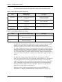
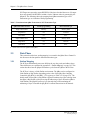
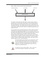
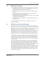
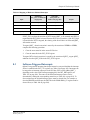
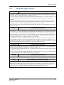
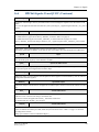
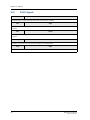
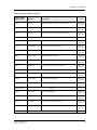
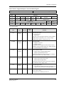
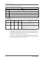
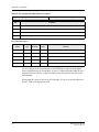
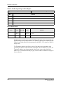
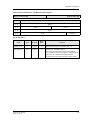
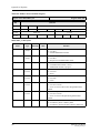
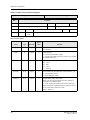
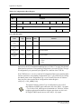
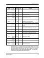
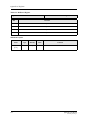
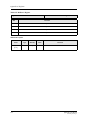
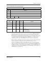
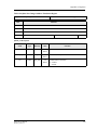
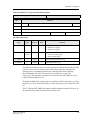
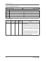
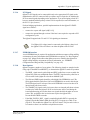
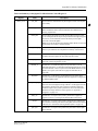
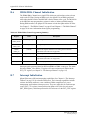
Table 118: IACK Cycle Generator Register
Register Name: IACK_GEN
Register Offset: 508
Bits
Function
31–24
IACK_VEC
23–16
IACK_VEC
15–08
IACK_VEC
07–00
IACK_VEC
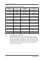
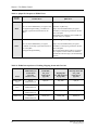
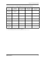
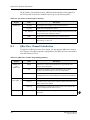
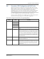
IACK_GEN Description
Name
Type
Reset By
Reset
State
IACK_VEC
[31:0]
R
GEN_RST
0
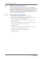
Function
PCI IACK Cycle Vector
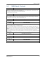
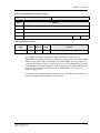
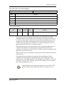
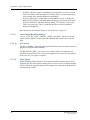
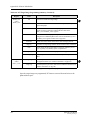
This register generates an Interrupt Acknowledge cycle originating on the QBus.
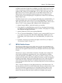
Reading this register from the QBus causes an IACK cycle to be generated on the PCI
bus. The byte lanes enabled on the PCI bus are determined by SIZ[1:0] and A[1:0] of
the QBus read. The address on the QBus used to access the IACK_GEN register is
passed to the PCI bus during the PCI IACK cycle. Address information, however, is
ignored during PCI IACK cycles, so this has no effect.
Reads from this register act as delayed transfers. This means that the QBus master is
retried until the read data is latched from the PCI target. When the IACK cycle
completes on the PCI bus, the IACK_VEC[31:0] field is returned as read data when the
QBus master returns after the retry.
Writing to this register from the QBus or PCI bus has no effect. Reads from the PCI bus
return all zeros.
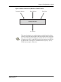
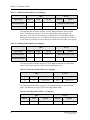
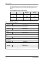
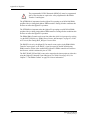
The QSpan II does not perform byte swapping of data in the Register Channel
regardless of whether the QBus is configured as big or little endian. Bit 31 in the
register is bit 31 on the QBus regardless of the QB_BOC bit in the MISC_CTL register
(see Table 127 on page 276). Therefore, software on the QBus may need to swap the
data when performing IACK cycles.
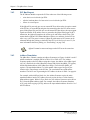
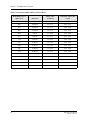
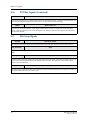
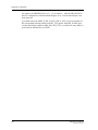
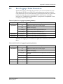
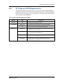
QSpan II generates a bus error upon register access to the IACK_GEN
register if the bus master (BM) bit in the PCI_CS register is not set.
QSpan II User Manual
8091862_MA001_08
261