1
Digital-Analog Converter Module Type
AJ65SBT2B-64DA
User's Manual
SAFETY PRECAUTIONS
(Read these precautions before using this product.)
Before using this product, please read this manual and the relevant manuals carefully and pay full attention
to safety to handle the product correctly.
The instructions given in this manual are concerned with this product. For the safety instructions of the
programmable controller system, please read the CPU module user's manual.
In this manual, the safety precautions are classified into two levels: "
WARNING" and "
CAUTION".
WARNING
Indicates that incorrect handling may cause hazardous conditions,
resulting in death or severe injury.
CAUTION
Indicates that incorrect handling may cause hazardous conditions,
resulting in minor or moderate injury or property damage.
Under some circumstances, failure to observe the precautions given under "
CAUTION" may lead to
serious consequences.
Observe the precautions of both levels because they are important for personal and system safety.
Make sure that the end users read this manual and then keep the manual in a safe place for future
reference.
[Design Precautions]
WARNING
Configure a safety circuit so that the safety of the overall system is maintained even if an external
power failure or a programmable controller failure occurs. Incorrect output or malfunction can lead to
an accident.
(1) The status of analog output changes depending on the setting of various functions that control
the analog output. Take sufficient caution when setting for those functions. For details of analog
output status, refer to Section 3.4.1.
(2) Normal output may not be obtained due to malfunctions of output elements or the internal circuits.
For output signals that may cause a serious accident, provide an external monitoring circuit.
CAUTION
Do not install the control or communication cable(s) together with the main circuit or power cables.
Keep a distance of 100mm (3.94 inches) or more between them.
Doing so may cause malfunctions due to noise.
At power ON/OFF, voltage or current may instantaneously be output from the output terminal of this
module.
In such case, wait until the analog output becomes stable to start controlling the external device.
A-1
[Installation Precautions]
CAUTION
Use the module in an environment that meets the general specifications given in this manual.
Operating it in any other environment may cause an electric shock, fire, malfunction, product
damage or deterioration.
For protection of the switches, do not remove the cushioning material before installation.
Securely fix the module with a DIN rail or mounting screws. Tighten the screws within the specified
torque range.
Undertightening can cause drop of the screw, short circuit or malfunction.
Overtightening can damage the screw and/or module, resulting in drop, short circuit, or malfunction.
Do not directly touch any conductive part of the module.
Doing so may result in a malfunction or failure of the module.
[Wiring Precautions]
CAUTION
Shut off the external power supply for the system in all phases before wiring.
Failure to do so may result in damage to the product.
Always ground the FG terminal to the protective ground conductor.
Failure to do so may result in malfunctions.
Be sure to tighten any unused terminal screws within a tightening torque range. Failure to do so may
cause a short circuit due to contact with a solderless terminal.
Use applicable solderless terminals and tighten them with the specified torque.
If any solderless spade terminal is used, it may be disconnected when the terminal screw comes
loose, resulting in failure.
Check the rated voltage and terminal layout and then wire the module correctly.
Connecting a power supply of a different voltage rating or incorrect wiring may cause a fire or failure.
Tighten terminal screws within the specified torque range.
A loose terminal screw may cause a short circuit or malfunction.
Overtightening can cause a short circuit or malfunction due to damage of the screws or module.
Take care to prevent foreign matter such as dust or wire chips from entering the module.
Failure to do so may cause a fire, failure or malfunctions.
A-2
[Wiring Precautions]
CAUTION
Place the connection wires and cables in a duct or clamp them.
If not, dangling cables may swing or inadvertently be pulled, resulting in damage to the module and/
or cables or malfunctions due to poor cable connection.
Do not install the control lines or communication cables together with the main circuit lines or
power cables. Failure to do so may result in malfunction due to noise.
When disconnecting the cables from the module, do not hold and pull the cable part.
Disconnect the cables after loosening the screws in the portions connected to the module.
Pulling the cable that is still connected to the module may damage the module and/or cable and
cause malfunctions due to poor cable connection.
[Starting and Maintenance Precautions]
CAUTION
Do not touch the terminals while the power is on.
Doing so may cause malfunction.
Be sure to shut off all phases of the external power supply used by the system before cleaning or
retightening the terminal screws.
Not doing so can cause the module to fail or malfunction.
Never disassemble or modify the module.
This may cause breakdowns, malfunction, injury and/or fire.
Do not drop or apply any strong impact to the module.
Doing so may damage the module.
Be sure to shut off all phases of the external power supply used by the system before mounting or
dismounting the module to or from the panel.
Not doing so can cause the module to fail or malfunction.
Do not install/remove the terminal block more than 50 times after the first use of the product.
(IEC 61131-2 compliant)
Before handling the module, always touch grounded metal, etc. to discharge static electricity from
the human body. Failure to do so can cause the module to fail or malfunction.
A-3
[Disposal Precautions]
CAUTION
When disposing of this product, treat it as industrial waste.
A-4
CONDITIONS OF USE FOR THE PRODUCT
(1) Mitsubishi programmable controller ("the PRODUCT") shall be used in conditions;
i) where any problem, fault or failure occurring in the PRODUCT, if any, shall not lead to any major
or serious accident; and
ii) where the backup and fail-safe function are systematically or automatically provided outside of
the PRODUCT for the case of any problem, fault or failure occurring in the PRODUCT.
(2) The PRODUCT has been designed and manufactured for the purpose of being used in general
industries.
MITSUBISHI SHALL HAVE NO RESPONSIBILITY OR LIABILITY (INCLUDING, BUT NOT
LIMITED TO ANY AND ALL RESPONSIBILITY OR LIABILITY BASED ON CONTRACT,
WARRANTY, TORT, PRODUCT LIABILITY) FOR ANY INJURY OR DEATH TO PERSONS OR
LOSS OR DAMAGE TO PROPERTY CAUSED BY the PRODUCT THAT ARE OPERATED OR
USED IN APPLICATION NOT INTENDED OR EXCLUDED BY INSTRUCTIONS, PRECAUTIONS,
OR WARNING CONTAINED IN MITSUBISHI'S USER, INSTRUCTION AND/OR SAFETY
MANUALS, TECHNICAL BULLETINS AND GUIDELINES FOR the PRODUCT.
("Prohibited Application")
Prohibited Applications include, but not limited to, the use of the PRODUCT in;
• Nuclear Power Plants and any other power plants operated by Power companies, and/or any
other cases in which the public could be affected if any problem or fault occurs in the PRODUCT.
• Railway companies or Public service purposes, and/or any other cases in which establishment of
a special quality assurance system is required by the Purchaser or End User.
• Aircraft or Aerospace, Medical applications, Train equipment, transport equipment such as
Elevator and Escalator, Incineration and Fuel devices, Vehicles, Manned transportation,
Equipment for Recreation and Amusement, and Safety devices, handling of Nuclear or
Hazardous Materials or Chemicals, Mining and Drilling, and/or other applications where there is a
significant risk of injury to the public or property.
Notwithstanding the above, restrictions Mitsubishi may in its sole discretion, authorize use of the
PRODUCT in one or more of the Prohibited Applications, provided that the usage of the PRODUCT
is limited only for the specific applications agreed to by Mitsubishi and provided further that no
special quality assurance or fail-safe, redundant or other safety features which exceed the general
specifications of the PRODUCTs are required. For details, please contact the Mitsubishi
representative in your region.
A-5
REVISIONS
*The manual number is given on the bottom left of the back cover.
Print date
*Manual number
Revision
Aug., 2008
SH(NA)-080768ENG-A First edition
Oct., 2010
SH(NA)-080768ENG-B Addition
CONDITIONS OF USE FOR THE PRODUCT, Section 6.4
Correction
SAFETY PRECAUTIONS, ABOUT MANUALS, GENERIC TERMS AND
ABBREVIATIONS, Section 2.1, 2.2, 3.1, 3.2, 4.2, 4.6.2, 4.7.2
Jun., 2011
SH(NA)-080768ENG-C Correction
COMPLIANCE WITH EMC AND LOW VOLTAGE DIRECTIVES, Section 3.1,
3.2, 3.3.1, 3.3.2
Japanese Manual Version SH-080729-C
This manual confers no industrial property rights or any rights of any other kind, nor does it confer any patent licenses.
Mitsubishi Electric Corporation cannot be held responsible for any problems involving industrial property rights which may
occur as a result of using the contents noted in this manual.
2008 MITSUBISHI ELECTRIC CORPORATION
A-6
INTRODUCTION
Thank you for choosing Mitsubishi general-purpose programmable controller.
Before using this product, please read this manual carefully to fully understand the functions and
performance of the programmable controller to ensure correct use.
CONTENTS
SAFETY PRECAUTIONS•••••••••••••••••••••••••••••••••••••••••••••••••••••••••••••••••••••••••••••••••••••••••••••••••••••• A - 1
CONDITIONS OF USE FOR THE PRODUCT••••••••••••••••••••••••••••••••••••••••••••••••••••••••••••••••••••••••••••• A - 5
REVISIONS••••••••••••••••••••••••••••••••••••••••••••••••••••••••••••••••••••••••••••••••••••••••••••••••••••••••••••••••••••••• A - 6
INTRODUCTION •••••••••••••••••••••••••••••••••••••••••••••••••••••••••••••••••••••••••••••••••••••••••••••••••••••••••••••••• A - 7
CONTENTS••••••••••••••••••••••••••••••••••••••••••••••••••••••••••••••••••••••••••••••••••••••••••••••••••••••••••••••••••••••• A - 7
ABOUT MANUALS •••••••••••••••••••••••••••••••••••••••••••••••••••••••••••••••••••••••••••••••••••••••••••••••••••••••••••••• A - 9
COMPLIANCE WITH EMC AND LOW VOLTAGE DIRECTIVES •••••••••••••••••••••••••••••••••••••••••••••••••••••• A - 9
GENERIC TERMS AND ABBREVIATIONS ••••••••••••••••••••••••••••••••••••••••••••••••••••••••••••••••••••••••••••••• A - 10
PACKING LIST•••••••••••••••••••••••••••••••••••••••••••••••••••••••••••••••••••••••••••••••••••••••••••••••••••••••••••••••••• A - 11
CHAPTER1 OVERVIEW
1.1
1 - 1 to 1 - 2
Features •••••••••••••••••••••••••••••••••••••••••••••••••••••••••••••••••••••••••••••••••••••••••••••••••••••••••••••• 1 - 1
CHAPTER2 SYSTEM CONFIGURATION
2 - 1 to 2 - 2
2.1
Overall Configuration••••••••••••••••••••••••••••••••••••••••••••••••••••••••••••••••••••••••••••••••••••••••••••••• 2 - 1
2.2
Applicable System •••••••••••••••••••••••••••••••••••••••••••••••••••••••••••••••••••••••••••••••••••••••••••••••••• 2 - 2
CHAPTER3 SPECIFICATIONS
3 - 1 to 3 - 21
3.1
General Specifications ••••••••••••••••••••••••••••••••••••••••••••••••••••••••••••••••••••••••••••••••••••••••••••• 3 - 1
3.2
Performance Specifications••••••••••••••••••••••••••••••••••••••••••••••••••••••••••••••••••••••••••••••••••••••• 3 - 2
3.3
I/O Conversion Characteristics ••••••••••••••••••••••••••••••••••••••••••••••••••••••••••••••••••••••••••••••••••• 3 - 3
3.3.1
3.3.2
3.3.3
3.3.4
3.3.5
3.4
Functions ••••••••••••••••••••••••••••••••••••••••••••••••••••••••••••••••••••••••••••••••••••••••••••••••••••••••••• 3 - 11
3.4.1
3.5
Combinations of functions ••••••••••••••••••••••••••••••••••••••••••••••••••••••••••••••••••••••••••••••••• 3 - 12
Remote I/O Signals••••••••••••••••••••••••••••••••••••••••••••••••••••••••••••••••••••••••••••••••••••••••••••••• 3 - 13
3.5.1
3.5.2
3.6
Voltage output characteristics •••••••••••••••••••••••••••••••••••••••••••••••••••••••••••••••••••••••••••••• 3 - 4
Current output characteristics••••••••••••••••••••••••••••••••••••••••••••••••••••••••••••••••••••••••••••••• 3 - 6
Relationship between offset/gain setting and analog output value •••••••••••••••••••••••••••••••••• 3 - 8
Accuracy •••••••••••••••••••••••••••••••••••••••••••••••••••••••••••••••••••••••••••••••••••••••••••••••••••••••• 3 - 9
Conversion speed ••••••••••••••••••••••••••••••••••••••••••••••••••••••••••••••••••••••••••••••••••••••••••• 3 - 10
List of remote I/O signals •••••••••••••••••••••••••••••••••••••••••••••••••••••••••••••••••••••••••••••••••• 3 - 13
Details of the remote I/O signals ••••••••••••••••••••••••••••••••••••••••••••••••••••••••••••••••••••••••• 3 - 14
Remote Register •••••••••••••••••••••••••••••••••••••••••••••••••••••••••••••••••••••••••••••••••••••••••••••••••• 3 - 19
3.6.1
3.6.2
Remote register list ••••••••••••••••••••••••••••••••••••••••••••••••••••••••••••••••••••••••••••••••••••••••• 3 - 19
Details of the remote register ••••••••••••••••••••••••••••••••••••••••••••••••••••••••••••••••••••••••••••• 3 - 20
CHAPTER4 PROCEDURES AND SETTINGS BEFORE OPERATION
4 - 1 to 4 - 11
A-7
4.1
Procedures before Operation•••••••••••••••••••••••••••••••••••••••••••••••••••••••••••••••••••••••••••••••••••••4 - 1
4.2
Handling Precautions ••••••••••••••••••••••••••••••••••••••••••••••••••••••••••••••••••••••••••••••••••••••••••••••4 - 2
4.3
Part Names ••••••••••••••••••••••••••••••••••••••••••••••••••••••••••••••••••••••••••••••••••••••••••••••••••••••••••4 - 4
4.3.1
Transmission speed auto-tracking function ••••••••••••••••••••••••••••••••••••••••••••••••••••••••••••••4 - 5
4.4
Station Number Setting ••••••••••••••••••••••••••••••••••••••••••••••••••••••••••••••••••••••••••••••••••••••••••••4 - 6
4.5
Module Mounting Orientation •••••••••••••••••••••••••••••••••••••••••••••••••••••••••••••••••••••••••••••••••••••4 - 6
4.6
Wiring of Data Link Cable •••••••••••••••••••••••••••••••••••••••••••••••••••••••••••••••••••••••••••••••••••••••••4 - 7
4.6.1
4.6.2
4.6.3
4.7
Wiring precautions ••••••••••••••••••••••••••••••••••••••••••••••••••••••••••••••••••••••••••••••••••••••••••••4 - 7
CC-Link dedicated cable connection ••••••••••••••••••••••••••••••••••••••••••••••••••••••••••••••••••••••4 - 7
Terminating resistor connection ••••••••••••••••••••••••••••••••••••••••••••••••••••••••••••••••••••••••••••4 - 7
Wiring with External Devices •••••••••••••••••••••••••••••••••••••••••••••••••••••••••••••••••••••••••••••••••••••4 - 8
4.7.1
4.7.2
Wiring precautions ••••••••••••••••••••••••••••••••••••••••••••••••••••••••••••••••••••••••••••••••••••••••••••4 - 8
Wiring with external devices ••••••••••••••••••••••••••••••••••••••••••••••••••••••••••••••••••••••••••••••••4 - 9
4.8
Offset/Gain Setting ••••••••••••••••••••••••••••••••••••••••••••••••••••••••••••••••••••••••••••••••••••••••••••••• 4 - 10
4.9
Maintenance and Inspection •••••••••••••••••••••••••••••••••••••••••••••••••••••••••••••••••••••••••••••••••••• 4 - 11
CHAPTER5 PROGRAMMING
5 - 1 to 5 - 20
5.1
Programming Procedure ••••••••••••••••••••••••••••••••••••••••••••••••••••••••••••••••••••••••••••••••••••••••••5 - 1
5.2
Conditions of Program Examples ••••••••••••••••••••••••••••••••••••••••••••••••••••••••••••••••••••••••••••••••5 - 2
5.3
Program Example When the QCPU (Q mode) is Used •••••••••••••••••••••••••••••••••••••••••••••••••••••5 - 4
5.4
Program Example When the QnACPU is Used •••••••••••••••••••••••••••••••••••••••••••••••••••••••••••••••5 - 8
5.5
Program Example When the ACPU/QCPU (A mode) is Used (Dedicated Instructions) •••••••••••• 5 - 13
5.6
Program Example When the ACPU/QCPU (A mode) is Used (FROM/TO Instructions) •••••••••••• 5 - 17
CHAPTER6 TROUBLESHOOTING
6 - 1 to 6 - 7
6.1
Error Code List ••••••••••••••••••••••••••••••••••••••••••••••••••••••••••••••••••••••••••••••••••••••••••••••••••••••6 - 1
6.2
Checking Errors Using LED Indications ••••••••••••••••••••••••••••••••••••••••••••••••••••••••••••••••••••••••6 - 2
6.3
Troubleshooting When Analog Output Values are Not Output•••••••••••••••••••••••••••••••••••••••••••••6 - 4
6.4
Troubleshooting When Data Link Execution Takes Much Time •••••••••••••••••••••••••••••••••••••••••••6 - 4
6.5
Troubleshooting When the "ERR." LED of the Master Station Flashes ••••••••••••••••••••••••••••••••••6 - 5
6.6
When Flash Memory Read Error Flag (RXnA) Turns on ••••••••••••••••••••••••••••••••••••••••••••••••••••6 - 7
6.7
When User Range Read Error Flag (RXnB) Turns on•••••••••••••••••••••••••••••••••••••••••••••••••••••••6 - 7
6.8
When Flash Memory Write Error Flag (RXnC) Turns on ••••••••••••••••••••••••••••••••••••••••••••••••••••6 - 7
APPENDICES
Appendix 1
INDEX
A-8
App - 1 to App - 2
External Dimensions •••••••••••••••••••••••••••••••••••••••••••••••••••••••••••••••••••••••••••••••••• App - 1
Index - 1 to Index - 3
ABOUT MANUALS
The following manuals are also related to the product.
Refer to the following table for ordering a manual.
Related manuals
Manual number
Manual name
(model code)
CC-Link System Master/Local Module Type AJ61BT11/A1SJ61BT11 User's Manual
Describes the system configuration, performance specifications, functions, handling, wiring, and troubleshooting
IB-66721
of the AJ61BT11 and A1SJ61BT11.
(13J872)
(Sold separately.)
CC-Link System Master/Local Module Type AJ61QBT11/A1SJ61QBT11 User's Manual
Describes the system configuration, performance specifications, functions, handling, wiring, and troubleshooting
IB-66722
of the AJ61QBT11 and A1SJ61QBT11.
(13J873)
(Sold separately.)
CC-Link System Master/Local Module User's Manual
Describes the system configuration, performance specifications, functions, handling, wiring, and troubleshooting
SH-080394E
(13JR64)
of the CC-Link module.
(Sold separately.)
Type AnSHCPU/AnACPU/AnUCPU/QCPU-A (A Mode) Programming Manual (Dedicated Instructions)
Describes the instructions extended for the AnSHCPU/AnACPU/AnUCPU.
(Sold separately.)
IB-66251
(13J742)
MELSEC-L CC-Link System Master/Local Module User's Manual
Describes the system configuration, performance specifications, functions, handling, wiring, and troubleshooting
SH-080895ENG
(13JZ41)
of the built-in CC-Link system master/local function and CC-Link system master/local module.
(Sold separately.)
COMPLIANCE WITH EMC AND LOW VOLTAGE DIRECTIVES
(1) Method of ensuring compliance
To ensure that Mitsubishi programmable controllers maintain EMC and Low Voltage
Directives when incorporated into other machinery or equipment, certain measures
may be necessary.
Please refer to the "EMC AND LOW VOLTAGE DIRECTIVES" chapter in the user's
manual for the CPU module used. The CE mark on the side of the programmable
controller indicates compliance with EMC and Low Voltage Directives.
(2) Additional measures
To ensure that this product maintains EMC and Low Voltage Directives, please refer
to the "CC-Link module" section in the "EMC AND LOW VOLTAGE DIRECTIVES"
chapter in the user's manual for the CPU module used.
A-9
GENERIC TERMS AND ABBREVIATIONS
Unless otherwise specified, the following generic terms and abbreviations are used in this manual to describe the
AJ65SBT2B-64DA digital-analog converter module.
Generic term/
Description
abbreviation
GX Developer
GX Works2
Product name of the software package for the MELSEC programmable controllers
Generic term for A0J2CPU, A0J2HCPU, A1CPU, A2CPU, A2CPU-S1, A3CPU, A1SCPU,
A1SCPUC24-R2, A1SHCPU, A1SJCPU, A1SJCPU-S3, A1SJHCPU, A1NCPU, A2NCPU,
ACPU
A2NCPU-S1, A3NCPU, A3MCPU, A3HCPU, A2SCPU, A2SHCPU, A2ACPU, A2ACPU-S1,
A3ACPU, A2UCPU, A2UCPU-S1, A2USCPU, A2USCPU-S1, A2USHCPU-S1, A3UCPU, and
A4UCPU
QnACPU
QCPU (A mode)
Generic term for Q2ACPU, Q2ACPU-S1, Q2ASCPU, Q2ASCPU-S1, Q2ASHCPU, Q2ASHCPUS1, Q3ACPU, Q4ACPU, and Q4ARCPU
Generic term for Q02CPU-A, Q02HCPU-A, and Q06HCPU-A
Generic term for Q00JCPU, Q00CPU, Q01CPU, Q02CPU, Q02HCPU, Q06HCPU, Q12HCPU,
Q25HCPU, Q02PHCPU, Q06PHCPU, Q12PHCPU, Q25PHCPU, Q12PRHCPU, Q25PRHCPU,
QCPU (Q mode)
Q00UJCPU, Q00UCPU, Q01UCPU, Q02UCPU, Q03UDCPU, Q04UDHCPU, Q06UDHCPU,
Q10UDHCPU, Q13UDHCPU, Q20UDHCPU, Q26UDHCPU, Q03UDECPU, Q04UDEHCPU,
Q06UDEHCPU, Q13UDEHCPU, Q26UDEHCPU, Q50UDEHCPU and Q100UDEHCPU
LCPU
Master station
Local station
Generic term for L02CPU, L26CPU-BT
A station that controls data link system
One master station is required for each system.
A station that has a programmable controller CPU and can communicate with the master and other
local stations
A station that treats information in units of bits only (performs input and output with external
Remote I/O station
devices.)
(e.g. AJ65BTB1-16D and AJ65SBTB1-16D)
Remote device station
Remote station
A station that treats information in units of bits and words (performs input and output with external
devices and converts analog data.)
Generic term for remote I/O station and remote device station
This station is controlled by the master station.
Intelligent device
A station that can perform transient transmission, such as the AJ65BT-R2N (including local
station
Master module
stations)
Generic term for modules that can be used as the master station
Link special relay (for CC-Link)
SB
Information in units of bits that indicates the data link status and module operating status of the
master station/local stations
Link special register (for CC-Link)
SW
Information in units of 16 bits that indicates the data link status and module operating status of the
master station/local stations
RX
RY
RWw
RWr
A - 10
Remote input (for CC-Link)
Information input in units of bits from the remote station to the master station
Remote output (for CC-Link)
Information output in units of bits from the master station to the remote station
Remote register (write area for CC-Link)
Information output in units of 16 bits from the master station to the remote device station
Remote register (read area for CC-Link)
Information input in units of 16 bits from the remote device station to the master station
PACKING LIST
The following table shows the packing list of the AJ65SBT2B-64DA digital-analog
converter module.
Product
AJ65SBT2B-64DA digital-analog converter module
Digital-Analog Converter Module User's Manual (Hardware) Type AJ65SBT2B-64DA
Quantity
1
1
A - 11
1
OVERVIEW
CHAPTER1
OVERVIEW
This manual describes the specifications, handling, and programming methods of the
AJ65SBT2B-64DA digital-analog converter module (hereafter abbreviated as
AJ65SBT2B-64DA) used as a remote device station in a CC-Link system.
The AJ65SBT2B-64DA is a module that converts digital values (16-bit signed binary data)
into analog values (voltage or current).
1.1
Features
This section describes the features of the AJ65SBT2B-64DA.
(1) One module can output analog values from four channels.
One module can output analog values (voltage output or current output) from four
channels.
In voltage output, analog values can be output in the range of 10V.
In current output, analog values can be output in the range of 0 to 20mA.
(2) Output range is selectable per channel.
Analog output ranges can be switched per channel and the I/O conversion
characteristics can be changed.
(3) High resolution
By switching the output range, the resolution can be set any of 1/12000, 1/ 12000,
and 1/ 16000, so high-resolution analog values can be obtained.
(4) High accuracy
When the operating ambient temperature is 0 to 55
conversion in accuracy of
0.3%*
at the maximum analog output value. When the
operating ambient temperature is 25 5
accuracy of
0.2%*
, the module performs D/A
, the module performs D/A conversion in
at the maximum analog output value.
* Except when noise is applied.
(5) Setting whether to hold or clear analog output while the programmable
controller CPU is in the STOP status is possible.
When the programmable controller CPU is in the STOP status or the AJ65SBT2B64DA has stopped D/A conversion due to an error, whether to hold or clear an analog
value output from each channel immediately before the error occurrence can be
specified.
(6) Saving man-hour
(a) The module has built-in terminating resistor of 110 , which eases wiring.
(b) The transmission speed of the AJ65SBT2B-64DA needs not be set by the user. It
is set automatically according to the transmission speed set in the master station.
1-1
1.1 Features
OVERVIEW
1
Maximum 42 AJ65SBT2B-64DA modules are connectable to one master station.
(8) Maintenance is easy.
OVERVIEW
(7) Maximum 42 modules are connectable.
2
SYSTEM
CONFIGURATION
Since 2-piece terminal block is used, the maintenance is easy.
SPECIFICATIONS
3
PROCEDURES AND
SETTINGS BEFORE
OPERATION
4
PROGRAMMING
5
APPENDICES
TROUBLESHOOTING
6
INDEX
1
1.1 Features
1-2
2
SYSTEM CONFIGURATION
CHAPTER2
SYSTEM CONFIGURATION
This chapter describes the system configuration for using the AJ65SBT2B-64DA.
2.1
Overall Configuration
This section describes the overall configuration for using the AJ65SBT2B-64DA.
CC-Link system master/local module (master station)
CC-Link system master/local module (local station)
Terminating resistor
CC-Link dedicated cable
(Intelligent device station)
(Remote I/O station)
(Remote device station)
Terminating resistor
AJ65SBT2B-64DA
(Remote device station)
Occupies one station.
Device for which voltage/current is output
(such as a solenoid valve)
Figure 2.1 Overall configuration for using the AJ65SBT2B-64DA
2-1
2.1 Overall Configuration
1
OVERVIEW
Applicable System
(1) Applicable master modules
For available master modules, visit the CC-Link Partner Association (CLPA) website
at:
http://www.cc-link.org/
Remark
Check the specifications of the master module before use.
2
SYSTEM
CONFIGURATION
This section describes the applicable system.
The CC-Link dedicated instructions (RLPA, RRPA) cannot be used depending on the
programmable controller CPU and master module used.
For details on restrictions, refer to the user's manual of the master module for A series
and Type AnSHCPU/AnACPU/AnUCPU/QCPU-A (A Mode) Programming Manual
(Dedicated Instructions).
Dedicated instructions other than the RLPA and RRPA cannot be used for the
module.
For a program example using the dedicated instructions (RLPA, RRPA), refer to
Section 5.5.
4
PROCEDURES AND
SETTINGS BEFORE
OPERATION
(2) Restrictions on using the CC-Link dedicated instructions (RLPA, RRPA)
SPECIFICATIONS
3
PROGRAMMING
5
TROUBLESHOOTING
6
APPENDICES
2.2
SYSTEM CONFIGURATION
INDEX
2
2.2 Applicable System
2-2
3
SPECIFICATIONS
CHAPTER3
SPECIFICATIONS
This chapter describes the specifications of the AJ65SBT2B-64DA.
3.1
General Specifications
This section describes the general specifications of the AJ65SBT2B-64DA.
Table 3.1 General specifications
Item
Specifications
Operating ambient temperature
0 to 55
Storage ambient temperature
-20 to 75
Operating ambient humidity
10 to 90% RH, non-condensing
Storage ambient humidity
10 to 90% RH, non-condensing
Frequency
JIS B 3502 and
Vibration resistance
IEC 61131-2
For intermittent
vibration
Acceleration
For continuous
vibration
Shock resistance
-
8.4 to 150Hz
9.8m/s2
5 to 8.4Hz
-
8.4 to 150Hz
JIS B 3502 and IEC 61131-2 compliant
Operating atmosphere
3.5mm
5 to 8.4Hz
compliant
(147m/s2,
4.9m/s
Amplitude
(0.14inches)
-
Number of
sweeps
10 times each
in X, Y, and Z
directions
1.75mm
(0.069inches)
2
-
-
3 times each in X, Y, and Z directions)
No corrosive gases
Operating altitude*3
2000m or lower
Installation location
Inside control panel
Overvoltage category*1
II or lower
Pollution degree*2
2 or lower
* 1: This indicates the section of the power supply to which the device is assumed to be connected
between the public distribution network and the machinery within premises.
Category II applies to devices to which a power is supplied from installed equipment.
The surge voltage withstand for devices with rated voltage of up to 300V is 2500V.
* 2: This index indicates the degree to which conductive material can be generated in terms of the
environment where the devices are used.
In the environment corresponding to "Pollution level 2", basically only non-conductive pollution
occurs. However, temporary conductivity may occur due to occasional condensation.
* 3: Do not operate or store the programmable controller in the environment where the pressure
applied is equal to or greater than the atmospheric pressure at an altitude of 0m. Doing so may
cause malfunction.
Please consult our branch office for more information.
3-1
3.1 General Specifications
3
SPECIFICATIONS
1
OVERVIEW
Performance Specifications
This section describes the performance specifications of the AJ65SBT2B-64DA.
Table 3.2 Performance specifications
2
AJ65SBT2B-64DA
Voltage
16-bit signed binary (-12288 to 12287, -16384 to 16383, -288 to 12287)
value
Current
16-bit signed binary (-288 to 12287)
Analog output
Voltage
value
Current
-10 to 10VDC (external load resistance: 1k
SYSTEM
CONFIGURATION
Digital input
to 1M )
0 to 20mADC (external load resistance: 0 to 600 )
3
Accuracy*2
Analog output range*1
Ambient
Ambient
Maximum
temperature
temperature
resolution
0 to 55
-16000 to 16000
I/O characteristics,
maximum resolution,
Voltage
0 to 5V
0 to 12000
0.3%
( 15mV)
1 to 5V
maximum analog output
value)
( 30mV)
0.3%
User range setting 2
-12000 to 2000
(-10 to 10V)
( 30mV)
5
0.2%
( 20mV)
0.2%
( 10mV)
0.2%
( 20mV)
0 to 20mA
Current
0.3%
User range setting 1
( 60 A)
0.333mV
0.2%
1.33 A
Available
Number of analog output
4 channels/module
points
Number of writes to Flash
4
5
0.95 A
200 s/channel
Output short protection
6
Maximum 10,000 times
memory
CC-Link station type
Remote device station
Number of occupied stations
1 station
Connection cable
Withstand voltage
0.333mV
( 40 A)
(0 to 20mA)
Conversion speed
0.416mV
1.66 A
4 to 20mA
0 to 12000
0.625mV
TROUBLESHOOTING
accuracy (accuracy at the
0.3%
-10 to 10V
25
PROGRAMMING
Digital input value
SPECIFICATIONS
Item
PROCEDURES AND
SETTINGS BEFORE
OPERATION
3.2
CC-Link dedicated cable
500VAC between all power supply and communication system terminals and all analog output terminals for
one minute
Between communication system terminal and all analog output terminals: photocoupler isolation
Between power supply system terminal and all analog output terminals: transformer isolation
Between channels: non-isolation
Noise immunity
Tested by a noise simulator with noise voltage of 500Vp-p, noise width of 1 s, and noise frequency of 25 to
60Hz.
Communication
part, module
power supply
connection part
7-point, 2-piece terminal block
M3
5.2 Tightening torque: 0.59 to 0.88N m
Number of applicable solderless terminals: maximum 2
18-point, 2-piece terminal block
system
I/O part
M3
5.2 Tightening torque: 0.59 to 0.88N m
Number of applicable solderless terminals: maximum 2
3.2 Performance Specifications
INDEX
External
APPENDICES
Isolation method
3-2
3
SPECIFICATIONS
Table 3.2 Performance specifications
Item
AJ65SBT2B-64DA
0.3 to 2.0mm2
Applicable wire size
RAV1.25-3 (IEC 60715 compliant)
Applicable solderless
terminal
[Applicable wire size: 0.3 to 1.25mm2]
V2-MS3, RAP2-3SL, TGV2-3N
[Applicable wire size: 1.25 to 2.0mm2]
Module mounting screw
M4 screw
0.7mm
16mm or more (Tightening torque range: 0.78 to 1.08N m)
The module can also be mounted to a DIN rail.
Applicable DIN rail
TH35-7.5Fe, TH35-7.5Al (IEC 60175 compliant)
24VDC (20.4 to 28.8VDC)
External power supply
Inrush current: 2.6A, 3.2ms or shorter
Current consumption: 0.24A (24VDC)
Weight
0.25kg
* 1 The factory default is set to "-10 to 10V".
* 2 Except when noise is applied.
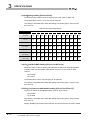
3.3
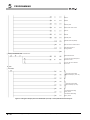
I/O Conversion Characteristics
I/O conversion characteristics are an inclination of a straight line connecting an offset
value and a gain value when a digital input value set from the programmable controller
CPU is converted into an analog value (voltage or current output).
An offset value is an analog value (voltage or current) output when the digital input value
set from the programmable controller CPU is 0.
A gain value is an analog value (voltage or current) output when the digital input value set
from the programmable controller CPU is as follows:
12000 (when 0 to 5V, 1 to 5V, 0 to 20mA, 4 to 20mA, user range setting 1, or user range
setting 2 is selected for output range)
16000 (when -10 to 10V is selected for output range)
3-3
3.3 I/O Conversion Characteristics
3
SPECIFICATIONS
1
3.3.1
Voltage output characteristics
OVERVIEW
A graph for voltage output characteristics is shown below.
2
SYSTEM
CONFIGURATION
10
Practical range of analog output
5
3)
1
0
2)
3
SPECIFICATIONS
Analog output value (V)
1)
4
PROCEDURES AND
SETTINGS BEFORE
OPERATION
-5
-10
-12
-16000
0
-8000
-16384
8000
-288
5
12000 16000
12287 16383
Table 3.3 Voltage output characteristics table
Num
ber
Analog output range setting
Offset value
Gain value
Digital input value
-16000 to 16000
-10 to 10V
0V
10V
2)
0 to 5V
0V
5V
3)
1 to 5V
1V
5V
-
User range setting 2 (-10 to 10V)
-
-
0 to 12000
-12000 to 12000
0.625mV
0.416mV
0.333mV
0.333mV
6
INDEX
APPENDICES
1)
Maximum
resolution
TROUBLESHOOTING
Figure 3.1 Voltage output characteristics graph
PROGRAMMING
Digital input value
3.3 I/O Conversion Characteristics
3.3.1 Voltage output characteristics
3-4
3
SPECIFICATIONS
POINT
(1) The maximum resolution and accuracy will be within their performance
specifications range when they are within digital input range and analog
output range of each output range.
Outside those ranges, however, they may not fall within the performance
specifications. (Avoid using the dotted line parts in Figure 3.1.)
(2) Set the offset/gain values of the user range setting 2 within the range satisfying
the following conditions.
(a)
(b)
Setting range: -10 to 10V
(Gain value) - (Offset value) > 4V
If one of the conditions is not met, the "RUN" LED falshes every 0.5s. Start
over the setting.
3-5
3.3 I/O Conversion Characteristics
3.3.1 Voltage output characteristics
3
SPECIFICATIONS
1
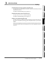
3.3.2
Current output characteristics
OVERVIEW
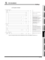
A graph for current output characteristics is shown below.
2
Practical range of analog output
10
2)
1)
3
SPECIFICATIONS
Analog output value (mA)
15
5
SYSTEM
CONFIGURATION
20
4
PROCEDURES AND
SETTINGS BEFORE
OPERATION
4
0
5
12000
-288
12287
Digital input value
Figure 3.2 Current output characteristics graph
Table 3.4 Current output characteristics table
Analog output range setting
Offset value
Gain value
1)
0 to 20mA
0mA
20mA
2)
4 to 20mA
4mA
20mA
-
User range setting 1 (0 to 20mA)
-
-
Digital input value
Maximum
resolution
1.66 A
0 to 12000
1.33 A
6
APPENDICES
0.95 A
INDEX
ber
TROUBLESHOOTING
Num
PROGRAMMING
6000
0
3.3 I/O Conversion Characteristics
3.3.2 Current output characteristics
3-6
3
SPECIFICATIONS
POINT
(1) The maximum resolution and accuracy will be within their performance
specifications range when they are within digital input range and analog
output range of each output range.
Outside those ranges, however, they may not fall within the performance
specifications. (Avoid using the dotted line parts in Figure 3.2.)
(2) Set the offset/gain values of the user range setting 1 within the range satisfying
the following conditions.
(a)
(b)
Setting range: 0 to 20mA
(Gain value) - (Offset value) > 11.5mA
If one of the conditions is not met, the "RUN" LED falshes every 0.5s. Start
over the setting.
3-7
3.3 I/O Conversion Characteristics
3.3.2 Current output characteristics
SPECIFICATIONS
1
(1) Resolution
Find the resolution by the following formula.
(Gain value) - (Offset value)
3
12000
SPECIFICATIONS
(Analog resolution) =
(2) Analog output value
Find the analog output value by the following formula.
Analog
resolution
Digital input
value
+
Offset value
4
PROCEDURES AND
SETTINGS BEFORE
OPERATION
Alalog output
=
value
2
SYSTEM
CONFIGURATION
The resolution of the AJ65SBT2B-64DA can be set by changing settings of the offset/gain
values.
Calculation formulas of the resolution for an analog value and the analog output value for
a digital input value when the settings of the offset/gain value are changed are shown
below.
OVERVIEW
Relationship between offset/gain setting and analog output value
PROGRAMMING
5
TROUBLESHOOTING
6
APPENDICES
3.3.3
INDEX
3
3.3 I/O Conversion Characteristics
3.3.3 Relationship between offset/gain setting and analog output value
3-8
3
SPECIFICATIONS
3.3.4
Accuracy
The accuracy is a value when an analog output value is the maximum value.
Even when the output characteristics are changed by changing the offset/gain setting or
output range, the accuracy does not change and is remained within the range shown in
the performance specifications.
(1) Accuracy of voltage output
For voltage output, the maximum analog output value varies depending on the range
setting.
For example, when 0 to 5V is selected for the output range, the accuracy will be a
value at 5V.
Analog value is output in accuracy of within 0.2% ( 10mV) when the operating
ambient temperature is 25 5
, or in accuracy of within
operating ambient temperature is 0 to 55
0.3% ( 15mV) when the
.
5V
Alalog output value
Varies in the range of 0.2% (within 10mV)
when the operating ambient temperature is 25
5
.
Varies in the range of 0.3% (within 15mV)
when the operating ambient temperature is 0 to 55 .
0V
0
Digital input value
12000
Figure 3.3 Accuracy of voltage output (when 0 to 5V is selected for the output range)
(2) Accuracy of current output
The accuracy of current output is for 20mA.
Analog value is output at accuracy of within
ambient temperature is 25 5
0.2% ( 40 A) when the operating
, or at accuracy of within
operating ambient temperature is 0 to 55
0.3% ( 60 A) when the
.
20mA
Alalog output value
Varies in the range of 0.2% (within 40 A)
when the operating ambient temperature is 25 5 .
0mA
3-9
Varies in the range of 0.3% (within 60 A)
when the operating ambient temperature is 0 to 55 .
0
12000
Digital input value
Figure 3.4 Accuracy of current output
3.3 I/O Conversion Characteristics
3.3.4 Accuracy
SPECIFICATIONS
1
Conversion speed of the AJ65SBT2B-64DA is 200 s per channel.
However, the time from when an digital input value is converted into an analog value till
when the analog value is output varies depending on "transmission delay time" of the CCLink system.
2
processing time
SYSTEM
CONFIGURATION
(1) Remote device station processing time
OVERVIEW
Conversion speed
1
0.4ms
3
2
0.6ms
3
0.8ms
4
1.0ms
Table 3.5 Remote device station processing time
AJ65SBT2B-64DA
Remote device station
SPECIFICATIONS
channels of the
(2) Transmission delay time
For details on transmission delay time, refer to user's manual of the master module
used.
5
PROGRAMMING
(Example) Data link processing time when the master module of the QJ61BT11N is
used in asynchronous mode (normal value)
[Calculation formula]
SM + LS
1 + Remote device station processing time
SM: Scan time of master station sequence program
LS: Link scan time
4
PROCEDURES AND
SETTINGS BEFORE
OPERATION
Number of used
TROUBLESHOOTING
6
APPENDICES
3.3.5
INDEX
3
3.3 I/O Conversion Characteristics
3.3.5 Conversion speed
3 - 10
3
SPECIFICATIONS
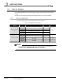
3.4
Functions
This section describes the functions of the AJ65SBT2B-64DA.
Table 3.6 AJ65SBT2B-64DA function list
Item
Description
Reference
Specifies a value to be output, D/A conversion value or offset value, for
D/A output enable/disable
each channel.
Section
function
Note that the conversion speed is constant regardless of the output
3.5.2 (9)
enable/disable setting.
D/A conversion enable/disable
function
Sets the D/A conversion enable/disable status for each channel.
Setting "Disable" for the unused channel can shorten the conversion
speed.
Section
3.5.2 (12)
Output range switching
Sets the analog output range for each channel and changes the I/O
Section
function
conversion characteristics.
3.5.2 (10)
Analog output hold/clear
function when the
programmable controller CPU
is in the STOP status (HOLD/
CLEAR setting)
Offset/gain setting
Specifies whether to hold or clear an analog value (output an offset
value) output from each channel immediately before the programmable Section
controller CPU has entered the STOP status or the AJ65SBT2B-64DA
Sets the offset/gain values using the UP/DOWN switch and changes
I/O conversion characteristics freely.
Transmission speed
Sets transmission speed automatically according to the setting in the
auto-tracking function
master module when the AJ65SBT2B-64DA is powered on.
3 - 11
3.4 Functions
3.5.2 (11)
has stopped D/A conversion due to an error, for each channel.
Section 4.8
-
SPECIFICATIONS
1
3.4.1
Combinations of functions
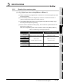
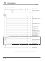
Analog output can be set as shown in Table 3.7, according to the combinations of CH
Conversion enable/disable setting (RY(n+1)4 to RY(n+1)7), CH
disable flag (RYn0 to RYn3), and CH
Analog output enable/
HOLD/CLEAR setting (RY(n+1)0 to RY(n+1)3).
OVERVIEW
3
2
Analog output enable/
Enable (on)
disable flag (RYn0 to RYn3)
Execution
status
CH
HOLD/CLEAR setting
(RY(n+1)0 to RY(n+1)3)
Analog output status while the programmable
controller CPU is in the RUN status
HOLD (on)
Disable (off)
Enable (on) or
Disable (off)
HOLD (on) or
HOLD (on) or
CLEAR (off)
CLEAR (off)
Offset value
0V/0mA
Offset value
Offset value
0V/0mA
Offset value
Offset value
0V/0mA
CLEAR (off)
An analog value converted from a digital input
value set by the programmable controller CPU
is output.
An analog value before
Analog output status while the programmable
controller CPU is in the STOP status
the programmable
controller CPU
becomes the STOP
status is held.
An analog value before
Analog output status while the programmable
controller CPU is in stop error
the programmable
controller CPU
becomes the STOP
status is held.
Analog output status while the "L RUN" LED
turns off/"L.ERR." LED turns on
output.
Offset value
0V/0mA
Offset value
0V/0mA
Offset value
0V/0mA
Offset value
0V/0mA
An analog value before
the "L RUN" LED turns
Offset value
off is held.
Analog output status while the "L ERR." LED
flashes
An analog value converted from a digital input
value set by the programmable controller CPU
is output.
Analog output status during initial processing
completion status after power reset
An analog value converted from a digital input
value set by the programmable controller CPU
is output.
Analog output status while output range
setting error occurs at the AJ65SBT2B-64DA
Analog output status while watchdog timer
error occurs at the AJ65SBT2B-64DA
4
5
Analog output status while digital input setting The upper limit or lower limit analog value is
value error occurs at the AJ65SBT2B-64DA
3
0V/0mA
0V/0mA
0V/0mA
0V/0mA
0V/0mA
0V/0mA
0V/0mA
0V/0mA
POINT
PROGRAMMING
CH
Disable (off)
SPECIFICATIONS
Enable (on)
PROCEDURES AND
SETTINGS BEFORE
OPERATION
Conversion enable/
6
TROUBLESHOOTING
CH
combination disable setting (RY(n+1)4 to
RY(n+1)7)
APPENDICES
Setting
SYSTEM
CONFIGURATION
Table 3.7 Combination list of analog output status
INDEX
When using the QnACPU, using "Y" as the remote output (RY) refresh device of
the auto refresh parameter may not hold the analog value even in HOLD setting.
In HOLD setting, use "M" or "B" as the remote output (RY) refresh device.
3.4 Functions
3.4.1 Combinations of functions
3 - 12
3
SPECIFICATIONS
3.5
Remote I/O Signals
This section describes the assignment and functions of the remote I/O signals.
3.5.1
List of remote I/O signals
Remote input (RX) is an input signal from the AJ65SBT2B-64DA to the master module,
and remote output (RY) is an output signal from the master module to the AJ65SBT2B64DA.
In communications with the master station, the AJ65SBT2B-64DA uses 32 points for the
remote input (RX) and the remote output (RY), respectively.
Table 3.8 List of remote I/O signals
Signal direction: AJ65SBT2B-64DA
Remote input (RX)
Master module
Name
Signal direction: Master module
Remote output (RY)
AJ65SBT2B-64DA
Name
RXn0
RYn0
CH1 Analog output enable/disable flag
RXn1
RYn1
CH2 Analog output enable/disable flag
RXn2
RYn2
CH3 Analog output enable/disable flag
RXn3
RYn3
CH4 Analog output enable/disable flag
RYn4
CH1 Range setting 0th bit
RXn4
RXn5
Reserved
RYn5
CH1 Range setting 1st bit
RXn6
RYn6
CH1 Range setting 2nd bit
RXn7
RYn7
CH2 Range setting 0th bit
RXn8
RYn8
CH2 Range setting 1st bit
RXn9
RYn9
CH2 Range setting 2nd bit
RXnA
Flash memory read error flag
RYnA
CH3 Range setting 0th bit
RXnB
User range read error flag
RYnB
CH3 Range setting 1st bit
RXnC
Flash memory write error flag
RYnC
CH3 Range setting 2nd bit
RYnD
CH4 Range setting 0th bit
RXnD
RXnE
Reserved
RYnE
CH4 Range setting 1st bit
RYnF
CH4 Range setting 2nd bit
RX(n+1)0
RY(n+1)0
CH1 HOLD/CLEAR setting
RX(n+1)1
RY(n+1)1
CH2 HOLD/CLEAR setting
RX(n+1)2
RY(n+1)2
CH3 HOLD/CLEAR setting
RX(n+1)3
RY(n+1)3
CH4 HOLD/CLEAR setting
RXnF
RX(n+1)4
Test mode flag
Reserved
RY(n+1)4
CH1 Conversion enable/disable setting
RX(n+1)5
RY(n+1)5
CH2 Conversion enable/disable setting
RX(n+1)6
RY(n+1)6
CH3 Conversion enable/disable setting
RX(n+1)7
RY(n+1)7
CH4 Conversion enable/disable setting
RY(n+1)8
Initial data processing completion flag
RX(n+1)8
Initial data processing request flag
RX(n+1)9
Initial data setting completion flag
RY(n+1)9
Initial data setting request flag
RX(n+1)A
Error flag
RY(n+1)A
Error reset request flag
RX(n+1)B
Remote ready
RY(n+1)B
RX(n+1)C
RX(n+1)D
RX(n+1)E
RY(n+1)C
Reserved
RX(n+1)F
RY(n+1)D
Reserved
RY(n+1)E
RY(n+1)F
n: Address assigned to the master station by station number setting
3 - 13
3.5 Remote I/O Signals
3.5.1 List of remote I/O signals
SPECIFICATIONS
1
This section describes the functions of each remote I/O signal of the AJ65SBT2B-64DA.
(1) Flash memory read error flag (RXnA)
This flag turns on when an error occurs while reading data from the Flash memory.
If the flag turns on, the AJ65SBT2B-64DA has failed (hardware failure). Therefore, the
flag cannot be reset (turned off) by Error reset request flag (RY(n+1)A).
SYSTEM
CONFIGURATION
Details of the remote I/O signals
3
4
(2) User range read error flag (RXnB)
(3) Flash memory write error flag (RXnC)
This flag turns on when the number of writes to the Flash memory exceeds the limit
(10,000 times).
6
TROUBLESHOOTING
If the flag turns on, the AJ65SBT2B-64DA has failed (hardware failure). Therefore, the
flag cannot be reset (turned off) by Error reset request flag (RY(n+1)A).
5
PROGRAMMING
When this flag turns on, re-set the offset/gain values on all channels which use the
user range setting.
If the flag turns on again, the module may have failed. Please consult your local
Mitsubishi representative, explaining a detailed description of the problem.
PROCEDURES AND
SETTINGS BEFORE
OPERATION
This flag turns on when an error occurs while reading the user range setting data.
(4) Test mode flag (RXnF)
This flag turns on when the module enters test mode.
The flag turns off when the module exits test mode.
Use the flag for an interlock to prevent incorrect output during offset/gain setting.
APPENDICES
3.5.2
2
SPECIFICATIONS
The "Reserved" devices shown in Table 3.8 are used by the system and cannot
be used by the user. If used (turned on/off), the functions of the AJ65SBT2B64DA will not be guaranteed.
OVERVIEW
POINT
INDEX
3
3.5 Remote I/O Signals
3.5.2 Details of the remote I/O signals
3 - 14
3
SPECIFICATIONS
(5) Initial data processing request flag (RX(n+1)8)
This flag turns on for the AJ65SBT2B-64DA to request the initial data setting after
power-on.
The flag turns off when the initial data processing is completed (Initial data processing
completion flag (RY(n+1)8) turns on).
RX(n+1)8
Initial data processing request flag
RY(n+1)8
Initial data processing completion flag
RX(n+1)9
Initial data setting completion flag
RY(n+1)9
Initial data setting request flag
RY(n+1)B
Remote ready
CH
Range setting (RXn4 to RYnF)
CH HOLD/CLEAR setting
(RY(n+1)0 to RY(n+1)3)
CH
Conversion enable/disable setting
(RY(n+1)4 to RY(n+1)7)
: Performed by sequence program.
: Performed by the AJ65SBT2B-64DA.
Figure 3.5 Operation at initial setting
(6) Initial data setting completion flag (RX(n+1)9)
This flag turns on after the initial data setting is completed when initial data setting has
been requested (Initial data setting request flag (RY(n+1)9) is turned on).
The flag turns off when Initial data setting request flag (RY(n+1)9) is turned off after
the initial data setting is completed.
For details on initial data setting, refer to Figure 3.5.
3 - 15
3.5 Remote I/O Signals
3.5.2 Details of the remote I/O signals
SPECIFICATIONS
1
This flag turns on when the output range setting error, digital input value setting error,
or Flash memory write error occurs.
2
SYSTEM
CONFIGURATION
This flag does not turn on when the watchdog timer error occurs. (In this case, the
"RUN" LED turns off.)
OVERVIEW
(7) Error flag (RX(n+1)A)
RX(n+1)A
Error flag
RY(n+1)A
Error reset request flag
Error code
0
RWrn, RWrn+1
CH Check code
0
Check code
0
3
SPECIFICATIONS
0
: Performed by sequence program.
: Performed by the AJ65SBT2B-64DA.
4
Figure 3.6 Operation at error occurrence and reset
(8) Remote ready (RX(n+1)B)
This flag turns on when initial data setting is completed after power-on or exiting test
mode.
Use the flag for an interlock to read/write data from/to the master module.
PROCEDURES AND
SETTINGS BEFORE
OPERATION
RWrn+2
Error code
5
PROGRAMMING
Analog output enable/disable flag (RYn0 to RYn3)
This signal is turned on to enable output of the D/A conversion value of the
corresponding channel.
Turn off the signal to disable output of the D/A conversion value.
6
APPENDICES
Enabling/disabling outputs is switched at the rising edge, the signal turns from off to
on.
TROUBLESHOOTING
(9) CH
INDEX
3
3.5 Remote I/O Signals
3.5.2 Details of the remote I/O signals
3 - 16
3
SPECIFICATIONS
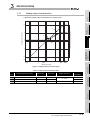
(10)CH
Range setting (RYn4 to RYnF)
The analog output range for each channel is set in 3-bit (refer to Table 3.9).
The default value is set to "-10 to 10V" for all channels.
This setting is activated when Initial data setting request flag (RY(n+1)9) is turned
from off to on.
Table 3.9 List of output range settings
Output range
CH4
CH3
CH2
CH1
RYnF RYnE RYnD RYnC RYnB RYnA RYn9 RYn8 RYn7 RYn6 RYn5 RYn4
-10 to 10V
Off
Off
Off
Off
Off
Off
Off
Off
Off
Off
Off
Off
0 to 5V
Off
Off
On
Off
Off
On
Off
Off
On
Off
Off
On
1 to 5V
Off
On
Off
Off
On
Off
Off
On
Off
Off
On
Off
0 to 20mA
Off
On
On
Off
On
On
Off
On
On
Off
On
On
4 to 20mA
On
Off
Off
On
Off
Off
On
Off
Off
On
Off
Off
On
Off
On
On
Off
On
On
Off
On
On
Off
On
On
On
Off
On
On
Off
On
On
Off
On
On
Off
User range setting 1
(0 to 20mA)
User range setting 2
(-10 to 10V)
(11)CH
HOLD/CLEAR setting (RY(n+1)0 to RY(n+1)3)
Whether to hold or clear an analog value that was output when the programmable
controller CPU has entered the STOP status or an error occurs is set for each
channel.
Off: CLEAR
On: HOLD
The default value is set to "CLEAR (off)" for all channels.
This setting is activated when Initial data setting request flag (RY(n+1)9) is turned
from off to on.
(12)CH
Conversion enable/disable setting (RY(n+1)4 to RY(n+1)7)
The D/A conversion enable/disable status is set for each channel.
Off: Disable
On: Enable
This setting is activated when Initial data setting request flag (RY(n+1)9) is turned
from off to on.
Setting "Disable"(off) for the unused channel can shorten the D/A conversion speed.
3 - 17
3.5 Remote I/O Signals
3.5.2 Details of the remote I/O signals
SPECIFICATIONS
1
This flag turns on when initial data processing is completed if initial data processing is
requested after power-on.
For details on initial data setting, refer to Figure 3.5.
OVERVIEW
(13)Initial data processing completion flag (RY(n+1)8)
2
SYSTEM
CONFIGURATION
(14)Initial data setting request flag (RY(n+1)9)
This flag is turned on to set or change the initial data.
For details on initial data setting, refer to Figure 3.5.
3
(15)Error reset request flag (RY(n+1)A)
00H) in Error code (RWrn+2) and CH
Check code (RWrn, RWrn+1) of the remote
register.
4
PROCEDURES AND
SETTINGS BEFORE
OPERATION
However, Error flag (RX(n+1)A) cannot be reset when the Flash memory write error
occurs (Flash memory write error flag (RXnC) turns on). Error flag (RX(n+1)9) also
remains on.
SPECIFICATIONS
This flag is turned on to reset (turns off) Error flag (RX(n+1)A) and clear values (set
PROGRAMMING
5
APPENDICES
TROUBLESHOOTING
6
INDEX
3
3.5 Remote I/O Signals
3.5.2 Details of the remote I/O signals
3 - 18
3
3.6
SPECIFICATIONS
Remote Register
The AJ65SBT2B-64DA has a remote resister for data communications with a master
module.
This section describes the assignment and data structure of the remote register.
3.6.1
Remote register list
The following table shows the assignment of remote register.
Table 3.10 Assignment of remote register
Communication
direction
Master
Remote
Remote
Master
Address
Description
Default value
Reference
RWwm
CH1 Digital input value setting
0
RWwm+1
CH2 Digital input value setting
0
Section 3.6.2
RWwm+2
CH3 Digital input value setting
0
(1)
RWwm+3
CH4 Digital input value setting
0
RWrn
CH1, 2 Check code
0
Section 3.6.2
RWwm+1
CH3, 4 Check code
0
(2)
RWwm+2
Error code
0
RWwm+3
Reserved
0
Section 3.6.2
(3)
-
m, n: Addresses assigned to the master station by station number setting
POINT
Do not read/write data to the "Reserved" remote register. If read/written, the
functions of the AJ65SBT2B-64DA will not be guaranteed.
3 - 19
3.6 Remote Register
3.6.1 Remote register list
SPECIFICATIONS
1
(b) In the following condition, the digital input values at all channels become "0".
• Remote ready (RX(n+1)B) turns on after power-on.
(c) The settable digital input value is 16-bit signed binary within the setting range
according to the output range setting.
(d) If a set value is outside the setting range, D/A conversion is performed with the
data shown in Table 3.11.
Also, the corresponding check code is stored in Check code (RWrn, RWrn+1).
Table 3.11 Settable range of the digital input value
Output range
Settable range
Digital input value when a value is
set outside the setting range
-16384 to 16383
16384 or more: 16383
(Practical range: -16000 to 16000)
-16385 or less: -16384
0 to 20mA
-288 to 12287
12288 or more: 12287
4 to 20mA
(Practical range: 0 to 12000)
-289 or less: -288
-10 to 10V
0 to 5V
1 to 5V
User range setting 1
(0 to 20mA)
-12288 to 12287
12288 or more: 12287
(-10 to 10V)
(Practical range: -12000 to 12000)
-12289 or less: -12288
3
4
5
PROGRAMMING
User range setting 2
2
SYSTEM
CONFIGURATION
(a) This is an area for the programmable controller CPU to write the digital input value
for D/A conversion.
SPECIFICATIONS
Digital input value setting (RWwm to RWwm+3)
PROCEDURES AND
SETTINGS BEFORE
OPERATION
(1) CH
OVERVIEW
Details of the remote register
TROUBLESHOOTING
6
APPENDICES
3.6.2
INDEX
3
3.6 Remote Register
3.6.2 Details of the remote register
3 - 20
3
SPECIFICATIONS
(2) CH
Check code (RWrn, RWrn+1)
(a) This is an area to check if a digital input value is set within the setting range.
If a digital input value lower or greater than the setting range is set, any of the
following check codes is stored.
b15
b8
RWrn
b7
b0
CH2
b15
CH1
b8
RWrn+1
b7
b0
CH3
CH4
Check code
Description
0FH
A digital input value over the setting range was set.
F0H
A digital input value below the setting range was set.
FFH
A digital input value below the setting range and a digital input value
over the range were set before error reset request.
For example, if writing a digital input value over the setting range, and than,
writing a digital input value below the setting range without resetting
the check code, a check code of FFH is stored.
Figure 3.7 List of check codes and storage locations
(b) A check code once stored is not reset even if the setting value becomes within the
setting range.
(c) Reset Check code (RWrn, RWrn+1) by turning on Error reset request flag
(RY(n+1)A).
(3) Error code (RWrn+2)
(a) If an error occurs (the "RUN" LED flashes) when data are written to the
AJ65SBT2B-64DA, the corresponding error code is stored into this area.
(b) For details on error code, refer to Section 6.1.
3 - 21
3.6 Remote Register
3.6.2 Details of the remote register
1
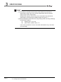
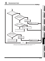
Procedures before Operation
2
SYSTEM
CONFIGURATION
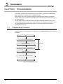
This section describes the procedures for operating the AJ65SBT2B-64DA.
Start
3
Refer to Section 4.2 and Section 4.5.
Wiring
(Connect CC-Link dedicated cable and external
devices to the AJ65SBT2B-64DA.
Turn on the L TER. switch or connect a
terminating resistor if the module is connected at
the end of the network.)
Refer to Section 4.6 and Section 4.7.
Switch setting
(Set the station number of the AJ65SBT2B-64DA.)
Refer to Section 4.3 and Section 4.4.
SPECIFICATIONS
Module mounting
(Mount the AJ65SBT2B-64DA to the panel or
DIN rail.)
PROCEDURES AND
SETTINGS BEFORE
OPERATION
5
PROGRAMMING
Programming
4
Refer to CHAPTER 5.
Perform offset/gain setting?
TROUBLESHOOTING
6
No
Yes
Starting data link
Offset/gain setting (Refer to Section 4.8.)
APPENDICES
4.1
PROCEDURES AND SETTINGS BEFORE
OPERATION
OVERVIEW
CHAPTER4
End
Figure 4.1 Procedures before operation
INDEX
4
PROCEDURES AND SETTINGS BEFORE
OPERATION
4.1 Procedures before Operation
4-1
4
4.2
PROCEDURES AND SETTINGS BEFORE
OPERATION
Handling Precautions
This section describes the precautions for handling the AJ65SBT2B-64DA.
CAUTION
Do not touch the terminals while the power is on. Doing so may cause malfunction.
Take care to prevent foreign matter such as dust or wire chips from entering the module.
Failure to do so may cause a fire, failure or malfunctions.
Never disassemble or modify the module.
This may cause breakdowns, malfunction, injury and/or fire.
Do not directly touch the conductive area or electronic components of the module.
Doing so may result in a malfunction or failure of the module.
Do not drop or apply any strong impact to the module.
Doing so may damage the module.
Tighten terminal screws within the specified torque range.
A loose terminal screw may cause a short circuit or malfunction.
Overtightening can cause a short circuit or malfunction due to damage of the screws or module.
When disposing of this product, treat it as industrial waste.
Use the module in an environment that meets the general specifications given in this manual.
Operating it in any other environment may cause an electric shock, fire, malfunction, product
damage or deterioration.
For protection of the switches, do not remove the cushioning material before installation.
Securely fix the module with the DIN rail or installation screws. Installation screws must be tighten
within the specified torque range.
A loose screw may cause a drop of the module or malfunction.
Overtightening may damage the screw, resulting in a drop of the module or malfunction.
Be sure to shut off all phases of the external power supply used by the system before mounting or
dismounting the module to or from the panel. Not doing so can cause the module to fail or
malfunction.
Before handling the module, always touch grounded metal, etc. to discharge static electricity from the
human body.
Failure to do so may cause a failure or malfunctions of the module.
4-2
4.2 Handling Precautions
(1) Tighten the screws such as module mounting screws and terminal block
screws within the following ranges.
Table 4.1 Tightening torque range
0.78 to 1.08N m
0.59 to 0.88N m
Terminal block installation screw (M3.5 screw)
0.68 to 0.98N m
2
(2) To prevent defect during transportation, a protective film is attached on
the surface of the module. Remove the film before using the module.
SYSTEM
CONFIGURATION
Module mounting screw (M4 screw)
Terminal block terminal screw (M3 screw)
3
(3) When using the DIN rail, pay attention to the followings.
(a) Applicable DIN rail model (IEC 60715 compliant)
TH35-7.5Fe
TH35-7.5Al
(b) DIN rail installation screw pitch
When installing a DIN rail, tighten the screws at a pitch of 200mm (7.87 inches) or
less.
4
5
PROGRAMMING
(4) When mounting the AJ65SBT2B-64DA to the DIN rail, hold the center of
the module and press it until the DIN rail hook at the bottom of the
module clicks.
SPECIFICATIONS
Tightening torque range
PROCEDURES AND
SETTINGS BEFORE
OPERATION
Screw location
OVERVIEW
1
DIN rail
Figure 4.2 Mounting a module to the DIN rail
APPENDICES
(5) For the models, specifications, and manufacturers of cables available
for the AJ65SBT2B-64DA, refer to the user's manual of the master
module used.
TROUBLESHOOTING
6
DIN rail hook
INDEX
4
PROCEDURES AND SETTINGS BEFORE
OPERATION
4.2 Handling Precautions
4-3
4
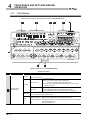
4.3
PROCEDURES AND SETTINGS BEFORE
OPERATION
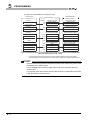
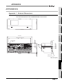
Part Names
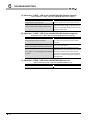
This section describes each part name of the AJ65SBT2B-64DA.
Figure 4.3 Appearance of the AJ65SBT2B-64DA
Table 4.2 Part names
No.
Name
Description
PW LED
On: Power supply on
Off: Power supply off
On: Normal operation
Flashing: 0.1s intervals: Output range setting error
Normal mode
RUN LED
1
memory write error
On: The SELECT/SET switch is in the SET position.
Operating status
Test mode
indication LED
Flashing: Offset/gain values are outside the setting range.
Off: The SELECT/SET switch is in the SELECT or center position.
L RUN LED
L ERR.
LED
On: Normal communication
Off: Communication cutoff (Timeout error)
On:
Station number is outside the setting range.
Flashing regularly:
Station number setting has been changed after power-on.
Flashing irregularly: Terminating resistor is not connected or the module or CC-Link dedicated
cable is affected by noise.
Off:
4-4
0.5s intervals: Digital input value setting error
Off: 24VDC power supply interrupted, watchdog timer error or Flash
4.3 Part Names
Normal communication
1
Table 4.2 Part names
No.
Name
Description
V
2
Offset/gain
adjusting LED
Normal mode
Normally off
I
CH
OFFSET
Every time the SELECT/SET switch is moved to the "SELECT" position,
Test mode
the LED status changes. (Refer to Section 4.8.)
OVERVIEW
4
PROCEDURES AND SETTINGS BEFORE
OPERATION
2
3
SELECT/SET switch
Performs offset/gain setting in test mode.
4
UP/DOWN switch
Adjusts the offset/gain values of the channel specified by the SELECT/SET switch.
SYSTEM
CONFIGURATION
GAIN
Sets the tens place of station number using the switches, STATION NO. "10", "20", and "40".
Sets the ones place of station number using the switches, STATION NO. "1", "2", "4", and "8".
All switches are set to "off" at the factory.
3
Set the station number within the range 1 to 64.
If not, an error occurs and the "L ERR." LED flashes.
40
20
10
8
4
2
1
1
Off
Off
Off
Off
Off
Off
On
2
Off
Off
Off
Off
Off
On
Off
Station number
3
Off
Off
Off
Off
Off
On
On
setting switch
4
Off
Off
Off
Off
On
Off
Off
10
Off
Off
On
Off
Off
Off
Off
11
Off
Off
On
Off
Off
Off
On
64
On
On
Off
Off
On
Off
Off
4
5
(Example) For the station number "32", set the switches as shown below.
20
10
8
4
2
1
32
Off
On
On
Off
Off
On
Off
6
Reserved
Set all switches to off.
7
Terminal block
Used to connect the module power supply, transmission, and I/O signals.
8
DIN rail hook
Used to mount the module to the DIN rail.
Termination)
switch
4.3.1
6
Turned on to enable the terminating resistor built in the AS65SBT2B-64DA.
Used when the AJ65SBT2B-64DA is connected at the end of the network.
Transmission speed auto-tracking function
Transmission speed is set automatically according to the setting in the master module.
INDEX
L TER (Line
9
PROGRAMMING
Ones place
40
TROUBLESHOOTING
Tens place
Station
number
APPENDICES
5
Ones place
number
PROCEDURES AND
SETTINGS BEFORE
OPERATION
Tens place
Station
SPECIFICATIONS
Station number setting should not be overlapped.
4.3 Part Names
4.3.1 Transmission speed auto-tracking function
4-5
4
4.4
PROCEDURES AND SETTINGS BEFORE
OPERATION
Station Number Setting
The buffer memory addresses of the master module, where the remote I/O signals and
read/write data are stored, are determined by the station number setting of the
AJ65SBT2B-64DA.
For details, refer to the user's manual of the master module used.
4.5
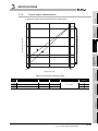
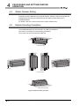
Module Mounting Orientation
The AJ65SBT2B-64DA can be mounted in six different orientations.
(There are no restrictions on the mounting orientation.)
The module can also be mounted to a DIN rail.
Ceiling mounting
DIN rail
Front mounting
Flat surface mounting
Figure 4.4 Module mounting orientation
4-6
4.4 Station Number Setting
4
PROCEDURES AND SETTINGS BEFORE
OPERATION
1
OVERVIEW
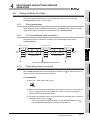
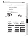
Wiring of Data Link Cable
This section describes the wiring of CC-Link dedicated cables for connecting the
AJ65SBT2B-64DA to the CC-Link system.
When replacing existing AJ65SBT-62DA with the AJ65SBT2B-64DA, rewire the module
using communication terminal block dedicated for the AJ65SBT2B-64DA.
4.6.2
CC-Link dedicated cable connection
3
DB
Terminal
resistor
DG
SLD
FG
(Blue)
(Blue)
(White)
(White)
(Yellow)
(Yellow)
CC-Link
dedicated cable
DA
DB
DG
I/O module, etc.
(Blue)
(Blue)
(White)
(White)
(Yellow)
(Yellow)
SLD
FG
CC-Link
dedicated cable
DA
4
DB
DG
Terminal
resistor
PROCEDURES AND
SETTINGS BEFORE
OPERATION
DA
AJ65SBT2B-64DA
SPECIFICATIONS
The following shows a connection example of CC-Link dedicated cables for the
AJ65SBT2B-64DA.
Master module side
SLD
FG
5
Figure 4.5 CC-Link dedicated cable connection
Terminating resistor connection
The AJ65SBT2B-64DA has a built-in terminating resister of 110 . Therefore, there is no
need to connect a terminating resister externally.
6
TROUBLESHOOTING
(1) Precautions
(a) Move the L TER. switch until it clicks.
Click
(b) Make sure that between DA and DB is high resistance (when the L TER. switch is
off) or is 110 (when the L TER. switch is on) with a tester before wiring the
system with CC-Link dedicated cables.
(c) The built-in terminating resistor cannot be used in the following cases. Connect a
terminating resistor (110 or 130 ).
• A CC-Link system is configured using CC-Link dedicated cables of 130 .
• The AJ65SBT2B-64DA may be replaced during data link.
INDEX
4.6.3
SYSTEM
CONFIGURATION
2
Wiring precautions
PROGRAMMING
4.6.1
APPENDICES
4.6
4.6 Wiring of Data Link Cable
4.6.1 Wiring precautions
4-7
4
4.7
PROCEDURES AND SETTINGS BEFORE
OPERATION
Wiring with External Devices
This section describes the precautions for wiring the AJ65SBT2B-64DA and its wiring with
external devices.
4.7.1
Wiring precautions
External wiring that is less susceptible to noise is required as a condition of enabling a
highly reliable system and making full use of the capabilities of AJ65SBT2B-64DA.
The precautions when performing external wiring are described below.
(a) Use separate cables for the AC control circuit and the external output signals of
the AJ65SBT2B-64DA or the external power supply to avoid the influence of the
AC side surges and induction.
(b) Do not mount the cables close to or bundle them with the main circuit line, a highvoltage cable or a load cable from other than the programmable controller.
Not doing so will cause the module more susceptible to noises, surges, and
inductions.
(c) The shield wire or the shielded cable must be grounded at one end.
4-8
4.7 Wiring with External Devices
4.7.1 Wiring precautions
1
4.7.2
Wiring with external devices
OVERVIEW
(1) For voltage output
*1
*2
Motor drive module, etc.
2
1k
V
to
SYSTEM
CONFIGURATION
D/A
conversion
COM
GND
1M
3
24V
24G
SPECIFICATIONS
Filter
FG
4
PROCEDURES AND
SETTINGS BEFORE
OPERATION
Figure 4.6 Wiring for voltage output
* 1 For wiring, use shielded twisted pair cables.
* 2 If there is noise or ripples in the external wiring, connect a 0.1 to 0.47 F capacitor
(25V or higher voltage-resistant product) to the input terminals of the external device.
(2) For current output
5
*2
Motor drive module, etc.
PROGRAMMING
*1
0
I
to
COM
600
6
TROUBLESHOOTING
GND
24V
Filter
24G
FG
Figure 4.7 Wiring for current output
* 1 For wiring, use shielded twisted pair cables.
* 2 If there is noise or ripples in the external wiring, connect a 0.1 to 0.47 F capacitor (25V or higher
voltage-resistant product) to the input terminals of the external device.
APPENDICES
D/A
conversion
INDEX
4
PROCEDURES AND SETTINGS BEFORE
OPERATION
4.7 Wiring with External Devices
4.7.2 Wiring with external devices
4-9
4
PROCEDURES AND SETTINGS BEFORE
OPERATION
4.8
Offset/Gain Setting
To change the I/O conversion characteristics, follow the procedure below.
Start
Set the offset value for voltage or current using the UP/DOWN
switch.
Short the TEST terminals to enter test mode.
For voltage
For current
Power on.
Move the SELECT/SET switch to the "SET" position.
Check that the "RUN" LED is on* and then let go of the switch.
Starting data link
On
Check that the "RUN" LED is off.
A
Every time the SELECT/SET switch is moved to the "SELECT"
position, the status of the offset/gain adjusting LEDs changes as
shown below.
Check that the gain setting target channel is correct and
the "GAIN" LED is on by switching the status of the offset/gain
adjusting LEDs using the SELECT/SET switch.
For voltage
On
CH1 Offset value setting
On
On
CH1 Gain value setting
CH2 Offset value setting
Set the gain value for voltage or current using
the UP/DOWN switch.
CH2 Gain value setting
For voltage
For current
CH3 Offset value setting
CH3 Gain value setting
CH4 Offset value setting
CH4 Gain value setting
For current
Move the SELECT/SET switch to the "SET" position.
Check that the "RUN" LED is on* and then let go of the switch.
CH1 Offset value setting
CH1 Gain value setting
CH2 Offset value setting
On
CH2 Gain value setting
CH3 Offset value setting
CH3 Gain value setting
Adjust other channels?
CH4 Offset value setting
NO
CH4 Gain value setting
Power off.
Check that the offset setting target channel is correct and
the "OFFSET" LED is on by switching the status of the offset/gain
adjusting LEDs using the SELECT/SET switch.
On
On
Open the TEST terminals. The "RUN" LED turns on.
On
End
Figure 4.8 Offset/gain setting procedure
* : If the "RUN" LED does not turn on, Flash memory may have failed.
For details, refer to Section 3.5.2.
4 - 10
4.8 Offset/Gain Setting
YES
A
4
PROCEDURES AND SETTINGS BEFORE
OPERATION
1
2
SYSTEM
CONFIGURATION
(1) Set the offset/gain values in the actual operating status.
(2) The offset/gain values are stored in the Flash memory of the AJ65SBT2B64DA and not cleared even at power-off.
(3) If initial setting is executed in test mode, which is the mode after shorting the
TEST terminals, D/A conversion is performed on all channels. During offset/
gain setting, use Test mode flag (RXnF) as an interlock.
(4) Set the offset/gain values within the range described in POINT of Section 3.3.1
and Section 3.3.2. If the values are outside the setting range, the maximum
resolution and accuracy may exceed the performance specifications range.
OVERVIEW
POINT
Maintenance and Inspection
4
PROCEDURES AND
SETTINGS BEFORE
OPERATION
There are no special inspection items for the AJ65SBT2B-64DA. To keep the system in
the best condition, however, perform inspection following the items described in the user's
manual of the programmable controller CPU.
PROGRAMMING
5
APPENDICES
TROUBLESHOOTING
6
INDEX
4.9
SPECIFICATIONS
3
4.9 Maintenance and Inspection
4 - 11
5
PROGRAMMING
CHAPTER5
PROGRAMMING
This chapter describes the programming procedure, basic programs for reading/writing
data, and program examples for the AJ65SBT2B-64DA.
When applying any of the program examples introduced in this chapter to the actual
system, make sure to examine the applicability and confirm that no problems will occur in
the system control.
For the master module, refer to the user's manual of the master module used. For the
remote register, refer to Section 3.6. For the details on the dedicated instructions, refer to
the Type AnSHCPU/AnACPU/AnUCPU/QCPU-A (A Mode) Programming Manual
(Dedicated Instructions).
5.1
Programming Procedure
Create programs for performing D/A conversion in the AJ65SBT2B-64DA in the following
procedure.
Start
D/A conversion enable/disable setting
Output range setting
Analog output HOLD/CLEAR setting
Digital value setting
Analog output enable/disable setting
End
Figure 5.1 Programming procedure
5-1
5.1 Programming Procedure
Initial setting
1
OVERVIEW
Conditions of Program Examples
(1) Conditions of the AJ65SBT2B-64DA
• Channels to be used: CH1 and CH2
• Output range: -10 to 10V for CH1, 0 to 5V for CH2
• When an error occurs, the module outputs the corresponding error code in BCD
and resets the error.
• When an error occurs, the module holds the output status for both CH1 and CH2.
2
SYSTEM
CONFIGURATION
The program examples in this chapter are created under the following conditions.
3
(2) System configuration
SPECIFICATIONS
Programmable controller CPU
Master module (X0 to X1F/Y0 to Y1F)
I/O (Input 64 points) (X20 to X5F)
I/O (Output 64 points) (Y60 to Y9F)
L TER. switch: On
Terminating
resistor
Master station
AJ65SBT2B-64DA (Station number 1)
Figure 5.2 System configuration and wiring diagram
(3) Relationship between programmable controller CPU, master module,
and AJ65SBT2B-64DA
Master module
AJ65SBT2B-64DA
(Station number 1)
Remote input (RX)
Remote input (RX)
X1000 to X100F
E0H
RX00 to RX0F
RX00 to RX0F
X1010 to X101F
E1H
RX10 to RX1F
RX10 to RX1F
Device Y
Y1000 to Y100F
Remote output (RY)
Remote output (RY)
160H
RY00 to RY0F
RY00 to RY0F
Y1010 to Y101F
161H
RY10 to RY1F
RY10 to RY1F
Device X
Address
Remote register (RWw)
Device D
6
TROUBLESHOOTING
Programmable
controller CPU
Remote register (RWw)
D1000
1E0H
RWw0
RWw0 CH1 Digital value setting
D1001
1E1H
RWw1
RWw1 CH2 Digital value setting
D1002
1E2H
RWw2
RWw2 CH3 Digital value setting
D1003
1E3H
RWw3
RWw3 CH4 Digital value setting
Remote register (RWr)
Device D
Remote register (RWr)
D1100
2E0H
RWr0
RWr0 CH1,2 Check code
D1101
2E1H
RWr1
RWr1 CH3,4 Check code
D1102
2E2H
RWr2
RWr2 Error code
D1103
2E3H
RWr3
RWr3 Reserved
5
PROGRAMMING
(a) When the QCPU (Q mode) or QnACPU is used
PROCEDURES AND
SETTINGS BEFORE
OPERATION
4
APPENDICES
5.2
PROGRAMMING
Figure 5.3 Relationship between programmable controller CPU, master module, and AJ65SBT2B-64DA
(when the QCPU (Q mode) or QnACPU is used)
INDEX
5
5.2 Conditions of Program Examples
5-2
5
PROGRAMMING
(b) When the ACPU/QCPU (A mode) is used
Programmable
controller CPU
Device X
Master module
X100 to X10F
Address
E0H
X110 to X11F
E1H
Device Y
AJ65SBT2B-64DA
(Station number 1)
Remote input (RX)
RX00 to RX0F
Remote input (RX)
RX00 to RX0F
RX10 to RX1F
RX10 to RX1F
Remote output (RY)
Remote output (RY)
Y100 to Y10F
160H
RY00 to RY0F
RY00 to RY0F
Y110 to Y11F
161H
RY10 to RY1F
RY10 to RY1F
D200
1E0H
Remote register (RWw)
RWw0
RWw0 CH1 Digital value setting
D201
1E1H
RWw1
RWw1 CH2 Digital value setting
D202
1E2H
RWw2
RWw2 CH3 Digital value setting
D203
1E3H
RWw3
RWw3 CH4 Digital value setting
Device D
Device D
Remote register (RWr)
RWr0
Remote register (RWw)
Remote register (RWr)
D300
2E0H
D301
2E1H
RWr1
RWr1 CH3,4 Check code
D302
2E2H
RWr2
RWr2 Error code
D303
2E3H
RWr3
RWr3 Reserved
RWr0 CH1,2 Check code
Figure 5.4 Relationship between programmable controller CPU, master module, and AJ65SBT2B-64DA
(When the ACPU/QCPU (A mode) is used)
* : In the program example (refer to Section 5.5) that uses the RRPA instruction (auto refresh
parameter setting) in the ACPU/QCPU (A mode), RWr0 to RWr3 are assigned to D456 to D459.
POINT
Devices used in the program examples described in this chapter may not be used
depending on the CPU module.
For the available device setting range, refer to the user's manual of the CPU
module used.
For example, when the A1SCPU is used, devices X100, Y100 and later cannot be
used. Use devices such as B or M.
5-3
5.2 Conditions of Program Examples
1
Parameters are set in Network parameter using GX Developer.
Initial setting of the AS65SBT2B-64DA cannot be performed using the remote device
station initialization procedure registration function.
OVERVIEW
Program Example When the QCPU (Q mode) is Used
2
SYSTEM
CONFIGURATION
(1) Parameter setting
(a) Network parameter setting
SPECIFICATIONS
3
PROCEDURES AND
SETTINGS BEFORE
OPERATION
4
5
Figure 5.5 Network parameter setting screen for CC-Link (when the QCPU (Q mode) is used)
PROGRAMMING
Table 5.1 Setting items on the Network parameter setting screen for CC-Link
(when the QCPU (Q mode) is used)
Setting value
1 (Boards)
Start I/O No
0000
Type
Master station
Mode
Remote net[Ver.1 mode]
All connect count
1 (module)
Remote input[RX]
X1000
Remote output[RY]
Y1000
Remote register[RWr]
D1100
Remote register[RWw]
D1000
Special relay[SB]
SB0
Special register[SW]
SW0
Station information setting
Refer to (1) (b) in this section.
6
TROUBLESHOOTING
Setting item
No. of boards in module
APPENDICES
5.3
PROGRAMMING
INDEX
5
5.3 Program Example When the QCPU (Q mode) is Used
5-4
5
PROGRAMMING
(b) Station information setting
Figure 5.6 CC-Link station information. Module 1 screen (when the QCPU (Q mode) is used)
Table 5.2 Setting items on the CC-Link station information. Module 1 screen
(when the QCPU (Q mode) is used)
Setting item
Setting value
Station type
Remote device station
Exclusive station count
Exclusive station 1
Reserve/invalid station select
No setting
(2) List of devices used in the program example
Table 5.3 List of devices used in the program example (when the QCPU (Q mode) is used)
Device
Description
X0
Module error
X1
Host station data link status
XF
Module ready
X20
Signal that is turned on to write the digital input value to CH1 Digital input value setting
(RWw0) or CH2 Digital input value setting (RWw1) of the AJ65SBT2B-64DA
X21
Signal that is turned on to output the analog value from CH1 or CH2
X22
Signal that is turned on to reset an error
X23
Signal that is turned on to change the initial setting
X1018
Initial data processing request flag
X1019
Initial data setting completion flag
X101A
Error flag
X101B
Remote ready
Y60
Signal that is output when a data link error occurs
Y70 to Y72
Signal that is output an error code in BCD
Y1000 to
Y101A
Signal for settings of the AJ65SBT2B-64DA
Signal that stores the data link status of the AJ65SBT2B-64DA
M0
0 (Off): Data link normal
1 (On): Data link error
5-5
M100
Master control contact
D1000
CH1 Digital input value setting
D1001
CH2 Digital input value setting
D1102
Error code
SW80
Other station data link status
5.3 Program Example When the QCPU (Q mode) is Used
5
PROGRAMMING
1
OVERVIEW
(3) Program example
Checking connection status of the AJ65SBT2B-64DA
Reads data link status.
2
Turns on MC contact (M100)
when data link is normal.
SYSTEM
CONFIGURATION
Turns on Y60 when a data
link error occurs.
CH1 Output range setting
(RY04 to RY06): 0 (-10 to 10V)
CH2 Output range setting
(RY07 to RY09): 1 (0 to 5V)
3
SPECIFICATIONS
Initial setting
CH1 Conversion enable/disable
setting (RY14): Enable
CH2 Conversion enable/disable
setting (RY15): Enable
Turns on Initial data processing
completion flag (RY18).
Turns on Initial data setting
request flag (RY19).
Changing initial setting
CH1 Conversion enable/disable
setting (RY14): Disable
CH2 Conversion enable/disable
setting (RY15): Disable
Turns on Initial data setting
request flag (RY19).
Processing for completing initial setting
Turns off Initial data processing
completion flag (RY18).
Turns off Initial data setting
request flag (RY19).
5
PROGRAMMING
CH2 HOLD/CLEAR setting
(RY11): HOLD
6
TROUBLESHOOTING
CH1 HOLD/CLEAR setting
(RY10): HOLD
PROCEDURES AND
SETTINGS BEFORE
OPERATION
4
Figure 5.7 Program example (when the QCPU (Q mode) is used) 1/2
INDEX
APPENDICES
* 1: The program in the dotted area is required only when the initial setting is changed.
5.3 Program Example When the QCPU (Q mode) is Used
5-6
5
PROGRAMMING
Writing digital values
Sets "1000" for CH1 Digital
input value setting (RWw0).
Sets "2000" for CH2 Digital
input value setting (RWw1).
Analog output enable/disable setting
CH1 Analog output enable/disable
flag (RY00): Enable
CH2 Analog output enable/disable
flag (RY01): Enable
Processing at error occurrence
Outputs error code in BCD.
Turns on Error reset
request flag (RY1A).
Turns off Error reset
request flag (RY1A).
Figure 5.8 Program example (when the QCPU (Q mode) is used) 2/2
5-7
5.3 Program Example When the QCPU (Q mode) is Used
1
OVERVIEW
Program Example When the QnACPU is Used
Parameters are set in Network parameter using GX Developer.
(1) Parameter setting
2
SYSTEM
CONFIGURATION
(a) Network parameter setting
SPECIFICATIONS
3
PROCEDURES AND
SETTINGS BEFORE
OPERATION
4
Figure 5.9 Network parameter setting screen for CC-Link (when the QnACPU is used)
Table 5.4 Setting items on the Network parameter setting screen for CC-Link
5
No. of boards in module
1 (Boards)
Start I/O No
0000
Type
Master station
All connect count
1 (module)
Remote input[RX]
X1000
Remote output[RY]
Y1000
Remote register[RWr]
D1100
Remote register[RWw]
D1000
Special relay[SB]
B0
Special register[SW]
W0
Station information setting
Refer to (1) (b) in this section.
6
TROUBLESHOOTING
Setting value
PROGRAMMING
(when the QnACPU is used)
Setting item
APPENDICES
5.4
PROGRAMMING
INDEX
5
5.4 Program Example When the QnACPU is Used
5-8
5
PROGRAMMING
(b) Station information setting
Figure 5.10 CC-Link station information. Module 1 screen (when the QnACPU is used)
Table 5.5 Setting items on the CC-Link station information. Module 1 screen
(when the QnACPU is used)
Setting item
Setting value
Station type
Remote device station
Exclusive station count
Exclusive station 1
Reserve/invalid station select
No setting
POINT
When using the QnACPU, using "Y" as the remote output (RY) refresh device of
the auto refresh parameter may not hold the analog value even in HOLD setting.
In HOLD setting, use "M" or "B" as the remote output (RY) refresh device.
5-9
5.4 Program Example When the QnACPU is Used
PROGRAMMING
1
Table 5.6 List of devices used in the program example (when the QnACPU is used)
Description
Module error
X1
Host station data link status
XF
Module ready
Signal that is turned on to write the digital input value to CH1 Digital input value setting
(RWw0) or CH2 Digital input value setting (RWw1) of the AJ65SBT2B-64DA
X21
Signal that is turned on to output the analog value from CH1 or CH2
X22
Signal that is turned on to reset an error
X23
Signal that is turned on to change the initial setting
X1018
Initial data processing request flag
X1019
Initial data setting completion flag
X101A
Error flag
X101B
Remote ready
Y60
Signal that is output when a data link error occurs
Y70 to Y72
Signal that is output an error code in BCD
Y1000 to
Y101A
3
SPECIFICATIONS
X20
2
Signal for settings of the AJ65SBT2B-64DA
4
Signal that stores the data link status of the AJ65SBT2B-64DA
0 (Off): Data link normal
PROCEDURES AND
SETTINGS BEFORE
OPERATION
M0
1 (On): Data link error
M100
Master control contact
D1000
CH1 Digital input value setting
CH2 Digital input value setting
D1102
Error code
W80
Other station data link status
5
PROGRAMMING
D1001
SYSTEM
CONFIGURATION
Device
X0
OVERVIEW
(2) List of devices used in the program example
APPENDICES
TROUBLESHOOTING
6
INDEX
5
5.4 Program Example When the QnACPU is Used
5 - 10
5
PROGRAMMING
(3) Program example
Checking connection status of the AJ65SBT2B-64DA
Reads data link status.
Turns on MC contact (M100)
when data link is normal.
Turns on Y60 when a data
link error occurs.
Initial setting
CH1 Output range setting
(RY04 to RY06)
: 0 (-10 to 10V)
CH2 Output range setting
(RY07 to RY09)
: 1 (0 to 5V)
CH1 HOLD/CLEAR setting
(RY10): HOLD
CH2 HOLD/CLEAR setting
(RY11): HOLD
CH1 Conversion enable/disable
setting (RY14): Enable
CH2 Conversion enable/disable
setting (RY15): Enable
Turns on Initial data processing
completion flag (RY18).
Turns on Initial data setting
request flag (RY19).
Changing initial setting
CH1 Conversion enable/disable
setting (RY14): Disable
CH2 Conversion enable/disable
setting (RY15): Disable
Turns on Initial data setting
request flag (RY19).
Processing for completing initial setting
Turns off Initial data processing
completion flag (RY18).
Turns off Initial data setting
request flag (RY19).
Figure 5.11 Program example (when the QnACPU is used) 1/2
* 1: The program in the dotted area is required only when the initial setting is changed.
5 - 11
5.4 Program Example When the QnACPU is Used
5
PROGRAMMING
1
Sets "2000" for CH2 Digital
input value setting (RWw1).
Analog output enable/disable setting
CH1 Analog output enable/disable
flag (RY00): Enable
CH2 Analog output enable/disable
flag (RY01): Enable
Processing at error occurrence
Outputs error code in BCD.
Turns on Error reset
request flag (RY1A).
2
SYSTEM
CONFIGURATION
Sets "1000" for CH1 Digital
input value setting (RWw0).
OVERVIEW
Writing digital values
3
SPECIFICATIONS
Turns off Error reset
request flag (RY1A).
4
PROCEDURES AND
SETTINGS BEFORE
OPERATION
Figure 5.12 Program example (when the QnACPU is used) 2/2
PROGRAMMING
5
INDEX
APPENDICES
TROUBLESHOOTING
6
5.4 Program Example When the QnACPU is Used
5 - 12
5
5.5
PROGRAMMING
Program Example When the ACPU/QCPU (A mode) is Used
(Dedicated Instructions)
Parameters are set in the sequence program.
(1) List of devices used in the program example
Table 5.7 List of devices used in the program example (when the ACPU/QCPU (A mode) is used
(dedicated instructions))
Device
Description
X0
Module error
X1
Host station data link status
XF
Module ready
X20
Signal that is turned on to write the digital input value to CH1 Digital input value setting
(RWw0) or CH2 Digital input value setting (RWw1) of the AJ65SBT2B-64DA
X21
Signal that is turned on to output the analog value from CH1 or CH2
X22
Signal that is turned on to reset an error
X23
Signal that is turned on to change the initial setting
X118
Initial data processing request flag
X119
Initial data setting completion flag
X11A
Error flag
X11B
Remote ready
Y60
Signal that is output when a data link error occurs
Y70 to Y72
Signal that is output an error code in BCD
Y100 to
Y11A
Signal for settings of the AJ65SBT2B-64DA
Signal that stores the data link status of the AJ65SBT2B-64DA
M0
0 (Off): Data link normal
1 (On): Data link error
M10
Network parameter setting start pulse signal
M11
Signal that is turned on when parameter setting is completed normally
M12
Signal that is turned on when parameter setting is completed in error
M13
Auto refresh parameter setting start pulse signal
M20
Initial setting change command pulse
M100
Master control contact
D0 to D2
Device for Network parameter setting
D3
Device that stores host station parameter status when the instruction is completed in error
D100 to
D119
5 - 13
Device for auto refresh parameter setting
D200
CH1 Digital input value setting
D201
CH2 Digital input value setting
D458
Error code
W80
Other station data link status
5.5 Program Example When the ACPU/QCPU (A mode) is Used (Dedicated Instructions)
5
PROGRAMMING
1
OVERVIEW
(2) Program example
Network parameter setting using RLPA dedicated instruction
2
Disables synchronous mode.
Station information of the AJ65SBT2B-64DA
: Remote device station, one station
occupied, station No.1
Dedicated instruction (RLPA)
Start I/O number of master module
SYSTEM
CONFIGURATION
Number of connected modules: 1
3
Device that is turned on for one scan when
the instruction is completed normally
Reads the host station parameter status when
the instruction is completed in error.
Auto refresh parameter setting using RRPA dedicated instruction
SPECIFICATIONS
Start device number for storing parameter
4
PROCEDURES AND
SETTINGS BEFORE
OPERATION
Sets the start number of RX.
Sets "X".
Sets X100.
Sets 32 points.
5
Sets the start number of RY.
PROGRAMMING
Sets "Y".
Sets Y100.
Sets 32 points.
6
Sets the start number of RW.
TROUBLESHOOTING
Sets "D".
Sets D200.
Sets 260 points.
Sets the start number of SB.
INDEX
APPENDICES
Figure 5.13 Program example (when the ACPU/QCPU (A mode) is used (dedicated instructions)) 1/3
5.5 Program Example When the ACPU/QCPU (A mode) is Used (Dedicated Instructions)
5 - 14
5
PROGRAMMING
Sets "B".
Sets B0.
Sets 512 points.
Sets the start number of SW.
Sets "W".
Sets W0.
Sets 256 points.
Dedicated instruction (RRPA)
Start I/O number of master module
Start device number for
storing parameter
Checking connection status of the AJ65SBT2B-64DA
Reads data link status.
Turns on MC contact (M100) when
data link is normal.
Turns on Y60 when a data link
error occurs.
Initial setting
CH1 Output range setting
(RY04 to RY06): 0 (-10 to 10V)
CH2 Output range setting
(RY07 to RY09): 1 (0 to 5V)
CH1 HOLD/CLEAR setting
(RY10): HOLD
CH2 HOLD/CLEAR setting
(RY11): HOLD
Figure 5.14 Program example (when the ACPU/QCPU (A mode) is used (dedicated instructions)) 2/3
5 - 15
5.5 Program Example When the ACPU/QCPU (A mode) is Used (Dedicated Instructions)
PROGRAMMING
CH2 Conversion enable/disable
setting (RY15): Enable
Turns on Initial data processing
completion flag (RY18).
Turns on Initial data setting
request flag (RY19).
Changing initial setting
CH1 Conversion enable/disable
setting (RY14): Disable
CH2 Conversion enable/disable
setting (RY15): Disable
Turns on Initial data setting
request flag (RY19).
Processing for completing initial setting
Turns off Initial data processing
completion flag (RY18).
Turns off Initial data setting
request flag (RY19).
Writing digital values
3
4
CH1 Analog output enable/disable
flag (RY00): Enable
PROCEDURES AND
SETTINGS BEFORE
OPERATION
Sets "1000" for CH1 Digital input
value setting (RWw0).
2
SYSTEM
CONFIGURATION
CH1 Conversion enable/disable
setting (RY14): Enable
OVERVIEW
1
SPECIFICATIONS
5
CH2 Analog output enable/disable
flag (RY01): Enable
5
Sets "2000" for CH2 Digital input
value setting (RWw1).
Analog output enable/disable setting
Outputs error code in BCD.
Turns on Error reset
request flag (RY1A).
Turns off Error reset
request flag (RY1A).
PROGRAMMING
Processing at error occurrence
TROUBLESHOOTING
6
Figure 5.15 Program example (when the ACPU/QCPU (A mode) is used (dedicated instructions)) 3/3
INDEX
APPENDICES
* 1: The program in the dotted area is required only when the initial setting is changed.
5.5 Program Example When the ACPU/QCPU (A mode) is Used (Dedicated Instructions)
5 - 16
5
5.6
PROGRAMMING
Program Example When the ACPU/QCPU (A mode) is Used
(FROM/TO Instructions)
Parameters are set in the sequence program.
(1) List of devices used in the program example
Table 5.8 List of devices used in the program example (when the ACPU/QCPU (A mode) is used
(FROM/TO instructions))
Device
X0
Description
Module error
X1
Host station data link status
X6
Data link start by parameters in buffer memory normally completed
X7
Data link start by parameters in buffer memory failed
XF
Module ready
X20
Signal that is turned on to write the digital input value to CH1 Digital input value setting
(RWw0) or CH2 Digital input value setting (RWw1) of the AJ65SBT2B-64DA
X21
Signal that is turned on to output the analog value from CH1 or CH2
X22
Signal that is turned on to reset an error
X23
Signal that is turned on to change the initial setting
X118
Initial data processing request flag
X119
Initial data setting completion flag
X11A
Error flag
X11B
Remote ready
Y0
Refresh instruction
Y6
Request for data link start by parameters in buffer memory
Y60
Signal that is output when a data link error occurs
Y70 to Y72
Signal that is output an error code in BCD
Y100 to
Y11A
Signal for settings of the AJ65SBT2B-64DA
Signal that stores the data link status of the AJ65SBT2B-64DA
M0
0 (Off): Data link normal
1 (On): Data link error
5 - 17
M10
Network parameter setting start pulse signal
M20
Initial setting change command pulse
M100
Master control contact
D0 to D4
Device for Network parameter setting
D100
Device that stores host station parameter status when the instruction is completed in error
D200
CH1 Digital input value setting
D201
CH2 Digital input value setting
5.6 Program Example When the ACPU/QCPU (A mode) is Used (FROM/TO Instructions)
5
PROGRAMMING
1
OVERVIEW
(2) Program example
Number of retries: 3
Number of automatic return modules: 1
Writes parameter settings to
the master module.
Data link status when an error occurs
in the programmable controller CPU
of the master station: Continue
Writes parameter settings to
the master module.
Station information of the AJ65SBT2B-64DA
: Remote device station, one station
occupied, station No.1
Writes parameter settings to
the master module.
Starting data link
2
SYSTEM
CONFIGURATION
Number of connected modules: 1
3
SPECIFICATIONS
Network parameter setting
4
Refresh instruction
Reads parameter status when data
link start failed.
PROCEDURES AND
SETTINGS BEFORE
OPERATION
Turns on Request for data link start
by parameters in buffer memory (Y06).
Turns off Request for data link start
by parameters in buffer memory (Y06).
5
Turns off Request for data link start
by parameters in buffer memory (Y06).
Reads RX0 to RX1F to X100 to X11F.
Figure 5.16 Program example (when the ACPU/QCPU (A mode) is used (FROM/TO instructions)) 1/3
PROGRAMMING
Reading remote input signals
INDEX
APPENDICES
TROUBLESHOOTING
6
5.6 Program Example When the ACPU/QCPU (A mode) is Used (FROM/TO Instructions)
5 - 18
5
PROGRAMMING
Checking connection status of the AJ65SBT2B-64DA
Reads data link status.
Turns on MC contact (M100)
when data link is normal.
Turns on Y60 when a data link
error occurs.
Initial setting
CH1 Output range setting
(RY04 to RY06): 0 (-10 to 10V)
CH2 Output range setting
(RY07 to RY09): 1 (0 to 5V)
CH1 HOLD/CLEAR setting
(RY10): HOLD
CH2 HOLD/CLEAR setting
(RY11): HOLD
CH1 Conversion enable/disable
setting (RY14): Enable
CH2 Conversion enable/disable
setting (RY15): Enable
Turns on Initial data processing
completion flag (RY18).
Turns on Initial data setting
request flag (RY19).
Changing initial setting
CH1 Conversion enable/disable
setting (RY14): Disable
CH2 Conversion enable/disable
setting (RY15): Disable
Turns on Initial data setting
request flag (RY19).
Processing for completing initial setting
Turns off Initial data processing
completion flag (RY18).
Turns off Initial data setting
request flag (RY19).
Figure 5.17 Program example (when the ACPU/QCPU (A mode) is used (FROM/TO instructions)) 2/3
* 1: The program in the dotted area is required only when the initial setting is changed.
5 - 19
5.6 Program Example When the ACPU/QCPU (A mode) is Used (FROM/TO Instructions)
PROGRAMMING
1
Writing digital values
Sets "1000" for CH1 Digital input
value setting (RWw0).
Sets "2000" for CH2 Digital input
value setting (RWw1).
Writes values to the master station.
OVERVIEW
5
2
CH1 Analog output enable/disable
flag (RY00): Enable
CH2 Analog output enable/disable
flag (RY01): Enable
Processing at error occurrence
SYSTEM
CONFIGURATION
Analog output enable/disable setting
3
Outputs error code in BCD.
Turns off Error reset request flag (RY1A).
Reading remote output signals
Writes Y100 to Y11F to RY0 to RY1F.
SPECIFICATIONS
Turns on Error reset request flag (RY1A).
PROCEDURES AND
SETTINGS BEFORE
OPERATION
4
Figure 5.18 Program example (when the ACPU/QCPU (A mode) is used (FROM/TO instructions)) 3/3
PROGRAMMING
5
INDEX
APPENDICES
TROUBLESHOOTING
6
5.6 Program Example When the ACPU/QCPU (A mode) is Used (FROM/TO Instructions)
5 - 20
6
TROUBLESHOOTING
CHAPTER6
TROUBLESHOOTING
This chapter describes the errors which may occur during the use of the AJ65SBT2B64DA and troubleshooting.
6.1
Error Code List
If an error occurs when data is written to the master module from the programmable
controller CPU (if the "RUN" LED of the AJ65SBT2B-64DA flashes), Error flag (RX(n+1)A)
turns on and the corresponding error code shown in Table 6.1 is stored in Error code
(RWrn+2).
Table 6.1 Error code list (Errors detected in the AJ65SBT2B-64DA)
Error code
Description
(decimal)
11
20
*
The set digital input value is outside the setting range.
Corrective action
Set the digital input value
within the setting range.
The set output range setting is outside the setting
Set the output range setting
range.
within the setting range.
indicates the error channel number.
(a) When the digital input value setting error occurs, the "RUN" LED flashes at
intervals of 0.5s and D/A conversion is performed using the upper or lower limit
value.
When the output range setting error occurs, the "RUN" LED flashes at intervals of
0.1s and D/A conversion is not performed on any channels.
(b) When two or more errors occurred, only the error code of the first error is stored.
The error codes of the second or later errors are not stored.
(c) The error code can be reset by turning on Error reset request flag (RY(n+1)A).
6-1
6.1 Error Code List
1
This section describes how to check errors using the LED indications of the AJ65SBT2B64DA.
For the errors regarding the programmable controller CPU and master module, refer to the
user's manuals of the programmable controller CPU and master module, respectively.
specified value?
28.8V.
(2) When the "RUN" LED of the AJ65SBT2B-64DA flashes
Table 6.3 When the "RUN" LED of the AJ65SBT2B-64DA flashes
Check item
Corrective action
Is the LED flashing at 0.1s intervals in normal
mode?
Is the LED flashing at 0.5s intervals in normal
mode?
1.
Check the output range setting error channel
in Error code (RWrn+2).
2.
Correct the sequence program.
1.
Check the digital input value setting error
channel in Error code (RWrn+2).
2.
Check the code in Check code (RWrn,
RWrn+1) of the error channel.
3.
Is the LED flashing at 0.5s intervals in test mode?
Correct the sequence program.
Re-set the offset/gain values within the available
setting range.
(3) When the "RUN" LED of the AJ65SBT2B-64DA turns off
Table 6.4 When the "RUN" LED of the AJ65SBT2B-64DA turns off
Check item
Corrective action
Check the watchdog timer error using the link
special register (SW0084 to 0087) of the master
module and supply power to the AJ65SBT2B-64DA
Has the watchdog timer error occurred?
once again. If the "RUN" LED does not turn on after
power is supplied again, the module may have
failed. Please consult your local Mitsubishi
representative.
Has the TEST terminals been shorted to enter test
Open the TEST terminals after setting offset/gain
mode?
values.
3
SPECIFICATIONS
Is the voltage of the 24VDC power supply within the Set the voltage value within the range 20.4 to
4
PROCEDURES AND
SETTINGS BEFORE
OPERATION
Corrective action
Check the external power supply.
5
PROGRAMMING
Check item
6
TROUBLESHOOTING
Table 6.2 When the "PW" LED of the AJ65SBT2B-64DA turns off
Is 24VDC power supplied?
2
SYSTEM
CONFIGURATION
(1) When the "PW" LED of the AJ65SBT2B-64DA turns off
OVERVIEW
Checking Errors Using LED Indications
(4) When the "L RUN" LED of the AJ65SBT2B-64DA turns off
Communication has been disconnected.
For details, refer to the troubleshooting section in the user's manual of the master
module used.
APPENDICES
6.2
TROUBLESHOOTING
INDEX
6
6.2 Checking Errors Using LED Indications
6-2
6
TROUBLESHOOTING
(5) When the "L ERR." LED of the AJ65SBT2B-64DA flashes regularly
Table 6.5 When the "L ERR." LED of the AJ65SBT2B-64DA flashes regularly
Check item
Corrective action
Have the station number setting switches been
Set the station number setting switches properly,
changed during normal operation?
and then supply power to the module once again.
If the "L ERR." LED starts flashing without the
Have the station number setting switches failed?
switch setting being changed during operation, the
module may have failed. Please consult your local
Mitsubishi representative.
(6) When the "L ERR." LED of the AJ65SBT2B-64DA flashes irregularly
Table 6.6 When the "L ERR." LED of the AJ65SBT2B-64DA flashes irregularly
Check item
Corrective action
Check that the terminating resistor is connected. If
Is the terminating resistor connected?
not, connect it and supply power to the module
once again.
Is the L TER. switch on when the AJ65SBT2B64DA is not connected at the end of the network?
Turn off the L TER. switch.
Ground both ends of the shield part of CC-Link
dedicated cable to the protective ground conductor
Is the module or CC-Link dedicated cable affected
via the SLD and FG terminals of each module.
by noise?
Ground the FG terminal of the module without fail.
When wiring is performed using pipes, ground the
pipes without fail.
(7) When the "L ERR." LED of the AJ65SBT2B-64DA turns on
Table 6.7 When the "L ERR." LED of the AJ65SBT2B-64DA turns on
Check item
Is the station number setting correct?
6-3
6.2 Checking Errors Using LED Indications
Corrective action
Set the correct station number.
1
OVERVIEW
Troubleshooting When Analog Output Values are Not Output
Check item
Corrective action
Is power supplied to the external power supply
Supply voltage of 24VDC to the external power
terminals?
supply terminals.
Are analog signal lines connected properly (not
Identify the failure location by conducting visual
disconnected)?
check or cable check, and then re-wire the cables.
Change the operating status to RUN.
Check that the offset/gain setting is correct.
If the user range setting is used, change the output
Is the offset/gain setting correct?
range to another default setting range and check if
If D/A conversion is performed properly, re-set the
offset/gain values.
Check CH
Is the output range setting correct?
Range setting (RYn4 to RYnF) using
the monitor function of GX Developer.
When the setting is wrong, correct the sequence
program.
Check CH
Is Analog output enable/disable flag of the output
target channel set to "Disable"?
Analog output enable/disable flag
(RYn0 to RYn3) using the monitor function of GX
Developer.
When the setting is wrong, correct the sequence
program.
Check CH
Is Conversion enable/disable setting of the output
target channel set to "Disable"?
Conversion enable/disable setting
(RY(n+1)4 to RY(n+1)7) using the monitor function
of GX Developer.
channel?
Check the CH
Digital input value setting (RWwm
to RWwm+3) using the monitor function of GX
Developer.
Troubleshooting When Data Link Execution Takes Much Time
Table 6.9 Troubleshooting when data link execution takes much time
Check item
5
Corrective action
Set large values for the "Number of automatic
Are "Number of automatic return modules" setting
return modules" in the GX Developer network
values of the master module small?
parameter. For details of the setting method, refer
6
APPENDICES
to the user's manual of your master module.
INDEX
6.4
4
When the setting is wrong, correct the sequence
program.
Is the digital input value written to the output target
3
D/A conversion is performed properly.
SPECIFICATIONS
STOP?
PROCEDURES AND
SETTINGS BEFORE
OPERATION
Is the operating status of the CPU module in
2
SYSTEM
CONFIGURATION
Table 6.8 Troubleshooting when analog output values are not output
PROGRAMMING
6.3
TROUBLESHOOTING
TROUBLESHOOTING
6
6.3 Troubleshooting When Analog Output Values are Not Output
6-4
6
TROUBLESHOOTING
6.5
Troubleshooting When the "ERR." LED of the Master Station
Flashes
The "ERR." LED of the master
tation flashes.
Are the parameter
setting and actual system
configuration consistent?
N
Correct the parameter setting
or actual system configuration.
Y
Are the link
special registers
SW0080 to SW0083 (Other
station data link status)
on?
N
Master station failure
Y
Are the link
special registers
SW0098 to SW009B
(Station number overlap
status) on?
N
Y
Check the module for which
SW0098 to SW009B turned on.
Are the station
number setting switches
set properly?
Check on the master station side
Check the module for which
SW0080 to SW0083 turned on.
N
Is power supplied?
Y
Y
Check on the slave station side
N
Supply power to the module.
Set the station number setting
switches properly.
Is the "PW" LED on?
Supply power to the module
once again.
Y
N
Is the supplied
voltage within the specified
range?
Y
Corresponding module failure
N
Set the supplied voltage within
the specified range.
Corresponding module failure
1)
6-5
2)
6.5 Troubleshooting When the "ERR." LED of the Master Station Flashes
3)
TROUBLESHOOTING
1
2)
3)
OVERVIEW
1)
N
3
Are the communication
cables wired properly? *1
N
SPECIFICATIONS
Set the station
number setting
switches properly.
Y
Y
SYSTEM
CONFIGURATION
Are the station
number setting switches
set properly (not overlapping with
other stations)?
Supply power to the module
once again.
4
Wire the communication cable
properly.
PROCEDURES AND
SETTINGS BEFORE
OPERATION
Y
2
N
Is the "L RUN" LED on?
Corresponding module failure
5
N
PROGRAMMING
Are the station
number setting switches
set properly (not overlapping with
other stations)?
Set the station
number setting
switches properly.
6
Supply power to the module
once again.
Corresponding module failure
(Station number setting switch)
TROUBLESHOOTING
Y
End
Check for a short circuit, reversed connection, disconnection, terminating resistor,
FG connection, overall cable distance, and station-to-station distance.
APPENDICES
*1
INDEX
6
6.5 Troubleshooting When the "ERR." LED of the Master Station Flashes
6-6
6
6.6
TROUBLESHOOTING
When Flash Memory Read Error Flag (RXnA) Turns on
This indicates that an error has occurred while reading data from the Flash memory.
When this flag turns on, supply power to the AJ65SBT2B-64DA once again.
If Flash memory read error flag (RXnA) is still on after power is supplied to the module
once again, the AJ65SBT2B-64DA may have failed.
Please consult your local Mitsubishi representative, explaining a detailed description of the
problem.
6.7
When User Range Read Error Flag (RXnB) Turns on
This indicates that an error has occurred while reading the user range setting data.
When this flag turns on, re-set the offset/gain values on all channels which use the user
range setting.
If User range read error flag (RXnB) is still on after the offset/gain values are re-set, the
AJ65SBT2B-64DA may have failed. Please consult your local Mitsubishi representative,
explaining a detailed description of the problem.
6.8
When Flash Memory Write Error Flag (RXnC) Turns on
This indicates that the number of writes to the Flash memory which is performed during
offset/gain setting or transmission speed automatic setting exceeds the limit (10000
times).
When this flag turns on, supply power to the AJ65SBT2B-64DA once again.
If Flash memory write error flag (RXnC) is still on after power is supplied to the module
once again, the AJ65SBT2B-64DA may have failed.
Please consult your local Mitsubishi representative, explaining a detailed description of the
problem.
6-7
6.6 When Flash Memory Read Error Flag (RXnA) Turns on
APPENDICES
1
OVERVIEW
APPENDICES
Appendix 1 External Dimensions
2
54 (2.13)
SYSTEM
CONFIGURATION
The external dimensions of the AJ65SBT2B-64DA is shown below.
SPECIFICATIONS
3
4
0.02)
5
50 (1.97)
PROGRAMMING
5
10
7.5 (0.30)
7.9 (0.31)
DIN rail center
INDEX
APPENDICES
Unit: mm (inch)
TROUBLESHOOTING
6
4.5 (0.18)
2-4.5 5.1 M4
0.5 (4.31
16.5 (0.65)
109.5
PROCEDURES AND
SETTINGS BEFORE
OPERATION
122 (4.80)
Appendix 1 External Dimensions
App - 1
APPENDICES
Memo
App - 2
Appendix 1 External Dimensions
INDEX
[E]
Error code•••••••••••••••••••••••••••••••••••• 3-19,3-21,6-1
Error flag •••••••••••••••••••••••••••••••••••••••••• 3-13,3-16
Error reset request flag ••••••••••••••••••••••••• 3-13,3-18
[F]
Flash memory read error flag ••••••••••••••••• 3-13,3-14
Flash memory write error •••••••••••••••••••••••• 3-16,4-4
Flash memory write error flag ••••••••••••••••• 3-13,3-14
[G]
Gain value •••••••••••••••••••••••••••••••••••••••••••••••• 3-3
General Specifications ••••••••••••••••••••••••••••••••• 3-1
GX Developer •••••••••••••••••••••••••••••••••••••••••••A-10
[H]
HOLD/CLEAR setting••••••••••••••••••••••••••• 3-13,3-17
[I]
Initial data processing completion flag •••••• 3-13,3-18
Initial data processing request flag••••••••••• 3-13,3-15
Initial data setting completion flag •••••••••••• 3-13,3-15
Initial data setting request flag •••••••••••••••• 3-13,3-18
Intelligent device station•••••••••••••••••••••••••••••••A-10
I/O characteristics ••••••••••••••••••••••••••••••••••••••• 3-2
OVERVIEW
SYSTEM
CONFIGURATION
3
[O]
Offset value ••••••••••••••••••••••••••••••••••••••••••••••• 3-3
Offset/gain adjusting LED•••••••••••••••••••••••••••••• 4-5
Offset/gain setting ••••••••••••••••••••••••••••••• 3-11,4-10
Output range setting error •••••••••••••••••• 3-16,4-4,6-1
Output range switching function ••••••••••••••••••••• 3-11
Output short protection ••••••••••••••••••••••••••••••••• 3-2
[P]
Performance Specifications ••••••••••••••••••••••••••• 3-2
PW LED ••••••••••••••••••••••••••••••••••••••••••••••••••• 4-4
[Q]
QCPU (A mode) ••••••••••••••••••••••••••••••••••••••• A-10
QCPU (Q mode) ••••••••••••••••••••••••••••••••••••••• A-10
QnACPU •••••••••••••••••••••••••••••••••••••••••••••••• A-10
[R]
Range setting••••••••••••••••••••••••••••••••••••• 3-13,3-17
Remote device station •••••••••••••••••••••••••••••••• A-10
Remote device station processing time •••••••••••• 3-10
Remote I/O station •••••••••••••••••••••••••••••••••••• A-10
Remote ready •••••••••••••••••••••••••••••••••••• 3-13,3-16
Remote station ••••••••••••••••••••••••••••••••••••••••• A-10
Resolution••••••••••••••••••••••••••••••••••••••••••••••••• 3-8
RLPA••••••••••••••••••••••••••••••••••••••••••••••••••••••• 2-2
RRPA •••••••••••••••••••••••••••••••••••••••••••••••••••••• 2-2
RUN LED•••••••••••••••••••••••••••••••••••••••••••••••••• 4-4
RWr •••••••••••••••••••••••••••••••••••••••••••••••••••••• A-10
RWw ••••••••••••••••••••••••••••••••••••••••••••••••••••• A-10
RX •••••••••••••••••••••••••••••••••••••••••••••••••••••••• A-10
RY •••••••••••••••••••••••••••••••••••••••••••••••••••••••• A-10
[S]
SB •••••••••••••••••••••••••••••••••••••••••••••••••••••••• A-10
SELECT/SET switch •••••••••••••••••••••••••••••••••••• 4-5
Station Number Setting••••••••••••••••••••••••••••••••• 4-6
Station number setting switch ••••••••••••••••••••••••• 4-5
SW•••••••••••••••••••••••••••••••••••••••••••••••••••••••• A-10
SPECIFICATIONS
Data link cable ••••••••••••••••••••••••••••••••••••••••••• 4-7
Digital input value setting •••••••••••••••••••••• 3-19,3-20
Digital input value setting error •••••••••••• 3-16,4-4,6-1
DIN rail••••••••••••••••••••••••••••••••••••••••••••3-3,4-2,4-3
DIN rail hook•••••••••••••••••••••••••••••••••••••••••••••• 4-5
D/A conversion enable/disable function•••••••••••• 3-11
D/A output enable/disable function•••••••••••••••••• 3-11
Master module ••••••••••••••••••••••••••••••••••••••••• A-10
Master station •••••••••••••••••••••••••••••••••••••••••• A-10
Maximum resolution••••••••••••••••••••••••••••••••••••• 3-2
Module mounting orientation •••••••••••••••••••••••••• 4-6
4
PROCEDURES AND
SETTINGS BEFORE
OPERATION
[D]
[M]
5
PROGRAMMING
CC-Link dedicated cable ••••••••••••••••••••••••••••••• 4-7
CC-Link dedicated instructions ••••••••••••••••••••••• 2-2
Check code ••••••••••••••••••••••••••••••••••••••• 3-19,3-21
Conversion enable/disable setting ••••••••••• 3-13,3-17
Conversion speed •••••••••••••••••••••••••••••••••••••• 3-10
Current output characteristics••••••••••••••••••••••••• 3-6
2
6
TROUBLESHOOTING
[C]
L ERR. LED••••••••••••••••••••••••••••••••••••••••••••••• 4-4
L RUN LED ••••••••••••••••••••••••••••••••••••••••••••••• 4-4
L TER (Line Termination) switch ••••••••••••••••••••• 4-5
Local station •••••••••••••••••••••••••••••••••••••••••••• A-10
APPENDICES
Accuracy ••••••••••••••••••••••••••••••••••••••••••••••3-2,3-9
ACPU •••••••••••••••••••••••••••••••••••••••••••••••••••••A-10
Analog output enable/disable flag •••••••••••• 3-13,3-16
Analog output hold/clear function when the
programmable controller CPU is in the STOP status
••••••••••••••••••••••••••••••••••••••••••••••••••••••••••••• 3-11
Analog output value ••••••••••••••••••••••••••••••••••••• 3-8
[L]
INDEX
[A]
1
Index - 1
[T]
Terminal block•••••••••••••••••••••••••••••••••••••••••••• 4-5
Test mode flag ••••••••••••••••••••••••••••••••••• 3-13,3-14
Tightening torque •••••••••••••••••••••••••••••••••••••••• 4-3
Transmission delay time •••••••••••••••••••••••••••••• 3-10
Transmission speed auto-tracking function •• 3-11,4-5
[U]
UP/DOWN switch•••••••••••••••••••••••••••••••••••••••• 4-5
User range read error flag ••••••••••••••••••••• 3-13,3-14
[V]
Voltage output characteristics••••••••••••••••••••••••• 3-4
[W]
Watchdog timer error ••••••••••••••••••••••••••••• 3-16,4-4
Wiring with External Devices •••••••••••••••••••••••••• 4-8
Index - 2
INDEX
APPENDICES
TROUBLESHOOTING
PROGRAMMING
PROCEDURES AND
SETTINGS BEFORE
OPERATION
SPECIFICATIONS
SYSTEM
CONFIGURATION
OVERVIEW
1
Memo
2
3
4
5
6
Index - 3
WARRANTY
Please confirm the following product warranty details before using this product.
1. Gratis Warranty Term and Gratis Warranty Range
If any faults or defects (hereinafter "Failure") found to be the responsibility of Mitsubishi occurs during use of the
product within the gratis warranty term, the product shall be repaired at no cost via the sales representative or
Mitsubishi Service Company.
However, if repairs are required onsite at domestic or overseas location, expenses to send an engineer will be
solely at the customer's discretion. Mitsubishi shall not be held responsible for any re-commissioning,
maintenance, or testing on-site that involves replacement of the failed module.
[Gratis Warranty Term]
The gratis warranty term of the product shall be for one year after the date of purchase or delivery to a designated
place.
Note that after manufacture and shipment from Mitsubishi, the maximum distribution period shall be six (6) months,
and the longest gratis warranty term after manufacturing shall be eighteen (18) months. The gratis warranty term of
repair parts shall not exceed the gratis warranty term before repairs.
[Gratis Warranty Range]
(1) The range shall be limited to normal use within the usage state, usage methods and usage environment, etc.,
which follow the conditions and precautions, etc., given in the instruction manual, user's manual and caution
labels on the product.
(2) Even within the gratis warranty term, repairs shall be charged for in the following cases.
1. Failure occurring from inappropriate storage or handling, carelessness or negligence by the user. Failure
caused by the user's hardware or software design.
2. Failure caused by unapproved modifications, etc., to the product by the user.
3. When the Mitsubishi product is assembled into a user's device, Failure that could have been avoided if
functions or structures, judged as necessary in the legal safety measures the user's device is subject to or
as necessary by industry standards, had been provided.
4. Failure that could have been avoided if consumable parts (battery, backlight, fuse, etc.) designated in the
instruction manual had been correctly serviced or replaced.
5. Failure caused by external irresistible forces such as fires or abnormal voltages, and Failure caused by
force majeure such as earthquakes, lightning, wind and water damage.
6. Failure caused by reasons unpredictable by scientific technology standards at time of shipment from
Mitsubishi.
7. Any other failure found not to be the responsibility of Mitsubishi or that admitted not to be so by the user.
2. Onerous repair term after discontinuation of production
(1) Mitsubishi shall accept onerous product repairs for seven (7) years after production of the product is
discontinued.
Discontinuation of production shall be notified with Mitsubishi Technical Bulletins, etc.
(2) Product supply (including repair parts) is not available after production is discontinued.
3. Overseas service
Overseas, repairs shall be accepted by Mitsubishi's local overseas FA Center. Note that the repair conditions at
each FA Center may differ.
4. Exclusion of loss in opportunity and secondary loss from warranty liability
Regardless of the gratis warranty term, Mitsubishi shall not be liable for compensation of damages caused by any
cause found not to be the responsibility of Mitsubishi, loss in opportunity, lost profits incurred to the user by Failures
of Mitsubishi products, special damages and secondary damages whether foreseeable or not, compensation for
accidents, and compensation for damages to products other than Mitsubishi products, replacement by the user,
maintenance of on-site equipment, start-up test run and other tasks.
5. Changes in product specifications
The specifications given in the catalogs, manuals or technical documents are subject to change without prior notice.
SH(NA)-080768ENG-C
SH(NA)-080768ENG-C(1106)MEE
MODEL:
AJ65S-64DA-U-SY-E
MODEL CODE: 13JZ19
HEAD OFFICE : TOKYO BUILDING, 2-7-3 MARUNOUCHI, CHIYODA-KU, TOKYO 100-8310, JAPAN
NAGOYA WORKS : 1-14 , YADA-MINAMI 5-CHOME , HIGASHI-KU, NAGOYA , JAPAN
When exported from Japan, this manual does not require application to the
Ministry of Economy, Trade and Industry for service transaction permission.
Specifications subject to change without notice.