1
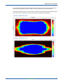
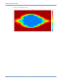
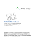
Opal Kelly
XEM7350 User’s Manual
A compact (80mm x 70mm) FMC carrier featuring the
Xilinx Kintex-7 FPGA, SuperSpeed USB 3.0, on-board
DDR3 memory, and two 16 MiB Flash memories.
The XEM7350 is a compact USB 3.0 (SuperSpeed) FPGA integration module featuring the Xilinx Kintex-7 FPGA, 4 Gib (256 Mx16-bit) DDR3 SDRAM, two 128 Mib SPI Flash devices, high-efficiency switching power supplies, and a single FMC HPC expansion connector with full gigabit transceiver capability.
The USB 3.0 SuperSpeed interface provides fast configuration downloads and PC-FPGA communication
as well as easy access with our popular FrontPanel application and SDK. Two low-jitter crystal oscillators (100 MHz and 200 MHz) are attached to the FPGA.
Software, documentation, samples, and related materials are
Copyright © 2014-2015 Opal Kelly Incorporated.
Opal Kelly Incorporated
Portland, Oregon
http://www.opalkelly.com
All rights reserved. Unauthorized duplication, in whole or part, of this document by any means except for brief
excerpts in published reviews is prohibited without the express written permission of Opal Kelly Incorporated.
Opal Kelly, the Opal Kelly Logo, and FrontPanel are trademarks of Opal Kelly Incorporated.
Linux is a registered trademark of Linus Torvalds. Microsoft and Windows are both registered trademarks of
Microsoft Corporation. All other trademarks referenced herein are the property of their respective owners and no
trademark rights to the same are claimed.
Revision History:
Date
Description
20140423
Initial release.
20140924
Fixed location reference for R48.
20141216
Add clock oscillator pin references.
20150303
Added additional information about Pins.
20150729
Fixed some minor formatting issues.
20151202
Updated Vccauxio to 2.0v in MIG guidance.
Contents
Introducing the XEM7350 . . . . . . . . . . . . . . . . . . . . . . . 5
PCB Footprint. . . . . . . . . . . . . . . . . . . . . . . . . . . . . . . . . . . . . 5
Functional Block Diagram. . . . . . . . . . . . . . . . . . . . . . . . . . . . 6
FPGA . . . . . . . . . . . . . . . . . . . . . . . . . . . . . . . . . . . . . . . . . . . 6
Power Supply. . . . . . . . . . . . . . . . . . . . . . . . . . . . . . . . . . . . . 6
DC Power Connector. . . . . . . . . . . . . . . . . . . . . . . . . . . . 6
Powering via USB . . . . . . . . . . . . . . . . . . . . . . . . . . . . . . 7
Powering via the FMC Connector . . . . . . . . . . . . . . . . . . 7
SuperSpeed USB 3.0 Interface . . . . . . . . . . . . . . . . . . . . . . . 7
On-board Peripherals. . . . . . . . . . . . . . . . . . . . . . . . . . . . . . . 7
Low-Jitter Crystal Oscillators. . . . . . . . . . . . . . . . . . . . . . 7
512-MByte Word-Wide DDR3 Synchronous DRAM . . . . 7
FPGA Flash - 16 MiB Serial Flash Memory. . . . . . . . . . . 8
System Flash - 16 MiB Serial Flash Memory. . . . . . . . . . 8
LEDs. . . . . . . . . . . . . . . . . . . . . . . . . . . . . . . . . . . . . . . . . 8
FPGA Fan Controller . . . . . . . . . . . . . . . . . . . . . . . . . . . . 8
Device Sensors . . . . . . . . . . . . . . . . . . . . . . . . . . . . . . . . 8
FMC Expansion Connector. . . . . . . . . . . . . . . . . . . . . . . . . . . 8
FrontPanel Support. . . . . . . . . . . . . . . . . . . . . . . . . . . . . . . . . 8
Programmer’s Interface. . . . . . . . . . . . . . . . . . . . . . . . . . 9
Applying the XEM7350 . . . . . . . . . . . . . . . . . . . . . . . . . 11
Powering the XEM7350 . . . . . . . . . . . . . . . . . . . . . . . . . . . . . 11
Power Budget. . . . . . . . . . . . . . . . . . . . . . . . . . . . . . . . . . 12
Example XEM7350-K160T FPGA Power Consumption. . 13
Supply Heat Dissipation (IMPORTANT!!). . . . . . . . . . . . . 13
Host Interface. . . . . . . . . . . . . . . . . . . . . . . . . . . . . . . . . . . . . 14
Reset Profile RESET. . . . . . . . . . . . . . . . . . . . . . . . . . . . 14
System Flash . . . . . . . . . . . . . . . . . . . . . . . . . . . . . . . . . . . . . 14
Layout. . . . . . . . . . . . . . . . . . . . . . . . . . . . . . . . . . . . . . . . 14
Loading a Power-On FPGA Configuration. . . . . . . . . . . . 14
Clock Oscillator. . . . . . . . . . . . . . . . . . . . . . . . . . . . . . . . . . . . 15
FPGA Flash . . . . . . . . . . . . . . . . . . . . . . . . . . . . . . . . . . . . . . 15
LEDs. . . . . . . . . . . . . . . . . . . . . . . . . . . . . . . . . . . . . . . . . . . . 16
JTAG. . . . . . . . . . . . . . . . . . . . . . . . . . . . . . . . . . . . . . . . . . . . 16
DDR3 SDRAM. . . . . . . . . . . . . . . . . . . . . . . . . . . . . . . . . . . . 16
Clock Configuration (Source Synchronous). . . . . . . . . . . 17
MIG Settings. . . . . . . . . . . . . . . . . . . . . . . . . . . . . . . . . . . 17
Key Memory Storage . . . . . . . . . . . . . . . . . . . . . . . . . . . . . . . 18
Volatile Encryption Key Storage (Vbatt). . . . . . . . . . . . . . 19
Non-Volatile Encryption Key Storage (eFUSE) . . . . . . . . 19
Device Sensors. . . . . . . . . . . . . . . . . . . . . . . . . . . . . . . . . . . . 19
Device Settings. . . . . . . . . . . . . . . . . . . . . . . . . . . . . . . . . . . . 20
FMC Device Settings. . . . . . . . . . . . . . . . . . . . . . . . . . . . 20
Fan Control Device Settings. . . . . . . . . . . . . . . . . . . . . . . 20
Expansion Connector. . . . . . . . . . . . . . . . . . . . . . . . . . . . . . . 21
Fan Power Supply . . . . . . . . . . . . . . . . . . . . . . . . . . . . . . 21
FMC-HPC. . . . . . . . . . . . . . . . . . . . . . . . . . . . . . . . . . . . . 22
Setting the FMC Vadj I/O Voltage (LA and HA Groups). . 22
FMC Vio (HB Group) . . . . . . . . . . . . . . . . . . . . . . . . . . . . 23
XADC (Optional). . . . . . . . . . . . . . . . . . . . . . . . . . . . . . . . 23
Considerations for Differential Signals. . . . . . . . . . . . . . . 23
Gigabit Transceivers. . . . . . . . . . . . . . . . . . . . . . . . . . . . . 24
Gigabit Transceiver IBERT Performance. . . . . . . . . . . . . 24
Pins. . . . . . . . . . . . . . . . . . . . . . . . . . . . . . . . . . . . . . . . . . . . . 27
Toolbar. . . . . . . . . . . . . . . . . . . . . . . . . . . . . . . . . . . . . . . 27
Pin Lists . . . . . . . . . . . . . . . . . . . . . . . . . . . . . . . . . . . . . . 27
Filters. . . . . . . . . . . . . . . . . . . . . . . . . . . . . . . . . . . . . . . . 28
Search . . . . . . . . . . . . . . . . . . . . . . . . . . . . . . . . . . . . . . . 28
Export (PDF, CSV, Constraints Files). . . . . . . . . . . . . . . . 28
Peripherals. . . . . . . . . . . . . . . . . . . . . . . . . . . . . . . . . . . . 28
PCB Version History. . . . . . . . . . . . . . . . . . . . . . . . . . . . . . . . 30
20131121 . . . . . . . . . . . . . . . . . . . . . . . . . . . . . . . . . . . . . 30
XEM7350 Mechanical Drawing. . . . . . . . . . . . . . . . . . . 32
XEM7350 User’s Manual
Introducing the XEM7350
The XEM7350 is a compact FPGA board featuring the Xilinx Kintex-7 FPGA and SuperSpeed
USB 3.0 connectivity via a USB 3.0 Micro-B receptacle. Designed as a full-featured integration
and evaluation system, the XEM7350 provides access to over 170 I/O pins on its 676-pin Kintex-7 device and has a 512-MiByte DDR3 SDRAM available to the FPGA. Two SPI Flash devices provide a total of 32 MiB of non-volatile memory, one attached to the USB microcontroller
and one attached to the FPGA. Available with LX70T, LX160T, and LX410T FPGA densities, the
XEM7350 is designed for high-performance system integrations with transceiver-capable FMC
modules including JESD204B data converters.
PCB Footprint
A mechanical drawing of the XEM7350 is shown at the end of this manual. The PCB is 80mm
x 70mm with four mounting holes (M2 metric screws) spaced as shown in the figure. These
mounting holes are electrically isolated from all signals on the XEM7350. The two connectors
(USB and DC power) overhang the PCB by approximately 1.3mm in order to accommodate
mounting within an enclosure.
The XEM7350 has a single high pin count (HPC) FMC connector providing access to over 170
I/O, 8 multi-gigabit transceivers, and electrically-programmable adjustable voltage per the VITA57 standard.
www.opalkelly.com
5
XEM7350 User’s Manual
Functional Block Diagram
System Flash
16 MiB
USB 3.0
USB 3.0
Controller
DDR3 SDRAM
4 Gb (512 MB)
FPGA Flash
16 MiB
Host Interface
Bus
Kintex-7 FPGA
XC7K70T-1FBG676C
4 LEDs
or
200 MHz
Clock
LVDS
XC7K160T-1FFG676C
LVDS
100 MHz
MGT Reference
170 I/O
8 Multi-Gb Transceivers
FMC (VITA 57) Expansion Connector
FPGA
The XEM7350 is offered in three variants. These variants are identical except for the FPGA provided. The table below lists some of the differences between the two devices. Please consult
the Xilinx documentation for a more thorough comparison.
Feature
XEM7350-LX70T
XEM7350-LX160T
XEM7350-LX410T
FPGA
XC7K70T-1FBG
XC7K160T-1FFG
XC7K410T-1FFG
Slice Count
10,250
25,350
63,550
D Flip-Flops
82,000
202,800
508,400
Distributed RAM
838 Kib
2,188 Kib
5,663 Kib
Block RAM
4,860 Kib
11,700 Kib
28,620 Kib
DSP Slices
240
600
1,540
Clock Management Tiles
6
8
10
Power Supply
The XEM7350 is designed to be operated from a single 5-volt power source supplied through the
DC power jack on the device. This provides power for the several high-efficiency switching regulators on-board to provide multiple DC voltages for various components on the device as well as
an adjustable supply for the FMC peripheral.
DC Power Connector
The DC power connector on the XEM7350 is part number PJ-102AH from CUI, Inc. It is a standard “canon-style” 2.1mm / 5.5mm jack. The outer ring is connected to DGND. The center pin is
connected to +VDC.
6
www.opalkelly.com
XEM7350 User’s Manual
Powering via USB
Note: Read this section carefully before applying this technique. The XEM7350 power consumption depends greatly on the FPGA and device configuration and could easily exceed available
power from USB.
The XEM7350 has been designed to accept power (+5VDC only) via the USB connector with a
small modification. To power from USB, you will need to install a 0 Ω resistor (0402 dimension) at
location R30, located on the reverse side of the PCB under the power connector. This will connect the +5VUSB from the USB connector to the +5VDC on the XEM7350.
With this resistor in place, you should not apply +5VDC to the external power connector.
Powering via the FMC Connector
Note: Read this section carefully before applying this technique. This technique is not part of the
FMC standard so will not work with other FMC carriers.
The XEM7350 has been designed to accept power (+5VDC only) via the FMC connector with
a small modification. To power from the FMC peripheral, you will need to install a 0 Ω resistor
(0402 dimension) at location R48, located on the top side of the PCB near the JTAG bypass
switch. This will electrically connect the device +5VDC to +12PV0 pins C35 and C37 on the FMC
connector.
With this resistor in place, you may apply +5VDC (NOT 12v as is indicated by the FMC naming
for these pins) to power the Shuttle TX1 from the FMC peripheral.
SuperSpeed USB 3.0 Interface
The XEM7350 uses a Cypress FX3 USB microcontroller to make the XEM a USB 3.0 peripheral.
As a USB peripheral, the XEM is instantly recognized as a plug and play peripheral on millions of
PCs. More importantly, FPGA downloads to the XEM happen quickly, virtual instruments under
FrontPanel update quickly, and data transfers are blazingly fast.
On-board Peripherals
The XEM7350 is designed to compactly support a large number of applications with a small number of on-board peripherals. These peripherals are listed below.
Low-Jitter Crystal Oscillators
A fixed-frequency, 200 MHz, low-jitter oscillator is included on-board and outputs LVDS to the
FPGA. The Kintex-7 FPGA can produce a wide range of clock frequencies using the on-chip
DCM and PLL capabilities.
A second 100 MHz oscillator is available to the transceiver portions of the FPGA as a reference.
512-MByte Word-Wide DDR3 Synchronous DRAM
The XEM also includes a 512-MiByte DDR3 SDRAM with a full 16-bit word-wide interface to the
FPGA. This SDRAM is attached exclusively to the FPGA and does not share any pins with the
expansion connector. The maximum clock rate of the SDRAM is 800 MHz. With the -1 speed
grade of the Kintex-7, the maximum clock rate is 800 MHz (400 MHz for the -K70T) for a supported peak memory bandwidth of 25.6 Gb/s (12.8 Gb/s for the -K70T).
www.opalkelly.com
7
XEM7350 User’s Manual
The DDR3 SDRAM is a Micron MT41K256M16HA-125:E (or compatible).
FPGA Flash - 16 MiB Serial Flash Memory
A 128 Mib serial flash device (Numonyx N25Q128A11B1240E or equivalent) provides on-board
non-volatile storage for the FPGA. This device is attached directly to the FPGA for use in your
design.
System Flash - 16 MiB Serial Flash Memory
A 128 Mib serial flash device (Numonyx N25Q128A11B1240E or equivalent) provides on-board
non-volatile storage accessible to the USB microcontroller. This device is used to store device
firmware and configuration settings as well as other user assets such as FPGA configuration files
or calibration data. Erase, read, and write functions are available at all times (with or without a
configured FPGA) through the use of FrontPanel API methods.
LEDs
Four LEDs and are available for general use as indicators.
FPGA Fan Controller
A small connector provides power to an optional 5v fan mounted on the FPGA heat sink. This
power is under the control of the microcontroller.
Device Sensors
On-board voltage and current sensors provide real-time access to several power supply measurements through the FrontPanel SDK sensors API.
FMC Expansion Connector
FMC (FPGA Mezzanine Connector) is the common name for the VITA 57 specification which
describes a common connector design to interface large pin-counts to devices with configurable
I/O such as an FPGA. The specification is available for purchase through the VITA website:
http://www.vita.com/fmc.html8
The XEM7350 specifically supports the HPC (high pin-count) version of the specification (Note:
the -K70T does not have a fully-populated HPC connector). For details on supported FMC
features, please see the FMC Feature Support section. FMC connectors are manufactured by
Samtec. The FMC connector on the XEM7350 is the Samtec ASP-134486-01. The mating connector which would appear on an FMC peripheral is the Samtec ASP-134488-01. These are both
surface-mount pin-field-array style connectors. The connectors ship with a solder plug on each
connector which melts during reflow to the solder paste spread on the bare board for assembly.
Connector contact is solid and insertion and removal forces are relatively small. High frequency
performance is up to 9.5 GHz in single-ended operation and to 10.5 GHz in differential operation.
FrontPanel Support
The XEM7350 is fully supported by Opal Kelly’s FrontPanel Application. FrontPanel augments
the limited peripheral support with a host of PC-based virtual instruments such as LEDs, hex displays, pushbuttons, toggle buttons, and so on. Essentially, this makes your PC a reconfigurable
I/O board and adds tremendous value to the XEM7350 as an experimentation or prototyping
system.
8
www.opalkelly.com
XEM7350 User’s Manual
Programmer’s Interface
In addition to complete support within FrontPanel, the XEM7350 is also fully supported by the
FrontPanel SDK, a powerful C++ class library available to Windows, Mac OS X, and Linux programmers allowing you to easily interface your own software to the XEM.
In addition to the C++ library, wrappers have been written for C#, Java, and Python making the
API available under those languages as well. Sample wrappers (unsupported) are also provided
for Matlab and LabVIEW.
Complete documentation and several sample programs are installed with FrontPanel.
www.opalkelly.com
9
XEM7350 User’s Manual
10
www.opalkelly.com
XEM7350 User’s Manual
Applying the XEM7350
Powering the XEM7350
The XEM7350 requires a clean, filtered, DC supply within the range of 4.5v to 5.5v. This supply
must be delivered through the DC power connector.
The XEM7350 power distribution system is rather complex, with several supplies designed to
provide suitable, efficient power for several systems and modules. A schematic diagram of the
system follows, with input (+VDC) shown to the left and accessible supply rails shown to the right.
www.opalkelly.com
11
XEM7350 User’s Manual
Current Sensor
Linear Supply
Voltage Sensor
Switching Supply
Jumper
R48
+VDC
(+4.5 to +5.5v)
3.3v
FMC 12P0V
FMC 3P3V
6A
FMC 3P3VAUX
System Controller
FPGA Vccio
0.75v 500mA
2.0v
0.4A
DDR3 Memory
DDR3 Termination
1.8v
1.5A
1.5v
1.5A
1.2v
0.4A
1.0v
9A
1.8v
3A
GTP Transceiver Aux
FPGA Vccint
1.8v
1.5A
1.2v
3A
GTP Transceiver Termination
1.5v
3A
1.0v
3A
GTP Transceiver Core
ADJv
6A
FMC VADJ
FMC Vadj
Power Budget
The table below can help you determine your power budget for each supply rail on the XEM7350.
All values are highly dependent on the application, speed, usage, and so on. Entries we have
made are based on typical values presented in component datasheets or approximations based
on Xilinx power estimator results. Shaded boxes represent unconnected rails to a particular
component. Empty boxes represent data that the user must provide based on power estimates.
The user may also need to adjust parameters we have already estimated (such as FPGA Vcco
values) where appropriate. All values are shown in milliwatts (mW). Note that this table does not
include the two supplies dedicated to the GTX transceivers. These are independent and can be
computed separately for power budget based on their assigned function.
12
www.opalkelly.com
XEM7350 User’s Manual
Component(s)
1.0v
1.2v
1.5v
1.8v
2.0v
200 MHz
3.3v
231
USB, DDR3
240
720
250
FPGA Vccint, Vccbram
FPGA Vccaux
355
FPGA Vccaux_io
120
FPGA Vcco33,34 (DDR3), est.
273
FPGA Vcco14 (USB), est.
216
FPGA Vcco
Total (mW)
Available (mW) 6,000
480
2,250
2,700
800
19,800
Example XEM7350-K160T FPGA Power Consumption
XPower Estimator version 14.3 was used to compute the following power estimates for the Vccint
supply. These are simply estimates; your design requirements may vary considerably. The numbers below indicate approximately 80% utilization.
Component
Parameters
Vccint
Clock
250 MHz GCLK, 163,237 fanout
716 mW
Logic (DFF)
250 MHz, 162,240 DFFs
1,322 mW
Logic (LUT)
250 MHz, 81,120
927 mW
BRAM
18-bit, 517 @ 250 MHz
674 mW
DSP
250 MHz, 480 slices
605 mW
Memory Controller 1600 Mb/s, DDR3
7 mW
GTX
Aurora, 8 lanes, 8 Gb/s
458 mW
Misc.
DCM, PLL, etc.
5 mW
Total: 4,714 mW
Available: 6,000 mW
Supply Heat Dissipation (IMPORTANT!!)
Due to the limited area available on the small form-factor of the XEM7350 and the density of logic
provided, heat dissipation may be a concern. This depends entirely on the end application and
cannot be predicted in advance by Opal Kelly. Heat sinks may be required on any of the devices
on the XEM7350. Of primary focus should be the FPGA (U8) and SDRAM (U12). Although the
switching supplies are high-efficiency, they are very compact and consume a small amount of
PCB area for the current they can provide.
If you plan to put the XEM7350 in an enclosure, be sure to consider heat dissipation in your
design.
Heat Sink
The device has been fitted with two heat sink anchors, proximate to the FPGA for mounting a
passive or active heat sink. The following heat sinks have been tested with the XEM7350.
www.opalkelly.com
13
XEM7350 User’s Manual
Manufacturer
Part Number
Description
Aavid Termalloy
374524B60023G
Off-the-shelf passive
Aavid Termalloy
3358230-PAL03010-P0
Custom with fan mount
The passive heat sink above is a low cost option available through Aavid Thermalloy distributors
such as Arrow Electronics and Newark Electronics.
The active heat sink above was custom built based on design specifications provided by Opal
Kelly to mate to the XEM7350. It includes a small fan which connects to the fan controller onboard for manual or automatic fan speed control. It is available for purchase directly from Opal
Kelly. The assigned part number should allow you to order direct from Aavid, if desired.
Host Interface
There are 41 signals that connect the on-board USB microcontroller to the FPGA. These signals
comprise the host interface on the FPGA and are used for configuration downloads. After configuration, these signals are used to allow FrontPanel communication with the FPGA.
If the FrontPanel okHost module is instantiated in your design, you must map the interface pins to
specific pin locations using Xilinx LOC constraints. This may be done using the Xilinx constraints
editor or specifying the constraints manually in a text file. Please see the sample projects included with your FrontPanel installation for examples.
Reset Profile RESET
Pin AB8 of the FPGA is an active-high RESET signal from the host interface. This signal is asserted when configuration download begins and is deasserted during the execution of the Reset
Profile. For more information on the timing of this deassertion event, see the FrontPanel User’s
Manual.
System Flash
The Flash memory attached to the USB microcontroller stores device firmware and settings as
well as user data that is accessible via the FrontPanel API. The API includes three methods
for accessing this memory: FlashEraseSector, FlashWrite, and FlashRead. Please refer to
the FrontPanel User’s Manual and the FrontPanel API Reference for information about applying
these methods.
Layout
The Numonyx N25Q128A11B1240E is a 16 MiB Flash memory arranged into 256 64-kiB sectors.
Each sector contains 256 256-byte pages. Sectors 0...15 are reserved for device firmware and
settings and are not accessible to user software. The remaining 15 MiB may be erased, written,
and read using the FrontPanel API at any time even without a valid FPGA configuration. Full 64
kiB sectors must be erased at a time. However, contents may be read or written on any page
address boundary.
Loading a Power-On FPGA Configuration
The user-area in System Flash may be used to store a Xilinx bitfile to configure the FPGA at
power-on. Power-on configuration takes approximately 6-10 seconds from when power is applied. A full Reset Profile may also be performed after configuration.
14
www.opalkelly.com
XEM7350 User’s Manual
The API is used to erase and program the power-on bitfile and the Flashloader sample is provided to perform these steps from a simple command-line utility. Source code to the Flashloader
sample is included with the FrontPanel SDK.
Called with a single argument (the filename for a valid Xilinx bitfile), the Flashloader sample will
erase the first sectors in the System Flash user-area, then write the bitfile. It will also setup the
Boot Reset Profile to point to this area on power-on.
No Power-On Configuration
Called with no arguments, the Flashloader sample will clear the existing Boot Reset Profile. This
has the effect of preventing an FPGA configuration from being loaded at power-on. This functionality may also be accomplished from the API by setting an empty okTFPGAResetProfile using
the API SetFPGABootResetProfile. See the FrontPanel API Reference for details.
Clock Oscillator
A fixed-frequency, 200 MHz, low-jitter oscillator is included on-board and outputs LVDS to the
FPGA on bank 34. The Kintex-7 FPGA can produce a wide range of clock frequencies using the
on-chip DCM and PLL capabilities.
200 MHz Pin
FPGA Pin
LVDS +
AC4
LVDS -
AC3
A second 100 MHz oscillator is available to the transceiver portions of the FPGA as a reference.
100 MHz Pin
FPGA Pin
LVDS +
K6
LVDS -
K5
FPGA Flash
The SPI Flash attached to the FPGA is a Numonyx N25Q128A11B1240E or equivalent. It provides non-volatile storage for use by the FPGA. It may not be used for FPGA configuration storage. The System Fash is used to store FPGA “boot” configurations.
The Flash / FPGA pin mappings are shown in the table below.
Flash Pin
FPGA Pin
C
N16
S
R16
DQ0
N17
DQ1
U17
DQ2 / W
U16
DQ3 / HOLD
T17
www.opalkelly.com
15
XEM7350 User’s Manual
LEDs
There are four LEDs on the XEM7350 in addition to the power LED. Each is wired directly to the
FPGA according to the pin mapping tables at the end of this document.
The LED anodes are connected to a pull-up resistor to +3.3VDD and the cathodes wired directly
to the FPGA on Bank 13 with a bank I/O voltage of 3.3v. To turn ON an LED, the FPGA pin
should be at logic ‘0’. To turn OFF an LED, the FPGA pin should be at logic ‘1’.
JTAG
The JTAG connections on the FPGA are wired directly to the 2mm header JP2 on the XEM7350
to facilitate FPGA configuration and ChipScope usage using a Xilinx JTAG cable. The JTAG
interface presented at JP2 is a 1.8v interface.
By design, the FMC module is intended to complete the JTAG chain. If a mezzanine module is
not present, or does not properly complete the chain, the chain may be bypassed using SW1 or,
optionally, installing a 0-Ω resistor at location R56.
To accommodate the FMC requirement that the JTAG chain operate at 3.3v, level shifters are
present on-board. Installing a 0-Ω resistor at location R73 keeps the entire chain at 1.8v, but U33
must also be removed to avoid drive contention from the 3.3v side to the 1.8v side.
Level
Shift
JP2
1.8v
Xilinx
JTAG
Cable
P2
Module
3.3v
TMS
TCK
TMS
TCK
TMS
TDI
TDI
TCK
D30
TDO
FPGA
R56*
FMC
MM
SW1
D31
TDO
TDI
TDO
Shuttle TX1
* R56 is not installed at the factory.
DDR3 SDRAM
The Micron DDR3 SDRAM is connected exclusively to the 1.5-v I/O on Banks 33 and 34 of the
FPGA. The tables below list these connections.
16
www.opalkelly.com
XEM7350 User’s Manual
DDR3 Pin
FPGA Pin
DDR3 Pin
FPGA Pin
RESET
AA4
A9
W3
CK
W6
A10
V3
CK
W5
A11
U1
CKE
AB5
A12
U2
CS
AA5
A13
U5
RAS
AC2
A14
U6
CAS
AA3
BA0
AB2
WE
AA2
BA1
Y1
DQS0
AF5
BA2
W1
DQS0
AF4
D0
AD1
DQS1
W10
D1
AE1
DQS1
W9
D2
AE3
DM0
AD4
D3
AE2
DM1
V11
D4
AE6
ODT
AB6
D5
AE5
A0
AC1
D6
AF3
A1
AB1
D7
AF2
A2
V1
D8
W11
A3
V2
D9
V8
A4
Y2
D10
V7
A5
Y3
D11
Y8
A6
V4
D12
Y7
A7
V6
D13
Y11
A8
U7
D14
Y10
D15
V9
Clock Configuration (Source Synchronous)
The DDR3 clocking is designed to be source-synchronous from the FPGA. This means that the
FPGA sends the clock signal directly to the SDRAM along with control and data signals, allowing
very good synchronization between clock and data.
MIG Settings
Kintex-7 devices support external, high-performance memory through the use of the Memory
Interface Generator (MIG) provided by Xilinx. MIG produces a custom memory interface core
that may be included in your design. These parameters have been used successfully within Opal
Kelly but your design needs may require deviations.
www.opalkelly.com
17
XEM7350 User’s Manual
Parameter
XEM7350-K70T
XEM7350-K160T
System Clock Type
Differential
Reference Clock Type
User System Clock
Debug Port
Off
Internal Vref
Disabled
IO Power Reduction
On
DCI for DQ / DQS / DM
Enabled
Internal Termination
40 Ω
Memory
DDR3_SDRAM
Interface
Native
Design Clock Frequency
2500ps (400.0 MHz)
1250ps (800.0 MHz)
Phy to Controller Ratio
4:1
4:1
Input Clock Period
5000ps
5000ps
CLKFBOUT_MULT
4
8
DIVCLK_DIVIDE
1
Vcc_aux_io
2.0v
Memory Type
Components
Memory Part
MT41K256M16XX-125
Data Width
16
ECC
Disabled
Data Mask
Enabled
Ordering
Normal
Burst Length
8 - Fixed
Read Burst Type
Sequential
CAS Latency
6
Output Drive Strength
RZQ/6
Controller CS Option
ENable
Rtt NOM - ODT
RZQ/6
Rtt WR - Dynamic ODT
Dynamic ODT off
Memory Address Mapping
BANK_ROW_COLUMN
Bank 33
Byte Group T0 : DQ[8-15]
Bank 34
Byte Group T0 : Address/Ctrl-0
Byte Group T1 : Address/Ctrl-1
Byte Group T2 : Address/Ctrl-2
Byte Group T3 : DQ[0-7]
11
Key Memory Storage
The Kintex-7 FPGA supports design security using AES decryption logic and provides two
methods for encryption key memory storage. The first is a volatile memory storage supported
by an external battery backup supply voltage (Vbatt). The second is a one-time programmable
eFUSE register. The XEM7350 design supports both types of key storage with user-modification
required for Vbatt support.
18
www.opalkelly.com
XEM7350 User’s Manual
For quantity purchases of 50 or more units, please contact Opal Kelly ([email protected]) to
discuss factory installation of these components.
Volatile Encryption Key Storage (Vbatt)
A small lithium rechargeable battery and three support components can be installed to provide
Vbatt to the FPGA when the XEM is unpowered. This will preserve the contents of the FPGA’s
volatile key storage so long as Vbatt remains over the threshold specified in the Kintex-7 documentation. Please see the Xilinx 7-Series FPGA’s Configuration (UG470) for more details.
The applicable schematic section and components required to support this functionality are
shown below.
RefDes
Manufacturer
Manufacturer P/N
Comment
BT1
Seiko Instruments
TS518FE-FL35E
1.5V, 1.5mAh lithium battery
D5
Micro Commercial
BAS40-04-TP
Schottky Diode, SOT23
R78
Generic
4.7 kΩ, 5%, SM-0402
R139
Generic
0 Ω, SM-0402
Connects Vbatt to DGND
(Required if not used)
Non-Volatile Encryption Key Storage (eFUSE)
Non-volatile storage of the encryption key is also possible by programming the Kintex-7 eFUSE
register via JTAG. Please see the Xilinx 7-Series FPGAs Configuration (UG470) for more details.
Device Sensors
On-board device sensors provide measurements of a number of device parameters. These may
be read via the FrontPanel Device Sensors API and can be displayed in the FrontPanel GUI in
real-time.
Name
Type
Min
Max
Step
VDC Voltage
VOLTAGE
0
6
601.36 μV
www.opalkelly.com
19
XEM7350 User’s Manual
Name
Type
Min
Max
Step
+3.3 Voltage
VOLTAGE
0
3.5
305.18 μV
+3.3 Current
CURRENT
0
60
3.815 mA
+2.0 Voltage
VOLTAGE
0
3.5
305.18 μV
+1.8 Voltage
VOLTAGE
0
3.5
305.18 μV
+1.5 Voltage
VOLTAGE
0
3.5
305.18 μV
+1.2 Voltage
VOLTAGE
0
3.5
305.18 μV
+1.0 Current
CURRENT
0
60
3.815 mA
FMC VIO Voltage
VOLTAGE
0
3.5
305.18 μV
FMC 12v Voltage
VOLTAGE
0
18.829
1.642 mV
FMC Vadj Current
CURRENT
0
60
3.815 mA
Board Temp #1
TEMPERATURE
-256
255
0.0625
Board Temp #2
TEMPERATURE
-256
255
0.0625
FPGA Temp
TEMPERATURE
-256
255
0.0625
Device Settings
The XEM7350 supports the FrontPanel Device Settings in the table below, accessible from the
FrontPanel Application as well as the Device Settings API.
FMC Device Settings
The XEM7350 has a single FMC port which is configured using the FMC1_* settings. These settings are used to control FMC Vadj behavior as well as control and query FMC connector signals.
FMC1_CONTROL and FMC1_STATUS are volatile device settings that are never stored to nor
retrieved from non-volatile storage on the device. Instead, they control and query signals on the
connector in real time.
Fan Control Device Settings
You may optionally connect a fan to JP1 (Molex 53398-0271). This connector drives a 3.3v PWM
signal to the fan according to the Device Settings. For most applications, we recommend binary
operating mode and enabling the fan at all times. You may optionally configure a proportional
control whereby the PWM output is proportional to the measured temperature of the FPGA die.
Name
Type
Description
FMC1_VADJ_VOLTAGE
INT32
Vadj output voltage specified in 10’s of mV. For example, “330”
would set Vadj = 3.3v.
DEFAULT: 0
FMC1_VADJ_ENABLE
INT32
Vadj output enable: 0=disable, 1=enable
DEAFULT: 0
20
www.opalkelly.com
XEM7350 User’s Manual
Name
Type
Description
FMC1_VADJ_MODE
INT32
Vadj setting mode
0=Disabled
1=IPMI setting only. If a valid IPMI EEPROM is not found, Vadj
is disabled.
2=IPMI with fallback. If a valid IPMI EEPROM is not found, Vadj
is set according to FMC1_VADJ_VOLTAGE.
3=IPMI ignore. IPMI settings are ignored and Vadj is set according to FMC1_VADJ_VOLTAGE.
DEFAULT: 2
FMC1_CONTROL
INT32
Write-only register that controls FMC1 signals during runtime.
[0] - TRST_L
DEFAULT: 0x00000001
FMC1_STATUS
INT32
Read-only register that contains the FMC1 signal status during
runtime.
[0] - PRSNT_M2C_L
[1] - CLKDIR
[2] - PG_M2C
[3] - POK_3P3
[4] - POK_VADJ
[6:5] - GA[0:1]
XEM7350_FAN_MODE
INT32
0=Binary mode
1=Temperature slope mode
DEFAULT: 0
XEM7350_FAN_ENABLE
INT32
In binary mode, 0=disable, 1=enable
DEFAULT: 1
XEM7350_FAN_TEMP_THRESHOLD
INT32
In temperature slope mode, the number here represents the
lower threshold (in degrees Celsius) for temperature-dependent
operation.
At THRESH, fan control PWM=0%.
At THRESH+16C, fan control PWM=50%.
At THRESH+32C, fan control PWM=100%.
Expansion Connector
Opal Kelly Pins is an interactive online reference for the expansion connectors on all Opal Kelly
FPGA integration modules. It provides additional information on pin capabilities, pin characteristics, and PCB routing. Additionally, Pins provides a tool for generating constraint files for place
and route tools. Pins can be found at the URL below.
http://www.opalkelly.com/pins
Fan Power Supply
A small 2-pin connector (Molex 53398-0271) at JP1 provides power to an optional fan for FPGA
cooling. This fan is under direct or temperature-proportional control of a digital fan controller.
Please see the Device Settings section for details on controlling the fan.
www.opalkelly.com
21
XEM7350 User’s Manual
Pin
Signal
1
GND
2
+5VDC
FMC-HPC
A single FMC-HPC (high pin count) connector provides direct access to I/O pins and Gigabit
transceiver on the FPGA. The tables below illustrate the number of pins that are available on an
FMC-HPC connector and the number that are routed to available sites on the FPGA.
Bank / Group (I/O voltage)
FMC-HPC
-70T
-160T/-410T
LA (Vadj) - I/O pairs
34
34
34
HA (Vadj) - I/O pairs
24
0
24
HB (Vio) - I/O pairs
22
0
22
GBT - # of transceivers
10
8
8
Clock Pins
Clock pins are given special attribution within the FMC specification. Available clock pins are illustrated in the table below.
Bank / Group (I/O voltage)
FMC-HPC
-70T
-160T/-410T
LA (Vadj) - Clock pairs
2
2
2
HA (Vadj) - Clock pairs
1
1
1
HB (Vio) - Clock pairs
1
0
1
GBT - Reference Clocks
2
2
2
Setting the FMC Vadj I/O Voltage (LA and HA Groups)
FMC specifies a single adjustable voltage (Vadj) for the two LA groups that are routed to FPGA
banks 15 and 16 and the HA group routed to FPGA bank 12. A high-efficiency switching regulator on the XEM7350 controls this voltage and is configured according to Device Settings FMC1_
VADJ_MODE, FMC1_VADJ_VOLTAGE, and FMC1_VADJ_ENABLE.
When FMC1_VADJ_MODE=2 (default), the contents of the IPMI EEPROM on the FMC peripheral are queried. If the contents are valid, Vadj is set to the voltage specified. If the contents are
not valid, then Vadj is set to the FMC1_VADJ_VOLTAGE as a fallback.
When FMC1_VADJ_MODE=1, the contents of the IPMI EEPROM are queried. If the contents
are valid, Vadj is set to the voltage specified. If the contents are not valid, then the voltage output
is disabled.
When FMC1_VADJ_MODE=3, the contents of the IPMI EEPROM are ignored and Vadj is set to
the value in FMC1_VADJ_VOLTAGE.
When FMC1_VADJ_MODE=0, Vadj output is disabled.
Valid output voltages are: 3.3v, 2.5v, 1.8v, 1.5v, 1.25v, 1.2v, and 0.8v.
22
www.opalkelly.com
XEM7350 User’s Manual
FMC Vio (HB Group)
The pins on the FMC HB group are routed to FPGA bank 32. Vcco for this bank is connected
to FMC_VIO_B_M2C which is a voltage provided by the mezzanine (peripheral) to the carrier
(XEM7350). Please see the Xilinx Kintex-7 User’s Manual for details on acceptable voltages.
XADC (Optional)
The Xilinx Kintex-7 XADC feature is routed through two resistors to the FMC connector. In the
factory configuration, these two resistors are not inserted. In the FMC specification, B24 and B25
locations are transceiver pin locations. These pins are otherwise not used on the XEM7350.
FPGA Function
FPGA Pin
FMC
Resistor RefDes
ADC_VN_0
P11
B24
R75
ADC_VP_0
N12
B25
R74
Considerations for Differential Signals
The XEM7350 PCB layout and routing has been designed with several applications in mind,
including applications requiring the use of differential (LVDS) pairs. Please refer to the Xilinx
Kintex-7 datasheet for details on using differential I/O standards with the Kintex-7 FPGA.
FPGA I/O Bank Voltages
In order to use differential I/O standards with the Kintex-7, you must set the VCCO voltages for
the appropriate banks to 2.5v according to the Xilinx Kintex-7 datasheet. Please see the section
above entitled “Setting the FMC Vadj I/O Voltage” for details.
Characteristic Impedance
The characteristic impedance of all routes from the FPGA to the expansion connector is approximately 50Ω.
Differential Pair Lengths
In many cases, it is desirable that the route lengths of a differential pair be matched within some
specification. Care has been taken to route differential pairs on the FPGA to adjacent pins on
the expansion connectors whenever possible. We have also included the lengths of the board
routes for these connections to help you equalize lengths in your final application. Due to space
constraints, some pairs are better matched than others.
Reference Voltage Pins (Vref)
The Xilinx Kintex-7 supports both internal and externally-applied input voltage thresholds for
some input signal standards. The XEM7350 supports these Vref applications for banks 12, 15,
16, and 32. Please see the Xilinx Kintex 7 documentation for more details. In summary,
For banks 15 and 16, the four Vref pins are routed to the FMC connector pin VREF_A_M2C at
location H1. Internal Vref may also be used.
For bank 12, internal Vref may be used. Vref pins are also available on the FMC connector
pins HA18_N (J19) and HA22_N (J22) if external Vref is required. Doing so prevents the use of
HA18_N and HA22_N for I/O.
www.opalkelly.com
23
XEM7350 User’s Manual
For bank 32, internal Vref may be used. Vref pins are also available on the FMC connector pin
VREF_B_M2C (K1). For external Vref you must install 0 Ω resistors (0402 dimension) at R105
and R106. Doing so prevents the use of HB01_N (J25) for I/O.
Gigabit Transceivers
Access to eight high-speed serial transceiver pairs (8 Rx and 8 Tx) corresponding to GTX tiles
115 and 116 on the FPGA are available on the FMC expansion connector. MGTREFCLK0 of tile
115 and MGTREFCLK0 of tile 116 are also routed to FMC. MGTREFCLK1 of tile 115 is connected
to a low-jitter 100 MHz LVDS oscillator.
AC-Coupling
0.1μF AC-coupling capacitors are installed between the FMC connector and the FPGA for all
MGTREFCLK signals.
AC-coupling capacitors are not installed for any of the GTP transmit or receive pairs. If AC-coupling is desired or required for the serial application, they should be installed on the peripheral
side (your board).
IBERT Configuration
Xilinx provides the IBERT tool to test and experiment with gigabit transceivers. The settings
below are compatible with the XEM7350 using Vivado 2013.4:
Protocol Definition
Silicon Version
General ES / Production
ProtocolCustom 1
Line Rate
6.6 Gbps
Data Width32
RefClk100.000 MHz
Quad Count
2
Quad PLL
Checked
Protocol Selection
GTX Location
QUAD_115
QUAD_116
Protocol Selected
Custom 1 / 6.6 Gbps
Custom 1 / 6.6 Gbps
RefClk SelectionMGTREFCLK1_115MGTREFCLK1_115
TXUSRCLK Source
Channel 0
Channel 0
Clock Settings
Add RXOUTCLK Probes
Unchecked
Clock Type
System Clock
SourceExternal
I/O StandardLVDS
P Package Pin
AC4
N Package Pin
AC3
Frequency200 MHz
Enable DIFF Term
Unchecked
Gigabit Transceiver IBERT Performance
Xilinx’s IBERT tool enables an automated self-measurement of a GTP channel’s eye diagram
when used in a loopback mode. Eye diagrams for three different speeds were captured using this
24
www.opalkelly.com
XEM7350 User’s Manual
tool on an FMC loopback peripheral. While results may vary, these were rather typical captures
and actually represent the worst case capture over all channels for the respective rates.
Note that in loopback modes, it is often helpful to disable the GBT DFE (decision feedback equalizer) to avoid over-compensation. In these test cases, the DFE has been disabled.
3.3 Gbps / XEM7350-K70T
6.6 Gbps / XEM7350-K70T
www.opalkelly.com
25
XEM7350 User’s Manual
8.0 Gbps / XEM7350-K160T
26
www.opalkelly.com
XEM7350 User’s Manual
Pins
Opal Kelly Pins is an interactive online reference for the expansion connectors on all Opal Kelly
FPGA integration modules. It provides additional information on pin capabilities, pin characteristics, and PCB routing. Additionally, Pins provides a tool for generating constraint files for place
and route tools. Pins can be found at the URL below.
http://www.opalkelly.com/pins
Toolbar
The toolbar at the top of a Pins product page has a number of features. Explore a bit; you won’t
break it.
Pin Lists
As the primary reference for Opal Kelly integration module expansion connectors, Pin Lists contain a comprehensive table of the FPGA-to-Connector data including connector pin, FPGA pin,
signal description, routed length (when applicable), breakout board pin mapping, FPGA I/O bank,
and other properties.
By default, not all data columns are visible. Click on the “Toggle Filters” icon at the top-left to select which columns to show. Depending on the specific module, several additional columns may
be shown. The data in these columns is always exported when you export the pin list to CSV.
www.opalkelly.com
27
XEM7350 User’s Manual
Filters
You can hide or show the additional information associated with each signal by clicking on the
icon at the top left (“Toggle Filters”). Use these filters to limit the visible pin listing to particular
subsets of signals you are interested in.
Search
You can search the pin list using the search entry at the top-right. Click on the magnifying glass
drop-down to adjust the function of the search to one of:
•
•
•
Highlight - Highlights search results only.
Hide Matching - Hides rows where search matches are found.
Show Only Matching - Shows only rows where a search match is found.
Export (PDF, CSV, Constraints Files)
The export button near the search entry allows you to export the pin list in several formats. PDFs
can be viewed or printed. CSV can be loaded into a spreadsheet application or manipulated with
scripts. Constraints files can be used as inputs to Xilinx and Altera synthesis and mapping tools.
The constraints files include additional mapping information for other peripherals on the module
such as memory, clock oscillators, and LEDs.
Peripherals
A Pins Peripheral is a project definition where you can enter your top-level HDL design nets to
have Pins generate a complete constraint file for you.
When you create a Peripheral, you will select a target integration module. The Peripheral is
paired to this module so that the design parameters match the features and expansion capabilities of the module.
Specifying Net Names
The Pin List view for a Peripheral includes three additional, editable columns:
•
•
•
Design Net - The name of the signal as it appears in your top-level HDL.
Constraints - Text that is inserted into the constraints file for that signal.
Comment - Additional comment text that is added to the constraints file.
These additional data are merged with the default Pin List constraints file prior to export. The result is a constraints file complete with net names that can be used with your FPGA development
flow.
28
www.opalkelly.com
XEM7350 User’s Manual
Export Features
Enable the specific module features you
would like to appear in the exported constraints file. When a feature is enabled,
Pins will export the constraints appropriate to that feature such as pin locations.
When a feature is disabled, Pins will skip
that portion.
The User Lead In and User Lead Out
sections allow you to add custom payloads (your own constraints) that will be
added to the exported constraints file.
Additional timing constraints or comments can be added here.
www.opalkelly.com
29
XEM7350 User’s Manual
PCB Version History
20131121
First production PCB.
30
www.opalkelly.com
XEM7350 User’s Manual
www.opalkelly.com
31
XEM7350 User’s Manual
2.
70
63.67
66.46
70.00
34.94
0
3.07
3.46
6.21
XEM7350 Mechanical Drawing
2.
70
80.00
78.62
74.00
72.00
69.36
65.38
62.66
57.25
50.00
5.00
3.00
0
62.33
66.50
70.00
48.91
41.50
20.00
0
3.50
11.00
1.30
13.06
8.56
2.03
0
8.53
4.84
1.82
0
All dimensions in mm
32
www.opalkelly.com