1
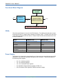
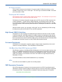
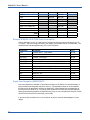
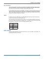
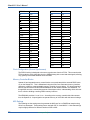
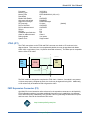
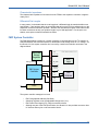
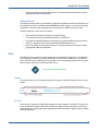
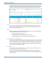
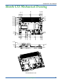
Opal Kelly
Shuttle LX1 User’s Manual
A compact (69mm x 50mm) Xilinx Spartan-6 FMC
Carrier with high-speed USB 2.0 interface and
1 Gb DDR2 SDRAM.
The Shuttle LX1 is a compact USB 2.0 FPGA integration module featuring the Xilinx Spartan-6 FPGA,
1 Gb (64 Mx16-bit) DDR2 SDRAM, high-efficiency switching power supplies, and a single FMC-LPC
(FPGA mezzanine connector, low pin count) expansion connector. The high-speed USB 2.0 interface
provides fast configuration downloads and PC-FPGA communication as well as easy access with our
popular FrontPanel application and SDK.
Software, documentation, samples, and related materials are
Copyright © 2011-2015 Opal Kelly Incorporated.
Opal Kelly Incorporated
Portland, Oregon
http://www.opalkelly.com
All rights reserved. Unauthorized duplication, in whole or part, of this document by any means except for brief
excerpts in published reviews is prohibited without the express written permission of Opal Kelly Incorporated.
Opal Kelly, the Opal Kelly Logo, and FrontPanel are trademarks of Opal Kelly Incorporated.
Linux is a registered trademark of Linus Torvalds. Microsoft and Windows are both registered trademarks of
Microsoft Corporation. All other trademarks referenced herein are the property of their respective owners and no
trademark rights to the same are claimed.
Revision History:
Date
Description
20111017
Initial release.
20120207
Added JTAG connection diagram and references in FMC pinout.
20130430
Removed text that said power could be delivered through expansion connector.
20130523
Added text to clarify power delivery option from the FMC peripheral.
20140331
Replace pin list tables with reference to Pins.
20150303
Added additional information about Pins.
Contents
Introducing the Shuttle LX1. . . . . . . . . . . . . . . . . . . . . . 5
PCB Footprint. . . . . . . . . . . . . . . . . . . . . . . . . . . . . . . . . . . . . 5
Functional Block Diagram. . . . . . . . . . . . . . . . . . . . . . . . . . . . 6
FPGA . . . . . . . . . . . . . . . . . . . . . . . . . . . . . . . . . . . . . . . . . . . 6
Power Supply. . . . . . . . . . . . . . . . . . . . . . . . . . . . . . . . . . . . . 6
DC Power Connector. . . . . . . . . . . . . . . . . . . . . . . . . . . . 7
Powering via FMC Connector . . . . . . . . . . . . . . . . . . . . . 7
High-Speed USB 2.0 Interface. . . . . . . . . . . . . . . . . . . . . . . . 7
On-board Peripherals. . . . . . . . . . . . . . . . . . . . . . . . . . . . . . . 7
128-MByte Word-Wide DDR2 Synchronous DRAM. . . . 7
LEDs. . . . . . . . . . . . . . . . . . . . . . . . . . . . . . . . . . . . . . . . . 7
FMC Expansion Connector. . . . . . . . . . . . . . . . . . . . . . . . . . . 7
FrontPanel Support. . . . . . . . . . . . . . . . . . . . . . . . . . . . . . . . . 8
Programmer’s Interface. . . . . . . . . . . . . . . . . . . . . . . . . . 8
Applying the Shuttle LX1. . . . . . . . . . . . . . . . . . . . . . . . 9
Powering the Shuttle LX1. . . . . . . . . . . . . . . . . . . . . . . . . . . . 9
Power Budget. . . . . . . . . . . . . . . . . . . . . . . . . . . . . . . . . . 9
Example XEM6006-LX16 FPGA Power Consumption . . 10
Supply Heat Dissipation (IMPORTANT!!). . . . . . . . . . . . . 10
Host Interface. . . . . . . . . . . . . . . . . . . . . . . . . . . . . . . . . . . . . 11
LEDs. . . . . . . . . . . . . . . . . . . . . . . . . . . . . . . . . . . . . . . . . . . . 11
DDR2 SDRAM. . . . . . . . . . . . . . . . . . . . . . . . . . . . . . . . . . . . 11
Clock Configuration (Source Synchronous). . . . . . . . . . . 12
Memory Controller Blocks . . . . . . . . . . . . . . . . . . . . . . . . 12
MIG Settings. . . . . . . . . . . . . . . . . . . . . . . . . . . . . . . . . . . 12
JTAG (JP1) . . . . . . . . . . . . . . . . . . . . . . . . . . . . . . . . . . . . . . . 13
FMC Expansion Connector (P3). . . . . . . . . . . . . . . . . . . . . . . 13
PCB Design Recommendations. . . . . . . . . . . . . . . . . . . . 14
Setting I/O Voltages. . . . . . . . . . . . . . . . . . . . . . . . . . . . . 14
Considerations for Differential Signals. . . . . . . . . . . . . . . 14
FMC System Controller . . . . . . . . . . . . . . . . . . . . . . . . . . . . . 15
FMC Geographical Address. . . . . . . . . . . . . . . . . . . . . . . 16
Adjustable Voltage. . . . . . . . . . . . . . . . . . . . . . . . . . . . . . 16
Startup Modes. . . . . . . . . . . . . . . . . . . . . . . . . . . . . . . . . 16
Pins. . . . . . . . . . . . . . . . . . . . . . . . . . . . . . . . . . . . . . . . . . . . . 17
Toolbar. . . . . . . . . . . . . . . . . . . . . . . . . . . . . . . . . . . . . . . 17
Pin Lists . . . . . . . . . . . . . . . . . . . . . . . . . . . . . . . . . . . . . . 17
Filters. . . . . . . . . . . . . . . . . . . . . . . . . . . . . . . . . . . . . . . . 18
Search . . . . . . . . . . . . . . . . . . . . . . . . . . . . . . . . . . . . . . . 18
Export (PDF, CSV, Constraints Files). . . . . . . . . . . . . . . . 18
Peripherals. . . . . . . . . . . . . . . . . . . . . . . . . . . . . . . . . . . . 18
The User Lead In and User Lead Out sections allow you to add custom payloads (your own
constraints) that will be added to the exported constraints file. Additional timing constraints or
comments can be added here.. . . . . . . . . . . . . . . . . . . . . . . . 19
. . . . . . . . . . . . . . . . . . . . . . . . . . . . . . . . . . . . . . . . . . . . . . . . 19
Shuttle LX1 User’s Manual
FMC Compatibility Checklist. . . . . . . . . . . . . . . . . . . . . . . . . . 20
Shuttle LX1 Mechanical Drawing. . . . . . . . . . . . . . . . . . 21
4
www.opalkelly.com
Shuttle LX1 User’s Manual
Introducing the Shuttle LX1
The Shuttle LX1 is a compact FPGA board featuring the Xilinx Spartan-6 FPGA and high-speed
USB 2.0 connectivity. Designed as a full-featured integration system, the Shuttle LX1 provides access to up to 78 I/O pins on its 484-pin Spartan-6 device and has a 128-MiByte DDR2
SDRAM available to the FPGA. The Shuttle LX1 is designed for medium-sized FPGA designs
with a wide variety of external interface requirements.
Note: The Shuttle LX1 is also known as the XEM6006 and the names may be used interchangeably.
PCB Footprint
A mechanical drawing of the Shuttle LX1 is shown at the end of this manual. The PCB is 69mm
x 50mm with four mounting holes (M2 metric screws) spaced as shown in the figure. These
mounting holes are electrically isolated from all signals on the Shuttle LX1. Two additional
mounting holes are available for mechanical mating to the FMC module per the Vita-57 specification. The two connectors (USB and DC power) overhang the PCB by approximately 4mm in
order to accommodate mounting within an enclosure.
www.opalkelly.com
5
Shuttle LX1 User’s Manual
Functional Block Diagram
DDR2 SDRAM
128 MiB
USB Micro
(CY68013A)
USB 2.0
Host Interface
Bus
Spartan-6 FPGA
XC6SLX16-2FGG256
4 LEDs
78 I/O
FMC (VITA 57) Expansion Connector
FPGA
The off-the-shelf Shuttle LX1 has the LX16 FPGA density. Two additional densities are compatible with the Shuttle LX1 design and are available for quantity orders. The table below lists some
of the differences between the two devices. Please consult the Xilinx documentation for a more
thorough comparison.
Feature
XEM6006-LX16
XEM6006-LX25
FPGA
XC6SLX16-2FGG256C
XC6SLX25-2FGG256C
Slice Count
2,278
3,758
Flip-Flops
18,224
30,064
Distributed RAM
136 Kib
229 Kib
Block RAM
576 Kib
936 Kib
DSP Slices
32
38
Clock Management Tiles
2
2
Power Supply
The Shuttle LX1 is designed to be operated from a 5-volt power source supplied through the DC
power jack on the device (or, optionally, through the FMC connector). This provides power for
the following power supplies:
•
•
•
•
•
6
3-A, 3.3-v switching regulator
1-A, 1.8-v switching regulator
1-A, 1.2-v low-dropout linear regulator
2-A, Adjustable voltage switching regulator for FMC Vadj
0.9-v low-dropout linear regulator for DDR2 termination voltage
www.opalkelly.com
Shuttle LX1 User’s Manual
DC Power Connector
The DC power connector on the Shuttle LX1 is part number PJ-102AH from CUI, Inc. It is a
standard “cannon-style” 2.1mm / 5.5mm jack. The outer ring is connected to DGND. The center
pin is connected to +VDC.
Powering via FMC Connector
Note: Read this section carefully before applying this technique. This technique is not part of the
FMC standard so will not work with other FMC carriers.
The Shuttle LX1 has been designed to accept power (+5VDC only) via the FMC connector with
a small modification. To power from the FMC peripheral, you will need to install a 0 Ω resistor at location R23, located on the reverse side of the PCB under the FMC connector. This will
electrically connect +VDC on the DC power connector to +12P0V pins C35 and C37 on the FMC
connector.
With this resistor in place, you may apply +5VDC (NOT 12v as is indicated by the FMC naming
for these pins) to power the Shuttle LX1 from the FMC peripheral.
High-Speed USB 2.0 Interface
The Shuttle LX1 uses a Cypress CY7C68013A FX2LP USB microcontroller to make the XEM
a USB 2.0 peripheral. As a USB peripheral, the XEM is instantly recognized as a plug and play
peripheral on millions of PCs. More importantly, FPGA downloads to the XEM happen blazingly
fast, virtual instruments under FrontPanel update quickly, and data transfers are much faster than
the parallel port interfaces common on many FPGA experimentation boards.
On-board Peripherals
The Shuttle LX1 is designed to compactly support a large number of applications with a small
number of on-board peripherals. These peripherals are listed below.
128-MByte Word-Wide DDR2 Synchronous DRAM
The XEM also includes a 128-MiByte DDR2 SDRAM with a full 16-bit word-wide interface to the
FPGA. This SDRAM is attached exclusively to the FPGA and does not share any pins with the
expansion connector. The maximum clock rate of the SDRAM is 333 MHz. With the -2 speed
grade of the Spartan-6, the maximum clock rate is 312.5 MHz for a supported peak memory
bandwidth of 10 Gb/s.
The DDR2 SDRAM is a Micron MT47H64M16HR-3:H (or compatible).
LEDs
Four LEDs and are available for general use as debug outputs.
FMC Expansion Connector
FMC (FPGA Mezzanine Connector) is the common name for the VITA 57 specification which
describes a common connector design to interface large pin-counts to devices with configurable
I/O such as an FPGA. The specification is available for purchase through the VITA website:
http://www.vita.com/fmc.html
www.opalkelly.com
7
Shuttle LX1 User’s Manual
The Shuttle LX1 specifically supports the LPC (low pin-count) version of the specification. For
details on supported FMC features, please see the FMC Feature Support section.
FMC connectors are manufactured by Samtec. The FMC connector on the Shuttle LX1 is the
Samtec ASP-134603-01. The mating connector which would appear on an FMC module is the
Samtec ASP-134604-01. These are both surface-mount pin-field-array style connectors. The
connectors ship with a solder plug on each connector which melts during reflow to the solder
paste spread on the bare board for assembly. Connector contact is solid and insertion and removal forces are relatively small. High frequency performance is up to 9.5 GHz in single-ended
operation and to 10.5 GHz in differential operation.
FrontPanel Support
The Shuttle LX1 is fully supported by Opal Kelly’s FrontPanel Application. FrontPanel augments
the limited peripheral support with a host of PC-based virtual instruments such as LEDs, hex
displays, pushbuttons, toggle buttons, and so on. Essentially, this makes your PC a reconfigurable I/O board and adds tremendous value to the Shuttle LX1 as a device evaluation platform,
general-purpose experimentation, or prototyping system.
Programmer’s Interface
In addition to complete support within FrontPanel, the Shuttle LX1 is also fully supported by the
FrontPanel SDK, a powerful C++ class library available to Windows, Mac OS X, and Linux programmers allowing you to easily interface your own software to the XEM.
In addition to the C++ library, wrappers have been written for C#, Java, and Python making the
API available under those languages as well. The Opal Kelly community has also successfully
used our API from within third-party environments such as Matlab and LabVIEW.
Complete documentation and several sample programs are installed with FrontPanel.
8
www.opalkelly.com
Shuttle LX1 User’s Manual
Applying the Shuttle LX1
Powering the Shuttle LX1
The Shuttle LX1 requires that this supply be clean, filtered, and within the range of 4.5v to 5.5v.
This supply must be delivered through the power connector on-board.
Power Budget
The table below can help you determine your power budget for each supply rail on the Shuttle
LX1. All values are highly dependent on the application, speed, usage, and so on. Entries we
have made are based on typical values presented in component datasheets or approximations
based on Xilinx power estimator results. Shaded boxes represent unconnected rails to a particular component. Empty boxes represent data that the user must provide based on power estimates.
The user may also need to adjust parameters we have already estimated (such as FPGA Vcco
values) where appropriate.
Note that Vadj is provided to the FMC as a programmable voltage selected by an EEPROM present on the peripheral module. The maximum current available to this device is two amps. 3.3v is
also provided to the FMC mezzanine module with some current consumed on the Shuttle LX1 by
the USB interface, the FPGA’s Vccaux supply, and the DDR2 termination voltage regulator.
www.opalkelly.com
9
Shuttle LX1 User’s Manual
Component(s)
1.2v
1.8v
USB 2.0
3.3v
Vadj (2 Amp)
280 mW
DDR2
600 mW
250 mW
FPGA Vccint
FPGA Vccaux
250 mW
FPGA Vcco1 (DDR2), est.
250 mW
FPGA Vcco2 (USB), est.
100 mW
FPGA Vcco0,3
FMC Mezzanine Module
Total:
Available: 1,200 mW
1,800 mW
9,900 mW
Example XEM6006-LX16 FPGA Power Consumption
XPower Estimator version 12.3 was used to compute the following power estimates for the Vcsupply. These are simply estimates; your design requirements may vary considerably. The
numbers below indicate approximately 70% to 80% utilization.
cint
Component
Parameters
Vccint
Clock
150 MHz GCLK - 7,200 fanout
42 mW
Clock
100 MHz GCLK - 7,200 fanout
28 mW
Logic (DFF)
150 MHz, 7,200 DFFs
39 mW
Logic (DFF)
100 MHz, 7,200 DFFs
24 mW
Logic (LUT)
150 MHz, 3,600 Combinatorial, 100 SR, 100 RAM
32 mW
Logic (LUT)
100 MHz, 3,600 Combinatorial, 100 SR, 100 RAM
21 mW
BRAM
18-bit, 12 @ 150 MHz, 12 @ 100 MHz
15 mW
DSP
150 MHz, 25 slices
14 mW
MCB
150 MHz
85 mW
Misc.
DCM, PLL, etc.
50 mW
Total: 350 mW
Available: 1,200 mW
Supply Heat Dissipation (IMPORTANT!!)
Due to the limited area available on the small form-factor of the Shuttle LX1 and the density of
logic provided, heat dissipation may be a concern. This depends entirely on the end application and cannot be predicted in advance by Opal Kelly. Heat sinks may be required on any of
the devices on the Shuttle LX1. Of primary focus should be the FPGA (U5) and SDRAM (U6).
Although the switching supplies are high-efficiency, they are very compact and consume a small
amount of PCB area for the current they can provide.
If you plan to put the Shuttle LX1 in an enclosure, be sure to consider heat dissipation in your
design.
10
www.opalkelly.com
Shuttle LX1 User’s Manual
Host Interface
There are 26 pins that connect the on-board USB microcontroller to the FPGA. These pins comprise the host interface on the FPGA and are used for configuration downloads. After configuration, these pins are used to allow FrontPanel communication with the FPGA.
If the FrontPanel okHost module is instantiated in your design, you must map the interface pins to
specific pin locations using Xilinx LOC constraints. This may be done using the Xilinx constraints
editor or specifying the constraints manually in a text file. Please see the sample projects included with your FrontPanel installation for examples.
LEDs
In addition to the power LED, there are four LEDs attached to the FPGA. Each is wired directly
to the FPGA according to the mapping table below.
The LED anodes are connected to a pull-up resistor to +3.3VDD and the cathodes wired directly
to the FPGA on Bank 2 with a bank I/O voltage of 3.3v. To turn ON an LED, the FPGA pin should
be brought low. To turn OFF an LED, the FPGA pin should be at logic ‘1’.
LED
FPGA Pin
D2
M12
D3
L10
D4
M9
D5
T3
DDR2 SDRAM
The Micron DDR2 SDRAM is connected exclusively to the 1.8-v I/O on Bank 1 of the FPGA. The
following tableslist these connections.
www.opalkelly.com
11
Shuttle LX1 User’s Manual
DDR2 Pin
FPGA Pin
DDR2 Pin
FPGA Pin
CK
G12
A9
F14
CK
H11
A10
C15
CKE
D14
A11
G11
CS
F12
A12
D16
RAS
J13
BA0
G14
CAS
K14
BA1
G16
WE
E15
BA2
E16
LDQS
N14
D0
L14
LDQS
N16
D1
L16
UDQS
R14
D2
M15
UDQS
T15
D3
M16
LDM
K11
D4
J14
UDM
K12
D5
J16
ODT
H14
D6
K15
A0
H15
D7
K16
A1
H16
D8
P15
A2
F16
D9
P16
A3
H13
D10
R15
A4
C16
D11
R16
A5
J11
D12
T14
A6
J12
D13
T13
A7
F15
D14
R12
F13
D15
T12
A8
Clock Configuration (Source Synchronous)
The DDR2 clocking is designed to be source-synchronous from the FPGA. This means that the
FPGA sends the clock signal directly to the SDRAM along with control and data signals, allowing
very good synchronization between clock and data.
Memory Controller Blocks
Spartan-6 has integrated memory control blocks to communicate with the external DDR2 memory on the Shuttle LX1. This is instantiated using the Xilinx Core Generator (memory interface
generator, or MIG) to create a suitable memory controller for your design. You should read and
become familiar with the DDR2 SDRAM datasheet as well as MIG and the core datasheet. Although MIG can save a tremendous amount of development time, understanding all this information is critical to building a working DDR2 memory interface.
The XEM6006 provides 1.2v as Vccint. According to the memory controller block documentation, the Spartan-6, -2 speed grade can operate memory to 312.5 MHz with this internal voltage.
MIG Settings
The following are the settings used to generate the MIG core for our RAMTester sample using
Xilinx Core Generator. These settings were used with ISE 12.2 and MIG 2.3. Note that settings
may be slightly different for different versions of ISE or MIG.
12
www.opalkelly.com
Shuttle LX1 User’s Manual
Frequency
312.5 MHz
Memory Type
Component
Memory Part
MT47H64M16XX-3 (1Gb, x16)
Data Width16
Enable DQS Enable
CHECKED
High-temp self-refresh
DISABLED
Output drive strength
Reducedstrength
RTT(nominal)50 ohms[default]
DCI for DQ/DQS
CHECKED
DCI for address/control
CHECKED
ZIO pin
L12
RZQ pinE13
Calibrated Input Selection
Yes
Class for address/control
Class II
Debug signals
Your option
System clock
Single-ended
JTAG (JP1)
The JTAG connections on the FPGA and FMC connector are wired to JP1 as shown in the
diagram below. This connector is not populated by default, but may be populated with Molex
87831-1420 or equivalent (2-mm, 14-position shrouded connector). The Molex part is compatible
with the Xilinx JTAG cable.
JP1
Xilinx
JTAG
Cable
TDO
P3
Module
XEM6006
FMC
MM
FPGA
TDI
TDI
D30
TDO
R30
(Not Loaded)
TDI
TDO
SW1
D31
The FMC module is designed to complete the JTAG chain. However, if a module is not present
or it does not properly complete the chain, the chain may be bypassed using SW1. Additionally,
a 0-Ω resistor may be installed at R30 to bypass the chain.
FMC Expansion Connector (P3)
Opal Kelly Pins is an interactive online reference for the expansion connectors on all Opal Kelly
FPGA integration modules. It provides additional information on pin capabilities, pin characteristics, and PCB routing. Additionally, Pins provides a tool for generating constraint files for place
and route tools. Pins can be found at the URL below.
http://www.opalkelly.com/pins
www.opalkelly.com
13
Shuttle LX1 User’s Manual
The FMC expansion connector (P3) is a Samtec ASP-134603-01, FMC LPC carrier connector. It
is the specified connector the LPC versions of the FMC / VITA 57 specification and is compatible
with the corresponding LPC mezzanine connector, Samtec ASP-134604-01.
The ASP-134603-01 is a 0.5-mm pitch pin grid array connector. In raw form, it is a terminal
assembly whereby each pin has a solder plug at the board-side base. The PCB footprint is
specified by the appropriate Samtec documentation and is similar to a BGA device footprint with
surface-mount pads. The solder plug is designed to melt just like BGA solder balls and attach
the terminals to the PCB. Despite the high pin-count, this connector has low insertion and removal forces, provides good connectivity, and very good high-frequency performance.
PCB Design Recommendations
Opal Kelly suggests following manufacturer’s recommendations for all footprint and assembly
guidelines when designing your own FMC mezzanine modules. However, the following remarks
may prove helpful.
Samtec suggests using a 6-mil solder stencil when assembling boards with the FMC connectors.
Assembly of other components with fine geometry such as QFN packages may benefit from the
more standard 5-mil solder stencil. In this case, Opal Kelly has had good success in expanding
the FMC stencil apertures from their specified round aperture to a 0.037-inch square aperture
with 0.003-inch rounded corners. The increase in paste application from aperture makes up for
the reduced paste volume from the thinner stencil.
Setting I/O Voltages
The FMC specification is designed to allow the FMC mezzanine module to determine the interface voltage by communicating the desired Vadj voltage at start-up. This is done by programming the desired settings into a small I2C EEPROM following the IPMI specification with details
in the FMC specification. Opal Kelly provides an online tool for generating compliant EEPROM
binaries at the following URL:
http://www.opalkelly.com/tools/FMCEepromGenerator
If an EEPROM on-board is not available or desired, the FMC system controller on the Shuttle
LX1 provides a manual mode to override this type of Vadj specification. To configure these
modes, Opal Kelly provides an executable tool called fmcconfig and FPGA configuration bitfile.
Please see the fmcconfig sample in the FrontPanel SDK for usage information.
Considerations for Differential Signals
The Shuttle LX1 PCB layout and routing has been designed with several applications in mind,
including applications requiring the use of differential (LVDS) pairs. Please refer to the Xilinx
Spartan-6 datasheet for details on using differential I/O standards with the Spartan-6 FPGA.
Note: LVDS output on the Spartan-6 is restricted to banks 0 and 2. LVDS input is available on
all banks. For more information, please refer to the Spartan-6 FPGA SelectIO Resources User
Guide from Xilinx.
FPGA I/O Bank Voltages
In order to use differential I/O standards with the Spartan-6, you must set the VCCO voltages for
the appropriate banks to 2.5v according to the Xilinx Spartan-6 datasheet. Please see the section above entitled “Setting I/O Voltages” for details.
14
www.opalkelly.com
Shuttle LX1 User’s Manual
Characteristic Impedance
The characteristic impedance of all routes from the FPGA to the expansion connector is approximately 50-Ω.
Differential Pair Lengths
In many cases, it is desirable that the route lengths of a differential pair be matched within some
specification. Care has been taken to route differential pairs on the FPGA to adjacent pins on the
expansion connectors whenever possible. We have also included the lengths of the board routes
for these connections to help you equalize lengths in your final application. Due to space constraints, some pairs are better matched than others.
FMC System Controller
The FMC specification provides for a system controller to communicate over the I2C signals to a
small EEPROM on the mezzanine device for identification and settings such as Vadj voltage. On
the Shuttle LX1, this system controller role is served by a small microcontroller as shown in the
diagram below.
Voltage Select
FMC System
Controller
IC
2
to Host
VADJ
G39, H40
FMC (VITA 57) Expansion Connector
Adjustable
Voltage
Regulator
PG_C2M
D1
FMC Mezzanine Card
Misc.
Logic
GA0:GA1
C34,D35
SCL
C30
IPMI
EEPROM
SDA
C31
FPGA
The system controller manages four items:
•
•
•
•
FMC Geographical Address (GA1:GA0)
Switching regulator to set the adjustable voltage level (Vadj)
FMC Power Good signal (PG_C2M) to mezzanine device
Although not part of the FMC specification, the Shuttle LX1 also provides access to other
I2C devices that may be on the mezzanine device.
www.opalkelly.com
15
Shuttle LX1 User’s Manual
FMC Geographical Address
The FMC Geographical Address is two pins (GA1:GA0) that are typically used by a mezzanine
device to determine which FMC connector on a carrier it is attached to. The Shuttle LX1 has
only one FMC connector and therefore the default geographical address is 00. This default may
be changed using the FlashLoader sample.
Some mezzanine cards may attach other devices to the I2C bus and address them through the
system controller, using the geographical address as a chip-select. This is not strictly in adherence with the FMC specification, but the Shuttle LX1 allows it by providing I2C commands to set
the geographical address dynamically.
Adjustable Voltage
FMC specifies that Vadj be adjustable using a “personality” EEPROM installed on the mezzanine
board. This EEPROM should contain an IPMI-formatted personality which informs the system
controller what voltage to use.
To make things simple and obviate the need for a full IPMI-formatted EEPROM on the mezzanine board, the Shuttle LX1 system controller allows the user to configure the Vadj voltage
applied using the FlashLoader sample.
Startup Modes
The system controller has three modes of startup operation. The user can set the startup mode
using the FlashLoader sample.
Automatic
In this mode, the system controller boots and looks for an IPMI-formatted EEPROM attached to
the FMC bus. If an FMC device is not attached or an IPMI-formatted EEPROM is not found, the
system controller disables the adjustable voltage regulator and does not power Vadj.
The boot sequence in this mode is as follows:
• Set GA1:GA0 according to internal non-volatile settings.
• If a mezzanine board is not attached, disable Vadj and STOP.
• If an IPMI-formatted EEPROM is not attached, disable Vadj and STOP.
•Load Vadj settings from the mezzanine board’s EEPROM and set Vadj.
• Enter command processing mode to allow I2C communication pass-through as well as
geographical address manipulation.
Manual
When the Manual startup mode is selected, the system controller will ignore the existence of an
EEPROM on the FMC bus and use the settings stored in an internal non-volatile memory to set
Vadj and the FMC Geographical Address.
The boot sequence in this mode is as follows:
• Set GA1:GA0 according to internal non-volatile settings.
• If a mezzanine board is not attached, disable Vadj and STOP.
•Set Vadj according to internal non-volatile settings.
16
www.opalkelly.com
Shuttle LX1 User’s Manual
•
Enter command processing mode to allow I2C communication pass-through as well as
geographical address manipulation.
Fallback [Default]
The Fallback startup mode is a combination of Automatic and Manual modes and allows the system controller to look for an IPMI-formatted EEPROM for FMC settings. If found, those settings
are applied. If not found, the settings stored in an internal non-volatile memory are used.
The boot sequence in this mode is as follows:
• Set GA1:GA0 according to internal non-volatile settings.
• If a mezzanine board is not attached, disable Vadj and STOP.
• If an IPMI-formatted EEPROM is not attached, proceed with Manual startup procedure.
•Load Vadj settings from the mezzanine board’s EEPROM and set Vadj.
• Enter command processing mode to allow I2C communication pass-through as well as
geographical address manipulation.
Pins
Opal Kelly Pins is an interactive online reference for the expansion connectors on all Opal Kelly
FPGA integration modules. It provides additional information on pin capabilities, pin characteristics, and PCB routing. Additionally, Pins provides a tool for generating constraint files for place
and route tools. Pins can be found at the URL below.
http://www.opalkelly.com/pins
Toolbar
The toolbar at the top of a Pins product page has a number of features. Explore a bit; you won’t
break it.
Pin Lists
As the primary reference for Opal Kelly integration module expansion connectors, Pin Lists contain a comprehensive table of the FPGA-to-Connector data including connector pin, FPGA pin,
signal description, routed length (when applicable), breakout board pin mapping, FPGA I/O bank,
and other properties.
www.opalkelly.com
17
Shuttle LX1 User’s Manual
By default, not all data columns are visible. Click on the “Toggle Filters” icon at the top-left to select which columns to show. Depending on the specific module, several additional columns may
be shown. The data in these columns is always exported when you export the pin list to CSV.
Filters
You can hide or show the additional information associated with each signal by clicking on the
icon at the top left (“Toggle Filters”). Use these filters to limit the visible pin listing to particular
subsets of signals you are interested in.
Search
You can search the pin list using the search entry at the top-right. Click on the magnifying glass
drop-down to adjust the function of the search to one of:
•
•
•
Highlight - Highlights search results only.
Hide Matching - Hides rows where search matches are found.
Show Only Matching - Shows only rows where a search match is found.
Export (PDF, CSV, Constraints Files)
The export button near the search entry allows you to export the pin list in several formats. PDFs
can be viewed or printed. CSV can be loaded into a spreadsheet application or manipulated with
scripts. Constraints files can be used as inputs to Xilinx and Altera synthesis and mapping tools.
The constraints files include additional mapping information for other peripherals on the module
such as memory, clock oscillators, and LEDs.
Peripherals
A Pins Peripheral is a project definition where you can enter your top-level HDL design nets to
have Pins generate a complete constraint file for you.
When you create a Peripheral, you will select a target integration module. The Peripheral is
paired to this module so that the design parameters match the features and expansion capabilities of the module.
18
www.opalkelly.com
Shuttle LX1 User’s Manual
Specifying Net Names
The Pin List view for a Peripheral includes three additional, editable columns:
•
•
•
Design Net - The name of the signal as it appears in your top-level HDL.
Constraints - Text that is inserted into the constraints file for that signal.
Comment - Additional comment text that is added to the constraints file.
These additional data are merged with the default Pin List constraints file prior to export. The result is a constraints file complete with net names that can be used with your FPGA development
flow.
Export Features
Enable the specific module features you
would like to appear in the exported constraints file. When a feature is enabled,
Pins will export the constraints appropriate to that feature such as pin locations.
When a feature is disabled, Pins will skip
that portion.
The User Lead In and User Lead Out sections allow you
to add custom payloads (your own constraints) that will
be added to the exported constraints file. Additional timing constraints or comments can be added here.
www.opalkelly.com
19
Shuttle LX1 User’s Manual
FMC Compatibility Checklist
The specifications below are intended to help you determine compatibility between a specific
FMC device and the Shuttle LX1 FMC carrier.
Feature / Specification
Shuttle LX1 Support
FMC LPC pins available
LA[33:0]_P and LA[33:0]_N
LA[16:0] are on FPGA bank 0
LA[33:17] are on FPGA bank 3
FMC HPC pins available
HPC not supported
Bank LA signaling standard support
See Xilinx Spartan-6 SelectIO User Guide
LVDS input-only for LA[16:0] on Bank 0
LVDS input and output for LA[33:17] on Bank 3
3P3V current available
Approximately 2.8A available to module
12PV0 current available
User-supplied via TP10, if required
VADJ ranges allowed
0.8, 1.2, 1.25, 1.5, 1.8, 2.5, 3.3
VADJ current available
2A
JTAG clock speed
0 MHz to 33 MHz
Data line trace lengths for skew matching
LA[33:0], CLK[1:0] matched to within 1mm
CLK bank connections
CLK[1:0] are connected to GCLKs on Bank 3
Source-synchronous clocking for _CC pins
LA[0, 1, 17, 18] are connected to GCLKs
20
www.opalkelly.com
Shuttle LX1 User’s Manual
63.17
65.96
69.00
34.44
5.72
0
2.96
Shuttle LX1 Mechanical Drawing
50.00
49.62
45.00
43.00
38.00
36.38
32.20
2.70
2.50
2.50
66.00
69.00
48.60
33.64
24.64
19.59
0
3.00
7.59
3.00
2.15
0
12.99
8.49
8.55
1.94
0
0
All dimensions in mm
www.opalkelly.com
21