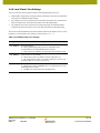
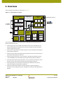
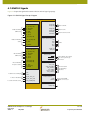
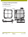
1
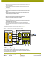
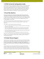
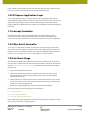
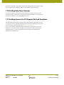
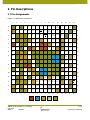
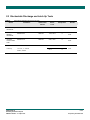
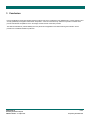
ADVANCED PRODUCT DISCONTINUANCE NOTIFICATION Date: March 10, 2015 P1/2 Semtech Corporation, 200 Flynn Road, Camarillo CA 93012 ☒ Semtech Canada Corporation, 4281 Harvester Road, Burlington, Ontario L7L 5M4 Canada Semtech Irvine, 5141 California Ave., Suite 100, Irvine CA 92617 Semtech Neuchatel Sarl, Route des Gouttes d’Or 40, CH-2000 Neuchatel Switzerland Nanotech Semiconductor, Semtech Corporation, 2 West Point Court, Bristol, United Kingdom, BS32 4PY Semtech Corpus Christi SA de CV, Carretera Matamorros Edificio 7, Reynosa, Tamaulipas, Mexico 88780 Product Discontinuance Details Purpose, Description and Effect of Change: Due to unforeseen supply constraints, we are no longer able to supply the GN4121-CBE3 x1 Lane PCIe Bridge to Local Bus device. However, we are able to supply the GN4124-CBE3 x4 Lane PCIe Bridge to Local Bus device as a fully compatible drop in replacement part. The GN4121 and GN4124 parts are physically identical and share the same manufacturing flow and final test process. Only the part number marking on the package distinguishes the difference between the two products. All reliability and qualification data is identical for both part numbers. In light of this, we would like all existing GN4121 customers to switch to the GN4124 with immediate effect. Existing GN4121 designs will have ball E4 tied to 3.3V VCC, which will configure the GN4124 to operate as a GN4121 in x1 PCIe mode. Therefore, no design or PCB changes are required. The GN4124 will be functionally identical to the GN4121 in a GN4121based x1 PCIe application. Formal End of Life Notification will follow upon review of customer feedback. Customer Part Number(s) Affected: ☒ N/A Part Number(s) Affected: GN4121-CBE3 Replacement or Alternate Part Number(s) N/A or Not Offered GN4124-CBE3 Last Time Buy (LTB) Date Sample Availability of Alt. Part NA Must Accept Final Delivery by NA Now Qualification Report Availability of Alt. Part Now Supporting Documents for Alternate or Replacement parts/Attachments: 1. GN4124-CBE3 Datasheet (GENDOC-048407) 2. GN4124-CBE3 Reliability Qualification Report (GENDOC-052220) Semtech Corporation • 200 Flynn Road • Camarillo • Ca • 93012 • Phone +1 (805) 498-2111 ADVANCED PRODUCT DISCONTINUANCE NOTIFICATION Date: March 10, 2015 P2/2 Additional Provisions We regret the inconvenience and impact this notice may cause your company. Semtech’s sales, marketing, and distribution personnel stand ready to assist you in placing your company’s final orders, or in providing the product information you require. For product inquiries or purchase order information, please contact your local Semtech sales representative. Issuing Authority Semtech Business Unit: Semtech Contact Info: SIPG Luis Blanco Semtech Corporation Sr. Manager, Quality Engineering 4281 Harvester Road Burlington, ON L7L 5M4 [email protected] Office: (905) 632-7253 Fax: (905) 632-2055 FOR FURTHER INFORMATION & WORLDWIDE SALES COVERAGE: http://www.semtech.com/contact/index.html#support Semtech Corporation • 200 Flynn Road • Camarillo • Ca • 93012 • Phone +1 (805) 498-2111 GN4124 x4 Lane PCI Express to Local Bridge Data Sheet GN4124 x4 Lane PCI Express to Local Bridge Data Sheet 48407 - 1 May 2009 www.gennum.com 1 of 31 Proprietary & Confidential Revision History Version ECR Date Changes and Modifications 2 151915 May 2009 Created new document describing functionality and the register map for GN4124 & GN4121 devices. These common sections have been removed. 1 151527 May 2009 It is now a Data Sheet. Added the content of the document: GN4124 x4 PCI Express to Local Bus Bridge User Manual (Document ID: 47719) to this data sheet. This User Manual is no longer a stand-alone document. Changed some parameters in Table 2-1 (EEPROM_EN), Table 3-2, Table 3-3, Table 5-2 and Table 13-2. Changed Figure 4-2, Figure 6-2, Figure 7-1 and Figure 9-16. Modified descriptions in 9.4 Operation, 9.7.3 FCL FPGA Configuration and 9.7.4 FCL FSM FPGA Configuration. Changes to registers to PCI_BAR0_LOW, PCI_BAR2_LOW, PCI_BAR2_HIGH, PCI_BAR4_LOW, PCI_BAR4_HIGH, PCI_SUB_VENDOR, PCI_SUB_SYS, PCIE_DEVICE_CAP, PCIE_DCR, INT_CTRL, INT_STAT, INT_CFG0-7, GPIO_DIRECTION_MODE, GPIO_OUTPUT_ENABLE, GPIO_OUTPUT_VALUE, GPIO_INT_MASK, GPIO_INT_MASK_CLR (Note: formerly GPIO_INT_ENABLE), GPIO_INT_MASK_SET (Note: formerly GPIO_INT_DISABLE), GPIO_INT_STATUS, GPIO_INT_TYPE, GPIO_INT_VALUE, GPIO_INT_ON_ANY and FCL_CTRL. D 151519 March 2009 Clarified output voltage and local bus timing in Table 3-6 and Table 3-11. C 150789 December 2008 Corrected pin assignments and definitions. Updated electrical characteristics. Corrected Figure 2-2. Updated Local Bus Interface clock range. B 150182 August 2008 Corrected pin assignments, part number and other updates. A 148626 May 2008 New document. Contents 1. Introduction.....................................................................................................................................................4 1.1 Features ...............................................................................................................................................4 1.2 Live on Power-up ..............................................................................................................................5 1.3 FPGA On-the-Fly Configuration Loader ...................................................................................6 1.4 Local Bus Interface ...........................................................................................................................6 1.5 Virtual Channel Support ................................................................................................................6 1.6 PCI Express Application Layer ....................................................................................................7 1.7 Interrupt Controller .........................................................................................................................7 1.8 2-Wire Serial Controller .................................................................................................................7 1.9 Data Sheet Usage ..............................................................................................................................7 1.10 Getting Help from Gennum ........................................................................................................8 GN4124 x4 Lane PCI Express to Local Bridge Data Sheet 48407 - 1 May 2009 2 of 31 Proprietary & Confidential 1.11 Getting Answers to PCI Express Related Questions ...........................................................8 2. Pin Descriptions .............................................................................................................................................9 2.1 Pin Assignments ................................................................................................................................9 2.2 Pin Descriptions ............................................................................................................................. 10 3. Electrical Characteristics ......................................................................................................................... 16 3.1 Absolute Maximum Ratings ....................................................................................................... 16 3.2 Operating Conditions ................................................................................................................... 16 3.3 DC Electrical Characteristics ..................................................................................................... 17 3.4 PCI Express Electrical Characteristics .................................................................................... 18 3.4.1 PCI Express Transmitter Characteristics ................................................................... 18 3.4.2 PCI Express Receiver Characteristics ......................................................................... 21 3.4.3 Local Bus Timing................................................................................................................ 22 3.4.4 Local Clocks’ Pins Settings.............................................................................................. 24 4. Overview....................................................................................................................................................... 25 4.1 GN4124 Signals .............................................................................................................................. 26 5. Package & Ordering Information .......................................................................................................... 27 5.1 Package Dimensions ..................................................................................................................... 27 5.2 Packaging Data ............................................................................................................................... 28 5.3 Ordering Information ................................................................................................................... 28 GN4124 x4 Lane PCI Express to Local Bridge Data Sheet 48407 - 1 May 2009 3 of 31 Proprietary & Confidential GN4124 x4 Lane PCI Express to Local Bridge Data Sheet 1. Introduction For the past decade, PCI has been a dominant interconnect for both PC and embedded systems. With the shift to high-speed serial interfaces, PCI Express® is quickly replacing parallel PCI. As a leader in providing solutions for high-speed serial communications, Gennum has developed the GN4124 family of PCI bridge controller components to complement FPGA devices. The GN4124 is specifically designed to take advantage of the architectural features of low-cost FPGA devices that do not have PCI Express capable SerDes on-chip. The result is a low-cost bridging solution for high-performance native PCI Express bridging. The GN4124 is a desirable companion to large FPGA devices, where the requirement for firmware upgrading and on-the-fly reconfiguration are required. The GN4124 is a 4-lane PCI Express to local bus bridge that is designed to work as a companion for FPGA devices to provide a complete bridging solution for general applications. In addition to a 4-lane PCI Express compliant PHY interface, the GN4124 contains the link and transaction layers, and an applications interface that is ideally suited to FPGA interfacing using a small number of pins. Since the PCI Express transaction/link IP is hard-wired into the GN4124, there is no need to license PCIe IP. The level of integration and very low power operation of the GN4124 make it an ideal alternative to using a PIPE PHY, where IP licensing and the cost of FPGA resources and power consumption is unattractive by comparison. Using the GN4124, allows FPGA resources to be spent on what differentiates the product, rather than on implementing the PCI Express protocol. 1.1 Features • 4 Lane PCI Express interface Complies with PCI Express Base Specification 1.1 On-chip PHY, transaction, and link layer eliminates the cost of IP licensing Two hardware virtual channels supported Payload size of up to 512 bytes with up to three outstanding transactions in each direction Supports 3x64-bit base address registers Provides flexible power management capability • Provides pin efficient local bus interface for easy attachment to popular low-cost FPGA devices Uses DDR SSTL I/O for high-speed data transfer (up to 800MB/s) GN4124 x4 Lane PCI Express to Local Bridge Data Sheet 48407 - 1 May 2009 www.gennum.com 4 of 31 Proprietary & Confidential FPGA source code provided for 64-bit master/target read/write buses for easy user logic attachment Local bus may be operated asynchronously to the PCIe clock rate for power optimization • “Live” on power up On-chip type 0 PCI configuration space enables auto detection without FPGA activity On-chip extended configuration space supports power management, serial number, MSI, and PCIe capability registers • FPGA bitstream loader Allows easy configuration of the attached FPGA through PCIe Provides on-the-fly FPGA reconfiguration capability • 2-wire master/target Boot master mode allows PCI configuration space defaults to be loaded from a small EEPROM upon system reset General master mode allows attached 2-wire devices to be read/written Target mode allows internal registers to be accessed from an external circuit or processor A simplified block diagram of the GN4124 chip is shown in Figure 1-1. Figure 1-1: GN4124 with FPGA Simplified Block Diagram FPGA Pin Efficient Local Bus GN4124 Clock Boundary PCI Express Core TX Data Master DDR SSTL RX Data User Application IP Gennum Local Bus IP Target Streamlined Application Layer with Buffering Data Buffers Control SDR SSTL Local Clock Gen TL DLL PHY x4 Lanes PCI Configuration and Extended Registers FPGA Cfg. Loader I 2C M/T GPIO Serial Programming Interface 1.2 Live on Power-up Since the GN4124 contains a complete type 0 PCI configuration space, it is live on power-up so that a plug-and-play BIOS can auto-detect it and enumerate it without an attached FPGA having to be configured. GN4124 x4 Lane PCI Express to Local Bridge Data Sheet 48407 - 1 May 2009 5 of 31 Proprietary & Confidential 1.3 FPGA On-the-Fly Configuration Loader An FPGA bitstream may be downloaded from the host system over PCIe to the attached FPGA using the on-chip FPGA configuration loader. This eliminates the expense of a dedicated FPGA ROM and makes on-the-fly reconfiguration and firmware upgrades simple. The ability to dynamically configure an attached FPGA over PCIe makes the GN4124 an ideal companion to all ranges of FPGA devices, including large SerDes capable devices, that require reconfiguration or firmware upgrades over PCIe. 1.4 Local Bus Interface The local bus interface uses a combination of single and dual data rate SSTL I/O to accomplish very high data rates in the fewest possible pins. A singe data rate clock is used for SSTL control signals and separate dual data rate source synchronous clocking is used for the DDR SSTL data. The SDR control signals operate at up to 200MHz and the DDR I/O operate at up to 400MT/s across 16 bits using a 200MHz DDR clock. This provides 800MB/s in each direction. The local bus may operate asynchronously from the PCI Express rate. In order to save power, the local bus clock can operate at the lowest possible rate required by an application. The local bus protocol facilitates four types of transactions: • PCIe-to-Local Target Writes: A PCIe agent (such as the host processor/root complex) writes data to the local bus. • PCIe-to-Local Target Reads: A PCIe agent reads data from the local bus. Reads are split into a request phase (address phase) and a completion phase (data phase). • Local-to-PCIe Master Writes: The attached FPGA writes data to a PCIe device (such as host memory via a root complex). • Local-to-PCIe Master Reads: The attached FPGA reads data from a PCIe device. The PCIe-to-Local transactions would typical involve a target controller implemented in the FPGA. Local-to-PCIe Master transactions allow a DMA controller in the FPGA to access PCI Express devices. 1.5 Virtual Channel Support The GN4124 has two independent virtual channels that support the eight PCIe defined traffic classes. This enables high local bus utilization by supporting non-blocking traffic between virtual channels. This is accomplished with separate on-chip buffering resources for each of the two virtual channels. For example, when write buffering is full for VC0 and VC1 has room, then VC1 traffic may proceed without reference to the state of VC0. Virtual channels may be used to separate different types of application traffic. For example, a DMA engine in the FPGA may be aggressively reading and writing host memory to stream video data. At the same time another agent in the FPGA may need to communicate low bandwidth, latency sensitive synchronization information. If the two GN4124 x4 Lane PCI Express to Local Bridge Data Sheet 48407 - 1 May 2009 6 of 31 Proprietary & Confidential types of traffic are segregated in terms of virtual channels and traffic classes, then the low latency traffic can be allowed to pass the high bandwidth traffic. 1.6 PCI Express Application Layer The on-chip applications layer transfers data between the PCI Express port and an attached FPGA using the local bus interface. It provides a mechanism to access internal registers through configuration space access and through one of the Base Address Registers (BAR4). The applications layer supports the transmission of message signalled interrupts. 1.7 Interrupt Controller A flexible interrupt controller automatically generates PCIe message signalled interrupts from either external pins (GPIO pins) or internally generated interrupt sources. The interrupt controller can route any interrupt source to up to four GPIO pins. 1.8 2-Wire Serial Controller An on-chip I2C compatible controller provides both a master and target mode. After device reset, default configuration register values, such as Subsystem Vendor ID and BAR sizes, can be automatically loaded from a small serial EEPROM. After initialization, an external 2-wire master can access on-chip registers to read/write them. 1.9 Data Sheet Usage The GN4124 Data Sheet includes detailed specifications on GN4124 device. However, there are other complementary documents to assist designers available on the Gennum Web site: www.gennum.com/mygennum. A complete set of documentation includes the following: • GN4124 Data Sheet (this document) • GN412x PCI Express Family Reference Manual (Document ID: 52624), which provides the details on functionality and the register map associated with the GN412x family of chips • GN4124 Master List of Documents & Electronic Files (Document ID: 52423), which provides a summary of the content of the documentation & electronic files, to help navigate the content on MyGennum • Reference Design Kit (RDK) board and the asssociated documentation Following chapters detail the specifications of the GN4124: • 2. Pin Descriptions • 3. Electrical Characteristics • 5. Package & Ordering Information Before finalizing a system design based on the GN4124, please contact Gennum to verify that you have the most recent specifications. GN4124 x4 Lane PCI Express to Local Bridge Data Sheet 48407 - 1 May 2009 7 of 31 Proprietary & Confidential Gennum is constantly trying to improve the quality of its product documentation. If you have any questions or comments, please contact Gennum Technical Support. 1.10 Getting Help from Gennum For technical support, contact Gennum by telephone or e-mail. E-mail ensures the quickest response. The most up-to-date technical support information is also posted on the Gennum website. E-mail: [email protected]. 1.11 Getting Answers to PCI Express Related Questions This data sheet assumes a basic understanding of the PCI Express Specification. If you are looking for a copy of the specification please contact the PCI Special Interest group at 503-619-0569 or visit their Web site at: http://www.pcisig.com. If you are not familiar with the PCI Express specification, a good place to start is by reading one of several books on the subject. One of the most popular is PCI Express System Architecture written by Tom Shanley, Don Anderson, and Ravi Budruk (published by MindShare Inc.). GN4124 x4 Lane PCI Express to Local Bridge Data Sheet 48407 - 1 May 2009 8 of 31 Proprietary & Confidential 2. Pin Descriptions 2.1 Pin Assignments Figure 2-1: GN4124 Pin Assignment 1 2 3 4 5 6 7 8 9 10 11 12 13 14 15 16 A VSS_ PCIE PERn0 VSS_ PCIE DBG0 DBG7 GPIO15 GPIO9 SPRI_CLK TDI GPIO7 GPIO6 SPRI_ DONE GPIO4 TDO PLL_TEST _OUT VSS A B VDD_ PCIE PERp0 NC DBG2 DBG6 GPIO13 GPIO14 RSTIN GPIO8 SPRI_ DATAOUT SCLK TRST SPRI_XI_ SWAP SPRI_ STATUS VSS L2P_ DATA15 B C PETp0 VSS_ PCIE VDD_ PCIE VSS DBG5 DBG1 GPIO12 GPIO10 RSTOUT 33 GPIO2 SPRI_ CONFIG SDATA LB_REF_ CLK_MO VSS L2P_ DATA7 L2P_ DATA14 C D PETn0 VSS_ PCIE VDD_ PCIE VSS VDDC SCAN_EN DBG3 VDDC GPIO3 NC GPIO1 LB_REF_ CLK_MI VDDC NC L2P_ DATA6 VDDC D E VDDP PETn1 VSS_ PCIE VSS EEPROM TEST_EN _EN DBG4 VCCO33 VCCO33 VDDC GPIO5 GPIO0 VDDC NC L2P_ DATA5 L2P_ DATA13 E F VTT_AB PETp1 VSS_ PCIE NC VDDW VDDC GPIO11 VCCO33 VCCO33 TMS TCK VDDC VDDC L2P_RDY L2P_ DATA4 L2P_ DATA12 F G PERp1 VSS_ PCIE VDDAUX VSS PECLKINp VSS VSS VSS VSS VSS VSS VDDC NC L2P_EDB L2P_ CLKn L2P_ CLKp G H PERn1 VSS_ PCIE PCIE_ VDDA VDDC PECLKINn VSS VSS VSS VSS VSS VCCO18 VCCO18 VSS L2P_ DFRAME VDDC L2P_ VALID H J PERn2 VSS_ PCIE PCIE_ VDDA VSS VSS NC VSS VSS VSS VSS VCCO18 VCCO18 VDDC L_WR_ RDY1 L2P_ DATA3 L2P_ DATA11 J K PERp2 VSS_ PCIE VSS VDDP VDDW LCLK_ MODE3 VSS VSS VSS VSS VSS VSS NC L_WR_ RDY0 VDDC L2P_ DATA10 K L VSS PETp2 VSS_ PCIE LCLK_ MODE2 VDDC VDDC NC VCCO18 VCCO18 VDDC VSS VSS VDDC P_RD_ D_RDY1 L2P_ DATA2 L2P_ DATA9 L M VTT_CD PETn2 VSS_ PCIE LCLK_ MODE1 LCLK_ MODE0 VDDC VSS VCCO18 VCCO18 VDDC VSS VSS NC P_RD_ D_RDY0 L2P_ DATA1 VDDC M N PETn3 VSS_ PCIE VDD_ PCIE NC VSS RX_ ERROR NC VDDC P_WR _RDY1 P_WR _RDY0 PLL_ AVSS TX_ ERROR L2P_ DATA0 L2P_ DATA8 N P PETp3 VSS_ PCIE VDD_ PCIE VSS P2L_ DATA15 VDDC P2L_ VALID P_WR _REQ1 VC_ RDY1 VC_ RDY0 VDDC LCLK VDDC RSTOUT 18 P R VDD_PCIE PERp3 VSS VREF P2L_ DATA10 P2L_ DATA9 P2L_ DATA8 NC VSS LCLKn R T VSS_PCIE PERn3 VSS_PCIE VDDC P2L_ DATA7 P2L_ DATA6 P2L_ DATA5 P2L_ DATA4 P2L_ DATA3 P2L_ DATA2 P2L_ DATA1 VDDC P2L_ DATA0 PLL_ AVDD NC VSS T 1 2 3 4 5 6 7 8 9 10 11 12 13 14 15 16 VDDC P_WR _REQ0 P2L_CLKp P2L_RDY P2L_ P2L_ P2L_ P2L_ P2L_ P2L_CLKn DATA11 DATA14 DATA13 DATA12 DFRAME 3.3V GN4124 x4 Lane PCI Express to Local Bridge Data Sheet 48407 - 1 May 2009 1.8V 1.2V 900mV 0V 9 of 31 Proprietary & Confidential 2.2 Pin Descriptions Table 2-1: GN4124 Pin Descriptions Group Global Pin No. B8 No. of Pins 1 Pin Name RSTIN I/O I Description Global Asynchronous Reset (Active LOW). LVCMOS, 3.3V, input, hysteresis. C9 1 RSTOUT33 O Reset Output; 3.3V (Active LOW). 3.3 V LVCMOS, totem-pole. D12 1 LB_REF_CLK_MI I Local Bus Reference Clock Crystal or Oscillator Input. C13 1 LB_REF_CLK_MO O Local Bus Reference Clock Crystal feedback output. Functional mode only. H3, J3 2 PCIE_VDDA P Clock Reference Analog Supply. (1.2V) G5, H5 2 PECLKINp, PECLKINn I PCIe Reference Clock Signal. For a PCI Express add-in card, these signals should be driven by the card edge connector and AC coupled using 150nF capacitors. E5 1 EEPROM_EN I Used to report that EEPROM is present. (1 = present) LVCMOS, 3.3V, input. EEPROM_EN should be tied HIGH, to allow the internal GN4124 registers to load on power up from the EEPROM. Refer to Initialization from a 2-Wire EEPROM from on what is required for EEPROM boot up options. GN4124 x4 Lane PCI Express to Local Bridge Data Sheet 48407 - 1 May 2009 10 of 31 Proprietary & Confidential Group Global: Test Interface Pin No. A9 No. of Pins 1 Pin Name TDI I/O I Description JTAG Test Data Input. LVCMOS, 3.3V, input, pull-up. F10 1 TMS I JTAG Test Mode Select Input. LVCMOS, 3.3V, input, pull-up. F11 1 TCK I JTAG Test Clock. LVCMOS, 3.3V, input. B12 1 TRST I JTAG Test Reset. LVCMOS, 3.3V, input, hysteresis, pull-up. A14 1 TDO O JTAG Test Data Output. LVTTL, 3.3V, output, 6mA, tristate. D6 1 SCAN_EN I Scan Enable (Tied LOW for normal operations). LVCMOS, 3.3V, input, pull-down. E6 1 TEST_EN I Test Mode Enable (Tied LOW for normal operations). LVCMOS, 3.3V, input, pull-down. A15 1 PLL_TEST_OUT I/O PLL Test Output (No connect for normal operations). LVCMOS, 3.3V, bidirectional, 4mA, tristate. Global: 2-Wire Interface B11 1 SCLK I/O Two-wire Clock port. LVCMOS, 3.3V, bidirectional, 4mA, tristate. C12 1 SDATA I/O Two-wire Data port. LVCMOS, 3.3V, bidirectional, 4mA, tristate. Global: General Purpose Interface A6, B7, B6, C7, F7, C8, A7, B9, A10, A11, E11, A13, D9, C10, D11, E12 16 Global: Debug Interface A5, B5, C5, E7, D7, B4, C6, A4 8 GPIO[15:0] I/O General Purpose Input/Output. LVCMOS, 3.3V, bidirectional, 4mA, tristate. GN4124 x4 Lane PCI Express to Local Bridge Data Sheet 48407 - 1 May 2009 DBG[7:0] I Debug Bus Port (Tied LOW for normal operations). LVCMOS, 3.3V, input, pull-down. 11 of 31 Proprietary & Confidential Group Global: Serial Programming Interface Pin No. A8 No. of Pins 1 Pin Name SPRI_CLK I/O I/O Description Serial Programming Interface (FPGA Configuration Loader). LVCMOS, 3.3V, bidirectional, 12mA, tristate. B10 1 SPRI_DATAOUT I/O Serial Programming Interface (FPGA Configuration Loader). LVCMOS, 3.3V, bidirectional, 12mA, tristate. C11 1 SPRI_CONFIG I/O Serial Programming Interface (FPGA Configuration Loader). LVCMOS, 3.3V, bidirectional, 12mA, tristate. A12 1 SPRI_DONE I/O Serial Programming Interface (FPGA Configuration Loader). LVCMOS, 3.3V, bidirectional, 12mA, tristate. B13 1 SPRI_XI_SWAP I/O Serial Programming Interface (FPGA Configuration Loader). LVCMOS, 3.3V, bidirectional, 12mA, tristate. B14 1 SPRI_STATUS I/O Serial Programming Interface (FPGA Configuration Loader). LVCMOS, 3.3V, bidirectional, 12mA, tristate. PCI Express Link: PCIe x4 PHY interface A1, A3, C2, D2, E3, F3, G2, H2, J2, K2, L3, M3, N2, P2, T1, T3 16 VSS_PCIE G B1, C3, D3, N3, P3, R1 6 VDD_PCIE P G3 1 PHY VSS. PHY VDD. 1.2V (Core) VDDAUX P PHY VDDAUX. 1.2V F1 1 VTT_AB P PCIe PHY transmit termination lanes A/B. Driven to voltage VTT. 1.5V See Table 3-6. M1 1 VTT_CD P PCIe PHY transmit termination lanes C/D. Driven to voltage VTT. 1.5V See Table 3-6. PCI Express Link: PCIe Transmit [Output from the device] N1, M2, E2, D1 4 PETn[3:0] O PCIe Transmit -Bus Lane A. CML P1, L2, F2, C1 4 GN4124 x4 Lane PCI Express to Local Bridge Data Sheet 48407 - 1 May 2009 PETp[3:0] O PCIe Transmit +Bus Lane A. CML 12 of 31 Proprietary & Confidential Group PCI Express Link: PCIe Receive [Input to the device] Pin No. T2, J1, H1, A2 No. of Pins 4 Pin Name PERn[3:0] I/O I Description PCIe Receive -Bus Lane A. CML Note: PERp[3:0] / PERn[3:0] each receiver lane can be connected using either the indicated polarity, or inverted polarity. Inverted polarity may be chosen in order to simplify the PCB layout by avoiding signal crossover and additional PCB vias. The GN4124 will automatically detect and compensate for polarity inversion during link training. R2, K1, G1, B2 4 PERp[3:0] I PCIe Receive +Bus Lane A. CML Local Bus P14, R16 2 LCLK, LCLKn O Local Bus Clock. SSTL, 1.8V, differential K6, L4, M4, M5 4 LCLK_MODE[3:0] I Selects the clock mode. LVCMOS, 3.3V, input, pull-down. P16 1 RSTOUT18 O Reset Output; 1.8V (Active LOW). CMOS, 1.8V, output Local Bus: PCIe to Local [Inbound Data] P9 1 P2L_RDY I Rx Buffer Full Flag. SSTL, 1.8V, input, with ODT. P5, R4, R5, R6, R9, R11, R12, R13, T5, T6, T7, T8, T9, T10, T11, T13 16 R7 1 P2L_DATA[15:0] O Parallel Receive Data. SSTL, 1.8V, output P2L_DFRAME O Receive Frame. SSTL, 1.8V, output P7 1 P2L_VALID O Receive Data Valid. SSTL, 1.8V, output P8, R8 2 GN4124 x4 Lane PCI Express to Local Bridge Data Sheet 48407 - 1 May 2009 P2L_CLKp, P2L_CLKn O Receiver Source Synchronous Clock. SSTL, 1.8V, output, differential 13 of 31 Proprietary & Confidential Group Local Bus: Inbound Buffer Request/Status Pin No. P10, N9 No. of Pins 2 Pin Name P_WR_REQ[1:0] I/O O Description PCIe Write Request. SSTL, 1.8V, output N11, N12 2 P_WR_RDY[1:0] I PCIe Write Ready. SSTL, 1.8V, input, with ODT. N6 1 RX_ERROR I Receive Error. SSTL, 1.8V, input, with ODT. P11, P12 2 VC_RDY[1:0] O Virtual Channel Ready Status. This provides a VC_RDY output to indicate the DL_UP1 status of the Virtual Channel. This can be used to provide a synchronous reset to the external application in the event one of the Virtual Channels goes down e.g. hot reset initiated by PCIe host. SSTL, 1.8V, output Local Bus: Local PCIe [Outbound Data] B16, C16, E16, F16, J16, K16, L16, N16, C15, D15, E15, F15, J15, L15, M15, N15 16 H14 1 L2P_DATA[15:0] I Parallel Transmit Data. SSTL, 1.8V, input, with ODT. L2P_DFRAME I Transmit Data Frame. SSTL, 1.8V, input, with ODT. H16 1 L2P_VALID I Transmit Data Valid. SSTL, 1.8V, input, with ODT. G14 1 L2P_EDB I End-of-Packet Bad Flag. When a packet is considered bad and is terminated with EDB. SSTL, 1.8V, input, with ODT. G16, G15 Local Bus: Outbound Buffer Status F14 2 1 L2P_CLKp, L2P_CLKn I L2P_RDY O Transmitter Source Synchronous Clock. SSTL, 1.8V, input, differential, with ODT. Tx Buffer Full Flag. SSTL, 1.8V, output J14, K14 2 L_WR_RDY[1:0] O Local-to-PCIe Write. SSTL, 1.8V, output L14, M14 2 P_RD_D_RDY[1:0] O PCIe-to-Local Read Response Data Ready. SSTL, 1.8V, output N14 1 TX_ERROR O Transmit Error. SSTL, 1.8V, output GN4124 x4 Lane PCI Express to Local Bridge Data Sheet 48407 - 1 May 2009 14 of 31 Proprietary & Confidential Group Power Ground Pin No. No. of Pins Pin Name I/O Description F5, K5 2 VDDW P 3.3V R10 1 VREF P 900mV reference voltage for SSTL I/O T14 1 PLL_AVDD P 1.2V PLL supply voltage D5, D8, D13, D16, E10, E13, F6, F12, F13, G12, H4, H15, J13, K15, L5, L6, L10, L13, M6, M10, M16, N8, N10, P6, P13, P15, T4, T12 28 VDDC P 1.2V core power E1, K4 2 VDDP P 3.3V H11, H12, J11, J12, L8, L9, M8, M9 8 VCCO18 P Power for 1.8V I/O E8, E9, F8, F9 4 VCCO33 P Power for 3.3V I/O N13 1 PLL_AVSS G PLL Ground. This pin is internally connected to VSS and, for noise isolation, should not be connected to VSS externally. Refer to the Gullwing RDK schematics and PCB layout for proper implementation. No Connect A16, B15, C4, C14, D4, E4, G4, G6, G7, G8, G9, G10, G11, H6, H7, H8, H9, H10, H13, J4, J5, J7, J8, J9, J10, K3, K7, K8, K9, K10, K11, K12, L1, L11, L12, M7, M11, M12, N5, P4, R3, R15, T16 43 VSS G Ground. B3, D10, D14, E14, F4, G13, J6, K13, L7, M13, N4, N7, R14, T15 14 NC — No Connect. 1. Data Link Layer indicates that a connection with the upstream devices has been established. GN4124 x4 Lane PCI Express to Local Bridge Data Sheet 48407 - 1 May 2009 15 of 31 Proprietary & Confidential 3. Electrical Characteristics 3.1 Absolute Maximum Ratings Table 3-1: Absolute Maximum Ratings Parameter Value Core Supply Voltage -0.5V to +1.8 VDC SSTL IO Supply Voltage -0.5V to +2.5 VDC LVCMOS IO Supply Voltage -0.5V to +4.6 VDC Input ESD Voltage (HBM) 2kV Storage Temperature Range -50°C < Ts < 125°C Solder Reflow Temperature 260°C 3.2 Operating Conditions Table 3-2: Operating Conditions All electrical characteristics are valid over the range of these operating conditions, unless otherwise noted. Parameter Symbol Conditions Min Typ Max Units Notes Core Supply Voltage on pins VDDC, VDD_PCIE, VDDAUX, PLL_AVDD, PCIE_VDDA VCORE – 1.14 1.2 1.26 V ±5% SSTL IO Supply Voltage on pins VCCO18 VVCCO18 – 1.71 1.8 1.89 V ±5% LVCMOS IO and 3.3V Core Supply Voltage: pins VCCO33, VDDW, VDDP VVCCO33 – 3.0 3.3 3.6 V ±10% Operating Temperature Range TA Ambient 0 25 85 °C GN4124 x4 Lane PCI Express to Local Bridge Data Sheet 48407 - 1 May 2009 16 of 31 Proprietary & Confidential 3.3 DC Electrical Characteristics Table 3-3: DC Electrical Characteristics Power and current limits listed have been derived from design and characteristics data. They are not 100% tested in production. Parameter Power Consumption Symbol PD Conditions Min Typ Max Units Notes PCIe x4, LCLK=200MHz – 650 950 mW 1 PCIe x4, LCLK=100MHz – 600 – mW 2 PCIe x1, LCLK=100MHz – 475 – mW 3 – – 1104 – mA – Total Core Supply Current on pins VDDC, VDD_PCIE, VDDAUX, PLL_AVDD, PCIE_VDDA ICORE SSTL IO Supply Current IVCCO18 – – 3406 – (See Note 5) mA – LVCMOS IO and 3.3V Core Supply Current: pins VCCO33, VDDW, VDDP IVCCO33 – – 907 – (See Note 5.) mA – (See Note 5) 1. Data is based on an application circuit equivalent to that used on the GN4124 RDK board (Gullwing), typical operating conditions, PCIe negotiated to 4 lanes, default PCIe PHY settings, 200MHz local bus operation, and with concurrent data traffic at 75% bus utilization. Doesn’t include power dissipated by components outside of the GN4124. 2. See Note 1. Typical operating conditions, 100MHz local bus operation. 3. See Note 1. Typical operating conditions, 100MHz local bus operation, PCIe negotiated to 1 lane. 4. This information is intended to guide power supply design. Data is based on an application circuit equivalent to that used on the GN4124 RDK board (Gullwing), typical operating conditions, 200MHz local bus operation, and with concurrent data traffic at 75% bus utilization. 5. Maximum supply current will vary greatly depending on the application circuit and device usage. A specific application’s maximum current can be be predicted by measuring current under high temperature, high supply and full load conditions. To this resultant number, the following factors needed to be added: +25% for ICORE +35% for IVCCO18 +25% for IVCCO33 6. See Note 4. Based on use of 22-ohm serial termination and 51-ohm parallel termination in the application circuit. 7. See Note 4. Also includes current draw from an LDO used to power VTT_AB and VTT_CD. GN4124 x4 Lane PCI Express to Local Bridge Data Sheet 48407 - 1 May 2009 17 of 31 Proprietary & Confidential Table 3-4: DC Electrical Characteristics for LVCMOS Buffers Parameter Symbol Conditions Min Typ Max Units Notes High-level input voltage VIH – 2 – – V – Low-level input voltage VIL – – – 0.8 V – Input leakage current IL – – – ±5 μA – High-level output voltage VOH IOH = -100 μA 2.8 – – V – Low-level output voltage VOL IOL = 100 μA – – 0.2 V – Table 3-5: DC Electrical Characteristics for SSTL Buffers Parameter Symbol Conditions Min Typ Max Units Notes VREF input reference voltage VREF – 833 900 969 mV 1 SSTL termination voltage VTT – VREF-40 VREF VREF+40 mV 2 High-level input voltage (DC) VIH – VREF+125 – VVCCO18+ 300 mV – Low-level input voltage (DC) VIL – -300 – VREF-125 mV – High-level input voltage (AC) VIH – VREF+250 – – mV – Low-level input voltage (AC) VIL – – – VREF-250 mV – 1. Typically the value of VREF is expected to be 50% * VDDQ of the transmitting device. Peak to peak AC noise on VREF may not exceed +/- 2% of VREF. 2. The termination voltage VTT should track the reference voltage VREF. 3.4 PCI Express Electrical Characteristics 3.4.1 PCI Express Transmitter Characteristics Table 3-6: Transmitter Characteristics Symbol Description Min Typical Max Unit Voltage Parameters VTX-DIFF1 Output voltage compliance @ typical swing VTX-DIFFp (peak-to-peak, single ended) 400 500 600 mV VTX-DIFFpp (peak-to-peak, differential) 800 1000 1200 mV VTT Transmitter termination voltage 1.2 1.5 1.89 V VOL Low-level output voltage – VTT - 1.5 * VTX-DIFFp – V GN4124 x4 Lane PCI Express to Local Bridge Data Sheet 48407 - 1 May 2009 18 of 31 Proprietary & Confidential Symbol Description Min Typical Max Unit VOH High-level output voltage – VTT - 0.5 * VTX-DIFFp – V VTX-DC-CM Transmit common-mode voltage 0 VTT - VTX-DIFFp 3.6 V VTX-CM-DCACTIVE- Absolute Delta of DC Common Mode Voltage During L0 and Electrical Idle. – – 100 mV VTX-DE-RATIO De-emphasized differential output voltage 0 -3.35 -7.96 dB2 VTX-IDLE-DIFFp Electric Idle differential peak voltage – – 20 mV VTX-RCV-DETECT Voltage change during Receive Detection – – 600 mV RLTX-DIFF Transmitter Differential Return loss 10 – – dB RLTX-CM Transmitter Common Mode Return loss 6 – – dB ZOSE Single-ended output impedance 40 50 60 Ω ZTX-DIFF-DC DC Differential TX Impedance 80 100 120 Ω TTX-RISE, TTX-FALL Rise / Fall time of TxP, TxN outputs .125 – UI Unit Interval 399.88 400 400.12 ps4 TTX-MAX-JITTER Transmitter total jitter (peak-to-peak) – – 0.305 UI TTX-EYE Minimum TX Eye Width (1 - TTX-MAX-JITTER) 0.70 – – UI TTX-EYE-MEDIAN-to-MAX- Maximum time between the jitter median and maximum deviation from the median – – 0.15 UI LTX-SKEW Transmitter data skew between any 2 lanes 0 – 2UI + 200ps ps TTX-IDLE-SET-TO-IDLE Maximum time to transition to a valid electrical idle after sending an Electrical Idle ordered set – 4 6 ns TEIExit Time to exit Electrical Idle (L0s) state into L0 – 12 16 ns IDLEDELTA UI3 Jitter Parameters JITTER Timing Parameters 1. Measured with Vtt = 1.2V, PHY_CONTROL register bits HIDRV=’0’, LODRV=’0’ and DTX=”0000”(1x). 2. The de-emphasis ratio is determined through the DEQ bits of the PHY_CONTROL register inside the GN4124. Typical value is based on recommended setting of the PHY_CONTROL register. 3. As measured between 20% and 80% points. 4. UI does not account for SSC dictated variations. 5. Measured using PCI Express Compliance Pattern. GN4124 x4 Lane PCI Express to Local Bridge Data Sheet 48407 - 1 May 2009 19 of 31 Proprietary & Confidential Figure 3-1: Typical Transition Signal Eye, De-emphasis Disabled, Default Drive Setting The eye diagram is generated from SIGtest Version 2.1 available from the PCI Special Interest Group. Figure 3-2: Typical Non-Transition Signal Eye, De-emphasis Disabled, Default Drive Setting GN4124 x4 Lane PCI Express to Local Bridge Data Sheet 48407 - 1 May 2009 20 of 31 Proprietary & Confidential 3.4.2 PCI Express Receiver Characteristics Table 3-7: PCI Express Receiver Characteristics Symbol Description Min Typical Max Unit Voltage Parameters VRX-DIFFp-p Differential input voltage (peak-to-peak) 170 – 1200 mV VRX-IDLE-DET-DIFFp-p Differential input threshold voltage (peak-to-peak) to assert TxIdleDetect output 65 – 235 mV VRX-CM-AC Receiver common-mode voltage for AC-coupling – 0 150 mV TRX-RISE, TRX-FALL Rise time / Fall time of RxP, RxN inputs – – 160 ps ZRX-DIFF-DC Differential input impedance (DC) 80 100 120 Ω ZRX-COM-DC Single-ended input impedance 40 50 60 Ω ZRX-COM-INITIAL-DC Initial input common mode impedance (DC) 5 50 60 Ω ZRX-COM-HIGH-IMP-DC Powered down input common mode impedance (DC) 200k – – Ω RLRX-DIFF Receiver Differential Return Loss1 10 – – dB RLRX-CM Receiver Common Mode Return Loss 6 – – dB TRX-MAX-JITTER Receiver maximum total jitter tolerance 0.65 – – UI TRX-EYE Minimum Receiver Eye Width 0.35 – – UI TRX-EYE-MEDIAN-to-MAX- Maximum time between jitter median and max deviation from median – – 0.325 UI TRX-SKEW Maximum skew across all 4 lanes of the link – – 20 ns TBDDly Beacon-Activity on channel to 33 – 100 ns Jitter Parameters JITTER Timing Parameters detection of Beacon2 TRX-IDLE_ENTER Delay from detection of Electrical Idle condition on the channel to assertion of TxIdleDetect output – 10 20 ns TRX-IDLE_EXIT Delay from detection of L0s to L0 transition to de-assertion of TxIdleDetect output – 5 10 ns 1. Over a frequency range of 50MHz to 1.25GHz. 2. This is a function of beacon frequency. GN4124 x4 Lane PCI Express to Local Bridge Data Sheet 48407 - 1 May 2009 21 of 31 Proprietary & Confidential Table 3-8: Reference Clock (PECLKINn) Requirements Symbol Description Min Typical Max VDD - 0.5 Unit VIL-RC Low-level CML/CMOS input voltage 0 – V VIH-RC High-level CML/CMOS input voltage – VDD FRefClk Clock frequency range 99.5 100 100.03 MHz1 D.C.RefClk Duty cycle 40 50 60 % TSkew-Ref Skew between PECLKINp/PECLKINn inputs – – 0.05 RCUI TCCJITTER Cycle to Cycle jitter – – 150 ps TRRef,TFRef Rise/Fall time of PECLKINp/PECLKINn inputs – 0.2 0.25 RCUI PPM PPM difference between reference clocks on different ends of a link -300 – +300 PPM V 1. Includes 0 to -0.5% spread spectrum clock range. 3.4.3 Local Bus Timing Figure 3-3 illustrates the timing relationships of the three local bus clock domains. Figure 3-3: Local Bus Timing TLCLK LCLK TCO TH LB Control (Output from GN4124) LB Control (Input to GN4124) TSU TLCLK-to-L2P_CLK TS TH TL2P_CLK TS L2P_CLK Lower Data Output from FPGA as Received by GN4124 L2P_DATA[15:0] Upper Data TH 0 TH 1 TSU TSU Data sampled by GN4124 90° from rising/falling of L2P_CLK L2P_FRAME, L2P_VALID, L2P_EDB TSU TH L2P_FRAME, L2P_VALID sampled by GN4124 90° from falling of L2P_CLK TLCLK-to-P2L_CLK TP2L_CLK P2L_CLK Output from GN4124 P2L_DATA[15:0] Lower Data 0 TSU Upper Data 1 TH TSU TH P2L_FRAME, P2L_VALID TSU GN4124 x4 Lane PCI Express to Local Bridge Data Sheet 48407 - 1 May 2009 TH 22 of 31 Proprietary & Confidential Table 3-9: Local Bus Signal Timing for Single Data Rate SSTL Over Specified Operating Conditions (TARGET SPECIFICATION) Symbol Description Min Max Units TLCLK LCLK Cycle Time 5 10 ns TCO Clock to output delay for local bus control signals 0.7 5.0 ns1 TSU Required input set-up time to LCLK for local bus control inputs – 1.02 ns TH Required input hold time from LCLK for local bus control inputs – 0.7 ns 1. Local bus control signals received by an attached FPGA should be treated as asynchronous. 2. Local bus control inputs are synchronized by the GN4124. Failure to meet setup time will simply delay the cycle in which the change is recognized. Table 3-10: Local Bus Timing for Source Synchronous SSTL Input Signals Over Specified Operating Conditions (TARGET SPECIFICATION) Input signals include L2P_CLK, L2P_DATA(15:0), L2P_DFRAME, and L2P_VALID. Symbol Description Min Max Units TL2P_CLK L2P_CLK Cycle Time or Unit Interval (UI) TLCLK ns IJTL2P_CLK L2P_CLK input jitter tolerance (cycle-to-cycle) – 100 ps TL2P_CLK_LOCK L2P_CLK input lock time – 1380 cycles TLCLK-to-L2P_CLK Delay from LCLK to L2P_CLK 0 TLCLK ns TS Sample point for data relative to L2P_CLK (rising and falling) L2P_CLK +90º TSU (L2P_DATA) Required input set-up time to L2P_CLK+TS (rising and falling) – 400 ps TH (L2P_DATA) Required input hold time from L2P_CLK+TS (rising and falling) – 400 ps Table 3-11: Local Bus Timing for Source Synchronous SSTL Output Signals Over Specified Operating Conditions (TARGET SPECIFICATION) Output signals include P2L_CLK, P2L_DATA(15:0), P2L_DFRAME, and P2L_VALID. Symbol Description Min Max Units TP2L_CLK P2L_CLK Cycle Time or Unit Interval (UI) TLCLK TLCLK-to-P2L_CLK Delay from LCLK to P2L_CLK TLCLK/2 - 1.2 TLCLK/2 +1.2 ns TSU (P2L_DATA) Output set-up time to P2L_CLK (rising and falling) 1200 – ps TH (P2L_DATA) Output hold time from P2L_CLK (rising and falling) 400 – ps TSKEW Skew between P2L_DATA lanes – 300 ps GN4124 x4 Lane PCI Express to Local Bridge Data Sheet 48407 - 1 May 2009 ns 23 of 31 Proprietary & Confidential 3.4.4 Local Clocks’ Pins Settings There are 3 local clocks used by the GN4124 and attached FPGA. They are: • LCLK/LCLKn: The primary clock generated by the GN4124 and driven to the FPGA in the form of a differential SSTL output. • P2L_CLKp/n: The source synchronous clock used by the GN4124 to communicate data to the FPGA. It is derived from the same source as LCLK/LCLKn. • L2P_CLKp/n: The source synchronous clock generated by the attached FPFA to communicate data to the GN4124. It is derived by the FPGA from LCLK/LCLKn. The local clock LCLK/LCLKn may be derived from either the PCI Express clock or a low frequency crystal oscillator. The options are described in Table 3-12. Table 3-12: GN4124 Clocks’ Pins Settings Signal LCLK_MODE[2] Description Controls PLL Bypass. ‘0’ = LCLK is generated by the PLL, which is configurable. This is recommended for low and predictable LCLK clock jitter. ‘1’ = LCLK is driven by 125MHz clock generated from the PCI Express link. LCLK_MODE[1] Resets the PLL test clock divider. ‘0’ = Resets the PLL test clock divider, so that PLL_TEST_OUT = ‘0’. ‘1’ = PLL_TEST_OUT pin outputs a clock with a frequency of the PLL clock divided by 1024. This is used for test purposes. LCLK_MODE[0] Selects the source for the LCLK PLL. ‘0’ = LB_REF_CLK oscillator (20-40MHz). This is recommended for low and predictable LCLK clock jitter. ‘1’ = 125MHz clock generated from the PCI Express link. GN4124 x4 Lane PCI Express to Local Bridge Data Sheet 48407 - 1 May 2009 24 of 31 Proprietary & Confidential 4. Overview A block diagram of the GN4124 is depicted in Figure 4-1. Figure 4-1: GN4124 Block Diagram Local Interface DDR DES Local Bus (to FPGA) GN4124 Tx Buffers Buffer Status and Throttle Control DDR SER Tx TL Tx Tx DLL PHY Rx TL Rx Rx DLL PHY PCIe Reference Clock (x4 Lanes) Rx Buffers BAR4 and Config. Handler Local Clock FPGA Config. Loader PCI Express Core Type 0 Config. GPIO Extended Config. Interrupt Controller 2-Wire Controller MSI Ctrl. Target Master Control Reg. Boot Master Each of the internal blocks is described in detail in the GN412x PCI Express Family Reference Manual. They are: • The PCI Express link is described in PCI Express Link section of the GN412x PCI Express Family Reference Manual. This includes a description of the PCI Express related configuration registers. • The Local bus is described in Local Bus Interface section of the GN412x PCI Express Family Reference Manual. • The interrupt controller is described in Interrupt Control Unit section of the GN412x PCI Express Family Reference Manual. • The boot master mode of the 2-wire controller is described in Initialization from a 2-Wire EEPROM section of the GN412x PCI Express Family Reference Manual. • General purpose master/target mode of the 2-wire controller is described in 2-Wire Interface section of the GN412x PCI Express Family Reference Manual. • General purpose IO are described in General Purpose IO Block section of the GN412x PCI Express Family Reference Manual. • Details of all the internal registers and their respective register bit fields are described in Internal Registers section of the GN412x PCI Express Family Reference Manual. GN4124 x4 Lane PCI Express to Local Bridge Data Sheet 48407 - 1 May 2009 25 of 31 Proprietary & Confidential 4.1 GN4124 Signals Figure 4-2 depicts the signals of the GN4124 laid out in their logical groupings. Figure 4-2: GN4124 Signal Groups Diagram GN4124 Local Bus Interface Transmit Interface Outbound Data (DDR SSTL) L2P_DATA[15:0] L2P_DFRAME L2P_VALID L2P_EDB L2P_CLKp L2P_CLKn PCIe Link PETp[3:0] PETn[3:0] PCIe Transmit PERp[3:0] PERn[3:0] PCIe Receive PECLKINp PECLKINn PCIe Reference Clock L_WR_RDY[1:0] Outbound Buffer Status P_RD_D_RDY[1:0] L2P_RDY TX_ERROR Receive Interface Inbound Data (DDR SSTL) Inbound Buffer Request / Status Local Bus Clock Output P2L_DATA[15:0] P2L_DFRAME P2L_VALID P2L_CLKp P2L_CLKn P_WR_REQ[1:0] P_WR_RDY[1:0[ P2L_RDY VC_RDY[1:0] Rx_ERROR LCLK LCLKn To Xtal or Oscillator LB_REF_CLK_MI LB_REF_CLK_MO Local Clock Mode Select LCLK_MODE[3:0] Scan / Test Control TDI TMS TCK TRST TDO JTAG SCAN_EN TEST_EN Reset Control RSTIN RSTOUT33 RSTOUT18 From PERST (PCIe CEM) To other system logic To FPGA FPGA Configuration SPRI_CLK SPRI_DATAOUT SPRI_CONFIG SPRI_DONE SPRI_XI_SWAP SPRI_STATUS To FPGA Serial Programming Interface 2-Wire Interface SCLK SDATA To Serial PROM and / or Processor General Purpose IO GPIO[15:0] GN4124 x4 Lane PCI Express to Local Bridge Data Sheet 48407 - 1 May 2009 26 of 31 Proprietary & Confidential 5. Package & Ordering Information 5.1 Package Dimensions The GN4124 is packaged in a 256 ball BGA as illustrated in Figure 5-1. Figure 5-1: GN4124 Package Dimensions GN4124 x4 Lane PCI Express to Local Bridge Data Sheet 48407 - 1 May 2009 27 of 31 Proprietary & Confidential 5.2 Packaging Data Table 5-1: Packaging Data Parameter Value Package Type 17mm x 17mm 256-ball BGA Package Drawing Reference Moisture Sensitivity Level 3 Junction to Air Thermal Resistance, θj-a (at zero airflow) 27°C/W Junction to Air Thermal Resistance, θj-a (at 1m/s airflow) 24°C/W Junction to Air Thermal Resistance, θj-a (at 2m/s airflow) 22°C/W Junction to Case Thermal Resistance, θ j-c 5.5°C/W Psi 11.0°C/W Pb-free and RoHS compliant Yes 5.3 Ordering Information Table 5-2: Packaging Data Part Number GN4124-CBE3 Package 256-BGA GN4124 x4 Lane PCI Express to Local Bridge Data Sheet 48407 - 1 May 2009 Temperature Range 0°C to 85°C 28 of 31 Proprietary & Confidential Index L live on power-up 5 local bus interface 6 Numerics local bus timing electrical characteristics 22 2-wire serial controller 7 local clocks’ pins settings 24 A LVCMOS buffers, DC electrical characteristics 18 absolute maximum ratings, electrical characteristics 16 application layer PCI Express 7 O operating conditions, electrical characteristics 16 ordering information 28 C overview 25 configuration loader FPGA on-the-fly 6 P package dimensions 27 D packaging and ordering information 27 data sheet usage 7 packaging data 28 DC electrical characteristics 17 PCI Express application layer 7 PCI Express contact information 8 E electrical characteristics absolute maximum ratings 16 DC 17 DC, LVCMOS buffers 18 DC, SSTL buffers 18 local bus timing 22 operating conditions 16 PCIe receiver 21 PCIe transmitter 18 F features 4 PCI Special Interest Group 8 PCIe receiver, electrical characteristics 21 PCIe transmitter, electrical characteristics 18 pin descriptions 10 pins global 10 global, 2-wire interface 11 global, debug interface 11 global, general purpose interface 11 global, serial programming interface 12 global, test interface 11 ground 15 FPGA on-the-fly configuration loader 6 local bus 13 G local bus, local PCIe (outbound data) 14 Gennum contact information 8 local bus, outbound buffer status 14 getting answers to PCI Express related questions 8 local bus, PCIe to local (inbound data) 13 getting help from Gennum 8 no connect 15 GN4124 signals 26 PCIe link, PCIe receive (input from the device) 13 I I2C serial controller 7 interrupt controller 7 introduction 4 GN4124 x4 Lane PCI Express to Local Bridge Data Sheet 48407 - 1 May 2009 local bus, inbound buffer request/status 14 PCIe link, PCIe transmit (output from the device) 12 PCIe link, PCIe x4 PHY interface 12 power 15 power-up 29 of 31 Proprietary & Confidential live 5 S signals GN4124 26 SSTL buffers, DC electrical characteristics 18 V virtual channel support 6 GN4124 x4 Lane PCI Express to Local Bridge Data Sheet 48407 - 1 May 2009 30 of 31 Proprietary & Confidential 31 DOCUMENT IDENTIFICATION CAUTION DATA SHEET ELECTROSTATIC SENSITIVE DEVICES The product is in production. Gennum reserves the right to make changes to the product at any time without notice to improve reliability, function or design, in order to provide the best product possible. DO NOT OPEN PACKAGES OR HANDLE EXCEPT AT A STATIC-FREE WORKSTATION GENNUM CORPORATE HEADQUARTERS Phone: +1 (905) 632-2996 Fax: +1 (905) 632-2055 4281 Harvester Road, Burlington, Ontario L7L 5M4 Canada E-mail: [email protected] www.gennum.com OTTAWA SNOWBUSH IP - A DIVISION OF GENNUM GERMANY 232 Herzberg Road, Suite 101 Kanata, Ontario K2K 2A1 Canada 439 University Ave. Suite 1700 Toronto, Ontario M5G 1Y8 Canada Hainbuchenstraße 2 80935 Muenchen (Munich), Germany Phone: +1 (613) 270-0458 Phone: +1 (416) 925-5643 Fax: +49-89-35804653 Fax: +1 (613) 270-0429 Fax: +1 (416) 925-0581 E-mail: [email protected] CALGARY E-mail: [email protected] 3553 - 31st St. N.W., Suite 210 Calgary, Alberta T2L 2K7 Canada Web Site: http://www.snowbush.com Phone: +1 (403) 284-2672 UNITED KINGDOM MEXICO 288-A Paseo de Maravillas Jesus Ma., Aguascalientes Mexico 20900 Phone: +49-89-35831696 NORTH AMERICA WESTERN REGION Bayshore Plaza 2107 N 1st Street, Suite #300 San Jose, CA 95131 United States Phone: +1 (408) 392-9454 Phone: +1 (416) 848-0328 Fax: +1 (408) 392-9427 JAPAN KK E-mail: [email protected] NORTH AMERICA EASTERN REGION Fax: +44 1279 714171 Shinjuku Green Tower Building 27F 6-14-1, Nishi Shinjuku Shinjuku-ku, Tokyo, 160-0023 Japan INDIA Phone: +81 (03) 3349-5501 Phone: +1 (905) 632-2996 #208(A), Nirmala Plaza, Airport Road, Forest Park Square Bhubaneswar 751009 India Fax: +81 (03) 3349-5505 Fax: +1 (905) 632-2055 E-mail: [email protected] E-mail: [email protected] Phone: +91 (674) 653-4815 TAIWAN Fax: +91 (674) 259-5733 6F-4, No.51, Sec.2, Keelung Rd. Sinyi District, Taipei City 11502 Taiwan R.O.C. North Building, Walden Court Parsonage Lane, Bishop’s Stortford Hertfordshire, CM23 5DB United Kingdom Phone: +44 1279 714170 Web Site: http://www.gennum.co.jp 4281 Harvester Road Burlington, Ontario L7L 5M4 Canada KOREA 8F Jinnex Lakeview Bldg. 65-2, Bangidong, Songpagu Seoul, Korea 138-828 Phone: +82-2-414-2991 Phone: (886) 2-8732-8879 Fax: +82-2-414-2998 Fax: (886) 2-8732-8870 E-mail: [email protected] E-mail: [email protected] Gennum Corporation assumes no liability for any errors or omissions in this document, or for the use of the circuits or devices described herein. The sale of the circuit or device described herein does not imply any patent license, and Gennum makes no representation that the circuit or device is free from patent infringement. PCIe and PCI Express mark are registered trademarks and/or service marks of PCI-SIG. All other trademarks mentioned are the properties of their respective owners. GENNUM and the Gennum logo are registered trademarks of Gennum Corporation. © Copyright 2009 Gennum Corporation. All rights reserved. www.gennum.com GN4124 x4 Lane PCI Express to Local Bridge Data Sheet 48407 - 1 May 2009 31 of 31 31 Proprietary & Confidential GN4124/GN4121 Reliability Qualification Report GN4124/GN4121 Reliability Qualifcation Report GENDOC-052220 – 2 10 Apr. 2014 1 of 6 Proprietary & Confidential Revision History Version ECR/ECO Date Modifications / Changes 0 151544 Mar. 2009 New document 1 151730 Apr. 2009 HTOL 2000hrs data added and GN4121 included as qualified 2 ECO-018675 Mar. 2014 Updated formatting, minor corrections, additional qualification data to support PCN for bond wire change Contents 1 Device Specifics ....................................................................................................................... 3 1.1 Manufacturing Summary .......................................................................................................... 3 1.2 Product Information .................................................................................................................. 3 1.3 Process Qualification ............................................................................................................... 3 1.4 Product Qualification Approach ................................................................................................ 3 2 Reliability Qualification Stresses .............................................................................................. 4 2.1 Environmental Tests ................................................................................................................ 4 2.2 Electrostatic Discharge and Latch Up Tests ............................................................................ 5 3 Conclusion ............................................................................................................................... 6 GN4124/GN4121 Reliability Qualifcation Report GENDOC-052220 – 2 10 Apr. 2014 2 of 6 Proprietary & Confidential 1 Device Specifics 1.1 Manufacturing Summary Table 1. Manufacturing Summary Gennum Device Codes GN4124/GN4121 Silicon Fab Technology UMC 0.13um Assembly House Package Type ASE-K 17mm x 17mm LBGA 1.2 Product Information The GN4124 is a four lane PCI Express to local bus bridge that is designed to work as a companion for FPGA devices to provide a complete bridging solution for general applications. In addition to a 4-lane PCI Express compliant PHY. It provides pin efficient local bus interface for easy attachment to popular low-cost FPGA devices (Uses SSTL I/O for high-speed data transfer). “Live” on power up enables auto detection without FPGA activity. FPGA bitstream loader allows easy configuration of the attached FPGA through PCIe. The GN4121 is a single lane PCI Express to local bus bridge that is designed to work as a companion for FPGA devices to provide a complete bridging solution for general applications. In addition to a PCI Express compliant PHY interface, the GN4121 contains the link and transaction layers, and an applications interface that is ideally suited to FPGA interfacing using a small number of pins. 1.3 Process Qualification GN4124/GN4121 are manufactured in UMC 0.13um Logic Process Technology. The UMC qualification report is accepted In Agile id# GENDOC-036661. 1.4 Product Qualification Approach GN4124 four lane PCI Express was chosen as the main test vehicle for qualification. GN4121 is considered a subset of GN4124 using the same back end and fab process, but with only a single lane PCI Express bus. GN4121 Reliability Qualification has been bridged to GN4124 due to its similarities in architecture and design. Package reliability stress experiments have been bridged to 352 LBGA (35x35mm body size, Au wire) ASE package qualification report which covers the GN4124 package envelope (17x17mm LBGA package). The 35x35mm 352 LBGA ASE-K Package Qualification Report is accepted in Agile ID# GENDOC-047723. PCN-000163 was introducted with a change to copper wire from gold wire, additional reliability stress experiments have been performed in a 256 LBGA (17x17mm) GN4124 device as the test vehicle. The ASE-K Cu wire Package Qualificaiton Report is accepted in Agile ID# PRODDOC004748 The Qualification Report has been reviewed and approved by design, product engineering, and reliability engineering. GN4124/GN4121 Reliability Qualifcation Report GENDOC-052220 – 2 10 Apr. 2014 3 of 6 Proprietary & Confidential 2 Reliability Qualification Stresses 2.1 Environmental Tests Table 2. Environmental Tests Stress High Temperature Operating Life Conditions JESD22-A108 HAST (unbiased) Qualification Vehicle Sample Size Result 2000 hrs GN4124 80 Pass 1000 cycles Bridged to 352 LBGA Package Qual 25 each from 3 lots Pass 100 hours Bridged to 256 PBGA Test Vehicle 77 Pass 192hrs Bridged to 352 LBGA Package Qual 75 Pass 96hrs Bridged to 352 LBGA Package Qual 22 Pass 1000 cycles GN4124 (Cu wire) 77 Pass 100 hours GN4124 (Cu wire) 77 Pass 192hrs GN4124 (Cu wire) 77 Pass o Tj ≥ 125 C, Vcc ≥ Vccmax JESD22-A104 Temperature Cycling Duration MSL Preconditioning, -55oC to +125oC (Condition B) JESD22-A118 MSL Preconditioning, 130oC/85% RH Moisture Sensitivity Level PCT J-STD-020 MSL3, 30oC/60% JESD22-A102 121 C/100% RH 2ATM o JESD22-A104 Temperature Cycling MSL Preconditioning, -55oC to +125oC (Condition B) HAST JESD22-A118 (unbiased) MSL Preconditioning, 130oC/85% RH Moisture Sensitivity Level J-STD-020 MSL3, 30 C/60% o GN4124/GN4121 Reliability Qualifcation Report GENDOC-052220 – 2 10 Apr. 2014 4 of 6 Proprietary & Confidential 2.2 Electrostatic Discharge and Latch Up Tests Table 3. Electrostatic Discharge and Latch Up Tests Stress Conditions Qualification Vehicle Stress Level Sample Size Human Body Model ESD JESD22-A114 GN4124 1KV, 2kV 6 Machine Model ESD JESD22-A115 GN4124 100V, 200 V 6 Charged Device Model ESD JESD22-C101 GN4124 500V, 700V 6 GN4124 25oC 6 85oC 6 JESD78 Latch Up 1.5 x Vcc; +/- 100 mA Level II, Class A GN4124/GN4121 Reliability Qualifcation Report GENDOC-052220 – 2 10 Apr. 2014 Results Pass Pass Pass Pass 5 of 6 Proprietary & Confidential 3 Conclusion Process qualification reports demonstrate that the processes used in the manufacture of the GS3490 are in volume production and are fully qualified by the suppliers and Semtech Corporation – Gennum Products Group. Semtech Corporation considers these process and libraries acceptable for use in the design and manufacture of Semtech products. The GN4124 and GN4121 passed reliability tests. No performance degradation was observed during the evaluation. These products are considered suitable for production. GN4124/GN4121 Reliability Qualifcation Report GENDOC-052220 – 2 10 Apr. 2014 6 of 6 Proprietary & Confidential