1
A
AP-720
APPLICATION
NOTE
Programming Flash Memory
through the Intel386™ EX Embedded
Microprocessor JTAG Port
Daniel Hays - Applications Engineer
Dmitrii Loukianov - Field Applications Engineer
Intel Corporation
5000 West Chandler Boulevard
Chandler, AZ 85226
August 8, 1995
Order Number: 272753-001
Information in this document is provided solely to enable use of Intel products. Intel assumes no liability
whatsoever, including infringement of any patent or copyright, for sale and use of Intel products except as provided
in Intel’s Terms and Conditions of Sale for such products.
Intel Corporation makes no warranty for the use of its products and assumes no responsibility for any errors which
may appear in this document nor does it make a commitment to update the information contained herein.
Intel retains the right to make changes to these specifications at any time, without notice.
Contact your local Intel sales office or your distributor to obtain the latest specifications before placing your product
order.
MDS is an ordering code only and is not used as a product name or trademark of Intel Corporation.
Intel Corporation and Intel's FASTPATH are not affiliated with Kinetics, a division of Excelan, Inc. or its FASTPATH
trademark or products.
*Other brands and names are the property of their respective owners.
Additional copies of this document or other Intel literature may be obtained from:
Intel Corporation
Literature Sales
P.O. Box 7641
Mt. Prospect, IL 60056-7641
or call 1-800-879-4683
© INTEL CORPORATION 1995
A
Contents
Programming Flash Memory through the Intel386™ EX
Embedded Microprocessor JTAG Port
1.0 INTRODUCTION ........................................................................................................................................1
1.1 Design Motivation ...............................................................................................................................1
2.0 BACKGROUND INFORMATION ...............................................................................................................1
2.1 IEEE 1149.1 - The JTAG Specification ...............................................................................................1
2.1.1 TAP Signal Descriptions ...........................................................................................................2
2.1.2 JTAG State Machine ................................................................................................................2
2.2 Intel386 EX Embedded Processor JTAG Test-Logic Unit ...................................................................3
2.2.1 Boundary Scan Register ..........................................................................................................4
2.2.2 Identification Code Register .....................................................................................................6
2.3 Intel 4 Mbit Boot Block Flash ..............................................................................................................6
3.0 SAMPLE DESIGN ......................................................................................................................................6
3.1 TAP Hardware Interface .....................................................................................................................6
3.2 JTAG Software Interface .....................................................................................................................8
3.2.1 Hardware Considerations ........................................................................................................8
3.2.2 Assembly Language Routines .................................................................................................8
3.2.3 “C” Routines .............................................................................................................................9
3.2.4 Program Operation and Options ............................................................................................10
4.0 PERFORMANCE ANALYSIS AND CONSIDERATIONS ........................................................................ 11
5.0 CONCLUSION .........................................................................................................................................12
6.0 RELATED INFORMATION .......................................................................................................................12
APPENDIX A
PROGRAM SOURCE CODE
APPENDIX B
Intel386TM EX Embedded Processor BSDL File
FIGURES
Figure 1.
TAP Controller (Finite State Machine) ...................................................................................... 3
Figure 2.
TAP Parallel Port Interface........................................................................................................ 7
TABLES
Table 1.
Test-Logic Unit Instructions....................................................................................................... 4
Table 2.
Boundary-scan Register Bit Assignments ................................................................................. 5
Table 3.
Device Identification Codes....................................................................................................... 6
Table 4.
TAPLOADER.EXE Order of Execution ................................................................................... 10
Table 5.
TAP Flash Programming Sample Timings .............................................................................. 11
Table 6.
Related Intel Documents ......................................................................................................... 12
Table A-1.
Program Source Code........................................................................................................... A-1
Table B-1.
BSDL File .............................................................................................................................. B-1
iii
A
1.0
INTRODUCTION
This application note describes a simple method for
programming data into flash memory using a standard
JTAG (Joint Test Action Group) port specified by IEEE
1149.1. The JTAG device used in this case is the
Intel386TM EX embedded processor; however, the scope of
this application is easily extended to many other JTAG
compliant devices. Using the features of the Intel386 EX
embedded processor in conjunction with a simple hardware
interface, a standard set of software routines can be used to
program data into flash memory. By controlling the CPU’s
JTAG port, these routines manage the data that is
programmed into flash memory as well as the processor’s
control lines.
AP-720
space required by the hardware. Additionally, Just-In-Time
manufacturing requirements make it desirable to solder
unprogrammed devices, such as flash memory, onto printed
circuit boards. This allows designers to customize the
boards in their final stage, while reducing the amount of
inventory that is required by the use of preprogrammed
devices.
•
The basic functions specified by IEEE 1149.1
These constraints make the programming of bootstrap
software and other firmware an even more formidable task
than in the past. It is now desirable to download these
integral pieces of the product into initially unprogrammed
memories on the board in order to have the microprocessor
up and running when it comes time to develop, test, and
manufacture systems which take advantage of the latest
advanced technologies. A good solution is to use a simple
flash memory programming device that uses the Test
Access Port (TAP) found on JTAG-compliant devices.
•
The operation of the JTAG port of the Intel386 EX
processor
2.0
•
The features of the Intel 28F400BV-T 4-Mbit Boot
Block device flash device
This document contains a general overview of:
BACKGROUND INFORMATION
This application note also provides a functional design
which can be used in conjunction with Revision 2.1 of the
EV386EX Intel386TM EX Embedded Microprocessor
Evaluation Board. The design consists of:
Designers unfamiliar with the features of the IEEE 1149.1
specification, the Intel386 EX embedded processor, or the
Intel 28F400BV-T Boot Block flash will benefit from a
brief overview of the features that these pieces provide. The
design for programming flash memory shown in Figure 2
takes advantage of these features. The design uses:
•
A simple low-cost parallel port host interface design
•
The five-wire interface of the TAP, which simplifies
the hardware requirements
•
A standard set of JTAG C++ in-line assembly source
code functions
•
•
Source code that implements the programming,
validation, and erasure of the contents of the Boot
Block flash device
The unique configuration of the Intel386 EX embedded
processor in the embedded system to control flash
memory programming
•
The advanced programming algorithm of the Intel
28F400BV-T Boot Block flash device
The compiled and executable code are available through
Intel’s America’s Application Support BBS, at (916) 356- This application note focuses on the 101-pin JTAG implementation found on the Intel386 EX embedded processor.
3600. They are contained in the file TAPLOADR.ZIP.
Sections 2.1 and 2.2 describe this implementation, while
the features of the Boot Block flash device are described in
section 2.3.
1.1
Design Motivation
As more packaged silicon devices populate printed circuit
boards, the connection of test and programming equipment
to the fine-pitch IC packages replacing socketed, broaderpitch parts becomes less feasible. Furthermore, the design
of mobile equipment with even smaller form factors and
more stringent shock tolerance requirements does not allow
the designer to use sockets at all. The components in this
case must be soldered directly onto the board to reduce
manufacturing costs, improve reliability, and decrease the
2.1
IEEE 1149.1 - The JTAG Specification
The IEEE 1149.1 specification was originally intended to
provide an easy way to verify the functionality and correct
interconnection of both compliant and non-compliant
devices in a printed circuit board design. However, without
the presence of any firmware, the JTAG-compliant Intel386
EX embedded processor can imitate most of the bus signals
1
A
AP-720
by controlling the TAP. This powerful feature can be used to
access all of the peripherals as if an emulator or
programmer were connected instead of the CPU.
The IEEE’s official publication, the IEEE Standard Test
Access Port and Boundary-Scan Architecture, contains a
complete description of the JTAG standard and the
operation of JTAG-compliant devices.
2.1.1
TMS - Test Mode Select - this signal, used in
conjunction with TDI, controls the state machine which
determines the state of the TAP-related circuitry and
the direction of data streams within the device under
test.
•
TRST# - Test Port Reset - an optional signal,
implemented in the Intel386 EX processor, that resets
the TAP state machine to the predetermined initial
state.
TAP Signal Descriptions
The TAP uses a serial synchronous data exchange protocol
and consists of five signals:
•
TDI - Test Data Input - a serial bit stream that goes into
either the JTAG control/command registers or
Boundary Scan Registers (BSR) that control the pin
drivers register on the Intel386 EX processor.
•
TDO - Test Data Output - a serial bit stream which
goes to the tester and contains information shifted out
of either the identifier register or the Pin Data Capture
register of the JTAG unit.
•
TCK - Test Port Clock - a synchronous clock which
accompanies any data transfers through the JTAG port.
Data on input lines is sampled on the rising edge of the
TCK signal. Data on the output line is sampled on the
falling edge of the TCK signal.
2
•
2.1.2
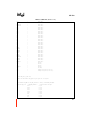
JTAG State Machine
The movement of data through the TAP can be controlled
by supplying the proper logic level to the TMS pin at the
rising edge of consecutive TCK cycles. The TAP controller
itself is a finite-state machine that is capable of 16 states.
Each state contains a link in the operation sequence
necessary to manipulate the data moving through the TAP.
This includes applying stimuli to the pins, capturing
incoming data, loading instructions, and shifting data into
and out of the Boundary-Scan Register. Figure 1 shows the
TAP state machine flowchart, and demonstrates the
sequence of inputs on TMS necessary to progress from any
one state to another. Asserting the TRST# pin at any time
will cause the TAP to reset to the Test-Logic-Reset home
state.
A
AP-720
1
Test - Logic
- Reset
0
0
Run - Test/
Idle
1
Select DR - Scan
1
Select IR - Scan
0
1
0
1
Capture DR
Capture IR
0
0
Shift IR
1
1
1
Exit1 DR
1
Exit1 IR
0
0
0
0
Pause DR
Pause IR
1
1
0
Exit2 DR
Exit2 IR
1
1
Update DR
Update IR
1
0
0
Shift DR
0
1
0
1
0
A2356-01
Figure 1. TAP Controller (Finite State Machine)
2.2
Intel386 EX Embedded Processor
JTAG Test-Logic Unit
The JTAG Test-Logic Unit of the Intel386 EX embedded
processor can control all device pins except those of the
clock, power, ground, and TAP control signals. A boundaryscan cell resides at each of the 101 controlled device pins.
The cells are connected serially to form the 101 bit
boundary-scan register. Each bit has both a control cell,
which controls the I/O status of the pin, and a data cell,
which holds the logical high or low value to be asserted at
the pin itself. An EXTEST or INTEST instruction, as
shown in Table 1, requires a total of 202 (101 bits x 2 cells)
shifts of data into the TAP.
In addition to the boundary-scan (BOUND) register, the
Intel386 EX processor has an instruction register (IR)
whose instructions are shown in Table 1. These instructions
are used in programming flash memory through the JTAG
port. The bypass register (BYPASS) is also featured on the
processor, but is only used in systems with two or more
JTAG-compliant devices. The identification code
(IDCODE) register is the last one implemented in the
Intel386 EX processor, and is discussed further in Section
2.2.2.
3
A
AP-720
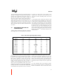
Table 1. Test-Logic Unit Instructions
Mnemonic
Opcode1,2
BYPASS
1111
EXTEST
0000
SAMPRE
0001
IDCODE
0010
INTEST
1001
Description
Bypass on-chip system logic (mandatory instruction).
Used for those components that are not being tested.
Off-chip circuitry test (mandatory instruction).
Used for testing device interconnections on a board.
Sample pins/preload data (mandatory instruction).
Used for controlling (preload) or observing (sample) the signals at
device pins. This test has no effect on system operation.
ID code test (optional instruction).
Used to identify devices on a board.
On-chip system test (optional instruction).
Used for static testing of the internal device logic in a single-step
mode.
High-impedance/ONCE mode test (optional instruction).
HIGHZ
1000
Used to place device pins into their inactive drive states. Allows
external components to drive signals onto connections that the
processor normally drives.
NOTES:
1 The opcode is the sequence of data bits shifted serially into the instruction register (IR) from
the TDI input. The opcodes for EXTEST and BYPASS are mandated by IEEE 1149.1, so
they should be the same for all JTAG-compliant devices. The remaining opcodes are
defined for use on the Intel386 EX embedded processor, so they may vary among devices.
2 All unlisted opcodes are reserved. Use of reserved opcodes could cause the device to enter
reserved factory-test modes.
2.2.1
Boundary Scan Register
The order of the bits contained in the Boundary Scan
Register (BSR) is shown in Table 2. The direction, or
control, bits follow their corresponding data bits in the
chain sequence. For example, Bit 0, M/IO# would be
followed in the chain by its directional bit, which in turn
would be followed by Bit 1, D/C#. It is important to
remember that the boundary scan register is shifted in
serially; when shifting data out onto the pins, the first bit
shifted into the BSR must be the directional bit of D15
(entry number 100 in Table 2). This method ensures that all
data is loaded onto the correct pins at the conclusion of the
202-bit serial data shift.
Although it is not used in the software examples included in
Appendix A, a copy of the BSDL (Boundary-Scan
Description Language) file for the A and B steppings of the
Intel386 EX embedded processor (JTAGBSDL.ZIP) is
4
located on Intel’s America’s Application Support BBS, at
(916) 356-3600. This file lists:
•
The physical pin layout of all pins in the BoundaryScan Register
•
The valid and reserved JTAG unit opcodes
•
The expected contents of the IDCODE register (shown
also in Section 2.2.2) for the Intel386 EX embedded
processor
•
A description of the BSR contents
The BSDL file may be incorporated into software which
uses the JTAG port for testing or programming functions.
BSDL is a de-facto standard recently approved by the IEEE
for describing essential features of IEEE 1149.1(b)
compliant devices. A copy of the Intel386 EX embedded
processor BSDL file is shown in Appendix B.
A
AP-720
Table 2. Boundary-scan Register Bit Assignments
Bit
Pin
Bit
Pin
Bit
Pin
Bit
Pin
0
M/IO#
25
A15
50
TMROUT2
75
P2.2
1
D/C#
26
A16/CAS0
51
TMRGATE2
76
P2.3
2
W/R#
27
A17/CAS1
52
INT4/TMRCLK0
77
P2.4
3
READY# 28
A18/CAS2
53
INT5/TMRGATE0
78
DACK0#
4
BS8#
29
A19
54
INT6/TMRCLK1
79
P2.5/RXD0
5
RD#
30
A20
55
INT7/TMRGATE1
80
P2.6/TXD0
6
WR#
31
A21
56
STXCLK
81
P2.7
7
BLE#
32
A22
57
FLT#
82
UCS#
8
BHE#
33
A23
58
P1.0
83
CS6#/REFRESH#
9
ADS#
34
A24
59
P1.1
84
LBA#
10
NA#
35
A25
60
P1.2
85
D0
11
A1
36
SMI#
61
P1.3
86
D1
12
A2
37
P3.0/TMROUT0
62
P1.4
87
D2
13
A3
38
P3.1/TMROUT1
63
P1.5
88
D3
14
A4
39
SRXCLK
64
P1.6/HOLD
89
D4
15
A5
40
SSIORX
65
RESET
90
D5
16
A6
41
SSIOTX
66
P1.7/HLDA
91
D6
17
A7
42
P3.2/INT0
67
DACK1#/TXD1
92
D7
18
A8
43
P3.3/INT1
68
EOP#
93
D8
19
A9
44
P3.4/INT2
69
WDTOUT
94
D9
20
A10
45
P3.5/INT3
70
DRQ0
95
D10
21
A11
46
P3.6/PWRDOWN
71
DRQ1/RXD1
96
D11
22
A12
47
P3.7/SERCLK
72
SMIACT#
97
D12
23
A13
48
PEREQ/TMRCLK2
73
P2.0
98
D13
24
A14
49
NMI
74
P2.1
99
D14
100
D15
NOTES:
1 Bit 0 is closest to TDI; bit 100 is closest to TDO.
2 The boundary-scan chain consists of 101 bits; however, each bit has both a control cell and
a data cell, so an EXTEST or INTEST instruction requires 202 shifts (101 bits × 2 cells).
5
A
AP-720
2.2.2
Identification Code Register
The IDCODE instruction allows the user to determine the
contents of the device’s identification code register. For the
Intel386 EX embedded processor this command should
return one of the values shown in Table 3.
Table 3. Device Identification Codes
Step
VCC
IDCODE
A
5V
0027 0013H
B
5V
0027 0013H
C
5V
2027 0013H
C
3V
2827 0013H
For more information about identification codes, see the
Intel386TM EX Embedded Microprocessor User’s Manual.
2.3
Intel 4 Mbit Boot Block Flash
The number of instructions necessary to program flash
devices is significantly reduced by using an Intel Boot
Block device. In the sample design described in the next
section, the automated Write State Machine (WSM) of the
28F400BV-T flash unit ensures that all algorithms and
timings necessary for erasing and programming the device
are executed automatically, freeing the TAP control
software of additional burdensome I/O cycles and iterative
code. The device also performs its own program and erase
verifications, updating the Status Register (SR) to indicate
the successful completion of operations. These features are
standard with Intel’s Boot Block, FlashFileTM, and
Embedded Flash RAM families, which are available in a
variety of sizes and configurations.
Writing data to Intel’s second-generation flash memories
consists of these steps:
1.
The write setup command (40H) is issued to flash
memory.
2.
This is followed by a second write specifying the
address and data for the location to be written.
3.
The data and address are latched internally on the rising
edge of the WE# strobe, which may be issued by one of
a variety of sources.
6
At this point, the WSM takes over, writing the results of the
verification into the status register. Since data access is
much slower than the typical programming time, the
contents of the SR need not be checked after each write.
Instead, writes are repeated sequentially for all locations to
be programmed, with the SR verified when the block
programming is completed. After the device is
programmed, the data may be read back sequentially with
RD# held constantly low, and the contents may be verified
by comparison against the source code.
The static nature of the Intel386 EX embedded processor’s
Boundary Scan Register outputs combined with the high
speed of the flash device ensures that timing issues are a
minimal problem. In fact, a 16-bit word may be written to
the flash device in only a single cycle of the boundary scan
register. This is accomplished by using an additional output
pin of the controlling PC’s parallel port connected to WE#
to clock the data and address into the chip. By doing so, as
is discussed in Section 4.0, PERFORMANCE ANALYSIS
AND CONSIDERATIONS, even a simple design can
achieve throughput levels of more than 1 Kbyte per second
through the serial BSR of the Test Access Port.
3.0
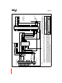
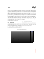
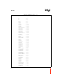
3.1
SAMPLE DESIGN
TAP Hardware Interface
Figure 2 illustrates a straightforward design that uses a
standard parallel port to communicate with the TAP of the
Intel386TM EX Embedded Microprocessor Evaluation
Board. This interface is typical of any design based on the
Intel386 EX embedded processor, and requires only a
CMOS buffer to protect the TAP pins and translate the
printer port signals to the CMOS levels required for the
TAP. This assembly can be built onto a simple cable or card
that plugs into the Intel386 EX Embedded Microprocessor
Evaluation Board Option Header. It receives power and
ground signals from the Evaluation Board, which must be
powered on during operation of the TAP programmer. The
majority of the signal control is done by software routines
which read and write data to and from the BSR.
1Y1
1Y2
1Y3
1Y4
2Y1
2Y2
2Y3
2Y4
TDI
TMS
TRST#
TCK
TDI_PRTY
STROBE#
For programming to complete successfully, the output trace on pin 20 of the U16 PLD on
the Evaluation Board must be cut between the PLD and the flash device. Additionally,
Pin 8 of JP7 should be wired to US4, Pin 47 (WE# on the DRAM socket). Pin 10 of JP7
should be wired to U16, Pin 20 (called FLSH_WE# on the PLD). Pin 4 of U7 should be
wired to US3, Pin 43 (WE# on the flash device). This will not affect the operation of the
Evaluation Board if pins 3-4 of JMP_WE# are jumpered.
18
16
14
12
9
7
5
3
2)
74HCT244
1G
2G
1A1
1A2
1A3
1A4
2A1
2A2
2A3
2A4
BUFFER
330_OHM
VCC
This additional circuit board should be placed in the JP7 connection of the Intel386TM EX
Evaluation Board to facilitate the programming of the Boot Block flash through the chip’s
JTAG port.
1
19
15
17
TDO_PRTA 2
TMS_A 4
RESET_A# 6
TCK_A 8
TDO 11
STROBE# 13
SIP_4
2
4
6
8
1)
NOTES:
CONNECTOR DB25
Parallel Port Conn
13
25
12 CM_CHK
24
11 TDI_PRTY
23
10
22
9 CM_CHK
21
8 TDO_PRTA
20
7
19
6
18
5
17
4
16 RESET_A#
3 TMS_A
15
2 TCK_A
14
1 STROBE#
TDO_PRTA
STROBE#
TMS_A
TCK_A
1
3
5
7
RN_PULLUP
2
4
6
8
10
12
14
16
18
20
22
24
26
28
30
32
34
36
38
40
42
44
46
48
50
52
54
56
58
60
62
64
GND
VCC
VCC
DECOUPLING
CAP NP
.47 uF
16V
1-2 = DRAM WE#
3-4 = PLD WE#
5-6 = STROBE# WE#
HEADER 3X2
JMP_WE#
DRAM WE# 1
2
4
PLD WE# 3
6
STROBE# 5
FLSH_WE#
Sheet
1
of
EV386EX - JTAG INTERFACE BOARD
Size Document Number
A
Date:
July 31, 1995
Title
INTEL CORPORATION
5000 W. CHANDLER BOULEVARD
CHANDLER, AZ 85226
REV
1.0
1
Although Intel has verified this design to be functional, Intel
assumes no responsibility for any errors that may appear in the
design. Intel reserves the right to modify this design without notice.
HEADER 32X2
TMS
TDO
GND
TRST#
TCK
TDI
1
3
5
7
9
11
13
15
17
19
21
23
25
27
29
31
33
35
37
39
41
43
45
47
49
51
53
55
57
59
61
63
JP7 CONNECTOR
A
AP-720
Figure 2. TAP Parallel Port Interface
7
A
AP-720
3.2
JTAG Software Interface
This section details the operation of the various software
routines that use the Test Access Port to program data into
the Boot Block flash. The source code for the executable
program TAPLOADR.EXE, which contains both inline
assembly routines as well as C language functions, is shown
in Appendix A. The software demonstrates how to:
•
Configure and modify the status of pins for data input
and output
•
Shift in the values necessary to perform I/O to the flash
device
•
Perform operations such as status checks and data I/O
3.2.1
Hardware Considerations
The high-level routines used in programming data through
the TAP are device-dependent because they assume a
particular device configuration on the board as well as a
predetermined system interface. In the example, the JTAG
chain contains only a single IEEE 1149.1 compliant device,
the Intel386 EX embedded processor. If the JTAG chain
consisted of several devices connected in series, the
routines would need to control the whole chain and place
any other devices into the BYPASS mode. The routines in
the example assume only a single device with separate RD#
and WR# strobes generated by the CPU. The WR# signal
may be enabled externally to improve performance; this is
discussed in Section 4.0, PERFORMANCE ANALYSIS
AND CONSIDERATIONS.
Several preparations must be made before the flash memory
can be programmed. On the Evaluation Board, JP12 must
be installed and R12 removed. Jumpering pins 1 and 2 of
JP12 enables the PWD signal (pin 44) of the 28F400BV-T
flash device, which provides programming voltage for
block erases and writes. When programming the flash, it is
also critical to enable VPP (pin 1) by setting Port 1.5 (pin
107) of the Intel386 EX embedded processor on the
Evaluation Board used in the example.
In the example, UCS# is used as the chip select (CS#) for
the flash device; it is LOW for any address that is accessed.
The example also implies static behavior of the bus;
therefore, the connection of flash chips to the CPU should
be independent of any clocks. If any buffers on the busses
are required in the design, their direction and enable signals
should be static. Take care to ensure that all flash control
signals are clock-independent. Revision 2.1 of the
EV386EX Intel386TM EX Embedded Microprocessor
8
Evaluation Board requires that a change be made to
temporarily disconnect the output of Pin 20 of the U16 PLD
(FLSH_WE#) so that the flash’s WE# signal may be
controlled by an external, static, and clock-independent
source. Examples are shown in Figure 2 for Parallel Port
and TAP control of the WE# signal. Making the changes
described in the figure notes enables the correct operation
of the programming functions and eliminates any
contention for control of the devices and their signals.
Future steppings of the Intel386 EX embedded processor
remove the need for PLD control of the flash’s WE# signal
by correcting errata #29 of the Intel386 EX embedded
processor errata list. This allows a glueless flash interface to
be used in some designs and eliminates the need for modifications to the PLD when implementing the programming of
the flash memory through the TAP. When cutting the trace
on the FLSH_WE# signal, however, care must be taken to
jumper pins 3-4 on the JTAG interface card so that correct
operation of the EV386EX evaluation board is retained.
Although two examples are given for resetting the JTAG
unit of the Intel386 EX embedded processor, it is only
necessary to use one of the provided means to return the
TAP state machine to Test-Logic-Reset. If the chosen
implementation uses the Restore_Idle function rather than
the Reset_JTAG routine, it is advisable to tie an inverted
CPU Reset signal to the TRST# input of the processor. This
guarantees that the TAP relinquishes control of all the
controlled CPU pins upon a system reset. If the
Reset_JTAG function is used, care must be taken to reset
the system immediately after TRST# is asserted.
3.2.2
Assembly Language Routines
The heart of the software that allows you to program flash
through the JTAG port is contained in the assembly routines
which control the JTAG unit of the Intel386 EX embedded
processor via the parallel port of a PC. These routines have
been implemented as inline assembly code to simplify the
development process and the clarity of the software. They
use a set of bit masks and variables shown in the first
section of Appendix A under the heading “Assembly
Language Variables.” A description of each function is
shown below:
•
Reset_JTAG - Resets the TAP to the Test-Logic-Reset
state by toggling the TRST# signal. This signal is
optional in IEEE 1149.1, but has been provided on the
Intel386 EX embedded processor. Alternately, the same
A
•
AP-720
function is provided by five consecutive TCK periods
with TMS held high. See Restore_Idle (below) for
more details.
•
Send_Data - Sends a JTAG data string into the TAP.
Replaces the original string with the data that is shifted
out on TDO.
Restore_Idle - Resets the TAP to the Test-Logic-Reset
state by transitioning through the state machine. TMS
is held high for five consecutive TCK clock periods.
This is in accordance with the IEEE 1149.1 specification.
•
Send_Data_IN - Sends a JTAG data string into the
TAP. Does not replace the original string with the data
that is shifted out on TDO.
•
Flip_ID_String - Flips the JTAG unit ID string within
its own array. This needs to be done in order to reverse
the string which is read in backwards, least significant
bit first. This allows for verification of the data that is
read against the value shown in the Intel386TM EX
Embedded Microprocessor User’s Manual, most
significant bit first.
•
TMS_High - Provides a vehicle for progression
through the state machine with TMS held high for a
single TCK clock period. Used when shifting data into
and out of the TAP.
•
TMS_Low - Provides a vehicle for progression
through the state machine with TMS held low for a •
single TCK clock period. Used when shifting data into
and out of the TAP.
•
Shift_Data_Array - Shifts a data string into the TAP
while copying the data in the TAP into the place of the
incoming data. This function is called when the TAP
state machine is in the Select_DR_Scan state.
•
Shift_Data_Array_IN - Shifts a data string into the
TAP and does not copy any data from the TAP in the
place of the incoming data. This function is called
when the TAP state machine is in the Select_DR_Scan
state.
•
Strobe_Data_In - Pulses the STROBE# line of the
PC’s parallel port. This function is used only when
STROBE# is connected to the WE# line of the flash.
3.2.3
•
Fill_JTAG - Initializes the values in the 202 bit JTAG
BSR array for a standard configuration. Sets up input
and output pins and values for the control pins in the
BSR. Sets the direction bits of the unused pins to a
value of “0” which makes them inputs. This routine is
unique to the Intel386 EX embedded processor and
must be configured differently for other devices.
•
Set_Data - Decodes a 16-bit data word onto the D0
through D15 data lines in the BSR array. Sets the data
line directional bits to a value of “1” which makes
them into outputs. Used when writing data to the flash.
•
Get_Data - Configures the data lines as inputs,
allowing data to be output from the flash and read into
the BSR array. Used when reading data back from the
flash.
•
Parse_Data - Reads the data from the data lines in the
BSR array and parses it into a 16-bit data word. Used
when reading data back from the flash.
•
Set_Address - Decodes an address onto the A1
through A25 data lines in the BSR array. Sets the
directional bits for the address lines to a value of “1”
which makes them into outputs. Used for both reads
and writes to and from the flash.
•
Flash_Read - Reads a 16-bit data word from the flash
device at the specified address. Used for verification of
data and status checks.
•
Flash_Write - Writes a 16-bit data word to the flash
device at the specified address. Used for data
programming and status checks. Optional section
within this procedure may be chosen depending on
“C” Routines
Appendix A contains a number of “C” language functions
that make the programming of flash modular and easy to
implement. Many of them are called from the “Main”
function of TAPLOADR.EXE, but others are used to move
data back and forth into the TAP by means that would be
complicated by using assembly language programming.
The program was compiled under Microsoft* Visual C++
1.50. A list of the functions, their dependencies, and a brief
description of their operation is given below.
•
Send_Instruction - Sends a JTAG instruction as a
string into the TAP. Replaces the original string with
the data that is shifted out on TDO.
•
Send_Instruction_IN - Sends a JTAG instruction as a
string into the TAP. Does not replace the original string
with the data that is shifted out on TDO.
Get_JTAG_Device_ID - Retrieves the JTAG device
ID from the processor. Displays the results and the
expected value.
9
A
AP-720
chosen method of WE# hardware control. Only one
type of WE# signal enabling procedure may be used at
a time.
•
Input_File_Name_OK - Verifies that the input file is a
file that can be read. When this function does not return
a value of TRUE, the program displays an error
message and prompts the user to try executing the
program again. If the file is valid, the program executes
normally.
•
Get_Flash_Device_ID - Retrieves the flash device ID
from the Intel Boot Block flash Device. Displays the
results and the expected value.
•
Check_Flash_Status - Clears the flash status registers
and sends a Read Status command to the device. The
results are read back and displayed along with the
expected values for a properly functioning device.
•
Erase_Flash - Erases each block within the Intel Boot
Block flash device. An address within each block is
stored in an array in this function, and the function
loops for a specified number of blocks, seven in this
case. The function may be altered to erase only the
Boot Block or selected blocks within the device.
•
Program_Flash_Data - Outputs data from the
specified binary input file to the flash device. Data is
read in as 8-bit characters and is merged into 16-bit
words which are then written to the Flash device. Status
checks are not performed after each write, because
doing so slows performance. The function displays the
status of a successful programming operation and
notifies the user if the input file has been closed
successfully.
•
Read_Flash_Data - Reads back the data that has been
written to the flash into the file VERIFY.BIN. A file
comparison may be done to check the correct
programming of flash data. This is unnecessary in most
real applications, but is marginally faster than checking
status after each word is programmed.
3.2.4
Program Operation and Options
TAPLOADR.EXE operations are controlled from the
program’s “Main” function. The program does not execute
until it is given a valid input file name. Table 4 lists the
functions which verify, write, and then read back the data in
the file that is written to the flash device.
Table 4. TAPLOADER.EXE Order of Execution
10
Input_File_Name_OK (input_file)
// Checks input file name
Fill_JTAG(PinState);
// Initialization string
Reset_JTAG();
// Reset the JTAG unit
Restore_Idle();
// Used to reset JTAG state machine
Get_JTAG_Device_ID();
// Get ID - see 386EX manual for code
Get_Flash_Device_ID();
// Get ID - see flash manual
Check_Flash_Status();
// Check status register example
Erase_Flash();
// Erases the entire flash chip
i = Program_Flash_Data();
// Opens file and programs flash data
Check_Flash_Status();
// Checks status before continuing
Read_FLASH_Data(“verify.bin”,
data_start_address, i);
// Copy contents to file
A
AP-720
The program displays status check messages throughout its
operation. It is important to recognize that some operations,
especially when programming large amounts of data, may
take from a few seconds to a few minutes to complete. A
block erase operation normally requires approximately 0.5
seconds per block, or about 4 seconds per flash device.
Writing data may take from just a few seconds to over 30
minutes, depending on the size of the input file and the
methods used for verifying data programming and enabling
WE# on the flash chip. These issues are discussed in the
next section.
4.0
PERFORMANCE ANALYSIS AND
CONSIDERATIONS
A number of factors can affect the performance, specifically
the throughput levels, of any programming device that uses
the JTAG port. Among these, the most critical are the
methods used to write the data into the flash device and
verify that it has been successfully stored at the correct
location.
As was mentioned earlier, reducing the number of status
checks performed while programming can greatly reduce
the time required to program data into flash. The relatively
slow operation of the parallel port and TAP combination
ensures that read and write operations do not interfere with
those that precede them. Checking status bits only at the end
of blocks of writes can reduce programming time by as
much as one half. Table 5 shows a comparison of typical
timings measured while loading data into the flash device
found on the Intel386TM EX Embedded Microprocessor
Evaluation Board.
Table 5. TAP Flash Programming Sample Timings
Size of Operation Type of Access Status Check FLSH_WE# Type Seconds Seconds/Kbyte
32 Kbyte
Write
Yes
WE#
180
32 Kbyte
Read
N/A
WE#
40
5.62
1.25
32 Kbyte
Write
No
WE#
100
3.12
32 Kbyte
Read
N/A
WE#
40
1.25
32 Kbyte
Write
No
STROBE#
45
1.41
32 Kbyte
Read
N/A
STROBE#
40
1.25
512 Kbyte
Write
Yes
WE#
2940
5.74
512 Kbyte
Read
N/A
WE#
660
1.28
512 Kbyte
Write
No
WE#
1620
3.16
512 Kbyte
Read
N/A
WE#
660
1.28
512 Kbyte
Write
No
STROBE#
555
1.08
512 Kbyte
Read
N/A
STROBE#
590
1.15
Table 5 also illustrates how the use of a WE# generated by
the STROBE# line of a typical parallel port may expedite
the delivery of data through the TAP. Using this method
allows writes to complete in a single cycle of the TAP,
rather than the normal three cycles that are required when
strobing the WE# signal from the TAP. As shown in
Appendix A, the data and address are placed on the bus in a
single cycle when using STROBE# as WE#. They are then
clocked into the flash device by toggling the STROBE# line
externally. In the latter case, however, three complete shifts
of the BSR data must be performed in order to send the data
and address and simultaneously toggle the WE# line in a
similar high-low-high pattern. Reductions in write cycle
time of close to two thirds are expected when using the first
method. The unused data signals of the parallel port may
also be used to control other useful signals such as RD#, or
to monitor the status of control lines on the system under
test.
It is worth mentioning that several companies currently
offer JTAG port interface cards that use a standard ISA bus
interface to communicate with one or more Test Access
11
A
AP-720
Ports. These cards can vastly improve the data transfer rates
of about 0.5 Kbytes per second that are typical of a parallel
port programmer. Although this rate is comparable to that of
a typical EPROM programmer, TMS periods on the order of
a few microseconds are less than ideal. Typical data rates of
8 Mbits per second may be achieved by a simple card which
uses RAM to send and read data patterns from the JTAG
port. Since the bus signal emulation requires only the
toggling of a few signals out of all that are within the BSR,
the card stores the data to be written and transfers it to the
TAP in a rapid manner. Most hardware vendors provide a
library of software to assist the programmer in writing code
to interface with such cards. Even the simplest combination
of hardware and software can be a valuable tool in
programming and testing new code in flash.
without the loss of valuable time or inventory. Accessing
these devices via the chip’s IEEE 1149.1-compliant Test
Access Port provides an inexpensive, versatile, and reliable
tool that functions far beyond the realms of debug and test.
If shock-tolerance and reduction of form-factor are primary
design concerns, using the JTAG port is sure to be an
important tool for in-circuit device reprogramming and
reconfiguration. The parallel port of a standard PC becomes
a flexible tool in this case, and may be used to generate TAP
signals for either lab or low-volume production. With a
high-performance solution based on a simple TAP
controller card in a PC, programming performance significantly improves without the purchase of costly test
equipment.
6.0
5.0
CONCLUSION
The Intel386 EX processor provides a powerful means of
programming onboard flash devices to meet the needs of
Just-In-Time manufacturing systems. Unprogrammed
devices may now be soldered directly onto PCB’s, allowing
for concurrent software and hardware development
processes as well as last minute changes in BIOS code
RELATED INFORMATION
This application note is one of the many sources of
information available regarding designing with the Intel386
EX embedded processor. Table 6 shows other useful
documents and their Intel order numbers.
Table 6. Related Intel Documents
Publication Title
12
Order
Number
Intel386TM EX Embedded Microprocessor datasheet
272420
Intel386TM EX Embedded Microprocessor User’s Manual
272485
Intel386TM SX Embedded Microprocessor datasheet
240187
Intel386TM SX Embedded Microprocessor Programmer’s Reference Manual
240331
Intel386TM SX Embedded Microprocessor Hardware Reference Manual
240332
186 Development Tools Handbook
272326
Intel386TM
272525
EX Embedded Microprocessor Evaluation Board Manual
Buyer’s Guide for the Intel386TM EX Embedded Processor Family
272520
Packaging
240800
1995 Flash Memory Databook
210830
A
To receive these documents or any other available Intel
literature, contact:
Intel Corporation
Literature Sales
P.O. Box 7641
Mt. Prospect IL 60056-7641
1-800-879-4683
To receive files that contain the source code, executable
programs, and schematics for this application of flash
programming through the TAP, contact:
AP-720
Additional information on the IEEE 1149.1/1a specification
may be found in the official IEEE Standards document
IEEE Standard Test Access Port and Boundary-Scan Architecture. This publication is sponsored by the Test
Technology Standards Committee of the IEEE Computer
Society and is available from:
Institute of Electrical and Electronics Engineers, Inc.
345 East 47th Street
New York NY 10017
Intel Corporation
America’s Application Support BBS
916-356-3600
13
A
AP-720
APPENDIX A
PROGRAM SOURCE CODE
The following source code was written in Microsoft Visual C++ version 1.5 and has been tested using the aforementioned
hardware interface on a Intel386TM EX Embedded Processor Evaluation Board. It was compiled and linked into the file
TAPLOADR.EXE, which is available on Intel’s America’s Application Support BBS in the zipped file TAPLOADR.ZIP.
Table A-1. Program Source Code (Sheet 1 of 15)
/***************************** TAPLOADR.CPP *********************************
*
* Program Name: TAPLOADR.CPP
*
* Version:
1.0
*
* Date:
July 18, 1995
*
* Author:
Daniel S. Hays
*
386 Applications Engineer
*
* References:
Excerpts of code taken from modules of the article
*
"Beyond the Myth of JTAG Boundary Scan Port" by Dmitrii
*
Loukianov, Intel Corp., 1995.
*
* Program Spec: This program will take an input flash file residing on a PC
*
and program it into the boot block flash of the 386EX
*
Evaluation Board utilizing the JTAG unit onboard the 386EX
*
embedded processor. It will also erase the entire FLASH
*
chip beforehand, including the boot block area, if
*
enabled as described in the requirements section below.
*
* Requirements: In addition to the eval board itself, it is required that
*
the user has a JTAG interface board plugged into both the
*
evaluation board's expansion bus slot and the host PC's
*
parallel port. The U16 PLD chip must be updated in order to
*
disable the FLASH_WE# signal, and a jumper must be installed
*
on pins 1-2 of Jumper J12, which is not normally populated
*
on the standard eval board.
*
*
*** Note: The power supply for the 386EX eval board must be
*
ON in order for successful programming of the flash to take
*
place. The program implies that UCS is the CS# pin for flash
*
memory being programmed. UCS is set LOW for any address!
*
*
The user must also know the location and name of the input
*
data file in .BIN format, as well as the starting location
*
in FLASH memory that the file is to be located at.
*
* Disclaimer:
Information in this document is provided 'as is' solely to
*
enable use of Intel products. Intel assumes no liability
*
whatsoever, including infringement of any patent or
*
copyright, concerning the included software. Intel
*
Corporation makes no warranty for the use of this software
*
and assumes no responsibility for any errors which may
*
appear in this document nor does it make a commitment to
*
update the information contained herein.
*
*
Copyright (C) Intel Corporation 1995
*
All Rights Reserved.
A-1
A
AP-720
Table A-1. Program Source Code (Sheet 2 of 15)
*
*************************
#include
#include
#include
#include
GLOBAL DECLARATIONS
**************************/
<stdio.h>
<string.h>
<stdlib.h>
<conio.h>
/**** Definitions of JTAG BSR pins for sequence for Intel 386 EX CPU ****/
/***** Note: MIO shifted out LAST, D15 - first! *************************/
#define
#define
#define
#define
#define
#define
#define
#define
#define
#define
#define
#define
#define
#define
#define
#define
#define
#define
#define
#define
#define
#define
#define
#define
#define
#define
#define
#define
#define
#define
#define
#define
#define
#define
#define
#define
#define
#define
#define
#define
#define
#define
#define
#define
#define
#define
#define
#define
#define
#define
#define
A-2
D15
D14
D13
D12
D11
D10
D9
D8
D7
D6
D5
D4
D3
D2
D1
D0
LBA
CS6
UCS
P27
P26
P25
DACK0
P24
P23
P22
P21
P20
SMIACT
DRQ1
DRQ0
WDTOUT
EOP
DACK1
P17
RESET
P16
P15
P14
P13
P12
P11
P10
FLT
STXCLK
INT7
INT6
INT5
INT4
TMRGATE2
TMROUT2
0
1
2
3
4
5
6
7
8
9
10
11
12
13
14
15
16
17
18
19
20
21
22
23
24
25
26
27
28
29
30
31
32
33
34
35
36
37
38
39
40
41
42
43
44
45
46
47
48
49
50
A
AP-720
Table A-1. Program Source Code (Sheet 3 of 15)
#define
#define
#define
#define
#define
#define
#define
#define
#define
#define
#define
#define
#define
#define
#define
#define
#define
#define
#define
#define
#define
#define
#define
#define
#define
#define
#define
#define
#define
#define
#define
#define
#define
#define
#define
#define
#define
#define
#define
#define
#define
#define
#define
#define
#define
#define
#define
#define
#define
#define
NMI
PEREQ
P37
P36
P35
P34
P33
P32
SSIOTX
SSIORX
SRXCLK
P31
P30
SMI
A25
A24
A23
A22
A21
A20
A19
A18
A17
A16
A15
A14
A13
A12
A11
A10
A9
A8
A7
A6
A5
A4
A3
A2
A1
NA
ADS
BHE
BLE
WR
RD
BS8
READY
WRD
DC
MIO
#define
#define
TRUE
FALSE
51
52
53
54
55
56
57
58
59
60
61
62
63
64
65
66
67
68
69
70
71
72
73
74
75
76
77
78
79
80
81
82
83
84
85
86
87
88
89
90
91
92
93
94
95
96
97
98
99
100
1
0
typedef
typedef
typedef
typedef
unsigned int
unsigned char
char
Pchar
const
const
word
word
word;
byte;
*Pchar;
PJTAGdata;
BSR_Length=202;
ID_String_Length=32;
unsigned long int A;
// 16 Bit word
// 8 Bit Byte
// JTAG Data array / null term string
// # bits in JTAG BSR string 101x2
// # bits in JTAG CPU ID String
// Stores address data
A-3
A
AP-720
Table A-1. Program Source Code (Sheet 4 of 15)
unsigned long int i;
unsigned long int data_start_address;
word RX;
word new_word;
word high_part;
char PinState[BSR_Length];
char input_file[80];
int c;
FILE *in;
//
//
//
//
//
//
//
//
//
Stores index value
Holds starting address of program
Stores register data
Holds word to be written to FLASH
Temp Holder for upper part of word
Holds Pin Data to move in and out
Holds name of input file
Holds character being worked with
Points to input file location
/****** JTAG1149 Commands for Intel386EX Embedded Processor *************/
char
char
char
char
char
char
*BYPASS
*EXTEST
*SAMPLE
*IDCODE
*INTEST
*HIGHZ
="1111";
="0000";
="1000";
="0100";
="1001";
="0001";
//
//
//
//
//
//
Use BYPASS register in data path
External Test Mode
Sample/Preload Instruction
Read ID CODE from the chip
On-chip System Test
Place device into Hi-Z mode
/******************* Assembly language variables ************************/
#define
#define
#define
#define
#define
#define
#define
#define
TCK
TMS
TCKTMS
TDI
notTCKTMS
TDITMS
TRST
TDO
static
const
const
word
word
word
1;
2;
3;
0x40;
0xFC;
0x42;
4;
0x80;
JTAG=0x378;
JTAGI=JTAG+1;
JTAGR=JTAG+2;
//
//
//
//
//
//
//
//
Bit 0 is TCK output
Bit 1 is TMS output
Bit 0+1
Bit 6 is TDI output
Bit 0+1
Bit TDI+TMS
JTAG+2
JTAG+1, bit is inverted!
// LPT1 Data Address Default
// Contains circuit input
// Reset bit is here
/**************************************************************************/
/************** INLINE ASSEMBLER FUNCTIONS FOR JTAG I/O *******************/
/**************************************************************************/
/**************** Assembly function to reset the JTAG unit ****************/
void far Reset_JTAG() /** Reset TAP logic by optional TRST# signal **/
{
_asm
{
mov
dx,JTAG
mov
al,0
// +TDI
out
dx,al
mov
dx,JTAGR
mov
al,0
// TRST# LOW
out
dx,al
mov
dx,JTAGR
mov
al,TRST
// TRST# HIGH
out
dx,al
}
}
/*** Assembly function to go into Run_Test_Idle state from unknown state **/
void far Restore_Idle () /** Restore Test_Logic_Reset state by 5 TCK's **/
{
/** Goes into TLR state from any **/
/** unknown state of the JTAG controller **/
_asm
{
A-4
A
AP-720
Table A-1. Program Source Code (Sheet 5 of 15)
mov
mov
cx,5
dx,JTAG
FiveTimes:
mov
out
or
out
xor
out
loop
al,TMS
dx,al
al,TCK
dx,al
al,TCK
dx,al
FiveTimes
// TMS HIGH
// Set TMS/TDI
// TCK High
// TCK Low
}
}
/********* Assembly function to do one transition with TMS High ***********/
void near TMS_High () /** One transition with TMS High **/
{
_asm
{
mov
dx,JTAG
mov
al,TMS
// Sets TMS high
out
dx,al
// Set TMS/TDI
or
al,TCK
out
dx,al
// TCK High
xor
al,TCK
// TCK Low
out
dx,al
}
}
/********* Assembly function to do one transition with TMS Low ************/
void near TMS_Low () /** One transition with TMS Low **/
{
__asm
{
mov
dx,JTAG
mov
al,0
// Set TMS Low
out
dx,al
// Set TMS/TDI
or
al,TCK
out
dx,al
// TCK High
xor
al,TCK
// TCK Low
out
dx,al
}
}
/***** Assembly function to shift data into JTAG port while reading *****/
void near Shift_Data_Array(unsigned S, char far *D)
{
/** Shifts data String into JTAG port while reading data **/
/** from JTAG port back into D, **/
/** The procedure should be called when JTAG controller **/
/** is in the SelectDRScan state **/
_asm
{
mov
dx,JTAG
push
es
push
di
les
di, D
// Get array pointer
cld
xor
ax,ax
mov
ax, S
// Get Size
dec
ax
A-5
A
AP-720
Table A-1. Program Source Code (Sheet 6 of 15)
mov
jz
cx,ax
LastClock3
I_Shift3:
mov
shl
and
out
or
out
al, byte ptr es:[di]
al,6
al, notTCKTMS
//
dx,al
//
al,TCK
//
dx,al
//
inc
dx
in
and
mov
je
mov
al,dx
al,80h
al,'1'
Ex_1
al,'0'
stosb
dec
loop
dx
I_Shift3
Clear TCK and TMS bits
Put first data bit
Set TCK high
Shift in first data bit
// Sample first data bit
ex_1:
LastClock3:
mov
shl
and
or
out
or
out
al, byte ptr es:[di]
al,6
al, notTCKTMS
ax, TMS
//
dx,al
//
al,TCK
//
dx,al
//
inc
dx
in
and
mov
je
mov
al,dx
al,80h
al,'1'
Ex_2
al,'0'
Set TMS bit
Put last data bit
Set TCK high
Shift in first data bit
// Sample first data bit
ex_2:
stosb
dec
dx
mov
out
al,TDITMS
dx,al
pop
pop
di
es
// Leave TCK pin Low
}
}
/*** Assembly function to shift data into JTAG port while not reading ***/
void near Shift_Data_Array_IN(unsigned S, char far *D)
{
/** Shifts data String into JTAG port WITHOUT reading data **/
/** from JTAG port back into D. **/
/** The procedure should be called when JTAG controller is in the **/
/** SelectDRScan state. **/
A-6
A
AP-720
Table A-1. Program Source Code (Sheet 7 of 15)
_asm
{
mov
push
push
les
cld
xor
mov
dec
mov
jz
dx,JTAG
es
di
di, D
// Get string
ax,ax
ax, S ; Get Size
ax
cx,ax
LastClock4
I_Shift4:
mov
shl
and
out
or
out
inc
loop
al, byte ptr es:[di]
al,6
al, notTCKTMS
dx,al
//
al,TCK
//
dx,al
//
di
//
I_Shift4
Put first data bit
Set TCK high
Shift in first data bit
Update pointer
LastClock4:
mov
shl
and
or
out
or
out
mov
out
al, byte ptr es:[di]
al,6
al, notTCKTMS
al, TMS
dx,al
//
al,TCK
//
dx,al
//
al,TDITMS
//
dx,al
pop
pop
}
di
es
Put last data bit
Set TCK high
Shift in last data bit
Leave TCK pin Low!
}
/********* Assembly function to pulse STROBE line on parallel ports ******/
void far Strobe_Data_In ()
{
_asm
{
push
dx
mov
dx,JTAGR
mov
al,1+TRST
// Sets STROBE# bit low for WE# use
out
dx,al
mov
al,TRST
// Returns STROBE# without RESET#
out
dx,al
pop
dx
}
}
/**************************************************************************/
/******************** C++ FUNCTIONS FOR JTAG PROGRAMMING ******************/
/**************************************************************************/
/************** Function to send instruction to JTAG
*********************/
void Send_Instruction (unsigned S, char far *D)
/* Send instruction string into JTAG port, replace */
A-7
A
AP-720
Table A-1. Program Source Code (Sheet 8 of 15)
/* the original string with the data that comes out TDO */
{
TMS_Low;
TMS_Low;
TMS_High;
TMS_High;
TMS_Low;
TMS_Low;
Shift_Data_Array(S,D);
TMS_High;
TMS_Low;
//
//
//
//
//
//
Go
Go
Go
Go
Go
Go
to
to
to
to
to
to
Run_Test_Idle
Run_Test_Idle
Select_DR_Scan
Select_IR_Scan
Capture_IR
Shift_IR
// Update_IR, new instr. in effect
// Run_Test_Idle
}
/******** Function to send instruction into JTAG port, do not read TDO ***/
void Send_Instruction_IN (unsigned S, char far *D)
{
TMS_Low();
// Go to Run_Test_Idle
TMS_Low();
// Go to Run_Test_Idle
TMS_High();
// Go To Select_DR_Scan
TMS_High();
// Go To Select_IR_Scan
TMS_Low();
// Go to Capture_IR
TMS_Low();
// Go to Shift_IR }
Shift_Data_Array_IN(S,D);//
TMS_High();
// Update_IR, new instr. in effect
TMS_Low();
// Run_Test_Idle
}
/**** Function to send data string into JTAG port + replace original *****/
void Send_Data (unsigned S, char far *D)
/* Send data string into JTAG port */
/* replace the original string with the data that comes out TDO */
{
TMS_Low();
// Go to Run_Test_Idle
TMS_Low();
// Go to Run_Test_Idle
TMS_High();
// Go To Select_DR_Scan
TMS_Low();
// Go to Capture_DR
TMS_Low();
// Go to Shift_DR
Shift_Data_Array(S,D);
TMS_High();
// Update_IR, new data is in effect
TMS_Low();
// Run_Test_Idle
}
/**** Function to send data string into JTAG port w/o replacing orig. ****/
void far Send_Data_IN (unsigned S, char far *D)
/* Send data string into JTAG port, */
/* The original data is not overwritten */
{
TMS_Low();
// Go to Run_Test_Idle
TMS_Low();
// Go to Run_Test_Idle
TMS_High();
// Go To Select_DR_Scan
TMS_Low();
// Go to Capture_DR
TMS_Low();
// Go to Shift_DR
Shift_Data_Array_IN(S,D);
TMS_High();
// Update_IR, new data is in effect
TMS_Low();
// Run_Test_Idle
}
/*************** Function to invert a data string so MSB is first *********/
void Flip_ID_String (int length, char Input[ID_String_Length])
{
/* Flips the JTAG Unit ID string */
/* since it is read in backwards */
A-8
A
AP-720
Table A-1. Program Source Code (Sheet 9 of 15)
int i,j;
char Temp[ID_String_Length];
j = 0;
for ( i=length; i >= 1; --i)
{
Temp[j] = Input[i-1];
++j;
}
for ( i=0; i <= (length-1); ++i)
Input[i] = Temp[i];
// Initialize Temporary place holder
// Copy Temp string to perm. one
}
/********** Function to get ID string from the Intel(tm)386EX Chip ********/
void Get_JTAG_Device_ID ()
{
const char *p="01010101010101010101010101010101";
// Dummy string, will change value
// after Send_Data executes
char ID[ID_String_Length];
strcpy(ID,p);
// Fill with dummy string
Send_Instruction_IN(strlen(IDCODE),IDCODE); // Do NOT overwrite Instr.
// Because it resides in the
// Fixed string area!
Send_Data(strlen(ID),ID);
Flip_ID_String(strlen(ID),ID);
// Makes MSB first in array
printf("\nThe JTAG CPU Chip Identifier is: %s\n",ID);
printf
("For Intel386(tm)EX it should be: 00000000001001110000000000010011\n");
}
/**** Function to fill the JTAG array with zeros and set all as inputs **/
void Fill_JTAG(PJTAGdata P)
/******************************************
Configures pins for typical configuration:
P15: Out, Low
ADS: Out, Low
BHE: Out, Low
BLE: Out, Low
WR : Out, Don't Care
RD : Out, Don't Care
WRD: Out, Low
DC : Out, High
MIO: Out, High
UCS: Out, Don't Care
LBA: Out, Low
All other entries configured as inputs
Dir Bit Output = i*2
Data Bit
= i*2+1
*******************************************/
{
unsigned i;
for (i=0;i<=BSR_Length-1;i++)
P[i] ='0';
P[P15*2]
P[P15*2+1]
P[ADS*2]
P[ADS*2+1]
= '1';
= '0';
= '1';
= '0';
// Make Vpp active to program FLASH
A-9
A
AP-720
Table A-1. Program Source Code (Sheet 10 of 15)
P[BHE*2]
P[BHE*2+1]
P[BLE*2]
P[BLE*2+1]
P[WR*2]
P[RD*2]
P[WRD*2]
P[WRD*2+1]
P[DC*2]
P[DC*2+1]
P[MIO*2]
P[MIO*2+1]
P[UCS*2]
P[LBA*2]
P[LBA*2+1]
=
=
=
=
=
=
=
=
=
=
=
=
=
=
=
'1';
'0';
'1';
'0';
'1';
'1';
'1';
'0';
'1';
'1';
'1';
'1';
'1';
'1';
'0';
// BHE and BLE active for 16 Bit
// Not necessary to initialize value
// Not necessary to initialize value
// WRD is Read by default
// Not necessary to initialize value
// Enables U8 by fooling PLD
}
/******** Function to Set Data Pins given 16 Bit Data ********************/
void Set_Data (PJTAGdata P, word D) /* Sets data onto pins and makes them */
{
/* into outputs */
int i;
word M;
M = 1;
for (i=D0 ; i>=D15; --i )
{
if ((D & M) != FALSE)
P[i*2+1] = '1';
else
P[i*2+1] = '0';
P[i*2] = '1';
M <<= 1;
}
// Data pins are Outputs now
}
/******** Function to set data DIR bits to 0 on 16 bit data bus ***********/
void Get_Data(PJTAGdata P)
{
int i;
/** Configures data lines as inputs **/
for ( i=D0; i>=D15; --i)
P[i*2] = '0';
// Configure as inputs
}
/**** Function to convert JTAG output string into byte ******************/
word Parse_Data(PJTAGdata P) /** Reads data lines and returns data word **/
{
int i;
word M=1,D=0;
for ( i=D0; i>=(D15); --i)
{
if (P[i*2+1] == '1')
D=D|M;
M <<= 1;
}
return(D);
// Reads data lines
}
/*********** Function to set the address on the address pins *************/
void Set_Address(PJTAGdata P, unsigned long int Address)
A-10
A
AP-720
Table A-1. Program Source Code (Sheet 11 of 15)
{
/* Sets address lines and makes them into outputs */
int i;
long int M=1;
for (i=A1; i>=A25; --i)
{
if ((Address & M) != 0)
P[i*2+1]='1';
else
P[i*2+1]='0';
M <<= 1;
P[i*2]='1';
}
P[UCS*2+1] = '0';
}
/************* Function to read data from FLASH *************************/
word Flash_Read(PJTAGdata P, unsigned long int Address)
{
Get_Data(P);
// Configure Data Bus as inputs
Set_Address(P,Address);
// Set addr on bus
P[UCS*2+1] = '0';
// Selects Flash chip
P[RD*2+1] = '0';
// RD#=Low Data
P[WR*2+1] = '1';
// WR#=High Data
P[WRD*2+1] = '0';
// For Read
Send_Data_IN(BSR_Length,P);
// sets data on the Address bus, Data bus in the input mode
Send_Data(BSR_Length,P);
// Latches Data bus into BSR and then shifts it out into P
return(Parse_Data(P));
// Convert result into binary
}
/******************* Function to Write Data to Flash **********************/
void Flash_Write(PJTAGdata P, unsigned long int A, word D)
{
Set_Data(P,D);
// Output data on bus
Set_Address(P,A);
// Output address
P[UCS*2+1] = '0';
// Selects Flash Chip
P[RD*2+1] = '1';
// RD#=High Data
// !!!! ONLY ONE OF SECTIONS 1 or 2 MAY BE USED - COMMENT OUT THE OTHER !!!!
// SECTION 1 - USE IF STROBE# IS CONNECTED DIRECTLY TO FLASH_WE# - FASTEST
Send_Data_IN(BSR_Length,P);
Strobe_Data_In();
// Clocks the Par. Port STROBE line
// SECTION 2 - USE IF DRAM WE# IS CONNECTED DIRECTLY TO FLASH_WE# - SLOWER
//
//
P[WR*2+1] = '1';
// WR#=High Data
//
P[WRD*2+1] = '0';
// For Read
//
Send_Data_IN(BSR_Length,P);
// Can skip if WE# is already High!
//
P[WR*2+1] = '0';
// WR#=Low Data
//
P[WRD*2+1] = '1';
// For Write access
//
Send_Data_IN(BSR_Length,P);
//
P[WR*2+1] = '1';
// WR#=High Data again
//
P[WRD*2+1] = '0';
// Read access again */
//
Send_Data_IN(BSR_Length,P);
}
/************** Function to read input file name and data *****************/
int Input_File_Name_OK (char input_file_name[80])
{
A-11
A
AP-720
Table A-1. Program Source Code (Sheet 12 of 15)
FILE *in;
// Points to the input file
printf ("\nEnter name of input file: ");
scanf ("%80s", input_file_name);
if ( (in = fopen (input_file_name, "rb")) == (FILE *) NULL )
{
printf ("Could not open %s for input data.\n", input_file_name);
fclose (in);
return (FALSE);
// File not loaded into memory
}
else
{
printf ("File name is good ..... continuing..... \n");
fclose (in);
return (TRUE);
// File is loaded in memory
}
}
/****** Function to retrieve info about FLASH manufacturer and Device ****/
void Get_Flash_Device_ID ()
{
Send_Instruction_IN(strlen(SAMPLE),SAMPLE);
// Sample/Preload to initialize BSR
Send_Instruction_IN(strlen(EXTEST),EXTEST);
// Configure for External Test
A=0x0;
// Initializer
Flash_Write(PinState,A,0x90);
// Send command to flash: read ID
RX = Flash_Read(PinState,A);
// Rd 1 word Flash Device ID
printf("\nFlash Chip Intelligent ID reads: %4.4xH",RX);// Print first word
RX = Flash_Read(PinState,A+1);
printf(" * %4.4xH\n",RX);
// Print second word
printf("Flash ID for 28F400-T should be: 0089H * 4470H\n");
}
/*** Function checks FLASH status register and displays the contents *****/
void Check_Flash_Status ()
{
Flash_Write(PinState,A,0x50);
// Clears Status Registers
Flash_Write(PinState,A,0x70);
// Send command to flash: RD Status
RX = Flash_Read(PinState, A);
printf("\nStatus of the FLASH part is: %4.4xH\n",RX);
printf("FLASH status should be read: 0080H\n");
}
/******** Function to erase the contents of the entire FLASH chip ********/
void Erase_Flash ()
{
int index;
unsigned long int blocks[] =
{0x0000,0x10000,0x20000,0x30000,0x3C000,0x3D000,0x3E000};
// Above = Starting *word* address of
// each of the blocks in a 28F400BV-T
printf("\nNow Erasing FLASH......Please be patient.....\n");
for (index=0; index<=6; index++)
{
A=blocks[index];
Flash_Write(PinState,A,0x20);
Flash_Write(PinState,A,0xD0);
// Wait until Erase Complete
do
{
A-12
A
AP-720
Table A-1. Program Source Code (Sheet 13 of 15)
Flash_Write(PinState,A,0x70);
RX = Flash_Read(PinState,A);
}
while ((RX & 0x80) == FALSE);
// Check Status Register
// Wait Until Ready again
printf("Status of FLASH block #%x is: %4.4xH\n", index+1,RX);
Flash_Write(PinState,A,0x50);
// Clears Status Registers for next
}
// block erase
printf("FLASH status should be read: 0080H\n");
printf("FLASH has been erased.....Ready to write data.... \n");
}
/****** Function to program the data in the file into the FLASH **********/
unsigned long int Program_Flash_Data ()
{
/* Code below outputs data from */
/* binary file to the FLASH. Outputs words. */
A = data_start_address >> 1;
// So that starting point can be remembered
in = fopen (input_file, "rb");
printf("\nWriting input file data into FLASH... \n");
printf("Please be patient.... May take 2-10 seconds per kilobyte.\n");
while ((c = fgetc(in)) != EOF)
{
// Code to make a word from two chars
new_word = 0;
// Initializes the two byte word
new_word = (new_word | c);
// Puts first byte into low 8 bits
c = fgetc(in);
// Gets second bytes
high_part = 0;
// Initializes temporary space
high_part = (high_part | c);
// Puts second byte into low 8 bits
high_part = high_part << 8;
// Shifts second byte up 8 bits to top
new_word = (new_word | high_part); // Combines low 8 and high
Flash_Write(PinState,A,0x40);
Flash_Write(PinState,A,new_word);
// Program set-up command
// Writes 16 bit word
// May add the following section to do status checks for each write
// Not necessary for the very slow speed of parallel port.
// Will severely inhibit performance.
//
//
//
//
//
//
do
{
Flash_Write(PinState,A,0x70);
RX = Flash_Read(PinState,A);
}
while ((RX & 0x80) == FALSE);
// Check Status Register
// for each word ....
// Wait Until Ready again
++A;
// Increments address in word mode
}
printf("File has been sucessfully read from disk.\n");
printf("Data programmed at hex byte location %lxH\n", data_start_address);
if (fclose (in))
printf ("The file %s was not closed successfully.\n", input_file);
else
printf ("The file %s was closed successfully.\n", input_file);
return (A - (data_start_address >> 1));
}
/************ Function to read the upper 32k of FLASH for Debug **********/
void Read_FLASH_Data (char *FileName,
unsigned long int AStart,
unsigned long int Size)
/* Reads 16 bit words from FLASH chip into binary file starting @ AStart */
{
A-13
A
AP-720
Table A-1. Program Source Code (Sheet 14 of 15)
FILE *DataFile;
unsigned long int Address;
word Data;
printf("\nNow reading back data for verification of program success...\n");
printf("Please be patient. May take up to 2 seconds per kilobyte.....\n");
printf("\nFile starting location in FLASH is %lxH\n", AStart);
printf("File ending location in FLASH is
%lxH\n", AStart+(Size<<1));
Flash_Write(PinState,A,0xFF);
// Sets up to read back data
DataFile = fopen(FileName, "w+b");
AStart = AStart >> 1;
// For word access addressing
for (Address = AStart; Address < AStart+Size; Address++)
{
Data=Flash_Read(PinState,Address);
if (fwrite(&Data, sizeof(Data),1,DataFile) != 1)
printf("problem writing to file");
}
fclose(DataFile);
printf
("\nFile verification image has been written to file ""VERIFY.BIN""...\n");
printf
("WARNING: Verification file will contain one extra byte for\n");
printf
("input files with odd byte counts.\n");
}
/*************************************************************************/
/***************************** BEGIN MAIN ******************************/
/*************************************************************************/
void main ()
{
if (Input_File_Name_OK (input_file))
{
printf
// On next line...
("\n********* INTEL i386EX PROGRAMS FLASH VIA THE JTAG PORT *********\n");
Fill_JTAG(PinState);
// Initialization string
Reset_JTAG();
// Reset the JTAG unit
// Reset board while TRST# is low
// to insure proper startup
printf("\nWARNING: Reset Evaluation Board now and press any key.\n");
while (!_kbhit());
// Waits until a key is hit
_getch();
// Throws away character
Restore_Idle();
// Used to reset JTAG state machine
Get_JTAG_Device_ID();
// Get ID - see 386EX manual for code
Get_Flash_Device_ID();
// Get ID - see flash manual
Check_Flash_Status();
// Check status register example
Erase_Flash();
// Erases the entire Flash chip
printf("\nEnter starting address of program data in hex bytes: ");
scanf("%lx",&data_start_address);
// Scans starting address in hex
// Uses word mode below
i = Program_Flash_Data();
// Opens file and programs FLASH data
Check_Flash_Status();
// Checks status before continuing
Read_FLASH_Data("verify.bin", data_start_address, i);
// Copy contents to
// file to verify OK
printf("\nThe board must now be reset to return to normal operation.");
// Reset board while TRST# is low
// to insure proper startup
printf("\nWARNING: Reset Evaluation Board now and press any key.\n");
while (!_kbhit());
// Waits until a key is hit
A-14
A
AP-720
Table A-1. Program Source Code (Sheet 15 of 15)
_getch();
// Throws away character
Reset_JTAG();
// Reset TAP to release BSR control
printf("\n<<<<<<<<<<<<<<<< The end... >>>>>>>>>>>>>>>>>\n\n");
printf("
Hit any key to return to DOS.\n");
while (!_kbhit());
// Waits until a key is hit
_getch();
// Throws away character
}
else
{
printf("File transmission unsuccessful.\n");
printf("Please check input file and physical connections.\n");
}
}
/*****************************
END MAIN
********************************/
A-15
A
AP-720
Intel386TM
APPENDIX B
EX Embedded Processor BSDL File
The following BSDL file for the A and B steppings of the Intel386 EX embedded processor is located on Intel’s America’s
Application Support BBS, at (916) 356-3600. It is contained in the zipped file called JTAGBSDL.ZIP located in the
Intel386TM EX embedded processor area.
Table B-1. BSDL File (Sheet 1 of 10)
-- Copyright Intel Corporation 1994
--***************************************************************************
-- Intel Corporation makes no warranty for the use of its products
-- and assumes no responsibility for any errors which may appear in
-- this document nor does it make a commitment to update the information
-- contained herein.
--***************************************************************************
-- Boundary-Scan Description Language (BSDL Version 0.0) is a de-facto
-- standard means of describing essential features of ANSI/IEEE 1149.1-1993
-- compliant devices. This language is under consideration by the IEEE for
-- formal inclusion within a supplement to the 1149.1-1990 standard. The
-- generation of the supplement entails an extensive IEEE review and a formal
-- acceptance balloting procedure which may change the resultant form of the
-- language. Be aware that this process may extend well into 1993, and at
-- this time the IEEE does not endorse or hold an opinion on the language.
--***************************************************************************
--- Intel386 (TM) EX Processor BSDL Model
-- File **NOT** verified electrically
-- ---------------------------------------------------------- Rev 0.4
14 Sep 1994
--The following list describes all of the pins that are contained in the E3D
entity i386_EX_Processor is
generic(PHYSICAL_PIN_MAP : string := “PQFP_132”);
port(
D15
D14
:
:
inout bit;
inout bit;
D13
D12
:
:
inout bit;
inout bit;
D11
D10
:
:
inout bit;
inout bit;
D9
D8
:
:
inout bit;
inout bit;
D7
D6
:
:
inout bit;
inout bit;
D5
D4
:
:
inout bit;
inout bit;
D3
D2
:
:
inout bit;
inout bit;
D1
D0
:
:
inout bit;
inout bit;
B-1
A
AP-720
Table B-1. BSDL File (Sheet 2 of 10)
LBAbar
:
inout bit;
LCSbar
UCSbar
:
:
inout bit;
inout bit;
P27XCTS0
P26XTXD0
:
:
inout bit;
inout bit;
P25XRXD0
DACK0barXGCS5bar
:
:
inout bit;
inout bit;
P24XGCS4bar
P23XGCS3bar
:
:
inout bit;
inout bit;
P22XGCS2bar
P21XGCS1bar
:
:
inout bit;
inout bit;
P20XGCS0bar
SMIACTbarXEXCSIG
:
:
inout bit;
inout bit;
DRQ1XRXD1
DRQ0XDCD1bar
:
:
inout bit;
inout bit;
WDTOUT
EOPbarXCTS1bar
:
:
inout bit;
inout bit;
DACK1barXTXD1
P17XHLDA
:
:
inout bit;
inout bit;
RESET
P16XHOLD
:
:
inout bit;
inout bit;
P15XLOCKbar
P14XRIObar
:
:
inout bit;
inout bit;
P13XDSR0bar
P12XDTR0bar
:
:
inout bit;
inout bit;
P11XRTS0bar
P10XDCD0bar
:
:
inout bit;
inout bit;
FLTbar
DSR1barXSTXCLK
:
:
inout bit;
inout bit;
INT7XTMRGATE1
INT6XTMRCLK1
:
:
inout bit;
inout bit;
INT5XTMRGATE0
INT4XTMRCLK0
:
:
inout bit;
inout bit;
BUSYbarXTMRGATE2
ERRORbarXTMROUT2
:
:
inout bit;
inout bit;
NMI
PEREQXTMRCLK2
:
:
inout bit;
inout bit;
P37XCOMCLK
P36XPWRDOWN
:
:
inout bit;
inout bit;
P35XINT3
P34XINT2
:
:
inout bit;
inout bit;
P33XINT1
P32XINT0
:
:
inout bit;
inout bit;
RTS1barXSSIOTX
RI1barXSSIORX
:
:
inout bit;
inout bit;
DTR1barXSRXCLK
P31XTMROUT1
:
:
inout bit;
inout bit;
P30XTMROUT0
SMIbar
:
:
inout bit;
inout bit;
A25
A24
:
:
inout bit;
inout bit;
A23
A22
:
:
inout bit;
inout bit;
A21
A20
:
:
inout bit;
inout bit;
B-2
A
AP-720
Table B-1. BSDL File (Sheet 3 of 10)
A19
:
inout bit;
A18XCAS2
A17XCAS1
:
:
inout bit;
inout bit;
A16XCAS0
A15
:
:
inout bit;
inout bit;
A14
A13
:
:
inout bit;
inout bit;
A12
A11
:
:
inout bit;
inout bit;
A10
A9
:
:
inout bit;
inout bit;
A8
A7
:
:
inout bit;
inout bit;
A6
A5
:
:
inout bit;
inout bit;
A4
A3
:
:
inout bit;
inout bit;
A2
A1
:
:
inout bit;
inout bit;
NAbar
ADSbar
:
:
inout bit;
inout bit;
BHEbar
BLEbar
:
:
inout bit;
inout bit;
WRbar
RDbar
:
:
inout bit;
inout bit;
BS8bar
READYbar
:
:
inout bit;
inout bit;
WXRbar
DXCbar
:
:
inout bit;
inout bit;
MXIObar
TCK
:
:
inout bit;
in bit;
TDI
TMS
:
:
in bit;
in bit;
TRSTbar
TDO
:
:
in bit;
out bit;
VCC
VSS
:
:
linkage bit_vector(0 to 10);
linkage bit_vector(0 to 12));
use STD_1149_1_1990.all;
--This list describes the physical pin layout of all signals
attribute PIN_MAP of i386_EX_Processor : entity is PHYSICAL_PIN_MAP;
constant PQFP_132
: PIN_MAP_STRING :=
-- Define PinOut of PQFP
“D15
: 23,”&
“D14
“D13
:
:
22,”&
21,”&
“D12
“D11
:
:
20,”&
19,”&
“D10
“D9
:
:
18,”&
16,”&
“D8
“D7
:
:
14,”&
13,”&
B-3
A
AP-720
Table B-1. BSDL File (Sheet 4 of 10)
B-4
“D6
:
12,”&
“D5
“D4
:
:
11,”&
10,”&
“D3
“D2
:
:
8,”&
7,”&
“D1
“D0
:
:
6,”&
5,”&
“LBAbar
“LCSbar
:
:
4,”&
2,”&
“UCSbar
“P27XCTS0
:
:
1,”&
132,”&
“P26XTXD0
“P25XRXD0
:
:
131,”&
129,”&
“DACK0barXGCS5bar
“P24XGCS4bar
:
:
128,”&
126,”&
“P23XGCS3bar
“P22XGCS2bar
:
:
125,”&
124,”&
“P21XGCS1bar
“P20XGCS0bar
:
:
123,”&
122,”&
“SMIACTbarXEXCSIG
“DRQ1XRXD1
:
:
120,”&
118,”&
“DRQ0XDCD1bar
“WDTOUT
:
:
117,”&
114,”&
“EOPbarXCTS1bar
“DACK1barXTXD1
:
:
113,”&
112,”&
“P17XHLDA
“RESET
:
:
111,”&
110,”&
“P16XHOLD
“P15XLOCKbar
:
:
108,”&
107,”&
“P14XRIObar
“P13XDSR0bar
:
:
106,”&
105,”&
“P12XDTR0bar
“P11XRTS0bar
:
:
104,”&
102,”&
“P10XDCD0bar
“FLTbar
:
:
101,”&
99,”&
“DSR1barXSTXCLK
“INT7XTMRGATE1
:
:
98,”&
96,”&
“INT6XTMRCLK1
“INT5XTMRGATE0
:
:
95,”&
94,”&
“INT4XTMRCLK0
“BUSYbarXTMRGATE2
:
:
93,”&
92,”&
“ERRORbarXTMROUT2
“NMI
:
:
91,”&
90,”&
“PEREQXTMRCLK2
“P37XCOMCLK
:
:
89,”&
87,”&
“P36XPWRDOWN
“P35XINT3
:
:
86,”&
85,”&
“P34XINT2
“P33XINT1
:
:
84,”&
82,”&
“P32XINT0
“RTS1barXSSIOTX
:
:
80,”&
79,”&
“RI1barXSSIORX
“DTR1barXSRXCLK
:
:
78,”&
77,”&
“P31XTMROUT1
“P30XTMROUT0
:
:
75,”&
74,”&
A
AP-720
Table B-1. BSDL File (Sheet 5 of 10)
“SMIbar
:
73,”&
“A25
“A24
:
:
72,”&
70,”&
“A23
“A22
:
:
68,”&
67,”&
“A21
“A20
:
:
66,”&
65,”&
“A19
“A18XCAS2
:
:
63,”&
62,”&
“A17XCAS1
“A16XCAS0
:
:
61,”&
59,”&
“A15
“A14
:
:
58,”&
57,”&
“A13
“A12
:
:
56,”&
55,”&
“A11
“A10
:
:
54,”&
53,”&
“A9
“A8
:
:
52,”&
51,”&
“A7
“A6
:
:
50,”&
49,”&
“A5
“A4
:
:
48,”&
45,”&
“A3
“A2
:
:
44,”&
43,”&
“A1
“NAbar
:
:
42,”&
41,”&
“ADSbar
“BHEbar
:
:
40,”&
39,”&
“BLEbar
“WRbar
:
:
37,”&
35,”&
“RDbar
“BS8bar
:
:
34,”&
33,”&
“READYbar
“WXRbar
:
:
32,”&
30,”&
“DXCbar
“MXIObar
:
:
29,”&
27,”&
“TRSTbar
:
119,”&
“TDO
“TDI
:
:
24,”&
25,”&
“TMS
“TCK
:
:
26,”&
76,”&
“VCC
“VSS
: (15,28,38,47,60,71,81,88,109,121,127),”&
: (3,17,31,36,46,64,69,83,97,100,103,116,130)”;
attribute Tap_Scan_In
of
TDI
: signal is true;
attribute Tap_Scan_Mode
attribute Tap_Scan_Out
of
of
TMS
TDO
: signal is true;
: signal is true;
attribute Tap_Scan_Reset of
attribute Tap_Scan_Clock of
TRSTBAR : signal is true;
TCK
: signal is (33.0e6, BOTH);
attribute Instruction_Length of i386_EX_Processor: entity is 4;
attribute Instruction_Opcode of i386_EX_Processor: entity is
“BYPASS
(1111),” &
B-5
A
AP-720
Table B-1. BSDL File (Sheet 6 of 10)
“EXTEST
(0000),” &
“SAMPLE
“IDCODE
(0001),” &
(0010),” &
“HIGHZ
“Reserved
(1000),” &
(1100, 1011)”;
-- Private instructions DO NOT belong in BSDL
attribute Instruction_Capture of i386_EX_Processor: entity is “0001”;
-- there is no Instruction_Disable attribute for i386_EX_Processor
attribute Instruction_Private of i386_EX_Processor: entity is “Reserved” ;
attribute Idcode_Register of i386_EX_Processor: entity is
“0000”
“0000001001110000”
&
&
--version,
--part number ??
“00000001001”
“1”;
&
--manufacturers identity
--required by the standard
attribute Register_Access of i386_EX_Processor: entity is
“Bypass
(HIGHZ)”;
--{*******************************************************************}
--{ The first cell, cell 0, is closest to TDO
}
--{*******************************************************************}
attribute Boundary_Cells of i386_EX_Processor: entity is “BC_6, BC_2”;
attribute Boundary_Length of i386_EX_Processor: entity is 202;
attribute Boundary_Register of i386_EX_Processor: entity is
B-6
“0
“1
(BC_2, *, control, 0),” &
(BC_6, D15, bidir, X, 0, 0, Z),”
&
“2
“3
(BC_2, *, control, 0),” &
(BC_6, D14, bidir, X, 2, 0, Z),”
&
“4
“5
(BC_2, *, control, 0),” &
(BC_6, D13, bidir, X, 4, 0, Z),”
&
“6
“7
(BC_2, *, control, 0),” &
(BC_6, D12, bidir, X, 6, 0, Z),”
&
“8
“9
(BC_2, *, control, 0),” &
(BC_6, D11, bidir, X, 8, 0, Z),”
&
“10
“11
(BC_2, *, control, 0),” &
(BC_6, D10, bidir, X, 10, 0, Z),”
“12
“13
(BC_2, *, control, 0),” &
(BC_6, D9, bidir, X, 12, 0, Z),”
&
“14
“15
(BC_2, *, control, 0),” &
(BC_6, D8, bidir, X, 14, 0, Z),”
&
“16
“17
(BC_2, *, control, 0),” &
(BC_6, D7, bidir, X, 16, 0, Z),”
&
“18
“19
(BC_2, *, control, 0),” &
(BC_6, D6, bidir, X, 18, 0, Z),”
&
“20
“21
(BC_2, *, control, 0),” &
(BC_6, D5, bidir, X, 20, 0, Z),”
&
“22
“23
(BC_2, *, control, 0),” &
(BC_6, D4, bidir, X, 22, 0, Z),”
&
“24
“25
(BC_2, *, control, 0),” &
(BC_6, D3, bidir, X, 24, 0, Z),”
&
&
A
AP-720
Table B-1. BSDL File (Sheet 7 of 10)
“26
(BC_2, *, control, 0),”
“27
“28
(BC_6, D2, bidir, X, 26, 0, Z),”
(BC_2, *, control, 0),” &
&
&
“29
“30
(BC_6, D1, bidir, X, 28, 0, Z),”
(BC_2, *, control, 0),” &
&
“31
“32
(BC_6, D0, bidir, X, 30, 0, Z),”
(BC_2, *, control, 0),” &
&
“33
“34
(BC_6, LBAbar, bidir, X, 32, 0, Z),”
(BC_2, *, control, 0),” &
&
“35
“36
(BC_6, LCSbar, bidir, X, 34, 0, Z),”
(BC_2, *, control, 0),” &
&
“37
“38
(BC_6, UCSbar, bidir, X, 36, 0, Z),”
(BC_2, *, control, 0),” &
&
“39
“40
(BC_6, P27XCTS0, bidir, X, 38, 0, Z),”
(BC_2, *, control, 0),” &
&
“41
“42
(BC_6, P26XTXD0, bidir, X, 40, 0, Z),”
(BC_2, *, control, 0),” &
&
“43
“44
(BC_6, P25XRXD0, bidir, X, 42, 0, Z),”
(BC_2, *, control, 0),” &
&
“45
“46
(BC_6, DACK0barXGCS5bar, bidir, X, 44, 0, Z),”
(BC_2, *, control, 0),” &
“47
“48
(BC_6, P24XGCS4bar, bidir, X, 46, 0, Z),”
(BC_2, *, control, 0),” &
&
“49
“50
(BC_6, P23XGCS3bar, bidir, X, 48, 0, Z),”
(BC_2, *, control, 0),” &
&
“51
“52
(BC_6, P22XGCS2bar, bidir, X, 50, 0, Z),”
(BC_2, *, control, 0),” &
&
“53
“54
(BC_6, P21XGCS1bar, bidir, X, 52, 0, Z),”
(BC_2, *, control, 0),” &
&
“55
“56
(BC_6, P20XGCS0bar, bidir, X, 54, 0, Z),”
(BC_2, *, control, 0),” &
&
“57
“58
(BC_6, SMIACTbarXEXCSIG, bidir, X, 56, 0, Z),”
(BC_2, *, control, 0),” &
“59
“60
(BC_6, DRQ1XRXD1, bidir, X, 58, 0, Z),”
(BC_2, *, control, 0),” &
“61
“62
(BC_6, DRQ0XDCD1bar, bidir, X, 60, 0, Z),”
(BC_2, *, control, 0),” &
“63
(BC_6, WDTOUT, bidir, X, 62, 0, Z),”
“64
“65
(BC_2, *, control, 0),” &
(BC_6, EOPbarXCTS1bar, bidir, X, 64, 0, Z),”
“66
“67
(BC_2, *, control, 0),” &
(BC_6, DACK1barXTXD1, bidir, X, 66, 0, Z),”
“68
“69
(BC_2, *, control, 0),” &
(BC_6, P17XHLDA, bidir, X, 68, 0, Z),”
“70
“71
(BC_2, *, control, 0),” &
(BC_6, RESET, bidir, X, 70, 0, Z),”
“72
“73
(BC_2, *, control, 0),” &
(BC_6, P16XHOLD, bidir, X, 72, 0, Z),”
“74
“75
(BC_2, *, control, 0),” &
(BC_6, P15XLOCKbar, bidir, X, 74, 0, Z),”
“76
“77
(BC_2, *, control, 0),” &
(BC_6, P14XRIObar, bidir, X, 76, 0, Z),”
“78
“79
(BC_2, *, control, 0),” &
(BC_6, P13XDSR0bar, bidir, X, 78, 0, Z),”
&
“80
“81
(BC_2, *, control, 0),” &
(BC_6, P12XDTR0bar, bidir, X, 80, 0, Z),”
&
&
&
&
&
&
&
&
&
&
&
&
&
B-7
A
AP-720
Table B-1. BSDL File (Sheet 8 of 10)
“82
(BC_2, *, control, 0),”
“83
“84
(BC_6, P11XRTS0bar, bidir, X, 82, 0, Z),”
(BC_2, *, control, 0),” &
&
&
“85
“86
(BC_6, P10XDCD0bar, bidir, X, 84, 0, Z),”
(BC_2, *, control, 0),” &
&
“87
“88
(BC_6, FLTbar, bidir, X, 86, 0, Z),”
(BC_2, *, control, 0),” &
“89
“90
(BC_6, DSR1barXSTXCLK, bidir, X, 88, 0, Z),”
(BC_2, *, control, 0),” &
“91
“92
(BC_6, INT7XTMRGATE1, bidir, X, 90, 0, Z),”
(BC_2, *, control, 0),” &
“93
“94
(BC_6, INT6XTMRCLK1, bidir, X, 92, 0, Z),”
(BC_2, *, control, 0),” &
“95
“96
(BC_6, INT5XTMRGATE0, bidir, X, 94, 0, Z),”
(BC_2, *, control, 0),” &
“97
“98
(BC_6, INT4XTMRCLK0, bidir, X, 96, 0, Z),”
(BC_2, *, control, 0),” &
&
&
&
&
&
&
“99 (BC_6, BUSYbarXTMRGATE2, bidir, X, 98, 0, Z),”
“100 (BC_2, *, control, 0),” &
B-8
&
“101
“102
(BC_6, ERRORbarXTMROUT2, bidir, X, 100, 0, Z),”
(BC_2, *, control, 0),” &
“103
“104
(BC_6, NMI, bidir, X, 102, 0, Z),”
(BC_2, *, control, 0),” &
“105
“106
(BC_6, PEREQXTMRCLK2, bidir, X, 104, 0, Z),”
(BC_2, *, control, 0),” &
“107
“108
(BC_6, P37XCOMCLK, bidir, X, 106, 0, Z),”
(BC_2, *, control, 0),” &
“109
“110
(BC_6, P36XPWRDOWN, bidir, X, 108, 0, Z),”
(BC_2, *, control, 0),” &
“111
“112
(BC_6, P35XINT3, bidir, X, 110, 0, Z),”
(BC_2, *, control, 0),” &
&
“113
“114
(BC_6, P34XINT2, bidir, X, 112, 0, Z),”
(BC_2, *, control, 0),” &
&
“115
“116
(BC_6, P33XINT1, bidir, X, 114, 0, Z),”
(BC_2, *, control, 0),” &
&
“117
“118
(BC_6, P32XINT0, bidir, X, 116, 0, Z),”
(BC_2, *, control, 0),” &
&
“119
“120
(BC_6, RTS1barXSSIOTX, bidir, X, 118, 0, Z),”
(BC_2, *, control, 0),” &
“121
“122
(BC_6, RI1barXSSIORX, bidir, X, 120, 0, Z),”
(BC_2, *, control, 0),” &
“123
“124
(BC_6, DTR1barXSRXCLK, bidir, X, 122, 0, Z),”
(BC_2, *, control, 0),” &
“125
“126
(BC_6, P31XTMROUT1, bidir, X, 124, 0, Z),”
(BC_2, *, control, 0),” &
&
“127
“128
(BC_6, P30XTMROUT0, bidir, X, 126, 0, Z),”
(BC_2, *, control, 0),” &
&
“129
“130
(BC_6, SMIbar, bidir, X, 128, 0, Z),”
(BC_2, *, control, 0),” &
“131
“132
(BC_6, A25, bidir, X, 130, 0, Z),”
(BC_2, *, control, 0),” &
&
“133
“134
(BC_6, A24, bidir, X, 132, 0, Z),”
(BC_2, *, control, 0),” &
&
“135
“136
(BC_6, A23, bidir, X, 134, 0, Z),”
(BC_2, *, control, 0),” &
&
&
&
&
&
&
&
&
&
&
A
AP-720
Table B-1. BSDL File (Sheet 9 of 10)
“137
(BC_6, A22, bidir, X, 136, 0, Z),”
&
“138
“139
(BC_2, *, control, 0),” &
(BC_6, A21, bidir, X, 138, 0, Z),”
&
“140
“141
(BC_2, *, control, 0),” &
(BC_6, A20, bidir, X, 140, 0, Z),”
&
“142
“143
(BC_2, *, control, 0),” &
(BC_6, A19, bidir, X, 142, 0, Z),”
&
“144
“145
(BC_2, *, control, 0),” &
(BC_6, A18XCAS2, bidir, X, 144, 0, Z),”
&
“146
“147
(BC_2, *, control, 0),” &
(BC_6, A17XCAS1, bidir, X, 146, 0, Z),”
&
“148
“149
(BC_2, *, control, 0),” &
(BC_6, A16XCAS0, bidir, X, 148, 0, Z),”
&
“150
“151
(BC_2, *, control, 0),” &
(BC_6, A15, bidir, X, 150, 0, Z),”
&
“152
“153
(BC_2, *, control, 0),” &
(BC_6, A14, bidir, X, 152, 0, Z),”
&
“154
“155
(BC_2, *, control, 0),” &
(BC_6, A13, bidir, X, 154, 0, Z),”
&
“156
“157
(BC_2, *, control, 0),” &
(BC_6, A12, bidir, X, 156, 0, Z),”
&
“158
“159
(BC_2, *, control, 0),” &
(BC_6, A11, bidir, X, 158, 0, Z),”
&
“160
“161
(BC_2, *, control, 0),” &
(BC_6, A10, bidir, X, 160, 0, Z),”
&
“162
“163
(BC_2, *, control, 0),” &
(BC_6, A9, bidir, X, 162, 0, Z),”
&
“164
“165
(BC_2, *, control, 0),” &
(BC_6, A8, bidir, X, 164, 0, Z),”
&
“166
“167
(BC_2, *, control, 0),” &
(BC_6, A7, bidir, X, 166, 0, Z),”
&
“168
“169
(BC_2, *, control, 0),” &
(BC_6, A6, bidir, X, 168, 0, Z),”
&
“170
“171
(BC_2, *, control, 0),” &
(BC_6, A5, bidir, X, 170, 0, Z),”
&
“172
“173
(BC_2, *, control, 0),” &
(BC_6, A4, bidir, X, 172, 0, Z),”
&
“174
(BC_2, *, control, 0),”
“175
“176
(BC_6, A3, bidir, X, 174, 0, Z),”
(BC_2, *, control, 0),” &
&
“177
“178
(BC_6, A2, bidir, X, 176, 0, Z),”
(BC_2, *, control, 0),” &
&
“179
“180
(BC_6, A1, bidir, X, 178, 0, Z),”
(BC_2, *, control, 0),” &
&
“181
“182
(BC_6, NAbar, bidir, X, 180, 0, Z),”
(BC_2, *, control, 0),” &
“183
“184
(BC_6, ADSbar, bidir, X, 182, 0, Z),”
(BC_2, *, control, 0),” &
&
“185
“186
(BC_6, BHEbar, bidir, X, 184, 0, Z),”
(BC_2, *, control, 0),” &
&
“187
“188
(BC_6, BLEbar, bidir, X, 186, 0, Z),”
(BC_2, *, control, 0),” &
&
“189
“190
(BC_6, WRbar, bidir, X, 188, 0, Z),”
(BC_2, *, control, 0),” &
&
“191
“192
(BC_6, RDbar, bidir, X, 190, 0, Z),”
(BC_2, *, control, 0),” &
&
&
&
B-9
A
AP-720
Table B-1. BSDL File (Sheet 10 of 10)
“193
(BC_6, BS8bar, bidir, X, 192, 0, Z),”
“194
“195
(BC_2, *, control, 0),” &
(BC_6, READYbar, bidir, X, 194, 0, Z),”
“196
“197
(BC_2, *, control, 0),” &
(BC_6, WXRbar, bidir, X, 196, 0, Z),”
&
“198
“199
(BC_2, *, control, 0),” &
(BC_6, DXCbar, bidir, X, 198, 0, Z),”
&
“200
“201
(BC_2, *, control, 0),” &
(BC_6, MXIObar, bidir, X, 200, 0, Z)”;
end i386_EX_Processor;
B-10
&
&