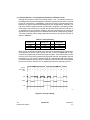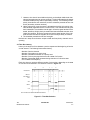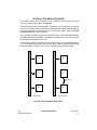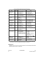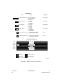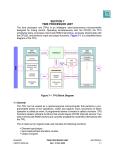
1
TPU
TIME PROCESSOR UNIT
REFERENCE MANUAL
(INCLUDING THE TPU2)
Motorola reserves the right to make changes without further notice to any products herein. Motorola makes no warranty, representation or guarantee regarding
the suitability of its products for any particular purpose, nor does Motorola assume any liability arising out of the application or use of any product or circuit, and
specifically disclaims any and all liability, including without limitation consequential or incidental damages. “Typical” parameters can and do vary in different
applications. All operating parameters, including “Typicals” must be validated for each customer application by customer’s technical experts. Motorola does not
convey any license under its patent rights nor the rights of others. Motorola products are not designed, intended, or authorized for use as components in
systems intended for surgical implant into the body, or other applications intended to support or sustain life, or for any other application in which the failure of
the Motorola product could create a situation where personal injury or death may occur. Should Buyer purchase or use Motorola products for any such
unintended or unauthorized application, Buyer shall indemnify and hold Motorola and its officers, employees, subsidiaries, affiliates, and distributors harmless
against all claims, costs, damages, and expenses, and reasonable attorney fees arising out of, directly or indirectly, any claim of personal injury or death
associated with such unintended or unauthorized use, even if such claim alleges that Motorola was negligent regarding the design or manufacture of the part.
Motorola and the Motorola logoare registered trademarks of Motorola, Inc. Motorola, Inc. is an Equal Opportunity/Affirmative Action Employer.
©MOTOROLA, INC., 1996
PREFACE
This manual describes the capabilities, operation, and functions of the time processor
unit (TPU) and the enhanced TPU2, both of which are integral modules in Motorola’s
family of modular microcontrollers. Documentation for the Modular Microcontroller
Family follows the modular construction of the devices in the product line. Each device
has a comprehensive user’s manual which provides sufficient information for normal
operation of the device. The user’s manual is supplemented by module reference
manuals, including the TPU reference manual, that provide detailed information about
module operation and applications. Refer to Motorola publication Advanced Microcontroller Unit (AMCU) Literature (BR1116/D) for a complete listing of documentation.
The following conventions are used throughout the manual.
The TPU and TPU2 are generically referred to as TPU except when specific
differences require separate identification.
Logic level one is the voltage that corresponds to Boolean true (1) state.
Logic level zero is the voltage that corresponds to Boolean false (0) state.
To set a bit or bits means to establish logic level one on the bit or bits.
To clear a bit or bits means to establish logic level zero on the bit or bits.
A signal that is asserted is in its active logic state. An active low signal changes from
logic level one to logic level zero when asserted, and an active high signal changes
from logic level zero to logic level one.
A signal that is negated is in its inactive logic state. An active low signal changes from
logic level zero to logic level one when negated, and an active high signal changes
from logic level one to logic level zero.
LSB means least significant bit or bits. MSB means most significant bit or bits. References to low and high bytes are spelled.
A specific bit or signal within a range is referred to by mnemonic and number. For
example, ADDR15 is bit 15 of the address bus. A range of bits or signals is referred
to by mnemonic and the numbers that define the range. For example, DATA[7:0] form
the low byte of the data bus.
This manual is intended for users of the pre-programmed time functions provided in
microcoded ROM, as well as for those who wish to incorporate functions from the TPU
function library.
TPU
REFERENCE MANUAL
MOTOROLA
iii
This manual should be used in conjunction with programming notes for the individual
TPU functions. Motorola Programming Note Literature Pack (TPULITPAK/D) provides
available programming notes.
Programmers intending to modify existing time functions or develop their own microcoded functions should read this manual and Motorola document number TPUMASMREF/D1, Time Processor Unit Programmer’s Reference Manual. In addition, they
should consult Motorola Programming Note TPUPN00/D, Using the TPU Function Library and TPU Emulation Mode, as well as the programming notes for any pre-programmed time functions they intend to use or modify.
MOTOROLA
iv
TPU
REFERENCE MANUAL
TABLE OF CONTENTS
Paragraph
Title
Page
SECTION 1OVERVIEW
1.1
1.2
1.2.1
1.2.2
1.2.3
1.2.4
1.2.5
1.2.6
1.3
1.3.1
1.3.2
1.3.3
1.3.4
1.4
1.5
Introduction ..................................................................................................... 1-2
TPU Components ........................................................................................... 1-2
Time Bases ............................................................................................ 1-2
Timer Channels ...................................................................................... 1-2
Host Interface ......................................................................................... 1-2
Parameter RAM ...................................................................................... 1-3
Scheduler ............................................................................................... 1-3
Microengine ............................................................................................ 1-3
TPU Features ................................................................................................. 1-3
Emulation Support .................................................................................. 1-3
Channel Orthogonality ............................................................................ 1-4
Interchannel Communication .................................................................. 1-4
Coherency .............................................................................................. 1-4
TPU Memory Map .......................................................................................... 1-4
Signal Descriptions ......................................................................................... 1-6
SECTION 2 HOST INTERFACE
2.1
2.1.1
2.1.2
2.2
2.2.1
2.2.2
2.2.3
2.2.4
2.2.5
2.2.6
2.3
2.4
2.5
2.6
2.7
2.7.1
2.8
2.9
2.9.1
2.9.2
System Configuration ..................................................................................... 2-1
TPUMCR Register .................................................................................. 2-2
TPUMCR2 Register ................................................................................ 2-6
Interrupts ........................................................................................................ 2-8
Interrupt Levels ....................................................................................... 2-8
Interrupt Arbitration ................................................................................. 2-9
Interrupt Vectors ..................................................................................... 2-9
Enabling Interrupts ................................................................................. 2-9
Development Support and Test Registers ........................................... 2-10
Channel Interrupt Registers ................................................................. 2-10
Channel Function Select Registers .............................................................. 2-11
Host Sequence Registers ............................................................................. 2-12
Host Service Request Registers .................................................................. 2-12
Channel Priority Registers ............................................................................ 2-13
Channel Parameter RAM ............................................................................. 2-14
Parameter RAM Address Map ............................................................. 2-14
Configuration Summary ................................................................................ 2-17
Configuration Examples ............................................................................... 2-19
CPU32 Configuration Example ............................................................ 2-19
CPU16 Configuration Example ............................................................ 2-21
SECTION 3 SCHEDULER
TPU
REFERENCE MANUAL
MOTOROLA
v
TABLE OF CONTENTS
Paragraph
3.1
3.1.1
3.1.2
3.1.3
3.2
3.3
(Continued)
Title
Page
Priority Scheme ............................................................................................. 3-1
Primary Scheme — Priority Among Channels on Different Levels ........ 3-3
Secondary Scheme — Priority Among Channels on the Same Level .... 3-4
Correlation of Primary and Secondary Schemes ................................... 3-4
Time-Slot Latency .......................................................................................... 3-5
Disabling a Function ....................................................................................... 3-6
SECTION 4TPU EMULATION MODE
4.1
4.2
4.3
4.4
TPU Control Store Organization ..................................................................... 4-2
Emulation Mode Memory Map ....................................................................... 4-2
TPU Function Library ..................................................................................... 4-6
Emulation Mode Summary ............................................................................. 4-7
APPENDIX ATPU FUNCTIONS
A.1
A.2
A.3
A.4
A.5
A.6
A.7
A.8
A.9
A.10
A.11
A.12
A.13
A.14
A.15
A.16
A.17
A.18
A.19
A.20
A.21
A.22
A.23
A.24
Mask Set A .....................................................................................................A-1
Mask Set G .....................................................................................................A-2
CHANNEL CONTROL Parameter ..................................................................A-4
Period/Pulse-Width Accumulator (PPWA) ......................................................A-5
Output Compare (OC) ....................................................................................A-7
Stepper Motor (SM) Control ...........................................................................A-9
Position-Synchronized Pulse Generator (PSP) ............................................A-11
Period Measurement with Additional Transition Detection (PMA) ................A-13
Period Measurement with Missing Transition Detection (PMM) ...................A-15
Input Capture/Input Transition Counter (ITC) ...............................................A-17
Pulse-Width Modulation (PWM) ...................................................................A-19
Discrete Input/Output (DIO) ..........................................................................A-21
Synchronized Pulse-Width Modulation (SPWM) ..........................................A-23
Quadrature Decode (QDEC) ........................................................................A-26
Programmable Time Accumulator (PTA) .....................................................A-28
Queued Output Match TPU Function (QOM) ...............................................A-30
Table Stepper Motor (TSM) ..........................................................................A-32
Frequency Measurement (FQM) ..................................................................A-35
Universal Asynchronous Receiver/Transmitter (UART) ...............................A-37
New Input Capture/Transition Counter (NITC) .............................................A-40
Multiphase Motor Commutation (COMM) .....................................................A-42
Multichannel Pulse-Width Modulation (MCPWM) ........................................A-44
Hall Effect Decode (HALLD) .........................................................................A-51
Fast Quadrature Decode TPU Function (FQD) ............................................A-53
APPENDIX B MEMORY MAP AND REGISTERS
MOTOROLA
vi
TPU
REFERENCE MANUAL
TABLE OF CONTENTS
(Continued)
Title
Paragraph
Page
B.1
Memory Map ..................................................................................................B-1
B.2
Registers ........................................................................................................B-2
B.2.1
TPU Module Configuration Register .......................................................B-2
B.2.2
Test Configuration Register ....................................................................B-4
B.2.3
Development Support Control Register ..................................................B-4
B.2.4
Development Support Status Register ...................................................B-5
B.2.5
TPU Interrupt Configuration Register .....................................................B-5
B.2.6
Channel Interrupt Enable Register .........................................................B-6
B.2.7
Channel Function Select Registers ........................................................B-6
B.2.8
Host Sequence Registers .......................................................................B-7
B.2.9
Host Service Request Registers ............................................................B-7
B.2.10
Channel Priority Registers ......................................................................B-7
B.2.11
Channel Interrupt Status Register ..........................................................B-8
B.2.12
Link Register ..........................................................................................B-8
B.2.13
Service Grant Latch Register .................................................................B-9
B.2.14
Decoded Channel Number Register ......................................................B-9
B.2.15
TPUMCR2 Module Configuration Register 2 .........................................B-9
B.2.16
TPU Parameter RAM ...........................................................................B-10
APPENDIX CESTIMATING WORST-CASE LATENCY
C.1
C.2
C.3
C.3.1
C.3.2
C.3.3
C.3.4
C.4
C.4.1
C.4.1.1
C.4.1.2
C.4.1.3
C.4.2
C.4.2.1
C.4.2.2
C.4.2.3
C.5
C.5.1
C.5.2
C.5.2.1
C.5.2.2
Introduction to Worst-Case Latency .............................................................. C-1
Using Worst-Case Latency Estimates to Evaluate Performance .................. C-3
Priority Scheme Details Used in WCL Analysis ............................................ C-3
Priority Passing ..................................................................................... C-4
Time-Slot Transition .............................................................................. C-5
Channel Number Priority ....................................................................... C-5
RAM Collision Rate ............................................................................... C-5
First-Pass Worst-Case Latency Analysis ...................................................... C-6
Worst-Case Assumptions and Formula ................................................. C-6
Finding the Worst-Case Service Time for Each Active Channel ... C-7
Mapping the Channels for Each Time Slot .................................... C-8
Adding Time for Time-Slot Transitions and NOPs ........................ C-8
First-Pass Analysis Worst-Case Latency Examples ............................. C-8
Finding the WCL for PWM on Channel 0 ...................................... C-8
Finding the WCL for PPWA on Channel 1 .................................... C-9
Finding the WCL for DIO on Channel 2 ...................................... C-10
Second-Pass Worst-Case Latency Analysis ............................................... C-11
Second-Pass Analysis Guidelines ....................................................... C-11
Second-Pass Analysis Example .......................................................... C-12
First-Try System Configuration ................................................... C-13
Second-Try System Configuration .............................................. C-14
TPU
REFERENCE MANUAL
MOTOROLA
vii
TABLE OF CONTENTS
Paragraph
(Continued)
Title
Page
APPENDIX DCHANNEL HARDWARE DIAGRAM
MOTOROLA
viii
TPU
REFERENCE MANUAL
LIST OF ILLUSTRATIONS
Figure
1-1
1-2
2-1
2-2
2-3
2-4
2-5
3-1
3-2
3-3
4-1
4-2
4-3
4-4
4-5
A-1
A-2
A-3
A-4
A-5
A-6
A-7
A-8
A-9
A-10
A-11
A-12
A-13
A-14
A-15
A-16
A-17
A-18
A-19
A-20
A-21
A-22
A-23
A-24
A-25
A-26
Title
Page
TPU Block Diagram ........................................................................................ 1-1
TPU Pins ........................................................................................................ 1-6
TCR1 Prescaler Control ................................................................................. 2-3
TCR2 Prescaler Control 2 .............................................................................. 2-3
Parameter RAM Arbitration Timing, Word Access by Host .......................... 2-16
Parameter RAM Arbitration Timing, Word or Long-Word Access by TPU ... 2-17
Channel Control and Parameter RAM Configuration ................................... 2-18
Priority Levels ................................................................................................. 3-2
Priority Passing .............................................................................................. 3-3
Time-Slot Variation ......................................................................................... 3-5
On-Chip RAM Configuration ........................................................................... 4-1
TPU Control Store and 2-Kbyte Emulation RAM Map .................................... 4-3
TPU2 Micro-Store Size Configurations .......................................................... 4-4
Extending Microcode Segment by Means of Unused Entry Points ................ 4-5
1-Kbyte Emulation RAM Memory Map ........................................................... 4-6
PPWA Parameters ......................................................................................... A-6
OC Parameters .............................................................................................. A-8
SM Parameters, Part 1 of 2 .......................................................................... A-10
SM Parameters, Part 2 of 2 .......................................................................... A-11
PSP Parameters ........................................................................................... A-12
PMA Parameters .......................................................................................... A-14
PMM Parameters ......................................................................................... A-16
ITC Parameters ............................................................................................ A-18
PWM Parameters ......................................................................................... A-20
DIO Parameters ........................................................................................... A-22
SPWM Parameters, Part 1 of 2 .................................................................... A-24
SPWM Parameters, Part 2 of 2 .................................................................... A-25
QDEC Parameters ....................................................................................... A-27
PTA Parameters ........................................................................................... A-29
QOM Parameters ......................................................................................... A-31
TSM Parameters — Master Mode ................................................................ A-33
TSM Parameters — Slave Mode .................................................................. A-34
FQM Parameters .......................................................................................... A-36
UART Transmitter Parameters ..................................................................... A-38
UART Receiver Parameters ......................................................................... A-39
NITC Parameters ......................................................................................... A-41
COMM Parameters, Part 1 of 2 .................................................................... A-43
COMM Parameters, Part 2 of 2 .................................................................... A-44
MCPWM Parameters — Master Mode ......................................................... A-45
MCPWM Parameters — Slave Edge-Aligned Mode .................................... A-46
MCPWM Parameters — Slave Ch A Non-Inverted Center-Aligned Mode ... A-47
TPU
REFERENCE MANUAL
MOTOROLA
ix
LIST OF ILLUSTRATIONS
(Continued)
Title
Figure
A-27
A-28
A-29
A-30
A-31
A-32
C-1
C-2
C-3
C-4
C-5
C-6
C-7
C-8
C-9
C-10
C-11
D-1
Page
MCPWM Parameters — Slave Ch B Non-Inverted Center-Aligned Mode ... A-48
MCPWM Parameters — Slave Ch A Inverted Center-Aligned Mode ........... A-49
MCPWM Parameters — Slave Ch B Inverted Center-Aligned Mode ........... A-50
HALLD Parameters ...................................................................................... A-52
FQD Parameters — Primary Channel .......................................................... A-54
FQD Parameters — Secondary Channel ..................................................... A-55
Worst-Case Latency for PWM ........................................................................C-1
TPU Function States ......................................................................................C-2
Time-Slot Sequence .......................................................................................C-4
Multiple Time-Slot Sequences ........................................................................C-4
First-Pass Worst-Case Latency ......................................................................C-6
Next Servicing for Channel 0 ..........................................................................C-9
Next Servicing for Channel 1 ........................................................................C-10
Next Servicing for Channel 2 ........................................................................C-11
Worst-Case Latency for Channel 0 (First Try) ..............................................C-14
Worst-Case Latency for Channel 0 (Second Try) ........................................C-15
Worst-Case Latency for Channel 2 ..............................................................C-15
Channel Hardware Block Diagram .................................................................D-2
MOTOROLA
x
TPU
REFERENCE MANUAL
LIST OF TABLES
Table
Title
Page
1-1 TPU Address Map ................................................................................................. 1-5
2-1 TPUMCR/TPUMCR2 Bit Configuration Fields....................................................... 2-1
2-2 TCR1 Prescaler Control......................................................................................... 2-2
2-3 TCR2 Prescaler Output ......................................................................................... 2-4
2-4 TPU/TPU2 Reset with Flash EEPROM ................................................................. 2-4
2-5 TCR2 Counter Clock Source ................................................................................. 2-5
2-6 Divide by 2 Control ................................................................................................ 2-6
2-7 Entry Table Bank Location..................................................................................... 2-7
2-8 System Clock Frequency/Minimum Detected Pulse.............................................. 2-8
2-9 Channel Priorities ................................................................................................ 2-13
2-10 Parameter RAM Address Map........................................................................... 2-14
3-1 Priority Passing...................................................................................................... 3-3
A-1 Mask Set A Time Function Encodings .................................................................. A-2
A-2 Mask Set G Time Function Encodings .................................................................. A-3
A-3 CHANNEL CONTROL Options ............................................................................. A-4
A-4 QOM Bit Encoding............................................................................................... A-30
B-1 TPU Address Map ................................................................................................. B-1
B-2 TPU/TPU2 Reset with Flash EEPROM................................................................. B-3
B-3 TCR2 Counter Clock Source................................................................................. B-3
B-4 FRZ[1:0] Bit Field .................................................................................................. B-4
B-5 Channel Priorities .................................................................................................. B-8
B-6 Entry Table Bank Location .................................................................................... B-9
B-7 System Clock Frequency/Minimum Guaranteed Detected Pulse ....................... B-10
B-8 Parameter RAM Address Map ............................................................................ B-10
C-1 Longest States and RAM Accesses for Mask Set A Functions.............................C-7
C-2 System Configuration Example.............................................................................C-8
C-3 Worst-Case Latency for Channel 0 .......................................................................C-9
C-4 Worst Case Latency for Channel 1 .....................................................................C-10
C-5 Worst Case Latency for Channel 2 .....................................................................C-11
C-6 First-Try System Configuration ...........................................................................C-13
C-7 Second-Try System Configuration ......................................................................C-14
C-8 Second-Try System with Channel 0 and 1 Reconfigured ...................................C-15
TPU
REFERENCE MANUAL
MOTOROLA
xi
LIST OF TABLES
Table
MOTOROLA
xii
(Continued)
Title
Page
TPU
REFERENCE MANUAL
SECTION 1 OVERVIEW
The following section provides general information on the time processor unit (TPU)
and the enhanced TPU2.
NOTE
The TPU and TPU2 are generically referred to as TPU except when
specific differences require separate identification.
HOST
INTERFACE
CONTROL
IMB
SYSTEM
CONFIGURATION
SCHEDULER
SERVICE REQUESTS
CHANNEL
The TPU is an intelligent, semi-autonomous co-processor designed for timing control.
Operating simultaneously with the CPU, the TPU processes microinstructions, schedules and processes real-time hardware events, performs input and output, and accesses shared data without CPU intervention. Consequently, for each timer event, the
CPU setup and service time are minimized or eliminated. Figure 1-1 is a simplified
block diagram of the TPU.
TCR1
T2CLK
PIN
TIMER
CHANNELS
CHANNEL 0
CHANNEL 1
TCR2
DEVELOPMENT
SUPPORT AND TEST
PINS
MICROENGINE
CHANNEL
CONTROL
PARAMETER
RAM DATA
DATA
CONTROL
STORE
CONTROL AND DATA
EXECUTION
UNIT
CHANNEL 15
TPU BLOCK
Figure 1-1 TPU Block Diagram
TPU
REFERENCE MANUAL
OVERVIEW
MOTOROLA
1-1
1.1 Introduction
The TPU module includes a set of pre-programmed functions microcoded in ROM. Different ROM mask sets are provided with different microcontrollers (MCUs). Refer to
the appropriate MCU user’s manual for a list of the time functions provided. Pre-programmed time functions for the two mask sets currently in production are described
briefly in APPENDIX A TPU FUNCTIONS. In addition, individual programming notes
for each function describe the functions in greater detail and provide application examples. Refer to Motorola Programming Note TPUPN00/D, Using the TPU Function Library and TPU Emulation Mode, for a list of available programming notes for individual
functions.
1.2 TPU Components
The TPU module consists of two 16-bit time bases, sixteen independent timer channels, a task scheduler, a microengine, and a host interface. In addition, a dual-port parameter RAM is used for TPU data storage and for passing parameters between the
module and the host CPU.
1.2.1 Time Bases
Two 16-bit counters provide reference time bases for all output compare and input
capture events. Prescalers for both time bases are controlled by the host CPU through
bit fields in the TPU module configuration register (TPUMCR). The TPU2 uses an additional control register (TPUMCR2). The TCR1 clock is always derived from the system clock. The TCR2 clock can be derived from the system clock or from an external
input via the T2CLK clock pin. The duration between active edges on the T2CLK clock
pin must be at least nine system clocks.
1.2.2 Timer Channels
The TPU has 16 independent channels, each connected to an MCU pin. The channels
have identical hardware with the exception of channel 15 on the TPU2, which has additional output disable logic. Each channel consists of an event register and pin control
logic. The event register contains a 16-bit capture register, a 16-bit compare/match
register, and a 16-bit greater-than-or-equal-to comparator. The direction of each pin,
either output or input, is determined by the TPU microengine. Each channel can either
use the same time base for match and capture, or can use one time base for match
and the other for capture.
1.2.3 Host Interface
The host interface allows the host CPU to control the operation of the TPU. The host
CPU must initialize the TPU by writing to the appropriate host interface registers to assign a function, interrupt level, and priority to each channel. In addition, the CPU writes
to the host service request and host sequence registers to further define function operation for each initialized channel. Refer to SECTION 2 HOST INTERFACE for a description of the host interface, including register bit/field definitions.
MOTOROLA
1-2
OVERVIEW
TPU
REFERENCE MANUAL
1.2.4 Parameter RAM
TPU parameter RAM occupies 200 bytes at the top of the TPU module address map.
Channel parameters are organized as 100 16-bit words. Channels 0 to 13 have six
parameters; channels 14 and 15 each have eight parameters.
TPU2 parameter RAM occupies 256 bytes at the top of the TPU2 module address
map. Channel parameters are organized as 128 16-bit words. Channels 0 through 15
each have eight parameters.
Refer to paragraphs 1.4 TPU Memory Map and 2.7.1 Parameter RAM Address Map
for information on how parameter words are organized in memory.
The parameter RAM is used as a dual-ported communication RAM for the TPU and
the host CPU. The parameters required by each pre-programmed time function are
shown in APPENDIX A TPU FUNCTIONS and described in detail in individual programming notes.
1.2.5 Scheduler
Out of reset, all channels are disabled. The host CPU makes a channel active by assigning it one of three priorities: high, middle, or low. The scheduler determines the order in which channels are serviced based on channel number and assigned priority.
Refer to SECTION 3 SCHEDULER for additional details.
1.2.6 Microengine
The microengine is composed of a control store and an execution unit. Control-store
ROM holds the microcode for each factory-masked function. Alternatively, in emulation mode, microcode is executed from the TPURAM module instead of the control
store. Emulation mode allows the development of custom TPU functions. Refer to
SECTION 4 TPU EMULATION MODE for more information.
1.3 TPU Features
Important TPU features are summarized in the following paragraphs.
1.3.1 Emulation Support
To support changing TPU application requirements, Motorola has established a TPU
function library. The function library is a collection of TPU functions written for easy assembly in combination with each other or with custom functions. In emulation mode,
the TPU uses an on-chip RAM module (TPURAM) as control store instead of the TPU
control store ROM. There is no performance loss in emulation mode; functions execute as quickly as they would in TPU control ROM. Notice that in emulation mode, the
CPU cannot access the TPURAM. Refer to SECTION 4 TPU EMULATION MODE for
information on TPU emulation mode. See Motorola Programming Note TPUPN00/D,
Using the TPU Function Library and TPU Emulation Mode, for details on the TPU function library.
TPU
REFERENCE MANUAL
OVERVIEW
MOTOROLA
1-3
1.3.2 Channel Orthogonality
All TPU channels contain identical hardware and are functionally equivalent in operation. This allows any channel to be configured to perform any time function. The user
controls the combination of functions.
1.3.3 Interchannel Communication
The autonomy of the TPU is enhanced by the ability of a channel to affect the operation of one or more other channels without CPU intervention. Interchannel communication allows one channel to control multiple channels, or allows multiple functions to
interact.
1.3.4 Coherency
For data to be coherent, all available portions of it must be identical in age or logically
related. As an example, consider a 32-bit counter value that is read and written as two
16-bit words. The 32-bit value is read-coherent only if both 16-bit portions are updated
at the same time, and write-coherent only if both portions take effect at the same time.
Parameter RAM hardware supports coherent access of two adjacent 16-bit parameters. The host CPU must use a long-word operation to guarantee coherency.
1.4 TPU Memory Map
TPU registers and parameter RAM are mapped into a 512-byte address space. Unused registers within the 512-byte address space return zeros when read. All registers
except the channel interrupt status register (CISR), which permits byte accesses, must
be read or written through word or long-word accesses.
The TPU address map is shown in Table 1-1. The column labeled “Access” indicates
the privilege level required to access the register. A designation of “S” indicates that
supervisor access is required; a designation of “S/U” indicates that the register can be
programmed (by setting or clearing a bit in the TPUMCR) for supervisor access only
or for both supervisor and user access.
Table 1-1 provides TPU register addresses relative to the TPU base address. In this
table, the high-order part of each address is listed as ###. Refer to the user’s manual
for the specific MCU for the exact location of the registers. The most significant bit of
the address is determined by the module mapping (MM) bit in the SIM or SCIM configuration register. The shaded area applies to the TPU2 only.
MOTOROLA
1-4
OVERVIEW
TPU
REFERENCE MANUAL
Table 1-1 TPU Address Map
Access
Address
S1
$###E00
15
TPU MODULE CONFIGURATION REGISTER (TPUMCR)
8 7
0
S
$###E02
TPU TEST CONFIGURATION REGISTER (TCR)
S
$###E04
DEVELOPMENT SUPPORT CONTROL REGISTER (DSCR)
S
$###E06
DEVELOPMENT SUPPORT STATUS REGISTER (DSSR)
S
$###E08
TPU INTERRUPT CONFIGURATION REGISTER (TICR)
S
$###E0A
CHANNEL INTERRUPT ENABLE REGISTER (CIER)
S
$###E0C
CHANNEL FUNCTION SELECT REGISTER 0 (CFSR0)
S
$###E0E
CHANNEL FUNCTION SELECT REGISTER 1 (CFSR1)
S
$###E10
CHANNEL FUNCTION SELECT REGISTER 2 (CFSR2)
S
$###E12
CHANNEL FUNCTION SELECT REGISTER 3 (CFSR3)
S/U2
$###E14
HOST SEQUENCE REGISTER 0 (HSQR0)
S/U
$###E16
HOST SEQUENCE REGISTER 1 (HSQR1)
S/U
$###E18
HOST SERVICE REQUEST REGISTER 0 (HSRR0)
S/U
$###E1A
HOST SERVICE REQUEST REGISTER 1 (HSRR1)
S
$###E1C
CHANNEL PRIORITY REGISTER 0 (CPR0)
S
$###E1E
CHANNEL PRIORITY REGISTER 1 (CPR1)
S
$###E20
CHANNEL INTERRUPT STATUS REGISTER (CISR)
S
$###E22
LINK REGISTER (LR)
S
$###E24
SERVICE GRANT LATCH REGISTER (SGLR)
S
$###E26
DECODED CHANNEL NUMBER REGISTER (DCNR)
S
$###E28
TPU2 MODULE CONFIGURATION REGISTER 2 (TPUMCR2) — TPU2 ONLY
S/U
$###F00 – $###F0E
CHANNEL 0 PARAMETER REGISTERS
S/U
$###F10 – $###F1E
CHANNEL 1 PARAMETER REGISTERS
S/U
$###F20 – $###F2E
CHANNEL 2 PARAMETER REGISTERS
S/U
$###F30 – $###F3E
CHANNEL 3 PARAMETER REGISTERS
S/U
$###F40 – $###F4E
CHANNEL 4 PARAMETER REGISTERS
S/U
$###F50 – $###F5E
CHANNEL 5 PARAMETER REGISTERS
S/U
$###F60 – $###F6E
CHANNEL 6 PARAMETER REGISTERS
S/U
$###F70 – $###F7E
CHANNEL 7 PARAMETER REGISTERS
S/U
$###F80 – $###F8E
CHANNEL 8 PARAMETER REGISTERS
S/U
$###F90 – $###F9E
CHANNEL 9 PARAMETER REGISTERS
S/U
$###FA0 – $###FAE
CHANNEL 10 PARAMETER REGISTERS
S/U
$###FB0 – $###FBE
CHANNEL 11 PARAMETER REGISTERS
S/U
$###FC0 – $###FCE
CHANNEL 12 PARAMETER REGISTERS
S/U
$###FD0 – $###FDE
CHANNEL 13 PARAMETER REGISTERS
S/U
$###FE0 – $###FEE
CHANNEL 14 PARAMETER REGISTERS
S/U
$###FF0 – $###FFE
CHANNEL 15 PARAMETER REGISTERS
NOTES:
1. S = Supervisor accessible only.
2. S/U = Supervisor accessible only (if SUPV = 1) or unrestricted (if SUPV = 0). Unrestricted registers allow both
user and supervisor access.
TPU
REFERENCE MANUAL
OVERVIEW
MOTOROLA
1-5
1.5 Signal Descriptions
There are 17 external pins associated with the TPU: 16 channel pins and the T2CLK
pin. These signals are illustrated in Figure 1-2.
TPU
IMB
TPUCH0
TPUCH1
TPUCH2
TPUCH3
TPUCH4
TPUCH5
TPUCH6
TPUCH7
TPUCH8
TPUCH9
TPUCH10
TPUCH11
TPUCH12
TPUCH13
TPUCH14
TPUCH15
T2CLK
1015A
Figure 1-2 TPU Pins
The direction of each channel pin, either output or input, is determined by the function.
The T2CLK pin is used to clock or gate the TCR2 counter. Refer to 2.1 System Configuration for proper use of this pin.
MOTOROLA
1-6
OVERVIEW
TPU
REFERENCE MANUAL
SECTION 2 HOST INTERFACE
The following section describes the host interface to the TPU. The registers described
in this section configure the TPU as a whole, the 16 individual channels, and the parameter registers within the RAM used to exchange parameters between the TPU and
host CPU.
NOTE
All registers are 16 bits in length and are only accessible through
word transfers with one exception – the channel interrupt status register (CISR) can also be accessed on a byte basis. This allows the
CPU to perform bit manipulation instructions on the CISR only. A
byte write of any TPU register other than the CISR sets the other byte
of the word to $FF.
2.1 System Configuration
The TPU module configuration register (TPUMCR) contains the bit fields that define
TPU and TPU2 module attributes.The TPUMCR resides in supervisor data space.
The TPU2 module contains an additional system configuration register, the TPU module configuration register 2 (TPUMCR2). The TPUMCR2 resides in supervisor data
space.
Table 2-1 provides an overview of the different bits and bit fields found in the TPU and
TPU2 module configuration registers.
Table 2-1 TPUMCR/TPUMCR2 Bit Configuration Fields
Register Name
TPUMCR
Module
TPU, TPU2
TPU2
TPUMCR2
TPU
REFERENCE MANUAL
Bit/Field Name
Stop control
TCR1 Prescaler control field
TCR2 Prescaler control field
Emulation control
Timer count register 2 clock control field
Stop flag
Supervisor/unrestricted
Prescaler clock
Interrupt arbitration field
TPU2 enable
TCR2 counter clock edge
Divide by two control
Soft reset
Entry table bank
Filter prescaler clock
T2CLK pin filter control
Disable TPU2 pins
HOST INTERFACE
Mnemonic
STOP
TCR1P[1:0]
TCR2P[1:0]
EMU
T2CG
STF
SUPV
PSCK
IARB[3:0]
TPU2
T2CSL
DIV2
SOFT RST
ETBANK[1:0]
FPSCK[2:0]
T2CF
DTPU
Bit Position
15
14-13
12-11
10
9
8
7
6
3-1
5
4
8
7
6-5
4-2
1
0
MOTOROLA
2-1
2.1.1 TPUMCR Register
The TPUMCR controls configuration parameters in the TPU and the TPU2. Register
diagrams and bit/field descriptions follow.
TPUMCR — TPU Module Configuration Register
14
15
STOP
13
12
11
TCR1P[1:0]
TCR2P[1:0]
0
0
$###E00
10
9
8
7
6
5
4
EMU1
T2CG
STF
SUPV
PSCK
TPU22
T2CSL3
0
0
0
1
0
1
0
3
2
1
0
IARB[3:0]
RESET:
0
0
0
0
0
0
0
NOTES:
1. On TPU2, this bit is set or cleared according to the shadow bit for bit four of the flash EEPROM module configuration (FEEMCR) register.
2. After reset, the TPU2 enable (TPU2) bit is zero if TPU module is present. In this case, the bit cannot be modified.
If the TPU2 module is present, the TPU2 enable bit is one after reset.
3. After reset, TCR2 counter clock edge (T2CSL) bit is zero if the TPU module is present. In this case, the bit cannot
be modified. If the TPU2 module is present, this bit is zero after reset and can be modified.
STOP — Stop Bit
When the STOP bit in the TPUMCR is set, the TPU shuts down its internal clocks,
shutting down the internal microengine. TCR1 and TCR2 cease to increment and retain the last value before the stop condition was entered. The TPU asserts the stop
flag (STF) in the TPUMCR to indicate that it has stopped.
When the STOP bit is set, the CPU can access all registers it can normally access except the priority registers. Accessing the priority registers causes a bus-error exception from the internal bus monitor. Refer to the appropriate MCU user’s manual or to
the SIM Reference Manual (SIMRM/AD) or SCIM Reference Manual (SCIMRM/AD)
for information on the internal bus monitor.
0 = TPU operating normally
1 = Internal clocks shut down
TCR1P — Timer Count Register 1 Prescaler Control
Timer count register 1 (TCR1) is clocked from the output of a prescaler. In the TPU,
two fields (PSCK, TCR1P) in the TPUMCR control TCR1. In the TPU2, an additional
field is required — DIV2, which is located in the TPUMCR2.
The input to the prescaler is the internal TPU system clock divided by either four or 32,
depending on the value of the PSCK bit. The prescaler divides this input by one, two,
four, or eight, depending on the value of TCR1P. Refer to Figure 2-1 and Table 2-2.
In the TPU2, if the DIV2 bit is one, the TCR1 counter increments at a rate of the internal
clock divided by two. If DIV2 is zero, the TCR1 increment rate is defined by the values
in Table 2-2.
Table 2-2 TCR1 Prescaler Control
PSCK = 0
Divide
By
Number of
Clocks
Rate at
16 MHz
Number of
Clocks
Rate at
16 MHz
00
01
10
11
1
2
4
8
32
64
128
256
2 µs
4 µs
8 µs
16 µs
4
8
16
32
250 ns
500 ns
1 µs
2 µs
MOTOROLA
2-2
PSCK = 1
TCR1P
HOST INTERFACE
TPU
REFERENCE MANUAL
Figure 2-1 shows a diagram of the TCR1 prescaler control block.
÷2
DIV2 CLOCK
CSEL
MUX
SYSTEM
CLOCK
÷4
÷ 32
DIV4 CLOCK
0
PSCK
MUX
00 ÷ 1
01 ÷ 2
10 ÷ 4
11 ÷ 8
DIV32 CLOCK
15
TCR1
TCR1
PRESCALER
0 – TCR1 PRESCALER
1 – DIV2
0 – DIV32 CLOCK
1 – DIV4 CLOCK
TPU PRE BLOCK 1
Figure 2-1 TCR1 Prescaler Control
TCR2P — Timer Count Register 2 Prescaler Control
Timer count register two (TCR2), like TCR1, is clocked from the output of a prescaler.
The T2CG (TCR2 clock/gate control) bit in TPUMCR determines whether the external
TCR2 pin functions as an external clock source for TCR2 or as the gate in the use of
TCR2 as a gated pulse accumulator.
In the TPU2, the T2CG bit and the T2CSL bit determine TCR2 pin functions.
The function of the T2CG bit is shown in Figure 2-2.
0–A
1–B
T2CF BIT
DIGITAL
FILTER
0–A
1–B
T2CG CONTROL BIT
T2CSL BIT
A
MUX
A
T2CLK
PIN
SYNCHRONIZER
MUX
PROGRAMMABLE B
DIGITAL
FILTER
B
DIV8 CLK
TCR2
PRESCALER
00 ÷ 1
01 ÷ 2
10 ÷ 4
11 ÷ 8
0
15
TCR2
TPU2 PRE BLOCK 2
Figure 2-2 TCR2 Prescaler Control 2
When the T2CG bit is set, the external T2CLK pin functions as a gate of the DIV8 clock
(the TPU system clock divided by eight). In this case, when the external TCR2 pin is
low, the DIV8 clock is blocked, preventing it from incrementing TCR2. When the external TCR2 pin is high, TCR2 is incremented at the frequency of the DIV8 clock. When
the T2CG bit is cleared, an external clock from the TCR2 pin increments TCR2. The
duration between active edges on the T2CLK clock pin must be at least nine system
clocks.
The TCR2 pin and each channel configured as an input have an associated synchronizer followed by a digital filter connected to the pin that samples pin transitions. These
TPU
REFERENCE MANUAL
HOST INTERFACE
MOTOROLA
2-3
filter out high and low pulse widths less than the period of two system clocks, preventing these transitions from being input to the transition detect logic. The synchronizer
and digital filter are guaranteed to pass pulses that are greater than the period of four
system clocks.
The TCR2 field in TPUMCR specifies the value of the prescaler: one, two, four, or
eight. Channels using TCR2 have the capability to resolve down to the TPU system
clock divided by eight. Table 2-3 is a summary of prescaler output.
Table 2-3 TCR2 Prescaler Output
TCR2 Prescaler
Divide By
Internal Clock
Divided By
External Clock
Divided By
00
01
10
11
1
2
4
8
8
16
32
64
1
2
4
8
EMU — Emulation Control
Emulation mode is entered by setting the EMU bit in the TPUMCR. In emulation mode,
an auxiliary bus connection is made between TPURAM and the TPU module, and access to TPURAM via the intermodule bus is disabled. A 9-bit address bus, a 32-bit
data bus, and control lines transfer information between the modules. To ensure exact
emulation, TPURAM module access timing remains consistent with access timing of
the TPU ROM control store.
The TPU function library is a collection of TPU functions written for easy assembly in
combination with each other or with custom functions. TPU emulation capability allows
the user to use the TPU library functions and develop new time functions. Refer to
SECTION 4 TPU EMULATION MODE for information about emulation mode, and to
Motorola Programming Note TPUPN00/D, Using the TPU Function Library and TPU
Emulation Mode, for details on the TPU function library.
0 = TPU and TPURAM in normal mode (operating as separate modules)
1 = TPU and TPURAM in emulation mode
After reset, this bit can be written only once.
When the TPU or TPU2 module is used with a flash EEPROM, the EMU bit is either
set or cleared upon a reset according to the conditions shown in Table 2-4.
Table 2-4 TPU/TPU2 Reset with Flash EEPROM
Module
Reset Condition
TPU
TPU2
EMU bit is cleared out of reset.
If the shadow bit for bit four of the flash EEPROM module configuration register
(FEEMCR) for the 4-Kbyte flash block is set, the EMU bit is cleared out of reset.
If the shadow bit for bit four of the FEEMCR for the 4-Kbyte flash block is clear,
the EMU bit is set out of reset.
T2CG — TCR2 Clock/Gate Control
In the TPU, the following states apply:
0 = TCR2 pin used as clock source for TCR2
1 = TCR2 pin used as gate of DIV8 clock for TCR2
In the TPU2, T2CG control bit and the T2CSL control bit determine the clock source
for TCR2.
MOTOROLA
2-4
HOST INTERFACE
TPU
REFERENCE MANUAL
STF — Stop Flag
0 = TPU operating
1 = TPU stopped (STOP bit has been asserted)
SUPV — Supervisor Data Space
In systems that support privilege levels, the CPU can operate at either of two levels:
user or supervisor. Certain TPU registers can be accessed only when the CPU is operating at the supervisor level. Other registers can be assigned supervisor-only access
by setting the SUPV bit in the TPUMCR. When SUPV is cleared, the programmable
registers are accessible from either the supervisor or user privilege level. In systems
that do not support privilege levels, the CPU always operates at the supervisor level.
When SUPV is cleared, if a supervisor-only register is accessed from the user privilege
level, the module responds as though an access had been made to an unimplemented
register location. When SUPV is set, accesses to all TPU registers from the user privilege level are transferred externally.
The S bit in the CPU status register determines the privilege level at which the CPU is
operating (0 = user level, 1 = supervisor level). Refer to the appropriate CPU reference
manual for more information on privilege levels.
0 = Assignable registers are accessible from user or supervisor privilege level
1 = Assignable registers are accessible from supervisor privilege level only
PSCK — Prescaler Clock
0 = System clock/32 is input to TCR1 prescaler
1 = System clock/4 is input to TCR1 prescaler
TPU2 — TPU2 Enable
In the TPU2, the TPU2 enable bit provides compatibility with the TPU. If running TPU
code on the TPU2, the microcode size should not be greater than two Kbytes and the
TPU2 enable bit should be cleared to zero. The TPU2 enable bit is write-once after
reset. The reset value is one, meaning that the TPU2 will operate in TPU2 mode.
0 = TPU mode; zero is the TPU reset value.
1 = TPU2 mode; one is the TPU2 reset value.
NOTE
The programmer should not change this value unless necessary
when developing custom TPU microcode.
T2CSL — TCR2 Counter Clock Edge
In the TPU2, this bit and the T2CG control bit determine the clock source for TCR2.
Refer to Table 2-5.
Table 2-5 TCR2 Counter Clock Source
T2CSL
0
0
1
1
TPU
REFERENCE MANUAL
T2CG
0
1
0
1
TCR2 Clock
Rise transition T2CLK
Gated system clock
Fall transition T2CLK
Rise and fall transition T2CLK
HOST INTERFACE
MOTOROLA
2-5
IARB — Interrupt Arbitration Number
This field contains the TPU arbitration number that is used to arbitrate for the intermodule bus when two or more modules or peripherals have an interrupt on the same priority level. The highest arbitration priority is $F, and the lowest is one. An IARB value
of zero causes the TPU not to arbitrate for the intermodule bus during an interrupt-acknowledge cycle. Refer to 2.2.2 Interrupt Arbitration for more information.
2.1.2 TPUMCR2 Register
The TPUMCR2 controls the configuration parameters discussed in the preceding
paragraphs. A register diagram and brief bit/field descriptions follow.
TPUMCR2 — TPU Module Configuration Register 2 (TPU2 Only)
15
14
13
12
11
10
9
8
7
0
0
0
0
0
0
0
DIV2
SOFT
RST
0
0
0
0
0
0
0
0
6
5
4
ETBANK[1:0]
$###E28
3
2
FPSCK[2:0]
1
0
T2CF
DTPU
0
0
RESET:
0
0
0
0
0
0
DIV2 — Divide by 2 Control
When asserted, the DIV2 bit, along with the TCR1P bit and the PSCK bit in the TPUMCR, determines the rate of the TCR1 counter in the TPU2. If set, the TCR1 counter
increments at a rate of two system clocks. If negated, TCR1 increments at the rate determined by control bits in the TCR1P and PSCK fields. Refer to Table 2-6.
Table 2-6 Divide by 2 Control
DIV2
1
PSCK
X
TCR1P
XX
Clocks
2
Rate at 16.7 MHz
125 ns
Rate at 20 MHz
100 ns
0 = TCR1 increments at rate determined by control bits in the TCR1P and PSCK
fields of the TPUMCR register.
1 = Causes TCR1 counter to increment at a rate of the system clock frequency
divided by two.
SOFT RST — Soft Reset
The TPU2 performs an internal reset when both the SOFT RST bit in the TPUMCR2
and the STOP bit in TPUMCR are set. CPU must write zero to the SOFT RST bit to
bring the TPU2 out of reset. The SOFT RST bit must be asserted for at least nine
clocks.
NOTE
Do not attempt to access any other TPU2 registers when this bit is
asserted. When this bit is asserted, it is the only accessible bit in the
register.
0 = Normal operation
1 = Puts TPU2 in reset until bit is cleared, but only if the STOP bit in the TPUMCR
is also set.
MOTOROLA
2-6
HOST INTERFACE
TPU
REFERENCE MANUAL
ETBANK[1:0] — Entry Table Bank Select
In the TPU2, the entry table bank (ETBANK[1:0]) field determines the bank where the
microcoded entry table is situated. After reset, this field is %00. This control bit field is
write once after reset. ETBANK[1:0] is used when the microcode contains entry tables
not located in the default bank 0. To execute the ROM functions on this MCU,
ETBANK[1:0] must be 00. Refer to Table 2-7.
NOTE
This field should not be modified by the programmer unless necessary because of custom microcode.
Table 2-7 Entry Table Bank Location
ETBANK
00
01
10
11
BANK
0
1
2
3
FPSCK[2:0] — Filter Prescaler Clock Control
In the TPU2, the filter prescaler clock control bit field determines the ratio between system clock frequency and minimum detectable pulses. The reset value of these bits is
zero, defining the filter clock as four system clocks. Refer to Table 2-8.
Table 2-8 System Clock Frequency/Minimum Detected Pulse
Filter Control
000
001
010
011
100
101
110
111
Divide By
4
8
16
32
64
128
256
512
16.7 MHz
240 ns
480 ns
960 ns
1.92 µs
3.84 µs
7.68 µs
15.36 µs
30.72 µs
20 MHz
200 ns
400 ns
800 ns
1.6 µs
3.2 µs
6.4 µs
12.8 µs
25.6 µs
T2CF — T2CLK Pin Filter Control
When asserted, the T2CLK input pin in the TPU2 is filtered with the same filter clock
that is supplied to the channels. This control bit is write once after reset.
0 = Uses fixed four-clock filter
1 = T2CLK input pin filtered with same filter clock that is supplied to the channels.
DTPU — Disable TPU2 Pins
In the TPU2, when the disable TPU2 control pin is asserted, pin TP15 is configured as
an input disable pin. When the TP15 pin value is zero, all TPU2 output pins are threestated, regardless of the pins function. The input is not synchronized. This control bit
is write once after reset.
0 = TP15 functions as normal TPU channel.
1 = TP15 pin configured as output disable pin. When TP15 pin is low, all TPU2 output pins are in a high-impedance state, regardless of the pin function.
TPU
REFERENCE MANUAL
HOST INTERFACE
MOTOROLA
2-7
2.2 Interrupts
The CPU services interrupt requests from peripherals. The peripherals may be located
on the same chip as the CPU, or may be off chip. A priority scheme is implemented to
prioritize all system peripherals, both on and off chip.
2.2.1 Interrupt Levels
The priority scheme that CPU16-based and CPU32-based MCUs use is based on the
68000 family priority scheme. The CPU16 and CPU32 contain a three-bit interrupt
priority mask. This mask is located in the condition code register in the CPU16 and in
the status register in the CPU32.
The CPU compares the level of each interrupt request it receives with the mask value.
Interrupt request levels greater than the mask are accepted; interrupt request levels
less than or equal to the mask are ignored. The only exception to the rule is the nonmaskable level seven interrupt request, which is accepted and serviced even if the
CPU interrupt mask is seven.
All on-chip peripherals are assigned an interrupt request level from zero to seven.
Seven is the highest priority, one is the lowest, and zero disables any interrupt requests. The channel interrupt request level (CIRL) in the TPU interrupt configuration
register (TICR) contains the request level associated with TPU interrupts.
2.2.2 Interrupt Arbitration
The same interrupt priority level can be assigned to more than one module. For example, the TPU and the QSM can both be assigned interrupt level five. If both the TPU
and the QSM interrupt the CPU simultaneously, then the interrupt arbitration (IARB)
fields in the respective module configuration registers determine which module is serviced first.
The IARB field is essentially a second-level priority in case of a tie. Each module that
has an interrupt priority level also has an IARB field. Each module must be assigned
a unique non-zero IARB value, or operation is undefined when interrupts with the
same priority level are issued simultaneously.
IARB fields contain four bits. An IARB value of %1111 is the highest arbitration priority,
%0001 is the lowest, and %0000 disables interrupt arbitration. Whereas zero in the interrupt priority level field disables a module from requesting an interrupt, a zero in the
IARB field disables a module from acknowledging its interrupt request. If a module with
a non-zero interrupt priority field and a zero IARB field requests an interrupt, the CPU
sees a spurious interrupt, because the module requesting the interrupt service never
confirms that it made the request. The IARB field for the TPU is located in the TPUMCR.
2.2.3 Interrupt Vectors
The system designer must make sure the CPU knows where to find the service routine
for each type of interrupt. The channel interrupt base vector (CIBV) determines where
to find the 16 TPU service routines, one for each of the 16 TPU channels. CIBV is the
MOTOROLA
2-8
HOST INTERFACE
TPU
REFERENCE MANUAL
upper nibble of a byte-size vector number; the lower nibble is the channel number itself. CIBV should contain an unreserved vector number. For example, if CIBV contains
$8, the vector number for a channel 0 interrupt is $80, the vector number for a channel
1 interrupt is $81, and so on to $8F for channel 15. The TPU passes the appropriate
vector number to the CPU when it acknowledges its interrupt request.
The system designer must set up the vector table. Refer to the CPU16 Reference
Manual (CPU16RM/AD) or the CPU32 Reference Manual (CPU32RM/AD) for additional information on the vector table.
2.2.4 Enabling Interrupts
The CPU can mask interrupts from individual channels in the channel interrupt enable
register (CIER). A zero in a bit field masks the interrupt from a specific channel; a one
enables the channel interrupt. If a channel interrupt is masked, the channel interrupt
status register (CISR) can be polled to see if an interrupt request is pending. The CISR
is the only TPU register that can be accessed by individual byte. This allows CPU32
bit test instructions, which only work on byte accesses, to be used for ease in polling.
To clear a status flag, read the CISR with the bit set, and then write a zero to the appropriate bit.
2.2.5 Development Support and Test Registers
The following registers are used for custom microcode development or for factory test.
Describing the use of the registers is beyond the scope of this manual. Refer to TPUMASMREF/D1, Time Processor Unit Programmer’s Reference Manual for information
on modifying existing time functions or developing microcoded functions. In addition,
refer to Motorola Programming Note TPUPN00/D, Using the TPU Function Library and
TPU Emulation Mode. Register descriptions are provided in APPENDIX B MEMORY
MAP AND REGISTERS.
TCR — Test Configuration Register
The TCR is used for factory test only.
$###E02
DSCR — Development Support Control Register
$###E04
DSSR — Development Support Status Register
$###E06
LR — Link Register
$###E22
SGLR — Service Grant Latch Register
$###E24
DCNR — Decoded Channel Number Register
$###E28
TPU
REFERENCE MANUAL
MOTOROLA
2-9
HOST INTERFACE
2.2.6 Channel Interrupt Registers
CIER — Channel Interrupt Enable Register
$###E0A
15
14
13
12
11
10
9
8
7
6
5
4
3
2
1
0
CH 15
CH 14
CH 13
CH 12
CH 11
CH 10
CH 9
CH 8
CH 7
CH 6
CH 5
CH 4
CH 3
CH 2
CH 1
CH 0
0
0
0
0
0
0
0
0
0
0
0
0
0
0
RESET:
0
0
CH[15:0] — Channel Interrupt Enable/Disable
0 = Channel interrupts disabled
1 = Channel interrupts enabled
CISR — Channel Interrupt Status Register
$###E20
15
14
13
12
11
10
9
8
7
6
5
4
3
2
1
0
CH 15
CH 14
CH 13
CH 12
CH 11
CH 10
CH 9
CH 8
CH 7
CH 6
CH 5
CH 4
CH 3
CH 2
CH 1
CH 0
0
0
0
0
0
0
0
0
0
0
0
0
0
0
RESET:
0
0
CH[15:0] — Channel Interrupt Status Bit
0 = Channel interrupt not asserted
1 = Channel interrupt asserted
TICR — TPU Interrupt Configuration Register
15
14
13
12
11
0
0
0
0
0
0
0
0
0
10
9
8
$###E08
7
6
CIRL
5
4
CIBV
3
2
1
0
0
0
0
0
0
0
0
0
RESET:
0
0
0
0
0
0
0
0
CIRL — Channel Interrupt Request Level
This three-bit encoded field specifies the interrupt request level for all channels. Level
seven for this field indicates a non-maskable interrupt; level zero indicates that all
channel interrupts are disabled.
CIBV — Channel Interrupt Base Vector
The TPU is assigned 16 unique interrupt vector numbers, one vector number for each
channel. The CIBV field specifies the most significant nibble of all 16 TPU channel interrupt vector numbers. The lower nibble of the TPU interrupt vector number is determined by the channel number on which the interrupt occurs.
2.3 Channel Function Select Registers
Each 4-bit field within the channel function select registers specifies one of up to 16
time functions to be executed on the corresponding channel. Numbers for predefined
functions in both TPU ROM mask sets currently in production are found in Tables A1 and A-2. Channel function select registers reside in supervisor data space.
MOTOROLA
2-10
HOST INTERFACE
TPU
REFERENCE MANUAL
CFSR0 — Channel Function Select Register 0
15
14
13
12
11
10
CHANNEL 15
9
8
$###E0C
7
6
CHANNEL 14
5
4
3
2
CHANNEL 13
1
0
CHANNEL 12
RESET:
0
0
0
0
0
0
0
0
0
0
0
0
0
0
CFSR1 — Channel Function Select Register 1
15
14
13
12
11
10
CHANNEL 11
9
8
0
0
$###E0E
7
6
CHANNEL 10
5
4
3
2
CHANNEL 9
1
0
CHANNEL 8
RESET:
0
0
0
0
0
0
0
0
0
0
0
0
0
0
CFSR2 — Channel Function Select Register 2
15
14
13
12
11
10
CHANNEL 7
9
8
0
0
$###E10
7
6
CHANNEL 6
5
4
3
2
CHANNEL 5
1
0
CHANNEL 4
RESET:
0
0
0
0
0
0
0
0
0
0
0
0
0
0
CFSR3 — Channel Function Select Register 3
15
14
13
12
11
10
CHANNEL 3
9
8
0
0
$###E12
7
6
CHANNEL 2
5
4
3
2
CHANNEL 1
1
0
CHANNEL 0
RESET:
0
0
0
0
0
0
0
0
0
0
0
0
0
0
0
0
CHANNEL[15:0] — Function to Execute on Corresponding Channel
2.4 Host Sequence Registers
The host sequence field helps specify the operation of the time function selected on a
given channel. The meaning of the host sequence bits depends on the time function
specified. Refer to Tables A-1 and A-2 for a summary of host sequence bits for the
predefined functions in the two TPU ROM mask sets currently in production.
The CPU can read or write the host sequence registers, but the TPU can only read
them. In systems that support privilege levels, host sequence registers can be assigned to either supervisor or user data space.
HSQR0 — Host Sequence Register 0
15
14
13
CH 15
12
11
CH 14
10
9
CH 13
$###E14
8
7
CH 12
6
5
CH 11
4
3
CH 10
2
1
CH 9
0
CH 8
RESET:
0
0
0
0
0
0
0
0
0
0
0
0
0
0
HSQR1 — Host Sequence Register 1
15
14
13
CH 7
12
11
CH 6
10
9
CH 5
0
0
$###E16
8
7
CH 4
6
5
CH 3
4
3
CH 2
2
1
CH 1
0
CH 0
RESET:
0
0
0
0
0
0
0
0
0
0
0
0
0
0
0
0
CH[15:0] — Host Sequence Bits
TPU
REFERENCE MANUAL
HOST INTERFACE
MOTOROLA
2-11
2.5 Host Service Request Registers
The host service request field selects the type of host service request for the time function selected on a given channel. The meaning of the host service request bits depends on the time function specified. Refer to Tables A-1 and A-2 for a summary of
host service bits for the predefined functions in the two TPU ROM mask sets currently
in production.
A host service request field with a value of %00 signals the host that no service is being
requested on the channel. The host can request service on a channel by writing the
corresponding host service request field to one of three non-zero states. The CPU
should monitor the host service request register and wait until the TPU microengine
clears the service request bits to %00 before changing any parameters or issuing a
new service request to the channel.
The host CPU can set bits in the host service request registers but cannot clear them.
To issue a host service request, the CPU should set the desired bits. All other bits must
be written back as zeros.
In systems that support privilege levels, host service request registers can be assigned to either supervisor or user data space.
HSRR0 — Host Service Request Register 0
15
14
13
CH 15
12
11
CH 14
10
9
CH 13
8
$###E18
7
CH 12
6
5
CH 11
4
3
CH 10
2
1
CH 9
0
CH 8
RESET:
0
0
0
0
0
0
0
0
0
0
0
0
0
0
7
6
5
4
3
2
HSRR1 — Host Service Request Register 1
15
14
13
CH 7
12
11
CH 6
10
9
CH 5
8
0
0
$###E1A
CH 4
CH 3
CH 2
1
CH 1
0
CH 0
RESET:
0
0
0
0
0
0
0
0
0
0
0
0
0
0
0
0
CH[15:0] — Host Service Request
2.6 Channel Priority Registers
The channel priority registers (CPR0, CPR1) assign one of three priority levels to a
channel or disable the channel. Table 2-9 indicates the priority assignments.
Table 2-9 Channel Priorities
CHX[1:0]
00
01
10
11
MOTOROLA
2-12
Service
Disabled
Low
Middle
High
HOST INTERFACE
TPU
REFERENCE MANUAL
Access to the channel priority registers may generate a wait state (one clock delay of
data transfer acknowledge assertion). The channel priority registers are accessible
only from the supervisor privilege level.
It is possible to change the priority level of or disable a channel dynamically. A disabled
channel is never scheduled to be serviced. Service requests that are pending before
a channel is disabled or occur while a channel is disabled remain asserted until the
channel is serviced. It is recommended to configure a host service request for initialization of a channel before that channel is enabled to active priority.
Refer to SECTION 3 SCHEDULER for additional information on channel priorities.
CPR0 — Channel Priority Register 0
15
14
13
CH 15
12
11
CH 14
10
$###E1C
9
CH 13
8
7
CH 12
6
5
CH 11
4
3
CH 10
2
1
CH 9
0
CH 8
RESET:
0
0
0
0
0
0
0
0
0
0
0
0
0
0
8
7
6
5
4
3
2
CPR1 — Channel Priority Register 1
15
14
13
CH 7
12
11
CH 6
10
0
$###E1E
9
CH 5
0
CH 4
CH 3
CH 2
1
CH 1
0
CH 0
RESET:
0
0
0
0
0
0
0
0
0
0
0
0
0
0
0
0
CH[15:0] — Priority Level
2.7 Channel Parameter RAM
The channel parameter RAM is organized as one hundred 16-bit words of RAM. In the
TPU, channels 0 to 13 have six parameters; channels 14 and 15 each have eight parameters. In the TPU2, channels 0 through 15 each have eight parameters.
The parameter RAM constitutes a shared work space for communication between the
CPU and the TPU and provides data storage for the TPU. The TPU can only access
data in the parameter RAM.
The parameters required by each pre-programmed time function in the two TPU mask
sets currently in production are provided in APPENDIX A TPU FUNCTIONS. Refer to
the programming notes for the individual functions for additional information.
2.7.1 Parameter RAM Address Map
Table 2-10 is the address map for the channel parameter registers. Addresses are offsets from the parameter RAM base address. Refer to the appropriate user’s manual
for the parameter RAM base address for a particular MCU.
Parameter RAM is not initialized during reset. It is assignable to either user or supervisor data space.
TPU
REFERENCE MANUAL
HOST INTERFACE
MOTOROLA
2-13
Table 2-10 Parameter RAM Address Map
Channel
Number
0
1
2
3
4
5
6
7
8
9
10
11
12
13
14
15
0
00
10
20
30
40
50
60
70
80
90
A0
B0
C0
D0
E0
F0
1
02
12
22
32
42
52
62
72
82
92
A2
B2
C2
D2
E2
F2
2
04
14
24
34
44
54
64
74
84
94
A4
B4
C4
D4
E4
F4
Parameter
3
4
06
08
16
18
26
28
36
38
46
48
56
58
66
68
76
78
86
88
96
98
A6
A8
B6
B8
C6
C8
D6
D8
E6
E8
F6
F8
5
0A
1A
2A
3A
4A
5A
6A
7A
8A
9A
AA
BA
CA
DA
EA
FA
6
0C1
1C
2C
3C
4C
5C
6C
7C
8C
9C
AC
BC
CC
DC
EC
FC
7
0E
1E
2E
3E
4E
5E
6E
7E
8E
9E
AE
BE
CE
DE
EE
FE
NOTES:
1. Shaded areas apply to the TPU2 only.
The TPU shares parameter RAM with the CPU. Parameter RAM may be accessed by
only one source at a time; an arbitration scheme prevents simultaneous accesses, allowing eventual access to all requesting sources. Long-word CPU accesses are coherent. The following rules regulate parameter RAM access.
The TPU gives priority to the CPU for parameter RAM accesses under any of the following conditions:
• The TPU has completed accessing the second word of a long-word parameter
RAM access.
• The parameter RAM was not accessed during the last arbitration period.
• The CPU is arbitrating for the second word access of a long-word transfer.
The TPU takes priority for parameter RAM accesses under either of the following conditions:
• The CPU has completed a data transfer during the last access; or
• The TPU is arbitrating for the second access of a data transfer. (A data transfer
is defined as word or long-word access.) All even multiples of back-to-back word
accesses are coherent.
Figure 2-3 and Figure 2-4 illustrate word accesses by a host, such as a CPU, and
word or long-word accesses by the TPU.
MOTOROLA
2-14
HOST INTERFACE
TPU
REFERENCE MANUAL
T1 T2 T3 T4 T1 T2 T3 T4 T1 T2 T3 T4 T1 T2 T3 T4 T1 T2 T3 T4 T1 T2 T3 T4 T1 T2 T3 T4
TPU STATES
B4 B1 B2 B3 B4 B1 B2 B3 B4 B1 B2 B3 B3 B3 B3 B3 B3 B3 B3 B3 B4 B1 B2 B3 B4 B1 B2 B3
IMB STATES
ARBITRATION
TPU RAM
REQUEST LATCH
TPU ACCESS
GRANTED
CPU RAM
REQUEST
CPU ACCESS
GRANTED
CPU RAM
PRIORITY
DTACK
TPU
REQUEST
CPU
REQUEST
BOTH
REQUEST
TPU WINS
BOTH
REQUEST
TPU WINS
BOTH
REQUEST
CPU WINS
TPU
REQUEST
1013A
Figure 2-3 Parameter RAM Arbitration Timing, Word Access by Host
TPU
REFERENCE MANUAL
HOST INTERFACE
MOTOROLA
2-15
TPU STATES
T1 T2 T3 T4 T1 T2 T3 T4 T1 T2 T3 T4 T1 T2 T3 T4 T1 T2 T3 T4 T1 T2 T3 T4 T1 T2 T3 T4 T1 T2 T3 T4
IMB STATES
B4 B1 B2 B3 B4 B1 B2 B3 B4 B1 B2 B3 B4 B1 B2 B3 B3 B3 B3 B3 B3 B3 B3 B3 B4 B1 B2 B3 B4 B1 B2 B3
ARBITRATION
TPU RAM
REQUEST
LATCH
TPU ACCESS
GRANTED
CPU RAM
REQUEST
CPU ACCESS
GRANTED
CPU RAM
PRIORITY
DTACK
CPU
REQUEST
TPU
REQUEST
CPU
REQUEST
BOTH REQUEST
TPU WINS
BOTH
REQUEST
TPU WINS
CPU
REQUEST
1014A
Figure 2-4 Parameter RAM Arbitration Timing, Word or Long-Word Access by TPU
2.8 Configuration Summary
After initial power-on reset, the TPU remains in an idle state, requiring initialization of
several registers before any function may begin execution. Configuration procedures
are summarized in the following paragraphs, in Figure 2-5, and in 2.9 Configuration
Examples.
• Initialize the module configuration register to configure the following:
— TCR1 selection of clock rate input to prescaler
— TCR2 selection of either clock or gate function
— Prescalers for both TCR1 and TCR2
— Interrupt arbitration identification number for the entire TPU module
— User/supervisor bit
MOTOROLA
2-16
HOST INTERFACE
TPU
REFERENCE MANUAL
• Write to the interrupt configuration register to choose the base vector number and
interrupt level for the TPU module.
• Write to the channel function select registers to choose the function to be performed by each channel.
• Write to the host sequence registers to choose the variations possible within the
function flow.
• Write to parameter RAM for each configured channel.
• Write the host service request registers to initialize the active channels.
• Write to the channel interrupt enable register if interrupts are to be enabled from
the appropriate channels.
• Write the channel priority registers last to enable each channel by assigning it a
high, middle, or low priority.
• Monitor the host service request registers for completion of initialization.
TPU MAP
TPU MAP PER CHANNEL
3
HOST
INTERFACE
SYSTEM
CONFIGURATION
2
1
0
CHANNEL FUNCTION SELECT
REGISTER ADDRESSES
1
0
CHANNEL PRIORITY
REGISTER ADDRESSES
1
0
HOST SEQUENCE
REGISTER ADDRESSES
DEVELOPMENT
SUPPORT
1
0
HOST SERVICE REQUEST
REGISTER ADDRESSES
CHANNEL
CONTROL
0
INTERRUPT ENABLE
REGISTER ADDRESSES
PARAMETER
RAM
0
INTERRUPT STATUS
REGISTER ADDRESSES
PARAMETERS
PARAMETER 0
PARAMETER 1
PARAMETER 2
PARAMETER 3
PARAMETER 4
PARAMETER 5
* PARAMETERS 6 AND 7 ARE ONLY
AVAILABLE ON CHANNELS 14 AND 15.
PARAMETER 6 *
PARAMETER 7 *
1016A
Figure 2-5 Channel Control and Parameter RAM Configuration
TPU
REFERENCE MANUAL
HOST INTERFACE
MOTOROLA
2-17
2.9 Configuration Examples
The following examples show how to initialize the TPU for CPU32- and CPU16-based
MCUs, respectively.
2.9.1 CPU32 Configuration Example
The following code initializes the TPU to run input transition counter (ITC) on channel
1 and pulse-width modulation (PWM) on channel 0.
** Initialize TPU module configuration register and TPU interrupt control register to set up for interrupts from TPU and to set up for a fast clock. **
ori.w
#$004E, TPUMCR
move.w
#$0640, ticr
;prescale TCR1 by 4, set
;IARB to $E
TPU interrupt level = 6,
;vectors $4X
** Enable interrupts on channels 0 and 1 only by setting corresponding bits
in channel interrupt enable register **
move.w
#$0003, cier
;enable interrupts for ch. 0 & 1
** Choose ITC for channel 1 and PWM for channel 0 by writing to the channel
function select register **
move.w
#$00A9, cfsr3
;ITC ($A) to ch. 1, PWM (9) to
;ch. 0
** Choose options for channel 1 by writing to the host sequence register. Set
up parameters for channel 1. **
move.w
#$0004, hsqr1
move.w
move.w
#$0007, ch1par0
#$000E, ch1par1
move.w
#$000A, ch1par2
;no link, cont. mode (%01) to
;ch. 1
;capture tcr1 on rising edges
;bank addr pointed to nonexistent
;addr
;(if using TPU2, make sure that
;this address is unused)
;maxcount - $A for ch. 1
** Set up parameters for channel 0 **
move.w
move.w
move.w
#$0091, ch0par0
#$1000, ch0par2
#$2000, ch0par3
;match TCR1, initialize pin high
;high time = $1000 TCR1 tics
;period = $2000 TCR1 tics
** Request service to initialize channels 1 and 0 by writing to HSR **
move.w
MOTOROLA
2-18
#$0006, hsrr1
;HSR requests to init. ch. 0 and 1
;(%01 for ch. 1 and %10 for ch. 0)
HOST INTERFACE
TPU
REFERENCE MANUAL
** Assign priorities for channels 1 and 0 by writing to the channel priority
register **
move.w
#$000B, cpr1
move.l
#INT0, $100
andi.w
#$F0FF, sr
ori.w
#$0500, sr
;ch. 1 = middle priority (%10)
;ch. 0 = high priority (%11)
;store starting address of
;interrupt routines in vector
;table
;allow interrupts of level 6
;and above
** Make sure channels 1 and 0 have been initialized before continuing. (This
may not be necessary.) **
wait:
move.w
hsrr1, d0
andi.b
#$0F, d0
bne
bra
wait
*
andi.w
rte
#$fffe, cisr
andi.w
rte
#$fffd, cisr
INT0
;check host service bits for ch.
;1 & 0
;if host service request bits =
;00 then channel has been
;serviced
;wait here for interrupts to
;occur
;code for interrupt routine for
;channels 0 and 1
INT
TPU
REFERENCE MANUAL
HOST INTERFACE
MOTOROLA
2-19
2.9.2 CPU16 Configuration Example
The following code initializes the TPU to run the input transition counter (ITC) function
on channel 1 and the pulse-width modulation (PWM) function on channel 0.
** Initialize the TPU module configuration register and TPU interrupt control
register to set up for interrupts from TPU and to set up for a fast clock. **
ldd
ord
std
TPUMCR
#$004E
TPUMCR
ldd
std
#$0640
ticr
;prescale TCR1 by 4, set IARB to
;$E
;tpu interrupt level = 6, vectors
;$4X
** Enable interrupts on channels 0 and 1 only by setting corresponding bits
in channel interrupt enable register (CIER) **
ldd
std
#$0003
cier
;enable interrupts for ch. 0
;and 1
** Choose ITC for channel 1 and PWM for channel 0 by writing to the channel
function select register (CFSR) **
ldd
std
#$00A9
cfsr3
;ITC ($A) to ch. 1, PWM ($9) to
;ch. 0
** Choose options for channel 1 by writing to the host sequence register. Set
up parameters for channel 1. **
ldd
std
#$0004
hsqr1
ldd
std
ldd
std
#$0007
ch1par0
#$000E
ch1par1
ldd
std
#$000A
ch1par2
;no link, cont. mode (%01) to
;ch. 1
;capture TCR1 on rising edges
;bank addr pointed to nonexistent
;addr (if using TPU2, make sure
;that this address is unused)
;max count = $A for ch. 1
** Set up parameters for channel 0 **
ldd
std
ldd
MOTOROLA
2-20
#$0091
ch0par0
#$1000
;match TCR1, initialize pin high
HOST INTERFACE
TPU
REFERENCE MANUAL
std
ldd
std
ch0par2
#$2000
ch0par3
;high time = $1000 TCR1 tics
;period = $2000 TCR1 tics
** Request service to initialize channels 1 and 0 by writing to the host service register **
ldd
#$0006
std
hsrr1
;host service requests to init.
;ch. 0 & 1
;(%01 for ch. 1 and %10 for Ch. 0)
** Assign priorities for channels 1 and 0 by writing to the channel priority
register. **
ldd
std
ldab
tbzk
ldz
ldd
#$000B
cpr1
#$00
std
ldd
std
andp
$80,z
#INT1
$82,z
#$FF1F
orp
#$00A0
#$0000
#INT0
;ch. 1 = middle priority (%10)
;ch. 0 = high priority (%11)
;(store starting address of
;interrupt routines in the vector
;table)
;allow interrupts of level 6 and
above
** Make sure channels 1 and 0 have been initialized before continuing. (This
may not be necessary.) **
wait:
INT0
INT1
ldd
hsrr1
andd
#$000F
bne
bra
wait
*
ldd
andd
std
rti
ldd
andd
std
rti
cisr
#$fffe
cisr
TPU
REFERENCE MANUAL
;check host service bits for ch.
;1 & 0
;if host service request bits =
;00 then channel has been
;serviced
;wait here for interrupts to
;occur
;interrupt routines
cisr
#$fffd
cisr
HOST INTERFACE
MOTOROLA
2-21
MOTOROLA
2-22
HOST INTERFACE
TPU
REFERENCE MANUAL
SECTION 3 SCHEDULER
Every function is composed of one or more states. A state is constructed of a specific
number of microinstructions that cannot be interrupted when executed by the microengine. The intent of every channel is to receive time for state execution (to be serviced). Since one microengine handles up to 16 functions operating concurrently, the
function states must be executed serially. The task of the scheduler is to recognize and
prioritize the channels needing service and to grant each channel state execution time.
The time given to an individual state for execution or service is called a time slot. The
duration of a time slot is determined by the number of microinstructions the state contains and, therefore, varies in length.
At any time, an arbitrary number of channels can require service by the microengine.
To request service, a channel notifies the scheduler by issuing a service request. A
service request, which is any occurrence that asserts the service request latch, has
four origins:
1. Match Recognition Service Request
2. Transition Detect Service Request
3. Channel Linking Service Request
4. Host Service Request
Once the scheduler grants a channel a time slot, the service grant latch for that channel is asserted, disabling the service request latch. As a result, the channel may request new service but is not serviced again until all other requesting channels have
been serviced. The service grant latch then notifies the scheduler that the channel has
been granted a time slot. Likewise, while this latch is asserted, the channel is not
granted another time slot for new service.
3.1 Priority Scheme
In order to organize incoming requests and ensure that no channel permanently
blocks another channel from receiving a time slot, the scheduler requires a priority
scheme. Every channel is assigned one of three priority levels: high, middle, or low.
Channel priority assignment is discussed in 2.6 Channel Priority Registers.
Priority level is determined based on the maximum latency desired for each channel.
A channel having a function that requires the most frequent or more immediate service
should be allocated a high priority level. To execute service requests, the scheduler
addresses two aspects of priority:
• It recognizes that the function of one channel may require data more frequently
than the function of another channel.
• It recognizes that all channels need an equal opportunity to be serviced.
TPU
REFERENCE MANUAL
SCHEDULER
MOTOROLA
3-1
The TPU employs a primary and a secondary priority scheme. These two schemes ensure frequent servicing of high-demand functions and ensure a minimum time allocation to all channels requesting service, regardless of their priority level. The primary
scheme prioritizes requesting channels that have different priority levels; the secondary scheme prioritizes requesting channels that have the same priority level. The relationship of these schemes is discussed in the following paragraphs.
Initially, a channel requests service and is granted a time slot by the scheduler. Both
service request and service grant latches are asserted. If only high-level channels constantly receive service first because of their priority level, middle- and low-level channels would only be serviced by default, i.e., if no high-level channels request service.
To ensure that each priority level receives an opportunity for servicing, every time slot
has a fixed priority level that the scheduler honors first. Divided into sets of seven, time
slots are numbered from one to seven. Figure 3-1 illustrates the numbered time slots
in sets of seven (fields A and B) and identifies their assigned priority level. The high
level has more time slots than the middle and low levels. Out of every seven time slots
available, four are assigned to honor high-level channels first, two are assigned to honor middle-level channels first, and one is assigned to honor low-level channels first.
Service requests are assigned a time slot for execution. Only one request is serviced
per time slot.
A
B
TIME SLOT
1
2
3
4
5
6
7
1
2
3
4
5
FIXED PRIORITY
LEVEL
H
M
H
L
H
M
H
H
M
H
L
H
HIGH
MIDDLE
LOW
1053A
Figure 3-1 Priority Levels
MOTOROLA
3-2
SCHEDULER
TPU
REFERENCE MANUAL
3.1.1 Primary Scheme — Priority Among Channels on Different Levels
Although time priority is fixed, the servicing priority is not. The primary scheme acknowledges the priority level assigned to a time slot, granting service first to a channel
having the same priority. In Figure 3-1, time slot one has a high-level assignment;
therefore, any high-level channel requesting service is recognized first. However, if no
high-level channel requests service, the scheduler recognizes a requesting middlelevel channel. If this level has no request, the scheduler continues to the low level. If
no requests occur, the scheduler remains in the time slot waiting for any channel to
request service. Granting service to a different-level channel is called priority passing.
The order of passing, which always gives second priority to a high-level channel, is
shown in Table 3-1.
Table 3-1 Priority Passing
Assigned
Priority Level
High
Middle
Low
Next
Priority Level
Middle
High
High
→
→
→
Next
Priority Level
Low
Low
Middle
→
→
→
When priority is passed to another level, that level is serviced and the fixed-prioritylevel sequence is resumed with the next time slot. In field A of Figure 3-2, no highlevel service requests are present before time slot seven. Thus, time slots one, three,
and five, which are normally granted to the high-level channels, are passed to the next
privileged level. Time slot one passes priority to a requesting middle-level channel;
time slot three passes priority to another middle-level channel, but time slot five passes
priority to a low-level channel since no middle-level channel is requesting service.
A
B
TIME SLOT
6
7
1
2
3
4
5
6
7
1
2
3
FIXED PRIORITY
LEVEL
M
H
H
M
H
L
H
M
H
H
M
H
HIGH
MIDDLE
LOW
1054A
Figure 3-2 Priority Passing
TPU
REFERENCE MANUAL
SCHEDULER
MOTOROLA
3-3
A two-microcycle (four-clock) delay is introduced after channel service under the following condition: when the service request of a channel is recognized and the channel
is the last one on a priority level whose service grant latch is negated. When that channel has been serviced, a two-microcycle delay is introduced. At all other times, service
proceeds with the next time slot number without introduction of the delay. This delay
mechanism, necessary because of design timing constraints, allows the last channel
serviced to be included in the next arbitration for new service on its assigned priority
level. This mechanism is necessary for the secondary scheme.
3.1.2 Secondary Scheme — Priority Among Channels on the Same Level
Because channels can randomly request service, inevitably, channels having the
same priority level will request service simultaneously. A secondary scheme prioritizes
these requests. The scheduler services channels on each of the three priority levels,
beginning with the lowest numbered channel on that level. It services all requesting
same-level channels before clearing any of them for new service.
3.1.3 Correlation of Primary and Secondary Schemes
The overall priority scheme simultaneously incorporates both primary and secondary
schemes. Combining both schemes in the following example conveys their correlation.
1. Having its service request latch asserted, a single high-level channel requires
service and is granted time slot one, which has high-level priority (primary
scheme). Once serviced, the channel's service grant latch is asserted. Next, the
service grant and service request latches are negated, and a two-microcycle
delay is introduced.
2. The scheduler proceeds to time slot two, which has middle-level priority; however, no middle-level channel is requesting service. Priority is passed to the
high level, but no high-level channel is requesting service; therefore, priority is
passed again, and service is granted to the single requesting low-level channel.
Once scheduled, this channel's service latches are negated, and a two-microcycle delay is introduced.
3. The scheduler resumes with the fixed-priority sequence on time slot three; however, no channels are requesting service. A two-microcycle delay is introduced,
and the scheduler remains at time slot three inserting two-microcycle delays
while waiting for requests.
4. Three high-level channels simultaneously request service (this is the secondary
scheme). The scheduler finds the lowest numbered high-level channel and assigns it to time slot three, which has high-level priority. This channel's service
grant latch is asserted; however, the two remaining high-level channels have
asserted service request latches.
5. The scheduler continues to time slot four, which has low priority, and allocates
the slot to the lowest numbered low-level channel requesting service (primary
scheme). The scheduler notes the still unserviced low-level channels and proceeds to time slot five (secondary scheme resumes).
6. The next lowest numbered high-level channel is assigned to time slot five,
which has high priority. Noting the one remaining high-level channel, the scheduler continues to time slot six.
MOTOROLA
3-4
SCHEDULER
TPU
REFERENCE MANUAL
7. However, time slot six has middle-level priority, and multiple middle-level channels are requesting service (primary scheme). The slot is allocated to the lowest
numbered middle-priority channel (secondary scheme). The remaining middlepriority channels are still unserviced, and the scheduler proceeds to time slot
seven (secondary scheme resumes).
8. Having high priority, time slot seven is allocated to the third high-priority channel that initially requested service in time slot four. This channel's service grant
latch is asserted. The scheduler checks again. All service grant latches are asserted; therefore, all high-priority channels have been allocated execution time.
Under this condition, all service request and service grant latches of the highlevel serviced channels are negated, and a two-microcycle delay is inserted.
9. The scheduler proceeds to time slot one again.
Notice that in steps six and seven multiple middle and low-priority channels are requesting.
3.2 Time-Slot Latency
Latency is the amount of time between a service request and the beginning of service
on that channel. The following factors affect latency:
• Number of active channels
• Number of channels on a priority level
• Number of available time slots on a priority level
• Number of microcycles required to execute a state of a function
• Number of parameter RAM accesses during execution of a function state
• TPU module clock frequency
Each time slot may require a different number of microcycles, depending on the state
of a function to be executed. This variation is shown in Figure 3-3.
18
27
6
9
12
TIME SLOT
1
2
3
4
5
6
FIXED PRIORITY
LEVEL
H
M
H
L
H
M
MICROCYCLES
HIGH
MIDDLE
LOW
NOTE: THE MICROCYCLE FIGURES ARE ARBITRARY EXAMPLES.
1055A
Figure 3-3 Time-Slot Variation
TPU
REFERENCE MANUAL
SCHEDULER
MOTOROLA
3-5
If the maximum time slot for each channel and the number of RAM accesses by the
host CPU are known, the user can determine the maximum latency that will occur for
each channel. Procedures for estimating worst-case latency are given in APPENDIX
C ESTIMATING WORST-CASE LATENCY.
3.3 Disabling a Function
The CPU disables the function operating on a given channel by clearing the channel
priority bits to zero. When the CPU disables a function, if the function is currently being
serviced, servicing of the function will complete. This means that it is possible for the
output level of a channel pin to change even after the priority bits are cleared. For instance, if an output transition is scheduled, the transition will occur even after the channel is disabled.
MOTOROLA
3-6
SCHEDULER
TPU
REFERENCE MANUAL
SECTION 4 TPU EMULATION MODE
In emulation mode, the TPU uses the on-chip TPURAM, normally used by the host
CPU, for the control store. Refer to Figure 4-1.
Emulation mode gives the user flexibility in selecting a TPU function set. A user can
write his or her own functions, download the standard mask set and make changes, or
select any combination of functions from the TPU function library. Refer to 4.3 TPU
Function Library for more information.
Any combination of library functions and custom functions can be assembled together
and downloaded to the TPURAM, provided the combined size of the functions does
not exceed the limit placed on the TPU.
This section provides an overview of TPU emulation mode. For a complete discussion
of TPU emulation mode and the TPU function library, refer to Motorola Programming
Note TPUPN00/D, Using the TPU Function Library and TPU Emulation Mode.
RAM
CPU
IMB
IMB
CPU
RAM
ADDRESS AND
DATA
TPU
TPU
NORMAL MODE
EMULATION MODE
F1
Figure 4-1 On-Chip RAM Configuration
TPU
REFERENCE MANUAL
TPU EMULATION MODE
MOTOROLA
4-1
4.1 TPU Control Store Organization
The TPU control store consists of a contiguous 2-Kbyte block of micro-ROM arranged
as 512 long words. Refer to Figure 4-2.
The TPU2 includes a 4-Kbyte block of micro-ROM and up to eight Kbytes of additional
address space. Three configurations of address space are possible. Refer to Figure
4-3.
Emulation mode memory is partitioned into a microcode segment and an entry point
segment. Each TPU function has 16 word-sized entry points associated with it; there
are a total of 128 long words for all 16 possible functions. TPU2 memory can contain
multiple entry point segments. Entry point segments are arranged in order by function
number (0 to 15). Function numbers are assigned to functions as part of the assembly
process. Each entry point includes a vector that forces function execution to begin at
a known address. The entry point used at the start of each channel service depends
on several conditions.
It is often neither possible nor necessary to fit 16 functions into the control store. When
this is the case, the memory area occupied by entry points of unused function numbers
is available for extra microcode space. Begin function number assignment with 15 and
work down, so that any unused entry point segment is contiguous with the normal microcode segment. This is the most efficient use of the available space. Figure 4-4
shows unused entry points being used for additional opcode space.
All operations, timing, and conditions that apply to the ROM control store also apply to
the RAM when used for emulation.
4.2 Emulation Mode Memory Map
When the TPU enters emulation mode, the TPURAM is dedicated to the TPU and replaces the control store ROM. Most microcontrollers currently available with a TPU
have a full two Kbytes of TPURAM, which allows complete emulation of the control
store. Figure 4-2 shows the equivalent host CPU byte addresses that are used to load
TPURAM with TPU microcode before invoking emulation mode.
Some Motorola MCUs contain only one Kbyte of TPURAM. With these devices, it is
only possible to emulate half the TPU control store. Figure 4-5 shows emulation memory map and equivalent TPURAM addresses for these devices.
Some Motorola microcontrollers contain TPURAM modules that are larger than the
TPU microcode control store. In these devices, only a portion of the TPURAM will be
used for TPU emulation, but the entire TPURAM will be removed from the CPU memory map during emulation. The emulation mode memory map will never be larger than
the control store map.
MOTOROLA
4-2
TPU EMULATION MODE
TPU
REFERENCE MANUAL
MICROCODE
LONGWORD
ADDRESS
$000
EQUIVALENT
CPU RAM BYTE
ADDRESS
FOR EMULATION
PURPOSES
$000
$17F
$180
$5FC
$600
$187
$188
$61C
$620
•••
•••
1,14
1,15
$18F
$63C
15,1
$1F8
$7E0
$1FF
$7FC
LONGWORDS
MICROCODE
0,1
0,14
1,0
0,15
1,1
••••••
FUNCTION 1
ENTRY POINTS 0–15
•••
FUNCTION 0
ENTRY POINTS 0–15
•••
0,0
•••
•••
15,0
FUNCTION 15
ENTRY POINTS 0–15
15,14
15,15
— MICROCODE SEGMENT
— ENTRY POINT SEGMENT
F2
Figure 4-2 TPU Control Store and 2-Kbyte Emulation RAM Map
TPU
REFERENCE MANUAL
TPU EMULATION MODE
MOTOROLA
4-3
4KBYTES
8KBYTES
CODE
1FF
ENTRY
CODE
BANK 0
ENTRY
0
1FF
ADD. ENTRY
0
CODE
ENTRY
1FF
CODE
BANK 1
CODE
BANK 0
0
BANK 0
2KBYTES
3FF
BANK 1
µSTORE SIZE =
ADD. ENTRY
LEGEND:
BANK 2
CODE
3FF
ADD. ENTRY
CODE
CODE
ENTRY TABLE
5FF
BANK 3
ENTRY
—ENTRY TABLE LOCATION
ADD. ENTRY —OPTIONAL ADDITIONAL ENTRY TABLE LOCATIONS
ADD. ENTRY
7FF
MSTORE CONFIG
Figure 4-3 TPU2 Micro-Store Size Configurations
MOTOROLA
4-4
TPU EMULATION MODE
TPU
REFERENCE MANUAL
MICROCODE
LONGWORD
ADDRESS
LONGWORDS
$000
FUNCTION 7
FUNCTION 8
FUNCTION 11
FUNCTION 9
FUNCTION 10
FUNCTION 12
FUNCTION 14
FUNCTION 13
FUNCTION 15
$1B4
7,1
7,14
7,15
$1B8
$1BF
••••••
•••
7,0
•••
FUNCTION 7
ENTRY POINTS 0–15
— MICROCODE SEGMENT
•••
15,1
•••
15,0
FUNCTION 15
ENTRY POINTS 0–15
15,14
15,15
$1F8
$1FF
— ENTRY POINT SEGMENT
F3
Figure 4-4 Extending Microcode Segment by Means of Unused Entry Points
TPU
REFERENCE MANUAL
TPU EMULATION MODE
MOTOROLA
4-5
MICROCODE
LONGWORD
ADDRESS
LONGWORDS
EQUIVALENT
CPU RAM BYTE
ADDRESS
FOR EMULATION
PURPOSES
$100
$400
$17F
$5FC
$180
$600
•••
•••
MICROCODE
0,14
0,15
$187
$61C
15,1
$1F8
$7E0
$1FF
$7FC
0,0
0,1
••••••
FUNCTION 0
ENTRY POINTS 0–15
— MICROCODE SEGMENT
•••
•••
15,0
FUNCTION 15
ENTRY POINTS 0–15
15,14
15,15
— ENTRY POINT SEGMENT
F4
Figure 4-5 1-Kbyte Emulation RAM Memory Map
4.3 TPU Function Library
To support changing TPU application requirements and to allow inclusion of customerdefined TPU functions, Motorola has established a TPU function library. The function
library is a collection of TPU functions written for easy assembly in combination with
each other or with custom functions. The library currently includes all functions from
the standard microcode ROMs and several other functions. Refer to Motorola Programming Note TPUPN00/D, Using the TPU Function Library and TPU Emulation
Mode, for details on using the function code library and for a list of functions currently
available. Other functions are being developed and the list of functions will continue to
grow as Motorola responds to requests for new features.
Source code for functions, which is required to combine them into a new set, is available from Motorola (refer to Motorola Programming Note TPUPN00/D, Using the TPU
Function Library and TPU Emulation Mode for details) or your local Motorola technical
representative.
MOTOROLA
4-6
TPU EMULATION MODE
TPU
REFERENCE MANUAL
4.4 Emulation Mode Summary
Motorola Programming Note TPUPN00/D, Using the TPU Function Library and TPU
Emulation Mode, provides detailed instructions on installing and running functions
from the function library. Following is a summary of the steps required:
1. Select the desired set of functions and determine that total code size is within
the limit (512 long words).
2. Assemble the source code for the desired functions to produce executable
code.
3. Configure the on-chip emulation TPURAM by writing to the TPURAM base address register.
4. Load the code into TPURAM.
5. Put the TPU into emulation mode by setting the EMU bit in the TPU module
configuration register.
While the TPU is in emulation mode, the TPURAM module is removed from the CPU
memory map, and the vacated address space may be allocated to other internal or external peripheral modules.
Once procedures for loading and configuring the TPU for emulation mode operation
are completed, the TPU will run the set of newly installed functions as though they
were contained in the control store ROM. To run the functions, the CPU must set up
control registers and parameter RAM as explained in the documentation for each function. In emulation mode, the functions in microcode ROM are not available to the TPU.
TPU
REFERENCE MANUAL
TPU EMULATION MODE
MOTOROLA
4-7
MOTOROLA
4-8
TPU EMULATION MODE
TPU
REFERENCE MANUAL
APPENDIX A TPU FUNCTIONS
The following pages provide brief descriptions of the pre-programmed functions in the
two TPU mask sets currently in use. For detailed descriptions, refer to the programming note for the individual function. Motorola Programming Note TPUPN00/D, Using
the TPU Function Library and TPU Emulation Mode, provides a list of available programming notes.
A.1 Mask Set A
Table A-1 gives the function code and lists options for the host sequence bits and the
host service request bits for each function in mask set A.
TPU
REFERENCE MANUAL
TPU FUNCTIONS
MOTOROLA
A-1
Table A-1 Mask Set A Time Function Encodings
Function
Name
PPWA
Period/Pulse-Width
Accumulator
Function
Code
$F
Host Service Request Code
Host Sequence
Code1
0 = None
1 = (Not Implemented)
2 = Initialization
3 = (Not Implemented)
0 = 24-Bit Period
1 = 16-Bit Period + Link
2 = 24-Bit Pulse Width
3 = 16-Bit Pulse Width + Link
OC
Output Compare
$E
0 = None
1 = Host-Initiated Pulse Mode
2 = (Not Implemented)
3 = Continuous Pulse Mode
0 = Execute All Functions
1 = Execute All Functions
2 = Only Update TCRn Parameters
3 = Only Update TCRn Parameters
SM
Stepper Motor
$D
0 = None
1 = None
2 = Initialization
3 = Step Request
(None Implemented)
PSP
Position-Synchronized
Pulse Generator
$C
0 = None
1 = Immediate Update Request
2 = Initialization
3 = Force Change
0 = Pulse Width Set by Angle
1 = Pulse Width Set by Time
2 = Pulse Width Set by Angle
3 = Pulse Width Set by Time
PMA/PMM
Period Measurement
with Additional/Missing
Transition Detect
ITC
Input Capture/
Input Transition Counter
$B
0 = None
1 = Initialization
2 = (Not Implemented)
3 = (Not Implemented)
0 = PMA Bank Mode
1 = PMA Count Mode
2 = PMM Bank Mode
3 = PMM Count Mode
$A
0 = None
1 = Initialization
2 = (Not Implemented)
3 = (Not Implemented)
0 = No Link, Single Mode
1 = No Link, Continuous Mode
2 = Link, Single Mode
3 = Link, Continuous Mode
PWM
Pulse-Width Modulation
$9
0 = None
1 = Immediate Update Request
2 = Initialization
3 = (Not Implemented)
(None Implemented)
DIO
Discrete Input/Output
$8
0 = Trans Mode – Record Pin on
0 = None
Transition
1 = Force Output High
0 = Trans Mode – Record Pin on
2 = Force Output Low
Transition
3 = Initialization, Input Specified
0 = Trans Mode – Record Pin on
3 = Initialization, Periodic Input
Transition
3 = Update Pin Status Parameter
1 = Match Mode – Record Pin at
MATCH_RATE
2 = Record Pin State on HSR 11
SPWM
Synchronized PulseWidth Modulation
$7
0 = None
1 = (Not Implemented)
2 = Initialization
3 = Immediate Update Request
0 = Mode 0
1 = Mode 1
2 = Mode 2
3 = (Not Implemented)
QDEC
Quadrature Decode
$6
0x = No Action
10 = Read TCR1
11 = Initialize
x0 = Primary Channel
x1 = Secondary Channel
NOTES:
1. Host Sequence Code interpretation is determined by the function; some HSQ codes apply to all HSR codes,
some to only one, such as Init. See detailed function description for full information.
A.2 Mask Set G
Table A-2 gives the function code and lists options for the host sequence bits and the
HSR bits for each function in mask set G.
MOTOROLA
A-2
TPU FUNCTIONS
TPU
REFERENCE MANUAL
Table A-2 Mask Set G Time Function Encodings
Function
Name
PTA
Programmable Time
Accumulator
Function
Code
$F
Host Service Request Code
Host Sequence
Code*
0 = No host service
1 = No effect
2 = No effect
3 = Initialize function
0 = High time accumulate
1 = Low time accumulate
2 = Period accumulate – rising
3 = Period accumulate – falling
0 = Single-shot mode
1 = Loop Mode
2 = Continuous Mode
3 = Continuous Mode
Queued Output
Match (QOM)
$E
0 = No Host Service
1 = Initialize, No Pin Change
2 = Initialize, Pin Low
3 = Initialize, Pin High
TSM
Table Stepper Motor
$D
0 = No Host Service
0 = Rotate PIN_SEQUENCE once
1 = Initialize, Pin Low
between steps, local mode
2 = Initialize, Pin High
acceleration table
3 = Move Request (Master Only) 1 = Rotate PIN_SEQUENCE once
between steps, split mode
acceleration table
2 = Rotate PIN_SEQUENCE twice
between steps, local mode
acceleration table
3 = Rotate PIN_SEQUENCE twice
between steps, split mode
acceleration table
FQM
Frequency Measurement
$C
0 = No Host Service
1 = Undefined
2 = Initialize
3 = Undefined
0 = Begin with Falling Edge –SingleShot Mode
1 = Begin with Falling Edge –
Continuous Mode
2 = Begin with Rising Edge – SingleShot Mode
3 = Begin with Rising Edge –
Continuous Mode
UART
Asynchronous
Receiver/Transmitter
$B
0 = No Host Service
1 = Not used
2 = Receive
3 = Transmit
0 = No Parity
1 = No Parity
2 = Even Parity
3 = Odd Parity
NITC
New Input Transition
Counter
$A
0 = No Host Service
1 = Initialize TCR Mode
2 = Initialize Parameter Mode
3 = Not Used
0 = Single Shot, No Links
1 = Continual, No Links
2 = Single Shot, Links
3 = Continual, Links
COMM
Multiphase Motor
Commutation
$9
0 = No host service request
1 = Not used
2 = Initialize or force state
3 = Initialize or force immediate
state test
0 = Sensorless match update mode
1 = Sensorless match update mode
2 = Sensorless link update mode
3 = Sensored mode
HALLD
$8
0 = No host service
1 = Not used
2 = Initialize – two channel mode
3 = Initialize – three channel
mode
0 = Channel A
1 = Channel B
2 = Channel B
3 = Channel C (3-channel mode
only)
MCPWM
Multichannel PWM
$7
0 = No Host Service
1 = Initialize as Slave (Inverted)
2 = Initialize as Slave (Normal)
3 = Initialize as Master
0 = Edge-Aligned Mode
1 = Slave A Type CA Mode
2 = Slave B Type CA Mode
3 = Slave B Type CA Mode
FQD
Fast Quadrature
Decode
$6
0 = No Host Service Request
1 = Not Used
2 = Read TCR1
3 = Initialize
0 = Primary Channel – Normal Mode
1 = Secondary Channel – Normal
Mode
2 = Primary Channel – Fast Mode
3 = Secondary Channel – Fast Mode
TPU
REFERENCE MANUAL
TPU FUNCTIONS
MOTOROLA
A-3
A.3 CHANNEL CONTROL Parameter
Mask set A functions have a common parameter called CHANNEL_CONTROL. Channel control fields are described in the following paragraphs and summarized in Table
A-3.
TBS — Time Base/Directionality Selection
The TBS field specifies a channel pin as either input or output, and the time base to
be used for match and capture events. Either TCR can be used for the match event or
for the input capture event. For example, the match event of the channel may use one
TCR as a time base, while the input capture event of the same channel may use the
other TCR as a time base.
PAC — Pin Action Control
The PAC field specifies the pin logic response as either a timer channel input or output.
For input, PAC specifies the transition edge to be detected, resulting in assertion of
the transition detect latch. For output, PAC specifies the logic level to be output to the
pin due to assertion of the match recognition latch.
PSC — Pin State Control (PSC)
The PSC field forces the output logic level of the pin directly, while not affecting the pin
action control latches or the output level specified by the state of the pin action control
latches.
Table A-3 CHANNEL CONTROL Options
TBS
8 7 6 5
PAC
4 3 2
PSC
1 0
0 0
0 1
1 0
1 1
0 0 0
0
0
0
1
0
0
0
0
0
0
0
0
0
0
1
MOTOROLA
A-4
0
0
0
0
0
1
1
1
1
1
x
x
0
0
1
1
x
0
0
1
1
x
x
0
1
0
1
x
0
1
0
1
x
0
1
1
x
1
0
1
x
Action
Input
—
—
—
—
Do Not Detect Transition
Detect Rising Edge
Detect Falling Edge
Detect Either Edge
Do Not Change PAC
Input Channel
Capture TCR1, Match TCR1
Capture TCR1, Match TCR2
Capture TCR2, Match TCR1
Capture TCR2, Match TCR2
—
—
—
—
Do Not Change TBS
TPU FUNCTIONS
Output
Force Pin as Specified by
PAC Latches
Force Pin High
Force Pin Low
Do Not Force Any State
Do Not Change Pin State on
Match
High on Match
Low on Match
Toggle on Match
Do Not Change PAC
—
—
—
—
Output Channel
Capture TCR1, Match TCR1
Capture TCR2, Match TCR2
Capture TCR2, Match TCR1
Capture TCR2, Match TCR2
Do Not Change TBS
TPU
REFERENCE MANUAL
A.4 Period/Pulse-Width Accumulator (PPWA)
The period/pulse-width accumulator (PPWA) algorithm accumulates a 16-bit or 24-bit
sum of either the period or the pulse width of an input signal over a programmable
number of periods or pulses (from 1 to 255). After an accumulation period, the algorithm can generate a link to a sequential block of up to eight channels. The user specifies a starting channel of the block and number of channels within the block.
Generation of links depends on the mode of operation.
Any channel can be used to measure an accumulated number of periods of an input
signal. A maximum of 24 bits can be used for the accumulation parameter. From 1 to
255 period measurements can be made and summed with the previous measurement(s) before the TPU interrupts the CPU, allowing instantaneous or average frequency measurement, and the latest complete accumulation (over the programmed
number of periods).
The pulse width (high-time portion) of an input signal can be measured (up to 24 bits)
and added to a previous measurement over a programmable number of periods (1 to
255). This provides an instantaneous or average pulse-width measurement capability,
allowing the latest complete accumulation (over the specified number of periods) to
always be available in a parameter.
By using the output compare function in conjunction with PPWA, an output signal can
be generated that is proportional to a specified input signal. The ratio of the input and
output frequency is programmable. One or more output signals with different frequencies, yet proportional and synchronized to a single input signal, can be generated on
separate channels.
Figure A-1 shows the host interface areas and parameter RAM for the PPWA
function.
TPU
REFERENCE MANUAL
TPU FUNCTIONS
MOTOROLA
A-5
CONTROL BITS
NAME
3
2
1
1
1
1
OPTIONS
ADDRESSES
0
CHANNEL FUNCTION SELECT PPWA FUNCTION NUMBER
(ASSIGNED DURING MICROCODE ASSEMBLY)
$###E0C–$###E12
CHANNEL PRIORITY
00 — CHANNEL DISABLED
01 — LOW PRIORITY
10 — MEDIUM PRIORITY
11 — HIGH PRIORITY
$###E1C–$###E1E
HOST SEQUENCE BITS
00 — ACCUMULATE 24-BIT PERIODS, NO LINKS
$###E14–$###E16
01 — ACCUMULATE 16-BIT PERIODS, LINKS
10 — ACCUMULATE 24-BIT PULSE WIDTHS, NO LINKS
11 — ACCUMULATE 16-BIT PULSE WIDTHS, LINKS
HOST SERVICE BITS
00 — NOT USED
01 — NOT USED
10 — INITIALIZE
11 — NOT USED
0
0
0
0
INTERRUPT ENABLE
$###E18–$###E1A
0 — INTERRUPT NOT ASSERTED
1 — INTERRUPT ASSERTED
$###E0A
0
$###E20
INTERRUPT STATUS
PARAMETER RAM
15
$###FW0
14
13
12
11
START_LINK_CHANNEL
10
9
8
7
6
LINK_CHANNEL_COUNT
MAX_COUNT
$###FW2
5
4
3
2
1
0
CHANNEL_CONTROL
PERIOD_COUNT
LAST_ACCUM
$###FW4
ACCUM
$###FW6
ACCUM_RATE
$###FW8
PPWA_UB
PPWA_LW
$###FWA
$###FWC
$###FWE
W
= WRITTEN BY CPU
= WRITTEN BY CPU AND TPU
= WRITTEN BY TPU
= UNUSED PARAMETERS
= CHANNEL NUMBER
NOTES:
1. THE TPU DOES NOT CHECK THE VALUE OF LINK_CHANNEL_COUNT. IF THIS PARAMETER IS NOT > 0 AND ≤ 8,
RESULTS ARE UNPREDICTABLE.
2. MAX_COUNT MAY BE WRITTEN AT ANY TIME BY THE HOST CPU, BUT IF THE VALUE WRITTEN IS ≤ PERIOD_COUNT,
A PERIOD OR PULSE-WIDTH ACCUMULATION IS TERMINATED. IF THIS HAPPENS, THE NUMBER OF PERIODS OVER
WHICH THE ACCUMULATION IS DONE WILL NOT CORRESPOND TO MAX_COUNT.
1049A
Figure A-1 PPWA Parameters
MOTOROLA
A-6
TPU FUNCTIONS
TPU
REFERENCE MANUAL
A.5 Output Compare (OC)
The output compare (OC) function generates a rising edge, falling edge, or a toggle of
the previous edge in one of three ways:
1. Immediately upon CPU initiation, thereby generating a pulse with a length equal
to a programmable delay time.
2. At a programmable delay time from a user-specified time.
3. Continuously. Upon receiving a link from a channel, OC references, without
CPU interaction, a specifiable period and calculates an offset:
Offset = Period × Ratio
where RATIO is a parameter supplied by the user.
This algorithm generates a 50% duty-cycle continuous square wave with each high/
low time equal to the calculated OFFSET. Due to offset calculation, there is an initial
link time before continuous pulse generation begins.
Figure A-2 shows the host interface areas and parameter RAM for the OC function.
TPU
REFERENCE MANUAL
TPU FUNCTIONS
MOTOROLA
A-7
CONTROL BITS
NAME
3
2
1
OPTIONS
ADDRESSES
0
1
1
1
CHANNEL FUNCTION SELECT
OC FUNCTION NUMBER
(ASSIGNED DURING MICROCODE ASSEMBLY)
$###E0C–$###E12
CHANNEL PRIORITY
00 — CHANNEL DISABLED
01 — LOW PRIORITY
10 — MEDIUM PRIORITY
11 — HIGH PRIORITY
$###E1C–$###E1E
HOST SEQUENCE BITS
0x — MATCHES AND PULSES SCHEDULED
1x — ONLY READ TCR1, TCR2
$###E14–$###E16
HOST SERVICE BITS
00 — NO HOST SERVICE REQUEST
01 — HOST-INITIATED PULSE
10 — NOT USED
11 — INITIALIZE, CONTINUOUS PULSES
$###E18–$###E1A
0
0
0
0
INTERRUPT ENABLE
0 — INTERRUPT NOT ASSERTED
1 — INTERRUPT ASSERTED
$###E0A
0
$###E20
INTERRUPT STATUS
PARAMETER RAM
15
14
13
12
11
10
9
8
7
6
5
4
3
2
1
0
CHANNEL_CONTROL
$###FW0
OFFSET
$###FW2
$###FW4
RATIO
$###FW6
REF_ADDR2
0
$###FW8
REF_TIME
$###FWA
ACTUAL_MATCH_TIME
$###FEC
TCR1
$###FEE
TCR2
W
= WRITTEN BY CPU
= WRITTEN BY CPU AND TPU
= WRITTEN BY TPU
= UNUSED PARAMETERS
REF_ADDR1
0
REF_ADDR3
0
= CHANNEL NUMBER
1024A
Figure A-2 OC Parameters
MOTOROLA
A-8
TPU FUNCTIONS
TPU
REFERENCE MANUAL
A.6 Stepper Motor (SM) Control
The stepper motor (SM) control algorithm provides for linear acceleration and deceleration control of a stepper motor with a programmable number of step rates of up to
14. Any group of channels, up to eight, can be programmed to generate the control
logic necessary to drive a stepper motor.
The time period between steps (P) is defined as:
P ( r ) = K1 – K2 × r
where r is the current step rate (1–14), and K1 and K2 are supplied as parameters.
After providing the desired step position in a 16-bit parameter, the CPU issues a step
request. Next, the TPU steps the motor to the desired position through an acceleration/
deceleration profile defined by parameters. The parameter indicating the desired position can be changed by the CPU while the TPU is stepping the motor. This algorithm
changes the control state every time a new step command is received.
A 16-bit parameter initialized by the CPU for each channel defines the output state of
the associated pin. The bit pattern written by the CPU defines the method of stepping,
such as full stepping or half stepping. With each transition, the 16-bit parameter rotates
one bit. The period of each transition is defined by the programmed step rate.
Figures A-3 and A-4 show the host interface areas and parameter RAM for the SM
function.
TPU
REFERENCE MANUAL
TPU FUNCTIONS
MOTOROLA
A-9
CONTROL BITS
NAME
3
2
1
1
1
1
OPTIONS
ADDRESSES
0
CHANNEL FUNCTION SELECT
SM FUNCTION NUMBER
(ASSIGNED DURING MICROCODE ASSEMBLY)
$###E0C–$###E12
CHANNEL PRIORITY
00 — CHANNEL DISABLED
01 — LOW PRIORITY
10 — MEDIUM PRIORITY
11 — HIGH PRIORITY
$###E1C–$###E1E
HOST SEQUENCE BITS
xx — NOT USED
$###E14–$###E16
HOST SERVICE BITS
00 — NO HOST SERVICE REQUEST
01 — NOT USED
10 — INITIALIZE
11 — STEP REQUEST (PRIMARY
CHANNEL ONLY)
0 — INTERRUPT NOT ASSERTED
1 — INTERRUPT ASSERTED
$###E18–$###E1A
0
0
0
0
INTERRUPT ENABLE
$###E0A
0
$###E20
INTERRUPT STATUS
PARAMETER RAM (PRIMARY CHANNEL)
15
14
13
12
11
10
9
8
7
6
5
4
3
2
1
0
CHANNEL_CONTROL
$###FW0
$###FW2
PIN_CONTROL
$###FW4
CURRENT_POSITION
DESIRED_POSITION
$###FW6
$###FW8
0
0
0
0
MOD_CNT
0
0
0
0
NEXT_STEP_RATE
$###FWA
0
0
0
0
STEP_RATE_CNT
0
0
0
0
LAST_SEC_CHN
$###FWC
$###FWE
W
= WRITTEN BY CPU
= WRITTEN BY CPU AND TPU
= WRITTEN BY TPU
= UNUSED PARAMETERS
= CHANNEL NUMBER
1046A-1
Figure A-3 SM Parameters, Part 1 of 2
MOTOROLA
A-10
TPU FUNCTIONS
TPU
REFERENCE MANUAL
PARAMETER RAM (SECONDARY CHANNEL)
15
14
13
12
11
10
9
8
7
6
5
4
3
2
1
0
CHANNEL_CONTROL
$###FW0
$###FW2
PIN_CONTROL
$###FW4
STEP_CNTL0
$###FW6
STEP_CNTL1
$###FW8
$###FWA
$###FWC
$###FWE
W
= WRITTEN BY CPU
= WRITTEN BY CPU AND TPU
= WRITTEN BY TPU
= UNUSED PARAMETERS
= CHANNEL NUMBER
1046A-2
Figure A-4 SM Parameters, Part 2 of 2
A.7 Position-Synchronized Pulse Generator (PSP)
The PSP function generates pulses of variable length at specified “angles.” Angle
clock period is measured (in TCR1 clocks) using the PMA/PMM function on another
channel.
Any channel of the TPU can generate an output transition or pulse, which is a projection in time based on a reference period previously calculated on another channel.
Both TCRs are used in this algorithm: TCR1 is internally clocked, and TCR2 is clocked
by a position indicator in the user's device. An example of a TCR2 clock source is a
sensor that detects special teeth on the flywheel of an automobile using PMA or PMM.
The teeth are placed at known degrees of engine rotation; hence, TCR2 is a coarse
representation of engine degrees (for example, each count represents some number
of degrees).
Up to 15 position-synchronized pulse generator (PSP) function channels can operate
with a single input reference channel executing a PMA or PMM input function. The input channel measures and stores the time period between the flywheel teeth and resets TCR2 when the engine reaches a reference position. The output channel uses
the period calculated by the input channel to project output transitions at specific engine degrees. Because the flywheel teeth might be 30 or more degrees apart, a fractional multiplication operation resolves down to the desired degrees. Two modes of
operation allow pulse length to be determined either by angular position or by time.
TPU
REFERENCE MANUAL
TPU FUNCTIONS
MOTOROLA
A-11
Figure A-5 shows the host interface areas and parameter RAM for the PSP function.
CONTROL BITS
NAME
3
2
1
1
1
1
OPTIONS
ADDRESSES
0
CHANNEL FUNCTION SELECT
PSP FUNCTION NUMBER
(ASSIGNED DURING MICROCODE ASSEMBLY)
$###E0C–$###E12
CHANNEL PRIORITY
00 — CHANNEL DISABLED
01 — LOW PRIORITY
10 — MEDIUM PRIORITY
11 — HIGH PRIORITY
$###E1C–$###E1E
HOST SEQUENCE BITS
x0 — ANGLE-ANGLE MODE
x1 — ANGLE-TIME MODE
$###E14–$###E16
HOST SERVICE BITS
00 — NO HOST SERVICE REQUEST
01 — IMMEDIATE UPDATE
10 — INITIALIZE
11 — FORCE PIN
$###E18–$###E1A
INTERRUPT ENABLE
0 — INTERRUPT NOT ASSERTED
1 — INTERRUPT ASSERTED
0
0
0
0
$###E0A
0
$###E20
INTERRUPT STATUS
PARAMETER RAM
15
14
13
12
11
10
9
8
7
6
PERIOD_ADDRESS
$###FW0
$###FW2
R2_A2_TEMP
$###FW4
ANGLE_TIME
$###FW6
RATIO_TEMP
$###FW8
RATIO1 (1)
$###FWA
RATIO2 (1, 2)
5
4
3
2
1
0
CHANNEL_CONTROL
ANGLE1 (1)
HIGH_TIME (3)
ANGLE2 (1, 2)
$###FWC
$###FWE
W
= WRITTEN BY CPU
= WRITTEN BY CPU AND TPU
= WRITTEN BY TPU
= UNUSED PARAMETERS
= CHANNEL NUMBER
NOTES:
1. RESTRICTIONS ON THE ANGLE AND RATIO PARAMETERS:
A) ANGLE1 AND ANGLE2 MUST BE A VALUE THAT IS IN THE COUNTING RANGE OF TCR2 FOR THE APPLICATION.
B) IF ANGLE1 = ANGLE2, THEN RATIO2 MUST BE GREATER THAN RATIO1.
C) A RESTRICTION IS PLACED UPON THESE PARAMETERS BECAUSE OF TPU LATENCY; E.G., IF THE OUTPUT PULSE
IS PROGRAMMED TO BE 99.9% DUTY CYCLE, AN OUTPUT PULSE OF A SMALLER PERCENTAGE MAY RESULT.
2. USED ONLY IN ANGLE-ANGLE MODE.
3. USED ONLY IN ANGLE-TIME MODE.
1043A
Figure A-5 PSP Parameters
MOTOROLA
A-12
TPU FUNCTIONS
TPU
REFERENCE MANUAL
A.8 Period Measurement with Additional Transition Detection (PMA)
The PMA function measures the period (in TCR1 clocks) between regularly occurring
input transitions and makes this period available for use by other functions or by the
CPU. The function detects when the period between transitions is less than a userspecified fraction of the last “normal” period, indicating the presence of additional transitions.
This function is used primarily in toothed-wheel speed-sensing applications, such as
monitoring rotational speed of an engine. The period measurement with additional
transition detect (PMA) function allows for a special-purpose 23-bit period measurement. It can detect the occurrence of an additional transition (caused by an extra tooth
on the sensed wheel) indicated by a period measurement that is less than a programmable ratio of the previous period measurement. Once detected, this condition can be
counted and compared to a programmable number of additional transitions detected
before TCR2 is reset to $FFFF. Alternately, a byte at an address specified by a channel parameter can be read and used as a flag. A non-zero value of the flag indicates
that TCR2 is to be reset to $FFFF once the next additional transition is detected.
Figure A-6 shows the host interface areas and parameter RAM for the PMA function.
TPU
REFERENCE MANUAL
TPU FUNCTIONS
MOTOROLA
A-13
CONTROL BITS
NAME
3
2
1
1
1
1
OPTIONS
ADDRESSES
0
CHANNEL FUNCTION SELECT
PMA FUNCTION NUMBER
(ASSIGNED DURING MICROCODE ASSEMBLY)
$###E0C–$###E12
CHANNEL PRIORITY
00 — DISABLE
01 — LOW PRIORITY
10 — MEDIUM PRIORITY
11 — HIGH PRIORITY
$###E1C–$###E1E
HOST SEQUENCE BITS
00 — ADDITIONAL TOOTH BANK MODE $###E14–$###E16
01 — ADDITIONAL TOOTH COUNT MODE
10 — (MISSING TOOTH BANK MODE)
11 — (MISSING TOOTH COUNT MODE)
HOST SERVICE BITS
00 — NO HOST SERVICE REQUEST
01 — INITIALIZE
10 — NOT USED
11 — NOT USED
INTERRUPT ENABLE
0 — INTERRUPT NOT ASSERTED
1 — INTERRUPT ASSERTED
0
0
0
0
$###E18–$###E1A
$###E0A
0
$###E20
INTERRUPT STATUS
PARAMETER RAM
15
14
13
12
11
10
9
8
7
6
REF_TIME
$###FW0
5
4
3
$###FW2
MAX_ADDITIONAL
NUM_OF_TEETH
$###FW4
BANK_SIGNAL/ADDITIONAL_COUNT
ROLLOVER_COUNT
$###FW6
RATIO
PERIOD_HIGH_WORD
$###FWA
PERIOD_LOW_WORD
ERROR
W
1
0
TCR2_MAX_VALUE
$###FW8
$###FFC
2
CHANNEL_CONTROL
TCR2_VALUE
= WRITTEN BY CPU
= WRITTEN BY CPU AND TPU
= WRITTEN BY TPU
= UNUSED PARAMETERS
= CHANNEL NUMBER
1034A
Figure A-6 PMA Parameters
MOTOROLA
A-14
TPU FUNCTIONS
TPU
REFERENCE MANUAL
A.9 Period Measurement with Missing Transition Detection (PMM)
Period measurement with missing transition detect (PMM) allows a special-purpose
23-bit period measurement. It detects the occurrence of a missing transition (caused
by a missing tooth on the sensed wheel), indicated by a period measurement that is
greater than a programmable ratio of the previous period measurement. Once detected, this condition can be counted and compared to a programmable number of additional transitions detected before TCR2 is reset to $FFFF. In addition, one byte at an
address specified by a channel parameter can be read and used as a flag. A non-zero
value of the flag indicates that TCR2 is to be reset to $FFFF once the next missing
transition is detected.
Figure A-7 shows the host interface areas and parameter RAM for the PMM function.
TPU
REFERENCE MANUAL
TPU FUNCTIONS
MOTOROLA
A-15
CONTROL BITS
NAME
3
2
1
1
1
1
OPTIONS
ADDRESSES
0
CHANNEL FUNCTION SELECT
PMM FUNCTION NUMBER
(ASSIGNED DURING MICROCODE ASSEMBLY)
$###E0C–$###E12
CHANNEL PRIORITY
00 — DISABLE
01 — LOW PRIORITY
10 — MEDIUM PRIORITY
11 — HIGH PRIORITY
$###E1C–$###E1E
HOST SEQUENCE BITS
00 — (ADDITIONAL TOOTH BANK MODE) $###E14–$###E16
01 — (ADDITIONAL TOOTH COUNT MODE)
10 — MISSING TOOTH BANK MODE
11 — MISSING TOOTH COUNT MODE
HOST SERVICE BITS
00 — NO HOST SERVICE REQUEST
01 — INITIALIZE
10 — NOT USED
11 — NOT USED
INTERRUPT ENABLE
0 — INTERRUPT NOT ASSERTED
1 — INTERRUPT ASSERTED
0
0
0
0
$###E18–$###E1A
$###E0A
0
$###E20
INTERRUPT STATUS
PARAMETER RAM
15
14
13
12
11
10
9
8
7
6
REF_TIME
$###FW0
5
4
3
$###FW2
MAX_MISSING
NUM_OF_TEETH
$###FW4
BANK_SIGNAL/MISSING_COUNT
ROLLOVER_COUNT
$###FW6
RATIO
PERIOD_HIGH_WORD
$###FWA
PERIOD_LOW_WORD
ERROR
W
1
0
TCR2_MAX_VALUE
$###FW8
$###FFC
2
CHANNEL_CONTROL
TCR2_VALUE
= WRITTEN BY CPU
= WRITTEN BY CPU AND TPU
= WRITTEN BY TPU
= UNUSED PARAMETERS
= CHANNEL NUMBER
1038A
Figure A-7 PMM Parameters
MOTOROLA
A-16
TPU FUNCTIONS
TPU
REFERENCE MANUAL
A.10 Input Capture/Input Transition Counter (ITC)
Any channel of the TPU can capture the value of a specified TCR upon the occurrence
of each transition or specified number of transitions, and then generate an interrupt request to notify the CPU. A channel can perform input captures continually, or a channel can detect a single transition or specified number of transitions, then cease
channel activity until reinitialization. After each transition or specified number of transitions, the channel can generate a link to a sequential block of up to eight channels.
The user specifies a starting channel of the block and the number of channels within
the block. The generation of links depends on the mode of operation. In addition, after
each transition or specified number of transitions, one byte of the parameter RAM (at
an address specified by channel parameter) can be incremented and used as a flag
to notify another channel of a transition.
Figure A-8 shows the host interface areas and parameter RAM for the ITC function.
TPU
REFERENCE MANUAL
TPU FUNCTIONS
MOTOROLA
A-17
CONTROL BITS
NAME
3
2
1
1
1
1
OPTIONS
ADDRESSES
0
CHANNEL FUNCTION SELECT
ITC FUNCTION NUMBER
(ASSIGNED DURING MICROCODE ASSEMBLY)
$###E0C–$###E12
CHANNEL PRIORITY
00 — DISABLE
01 — LOW PRIORITY
10 — MEDIUM PRIORITY
11 — HIGH PRIORITY
$###E1C–$###E1E
HOST SEQUENCE BITS
00 — SINGLE-SHOT MODE, NO LINKS
01 — CONTINUOUS MODE, NO LINKS
10 — SINGLE-SHOT MODE, LINKS
11 — CONTINUOUS MODE, LINKS
$###E14–$###E16
HOST SERVICE BITS
00 — NOT USED
01 — INITIALIZE
10 — NOT USED
11 — NOT USED
$###E18–$###E1A
0
0
0
0
INTERRUPT ENABLE
0 — INTERRUPT NOT ASSERTED
1 — INTERRUPT ASSERTED
$###E0A
0
INTERRUPT STATUS
$###E20
PARAMETER RAM
15
14
13
12
11
10
9
8
7
6
5
4
3
2
1
0
CHANNEL_CONTROL
$###FW0
START_LINK_CHANNEL
$###FW2
LINK_CHANNEL_COUNT (2)
BANK_ADDRESS
0
MAX_COUNT (1, 3)
$###FW4
$###FW6
TRANS_COUNT (1)
$###FW8
FINAL_TRANS_TIME
$###FWA
LAST_TRANS_TIME
$###FWC
$###FWE
W
= WRITTEN BY CPU
= WRITTEN BY CPU AND TPU
= WRITTEN BY TPU
= UNUSED PARAMETERS
= CHANNEL NUMBER
NOTES:
1. MAX_COUNT AND TRANS_COUNT SHOULD BE ACCESSED COHERENTLY AND RESIDE ON A DOUBLE-WORD BOUNDARY.
2. THE TPU DOES NOT PERFORM CHECKS ON LINK_CHANNEL_COUNT VALUE. IF LINK_CHANNEL_COUNT IS GREATER
THAN EIGHT OR EQUAL TO ZERO, RESULTS ARE UNPREDICTABLE.
3. MAX_COUNT SHOULD BE BETWEEN ZERO AND $FFFF. IF MAX_COUNT EQUALS ZERO, THE TPU COUNTS ONE TRANSITION.
1019A
Figure A-8 ITC Parameters
MOTOROLA
A-18
TPU FUNCTIONS
TPU
REFERENCE MANUAL
A.11 Pulse-Width Modulation (PWM)
The TPU can generate a pulse-width modulation (PWM) waveform with any duty
cycle from zero to 100% (within the resolution and latency capability of the TPU).
To define the PWM, the CPU provides one parameter that indicates the period and
another parameter that indicates the high time. Updates to one or both of these parameters can direct the waveform change to take effect immediately, or coherently
beginning at the next low-to-high transition of the pin.
Figure A-9 shows the host interface areas and parameter RAM for the PWM function.
TPU
REFERENCE MANUAL
TPU FUNCTIONS
MOTOROLA
A-19
CONTROL BITS
NAME
3
2
1
1
1
1
OPTIONS
ADDRESSES
0
CHANNEL FUNCTION SELECT
PWM FUNCTION NUMBER
(ASSIGNED DURING MICROCODE ASSEMBLY)
$###E0C–$###E12
CHANNEL PRIORITY
00 — DISABLE
01 — LOW PRIORITY
10 — MEDIUM PRIORITY
11 — HIGH PRIORITY
$###E1C–$###E1E
HOST SEQUENCE BITS
xx — NOT USED
$###E14–$###E16
HOST SERVICE BITS
00 — NOT USED
01 — IMMEDIATE UPDATE OF PWM
10 — INITIALIZE
11 — NOT USED
$###E18–$###E1A
INTERRUPT ENABLE
0 — INTERRUPT NOT ASSERTED
1 — INTERRUPT ASSERTED
0
0
0
0
$###E0A
0
$###E20
INTERRUPT STATUS
PARAMETER RAM
15
14
13
12
11
10
9
8
7
6
5
4
3
2
1
0
CHANNEL_CONTROL
$###FW0
OLDRIS
$###FW2
$###FW4
PWMHI (1, 3)
$###FW6
PWMPER (2,3)
$###FW8
PWMRIS
$###FWA
$###FWC
$###FWE
W
= WRITTEN BY CPU
= WRITTEN BY CPU AND TPU
= WRITTEN BY TPU
= UNUSED PARAMETERS
= CHANNEL NUMBER
NOTES:
1. BEST-CASE MINIMUM FOR PWMHI IS 32 SYSTEM CLOCK CYCLES.
2. BEST-CASE MINIMUM FOR PWMPER IS 48 SYSTEM CLOCK CYCLES.
3. PWMHI AND PWMPER MUST BE ACCESSED COHERENTLY.
1027A
Figure A-9 PWM Parameters
MOTOROLA
A-20
TPU FUNCTIONS
TPU
REFERENCE MANUAL
A.12 Discrete Input/Output (DIO)
The DIO function allows a TPU channel to be used as a digital I/O pin.
When a pin is used as a discrete input, a parameter indicates the current input level
and the previous 15 levels of a pin. Bit 15, the most significant bit of the parameter,
indicates the most recent state. Bit 14 indicates the next most recent state, and so on.
The programmer can choose one of the three following conditions to update the parameter: 1) when a transition occurs, 2) when the CPU makes a request, or 3) when a
rate specified in another parameter is matched.
When a pin is used as a discrete output, it is set high or low only upon request by the
CPU.
Figure A-10 shows the host interface areas for the DIO function.
TPU
REFERENCE MANUAL
TPU FUNCTIONS
MOTOROLA
A-21
CONTROL BITS
NAME
3
2
1
1
1
1
OPTIONS
ADDRESSES
0
CHANNEL FUNCTION SELECT
DIO FUNCTION NUMBER
(ASSIGNED DURING MICROCODE ASSEMBLY)
$###E0C–$###E12
CHANNEL PRIORITY
00 — DISABLE
01 — LOW PRIORITY
10 — MEDIUM PRIORITY
11 — HIGH PRIORITY
$###E1C–$###E1E
HOST SEQUENCE BITS
00 — UPDATE ON TRANSITION
01 — UPDATE AT MATCH RATE
10 — UPDATE ON HSR 11
11 — NOT USED
$###E14–$###E16
HOST SERVICE BITS
00 — NOT USED
01 — DRIVE PIN HIGH
10 — DRIVE PIN LOW
11 — INITIALIZE
$###E18–$###E1A
0
0
0
0
INTERRUPT ENABLE
0 — INTERRUPT NOT ASSERTED
1 — INTERRUPT ASSERTED
$###E0A
0
$###E20
INTERRUPT STATUS
PARAMETER RAM
15
14
13
12
11
10
9
8
7
6
5
4
3
2
1
0
CHANNEL_CONTROL
$###FW0
$###FW2
PIN_LEVEL
$###FW4
MATCH_RATE
$###FW6
$###FW8
$###FWA
$###FWC
$###FWE
W
= WRITTEN BY CPU
= WRITTEN BY CPU AND TPU
= WRITTEN BY TPU
= UNUSED PARAMETERS
= CHANNEL NUMBER
1017A
Figure A-10 DIO Parameters
MOTOROLA
A-22
TPU FUNCTIONS
TPU
REFERENCE MANUAL
A.13 Synchronized Pulse-Width Modulation (SPWM)
The SPWM function generates a pulse-width modulated waveform (PWM). The CPU
can change the period or high time of the waveform at any time. Three different operating modes allow the function to maintain complex timing relationships between
channels without CPU intervention.
The SPWM output waveform duty cycle excludes 0% and 100%. If a PWM does not
need to maintain a time relationship to another PWM, the PWM function should be
used instead.
Figures A-11 and A-12 show all of the host interface areas for the SPWM function.
TPU
REFERENCE MANUAL
TPU FUNCTIONS
MOTOROLA
A-23
CONTROL BITS
NAME
3
2
1
1
1
1
OPTIONS
ADDRESSES
0
CHANNEL FUNCTION SELECT
SPWM FUNCTION NUMBER
(ASSIGNED DURING MICROCODE ASSEMBLY)
$###E0C–$###E12
CHANNEL PRIORITY
00 — DISABLE
01 — LOW PRIORITY
10 — MEDIUM PRIORITY
11 — HIGH PRIORITY
$###E1C–$###E1E
HOST SEQUENCE BITS
00 — MODE 0
01 — MODE 1
10 — MODE 2
11 — NOT USED
$###E14–$###E16
HOST SERVICE BITS
00 — NO HOST SERVICE REQUEST
01 — NOT USED
10 — INITIALIZE
11 — IMMEDIATE UPDATE (MODE 1)
$###E18–$###E1A
INTERRUPT ENABLE
0 — INTERRUPT NOT ASSERTED
1 — INTERRUPT ASSERTED
0
0
0
0
$###E0A
0
$###E20
INTERRUPT STATUS
PARAMETER RAM (MODE 0)
15
14
13
12
11
10
9
8
7
6
LASTRISE
$###FW0
5
4
3
2
1
0
CHANNEL_CONTROL
$###FW2
NEXTRISE
$###FW4
HIGH_TIME
PERIOD
$###FW6
PWMRIS
$###FW8
REF_ADDR1
DELAY
$###FWA
$###FWC
$###FWE
W
= WRITTEN BY CPU
= WRITTEN BY CPU AND TPU
= WRITTEN BY TPU
= UNUSED PARAMETERS
= CHANNEL NUMBER
1030A-1
Figure A-11 SPWM Parameters, Part 1 of 2
MOTOROLA
A-24
TPU FUNCTIONS
TPU
REFERENCE MANUAL
PARAMETER RAM (MODE 1)
15
14
13
12
11
10
9
8
7
6
LASTRISE
$###FW0
5
4
3
2
1
0
2
1
0
CHANNEL_CONTROL
$###FW2
NEXTRISE
$###FW4
HIGH_TIME
DELAY
$###FW6
REF_ADDR1
$###FW8
REF_ADDR2
REF_VALUE
$###FWA
$###FWC
$###FWE
PARAMETER RAM (MODE 2)
15
14
13
12
11
10
9
8
7
5
4
3
CHANNEL_CONTROL
$###FW2
NEXTRISE
$###FW4
HIGH_TIME
PERIOD
$###FW6
$###FW8
6
LASTRISE
$###FW0
START_LINK_CHANNEL
PWMRIS
LINK_CHANNEL_COUNT
REF_ADDR1
DELAY
$###FWA
$###FWC
$###FWE
W
= WRITTEN BY CPU
= WRITTEN BY CPU AND TPU
= WRITTEN BY TPU
= UNUSED PARAMETERS
= CHANNEL NUMBER
1030A-2
Figure A-12 SPWM Parameters, Part 2 of 2
TPU
REFERENCE MANUAL
TPU FUNCTIONS
MOTOROLA
A-25
A.14 Quadrature Decode (QDEC)
QDEC uses two channels to decode a pair of out-of-phase signals in order to present
the CPU with directional information and a position value. It is particularly suitable for
use with slotted encoders employed in motor control. The function derives full resolution from the encoder signals and provides a 16-bit position counter with rollover/under
indication via an interrupt.
Figure A-13 shows all of the host interface areas for the QDEC function.
MOTOROLA
A-26
TPU FUNCTIONS
TPU
REFERENCE MANUAL
CONTROL BITS
NAME
3
2
1
1
1
1
OPTIONS
ADDRESSES
0
CHANNEL FUNCTION SELECT
QDEC FUNCTION NUMBER
(ASSIGNED DURING MICROCODE ASSEMBLY)
$###E0C–$###E12
CHANNEL PRIORITY
00 — DISABLE
01 — LOW PRIORITY
10 — MIDDLE PRIORITY
11 — HIGH PRIORITY
$###E1C–$###E1E
HOST SEQUENCE BITS
x0 — PRIMARY CHANNEL
x1 — SECONDARY CHANNEL
$###E14–$###E16
HOST SERVICE BITS
0x — NO ACTION
10 — READ TCR1
11 — INITIALIZE
$###E18–$###E1A
0
0
0
0
INTERRUPT ENABLE
x — NO INTERRUPT
$###E0A
INTERRUPT STATUS
INTERRUPTS NOT USED
$###E20
0
PARAMETER RAM
15
14
13
12
11
10
9
8
7
$###FW0
EDGE_TIME*
$###FW2
POSITION_COUNT*
6
$###FW4
TCR1_VALUE
$###FW6
CHAN_PINSTATE
$###FW8
CORR_PINSTATE_ADDR
$###FWA
EDGE_TIME_LSB_ADDR
5
4
3
2
1
0
$###FWC
$###FWE
W
= WRITTEN BY CPU
= WRITTEN BY CPU AND TPU
= WRITTEN BY TPU
= UNUSED PARAMETERS
= CHANNEL NUMBER
* THE PARAMETERS EDGE_TIME AND POSITION_COUNT EXIST IN ONLY ONE OF THE QDEC CHANNELS.
EDGE_TIME_LSB_ADDR MUST HAVE THE SAME VALUE IN BOTH CHANNELS.
TPU QDEC CHRT
Figure A-13 QDEC Parameters
TPU
REFERENCE MANUAL
TPU FUNCTIONS
MOTOROLA
A-27
A.15 Programmable Time Accumulator (PTA)
PTA accumulates a 32-bit sum of the total high time, low time, or period of an input
signal over a programmable number of periods or pulses. The period accumulation
can start on a rising or falling edge. After the specified number of periods or pulses,
the PTA generates an interrupt request.
From 1 to 255 period measurements can be accumulated before the TPU interrupts
the CPU, providing instantaneous or average frequency measurement capability.
Figure A-14 shows all of the host interface areas for the PTA function.
MOTOROLA
A-28
TPU FUNCTIONS
TPU
REFERENCE MANUAL
CONTROL BITS
NAME
3
2
1
OPTIONS
ADDRESSES
0
1
CHANNEL FUNCTION SELECT
PTA FUNCTION NUMBER
(ASSIGNED DURING MICROCODE ASSEMBLY)
$###E0C–$###E12
HOST SEQUENCE
00 — HIGH TIME ACCUMULATE
01 — LOW TIME ACCUMULATE
10 — PERIOD ACCUMULATE, RISING
11 — PERIOD ACCUMULATE, FALLING
$###E14–$###E16
HOST SERVICE REQUEST
00 — NO HOST SERVICE (RESET CONDITION)
01 — NOT USED
10 — NOT USED
11 — INITIALIZE
$###E18–$###E1A
CHANNEL PRIORITY
00 — DISABLED
01 — LOW PRIORITY
10 — MEDIUM PRIORITY
11 — HIGH PRIORITY
$###E1C–$###E1E
CHANNEL INTERRUPT ENABLE
0 — CHANNEL INTERRUPTS DISABLED
1 — CHANNEL INTERRUPTS ENABLED
$###E0A
CHANNEL INTERRUPT STATUS
0 — CHANNEL INTERRUPT NOT ASSERTED
1 — CHANNEL INTERRUPT ASSERTED
$###E20
0
1
0
1
0
0
0
PARAMETER RAM
15
14
13
12
11
10
9
8
7
6
5
4
3
2
1
0
CHANNEL_CONTROL
$###FW0
MAX_COUNT
$###FW2
PERIOD_COUNT
$###FW4
LAST_TIME
$###FW6
ACCUM
$###FW8
HW
$###FWA
LW
$###FWC
$###FWE
W
= WRITTEN BY CPU
= WRITTEN BY CPU AND TPU
= WRITTEN BY TPU
= UNUSED PARAMETERS
= CHANNEL NUMBER
TPU PTA CHRT
Figure A-14 PTA Parameters
TPU
REFERENCE MANUAL
TPU FUNCTIONS
MOTOROLA
A-29
A.16 Queued Output Match TPU Function (QOM)
QOM can generate single or multiple output match events from a table of offsets in parameter RAM. Loop modes allow complex pulse trains to be generated once, a specified number of times, or continuously. The function can be triggered by a link from
another TPU channel. In addition, the reference time for the sequence of matches can
be obtained from another channel. QOM can generate pulse-width modulated waveforms, including waveforms with high times of 0% or 100%. QOM also allows a TPU
channel to be used as a discrete output pin.
Figure A-15 shows all of the host interface areas for the QOM function. The bit encodings shown in Table A-4 describe the corresponding fields in parameter RAM.
Table A-4 QOM Bit Encoding
MOTOROLA
A-30
A
0
1
Timebase Selection
Use TCR1 as Timebase
Use TCR2 as Timebase
0↕
1
Edge Selection
Falling Edge at Match
Rising Edge at Match
B:C
00
01
10
11
Reference for First Match
Immediate TCR Value
Last Event Time
Value Pointed to by REF_ADDR
Last Event Time
TPU FUNCTIONS
TPU
REFERENCE MANUAL
CONTROL BITS
3
2
1
1
1
0
NAME
OPTIONS
QOM FUNCTION NUMBER
(ASSIGNED DURING MICROCODE ASSEMBLY)
$###E0C–$###E12
HOST SEQUENCE
00 — SINGLE-SHOT MODE
01 — LOOP MODE
10 — CONTINUOUS MODE
11 — CONTINUOUS MODE
00 — NO HOST SERVICE (RESET CONDITION)
01 — INITIALIZE, NO PIN CHANGE
10 — INITIALIZE, PIN LOW
11 — INITIALIZE, PIN HIGH
00 — DISABLED
01 — LOW PRIORITY
10 — MEDIUM PRIORITY
11 — HIGH PRIORITY
$###E14–$###E16
CHANNEL INTERRUPT ENABLE
0 — CHANNEL INTERRUPTS DISABLED
1 — CHANNEL INTERRUPTS ENABLED
$###E0A
CHANNEL INTERRUPT STATUS
0 — CHANNEL INTERRUPT NOT ASSERTED
1 — CHANNEL INTERRUPT ASSERTED
$###E20
0
0
HOST SERVICE REQUEST
1
ADDRESSES
CHANNEL FUNCTION SELECT
0
CHANNEL PRIORITY
0
$###E18–$###E1A
$###E1C–$###E1E
0
PARAMETER RAM
15
14
13
12
11
$###FW0
REF_ADDR
$###FW2
LOOP_CNT
10
9
8
7
6
B
5
4
3
2
1
0
LAST_OFF_ADDR
A
OFF_PTR
C
(LAST_MATCH_TIM)
$###FW4
OFFSET_1
↕
$###FW6
OFFSET_2
↕
$###FW8
OFFSET_3
↕
$###FWA
OFFSET_4
↕
$###FWC
OFFSET_5*
↕
$###FWE
OFFSET_6*
↕
$###F(W + 1)0
OFFSET_7*
↕
$###F(W + 1)2
OFFSET_8*
↕
$###F(W + 1)14
OFFSET_14*
↕
* NOT AVAILABLE ON ALL CHANNELS
W
= WRITTEN BY CPU
= WRITTEN BY CPU AND TPU
= WRITTEN BY TPU
= UNUSED PARAMETERS
= PRIMARY CHANNEL NUMBER
TPU QOM CHRT
Figure A-15 QOM Parameters
TPU
REFERENCE MANUAL
TPU FUNCTIONS
MOTOROLA
A-31
A.17 Table Stepper Motor (TSM)
The TSM function provides for acceleration and deceleration control of a stepper motor with a programmable number of step rates up to 58. TSM uses a table in parameter
RAM, rather than an algorithm, to define the stepper motor acceleration profile, allowing the user to fully define the profile. In addition, a slew rate parameter allows fine
control of the terminal running speed of the motor independent of the acceleration table. The CPU need only write a desired position, and the TPU accelerates, slews, and
decelerates the motor to the required position. Full and half step support is provided
for two-phase motors. In addition, a slew rate parameter allows fine control of the terminal running speed of the motor independent of the acceleration table.
Figures A-16 and A-17 show all of the host interface areas for the TSM function when
operating in master and slave mode, respectively.
MOTOROLA
A-32
TPU FUNCTIONS
TPU
REFERENCE MANUAL
CONTROL BITS
NAME
3
2
1
OPTIONS
ADDRESSES
0
1
CHANNEL FUNCTION SELECT
TSM FUNCTION NUMBER
(ASSIGNED DURING MICROCODE ASSEMBLY)
$###E0C–$###E12
HOST SEQUENCE BITS
x0 — LOCAL MODE ACCELERATION TABLE
$###E14–$###E16
x1 — SPLIT MODE ACCELERATION TABLE
0x — ROTATE PIN_SEQUENCE ONCE BETWEEN STEPS
1x — ROTATE PIN_SEQUENCE TWICE BETWEEN STEP
HOST SERVICE BITS
00 — NO HOST SERVICE (RESET CONDITION)
01 — INITIALIZE, PIN LOW
10 — INITIALIZE, PIN HIGH
11 — MOVE REQUEST (MASTER ONLY)
$###E18–$###E1A
CHANNEL PRIORITY
00 — DISABLED
01 — LOW PRIORITY
10 — MEDIUM PRIORITY
11 — HIGH PRIORITY
$###E1C–$###E1E
0
1
0
1
0
0
CHANNEL INTERRUPT ENABLE 0 — CHANNEL INTERRUPTS DISABLED
1 — CHANNEL INTERRUPTS ENABLED
$###E0A
CHANNEL INTERRUPT STATUS
$###E20
0
0 — CHANNEL INTERRUPT NOT ASSERTED
1 — CHANNEL INTERRUPT ASSERTED
PARAMETER RAM
15
14
13
12
11
10
9
8
7
6
5
4
3
2
1
0
DESIRED_POSITION
$###FW0
CURRENT_POSITION
$###FW2
TABLE_SIZE
$###FW4
CHANNEL_CONTROL
TABLE_INDEX
$###FW6
SLEW_PERIOD
S
$###FW8
START_PERIOD
A
$###FWA
PIN_SEQUENCE
$###FWC
$###FWE
W
= WRITTEN BY CPU
= WRITTEN BY CPU AND TPU
= WRITTEN BY TPU
= UNUSED PARAMETERS
= PRIMARY CHANNEL NUMBER
TPU TSM MAS CHRT
Figure A-16 TSM Parameters — Master Mode
TPU
REFERENCE MANUAL
TPU FUNCTIONS
MOTOROLA
A-33
CONTROL BITS
NAME
3
2
1
OPTIONS
ADDRESSES
0
1
CHANNEL FUNCTION SELECT
TSM FUNCTION NUMBER
(ASSIGNED DURING MICROCODE ASSEMBLY)
$###E0C–$###E12
HOST SEQUENCE BITS
x0 — LOCAL MODE ACCELERATION TABLE
$###E14–$###E16
x1 — SPLIT MODE ACCELERATION TABLE
0x — ROTATE PIN_SEQUENCE ONCE BETWEEN STEPS
1x — ROTATE PIN_SEQUENCE TWICE BETWEEN STEP
HOST SERVICE BITS
00 — NO HOST SERVICE (RESET CONDITION)
01 — INITIALIZE, PIN LOW
10 — INITIALIZE, PIN HIGH
11 — MOVE REQUEST (MASTER ONLY)
$###E18–$###E1A
CHANNEL PRIORITY
00 — DISABLED
01 — LOW PRIORITY
10 — MEDIUM PRIORITY
11 — HIGH PRIORITY
$###E1C–$###E1E
0
1
0
1
0
0
CHANNEL INTERRUPT ENABLE 0 — CHANNEL INTERRUPTS DISABLED
1 — CHANNEL INTERRUPTS ENABLED
$###E0A
CHANNEL INTERRUPT STATUS
$###E20
0
0 — CHANNEL INTERRUPT NOT ASSERTED
1 — CHANNEL INTERRUPT ASSERTED
PARAMETER RAM
15
14
13
12
11
10
9
8
7
6
5
4
3
2
$###F(W + 1)0
ACCEL_RATIO_2
ACCEL_RATIO_1
$###F(W + 1)2
ACCEL_RATIO_4
ACCEL_RATIO_3
$###F(W + 1)4
ACCEL_RATIO_6
ACCEL_RATIO_5
$###F(W + 1)6
ACCEL_RATIO_8
ACCEL_RATIO_7
$###F(W + 1)8
ACCEL_RATIO_10
ACCEL_RATIO_9
$###F(W + 1)A
ACCEL_RATIO_12
ACCEL_RATIO_11
$###F(W + 1)C *
ACCEL_RATIO_14 *
ACCEL_RATIO_13 *
$###F(W + 3)A *
ACCEL_RATIO_36 *
ACCEL_RATIO_35 *
1
0
* OPTIONAL ADDITIONAL PARAMETERS NOT AVAILABLE IN ALL CASES. REFER TO MOTOROLA PROGRAMMING NOTE
TPUPN04 FOR DETAILS.
W
= WRITTEN BY CPU
= WRITTEN BY CPU AND TPU
= WRITTEN BY TPU
= UNUSED PARAMETERS
= MASTER CHANNEL NUMBER
TPU TSM SLV CHRT
Figure A-17 TSM Parameters — Slave Mode
MOTOROLA
A-34
TPU FUNCTIONS
TPU
REFERENCE MANUAL
A.18 Frequency Measurement (FQM)
FQM counts the number of input pulses to a TPU channel during a user-defined window period. The function has single shot and continuous modes. No pulses are lost
between sample windows in continuous mode. The user selects whether to detect
pulses on the rising or falling edge. This function is intended for high speed measurement; measurement of slow pulses with noise rejection can be made with PTA.
Figure A-18 shows all of the host interface areas for the FQM function.
TPU
REFERENCE MANUAL
TPU FUNCTIONS
MOTOROLA
A-35
CONTROL BITS
NAME
OPTIONS
ADDRESSES
0
3
2
1
CHANNEL INTERRUPT ENABLE 0 — CHANNEL INTERRUPTS DISABLED
1 — CHANNEL INTERRUPTS ENABLED
$###E0A
CHANNEL FUNCTION SELECT
xxxx — FQD FUNCTION NUMBER
(ASSIGNED DURING
MICROCODE ASSEMBLY)
$###E0C–$###E12
HOST SEQUENCE BITS
00 — BEGIN WITH FALLING EDGE, SINGLE-SHOT MODE $###E14–$###E16
01 — BEGIN WITH FALLING EDGE, CONTINUOUS MODE
10 — BEGIN WITH RISING EDGE, SINGLE-SHOT MODE
11 — BEGIN WITH RISING EDGE, CONTINUOUS MODE
HOST SERVICE BITS
00 — NO HOST SERVICE (RESET CONDITION)
01 — NOT USED
10 — INITIALIZE
11 — NOT USED
$###E18–$###E1A
CHANNEL PRIORITY
00 — DISABLED
01 — LOW PRIORITY
10 — MEDIUM PRIORITY
11 — HIGH PRIORITY
$###E1C–$###E1E
CHANNEL INTERRUPT STATUS
0 — CHANNEL INTERRUPT NOT ASSERTED
1 — CHANNEL INTERRUPT ASSERTED
$###E20
0
1
0
1
0
1
0
0
PARAMETER RAM
15
14
13
12
11
10
9
8
7
6
5
4
3
2
1
0
$###FW0
$###FW2
$###FW4
CHANNEL_CONTROL
$###FW6
WINDOW_SIZE
$###FW8
PULSE_COUNT
$###FWA
IN_WINDOW_ACCUMULATOR
W
= WRITTEN BY CPU
= WRITTEN BY CPU AND TPU
= WRITTEN BY TPU
= UNUSED PARAMETERS
= PRIMARY CHANNEL NUMBER
TPU FQM CHRT
Figure A-18 FQM Parameters
MOTOROLA
A-36
TPU FUNCTIONS
TPU
REFERENCE MANUAL
A.19 Universal Asynchronous Receiver/Transmitter (UART)
The UART function uses one or two TPU channels to provide asynchronous communications. Data word length is programmable from 1 to 14 bits. The function supports
detection or generation of even, odd, and no parity. Baud rate is freely programmable
and can be higher than 100 Kbaud. Eight bidirectional UART channels running in excess of 9600 baud could be implemented on the TPU.
Figures A-19 and A-20 show all of the host interface areas for the UART function in
transmitting and receiving modes, respectively.
TPU
REFERENCE MANUAL
TPU FUNCTIONS
MOTOROLA
A-37
CONTROL BITS
NAME
3
2
1
OPTIONS
ADDRESSES
0
1
CHANNEL FUNCTION SELECT
UART FUNCTION NUMBER
(ASSIGNED DURING MICROCODE ASSEMBLY)
$###E0C–$###E12
HOST SEQUENCE BITS
00 — NO PARITY
01 — NO PARITY
10 — EVEN PARITY
11 — ODD PARITY
$###E14–$###E16
HOST SERVICE BITS
00 — NOT USED
01 — NOT USED
10 — TRANSMIT
11 — RECEIVE
$###E18–$###E1A
CHANNEL PRIORITY
00 — DISABLED
01 — LOW PRIORITY
10 — MEDIUM PRIORITY
11 — HIGH PRIORITY
$###E1C–$###E1E
0
1
0
1
0
0
CHANNEL INTERRUPT ENABLE 0 — CHANNEL INTERRUPTS DISABLED
1 — CHANNEL INTERRUPTS ENABLED
$###E0A
CHANNEL INTERRUPT STATUS
$###E20
0
0 — CHANNEL INTERRUPT NOT ASSERTED
1 — CHANNEL INTERRUPT ASSERTED
PARAMETER RAM (TRANSMITTER)
15
14
13
12
11
10
9
8
7
6
5
4
3
2
1
0
PARITY_TEMP
$###FW0
$###FW2
MATCH_RATE
$###FW4
TRANSMIT_DATA_REG
CHANNEL_CONTROL
TDRE
$###FW6
DATA_SIZE
$###FW8
ACTUAL_BIT_COUNT
$###FWA
SHIFT_REGISTER
W
= WRITTEN BY CPU
= WRITTEN BY CPU AND TPU
= WRITTEN BY TPU
= UNUSED PARAMETERS
= PRIMARY CHANNEL NUMBER
TPU UART TRANS CHRT
Figure A-19 UART Transmitter Parameters
MOTOROLA
A-38
TPU FUNCTIONS
TPU
REFERENCE MANUAL
CONTROL BITS
NAME
3
2
1
OPTIONS
ADDRESSES
0
1
CHANNEL FUNCTION SELECT
UART FUNCTION NUMBER
(ASSIGNED DURING MICROCODE ASSEMBLY)
$###E0C–$###E12
HOST SEQUENCE BITS
00 — NO PARITY
01 — NO PARITY
10 — EVEN PARITY
11 — ODD PARITY
$###E14–$###E16
HOST SERVICE BITS
00 — NOT USED
01 — NOT USED
10 — TRANSMIT
11 — RECEIVE
$###E18–$###E1A
CHANNEL PRIORITY
00 — DISABLED
01 — LOW PRIORITY
10 — MEDIUM PRIORITY
11 — HIGH PRIORITY
$###E1C–$###E1E
0
1
0
1
0
0
CHANNEL INTERRUPT ENABLE 0 — CHANNEL INTERRUPTS DISABLED
1 — CHANNEL INTERRUPTS ENABLED
$###E0A
CHANNEL INTERRUPT STATUS
$###E20
0
0 — CHANNEL INTERRUPT NOT ASSERTED
1 — CHANNEL INTERRUPT ASSERTED
PARAMETER RAM (RECEIVER)
15
14
13
12
11
9
8
7
6
5
4
3
2
1
0
MATCH_RATE
$###FW2
$###FW4
10
PARITY_TEMP
$###FW0
PE
CHANNEL_CONTROL
RECEIVE_DATA_REG
FE
$###FW6
DATA_SIZE
$###FW8
ACTUAL_BIT_COUNT
$###FWA
SHIFT_REGISTER
W
= WRITTEN BY CPU
= WRITTEN BY CPU AND TPU
= WRITTEN BY TPU
= UNUSED PARAMETERS
= PRIMARY CHANNEL NUMBER
TPU UART REC CHRT
Figure A-20 UART Receiver Parameters
TPU
REFERENCE MANUAL
TPU FUNCTIONS
MOTOROLA
A-39
A.20 New Input Capture/Transition Counter (NITC)
Any channel of the TPU can capture the value of a specified TCR or any specified location in parameter RAM upon the occurrence of each transition or specified number
of transitions, and then generate an interrupt request to notify the bus master. The
times of the most recent two transitions are maintained in parameter RAM. A channel
can perform input captures continually, or a channel can detect a single transition or
specified number of transitions, ceasing channel activity until reinitialization. After
each transition or specified number of transitions, the channel can generate a link to
other channels.
Figure A-21 shows all of the host interface areas for the NITC function.
MOTOROLA
A-40
TPU FUNCTIONS
TPU
REFERENCE MANUAL
CONTROL BITS
NAME
3
2
1
OPTIONS
ADDRESSES
0
1
CHANNEL FUNCTION SELECT
NITC FUNCTION NUMBER
(ASSIGNED DURING MICROCODE ASSEMBLY)
$###E0C–$###E12
HOST SEQUENCE
00 — SINGLE-SHOT MODE, NO LINKS
01 — CONTINUOUS MODE, NO LINKS
10 — SINGLE-SHOT MODE, LINKS
11 — CONTINUOUS MODE, LINKS
$###E14–$###E16
HOST SERVICE REQUEST
00 — NO HOST SERVICE (RESET CONDITION)
01 — INITIALIZE TCR MODE
10 — INITIALIZE PARAMETER MODE
11 — NOT USED
$###E18–$###E1A
CHANNEL PRIORITY
00 — DISABLED
01 — LOW PRIORITY
10 — MEDIUM PRIORITY
11 — HIGH PRIORITY
$###E1C–$###E1E
CHANNEL INTERRUPT ENABLE
0 — CHANNEL INTERRUPTS DISABLED
1 — CHANNEL INTERRUPTS ENABLED
$###E0A
CHANNEL INTERRUPT STATUS
0 — CHANNEL INTERRUPT NOT ASSERTED
1 — CHANNEL INTERRUPT ASSERTED
$###E20
0
1
0
1
0
0
0
PARAMETER RAM
15
14
13
12
11
10
9
8
7
6
$###FW2
5
4
3
2
1
0
CHANNEL_CONTROL
$###FW0
START_LINK_CHANNEL
LINK_CHANNEL_COUNT
PARAM_ADDR
0
MAX_COUNT
$###FW4
$###FW6
TRANS_COUNT
$###FW8
FINAL_TRANS_TIME
$###FWA
LAST_TRANS_TIME
W
= WRITTEN BY CPU
= WRITTEN BY CPU AND TPU
= WRITTEN BY TPU
= UNUSED PARAMETERS
= PRIMARY CHANNEL NUMBER
TPU NITC CHRT
Figure A-21 NITC Parameters
TPU
REFERENCE MANUAL
TPU FUNCTIONS
MOTOROLA
A-41
A.21 Multiphase Motor Commutation (COMM)
The COMM function generates the phase commutation signals for a variety of brushless motors, including three-phase brushless direct current. It derives the commutation
state directly from the position decoded in FQD, thus eliminating the need for hall effect sensors.
The state sequence is implemented as a user-configurable state machine, thus providing a flexible approach with other general applications. A CPU offset parameter is
provided to allow all the switching angles to be advanced or retarded on the fly by the
CPU. This feature is useful for torque maintenance at high speeds.
Figures A-22 and A-23 show all of the host interface areas for the COMM function.
MOTOROLA
A-42
TPU FUNCTIONS
TPU
REFERENCE MANUAL
CONTROL BITS
NAME
OPTIONS
ADDRESSES
0
3
2
1
CHANNEL INTERRUPT ENABLE
0 — CHANNEL INTERRUPTS DISABLED
1 — CHANNEL INTERRUPTS ENABLED
$###E0A
CHANNEL FUNCTION SELECT
xxxx — FQD FUNCTION NUMBER
(ASSIGNED DURING
MICROCODE ASSEMBLY)
$###E0C–$###E12
HOST SEQUENCE
00 — SENSORLESS MATCH UPDATE MODE
01 — SENSORLESS MATCH UPDATE MODE
10 — SENSORLESS LINK UPDATE MODE
11 — SENSORED MODE
$###E14–$###E16
HOST SERVICE REQUEST
00 — NO HOST SERVICE (RESET CONDITION) $###E18–$###E1A
01 — NOT USED
10 — INITIALIZE OR FORCE STATE
11 — INITIALIZE OR FORCE IMMEDIATE STATE TEST
CHANNEL PRIORITY
00 — DISABLED
01 — LOW PRIORITY
10 — MEDIUM PRIORITY
11 — HIGH PRIORITY
$###E1C–$###E1E
CHANNEL INTERRUPT STATUS
0 — CHANNEL INTERRUPT NOTASSERTED
1 — CHANNEL INTERRUPT ASSERTED
$###E20
0
1
0
1
0
1
0
0
PARAMETER RAM
15
14
13
12
11
10
9
8
7
6
START_LINK_CHANNEL
$###FW0
NO_OF_STATES
$###FW2
5
4
3
2
1
0
COUNTER_ADDR
STATE_NO
$###FW4
OFFSET
$###FW6
UPDATE_PERIOD
$###FW8
UPPER
$###FWA
LOWER
$###FWC
$###FWE
W
= WRITTEN BY CPU
= WRITTEN BY CPU AND TPU
= WRITTEN BY TPU
= UNUSED PARAMETERS
= MASTER COMM CHANNEL NUMBER
TPU COMM CHRT 1
Figure A-22 COMM Parameters, Part 1 of 2
TPU
REFERENCE MANUAL
TPU FUNCTIONS
MOTOROLA
A-43
15
14
13
12
11
10
9
8
7
6
5
4
3
2
$###F(W + 1)0
LENGTH
STATE 0
$###F(W + 1)2
LENGTH
STATE 1
PIN_CONFIG
$###F(W + 1)4
LENGTH
STATE 2
PIN_CONFIG
$###F(W + 1)6
LENGTH
STATE 3
PIN_CONFIG
PIN_CONFIG
PIN_CONFIG
$###F(W + 1)8
LENGTH
STATE 4
$###F(W + 1)A
LENGTH
STATE 5
PIN_CONFIG
$###F(W + 1)C
LENGTH
STATE 6 *
PIN_CONFIG
$###F(W + 1)E
LENGTH
STATE 7 *
PIN_CONFIG
$###F(W + 2)0
LENGTH
STATE 8 *
PIN_CONFIG
$###F(W + 2)2
LENGTH
STATE 9 *
PIN_CONFIG
$###F(W + 3)A
LENGTH
STATE 21 *
PIN_CONFIG
* NOT AVAILABLE ON ALL CHANNELS
W
1
0
= WRITTEN BY CPU
= WRITTEN BY CPU AND TPU
= WRITTEN BY TPU
= UNUSED PARAMETERS
= MASTER COMM CHANNEL NUMBER
TPU COMM CHRT 2
Figure A-23 COMM Parameters, Part 2 of 2
A.22 Multichannel Pulse-Width Modulation (MCPWM)
MCPWM generates pulse-width modulated outputs with full 0% to 100% duty cycle
range independent of other TPU activity. This capability requires two TPU channels
plus an external gate for one PWM channel. (A simple one-channel PWM capability is
supported by the QOM function.)
Multiple PWMs generated by MCPWM have two types of high time alignment: edge
aligned and center aligned. Edge-aligned mode uses n + 1 TPU channels for n PWMs;
center-aligned mode uses 2n + 1 channels. Center-aligned mode allows a user-defined “dead time” to be specified so that two PWMs can be used to drive an H-bridge
without destructive current spikes. This feature is important for motor control applications.
Figures A-24 through A-29 show the host interface areas for the MCPWM function in
each mode.
MOTOROLA
A-44
TPU FUNCTIONS
TPU
REFERENCE MANUAL
CONTROL BITS
NAME
OPTIONS
ADDRESSES
0
3
2
1
CHANNEL INTERRUPT ENABLE
0 — CHANNEL INTERRUPTS DISABLED
1 — CHANNEL INTERRUPTS ENABLED
$###E0A
CHANNEL FUNCTION SELECT
xxxx — FQD FUNCTION NUMBER
(ASSIGNED DURING
MICROCODE ASSEMBLY)
$###E0C–$###E12
HOST SEQUENCE
00 — EDGE ALIGNED MODE
01 — SLAVE A TYPE CENTER ALIGNED MODE
10 — SLAVE B TYPE CENTER ALIGNED MODE
11 — SLAVE C TYPE CENTER ALIGNED MODE
$###E14–$###E16
HOST SERVICE REQUEST
00 — NO HOST SERVICE (RESET CONDITION)
01 — INITIALIZE AS SLAVE (INVERTED)
10 — INITIALIZE AS SLAVE (NORMAL)
11 — INITIALIZE AS MASTER
$###E18–$###E1A
CHANNEL PRIORITY
00 — DISABLED
01 — LOW PRIORITY
10 — MEDIUM PRIORITY
11 — HIGH PRIORITY
$###E1C–$###E1E
CHANNEL INTERRUPT STATUS
0 — CHANNEL INTERRUPT NOTASSERTED
1 — CHANNEL INTERRUPT ASSERTED
$###E20
0
1
0
1
0
1
0
0
PARAMETER RAM
15
14
13
12
11
10
9
8
7
6
5
4
3
2
1
0
PERIOD
$###FW0
IRQ_RATE
$###FW2
PERIOD_COUNT
$###FW4
LAST_RISE_TIME
$###FW6
LAST_FALL_TIME
$###FW8
RISE_TIME_PTR
$###FWA
FALL_TIME_PTR
$###FWC
$###FWE
W
= WRITTEN BY CPU
= WRITTEN BY CPU AND TPU
= WRITTEN BY TPU
= UNUSED PARAMETERS
= PRIMARY CHANNEL NUMBER
TPU MCPWM MAS CHRT
Figure A-24 MCPWM Parameters — Master Mode
TPU
REFERENCE MANUAL
TPU FUNCTIONS
MOTOROLA
A-45
CONTROL BITS
NAME
3
2
1
OPTIONS
ADDRESSES
0
1
CHANNEL FUNCTION SELECT
MCPWM FUNCTION NUMBER
(ASSIGNED DURING MICROCODE ASSEMBLY)
$###E0C–$###E12
HOST SEQUENCE
00 — EDGE ALIGNED MODE
01 — SLAVE A TYPE CENTER ALIGNED MODE
10 — SLAVE B TYPE CENTER ALIGNED MODE
11 — SLAVE C TYPE CENTER ALIGNED MODE
$###E14–$###E16
HOST SERVICE REQUEST
00 — NO HOST SERVICE (RESET CONDITION)
01 — INITIALIZE AS SLAVE (INVERTED)
10 — INITIALIZE AS SLAVE (NORMAL)
11 — INITIALIZE AS MASTER
$###E18–$###E1A
CHANNEL PRIORITY
00 — DISABLED
01 — LOW PRIORITY
10 — MEDIUM PRIORITY
11 — HIGH PRIORITY
$###E1C–$###E1E
CHANNEL INTERRUPT ENABLE
0 — CHANNEL INTERRUPTS DISABLED
1 — CHANNEL INTERRUPTS ENABLED
$###E0A
CHANNEL INTERRUPT STATUS
0 — CHANNEL INTERRUPT NOT ASSERTED
1 — CHANNEL INTERRUPT ASSERTED
$###E20
0
1
0
1
0
0
0
PARAMETER RAM
15
14
13
12
11
10
9
8
7
$###FW0
PERIOD
$###FW2
HIGH_TIME
6
5
4
3
2
1
0
$###FW4
HIGH_TIME_PTR
$###FW6
$###FW8
RISE_TIME_PTR
$###FWA
FALL_TIME_PTR
$###FWC
$###FWE
W
= WRITTEN BY CPU
= WRITTEN BY CPU AND TPU
= WRITTEN BY TPU
= UNUSED PARAMETERS
= PRIMARY CHANNEL NUMBER
TPU MCPWM S EA CHRT
Figure A-25 MCPWM Parameters — Slave Edge-Aligned Mode
MOTOROLA
A-46
TPU FUNCTIONS
TPU
REFERENCE MANUAL
CONTROL BITS
NAME
3
2
1
OPTIONS
ADDRESSES
0
1
CHANNEL FUNCTION SELECT
MCPWM FUNCTION NUMBER
(ASSIGNED DURING MICROCODE ASSEMBLY)
$###E0C–$###E12
HOST SEQUENCE
00 — EDGE ALIGNED MODE
01 — SLAVE A TYPE CENTER ALIGNED MODE
10 — SLAVE B TYPE CENTER ALIGNED MODE
11 — SLAVE C TYPE CENTER ALIGNED MODE
$###E14–$###E16
HOST SERVICE REQUEST
00 — NO HOST SERVICE (RESET CONDITION)
01 — INITIALIZE AS SLAVE (INVERTED)
10 — INITIALIZE AS SLAVE (NORMAL)
11 — INITIALIZE AS MASTER
$###E18–$###E1A
CHANNEL PRIORITY
00 — DISABLED
01 — LOW PRIORITY
10 — MEDIUM PRIORITY
11 — HIGH PRIORITY
$###E1C–$###E1E
CHANNEL INTERRUPT ENABLE
0 — CHANNEL INTERRUPTS DISABLED
1 — CHANNEL INTERRUPTS ENABLED
$###E0A
CHANNEL INTERRUPT STATUS
0 — CHANNEL INTERRUPT NOT ASSERTED
1 — CHANNEL INTERRUPT ASSERTED
$###E20
0
1
0
1
0
0
0
PARAMETER RAM
15
14
13
12
11
10
9
8
7
$###FW0
PERIOD
$###FW2
NXT_B_RISE_TIME
6
5
4
3
2
1
0
NXT_B_FALL_TIME
$###FW4
DEAD_TIME
$###FW6
HIGH_TIME_PTR
$###FW8
RISE_TIME_PTR
$###FWA
FALL_TIME_PTR
$###FWC
$###FWE
W
= WRITTEN BY CPU
= WRITTEN BY CPU AND TPU
= WRITTEN BY TPU
= UNUSED PARAMETERS
= PRIMARY CHANNEL NUMBER
TPU MCPWM SA NICA CHRT
Figure A-26 MCPWM Parameters — Slave Ch A Non-Inverted Center-Aligned Mode
TPU
REFERENCE MANUAL
TPU FUNCTIONS
MOTOROLA
A-47
CONTROL BITS
NAME
3
2
1
OPTIONS
ADDRESSES
0
1
CHANNEL FUNCTION SELECT
MCPWM FUNCTION NUMBER
(ASSIGNED DURING MICROCODE ASSEMBLY)
$###E0C–$###E12
HOST SEQUENCE
00 — EDGE ALIGNED MODE
01 — SLAVE A TYPE CENTER ALIGNED MODE
10 — SLAVE B TYPE CENTER ALIGNED MODE
11 — SLAVE C TYPE CENTER ALIGNED MODE
$###E14–$###E16
HOST SERVICE REQUEST
00 — NO HOST SERVICE (RESET CONDITION)
01 — INITIALIZE AS SLAVE (INVERTED)
10 — INITIALIZE AS SLAVE (NORMAL)
11 — INITIALIZE AS MASTER
$###E18–$###E1A
CHANNEL PRIORITY
00 — DISABLED
01 — LOW PRIORITY
10 — MEDIUM PRIORITY
11 — HIGH PRIORITY
$###E1C–$###E1E
CHANNEL INTERRUPT ENABLE
0 — CHANNEL INTERRUPTS DISABLED
1 — CHANNEL INTERRUPTS ENABLED
$###E0A
CHANNEL INTERRUPT STATUS
0 — CHANNEL INTERRUPT NOT ASSERTED
1 — CHANNEL INTERRUPT ASSERTED
$###E20
0
1
0
1
0
0
0
PARAMETER RAM
15
14
13
12
11
10
9
8
7
6
$###FW0
HIGH_TIME
$###FW2
CURRENT_HIGH_TIME
$###FW4
TEMP_STORAGE
5
4
3
2
1
0
$###FW6
$###FW8
B_FALL_TIME_PTR
$###FWA
B_RISE_TIME_PTR
$###FWC
$###FWE
W
= WRITTEN BY CPU
= WRITTEN BY CPU AND TPU
= WRITTEN BY TPU
= UNUSED PARAMETERS
= PRIMARY CHANNEL NUMBER
TPU MCPWM SB NICA CHRT
Figure A-27 MCPWM Parameters — Slave Ch B Non-Inverted Center-Aligned Mode
MOTOROLA
A-48
TPU FUNCTIONS
TPU
REFERENCE MANUAL
CONTROL BITS
NAME
3
2
1
OPTIONS
ADDRESSES
0
1
CHANNEL FUNCTION SELECT
MCPWM FUNCTION NUMBER
(ASSIGNED DURING MICROCODE ASSEMBLY)
$###E0C–$###E12
HOST SEQUENCE
00 — EDGE ALIGNED MODE
01 — SLAVE A TYPE CENTER ALIGNED MODE
10 — SLAVE B TYPE CENTER ALIGNED MODE
11 — SLAVE C TYPE CENTER ALIGNED MODE
$###E14–$###E16
HOST SERVICE REQUEST
00 — NO HOST SERVICE (RESET CONDITION)
01 — INITIALIZE AS SLAVE (INVERTED)
10 — INITIALIZE AS SLAVE (NORMAL)
11 — INITIALIZE AS MASTER
$###E18–$###E1A
CHANNEL PRIORITY
00 — DISABLED
01 — LOW PRIORITY
10 — MEDIUM PRIORITY
11 — HIGH PRIORITY
$###E1C–$###E1E
CHANNEL INTERRUPT ENABLE
0 — CHANNEL INTERRUPTS DISABLED
1 — CHANNEL INTERRUPTS ENABLED
$###E0A
CHANNEL INTERRUPT STATUS
0 — CHANNEL INTERRUPT NOT ASSERTED
1 — CHANNEL INTERRUPT ASSERTED
$###E20
0
1
0
1
0
0
0
PARAMETER RAM
15
14
13
12
11
10
9
8
7
$###FW0
PERIOD
$###FW2
NXT_B_FALL_TIME
6
5
4
3
2
1
0
NXT_B_RISE_TIME
$###FW4
DEAD_TIME
$###FW6
HIGH_TIME_PTR
$###FW8
FALL_TIME_PTR
$###FWA
RISE_TIME_PTR
$###FWC
$###FWE
W
= WRITTEN BY CPU
= WRITTEN BY CPU AND TPU
= WRITTEN BY TPU
= UNUSED PARAMETERS
= PRIMARY CHANNEL NUMBER
TPU MCPWM SA ICA CHRT
Figure A-28 MCPWM Parameters — Slave Ch A Inverted Center-Aligned Mode
TPU
REFERENCE MANUAL
TPU FUNCTIONS
MOTOROLA
A-49
CONTROL BITS
NAME
3
2
1
OPTIONS
ADDRESSES
0
1
CHANNEL FUNCTION SELECT
MCPWM FUNCTION NUMBER
(ASSIGNED DURING MICROCODE ASSEMBLY)
$###E0C–$###E12
HOST SEQUENCE
00 — EDGE ALIGNED MODE
01 — SLAVE A TYPE CENTER ALIGNED MODE
10 — SLAVE B TYPE CENTER ALIGNED MODE
11 — SLAVE C TYPE CENTER ALIGNED MODE
$###E14–$###E16
HOST SERVICE REQUEST
00 — NO HOST SERVICE (RESET CONDITION)
01 — INITIALIZE AS SLAVE (INVERTED)
10 — INITIALIZE AS SLAVE (NORMAL)
11 — INITIALIZE AS MASTER
$###E18–$###E1A
CHANNEL PRIORITY
00 — DISABLED
01 — LOW PRIORITY
10 — MEDIUM PRIORITY
11 — HIGH PRIORITY
$###E1C–$###E1E
CHANNEL INTERRUPT ENABLE
0 — CHANNEL INTERRUPTS DISABLED
1 — CHANNEL INTERRUPTS ENABLED
$###E0A
CHANNEL INTERRUPT STATUS
0 — CHANNEL INTERRUPT NOT ASSERTED
1 — CHANNEL INTERRUPT ASSERTED
$###E20
0
1
0
1
0
0
0
PARAMETER RAM
15
14
13
12
11
10
9
8
7
6
$###FW0
HIGH_TIME
$###FW2
CURRENT_HIGH_TIME
$###FW4
TEMP_STORAGE
5
4
3
2
1
0
$###FW6
$###FW8
B_FALL_TIME_PTR
$###FWA
B_RISE_TIME_PTR
$###FWC
$###FWE
W
= WRITTEN BY CPU
= WRITTEN BY CPU AND TPU
= WRITTEN BY TPU
= UNUSED PARAMETERS
= PRIMARY CHANNEL NUMBER
TPU MCPWM SB ICA CHRT
Figure A-29 MCPWM Parameters — Slave Ch B Inverted Center-Aligned Mode
MOTOROLA
A-50
TPU FUNCTIONS
TPU
REFERENCE MANUAL
A.23 Hall Effect Decode (HALLD)
The HALLD function decodes the sensor signals from a brushless motor, along with a
direction input from the CPU, into a state number. The function supports two- or threesensor decoding. The decoded state number is written into a COMM channel, which
outputs the required commutation drive signals. In addition to brushless motor applications, the function can have more general applications, such as decoding “option”
switches.
Figure A-30 shows all of the host interface areas for the HALLD function.
TPU
REFERENCE MANUAL
TPU FUNCTIONS
MOTOROLA
A-51
CONTROL BITS
NAME
OPTIONS
ADDRESSES
0
3
2
1
1
1
1
CHANNEL INTERRUPT ENABLE
0 — CHANNEL INTERRUPTS DISABLED
1 — CHANNEL INTERRUPTS ENABLED
$###E0A
CHANNEL FUNCTION SELECT
xxxx — FQD FUNCTION NUMBER
(ASSIGNED DURING
MICROCODE ASSEMBLY)
$###E0C–$###E12
HOST SEQUENCE
00 — CHANNEL A
01 — CHANNEL B
10 — CHANNEL B
11 — CHANNEL C (3-CHANNEL MODE ONLY)
$###E14–$###E16
HOST SERVICE REQUEST
00 — NO HOST SERVICE (RESET CONDITION)
01 — NOT USED
10 — INITIALIZE, 2-CHANNEL MODE
11 — INITIALIZE, 3-CHANNEL MODE
$###E18–$###E1A
CHANNEL PRIORITY
00 — DISABLED
01 — LOW PRIORITY
10 — MEDIUM PRIORITY
11 — HIGH PRIORITY
$###E1C–$###E1E
CHANNEL INTERRUPT STATUS
x — NOT USED
$###E20
0
0
0
0
0
PARAMETER RAM
15
14
13
12
11
10
9
8
7
6
5
4
3
2
1
0
$###FW0
$###FW2
$###FW4
DIRECTION (1)
$###FW6
STATE_NO_ADDR (2)
$###FW8
PINSTATE
$###FWA
$###FWC
$###FWE
NOTES:
1. CHANNEL A ONLY.
2. 1 CHANNEL ONLY (CHANNEL B IN 2-CHANNEL MODE,
CHANNEL C IN 3-CHANNEL MODE).
W
= WRITTEN BY CPU
= WRITTEN BY CPU AND TPU
= WRITTEN BY TPU
= UNUSED PARAMETERS
= CHANNEL NUMBER
TPU HALLD CHRT
Figure A-30 HALLD Parameters
MOTOROLA
A-52
TPU FUNCTIONS
TPU
REFERENCE MANUAL
A.24 Fast Quadrature Decode TPU Function (FQD)
FQD is a position feedback function for motor control. It decodes the two signals from
a slotted encoder to provide the CPU with a 16-bit free running position counter. FQD
incorporates a “speed switch” which disables one of the channels at high speed, allowing faster signals to be decoded. A time stamp is provided on every counter update
to allow position interpolation and better velocity determination at low speed or when
low resolution encoders are used. The third index channel provided by some encoders
is handled by the ITC function.
Figures A-31 and A-32 show the host interface areas for the FQD function for primary
and secondary channels, respectively.
TPU
REFERENCE MANUAL
TPU FUNCTIONS
MOTOROLA
A-53
CONTROL BITS
NAME
OPTIONS
ADDRESSES
0
3
2
1
CHANNEL INTERRUPT ENABLE
x — NOT USED
$###E0A
CHANNEL FUNCTION SELECT
xxxx — FQD FUNCTION NUMBER
(ASSIGNED DURING
MICROCODE ASSEMBLY)
$###E0C–$###E12
HOST SEQUENCE BITS
00 — PRIMARY CHANNEL (NORMAL MODE)
01 — SECONDARY CHANNEL (NORMAL MODE)
10 — PRIMARY CHANNEL (FAST MODE)
11 — SECONDARY CHANNEL (FAST MODE)
$###E14–$###E16
HOST SERVICE BITS
00 — NO HOST SERVICE (RESET CONDITION)
01 — NOT USED
10 — READ TCR1
11 — INITIALIZE
$###E18–$###E1A
CHANNEL PRIORITY
00 — DISABLED
01 — LOW PRIORITY
10 — MEDIUM PRIORITY
11 — HIGH PRIORITY
$###E1C–$###E1E
CHANNEL INTERRUPT STATUS
xx — NOT USED
$###E20
0
1
0
1
0
1
0
0
PARAMETER RAM
15
14
13
12
11
10
9
8
7
$###FW0
EDGE_TIME
$###FW2
POSITION_COUNT
6
$###FW4
TCR1_VALUE
$###FW6
CHAN_PINSTATE
$###FW8
CORR_PINSTATE_ADDR
$###FWA
EDGE_TIME_LSB_ADDR
5
4
3
2
1
0
$###FWC
$###FWE
W
= WRITTEN BY CPU
= WRITTEN BY CPU AND TPU
= WRITTEN BY TPU
= UNUSED PARAMETERS
= CHANNEL NUMBER
TPU FQD PRI CHRT
Figure A-31 FQD Parameters — Primary Channel
MOTOROLA
A-54
TPU FUNCTIONS
TPU
REFERENCE MANUAL
CONTROL BITS
NAME
OPTIONS
ADDRESSES
0
3
2
1
CHANNEL INTERRUPT ENABLE
x — NOT USED
$###E0A
CHANNEL FUNCTION SELECT
xxxx — FQD FUNCTION NUMBER
(ASSIGNED DURING
MICROCODE ASSEMBLY)
$###E0C–$###E12
HOST SEQUENCE BITS
00 — PRIMARY CHANNEL (NORMAL MODE)
01 — SECONDARY CHANNEL (NORMAL MODE)
10 — PRIMARY CHANNEL (FAST MODE)
11 — SECONDARY CHANNEL (FAST MODE)
$###E14–$###E16
HOST SERVICE BITS
00 — NO HOST SERVICE (RESET CONDITION)
01 — NOT USED
10 — READ TCR1
11 — INITIALIZE
$###E18–$###E1A
CHANNEL PRIORITY
00 — DISABLED
01 — LOW PRIORITY
10 — MEDIUM PRIORITY
11 — HIGH PRIORITY
$###E1C–$###E1E
CHANNEL INTERRUPT STATUS
xx — NOT USED
$###E20
0
1
0
1
0
1
0
0
PARAMETER RAM
15
14
13
12
11
10
9
8
7
6
5
4
3
2
1
0
$###F(W+1)0
$###F(W+1)2
$###F(W+1)4
TCR1_VALUE
$###F(W+1)6
CHAN_PINSTATE
$###F(W+1)8
CORR_PINSTATE_ADDR
$###F(W+1)A
EDGE_TIME_LSB_ADDR
$###F(W+1)C
$###F(W+1)E
W
= WRITTEN BY CPU
= WRITTEN BY CPU AND TPU
= WRITTEN BY TPU
= UNUSED PARAMETERS
= PRIMARY CHANNEL NUMBER
TPU FQD SEC CHRT
Figure A-32 FQD Parameters — Secondary Channel
TPU
REFERENCE MANUAL
TPU FUNCTIONS
MOTOROLA
A-55
MOTOROLA
A-56
TPU FUNCTIONS
TPU
REFERENCE MANUAL
APPENDIX B MEMORY MAP AND REGISTERS
B.1 Memory Map
Table B-1 TPU Address Map
Access
S1
S
S
S
S
S
S
S
S
S
S/U2
S/U
S/U
S/U
S
S
S
S
S
S
S
S/U
S/U
S/U
S/U
S/U
S/U
S/U
S/U
S/U
S/U
S/U
S/U
S/U
S/U
S/U
S/U
Address
$###E00
$###E02
$###E04
$###E06
$###E08
$###E0A
$###E0C
$###E0E
$###E10
$###E12
$###E14
$###E16
$###E18
$###E1A
$###E1C
$###E1E
$###E20
$###E22
$###E24
$###E26
$###E28
$###F00 – $###F0E
$###F10 – $###F1E
$###F20 – $###F2E
$###F30 – $###F3E
$###F40 – $###F4E
$###F50 – $###F5E
$###F60 – $###F6E
$###F70 – $###F7E
$###F80 – $###F8E
$###F90 – $###F9E
$###FA0 – $###FAE
$###FB0 – $###FBE
$###FC0 – $###FCE
$###FD0 – $###FDE
$###FE0 – $###FEE
$###FF0 – $###FFE
15
8 7
0
TPU MODULE CONFIGURATION REGISTER (TPUMCR)
TPU TEST CONFIGURATION REGISTER (TCR)
DEVELOPMENT SUPPORT CONTROL REGISTER (DSCR)
DEVELOPMENT SUPPORT STATUS REGISTER (DSSR)
TPU INTERRUPT CONFIGURATION REGISTER (TICR)
CHANNEL INTERRUPT ENABLE REGISTER (CIER)
CHANNEL FUNCTION SELECT REGISTER 0 (CFSR0)
CHANNEL FUNCTION SELECT REGISTER 1 (CFSR1)
CHANNEL FUNCTION SELECT REGISTER 2 (CFSR2)
CHANNEL FUNCTION SELECT REGISTER 3 (CFSR3)
HOST SEQUENCE REGISTER 0 (HSQR0)
HOST SEQUENCE REGISTER 1 (HSQR1)
HOST SERVICE REQUEST REGISTER 0 (HSRR0)
HOST SERVICE REQUEST REGISTER 1 (HSRR1)
CHANNEL PRIORITY REGISTER 0 (CPR0)
CHANNEL PRIORITY REGISTER 1 (CPR1)
CHANNEL INTERRUPT STATUS REGISTER (CISR)
LINK REGISTER (LR)
SERVICE GRANT LATCH REGISTER (SGLR)
DECODED CHANNEL NUMBER REGISTER (DCNR)
TPU2 MODULE CONFIGURATION REGISTER 2 (TPUMCR2) — TPU2 ONLY
CHANNEL 0 PARAMETER REGISTERS
CHANNEL 1 PARAMETER REGISTERS
CHANNEL 2 PARAMETER REGISTERS
CHANNEL 3 PARAMETER REGISTERS
CHANNEL 4 PARAMETER REGISTERS
CHANNEL 5 PARAMETER REGISTERS
CHANNEL 6 PARAMETER REGISTERS
CHANNEL 7 PARAMETER REGISTERS
CHANNEL 8 PARAMETER REGISTERS
CHANNEL 9 PARAMETER REGISTERS
CHANNEL 10 PARAMETER REGISTERS
CHANNEL 11 PARAMETER REGISTERS
CHANNEL 12 PARAMETER REGISTERS
CHANNEL 13 PARAMETER REGISTERS
CHANNEL 14 PARAMETER REGISTERS
CHANNEL 15 PARAMETER REGISTERS
NOTES:
1. S = Supervisor accessible only.
2. S/U = Supervisor accessible only (if SUPV = 1) or unrestricted (if SUPV = 0). Unrestricted registers allow both
user and supervisor access.
TPU
REFERENCE MANUAL
MEMORY MAP AND REGISTERS
MOTOROLA
B-1
B.2 Registers
The following section provides a summary of TPU registers and their contents.
B.2.1 TPU Module Configuration Register
TPUMCR — TPU Module Configuration Register
15
14
STOP
13
12
11
TCR1P[1:0]
TCR2P[1:0]
0
0
$###E00
10
9
8
7
6
5
4
EMU
T2CG
STF
SUPV
PSCK
TPU21
T2CSL2
0
0
0
1
0
1
0
3
2
1
0
IARB[3:0]
RESET:
0
0
0
0
0
0
0
NOTES:
1. After reset, the TPU2 enable (TPU2) bit is zero if TPU module is present. In this case, the bit cannot be modified.
If the TPU2 module is present, the TPU2 enable bit is one after reset.
2. After reset, TCR2 counter clock edge (T2CSL) bit is zero if the TPU module is present. In this case, the bit cannot
be modified. If the TPU2 module is present, this bit is zero after reset and can be modified.
STOP — Stop Bit
0 = TPU operating normally
1 = Internal clocks shut down
TCR1P — Timer Count Register 1 Prescaler Control
TCR1 is clocked from the output of a prescaler. The input to the prescaler is the internal TPU system clock divided by either four or 32, depending on the value of the PSCK
bit.The prescaler divides this input by one, two, four, or eight. In the TPU2, if the DIV2
bit is one, the TCR1 counter increments at a rate of the internal clock divided by two.
If DIV2 is zero, TCR1 increment rate is defined by the values below.
00 = Divide by one
01 = Divide by two
10 = Divide by four
11 = Divide by eight
TCR2P — Timer Count Register 2 Prescaler Control
TCR2 is clocked from the output of a prescaler. The TCR2 field specifies the value of
the prescaler: one, two, four, or eight.
00 = Divide by one
01 = Divide by two
10 = Divide by four
11 = Divide by eight
EMU — Emulation Control
0 = TPU and TPURAM in normal mode (operating as separate modules)
1 = TPU and TPURAM in emulation mode
After reset, this bit can be written only once.
When the TPU or TPU2 module is used with a flash EEPROM, the EMU bit is either
set or cleared upon a reset according to the conditions shown in Table B-2.
MOTOROLA
B-2
MEMORY MAP AND REGISTERS
TPU
REFERENCE MANUAL
Table B-2 TPU/TPU2 Reset with Flash EEPROM
Module
Reset Condition
TPU
TPU2
EMU bit is cleared out of reset.
If the shadow bit for bit four of the flash EEPROM module configuration register
(FEEMCR) for the 4-Kbyte flash block is set, the EMU bit is cleared out of reset.
If the shadow bit for bit four of the FEEMCR for the 4-Kbyte flash block is clear,
the EMU bit is set out of reset.
T2CG — TCR2 Clock/Gate Control
In the TPU, the following states apply:
0 = TCR2 pin used as clock source for TCR2
1 = TCR2 pin used as gate of DIV8 clock for TCR2
In the TPU2, T2CG control bit and the T2CSL control bit determine the clock source
for TCR2.
STF — Stop Flag
0 = TPU operating
1 = TPU stopped (STOP bit has been asserted)
SUPV — Supervisor Data Space
0 = Assignable registers are accessible from user or supervisor privilege level
1 = Assignable registers are accessible from supervisor privilege level only
PSCK — Prescaler Clock
0 = System clock/32 is input to TCR1 prescaler
1 = System clock/4 is input to TCR1 prescaler
TPU2 — TPU2 Enable
0 = TPU mode; zero is the TPU reset value.
1 = TPU2 mode; one is the TPU2 reset value.
T2CSL — TCR2 Counter Clock Edge
In the TPU2, this bit and the T2CG control bit determine the clock source for TCR2.
Refer to Table B-3.
Table B-3 TCR2 Counter Clock Source
T2CSL
0
0
1
1
T2CG
0
1
0
1
TCR2 Clock
Rise transition T2CLK
Gated system clock
Fall transition T2CLK
Rise and fall transition T2CLK
IARB — Interrupt Arbitration Number
This field contains the TPU2 arbitration number that is used to arbitrate for the intermodule bus when two or more modules or peripherals have an interrupt on the same
priority level. The highest arbitration priority is $F, and the lowest is one. An IARB value of zero causes the TPU not to arbitrate for the intermodule bus during an interruptacknowledge cycle. Refer to 2.2.2 Interrupt Arbitration for more information.
TPU
REFERENCE MANUAL
MEMORY MAP AND REGISTERS
MOTOROLA
B-3
B.2.2 Test Configuration Register
TPUTCR — TPU Test Configuration Register
The TCR is used for factory test only.
$###E02
B.2.3 Development Support Control Register
DSCR — Development Support Control Register
15
14
13
12
11
10
9
HOT4
0
0
0
0
BLC
CLKS
0
0
0
0
0
0
8
7
FRZ[1:0]
$###E04
6
5
4
3
2
1
0
CCL
BP
BC
BH
BL
BM
BT
0
0
0
0
0
0
0
RESET:
0
0
0
HOT4 — Hang on T4
0 = Exit wait on T4 state caused by assertion of HOT4
1 = Enter wait on T4 state
BLC — Branch Latch Control
0 = Latch conditions into branch condition register before exiting halted state.
1 = Do not latch conditions into branch condition register before exiting the halted
state or during the time-slot transition period.
CLKS — Stop Clocks (to TCRs)
0 = Do not stop TCRs.
1 = Stop TCRs during the halted state.
FRZ[1:0] — IMB FREEZE Response
The FRZ bits specify the TPU microengine response to the FREEZE signal. Refer to
Table B-4.
Table B-4 FRZ[1:0] Bit Field
FRZ[1:0]
00
01
10
11
TPU Response
Ignore FREEZE
Reserved
FREEZE at end of current microcycle
FREEZE at next time-slot boundary
CCL — Channel Conditions Latch
CCL controls the latching of channel conditions (MRL and TDL) when the CHAN register is written.
0 = Only the pin state condition of the new channel is latched as a result of the write
CHAN register microinstruction.
1 = Pin state, MRL, and TDL conditions of the new channel are latched as a result
of a write CHAN register microinstruction.
BP, BC, BH, BL, BM, and BT — Breakpoint Enable Bits
DSCR[5:0] are TPU breakpoint enables. Setting a bit enables a breakpoint condition.
BP — Break if mPC equals mPC breakpoint register.
BC — Break if CHAN register equals channel breakpoint register at beginning of state
MOTOROLA
B-4
MEMORY MAP AND REGISTERS
TPU
REFERENCE MANUAL
or when CHAN is changed through microcode.
BH — Break if host service latch is asserted at beginning of state.
BL — Break if link service latch is asserted at beginning of state.
BM — Break if MRL is asserted at beginning of state.
BT — Break if TDL is asserted at beginning of state.
B.2.4 Development Support Status Register
DSSR — Development Support Status Register
$###E06
15
14
13
12
11
10
9
8
7
6
5
4
3
2
1
0
0
0
0
0
0
0
0
0
BKPT
PCBK
CHBK
SRBK
TPUF
0
0
0
0
0
0
0
0
0
0
0
0
0
0
0
0
0
0
RESET:
0
BKPT — Breakpoint Asserted Flag
If an internal breakpoint caused the TPU to enter the halted state, the TPU asserts the
BKPT signal on the IMB and the BKPT flag. The TPU continues to assert BKPT until
it recognizes a breakpoint acknowledge cycle from a host, or until the FREEZE signal
on the IMB is asserted.
PCBK — µPC Breakpoint Flag
PCBK is asserted if a breakpoint occurs because of a µPC register match with the µPC
breakpoint register. PCBK is negated when the BKPT flag is negated.
CHBK — Channel Register Breakpoint Flag
CHBK is asserted if a breakpoint occurs because of a CHAN register match with the
channel register breakpoint register. CHBK is negated when the BKPT flag is negated.
SRBK — Service Request Breakpoint Flag
SRBK is asserted if a breakpoint occurs because of any of the service request latches
being asserted along with their corresponding enable flag in the development support
control register. SRBK is negated when the BKPT flag is negated.
TPUF — TPU FREEZE Flag
TPUF is asserted whenever the TPU is in a halted state as a result of FREEZE being
asserted. This flag is automatically negated when the TPU exits the halted state because of FREEZE being negated.
B.2.5 TPU Interrupt Configuration Register
TICR — TPU Interrupt Configuration Register
15
14
13
12
11
0
0
0
0
0
0
0
0
0
10
9
8
$###E08
7
6
CIRL
5
4
CIBV
3
2
1
0
0
0
0
0
0
0
0
0
RESET:
0
0
0
0
0
0
0
0
CIRL — Channel Interrupt Request Level
This three-bit encoded field specifies the interrupt request level for all channels. Level
seven for this field indicates a non-maskable interrupt; level zero indicates that all
channel interrupts are disabled.
TPU
REFERENCE MANUAL
MEMORY MAP AND REGISTERS
MOTOROLA
B-5
CIBV — Channel Interrupt Base Vector
The TPU is assigned 16 unique interrupt vector numbers, one vector number for each
channel. The CIBV field specifies the most significant nibble of all 16 TPU channel interrupt vector numbers. The lower nibble of the TPU interrupt vector number is determined by the channel number on which the interrupt occurs.
B.2.6 Channel Interrupt Enable Register
CIER — Channel Interrupt Enable Register
$###E0A
15
14
13
12
11
10
9
8
7
6
5
4
3
2
1
0
CH 15
CH 14
CH 13
CH 12
CH 11
CH 10
CH 9
CH 8
CH 7
CH 6
CH 5
CH 4
CH 3
CH 2
CH 1
CH 0
0
0
0
0
0
0
0
0
0
0
0
0
0
0
RESET:
0
0
CH[15:0] — Channel Interrupt Enable/Disable
0 = Channel interrupts disabled
1 = Channel interrupts enabled
B.2.7 Channel Function Select Registers
CFSR0 — Channel Function Select Register 0
15
14
13
12
11
CHANNEL 15
10
9
8
$###E0C
7
CHANNEL 14
6
5
4
3
CHANNEL 13
2
1
0
CHANNEL 12
RESET:
0
0
0
0
0
0
0
0
0
0
0
0
0
0
CFSR1 — Channel Function Select Register 1
15
14
13
12
11
CHANNEL 11
10
9
8
0
0
$###E0E
7
CHANNEL 10
6
5
4
3
CHANNEL 9
2
1
0
CHANNEL 8
RESET:
0
0
0
0
0
0
0
0
0
0
0
0
0
0
CFSR2 — Channel Function Select Register 2
15
14
13
12
11
CHANNEL 7
10
9
8
0
0
$###E10
7
CHANNEL 6
6
5
4
3
CHANNEL 5
2
1
0
CHANNEL 4
RESET:
0
0
0
0
0
0
0
0
0
0
0
0
0
0
CFSR3 — Channel Function Select Register 3
15
14
13
12
11
CHANNEL 3
10
9
8
0
0
$###E12
7
CHANNEL 2
6
5
4
3
CHANNEL 1
2
1
0
CHANNEL 0
RESET:
0
0
0
0
0
0
0
0
0
0
0
0
0
0
0
0
CHANNEL[15:0] — Function to Execute on Corresponding Channel
Each four-bit field within the channel function select registers specifies one of up to 16
time functions to be executed on the corresponding channel. Numbers for predefined
functions in both TPU ROM mask sets currently in production are found in Tables A1 and A-2. Channel function select registers reside in supervisor data space.
MOTOROLA
B-6
MEMORY MAP AND REGISTERS
TPU
REFERENCE MANUAL
B.2.8 Host Sequence Registers
HSQR0 — Host Sequence Register 0
15
14
13
CH 15
12
11
CH 14
10
9
CH 13
$###E14
8
7
CH 12
6
5
CH 11
4
3
CH 10
2
1
CH 9
0
CH 8
RESET:
0
0
0
0
0
0
0
0
0
0
0
0
0
0
8
7
6
5
4
3
2
HSQR1 — Host Sequence Register 1
15
14
13
CH 7
12
11
CH 6
10
9
CH 5
0
0
$###E16
CH 4
CH 3
CH 2
1
CH 1
0
CH 0
RESET:
0
0
0
0
0
0
0
0
0
0
0
0
0
0
0
0
CH[15:0] — Host Sequence Bits
The host sequence field helps specify the operation of the time function selected on a
given channel. The meaning of the host sequence bits depends on the time function
specified. Refer to Tables A-1 and A-2 for a summary of host sequence bits for the
predefined functions in the two TPU ROM mask sets currently in production.
B.2.9 Host Service Request Registers
HSRR0 — Host Service Request Register 0
15
14
13
CH 15
12
11
CH 14
10
9
CH 13
8
$###E18
7
CH 12
6
5
CH 11
4
3
CH 10
2
1
CH 9
0
CH 8
RESET:
0
0
0
0
0
0
0
0
0
0
0
0
0
0
HSRR1 — Host Service Request Register 1
15
14
13
CH 7
12
11
CH 6
10
9
CH 5
8
0
0
$###E1A
7
CH 4
6
5
CH 3
4
3
CH 2
2
1
CH 1
0
CH 0
RESET:
0
0
0
0
0
0
0
0
0
0
0
0
0
0
0
0
CH[15:0] — Host Service Request
The host service request field selects the type of host service request for the time function selected on a given channel. The meaning of the host service request bits depends on the time function specified. Refer to Tables A-1 and A-2 for a summary of
host service bits for the predefined functions in the two TPU ROM mask sets currently
in production.
B.2.10 Channel Priority Registers
CPR0 — Channel Priority Register 0
15
14
13
CH 15
12
11
CH 14
10
$###E1C
9
CH 13
8
7
CH 12
6
5
CH 11
4
3
CH 10
2
1
CH 9
0
CH 8
RESET:
0
0
0
0
TPU
REFERENCE MANUAL
0
0
0
0
0
0
0
MEMORY MAP AND REGISTERS
0
0
0
0
0
MOTOROLA
B-7
CPR1 — Channel Priority Register 1
15
14
13
CH 7
12
11
CH 6
10
$###E1E
9
CH 5
8
7
CH 4
6
5
CH 3
4
3
CH 2
2
1
CH 1
0
CH 0
RESET:
0
0
0
0
0
0
0
0
0
0
0
0
0
0
0
0
CH[15:0] — Priority Level
The channel priority registers (CPR0, CPR1) assign one of three priority levels to a
channel or disable the channel. Table B-5 indicates the priority assignments.
Table B-5 Channel Priorities
CHx[1:0]
00
01
10
11
Service
Disabled
Low
Middle
High
Access to the channel priority registers may generate a wait state (one clock delay of
data transfer acknowledge assertion). The channel priority registers are accessible
only from the supervisor privilege level.
B.2.11 Channel Interrupt Status Register
CISR — Channel Interrupt Status Register
$###E20
15
14
13
12
11
10
9
8
7
6
5
4
3
2
1
0
CH 15
CH 14
CH 13
CH 12
CH 11
CH 10
CH 9
CH 8
CH 7
CH 6
CH 5
CH 4
CH 3
CH 2
CH 1
CH 0
0
0
0
0
0
0
0
0
0
0
0
0
0
0
RESET:
0
0
CH[15:0] — Channel Interrupt Status Bit
0 = Channel interrupt not asserted
1 = Channel interrupt asserted
B.2.12 Link Register
LR — Link Register
$###E22
15
14
13
12
11
10
9
8
7
6
5
4
3
2
1
0
CH 15
CH 14
CH 13
CH 12
CH 11
CH 10
CH 9
CH 8
CH 7
CH 6
CH 5
CH 4
CH 3
CH 2
CH 1
CH 0
0
0
0
0
0
0
0
0
0
0
0
0
0
0
RESET:
0
0
CH[15:0] — Test Mode Link Service Request Enable Bit
0 = Link bit not asserted
1 = Link bit asserted
MOTOROLA
B-8
MEMORY MAP AND REGISTERS
TPU
REFERENCE MANUAL
B.2.13 Service Grant Latch Register
SGLR — Service Grant Latch Register
$###E24
15
14
13
12
11
10
9
8
7
6
5
4
3
2
1
0
CH 15
CH 14
CH 13
CH 12
CH 11
CH 10
CH 9
CH 8
CH 7
CH 6
CH 5
CH 4
CH 3
CH 2
CH 1
CH 0
0
0
0
0
0
0
0
0
0
0
0
0
0
0
RESET:
0
0
CH[15:0] — Service Granted Bits
B.2.14 Decoded Channel Number Register
DCNR — Decoded Channel Number Register
$###E26
15
14
13
12
11
10
9
8
7
6
5
4
3
2
1
0
CH 15
CH 14
CH 13
CH 12
CH 11
CH 10
CH 9
CH 8
CH 7
CH 6
CH 5
CH 4
CH 3
CH 2
CH 1
CH 0
0
0
0
0
0
0
0
0
0
0
0
0
0
0
3
2
RESET:
0
0
CH[15:0] — Service Status Bits
B.2.15 TPUMCR2 Module Configuration Register 2
TPUMCR2 — TPU Module Configuration Register 2 (TPU2 Only)
15
14
13
12
11
10
9
8
7
6
0
0
0
0
0
0
0
DIV2
SOFT
RST
0
0
0
0
0
0
0
0
5
4
ETBANK[1:0]
$###E28
FPSCK[2:0]
1
0
T2CF
DTPU
0
0
RESET:
0
0
0
0
0
0
DIV2 — Divide by 2 Control
0 = TCR1 increments at rate determined by control bits in the TCR1P and PSCK
fields of the TPUMCR register.
1 = Causes TCR1 counter to increment at a rate of the system clock divided by two.
SOFT RST — Soft Reset
0 = Normal operation
1 = Puts TPU2 in reset until bit is cleared
ETBANK[1:0] — Entry Table Bank Select
Refer to Table B-6.
Table B-6 Entry Table Bank Location
ETBANK
BANK
00
0
01
1
10
2
11
3
FPSCK[2:0] — Filter Prescaler Clock
Refer to Table B-7.
TPU
REFERENCE MANUAL
MEMORY MAP AND REGISTERS
MOTOROLA
B-9
Table B-7 System Clock Frequency/Minimum Guaranteed Detected Pulse
Filter Control
000
001
010
011
100
101
110
111
Divide By
2
4
8
16
32
64
128
256
16.7 MHz
240 ns
480 ns
960 ns
1.92 µs
3.2 µs
6.4 µs
12.8 µs
2.56 µs
20 MHz
200 ns
400 ns
800 ns
1.6 µs
2.12 µs
5.12 µs
10.24 µs
20.48 µs
T2CF — T2CLK Pin Filter Control
0 = Uses fixed four-clock filter
1 = T2CLK input pin filtered with same filter clock that is supplied to the channels.
DTPU — Disable TPU2 Pins
0 = TP15 functions as normal TPU channel.
1 = TP15 pin configured as output disable pin. When TP15 pin is low, all TPU2 output pins are in a high-impedance state, regardless of the pin function.
B.2.16 TPU Parameter RAM
The channel parameter registers are organized as one hundred 16-bit words of RAM.
In the TPU, channels 0 to 13 have six parameters; channels 14 and 15 each have eight
parameters. In the TPU2, channels 0 through 15 each have eight parameters. The parameter RAM constitutes a shared work space for communication between the CPU
and the TPU and provides data storage for the TPU. The TPU can only access data
in the parameter RAM. Refer to Table B-8.
Table B-8 Parameter RAM Address Map
Channel
Parameter
Number
0
1
2
3
4
5
6
7
0
1
2
3
4
5
6
7
8
9
10
11
12
13
14
15
00
10
20
30
40
50
60
70
80
90
A0
B0
C0
D0
E0
F0
02
12
22
32
42
52
62
72
82
92
A2
B2
C2
D2
E2
F2
04
14
24
34
44
54
64
74
84
94
A4
B4
C4
D4
E4
F4
06
16
26
36
46
56
66
76
86
96
A6
B6
C6
D6
E6
F6
08
18
28
38
48
58
68
78
88
98
A8
B8
C8
D8
E8
F8
0A
1A
2A
3A
4A
5A
6A
7A
8A
9A
AA
BA
CA
DA
EA
FA
0C1
1C
2C
3C
4C
5C
6C
7C
8C
9C
AC
BC
CC
DC
EC
FC
0E
1E
2E
3E
4E
5E
6E
7E
8E
9E
AE
BE
CE
DE
EE
FE
NOTES:
1. Shaded areas apply to the TPU2 only.
MOTOROLA
B-10
MEMORY MAP AND REGISTERS
TPU
REFERENCE MANUAL
APPENDIX C ESTIMATING WORST-CASE LATENCY
Reliable systems are designed to work under worst-case conditions. This section explains how to estimate worst-case latency (WCL) for any TPU function in any system.
The appendix covers the following topics:
• Introduction to Worst-Case Latency
• Using Worst-Case Latency Estimates to Evaluate Performance
• Priority Scheme Details used in WCL Analyses
• First-Pass WCL Analysis
• Second-Pass WCL Analysis
The first-pass WCL analysis is based on a deterministic, generalized formula that is
easy to apply. Because of the generalizations in the formula, the first analysis result is
almost always much worse than the real worst case. If the desired system performance is within the limits of this first analysis, then no further analysis is required; the
system is well within the performance limits of the TPU. If the desired system performance exceeds that indicated by the first analysis, the second-pass WCL analysis
should be applied. The second-pass analysis is not a generalized formula, but rather
uses specific system details for a realistic worst-case estimation.
C.1 Introduction to Worst-Case Latency
Worst-case latency for a channel is the longest amount of time that can elapse between the execution of any two function states on that channel. For example, if in a
particular system, channel 5 is running PWM, the worst-case latency for channel 5 is
the longest possible time between the execution of two PWM states. The worst case
time includes the time the execution unit takes to execute states for other active channels, and other delays described later in this appendix. Refer to Figure C-1.
WORST CASE LATENCY
FOR CHANNEL 5
ADDITIONAL CHANNEL STATES
AND OTHER DELAYS
PWM STATE
EXECUTED FOR
CHANNEL 5
NEXT PWM STATE
EXECUTED FOR
CHANNEL 5
TPU LATENCY STATE
Figure C-1 Worst-Case Latency for PWM
TPU
REFERENCE MANUAL
ESTIMATING WORST-CASE LATENCY
MOTOROLA
C-1
Worst-case latency for a channel depends both on the function running on that channel and on the activity on other channels. Since the sixteen TPU channels must all
share the same TPU execution unit, execution speed of a particular function varies
with each system. The PWM runs faster if it is on the only active channel than if other
channels are also active. In addition, changing the priority scheme and channel number assignments can change performance for a function even if the same set of functions are still active.
Each function is divided into states, as shown in Figure C-2. The TPU execution unit
executes one state of a function at a time. For example, the execution unit might execute state 1 of PWM, then state 3 of DIO, then state 2 of PWM, then state 2 of SM, and
so on. The amount of time the TPU execution unit grants a function to execute a state
varies with the number of microcode instructions in the state.
S1
S2
S1
S3
S5
S4
S2
S6
S3
S5
S1
DIO FUNCTION STATES
S2
S3
S4
S6
PWM FUNCTION STATES
S4
SM FUNCTION STATES
TPU FUNCTIONS STATE
Figure C-2 TPU Function States
Since there is only one TPU execution unit, the TPU cannot actually execute the software for multiple functions simultaneously. However, the hardware for each of the sixteen channels is independent. This means that, for example, all sixteen channel pins
can change state at the same moment, provided that the function software sets up the
channel hardware to do so beforehand.
With CPU code, the system designer assigns functions to channels and initializes the
functions. After initialization, functions typically run without CPU intervention, except
for TPU channel interrupts to the CPU to give or receive information. Most functions
can run continuously with periodic servicing from the TPU execution unit. As required,
the channels request to be serviced from the TPU execution unit, and the TPU scheduler determines the order in which the channels are serviced. Worst-case latency for
a channel can be derived from the details of the priority scheme that the scheduler
uses.
MOTOROLA
C-2
ESTIMATING WORST-CASE LATENCY
TPU
REFERENCE MANUAL
C.2 Using Worst-Case Latency Estimates to Evaluate Performance
Once WCL is found for a channel, the user must determine how to use this number to
analyze performance. To analyze the performance of a channel running the PWM
function, for example, some information about what happens in each state is necessary.
For PWM, state 1 is the initialization state, and states 2 and 3 are used during normal
function execution. (PWM states 4, 5, and 6 are for special modes and will be assumed
to be unused on channel 5.) State 2 writes a time into the channel 5 match register and
performs other operations that will cause the channel 5 pin to go from low to high at
the time indicated in the match register (match time). At match time, the pin goes high
and channel 5 requests service from the TPU execution unit to execute state 3. State
3 writes a time into the channel 5 match register and performs other operations that
will cause the channel 5 pin to go from high to low at match time. At match time, the
pin goes low and channel 5 requests service from the TPU execution unit to execute
state 2. A PWM wave is kept running on the system by the TPU executing state 2, then
state 3, then state 2, then state 3, and so on.
Since the definition of worse-case latency assumes a fully loaded running system, initialization states are not part of worst-case calculations. For the channel 5 example,
the two PWM states in Figure C-1 are thus the two normal running states, states 2 and
3.
Figure C-1 does not define which state is state 2 and which is state 3. Since the worstcase latency derived from the first-pass analysis is the worst case between any 2
states (not counting initialization states), it is safe to say that the worst-case latency
shown in Figure C-2 represents both the worst-case high time and the worst-case low
time.
Notice in Figure C-2 that worst-case latency is drawn from the end of the execution of
the first PWM state to the end of the execution of the next PWM state. It is drawn from
end to end because the microcode instructions that make up the states control the
channel hardware. To make sure that all the microcode instructions needed to change
the pin state have been executed, it is necessary to include the execution time of the
second state.
State information for each function is found in the programming notes for individual
TPU functions. Refer to Motorola Programming Note TPUPN00/D, Using the TPU
Function Library and TPU Emulation Mode, for a list of available programming notes.
C.3 Priority Scheme Details Used in WCL Analysis
The user assigns functions to channel numbers and gives each active channel a priority level of high, middle, or low. The scheduler uses the channel number and channel
priority level to determine the order in which to grant service.
The scheduler allocates time slots to specific priority levels of high, middle, or low. One
function state is executed in each time slot. The length of a time slot varies according
to the length of the executing state. The scheduler always assigns time slots in a sevTPU
REFERENCE MANUAL
ESTIMATING WORST-CASE LATENCY
MOTOROLA
C-3
en-slot sequence. Refer to Figure C-3. After a seven-slot sequence is completed, another seven-slot sequence begins. Refer to Figure C-4.
TIME SLOT TRANSITIONS
(10 CPU CLOCK CYCLES EACH)
H
M
H
L
H
M
H
TIME SLOTS OF
VARYING LENGTHS
TPU TIME SLOT TIM
Figure C-3 Time-Slot Sequence
H
M
NEW 7-SLOT
SEQUENCE
H
L
H
M
H
H
M
NEW 7-SLOT
SEQUENCE
H
L
H
M
H
H
M
H
NEW 7-SLOT
SEQUENCE
TPU MULT TIME SLOT TIM
Figure C-4 Multiple Time-Slot Sequences
This fixed-sequence scheme gives higher-priority channels more service time than
lower-priority channels. High-priority channels are allocated four of seven time slots,
middle-priority channels are allocated two of seven time slots, and low-priority channels are allocated one of seven time slots.
C.3.1 Priority Passing
If no channel of the priority level assigned to the time slot is requesting service, the
TPU scheduler can pass priority to other levels. If no high-level channel is requesting
service during a high level time slot, a middle-level channel is granted service; or, if no
middle level-channel is requesting service, a low-level channel is granted service. If no
middle-level channel is requesting service during a middle-level time slot, a high-level
channel is granted service; or, if no high-level channel is requesting service, a low-level channel is granted service. If no low-level channel is requesting service during a
low-level time slot, a high-level channel is granted service; or, if no high-level channel
is requesting service, a middle-level channel is granted service. If no channel is requesting service, the scheduler idles at the current time slot until a request is received.
Priority passing is implemented in hardware and does not contribute to worst-case
latency.
MOTOROLA
C-4
ESTIMATING WORST-CASE LATENCY
TPU
REFERENCE MANUAL
C.3.2 Time-Slot Transition
After each time slot, the TPU must prepare for the next time slot. This preparation time
between each time slot is called a time-slot transition. Refer to Figure C-3. Time-slot
transitions always take ten CPU clocks.
C.3.3 Channel Number Priority
If more than one channel of a priority level is requesting service, the lowest numbered
channel is granted service first. For example, if channels 0, 5, and 9 are all high-level
channels requesting service during a high time slot, channel 0 is granted service first.
Continuing this example, if channel 0 requests service again immediately after being
serviced, it is not serviced again until channels 5 and 9 are serviced. This scheme is
implemented so that continuously-requesting low numbered channels do not take all
the time on the TPU execution unit and leave no time for other channels.
The scheduler uses latches to keep track of which channels have been serviced and
which require servicing. Each channel has two latches: a service request latch (SRL)
and a service grant latch (SGL). The SRL is set when a channel requests service. After
the channel has been granted service, the SGL is set and the SRL is cleared.
SGLs are not cleared individually by channel, but rather as priority level groups. The
clearing of a group of SGLs begins a new cycle for that priority level. An SGL group is
cleared on the condition that a channel of that priority level has just been serviced, and
no other channel of that priority level is requesting service (has a set SRL) and has not
been granted service (has a clear SGL).
For example, if a middle-priority channel has just been serviced (either in a middle-priority time slot or a high or low-priority time slot gained by priority passing), the SRLs
and SGLs of all middle-priority channels are compared. If there is no middle-priority
channel with its SRL set and SGL cleared, the scheduler clears all middle-level SGLs.
If there is a middle-level channel with its SRL set and SGL cleared, the scheduler does
not clear the SGL group, and the requesting middle-level channel is serviced on the
next middle-level time slot (or possibly sooner by priority passing).
While it is clearing a group of SGLs, the TPU issues a 4-clock no operation (NOP).
This four clock delay must be included in worst case latency estimations as appropriate.
C.3.4 RAM Collision Rate
Most function states read or write to the TPU parameter RAM at least once. Because
both the TPU and CPU can access the parameter RAM but not at the same time, the
TPU may stall during a parameter RAM access while waiting for the CPU to finish accessing the RAM. At other times the CPU may stall for the TPU. A stall can take up to
two CPU clocks. TPU stalls must be added into the worst-case latency calculation. The
system designer should estimate the percentage of parameter RAM accesses in the
system that will result in a TPU stall. This percentage is called the RAM collision rate
(RCR).
TPU
REFERENCE MANUAL
ESTIMATING WORST-CASE LATENCY
MOTOROLA
C-5
A 100% RCR for a system is the theoretical worst case. In many systems, however,
the RCR is very low, sometimes even near 0%. This is because the TPU is an independent processor capable of servicing most function needs, so that the CPU rarely
needs to access the TPU parameter RAM. To find a realistic RCR, the system designer should evaluate the CPU code and find the percentage of time it accesses the TPU
parameter RAM. This percentage is a good RCR.
NOTE
The programming practice of polling a flag in the TPU parameter
RAM causes a very high RCR and should be avoided in high-performance systems.
After a RAM collision rate for a system is found, it can be applied to the WCL calculations for each channel. The system designer can use the RCR and the number of RAM
accesses in the longest state to estimate the TPU stall time for a function. The estimation of TPU stall time is as follows:
Function TPU stall time =
Number of RAM acesses in the longest state × RCR × 2 CPU clocks
C.4 First-Pass Worst-Case Latency Analysis
Following is the “first-pass” calculation of worst-case latency for a channel. Remember
that this analysis uses generalizations that usually produce a result much worse than
the real worst case. If the worst-case result from the first analysis is too long for the
desired performance, use the second analysis for a more realistic worst-case analysis.
C.4.1 Worst-Case Assumptions and Formula
To estimate worst-case latency for a channel, assume this worst-case condition: the
channel has just been serviced in a time slot of its priority level, and all other channels
in the system are continuously requesting service and have cleared SGLs. The worstcase latency is the time from the end of the channel's service until the end of the channel's next service. See Figure C-5.
WORST CASE LATENCY
CHANNEL x
CHANNEL x
SERVICED
OTHER CHANNELS
SERVICED
CHANNEL x
SERVICED NEXT
TPU FIRST WCL TIM
Figure C-5 First-Pass Worst-Case Latency
MOTOROLA
C-6
ESTIMATING WORST-CASE LATENCY
TPU
REFERENCE MANUAL
To estimate worst-case latency:
• Find the worst-case service time for each active channel.
• Using the H-M-H-L-H-M-H time-slot sequence, map the channels that are granted
for each time slot.
• Add time for ten-clock time-slot transitions and four-clock NOPs.
C.4.1.1 Finding the Worst-Case Service Time for Each Active Channel
Table C-1 lists the longest states (not counting initialization states) for the functions
from the first TPU mask. Table C-1 also includes the number of TPU parameter RAM
accesses in the longest state, which is used in estimating TPU stall time. Table C-1 is
referenced in the examples in this section.
Table C-1 Longest States and RAM Accesses for Mask Set A Functions
Function
DIO
ITC
OC
PWM
SPWM
Mode 0
Mode1
Mode 2
PMA
PMM
PSP
Angle-Angle Mode
Angle-Time Mode
SM1
PPWA
Mode 0
Mode 1
Mode 2
Mode 3
Longest State
10
40 (no linking)
42 (linking)
40
24
RAM Accesses
4
7
14
18
20 (no linking)
22 (linking
94
94
4
4
4
4
8
8
76
50
160
6
3
21
44
502
44
50
9
10
9
10
7
4
NOTES:
1. Assumes one master and one slave. For each additional slave
a) Add 32 clocks and 2 RAM accesses, and
b) Add (STEP_RATE_CNT ∗ two clocks)
2. With one channel linked. Add two clocks for each additional channel
linked.
The worst-case service time for each channel is:
Longest state + ( number of RAM accesses in longest state × RCR × 2 clocks )
TPU
REFERENCE MANUAL
ESTIMATING WORST-CASE LATENCY
MOTOROLA
C-7
C.4.1.2 Mapping the Channels for Each Time Slot
To determine when a channel will be serviced again, it is necessary to determine
which other channels will be serviced first. Do this by assuming all channels are continuously requesting service and mapping the channels into the time-slot sequence.
C.4.1.3 Adding Time for Time-Slot Transitions and NOPs
Add time for time-slot transitions which occur after each time slot and four-clock NOPs
which occur when the TPU clears a group of SGLs to start a new cycle for a priority
level.
C.4.2 First-Pass Analysis Worst-Case Latency Examples
The examples in this section assume the system configuration shown in Table C-2.
Table C-2 System Configuration Example
Channel
0
1
2
Priority
High
Middle
Low
Function1, 2
PWM (driving a DC motor)
PPWA (Mode 0, measuring the DC motor speed)
DIO (Input)
NOTES:
1. 9% RAM Collision Rate (RCR)
2. CPU clock rate = 16.67 MHz, or 60 ns per clock period
C.4.2.1 Finding the WCL for PWM on Channel 0
Find the worst-case service time for each active channel.
1. Longest state of PWM is 24 CPU clocks with four RAM accesses.
24 + (4 RAM accesses × .09 × 2 CPU clock stalls) = 24.72 CPU clocks, rounded
up to 25 CPU clocks (since there are no partial clock periods)
Channel 0 worst-case service time = 25 CPU clocks.
2. Longest state of PPWA in mode 0 is 44 CPU clocks with nine RAM accesses.
44 + (9 RAM accesses × .09 × 2 CPU clock stalls) = 45.62 CPU clocks, rounded
up to 46 CPU clocks
Channel 1 worst-case service time = 46 CPU clocks.
3. Longest state of DIO is ten CPU clocks with four RAM accesses.
10 + (4 RAM accesses × .09 × 2 CPU clock stalls) = 10.72 CPU clocks, rounded
up to 11 CPU clocks
Channel 2 worst-case service time = 11 CPU clocks.
4. Assume channel 0 has just been serviced and that channels 1 and 2 are continuously requesting service. Using the H-M-H-L-H-M-H time-slot sequence,
map the channels that are granted for each time slot. See Figure C-6.
MOTOROLA
C-8
ESTIMATING WORST-CASE LATENCY
TPU
REFERENCE MANUAL
WORST CASE LATENCY
CHANNEL 0
H
= 10-CYCLE TIME SLOT TRANSITION
M
H
L
H
M
H
H
CHANNEL 0
CHANNEL 0
SERVICED
SERVICED
CHANNEL 1
SERVICED
= 4-CYCLE NOP INSTRUCTION
TPU CH0 WCL TIM
Figure C-6 Next Servicing for Channel 0
Channel 1 will be serviced in the middle-priority time slot before channel 0 is
serviced again.
5. Add time for the ten-clock CPU time-slot transitions and the four-clock NOPs.
Refer to Figure C-6 and Table C-3.
A four-clock NOP occurs after each channel is serviced since there is one channel in each priority level, i.e., a new cycle for a priority level is started after each
channel is serviced. Time-slot transitions occur after each time slot.
Table C-3 Worst-Case Latency for Channel 0
Channel 0 worst-case service time
Channel 1 worst-case service time
Two 10-clock time-slot transitions
Two 4-clock NOPs
Total clocks
25 clocks
46 clocks
20 clocks
8 clocks
99 clocks
99 clocks × 60 ns/clock = 5940 ns
Conclusion: in this system configuration PWM can run with a minimum high
time or low time of 5940 ns.
C.4.2.2 Finding the WCL for PPWA on Channel 1
Find the worst-case service time for each active channel. See step 1 of previous example.
1. Assume channel 1 has just been serviced and that channels 0 and 2 are continuously requesting service. Using the H-M-H-L-H-M-H time-slot sequence,
map the channels that are granted for each time slot. See Figure C-7.
TPU
REFERENCE MANUAL
ESTIMATING WORST-CASE LATENCY
MOTOROLA
C-9
WORST CASE LATENCY
CHANNEL 1
H
M
CHANNEL 1
SERVICED
= 10-CYCLE TIME SLOT TRANSITION
H
L
H
CHANNEL 2
SERVICED
CHANNEL 0
SERVICED
M
H
H
CHANNEL 1
SERVICED
CHANNEL 0
SERVICED
= 4-CYCLE NOP INSTRUCTION
TPU CH1 WCL TIM
Figure C-7 Next Servicing for Channel 1
Channel 0 will be serviced twice and channel 2 once before channel 1 is serviced again.
2. Add time for the ten-clock CPU time-slot transitions and the four-clock NOPs.
Refer to Figure C-7 and Table C-4.
Table C-4 Worst Case Latency for Channel 1
Two Channel 0 worst-case service times
Channel 1 worst-case service time
Channel 2 worst-case service time
Four 10-clock time-slot transitions
Four 4-clock NOPs
Total clocks
50 clocks
46 clocks
11 clocks
40 clocks
16 clocks
163 clocks
163 clocks × 60 ns/clock = 9780 ns
Conclusion: in this system configuration PPWA can measure a period or pulse
of minimum 9780 ns.
C.4.2.3 Finding the WCL for DIO on Channel 2
Find the worst-case service time for each active channel. See step 1 of previous examples.
1. Assume channel 2 has just been serviced and that channels 0 and 1 are continuously requesting service. Using the H-M-H-L-H-M-H time-slot sequence,
map the channels that are granted for each time slot. See Figure C-8.
MOTOROLA
C-10
ESTIMATING WORST-CASE LATENCY
TPU
REFERENCE MANUAL
WORST CASE LATENCY
CHANNEL 2
H
M
H
L
H
CHANNEL 2
SERVICED
= 10-CYCLE TIME SLOT TRANSITION
M
H
H
CHANNEL 1 CHANNEL 0
SERVICED
SERVICED
CHANNEL 0
SERVICED
M
H
L
H
CHANNEL 0
SERVICED
CHANNEL 0 CHANNEL 1
SERVICED
SERVICED
CHANNEL 2
SERVICED
= 4-CYCLE NOP INSTRUCTION
TPU CH2 WCL TIM
Figure C-8 Next Servicing for Channel 2
Channel 0 will be serviced four times and channel 1 twice before channel 2 is
serviced again.
2. Add time for the ten-clock CPU time-slot transitions and the four-clock NOPs.
See Figure C-8 and Table C-5.
Table C-5 Worst Case Latency for Channel 2
Four Channel 0 worst-case service times
Two Channel 1 worst-case service time
Channel 2 worst-case service time
Seven 10-clock time-slot transitions
Seven 4-clock NOPs
Total clocks
100 clocks
92 clocks
11 clocks
70 clocks
28 clocks
301 clocks
301 clocks × 60 ns/clock = 18060 ns
Conclusion: in this system configuration DIO can keep track of the input level
at a minimum of every 18060 ns.
C.5 Second-Pass Worst-Case Latency Analysis
Following is an example of a “second-pass” analysis for calculating worst-case latency
for a channel. The second-pass analysis is useful for higher-performance systems,
since it gives a more realistic worst-case latency result than first-pass analysis.
This example uses a relatively simple system in order to illustrate the basic principles
of second-pass analysis. For a more complex example of second-pass analysis, refer
to Multiphase Motor Commutation TPU Function (COMM) (TPUPN09/D).
C.5.1 Second-Pass Analysis Guidelines
Rather than use a fixed formula, a second-pass analysis relies on the application of
the following guidelines.
TPU
REFERENCE MANUAL
ESTIMATING WORST-CASE LATENCY
MOTOROLA
C-11
1. The first-pass analysis makes the assumption that all channels in the system
are continually requesting service. For many systems this is an unrealistic assumption. For example, if TCR1 is counting at a rate of 2 MHz (500 ns per
count) and a channel is running the DIO function with a match rate of 20,000
TCR1 counts, the DIO will request service every 10 ms (20,000 × 500 ns =
10,000,000 ns or 10 ms). It is therefore unrealistic to assume that the channel
running this DIO function is continuously requesting service. Figure out a realistic service request rate for each channel. Time slots can then be mapped to
each channel at the real rate of request.
2. If a function is active during system initialization but not during the high-speed
“running mode” of the system, then that system does not need to be included
in the high-speed worst-case latency calculations.
3. Use a realistic RAM collision rate.
4. Be careful when assigning functions priority levels and channel numbers. Decide which function or functions will be most difficult to make perform at the desired level. Assign those channels high priority and low channel numbers. Try
different priority and channel assignments to see how it affects the system.
5. The seven-slot sequence of || H | M | H | L | H | M | H || is asymmetrical when
put back-to-back with other seven-slot sequences. Note that in the following sequence there are two high-priority slots next to each other:
|| H | M | H | L | H | M | H || || H | M | H | L | H | M | H ||
Make sure that when mapping out channels to the sequence, you choose a
worst-case slot to start the mapping. For example, when estimating WCL for a
high-priority channel, do not start the mapping in the last high-priority slot in a
seven-slot sequence, as that is a best case for a high-priority channel since another high-priority time slot is next.
6. Instead of always using the longest state in the function as the worst-case state,
evaluate the states in the function that will be used in the system and use the
appropriate worst-case states. For example, in the preceding example of firstpass analysis, the PWM was shown to be able to achieve a high time and low
time of 5940 ns under worst-case conditions. This was derived using the longest PWM state of 24 CPU clocks. This longest state is actually state 2, the state
that is entered after the pin has just gone high. State 3, the state that is entered
after the pin has just gone low, requires only 2 CPU clocks. Therefore, in the
first-pass example, the high time was correctly derived, but the low time is actually shorter than was estimated.
C.5.2 Second-Pass Analysis Example
This example requires three 50% PWM waveforms: one 5 kHz (200 µs/period) and two
50 MHz (20 µs/period), each running DC motors. (Remember that the PWM function
requests service from the TPU after each high time and after each low time, so the
TPU must handle a request every 100 µs for the 5 kHz PWM and every 10 µs for the
50 MHz PWM.)
MOTOROLA
C-12
ESTIMATING WORST-CASE LATENCY
TPU
REFERENCE MANUAL
NOTE
This example uses square waves for simplicity. Notice that to use a
PWM waveform in the typical way, in which the pulse is modulated,
the pulse must not be modulated in a way that violates the worstcase latency requirements.
This example also uses one DIO channel monitoring a signal level every millisecond
and one PPWA channel in mode 0 monitoring the speed of the 5-kHz DC motor. The
PPWA must measure periods of 5 kHz (200 µs/period).
The CPU is interrupted by the channel running the PPWA function after measuring 200
periods (every 40 ms). The interrupt service routine performs an averaging of the period accumulation and checks it against a known parameter. The interrupt service time
is so short and infrequent that it is a tiny fraction of total system time. The interrupt service routine contains no polling of the parameter RAM. Therefore a realistic RCR =
0%.
C.5.2.1 First-Try System Configuration
Try a system configuration that seems likely to work. If it does not, change priority levels or channel numbers.
The 5 kHz and 50 kHz PWMs are the most time-critical functions. Those are assigned
high priority. PPWA is assigned middle priority. The DIO is low performance and is assigned low priority. Refer to Table C-6.
Table C-6 First-Try System Configuration
Channel
0
1
2
8
15
Priority
High
High
High
Middle
Low
Function1, 2
PWM at 50 kHz (needs a 10-µs WCL)
PWM at 50 kHz (needs a 10-µs WCL)
PWM at 5 kHz (needs a 100-µs WCL)
PPWA at 5 kHz (needs a 200-µs WCL)
DIO as input at rate of 1 ms
NOTES:
1. 0% RAM collision rate
2. CPU clock rate = 16.67 MHz, or 60 ns per clock period
With this system configuration, worst-case service time for each active channel is determined as follows:
1. Longest state of PWM is 24 CPU clocks with four RAM accesses.
24 + (4 RAM accesses × 0 × 2 CPU clock stalls) = 24 CPU clocks
Channels 0-2 worst-case service time = 24 CPU clocks.
2. Longest state of PPWA in mode 0 is 44 CPU clocks with nine RAM accesses.
44 + (9 RAM accesses × 0 × 2 CPU clock stalls) = 44 CPU clocks
Channel 8 worst-case service time = 44 CPU clocks.
TPU
REFERENCE MANUAL
ESTIMATING WORST-CASE LATENCY
MOTOROLA
C-13
3. Longest state of DIO is ten CPU clocks with four RAM accesses.
10 + (4 RAM accesses × 0 × 2 CPU clock stalls) = 10 CPU clocks
Channel 15 worst-case service time = 10 CPU clocks.
To find the WCL for channel 0, assume channel 0 has just finished service. Map the
channels in the H-M-H-L-H-M-H sequence. See Figure C-9.
WORST CASE LATENCY
H
M
CHANNEL 0
SERVICED
= 10-CYCLE TIME SLOT TRANSITION
H
L
H
M
H
H
M
H
L
CHANNEL 1 CHANNEL 2
SERVICED SERVICED
CHANNEL 8 CHANNEL 15 CHANNEL 0
SERVICED SERVICED SERVICED
= 4-CYCLE NOP INSTRUCTION
TPU CH0 WCL TIM 1
Figure C-9 Worst-Case Latency for Channel 0 (First Try)
Conclusion: with this system configuration, worst-case latencies for channels 0 and 1
are too high (WCL for channel 1 is the same as WCL for channel 0). Try a different
system configuration.
C.5.2.2 Second-Try System Configuration
The second-try system configuration is shown in Table C-7.
Table C-7 Second-Try System Configuration
Channel
0
1
2
8
15
Priority
High
High
Middle
Middle
Low
Function1, 2
PWM at 50 kHz (needs a 10-µs WCL)
PWM at 50 kHz (needs a 10-µs WCL)
PWM at 5 kHz (needs a 100-µs WCL)
PPWA at 5 kHz (needs a 200-µs WCL)
DIO as input at rate of 1 ms
NOTES:
1. 0% RAM collision rate
2. CPU clock rate = 16.67 MHz, or 60 ns per clock period
To find the WCL for channel 0, assume channel 0 has just finished service. Map the
channels in the H-M-H-L-H-M-H sequence. See Figure C-10.
MOTOROLA
C-14
ESTIMATING WORST-CASE LATENCY
TPU
REFERENCE MANUAL
WORST CASE LATENCY
H
M
CHANNEL 0
SERVICED
H
L
H
M
H
H
M
H
L
CHANNEL 1 CHANNEL 0
SERVICED SERVICED
CHANNEL 2 CHANNEL 15
OR CHANNEL 8 SERVICED
SERVICED
= 10-CYCLE TIME SLOT TRANSITION
= 4-CYCLE NOP INSTRUCTION
TPU CH0 WCL TIM 2
Figure C-10 Worst-Case Latency for Channel 0 (Second Try)
Conclusion: with this system configuration, the WCL of both channel 0 and channel 1
is 9.24 µs, which is within the limit of 10 µs needed for a 50-kHz PWM.
Next, find the WCL for channel 2. Assume channel 2 has just finished service. Map the
channels in the H-M-H-L-H-M-H sequence. See Figure C-11.
WORST CASE LATENCY
H
M
CHANNEL 2
SERVICED
H
L
M
H
H
M
H
L
CHANNEL 15 CHANNEL 8
SERVICED SERVICED
CHANNEL 0
SERVICED
= 10-CYCLE TIME SLOT TRANSITION
H
CHANNEL 1
SERVICED
CHANNEL 2
SERVICED
= 4-CYCLE NOP INSTRUCTION
TPU CH2 WCL TIM 1
Figure C-11 Worst-Case Latency for Channel 2
Conclusion: with this system configuration, the WCL for channels 2 and 8 is 11.28 µs,
which is within the 100 and 200 µs WCL requirements.
Notice that channels 2 and 8 are well within their WCL requirements. The system could
be re-configured as shown in Table C-7 to give channels 0 and 1 a larger margin while
still keeping channels 2, 8 and 15 within their WCL requirements.
Table C-8 Second-Try System with Channel 0 and 1 Reconfigured
Channel
0
1
2
8
15
Priority
High
High
Low
Middle
Low
Function1, 2
PWM at 50 kHz (needs a 10-µs WCL)
PWM at 50 kHz (needs a 10-µs WCL)
PWM at 5 kHz (needs a 100-µs WCL)
PPWA at 5 kHz (needs a 200-µs WCL)
DIO as input at rate of 1 ms
NOTES:
1. 0% RAM collision rate
2. CPU clock rate = 16.67 MHz, or 60 ns per clock period
TPU
REFERENCE MANUAL
ESTIMATING WORST-CASE LATENCY
MOTOROLA
C-15
MOTOROLA
C-16
ESTIMATING WORST-CASE LATENCY
TPU
REFERENCE MANUAL
APPENDIX D CHANNEL HARDWARE DIAGRAM
Figure D-1 is a block diagram of the TPU channel control hardware. This diagram
helps clarify the interaction of the event register, control signals, the I/O, and other
channel features.
TPU
REFERENCE MANUAL
CHANNEL HARDWARE DIAGRAM
MOTOROLA
D-1
TCR1
TCR2
X
TCR2 BUS
CAPTURE
EVENT
SIGNAL
WRITE TO
MATCH EVENT
REGISTER
X
EVENT
REGISTER
TIME BASE
SELECT (TBS)
TDL
MATCH
EVENT
SIGNAL
MRL
SERVICE
REQUEST
S
R
HOST
SERVICE
LATCH
MRLE
LATCH CONTROL
Q
LINK
SERVICE
LATCH
CPU
(ASSERT)
S
CHANNEL
SELECT
R
S
CHANNEL LINK
ENCODING LSL
S OR R
X
16-BIT MATCH REGISTER
16-BIT CAPTURE REGISTER
X
TCR1 BUS
GREATER THAN OR EQUAL TO COMPARATOR
TPU BUS
MATCH
RECOGNITION
LATCH
M/T SERVICE
REQUEST INHIBIT
(SRI)
Q
R
MATCH
ENABLE
LATCH
R
SCHEDULER
Q
S
Q
R
ENTRY POINT
MATCH ENABLE BIT
TRANSITION
DETECTION
LATCH (TDL)
S
PIN STATE CONTROL (PSC)
PIN ACTION CONTROL (PAC)
PIN CONTROL LOGIC
AND
DIGITAL FILTER
PIN STATUS
PIN DIRECTION (TBS)
PIN
CONTROL
PIN
CHANNEL HARDWARE BLOCK
Figure D-1 Channel Hardware Block Diagram
MOTOROLA
D-2
CHANNEL HARDWARE DIAGRAM
TPU
REFERENCE MANUAL
INDEX
–A–
Adding time C-8
–B–
BC B-4
BH B-4
BKPT B-5
BL B-4
BLC B-4
BM B-4
BP B-4
Branch latch control (BLC) B-4
Breakpoint
asserted flag (BKPT) B-5
enable bits B-4
flag (PCBK) B-5
BT B-4
–C–
CCL B-4
CFSR 2-11, B-6
Channel
conditions latch (CCL) B-4
function select registers (CFSR) 2-11, B-6
hardware block diagram D-2
interrupt
base vector (CIBV) 2-11, B-6
enable register (CIER) 2-10, B-6
request level (CIRL) 2-11, B-5
status register (CISR) 2-1, 2-10, B-8
number priority C-5
orthogonality 1-4
parameter RAM 2-14
priority registers (CPR) 2-13, B-7
register breakpoint flag (CHBK) B-5
CHANNEL_CONTROL A-4
options A-4
CHBK B-5
CIBV 2-11, B-6
CIER 2-10, B-6
CIRL 2-11, B-5
CISR 2-1, 2-10, B-8
CLKS B-4
Coherency 1-4
COMM A-42
Configuration
examples
TPU
REFERENCE MANUAL
CPU16 2-21
CPU32 2-19
summary 2-17
Control store 4-2
CPR 2-13, B-7
CPU16 2-8
CPU32 2-8
–D–
Data transfer 2-15
DCNR 2-10, B-9
Decoded channel number register (DCNR) 2-10, B-9
Development support 2-10
control register (DSCR) 2-10, B-4
status register (DSSR) 2-10, B-5
DIO A-21
Disable TPU2 pins field (DTPU) B-10
Discrete input/output (DIO) A-21
parameters A-22
DIV2 2-6, B-9
Divide by two control field (DIV2) B-9
DSCR 2-10, B-4
DSSR 2-10, B-5
DTPU 2-8, B-10
–E–
EMU 2-4, B-2
Emulation
mode 4-1
memory 4-2
memory map 4-2
support 1-3
Entry
point segments 4-2
table bank select field (ETBANK) B-9
ETBANK 2-7, B-9
–F–
Fast quadrature decode TPU function (FQD) A-53
parameters
primary channel A-54
secondary channel A-55
FPSCK 2-7, B-9
FQD A-53
FQM A-35
Frequency measurement (FQM) A-35
parameters A-36
MOTOROLA
I-1
–N–
FRZ B-4
Function library 4-6
–H–
Hall effect decode (HALLD) A-51
parameters A-52
HALLD A-51
Hang on T4 (HOT4) B-4
Host
interface 1-2, 2-1
sequence registers (HSQR) 2-12, B-7
service request registers (HSRR) 2-12, B-7
HOT4 B-4
HSQR 2-12, B-7
HSRR 2-12, B-7
–I–
IARB 2-6, B-3
IMB FREEZE response (FRZ) B-4
Input capture/input transistion counter (ITC) A-17
parameters A-18
Interchannel communication 1-4
Interrupt
arbitration 2-9
enabling 2-9
levels 2-8
vectors 2-9
ITC A-17
–L–
Link register (LR) 2-10, B-8
LR 2-10, B-8
–M–
Mapping channels C-8
Mask set
A time function encodings A-2
G time function encodings A-3
MCPWM A-44
Microengine 1-3
Module mapping (MM) bit 1-4
Multichannel pulse-width modulation (MCPWM) A-44
parameters
master mode A-45
slave channel A
inverted center aligned mode A-49
non-inverted center aligned mode A-47
slave channel B
inverted center aligned mode A-50
non-inverted center aligned mode A-48
slave edge-aligned mode A-46
Multiphase motor commutation (COMM) A-42
parameters A-43, A-44
Multiple time slot sequences C-4
MOTOROLA
I-2
New input capture/transistion counter (NITC) A-40
parameters A-41
NITC A-40
No operation (NOP) C-5
NOP C-5
–O–
OC A-7
Output compare (OC) A-7
parameters A-8
–P–
PAC A-4
Parameter RAM 1-3
address map 2-14, B-10
PCBK B-5
Period
/pulse-width accumulator (PPWA) A-5
parameters A-6
measurement
w/ additional transistion detection (PMA) A-13
parameters A-14
w/ missing transistion detection (PMM) A-15
parameters A-16
Pin
action control (PAC) A-4
state control (PSC) A-4
PMA A-13
PMM A-15
Position-synchronized pulse generator (PSP) A-11
parameters A-12
PPWA A-5
Priority passing C-4
Programmable time accumulator (PTA) A-28
parameters A-29
PSC A-4
PSCK 2-5, B-3
PSP A-11
PTA A-28
Pulse-width modulation (PWM) A-19
parameters A-20
PWM A-19
–Q–
QDEC A-26
QOM A-30
Quadrature decode (QDEC) A-26
parameters A-27
Queued output match TPU function (QOM) A-30
parameters A-31
TPU
REFERENCE MANUAL
–R–
RAM collision rate (RCR) C-5
RCR C-5
–S–
Scheduler 1-3, C-3
Service
grant latch (SGL) C-5
grant latch register (SGLR) 2-10, B-9
request breakpoint flag (SRBK) B-5
request latch (SRL) C-5
SGL C-5
SGLR 2-10, B-9
SM A-9
Soft reset control field (SOFT_RST) B-9
SOFT_RST 2-6, B-9
SPWM A-23
SRBK B-5
SRL C-5
Stall time C-6
Stepper motor control (SM) A-9
parameters A-10, A-11
STF 2-5, B-3
STOP 2-2
Stop
clocks (to TCRs) B-4
Supervisor privilege level 1-4
SUPV 2-5, B-3
Synchronized pulse-width modulation (SPWM) A-23
parameters A-24, A-25
System configuration 2-1
–T–
T2CF 2-8
T2CFILTER B-10
T2CG 2-4, B-3
T2CLK pin filter control (T2CFILTER) B-10
T2CSL 2-5, B-3
Table stepper motor (TSM) A-32
parameters
master mode A-33
slave mode A-34
TCR 2-10, B-4
TCR1P 2-2, B-2
TCR2P 2-3, B-2
Test configuration register (TCR) 2-10, B-4
TICR 2-11, B-5
Time
base/directionality selection A-4
bases 1-2
processor unit (TPU/TPU2) 1-1
-slot
sequence C-4
transition C-5
Timer channels 1-2
TPU
TPU
REFERENCE MANUAL
block diagram 1-1
components 1-2
control store 4-2
emulation mode 4-1
FREEZE flag (TPUF) B-5
function
states C-2
function library 4-6
interrupt configuration register (TICR) 2-11, B-5
mask sets A-1
memory map 1-4, B-1
module configuration register (TPUMCR) 2-1, B-2
overview 1-1
parameter RAM B-10
pins 1-6
programming note
Time Processor Unit Programmer’s Reference
Manual 2-10
Using the TPU Function Library and TPU Emulation Mode 1-2, 1-3, 2-4, 4-1, C-3
signal descriptions 1-6
TPU2
enable bit 2-5, B-3
module configuration register 2 (TPUMCR2) 2-1, B-9
TPUF B-5
TPUMCR 2-1, 2-2, B-2
TPUMCR2 2-1, 2-6, B-9
TSM A-32
–U–
UART A-37
Universal asynchronous receiver/transmitter (UART)
A-37
parameters
receiver parameters A-39
transmitter parameters A-38
User privilege level 1-4
–W–
WCL C-1
Worst-case latency (WCL) C-1
assumptions and formula C-6
defined C-1
first-pass analysis C-6
examples C-8
for PWM C-1
second-pass analysis C-11
example C-12
guidelines C-11
using to evaluate performance C-3
worst-case service time for each active channel C-7
MOTOROLA
I-3
MOTOROLA
I-4
TPU
REFERENCE MANUAL