1
LCD-Pro IP user manual
UM0011 (v1.0) – 14 July 2009
User Manual:
Overview
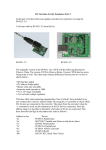
This document describes the LCD-Pro IP architecture, including the next cores: UltiEVC display controller, UltiEBB 2D
graphic accelerator, UltiEMC DDR memory controller, UltiVidin video input core, UltiDMA DMA controller, UltiSPI2AHB SPI
slave core and UltiSPI_M SPI master core.
Full core interfaces and registers are described for user reference.
This document describes the LCD-Pro IP core for Full Version1.
1 Refer to LCD-Pro IP architecture datasheet (DS0031) for more information on other versions.
The reproduction, transmission or use of this document or its contents is not permitted without express written authority. Offenders will be liable for damages.
All rights, including rights created by patent grant or registration of a utility model or design, are reserved. Technical data subject to change. All trademarks and
trade names appearing in this document are property of their respective owners. Copyright © 2008-2009 Sitek SpA-Verona-Italy, All Rights Reserved.
Disclaimer Sitek SpA is providing this design, code, or information "as is." basis, without warranty of any kind, either expressed or implied, including, without
limitation, warranties that the covered code is free of defects, merchantable, fit for a particular purpose or non-infringing. Each party bears the entire risk as to
the quality and performance of the original code, upgraded code, and modifications, to the extent originating with and provided by such party. Should any
covered code prove defective in any respect, you assume the cost of any resulting damages, necessary servicing, repair or correction. This disclaimer of
warranty constitutes an essential part of this license. No use of any covered code is authorized hereunder except subject to this disclaimer.
UM0011 (v1.0) – 14 July 2009
User Manual
www.exorint.net
1/112
LCD-Pro IP user manual
1
INTRODUCTION ................................................................................................................ 4
1.1
2
CORE ARCHITECTURE .................................................................................................... 5
2.1
3
BLOCK SCHEMATICS ............................................................................................... 6
System Interconnect........................................................................................................... 7
3.1
3.2
3.3
4
FEATURES................................................................................................................. 4
AHB bus...................................................................................................................... 7
APB bus ...................................................................................................................... 9
Address range mapping.............................................................................................. 9
System Components ........................................................................................................ 11
4.1
USB Interface............................................................................................................ 11
4.1.1
Bulk access........................................................................................... 12
4.1.2
Single access........................................................................................ 13
4.1.3
Registers............................................................................................... 14
4.2
SPI master interface ................................................................................................. 15
4.2.1
Registers............................................................................................... 16
4.2.2
General description and operation ........................................................ 17
4.3
EVC video controller ................................................................................................. 19
4.3.1
General Description .............................................................................. 19
4.3.2
Core architecture .................................................................................. 20
4.3.3
Functional description ........................................................................... 21
4.3.4
Layer image acquisition ........................................................................ 21
4.3.5
Layer image definition........................................................................... 24
4.3.6
Multi –layer blending ............................................................................. 28
4.3.7
Pixel color conversion and scrambling.................................................. 32
4.3.8
Flat panel display control ...................................................................... 32
4.3.9
Configuration and control...................................................................... 36
4.3.10
Configuration example .......................................................................... 44
4.4
BitBlit core: UltiEBB .................................................................................................. 46
4.4.1
Registers............................................................................................... 47
4.4.2
Operation .............................................................................................. 55
4.4.3
Configuration examples ........................................................................ 69
4.5
DDR memory controller: UltiEMC ............................................................................. 71
UM0011 (v1.00) – 14 July 2009
www.exorint.net
2/112
LCD-Pro IP user manual
4.6
Video Input core: UltiVIDIN ....................................................................................... 72
4.6.1
Registers............................................................................................... 73
4.6.2
UltiVIDIN operation ............................................................................... 77
4.6.3
Configuration example .......................................................................... 78
4.7
AD/DA controller: UltiADDA ...................................................................................... 79
4.7.1
Functional description ........................................................................... 80
4.7.2
Memory and registers ........................................................................... 82
4.8
UltiDMA..................................................................................................................... 83
4.8.1
Operation .............................................................................................. 84
4.8.2
Configuration and control...................................................................... 90
4.9
I2C architecture and interface ................................................................................... 95
4.9.1
UltiI2C2SA core .................................................................................... 96
4.9.2
UltiI2C_M .............................................................................................. 97
UltiSPI2AHB core .................................................................................................................. 100
4.9.3
Instruction set...................................................................................... 101
4.9.4
Operation ............................................................................................ 102
4.10
UltiINT Interrupt controller..................................................................................... 111
4.10.1
4.11
Configuration and register map........................................................... 111
UltiSYS ................................................................................................................. 112
4.11.1
Registers and use ............................................................................... 112
UM0011 (v1.00) – 14 July 2009
www.exorint.net
3/112
LCD-Pro IP user manual
1 INTRODUCTION
LCD-Pro IP is designed as multipurpose Video controller, targeted for TFT displays, based on Lattice ECP2-50 FPGA.
The module’s functionality is implemented using an FPGA-based system-on-chip (Lattice ECP2-50 FPGA). The system-onchip is based on the SoC interconnect, enabling simplified FPGA design integration and IP-block oriented design for the
FPGA.
One of the features of the LCD-Pro IP modules is the ability to operate as a standalone USB peripheral.
LCD-Pro IP supports the 8051-based high speed USB peripheral controller, Cypress EZ-USB FX2 (CY7C68013A), used for
interfacing the LCD-Pro IP module to a device with USB host functionality, such as PCs and USB-OTG compliant devices.
1.1 FEATURES
°
°
°
°
°
°
°
°
°
Supports Lattice ECP2 family
Supports video controller module
Supports touch controller module
Supports backlight dimming control
Supports memory controller module
Supports USB controller module
Supports Video input module
Supports SPI master module
System-on-chip architecture based
UM0011 (v1.00) – 14 July 2009
www.exorint.net
4/112
LCD-Pro IP user manual
2 CORE ARCHITECTURE
The LCD-Pro IP includes the next cores:
°
°
°
°
°
°
°
°
°
°
°
°
°
°
°
°
UltiEVC
UltiEBB
UltiVidin
USB_DMA
UltiSPI_M
UltiEMC
UltiI2C_M
UltiI2C_C
UltiI2C_E
UltiI2C2SA
UltiADDA
UltiDMA
UltiINT
UltiSPI2AHB
UltiSYS
SoC buses, switch matrix and bridges
UM0011 (v1.00) – 14 July 2009
www.exorint.net
5/112
LCD-Pro IP user manual
2.1 BLOCK SCHEMATICS
UltiSPI_M
SPI Master
APB Slave
UltiI2C_C
I2C Crossbar
UltiEMC
DDR SDRAM
Memory controller
AHB slave
UltiI2C2SA
I2C to SA bridge
I2C Slave
SA Master
USB FIFO
UltiI2C_M
I2C Master
APB Slave
UltiI2C_E
I2C EEPROM
emulation
UltiADDA
AD/DA Controller
UltiUSBDMA
Cypress
EZ-USB FX2
DMA interface
AHB master
APB Slave
Touch+ dimming
UltiDMA
APB Slave
AHB Master
Display
UltiEVC
Video Controller
AHB master
APB slave
UltiEBB
Graphic Accelerator
AHB master
APB slave
ITU656
UltiVIDIN
Video input
AHB master
APB slave
VGA
UltiSYS
Peripheral core
APB Slave
UltiSPI2AHB
SPI slave
AHB master
UltiINT
Interrupt controller
APB Slave
LCD-Pro IP Block Diagram. Full version: Full version Video Controller + Video Input module
UM0011 (v1.00) – 14 July 2009
www.exorint.net
6/112
LCD-Pro IP user manual
3 System Interconnect
The LCD-Pro IP is based on SoC interconnection, bus structure is organized in 2 layers:
1. AHB bus: high speed, multiplexed, pipelined bus
2. APB bus: low speed multiplexed bus, not pipelined, used primarily for peripheral access
3.1 AHB bus
The AHB bus is the main system interconnect in LCD-Pro IP SoC, providing high-speed system interface for system bus
masters. AHB is a multiplexed bus, where one AHB master can perform transaction to an only one AHB slave at the same
time. AHB is also a pipelined bus, and the slave response to the master transaction is active at least one clock cycle after
the master’s request. The bus protocol is synchronous, and the pipelined operation enables high transfer speeds.
AHB slaves are connected to the master via a bus decoder/multiplexor which generates slave enable signals and muxes the
slave response lines to the master. Additionally the decoder behaves as a default, idle slave.
AHB Decoder/M UX
AHB slaves
Slave #1
Decoder
HSEL
HADDR
AHB m aster
HW DATA
MASTER
HRDATA
HADDR
HW DATA
Slave #2
HRDATA
HSEL
HADDR
HW DATA
HRDATA
Slave #N
Read Data / Response
MUX
HSEL
HADDR
HW DATA
HRDATA
AHB Bus decoding/multiplexing
UM0011 (v1.00) – 14 July 2009
www.exorint.net
7/112
LCD-Pro IP user manual
Multilayer AHB switch matrix operation
The AHB switch matrix appears as a slave to the AHB master which attempts the transaction. The switch matrix accepts the
transaction, delaying the transfer with the HREADY line until the slave access becomes available.
A master also has the capability to lock a bus for its use in consecutive transfers.
Simultaneous bus transactions through the AHB switch matrix raise effective bus bandwidth, and reduce access latencies.
For example, a video controller could fetch image data at a constant rate from the video memory concurrently to a DMA I/O
transfer from the system memory to the Ethernet controller.
In LCD-Pro IP, the AHB bus has a 32 bit data bus clocked at 96 MHz. The AHB address bus is 32 bits wide, which can be
used to address 4.294.967.296 bytes (4 GB)
UM0011 (v1.00) – 14 July 2009
www.exorint.net
8/112
LCD-Pro IP user manual
3.2 APB bus
APB bus is the peripheral bus, designed for simpler or slower devices, primarily peripherals. It is a non-pipelined multiplexed
synchronous bus which allows a single master to drive multiple slaves. The protocol does not support burst transfers, and
does not support transfer sizes less than the bus width. The minimum addressable chunk of address space on the APB bus
is the bus width.
APB is envisioned as the hierarchical extension of the AHB bus. The APB bus master is, effectively, an AHB-to-APB bus
bridge. The AHB-APB bus bridge behaves as an AHB slave, which converts the AHB transfers to the APB transfers. The
address space of the APB bus is mapped in the address space of the AHB bus.
On LCD-Pro IP, the APB bus has a 32-bit address and data bus size. Only part of this address range is decoded for slave
selection, so user has to take care not to access non-existing addresses, which will wrap to unknown APB slave. The APB
bus is clocked on 48 MHz. The APB bridge resamples the transfer internally between the faster AHB clock domain and the
slower APB clock domain. Running the APB logic on a slower clock enables better timing optimization in the logic design, as
it decouples the slow peripheral access bus from the fast system bus.
The APB decoder is connected to a dedicated AHB layer on the AHB interconnection matrix, which prevents the AHB bus
operation being interrupted by slow APB transfers from a high priority master.
3.3 Address range mapping
The only true AHB slave in the system is the UltiEMC DDR memory controller. As the source of the image refresh, it
requires the burst capability and high bandwidth offered by the AHB.
Additionally, two distinct AHB-to-APB interface bridges are present, each of them mapped to a different address range.
The control interfaces of the IP in the system are mapped to the APB buses.
The LCD-Pro IP AHB interconnection matrix maps the AHB address space into ranges:
0x00000000
DDR SDRAM memory range
0x7FFFFFFF
0x80000000
48 MHz APB #0
0xBFFFFFFF
0xC0000000
48 MHz APB #1
0xFFFFFFFF
The APB address spaces are further divided. Several cores are mapped to the 48 MHz APB.
APB #0
0x80000000
UltiEVC
0xA0000FFF
0xA0001000
UltiEBB
0xA0001FFF
0xA0002000
UltiSPI_M
0xA0002FFF
0xA0003000
UltiSYS
0xA0003FFF
0xA0004000
USB_DMA
0xA0004FFF
UM0011 (v1.00) – 14 July 2009
www.exorint.net
9/112
LCD-Pro IP user manual
0xA0005000
UltiVidin
0xA0007FFF
APB #1
0xC0000000
UltiADDA
0xC0001FFF
0xC0002000
UltiI2C_M
0xC0002FFF
0xC0003000
Ulti_INT
0xC0004FFF
0xC0005000
UltiDMA
0xC000FFFF
Note: The apparently large address range of the UltiEVC is due to the functionality of the AHB-APB bridge. For the APB
slave with the highest base address, the bridge will map the entire remainder of the address space. Identical decoding
principle is used also by the AHB switch matrix, hence the large address space assigned to the APB.
UM0011 (v1.00) – 14 July 2009
www.exorint.net
10/112
LCD-Pro IP user manual
4 System Components
4.1 USB Interface
The Cypress USB DMA is a programmable data pump used to transfer data from the USB endpoints of the external
Cypress EZ-USB FX2 chip to the LCD-Pro IP video memory. The primary function is to transfer image data. With its
quantum fifo interface, the Cypress can support high speed USB data streaming to the device over bulk or isochronous USB
endpoints. Additionally, it supports issue of single access operations on the AHB bus.
The USB DMA uses a modular internal architecture which enables the hardware to be easily configured for the target
application, based on the number of the data endpoints and their direction. In LCD-Pro IP, the USB DMA is currently
configured to work as a single endpoint, downstream data pipe, enabling transfer of data from the USB host to the LCD-Pro
IP device.
Transfer controller(s)
APB
Input FIFO
EZ-USB
Cypress FX2
interface
AHB Master
Controller
AHB
Output FIFO
For configuration, the DMA interface also behaves as an APB slave, enabling the configuration of the USB DMA.
UM0011 (v1.00) – 14 July 2009
www.exorint.net
11/112
LCD-Pro IP user manual
4.1.1 Bulk access
Bulk access operation enables the transfer of a data stream from the USB endpoint to the LCD-Pro IP device memory (the
streaming from the memory to the USB endpoint is not currently implemented, but is possible).
The USB DMA supports several bulk access operating modes, enabling operation from simple data transfers to image
transfers, which require image dimension information for correct alignment. The USB DMA supports several operating
modes.
-
Linear: the data is written to the AHB bus incrementally from a defined base address.
-
Circular: the data is written to the AHB bus incrementally from a defined base address for a specific data count,
after which it returns back to the starting address.
-
Stride: used for image transfer. The data is written to the AHB bus incrementally from a starting address for a
specified number of data elements. After that the new starting address is defined as old starting address
incremented by the stride length. After a specific data count has been reached, the new starting address to the
original base address.
The USB DMA bulk interface transfers data in 16-word bursts, which is the maximum specified burst size on the AHB bus.
Data sizes less than a word (32 bits) are not supported. The destination addresses and counts need to be defined in
quantums of the burst size. These limitations reflect the nature of the interface, which supports high speed operation of the
interface while keeping the logic simple.
UM0011 (v1.00) – 14 July 2009
www.exorint.net
12/112
LCD-Pro IP user manual
4.1.2 Single access
The single access mode enables random access to the bus address space. It supports single read and write accesses of all
sizes. The single access mode utilizes two USB endpoints for a request-response protocol. The requests are sent over one
endpoint, while over the second endpoint the responses are received by the USB host.
Over each endpoint a stream of messages is transferred.
4.1.2.1
Request message
A request message is 16 bytes in size.
0
Tag
A2
D2
padding
0x0
0x4
0x8
0xC
1
Command/Size
A3
D3
2
A0
D0
padding
3
A1
D1
A
request message consists of:
•
Tag - the identifier of the operation in the stream, used to identify the corresponding response message in the
response stream. The tag of the request will be copied to the response.
•
Command/size – the identifier used to define the bus operation.
•
A[3:0] – the bus address in little endian ordering (A0 = LSB byte, A3 = MSB byte)
•
D[3:0] – the bus data (for write operations) in little endian ordering (D0 = LSB byte, D3 = MSB byte). Dummy
data/padding for read operations.
•
Padding – dummy data to align on 16 byte boundary (to pack messages into a single USB frame and for future
use).
The command/size identifier:
7
6
HWRITE
5
4
3
2
HSIZE2
RFU
1
HSIZE1
0
HSIZE0
The HWRITE line is mapped to the HWRITE flag on the AHB bus.
•
1 – AMBA write
•
0 – AMBA read
The HSIZE[2:0] identifier is mapped to the HSIZE bus on the AHB bus.
•
•
•
000 = Byte
001 = Halfword (16 bits)
010 = Word (32 bits)
Bits 6:3 are RFU and should be set to 0.
4.1.2.2
Response message
A response message is 8 bytes in size.
0x0
0x4
0
Tag
D3
1
D0
2
D1
3
D2
Padding
A response message consists of:
•
Tag - the identifier of the operation in the stream, used to match the response message in the response stream to
its corresponding request message The tag of the request is copied to the response.
•
D[3:0] – the bus data (for read operations) in little endian ordering (D0 = LSB byte, D3 = MSB byte). Dummy
data/padding for write operations.
UM0011 (v1.00) – 14 July 2009
www.exorint.net
13/112
LCD-Pro IP user manual
•
Padding – dummy data to align on 8 byte boundary (to pack messages into a single USB frame and for future use).
4.1.3 Registers
The USB DMA has several APB-mapped registers used to control the DMA transfer.
Offset
0x0
0x4
0x8
0xC
0x10
0x14
0x18
Name
MODE
ADDR
CNT
STRIDE
LINE
RESET
PE_CNT
Description
Operating mode for bulk transfer
Address for bulk transfer
Data count for bulk transfer
Stride for bulk transfer stride mode
Line for bulk transfer line mode
Reset for the entire USB DMA
PKTEND timeout counter
The MODE register is used to control the USB DMA bulk operating mode.
31
3
2
1
unused
0
ENABLE
MODE
The MODE parameter denotes the operating mode.
•
00 – Linear mode
•
01 – Circular mode
•
10 – Stride mode
The ENABLE bit serves as the mode initiator/local reset. The USB DMA needs to be disabled (ENABLE = 0) before the
parameters (mode, address, stride, line, count) can be modified. Once the ENABLE bit is set from 0 to 1, the parameters
from the registers are initialized and transfer can begin.
The ADDR register contains the address of the bulk transfer. The address must be aligned to the bus burst boundary.
31
6
5
ADDR
0
0
The bits 5:0 of the address counter MUST be always set to 0.
The CNT register holds the data count for the transfer. Which is the size of the circular buffer in the Circular transfer mode,
and the size of the image for transfer in the Stride mode.
31
0
COUNT
The STRIDE register holds the stride size for the Stride transfer mode. Not used otherwise.
31
0
COUNT
The LINE register holds the size of the image line for the Stride transfer mode. Not used otherwise.
31
16
15
unused
0
LINE
The RESET register contains the reset bit. This bit resets the entire USB DMA while set to 1.
31
UM0011 (v1.00) – 14 July 2009
1
www.exorint.net
0
14/112
LCD-Pro IP user manual
unused
RESET
The initial state of the reset bit is set to ‘1’ which keeps the DMA machine in total reset. This is to prevent the transient
occurring during the system power-up and Cypress SDRAM, and to prevent contention on external lines until the Cypress
FX2 boot up process is completed.
The PE_CNT register holds the timeout counter for the PKTEND commit line of the Cypress FX2.
31
13
12
0
unused
PE_CNT
This is used with single access mode to enable the commit of the last packet in the Cypress FX2 FIFO to the USB domain
even if the packet is not completely full (required for the FX2 to auto-commit the packet to the USB domain). The timeout
counter is reset to PE_CNT on each byte transferred to FX2. When the timeout reaches 0 (no response has been issued for
a given period of time indicating that the transfer queue is completed), the PKTEND is issued and the packet is committed.
This register is initialized by the FX2 firmware and should not be modified!
4.2 SPI master interface
SPI master interface is implemented using the UltiSPI_M core, based on FIFO interface for data and registers for
configuration.
SPI interface consists of two FIFOs for data flow, registers for configuration and interrupt logic (the interrupt output line is not
connected on LCD-Pro IP design). SPI interface consists of chip select output, clock output, serial data output and serial
data input. Both transmit and receive FIFO are 2048 bytes deep.
NC on design
Internal structure of SPI master interface
UM0011 (v1.00) – 14 July 2009
www.exorint.net
15/112
LCD-Pro IP user manual
4.2.1 Registers
Register
FIFO
TX_STATUS
RX_STATUS
CLK_DIV
SPI_CONFIG
TRN_BYTE_NUM
FRAME_SIZE
TIMEOUT
DESEL_TIME
STATUS
INT_MASK
INTERRUPT
Width (bits)
8
16
16
5
9
12
12
16
8
3
4
4
Read/Write
R/W
R
R
R/W
R/W
R/W
R/W
R/W
R/W
R/W*
R/W
R/Clear on write ‘1’
Address offset
0x00
0x10
0x20
0x30
0x40
0x50
0x60
0x70
0x80
0x90
0xA0
0xB0
SPI_master registers
•
- write access to the STATUS register is used for start (write “001”) or reset (write “1XX”).
The FIFO register is organized as follows
Register bit(s)
FIFO
Description
Write to TX_FIFO, read from RX_FIFO
The TX_STATUS is organized as follows
Register bit(s)
TX_STATUS[11:0]
TX_STATUS[14]
TX_STATUS[15]
Description
Number of bytes in TX_FIFO
TX_FIFO empty flag
TX_FIFO full flag
The RX_STATUS is organized as follows
Register bit(s)
RX_STATUS[11:0]
RX_STATUS[14]
RX_STATUS[15]
Description
Number of bytes in RX_FIFO
RX_FIFO empty flag
RX_FIFO full flag
The SPI_CONFIG register is organized as follows
Register bit(s)
SPI_CONFIG[0]
SPI_CONFIG[1]
SPI_CONFIG[3:2]
SPI_CONFIG[7: 4]
SPI_CONFIG[8]
UM0011 (v1.00) – 14 July 2009
Description
CPOL mode
CPHA mode
RFU
Reserved: must be all 0s
CS active polarity. If CS(0) is
active
low,
write
‘0’
to
SPI_CONFIG[8].
www.exorint.net
16/112
LCD-Pro IP user manual
The STATUS register is organized as follows
Register bit(s)
STATUS[0]
STATUS[1]
STATUS[2]
Description
Write – (‘1’) start operation
Read - UltiSPI_M busy (‘1’) or idle (‘0’)
Read only.
(‘1’) TX_FIFO underrun occurred during last
operation. This bit is cleared on beginning of
each new operation.
(‘0’) no underrun occurred.
Write – (‘1’) reset UltiSPI_M
Read – (‘1’) RX_FIFO overrun occurred during
last operation. This bit is cleared on beginning of
each new operation.
(‘0’) no overrun occurred
The INT_MASK register is organized as follows
Register bit(s)
INT_MASK[0]
INT_MASK[1]
INT_MASK[2]
INT_MASK[3]
Description
Mask (‘1’) or unmask (‘0’) INTERRUPT[0]
Mask (‘1’) or unmask (‘0’) INTERRUPT[1]
Mask (‘1’) or unmask (‘0’) INTERRUPT[2]
Mask (‘1’) or unmask (‘0’) INTERRUPT[3]
The INTERRUPT register is organized as follows
Register bit(s)
INTERRUPT[0]
INTERRUPT[1]
INTERRUPT[2]
INTERRUPT[3]
Description
Interrupt on UltiSPI_M idle. Reset by writing ‘1’.
Interrupt on error, TX_FIFO underrun, or
RX_FIFO overrun. Reset by writing ‘1’.
Interrupt on TX_FIFO empty. Reset by writing ‘1’.
Interrupt on RX_FIFO not empty. Reset by
writing ‘1’.
4.2.2 General description and operation
All time periods are calculated in the number of the clock cycles, so the configuration parameters need to be calculated in
relation to the 48Mhz AMBA APB interface clock frequency. All relevant registers need to be set prior to the starting of the
operation and TX_FIFO needs to be filled with at least one byte.
All frequencies obtainable by dividing the 48Mhz frequency with an even number up to 16 are possible. Highest frequency is
equal to the half of the system frequency, set when writing 0 or 2 to the divider register. Desired frequency is set by the
register CLK_DIV. After reset, UltiSPI_M is set to the highest frequency.
The SPI mode of operation and the polarity of chip select are configured by the register SPI_CONFIG. This register sets
CPOL, CPHA and active state of the chip select output. After reset all these bits are set to ‘0’, setting the idle clock low, data
sampling on the rising edge and the chip select active low.
The number of bytes to be transmitted on the write operation is set by the register TRN_BYTE_NUM. Present maximum
size is 4096 bytes. Data is written in format N-1, so to send 2 bytes this register should be set to 0x001.
The total length of the SPI frame is set by the register FRAME_SIZE. Present maximum size is 4096 bytes. The size of
frame can be set to any value, which if larger than the value in TRN_BYTE_NUM means that, after sending bytes, frame will
be extended to the size specified, with data being inputted to RX_FIFO.
If TX_FIFO does not contain enough data to complete the write operation, or RX_FIFO is full during read operation,
UltiSPI_M will go to stall mode, stopping clock for a number of system clock cycles defined in the TIMEOUT register. If
operation still cannot be completed after this period expires, system will report error in register STATUS and set chip select
output to the inactive state. Maximum value for this interval is 0xFFFF. After reset, this register is set to 0x0000.
UM0011 (v1.00) – 14 July 2009
www.exorint.net
17/112
LCD-Pro IP user manual
SPI devices set minimum intervals between two operations, which is the minimum time for chip select set to the inactive
state. This interval can be set by the register DESEL_TIME; it will always be executed after operation is completed. During
this interval, UltiSPI_M will report busy state and not allow new operations. Maximum value is 0xFF, after reset this register
is set to 0x00.
An operation or core reset is started by a write access to the register status, with the following options:
-
Write 0x1 starts the operation, if TX_FIFO is not empty. Otherwise, write access is ignored.
Write 0x4 resets UltiSPI_M, emptying FIFOs and resetting all registers to the reset value.
Status of the device and the result of the previous operation (whether error occurred or not) can be read from the register
STATUS. Bits have the following meaning:
-
STATUS[0] = ‘1’ (busy), ‘0’ (idle)
STATUS[1] = ‘1’ (TX FIFO underrun, not enough data to transmit, TIMEOUT period expired),
‘0’ (transmit OK)
STATUS[2] = ‘1’ (RX FIFO overrun, not enough space to receive, TIMEOUT period expired),
‘0’ (receive OK)
Status of the transmit FIFO can be read from the register TX_STATUS, with 12 LSB bits showing the number of bytes in the
FIFO and TX_STATUS [14] being equal to the empty flag, and TX_STATUS[15] to the full flag.
Status of the receive FIFO can be read from the register RX_STATUS, with 12 LSB bits showing number of bytes in the
FIFO and RX_STATUS [14] being equal to the empty flag, and RX_STATUS[15] to the full flag.
FIFO data access is done over the same address on APB, accessing TX_FIFO on writes and RX_FIFO on reads. When
writing, it is not possible to overrun FIFO, starting the fill process again. When reading from an empty FIFO, FIFO will output
last valid data and remain in the empty state. Both data write and read are mapped to the same APB address, but all writes
are forwarded to the transmission FIFO, and reads are only from the receiver FIFO. To empty transmission FIFO, UltiSPI_M
has to be reset. Data access is 8-bit, while registers are various sizes, with the biggest being 32 bits.
UM0011 (v1.00) – 14 July 2009
www.exorint.net
18/112
LCD-Pro IP user manual
4.3 EVC video controller
The EVC video controller interface is implemented using the UltiEVC core.
UltiEVC is a high performance modular embedded graphic display controller, targeted for driving active matrix flat panel
displays. UltiEVC supports multi-layer overlay between multiple frame buffers with color-key transparency and alpha
blending.
AMBA AHB interface is used as video memory interface and AMBA APB interface is used as register interface.
4.3.1 General Description
A display controller’s function is to continuously refresh the image present on a graphic display device. The sequence of
displayed images can be described as a continuous video stream, which can be either sourced externally or generated by
scanning the image data present in a memory device. The UltiEVC generates the image stream by reading a memory area
in the display memory, the frame buffer. The UltiEVC is capable of reading multiple frame buffer areas into different layers,
and blending them into a single image, enabling complex graphics effects within the display controller.
Line 1
Line 2
Line 3
Display data stream
Address fetch
Image data
(Memory)
Display controller
(SlixEVC)
Image data
vsync
hsync
blank
Display
Line n
The refresh operation is accompanied by generating the display control signals for horizontal and vertical synchronization
(hsync and vsync) and data enable (blank). These signals define the refresh cycle and refresh rate of the display and are
usually specific for a display panel. Timings for control signals are software configurable.
The following characteristics are given for the LCD-Pro IP configuration:
•
•
•
•
•
•
•
•
•
•
•
•
Active matrix display refresh
Display resolution:
(1)
o up to 1366x768 (2 16-bit layers, no video input)
(1)
o up to 800x480 (4 layers)
16 bit data output
Display power-up sequence control
Internal pixel clock generator
ARM AMBA 3 compliant system interconnection
o AHB memory interface
o APB register interface
RGB8, RGB16,RGB32, ARGB32 frame buffer formats
(2)
Multi-layer window and overlay image assembly (n° 4 layers available )
Variable frame buffer geometry – stripe setting per layer
Common overlay with color-key transparency
Alpha blending with per-layer fading
Alpha mask layer support
NOTE (1) : The max display resolution depends on many factors, such as the number of layers effectively used for blending, the display
refresh rate and the contemporary use of video input features. It is suggested to contact Exor International for any request regarding
the specific application.
NOTE (2) : The max number of layers which can be effectively used depends on many factors, such as the display resolution and
refresh rate and the contemporary use of video input features. It is suggested to contact Exor International for any request regarding
the specific application.
UM0011 (v1.00) – 14 July 2009
www.exorint.net
19/112
LCD-Pro IP user manual
4.3.2 Core architecture
The UltiEVC core consists of:
°
Register APB slave
°
Address generator
°
AHB master
°
Master and slave (overlay) layer fetchers
°
Pixel pipelines
°
Layers blending module
°
Clock generator module
°
Syncs generator module
°
Pixel data fifo
°
Pixel scramble module
Diagram below shows UltiEVC core architecture (simplified diagram; the real core contains n° 4 layers)
UltiEVC display controller
Core control & status
Display control and output
APB
Control
Clock generator
VCLK
Sync generator
SYNCS
Registers – AMBA APB slave
APB
data
Image layers fetch, process and blend
AHB
Control
Frame
Buffer
Data
AMBA
AHB
Master
engine
Variable
Stripe
Address
Generator
Master layer
fetcher
Pixel pipeline
Slave layer
fetcher
Pixel pipeline
Slave layer
fetcher
Pixel pipeline
Layer
blender
Pixel data
fifo
Pixel
scramble
Pixel Data
UltiEVC Block Diagram
UM0011 (v1.00) – 14 July 2009
www.exorint.net
20/112
LCD-Pro IP user manual
4.3.3 Functional description
The operation of the UltiEVC can be divided into:
•
Layer image acquisition with frame buffer geometry handling
•
Multi-layer image blending (with Alpha channel)
•
Pixel color conversion and scrambling
•
Flat panel display control
EVC operation in phases
4.3.4 Layer image acquisition
The source images for the UltiEVC are stored in the display video memory. UltiEVC behaves as an AHB master and
accesses the video memory through the on-chip AMBA AHB bus. Each image is stored in its own respective memory area
(a frame buffer).
The image in memory is stored as RGB pixel data in 8, 16 or 32-bit format with or without Alpha information.
All formats are RGB. 8-bit format can be used either as 8-bit alpha channel information (for alpha mask) or as 8-bit RGB
with 3 bits for red channel, 3 bits for green channel and 2 bits for blue channel (RGB 332).
16-bit format allows for RGB565, with 5 bits for red, 6 for green and 5 for blue.
32-bit format allows for RGB888, with 8 bits for each channel, and the upper 8 bits of a 32 bit word stand unused, or for
ARGB8888, with 3-byte packing of pixels and alpha channel in the MSB byte.
UM0011 (v1.00) – 14 July 2009
www.exorint.net
21/112
LCD-Pro IP user manual
EVC pixel formats in memory
Each frame buffer is a rectangular memory area consisting of multiple lines. The size of a frame buffer is limited by the size
of the system memory. The width of a frame buffer line in the memory is called the stripe, or stride. The stripe is also the
distance in memory between two vertically adjacent pixels. EVC supports variable stripe length for each frame buffer, and is
able to support any frame buffer geometry, which allows for more efficient memory usage.
The stripe used for a frame buffer is defined in bytes. Depending on the color depth used, the pixel geometry of the frame
buffer , and the maximum achievable resolution is changed accordingly. For a defined frame buffer, the maximum horizontal
resolution is equal to the stripe divided by the number of bytes occupied by a single pixel. The pixels of an individual line are
ordered in ascending order in memory.
UM0011 (v1.00) – 14 July 2009
www.exorint.net
22/112
LCD-Pro IP user manual
Memory
0
1
2
Frame buffer image
3
A
A+0x4
A+0x8
...
A+0xAA0
A+0xAA4
A+0xAA8
A+0xAAC
A+0xAB0
A+0xAB4
0
1
2
3
4
5
6
7
8
9
1362
1363
1364
1365
Line 0
Line 1
Line 2
Line 3
Line 4
...
Line 5
Line 6
Line 7
Line 8
Line 9
Line 10
...
A+0x154C
...
...
...
A+0x1550
A+0x1554
A+0x1558
A+0x155C
A+0x1560
A+0x1564
A+0x1568
Line 765
...
Line 766
Line 767
Stride length: 1366 pixels, 2 bytes per pixel = 2732 bytes = 0xAAC bytes
...
Frame buffer size = 1366x768 pixels = 2098176 bytes = 0x200400 bytes
A+0x1FEE9C
A+0x1FEEA0
A+0x1FEEA4
A+0x1FEEA8
A+0x4
Pix 7
Pix6
Pix5
Pix4
A+0x0
Pix3
Pix2
Pix1
Pix0
8-bit pixel formats:
RGB, Alpha
A+0x1FEEAC
A+0x1FEEB0
A+0x4
Pix3
Pix2
A+0x0
Pix1
Pix0
16-bit pixel
formats
A+0x2003F8
A+0x2003FC
A+0x4
Pix1
A+0x0
Pix0
32-bit pixel formats
Frame buffer geometry and memory organization
For the memory organization in Error! Reference source not found., the EVC allows the maximum image of 1366x768
pixels with 16-bit color. If the color depth is changed to 32 bits, the maximum image resolution is decreased to 683 pixels.
The maximum vertical resolution is constrained only by the size of the allocated memory space. EVC has no limitation in the
number of lines for a given frame buffer (other than the address bus width) and will successively increment the image
address with the stripe count during the image fetch.
The address of a pixel within the frame buffer can be defined by the equation:
Pix_address = y*STRIPE + x*BPP;
Where:
•
STRIPE is the length of the frame buffer line (the stripe) in bytes
•
x, and y are the horizontal and vertical coordinates, respectively
•
BPP is the number of bytes occupied by each pixel
The frame buffer organization is rectangular. For a given stride, each line of the image will be put in the corresponding line
of the frame buffer, regardless of the horizontal resolution of the actual image. The remaining part of the frame buffer line
will not be used.
UM0011 (v1.00) – 14 July 2009
www.exorint.net
23/112
LCD-Pro IP user manual
Image within a frame buffer
For more efficient memory usage, each image can be allocated a frame buffer exactly the size of the image.
4.3.5 Layer image definition
The image which is output to the display can be composed from multiple overlay image layers. Each overlay layer is fetched
from its defined memory region (which acts as a separate frame buffer).
The overlay layers are divided into the master layer, which is always present, and a variable number of slave layers. Slave
layers are overlayed over the master layer, with each subsequent slave layer being overlayed over the previous one. The
master layer can be deactivated, but in that case the contents of the layer fetched from memory is replaced by a rectangle
of a chosen color.
UM0011 (v1.00) – 14 July 2009
www.exorint.net
24/112
LCD-Pro IP user manual
For each layer a visible overlay rectangle can be defined. The visible rectangle can be less or equal in size to the master
layer (the screen resolution), and can be placed anywhere within the master layer visible rectangle as long as its boundaries
are within the visible area of the master layer. Only the data in the bounding rectangle will be fetched from the frame buffer
memory.
The layer rectangles can be simply overlayed, or blended together using alpha blending. When the layers are simply
overlayed, each pixel within the visible rectangle of an overlay layer masks the pixels in the visible layers below. When the
layers are alpha-blended, the layer image is used in alpha-compositing operation.
A visible rectangle is defined by 4 parameters:
•
rectangle size: LHRES and LVRES
•
rectangle offset: LHOFF and LVOFF
Overlay image geometry
Note: the Master layer is bound to the flat panel display size, and the layer parameters are undefined for the master
layer.
UM0011 (v1.00) – 14 July 2009
www.exorint.net
25/112
LCD-Pro IP user manual
4.3.5.1 Layer smooth positioning
The image within the rectangle is always fetched from the base address in memory defined by the LBADDR register.
Modifying the LHOFF and LVOFF will move the image across the visible screen.
This functionality is fundamental for achieving hardware cursor operation. A layer can be set to display a cursor image, and
be fluidly moven around by setting LHOFF and LVOFF.
LHOFF and LVOFF are defined in pixels or lines, and can be set to any value within the visible area of the screen.
4.3.5.2 Smooth Scrolling
The image fetched to fill the overlay rectangle is defined by a rectangular area within a frame buffer with equal size in pixels
(geometry within the frame buffer is defined by the layer color depth). The base address of the layer is the address of the
upper left pixel in the layer rectangle within the frame buffer.
The starting point of the image can be changed by changing the base address of the layer. If the image contained in the
overlay frame buffer is larger than the visible rectangle part, by changing the base address scrolling of the image in the
frame buffer can be performed.
UM0011 (v1.00) – 14 July 2009
www.exorint.net
26/112
LCD-Pro IP user manual
Scroll function
In Error! Reference source not found., the overlay rectangle does not change the screen position, but the base address is
changed from the base coordinates of rectangle A to the base coordinates of rectangle B, resulting in a “scroll” effect of the
map image.
In case the position and the size of the rectangle within the frame buffer causes the rectangle to exceed the frame buffer
boundaries, the image will be corrupted. The visible window within the frame buffer must not cross the frame buffer
boundaries.
Proper positioning of a layer visible rectangle within a frame buffer
UM0011 (v1.00) – 14 July 2009
www.exorint.net
27/112
LCD-Pro IP user manual
In Error! Reference source not found., only the rectangle “C” is properly positioned. The rectangles “A” and “B” are not,
due to crossing of the frame buffer border. In case of rectangle “A”, the line crosses the stripe boundary into the next line,
and fetches incorrect data. In case of rectangle “B”, the rectangle includes a part of the memory outside the logical space
allocated for the frame buffer.
Rectangle positioning and scrolling in the UltiEVC is applicable only to the slave layers and overlay rectangles. The master
layer, which defines the image resolution and contains the background image, can have its rectangle positioned only at the
beginning of a frame buffer in memory.
4.3.6 Multi –layer blending
Multi-layer blending is a process of combining multiple image windows into a single resulting image. UltiEVC supports
blending of multiple image layers.
4.3.6.1
Basic Overlay (Color-keyed overlay)
The layers are overlayed so that the image data of the higher layer replaces the image data of the lower layer. The lower
layer image data is however fetched from memory. In case the color key is used, any pixel that is matched to the color key
is removed from the image and set to be transparent.
Color-keyed overlay
The color key (transparent color) can be set independently for each layer through the COLKEY parameter, however it
cannot be applied to the master layer. If a transparent pixel is overlayed by a higher layer nontransparent pixel, it will be
replaced by the higher layer.
UM0011 (v1.00) – 14 July 2009
www.exorint.net
28/112
LCD-Pro IP user manual
4.3.6.2
Alpha Blending
If Alpha blending is used, the two layers are combined using alpha compositing. Alpha compositing operation is defined on
two pixels A and B, with the mixing factor alpha(α) attached to the pixel A. The basic alpha operation defines a pixel C as
The alpha blending operation results in an effect of transparent overlay. The pixel A appears overlayed over the pixel B with
a transparency factor α, where
The alpha operation is performed on each color component (R,G,B) independently.
In UltiEVC, alpha blending can be performed between multiple layers, where overlay layers are consecutively blended into
the result of the previous blending. The blending process starts with the master layer and the first overlay layer, and finishes
with the last overlay layer.
Alpha blending between multiple layers
The equation used for blending of each color channel (red, green, or blue) in a particular overlay layer is:
UM0011 (v1.00) – 14 July 2009
www.exorint.net
29/112
LCD-Pro IP user manual
For
, where
is the resulting pixel color for the current layer,
is individual pixel alpha,
alpha (layer fading factor),
is the resultant per pixel alpha prescaled by the fading factor,
color, and
is the result of previous blending operation.
is the overall fading
is the current layer pixel
Image composited using alpha blending
Alpha information used in the blending process is an 8-bit number,from 0 to 255, allowing for 255 transparency levels,
where 0xFF(255) generates a fully opaque pixel, and 0x0 stands for fully transparent pixel.
Note: The alpha value 0xFF is interpreted as a special case (255 is incremented to 256 in the calculation) to allow the
calculation to produce a fully opaque pixel. That means that the step in alpha value from alpha = 0xFE to alpha = 0xFF
is actually 2.
32-bit ARGB images have the alpha channel embedded in the image itself, allowing for individual alpha values,
, for
each pixel. This allows for advanced transparency effects, and is most prominently used for edge anti-aliasing, where the
transparency of the boundary pixels is varied to create a smooth transition.
UM0011 (v1.00) – 14 July 2009
www.exorint.net
30/112
LCD-Pro IP user manual
Antialising through alpha blending
Images of a lower colordepth, and 24 bit RGB images without alpha information have no room for alpha factors and are
interpreted as fully opaque (
. However, an 8-bit alpha channel can be attached to them by using dedicated
alpha layers.
Each layer has an additional alpha prescaling factor, or a fading factor. The fading factor premultiplies the alpha channel of
the layer (whether implied to opaque or defined by the pixel). This allows fading and definition of overall transparency for a
single layer. The overall layer alpha
is defined in the layer LALPHA parameter.
The master layer is always treated as completely opaque, and has no transparency.
regardless of the actual setting. LALPHA is not defined on the master layer, hence
and
are set to 0xFF
.
4.3.6.3 Alpha mask layers
For 16-bit layers there is no space sufficient to add full alpha transparency information to the image. Also it may be desired
to change the alpha channel without disturbing the original RGB data, 16 or 24 bit. For those purposes, Alpha mask layers
are used.
Each slave layer can be used as the alpha mask layer for the layer with the previous index. When functioning in alpha mask
mode, the layer fetches an 8-bit monochrome image. Each pixel of the monochrome image is attached as the alpha factor to
the corresponding pixel of the layer displayed beneath it.
In order to have the pixel-by-pixel alignment of the color and the mask layer, the two visible rectangles have to be of the
same size and the same position within the visible image. The LHOFF, LVOFF, LHRES and LVRES parameters of the two
layers must always be kept identical between the two layers.
UM0011 (v1.00) – 14 July 2009
www.exorint.net
31/112
LCD-Pro IP user manual
Areas outside of the alpha mask layer will be considered as having the alpha layer equal to 0, or completely transparent. If
needed, the alpha mask layer can be moved around independently of the color layer, which will shift the transparency
information (mask) over the underlying image.
4.3.7 Pixel color conversion and scrambling
Various flat panel displays require different color formats for image refresh. However, not all color formats are convenient for
memory storage and operations in the image datapath and blending process. Some displays show colors by using a smaller
number of bits, and compensate the remaining number of bits by pulse width modulation of individual pixels (FRC).
Additionally, it is hard to create a blending pipeline to work with multiple/various color formats.
Pixel scrambling is a conversion process which translates the internal color format, or blender color format, to the external
display color format. The pixel scrambler unit takes the result of the blender (in 8, 16 or 24 bit color) and translates it to the
external display color format, pixel by pixel.
Pixel scrambling allows decoupling of the internal and the external color format. The internal color format is therefore
aligned with the pipeline processing and software requirements.
UltiEVC supports pixel scrambling for the following combinations of internal and external color formats.
External color formats
RGB16
RGB8
Yes
Internal color formats
RGB16
Yes
RGB32
Yes
Supported pixel scrambling combinations
4.3.8 Flat panel display control
For flat panel displays, the display control parameters define the timing of control signals, consisting of:
Signal
Function
disp_clk
Display clock
Vsync
Vertical sync signal (frame start)
Hsync
Horizontal sync signal (line start)
Blank
Blank/Pixel data valid signal
pix_data
Pixel data
The display clock is the driver for the synchronous logic of the flat panel display. It defines the time base of the display
timing and the pixel data rate. The pixel data is output from the UltiEVC to the display synchronous to the display clock.
Within the UltiEVC the output display clock can be inverted (new data can be output on rising or falling edge of the display
clock) to ensure valid data sampling in the display.
Some displays do not use the blank (pixel valid) signal, but sample pixels on every active clock edge. For these displays,
the clock must be active only when the valid pixel data is output. This functionality is supported through clock burst mode of
the UltiEVC.
Flat panel displays are refreshed line by line. Therefore each frame consists of VRES line refresh cycles, where each line
consists of HRES pixel data elements. HRES and VRES are the horizontal and vertical resolution, respectively.
Each line refresh has the following structure. For each line, all of the timing is expressed in periods of the display clock.
UM0011 (v1.00) – 14 July 2009
www.exorint.net
32/112
LCD-Pro IP user manual
hsync
blank
Entire pixel line
The blank signal is asserted when valid pixel data is present on the pixel bus. The length of each blank impulse is equal to
HRES periods of display clock, while the number of blank impulses in each frame is equal to VRES.
The blank signal can be turned off, in which case it remains in inactive state.
The hsync signal is used for line start detection. Length of hsync is always expressed in number of clock periods. Length of
hsync is marked HSYNC on following picture. Each display can demand pauses between last pixel and assertion of hsync,
or pause from deassertion of hsync to first pixel in new line. This intervals are also a expressed in clock periods and usually
called hsync front porch (HSYNC_FP on picture) and hsync back porch (HSYNC_BP on picture).
HSYNC_FP
HSYNC
HSYNC_BP
hsync
blank
Hsync front and back porches
The period of hsync signal can be calculated as HYNC_FP + HSYNC + HSYNC_BP + HRES.
The hsync signal can be turned off, in which case it stays in inactive state.
The complete image frame consists of VRES line refresh cycles as shown below.
vsync
hsync
blank
Full image frame
The vsync signal is used for frame start detection. Vsync timing parameters are expressed in number of hsync signal
periods. In UltiEVC, the vsync signal always asserts and deasserts together with the asserting of the hsync signal. The
length of vsync is marked VSYNC on the following picture.
UM0011 (v1.00) – 14 July 2009
www.exorint.net
33/112
LCD-Pro IP user manual
Each display can demand pauses between the last pixel line and the assertion of vsync, or a pause from deassertion of
vsync to the first pixel line in the new frame. These intervals are also a multiple of the hsync signal period and are usually
called vsync front porch (VSYNC_FP on picture) and vsync back porch (VSYNC_BP on picture). The vsync signal can be
turned off, in which case it will remain in inactive state.
VSYNC_FP
VSYNC
VSYNC_BP
vsync
hsync
blank
Vsync front and back porches
The overall refresh sequence can be visualised as the image being larger than the actual visible image, with horizontal and
vertical sync areas in the nonvisible space.
UM0011 (v1.00) – 14 July 2009
www.exorint.net
34/112
LCD-Pro IP user manual
2D Visualization of flat panel display timing
UM0011 (v1.00) – 14 July 2009
www.exorint.net
35/112
LCD-Pro IP user manual
4.3.9 Configuration and control
The registers are accessed through the AMBA APB interface. All registers are 32-bit and located on adjacent addresses.
The layer control registers accessed through the APB are shadowed in the EVC hardware. The update of the registers in
the EVC hardware occurs automatically on each VSYNC. This prevents image artifacts which occur because of
configuration changes during operation. Each frame is completely output using the same configuration, which prevents logic
glitches.
The UltiEVC is controlled through an array of registers mapped within the AMBA APB address space of the core. All
registers occupy 1 word (32 bits) of address space, even if their physical size is less, and are aligned to 1-word boundaries
(The address is always a multiple of 4).
The register space is divided into a variable number of register banks. Each bank is 64 bytes in size.
Each register bank is assigned a specific function, and contains registers relevant to that function. The functions of register
banks are summarized in the table below.
Bank
Bank 0
Bank 1
Bank 2
Bank 3
Bank 4
Function
Display control and timing parameters
Master layer control parameters
Overlay layer 1 control parameters
Overlay layer 2 control parameters
Overlay layer 3 control parameters
Base address
0x00
0x40
0x80
0xC0
0x100
Bank 0 defines a separate set of registers, while banks 1 … 4 define an identical set of registers, as each bank controls a
generic image layer control structure.
For any register, the absolute AMBA address in the system is calculated as:
Register address = core base address + bank base address + register offset
4.3.9.1
Display parameter registers
The display control, signal and timing parameters are defined through 12 registers in bank 0. The register offset is
calculated from the bank base address.
Register
HSY_FP
HSY
HSY_BP
HRES
VSY_FP
VSY
VSY_BP
VRES
SCTRL
CLKCTRL
DCTRL
PWRCTRL
UM0011 (v1.00) – 14 July 2009
Bits
8
8
8
16
8
8
8
16
6
8
4
4
Access
R/W
R/W
R/W
R/W
R/W
R/W
R/W
R/W
R/W
R/W
R/W
R/W
Function
Horizontal sync front porch
Horizontal sync period
Horizontal sync back porch
Horizontal resolution
Vertical sync front porch
Vertical sync
Vertical sync back porch
Vertical resolution
Signal enable & polarity control
Clock selection and division control
Display color depth and pixel merge control
Power control signals control
www.exorint.net
Offset
0x00
0x04
0x08
0x0C
0x10
0x14
0x18
0x1C
0x20
0x24
0x28
0x2C
36/112
LCD-Pro IP user manual
HSY_FP
31
8
Bank 0, offset 0x00
0
HSYNC_FP
7
unused
The HSY_FP register contains the value of the horizontal front porch.
HSY_FP[7:0] contains the HSYNC_FP value, e.g. the number of display clock periods between the deassertion of blank
signal and the assertion of hsync signal.
HSY
31
8
Bank 0, offset 0x04
0
HSYNC
7
unused
The HSY register contains the value of the horizontal sync. HSY[7:0] contain the HSYNC value, e.g. the number of display
clock periods during which the hsync signal is asserted.
HSY_BP
31
8
Bank 0, offset 0x08
0
HSYNC_BP
7
unused
The HSY_BP register contains the value of the horizontal back porch. HSY_BP[7:0] contain the HSYNC_BP value, e.g. the
number of display clock periods between the deassertion of hsync signal and the assertion of blank signal.
HRES
31
16
Bank 0, offset 0x0C
0
15
unused
HRES
The HRES register contains the value of the horizontal resolution. HRES[15:0] contain the HRES value, e.g. the number of
pixels in a display line, and the number of display clock periods during which the blank signal is asserted.
VSY_FP
31
8
7
unused
Bank 0, offset 0x10
0
VSYNC_FP
The VSY_FP register contains the value of the vertical front porch.
VSY_FP[7:0] contains the VSYNC_FP value, e.g. the number of HSYNC periods between the last deassertion of blank
signal in the previous frame and the assertion of vsync signal.
VSY
31
8
unused
7
Bank 0, offset 0x14
0
VSYNC
The VSY register contains the value of the vertical sync. VSY[7:0] contain the VSYNC value, e.g. the number of HSYNC
periods during which the vsync signal is asserted.
UM0011 (v1.00) – 14 July 2009
www.exorint.net
37/112
LCD-Pro IP user manual
VSY_BP
31
8
Bank 0, offset 0x18
0
VSYNC_BP
7
unused
The VSY_BP register contains the value of the vertical back porch. VSY_BP[7:0] contain the VSYNC_BP value, e.g. the
number of display clock periods between the deassertion of the vsync signal and the first active line refresh cycle.
VRES
31
16
Bank 0, offset 0x1C
0
15
Unused
VRES
The VRES register contains the value of the vertical resolution. VRES[15:0] contain the VRES value, e.g. the number of
lines in a display frame, and the number of blank signal pulses within a display frame.
SCTRL
31
6
Unused
5
ENPOL
4
ENEN
3
HSPOL
Bank 0, offset 0x20
1
0
VSPOL
VSEN
2
HSEN
The SCTRL register defines whether the control signals VSYNC, HSYNC and BLANK(enable) are used, and what is their
active polarity (value when the signal is asserted).
The VSEN, HSEN and ENEN flags define whether the VSYNC,HSYNC and BLANK(EN) signals are driven by the state
machine or kept inactive. The VSPOL,HSPOL and ENPOL flags define the active state (“1” for active high, or “0” for active
low) for VSYNC, HSYNC and BLANK(EN) signals, respectively.
Flag
VSEN
VSPOL
HSEN
HSPOL
ENEN
ENPOL
Value
0
1
0
1
0
1
0
1
0
1
0
1
Behavior
VSYNC is disabled. Set to inactive state.
VSYNC is enabled.
VSYNC is active low
VSYNC is active high
HSYNC is disabled. Set to inactive state.
HSYNC is enabled.
HSYNC is active low
HSYNC is active high
BLANK/EN is disabled. Set to inactive state.
BLANK is enabled.
BLANK is active low
BLANK is active high
CLKCTRL
31
8
unused
7
CKINV
6
CKBRST
5
3
CKDIV
2
Bank 0, offset 0x24
0
CKSEL
The CLKCTRL register defines the pixel clock frequency and behavior. Specific clock frequencies are generated within the
UltiEVC, which can be later subjected to division to get the final pixel clock.
UM0011 (v1.00) – 14 July 2009
www.exorint.net
38/112
LCD-Pro IP user manual
The flags CKSEL[2:0] define the base clock frequency.
CKSEL[2:0]
000
001
010
011
100
101
110
111
Base clock frequency
24 MHz
32 MHz
38 MHz
48 MHz
64 MHz
76 MHz
96 MHz
Reserved
The flags CKDIV[2:0] define the division factor applied to the base clock frequency to obtain the final pixel clock frequency.
(note here, that some division factors might generate already present base frequencies).
CKDIV[2:0]
000
001
010
011
100
101
110
111
Base clock divider
1 (no division)
2
4
8
Reserved
Reserved
Reserved
Reserved
The CKBRST flag controls the clock behavior. When CKBRST is active, the clock will be active (toggling) only during the
BLANK active period (pixel valid data period, even if blank signal is not enabled).
The CKINV flag controls clock polarity. When CKINV is high, the clock is inverted, and the pixel data will be synchronous to
the falling edge of the display clock. Otherwise the data will be synchronous to the rising edge of the display clock.
Flag
CKBURST
Value
0
1
0
1
CKINV
Behavior
Display clock is free running.
Display clock is bursting only during blank periods.
Display clock is normal, data synchronous to rising edge.
Display clock is inverted, data synchronous to falling edge.
DCTRL
31
7
unused
6
4
BDEPTH
3
RGBBG
2
Bank 0, offset 0x28
0
DCOLOR
The DCTRL register defines the color depth and pixel scrambling settings for the current display.
The display color depth and configuration is set through DCOLOR[2:0] parameter.
DCOLOR[2:0]
001
All other values
UM0011 (v1.00) – 14 July 2009
Bits per pixel
16
Reserved
Available colors
65536
www.exorint.net
39/112
LCD-Pro IP user manual
The RGBBG bit controls the color component order within the pixel. If set to “0”, the order is RGB. If set to “1”, the order is
RBG.
Flag
RGBBG
Value
0
1
Behavior
Color order RGB is used
Color order RBG is used
The internal pixel format used by the blender (or largest BPP in layers) is set by the BDEPTH[2:0] parameter. Separation of
the internal BPP (set by this parameter) and the external BPP (set by the DCOLOR) enables adapting output to any BPP or
pixel format without changing internal hardware configuration.
BDEPTH[2:0]
000
001
010
011
100
101
110
111
Bits per pixel
Reserved
8
16
Reserved
32
Reserved
Reserved
Reserved
Available colors
256
65,536
16,777,216
Note: when UltiEVC is used in Alpha blending configuration, the BDEPTH parameter must be set to “100” as the
blending color depth is always 32-bit when using the alpha blender.
PWRCTRL
31
4
unused
3
BLEN
2
VEEN
Bank 0, offset 0x2C
1
0
VDEN
VEN
The PWRCTRL register contains flags directly mapped to the external display control signals: enable backlight, enable VEE,
enable VDD, and enable video signal.
The BLEN flag is mapped to BLIGHT_EN external signal which controls the backlight and/or CCFL inverter.
The VEEN flag controls the VEE power control signal.
The VDEN flag controls the VDD power control signal.
The VEN flag controls the UltiEVC output. When the VEN flag is asserted, the display control state machine starts and the
output signal tristate control is deactivated, starting the display refresh.
Flag
VEN
VDEN
VEEN
BLEN
UM0011 (v1.00) – 14 July 2009
Value
0
1
0
1
0
1
0
1
Behavior
Video control signals are disabled and tristated
Video control signals are enabled and driven
VDD enable signal is deasserted
VDD enable signal is asserted
VEE enable signal is deasserted
VEE enable signal is asserted
Backlight enable signal is deasserted
Backlight enable signal is asserted
www.exorint.net
40/112
LCD-Pro IP user manual
4.3.9.2
Layer control registers
LBADDRn
Banks 1..4, offset 0x0
0
31
BADDR
The LBADDRn contains the base address for an image layer. It contains an address in the video memory at which the first
pixel of the layer’s image is located.
The base address of the layer must be aligned to the color depth boundary. If color depth is 8-bit, the base address must be
byte-aligned. For 16-bit pixels the address must be halfword-aligned. For 32 bit pixels the address must be word-aligned.
LSTRIPEn
Banks 1..4, offset 0x04
0
31
LSTRIPE
The LSTRIPEn contains the stripe for an image layer and defines the image geometry. The LSTRIPE parameter is the
length of a frame buffer line in bytes, decremented by 1.
LSTRIPE = line_length_in_bytes
- 1;
The stripe is defined in bytes. The line length in pixels is derived by dividing the byte count with the BPP for the current
layer. The stripe can be arbitrarily small and of any value, allowing linear memory organization for small images such as
cursors.
LCTRLn
31
9
unused
8
LYREN
7
CKEY
6
4
LBPP
3
Banks 1..4, offset 0x08
0
LCOLF
The LCTRLn is the control register for an individual layer. It contains flags that control the layer’s color depth, color format,
and whether the layer is enabled. Additionally it contains control bits for the layer’s memory fetcher and pipeline modules.
The LCOLF[3:0] value contains the information on the layer’s color format.
LCOLF[3:0]
0000
0001
0010
0011
0100
0101
0110
0111
1000
1001
1010
1011
1100
1101
1110
1111
UM0011 (v1.00) – 14 July 2009
Layer color format
RGB
RGBA
Reserved
RGBAE
Reserved
Reserved
Reserved
Reserved
Reserved
Reserved
Reserved
Reserved
Reserved
Reserved
Reserved
Reserved
www.exorint.net
41/112
LCD-Pro IP user manual
When LCOLF[3:0] is set to RGB, alpha information is neglected in the blending process, and the pixels are treated as 24-bit
color. If alpha blending is disabled in the hardware configuration, this is the only available setting.
When LCOLF[3:0] is set to RGBA, the alpha information is used in the blending process. The alpha values attached to
pixels are used in the blending process. For 16-bit layers, the alpha value is implicitly 0xFF. RGBA setting is available only
for slave overlay layers.
When LCOLF[3:0] is set to RGBAE, the alpha information is used, but it is drawn from the adjacent upper overlay layer. If
Layer 1 is set to be RGBAE, Layer 2 will be used as the alpha mask layer.
Note: the layer used as the alpha mask layer must be set to 8 BPP/RGB color. For most applications, the LHOFF,
LVOFF, LHRES and LVRES values must match the values of the color layer which is being masked.
The LBPP[2:0] value defines what is the number of bits per pixel defined for the current layer.
LBPP[2:0]
000
001
010
011
100
101
110
111
Layer color depth
Reserved
8 bits per pixel
16 bits per pixel
Reserved
32 bits per pixel (24 bpp)
Reserved
Reserved
Reserved
The LBPP defines the memory space occupied by a single pixel. The pixel formatting within the memory space is then
further described by LCOLF.
The CKEY bit defines whether the color-key transparency is used on a layer, if the colorkey module is implemented within
the layer’s processing pipeline. In other case, this bit has no effect.
The LYREN bit defines whether the selected layer is active. If the layer is activated, then layer image data will be fetched
from its memory area and shown on the screen. If not, the layer will be inactive, and the image data will not be fetched nor
output to the screen.
Flag
CKEY
LYREN
Value
0
1
0
1
Behavior
Colorkey is disabled. All colors are shown.
Colorkey is enabled. Transparent color is omitted from overlay.
Layer is disabled.
Layer is enabled, fetched and displayed.
Note: when the master layer (Layer 0) is disabled, fetching from memory is disabled, but the Layer 0 outputs a
rectangle filled with BASECOLOR, defined by the size of the display. Colorkey is undefined for Layer 0.
LBASECOLOR
Bank 1, offset 0x0C
0
31
BASECOLOR
The BASECOLOR value defines the color being pumped into the master layer if the fetching of the image is disabled. The
entire display image covered by the master layer will be set to pixels of the color written to the BASECOLOR register.
UM0011 (v1.00) – 14 July 2009
www.exorint.net
42/112
LCD-Pro IP user manual
LCOLKEYn
Banks 2..4, offset 0x0C
0
31
COLKEY
The COLKEY value defines the transparent color within an individual overlay layer. If the colorkey module is not present in
the pipeline configuration this register will have no effect. The written colorkey value is dependant on the color depth of the
layer, the appropriate subrange of the register will always be used based on the colorkey depth and color format.
LHRESn
31
16
Banks 1..4, offset 0x10
0
15
unused
LHRES
The LHRES register contains the value of the horizontal size for the layer. LHRES[15:0] contains the horizontal size of the
overlay bounding rectangle in pixels. For layer 1 (master layer), this register has no effect as the master layer resolution is
defined by the screen resolution.
LVRESn
31
16
Banks 1..4, offset 0x14
0
15
unused
LVRES
The LVRES register contains the value of the vertical size for the layer. LHRES[15:0] contains the vertical size of the overlay
bounding rectangle in pixels. For layer 1 (master layer), this register has no effect as the master layer resolution is defined
by the screen resolution.
LHOFFn
31
16
Banks 1..4, offset 0x18
0
15
unused
LHOFF
The LHOFF register contains the value of the horizontal offset for the overlay bounding rectangle. LHOFF[15:0] contains the
offset of the overlay bounding rectangle in pixels. For layer 1 (master layer), this register has no effect.
LVOFFn
31
16
Banks 1..4, offset 0x1C
0
15
unused
LVOFF
The LVOFF register contains the value of the vertical offset for the overlay bounding rectangle. LVOFF[15:0] contains the
vertical size of the overlay bounding rectangle. For layer 1 (master layer), this register has no effect.
LALPHAn
31
8
unused
7
Banks 1..4, offset 0x20
0
LALPHA
The LALPHA register contains the value of the overall layer alpha, or the fading factor, which is used as a prescaler for the
alpha values in the given layer. Setting LALPHA to 0 generates a completely transparent image, while setting LALPHA to
0xFF retains the original image transparency.
Note: if LALPHA is set to 0 it is probably wise to deactivate the layer to avoid unnecessary bandwidth consumption.
UM0011 (v1.00) – 14 July 2009
www.exorint.net
43/112
LCD-Pro IP user manual
4.3.10 Configuration example
Example is written for the Hitachi TX18D16VM1CBA-3 display, 800x480 with 64k colors. EVC is configured for 4 layers,
each supporting alpha blending. Layer #0 is set to 16-bit pixels, layer #1 to 16-bit pixels and transparent color 0xF81F, with
alpha fading, and layers #2 and #3 to 32-bit pixels in ARGB format.
/* Define UINT32 example: typedef unsigned long UINT32; */
/* base_addr is address offset of the UltiEVC core on the APB bus */
/* wait function inserts a delay od time specified in the parameter */
/* initialize synch control registers */
*( (UINT32 *)(base_addr + 0x00) ) = 0x28; /* hor front porch = 40 */
*( (UINT32 *)(base_addr + 0x04) ) = 0x20; /* hsync = 32 */
*( (UINT32 *)(base_addr + 0x08) ) = 0x22; /* hor back porch = 34 */
*( (UINT32 *)(base_addr + 0x0C) ) = 0x320; /* hor res = 800 */
*( (UINT32 *)(base_addr + 0x10) ) = 0x0B; /* ver front porch = 11 */
*( (UINT32 *)(base_addr + 0x14) ) = 0x01; /* vsync = 1 */
*( (UINT32 *)(base_addr + 0x18) ) = 0x03; /* ver back porch = 3 */
*( (UINT32 *)(base_addr + 0x1C) ) = 0x1E0; /* ver res = 480 */
*( (UINT32 *)(base_addr + 0x20) ) = 0x35; /* synch control, enable blank, hsync and vsync,
hsync and vsync active low, blank active high */
*( (UINT32 *)(base_addr + 0x24) ) = 0x81; /* 48 MHz clock, inverted */
*( (UINT32 *)(base_addr + 0x28) ) = 0x41; /* Internal pixel width 32-bit, output pixel
width 16-bit */
/*
*(
*(
*(
initialize layer#0 to address 0x0, stripe 4096, 16-bit */
(UINT32 *)(base_addr + 0x40) ) = 0x0; /* frame buffer address */
(UINT32 *)(base_addr + 0x44) ) = 0x0FFF; /* frame buffer stripe */
(UINT32 *)(base_addr + 0x48) ) = 0x121; /* enable layer, 16-bit pixels, alpha enabled */
/* initialize layer#1 to address 0x00C00000, stripe 4096, 16-bit, trans color 0xF81F, gen.
alpha factor 0xA0, size (300,300), offset (20, 20) */
*( (UINT32 *)(base_addr + 0x80) ) = 0xC00000; /* frame buffer address */
*( (UINT32 *)(base_addr + 0x84) ) = 0x0FFF; /* frame buffer stripe */
*( (UINT32 *)(base_addr + 0x88) ) = 0x1A1; /* enable layer, color-keyed transparency, 16bit pixels, alpha enabled */
*( (UINT32 *)(base_addr + 0x8C) ) = 0xF81F; /* transparent color */
*( (UINT32 *)(base_addr + 0x90) ) = 0x12C; /* layer width = 300 */
*( (UINT32 *)(base_addr + 0x94) ) = 0x12C; /* layer height = 300 */
*( (UINT32 *)(base_addr + 0x98) ) = 0x14; /* layer hor offset = 20 */
*( (UINT32 *)(base_addr + 0x9C) ) = 0x14; /* layer ver offset = 20 */
*( (UINT32 *)(base_addr + 0xA0) ) = 0xA0; /* layer alpha factor 0xA0 */
/* initialize layer#2 to address
size (300,300), offset (448, 160)
*( (UINT32 *)(base_addr + 0xC0) )
*( (UINT32 *)(base_addr + 0xC4) )
*( (UINT32 *)(base_addr + 0xC8) )
*( (UINT32 *)(base_addr + 0xD0) )
*( (UINT32 *)(base_addr + 0xD4) )
*( (UINT32 *)(base_addr + 0xD8) )
*( (UINT32 *)(base_addr + 0xDC) )
*( (UINT32 *)(base_addr + 0xE0) )
0x01400000, stripe 4096, 32-bit, gen. alpha factor 0xFF,
*/
= 0x1400000; /* frame buffer address */
= 0x0FFF; /* frame buffer stripe */
= 0x141; /* enable layer, 32-bit pixels, alpha enabled */
= 0x12C; /* layer width = 300 */
= 0x12C; /* layer height = 300 */
= 0x1C0; /* layer hor offset = 448 */
= 0xA0; /* layer ver offset = 160 */
= 0xFF; /* alpha fading factor = 0xFF (no fading) */
/* initialize layer#3 to address 0x01800000, stripe 4096, 32-bit, gen. alpha factor 0xFF,
size (300,300), offset (448, 160) */
*( (UINT32 *)(base_addr + 0x100) ) = 0x1800000; /* frame buffer address */
*( (UINT32 *)(base_addr + 0x104) ) = 0x0FFF; /* frame buffer stripe */
*( (UINT32 *)(base_addr + 0x108) ) = 0x141; /* enable layer, 32-bit pixels, alpha enabled
*/
UM0011 (v1.00) – 14 July 2009
www.exorint.net
44/112
LCD-Pro IP user manual
*(
*(
*(
*(
*(
(UINT32
(UINT32
(UINT32
(UINT32
(UINT32
*)(base_addr
*)(base_addr
*)(base_addr
*)(base_addr
*)(base_addr
+
+
+
+
+
0x110)
0x114)
0x118)
0x11C)
0x120)
)
)
)
)
)
=
=
=
=
=
0x12C; /* layer width = 300 */
0x12C; /* layer width = 300 */
0x1C0; /* layer hor offset = 448 */
0xA0; /* layer ver offset = 160 */
0xFF; /* alpha fading factor = 0xFF (no fading) */
/* power on display */
/* Displays usually require a pause between power-up phases. For that reason, wait(time)
function is called between power pin assertions.*/
*( (UINT32 *)(base_addr + 0x2C) ) = 0x02; /* Turn on VDD power */
Wait(100 ms);
*( (UINT32 *)(base_addr + 0x2C) ) = 0x0A; /* Turn on VEE power */
Wait(100 ms);
*( (UINT32 *)(base_addr + 0x2C) ) = 0x0B; /* Turn on back light */
UM0011 (v1.00) – 14 July 2009
www.exorint.net
45/112
LCD-Pro IP user manual
4.4 BitBlit core: UltiEBB
The BitBlit functionalities are implemented by the UltiEBB core.
UltiEBB core contains:
o Slave and registers module (AMBA 3 APB interconnect)
o Master interface module (AMBA 3 AHB interconnect)
o Data buffer and pixel processing module
o Main state machine and calculation module
The diagram below shows the UltiEBB block diagram and its connections inside the LCD-Pro IP design..
UltiEBB
registers
APB
busy
main
state machine
dst_ready
AHB
AHB
master
Data buffer
FIFO
BRAM
pixel
processing
BRAM
Block diagram of UltiEBB
UM0011 (v1.00) – 14 July 2009
www.exorint.net
46/112
LCD-Pro IP user manual
4.4.1 Registers
All registers are aligned to the AMBA data bus width (4 bytes). The address is calculated by adding the offset to the AMBA
base address of the EBB core.
Register
OPR1
Bits
29
Access
R/W
SRC1_ADDR
32
R/W
SRC1_STRIPE
FG_COL_1
BG_COL_1
OPR2
16
32
32
29
R/W
R/W
R/W
R/W
SRC2_ADDR
32
R/W
SRC2_STRIPE
FG_COL_2
BG_COL_2
OPERATION
DST_ADDR
16
32
32
7
32
R/W
R/W
R/W
R/W
R/W
DST_STRIPE
TP_COL
PATT_XW
PATT_YW
XWIDTH
YWIDTH
CTRL
16
32
9
9
16
16
10
R/W
R/W
R/W
R/W
R/W
R/W
R/W*
Function
Configure SRC1 format (solid color, color expansion,
pattern, transparency, and alpha bitmask) and
pattern/color expansion offset.
SRC1 memory address (first pixel with positive
direction, last pixel with negative)
SRC1 pixel line stripe
SRC1 foreground color (color expansion, solid fill)
SRC1 background color (color expansion)
Configure SRC2 format (solid color, color expansion,
alpha bitmask) and color expansion offset.
SRC2 memory address (first pixel with positive
direction, last pixel with negative)
SRC2 pixel line stripe
SRC2 foreground color (color expansion, solid fill)
SRC2 background color (color expansion)
ROP operation
DST memory address (first pixel with positive
direction, last pixel with negative)
DST pixel line stripe
Transparent color
Pattern horizontal width
Pattern vertical width
Blitted area horizontal width
Blitted area vertical width
Main control register (picture BPP, picture format
(TBD), positive/negative direction, module start,
module reset).
Offset
0x00
0x04
0x08
0x0C
0x10
0x14
0x18
0x1C
0x20
0x24
0x28
0x2C
0x30
0x34
0x38
0x3C
0x40
0x44
0x48
Registers in UltiEBB
* CTRL register’s bit 8 is used for starting the BitBlt operation and reading the status of the core. Writing ‘1’ to the bit 8 starts
the new operation, if core is in the idle mode, while read of this bit always returns the status of core. Other bits in CTRL
register have standard behavior.
OPR1
offset 0x00
15
13
12
unused
31
4
OFFSET_X
29
unused
28
BITMASK
27
25
3
PTRN
2
TRANS
1
CEXP
24
unused
0
SRC
16
OFFSET_Y
OPR1 register defines the SRC1 bitmap format.
SRC flag configures the SRC1 load from the memory (‘1’) or use of the solid color (‘0’). If the solid color mode is used, the
value stored in the FG_COL_1 register will be used as the SRC1 operand.
UM0011 (v1.00) – 14 July 2009
www.exorint.net
47/112
LCD-Pro IP user manual
CEXP flag enables the color expansion of the SRC1 bitmap (‘1’) or disables it (‘0’). The color expansion is supported only
for the monochromatic bitmaps, transforming ‘1’ to the foreground color pixel (set by the register FG_COL_1) and ‘0’ to the
background color pixel (set by the register BG_COL_1).
TRANS flag enables the color-keyed transparency function, detecting the transparent pixels (set in the register TP_COL) in
the SRC1 bitmap and replacing them with the corresponding pixels in the SRC2 bitmap.
PTRN flag enables the pattern functionality on the SRC1, using a bitmap of variable size (up to 512x512 pix) as a repeating
pattern which is then used as the SRC1 operand.
BITMASK flag enables the alpha bitmask functionality on the SRC1, using a monochromatic bitmap (BPP = 8) as a source
of alpha parameters, combining them with 24 LSB bits stored in foreground color register to form a 32-bit pixel.
Flag
SRC
CEXP
TRANS
Value
0
1
0
1
0
1
PTRN
0
1
BITMASK
0
1
Behavior
SRC1 operand is equal to the FG_COL_1 foreground color
SRC2 operand is fetched from memory
SRC1 operand is not color expanded
SRC1 operand is color expanded
Transparent pixels in SRC1 are ignored.
All pixels resulting from operations with transparent pixels from
SRC1 bitmap are replaced with corresponding SRC2 bitmap
pixels.
SRC1 bitmap is outputted normally
SRC1 bitmap is outputted as a pattern with dimensions defined in
PATT_XW and PATT_YW, replicated inside output bitmap with
dimensions XWIDTH and YWIDTH.
SRC1 bitmap is outputted normally
SRC1 bitmap is outputted as an 8-bit monochromatic bitmap,
combined with RGB in foreground color register to form 32-bit
pixels.
OPR1 register flags
OFFSET_X[8:0] parameter defines the horizontal offset in the pattern mode (starting position in the pattern), or the bit offset
in the color expand mode (bits [2:0]). Setting the offset larger than the pattern size in the pattern mode, or larger than seven
in the color expand mode will result in the core malfunction. Offset is expressed in the number of pixel (pattern mode) or bit
(color expand mode) to be outputted first. First pixel in the pattern is tagged by 0, while first pixel in the monochromatic
bitmap is tagged 7 (MSB bit in the byte).
OFFSET_Y[8:0] parameter defines the vertical offset in the pattern mode (starting position in the pattern). Setting the offset
larger than the pattern size in the pattern mode, or larger than seven in the color expand mode will result in the core
malfunction. Offset is expressed in the number of pixel (pattern mode) or bit (color expand mode) to be outputted first. First
pixel in the pattern is tagged by 0, while first pixel in the monochromatic bitmap is tagged 7 (MSB bit in the byte).
SRC1_ADDR
offset 0x04
0
31
ADDR_1
SRC1_ADDR register defines the address of the first pixel in SRC1 bitmap (positive direction) or the last pixel (negative
direction).
ADDR_1[31:0] contains the SRC1 bitmap address in bytes. Depending on the direction of the operation, the first pixel to be
processed will be located in the upper left corner of the bitmap (positive direction) or the lower right corner (negative
direction). The bitmap address should always point to the first pixel to be processed.
UM0011 (v1.00) – 14 July 2009
www.exorint.net
48/112
LCD-Pro IP user manual
SRC1_STRIPE
31
16
offset 0x08
0
15
unused
STRIPE_1
SRC1_STRIPE register defines the stripe size of the SRC1 bitmap.
STRIPE_1[15:0] contains the size of the memory block allocated for the each line in the SRC1 bitmap. The size of the
memory block is expressed in bytes.
FG_COL_1
offset 0x0C
0
31
FG_COL_SRC1
FG_COL_1 register defines the foreground color pixel for the SRC1 bitmap.
FG_COL_SRC1[31:0] contains the foreground color pixel for the SRC1 bitmap, used in the color expand mode and the solid
color mode. Depending on the BPP (configured in the CTRL register), only bits [7:0] (BPP=1), bits [15:0] (BPP=2) or bits
[23:0] (BPP=3) will be used. Bits [31:24] are RFU.
BG_COL_1
offset 0x10
0
31
BG_COL_SRC1
BG_COL_1 register defines the background color pixel for the SRC1 bitmap.
BG_COL_SRC1[31:0] contains the background color pixel for the SRC1 bitmap, used in the color expand mode. Depending
on the BPP (configured in the CTRL register), only bits [7:0] (BPP=1), bits [15:0] (BPP=2) or bits [23:0] (BPP=3) will be
used. Bits [31:24] are RFU.
OPR2
offset 0x14
15
13
12
unused
31
4
OFFSET_X
29
unused
28
BITMASK
3
2
unused
27
1
CEXP
0
SRC
16
unused
OPR2 register defines the SRC2 bitmap format.
SRC flag configures the SRC2 load from the memory (‘1’) or use of the solid color (‘0’). If the solid color mode is used, the
value stored in FG_COL_2 register will be used as the SRC2 operand.
CEXP flag enables (‘1’) or disables (‘0’) the color expansion of the SRC2 bitmap. The color expansion is supported only for
the monochromatic bitmaps, transforming ‘1’ to the foreground color pixel (set by the register FG_COL_2) and ‘0’ to the
background color pixel (set by the register BG_COL_2).
UM0011 (v1.00) – 14 July 2009
www.exorint.net
49/112
LCD-Pro IP user manual
BITMASK flag enables the alpha bitmask functionality on the SRC1, using a monochromatic bitmap (BPP = 8) as a source
of alpha parameters, combining them with 24 LSB bits stored in foreground color register to form a 32-bit pixel.
Flag
SRC
CEXP
BITMASK
Value
0
1
0
1
0
1
Behavior
SRC2 operand is equal to the SRC2 foreground color
SRC2 operand is fetched from memory
SRC2 operand is not color expanded
SRC2 operand is color expanded
SRC2 bitmap is outputted normally
SRC2 bitmap is outputted as an 8-bit monochromatic bitmap,
combined with RGB in foreground color register to form 32-bit
pixels.
OPR2 register flags
OFFSET_X[8:0] parameter defines the bit offset in the color expand mode. Setting the offset larger than seven will result in
the core malfunction. Offset is expressed in number of bit to be outputted first. First bit in the monochromatic bitmap is
tagged 7 (MSB bit in the byte).
SRC2_ADDR
offset 0x18
0
31
ADDR_2
SRC2_ADDR register defines the address of the first pixel in the SRC2 bitmap (positive direction) or the last pixel (negative
direction).
ADDR_2[31:0] contains the SRC2 bitmap address in bytes. Depending on the direction of the operation, the first pixel to be
processed will be located in the upper left corner of the bitmap (positive direction) or the lower right corner (negative
direction). The bitmap address should always point to the first pixel to be processed.
SRC2_STRIPE
31
16
offset 0x1C
0
15
unused
STRIPE_2
SRC2_STRIPE register defines the stripe size of the SRC2 bitmap.
STRIPE_2[15:0] contains the size of the memory block allocated for the each line in the SRC2 bitmap. The size of the
memory block is expressed in bytes.
FG_COL_2
offset 0x20
0
31
FG_COL_SRC2
FG_COL_2 register defines the foreground color pixel for the SRC2 bitmap.
FG_COL_SRC2[31:0] contains the foreground color pixel for the SRC2 bitmap, used in the color expand mode and the solid
color mode. Depending on the BPP (configured in the CTRL register), only bits [7:0] (BPP=1), bits [15:0] (BPP=2) or bits
[23:0] (BPP=3) will be used. Bits [31:24] are RFU.
UM0011 (v1.00) – 14 July 2009
www.exorint.net
50/112
LCD-Pro IP user manual
BG_COL_2
offset 0x24
0
31
BG_COL_SRC2
BG_COL_2 register defines the foreground color pixel for the SRC2 bitmap.
BG_COL_SRC2[31:0] contains the background color pixel for the SRC2 bitmap, used in the color expand mode. Depending
on the BPP (configured in the CTRL register), only bits [7:0] (BPP=1), bits [15:0] (BPP=2) or bits [23:0] (BPP=3) will be
used. Bits [31:24] are RFU.
OPERATION
31
7
6
NEG_OP1
unused
5
NEG_OP2
offset 0x28
0
4
OP_T
OPERATION register defines ROP or ALPHA operations to be performed on SRC1 and SRC2.
OP_T[4:0] parameter configures the elementary ROP or ALPHA operation to be performed on SRC1 and SRC2.
OP_T[4:0]
00000
00001
00010
00011
001XX
OP_T[4:0]
01000
01001
01010
01011
01100
01101
0111X
OP_T[4:0]
1????
ROP
A OVER B
A AND B
A OR B
A XOR B
RFU
ALPHA
A OVER B
A IN B
A OUT B
A ATOP B
A XOR B
A PLUS B
RFU
CHANNEL
A CH B
OP_T predefined values
The channel operation is used for the combining of two source pictures into the one destination picture, on color component
level. Writing ‘1’ to OP_T[x] selects use of that color component from the SRC2, while writing ‘0’ selects use of color
component from the SRC1.
OP_T[3:0]
0000
0001
0010
0011
0100
0101
0110
0111
1000
1001
1010
UM0011 (v1.00) – 14 July 2009
CHANNEL OPERATION
A(SRC1) & R(SRC1) & G(SRC1) & B(SRC1)
A(SRC1) & R(SRC1) & G(SRC1) & B(SRC2)
A(SRC1) & R(SRC1) & G(SRC2) & B(SRC1)
A(SRC1) & R(SRC1) & G(SRC2) & B(SRC2)
A(SRC1) & R(SRC2) & G(SRC1) & B(SRC1)
A(SRC1) & R(SRC2) & G(SRC1) & B(SRC2)
A(SRC1) & R(SRC2) & G(SRC2) & B(SRC1)
A(SRC1) & R(SRC2) & G(SRC2) & B(SRC2)
A(SRC2) & R(SRC1) & G(SRC1) & B(SRC1)
A(SRC2) & R(SRC1) & G(SRC1) & B(SRC2)
A(SRC2) & R(SRC1) & G(SRC2) & B(SRC1)
www.exorint.net
51/112
LCD-Pro IP user manual
1011
1100
1101
1110
1111
A(SRC2) & R(SRC1) & G(SRC2) & B(SRC2)
A(SRC2) & R(SRC2) & G(SRC1) & B(SRC1)
A(SRC2) & R(SRC2) & G(SRC1) & B(SRC2)
A(SRC2) & R(SRC2) & G(SRC2) & B(SRC1)
A(SRC2) & R(SRC2) & G(SRC2) & B(SRC2)
Channel operations
NEG_OP1 flag configures whether the SRC1 pixel is inverted or not before ROP operation.
NEG_OP2 flag configures whether the SRC2 pixel is inverted or not before ROP operation.
These flags are ignored in ALPHA operations.
Flag
NEG_OP1
NEG_OP2
Value
0
1
0
1
Behavior
A = SRC1
A = NOT(SRC1)
B = SRC2
B = NOT(SRC2)
OPERATION register flags
DST_ADDR
offset 0x2C
0
31
ADDR_D
DST_ADDR register defines the address of the first pixel in the DST bitmap (positive direction) or the last pixel (negative
direction).
ADDR_D[31:0] contains the DST bitmap address in bytes. Depending on the direction of the operation, the first pixel to be
processed will be located in the upper left corner of the bitmap (positive direction) or the lower right corner (negative
direction). Bitmap address should always point to the first pixel to be processed.
DST_STRIPE
31
16
offset 0x30
0
15
unused
STRIPE_D
DST_STRIPE register defines the stripe size of the DST bitmap.
STRIPE_D[15:0] contains the size of the memory block allocated for the each line in the DST bitmap. The size of the
memory block is expressed in bytes - 1.
TP_COL
offset 0x34
0
31
TRAN_COL
TP_COL register defines the transparent color for the SRC1 bitmap.
TRAN_COL[31:0] contains the transparent color pixel for the SRC1 bitmap, used in the transparent mode. Depending on
the BPP (configured in the CTRL register), only bits [7:0] (BPP=1), bits [15:0] (BPP=2) or bits [23:0] (BPP=3) will be used.
Bits [31:24] are RFU.
UM0011 (v1.00) – 14 July 2009
www.exorint.net
52/112
LCD-Pro IP user manual
PATT_XW
31
9
offset 0x38
0
8
unused
PATTERN_XWIDTH
PATT_XW register defines the horizontal resolution of the pattern.
PATTERN_XWIDTH [9:0] contains the horizontal resolution of the SRC1 bitmap, outputted in the pattern mode. The
resolution is expressed in the number of pixels - 1.
PATT_YW
31
9
offset 0x3C
0
8
unused
PATTERN_YWIDTH
PATT_YW register defines the vertical resolution of the pattern.
PATTERN_YWIDTH [9:0] contains the vertical resolution of the SRC1 bitmap, outputted in the pattern mode. The resolution
is expressed in the number of pixels - 1.
XWIDTH
31
16
offset 0x40
0
15
unused
OUTPUT_XWIDTH
XWIDTH register defines the horizontal resolution of the output bitmap.
OUTPUT_XWIDTH [15:0] contains the horizontal resolution of the DST bitmap, SRC2 bitmap and the horizontal resolution
of the SRC1 bitmap when not in the pattern mode. The resolution is expressed in the number of pixels - 1.
YWIDTH
31
16
offset 0x44
0
15
unused
OUTPUT_YWIDTH
YWIDTH register defines the vertical resolution of the output bitmap.
OUTPUT_YWIDTH [15:0] contains the vertical resolution of the DST bitmap, the SRC2 bitmap, and the vertical resolution of
the SRC1 bitmap when not in the pattern mode. The resolution is expressed in the number of pixels - 1.
CTRL
31
10
unused
9
RESET
8
START_BUSY
7
DIR_NEG
6
4
COLOR_BPP
3
offset 0x48
0
COLOR_FORMAT
CTRL register is the main control register.
COLOR_FORMAT[3:0] parameter is reserved for the future use.
UM0011 (v1.00) – 14 July 2009
www.exorint.net
53/112
LCD-Pro IP user manual
COLOR_BPP[2:0] parameter configures the number of bytes per pixel in the DST bitmap and SRC1 and SRC2 bitmaps
(when not using the color expand mode).
COLOR_BPP[2:0]
000
001
010
011
100
101
110
111
Bits per pixel
Reserved
8
16
Reserved
24
Reserved
Reserved
Reserved
Available colors
256
65536
16,777,216
COLOR_BPP predefined values
DIR_NEG flag configures direction of moving over source and destination maps, starting from upper left pixel and moving to
the right and down (positive direction), or starting from bottom right pixel, and moving left and up (negative direction).
START_BUSY flag is used for starting the EBB operation (write access) and reading status of the EBB core (read access).
New operation will be started only if EBB is in the idle state.
RESET flag is used for resetting the EBB core, in case of need for the operation termination. Flag is self-clearing, so ‘0’ will
always be read from this location.
Flag
DIR_NEG
START
BUSY
RESET
Value
0
1
0 (write)
1 (write)
0 (read)
1 (read)
0
1
Behavior
Positive direction, upper left corner will be blitted first.
Negative direction, lower right corner will be blitted first.
Access is ignored
EBB will start a new operation if it is in idle state.
EBB is in idle state.
EBB is busy.
Access is ignored.
Last AHB operation will be finished, and then EBB will go to the idle state.
CTRL register flags
UM0011 (v1.00) – 14 July 2009
www.exorint.net
54/112
LCD-Pro IP user manual
4.4.2 Operation
4.4.2.1
Moving bitmap
Most commonly used BitBlit operation is moving bitmaps. The bitmaps can be copied from the any memory location to the
any memory location (full address range is supported). The bitmaps can be written in the linear memory mode (one line
continuing after the other, with no unused memory locations), or in the rectangular memory mode, with a fixed size memory
block allocated for the each line. Both modes and any sub variant are supported by EBB, due to the adaptable logic
supporting any stripe size (memory block allocated for each line) and starting address. The addresses of the each
subsequent line will be calculated by adding the stripe size, with the arbitrary number of pixels being processed in each line.
In case of the rectangular memory, empty space between the two lines will be treated as a part of line not being processed.
Both sources and the destination bitmap can be configured independently, allowing use of the any bitmap format and easy
adaptation to the memory organization of the display controller.
User must take care when the memory areas of the old bitmap and the new bitmap overlap, because in that case data
corruption could occur. The bitmap overlapping can be divided into the two discrete cases, associated with the two modes of
operation: the positive direction and the negative direction.
•
positive direction – to be used when moving the first line starting from the left side and moving to the right will not
corrupt any unbuffered pixels
The bitmap addresses should point to the first pixel in the bitmap (upper-left pixel), which is the first pixel to be
processed.
Line 1
Line 2
Line 3
Line n
Line n+1
Line n+2
memory
Destination bitmap
Source bitmap
First pixel to be written
First pixel to be read
Buffer-sized block
Positive direction mode
•
negative direction – to be used when moving last line from the right side and moving to the left will not corrupt any
unbuffered pixels
UM0011 (v1.00) – 14 July 2009
www.exorint.net
55/112
LCD-Pro IP user manual
The bitmap addresses should point to the last pixel in the bitmap (lower-right pixel), which will be processed in the
first buffer (memory bursts always start with lower addresses, i.e. pixels on the left side, so lower-right pixel will not
be processed first, but it will be transferred in the first block of pixels).
Negative direction mode
4.4.2.2
ROP
EBB can perform different ROPs (raster operations) on one or two source bitmaps, and output the result to the destination
address. Full range of the bitwise Boolean operations is supported, suitable for the picture processing or the bitmap
animation.
Inversion
A = SRC1
A = NOT(SRC1)
B = SRC2
B = NOT(SRC2)
Boolean operation
A OVER B
A AND B
A OR B
A XOR B
Description
Operand A is equal to SRC1 bitmap.
Operand A is equal to inverted SRC1 bitmap.
Operand B is equal to SRC2 bitmap.
Operand B is equal to inverted SRC2 bitmap.
Description
Copy operand A to DST bitmap.
Write result of bitwise AND between A and B operands.
Write result of bitwise OR between A and B operands.
Write result of bitwise XOR between A and B operands.
ROP operations
UM0011 (v1.00) – 14 July 2009
www.exorint.net
56/112
LCD-Pro IP user manual
•
DST = NOT(SRC1)
source 1
•
DST = SRC1 AND SRC2
source 1
•
source 2
destination
source 2
destination
source 2
destination
DST = NOT(SRC1) AND SRC2
source 1
•
destination
DST = SRC1 AND NOT(SRC2)
source 1
UM0011 (v1.00) – 14 July 2009
www.exorint.net
57/112
LCD-Pro IP user manual
•
DST = NOT(SRC1) AND NOT(SRC2)
source 1
•
source 2
destination
source 2
destination
source 2
destination
DST = NOT(SRC1) OR SRC2
source 1
•
destination
DST = SRC1 OR SRC2
source 1
•
source 2
DST = SRC1 OR NOT(SRC2)
source 1
UM0011 (v1.00) – 14 July 2009
www.exorint.net
58/112
LCD-Pro IP user manual
•
DST = NOT(SRC1) OR NOT(SRC2)
source 1
•
source 2
destination
source 2
destination
source 2
destination
DST = NOT(SRC1) XOR SRC2
source 1
•
destination
DST = SRC1 XOR SRC2
source 1
•
source 2
DST = SRC1 XOR NOT(SRC2)
source 1
UM0011 (v1.00) – 14 July 2009
www.exorint.net
59/112
LCD-Pro IP user manual
•
DST = NOT(SRC1) XOR NOT(SRC2)
source 1
4.4.2.3
source 2
destination
Pattern
EBB supports versatile pattern generation, in combination with the other functions. The bitmaps with the resolution up to
512x512 pixels can be used as a SRC1 input for the pattern generation, replicated to the DST bitmap size, and used as an
input for ROP. The starting point for the pattern generation can be offset, both on the horizontal and on the vertical axis.
The pattern bitmap has to be aligned to the AMBA data bus width, due to the pattern hardware limitations. If using 32-bit
AMBA data bus, the horizontal resolution will have to be a multiple of 4 (BPP = 1) or 2 (BPP = 2).
•
DST = PATT(SRC1) (pattern starting at the middle of the picture)
source 1
•
destination
DST = PATT(SRC1) AND NOT(SRC2) (pattern starting at the middle of the picture)
source 1
UM0011 (v1.00) – 14 July 2009
source 2
destination
www.exorint.net
60/112
LCD-Pro IP user manual
4.4.2.4
Color expand
EBB supports monochromatic bitmap expansion, substituting all white pixels (set to ‘1’) with the foreground color and all
black pixels (set to ‘0’) with the background color. The result of the color expansion can then be used in ROP (similar to the
result of pattern generation). The color expand mode and the pattern mode are not supported at the same time. The input
bitmap has to have the stripe size rounded to the byte size, and it can be offset by any number of bits (the offset larger than
1 byte and the vertical offset are not supported, because they can be achieved by changing the starting address). The
maximum horizontal resolution of the monochromatic bitmaps is currently limited to 2048/BPP, when using mixed
monochromatic and RGB bitmaps.
•
DST = CE(SRC1)
source 1
4.4.2.5
destination
Solid color
One or both operands can be replaced by a solid color, enabling easy extraction of a single color, replacement of one color
by another (see later in 4.4.2.6), or adding color component to the picture, besides standard solid color fill.
•
DST = SOLID(0x0000FF)
destination
•
DST = SRC1 AND SOLID(0x0000FF)
source 1
UM0011 (v1.00) – 14 July 2009
destination
www.exorint.net
61/112
LCD-Pro IP user manual
•
DST = SRC1 OR SOLID(0x800000)
source 1
4.4.2.6
destination
Transparency
EBB supports the color-keyed transparency function. The transparency logic detects pixels with the transparent color in the
SRC1 bitmap, and replaces all output pixels resulting from this pixel (either equal to the transparent pixel, or the result of a
ROP on the transparent pixel) with the corresponding pixels from the SRC2 bitmap. The resulting bitmap is equal to writing
only non-transparent pixels in the SRC1 bitmap (with selected ROP) to the DST bitmap, if SRC2 is equal to DST. If SRC2 is
not equal to DST, the resulting bitmap is equal to writing only non-transparent pixels (with selected ROP) from the SRC1
bitmap to the SRC2 bitmap, and then moving the result to the DST bitmap.
When using the color expand mode, the transparent color is detected after expansion, enabling transparency of either the
foreground or the background color.
•
DST = TRAN(SRC1) OVER SRC2
source 1
•
source 2
destination
DST = NOT(TRAN(SRC1)) OVER SRC2
source 1
UM0011 (v1.00) – 14 July 2009
source 2
destination
www.exorint.net
62/112
LCD-Pro IP user manual
•
DST = NOT(TRAN(SRC1)) AND SRC2
source 1
•
source 2
destination
DST = TRAN(CE(SRC1)) OVER SRC2 (background color is transparent)
source 1
•
destination
DST = TRAN(PATT(SRC1)) OVER SRC2
source 1
•
source 2
source 2
destination
DST = TRAN(SRC1) OVER SOLID(0x00FF00)
source 1
UM0011 (v1.00) – 14 July 2009
destination
www.exorint.net
63/112
LCD-Pro IP user manual
4.4.2.7
Alpha blending
The EBB core supports the alpha blending of the 32-bit ARGB bitmaps and the 8-bit alpha bitmasks. Any combination of
these two types of input can be used as an input for the alpha blending. Before blending, both bitmaps can be additionally
faded, multiplying their alpha factors with the alpha stored in the respective foreground color register. To disable fading
function, write 0xFF to the bits (31:24) of the respective FG_COL_? register.
The EBB core supports Porter-Duff alpha blending functions, using a LUT implemented in a single BRAM to perform the
division. Due to the limitations of hardware, some error in calculation has to be expected, especially with very low alpha
parameters.
•
DST = SRC1 OVER SRC2
Alpha calculation
Color component calculation
Usage
Object drawn in the SRC1 bitmap is placed in front of the object drawn in the SRC2 bitmap.
source 1
•
source 2
destination
DST = SRC1 IN SRC2
Alpha calculation
Color component calculation
Usage
Show only the part of the object drawn in the SRC1 bitmap contained in the object drawn in the
SRC2 bitmap.
UM0011 (v1.00) – 14 July 2009
www.exorint.net
64/112
LCD-Pro IP user manual
source 1
•
source 2
destination
DST = SRC1 OUT SRC2
Alpha calculation
Color component calculation
Usage
Show only the part of the object drawn in the SRC1 bitmap contained outside of the object
drawn in the SRC2 bitmap.
source 1
•
source 2
destination
DST = SRC1 ATOP SRC2
Alpha calculation
Color component calculation
Usage
UM0011 (v1.00) – 14 July 2009
www.exorint.net
65/112
LCD-Pro IP user manual
Show only the part of the object drawn in the SRC1 bitmap contained in the object drawn in the
SRC2 bitmap, and the part of the object drawn in the SRC2 bitmap contained outside of the
object drawn in the SRC1 bitmap.
source 1
•
source 2
destination
DST = SRC1 XOR SRC2
Alpha calculation
Color component calculation
Usage
Show only the part of the object drawn in the SRC1 bitmap contained outside of the object
drawn in the SRC2 bitmap, and the part of the object drawn in the SRC2 bitmap contained
outside of the object drawn in the SRC1 bitmap.
source 1
•
source 2
destination
DST = SRC1 PLUS SRC2
Alpha calculation
UM0011 (v1.00) – 14 July 2009
www.exorint.net
66/112
LCD-Pro IP user manual
Color component calculation
Usage
Show sum of both objects. Alpha and color components are both clipped to the maximum value
in case of the overflow.
source 1
•
source 2
destination
DST = FAD(SRC1) OVER SRC2
Alpha calculation
Color component calculation
Usage
Object drawn in the SRC1 bitmap is multiplied by a constant alpha factor (increasing
transparency), then placed in front of the object drawn in the SRC2 bitmap.
source 1
UM0011 (v1.00) – 14 July 2009
source 2
destination
www.exorint.net
67/112
LCD-Pro IP user manual
Alpha mask
Besides standard 32-bit ARGB format, SRC1 and SRC2 bitmaps can be 8-bit alpha bitmasks. They are combined with the
RGB components (bits [23:0]) stored in the foreground color register to form full 32-bit pixel bitmaps. This operation is
especially useful in the generation of fonts with anti-aliased edges.
•
DST = BITMASK(SRC1) OVER SRC2
source 1
source 2
destination
Alpha channel
In the channel mode, each color component (R, G, B or alpha) can be selected between SRC1 and SRC2 pixel components
to form the DST pixel. Bits [3:0] of the OPERATION register do selection of components to be used. This operation is
especially useful for merging 24-bit bitmaps with the 8-bit alpha bitmask to form a 32-bit ARGB bitmap.
Channel mode also supports the alpha fading, multiplying the alpha factor of each source with the value stored in the
FG_COL_?(31:24), to achieve an increase in the transparency. To disable this function, write 0xFF to FG_COL_?(31:24).
•
DST = BITMASK(SRC1) CH SRC2, (OPERATION[3:0] = “0111”)
source 1
UM0011 (v1.00) – 14 July 2009
source 2
destination
www.exorint.net
68/112
LCD-Pro IP user manual
4.4.3 Configuration examples
Examples are written for three use cases – simple ROP operation, alpha blending of two images and channel operation for
alpha bitmask and pattern.
Example 1: simple ROP operation
Simple ROP operation, source_1 AND source_2, with source_1 image on address 0x0 and source_2 image on address
0x200000. The result will be stored on address 0x1000000. Images are in 24-bit format (RGB).
/* Define UINT32 example: typedef unsigned long UINT32; */
/* base_addr is address offset of the UltiEBB core on the APB bus */
UINT32 temp_reg;
*( (UINT32 *)(base_addr + 0x0) ) = 0x01; /* OPR1 enabled */
*( (UINT32 *)(base_addr + 0x4) ) = 0x0; /* set src1 address to 0x00000000 */
*( (UINT32 *)(base_addr + 0x8) ) = 0x0FFF; /* set src1 stripe to 4k */
*( (UINT32 *)(base_addr + 0x14) ) = 0x1; /* OPR2 enabled */
*( (UINT32 *)(base_addr + 0x18) ) = 0x200000; /* set src2 address to 0x00200000 */
*( (UINT32 *)(base_addr + 0x1C) ) = 0x0FFF; /* set src2 stripe to 4k */
*( (UINT32 *)(base_addr + 0x28) ) = 0x1; /* set operation to 1, AND */
*( (UINT32 *)(base_addr + 0x2C) ) = 0x1000000; /* set dst address to 0x01000000 */
*( (UINT32 *)(base_addr + 0x30) ) = 0x07FF; /* set dst stripe to 2k */
*( (UINT32 *)(base_addr + 0x40) ) = 0x9F; /* set x_width to 160 */
*( (UINT32 *)(base_addr + 0x44) ) = 0x77; /* set y_width to 120 */
*( (UINT32 *)(base_addr + 0x48) ) = 0x0140; /* set BPP to 4, positive direction (control
register). Start ROP */
/* poll busy flag until operation is done */
do {
temp_reg = *( (UINT32 *)(base_addr + 0x48) ) & 0x0100;
} while (temp_reg != 0);
Example 2: alpha blending
Alpha blending of two pictures, source_1 OVER source_2, with source_1 image on address 0x800000 and source_2 image
on address 0xA00000. The result will be stored on address 0x1000000. Images are in 32-bit format (ARGB).
/* Define UINT32 example: typedef unsigned long UINT32; */
/* base_addr is address offset of the UltiEBB core on the APB bus */
UINT32 temp_reg;
*( (UINT32 *)(base_addr
*( (UINT32 *)(base_addr
*( (UINT32 *)(base_addr
*( (UINT32 *)(base_addr
for alpha fading */
*( (UINT32 *)(base_addr
*( (UINT32 *)(base_addr
*( (UINT32 *)(base_addr
*( (UINT32 *)(base_addr
for alpha fading */
*( (UINT32 *)(base_addr
*( (UINT32 *)(base_addr
*( (UINT32 *)(base_addr
*( (UINT32 *)(base_addr
*( (UINT32 *)(base_addr
UM0011 (v1.00) – 14 July 2009
+
+
+
+
0x0)
0x4)
0x8)
0xC)
) = 0x01; /* OPR1 enabled */
) = 0x800000; /* set src1 address to 0x00800000 */
) = 0x0FFF; /* set src1 stripe to 4k */
) = 0xFF000000; /* set SRC1 foreground color to 0xFF000000,
+
+
+
+
0x14)
0x18)
0x1C)
0x20)
)
)
)
)
=
=
=
=
0x1; /* OPR2 enabled */
0xA00000; /* set src2 address to 0x00A00000 */
0x0FFF; /* set src2 stripe to 4k */
0xFF000000; /* set SRC2 foreground color to 0xFF000000,
+
+
+
+
+
0x28)
0x2C)
0x30)
0x40)
0x44)
)
)
)
)
)
=
=
=
=
=
0x8; /* set operation to 8, SRC1 OVER SRC2 (ALPHA)*/
0x1000000; /* set dst address to 0x01000000 */
0x0FFF; /* set dst stripe to 4k */
0x12B; /* set x_width to 300 */
0x12B; /* set y_width to 300 */
www.exorint.net
69/112
LCD-Pro IP user manual
*( (UINT32 *)(base_addr + 0x48) ) = 0x0140; /* set BPP to 4, positive direction (control
register). Start alpha blending */
/* poll busy flag until operation is done */
do {
temp_reg = *( (UINT32 *)(base_addr + 0x48) ) & 0x0100;
} while (temp_reg != 0);
Example 3
Alpha channel operation of two pictures, alpha(source_1) combined with the RGB(source_2), with source_1 image on
address 0xC00000 and source_2 image on address 0xE00000. The result will be stored on address 0x1000000. Source_1
image is 24-bit RGB, source_2 image 8-bit alpha bitmask, and result 32-bit ARGB.
/* Define UINT32 example: typedef unsigned long UINT32; */
/* base_addr is address offset of the UltiEBB core on the APB bus */
UINT32 temp_reg;
*( (UINT32 *)(base_addr + 0x0) ) = 0x01; /* OPR1 enabled */
*( (UINT32 *)(base_addr + 0x4) ) = 0xC00000; /* set src1 address to 0x00C00000 */
*( (UINT32 *)(base_addr + 0x8) ) = 0x0FFF; /* set src1 stripe to 4k */
*( (UINT32 *)(base_addr + 0xC) ) = 0xFF000000; /* set SRC1 foreground color to 0xFF000000,
for alpha fading */
*( (UINT32 *)(base_addr + 0x14) ) = 0x1; /* OPR2 enabled */
*( (UINT32 *)(base_addr + 0x18) ) = 0xE00000; /* set src2 address to 0x00E00000 */
*( (UINT32 *)(base_addr + 0x1C) ) = 0x0FFF; /* set src2 stripe to 4k */
*( (UINT32 *)(base_addr + 0x20) ) = 0xFF000000; /* set SRC2 foreground color to 0xFF000000,
for alpha fading */
*( (UINT32 *)(base_addr + 0x28) ) = 0x17; /* set operation to 17, SRC1 CH SRC2 (alpha SRC1,
RGB SRC2)*/
*( (UINT32 *)(base_addr + 0x2C) ) = 0x1000000; /* set dst address to 0x01000000 */
*( (UINT32 *)(base_addr + 0x30) ) = 0x0FFF; /* set dst stripe to 4k */
*( (UINT32 *)(base_addr + 0x40) ) = 0x12B; /* set x_width to 300 */
*( (UINT32 *)(base_addr + 0x44) ) = 0x12B; /* set y_width to 300 */
*( (UINT32 *)(base_addr + 0x48) ) = 0x0140; /* set BPP to 4, positive direction (control
register). Start channel operation. */
/* poll busy flag until operation is done */
do {
temp_reg = *( (UINT32 *)(base_addr + 0x48) ) & 0x0100;
} while (temp_reg != 0);
UM0011 (v1.00) – 14 July 2009
www.exorint.net
70/112
LCD-Pro IP user manual
4.5 DDR memory controller: UltiEMC
The DDR memory controller is implemented by the UltiEMC core, providing a ready-to-use memory controller which is
suitable for the 16-bit data bus width of the DDR devices used on the reference design.
The core behaves as an AMBA 3 AHB bus slave device, giving full access to the DDR memory address space (mapped
inside the address space of UltiEMC).
UltiEMC
state_machine
cke
ADDR
AHB
AHB
addr_synch
synch
DQM
data_io
DQS
DATA
UltiEMC Block Diagram
At power up the memory controller is still initialized accordingly with the DDR device used; no configuration registers are
given.
UM0011 (v1.00) – 14 July 2009
www.exorint.net
71/112
LCD-Pro IP user manual
4.6 Video Input core: UltiVIDIN
UltiVIDIN implements the video input core, used to receive the ITU656 pixel stream or the VGA digital input.
ITU656 is decoded and deinterlaced, while VGA input is simply forwarded to the video input mux.
Selected input is then scaled and outputted to the memory.
UltiVIDIN supports upscaling (up to the factor 2) in the horizontal direction and downscaling in the horizontal and the vertical
direction up to the factor 7.96875.
The output format is fully SW configurable, with any starting address and any stripe.
Output can be continuous or limited to just one frame, with the optional horizontal and/or vertical flip.
The image is always stored in the 16 bits per pixel format (BPP = 2).
One ITU656 input stream and one VGA input core are present on design.
UltiVIDIN consists of the following modules:
•
Registers with the APB interface
•
VIDIN core containing ITU656 deinterlacer, VGA input, scaler and memory output
•
AHB interface
Block diagram of UltiVIDIN
Simplified block diagram of VIDIN core
UM0011 (v1.0) – 14 July 2009
www.exorint.net
72/112
LCD-Pro IP user manual
4.6.1 Registers
All registers are aligned to the AMBA APB data bus width (4 bytes).
Register
CONTROL
Bits
9
Access
R/W
HSFC
HSFC_R
VSFC
VSFC_R
MEM_ADDR
MEM_STRIPE
HCROPP
HLENGTH
VCROPP
VHEIGHT
SOURCE
LINENUM
LINELEN
HOROFF
VEROFF
HORRES
VERRES
8
8
8
8
32
16
16
16
10
10
3
12
15
13
13
13
13
R/W
R/W
R/W
R/W
R/W
R/W
R/W
R/W
R/W
R/W
R/W
R
R
R/W
R/W
R/W
R/W
Function
Configure VIDIN operation; output enable, one-shot
mode, horizontal/vertical flip, double horizontal
resolution
Horizontal scaling factor.
Reciprocal horizontal scaling factor.
Vertical scaling factor.
Reciprocal vertical scaling factor.
Memory address of first pixel in frame.
Stripe size of image in memory.
Horizontal crop size.
Output horizontal resolution.
Vertical crop size.
Output vertical resolution.
Image source selection.
Total number of lines in VGA frame.
Total length of line in VGA frame.
Horizontal offset of VGA image.
Vertical offset of VGA image.
Horizontal resolution of VGA image.
Vertical resolution of VGA image.
Offset
0x00
0x04
0x08
0x0C
0x10
0x14
0x18
0x1C
0x20
0x24
0x28
0x2C
0x30
0x34
0x38
0x3C
0x40
0x44
Registers in the UltiVIDIN core
CONTROL
31
9
RFU
8
DBL_HRES
7
4
RFU
3
VFLIP_EN
2
HFLIP_EN
1
ONESHOT_EN
offset 0x00
0
MEM_EN
CONTROL register configures the operation of UltiVIDIN.
MEM_EN flag enables (‘1’) or disables (‘0’) writing to the memory. This flag is self-clearing if one-shot mode is enabled.
ONESHOT_EN flag enables (‘1’) or disables (‘0’) the one-shot mode. When enabled, VIDIN will output one frame to the
memory and disable writing to the memory (clear MEM_EN flag).
HFLIP_EN flag enables (‘1’) or disables (‘0’) the horizontal flip mode. When enabled, VIDIN will output the image to the
decreasing addresses in the each stripe (the second pixel will go to the lower address than the first one).
VFLIP_EN flag enables (‘1’) or disables (‘0’) the vertical flip mode. When enabled, VIDIN will output image to the decreasing
addresses for the each stripe (the second line will go to the lower address than the first line).
DBL_HRES flag enables (‘1’) or disables (‘0’) the doubling of the input pixels to the scaler module. This feature works only if
the pixel clock frequency is at least 2x lower than the memory clock.
HSFC
31
8
RFU
offset 0x04
0
7
HSCALE
HSFC register defines the horizontal scaling factor (together with the DBL_HRES flag in the CONTROL register).
HSCALE[7:0] contains the horizontal scaling factor, multiplied by 32. 5 LSB digits are decimals. If the DBL_HRES flag is
asserted, actual scaling factor is divided by 2. Maximum scaling factor is 7.96875, while the minimum scaling factor is 0.5
(HSCALE set to 0x20 and DBL_HRES flag set to ‘1’).
UM0011 (v1.0) – 14 July 2009
www.exorint.net
73/112
LCD-Pro IP user manual
HSFC_R
31
8
offset 0x08
0
7
RFU
HSCALE_R
HSFC_R register defines the reciprocal horizontal scaling factor.
HSCALE_R[7:0] contains the reciprocal horizontal scaling factor, multiplied by 128. 7 LSB digits are decimals. To avoid the
division in the HW, the reciprocal scaling factor (reciprocal = 1/x) has to be calculated by the user and written to this register.
WARNING!
To avoid an error in the calculation, the internal value of the HSFC_R register will change only on write to the HSFC
register. User should write the reciprocal scaling factor to the HSFC_R first, and then the scaling factor to the HSFC.
VSFC
31
8
offset 0x0C
0
7
RFU
VSCALE
VSFC register defines the vertical scaling factor.
VSCALE[7:0] contains the vertical scaling factor, multiplied by 32. 5 LSB digits are decimals. The maximum scaling factor is
7.96875, while the minimum scaling factor is 1.0 (VSCALE set to 0x20).
VSFC_R
31
8
offset 0x10
0
7
RFU
VSCALE_R
VSFC_R register defines the reciprocal vertical scaling factor.
VSCALE_R[7:0] contains the reciprocal vertical scaling factor, multiplied by 128. 7 LSB digits are decimals. To avoid the
division in the HW, the reciprocal scaling factor (reciprocal = 1/x) has to be calculated by the user and written to this register.
WARNING!
To avoid an error in the calculation, the internal value of the VSFC_R register will change only on write to the VSFC register.
User should write the reciprocal scaling factor to the VSFC_R first, and then the scaling factor to the VSFC.
MEM_ADDR
offset 0x14
0
31
M_ADDRESS
MEM_ADDR register defines the memory address of the first pixel in the input frame.
M_ADDRESS [31:0] contains the memory address (in bytes) of the first pixel in the input frame. Depending on the
horizontal/vertical flip, the first pixel from the input frame will be located in the upper left corner of the output image (no flip),
the upper right corner of the output image (horizontal flip), the lower left corner of the output image (vertical flip), or the lower
right corner of the output image (horizontal and vertical flip). User should calculate the memory address accordingly.
MEM_STRIPE
31
16
offset 0x18
0
15
unused
MEMORY_STRIPE
MEM_STRIPE register defines the stripe size of the output image, written in the format STRIPE-1.
UM0011 (v1.0) – 14 July 2009
www.exorint.net
74/112
LCD-Pro IP user manual
MEMORY_STRIPE[15:0] contains the size of the memory block allocated for the each line in the output image. The size of
the memory block is expressed in bytes (with 1 subtracted). The maximum supported memory stripe is 65536 bytes.
HCROPP
31
16
offset 0x1C
0
15
RFU
HOR_CROPP
HCROPP register defines the number of the pixels to be cropped.
HOR_CROPP[15:0] contains the number of the pixels which will be discarded at the beginning of the each line. If 0x0 is
written to this register, no pixels will be cropped. The maximum number of cropped pixels is 65535.
HLENGTH
31
16
offset 0x20
0
15
RFU
HOR_RES
HLENGTH register defines the horizontal resolution of the output image.
HOR_RES[15:0] contains the maximum output resolution (written in format HRES-1). Maximum supported resolution is
65536.
The input image will be scaled, HOR_CROPP number of pixels will be discarded and the remaining pixels outputted to the
memory. If the resulting resolution is smaller or equal to the HOR_RES, all pixels will be outputted, otherwise excess pixels
on the end of the line will be discarded.
VCROPP
31
10
offset 0x24
0
9
RFU
VER_CROPP
VCROPP register defines the number of the lines to be cropped.
VER_CROPP[9:0] contains the number of the lines which will be discarded at the beginning of the each frame. If 0x0 is
written to this register, no lines will be cropped. The maximum number of cropped lines is 1023.
VHEIGHT
31
10
offset 0x28
0
9
RFU
VER_RES
VHEIGHT register defines the vertical resolution of the output image.
VER_RES[9:0] contains the maximum output resolution (written in format VRES-1). The maximum supported resolution is
1024.
The input image will be scaled, VERR_CROPP number of lines will be subtracted and remaining lines outputted to the
memory. If resulting resolution is smaller or equal to the VER_RES, all lines will be outputted, otherwise excess lines will be
discarded at the end of the frame.
SOURCE
31
3
RFU
2
1
ITU656_SEL
offset 0x2C
0
INPUT_SEL
SOURCE register configures inputs to the ITU656 deinterlacer and to the scaler.
UM0011 (v1.0) – 14 July 2009
www.exorint.net
75/112
LCD-Pro IP user manual
INPUT_SEL configures input to the scaler, VGA image (‘1’) or output from ITU656 mux (‘0’).
ITU656_SEL[1:0] contains ITU656 input stream selector. Only ‘00’ is allowed on actual design.
LINENUM
31
12
offset 0x30
0
11
RFU
LINE_NUMBER
LINENUM register contains result of the line counting in each VGA frame.
LINE_NUMBER [11:0] contains result of the line counting in the VGA frame. Number is equal to the number of hsync pulses
in each VGA frame.
LINELEN
31
15
offset 0x34
0
14
RFU
LINE_LENGTH
LINELEN register contains result of the internal clock period counting in each VGA line.
LINE_LENGTH [14:0] contains result of the internal clock period counting in each VGA line. Number is equal to the number
of clock periods contained in each VGA line. Length of the clock period depends on the clock connected to the VGA logic.
HOROFF
31
13
offset 0x38
0
12
RFU
HOR_OFFSET
HOROFF register contains the number of the VGA clocks between the hsync pulse and the first valid pixel.
HOR_OFFSET [12:0] contains the number of pixel clocks between the deassertion of the hsync signal and the first valid
pixel. This number is equal to the horizontal back porch, and depends on the timing of the VGA input. It is set by the
software depending on the values read from the registers LINENUM and LINELEN.
VEROFF
31
13
offset 0x3C
0
12
RFU
VER_OFFSET
VEROFF register contains the number of the lines between the vsync pulse and the first line which contains valid pixels.
VER_OFFSET [12:0] contains the number of lines (i.e. hsync pulses) between the deassertion of the vsync signal and the
first line which contains valid pixels. This number is equal to the vertical back porch, and depends on the timing of the VGA
input. It is set by software depending on the values read from the registers LINENUM and LINELEN.
HORRES
31
13
RFU
offset 0x40
0
12
HOR_RES
HORRES register contains the horizontal resolution of the VGA input.
HOR_RES [12:0] contains the horizontal resolution (i.e. number of visible pixels in each line) of the VGA input.
UM0011 (v1.0) – 14 July 2009
www.exorint.net
76/112
LCD-Pro IP user manual
VERRES
31
13
offset 0x44
0
12
RFU
VER_RES
VERRES register contains the vertical resolution of the VGA input.
VER_RES [12:0] contains the vertical resolution (i.e. number of visible lines in each frame) of the VGA input.
4.6.2 UltiVIDIN operation
The VIDIN core can be divided into the 4 main components:
•
ITU656 receiver and deinterlacer
•
VGA receiver
•
scaler
•
memory interface
The ITU656 receiver and deinterlacer receive the input pixel stream in the ITU656 format. It performs deinterlacing and then
forwards the resulting frame in the full resolution to the scaler.
The VGA receiver simply samples VGA input and outputs only synch signals and valid pixels. It also serves as cross-clock
bridge between VGA clock and scaler clock (i.e. pixel processing clock).
Muxing between these two sources was explained above, only one of the video inputs can be processed at one time by the
scaler and memory output.
The scaler downscales the input image using the factors stored in the HSFC, HSFC_R, VSFC and VSFC_R registers. Each
scaling factor has to be inputted in normal and reciprocal version, to avoid division in the VIDIN core. Additionally, pixels can
be doubled, effectively multiplying the horizontal input resolution by 2 before applying the scaling algorithm. The upscaling in
the horizontal direction can be achieved this way. User should take care that the horizontal resolution of the resulting image
(after scaling) doesn’t exceed 2048. Bigger resolutions are not supported by the scaler, and will result in the image
corruption. The resulting image is forwarded to the memory interface.
The memory interface is used for buffering the input pixel stream and outputting it to the memory. The scaled image is
outputted to the memory in the desired format. The memory interface also performs cropping (horizontal and/or vertical) and
flipping (horizontal and vertical) of the image.
If flipping image, the location of the upper left pixel in the memory will not be equal to the address stored in the MEM_ADDR
register. To avoid complicated calculations in the HW, the VIDIN core was designed in such a way that address stored in the
MEM_ADDR register should point to the location of the first pixel to be written into the memory (i.e. upper left pixel of the
image, before flipping). This pixel will be the one of the corner pixels in the output image, depending on the flip settings. For
the address calculation, see Error! Reference source not found. below:
VFLIP
HFLIP
MEM_ADDR <-> upper left pixel address
0
0
MEM _ ADDR = ADDULP
0
1
MEM _ ADDR = ADDULP + HOR _ RES * BPP
1
0
MEM _ ADDR = ADDULP + VER _ RES * ( MEM _ STRIPE + 1)
1
1
MEM _ ADDR = ADDULP + HOR _ RES * BPP + VER _ RES * ( MEM _ STRIPE + 1)
Calculation of the MEM_ADDR
All numbers used in this calculation are in the same format as written in the registers – i.e. (number-1) for the resolutions
and the stripe size.
Memory interface can also operate in the continuous or the one-shot mode. When one-shot mode is enabled (by setting
ONESHOT_EN flag in the CONTROL register), VIDIN will (when output is enabled, MEM_EN = ‘1’) always output exactly 1
frame (it will wait until the start of the next frame, and then start writing to memory. It will stop only after the final pixel in
UM0011 (v1.0) – 14 July 2009
www.exorint.net
77/112
LCD-Pro IP user manual
frame was outputted). In case of an overflow, VIDIN will wait for the beginning of the next frame, and attempt outputting the
frame again. After successfully writing one frame, VIDIN will clear MEM_EN flag. To output another frame, user should set
MEM_EN flag again.
All changes in the scaler and memory interface parameters are applied only after the beginning of the next frame (i.e. after
vsync is detected in the input stream). To enable detection of at least 1 frame outputted to the memory, VIDIN generates
frame_done pulse. This signal should be connected to the interrupt controller, to enable detection of the outputted frames. It
should be mentioned that, when operating in the one-shot mode, frame_done will be asserted only after successful output of
a whole frame (in case of an overflow, VIDIN will attempt to output the frame again). When outputting continuously,
frame_done will be asserted on each vsync detected on the output (if no overflow happened during this frame), except the
first one after core was enabled (MEM_EN flag was asserted). Therefore, the core will always assert frame_done after
successful output of one frame, not vsync detection on the memory interface.
When changing muxing parameters, user should first disable the core (clear MEM_EN flag) and wait for the frame_done
strobe, then change the parameters and enable core operation again. After this, user should wait for the next frame_done
strobe to be sure that at least one frame was outputted with the new settings.
4.6.3 Configuration example
The example features ITU656 pixel doubling which assumes that the internal ITU656 logic clock is at least 2x larger than
input ITU656 clock.
/* Define UINT32 example: typedef unsigned long UINT32; */
/* base_addr is address offset of the UltiVIDIN core on the APB bus */
/*////////////////////////////////////////////////////////////////////
/ ITU656 input, upscaling 1.11 horizontally and no scaling vertically,
/ horizontal and vertical flip, output one frame only
////////////////////////////////////////////////////////////////////*/
/* horizontal scaling 1.8 (0x39, 0x47) */
*( (UINT32 *)(base_addr + 0x08) ) = 0x39;
*( (UINT32 *)(base_addr + 0x04) ) = 0x47;
/* vertical scaling 1 (0x20, 0x80) */
*( (UINT32 *)(base_addr + 0x10) ) = 0x80;
*( (UINT32 *)(base_addr + 0x0C) ) = 0x20;
/* memory address */
*( (UINT32 *)(base_addr + 0x14) ) = 0x001DF63E;
/* memory stripe */
*( (UINT32 *)(base_addr + 0x18) ) = 0x0FFF;
/* horizontal crop */
*( (UINT32 *)(base_addr + 0x1C) ) = 0x0;
/* horizontal resolution */
*( (UINT32 *)(base_addr + 0x20) ) = 0x31F;
/* vertical crop */
*( (UINT32 *)(base_addr + 0x24) ) = 0x0;
/* vertical resolution */
*( (UINT32 *)(base_addr + 0x28) ) = 0x1DF;
/* source ITU656, sel ch 0 */
*( (UINT32 *)(base_addr + 0x2C) ) = 0x0;
/* enable output, single shot, double hor res, hor and vert flip */
*( (UINT32 *)(base_addr + 0x00) ) = 0x010F;
UM0011 (v1.0) – 14 July 2009
www.exorint.net
78/112
LCD-Pro IP user manual
4.7 AD/DA controller: UltiADDA
UltiADDA is an AD/DA converter, targeted for the brightness control and the resistive touch control.
Conversion values are 13-bit wide, with an effective 12-bit resolution.
N° 8 channels are handled on design.
Both A/D and D/A conversion use the same externally generated ramp voltage and conversion counter (AVAL). One period
of ramp voltage is required for conversion of one A/D or D/A channel, which results in conversion time of 125 us per channel
(1 ms per 8 channels).
The initialization values for UltiADDA and the values related with AD and DA conversions are mapped into the internal
FPGA memory.
The initialization value for UltiADDA is built of three MSBs that define the next ULTIADDA channel to be processed and 13
bits used as a DA value if particular channel is defined as a DA channel.
The results of AD conversion (captured values) are stored in two separated memory buffers. The first one stores the results
of X-touch conversion, while the second one contains the results of Y-touch conversion.
Prior to the start of the UltiADDA conversion cycle it is necessary to write the type of each channel into the UltiADDA control
register ADDA_CTRL: for every channel the MSBs [15:13] must define the next channel to be processed and for channels
defined as D/A digital values must be written into corresponding LSBs [12:0]. For channels defined as A/D, LSBs [12:0] can
be 0.
Besides these memory locations, mapped into distributed RAMs, there is an 8-bit register ADDA_CTRL. This register is
used for the definition of the channel type (AD or DA), and enabling the conversion.
Diagram below shows UltiADDA core architecture and external related circuitry.
UltiADDA Block Diagram
UM0011 (v1.0) – 14 July 2009
www.exorint.net
79/112
LCD-Pro IP user manual
4.7.1 Functional description
Conversion cycles
Once the conversion cycle is started, the first channel processed is channel 0. The next channel to be processed is
determined by the 3 most significant bits (13, 14, 15) in memory location reserved for the D/A value of the channel currently
being processed (pointer, linked list of channels). The last channel in the chain must be the channel 7 (GND). This method
results in variable conversion cycle duration, for example:
channel conversion sequence
0→7
0→2→7
0→5→3→7
....
0 → any combination of → 7
1,2,3,4,5,6
conversion cycle duration [periods of ramp voltage]
2
3
4
...
8
A/D conversion
On the falling edge of AD_START, the counter AVAL starts counting from 0 up. RAMP_STOP is the signal for control of the
ramp voltage. When high, ramp rises from negative to positive saturation voltage, and vice versa. AD_START is high when
ramp is above reference voltage level, and is used for synchronizing the start of AVAL counter. When input analog voltage
(from analog mux currently addressed input) equals the externally generated ramp voltage, AD_IN becomes active (low),
the current AVAL value is written into internal FPGA memory (captured values memory space).
Since the start of AVAL is synchronized with ramp reaching reference voltage VREF (signal AD_START), range scaling
software routines should use only the value of reference GND measured on channel 7.
+2,5V
measure
0V
-2,5V
RAMP_STOP
AD_START
AD_IN
AD/DA_CNT
23
0
31
0
10
AD conversion
UM0011 (v1.0) – 14 July 2009
www.exorint.net
80/112
LCD-Pro IP user manual
D/A conversion
If the next channel to be processed is defined as D/A (in ADDA_CTRL register), during ramp reset period digital value for
the channel is transferred from internal FPGA memory to internal register (it holds the value unchanged during the
comparison), where it is compared with AVAL, which again starts counting from zero up on the falling edge of AD_START.
When AVAL reaches the desired, from internal memory read digital value, and AMUX bits select the corresponding analog
output, AD_SAMPLE is activated (high.
The activation of AD_SAMPLE always lasts for the same amount of time (counter controlled) as a result, the ramp voltage is
being transferred to the wanted analog output. In order to hold this voltage level until the next charging, analog output must
have sample and hold circuit (capacitor). The digital value 0x0000 of AVAL represents the most positive D/A voltage value,
and 0x1FFF represents the most negative D/A voltage value.
+2,5V
generated
0V
-2,5V
RAMP_STOP
AD_START
AD/DA_CNT
23
0
31
0
10
AD_SAMPLE
DA conversion
UM0011 (v1.0) – 14 July 2009
www.exorint.net
81/112
LCD-Pro IP user manual
4.7.2 Memory and registers
UltiADDA architecture requires eight 16-bit wide locations for next channel (3 bits per channel are used) definition and DA
value initialization (13 bits per channel are used). It also requires 16 16-bit wide locations for storage of AD conversion’s
results (lower 13 bits per channel are used).
Memory mapping is the following:
Offset
0x00
0x04
0x08
0x0C
0x10
0x14
0x18
0x1C
0x40
0x44
0x48
0x4C
0x50
0x54
0x58
0x5C
0x80
0x84
0x88
0x8C
0x90
0x94
0x98
0x9C
Type
W
W
W
W
W
W
W
W
R
R
R
R
R
R
R
R
R
R
R
R
R
R
R
R
Purpose
B[15:13] next channel, B[12:0] = 0
B[15:13] next channel, B[12:0] = 0
B[15:13] next channel, B[12:0] = 0
B[15:13] next channel, B[12:0] = 0
B[15:13] next channel, B[12:0] = 0
B[15:13] next channel, B[12:0] DA value if set as DA channel
B[15:13] next channel, B[12:0] DA value if set as DA channel
B[15:13] next channel, B[12:0] = 0
B[15:13] don’t care, B[12:0] result of AD conversion – X touch
B[15:13] don’t care, B[12:0] result of AD conversion – X touch
B[15:13] don’t care, B[12:0] result of AD conversion – X touch
B[15:13] don’t care, B[12:0] result of AD conversion – X touch
B[15:13] don’t care, B[12:0] result of AD conversion – X touch
B[15:13] don’t care, B[12:0] result of AD conversion if set as AD – X touch
B[15:13] don’t care, B[12:0] result of AD conversion if set as AD – X touch
B[15:13] don’t care, B[12:0] result of AD conversion – X touch
B[15:13] don’t care, B[12:0] result of AD conversion – Y touch
B[15:13] don’t care, B[12:0] result of AD conversion – Y touch
B[15:13] don’t care, B[12:0] result of AD conversion – Y touch
B[15:13] don’t care, B[12:0] result of AD conversion – Y touch
B[15:13] don’t care, B[12:0] result of AD conversion – Y touch
B[15:13] don’t care, B[12:0] result of AD conversion if set as AD – Y touch
B[15:13] don’t care, B[12:0] result of AD conversion if set as AD – Y touch
B[15:13] don’t care, B[12:0] result of AD conversion – Y touch
Control register
31
6
ADDA6
unused
5
ADDA5
4
1
unused
Offset 0xC0
0
AD_DISABLE
ADDA_CTRL (WRITE operation) register is used for storing the channel type (A/D or D/A) for every UltiADDA channel that
can be programmed.
Flag
AD_DISABLE
ADDA5
ADDA6
UM0011 (v1.0) – 14 July 2009
Value
0
1
0
1
0
1
Behavior
UltiADDA operation is enabled
UltiADDA operation is enabled
Channel is defined as A/D
Channel is defined as D/A
Channel is defined as A/D
Channel is defined as D/A
www.exorint.net
82/112
LCD-Pro IP user manual
In ADDA_CTRL register channel ADDA5 and ADDA6 can be programmed. ADDA5 and ADDA6 are automatically returned
to DA mode after single A/D conversion is performed. Therefore, proper sequence for reading ADDA5 or ADDA6 is:
1.
2.
3.
Set ADDA_CTRL bit 5 (or bit 6)
Wait at least 2ms
Read data
The AD/DA channels currently used are:
Channel
Type
Description
ADDA0
A/D
GND
ADDA1
A/D
GND
ADDA2
A/D
Analog touch panel X/Y input
ADDA3
A/D
Half Y – touch panel temperature compensation
ADDA4
A/D
Half X – touch panel temperature compensation
ADDA5
D/A
Display contrast regulation
ADDA6
D/A
Display backlight intensity
4.8
UltiDMA
UltiDMA is a high performance multichannel DMA controller capable of executing data transactions on the AMBA 3 AHB
interconnect. It is compliant with AMBA3 interconnect protocol and uses AHB as its DMA interface and APB as its register
interface.
The role of UltiDMA is to provide DMA support for peripheral cores which do not have their own memory master. It is also
used to accelerate the transfers between the memory and the peripheral devices (or between two distinct memory areas).
DMA is the preferred method to move large blocks of data between the system memory and the peripherals.
In FPGA-based systems where a large number of relatively slow, slave only peripherals require frequent servicing, adding
memory masters for the peripherals would result in a challenging implementation of the AMBA AHB interconnection matrix.
Also, implementing dedicated memory masters on all cores would essentially multiply the master logic, raising the design
consumption and complexity. For most peripherals, a single external DMA controller can service multiple peripherals on
demand, raising performance, however increasing of the overall logic utilization only by the fixed cost of DMA and not with a
variable additional cost per peripheral. Additionally, the DMA controller requires adding only one additional AHB master to
enable DMA functionality for multiple other cores, thereby reducing the potential stress on the AMBA AHB interconnect.
Main Features
•
Byte stream copy between arbitrary source and destination address per channel
•
4 channels
•
Fixed priority between channels
•
Various access modes: fixed address, single access, burst access, memory access
•
Support for data pumping
•
Support for transfer chaining
•
Interrupt support (interrupt signal not connected on actual design)
•
Support for contiguous or split, single or multiple operations per channel
•
Support for external triggering and arbitrary trigger assignment per channel
•
Support for CRC32 calculation on a selected channel
UM0011 (v1.0) – 14 July 2009
www.exorint.net
83/112
LCD-Pro IP user manual
UltiDMA
Register file
APB
Descriptor memory
Control machine
AHB
AHB engine
Datapath and buffers
UltiDMA architecture
4.8.1 Operation
Basic operation
The basic operation of the DMA controller is a sequence of read-write cycles between two areas on the AMBA bus: a source
pointer and a destination pointer.A read-write cycle consist of a read transfer, and a write transfer. Multiple read-write cycles
comprise a DMA operation. A DMA operation transfers an exact, defined number of bytes from the source to the destination.
This number of bytes is defined as operation length.
The source and the destination are two addresses on the AMBA bus, which can represent any specific device: memory,
peripheral, FIFO, register etc. To enable transfer from various kinds of peripherals to memory, or from peripheral to
peripheral, the DMA supports multiple transfer modes. Each area has its own specific set transfer size, which defines the
size of the data request on the AMBA bus. The transfer size is used in conjunction with the transfer mode to define the
transfer properties.
Transfer sizes
Each transfer area has a defined transfer size. The transfer size is the size of an individual data request on the bus.
UltiDMA supports byte, half word(2 bytes) and word(4 bytes) transfer sizes.
All transfer modes respect the defined transfer sizes, except the memory mode, which uses the largest available transfer
size.
The size can be set arbitrarily for source and the destination area. The UltiDMA data path handles the conversion between
data sizes.
UM0011 (v1.0) – 14 July 2009
www.exorint.net
84/112
LCD-Pro IP user manual
Transfer modes
In a DMA operation, both source and the destination pointer have defined transfer modes. A read transfer from the
source area or the write transfer to the destination area is always performed in a defined mode. The UltiDMA controller
supports 4 transfer modes.
a) Fixed access mode
In the fixed access mode, the source or the destination address is not incremented between transfer beats. A read or write
transfer in fixed mode is actually a series of consecutive single read or write accesses (AHB NONSEQ requests) of a
defined, fixed size, to a single address. This mode is usually used for data pumping from or to a fifo or a register. The data
stream will be read from or written to a single address. The address must be aligned to the data size.
D4
3
2
1
0
A
D3
3
2
1
0
A
D2
3
2
1
0
A
D1
3
2
1
0
A
D0
3
2
1
0
A
Buffer
2
2
2
2
2
0
1
2
3
4
Data transfer in fixed access mode
b) Single access mode
In the single access mode, the source or the destination address is incremented, however the transfer is single access. A
read or write transfer in single access mode is actually a series of consecutive single read or write accesses (AHB NONSEQ
requests) ) of a defined, fixed size, to a series of consecutive addresses, with the address incremented by the size of the
data on the bus. This mode is usually used for accessing multiple addresses on slaves which do not support burst
operations, and require fixed data size (Usually for APB access). The address must be aligned to the data size.
c) Burst access mode
In the burst access mode, the source or the destination address is incremented, and the transfer is a full AMBA AHB burst.
A read or write transfer in burst access mode is an AHB burst access (AHB NONSEQ followed by AHB SEQ requests) ) of a
defined, fixed size, to a series of consecutive addresses, with the address incremented by the size of the data on the bus.
This mode is usually used for accessing multiple addresses on slaves which support burst operations, and require fixed data
size. The address must be aligned to the data size.
UM0011 (v1.0) – 14 July 2009
www.exorint.net
85/112
LCD-Pro IP user manual
Data transfers in single and burst modes
d) Memory access mode
Memory access mode is similar to the burst access mode, but removes the necessity of having an address aligned to the
data size. The memory access mode treats the incoming data as a stream of bytes, but accesses are performed in the
largest possible data size on the bus(word). This mode is used for efficiently accessing memory. The byte stream which is
read or written can start on any address.
Data transfers in memory mode
For source accesses in memory mode, the data is read in words, and the alignment is internally compensated. For
destination accesses in memory mode, the DMA logic handles the alignment by writing a short lead-in burst of bytes to
compensate word alignment, and then continues its access in words. The final transfer is also performed using a word,
which allows for 0-3 bytes to be overwritten by dummy data after the end of the actual transferred data. The programmer
must take this into account when allocating the memory buffer.
UM0011 (v1.0) – 14 July 2009
www.exorint.net
86/112
LCD-Pro IP user manual
Using transfer modes
The source and the destination can be set to its own independent transfer mode, providing capabilities for various transfer
setups:
Note: the diagrams represent the entire bus lane, divided in bytes, during the transfer sequence. Each box represents a
byte. Active data is highlighted in orange. The alternating light/dark orange colors represent the sequence of input data.
The alternating light/dark sequence of the source stream is kept in the destination stream to show how the DMA
controller aligns the data. Gray boxes represent bytes unused on the bus lane.
In some cases, destination will show more data than the source. The data exists in the source, however it is omitted to
keep the illustrations compact.
Source in fixed mode, byte size, destination in memory mode
Data pumping from a fifo to memory
Source
Destination
3
2
1
0
S
3
2
1
0
D+0x10
3
2
1
0
S
3
2
1
0
D+0xC
3
2
1
0
S
3
2
1
0
D+0x8
3
2
1
0
S
3
2
1
0
D+0x4
3
2
1
0
S
3
2
1
0
D
Data pumping – single location (FIFO) replicated to a series of memory locations
Source in memory mode, destination in memory mode
Memcpy function acceleration
Source
Destination
3
2
1
0
S+0x10
3
2
1
0
D+0x10
3
2
1
0
S+0xC
3
2
1
0
D+0xC
3
2
1
0
S+0x8
3
2
1
0
D+0x8
3
2
1
0
S+0x4
3
2
1
0
D+0x4
3
2
1
0
S
3
2
1
0
D
Memory-to-memory copy
UM0011 (v1.0) – 14 July 2009
www.exorint.net
87/112
LCD-Pro IP user manual
Source in burst mode, half word size, destination in memory mode
Copying from a slave which supports bursts to the memory
Source
Destination
3
2
1
0
S+0x8
3
2
1
0
D+0x10
3
2
1
0
S+0x6
3
2
1
0
D+0xC
3
2
1
0
S+0x4
3
2
1
0
D+0x8
3
2
1
0
S+0x2
3
2
1
0
D+0x4
3
2
1
0
S
3
2
1
0
D
Transferring a burst of half words to a contiguous block of memory. Example: register dump from a peripheral
Source in fixed mode, byte size, destination in single mode, word size
Direct register initialization from data incoming from a fifo buffer (SPI flash, for instance). The byte stream from the
fifo is converted to an array of words which are written to consecutive registers.
Source
Destination
3
2
1
0
S
3
2
1
0
D+0x10
3
2
1
0
S
3
2
1
0
D+0xC
3
2
1
0
S
3
2
1
0
D+0x8
3
2
1
0
S
3
2
1
0
D+0x4
3
2
1
0
S
3
2
1
0
D
Transferring a sequence of bytes from a single address to a sequence of words in consecutive addresses. Example: register
initialization from external byte-wide memory.
Various other useful combinations are possible.
Channels
UltiDMA has 4 channels implemented. A channel provides an independent, discrete setting for a DMA operation. Having 4
channels means that settings for 4 independent transfers can be kept in the DMA controller. In triggered operation, this
allows for the external peripheral to trigger a predefined transfer, and accelerate reaction to the transfer request, thus also
relieving the CPU of the need to initialize and start a DMA transfer on demand.
The DMA controller can service only a single channel at a time. The channels are set in priority order, Channel 0 being of
the highest priority, and channel 4 being of the lowest priority. The channels behave like leveled interrupt subroutines. A
DMA operation of a certain priority can be interrupted only by a channel of a higher priority. Once the DMA channel has
started an operation, it will perform the operation until the operation is complete, or until the operation has been interrupted
by a channel of a higher priority. Once the interrupting operation is complete, the DMA will return to the interrupted operation
and finish it.
UM0011 (v1.0) – 14 July 2009
www.exorint.net
88/112
LCD-Pro IP user manual
Timeline of multichannel operations on UltiDMA
Each channel has an assigned channel descriptor located in the descriptor memory internal to the DMA core. The channel
descriptor contains the control word with parameters (src/dest mode/size, interrupt enable and src/dest address write back,
used for operation chaining), operation length in bytes, source and destination address.
A channel is activated on its starting condition, defined by the channel’s operating mode. Channels are activated either on
enable, or on external trigger. After the operation completes, the transfer is reported as done. The behavior of the channel
during transfer, after transfer and between transfers is determined by the selected operating mode.
Operation chaining
The DMA supports operation chaining. On the start of DMA operation, the settings of the operation are copied from the
channel descriptor to a shadowed internal memory, which is used subsequently instead of the descriptor. The descriptor
retains the original settings during the operation.
However, the source or the write pointer can be selected by the user to be updated after the operation is completed. The
address which is written back to the source or the destination pointer is the first address following the last address of the
previous operation (for fixed transfer mode, this is the same address, for memory mode, this is the byte-aligned address).
This allows for multiple operations being chained into one contiguous block.
UM0011 (v1.0) – 14 July 2009
www.exorint.net
89/112
LCD-Pro IP user manual
4.8.2 Configuration and control
The register access to the UltiDMA used an address space of 512 bytes, divided into two areas: the descriptor memory and
registers.
Channel 0
Descriptor
Channel 1
Descriptor
Channel 2..
Channel 3..
Registers
RFU
Control Word 0
Length 0
Source address 0
Destination address 0
Control Word 1
Length 1
Source address 1
Destination address 1
Control word 2
…
0x0
0x4
0x8
0xC
0x10
0x14
0x18
0x1C
0x20
…
…
Control word 3
…
Control register
Control register 2
Trigger register 1
Trigger register 2
Status register
Interrupt register
CRC data register
CRC control register
RFU
...
RFU
…
0x30
…
0x100
0x104
0x108
0x10C
0x110
0x114
0x118
0x11C
0x120
0x1FC
The registers on address offsets greater than or equal to 0x120 are reserved for future use.
4.8.2.1 Channel descriptors
Control word
31
13
Unused
12
DWB
11
SWB
10
IEN
9
8
DMODE
7
5
DSIZE
Channel index * 4 + offset 0x0
4
3 2
0
SMODE
SSIZE
First word in each descriptor is a control word setting for the channel, defining the source and destination modes and sizes,
interrupt generation and optional address write back for source or destination.
The SSIZE[2:0] and DSIZE [2:0] values contain the information on the set size for the source(S) and the destination (D) ,
respectively.
S/DSIZE[2:0]
000
001
010
011
100
101
110
111
UM0011 (v1.0) – 14 July 2009
AMBA data size
Byte
Half word(2 bytes)
Word (4 bytes)
Reserved
Reserved
Reserved
Reserved
Reserved
www.exorint.net
90/112
LCD-Pro IP user manual
The SMODE[1:0] and DMODE[1:0] values define the transfer mode for the source(S) and the destination (D) , respectively.
S/DMODE[1:0]
00
01
10
11
DMA transfer mode
Fixed access mode
Single access mode
Burst access mode
Memory access mode
The IEN bit defines whether the completion of the transfer will cause an interrupt.
The SWB and DWB flags control the write back of the address to the descriptor at the end of the transfer, used for operation
chaining.
Flag
IEN
SWB
DWB
Value
0
1
0
1
0
1
Behavior
Interrupt is not asserted.
Interrupt is asserted at the end of the transfer.
Source address of the descriptor is preserved.
Source address of the descriptor is updated from the channel.
Destination address of the descriptor is preserved.
Destination address of the descriptor is updated from the channel.
Length
Channel index * 4 + offset 0x04
0
31
LEN
The LEN field contains the size of the operation in bytes.
Source address
Channel index * 4 + offset 0x08
0
31
SRC
The SRC field contains the source address for the operation.
Destination address
Channel index * 4 + offset 0x0C
0
31
DST
The SRC field contains the destination address for the operation.
UM0011 (v1.0) – 14 July 2009
www.exorint.net
91/112
LCD-Pro IP user manual
4.8.2.2 Registers
Apart from channel descriptors, the core is controlled through 4 registers.
DMA_CTRL control register
15
12
11
8
CTRL3
31
7
CTRL2
28
3
20
19
CTRL1
27
NOT USED
4
24
23
NOT USED
NOT USED
Offset 0x100
0
CTRL0
16
NOT USED
The DMA_CTRL register contains the control settings for channels 0-3. Each channel is controlled by its associated control
field, CTRL[3:0]. The control field for the desired channel is located at DMA_CTRL[channel_index*4+3:channel_index*4].
The control field contains 4 control flags.
3
ALT
2
SPLIT
1
TRIG
0
SINGLE
Not all combinations of the control bits are usable. The actually usable (and useful) configurations are summarized in table
below.
ALT
0
SPLIT
0
TRIG
0
SINGLE
0
0
0
0
1
Description
Channel is inactive
Channel is active in “single run” mode. The operation will be executed.
The channel will not be activated again until it is deactivated and
activated again.
DMA_CTRL2 control register
Offset 0x104
0
31
NOT USED
The DMA_CTRL2 register is actually NOT USED.
TRIG_REG register
Offset 0x108
0
31
NOT USED
The TRIG_REG register is actually NOT USED.
TRIG_REG2 register
Offset 0x10C
0
31
NOT USED
The TRIG_REG2 register is actually NOT USED.
UM0011 (v1.0) – 14 July 2009
www.exorint.net
92/112
LCD-Pro IP user manual
STATUS register
The status register is a read-write register through which the core’s current operation status can be detected and monitored.
The status register contains a status field for each channel, labeled ST0-ST3.
15
8
7
NOT USED
6
ST3
5
4
3
ST2
2
ST1
31
Offset 0x110
1
0
ST0
16
NOT USED
Fields STx[1:0] show the status of the channels 0-3.
Each status field contains 2 control flags.
1
DONE
Flag
BUSY
DONE
Value
0
1
0
1
0
BUSY
Behavior
Channel is idle, no operation is in progress
Channel is active, operation is in progress.
Channel operation did not complete
Channel operation is completed
The status register shows the status of all channel operations. The BUSY bit of STn shows if channel n is currently being
serviced, e.g. if the transfer is in progress. The DONE bit of STn shows if channel n has completed its operation. The DONE
bit will raise to ‘1’ when the operation completes.
The DONE bit for a given channel is cleared by writing a “1” to its location.
INTERRUPT register
The interrupt register is a read-write register which contains the interrupt request status for all DMA channels.
31
4
Offset 0x114
0
3
RFU
INT
INT[3:0] are the interrupt request bits for the DMA channels. A channel will signalize an interrupt at the end of its operation if
its IEN bit is set in the descriptor control word. The interrupt request will be set as ‘1’.
Flag
INT[x]
Value
0
1
Behavior
Interrupt is not asserted.
Interrupt is asserted.
The interrupt for a given channel is cleared by writing a ‘1’ to the location of the asserted interrupt.
CRC register
Offset 0x118
0
31
CRC value
The CRC register contains the 32-bit CRC value calculated on the data output during the transfer on a selected DMA
channel, if the CRC calculation is enabled. The selected DMA channel, and the CRC enable, is configured in the CRCTRL
register.
The CRC value is calculated and updated whenever the selected channel is transferring data and the CRC calculation is
enabled. The CRC value is reset by writing any value to the CRC register.
UM0011 (v1.0) – 14 July 2009
www.exorint.net
93/112
LCD-Pro IP user manual
The CRC is calculated using the standard IEEE 802.3 CRC32 polynomial and CRC calculation method.
CRCTRL register
4
CRCEN
unused
0x11C
0
3
CHIDX
The CRCTRL register controls the CRC calculation engine inside the DMA.
The CRCEN bit controls whether the CRC is actively calculated.
Flag
CRCEN
Value
0
1
Behavior
CRC disabled
CRC enabled
The CHIDX[3:0] contains the value from 0 to 3, representing index of the channel for which the CRC is calculated during
transfer.
To enable CRC, the user must select the channel for which the CRC is calculated by writing its index to CHIDX, and enable
CRC calculation by setting CRCEN to ‘1’.
4.8.2.3 Programming
The programming of the UltiDMA follows a simple model.
1) Set transfer parameters for the channel in the appropriate descriptor
2) Enable the channel
3) Detect transfer end
The setting of the transfer parameters is done by initializing a channel’s descriptor in the descriptor memory.
Example:
The user wants to initialize Channel 2 to copy an array of 128 bytes from a fixed address using byte-by-byte reads, to an
arbitrary byte location in the memory. The DMA should update destination address in the descriptor after the transfer end,
and interrupt should be asserted at the end of the transfer.
The descriptor settings are:
0x20
0b1|0|1|11|010|00|000
(0x1740)
0x24
0x28
0x2C
0x80
0xA0005000
0x00800000
DWB and IEN active,
SWB inactive
DST: Memory mode, Size Word
SRC: Fixed mode, Size byte
Length: 128 bytes
Source address: Fifo buffer
Destination address: Memory
After the descriptor is set, the channel is ready to be enabled. The channel is enabled in single run mode by setting the
SINGLE bit of CTRL2 in the DMA_CTRL register to ‘1’. Other bits are set to ‘0’.
Note: the programmer must watch that he does not overwrite or clear the control bits of other channels while setting EN
or TR bits. The write to DMA_CTRL registers overwrites the entire register! To set individual bits, the registers should
be read, masked, then written back.
The transfer end will be detected by interrupt. Otherwise, the transfer end can be detected by polling the STATUS register
and waiting for the ST2 field to change into “10” meaning that the DMA channel is idle and the operation is done. The DONE
bit must be cleared afterwards by writing a “1” to its location.
UM0011 (v1.0) – 14 July 2009
www.exorint.net
94/112
LCD-Pro IP user manual
4.9 I2C architecture and interface
I2C is used in LCD-Pro IP as the local system control and supervision bus. A number of I2C peripherals are required in the
system. For example, an I2C serial eeprom located on the display board enables plug&play capability for the display.
The Cypress uses the I2C to read the contents of a serial eeprom at boot-up to determine it’s vendor and product ID. To
avoid an additional serial eeprom in the system, and to avoid that an accidental change of data in the eeprom corrupts the
devices vendor and product ID (used to load the driver on the USB host), the VID/PID data is hard-coded in the FPGA
design, using an I2C eeprom emulation (UltiI2C_E core, slave address 0x50).
The UltiI2C2SA allows access to AMBA bus via I2C external master device.
The UltiI2C_M core performs the functionalities of I2C master device (driven by AMBA 3 APB interface).
FPGA
UltiI2C_M
I2C Master
APB Slave
UltiI2C_C
I2C
Crossbar
APB
UltiI2C_E
EEPROM
Emulation
I2C Slave
UltiI2C2SA
I2C Slave
SA Master
AMBA
Bus
USB FIFO
USB_DMA
AHB Master
APB Slave
SA Slave
System I2C
Cypress EZ-USB
I2C Master
The UltiI2C_C Crossbar can connect multiple I2C buses together, and effectively acts as an I2C hub, redirecting data from
any input to all outputs. The crossbar also performs resampling and filtering of the I2C data to avoid glitches and oscillatory
behavior.
UM0011 (v1.0) – 14 July 2009
www.exorint.net
95/112
LCD-Pro IP user manual
4.9.1 UltiI2C2SA core
UltiI2C2SA is a wrapper module, used for transforming the I2C transfers to the SA bus, used by the USB DMA to enable
single access AHB operations to multiple devices. This enables access to the devices connected to the AMBA bus over the
I2C bus, available to all I2C Masters. Data can either be written (first 5 bytes transferred over I2C being address and
transfer size, followed by data to be written) or read (reading data over AHB and then outputting it over I2C, using address
and transfer size from the previous write command). Invalid transfers are detected, and reported by not acknowledging the
next operation over I2C. Wrapper has an I2C slave address 0x20.
Diagram below shows internal structure of UltiI2C2SA module, and connection to the AMBA3 AHB interface.
I2C clock
FIFO
SA logic
UltiI2C_S
I2C data
SA ports
error
detection
USB DMA
AHB ports
FIFO
AMBA3 AHB bus
UltiI2C2SA
Architecture of UltiI2C2SA
UltiI2C2SA wrapper consists of the SA wrapper and the I2C slave with FIFOs for reading and writing. Both the standard
mode (100 kHz) and the fast mode (400 kHz) are supported.
UltiI2C_S, an I2C slave module, will store received data in the FIFO and request a write operation over the SA bus. In case
of a faulty transfer, FIFOs are flushed, and the whole module reset.
Communication protocol
Since I2C is a byte-oriented bus, a protocol for the communication had to be defined. Protocol is as follows:
When writing, first 4 bytes after I2C slave address contain AHB address. Bytes are sent in the format MSB first (first byte is
addr[31:24], second byte addr[23:16], and so on…). Next byte is the transfer size identifier, with the valid values 0x02 (word,
32 bits), 0x01 (half-word, 16 bits) and 0x00 (byte, 8 bits). After those 5 bytes, the core will receive data to be written.
Depending on the transfer size, 1, 2 or 4 bytes will be expected. Data is received in order LSB first (first byte is word[7:0],
second byte is word[15:8] and so on). Transfer can be interrupted after first 5 bytes, if only address and transfer size are
being sent (in preparation for the read operation).
7 bits
1 bit
8 bits
8 bits
8 bits
8 bits
8 bits
? bits
I2C slave
address
0
ADDR[31:24]
ADDR[23:16]
ADDR[15:8]
ADDR[7:0]
Transfer size
Data
Data format when writing
When reading, after slave address UltiI2C2SA will start outputting data, read from the address inputted in the last write
operation, in format LSB first (see below). Number of bytes to be sent is determined by the transfer size identifier, also
UM0011 (v1.0) – 14 July 2009
www.exorint.net
96/112
LCD-Pro IP user manual
saved from the last write transfer. Repeated read mode is not supported, and address will not be incremented after the
operation.
7 bits
1 bit
8 bits
8 bits
..
I2C slave
address
1
Data [7:0]
Data[15:8]
..
Data format when reading
If an invalid transfer is detected (too few or too many received bytes during write operation, read data not acknowledged by
the I2C master, address not aligned for the transfer size) then error is signaled by not acknowledging the next operation
over I2C. If possible, error is detected early enough to avoid access over SA (in case of too few bytes received when writing,
or not aligned address), but sometimes SA access is not avoided, and data corruption is possible.
In case of the SA operation not completed in time for I2C transfer to continue (input FIFO full or read operation not finished),
UltiI2C2SA will stall the I2C transfer by pulling down the clock line, until I2C operation can be completed.
UltiI2C2SA aligns data automatically on the SA data bus when writing, using the selected transfer size and the address. It
also outputs over I2C only selected bytes when reading, preserving the I2C bandwidth.
4.9.2 UltiI2C_M
UltiI2C_M is an I2C master module, based on the FIFO interface for data flow, and the registers for the configuration. It
enables the I2C communication to all AHB masters. It will automatically detect the bus collision or the data transfer
error, and release bus to the other masters.
4.9.2.1 Registers
Register
FIFO
TX_STATUS
RX_STATUS
MODE_F_S
SLV_ADDR
TRN_BYTE_NUM
RCV_BYTE_NUM
START
STATUS
INT_MASK
INTERRUPT
Width (bits)
8
10
10
1
7
5
5
3
5
4
4
Read/Write
R/W
R
R
R/W
R/W
R/W
R/W
R/W
R
R/W
R/Clear on write ‘1’
Address offset
0x00
0x10
0x20
0x30
0x40
0x50
0x60
0x70
0x80
0x90
0xA0
FIFO
Register bit(s)
FIFO[7:0]
UM0011 (v1.0) – 14 July 2009
Description
Write – write byte to TX FIFO
Read – read byte from RX FIFO
www.exorint.net
97/112
LCD-Pro IP user manual
TX_STATUS
Register bit(s)
TX_STATUS[7:0]
TX_STATUS[8]
TX_STATUS[9]
Description
Number of bytes in TX_FIFO
TX_FIFO empty flag
TX_FIFO full flag
Register bit(s)
RX_STATUS[7:0]
RX_STATUS[8]
RX_STATUS[9]
Description
Number of bytes in RX_FIFO
RX_FIFO empty flag
RX_FIFO full flag
Register bit(s)
MODE_F_S[0]
Description
‘0’ – 100 kHz scl frequency, Standard mode
‘0’ – 400 kHz scl frequency, Fast mode
Register bit(s)
SLV_ADDR [6:0]
Description
I2C slave address (without write/read bit).
RX_STATUS
MODE_F_S
SLV_ADDR
TRN_BYTE_NUM
Register bit(s)
TRN_BYTE_NUM [5:0]
Description
Number of bytes to be transmitted after I2C
slave address.
Register bit(s)
RCV_BYTE_NUM [5:0]
Description
Number of bytes to be received after I2C
slave address.
RCV_BYTE_NUM
START
Register bit(s)
START[1:0]
START[2]
UM0011 (v1.0) – 14 July 2009
Description
Write “01” starts write operation
Write “10” starts read operation
Write “11” starts write followed by read.
Write ‘1’ to reset UltiI2C_M. This will also clear all
registers except INT_MASK. This register is set
to all ‘1’ at reset.
www.exorint.net
98/112
LCD-Pro IP user manual
STATUS
Register bit(s)
STATUS[0]
STATUS[1]
STATUS[2]
STATUS[3]
STATUS[4]
Description
UltiI2C_M busy (‘1’) or idle (‘0’)
Error occurred on I2C bus while doing last
operation (set to ‘1’). This bit is cleared on
beginning of each new operation.
Banned I2C address entered into SLV_ADDR
register.
TX_FIFO underrun occurred during last
operation. This bit is cleared on beginning of
each new operation.
RX_FIFO overrun occurred during last operation.
This bit is cleared on beginning of each new
operation.
INT_MASK
Register bit(s)
INT_MASK[0]
INT_MASK[1]
INT_MASK[2]
INT_MASK[3]
Description
Mask (‘1’) or unmask (‘0’) INTERRUPT[0]
Mask (‘1’) or unmask (‘0’) INTERRUPT[1]
Mask (‘1’) or unmask (‘0’) INTERRUPT[2]
Mask (‘1’) or unmask (‘0’) INTERRUPT[3]
Register bit(s)
INTERRUPT[0]
Description
Interrupt on UltiI2C_M finished with operation.
Reset by writing ‘1’.
Interrupt on error on I2C, TX_FIFO underrun or
RX_FIFO overrun. Reset by writing ‘1’.
Interrupt on TX_FIFO empty. Reset by writing ‘1’.
Interrupt on RX_FIFO not empty. Reset by
writing ‘1’.
INTERRUPT
INTERRUPT[1]
INTERRUPT[2]
INTERRUPT[3]
NOTE: Interrupt signal of UltiI2C_M is not connected on LCD-Pro IP design.
4.9.2.2 Operation
UltiI2C_M supports 100 kHz I2C clock frequency (the Standard mode) and 400 kHz I2C clock frequency (the Fast mode).
Desired mode is set by the register MODE_F_S. After the reset, UltiI2C_M is set to the Standard mode.
I2C slave address is set by the register SLV_ADDR. This register is 7 bits wide, and stores the slave address without LSB
bit, which sets either write or read access. This is not according to the I2C specification, where slave addresses are written
in full length. Address 0x20 is a banned value (it corresponds to UltiI2C_E address, which should be accessed only by
external devices).
The number of bytes to be transmitted on write operation is set by the register TRN_BYTE_NUM, and is limited by the size
of the data counter. Present maximum size is 31 bytes.
The number of bytes to be received on read operation is set by the register RCV_BYTE_NUM, and is limited by the size of
the data counter. Present maximum size is 31 bytes.
Operation is started by the write access to the register start, with the following options:
•
Write 0x1 starts write operation
•
Write 0x2 starts read operation
UM0011 (v1.0) – 14 July 2009
www.exorint.net
99/112
LCD-Pro IP user manual
•
•
Write 0x3 starts write operation followed by the read operation (used for writing address to slave, then reading data
from that slave)
Write 0x4 resets UltiI2C_M, emptying FIFOs, and resetting all registers (including this one) to the reset value.
Status of the device and the result of the previous operation (whether error occurred or not) can be read from the register
STATUS. Bits have the following meaning:
•
STATUS[0] = ‘1’ (busy), ‘0’ (idle)
•
STATUS[1] = ‘1’ (error in last transfer, either unexpected start or stop, no acknowledge from slave), ‘0’ (operation
finished successfully)
•
STATUS[2] = ‘1’ (banned I2C slave address), ‘0’ (slave address ok)
•
STATUS[3] = ‘1’ (TX FIFO underrun, not enough data to transmit), ‘0’ (transmit OK)
•
STATUS[4] = ‘1’ (RX FIFO overrun, not enough space to receive), ‘0’ (receive OK)
Status of the transmit FIFO can be read from the register TX_STATUS, with 8 LSB bits showing the number of bytes in
FIFO and TX_STATUS [8] being equal to the empty flag, and TX_STATUS[9] to the full flag. Present size of the TX FIFO is
16 bytes.
Status of the receive FIFO can be read from the register RX_STATUS, with 8 LSB bits showing number of bytes in FIFO
and RX_STATUS [8] being equal to the empty flag, and RX_STATUS[9] to the full flag. Present size of the RX FIFO is 16
bytes.
FIFO data access is done over the same address on APB, accessing TX_FIFO on writes and RX_FIFO on reads. When
writing, it is possible to overrun FIFO, starting the fill process again. When reading from the empty FIFO, FIFO will output
last valid data and remain in the empty state. Both data write and data read are mapped to the same APB address, but all
writes are forwarded to the transmission FIFO, and reads are only from the receiver FIFO. To empty transmission FIFO,
UltiI2C_M has to be reset. Data access is 8-bit, while registers are various sizes, with biggest being 10 bits wide.
UltiSPI2AHB core
UltiSPI2AHB is an AHB wrapper for SPI interface (AHB master, SPI slave) based on 8-bit frames. Small instruction set is
included, enabling simple register and memory access operations.
spi_cs
spi_sck
spi_mosi
UltiSPI2AHB
AHB ports
spi_miso
UltiSPI2AHB block diagram
UM0011 (v1.0) – 14 July 2009
www.exorint.net
100/112
LCD-Pro IP user manual
4.9.3 Instruction set
Instruction code
Register access
00000 (0x00)
00001 (0x01)
00010 (0x02)
00011 (0x03)
00100 (0x04)
00101 (0x05)
00110 (0x06)
00111 (0x07)
01000 (0x08)
01001 (0x09)
01010 (0x0A)
01011 (0x0B)
01100 (0x0C)
01101 (0x0D)
01110 (0x0E)
01111 (0x0F)
10000 (0x10)
10001 (0x11)
10010 (0x12)
10011 (0x13)
10100 (0x14)
10101 (0x15)
10110 (0x16)
10111 (0x17)
11000 (0x18)
11001 (0x19)
11010 (0x1A)
11011 (0x1B)
11100 (0x1C)
11101 (0x1D)
11110 (0x1E)
11111 (0x1F)
Name
Byte num (min)
Read B
Write B
Read HW
Write HW
Read W
Write W
RFU
RFU
Read block
Write block
RFU
RFU
RFU
RFU
RFU
RFU
Set pointer B0
Set pointer B1
Set pointer B2
Set pointer B3
RFU
RFU
RFU
RFU
Get pointer
Set pointer
Set block
RFU
NOP
POST_OP
RFU
Reset ERROR response
3
3
4
4
6
6
2 + block size
2 + block size
2
2
2
2
5
5
2
1
1
1
1
Instruction codes
Response code
0xAA
0xBB
0xCC
0xDD
Name
READY
WAIT
OK
ERROR
Response codes
UM0011 (v1.0) – 14 July 2009
www.exorint.net
101/112
LCD-Pro IP user manual
4.9.4 Operation
UltiSPI2AHB is set to operate in SPI MODE 0, with SPI clock low in idle state and data sampled on rising clock edge and
outputted on falling clock edge. Frame size is limited to 8 bits; all other frame sizes are forbidden. All operations are
performed by issuing the instruction code. In case of write operations, the instruction code is followed by data. For both read
or write operations, the instruction is finished with NOP or POST_OP frames. UltiSPI2AHB will issue READY response on
first frame (if not busy and no error detected), followed by appropriate response depending on each instruction. If error is
detected, UltiSPI2AHB will respond with ERROR response, until reset by instruction “Reset ERROR response” (0x0F). This
way, SPI master can detect errors.
All operations use one of the 8 32-bit wide address pointers which cover the entire AMBA address space.
When in idle mode, UltiSPI2AHB will always respond on the first frame (instruction code) with READY. If total instruction
length is 1 Byte, next frame will also be responded by READY, while other lengths have various responses. New
instructions while busy with the previous instruction are strictly forbidden, and result with the ERROR response on all
following frames, until the reset command is received. When performing operation on the AHB bus, slave will respond with
WAIT if not finished and OK when finished. When reading, valid data will follow the OK response.
Instruction codes are all 5-bit, located in the upper 5 bits of instruction code frame. Lower 3 bits are used to select the
address pointer associated with the operation.
Read Byte (0x00)
This instruction reads one byte from the address on the AMBA bus contained in PT[2:0]. After receiving the first frame,
UltiSPI2AHB will start the read operation over AHB. Next frame(s) will be answered by WAIT if operation is not finished or
OK if operation is finished. First frame after OK response will be responded by byte read over AHB. Master has to send
NOP or POST_OP instructions after the first frame until slave responds with OK and sends data. Otherwise, error will be
detected.
•
First frame
SPI master output
‘0’
‘0’
‘0’
UltiSPI2AHB SPI slave output
READY (0xAA)
•
‘0’
‘0’
‘0’
‘0’
‘0’
‘1’
‘0’
‘0’
PT2
PT1
PT0
INCDEC
AM1
AM0
Next frame(s)
SPI master output
‘1’
‘1’
‘1’
UltiSPI2AHB SPI slave output
WAIT (0xBB) / OK (0xCC)
Or :
SPI master output
‘1’
‘1’
‘1’
UltiSPI2AHB SPI slave output
WAIT (0xBB) / OK (0xCC)
•
Last frame
SPI master output
‘1’
‘1’
‘1’
UltiSPI2AHB SPI slave output
Byte read over AHB
Or:
UM0011 (v1.0) – 14 July 2009
www.exorint.net
102/112
LCD-Pro IP user manual
SPI master output
‘1’
‘1’
‘1’
UltiSPI2AHB SPI slave output
Byte read over AHB
‘0’
‘1’
INCDEC
AM1
AM0
Write Byte (0x01)
This instruction writes byte contained in the second frame to the address contained in the pointer PT[2:0]. First frame is
answered by READY, all other frames with WAIT until write operation is complete. SPI master has to send NOP instructions
after the second (data) frame until receiving OK response, or error will be detected.
•
First frame
SPI master output
‘0’
‘0’
‘0’
UltiSPI2AHB SPI slave output
READY (0xAA)
•
‘1’
PT2
PT1
PT0
D[4]
D[3]
D[2]
D[1]
D[0]
‘0’
‘0’
‘0’
‘1’
INCDEC
AM1
AM0
Data frames
SPI master output
D[7]
D[6]
D[5]
UltiSPI2AHB SPI slave output
WAIT (0xBB)
•
‘0’
Next frames
SPI master output
‘1’
‘1’
‘1’
UltiSPI2AHB SPI slave output
WAIT (0xBB) / OK (0xCC)
Or:
SPI master output
‘1’
‘1’
‘1’
UltiSPI2AHB SPI slave output
WAIT (0xBB) / OK (0xCC)
Read Halfword (0x02)
This instruction reads one halfword from the address on the AMBA bus contained in PT[2:0]. After receiving the first frame,
UltiSPI2AHB will start the read operation over AHB. Next frame(s) will be answered by WAIT if operation is not finished or
OK if operation is finished. First two frames after OK response will be responded by the bytes read over AHB. Master has to
send NOP or POST_OP instructions after the first frame until slave responds with OK and sends data. Otherwise, error will
be detected.
•
First frame
SPI master output
‘0’
‘0’
‘0’
UltiSPI2AHB SPI slave output
READY (0xAA)
•
‘1’
‘0’
PT2
PT1
PT0
Next frame(s)
UM0011 (v1.0) – 14 July 2009
www.exorint.net
103/112
LCD-Pro IP user manual
SPI master output
‘1’
‘1’
‘1’
UltiSPI2AHB SPI slave output
WAIT (0xBB) / OK (0xCC)
‘0’
‘0’
‘0’
‘1’
‘0’
‘0’
‘0’
‘1’
Or :
SPI master output
‘1’
‘1’
‘1’
UltiSPI2AHB SPI slave output
WAIT (0xBB) / OK (0xCC)
•
INCDEC
AM1
AM0
INCDEC
AM1
AM0
Last frames
SPI master output
‘1’
‘1’
‘1’
UltiSPI2AHB SPI slave output
Byte read over AHB
Or:
SPI master output
‘1’
‘1’
‘1’
UltiSPI2AHB SPI slave output
Byte read over AHB
Write Halfword (0x03)
This instruction writes a half word contained in the frames 2 and 3 to the address contained in the pointer PT[2:0]. First
frame is answered by READY, all other frames with WAIT until write operation is complete. SPI master has to send NOP
instructions after the second (data) frame until receiving OK response, or error will be detected.
•
First frame
SPI master output
‘0’
‘0’
‘0’
UltiSPI2AHB SPI slave output
READY (0xAA)
•
‘1’
PT2
PT1
PT0
D[4]
D[3]
D[2]
D[1]
D[0]
‘0’
‘0’
Data frames
SPI master output
D[7]
D[6]
D[5]
UltiSPI2AHB SPI slave output
WAIT (0xBB)
•
‘1’
Next frames
SPI master output
‘1’
‘1’
‘1’
UltiSPI2AHB SPI slave output
WAIT (0xBB) / OK (0xCC)
UM0011 (v1.0) – 14 July 2009
www.exorint.net
104/112
LCD-Pro IP user manual
Or:
SPI master output
‘1’
‘1’
‘1’
UltiSPI2AHB SPI slave output
WAIT (0xBB) / OK (0xCC)
‘0’
‘1’
INCDEC
AM1
AM0
Read Word (0x04)
This instruction reads one word from the address on the AMBA bus contained in PT[2:0]. After receiving the first frame,
UltiSPI2AHB will start the read operation over AHB. Next frame(s) will be answered by WAIT if operation is not finished or
OK if operation is finished. First frame after OK response will be responded by byte read over AHB. Master has to send
NOP or POST_OP instructions after the first frame until slave responds with OK and sends data. Otherwise, error will be
detected.
•
First frame
SPI master output
‘0’
‘0’
‘1’
UltiSPI2AHB SPI slave output
READY (0xAA)
•
‘0’
‘0’
‘0’
‘0’
‘0’
‘1’
‘0’
‘0’
‘0’
‘1’
PT2
PT1
PT0
INCDEC
AM1
AM0
INCDEC
AM1
AM0
Next frame(s)
SPI master output
‘1’
‘1’
‘1’
UltiSPI2AHB SPI slave output
WAIT (0xBB) / OK (0xCC)
Or :
SPI master output
‘1’
‘1’
‘1’
UltiSPI2AHB SPI slave output
WAIT (0xBB) / OK (0xCC)
•
Last frames
SPI master output
‘1’
‘1’
‘1’
UltiSPI2AHB SPI slave output
Byte read over AHB
Or:
SPI master output
‘1’
‘1’
‘1’
UltiSPI2AHB SPI slave output
Byte read over AHB
UM0011 (v1.0) – 14 July 2009
www.exorint.net
105/112
LCD-Pro IP user manual
Write Word (0x05)
This instruction writes a word contained in frames 2,3,4 and 5 to the address contained in the pointer PT[2:0]. First frame is
answered by READY, all other frames with WAIT until write operation is complete. SPI master has to send NOP instructions
after the second (data) frame until receiving OK response, or error will be detected.
•
First frame
SPI master output
‘0’
‘0’
‘1’
UltiSPI2AHB SPI slave output
READY (0xAA)
•
‘1’
PT2
PT1
PT0
D[4]
D[3]
D[2]
D[1]
D[0]
‘0’
‘0’
‘0’
‘1’
INCDEC
AM1
AM0
Data frames
SPI master output
D[7]
D[6]
D[5]
UltiSPI2AHB SPI slave output
WAIT (0xBB)
•
‘0’
Next frames
SPI master output
‘1’
‘1’
‘1’
UltiSPI2AHB SPI slave output
WAIT (0xBB) / OK (0xCC)
Or:
SPI master output
‘1’
‘1’
‘1’
UltiSPI2AHB SPI slave output
WAIT (0xBB) / OK (0xCC)
Read block from memory (0x08)
This instruction reads bytes from the memory location pointed by the pointer PT[2:0]. After each read, pointer is incremented
by 1. Size of the block is determined by the value in the block size register + 1, giving maximum block size of 256 (0xFF in
the block size register). If for some reason AHB operation was not completed before new byte should be transmitted,
UltiSPI2AHB will report an error. After receiving the instruction code, UltiSPI2AHB will start the first AHB operation. If it is not
finished by the next frame, UltiSPI2AHB will transmit WAIT. If finished, UltiSPI2AHB will transmit OK, and follow with bytes
of data read over AHB. The pointer PT[2:0] is autoincremented with the block size after successful operation completion.
•
First frame
SPI master output
‘0’
‘1’
‘0’
UltiSPI2AHB SPI slave output
READY (0xAA)
•
‘0’
‘0’
‘0’
‘0’
PT2
PT1
PT0
Next frame(s)
SPI master output
‘0’
‘1’
‘0’
UltiSPI2AHB SPI slave output
WAIT (0xBB) / OK (0xCC)
UM0011 (v1.0) – 14 July 2009
www.exorint.net
106/112
LCD-Pro IP user manual
•
Next N frames (N is number in block size register + 1)
SPI master output
‘1’
‘1’
‘1’
UltiSPI2AHB SPI slave output
Byte read over AHB
‘0’
‘0’
Write block into memory (0x09)
This instruction writes bytes transmitted after the instruction code to the memory location addressed by the pointer PT[2:0].
After each write, pointer is incremented by 1. Size of the block is determined by the value in the block size register + 1,
giving maximum block size of 256 (0xFF in the block size register). If for some reason AHB operation was not completed
before new byte was received, UltiSPI2AHB will report an error. The pointer PT[2:0] is autoincremented with the block size
after successful operation completion.
•
First frame
SPI master output
‘0’
‘1’
‘0’
UltiSPI2AHB SPI slave output
READY (0xAA)
•
‘1’
PT2
PT1
PT0
D[2+8*i]
D[1+8*i]
D[0+8*i]
Next N frames (N is number in block size register + 1)
SPI master output
D[7+8*i]
D[6+8*i]
D[5+8*i]
UltiSPI2AHB SPI slave output
WAIT (0xBB)
•
‘0’
D[4+8*i]
D[3+8*i]
‘0’
‘0’
Next frames
SPI master output
‘1’
‘1’
‘1’
UltiSPI2AHB SPI slave output
WAIT (0xBB) / OK (0xCC)
Set byte 0 in pointer (0x10)
This instruction writes byte contained in the second frame to the byte B0 of the pointer PT[2:0]. Both frames are responded
by READY.
•
First frame
SPI master output
‘1’
‘0’
‘0’
UltiSPI2AHB SPI slave output
READY (0xAA)
•
‘0’
‘0’
PT2
PT1
PT0
M_A [4]
M_A [3]
M_A [2]
M_A [1]
M_A[0]
Second frame
SPI master output
M_A [7]
M_A [6]
M_A [5]
UltiSPI2AHB SPI slave output
READY (0xAA)
UM0011 (v1.0) – 14 July 2009
www.exorint.net
107/112
LCD-Pro IP user manual
Set byte 1 in pointer (0x11)
This instruction writes byte contained in the second frame to the byte B1 of the pointer PT[2:0]. Both frames are responded
by READY.
•
First frame
SPI master output
‘1’
‘0’
‘0’
UltiSPI2AHB SPI slave output
READY (0xAA)
•
‘0’
‘1’
PT2
PT1
PT0
M_A [12]
M_A [11]
M_A [10]
M_A [9]
M_A[8]
Second frame
SPI master output
M_A [15]
M_A [14]
M_A [13]
UltiSPI2AHB SPI slave output
READY (0xAA)
Set byte 2 in pointer (0x12)
This instruction writes byte contained in the second frame to the byte B2 of the pointer PT[2:0]. Both frames are responded
by READY.
•
First frame
SPI master output
‘1’
‘0’
‘0’
UltiSPI2AHB SPI slave output
READY (0xAA)
•
‘1’
‘0’
PT2
PT1
PT0
M_A [20]
M_A [19]
M_A [18]
M_A [17]
M_A[16]
Second frame
SPI master output
M_A [23]
M_A [22]
M_A [21]
UltiSPI2AHB SPI slave output
READY (0xAA)
Set byte 3 in pointer (0x13)
This instruction writes byte contained in the second frame to the byte B3 of the pointer PT[2:0]. Both frames are responded
by READY.
•
First frame
SPI master output
‘1’
‘0’
‘0’
UltiSPI2AHB SPI slave output
READY (0xAA)
•
‘1’
‘1’
PT2
PT1
PT0
M_A [28]
M_A [27]
M_A [26]
M_A [25]
M_A[24]
Second frame
SPI master output
M_A [31]
M_A [30]
M_A [29]
UltiSPI2AHB SPI slave output
READY (0xAA)
UM0011 (v1.0) – 14 July 2009
www.exorint.net
108/112
LCD-Pro IP user manual
Get pointer (0x18)
This instruction reads the address on the AMBA bus contained in PT[2:0]. First frame is responded with READY.
•
First frame
SPI master output
‘1’
‘1’
‘0’
UltiSPI2AHB SPI slave output
READY (0xAA)
•
‘0’
‘0’
‘0’
‘0’
PT2
PT1
PT0
Data frames
SPI master output
‘1’
‘1’
‘1’
UltiSPI2AHB SPI slave output
Byte read over AHB
Set pointer (0x19)
This instruction writes a word contained in frames 2,3,4 and 5 to the pointer PT[2:0]. All frames are answered with READY.
•
First frame
SPI master output
‘1’
‘1’
‘0’
UltiSPI2AHB SPI slave output
READY (0xAA)
•
‘0’
‘1’
PT2
PT1
PT0
D[4]
D[3]
D[2]
D[1]
D[0]
Data frames
SPI master output
D[7]
D[6]
D[5]
UltiSPI2AHB SPI slave output
READY (0xAA)
Set block (0x1A)
This instruction writes byte contained in the second frame to the block size register. Both frames are responded by READY.
•
First frame
SPI master output
‘1’
‘1’
‘0’
UltiSPI2AHB SPI slave output
READY (0xAA)
•
‘1’
‘0’
Second frame
UM0011 (v1.0) – 14 July 2009
www.exorint.net
109/112
LCD-Pro IP user manual
SPI master output
BS [7]
BS [6]
BS [5]
UltiSPI2AHB SPI slave output
READY (0xAA)
BS [4]
BS [3]
BS [2]
BS [1]
BS[0]
NOP (0x1C)
This instruction is used as the padding when waiting for the response from UltiSPI2AHB. The response depends on
the previous action. If SPI slave is idle, it will return READY.
•
First frame
SPI master output
‘1’
‘1’
‘1’
UltiSPI2AHB SPI slave output
‘0’
‘0’
POST_OP (0x1D)
This instruction is used as the padding when waiting for the response from UltiSPI2AHB. It is used to execute an additional
operation on the pointer used in the active operation. The response depends on the previous action. If SPI slave is idle, it
will return READY.
•
First frame
SPI master output
‘1’
‘1’
‘1’
UltiSPI2AHB SPI slave output
‘0’
‘1’
INCDEC
AM1
AM0
The INCDEC field defines the operation: Increment or decrement the pointer, 0 being for increment, 1 for decrement.
The AM[1:0] field defines the increment/decrement amount:
“00” – increment/decrement by 1
“01” – increment/decrement by 2
“10” – increment/decrement by 4
“11” – RFU
Reset error response (0x1F)
In case of error detected in the SPI protocol, UltiSPI2AHB will stop all operations and respond with ERROR until this
instruction is received. SPI master will have to detect ERROR response, send this instruction to reset UltiSPI2AHB
(preferably until receiving READY response) and repeat the last instruction.
•
First frame
SPI master output
‘0’
‘1’
‘1’
UltiSPI2AHB SPI slave output
ERROR (0xDD) / READY (0xAA)
UM0011 (v1.0) – 14 July 2009
‘1’
‘1’
www.exorint.net
110/112
LCD-Pro IP user manual
4.10 UltiINT Interrupt controller
UltiINT is an interrupt controller with the APB slave interface to the configuration registers.
FPGA
Interrupt
source
UltiINT
APB ports
AMBA3 APB bus
Interrupt
source
UltiINT block diagram
(2)
UltiINT consists of the interrupt logic, detecting interrupt requests and forwarding them to the selected interrupt output port
, and the APB interface logic used for the register access.
(2)
NOTE : On actual design no external output port is used; UltiInt interrupt controller is only used to collect interrupt
signals from other cores and allow them to be simultaneously accessed on the same status register.
The mode of operation of the UltiINT core is configured the registers.
Each input can be set to the level sensitivity (high/low) or the edge sensitivity (rising/falling). Bits in the INTERRUPT register
have to be cleared by writing ‘1’, they will not reset when interrupt conditions are removed.
4.10.1 Configuration and register map
The useful registers are shown and described below.
Register
INT_LEVEL
INT_EDGE
INTERRUPT
Width (bits)
2
2
2
Read/Write
R/W
R/W
R/Clear on write ‘1’
Address offset
0x00
0x10
0x30
UltiINT registers
UM0011 (v1.0) – 14 July 2009
www.exorint.net
111/112
LCD-Pro IP user manual
Register bit
INT_LEVEL [x]
Description
‘1’ - internal_int[x] input active high (INT_EDGE[x] set to ‘0’) or
active on rising edge (INT_EDGE[x] set to ‘1’)
‘0’ - internal_int[x] input active low (INT_EDGE[x] set to ‘0’) or active
on falling edge (INT_EDGE[x] set to ‘1’)
‘1’ - internal_int[x] input edge sensitive
‘0’ - internal_int[x] input level sensitive
‘1’ - INTERRUPT [x] set
‘0’ - INTERRUPT [x] not set
Clear when write ‘1’
INT_EDGE [x]
INTERRUPT [x]
On actual design, the following interrupt inputs are connected:
•
•
INTERNAL_INT[0] = Interrupt from EVC (vsync_pulse)
INTERNAL_INT[1] = Interrupt from video input (frame_done)
4.11 UltiSYS
UltiSYS is a system support module, holding miscellaneous peripheral devices. Devices and signals connected to UltiSYS
are:
•
•
N° 2 system LEDs outputs
PWM controller output (fixed 11.71 Khz frequency, programmable duty cycle)
4.11.1 Registers and use
Register
LED_REG
PWM_DUTY
Width (bits)
2
13
Read/Write
R/W
R/W
Address offset
0x50
0x60
LED_REG
Register bit(s)
LED_REG[0]
LED_REG[1]
Description
‘1’ turns on led, ‘0’ turns off (RED led typically, ‘error’ signal)
‘1’ turns on led, ‘0’ turns off (GREEN led typically, ‘run’ signal)
PWM_DUTY
Register bit(s)
PWM_DUTY[31]
PWM_DUTY[11:0]
UM0011 (v1.0) – 14 July 2009
Description
‘1’ turns on PWM, ‘0’ turns off
PWM duty cycle – 12 bits
www.exorint.net
112/112