1
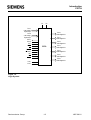
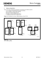
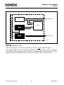
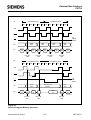
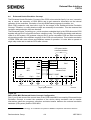
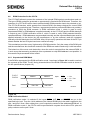
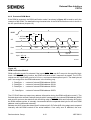
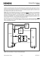
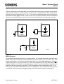
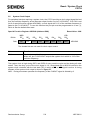
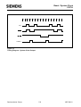
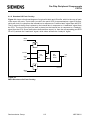
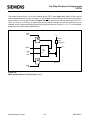
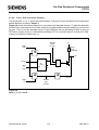
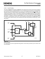
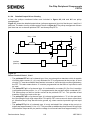
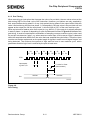
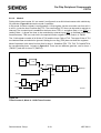
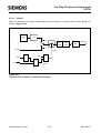
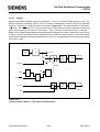
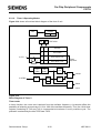
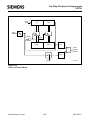
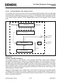
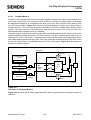
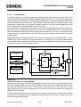
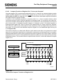
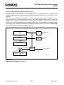
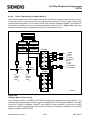
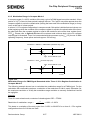
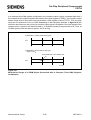
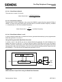
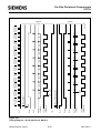
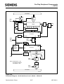
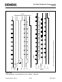
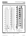
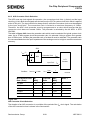
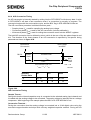
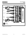
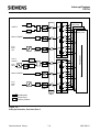
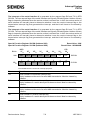
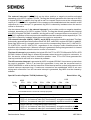
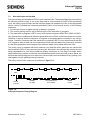
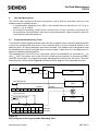
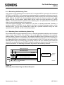
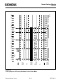
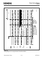
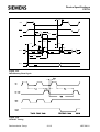
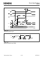
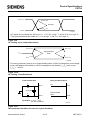
On-Chip Peripheral Components
C517A
6.5.3 Detailed Description of the Operating Modes
The following sections give a more detailed description of the several operating modes of the two
serial interfaces.
6.5.3.1
Mode 0, Synchronous Mode (Serial Interface 0)
Serial data enters and exits through RXD0. TXD0 outputs the shift clock. 8 data bits are transmitted/
received (LSB first). The baud rate is fixed at 1/12 of the oscillator frequency.
Figure 6-36 shows a simplified functional diagram of the serial port in mode 0. The associated
timing is illustrated in figure 6-37.
Transmission is initiated by any instruction that uses S0BUF as a destination register. The "Writeto-S0BUF" signal at S6P2 also loads a 1 into the 9th bit position of the transmit shift register and
tells the TX control block to commence a transmission. The internal timing is such that one full
machine cycle will elapse between "Write-to-S0BUF" and activation of SEND.
SEND enables the output of the shift register to the alternate output function line P3.0, and also
enables SHIFT CLOCK to the alternate output function line P3.1. SHIFT CLOCK is low during S3,
S4, and S5 of every machine cycle, and high during S6, S1, and S2. At S6P2 of every machine cycle
in which SEND is active, the contents of the transmit shift register is shifted one position to the right.
As data bits shift out to the right, zeros come in from the left. When the MSB of the data byte is at
the output position of the shift register, then the 1 that was initially loaded into the 9th position, is
just left of the MSB, and all positions to the left of that contain zeros. This condition flags the TX
control block to do one last shift and then deactivates SEND and sets TI0. Both of these actions
occur at S1P1 in the 10th machine cycle after "Write-to-S0BUF".
Reception is initiated by the condition REN0 = 1 and RI0 = 0. At S6P2 in the next machine cycle,
the RX control unit writes the bits 1111 1110 to the receive shift register, and in the next clock phase
activates RECEIVE.
RECEIVE enables SHIFT CLOCK to the alternate output function line of P3.1. SHIFT CLOCK
makes transitions at S3P1 and S6P1 in every machine cycle. At S6P2 of every machine cycle in
which RECEIVE is active, the contents of the receive shift register are shifted one position to the
left. The value that comes in from the right is the value that was sampled at the P3.0 pin at S5P2 in
the same machine cycle.
As data bits come in from the right, 1 s shift out to the left. When the 0 that was initially loaded into
the rightmost position arrives at the leftmost position in the shift register, it flags the RX control block
to do one last shift and load S0BUF. At S1P1 in the 10th machine cycle after the write to S0CON
that cleared RI0, RECEIVE is cleared and RI0 is set.
Semiconductor Group
6-83
1997-08-01