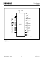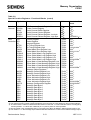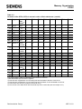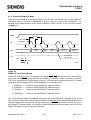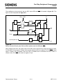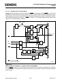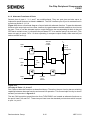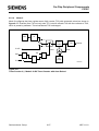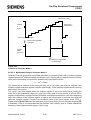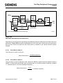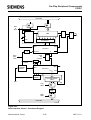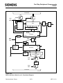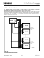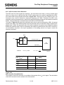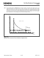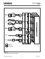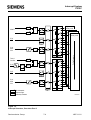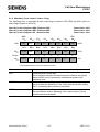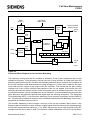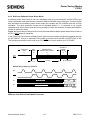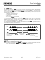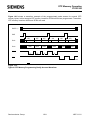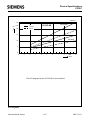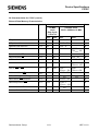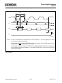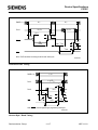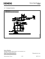
1
C515C
ht
User's Manual 11.97
tp
:/
Se /ww
m w
ic .s
on ie
du me
ct ns
or .d
/ e/
8-Bit CMOS Microcontroller
Edition 11.97
Published by Siemens AG,
Bereich Halbleiter, MarketingKommunikation, Balanstraße 73,
81541 München
© Siemens AG 1997.
All Rights Reserved.
Attention please!
As far as patents or other rights of third parties are concerned, liability is only assumed
for components, not for applications, processes and circuits implemented within components or assemblies.
The information describes the type of component and shall not be considered as assured
characteristics.
Terms of delivery and rights to change design
reserved.
For questions on technology, delivery and
prices please contact the Semiconductor
Group Offices in Germany or the Siemens
Companies and Representatives worldwide
(see address list).
Due to technical requirements components
may contain dangerous substances. For information on the types in question please
contact your nearest Siemens Office, Semiconductor Group.
Siemens AG is an approved CECC manufacturer.
Packing
Please use the recycling operators known to
you. We can also help you – get in touch with
your nearest sales office. By agreement we
will take packing material back, if it is sorted.
You must bear the costs of transport.
For packing material that is returned to us unsorted or which we are not obliged to accept,
we shall have to invoice you for any costs incurred.
Components used in life-support devices
or systems must be expressly authorized
for such purpose!
Critical components1 of the Semiconductor
Group of Siemens AG, may only be used in
life-support devices or systems2 with the express written approval of the Semiconductor
Group of Siemens AG.
1 A critical component is a component used
in a life-support device or system whose
failure can reasonably be expected to
cause the failure of that life-support device or system, or to affect its safety or effectiveness of that device or system.
2 Life support devices or systems are intended (a) to be implanted in the human
body, or (b) to support and/or maintain
and sustain human life. If they fail, it is
reasonable to assume that the health of
the user may be endangered.
General Information
C515C
C515C User’s Manual
Revision History :
11.97
Previous Releases :
06.96 (Original Version)
Page (new
version)
Page (prev. Subjects (changes since last revision)
version)
general
C515C-8E OTP version included (new chapter 10)
C515C AC/DC characteristics are now in chapter 11
1-1
1-9
Table 1-1
2-2
3-2
3-3, 3-11,
4-4, 6-4,
Tab.3-2/3-3
Tab.3-2 /
3-3, pg.9-2
3-17
1-1
1-9
Table 1-1
2-2
3-2
3-3, 3-11,
4-4, 6-4,
Tab.3-2/3-3
Tab.3-2 /
3-3, pg.9-2
3-17
4-2, 4-5
4-3
4-10 - 4-12
4-11
4-12
6-6
6-10, 6-11
6-18
6-39, 6-43
6-67
6-72
6-105,
6-106
6-108
6-109
7-2
9-6, 9-7
9-7
9-8
9-15
Chapter 10
11-1
11-4 - 11-6
11-10
11-11
11-14 to
11-17
4-2, 4-5
4-3
4-10 - 4-12
4-11
4-12
6-6
6-10, 6-11
6-18
6-39, 6-43
6-67
6-72
6-105,
6-106
6-108
7-2
9-6, 9-7
9-7
9-8
9-15
10-1
10-3
10-8
10-10
-
Semiconductor Group
Description of the new features of the C515C-8E; figure 1-1 modified
PSEN and ALE are activated every three (and not six) osc. periods
Ports 1 to 5 and 7 descriptions are corrected to quasi-bidirectional
Figure 2-1 modified for C515C-8E
Section 3.1 : C515C-8E version included
Description of SYSCON : bit CSWO and C515C-8E reset value added
Description of PCON1 : bit WS and C515C-8E reset value added
Reset value of P4 and table entry for bit P7.0 (INT7) corrected;
Version registers for C515C-8E added
Figure 4-1 and 4-2 corrected
3rd paragraph of chapter 4.1.3 removed
Chapter 4.7 “ROM Protection...“ enhanced for OTP verification
Figure 4-5 corrected
Figure 4-5 : OTP version reference added
Figure 6-4 and text : delay part corrected
Figures 6-7 and 6-8 : delay part corrected
Figure 6-14 corrected
Figure 6-22 and 6-26 : figure content exchanged
6.4.3.: first paragraph, divider range corrected
Baudrate selection bits corrected
multiple formulas corrected
last paragraph added
Chapter 6.5.8 (CAN switch-off capability) added
Figure 7-1 : bit address for bit RXIE added
Adding P4.7/RXDC wake-up capability to the description
Figure 9-1 corrected
Additional text in last paragraph before 9.5
Note below figure 9-5 added
New chapter : describes OTP programming of the C515C-8E
Minimum value for ambient temperature under bias corrected to –40˚C
Improved and extended Icc specification
SSC timing parameter tSCLK (master mode) and tHI improved
Wrong figure “External Clock Cycle“ exchanged with correct figure
Programming interface characteristics added
General Information
C515C
Table of Contents
Page
1
1.1
1.2
Introduction . . . . . . . . . . . . . . . . . . . . . . . . . . . . . . . . . . . . . . . . . . . . . . . . . . . . . . 1-1
Pin Configuration . . . . . . . . . . . . . . . . . . . . . . . . . . . . . . . . . . . . . . . . . . . . . . . . . . . 1-4
Pin Definitions and Functions . . . . . . . . . . . . . . . . . . . . . . . . . . . . . . . . . . . . . . . . . . 1-5
2
2.1
2.2
Fundamental Structure . . . . . . . . . . . . . . . . . . . . . . . . . . . . . . . . . . . . . . . . . . . . . 2-1
CPU . . . . . . . . . . . . . . . . . . . . . . . . . . . . . . . . . . . . . . . . . . . . . . . . . . . . . . . . . . . . . 2-3
CPU Timing . . . . . . . . . . . . . . . . . . . . . . . . . . . . . . . . . . . . . . . . . . . . . . . . . . . . . . . 2-5
3
3.1
3.2
3.3
3.4
3.4.1
3.4.2
3.4.3
3.4.4
3.4.5
3.5
Memory Organization . . . . . . . . . . . . . . . . . . . . . . . . . . . . . . . . . . . . . . . . . . . . . . 3-1
Program Memory, "Code Space" . . . . . . . . . . . . . . . . . . . . . . . . . . . . . . . . . . . . . . . 3-2
Data Memory, "Data Space" . . . . . . . . . . . . . . . . . . . . . . . . . . . . . . . . . . . . . . . . . . . 3-2
General Purpose Registers . . . . . . . . . . . . . . . . . . . . . . . . . . . . . . . . . . . . . . . . . . . 3-2
XRAM Operation. . . . . . . . . . . . . . . . . . . . . . . . . . . . . . . . . . . . . . . . . . . . . . . . . . . . 3-3
XRAM/CAN Controller Access Control . . . . . . . . . . . . . . . . . . . . . . . . . . . . . . . . . . . 3-3
Accesses to XRAM using the DPTR (16-bit Addressing Mode) . . . . . . . . . . . . . . . . 3-5
Accesses to XRAM using the Registers R0/R1 (8-bit Addressing Mode). . . . . . . . . 3-5
Reset Operation of the XRAM . . . . . . . . . . . . . . . . . . . . . . . . . . . . . . . . . . . . . . . . . 3-9
Behaviour of Port0 and Port2 . . . . . . . . . . . . . . . . . . . . . . . . . . . . . . . . . . . . . . . . . . 3-9
Special Function Registers . . . . . . . . . . . . . . . . . . . . . . . . . . . . . . . . . . . . . . . . . . . 3-11
4
4.1
4.1.1
4.1.2
4.1.3
4.2
4.3
4.4
4.5
4.6
4.6.1
4.6.2
4.6.3
4.6.4
4.7
4.7.1
4.7.2
External Bus Interface . . . . . . . . . . . . . . . . . . . . . . . . . . . . . . . . . . . . . . . . . . . . . . 4-1
Accessing External Memory . . . . . . . . . . . . . . . . . . . . . . . . . . . . . . . . . . . . . . . . . . . 4-1
Role of P0 and P2 as Data/Address Bus . . . . . . . . . . . . . . . . . . . . . . . . . . . . . . . . . 4-1
Timing . . . . . . . . . . . . . . . . . . . . . . . . . . . . . . . . . . . . . . . . . . . . . . . . . . . . . . . . . . . . 4-3
External Program Memory Access . . . . . . . . . . . . . . . . . . . . . . . . . . . . . . . . . . . . . . 4-3
PSEN, Program Store Enable . . . . . . . . . . . . . . . . . . . . . . . . . . . . . . . . . . . . . . . . . 4-3
Overlapping External Data and Program Memory Spaces. . . . . . . . . . . . . . . . . . . . 4-3
ALE, Address Latch Enable . . . . . . . . . . . . . . . . . . . . . . . . . . . . . . . . . . . . . . . . . . . 4-4
Enhanced Hooks Emulation Concept . . . . . . . . . . . . . . . . . . . . . . . . . . . . . . . . . . . . 4-5
Eight Datapointers for Faster External Bus Access . . . . . . . . . . . . . . . . . . . . . . . . . 4-6
The Importance of Additional Datapointers . . . . . . . . . . . . . . . . . . . . . . . . . . . . . . . 4-6
How the eight Datapointers of the C515C are realized . . . . . . . . . . . . . . . . . . . . . . 4-6
Advantages of Multiple Datapointers . . . . . . . . . . . . . . . . . . . . . . . . . . . . . . . . . . . . 4-7
Application Example and Performance Analysis . . . . . . . . . . . . . . . . . . . . . . . . . . . 4-7
ROM/OTP Protection for the C515C-8R / C515C-8E . . . . . . . . . . . . . . . . . . . . . . 4-10
Unprotected ROM Mode. . . . . . . . . . . . . . . . . . . . . . . . . . . . . . . . . . . . . . . . . . . . . 4-10
Protected ROM/OTP Mode. . . . . . . . . . . . . . . . . . . . . . . . . . . . . . . . . . . . . . . . . . . 4-11
5
5.1
5.2
5.3
5.4
5.5
Reset and System Clock Operation . . . . . . . . . . . . . . . . . . . . . . . . . . . . . . . . . . .
Hardware Reset Operation . . . . . . . . . . . . . . . . . . . . . . . . . . . . . . . . . . . . . . . . . . . .
Hardware Reset Timing . . . . . . . . . . . . . . . . . . . . . . . . . . . . . . . . . . . . . . . . . . . . . .
Fast Internal Reset after Power-On . . . . . . . . . . . . . . . . . . . . . . . . . . . . . . . . . . . . .
Oscillator and Clock Circuit. . . . . . . . . . . . . . . . . . . . . . . . . . . . . . . . . . . . . . . . . . . .
System Clock Output . . . . . . . . . . . . . . . . . . . . . . . . . . . . . . . . . . . . . . . . . . . . . . . .
Semiconductor Group
I-1
5-1
5-1
5-3
5-4
5-6
5-8
1997-11-01
General Information
C515C
Table of Contents
6
6.1
6.1.1
6.1.1.1
6.1.1.2
6.1.1.2.1
6.1.1.2.2
6.1.1.2.3
6.1.1.2.4
6.1.1.3
6.1.1.3.1
6.1.1.3.2
6.1.1.3.3
6.1.2
6.1.3
6.1.3.1
6.1.3.2
6.1.3.3
6.2
6.2.1
6.2.1.1
6.2.1.2
6.2.1.3
6.2.1.4
6.2.1.5
6.2.2
6.2.2.1
6.2.2.2
6.2.2.3
6.2.2.3.1
6.2.2.3.2
6.2.2.3.3
6.2.2.4
6.2.2.5
6.3
6.3.1
6.3.2
6.3.3
6.3.3.1
6.3.3.2
6.3.3.3
6.3.3.3.1
6.3.3.3.2
6.3.4
6.3.5
Page
On-Chip Peripheral Components . . . . . . . . . . . . . . . . . . . . . . . . . . . . . . . . . . . . . 6-1
Parallel I/O . . . . . . . . . . . . . . . . . . . . . . . . . . . . . . . . . . . . . . . . . . . . . . . . . . . . . . . . 6-1
Port Structures . . . . . . . . . . . . . . . . . . . . . . . . . . . . . . . . . . . . . . . . . . . . . . . . . . . . . 6-1
Port Structure Selection . . . . . . . . . . . . . . . . . . . . . . . . . . . . . . . . . . . . . . . . . . . . . . 6-3
Quasi-Bidirectional Port Structure . . . . . . . . . . . . . . . . . . . . . . . . . . . . . . . . . . . . . . 6-5
Basic Port Circuirty of Port 1 to 5 and 7 . . . . . . . . . . . . . . . . . . . . . . . . . . . . . . . . . . 6-5
Port 0 Circuitry . . . . . . . . . . . . . . . . . . . . . . . . . . . . . . . . . . . . . . . . . . . . . . . . . . . . . 6-8
Port 0 and Port 2 used as Address/Data Bus . . . . . . . . . . . . . . . . . . . . . . . . . . . . . . 6-9
SSC Port Pins of Port 4 . . . . . . . . . . . . . . . . . . . . . . . . . . . . . . . . . . . . . . . . . . . . . 6-10
Bidirectional (CMOS) Port Structure of Port 5 . . . . . . . . . . . . . . . . . . . . . . . . . . . . 6-12
Input Mode . . . . . . . . . . . . . . . . . . . . . . . . . . . . . . . . . . . . . . . . . . . . . . . . . . . . . . . 6-12
Output Mode . . . . . . . . . . . . . . . . . . . . . . . . . . . . . . . . . . . . . . . . . . . . . . . . . . . . . . 6-13
Hardware Power Down Mode. . . . . . . . . . . . . . . . . . . . . . . . . . . . . . . . . . . . . . . . . 6-15
Alternate Functions of Ports . . . . . . . . . . . . . . . . . . . . . . . . . . . . . . . . . . . . . . . . . . 6-16
Port Handling . . . . . . . . . . . . . . . . . . . . . . . . . . . . . . . . . . . . . . . . . . . . . . . . . . . . . 6-18
Port Timing . . . . . . . . . . . . . . . . . . . . . . . . . . . . . . . . . . . . . . . . . . . . . . . . . . . . . . . 6-18
Port Loading and Interfacing. . . . . . . . . . . . . . . . . . . . . . . . . . . . . . . . . . . . . . . . . . 6-19
Read-Modify-Write Feature of Ports 1 to 5 and 7 . . . . . . . . . . . . . . . . . . . . . . . . . . 6-19
Timers/Counters . . . . . . . . . . . . . . . . . . . . . . . . . . . . . . . . . . . . . . . . . . . . . . . . . . . 6-21
Timer/Counter 0 and 1 . . . . . . . . . . . . . . . . . . . . . . . . . . . . . . . . . . . . . . . . . . . . . . 6-21
Timer/Counter 0 and 1 Registers . . . . . . . . . . . . . . . . . . . . . . . . . . . . . . . . . . . . . . 6-22
Mode 0 . . . . . . . . . . . . . . . . . . . . . . . . . . . . . . . . . . . . . . . . . . . . . . . . . . . . . . . . . . 6-25
Mode 1 . . . . . . . . . . . . . . . . . . . . . . . . . . . . . . . . . . . . . . . . . . . . . . . . . . . . . . . . . . 6-26
Mode 2 . . . . . . . . . . . . . . . . . . . . . . . . . . . . . . . . . . . . . . . . . . . . . . . . . . . . . . . . . . 6-27
Mode 3 . . . . . . . . . . . . . . . . . . . . . . . . . . . . . . . . . . . . . . . . . . . . . . . . . . . . . . . . . . 6-28
Timer/Counter 2 with Additional Compare/Capture/Reload . . . . . . . . . . . . . . . . . . 6-29
Timer 2 Registers . . . . . . . . . . . . . . . . . . . . . . . . . . . . . . . . . . . . . . . . . . . . . . . . . . 6-31
Timer 2 Operation. . . . . . . . . . . . . . . . . . . . . . . . . . . . . . . . . . . . . . . . . . . . . . . . . . 6-36
Compare Function of Registers CRC, CC1 to CC3 . . . . . . . . . . . . . . . . . . . . . . . . 6-38
Compare Mode 0 . . . . . . . . . . . . . . . . . . . . . . . . . . . . . . . . . . . . . . . . . . . . . . . . . . 6-38
Modulation Range in Compare Mode 0 . . . . . . . . . . . . . . . . . . . . . . . . . . . . . . . . . 6-40
Compare Mode 1 . . . . . . . . . . . . . . . . . . . . . . . . . . . . . . . . . . . . . . . . . . . . . . . . . . 6-42
Using Interrupts in Combination with the Compare Function . . . . . . . . . . . . . . . . . 6-44
Capture Function . . . . . . . . . . . . . . . . . . . . . . . . . . . . . . . . . . . . . . . . . . . . . . . . . . 6-46
Serial Interface . . . . . . . . . . . . . . . . . . . . . . . . . . . . . . . . . . . . . . . . . . . . . . . . . . . . 6-48
Multiprocessor Communication . . . . . . . . . . . . . . . . . . . . . . . . . . . . . . . . . . . . . . . 6-49
Serial Port Registers. . . . . . . . . . . . . . . . . . . . . . . . . . . . . . . . . . . . . . . . . . . . . . . . 6-49
Baud Rate Generation . . . . . . . . . . . . . . . . . . . . . . . . . . . . . . . . . . . . . . . . . . . . . . 6-51
Baud Rate in Mode 0 . . . . . . . . . . . . . . . . . . . . . . . . . . . . . . . . . . . . . . . . . . . . . . . 6-52
Baud Rate in Mode 2 . . . . . . . . . . . . . . . . . . . . . . . . . . . . . . . . . . . . . . . . . . . . . . . 6-52
Baud Rate in Mode 1 and 3 . . . . . . . . . . . . . . . . . . . . . . . . . . . . . . . . . . . . . . . . . . 6-53
Using the Internal Baud Rate Generator . . . . . . . . . . . . . . . . . . . . . . . . . . . . . . . . 6-53
Using Timer 1 to Generate Baud Rates . . . . . . . . . . . . . . . . . . . . . . . . . . . . . . . . . 6-55
Details about Mode 0 . . . . . . . . . . . . . . . . . . . . . . . . . . . . . . . . . . . . . . . . . . . . . . . 6-56
Details about Mode 1 . . . . . . . . . . . . . . . . . . . . . . . . . . . . . . . . . . . . . . . . . . . . . . . 6-59
Semiconductor Group
I-2
1997-11-01
General Information
C515C
Table of Contents
Page
6.3.6
6.4
6.4.1
6.4.2
6.4.3
6.4.4
6.4.5
6.4.6
6.4.6.1
6.4.6.2
6.4.7
6.5
6.5.1
6.5.2
6.5.2.1
6.5.2.2
6.5.3
6.5.4
6.5.5
6.5.5.1
6.5.5.2
6.5.6
6.5.7
6.5.8
6.5.9
6.5.10
6.5.11
6.6
6.6.1
6.6.2
6.6.3
6.6.4
6.6.5
Details about Modes 2 and 3 . . . . . . . . . . . . . . . . . . . . . . . . . . . . . . . . . . . . . . . . . 6-62
SSC Interface . . . . . . . . . . . . . . . . . . . . . . . . . . . . . . . . . . . . . . . . . . . . . . . . . . . . . 6-65
General Operation of the SSC . . . . . . . . . . . . . . . . . . . . . . . . . . . . . . . . . . . . . . . . 6-66
Enable/Disable Control . . . . . . . . . . . . . . . . . . . . . . . . . . . . . . . . . . . . . . . . . . . . . . 6-66
Baudrate Generation (Master Mode only) . . . . . . . . . . . . . . . . . . . . . . . . . . . . . . . 6-67
Write Collision Detection. . . . . . . . . . . . . . . . . . . . . . . . . . . . . . . . . . . . . . . . . . . . . 6-67
Master/Slave Mode Selection . . . . . . . . . . . . . . . . . . . . . . . . . . . . . . . . . . . . . . . . . 6-68
Data/Clock Timing Relationships . . . . . . . . . . . . . . . . . . . . . . . . . . . . . . . . . . . . . . 6-69
Master Mode Operation . . . . . . . . . . . . . . . . . . . . . . . . . . . . . . . . . . . . . . . . . . . . . 6-69
Slave Mode Operation . . . . . . . . . . . . . . . . . . . . . . . . . . . . . . . . . . . . . . . . . . . . . . 6-70
Register Description . . . . . . . . . . . . . . . . . . . . . . . . . . . . . . . . . . . . . . . . . . . . . . . . 6-71
The On-Chip CAN Controller . . . . . . . . . . . . . . . . . . . . . . . . . . . . . . . . . . . . . . . . . 6-76
Basic CAN Controller Functions . . . . . . . . . . . . . . . . . . . . . . . . . . . . . . . . . . . . . . . 6-77
CAN Register Description. . . . . . . . . . . . . . . . . . . . . . . . . . . . . . . . . . . . . . . . . . . . 6-81
General Registers. . . . . . . . . . . . . . . . . . . . . . . . . . . . . . . . . . . . . . . . . . . . . . . . . . 6-81
The Message Object Registers / Data Bytes . . . . . . . . . . . . . . . . . . . . . . . . . . . . . 6-91
Handling of Message Objects. . . . . . . . . . . . . . . . . . . . . . . . . . . . . . . . . . . . . . . . . 6-97
Initialization and Reset . . . . . . . . . . . . . . . . . . . . . . . . . . . . . . . . . . . . . . . . . . . . . 6-104
Configuration of the Bit Timing . . . . . . . . . . . . . . . . . . . . . . . . . . . . . . . . . . . . . . . 6-105
Hard Synchronization and Resynchronization . . . . . . . . . . . . . . . . . . . . . . . . . . . 6-106
Calculation of the Bit Time . . . . . . . . . . . . . . . . . . . . . . . . . . . . . . . . . . . . . . . . . . 6-106
CAN Interrupt Handling. . . . . . . . . . . . . . . . . . . . . . . . . . . . . . . . . . . . . . . . . . . . . 6-107
CAN Controller in Power Saving Modes. . . . . . . . . . . . . . . . . . . . . . . . . . . . . . . . 6-108
Switch-off Capability of the CAN Controller (C515C-8E only) . . . . . . . . . . . . . . . 6-109
Configuration Examples of a Transmission Object. . . . . . . . . . . . . . . . . . . . . . . . 6-110
Configuration Examples of a Reception Object . . . . . . . . . . . . . . . . . . . . . . . . . . 6-111
The CAN Application Interface . . . . . . . . . . . . . . . . . . . . . . . . . . . . . . . . . . . . . . . 6-112
A/D Converter . . . . . . . . . . . . . . . . . . . . . . . . . . . . . . . . . . . . . . . . . . . . . . . . . . . . 6-113
A/D Converter Operation . . . . . . . . . . . . . . . . . . . . . . . . . . . . . . . . . . . . . . . . . . . 6-113
A/D Converter Registers. . . . . . . . . . . . . . . . . . . . . . . . . . . . . . . . . . . . . . . . . . . . 6-115
A/D Converter Clock Selection . . . . . . . . . . . . . . . . . . . . . . . . . . . . . . . . . . . . . . . 6-119
A/D Conversion Timing. . . . . . . . . . . . . . . . . . . . . . . . . . . . . . . . . . . . . . . . . . . . . 6-120
A/D Converter Calibration. . . . . . . . . . . . . . . . . . . . . . . . . . . . . . . . . . . . . . . . . . . 6-124
7
7.1
7.1.1
7.1.2
7.1.3
7.2
7.3
7.4
7.5
Interrupt System . . . . . . . . . . . . . . . . . . . . . . . . . . . . . . . . . . . . . . . . . . . . . . . . . . 7-1
Interrupt Registers . . . . . . . . . . . . . . . . . . . . . . . . . . . . . . . . . . . . . . . . . . . . . . . . . . 7-5
Interrupt Enable Registers . . . . . . . . . . . . . . . . . . . . . . . . . . . . . . . . . . . . . . . . . . . . 7-5
Interrupt Request / Control Flags . . . . . . . . . . . . . . . . . . . . . . . . . . . . . . . . . . . . . . . 7-8
Interrupt Priority Registers . . . . . . . . . . . . . . . . . . . . . . . . . . . . . . . . . . . . . . . . . . . 7-14
Interrupt Priority Level Structure . . . . . . . . . . . . . . . . . . . . . . . . . . . . . . . . . . . . . . . 7-15
How Interrupts are Handled . . . . . . . . . . . . . . . . . . . . . . . . . . . . . . . . . . . . . . . . . . 7-16
External Interrupts . . . . . . . . . . . . . . . . . . . . . . . . . . . . . . . . . . . . . . . . . . . . . . . . . 7-18
Interrupt Response Time . . . . . . . . . . . . . . . . . . . . . . . . . . . . . . . . . . . . . . . . . . . . 7-20
Semiconductor Group
I-3
1997-11-01
General Information
C515C
Table of Contents
Page
8
8.1
8.1.1
8.1.2
8.1.3
8.1.3.1
8.1.3.2
8.1.4
8.1.5
8.2
Fail Safe Mechanisms . . . . . . . . . . . . . . . . . . . . . . . . . . . . . . . . . . . . . . . . . . . . . .
Programmable Watchdog Timer. . . . . . . . . . . . . . . . . . . . . . . . . . . . . . . . . . . . . . . .
Input Clock Selection . . . . . . . . . . . . . . . . . . . . . . . . . . . . . . . . . . . . . . . . . . . . . . . .
Watchdog Timer Control / Status Flags. . . . . . . . . . . . . . . . . . . . . . . . . . . . . . . . . .
Starting the Watchdog Timer . . . . . . . . . . . . . . . . . . . . . . . . . . . . . . . . . . . . . . . . . .
The First Possibility of Starting the Watchdog Timer . . . . . . . . . . . . . . . . . . . . . . . .
The Second Possibility of Starting the Watchdog Timer. . . . . . . . . . . . . . . . . . . . . .
Refreshing the Watchdog Timer . . . . . . . . . . . . . . . . . . . . . . . . . . . . . . . . . . . . . . . .
Watchdog Reset and Watchdog Status Flag . . . . . . . . . . . . . . . . . . . . . . . . . . . . . .
Oscillator Watchdog Unit . . . . . . . . . . . . . . . . . . . . . . . . . . . . . . . . . . . . . . . . . . . . .
9
9.1
9.2
9.3
9.4
9.4.1
9.4.2
9.5
9.6
9.7
9.8
Power Saving Modes . . . . . . . . . . . . . . . . . . . . . . . . . . . . . . . . . . . . . . . . . . . . . . . 9-1
Power Saving Mode Control Registers. . . . . . . . . . . . . . . . . . . . . . . . . . . . . . . . . . . 9-1
Idle Mode . . . . . . . . . . . . . . . . . . . . . . . . . . . . . . . . . . . . . . . . . . . . . . . . . . . . . . . . . 9-3
Slow Down Mode Operation . . . . . . . . . . . . . . . . . . . . . . . . . . . . . . . . . . . . . . . . . . . 9-5
Software Power Down Mode . . . . . . . . . . . . . . . . . . . . . . . . . . . . . . . . . . . . . . . . . . 9-6
Invoking Software Power Down Mode . . . . . . . . . . . . . . . . . . . . . . . . . . . . . . . . . . . 9-6
Exit from Software Power Down Mode . . . . . . . . . . . . . . . . . . . . . . . . . . . . . . . . . . . 9-7
State of Pins in Software Initiated Power Saving Modes . . . . . . . . . . . . . . . . . . . . . 9-8
Hardware Power Down Mode. . . . . . . . . . . . . . . . . . . . . . . . . . . . . . . . . . . . . . . . . . 9-9
Hardware Power Down Reset Timing. . . . . . . . . . . . . . . . . . . . . . . . . . . . . . . . . . . 9-11
CPUR Signal. . . . . . . . . . . . . . . . . . . . . . . . . . . . . . . . . . . . . . . . . . . . . . . . . . . . . . 9-15
10
10.1
10.2
10.3
10.4
10.4.1
10.4.2
10.5
10.6
10.7
OTP Memory Operation (C515C-8E only) . . . . . . . . . . . . . . . . . . . . . . . . . . . . . 10-1
Programming Configuration . . . . . . . . . . . . . . . . . . . . . . . . . . . . . . . . . . . . . . . . . . 10-1
Pin Configuration . . . . . . . . . . . . . . . . . . . . . . . . . . . . . . . . . . . . . . . . . . . . . . . . . . 10-2
Pin Definitions. . . . . . . . . . . . . . . . . . . . . . . . . . . . . . . . . . . . . . . . . . . . . . . . . . . . . 10-3
Programming Mode Selection . . . . . . . . . . . . . . . . . . . . . . . . . . . . . . . . . . . . . . . . 10-5
Basic Programming Mode Selection. . . . . . . . . . . . . . . . . . . . . . . . . . . . . . . . . . . . 10-5
OTP Memory Access Mode Selection . . . . . . . . . . . . . . . . . . . . . . . . . . . . . . . . . . 10-6
Program / Read OTP Memory Bytes . . . . . . . . . . . . . . . . . . . . . . . . . . . . . . . . . . . 10-7
Lock Bits Programming / Read . . . . . . . . . . . . . . . . . . . . . . . . . . . . . . . . . . . . . . . . 10-9
Access of Version Bytes . . . . . . . . . . . . . . . . . . . . . . . . . . . . . . . . . . . . . . . . . . . . 10-11
11
11.1
11.2
11.3
11.4
11.5
11.6
11.7
Device Specifications . . . . . . . . . . . . . . . . . . . . . . . . . . . . . . . . . . . . . . . . . . . . . 11-1
Absolute Maximum Ratings . . . . . . . . . . . . . . . . . . . . . . . . . . . . . . . . . . . . . . . . . . 11-1
DC Characteristics . . . . . . . . . . . . . . . . . . . . . . . . . . . . . . . . . . . . . . . . . . . . . . . . . 11-2
A/D Converter Characteristics . . . . . . . . . . . . . . . . . . . . . . . . . . . . . . . . . . . . . . . . 11-6
AC Characteristics for C515C. . . . . . . . . . . . . . . . . . . . . . . . . . . . . . . . . . . . . . . . . 11-8
OTP Memory Programming Mode Characteristics . . . . . . . . . . . . . . . . . . . . . . . . 11-14
ROM/OTP Verification Characteristics for C515C-8R / C515C-8E . . . . . . . . . . 11-18
Package Information. . . . . . . . . . . . . . . . . . . . . . . . . . . . . . . . . . . . . . . . . . . . . . . 11-21
12
Index . . . . . . . . . . . . . . . . . . . . . . . . . . . . . . . . . . . . . . . . . . . . . . . . . . . . . . . . . . . 12-1
Semiconductor Group
I-4
8-1
8-1
8-2
8-3
8-4
8-4
8-4
8-5
8-5
8-6
1997-11-01
Introduction
C515C
1
Introduction
The C515C is an enhanced, upgraded version of the SAB 80C515A 8-bit microcontroller which
additionally provides a full CAN interface, a SPI compatible synchronous serial interface, extended
power save provisions, additional on-chip RAM, 64K byte of on-chip program memory, two new
external interrupts and RFI related improvements. With a maximum external clock rate of 10 MHz
it achieves a 600 ns instruction cycle time (1 µs at 6 MHz).
The C515C-8R contains a non-volatile 64k byte read-only program memory. The C515C-L is
identical to the C515C-8R, except that it lacks the on-chip program memory The C515C-8E is the
OTP version in the C515C microcontroller with a 64k byte one-time programmable (OTP) program
memory. With the C515C-8E fast programming cycles are achieved (1 byte in 100 µsec). Also
several levels of OTP memory protection can be selected. If compared to the C515C-8R and
C515C-L, the C515C-8E OTP version additionally provides two features :
– the wake-up from software power down mode can, additionally to the external pin P3.2/INT0
wake-up capability, also be triggered alternatively by a second pin P4.7/RXDC.
– for power consumption reasons the on-chip CAN controller can be switched off
The term C515C refers to all versions within this documentation unless otherwise noted.
On-Chip Emulation Support Module
Figure 1-1 shows the different functional units of the C515C and figure 1-2 shows the simplified
logic symbol of the C515C.
Full-CAN
Controller
SSC (SPI)
Interface
Oscillator
Watchdog
Power
Save Modes
Idle/
Power down
Slow down
XRAM
2k x 8
10 Bit ADC
(8 inputs)
RAM
256 x 8
T0
CPU
8 Datapointer
Timer 2
Capture/Compare Unit
Port 7
Port 6
Port 5
Port 4
I/O
Analog/
Digital
Input
I/O
I/O
T1
Program Memory
C515C-8R : 64k x 8 ROM
C515C-8E : 64k x 8 OTP
Port 0
I/O
Port 1
I/O
Port 2
I/O
Port 3
I/O
8 Bit
USART
MCA03646
Figure 1-1
C515C Functional Units
Semiconductor Group
1-1
1997-11-01
Introduction
C515C
Listed below is a summary of the main features of the C515C:
•
•
•
•
•
•
•
•
•
•
•
•
•
•
•
•
•
•
•
•
•
•
•
Full upward compatibility with SAB 80C515A
On-chip program memory (with optional memory protection)
– C515C-8R : 64k byte on-chip ROM
– C515C-8E : 64k byte on-chip OTP
– alternatively up to 64k byte external program memory
256 byte on-chip RAM
2K byte on-chip XRAM
Up to 64K byte external data memory
Superset of the 8051 architecture with 8 datapointers
Up to 10 MHz external operating frequency
– without clock prescaler (1 µs instruction cycle time at 6 MHz external clock)
On-chip emulation support logic (Enhanced Hooks Technology TM)
Current optimized oscillator circuit
Eight ports: 48 + 1 digital I/O lines, 8 analog inputs
– Quasi-bidirectional port structure (8051 compatible)
– Port 5 selectable for bidirectional port structure (CMOS voltage levels)
Three 16-bit timer/counters
– Timer 2 can be used for compare/capture functions
10-bit A/D converter with multiplexed inputs and Built-in self calibration
Full duplex serial interface with programmable baudrate generator (USART)
SSC synchronous serial interface (SPI compatible)
– Master and slave capable
– Programmable clock polarity / clock-edge to data phase relation
– LSB/MSB first selectable
– 2.5 MHz transfer rate at 10 MHz operating frequency
Full-CAN Module
– 256 register/data bytes are located in external data memory area
– max.1 MBaud at 10 MHz operating frequency
Seventeen interrupt vectors, at four priority levels selectable
Extended watchdog facilities
– 15-bit programmable watchdog timer
– Oscillator watchdog
Power saving modes
– Slow-down mode
– Idle mode (can be combined with slow-down mode)
– Software power-down mode with wake-up capability through INT0 or RXDC pin
– Hardware power-down mode
CPU running condition output pin
ALE can be switched off
Multiple separate VCC/VSS pin pairs
P-MQFP-80 package
Temperature Ranges: SAB-C515C
TA = 0 to 70 °C
SAF-C515C
TA = – 40 to 85 °C
SAH-C515C
TA = – 40 to 110 °C
Semiconductor Group
1-2
1997-11-01
Introduction
C515C
VAGND
VAREF
Port 0
8 Bit Digital I/O
Port 1
8 Bit Digital I/O
XTAL1
XTAL2
Port 2
8 Bit Digital I/O
ALE
PSEN
EA
RESET
PE/SWD
HWPD
CPUR
Port 3
8 Bit Digital I/O
Port 4
8 Bit Digital I/O
C515C
Port 5
8 Bit Digital I/O
Port 6
8 Bit Analog/
Digital Inputs
VSSE1
VCCE1
VSSE2
VCCE2
Port 7
1 Bit Digital I/O
VSS1
VCC1
VSSCLK
VCCCLK
VSSEXT
VCCEXT
MCL02714
Figure 1-2
Logic Symbol
Semiconductor Group
1-3
1997-11-01
Introduction
C515C
1.1
Pin Configuration
P5.7
P0.7/AD7
P0.6/AD6
P0.5/AD5
P0.4/AD4
P0.3/AD3
P0.2/AD2
P0.1/AD1
P0.0/AD0
VSSEXT
VCCEXT
EA
ALE
PSEN
CPUR
P2.7/A15
P2.6/A14
P2.5/A13
P2.4/A12
P2.3/A11
This section describes the pin configuration of the C515C in the P-MQFP-80 package.
60 59 58 57 56 55 54 53 52 51 50 49 48 47 46 45 44 43 42 41
P5.6
P5.5
P5.4
P5.3
P5.2
P5.1
P5.0
VCCE2
HWPD
VSSE2
N.C.
P4.0/ADST
P4.1/SCLK
P4.2/SRI
PE/SWD
P4.3/STO
P4.4/SLS
P4.5/INT8
P4.6/TXDC
P4.7/RXDC
61
62
63
64
65
66
67
68
69
70
71
72
73
74
75
76
77
78
79
80
C515C
40
39
38
37
36
35
34
33
32
31
30
29
28
27
26
25
24
23
22
21
P2.2/A10
P2.1/A9
P2.0/A8
XTAL1
XTAL2
VSSE1
VSS1
VCC1
VCCE1
P1.0/INT3/CC0
P1.1/INT4/CC1
P1.2/INT5/CC2
P1.3/INT6/CC3
P1.4/INT2
P1.5/T2EX
P1.6/CLKOUT
P1.7/T2
P7.0/INT7
P3.7/RD
P3.6/WR
RESET
N.C.
VAREF
VAGND
P6.7/AIN7
P6.6/AIN6
P6.5/AIN5
P6.4/AIN4
P6.3/AIN3
P6.2/AIN2
P6.1/AIN1
P6.0/AIN0
VSSCLK
VCCCLK
P3.0/RXD
P3.1/TXD
P3.2/INT0
P3.3/INT1
P3.4/T0
P3.5/T1
1 2 3 4 5 6 7 8 9 10 11 12 13 14 15 16 17 18 19 20
MCP02715
Figure 1-3
Pin Configuration (top view)
Semiconductor Group
1-4
1997-11-01
Introduction
C515C
1.2
Pin Definitions and Functions
This section describes all external signals of the C515C with its function.
Table 1-1
Pin Definitions and Functions
Symbol
Pin Number
I/O*)
Function
I/O
Port 4
is an 8-bit quasi-bidirectional I/O port with internal pull-up
resistors. Port 4 pins that have 1’s written to them are
pulled high by the internal pull-up resistors, and in that
state can be used as inputs. As inputs, port 4 pins being
externally pulled low will source current (I IL, in the DC
characteristics) because of the internal pull-up resistors.
P4 also contains the external A/D converter control pin,
the SSC pins, the CAN controller input/output lines, and
the external interrupt 8 input. The output latch
corresponding to a secondary function must be
programmed to a one (1) for that function to operate.
The alternate functions are assigned to port 4 as follows:
P4.0 ADST
External A/D converter start pin
P4.1 SCLK
SSC Master Clock Output /
SSC Slave Clock Input
P4.2 SRI
SSC Receive Input
P4.3 STO
SSC Transmit Output
P4.4 SLS
Slave Select Input
P4.5 INT8
External interrupt 8 input
P4.6 TXDC
Transmitter output of the CAN controller
P4.7 RXDC
Receiver input of the CAN controller
P-MQFP-80
P4.0-P4.7
72-74, 76-80
72
73
74
76
77
78
79
80
PE/SWD
75
I
Power saving mode enable / Start watchdog timer
A low level on this pin allows the software to enter the
power down, idle and slow down mode. In case the low
level is also seen during reset, the watchdog timer
function is off on default.
Use of the software controlled power saving modes is
blocked, when this pin is held on high level. A high level
during reset performs an automatic start of the watchdog
timer immediately after reset. When left unconnected this
pin is pulled high by a weak internal pull-up resistor.
RESET
1
I
RESET
A low level on this pin for the duration of two machine
cycles while the oscillator is running resets the C515C. A
small internal pullup resistor permits power-on reset
using only a capacitor connected to VSS .
*) I = Input
O = Output
Semiconductor Group
1-5
1997-11-01
Introduction
C515C
Table 1-1
Pin Definitions and Functions (cont’d)
Symbol
Pin Number
I/O*)
Function
P-MQFP-80
VAREF
3
–
Reference voltage for the A/D converter
VAGND
4
–
Reference ground for the A/D converter
P6.7-P6.0
5-12
I
Port 6
is an 8-bit unidirectional input port to the A/D converter.
Port pins can be used for digital input, if voltage levels
simultaneously meet the specifications high/low input
voltages and for the eight multiplexed analog inputs.
P3.0-P3.7
15-22
I/O
Port 3
is an 8-bit quasi-bidirectional I/O port with internal pullup
resistors. Port 3 pins that have 1's written to them are
pulled high by the internal pullup resistors, and in that
state can be used as inputs. As inputs, port 3 pins being
externally pulled low will source current (I IL, in the DC
characteristics) because of the internal pullup resistors.
Port 3 also contains the interrupt, timer, serial port and
external memory strobe pins that are used by various
options. The output latch corresponding to a secondary
function must be programmed to a one (1) for that
function to operate. The secondary functions are
assigned to the pins of port 3, as follows:
P3.0
RXD
Receiver data input (asynch.) or
data input/output (synch.) of serial
interface
P3.1
TXD
Transmitter data output (asynch.) or
clock output (synch.) of serial
interface
P3.2
INT0
External interrupt 0 input / timer 0
gate control input
External interrupt 1 input / timer 1
P3.3
INT1
gate control input
P3.4
T0
Timer 0 counter input
P3.5
T1
Timer 1 counter input
P3.6
WR
WR control output; latches the data
byte from port 0 into the external
data memory
P3.7
RD
RD control output; enables the
external data memory
15
16
17
18
19
20
21
22
*) I = Input
O = Output
Semiconductor Group
1-6
1997-11-01
Introduction
C515C
Table 1-1
Pin Definitions and Functions (cont’d)
Symbol
Pin Number
I/O*)
Function
P-MQFP-80
P7.0
23
I/O
Port 7
is an 1-bit quasi-bidirectional I/O port with internal pull-up
resistor. When a 1 is written to P7.0 it is pulled high by an
internal pull-up resistor, and in that state can be used as
input. As input, P7.0 being externally pulled low will
source current (I IL, in the DC characteristics) because of
the internal pull-up resistor. If P7.0 is used as interrupt
input, its output latch must be programmed to a one (1).
The secondary function is assigned to the port 7 pin as
follows:
P7.0 INT7 Interrupt 7 input
P1.0 - P1.7
31-24
I/O
Port 1
is an 8-bit quasi-bidirectional I/O port with internal pullup
resistors. Port 1 pins that have 1's written to them are
pulled high by the internal pullup resistors, and in that
state can be used as inputs. As inputs, port 1 pins being
externally pulled low will source current (I IL, in the DC
characteristics) because of the internal pullup resistors.
The port is used for the low-order address byte during
program verification. Port 1 also contains the interrupt,
timer, clock, capture and compare pins that are used by
various options. The output latch corresponding to a
secondary function must be programmed to a one (1) for
that function to operate (except when used for the
compare functions). The secondary functions are
assigned to the port 1 pins as follows:
P1.0 INT3 CC0 Interrupt 3 input / compare 0 output /
capture 0 input
P1.1 INT4 CC1 Interrupt 4 input / compare 1 output /
capture 1 input
P1.2 INT5 CC2 Interrupt 5 input / compare 2 output /
capture 2 input
P1.3 INT6 CC3 Interrupt 6 input / compare 3 output /
capture 3 input
P1.4 INT2
Interrupt 2 input
P1.5 T2EX
Timer 2 external reload / trigger
input
P1.6 CLKOUT
System clock output
P1.7 T2
Counter 2 input
31
30
29
28
27
26
25
24
*) I = Input
O = Output
Semiconductor Group
1-7
1997-11-01
Introduction
C515C
Table 1-1
Pin Definitions and Functions (cont’d)
Symbol
Pin Number
I/O*)
Function
P-MQFP-80
XTAL2
36
–
XTAL2
Input to the inverting oscillator amplifier and input to the
internal clock generator circuits.
To drive the device from an external clock source, XTAL2
should be driven, while XTAL1 is left unconnected.
Minimum and maximum high and low times as well as
rise/fall times specified in the AC characteristics must be
observed.
XTAL1
37
–
XTAL1
Output of the inverting oscillator amplifier.
P2.0-P2.7
38-45
I/O
Port 2
is an 8-bit quasi-bidirectional I/O port with internal pullup
resistors. Port 2 pins that have 1's written to them are
pulled high by the internal pullup resistors, and in that
state can be used as inputs. As inputs, port 2 pins being
externally pulled low will source current (I IL, in the DC
characteristics) because of the internal pullup resistors.
Port 2 emits the high-order address byte during fetches
from external program memory and during accesses to
external data memory that use 16-bit addresses
(MOVX @DPTR). In this application it uses strong
internal pullup resistors when issuing 1's. During
accesses to external data memory that use 8-bit
addresses (MOVX @Ri), port 2 issues the contents of
the P2 special function register.
CPUR
46
O
CPU running condition
This output pin is at low level when the CPU is running
and program fetches or data accesses in the external
data memory area are executed. In idle mode, hardware
and software power down mode, and with an active
RESET signal CPUR is set to high level.
CPUR can be typically used for switching external
memory devices into power saving modes.
*) I = Input
O = Output
Semiconductor Group
1-8
1997-11-01
Introduction
C515C
Table 1-1
Pin Definitions and Functions (cont’d)
Symbol
Pin Number
I/O*)
Function
P-MQFP-80
PSEN
47
O
The Program Store Enable
output is a control signal that enables the external
program memory to the bus during external fetch
operations. It is activated every three oscillator periods,
except during external data memory accesses. The
signal remains high during internal program execution.
ALE
48
O
The Address Latch enable
output is used for latching the address into external
memory during normal operation. It is activated every
three oscillator periods, except during an external data
memory access. ALE can be switched off when the
program is executed internally.
EA
49
I
External Access Enable
When held high, the C515C executes instructions always
from internal program memory. When EA is held low, all
instructions are fetched from external program memory.
EA should not be driven during reset operation
P0.0-P0.7
52-59
I/O
Port 0
is an 8-bit open-drain bidirectional I/O port.
Port 0 pins that have 1's written to them float, and in that
state can be used as high-impedance inputs.
Port 0 is also the multiplexed low-order address and data
bus during accesses to external program and data
memory. In this application it uses strong internal pullup
resistors when issuing 1's. Port 0 also outputs the code
bytes during program verification in the C515C-8E.
External pullup resistors are required during program.
P5.7-P5.0
60-67
I/O
Port 5
is an 8-bit quasi-bidirectional I/O port with internal pullup
resistors. Port 5 pins that have 1's written to them are
pulled high by the internal pullup resistors, and in that
state can be used as inputs. As inputs, port 5 pins being
externally pulled low will source current (I IL, in the DC
characteristics) because of the internal pullup resistors.
Port 5 can also be switched into a bidirectional mode, in
which CMOS levels are provided. In this bidirectional
mode, each port 5 pin can be programmed individually as
input or output.
*) I = Input
O = Output
Semiconductor Group
1-9
1997-11-01
Introduction
C515C
Table 1-1
Pin Definitions and Functions (cont’d)
Symbol
Pin Number
I/O*)
Function
P-MQFP-80
HWPD
69
I
Hardware Power Down
A low level on this pin for the duration of one machine
cycle while the oscillator is running resets the C515C.
A low level for a longer period will force the part to power
down mode with the pins floating.
VCC1
33
–
Supply voltage for internal logic
This pins is used for the power supply of the internal logic
circuits during normal, idle, and power down mode.
VSS1
34
–
Ground (0 V) for internal logic
This pin is used for the ground connection of the internal
logic circuits during normal, idle, and power down mode.
VCCE1
VCCE2
32
68
–
Supply voltage for I/O ports
These pins are used for power supply of the I/O ports
during normal, idle, and power-down mode.
VSSE1
VSSE2
35
70
–
Ground (0 V) for I/O ports
These pins are used for ground connections of the I/O
ports during normal, idle, and power-down mode.
VCCEXT
50
–
Supply voltage for external access pins
This pin is used for power supply of the I/O ports and
control signals which are used during external accesses
(for Port 0, Port 2, ALE, PSEN, P3.6/WR, and P3.7/RD).
VSSEXT
51
–
Ground (0 V) for external access pins
This pin is used for the ground connection of the I/O ports
and control signals which are used during external
accesses (for Port 0, Port 2, ALE, PSEN, P3.6/WR, and
P3.7/RD).
VCCCLK
14
–
Supply voltage for on-chip oscillator
This pin is used for power supply of the on-chip oscillator
circuit.
VSSCLK
13
–
Ground (0 V) for on-chip oscillator
This pin is used for ground connection of the on-chip
oscillator circuit.
N.C.
2, 71
–
Not connected
These pins should not be connected.
*) I = Input
O = Output
Semiconductor Group
1-10
1997-11-01
Fundamental Structure
C515C
2
Fundamental Structure
The C515C is fully compatible to the architecture of the standard 8051/C501 microcontroller family.
While maintaining all architectural and operational characteristics of the C501, the C515C
incorporates a CPU with 8 datapointers, a genuine 10-bit A/D converter, a capture/compare unit, a
Full-CAN controller unit, a SSC synchronous serial interface, a USART serial interface, a XRAM
data memory as well as some enhancements in the Fail Save Mechanism Unit. Figure 2-1 shows
a block diagram of the C515C.
Semiconductor Group
2-1
1997-11-01
Fundamental Structure
C515C
Oscillator Watchdog
XRAM
2k x 8
XTAL1
XTAL2
RAM
256 x 8
ROM/OTP
64k x 8
Multiple
V CC /V SS
Lines
OSC & Timing
ALE
CPU
PSEN
8 Datapointers
EA
Emulation
Support
Logic
Programmable
Watchdog Timer
CPUR
PE/SWD
HWPD
Timer 0
Port 0
Port 0
8 Bit Digital I/O
Port 1
Port 1
8 Bit Digital I/O
Capture
Compare Unit
Port 2
Port 2
8 Bit Digital I/O
USART
Port 3
Port 3
8 Bit Digital I/O
Port 4
Port 4
8 Bit Digital I/O
Port 5
Port 5
8 Bit Digital I/O
Port 6
Port 6
8 Bit Analog/
Digital Inputs
Port 7
Port 7
1 Bit Digital I/O
RESET
Timer 1
Timer 2
Baud Rate Generator
256 Byte
Reg./Data
SSC (SPI) Interface
Full-CAN
Controller
Interrupt Unit
V AREF
V AGND
A/D Converter
10 Bit
S&H
MUX
C515C
MCB03647
Figure 2-1
Block Diagram of the C515C
Semiconductor Group
2-2
1997-11-01
Fundamental Structure
C515C
2.1
CPU
The C515C is efficient both as a controller and as an arithmetic processor. It has extensive facilities
for binary and BCD arithmetic and excels in its bit-handling capabilities. Efficient use of program
memory results from an instruction set consisting of 44% one-byte, 41% two-byte, and 15% threebyte instructions. With a 6 MHz external clock, 58% of the instructions execute in 1.0 µs (10 MHz:
600 ns).
The CPU (Central Processing Unit) of the C515C consists of the instruction decoder, the arithmetic
section and the program control section. Each program instruction is decoded by the instruction
decoder. This unit generates the internal signals controlling the functions of the individual units
within the CPU. They have an effect on the source and destination of data transfers and control the
ALU processing.
The arithmetic section of the processor performs extensive data manipulation and is comprised of
the arithmetic/logic unit (ALU), an A register, B register and PSW register.
The ALU accepts 8-bit data words from one or two sources and generates an 8-bit result under the
control of the instruction decoder. The ALU performs the arithmetic operations add, substract,
multiply, divide, increment, decrement, BDC-decimal-add-adjust and compare, and the logic
operations AND, OR, Exclusive OR, complement and rotate (right, left or swap nibble (left four)).
Also included is a Boolean processor performing the bit operations as set, clear, complement, jumpif-not-set, jump-if-set-and-clear and move to/from carry. Between any addressable bit (or its
complement) and the carry flag, it can perform the bit operations of logical AND or logical OR with
the result returned to the carry flag.
The program control section controls the sequence in which the instructions stored in program
memory are executed. The 16-bit program counter (PC) holds the address of the next instruction to
be executed. The conditional branch logic enables internal and external events to the processor to
cause a change in the program execution sequence.
Additionally to the CPU functionality of the C501/8051 standard microcontroller, the C515C
contains 8 datapointers. For complex applications with peripherals located in the external data
memory space (e.g. CAN controller) or extended data storage capacity this turned out to be a "bottle
neck" for the 8051’s communication to the external world. Especially programming in high-level
languages (PLM51, C51, PASCAL51) requires extended RAM capacity and at the same time a fast
access to this additional RAM because of the reduced code efficiency of these languages.
Accumulator
ACC is the symbol for the accumulator register. The mnemonics for accumulator-specific
instructions, however, refer to the accumulator simply as A.
Program Status Word
The Program Status Word (PSW) contains several status bits that reflect the current state of the
CPU.
Semiconductor Group
2-3
1997-11-01
Fundamental Structure
C515C
Special Function Register PSW (Address D0H)
Reset Value : 00H
Bit No. MSB
D0H
LSB
D7H
D6H
D5H
D4H
D3H
D2H
D1H
D0H
CY
AC
F0
RS1
RS0
OV
F1
P
Bit
Function
CY
Carry Flag
Used by arithmetic instruction.
AC
Auxiliary Carry Flag
Used by instructions which execute BCD operations.
F0
General Purpose Flag
RS1
RS0
Register Bank select control bits
These bits are used to select one of the four register banks.
PSW
RS1
RS0
Function
0
0
Bank 0 selected, data address 00H-07H
0
1
Bank 1 selected, data address 08H-0FH
1
0
Bank 2 selected, data address 10H-17H
1
1
Bank 3 selected, data address 18H-1FH
OV
Overflow Flag
Used by arithmetic instruction.
F1
General Purpose Flag
P
Parity Flag
Set/cleared by hardware after each instruction to indicate an odd/even
number of "one" bits in the accumulator, i.e. even parity.
B Register
The B register is used during multiply and divide and serves as both source and destination. For
other instructions it can be treated as another scratch pad register.
Stack Pointer
The stack pointer (SP) register is 8 bits wide. It is incremented before data is stored during PUSH
and CALL executions and decremented after data is popped during a POP and RET (RETI)
execution, i.e. it always points to the last valid stack byte. While the stack may reside anywhere in
the on-chip RAM, the stack pointer is initialized to 07H after a reset. This causes the stack to begin
a location = 08H above register bank zero. The SP can be read or written under software control.
Semiconductor Group
2-4
1997-11-01
Fundamental Structure
C515C
2.2
CPU Timing
The C515C has no clock prescaler. Therefore, a machine cycle of the C515C consists of 6 states
(6 oscillator periods). Each state is divided into a phase 1 half and a phase 2 half. Thus, a machine
cycle consists of 6 oscillator periods, numbered S1P1 (state 1, phase 1) through S6P2 (state 6,
phase 2). Each state lasts one oscillator period. Typically, arithmetic and logic operations take place
during phase 1 and internal register-to-register transfers take place during phase 2.
The diagrams in figure 2-2 show the fetch/execute timing related to the internal states and phases.
Since these internal clock signals are not user-accessible, the XTAL1 oscillator signals and the ALE
(address latch enable) signal are shown for external reference. ALE is normally activated twice
during each machine cycle: once during S1P2 and S2P1, and again during S4P2 and S5P1.
Executing of a one-cycle instruction begins at S1P2, when the op-code is latched into the instruction
register. If it is a two-byte instruction, the second reading takes place during S4 of the same
machine cycle. If it is a one-byte instruction, there is still a fetch at S4, but the byte read (which would
be the next op-code) is ignored (discarded fetch), and the program counter is not incremented. In
any case, execution is completed at the end of S6P2.
Figures 2-2 (a) and (b) show the timing of a 1-byte, 1-cycle instruction and for a 2-byte, 1-cycle
instruction.
Semiconductor Group
2-5
1997-11-01
Fundamental Structure
C515C
S1 S2
S3
S4
S5
S6
S1 S2
S3
S4
S5
S6
P1 P2 P1 P2 P1 P2 P1 P2 P1 P2 P1 P2 P1 P2 P1 P2 P1 P2 P1 P2 P1 P2 P1 P2
OSC
(XTAL1)
ALE
Read
Opcode
S1
S2
Read next
Opcode (Discard)
S3
S4
S5
Read next
Opcode again
S6
a) 1 Byte, 1-Cycle Instruction, e.g. INC A
Read 2nd
Byte
Read
Opcode
S1
S2
S3
S4
S5
Read next
Opcode
S6
b) 2 Byte, 1-Cycle Instruction, e.g. ADD A, # Data
Read next Opcode again
Read
Opcode
S1
S2
Read next Opcode (Discard)
S3
S4
S5
S6
S1
S2
S3
S4
S5
S6
c) 1 Byte, 2-Cycle Instruction, e.g. INC DPTR
S1
S2
d) MOVX (1 Byte, 2-Cycle)
Read next Opcode again
Read next
Opcode
(Discard)
Read
Opcode
(MOVX)
S3
S4
S5
S6
ADDR
No Fetch
No ALE
S1
S2
S3
No Fetch
S4
S5
S6
DATA
Access of External Memory
MCD02638
Figure 2-2
Fetch Execute Sequence
Semiconductor Group
2-6
1997-11-01
Memory Organization
C515C
3
Memory Organization
The C515C CPU manipulates operands in the following four address spaces:
–
–
–
–
–
–
up to 64 Kbyte of internal/external program memory
up to 64 Kbyte of external data memory
256 bytes of internal data memory
256 bytes CAN controller registers / data memory
2K bytes of internal XRAM data memory
a 128 byte special function register area
Figure 3-1 illustrates the memory address spaces of the C515C.
Alternatively
FFFF H
FFFF H
Internal
XRAM
(2 KByte)
External
Data
Memory
F800 H
Internal
(EA = 1)
Int. CAN
Controller
(256 Byte)
F6FF H
External
(EA = 0)
F7FF H
F700 H
Indirect
Address
Direct
Address
FF H
Internal
RAM
80 H
External
Special
Function
Register
FF H
80 H
7F H
Internal
RAM
0000 H
0000 H
"Code Space"
"Data Space"
00 H
"Internal Data Space"
MCD02717
Figure 3-1
C515C Memory Map
Semiconductor Group
3-1
1997-11-01
Memory Organization
C515C
3.1
Program Memory, "Code Space"
The C515C-8R provides 64 Kbytes of read-only program memory while the C515C-L has no
internal program memory. The C515C-8E provides 64 Kbytes of OTP program memory.. For
internal ROM/OTP program execution the EA pin must be put to high level. The 64K bytes program
memory can also be located completely external. If the EA pin is held low, the C515C fetches all
instructions from an external program memory.
3.2
Data Memory, "Data Space"
The data memory address space consists of an internal and an external memory space. The
internal data memory is divided into three physically separate and distinct blocks : the lower 128
bytes of RAM, the upper 128 bytes of RAM, and the 128 byte special function register (SFR) area.
While the upper 128 bytes of data memory and the SFR area share the same address locations,
they are accessed through different addressing modes. The lower 128 bytes of data memory can
be accessed through direct or register indirect addressing; the upper 128 bytes of RAM can be
accessed through register indirect addressing; the special function registers are accessible through
direct addressing. Four 8-register banks, each bank consisting of eight 8-bit multi-purpose registers,
occupy locations 0 through 1FH in the lower RAM area. The next 16 bytes, locations 20H through
2FH, contain 128 directly addressable bit locations. The stack can be located anywhere in the
internal data memory address space, and the stack depth can be expanded up to 256 bytes.
The external data memory can be expanded up to 64 Kbyte and can be accessed by instructions
that use a 16-bit or an 8-bit address. The internal CAN controller and the internal XRAM are located
in the external address memory area at addresses F700H to FFFFH. Using MOVX instruction with
addresses pointing to this address area, alternatively XRAM and CAN controller registers or
external XRAM are accessed.
3.3
General Purpose Registers
The lower 32 locations of the internal RAM are assigned to four banks with eight general purpose
registers (GPRs) each. Only one of these banks may be enabled at a time. Two bits in the program
status word, RS0 (PSW.3) and RS1 (PSW.4), select the active register bank (see description of the
PSW in chapter 2). This allows fast context switching, which is useful when entering subroutines
or interrupt service routines.
The 8 general purpose registers of the selected register bank may be accessed by register
addressing. With register addressing the instruction op code indicates which register is to be used.
For indirect addressing R0 and R1 are used as pointer or index register to address internal or
external memory (e.g. MOV @R0).
Reset initializes the stack pointer to location 07H and increments it once to start from location 08H
which is also the first register (R0) of register bank 1. Thus, if one is going to use more than one
register bank, the SP should be initialized to a different location of the RAM which is not used for
data storage.
Semiconductor Group
3-2
1997-11-01
Memory Organization
C515C
3.4
XRAM Operation
The XRAM in the C515C is a memory area that is logically located at the upper end of the external
memory space, but is integrated on the chip. Because the XRAM is used in the same way as
external data memory the same instruction types (MOVX) must be used for accessing the XRAM.
3.4.1 XRAM/CAN Controller Access Control
Two bits in SFR SYSCON, XMAP0 and XMAP1, control the accesses to XRAM and the CAN
controller. XMAP0 is a general access enable/disable control bit and XMAP1 controls the external
signal generation during XRAM/CAN controller accesses.
Special Function Register SYSCON (Address B1H)
Bit No. MSB
7
B1H
–
6
5
PMOD EALE
4
3
RMAP
–
Reset Value C515C-8R : X010XX01B
Reset Value C515C-8E : X010X001B
2
1
LSB
0
CSWO XMAP1 XMAP0
SYSCON
The function of the shaded bit is not described in this section.
Bit
Function
–
Not implemented. Reserved for future use.
XMAP1
XRAM/CAN controller visible access control
Control bit for RD/WR signals during XRAM/CAN Controller accesses. If
addresses are outside the XRAM/CAN controller address range or if
XRAM is disabled, this bit has no effect.
XMAP1 = 0 : The signals RD and WR are not activated during accesses to
the XRAM/CAN Controller
XMAP1 = 1 : Ports 0, 2 and the signals RD and WR are activated during
accesses to XRAM/CAN Controller. In this mode, address
and data information during XRAM/CAN Controller accesses
are visible externally.
XMAP0
Global XRAM/CAN controller access enable/disable control
XMAP0 = 0 : The access to XRAM and CAN controller is enabled.
XMAP0 = 1 : The access to XRAM and CAN controller is disabled (default
after reset!). All MOVX accesses are performed via the
external bus. Further, this bit is hardware protected.
When bit XMAP1 in SFR SYSCON is set, during all accesses to XRAM and CAN Controller RD and
WR become active and port 0 and 2 drive the actual address/data information which is read/written
from/to XRAM or CAN controller. This feature allows to check the internal data transfers to XRAM
and CAN controller. When port 0 and 2 are used for I/O purposes, the XMAP1 bit should not be set.
Otherwise the I/O function of the port 0 and port 2 lines is interrupted.
Semiconductor Group
3-3
1997-11-01
Memory Organization
C515C
After a reset operation, bit XMAP0 is reset. This means that the accesses to XRAM and CAN
controller are generally disabled. In this case, all accesses using MOVX instructions within the
address range of F700H to FFFFH generate external data memory bus cycles. When XMAP0 is set,
the access to XRAM and CAN controller is enabled and all accesses using MOVX instructions with
an address in the range of F700H to FFFFH will access internal XRAM or CAN controller.
Bit XMAP0 is hardware protected. If it is reset once (XRAM and CAN controller access enabled) it
cannot be set by software. Only a reset operation will set the XMAP0 bit again. This hardware
protection mechanism is done by an unsymmetric latch at XMAP0 bit. A unintentional disabling of
XRAM and CAN controller could be dangerous since indeterminate values could be read from the
external bus. To avoid this the XMAP0 bit is forced to '1' only by a reset operation. Additionally,
during reset an internal capacitor is loaded. So the reset state is a disabled XRAM and CAN
controller. Because of the load time of the capacitor, XMAP0 bit once written to '0' (that is,
discharging the capacitor) cannot be set to '1' again by software. On the other hand any distortion
(software hang up, noise,...) is not able to load this capacitor, too. That is, the stable status is XRAM
and CAN controller enabled.
The clear instruction for the XMAP0 bit should be integrated in the program initialization routine
before XRAM or CAN controller is used. In extremely noisy systems the user may have redundant
clear instructions.
Semiconductor Group
3-4
1997-11-01
Memory Organization
C515C
3.4.2 Accesses to XRAM using the DPTR (16-bit Addressing Mode)
The XRAM and CAN controller can be accessed by two read/write instructions, which use the 16bit DPTR for indirect addressing. These instructions are :
– MOVX
– MOVX
A, @DPTR
@DPTR, A
(Read)
(Write)
For accessing the XRAM, the effective address stored in DPTR must be in the range of F800H to
FFFFH. For accessing the CAN controller, the effective address stored in DPTR must be in the
range of F700H to F7FFH.
3.4.3 Accesses to XRAM using the Registers R0/R1 (8-bit Addressing Mode)
The 8051 architecture provides also instructions for accesses to external data memory range which
use only an 8-bit address (indirect addressing with registers R0 or R1). The instructions are:
MOVX
MOVX
A, @ Ri
@Ri, A
(Read)
(Write)
As in the SAB 80C515A a special page register is implemented into the C515C to provide the
possibility of accessing the XRAM or CAN controller also with the MOVX @Ri instructions, i.e.
XPAGE serves the same function for the XRAM and CAN controller as Port 2 for external data
memory.
Special Function Register XPAGE (Address 91H)
Reset Value : 00H
Bit No. MSB
7
6
5
4
3
2
1
LSB
0
91H
.6
.5
.4
.3
.2
.1
.0
.7
XPAGE
Bit
Function
XPAGE.7-0
XRAM/CAN controller high address
XPAGE.7-0 is the address part A15-A8 when 8-bit MOVX instructions are
used to access internal XRAM or CAN controller.
Figures 3-2 to 3-4 show the dependencies of XPAGE- and Port 2 - addressing in order to explain
the differences in accessing XRAM/CAN controller, ext. RAM or what is to do when Port 2 is used
as an I/O-port.
Semiconductor Group
3-5
1997-11-01
Memory Organization
C515C
Port 0
Address/Data
XRAM
CAN-Controller
XPAGE
Write to
Port 2
Page Address
Port 2
MCS02761
Figure 3-2
Write Page Address to Port 2
“MOV P2,pageaddress“ will write the page address to Port 2 and the XPAGE-Register.
When external RAM is to be accessed in the XRAM/CAN controller address range (F700H FFFFH), the XRAM/CAN controller has to be disabled. When additional external RAM is to be
addressed in an address range < F700H, the XRAM/CAN controller may remain enabled and there
is no need to overwrite XPAGE by a second move.
Semiconductor Group
3-6
1997-11-01
Memory Organization
C515C
Port 0
Address/Data
XRAM
CAN-Controller
XPAGE
Write to
XPAGE
Address/
I/O Data
Port 2
MCS02762
Figure 3-3
Write Page Address to XPAGE
The page address is only written to the XPAGE register. Port 2 is available for addresses or I/O
data.
Semiconductor Group
3-7
1997-11-01
Memory Organization
C515C
Port 0
Address/Data
XRAM
CAN-Controller
XPAGE
Write
I/O Data
to Port 2
I/O Data
Port 2
MCS02763
Figure 3-4
Use of Port 2 as I/O Port
At a write to port 2, the XRAM/CAN controller address in XPAGE register will be overwritten
because of the concurrent write to port 2 and XPAGE register. So, whenever XRAM is used and the
XRAM address differs from the byte written to port 2 latch it is absolutely necessary to rewrite
XPAGE with the page address.
Example :
I/O data at port 2 shall be AAH. A byte shall be fetched from XRAM at address F830H.
MOV
MOV
MOV
MOVX
R0, #30H
P2, #0AAH
XPAGE, #0F8H
A, @R0
Semiconductor Group
;
; P2 shows AAH and XPAGE contains AAH
; P2 still shows AAH but XRAM is addressed
; the contents of XRAM at F830H is moved to accumulator
3-8
1997-11-01
Memory Organization
C515C
The register XPAGE provides the upper address byte for accesses to XRAM with MOVX @Ri
instructions. If the address formed by XPAGE and Ri points outside the XRAM/CAN Controller
address range, an external access is performed. For the C515C the content of XPAGE must be
greater or equal F7H in order to use the XRAM/CAN Controller.
The software has to distinguish two cases, if the MOVX @Ri instructions with paging shall be used :
a) Access to XRAM/CAN Contr. : The upper address byte must be written to XPAGE or P2;
both writes select the XRAM/CAN controller address range.
b) Access to external memory : The upper address byte must be written to P2; XPAGE will be
loaded with the same address in order to deselect the XRAM.
3.4.4 Reset Operation of the XRAM
The contents of the XRAM is not affected by a reset. After power-up the contents are undefined,
while they remain unchanged during and after a reset as long as the power supply is not turned off.
If a reset occurs during a write operation to XRAM, the content of a XRAM memory location
depends on the cycle in which the active reset signal is detected (MOVX is a 2-cycle instruction):
Reset during 1st cycle : The new value will not be written to XRAM. The old value is not affected.
Reset during 2nd cycle : The old value in XRAM is overwritten by the new value.
3.4.5 Behaviour of Port0 and Port2
The behaviour of Port 0 and P2 during a MOVX access depends on the control bits in register
SYSCON and on the state of pin EA. The table 3-1 lists the various operating conditions. It shows
the following characteristics:
a) Use of P0 and P2 pins during the MOVX access.
Bus: The pins work as external address/data bus. If (internal) XRAM is accessed, the data
written to the XRAM can be seen on the bus in debug mode.
I/0: The pins work as Input/Output lines under control of their latch.
b) Activation of the RD and WR pin during the access.
c) Use of internal or external XDATA memory.
The shaded areas describe the standard operation as each 80C51 device without on-chip XRAM
behaves.
Semiconductor Group
3-9
1997-11-01
Semiconductor Group
MOVX
@DPTR
3-10
MOVX
@ Ri
EA = 0
EA = 1
XMAP1, XMAP0
XMAP1, XMAP0
00
10
X1
00
10
X1
a)P0/P2→Bus
b)RD/WR active
c)ext.memory
is used
a)P0/P2→Bus
b)RD/WR active
c)ext.memory
is used
a)P0/P2→Bus
b)RD/WR active
c)ext.memory
is used
a)P0/P2→Bus
b)RD/WR active
c)ext.memory
is used
a)P0/P2→Bus
b)RD/WR active
c)ext.memory
is used
a)P0/P2→Bus
b)RD/WR active
c)ext.memory
is used
DPTR
≥
XRAM
address
range
a)P0/P2→Bus
(RD/WR-Data)
b)RD/WR
inactive
c)XRAM is used
a)P0/P2→Bus a)P0/P2→Bus a)P0/P2→I/0
(RD/WR-Data)
b)RD/WR active b)RD/WR active b)RD/WR
c)XRAM is used c) ext.memory
inactive
is used
c)XRAM is used
a)P0/P2→Bus a)P0/P2→Bus
(RD/WR-Data)
b)RD/WR active b)RD/WR active
c)XRAM is used c) ext.memory
is used
XPAGE
<
XRAM
addr.page
range
a)P0→Bus
P2→I/O
b)RD/WR active
c)ext.memory
is used
a)P0→Bus
P2→I/O
b)RD/WR active
c)ext.memory
is used
a)P0→Bus
P2→I/O
b)RD/WR active
c)ext.memory
is used
XPAGE
≥
XRAM
addr.page
range
a)P0→Bus
(RD/WR-Data)
P2→I/O
b)RD/WR
inactive
c)XRAM is used
a)P0→Bus
a)P0→Bus
a)P2→I/O
(RD/WR-Data
P2→I/O
P0/P2→I/O
only)
P2→I/O
b)RD/WR active b)RD/WR
b)RD/WR active
inactive
c)ext.memory
c)XRAM is used
c)XRAM is used is used
DPTR
<
XRAM
address
range
Table 3-1
Behaviour of P0/P2 and RD/WR During MOVX Accesses
a)P0→Bus
P2→I/O
b)RD/WR active
c)ext.memory
is used
a)P0→Bus
P2→I/O
b)RD/WR active
c)ext.memory
is used
a)P0→Bus
a)P0→Bus
(RD/WR-Data)
P2→I/O
P2→I/O
b)RD/WR active b)RD/WR active
c)XRAM is used c)ext.memory
is used
Memory Organization
C515C
1997-11-01
modes compatible to 8051/C501 family
a)P0→Bus
P2→I/O
b)RD/WR active
c)ext.memory
is used
Memory Organization
C515C
3.5
Special Function Registers
The registers, except the program counter and the four general purpose register banks, reside in
the special function register area. The special function register area consists of two portions : the
standard special function register area and the mapped special function register area. Two special
function registers of the C515C (PCON1 and DIR5) are located in the mapped special function
register area. For accessing the mapped special function register area, bit RMAP in special function
register SYSCON must be set. All other special function registers are located in the standard
special function register area which is accessed when RMAP is cleared (“0“).
The registers and data locations of the CAN controller (CAN-SFRs) are located in the external data
memory area at addresses F700H to F7FFH. Details about the access of these registers is
described in section 3.4.1 of this chapter.
Special Function Register SYSCON (Address B1H)
Bit No. MSB
7
B1H
–
6
5
PMOD EALE
4
3
RMAP
–
Reset Value C515C-8R : X010XX01B
Reset Value C515C-8E : X010X001B
2
1
LSB
0
CSWO XMAP1 XMAP0
SYSCON
The functions of the shaded bits are not described in this section.
Bit
Function
–
Reserved bits for future use.
RMAP
Special function register map bit
RMAP = 0 : The access to the non-mapped (standard) special function
register area is enabled.
RMAP = 1 : The access to the mapped special function register area is
enabled.
As long as bit RMAP is set, mapped special function register area can be accessed. This bit is not
cleared by hardware automatically. Thus, when non-mapped/mapped registers are to be accessed,
the bit RMAP must be cleared/set by software, respectively each.
All SFRs with addresses where address bits 0-2 are 0 (e.g. 80H, 88H, 90H, 98H, ..., F8H, FFH) are
bitaddressable.
The 59 special function registers (SFRs) in the standard and mapped SFR area include pointers
and registers that provide an interface between the CPU and the other on-chip peripherals. The
SFRs of the C515C are listed in table 3-2 and table 3-3. In table 3-2 they are organized in groups
which refer to the functional blocks of the C515C. The CAN-SFRs are also included in table 3-2.
Table 3-3 illustrates the contents of the SFRs in numeric order of their addresses. Table 3-4 list the
CAN-SFRs in numeric order of their addresses. .
Semiconductor Group
3-11
1997-11-01
Memory Organization
C515C
Table 3-2
Special Function Registers - Functional Blocks
Block
Symbol
Name
CPU
ACC
B
DPH
DPL
DPSEL
PSW
SP
SYSCON 2)
Accumulator
B-Register
Data Pointer, High Byte
Data Pointer, Low Byte
Data Pointer Select Register
Program Status Word Register
Stack Pointer
System Control Register
A/DADCON0 2)
Converter ADCON1
ADDATH
ADDATL
Address Contents after
Reset
E0H 1)
F0H 1)
83H
82H
92H
D0H 1)
81H
C515C-8R B1H
C515C-8E B1H
00H
00H
00H
00H
XXXXX000B 3)
00H
07H
X010XX01B 3)
X010X001B 3)
A/D Converter Control Register 0
A/D Converter Control Register 1
A/D Converter Data Register High Byte
A/D Converter Data Register Low Byte
D8H 1)
DCH
D9H
DAH 4)
00H
0XXXX000B 3)
00H
00XXXXXXB 3)
A8H1)
B8H 1)
9AH
A9H
B9H
88H 1)
C8H 1)
98H 1)
C0H 1)
00H
00H
XX00X00XB 3)
00H
0X000000B 3)
00H
00H
00H
00H
Interrupt
System
IEN0 2)
IEN1 2)
IEN2
IP0 2)
IP1
TCON 2)
T2CON 2)
SCON 2)
IRCON
Interrupt Enable Register 0
Interrupt Enable Register 1
Interrupt Enable Register 2
Interrupt Priority Register 0
Interrupt Priority Register 1
Timer Control Register
Timer 2 Control Register
Serial Channel Control Register
Interrupt Request Control Register
XRAM
XPAGE
Page Address Register for Extended on-chip 91H
XRAM and CAN Controller
System Control Register
C515C-8R B1H
C515C-8E B1H
Port 0
80H 1)
90H 1)
Port 1
A0H 1)
Port 2
B0H 1
Port 3
E8H 1)
Port 4
F8H 1)
Port 5
F8H 1) 4)
Port 5 Direction Register
DBH
Port 6, Analog/Digital Input
FAH
Port 7
System Control Register
C515C-8R B1H
C515C-8E B1H
SYSCON 2)
Ports
P0
P1
P2
P3
P4
P5
DIR5
P6
P7
SYSCON 2)
00H
X010XX01B 3)
X010X001B 3)
FFH
FFH
FFH
FFH
FFH
FFH
FFH
–
XXXXXXX1B 3)
X010XX01B 3)
X010X001B 3)
1) Bit-addressable special function registers
2) This special function register is listed repeatedly since some bits of it also belong to other functional blocks.
3) “X“ means that the value is undefined and the location is reserved
4) This SFR is a mapped SFR. For accessing this SFR, bit PDIR in SFR IP1 must be set.
Semiconductor Group
3-12
1997-11-01
Memory Organization
C515C
Table 3-2
Special Function Registers - Functional Blocks (cont’d)
Block
Symbol
Name
Address Contents after
Reset
Serial
Channel
ADCON0 2)
PCON 2)
SBUF
SCON
SRELL
SRELH
A/D Converter Control Register 0
Power Control Register
Serial Channel Buffer Register
Serial Channel Control Register
Serial Channel Reload Register, low byte
Serial Channel Reload Register, high byte
D8H 1
87H
99H
98H 1)
AAH
BAH
00H
00H
XXH 3)
00H
D9H
XXXXXX11B 3)
Control Register
Status Register
Interrupt Register
Bit Timing Register Low
Bit Timing Register High
Global Mask Short Register Low
Global Mask Short Register High
Upper Global Mask Long Register Low
Upper Global Mask Long Register High
Lower Global Mask Long Register Low
Lower Global Mask Long Register High
Upper Mask of Last Message Register Low
Upper Mask of Last Message Register High
Lower Mask of Last Message Register Low
Lower Mask of Last Message Register High
Message Object Registers :
Message Control Register Low
Message Control Register High
Upper Arbitration Register Low
Upper Arbitration Register High
Lower Arbitration Register Low
Lower Arbitration Register High
Message Configuration Register
Message Data Byte 0
Message Data Byte 1
Message Data Byte 2
Message Data Byte 3
Message Data Byte 4
Message Data Byte 5
Message Data Byte 6
Message Data Byte 7
F700H
F701H
F702H
F704H
F705H
F706H
F707H
F708H
F709H
F70AH
F70BH
F70CH
F70DH
F70EH
F70FH
01H
XXH 3)
XXH 3)
UUH 3)
F7n0H 5)
F7n1H 5)
F7n2H 5)
F7n3H 5)
F7n4H 5)
F7n5H 5)
F7n6H 5)
F7n7H 5)
F7n8H 5)
F7n9H 5)
F7nAH 5)
F7nBH 5)
F7nCH 5)
F7nDH 5)
F7nEH 5)
UUH 3)
UUH 3)
UUH 3)
UUH 3)
UUH 3)
UUUUU000B 3)
UUUUUU00B3)
XXH 3)
XXH 3)
XXH 3)
XXH 3)
XXH 3)
XXH 3)
XXH 3)
XXH 3)
CAN
CR
Controller SR
IR
BTR0
BTR1
GMS0
GMS1
UGML0
UGML1
LGML0
LGML1
UMLM0
UMLM1
LMLM0
LMLM1
MCR0
MCR1
UAR0
UAR1
LAR0
LAR1
MCFG
DB0
DB1
DB2
DB3
DB4
DB5
DB6
DB7
0UUUUUUUB 3)
UUH 3)
UUU11111B 3)
UUH 3)
UUH 3)
UUH 3)
UUUUU000B 3)
UUH 3)
UUH 3)
UUH 3)
UUUUU000B 3)
1) Bit-addressable special function registers
2) This special function register is listed repeatedly since some bits of it also belong to other functional blocks.
3) “X“ means that the value is undefined and the location is reserved. “U“ means that the value is unchanged by
a reset operation. “U“ values are undefined (as “X“) after a power-on reset operation
4) SFR is located in the mapped SFR area. For accessing this SFR, bit RMAP in SFR SYSCON must be set.
5) The notation “n“ in the message object address definition defines the number of the related message object.
Semiconductor Group
3-13
1997-11-01
Memory Organization
C515C
Table 3-2
Special Function Registers - Functional Blocks (cont’d)
Block
Symbol
Name
Address Contents after
Reset
SSC
Interface
SSCCON
STB
SRB
SCF
SCIEN
SSCMOD
SSC Control Register
SSC Transmit Buffer
SSC Receive Register
SSC Flag Register
SSC Interrupt Enable Register
SSC Mode Test Register
93H 1)
94H
95H
ABH 1)
ACH
96H
07H
XXH 3)
XXH 3)
XXXXXX00B 3)
XXXXXX00B 3)
00H
Timer 0/
Timer 1
TCON
TH0
TH1
TL0
TL1
TMOD
Timer 0/1 Control Register
Timer 0, High Byte
Timer 1, High Byte
Timer 0, Low Byte
Timer 1, Low Byte
Timer Mode Register
88H 1)
8CH
8DH
8AH
8BH
89H
00H
00H
00H
00H
00H
00H
Compare/
Capture
Unit /
Timer 2
CCEN
CCH1
CCH2
CCH3
CCL1
CCL2
CCL3
CRCH
CRCL
TH2
TL2
T2CON
Comp./Capture Enable Reg.
Comp./Capture Reg. 1, High Byte
Comp./Capture Reg. 2, High Byte
Comp./Capture Reg. 3, High Byte
Comp./Capture Reg. 1, Low Byte
Comp./Capture Reg. 2, Low Byte
Comp./Capture Reg. 3, Low Byte
Com./Rel./Capt. Reg. High Byte
Com./Rel./Capt. Reg. Low Byte
Timer 2, High Byte
Timer 2, Low Byte
Timer 2 Control Register
C1H
C3H
C5H
C7H
C2H
C4H
C6H
CBH
CAH
CDH
CCH
C8H 1)
00H
00H
00H
00H
00H
00H
00H
00H
00H
00H
00H
00H
Watchdog Timer Reload Register
Interrupt Enable Register 0
Interrupt Enable Register 1
Interrupt Priority Register 0
86H
A8H1)
B8H 1)
A9H
00H
00H
00H
00H
Watchdog WDTREL
IEN0 2)
IEN1 2)
IP0 2)
Power
Save
Modes
PCON 2)
PCON1
Power Control Register
Power Control Register 1
87H
C515C-8R 88H
C515C-8E 88H
4)
4)
00H
0XXXXXXXB 3)
0XX0XXXXB 3)
1) Bit-addressable special function registers
2) This special function register is listed repeatedly since some bits of it also belong to other functional blocks.
3) “X“ means that the value is undefined and the location is reserved
4) SFR is located in the mapped SFR area. For accessing this SFR, bit RMAP in SFR SYSCON must be set.
Semiconductor Group
3-14
1997-11-01
Memory Organization
C515C
Table 3-3
Contents of the SFRs, SFRs in numeric order of their addresses
Addr Register Content Bit 7
after
Reset1)
Bit 6
Bit 5
Bit 4
Bit 3
Bit 2
Bit 1
Bit 0
80H 2) P0
81H
SP
FFH
07H
82H
DPL
00H
.7
.6
.5
.4
.3
.2
.1
.0
83H
DPH
00H
.7
.6
.5
.4
.3
.2
.1
.0
86H
WDTREL 00H
WDT
PSEL
.6
.5
.4
.3
.2
.1
.0
87H
PCON
00H
SMOD PDS
IDLS
SD
GF1
GF0
PDE
IDLE
00H
TF1
TF0
TR0
IE1
IT1
IE0
IT0
0XXXXXXXB
EWPD –
–
–
–
–
–
–
88H 3) PCON1 5) 0XX0XXXXB
EWPD –
–
WS
–
–
–
–
89H
TMOD
00H
GATE
C/T
M1
M0
GATE
C/T
M1
M0
8AH
TL0
00H
.7
.6
.5
.4
.3
.2
.1
.0
8BH
TL1
00H
.7
.6
.5
.4
.3
.2
.1
.0
8CH TH0
00H
.7
.6
.5
.4
.3
.2
.1
.0
8DH TH1
00H
.7
.6
.5
.4
.3
.2
.1
.0
90H 2) P1
FFH
T2
CLKOUT
T2EX
INT2
INT6
INT5
INT4
INT3
91H
XPAGE
.7
.6
.5
.4
.3
.2
.1
.0
92H
DPSEL
00H
XXXXX000B
–
–
–
–
–
.2
.1
.0
93H
SSCCON 07H
SCEN
TEN
MSTR
CPOL
CPHA
BRS2
BRS1
BRS0
94H
STB
.7
.6
.5
.4
.3
.2
.1
.0
95H
SRB
.7
.6
.5
.4
.3
.2
.1
.0
96H
SSCMOD 00H
LOOPB TRIO
0
0
0
0
0
LSBSM
88H 2) TCON
88H
3)
PCON1
4)
XXH
XXH
.7
.6
.5
.4
.3
.2
.1
.0
.7
.6
.5
.4
.3
.2
.1
.0
TR1
98H 2) SCON
00H
SM0
SM1
SM2
REN
TB8
RB8
TI
RI
99H
XXH
.7
.6
.5
.4
.3
.2
.1
.0
SBUF
1) X means that the value is undefined and the location is reserved
2) Bit-addressable special function registers
3) SFR is located in the mapped SFR area. For accessing this SFR, bit RMAP in SFR SYSCON must be set.
4) This SFR is available in the C515C-8R and C515C-L.
5) This SFR is available in the C515C-8E.
Semiconductor Group
3-15
1997-11-01
Memory Organization
C515C
Table 3-3
Contents of the SFRs, SFRs in numeric order of their addresses (cont’d)
Addr Register Content Bit 7
after
Reset1)
Bit 6
Bit 5
Bit 4
Bit 3
Bit 2
Bit 1
Bit 0
9AH
IEN2
X00XX00XB
–
–
EX8
EX7
–
ESSC
ECAN
–
.7
.6
.5
.4
.3
.2
.1
.0
A8H2) IEN0
FFH
00H
EAL
WDT
ET2
ES
ET1
EX1
ET0
EX0
A9H
00H
OWDS WDTS .5
.4
.3
.2
.1
.0
AAH SRELL
D9H
.7
.6
.5
.4
.3
.2
.1
.0
ABH SCF
XXXXXX00B
–
–
–
–
–
–
WCOL TC
ACH SCIEN
XXXXXX00B
–
–
–
–
–
–
WCEN TCEN
B0H2) P3
RD
WR
T1
T0
INT1
INT0
TxD
B1H
FFH
SYSCON X0103)
XX01B
–
PMOD EALE
RMAP
–
–
XMAP1 XMAP0
SYSCON X0104)
X001B
–
PMOD EALE
RMAP
–
CSWO XMAP1 XMAP0
A0H2) P2
B1H
IP0
RxD
B8H2) IEN1
00H
EXEN2 SWDT EX6
EX5
EX4
EX3
EX2
EADC
B9H
0X000000B
PDIR
–
.5
.4
.3
.2
.1
.0
BAH SRELH
XXXXXX11B
–
–
–
–
–
–
.1
.0
C0H2) IRCON
00H
EXF2
TF2
IEX6
IEX5
IEX4
IEX3
IEX2
IADC
C1H CCEN
00H
COCA
H3
COCAL COCA
3
H2
COCAL COCA
2
H1
COCAL COCA
1
H0
COCAL
0
C2H CCL1
00H
.7
.6
.5
.4
.3
.2
.1
.0
C3H CCH1
00H
.7
.6
.5
.4
.3
.2
.1
.0
C4H CCL2
00H
.7
.6
.5
.4
.3
.2
.1
.0
C5H CCH2
00H
.7
.6
.5
.4
.3
.2
.1
.0
C6H CCL3
00H
.7
.6
.5
.4
.3
.2
.1
.0
C7H CCH3
00H
.7
.6
.5
.4
.3
.2
.1
.0
C8H2) T2CON
00H
T2PS
I3FR
I2FR
T2R1
T2R0
T2CM
T2I1
T2I0
IP1
1) X means that the value is undefined and the location is reserved
2) Bit-addressable special function registers
3) This SFR is available in the C515C-8R and C515C-L.
4) This SFR is available in the C515C-8E.
Semiconductor Group
3-16
1997-11-01
Memory Organization
C515C
Table 3-3
Contents of the SFRs, SFRs in numeric order of their addresses (cont’d)
Addr Register Content Bit 7
after
Reset1)
Bit 6
Bit 5
Bit 4
Bit 3
Bit 2
Bit 1
Bit 0
CAH CRCL
00H
.7
.6
.5
.4
.3
.2
.1
.0
CBH CRCH
00H
.7
.6
.5
.4
.3
.2
.1
.0
CCH TL2
00H
.7
.6
.5
.4
.3
.2
.1
.0
CDH TH2
00H
.7
.6
.5
.4
.3
.2
.1
.0
D0H2) PSW
00H
CY
AC
F0
RS1
RS0
OV
F1
P
D8H ADCON0 00H
D9H ADDATH 00H
BD
CLK
ADEX
BSY
ADM
MX2
MX1
MX0
.9
.8
.7
.6
.5
.4
.3
.2
DAH ADDATL 00XXXXXXB
.1
.0
–
–
–
–
–
–
DBH P6
.7
.6
.5
.4
.3
.2
.1
.0
DCH ADCON1 0XXXX000B
ADCL
–
–
–
0
MX2
MX1
MX0
E0H2) ACC
00H
.7
.6
.5
.4
.3
.2
.1
.0
E8H2) P4
FFH
00H
RXDC
TXDC
INT8
SLS
STO
SRI
SCLK
ADST
.7
.6
.5
.4
.3
.2
.1
.0
FFH
FFH
.7
.6
.5
.4
.3
.2
.1
.0
.7
.6
.5
.4
.3
.2
.1
.0
XXXXXXX1B
–
–
–
–
–
–
–
INT7
C5H
1
1
0
0
0
1
0
1
95H
1
0
0
1
0
1
0
1
6)
.7
.6
.5
.4
.3
.2
.1
.0
2)
–
F0H2) B
F8H2) P5
F8H2) DIR5 3)
FAH
P7
FCH VR0
FDH VR1
FEH
VR2
4) 5)
4) 5)
4) 5)
1) X means that the value is undefined and the location is reserved
2) Bit-addressable special function registers
3) This SFR is a mapped SFR. For accessing this SFR, bit PDIR in SFR IP1 must be set.
4) This SFR is a mapped SFR. For accessing this SFR, bit RMAP in SFR SYSCON must be set.
5) These SFRs are read-only registers (C515C-8E only).
6) The content of this SFR varies with the actual step of the C515C-8E (see also chapter 10-7).
Semiconductor Group
3-17
1997-11-01
Memory Organization
C515C
Table 3-4
Contents of the CAN Registers in numeric order of their addresses
Addr.
Register Content Bit 7
n=1-FH1)
after
Reset 2)
Bit 6
Bit 5
Bit 4
Bit 3
Bit 2
Bit 1
Bit 0
F700H
CR
01H
TEST
CCE
0
0
EIE
SIE
IE
INIT
F701H
SR
XXH
BOFF
EWRN –
LEC2
LEC1
LEC0
F702H
IR
F704H
BTR0
XXH
UUH
F705H
BTR1
0UUU. 0
UUUUB
F706H
GMS0
UUH
F707H
GMS1
F708H
UGML0
UUU1.
1111B
UUH
F709H
UGML1
UUH
ID20-13
F70AH
LGML0
UUH
ID12-5
F70BH
LGML1
UUUU.
U000B
F70CH
UMLM0
UUH
F70DH
UMLM1
UUH
F70EH
LMLM0
UUH
F70FH
LMLM1
UUUU.
U000B
F7n0H
MCR0
UUH
MSGVAL
TXIE
RXIE
INTPND
F7n1H
MCR1
UUH
RMTPND
TXRQ
MSGLST
CPUUPD
NEWDAT
F7n2H
UAR0
UUH
F7n3H
UAR1
UUH
F7n4H
LAR0
UUH
F7n5H
LAR1
UUUU.
U000B
F7n6H
MCFG
UUUU.
UU00B
RXOK TXOK
INTID
SJW
BRP
TSEG2
TSEG1
ID28-21
ID20-18
1
1
1
1
1
0
0
0
0
0
ID28-21
ID4-0
ID28-21
ID20-18
ID17-13
ID12-5
ID4-0
0
ID28-21
ID20-18
ID17-13
ID12-5
ID4-0
DLC
DIR
0
0
0
XTD
0
0
1) The notation “n“ in the address definition defines the number of the related message object.
2) “X“ means that the value is undefined and the location is reserved. “U“ means that the value is unchanged by
a reset operation. “U“ values are undefined (as “X“) after a power-on reset operation
Semiconductor Group
3-18
1997-11-01
Memory Organization
C515C
Table 3-4
Contents of the CAN Registers in numeric order of their addresses (cont’d)
Addr.
Register Content Bit 7
n=1-FH1)
after
Reset 2)
Bit 6
Bit 5
Bit 4
Bit 3
Bit 2
Bit 1
Bit 0
F7n7H
DB0n
XXH
.7
.6
.5
.4
.3
.2
.1
.0
F7n8H
DB1n
XXH
.7
.6
.5
.4
.3
.2
.1
.0
F7n9H
DB2n
XXH
.7
.6
.5
.4
.3
.2
.1
.0
F7nAH
DB3n
XXH
.7
.6
.5
.4
.3
.2
.1
.0
F7nBH
DB4n
XXH
.7
.6
.5
.4
.3
.2
.1
.0
F7nCH
DB5n
XXH
.7
.6
.5
.4
.3
.2
.1
.0
F7nDH
DB6n
XXH
.7
.6
.5
.4
.3
.2
.1
.0
F7nEH
DB7n
XXH
.7
.6
.5
.4
.3
.2
.1
.0
1) The notation “n“ in the address definition defines the number of the related message object.
2) “X“ means that the value is undefined and the location is reserved. “U“ means that the value is unchanged by
a reset operation. “U“ values are undefined (as “X“) after a power-on reset operation
Semiconductor Group
3-19
1997-11-01
External Bus Interface
C515C
4
External Bus Interface
The C515C allows for external memory expansion. The functionality and implementation of the
external bus interface is identical to the common interface for the 8051 architecture with one
exception : if the C515C is used in systems with no external memory the generation of the ALE
signal can be suppressed. Resetting bit EALE in SFR SYSCON register, the ALE signal will be
gated off. This feature reduces RFI emisions of the system.
4.1
Accessing External Memory
It is possible to distinguish between accesses to external program memory and external data
memory or other peripheral components respectively. This distinction is made by hardware:
accesses to external program memory use the signal PSEN (program store enable) as a read
strobe. Accesses to external data memory use RD and WR to strobe the memory (alternate
functions of P3.7 and P3.6). Port 0 and port 2 (with exceptions) are used to provide data and
address signals. In this section only the port 0 and port 2 functions relevant to external memory
accesses are described.
Fetches from external program memory always use a 16-bit address. Accesses to external data
memory can use either a 16-bit address (MOVX @DPTR) or an 8-bit address (MOVX @Ri).
4.1.1 Role of P0 and P2 as Data/Address Bus
When used for accessing external memory, port 0 provides the data byte time-multiplexed with the
low byte of the address. In this state, port 0 is disconnected from its own port latch, and the address/
data signal drives both FETs in the port 0 output buffers. Thus, in this application, the port 0 pins are
not open-drain outputs and do not require external pullup resistors.
During any access to external memory, the CPU writes FFH to the port 0 latch (the special function
register), thus obliterating whatever information the port 0 SFR may have been holding.
Whenever a 16-bit address is used, the high byte of the address comes out on port 2, where it is
held for the duration of the read or write cycle. During this time, the port 2 lines are disconnected
from the port 2 latch (the special function register).
Thus the port 2 latch does not have to contain 1s, and the contents of the port 2 SFR are not
modified.
If an 8-bit address is used (MOVX @Ri), the contents of the port 2 SFR remain at the port 2 pins
throughout the external memory cycle. This will facilitate paging. It should be noted that, if a port 2
pin outputs an address bit that is a 1, strong pullups will be used for the entire read/write cycle and
not only for two oscillator periods.
Semiconductor Group
4-1
1997-11-01
External Bus Interface
C515C
a)
One Machine Cycle
S1
S2
S3
S4
S5
One Machine Cycle
S6
S1
S2
S3
S4
S5
S6
ALE
PSEN
(A)
without
MOVX
RD
P2
P0
PCH
OUT
PCH
OUT
PCH
OUT
INST
IN
PCL
OUT
INST
IN
INST
IN
PCL
OUT
PCL OUT
valid
PCL OUT
valid
b)
PCH
OUT
S2
S3
S4
S5
INST
IN
PCL OUT
valid
One Machine Cycle
S1
PCL
OUT
PCH
OUT
INST
IN
PCL
OUT
PCL OUT
valid
One Machine Cycle
S6
S1
S2
S3
S4
S5
S6
ALE
PSEN
(B)
with
MOVX
RD
P2
P0
PCH
OUT
INST
IN
PCL
OUT
PCL OUT
valid
PCH
OUT
DPH OUT OR
P2 OUT
PCH
OUT
INST
IN
DATA
IN
DPL or Ri
valid
PCL
OUT
PCL OUT
valid
INST
IN
MCD02575
Figure 4-1
External Program Memory Execution
Semiconductor Group
4-2
1997-11-01
External Bus Interface
C515C
4.1.2 Timing
The timing of the external bus interface, in particular the relationship between the control signals
ALE, PSEN, RD, WR and information on port 0 and port 2, is illustated in figure 4-1 a) and b).
Data memory:
in a write cycle, the data byte to be written appears on port 0 just before WR is
activated and remains there until after WR is deactivated. In a read cycle, the
incoming byte is accepted at port 0 before the read strobe is deactivated.
Program memory: Signal PSEN functions as a read strobe.
4.1.3 External Program Memory Access
The external program memory is accessed whenever signal EA is active (low): Due to the 64K
internal ROM, no mixed internal/external program memory execution is possible.
When the CPU is executing out of external program memory, all 8 bits of port 2 are dedicated to an
output function and may not be used for general-purpose I/O. The contents of the port 2 SFR
however is not affected. During external program memory fetches port 2 lines output the high byte
of the PC, and during accesses to external data memory they output either DPH or the port 2 SFR
(depending on whether the external data memory access is a MOVX @DPTR or a MOVX @Ri).
4.2
PSEN, Program Store Enable
The read strobe for external fetches is PSEN. PSEN is not activated for internal fetches. When the
CPU is accessing external program memory, PSEN is activated twice every cycle (except during a
MOVX instruction) no matter whether or not the byte fetched is actually needed for the current
instruction. When PSEN is activated its timing is not the same as for RD. A complete RD cycle,
including activation and deactivation of ALE and RD, takes 6 oscillator periods. A complete PSEN
cycle, including activation and deactivation of ALE and PSEN takes 3 oscillator periods. The
execution sequence for these two types of read cycles is shown in figure 4-1 a) and b).
4.3
Overlapping External Data and Program Memory Spaces
In some applications it is desirable to execute a program from the same physical memory that is
used for storing data. In the C515C the external program and data memory spaces can be
combined by AND-ing PSEN and RD. A positive logic AND of these two signals produces an active
low read strobe that can be used for the combined physical memory. Since the PSEN cycle is faster
than the RD cycle, the external memory needs to be fast enough to adapt to the PSEN cycle.
Semiconductor Group
4-3
1997-11-01
External Bus Interface
C515C
4.4
ALE, Address Latch Enable
The C515C allows to switch off the ALE output signal. If the internal ROM is used (EA=1) and ALE
is switched off by EALE=0, Then, ALE will only go active during external data memory accesses
(MOVX instructions). If EA=0, the ALE generation is always enabled and the bit EALE has no effect.
After a hardware reset the ALE generation is enabled.
Special Function Register SYSCON (Address B1H)
Bit No. MSB
7
B1H
–
6
5
PMOD EALE
4
3
RMAP
–
Reset Value C515C-8R : X010XX01B
Reset Value C515C-8E : X010X001B
2
1
LSB
0
CSWO XMAP1 XMAP0
SYSCON
The function of the shaded bit is not described in this section.
Bit
Function
–
Reserved bits for future use.
EALE
Enable ALE output
EALE = 0 : ALE generation is disabled; disables ALE signal generation
during internal code memory accesses (EA=1). With EA=1,
ALE is automatically generated at MOVX instructions.
EALE = 1 : ALE generation is enabled
If EA=0, the ALE generation is always enabled and the bit EALE has no
effect on the ALE generation.
Semiconductor Group
4-4
1997-11-01
External Bus Interface
C515C
4.5
Enhanced Hooks Emulation Concept
The Enhanced Hooks Emulation Concept of the C500 microcontroller family is a new, innovative
way to control the execution of C500 MCUs and to gain extensive information on the internal
operation of the controllers. Emulation of on-chip ROM based programs is possible, too.
Each production chip has built-in logic for the support of the Enhanced Hooks Emulation Concept.
Therefore, no costly bond-out chips are necessary for emulation. This also ensure that emulation
and production chips are identical.
The Enhanced Hooks TechnologyTM, which requires embedded logic in the C500 allows the C500
together with an EH-IC to function similar to a bond-out chip. This simplifies the design and reduces
costs of an ICE-system. ICE-systems using an EH-IC and a compatible C500 are able to emulate
all operating modes of the different versions of the C500 microcontrollers. This includes emulation
of ROM, ROM with code rollover and ROMless modes of operation. It is also able to operate in
single step mode and to read the SFRs after a break.
ICE-System Interface
to Emulation Hardware
RESET
EA
ALE
PSEN
SYSCON
PCON
TCON
C500
MCU
RSYSCON
RPCON
RTCON
EH-IC
Enhanced Hooks
Interface Circuit
Port 0
Port 2
Optional
I/O Ports
Port 3
Port 1
RPort 2 RPort 0
Target System Interface
TEA TALE TPSEN
MCS03280
Figure 4-2
Basic C500 MCU Enhanced Hooks Concept Configuration
Port 0, port 2 and some of the control lines of the C500 based MCU are used by Enhanced Hooks
Emulation Concept to control the operation of the device during emulation and to transfer
informations about the programm execution and data transfer between the external emulation
hardware (ICE-system) and the C500 MCU.
Semiconductor Group
4-5
1997-11-01
External Bus Interface
C515C
4.6
Eight Datapointers for Faster External Bus Access
4.6.1 The Importance of Additional Datapointers
The standard 8051 architecture provides just one 16-bit pointer for indirect addressing of external
devices (memories, peripherals, latches, etc.). Except for a 16-bit "move immediate" to this
datapointer and an increment instruction, any other pointer handling is to be handled bytewise. For
complex applications with peripherals located in the external data memory space (e.g. CAN
controller) or extended data storage capacity this turned out to be a "bottle neck" for the 8051’s
communication to the external world. Especially programming in high-level languages (PLM51,
C51, PASCAL51) requires extended RAM capacity and at the same time a fast access to this
additional RAM because of the reduced code efficiency of these languages.
4.6.2 How the eight Datapointers of the C515C are realized
Simply adding more datapointers is not suitable because of the need to keep up 100% compatibility
to the 8051 instruction set. This instruction set, however, allows the handling of only one single 16bit datapointer (DPTR, consisting of the two 8-bit SFRs DPH and DPL).
To meet both of the above requirements (speed up external accesses, 100% compatibility to 8051
architecture) the C515C contains a set of eight 16-bit registers from which the actual datapointer
can be selected.
This means that the user’s program may keep up to eight 16-bit addresses resident in these
registers, but only one register at a time is selected to be the datapointer. Thus the datapointer in
turn is accessed (or selected) via indirect addressing. This indirect addressing is done through a
special function register called DPSEL (data pointer select register). All instructions of the C515C
which handle the datapointer therefore affect only one of the eight pointers which is addressed by
DPSEL at that very moment.
Figure 4-3 illustrates the addressing mechanism: a 3-bit field in register DPSEL points to the
currently used DPTRx. Any standard 8051 instruction (e.g. MOVX @DPTR, A - transfer a byte from
accumulator to an external location addressed by DPTR) now uses this activated DPTRx.
Special Function Register DPSEL (Address 92H)
Reset Value : XXXXX000B
Bit No. MSB
7
6
5
4
3
2
1
LSB
0
92H
–
–
–
–
.2
.1
.0
–
DPSEL
Bit
Function
DPSEL.2-0
Data pointer select bits
DPSEL.2-0 defines the number of the actual active data pointer.DPTR0-7.
Semiconductor Group
4-6
1997-11-01
External Bus Interface
C515C
- - - - -
.2 .1 .0
DPSEL(92 H)
DPSEL
DPTR7
Selected
Data-
.2
.1
.0
pointer
0
0
0
DPTR 0
0
0
1
DPTR 1
0
1
0
DPTR 2
0
1
1
DPTR 3
1
0
0
DPTR 4
1
0
1
DPTR 5
1
1
0
DPTR 6
1
1
1
DPTR 7
DPTR0
DPH(83 H )
DPL(82 H)
External Data Memory
MCD00779
Figure 4-3
Accessing of External Data Memory via Multiple Datapointers
4.6.3 Advantages of Multiple Datapointers
Using the above addressing mechanism for external data memory results in less code and faster
execution of external accesses. Whenever the contents of the datapointer must be altered between
two or more 16-bit addresses, one single instruction, which selects a new datapointer, does this job.
lf the program uses just one datapointer, then it has to save the old value (with two 8-bit instructions)
and load the new address, byte by byte. This not only takes more time, it also requires additional
space in the internal RAM.
4.6.4 Application Example and Performance Analysis
The following example shall demonstrate the involvement of multiple data pointers in a table
transfer from the code memory to external data memory.
Start address of ROM source table:
Start address of table in external RAM:
Semiconductor Group
1FFFH
2FA0H
4-7
1997-11-01
External Bus Interface
C515C
Example 1 : Using only One Datapointer (Code for an C501)
Initialization Routine
MOV
MOV
MOV
MOV
LOW(SRC_PTR), #0FFH
HIGH(SRC_PTR), #1FH
LOW(DES_PTR), #0A0H
HIGH(DES_PTR), #2FH
;Initialize shadow_variables with source_pointer
;Initialize shadow_variables with destination_pointer
Table Look-up Routine under Real Time Conditions
PUSH
PUSH
MOV
MOV
;INC
;CJNE
MOVC
MOV
MOV
MOV
MOV
INC
DPL
DPH
DPL, LOW(SRC_PTR)
DPH, HIGH(SRC_PTR)
DPTR
…
A,@DPTR
LOW(SRC_PTR), DPL
HIGH(SRC_PTR), DPH
DPL, LOW(DES_PTR)
DPH, HIGH(DES_PTR)
DPTR
MOVX
MOV
MOV
POP
POP
@DPTR, A
LOW(DES_PTR), DPL
HIGH(DES_PTR),DPH
DPH
DPL
;
Semiconductor Group
;
Number of cycles
;Save old datapointer
2
;
2
;Load Source Pointer
2
;
2
Increment and check for end of table (execution time
not relevant for this consideration)
–
;Fetch source data byte from ROM table
2
;Save source_pointer and
2
;load destination_pointer
2
;
2
;
2
;Increment destination_pointer
;(ex. time not relevant)
–
;Transfer byte to destination address
2
;Save destination_pointer
2
;
2
;Restore old datapointer
2
;
2
Total execution time (machine cycles) :
4-8
28
1997-11-01
External Bus Interface
C515C
Example 2 : Using Two Datapointers (Code for an C515C)
Initialization Routine
MOV
MOV
MOV
MOV
DPSEL, #06H
DPTR, #1FFFH
DPSEL, #07H
DPTR, #2FA0H
;Initialize DPTR6 with source pointer
;Initialize DPTR7 with destination pointer
Table Look-up Routine under Real Time Conditions
PUSH
MOV
;INC
;CJNE
MOVC
MOV
DPSEL
DPSEL, #06H
DPTR
…
A,@DPTR
DPSEL, #07H
MOVX
POP
@DPTR, A
DPSEL
;
;
Number of cycles
;Save old source pointer
2
;Load source pointer
2
Increment and check for end of table (execution time
not relevant for this consideration)
–
;Fetch source data byte from ROM table
2
;Save source_pointer and
;load destination_pointer
2
;Transfer byte to destination address
2
;Save destination pointer and
;restore old datapointer
2
Total execution time (machine cycles) :
12
The above example shows that utilization of the C515C’s multiple datapointers can make external
bus accesses two times as fast as with a standard 8051 or 8051 derivative. Here, four data variables
in the internal RAM and two additional stack bytes were spared, too. This means for some
applications where all eight datapointers are employed that an C515C program has up to 24 byte
(16 variables and 8 stack bytes) of the internal RAM free for other use.
Semiconductor Group
4-9
1997-11-01
External Bus Interface
C515C
4.7
ROM/OTP Protection for the C515C-8R / C515C-8E
The C515C-8R ROM version allows to protect the contents of the internal ROM against read out by
non authorized people. The type of ROM protection (protected or unprotected) is fixed with the
ROM mask. Therefore, the customer of a C515C-8R ROM version has to define whether ROM
protection has to be selected or not.
The C515C-8E OTP version allows also program memory protection in several levels (see
chapter 10.6). The program memory protection for the C515C-8E can be activated after
programming of the device.
The C515C-8R devices, which operate from internal ROM, are always checked for correct ROM
contents during production test. Therefore, unprotected and also protected ROMs must provide a
procedure to verify the ROM contents. In ROM verification mode 1, which is used to verify
unprotected ROMs, a ROM address is applied externally to the C515C-8R and the ROM data byte
is output at port 0. ROM verification mode 2, which is used to verify ROM and OTP (in protection
level 1) protected devices, operates different : ROM addresses are generated internally and the
expected data bytes must be applied externally to the device (by the manufacturer or by the
customer) and are compared internally with the data bytes from the ROM. After 16 byte verify
operations the state of the P3.5 pin shows whether the last 16 bytes have been verified correctly.
This mechanism provides a very high security of ROM protection. Only the owner of the ROM code
and the manufacturer who know the contents of the ROM can read out and verify it with less effort.
4.7.1 Unprotected ROM Mode
If the ROM is unprotected, the ROM verification mode 1 as shown in figure 4-4 is used to read out
the contents of the ROM. The AC timing characteristics of the ROM verification mode is shown in
the AC specifications (chapter 11).
P1.0 - P1.7
P2.0 - P2.7
Port 0
Address 1
Data 1 Out
Inputs: PSEN = VSS
ALE, EA = VIH / VIH2
RESET = VIL2
Address 2
Data 2 Out
MCT02718
Figure 4-4
ROM Verification Mode 1
ROM verification mode 1 is selected if the inputs PSEN, ALE, EA, and RESET are put to the
specified logic level. Then the 16-bit address of the internal ROM byte to be read is applied to the
port 1 and port 2 lines. After a delay time, port 0 outputs the content of the addressed ROM cell. In
ROM verification mode 1, the C515C-8R must be provided with a system clock at the XTAL pins and
pullup resistors on the port 0 lines.
Semiconductor Group
4-10
1997-11-01
External Bus Interface
C515C
4.7.2 Protected ROM/OTP Mode
~
~
~
~
If the C515C-8R ROM is protected by mask (or C515C-8E in protection level 1), the ROM/OTP
verification mode 2 as shown in figure 4-5 is used to verify the content of the ROM/OTP. The
detailed timing characteristics of the ROM verification mode is shown in the AC specifications
(chapter 11).
RESET
~
~
1. ALE Pulse
after Reset
~
~
Latch
Data for
Addr. 0
Latch
Data for
Addr. X . 16 -1
~
~
Data for
Addr. 1
~
~
~
~
Port 0
Latch
~
~
~
~
Latch
~
~
ALE
6 CLP
3 CLP
P3.5
Inputs: ALE = VSS
PSEN, EA = VIH
RESET =
Latch
Data for
Addr. X . 16
Data for
Addr. X . 16
Low: Verify Error
High: Verify OK
MCT03648
Figure 4-5
ROM/OTP Verification Mode 2
ROM/OTP verification mode 2 is selected if the inputs PSEN, EA, and ALE are put to the specified
logic levels. With RESET going inactive, the ROM/OTP verification mode 2 sequence is started.
The C515C outputs an ALE signal with a period of 3 CLP and expects data bytes at port 0. The data
bytes at port 0 are assigned to the ROM addresses in the following way :
1. Data Byte =
2. Data Byte =
3. Data Byte =
:
16. Data Byte =
:
content of internal ROM/OTP address 0000H
content of internal ROM/OTP address 0001H
content of internal ROM/OTP address 0002H
content of internal ROM/OTP address 000FH
The C515C does not output any address information during the ROM/OTP verification mode 2. The
first data byte to be verified is always the byte which is assigned to the internal ROM address 0000H
and must be put onto the data bus with the rising edge of RESET. With each following ALE pulse
the ROM/OTP address pointer is internally incremented and the expected data byte for the next
ROM/OTP address must be delivered externally.
Semiconductor Group
4-11
1997-11-01
External Bus Interface
C515C
Between two ALE pulses the data at port 0 is latched (at 3 CLP after ALE rising edge) and compared
internally with the ROM/OTP content of the actual address. If an verify error is detected, the error
condition is stored internally. After each 16th data byte the cumulated verify result (pass or fail) of
the last 16 verify operations is output at P3.5. If P3.5 has been set low (verify error detected), it will
stay at low level even if the following ROM verification sequence does not detect further verify
errors. In ROM/OTP verification mode 2, the C515C must be provided with a system clock at the
XTAL pins.
Figure 4-6 shows an application example of a external circuitry which allows to verify a protected
ROM/OTP inside the C515C in ROM/OTP verification mode 2. With RESET going inactive, the
C515C starts the ROM/OTP verify sequence. Its ALE is clocking an 16-bit address counter. This
counter generates the addresses for an external EPROM which is programmed with the contents of
the internal (protected) ROM/OTP. The verify detect logic typically displays the pass/fail information
of the verify operation. P3.5 can be latched with the falling edge of ALE.
When the last byte of the internal ROM/OTP has been handled, the C515C starts generating a
PSEN signal. This signal or the CY signal of the address counter indicate to the verify detect logic
the end of the internal ROM/OTP verification.
P3.5
Verify
Detect
Logic
ALE
2 kΩ
Carry
CLK
16 Bit
Address
Counter
A0 - A15
R
C515C-8R
C515C-8E
&
RESET
VCC
Compare
Code
ROM
&
D0 - D7
Port 0
EA
VCC
PSEN
CS
OE
MCS02720
Figure 4-6
ROM Verification Mode 2 - External Circuitry Example
Semiconductor Group
4-12
1997-11-01
Reset / System Clock
C515C
5
Reset and System Clock Operation
5.1
Hardware Reset Operation
The hardware reset function incorporated in the C515C allows for an easy automatic start-up at a
minimum of additional hardware and forces the controller to a predefined default state. The
hardware reset function can also be used during normal operation in order to restart the device. This
is particularly done when the power-down mode is to be terminated.
Additionally to the hardware reset, which is applied externally to the C515C, there are two internal
reset sources, the watchdog timer and the oscillator watchdog. The chapter at hand only deals with
the external hardware reset.
The reset input is an active low input. An internal Schmitt trigger is used at the input for noise
rejection. Since the reset is synchronized internally, the RESET pin must be held low for at least two
machine cycle (12 oscillator periods) while the oscillator is running. With the oscillator running the
internal reset is executed during the second machine cycle and is repeated every cycle until RESET
goes high again.
During reset, pins ALE and PSEN are configured as inputs and should not be stimulated externally.
An external stimulation at these lines during reset activates several test modes which are reserved
for test purposes. This in turn may cause unpredictable output operations at several port pins.
A pullup resistor is internally connected to VCC to allow a power-up reset with an external capacitor
only. An automatic reset can be obtained when VCC is applied by connecting the RESET pin to VSS
via a capacitor (figure 5-1 a) and c)). After VCC has been turned on, the capacitor must hold the
voltage level at the reset pin for a specific time to effect a complete reset.
Semiconductor Group
5-1
1997-11-01
Reset / System Clock
C515C
The time required for a reset operation is the oscillator start-up time plus 2 machine cycles, which,
under normal conditions, must be at least 10 - 20 ms for a crystal oscillator. This requirement is
typically met using a capacitor of 4.7 to 10 µF. The same considerations apply if the reset signal is
generated externally (figure 5-1 b). In each case it must be assured that the oscillator has started
up properly and that at least two machine cycles have passed before the reset signal goes inactive.
a)
b)
&
+
RESET
RESET
C515C
C515C
c)
+
RESET
C515C
MCS02721
Figure 5-1
Reset Circuitries
A correct reset leaves the processor in a defined state. The program execution starts at location
0000H. After reset is internally accomplished the port latches are set to FFH. This leaves port 0
floating, since it is an open drain port when not used as data/address bus. All other I/O port lines
(ports 1 to 5 and 7) output a one (1). Port 6 is an input-only port. It has no internal latch and therefore
the contents of the special function registers P6 depend on the levels applied to port 6.
The content of the internal RAM and XRAM of the C515C is not affected by a reset. After power-up
the content is undefined, while it remains unchanged during a reset if the power supply is not turned
off.
Semiconductor Group
5-2
1997-11-01
Reset / System Clock
C515C
5.2
Hardware Reset Timing
This section describes the timing of the hardware reset signal.
The input pin RESET is sampled once during each machine cycle. This happens in state 5 phase 2.
Thus, the external reset signal is synchronized to the internal CPU timing. When the reset is found
active (low level) the internal reset procedure is started. It needs two machine cycles to put the
complete device to its correct reset state, i.e. all special function registers contain their default
values, the port latches contain 1's etc. Note that this reset procedure is also performed if there is
no clock available at the device. This is done by the oscillator watchdog, which provides an auxiliary
clock for performing a perfect reset without clock at the XTAL1 and XTAL2 pins. The RESET signal
must be active for at least one machine cycle. After this time the C515C remains in its reset state
as long as the signal is active. When the reset signal goes inactive this transition is recognized in the
following state 5 phase 2 of the machine cycle. Then the processor starts its address output (when
configured for external ROM) in the following state 5 phase 1. One phase later (state 5 phase 2) the
first falling edge at pin ALE occurs.
Figure 5-2 shows this timing for a configuration with EA = 0 (external program memory). Thus,
between the release of the RESET signal and the first falling edge at ALE there is a time period of
at least one machine cycle but less than two machine cycles.
One Machine Cycle
S4
S5
S6
S1
S2
S3
S4
S5
S6
S1
S2
S3
S4
S5
S6
S1
S2
INST
IN
PCL
OUT
P1 P2
RESET
PCL
OUT
P0
PCH
OUT
P2
PCH
OUT
ALE
MCT01821
Figure 5-2
CPU Timing after Reset
Semiconductor Group
5-3
1997-11-01
Reset / System Clock
C515C
5.3
Fast Internal Reset after Power-On
The C515C uses the oscillator watchdog unit (see also chapter 8) for a fast internal reset procedure
after power-on. Figure 5-3 shows the power-on sequence under control of the oscillator watchdog.
Normally the devices of the 8051 family enter their default reset state not before the on-chip
oscillator starts. The reason is that the external reset signal must be internally synchronized and
processed in order to bring the device into the correct reset state. Especially if a crystal is used the
start up time of the oscillator is relatively long (max. 10 ms). During this time period the pins have
an undefined state which could have severe effects especially to actuators connected to port pins.
In the C515C the oscillator watchdog unit avoids this situation. In this case, after power-on the
oscillator watchdog's RC oscillator starts working within a very short start-up time (typ. less than
2 microseconds). In the following the watchdog circuitry detects a failure condition for the on-chip
oscillator because this has not yet started (a failure is always recognized if the watchdog's RC
oscillator runs faster than the on-chip oscillator). As long as this condition is detected the watchdog
uses the RC oscillator output as clock source for the chip rather than the on-chip oscillator's output.
This allows correct resetting of the part and brings also all ports to the defined state (see figure 5-3).
Under worst case conditions (fast VCC rise time - e.g. 1 µs, measured from VCC = 4.25 V up to stable
port condition), the delay between power-on and the correct port reset state is :
– Typ.:
– Max.:
18 µs
34 µs
The RC oscillator will already run at a VCC below 4.25 V (lower specification limit). Therefore, at
slower VCC rise times the delay time will be less than the two values given above.
After the on-chip oscillator finally has started, the oscillator watchdog detects the correct function;
then the watchdog still holds the reset active for a time period of max. 768 cycles of the RC oscillator
clock in order to allow the oscillation of the on-chip oscillator to stabilize (figure 5-3, II).
Subsequently, the clock is supplied by the on-chip oscillator and the oscillator watchdog's reset
request is released (figure 5-3, III). However, an externally applied reset still remains active
(figure 5-3, IV) and the device does not start program execution (figure 5-3, V) before the external
reset is also released.
Although the oscillator watchdog provides a fast internal reset it is additionally necessary to apply
the external reset signal when powering up. The reasons are as follows:
–
–
–
Termination of Hardware Power-Down Mode (a HWPD signal is overriden by reset)
Termination of the Software Power Down Mode
Reset of the status flag OWDS that is set by the oscillator watchdog during the power up
sequence.
Using a crystal for clock generation, the external reset signal must be hold active at least until the
on-chip oscillator has started (max.10 ms) and the internal watchdog reset phase is completed
(after phase III in figure 5-3). When an external clock generator is used, phase II is very short.
Therefore, an external reset time of typically 1 ms is sufficient in most applications.
Generally, for reset time generation at power-on an external capacitor can be applied to the RESET
pin.
Semiconductor Group
5-4
1997-11-01
Semiconductor Group
5-5
Phase
RESET
VCC
RC
Oscillator
On-Chip
Oscillator
Ports
II
Clock from RC-Oscillator, Reset at Ports
Power On;
undef. Port
typ. 18 µs
max. 34 µs
Reset
I
Undef.
IV
Port remains
in reset
because of
ext. reset
signal
III
On-chip oscillator
starts; final reset
sequence by
oscillator WD;
max. 768 Cycles
MCD02722
Start of
program
execution
V
Reset / System Clock
C515C
Figure 5-3
Power-On Reset of the C515C
1997-11-01
Reset / System Clock
C515C
5.4
Oscillator and Clock Circuit
XTAL1 and XTAL2 are the output and input of a single-stage on-chip inverter which can be
configured with off-chip components as a Pierce oscillator. The oscillator, in any case, drives the
internal clock generator. The clock generator provides the internal clock signals to the chip. These
signals define the internal phases, states and machine cycles.
Figure 5-4 shows the recommended oscillator circuit.
C
XTAL2
2-10 MHz
C515C
C
XTAL1
C = 20 pF ± 10 pF for Crystal Operation
MCS02723
Figure 5-4
Recommended Oscillator Circuit
In this application the on-chip oscillator is used as a crystal-controlled, positive-reactance oscillator
(a more detailed schematic is given in figure 5-5). lt is operated in its fundamental response mode
as an inductive reactor in parallel resonance with a capacitor external to the chip. The crystal
specifications and capacitances are non-critical. In this circuit 20 pF can be used as single
capacitance at any frequency together with a good quality crystal. A ceramic resonator can be used
in place of the crystal in cost-critical applications. lt a ceramic resonator is used, C1 and C2 are
normally selected to be of somewhat higher values, typically 47 pF. We recommend consulting the
manufacturer of the ceramic resonator for value specifications of these capacitors.
Semiconductor Group
5-6
1997-11-01
Reset / System Clock
C515C
To Internal
Timing Circuitry
C515C
XTAL1
XTAL2
1)
C1
1)
C2
Crystal or Ceramic Resonator
MCS02724
Figure 5-5
On-Chip Oscillator Circuitry
To drive the C515C with an external clock source, the external clock signal has to be applied to
XTAL2, as shown in figure 5-6. XTAL1 has to be left unconnected. A pullup resistor is suggested
(to increase the noise margin), but is optional if VOH of the driving gate corresponds to the VIH2
specification of XTAL2.
VCC
C515C
N.C.
External
Clock Signal
XTAL1
XTAL2
MCS02725
Figure 5-6
External Clock Source
Semiconductor Group
5-7
1997-11-01
Reset / System Clock
C515C
5.5
System Clock Output
For peripheral devices requiring a system clock, the C515C provides a clock output signal derived
from the oscillator frequency as an alternate output function on pin P1.6/CLKOUT. lf bit CLK is set
(bit 6 of special function register ADCON0), a clock signal with 1/6 of the oscillator frequency is
gated to pin P1.6/CLKOUT. To use this function the port pin must be programmed to a one (1),
which is also the default after reset.
Special Function Register ADCON0 (Address D8H)
Bit No.
D8H
Reset Value : 00H
MSB
DFH
DEH
DDH
DCH
DBH
DAH
D9H
LSB
D8H
BD
CLK
ADEX
BSY
ADM
MX2
MX1
MX0
ADCON0
The shaded bits are not used in controlling the clock output function.
Bit
Function
CLK
Clockout enable bit
When set, pin P1.6/CLKOUT outputs the system clock which is 1/6 of the
oscillator frequency.
The system clock is high during S3P1 and S3P2 of every machine cycle and low during all other
states. Thus, the duty cycle of the clock signal is 1:6. Associated with a MOVX instruction the
system clock coincides with the last state (S3) in which a RD or WR signal is active. A timing
diagram of the system clock output is shown in figure 5-7.
Note : During slow-down operation the frequency of the CLKOUT signal is divided by 32.
Semiconductor Group
5-8
1997-11-01
Reset / System Clock
C515C
S6
S1 S2 S3 S4 S5 S6
S1 S2 S3 S4 S5 S6
S1 S2
ALE
PSEN
RD,WR
CLKOUT
MCT01858
Figure 5-7
Timing Diagram - System Clock Output
Semiconductor Group
5-9
1997-11-01
On-Chip Peripheral Components
C515C
6
On-Chip Peripheral Components
This chapter gives detailed information about all on-chip peripherals of the C515C except for the
integrated interrupt controller, which is described separately in chapter 7.
6.1
Parallel I/O
6.1.1 Port Structures
Digital I/O Ports
The C515C allows for digital I/O on 49 lines grouped into 6 bidirectional 8-bit ports and one 1-bit
port. Each port bit consists of a latch, an output driver and an input buffer. Read and write accesses
to the I/O ports P0 through P7 are performed via their corresponding special function registers P0
to P7. The port structure of port 5 of the C515C is especially designed to operate either as a quasibidirectional port structure, compatible to the standard 8051-Family, or as a genuine bidirectional
port structure. This port operating mode can be selected by software (setting or clearing the bit
PMOD in the SFR SYSCON).
The output drivers of port 0 and 2 and the input buffers of port 0 are also used for accessing external
memory. In this application, port 0 outputs the low byte of the external memory address, timemultiplexed with the byte being written or read. Port 2 outputs the high byte of the external memory
address when the address is 16 bits wide. Otherwise, the port 2 pins continue emitting the P2 SFR
contents.
Analog Input Ports
Ports 6 is available as input port only and provides two functions. When used as digital inputs, the
corresponding SFR P6 contains the digital value applied to the port 6 lines. When used for analog
inputs the desired analog channel is selected by a three-bit field in SFR ADCON0 or SFR ADCON1.
Of course, it makes no sense to output a value to these input-only ports by writing to the SFR P6.
This will have no effect.
lf a digital value is to be read, the voltage levels are to be held within the input voltage specifications
(VIL/VIH). Since P6 is not bit-addressable, all input lines of P6 are read at the same time by byte
instructions.
Nevertheless, it is possible to use port 6 simultaneously for analog and digital input. However, care
must be taken that all bits of P6 that have an undetermined value caused by their analog function
are masked.
In order to guarantee a high-quality A/D conversion, digital input lines of port 6 should not toggle
while a neighbouring port pin is executing an A/D conversion. This could produce crosstalk to the
analog signal.
Semiconductor Group
6-1
1997-11-01
On-Chip Peripheral Components
C515C
Figure 6-1 shows a functional diagram of a typical bit latch and I/O buffer, which is the core of each
of the 7 digital I/O-ports. The bit latch (one bit in the port’s SFR) is represented as a type-D flip-flop,
which will clock in a value from the internal bus in response to a "write-to-latch" signal from the CPU.
The Q output of the flip-flop is placed on the internal bus in response to a "read-latch" signal from
the CPU. The level of the port pin self is placed on the internal bus in response to a "read-pin" signal
from the CPU. Some instructions that read from a port activate the "read-port-latch" signal, while
others activate the "read-port-pin" signal.
Read Port Latch
Quasi Bidirectional : TTL Level
Bidirectional : CMOS Level
Internal Bus
D
Q
Write to Latch
Port
Latch
CLK
Q
&
Port
Driver
Circuitry
Port
Pin
Read Port Pin
Read Direction Latch
D
&
D
R
PMOD
Q = 0 : Output
Q = 1 : Input
Q
PDIR
Write to IP1
Q
Direction
Latch
CLK
Q
Bidirectional Port
Control Logic
Q
Delay = 2.5 Machine Cycles
MCS02648
Figure 6-1
Basic Structure of a Port Circuitry
The shaded area in figure 6-1 shows the control logic of the C515C port 5 circuitry, which has been
added to the functionality of the standard 8051 digital I/O port structure. This control logic is used
to provide the additional bidirectional port 5 structure with CMOS voltage levels.
Semiconductor Group
6-2
1997-11-01
On-Chip Peripheral Components
C515C
6.1.1.1
Port Structure Selection
After a reset operation, the quasi-bidirectional 8051-compatible port structure is selected for all
digital I/O ports of the C515C. For selection of the bidirectional (CMOS) port 5 structure the bit
PMOD of SFR SYSCON must be set. Because each port 5 pin can be programmed as an input or
an output, additionally, after the selection of the bidirectional mode, the direction register DIR5 of
port 5 must be written . This direction register is mapped to the port 5 register. This means, the port
register address is equal to its direction register address. Figure 6-2 illustrates the port- and
direction register configuration of port 5.
Write to Port
Int. Bus, Bit 7
D
Enable
Q
Internal
Bus
Port Register
PDIR
Write to IP 1
R
Q
Delay:
2.5 Machine Cycles
Enable
Direction Register
Read Port
Instruction sequence for the programming of the direction registers:
ORL IP1, #80H ; Set bit PDIR
MOV DIRx, #OYYH ; Write port x direction register with value YYH
MCS02649
Figure 6-2
Port 5 Register, Direction Register
For the access the direction register a double instruction sequence must be executed. The first
instruction has to set bit PDIR in SFR IP1. Thereafter, a second instruction can read or write the
direction registers. PDIR will automatically be cleared after the second machine cycle (S2P2) after
having been set. For this time, the access to the direction register is enabled and the register can
be read or written. Further, the double instruction sequence as shown in figure 6-2, cannot be
interrupted by an interrupt,
When the bidirectional port structure is activated (PMOD=1) after a reset, the ports are defined as
inputs (direction registers default values after reset are set to FFH).
With PMOD = 0 (quasi-bidirectional port structure selected), any access to the direction registers
has no effect on the port driver circuitries.
Semiconductor Group
6-3
1997-11-01
On-Chip Peripheral Components
C515C
Special Function Register SYSCON (Address B1H)
Special Function Register IP1 (Address B9H)
Bit No.
MSB
7
6
5
4
3
RMAP
–
Reset Value C515C-8R : X010XX01B
Reset Value C515C-8E : X010X001B
Reset Value : 0X000000B
2
1
LSB
0
B1H
–
Bit No.
7
6
5
4
3
2
1
0
PDIR
–
.5
.4
.3
.2
.1
.0
B9H
PMOD EALE
CSWO XMAP1 XMAP0
SYSCON
IP1
The shaded bits are not used for port selection.
Bit
Function
PMOD
Port 5 mode selection
PMOD = 0 : Quasi-bidirectional port structure of port 5 is selected (reset value)
PMOD = 1 : Bidirectional port structure of port 5 is selected.
PDIR
Direction register enable
PDIR = 0 : Port 5 register access is enabled (reset value)
PDIR = 1 : Direction register is enabled.
PDIR will automatically be cleared after the second machine cycle (S2P2) after
having been set.
Direction Register DIR5 (Address F8H)
Reset Value : FFH
Bit No.
MSB
7
6
5
4
3
2
1
LSB
0
F8H
.7
.6
.5
.4
.3
.2
.1
.0
DIR5
Bit
Function
DIR5.7-0
Port driver circuitry, input/output selection
Bit = 0 :
Port line is in output mode
Bit = 1 :
Port line is in input mode (reset value).
This register can only be read and written by software when bit PDIR (IP1) was set
one instruction before.
Semiconductor Group
6-4
1997-11-01
On-Chip Peripheral Components
C515C
6.1.1.2
Quasi-Bidirectional Port Structure
6.1.1.2.1 Basic Port Circuirty of Port 1 to 5 and 7
The basic quasi-bidirectional port structure as shown in the upper part of the schematics of
figure 6-3 provides a port driver circuit which is build up by an internal pullup FET as shown in
figure 6-3. Each I/O line can be used independently as an input or output. To be used as an input,
the port bit stored in the bit latch must contain a one (1) (that means for figure 6-3, Q=0), which
turns off the output driver FET n1. Then, for ports 1 to 5 and 7, the pin is pulled high by the internal
pullups, but can be pulled low by an external source. When externally pulled low the port pins
source current (IIL or ITL). For this reason these ports are sometimes called "quasi-bidirectional".
Read
Latch
VCC
Internal
Pull Up
Arrangement
Int. Bus
Write
to
Latch
Q
D
Bit
Latch
CLK
Q
Pin
n1
MCS01823
Read
Pin
Figure 6-3
Basic Output Driver Circuit of Ports 1 to 5 and 7
Semiconductor Group
6-5
1997-11-01
On-Chip Peripheral Components
C515C
In fact, the pullups mentioned before and included in figure 6-3 are pullup arrangements as shown
in figure 6-4. One n-channel pulldown FET and three pullup FETs are used:
VCC
Delay = 1 State
=1
<_ 1
p1
p2
p3
Port
Pin
n1
Q
VSS
Input Data
(Read Pin)
=1
=1
MCS03230
Figure 6-4
Output Driver Circuit of Ports 1 to 5 and 7
– The pulldown FET n1 is of n-channel type. It is a very strong driver transistor which is capable
of sinking high currents (IOL); it is only activated if a "0" is programmed to the port pin. A short
circuit to VCC must be avoided if the transistor is turned on, since the high current might destroy
the FET. This also means that no ”0“ must be programmed into the latch of a pin that is used
as input.
– The pullup FET p1 is of p-channel type. It is activated for one state (S1) if a 0-to-1 transition
is programmed to the port pin, i.e. a "1" is programmed to the port latch which contained a "0".
The extra pullup can drive a similar current as the pulldown FET n1. This provides a fast
transition of the logic levels at the pin.
– The pullup FET p2 is of p-channel type. It is always activated when a "1" is in the port latch,
thus providing the logic high output level. This pullup FET sources a much lower current than
p1; therefore the pin may also be tied to ground, e.g. when used as input with logic low input
level.
– The pullup FET p3 is of p-channel type. It is only activated if the voltage at the port pin is
higher than approximately 1.0 to 1.5 V. This provides an additional pullup current if a logic
high level shall be output at the pin (and the voltage is not forced lower than approximately
1.0 to 1.5 V). However, this transistor is turned off if the pin is driven to a logic low level, e.g
when used as input. In this configuration only the weak pullup FET p2 is active, which sources
the current IIL . If, in addition, the pullup FET p3 is activated, a higher current can be sourced
(ITL). Thus, an additional power consumption can be avoided if port pins are used as inputs
with a low level applied. However, the driving capability is stronger if a logic high level is
output.
Semiconductor Group
6-6
1997-11-01
On-Chip Peripheral Components
C515C
The described activating and deactivating of the four different transistors results in four states which
can be :
–
–
–
–
input low state (IL), p2 active only
input high state (IH) = steady output high state (SOH), p2 and p3 active
forced output high state (FOH), p1, p2 and p3 active
output low state (OL), n1 active
If a pin is used as input and a low level is applied, it will be in IL state, if a high level is applied, it
will switch to IH state. If the latch is loaded with "0", the pin will be in OL state. If the latch holds a
"0" and is loaded with "1", the pin will enter FOH state for two cycles and then switch to SOH state.
If the latch holds a "1" and is reloaded with a "1" no state change will occur.
At the beginning of power-on reset the pins will be in IL state (latch is set to "1", voltage level on
pin is below of the trip point of p3). Depending on the voltage level and load applied to the pin, it will
remain in this state or will switch to IH (=SOH) state.
If it is is used as output, the weak pull-up p2 will pull the voltage level at the pin above p3’s trip point
after some time and p3 will turn on and provide a strong "1". Note, however, that if the load exceeds
the drive capability of p2 (IIL), the pin might remain in the IL state and provide a week "1" until the
first 0-to-1 transition on the latch occurs. Until this the output level might stay below the trip point of
the external circuitry.
The same is true if a pin is used as bidirectional line and the external circuitry is switched from
output to input when the pin is held at "0" and the load then exceeds the p2 drive capabilities.
If the load exceeds IIL the pin can be forced to “1“ by writing a “0“ followed by a “1“ to the port pin..
Note : The port 4 pins P4.1 to P4.4 are used by the SSC interface as alternate functions pins. The
detailed port structure of these four port 4 pins is described in section 6.1.1.2.4
Semiconductor Group
6-7
1997-11-01
On-Chip Peripheral Components
C515C
6.1.1.2.2 Port 0 Circuitry
Port 0, in contrast to ports 1 to 5 and 7, is considered as "true" bidirectional, because the port 0 pins
float when configured as inputs. Thus, this port differs in not having internal pullups. The pullup FET
in the P0 output driver (see figure 6-5) is used only when the port is emitting 1 s during the external
memory accesses. Otherwise, the pullup is always off. Consequently, P0 lines that are used as
output port lines are open drain lines. Writing a "1" to the port latch leaves both output FETs off and
the pin floats. In that condition it can be used as high-impedance input. If port 0 is configured as
general I/O port and has to emit logic high-level (1), external pullups are required.
VCC
Addr./Data
Control
Read
Latch
&
=1
Int. Bus
Write to
Latch
D
Port
Pin
Q
Bit
Latch
CLK
MUX
Q
Read
Pin
MCS02434
Figure 6-5
Port 0 Circuitry
Semiconductor Group
6-8
1997-11-01
On-Chip Peripheral Components
C515C
6.1.1.2.3 Port 0 and Port 2 used as Address/Data Bus
As shown in figure 6-5 and below in figure 6-6, the output drivers of ports 0 and 2 can be switched
to an internal address or address/data bus for use in external memory accesses. In this application
they cannot be used as general purpose I/O, even if not all address lines are used externally. The
switching is done by an internal control signal dependent on the input level at the EA pin and/or the
contents of the program counter. If the ports are configured as an address/data bus, the port latches
are disconnected from the driver circuit. During this time, the P2 SFR remains unchanged while the
P0 SFR has 1’s written to it. Being an address/data bus, port 0 uses a pullup FET as shown in
figure 6-5. When a 16-bit address is used, port 2 uses the additional strong pullups p1 to emit 1’s
for the entire external memory cycle instead of the weak ones (p2 and p3) used during normal port
activity.
Read
Latch
Addr.
Control
V CC
Internal
Pull Up
Arrangement
Int. Bus
Write to
Latch
D
Q
Bit
Latch
CLK
Port
Pin
MUX
Q
=1
Read
Pin
MCS02123
Figure 6-6
Port 2 Circuitry
Semiconductor Group
6-9
1997-11-01
On-Chip Peripheral Components
C515C
6.1.1.2.4 SSC Port Pins of Port 4
The port pins of the SSC interface are located as alternate functions at four lines of port 4 :
– P4.1/SCLK : when used as SSC clock output, pin becomes a true push-pull output
– P4.2/SRI : when used as SSC receiver input, pin becomes an input without pullups.
– P4.3/STO : when used as SSC transmitter output, pin becomes a true push-pull output with
tristate capability
– P4.4/SLS : when used as SSC slave select input, pin directly controls the tristate condition
of P4.3
The modified port 4 structure for the two SSC outputs SCLK and STO is illustrated in figure 6-7.
This figure can be compared with figure 6-4.
VCC
Delay = 1 State
Enable Push-pull
&
=1
<_1
<_1
p1
p2
p3
<_1
Port
Pin
&
Q
n1
<_1
Tristate
VSS
=1
Input Data (Read Pin)
=1
MCS02432
Figure 6-7
Driver Circuit of Port 4 Pins P4.1and P4.3 (when used for SLCK and STO)
Pin Control for P4.1/SCLK
When the SSC is disabled, both control lines “Enable Push-pull“ and “Tristate“ will be inactive, the
pin behaves like a standard IO pin. In master mode with SSC enabled, “Enable Push-pull“ will be
active and “Tristate“ will be inactive. In slave mode with SSC enabled, “Enable Push-pull“ will be
inactive and “Tristate“ will be active.
Pin Control for P4.3/STO
When the SSC is disabled, both control lines “Enable Push-pull“ and “Tristate“ will be inactive. In
master mode with SSC enabled, “Enable Push-pull“ will be active and “Tristate“ will be inactive. In
slave mode with SSC enabled, “Enable Push-pull“ will be active. If the transmitter is enabled (SLS
and TEN active), “Tristate“ will be inactive. If the transmitter is disabled (either SLS or TEN inactive),
“Tristate“ will be active.
Semiconductor Group
6-10
1997-11-01
On-Chip Peripheral Components
C515C
The modified port 4 structure for the two SSC inputs SRI and SLS is illustrated in figure 6-8. This
figure can be compared with figure 6-4.
VCC
Delay = 1 State
=1
<_1
p1
p2
p3
<_1
Port
Pin
Q
&
n1
<_1
Tristate
VSS
Input Data (Read Pin)
=1
=1
MCS02433
Figure 6-8
Driver Circuit of Port 4 pins P4.2 and P4.4 (when used for SRI and SLS)
When enabling the SSC, the inputs used for the SSC will be switched into a high-impedance mode.
For P4.2/SRI, control signal “Tristate“ will be active when the SSC is enabled. For P4.4/SLS, control
signal “Tristate“ will be enabled, when the SSC is enabled and is switched into slave mode. In
master mode, P4.4/SLS will remain a regular I/O pin.
Semiconductor Group
6-11
1997-11-01
On-Chip Peripheral Components
C515C
6.1.1.3
Bidirectional (CMOS) Port Structure of Port 5
Port 5 of the C515C provides a special port structure: This port is designed to operate either as a
quasi-bidirectional port structure, compatible to the standard 8051-Family, or as a genuine
bidirectional port structure with CMOS level driving capabilities. This bidirectional CMOS port
operating mode can be selected by software by setting or clearing bit PMOD in SFR SYSCON (see
chapter 6.1.1.1). After reset the quasi-bidirectional port structure is selected.
Based on the port structure of a port circuitry as shown in figure 6-1, the following sections describe
the different operating modes (input mode, output mode, hardware power-down mode) of port 5.
6.1.1.3.1 Input Mode
Figure 6-9 shows the bidirectional port structure in the input mode.
VCC
"1"
p1
"1"
p2
"1"
p3
<_ 1
Port
Pin
=1
QDL
PMOD
"1"
"0"
n1
&
<_ 1
"1"
VSS
HWPD
"1"
=1
p5
CMOS
Input Data
(read pin)
&
=1
n2
VSS
QDL : Direction Latch, Output Q
MCS02650
Figure 6-9
Bidirectional Port Structure - Input Mode
The input mode for a port 5 pin is selected by programming the corresponding direction bit to '1'
(QDL='1'). The FETs p1, p2, p3 and n1 are switched off. Through a Schmitt-Trigger, designed to
detect CMOS levels, the input signal is lead to the internal bus where it can be read by the
microcontroller.
Semiconductor Group
6-12
1997-11-01
On-Chip Peripheral Components
C515C
6.1.1.3.2 Output Mode
The output mode for a port 5 pin is selected by programming the corresponding direction bit to '0'
(QDL='0'). The content of the port latch determines whether a '1' (QPL='0') or a '0' (QPL='1') is
driven. Figure 6-10 shows the port structure in the output mode driving a '1' while figure 6-11
illustrates the port structure in the output mode driving a '0'.
VCC
Delay = 1 State
=1
<_ 1
"0"
"1"
p1
"0"
p2
"0"
p3
<_ 1
"1"
QPL
QDL
PMOD
"0"
"0"
&
"0"
Port
Pin
n1
<_ 1
&
"1"
VSS
HWPD
"1"
=1
p5
CMOS
Input Data
(read pin)
&
QPL : Port Latch, Output Q
QDL : Direction Latch, Output Q
MCS02651
Figure 6-10
Bidirectional Port Structure - Output Mode - "1"
The FET n1 is switched off. FET p1 is activated for one state if a 0-to-1 transition is programmed to
the port pin, i.e. a '1' is programmed to the port latch which contained a '0' . The FETs p2, p3 are
both active and are driving the '1' at the port pin.
Semiconductor Group
6-13
1997-11-01
On-Chip Peripheral Components
C515C
VCC
Delay = 1 State
=1
<_ 1
"1"
p1
"1"
p2
"1"
p3
<_ 1
"0"
QPL
QDL
PMOD
"1"
"0"
&
"1"
Port
Pin
n1
<_ 1
&
"1"
VSS
HWPD
"1"
=1
p5
CMOS
Input Data
(read pin)
&
QPL : Port Latch, Output Q
QDL : Direction Latch, Output Q
MCS02652
Figure 6-11
Bidirectional Port Structure - Output Mode - "0"
The FET n1 is switched on and is driving a '0' at the port pin. FETs p1, p2, p3 are switched off.
Semiconductor Group
6-14
1997-11-01
On-Chip Peripheral Components
C515C
6.1.1.3.3 Hardware Power Down Mode
Figure 6-12 shows the port 5 structure when the HWPD-pin becomes active (HWPD='0'). First of all
the SFRs are written with their reset values. Therefore, the bit PMOD is cleared (PMOD=0), quasibidirectional port structure is enabled after leaving the hardware power down mode) and the port 5
latch and its direction latch contain a '1' (QPL = '0', QDL='1'). Then the hardware power down mode
with port 5 in tri-state status is entered.
VCC
Delay = 1 State
=1
<_ 1
"1"
p1
"1"
p2
"1"
p3
<_ 1
Tristate
QPL
QDL
PMOD
HWPD
"0"
"1"
&
"0"
Port
Pin
n1
<_ 1
&
"0"
"0"
VSS
=1
p5
TTL
=1
&
&
n2
=1
VSS
QPL : Port Latch, Output Q
QDL : Direction Latch, Output Q
MCS02653
Figure 6-12
Bidirectional Port Structure - Hardware Power Down Mode
Due to HWPD='0' the FET n2 becomes active and the FETs p2 and p5 are switched off. The FETs
p1, p3 and n1 are switched off caused by the status of the port latch, direction latch and of PMOD
(reset values).
Semiconductor Group
6-15
1997-11-01
On-Chip Peripheral Components
C515C
6.1.2 Alternate Functions of Ports
Several pins of ports 1, 3, 4, and 7 are multifunctional. They are port pins and also serve to
implement special features as listed in table 6-1. The SSC interface pins of port 4 are described in
a previous section 6.1.1.2.4.
Figure 6-13 shows a functional diagram of a port latch with alternate function. To pass the alternate
function to the output pin and vice versa, however, the gate between the latch and driver circuit must
be open. Thus, to use the alternate input or output functions, the corresponding bit latch in the port
SFR has to contain a one (1); otherwise the pull-down FET is on and the port pin is stuck at 0. (This
does not apply to ports 1.0 to 1.3 when operating in compare output mode). After reset all port
latches contain ones (1).
VCC
Alternate
Output
Function
Read
Latch
Internal
Pull Up
Arrangement
Pin
Int. Bus
Write
to
Latch
Q
D
Bit
Latch
CLK
&
Q
MCS01827
Read
Pin
Alternate
Input
Function
Figure 6-13
Circuitry of Ports 1, 3, 4 and 7
Port 5 has no alternate functions as described above. Therefore, the port circuitry has no switching
capability between alternate function and normal I/O operation. This more simple circuitry is shown
as basic port structure in figure 6-3.
The two CAN controller transmit/receive lines TXDC/RXDC are located as alternate functions on
the port 4 lines P4.6 and P4.7. These two port lines have the standard port structure which is equal
to port 1 or port 3.
Semiconductor Group
6-16
1997-11-01
On-Chip Peripheral Components
C515C
Table 6-1
Alternate Functions of Port Pins
Port
Pin
Alternate Function
P1.0
P1.1
P1.2
P1.3
P1.4
P1.5
P1.6
P1.7
INT3/CC0
INT4/CC1
INT5/CC2
INT6/CC3
INT2
T2EX
CLKOUT
T2
External interrupt 3/capture 0/compare 0
External interrupt 4/capture 1/compare 1
External interrupt 5/capture 2/compare 2
External interrupt 6/capture 3/compare 3
External interrupt 2
Timer 2 external reload trigger input
System clock output
Timer 2 external count input
P3.0
P3.1
P3.2
P3.3
P3.4
P3.5
P3.6
P3.7
RXD
TXD
INT0
INT1
T0
T1
WR
RD
Serial input channel 0
Serial output channel 0
External interrupt 0
External interrupt 1
Timer 0 external count input
Timer 1 external count input
External data memory write strobe
External data memory read strobe
P4.0
P4.1
P4.2
P4.3
P4.4
P4.5
P4.6
P4.7
ADST
SCLK
SRI
STO
SLS
INT8
TXDC
RXDC
A/D converter external start pin
SSC master clock output, SSC slave clock input
SSC receive input
SSC transmit output
SSC slave select input
External interrupt 8
CAN controller transmitter output
CAN controller receiver input
P7.0
INT7
External interrupt 7
Semiconductor Group
6-17
1997-11-01
On-Chip Peripheral Components
C515C
6.1.3 Port Handling
6.1.3.1
Port Timing
When executing an instruction that changes the value of a port latch, the new value arrives at the
latch during S6P2 of the final cycle of the instruction. However, port latches are only sampled by
their output buffers during phase 1 of any clock period (during phase 2 the output buffer holds the
value it noticed during the previous phase 1). Consequently, the new value in the port latch will not
appear at the output pin until the next phase 1, which will be at S1P1 of the next machine cycle.
When an instruction reads a value from a port pin (e.g. MOV A, P1) the port pin is actually sampled
in state 5 phase 1 or phase 2 depending on port and alternate functions. Figure 6-14 illustrates this
port timing. lt must be noted that this mechanism of sampling once per machine cycle is also used
if a port pin is to detect an "edge", e.g. when used as counter input. In this case an "edge" is
detected when the sampled value differs from the value that was sampled the cycle before.
Therefore, there must be met certain requirements on the pulse length of signals in order to avoid
signal "edges" not being detected. The minimum time period of high and low level is one machine
cycle, which guarantees that this logic level is noticed by the port at least once.
S4
S5
S6
S1
S2
S3
P1 P2 P1 P2 P1 P2 P1 P2 P1 P2 P1 P2
XTAL1
Input sampled;
e.g.:MOV A, P1
Port
P1 active for 1 state
(driver transistor)
Old Data
New Data
MCT03649
Figure 6-14
Port Timing
Semiconductor Group
6-18
1997-11-01
On-Chip Peripheral Components
C515C
6.1.3.2
Port Loading and Interfacing
The output buffers of ports 1 to 5 and 7 can drive TTL inputs directly. The maximum port load which
still guarantees correct logic output levels can be looked up in the C515C DC characteristics in
chapter 10. The corresponding parameters are VOL and VOH.
The same applies to port 0 output buffers. They do, however, require external pullups to drive
floating inputs, except when being used as the address/data bus.
When used as inputs it must be noted that the ports 1 to 5 and 7 are not floating but have internal
pullup transistors. The driving devices must be capable of sinking a sufficient current if a logic low
level shall be applied to the port pin (the parameters ITL and IIL in the C515C DC characteristics
specify these currents). Port 0 has floating inputs when used for digital input.
6.1.3.3
Read-Modify-Write Feature of Ports 1 to 5 and 7
Some port-reading instructions read the latch and others read the pin. The instructions reading the
latch rather than the pin read a value, possibly change it, and then rewrite it to the latch. These are
called "read-modify-write"- instructions, which are listed in table 6-2. If the destination is a port or a
port pin, these instructions read the latch rather than the pin. Note that all other instructions which
can be used to read a port, exclusively read the port pin. In any case, reading from latch or pin,
respectively, is performed by reading the SFR P0, P1, P2 and P3; for example, "MOV A, P3" reads
the value from port 3 pins, while "ANL P3, #0AAH" reads from the latch, modifies the value and
writes it back to the latch.
It is not obvious that the last three instructions in table 6-2 are read-modify-write instructions, but
they are. The reason is that they read the port byte, all 8 bits, modify the addressed bit, then write
the complete byte back to the latch.
Table 6-2
Read-Modify-Write"- Instructions
Instruction
Function
ANL
Logic AND; e.g. ANL P1, A
ORL
Logic OR; e.g. ORL P2, A
XRL
Logic exclusive OR; e.g. XRL P3, A
JBC
Jump if bit is set and clear bit; e.g. JBC P1.1, LABEL
CPL
Complement bit; e.g. CPL P3.0
INC
Increment byte; e.g. INC P1
DEC
Decrement byte; e.g. DEC P1
DJNZ
Decrement and jump if not zero; e.g. DJNZ P3, LABEL
MOV Px.y,C
Move carry bit to bit y of port x
CLR Px.y
Clear bit y of port x
SETB Px.y
Set bit y of port x
Semiconductor Group
6-19
1997-11-01
On-Chip Peripheral Components
C515C
The reason why read-modify-write instructions are directed to the latch rather than the pin is to avoid
a possible misinterpretation of the voltage level at the pin. For example, a port bit might be used to
drive the base of a transistor. When a "1" is written to the bit, the transistor is turned on. If the CPU
then reads the same port bit at the pin rather than the latch, it will read the base voltage of the
transistor (approx. 0.7 V, i.e. a logic low level!) and interpret it as "0". For example, when modifying
a port bit by a SETB or CLR instruction, another bit in this port with the above mentioned
configuration might be changed if the value read from the pin were written back to the latch.
However, reading the latch rater than the pin will return the correct value of "1".
Semiconductor Group
6-20
1997-11-01
On-Chip Peripheral Components
C515C
6.2
Timers/Counters
The C515C contains three 16-bit timers/counters, timer 0, 1, and 2, which are useful in many
applications for timing and counting.
In "timer" function, the register is incremented every machine cycle. Thus one can think of it as
counting machine cycles. Since a machine cycle consists of 6 oscillator periods, the counter rate is
1/6 of the oscillator frequency.
In "counter" function, the register is incremented in response to a 1-to-0 transition (falling edge) at
its corresponding external input pin, T0 or T1 (alternate functions of P3.4 and P3.5, resp.). In this
function the external input is sampled during S5P2 of every machine cycle. When the samples show
a high in one cycle and a low in the next cycle, the count is incremented. The new count value
appears in the register during S3P1 of the cycle following the one in which the transition was
detected. Since it takes two machine cycles (12 oscillator periods) to recognize a 1-to-0 transition,
the maximum count rate is 1/12 of the oscillator frequency. There are no restrictions on the duty
cycle of the external input signal, but to ensure that a given level is sampled at least once before it
changes, it must be held for at least one full machine cycle.
6.2.1 Timer/Counter 0 and 1
Timer / counter 0 and 1 of the C515C are fully compatible with timer / counter 0 and 1 of the C501
and can be used in the same four operating modes:
Mode 0: 8-bit timer/counter with a divide-by-32 prescaler
Mode 1: 16-bit timer/counter
Mode 2: 8-bit timer/counter with 8-bit auto-reload
Mode 3: Timer/counter 0 is configured as one 8-bit timer/counter and one 8-bit timer;
Timer/counter 1 in this mode holds its count. The effect is the same as setting TR1 = 0.
External inputs INT0 and INT1 can be programmed to function as a gate for timer/counters 0 and 1
to facilitate pulse width measurements.
Each timer consists of two 8-bit registers (TH0 and TL0 for timer/counter 0, TH1 and TL1 for
timer/counter 1) which may be combined to one timer configuration depending on the mode that is
established. The functions of the timers are controlled by two special function registers TCON and
TMOD.
In the following descriptions the symbols TH0 and TL0 are used to specify the high-byte and the
low-byte of timer 0 (TH1 and TL1 for timer 1, respectively). The operating modes are described and
shown for timer 0. If not explicity noted, this applies also to timer 1.
Semiconductor Group
6-21
1997-11-01
On-Chip Peripheral Components
C515C
6.2.1.1
Timer/Counter 0 and 1 Registers
Totally six special function registers control the timer/counter 0 and 1 operation :
– TL0/TH0 and TL1/TH1 - counter registers, low and high part
– TCON and TMOD - control and mode select registers
Special Function Register TL0 (Address 8AH)
Special Function Register TH0 (Address 8CH)
Special Function Register TL1 (Address 8BH)
Special Function Register TH1 (Address 8DH)
Bit No.
MSB
7
6
5
4
3
2
1
LSB
0
8AH
.7
.6
.5
.4
.3
.2
.1
.0
TL0
8CH
.7
.6
.5
.4
.3
.2
.1
.0
TH0
8BH
.7
.6
.5
.4
.3
.2
.1
.0
TL1
8DH
.7
.6
.5
.4
.3
.2
.1
.0
TH1
Bit
Function
TLx.7-0
x=0-1
Timer/counter 0/1 low register
THx.7-0
x=0-1
Reset Value : 00H
Reset Value : 00H
Reset Value : 00H
Reset Value : 00H
Operating Mode Description
0
"TLx" holds the 5-bit prescaler value.
1
"TLx" holds the lower 8-bit part of the 16-bit timer/counter value.
2
"TLx" holds the 8-bit timer/counter value.
3
TL0 holds the 8-bit timer/counter value; TL1 is not used.
Timer/counter 0/1 high register
Operating Mode Description
0
"THx" holds the 8-bit timer/counter value.
1
"THx" holds the higher 8-bit part of the 16-bit timer/counter value
2
"THx" holds the 8-bit reload value.
3
TH0 holds the 8-bit timer value; TH1 is not used.
Semiconductor Group
6-22
1997-11-01
On-Chip Peripheral Components
C515C
Special Function Register TCON (Address 88H)
Bit No.
88H
MSB
7
Reset Value : 00H
LSB
0
6
5
4
3
2
1
8FH
8EH
8DH
8CH
8BH
8AH
89H
88H
TF1
TR1
TF0
TR0
IE1
IT1
IE0
IT0
TCON
The shaded bits are not used in controlling timer/counter 0 and 1.
Bit
Function
TR0
Timer 0 run control bit
Set/cleared by software to turn timer/counter 0 ON/OFF.
TF0
Timer 0 overflow flag
Set by hardware on timer/counter overflow.
Cleared by hardware when processor vectors to interrupt routine.
TR1
Timer 1 run control bit
Set/cleared by software to turn timer/counter 1 ON/OFF.
TF1
Timer 1 overflow flag
Set by hardware on timer/counter overflow.
Cleared by hardware when processor vectors to interrupt routine.
Semiconductor Group
6-23
1997-11-01
On-Chip Peripheral Components
C515C
Special Function Register TMOD (Address 89H)
Bit No.
MSB
7
89H
Gate
6
5
4
C/T
M1
M0
Reset Value : 00H
3
Timer 1 Control
Gate
2
1
C/T
M1
LSB
0
M0
TMOD
Timer 0 Control
Bit
Function
GATE
Gating control
When set, timer/counter "x" is enabled only while "INT x" pin is high and "TRx"
control bit is set.
When cleared timer "x" is enabled whenever "TRx" control bit is set.
C/T
Counter or timer select bit
Set for counter operation (input from "Tx" input pin).
Cleared for timer operation (input from internal system clock).
M1
M0
Mode select bits
M1
M0
Function
0
0
8-bit timer/counter:
"THx" operates as 8-bit timer/counter
"TLx" serves as 5-bit prescaler
0
1
16-bit timer/counter.
"THx" and "TLx" are cascaded; there is no prescaler
1
0
8-bit auto-reload timer/counter.
"THx" holds a value which is to be reloaded into "TLx" each
time it overflows
1
1
Timer 0 :
TL0 is an 8-bit timer/counter controlled by the standard
timer 0 control bits. TH0 is an 8-bit timer only controlled by
timer 1 control bits.
Timer 1 :
Timer/counter 1 stops
Semiconductor Group
6-24
1997-11-01
On-Chip Peripheral Components
C515C
6.2.1.2
Mode 0
Putting either timer/counter 0,1 into mode 0 configures it as an 8-bit timer/counter with a divide-by32 prescaler. Figure 6-15 shows the mode 0 operation.
In this mode, the timer register is configured as a 13-bit register. As the count rolls over from all 1’s
to all 0’s, it sets the timer overflow flag TF0. The overflow flag TF0 then can be used to request an
interrupt. The counted input is enabled to the timer when TR0 = 1 and either Gate = 0 or INT0 = 1
(setting Gate = 1 allows the timer to be controlled by external input INT0, to facilitate pulse width
measurements). TR0 is a control bit in the special function register TCON; Gate is in TMOD.
The 13-bit register consists of all 8 bits of TH0 and the lower 5 bits of TL0. The upper 3 bits of TL0
are indeterminate and should be ignored. Setting the run flag (TR0) does not clear the registers.
Mode 0 operation is the same for timer 0 as for timer 1. Substitute TR0, TF0, TH0, TL0 and INT0 for
the corresponding timer 1 signals in figure 6-15. There are two different gate bits, one for timer 1
(TMOD.7) and one for timer 0 (TMOD.3).
OSC
÷6
C/T = 0
TL0
(5 Bits)
TH0
(8 Bits)
TF0
Interrupt
C/T = 1
P3.4/T0
Control
Gate
TR0
=1
&
<_ 1
P3.2/INT0
MCS02726
Figure 6-15
Timer/Counter 0, Mode 0: 13-Bit Timer/Counter
Semiconductor Group
6-25
1997-11-01
On-Chip Peripheral Components
C515C
6.2.1.3
Mode 1
Mode 1 is the same as mode 0, except that the timer register is running with all 16 bits. Mode 1 is
shown in figure 6-16.
OSC
÷6
C/T = 0
TL0
(8 Bits)
TH0
(8 Bits)
TF0
Interrupt
C/T = 1
P3.4/T0
Control
Gate
TR0
=1
&
<_ 1
P3.2/INT0
MCS02727
Figure 6-16
Timer/Counter 0, Mode 1: 16-Bit Timer/Counter
Semiconductor Group
6-26
1997-11-01
On-Chip Peripheral Components
C515C
6.2.1.4
Mode 2
Mode 2 configures the timer register as an 8-bit counter (TL0) with automatic reload, as shown in
figure 6-17. Overflow from TL0 not only sets TF0, but also reloads TL0 with the contents of TH0,
which is preset by software. The reload leaves TH0 unchanged.
OSC
÷6
C/T = 0
TL0
(8 Bits)
TF0
Interrupt
C/T = 1
P3.4/T0
Control
Gate
TR0
=1
Reload
&
<_ 1
TH0
(8 Bits)
P3.2/INT0
MCS02728
Figure 6-17
Timer/Counter 0,1, Mode 2: 8-Bit Timer/Counter with Auto-Reload
Semiconductor Group
6-27
1997-11-01
On-Chip Peripheral Components
C515C
6.2.1.5
Mode 3
Mode 3 has different effects on timer 0 and timer 1. Timer 1 in mode 3 simply holds its count. The
effect is the same as setting TR1=0. Timer 0 in mode 3 establishes TL0 and TH0 as two seperate
counters. The logic for mode 3 on timer 0 is shown in figure 6-18. TL0 uses the timer 0 control bits:
C/T, Gate, TR0, INT0 and TF0. TH0 is locked into a timer function (counting machine cycles) and
takes over the use of TR1 and TF1 from timer 1. Thus, TH0 now controls the "timer 1" interrupt.
Mode 3 is provided for applications requiring an extra 8-bit timer or counter. When timer 0 is in mode
3, timer 1 can be turned on and off by switching it out of and into its own mode 3, or can still be used
by the serial channel as a baud rate generator, or in fact, in any application not requiring an interrupt
from timer 1 itself.
OSC
f OSC /6
÷6
Timer Clock
C/T = 0
TL0
(8 Bits)
TF0
Interrupt
TH0
(8 Bits)
TF1
Interrupt
C/T = 1
P3.4/T0
Gate
Control
TR0
=1
&
<_ 1
P3.2/INT0
MCS02729
TR1
Figure 6-18
Timer/Counter 0, Mode 3: Two 8-Bit Timers/Counters
Semiconductor Group
6-28
1997-11-01
On-Chip Peripheral Components
C515C
6.2.2 Timer/Counter 2 with Additional Compare/Capture/Reload
The timer 2 with additional compare/capture/reload features is one of the most powerful peripheral
units of the C515C. lt can be used for all kinds of digital signal generation and event capturing like
pulse generation, pulse width modulation, pulse width measuring etc.
Timer 2 is designed to support various automotive control applications (ignition/injection-control,
anti-lock-brake ... ) as weil as industrial applications (DC-, three-phase AC- and stepper-motor
control, frequency generation, digital-to-analog conversion, process control ...). Please note that
this timer is not equivalent to timer 2 of the C501.
The C515C timer 2 in combination with the compare/capture/reload registers allows the following
operating modes:
– Compare
– Capture
– Reload
: up to 4 PWM signals with 65535 steps at maximum, and 600 ns resolution
: up to 4 high speed capture inputs with 600 ns resolution
: modulation of timer 2 cycle time
The block diagram in figure 6-19 shows the general configuration of timer 2 with the additional
compare/capture/reload registers. The I/O pins which can used for timer 2 control are located as
multifunctional port functions at port 1 (see table 6-3).
Table 6-3
Alternate Port Functions of Timer 2
Pin Symbol
Function
P1.7 / T2
External count or gate input to timer 2
P1.5 / T2EX
External reload trigger input
P1.3 / INT6 / CC3
Compare output / capture input for CC register 3
P1.2 / INT5 / CC2
Compare output / capture input for CC register 2
P1.1 / INT4 / CC1
Compare output / capture input for CC register 1
P1.0 / INT3 / CC0
Compare output / capture input for CRC register
Semiconductor Group
6-29
1997-11-01
On-Chip Peripheral Components
C515C
P1.5/
T2EX
Sync.
EXF2
T2I0
T2I1
P1.7/
T2
<_ 1
Interrupt
Request
EXEN2
Sync.
&
Reload
÷6
OSC
Reload
f OSC
÷12
Timer 2
TL2 TH2
T2PS
TF2
Compare
16 Bit
Comparator
16 Bit
Comparator
16 Bit
Comparator
P1.0/
INT3/
CC0
16 Bit
Comparator
Capture
CCL3/CCH3
CCL2/CCH2
CCL1/CCH1
CRCL/CRCH
Input/
Output
Control
P1.1/
INT4/
CC1
P1.2/
INT5/
CC2
P1.2/
INT6/
CC3
MCB02730
Figure 6-19
Timer 2 Block Diagram
Semiconductor Group
6-30
1997-11-01
On-Chip Peripheral Components
C515C
6.2.2.1
Timer 2 Registers
This chapter describes all timer 2 related special function registers of timer 2. The interrupt related
SFRs are also included in this section. Table 6-4 summarizes all timer 2 SFRs.
Table 6-4
Special Function Registers of the Timer 2 Unit
Symbol
Description
Address
T2CON
TL2
TH2
CRCL
CRCH
CCEN
CCL1
CCH1
CCL2
CCH2
CCL3
CCH3
IEN0
IEN1
IRCON
Timer 2 control register
Timer 2, low byte
Timer 2, high byte
Compare / reload / capture register, low byte
Compare / reload / capture register, high byte
Compare / capture enable register
Compare / capture register 1, low byte
Compare / capture register 1, high byte
Compare / capture register 2, low byte
Compare / capture register 2, high byte
Compare / capture register 3, low byte
Compare / capture register 3, high byte
Interrupt enable register 0
Interrupt enable register 1
Interrupt control register
C8H
CCH
CDH
CAH
CBH
C1H
C2H
C3H
C4H
C5H
C6H
C7H
A8H
B8H
C0H
Semiconductor Group
6-31
1997-11-01
On-Chip Peripheral Components
C515C
The T2CON timer 2 control register is a bitaddressable register which controls the timer 2 function
and the compare mode of registers CRC, CC1 to CC3.
Special Function Register T2CON (Address C8H)
Bit No.
MSB
7
C8H
Reset Value : 00H
LSB
0
6
5
4
3
2
1
CFH
CEH
CDH
CCH
CBH
CAH
C9H
C8H
T2PS
I3FR
I2FR
T2R1
T2R0
T2CM
T2I1
T2I0
T2CON
The shaded bit is not used in controlling timer/counter 2.
Bit
Function
T2PS
Prescaler select bit
When set, timer 2 is clocked in the “timer“ or “gated timer“ function with 1/12 of the
oscillator frequency. When cleared, timer 2 is clocked with 1/6 of the oscillator
frequency. T2PS must be 0 for the counter operation of timer 2.
I3FR
External interrupt 3 falling/rising edge flag
Used for capture function in combination with register CRC. lf set, a capture to
register CRC (if enabled) will occur on a positive transition at pin P1.0 / INT3 / CC0.
lf I3FR is cleared, a capture will occur on a negative transition.
T2R1
T2R0
Timer 2 reload mode selection
T2R1
T2R0
Function
0
X
Reload disabled
1
0
Mode 0 : auto-reload upon timer 2 overflow (TF2)
1
1
Mode 1 : reload on falling edge at pin T2EX / P1.5
T2CM
Compare mode bit for registers CRC, CC1 through CC3
When set, compare mode 1 is selected. T2CM = 0 selects compare mode 0.
T2I1
T2I0
Timer 2 input selection
T2I1
T2I0
Function
0
0
No input selected, timer 2 stops
0
1
Timer function :
input frequency = fosc/6 (T2PS = 0) or fosc/12 (T2PS = 1)
1
0
Counter function : external input signal at pin T2 / P1-7
1
1
Gated timer function : input controlled by pin T2 / P1.7
Semiconductor Group
6-32
1997-11-01
On-Chip Peripheral Components
C515C
Special Function Register TL2 (Address CCH)
Special Function Register TH2 (Address CDH)
Special Function Register CRCL (Address CAH)
Special Function Register CRCH (Address CBH)
Bit No.
Reset Value : 00H
Reset Value : 00H
Reset Value : 00H
Reset Value : 00H
MSB
7
6
5
4
3
2
1
LSB
0
CCH
.7
.6
.5
.4
.3
.2
.1
LSB
TL2
CDH
MSB
.6
.5
.4
.3
.2
.1
.0
TH2
CAH
.7
.6
.5
.4
.3
.2
.1
LSB
CRCL
CBH
MSB
.6
.5
.4
.3
.2
.1
.0
CRCH
Bit
Function
TL2.7-0
Timer 2 value low byte
The TL2 register holds the 8-bit low part of the 16-bit timer 2 count value.
TH2.7-0
Timer 2 value high byte
The TH2 register holds the 8-bit high part of the 16-bit timer 2 count value.
CRCL.7-0
Compare / reload / capture register low byte
CRCL is the 8-bit low byte of the 16-bit reload register of timer 2. It is also used for
compare/capture functions.
CRCH.7-0
Compare / reload / capture register high byte
CRCH is the 8-bit high byte of the 16-bit reload register of timer 2. It is also used for
compare/capture functions.
Semiconductor Group
6-33
1997-11-01
On-Chip Peripheral Components
C515C
Special Function Register IEN0 (Address A8H)
Special Function Register IEN1 (Address B8H)
Special Function Register IRCON (Address C0H)
Bit No.
MSB
AFH
A8H
EAL
Bit No.
B8H
BFH
AEH
WDT
BEH
ADH
ACH
ET2
ES
BDH
BCH
EXEN2 SWDT
EX6
C6H
C5H
Bit No.
C7H
C0H
EXF2
TF2
IEX6
Reset Value : 00H
Reset Value : 00H
Reset Value : 00H
ABH
ET1
EX5
BBH
EX4
C4H
IEX5
C3H
IEX4
AAH
A9H
LSB
A8H
EX1
ET0
EX0
BAH
B9H
B8H
EX3
EX2
EADC
C2H
C1H
C0H
IEX3
IEX2
IADC
IEN0
IEN1
IRCON
The shaded bits are not used in timer/counter 2 interrupt control.
Bit
Function
ET2
Timer 2 overflow / external reload interrupt enable.
If ET2 = 0, the timer 2 interrupt is disabled.
If ET2 = 1, the timer 2 interrupt is enabled.
EXEN2
Timer 2 external reload interrupt enable
If EXEN2 = 0, the timer 2 external reload interrupt is disabled.
If EXEN2 = 1, the timer 2 external reload interrupt is enabled. The external reload
function is not affected by EXEN2.
EXF2
Timer 2 external reload flag
EXF2 is set when a reload is caused by a falling edge on pin T2EX while EXEN2 =
1. If ET2 in IEN0 is set (timer 2 interrupt enabled), EXF2 = 1 will cause an interrupt.
EXF2 can be used as an additional external interrupt when the reload function is
not used. EXF2 must be cleared by software.
TF2
Timer 2 overflow flag
Set by a timer 2 overflow and must be cleared by software. If the timer 2 interrupt
is enabled, TF2 = 1 will cause an interrupt.
Semiconductor Group
6-34
1997-11-01
On-Chip Peripheral Components
C515C
Special Function Register CCEN (Address C1H)
Bit No.
C1H
MSB
7
6
5
4
Reset Value : 00H
3
Function
COCAH3
COCAL3
Compare/capture mode for CC register 3
COCAH1
COCAL1
COCAH0
COCAL0
1
COCAH3 COCAL3 COCAH2 COCAL2 COCAH1 COCAL1 COCAH0 COCAL0
Bit
COCAH2
COCAL2
2
LSB
0
CCEN
COCAH3
COCAL3
Function
0
0
Compare/capture disabled
0
1
Capture on rising edge at pin P1.3 / INT6 / CC3
1
0
Compare enabled
1
1
Capture on write operation into register CCL3
Compare/capture mode for CC register 2
COCAH2
COCAL2
Function
0
0
Compare/capture disabled
0
1
Capture on rising edge at pin P1.2 / INT5 / CC2
1
0
Compare enabled
1
1
Capture on write operation into register CCL2
Compare/capture mode for CC register 1
COCAH1
COCAL1
Function
0
0
Compare/capture disabled
0
1
Capture on rising edge at pin P1.1 / INT4 / CC1
1
0
Compare enabled
1
1
Capture on write operation into register CCL1
Compare/capture mode for CRC register
COCAH0
COCAL0
Function
0
0
Compare/capture disabled
0
1
Capture on falling/rising edge at pin P1.0 / INT3 / CC0
1
0
Compare enabled
1
1
Capture on write operation into register CRCL
Semiconductor Group
6-35
1997-11-01
On-Chip Peripheral Components
C515C
6.2.2.2
Timer 2 Operation
The timer 2, which is a 16-bit-wide register, can operate as timer, event counter, or gated timer. The
control register T2CON and the timer/counter registers TL2/TH2 are described below.
Timer Mode
In timer function, the count rate is derived from the oscillator frequency. A prescaler offers the
possibility of selecting a count rate of 1/6 or 1/12 of the oscillator frequency. Thus, the 16-bit timer
register (consisting of TH2 and TL2) is either incremented in every machine cycle or in every second
machine cycle. The prescaler is selected by bit T2PS in special function register T2CON. lf T2PS is
cleared, the input frequency is 1/6 of the oscillator frequency. if T2PS is set, the 2:1 prescaler gates
1/12 of the oscillator frequency to the timer.
Gated Timer Mode
In gated timer function, the external input pin T2 (P1.7) functions as a gate to the input of timer 2. lf
T2 is high, the internal clock input is gated to the timer. T2 = 0 stops the counting procedure. This
facilitates pulse width measurements. The external gate signal is sampled once every machine
cycle.
Event Counter Mode
In the counter function, the timer 2 is incremented in response to a 1-to-0 transition at its
corresponding external input pin T2 (P1.7). In this function, the external input is sampled every
machine cycle. When the sampled inputs show a high in one cycle and a low in the next cycle, the
count is incremented. The new count value appears in the timer register in the cycle following the
one in which the transition was detected. Since it takes two machine cycles (12 oscillator periods)
to recognize a 1-to-0 transition, the maximum count rate is 1/6 of the oscillator frequency. There are
no restrictions on the duty cycle of the external input signal, but to ensure that a given level is
sampled at least once before it changes, it must be held for at least one full machine cycle.
Note: The prescaler must be off for proper counter operation of timer 2, i.e. T2PS must be 0.
In either case, no matter whether timer 2 is configured as timer, event counter, or gated timer, a
rolling-over of the count from all 1’s to all 0’s sets the timer overflow flag TF2 in SFR IRCON, which
can generate an interrupt.
lf TF2 is used to generate a timer overflow interrupt, the request flag must be cleared by the interrupt
service routine as it could be necessary to check whether it was the TF2 flag or the external reload
request flag EXF2 which requested the interrupt. Both request flags cause the program to branch to
the same vector address.
Semiconductor Group
6-36
1997-11-01
On-Chip Peripheral Components
C515C
Reload of Tirner 2
The reload mode for timer 2 is selected by bits T2R0 and T2R1 in SFR T2CON. Figure 6-20 shows
the configuration of timer 2 in reload mode.
Mode 0 : When timer 2 rolls over from all l’s to all 0’s, it not only sets TF2 but also causes the timer
2 registers to be loaded with the 16-bit value in the CRC register, which is preset by
software. The reload will happen in the same machine cycle in which TF2 is set, thus
overwriting the count value 0000H.
Mode 1 : When a 16-bit reload from the CRC register is caused by a negative transition at the
corresponding input pin T2EX/P1.5. In addition, this transition will set flag EXF2, if bit
EXEN2 in SFR IEN1 is set. lf the timer 2 interrupt is enabled, setting EXF2 will generate
an interrupt. The external input pin T2EX is sampled in every machine cycle. When the
sampling shows a high in one cycle and a low in the next cycle, a transition will be
recognized. The reload of timer 2 registers will then take place in the cycle following the
one in which the transition was detected.
Input
Clock
TL2
TH2
T2EX
P1.5
Mode 1
Reload
Mode 0
CRCL
CRCH
TF2
<_ 1
Timer 2
Interrupt
Request
EXF2
EXEN2
MCS01903
Figure 6-20
Timer 2 in Reload Mode
Semiconductor Group
6-37
1997-11-01
On-Chip Peripheral Components
C515C
6.2.2.3
Compare Function of Registers CRC, CC1 to CC3
The compare function of a timer/register combination can be described as follows. The 16-bit value
stored in a compare/capture register is compared with the contents of the timer register. lf the count
value in the timer register matches the stored value, an appropriate output signal is generated at a
corresponding port pin, and an interrupt is requested.
The contents of a compare register can be regarded as ’time stamp’ at which a dedicated output
reacts in a predefined way (either with a positive or negative transition). Variation of this ’time stamp’
somehow changes the wave of a rectangular output signal at a port pin. This may - as a variation
of the duty cycle of a periodic signal - be used for pulse width modulation as well as for a continually
controlled generation of any kind of square wave forms. Two compare modes are implemented to
cover a wide range of possible applications.
The compare modes 0 and 1 are selected by bit T2CM in special function register T2CON. In both
compare modes, the new value arrives at the port pin 1 within the same machine cycle in which the
internal compare signal is activated.
The four registers CRC, CC1 to CC3 are multifunctional as they additionally provide a capture,
compare or reload capability (the CRC register only). A general selection of the function is done in
register CCEN. Please note that the compare interrupt CC0 can be programmed to be negative or
positive transition activated. The internal compare signal (not the output signal at the port pin!) is
active as long as the timer 2 contents is equal to the one of the appropriate compare registers, and
it has a rising and a falling edge. Thus, when using the CRC register, it can be selected whether an
interrupt should be caused when the compare signal goes active or inactive, depending on bit I3FR
in T2CON. For the CC registers 1 to 3 an interrupt is always requested when the compare signal
goes active (see figure 6-22).
6.2.2.3.1 Compare Mode 0
In mode 0, upon matching the timer and compare register contents, the output signal changes from
low to high. lt goes back to a low level on timer overflow. As long as compare mode 0 is enabled,
the appropriate output pin is controlled by the timer circuit only, and not by the user. Writing to the
port will have no effect. Figure 6-21 shows a functional diagram of a port latch in compare mode 0.
The port latch is directly controlled by the two signals timer overflow and compare. The input line
from the internal bus and the write-to-latch line are disconnected when compare mode 0 is enabled.
Compare mode 0 is ideal for generating pulse width modulated output signals, which in turn can be
used for digital-to-analog conversion via a filter network or by the controlled device itself (e.g. the
inductance of a DC or AC motor). Mode 0 may also be used for providing output clocks with initially
defined period and duty cycle. This is the mode which needs the least CPU time. Once set up, the
output goes on oscillating without any CPU intervention. Figure 6-22 and 6-23 illustrate the function
of compare mode 0.
Semiconductor Group
6-38
1997-11-01
On-Chip Peripheral Components
C515C
Port Circuit
Read Latch
VCC
Compare Register
Circuit
Compare Reg.
16 Bit
Comparator
16 Bit
Compare
Match
S
D
Q
Port
Latch
CLK
Q
R
Internal
Bus
Write to
Latch
Port
Pin
Timer Register
Timer
Overflow
Timer Circuit
Read Pin
MCS02661
Figure 6-21
Port Latch in Compare Mode 0
I3FR
Interrupt
IEXx
Compare Register
CCx
Shaded Function
for CRC only
16 Bit
Comparator
Set Latch
Compare Signal
Reset Latch
16 Bit
TH2
TL2
Overflow
R S R S R S R S
Q
Q
Q
Q
Timer 2
Interrupt
P1.3/ P1.2/ P1.1/ P1.0/
INT6/ INT5/ INT4/ INT3/
CC3 CC2 CC1 CC0
MCS02923
Figure 6-22
Timer 2 with Registers CCx in Compare Mode 0
Semiconductor Group
6-39
1997-11-01
On-Chip Peripheral Components
C515C
Timer Count = FFFF H
~
~
~
~
Contents
of
Timer 2
Timer Count =
Compare Value
Timer Count = Reload Value
Interrupt can be generated
on overflow
Compare
Output
(P1.x/CCx)
MCT01906
Interrupt can be generated
on compare-match
Figure 6-23
Function of Compare Mode 0
6.2.2.3.2 Modulation Range in Compare Mode 0
Generally it can be said that for every PWM generation in compare mode 0 with n-bit wide compare
registers there are 2n different settings for the duty cycle. Starting with a constant low level (0%duty
cycle) as the first setting, the maximum possible duty cycle then would be :
(1 - 1/2n) x 100%
This means that a variation of the duty cycle from 0% to real 100% can never be reached if the
compare register and timer register have the same length. There is always a spike which is as long
as the timer clock period.
This “spike“ may either appear when the compare register is set to the reload value (limiting the
lower end of the modulation range) or it may occur at the end of a timer period. In a timer 2/CCx
register configuration in compare mode 0 this spike is divided into two halves: one at the beginning
when the contents of the compare register is equal to the reload value of the timer; the other half
when the compare register is equal to the maximum value of the timer register (here: FFFFH).
Please refer to figure 6-24 where the maximum and minimum duty cycle of a compare output signal
is illustrated. Timer 2 is incremented with the machine clock (fosc/6), thus at 10-MHz operational
frequency, these spikes are both approx. 300 ns long.
Semiconductor Group
6-40
1997-11-01
On-Chip Peripheral Components
C515C
a) CCHx/CCLx = 0000 or H = CRCH/CRCL (maximum duty cycle)
P1.x
H
L
Appr. 1/2 Machine Cycle
b) CCHx/CCLx = FFFF H (minimum duty cycle)
Appr. 1/2 Machine Cycle
P1.x
H
L
MCT01907
Figure 6-24
Modulation Range of a PWM Signal, generated with a Timer 2/CCx Register Combination in
Compare Mode 0*
The following example shows how to calculate the modulation range for a PWM signal. To calculate
with reasonable numbers, a reduction of the resolution to 8-bit is used. Otherwise (for the maximum
resolution of 16-bit) the modulation range would be so severely limited that it would be negligible.
Example:
Timer 2 in auto-reload mode; contents of reload register CRC = FF00H
Restriction of modulation range = 1 / 256 x 2 x 100% = 0.195%
This leads to a variation of the duty cycle from 0.195% to 99.805% for a timer 2/CCx register
configuration when 8 of 16 bits are used.
Semiconductor Group
6-41
1997-11-01
On-Chip Peripheral Components
C515C
6.2.2.3.3 Compare Mode 1
In compare mode 1, the software adaptively determines the transition of the output signal. lt is
commonly used when output signals are not related to a constant signal perlod (as in a standard
PWM Generation) but must be controlled very precisely with high resolution and without jitter. In
compare mode 1, both transitions of a signal can be controlled. Compare outputs in this mode can
be regarded as high speed outputs which are independent of the CPU activity.
lf compare mode 1 is enabled and the software writes to the appropriate output latch at the port, the
new value will not appear at the output pin until the next compare match occurs. Thus, one can
choose whether the output signal is to make a new transition (1-to-0 or 0-to-1, depending on the
actual pin level) or should keep its old value at the time the timer 2 count matches the stored
compare value.
Figure 6-25 and figure 6-26 show functional diagrams of the timer/compare register/port latch
configuration in compare mode 1. In this function, the port latch consists of two separate latches.
The upper latch (which acts as a “shadow latch“) can be written under software control, but its value
will only be transferred to the output latch (and thus to the port pin) in response to a compare match.
Note that the double latch structure is transparent as long as the internal compare signal is active.
While the compare signal is active, a write operation to the port will then change both latches. This
may become important when driving timer 2 with a slow external clock. In this case the compare
signal could be active for many machine cycles in which the CPU could unintentionally change the
contents of the port latch.
A read-modify-write instruction will read the user-controlled „shadow latch“ and write the modified
value back to this “shadow-latch“. A standard read instruction will - as usual - read the pin of the
corresponding compare output.
Semiconductor Group
6-42
1997-11-01
On-Chip Peripheral Components
C515C
Port Circuit
Read Latch
VCC
Compare Register
Circuit
Compare Reg.
Internal
Bus
16 Bit
Comparator
Compare
Match
16 Bit
D
Q
Shadow
Latch
CLK
Write to
Latch
D
Q
Port
Latch
CLK
Q
Port
Pin
Timer Register
Timer Circuit
Read Pin
MCS02662
Figure 6-25
Port Latch in Compare Mode 1
I3FR
IEXx
Interrupt
Shaded Function
for CRC only
Compare Register CCx
16 Bit
Comparator
Compare Signal
16 Bit
TH2
TL2
Port
Latch
Circuit
Shadow Latch
Overflow
Interrupt
Timer 2
Output Latch
P1.7
P1.3/
INT6/
CC3
P1.0/
INT3/
CC0
MCS02732
Figure 6-26
Timer 2 with Registers CCx in Compare Mode 1
(CCx stands for CRC, CC1 to CC3, IEXx stands for IEX3 ti IEX6)
Semiconductor Group
6-43
1997-11-01
On-Chip Peripheral Components
C515C
6.2.2.4
Using Interrupts in Combination with the Compare Function
The compare service of registers CRC, CC1, CC2 and CC3 is assigned to alternate output functions
at port pins P1.0 to P1.3. Another option of these pins is that they can be used as external interrupt
inputs. However, when using the port lines as compare outputs then the input line from the port pin
to the interrupt system is disconnected (but the pin’s level can still be read under software control).
Thus, a change of the pin’s level will not cause a setting of the corresponding interrupt flag. In this
case, the interrupt input is directly connected to the (internal) compare signal thus providing a
compare interrupt.
The compare interrupt can be used very effectively to change the contents of the compare registers
or to determine the level of the port outputs for the next “compare match“. The principle is, that the
internal compare signal (generated at a match between timer count and register contents) not only
manipulates the compare output but also sets the corresponding interrupt request flag. Thus, the
current task of the CPU is interrupted - of course provided the priority of the compare interrupt is
higher than the present task priority - and the corresponding interrupt service routine is called. This
service routine then sets up all the necessary parameters for the next compare event.
Advantages when using compare interrupts
Firstly, there is no danger of unintentional overwriting a compare register before a match has been
reached. This could happen when the CPU writes to the compare register without knowing about
the actual timer 2 count.
Secondly, and this is the most interesting advantage of the compare feature, the output pin is
exclusively controlled by hardware therefore completely independent from any service delay which
in real time applications could be disastrous. The compare interrupt in turn is not sensitive to such
delays since it loads the parameters for the next event. This in turn is supposed to happen after a
suff icient space of time.
Please note two special cases where a program using compare interrupts could show a “surprising“
behavior:
The first configuration has already been mentioned in the description of compare mode 1. The fact
that the compare interrupts are transition activated becomes important when driving timer 2 with a
slow external clock. In this case it should be carefully considered that the compare signal is active
as long as the timer 2 count is equal to the contents of the corresponding compare register, and that
the compare signal has a rising and a falling edge. Furthermore, the “shadow latches“ used in
compare mode 1 are transparent while the compare signal is active.
Thus, with a slow input clock for timer 2, the comparator signal is active for a long time (= high
number of machine cycles) and therefore a fast interrupt controlled reload of the compare register
could not only change the “shadow latch“ - as probably intended - but also the output buffer.
When using the CRC, you can select whether an interrupt should be generated when the compare
signal goes active or inactive, depending on the status of bit I3FR in T2CON.
Initializing the interrupt to be negative transition triggered is advisable in the above case. Then the
compare signal is already inactive and any write access to the port latch just changes the contents
of the “shadow-latch“.
Please note that for CC registers 1 to 3 an interrupt is always requested when the compare signal
goes active.
Semiconductor Group
6-44
1997-11-01
On-Chip Peripheral Components
C515C
The second configuration which should be noted is when compare function is combined with
negative transition activated interrupts. lf the port latch of port P1.0 contains a 1, the interrupt
request flags IEX3 will immediately be set after enabling the compare mode for the CRC register.
The reason is that first the external interrupt input is controlled by the pin’s level. When the compare
option is enabled the interrupt logic input is switched to the internal compare signal, which carries
a low level when no true comparison is detected. So the interrupt logic sees a 1-to-0 edge and sets
the interrupt request flag.
An unintentional generation of an interrupt during compare initialization can be prevented lf the
request flag is cleared by software after the compare is activated and before the external interrupt
is enabled.
Semiconductor Group
6-45
1997-11-01
On-Chip Peripheral Components
C515C
6.2.2.5
Capture Function
Each of the three compare/capture registers CC1 to CC3 and the CRC register can be used to latch
the current 16-bit value of the timer 2 registers TL2 and TH2. Two different modes are provided for
this function. In mode 0, an external event latches the timer 2 contents to a dedicated capture
register. In mode 1, a capture will occur upon writing to the low order byte of the dedicated 16-bit
capture register. This mode is provided to allow the software to read the timer 2 contents “on-thefly“.
In mode 0, the external event causing a capture is :
– for CC registers 1 to 3: a positive transition at pins CC1 to CC3 of port 1
– for the CRC register:
a positive or negative transition at the corresponding pin, depending
on the status of the bit I3FR in SFR T2CON. lf the edge flag is
cleared, a capture occurs in response to a negative transition; lf the
edge flag is set a capture occurs in response to a positive transition
at pin P1.0 / INT3 / CC0.
In both cases the appropriate port 1 pin is used as input and the port latch must be programmed to
contain a one (1). The external input is sampled in every machine cycle. When the sampled input
shows a low (high) level in one cycle and a high (low) in the next cycle, a transition is recognized.
The timer 2 contents is latched to the appropriate capture register in the cycle following the one in
which the transition was identified.
In mode 0 a transition at the external capture inputs of registers CC1 to CC3 will also set the
corresponding external interrupt request flags IEX3 to IEX6. lf the interrupts are enabled, an
external capture signal will cause the CPU to vector to the appropriate interrupt service routine.
In mode 1 a capture occurs in response to a write instruction to the low order byte of a capture
register. The write-to-register signal (e.g. write-to-CRCL) is used to initiate a capture. The value
written to the dedicated capture register is irrelevant for this function. The timer 2 contents will be
latched into the appropriate capture register in the cycle following the write instruction. In this mode
no interrupt request will be generated.
Figures 6-27 and 6-28 show functional diagrams of the capture function of timer 2. Figure 6-27
illustrates the operation of the CRC register, while figure 6-28 shows the operation of the compare/
capture registers 1 to 3.
The two capture modes can be established individually for each capture register by bits in SFR
CCEN (compare/capture enable register). That means, in contrast to the compare modes, it is
possible to simultaneously select mode 0 for one capture register and mode 1 for another register.
Semiconductor Group
6-46
1997-11-01
On-Chip Peripheral Components
C515C
Input
Clock
TL2
TH2
TF2
Timer 2
Interrupt
Request
IEX3
External
Interrupt 3
Request
"Write to
CRCL"
Mode 1
P1.0/INT 3/
CC0
Capture
Mode 0
T2
CON.6
CRCL
CRCH
MCS01909
Figure 6-27
Timer 2 - Capture with Register CRC
Input
Clock
TL2
TH2
TF2
Timer 2
Interrupt
Request
IEX4
External
Interrupt 4
Request
"Write to
CCL1"
Mode 1
Capture
Mode 0
CCL1
P1.1/INT 4/
CC1
CCH1
MCS01910
Figure 6-28
Timer 2 - Capture with Registers CC1 to CC3
Semiconductor Group
6-47
1997-11-01
On-Chip Peripheral Components
C515C
6.3
Serial Interface
The serial port of the C515C is full duplex, meaning it can transmit and receive simultaneously. It is
also receive-buffered, meaning it can commence reception of a second byte before a previously
received byte has been read from the receive register (however, if the first byte still hasn’t been read
by the time reception of the second byte is complete, one of the bytes will be lost). The serial port
receive and transmit registers are both accessed at special function register SBUF. Writing to SBUF
loads the transmit register, and reading SBUF accesses a physically separate receive register.
The serial port can operate in 4 modes (one synchronous mode, three asynchronous modes). The
baud rate clock for the serial port is derived from the oscillator frequency (mode 0, 2) or generated
either by timer 1 or by a dedicated baud rate generator (mode 1, 3).
Mode 0, Shift Register (Synchronous) Mode:
Serial data enters and exits through RXD. TXD outputs the shift clock. 8 data bits are
transmitted/received: (LSB first). The baud rate is fixed at 1/6 of the oscillator frequency. (See
section 6.3.4 for more detailed information)
Mode 1, 8-Bit USART, Variable Baud Rate:
10 bits are transmitted (through TXD) or received (through RXD): a start bit (0), 8 data bits (LSB
first), and a stop bit (1). On receive, the stop bit goes into RB8 in special function register SCON.
The baud rate is variable. (See section 6.3.5 for more detailed information)
Mode 2, 9-Bit USART, Fixed Baud Rate:
11 bits are transmitted (through TXD) or received (through RXD): a start bit (0), 8 data bits (LSB
first), a programmable 9th bit, and a stop bit (1). On transmit, the 9th data bit (TB8 in SCON) can be
assigned to the value of 0 or 1. Or, for example, the parity bit (P, in the PSW) could be moved into
TB8. On receive, the 9th data bit goes into RB8 in special function register SCON, while the stop bit
is ignored. The baud rate is programmable to either 1/16 or 1/32 of the oscillator frequency. (See
section 6.3.6 for more detailed information)
Mode 3, 9-Bit USART, Variable Baud Rate:
11 bits are transmitted (through TXD) or received (through RXD): a start bit (0), 8 data bits (LSB
first), a programmable 9th data bit, and a stop bit (1). In fact, mode 3 is the same as mode 2 in all
respects except the baud rate. The baud rate in mode 3 is variable. (See section 6.3.6 for more
detailed information)
In all four modes, transmission is initiated by any instruction that uses SBUF as a destination
register. Reception is initiated in mode 0 by the condition RI = 0 and REN = 1. Reception is initiated
in the other modes by the incoming start bit if REN = 1. The serial interfaces also provide interrupt
requests when a transmission or a reception of a frame has completed. The corresponding interrupt
request flags for serial interface 0 are TI or RI, resp. See chapter 7 of this user manual for more
details about the interrupt structure. The interrupt request flags TI and RI can also be used for
polling the serial interface 0 if the serial interrupt is not to be used (i.e. serial interrupt 0 not enabled).
Semiconductor Group
6-48
1997-11-01
On-Chip Peripheral Components
C515C
6.3.1 Multiprocessor Communication
Modes 2 and 3 have a special provision for multiprocessor communications. In these modes, 9 data
bits are received. The 9th one goes into RB8. Then comes a stop bit. The port can be programmed
such that when the stop bit is received, the serial port interrupt will be activated only if RB8 = 1. This
feature is enabled by setting bit SM2 in SCON. A way to use this feature in multiprocessor systems
is as follows.
When the master processor wants to transmit a block of data to one of several slaves, it first sends
out an address byte which identifies the target slave. An address byte differs from a data byte in
that the 9th bit is 1 in an address byte and 0 in a data byte. With SM2 = 1, no slave will be interrupted
by a data byte. An address byte, however, will interrupt all slaves, so that each slave can examine
the received byte and see if it is beeing addressed. The addressed slave will clear its SM2 bit and
prepare to receive the data bytes that will be coming. The slaves that weren't being addressed leave
their SM2s set and go on about their business, ignoring the incoming data bytes.
SM2 has no effect in mode 0. SM2 can be used in mode 1 to check the validity of the stop bit. In a
mode 1 reception, if SM2 = 1, the receive interrupt will not be activated unless a valid stop bit is
received.
6.3.2 Serial Port Registers
The serial port control and status register is the special function register SCON. This register
contains not only the mode selection bits, but also the 9th data bit for transmit and receive (TB8 and
RB8), and the serial port interrupt bits (TI and RI).
SBUF is the receive and transmit buffer of serial interface 0. Writing to SBUF loads the transmit
register and initiates transmission. Reading out SBUF accesses a physically separate receive
register.
Semiconductor Group
6-49
1997-11-01
On-Chip Peripheral Components
C515C
Special Function Register SCON (Address 98H)
Special Function Register SBUF (Address 99H)
Bit No.
98H
Reset Value : 00H
Reset Value : XXH
MSB
LSB
9FH
9EH
9DH
9CH
9BH
9AH
99H
98H
SM0
SM1
SM2
REN
TB8
RB8
TI
RI
3
2
1
0
7
6
5
4
Serial Interface 0 Buffer Register
99H
Bit
Function
SM0
SM1
Serial port 0 operating mode selection bits
SCON
SBUF
SM0
SM1
Selected operating mode
0
0
Serial mode 0 : Shift register, fixed baud rate (fOSC/6)
0
1
Serial mode 1 : 8-bit UART, variable baud rate
1
0
Serial mode 2 : 9-bit UART, fixed baud rate (fOSC/16 or fOSC/32)
1
1
Serial mode 3 : 9-bit UART, variable baud rate
SM2
Enable serial port multiprocessor communication in modes 2 and 3
In mode 2 or 3, if SM2 is set to 1 then RI0 will not be activated if the received 9th
data bit (RB8) is 0. In mode 1, if SM2 = 1 then RI will not be activated if a valid
stop bit was not received. In mode 0, SM2 should be 0.
REN
Enable receiver of serial port 0
Enables serial reception. Set by software to enable serial reception. Cleared by
software to disable serial reception.
TB8
Serial port transmitter bit 9
TB8 is the 9th data bit that will be transmitted in modes 2 and 3. Set or cleared by
software as desired.
RB8
Serial port receiver bit 9
In modes 2 and 3, RB8 is the 9th data bit that was received. In mode 1, if SM2 = 0,
RB8 is the stop bit that was received. In mode 0, RB8 is not used.
TI
Serial port transmitter interrupt flag
TI is set by hardware at the end of the 8th bit time in mode 0, or at the beginning
of the stop bit in the other modes, in any serial transmission. TI must be cleared
by software.
RI
Serial port receiver interrupt flag
RI is set by hardware at the end of the 8th bit time in mode 0, or halfway through
the stop bit time in the other modes, in any serial reception (exception see SM2).
RI must be cleared by software.
Semiconductor Group
6-50
1997-11-01
On-Chip Peripheral Components
C515C
6.3.3 Baud Rate Generation
There are several possibilities to generate the baud rate clock for the serial port depending on the
mode in which it is operating.
For clarification some terms regarding the difference between "baud rate clock" and "baud rate"
should be mentioned. The serial interface requires a clock rate which is 16 times the baud rate for
internal synchronization. Therefore, the baud rate generators have to provide a "baud rate clock" to
the serial interface which - there divided by 16 - results in the actual "baud rate". However, all
formulas given in the following section already include the factor and calculate the final baud rate.
Further, the abrevation fOSC refers to the external clock frequency (oscillator or external input clock
operation).
The baud rate of the serial port is controlled by two bits which are located in the special function
registers as shown below.
Special Function Register ADCON0 (Address D8H)
Special Function Register PCON (Address 87H)
Bit No.
D8H
87H
Reset Value : 00H
Reset Value : 00H
MSB
DFH
DEH
DDH
DCH
DBH
DAH
D9H
LSB
D8H
BD
CLK
ADEX
BSY
ADM
MX2
MX1
MX0
7
6
5
4
3
2
1
0
SMOD
PDS
IDLS
SD
GF1
GF0
PDE
IDLE
ADCON0
PCON
The shaded bits are not used in controlling the serial port baud rate.
Bit
Function
BD
Baud rate generator enable
When set, the baud rate of serial interface 0 is derived from the dedicated baud
rate generator. When cleared (default after reset), baud rate is derived from the
timer 1 overflow rate.
SMOD
Double baud rate
When set, the baud rate of serial interface 0 in modes 1, 2, 3 is doubled. After
reset this bit is cleared.
Figure 6-29 shows the configuration for the baud rate generation of the serial port.
Semiconductor Group
6-51
1997-11-01
On-Chip Peripheral Components
C515C
Timer 1
Overflow
f OSC
SCON.7
SCON.6
(SM0/
SM1)
ADCON0.7
(BD)
Baud
Rate
Generator
0
1
Mode 1
Mode 3
÷2
PCON.7
(SMOD)
0
1
(SRELH
SRELL)
Baud
Rate
Clock
Mode 2
Only one mode
can be selected
Mode 0
÷6
Note: The switch configuration shows the reset state.
MCS02733
Figure 6-29
Baud Rate Generation for the Serial Port
Depending on the programmed operating mode different paths are selected for the baud rate clock
generation. Figure 6-29 shows the dependencies of the serial port 0 baud rate clock generation
from the two control bits and from the mode which is selected in the special function register
S0CON.
6.3.3.1
Baud Rate in Mode 0
The baud rate in mode 0 is fixed to :
Mode 0 baud rate =
oscillator frequency
6
6.3.3.2
Baud Rate in Mode 2
The baud rate in mode 2 depends on the value of bit SMOD in special function register PCON. If
SMOD = 0 (which is the value after reset), the baud rate is 1/32 of the oscillator frequency. If SMOD
= 1, the baud rate is 1/16 of the oscillator frequency.
Mode 2 baud rate =
2 SMOD
32
Semiconductor Group
6-52
x oscillator frequency
1997-11-01
On-Chip Peripheral Components
C515C
6.3.3.3
Baud Rate in Mode 1 and 3
In these modes the baud rate is variable and can be generated alternatively by a baud rate
generator or by timer 1.
6.3.3.3.1 Using the Internal Baud Rate Generator
In modes 1 and 3, the C515C can use an internal baud rate generator for the serial port. To enable
this feature, bit BD (bit 7 of special function register ADCON0) must be set. Bit SMOD (PCON.7)
controls a divide-by-2 circuit which affect the input and output clock signal of the baud rate
generator. After reset the divide-by-2 circuit is active and the resulting overflow output clock will be
divided by 2. The input clock of the baud rate generator is fOSC.
Baud Rate Generator
SRELH
f OSC
Input
Clock
.1 .0
SRELL
PCON.7
(SMOD)
10 Bit Timer
Overflow
÷2
Note : The switch configuration shows the reset state.
0
1
Baud
Rate
Clock
MCS02734
Figure 6-30
Serial Port Input Clock when using the Baud Rate Generator
The baud rate generator consists of a free running upward counting 10-bit timer. On overflow of this
timer (next count step after counter value 3FFH) there is an automatic 10-bit reload from the
registers SRELL and SRELH. The lower 8 bits of the timer are reloaded from SRELL, while the
upper two bits are reloaded from bit 0 and 1 of register SRELH. The baud rate timer is reloaded by
writing to SRELL.
Semiconductor Group
6-53
1997-11-01
On-Chip Peripheral Components
C515C
Special Function Register SRELH (Address BAH)
Special Function Register SRELL (Address AAH)
Bit No.
Reset Value : XXXXXX11B
Reset Value : D9H
MSB
LSB
7
6
5
4
3
2
BAH
–
–
–
–
–
–
AAH
.7
.6
.5
.4
.3
.2
1
MSB
.9
.1
0
.8
SRELH
LSB
.0
SRELL
The shaded bits are don’t care for reload operation.
Bit
Function
SRELH.0-1
Baudrate generator reload high value
Upper two bits of the baudrate timer reload value.
SRELL.0-7
Baudrate generator reload low value
Lower 8 bits of the baudrate timer reload value.
After reset SRELH and SRELL have a reload value of 3D9H. With this reload value the baud rate
generator has an overflow rate of input clock / 39. With a 6 MHz oscillator frequency, the commonly
used baud rates 4800 baud (SMOD = 0) and 9600 baud (SMOD = 1) are available (with 0.16 %
deviation).
With the baud rate generator as clock source for the serial port in mode 1 and 3, the baud rate of
can be determined as follows:
Mode 1, 3 baud rate =
2SMOD × oscillator frequency
32 × (baud rate generator overflow rate)
Baud rate generator overflow rate = 210 – SREL
with SREL = SRELH.1 – 0, SRELL.7 – 0
Semiconductor Group
6-54
1997-11-01
On-Chip Peripheral Components
C515C
6.3.3.3.2 Using Timer 1 to Generate Baud Rates
In mode 1 and 3 of the serial port also timer 1 can be used for generating baud rates. Then the baud
rate is determined by the timer 1 overflow rate and the value of SMOD as follows:
Mode 1, 3 baud rate =
2SMOD
32
× (timer 1 overflow rate)
The timer 1 interrupt is usually disabled in this application. Timer 1 itself can be configured for either
"timer" or "counter" operation, and in any of its operating modes. In most typical applications, it is
configured for "timer" operation in the auto-reload mode (high nibble of TMOD = 0010B). In this
case the baud rate is given by the formula:
Mode 1, 3 baud rate =
2SMOD × oscillator frequency
32 × 6 × (256 – (TH1))
Very low baud rates can be achieved with timer 1 if leaving the timer 1 interrupt enabled,
configuring the timer to run as 16-bit timer (high nibble of TMOD = 0001B), and using the timer 1
interrupt for a 16-bit software reload.
Semiconductor Group
6-55
1997-11-01
On-Chip Peripheral Components
C515C
6.3.4 Details about Mode 0
Serial data enters and exists through RXD. TXD outputs the shift clock. 8 data bits are
transmitted/received: (LSB first). The baud rate is fixed at fOSC/6.
Figure 6-31 shows a simplified functional diagram of the serial port in mode 0. The associated
timing is illustrated in figure 6-32.
Transmission is initiated by any instruction that uses SBUF as a destination register. The "WRITE
to SBUF" signal at S6P2 also loads a 1 into the 9th position of the transmit shift register and tells
the TX control block to commence a transmission. The internal timing is such that one full machine
cycle will elapse between "WRITE to SBUF", and activation of SEND.
SEND enables the output of the shift register to the alternate output function line of P3.0, and also
enables SHIFT CLOCK to the alternate output function line of P3.1. SHIFT CLOCK is low during
S3, S4, and S5 of every machine cycle, and high during S6, S1 and S2. At S6P2 of every machine
cycle in which SEND is active, the contents of the transmit shift register are shifted to the right one
position.
As data bits shift out to the right, zeroes come in from the left. When the MSB of the data byte is at
the output position of the shift register, then the 1 that was initially loaded into the 9th position, is
just to the left of the MSB, and all positions to the left of that contain zeroes. This condition flags the
TX control block to do one last shift and then deactivate SEND and set TI. Both of these actions
occur at S1P1 of the 10th machine cycle after "WRITE to SBUF".
Reception is initiated by the condition REN = 1 and RI = 0. At S6P2 of the next machine cycle, the
RX control unit writes the bits 1111 1110 to the receive shift register, and in the next clock phase
activates RECEIVE.
RECEIVE enables SHIFT CLOCK to the alternate output function line of P3.1. SHIFT CLOCK
makes transitions at S3P1 and S6P1 of every machine cycle. At S6P2 of every machine cycle in
which RECEIVE is active, the contents of the receive shift register are shifted to the left one position.
The value that comes in from the right is the value that was sampled at the P3.0 pin at S5P2 of the
same machine cycle.
As data bit comes in from the right, 1s shift out to the left. When the 0 that was initially loaded into
the rightmost position arrives at the leftmost position in the shift register, it flags the RX control block
to do one last shift and load SBUF. At S1P1 of the 10th machine cycle after the write to SCON that
cleared RI, RECEIVE is cleared and RI is set.
Semiconductor Group
6-56
1997-11-01
On-Chip Peripheral Components
C515C
Internal Bus
1
Write
to
SBUF
S
Q
&
SBUF
CLK
Shift
D
Zero Detector
Start
Baud
Rate S6
Clock
Shift
TX Control
TX Clock
TI
<_ 1
&
TXD
P3.1 Alt.
Output
Function
Shift
Clock
&
RI
Send
<_ 1
Serial
Port
Interrupt
REN
RXD
P3.0 Alt.
Output
Function
RI
Start
Receive
RX Control
RX Clock
1 1 1 1 1 1 1 0 Shift
Input Shift Register
Shift
Load
SBUF
RXD
P3.0 Alt.
Input
Function
SBUF
Read
SBUF
Internal Bus
MCS02101
Figure 6-31
Serial Interface, Mode 0, Functional Diagram
Semiconductor Group
6-57
1997-11-01
Semiconductor Group
S6P2
Write to SBUF
6-58
TXD (Shift Clock)
RXD (Data In)
Write to SCON (Clear RI)
D0
S3P1 S6P1
D0
S5P
D1
D1
D2
D2
D3
D3
D4
D4
D5
D5
D6
D6
D7
D7
MCT02102
Transmit
Shift
Receive
RI
TI
TXD (Shift Clock)
RXD (Data Out)
Shift
Send
ALE
SSSSSS SSSSSS SSSSSS SSSSSS SSSSSS SSSSSS SSSSSS SSSSSS SSSSSS SSSSSS
123456 123456 123456 123456 123456 123456 123456 123456 123456 123456
On-Chip Peripheral Components
C515C
Receive
Figure 6-32
Serial Interface, Mode 0, Timing Diagram
1997-11-01
On-Chip Peripheral Components
C515C
6.3.5 Details about Mode 1
Ten bits are transmitted (through TXD), or received (through RXD): a start bit (0), 8 data bits (LSB
first), and a stop bit (1). On receive, the stop bit goes into RB8 in SCON. The baud rate is
determined either by the timer 1 overflow rate or by the internal baud rate generator.
Figure 6-33 shows a simplified functional diagram of the serial port in mode 1. The associated
timings for transmit/receive are illustrated in figure 6-34.
Transmission is initiated by an instruction that uses SBUF as a destination register. The "WRITE to
SBUF" signal also loads a 1 into the 9th bit position of the transmit shift register and flags the TX
control unit that a transmission is requested. Transmission starts at the next rollover in the divideby-16 counter. (Thus, the bit times are synchronized to the divide-by-16 counter, not to the "WRITE
to SBUF" signal).
The transmission begins with activation of SEND, which puts the start bit at TXD. One bit time later,
DATA is activated, which enables the output bit of the transmit shift register to TXD. The first shift
pulse occurs one bit time after that.
As data bits shift out to the right, zeroes are clocked in from the left. When the MSB of the data byte
is at the output position of the shift register, then the 1 that was initially loaded into the 9th position
is just to the left of the MSB, and all positions to the left of that contain zeroes. This condition flags
the TX control unit to do one last shift and then deactivate SEND and set TI. This occurs at the 10th
divide-by-16 rollover after "WRITE to SBUF".
Reception is initiated by a detected 1-to-0 transition at RXD. For this purpose RXD is sampled at a
rate of 16 times whatever baud rate has been established. When a transition is detected, the divideby-16 counter is immediately reset, and 1FFH is written into the input shift register, and reception
of the rest of the frame will proceed.
The 16 states of the counter divide each bit time into 16ths. At the 7th, 8th and 9th counter states
of each bit time, the bit detector samples the value of RXD. The value accepted is the value that
was seen in at latest 2 of the 3 samples. This is done for the noise rejection. If the value accepted
during the first bit time is not 0, the receive circuits are reset and the unit goes back to looking for
another 1-to-0 transition. This is to provide rejection or false start bits. If the start bit proves valid, it
is shifted into the input shift register, and reception of the rest of the frame will proceed.
As data bits come in from the right, 1s shift out to the left. When the start bit arrives at the leftmost
position in the shift register, (which in mode 1 is a 9-bit register), it flags the RX control block to do
one last shift, load SBUF and RB8, and set RI. The signal to load SBUF and RB8, and to set RI, will
be generated if, and only if, the following conditions are met at the time the final shift pulse is
generated.
1) RI = 0, and
2) either SM2 = 0, or the received stop bit = 1
If one of these two condtions is not met, the received frame is irretrievably lost. If both conditions
are met, the stop bit goes into RB8, the 8 data bit goes into SBUF, and RI is activated. At this time,
whether the above conditions are met or not, the unit goes back to looking for a 1-to-0 transition in
RXD.
Semiconductor Group
6-59
1997-11-01
On-Chip Peripheral Components
C515C
Internal Bus
1
Write
to
SBUF
S
Q
&
SBUF
<_ 1
TXD
D
CLK
Zero Detector
Shift
Start
Data
TX Control
÷ 16
TX Clock
Send
RI
Load
SBUF
<_ 1
Serial
Port
Interrupt
Baud
Rate
Clock
TI
÷ 16
Sample
1-to-0
Transition
Detector
RX
Start
RX Control
1FFH Shift
Bit
Detector
Input Shift Register
(9Bits)
RXD
Shift
Load
SBUF
SBUF
Read
SBUF
Internal Bus
MCS02103
Figure 6-33
Serial Interface, Mode 1, Functional Diagram
Semiconductor Group
6-60
1997-11-01
Semiconductor Group
TI
TXD
Shift
Data
Send
6-61
RI
Shift
Bit Detector
Sample Times
Start Bit
S1P1
D1
Start Bit
÷ 16 Reset
D0
D0
D2
D1
D3
D2
D4
D3
D5
D4
D6
D5
D7
D6
D7
Stop Bit
MCT02104
Stop Bit
Transmit
RXD
RX
Clock
Write
to SBUF
TX
Clock
On-Chip Peripheral Components
C515C
Receive
Figure 6-34
Serial Interface, Mode 1, Timing Diagram
1997-11-01
On-Chip Peripheral Components
C515C
6.3.6 Details about Modes 2 and 3
Eleven bits are transmitted (through TXD), or received (through RXD): a start bit (0), 8 data bits
(LSB first), a programmable 9th data bit, and a stop bit (1). On transmit, the 9th data bit (TB8) can
be assigned the value of 0 or 1. On receive, the 9th data bit goes into RB8 in SCON. The baud rate
is programmable to either 1/16 or 1/32 the oscillator frequency in mode 2 (When bit SMOD in SFR
PCON (87H) is set, the baud rate is fOSC/16). In mode 3 the baud rate clock is generated by timer 1,
which is incremented by a rate of fOSC/6 or by the internal baud rate generator.
Figure 6-35 shows a functional diagram of the serial port in modes 2 and 3. The receive portion is
exactly the same as in mode 1. The transmit portion differs from mode 1 only in the 9th bit of the
transmit shift register. The associated timings for transmit/receive are illustrated in figure 6-36.
Transmission is initiated by any instruction that uses SBUF as a destination register. The "WRITE
to SBUF" signal also loads TB8 into the 9th bit position of the transmit shift register and flags the
TX control unit that a transmission is requested. Transmission starts at the next rollover in the
divide-by-16 counter. (Thus, the bit times are synchronized to the divide-by-16 counter, not to the
"WRITE to SBUF" signal.)
The transmission begins with activation of SEND, which puts the start bit at TXD. One bit time later,
DATA is activated, which enables the output bit of the transmit shift register to TXD. The first shift
pulse occurs one bit time after that. The first shift clocks a 1 (the stop bit) into the 9th bit position of
the shift register. Thereafter, only zeroes are clocked in. Thus, as data bits shift out to the right,
zeroes are clocked in from the left. When TB8 is at the output position of the shift register, then the
stop bit is just to the left of TB8, and all positions to the left of that contain zeroes. This condition
flags the TX control unit to do one last shift and then deactivate SEND and set TI. This occurs at
the 11th divide-by-16 rollover after "WRITE to SBUF".
Reception is initiated by a detected 1-to-0 transition at RXD. For this purpose RXD is sampled at a
rate of 16 times whatever baud rate has been established. When a transition is detected, the divideby-16 counter is immediately reset, and 1FFH is written to the input shift register.
At the 7th, 8th and 9th counter states of each bit time, the bit detector samples the value of RXD.
The value accepted is the value that was seen in at least 2 of the 3 samples. If the value accepted
during the first bit time is not 0, the receive circuits are reset and the unit goes back to looking for
another 1-to-0 transition. If the start bit proves valid, it is shifted into the input shift register, and
reception of the rest of the frame will proceed.
As data bit come from the right, 1s shift out to the left. When the start bit arrives at the leftmost
position in the shift register (which in modes 2 and 3 is a 9-bit register), it flags the RX control block
to do one last shift, load SBUF and RB8, and to set RI. The signal to load SBUF and RB8, and to
set RI, will be generated if, and only if, the following conditions are met at the time the final shift
pulse is generated:
1) RI = 0, and
2) Either SM2 = 0 or the received 9th data bit = 1
If either of these conditions is not met, the received frame is irretrievably lost, and RI is not set. If
both conditions are met, the received 9th data bit goes into RB8, and the first 8 data bit goes into
SBUF. One bit time later, whether the above conditions were met or not, the unit goes back to
looking for a 1-to-0 transition at the RXD input.
Note that the value of the received stop bit is irrelevant to SBUF, RB8 or RI.
Semiconductor Group
6-62
1997-11-01
On-Chip Peripheral Components
C515C
Internal Bus
TB8
Write
to
SBUF
S
Q
&
SBUF
<_ 1
TXD
D
CLK
Zero Detector
Start
÷ 16
Stop Bit
Shift
Generation
TX Control
TX Clock
Baud
Rate
Clock
Data
TI
Send
RI
Load
SBUF
<_ 1
Serial
Port
Interrupt
÷ 16
Sample
1-to-0
Transition
Detector
RX Clock
Start
RX Control
1FF
Bit
Detector
Shift
Input Shift Register
(9Bits)
RXD
Shift
Load
SBUF
SBUF
Read
SBUF
Internal Bus
MCS02105
Figure 6-35
Serial Interface, Mode 2 and 3, Functional Diagram
Semiconductor Group
6-63
1997-11-01
Semiconductor Group
6-64
RI
Shift
Sample Times
Bit Detector
÷ 16 Reset
Start Bit
Start Bit
RX Clock
D0
Mode 2 : S6P1
Mode 3 : S1P1
D0
D1
D1
D2
D2
D3
D3
D4
D4
D5
D5
D6
D6
D7
D7
TB8
RB8
Stop Bit
MCT02587
Stop Bit
Transmit
RX
Stop Bit Gen.
TI
TXD
Shift
Data
Send
Write to SBUF
TX Clock
On-Chip Peripheral Components
C515C
Receive
Figure 6-36
Serial Interface, Mode 2 and 3, Timing Diagram
1997-11-01
On-Chip Peripheral Components
C515C
6.4
SSC Interface
The C515C microcontroller provides a Synchronous Serial Channel unit, the SSC. This interface is
compatible to the popular SPI serial bus interface. It can be used for simple I/O expansion via shift
registers, for connection of a variety of peripheral components, such as A/D converters, EEPROMs
etc., or for allowing several microcontrollers to be interconnected in a master/slave structure. It
supports full-duplex or half-duplex operation and can run in a master or a slave mode.
Figure 6-37 shows the block diagram of the SSC. The central element of the SSC is an 8-bit shift
register. The input and the output of this shift register are each connected via a control logic to the
pin P4.2 / SRI (SSC Receiver In) and P4.3 / STO (SSC Transmitter Out). This shift register can be
written to (SFR STB) and can be read through the Receive Buffer Register SRB.
P4.1/SCLK
f OSC
P4.2/SRI
Clock Divider
STB
Pin
Control
Logic
Shift Register
Clock Selection
P4.3/STO
SRB
P4.4/SLS
Receive Buffer Register
Interrupt
SCIEN
Int. Enable Reg.
SSCCON
Control Register
Control Logic
SCF
Status Register
Internal Bus
MCB02735
Figure 6-37
SSC Block Diagram
Semiconductor Group
6-65
1997-11-01
On-Chip Peripheral Components
C515C
As the SSC is a synchronous serial interface, for each transfer a dedicated clock signal sequence
must be provided. The SSC has implemented a clock control circuit, which can generate the clock
via a baud rate generator in the master mode, or receive the transfer clock in the slave mode. The
clock signal is fully programmable for clock polarity and phase. The pin used for the clock signal is
P4.1 / SCLK.
When operating in slave mode, a slave select input SLS is provided which enables the SSC
interface and also will control the transmitter output. The pin used for this is P4.4 / SLS. In addition
to this there is an additional option for controlling the transmitter output by software.
The SSC control block is responsible for controlling the different modes and operation of the SSC,
checking the status, and generating the respective status and interrupt signals.
6.4.1 General Operation of the SSC
After initialization of the SSC, the data to be transmitted has to be written into the shift register
STB.
In master mode this will initiate the transfer by resetting the baudrate generator and starting the
clock generation. The control bits CPOL and CPHA in the SSCCON register determine the idle
polarity of the clock (polarity between transfers) and which clock edges are used for shifting and
sampling data (see figure 6-39).
While the transmit data in the shift register is shifted out bit per bit starting with the MSB or LSB, the
incoming receive data are shifted in, synchronized with the clock signal at pin SCLK. When the eight
bits are shifted out (and the same number is of course shifted in), the contents of the shift register
is transferred to the receive buffer register SRB, and the transmission complete flag TC is set. If
enabled an interrupt request will be generated.
After the last bit has been shifted out and was stable for one bit time, the STO output will be switched
to "1" (forced "1"), the idle state of STO. This allows connection of standard asynchronous receivers
to the SSC in master mode.
In slave mode the device will wait for the slave select input SLS to be activated (=low) and then will
shift in the data provided on the receive input according to the clock provided at the SCLK input and
the setting of the CPOL ad CPHA bits. After eight bits have been shifted in, the content of the shift
register is transferred to the receive buffer register and the transmission complete flag TC is set. If
the transmitter is enabled in slave mode (TEN bit set to 1), the SSC will shift out at STO at the same
time the data currently contained in the shift register. If the transmitter is disabled, the STO output
will remain in the tristate state. This allows more than one slave to share a common select line.
If SLS is inactive the SSC will be inactive and the content of the shift register will not be modified.
6.4.2 Enable/Disable Control
Bit SSCEN of the SSCCON register globally enables or disables the synchronous serial interface.
Setting SSCEN to “0” stops the baud rate generator and all internal activities of the SSC. Current
transfers are aborted. The alternate output functions at pins P4.2 / SRI, P4.3 / STO, P4.4 / SLS, and
P4.1 / SCLK return to their primary I/O port function. These pins can now be used for general
purpose I/O.
Semiconductor Group
6-66
1997-11-01
On-Chip Peripheral Components
C515C
When the SSC is enabled and in master mode, pins P4.2 / SRI, P4.3 / STO, and P4.1 / SCLK will
be switched to the SSC control function. P4.3 / STO and P4.1 / SCLK actively will drive the lines
P4.4 / SLS will remain a regular I/O pin.
The output latches of port pins dedicated to alternate functions must be programmed to logic 1
(= state after reset).
In slave mode all four control pins will be switched to the alternate function. However, STO will stay
in the tristate state until the transmitter is enabled by SLS input being low and the TEN control bit is
set to 1. This allows for more than one slave to be connected to one select line and the final
selection of the slave will be done by a software protocol.
6.4.3 Baudrate Generation (Master Mode only)
The baudrate clock is generated out of the processor clock (fosc). This clock is fed into a resetable
divider with seven outputs for different baudrate clocks (fosc/4 to fosc/256). One of these eight
clocks is selected by the bits BRS2,1, 0 in SSCCON and provided to the shift control logic.
Whenever the shift register is loaded with a new value, the baudrate generation is restarted with the
trailing edge of the write signal to the shift register. In the case of CPHA = 0 the baudrate generator
will be restarted in a way, that the first SCLK clock transisition will not occur before one half transmit
clock cycle time after the register load. This ensures that there is sufficient setup time between MSB
or LSB valid on the data output and the first sample clock edge and that the MSB or LSB has the
same length than the other bits. (No special care is necessary in case of CPHA=1, because here the
first clock edge will be used for shifting).
6.4.4 Write Collision Detection
When an attempt is made to write data to the shift register while a transfer is in progress, the WCOL
bit in the status register will be set. The transfer in progress continues uninterrupted, the write will
not access the shift register and will not corrupt data.
However, the data written erroneously will be stored in a shadow register and can be read by
reading the STB register.
Depending on the operation mode there are different definitions for a transfer being considered to
be in progress:
Master Mode :
CPHA=0:
CPHA=1:
from the trailing edge of the write into STB until the last sample clock edge
from the first SCLK clock edge until the last sample clock edge
Note, that this also means, that writing new data into STB immediately after the transfer
complete flag has been set (also initiated with the last sample clock edge) will not generate a
write collision. However, this may shorten the length of the last bit (especially at slow baudrates)
and prevent STO from switching to the forced "1" between transmissions.
Slave Mode :
CPHA=0:
CPHA=1:
while SLS is active
from the first SCLK clock edge until the last sample clock edge
Semiconductor Group
6-67
1997-11-01
On-Chip Peripheral Components
C515C
6.4.5 Master/Slave Mode Selection
The selection whether the SSC operates in master mode or in slave mode has to be made
depending on the hardware configuration before the SSC will be enabled.
Normally a specific device will operate either as master or as slave unit. The SSC has no on-chip
support for multimaster configurations (switching between master and slave mode operation).
Operating the SSC as a master in a multimaster environment requires external circuitry for
swapping transmit and receive lines.
SCLK
Master SSC
STO
SRI
Px.x Px.y Px.z
SCLK
SRI
Slave SSC
STO
SLS
SCLK
SRI
Slave SSC
STO
SLS
SCLK
SRI
Slave SSC
STO
SLS
SCLK
SRI
Slave SSC
STO
SLS
Dedicated
Slave Select
Lines
Common
Slave Select
Lines
MCS02439
Figure 6-38
Typical SSC System Configuration
Semiconductor Group
6-68
1997-11-01
On-Chip Peripheral Components
C515C
6.4.6 Data/Clock Timing Relationships
The SSC provides four different clocking schemes for clocking the data in and out of the shift
register. Controlled by two bits in SSCCON, the clock polarity (idle state of the clock, control register
bit CPOL) and the clock/data relationship (phase control, control register bit CPHA), i.e. which clock
edges will be used for sample and shift. The following figures show the various possibilities.
6.4.6.1
Master Mode Operation
Figure 6-39 shows the clock/data/control relationship of the SSC in master mode. When CPHA is
set to 1, the MSB of the data that was written into the shift register will be provided on the transmitter
output after the first clock edge, the receiver input will sample with the next clock edge. The direction
(rising or falling) of the respective clock edge is depending on the clock polarity selected. After the
last bit has been shifted out, the data output STO will go to the high output level (logic 1) and remain
there until the next transmission is started. However, when enabling the SSC after reset, the logic
level of STO will be undefined, until the first transmission starts.
When CPHA is 0, the MSB will output immediately after the data was written into the shift register.
The first clock edge of SCLK will be used for sampling the input data, the next to shift out the next
bit. Between transmissons the data output STO will be "1".
SCLK
(CPOL = 0)
SCLK
(CPOL = 1)
CPHA = 0
Write to
STB Register
STO
MSB
Bit 6
Bit 5
Bit 3
Bit 4
Bit 2
Bit 0
Bit 1
Input Sample
at SRI
CPHA = 1
Write to
STB Register
STO
MSB
Bit 6
Bit 5
Bit 4
Bit 3
Bit 2
Bit 1
Bit 0
Input Sample
at SRI
MCS02440
1) MSB shift first mode is assumed (Bit LSBSM in register SCCMOD is 0)
Figure 6-39
Master Mode Operation of SSC
Semiconductor Group
6-69
1997-11-01
On-Chip Peripheral Components
C515C
6.4.6.2
Slave Mode Operation
Figure 6-40 shows the clock/data/control relationship of the SSC in slave mode. When SLS is
active (low) and CPHA is 1, the MSB of the data that was written into the shift register will be
provided on the transmitter output after the first clock edge (if the transmitter was enabled by setting
the TEN bit to 1), the receiver input will sample the input data with the next clock edge. The direction
(rising or falling) of the respective clock edge is depending on the clock polarity selected. In this
case (CPHA = 1) the SLS input may stay active during the transmission of consecutive bytes.
When CPHA = 0 and the transmitter is enabled, the MSB of the shift register is provided
immediately after the SLS input is pulled to active state (low). The receiver will sample the input with
the first clock edge, and the transmitter will shift out the next bit with the following clock edge. If the
transmitter is disabled the output will remain in the high impedance state. In this case (CPHA=0),
correct operation requires that the SLS input to go inactive between consecutive bytes.
When SLS is inactive the internal shift clock is disabled and the content of the shift register will not
be modified. This also means that SLS must stay active until the transmission is completed.
If during a transmission SLS goes inactive before all eight bits are received, the reception process
will be aborted and the internal frame counter will be reset. TC will not be set in this case. With the
next activation of SLS a new reception process will be started.
SCLK
(CPOL = 0)
SCLK
(CPOL = 1)
CPHA = 1
SLS
STO
Bit 6
MSB
Bit 5
Bit 3
Bit 4
Bit 2
Bit 0
Bit 1
Input Sample
at SRI
CPHA = 0
SLS
STO
MSB
Bit 6
Bit 5
Bit 4
Bit 3
Bit 2
Bit 1
Bit 0
Input Sample
at SRI
MCS02441
1) MSB shift first mode is assumed (Bit LSBSM in register SCCMOD is 0)
Figure 6-40
Slave Mode Operation of SSC
Semiconductor Group
6-70
1997-11-01
On-Chip Peripheral Components
C515C
6.4.7 Register Description
The SSC interface has six SFRs which are listed in table 6-5.
Table 6-5 Special Function Registers of the SSC Interface
Symbol
Description
Address
SSCCON
SCIEN
SCF
STB
SRB
SSCMOD
SSC Control Register
SSC Interrupt Enable Register
SSC Status Register
SSC Transmit Buffer Register
SSC Receive Buffer Register
SSC Mode Test Register
93H
ACH
ABH
94H
95H
96H
The register SSCCON provides the basic control of the SSC functions like general enable/disable,
mode selections and transmitter control.
Special Function Register SSCCON (Address 93H)
Bit No.
MSB
7
6
93H
SCEN
TEN
5
4
3
MSTR CPOL CPHA
Reset Value : 07H
2
1
LSB
0
BRS2
BRS1
BRS0
SSCCON
Bit
Function
SCEN
SSC system enable
SCEN =0 : SSC subsystem is disabled, related pins are available as general I/O.
SCEN=1 : SSC subsystem is enabled.
TEN
Slave mode - transmitter enable
TEN =0
: Transmitter output STO will remain in tristate state,
regardless of the state of SLS.
TEN = 1 and SLS = 0 : Transmitter will drive the STO output.
In master mode the transmitter will be enabled all the time, regardless of the setting
of TEN.
MSTR
Master mode selection
MSTR=0 : Slave mode is selected
MSTR=1 : Master mode is selected
This bit has to be set to the correct value depending on the hardware setup of the
system before the SSC will be enabled. It must not be modified afterwards. There
is no on-chip support for dynamic switching between master and slave mode
operation.
Semiconductor Group
6-71
1997-11-01
On-Chip Peripheral Components
C515C
Bit
Function
CPOL
Clock polarity
This bit controls the polarity of the shift clock and in conjunction with the CPHA bit
which clock edges are used for sample and shift.
CPOL=0 : SCLK idle state is low.
CPOL=1 : SCLK idle state is high.
CPHA
Clock phase
This bit controls in conjunction with the CPOL bit controls which clock edges are
used for sample and shift
CPHA=0 : The first clock edge of SCLK is used to sample the data, the second
to shift the next bit out at STO.
In master mode the transmitter will provide the first data bit on STO
immediately after the data was written into the STB register.
In slave mode the transmitter (if enabled via TEN) will shift out the
first data bit with the falling edge of SLS .
CPHA=1 : The first data bit is shifted out with the first clock edge of SCLK and
sampled with the second clock edge
BRS2,
BRS1,
BRS0
Baudrate selection bits
These bits select one of the possible divide factors for generating the baudrate out
of the micrcontroller clock rate fosc . The baudrate is defined by .
Baudrate =
fOSC
Dividefactor
=
fOSC
2 x 2BRS(2-0)
for BRS (2-0) ≠ 0
Note:
BRS(2-0)
Divide
Factor
Example:
Baudrate for fosc
= 8 MHz
0
reserved
reserved
1
4
2 MBaud
2
8
1 MBaud
3
16
500 kBaud
4
32
250 kBaud
5
64
125 kBaud
6
128
62.5 kBaud
7
256
31.25 kBaud
SSCCON must be programmed only when the SSC is idle. Modifying the contents of
SSCCON while a transmission is in progress will corrupt the current transfer and will lead
to unpredictable results.
Semiconductor Group
6-72
1997-11-01
On-Chip Peripheral Components
C515C
This register enables or disables interrupt request for the status bits. SCIEN must only be written
when the SSC interrupts are disabled in the general interrupt enable register IEN2 (9AH) using bit
ESSC otherwise unexpected interrupt requests may occur.
Special Function Register SCIEN (Address ACH)
Bit No.
ACH
Reset Value : XXXXXX00B
MSB
7
6
5
4
3
2
–
–
–
–
–
–
1
LSB
0
WCEN TCEN
SCIEN
Bit
Function
–
Reserved for future use.
WCEN
Write collision interrupt enable
WCEN =0 : No interrupt request will be generated if the WCOL bit in the status
register SCF is set.
WCEN=1 : An interrupt is generated if the WCOL bit in the status register SCF is
set.
TCEN
Transfer completed interrupt enable
TCEN =0 : No interrupt request will be generated if the TC bit in the status
register SCF is set.
TCEN=1 : An interrupt is generated if the TC bit in the status register SCF is set.
Note:
The SSC interrupt behaviour is in addition affected by bit ESSC in the interrupt enable
register IEN2 and by bit 2 in the interrupt priority registers IP0 and IP1.
Semiconductor Group
6-73
1997-11-01
On-Chip Peripheral Components
C515C
Special Function Register SCF (Address ABH)
Bit No.
ABH
Reset Value : XXXXXX00B
MSB
7
6
5
4
3
2
1
LSB
0
–
–
–
–
–
–
WCOL
TC
SCF
Bit
Function
–
Reserved for future use.
WCOL
Write collision detect
If WCOL is set it indicates that an attempt was made to write to the
shift register STB while a data transfer was in progress and not fully
completed. This bit will be set at the trailing edge of the write signal
during the erronous write attempt.
This bit can be reset in two different ways :
1. writing a "0" to the bit (bit access, byte access or read-modifywrite access);
2. by reading the bit or the status register, followed by a write
access to STB.
If bit WCEN in the SCIEN register is set, an interrupt request will be
generated if WCOL is set.
TC
Transfer completed
If TC is set it indicates that the last transfer has been completed. It is
set with the last sample clock edge of a reception process.
This bit can be reset in two different ways:
1. writing a "0" to the bit (bit access, byte access or read-modifywrite access) after the receive buffer register SRB has been read;
2. by reading the bit or the status register, followed by a read
access to SRB.
If bit TCEN in the SCIEN register is set, an interrupt request will be
generated if TC is set.
The register STB (at SFR address 94H) holds the data to be transmitted while SRB (at SFR address
95H) contains the data which was received during the last transfer. A write to the STB places the
data directly into the shift register for transmission. Only in master mode this also will initiate the
transmission/reception process. When a write collision occurs STB will hold the value written
erroneously. This value can be read by reading from STB.
A read from the receive buffer register SRB will transfer the data of the last transfer completed. This
register must be read before the next transmission completes or the data will be lost. There is no
indication for this overrun condition.
Semiconductor Group
6-74
1997-11-01
On-Chip Peripheral Components
C515C
Special Function Register STB (Address 94H)
Special Function Register SRB (Address 95H)
Reset Value : XXH
Reset Value : XXH
MSB
7
6
5
4
3
2
1
LSB
0
94H
.7
.6
.5
.4
.3
.2
.1
.0
STB
95H
.7
.6
.5
.4
.3
.2
.1
.0
SRB
Bit No.
After reset the contents of the shift register and the receive buffer register are undefined.
The register SSCMOD is used to enable test modes during factory test. It must not be written or
modified during normal operation of the C515C.
Special Function Register SSCMOD (Address 96H)
Bit No.
96H
MSB
7
6
LOOPB TRIO
Reset Value : 00H
5
4
3
2
1
LSB
0
0
0
0
0
0
LSBSM
SSCMOD
Bit
Function
LOOPB
Loopback enable
This bit should be used for test purposes only.
LOOPB = 0 : The SSC operates as specified.
LOOPB = 1 : The STO output is connected internally via an
inverter to the SRI input, allowing to check the
transfer locally without a second SSC device.
TRIO
Disable tristate mode of SSC inputs
This bit should be used for test purposes only.
TRIO = 0 :
The SSC operates as specified.
TRIO = 1 :
The SSC inputs will be connected to the output latch
of the corresponding port pin. This allows a test of the
SSC in slave mode by simulating a transfer via a
program setting the port latches accordingly.
5-1
All bits of this register are set to 0 after reset. When writing
SSCMOD, these bits must be written with 0.
LSBSM
LSB shift mode
If LSBSM is cleared, the SSC will shift out the MSB of the data first
LSB last. If LSBSM is set, the SSC will shift out LSB first and MSB
last.
Semiconductor Group
6-75
1997-11-01
On-Chip Peripheral Components
C515C
6.5
The On-Chip CAN Controller
The Controller Area Network (CAN) bus with its associated protocol allows communication between
a number of stations which are connected to this bus with high efficiency. Efficiency in this context
means:
–
–
–
–
Transfer speed (data rates of up to 1 Mbit/sec can be achieved)
Data integrity (the CAN protocol provides several means for error checking)
Host processor unloading (the controller here handles most of the tasks autonomously)
Flexible and powerful message passing (the extended CAN protocol is supported)
The CAN interface which is integrated in the C515C is fully compatible with the CAN module which
is available in the 16-bit microcontroller C167CR. This CAN module has been adapted with its
internal bus interface, clock generation logic, register access control logic, and interrupt function to
the requirements of the 8-bit C500 microcontroller architecture.
Generally, the CAN interface is made of two major blocks :
– The CAN controller
– The internal bus interface
The CAN controller is the functional heart which provides all resources that are required to run the
standard CAN protocol (11-bit identifiers) as well as the extended CAN protocol (29-bit identifiers).
It provides a sophisticated object layer to relieve the CPU of as much overhead as possible when
controlling many different message objects (up to 15). This includes bus arbitration, resending of
garbled messages, error handling, interrupt generation, etc. In order to implement the physical
layer, external components have to be connected to the C515C.
The internal bus interface connects the on-chip CAN controller to the internal bus of the
microcontroller. The registers and data locations of the CAN interface are mapped to a specific 256
byte wide address range of the external data memory area (XX00H to XXFFH) and can be
accessed using MOVX instructions.
Semiconductor Group
6-76
1997-11-01
On-Chip Peripheral Components
C515C
6.5.1 Basic CAN Controller Functions
The on-chip CAN controller combines several functional blocks (see figure 6-41) that work in
parallel and contribute to the controller’s performance. These units and the functions they provide
are described below.
The CAN controller provides storage for up to 15 message objects of maximum 8 data bytes length.
Each of these objects has a unique identifier and its own set of control and status bits. Each object
can be configured with its direction as either transmit or receive, except the last message which is
only a receive buffer with a special mask register.
An object with its direction set as transmit can be configured to be automatically sent whenever a
remote frame with a matching identifier (taking into account the respective global mask register) is
received over the CAN bus. By requesting the transmission of a message with the direction set as
receive, a remote frame can be sent to request that the appropriate object be sent by some other
node. Each object has separate transmit and receive interrupts and status bits, allowing the
microcontroller full flexibility in detecting when a remote/data frame has been sent or received.
For general purpose two masks for acceptance filtering can be programmed, one for identifiers of
11 bits and one for identifiers of 29 bits. However the microcontroller must configure bit XTD
(Normal or Extended Frame Identifier) in the message configuration register for each valid message
to determine whether a standard or extended frame will be accepted.
The last message object has its own programmable mask for acceptance filtering, allowing a large
number of infrequent objects to be handled by the system.
The object layer architecture of the CAN controller is designed to be as regular and orthogonal as
possible. This makes it easy to use and small for implementation.
The message storage is implemented in an intelligent memory which can be addressed by the CAN
controller and the microcontroller interface. The content of various bit fields in the object are used
to perform the functions of acceptance filtering, transmit search, interrupt search and transfer
completion. It can be filled with up to 15 messages of 8 bytes data.
The CAN controller offers significantly improved status information over earlier versions, enabling a
much easier diagnosis of the state of the network.
Semiconductor Group
6-77
1997-11-01
On-Chip Peripheral Components
C515C
TXDC
RXDC
BTL-Configuration
CRC
Gen./Check
Bit
Timing
Logic
Timing
Generator
TX/RX Shift Register
Messages
Messages
Handlers
Clocks
(to all)
Control
Intelligent
Memory
Interrupt
Register
Status +
Control
Bit
Stream
Processor
Error
Management
Logic
Status
Register
to internal Bus
MCB02736
Figure 6-41
CAN Controller Block Diagram
Semiconductor Group
6-78
1997-11-01
On-Chip Peripheral Components
C515C
TX/RX Shift Register
The Transmit / Receive Shift Register holds the destuffed bit stream from the bus line to allow the
parallel access to the whole data or remote frame for the acceptance match test and the parallel
transfer of the frame to and from the Intelligent Memory.
Bit Stream Processor (BSP)
The Bit Stream Processor is a sequencer controlling the sequential data stream between the TX/RX
Shift Register, the CRC Register, and the bus line. The BSP also controls the EML and the parallel
data stream between the TX/RX Shift Register and the Intelligent Memory such that the processes
of reception, arbitration, transmission, and error signalling are performed according to the CAN
protocol. Note that the automatic retransmission of messages which have been corrupted by noise
or other external error conditions on the bus line is handled by the BSP.
Cyclic Redundancy Check Register (CRC)
This register generates the Cyclic Redundancy Check code to be transmitted after the data bytes
and checks the CRC code of incoming messages. This is done by dividing the data stream by the
code generator polynomial.
Error Management Logic (EML)
The Error Management Logic is responsible for the fault confinement of the CAN device. Its
counters, the Receive Error Counter and the Transmit Error Counter, are incremented and
decremented by commands from the Bit Stream Processor. According to the values of the error
counters, the CAN controller is set into the states error active, error passive and busoff.
The CAN controller is error active, if both error counters are below the error passive limit of 128. It
is error passive, if at least one of the error counters equals or exceeds 128.
It goes busoff, if the Transmit Error Counter equals or exceeds the busoff limit of 256. The device
remains in this state, until the busoff recovery sequence is finished.
Additionally, there is the bit EWRN in the Status Register, which is set, if at least one of the error
counters equals or exceeds the error warning limit of 96. EWRN is reset, if both error counters are
less than the error warning limit.
Bit Timing Logic (BTL)
This block monitors the busline input RXDC and handles the busline related bit timing according to
the CAN protocol.
The BTL synchronizes on a recessive to dominant busline transition at Start of Frame (hard
synchronization) and on any further recessive to dominant busline transition, if the CAN controller
itself does not transmit a dominant bit (resynchronization).
The BTL also provides programmable time segments to compensate for the propagation delay time
and for phase shifts and to define the position of the Sample Point in the bit time. The programming
of the BTL depends on the baudrate and on external physical delay times.
Semiconductor Group
6-79
1997-11-01
On-Chip Peripheral Components
C515C
Intelligent Memory
The Intelligent Memory (CAM/RAM array) provides storage for up to 15 message objects of
maximum 8 data bytes length. Each of these objects has a unique identifier and its own set of
control and status bits. After the initial configuration, the Intelligent Memory can handle the
reception and transmission of data without further microcontroller actions.
Organization of Registers and Message Objects
All registers and message objects of the CAN controller are located in the CAN address area of 256
bytes, which is mapped into the external data memory area of the C515C.
Semiconductor Group
6-80
1997-11-01
On-Chip Peripheral Components
C515C
6.5.2 CAN Register Description
Notational Conventions
Each CAN register is described with its bit symbols, address, reset value, and a functional
description of each bit or bitfield. Also the access type is indicated for each bit or bitfield :
r : for read access
w : for write access
rw : for read and write access
After reset the CAN registers either contain a defined reset value, keep their previous contents
(UUH), or are undefined (XXH). Locations that are unchanged (UUH) after reset, of course are
undefined (XXH) after a power-on reset operation. The reset values are defined either in hex (with
index H) or binary (with index B) expressions.
The notation “n“ in the address definition of the message object registers defines the number of the
related message object (n=1-15).
6.5.2.1
General Registers
The general registers of the CAN controller are located at the external data memory location XX00H
to XX0FH. The registers of this general register block is shown in figure 6-42. The address mapping
of the 15 registers/bytes of a message object is shown in figure 6-43.
Semiconductor Group
6-81
1997-11-01
On-Chip Peripheral Components
C515C
F700 H
F710 H
F720 H
F730 H
F740 H
F750 H
F760 H
F770 H
F780 H
F790 H
F7A0 H
F7B0 H
F7C0 H
F7D0 H
F7E0 H
F7F0 H
CAN Register Address Area
General Registers
General Registers
Control Register
F700 H
Message Object 1
Status Register
F701H
Message Object 2
Interrupt Register
F702 H
Message Object 3
Reserved
F703 H
Bit Timing Register
Low
Bit Timing Register
Hihg
Global Mask Short
Register Low
Global Mask Short
Register High
Upper Global Mask Long
Register Low
Upper Global Mask Long
Register High
Lower Global Mask Long
Register Low
Lower Global Mask Long
Register High
Upper Mask of Last
Message Register Low
Upper Mask of Last
Message Register High
Lower Mask of Last
Message Register Low
Lower Mask of Last
Message Register High
Message Object 4
Message Object 5
Message Object 6
Message Object 7
Message Object 8
Message Object 9
Message Object 10
Message Object 11
Message Object 12
Message Object 13
Message Object 14
Message Object 15
F704 H
F705 H
F706 H
F707 H
F708 H
F709 H
F70A H
F70B H
F70C H
F70D H
F70E H
F70F H
MCD02737
Figure 6-42
CAN Module Address Map
Semiconductor Group
6-82
1997-11-01
On-Chip Peripheral Components
C515C
CAN Control Register CR (Address XX00H)
Bit No. MSB
7
XX00H
Reset Value : 01H
LSB
0
6
5
4
3
2
1
TEST
CCE
0
0
EIE
SIE
IE
INIT
rw
rw
r
r
rw
rw
rw
rw
CR
Bit
Function
TEST
Test mode
Make sure that bit 7 is cleared when writing to the control register, as this bit
controls a special test mode, that is used for production testing. During normal
operation, however, this test mode may lead to undesired behaviour of the device.
CCE
Configuration change enable
Allows or inhibits microcontroller access to the bit timing register.
EIE
Error interrupt enable
Enables or disables interrupt generation on a change of bit BOFF or EWRN in the
status register.
SIE
Status change interrupt enable
Enables or disables interrupt generation when a message transfer (reception or
transmission) is successfully completed or a CAN bus error is detected (and
registered in the status register).
IE
Interrupt enable
Enables or disables interrupt generation from the CAN module to the interrupt
controller of the C515C. Does not affect status updates. Additionally, bit ECAN if
SFR IEN2 and bit EAL in SFR IEN0 must be set when a CAN controller interrupt
should be generated.
INIT
Initialization
Starts the initialization of the CAN controller, when set.
Semiconductor Group
6-83
1997-11-01
On-Chip Peripheral Components
C515C
CAN Status Register SR (Address XX01H)
Bit No. MSB
7
XX01H
Reset Value : XXH
6
5
4
3
2
1
BOFF
EWRN
–
RXOK
TXOK
LEC
r
r
r
rw
rw
rw
LSB
0
SR
Bit
Function
BOFF
Busoff status
Indicates when the CAN controller is in busoff state (see EML).
EWRN
Error warning status
Indicates that at least one of the error counters in the EML has reached the error
warning limit of 96.
RXOK
Received message successfully
Indicates that a message has been received successfully, since this bit was last
reset by the CPU (the CAN controller does not reset this bit!).
TXOK
Transmitted message successfully
Indicates that a message has been transmitted successfully (error free and
acknowledged by at least one other node), since this bit was last reset by the CPU
(the CAN controller does not reset this bit!).
Semiconductor Group
6-84
1997-11-01
On-Chip Peripheral Components
C515C
Bit
Function
LEC
Last error code
This field holds a code which indicates the type of the last error occurred on the
CAN bus. If a message has been transferred (reception or transmission) without
error, this field will be cleared. Code “7” is unused and may be written by the
microcontroller to check for updates.
LEC2-0
Error
Description
0
0
0
No Error
–
0
0
1
Stuff Error
More than 5 equal bits in a sequence have occurred
in a part of a received message where this is not
allowed.
0
1
0
Form Error A fixed format part of a received frame has the
wrong format
0
1
1
Ack Error
The message this CAN controller transmitted was
not acknowledged by another node.
1
0
0
Bit1 Error
During the transmission of a message (with the
exception of the arbitration field), the device wanted
to send a recessive level (“1”), but the monitored bus
value was dominant.
1
0
1
Bit0 Error
During the transmission of a message (or
acknowledge bit, active error flag, or overload flag),
the device wanted to send a dominant level (“0”), but
the monitored bus value was recessive. During
busoff recovery this status is set each time a
sequence of 11 recessive bits has been monitored.
This enables the microcontroller to monitor the
proceeding of the busoff recovery sequence
(indicating the bus is not stuck at dominant or
continously disturbed).
1
1
0
CRC Error The CRC check sum was incorrect in the message
received.
Note :Reading the SR when an interrupt is pending, resets the pending interrupt request.
Semiconductor Group
6-85
1997-11-01
On-Chip Peripheral Components
C515C
CAN Interrupt Register IR (Address XX02H)
Bit No. MSB
7
6
5
Reset Value : XXH
4
3
INTID
XX02H
2
1
LSB
0
IR
r
Bit
Function
INTID
Interrupt identifier
This number indicates the cause of the interrupt. When no interrupt is pending, the
value will be “00”.
See also section 6.5.6 with table 6-7 for further details about the CAN controller interrupt handling.
Semiconductor Group
6-86
1997-11-01
On-Chip Peripheral Components
C515C
CAN Bit Timing Register Low BTR0 (Address XX04H)
Bit No. MSB
7
XX04H
6
5
4
Reset Value : UUH
3
2
SJW
BRP
rw
rw
1
LSB
0
BTR0
Bit
Function
SJW
(Re)Synchronization jump width
Adjust the bit time by (SJW+1) time quanta for resynchronization.
BRP
Baud rate prescaler
For generating the bit time quanta the oscillator frequency is divided by (BRP+1).
Note :This register can only be written, if the configuration change enable bit (CCE) is set.
CAN Bit Timing Register High BTR1 (Address XX05H)
Bit No. MSB
7
XX05H
6
5
4
3
Reset Value : 0UUUUUUUB
2
1
0
TSEG2
TSEG1
r
rw
rw
LSB
0
BTR1
Bit
Function
TSEG2
Time segment after sample point
There are (TSEG2+1) time quanta after the sample point. Valid values for TSEG2
are “1...7”.
TSEG1
Time segment before sample point
There are (TSEG1+1) time quanta before the sample point. Valid values for
TSEG1 are “2...15”.
Note :This register can only be written, if the configuration change enable bit (CCE) is set.
Semiconductor Group
6-87
1997-11-01
On-Chip Peripheral Components
C515C
Mask Registers
Messages can use standard or extended identifiers. Incoming frames are masked with their
appropriate global masks. Bit IDE of the incoming message determines, if the standard 11-bit mask
in global mask short is to be used, or the 29-bit extended mask in global mask long. Bits holding a
“0” mean “don’t care”, ie. do not compare the message’s identifier in the respective bit position.
The last message object (15) has an additional individually programmable acceptance mask (mask
of last message) for the complete arbitration field. This allows classes of messages to be received
in this object by masking some bits of the identifier.
Note :The mask of last message is ANDed with the global mask that corresponds to the incoming
message.
CAN Global Mask Short Register Low GMS0 (Address XX06H)
CAN Global Mask Short Register High GMS1 (Address XX07H)
Bit No. MSB
7
6
5
4
XX06H
3
2
Reset Value : UUH
Reset Value : UUU11111B
1
LSB
0
ID28-21
GMS0
rw
XX07H
ID20-18
1
1
1
1
1
rw
r
r
r
r
r
Bit
Function
ID28-18
Identifier (11-bit)
Mask to filter incoming messages with standard identifier.
Semiconductor Group
6-88
GMS1
1997-11-01
On-Chip Peripheral Components
C515C
CAN Upper Global Mask Long Register Low UGML0 (Addr. XX08H)
Reset Value : UUH
CAN Upper Global Mask Long Register High UGML1 (Addr. XX09H)
Reset Value : UUH
CAN Lower Global Mask Long Register Low LGML0 (Addr. XX0AH)
Reset Value : UUH
CAN Lower Global Mask Long Register High LGML1 (Addr. XX0BH) Reset Val. UUUUU000B
Bit No. MSB
7
6
5
XX08H
4
3
2
1
LSB
0
ID28-21
UGML0
rw
ID20-13
XX09H
UGML1
rw
XX0AH
ID12-5
LGML0
rw
XX0BH
ID4-0
0
0
0
rw
r
r
r
Bit
Function
ID28-0
Identifier (29-bit)
Mask to filter incoming messages with extended identifier.
Semiconductor Group
6-89
LGML1
1997-11-01
On-Chip Peripheral Components
C515C
CAN Upper Mask of Last Message Register Low UMLM0 (Addr. XX0CH) Reset Value : UUH
CAN Upper Mask of Last Message Register High UMLM1 (Addr. XX0DH) Reset Value : UUH
CAN Lower Mask of Last Message Register Low LMLM0 (Addr. XX0EH) Reset Value : UUH
CAN Lower Mask of Last Message Reg. High LMLM1 (Addr. XX0FH) Reset Val.: UUUUU000B
Bit No. MSB
7
6
5
XX0CH
4
3
2
1
LSB
0
ID28-21
UMLM0
rw
XX0DH
ID20-18
ID17-13
rw
rw
XX0EH
UMLM1
ID12-5
LMLM0
rw
XX0FH
ID4-0
0
0
0
rw
r
r
r
LMLM1
Bit
Function
ID28-0
Identifier (29-bit)
Mask to filter the last incoming message (no. 15) with standard or extended
identifier (as configured).
Semiconductor Group
6-90
1997-11-01
On-Chip Peripheral Components
C515C
6.5.2.2
The Message Object Registers / Data Bytes
The message object is the primary means of communication between microcontroller and CAN
controller. Each of the 15 message objects uses 15 consecutive bytes (see figure 6-43) and starts
at an address that is a multiple of 16.
Note: All message objects must be initialized by the C515C, even those which are not going to be
used, before clearing the INIT bit.
Offset
Message Control Reg. Low
+0
Message Control Reg. High
+1
Upper Arbitration Reg. Low
+2
Upper Arbitration Reg. High
+3
Lower Arbitration Reg. Low
+4
Lower Arbitration Reg. High
+5
Message Configuration Reg.
+6
Data Byte 0
+7
Data Byte 1
+8
Data Byte 2
+9
Data Byte 3
+10
Data Byte 4
+11
Data Byte 5
+12
Data Byte 6
+13
Data Byte 7
+14
Reserved
+15
Register Address Calculation:
Message Object n Register Address =
Message Object n Base Address + Offset
(see also Figure 6-31 )
Message Object n
(n=1 to F H )
Message Object n
Base Address
1
2
3
4
5
6
7
8
9
AH
BH
CH
DH
EH
FH
F710 H
F720 H
F730 H
F740 H
F750 H
F760 H
F770 H
F780 H
F790 H
F7A0 H
F7B0 H
F7C0 H
F7D0 H
F7E0 H
F7F0 H
MCD02738
Figure 6-43
Message Object Address Map
Semiconductor Group
6-91
1997-11-01
On-Chip Peripheral Components
C515C
Each element of the message control register is made of two complementary bits. This special
mechanism allows to selectively set or reset specific elements (leaving others unchanged) without
requiring read-modify-write cycles. None of these elements will be affected by reset.
Table 6-6 below shows how to use and interpret these 2-bit fields.
Table 6-6 : Set/Reset Bits
Value of
Function on Write
the 2-bit Field
Meaning on Read
0
0
reserved
reserved
0
1
Reset element
Element is reset
1
0
Set element
Element is set
1
1
Leave element unchanged
reserved
CAN Message Control Register Low MCR0 (Address XXn0H)
CAN Message Control Register High MCR1 (Address XXn1H)
Bit No. MSB
7
XXn0H
XXn1H
6
5
4
3
2
Reset Value : UUH
Reset Value : UUH
LSB
0
1
MSGVAL
TXIE
RXIE
INTPND
rw
rw
rw
rw
RMTPND
TXRQ
NEWDAT
rw
rw
MSGLST
CPUUPD
rw
MCR0
MCR1
rw
Bit
Function
MSGVAL
Message valid
Indicates, if the corresponding message object is valid or not. The CAN controller
only operates on valid objects. Message objects can be tagged invalid, while they
are changed, or if they are not used at all.
TXIE
Transmit interrupt enable
Defines, if bit INTPND is set after successful transmission of a frame. 1)
RXIE
Receive interrupt enable
Defines, if bit INTPND is set after successful reception of a frame.
INTPND
Interrupt pending
Indicates, if this message object has generated an interrupt request (see TXIE
and RXIE), since this bit was last reset by the microcontroller, or not.
Semiconductor Group
6-92
1997-11-01
On-Chip Peripheral Components
C515C
Bit
Function
RMTPND
Remote pending (used for transmit-objects)
Indicates that the transmission of this message object has been requested by a
remote node, but the data has not yet been transmitted. When RMTPND is set,
the CAN controller also sets TXRQ. RMTPND and TXRQ are cleared, when the
message object has been successfully transmitted.
TXRQ
Transmit request
Indicates that the transmission of this message object is requested by the CPU or
via a remote frame and is not yet done. TXRQ can be disabled by CPUUPD. 1) 3)
MSGLST
Message lost (this bit applies to receive-objects only!)
Indicates that the CAN controller has stored a new message into this object, while
NEWDAT was still set, ie. the previously stored message is lost.
CPUUPD
CPU update (this bit applies to transmit-objects only!)
Indicates that the corresponding message object may not be transmitted now. The
microcontroller sets this bit in order to inhibit the transmission of a message that
is currently updated, or to control the automatic response to remote requests.
NEWDAT
New data
Indicates, if new data has been written into the data portion of this message object
by microcontroller (transmit-objects) or CAN controller (receive-objects) since this
bit was last reset, or not. 2)
1) In message object 15 (last message) these bits are hardwired to “0” (inactive) in order to
prevent transmission of message 15.
2) When the CAN controller writes new data into the message object, unused message bytes will
be overwritten by non specified values. Usually the microcontroller will clear this bit before
working on the data, and verify that the bit is still cleared once it has finished working to ensure
that it has worked on a consistent set of data and not part of an old message and part of the
new message.
For transmit-objects the microcontroller will set this bit along with clearing bit CPUUPD. This
will ensure that, if the message is actually being transmitted during the time the message was
being updated by the microcontroller, the CAN controller will not reset bit TXRQ. In this way bit
TXRQ is only reset once the actual data has been transferred.
3) When the microcontroller requests the transmission of a receive-object, a remote frame will be
sent instead of a data frame to request a remote node to send the corresponding data frame.
This bit will be cleared by the CAN controller along with bit RMTPND when the message has
been successfully transmitted, if bit NEWDAT has not been set. If there are several valid
message objects with pending transmission request, the message with the lowest message
number is transmitted first.
Semiconductor Group
6-93
1997-11-01
On-Chip Peripheral Components
C515C
Arbitration Registers
The arbitration registers are used for acceptance filtering of incoming messages and to define the
identifier of outgoing messages. A received message is stored into the valid message object with a
matching identifier and DIR=”0” (data frame) or DIR=”1” (remote frame). Extended frames can be
stored only in message objects with XTD=”1”, standard frames only in message objects with
XTD=”0”. For matching, the corresponding global mask has to be considered (in case of message
object 15 also the mask of last message). If a received message (data frame or remote frame)
matches with more than one valid message object, it is stored into that with the lowest message
number.
When the CAN controller stores a data frame, not only the data bytes, but the whole identifier and
the data length code are stored into the corresponding message object (standard identifiers have
bits ID17...0 filled with “0”). This is implemented to keep the data bytes connected with the identifier,
even if arbitration mask registers are used. When the CAN controller stores a remote frame, only the
data length code is stored into the corresponding message object. The identifier and the data bytes
remain unchanged.
There must not be more than one valid message object with a particular identifier at any time. If
some bits are masked by the global mask registers (ie. “don’t care”), then the identifiers of the valid
message objects must differ in the remaining bits which are used for acceptance filtering.
If a received data frame is stored into a message object, the identifier of this message object is
updated. If some of the identifier bits are set to “don’t care” by the corresponding mask register,
these bits may be changed in the message object. If a remote frame is received, the identifier in
transmit-object remain unchanged, except for the last message object (which cannot start a
transmission). Here, the identifier bits corresponding to the “don’t care” bits of the last message
object’s mask may be overwritten by the incoming message.
Semiconductor Group
6-94
1997-11-01
On-Chip Peripheral Components
C515C
CAN Upper Arbitration Register Low UAR0 (Address XXn2H)
CAN Upper Arbitration Register High UAR1 (Address XXn3H)
CAN Lower Arbitration Register Low LAR0 (Address XXn4H)
CAN Lower Arbitration Register High LAR1 (Address XXn5H)
Bit No. MSB
7
6
5
XXn2H
4
3
2
Reset Value : UUH
Reset Value : UUH
Reset Value : UUH
Reset Value : UUUUU000B
1
LSB
0
ID28-21
UAR0
rw
XXn3H
ID20-18
ID17-13
rw
rw
XXn4H
UAR1
ID12-5
LAR0
rw
XXn5H
ID4-0
0
0
0
rw
r
r
r
LAR1
Bit
Function
ID28-0
Identifier (29-bit)
Identifier of a standard message (ID28...18) or an extended message (ID28...0).
For standard identifiers bits ID17...0 are “don’t care”.
Semiconductor Group
6-95
1997-11-01
On-Chip Peripheral Components
C515C
Message Configuration and Data
The following fields hold a description of the message within this object. The data field occupies the
following 8 byte positions after the message configuration register.
Note: There is no “don’t care” option for bits XTD and DIR. So incoming frames can only match with
corresponding message objects, either standard (XTD=0) or extended (XTD=1). Data
frames only match with receive-objects, remote frames only match with transmit-objects.
When the CAN controller stores a data frame, it will write all the eight data bytes into a
message object. If the data length code was less than 8, the remaining bytes of the message
object will be overwritten by non specified values.
CAN Message Configuration MCFG Register (Address XXn6H)
Bit No. MSB
7
XXn6H
Reset Value : UUUUUU00B
3
2
1
LSB
0
DLC
DIR
XTD
0
0
rw
rw
rw
r
r
6
5
4
MCFG
Bit
Function
DLC
Data length code
Valid values for the data length are 0...8.
DIR
Message direction
DIR=”1”: transmit. On TXRQ, the respective message object is transmitted. On
reception of a remote frame with matching identifier, the TXRQ and RMTPND bits
of this message object are set.
DIR=”0”: receive. On TXRQ, a remote frame with the identifier of this message
object is transmitted. On reception of a data frame with matching identifier, that
message is stored in this message object.
XTD
Extended identifier
Indicates, if this message object will use an extended 29-bit identifier or a standard
11-bit identifier
Semiconductor Group
6-96
1997-11-01
On-Chip Peripheral Components
C515C
CAN Data Bytes DB0-DB7 (Addresses XXn7H-XXnEH)
Bit No. MSB
7
XXn7H .7
XXnEH
rw
Reset Value : XXH
6
5
4
3
2
1
LSB
0
.6
.5
.4
.3
.2
.1
.0
rw
rw
rw
rw
rw
rw
rw
DB0-7
Message data for message object 15 (last message) will be written into a two-message-alternating
buffer to avoid the loss of a message, if a second message has been received, before the
microcontroller has read the first one.
6.5.3 Handling of Message Objects
The following diagrams (figures 6-44 to 6-49) summarize the actions that have to be taken in order
to transmit and receive messages over the CAN bus. The actions taken by the CAN controller are
described as well as the actions that have to be taken by the microcontroller (i.e. the servicing
program).
Semiconductor Group
6-97
1997-11-01
On-Chip Peripheral Components
C515C
Yes
No
bus free
?
TXRQ = 1
CPUUPD = 0
No
received remote frame
with same identifier as
this message object
?
Yes
NEWDAT: = 1
load message
into buffer
No
Yes
TXRQ: = 1
RMTPND: = 1
send message
No
RXIE = 1
transmission
successful
?
Yes
No
Yes
INTPND: = 1
NEWDAT = 1
No
TXRQ: = 1
RMTPND: = 1
Yes
No
TXIE =1
Yes
INTPND: = 1
0:reset
1:set
MCD02739
Figure 6-44
CAN Controller Handling of Message Objects with Direction = transmit
Semiconductor Group
6-98
1997-11-01
On-Chip Peripheral Components
C515C
Yes
No
bus idle
?
No
TXRQ = 1
CPUUPD = 0
received frame with
same identifier as this
message object
?
Yes
Yes
NEWDAT: = 0
load identifier and
control into buffer
Yes
send remote frame
No
No
NEWDAT = 1
MSGLST: = 1
transmission
successful
?
Yes
No
store message
NEWDAT: = 1
TXRQ: = 0
RMTPND: = 0
TXRQ: = 0
RMTPND: = 0
RXIE = 1
No
Yes
No
TXIE = 1
INTPND: = 1
Yes
INTPND: = 1
0:reset
1:set
MCD02740
Figure 6-45
CAN Controller Handling of Message Objects with Direction = receive
Semiconductor Group
6-99
1997-11-01
On-Chip Peripheral Components
C515C
(all bits undefined)
Power Up
TXIE: = (application specific)
RXIE: = (application specific)
INTPND: = 0
RMTPND: = 0
TXRQ: = 0
CPUUPD: = 1
Identifier: = (application specific)
NEWDAT: = 0
Direction: = transmit
DLC: = (application specific)
MSGVAL: = 1
XTD: = (application specific)
Initialization
CPUUPD: = 1
NEWDAT: = 1
Update: Start
write/calculate message contents
Update
CPUUPD: = 0
Update: End
Yes
want to send
?
TXRQ: = 1
No
No
update message
?
0:reset
1:set
Yes
MCD02741
Figure 6-46
Microcontroller Handling of Message Objects with Direction = transmit
Semiconductor Group
6-100
1997-11-01
On-Chip Peripheral Components
C515C
(all bits undefined)
Power Up
Initialization
TXIE: = (application specific)
RXIE: = (application specific)
INTPND: = 0
RMTPND: = 0
TXRQ: = 0
MSGLST: = 0
Identifier: = (application specific)
NEWDAT: = 0
Direction: = receive
DLC: = (value of DLC in transmitter)
MSGVAL: = 1
XTD: = (application specific)
Process:Start
NEWDAT: = 0
process message contents
Process
Process:End
NEWDAT = 1
?
Yes
Restart Process
No
No
request update
?
Yes
TXRQ: = 1
0:reset
1:set
MCD02742
Figure 6-47
Microcontroller Handling of Message Objects with Direction = receive
Semiconductor Group
6-101
1997-11-01
On-Chip Peripheral Components
C515C
Power Up
Initialization
Process:Start
Process
Process:End
(all bits undefined)
RXIE: = (application specific)
INTPND: = 0
RMTPND: = 0
MSGLST: = 0
Identifier: = (application specific)
NEWDAT: = 0
Direction: = receive
DLC: = (value of DLC in transmitter)
MSGVAL: = 1
XTD: = (application specific)
NEWDAT: = 0
process message contents
NEWDAT = 1
?
Yes
Restart Process
No
0:reset
1:set
MCD02743
Figure 6-48
Microcontroller Handling of the Last Message Object
Semiconductor Group
6-102
1997-11-01
On-Chip Peripheral Components
C515C
MCU releases Buffer 2
Reset
MCU releases Buffer 1
Buffer 1 = released
Buffer 2 = released
MCU access to Buffer 2
Store received Message
into Buffer 1
MCU allocates Buffer 2
Buffer 1 = released
Buffer 2 = allocated
MCU access to Buffer 2
Buffer 1 = allocated
Buffer 2 = released
MCU access to Buffer 1
Store received
Message
into Buffer 1
Store received
Message
into Buffer 2
Buffer 1 = allocated
Buffer 2 = allocated
MCU access to Buffer 2
Store received
message into
Buffer 1
MSGLST is set
Buffer 1 = allocated
Buffer 2 = allocated
MCU access to Buffer 1
MCU releases
Buffer 2
MCU releases
Buffer 1
Store received
message into
Buffer 2
MSGLST is set
Allocated:NEWDAT = 1 OR RMTPND = 1
Released:NEWDAT = 0 AND RMTPND = 0
MCD02744
Figure 6-49
Microcontroller Handling of the Last Message Object’s Alternating Buffer
Semiconductor Group
6-103
1997-11-01
On-Chip Peripheral Components
C515C
6.5.4 Initialization and Reset
The CAN controller is reset by a hardware reset or by a watchdog timer reset of the C515C. A reset
operation of the CAN controller performs the following actions :
–
–
–
–
–
–
sets the TXDC output to “1” (recessive)
clears the error counters
resets the busoff state
switches the control register’s low byte to 01H
leaves the control register’s high byte and the interrupt register undefined
does not change the other registers including the message objects (notified as UUUU)
The first hardware reset after power-on leaves the unchanged registers in an undefined state, of
course. The value 01H in the control register’s low byte prepares for software initialization.
Software Initialization
The software Initialization is enabled by setting bit INIT in the control register. This can be done by
the microcontroller via software, or automatically by the CAN controller on a hardware reset, or if the
EML switches to busoff state.
While INIT is set
–
–
–
–
all message transfer from and to the CAN bus is stopped
the CAN bus output TXDC is “1” (recessive)
the control bits NEWDAT and RMTPND of the last message object are reset
the counters of the EML are left unchanged.
Setting bit CCE in addition, allows to change the configuration in the bit timing register.
For initialization of the CAN Controller, the following actions are required:
– configure the bit timing register (CCE required)
– set the Global Mask Registers
– initialize each message object.
If a message object is not needed, it is sufficient to clear its message valid bit (MSGVAL), ie. to
define it as not valid. Otherwise, the whole message object has to be initialized.
After the initialization sequence has been completed, the microcontroller clears the INIT bit.
Now the BSP synchronizes itself to the data transfer on the CAN bus by waiting for the occurrence
of a sequence of 11 consecutive recessive bits (ie. bus idle) before it can take part in bus activities
and start message transfers.
The initialization of the message objects is independent of the state of bit INIT and can be done on
the fly, the message objects should all be configured to particular identifiers or set to not valid before
the BSP starts the message transfer, however.
To change the configuration of a message object during normal operation, the microcontroller first
clears bit MSGVAL, which defines it as not valid. When the configuration is completed, MSGVAL is
set again.
Note that the busoff recovery sequence cannot be shortened by setting or resetting INIT. If the
device goes busoff, it will set INIT of its own accord, stopping all bus activities. Once INIT has been
cleared by the microcontroller, the device will then wait for 129 occurrences of Bus Idle before
Semiconductor Group
6-104
1997-11-01
On-Chip Peripheral Components
C515C
resuming normal operation. At the end of the busoff recovery sequence, the error management
counters will be reset.
During the waiting time after the resetting of INIT, each time a sequence of 11 recessive bits has
been monitored, a Bit0Error code is written to the control register, enabling the microcontroller to
check up whether the CAN bus is stuck at dominant or continously disturbed and to monitor the
proceeding of the busoff recovery sequence.
6.5.5 Configuration of the Bit Timing
According to the CAN specification, a bit time is subdivided into four segments (see figure 6-50).
Each segment is a multiple of the time quantum tq. The synchronization segment (Sync-Seg) is
always 1 tq long. The propagation time segment and the phase buffer segment1 (combined to
Tseg1) defines the time before the sample point, while phase buffer segment2 (Tseg2) defines the
time after the sample point. The length of these segments is programmable (except Sync-Seg).
Note : For exact definition of these segments please refer to the CAN specification.
1 Bit Time
SyncSeg
TSeg1
TSeg2
1 Time Quantum
(t q )
Sample
Point
SyncSeg
Transmit
Point
MCT02745
Figure 6-50
Bit Timing Definition
The bit time is determined by the C515C clock period CLP (see AC characteristics), the Baud Rate
Prescaler, and the number of time quanta per bit:
bit time
t
Sync-Seg
t
TSeg1
=t
+t
+t
Sync-Seg TSeg1 TSeg2
=1•t
q
= ( TSEG1 + 1 ) • t
(= min. 4 • t )
q
q
t
TSeg2
= ( TSEG2 + 1 ) • t
q
(= min. 3 • t )
q
tq
= ( BRP + 1 ) • CLP
(= min. CLP)
TSEG1, TSEG2, and BRP are the programmed numerical values from the respective fields of the
Bit Timing Register.
Semiconductor Group
6-105
1997-11-01
On-Chip Peripheral Components
C515C
6.5.5.1
Hard Synchronization and Resynchronization
To compensate phase shifts between clock oscillators of different CAN controllers, any CAN
controller has to synchronize on any edge from recessive to dominant bus level, if the edge lies
between a sample point and the next synchronization segment, and on any other edge, if it itself
does not send a dominant level. If the hard synchronization is enabled (at the start of frame), the bit
time is restarted at the synchronization segment, otherwise, the resynchronization jump width
(SJW) defines the maximum number of time quanta a bit time may be shortened or lengthened by
one resynchronization. The current bit time is adjusted by
tSJW
= ( SJW + 1 ) • tq
Note :SJW is the programmed numerical value from the respective field of the bit timing register.
6.5.5.2
Calculation of the Bit Time
The programming of the bit time according to the CAN specification depends on the desired
baudrate, the CLP microcontroller system clock rate and on the external physical delay times of the
bus driver, of the bus line and of the input comparator. These delay times are summarised in the
propagation time segment tProp, where
t
Prop
is two times the maximum of the sum of physical bus delay, the
input comparator delay, and the output driver delay rounded up
to the nearest multiple of tq
.
To fulfill the requirements of the CAN specification, the following conditions must be met:
t
TSeg2
t
TSeg2
t
TSeg1
t
TSeg1
≥ 3 • tq = Information Processing Time
≥t
SJW
≥ 4 • tq
≥t
+t
SJW Prop
Note: In order to achieve correct operation according to the CAN protocol the total bit time should
be at least 8 tq, i.e. t
+t
≥ 7 tq.
TSeg1 TSeg2
So, to operate with a baudrate of 1 MBit/sec, the CLP frequency has to be at least 8 MHz.
The maximum tolerance for CLP depends on the phase buffer segment1 (PB1), the phase buffer
segment2 (PB2), and the resynchronization jump width (SJW):
df
≤
min (PB1, PB2)
2 x (13 x bit time – PB2)
AND
df
≤
t
SJW
20 x bit time
Semiconductor Group
6-106
1997-11-01
On-Chip Peripheral Components
C515C
6.5.6 CAN Interrupt Handling
The CAN controller has one interrupt output, which is connected with the interrupt controller unit in
the C515C. This interrupt can be enabled/disabled using bit ECAN of SFR IEN2 (further details
about interrupt vector, priority, etc. see chapter 7). Additionally, three bits in the CAN control register
(XX01H) are used to enable specific interrupt sources for interrupt generation.
Since an interrupt request of the CAN-Module can be generated due to different conditions, the
appropriate CAN interrupt status register must be read in the service routine to determine the cause
of the interrupt request. The interrupt identifier INTID (a number) in the interrupt register indicates
the cause of an interrupt. When no interrupt is pending, the identifier will have the value “00”.
If the value in INTID is not “00”, then there is an interrupt pending. If bit IE in the control register is
set, also the interrupt line is activated. The interrupt line remains active until either INTID gets “00”
(ie. the interrupt requester has been serviced) or until IE is reset (ie. interrupts are disabled).
The interrupt with the lowest number has the highest priority. If a higher priority interrupt (lower
number) occurs before the current interrupt is processed, INTID is updated and the new interrupt
overrides the last one.
Table 6-7 below lists the valid values for INTID and their corresponding interrupt sources.
Table 6-7 : Interrupt IDs
INTID
Cause of the Interrupt
00
Interrupt idle
There is no interrupt request pending.
01
Status change interrupt
The CAN controller has updated (not necessarily changed) the status register. This
can refer to a change of the error status of the CAN controller (EIE is set and BOFF or
EWRN change) or to a CAN transfer incident (SIE must be set), like reception or
transmission of a message (RXOK or TXOK is set) or the occurrence of a CAN bus
error (LEC is updated). The microcontroller may clear RXOK, TXOK, and LEC,
however, writing to the status partition of the control register can never generate or
reset an interrupt. To update the INTID value the status partition of the control register
must be read.
02
Message 15 interrupt
Bit INTPND in the message control register of message object 15 (last message) has
been set.
The last message object has the highest interrupt priority of all message objects. 1)
(2+N)
Message N interrupt:
Bit INTPND in the message control register of message object ‘N’ has been set
(N = 1...14). Note that a message interrupt code is only displayed, if there is no other
interrupt request with a higher priority. 1)
1)
Bit INTPND of the corresponding message object has to be cleared to give messages with a
lower priority the possibility to update INTID or to reset INTID to “00” (idle state).
Semiconductor Group
6-107
1997-11-01
On-Chip Peripheral Components
C515C
6.5.7 CAN Controller in Power Saving Modes
Idle mode
In the idle mode of the C515C the CAN controller is fully operable. When a CAN controller interrupt
becomes active and the CAN controller interrupt is enabled, the C515C restarts returns to normal
operation mode and starts executing the CAN controller interrupt routine.
Slow Down Mode
When the slow down mode is enabled the CAN controller is clocked with the reduced system clock
rate (1/32 of the nominal clock rate). Therefore, also the CAN bit timing in slow down mode is
reduced to 1/32 of the bit timing in normal mode. The slow down mode can be also combined with
idle mode.
Power Down Mode
If the C515C enters software Power Down Mode, the system clock signal is turned off which will
stop the operation of the CAN-Module. Any message transfer is interrupted. In order to ensure that
the CAN controller is not stopped while sending a dominant level (“0”) on the CAN bus, the
microcontroller should set bit INIT in the Control Register prior to entering Power Down Mode. The
microcontroller can check, if a transmission is in progress by reading bits TXRQ and NEWDAT in
the message objects and bit TXOK in the Control Register. After returning from Power Down Mode
the CAN-Module has to be reconfigured.
The C515C-8E (OTP version) provides the capability to wake-up the software power down mode
through the pin P4.7/RXDC, the CAN receiver input. The selection of the port pin for the wake-up
function is controlled by bit WS in SFR PCON1. Details about the wake-up sequence are given in
chapter 9.4.2. T
Semiconductor Group
6-108
1997-11-01
On-Chip Peripheral Components
C515C
6.5.8 Switch-off Capability of the CAN Controller (C515C-8E only)
For power consumption reasons, the on-chip CAN controller in the C515C-8E can be switched off
by setting bit CSWO in SFR SYSCON. When the CAN controller is switched off its clock signal is
turned off and the operation of the CAN controller is stopped. This switch-off state of the CAN
controller is equal to its state in software power down mode. Any message transfer is interrupted.
In order to ensure that the CAN controller is not stopped while sending a dominant level (“0”) on the
CAN bus, the microcontroller should set bit INIT in the Control Register prior to setting bit CSWO.
The C515C-8E can check, if a transmission is in progress by reading bits TXRQ and NEWDAT in
the message objects and bit TXOK in the Control Register. After clearing bit CSWO again the CAN
controller has to be reconfigured.
Special Function Register SYSCON (Address B1H)
Bit No. MSB
7
B1H
–
6
5
PMOD EALE
4
3
RMAP
–
Reset Value : XX100001B
2
1
LSB
0
CSWO XMAP1 XMAP0
SYSCON
The functions of the shaded bits are not described in this section.
Bit
Function
–
Reserved bits for future use. Read by CPU returns undefined values.
CSWO
CAN controller switch-off bit
CSWO = 0 : CAN controller is enabled (default after reset).
CSWO = 1 : CAN controller is switched off.
When the C515C-8E is put into software power down mode, bit CSWO is not affected. This means,
when software power down mode is entered with CAN controller switched off, the CAN controller
stays in switch-off state after the wake-up from software power down mode has been left.
Semiconductor Group
6-109
1997-11-01
On-Chip Peripheral Components
C515C
6.5.9 Configuration Examples of a Transmission Object
The microcontroller wishes to configure an object for transmission. It wants to allow automatic
transmission in response to remote frames but does not wish to receive interrupts for this object.
Initialization: The identifier and direction are set up.
Message Control Register
Bit No. MSB
7
6
5
4
3
2
1
LSB
0
1
0
0
1
0
1
0
1
TXIE
MSGVAL
0
1
0
RXIE
1
1
TXRQ
RMTPND
MCR0
INTPND
0
CPUUPD
0
MCR1
1
NEWDAT
CPUUPD is initially set, as the data bytes for the message have not yet been initialized.
Configuration after remote frame received.
Message Control Register
Bit No. MSB
7
6
5
4
3
2
1
LSB
0
1
0
0
1
0
1
0
1
TXIE
MSGVAL
1
0
RMTPND
1
RXIE
0
1
TXRQ
MCR0
INTPND
0
CPUUPD
0
1
MCR1
NEWDAT
After updating the message the microcontroller should clear CPUUPD and set NEWDAT. If the
microcontroller wants to transmit the message it should also set TXRQ, which should otherwise be
left alone.
Semiconductor Group
6-110
1997-11-01
On-Chip Peripheral Components
C515C
6.5.10Configuration Examples of a Reception Object
The microcontroller wishes to configure an object for reception. It wishes to receive an interrupt
each time new data comes in. From time to time the microcontroller sends a remote request to
trigger the sending of this data from a remote node.
Initialization: The identifier and direction are set up.
Message Control Register
Bit No. MSB
7
6
5
4
3
2
1
LSB
0
1
0
0
1
1
0
0
1
TXIE
MSGVAL
0
1
0
RXIE
1
0
TXRQ
RMTPND
MCR0
INTPND
1
MSGLST
0
1
MCR1
NEWDAT
Configuration after reception of data.
Message Control Register
Bit No. MSB
7
6
5
4
3
2
1
LSB
0
1
0
0
1
1
0
1
0
TXIE
MSGVAL
0
1
RMTPND
0
RXIE
1
0
TXRQ
MCR0
INTPND
1
MSGLST
1
0
MCR1
NEWDAT
To process the message the microcontroller should clear IntPnd, clear NewDat, process the data,
and check that NewDat is still clear. If not, it should repeat the process again. To send a remote
frame to request the data, the microcontroller simply needs to set the TXRQ bit. This bit will be
cleared by the CAN controller, once the remote frame has been sent or if the data is received before
the CAN controller could transmit the remote frame.
Semiconductor Group
6-111
1997-11-01
On-Chip Peripheral Components
C515C
6.5.11The CAN Application Interface
The on-chip CAN controller of the C515C does not incorporate the physical layer that connects to
the CAN bus. This must be provided externally. The module’s CAN controller is connected to this
physical layer (ie. the CAN bus) via two signals:
CAN Signal
Function
P4.7 / RXDC
Receive data from the physical layer of the CAN bus.
P4.6 / TXDC
Transmit data to the physical layer of the CAN bus.
P4.6/TXDC
CAN
Interface
P4.7/RXDC
Physical
Layer
C515C
CAN Bus
A logic low level (“0”) is interpreted as the dominant CAN bus level, a logic high level (“1”) is
interpreted as the recessive CAN bus level.
MCS02746
Figure 6-51
Connection to the CAN Bus
Semiconductor Group
6-112
1997-11-01
On-Chip Peripheral Components
C515C
6.6
A/D Converter
The C515C includes a high performance / high speed 10-bit A/D-Converter (ADC) with 8 analog
input channels. It operates with a successive approximation technique and uses self calibration
mechanisms for reduction and compensation of offset and linearity errors. The A/D converter
provides the following features:
–
–
–
–
–
–
–
8 multiplexed input channels (port 6), which can also be used as digital inputs
10-bit resolution
Single or continuous conversion mode
Internal or external start-of-conversion trigger capability
Interrupt request generation after each conversion
Using successive approximation conversion technique via a capacitor array
Built-in hidden calibration of offset and linearity errors
The externally applied reference voltage range has to be held on a fixed value within the
specifications. The main functional blocks of the A/D converter are shown in figure 6-52.
6.6.1 A/D Converter Operation
An internal start of a single A/D conversion is triggered by a write-to-ADDATL instruction. The start
procedure itself is independent of the value which is written to ADDATL. When single conversion
mode is selected (bit ADM=0) only one A/D conversion is performed. In continuous mode (bit
ADM=1), after completion of an A/D conversion a new A/D conversion is triggered automatically
until bit ADM is reset.
An externally controlled conversion can be achieved by setting the bit ADEX. In this mode one
single A/D conversion is triggered by a 1-to-0 transition at pin P4.0/ADST (when ADM is 0).
P4.0/ADST is sampled during S5P2 of every machine cycle. When the samples show a logic high
in one cycle and a logic low in the next cycle the transition is detected and the A/D conversion is
started. When ADM and ADEX is set, a continuous conversion is started when pin P4.0/ADST sees
a low level. Only if no A/D conversion (single or continuous) has occurred after the last reset
operation, a 1-to-0 transition is required at pin P4.0/ADST for starting the continuous conversion
mode externally. The continuous A/D conversion is stopped when the pin P4.0/ADST goes back to
high level. The last running A/D conversion during P4.0/ADST low level will be completed.
The busy flag BSY (ADCON0.4) is automatically set when an A/D conversion is in progress. After
completion of the conversion it is reset by hardware. This flag can be read only, a write has no
effect. The interrupt request flag IADC (IRCON.0) is set when an A/D conversion is completed.
The bits MX0 to MX2 in special function register ADCON0 and ADCON1 are used for selection of
the analog input channel. The bits MX0 to MX2 are represented in both registers ADCON0 and
ADCON1; however, these bits are present only once. Therefore, there are two methods of selecting
an analog input channel : If a new channel is selected in ADCON1 the change is automatically done
in the corresponding bits MX0 to MX2 in ADCON0 and vice versa.
Port 4 is a dual purpose input port. lf the input voltage meets the specified logic levels, it can also
be used as digital inputs regardless of whether the pin levels are sampled by the A/D converter at
the same time.
Semiconductor Group
6-113
1997-11-01
On-Chip Peripheral Components
C515C
Internal
Bus
IEN1 (B8 H)
EXEN2 SWDT
EX6
EX5
EX4
EX3
EX2
EADC
TF2
IEX6
IEX5
IEX4
IEX3
IEX2
IADC
P6.6
P6.5
P6.4
P6.3
P6.2
P6.1
P6.0
-
-
-
MX2
MX1
MX0
ADEX
BSY
ADM
MX2
MX1
MX0
IRCON (C0 H)
EXF2
P6 (DB H )
P6.7
ADCON1 (DC H )
ADCL
-
ADCON0 (D8 H)
BD
CLK
Single/
Continuous
Mode
Port 6
MUX
S&H
A/D
Converter
Conversion
Clock
Prescaler
f OSC
ADDATH ADDATL
(D9H ) (DA H)
.2
.3
.4
.5
.6
.7
LSB
.8
MSB
.1
Conversion
Clock f ADC
Input
Clock f IN
VAREF
VAGND
P4.0/ADST
Write to
ADDATL
Start of
Conversion
Internal
Bus
Shaded bit locations are not used in ADC-functions.
MCB02747
Figure 6-52
Block Diagram of the A/D Converter
Semiconductor Group
6-114
1997-11-01
On-Chip Peripheral Components
C515C
6.6.2 A/D Converter Registers
This section describes the bits/functions of all registers which are used by the A/D converter.
Special Function Register ADDATH (Address D9H)
Special Function Register ADDATL (Address DAH)
Bit No. MSB
7
MSB
D9H
.9
DAH
.1
Reset Value : 00H
Reset Value : 00XXXXXXB
6
5
4
3
2
1
LSB
0
.8
.7
.6
.5
.4
.3
.2
ADDATH
LSB
.0
–
–
–
–
–
–
ADDATL
The registers ADDATH and ADDATL hold the 10-bit conversion result in left justified data format.
The most significant bit of the 10-bit conversion result is bit 7 of ADDATH. The least significant bit
of the 10-bit conversion result is bit 6 of ADDATL. To get a 10-bit conversion result, both ADDAT
register must be read. If an 8-bit conversion result is required, only the reading of ADDATH is
necessary. The data remains in ADDAT until it is overwritten by the next converted data. ADDAT
can be read or written under software control. lf the A/D converter of the C515C is not used, register
ADDATH can be used as an additional general purpose register.
Semiconductor Group
6-115
1997-11-01
On-Chip Peripheral Components
C515C
Special Function Register ADCON0 (Address D8H)
Special Function Register ADCON1 (Address DCH)
Bit No. MSB
7
Reset Value : 00H
Reset Value : 0XXXX000B
6
5
4
3
2
1
LSB
0
D8H
BD
CLK
ADEX
BSY
ADM
MX2
MX1
MX0
ADCON0
DCH
ADCL
–
–
–
–
MX2
MX1
MX0
ADCON1
The shaded bits are not used for A/D converter control.
Bit
Function
–
Reserved bits for future use
ADEX
Internal / external start of converrsion
When set, the external start of an A/D conversion by a falling edge at pin
P4.0/ADST is enabled.
BSY
Busy flag
This flag indicates whether a conversion is in progress (BSY = 1). The flag is
cleared by hardware when the conversion is finished.
ADM
A/D conversion mode
When set, a continuous A/D conversion is selected. If cleared during a running
A/D conversion, the conversion is stopped at its end.
MX2 - MX0
A/D converter input channel select bits
Bits MX2-0 can be written or read either in ADCON0 or ADCON1. The channel
selection done by writing to ADCON 1(0) overwrites the selection in ADCON
0(1) when ADCON 1(0) is written after ADCON 0(1).
The analog inputs are selected according the following table :
MX2
0
0
0
0
1
1
1
1
Semiconductor Group
MX1
MX0
Selected Analog Input
0
0
1
1
0
0
1
1
0
1
0
1
0
1
0
1
P6.0 / AIN0
P6.1 / AIN1
P6.2 / AIN2
P6.3 / AIN3
P6.2 / AIN4
P6.3 / AIN5
P6.4 / AIN6
P6.5 / AIN7
6-116
1997-11-01
On-Chip Peripheral Components
C515C
Bit
Function
ADCL
A/D converter clock prescaler selection
ADCL selects the prescaler ratio for the A/D conversion clock fADC. Depending
on the clock rate fOSC of the C515C, fADC must be adjusted in a way that the
resulting conversion clock fADC is less or equal 2 MHz.
The prescaler ratio is selected according the following table :
ADCL
0
1
fADC Prescaler Ratio
divide by 4 (default after reset)
divide by 8
Note :Generally, before entering the power-down mode, an A/D conversion in progress must be
stopped. If a single A/D conversion is running, it must be terminated by polling the BSY bit or
waiting for the A/D conversion interrupt. In continuous conversion mode, bit ADM must be
cleared and the last A/D conversion must be terminated before entering the power-down
mode.
A single A/D conversion is started by writing to SFR ADDATL with dummy data. A continuous
conversion is started under the following conditions :
– By setting bit ADM during a running single A/D conversion
– By setting bit ADM when at least one A/D conversion has occured after the last reset
operation.
– By writing ADDATL with dummy data after bit ADM has been set before (if no A/D conversion
has occured after the last reset operation).
When bit ADM is reset by software in continuous conversion mode, the just running A/D conversion
is stopped after its end.
Semiconductor Group
6-117
1997-11-01
On-Chip Peripheral Components
C515C
The A/D converter interrupt is controlled by bits which are located in the SFRs IEN1 and IRCON.
Special Function Register IEN1 (Address B8H)
Special Function Register IRCON (Address C0H)
Bit No.
B8H
C0H
MSB
BFH
BEH
EXEN2 SWDT
BDH
BCH
BBH
Reset Value : 00H
Reset Value : 00H
BAH
B9H
LSB
B8H
EX6
EX5
EX4
EX3
EX2
EADC
C7H
C6H
C5H
C4H
C3H
C2H
C1H
C0H
EXF2
TF2
IEX6
IEX5
IEX4
IEX3
IEX2
IADC
IEN1
IRCON
The shaded bits are not used for A/D converter control.
Bit
Function
EADC
Enable A/D converter interrupt
If EADC = 0, the A/D converter interrupt is disabled.
IADC
A/D converter interrupt request flag
Set by hardware at the end of an A/D conversion. Must be cleared by software.
Semiconductor Group
6-118
1997-11-01
On-Chip Peripheral Components
C515C
6.6.3 A/D Converter Clock Selection
The ADC uses two clock signals for operation : the conversion clock fADC (=1/tADC) and the input
clock fIN (=1/tIN). fADC is derived from the C515C system clock fOSC which is applied at the XTAL
pins via the ADC clock prescaler as shown in figure 6-53. The input clock fIN is equal to fOSC The
conversion fADC clock is limited to a maximum frequency of 2 MHz. Therefore, the ADC clock
prescaler must be programmed to a value which assures that the conversion clock does not exceed
2 MHz. The prescaler ratio is selected by the bit ADCL of SFR ADCON1.
The table in figure 6-53 shows the prescaler ratio which must be selected by ADCL for typical
system clock rates. Up to 8 MHz system clock the prescaler ratio 4 is selected. Using a system clock
greater than 8 MHz, the prescaler ratio of 8 must be selected. At system clock frequencies below
8 MHz the prescaler ratio 8 can be used when the maximum performance of the A/D converter is
not necessarily required or the input impedance of the analog source is to high to reach the
maximum accuracy.
ADCL
f OSC
÷4
Conversion Clock f ADC
MUX
÷8
A/D
Converter
Clock Prescaler
Conditions:
Input Clock f IN
f ADC max <_ 2 MHz
f IN = f OSC =
1
CLP
MCU System Clock ADCL
Rate (fOSC)
Conversion Clock
fADC [MHz]
2 MHz
0
.5
4 MHz
0
1
6 MHz
0
1.5
8 MHz
0
2
10 MHz
1
1.25
MCS02748
Figure 6-53
A/D Converter Clock Selection
The duration of an A/D conversion is a multiple of the period of the fIN clock signal. The calculation
of the A/D conversion time is shown in the next section.
Semiconductor Group
6-119
1997-11-01
On-Chip Peripheral Components
C515C
6.6.4 A/D Conversion Timing
An A/D conversion is internally started by writing into the SFR ADDATL with dummy data. A write
to SFR ADDATL will start a new conversion even if a conversion is currently in progress. The
conversion begins with the next machine cycle, and the BSY flag in SFR ADCON0 will be set.
The A/D conversion procedure is divided into three parts :
– Sample phase (tS), used for sampling the analog input voltage.
– Conversion phase (tCO), used for the real A/D conversion (including calibration).
– Write result phase (tWR), used for writing the conversion result into the ADDAT registers.
The total A/D conversion time is defined by tADCC which is the sum of the two phase times tS and
tCO. The duration of the three phases of an A/D conversion is specified by their corresponding
timing parameter as shown in figure 6-54.
Start of an
A/D Conversion
Result is written
into ADDAT
Sample
Phase
BSY Bit
Conversion Phase
Write Result
Phase
tS
t WR
t CO
t ADCC
A/C Conversion Time Cycle Time
t WR = t IN
t ADCC = t S + t CO
PS = Prescaler Value
Prescaler Ratio tS
(=PS)
MCT02749
tCO
tADCC
4
8 × tIN
40 × tIN
48 × tIN
8
16 × tIN
80 × tIN
96 × tIN
Figure 6-54
A/D Conversion Timing
Sample Time tS:
During this time the internal capacitor array is connected to the selected analog input channel and
is loaded with the analog voltage to be converted. The analog voltage is internally fed to a voltage
comparator. With beginning of the sample phase the BSY bit in SFR ADCON0 is set.
Semiconductor Group
6-120
1997-11-01
On-Chip Peripheral Components
C515C
Conversion Time tCO:
During the conversion time the analog voltage is converted into a 10-bit digital value using the
successive approximation technique with a binary weighted capacitor network. During an A/D
conversion also a calibration takes place. During this calibration alternating offset and linearity
calibration cycles are executed (see also section 6.6.5). At the end of the calibration time the BSY
bit is reset and the IADC bit in SFR IRCON is set indicating an A/D converter interrupt condition.
Write Result Time tWR:
At the result phase the conversion result is written into the ADDAT registers.
Figure 6-55 shows how an A/D conversion is embedded into the microcontroller cycle scheme
using the relation 6 × tIN = 1 instruction cycle. It also shows the behaviour of the busy flag (BSY) and
the interrupt flag (IADC) during an A/D conversion.
Prescaler
Selection
MOV ADDATL, #0
Write result cycle
MOV A, ADDATL
1 instruction cycle
X-1
X
1
2
3
4
5
ADCL = 1
X-1
X
1
2
3
4
5
6
7
8
9
10
11
12
15
16
17
18
19
20
IADC Bit
with ADCL = 0
IADC Bit
with ADCL = 1
~
~
BSY Bit
Write
ADDAT
Cont. conv.
Single conv.
~
~
A/D Conversion Cycle
First instr. of an
interrupt routine
~
~
Start of A/D
conversion cycle
Start of next conversion
(in continuous mode)
~
~
t ADCC
~
~
~
~
ADCL = 0
First instr. of an
interrupt routine
MCT02750
Figure 6-55
A/D Conversion Timing in Relation to Processor Cycles
Depending on the selected prescaler ratio (see figure 6-53), two different relationships between
machine cycles and A/D conversion are possible. The A/D conversion is always started with the
beginning of a processor cycle when it has been started by writing SFR ADDATL with dummy data
or after an high-to-low transition has been detected at P4.0/ADST. The ADDATL write operation
may take one or two machine cycles. In figure 6-55, the instruction MOV ADDATL,#0 starts the A/D
conversion (machine cycle X-1 and X). The total A/D conversion (sample and conversion phase) is
finished with the end of the 8th or 16th machine cycle after the A/D conversion start. In the next
machine cycle the conversion result is written into the ADDAT registers and can be read in the same
cycle by an instruction (e.g. MOV A,ADDATL). If continuous conversion is selected (bit ADM set),
the next conversion is started with the beginning of the machine cycle which follows the write result
cycle.
Semiconductor Group
6-121
1997-11-01
On-Chip Peripheral Components
C515C
The BSY bit is set at the beginning of the first A/D conversion machine cycle and reset at the
beginning of the write result cycle. If continuous conversion is selected, BSY is again set with the
beginning of the machine cycle which follows the write result cycle.
The interrupt flag IADC is set at the end of the A/D conversion. If the A/D converter interrupt is
enabled and the A/D converter interrupt is priorized to be serviced immediately, the first instruction
of the interrupt service routine will be executed in the third machine cycle which follows the write
result cycle. IADC must be reset by software.
Depending on the application, typically there are three methods to handle the A/D conversion in the
C515C.
– Software delay
The machine cycles of the A/D conversion are counted and the program executes a software
delay (e.g. NOPs) before reading the A/D conversion result in the write result cycle. This is
the fastest method to get the result of an A/D conversion.
– Polling BSY bit
The BSY bit is polled and the program waits until BSY=0. Attention : a polling JB instruction
which is two machine cycles long, possibly may not recognize the BSY=0 condition during the
write result cycle in the continuous conversion mode.
– A/D conversion interrupt
After the start of an A/D conversion the A/D converter interrupt is enabled. The result of the
A/D conversion is read in the interrupt service routine. If other C515C interrupts are enabled,
the interrupt latency must be regarded. Therefore, this software method is the slowest method
to get the result of an A/D conversion.
Depending on the oscillator frequency of the C515C and the selected divider ratio of the conversion
clock prescaler the total time of an A/D conversion is calculated according figure 6-54 and
table 6-8. Figure 6-56 on the next page shows the minimum A/D conversion time in relation to the
oscillator frequency fOSC. The minimum conversion time is 6 µs and can be achieved at fOSC of
8 MHz.
Table 6-8
A/D Conversion Time for Dedicated System Clock Rates
fOSC [MHz]
Prescaler
Ratio PS
fADC [MHz]
Sample Time
tS [µs]
Total Conversion
Time tADCC [µs]
2 MHz
÷4
.5
4
24
4 MHz
÷4
1
2
12
6 MHz
÷4
1.5
1.33
8
8 MHz
÷4
2
1
6
10 MHz
÷8
1.25
1.6
9.6
Semiconductor Group
6-122
1997-11-01
On-Chip Peripheral Components
C515C
Note : The prescaler ratios in table 6-8 are minimum values. At system clock rates (fOSC) up to
8 MHz the divider ratio 4 and 8 can be used. At system clock rates greater than 8 MHz
divider ratio 8 must be used. Using higher divider ratios than required increases the total
conversion time but can be useful in applications which have voltage sources with higher
input resistances for the analog inputs (increased sample phase).
t ADCC
µs
30
t ADCC min = 6 µ s
20
10
6
Prescaler ÷ 4
1
2
3
4
5
Prescaler ÷ 8
6
7
8
9
10
MHz
f OCS
MCD02751
Figure 6-56
Minimum A/D Conversion Time in Relation to System Clock
Semiconductor Group
6-123
1997-11-01
On-Chip Peripheral Components
C515C
6.6.5 A/D Converter Calibration
The C515C A/D converter includes hidden internal calibration mechanisms which assure a save
functionality of the A/D converter according to the DC characteristics. The A/D converter calibration
is implemented in a way that a user program which executes A/D conversions is not affected by its
operation. Further, the user program has no control on the calibration mechanism. The calibration
itself executes two basic functions :
– Offset calibration
– Linearity calibration
: compensation of the offset error of the internal comparator
: correction of the binary weighted capacitor network
The A/D converter calibration operates in two phases : calibration after a reset operation and
calibration at each A/D conversion. The calibration phases are controlled by a state machine in the
A/D converter. This state machine executes the calibration phases and stores the calibration results
dynamically in a small calibration RAM.
After a reset operation the A/D calibration is automatically started. This reset calibration phase
which takes 3328 fADC clocks, alternating offset and linearity calibration is executed. Therefore, at
8 MHz oscillator frequency and with the default after reset prescaler value of 4, a reset calibration
time of approx. 1.66 ms is reached. For achieving a proper reset calibration, the fADC prescaler
value must satisfy the condition fADC max ≤ 2 MHz.
After the reset calibration phase the A/D converter is calibrated according to its DC characteristics.
Nevertheless, during the reset calibration phase single or continuous A/D can be executed. In this
case it must be regarded that the reset calibration is interrupted and continued after the end of the
A/D conversion. Therefore, interrupting the reset calibration phase by A/D conversions extends the
total reset calibration time. If the specified total unadjusted error (TUE) has to be valid for an A/D
conversion, it is recommended to start the first A/D conversions after reset when the reset
calibration phase is finished. When programming the bit ADCL to ´1´ directly after reset (required
for oscillator clocks greater or equal 8 MHz) the clock prescaler ratio ÷8 is selected and therefore
the reset calibration phase will be extended by factor 2.
After the reset calibration, a second calibration mechanism is initiated. This calibration is coupled
to each A/D conversion. With this second calibration mechanism alternatively offset and linearity
calibration values, stored in the calibration RAM, are always checked when an A/D conversion is
executed and corrected if required.
Semiconductor Group
6-124
1997-11-01
Interrupt System
C515C
7
Interrupt System
The C515C provides 17 interrupt sources with four priority levels. Seven interrupts can be
generated by the on-chip peripherals (timer 0, timer 1, timer 2, serial interface, A/D converter, SSC
interface, CAN controller), and ten interrupts may be triggered externally (P1.5/T2EX, P3.2/INT0,
P3.3/INT1, P1.4/INT2, P1.0/INT3, P1.1/INT4, P1.2/INT5, P1.3/INT6, P7.0/INT7, P4.5/INT8). The
wake-up from power-down mode interrupt has a special functionality which allows to exit from the
software power-down mode by a short low pulse at pin P3.2/INT0.
This chapter shows the interrupt structure, the interrupt vectors and the interrupt related special
function registers. Figure 7-1 to 7-3 give a general overview of the interrupt sources and illustrate
the request and the control flags which are described in the next sections.
Semiconductor Group
7-1
1997-11-01
Interrupt System
C515C
Highest
Priority Level
P3.2/
INT0
IE0
TCON.1
IT0
TCON.0
A/D Converter
IADC
IRCON.0
Timer 0
Overflow
TF0
TCON.5
EX0
IEN0.0
0003 H
EADC
IEN1.0
0043 H
Lowest
Priority Level
ET0
IEN0.1
000B H
ECAN
IEN2.1
008B H
EX2
IEN1.1
004B H
IP1.0
IP0.0
IP1.1
IP0.1
SIE
CR.2
Polling Sequence
CAN Controller Interrupt Sources
Status
<_1
IE
CR.1
Error
EIE
CR.3
Message
Transmit
Message
Receive
see Note
TXIE
MCR0.3/2
<_ 1
INTPND
MCR0.0/1
RXIE
MCR0.5/4
P1.4/
INT2
I2FR
T2CON.5
IEX2
IRCON.1
Bit addressable
EAL
IEN0.7
MCS02752
Request Flag is
cleared by hardware
Note: Each of the 15 CAN controller message objects provides the bits/flags in the shaded area.
Figure 7-1
Interrupt Structure, Overview Part 1
Semiconductor Group
7-2
1997-11-01
Interrupt System
C515C
Highest
Priority Level
IE1
TCON.3
IT1
TCON.2
SSC
Inerface
WCOL
SCF.1
TC
SCF.0
P1.0/
INT3/
CC0
WCEN
SCIEN.1
Timer 1
Overflow
ESSC
IEN2.2
IEX3
IRCON.2
TF1
TCON.7
P1.1/
INT4/
CC1
0013 H
Lowest
Priority Level
<_ 1
TCEN
SCIEN.0
I3FR
T2CON.6
EX1
IEN0.2
IEX4
IRCON.3
Bit addressable
EX3
IEN1.2
ET1
IEN0.3
EX4
IEN1.3
0093 H
0053 H
IP1.2
IP0.2
IP1.3
IP0.3
Polling Sequence
P3.3/
INT1
001B H
005B H
EAL
IEN0.7
Request Flag is
cleared by hardware
MCS02753
Figure 7-2
Interrupt Structure, Overview Part 2
Semiconductor Group
7-3
1997-11-01
Interrupt System
C515C
USART
Highest
Priority Level
<_ 1
TI
SCON.1
P7.0/
INT7
EX7
IEN2.4
P1.2/
INT5/
CC2
IEX5
IRCON.4
Timer 2
Overflow
TF2
IRCON.6
P1.5/
T2EX
P4.5/
INT8
EXEN2
IEN1.7
Lowest
Priority Level
00A3 H
0063 H
EX5
IEN1.4
IP1.4
IP0.4
IP1.5
IP0.5
<_ 1
EXF2
IRCON.7
ET2
IEN0.5
EX8
IEN2.5
P1.3/
INT6/
CC3
0023 H
ES
IEN0.4
IEX6
IRCON.5
Bit addressable
EX6
IEN1.5
002B H
Polling Sequence
RI
SCON.0
00AB H
006B H
EAL
IEN0.7
Request Flag is
cleared by hardware
MCS02754
Figure 7-3
Interrupt Structure, Overview Part 3
Semiconductor Group
7-4
1997-11-01
Interrupt System
C515C
7.1
Interrupt Registers
7.1.1 Interrupt Enable Registers
Each interrupt vector can be individually enabled or disabled by setting or clearing the
corresponding bit in the interrupt enable registers IEN0, IEN1, IEN2, or SCIEN. Register IEN0 also
contains the global disable bit (EAL), which can be cleared to disable all interrupts at once.
Generally, after reset all interrupt enable bits are set to 0. That means that the corresponding
interrupts are disabled.
The IEN0 register contains the general enable/disable flags of the external interrupts 0 and 1, the
timer interrupts, and the USART interrupt.
Special Function Register IEN0 (Address A8H)
Bit No.
MSB
AFH
A8H
EAL
AEH
WDT
ADH
ACH
ET2
ES
Reset Value : 00H
ABH
ET1
AAH
A9H
LSB
A8H
EX1
ET0
EX0
IEN0
The shaded bit is not used for interrupt control.
Bit
Function
EAL
Enable/disable all interrupts.
If EAL=0, no interrupt will be acknowledged.
If EAL=1, each interrupt source is individually enabled or disabled by setting or
clearing its enable bit.
ET2
Timer 2 overflow / external reload interrupt enable.
If ET2 = 0, the timer 2 interrupt is disabled.
If ET2 = 1, the timer 2 interrupt is enabled.
ES
Serial channel (USART) interrupt enable
If ES = 0, the serial channel interrupt 0 is disabled.
If ES = 1, the serial channel interrupt 0 is enabled.
ET1
Timer 1 overflow interrupt enable.
If ET1 = 0, the timer 1 interrupt is disabled.
If ET1 = 1, the timer 1 interrupt is enabled.
EX1
External interrupt 1 enable.
If EX1 = 0, the external interrupt 1 is disabled.
If EX1 = 1, the external interrupt 1 is enabled.
ET0
Timer 0 overflow interrupt enable.
If ET0 = 0, the timer 0 interrupt is disabled.
If ET0 = 1, the timer 0 interrupt is enabled.
EX0
External interrupt 0 enable.
If EX0 = 0, the external interrupt 0 is disabled.
If EX0 = 1, the external interrupt 0 is disabled.
Semiconductor Group
7-5
1997-11-01
Interrupt System
C515C
The IEN1 register contains enable/disable flags of the timer 2 external timer reload interrupt, the
external interrupts 2 to 6, and the A/D converter interrupt.
Special Function Register IEN1 (Address B8H)
Bit No.
B8H
MSB
BFH
BEH
EXEN2 SWDT
BDH
EX6
BCH
EX5
Reset Value : 00H
BBH
EX4
BAH
B9H
LSB
B8H
EX3
EX2
EADC
IEN1
The shaded bit is not used for interrupt control.
Bit
Function
EXEN2
Timer 2 external reload interrupt enable
If EXEN2 = 0, the timer 2 external reload interrupt is disabled.
If EXEN2 = 1, the timer 2 external reload interrupt is enabled. The external reload
function is not affected by EXEN2.
EX6
External interrupt 6 / capture/compare interrupt 3 enable
If EX6 = 0, external interrupt 6 is disabled.
If EX6 = 1, external interrupt 6 is enabled.
EX5
External interrupt 5 / capture/compare interrupt 2 enable
If EX5 = 0, external interrupt 5 is disabled.
If EX5 = 1, external interrupt 5 is enabled.
EX4
External interrupt 4 / capture/compare interrupt 1 enable
If EX4 = 0, external interrupt 4 is disabled.
If EX4 = 1, external interrupt 4 is enabled.
EX3
External interrupt 3 / capture/compare interrupt 0 enable
If EX3 = 0, external interrupt 3 is disabled.
If EX3 = 1, external interrupt 3 is enabled.
EX2
External interrupt 2 / capture/compare interrupt 4 enable
If EX2 = 0, external interrupt 2 is disabled.
If EX2 = 1, external interrupt 2 is enabled.
EADC
A/D converter interrupt enable
If EADC = 0, the A/D converter interrupt is disabled.
If EADC = 1, the A/D converter interrupt is enabled.
Semiconductor Group
7-6
1997-11-01
Interrupt System
C515C
The IEN2 and the SCIEN registers contain enable/disable flags of the SSC interrupt, the CAN
controller interrupt, and the external interrupts 7 and 8.
Special Function Register IEN2 (Address 9AH)
Special Function Register SCIEN (Address ACH)
Reset Value : XX00X00XB
Reset Value : XXXXXX00B
MSB
7
6
5
4
3
9AH
–
–
EX8
EX7
–
ACH
–
–
–
–
–
Bit No.
2
1
ESSC ECAN
–
LSB
0
–
WCEN TCEN
IEN2
SCIEN
Bit
Function
–
Reserved bits for future use.
EX7
External interrupt 7 enable
If EX7 = 0, external interrupt 7 is disabled.
If EX7 = 1, external interrupt 7 is enabled.
EX8
External interrupt 8 enable
If EX8 = 0, external interrupt 8 is disabled.
If EX8 = 1, external interrupt 8 is enabled.
ESSC
SSC general interrupt enable
If ESSC = 0, the SSC general interrupt is disabled.
If ESSC = 1, the SSC general interrupt is enabled.
ECAN
CAN controller interrupt enable
If ECAN = 0, the CAN controller interrupt is disabled.
If ECAN = 1, the CAN controller interrupt is enabled.
WCEN
SSC write collision interrupt enable
If WCEN = 0, the SSC write collision interrupt is disabled.
If WCEN = 1, the SSC write collison interrupt is enabled. Additionally, bit ESSC
must be set if the SSC write collision interrupt should be generated.
TCEN
SSC transfer completed interrupt enable
If TCEN = 0, the SSC transfer completed interrupt is disabled.
If TCEN = 1, the SSC transfer completed interrupt is enabled. Additionally, bit
ESSC must be set if the SSC transfer completed interrupt should be generated.
Semiconductor Group
7-7
1997-11-01
Interrupt System
C515C
7.1.2 Interrupt Request / Control Flags
Special Function Register TCON (Address 88H)
Bit No.
88H
MSB
8FH
TF1
8EH
TR1
8DH
TF0
8CH
TR0
Reset Value : 00H
8BH
IE1
8AH
89H
LSB
88H
IT1
IE0
IT0
TCON
The shaded bits are not used for interrupt control.
Bit
Function
TF1
Timer 1 overflow flag
Set by hardware on timer/counter 1 overflow. Cleared by hardware when
processor vectors to interrupt routine.
TF0
Timer 0 overflow flag
Set by hardware on timer/counter 0 overflow. Cleared by hardware when
processor vectors to interrupt routine.
IE1
External interrupt 1 request flag
Set by hardware when external interrupt 1 edge is detected. Cleared by hardware
when processor vectors to interrupt routine.
IT1
External interrupt 1 level/edge trigger control flag
If IT1 = 0, low level triggered external interrupt 1 is selected.
If IT1 = 1, falling edge triggered external interrupt 1 is selected.
IE0
External interrupt 0 request flag
Set by hardware when external interrupt 0 edge is detected. Cleared by hardware
when processor vectors to interrupt routine.
IT0
External interrupt 0 level/edge trigger control flag
If IT0 = 0, low level triggered external interrupt 0 is selected.
If IT0 = 1, falling edge triggered external interrupt 0 is selected.
The external interrupts 0 and 1 (INT0 and INT1) can each be either level-activated or negative
transition-activated, depending on bits IT0 and IT1 in register TCON. The flags that actually
generate these interrupts are bits IE0 and lE1 in TCON. When an external interrupt is generated, the
flag that generated this interrupt is cleared by the hardware when the service routine is vectored too,
but only if the interrupt was transition-activated. lf the interrupt was level-activated, then the
requesting external source directly controls the request flag, rather than the on-chip hardware.
The timer 0 and timer 1 interrupts are generated by TF0 and TF1 in register TCON, which are set
by a rollover in their respective timer/counter registers. When a timer interrupt is generated, the flag
that generated it is cleared by the on-chip hardware when the service routine is vectored too.
Semiconductor Group
7-8
1997-11-01
Interrupt System
C515C
Special Function Register T2CON (Address C8H)
Bit No.
MSB
CFH
C8H
T2PS
CEH
I3FR
CDH
I2FR
CCH
T2R1
CBH
T2R0
Reset Value : 00H
CAH
C9H
T2CM
T2I1
LSB
C8H
T2I0
T2CON
The shaded bits are not used for interrupt control.
Bit
Function
I3FR
External interrupt 3 rising/falling edge control flag
If I3FR = 0, the external interrupt 3 is activated by a falling edge at P1.0/INT3/CC0.
If I3FR = 1, the external interrupt 3 is activated by a rising edge at P1.0/INT3/CC0.
I2FR
External interrupt 2 rising/falling edge control flag
If I3FR = 0, the external interrupt 3 is activated by a falling edge at P1.4/INT2.
If I3FR = 1, the external interrupt 3 is activated by a rising edge at P1.4/INT2.
The external interrupt 2 (INT2) can be either positive or negative transition-activated depending
on bit I2FR in register T2CON. The flag that actually generates this interrupt is bit IEX2 in register
IRCON. lf an interrupt 2 is generated, flag IEX2 is cleared by hardware when the service routine is
vectored too.
Like the external interrupt 2, the external interrupt 3 (INT3) can be either positive or negative
transition-activated, depending on bit I3FR in register T2CON. The flag that actually generates this
interrupt is bit IEX3 in register IRCON. In addition, this flag will be set if a compare event occurs at
pin P1.0/INT3/CC0, regardless of the compare mode established and the transition at the
respective pin. The flag IEX3 is cleared by hardware when the service routine is vectored too.
Semiconductor Group
7-9
1997-11-01
Interrupt System
C515C
Special Function Register IRCON (Address C0H)
Bit No.
MSB
C7H
C0H
EXF2
C6H
TF2
C5H
IEX6
C4H
IEX5
C3H
IEX4
Reset Value : 00H
C2H
C1H
LSB
C0H
IEX3
IEX2
IADC
IRCON
Bit
Function
EXF2
Timer 2 external reload flag
EXF2 is set when a reload is caused by a falling edge on pin T2EX while EXEN2 =
1. If ET2 in IEN0 is set (timer 2 interrupt enabled), EXF2 = 1 will cause an interrupt.
EXF2 can be used as an additional external interrupt when the reload function is
not used. EXF2 must be cleared by software.
TF2
Timer 2 overflow flag
Set by a timer 2 overflow and must be cleared by software. If the timer 2 interrupt
is enabled, TF2 = 1 will cause an interrupt.
IEX6
External interrupt 6 edge flag
Set by hardware when external interrupt edge was detected or when a compare
event occurred at pin P1.3/INT6/CC3. Cleared by hardware when processor
vectors to interrupt routine.
IEX5
External interrupt 5 edge flag
Set by hardware when external interrupt edge was detected or when a compare
event occurred at pin P1.2/INT5/CC2. Cleared by hardware when processor
vectors to interrupt routine.
IEX4
External interrupt 4 edge flag
Set by hardware when external interrupt edge was detected or when a compare
event occurred at pin P1.1/INT4/CC1. Cleared by hardware when processor
vectors to interrupt routine.
IEX3
External interrupt 3 edge flag
Set by hardware when external interrupt edge was detected or when a compare
event occurred at pin P1.0/INT3/CC0. Cleared by hardware when processor
vectors to interrupt routine.
IEX2
External interrupt 2 edge flag
Set by hardware when external interrupt edge was detected or when a compare
event occurred at pin P1.4/INT2/CC4. Cleared by hardware when processor
vectors to interrupt routine.
IADC
A/D converter interrupt request flag
Set by hardware at the end of an A/D conversion. Must be cleared by software.
Semiconductor Group
7-10
1997-11-01
Interrupt System
C515C
The timer 2 interrupt is generated by the logical OR of bit TF2 in register T2CON and bit EXF2 in
register IRCON. Neither of these flags is cleared by hardware when the service routine is vectored
to. In fact, the service routine may have to determine whether it was TF2 or EXF2 that generated the
interrupt, and the bit will have to be cleared by software.
The A/D converter interrupt is generated by IADC bit in register IRCON. If an interrupt is
generated, in any case the converted result in ADDAT is valid on the first instruction of the interrupt
service routine. lf continuous conversion is established, IADC is set once during each conversion.
lf an A/D converter interrupt is generated, flag IADC will have to be cleared by software.
The external interrupts 4 to 6 (INT4, INT5, INT6) are positive transition-activated. The flags that
actually generate these interrupts are bits IEX4, IEX5, and IEX6 in register IRCON. In addition,
these flags will be set if a compare event occurs at the corresponding output pin P1.1/ INT4/CC1,
P1.2/INT5/CC2, and P1.3/INT6/CC3, regardless of the compare mode established and the
transition at the respective pin. When an interrupt is generated, the flag that generated it is cleared
by the on-chip hardware when the service routine is vectored too.
All of these interrupt request bits that generate interrupts can be set or cleared by software, with the
same result as if they had been set or cleared by hardware. That is, interrupts can be generated or
pending interrupts can be cancelled by software. The only exceptions are the request flags IE0 and
lE1. lf the external interrupts 0 and 1 are programmed to be level-activated, IE0 and lE1 are
controlled by the external source via pin INT0 and INT1, respectively. Thus, writing a one to these
bits will not set the request flag IE0 and/or lE1. In this mode, interrupts 0 and 1 can only be
generated by software and by writing a 0 to the corresponding pins INT0 (P3.2) and INT1 (P3.3),
provided that this will not affect any peripheral circuit connected to the pins.
Semiconductor Group
7-11
1997-11-01
Interrupt System
C515C
Special Function Register SCON (Address. 98H)
Bit No.
MSB
9FH
98H
SM0
9EH
SM1
9DH
SM2
9CH
REN
9BH
TB8
Reset Value : 00H
9AH
99H
LSB
98H
RB8
TI
RI
SCON
The shaded bits are not used for interrupt control.
Bit
Function
TI
Serial interface transmitter interrupt flag
Set by hardware at the end of a serial data transmission. Must be cleared by
software.
RI
Serial interface receiver interrupt flag
Set by hardware if a serial data byte has been received. Must be cleared by
software.
The serial port interrupt is generated by a logical OR of flag RI and TI in SFR SCON. Neither of
these flags is cleared by hardware when the service routine is vectored too. In fact, the service
routine will normally have to determine whether it was the receive interrupt flag or the transmission
interrupt flag that generated the interrupt, and the bit will have to be cleared by software.
Semiconductor Group
7-12
1997-11-01
Interrupt System
C515C
Special Function Register SCF (Address ABH)
Bit No.
ABH
Reset Value : XXXXXX00B
MSB
7
6
5
4
3
2
1
LSB
0
–
–
–
–
–
–
WCOL
TC
SCF
Bit
Function
–
Reserved bits for future use.
WCOL
SSC write collision interrupt flag
WCOL set indicates that an attempt was made to write to the shift register STB
while a data transfer was in progress and not fully completed. Bit WCEN in the
SCIEN register must be set, if an interrupt request will be generated when WCOL
is set.
TC
SSC transfer complete interrupt flag
If TC is set it indicates that the last transfer has been completed. Bit TCEN in the
SCIEN register must be set, if an interrupt request will be generated when TC is
set.
The SSC interrupt is generated by a logical OR of flag WCOL and TC in SFR SCF. Both bits can
be cleared by software when a “0“ is written to the bit location. WCOL is reset by hardware when
after a preceeding read operation of the SCF register the SSC transmit data register STB is written
with data. TC is reset by hardware when after a preceeding read operation of the SCF register the
receive data register SRB is read the next time. The interrupt service routine will normally have to
determine whether it was the WCOL or the TC flag that generated the interrupt, and the bit will have
to be cleared by software.
Semiconductor Group
7-13
1997-11-01
Interrupt System
C515C
7.1.3 Interrupt Priority Registers
The lower six bits of these two registers are used to define the interrupt priority level of the interrupt
groups as they are defined in table 7-1 in the next section.
Special Function Register IP0 (Address A9H)
Special Function Register IP1 (Address B9H)
Bit No.
A9H
MSB
7
5
4
3
2
1
LSB
0
IP0.5
IP0.4
IP0.3
IP0.2
IP0.1
IP0.0
6
OWDS WDTS
Reset Value : 00H
Reset Value : 0X000000B
Bit No.
7
6
5
4
3
2
1
0
B9H
PDIR
–
IP1.5
IP1.4
IP1.3
IP1.2
IP1.1
IP1.0
IP0
IP1
The shaded bits are not used for interrupt control.
Bit
Function
IP1.x
IP0.x
Interrupt group priority level bits (x=1-6, see table 7-1)
Semiconductor Group
IP1.x
IP0.x
Function
0
0
Interrupt group x is set to priority level 0 (lowest)
0
1
Interrupt group x is set to priority level 1
1
0
Interrupt group x is set to priority level 2
1
1
Interrupt group x is set to priority level 3 (highest)
7-14
1997-11-01
Interrupt System
C515C
7.2
Interrupt Priority Level Structure
The following table shows the interrupt grouping of the C515C interrupt sources.
Table 7-1
Interrupt Source Structure
Interrupt Associated Interrupts
Group
High Priority
Priority
Low Priority
1
External interrupt 0
–
A/D converter interrupt
2
Timer 0 overflow
CAN controller interrupt External interrupt 2
3
External interrupt 1
SSC interrupt
External interrupt 3
4
Timer 1 overflow
–
External interrupt 4
5
Serial channel interrupt External interrupt 7
External interrupt 5
6
Timer 2 interrupt
External interrupt 6
External interrupt 8
High
Low
Each group of interrupt sources can be programmed individually to one of four priority levels by
setting or clearing one bit in the special function register IP0 and one in IP1. A low-priority interrupt
can be interrupted by a high-priority interrupt, but not by another interrupt of the same or a lower
priority. An interrupt of the highest priority level cannot be interrupted by another interrupt source.
lf two or more requests of different priority leveis are received simultaneously, the request of the
highest priority is serviced first. lf requests of the same priority level are received simultaneously, an
internal polling sequence determines which request is to be serviced first. Thus, within each priority
level there is a second priority structure determined by the polling sequence, as follows.
– Within one interrupt group the „left“ interrupt is serviced first
– The interrupt groups are serviced from top to bottom of the table.
Semiconductor Group
7-15
1997-11-01
Interrupt System
C515C
7.3
How Interrupts are Handled
The interrupt flags are sampled at S5P2 in each machine cycle. The sampled flags are polled during
the following machine cycle. If one of the flags was in a set condition at S5P2 of the preceeding
cycle, the polling cycle will find it and the interrupt system will generate a LCALL to the appropriate
service routine, provided this hardware-generated LCALL is not blocked by any of the following
conditions:
1. An interrupt of equal or higher priority is already in progress.
2. The current (polling) cycle is not in the final cycle of the instruction in progress.
3. The instruction in progress is RETI or any write access to registers IEN0/IEN1/IEN2 or IP0/IP1.
Any of these three conditions will block the generation of the LCALL to the interrupt service routine.
Condition 2 ensures that the instruction in progress is completed before vectoring to any service
routine. Condition 3 ensures that if the instruction in progress is RETI or any write access to
registers IEN0/IEN1/IEN2 or IP0/IP1, then at least one more instruction will be executed before any
interrupt is vectored too; this delay guarantees that changes of the interrupt status can be observed
by the CPU.
The polling cycle is repeated with each machine cycle, and the values polled are the values that
were present at S5P2 of the previous machine cycle. Note that if any interrupt flag is active but not
being responded to for one of the conditions already mentioned, or if the flag is no longer active
when the blocking condition is removed, the denied interrupt will not be serviced. In other words, the
fact that the interrupt flag was once active but not serviced is not remembered. Every polling cycle
interrogates only the pending interrupt requests.
The polling cycle/LCALL sequence is illustrated in figure 7-4.
C1
C2
C3
C4
C5
S5P2
Interrupt
is latched
Interrupts
are polled
Long Call to Interrupt
Vector Address
Interrupt
Routine
MCT01859
Figure 7-4
Interrupt Response Timing Diagram
Semiconductor Group
7-16
1997-11-01
Interrupt System
C515C
Note that if an interrupt of a higher priority level goes active prior to S5P2 in the machine cycle
labeled C3 in figure 7-4 then, in accordance with the above rules, it will be vectored to during C5
and C6 without any instruction for the lower priority routine to be executed.
Thus, the processor acknowledges an interrupt request by executing a hardware-generated LCALL
to the appropriate servicing routine. In some cases it also clears the flag that generated the
interrupt, while in other cases it does not; then this has to be done by the user's software. The
hardware clears the external interrupt flags IE0 and IE1 only if they were transition-activated. The
hardware-generated LCALL pushes the contents of the program counter onto the stack (but it does
not save the PSW) and reloads the program counter with an address that depends on the source of
the interrupt being vectored too, as shown in the following table 7-2.
Table 7-2
Interrupt Source and Vectors
Interrupt Source
Interrupt Vector Address
Interrupt Request Flags
External Interrupt 0
0003H
IE0
Timer 0 Overflow
000BH
TF0
External Interrupt 1
0013H
IE1
Timer 1 Overflow
001BH
TF1
Serial Channel
0023H
RI / TI
Timer 2 Overflow / Ext. Reload
002BH
TF2 / EXF2
A/D Converter
0043H
IADC
External Interrupt 2
004BH
IEX2
External Interrupt 3
0053H
IEX3
External Interrupt 4
005BH
IEX4
External Interrupt 5
0063H
IEX5
External Interrupt 6
006BH
IEX6
Wake-up from power-down mode
007BH
–
CAN controller
008BH
–
External Interrupt 7
00A3H
–
External Interrupt 8
00ABH
–
SSC interface
0093H
TC / WCOL
Execution proceeds from that location until the RETI instruction is encountered. The RETI
instruction informs the processor that the interrupt routine is no longer in progress, then pops the
two top bytes from the stack and reloads the program counter. Execution of the interrupted program
continues from the point where it was stopped. Note that the RETI instruction is very important
because it informs the processor that the program left the current interrupt priority level. A simple
RET instruction would also have returned execution to the interrupted program, but it would have
left the interrupt control system thinking an interrupt was still in progress. In this case no interrupt of
the same or lower priority level would be acknowledged.
Semiconductor Group
7-17
1997-11-01
Interrupt System
C515C
7.4
External Interrupts
The external interrupts 0 and 1 can be programmed to be level-activated or negative-transition
activated by setting or clearing bit IT0, respectively in register TCON. If ITx = 0 (x = 0 or 1), external
interrupt x is triggered by a detected low level at the INTx pin. If ITx = 1, external interrupt x is
negative edge-triggered. In this mode, if successive samples of the INTx pin show a high in one
cycle and a low in the next cycle, interrupt request flag IEx in TCON is set. Flag bit IEx=1 then
requests the interrupt.
If the external interrupt 0 or 1 is level-activated, the external source has to hold the request active
until the requested interrupt is actually generated. Then it has to deactivate the request before the
interrupt service routine is completed, or else another interrupt will be generated.
The external interrupts 2 and 3 can be programmed to be negative or positive transition-activated
by setting or clearing bit I2FR or I3FR in register T2CON. lf IxFR = 0 (x = 2 or 3), the external
interrupt x is negative transition-activated. lf IxFR = 1, the external interrupt is triggered by a positive
transition.
The external interrupts 4, 5, and 6 are activated only by a positive transition. The external timer 2
reload trigger interrupt request flag EXF2 will be activated by a negative transition at pin Pl.5/T2EX
but only if bit EXEN2 is set.
Since the external interrupt pins (INT2 to INT6) are sampled once in each machine cycle, an input
high or low should be held for at least 6 oscillator periods to ensure sampling. lf the external interrupt
is transition-activated, the external source has to hold the request pin low (high for INT2 and INT3,
if it is programmed to be negative transition-active) for at least one cycle, and then hold it high (low)
for at least one cycle to ensure that the transition is recognized so that the corresponding interrupt
request flag will be set (see figure 7-5). The external interrupt request flags will automatically be
cleared by the CPU when the service routine is called.
The external interrupts 7 and 8 are low level sensitive interrupt inputs. Its external interrupt source
has to be hold active (low) until the requested interrupt is actually generated and serviced. Then it
has to be deactivated before the interrupt service routine is left by the execution of a RETI
instruction. Otherwise, another interrupt will be generated. The external interrupt pins are sampled
once in each machine cycle. Therefore, an active low level at INT7 or INT8 should be held low for
at least 6 oscillator periods to ensure sampling. There is no interrupt request flag available for the
INT7 and INT8 external interrupts.
Semiconductor Group
7-18
1997-11-01
Interrupt System
C515C
a) Level-Activated Interrupt
P3.x/INTx
Low-Level Threshold
> 1 Machine Cycle
b) Transition-Activated Interrupt
High-Level Threshold
e.g. P3.x/INTx
Low-Level Threshold
> 1 Machine Cycle
> 1 Machine Cycle
MCD01860
Transition to
be detected
Figure 7-5
External Interrupt Detection
Semiconductor Group
7-19
1997-11-01
Interrupt System
C515C
7.5
Interrupt Response Time
If an external interrupt is recognized, its corresponding request flag is set at S5P2 in every machine
cycle. The value is not polled by the circuitry until the next machine cycle. If the request is active and
conditions are right for it to be acknowledged, a hardware subroutine call to the requested service
routine will be next instruction to be executed. The call itself takes two cycles. Thus a minimum of
three complete machine cycles will elapse between activation and external interrupt request and the
beginning of execution of the first instruction of the service routine.
A longer response time would be obtained if the request was blocked by one of the three previously
listed conditions. If an interrupt of equal or higer priority is already in progress, the additional wait
time obviously depends on the nature of the other interrupt's service routine. If the instruction in
progress is not in its final cycle, the additional wait time cannot be more than 3 cycles since the
longest instructions (MUL and DIV) are only 4 cycles long; and, if the instruction in progress is RETI
or a write access to registers IEN0, IEN1, IEN2 or IP0, IP1 the additional wait time cannot be more
than 5 cycles (a maximum of one more cycle to complete the instruction in progress, plus 4 cycles
to complete the next instruction, if the instruction is MUL or DIV).
Thus a single interrupt system, the response time is always more than 3 cycles and less than
9 cycles.
Semiconductor Group
7-20
1997-11-01
Fail Save Mechanisms
C515C
8
Fail Safe Mechanisms
The C515C offers enhanced fail safe mechanisms, which allow an automatic recovery from
software upset or hardware failure :
– a programmable watchdog timer (WDT), with variable time-out period from 512 µs up to
approx. 1.1 s at 6 MHz.
– an oscillator watchdog (OWD) which monitors the on-chip oscillator and forces the
microcontroller into reset state in case the on-chip oscillator fails; it also provides the clock for
a fast internal reset after power-on.
8.1
Programmable Watchdog Timer
To protect the system against software upset, the user’s program has to clear this watchdog within
a previously programmed time period. lf the software fails to do this periodical refresh of the
watchdog timer, an internal hardware reset will be initiated. The software can be designed so that
the watchdog times out if the program does not work properly. lt also times out if a software error is
based on hardware-related problems.
The watchdog timer in the C515C is a 15-bit timer, which is incremented by a count rate of fOSC/12
up to fOSC/192. The system clock of the C515C is divided by two prescalers, a divide-by-two and a
divide-by-16 prescaler. For programming of the watchdog timer overflow rate, the upper 7 bit of the
watchdog timer can be written. Figure 8-1 shows the block diagram of the watchdog timer unit.
0
f OSC /6
÷2
7
÷16
WDTL
14
8
WDT Reset Request
WDTH
IP0 (A9 H)
-
WDTS
-
-
-
-
-
-
External HW Reset
WDTPSEL
External HW Power-Down
PE/SWD
Control Logic
7 6
-
WDT
-
-
-
-
-
-
IEN0 (A8 H)
-
SWDT
-
-
-
-
-
-
IEN1 (B8 H)
0
WDTREL (86 H)
MCB02755
Figure 8-1
Block Diagram of the Programmable Watchdog Timer
Semiconductor Group
8-1
1997-11-01
Fail Save Mechanisms
C515C
8.1.1 Input Clock Selection
The input clock rate of the watchdog timer is derived from the system clock of the C515C. There is
a prescaler available, which is software selectable and defines the input clock rate. This prescaler
is controlled by bit WDTPSEL in the SFR WDTREL. Tabel 8-1 shows resulting timeout periods at
fOSC = 6 and 10 MHz.
Special Function Register WDTREL (Address 86H)
MSB
Bit No.
7
86H
6
5
4
WDT
PSEL
3
Reset Value : 00H
2
1
LSB
0
Reload Value
WDTREL
Bit
Function
WDTPSEL
Watchdog timer prescaler select bit.
When set, the watchdog timer is clocked through an additional divide-by16 prescaler .
WDTREL.6 - 0
Seven bit reload value
for the high-byte of the watchdog timer. This value is loaded to WDTH
when a refresh is triggered by a consecutive setting of bits WDT and
SWDT.
Table 8-1
Watchdog Timer Time-Out Periods (WDTPSEL = 0)
WDTREL
Time-Out Period
Comments
fOSC = 6 MHz
fOSC = 10 MHz
00H
65.535 ms
39.322 ms
This is the default value
80H
1.1 s
0.63 s
Maximum time period
7FH
512 µs
307 µs
Minimum time period
Semiconductor Group
8-2
1997-11-01
Fail Save Mechanisms
C515C
8.1.2 Watchdog Timer Control / Status Flags
The watchdog timer is controlled by two control flags (located in SFR IEN0 and IEN1) and one
status flags (located in SFR IP0).
Special Function Register IEN0 (Address A8H)
Special Function Register IEN1 (Address B8H)
Special Function Register IP0 (Address A9H)
MSB
AFH
A8H
EAL
BFH
B8H
Bit No.
A9H
AEH
WDT
BEH
EXEN2 SWDT
7
6
OWDS WDTS
ADH
ACH
ET2
ES
BDH
BCH
Reset Value : 00H
Reset Value : 00H
Reset Value : 00H
ABH
ET1
BBH
AAH
A9H
LSB
A8H
EX1
ET0
EX0
BAH
B9H
B8H
EX6
EX5
EX4
EX3
EX2
EADC
5
4
3
2
1
0
IP0.5
IP0.4
IP0.3
IP0.2
IP0.1
IP0.0
IEN0
IEN1
IP0
The shaded bits are not used for fail save control.
Bit
Function
WDT
Watchdog timer refresh flag.
Set to initiate a refresh of the watchdog timer. Must be set directly
before SWDT is set to prevent an unintentional refresh of the
watchdog timer.
SWDT
Watchdog timer start flag.
Set to activate the Watchdog Timer. When directly set after setting
WDT, a watchdog timer refresh is performed.
WDTS
Watchdog timer status flag.
Set by hardware when a watchdog Timer reset occured. Can be
cleared and set by software.
Semiconductor Group
8-3
1997-11-01
Fail Save Mechanisms
C515C
8.1.3 Starting the Watchdog Timer
Immediately after start (see next section for the start procedure), the watchdog timer is initialized to
the reload value programmed to WDTREL.0 - WDTREL.6. After an external HW or HWPD reset, an
oscillator power on reset, or a watchdog timer reset, register WDTREL is cleared to 00H. WDTREL
can be loaded by software at any time.
There are two ways to start the watchdog timer depending on the level applied to pin PE/SWD. This
pin serves two functions, because it is also used for blocking the power saving modes. (see also
chapter 9).
8.1.3.1
The First Possibility of Starting the Watchdog Timer
The automatic start of the watchdog timer directly while an external HW reset is a hardware start
initialized by strapping pin PE/SWD to VCC. In this case the power saving modes (power down
mode, idle mode and slow down mode) are also disabled and cannot be started by software. If pin
PE/SWD is left unconnected, a weak pull-up transistor ensures the automatic start of the watchdog
timer.
The self-start of the watchdog timer by a pin option has been implemented to provide high system
security in electrically very noisy environments.
Note :The automatic start of the watchdog timer is only performed if PE/SWD (power-save enable/
start watchdog timer) is held at high level while RESET or HWPD is active. A positive
transition at these pins during normal program execution will not start the watchdog timer.
Furthermore, when using the hardware start, the watchdog timer starts running with its
default time-out period. The value in the reload register WDTREL, however, can be
overwritten at any time to set any time-out period desired.
8.1.3.2
The Second Possibility of Starting the Watchdog Timer
The watchdog timer can also be started by software. Setting of bit SWDT in SFR IEN1 starts the
watchdog timer. Using the software start, the timeout period can be programmed before the
watchdog timer starts running.
Note that once the watchdog timer has been started it can only be stopped if one of the following
conditions are met :
– active external hardware reset through pin RESET with a low level at pin PE/SWD
– active hardware power down signal HWPD, independently of the level at PE/SWD
– entering idle mode or power down mode by software
See chapter 9 for entering the power saving modes by software.
Semiconductor Group
8-4
1997-11-01
Fail Save Mechanisms
C515C
8.1.4 Refreshing the Watchdog Timer
At the same time the watchdog timer is started, the 7-bit register WDTH is preset by the contents of
WDTREL.0 to WDTREL.6. Once started the watchdog cannot be stopped by software but can only
be refreshed to the reload value by first setting bit WDT (IEN0.6) and by the next instruction setting
SWDT (IEN1.6). Bit WDT will automatically be cleared during the second machine cycle after
having been set. For this reason, setting SWDT bit has to be a one cycle instruction (e.g. SETB
SWDT). This double-instruction refresh of the watchdog timer is implemented to minimize the
chance of an unintentional reset of the watchdog.
The reload register WDTREL can be written to at any time, as already mentioned. Therefore, a
periodical refresh of WDTREL can be added to the above mentioned starting procedure of the
watchdog timer. Thus a wrong reload value caused by a possible distortion during the write
operation to the WDTREL can be corrected by software.
8.1.5 Watchdog Reset and Watchdog Status Flag
lf the software fails to clear the watchdog in time, an internally generated watchdog reset is entered
at the counter state 7FFCH. The duration of the reset signal then depends on the prescaler
selection (either 8 cycles or 128 cycles). This internal reset differs from an external one only in so
far as the watchdog timer is not disabled and bit WDTS (watchdog timer status, bit 6 in SFR IP0) is
set. Figure 8-2 shows a block diagram of all reset requests in the C515C and the function of the
watchdog status flags. The WDTS flag is a flip-flop, which is set by a watchdog timer reset and
cleared by an external HW reset. Bit WDTS allows the software to examine from which source the
reset was activated. The watchdog timer status flag can also be cleared by software.
OWD Reset Request
<_ 1
WDT Reset Request
Set
Set
IP0 ( A9 H )
OWDS WDTS
Clear
RESET
HWPD
Synchronization
Internal
Reset
External HW Reset Request
External HW-Power Down Request
Internal Bus
MCS02756
Figure 8-2
Watchdog Timer Status Flags and Reset Requests
Semiconductor Group
8-5
1997-11-01
Fail Save Mechanisms
C515C
8.2
Oscillator Watchdog Unit
The oscillator watchdog unit serves for four functions:
– Monitoring of the on-chip oscillator's function
The watchdog supervises the on-chip oscillator's frequency; if it is lower than the frequency
of the auxiliary RC oscillator in the watchdog unit, the internal clock is supplied by the RC
oscillator and the device is brought into reset; if the failure condition disappears (i.e. the onchip oscillator has a higher frequency than the RC oscillator), the part executes a final reset
phase of typ. 1 ms in order to allow the oscillator to stabilize; then the oscillator watchdog reset
is released and the part starts program execution again.
– Fast internal reset after power-on
The oscillator watchdog unit provides a clock supply for the reset before the on-chip oscillator
has started. The oscillator watchdog unit also works identically to the monitoring function.
– Restart from the hardware power down mode.
If the hardware power down mode is terminated the oscillator watchdog has to control the
correct start-up of the on-chip oscillator and to restart the program. The oscillator watchdog
function is only part of the complete hardware power down sequence; however, the watchdog
works identically to the monitoring function.
– Control of external wake-up from software power-down mode
When the power-down mode is left by a low level at the P3.2/INT0 pin, the oscillator watchdog
unit assures that the microcontroller resumes operation (execution of the power-down wakeup interrupt) with the nominal clock rate. In the power-down mode the RC oscillator and the
on-chip oscillator are stopped. Both oscillators are started again when power-down mode is
released. When the on-chip oscillator has a higher frequency than the RC oscillator, the
microcontroller starts operation after a final delay of typ. 1 ms in order to allow the on-chip
oscillator to stabilize.
Note: The oscillator watchdog unit is always enabled.
Figure 8-3 shows the block diagram of the oscillator watchdog unit. It consists of an internal RC
oscillator which provides the reference frequency for the comparison with the frequency of the onchip oscillator. It also shows the modifications which have been made for integration of the wakeup from power down mode capability.
Special Function Register IP0 (Address A9H)
Bit No.
A9H
MSB
7
6
OWDS WDTS
Reset Value : 00H
5
4
3
2
1
LSB
0
IP0.5
IP0.4
IP0.3
IP0.2
IP0.1
IP0.0
IP0
The shaded bits are not used for fail save control.
Bit
Function
OWDS
Oscillator Watchdog Timer Status Flag.
Set by hardware when an oscillator watchdog reset occured. Can be
set and cleared by software.
Semiconductor Group
8-6
1997-11-01
Fail Save Mechanisms
C515C
EWPD
(PCON1.7)
P3.2/
INT0
Power-Down
Mode Activated
Control
Logic
Power-Down Mode
Wake-Up Interrupt
Control
Logic
Internal
Reset
Start/
Stop
RC
Oscillator
f RC
3 MHz
÷2
÷5
f1
Frequency
Comparator
Start/
Stop
XTAL1
XTAL2
f2<f1
Delay
<_ 1
f2
On-Chip
Oscillator
IP0 (A9 H)
OWDS
Internal
Clock
MCB02757
Figure 8-3
Functional Block Diagram of the Oscillator Watchdog
The frequency coming from the RC oscillator is divided by 2 and 5 and compared to the on-chip
oscillator's frequency. If the frequency coming from the on-chip oscillator is found lower than the
frequency derived from the RC oscillator the watchdog detects a failure condition (the oscillation at
the on-chip oscillator could stop because of crystal damage etc.). In this case it switches the input
of the internal clock system to the output of the RC oscillator. This means that the part is being
clocked even if the on-chip oscillator has stopped or has not yet started. At the same time the
watchdog activates the internal reset in order to bring the part in its defined reset state. The reset
is performed because clock is available from the RC oscillator. This internal watchdog reset has the
same effects as an externally applied reset signal with the following exceptions: The Watchdog
Timer Status flag WDTS is not reset (the Watchdog Timer however is stopped); and bit OWDS is
set. This allows the software to examine error conditions detected by the Watchdog Timer even if
meanwhile an oscillator failure occured.
The oscillator watchdog is able to detect a recovery of the on-chip oscillator after a failure. If the
frequency derived from the on-chip oscillator is again higher than the reference the watchdog starts
a final reset sequence which takes typ. 1 ms. Within that time the clock is still supplied by the RC
oscillator and the part is held in reset. This allows a reliable stabilization of the on chip oscillator.
Semiconductor Group
8-7
1997-11-01
Fail Save Mechanisms
C515C
After that, the watchdog toggles the clock supply back to the on-chip oscillator and releases the
reset request. If no reset is applied in this moment the part will start program execution. If an
external reset is active, however, the device will keep the reset state until also the external reset
request disappears.
Furthermore, the status flag OWDS is set if the oscillator watchdog was active. The status flag can
be evaluated by software to detect that a reset was caused by the oscillator watchdog. The flag
OWDS can be set or cleared by software. An external reset request, however, also resets OWDS
(and WDTS).
If software power-down mode is activated the RC oscillator and the on-chip oscillator is stopped.
Both oscillators are again started in power-down mode when a low level is detected at the P3.2/
INT0 input pin and when bit EWPD in SFR PCON1 is set (wake-up from power-down mode
enabled). After the start-up phase of the watchdog circuitry in power-down mode, a power-down
mode wake-up interrupt is generated (instead of an internal reset). Detailed description of the wakeup from software power-down mode is given in section 9.4.2.
Fast Internal Reset after Power-On
The C515C can use the oscillator watchdog unit for a fast internal reset procedure after power-on.
Normally the members of the 8051 family (e. g. SAB 80C52) enter their default reset state not before
the on-chip oscillator starts. The reason is that the external reset signal must be internally
synchronized and processed in order to bring the device into the correct reset state. Especially if a
crystal is used the start up time of the oscillator is relatively long (typ. 1 ms). During this time period
the pins have an undefined state which could have severe effects e.g. to actuators connected to
port pins.
In the C515C the oscillator watchdog unit avoids this situation. After power-on the oscillator
watchdog's RC oscillator starts working within a very short start-up time (typ. less than
2 microseconds). In the following the watchdog circuitry detects a failure condition for the on-chip
oscillator because this has not yet started (a failure is always recognized if the watchdog's RC
oscillator runs faster than the on-chip oscillator). As long as this condition is valid the watchdog uses
the RC oscillator output as clock source for the chip. This allows correct resetting of the part and
brings all ports to the defined state (see also chapter 5 of this manual).
Semiconductor Group
8-8
1997-11-01
Power Saving Modes
C515C
9
Power Saving Modes
The C515C provides two basic power saving modes, the idle mode and the power down mode.
Additionally, a slow down mode is available. This power saving mode reduces the internal clock
rate in normal operating mode and it can be also used for further power reduction in idle mode.
9.1
Power Saving Mode Control Registers
The functions of the power saving modes are controlled by bits which are located in the special
function registers PCON und PCON1. The SFR PCON is located at SFR address 87H. PCON1 is
located in the mapped SFR area (RMAP=1) at SFR address 88H.. Bit RMAP, which controls the
access to the mapped SFR area, is located in SFR SYSCON (B1H).
The bits PDE, PDS and IDLE, IDLS located in SFR PCON select the power down mode or the idle
mode, respectively. If the power down mode and the idle mode are set at the same time, power
down takes precedence.
Special Function Register PCON (Address 87H)
Bit No. MSB
7
87H
SMOD
Reset Value : 00H
6
5
4
3
2
1
PDS
IDLS
SD
GF1
GF0
PDE
LSB
0
IDLE
PCON
The function of the shaded bit is not described in this section.
Symbol
Function
PDS
Power down start bit
The instruction that sets the PDS flag bit is the last instruction before entering
the power down mode
IDLS
Idle start bit
The instruction that sets the IDLS flag bit is the last instruction before entering
the idle mode.
SD
Slow down mode bit
When set, the slow down mode is enabled
GF1
General purpose flag
GF0
General purpose flag
PDE
Power down enable bit
When set, starting of the power down is enabled
IDLE
Idle mode enable bit
When set, starting of the idle mode is enabled
Note :The PDS bit, which controls the software power down mode is forced to logic low whenever
the external PE/SWD pin is held at logic high level. Changing the logic level of the PE/SWD
pin from high to low will irregularly terminate the software power down mode an is not
permitted.
Semiconductor Group
9-1
1997-11-01
Power Saving Modes
C515C
Special Function Register PCON1 (Mapped Addr. 88H) Reset Val. C515C-8R : 0XXXXXXXB
Reset Val. C515C-8E : 0XX0XXXXB
Bit No. MSB
7
88H
EWPD
6
5
4
3
2
1
LSB
0
–
–
WS
–
–
–
–
PCON1
Symbol
Function
EWPD
External wake-up from power down enable bit
Setting EWPD before entering power down mode, enables the external wakeup from power down mode capability via the pin P3.2/INT0 (more details see
section 9.2).
WS
Wake-up from software power down mode source select
WS = 0 : wake-up via pin P3.2/INT0 selected (default after reset)
WS = 1 : wake-up via pin P4.7/RXDC selected
–
Reserved bits for future use.
Semiconductor Group
9-2
1997-11-01
Power Saving Modes
C515C
9.2
Idle Mode
In the idle mode the oscillator of the C515C continues to run, but the CPU is gated off from the clock
signal. However, the interrupt system, the serial port, the A/D converter, the CAN controller, the
SSC interface, and all timers with the exception of the watchdog timer are further provided with the
clock. The CPU status is preserved in its entirety: the stack pointer, program counter, program
status word, accumulator, and all other registers maintain their data during idle mode.
The reduction of power consumption, which can be achieved by this feature depends on the number
of peripherals running. If all timers are stopped and the A/D converter, and the serial interfaces are
not running, the maximum power reduction can be achieved. This state is also the test condition for
the idle mode ICC.
Thus, the user has to take care which peripheral should continue to run and which has to be stopped
during idle mode. Also the state of all port pins – either the pins controlled by their latches or
controlled by their secondary functions – depends on the status of the controller when entering idle
mode.
Normally, the port pins hold the logical state they had at the time when the idle mode was activated.
If some pins are programmed to serve as alternate functions they still continue to output during idle
mode if the assigned function is on. This especially applies to the system clock output signal at pin
P1.6/CLKOUT and to the serial interfaces in case it cannot finish reception or transmission during
normal operation. The control signals ALE and PSEN are hold at logic high levels.
As in normal operation mode, the ports can be used as inputs during idle mode. Thus a capture or
reload operation can be triggered, the timers can be used to count external events, and external
interrupts will be detected.
The idle mode is a useful feature which makes it possible to "freeze" the processor's status - either
for a predefined time, or until an external event reverts the controller to normal operation, as
discussed below. The watchdog timer is the only peripheral which is automatically stopped during
idle mode.
Semiconductor Group
9-3
1997-11-01
Power Saving Modes
C515C
The idle mode is entered by two consecutive instructions. The first instruction sets the flag bit IDLE
(PCON.0) and must not set bit IDLS (PCON.5), the following instruction sets the start bit IDLS
(PCON.5) and must not set bit IDLE (PCON.0). The hardware ensures that a concurrent setting of
both bits, IDLE and IDLS, does not initiate the idle mode. Bits IDLE and IDLS will automatically be
cleared after being set. If one of these register bits is read the value that appears is 0. This double
instruction is implemented to minimize the chance of an unintentional entering of the idle mode
which would leave the watchdog timer's task of system protection without effect.
Note:
PCON is not a bit-addressable register, so the above mentioned sequence for entering the idle
mode is obtained by byte-handling instructions, as shown in the following example:
ORL
ORL
PCON,#00000001B
PCON,#00100000B
;Set bit IDLE, bit IDLS must not be set
;Set bit IDLS, bit IDLE must not be set
The instruction that sets bit IDLS is the last instruction executed before going into idle mode.
There are two ways to terminate the idle mode:
– The idle mode can be terminated by activating any enabled interrupt. This interrupt will be
serviced and normally the instruction to be executed following the RETI instruction will be the
one following the instruction that sets the bit IDLS.
– The other way to terminate the idle mode, is a hardware reset. Since the oscillator is still
running, the hardware reset must be held active only for two machine cycles for a complete
reset.
Semiconductor Group
9-4
1997-11-01
Power Saving Modes
C515C
9.3
Slow Down Mode Operation
In some applications, where power consumption and dissipation is critical, the controller might run
for a certain time at reduced speed (e.g. if the controller is waiting for an input signal). Since in
CMOS devices there is an almost linear dependence of the operating frequency and the power
supply current, a reduction of the operating frequency results in reduced power consumption.
In the slow down mode all signal frequencies that are derived from the oscillator clock are divided
by 32. This also includes the clock output signal at pin P1.6/CLKOUT. Further, if the slow down
mode is used pin PE/SWD must be held low.
The slow down mode is activated by setting the bit SD in SFR PCON. If the slow down mode is
enabled, the clock signals for the CPU and the peripheral units are reduced to 1/32 of the nominal
system clock rate. The controller actually enters the slow down mode after a short synchronization
period (max. two machine cycles). The slow down mode is disabled by clearing bit SD.
The slow down mode can be combined with the idle mode by performing the following double
instruction sequence:
ORL
ORL
PCON,#00000001B
PCON,#00110000B
; preparing idle mode: set bit IDLE (IDLS not set)
; entering idle mode combined with the slow down mode:
; (IDLS and SD set)
There are two ways to terminate the combined Idle and Slow Down Mode :
– The idle mode can be terminated by activation of any enabled interrupt. The CPU operation
is resumed, the interrupt will be serviced and the next instruction to be executed after the RETI
instruction will be the one following the instruction that sets the bits IDLS and SD.
Nevertheless the slow down mode keeps enabled and if required has to be disabled by
clearing the bit SD in the corresponding interrupt service routine or after the instruction that
sets the bits IDLS and SD.
– The other possibility of terminating the combined idle and slow down mode is a hardware
reset. Since the oscillator is still running, the hardware reset has to be held active for only two
machine cycles for a complete reset.
Semiconductor Group
9-5
1997-11-01
Power Saving Modes
C515C
9.4
Software Power Down Mode
In the software power down mode, the RC osciillator and the on-chip oscillator which operates with
the XTAL pins is stopped. Therefore, all functions of the microcontroller are stopped and only the
contents of the on-chip RAM, XRAM and the SFR's are maintained. The port pins, which are
controlled by their port latches, output the values that are held by their SFR's. The port pins which
serve the alternate output functions show the values they had after the last instruction which
initiated the software power down mode. ALE and PSEN hold at logic low level (see table 9-1).
In the software power down mode of operation, VCC can be reduced to minimize power
consumption. It must be ensured, however, that is VCC not reduced before the software power down
mode is invoked, and that VCC is restored to its normal operating level before the software power
down mode is terminated.
The software power down mode can be left either by an active reset signal or by a low signal at the
P3.2/INT0 pin (or pin P4.7/RXDC, C515C-8E only, see also chapter 6.5.8). Using reset to leave
software power down mode puts the microcontroller with its SFRs into the reset state. Using the
P3.2/INT0 pin (or pin P4.7/RXDC, C515C-8E only) for software power down mode exit starts the RC
oscillator and the on-chip oscillator and maintains the state of the SFRs, which has been frozen
when software power down mode is entered. Leaving software power down mode should not be
done before VCC is restored to its nominal operating level.
9.4.1 Invoking Software Power Down Mode
The software power down mode is entered by two consecutive instructions. The first instruction has
to set the flag bit PDE (PCON.1) and must not set bit PDS (PCON.6), the following instruction has
to set the start bit PDS (PCON.6) and must not set bit PDE (PCON.1). The hardware ensures that
a concurrent setting of both bits, PDE and PDS, does not initiate the power down mode. Bits PDE
and PDS will automatically be cleared after having been set and the value shown by reading one of
these bits is always 0. This double instruction is implemented to minimize the chance of
unintentionally entering the software power down mode which could possibly ”freeze” the chip's
activity in an undesired status.
PCON is not a bit-addressable register, so the above mentioned sequence for entering the software
power down mode is obtained by byte-handling instructions, as shown in the following example:
ORL
PCON,#00000010B
;set bit PDE, bit PDS must not be set
ORL
PCON,#01000000B
;set bit PDS, bit PDE must not be set, enter power down
The instruction that sets bit PDS is the last instruction executed before going into software power
down mode. When the double instruction sequence shown above is used, the software power down
mode can only be left by a reset operation. If the external wake-up from power down capability has
also to be used, its function must be enabled using the following instruction sequence prior to
executing the double instruction sequence shown above.
ORL
ORL
SYSCON,#00010000B
PCON1,#80H
;set RMAP
;enable external wake-up from software power down by
setting EWPD
ANL
SYSCON,#11101111B ;reset RMAP (for future SFR accesses)
Setting EWPD automatically disables all interrupts still maintaining all actual values of the interrupt
enable bits.
Note: Before entering the software power down mode, an A/D conversion in progress must be
stopped.
Semiconductor Group
9-6
1997-11-01
Power Saving Modes
C515C
9.4.2 Exit from Software Power Down Mode
If software power down mode is exit via a hardware reset, the microcontroller with its SFRs is put
into the hardware reset state and the content of RAM and XRAM are not changed. The reset signal
that terminates the software power down mode also restarts the RC oscillator and the on-chip
oscillatror. The reset operation should not be activated before VCC is restored to its normal
operating level and must be held active long enough to allow the oscillator to restart and stabilize
(similar to power-on reset).
Figure 9-1 shows the procedure which must is executed when software power down mode is left via
the P3.2/INT0 wake-up capability.
In the C515C-8E, the exit from software power down mode procedure can also be triggered through
pin P4.7/RXDC. This pin is selected for the wake-up function when bit WS in SFR PCON1 is set.
The following description refers only to pin P3.2/INT0 but is also valid for pin P4.7/RXDC.
Watchdog Circuit
Oscillator Start-up Phase
3)
Latch
Phase
2)
Execution of
Interrupt
at 007B H
4)
~
~
Power Down
Mode
1)
~
~
P3.2/
INT0
10 µ s
min.
5 ms typ.
RETI Instruction
Detailed Timing of Beginning of Phase 4
ALE
PSEN
P2
P0
Invalid Address
Invalid Address/Data
00 H
7BH
1st. Instr.
of ISR
MCT03650
Figure 9-1
Wake-up from Power Down Mode Procedure
Semiconductor Group
9-7
1997-11-01
Power Saving Modes
C515C
When the software power down mode wake-up capability has been enabled (bit EWPD in SFR
PCON1 set) prior to entering software power down mode, the software power down mode can be
exit via INT0 while executing the following procedure :
1. In software power down mode pin P3.2/INT0 must be held at high level.
2. Software power down mode is left when P3.2/INT0 goes low for at least 10 µs (latch phase). After
this delay the internal RC oscillator and the on-chip oscillator are started, the state of pin P3.2/
INT0 is internally latched, and P3.2/INT0 can be set again to high level if required. Thereafter,
the oscillator watchdog unit controls the wake-up procedure in its start-up phase.
3. The oscillator watchdog unit starts operation. When the on-chip oscillator clock is detected for
stable nominal frequency, the microcontroller starts again with its operation initiating the software
power down wake-up interrupt. The interrupt address of the first instruction to be executed after
wake-up is 007BH.
4. After the RETI instruction of the software power down wake-up interrupt routine has been
executed, the instruction which follows the initiating power down mode double instruction
sequence will be executed. The peripheral units timer 0/1/2, SSC, CAN controller, and WDT are
frozen until end of phase 4.
All interrupts of the C515C are disabled from phase 2) until the end of phase 4). Other Interrupts
can be first handled after the RETI instruction of the wake-up interrupt routine. If e.g pin P3.2/INT0
is still at low level at the end of phase 4), an external interrupt 0 interrupt routine will be processed
after the RETI instruction of the software power down wake-up interrupt routine (if the external
interrupt 0 was enabled before by setting bit EX0 in SFR IEN0).
9.5
State of Pins in Software Initiated Power Saving Modes
In the idle mode and in the software power down mode the port pins of the C515C have a well
defined status which is listed in the following table 9-1. This state of some pins also depends on the
location of the code memory (internal or external).
Table 9-1
Status of External Pins During Idle and Software Power Down Mode
Outputs
Last Instruction Executed from
Internal Code Memory
Last Instruction Executed from
External Code Memory
Idle
Power Down
Idle
Power Down
ALE
High
Low
High
Low
PSEN
High
Low
High
Low
PORT 0
Data
Data
Float
Float
PORT2
Data
Data
Address
Data
PORT1, 3, 5
Data /
alternate outputs
Data /
last output
Data /
alternate outputs
Data /
last output
PORT 5
Data
Data
Data
Data
P7.0
Data
Data
Data
Data
Semiconductor Group
9-8
1997-11-01
Power Saving Modes
C515C
9.6
Hardware Power Down Mode
The power down mode of the C515C can also be initiated by an external signal at the pin HWPD.
Because this power down mode is activated by an external hardware signal it mode is referred to
as hardware power down mode in opposite to the program controlled software power down mode.
Pin PE/SWD has no control function for the hardware power down mode; it enables and disables
only the use of all software controlled power saving modes (idle mode, software power down mode).
The function of the hardware power down mode is as follows:
– The pin HWPD controls this mode. If it is on logic high level (inactive) the part is running in the
normal operating modes. If pin HWPD gets active (low level) the part enters the hardware
power down mode; as mentioned above this is independent of the state of pin PE/SWD.
HWPD is sampled once per machine cycle. If it is found active, the device starts a complete internal
reset sequence. This takes two machine cycles; all pins have their default reset states during this
time. This reset has exactly the same effects as a hardware reset; i.e.especially the watchdog timer
is stopped and its status flag WDTS is cleared. In this phase the power consumption is not yet
reduced. After completion of the internal reset both oscillators of the chip are disabled, the on-chip
oscillator as well as the oscillator watchdog's RC oscillator. At the same time the port pins and
several control lines enter a floating state as shown in table 9-2. In this state the power consumption
is reduced to the power down current IPD . Also the supply voltage can be reduced.
Table 9-2 also lists the voltages which may be applied at the pins during hardware power down
mode without affecting the low power consumption.
Table 9-2
Status of all Pins During Hardware Power Down Mode
Pins
Status
Voltage Range at Pin During
HW-Power Down
P0, P1, P2, P3, P4, P5,
P6, P7
Floating outputs/
Disabled input function
VSS ≤ VIN ≤ VCC
EA
Active input
VIN = VCC or VIN = VSS
PE/SWD
Active input, Pull-up resistor
Disabled during HW power down
VIN = VCC or VIN = VSS
XTAL 1
Active output
pin may not be driven
XTAL 2
Disabled input function
VSS ≤ VIN ≤ VCC
PSEN, ALE
Floating outputs/
Disabled input function
(for test modes only)
VSS ≤ VIN ≤ VCC
RESET
Active input; must be at high level if
HWPD is used
VIN = VCC
VARef
ADC reference supply input
VSS ≤ VIN ≤ VCC
Semiconductor Group
9-9
1997-11-01
Power Saving Modes
C515C
The hardware power down mode is maintained while pin HWPD is held active. If HWPD goes to
high level (inactive state) an automatic start up procedure is performed:
– First the pins leave their floating condition and enter their default reset state as they had
immediately before going to float state.
– Both oscillators are enabled. While the on-chip oscillator (with pins XTAL1 and XTAL2)
usually needs a longer time for start-up, if not externally driven (with crystal approx. 1 ms), the
oscillator watchdog's RC oscillator has a very short start-up time (typ. less than 2
microseconds).
– Because the oscillator watchdog is active it detects a failure condition if the on-chip oscillator
hasn't yet started. Hence, the watchdog keeps the part in reset and supplies the internal clock
from the RC oscillator.
– Finally, when the on-chip oscillator has started, the oscillator watchdog releases the part from
reset after it performed a final internal reset sequence and switches the clock supply to the onchip oscillator. This is exactly the same procedure as when the oscillator watchdog detects
first a failure and then a recovering of the oscillator during normal operation. Therefore, also
the oscillator watchdog status flag is set after restart from hardware power down mode.
When automatic start of the watchdog was enabled (PE/SWD connected to VCC), the
watchdog timer will start, too (with its default reload value for time-out period).
The SWD-Function of the PE/SWD Pin is sampled only by a hardware reset.Therefore at least one
power-on reset has to be performed.
Semiconductor Group
9-10
1997-11-01
Power Saving Modes
C515C
9.7
Hardware Power Down Reset Timing
Following figures show the timing diagrams for entering (figure 9-1) and leaving (figure 9-2) the
hardware power down mode. If there is only a short signal at pin HWPD (i.e. HWPD is sampled
active only once), then a complete internal reset is executed. Afterwards, the normal program
execution starts again (figure 9-3).
Note: Delay time caused by internal logic is not included.
The RESET pin overrides the hardware power down function, i.e. if reset gets active during
hardware power down it is terminated and the device performs the normal reset function. Thus, pin
TESET has to be inactive during hardware power down mode.
Semiconductor Group
9-11
1997-11-01
9-12
Figure 9-2
Timing Diagram of Entering Hardware Power Down Mode
Semiconductor Group
S5 S6 S1 S2 S3 S4 S5 S6 S1 S2 S3 S4 S5 S6 S1 S2 S3 S4 S5 S6 S1 S2 S3 S4 S5 S6
P1 P2
HWPD
P2
P2
P1
P2
Sample
HWPD
Internal
Reset
Reset
Ports
Float State
On-Chip
Oscillator
RC
Oscillator
VCC
Normal
Operation
Internal Reset Sequence
Reduced Power
Consumption
1997-11-01
MCT02757
Power Saving Modes
C515C
RESET
HWPD
Inactive
P2
S1 S2 S3 S4 S5 S6
P2
~
~
HWPD
~
~
Internal
Reset
Ports
Float State
~
~
~
~
9-13
On-Chip
Oscillator
RC
Oscillator
~
~
~
~
Figure 9-3
Timing Diagram of Leaving Hardware Power Down Mode
Semiconductor Group
S6
VCC
Reduced Power
Consumption
Normal Operation
1997-11-01
Oscillator watchdog detects on-chip
oscillator failure; RC oscillator start-up
time appr. 2 µ s; delay between HWPD
inactive and correct reset state is
typ. 18 µ s, max. 34 µ s
OWD detects
on-chip oscillator
is ok; add. max.
768 RC clocks
reset time
MCT02758
Power Saving Modes
C515C
~
~
RESET
9-14
P1 P2
HWPD
P2
P2
P1
P2
Sample
HWPD
Internal
Reset
Ports
On-Chip
Oscillator
RC
Oscillator
VCC
RESET
Normal
Operation
HWPD active
at least one cycle
Internal Reset Sequence (2 cycles)
Normal Operation
MCT02759
Power Saving Modes
C515C
1997-11-01
Figure 9-4
Timing Diagram of Hardware Power Down Mode, HWPD-Pin is active for only one Cycle
Semiconductor Group
S5 S6 S1 S2 S3 S4 S5 S6 S1 S2 S3 S4 S5 S6 S1 S2 S3 S4 S5 S6 S1 S2 S3 S4 S5 S6
Power Saving Modes
C515C
9.8
CPUR Signal
The dedicated output pin CPUR of the C515C provides a control output signal, which indicates
when the CPU is running and executing instructions from internal ROM or external program
memory. In this state CPUR is set to low level. CPUR is inactive (floating or set to high level) in the
following states of the CPU :
–
–
–
–
in hardware power down mode
in software power down mode
in idle mode
with an active RESET input signal
In a microcontroller application with the C515C, CPUR typically can be used to put an external
program memory device (EPROM) into its power saving mode (chip enable = high) when the
C515C is put into power down mode or idle mode.
The timing diagram in figure 9-5 shows the typical behaviour of the CPUR signal when entering
and leaving the software power down mode.
~
~
ALE
~
~
~
~
PSEN
CPUR
Last instruction fetches
before entering software
power down mode
Software power down
mode active
First instruction fetches
of normal mode
(e.g. interrupt entry)
MCT02760
Figure 9-5
CPUR Timing in Software Power Down Mode
Note: In hardware power down mode, CPUR is at floating level. In software power down mode, idle
mode, and with an active RESET input signal CPUR is set to high level.
Semiconductor Group
9-15
1997-11-01
OTP Memory Operation
C515C-8E
10
OTP Memory Operation (C515C-8E only)
The C515C-8E is the OTP version in the C515C microcontroller with a 64 Kbyte one-time
programmable (OTP) program memory. With the C515C-8E fast programming cycles are achieved
(1 byte in 100 µsec). Also several levels of OTP memory protection can be selected. The basic
functionality of the C515C-8E as microcontroller is identical to the C515C-8R (ROM part) or C515CL (romless part) functionality. Therefore, the programmable C515C-8E typically can be used for
prototype system design as a replacement for the ROM-based C515C-8R microcontroller.
10.1 Programming Configuration
During normal program execution the C515C-8E behaves like the C515C-8R/C515C-L. For
programming of the device, the C515C-8E must be put into the programming mode. This typically
is done not in-system but in a special programming hardware. In the programming mode the
C515C-8E operates as a slave device similar as an EPROM standalone memory device and must
be controlled with address/data information, control lines, and an external 11.5 V programming
voltage.
In the programming mode port 0 provides the bidirectional data lines and port 2 is used for the
multiplexed address inputs. The upper address information at port 2 is latched with the signal PALE.
For basic programming mode selection the inputs RESET, PSEN, EA/VPP, ALE, PMSEL1/0, and
PSEL are used. Further, the inputs PMSEL1,0 are required to select the access types (e.g.
program/verify data, write lock bits, ....) in the programming mode. In programming mode VCC/VSS
and a clock signal at the XTAL pins must be applied to the C515C-8E. The 11.5 V external
programming voltage is input through the EA/VPP pin.
Figure 10-1 shows the pins of the C515C-8E which are required for controlling of the OTP
programming mode.
VCC
A0-7
A8-A15
VSS
Port 2
Port 0
PALE
PMSEL0
PMSEL1
C515C-8E
P0-7
EA/VPP
PROG
PRD
RESET
PSEN
PSEL
XTAL1
XTAL2
MCP03651
Figure 10-1
C515C-8E Programming Mode Configuration
Semiconductor Group
10-1
1997-11-01
OTP Memory Operation
C515C-8E
10.2 Pin Configuration
N.C.
D7
D6
D5
D4
D3
D2
D1
D0
VSS
VCC
EA/VPP
PROG
PSEN
N.C.
A7/A15
A6/A14
A5/A13
A4/A12
A3/A11
Figure 10-2 shows the detailed pin configuration (P-MQFP-80 package) of the C515C-8E in
programming mode.
60 59 58 57 56 55 54 53 52 51 50 49 48 47 46 45 44 43 42 41
N.C.
N.C.
N.C.
N.C.
N.C.
N.C.
N.C.
VCC
N.C.
VSS
N.C.
N.C.
N.C.
N.C.
N.C.
N.C.
N.C.
N.C.
N.C.
N.C.
61
62
63
64
65
66
67
68
69
70
71
72
73
74
75
76
77
78
79
80
C515C-8E
40
39
38
37
36
35
34
33
32
31
30
29
28
27
26
25
24
23
22
21
A2/A10
A1/A9
A0/A8
XTAL1
XTAL2
VSS
VSS
VCC
VCC
N.C.
N.C.
N.C.
N.C.
N.C.
N.C.
N.C.
N.C.
N.C.
N.C.
N.C.
RESET
N.C.
N.C.
N.C.
N.C.
N.C.
N.C.
N.C.
N.C.
N.C.
N.C.
N.C.
VSS
VCC
PMSEL0
PMSEL1
PSEL
PRD
PALE
N.C.
1 2 3 4 5 6 7 8 9 10 11 12 13 14 15 16 17 18 19 20
MCP03652
Figure 10-2
Pin Configuration of the C515C-8E in Programming Mode (Top View)
Semiconductor Group
10-2
1997-11-01
OTP Memory Operation
C515C-8E
10.3 Pin Definitions
The following table 10-1 contains the functional description of all C515C-8E pins which are required
for OTP memory programming.
Table 10-1
Pin Definitions and Functions in Programming Mode
Symbol
Pin Number
I/O*) Function
RESET
1
I
Reset
This input must be at static “0“ (active) level during the whole
programming mode.
PMSEL0
PMSEL1
15
16
I
I
Programming mode selection pins
These pins are used to select the different access modes in
programming mode. PMSEL1,0 must satisfy a setup time to the
rising edge of PALE. When the logic level of PMSEL1,0 is
changed, PALE must be at low level.
PMSEL1
PMSEL0
Access Mode
0
0
Reserved
0
1
Read version bytes
1
0
Program/read lock bits
1
1
Program/read OTP memory byte
PSEL
17
I
Basic programming mode select
This input is used for the basic programming mode selection
and must be switched according figure 3.
PRD
18
I
Programming mode read strobe
This input is used for read access control for OTP memory
read, version byte read, and lock bit read operations.
PALE
19
I
Programming address latch enable
PALE is used to latch the high address lines. The high address
lines must satisfy a setup and hold time to/from the falling edge
of PALE. PALE must be at low level whenever the logic level of
PMSEL1,0 is changed.
XTAL2
36
I
XTAL2
Input to the oscillator amplifier.
XTAL1
37
O
XTAL1
Output of the inverting oscillator amplifier.
A0/A8 A7/A15
38 - 45
I
Address lines
P2.0-7 are used as multiplexed address input lines A0-A7 and
A8-A15. A8-A15 must be latched with PALE.
*) I = Input
O = Output
Semiconductor Group
10-3
1997-11-01
OTP Memory Operation
C515C-8E
Table 10-1
Pin Definitions and Functions in Programming Mode (cont’d)
Symbol
Pin Number
I/O*) Function
PSEN
47
I
Program store enable
This input must be at static “0“ level during the whole
programming mode.
PROG
48
I
Programming mode write strobe
This input is used in programming mode as a write strobe for
OTP memory program and lock bit write operations. During
basic programming mode selection a low level must be applied
to PROG.
EA/VPP
49
I
External Access / Programming voltage
This pin must be at 11.5 V (VPP) voltage level during
programming of an OTP memory byte or lock bit. During an
OTP memory read operation this pin must be at high level (VIH).
This pin is also used for basic programming mode selection. At
basic programming mode selection a low level must be applied
to EA/VPP.
D0 - 7
52 - 58
I/O
Data lines 0-7
During programming mode, data bytes are read or written from
or to the C515C-8E via the bidirectional D0-7 which are located
at port 0.
VSS
13, 34, 35,
51, 70
–
Circuit ground potential
must be applied to these pins in programming mode.
VCC
14, 32, 33,
50, 69
–
Power supply terminal
must be applied to these pins in programming mode.
N.C.
2-12, 20-31,
–
46, 60-67, 69,
71-80
Not Connected
These pins should not be connected in programming mode.
*) I = Input
O = Output
Semiconductor Group
10-4
1997-11-01
OTP Memory Operation
C515C-8E
10.4 Programming Mode Selection
The selection for the OTP programming mode can be separated into two different parts :
– Basic programming mode selection
– Access mode selection
With the basic programming mode selection the device is put into the mode in which it is possible
to access the OTP memory through the programming interface logic. Further, after selection of the
basic programming mode, OTP memory accesses are executed by using one of the access modes.
These access modes are OTP memory byte program/read, version byte read, and program/read
lock byte operations.
10.4.1 Basic Programming Mode Selection
The basic programming mode selection scheme is shown in figure 10-3.
5V
VCC
Clock
(XTAL1/XTAL2)
Stable
RESET
"0"
PSEN
"0"
0.1
PMSEL1, 0
"0"
PROG
"1"
PRD
PSEL
"0"
PALE
VPP
VIH
0V
EA/VPP
Ready for access
mode selection
During this period signals
are not actively driven
MCT03653
Figure 10-3
Basic Programming Mode Selection
Semiconductor Group
10-5
1997-11-01
OTP Memory Operation
C515C-8E
The basic programming mode is selected by executing the following steps :
– With a stable VCC and a clock signal applied to the XTAL pins; the RESET and PSEN pins are
set to “0“ level.
– PROG, PALE, PMSEL1 and EA/VPP are set to “0“ level; PRD, PSEL, and PMSEL0 are set to
“1“ level.
– PSEL is set to from “1“ to “0“ level and thereafter PROG is switched to “1“ level.
– PMSEL1,0 can now be changed; after EA/VPP has been set to VIH high level or to VPP the OTP
memory is ready for access.
The pins RESET and PSEN must stay at static “0“ signal level during the whole programming mode.
With a falling edge of PSEL the logic state of PROG and EA/VPP is internally latched. These two
signals are now used as programming write pulse signal (PROG) and as programming voltage input
pin VPP. After the falling edge of PSEL, PSEL must stay at “0“ state during all programming
operations.
Note: If protection level 1 to 3 has been programmed (see section 10.6) and the programming mode
has been left, it is no more possible to enter the programming mode !
10.4.2 OTP Memory Access Mode Selection
When the C515C-8E has been put into the programming mode using the basic programming mode
selection, several access modes of the OTP memory programming interface are available. The
conditions for the different control signals of these access modes are listed in table 10-2.
Table 10-2
Access Modes Selection
Access Mode
EA/
VPP
Program OTP memory byte
VPP
Read OTP memory byte
VIH
Program OTP lock bits
VPP
Read OTP lock bits
VIH
H
Read OTP version byte
VIH
H
PROG
PRD
PMSEL
Address
(Port 2)
Data
(Port 0)
1
0
H
H
H
A0-7
A8-15
D0-7
H
H
L
–
D1,D0 see
table 10-3
L
H
Byte addr.
of version byte
D0-7
H
The access modes from the table above are basically selected by setting the two PMSEL1,0 lines
to the required logic level. The PROG and PRD signal are the write and read strobe signal. Data is
transferred via port 0 and addresses are applied to port 2.
The following sections describe the details of the different access modes.
Semiconductor Group
10-6
1997-11-01
OTP Memory Operation
C515C-8E
10.5 Program / Read OTP Memory Bytes
The program/read OTP memory byte access mode is defined by PMSEL1,0 = 1,1. It is initiated
when the PMSEL1,0 = 1,1 is valid at the rising edge of PALE. With the falling edge of PALE the
upper addresses A8-A15 of the 16-bit OTP memory address are latched. After A8-A15 has been
latched, A0-A7 is put on the address bus (port 2). A0-A7 must be stable when PROG is low or PRD
is low. If subsequent OTP address locations are accessed with constant address information at the
high address lines A8-15, A8-A15 must only be latched once (page address mechanism).
Figure 10-4 shows a typical OTP memory programming cycle with a following OTP memory read
operation. In this example A8-A15 of the read operation are identical to A8-A15 of the preceeding
programming operation.
PMSEL1,0
Port 2
1,1
A8-A15
A0-A7
PALE
Port 0
D0-D7
D0-D7
min. 100 µs
PROG
min.
100 ns
PRD
MCT03654
Figure 10-4
Programming / Verify OTP Memory Access Waveform
If the address lines A8-A15 must be updated, PALE must be activated for the latching of the new
A8-A15 value. Control, address, and data information must only be switched when the PROG and
PRD signals are at high level. The PALE high pulse must always be executed if a different access
mode has been used prior to the actual access mode.
Semiconductor Group
10-7
1997-11-01
OTP Memory Operation
C515C-8E
Figure 10-5 shows a waveform example of the program/read mode access for several OTP
memory bytes. In this example OTP memory locations 3FDH to 400H are programmed. Thereafter,
OTP memory locations 400H and 3FDH are read.
PMSEL1, 0
1.1
PALE
PROG
FE
FF
Data1
Data2
Data3
Data4
~
~
Port 0
FD
~
~
03
3FF
~
~
Port 2
3FE
~
~
3FD
400
04
00
400
00
Data4
3FD
03
FD
Data1
PRD
MCT03655
Figure 10-5
Typical OTP Memory Programming/Verify Access Waveform
Semiconductor Group
10-8
1997-11-01
OTP Memory Operation
C515C-8E
10.6 Lock Bits Programming / Read
The C515C-8E has two programmable lock bits which, when programmed according tabie 10-3,
provide four levels of protection for the on-chip OTP program memory.
Table 10-3
Lock Bit Protection Types
Lock Bits at D1,D0
D1
D0
Protection Protection Type
Level
1
1
Level 0
The OTP lock feature is disabled. During normal operation of
the C515C-8E, the state of the EA pin is not latched on reset.
1
0
Level 1
During normal operation of the C515C-8E, MOVC instructions
executed from external program memory are disabled from
fetching code bytes from internal memory. EA is sampled and
latched on reset. An OTP memory read operation is only
possible according to ROM verification mode 2, as it is defined
for a protected ROM version of the C515C-8R. Further
programming of the OTP memory is disabled (reprogramming
security).
0
1
Level 2
Same as level 1, but also OTP memory read operation using
ROM verification mode 2 is disabled.
0
0
Level 3
Same as level 2; but additionally external code execution by
setting EA=low during normal operation of the C515C-8E is no
more possible.
External code execution, which is initiated by an internal
program (e.g. by an internal jump instruction above the ROM
boundary), is still possible.
Note : A 1 means that the lock bit is unprogrammed. 0 means that lock bit is programmed.
For a OTP verify operation at protection level 1, the C515C-8E must be put into the ROM verification
mode 2.
If a device is programmed with protection level 2 or 3, it is no more possible to verify the OTP
content of a customer rejected (FAR) OTP device.
When a protection level has been activated by programming of the lock bits, the basic programming
mode must be left for activation of the protection mechanisms. This means, after the activation of a
protection level further OTP program/verify operations are still possible if the basic programming
mode is maintained.
Figure 10-6 shows the waveform of a lock bit write/read access. For a simple drawing, the PROG
pulse is shortened. In reality, for Lock Bit programming, a 100µs PROG low puls must be applied.
Semiconductor Group
10-9
1997-11-01
OTP Memory Operation
C515C-8E
1.0
PMSEL1, 0
PALE
Port 0
(D1, D0)
1.0
~
~
PROG
1.0
PRD
MCT03656
Figure 10-6
Write/Read Lock Bit Waveform
Semiconductor Group
10-10
1997-11-01
OTP Memory Operation
C515C-8E
10.7 Access of Version Bytes
The C515C-8E and C515C-8R provide three version bytes at address locations FCH, FDH, and
FEH. The information stored in the version bytes, is defined by the mask of each microcontroller
step, Therefore, the version bytes can be read but not written. The three version bytes hold
information as manufacturer code, device type, and stepping code.
For reading of the version bytes the control lines must be used according table 10-2 and
figure 10-7. The address of the version byte must be applied at the port 1 address lines. PALE must
not be activated.
PMSEL1, 0
0.1
PALE
Port 2
Port 0
FC
FD
VR0
VR1
FE
VR2
PROG
PRD
MCT03657
Figure 10-7
Read Version Byte(s) Waveform
Version bytes are typically used by programming systems for adapting the programming firmware
to specifc device characteristics such as OTP size etc.
Note: The 3 version bytes are implemented in a way that they can be also read during normal
program execution mode as a mapped SFR when bit RMAP in SFR SYSCON is set. The SFR
addresses of the version bytes in normal mode are identical to the addresses which are used
in programming mode. Therefore, in normal operating mode of the C515C-8E, the SFR
locations which hold the version bytes are also referenced as version registers.
The first step of the C515C-8E will contain the following information at the signature bytes :
Name
Address
Value
Version Byte 0 = Version Register 0 (VR0)
FCH
C5H
Version Byte 1 = Version Register 1 (VR1)
FDH
95H
Version Byte 2 = Version Register 2 (VR2)
FEH
01H
Future steppings of the C515C-8E will typically have a different version byte 2 (incremented value).
Semiconductor Group
10-11
1997-11-01
Device Specifications
C515C
11
Device Specifications
11.1 Absolute Maximum Ratings
Ambient temperature under bias (TA) ..............................................................– 40 °C to + 110 °C
Storage temperature (TST) ...............................................................................– 65 °C to + 150 °C
Voltage on VCC pins with respect to ground (VSS) ............................................– 0.5 V to 6.5 V
Voltage on any pin with respect to ground (VSS) ..............................................– 0.5 V to VCC + 0.5 V
Input current on any pin during overload condition..........................................– 10 mA to + 10 mA
Absolute sum of all input currents during overload condition ..........................| 100 mA |
Power dissipation.............................................................................................TBD
Note: Stresses above those listed under “Absolute Maximum Ratings” may cause permanent
damage of the device. This is a stress rating only and functional operation of the device at
these or any other conditions above those indicated in the operational sections of this
specification is not implied. Exposure to absolute maximum rating conditions for longer
periods may affect device reliability. During overload conditions (VIN > VCC or VIN < VSS) the
Voltage on VCC pins with respect to ground (VSS) must not exceed the values defined by the
absolute maximum ratings.
Semiconductor Group
11-1
1997-11-01
Device Specifications
C515C
11.2 DC Characteristics
VCC = 5 V + 10%, – 15%; VSS = 0 V
Parameter
TA = 0 to 70 °C
TA = – 40 to 85 °C
TA = – 40 to 110 °C
Symbol
for the SAB-C515C
for the SAF-C515C
for the SAH-C515C
Limit Values
min.
max.
Unit Test Condition
Input low voltages
all except EA, RESET, HWPD
EA pin
RESET and HWPD pins
Port 5 in CMOS mode
VIL
VIL1
VIL2
VILC
– 0.5
– 0.5
– 0.5
– 0.5
0.2 VCC – 0.1
0.2 VCC – 0.3
0.2 VCC + 0.1
0.3 VCC
V
V
V
V
–
–
–
–
Input high voltages
all except XTAL2, RESET, and
HWPD)
XTAL2 pin
RESET and HWPD pins
Port 5 in CMOS mode
VIH
VIH1
VIH2
VIHC
0.2 VCC + 0.9
0.7 VCC
0.6 VCC
0.7 VCC
VCC + 0.5
VCC + 0.5
VCC + 0.5
VCC + 0.5
V
V
V
V
–
–
–
–
–
–
–
0.45
0.45
0.45
V
V
V
IOL = 1.6 mA 1)
IOL = 3.2 mA 1)
IOL = 3.75 mA 1)
VOHC
VOH3
2.4
0.9 VCC
2.4
0.9 VCC
0.9 VCC
0.9 VCC
–
–
–
–
–
–
V
V
V
V
V
V
IOH = – 80 µA
IOH = – 10 µA
IOH = – 800 µA
IOH = – 80 µA 2)
IOH = – 800 µA
IOH = – 833 µA
IIL
– 10
– 70
µA
VIN = 0.45 V
ITL
– 65
– 650
µA
VIN = 2 V
Input leakage current
Port 0, EA, P6, HWPD, AIN0-7
ILI
–
±1
µA
0.45 < VIN < VCC
Input low current
To RESET for reset
XTAL2
PE/SWD
ILI2
ILI3
ILI4
–
–
–
– 100
– 15
– 20
µA
µA
µA
VIN = 0.45 V
VIN = 0.45 V
VIN = 0.45 V
Pin capacitance
CIO
–
10
pF
fc = 1 MHz,
TA = 25 °C
Overload current
IOV
–
±5
mA
8) 9)
Programming voltage
VPP
10.9
12.1
V
11.5 V ± 5%
Output low voltages
Ports 1, 2, 3, 4, 5, 7 (incl. CMOS) VOL
Port 0, ALE, PSEN, CPUR
VOL1
P4.1, P4.3 in push-pull mode
VOL3
Output high voltages
Ports 1, 2, 3, 4, 5, 7
Port 0 in external bus mode,
ALE, PSEN, CPUR
Port 5 in CMOS mode
P4.1, P4.3 in push-pull mode
Logic 0 input current
Ports 1, 2, 3, 4, 5, 7
Logical 0-to-1 transition current
Ports 1, 2, 3, 4, 5, 7
Semiconductor Group
VOH
VOH2
11-2
1997-11-01
Device Specifications
C515C
Power Supply Current
Parameter
Symbol
Limit Values
Unit Test Condition
typ. 10)
max. 11)
C515C-8R 6 MHz ICC
10 MHz ICC
12.0
18.9
16.1
25.5
mA
mA
C515C-8E 6 MHz ICC
10 MHz ICC
TBD
TBD
TBD
TBD
mA
mA
C515C-8R 6 MHz ICC
10 MHz ICC
6.9
10.5
9.8
15
mA
mA
C515C-8E 6 MHz ICC
10 MHz ICC
TBD
TBD
TBD
TBD
mA
mA
Active mode with
C515C-8R 6 MHz ICC
slow-down enabled
10 MHz ICC
TBD
TBD
TBD
TBD
mA
mA
C515C-8E 6 MHz ICC
10 MHz ICC
TBD
TBD
TBD
TBD
mA
mA
Idle mode with
C515C-8R 6 MHz ICC
slow-down enabled
10 MHz ICC
TBD
TBD
TBD
TBD
mA
mA
C515C-8E 6 MHz ICC
10 MHz ICC
TBD
TBD
TBD
TBD
mA
mA
C515C-8R
IPD
TBD
50
µA
C515C-8E
IPD
TBD
TBD
µA
C515C-8E
ICCP
–
30
mA
Active mode
Idle mode
Power-down mode
At EA/VPP in
programming mode
4)
5)
6)
7)
VCC = 2…5.5 V 3)
Notes :
1) Capacitive loading on ports 0 and 2 may cause spurious noise pulses to be superimposed on the VOL of ALE
and port 3. The noise is due to external bus capacitance discharging into the port 0 and port 2 pins when these
pins make 1-to-0 transitions during bus operation. In the worst case (capacitive loading > 100 pF), the noise
pulse on ALE line may exceed 0.8 V. In such cases it may be desirable to qualify ALE with a schmitt-trigger,
or use an address latch with a schmitt-trigger strobe input.
2) Capacitive loading on ports 0 and 2 may cause the VOH on ALE and PSEN to momentarily fall below the
0.9 VCC specification when the address lines are stabilizing.
3) IPD (power-down mode) is measured under following conditions:
EA = RESET = Port 0 = Port 6 = V CC ; XTAL1 = N.C.; XTAL2 = V SS ; PE/SWD = V SS ; HWPD = V CC ;
VAGND = VSS ; VAREF = VCC ; all other pins are disconnected.
IPD (hardware power-down mode) is independent of any particular pin connection.
4) ICC (active mode) is measured with:
XTAL2 driven with tCLCH , tCHCL = 5 ns , VIL = VSS + 0.5 V, VIH = VCC – 0.5 V; XTAL1 = N.C.;
EA = PE/SWD = Port 0 = Port 6 = VCC ; HWPD = VCC ; RESET = VSS ; all other pins are disconnected.
5) ICC (idle mode) is measured with all output pins disconnected and with all peripherals disabled;
XTAL2 driven with tCLCH , tCHCL = 5 ns, VIL = VSS + 0.5 V, VIH = VCC – 0.5 V; XTAL1 = N.C.;
RESET = VCC ; EA = VSS ; Port0 = VCC ; all other pins are disconnected;
Semiconductor Group
11-3
1997-11-01
Device Specifications
C515C
Notes (cont’d) :
6) ICC (active mode with slow-down mode) is measured with: TBD
7) ICC (idle mode with slow-down mode) is measured with: TBD
8) Overload conditions occur if the standard operating conditions are exceeded, ie. the voltage on any pin
exceeds the specified range (i.e. VOV > VCC + 0.5 V or VOV < VSS - 0.5 V). The supply voltage VCC and VSS must
remain within the specified limits. The absolute sum of input currents on all port pins may not exceed 50 mA.
9) Not 100% tested, guaranteed by design characterization
10)The typical ICC values are periodically measured at TA = +25 °C and VCC = 5 V but not 100% tested.
11)The maximum ICC values are measured under worst case conditions (TA = 0 °C or -40 °C and VCC = 5.5 V)
Power Supply Current Calculation Formulas
Parameter
Active mode
Idle mode
Active mode with
slow-down enabled
Idle mode with
slow-down enabled
Symbol
Formula
C515C-8R
ICC typ
ICC max
1.72 * fOSC + 1.72
2.33 * fOSC + 2.15
C515C-8E
ICC typ
ICC max
TBD
TBD
C515C-8R
ICC typ
ICC max
0.9 * fOSC + 1.5
1.3 * fOSC + 2.0
C515C-8E
ICC typ
ICC max
TBD
TBD
C515C-8R
ICC typ
ICC max
TBD
TBD
C515C-8E
ICC typ
ICC max
TBD
TBD
C515C-8R
ICC typ
ICC max
TBD
TBD
C515C-8E
ICC typ
ICC max
TBD
TBD
Note: fosc is the oscillator frequency in MHz. ICC values are given in mA.
Semiconductor Group
11-4
1997-11-01
Device Specifications
C515C
MCD03313
25
20
Active Mode
C515C-8R
Ι CC max
Ι CC typ
Ι CC mA
Active Mode
15
Idle Mode
Idle Mode
10
5
0
0
1
2
3
4
5
6
7
8
MHz
f OSC
10
The ICC diagram for the C515C-8E is to be defined.
ICC Diagrams
Semiconductor Group
11-5
1997-11-01
Device Specifications
C515C
11.3 A/D Converter Characteristics
TA = 0 to 70 °C
TA = – 40 to 85 °C
TA = – 40 to 110 °C
VCC = 5 V + 10%, – 15%; VSS = 0 V
for the SAB-C515C
for the SAF-C515C
for the SAH-C515C
4 V ≤ VAREF ≤ VCC+0.1 V ; VSS-0.1 V ≤ VAGND ≤ VSS+0.2 V
Parameter
Symbol
Limit Values
min.
max.
Unit
Test Condition
1)
Analog input voltage
VAIN
VAGND
VAREF
V
Sample time
tS
–
16 x tIN
8 x tIN
ns
96 x tIN
48 x tIN
ns
LSB
Conversion cycle time
tADCC
–
Total unadjusted error
TUE
–
±2
Internal resistance of
reference voltage source
RAREF
–
tADC / 250 kΩ
Internal resistance of
analog source
RASRC
ADC input capacitance
CAIN
Prescaler ÷ 8
Prescaler ÷ 4
Prescaler ÷ 8
Prescaler ÷ 4
2)
3)
VSS+0.5V ≤ VIN ≤ VCC-0.5V 4)
tADC in [ns] 5) 6)
- 0.25
tS / 500
–
kΩ
tS in [ns]
pF
6)
2) 6)
- 0.25
–
50
Notes see next page.
Clock calculation table:
Clock Prescaler
Ratio
ADCL
tADC
tS
tADCC
÷8
1
8 x tIN
16 x tIN
96 x tIN
÷4
0
4 x tIN
8 x tIN
48 x tIN
Further timing conditions : tADC min = 500 ns
tIN = 1 / fOSC = tCLP
Semiconductor Group
11-6
1997-11-01
Device Specifications
C515C
Notes:
1) VAIN may exeed VAGND or VAREF up to the absolute maximum ratings. However, the conversion result in
these cases will be X000H or X3FFH, respectively.
2) During the sample time the input capacitance CAIN can be charged/discharged by the external source. The
internal resistance of the analog source must allow the capacitance to reach their final voltage level within tS.
After the end of the sample time tS, changes of the analog input voltage have no effect on the conversion
result.
3) This parameter includes the sample time tS, the time for determining the digital result and the time for the
calibration. Values for the conversion clock tADC depend on programming and can be taken from the table on
the previous page.
4) TUE is tested at VAREF = 5.0 V, VAGND = 0 V, VCC = 4.9 V. It is guaranteed by design characterization for all
other voltages within the defined voltage range.
If an overload condition occurs on maximum 2 not selected analog input pins and the absolute sum of input
overload currents on all analog input pins does not exceed 10 mA, an additional conversion error of 1/2 LSB
is permissible.
5) During the conversion the ADC’s capacitance must be repeatedly charged or discharged. The internal
resistance of the reference source must allow the capacitance to reach their final voltage level within the
indicated time. The maximum internal resistance results from the programmed conversion timing.
6) Not 100% tested, but guaranteed by design characterization.
Semiconductor Group
11-7
1997-11-01
Device Specifications
C515C
11.4 AC Characteristics for C515C
TA = 0 to 70 °C
TA = – 40 to 85 °C
TA = – 40 to 110 °C
VCC = 5 V + 10%, – 15%; VSS = 0 V
for the SAB-C515C
for the SAF-C515C
for the SAH-C515C
(CL for port 0, ALE and PSEN outputs = 100 pF; CL for all other outputs = 80 pF)
Program Memory Characteristics
Parameter
Symbol
Limit Values
10-MHz clock
Duty Cycle
0.4 to 0.6
Unit
Variable Clock
1/CLP = 2 MHz to
10 MHz
min.
max.
min.
max.
ALE pulse width
tLHLL
60
–
CLP - 40
–
ns
Address setup to ALE
tAVLL
15
–
TCLHmin -25 –
ns
Address hold after ALE
tLLAX
15
–
TCLHmin -25 –
ns
ALE to valid instruction in
tLLIV
–
113
–
ns
ALE to PSEN
tLLPL
20
–
TCLLmin -20 –
ns
PSEN pulse width
tPLPH
115
–
CLP+
–
TCLHmin -30
ns
PSEN to valid instruction in
tPLIV
–
75
–
CLP+
ns
TCLHmin- 65
Input instruction hold after PSEN
tPXIX
0
–
0
–
Input instruction float after PSEN
tPXIZ *)
–
30
–
TCLLmin -10 ns
Address valid after PSEN
tPXAV
35
–
TCLLmin - 5
–
Address to valid instruction in
tAVIV
–
180
–
2 CLP +
ns
TCLHmin -60
Address float to PSEN
tAZPL
0
0
–
*)
*)
2 CLP - 87
ns
ns
ns
Interfacing the C515C to devices with float times up to 35 ns is permissible. This limited bus contention will not
cause any damage to port 0 drivers.
Semiconductor Group
11-8
1997-11-01
Device Specifications
C515C
AC Characteristics for C515C (cont’d)
External Data Memory Characteristics
Parameter
Symbol
Limit Values
10-MHz
clock
Duty Cycle
0.4 to 0.6
Unit
Variable Clock
1/CLP= 2 MHz to 10 MHz
min.
max.
min.
max.
RD pulse width
tRLRH
230
–
3 CLP - 70
–
ns
WR pulse width
tWLWH
230
–
3 CLP - 70
–
ns
Address hold after ALE
tLLAX2
48
–
CLP - 15
–
ns
RD to valid data in
tRLDV
–
150
–
2 CLP+
TCLHmin - 90
ns
Data hold after RD
tRHDX
0
0
–
ns
Data float after RD
tRHDZ
–
80
–
CLP - 20
ns
ALE to valid data in
tLLDV
–
267
–
4 CLP - 133
ns
Address to valid data in
tAVDV
–
285
–
4 CLP +
TCLHmin -155
ns
ALE to WR or RD
tLLWL
90
190
CLP +
TCLLmin - 50
CLP+
TCLLmin+ 50
ns
Address valid to WR
tAVWL
103
–
2 CLP - 97
–
ns
WR or RD high to ALE high
tWHLH
15
65
TCLHmin - 25
TCLHmin + 25
ns
Data valid to WR transition
tQVWX
5
–
TCLLmin - 35
–
ns
Data setup before WR
tQVWH
218
–
3 CLP +
–
TCLLmin - 122
ns
Data hold after WR
tWHQX
13
–
TCLHmin - 27
–
ns
Address float after RD
tRLAZ
–
0
–
0
ns
Semiconductor Group
11-9
1997-11-01
Device Specifications
C515C
AC Characteristics for C515C (cont’d)
SSC Interface Characteristics
Parameter
Symbol
Limit Values
min.
max.
Unit
Clock Cycle Time : Master Mode
Slave Mode
tSCLK
tSCLK
0.4
1.0
–
–
µs
µs
Clock high time
tSCH
360
–
ns
Clock low time
tSCL
360
–
ns
Data output delay
tD
–
100
ns
Data output hold
tHO
0
–
ns
Data input setup
tS
100
–
ns
Data input hold
tHI
50
–
ns
TC bit set delay
tDTC
–
8 CLP
ns
External Clock Drive at XTAL2
Parameter
Symbol
CPU Clock = 10 MHz
Duty cycle 0.4 to 0.6
Variable CPU Clock
1/CLP = 2 to 10 MHz
min.
max.
min.
max.
Unit
Oscillator period
CLP
100
100
100
500
ns
High time
TCLH
40
–
40
CLP-TCLL
ns
Low time
TCLL
40
–
40
CLP-TCLH
ns
Rise time
tR
–
12
–
12
ns
Fall time
tF
–
12
–
12
ns
Oscillator duty cycle
DC
0.4
0.6
40 / CLP
1 - 40 / CLP
–
Clock cycle
TCL
40
60
CLP * DCmin
CLP * DCmax ns
Note: The 10 MHz values in the tables are given as an example for a typical duty cycle variation of
the oscillator clock from 0.4 to 0.6.
Semiconductor Group
11-10
1997-11-01
Device Specifications
C515C
t LHLL
ALE
t AVLL
t PLPH
t LLPL
t LLIV
t PLIV
PSEN
t AZPL
t PXAV
t LLAX
t PXIZ
t PXIX
Port 0
A0 - A7
A0 - A7
Instr.IN
t AVIV
Port 2
A8 - A15
A8 - A15
MCT00096
Program Memory Read Cycle
t WHLH
ALE
PSEN
t LLDV
t LLWL
t RLRH
RD
t RLDV
t AVLL
t RHDZ
t LLAX2
t RLAZ
Port 0
A0 - A7 from
Ri or DPL
t RHDX
Data IN
A0 - A7
from PCL
Instr.
IN
t AVWL
t AVDV
Port 2
P2.0 - P2.7 or A8 - A15 from DPH
A8 - A15 from PCH
MCT00097
Data Memory Read Cycle
Semiconductor Group
11-11
1997-11-01
Device Specifications
C515C
t WHLH
ALE
PSEN
t LLWL
t WLWH
WR
t QVWX
t AVLL
t WHQX
t LLAX2
A0 - A7 from
Ri or DPL
Port 0
t QVWH
A0 - A7
from PCL
Data OUT
Instr.IN
t AVWL
Port 2
P2.0 - P2.7 or A8 - A15 from DPH
A8 - A15 from PCH
MCT00098
Data Memory Write Cycle
tR
TCLH
tF
V IH2
V IL
XTAL2
TCLL
CLP
MCT02704
External Clock Cycle
Semiconductor Group
11-12
1997-11-01
Device Specifications
C515C
t SCLK
t SCL
t SCH
~
~
SCLK
t HD
~
~
tD
STO
LSB
~
~
MSB
t HI
~
~
tS
SRI
LSB
~
~
MSB
t DTC
~
~
TC
MCT02417
Notes: Shown is the data/clock relationship for CPOL=CPHA=1. The timing diagram is valid
for the other cases accordingly.
In the case of slave mode and CPHA=0, the output delay for the MSB applies to the
falling edge of SLS (if transmitter is enabled).
In the case of master mode and CPHA=0, the MSB becomes valid after the data has
been written into the shift register, i.e. at least one half SCLK clock cycle before the
first clock transition.
SSC Timing
Semiconductor Group
11-13
1997-11-01
Device Specifications
C515C
11.5 OTP Memory Programming Mode Characteristics
VCC = 5 V ± 10 %; VPP = 11.5 V ± 5 %; TA = 25 °C ± 10 °C
Parameter
Symbol
Limit Values
min.
max.
Unit
ALE pulse width
tPAW
35
–
PMSEL setup to ALE rising edge
tPMS
10
–
Address setup to ALE, PROG, or PRD falling tPAS
edge
10
–
ns
Address hold after ALE, PROG, or PRD
falling edge
tPAH
10
–
ns
Address, data setup to PROG or PRD
tPCS
100
–
ns
Address, data hold after PROG or PRD
tPCH
0
–
ns
PMSEL setup to PROG or PRD
tPMS
10
–
ns
PMSEL hold after PROG or PRD
tPMH
10
–
ns
PROG pulse width
tPWW
100
–
µs
PRD pulse width
tPRW
100
–
ns
Address to valid data out
tPAD
–
75
ns
PRD to valid data out
tPRD
–
20
ns
Data hold after PRD
tPDH
0
–
ns
Data float after PRD
tPDF
–
20
ns
PROG high between two consecutive PROG tPWH1
low pulses
1
–
µs
PRD high between two consecutive PRD low tPWH2
pulses
100
ns
XTAL clock period
tCLKP
100
ns
Semiconductor Group
11-14
ns
1997-11-01
Device Specifications
C515C
t PAW
PALE
t PMS
H, H
PMSEL1,0
t PAS
Port 2
t PAH
A8-15
A0-7
D0-7
Port 0
PROG
t PWH
t PCS
t PWW
Notes: PRD must be high during a programming write cycle.
t PCH
MCT03690
Programming Code Byte - Write Cycle Timing
Semiconductor Group
11-15
1997-11-01
Device Specifications
C515C
t PAW
PALE
t PMS
H, H
PMSEL1,0
t PAS
Port 2
t PAH
A8-15
A0-7
t PAD
t PDH
D0-7
Port 0
t PRD
t PDF
PRD
t PWH
t PCS
t PRW
Notes: PROG must be high during a programming read cycle.
t PCH
MCT03689
Verify Code Byte - Read Cycle Timing
Semiconductor Group
11-16
1997-11-01
Device Specifications
C515C
PMSEL1,0
H, L
H, L
Port 0
D0, D1
D0, D1
t PCH
t PCS
t PMS
t PMH
PROG
t PDH
t PMS t PRD
t PWW
t PDF
t PRW
t PMH
PRD
Note: PALE should be low during a lock bit read / write cycle.
MCT03393
Lock Bit Access Timing
L, H
PMSEL1,0
e. g. FD H
Port 2
t PCH
D0-7
Port 0
t PCS
t PDH
t PDF
t PRD
t PMS
PRD
t PRW
t PMH
Note: PROG must be high during a programming read cycle.
MCT03394
Version Byte - Read Timing
Semiconductor Group
11-17
1997-11-01
Device Specifications
C515C
11.6 ROM/OTP Verification Characteristics for C515C-8R / C515C-8E
ROM Verification Mode 1 (C515C-8R only)
Parameter
Symbol
Address to valid data
P1.0 - P1.7
P2.0 - P2.7
tAVQV
Limit Values
min.
max.
–
5 CLP
Address
Unit
ns
New Address
t AVQV
Port 0
Data Out
Data:
P0.0 - P0.7 = D0 - D7
Addresses: P1.0 - P1.7 = A0 - A7
P2.0 - P2.7 = A8 - A15
New Data Out
Inputs: PSEN = VSS
ALE, EA = VIH
RESET = VIL2
MCT02764
ROM Verification Mode 1
Semiconductor Group
11-18
1997-11-01
Device Specifications
C515C
ROM/OTP Verification Mode 2
Parameter
Symbol
Limit Values
Unit
min.
typ
max.
ALE pulse width
tAWD
–
CLP
–
ns
ALE period
tACY
–
6 CLP
–
ns
Data valid after ALE
tDVA
–
–
2 CLP
ns
Data stable after ALE
tDSA
4 CLP
–
–
ns
P3.5 setup to ALE low
tAS
–
tCL
–
ns
Oscillator frequency
1/ CLP
4
–
6
MHz
t ACY
t AWD
ALE
t DSA
t DVA
Port 0
Data Valid
t AS
P3.5
MCT02613
ROM/OTP Verification Mode 2
Semiconductor Group
11-19
1997-11-01
Device Specifications
C515C
VCC -0.5 V
0.2 VCC+0.9
Test Points
0.2 VCC -0.1
0.45 V
MCT00039
AC Inputs during testing are driven at VCC - 0.5 V for a logic ’1’ and 0.45 V for a logic ’0’.
Timing measurements are made at VIHmin for a logic ’1’ and VILmax for a logic ’0’.
AC Testing: Input, Output Waveforms
VOH -0.1 V
VLoad +0.1 V
Timing Reference
Points
VLoad
VLoad -0.1 V
VOL +0.1 V
MCT00038
For timing purposes a port pin is no longer floating when a 100 mV change from load voltage
occurs and begins to float when a 100 mV change from the loaded VOH/VOL level occurs.
IOL/IOH ≥ ± 20 mA
AC Testing : Float Waveforms
Crystal/Resonator Oscillator Mode
Driving from External Source
C
N.C.
XTAL1
XTAL1
2 - 10 MHz
External Oscillator
Signal
C
XTAL2
Crystal Mode
: C = 20 pF ± 10 pF (incl. stray capacitance)
Resonator Mode : C = depends on selected ceramic resonator
XTAL2
MCT02765
Recommended Oscillator Circuits for Crystal Oscillator
Semiconductor Group
11-20
1997-11-01
Device Specifications
C515C
11.7 Package Information
GPM05249
P-MQFP-80-1
(Plastic Metric Quad Flat Package)
Sorts of Packing
Package outlines for tubes, trays etc. are contained in our
Data Book “Package Information”.
SMD = Surface Mounted Device
Semiconductor Group
11-21
Dimensions in mm
1997-11-01
Index
C515C
12
Index
Note : Bold page numbers refer to the main definition
part of SFRs or SFR bits.
A
A/D converter . . . . . . . . . . . . 6-113 to 6-124
Block diagram . . . . . . . . . . . . . . . . . 6-114
Calibration mechanisms . . . . . . . . . 6-124
Clock selection . . . . . . . . . . . . . . . . 6-119
Conversion time calculation . . . . . . 6-122
Conversion timing . . . . . . . . . . . . . . 6-120
General operation . . . . . . . . . . . . . . 6-113
Registers. . . . . . . . . . . . . . 6-115 to 6-118
System clock relationship . . . . . . . . 6-121
A/D converter characteristics . . 11-6 to 11-7
Absolute maximum ratings . . . . . . . . . . 11-1
AC . . . . . . . . . . . . . . . . . . . . . . . . 2-4, 3-17
AC characteristics . . . . . . . . . 11-8 to 11-10
AC Testing
Float waveforms . . . . . . . . . . . . . . . 11-20
Input/output waveforms . . . . . . . . . 11-20
ACC . . . . . . . . . . . . . . . . . . . . . . 3-12, 3-17
ADCL . . . . . . . . . . . . . . . . . . . . 3-17, 6-117
ADCON0 3-12, 3-13, 3-17, 5-8, 6-51, 6-116
ADCON1 . . . . . . . . . . . . . 3-12, 3-17, 6-116
ADDATH. . . . . . . . . . . . . . 3-12, 3-17, 6-115
ADDATL . . . . . . . . . . . . . . 3-12, 3-17, 6-115
ADEX . . . . . . . . . . . . . . . . . . . . 3-17, 6-116
ADM . . . . . . . . . . . . . . . . . . . . . 3-17, 6-116
ADST . . . . . . . . . . . . . . . . . . . . . . . . . . 3-17
ALE signal . . . . . . . . . . . . . . . . . . . . . . . 4-4
B
B . . . . . . . . . . . . . . . . . . . . . . . . . 3-12, 3-17
Basic CPU timing . . . . . . . . . . . . . . . . . . 2-5
BD . . . . . . . . . . . . . . . . . . . . . . . 3-17, 6-51
Block diagram. . . . . . . . . . . . . . . . . . . . . 2-2
BOFF . . . . . . . . . . . . . . . . . . . . . 3-18, 6-84
BRP . . . . . . . . . . . . . . . . . . . . . . 3-18, 6-87
BRS0 . . . . . . . . . . . . . . . . . . . . . 3-15, 6-72
BRS1 . . . . . . . . . . . . . . . . . . . . . 3-15, 6-72
BRS2 . . . . . . . . . . . . . . . . . . . . . 3-15, 6-72
BSY . . . . . . . . . . . . . . . . . . . . . 3-17, 6-116
BTR0 . . . . . . . . . . . . . . . . . 3-13, 3-18, 6-87
BTR1 . . . . . . . . . . . . . . . . . 3-13, 3-18, 6-87
C
C/T . . . . . . . . . . . . . . . . . . . . . . . 3-15, 6-24
CAN controller . . . . . . . . . . . . 6-76 to 6-112
Semiconductor Group
12-1
Access control . . . . . . . . . . . . . . . . . . 3-3
Basic function. . . . . . . . . . . . . . . . . . 6-77
Bit time calculation . . . . . . . . . . . . . 6-106
Bit timing configuration. . . . . . . . . . 6-105
Block diagram . . . . . . . . . . . . . . . . . 6-78
Configuration examples . . . . . . . . . 6-110
Idle mode . . . . . . . . . . . . . . . . . . . . 6-108
Initialization . . . . . . . . . . . . . . . . . . 6-104
Interface signals . . . . . . . . . . . . . . . 6-112
Interrupt handling . . . . . . . . . . . . . . 6-107
Power down mode . . . . . . . . . . . . . 6-108
Registers . . . . . . . . . . . . . . . 6-81 to 6-97
Address map . . . . . . . . . . . . . . . . 6-82
General registers . . . . . . . . . . . . . 6-81
Message object address map. . . . 6-91
Message object handling 6-97 to 6-103
Message object registers . . . . . . . 6-91
Slow down mode . . . . . . . . . . . . . . 6-108
Synchronization . . . . . . . . . . . . . . . 6-106
CCE . . . . . . . . . . . . . . . . . . . . . . 3-18, 6-83
CCEN. . . . . . . . . . . . . . . . . 3-14, 3-16, 6-35
CCH1 . . . . . . . . . . . . . . . . . . . . . 3-14, 3-16
CCH2 . . . . . . . . . . . . . . . . . . . . . 3-14, 3-16
CCH3 . . . . . . . . . . . . . . . . . . . . . 3-14, 3-16
CCL1 . . . . . . . . . . . . . . . . . . . . . 3-14, 3-16
CCL2 . . . . . . . . . . . . . . . . . . . . . 3-14, 3-16
CCL3 . . . . . . . . . . . . . . . . . . . . . 3-14, 3-16
CLK . . . . . . . . . . . . . . . . . . . . . . . 3-17, 5-8
CLKOUT . . . . . . . . . . . . . . . . . . . 3-15, 5-8
COCAH0 . . . . . . . . . . . . . . . . . . 3-16, 6-35
COCAH1 . . . . . . . . . . . . . . . . . . 3-16, 6-35
COCAH2 . . . . . . . . . . . . . . . . . . 3-16, 6-35
COCAH3 . . . . . . . . . . . . . . . . . . 3-16, 6-35
COCAL0 . . . . . . . . . . . . . . . . . . 3-16, 6-35
COCAL1 . . . . . . . . . . . . . . . . . . 3-16, 6-35
COCAL2 . . . . . . . . . . . . . . . . . . 3-16, 6-35
COCAL3 . . . . . . . . . . . . . . . . . . 3-16, 6-35
CPHA. . . . . . . . . . . . . . . . . . . . . 3-15, 6-72
CPOL . . . . . . . . . . . . . . . . . . . . . 3-15, 6-72
CPU
Accumulator . . . . . . . . . . . . . . . . . . . . 2-3
B register . . . . . . . . . . . . . . . . . . . . . . 2-4
Basic timing . . . . . . . . . . . . . . . . . . . . 2-5
Fetch/execute diagram. . . . . . . . . . . . 2-6
Functionality . . . . . . . . . . . . . . . . . . . . 2-3
Program status word . . . . . . . . . . . . . 2-3
Stack pointer . . . . . . . . . . . . . . . . . . . 2-4
1997-11-01
Index
C515C
CPU run signal (CPUR) . . . . . . . . . . . . 9-15
CPU timing . . . . . . . . . . . . . . . . . . . . . . . 2-6
CPUUPD . . . . . . . . . . . . . . . . . . 3-18, 6-93
CR . . . . . . . . . . . . . . . . . . . 3-13, 3-18, 6-83
CRCH . . . . . . . . . . . . . . . . . 3-14, 3-17, 6-33
CRCL . . . . . . . . . . . . . . . . . 3-14, 3-17, 6-33
CSWO . . . . . . . . . . . . . . . . . . . 3-16, 6-109
CY . . . . . . . . . . . . . . . . . . . . . 2-4, 2-4, 3-17
EX3 . . . . . . . . . . . . . . . . . . . . . . . 3-16, 7-6
EX4 . . . . . . . . . . . . . . . . . . . . . . . 3-16, 7-6
EX5 . . . . . . . . . . . . . . . . . . . . . . . 3-16, 7-6
EX6 . . . . . . . . . . . . . . . . . . . . . . . 3-16, 7-6
EX7 . . . . . . . . . . . . . . . . . . . . . . . 3-16, 7-7
EX8 . . . . . . . . . . . . . . . . . . . . . . . 3-16, 7-7
Execution of instructions . . . . . . . . 2-5, 2-6
EXEN2 . . . . . . . . . . . . . . . . . 3-16, 6-34, 7-6
EXF2 . . . . . . . . . . . . . . . . . 3-16, 6-34, 7-10
External bus interface . . . . . . . . . . . . . . 4-1
ALE signal . . . . . . . . . . . . . . . . . . . . . 4-4
ALE switch-off control . . . . . . . . . . . . 4-4
Overlapping of data/program memory 4-3
Program memory access . . . . . . . . . . 4-3
Program/data memory timing. . . . . . . 4-2
PSEN signal . . . . . . . . . . . . . . . . . . . . 4-3
Role of P0 and P2 . . . . . . . . . . . . . . . 4-1
D
Datapointers . . . . . . . . . . . . . . . . . 4-6 to 4-9
Application examples . . . . . . . . 4-7 to 4-9
DPSEL register . . . . . . . . . . . . . . . . . . 4-6
Functionality . . . . . . . . . . . . . . . . . . . . 4-6
DB0 . . . . . . . . . . . . . . . . . . 3-13, 3-19, 6-97
DB1 . . . . . . . . . . . . . . . . . . 3-13, 3-19, 6-97
DB2 . . . . . . . . . . . . . . . . . . 3-13, 3-19, 6-97
DB3 . . . . . . . . . . . . . . . . . . 3-13, 3-19, 6-97
DB4 . . . . . . . . . . . . . . . . . . 3-13, 3-19, 6-97
DB5 . . . . . . . . . . . . . . . . . . 3-13, 3-19, 6-97
DB6 . . . . . . . . . . . . . . . . . . 3-13, 3-19, 6-97
DB7 . . . . . . . . . . . . . . . . . . 3-13, 3-19, 6-97
DC characteristics . . . . . . . . . . 11-2 to 11-5
Device Characteristics . . . . . . 11-1 to 11-21
DIR . . . . . . . . . . . . . . . . . . . . . . . 3-18, 6-96
DIR5 . . . . . . . . . . . . . . . . . . . 3-12, 3-17, 6-4
Direction register . . . . . . . . . . . . . . . . . . 6-4
DLC . . . . . . . . . . . . . . . . . . . . . . 3-18, 6-96
DPH . . . . . . . . . . . . . . . . . . . . . . 3-12, 3-15
DPL . . . . . . . . . . . . . . . . . . . . . . 3-12, 3-15
DPSEL . . . . . . . . . . . . . . . . . 3-12, 3-15, 4-6
E
F
F0. . . . . . . . . . . . . . . . . . . . . . . . . 2-4, 3-17
F1. . . . . . . . . . . . . . . . . . . . . . . . . 2-4, 3-17
Fast power-on reset. . . . . . . . . . . . 5-4, 8-8
Features. . . . . . . . . . . . . . . . . . . . . . . . . 1-2
Functional units . . . . . . . . . . . . . . . . . . . 1-1
Fundamental structure. . . . . . . . . . . . . . 2-1
G
GATE . . . . . . . . . . . . . . . . . . . . . 3-15, 6-24
GF0 . . . . . . . . . . . . . . . . . . . . . . . 3-15, 9-1
GF1 . . . . . . . . . . . . . . . . . . . . . . . 3-15, 9-1
GMS0. . . . . . . . . . . . . . . . . 3-13, 3-18, 6-88
GMS1. . . . . . . . . . . . . . . . . 3-13, 3-18, 6-88
H
EADC . . . . . . . . . . . . . . . . . 3-16, 6-118, 7-6
EAL. . . . . . . . . . . . . . . . . . . . . . . . 3-16, 7-5
EALE . . . . . . . . . . . . . . . . . . . . . . 3-16, 4-4
ECAN . . . . . . . . . . . . . . . . . . . . . . 3-16, 7-7
EIE . . . . . . . . . . . . . . . . . . . . . . . 3-18, 6-83
Emulation concept . . . . . . . . . . . . . . . . . 4-5
ES. . . . . . . . . . . . . . . . . . . . . . . . . 3-16, 7-5
ESSC . . . . . . . . . . . . . . . . . . . . . . 3-16, 7-7
ET0. . . . . . . . . . . . . . . . . . . . . . . . 3-16, 7-5
ET1. . . . . . . . . . . . . . . . . . . . . . . . 3-16, 7-5
ET2. . . . . . . . . . . . . . . . . . . . 3-16, 6-34, 7-5
EWPD. . . . . . . . . . . . . . . . . . . . . . 3-15, 9-2
EWRN . . . . . . . . . . . . . . . . . . . . 3-18, 6-84
EX0. . . . . . . . . . . . . . . . . . . . . . . . 3-16, 7-5
EX1. . . . . . . . . . . . . . . . . . . . . . . . 3-16, 7-5
EX2. . . . . . . . . . . . . . . . . . . . . . . . 3-16, 7-6
Semiconductor Group
Hardware reset . . . . . . . . . . . . . . . . . . . 5-1
I
12-2
I/O ports . . . . . . . . . . . . . . . . . . . 6-1 to 6-20
I2FR . . . . . . . . . . . . . . . . . . . . . . . 3-16, 7-9
I3FR . . . . . . . . . . . . . . . . . . . 3-16, 6-32, 7-9
IADC . . . . . . . . . . . . . . . . 3-16, 6-118, 7-10
ID12 . . . . . . . . . . . . . . . . . . . . . . . . . . . 3-18
ID17 . . . . . . . . . . . . . . . . . . . . . . . . . . . 3-18
ID20 . . . . . . . . . . . . . . . . . . . . . . . . . . . 3-18
ID28 . . . . . . . . . . . . . . . . . . . . . . . . . . . 3-18
ID4 . . . . . . . . . . . . . . . . . . . . . . . . . . . . 3-18
IDLE. . . . . . . . . . . . . . . . . . . . . . . 3-15, 9-1
Idle mode . . . . . . . . . . . . . . . . . . . 9-3 to 9-4
IDLS. . . . . . . . . . . . . . . . . . . . . . . 3-15, 9-1
IE . . . . . . . . . . . . . . . . . . . . . . . . 3-18, 6-83
1997-11-01
Index
C515C
IE0 . . . . . . . . . . . . . . . . . . . . . . . . 3-15, 7-8
IE1 . . . . . . . . . . . . . . . . . . . . . . . . 3-15, 7-8
IEN0 . . . . . . 3-12, 3-14, 3-16, 6-34, 7-5, 8-3
IEN1 3-12, 3-14, 3-16, 6-34, 6-118, 7-6, 8-3
IEN2 . . . . . . . . . . . . . . . . . . . 3-12, 3-16, 7-7
IEX2 . . . . . . . . . . . . . . . . . . . . . . 3-16, 7-10
IEX3 . . . . . . . . . . . . . . . . . . . . . . 3-16, 7-10
IEX4 . . . . . . . . . . . . . . . . . . . . . . 3-16, 7-10
IEX5 . . . . . . . . . . . . . . . . . . . . . . 3-16, 7-10
IEX6 . . . . . . . . . . . . . . . . . . 3-16, 7-10, 7-10
INIT. . . . . . . . . . . . . . . . . . . . . . . 3-18, 6-83
INT0 . . . . . . . . . . . . . . . . . . . . . . . . . . . 3-16
INT1 . . . . . . . . . . . . . . . . . . . . . . . . . . . 3-16
INT2 . . . . . . . . . . . . . . . . . . . . . . . . . . . 3-15
INT3 . . . . . . . . . . . . . . . . . . . . . . . . . . . 3-15
INT4 . . . . . . . . . . . . . . . . . . . . . . . . . . . 3-15
INT5 . . . . . . . . . . . . . . . . . . . . . . . . . . . 3-15
INT6 . . . . . . . . . . . . . . . . . . . . . . . . . . . 3-15
INT8 . . . . . . . . . . . . . . . . . . . . . . . . . . . 3-17
Interrupts . . . . . . . . . . . . . . . . . . . . . . . . 7-1
Block diagram . . . . . . . . . . . . . . 7-2 to 7-4
Enable registers . . . . . . . . . . . . 7-5 to 7-7
External interrupts. . . . . . . . . . . . . . . 7-18
Handling procedure . . . . . . . . . . . . . 7-16
Priority registers . . . . . . . . . . . . . . . . 7-14
Priority within level structure . . . . . . . 7-15
Request flags . . . . . . . . . . . . . 7-8 to 7-13
Response time . . . . . . . . . . . . . . . . . 7-20
Sources and vector addresses . . . . . 7-17
INTID . . . . . . . . . . . . . . . . . . . . . 3-18, 6-86
INTPND . . . . . . . . . . . . . . . . . . . 3-18, 6-92
IP0 . . . . . . . 3-12, 3-14, 3-16, 7-14, 8-3, 8-6
IP1 . . . . . . . . . . . . . . . 3-12, 3-16, 6-4, 7-14
IR . . . . . . . . . . . . . . . . . . . . 3-13, 3-18, 6-86
IRCON . . . . . 3-12, 3-16, 6-34, 6-118, 7-10
IT0 . . . . . . . . . . . . . . . . . . . . . . . . 3-15, 7-8
IT1 . . . . . . . . . . . . . . . . . . . . . . . . 3-15, 7-8
Logic symbol . . . . . . . . . . . . . . . . . . . . . 1-3
LOOPB . . . . . . . . . . . . . . . . . . . 3-15, 6-75
LSBSM. . . . . . . . . . . . . . . . . . . . 3-15, 6-75
M
M0 . . . . . . . . . . . . . . . . . . . . . . . 3-15, 6-24
M1 . . . . . . . . . . . . . . . . . . . . . . . 3-15, 6-24
MCFG . . . . . . . . . . . . . . . . 3-13, 3-18, 6-96
MCR0. . . . . . . . . . . . . . . . . 3-13, 3-18, 6-92
MCR1. . . . . . . . . . . . . . . . . 3-13, 3-18, 6-92
Memory organization . . . . . . . . . . . . . . . 3-1
Data memory . . . . . . . . . . . . . . . . . . . 3-2
General purpose registers . . . . . . . . . 3-2
Memory map . . . . . . . . . . . . . . . . . . . 3-1
Program memory . . . . . . . . . . . . . . . . 3-2
MSGLST . . . . . . . . . . . . . . . . . . 3-18, 6-93
MSGVAL . . . . . . . . . . . . . . . . . . 3-18, 6-92
MSTR. . . . . . . . . . . . . . . . . . . . . 3-15, 6-71
MX0 . . . . . . . . . . . . . . . . . . . . . . . . . . . 3-17
MX1 . . . . . . . . . . . . . . . . . . . . . . . . . . . 3-17
MX2 . . . . . . . . . . . . . . . . . . . . . . . . . . . 3-17
MX2-0 . . . . . . . . . . . . . . . . . . . . . . . . 6-116
N
NEWDAT . . . . . . . . . . . . . . . . . . 3-18, 6-93
O
Oscillator operation . . . . . . . . . . . 5-6 to 5-7
External clock source . . . . . . . . . . . . . 5-7
On-chip oscillator circuitry . . . . . . . . . 5-7
Recommended oscillator circuit . . . . . 5-6
Oscillator watchdog . . . . . . . . . . . 8-6 to 8-8
Behaviour at reset . . . . . . . . . . . . . . . 5-4
Block diagram . . . . . . . . . . . . . . . . . . 8-7
OTP memory of the C515C-8E . . . . . . . . . .
10-1 to 10-11
Access mode selection . . . . . . . . . . 10-6
Basic mode selection . . . . . . . . . . . . 10-5
Lock bit access. . . . . . . . . . . . . . . . . 10-9
Pin configuration . . . . . . . . . . . . . . . 10-2
Pin definitions and functions . 10-3, 10-4
Program/read operation . . . . . 10-7, 10-8
Programming mode . . . . . . . . . . . . . 10-1
Version byte access . . . . . . . . . . . . 10-11
OV . . . . . . . . . . . . . . . . . . . . . . . . 2-4, 3-17
OWDS . . . . . . . . . . . . . . . . . . . . . 3-16, 8-6
L
LAR0 . . . . . . . . . . . . . . . . . 3-13, 3-18, 6-95
LAR1 . . . . . . . . . . . . . . . . . 3-13, 3-18, 6-95
LEC0 . . . . . . . . . . . . . . . . . . . . . 3-18, 6-85
LEC1 . . . . . . . . . . . . . . . . . . . . . 3-18, 6-85
LEC2 . . . . . . . . . . . . . . . . . . . . . 3-18, 6-85
LGML0 . . . . . . . . . . . . . . . . 3-13, 3-18, 6-89
LGML1 . . . . . . . . . . . . . . . . 3-13, 3-18, 6-89
LMLM0 . . . . . . . . . . . . . . . . 3-13, 3-18, 6-90
LMLM1 . . . . . . . . . . . . . . . . 3-13, 3-18, 6-90
Semiconductor Group
P
12-3
P . . . . . . . . . . . . . . . . . . . . . . . . . 2-4, 3-17
P0 . . . . . . . . . . . . . . . . . . . . . . . 3-12, 3-15
1997-11-01
Index
C515C
P1 . . . . . . . . . . . . . . . . . . . . . . . . 3-12, 3-15
P2 . . . . . . . . . . . . . . . . . . . . . . . . 3-12, 3-16
P3 . . . . . . . . . . . . . . . . . . . . . . . . 3-12, 3-16
P4 . . . . . . . . . . . . . . . . . . . . . . . . 3-12, 3-17
P5 . . . . . . . . . . . . . . . . . . . . . . . . 3-12, 3-17
P6 . . . . . . . . . . . . . . . . . . . . . . . . 3-12, 3-17
P7 . . . . . . . . . . . . . . . . . . . . . . . . 3-12, 3-17
Package information. . . . . . . . . . . . . . 11-21
Parallel I/O . . . . . . . . . . . . . . . . . 6-1 to 6-20
PCON . . . . . . . . 3-13, 3-14, 3-15, 6-51, 9-1
PCON1 . . . . . . . . . . . . . . . . . 3-14, 3-15, 9-2
PDE . . . . . . . . . . . . . . . . . . . . . . . 3-15, 9-1
PDIR. . . . . . . . . . . . . . . . . . . . . 6-3, 6-4, 6-4
PDS . . . . . . . . . . . . . . . . . . . . . . . 3-15, 9-1
Pin Configuration . . . . . . . . . . . . . . . . . . 1-4
Pin Definitions and functions . . . 1-5 to 1-10
PMOD. . . . . . . . . . . . . . . . . . . . . . 3-16, 6-4
Port structure selection. . . . . . . . . . . . . . 6-3
Ports . . . . . . . . . . . . . . . . . . . . . . 6-1 to 6-20
Alternate functions . . . . . . . . 6-16 to 6-17
Basic structure . . . . . . . . . . . . . . . . . . 6-2
Bidirectional (CMOS) port structure of
port 5 . . . . . . . . . . . . . . . . . 6-12 to 6-15
Hardware power down mode . . . . 6-15
Input mode . . . . . . . . . . . . . . . . . . 6-12
Output mode . . . . . . . . . . . . . . . . . 6-13
Port loading and interfacing . . . . . . . 6-19
Port timing. . . . . . . . . . . . . . . . . . . . . 6-18
Quasi-bidirectional port structure . . . . . . .
6-5 to 6-11
Basic circuitry . . . . . . . . . . . . . . . . . 6-5
Output driver circuitry . . . . . . . . . . . 6-6
Port 0 circuitry . . . . . . . . . . . . . . . . . 6-8
Port 0/2 as address/data bus . . . . . 6-9
SSC port pins of port 4 . . . . . . . . . 6-10
Read-modify-write function . . . . . . . . 6-19
Selection of port structure. . . . . . . . . . 6-3
Power down mode
by hardware . . . . . . . . . . . . . . 9-9 to 9-14
by software . . . . . . . . . . . . . . . . 9-6 to 9-8
Power saving modes . . . . . . . . . 9-1 to 9-15
Control registers . . . . . . . . . . . . 9-1 to 9-2
Hardware power down mode . 9-9 to 9-14
Reset timing . . . . . . . . . . . . . . . . . 9-11
Status of external pins. . . . . . . . . . . 9-9
Idle mode . . . . . . . . . . . . . . . . . 9-3 to 9-4
Slow down mode . . . . . . . . . . . . . . . . 9-5
Semiconductor Group
Software power down mode. . . 9-6 to 9-8
Entry procedure . . . . . . . . . . . . . . . 9-6
Exit (wake-up) procedure . . . . . . . . 9-7
State of pins . . . . . . . . . . . . . . . . . . . . 9-8
Protected ROM verifiy timimg . . . . . . . 4-11
PSEN signal. . . . . . . . . . . . . . . . . . . . . . 4-3
PSW. . . . . . . . . . . . . . . . . . . 2-4, 3-12, 3-17
R
RB8 . . . . . . . . . . . . . . . . . . 3-15, 6-49, 6-50
RD . . . . . . . . . . . . . . . . . . . . . . . . . . . . 3-16
Recommended oscillator circuits . . . . 11-20
REN . . . . . . . . . . . . . . . . . . . . . . 3-15, 6-50
Reset . . . . . . . . . . . . . . . . . . . . . . . . . . . 5-1
Fast power-on reset . . . . . . . . . . . . . . 5-4
Hardware reset timing . . . . . . . . . . . . 5-3
Power-on reset timing . . . . . . . . . . . . 5-5
RI . . . . . . . . . . . . . . . 3-15, 6-49, 6-50, 7-12
RMAP . . . . . . . . . . . . . . . . . . . . 3-11, 3-16
RMTPND . . . . . . . . . . . . . . . . . . 3-18, 6-93
ROM protection . . . . . . . . . . . . . . . . . . 4-10
Protected ROM mode . . . . . . . . . . . 4-11
Protected ROM verification example 4-12
Unprotected ROM mode . . . . . . . . . 4-10
RS0 . . . . . . . . . . . . . . . . . . . . . . . 2-4, 3-17
RS1 . . . . . . . . . . . . . . . . . . . . . . . 2-4, 3-17
RXD . . . . . . . . . . . . . . . . . . . . . . . . . . . 6-48
RxD . . . . . . . . . . . . . . . . . . . . . . . . . . . 3-16
RXDC. . . . . . . . . . . . . . . . . . . . 3-17, 6-112
RXIE . . . . . . . . . . . . . . . . . . . . . 3-18, 6-92
RXOK. . . . . . . . . . . . . . . . . . . . . 3-18, 6-84
S
12-4
SBUF . . . . . . . . . . . . 3-13, 3-15, 6-49, 6-50
SCEN. . . . . . . . . . . . . . . . . . . . . 3-15, 6-71
SCF . . . . . . . . . . . . . 3-14, 3-16, 6-74, 7-13
SCIEN . . . . . . . . . . . . 3-14, 3-16, 6-73, 7-7
SCLK . . . . . . . . . . . . . . . . . . . . . . . . . . 3-17
SCON . . 3-12, 3-13, 3-15, 6-49, 6-50, 7-12
SD . . . . . . . . . . . . . . . . . . . . . . . . 3-15, 9-1
Serial interface (USART) . . . . . 6-48 to 6-64
Baudrate generation. . . . . . . . . . . . . 6-51
with internal baud rate generator . 6-53
with timer 1 . . . . . . . . . . . . . . . . . . 6-55
Multiprocessor communication. . . . . 6-49
Operating mode 0 . . . . . . . . 6-56 to 6-58
Operating mode 1 . . . . . . . . 6-59 to 6-61
Operating mode 2 and 3 . . . 6-62 to 6-64
Registers . . . . . . . . . . . . . . . . . . . . . 6-49
1997-11-01
Index
C515C
SIE . . . . . . . . . . . . . . . . . . . . . . . 3-18, 6-83
SJW . . . . . . . . . . . . . . . . . . . . . . 3-18, 6-87
SLS. . . . . . . . . . . . . . . . . . . . . . . . . . . . 3-17
SM0 . . . . . . . . . . . . . . . . . . 3-15, 6-50, 6-50
SM1 . . . . . . . . . . . . . . . . . . 3-15, 6-50, 6-50
SM2 . . . . . . . . . . . . . . . . . . . . . . 3-15, 6-50
SMOD. . . . . . . . . . . . . . . . . . . . . 3-15, 6-51
SP. . . . . . . . . . . . . . . . . . . . . . . . 3-12, 3-15
Special Function Registers. . . . . . . . . . 3-11
Access with RMAP . . . . . . . . . . . . . . 3-11
CAN registers - address ordered
. . . . . . . . . . . . . . . . . . . . . 3-18 to 3-19
Table - address ordered . . . . 3-15 to 3-17
Table - functional order. . . . . 3-12 to 3-14
SR . . . . . . . . . . . . . . . . . . . 3-13, 3-18, 6-84
SRB . . . . . . . . . . . . . . . . . . 3-14, 3-15, 6-75
SRELH . . . . . . . . . . . . . . . . 3-13, 3-16, 6-54
SRELL . . . . . . . . . . . . . . . . 3-13, 3-16, 6-54
SRI . . . . . . . . . . . . . . . . . . . . . . . . . . . . 3-17
SSCCON . . . . . . . . . . . . . . 3-14, 3-15, 6-71
SSCMOD . . . . . . . . . . . . . . 3-14, 3-15, 6-75
STB . . . . . . . . . . . . . . . . . . 3-14, 3-15, 6-75
STO . . . . . . . . . . . . . . . . . . . . . . . . . . . 3-17
SWDT. . . . . . . . . . . . . . . . . . . . . . 3-16, 8-3
Synchronous serial interface (SSC) . . . . . . .
6-65 to 6-75
Baudrate generation . . . . . . . . . . . . . 6-67
Block diagram . . . . . . . . . . . . . . . . . . 6-65
General operation . . . . . . . . . . . . . . . 6-66
Master mode timing . . . . . . . . . . . . . 6-69
Master/slave mode . . . . . . . . . . . . . . 6-68
Registers. . . . . . . . . . . . . . . . 6-71 to 6-75
Slave mode timing . . . . . . . . . . . . . . 6-70
Write collision detection . . . . . . . . . . 6-67
SYSCON
. . . 3-3, 3-11, 3-12, 3-16, 4-4, 6-4, 6-109
System clock output . . . . . . . . . . . 5-8 to 5-9
T
T0 . . . . . . . . . . . . . . . . . . . . . . . . . . . . . 3-16
T1 . . . . . . . . . . . . . . . . . . . . . . . . . . . . . 3-16
T2 . . . . . . . . . . . . . . . . . . . . . . . . . . . . . 3-15
T2CM . . . . . . . . . . . . . . . . . . . . . 3-16, 6-32
T2CON . . . . . . . 3-12, 3-14, 3-16, 6-32, 7-9
T2EX . . . . . . . . . . . . . . . . . . . . . . . . . . 3-15
T2I0 . . . . . . . . . . . . . . . . . . . . . . 3-16, 6-32
T2I1 . . . . . . . . . . . . . . . . . . . . . . 3-16, 6-32
T2PS . . . . . . . . . . . . . . . . . . . . . 3-16, 6-32
Semiconductor Group
12-5
T2R0 . . . . . . . . . . . . . . . . . . . . . 3-16, 6-32
T2R1 . . . . . . . . . . . . . . . . . . . . . 3-16, 6-32
TB8 . . . . . . . . . . . . . . . . . . 3-15, 6-49, 6-50
TC . . . . . . . . . . . . . . . . . . . 3-16, 6-74, 7-13
TCEN . . . . . . . . . . . . . . . . . . 3-16, 6-73, 7-7
TCON. . . . . . . . . 3-12, 3-14, 3-15, 6-23, 7-8
TEN . . . . . . . . . . . . . . . . . . . . . . 3-15, 6-71
TEST . . . . . . . . . . . . . . . . . . . . . 3-18, 6-83
TF0 . . . . . . . . . . . . . . . . . . . 3-15, 6-23, 7-8
TF1 . . . . . . . . . . . . . . . . . . . 3-15, 6-23, 7-8
TF2 . . . . . . . . . . . . . . . . . . 3-16, 6-34, 7-10
TH0 . . . . . . . . . . . . . . . . . . 3-14, 3-15, 6-22
TH1 . . . . . . . . . . . . . . . . . . 3-14, 3-15, 6-22
TH2 . . . . . . . . . . . . . . . . . . 3-14, 3-17, 6-33
TI . . . . . . . . . . . . . . . 3-15, 6-49, 6-50, 7-12
Timer/counter. . . . . . . . . . . . . . . . . . . . 6-21
Timer/counter 0 and 1 . . . . . 6-21 to 6-28
Mode 0, 13-bit timer/counter. . . . . 6-25
Mode 1, 16-bit timer/counter. . . . . 6-26
Mode 2, 8-bit rel. timer/counter. . . 6-27
Mode 3, two 8-bit timer/counter . . 6-28
Registers . . . . . . . . . . . . . 6-22 to 6-24
Timer/counter 2 . . . . . . . . . . 6-29 to 6-47
Block diagram. . . . . . . . . . . . . . . . 6-30
Capture function . . . . . . . . 6-46 to 6-47
Compare function . . . . . . . 6-38 to 6-43
Compare mode 0 . . . . . . . 6-38 to 6-41
Compare mode 1 . . . . . . . 6-42 to 6-43
Compare mode interrupts. . . . . . . 6-44
General operation. . . . . . . . . . . . . 6-36
Port functions . . . . . . . . . . . . . . . . 6-29
Registers . . . . . . . . . . . . . 6-31 to 6-35
Reload configuration. . . . . . . . . . . 6-37
Timings
Data memory read cycle . . . . . . . . 11-11
Data memory write cycle . . . . . . . . 11-12
External clock timing . . . . . . . . . . . 11-12
Program memory read cycle . . . . . 11-11
ROM verification mode 1 . . . . . . . . 11-18
ROM verification mode 2 . . . . . . . . 11-19
SSC timing . . . . . . . . . . . . . . . . . . . 11-13
TL0. . . . . . . . . . . . . . . . . . . 3-14, 3-15, 6-22
TL1. . . . . . . . . . . . . . . . . . . 3-14, 3-15, 6-22
TL2. . . . . . . . . . . . . . . . . . . 3-14, 3-17, 6-33
TMOD . . . . . . . . . . . . . . . . 3-14, 3-15, 6-24
TR0 . . . . . . . . . . . . . . . . . . . . . . 3-15, 6-23
TR1 . . . . . . . . . . . . . . . . . . . . . . 3-15, 6-23
1997-11-01
Index
C515C
TRIO. . . . . . . . . . . . . . . . . . . . . . 3-15, 6-75
TSEG1 . . . . . . . . . . . . . . . . . . . . 3-18, 6-87
TSEG2 . . . . . . . . . . . . . . . . . . . . 3-18, 6-87
TXD . . . . . . . . . . . . . . . . . . . . . . . . . . . 6-48
TxD. . . . . . . . . . . . . . . . . . . . . . . . . . . . 3-16
TXDC . . . . . . . . . . . . . . . . . . . . 3-17, 6-112
TXIE . . . . . . . . . . . . . . . . . . . . . . 3-18, 6-92
TXOK . . . . . . . . . . . . . . . . . . . . . 3-18, 6-84
TXRQ . . . . . . . . . . . . . . . . . . . . . 3-18, 6-93
U
Accessing through DPTR. . . . . . . . . . 3-5
Accessing through R0/R1 . . . . . . . . . 3-5
Behaviour of P2/P0 . . . . . . . . . . . . . . 3-9
Reset operation . . . . . . . . . . . . . . . . . 3-9
Table - P0/P2 during MOVX instr. . . 3-10
XPAGE register . . . . . . . . . . . . . . . . . 3-5
Use of P2 as I/O port . . . . . . . . . . . 3-8
Write page address to P2 . . . . . . . . 3-6
Write page address to XPAGE . . . . 3-7
XTD . . . . . . . . . . . . . . . . . . 3-18, 6-77, 6-96
UAR0 . . . . . . . . . . . . . . . . . 3-13, 3-18, 6-95
UAR1 . . . . . . . . . . . . . . . . . 3-13, 3-18, 6-95
UGML0 . . . . . . . . . . . . . . . . 3-13, 3-18, 6-89
UGML1 . . . . . . . . . . . . . . . . 3-13, 3-18, 6-89
UMLM0. . . . . . . . . . . . . . . . 3-13, 3-18, 6-90
UMLM1. . . . . . . . . . . . . . . . 3-13, 3-18, 6-90
Unprotected ROM verifiy timimg . . . . . 4-10
V
Version bytes . . . . . . . . . . . . . . . . . . . 10-11
Version registers . . . . . . . . . . . . . . . . 10-11
VR0 . . . . . . . . . . . . . . . . . . . . . . . . . . . 3-17
VR1 . . . . . . . . . . . . . . . . . . . . . . . . . . . 3-17
VR2 . . . . . . . . . . . . . . . . . . . . . . . . . . . 3-17
W
Watchdog timer . . . . . . . . . . . . . . 8-1 to 8-5
Block diagram . . . . . . . . . . . . . . . . . . . 8-1
Control/status flags . . . . . . . . . . . . . . . 8-3
Input clock selection . . . . . . . . . . . . . . 8-2
Refreshing of the WDT . . . . . . . . . . . . 8-5
Reset operation . . . . . . . . . . . . . . . . . 8-5
Starting of the WDT . . . . . . . . . . . . . . 8-4
Time-out periods. . . . . . . . . . . . . . . . . 8-2
WCEN . . . . . . . . . . . . . . . . . 3-16, 6-73, 7-7
WCOL. . . . . . . . . . . . . . . . . 3-16, 6-74, 7-13
WDT . . . . . . . . . . . . . . . . . . . . . . . 3-16, 8-3
WDTPSEL . . . . . . . . . . . . . . . . . . 3-15, 8-2
WDTREL . . . . . . . . . . . . . . . 3-14, 3-15, 8-2
WDTS. . . . . . . . . . . . . . . . . . . . . . 3-16, 8-3
WR . . . . . . . . . . . . . . . . . . . . . . . . . . . . 3-16
WS . . . . . . . . . . . . . . . . . . . . . . . . 3-15, 9-2
X
XMAP0 . . . . . . . . . . . . . . . . . . . . . 3-3, 3-16
XMAP1 . . . . . . . . . . . . . . . . . . . . . 3-3, 3-16
XPAGE . . . . . . . . . . . . . . . . . 3-5, 3-12, 3-15
XRAM operation . . . . . . . . . . . . . . . . . . . 3-3
Access control . . . . . . . . . . . . . . . . . . 3-3
Semiconductor Group
12-6
1997-11-01