1
4 SIGNAL DESCRIPTION continued
4.5 I/O Signals cont’d
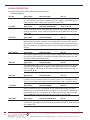
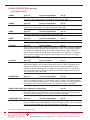
N2WCK
Type: I/O
Direction: Input/Output
Pin: 28
The NavSync 2 Wire Clock Signal. This is the open collector I2C compatible Clock Signal for the 2 wire serial interface. The signal return path is DIG_GND.
N2WDA
Type: I/O
Direction: Input/Output
Pin: 29
The NavSync 2 Wire Data Signal. This is the open collector I2C compatible Data Signal
for the 2 wire serial interface. The signal return path is DIG_GND.
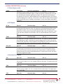
USBP 4
Type: I/O
Direction: Input/Output
Pin: 30
The positive USB Signal. The signal return path is DIG_GND.
USBN 4
Type: I/O
Direction: Input/Output
Pin: 31
The negative USB Signal. The signal return path is DIG_GND.
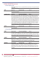
LED_RED
Type: I/O
Direction: Output
Pin: 8
This is a Dual Function Signal. Normally this signal is used to drive a red LED. Standard
software builds use this signal to indicate GPS status, where a Long red flash indicates
an invalid fix and Short red flashes for satellites tracked, but not used in solution. In
special software builds, this signal can be used as GPIO. This signal has a 3.3V CMOS
drive. A series limiting resistor is required to limit output current to ±5mA. The signal
return path is DIG_GND.
LED_GRN
Type: I/O
Direction: Output
Pin: 9
This is a Dual Function Signal. Normally this signal is used to drive a green LED. Standard software builds use this signal to indicate GPS status, where a Long green flash
indicates an valid 2D/3D fix and Short green flashes for number of satellites used in
solution. In special software builds, this signal can be used as GPIO. This signal has a
3.3V CMOS drive. A series limiting resistor is required to limit output current to ±5mA.
The signal return path is DIG_GND.
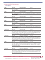
GPIO[0]/PWM
Type: I/O
Direction: Input/Output
Pin: 39
Normally the GPIO[0]/PWM output provides a Frequency Output that defaults to 10 MHz,
and is user configurable from 10 Hz to 30 MHz signal. The output is enabled on powerup and is steered by the GPS solution. Custom software versions can also configure this
pin for general I/O, PWM or EPOCH output. The signal return path is DIG_GND.
GPIO[1]/TIME_SYNCType: I/ODirection: Input/Output
Pin: 40
The GPIO[1]/TIME_SYNC pin provides a synchronization pulse generated by the onboard RTC. Custom software versions can also configure this pin for general purpose
I/O, or an additional PPS output. The signal return path is DIG_GND.
GPIO[2]/NEXT_INT Type: I/O
Direction: Input/Output
Pin: 41
The GPIO[2]/NEXT_INT output provides an active high status indicator for the Frequency
Output available on pin 39 (GPIO[0]/PWM). Custom software versions can also configure
this pin for general purpose I/O. The signal return path is DIG_GND.
Note: 4. USB is not supported in the current software build.
14
NS18-DSCW25-TIM
Copyright ©2009 NavSync Ltd. All Rights Reserved
Rev 07
Date: 03/26/09
Specifications subject to change without notice.