1
• Carrier concentration
• Trap
• Capture cross-section
• Defect
3
Background: Electrical Analysis of Semiconductors
Deep level transient spectroscopy (DLTS) will be the principal technique used in this experiment to evaluate
defect concentration levels as well their trap energy and capture cross-sections.
By comparing these characteristics, as well as the annealing behaviour of the defects, to those outlined in
literature it is possible to identify the species of defects present in the samples.
DLTS uses the fact that the energy levels of the deep level traps are affected by the energy band bending at the
interface between the semiconductor sample and a metal contact. This metal-semiconductor interface forms a
Schottky barrier diode. By varying the extent of the band bending by applied biases traps can be filled and
emptied. This has an affect on the capacitance of the diode which can be measured and the signal analysed to
evaluate the defect concentration and to characterise the defects present. To understand how this is possible it
is necessary first to describe the Schottky diode.
3.1
Schottky Barrier Diodes
Schottky diodes can be fabricated on doped semiconductor surfaces to facilitate electrical characterisation of
the sample. A Schottky diode is a metal-semiconductor interface that exhibits current rectifying properties. It
is similar to a p-n junction diode, except that the Schottky diode characteristics only depend on the majority
carrier electrons [4], whereas the p-n diode characteristics depend on both majority and minority carriers. This
discussion will focus on the characteristics of a n-type semiconductor Schottky diode. You can get the characteristics of the p-type semiconductor Schottky diode by simple (err..) extension.
The rectification is a result of the Schottky barrier formed at the interface due to the different work functions
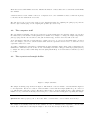
of the metal (φm ) and semiconductor (φs ). This barrier is characterised by a barrier height (φb ), see fig. 1.
Figure 1: The bending of the energy bands for a n-type semiconductor Schottky barrier diode [6].
In general the work function of a metal (φm ) is different to a semiconductor and when the two materials come
into electrical contact with each other electrons will from the material with the larger Fermi level (or smaller
work function) to that with a lower Fermi level.
The work function of a material describes the binding energy of the electrons and is related to their Fermi
level (see fig. 1). When the metal and semiconductor come into contact it becomes energetically favourable for
electrons in the material with the higher Fermi level to diffuse across to the other material. This builds up a
net charge difference over the interface which creates a built-in voltage (Vbi ). The region in the semiconductor
3