1
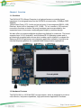
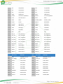
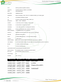
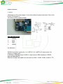
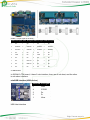
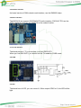
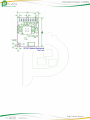
S3C6410-TFA User manual
Table of content
S3C6410-TFA User manual
............................................................................................................ 1
Catalogue ........................................................................................ 3
Chapter 1 Overview........................................................................ 4
1.1 OverView ............................................................................... 4
1.2 Hardware Features ................................................................ 4
Chapter 2 S3C6410-TFA CPU board
.......................................................................................................... 5
2.1 Feature of the S3C6410-TFA CPU board
..................................................................................................... 6
2.2 Pin definition of the S3C6410-TFA CPU
board............................................................................................ 7
2.3 Dimensions of the S3C6410-TFA CPU board
................................................................................................... 11
Chapter 3 Mother board ................................................................ 11
Chapter 4 Interface........................................................................ 14
4.1 Power In ........................................................................... 14
4.2 Serial port ........................................................................ 14
4.3 USB interface ................................................................... 15
4.4 SCON interface ................................................................ 16
4.5 Network interface ............................................................. 17
4.6 Audio intreface ................................................................. 17
4.7 TV-out interface................................................................ 17
4.8 JTAG ................................................................................ 17
4.9 LED .................................................................................. 17
4.9 Key ................................................................................... 18
4.11 LCD interface ................................................................. 19
4.12 ADC input ....................................................................... 20
4.13 PWM(buzzer) ................................................................. 20
4.14 temperature sensor ........................................................ 20
4.15 IR.................................................................................... 20
4.16 I2C-EEPROM ................................................................. 21
4.17 SD card slot................................................................... 21
4.18 SDIO-II/SD-WiFi interface ............................................. 21
Chapter V Hardware feature ......................................................... 23
5.1 Boot mode set...................................................................... 23
Chapter 1 Overview
1.1 OverView
The S3C6410-TFA vBoard Computer is a high-performance controller board
introduced. It is designed based on the S3C6410 microcontroller, 256MByte DDR
SDRAM,
1GByte Nand Flash, RTC, Audio and net on board. It has integrated RS232, USB,
Ethernet, Audio In/Out, Keyboard, LCD, CVBS、TV out, camera in, SD card and
more other functions on board. So many hardware resources provided by the
expansion board, it becomes a solid reference board for customer design.
We also offers a complete software development package to customers. The board
supports linux 2.6.36, Android2.1 and WindowsCE 6.0 operating system and is
provided with complete basic drivers which enable a quick channel to evaluate the
Samsung S3C6410 processor and customize application software. It would be an
ideal development platform for multimedia and communication applications
1.2 Hardware Features
The S3C6410X is a 16/32-bit RISC microprocessor, which is designed to provide a
cost-effective, low-power capabilities, high performance Application Processor
solution for mobile phones and general applications. To provide optimized H/W
performance for the 2.5G & 3G communication services, the S3C6410X adopts 64/
32-bit internal bus architecture. It also includes many powerful hardware accelerators
for tasks such as motion video processing, audio processing, 2D graphics, display
manipulation and scaling. An integrated Multi Format Codec (MFC) supports
encoding and decoding of MPEG4/H.263/H.264 and decoding of VC1.
The S3C6410-TFA Single Board Computer is based on S3C6410 processor. This
board is characterized as follows chapter.
Chapter 2 S3C6410-TFA CPU board
2.1 Feature of the S3C6410-TFA CPU board
Item
Description
CPU
• Samsung S3C6410A, run at 533Mhz ARM1176JZF-S, up to
667Mhz
RAM
• 256 DDR RAM
Flash
• 256 MB DDR RAM, 32 bit Bus
Interface
• 4 x User Leds
• 10 pin 2.0mm space Jtag connector
• Reset button on board
Connector
• 2 x 60 pin 2.0mm space DIP connector
• 2 x 30 pin 2.0mm space GPIO connector
Power
Supply
• Supply Voltage from 2.0V to 6V
Size
• 64 x 50 x 12mm (L x W x H)
OS Support
•
•
•
•
Windows CE 6
Linux 2.6.38
Android 2.3
Ubuntu 9.10
S3C6410-TFA Front view
S3C6410-TFA Bottom view
2.2 Pin definition of the S3C6410-TFA CPU board
S3C6410-TFA CPU board use the 2.0mm pitch double pin, leads to a total of 4
groups: P1, P2, CON1, CON2.
P1 and P2 are each 60 Pin; CON1 and CON2 are each 30Pin, leads to a total of 180
Pin.The follow shown is the layout description:
Pin
Details
Contain LCD, AD, SDIO2, EINT,
P1
USB, TVOUT0
Serial port, SPI1, I2C, SD Card,
P2
AC97(I2S), System bus
CON1
GPIO,AD,SPI0,TAVOUT1
CON2
CMOS,GPIO
JTAG
JTAG interface
Others
4 User LED, power LED, Reset
key.
P1
Pin define
Remarks
P1
Pin define
Remarks
P1.1
VDD_5V
DC 5V input
P1.2
GND
GND
P1.3
VD23
LCD_R5/GPJ7
P1.4
VD22
LCD_R4/GPJ6
P1.5
VD21
LCD_R3/GPJ5
P1.6
VD20
LCD_R2/GPJ4
P1.7
VD19
LCD_R1/GPJ3
P1.8
VD18
LCD_R0/GPJ2
P1.9
VD15
LCD_G5/GPI15
P1.10
VD14
LCD_G4/GPI14
P1.11
VD13
LCD_G3/GPI13
P1.12
VD12
LCD_G2/GPI12
P1.13
VD11
LCD_G1/GPI11
P1.14
VD10
LCD_G0/GPI10
P1.15
VD7
LCD_B5/GPI7
P1.16
VD6
LCD_B4/GPI6
P1.17
VD5
LCD_B3/GPI5
P1.18
VD4
LCD_B2/GPI4
P1.19
VD3
LCD_B1/GPI3
P1.20
VD2
LCD_B0/GPI2
P1.21
VDEN
VDEN/GPJ10
P1.22
PWM1
PWM1/GPF15
P1.23
VSYNC
LCD Column signal/GPJ9
P1.24
HSYNC
LCD row singal/GPJ8
P1.25
VCLK
LCD clock /GPJ11
P1.26
GPE0
GPE0
P1.27
VBUS
VBUS
P1.28
OTGDRV_VBUS
OTGDRV_VBUS
P1.29
OTGID
OTGID
P1.30
XEINT8
EINT8/GPN8
P1.31
OTGDM
USB Slave D-
P1.32
USBDN
USB Host D-
P1.33
OTGDP
USB Slave D+
P1.34
USBDP
USB Host D+
P1.35
TSXP
TSXP/AIN7
P1.36
TSXM
TSXM/AIN6
P1.37
TSYP
TSYP/AIN5
P1.38
TSYM
TSYM/AIN4
P1.39
AIN0
AIN0
P1.40
AIN1
AIN1
P1.41
WiFi_IO
WiFi_IO/GPP10
P1.42
WiFi_PD
WiFi_PD/GPP11
P1.43
SD1_CLK
SD1_CLK/GPH0
P1.44
SD1_CMD
SD1_CMD/GPH1
P1.45
SD1_nCD
SD1_nCD/GPN10
P1.46
SD1_nWP
SD1_nWP/GPL14
P1.47
SD_DAT0
SD1_DAT0/GPH2
P1.48
SD1_DAT1
SD1_DAT1/GPH3
P1.49
SD1_DAT2
SD1_DAT2/GPH4
P1.50
SD1_DAT3
SD1_DAT3/GPH5
P1.51
DACOUT0
TV -OUT
P1.52
PWM0
PWM0/GPF14
P1.53
XEINT0
XEINT0/GPN0
P1.54
XEINT1
XEINT1/GPN1
P1.55
XEINT2
XEINT2/GPN2
P1.56
XEINT3
XEINT3/GPN3
P1.57
XEINT4
XEINT4/GPN4
P1.58
XEINT5
XEINT5/GPN5
P1.59
XEINT19
XEINT19/GPL11
P1.60
XEINT20
XEINT20/GPL12
P2
Pin define
Remarks
P2
Pin define
Remarks
P2.1
OM3
SD/NAND boot set
P2.2
OM4
SD/NAND boot set
P2.3
M_nRESET
Reset signal
P2.4
VDD_RTC
RTC battle
P2.5
RTSn1
RTSn1/GPA7
P2.6
CTSn1
CTSn1/GPA6
P2.7
TXD0
TXD0/GPA1
P2.8
RXD0
RXD0/GPA0
P2.9
TXD1
TXD1/GPA5
P2.10
RXD1
RXD1/GPA4
P2.11
TXD2
TXD2/GPB1
P2.12
RXD2
RXD2/GPB0
P2.13
TXD3
TXD3/GPB3
P2.14
RXD3
RXD3/GPB2
P2.15
SPIMOSI
SPIMOSI/GPC6
P2.16
SPIMISO
SPIMISO/GPC4
P2.17
SPICLK
SPICLK/GPC5
P2.18
SPICS
SPICS/GPC7
P2.19
I2CSCL
I2CSCL/GPB5
P2.20
I2CSDA
I2CSDA/GPB6
P2.21
SD0_CLK
SD0_CLK/GPG0
P2.22
SD0_CMD
SD0_CMD/GPG1
P2.23
SD0_nCD
SD0_nCD/GPG6
P2.24
SD0_nWP
SD0_nWP/GPL13
P2.25
SD0_DAT0
SD0_DAT0/GPG2
P2.26
SD0_DAT1
SD0_DAT1/GPG3
P2.27
SD0_DAT2
SD0_DAT2/GPG4
P2.28
SD0_DAT3
SD0_DAT3/GPG5
P2.29
AC97_BITCLK
AC97_BITCLK/GPD0
P2.30
AC97_RSTn
AC97_RSTn/GPD1
P2.31
AC97_SYNC
AC97_SYNC/GPD2
P2.32
AC97_SDO
AC97_SDO/GPD4
P2.33
AC97_SDI
AC97_SDI/GPD3
P2.34
XEINT12
XEINT12/GPN12
P2.35
ADDR0
ADDR0
P2.36
ADDR1
ADDR1
P2.37
ADDR2
ADDR2
P2.38
ADDR3
ADDR3
P2.39
nCS1
nCS1
P2.40
XEINT7
XEINT7/GPN7
P2.41
nWAIT
nWAIT
P2.42
nESET
Reset Signal(Output)
P2.43
LnWE
LnWE
P2.44
LnOE
LnOE
P2.45
DATA0
DATA0
P2.46
DATA1
DATA1
P2.47
DATA2
DATA2
P2.48
DATA3
DATA3
P2.49
DATA4
DATA4
P2.50
DATA5
DATA5
P2.51
DATA6
DATA6
P2.52
DATA7
DATA7
P2.53
DATA8
DATA8
P2.54
DATA9
DATA9
P2.55
DATA10
DATA10
P2.56
DATA11
DATA11
P2.57
DATA12
DATA12
P2.58
DATA13
DATA13
P2.59
DATA14
DATA14
P2.60
DATA15
DATA15
CON1
Pin define
Remarks
CON1
Pin define
CON1.1
VDD_IO(3.3V)
OUT
CON1.2
GND
CON1.3
GPE1
CON1.4
GPE2
CON1.5
GPE3
CON1.6
GPE4
CON1.7
GPM0
CON1.8
GPM1
CON1.9
GPM2
CON1.10
GPM3
CON1.11
GPM4
CON1.12
GPM5
CON1.13
GPQ1
CON1.14
GPQ2
CON1.15
GPQ3
CON1.16
GPQ4
CON1.17
GPQ5
CON1.18
GPQ6
CON1.19
SPICLK0
CON1.20
SPIMISO0
CON1.21
SPICS0
CON1.22
SPIMOSI0
CON1.23
EINT6
CON1.24
EINT9
CON1.25
EINT11
CON1.26
EINT16
Remarks
CON1.27
EINT17
CON1.28
AIN2
CON1.29
AIN3
CON1.30
DACOUT1
CON2
Pin define
Remarks
CON2
Pin define
Remarks
CON2.1
CAMSDA
link I2CSDA
CON2.2
CAMSCL
CON2.3
GPK2
CON2.4
CAMRSTn
CON2.5
CAMCLK
CON2.6
CAMHREF
CON2.7
CAMVSYNC
CON2.8
CAMPCLK
CON2.9
CAMDATA7
CON2.10
CAMDATA6
CON2.11
CAMDATA5
CON2.12
CAMDATA4
CON2.13
CAMDATA3
CON2.14
CAMDATA2
CON2.15
CAMDATA1
CON2.16
CAMDATA0
CON2.17
VDD_IO(3.3V)
OUT
CON2.18
VDDCAM
CON2.19
1.8V
for CMOS
CON2.20
GND
CON2.21
GPK8
CON2.22
GPK12
CON2.23
GPK13
CON2.24
EINT18
CON2.25
VD0
For LCD
CON2.26
VD1
For LCD
CON2.27
VD8
For LCD
CON2.28
VD9
For LCD
CON2.29
VD16
For LCD
CON2.30
VD17
For LCD
2.4-2.8V for CMOS
JTAG
Pin define
Remarks
JTAG
Pin define
Remarks
1
VDD_IO
Power input 3.3V
2
VDD_IO
Power input 3.3V
3
TRSTn
TRSTn
4
nRESET
nRESET
5
TDI
TDI
6
TDO
TDO
7
TMS
TMS
8
GND
GND
9
TCK
TCK
10
GND
GND
2.3 Dimensions of the S3C6410-TFA CPU board
Chapter 3 Mother board
Feature of the S3C6410-TFA SDK board
Item
Description
CPU
Samsung S3C6410A(ARM1176JZF-S)
Frequency
Operating frequency 533Mhz, up to 667Mhz
RAM
256 MB DDR RAM
Nand Flash
256MB Nand Flash
Multimedia
Support for Mpeg4, H.264, H.263, VC1 hardware decoding, up to 30fps @ SD
3D
3D hardware acceleration support
2D
Promise to support graphics scaling, rotation, flip
Debug Port
COM0 + JTAG + USB Slave
Indicator
4 x User LED (in the core board), 1 x Power LED
Test button
8 x User Buttons, interrupt-style buttons
USB Slave
1 x mini USB (OTG floor is not designed to function)
USB Host
Through the USB HUB chip, to achieve 4 USB Host
Network Interface
10/100M MB Ethernet, RJ-45 interfaces
Audio I/O
Standard two-channel audio input 3.5mm input and output ports
SD Card
Normal SD card connector
Serial
3 x RS232 DB9 serial port, 4 x TTL-level serial port Block
TV-OUT
1 x RCA output
SDIO2 Interface
Mainly used to access SD WiFi module (also includes SPI, I2C interface)
LCD Interface
3 LCD Interface Block leads (0.5mm pitch SMT, including seats, seat pin and 2.0mm pitch)
Buzzer
1 x PWM control the buzzer output
IR
1 channel infrared receiver
Temperature Sensor 1 Road DS18B02 Temperature Sensor
ADC conversion
An adjustable resistor, connected CPU's AD0 channel
RTC clock
On-board battery backup RTC clock
Power Supply
5V
PCB size
180 x 130 mm
Address start Address end
Size(MB) Description
0x0000_0000
0x07FF_FFFF 128MB
Boot image
0x0800_0000
0x0BFF_FFFF 64MB
In-ROM
0x0C00_0000
0x0FFF_FFFF 128MB
Stepping Stone(8KB)
0x1000_0000
0x17FF_FFFF 128MB
0x1800_0000
0x1FFF_FFFF 128MB
0x2000_0000
0x27FF_FFFF 128MB
0x2800_0000
0x2FFF_FFFF 128MB
DM9000AEP
0x3000_0000
0x37FF_FFFF 128MB
0x3800_0000
0x3FFF_FFFF 128MB
0x4000_0000
0x47FF_FFFF 128MB
0x4800_0000
0x4FFF_FFFF 128MB
0x5000_0000
0x5FFF_FFFF 256MB
0x6000_0000
0x6FFF_FFFF 256MB
128MB DDR RAM
128M DDR RAM
Chapter 4 Interface
4.1 Power In
The board use 5V power supply, it have two method to power the board. One is the
D-jack (CN1)power in,
the others is 4Pin header(CON8).
CON8 Pins defines
1
VDD5V
2
GND
3
GND
4
VDDIN
4.2 Serial port
S3C6410 have four serial port, it is UART0,1,2,3, UART1 is 5-wired serial, the
others is 3-wired serial.
In S3C6410-TFASDK board, COM0,1,2 was linked to DB9 interface in RS232,
you can link it to PC.
And the all serial was linked from the board to CON1, CON2, CON3, CON4 in TTL.
CON0,1,2,3 pin signal is as follow:
CON0 Pins signal CON1 Pin signal CON2 Pin signal CON3 Pin signal
1
NC
1
NC
1
NC
1
NC
2
RSRXD0
2
RSRXD1
2
RSRXD2
2
RSRXD3
3
RSTXD0
3
RSRXD2
3
RSRXD2
3
RSRXD3
4
NC
4
NC
4
NC
4
NC
5
GND
5
NC
5
GND
5
NC
6
NC
6
NC
6
NC
6
NC
7
NC
7
RSCTS1
7
NC
7
NC
8
NC
8
RSRTS1
8
NC
8
NC
9
NC
9
NC
9
NC
9
NC
4.3 USB interface
In S3C6410-TFA board, it have 5 usb interface, there are 4 usb host, and the other
is usb slave interface.
miniUSB interface(USB device)
miniUSB Pin signal
USB Host interface
5
GND
4
OTGID
3
D+
2
D-
1
Vbus
Pin signal Pin signal
1
5V
2
D-
3
D+
4
GND
4.4 SCON interface
In order to use more serial port peripherals, we deliberately designed the SCON interface and call it
"serial port Center, "which includes two serial ports, an I2C interface, an SPI interface, a USB Host
port, but also Have a GPIO port, etc., and includes 5V and 3.3V power supply output pin, as shown in
Figure (right side interface mechanical dimensions SCON):
SCON Pin Define Remark SCON Pin Define
Remark
1
GND
2
5V Power out
3
USB_D-
4
USB_D+
5
I2CSCL
6
I2CSDA
7
TXD1
TTL level 8
RXD1
TTL level
9
CTSn1
TTL level 10
RTSn1
TTL level
11
TXD2
TTL level 12
RXD2
TTL level
13
SPIMOSI
SPI1
14
SPIMISO
SPI1
15
SPICS
SPI1
16
SPICLK
SPI1
17
nRESET
Reset
18
EINT8
EINT
19
GND
20
3.3V Power out
4.5 Network interface
the board carries a 100M network card interface, use the DM9000 chips.
4.6 Audio intreface
The S3C6410 can support I2C/PCM/AC97 audio interface, S3C6410-TFA use the
AC97 interfacem and use the WM9714 as the codec function.
4.7 TV-out interface
The board provide 1 TV-out interface, it is from DACOUT0.
When you use DACOUT0, you should set the TV mode for CVBS mode.
4.8 JTAG
4.9 LED
The board have 4 LED, you can control it, When output GPIO for 0, the LED will be
light.
LED LED4 LED3 LED2 LED1
GPIO GPK7 GPK6 GPK5 GPK4
4.9 Key
The board have 8 user key, and it can be linked for GPIO(CON12).
KEY K1
K2
K3
K4
K5
K6
K7
K8
EINT EINT0 EINT1 EINT2 EINT3 EINT4 EINT5 EINT19 EINT20
GPIO GPN0 GPN1 GPN2 GPN3 GPN4 GPN5 GPL11 GPL12
4.11 LCD interface
The board have 3 LCD interface, it have the same signal, LCD1 and LCD2 is the 40pin 0.5mm pitch
interface, LCD3 is the 40pin 2.0mm interface.
LCD2&LCD3 Pins signal detaisl
LCD1&LCD2&LCD3 signal
LCD1&LCD2&LCD3 signal
1
5V
2
5V
3
NC
4
NC
5
VD2
6
VD3
7
VD4
8
VD5
9
VD6
10
VD7
11
GND
12
NC
13
NC
14
VD10
15
VD11
16
VD12
17
VD13
18
VD14
19
VD15
20
GND
21
NC
22
NC
23
VD18
24
VD19
25
VD20
26
VD21
27
VD22
28
VD23
29
GND
30
GPE0/LCD_PWR
31
PWM1/GPF15
32
nRESET
33
VDEN/VM
34
VSYNC
35
HSYNC
36
VCLK
37
TSXM
38
TSXP
39
TSYM
40
TSYP
41
GND
4.12 ADC input
The board have 2 Chanel A/D, AIN0 was linked to W1, it can be configure 10/12 bit.
4.13 PWM(buzzer)
The Buzzer in the board was controlled by PWM, it is PWM0(GPF14)
4.14 temperature sensor
The board have a temperature sensor, it use DS18B20 chips.
4.15 IR
In the board, it have IR, the name is IRM3638, It link to the pin EINT12 as received
pins.
4.16 I2C-EEPROM
The I2C was linked to EEPROM, AT24C08, it was 256byte. only for test the I2C.
4.17 SD card slot
It have a SD card slot, can support 32GByte.
4.18 SDIO-II/SD-WiFi interface
The SDIO was linked to CON11, it also contain 1 SPI, 1 I2C, 4 GPIO.
SD wifi size:
Chapter V Hardware feature
5.1 Boot mode set
You can choose the boot mode for S2 switch,
S2: in SDBOOT, the board will boot from sd card,
S2: in NAND, the board will boot from nand.