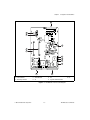
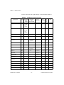
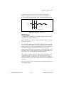
1
Click here to comment on this document via the National Instruments website at http://www.natinst.com/documentation/daq/ VXI-MIO Series User Manual Multifunction I/O Modules for VXIbus August 1996 Edition Part Number 321246A-01 Copyright 1996 National Instruments Corporation. All Rights Reserved. Internet Support GPIB: [email protected] DAQ: [email protected] VXI: [email protected] LabVIEW: [email protected] LabWindows: [email protected] HiQ: [email protected] Lookout: [email protected] E-mail: [email protected] FTP Site: ftp.natinst.com Web Address: http://www.natinst.com Bulletin Board Support BBS United States: (512) 794-5422 or (800) 327-3077 BBS United Kingdom: 01635 551422 BBS France: 1 48 65 15 59 FaxBack Support (512) 418-1111 Telephone Support (U.S.) Tel: (512) 795-8248 Fax: (512) 794-5678 International Offices Australia 03 9879 5166, Austria 0662 45 79 90 0, Belgium 02 757 00 20, Canada (Ontario) 905 785 0085, Canada (Québec) 514 694 8521, Denmark 45 76 26 00, Finland 90 527 2321, France 01 48 14 24 24, Germany 089 741 31 30, Hong Kong 2645 3186, Israel 03 5734815, Italy 02 413091, Japan 03 5472 2970, Korea 02 596 7456, Mexico 95 800 010 0793, Netherlands 0348 433466, Norway 32 84 84 00, Singapore 2265886, Spain 91 640 0085, Sweden 08 730 49 70, Switzerland 056 200 51 51, Taiwan 02 377 1200, U.K. 01635 523545 National Instruments Corporate Headquarters 6504 Bridge Point Parkway Austin, TX 78730-5039 Tel: (512) 794-0100 Important Information Warranty The VXI-MIO Series boards are warranted against defects in materials and workmanship for a period of one year from the date of shipment, as evidenced by receipts or other documentation. National Instruments will, at its option, repair or replace equipment that proves to be defective during the warranty period. This warranty includes parts and labor. The media on which you receive National Instruments software are warranted not to fail to execute programming instructions, due to defects in materials and workmanship, for a period of 90 days from date of shipment, as evidenced by receipts or other documentation. National Instruments will, at its option, repair or replace software media that do not execute programming instructions if National Instruments receives notice of such defects during the warranty period. National Instruments does not warrant that the operation of the software shall be uninterrupted or error free. A Return Material Authorization (RMA) number must be obtained from the factory and clearly marked on the outside of the package before any equipment will be accepted for warranty work. National Instruments will pay the shipping costs of returning to the owner parts which are covered by warranty. National Instruments believes that the information in this manual is accurate. The document has been carefully reviewed for technical accuracy. In the event that technical or typographical errors exist, National Instruments reserves the right to make changes to subsequent editions of this document without prior notice to holders of this edition. The reader should consult National Instruments if errors are suspected. In no event shall National Instruments be liable for any damages arising out of or related to this document or the information contained in it. EXCEPT AS SPECIFIED HEREIN, NATIONAL INSTRUMENTS MAKES NO WARRANTIES, EXPRESS OR IMPLIED, AND SPECIFICALLY DISCLAIMS ANY WARRANTY OF MERCHANTABILITY OR FITNESS FOR A PARTICULAR PURPOSE. CUSTOMER’S RIGHT TO RECOVER DAMAGES CAUSED BY FAULT OR NEGLIGENCE ON THE PART OF NATIONAL INSTRUMENTS SHALL BE LIMITED TO THE AMOUNT THERETOFORE PAID BY THE CUSTOMER. NATIONAL INSTRUMENTS WILL NOT BE LIABLE FOR DAMAGES RESULTING FROM LOSS OF DATA, PROFITS, USE OF PRODUCTS, OR INCIDENTAL OR CONSEQUENTIAL DAMAGES, EVEN IF ADVISED OF THE POSSIBILITY THEREOF. This limitation of the liability of National Instruments will apply regardless of the form of action, whether in contract or tort, including negligence. Any action against National Instruments must be brought within one year after the cause of action accrues. National Instruments shall not be liable for any delay in performance due to causes beyond its reasonable control. The warranty provided herein does not cover damages, defects, malfunctions, or service failures caused by owner’s failure to follow the National Instruments installation, operation, or maintenance instructions; owner’s modification of the product; owner’s abuse, misuse, or negligent acts; and power failure or surges, fire, flood, accident, actions of third parties, or other events outside reasonable control. Copyright Under the copyright laws, this publication may not be reproduced or transmitted in any form, electronic or mechanical, including photocopying, recording, storing in an information retrieval system, or translating, in whole or in part, without the prior written consent of National Instruments Corporation. Trademarks LabVIEW, NI-DAQ, ComponentWorks , DAQ-STC , MANTIS , MITE , NI-PGIA , NI-VISA , NI-VXI , SCXI , and VirtualBench are trademarks of National Instruments Corporation. Product and company names listed are trademarks or trade names of their respective companies. WARNING REGARDING MEDICAL AND CLINICAL USE OF NATIONAL INSTRUMENTS PRODUCTS National Instruments products are not designed with components and testing intended to ensure a level of reliability suitable for use in treatment and diagnosis of humans. Applications of National Instruments products involving medical or clinical treatment can create a potential for accidental injury caused by product failure, or by errors on the part of the user or application designer. Any use or application of National Instruments products for or involving medical or clinical treatment must be performed by properly trained and qualified medical personnel, and all traditional medical safeguards, equipment, and procedures that are appropriate in the particular situation to prevent serious injury or death should always continue to be used when National Instruments products are being used. National Instruments products are NOT intended to be a substitute for any form of established process, procedure, or equipment used to monitor or safeguard human health and safety in medical or clinical treatment. Table of Contents About This Manual Organization of This Manual ........................................................................................xi Conventions Used in This Manual ................................................................................xii National Instruments Documentation ...........................................................................xiii Related Documentation .................................................................................................xiv Customer Communication ............................................................................................xiv Chapter 1 Introduction About the VXI-MIO Series ...........................................................................................1-1 What You Need to Get Started ......................................................................................1-2 Software Programming Choices ...................................................................................1-2 National Instruments Application Software ...................................................1-2 NI-DAQ Driver Software ...............................................................................1-3 VXIplug&play Instrument Drivers .................................................................1-4 Optional Equipment ......................................................................................................1-5 Custom Cabling .............................................................................................................1-6 Unpacking .....................................................................................................................1-6 Chapter 2 Configuration and Installation Module Configuration ...................................................................................................2-1 VXIbus Logical Address ................................................................................2-1 SIMM Size ......................................................................................................2-5 Load USER/FACTORY Configuration ..........................................................2-7 Protect/Change Factory Configuration ...........................................................2-8 Hardware Installation ....................................................................................................2-8 Software Installation .....................................................................................................2-9 National Instruments Corporation v VXI-MIO Series User Manual Table of Contents Chapter 3 Hardware Overview Analog Input ................................................................................................................. 3-3 Input Mode ..................................................................................................... 3-3 Input Polarity and Input Range ...................................................................... 3-4 Considerations for Selecting Input Ranges ...................................... 3-6 Dither .............................................................................................................. 3-7 Multichannel Scanning Considerations .......................................................... 3-8 Analog Output .............................................................................................................. 3-10 Analog Output Reference Selection ............................................................... 3-10 Analog Output Polarity Selection .................................................................. 3-10 Analog Output Reglitch Selection ................................................................. 3-11 Analog Trigger ............................................................................................................. 3-11 Digital I/O ..................................................................................................................... 3-14 Timing Signal Routing ................................................................................................. 3-15 Programmable Function Inputs ...................................................................... 3-16 Module and Timebase .................................................................................... 3-16 VXIbus Triggers ............................................................................................. 3-17 Chapter 4 Signal Connections I/O Connector ............................................................................................................... 4-1 I/O Connector Signal Descriptions ................................................................ 4-3 Analog Input Signal Connections ................................................................................. 4-9 Types of Signal Sources ............................................................................................... 4-11 Floating Signal Sources .................................................................................. 4-11 Ground-Referenced Signal Sources ............................................................... 4-11 Input Configurations ..................................................................................................... 4-12 Differential Connection Considerations (DIFF Input Configuration) ........... 4-14 Differential Connections for Ground-Referenced Signal Sources ................................................................................ 4-15 Differential Connections for Nonreferenced or Floating Signal Sources ................................................................................ 4-16 Single-Ended Connection Considerations ...................................................... 4-18 Single-Ended Connections for Floating Signal Sources (RSE Configuration) ...................................................................... 4-19 Single-Ended Connections for Grounded Signal Sources (NRSE Configuration) ................................................................... 4-19 Common-Mode Signal Rejection Considerations .......................................... 4-20 Analog Output Signal Connections .............................................................................. 4-20 Digital I/O Signal Connections .................................................................................... 4-22 VXI-MIO Series User Manual vi National Instruments Corporation Table of Contents Power Connections ........................................................................................................4-23 Timing Connections ......................................................................................................4-23 Programmable Function Input Connections ...................................................4-24 Data Acquisition Timing Connections ...........................................................4-25 SCANCLK Signal ............................................................................4-26 EXTSTROBE* Signal ......................................................................4-26 TRIG1 Signal ...................................................................................4-27 TRIG2 Signal ...................................................................................4-28 STARTSCAN Signal .......................................................................4-30 CONVERT* Signal ..........................................................................4-32 AIGATE Signal ................................................................................4-33 SISOURCE Signal ...........................................................................4-34 Waveform Generation Timing Connections ...................................................4-34 WFTRIG Signal ...............................................................................4-36 UPDATE* Signal .............................................................................4-36 UISOURCE Signal ...........................................................................4-37 General-Purpose Timing Signal Connections ................................................4-38 GPCTR0_SOURCE Signal ..............................................................4-38 GPCTR0_GATE Signal ...................................................................4-39 GPCTR0_OUT Signal ......................................................................4-40 GPCTR0_UP_DOWN Signal ..........................................................4-40 GPCTR1_SOURCE Signal ..............................................................4-41 GPCTR1_GATE Signal ...................................................................4-41 GPCTR1_OUT Signal ......................................................................4-42 GPCTR1_UP_DOWN Signal ..........................................................4-43 FREQ_OUT Signal ..........................................................................4-44 Field Wiring Considerations .........................................................................................4-45 Chapter 5 Calibration Loading Calibration Constants ......................................................................................5-1 Self-Calibration .............................................................................................................5-2 External Calibration ......................................................................................................5-2 Other Considerations .....................................................................................................5-3 National Instruments Corporation vii VXI-MIO Series User Manual Table of Contents Appendix A Specifications VXI-MIO-64E-1 ........................................................................................................... A-1 VXI-MIO-64XE-10 ...................................................................................................... A-10 Appendix B Optional Cable Connector Descriptions Appendix C Common Questions Appendix D Customer Communication Glossary Index Figures Figure 1-1. The Relationship between the Programming Environment, Your Instrument Driver, and Your VXI-DAQ Hardware .............................. 1-5 Figure 2-1. Figure 2-2. Figure 2-3. Figure 2-4. Figure 2-5. Figure 2-6. VXI-MIO-64E-1 Parts Locator Diagram ................................................ 2-3 VXI-MIO-64XE-10 Parts Locator Diagram ........................................... 2-4 VXI-MIO-64XE-10 Logical Address Selection ...................................... 2-5 SIMM Size Configuration ....................................................................... 2-6 Load User/Factory Configuration ........................................................... 2-8 Protect/Change Factory Configuration .................................................... 2-8 Figure 3-1. Figure 3-2. Figure 3-3. Figure 3-4. Figure 3-5. Figure 3-6. Figure 3-7. Figure 3-8. Figure 3-9. Figure 3-10. VXI-MIO Series Block Diagram ............................................................ 3-2 Dither ....................................................................................................... 3-8 Analog Trigger Block Diagram ............................................................... 3-12 Below-Low-Level Analog Triggering Mode .......................................... 3-12 Above-High-Level Analog Triggering Mode ......................................... 3-13 Inside-Region Analog Triggering Mode ................................................. 3-13 High-Hysteresis Analog Triggering Mode .............................................. 3-13 Low-Hysteresis Analog Triggering Mode .............................................. 3-14 CONVERT* Signal Routing ................................................................... 3-15 VXIbus Trigger Utilization ..................................................................... 3-17 VXI-MIO Series User Manual viii National Instruments Corporation Table of Contents Figure 4-1. I/O Connector Pin Assignment for the VXI-MIO-64E-1 and VXI-MIO-64XE-10 ................................................................................4-2 Figure 4-2. VXI-MIO Series PGIA ............................................................................4-10 Figure 4-3. Summary of Analog Input Connections ..................................................4-13 Figure 4-4. Differential Input Connections for Ground-Referenced Signals .............4-15 Figure 4-5. Differential Input Connections for Nonreferenced Signals .....................4-16 Figure 4-6. Single-Ended Input Connections for Nonreferenced or Floating Signals.....................................................................................................4-19 Figure 4-7. Single-Ended Input Connections for Ground-Referenced Signal ............4-20 Figure 4-8. Analog Output Connections .....................................................................4-21 Figure 4-9. Digital I/O Connections ...........................................................................4-22 Figure 4-10. Timing I/O Connections ..........................................................................4-24 Figure 4-11. Typical Posttriggered Acquisition ...........................................................4-25 Figure 4-12. Typical Pretriggered Acquisition .............................................................4-26 Figure 4-13. SCANCLK Signal Timing .......................................................................4-26 Figure 4-14. EXTSTROBE* Signal Timing ................................................................4-27 Figure 4-15. TRIG1 Input Signal Timing .....................................................................4-28 Figure 4-16. TRIG1 Output Signal Timing ..................................................................4-28 Figure 4-17. TRIG2 Input Signal Timing .....................................................................4-29 Figure 4-18. TRIG2 Output Signal Timing ..................................................................4-29 Figure 4-19. STARTSCAN Input Signal Timing .........................................................4-30 Figure 4-20. STARTSCAN Output Signal Timing ......................................................4-31 Figure 4-21. CONVERT* Input Signal Timing ...........................................................4-32 Figure 4-22. CONVERT* Output Signal Timing .........................................................4-33 Figure 4-23. SISOURCE Signal Timing ......................................................................4-34 Figure 4-24. WFTRIG Input Signal Timing .................................................................4-35 Figure 4-25. WFTRIG Output Signal Timing ..............................................................4-35 Figure 4-26. UPDATE* Input Signal Timing ..............................................................4-37 Figure 4-27. UPDATE* Output Signal Timing ............................................................4-37 Figure 4-28. UISOURCE Signal Timing ......................................................................4-38 Figure 4-29. GPCTR0_SOURCE Signal Timing .........................................................4-39 Figure 4-30. GPCTR0_GATE Signal Timing in Edge-Detection Mode .....................4-40 Figure 4-31. GPCTR0_OUT Signal Timing ................................................................4-40 Figure 4-32. GPCTR1_SOURCE Signal Timing .........................................................4-41 Figure 4-33. GPCTR1_GATE Signal Timing in Edge-Detection Mode .....................4-42 Figure 4-34. GPCTR1_OUT Signal Timing ................................................................4-43 Figure 4-35. GPCTR Timing Summary .......................................................................4-43 Figure B-1. 68-Pin MIO Connector Pin Assignments ................................................B-2 Figure B-2. 68-Pin Extended Analog Input Connector Pin Assignments ...................B-3 National Instruments Corporation ix VXI-MIO Series User Manual Table of Contents Tables Table 2-1. VXI-MIO Series DRAM Configuration .................................................. 2-6 Table 3-1. Table 3-2. Table 3-3. Available Input Configurations for the VXI-MIO Series ....................... 3-3 Actual Range and Measurement Precision .............................................. 3-4 Actual Range and Measurement Precision, VXI-MIO-64XE-10 ........... 3-6 Table 4-1. Table 4-2. VXI-MIO-64E-1 I/O Signal Summary .................................................... 4-6 VXI-MIO-64XE-10 I/O Signal Summary ............................................... 4-8 VXI-MIO Series User Manual x National Instruments Corporation About This Manual This manual describes the electrical and mechanical aspects of each module in the VXI-MIO Series product line and contains information concerning their installation, operation, and programming. Unless otherwise noted, text applies to all modules in the VXI-MIO Series. The VXI-MIO Series includes the following modules: • VXI-MIO-64E-1 • VXI-MIO-64XE-10 The VXI-MIO Series modules are high-performance multifunction analog, digital, and timing I/O modules for VXIbus. Organization of This Manual The VXI-MIO Series User Manual is organized as follows: • Chapter 1, Introduction, describes the VXI-MIO Series modules, lists what you need to get started, describes the optional software and optional equipment, and explains how to unpack your VXI-MIO Series module. • Chapter 2, Configuration and Installation, explains how to configure and install your VXI-MIO Series module. • Chapter 3, Hardware Overview, presents an overview of the hardware functions on your VXI-MIO Series module. • Chapter 4, Signal Connections, describes how to make input and output signal connections to your VXI-MIO Series module via the module I/O connector. • Chapter 5, Calibration, discusses the calibration procedures for your VXI-MIO Series module. • Appendix A, Specifications, lists the specifications for each module in the VXI-MIO Series. • Appendix B, Optional Cable Connector Descriptions, describes the connectors on the optional cables for the VXI-MIO Series modules. National Instruments Corporation xi VXI-MIO Series User Manual About This Manual • Appendix C, Common Questions, contains a list of commonly asked questions and their answers relating to usage and special features of your VXI-MIO Series module. • Appendix D, Customer Communication, contains forms you can use to request help from National Instruments or to comment on our products. • The Glossary contains an alphabetical list and description of terms used in this manual, including acronyms, abbreviations, metric prefixes, mnemonics, and symbols. • The Index alphabetically lists topics covered in this manual, including the page where you can find the topic. Conventions Used in This Manual The following conventions are used in this manual. ♦ The ♦ indicates that the text following it applies only to specific VXI-MIO Series modules. <> Angle brackets containing numbers separated by an ellipsis represent a range of values associated with a bit, port, or signal name (for example, ACH<0..7> stands for ACH0 through ACH7). bold Bold text denotes parameters. bold italic Bold italic text denotes a note, caution, or warning. italic Italic text denotes emphasis on a specific module in the VXI-MIO Series or on other important information, a cross reference, or an introduction to a key concept. NI-DAQ NI-DAQ refers to the NI-DAQ software for PC compatibles unless otherwise noted. SCXI SCXI stands for Signal Conditioning eXtensions for Instrumentation and is a National Instruments product line designed to perform front-end signal conditioning for National Instruments plug-in DAQ boards. The Glossary lists abbreviations, acronyms, metric prefixes, mnemonics, symbols, and terms. VXI-MIO Series User Manual xii National Instruments Corporation About This Manual National Instruments Documentation The VXI-MIO Series User Manual is one piece of the documentation set for your VXI-DAQ system. You could have any of several types of manuals depending on the hardware and software in your system. Use the manuals you have as follows: • Getting Started with SCXI—If you are using SCXI, this is the first manual you should read. It gives an overview of the SCXI system and contains the most commonly needed information for the modules, chassis, and software. • Your SCXI hardware user manuals—If you are using SCXI, read these manuals next for detailed information about signal connections and module configuration. They also explain in greater detail how the module works and contain application hints. • Your VXI-DAQ hardware user manuals—These manuals have detailed information about the VXI-DAQ hardware that plugs into or is connected to your system. Use these manuals for hardware installation and configuration instructions, specification information about your VXI-DAQ hardware, and application hints. • Software documentation—You may have both application software and driver software documentation. National Instruments application software includes ComponentWorks, LabVIEW, LabWindows/CVI, Measure, and VirtualBench. National Instruments driver software includes NI-DAQ and VXIplug&play instrument drivers. After you set up your hardware system, use either your application or driver software documentation to help you write your application. If you have a large and complicated system, it is worthwhile to look through the software documentation before you configure your hardware. • Accessory installation guides or manuals—If you are using accessory products, read the terminal block and cable assembly installation guides. They explain how to physically connect the relevant pieces of the system. Consult these guides when you are making your connections. • SCXI chassis manuals—If you are using SCXI, read these manuals for maintenance information on the chassis and installation instructions. National Instruments Corporation xiii VXI-MIO Series User Manual About This Manual Related Documentation The following National Instruments document contains information you may find helpful: • Application Note 025, Field Wiring and Noise Considerations for Analog Signals Customer Communication National Instruments wants to receive your comments on our products and manuals. We are interested in the applications you develop with our products, and we want to help if you have problems with them. To make it easy for you to contact us, this manual contains comment and configuration forms for you to complete. These forms are in Appendix D, Customer Communication, at the end of this manual. VXI-MIO Series User Manual xiv National Instruments Corporation Chapter 1 Introduction This chapter describes the VXI-MIO Series modules, lists what you need to get started, describes the optional software and optional equipment, and explains how to unpack your VXI-MIO Series module. About the VXI-MIO Series Thank you for buying a National Instruments VXI-MIO Series module. The VXI-MIO Series modules are completely VXIplug&playcompatible multifunction analog, digital, and timing I/O modules for VXIbus. This family of modules features 12-bit and 16-bit ADCs with 64 analog inputs, 12-bit and 16-bit DACs with voltage outputs, eight lines of TTL-compatible digital I/O, and two 24-bit counter/timers for timing I/O. The VXI-MIO Series modules use the National Instruments DAQ-STC system timing controller for timer-related functions. The DAQ-STC consists of three timing groups that control analog input, analog output, and general-purpose counter/timer functions. These groups include a total of seven 24-bit and three 16-bit counters and a maximum timing resolution of 50 ns. A common problem with other VXI modules is that you cannot easily synchronize several measurement functions to a common trigger or timing event. The VXI-MIO Series modules solve this problem by using VXIbus triggers to synchronize measurements on several VXI-MIO Series modules. You can interface the VXI-MIO Series modules to an SCXI signal conditioning and multiplexing system to acquire over 3,000 analog signals from thermocouples, RTDs, strain gauges, voltage sources, and current sources. You can also acquire or generate digital signals for communication and control. Detailed specifications of the VXI-MIO Series modules are in Appendix A, Specifications. National Instruments Corporation 1-1 VXI-MIO Series User Manual Chapter 1 Introduction What You Need to Get Started To set up and use your VXI-MIO Series module, you will need the following: ❑ One of the following modules: VXI-MIO-64E-1 VXI-MIO-64XE-10 ❑ VXI-MIO Series User Manual ❑ One or more of the following software packages and documentation: ComponentWorks LabVIEW for Windows LabWindows/CVI Measure NI-DAQ for PC Compatibles VirtualBench VXIplug&play instrument driver ❑ Your VXIbus system Software Programming Choices There are several options to choose from when programming your National Instruments VXI-DAQ hardware. You can use LabVIEW, LabWindows/CVI, Measure, ComponentWorks, VirtualBench, or other application development environments with either NI-DAQ or the VXIplug&play instrument driver. Both NI-DAQ and the VXIplug&play instrument drivers access the VXI-DAQ hardware through the VISA driver software. National Instruments Application Software ComponentWorks contains tools for data acquisition and instrument control built on NI-DAQ driver software. ComponentWorks provides a higher-level programming interface for building virtual instruments through standard OLE controls and DLLs. With ComponentWorks, you can use all of the configuration tools, resource management utilities, and interactive control utilities included with NI-DAQ. VXI-MIO Series User Manual 1-2 National Instruments Corporation Chapter 1 Introduction LabVIEW features interactive graphics, a state-of-the-art user interface, and a powerful graphical programming language. The LabVIEW Data Acquisition VI Library, a series of VIs for using LabVIEW with National Instruments DAQ hardware, is included with LabVIEW. The LabVIEW Data Acquisition VI Library is functionally equivalent to the NI-DAQ software. LabWindows/CVI features interactive graphics, a state-of-the-art user interface, and uses the ANSI standard C programming language. The LabWindows/CVI Data Acquisition Library, a series of functions for using LabWindows/CVI with National Instruments DAQ hardware, is included with the NI-DAQ software kit. The LabWindows/CVI Data Acquisition Library is functionally equivalent to the NI-DAQ software. VirtualBench features VIs that combine DAQ products, software, and your computer to create a standalone instrument with the added benefit of the processing, display, and storage capabilities of your computer. VirtualBench instruments load and save waveform data to disk in the same forms that can be used in popular spreadsheet programs and word processors. VirtualBench features report generation and printing capabilities. Using ComponentWorks, LabVIEW, LabWindows/CVI, or VirtualBench software will greatly reduce the development time for your data acquisition and control application. NI-DAQ Driver Software The NI-DAQ driver software is included at no charge with all National Instruments DAQ hardware. NI-DAQ is not packaged with signal conditioning or accessory products. NI-DAQ has an extensive library of functions that you can call from your application programming environment. These functions include routines for analog input (A/D conversion), buffered data acquisition (high-speed A/D conversion), analog output (D/A conversion), waveform generation (timed D/A conversion), digital I/O, counter/timer operations, SCXI, triggering, calibration, messaging, and acquiring data to extended memory. NI-DAQ has both high-level DAQ I/O functions for maximum ease of use and low-level DAQ I/O functions for maximum flexibility and performance. Examples of high-level functions are streaming data to disk or acquiring a certain number of data points. An example of a low-level function is writing directly to registers on the DAQ device. NI-DAQ does not sacrifice the performance of National Instruments National Instruments Corporation 1-3 VXI-MIO Series User Manual Chapter 1 Introduction DAQ devices because it lets multiple devices operate at their peak performance. NI-DAQ also internally addresses many of the complex issues between the computer and the DAQ hardware such as programming interrupts and DMA controllers. NI-DAQ maintains a consistent software interface between its different versions so that you can change platforms with minimal modifications to your code. VXIplug&play Instrument Drivers National Instruments distributes VXIplug&play instrument drivers free of charge. VXIplug&play instrument drivers are one level above the NI-DAQ device driver and contain high-level software functions whose architecture is specified by the VXIplug&play Systems Alliance. The VXIplug&play standards increase interoperability with other vendors, and ensure that drivers are designed and presented in a consistent fashion that facilitates ease of use. Refer to Figure 1-1 to see the relationship between your software components. VXI-MIO Series User Manual 1-4 National Instruments Corporation Chapter 1 LabVIEW or LabWindows/CVI Introduction Other Application Development Environments VXIplug&play Instrument Driver NI-DAQ Driver Software VISA VXI-DAQ Hardware Figure 1-1. The Relationship between the Programming Environment, Your Instrument Driver, and Your VXI-DAQ Hardware Optional Equipment National Instruments offers a variety of products to use with your VXI-MIO Series module, including cables, connector blocks, and other accessories, as follows: • Cables and cable assemblies, shielded and ribbon • Connector blocks • SCXI modules and accessories for isolating, amplifying, exciting, and multiplexing signals for relays and analog output. With SCXI you can condition and acquire up to 3072 channels. • Low channel count signal conditioning modules, boards, and accessories, including conditioning for strain gauges and RTDs, simultaneous sample and hold, and relays For more specific information about these products, refer to your National Instruments catalogue or call the office nearest you. National Instruments Corporation 1-5 VXI-MIO Series User Manual Chapter 1 Introduction Custom Cabling Mating connectors and a backshell kit for making custom 96-pin cables for your VXI-MIO Series module are available from National Instruments. If you want to develop your own cable, however, the following guidelines may be useful: • For the analog input signals, shielded twisted-pair wires for each signal yields the best results, assuming that you use differential inputs. Tie the shield for each signal pair to the ground reference at the source. • You should route the analog lines separately from the digital lines. • When using a cable shield, use separate shields for the analog and digital halves of the cable. Failure to do so results in noise coupling into the analog signals from transient digital signals. Unpacking Your VXI-MIO Series module is shipped in an antistatic package to prevent electrostatic damage to the module. Electrostatic discharge can damage several components on the module. To avoid such damage in handling the module, take the following precautions: VXI-MIO Series User Manual • Ground yourself via a grounding strap or by holding a grounded object. • Touch the antistatic package to a metal part of your VXIbus chassis before removing the module from the package. • Remove the module from the package and inspect the module for loose components or any other sign of damage. Notify National Instruments if the module appears damaged in any way. Do not install a damaged module into your VXIbus chassis. • Never touch the exposed pins of connectors. 1-6 National Instruments Corporation Chapter Configuration and Installation 2 This chapter explains how to configure and install your VXI-MIO Series module. Module Configuration The VXI-MIO Series modules are software-configurable, except for the VXIbus logical address. You must perform two types of configuration on the VXI-MIO Series modules—bus-related configuration and data acquisition-related configuration. Bus-related configuration includes setting the VXIbus logical address, VXIbus address space (A24 versus A32), VXIbus interrupt levels, and amount of VXIbus address space required. Data acquisition-related configuration, explained in Chapter 3, Hardware Overview, includes such settings as analog input polarity and range, analog output reference source, and other settings. VXIbus Logical Address Each module in a VXIbus system is assigned a unique number between 0 and 254. This 8-bit number, called the logical address, defines the base address for the VXIbus configuration registers located on the module. With unique logical addresses, each VXIbus module in the system is assigned 64 bytes of configuration space in the upper 16 KB of the A16 address space. Logical address 0 is reserved for the Resource Manager in the VXIbus system. Because the VXI-MIO Series modules cannot act as a Resource Manager, do not configure the VXI-MIO Series modules with a logical address of 0. The factory-default logical address for the VXI-MIO-64E-1 is 3 and for the VXI-MIO-64XE-10 is 2. Some VXIbus modules have dynamically configurable logical addresses. These modules have an initial logical address of hex FF or decimal 255, which indicates that they can be dynamically configured. National Instruments Corporation 2-1 VXI-MIO Series User Manual Chapter 2 Configuration and Installation Your VXI-MIO Series module does not support dynamic configuration of its logical address. Ensure that no other statically configurable VXIbus modules have the same logical address as the VXI-MIO Series module. If they do, change the logical address setting of either the VXI-MIO Series module or the other module so that every module in the system has a different associated logical address. To change the logical address of the VXI-MIO Series modules, modify the setting of the 8-bit DIP switch labeled LOGICAL ADDRESS SWITCH (U3 for the VXI-MIO-64E-1 and U73 for the VXI-MIO-64XE-10). The down position of the DIP switch corresponds to a logic value of 0 and the up position corresponds to a logic value of 1. See Figures 2-1 and 2-2 for the VXI-MIO Series parts locator diagrams. VXI-MIO Series User Manual 2-2 National Instruments Corporation Chapter 2 Configuration and Installation 4 3 2 5 1 1 6 7 8 9 11 1 2 3 DRAM Product Name Assembly Number 4 5 6 10 P3 Serial Number S1 7 8 9 S2 S3 Logical Address Switch 10 P1 11 P2 Figure 2-1. VXI-MIO-64E-1 Parts Locator Diagram National Instruments Corporation 2-3 VXI-MIO Series User Manual Chapter 2 Configuration and Installation 4 3 2 1 1 5 6 7 8 11 1 2 3 DRAM Product Name Assembly Number 4 5 6 P3 S1 S2 10 7 8 9 9 S3 Logical Address Switch (U73) Serial Number 10 P1 11 P2 Figure 2-2. VXI-MIO-64XE-10 Block Diagram Figure 2-3 shows the VXI-MIO-64XE-10 switch settings for logical address 2 and 192. VXI-MIO Series User Manual 2-4 National Instruments Corporation Chapter 2 Configuration and Installation Logical Address Switch Push up for logic 1 Push down for logic 0 1 2 3 4 5 6 7 8 LSB P1 Connector MSB U73 VXI-MIO-64XE-10 Module a. Switch Set to Logical Address 2 (Default) Logical Address Switch Push up for logic 1 Push down for logic 0 1 2 3 4 5 6 7 8 LSB P1 Connector MSB U73 VXI-MIO-64XE-10 Module b. Switch Set to Logical Address 192 Figure 2-3. VXI-MIO-64XE-10 Logical Address Selection SIMM Size Each VXI-MIO module can accommodate up to two 1.35 in. DRAM SIMMs. Table 2-1 lists the SIMMS you can use. You can use 32-bit or 36-bit SIMMS since DRAM parity is not required. Because the VXI-MIO module supports only one organization at a time, all SIMMs installed must be of the same type. Use bank 0 first when installing the SIMMs, so that you can install up to 64 MB. The VXI-MIO module supports DRAM speeds of 80 ns or faster. Use switch S3 to select the size of each SIMM. The SIMM sockets are accessible only by removing the component right side cover, but S3 is National Instruments Corporation 2-5 VXI-MIO Series User Manual Chapter 2 Configuration and Installation accessible with the cover on. To access the SIMM sockets, perform the following steps: 1. Remove the four screws on the top, the four screws on the bottom, and the three screws on the right-side cover of the metal enclosure. 2. If the SIMMs are 4 MB x 32 bit or larger, set S3 as shown in Figure 2-4a. 3. For SIMMs smaller than 4 MB x 32 bit, set S3 as shown in Figure 2-4b. SIMM Size (Factory Default) SIMM Size (Factory Default) S3 a. 4 MB X 32 bit or larger S3 b. Smaller than 4 MB X 32 bit Figure 2-4. SIMM Size Configuration Refer to Table 2-1 to properly adjust the switch (ON or OFF) for all supported DRAM configurations. Many of the DRAM options are available from National Instruments. Table 2-1. VXI-MIO Series DRAM Configuration Bank 0 Bank 1 Total DRAM — — 0 — — 256 KB x 32 bit or 256 KB x 36 bit — 1 MB — ON 256 KB x 32 bit or 256 KB x 36 bit 256 KB x 32 bit or 256 KB x 36 bit 2 MB — ON 512 KB x 32 bit or 512 KB x 36 bit — 2 MB — ON 512 KB x 32 bit or 512 KB x 36 bit 512 KB x 32 bit or 512 KB x 36 bit 4 MB — ON VXI-MIO Series User Manual 2-6 National Switch Setting Instruments Option of S3 National Instruments Corporation Chapter 2 Table 2-1. Bank 0 1 MB x 32 bit or 1 MB x 36 bit 1 MB x 32 bit or 1 MB x 36 bit 2 MB x 32 bit or 2 MB x 36 bit Total DRAM — 4 MB Yes ON 8 MB — ON 8 MB Yes ON 16 MB — ON 16 MB Yes OFF 32 MB — OFF 32 MB Yes OFF 64 MB Yes OFF 2 MB x 32 bit or 2 MB x 36 bit — 4 MB x 32 bit or 4 MB x 36 bit 8 MB x 32 bit or 8 MB x 36 bit 8 MB x 32 bit or 8 MB x 36 bit Bank 1 — 4 MB x 32 bit or 4 MB x 36 bit 4 MB x 32 bit or 4 MB x 36 bit VXI-MIO Series DRAM Configuration (Continued) 1 MB x 32 bit or 1 MB x 36 bit 2 MB x 32 bit or 2 MB x 36 bit Configuration and Installation — 8 MB x 32 bit or 8 MB x 36 bit National Switch Setting Instruments Option of S3 Load USER/FACTORY Configuration The VXI-MIO module has an onboard EEPROM, which stores default register values that are loaded at power-on. The EEPROM is divided into two halves—a factory-configuration half, and a user-configuration half. Both halves were factory configured with the same configuration values so you can modify the user-configurable half, while the factoryconfigured half stores a back-up of the factory settings. Use switch S2 to control the operation of the EEPROM. The switch causes the VXI-MIO module to boot off the factory-configured half instead of the user-modified settings. This is useful in the event that the user-configured half of the EEPROM becomes corrupted in such a way that the VXI-MIO module boots to an unusable state. Refer to Figure 2-5 for configuration settings. National Instruments Corporation 2-7 VXI-MIO Series User Manual Chapter 2 Configuration and Installation Load User Configuration Load Factory Configuration S2 S2 Figure 2-5. Load User/Factory Configuration Protect/Change Factory Configuration Use switch S1 to change the factory-default configuration settings by permitting writes to the factory settings section of the EEPROM. This switch serves as a safety measure and should not be needed under normal circumstances. When this switch is off (its default setting) the factory configuration of the EEPROM is protected, so any writes to the factory area will be ignored. Refer to Figure 2-6 for configuration settings. Protect Factory Configuration Change Factory Configuration S1 S1 Figure 2-6. Protect/Change Factory Configuration Hardware Installation This section contains general installation instructions for the VXI-MIO Series modules. Consult your VXIbus mainframe user manual or technical reference manual for specific instructions and warnings. 1. Plug in your mainframe before installing your VXI module. The power cord grounds the mainframe and protects it from electrical damage while you install the module. Do not turn on the mainframe. Warning: To protect yourself and your mainframe from electrical hazards, DO NOT turn the mainframe on until you are finished installing your VXI-MIO Series module. VXI-MIO Series User Manual 2-8 National Instruments Corporation Chapter 2 Configuration and Installation 2. Remove or open any doors or covers blocking access to the mainframe slots. 3. If you are installing your VXI-DAQ module into a D-size mainframe, first install an appropriate support for C-size modules in D-size mainframes. 4. Insert the VXI-DAQ module in the slot you have selected: a. Align the top and bottom of the module with the card-edge guides inside the mainframe. b. Slowly push the VXI-DAQ module straight into the slot until its plug connectors are resting on the backplane receptacle connectors. c. Using evenly distributed pressure, slowly press the VXI-DAQ module straight in until it seats in the expansion slot. d. Make sure the front panel of the VXI-DAQ module is even with the front panel of the mainframe. 5. Tighten the retaining screws on the top and bottom edges of the front panel. 6. Replace or close any doors or covers to the mainframe. Software Installation Regardless of your programming methodology, proper operation of your VXI-MIO module depends on the correct installation of VISA on your VXIbus controller. If VISA is not installed, you must get this information from your VXIbus controller manufacturer. If you have a National Instruments VXIbus controller, contact our sales department for information on obtaining the NI-VISA software at no charge. If you are using NI-DAQ, refer to your release notes. Find the installation section for your operating system and follow the instructions given there. If you are using LabVIEW, refer to your LabVIEW release notes to install your application software. After you have installed LabVIEW, refer to the NI-DAQ release notes and follow the instructions given there for your operating system and LabVIEW. National Instruments Corporation 2-9 VXI-MIO Series User Manual Chapter 2 Configuration and Installation If you are using LabWindows/CVI, refer to your LabWindows/CVI release notes to install your application software. After you have installed LabWindows/CVI, refer to the NI-DAQ release notes and follow the instructions given there for your operating system and LabWindows/CVI. If you are using ComponentWorks, Measure, or VirtualBench application software, refer to your documentation for installation instructions. VXI-MIO Series User Manual 2-10 National Instruments Corporation Chapter 3 Hardware Overview This chapter presents an overview of the hardware functions on your VXI-MIO Series module. Figure 3-1 shows the block diagram for the VXI-MIO Series modules. National Instruments Corporation 3-1 VXI-MIO Series User Manual VXI-MIO Series User Manual 3-2 ACH 0:15 ACH 16:31 ACH 32:47 ACH 48:63 2 DAC1 DAC0 Calibration DACS DAC FIFOS Analog Trigger Circuit Mux Mode Selection Switches AD Control Digital I/O (8) Timing External Trigger Trigger Level DACS Bank Select Analog Muxes Banks 0-3 Cal/Aux Voltage REF Ref Buffer A/D Converter IO Data Lines Bus Interface Analog Output RTSI Bus Timing/Control Interface DAQ - STC Counter/ Timing I/O Digital I/O Analog Input Timing/Control ADC FIFO DMA/ Interrupt Request AI Control AD Control Trigger Configuration Memory + Programmable Gain Amplifier – 3 Calibration DACs Signal Conditioning Control Circuitry RITSI Bus IO Data Lines VXI Local Bus IO Data Lines Analog Output Control Configuration EPROM Interface Bus Interface DMA EEPROM Control Interface Optional Config EPROM IO Control, IRQ, and DMA Lines DAQ-STC EPF8282 Interface Analog Input Control EEPROM MXI Port DRAM Circuitry I/O Port MITE IO Control P2 MANTIS N.V. RAM VXI Trigger and Clock Circuitry VXI Local Bus CLK10 +/- ECL Triggers Logical Address Switch MODIO Lines VXI Triggers Utility Signals Interrupts Arbitration Signals Address Data Control Signals P1 MANTIS VXI Transceivers DRAM Control Signals RITSI Bus IO Data Lines IO Address Lines IO Control IO Data Lines IO Address Lines IO Control IO Data Lines IO Address Lines VXI Port CLK10 Analog Bus ECL Triggers (TTL Level) Chapter 3 Hardware Overview VXI Bus I/O Connector Figure 3-1. VXI-MIO Series Block Diagram National Instruments Corporation Chapter 3 Hardware Overview Analog Input The analog input section of each VXI-MIO Series module is software configurable. You can select different analog input configurations through application software designed to control the VXI-MIO Series modules. The following sections describe in detail each of the analog input categories. Input Mode The VXI-MIO Series modules have three different input modes— nonreferenced single-ended (NRSE) input, referenced single-ended (RSE) input, and differential (DIFF) input. The single-ended input configurations use up to 64 channels. The DIFF input configuration uses up to 32 channels. Input modes are programmed on a per channel basis for multimode scanning. For example, you can configure the circuitry to scan 48 channels—16 differentially-configured channels and 32 single-ended channels. Table 3-1 describes the three input configurations. Table 3-1. Available Input Configurations for the VXI-MIO Series Configuration National Instruments Corporation Description DIFF A channel configured in DIFF mode uses two analog input channel lines. One line connects to the positive input of the module programmable gain instrumentation amplifier (PGIA), and the other connects to the negative input of the PGIA. RSE A channel configured in RSE mode uses one analog input channel line, which connects to the positive input of the PGIA. The negative input of the PGIA is internally tied to analog input ground (AIGND). NRSE A channel configured in NRSE mode uses one analog input channel line, which connects to the positive input of the PGIA. The negative input of the PGIA connects to the analog input sense (AISENSE) input. 3-3 VXI-MIO Series User Manual Chapter 3 Hardware Overview For more information about the three types of input configuration, refer to the Analog Input Signal Connections section in Chapter 4, Signal Connections, which contains diagrams showing the signal paths for the three configurations. Input Polarity and Input Range ♦ VXI-MIO-64E-1 This module has two input polarities—unipolar and bipolar. The VXI-MIO-64E-1 has a unipolar input range of 10 V (0 to 10 V) and a bipolar input range of 10 V (± 5 V). You can program polarity and range settings on a per channel basis so that you can configure each input channel uniquely. The software-programmable gain on this module increases its overall flexibility by matching the input signal ranges to those that the ADC can accommodate. The VXI-MIO-64E-1 has gains of 0.5, 1, 2, 5, 10, 20, 50, and 100 and is suited for a wide variety of signal levels. With the proper gain setting, you can use the full resolution of the ADC to measure the input signal. Table 3-2 shows the overall input range and precision according to the configuration and gain used. Table 3-2. VXI-MIO Series User Manual Actual Range and Measurement Precision Range Configuration Gain Actual Input Range Precision1 0 to +10 V 1.0 2.0 5.0 10.0 20.0 50.0 100.0 0 to +10 V 0 to +5 V 0 to +2 V 0 to +1 V 0 to +500 mV 0 to +200 mV 0 to +100 mV 2.44 mV 1.22 mV 488.28 µV 244.14 µV 122.07 µV 48.83 µV 24.41 µV 3-4 National Instruments Corporation Chapter 3 Table 3-2. Actual Range and Measurement Precision (Continued) Range Configuration Gain Actual Input Range Precision1 -5 to +5 V 0.5 1.0 2.0 5.0 10.0 20.0 50.0 100.0 -10 to +10 V -5 to +5 V -2.5 to +2.5 V -1 to +1 V -500 to +500 mV -250 to +250 mV -100 to +100 mV -50 to +50 mV 4.88 mV 2.44 mV 1.22 mV 488.28 µV 244.14 µV 122.07 µV 48.83 µV 24.41 µV 1 The value of 1 LSB of the 12-bit ADC; that is, the voltage increment corresponding to a change of one count in the ADC 12-bit count. Note: ♦ Hardware Overview See Appendix A, Specifications, for absolute maximum ratings. VXI-MIO-64XE-10 This module has two input polarities—unipolar and bipolar. The VXI-MIO-64XE-10 has a unipolar input range of 10 V (0 to 10 V) and a bipolar input range of 20 V (± 10 V). You can program polarity and range settings on a per channel basis so that you can configure each input channel uniquely. Note: You can calibrate your VXI-MIO-64XE-10 analog input circuitry for either a unipolar or bipolar polarity. If you mix unipolar and bipolar channels in your scan list and you are using NI-DAQ, then NI-DAQ will load the calibration constants appropriate to the polarity for which analog input channel 0 is configured. The software-programmable gain on this module increases its overall flexibility by matching the input signal ranges to those that the ADC can accommodate. The VXI-MIO-64XE-10 has gains of 1, 2, 5, 10, 20, 50, and 100. These gains are suited for a wide variety of signal levels. With the proper gain setting, you can use the full resolution of the ADC to measure the input signal. Table 3-3 shows National Instruments Corporation 3-5 VXI-MIO Series User Manual Chapter 3 Hardware Overview the overall input range and precision according to the configuration and gain used. Table 3-3. Actual Range and Measurement Precision, VXI-MIO-64XE-10 Range Configuration Gain Actual Input Range Precision1 0 to +10 V 1.0 2.0 5.0 10.0 20.0 50.0 100.0 0 to +10 V 0 to +5 V 0 to +2 V 0 to +1 V 0 to +500 mV 0 to +200 mV 0 to 100 mV 152.59 µV 76.29 µV 30.52 µV 15.26 µV 7.63µV 3.05 µV 1.53 µV -10 to +10 V 1.0 2.0 5.0 10.0 20.0 50.0 100.0 -10 to +10 V -5 to +5 V -2 to +2 V -1 to +1 V -500 to +500 mV -200 to +200 mV -100 to +100 mV 305.18 µV 152.59 µV 61.04 µV 30.52 µV 15.26 µV 6.10 µV 3.05 µV 1 The value of 1 LSB of the 12-bit ADC; that is, the voltage increment corresponding to a change of one count in the ADC 12-bit count. Note: See Appendix A, Specifications, for absolute maximum ratings. Considerations for Selecting Input Ranges Which input polarity and range you select depends on the expected range of the incoming signal. A large input range can accommodate a large signal variation but reduces the voltage resolution. Choosing a smaller input range improves the voltage resolution but may result in the input signal going out of range. For best results, you should match the input range as closely as possible to the expected range of the input signal. For example, if you are certain the input signal will not be negative (below 0 V), unipolar input polarity is best. However, if the signal is negative or equal to zero, using unipolar input polarity will yield inaccurate readings. VXI-MIO Series User Manual 3-6 National Instruments Corporation Chapter 3 Hardware Overview Dither When you enable dither, you add approximately 0.5 LSB rms of white Gaussian noise to the signal to be converted by the ADC. This addition is useful for applications involving averaging to increase the resolution of your VXI-MIO Series module, as in calibration or spectral analysis. In such applications, noise modulation is decreased and differential linearity is improved by the addition of the dither. When taking DC measurements, such as when checking the module calibration, you should enable dither and average about 1,000 points to take a single reading. This process removes the effects of quantization and reduces measurement noise, resulting in improved resolution. For high-speed applications not involving averaging or spectral analysis, you may want to disable the dither to reduce noise. You enable and disable the dither circuitry through software. Figure 3-2 illustrates the effect of dither on signal acquisition. Figure 3-2a shows a small (± 4 LSB) sine wave acquired with dither off. The quantization of the ADC is clearly visible. Figure 3-2b shows what happens when 50 such acquisitions are averaged together; quantization is still plainly visible. In Figure 3-2c, the sine wave is acquired with dither on. There is a considerable amount of noise visible. But averaging about 50 such acquisitions, as shown in Figure 3-2d, eliminates both the added noise and the effects of quantization. Dither has the effect of forcing quantization noise to become a zero-mean random variable rather than a deterministic function of the input signal. National Instruments Corporation 3-7 VXI-MIO Series User Manual Chapter 3 Hardware Overview LSBs 6.0 LSBs 6.0 4.0 4.0 2.0 2.0 0.0 0.0 -2.0 -2.0 -4.0 -4.0 -6.0 -6.0 0 100 200 300 400 0 500 a. Dither disabled; no averaging 100 200 300 400 500 b. Dither disabled; average of 50 acquisitions LSBs 6.0 LSBs 6.0 4.0 4.0 2.0 2.0 0.0 0.0 -2.0 -2.0 -4.0 -4.0 -6.0 -6.0 0 100 200 300 400 500 0 c. Dither enabled; no averaging 100 200 300 400 500 d. Dither enabled; average of 50 acquisitions Figure 3-2. Dither You cannot disable dither on the VXI-MIO-64XE-10. This is because the ADC resolution is so fine that the ADC and the PGIA inherently produce almost 0.5 LSB rms of noise. This is equivalent to having a dither circuit that is always enabled. Multichannel Scanning Considerations All of the VXI-MIO Series modules can scan multiple channels at the same maximum rate as their single-channel rate; however, you should pay careful attention to the settling times for each of the modules. Refer to Appendix A, Specifications, for a complete listing of settling times for each of the VXI-MIO Series modules. When scanning among channels at various gains, the settling times may increase. When the PGIA switches to a higher gain, the signal on the previous channel may be well outside the new, smaller range. For instance, suppose a 4 V signal is connected to channel 0 and a 1 mV VXI-MIO Series User Manual 3-8 National Instruments Corporation Chapter 3 Hardware Overview signal is connected to channel 1, and suppose the PGIA is programmed to apply a gain of one to channel 0 and a gain of 100 to channel 1. When the multiplexer switches to channel 1 and the PGIA switches to a gain of 100, the new full-scale range is 100 mV (if the ADC is in unipolar mode). The approximately 4 V step from 4 V to 1 mV is 4,000% of the new full-scale range. For a 12-bit module to settle within 0.012% (120 ppm or 1/2 LSB) of the 100 mV full-scale range on channel 1, the input circuitry has to settle to within 0.0003% (3 ppm or 1/80 LSB) of the 4 V step. It may take as long as 100 µs for the circuitry to settle to this accuracy. For a 16-bit module to settle within 0.0015% (15 ppm or 1 LSB) of the 100 mV full-scale range on channel 1, the input circuitry has to settle within 0.00004% (0.4 ppm or 1/400 LSB) of the 4 V step. It may take as long as 200 µs for the circuitry to settle to this accuracy. In general, this extra settling time is not needed when the PGIA is switching to a lower gain. Settling times can also increase when scanning high-impedance signals due to a phenomenon called charge injection, where the analog input multiplexer injects a small amount of charge into each signal source when that source is selected. If the impedance of the source is not low enough, the effect of the charge—a voltage error—will not have decayed by the time the ADC samples the signal. For this reason, you should keep source impedances under 1 kΩ to perform high-speed scanning. Multichannel scanning is not recommended unless sampling rates are low enough or it is necessary to sample several signals as near to simultaneously as possible. Single-channel scanning yields more accurate settling times. The data is much more accurate and channel-to-channel independent if you acquire data from each channel independently (for example, 100 points from channel 0, then 100 points from channel 1, then 100 points from channel 2, and so on). National Instruments Corporation 3-9 VXI-MIO Series User Manual Chapter 3 Hardware Overview Analog Output ♦ VXI-MIO-64E-1 This module supplies two channels of analog output voltage at the I/O connector. The reference and range for the analog output circuitry is software-selectable. The reference can be either internal or external, whereas the range can be either bipolar or unipolar. ♦ VXI-MIO-64XE-10 This module supplies two channels of analog output voltage at the I/O connector. The range is bipolar or unipolar. Analog Output Reference Selection ♦ VXI-MIO-64E-1 You can connect each D/A converter (DAC) to this module’s internal reference of 10 V or to the external reference signal connected to the external reference (EXTREF) pin on the I/O connector. This signal applied to EXTREF should be between -10 and +10 V. You do not need to configure both channels for the same mode. Analog Output Polarity Selection Selecting a bipolar range for a particular DAC means that any data written to that DAC will be interpreted as two’s complement format. In two’s complement mode, data values written to the analog output channel can be either positive or negative. If you select unipolar range, data is interpreted in straight binary format. In straight binary mode, data values written to the analog output channel range must be positive. ♦ VXI-MIO-64E-1 You can configure each analog output channel for either unipolar or bipolar output. A unipolar configuration has a range of 0 to Vref at the analog output. A bipolar configuration has a range of -Vref to +Vref at the analog output. Vref is the voltage reference used by the DACs in the analog output circuitry and can be either the +10 V onboard reference or an externally supplied reference between -10 and +10 V. You do not need to configure both channels for the same range. VXI-MIO Series User Manual 3-10 National Instruments Corporation Chapter 3 ♦ Hardware Overview VXI-MIO-64XE-10 You can configure each analog output channel for either unipolar or bipolar output. A unipolar configuration has a range of 0 to 10 V at the analog output. A bipolar configuration has a range of -10 to +10 V at the analog output. You do not need to configure both channels for the same range. Analog Output Reglitch Selection ♦ VXI-MIO-64E-1 In normal operation, a DAC output will glitch whenever it is updated with a new value. The glitch energy differs from code to code and appears as distortion in the frequency spectrum. Each analog output of this module contains a reglitch circuit that generates uniform glitch energy at every code rather than large glitches at the major code transitions. This uniform glitch energy appears as a multiple of the update rate in the frequency spectrum. Notice that this reglitch circuit does not eliminate the glitches; it only makes them more uniform in size. Reglitching is normally disabled at startup and can be independently enabled for each channel through software. ♦ VXI-MIO-64XE-10 This module does not require reglitch selection. Analog Trigger In addition to supporting internal software triggering and external digital triggering to initiate a data acquisition sequence, the VXI-MIO-64E-1 and VXI-MIO-64XE-10 also support analog triggering. You can configure the analog trigger circuitry to accept either a direct analog input from the PFI0/TRIG1 pin on the I/O connector or a postgain signal from the output of the PGIA, as shown in Figure 3-3. The trigger-level range for the direct analog channel is ± 10 V in 78 mV steps for the VXI-MIO-64E-1, and ± 10 V in 4.9 mV steps for theVXI-MIO-64XE-10. The range for the post-PGIA trigger selection is simply the full-scale range of the selected channel, and the resolution is that range divided by 256 for the VXI-MIO-64E-1, and divided by 4,096 for the VXI-MIO-64XE-10. National Instruments Corporation 3-11 VXI-MIO Series User Manual Chapter 3 Hardware Overview Note: The PFI0/TRIG1 pin is a high-impedance input. Therefore, it is susceptible to cross-talk from adjacent pins, which can result in false triggering when the pin is left unconnected. To avoid false triggering, make sure this pin is connected to a low-impedance signal source (less than 10 kΩ source impedance) if you plan to enable this input via software. + Analog Input Channels PGIA ADC - Mux PFI0/TRIG1 Analog Trigger Circuit DAQ-STC Figure 3-3. Analog Trigger Block Diagram There are five analog triggering modes available, as shown in Figures 3-4 through 3-8. You can set lowValue and highValue independently in software. In below-low-level analog triggering mode, the trigger is generated when the signal value is less than lowValue. HighValue is unused. lowValue Trigger Figure 3-4. Below-Low-Level Analog Triggering Mode In above-high-level analog triggering mode, the trigger is generated when the signal value is greater than highValue. LowValue is unused. VXI-MIO Series User Manual 3-12 National Instruments Corporation Chapter 3 Hardware Overview highValue Trigger Figure 3-5. Above-High-Level Analog Triggering Mode In inside-region analog triggering mode, the trigger is generated when the signal value is between the lowValue and the highValue. highValue lowValue Trigger Figure 3-6. Inside-Region Analog Triggering Mode In high-hysteresis analog triggering mode, the trigger is generated when the signal value is greater than highValue, with the hysteresis specified by lowValue. highValue lowValue Trigger Figure 3-7. High-Hysteresis Analog Triggering Mode National Instruments Corporation 3-13 VXI-MIO Series User Manual Chapter 3 Hardware Overview In low-hysteresis analog triggering mode, the trigger is generated when the signal value is less than lowValue, with the hysteresis specified by highValue. highValue lowValue Trigger Figure 3-8. Low-Hysteresis Analog Triggering Mode The analog trigger circuit generates an internal digital trigger based on the analog input signal and the user-defined trigger levels. This digital trigger can be used by any of the timing sections of the DAQ-STC, including the analog input, analog output, and general-purpose counter/timer sections. For example, the analog input section can be configured to acquire n scans after the analog input signal crosses a specific threshold. As another example, the analog output section can be configured to update its outputs whenever the analog input signal crosses a specific threshold. Digital I/O The VXI-MIO Series modules contain eight lines of digital I/O for general-purpose use. You can individually configure each line through software for either input or output. At system startup and reset, the digital I/O ports are all high impedance. The hardware up/down control for general-purpose counters 0 and 1 are connected onboard to DIO6 and DIO7, respectively. Thus, you can use DIO6 and DIO7 to control the general-purpose counters. The up/down control signals are input only and do not affect the operation of the DIO lines. VXI-MIO Series User Manual 3-14 National Instruments Corporation Chapter 3 Hardware Overview Timing Signal Routing The DAQ-STC provides a very flexible interface for connecting timing signals to other modules or external circuitry. Your VXI-MIO Series module uses the VXIbus trigger for interconnecting timing signals between modules and the Programmable Function Input (PFI) pins on the I/O connector for connecting to external circuitry. These connections are designed to enable the VXI-MIO Series module to both control and be controlled by other modules and circuits. There are a total of 13 timing signals internal to the DAQ-STC that can be controlled by an external source. These timing signals can also be controlled by signals generated internally to the DAQ-STC, and these selections are fully software-configurable. For example, the signal routing multiplexer for controlling the CONVERT* signal is shown in Figure 3-9. VXI TTL Trigger <0..4> VXI ECL Trigger <0..1> CONVERT* PFI<0..9> Sample Interval Counter TC GPCTR0_OUT Figure 3-9. CONVERT* Signal Routing National Instruments Corporation 3-15 VXI-MIO Series User Manual Chapter 3 Hardware Overview This figure shows that CONVERT* can be generated from a number of sources, including the external signals VXI TTL Trig<0..4>, VXI ECL Trig<0..1>, and PFI<0..9>, and the internal signals Sample Interval Counter TC and GPCTR0_OUT. Many of these timing signals are also available as outputs on the VXIbus trigger, as indicated in the VXIbus Triggers section later in this chapter, and on the PFI pins, as indicated in Chapter 4, Signal Connections. Programmable Function Inputs The 10 PFIs are connected to the signal routing multiplexer for each timing signal, and software can select one of the PFIs as the external source for a given timing signal. It is important to note that any of the PFIs can be used as an input by any of the timing signals and that multiple timing signals can use the same PFI simultaneously. This flexible routing scheme reduces the need to change physical connections to the I/O connector for different applications. You can also individually enable each of the PFI pins to output a specific internal timing signal. For example, if you need the UPDATE* signal as an output on the I/O connector, your software can turn on the output driver for the PFI5/UPDATE* pin. Module and Timebase Many functions that the VXI-MIO Series modules perform require a frequency timebase to generate the necessary timing signals for controlling A/D conversions, DAC updates, or general-purpose signals at the I/O connector. A VXI-MIO Series module can use either its internal 20 MHz timebase, which is phase-locked to CLK10 on the VXIbus, or a timebase received over a VXIbus trigger line. In addition, if you configure the module to use the internal timebase, you can also program the module to drive its internal timebase over the VXIbus trigger line to another module that is programmed to receive this timebase signal. This clock source, whether local or from the VXIbus trigger line, is used directly by the module as the primary frequency source. The default configuration at startup is to use the internal timebase without driving the VXIbus trigger line timebase signal. This timebase is software-selectable. VXI-MIO Series User Manual 3-16 National Instruments Corporation Chapter 3 Hardware Overview VXIbus Triggers The VXI-MIO Series modules can use up to seven of the 10 VXIbus trigger lines to coordinate sampling and/or triggering across multiple modules. When using NI-DAQ software, the VXIbus trigger lines are functionally equivalent to RTSI bus trigger lines. DAQ-STC TRIG1 TRIG2 CONVERT* WFTRIG TTL Triggers 5 ECL Triggers Crossbar Switch VXIbus Trigger Lines UPDATE* GPCTR0_SOURCE GPCTR0_GATE GPCTR0_OUT STARTSCAN AIGATE SISOURCE 2 UISOURCE GPCTR1_SOURCE GPCTR1_GATE RTSI_OSC (20 MHz) Figure 3-10. VXIbus Trigger Utilization Refer to the Timing Connections section of Chapter 4 for a description of the signals shown in Figure 3-10. National Instruments Corporation 3-17 VXI-MIO Series User Manual Chapter 4 Signal Connections This chapter describes how to make input and output signal connections to your VXI-MIO Series module via the module I/O connector. The VXI-MIO-64E-1 and VXI-MIO-64XE-10 I/O connector has 96 pins that you can connect to 68-pin accessories with the SH966868 shielded cable. Refer to Appendix B, Optional Cable Connector Descriptions, for more information. I/O Connector Figure 4-1 shows the 96-pin I/O connector pin assignments on the VXI-MIO-64E-1 and VXI-MIO-64XE-10. A signal description follows the connector pinouts. Warning: Connections that exceed any of the maximum ratings of input or output signals on the VXI-MIO Series modules can damage the module. Maximum input ratings for each signal are given in Tables 4-1 and 4-2 in the Protection column. National Instruments is NOT liable for any damages resulting from signal connections that exceed these maximum ratings. National Instruments Corporation 4-1 VXI-MIO Series User Manual Chapter 4 Signal Connections A PFI9/GPCTR0_GATE PFI6/WFTRIG PFI4/GPCTR1_GATE PFI1/TRIG2 +5 V DIO7 DIO2 DIO4 DAC0OUT ACH0 ACH9 ACH3 ACH4 ACH13 ACH7 ACH16 ACH25 ACH19 ACH28 ACH22 ACH31 ACH33 ACH42 AISENSE21 ACH37 ACH46 ACH48 ACH57 ACH51 ACH60 ACH54 ACH63 32 31 30 29 28 27 26 25 24 23 22 21 20 19 18 17 16 15 14 13 12 11 10 9 8 7 6 5 4 3 2 1 B GPCTR0_OUT PFI7/STARTSCAN GPCTR1_OUT PFI2/CONVERT* EXTSTROBE* DGND DIO6 DIO1 AOGND EXTREF2 ACH1 ACH10 AISENSE3 ACH5 ACH14 AIGND ACH17 ACH26 ACH20 ACH29 ACH23 ACH40 ACH34 ACH43 ACH44 ACH38 ACH47 ACH49 ACH58 ACH52 ACH61 ACH55 32 31 30 29 28 27 26 25 24 23 C FREQ_OUT PFI8/GPCTR0_SOURCE PFI5/UPDATE* PFI3/GPCTR1_SOURCE PFI0/TRIG1 SCANCLK DIO3 DIO5 DIO0 DAC1OUT 22 21 20 19 18 17 16 15 14 13 12 11 10 9 8 7 6 5 4 3 2 1 ACH8 ACH2 ACH11 ACH12 ACH6 ACH15 ACH24 ACH18 ACH27 ACH21 ACH30 ACH32 ACH41 ACH35 ACH36 ACH45 ACH39 ACH56 ACH50 ACH59 ACH53 ACH62 1 SENSE for ACH16 through ACH63 2 This pin is not connected on the VXI-MIO-64XE-10 3 SENSE for ACH0 through ACH15 32 31 30 29 28 27 26 25 24 23 22 21 20 19 18 17 16 15 14 13 12 11 10 9 8 7 6 5 4 3 2 1 Figure 4-1. I/O Connector Pin Assignment for the VXI-MIO-64E-1 and VXI-MIO-64XE-10 VXI-MIO Series User Manual 4-2 National Instruments Corporation Chapter 4 Signal Connections I/O Connector Signal Descriptions Reference Direction Description AIGND — — Analog Input Ground—These pins are the reference point for single-ended measurements and the bias current return point for differential measurements. All three ground references—AIGND, AOGND, and DGND—are connected together on your VXI-MIO Series module. ACH<0..15> AIGND Input Analog Input Channels 0 through 15—Each channel pair, ACH<i, i+8> (i = 0..7), can be configured as either one differential input or two single-ended inputs. ACH<16..63> AIGND Input Analog Input Channels 16 through 63—Each channel pair, ACH<i, i+8> (i = 16..23, 32..39, 48..55), can be configured as either one differential input or two single-ended inputs. AISENSE AIGND Input Analog Input Sense—This pin serves as the reference node for any of channels ACH <0..15> in NRSE configuration. AISENSE2 AIGND Input Analog Input Sense—This pin serves as the reference node for any of channels ACH <16..63> in NRSE configuration. DAC0OUT AOGND Output Analog Channel 0 Output—This pin supplies the voltage output of analog output channel 0. DAC1OUT AOGND Output Analog Channel 1 Output—This pin supplies the voltage output of analog output channel 1. EXTREF AOGND Input External Reference—This is the external reference input for the analog output circuitry. This pin is not available on the VXI-MIO-64XE-10. AOGND — — Analog Output Ground—The analog output voltages are referenced to this node. All three ground references— AIGND, AOGND, and DGND—are connected together on your VXI-MIO Series module. DGND — — Digital Ground—This pin supplies the reference for the digital signals at the I/O connector as well as the +5 VDC supply. All three ground references—AIGND, AOGND, and DGND—are connected together on your VXI-MIO Series module. DIO<0..7> DGND Input or Output Digital I/O signals—DIO6 and 7 can control the up/down signal of general-purpose counters 0 and 1, respectively. +5 V DGND Output +5 VDC Source—These pins are fused for up to 1 A of +5 V supply. The circuit breaker is self-resetting. Signal Name National Instruments Corporation 4-3 VXI-MIO Series User Manual Chapter 4 Signal Connections Reference Direction Description SCANCLK DGND Output Scan Clock—This pin pulses once for each A/D conversion in the scanning modes when enabled. The low-to-high edge indicates when the input signal can be removed from the input or switched to another signal. EXTSTROBE* DGND Output External Strobe—This output can be toggled under software control to latch signals or trigger events on external devices. PFI0/TRIG1 DGND Input PFI0/Trigger 1—As an input, this is either one of the PFIs or the source for the hardware analog trigger. PFI signals are explained in the Timing Connections section later in this chapter. The hardware analog trigger is explained in the Analog Trigger section in Chapter 2. Output As an output, this is the TRIG1 signal. In posttrigger data acquisition sequences, a low-to-high transition indicates the initiation of the acquisition sequence. In pretrigger applications, a low-to-high transition indicates the initiation of the pretrigger conversions. Input PFI1/Trigger 2—As an input, this is one of the PFIs. Output As an output, this is the TRIG2 signal. In pretrigger applications, a low-to-high transition indicates the initiation of the posttrigger conversions. TRIG2 is not used in posttrigger applications. Input PFI2/Convert—As an input, this is one of the PFIs. Output As an output, this is the CONVERT* signal. A high-to-low edge on CONVERT* indicates that an A/D conversion is occurring. Input PFI3/Counter 1 Source—As an input, this is one of the PFIs. Output As an output, this is the GPCTR1_SOURCE signal. This signal reflects the actual source connected to the general-purpose counter 1. Input PFI4/Counter 1 Gate—As an input, this is one of the PFIs. Output As an output, this is the GPCTR1_GATE signal. This signal reflects the actual gate signal connected to the general-purpose counter 1. Output Counter 1 Output—This output is from the general-purpose counter 1 output. Signal Name PFI1/TRIG2 PFI2/CONVERT* PFI3/GPCTR1_SOURCE PFI4/GPCTR1_GATE GPCTR1_OUT VXI-MIO Series User Manual DGND DGND DGND DGND DGND 4-4 (Continued) National Instruments Corporation Chapter 4 Signal Name PFI5/UPDATE* PFI6/WFTRIG PFI7/STARTSCAN PFI8/GPCTR0_SOURCE PFI9/GPCTR0_GATE Signal Connections Reference Direction Description DGND Input PFI5/Update—As an input, this is one of the PFIs. Output As an output, this is the UPDATE* signal. A high-to-low edge on UPDATE* indicates that the analog output primary group is being updated. Input PFI6/Waveform Trigger—As an input, this is one of the PFIs. Output As an output, this is the WFTRIG signal. In timed analog output sequences, a low-to-high transition indicates the initiation of the waveform generation. Input PFI7/Start of Scan—As an input, this is one of the PFIs. Output As an output, this is the STARTSCAN signal. This pin pulses once at the start of each analog input scan in the interval scan. A low-to-high transition indicates the start of the scan. Input PFI8/Counter 0 Source—As an input, this is one of the PFIs. Output As an output, this is the GPCTR0_SOURCE signal. This signal reflects the actual source connected to the general-purpose counter 0. Input PFI9/Counter 0 Gate—As an input, this is one of the PFIs. Output As an output, this is the GPCTR0_GATE signal. This signal reflects the actual gate signal connected to the general-purpose counter 0. DGND DGND DGND DGND (Continued) GPCTR0_OUT DGND Output Counter 0 Output—This output is from the general-purpose counter 0 output. FREQ_OUT DGND Output Frequency Output—This output is from the frequency generator output. National Instruments Corporation 4-5 VXI-MIO Series User Manual Chapter 4 Signal Connections Table 4-1 shows the I/O signal summary for the VXI-MIO-64E-1. Table 4-1. Signal Name VXI-MIO-64E-1 I/O Signal Summary Drive Impedance Input/ Output Rise Time (ns) Bias ACH<0..63> AI 100 GΩ in parallel with 100 pF 25/15 — — — ±200 pA AISENSE, AISENSE2 AI 100 GΩ in parallel with 100 pF 25/15 — — — ±200 pA AIGND AI — — — — — — DAC0OUT AO 0.1 Ω Short-circuit to ground 5 at 10 V 5 at -10 V 20 V/µs — DAC1OUT AO 0.1 Ω Short-circuit to ground 5 at 10 V 5 at -10 V 20 V/µs — EXTREF AO 10 kΩ 25/15 — — — — AOGND AO — — — — — — DGND DO — — — — — — +5 V DO 0.1Ω Short-circuit to ground 1 A at 5 V — — — DIO<0..7> DIO — 5.5 V 13 at (4.6 V) 24 at 0.4 1.1 50 kΩ pu1 SCANCLK DO — — 3.5 at (4.6 V) 5 at 0.4 1.5 50 kΩ pu EXTSTROBE* DO — — 3.5 at (4.6 V) 5 at 0.4 1.5 50 kΩ pu PFI0/TRIG1 ADIO 10 kΩ 5.5 V 3.5 at (4.6 V) 5 at 0.4 1.5 50 kΩ pu2 PFI1/TRIG2 DIO — 5.5 V 3.5 at (4.6 V) 5 at 0.4 1.5 50 kΩ pu PFI2/CONVERT* DIO — 5.5 V 3.5 at (4.6 V) 5 at 0.4 1.5 50 kΩ pu PFI3/GPCTR1_SOURCE DIO — 5.5 V 3.5 at (4.6 V) 5 at 0.4 1.5 50 kΩ pu PFI4/GPCTR1_GATE DIO — 5.5 V 3.5 at (4.6 V) 5 at 0.4 1.5 50 kΩ pu VXI-MIO Series User Manual Protection (Volts) Power On/Off 4-6 Source (mA at V) Sink (mA at V) National Instruments Corporation Chapter 4 Table 4-1. Signal Name Drive Signal Connections VXI-MIO-64E-1 I/O Signal Summary (Continued) Impedance Input/ Output Protection (Volts) Power On/Off Source (mA at V) Sink (mA at V) Rise Time (ns) Bias GPCTR1_OUT DO — — 3.5 at (4.6 V) 5 at 0.4 1.5 50 kΩ pu PFI5/UPDATE* DIO — 5.5 V 3.5 at (4.6 V) 5 at 0.4 1.5 50 kΩ pu PFI6/WFTRIG DIO — 5.5 V 3.5 at (4.6 V) 5 at 0.4 1.5 50 kΩ pu PFI7/STARTSCAN DIO — 5.5 V 3.5 at (4.6 V) 5 at 0.4 1.5 50 kΩ pu PFI8/GPCTR0_SOURCE DIO — 5.5 V 3.5 at (4.6 V) 5 at 0.4 1.5 50 kΩ pu PFI9/GPCTR0_GATE DIO — 5.5 V 3.5 at (4.6 V) 5 at 0.4 1.5 50 kΩ pu GPCTR0_OUT DO — — 3.5 at (4.6 V) 5 at 0.4 1.5 50 kΩ pu FREQ_OUT DO — — 3.5 at (4.6 V) 5 at 0.4 1.5 50 kΩ pu AI = Analog Input AO = Analog Output DIO = Digital Input/Output DO = Digital Output 1DIO <6..7> are also pulled down with a 50 kΩ resistor. 2Also pulled down with a 10 kΩ resistor. Note: pu = pullup ADIO = Analog/Digital Input/Output The tolerance on the 50 kΩ pullup and pulldown resistors is very large. Actual value may range between 17 and 100 kΩ. National Instruments Corporation 4-7 VXI-MIO Series User Manual Chapter 4 Signal Connections Table 4-2 shows the I/O signal summary for the VXI-MIO-64XE-10. Table 4-2. Signal Name VXI-MIO-64XE-10 I/O Signal Summary Drive Impedance Input/ Output ACH<0..63> AI 100 GΩ in parallel with 100 pF 25/15 — — — ±1 nA AISENSE AI 100 GΩ in parallel with 100 pF 25/15 — — — ±1 nA AIGND AI — — — — — — DAC0OUT AO 0.1 Ω Short-circuit to ground 5 at 10 V 5 at -10 V 5 V/µs — DAC1OUT AO 0.1 Ω Short-circuit to ground 5 at 10 V 5 at -10 V 5 V/µs — AOGND AO — — — — — — DGND DO — — — — — — +5 V DO 0.1 Ω Short-circuit to ground 1A — — — DIO<0..7> DIO — 5.5 V 13 at (4.6 V) 24 at 0.4 1.1 50 kΩ pu SCANCLK DO — — 3.5 at (4.6 V) 5 at 0.4 1.5 50 kΩ pu EXTSTROBE* DO — — 3.5 at (4.6 V) 5 at 0.4 1.5 50 kΩ pu PFI0/TRIG1 DIO — 5.5 V 3.5 at (4.6 V) 5 at 0.4 1.5 4.75 kΩ pu PFI1/TRIG2 DIO — 5.5 V 3.5 at (4.6 V) 5 at 0.4 1.5 50 kΩ pu PFI2/CONVERT* DIO — 5.5 V 3.5 at (4.6 V) 5 at 0.4 1.5 50 kΩ pu PFI3/GPCTR1_SOURCE DIO — 5.5 V 3.5 at (4.6 V) 5 at 0.4 1.5 50 kΩ pu PFI4/GPCTR1_GATE DIO — 5.5 V 3.5 at (4.6 V) 5 at 0.4 1.5 50 kΩ pu GPCTR1_OUT DO — — 3.5 at (4.6 V) 5 at 0.4 1.5 50 kΩ pu VXI-MIO Series User Manual Protection (Volts) Power On/Off 4-8 Source (mA at V) Sink (mA at V) Rise Time (ns) Bias National Instruments Corporation Chapter 4 Table 4-2. Signal Name Drive Signal Connections VXI-MIO-64XE-10 I/O Signal Summary (Continued) Impedance Input/ Output Protection (Volts) Power On/Off Source (mA at V) Sink (mA at V) Rise Time (ns) Bias PFI5/UPDATE* DIO — 5.5 V 3.5 at (4.6 V) 5 at 0.4 1.5 50 kΩ pu PFI6/WFTRIG DIO — 5.5 V 3.5 at (4.6 V) 5 at 0.4 1.5 50 kΩ pu PFI7/STARTSCAN DIO — 5.5 V 3.5 at (4.6 V) 5 at 0.4 1.5 50 kΩ pu PFI8/GPCTR0_SOURCE DIO — 5.5 V 3.5 at (4.6 V) 5 at 0.4 1.5 50 kΩ pu PFI9/GPCTR0_GATE DIO — 5.5 V 3.5 at (4.6 V) 5 at 0.4 1.5 50 kΩ pu GPCTR0_OUT DO — — 3.5 at (4.6 V) 5 at 0.4 1.5 50 kΩ pu FREQ_OUT DO — — 3.5 at (4.6 V) 5 at 0.4 1.5 50 kΩ pu AI = Analog Input AO = Analog Output Note: DIO = Digital Input/Output DO = Digital Output pu = pullup The tolerance on the 50 kΩ pullup and pulldown resistors is very large. Actual value may range between 17 and 100 kΩ. Analog Input Signal Connections The VXI-MIO-64E-1 and VXI-MIO-64XE-10 analog input signals are ACH<0..63>, AISENSE, AISENSE2, and AIGND. The ACH<0..63> signals are tied to the 64 analog input channels of both modules. In single-ended mode, signals connected to ACH<0..63> are routed to the positive input of both modules. In differential mode, signals connected to ACH<0..7, 16..23, 32..39, 48..55> are routed to the positive input of the PGIA, and signals connected to ACH<8..15, 24..31, 40..47, 56..63> are routed to the negative input of the PGIA. Warning: Exceeding the differential and common-mode input ranges distorts your input signals. Exceeding the maximum input voltage rating can damage the VXI-MIO Series module and your VXIbus system. National Instruments is NOT liable for any damages resulting from such signal connections. The maximum input voltage ratings are listed in Tables 4-1 and 4-2 in the Protection column. National Instruments Corporation 4-9 VXI-MIO Series User Manual Chapter 4 Signal Connections In NRSE mode, the AISENSE and AISENSE2 signals are connected internally to the negative input of the VXI-MIO Series module PGIA when their corresponding channels are selected. In DIFF and RSE modes, the AISENSE/AISENSE signals are left unconnected. AIGND is an analog input common signal that is routed directly to the ground tie point on the VXI-MIO Series modules. You can use this signal for a general analog ground tie point to your VXI-MIO Series module if necessary. Connection of analog input signals to your VXI-MIO Series module depends on the configuration of the analog input channels you are using and the type of input signal source. With the different configurations, you can use the PGIA in different ways. Figure 4-2 shows a diagram of your VXI-MIO Series module PGIA. Instrumentation Amplifier Vin+ + + PGIA Vm - Vin- Measured Voltage Vm = [Vin+ - Vin-]* Gain Figure 4-2. VXI-MIO Series PGIA The PGIA applies gain and common-mode voltage rejection and presents high input impedance to the analog input signals connected to your VXI-MIO Series module. Signals are routed to the positive and negative inputs of the PGIA through input multiplexers on the module. The PGIA converts two input signals to a signal that is the difference between the two input signals multiplied by the gain setting of the amplifier. The amplifier output voltage is referenced to the board VXI-MIO Series User Manual 4-10 National Instruments Corporation Chapter 4 Signal Connections ground. Your VXI-MIO Series module ADC measures this output voltage when it performs A/D conversions. You must reference all signals to ground either at the signal source or at the module. If you have a floating source, reference the signal to ground by using the RSE input mode or the DIFF input configuration with bias resistors (see the Differential Connections for Nonreferenced or Floating Signal Sources section later in this chapter). If you have a grounded source, you should not reference the signal to AIGND. You can avoid this reference by using DIFF or NRSE input configurations. Types of Signal Sources When configuring the input channels and making signal connections, you must first determine whether the signal sources are floating or ground-referenced. The following sections describe these two types of signals. Floating Signal Sources A floating signal source is one that is not connected in any way to earth ground but, rather, has an isolated ground-reference point. Some examples of floating signal sources are outputs of transformers, thermocouples, battery-powered devices, optical isolated outputs, and isolation amplifiers. Tie the ground reference of a floating signal to your VXI-MIO Series module analog input ground to establish a local or onboard reference for the signal. Otherwise, the measured input signal varies as the source floats out of the common-mode input range. Ground-Referenced Signal Sources A ground-referenced signal source is one that is connected in some way to the same ground reference as the VXI-MIO Series module. An example of this type of signal is a nonisolated output of a signal generator which is powered from the same power strip as the VXIbus system. The difference in ground potential between two instruments connected to the same power distribution system is typically between 1 and 100 mV but can be much higher if power distribution circuits are not properly connected. If a grounded signal source is improperly measured, this difference may appear as an error in the measurement. The connection instructions for grounded signal sources are designed to eliminate this ground potential difference from the measured signal. National Instruments Corporation 4-11 VXI-MIO Series User Manual Chapter 4 Signal Connections Input Configurations You can configure your VXI-MIO Series module for one of three input modes—NRSE, RSE, or DIFF. The following sections discuss the use of single-ended and differential measurements and considerations for measuring both floating and ground-referenced signal sources. VXI-MIO Series User Manual 4-12 National Instruments Corporation Chapter 4 Signal Connections Figure 4-3 summarizes the recommended input configuration for both types of signal sources. Signal Source Type Grounded Signal Source Floating Signal Source (Not Connected to Earth Ground) Input Examples • Ungrounded thermocouples • Signal conditioning with isolated outputs • Battery devices ACH(+) + V1 - ACH (-) Examples • Plug-in instruments with nonisolated outputs ACH(+) + + V1 - - + ACH (-) - R Differential (DIFF) AIGND AIGND See text for information on bias resistors. NOT RECOMMENDED Referenced Single-Ended Ground (RSE) ACH + V1 - AIGND ACH + + + V1 - - + Vg - Ground-loop losses, Vg, are added to measured signal ACH ACH Nonreferenced Single-Ended (NRSE) + V1 - + AISENSE + V1 - - + AISENSE - R AIGND AIGND See text for information on bias resistors. Figure 4-3. Summary of Analog Input Connections National Instruments Corporation 4-13 VXI-MIO Series User Manual Chapter 4 Signal Connections Differential Connection Considerations (DIFF Input Configuration) A differential connection is one in which the VXI-MIO Series module analog input signal has its own reference signal or signal return path. These connections are available when the selected channel is configured in DIFF input mode. The input signal is tied to the positive input of the PGIA, and its reference signal, or return, is tied to the negative input of the PGIA. When you configure a channel for differential input, each signal uses two multiplexer input lines—one for the signal and one for its reference signal. Therefore, with a differential configuration for every channel, up to 32 analog input channels are available. You should use differential input connections for any channel that meets any of the following conditions: • The input signal is low level (less than 1 V). • The leads connecting the signal to the VXI-MIO Series module are greater than 10 ft (3 m). • The input signal requires a separate ground-reference point or return signal. • The signal leads travel through noisy environments. DIFF input connections reduce pick-up noise and increase common-mode noise rejection. Differential signal connections also allow input signals to float within the common-mode limits of the PGIA. VXI-MIO Series User Manual 4-14 National Instruments Corporation Chapter 4 Signal Connections Differential Connections for Ground-Referenced Signal Sources Figure 4-4 shows how to connect a ground-referenced signal source to a channel on a VXI-MIO Series module configured in DIFF input mode. ACH<0..7> GroundReferenced Signal Source + Vs + - Instrumentation Amplifier PGIA + ACH<8..15> CommonMode Noise and Ground Potential Measured Voltage Vm - + V cm - Other Input Multiplexers AISENSE AIGND I/O Connector Selected Channel in DIFF Configuration Figure 4-4. Differential Input Connections for Ground-Referenced Signals With this type of connection, the PGIA rejects both the common-mode noise in the signal and the ground potential difference between the signal source and the VXI-MIO Series module ground, shown as Vcm in Figure 4-4. National Instruments Corporation 4-15 VXI-MIO Series User Manual Chapter 4 Signal Connections Differential Connections for Nonreferenced or Floating Signal Sources Figure 4-5 shows how to connect a floating signal source to a channel on a VXI-MIO Series module configured in DIFF input mode. ACH<0..7> Floating Signal Source + Bias resistors (see text) VS Instrumentation Amplifier + - PGIA + ACH<8..15> Measured Voltage Vm - Bias Current Return Paths Other Input Multiplexers AISENSE AIGND I/O Connector Selected Channel in DIFF Configuration Figure 4-5. Differential Input Connections for Nonreferenced Signals Figure 4-5 shows two bias resistors connected in parallel with the signal leads of a floating signal source. If you do not use the resistors and the source is truly floating, the source is not likely to remain within the common-mode signal range of the PGIA, and the PGIA will saturate, causing erroneous readings. You must reference the source to AIGND. The easiest way is simply to connect the positive side of the signal to the positive input of the PGIA and connect the negative side of the signal to AIGND as well as to the negative input of the PGIA, without VXI-MIO Series User Manual 4-16 National Instruments Corporation Chapter 4 Signal Connections any resistors at all. This connection works well for DC-coupled sources with low source impedance (less than 100 Ω). However, for larger source impedances, this connection leaves the differential signal path significantly out of balance. Noise that couples electrostatically onto the positive line does not couple onto the negative line because it is connected to ground. Hence, this noise appears as a differential-mode signal instead of a common-mode signal, and so the PGIA does not reject it. In this case, instead of directly connecting the negative line to AIGND, connect it to AIGND through a resistor that is about 100 times the equivalent source impedance. The resistor puts the signal path nearly in balance, so that about the same amount of noise couples onto both connections, yielding better rejection of electrostatically coupled noise. Also, this configuration does not load down the source (other than the very high input impedance of the PGIA). You can fully balance the signal path by connecting another resistor of the same value between the positive input and AIGND, as shown in Figure 4-5. This fully-balanced configuration offers slightly better noise rejection but has the disadvantage of loading the source down with the series combination (sum) of the two resistors. If, for example, the source impedance is 2 kΩ and each of the two resistors is 100 kΩ, the resistors load down the source with 200 kΩ and produce a -1% gain error. Both PGIA inputs require a DC path to ground in order for the PGIA to work. If the source is AC-coupled (capacitively coupled), the PGIA needs a resistor between the positive input and AIGND. If the source has low impedance, choose a resistor that is large enough not to significantly load the source but small enough not to produce significant input offset voltage as a result of input bias current (typically 100 kΩ to 1 MΩ). In this case, you can tie the negative input directly to AIGND. If the source has high output impedance, you should balance the signal path as previously described using the same value resistor on both the positive and negative inputs; you should be aware that there is some gain error from loading down the source. Refer to Application Note 025, Field Wiring and Noise Considerations for Analog Signals, for more information. National Instruments Corporation 4-17 VXI-MIO Series User Manual Chapter 4 Signal Connections Single-Ended Connection Considerations A single-ended connection is one in which the VXI-MIO Series module analog input signal is referenced to a ground that can be shared with other input signals. The input signal is tied to the PGIA positive input, and the ground is tied to the PGIA negative input. When you configure every channel for single-ended input, up to 64 analog input channels are available. You can use single-ended input connections for any channel signal that meets all of the following conditions: • The input signal is high level (greater than 1 V). • The leads connecting the signal to the VXI-MIO Series module are less than 10 ft (3 m). • The input signal can share a common reference point with other signals. DIFF input connections are recommended for greater signal integrity for any input signal that does not meet the preceding conditions. You can software-configure the VXI-MIO Series module channels for two different types of single-ended connections—RSE configuration and NRSE configuration. The RSE configuration is used for floating signal sources; in this case, the VXI-MIO Series module provides the reference ground point for the external signal. The NRSE input configuration is used for ground-referenced signal sources; in this case, the external signal supplies its own reference ground point and the VXI-MIO Series module should not supply one. In single-ended configurations, more electrostatic and magnetic noise couples into the signal connections than in differential configurations. The coupling is the result of differences in the signal path. Magnetic coupling is proportional to the area between the two signal conductors. Electrical coupling is a function of how much the electric field differs between the two conductors. VXI-MIO Series User Manual 4-18 National Instruments Corporation Chapter 4 Signal Connections Single-Ended Connections for Floating Signal Sources (RSE Configuration) Figure 4-6 shows how to connect a floating signal source to a channel on the VXI-MIO Series module configured for RSE mode. ACH<0..15> Floating Signal Source + + Vs Instrumentation Amplifier PGIA - + Other Input Multiplexers - Measured Voltage Vm AISENSE AIGND I/O Connector Selected Channel in RSE Configuration Figure 4-6. Single-Ended Input Connections for Nonreferenced or Floating Signals Single-Ended Connections for Grounded Signal Sources (NRSE Configuration) To measure a grounded signal source with a single-ended configuration, you must configure your VXI-MIO Series module in the NRSE input configuration. The signal is then connected to the module’s PGIA positive input, and the signal local ground reference is connected to the PGIA negative input. The ground point of the signal should, therefore, be connected to the AISENSE pin. Any potential difference between the VXI-MIO Series ground and the signal ground appears as a common-mode signal at both the positive and negative inputs of the PGIA, and this difference is rejected by the amplifier. If the input circuitry of the VXI-MIO module were referenced to ground in this situation as in the RSE input configuration, this difference in ground potentials would appear as an error in the measured voltage. Figure 4-7 shows how to connect a grounded signal source to a channel on the VXI-MIO Series module configured for NRSE mode. National Instruments Corporation 4-19 VXI-MIO Series User Manual Chapter 4 Signal Connections ACH<0..15> + GroundReferenced Signal Source + Vs Instrumentation Amplifier PGIA - + Input Multiplexers CommonMode Noise and Ground Potential + AISENSE AIGND Vcm Measured Voltage Vm - - Selected Channel in NRSE Configuration I/O Connector Figure 4-7. Single-Ended Input Connections for Ground-Referenced Signal Common-Mode Signal Rejection Considerations Figures 4-6 and 4-7 show connections for signal sources that are already referenced to some ground point with respect to the VXI-MIO Series module. In these cases, the PGIA can reject any voltage caused by ground potential differences between the signal source and the module. In addition, with differential input connections, the PGIA can reject common-mode noise pickup in the leads connecting the signal sources to the module. The PGIA can reject common-mode signals as long as V+in and V-in are both within ± 11 V of AIGND. Analog Output Signal Connections The analog output signals are DAC0OUT, DAC1OUT, EXTREF, and AOGND. EXTREF is not available on the VXI-MIO-64XE-10. DAC0OUT is the voltage output signal for analog output channel 0. DAC1OUT is the voltage output signal for analog output channel 1. EXTREF is the external reference input signal for both analog output channels. You must configure each analog output channel individually for external reference selection in order for the signal applied at the VXI-MIO Series User Manual 4-20 National Instruments Corporation Chapter 4 Signal Connections external reference input to be used by that channel. If you do not specify an external reference, the channel will use the internal reference. You cannot use an external analog output reference with the VXI-MIO-64XE-10. Analog output configuration options are explained in the Analog Output section in Chapter 3, Hardware Overview. The following ranges and ratings apply to the EXTREF input signal: • Usable input voltage range: ± 11 V peak with respect to AOGND • Absolute maximum ratings: ± 15 V peak with respect to AOGND AOGND is the ground reference signal for both analog output channels and the external reference signal. Figure 4-8 shows how to make analog output connections and the external reference input connection to your VXI-MIO Series module. EXTREF DAC0OUT External Reference Signal (Optional) + Channel 0 + V ref - VOUT 0 Load - AOGND VOUT 1 Load DAC1OUT + Channel 1 Analog Output Channels VXI-MIO Series Board Figure 4-8. Analog Output Connections The external reference signal can be either a DC or an AC signal. The module multiplies this reference signal by the DAC code (divided by the full-scale DAC code) to generate the output voltage. National Instruments Corporation 4-21 VXI-MIO Series User Manual Chapter 4 Signal Connections Digital I/O Signal Connections The digital I/O signals are DIO<0..7> and DGND. DIO<0..7> are the signals making up the DIO port, and DGND is the ground reference signal for the DIO port. You can program all lines individually to be inputs or outputs. Warning: Exceeding the maximum input voltage ratings, which are listed in Tables 4-1 and 4-2, can damage the VXI-MIO Series module. National Instruments is NOT liable for any damages resulting from such incorrect signal connections. Figure 4-9 shows signal connections for three typical digital I/O applications. +5 V LED DIO<7> DIO<6> DIO<5> DIO<4> DIO<3> TTL Signal DIO<2> DIO<1> DIO<0> +5 V Switch* DGND I/O Connector VXI-MIO Series Board * Complex switch circuitry is not shown in order to simplify the figure. Figure 4-9. Digital I/O Connections VXI-MIO Series User Manual 4-22 National Instruments Corporation Chapter 4 Signal Connections Figure 4-9 shows DIO<0, 2..3, 5..6> configured for digital input and DIO<1, 4, 7> configured for digital output. Digital input applications include receiving TTL signals and sensing external device states such as the state of the switch. Digital output applications include sending TTL signals and driving external devices such as the LED. Power Connections One pin on the I/O connector supplies +5 V from the VXIbus power supply via a self-resetting fuse. The fuse will reset automatically after you remove the overcurrent condition. These pins are referenced to DGND and can be used to power external digital circuitry. • Power rating +4.65 to +5.25 VDC at 1 A Warning: Under no circumstances should you connect these +5 V power pins directly to analog or digital ground or to any other voltage source on the VXI-MIO Series module or any other device. Doing so can damage the VXI-MIO Series module and your device. National Instruments is NOT liable for damages resulting from such a connection. Timing Connections Warning: Exceeding the maximum input voltage ratings, which are listed in Tables 4-1 and 4-2, can damage the VXI-MIO Series module. National Instruments is NOT liable for any damages resulting from incorrect signal connections. All external control over the VXI-MIO module timing is routed through the 10 programmable function input signals labeled PFI<0..9>. These signals are explained in detail in the Programmable Function Input Connections section in this chapter. These PFI signals are bidirectional; as output signals they are not programmable and reflect the state of many data acquisition, waveform generation, and general-purpose timing signals. There are five other dedicated output lines for the remainder of the timing signals. As input signals, the PFI signals are programmable and can control any data acquisition, waveform generation, and general-purpose timing signals. The data acquisition signals are explained in the Data Acquisition Timing Connections section later in this chapter. The waveform generation signals are explained in the Waveform Generation Timing National Instruments Corporation 4-23 VXI-MIO Series User Manual Chapter 4 Signal Connections Connections section later in this chapter. The general-purpose timing signals are explained in the General-Purpose Timing Signal Connections section later in this chapter. All digital timing connections are referenced to DGND. This reference is demonstrated in Figure 4-10, which shows how to connect an external TRIG1 source and an external CONVERT* source to two of the VXI-MIO Series module PFI pins. PFI0/TRIG1 PFI2/CONVERT* TRIG1 Source CONVERT* Source DGND I/O Connector VXI-MIO Series Board Figure 4-10. Timing I/O Connections Programmable Function Input Connections There are a total of 13 internal timing signals that you can externally control from the PFI pins. The source for each of these signals is software-selectable from any of the PFIs when you want external control. This flexible routing scheme reduces the need to change the physical wiring to the module I/O connector for different applications requiring alternative wiring. You can individually enable each of the PFI pins to output a specific internal timing signal. For example, if you need the CONVERT* signal as an output on the I/O connector, your software can turn on the output VXI-MIO Series User Manual 4-24 National Instruments Corporation Chapter 4 Signal Connections driver for the PFI2/CONVERT* pin. Be careful not to drive a PFI signal externally when it is configured as an output. As an input, you can individually configure each PFI for edge or level detection and also for polarity selection. You can use the polarity selection for any of the 13 timing signals, but the edge or level detection will depend upon the particular timing signal being controlled. The detection requirements for each timing signal are listed in the section that discusses that individual signal. In edge-detection mode, a minimum pulse width of 10 ns is required. This applies for both rising-edge and falling-edge polarity settings. There is no maximum pulse-width requirement in edge-detection mode. In level-detection mode, there are no minimum or maximum pulse-width requirements imposed by the PFIs themselves, but limits may be imposed by the particular timing signal being controlled. These requirements are listed later in this chapter. Data Acquisition Timing Connections The data acquisition timing signals are SCANCLK, EXTSTROBE*, TRIG1, TRIG2, STARTSCAN, CONVERT*, AIGATE, and SISOURCE. Posttriggered data acquisition allows you to view only data that is acquired after a trigger event is received. A typical posttriggered data acquisition sequence is shown in Figure 4-11. Pretriggered data acquisition allows you to view data that is acquired before the trigger of interest in addition to data acquired after the trigger. Figure 4-12 shows a typical pretriggered data acquisition sequence. The description for each signal shown in these figures is included later in this chapter. TRIG1 STARTSCAN CONVERT* 4 Scan Counter 3 2 1 0 Figure 4-11. Typical Posttriggered Acquisition National Instruments Corporation 4-25 VXI-MIO Series User Manual Chapter 4 Signal Connections TRIG1 TRIG2 Don't Care STARTSCAN CONVERT* Scan Counter 3 2 1 0 2 2 2 1 0 Figure 4-12. Typical Pretriggered Acquisition SCANCLK Signal SCANCLK is an output-only signal that generates a pulse with the leading edge occurring approximately 50 to 100 ns after an A/D conversion begins. The polarity of this output is software selectable but is typically configured so that a low-to-high leading edge can clock external analog input multiplexers indicating when the input signal has been sampled and can be removed. This signal has a 400 to 500 ns pulse width and is software-enabled. Figure 4-13 shows the timing for the SCANCLK signal. CONVERT* td SCANCLK tw t d = 50 to 100 ns t w = 400 to 500 ns Figure 4-13. SCANCLK Signal Timing EXTSTROBE* Signal EXTSTROBE* is an output-only signal that generates either a single pulse or a sequence of eight pulses in the hardware-strobe mode. An external device can use this signal to latch signals or to trigger events. In the single-pulse mode, your software controls the EXTSTROBE* VXI-MIO Series User Manual 4-26 National Instruments Corporation Chapter 4 Signal Connections signal level. A 10 and 1.2 µs clock is available for generating a sequence of eight pulses in the hardware-strobe mode. Figure 4-14 shows the timing for the hardware-strobe mode EXTSTROBE* signal. VOH VOL tw tw tw = 600 ns or 5 µs Figure 4-14. EXTSTROBE* Signal Timing TRIG1 Signal Any PFI pin can externally input the TRIG1 signal, which is available as an output on the PFI0/TRIG1 pin. Refer to Figures 4-11 and 4-12 for the relationship of TRIG1 to the data acquisition sequence. As an input, the TRIG1 signal is configured in the edge-detection mode. You can select any PFI pin as the source for TRIG1 and configure the polarity selection for either rising or falling edge. The selected edge of the TRIG1 signal starts the data acquisition sequence for both posttriggered and pretriggered acquisitions. The VXI-MIO-64E-1 and VXI-MIO-64XE-10 support analog triggering on the PFI0/TRIG1 pin. See Chapter 3 for more information on analog triggering. As an output, the TRIG1 signal reflects the action that initiates a data acquisition sequence. This is true even if the acquisition is being externally triggered by another PFI. The output is an active high pulse with a pulse width of 50 to 100 ns. This signal is set to input (High-Z) at startup. Figures 4-15 and 4-16 show the input and output timing requirements for the TRIG1 signal. National Instruments Corporation 4-27 VXI-MIO Series User Manual Chapter 4 Signal Connections tw Rising-edge polarity Falling-edge polarity t w = 10 ns minimum Figure 4-15. TRIG1 Input Signal Timing tw t w = 50-100 ns Figure 4-16. TRIG1 Output Signal Timing The module also uses the TRIG1 signal to initiate pretriggered data acquisition operations. In most pretriggered applications, the acquisition is started by a software trigger. Refer to the TRIG2 signal description for a complete description of the use of TRIG1 and TRIG2 in a pretriggered data acquisition operation. TRIG2 Signal Any PFI pin can externally input the TRIG2 signal, which is available as an output on the PFI1/TRIG2 pin. Refer to Figure 4-12 for the relationship of TRIG2 to the data acquisition sequence. As an input, the TRIG2 signal is configured in the edge-detection mode. You can select any PFI pin as the source for TRIG2 and configure the polarity selection for either rising or falling edge. The selected edge of the TRIG2 signal initiates the posttriggered phase of a pretriggered acquisition sequence. In pretriggered mode, the TRIG1 signal initiates the data acquisition. The scan counter indicates the minimum number of VXI-MIO Series User Manual 4-28 National Instruments Corporation Chapter 4 Signal Connections scans before TRIG2 can be recognized. After the scan counter decrements to zero, it is loaded with the number of posttrigger scans to acquire while the acquisition continues. The module ignores the TRIG2 signal if it is asserted prior to the scan counter decrementing to zero. After the selected edge of TRIG2 is received, the module will acquire a fixed number of scans and the acquisition will stop. This mode acquires data both before and after receiving TRIG2. As an output, the TRIG2 signal reflects the posttrigger in a pretriggered acquisition sequence. This is true even if the acquisition is being externally triggered by another PFI. The TRIG2 signal is not used in posttriggered data acquisition. The output is an active high pulse with a pulse width of 50 to 100 ns. This signal is set to input (High-Z) at startup. Figures 4-17 and 4-18 show the input and output timing requirements for the TRIG2 signal. tw Rising-edge polarity Falling-edge polarity t w = 10 ns minimum Figure 4-17. TRIG2 Input Signal Timing tw t w = 50-100 ns Figure 4-18. TRIG2 Output Signal Timing National Instruments Corporation 4-29 VXI-MIO Series User Manual Chapter 4 Signal Connections STARTSCAN Signal Any PFI pin can externally input the STARTSCAN signal, which is available as an output on the PFI7/STARTSCAN pin. Refer to Figures 4-11 and 4-12 for the relationship of STARTSCAN to the data acquisition sequence. As an input, the STARTSCAN signal is configured in the edge-detection mode. You can select any PFI pin as the source for STARTSCAN and configure the polarity selection for either rising or falling edge. The selected edge of the STARTSCAN signal initiates a scan. The sample interval counter starts if you select internally triggered CONVERT*. As an output, the STARTSCAN signal reflects the actual start pulse that initiates a scan. This is true even if the starts are being externally triggered by another PFI. You have two output options. The first is an active high pulse with a pulse width of 50 to 100 ns, which indicates the start of the scan. The second action is an active high pulse that terminates at the start of the last conversion in the scan, which indicates a scan in progress. STARTSCAN will be deasserted toff after the last conversion in the scan is initiated. This signal is set to input (High-Z) at startup. Figures 4-19 and 4-20 show the input and output timing requirements for the STARTSCAN signal. tw Rising-edge polarity Falling-edge polarity t w = 10 ns minimum Figure 4-19. STARTSCAN Input Signal Timing VXI-MIO Series User Manual 4-30 National Instruments Corporation Chapter 4 Signal Connections tw STARTSCAN t w = 50-100 ns a. Start of Scan Start Pulse CONVERT* STARTSCAN toff toff = 10 ns minimum b. Scan in Progress, Two Conversions per Scan Figure 4-20. STARTSCAN Output Signal Timing The CONVERT* pulses are masked off until the module generates the STARTSCAN signal. If you are using internally generated conversions, the first CONVERT* will appear when the onboard sample interval counter reaches zero. If you select an external CONVERT*, the first external pulse after STARTSCAN will generate a conversion. Separate the STARTSCAN pulses by at least one scan period. A counter on your VXI-MIO Series module internally generates the STARTSCAN signal unless you select some external source. This counter is started by the TRIG1 signal and is stopped either by software or by the sample counter. Scans generated by either an internal or external STARTSCAN signal are inhibited unless they occur within a data acquisition sequence. Scans occurring within a data acquisition sequence may be gated by either the hardware (AIGATE) signal or software command register gate. National Instruments Corporation 4-31 VXI-MIO Series User Manual Chapter 4 Signal Connections CONVERT* Signal Any PFI pin can externally input the CONVERT* signal, which is available as an output on the PFI2/CONVERT* pin. Refer back to Figures 4-11 and 4-12 for the relationship of CONVERT* to the data acquisition sequence. As an input, the CONVERT* signal is configured in the edge-detection mode. You can select any PFI pin as the source for CONVERT* and configure the polarity selection for either rising or falling edge. The selected edge of the CONVERT* signal initiates an A/D conversion. As an output, the CONVERT* signal reflects the actual convert pulse that is connected to the ADC. This is true even if the conversions are being externally generated by another PFI. The output is an active low pulse with a pulse width of 50 to 100 ns. This signal is set to input (High-Z) at startup. Figures 4-21 and 4-22 show the input and output timing requirements for the CONVERT* signal. tw Rising-edge polarity Falling-edge polarity t w = 10 ns minimum Figure 4-21. CONVERT* Input Signal Timing VXI-MIO Series User Manual 4-32 National Instruments Corporation Chapter 4 Signal Connections tw t w = 50-100 ns Figure 4-22. CONVERT* Output Signal Timing The ADC switches to hold mode within 60 ns of the selected edge. This hold-mode delay time is a function of temperature and does not vary from one conversion to the next. Separate the CONVERT* pulses by at least one conversion period. The sample interval counter on the VXI-MIO Series module normally generates the CONVERT* signal unless you select some external source. The STARTSCAN signal starts the counter and the counter continues to count down and reload itself until the scan is finished. It then reloads itself in readiness for the next STARTSCAN pulse. A/D conversions generated by either an internal or external CONVERT* signal are inhibited unless they occur within a data acquisition sequence. Scans occurring within a data acquisition sequence may be gated by either the hardware (AIGATE) signal or software command register gate. AIGATE Signal Any PFI pin can externally input the AIGATE signal, which is not available as an output on the I/O connector. The AIGATE signal can mask off scans in a data acquisition sequence. You can configure the PFI pin you select as the source for the AIGATE signal in either the level-detection or edge-detection mode. You can configure the polarity selection for the PFI pin for either active high or active low. In the level-detection mode if AIGATE is active, the STARTSCAN signal is masked off and no scans can occur. In the edge-detection mode, the first active edge disables the STARTSCAN signal, and the second active edge enables STARTSCAN. The AIGATE signal can neither stop a scan in progress nor continue a previously gated-off scan; in other words, once a scan has started, National Instruments Corporation 4-33 VXI-MIO Series User Manual Chapter 4 Signal Connections AIGATE does not gate off conversions until the beginning of the next scan and, conversely, if conversions are being gated off, AIGATE does not gate them back on until the beginning of the next scan. SISOURCE Signal Any PFI pin can externally input the SISOURCE signal, which is not available as an output on the I/O connector. The onboard scan interval counter uses the SISOURCE signal as a clock to time the generation of the STARTSCAN signal. You must configure the PFI pin you select as the source for the SISOURCE signal in the level-detection mode. You can configure the polarity selection for the PFI pin for either active high or active low. The maximum allowed frequency is 20 MHz, with a minimum pulse width of 23 ns high or low. There is no minimum frequency limitation. Either the 20 MHz or 100 kHz internal timebase generates the SISOURCE signal unless you select some external source. Figure 4-23 shows the timing requirements for the SISOURCE signal. tp tw tw t p = 50 ns minimum t w = 23 ns minimum Figure 4-23. SISOURCE Signal Timing Waveform Generation Timing Connections The analog group defined for your VXI-MIO Series module is controlled by WFTRIG, UPDATE*, and UISOURCE. WFTRIG Signal Any PFI pin can externally input the WFTRIG signal, which is available as an output on the PFI6/WFTRIG pin. VXI-MIO Series User Manual 4-34 National Instruments Corporation Chapter 4 Signal Connections As an input, the WFTRIG signal is configured in the edge-detection mode. You can select any PFI pin as the source for WFTRIG and configure the polarity selection for either rising or falling edge. The selected edge of the WFTRIG signal starts the waveform generation for the DACs. The update interval (UI) counter is started if you select internally generated UPDATE*. As an output, the WFTRIG signal reflects the trigger that initiates waveform generation. This is true even if the waveform generation is being externally triggered by another PFI. The output is an active high pulse with a pulse width of 50 to 100 ns. This signal is set to input (High-Z) at startup. Figures 4-24 and 4-25 show the input and output timing requirements for the WFTRIG signal. tw Rising-edge polarity Falling-edge polarity t w = 10 ns minimum Figure 4-24. WFTRIG Input Signal Timing tw t w = 50-100 ns Figure 4-25. WFTRIG Output Signal Timing National Instruments Corporation 4-35 VXI-MIO Series User Manual Chapter 4 Signal Connections UPDATE* Signal Any PFI pin can externally input the UPDATE* signal, which is available as an output on the PFI5/UPDATE* pin. As an input, the UPDATE* signal is configured in the edge-detection mode. You can select any PFI pin as the source for UPDATE* and configure the polarity selection for either rising or falling edge. The selected edge of the UPDATE* signal updates the outputs of the DACs. In order to use UPDATE*, you must set the DACs to posted-update mode. As an output, the UPDATE* signal reflects the actual update pulse that is connected to the DACs. This is true even if the updates are being externally generated by another PFI. The output is an active low pulse with a pulse width of 300 to 350 ns. This signal is set to input (High-Z) at startup. Figures 4-26 and 4-27 show the input and output timing requirements for the UPDATE* signal. VXI-MIO Series User Manual 4-36 National Instruments Corporation Chapter 4 Signal Connections tw Rising-edge polarity Falling-edge polarity t w = 10 ns minimum Figure 4-26. UPDATE* Input Signal Timing tw t w = 300-350 ns Figure 4-27. UPDATE* Output Signal Timing The DACs are updated within 100 ns of the leading edge. Separate the UPDATE* pulses with enough time that new data can be written to the DAC latches. The VXI-MIO Series module UI counter normally generates the UPDATE* signal unless you select some external source. The UI counter is started by the WFTRIG signal and can be stopped by software or the internal Buffer Counter. D/A conversions generated by either an internal or external UPDATE* signal do not occur when gated by the software command register gate. UISOURCE Signal Any PFI pin can externally input the UISOURCE signal, which is not available as an output on the I/O connector. The UI counter uses the UISOURCE signal as a clock to time the generation of the UPDATE* signal. You must configure the PFI pin you select as the source for the UISOURCE signal in the level-detection mode. You can configure the National Instruments Corporation 4-37 VXI-MIO Series User Manual Chapter 4 Signal Connections polarity selection for the PFI pin for either active high or active low. Figure 4-28 shows the timing requirements for the UISOURCE signal. tp tw tw t p = 50 ns minimum t w = 23 ns minimum Figure 4-28. UISOURCE Signal Timing The maximum allowed frequency is 20 MHz, with a minimum pulse width of 23 ns high or low. There is no minimum frequency limitation. Either the 20 MHz or 100 kHz internal timebase normally generates the UISOURCE signal unless you select some external source. General-Purpose Timing Signal Connections The general-purpose timing signals are GPCTR0_SOURCE, GPCTR0_GATE, GPCTR0_OUT, GPCTR0_UP_DOWN, GPCTR1_SOURCE, GPCTR1_GATE, GPCTR1_OUT, GPCTR1_UP_DOWN, and FREQ_OUT. GPCTR0_SOURCE Signal Any PFI pin can externally input the GPCTR0_SOURCE signal, which is available as an output on the PFI8/GPCTR0_SOURCE pin. As an input, the GPCTR0_SOURCE signal is configured in the edge-detection mode. You can select any PFI pin as the source for GPCTR0_SOURCE and configure the polarity selection for either rising or falling edge. As an output, the GPCTR0_SOURCE signal reflects the actual clock connected to general-purpose counter 0. This is true even if another PFI is externally inputting the source clock. This signal is set to input (High-Z) at startup. VXI-MIO Series User Manual 4-38 National Instruments Corporation Chapter 4 Signal Connections Figure 4-29 shows the timing requirements for the GPCTR0_SOURCE signal. tp tw tw t p = 50 ns minimum t w = 23 ns minimum Figure 4-29. GPCTR0_SOURCE Signal Timing The maximum allowed frequency is 20 MHz, with a minimum pulse width of 23 ns high or low. There is no minimum frequency limitation. The 20 MHz or 100 kHz timebase normally generates the GPCTR0_SOURCE signal unless you select some external source. GPCTR0_GATE Signal Any PFI pin can externally input the GPCTR0_GATE signal, which is available as an output on the PFI9/GPCTR0_GATE pin. As an input, the GPCTR0_GATE signal is configured in the edge-detection mode. You can select any PFI pin as the source for GPCTR0_GATE and configure the polarity selection for either rising or falling edge. You can use the gate signal in a variety of different applications to perform actions such as starting and stopping the counter, generating interrupts, saving the counter contents, and so on. As an output, the GPCTR0_GATE signal reflects the actual gate signal connected to general-purpose counter 0. This is true even if the gate is being externally generated by another PFI. This signal is set to input (High-Z) at startup. Figure 4-30 shows the timing requirements for the GPCTR0_GATE signal. National Instruments Corporation 4-39 VXI-MIO Series User Manual Chapter 4 Signal Connections tw Rising-edge polarity Falling-edge polarity t w = 10 ns minimum Figure 4-30. GPCTR0_GATE Signal Timing in Edge-Detection Mode GPCTR0_OUT Signal This signal is available only as an output on the GPCTR0_OUT pin. The GPCTR0_OUT signal reflects the terminal count (TC) of general-purpose counter 0. You have two software-selectable output options— pulse on TC and toggle output polarity on TC. The output polarity is software-selectable for both options. This signal is set to input (High-Z) at startup. Figure 4-31 shows the timing of the GPCTR0_OUT signal. TC GPCTR0_SOURCE GPCTR0_OUT (Pulse on TC) GPCTR0_OUT (Toggle output on TC) Figure 4-31. GPCTR0_OUT Signal Timing GPCTR0_UP_DOWN Signal This signal can be externally input on the DIO6 pin and is not available as an output on the I/O connector. The general-purpose counter 0 will count down when this pin is at a logic low and count up when it is at a logic high. You can disable this input so that software can control the up-down functionality and leave the DIO6 pin free for general use. VXI-MIO Series User Manual 4-40 National Instruments Corporation Chapter 4 Signal Connections GPCTR1_SOURCE Signal Any PFI pin can externally input the GPCTR1_SOURCE signal, which is available as an output on the PFI3/GPCTR1_SOURCE pin. As an input, the GPCTR1_SOURCE signal is configured in the edge-detection mode. You can select any PFI pin as the source for GPCTR1_SOURCE and configure the polarity selection for either rising or falling edge. As an output, the GPCTR1_SOURCE monitors the actual clock connected to general-purpose counter 1. This is true even if the source clock is being externally generated by another PFI. This signal is set to input (High-Z) at startup. Figure 4-32 shows the timing requirements for the GPCTR1_SOURCE signal. tp tw tw t p = 50 ns minimum t w = 23 ns minimum Figure 4-32. GPCTR1_SOURCE Signal Timing The maximum allowed frequency is 20 MHz, with a minimum pulse width of 23 ns high or low. There is no minimum frequency limitation. The 20 MHz or 100 kHz timebase normally generates the GPCTR1_SOURCE unless you select some external source. GPCTR1_GATE Signal Any PFI pin can externally input the GPCTR1_GATE signal, which is available as an output on the PFI4/GPCTR1_GATE pin. As an input, the GPCTR1_GATE signal is configured in edge-detection mode. You can select any PFI pin as the source for GPCTR1_GATE and National Instruments Corporation 4-41 VXI-MIO Series User Manual Chapter 4 Signal Connections configure the polarity selection for either rising or falling edge. You can use the gate signal in a variety of different applications to perform such actions as starting and stopping the counter, generating interrupts, saving the counter contents, and so on. As an output, the GPCTR1_GATE signal monitors the actual gate signal connected to general-purpose counter 1. This is true even if the gate is being externally generated by another PFI. This signal is set to input (High-Z) at startup. Figure 4-33 shows the timing requirements for the GPCTR1_GATE signal. tw Rising-edge polarity Falling-edge polarity t w = 10 ns minimum Figure 4-33. GPCTR1_GATE Signal Timing in Edge-Detection Mode GPCTR1_OUT Signal This signal is available only as an output on the GPCTR1_OUT pin. The GPCTR1_OUT signal monitors the TC module general-purpose counter 1. You have two software-selectable output options—pulse on TC and toggle output polarity on TC. The output polarity is softwareselectable for both options. This signal is set to input (High-Z) at startup. Figure 4-34 shows the timing requirements for the GPCTR1_OUT signal. VXI-MIO Series User Manual 4-42 National Instruments Corporation Chapter 4 Signal Connections TC GPCTR1_SOURCE GPCTR1_OUT (Pulse on TC) GPCTR1_OUT (Toggle output on TC) Figure 4-34. GPCTR1_OUT Signal Timing GPCTR1_UP_DOWN Signal This signal can be externally input on the DIO7 pin and is not available as an output on the I/O connector. General-purpose counter 1 counts down when this pin is at a logic low and counts up at a logic high. This input can be disabled so that software can control the up-down functionality and leave the DIO7 pin free for general use. Figure 4-35 shows the timing requirements for the GATE and SOURCE input signals and the timing specifications for the OUT output signals of your VXI-MIO Series module. t sc SOURCE V V t sp IH IL t gsu GATE V V V OUT V t sp t gh IH IL t gw t out OH OL Source Clock Period Source Pulse Width Gate Setup Time Gate Hold Time Gate Pulse Width Output Delay Time t sc t sp t gsu t gh t gw t out 50 ns 23 ns 10 ns 0 ns 10 ns 80 ns minimum minimum minimum minimum minimum maximum Figure 4-35. GPCTR Timing Summary National Instruments Corporation 4-43 VXI-MIO Series User Manual Chapter 4 Signal Connections The GATE and OUT signal transitions shown in Figure 4-35 are referenced to the rising edge of the SOURCE signal. This timing diagram assumes that the counters are programmed to count rising edges. The same timing diagram, but with the source signal inverted and referenced to the falling edge of the source signal, would apply when the counter is programmed to count falling edges. The GATE input timing parameters are referenced to the signal at the SOURCE input or to one of the internally generated signals on your VXI-MIO Series module. Figure 4-35 shows the GATE signal referenced to the rising edge of a source signal. The gate must be valid (either high or low) for at least 10 ns before the rising or falling edge of a source signal for the gate to take effect at that source edge, as shown by tgsu and tgh in Figure 4-35. The gate signal is not required to be held after the active edge of the source signal. If an internal timebase clock is used, the gate signal cannot be synchronized with the clock. In this case, gates applied close to a source edge take effect either on that source edge or on the next one. This arrangement results in an uncertainty of one source clock period with respect to unsynchronized gating sources. The OUT output timing parameters are referenced to the signal at the SOURCE input or to one of the internally generated clock signals on the VXI-MIO Series modules. Figure 4-35 shows the OUT signal referenced to the rising edge of a source signal. Any OUT signal state changes occur within 80 ns after the rising or falling edge of the source signal. FREQ_OUT Signal This signal is available only as an output on the FREQ_OUT pin. The FREQ_OUT signal is the output of the VXI-MIO Series module frequency generator. The frequency generator is a 4-bit counter that can divide its input clock by the numbers 1 through 16. The input clock of the frequency generator is software selectable from the internal 10 MHz and 100 kHz timebases. The output polarity is software selectable. This signal is set to input (High-Z) at startup. VXI-MIO Series User Manual 4-44 National Instruments Corporation Chapter 4 Signal Connections Field Wiring Considerations Environmental noise can seriously affect the accuracy of measurements made with your VXI-MIO Series module if you do not take proper care when running signal wires between signal sources and the module. The following recommendations apply mainly to analog input signal routing to the module, although they also apply to signal routing in general. Take the following precautions to minimize noise pickup and maximize measurement accuracy: • Use differential analog input connections to reject common-mode noise. • Use individually shielded, twisted-pair wires to connect analog input signals to the module. With this type of wire, the signals attached to the CH+ and CH- inputs are twisted together and then covered with a shield. You then connect this shield only at one point to the signal source ground. This kind of connection is required for signals traveling through areas with large magnetic fields or high electromagnetic interference. • Route signals to the module carefully. Keep cabling away from noise sources. A common noise source in many data acquisition systems is the video monitor. Separate the monitor from the analog signals as much as possible. The following recommendations apply for all signal connections to your VXI-MIO Series module: • Separate VXI-MIO Series module signal lines from high-current or high-voltage lines. These lines are capable of inducing currents in or voltages on the VXI-MIO Series module signal lines if they run in parallel paths at a close distance. To reduce the magnetic coupling between lines, separate them by a reasonable distance if they run in parallel, or run the lines at right angles to each other. • Do not run signal lines through conduits that also contain power lines. • Protect signal lines from magnetic fields caused by electric motors, welding equipment, breakers, or transformers by running them through special metal conduits. For more information, refer to the application note, Field Wiring and Noise Consideration for Analog Signals available from National Instruments. National Instruments Corporation 4-45 VXI-MIO Series User Manual Chapter 5 Calibration This chapter discusses the calibration procedures for your VXI-MIO Series module. NI-DAQ and the VXIplug&play instrument drivers include calibration functions for performing all of the steps in the calibration process. Calibration refers to the process of minimizing measurement and output voltage errors by making small circuit adjustments. On the VXI-MIO Series modules, these adjustments take the form of writing values to onboard calibration DACs (CalDACs). Some form of module calibration is required for all but the most forgiving applications. If you do not perform module calibration, your signals and measurements could have offset, gain, and linearity errors. Three levels of calibration are available to you and described in this chapter. The first level is the fastest, easiest, and least accurate, whereas the last level is the slowest, most difficult, and most accurate. Loading Calibration Constants Your VXI-MIO Series module is factory calibrated before shipment at approximately 25° C to the levels indicated in Appendix A, Specifications. The associated calibration constants—the values that were written to the CalDACs to achieve calibration in the factory—are stored in the onboard nonvolatile memory (EEPROM). Because the CalDACs have no memory capability, they do not retain calibration information when the module is unpowered. Loading calibration constants refers to the process of loading the CalDACs with the values stored in the EEPROM. NI-DAQ, the VXIplug&play instrument drivers, or your application software determine when this is necessary and do it automatically. If you are not using NI-DAQ, the VXIplug&play instrument drivers, or your application software, you must load these values yourself. In the EEPROM there is a user-modifiable calibration area in addition to the permanent factory calibration area. This means that you can load National Instruments Corporation 5-1 VXI-MIO Series User Manual Chapter 5 Calibration the CalDACs with values either from the original factory calibration or from a calibration that you subsequently performed. This method of calibration is not very accurate because it does not take into account the fact that the module measurement and output voltage errors can vary with time and temperature. It is better to self-calibrate when the module is installed in the environment in which it will be used. Self-Calibration Your VXI-MIO Series module can measure and correct for almost all of its calibration-related errors without any external signal connections. Your National Instruments software provides a self-calibration method for you. This self-calibration process, which generally takes less than a minute, is the preferred method of assuring accuracy in your application. Initiate self-calibration to ensure that you minimize the effects of any offset, gain, and linearity drifts, particularly those due to warmup. Immediately after self-calibration, the only significant residual calibration error could be gain error due to time or temperature drift of the onboard voltage reference. External calibration addresses this error, which is discussed in the following section. If you are interested primarily in relative measurements, you can ignore a small amount of gain error, and self-calibration should be sufficient. External Calibration Your VXI-MIO Series module has an onboard calibration reference to ensure the accuracy of self-calibration. Its specifications are listed in Appendix A, Specifications. The reference voltage is measured at the factory and stored in the EEPROM for subsequent self-calibrations. This voltage is stable enough for most applications, but if you are using your module at an extreme temperature or if the onboard reference has not been measured for a year or more, you may wish to externally calibrate your module. An external calibration refers to calibrating your module with a known external reference rather than relying on the onboard reference. Redetermining the value of the onboard reference is part of this process and the results can be saved in the EEPROM, so you should not have to perform an external calibration very often. Externally calibrate your VXI-MIO Series User Manual 5-2 National Instruments Corporation Chapter 5 Calibration module by calling the NI-DAQ or VXIplug&play instrument driver calibration function. To externally calibrate your module, be sure to use a very accurate external reference. The reference should be several times more accurate than the module itself. For example, to calibrate a 12-bit module, the external reference should be at least ± 0.005% (± 50 ppm) accurate. To calibrate a 16-bit module, the external reference should be at least ± 0.001% (± 10 ppm) accurate. Other Considerations The CalDACs adjust the gain error of each analog output channel by adjusting the value of the reference voltage supplied to that channel. This calibration mechanism is designed to work only with the internal 10 V reference. Thus, in general, it is not possible to calibrate the analog output gain error when using an external reference. In this case, it is advisable to account for the nominal gain error of the analog output channel either in software or with external hardware. See Appendix A, Specifications, for analog output gain error information. National Instruments Corporation 5-3 VXI-MIO Series User Manual Appendix A Specifications This appendix lists the specifications of each module in the VXI-MIO Series. These specifications are typical at 25° C unless otherwise noted. VXI-MIO-64E-1 Analog Input Input Characteristics Number of channels .......................... 64 single-ended or 32 differential (software selectable) Type of ADC..................................... Successive approximation Resolution ......................................... 12 bits, 1 in 4,096 Max sampling rate ............................. 1.25 MS/s guaranteed National Instruments Corporation A-1 VXI-MIO Series User Manual Appendix A Specifications for VXI-MIO-64E-1 Input signal ranges ................ Module Gain (Software Selectable) Module Range (Software Selectable) Bipolar Unipolar 0.5 ±10 V — 1 ±5 V 0 to 10 V 2 ±2.5 V 0 to 5 V 5 ±1 V 0 to 2 V 10 ±500 mV 0 to 1 V 20 ±250 mV 0 to 500 mV 50 ±100 mV 0 to 200 mV 100 ±50 mV 0 to 100 mV Input coupling....................................DC Max working voltage (signal + common mode).................Each input should remain within ± 11 V of ground Overvoltage protection....................... ± 25 V powered on, ± 15 V powered off Inputs protected .......................... ACH<0..63>, AISENSE, AISENSE2 FIFO buffer size.................................8,192 S Data transfers.....................................DMA, interrupts, programmed I/O Configuration memory size ................512 words VXI-MIO Series User Manual A-2 National Instruments Corporation Appendix A Specifications for VXI-MIO-64E-1 Transfer Characteristics Relative accuracy ............................. ± 0.5 LSB typ dithered, ± 1.5 LSB max undithered DNL .................................................. ± 0.5 LSB typ, ± 1.0 LSB max No missing codes .............................. 12 bits, guaranteed Offset error Pregain error after calibration ..... ± 12 µV max Pregain error before calibration... ± 2.5 mV max Postgain error after calibration.... ± 0.5 mV max Postgain error before calibration . ± 100 mV max Gain error (relative to calibration reference) After calibration (gain = 1) ......... ± 0.02% of reading max Before calibration ....................... ± 2.5% of reading max Gain ≠ 1 with gain error adjusted to 0 at gain = 1 ....... ± 0.02% of reading max Amplifier Characteristics Input impedance Normal powered on..................... 100 GΩ in parallel with 100 pF Powered off ................................ 1 kΩ min Overload ..................................... 1 kΩ min Input bias current .............................. ± 200 pA Input offset current............................ ± 100 pA CMRR, DC to 60 Hz Gain = 0.5 ................................... 95 dB Gain = 1 ...................................... 100 dB Gain ≥ 2 ...................................... 106 dB National Instruments Corporation A-3 VXI-MIO Series User Manual Appendix A Specifications for VXI-MIO-64E-1 Dynamic Characteristics Bandwidth ......................... Settling time for full-scale step .................... Small signal (-3 dB) Large signal (1% THD) 1.6 MHz 1 MHz Accuracy Gain ±0.012% (±0.5 LSB) ±0.024% (±1 LSB) ±0.098% (±4 LSB) 3 µs typ 5 µs max 2 µs typ 3 µs max 1.8 µs typ 2 µs max All System noise (LSBrms) (not including quantization) ....... Gain Noise, dither off Noise, dither on 0.5 to 20 0.15 0.5 50 0.3 0.6 100 0.5 0.7 Crosstalk ............................................-70 dB, DC to 100 kHz Stability Recommended warm-up time.............15 min Offset temperature coefficient Pregain ....................................... ± 5 µV/°C Postgain ...................................... ± 240 µV/°C Gain temperature coefficient .............. ± 20 ppm/°C Onboard calibration reference Level .......................................... 5.000 V (± 0.5 mV) (actual value stored in EEPROM) Temperature coefficient.............. ± 0.6 ppm/°C max Long-term stability ..................... ± 6 ppm/ 1, 000 h VXI-MIO Series User Manual A-4 National Instruments Corporation Appendix A Specifications for VXI-MIO-64E-1 Analog Output Output Characteristics Number of channels .......................... 2 voltage Resolution ......................................... 12 bits, 1 in 4,096 Max update rate FIFO mode waveform generation Internally timed ................... 1 MS/s per channel All other cases ............................ 950 kS/s per channel Type of DAC..................................... Double buffered, multiplying FIFO buffer size ............................... 2,048 samples Data transfers .................................... DMA, interrupts, programmed I/O Transfer Characteristics Relative accuracy (INL) After calibration.......................... ± 0.3 LSB typ, ± 0.5 LSB max Before calibration ....................... ± 4 LSB max DNL After calibration.......................... ± 0.3 LSB typ, ± 1.0 LSB max Before calibration ....................... ± 3 LSB max Monotonicity..................................... 12 bits, guaranteed after calibration Offset error After calibration.......................... ± 1.0 mV max Before calibration ....................... ± 200 mV max Gain error (relative to internal reference) After calibration.......................... ± 0.01% of output max Before calibration ....................... ± 0.5% of output max National Instruments Corporation A-5 VXI-MIO Series User Manual Appendix A Specifications for VXI-MIO-64E-1 Gain error (relative to external reference) ...........+0% to +0.5% of output max, not adjustable Voltage Output Ranges ............................................... ± 5 V, 0 to 10 V, ± EXTREF, 0 to EXTREF (software-selectable) Output coupling .................................DC Output impedance ..............................0.1 Ω max Current drive...................................... ± 5 mA max Protection...........................................Short-circuit to ground Power-on state ...................................0 V External reference input Range ......................................... ±11 V Overvoltage protection ............... ±25 V powered on, ±15 V powered off Input impedance ......................... 10 kΩ Bandwidth (-3 dB) ...................... 1 MHz Dynamic Characteristics Settling time for full-scale step ..........3 µs to ± 0.5 LSB accuracy Slew rate ............................................20 V/µs Noise .................................................200 µVrms, DC to 1 MHz Glitch energy (at midscale transition) Magnitude Reglitching disabled............. ± 70 mV Reglitching enabled ............. ± 40 mV Duration ..................................... 1.5 µs Stability Offset temperature coefficient............ ± 50 µV/°C Gain temperature coefficient Internal reference........................ ± 25 ppm/°C External reference....................... ± 25 ppm/°C VXI-MIO Series User Manual A-6 National Instruments Corporation Appendix A Specifications for VXI-MIO-64E-1 Onboard calibration reference Level........................................... 5.000 V (± 0.5 mV) (actual value stored in EEPROM) Temperature coefficient .............. ± 0.6 ppm/°C max Long-term stability ..................... ± 6 ppm/ 1, 000 h Digital I/O Number of channels .......................... 8 input/output Compatibility .................................... TTL/CMOS Digital logic levels ............ Level Min Max Input low voltage 0V 0.8 V Input high voltage 2V 5V Input low current (Vin = 0 V) — -320 µA Input high current (Vin = 5 V) — 10 µA Output low voltage (IOL = 24 mA) — 0.4 V Output high voltage (IOH = 13 mA) 4.35 V — Power-on state................................... Input (High-Z) Data transfers .................................... Programmed I/O Timing I/O Number of channels .......................... 2 up/down counter/timers, 1 frequency scaler Resolution Counter/timers ............................ 24 bits Frequency scalers........................ 4 bits Compatibility .................................... TTL/CMOS Base clocks available Counter/timers ............................ 20 MHz, 100 kHz National Instruments Corporation A-7 VXI-MIO Series User Manual Appendix A Specifications for VXI-MIO-64E-1 Frequency scalers ....................... 10 MHz, 100 kHz Base clock accuracy ...........................±0.01% Max source frequency ........................20 MHz Min source pulse duration ..................10 ns in edge-detect mode Min gate pulse duration......................10 ns in edge-detect mode Data transfers.....................................DMA, interrupts, programmed I/O Triggers Analog Trigger Source................................................ACH<0..63>, PFI0/TRIG1 Level..................................................± full-scale, internal; ±10 V, external Slope..................................................Positive or negative (software selectable) Resolution..........................................8 bits, 1 in 256 Hysteresis ..........................................Programmable Bandwidth (-3 dB) .............................1.5 MHz internal, 7 MHz external External input (PFI0/TRIG1) Impedance .................................. 10 kΩ Coupling .................................... DC Protection ................................... -0.5 to 5.5 V when configured as a digital signal; ±35 V when configured as an analog trigger signal or disabled; ±35 V powered off Digital Trigger Compatibility .....................................TTL Response............................................Rising or falling edge Pulse width ........................................10 ns min VXIbus Trigger Trigger lines.......................................Supports 5 TTL and 2 ECL trigger lines VXI-MIO Series User Manual A-8 National Instruments Corporation Appendix A Specifications for VXI-MIO-64E-1 Power Requirement +5 VDC............................................. 1.80 A typ; 2.16 A max* (*Not including current used by accessories.) -5.2 VDC........................................... 0.15 A typ; 0.18 A max -2 VDC.............................................. 0.04 A typ; 0.06 A max +24 VDC........................................... 0.09 A typ; 0.10 A max -24 VDC............................................ 0.09 A typ; 0.10 A max Power available at I/O connector....... +4.65 VDC to +5.25 VDC at 1 A Physical Dimensions ...................................... VXI C-size single slot I/O connector .................................... 96-pin DIN Environment Operating temperature ....................... 0° to 55° C Storage temperature........................... -20° to 70° C Relative humidity .............................. 5% to 90% noncondensing National Instruments Corporation A-9 VXI-MIO Series User Manual Appendix A Specifications for VXI-MIO-64XE-10 VXI-MIO-64XE-10 Analog Input Input Characteristics Number of channels ...........................64 single-ended or 32 differential (software selectable) Type of ADC .....................................Successive approximation Resolution..........................................16 bits, 1 in 65,536 Maximum sampling rate.....................100 kS/s guaranteed Input signal ranges ................ Module Gain (Software Selectable) Module Range (Software Selectable) Bipolar Unipolar 1 ±10.0 V 0 to 10 V 2 ±5.0 V 0 to 5 V 5 ±2.0 V 0 to 2 V 10 ±1.0 V 0 to 1 V 20 ±0.5 V 0 to 0.5 V 50 ±0.2 V 0 to 0.2 V 100 ±0.1 V 0 to 0.1 V Input coupling....................................DC Maximum working voltage ................Each input should remain within ±11 V of ground Overvoltage protection.......................±25 V powered on, ±15 V powered off Inputs protected .......................... ACH<0..63>, AISENSE, AISENSE2 FIFO buffer size.................................512 S Data transfers.....................................DMA, interrupts, programmed I/O Configuration memory size ................512 words VXI-MIO Series User Manual A-10 National Instruments Corporation Appendix A Specifications for VXI-MIO-64XE-10 Transfer Characteristics Relative accuracy .............................. ±0.75 LSB typ, ±1 LSB max DNL .................................................. ±0.5 LSB typ, ±1 LSB max No missing codes .............................. 16 bits, guaranteed Offset error Pregain error after calibration ..... ±3 µV max Pregain error before calibration... ±2.2 mV max Postgain error after calibration.... ±76 µV max Postgain error before calibration . ±102 mV max Gain error (relative to calibration reference) After calibration (gain = 1) ......... ±30.5 ppm of reading max Before calibration ....................... ±2,150 ppm of reading max With gain error adjusted to 0 at gain = 1 Gain ≠ 1 ...................................... ±200 ppm of reading Amplifier Characteristics Input impedance Normal, powered on.................... 100 GΩ in parallel with 100 pF Powered off ................................ 1 kΩ min Overload ..................................... 1 kΩ min Input bias current .............................. ±1 nA Input offset current............................ ±2 nA CMRR, DC to 60 Hz Gain = 1 ...................................... 92 dB Gain = 2 ...................................... 97 dB Gain = 5 ...................................... 101 dB Gain = 10 .................................... 104 dB Gain = 20 .................................... 105 dB Gain = 50 .................................... 105 dB Gain = 100 .................................. 105 dB National Instruments Corporation A-11 VXI-MIO Series User Manual Appendix A Specifications for VXI-MIO-64XE-10 Dynamic Characteristics Bandwidth All gains ..................................... 255 kHz Settling time for full-scale step, all gains and ranges To ±0.5 LSB ............................... 50 µs typ To ±1 LSB.................................. 25 µs typ To ±6 LSB.................................. 10 µs typ System noise (including quantization noise) Gain = 1, 2, 5, 10 ........................ 0.6 LSB rms bipolar, 0.8 LSB rms unipolar Gain = 20.................................... 0.7 LSB rms bipolar, 1.1 LSB rms unipolar Gain = 50.................................... 1.1 LSB rms bipolar, 2.0 LSB rms unipolar Gain = 100.................................. 2.0 LSB rms bipolar, 3.8 LSB rms unipolar Dynamic range ...................................91.7 dB, full-scale input with gain 1 to 10 Crosstalk ............................................-70 dB max, DC to 100 kHz Stability Recommended warm-up time.............15 min. Offset temperature coefficient Pregain ....................................... ±5 µV/°C Postgain ...................................... ±120 µV/°C Gain temperature coefficient ..............±7 ppm/°C Onboard calibration reference Level..................................................5.000 V (±0.5 mV) (actual value stored in EEPROM) Temperature coefficient .....................±0.6 ppm/°C max Long-term stability ............................±6 ppm/ 1, 000 h VXI-MIO Series User Manual A-12 National Instruments Corporation Appendix A Specifications for VXI-MIO-64XE-10 Analog Output Output Characteristics Number of channels .......................... 2 voltage Resolution ......................................... 16 bits, 1 in 65,536 Max update rate................................. 100 kS/s Type of DAC .................................... Double-buffered FIFO buffer size ................................ 2,048 samples Data transfers .................................... DMA, interrupts, programmed I/O Transfer Characteristics Relative accuracy (INL) .................... ±0.5 LSB typ, ±1 LSB max DNL .................................................. ±1 LSB max Monotonicity..................................... 16 bits, guaranteed Offset error After calibration.......................... 305 µV max Before calibration ....................... 20 mV max Gain error (relative to internal reference) After calibration.......................... ±30.5 ppm max Before calibration ....................... ±2,000 ppm max Voltage Output Range ................................................ ±10 V, 0 to 10 V (software selectable) Output coupling................................. DC Output impedance ............................. 0.1 Ω max Current drive ..................................... ±5 mA Protection ......................................... Short-circuit to ground Power-on state................................... 0 V (± 20 mV) Dynamic Characteristics Settling time for full-scale step.......... 10 µs to ±1 LSB accuracy Slew rate ........................................... 5 V/µs Noise ................................................. 60 µVrms, DC to 1 MHz National Instruments Corporation A-13 VXI-MIO Series User Manual Appendix A Specifications for VXI-MIO-64XE-10 Stability Offset temperature coefficient............±50 µV/°C Gain temperature coefficient ..............±7.5 ppm/°C Onboard calibration reference Level .......................................... 5.000 V (±0.5 mV) (actual value stored in EEPROM) Temperature coefficient.............. ±0.6 ppm/°C max Long-term stability ..................... ±6 ppm/ 1, 000 h Digital I/O Number of channels ...........................8 input/output Compatibility .....................................TTL/CMOS Digital logic levels............ Level Min Max Input low voltage 0V 0.8 V Input high voltage 2V 5V Input low current — -320 µA Input high current — 10 µA — 0.4 V 4.35 V — Output low voltage (IOL = 24 mA) Output high voltage (IOH = 13 mA) Power-on state ...................................Input (High-Z) Data transfers.....................................Programmed I/O VXI-MIO Series User Manual A-14 National Instruments Corporation Appendix A Specifications for VXI-MIO-64XE-10 Timing I/O Number of channels .......................... 2 up/down counter/timers, 1 frequency scaler Resolution Counter/timers ............................ 24 bits Frequency scaler ......................... 4 bits Compatibility .................................... TTL/CMOS Base clocks available Counter/timers ............................ 20 MHz, 100 kHz Frequency scaler ......................... 10 MHz, 100 kHz Base clock accuracy .......................... ±0.01% Max source frequency ....................... 20 MHz Min source pulse duration ................ 10 ns, edge-detect mode Min gate pulse duration .................... 10 ns, edge-detect mode Data transfers .................................... DMA, interrupts, programmed I/O Triggers Analog Trigger Source ............................................... ACH<0..63>, PFI0/TRIG1 Level ................................................. ± Fullscale, internal; ±10 V, external Slope ................................................. Positive or negative (software selectable) Resolution ......................................... 12 bits, 1 in 4,096 Hysteresis.......................................... Programmable Bandwidth (-3 dB)............................. 255 kHz internal, 4 MHz external National Instruments Corporation A-15 VXI-MIO Series User Manual Appendix A Specifications for VXI-MIO-64XE-10 External input (PFI0/TRIG1) Impedance .................................. 10 kΩ Coupling..................................... DC Protection ................................... -0.5 to 5.5 V when configured as a digital signal; ±35 V when configured as an analog trigger signal or disabled; ±35 V powered off Accuracy............................................±1% of fullscale range Digital Trigger Compatibility .....................................TTL Response............................................Rising or falling edge Pulse width ........................................10 ns min VXIbus Trigger Trigger lines.......................................Supports 5 TTL and 2 ECL trigger lines Power Requirement +5 VDC .............................................2.82 A typ; 3.38 A max* (*Not including current used by accessories.) -5.2 VDC ...........................................0.15 A typ; 0.18 A max -2 VDC ..............................................0.04 A typ; 0.06 A max Power available at I/O connector .......+4.65 VDC to +5.25 VDC at 1 A Physical Dimensions .......................................VXI C-size single slot I/O connector .....................................96-pin DIN Environment Operating temperature........................0 to 55° C Storage temperature ...........................-20 to 70° C Relative humidity...............................5% to 90% noncondensing VXI-MIO Series User Manual A-16 National Instruments Corporation Appendix Optional Cable Connector Descriptions B This appendix describes the connectors on the optional cables for the VXI-MIO Series modules. Figure B-1 shows the pin assignments for the 68-pin MIO connector. This connector is one of the two 68-pin connectors available when you use the SH966868 cable assembly with the VXI-MIO-64E-1 or VXI-MIO-64XE-10. National Instruments Corporation B-1 VXI-MIO Series User Manual Appendix B Optional Cable Connector Descriptions ACH8 ACH1 AIGND ACH10 ACH3 AIGND ACH4 AIGND ACH13 ACH6 AIGND ACH15 DAC0OUT DAC1OUT EXTREF* DIO4 DGND DIO1 DIO6 DGND +5 V DGND DGND PFI0/TRIG1 PFI1/TRIG2 DGND +5 V DGND PFI5/UPDATE* PFI6/WFTRIG DGND PFI9/GPCTR0_GATE GPCTR0_OUT FREQ_OUT 34 33 32 31 30 29 28 27 26 25 24 23 22 21 20 19 18 17 16 15 14 13 12 11 10 9 8 7 6 5 4 3 2 1 68 67 66 65 64 63 62 61 60 59 58 57 56 55 54 53 52 51 50 49 48 47 46 45 44 43 42 41 40 39 38 37 36 35 ACH0 AIGND ACH9 ACH2 AIGND ACH11 AISENSE ACH12 ACH5 AIGND ACH14 ACH7 AIGND AOGND AOGND DGND DIO0 DIO5 DGND DIO2 DIO7 DIO3 SCANCLK EXTSTROBE* DGND PFI2/CONVERT* PFI3/GPCTR1_SOURCE PFI4/GPCTR1_GATE GPCTR1_OUT DGND PFI7/STARTSCAN PFI8/GPCTR0_SOURCE DGND DGND * Not connected on the VXI-MIO-64XE-10 Figure B-1. 68-Pin MIO Connector Pin Assignments VXI-MIO Series User Manual B-2 National Instruments Corporation Appendix B Optional Cable Connector Descriptions Figure B-2 shows the pin assignments for the 68-pin extended analog input connector. This is the other 68-pin connector available when you use the SH966868 cable assembly with the VXI-MIO-64E-1 or VXI-MIO-64XE-10. ACH 24 ACH 17 ACH 18 ACH 27 ACH 20 ACH 21 ACH 30 ACH 23 ACH 32 ACH 41 ACH 34 ACH 35 AIGND ACH 44 ACH 37 ACH 38 ACH 47 ACH 48 ACH 49 ACH 58 ACH 51 ACH 52 ACH 61 ACH 54 ACH 55 NC NC NC NC NC NC NC NC NC 34 33 32 31 30 29 28 27 26 25 24 23 22 21 20 19 18 17 16 15 14 13 12 11 10 9 8 7 6 5 4 3 2 1 68 67 66 65 64 63 62 61 60 59 58 57 56 55 54 53 52 51 50 49 48 47 46 45 44 43 42 41 40 39 38 37 36 35 ACH 16 ACH 25 ACH 26 ACH 19 ACH 28 ACH 29 ACH 22 ACH 31 ACH 40 ACH 33 ACH 42 ACH 43 AISENSE2 ACH 36 ACH 45 ACH 46 ACH 39 ACH 56 ACH 57 ACH 50 ACH 59 ACH 60 ACH 53 ACH 62 ACH 63 NC NC NC NC NC NC NC NC NC Figure B-2. 68-Pin Extended Analog Input Connector Pin Assignments National Instruments Corporation B-3 VXI-MIO Series User Manual Appendix C Common Questions This appendix contains a list of commonly asked questions and their answers relating to usage and special features of your VXI-MIO Series module. General Information 1. What is the DAQ-STC? The DAQ-STC is the system timing control ASIC (application-specific integrated circuit) designed by National Instruments and is the backbone of the VXI-MIO Series modules. The DAQ-STC contains seven 24-bit counters and three 16-bit counters. The counters are divided into three groups: • Analog input—two 24-bit, two 16-bit counters • Analog output—three 24-bit, one 16-bit counters • General-purpose counter/timer functions—two 24-bit counters The groups can be configured independently with timing resolutions of 50 ns or 10 µs. With the DAQ-STC, you can interconnect a wide variety of internal timing signals to other internal blocks. The interconnection scheme is quite flexible and completely software configurable. New capabilities such as buffered pulse generation, equivalent time sampling, and seamlessly changing the sampling rate are possible. 2. How fast is each VXI-MIO Series module? The last numeral in the name of an VXI-MIO Series module specifies the fastest sample period in microseconds for that particular module. For example, the VXI-MIO-64E-1 has a 1 µs sample period, which corresponds to a sampling rate of 1.25 MS/s. These sampling rates are aggregate: one channel at 1.25 MS/s or two channels at 500 kS/s per channel illustrates the relationship. Notice, however, that some VXI-MIO Series modules have settling times that vary with gain and accuracy. See Appendix A for exact specifications. National Instruments Corporation C-1 VXI-MIO Series User Manual Appendix C Common Questions 3. What type of 5 V protection do the VXI-MIO Series modules have? The VXI-MIO Series modules have 5 V lines equipped with a self-resetting 1 A fuse. Installation and Configuration 4. What jumpers should I be aware of when configuring my VXI-MIO Series module? Refer to the Module Configuration section of Chapter 2, Installation and Configuration, for this information. 5. Which National Instruments document should I read first to get started using DAQ software? The release notes document for your application or driver software is always the best starting place. 6. What version of NI-DAQ must I have to program my VXI-MIO Series module? You must have NI-DAQ version 4.9.0 or higher for the VXI-MIO-64E-1 or VXI-MIO-64XE-10 modules. 7. What is the best way to test my module without having to program the module? The NI-DAQ Configuration Utility (formerly WDAQCONF) has a Test menu with some excellent tools for doing simple functional tests of the module, such as analog input and output, digital I/O, and counter/timer tests. Also, the Test Configuration option will verify that the logical address and interrupt settings for the module are functioning properly. Analog Input and Output 8. I’m using my module in differential analog input mode and I have connected a differential input signal, but my readings are random and drift rapidly. What’s wrong? Check your ground reference connections. Your signal may be referenced to a level that is considered floating with reference to the module ground reference. Even if you are in differential mode, the signal must still be referenced to the same ground level as the module reference. There are various methods of achieving this VXI-MIO Series User Manual C-2 National Instruments Corporation Appendix C Common Questions while maintaining a high common-mode rejection ratio (CMRR). These methods are outlined in Chapter 4, Signal Connections. 9. Can I sample across a number of channels on a VXI-MIO Series module while each channel is being sampled at a different rate? NI-DAQ features a function called SCAN_Sequence_Setup, which allows for multirate scanning of your analog input channels. Refer to the NI-DAQ Function Reference Manual for PC Compatibles for more details. 10. I’m using the DACs to generate a waveform, but I discovered with a digital oscilloscope that there are glitches on the output signal. Is this normal? When it switches from one voltage to another, any DAC produces glitches due to released charges. The largest glitches occur when the most significant bit (MSB) of the D/A code switches. You can build a lowpass deglitching filter to remove some of these glitches, depending on the frequency and nature of your output signal. The VXI-MIO-64E-1 module has built-in reglitchers, which can be enabled through software, on its analog output channels. See the Analog Output Reglitch Selection section in Chapter 3 for more information about reglitching. 11. Can I synchronize a one-channel analog input data acquisition with a one-channel analog output waveform generation on my VXI-MIO Series module? Yes. One way to accomplish this is to use the waveform generation timing pulses to control the analog input data acquisition. To do this, follow steps a through d below, in addition to the usual steps for data acquisition and waveform generation configuration. National Instruments Corporation C-3 VXI-MIO Series User Manual Appendix C Common Questions a. Enable the PFI5 line for output, as follows: If you are using NI-DAQ, call Select_Signal(deviceNumber, ND_PFI_5, ND_OUT_UPDATE, ND_HIGH_TO_LOW). If you are using LabVIEW, invoke the Route Signal VI with signal name set to PFI5 and signal source set to AO Update. b. Set up data acquisition timing so that the timing signal for A/D conversion comes from PFI5, as follows: If you are using NI-DAQ, call Select_Signal(deviceNumber, ND_IN_CONVERT, ND_PFI_5, ND_HIGH_TO_LOW). If you are using LabVIEW, invoke the AI Clock Config VI with clock source code set to PFI pin, high to low, and clock source string set to 5. c. Initiate analog input data acquisition, which will start only when the analog output waveform generation starts. If you are using NI-DAQ, call DAQ_Start with appropriate parameters. If you are using LabVIEW, invoke the AI Control VI with control code set to 0 (start). d. Initiate analog output waveform generation. If you are using NI-DAQ, call WFM_Group_Control with operation set to 1 (start). If you are using LabVIEW, invoke the AO Control VI with control code set to 0 (start). Timing and Digital I/O 12. What types of triggering can be hardware implemented on my VXI-MIO Series module? Digital triggering is supported by hardware on every VXI-MIO Series module. In addition, the VXI-MIO-64E-1 and VXI-MIO-64XE-10 support analog triggering in hardware. 13. What added functionality does the DAQ-STC make possible in contrast to the Am9513? The DAQ-STC incorporates much more than just 10 Am9513-style counters within one chip. In fact, the DAQ-STC has the complexity of more than 24 chips. The DAQ-STC makes possible PFI lines, VXI-MIO Series User Manual C-4 National Instruments Corporation Appendix C Common Questions analog triggering, selectable logic level, and frequency shift keying. The DAQ-STC also makes buffered operations possible, such as direct up/down control, single or pulse train generation, equivalent time sampling, buffered period, and buffered semiperiod measurement. 14. I’m using one of the general-purpose counter/timers on my VXI-MIO Series module, but I do not see the counter/timer output on the I/O connector. What am I doing wrong? If you are using the NI-DAQ language interface or LabWindows/CVI, you must configure the output line to output the signal to the I/O connector. Use the Select_Signal call in NI-DAQ to configure the output line. By default, all timing I/O lines except EXTSTROBE* are tri-stated. 15. How does NI-DAQ treat bogus missed data transfer errors that can arise during DMA-driven GPCTR buffered-input operations? When doing buffered transfers using GPCTR function calls with DMA, you can call GPCTR_Watch to indicate dataTransfer errors. NI-DAQ takes a snapshot of transfers and counts how many points have been transferred. If all the points have been transferred and the first instance of this error occurs, NI-DAQ returns a gpctrDataTransferWarning indicating that the error could be bogus. If all the points have not been transferred, NI-DAQ returns the genuine error. The error continues to be returned until the acquisition completes. The error occurs because NI-DAQ disarms the counter from generating any more requests in the interrupt service routine. Due to interrupt latencies, it is possible that the counter may have generated some spurious requests which the DMA controller may not satisfy because it has already transferred the required number of points. 16. What are the PFIs and how do I configure these lines? PFIs are Programmable Function Inputs. These lines serve as connections to virtually all internal timing signals. If you are using the NI-DAQ language interface or LabWindows/CVI, use the Select_Signal function to route internal signals to the I/O connector, route external signals to internal timing sources, or tie internal timing signals together. If you are using NI-DAQ with LabVIEW and you want to connect external signal sources to the PFI lines, you can use the AI Clock Config, AI Trigger Config, AO Clock Config, AO Trigger and National Instruments Corporation C-5 VXI-MIO Series User Manual Appendix C Common Questions Gate Config, CTR Mode Config, and CTR Pulse Config advanced level VIs to indicate which function the connected signal will serve. Use the Route Signal VI to enable the PFI lines to output internal signals. Warning: If you enable a PFI line for output, do not connect any external signal source to it; if you do, you can damage the module and the connected equipment. 17. What are the power-on states of the PFI and DIO lines on the I/O connector? At system power-on and reset, both the PFI and DIO lines are set to high impedance by the hardware. This means that the module circuitry is not actively driving the output either high or low. However, these lines may have pull-up or pull-down resistors connected to them as shown in Table 4-1. These resistors weakly pull the output to either a logic high or logic low state. For example, DIO(0) will be in the high-impedance state after power on, and Table 4-1 shows that there is a 50 kΩ pull-up resistor. This pull-up resistor will set the DIO(0) pin to a logic high when the output is in a high-impedance state. National Instruments Corporation C-6 VXI-MIO Series User Manual Click here to comment on this document via the National Instruments website at http://www.natinst.com/documentation/daq/ Customer Communication Appendix D For your convenience, this appendix contains forms to help you gather the information necessary to help us solve your technical problems and a form you can use to comment on the product documentation. When you contact us, we need the information on the Technical Support Form and the configuration form, if your manual contains one, about your system configuration to answer your questions as quickly as possible. National Instruments has technical assistance through electronic, fax, and telephone systems to quickly provide the information you need. Our electronic services include a bulletin board service, an FTP site, a FaxBack system, and e-mail support. If you have a hardware or software problem, first try the electronic support systems. If the information available on these systems does not answer your questions, we offer fax and telephone support through our technical support centers, which are staffed by applications engineers. Electronic Services Bulletin Board Support National Instruments has BBS and FTP sites dedicated for 24-hour support with a collection of files and documents to answer most common customer questions. From these sites, you can also download the latest instrument drivers, updates, and example programs. For recorded instructions on how to use the bulletin board and FTP services and for BBS automated information, call (512) 795-6990. You can access these services at: United States: (512) 794-5422 or (800) 327-3077 Up to 14,400 baud, 8 data bits, 1 stop bit, no parity United Kingdom: 01635 551422 Up to 9,600 baud, 8 data bits, 1 stop bit, no parity France: 1 48 65 15 59 Up to 9,600 baud, 8 data bits, 1 stop bit, no parity FTP Support To access our FTP site, log on to our Internet host, ftp.natinst.com, as anonymous and use your Internet address, such as [email protected], as your password. The support files and documents are located in the /support directories. National Instruments Corporation D-1 VXI-MIO Series User Manual Click here to comment on this document via the National Instruments website at http://www.natinst.com/documentation/daq/ FaxBack Support FaxBack is a 24-hour information retrieval system containing a library of documents on a wide range of technical information. You can access FaxBack from a touch-tone telephone at (512) 418-1111. E-Mail Support (currently U.S. only) You can submit technical support questions to the appropriate applications engineering team through e-mail at the Internet addresses listed below. Remember to include your name, address, and phone number so we can contact you with solutions and suggestions. GPIB: [email protected] LabVIEW: [email protected] DAQ: [email protected] HiQ: [email protected] VXI: [email protected] VISA: [email protected] LabWindows: [email protected] Lookout: [email protected] Fax and Telephone Support National Instruments has branch offices all over the world. Use the list below to find the technical support number for your country. If there is no National Instruments office in your country, contact the source from which you purchased your software to obtain support. Telephone Australia Austria Belgium Canada (Ontario) Canada (Quebec) Denmark Finland France Germany Hong Kong Israel Italy Japan Korea Mexico Netherlands Norway Singapore Spain Sweden Switzerland Taiwan U.K. 03 9879 5166 0662 45 79 90 0 02 757 00 20 905 785 0085 514 694 8521 45 76 26 00 90 527 2321 01 48 14 24 24 089 741 31 30 2645 3186 03 5734815 02 413091 03 5472 2970 02 596 7456 95 800 010 0793 0348 433466 32 84 84 00 2265886 91 640 0085 08 730 49 70 056 200 51 51 02 377 1200 01635 523545 Fax 03 9879 6277 0662 45 79 90 19 02 757 03 11 905 785 0086 514 694 4399 45 76 26 02 90 502 2930 01 48 14 24 14 089 714 60 35 2686 8505 03 5734816 02 41309215 03 5472 2977 02 596 7455 5 520 3282 0348 430673 32 84 86 00 2265887 91 640 0533 08 730 43 70 056 200 51 55 02 737 4644 01635 523154 Technical Support Form Click here to comment on this document via the National Instruments website at http://www.natinst.com/documentation/daq/ Photocopy this form and update it each time you make changes to your software or hardware, and use the completed copy of this form as a reference for your current configuration. Completing this form accurately before contacting National Instruments for technical support helps our applications engineers answer your questions more efficiently. If you are using any National Instruments hardware or software products related to this problem, include the configuration forms from their user manuals. Include additional pages if necessary. Name __________________________________________________________________________ Company _______________________________________________________________________ Address ________________________________________________________________________ _______________________________________________________________________________ Fax (___ )___________________ Phone (___ ) ________________________________________ Computer brand ________________ Model ________________ Processor __________________ Operating system (include version number) ____________________________________________ Clock speed ______MHz RAM _____MB Mouse ___yes ___no Display adapter _________ Other adapters installed _______________________________________ Hard disk capacity _____MB Brand ____________________________________________ Instruments used ________________________________________________________________ _______________________________________________________________________________ National Instruments hardware product model_________ Revision ________________________ Configuration ___________________________________________________________________ National Instruments software product____________________________ Version_____________ Configuration ___________________________________________________________________ The problem is: _________________________________________________________________ _______________________________________________________________________________ _______________________________________________________________________________ _______________________________________________________________________________ _______________________________________________________________________________ _______________________________________________________________________________ List any error messages: ___________________________________________________________ _______________________________________________________________________________ _______________________________________________________________________________ The following steps reproduce the problem: ___________________________________________ _______________________________________________________________________________ _______________________________________________________________________________ _______________________________________________________________________________ _______________________________________________________________________________ VXI-MIO Series Hardware and Software Configuration Form Record the settings and revisions of your hardware and software on the line to the right of each item. Complete a new copy of this form each time you revise your software or hardware configuration, and use this form as a reference for your current configuration. Completing this form accurately before contacting National Instruments for technical support helps our applications engineers answer your questions more efficiently. National Instruments Products VXI-MIO Series Module ________________________________________________________ VXI-MIO Series Module Serial Number ____________________________________________ Interrupt Level of VXI-MIO Series Module __________________________________________ DMA Channels of VXI-MIO Series Module _________________________________________ Base I/O Address of VXI-MIO Series Module ________________________________________ Programming Choice (NI-DAQ, LabVIEW, LabWindows/CVI, or other) ___________________ Software Version ______________________________________________________________ Other Products Computer Model ______________________________________________________________ Microprocessor _______________________________________________________________ Clock Frequency ______________________________________________________________ Type of Video Board Installed ___________________________________________________ Operating System (DOS or Windows) _____________________________________________ Operating System Version_______________________________________________________ Operating System Mode ________________________________________________________ Programming Language ________________________________________________________ Programming Language Version__________________________________________________ Other Boards in System_________________________________________________________ Base I/O Address of Other Boards ________________________________________________ DMA Channels of Other Boards __________________________________________________ Interrupt Level of Other Boards __________________________________________________ Click here to comment on this document via the National Instruments website at http://www.natinst.com/documentation/daq/ Documentation Comment Form National Instruments encourages you to comment on the documentation supplied with our products. This information helps us provide quality products to meet your needs. Title: VXI-MIO Series User Manual Edition Date: August 1996 Part Number: 321246A-01 Click here to comment on this document via the National Instruments website at http://www.natinst.com/documentation/daq/ Please comment on the completeness, clarity, and organization of the manual. _______________________________________________________________________________ _______________________________________________________________________________ _______________________________________________________________________________ _______________________________________________________________________________ _______________________________________________________________________________ _______________________________________________________________________________ _______________________________________________________________________________ If you find errors in the manual, please record the page numbers and describe the errors. _______________________________________________________________________________ _______________________________________________________________________________ _______________________________________________________________________________ _______________________________________________________________________________ _______________________________________________________________________________ _______________________________________________________________________________ _______________________________________________________________________________ Thank you for your help. Name _________________________________________________________________________ Title __________________________________________________________________________ Company _______________________________________________________________________ Address _______________________________________________________________________ _______________________________________________________________________________ Phone ( )_____________________________________________________________________ Mail to: Technical Publications National Instruments Corporation 6504 Bridge Point Parkway Austin, TX 78730-5039 Fax to: Technical Publications National Instruments Corporation (512) 794-5678 Glossary Prefix Meaning Value p- pico- 10-12 n- nano- 10-9 µ- micro- 10-6 m- milli- 10-3 k- kilo- 103 M- mega- 106 G- giga- 109 Symbols ˚ degree – negative of, or minus Ω ohm / per % percent ± plus or minus + positive of, or plus square root of +5V National Instruments Corporation +5 VDC source signal G-1 VXI-MIO Series User Manual Glossary A A amperes A16 space VXIbus address space equivalent to the VME 64 KB short address space. In VXI, the upper 16 KB of A16 space is allocated for use by VXI module’s configuration registers. This 16 KB region is referred to as VXI configuration space. A24 space VXIbus address space equivalent to the VME 16 MB standard address space. A32 space VXIbus address space equivalent to the VME 4 GB extended address space. AC alternating current ACH analog input channel signal A/D analog-to-digital ADC A/D converter address space A set of 2n memory locations differentiated from other such sets in VXI/VMEbus systems by six addressing lines known as address modifiers. n is the number of address lines required to uniquely specify a byte location in a given space. Valid numbers for n are 16, 24, and 32. In VME/VXI, because there are six address modifiers, there are 64 possible address spaces. address window A portion of address space that can be accessed from the application program. AIGATE analog input gate signal AIGND analog input ground signal AISENSE analog input sense signal AISENSE2 analog input sense 2 signal ANSI American National Standards Institute AOGND analog output ground signal VXI-MIO Series User Manual G-2 National Instruments Corporation Glossary B backplane An assembly, typically a printed circuit board, with 96-pin connectors and signal paths that bus the connector pins. VXIbus systems will have two sets of bused connectors, called the J1 and J2 backplanes, or have three sets of bused connectors, called the J1, J2, and J3 backplane. base address A memory address that serves as the starting address for programmable registers. All other addresses are located by adding to the base address. BCD binary-coded decimal BIOS basic input/output system or built-in operating system bipolar A signal range that includes both positive and negative values (for example, -5 to +5 V). bit One binary digit, either 0 or 1. bus The group of conductors that interconnect individual circuitry in a computer. Typically, a bus is the expansion vehicle to which I/O or other devices are connected. byte Eight related bits of data, an eight-bit binary number. Also used to denote the amount of memory required to store one byte of data. C C Celsius CalDAC calibration DAC channel Pin or wire lead to which you apply or from which you read the analog or digital signal. Analog signals can be single-ended or differential. For digital signals, you group channels to form ports. Ports usually consist of either four or eight digital channels. clock Hardware component that controls timing for reading from or writing to groups. CMOS complementary metal-oxide semiconductor CMRR common-mode rejection ratio National Instruments Corporation G-3 VXI-MIO Series User Manual Glossary command Any communication, from a Commander to a Message-BasedServant, that consists of a write to the Servants Data Low register, possibly preceded by a write to the Data High or Data High and Data Extended registers. commander A message-based device that is also a bus master and can control one or more servants. component software An application that contains one or more component objects that can freely interact with other component software. Examples include OLE-enabled applications such as Microsoft Visual Basic and OLE Controls for virtual instrumentation in ComponentWorks. Configuration Registers (1) A set of registers through which the system can identify a module device type, model, manufacturer, address space, and memory requirements. In order to support automatic system and memory configuration, the VXIbus specification requires that all VXIbus devices have a set of such registers. (2) The A16 registers of a device that are required for the system configuration process. CONVERT* convert signal counter/timer A circuit that counts external pulses or clock pulses (timing). crosstalk An unwanted signal on one channel due to an input on a different channel. D D/A digital-to-analog DAC D/A converter DAC0OUT analog channel 0 output signal DAC1OUT analog channel 1 output signal DAQ data acquisition—(1) Collecting and measuring electrical signals from sensors, transducers, and test probes or fixtures and inputting them to a computer for processing; (2) Collecting and measuring the same kinds of electrical signals with A/D and/or DIO boards plugged into a computer, and possibly generating control signals with D/A and/or DIO boards in the same computer. DC direct current VXI-MIO Series User Manual G-4 National Instruments Corporation Glossary default setting A default parameter value recorded in the driver. In many cases, the default input of a control is a certain value (often 0) that means use the current default setting. For example, the default input for a parameter may be do not change current setting, and the default setting may be no AMUX-64T boards. If you do change the value of such a parameter, the new value becomes the new setting. You can set default settings for some parameters in the configuration utility or by manually using switches located on the device. device (1) A plug-in data acquisition board, card, or pad that can contain multiple channels and conversion devices. Plug-in boards, PCMCIA cards, and devices such as the DAQPad-1200, which connects to your computer parallel port, are all examples of DAQ devices. (2) A component of a VXIbus system, normally one VXIbus board. However, multiple-slot devices and multipledevice modules can operate on a VXIbus system as a single device. Some examples of devices are computers, multimeters, multiplexers, oscillators, operator interfaces, and counters. DGND digital ground signal DIFF differential mode differential input An analog input consisting of two terminals, both of which are isolated from computer ground, whose difference is measured. DIO digital input/output dithering The addition of Gaussian noise to an analog input signal. DLL Dynamic Link Library—A software module in Microsoft Windows containing executable code and data that can be called or used by Windows applications or by other DLLs. Functions and data in a DLL are loaded and linked at run time when they are referenced by a Windows application or other DLLs. DMA Direct Memory Access—A method by which data can be transferred to/from computer memory from/to a device or memory on the bus while the processor does something else. DMA is the fastest method of transferring data to/from computer memory. DNL differential nonlinearity—A measure in LSB of the worst-case deviation of code widths from their ideal value of 1 LSB. DRAM Dynamic RAM drivers/driver software Software that controls a specific hardware device such as a DAQ board. National Instruments Corporation G-5 VXI-MIO Series User Manual Glossary dual-access memory Memory that can be sequentially, but not simultaneously, accessed by more than one controller or processor. Also known as shared memory. dual-ported memory Memory that can be simultaneously accessed by more than one controller or processor. dynamic configuration A method of automatically assigning logical addresses to VXIbus devices at system startup or other configuration times. Each slot can contain one or more devices. Different devices within a slot can share address decoding hardware. dynamically configured device A device that has its logical address assigned by the Resource Manager. A VXI device initially responds at Logical Address 255 when its MODID line is asserted. The Resource Manager subsequently assigns it a new logical address, which the device responds to until powered down. dynamic range The ratio of the largest signal level a circuit can handle to the smallest signal level it can handle (usually taken to be the noise level), normally expressed in dB. E ECL Emitter-Coupled Logic EEPROM electrically erasable programmable read-only memory—ROM that can be erased with an electrical signal and reprogrammed. EISA Extended Industry Standard Architecture embedded controller An intelligent CPU (controller) interface plugged directly into the VXI backplane, giving it direct access to the VXIbus. It must have all of its required VXI interface capabilities built in. event Signals or interrupts generated by a device to notify another device of an asynchronous event. The contents of events are device-dependent. external controller In this configuration, a plug-in interface board in a computer is connected to the VXI mainframe via one or more VXIbus extended controllers. The computer then exerts overall control over VXIbus system operations. external trigger A voltage pulse from an external source that triggers an event such as A/D conversion. EXTREF external reference signal EXTSTROBE external strobe signal VXI-MIO Series User Manual G-6 National Instruments Corporation Glossary F FIFO first-in-first-out memory buffer—The first data stored is the first data sent to the acceptor. FIFOs are often used on DAQ devices to temporarily store incoming or outgoing data until that data can be retrieved or output. For example, an analog input FIFO stores the results of A/D conversions until the data can be retrieved into system memory, a process that requires the servicing of interrupts and often the programming of the DMA controller. This process can take several milliseconds in some cases. During this time, data accumulates in the FIFO for future retrieval. With a larger FIFO, longer latencies can be tolerated. In the case of analog output, a FIFO permits faster update rates, because the waveform data can be stored on the FIFO ahead of time. This again reduces the effect of latencies associated with getting the data from system memory to the DAQ device. floating signal sources Signal sources with voltage signals that are not connected to an absolute reference or system ground. Also called nonreferenced signal sources. Some common example of floating signal sources are batteries, transformers, or thermocouples. FREQ_OUT frequency output signal ft feet function A set of software instructions executed by a single line of code that may have input and/or output parameters and returns a value when executed. G gain The factor by which a signal is amplified, sometimes expressed in decibels. gain accuracy A measure of deviation of the gain of an amplifier from the ideal gain. GND ground signal or bit GPCTR0_GATE general purpose counter 0 gate signal GPCTR1_GATE general purpose counter 1 gate signal GPCTR0_OUT general purpose counter 0 output signal GPCTR1_OUT general purpose counter 1 output signal GPCTR0_SOURCE general purpose counter 0 clock source signal National Instruments Corporation G-7 VXI-MIO Series User Manual Glossary GPCTR1_SOURCE general purpose counter 1 clock source signal group A collection of digital ports, combined to form a larger entity for digital input and/or output. Groups can contain analog input, analog output, digital input, digital output, or counter/timer channels. A group can contain only one type of channel, however. You use a task ID number to refer to a group after you create it. You can define up to 16 groups at one time. To erase a group, you pass an empty channel array and the group number to the group configuration VI. You do not need to erase a group to change its membership. If you reconfigure a group whose task is active, LabVIEW clears the task and returns a warning. LabVIEW does not restart the task after you reconfigure the group. H h hour hardware The physical components of a computer system, such as the circuit boards, plug-in boards, chassis, enclosures, peripherals, cables, and so on. hardware triggering A form of triggering where you set the start time of an acquisition and gather data at a known position in time relative to a trigger signal. hex hexadecimal Hz hertz—A unit of frequency equal to one cycle per second. I IC integrated circuit in. inches INL Integral Nonlinearity—A measure in LSB of the worst-case deviation from the ideal A/D or D/A transfer characteristic of the analog I/O circuitry. input range The difference between the maximum and minimum voltages an analog input channel can measure at a gain of 1. The input range is a scalar value, not a pair of numbers. By itself the input range does not uniquely determine the upper and lower voltage limits. An input range of 10 V could mean an upper limit of +10 V and a lower of 0 V or an upper limit of +5 V and a lower limit of -5 V. The combination of input range, polarity, and gain determines the input limits of an analog input channel. For some boards, jumpers VXI-MIO Series User Manual G-8 National Instruments Corporation Glossary set the input range and polarity, while you can program them for other boards. Most boards have programmable gains. instrument driver A set of high-level software functions that controls a specific VXI or RS-232 programmable instrument or a specific plug-in DAQ board. interrupt A computer signal indicating that the CPU should suspend its current task to service a designated activity. interrupt level The relative priority at which a device can interrupt. interval scanning Scanning method where there is a longer interval between scans than there is between individual channels comprising a scan. I/O input/output—The transfer of data to/from a computer system involving communications channels, operator interface devices, and/or data acquisition and control interfaces. IOH current, output high IOL current, output low ISA Industry Standard Architecture K KB kilobytes—1,024 bytes when referring to memory kS 1,000 samples L LabVIEW Laboratory Virtual Instrument Engineering Workbench LASTCHAN last channel (bit) LED light-emitting diode logical address An 8-bit number that uniquely identifies each VXIbus device in a system. It defines the A16 register addresses of a device, and indicates Commander and Servant relationships. LSB least significant bit National Instruments Corporation G-9 VXI-MIO Series User Manual Glossary M m meters mainframe The chassis of a VXIbus system that mechanically contains VXI modules inserted into the backplane, ensuring that connectors fit properly and that adjacent modules do not contact each other. It also provides cooling airflow, and ensures that modules do not disengage from the backplane due to vibration or shock. MB megabytes of memory memory device A memory storage device that has configuration registers. MIO multifunction I/O MITE A National Instruments custom ASIC. A sophisticated dualchannel DMA controller that incorporates the Synchronous MXI and VME64 protocols to achieve high-performance block transfer rates. module Typically a board assembly and its associated mechanical parts, front panel, optional shields, and so on. A module contains everything required to occupy one or more slots in a mainframe. MSB most significant bit multitasking A property of an operating system in which several processes can be run simultaneously. mux multiplexer—A switching device with multiple inputs that sequentially connects each of its inputs to its output, typically at high speeds, in order to measure several signals with a single analog input channel. N NC Normally closed, or not connected NI-DAQ National Instruments driver software for DAQ hardware node Execution elements of a block diagram consisting of functions, structures, and subVIs noise An undesirable electrical signal—Noise comes from external sources such as the AC power line, motors, generators, transformers, fluorescent lights, soldering irons, CRT displays, computers, electrical storms, welders, radio transmitters, and VXI-MIO Series User Manual G-10 National Instruments Corporation Glossary internal sources such as semiconductors, resistors, and capacitors. Noise corrupts signals you are trying to send or receive. NRSE nonreferenced single-ended mode—All measurements are made with respect to a common (NRSE) measurement system reference, but the voltage at this reference can vary with respect to the measurement system ground. O OLE Object Linking and Embedding—A set of system services that provides a means for applications to interact and interoperate. Based on the underlying Component Object Model, OLE is object-enabling system software. Through OLE Automation, an application can dynamically identify and use the services of other applications, to build powerful solutions using packaged software. OLE also makes it possible to create compound documents consisting of multiple sources of information from different applications. onboard channels Channels provided by the plug-in data acquisition board. operating system Base-level software that controls a computer, runs programs, interacts with users, and communicates with installed hardware or peripheral devices. optical isolation The technique of using an optoelectric transmitter and receiver to transfer data without electrical continuity, to eliminate highpotential differences and transients. OUT output output limits The upper and lower voltage or current outputs for an analog output channel. The output limits determine the polarity and voltage reference settings for a board. output settling time The amount of time required for the analog output voltage to reach its final value within specified limits. P PC personal computer PFI Programmable Function Input PGIA Programmable Gain Instrumentation Amplifier National Instruments Corporation G-11 VXI-MIO Series User Manual Glossary plug and play devices Devices that do not require dip switches or jumpers to configure resources on the devices—also called switchless devices. port (1) A communications connection on a computer or a remote controller. (2) A digital port, consisting of four or eight lines of digital input and/or output. ppm parts per million pretriggering The technique used on a DAQ board to keep a continuous buffer filled with data, so that when the trigger conditions are met, the sample includes the data leading up to the trigger condition. Q quantization error The inherent uncertainty in digitizing an analog value due to the finite resolution of the conversion process. R RAM random access memory referenced signal sources Signal sources with voltage signals that are referenced to a system ground, such as the earth or a building ground. Also called grounded signal sources. relative accuracy A measure in LSB of the accuracy of an ADC. It includes all nonlinearity and quantization errors. It does not include offset and gain errors of the circuitry feeding the ADC. RESMAN The name of the National Instruments Resource Manager in NI-VXI bus interface software. See Resource Manager. resolution The smallest signal increment that can be detected by a measurement system. Resolution can be expressed in bits, in proportions, or in percent of full scale. For example, a system has 12-bit resolution, one part in 4,096 resolution, and 0.0244 percent of full scale. Resource Manager A message-based Commander, located at logical address 0, which provides configuration management services such as address map configuration, Commander and Servant mappings, and self-test and diagnostics management responses Signals or interrupts generated by a device to notify another device of an asynchronous event. Responses contain the information in the Response register of a sender. VXI-MIO Series User Manual G-12 National Instruments Corporation Glossary rms root mean square RSE referenced single-ended mode—All measurements are made with respect to a common reference measurement system or a ground. Also called a grounded measurement system. RTD resistive temperature detector—A metallic probe that measures temperature based upon its coefficient of resistivity. RTSI Bus Real-Time System Integration Bus—The National Instruments timing bus that connects DAQ boards directly for precise synchronization of functions. For the VXI-MIO Series modules, the RTSI bus trigger lines are implemented using VXIbus trigger lines. S s seconds S sample scan One or more analog or digital input samples. Typically, the number of input samples in a scan is equal to the number of channels in the input group. For example, one pulse from the scan clock produces one scan which acquires one new sample from every analog input channel in the group. scan clock The clock controlling the time interval between scans. On boards with interval scanning support, this clock gates the channel clock on and off. On boards with simultaneous sampling, this clock clocks the track-and-hold circuitry. SCANCLK scan clock signal scan rate The number of scans per second. scan width The number of channels in the channel list or number of ports in the port list you use to configure an analog or digital input group. SCXI Signal Conditioning eXtensions for Instrumentation—The National Instruments product line for conditioning low-level signals within an external chassis near sensors so only high-level signals are sent to DAQ boards in the noisy PC environment. SE single-ended inputs—A term used to describe an analog input that is measured with respect to a common ground. settling time The amount of time required for a voltage to reach its final value within specified limits. National Instruments Corporation G-13 VXI-MIO Series User Manual Glossary signal Any communication between message-based devices consisting of a write to a Signal register. SIMM Single In-line Memory Module SISOURCE SI counter clock signal slot A position where a module can be inserted into a VXIbus backplane. Each slot provides the 96-pin J connectors to interface with the board P connectors. A slot can have one, two, or three connectors. S/s Samples per Second—Used to express the rate at which a DAQ board samples an analog signal. STARTSCAN start scan signal statically configured device A device whose logical address cannot be set through software; that is, it is not dynamically configurable. system A system consists of one or more mainframes that are connected, all sharing a common Resource Manager. Each device in a system has a unique logical address. system RAM RAM installed on a personal computer and used by the operating system, as contrasted with onboard RAM. T TC terminal count—The highest value of a counter. THD total harmonic distortion—The ratio of the total rms signal due to harmonic distortion to the overall rms signal, in dB or percent. transfer rate The rate, measured in bytes/s, at which data is moved from source to destination after software initialization and set up operations; the maximum rate at which the hardware can operate. TRIG trigger signal trigger Any event that causes or starts some form of data capture. TTL transistor-transistor logic VXI-MIO Series User Manual G-14 National Instruments Corporation Glossary U UI update interval UISOURCE update interval counter clock signal unipolar Unipolar input means that the input voltage range is between 0 and Vref, where Vref is a positive reference voltage. update The output equivalent of a scan. One or more analog or digital output samples. Typically, the number of output samples in an update is equal to the number of channels in the output group. For example, one pulse from the update clock produces one update which sends one new sample to every analog output channel in the group. UPDATE update signal update rate The number of output updates per second. V V volts VDC volts direct current VI Virtual Instrument—(1) A combination of hardware and/or software elements, typically used with a PC, that has the functionality of a classic stand-alone instrument. (2) A LabVIEW software module (VI), which consists of a front panel user interface and a block diagram program. VISA A new driver software architecture developed by National Instruments to unify instrumentation software (GPIB, DAQ, and VXI). It has been accepted as a standard for VXI by the VXIplug&play Systems Alliance. VIH volts, input high VIL volts, input low Vin volts in VOH volts, output high VOL volts, output low Vref reference voltage National Instruments Corporation G-15 VXI-MIO Series User Manual Glossary VXIbus VMEbus eXtensions for Instrumentation VXIbus trigger lines These are the eight TTL and two ECL lines on the VXIbus backplane which are used for intermodule communication. Typical applications are triggering and clocking measurements. VXIplug&play Systems Alliance A group of VXI developers dedicated to making VXI devices as easy to use as possible, primarily by simplifying software development. W waveform Multiple voltage readings taken at a specific sampling rate WFTRIG waveform generation trigger signal wire Data path between nodes. word serial The simplest required communication protocol used by messagebased devices in the VXIbus system. It uses the A16 communication registers to transfer data with a simple polling handshake method. VXI-MIO Series User Manual G-16 National Instruments Corporation Index Numbers analog input, 3-3 to 3-9 common questions about, C-2 to C-4 considerations for selecting input ranges, 3-6 dither, 3-7 to 3-8 input modes, 3-3 to 3-4 input polarity and range, 3-4 to 3-6 VXI-MIO-64E-1, 3-4 to 3-5 VXI-MIO-64XE-10, 3-5 to 3-6 multichannel scanning considerations, 3-8 to 3-9 signal connections, 4-9 to 4-20 analog input specifications VXI-MIO-64E-1 amplifier characteristics, A-3 dynamic characteristics, A-4 input characteristics, A-1 to A-2 stability, A-4 transfer characteristics, A-3 VXI-MIO-64XE-10 amplifier characteristics, A-11 dynamic characteristics, A-12 input characteristics, A-10 stability, A-12 transfer characteristics, A-11 analog output, 3-10 to 3-11 common questions about, C-2 to C-4 output polarity selection, 3-10 to 3-11 reference selection, 3-10 reglitch selection, 3-11 signal connections, 4-20 to 4-21 analog output specifications VXI-MIO-64E-1 dynamic characteristics, A-6 output characteristics, A-5 stability, A-6 to A-7 +5 V signal description, 4-3 power connections, 4-23 VXI-MIO-64E-1 (table), 4-6 VXI-MIO-64XE-10 (table), 4-8 A ACH<0..15> signal (table), 4-3 ACH<0..63> signal analog input connections, 4-9 VXI-MIO-64XE-10 (table), 4-8 ACH<16..63> signal (table), 4-3 address, logical. See VXIbus logical address. AIGATE signal, 4-33 to 4-34 AIGND signal analog input connections, 4-9, 4-10 description (table), 4-3 differential connections for floating signal sources, 4-16 to 4-17 VXI-MIO-64E-1 (table), 4-6 VXI-MIO-64XE-10 (table), 4-8 AISENSE signal analog input connections, 4-9, 4-10 description (table), 4-3 VXI-MIO-64E-1 (table), 4-6 VXI-MIO-64XE-10 (table), 4-8 AISENSE2 signal analog input connections, 4-9, 4-10 description (table), 4-3 VXI-MIO-64E-1 (table), 4-6 VXI-MIO-64XE-10 (table), 4-8 amplifier characteristics VXI-MIO-64E-1, A-3 VXI-MIO-64XE-10, A-11 National Instruments Corporation I -1 VXI-MIO Series User Manual Index C transfer characteristics, A-5 to A-6 voltage output, A-6 VXI-MIO-64XE-10 dynamic characteristics, A-13 output characteristics, A-13 stability, A-14 transfer characteristics, A-13 voltage output, A-13 analog trigger, 3-11 to 3-14 above-high-level analog triggering mode (figure), 3-13 below-low-level analog triggering mode (figure), 3-12 block diagram, 3-12 high-hysteresis analog triggering mode (figure), 3-13 inside-region analog triggering mode (figure), 3-13 low-hysteresis analog triggering mode (figure), 3-14 specifications VXI-MIO-64E-1, A-8 VXI-MIO-64XE-10, A-15 to A-16 AOGND signal analog output connections, 4-20 to 4-21 description (table), 4-3 VXI-MIO-64E-1 (table), 4-6 VXI-MIO-64XE-10 (table), 4-8 cables. See also I/O connectors. field wiring considerations, 4-45 optional cable connectors 68-pin extended analog input connector pin assignments (figure), B-3 68-pin MIO connector pin assignments (figure), B-2 optional equipment, 1-6 calibration, 5-1 to 5-3 adjusting for gain error, 5-3 external calibration, 5-2 to 5-3 loading calibration constants, 5-1 to 5-2 self-calibration, 5-2 charge injection, 3-9 commonly asked questions. See questions about VXI-MIO series. common-mode signal rejection, 4-20 ComponentWorks software, 1-2 configuration. See also input configurations. block diagrams VXI-MIO-64E-1 parts locator diagram, 2-3 VXI-MIO-64XE-10 parts locator diagram, 2-4 common questions about, C-2 loading USER/FACTORY configuration, 2-7 to 2-8 protecting/changing FACTORY configuration, 2-8 SIMM size, 2-5 to 2-6 accessing SIMM sockets, 2-6 DRAM configuration (table), 2-6 to 2-7 VXIbus logical address, 2-1 to 2-2 connectors. See I/O connectors. CONVERT* signal signal routing, 3-15 timing connections, 4-32 to 4-33 input timing (figure), 4-32 output timing (figure), 4-33 customer communication, xiv, D-1 to D-2 B bipolar input, mixing with unipolar channels (note), 3-5 bipolar output, 3-10 to 3-11 block diagrams VXI-MIO series, 3-2 VXI-MIO-64E-1 parts locator diagram, 2-3 VXI-MIO-64XE-10 parts locator diagram, 2-4 board configuration. See configuration. bulletin board support, D-1 VXI-MIO Series User Manual I -2 National Instruments Corporation Index D grounded signal sources (NRSE), 4-19 to 4-20 when to use, 4-14 digital I/O common questions about, C-4 to C-6 operation, 3-14 signal connections, 4-22 to 4-23 specifications VXI-MIO-64E-1, A-7 VXI-MIO-64XE-10, A-14 digital trigger specifications VXI-MIO-64E-1, A-8 VXI-MIO-64XE-10, A-16 DIO<0..7> signal description (table), 4-3 digital I/O connections, 4-22 to 4-23 VXI-MIO-64E-1 (table), 4-6 VXI-MIO-64XE-10 (table), 4-8 dither enabling, 3-7 to 3-8 signal acquisition effects (figure), 3-8 documentation conventions used in manual, xii National Instruments documentation, xiii organization of manual, xi-xii related documentation, xiv DRAM configuration (table), 2-6 to 2-7 dynamic characteristics analog input VXI-MIO-64E-1, A-4 VXI-MIO-64XE-10, A-12 analog output VXI-MIO-64E-1, A-6 VXI-MIO-64XE-10, A-13 DAC0OUT signal analog output connections, 4-20 to 4-21 description (table), 4-3 VXI-MIO-64E-1 (table), 4-6 VXI-MIO-64XE-10 (table), 4-8 DAC1OUT signal analog output connections, 4-20 to 4-21 description (table), 4-3 VXI-MIO-64E-1 (table), 4-6 VXI-MIO-64XE-10 (table), 4-8 DAQ-STC, C-1 data acquisition timing connections, 4-25 to 4-34 AIGATE signal, 4-33 to 4-34 CONVERT* signal, 4-32 to 4-33 EXTSTROBE* signal, 4-26 to 4-27 posttriggered acquisition (figure), 4-25 pretriggered acquisition (figure), 4-26 SCANCLK signal, 4-26 SISOURCE signal, 4-34 STARTSCAN signal, 4-30 to 4-31 TRIG1 signal, 4-27 to 4-28 TRIG2 signal, 4-28 to 4-29 DGND signal description (table), 4-3 digital I/O connections, 4-22 power connections, 4-23 VXI-MIO-64E-1 (table), 4-6 VXI-MIO-64XE-10 (table), 4-8 DIFF (differential) input mode definition (table), 3-3 description, 4-14 ground-referenced signal sources, 4-15 illustration, 4-15 nonreferenced or floating signal sources, 4-16 to 4-17 illustration, 4-16 recommended configuration (figure), 4-13 single-ended connections, 4-18 floating signal sources (RSE), 4-19 National Instruments Corporation E EEPROM loading USER/FACTORY configuration, 2-7 to 2-8 protecting/changing factory configuration, 2-8 storage of calibration constants, 5-1 I -3 VXI-MIO Series User Manual Index G e-mail support, D-2 environment specifications VXI-MIO-64E-1, A-9 VXI-MIO-64XE-10, A-16 environmental noise, avoiding, 4-45 equipment, optional, 1-5 EXTREF signal analog output connections, 4-20 to 4-21 analog output reference selection, 3-10 description (table), 4-3 VXI-MIO-64E-1 (table), 4-6 EXTSTROBE* signal description (table), 4-4 timing connections, 4-26 to 4-27 illustration, 4-27 VXI-MIO-64E-1 (table), 4-6 VXI-MIO-64XE-10 (table), 4-8 general-purpose timing signal connections, 4-38 to 4-44 FREQ_OUT signal, 4-44 GPCTR0_GATE signal, 4-39 to 4-40 GPCTR0_OUT signal, 4-40 GPCTR0_SOURCE signal, 4-38 to 4-39 GPCTR0_UP_DOWN signal, 4-40 GPCTR1_GATE signal, 4-41 to 4-42 GPCTR1_OUT signal, 4-42 to 4-43 GPCTR1_SOURCE signal, 4-41 GPCTR1_UP_DOWN signal, 4-43 to 4-44 GPCTR0_GATE signal, 4-39 to 4-40 GPCTR0_OUT signal description (table), 4-5 VXI-MIO-64E-1 (table), 4-7 VXI-MIO-64XE-10 (table), 4-9 waveform generation timing connections, 4-40 GPCTR0_SOURCE signal, 4-38 to 4-39 GPCTR0_UP_DOWN signal, 4-40 GPCTR1_GATE signal, 4-41 to 4-42 GPCTR1_OUT signal description (table), 4-4 VXI-MIO-64E-1 (table), 4-7 VXI-MIO-64XE-10 (table), 4-8 waveform generation timing connections, 4-42 to 4-43 GPCTR1_SOURCE signal, 4-41 GPCTR1_UP_DOWN signal, 4-43 to 4-44 ground-referenced signal sources description, 4-11 differential connections, 4-15 recommended configuration (figure), 4-13 single-ended connections (NRSE configuration), 4-19 to 4-20 F factory configuration. See USER/FACTORY configuration. fax support, D-2 FaxBack support, D-2 field wiring considerations, 4-45 floating signal sources description, 4-11 differential connections, 4-16 to 4-17 recommended configuration (figure), 4-13 single-ended connections (RSE configuration), 4-19 FREQ_OUT signal description (table), 4-5 VXI-MIO-64E-1 (table), 4-7 VXI-MIO-64XE-10 (table), 4-9 waveform generation timing connections, 4-44 frequently asked questions. See questions about VXI-MIO series. FTP support, D-1 VXI-MIO Series User Manual I -4 National Instruments Corporation Index H NRSE (table), 3-3 RSE (table), 3-3 common-mode signal rejection, 4-20 differential connections DIFF input configuration, 4-14 floating signal sources, 4-16 to 4-17 ground-referenced signal sources, 4-15 nonreferenced signal sources, 4-16 to 4-17 recommended configuration (figure), 4-13 single-ended connections, 4-18 to 4-20 floating signal sources (RSE configuration), 4-19 grounded signal sources (NRSE configuration), 4-19 to 4-20 input polarity and range, 3-4 to 3-6 mixing bipolar and unipolar channels (note), 3-5 selection considerations, 3-6 VXI-MIO-64E-1, 3-4 to 3-5 actual range and measurement precision (table), 3-4 to 3-5 VXI-MIO-64XE-10, 3-5 to 3-6 actual range and measurement precision (table), 3-6 installation. See also configuration. common questions about, C-2 hardware installation, 2-8 to 2-9 software installation, 2-9 to 2-10 unpacking VXI-MIO series boards, 1-6 I/O connectors, 4-1 to 4-9 exceeding maximum ratings (warning), 4-1 optional cable connectors 68-pin extended analog input connector pin assignments (figure), B-3 68-pin MIO connector pin assignments (figure), B-2 pin assignments (figure), 4-2 signal descriptions (table), 4-3 to 4-5 hardware installation, 2-8 to 2-9 hardware overview analog input, 3-3 to 3-9 considerations for selecting input ranges, 3-6 dither, 3-7 to 3-8 input modes, 3-3 to 3-4 input polarity and range, 3-4 to 3-6 multichannel scanning considerations, 3-8 to 3-9 analog output, 3-10 to 3-11 output polarity selection, 3-10 to 3-11 reference selection, 3-10 reglitch selection, 3-11 analog trigger, 3-11 to 3-14 above-high-level analog triggering mode (figure), 3-13 below-low-level analog triggering mode (figure), 3-12 block diagram, 3-12 high-hysteresis analog triggering mode (figure), 3-13 inside-region analog triggering mode (figure), 3-13 low-hysteresis analog triggering mode (figure), 3-14 digital I/O, 3-14 timing signal routing, 3-15 to 3-16 CONVERT* signal routing (figure), 3-15 programmable function inputs, 3-16 VXIbus triggers, 3-17 I input characteristics VXI-MIO-64E-1, A-1 to A-2 VXI-MIO-64XE-10, A-10 input configurations, 4-12 to 4-20 available input modes, 3-3 to 3-4 DIFF (table), 3-3 National Instruments Corporation I -5 VXI-MIO Series User Manual Index L PFI2/CONVERT* signal description (table), 4-4 VXI-MIO-64E-1 (table), 4-6 VXI-MIO-64XE-10 (table), 4-8 PFI3/GPCTR1_SOURCE signal description (table), 4-4 VXI-MIO-64E-1 (table), 4-6 VXI-MIO-64XE-10 (table), 4-8 PFI4/GPCTR1_GATE signal description (table), 4-4 VXI-MIO-64E-1 (table), 4-6 VXI-MIO-64XE-10 (table), 4-9 PFI5/UPDATE* signal description (table), 4-5 VXI-MIO-64E-1 (table), 4-7 VXI-MIO-64XE-10 (table), 4-9 PFI6/WFTRIG signal description (table), 4-5 VXI-MIO-64E-1 (table), 4-7 VXI-MIO-64XE-10 (table), 4-9 PFI7/STARTSCAN signal description (table), 4-5 VXI-MIO-64E-1 (table), 4-7 VXI-MIO-64XE-10 (table), 4-9 PFI8/GPCTR0_SOURCE signal description (table), 4-5 VXI-MIO-64E-1 (table), 4-7 VXI-MIO-64XE-10 (table), 4-9 PFI9/GPCTR0_GATE signal description (table), 4-5 VXI-MIO-64E-1 (table), 4-7 VXI-MIO-64XE-10 (table), 4-9 PFIs (programmable function inputs), 4-24 to 4-25 common questions about, C-5 to C-6 overview, 4-23 signal routing, 3-16 timing input connections, 4-24 to 4-25 illustration, 4-24 PGIA (programmable gain instrumentation amplifier) analog input connections, 4-10 to 4-11 illustration, 4-10 LabVIEW and LabWindows/CVI software, 1-3 M manual. See documentation. memory. See SIMM size configuration. multichannel scanning, 3-8 to 3-9 N NI-DAQ driver software, 1-3 to 1-4 noise, avoiding, 4-45 NRSE (nonreferenced single-ended input) description (table), 3-3 differential connections, 4-16 to 4-17 recommended configuration (figure), 4-13 single-ended connections (NRSE configuration), 4-19 to 4-20 O onboard EEPROM. See EEPROM. operation of VXI-MIO series boards. See hardware overview. output characteristics VXI-MIO-64E-1, A-5 VXI-MIO-64XE-10, A-13 P parts locator diagrams, 2-3, 2-4 PFI0/TRIG1 signal description (table), 4-4 VXI-MIO-64E-1 (table), 4-6 VXI-MIO-64XE-10 (table), 4-8 PFI1/TRIG2 signal description (table), 4-4 VXI-MIO-64E-1 (table), 4-6 VXI-MIO-64XE-10 (table), 4-8 VXI-MIO Series User Manual I -6 National Instruments Corporation Index reglitch selection, 3-11 RSE (referenced single-ended input) description (table), 3-3 recommended configuration (figure), 4-13 single-ended connections for floating signal sources, 4-19 common-mode signal rejection, 4-20 differential connections floating signal sources, 4-16 to 4-17 ground-referenced signal sources, 4-15 single-ended connections floating signal sources (figure), 4-19 grounded signal sources (figure), 4-20 physical specifications VXI-MIO-64E-1, A-9 VXI-MIO-64XE-10, A-16 pin assignments. See I/O connectors. polarity input polarity and range, 3-4 to 3-6 output polarity selection, 3-10 to 3-11 posttriggered data acquisition, 4-25 illustration, 4-25 power connections, 4-23 power requirement specifications VXI-MIO-64E-1, A-9 VXI-MIO-64XE-10, A-16 pretriggered data acquisition, 4-25 illustration, 4-26 programmable function inputs (PFIs). See PFIs (programmable function inputs). programmable gain instrumentation amplifier. See PGIA (programmable gain instrumentation amplifier). S SCANCLK signal description (table), 4-4 timing connections, 4-26 VXI-MIO-64E-1 (table), 4-6 VXI-MIO-64XE-10 (table), 4-8 settling time, 3-9 signal connections analog input, 4-9 to 4-20 analog output, 4-20 to 4-21 digital I/O, 4-22 to 4-23 field wiring considerations, 4-45 input configurations, 4-12 to 4-20 common-mode signal rejection, 4-20 differential connections DIFF input configuration, 4-14 floating signal sources, 4-16 to 4-17 ground-referenced signal sources, 4-15 nonreferenced signal sources, 4-16 to 4-17 recommended configuration (figure), 4-13 single-ended connections, 4-18 to 4-20 floating signal sources (RSE configuration), 4-19 grounded signal sources (NRSE configuration), 4-19 to 4-20 I/O connector, 4-1 to 4-9 exceeding maximum ratings (warning), 4-1 pin assignments (figure), 4-2 signal descriptions (table), Q questions about VXI-MIO series, C-1 to C-6 analog input and analog output, C-2 to C-4 general information, C-1 to C-2 installation and configuration, C-2 timing and digital I/O, C-4 to C-6 R reference selection, analog output, 3-10 referenced single-ended input (RSE). See RSE (referenced single-ended input). National Instruments Corporation I -7 VXI-MIO Series User Manual Index waveform generation timing connections, 4-34 to 4-38 UISOURCE signal, 4-37 to 4-38 UPDATE* signal, 4-36 to 4-37 WFTRIG signal, 4-34 types of signal sources, 4-11 floating, 4-11 ground-referenced, 4-11 SIMM size configuration, 2-5 to 2-6 accessing SIMM sockets, 2-6 DRAM configuration (table), 2-6 to 2-7 single-ended connections description, 4-18 floating signal sources (RSE), 4-19 grounded signal sources (NRSE), 4-19 to 4-20 when to use, 4-18 SISOURCE signal, 4-34 software installation, 2-9 to 2-10 programming choices ComponentWorks, 1-2 LabVIEW and LabWindows/CVI, 1-3 NI-DAQ driver software, 1-3 to 1-4 VirtualBench, 1-3 specifications VXI-MIO-64E-1 analog input, A-1 to A-4 amplifier characteristics, A-3 dynamic characteristics, A-4 input characteristics, A-1 to A-2 stability, A-4 transfer characteristics, A-3 analog output, A-5 to A-7 dynamic characteristics, A-6 output characteristics, A-5 stability, A-6 to A-7 transfer characteristics, A-5 to A-6 voltage output, A-6 4-3 to 4-5 power connections, 4-23 timing connections, 4-23 to 4-44 data acquisition timing connections, 4-25 to 4-34 AIGATE signal, 4-33 to 4-34 CONVERT* signal, 4-32 to 4-33 EXTSTROBE* signal, 4-26 to 4-27 SCANCLK signal, 4-26 SISOURCE signal, 4-34 STARTSCAN signal, 4-30 to 4-31 TRIG1 signal, 4-27 to 4-28 TRIG2 signal, 4-28 to 4-29 typical posttriggered acquisition (figure), 4-25 typical pretriggered acquisition (figure), 4-26 general-purpose timing signal connections, 4-38 to 4-44 FREQ_OUT signal, 4-44 GPCTR0_GATE signal, 4-39 to 4-40 GPCTR0_OUT signal, 4-40 GPCTR0_SOURCE signal, 4-38 to 4-39 GPCTR0_UP_DOWN signal, 4-40 GPCTR1_GATE signal, 4-41 to 4-42 GPCTR1_OUT signal, 4-42 to 4-43 GPCTR1_SOURCE signal, 4-41 GPCTR1_UP_DOWN signal, 4-43 to 4-44 programmable function input connections, 4-24 to 4-25 VXI-MIO Series User Manual I -8 National Instruments Corporation Index T digital I/O, A-7 environment, A-9 physical, A-9 power requirements, A-9 timing I/O, A-7 to A-8 triggers, A-8 analog trigger, A-8 digital trigger, A-8 VXIbus, A-8 VXI-MIO-64XE-10 analog input, A-10 to A-12 amplifier characteristics, A-11 dynamic characteristics, A-12 input characteristics, A-10 stability, A-12 transfer characteristics, A-11 analog output, A-13 to A-14 dynamic characteristics, A-13 output characteristics, A-13 stability, A-14 transfer characteristics, A-13 voltage output, A-13 digital I/O, A-14 environment, A-16 physical, A-16 power requirement, A-16 timing I/O, A-15 triggers analog trigger, A-15 to A-16 digital trigger, A-16 VXIbus, A-16 stability analog input specifications VXI-MIO-64E-1, A-4 VXI-MIO-64XE-10, A-12 analog output specifications VXI-MIO-64E-1, A-6 to A-7 VXI-MIO-64XE-10, A-14 STARTSCAN signal timing connections, 4-30 to 4-31 input timing (figure), 4-30 output timing (figure), 4-31 National Instruments Corporation technical support, D-1 to D-2 theory of operation. See hardware overview. timebase, 3-16 timing connections, 4-23 to 4-44 common questions about, C-4 to C-6 data acquisition timing connections, 4-25 to 4-34 AIGATE signal, 4-33 to 4-34 CONVERT* signal, 4-32 to 4-33 EXTSTROBE* signal, 4-26 to 4-27 SCANCLK signal, 4-26 SISOURCE signal, 4-34 STARTSCAN signal, 4-30 to 4-31 TRIG1 signal, 4-27 to 4-28 TRIG2 signal, 4-28 to 4-29 typical posttriggered acquisition (figure), 4-25 typical pretriggered acquisition (figure), 4-26 general-purpose timing signal connections, 4-38 to 4-44 FREQ_OUT signal, 4-44 GPCTR0_GATE signal, 4-39 to 4-40 GPCTR0_OUT signal, 4-40 GPCTR0_SOURCE signal, 4-38 to 4-39 GPCTR0_UP_DOWN signal, 4-40 GPCTR1_GATE signal, 4-41 to 4-42 GPCTR1_OUT signal, 4-42 to 4-43 GPCTR1_SOURCE signal, 4-41 GPCTR1_UP_DOWN signal, 4-43 to 4-44 programmable function input connections, 4-24 to 4-25 timing I/O connections (figure), 4-24 I -9 VXI-MIO Series User Manual Index specifications VXI-MIO-64E-1 analog trigger, A-8 digital trigger, A-8 VXIbus, A-8 VXI-MIO-64XE-10 analog trigger, A-15 to A-16 digital trigger, A-16 VXIbus, A-16 VXIbus triggers, 3-17 troubleshooting. See questions about VXI-MIO series. waveform generation timing connections, 4-34 to 4-38 UISOURCE signal, 4-37 to 4-38 UPDATE* signal, 4-36 to 4-37 WFTRIG signal, 4-34 timing I/O specifications VXI-MIO-64E-1, A-7 to A-8 VXI-MIO-64XE-10, A-15 timing signal routing, 3-15 to 3-16 CONVERT* signal routing (figure), 3-15 programmable function inputs, 3-16 timebase, 3-16 VXIbus triggers, 3-17 transfer characteristics analog input VXI-MIO-64E-1, A-3 VXI-MIO-64XE-10, A-11 analog output VXI-MIO-64E-1, A-5 to A-6 VXI-MIO-64XE-10, A-13 TRIG1 signal timing connections, 4-27 to 4-28 input timing (figure), 4-28 output timing (figure), 4-28 TRIG2 signal timing connections, 4-28 to 4-29 input timing (figure), 4-29 output timing (figure), 4-29 triggers analog, 3-11 to 3-14 above-high-level triggering mode (figure), 3-13 below-low-level triggering mode (figure), 3-12 block diagram, 3-12 high-hysteresis triggering mode, 3-13 inside-region triggering mode (figure), 3-13 low-hysteresis triggering mode, 3-14 VXI-MIO Series User Manual U UISOURCE signal, 4-37 to 4-38 unipolar input, mixing with bipolar channels (note), 3-5 unipolar output, 3-10 to 3-11 unpacking VXI-MIO series boards, 1-6 UPDATE* signal timing connections, 4-36 to 4-37 input timing (figure), 4-37 output timing (figure), 4-37 USER/FACTORY configuration loading, 2-7 to 2-8 protecting/changing factory configuration, 2-8 V VirtualBench software, 1-3 voltage output VXI-MIO-64E-1, A-6 VXI-MIO-64XE-10, A-13 VXIbus logical address, 2-1 to 2-2 selecting (figure), 2-5 VXIbus triggers, 3-17 specifications VXI-MIO-64E-1, A-8 VXI-MIO-64XE-10, A-16 trigger line utilization (figure), 3-17 I -10 National Instruments Corporation Index W VXI-MIO series. See also hardware overview. common questions about, C-1 to C-6 custom cabling, 1-6 features, 1-1 optional equipment, 1-5 requirements for getting started, 1-2 software programming choices ComponentWorks, 1-2 LabVIEW and LabWindows/CVI, 1-3 NI-DAQ driver software, 1-3 to 1-4 VirtualBench, 1-3 unpacking, 1-6 VXIplug&play instrument drivers, 1-4 to 1-5 VXIplug&play instrument drivers, 1-4 to 1-5 National Instruments Corporation waveform generation timing connections, 4-34 to 4-38 UISOURCE signal, 4-37 to 4-38 UPDATE* signal, 4-36 to 4-37 WFTRIG signal, 4-34 WFTRIG signal timing connections, 4-35 input timing (figure), 4-35 output timing (figure), 4-35 wiring considerations, 4-45 I -11 VXI-MIO Series User Manual