1
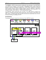
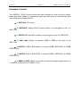
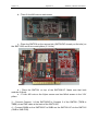
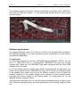
SMT8091_395VP
User Manual
Revision History
Date
Comments
Engineer
Version
02/06/05
First release
SM
1.0
02/08/05
Update: support Diamond V3
SM
1.1
User Manual (QCF42); Version 3.0, 8/11/00; © Sundance Multiprocessor Technology Ltd. 1999
Version 1.0
Page 2 of 12
SMT80901_395VP20 User Manual
Table of Contents
Revision History.......................................................................................................... 1
Table of Contents ....................................................................................................... 2
Contacting Sundance ................................................................................................. 3
Notes .......................................................................................................................... 3
Precautions................................................................................................................. 3
Outline description...................................................................................................... 4
Architecture ................................................................................................................ 5
Hardware involved...................................................................................................... 6
Hardware installation .................................................................................................. 7
Software applications ............................................................................................... 10
3L application........................................................................................................ 10
Description of the functions in the test software menu.......................................... 11
“ '0' to configure the FPGA and acquire data”.............................................. 11
“ '1' to skip the configuration of the FPGA and acquire data” .................... 11
CPLDReset(): Pulse on Config Line - for FPGA reconfiguring .......................... 11
Configuring internal Registers ........................................................................... 11
Capturing data................................................................................................... 11
Matlab application ................................................................................................. 12
Power consumption .................................................................................................. 12
Version 1.0
Page 3 of 12
SMT80901_395VP20 User Manual
Contacting Sundance
You can contact Sundance for additional information by posting a message in our
online support forum.
To access the support forum, please register first.
Notes
-
SHB stands for Sundance High-speed Bus
-
SDB stands for Sundance Digital Bus
-
RSL stands for Rocket-IO Serial Link
-
Comport denotes an 8-bit communication port following the TI C4x standards
Precautions
In order to guarantee that Sundance’s boards function correctly and to protect the
module from damage, the following precautions should be taken:
-
They are static sensitive products and should be handled accordingly.
Always place the modules in a static protective bag during storage and
transition.
-
When operating, make sure that the heat generated by the system is
extracted e.g. a fan extracting heat or air blower. It is vital for the SMT391
daughter module.
Version 1.0
Page 4 of 12
SMT80901_395VP20 User Manual
Outline description
The SMT8091_395VP is a single-C6416T based module (SMT395VP) combined
with a dual high-speed ADC module (SMT391-VP composed of SMT338-VP and
SMT391).
SMT395VP characteristics:
⇒ Single TMS320C6416T processor running @ 1GHz (32 bits)
⇒ Six 20MB/s communication ports (comports)
⇒ Up to 256MBytes of SDRAM @ 133MHz
⇒ 8MByte Flash ROM for boot code and FPGA programming
⇒ Global expansion connector
⇒ General purpose I/O connector
⇒ High bandwidth data I/O via 2 Sundance High-speed Buses (32-bit SDB
interfaces)
⇒ 8 Rocket Serial links @ 2Gbit/s per lane for inter-module communications
SMT391-VP characteristics:
⇒ Dual 8-bit ADC (AT84AD001) sampling at up to 1Gsps via LVDS bus (SLB)
⇒ Two Sundance High-speed Bus (SHB) connectors
⇒ Two 4-channel Rocket Serial Link (RSL) connector – 2.5Gbit/s per lane
⇒ Two 20 MBytes/s communication ports (comport)
⇒ Low-jitter on-board system clock
⇒ Xilinx Virtex-II Pro FPGA (VP30-6)
⇒ 50-Ohm terminated analogue inputs and outputs, external triggers and
clocks via MMCX or MMBX (Huber and Suhner) connectors
⇒ User defined pins for external connections
⇒ Compatible with a wide range of Sundance SHB modules
⇒ TIM standard compatible
Version 1.0
Page 5 of 12
SMT80901_395VP20 User Manual
The SMT8091_395VP is demonstration software for the evaluation of the SMT395VP
and SMT391-VP modules. It can be used for Broadband cable modem head-end
systems, Wireless infrastructure applications, 3G/4G Radio transceivers, Software
Defined Radio systems, Medical imaging systems, Spectrum analysers, High-speed
data acquisition system with or without digital processor. This document is an
installation guide for the SMT8091_395VP demonstration system.
The SMT8091_395VP application gets the DSP on the SMT395VP to configure the
SMT391_VP FPGA and control clock frequencies, clock routings, data format and
data capture. The DSP grabs data from both channels and stores them into a file for
further processing, like display and FFT.
Architecture
The following diagram shows the architecture of the SMT8091 system:
Version 1.0
Page 6 of 12
SMT80901_395VP20 User Manual
Hardware involved.
The SMT8091_395VP is built around two main modules but also involves a carrier
board and some cables to interconnect them and allow them to communicate with
each other and to access the PC.
⇒ 1x SMT310Q: PCI carrier
⇒ 1x SMT395VP: Single-C6416T based module; to be plugged on site 1 of
SMT310Q.
⇒ 1x SMT391-VP: Dual-ADC module; to be plugged on site 2 of SMT310Q.
⇒ 1x FMS cable (20cm): to connect T1C0 to T2C3 at the back of the
SMT310Q.
⇒ 1x SMT511 (SHB to SHB cable): to connect SHBB (SMT395VP) to SHBB
(SMT391VP).
⇒ 1x SMT516 (SHB to SHB PCB): to connect SHBA (SMT395VP) to SHBA
(SMT391VP).
⇒ 2x MMCX to BNC cables to connect an external analogue signal source to
J1 noted G (ChQ) and to J2 noted C (ChI).
Version 1.0
Page 7 of 12
SMT80901_395VP20 User Manual
Hardware installation
Here are the steps to follow to install the SMT8091_395VP system.
1 – Place the SMT395VP on TIM site 1 of the carrier board (SMT310Q).
2 – The following are then required to mount SMT338-VP+391 on the SMT310Q:
Top Primary TIM Connector
Power
TIM 3.3V
Holes mounted with
Nylon screw (M2x10) and
4 Nylon nuts (M2)
RSL
B
RSL
A
SMT338-VP
SHB
B
SMT390
SHB
A
Holes mounted with
Nylon screw (M2x10) and
4 Nylon nuts (M2)
TIM 3.3V
Bottom Primary TIM Connector
a – First, fit two Nylon screws (M2x10), pointing out (the head of the screws on
bottom side).
Version 1.0
Page 8 of 12
SMT80901_395VP20 User Manual
b – Then fit four M2 nuts on each screw.
c – Place the SMT338 on the second site (SMT395VP already on first site) on
the SMT310Q and fit two metal pillars (3.3 Volts).
d – Place the SMT391 on top of the SMT338-VP. Make sure that both
modules fit firmly.
e – Fit two M2 nuts on the Nylon screws and two M3x4 screws in the 3.3V
pillars.
3 – Connect Comport 1 of the SMT395VP to Comport 3 of the SMT391 (T1C0 to
T2C3) via an FMS cable at the back of the SMT310Q.
4 – Connect SHBA on the SMT395VP to SHBA on the SMT391-VP via the SMT516
(SHB to SHB PCB).
Version 1.0
Page 9 of 12
SMT80901_395VP20 User Manual
5 – Connect SHBB on the SMT395VP to SHBB on the SMT391-VP via the SMT511
(SHB to SHB cable).
6 – Connect external sources to J1 noted G (ChQ), J2 noted C (ChI) via MMCX-BNC
cables. Make sure that the external signal meets the input characteristics of the
SMT391-VP described in the SMT391-VP User Manual.
7 – Place the carrier board in the host system.
The following picture shows how connections are made at the top of the system:
Version 1.0
Page 10 of 12
SMT80901_395VP20 User Manual
The following picture shows the Comport connection at the back of the SMT310Q.
Note that the FMS are ‘twisted’, i.e. one end should be blue and the other should
show silver pins.
Software applications
You require Diamond version 3 or later to be able to run the application provided in
the SMT6600 package. If you have a previous version of Diamond, you may need to
recompile the application.
3L application
In a sub-folder labelled 3L (directory SMT6600\Systems\SMT8091_395VP), you will
find a C (SMT395VP_391.c), a configuration (SMT395VP_391.cfg) and a make
(nmake) files. Make sure the SMT395VP has been configured with the 32-bit SDB
interface of the firmware.
In a DOS prompt window, simply type nmake to generate the 3L application file,
which can be loaded into the SMT395VP by using the 3L Server (3L Diamond needs
to be installed first). Make sure that all the libraries located in the Lib folder are
properly compiled (if the nmake reports errors relevant to these libraries please
recompile the source located in the Source folder. You simply have to run the
Makefile with the nmake provided).
This application allows the user to execute simple commands such as configuring the
ADC (output format and scale), the clock synthesizers, clock routing, capturing data,
etc…
Version 1.0
Page 11 of 12
SMT80901_395VP20 User Manual
Description of the functions in the test software menu
The 3L application provided with the system allows the two options. The first one
allows to configure the SMT391-VP by using the SMT395VP via comport and next do
the data acquisition on both channels I and Q at several sampling frequencies. The
second option skips the configuration of the FPGA of the SMT391VP and then do the
data acquisition as defined previously.
“ '0' to configure the FPGA and acquire data”
This command loads the SMT391 bitstream contained in the directory where the
application is running from as well as the Start and End.
The ConfigStdioCP() function used is provided with the SMT6500 package. Please
refer to the SMT6500 for more details. This function loads the SMT391 firmware in
the FPGA via comport. Once the FPGA is configured, it starts to set up the ADC and
then acquire the input signals at several frequencies.
Both channels I and Q are captured and the acquisition starts with a sampling
frequency from 50MHz to 1000MHz by step of 50MHz. For the frequencies below
600MHz the clock synthesizer generates the sampling frequencies. Above 600MHz
the VCO generates them.
“ '1' to skip the configuration of the FPGA and acquire data”
This command skips the SMT391 configuration and should be use only when the
FPGA is already configured. This option starts to configure the ADC and then acquire
the input signals at several frequencies (as explained in the section just above).
CPLDReset(): Pulse on Config Line - for FPGA reconfiguring
By toggling the Config line, it is possible to reload the FPGA with a different
bitstream.
Configuring internal Registers
Set up the internal registers with values defines at the beginning of the application.
Capturing data
This command captures data from both I and Q channels, one after the other (not
simultaneously). Data are then stored into two separate files into the directory where
the application has been started. Files are called ChannelA_frequency.txt and
ChannelB_frequency.txt.
Note that without configuring the FPGA followed by its internal registers, none of the
other options will work.
Version 1.0
Page 12 of 12
SMT80901_395VP20 User Manual
Matlab application
The SMT8091_395VP is also provided with a Matlab application (3L folder – test.m),
which displays raw data captured with 3L application as well as the FFT.
Power consumption
The SMT8091_395VP system consumes about 14.6 Watts in idle mode, and 25.3
Watts with the application running (measured during the data acquisition).