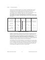
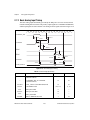
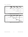
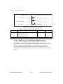
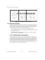
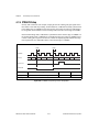
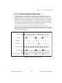
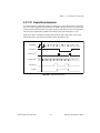
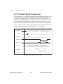
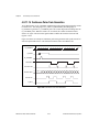
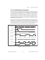
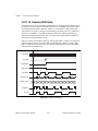
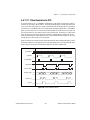
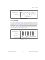
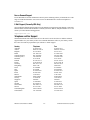
1
DAQ
DAQ-STC™ Technical
Reference Manual
System Timing Controller for Data Acquisition
DAQ-STC Technical Reference Manual
January 1999 Edition
Part Number 340934B-01
Internet Support
E-mail: [email protected]
FTP Site: ftp.natinst.com
Web Address: http://www.natinst.com
Bulletin Board Support
BBS United States: 512 794 5422
BBS United Kingdom: 01635 551422
BBS France: 01 48 65 15 59
Fax-on-Demand Support
512 418 1111
Telephone Support (USA)
Tel: 512 795 8248
Fax: 512 794 5678
International Offices
Australia 03 9879 5166, Austria 0662 45 79 90 0, Belgium 02 757 00 20, Brazil 011 288 3336,
Canada (Ontario) 905 785 0085, Canada (Québec) 514 694 8521, Denmark 45 76 26 00, Finland 09 725 725 11,
France 01 48 14 24 24, Germany 089 741 31 30, Hong Kong 2645 3186, Israel 03 6120092, Italy 02 413091,
Japan 03 5472 2970, Korea 02 596 7456, Mexico 5 520 2635, Netherlands 0348 433466, Norway 32 84 84 00,
Singapore 2265886, Spain 91 640 0085, Sweden 08 730 49 70, Switzerland 056 200 51 51, Taiwan 02 377 1200,
United Kingdom 01635 523545
National Instruments Corporate Headquarters
6504 Bridge Point Parkway Austin, Texas 78730-5039
USA Tel: 512 794 0100
© Copyright 1995, 1998 National Instruments Corporation. All rights reserved.
Important Information
Warranty
The DAQ-STC is warranted against defects in materials and workmanship for a period of one year from the date of
shipment, as evidenced by receipts or other documentation. National Instruments will, at its option, repair or replace
equipment that proves to be defective during the warranty period. This warranty includes parts and labor.
The media on which you receive National Instruments software are warranted not to fail to execute programming
instructions, due to defects in materials and workmanship, for a period of 90 days from date of shipment, as evidenced
by receipts or other documentation. National Instruments will, at its option, repair or replace software media that do not
execute programming instructions if National Instruments receives notice of such defects during the warranty period.
National Instruments does not warrant that the operation of the software shall be uninterrupted or error free.
A Return Material Authorization (RMA) number must be obtained from the factory and clearly marked on the outside
of the package before any equipment will be accepted for warranty work. National Instruments will pay the shipping costs
of returning to the owner parts which are covered by warranty.
National Instruments believes that the information in this document is accurate. The document has been carefully
reviewed for technical accuracy. In the event that technical or typographical errors exist, National Instruments reserves
the right to make changes to subsequent editions of this document without prior notice to holders of this edition. The
reader should consult National Instruments if errors are suspected. In no event shall National Instruments be liable for
any damages arising out of or related to this document or the information contained in it.
EXCEPT AS SPECIFIED HEREIN, NATIONAL INSTRUMENTS MAKES NO WARRANTIES, EXPRESS OR IMPLIED, AND SPECIFICALLY DISCLAIMS
ANY WARRANTY OF MERCHANTABILITY OR FITNESS FOR A PARTICULAR PURPOSE. CUSTOMER’S RIGHT TO RECOVER DAMAGES CAUSED
BY FAULT OR NEGLIGENCE ON THE PART OF NATIONAL INSTRUMENTS SHALL BE LIMITED TO THE AMOUNT THERETOFORE PAID BY THE
CUSTOMER. NATIONAL INSTRUMENTS WILL NOT BE LIABLE FOR DAMAGES RESULTING FROM LOSS OF DATA, PROFITS, USE OF PRODUCTS,
OR INCIDENTAL OR CONSEQUENTIAL DAMAGES, EVEN IF ADVISED OF THE POSSIBILITY THEREOF. This limitation of the liability of
National Instruments will apply regardless of the form of action, whether in contract or tort, including negligence.
Any action against National Instruments must be brought within one year after the cause of action accrues. National
Instruments shall not be liable for any delay in performance due to causes beyond its reasonable control. The warranty
provided herein does not cover damages, defects, malfunctions, or service failures caused by owner’s failure to follow
the National Instruments installation, operation, or maintenance instructions; owner’s modification of the product;
owner’s abuse, misuse, or negligent acts; and power failure or surges, fire, flood, accident, actions of third parties,
or other events outside reasonable control.
Copyright
Under the copyright laws, this publication may not be reproduced or transmitted in any form, electronic or mechanical,
including photocopying, recording, storing in an information retrieval system, or translating, in whole or in part, without
the prior written consent of National Instruments Corporation.
Trademarks
CVI™, DAQ-STC™, NI-DAQ™, and RTSI™ are trademarks of National Instruments Corporation.
Product and company names mentioned herein are trademarks or trade names of their respective companies.
WARNING REGARDING MEDICAL AND CLINICAL USE OF NATIONAL INSTRUMENTS PRODUCTS
National Instruments products are not designed with components and testing intended to ensure a level of reliability
suitable for use in treatment and diagnosis of humans. Applications of National Instruments products involving medical
or clinical treatment can create a potential for accidental injury caused by product failure, or by errors on the part of the
user or application designer. Any use or application of National Instruments products for or involving medical or clinical
treatment must be performed by properly trained and qualified medical personnel, and all traditional medical safeguards,
equipment, and procedures that are appropriate in the particular situation to prevent serious injury or death should always
continue to be used when National Instruments products are being used. National Instruments products are NOT intended
to be a substitute for any form of established process, procedure, or equipment used to monitor or safeguard human health
and safety in medical or clinical treatment.
Contents
About This Manual
Organization of This Manual .........................................................................................xxiii
Conventions Used in This Manual.................................................................................xxv
National Instruments Documentation ............................................................................xxvi
Related Documentation..................................................................................................xxvi
Customer Communication .............................................................................................xxvii
Chapter 1
Introduction
1.1
1.2
DAQ-STC Applications .....................................................................................1-2
1.1.1
Analog Input Application ...................................................................1-2
1.1.2
Analog Output Application ................................................................1-3
DAQ-STC Block Diagram .................................................................................1-4
Chapter 2
Analog Input Timing/Control
2.1
2.2
2.3
2.4
Overview ............................................................................................................2-1
2.1.1
Programming the AITM .....................................................................2-1
Features ..............................................................................................................2-2
Simplified Model................................................................................................2-4
Analog Input Functions ......................................................................................2-6
2.4.1
Low-Level Timing and Control..........................................................2-6
2.4.1.1
ADC Control.................................................................2-7
2.4.1.2
Data FIFO Control ........................................................2-7
2.4.1.3
Configuration FIFO and External
Multiplexer Control ...................................................2-7
2.4.1.4
CONVERT Timing.......................................................2-9
2.4.2
Scan-Level Timing and Control .........................................................2-11
2.4.2.1
Internal START Mode ..................................................2-11
2.4.2.2
External START Mode .................................................2-12
2.4.3
Acquisition-Level Timing and Control ..............................................2-14
2.4.3.1
Posttrigger Acquisition Mode .......................................2-14
2.4.3.2
Pretrigger Acquisition Mode ........................................2-14
2.4.3.3
Continuous Acquisition Mode ......................................2-15
2.4.3.4
Staged Acquisition ........................................................2-16
2.4.3.5
Master/Slave Trigger ....................................................2-16
2.4.4
Gating .................................................................................................2-16
2.4.4.1
Free-Run Gating Mode .................................................2-17
© National Instruments Corporation
v
DAQ-STC Technical Reference Manual
Contents
2.5
2.6
2.7
2.4.4.2
Halt-Gating Mode......................................................... 2-17
2.4.5
Single-Wire Mode.............................................................................. 2-18
Pin Locator Interface.......................................................................................... 2-19
Programming Information ................................................................................. 2-24
2.6.1
Register and Bitfield Programming Considerations .......................... 2-24
2.6.2
Windowing Registers ......................................................................... 2-25
2.6.3
Programming for an Analog Input Operation .................................... 2-25
2.6.3.1
Resetting ....................................................................... 2-26
2.6.3.2
Board Power-up Initialization ...................................... 2-27
2.6.3.3
Initialize Configuration Memory Output...................... 2-28
2.6.3.4
Board Environment Setup ............................................ 2-29
2.6.3.5
FIFO Request................................................................ 2-30
2.6.3.6
Hardware Gate Programming....................................... 2-30
2.6.3.7
Software Gate Operation .............................................. 2-31
2.6.3.8
Trigger Signals ............................................................. 2-32
2.6.3.9
Number of Scans .......................................................... 2-33
2.6.3.10
Start of Scan ................................................................. 2-34
2.6.3.11
End of Scan................................................................... 2-37
2.6.3.12
Convert Signal .............................................................. 2-38
2.6.3.13
Enable Interrupts .......................................................... 2-40
2.6.3.14
Arming.......................................................................... 2-41
2.6.3.15
Starting the Acquisition................................................ 2-41
2.6.3.16
Analog Input Program .................................................. 2-42
2.6.4
Single Scan......................................................................................... 2-42
2.6.5
Change Scan Rate during an Acquisition .......................................... 2-43
2.6.6
Staged Acquisition ............................................................................. 2-44
2.6.7
Master/Slave Operation Considerations............................................. 2-45
2.6.8
Analog Input-Related Interrupts ........................................................ 2-46
2.6.9
Bitfield Descriptions .......................................................................... 2-48
Timing Diagrams ............................................................................................... 2-84
2.7.1
Signal Definitions .............................................................................. 2-84
2.7.1.1
CONVERT_SRC.......................................................... 2-84
2.7.1.2
OUT_CLK.................................................................... 2-85
2.7.2
Basic Analog Input Timing................................................................ 2-86
2.7.3
Data FIFOs ......................................................................................... 2-88
2.7.4
Configuration Memory ...................................................................... 2-89
2.7.5
Maximum Rate Analog Input ............................................................ 2-91
2.7.6
External CONVERT Source .............................................................. 2-92
2.7.7
External Triggers................................................................................ 2-93
2.7.8
Trigger Output.................................................................................... 2-97
2.7.8.1
START1 and START2 Triggers .................................. 2-97
2.7.8.2
START Trigger and SCAN_IN_PROG Assertion....... 2-100
DAQ-STC Technical Reference Manual
vi
© National Instruments Corporation
Contents
2.8
2.7.8.3
SCAN_IN_PROG Deassertion .....................................2-103
2.7.8.4
STOP Trigger................................................................2-103
2.7.9
Counter Outputs..................................................................................2-105
2.7.9.1
SC_TC ..........................................................................2-105
2.7.9.2
SI_TC............................................................................2-105
2.7.9.3
DIV_TC ........................................................................2-106
2.7.10 Macro-Level Analog Input Timing ....................................................2-106
2.7.11 External Gating...................................................................................2-109
Detailed Description...........................................................................................2-112
2.8.1
Internal Signals and Operation ...........................................................2-113
2.8.2
Trigger Selection and Conditioning ...................................................2-119
2.8.2.1
Using Edge Detection ...................................................2-122
2.8.2.2
Using Synchronization..................................................2-122
2.8.2.3
Trigger Signals..............................................................2-122
2.8.3
Analog Input Counters .......................................................................2-123
2.8.3.1
SC Counter....................................................................2-124
2.8.3.2
SC Control ....................................................................2-124
2.8.3.3
SI Counter .....................................................................2-126
2.8.3.4
SI Control......................................................................2-126
2.8.3.5
SI2 Counter ...................................................................2-127
2.8.3.6
SI2 Control....................................................................2-127
2.8.3.7
DIV Counter .................................................................2-128
2.8.3.8
DIV Control ..................................................................2-129
2.8.4
Interrupt Control .................................................................................2-130
2.8.5
Error Detection ...................................................................................2-132
2.8.5.1
Overrun Error................................................................2-132
2.8.5.2
Overflow Error..............................................................2-132
2.8.5.3
SC_TC Error .................................................................2-132
2.8.6
Nominal Signal Pulsewidths...............................................................2-133
Chapter 3
Analog Output Timing/Control
3.1
3.2
3.3
3.4
Overview ............................................................................................................3-1
3.1.1
Programming the AOTM ...................................................................3-2
Features ..............................................................................................................3-2
Simplified Model................................................................................................3-4
Analog Output Functions ...................................................................................3-5
3.4.1
Primary Group Analog Output Modes ...............................................3-5
3.4.1.1
DAQ-STC-Driven Analog Output................................3-6
3.4.1.2
CPU-Driven Analog Output .........................................3-6
3.4.1.3
DAQ-STC and CPU Conflict .......................................3-7
3.4.2
DAC Interface ....................................................................................3-8
© National Instruments Corporation
vii
DAQ-STC Technical Reference Manual
Contents
3.4.3
3.5
3.6
Data Interfaces ................................................................................... 3-8
3.4.3.1
FIFO Data Interface...................................................... 3-8
3.4.3.2
Serial Link Data Interface ............................................ 3-10
3.4.3.3
Unbuffered Data Interface ............................................ 3-11
3.4.4
Update Timing for Primary Group Analog Output............................ 3-11
3.4.4.1
Internal UPDATE......................................................... 3-11
3.4.4.2
External UPDATE........................................................ 3-12
3.4.5
Buffer Timing and Control for Primary Analog Output .................... 3-12
3.4.5.1
Single-Buffer Mode...................................................... 3-13
3.4.5.2
Continuous Mode ......................................................... 3-13
3.4.5.3
Waveform Staging........................................................ 3-14
3.4.5.4
Mute Buffers................................................................. 3-15
3.4.5.5
Master/Slave Trigger .................................................... 3-15
3.4.6
Secondary Analog Output .................................................................. 3-16
Pin Interface ....................................................................................................... 3-16
Programming Information ................................................................................. 3-20
3.6.1
Programming for a Primary Analog Output Operation ..................... 3-20
3.6.1.1
Overview ...................................................................... 3-21
3.6.1.2
Resetting ....................................................................... 3-21
3.6.1.3
Board Power-up Initialization ...................................... 3-22
3.6.1.4
Trigger Signals ............................................................. 3-23
3.6.1.5
Number of Buffers........................................................ 3-24
3.6.1.6
Update Selection........................................................... 3-26
3.6.1.7
Channel Select .............................................................. 3-28
3.6.1.8
LDAC Source and UPDATE Mode ............................. 3-29
3.6.1.9
Stop On Error ............................................................... 3-29
3.6.1.10
FIFO Mode ................................................................... 3-29
3.6.1.11
Enable Interrupts .......................................................... 3-30
3.6.1.12
Arming.......................................................................... 3-30
3.6.1.13
Starting the Waveform ................................................. 3-31
3.6.1.14
Primary Analog Output Program.................................. 3-31
3.6.2
Waveform Staging for Primary Analog Output ................................. 3-32
3.6.3
Changing Update Rate during an Output Operation for
Primary Analog Output Group........................................................ 3-34
3.6.4
Master/Slave Operation Considerations for Primary Analog
Output Group .................................................................................. 3-35
3.6.5
Primary Analog Output Group-Related Interrupts............................. 3-35
3.6.6
Programming for a Secondary Analog Output Group Operation ...... 3-38
3.6.6.1
Overview ...................................................................... 3-38
3.6.6.2
Resetting ....................................................................... 3-38
3.6.6.3
Board Power-up Initialization ...................................... 3-39
3.6.6.4
Hardware Gate Programming....................................... 3-39
3.6.6.5
Software Gate Operation .............................................. 3-40
DAQ-STC Technical Reference Manual
viii
© National Instruments Corporation
Contents
3.7
3.8
3.6.6.6
Counting for Waveform Staging...................................3-40
3.6.6.7
Update Selection ...........................................................3-40
3.6.6.8
Arming ..........................................................................3-41
3.6.6.9
Secondary Analog Output Program ..............................3-41
3.6.7
Waveform Staging for Secondary Analog Output .............................3-42
3.6.8
Changing Update Rate during an Output Operation for
Secondary Analog Output ...............................................................3-44
3.6.9
Master/Slave Operation Considerations for
Secondary Analog Output ...............................................................3-45
3.6.10 Secondary Analog Output-Related Interrupts ....................................3-45
3.6.11 Bitfield Descriptions...........................................................................3-45
Timing Diagrams................................................................................................3-84
3.7.1
Signal Definitions...............................................................................3-84
3.7.1.1
UPDATE_SRC .............................................................3-85
3.7.1.1
UI2_SRC.......................................................................3-85
3.7.1.1
OUT_CLK ....................................................................3-86
3.7.2
DAQ-STC-Driven Analog Output Timing.........................................3-86
3.7.3
CPU-Driven Analog Output Timing ..................................................3-88
3.7.4
DAQ-STC- and CPU-Driven Analog Output Timing........................3-90
3.7.5
Secondary Analog Output Timing......................................................3-93
3.7.6
Decoded Signal Timing ......................................................................3-94
3.7.7
Local Buffer Mode Timing ................................................................3-96
3.7.8
Unbuffered Data Interface Timing .....................................................3-98
3.7.9
Maximum Update Rate Timing..........................................................3-101
3.7.10 External Trigger Timing.....................................................................3-102
3.7.11 Trigger Output ....................................................................................3-104
3.7.11.1
START1 Trigger...........................................................3-104
3.7.12 Counter Outputs..................................................................................3-107
3.7.12.1
BC_TC ..........................................................................3-107
3.7.12.2
UC_TC..........................................................................3-108
Detailed Description...........................................................................................3-108
3.8.1
Internal Signals and Operation ...........................................................3-109
3.8.2
Trigger Selection and Conditioning ...................................................3-114
3.8.2.1
Using Edge Detection ...................................................3-116
3.8.2.2
Using Synchronization..................................................3-116
3.8.2.3
Trigger Signals..............................................................3-116
3.8.3
Analog Output Counters.....................................................................3-117
3.8.3.1
UI Counter ....................................................................3-117
3.8.3.2
UI Control .....................................................................3-118
3.8.3.3
UC Counter ...................................................................3-118
3.8.3.4
UC Control....................................................................3-119
3.8.3.5
BC Counter ...................................................................3-120
3.8.3.6
BC Control ....................................................................3-120
© National Instruments Corporation
ix
DAQ-STC Technical Reference Manual
Contents
3.8.4
3.8.5
3.8.6
3.8.7
3.8.3.7
UI2 Counter .................................................................. 3-121
3.8.3.8
UI2 Control................................................................... 3-121
Interrupt Control ................................................................................ 3-122
Error Detection................................................................................... 3-122
3.8.5.1
Overrun Error ............................................................... 3-122
3.8.5.2
BC_TC Error ................................................................ 3-123
3.8.5.3
BC_TC Trigger Error ................................................... 3-123
3.8.5.4
UI2_TC Error ............................................................... 3-123
Output Control ................................................................................... 3-123
Nominal Signal Pulsewidths .............................................................. 3-124
Chapter 4
General-Purpose Counter/Timer
4.1
4.2
4.3
4.4
4.5
Overview............................................................................................................ 4-1
4.1.1
Programming the GPCT..................................................................... 4-1
Features .............................................................................................................. 4-1
Simplified Model ............................................................................................... 4-2
Counter/Timer Functions ................................................................................... 4-3
4.4.1
Event Counting .................................................................................. 4-3
4.4.1.1
Simple Event Counting................................................. 4-4
4.4.1.2
Simple Gated-Event Counting...................................... 4-4
4.4.1.3
Buffered Noncumulative Event Counting .................... 4-4
4.4.1.4
Buffered Cumulative Event Counting .......................... 4-5
4.4.1.5
Relative Position Sensing ............................................. 4-6
4.4.2
Time Measurement ............................................................................ 4-6
4.4.2.1
Single-Period Measurement ......................................... 4-6
4.4.2.2
Single-Pulsewidth Measurement .................................. 4-7
4.4.2.3
Buffered Period Measurement...................................... 4-7
4.4.2.4
Buffered Semiperiod Measurement.............................. 4-8
4.4.2.5
Buffered Pulsewidth Measurement .............................. 4-9
4.4.3
Pulse Generation ................................................................................ 4-9
4.4.3.1
Single Pulse Generation ............................................... 4-9
4.4.3.2
Single Triggered Pulse Generation............................... 4-10
4.4.3.3
Retriggerable Single Pulse Generation......................... 4-11
4.4.3.4
Buffered Retriggerable Single Pulse Generation ......... 4-11
4.4.4
Pulse-Train Generation ...................................................................... 4-12
4.4.4.1
Continuous Pulse-Train Generation ............................. 4-12
4.4.4.2
Buffered Static Pulse-Train Generation ....................... 4-13
4.4.4.3
Buffered Pulse-Train Generation ................................. 4-14
4.4.4.4
Frequency Shift Keying (FSK)..................................... 4-14
4.4.4.5
Pulse Generation for ETS............................................. 4-15
Pin Interface ....................................................................................................... 4-16
DAQ-STC Technical Reference Manual
x
© National Instruments Corporation
Contents
4.6
4.7
4.8
Programming Information..................................................................................4-17
4.6.1
Programming for a GPCT Operation .................................................4-17
4.6.1.1
Overview.......................................................................4-17
4.6.1.2
Notation ........................................................................4-18
4.6.1.3
Resetting .......................................................................4-18
4.6.1.4
Arming ..........................................................................4-18
4.6.1.5
Simple Event Counting .................................................4-19
4.6.1.6
Buffered Event Counting ..............................................4-20
4.6.1.7
Relative Position Sensing .............................................4-23
4.6.1.8
Single-Period and Pulsewidth Measurement ................4-24
4.6.1.9
Buffered Period, Semiperiod, and Pulsewidth
Measurement..............................................................4-26
4.6.1.10
Pulse and Continuous Pulse-Train Generation .............4-28
4.6.1.11
Frequency Shift Keying ................................................4-31
4.6.1.12
Pulse-Train Generation for ETS ...................................4-33
4.6.1.13
Reading the Counter Contents ......................................4-34
4.6.1.14
Reading the Hardware Save Registers..........................4-34
4.6.1.15
Enabling the General Purpose
Counter/Timer Output Pin .........................................4-35
4.6.2
Bitfield Descriptions...........................................................................4-35
Timing Diagrams................................................................................................4-53
4.7.1
CTRSRC Minimum Period and Minimum Pulsewidth......................4-55
4.7.2
CTRSRC to CTROUT Delay .............................................................4-55
4.7.3
G_GATE Minimum Pulsewidth.........................................................4-56
4.7.4
CTRGATE to CTROUT Delay ..........................................................4-57
4.7.5
CTRGATE to INTERRUPT...............................................................4-57
4.7.6
CTRGATE Setup................................................................................4-58
4.7.7
CTR_U/D Setup .................................................................................4-59
Detailed Description...........................................................................................4-61
4.8.1
Internal Signals and Operation ...........................................................4-62
4.8.2
G_SOURCE Selection and Conditioning...........................................4-63
4.8.3
G_GATE Selection and Conditioning................................................4-64
4.8.4
G_UP_DOWN Control ......................................................................4-64
4.8.5
G_OUT Conditioning and Routing ....................................................4-65
4.8.6
G_CONTROL Conditioning ..............................................................4-67
4.8.7
Gate Actions .......................................................................................4-67
4.8.7.1
START/STOP on G_CONTROL .................................4-68
4.8.7.2
Save on G_GATE .........................................................4-68
4.8.7.3
Reload on G_CONTROL .............................................4-68
4.8.7.4
UP/DOWN on G_CONTROL ......................................4-69
4.8.7.5
Generate Interrupt on G_GATE....................................4-69
4.8.7.6
Change Output Polarity on G_GATE ...........................4-69
4.8.7.7
Select Load Register on G_CONTROL .......................4-69
© National Instruments Corporation
xi
DAQ-STC Technical Reference Manual
Contents
4.8.8
4.8.9
4.8.10
4.8.11
4.8.7.8
Disarm Counter on G_CONTROL............................... 4-70
4.8.7.9
Switch Load Bank Selection on G_CONTROL........... 4-70
Interrupt Control ................................................................................ 4-70
PFI Selection ...................................................................................... 4-70
Error Detection................................................................................... 4-71
4.8.10.1
Gate Acknowledge Latency Error ................................ 4-71
4.8.10.2
Stale Data Error ............................................................ 4-71
4.8.10.3
Permanent Stale Data Error .......................................... 4-71
4.8.10.4
TC Latency Error.......................................................... 4-72
Detailed Operation by Application .................................................... 4-72
4.8.11.1
Simple Event Counting................................................. 4-72
4.8.11.2
Simple Gated-Event Counting...................................... 4-73
4.8.11.3
Buffered Noncumulative-Event Counting.................... 4-74
4.8.11.4
Buffered Cumulative-Event Counting.......................... 4-74
4.8.11.5
Relative-Position Sensing............................................. 4-75
4.8.11.6
Single-Period Measurement ......................................... 4-76
4.8.11.7
Single Pulsewidth Measurement .................................. 4-77
4.8.11.8
Buffered Period Measurement...................................... 4-78
4.8.11.9
Buffered Semiperiod Measurement.............................. 4-79
4.8.11.10
Buffered Pulsewidth Measurement .............................. 4-80
4.8.11.11
Single Pulse Generation ............................................... 4-81
4.8.11.12
Single-Triggered Pulse Generation .............................. 4-82
4.8.11.13
Retriggerable Single Pulse Generation......................... 4-83
4.8.11.14
Continuous Pulse-Train Generation ............................. 4-84
4.8.11.15
Buffered Pulse-Train Generation ................................. 4-85
4.8.11.16
Frequency Shift Keying................................................ 4-86
4.8.11.17
Pulse Generation for ETS............................................. 4-87
Chapter 5
Programmable Function Inputs
5.1
5.2
5.3
5.4
5.5
Overview............................................................................................................ 5-1
Features .............................................................................................................. 5-1
Pin Interface ....................................................................................................... 5-2
Programming Information ................................................................................. 5-5
5.4.1
Programming the PFI Pins ................................................................. 5-5
5.4.2
Bitfield Descriptions .......................................................................... 5-6
Detailed Description .......................................................................................... 5-7
Chapter 6
RTSI Trigger
6.1
6.2
Overview............................................................................................................ 6-1
Features .............................................................................................................. 6-1
DAQ-STC Technical Reference Manual
xii
© National Instruments Corporation
Contents
6.3
6.4
6.5
Pin Interface .......................................................................................................6-1
Programming Information..................................................................................6-2
6.4.1
Programming the RTSI Interface .......................................................6-2
6.4.2
Bitfield Descriptions...........................................................................6-3
Detailed Description...........................................................................................6-6
Chapter 7
Digital I/O
7.1
7.2
7.3
7.4
7.5
7.6
7.7
7.8
Overview ............................................................................................................7-1
Features ..............................................................................................................7-1
Simplified Model................................................................................................7-1
Overview of DIO Functions ...............................................................................7-2
7.4.1
Parallel Mode......................................................................................7-2
7.4.1.1
Parallel Input.................................................................7-3
7.4.1.2
Parallel Output ..............................................................7-3
7.4.2
Serial Mode ........................................................................................7-4
7.4.2.1
Serial Input....................................................................7-4
7.4.2.2
Serial Output .................................................................7-4
7.4.2.3
Serial I/O.......................................................................7-5
Pin Interface .......................................................................................................7-6
Programming Information..................................................................................7-7
7.6.1
Windowed Mode Register Access Example ......................................7-7
7.6.2
Programming the Digital Interface .....................................................7-8
7.6.2.1
Parallel Digital I/O........................................................7-9
7.6.2.2
Hardware-Controlled Serial Digital I/O........................7-10
7.6.2.3
Software-Controlled Serial Digital I/O.........................7-12
7.6.2.4
Programming the Control Lines ...................................7-12
7.6.2.5
Reading the Status Lines...............................................7-13
7.6.3
Bitfield Descriptions...........................................................................7-13
Timing Diagrams................................................................................................7-15
7.7.1
Serial Input Timing.............................................................................7-15
7.7.2
Serial Output Timing..........................................................................7-16
Detailed Description...........................................................................................7-17
Chapter 8
Interrupt Control
8.1
8.2
8.3
8.4
Overview ............................................................................................................8-1
Features ..............................................................................................................8-1
Pin Interface .......................................................................................................8-2
Programming Information..................................................................................8-3
8.4.1
Programming the Interrupt Interface ..................................................8-3
8.4.1.1
Interrupt Output Polarity...............................................8-3
© National Instruments Corporation
xiii
DAQ-STC Technical Reference Manual
Contents
8.5
8.4.1.2
Interrupt Output Select and Enable .............................. 8-3
8.4.1.3
Pass-Through Interrupt ................................................. 8-4
8.4.2
Interrupt Handling.............................................................................. 8-5
8.4.2.1
Interrupt Program ......................................................... 8-6
8.4.2.2
Interrupt Group A ......................................................... 8-6
8.4.2.3
Interrupt Group B ......................................................... 8-9
8.4.3
Bitfield Descriptions .......................................................................... 8-12
Interrupt Conditions ........................................................................................... 8-15
Chapter 9
Bus Interface
9.1
9.2
9.3
9.4
Overview............................................................................................................ 9-1
Features .............................................................................................................. 9-1
9.2.1
Pin Interface ....................................................................................... 9-1
Programming Information ................................................................................. 9-3
9.3.1
Programming the Write Strobes......................................................... 9-4
9.3.2
Bitfield Descriptions .......................................................................... 9-4
Timing Diagrams ............................................................................................... 9-5
Chapter 10
Miscellaneous Functions
10.1
10.2
10.3
10.4
10.5
10.6
10.7
10.8
Overview............................................................................................................ 10-1
Features .............................................................................................................. 10-1
Clock Distribution.............................................................................................. 10-2
Frequency Output............................................................................................... 10-3
Analog Trigger................................................................................................... 10-3
Test Mode .......................................................................................................... 10-6
Pin Interface ....................................................................................................... 10-9
Programming Information ................................................................................. 10-10
10.8.1 Programming Clock Distribution....................................................... 10-10
10.8.2 Programming FOUT .......................................................................... 10-12
10.8.3 Programming Analog Trigger ............................................................ 10-12
10.8.4 Bitfield Descriptions .......................................................................... 10-12
Appendix A
Specifications
Appendix B
Register Information
DAQ-STC Technical Reference Manual
xiv
© National Instruments Corporation
Contents
Appendix C
Pin List
Appendix D
DAQ-STC Revision History
Appendix E
Customer Communication
Glossary
Index
Figures
Figure 1-1.
Figure 1-2.
Figure 1-3.
Analog Input Application......................................................................1-2
Analog Output Application ...................................................................1-3
DAQ-STC Block Diagram ....................................................................1-4
Figure 2-1.
Figure 2-2.
Figure 2-3.
Figure 2-4.
Figure 2-5.
Figure 2-6.
Figure 2-7.
Figure 2-8.
Figure 2-9.
Figure 2-10.
Figure 2-11.
Figure 2-12.
Figure 2-13.
Figure 2-14.
Figure 2-15.
Figure 2-16.
Figure 2-17.
Figure 2-18.
Figure 2-19.
Figure 2-20.
Figure 2-21.
Typical Analog Input Waveform ..........................................................2-4
AITM Simplified Model .......................................................................2-5
ADC Control .........................................................................................2-7
Configuration FIFO Control..................................................................2-8
External Multiplexer Control ................................................................2-9
Internal CONVERT Timing..................................................................2-10
External CONVERT Timing.................................................................2-11
Internal START.....................................................................................2-12
External START....................................................................................2-13
SI Special Trigger Delay .......................................................................2-13
Posttrigger Acquisition Mode ...............................................................2-14
Pretrigger Acquisition Mode .................................................................2-15
Free-Run Gating Mode..........................................................................2-17
Halt-Gating Mode..................................................................................2-18
Single-Wire Mode .................................................................................2-18
Basic Analog Input Timing ...................................................................2-86
Data FIFO Timing .................................................................................2-88
Configuration Memory Timing .............................................................2-89
Maximum Rate Analog Input Timing ...................................................2-92
External CONVERT_SRC Timing .......................................................2-93
External Trigger Timing, Asynchronous Level ....................................2-94
© National Instruments Corporation
xv
DAQ-STC Technical Reference Manual
Contents
Figure 2-22.
Figure 2-23.
Figure 2-27.
Figure 2-28.
Figure 2-29.
Figure 2-30.
Figure 2-31.
Figure 2-32.
Figure 2-33.
Figure 2-34.
Figure 2-35.
Figure 2-36.
Figure 2-37.
Figure 2-38.
Figure 2-39.
Figure 2-40.
Figure 2-41.
Figure 2-42.
Figure 2-43.
Figure 2-44.
Figure 2-45.
Figure 2-46.
Figure 2-47.
Figure 2-48.
Figure 2-49.
Figure 2-50.
Figure 2-51.
Figure 2-52.
External Trigger Timing, Asynchronous Edge ..................................... 2-94
External Trigger Timing, Synchronous Level,
Internal CONVERT Mode .................................................................... 2-95
External Trigger Timing, Synchronous Edge,
Internal CONVERT Mode .................................................................... 2-95
External Trigger Timing, Synchronous Level,
External CONVERT Mode................................................................... 2-96
External Trigger Timing, Synchronous Edge,
External CONVERT Mode................................................................... 2-96
START1 Delays, Synchronous Mode, Internal CONVERT ................ 2-98
START2 Delays, Synchronous Mode, Internal CONVERT ............... 2-98
START1 Delays, Synchronous Mode, External CONVERT ............... 2-98
START2 Delays, Synchronous Mode, External CONVERT ............... 2-99
START1 Delays, Asynchronous Mode ................................................ 2-99
START2 Delays, Asynchronous Mode ................................................ 2-100
START Delays, Internal CONVERT ................................................... 2-101
START Delays, External CONVERT .................................................. 2-102
SCAN_IN_PROG Deassertion ............................................................. 2-103
STOP Delay, Synchronous Mode ......................................................... 2-104
STOP Delay, Asynchronous Mode....................................................... 2-104
SC_TC Delay ........................................................................................ 2-105
SI_TC Delay ......................................................................................... 2-105
DIV_TC Delay...................................................................................... 2-106
Interval Scanning Mode Timing ........................................................... 2-106
Free-Run Gating Mode Timing, Internal CONVERT .......................... 2-109
Free-Run Gating Mode Timing, External CONVERT ......................... 2-110
Halt-Gating Mode Timing, Internal CONVERT .................................. 2-111
AITM Block Diagram........................................................................... 2-112
START and STOP Routing Logic ........................................................ 2-120
START1 and START2 Routing Logic ................................................. 2-120
EXT_GATE Routing Logic .................................................................. 2-121
SC Control Circuit State Transitions .................................................... 2-125
SI Control Circuit State Transitions...................................................... 2-127
SI2 Control Circuit State Transitions.................................................... 2-128
DIV Control Circuit State Transitions .................................................. 2-130
Figure 3-1.
Figure 3-2.
Figure 3-3.
Figure 3-4.
Figure 3-5.
Figure 3-6.
Figure 3-7.
AOTM Simplified Mode....................................................................... 3-4
DAQ-STC-Driven Analog Output ........................................................ 3-6
CPU-Driven Analog Output ................................................................. 3-7
DAQ-STC and CPU Conflict................................................................ 3-7
FIFO Data Interface .............................................................................. 3-9
Local Buffer Mode................................................................................ 3-10
Serial Link Data Interface ..................................................................... 3-10
Figure 2-24.
Figure 2-25.
Figure 2-26.
DAQ-STC Technical Reference Manual
xvi
© National Instruments Corporation
Contents
Figure 3-8.
Figure 3-9.
Figure 3-10.
Figure 3-11.
Figure 3-12.
Figure 3-13.
Figure 3-14.
Figure 3-15.
Figure 3-16.
Figure 3-17.
Figure 3-18.
Figure 3-19.
Figure 3-20.
Figure 3-21.
Figure 3-22.
Figure 3-23.
Figure 3-24.
Figure 3-25.
Figure 3-26.
Figure 3-27.
Figure 3-28.
Figure 3-29.
Figure 3-30.
Figure 3-31.
Figure 3-32.
Figure 3-33.
Figure 3-34.
Figure 3-35.
Figure 3-36.
Figure 3-37.
Figure 3-38.
Figure 3-39.
Unbuffered Data Interface.....................................................................3-11
Internal UPDATE Timing .....................................................................3-12
External UPDATE Timing....................................................................3-12
Single-Buffer Mode...............................................................................3-13
Continuous Mode ..................................................................................3-14
Mute Buffers..........................................................................................3-15
DAQ-STC-Driven Analog Output Timing............................................3-87
CPU-Driven Analog Output Timing .....................................................3-89
Analog Output Contention Timing, Case A..........................................3-91
Analog Output Contention Timing, Case B ..........................................3-92
Secondary Analog Output Timing ........................................................3-93
Decoded Signal Timing.........................................................................3-95
Local Buffer Mode Timing ...................................................................3-97
Unbuffered Data Interface Timing ........................................................3-99
Maximum Update Rate Timing.............................................................3-101
External Trigger, Asynchronous Level .................................................3-102
External Trigger, Asynchronous Edge .................................................3-102
External Trigger, Synchronous Level, Internal UPDATE Mode.........3-103
External Trigger, Synchronous Edge, Internal UPDATE Mode..........3-103
External Trigger, Synchronous Level, External UPDATE Mode........3-103
External Trigger, Synchronous Edge, External UPDATE Mode.........3-103
START1 Delays, Synchronous Mode, Internal UPDATE....................3-105
START1 Delays, Synchronous Mode, External UPDATE...................3-106
START1 Delays, Asynchronous Mode.................................................3-107
BC_TC Delay ........................................................................................3-107
UC_TC Delay........................................................................................3-108
AOTM Block Diagram..........................................................................3-109
START1 Routing Logic ........................................................................3-115
EXT_GATE and EXT_GATE2 Routing Logic ....................................3-115
UI Control Circuit State Transitions .....................................................3-118
UC Control Circuit State Transitions ....................................................3-119
BC Control Circuit State Transitions ....................................................3-121
Figure 4-1.
Figure 4-2.
Figure 4-3.
Figure 4-4.
Figure 4-5.
Figure 4-6.
Figure 4-7.
Figure 4-8.
Figure 4-9.
Figure 4-10.
General-Purpose Counter/Timer Simplified Model ..............................4-2
Simple Event Counting .........................................................................4-4
Simple Gated-Event Counting...............................................................4-4
Buffered Noncumulative Event Counting .............................................4-5
Cumulative Event Counting ..................................................................4-5
Relative Position Sensing......................................................................4-6
Single-Period Measurement ..................................................................4-7
Single-Pulsewidth Measurement...........................................................4-7
Buffered Period Measurement...............................................................4-8
Buffered Semiperiod Measurement.......................................................4-8
© National Instruments Corporation
xvii
DAQ-STC Technical Reference Manual
Contents
Figure 4-11.
Figure 4-12.
Figure 4-13.
Figure 4-14.
Figure 4-15.
Figure 4-16.
Figure 4-17.
Figure 4-18.
Figure 4-19.
Figure 4-20.
Figure 4-21.
Figure 4-22.
Figure 4-23.
Figure 4-24.
Figure 4-25.
Figure 4-26.
Figure 4-27.
Figure 4-28.
Figure 4-29.
Figure 4-30.
Figure 4-31.
Figure 4-32.
Figure 4-33.
Figure 4-34.
Figure 4-35.
Figure 4-36.
Figure 4-37.
Figure 4-38.
Figure 4-39.
Figure 4-40.
Figure 4-41.
Figure 4-42.
Figure 4-43.
Figure 4-44.
Figure 4-45.
Figure 4-46.
Figure 4-47.
Figure 4-48.
Buffered Pulsewidth Measurement....................................................... 4-9
Single Pulse Generation ........................................................................ 4-10
Single Triggered-Pulse Generation....................................................... 4-10
Retriggerable Single Pulse Generation ................................................. 4-11
Buffered Retriggerable Single Pulse Generation .................................. 4-12
Continuous Pulse-Train Generation...................................................... 4-13
Buffered Static Pulse-Train Generation................................................ 4-13
Buffered Pulse-Train Generation .......................................................... 4-14
Frequency Shift Keying ........................................................................ 4-15
Pulse Generation for ETS ..................................................................... 4-15
CTRSRC Minimum Period and Minimum Pulsewidth ........................ 4-55
CTRSRC to CTROUT Timing ............................................................. 4-56
G_GATE Minimum Pulsewidth ........................................................... 4-56
CTRGATE to CTROUT Timing .......................................................... 4-57
CTRGATE to INTERRUPT Timing .................................................... 4-57
CTRGATE Setup Timing, Internal Timing Mode................................ 4-58
CTRGATE Setup Timing, External Timing Mode............................... 4-59
CTR_U/D Setup Timing, Internal Timing Mode ................................. 4-60
CTR_U/D Setup Timing, External Timing Mode ................................ 4-60
General-Purpose Counter/Timer Model ............................................... 4-61
G_SOURCE Generation ....................................................................... 4-72
Simple Event Counting ......................................................................... 4-73
Simple Gated-Event Counting .............................................................. 4-73
Buffered Noncumulative-Event Counting ............................................ 4-74
Buffered Cumulative-Event Counting .................................................. 4-75
Relative-Position Sensing ..................................................................... 4-75
Single-Period Measurement.................................................................. 4-76
Single Pulsewidth Measurement........................................................... 4-77
Buffered Period Measurement .............................................................. 4-78
Buffered Semiperiod Measurement ...................................................... 4-79
Buffered Pulsewidth Measurement....................................................... 4-80
Single Pulse Generation ........................................................................ 4-81
Single-Triggered Pulse Generation....................................................... 4-82
Retriggerable Single Pulse Generation ................................................. 4-83
Continuous Pulse-Train Generation...................................................... 4-84
Buffered Pulse-Train Generation .......................................................... 4-85
Frequency Shift Keying ........................................................................ 4-86
Pulse Generation for ETS ..................................................................... 4-87
Figure 7-1.
Figure 7-2.
Figure 7-3.
Figure 7-4.
DIO Simplified Model .......................................................................... 7-2
Parallel Input ......................................................................................... 7-3
Parallel Output ...................................................................................... 7-3
DIO Serial Input.................................................................................... 7-4
DAQ-STC Technical Reference Manual
xviii
© National Instruments Corporation
Contents
Figure 7-5.
Figure 7-6.
Figure 7-7.
Figure 7-8.
Serial Output..........................................................................................7-5
Serial I/O ...............................................................................................7-5
Serial Input Timing ...............................................................................7-16
Serial Output Timing.............................................................................7-16
Figure 9-1.
Figure 9-2.
Figure 9-3.
Figure 9-4.
Intel Bus Interface Read Timing ...........................................................9-6
Intel Bus Interface Write Timing ..........................................................9-6
Motorola Bus Interface Read Timing....................................................9-7
Motorola Bus Interface Write Timing...................................................9-8
Figure 10-1.
Figure 10-2.
Figure 10-3.
Figure 10-4.
Figure 10-5.
Figure 10-6.
Figure 10-7.
Clock Distribution .................................................................................10-2
Low-Window Mode ..............................................................................10-4
High-Window Mode..............................................................................10-4
Middle-Window Mode ..........................................................................10-5
High-Hysteresis Mode...........................................................................10-5
Low-Hysteresis Mode ...........................................................................10-6
Test Mode Internal Gate Tree ...............................................................10-7
Tables
Table 2-1.
Table 2-2.
Table 2-3.
Table 2-4.
Table 2-5.
Table 2-6.
Table 2-7.
Table 2-8.
Table 2-9.
Table 2-10.
Table 2-11.
Table 2-12.
Pin Interface .........................................................................................2-19
CONVERT_SRC Reference Pin Selection ..........................................2-84
Basic Analog Input Timing ..................................................................2-86
Configuration Memory Timing ............................................................2-90
External Analog Input Timing .............................................................2-96
START1 and START2 Timing, Synchronous Mode ...........................2-99
START1 and START2 Timing, Asynchronous Mode .........................2-100
Interval Scanning Mode Timing ...........................................................2-107
Internal Signals .....................................................................................2-113
PFI Selectors..........................................................................................2-121
Analog Input Interrupts .........................................................................2-131
Analog Input Nominal Signal Widths ..................................................2-133
Table 3-1.
Table 3-2.
Table 3-3.
Table 3-4.
Table 3-5.
Table 3-6.
Table 3-7.
Table 3-8.
Table 3-9.
Pin Interface .........................................................................................3-16
UPDATE_SRC Reference Pin Selection .............................................3-85
UI2_SRC Reference Pin Selection .......................................................3-85
DAQ-STC-Driven Analog Output Timing ...........................................3-87
External Trigger Timing........................................................................3-104
Internal Signals .....................................................................................3-109
PFI Selectors .........................................................................................3-115
Analog Output Interrupts ......................................................................3-122
Analog Output Nominal Signal Widths ...............................................3-124
© National Instruments Corporation
xix
DAQ-STC Technical Reference Manual
Contents
Table 4-1.
Table 4-2.
Table 4-3.
Table 4-4.
Table 4-5.
Table 4-6.
Table 4-7.
Table 4-8.
Table 4-9.
Table 4-10.
Table 4-11.
Table 4-12.
Table 4-13.
Table 4-14.
Table 4-15.
Table 4-16.
Table 4-17.
Table 4-18.
Table 4-19.
CTRSRC Reference Pin Selection........................................................ 4-53
CTRGATE Reference Pin Selection .................................................... 4-54
CTR_U/D Reference Pin Selection ...................................................... 4-54
Internal Signal Description .................................................................. 4-62
G_SOURCE Selection .......................................................................... 4-63
G_SOURCE Conditioning.................................................................... 4-63
G_GATE Selection ............................................................................... 4-64
G_GATE Conditioning ......................................................................... 4-64
G_UP_DOWN Modes ......................................................................... 4-65
G_OUT Mode ....................................................................................... 4-65
G_OUT Polarity.................................................................................... 4-65
G_OUT0/RTSI_IO Selection................................................................ 4-66
G_OUT1/DIV_TC_OUT Selection ...................................................... 4-66
G_CONTROL Conditioning................................................................. 4-67
Gate Actions ......................................................................................... 4-67
START/STOP Modes for Edge Gating ................................................ 4-68
Reload on G_CONTROL Selections ................................................... 4-68
Gate Interrupts ...................................................................................... 4-69
PFI Selectors ......................................................................................... 4-70
Table 5-1.
Table 5-2.
Table 5-3.
Pin Interface ......................................................................................... 5-2
PFI<0..9> Input Selections .................................................................. 5-7
PFI<0..9> Output Selections................................................................. 5-8
Table 6-1.
Table 6-2.
Table 6-3.
Table 6-4.
Pin Interface .......................................................................................... 6-2
RTSI_TRIGGER<0..6> Output Selections........................................... 6-6
RTSI_BRD<0..1> Output Selections.................................................... 6-7
RTSI_BRD<2..3> Output Selections.................................................... 6-7
Table 7-1.
Table 7-2.
Pin Interface ......................................................................................... 7-6
Serial Output Source Select .................................................................. 7-17
Table 8-1.
Table 8-2.
Pin Interface .......................................................................................... 8-2
Interrupt Condition Summary .............................................................. 8-15
Table 9-1.
Table 9-2.
Table 9-3.
Pin Interface ......................................................................................... 9-2
Intel Bus Interface Timing ................................................................... 9-6
Intel Bus Interface Timing .................................................................... 9-8
Table 10-1.
Table 10-2.
Table 10-3.
Timebases Derived from IN_TIMEBASE ........................................... 10-2
Test Mode Input Pin Pairs .................................................................... 10-8
Pin Interface ......................................................................................... 10-9
DAQ-STC Technical Reference Manual
xx
© National Instruments Corporation
Contents
Table B-1.
Table B-2.
Table B-3.
DAQ-STC Registers .............................................................................B-1
Registers in Order of Address* ............................................................B-5
Bitfield Description Guide ....................................................................B-9
Table C-1.
Table C-2.
DAQ-STC Pins in Alphabetical Order .................................................C-1
Summary of Buffer Types.....................................................................C-7
© National Instruments Corporation
xxi
DAQ-STC Technical Reference Manual
About This Manual
The DAQ-STC is an application-specific integrated circuit (ASIC)
designed by National Instruments. The DAQ-STC Technical Reference
Manual describes the programmable features of the DAQ-STC and is
intended for programmers who need to program the DAQ-STC on an
existing data acquisition (DAQ) board and for hardware engineers who
want to design a DAQ board using the DAQ-STC.
Before using this manual to program the DAQ-STC on an existing board,
you should be familiar with the board that contains your DAQ-STC. You
should begin by reading the user manual for the board containing the
DAQ-STC. Next, read the register-level programmer manual for the same
board. The register-level programmer manual refers to some of the sections
in this manual.
When you are familiar with the material in the register-level programmer
manual, you can refer directly to the DAQ-STC Technical Reference
Manual. Programmers should have to read only the Programming
Information section of each chapter in order to program the DAQ-STC.
Hardware engineers may need to read further for more detailed information
about hardware operation.
Organization of This Manual
The DAQ-STC Technical Reference Manual is organized as follows:
•
Chapter 1, Introduction, describes the data acquisition system timing
controller (DAQ-STC), an application-specific integrated circuit
(ASIC) for the system timing requirements of a general-purpose A/D
and D/A system, such as a system containing the National Instruments
multifunction I/O boards.
•
Chapter 2, Analog Input Timing/Control, describes the analog input
timing/control module (AITM), which generates timing for the ADC
and controls signals for the associated circuitry.
•
Chapter 3, Analog Output Timing/Control, describes the analog output
timing/control module (AOTM), which generates timing for the DACs
and controls signals for the associated circuitry, such as the data FIFO
buffers.
© National Instruments Corporation
xxiii
DAQ-STC Technical Reference Manual
About This Manual
•
Chapter 4, General-Purpose Counter/Timer, presents information
about the general-purpose counter/timer (GPCT) module of the
DAQ-STC.
•
Chapter 5, Programmable Function Inputs, explains the PFI module
on the DAQ-STC.
•
Chapter 6, RTSI Trigger, describes the features of the RTSI trigger
module (RTM) and explains how to program the RTSI interface.
•
Chapter 7, Digital I/O, describes the digital I/O (DIO) module and
explains how to use it on the DAQ-STC.
•
Chapter 8, Interrupt Control, describes the interrupt control module
(ICM), its features, and the conditions that cause interrupts.
•
Chapter 9, Bus Interface, describes the features of the bus interface
module, gives programming instructions, and presents the timing
diagrams for the bus interface.
•
Chapter 10, Miscellaneous Functions, discusses the miscellaneous
functions not covered in the other chapters. The miscellaneous
functions include clock distribution, the programmable frequency
output, analog triggering, and test mode.
•
Appendix A, Specifications, contains specifications for the DAQ-STC.
•
Appendix B, Register Information, contains information about the
DAQ-STC registers and bitfields.
•
Appendix C, Pin List, contains lists of the DAQ-STC pins.
•
Appendix D, DAQ-STC Revision History, lists the differences between
the first two revisions of the DAQ-STC and identifies those boards
containing the first revision of the DAQ-STC.
•
Appendix E, Customer Communication, contains forms you can use to
request help from National Instruments or to comment on our products
and manuals.
•
The Glossary contains an alphabetical list and description of terms
used in this manual, including abbreviations, acronyms, metric
prefixes, mnemonics, and symbols.
•
The Index contains an alphabetical list of key terms and topics in this
manual, including the page where you can find each one.
DAQ-STC Technical Reference Manual
xxiv
© National Instruments Corporation
About This Manual
Conventions Used in This Manual
The following conventions are used in this manual:
<>
Angle brackets containing numbers separated by an ellipsis represent a
range of values associated with a bit or signal name—for example,
ACH<0..7> stands for ACH0 through ACH7.
This icon to the left of bold italicized text denotes a note, which alerts you
to important information.
!
This icon to the left of bold italicized text denotes a caution, which advises
you of precautions to take to avoid injury, data loss, or a system crash.
This icon to the left of bold italicized text denotes a warning, which advises
you of precautions to take to avoid being electrically shocked.
bold
Bold text denotes the names of menu items, or dialog box buttons or
options.
bold italic
Bold italic text denotes a note, caution, or warning.
device
Device refers to any hardware that contains DAQ-STC.
italic
Italic text denotes emphasis, a cross reference, or an introduction to a key
concept.
module
Module refers to each functional group in the DAQ-STC, as shown in
Figure 1-3, DAQ-STC Block Diagram.
monospace
Text in this font denotes text or characters that you should literally enter
from the keyboard, sections of code, programming examples, and syntax
examples. This font is also used for the proper names of disk drives, paths,
directories, programs, subprograms, subroutines, device names, functions,
operations, variables, filenames and extensions, and for statements and
comments taken from programs.
© National Instruments Corporation
xxv
DAQ-STC Technical Reference Manual
About This Manual
National Instruments Documentation
The DAQ-STC Technical Reference Manual is one piece of the
documentation set for your data acquisition system. You could have any of
several types of manuals depending on the hardware and software in your
system. Use the manuals you have as follows:
•
Getting Started with SCXI—If you are using SCXI, this is the first
manual you should read. It gives an overview of the SCXI system and
contains the most commonly needed information for the modules,
chassis, and software.
•
Your SCXI hardware user manuals—If you are using SCXI, read these
manuals next for detailed information about signal connections and
module configuration. They also explain in greater detail how the
module works and contain application hints.
•
Your DAQ hardware user manuals—These manuals have detailed
information about the DAQ hardware that plugs into or is connected
in your computer. Use these manuals for hardware installation and
configuration instructions, specification information about your DAQ
hardware, and application hints.
•
Software manuals—Examples of software manuals you may have are
the LabVIEW and LabWindows/CVI manual sets and the NI-DAQ
manuals. After you set up your hardware system, use either the
application software (LabVIEW or LabWindows/CVI) manuals or the
NI-DAQ manuals to help you write your application. If you have a
large and complicated system, it is worthwhile to look through the
software manuals before you configure your hardware.
•
Accessory manuals—If you are using accessory products, read the
terminal block and cable assembly installation guides. They explain
how to physically connect the relevant pieces of the system. Consult
these guides when you are making your connections.
•
SCXI chassis manuals—If you are using SCXI, read these manuals for
maintenance information on the chassis and installation instructions.
Related Documentation
The following National Instruments documents contain general
information and operating instructions for the DAQ-STC:
•
The AT E Series Register-Level Programmer Manual
•
The AT E Series User Manual
DAQ-STC Technical Reference Manual
xxvi
© National Instruments Corporation
About This Manual
•
PCI E Series Register-Level Programmer Manual
•
Application Note 010: Programming Interrupts for Data Acquisition
on 80x86-Based Computers
Customer Communication
National Instruments wants to receive your comments on our products
and manuals. We are interested in the applications you develop with our
products, and we want to help if you have problems with them. To make it
easy for you to contact us, this manual contains comment and configuration
forms for you to complete. These forms are in Appendix E, Customer
Communication, at the end of this manual.
© National Instruments Corporation
xxvii
DAQ-STC Technical Reference Manual
1
Introduction
This chapter describes the data acquisition system timing controller (DAQ-STC), an
application-specific integrated circuit (ASIC) for the system timing requirements of a
general-purpose A/D and D/A system, such as a system containing the National Instruments
multifunction I/O (MIO) boards.
The DAQ-STC contains nine modules, or function groups. These function groups include the
analog input timing/control module, analog output timing/control module, general-purpose
counter/timer module, programmable function inputs module, RTSI trigger module, digital
I/O module, interrupt control module, bus interface module, and the miscellaneous functions
module.
The counters and support logic within the analog input timing/control and analog output
timing/control modules supply timing and control signals to independent A/D and D/A
subsystems.
Two counters in the general-purpose counter/timer module implement event-counting,
time-measurement, and pulse-generation functions, and supply timing and trigger signals to
the other modules.
The programmable function inputs and RTSI trigger modules have internal multiplexers to
route signals among the DAQ-STC and the RTSI and I/O connectors so that you can operate
the board with external timing and trigger signals, or you can output internally generated
timing and trigger signals to either connector.
The digital I/O module enables you to transfer serial and parallel data between the CPU and
an external device.
The interrupt control module simplifies software design by routing both board-level and
internally generated interrupts to the CPU subsystem, and the bus interface module enables
the DAQ-STC to communicate easily with most computer buses.
Finally, the miscellaneous functions module provides extra features such as clock
distribution, the programmable frequency output, and analog triggering.
© National Instruments Corporation
1-1
DAQ-STC Technical Reference Manual
Chapter 1
Introduction
1.1 DAQ-STC Applications
The primary function of the DAQ-STC is to provide timing and control for the A/D and D/A
subsystems of a DAQ board. To understand the DAQ-STC, you should be familiar with a
typical implementation of an A/D and D/A board. This section presents a typical
implementation of these two primary functions and familiarizes you with the components
controlled by the DAQ-STC. The remaining functions, such as digital I/O and
general-purpose counting, are self-contained and independent and can, therefore, be
understood without discussing any specific implementation.
1.1.1 Analog Input Application
Figure 1-1 shows the primary components of an analog input subsystem. On an analog input
board, a sample/hold circuit samples the analog value of one or more input channels, and an
A/D converter (ADC) converts the analog value to a digital value. A FIFO then holds the
digital data until it can be transferred to the host system memory.
Analog
Channels
Sample/Hold
Analog
Processing
ADC
AI Data
FIFO
Mux
Gain,
Polarity,
SE/diff
Clock
Clock,
Retransmit
Select
Convert
System Bus
I/O Connector
Hold
Configuration
FIFO
FIFO Empty,
Ghost
Status
DAQ-STC
Analog Input Timing/Control
Timing/Trigger
FIFO Status
Timing/Trigger
RTSI Connector
Figure 1-1. Analog Input Application
The analog channels enter the board through the I/O connector, as shown at the left of the
figure. The DAQ-STC supplies a hold command to latch the analog values at the sample/hold
device. On boards with multiple-input channels, a multiplexer selects each channel, one at a
DAQ-STC Technical Reference Manual
1-2
© National Instruments Corporation
Chapter 1
Introduction
time, and applies its voltage to the ADC. The DAQ-STC instructs the ADC to begin the
conversion and monitors the progress through status flags. When the conversion is complete,
the DAQ-STC clocks the digital data into the AI data FIFO until it can be retrieved by the
system bus.
The DAQ-STC monitors the status of the AI data FIFO so that the DAQ-STC can generate an
interrupt or a DMA request when the FIFO fills beyond a programmable threshold. On many
boards, a configuration FIFO is available to provide gain control and channel selection. The
DAQ-STC supplies a clock and a retransmit signal for the configuration FIFO and monitors
the FIFO empty flag. The ghost signal from the configuration FIFO inhibits the AI data FIFO
clock to provide a multirate sampling capability. Timing and trigger signals pass to and from
the DAQ-STC and the I/O and RTSI connectors for external timing applications.
1.1.2 Analog Output Application
Figure 1-2 shows the primary components of an analog output subsystem. On an analog
output board, the CPU typically writes the output data into the AO data FIFO, and one or more
D/A converters (DACs) subsequently convert the digital data to an analog form.
Output Data
Analog
Channels
DAC Write
DACs
DAC Address
Status
Retransmit
Update
CPU Request
Channel Ready
DAQ-STC
Analog Output Timing/Control
I/O Connector
System Bus
AO
Data
FIFO
Timing/Trigger
Timing/Trigger
RTSI Connector
Figure 1-2. Analog Output Application
© National Instruments Corporation
1-3
DAQ-STC Technical Reference Manual
Chapter 1
Introduction
The DAQ-STC monitors the status of the AO data FIFO so that it can generate an interrupt or
a DMA request when the FIFO empties beyond a programmable threshold. The DAQ-STC
can also supply a retransmit signal to the AO data FIFO if the FIFO is large enough to hold
the entire buffer. When the output data is needed at the converters, the DAQ-STC clocks the
data from the FIFO into the DACs using the DAC write and DAC address signals. An update
signal allows all of the DACs to update their outputs simultaneously.
The CPU can also write directly to the DACs, using the CPU request signal to request that the
DAQ-STC allow access. The DAQ-STC arbitrates between itself and the CPU, notifying the
CPU that the write has completed using the channel ready signal. Timing and trigger signals
pass to and from the DAQ-STC and the I/O and RTSI connectors for external timing
applications.
1.2 DAQ-STC Block Diagram
Figure 1-3 shows a block diagram of the DAQ-STC. The diagram shows all of the I/O signals
as well as the direction of the signal—input, output, or bidirectional. Each chapter of this
manual discusses one of the modules depicted in this block diagram.
A<1..7>
CS, RD/WR, WR/DS
RESET, INTEL/MOTO
D<0..15>
CHRDY_IN
CHRDY_OUT
WRITE_STROBE<0..3>
Bus Interface
AIFEF, AIFHF, AIFFF
SOC, EOC, GHOST, AI_STOP_IN
MUXFEF
CONVERT, AI_STOP_OUT, AIFREQ
LOCALMUX_CLK, LOCALMUX_FFRT
EXTMUX_CLK, SCAN_IN_PROG
SHIFTIN, AI_FIFO_SHIFTIN
SC_TC, SI_TC, DIV_TC
AOFEF, AOFHF, AOFFF
CPUDACREQ
Programmable
Function Inputs
Analog Input
Timing/Control
RTSI Trigger
Interrupt Control
Analog Output
Timing/Control
TMRDACREQ, TMRDACWR
CPUDACWR, AO_ADDR<0..3>
UPDATE, UPDATE2, AOFFRT
DACWR<0..1>, LDAC<0..1>, AOFREQ
BC_TC, UC_TC
RTSI_TRIGGER<0..6>
RTSI_BRD<0..3>
RTSI_OSC
IRQ_IN<0..1>
IRQ_OUT<0..7>
SEC_IRQ_OUT_BANK<0..1>
DIO<0..7>
Digital I/O
STATUS<0..3>
CONTROL<0..7>
EXTSTROBE/SDCLK
G_UP_DOWN<0..1>
G_OUT0/RTSI_IO
FFI<0..9>
General-Purpose
Counter/Timer
Miscellaneous
Functions
G_OUT1/DIV_TC_OUT
OSC, TEST_IN
ANALOG_TRIG_IN_LO
ANALOG_TRIG_IN_HI
OUTBRD_OSC, FOUT
ANALOG_TRIG_DRIVE
TEST_OUT
Figure 1-3. DAQ-STC Block Diagram
DAQ-STC Technical Reference Manual
1-4
© National Instruments Corporation
2
Analog Input Timing/Control
2.1 Overview
This chapter describes the analog input timing/control module (AITM), which generates
timing for the ADC and controls signals for the associated circuitry. The AITM contains a
24-bit scan interval counter (SI), a 24-bit scan counter (SC), a 16-bit sample interval counter
(SI2), and a 16-bit divide down counter (DIV).
There are eight timing and control signals associated with the analog input. These are the scan
interval clock (SI source), sample interval clock (SI2 source), ADC conversion strobe
(CONVERT), trigger (START1), second trigger (START2), start scan (START), stop scan
(STOP), and external gate. The AITM contains independent multiplexers and conditioning
circuits to derive these timing/control signals from any of 10 programmable function input
(PFI) signals (PFI<0..9>), seven RTSI trigger signals (RTSI_TRIGGER<0..6>), or other
internal signals.
This chapter presents a list of the AITM features, followed by a simplified model that
introduces a few AITM-related signals, an overview of each of the AITM modes, a list of the
external pins used by the AITM module, programming information for users who need to
program the hardware at a low level, a complete list of the AITM timing diagrams, and a
detailed description of the internal workings of the AITM. The final section is intended for
advanced users. Read section 1.1.1, Analog Input Application, for more information about
devices with which the AITM can work.
2.1.1 Programming the AITM
To program the AITM of the DAQ-STC, read the following:
•
Section 1.1.1, Analog Input Application
•
Sections 2.2, Features, through 2.6, Programming Information
As you read section 2.6, Programming Information, you will need to refer to section 2.7,
Timing Diagrams. You will also need to consult the register-level programmer manual for the
hardware containing the DAQ-STC. If you need additional help programming the AITM, read
section 2.8, Detailed Description.
© National Instruments Corporation
2-1
DAQ-STC Technical Reference Manual
Chapter 2
Analog Input Timing/Control
2.2 Features
The AITM has the following features:
•
•
•
•
Scan interval timing
–
24-bit scan interval down counter
–
Maximum frequency of 20 MHz yields 50 ns resolution with a maximum interval of
0.83 s
–
Divide-by-two timebase yields 100 ns resolution with a maximum interval of 1.67 s
–
Divide-by-200 timebase yields 10 µs resolution with a maximum interval of 167 s
Sample interval counter
–
16-bit sample interval down counter
–
Maximum sample rate of 10 MS/s
–
Maximum interval of 3.3 ms between channels with 50 ns resolution
External timing for the following signals
–
START
–
START1
–
START2
–
CONVERT
–
SI source, with special considerations for the SI2 source
–
STOP
–
External gate
Bidirectional external timing pins
–
Input timing and control signals from PFI<0..9> and RTSI_TRIGGER<0..6>
–
Output the most important internally generated timing and control signals to the
board
•
Programmable polarities for clock sources, trigger inputs, and the most important timing
outputs
•
Ability to change the scan rate during an acquisition, in combination with the GPCT
module or directly in software
•
Scan count
–
24-bit scan down counter
–
Trigger up to 224 scans or generate scans continuously
DAQ-STC Technical Reference Manual
2-2
© National Instruments Corporation
Chapter 2
•
•
•
•
Trigger modes
–
Hardware and software triggering
–
Support for versatile analog triggering
Delayed trigger
–
Interval counters have alternate first period capability for retriggerable delay from
trigger
–
Minimum delay of one SI source clock
–
Maximum delay of 224 SI source clocks
Pretrigger
–
Count pretrigger scans and ignore START2 triggers until the pretrigger count has
been satisfied
–
Synchronize multiple DAQ-STCs in the pretrigger mode
Gating
–
Hardware and software gating
•
Seamless interface to the configuration FIFO and the data FIFO
•
Error detection
•
•
Analog Input Timing/Control
–
Overrun and overflow error-detection flags for internal or external timing
–
Error detection for excessive interrupt latency during staged analog input
Bus interface support
–
Interrupts based on triggers, error conditions, and FIFO flags
–
FIFO-flag-based request signal to simplify DMA request logic
Seamless interface to external analog input accessories
–
Multiplexer
–
16-bit counter can generate internal multiplexer clock by dividing down the external
multiplexer clock
–
Provides a clock for the external multiplexer
–
Simultaneous sample and hold
–
Generates the track-and hold-signal
© National Instruments Corporation
2-3
DAQ-STC Technical Reference Manual
Chapter 2
Analog Input Timing/Control
2.3 Simplified Model
The AITM contains the hardware necessary to generate timing and control signals for the
ADC and the associated circuitry on a National Instruments DAQ board, such as an MIO
board. Figure 2-1 shows the timing and control signals used in a typical analog input
operation.
START1
START
STOP
CONVERT
Figure 2-1. Typical Analog Input Waveform
The primary analog input timing signal is the CONVERT pulse, which instructs the ADC to
begin a conversion on the selected analog input channel. CONVERT pulses are organized into
groups called scans. In each scan, the CONVERT signal pulses once for each input channel.
The purpose of the scan grouping is to sample multiple input channels nearly simultaneously.
Each scan begins with a START pulse and ends with a STOP pulse. The START1 trigger
begins the acquisition sequence. Figure 2-1 above depicts an acquisition consisting of three
scans, with each scan sampling four input channels.
DAQ-STC Technical Reference Manual
2-4
© National Instruments Corporation
Chapter 2
Analog Input Timing/Control
Figure 2-2 shows a simplified model of the AITM module.
PFI<0..9>
RTSI_TRIGGER<0..6>
AI_STOP_IN
SOC
EOC
GHOST
AIFFF
AIFHF
AIFEF
SELECT
STOP
START
SI2
COUNTER
CONVERT
SI2_TC
SI
COUNTER
LOCALMUX_CLK
LOCALMUX_FFRT
EXTMUX_CLK
AI_FIFO_SHIFTIN
SI_TC
DIV_TC
CONTROL
OUTPUT
SHIFTIN
AIFREQ
SCAN_IN_PROG
DIV
COUNTER
START1
SC
COUNTER
SC_TC
Figure 2-2. AITM Simplified Model
One of the primary features of the AITM is that a wide variety of signals can be selected as
timing and control sources. The simplified model depicts this as a select circuit, which
chooses between the 10 PFI signals PFI<0..9>, the seven RTSI signals
RTSI_TRIGGER<0..6>, and the dedicated STOP input signal AI_STOP_IN. Many of the
signals required for the ADC can come from external sources routed through the selector. The
DAQ-STC can also generate the timing sources internally.
The simplified model in Figure 2-2 shows that the source for the CONVERT pulse may come
from the SI2 counter (internal CONVERT source) or the select circuit (external CONVERT
source). SOC (start of conversion) and EOC (end of conversion) are status signals generated
by the ADC. SOC indicates that a conversion has begun and EOC indicates that a conversion
is complete.
Using CONVERT as a reference, the output circuit generates several ancillary signals used
on the board. The LOCALMUX_CLK (configuration FIFO advance) signal, which pulses
after an integral number of CONVERTs, advances the configuration FIFO to the next input
channel. The LOCALMUX_FFRT (configuration FIFO retransmit) signal, which pulses
when the configuration FIFO empties, refills the configuration FIFO. The EXTMUX_CLK
(external multiplexer clock) signal, which pulses on every CONVERT, advances the channel
multiplexer. The SHIFTIN signals (AI_FIFO_SHIFTIN and SHIFTIN), which pulse after the
ADC has completed a conversion, move the data into the analog input data FIFO. The
AIFREQ (AI data FIFO request) signal generates a DMA request based on the analog input
© National Instruments Corporation
2-5
DAQ-STC Technical Reference Manual
Chapter 2
Analog Input Timing/Control
FIFO flags AIFEF (AI data FIFO empty flag), AIFHF (AI data FIFO half-full flag), and
AIFFF (AI data FIFO full flag). Refer to section 2.5, Pin Locator Interface, for a complete
description of these signals.
The configuration FIFO may also supply the GHOST signal, which is updated on every
CONVERT. When the GHOST input is active, the AI_FIFO_SHIFTIN pulse is suppressed
following the conversion, so that the ADC data is not shifted into the AI data FIFO. This
feature allows the DAQ-STC to support multirate sampling where channels are sampled at
different input rates.
As shown in Figure 2-2, the START pulse may come from the SI counter (internal START
source) or the PFI selector (external START source). Similarly, the STOP pulse may come
from the DIV counter (internal STOP source) or the PFI selector (external STOP source). The
SCAN_IN_PROG output indicates that a scan is in progress by asserting on START and
deasserting on STOP.
The SC counter is available to count the number of scans that have occurred. This is useful
for generating a specific number of scans in an acquisition. The START1 trigger signal begins
the acquisition sequence and may come from one of several sources—PFI, RTSI, software, or
general-purpose counter 0.
2.4 Analog Input Functions
The AITM is a highly flexible circuit that can accommodate a variety of timing scenarios. The
most useful of these is the interval scanning mode. For this reason, the functional description
will present interval scanning as the primary analog input mode.
For the purpose of discussion, the analog input functions can be divided into three
groups—low-level timing and control, scan-level timing and control, and acquisition-level
timing and control. Low-level timing and control refers to the timing signals related to and
derived from CONVERT. Scan-level timing and control refers to the timing signals necessary
to organize the CONVERT pulses into scans. Acquisition-level timing and control refers to
the timing signals that govern the generation of scan sequences.
2.4.1 Low-Level Timing and Control
This section discusses CONVERT and the signals derived from CONVERT.
The CONVERT signal is the primary timing signal for analog input. Three board-level
subsystems are controlled by CONVERT and the signals derived from CONVERT—the
ADC, the data FIFO, and the configuration FIFO and external multiplexer. CONVERT timing
is affected by your selection of internal or external CONVERT mode.
DAQ-STC Technical Reference Manual
2-6
© National Instruments Corporation
Chapter 2
Analog Input Timing/Control
2.4.1.1 ADC Control
The basic function of the ADC control signals is to time ADC conversions and load the
resulting digital data into a latch. The primary output signals are CONVERT and SHIFTIN,
and the input signals are SOC and EOC. Figure 2-3 shows these signals in a basic data
acquisition sequence.
CONVERT
SOC
EOC
SHIFTIN
Figure 2-3. ADC Control
The SOC input informs the DAQ-STC when a conversion starts. Similarly, the EOC input
notifies the DAQ-STC when a conversion completes. The assertion of EOC leads to the
assertion of SHIFTIN, which loads the acquired data into its destination. An overrun
condition occurs when the conversion rate is too high for the A/D subsystem to maintain. If a
second CONVERT signal occurs before the current conversion is complete, the DAQ-STC
flags an overrun error and generates an interrupt if programmed to do so.
2.4.1.2 Data FIFO Control
Many DAQ products include data FIFOs to prevent loss of data at high speeds and to increase
bus bandwidth. The data FIFO control signals support such a FIFO. The SHIFTIN signal
loads the result of each conversion into the data FIFO. Three status flags indicate the amount
of data stored in the FIFO and are monitored by the DAQ-STC. The three status flags are
AIFFF, AIFHF, and AIFEF. When the FIFO flags indicate that the FIFO level has exceeded a
programmed threshold, the DAQ-STC notifies the host computer using either an interrupt
request, if the CPU performs data transfers, or the DMA request signal AIFREQ, if the DMA
controller performs data transfers. The host computer then transfers the input data stored in
the data FIFO to main memory.
2.4.1.3 Configuration FIFO and External Multiplexer Control
Typical DAQ products provide a means of setting channel, gain, polarity, and other
configuration information for the A/D subsystem. Recent products offer the ability to change
this information on a per conversion basis. The DAQ-STC fully supports a FIFO-based
configuration memory that can update on every CONVERT pulse. Typically, the
configuration FIFO contains one data word for each input channel included in the scan. At the
© National Instruments Corporation
2-7
DAQ-STC Technical Reference Manual
Chapter 2
Analog Input Timing/Control
end of the scan, the FIFO read pointer is reset, effectively reloading the FIFO with the
configuration list. The LOCALMUX_CLK signal, which asserts at the same time as
CONVERT, advances the configuration FIFO. At the leading edge of the final
LOCALMUX_CLK, the configuration FIFO becomes empty, causing MUXFEF to assert.
When MUXFEF asserts, LOCALMUX_FFRT pulses on the trailing edge of
LOCALMUX_CLK, causing the configuration FIFO to reload the entire configuration list.
Figure 2-4 shows the operation of these signals during two scans, where each scan contains
four channels.
CONVERT
LOCALMUX_CLK
DIV Counter
1
0
1
0
EXTMUX_CLK
MUXFEF
LOCALMUX_FFRT
Figure 2-4. Configuration FIFO Control
In addition to supporting the configuration FIFO, the DAQ-STC also supports an external
multiplexer. Typically, analog input boards are limited to eight or 16 input channels. An
external multiplexer overcomes this limitation by time division, multiplexing several analog
signals onto each input channel. Each memory location in the configuration FIFO
corresponds to one input channel. With an external multiplexer, the configuration FIFO does
not advance until all the external channels have been sampled for a given input channel. The
EXTMUX_CLK signal is available to advance the external multiplexer.
To use the DAQ-STC with an external multiplexer, you load the DIV counter with the number
of external channels corresponding to each input channel. The EXTMUX_CLK signal pulses
on every CONVERT, but the LOCALMUX_CLK signal pulses only when the DIV counter
reaches state 0. Figure 2-5 shows the operation of these signals during a scan where four
external channels are multiplexed onto each of two input channels.
DAQ-STC Technical Reference Manual
2-8
© National Instruments Corporation
Chapter 2
Analog Input Timing/Control
START
STOP
CONVERT
EXTMUX_CLK
LOCALMUX_CLK
DIV Counter
0
3
2
1
0
3
2
1
0
Figure 2-5. External Multiplexer Control
2.4.1.4 CONVERT Timing
As discussed in section 2.3, Simplified Model, sequences of CONVERT pulses are organized
into scans, which begin on START and terminate on STOP. The DAQ-STC can generate the
timing for the individual CONVERT pulses using the SI2 counter (internal CONVERT), or
the timing for CONVERT can come from an external source (external CONVERT). With an
external CONVERT, the SI2 counter is unused.
Internal CONVERT
In the internal CONVERT mode, the hardware generates the CONVERT pulses on SI2_TC
(SI2 counter TC). The START trigger causes the SI2 counter to begin counting and the STOP
trigger causes the SI2 counter to stop counting. Refer to section 2.4.2, Scan-Level Timing and
Control, for more information on the START trigger. The STOP trigger, which asserts after
the appropriate number of conversions, usually comes from the configuration FIFO. A second
option for generating the STOP trigger, an internal STOP, is to configure the DIV counter to
count the number of conversions, load the DIV counter with the number of conversions per
scan, then use the DIV counter TC as the STOP signal. However, you cannot use an internal
STOP and an external multiplexer at the same time because they both use the DIV counter.
The SI2 counter has dual load registers that allow two timing parameters at the CONVERT
timing level. The first parameter, A, gives the delay from START to the first CONVERT. The
second parameter, B, gives the delay between CONVERT pulses. The SI2 reload mode setting
allows the SI2 counter to alternate load registers on every STOP, thus providing the dual
timing feature.
© National Instruments Corporation
2-9
DAQ-STC Technical Reference Manual
Chapter 2
Analog Input Timing/Control
Figure 2-6 shows two scans with four internally timed CONVERT pulses each to indicate the
available timing parameters. The SCAN_IN_PROG output asserts on START and deasserts
at the completion of the scan.
START
STOP
SCAN_IN_PROG
CONVERT (SI2_TC)
Timing Parameter
A
B
B
B
A
B
B
B
Figure 2-6. Internal CONVERT Timing
External CONVERT
In the external CONVERT mode, the externally generated CONVERT pulses enter the
DAQ-STC through one of the PFI<0..9> or RTSI_TRIGGER<0..6> inputs. In order to
preserve the concept of interval scanning with an external CONVERT, the STST_GATE
(Start/Stop Gate) is available. The START trigger enables the STST_GATE and the STOP
trigger disables the STST_GATE.
External CONVERT pulses that occur when the STST_GATE is enabled pass through the
DAQ-STC. External CONVERT pulses that occur when the STST_GATE is disabled are
blocked.
Timing for the external CONVERT can be arbitrarily complex depending on the behavior of
the signal you select as the external CONVERT source. Typically, though, you will select a
periodic signal, in which case the only timing parameter available is the delay between
CONVERT pulses. The delay from START to the first CONVERT depends on the
relationship between the START trigger and the external CONVERT and can vary.
Figure 2-7 shows two scans with four externally timed CONVERT pulses each and indicates
how the delay from START to the first CONVERT can vary. The SCAN_IN_PROG output
asserts on the recognition of START and deasserts on STOP.
DAQ-STC Technical Reference Manual
2-10
© National Instruments Corporation
Chapter 2
Analog Input Timing/Control
External CONVERT
START
STOP
STST_GATE
SCAN_IN_PROG
CONVERT
Figure 2-7. External CONVERT Timing
Although successive CONVERT pulses in Figure 2-7 are equidistant, they could follow any
other timing.
2.4.2 Scan-Level Timing and Control
As discussed in section 2.3, Simplified Model, sequences of CONVERT pulses are organized
into scans. Each scan begins with a START pulse. The START pulse may come from either
the SI counter (internal START mode) or the PFI selector (external START mode).
2.4.2.1 Internal START Mode
In the internal START mode, the SI_TC (SI counter TC) signal becomes the START pulse.
The START1 trigger causes the SI counter to generate the START pulses which continue until
the acquisition sequence is complete. Refer to section 2.4.3, Acquisition-Level Timing and
Control, for more information on the START1 trigger.
The SI counter has dual-load registers that allow for two timing parameters at the START
timing level. The first parameter (A) gives the delay from START1 to the first START. The
second parameter (B) gives the delay between START pulses.
© National Instruments Corporation
2-11
DAQ-STC Technical Reference Manual
Chapter 2
Analog Input Timing/Control
Figure 2-8 shows three scans of four CONVERT pulses each to indicate the timing
parameters that are available.
Timing Parameter
A
B
B
B
START1
START (SI_TC)
STOP
CONVERT
Figure 2-8. Internal START
2.4.2.2 External START Mode
In the external START mode, the externally generated START pulses enter the DAQ-STC
through one of the PFI<0..9> or RTSI_TRIGGER<0..6> inputs or from general-purpose
counter 0. When the counters are armed and a START1 pulse is received, the DAQ-STC is
ready to recognize external START pulses. Each external START initiates a scan, causing the
DAQ-STC to generate CONVERT pulses until a STOP is received. If the external START
pulses occur at a rate higher than the DAQ-STC can maintain, the extra external START
pulses are ignored.
The timing for the external START can be arbitrarily complex depending on the behavior of
the signal you select as the external START source. Typically, though, you will select a
periodic signal, in which case the only timing parameter available is the delay between
START pulses. The delay from START1 to the first START depends on the relationship
between the START1 trigger and the external START and can vary.
DAQ-STC Technical Reference Manual
2-12
© National Instruments Corporation
Chapter 2
Analog Input Timing/Control
Figure 2-9 shows three scans of four CONVERT pulses each, where the scans are initiated by
an external START.
External START
START1
START
STOP
CONVERT
Figure 2-9. External START
In the external START mode, the SI special trigger delay feature of the SI counter allows an
extra timing parameter in the scan timing. This feature allows you to enforce a minimum
delay from the START1 trigger to the first START. When the SI special trigger delay is
enabled, the SI counter blocks external START pulses for a fixed time period after the
START1 trigger. Software can program the SI counter to count edges on the internal
IN_TIMEBASE signal for an absolute time delay, or it can program the SI counter to count
edges on the external START signal for a delay in terms of the number of START pulses
blocked.
Figure 2-10 depicts the SI special trigger delay feature where the SI counter counts edges on
the internal IN_TIMEBASE signal. The START1 pulse causes the SI counter to begin
counting. External START pulses are not recognized until the SI_TC. This feature gives the
user greater control over the external START timing.
External START
START1
SI_TC
START
Figure 2-10. SI Special Trigger Delay
© National Instruments Corporation
2-13
DAQ-STC Technical Reference Manual
Chapter 2
Analog Input Timing/Control
2.4.3 Acquisition-Level Timing and Control
The SC counter is available to control the acquisition-level timing. Two trigger signals are
available for acquisition-level timing—the START1 trigger and the START2 trigger. The
DAQ-STC has three acquisition-level timing modes—posttrigger mode, pretrigger mode, and
continuous acquisition mode. This section discusses the operation of the START1 and
START2 triggers in the context of these three timing modes.
2.4.3.1 Posttrigger Acquisition Mode
In the posttrigger acquisition mode, only one parameter is required—the number of scans to
complete. The START1 pulse initiates the scan sequence. The SC counter counts the number
of scans and terminates the acquisition upon completion of the programmed number of scans.
Posttrigger acquisitions can be retriggerable or nonretriggerable. In the retriggerable mode,
additional START1 pulses that occur after SC_TC initiate additional acquisition sequences.
In the nonretriggerable mode, only one acquisition sequence is allowed. Externally generated
START1 and START2 triggers enter the DAQ-STC through one of PFI<0..9> or
RTSI_TRIGGER<0..6>.
Figure 2-11 shows a single-posttrigger acquisition sequence consisting of three scans.
START1
START
STOP
CONVERT
SC Counter
2
1
0
SC_TC
Figure 2-11. Posttrigger Acquisition Mode
2.4.3.2 Pretrigger Acquisition Mode
In the pretrigger acquisition mode, two parameters are required. The first parameter gives the
pretrigger count requirement; that is, the number of scans that must occur before START2 can
be recognized. The second parameter gives the posttrigger count requirement; that is, the
number of scans that will occur after START2 is recognized.
DAQ-STC Technical Reference Manual
2-14
© National Instruments Corporation
Chapter 2
Analog Input Timing/Control
The START1 pulse initiates the scan sequence. After the pretrigger count requirement has
been satisfied, the DAQ-STC looks for the START2 trigger while continuing to generate
scans. When the START2 trigger has been received, the hardware generates a specific number
of additional scans according to the posttrigger count requirement. Pretrigger acquisitions can
be retriggerable or nonretriggerable. In the retriggerable mode, additional START1 pulses
initiate additional acquisition sequences. In the nonretriggerable mode, only one acquisition
sequence is allowed. Alternatively, START1 can come from general-purpose counter 0.
Figure 2-12 shows a single pretrigger acquisition sequence with a pretrigger count
requirement of four scans and a posttrigger scan requirement of three scans. The total number
of scans acquired before START2 occurs is six because the START2 trigger occurs after the
sixth scan but before the start of the second scan. The vertical lines indicate where the SC
counter transitions occur.
START1
START2
Don't Care
START
STOP
SC Counter
3
2
1
0
2
2
2
1
0
SC_TC
Figure 2-12. Pretrigger Acquisition Mode
2.4.3.3 Continuous Acquisition Mode
In the continuous acquisition mode, the START1 trigger initiates the scan sequence. The
hardware continues to generate scans until the software issues an AI_End_On_End_Of_Scan
command, an AI_End_On_SC_TC command, or a software reset command. The
AI_End_On_End_Of_Scan command terminates the scan sequence at the end of the next
scan. The AI_End_On_SC_TC command terminates the scan sequence at the next SC_TC
(SC counter TC). The software reset command terminates the scan sequence immediately.
© National Instruments Corporation
2-15
DAQ-STC Technical Reference Manual
Chapter 2
Analog Input Timing/Control
2.4.3.4 Staged Acquisition
Staged acquisition refers to the software action required to implement more than one
posttrigger acquisition sequence, each having unique timing parameters. This section
discusses how the software might handle staged acquisition.
In a programming sequence that occurs prior to the START1 trigger, software loads the
parameter values for the first two acquisition sequences. Software also configures the
counters to switch load registers after each acquisition sequence has completed, providing for
the switch from one sequence to the next. While the second sequence is in progress, software
loads the parameters for the third sequence into the unused load registers. Switching between
load registers occurs at the end of each sequence, that is, at SC_TC. This arrangement allows
the software a maximum latency of up to the duration of the sequence in progress to finish
writing the set of values for the next sequence into the alternate load register set.
Error detection is provided in case the next parameter set is not written in the allotted time.
The error-detection circuit is armed on each SC_TC. If a software clear does not occur before
the next SC_TC, the error-detection circuit latches an SC_TC error condition.
2.4.3.5 Master/Slave Trigger
Use master/slave triggers whenever you need DAQ devices with multiple DAQ-STC ASICs
to acquire data in a synchronized manner; that is, when multiple ASICs share the same
START1 and START2 triggers. With master/slave triggering, one DAQ-STC is designated to
be the master trigger ASIC, sourcing the START1 and START2 triggers to the other ASICs
through the PFI<0..9> or RTSI_TRIGGER<0..6> interface. This arrangement provides better
synchronization than if all DAQ-STC ASICs receive the same START1 and START2 triggers
independently, because different ASICs may synchronize differently.
In master/slave triggering, all DAQ-STC AITMs are timed from a common source. The
master ASIC delays recognition of the START1 and START2 triggers by one source period
to allow the slave ASICs adequate time to receive the triggers. On the following source edge,
all of the ASICs simultaneously begin the programmed acquisition sequence. Master/slave
triggering can be used with any of the three acquisition modes—pretrigger, posttrigger, or
continuous acquisition mode.
2.4.4 Gating
The DAQ-STC also supports gating, an additional external control layer. Both an external
source coming through the PFI<0..9> or RTSI_TRIGGER<0..6> interface and software can
supply the optional control signal. Gating provides a mechanism to pause the data acquisition
operation. When the START signal is internally generated (by the SI counter), gating is
available in two modes—free-run and halt. When the START signal is externally generated,
only free-run gating is available. In all modes, the conversion signal CONVERT is gated on
a scan basis; that is, entire scans are gated on or off.
DAQ-STC Technical Reference Manual
2-16
© National Instruments Corporation
Chapter 2
Analog Input Timing/Control
2.4.4.1 Free-Run Gating Mode
In the free-run gating mode, the scan timing continues without interruption while the outputs
are gated off. For the internal START case, the SI counter continues to count regardless of the
gating signal. If the external gate is asynchronous to the SI source (internal START mode) or
to the external START, the delay between active gate level and first conversion of a scan varies
and can be as long as one scan interval.
Figure 2-13 shows two scans and the location of the third scan had it not been gated off.
START1
External Gate
STARTs blocked
START
STOP
CONVERT
Figure 2-13. Free-Run Gating Mode
2.4.4.2 Halt-Gating Mode
Halt-gating mode is available only when the START signal is generated internally. In the
halt-gating mode, the delay from the assertion of the external gate to the next CONVERT is
minimized. The SI counter counts down normally until it reaches a count value of one. At this
point, the behavior of the SI counter depends upon the external gate. If the external gate is
deasserted, the SI counter pauses so that no START pulses are generated. When the external
gate asserts, the START occurs immediately (with jitter of up to one SI source clock period).
The external gate works as a pseudotrigger for a scan in this mode.
© National Instruments Corporation
2-17
DAQ-STC Technical Reference Manual
Chapter 2
Analog Input Timing/Control
Figure 2-14 shows three scans where the second scan has been delayed by the action of the
external gate. START is asserted immediately upon the assertion of the external gate.
START1
SI Counter Paused
External Gate
START (SI_TC)
STOP
CONVERT
Figure 2-14. Halt-Gating Mode
2.4.5 Single-Wire Mode
In the single-wire mode, one signal is used as both an external START and an external
CONVERT. Interval-scan timing is still permitted, although the number of timing parameters
is quite limited. Figure 2-15 shows an example of three scans of four CONVERT pulses each
in single-wire mode.
Single Wire
START1
START
STOP
CONVERT
Figure 2-15. Single-Wire Mode
DAQ-STC Technical Reference Manual
2-18
© National Instruments Corporation
Chapter 2
Analog Input Timing/Control
2.5 Pin Locator Interface
The I/O signals relevant to analog input are listed in Table 2-1. An asterisk following a pin
name indicates that the default polarity for that pin is active low.
Pin Type Notation:
IU
IU5
O4TU
O9TU
Input, pull up (50 kΩ)
Input, pull up (5 kΩ)
Output, 4 mA sink, 2.5 mA source tri-state, pull up (50 kΩ)
Output, 9 mA sink, 5 mA source, tri-state, pull up (50 kΩ)
Table 2-1. Pin Interface
Pin Name
Type
Description
AIFEF*
IU
Data FIFO Empty Flag—This input generates the FIFO
interrupt and the FIFO request signal (AIFREQ) based on the
status of the FIFO. The input polarity is selectable, and the
input state can be directly observed in one of the status
registers. Source: AI data FIFO. Related bitfields:
AI_FIFO_Flags_Polarity, AI_FIFO_Empty_St.
AIFFF*
IU
Data FIFO Full Flag—This input is used to generate the FIFO
interrupt and the FIFO request signal (AIFREQ) based on the
status of the FIFO. The input polarity is selectable, and the
input state can be directly observed in one of the status
registers. Source: AI data FIFO. Related bitfields:
AI_FIFO_Flags_Polarity, AI_FIFO_Full_St.
AIFHF*
IU
Data FIFO Half-full Flag—This input generates the FIFO
interrupt and the FIFO request signal (AIFREQ) based on the
status of the FIFO. The input polarity is selectable, and the
input state can be directly observed in one of the status
registers. Source: AI data FIFO. Related bitfields:
AI_FIFO_Flags_Polarity, AI_FIFO_Half_Full_St.
AI_FIFO_SHIFTIN*
O9TU
Data FIFO Write Clock—This output shifts the ADC data
from the ADC into the data FIFO at the end of conversion.
The AI_FIFO_SHIFTIN pulse is asserted on EOC and
remains asserted based on the selected pulsewidth. The
AI_FIFO_SHIFTIN pulse is inhibited for the conversions that
occur when the GHOST signal is active. Output polarity is
selectable. Destination: AI data FIFO. Options: Active Low,
Active High. Related bitfields: AI_SHIFTIN_Polarity,
AI_SHIFTIN_Pulse_Width.
© National Instruments Corporation
2-19
DAQ-STC Technical Reference Manual
Chapter 2
Analog Input Timing/Control
Table 2-1. Pin Interface (Continued)
Pin Name
Type
Description
AIFREQ
O4TU
Data FIFO Request—This output is a FIFO request signal
that indicates that the data FIFO contains data that requires
service. The AIFREQ signal is generated directly from the
data FIFO status flags (AIFEF, AIFHF, and AIFFF) and the
internal SC_TC signal. Output polarity is selectable.
Destination: DMA Controller or CPU. Options: Active Low,
Active High. Related bitfields: AI_AIFREQ_Polarity,
AI_FIFO_Mode.
AI_STOP_IN
IU5
Dedicated STOP Input—This input provides a optimized
path for the end-of-scan signal (LAST_CH) from the
configuration FIFO. Internally, the AI_STOP_IN signal is
routed directly to the STOP selector. Source: Configuration
FIFO. Related bitfields: AI_STOP_Select.
AI_STOP_OUT
O4TU
Dedicated STOP Output—This output reflects the state of the
active high internal STOP signal. The hardware generates
AI_STOP_OUT and the internal STOP signal by passing the
output of the STOP selector through polarity selection, edge
detection, and synchronization. Output polarity is selectable.
Related bitfields: AI_STOP_Select, AI_STOP_Polarity,
AI_STOP_Edge, AI_STOP_Sync, AI_STOP_St.
CONVERT*
O9TU
ADC Conversion Strobe—This output instructs the ADC to
perform a conversion. The hardware generates CONVERT by
passing the internal sample clock (SCLK) signal through
pulsewidth and polarity selection circuitry. Output polarity is
selectable. Destination: ADC. Options: Active Low, Active
High, Ground, High Z. Related bitfields:
AI_CONVERT_Output_Select, AI_CONVERT_Pulse,
AI_CONVERT_Original_Pulse,
AI_CONVERT_Pulse_Timebase,
AI_CONVERT_Pulse_Width.
DIV_TC
O4TU
DIV Counter TC Signal—Output polarity is active high.
Related bitfields: Misc_Counter_TCs_Output_Enable.
DAQ-STC Technical Reference Manual
2-20
© National Instruments Corporation
Chapter 2
Analog Input Timing/Control
Table 2-1. Pin Interface (Continued)
Pin Name
Type
Description
EOC
IU
End of Conversion—This input indicates that a conversion is
complete. Internally, the EOC signal causes the SHIFTIN
pulse to be generated and causes the overrun error-detection
circuitry to end the overrun-detection interval (in overrun
mode 0). The input polarity is selectable, and the input state
can be directly observed in one of the status registers. Source:
ADC. Related bitfields: AI_EOC_Polarity, AI_EOC_St,
AI_Overrun_Mode.
EXTMUX_CLK
O9TU
External Multiplexer Clock—This output pulses after each
CONVERT to clock an external multiplexer such as the
AMUX-64, causing the multiplexer to switch to the next
entry in the external scan list. Two output modes are available
for the EXTMUX_CLK output. In the first mode,
EXTMUX_CLK trails the LOCALMUX_CLK pulse by
0.5 - 1.5 AI_OUT_TIMEBASE periods and has a pulsewidth
of 4.5 AI_OUT_TIMEBASE periods. In the second mode,
EXTMUX_CLK and LOCALMUX_CLK are asserted at the
same time (when LOCALMUX_CLK is asserted), and their
pulsewidths are equal. Output polarity is selectable.
Destination: External Multiplexer. Options: Active Low,
Active High, Ground, High Z. Related bitfields:
AI_EXTMUX_CLK_Output_Select,
AI_EXTMUX_CLK_Pulse,
AI_EXTMUX_CLK_Pulse_Width.
GHOST
IU
Ghost Input—This active high input masks the
AI_FIFO_SHIFTIN pulses associated with specific channels
to allow multirate scanning. The GHOST signal is produced
by the configuration FIFO containing the scan list. Source:
Configuration FIFO.
© National Instruments Corporation
2-21
DAQ-STC Technical Reference Manual
Chapter 2
Analog Input Timing/Control
Table 2-1. Pin Interface (Continued)
Pin Name
Type
Description
LOCALMUX_CLK*
O4TU
Configuration FIFO Advance Clock—This output clocks the
local configuration FIFO containing the scan list, thereby
updating the channel, gain, and channel configuration
selections. The LOCALMUX_CLK pulse is asserted on
CONVERT and remains asserted based on the selected
pulsewidth, with the added condition that SOC must arrive
before the signal is deasserted. When an external multiplexer
is present, the LOCALMUX_CLK signal can be configured
to pulse only after every n conversions, where n is determined
by the value in the 16 bit DIV counter. This is useful when an
external multiplexer is used to switch more than one active
channel into a channel in the scan list. Output polarity is
selectable. Destination: Configuration FIFO. Options: Active
Low, Active High, Ground, High Z. Related bitfields:
AI_LOCALMUX_CLK_Output_Select,
AI_LOCALMUX_CLK_Pulse,
AI_LOCALMUX_CLK_Pulse_Width,
LOCALMUX_FFRT*
O9TU
Configuration FIFO Retransmit—This output indicates that
the configuration FIFO should repeat the scan list. When
MUXFEF is active, the LOCALMUX_FFRT signal is
asserted on the trailing edge of LOCALMUX_CLK and
remains asserted based on the selected pulsewidth. Output
polarity is active low. Destination: Configuration FIFO.
Related bitfields: AI_LOCALMUX_CLK_Pulse_Width.
MUXFEF
IU
Configuration FIFO Empty Flag—This input indicates that
the configuration FIFO is empty. The MUXFEF signal is used
to generate the configuration FIFO retransmit signal
(LOCALMUX_FFRT). The input polarity is selectable.
Source: Configuration FIFO. Related bitfields:
AI_FIFO_Flags_Polarity.
DAQ-STC Technical Reference Manual
2-22
© National Instruments Corporation
Chapter 2
Analog Input Timing/Control
Table 2-1. Pin Interface (Continued)
Pin Name
Type
Description
SCAN_IN_PROG
O4TU
Scan in Progress—This output indicates that a scan is in
progress. It is useful for generating track/hold signals for on
board track and hold systems in a simultaneous sampling
environment. In the internal CONVERT mode,
SCAN_IN_PROG is asserted when START is recognized. In
the external CONVERT mode, SCAN_IN_PROG is asserted
on the first CONVERT of each scan. The signal remains
asserted until SOC occurs while the internal STOP is active.
Output polarity is selectable. Destination: Sample and hold
circuit. Options: Active Low, Active High, Ground, High Z.
Related bitfields: AI_SCAN_IN_PROG_Output_Select,
AI_SCAN_IN_PROG_Pulse.
SC_TC
O9TU
SC Counter TC—This signal indicates the end of a data
acquisition operation. Output polarity is active high. Related
bitfields: Misc_Counter_TCs_Output_Enable.
SHIFTIN*
O9TU
Data Shift Pulse—This output sends ADC data over the serial
link. The serial link transfers data serially across the RTSI bus
but is not currently supported. The signal is similar to
AI_FIFO_SHIFTIN except that its generation is not inhibited
by the GHOST signal. The SHIFTIN pulse is asserted on
EOC and remains asserted based on the selected pulsewidth.
Output polarity is active low. Destination: Serial Data Link.
Related bitfields: AI_SHIFTIN_Pulse_Width.
SI_TC
O4TU
SI Counter TC Signal—Output polarity is active high.
Related bitfields: Misc_Counter_TCs_Output_Enable.
SOC
IU
Start of Conversion—This input indicates that a conversion
has begun. Internally, the SOC signal allows the trailing edge
of LOCALMUX_CLK to occur, enables the overrun
error-detection circuitry to start the overrun-detection
interval, and terminates the SCAN_IN_PROG signal (when
STOP is asserted). The input polarity is selectable, and the
input state can be directly observed in one of the status
registers. Source: ADC. Related bitfields: AI_SOC_Polarity,
AI_SOC_St.
© National Instruments Corporation
2-23
DAQ-STC Technical Reference Manual
Chapter 2
Analog Input Timing/Control
2.6 Programming Information
Programming the DAQ-STC involves writing to and reading from the registers on the chip.
The programming instructions are language independent; that is, they instruct you to write a
value to a given bitfield or register or to detect the state of a bitfield or a register without
presenting the actual code.
This section presents the functions required to implement some common analog input
applications, which are described in pseudocode that refers to the various bitfields. Bitfield
descriptions relevant to the AITM modules are also included. The bitfield descriptions are
intended to be used as a reference. See Appendix B, Register Information, for the DAQ-STC
register map and to locate specific bitfield descriptions in this manual.
A bitfield is a bit in a register, a group of functionally related bits in one register, or a pair of
registers that jointly perform a function. If a bitfield consists of several bits within one
register, the locations of the bits must be contiguous. Pairs of 16-bit registers are needed for
loading and saving the 24-bit counter contents. Each pair of registers is treated as a single
bitfield in this document.
2.6.1 Register and Bitfield Programming Considerations
Several write-only registers on the DAQ-STC contain bitfields that control a number of
functionally independent parts of the chip. To follow the instructions for assigning values to
bitfields, you must set or clear bits without changing the current state of the remaining bits in
the register. However, writing to these registers affects all register bits. You cannot read these
registers to determine which bits have been set or cleared in the past; therefore, you should
maintain a software copy of the write-only registers. You can then use this software copy to
determine the status of write-only registers. Because some bitfields get cleared automatically,
you should keep your software copies current. To change the state of a single bitfield without
disturbing the remaining bits, perform the following steps:
1.
Make a secondary copy of the software copy.
2.
Clear the bitfield in the secondary copy.
3.
Place the new bitfield value in the secondary copy.
4.
Write the value of the secondary copy to the register.
5.
If the bitfield is not cleared automatically, update the software copy by replacing it with
secondary copy.
Bitfields that get cleared automatically are called strobe bits. To change the state of a bitfield
that spans over two registers, you need to write to both registers.
DAQ-STC Technical Reference Manual
2-24
© National Instruments Corporation
Chapter 2
Analog Input Timing/Control
2.6.2 Windowing Registers
All of the write-only and read-only registers on the DAQ-STC can be addressed in two
modes—direct mode and windowed mode. A particular implementation on a board may use
either or both of these modes.
Direct mode allows direct access to all of the DAQ-STC registers. The register addresses are
calculated by adding the register offset to the base address assigned to the DAQ-STC on the
particular board. The Register Maps section of Appendix B, Register Information, lists the
register offsets.
Windowed mode allows a smaller address space requirement for the DAQ-STC at the expense
of requiring more accesses to perform the same task. In this mode, all DAQ-STC register
accesses use the Window_Address_Register and Window_Data_Register. Refer to the 7.6.1,
Windowed Mode Register Access Example section of Chapter 7, Digital I/O, for more
information on windowing mode and for an example program.
!
Caution
When using windowed-mode accesses from an interruptable process, your
application may not function properly if an interrupt occurs between the time that
the address is loaded into the Window_Address_Register and the time that an
access is made from the Window_Data_Register. Make sure that the interrupt does
not disturb the Window_Address_Register during this sensitive period; disable
interrupts during windowed-mode accesses or write the interrupt routines so that
they do not disturb the contents of the Window_Address_Register.
2.6.3 Programming for an Analog Input Operation
This section contains detailed programming information for bit-level programming of the
AITM for specialized applications. The programs are presented in a bottom-up fashion. This
section lists functions that can be used to configure the AITM for various operations. The
functions are then assembled into a complete program in section 2.6.3.16, Analog Input
Program.
Most of the programming sequences presented here must be executed exactly as shown.
Bitfield assignments are defined as pseudocode instructions of the form <bitfield name> =
<value>. Pseudocode sequences enclosed in braces that contain only bitfield assignments can
normally be executed in any order, or simultaneously, if possible. If the sequence must be
executed in exact order, the character ∑ marks the boundary between two groups of
assignments that have to be executed sequentially. For example, in the following pseudocode,
the first bitfield assignment must be performed first, the second and third assignments may
then be executed in any order, but the fourth bitfield assignment must be executed after the
second and third bitfield assignments. Other programming constructs, such as if-then, should
be executed in the order shown.
© National Instruments Corporation
2-25
DAQ-STC Technical Reference Manual
Chapter 2
Analog Input Timing/Control
{
FOUT_Enable = 0;
∑
FOUT_Timebase_Select = 0 (FOUT_IN_TIMEBASE1) or 1 (IN_TIMEBASE2);
FOUT_Divider = 0 (for division factor 16) or 1-15 (for division factor 1-15);
∑
FOUT_Enable = 1;
}
The directives Begin critical section and End critical section mark the beginning and end of
critical sections in the ensuing pseudocode. All statements under these directives must be
synchronized with the ISRs; in other words, while the code fragment under these directives is
executing in the foreground, all interrupt-time-specific code must be prevented from
executing in the background.
Under some single-tasking operating systems such as DOS, the directives Begin critical
section and End critical section directly map to CLI and STI assembly-language instructions,
respectively. However, other operating systems may require specific primitives to achieve this
functionality.
2.6.3.1 Resetting
Assume the AITM was set up to perform an unknown operation. The object is to stop any
activities in progress.
Function AI_Reset_All
{
Begin critical section;
AI_Reset = 1;
∑
AI_Configuration_Start = 1;
∑
AI_SC_TC_Interrupt_Enable = 0;
AI_START1_Interrupt_Enable = 0;
AI_START2_Interrupt_Enable = 0;
AI_START_Interrupt_Enable = 0;
AI_STOP_Interrupt_Enable = 0;
AI_Error_Interrupt_Enable = 0;
AI_FIFO_Interrupt_Enable = 0;
∑
AI_SC_TC_Error_Confirm = 1;
AI_SC_TC_Interrupt_Ack = 1;
AI_START1_Interrupt_Ack = 1;
AI_START2_Interrupt_Ack = 1;
AI_START_Interrupt_Ack = 1;
AI_STOP_Interrupt_Ack = 1;
AI_Error_Interrupt_Ack = 1;
∑
DAQ-STC Technical Reference Manual
2-26
© National Instruments Corporation
Chapter 2
Analog Input Timing/Control
At this point, you should clear your software copies of the registers so that they will agree
with the DAQ-STC registers. The affected registers are:
AI_Command_1_Register,
AI_Command_2_Register,
AI_Mode_1_Register,
AI_Mode_2_Register,
AI_Mode_3_Register,
AI_Output_Control_Register,
AI_Personal_Register,
AI_START_STOP_Select_Register,
AI_Trigger_Select_Register;
∑
Reserved_One = 1;
AI_Start_Stop = 1;
∑
AI_Configuration_End = 1;
End critical section;
}
You need to perform the AI_Board_Personalize function to bring the AITM into a known
state. You can then program the AITM for any desired operation.
2.6.3.2 Board Power-up Initialization
Part of the AITM programming depends only on properties of the hardware surrounding the
DAQ-STC. If you are programming a DAQ-STC that is part of a data acquisition system, refer
to the document for register-level programming for information about the proper selections to
make in this function.
Function AI_Board_Personalize
{
Begin critical section;
AI_Configuration_Start = 1;
∑
AI_Source_Divide_By_2 = 0 (AI_IN_TIMEBASE1 equals IN_TIMEBASE) or
1 (AI_IN_TIMEBASE1 is IN_TIMEBASE divided by two);
AI_Output_Divide_By_2 = 0 (AI_OUT_TIMEBASE equals IN_TIMEBASE) or
1 (AI_OUT_TIMEBASE is IN_TIMEBASE divided by
two);
AI_CONVERT_Pulse_Timebase = 0 (pulsewidth is selected by
AI_CONVERT_Pulse_Width) or
1 (pulse width is selected by
AI_CONVERT_Original_Pulse);
© National Instruments Corporation
2-27
DAQ-STC Technical Reference Manual
Chapter 2
Analog Input Timing/Control
AI_CONVERT_Pulse_Width = 0 (1.5–2 AI_OUT_TIMEBASE periods) or
1 (0.5–1 AI_OUT_TIMEBASE periods);
AI_CONVERT_Output_Select = 0 (high Z) or 1 (ground) or 2 (enable, active low) or
3 (enable, active high);
AI_FIFO_Flags_Polarity = 0 (active low) or 1 (active high);
AI_LOCALMUXCLK_Pulse_Width = 0 (Retransmit = 0.5–1 AI_OUT_TIMEBASE
periods, Read = 1.5–2 AI_OUT_TIMEBASE periods) or
1 (Retransmit = 0.5 AI output clock periods,
Read = 0.5–1 AI_OUT_TIMEBASE periods);
AI_AIFREQ_Polarity = 0 (active high) or 1 (active low);
AI_SC_TC_Output_Select = 0 (high Z) or 1 (ground) or 2 (enable, active low) or 3
(enable, active high);
AI_SHIFTIN_Polarity = 0 (active low) or 1 (active high);
AI_SHIFTIN_Pulse_Width = 0 (0.5–1.5 AI_OUT_TIMEBASE periods) or
1 (1.5–2 AI_OUT_TIMEBASE periods);
AI_EOC_Polarity = 0 (rising edge) or 1 (falling edge);
AI_SOC_Polarity = 0 (rising edge) or 1 (falling edge);
AI_Overrun_Mode = 0 (from SOC to EOC) or 1 (from SOC to the trailing edge of
SHIFTIN);
AI_SCAN_IN_PROG Output_Select = 0 (high Z) or 1 (ground) or 2 (enable, active low)
or 3 (enable, active high);
AI_LOCALMUX_CLK_Output_Select = 0 (high Z) or 1 (ground) or 2 (enable, active
low) or 3 (enable, active high);
∑
AI_Configuration_End = 1;
End critical section;
}
2.6.3.3 Initialize Configuration Memory Output
Use this function to generate a LOCALMUX_CLK pulse that accesses the first value in the
configuration FIFO.
Function AI_Initialize_Configuration_Memory_Output
{
Begin critical section;
AI_Configuration_Start = 1;
If (an external MUX is present) then
{
AI_External_MUX_Present = 0;
DAQ-STC Technical Reference Manual
2-28
© National Instruments Corporation
Chapter 2
Analog Input Timing/Control
∑
AI_CONVERT_Pulse = 1;
∑
/*Pause here long enough that the LOCALMUX_CLK pulse generated by the /
/*CONVERT* will have time to clock the configuration FIFO*/
AI_External_MUX_Present = 1;
}
Else
{
AI_CONVERT_Pulse = 1;
}
AI_Configuration_End = 1;
End critical section;
}
2.6.3.4 Board Environment Setup
Part of the AITM programming depends only on properties of hardware surrounding the
device that the DAQ-STC is on. For example, if you have an MIO board, the external
hardware can be an AMUX-64T or an SCXI device. The major distinction between power-up
initialization and environment setup is that power-up initialization is always the same for a
device using the DAQ-STC, while the latter environmental setup may be different.
Function AI_Board_Environmentalize
{
Begin critical section;
AI_Configuration_Start = 1;
∑
If (an external MUX is present) then
{
AI_EXTMUX_CLK_Output_Select = 2 (enable, active low) or 3 (enable, active high);
/*Base selection on board hardware*/
AI_EXTMUX_CLK_Pulse_Width = 0 (4.5 AI_OUT_TIMEBASE periods) or
1 (same as LOCALMUX_CLK);
If (more than one external MUX channel corresponds to each internal channel) then
{
AI_External_MUX_Present = 1;
∑
AI_DIV_Load_A = number of external channels corresponding to each internal
channel - 1;
∑
AI_DIV_Load = 1;
}
Else
{
AI_External_MUX_Present = 0;
© National Instruments Corporation
2-29
DAQ-STC Technical Reference Manual
Chapter 2
Analog Input Timing/Control
}
}
Else
{
AI_External_MUX_Present = 0;
AI_EXTMUX_CLK_Output_Select = 0 (high Z) or 1 (forced to logic low);
/*Base selection on board hardware*/
∑
AI_Configuration_End = 1;
End critical section;
}
If AI_External_MUX_Present is set to 1, you should use the DIV counter to account for the
external-to-internal multiplexing factor. In this case, you cannot use the DIV counter to
generate the STOP trigger.
2.6.3.5 FIFO Request
Use this function to select the data FIFO condition on which interrupt or DMA requests will
be generated.
Function FIFO_Request_Selection
{
Begin critical section;
AI_Configuration_Start = 1;
∑
AI_FIFO_Mode = 0 (FIFO not empty) or 1 (FIFO half-full) or 2 (FIFO full) or
3 (FIFO half-full until FIFO empty);
∑
AI_Configuration_End = 1;
End critical section;
}
2.6.3.6 Hardware Gate Programming
Use this function to enable or disable hardware and software gating. If you enable hardware
gating, you also select the signal that controls the gate, the gate polarity, and the gating mode.
Function AI_Hardware_Gating
{
Begin critical section;
∑
AI_Configuration_Start = 1;
If (external gating is desired) then
{
DAQ-STC Technical Reference Manual
2-30
© National Instruments Corporation
Chapter 2
Analog Input Timing/Control
AI_External_Gate_Select = 1 through 10 (PFI<0..9>) or 11 through 17
(RTSI_TRIGGER<0..6>);
AI_External_Gate_Polarity = 0 (active high; high enables operation) or
1 (active low; low enables operation);
AI_External_Gate_Mode = 0 (free-run gating) or 1 (halt-gating mode);
}
Else
{
AI_External_Gate_Select = 0 (disabled);
}
∑
AI_Configuration_End = 1;
End critical section;
}
2.6.3.7 Software Gate Operation
In order to use the software gate, the hardware gate must also be enabled. If you want to use
both the software and hardware gate at the same time, configure the hardware gate and then
start your application. If you only want to use the software gate, configure the hardware gate
as indicated in section 2.6.3.6, Hardware Gate Programming with the following changes to
the settings:
•
AI_External_+Gate_Select = 31;
•
AI_External_Gate_Polarity = 1;
Note
The hardware gate must be enabled in order for the software gate to operate
properly.
To use the software gate, issue the following commands:
•
To pause analog input:
AI_Software_Gate = 1;
•
To resume analog input after pause:
AI_Software_Gate = 0;
Notes
Software and external gating share the gating mode; that is,
AI_External_Gate_Mode determines the mode of operation for both hardware
and software gating.
Software and hardware gating can be used simultaneously without any special
setup. The analog input operation proceeds when neither hardware nor software
gate is in the pause state.
© National Instruments Corporation
2-31
DAQ-STC Technical Reference Manual
Chapter 2
Analog Input Timing/Control
2.6.3.8 Trigger Signals
Use this function to enable or disable retriggering and to select the START1 and START2
signals (if applicable).
Function AI_Trigger_Signals
{
Begin critical section;
AI_Configuration_Start = 1;
∑
If (retriggerable acquisition) then
AI_Trigger_Once = 0;
Else
AI_Trigger_Once = 1;
If (pretriggered acquisition) then
{
/*Trigger Selection*/
AI_START1_Select = 0 (bitfield AI_START1_Pulse) or 1 through 10 (PFI<0..9>)
or 11 through 17 (RTSI_TRIGGER<0..6>) or
18 (the G_OUT signal from general-purpose counter 0);
If (AI_START1_Select is 0) then
{
AI_START1_Polarity = 0;
AI_START1_Edge = 1;
AI_START1_Sync = 1;
}
Else
{
AI_START1_Polarity = 0 (active high or rising edge) or
1 (active low or falling edge);
AI_START1_Edge = 1;
AI_START1_Sync = 1;
}
/*Second Trigger Selection*/
AI_START2_Select = 0 (bitfield AI_START2_Pulse) or 1 through 10 (PFI<0..9>)
or 11 through 17 (RTSI_TRIGGER<0..6>);
If (AI_START2_Select is 0) then
{
AI_START2_Polarity = 0;
AI_START2_Edge = 1;
AI_START2_Sync = 1;
}
Else
{
AI_START2_Polarity = 0 (active high or rising edge) or
1 (active low or falling edge);
AI_START2_Edge = 1;
AI_START2_Sync = 1;
}
}
DAQ-STC Technical Reference Manual
2-32
© National Instruments Corporation
Chapter 2
Analog Input Timing/Control
Else
{
/*Trigger Selection*/
AI_START1_Select = 0 (bitfield AI_START1_Pulse) or 1 through 10 (PFI<0..9>)
or 11 through 17 (RTSI_TRIGGER<0..6>) or
18 (the G_OUT signal from general-purpose counter 0);
If (AI_START1_Select is 0) then
{
AI_START1_Polarity = 0;
AI_START1_Edge = 1;
AI_START1_Sync = 1;
}
Else
{
AI_START1_Polarity = 0 (active high or rising edge) or
1 (active low or falling edge);
AI_START1_Edge = 1;
AI_START1_Sync = 1;
}
}
∑
AI_Configuration_End = 1;
End critical section;
}
2.6.3.9 Number of Scans
Use this function to select the number of scans to be acquired. In a staged acquisition, the
number of scans to be executed in each stage is contained in an array named sc_ticks. If
the acquisition is staged, this function will load the initial value of sc_ticks into the SC load
register to initialize the first stage. The additional values in the array are written as needed by
the interrupt routine (see AI_Staged_ISR).
Function AI_Number_Of_Scans
{
Begin critical section;
AI_Configuration_Start = 1;
∑
If (continuous acquisition) then
AI_Continuous = 1;
Else
AI_Continuous = 0;
If (pretriggered acquisition) then
{
AI_Pre_Trigger = 1;
© National Instruments Corporation
/*Infinite number of scans*/
2-33
DAQ-STC Technical Reference Manual
Chapter 2
Analog Input Timing/Control
∑
AI_SC_Load_B = minimal number of pretrigger scans to acquire - 1;
∑
AI_SC_Initial_Load_Source = 1;
AI_SC_Reload_Mode = 1 (alternate load register on TC);
}
Else
{
AI_Pre_Trigger = 0;
AI_SC_Initial_Load_Source = 0;
AI_SC_Reload_Mode = 0 (same load register);
}
AI_SC_Load_A = number of posttrigger scans to acquire - 1;
∑
AI_SC_Load = 1;
If (staged acquisition) then
{
AI_SC_Load_B = sc_ticks[0] - 1;
∑
AI_SC_Reload_Mode = 0;
∑
AI_SC_Switch_Load_On_TC = 1;
}
∑
AI_Configuration_End = 1;
End critical section;
}
2.6.3.10 Start of Scan
Use this function to select the scan start event. You can specify the scan rate by choosing an
internally generated periodic signal to be the START signal. In a staged acquisition, the
number of clocks between START in each stage is contained in an array named si_ticks.
If the acquisition is staged, this function loads the initial value of si_ticks into the SI load
register to initialize the first stage. The additional values in the array are written as needed by
the interrupt routine (see AI_Staged_ISR).
Variable si_last_load_register introduced in this function will be used later in the
functions for changing the scan rate during an acquisition (AI_Scan_Rate_Change) and
staged acquisition (AI_Staged_ISR).
Function AI_Scan_Start
{
Begin critical section;
Declare variable si_last_load_register;
AI_Configuration_Start = 1;
∑
DAQ-STC Technical Reference Manual
2-34
© National Instruments Corporation
Chapter 2
Analog Input Timing/Control
If (internal START mode is selected) then
{
AI_SI_Special_Trigger_Delay = 0;
AI_START_Select = 0 (the internal signal SI_TC);
AI_START_Edge = 1;
AI_START_Sync = 1;
AI_START_Polarity = 0;
If (SI counter will use an internal timebase) then
{
AI_SI_Source_Select = 0 (AI_IN_TIMEBASE1) or 19 (IN_TIMEBASE2);
AI_SI_Source_Polarity = 0;
}
Else
{
AI_SI_Source_Select = 1 through 10 (PFI<0..9>) or 11 through 17
(RTSI_TRIGGER<0..6>);
AI_SI_Source_Polarity = 0 (rising edge) or 1 (falling edge);
}
If (acquisition is retriggerable) then
{
/*You can specify a special delay from the START1 trigger to the first start of
scan by preloading SI*/
AI_SI_Load_A = (number of clocks from START1 to first START) - 1;
AI_SI_Initial_Load_Source = 0;
∑
AI_SI_Load = 1;
∑
AI_SI_Load_A = number of clocks between each START - 1;
AI_SI_Reload_Mode = 0;
}
Else if (you will not change the scan rate during the acquisition) then
{
/*You can specify a special delay from the START1 trigger to the first start of */
/*a scan by using reload mode*/
AI_SI_Load_B = number of clocks from START1 to first START - 1;
AI_SI_Load_A = number of clocks between each START - 1;
AI_SI_Initial_Load_Source = 1;
∑
AI_SI_Load = 1;
∑
AI_SI_Initial_Load_Source = 0;
AI_SI_Reload_Mode = 6 (alternate first period on every SC_TC);
}
Else
{
/*Interval from the START1 trigger to the first start of scan is equal to the scan
interval*/
AI_SI_Load_A = number of clocks between each START - 1;
© National Instruments Corporation
2-35
DAQ-STC Technical Reference Manual
Chapter 2
Analog Input Timing/Control
AI_SI_Initial_Load_Source = 0;
AI_SI_Reload_Mode = 0;
∑
AI_SI_Load = 1;
}
AI_SI_Write_Switch = 0;
}
Else /*External START mode is selected*/
{
/*In the single wire for START and CONVERT case, you need to set
AI_START_Sync to 0*/
/*The single wire case is defined by START and CONVERT coming from a
single external source*/
/*with the same polarity*/
/*In other cases, it is safe to set AI_START_Sync to 1*/
/*It is always safe to set AI_START_Edge to 1*/
If (START source and CONVERT source are equal) AND (START and
CONVERT have the same polarity) then
{
AI_START_Select = 1 through 10 (PFI<0..9>) or 11 through 17
(RTSI_TRIGGER<0..6>) or 18 (bitfield
AI_START_Pulse) or 19 (the G_OUT signal from
general-purpose counter 0);
AI_START_Sync = 0;
AI_START_Edge = 1;
AI_START_Polarity = 0 (active high or rising edge) or
1 (active low or falling edge);
}
Else
{
AI_START_Select = 1 through 10 (PFI<0..9>) or 11 through 17
(RTSI_TRIGGER<0..6>) or 18 (bitfield
AI_START_Pulse) or 19 (the G_OUT signal from
general-purpose counter 0);
AI_START_Sync = 1;
AI_START_Edge = 1;
AI_START_Polarity = 0 (active high or rising edge) or
1 (active low or falling edge);
}
If (SI Special Trigger Delay is used) then
{
AI_SI_Special_Trigger_Delay = 1;
AI_SI_Write_Switch = 0;
If (an internal timebase is used) then
{
AI_SI_Source_Select = 0 (AI_IN_TIMEBASE1) or 19
(IN_TIMEBASE2);
AI_SI_Source_Polarity = 0;
DAQ-STC Technical Reference Manual
2-36
© National Instruments Corporation
Chapter 2
Analog Input Timing/Control
}
Else
{
AI_SI_Source_Select = 1 through 10 (PFI<0..9>) or 11 through 17
(RTSI_TRIGGER<0..6>);
AI_SI_Source_Polarity = 0 (rising edge) or 1 (falling edge);
}
AI_SI_Load_A = (minimum number of clocks from START1 to first
START) - 1;
AI_SI_Initial_Load_Source = 0;
∑
AI_SI_Load = 1;
}
Else
AI_SI_Special_Trigger_Delay = 0;
}
If (staged acquisition) then
{
AI_SI_Load_B = si_ticks[0] - 1;
AI_SI_Reload_Mode = 0;
AI_SI_Switch_Load_On_SC_TC = 1;
si_last_load_register = B;
}
Else
{
si_last_load_register = A;
}
∑
AI_Configuration_End = 1;
End critical section;
}
2.6.3.11 End of Scan
Use this function to select the end-of-scan event. On a typical MIO board, the end-of-scan
event comes from the configuration memory. On a typical board without configuration
memory, the end-of-scan event is generated by the DIV counter. Notice that the DAQ-STC
cannot simultaneously generate end-of-scan events and timing for an external signal
multiplexer.
Function AI_Scan_End
{
Begin critical section;
AI_Configuration_Start = 1;
∑
If (the end of scan is coming from the outside, either PFI or Configuration FIFO) then
{
© National Instruments Corporation
2-37
DAQ-STC Technical Reference Manual
Chapter 2
Analog Input Timing/Control
AI_STOP_Select = 1 through 10 (PFI<0..9>) or 11 through 17
(RTSI_TRIGGER<0..6>) or 19 (signal present on the AI_STOP_IN pin);
AI_STOP_Edge = 0;
AI_STOP_Polarity = 0 (active high or rising edge) or 1 (active low or falling edge);
AI_STOP_Sync = 1;
/*If you have a vary fast board, you may need to use an asynchronous STOP
(AI_STOP_Sync = 0)*/
}
Else
{
If (more than one channel per scan) then
{
/*DIV counter is used as the STOP source*/
AI_STOP_Select = 0 (DIV_TC);
AI_STOP_Sync = 1;
AI_STOP_Edge = 0;
AI_STOP_Polarity = 0;
AI_DIV_Load_A = number of channels per scan - 1;
∑
AI_DIV_Load = 1;
}
Else
{
/*Force START signal to be always high*/
AI_STOP_Select = 31 (logic low);
AI_STOP_Sync = 0;
AI_STOP_Edge = 0;
AI_STOP_Polarity = 1;
}
}
∑
AI_Configuration_End = 1;
End critical section;
}
2.6.3.12 Convert Signal
Use this function to select the CONVERT signal. You can specify the channel rate by
choosing an internally generated periodic event.
Function AI_CONVERT_Signal
{
Begin critical section;
AI_Configuration_Start = 1;
∑
If (internal CONVERT mode is selected) then
{
DAQ-STC Technical Reference Manual
2-38
© National Instruments Corporation
Chapter 2
Analog Input Timing/Control
AI_SC_Gate_Enable = 0;
AI_Start_Stop_Gate_Enable = 0;
If (SI2 counter will use internal time) then
{
/*If you want both SI and SI2 to use AI_IN_TIMEBASE1, you must program
SI to select*/
/*AI_IN_TIMEBASE1 and program SI2 to select the SI source*/
If (SI2 will use AI_IN_TIMEBASE1) then
{
If (internal START mode) AND (SI will use AI_IN_TIMEBASE1) then
AI_SI2_Source_Select = 0 (same signal selected as SI source);
Else
AI_SI2_Source_Select = 1 (AI_IN_TIMEBASE1);
}
Else
{
/*If you want SI2 to use IN_TIMEBASE2, program the SI2 counter to */
/*use the same timebase as the SI counter, and then program the SI */
/*counter to use IN_TIMEBASE2. This will work well in one of the */
/*following two cases: you are not using SI at all, or you are using */
/*SI and it uses IN_TIMEBASE2*/
AI_SI2_Source_Select = 0 (same signal selected as SI source);
AI_SI_Source_Select = 19 (IN_TIMEBASE2);
AI_SI_Source_Polarity = 0;
}
}
Else
{
/*You want to use SI2 and you want to use one of the external timebases. */
/*Program the SI2 counter to use the same timebase as the SI counter, */
/*and program the SI counter to use the external timebase of your choice. */
/*This will work well in one of the following are not using SI at all, or you*/
/*are using SI and it uses the timebase you have selected here*/
AI_SI2_Source_Select = 0 (same signal selected as SI source);
AI_SI_Source_Select = 1 through 10 (PFI<0..9>) or
11 through 17 (RTSI_TRIGGER<0..6>);
AI_SI_Source_Polarity = 0 (rising edge) or 1 (falling edge);
}
AI_SI2_Load_A = number of clocks from START to the first CONVERT - 1;
AI_SI2_Initial_Load_Source = 0;
AI_SI2_Load_B = number of clocks between two CONVERT signals within
a scan - 1;
AI_SI2_Reload_Mode = 1 (alternate first period on every STOP);
∑
AI_SI2_Load = 1;
∑
AI_SI2_Initial_Load_Source = 1;
© National Instruments Corporation
2-39
DAQ-STC Technical Reference Manual
Chapter 2
Analog Input Timing/Control
}
Else
{
AI_SC_Gate_Enable = 1;
AI_Start_Stop_Gate_Enable = 1;
AI_CONVERT_Source_Select = 1 through 10 (PFI<0..9>) or
11 through 17 (RTSI_TRIGGER<0..6>) or
19 (the G_OUT signal from general-purpose counter 0);
AI_CONVERT_Source_Polarity = 0 (falling edge) or 1 (rising edge);
}
∑
AI_Configuration_End = 1;
End critical section;
}
Another feature the DAQ-STC provides in the external CONVERT mode is SC_GATE
(SC Counter Gate). Similar to the STST_GATE, the SC_GATE provides a mechanism for
blocking the external CONVERT pulses. If you set AI_Start_Stop_Gate_Enable to 0 in the
external CONVERT section of the AI_Convert_Signal function, the SC_GATE is
selected. The SC_GATE enables the external CONVERT pulses whenever the SC counter is
enabled to count and blocks the external CONVERT pulses whenever the SC counter is not
enabled to count.
2.6.3.13 Enable Interrupts
Use this function to enable the AITM to generate interrupts.
Function AI_Interrupt_Enable
{
AI_FIFO_Interrupt_Enable = 0 (disabled) or 1 (enabled);
AI_START_Interrupt_Enable = 0 (disabled) or 1 (enabled);
/*START interrupt must be enabled in order for the STOP interrupt to operate*/
If (AI_START_Interrupt_Enable is 1) then
{
AI_STOP_Interrupt_Enable = 0 (disabled) or 1 (enabled);
}
Else
{
AI_STOP_Interrupt_Enable = 0 (disabled);
}
AI_SC_TC_Interrupt_Enable = 0 (disabled) or 1 (enabled);
AI_START1_Interrupt_Enable = 0 (disabled) or 1 (enabled);
AI_START2_Interrupt_Enable = 0 (disabled) or 1 (enabled);
AI_Error_Interrupt_Enable = 0 (disabled) or 1 (enabled);
}
DAQ-STC Technical Reference Manual
2-40
© National Instruments Corporation
Chapter 2
Analog Input Timing/Control
To generate interrupts, you must also program the interrupt control module. Refer to
Chapter 8, Interrupt Control, for more information on programming the interrupt control
module. To use interrupts, refer also to section 2.6.8, Analog Input-Related Interrupts.
2.6.3.14 Arming
Use this function to arm the analog input counters.
Function AI_Arming
{
Declare variable arm_si, arm_si2;
If (single scan) then
{
AI_DIV_Arm = 1;
AI_End_On_End_Of_Scan = 1;
}
If (internal START mode) OR (SI special trigger delay will be used) then
arm_si = 1;
Else
arm_si = 0;
If (internal CONVERT mode) then
arm_si2 = 1;
Else
arm_si2 = 0;
AI_SC_Arm = 1;
/*You must set these four bitfields in a single write*/
AI_SI_Arm = arm_si;
AI_SI2_Arm = arm_si2;
AI_DIV_Arm = 1;
}
2.6.3.15 Starting the Acquisition
Use this function to initiate an analog input operation if you have selected software pretrigger
(for pretriggered operation) or software posttrigger (for non-pretriggered operation). This
function does not do anything unless you have selected software pretrigger or posttrigger.
Function AI_Start_The_Acquisition
{
If (acquisition is pretriggered) then
{
If (software pretrigger) then
AI_START1_Pulse = 1;
}
Else
{
© National Instruments Corporation
2-41
DAQ-STC Technical Reference Manual
Chapter 2
Analog Input Timing/Control
If (software posttrigger) then
AI_START1_Pulse = 1;
}
}
2.6.3.16 Analog Input Program
The previous sections listed functions that you can use to configure the AITM. This section
shows how to organize these functions to implement a general analog input operation. You
can use the following sequence of functions to program the AITM for any analog input
operation.
{
/*Refer to Chapter 10, Miscellaneous Functions, to set up your timebase*/
/*Before beginning the programming sequence, you may want to program the */
/*Configuration FIFO and flush the AI data FIFO, if this is appropriate for your DAQ */
/*device*/
Call AI_Reset_All;
Call AI_Board_Personalize;
Call AI_Initialize_Configuration_Memory_Output;
Call AI_Board_Environmentalize;
Call AI_FIFO_Request_Selection;
Call AI_Hardware_Gating;
Call AI_Trigger_Signals;
Call AI_Number_Of_Scans;
Call AI_Scan_Start;
Call AI_Scan_End;
Call AI_CONVERT_Signal;
/*You may want to clear the AI data FIFO, if applicable. If you are using an external */
/*multiplexer, such as the AMUX-64T, you must program it here*/
/*If you are using an external track-and-hold module that requires the presence of the
/*SCAN_IN_PROG signal on PFI7, you must program it here*/
Call AI_Interrupt_Enable;
Call AI_Arming;
Call AI_Start_The_Acquisition;
}
2.6.4 Single Scan
To acquire exactly one scan of input, a special programming sequence is required, as follows.
{
Use the programming sequence from section 2.6.3.16, Analog Input Program.
In the function AI_Scan_Start, set
AI_START_Select = 31 (ground);
AI_START_Polarity = 0;
DAQ-STC Technical Reference Manual
2-42
© National Instruments Corporation
Chapter 2
Analog Input Timing/Control
After the programming sequence is complete, issue the following commands:
AI_START_Polarity = 1;
∑
AI_START_Polarity = 0;
}
2.6.5 Change Scan Rate during an Acquisition
You can change the scan rate if you do not have special requirements on the timing for the
START1 to START in retriggerable analog input or if the acquisition is not retriggerable. This
will not work in the case of retriggerable analog input with nondefault START1 to START
timing. Assume that the sequence of START rates is stored in the array si_ticks, and the
variable si_ticks_pointer indicates the current position in the array. You can use the
following function to change the scan rate.
Function AI_Scan_Rate_Change
{
If (acquisition is not retriggerable) OR (you will change the scan rate during an
acquisition) then
{
If (si_last_load_register is 0) then
{
/*If the last load was from the last load register written to, it is all right to */
/*change the rate Otherwise, you cannot change the rate*/
If (AI_SI_Next_Load_Source_St is 0) then
{
AI_SI_Load_B = si_ticks[si_ticks_pointer] - 1;
si_ticks_pointer + = 1;
si_last_load_register = 1;
If (switch SI load registers on TC) then
AI_SI_Switch_Load_On_TC = 1;
Else
AI_SI_Switch_Load_On_SC_TC = 1;
}
Else
Scan rate change cannot be performed;
}
Else
{
If (AI_SI_Next_Load_Source_St is 1) then
{
AI_SI_Load_A = si_ticks[si_ticks_pointer] - 1;
si_ticks_pointer + = 1;
si_last_load_register = 0;
If (switch SI load registers on TC) then
AI_SI_Switch_Load_On_TC = 1;
© National Instruments Corporation
2-43
DAQ-STC Technical Reference Manual
Chapter 2
Analog Input Timing/Control
Else
AI_SI_Switch_Load_On_SC_TC = 1;
}
Else
Scan rate change cannot be performed;
}
}
}
2.6.6 Staged Acquisition
In a staged acquisition, software implements more than one posttrigger acquisition sequence,
each having unique timing parameters. The number of scans to be executed in each stage is
contained in an array named sc_ticks. The variable sc_ticks_pointer is a pointer into
the array and should be initialized to 1. The number of scans for the first two posttrigger
acquisition sequences is programmed in the AI_Number_Of_Scans function.
The number of clocks between START in each stage is contained in an array named
si_ticks. The variable si_ticks_pointer is a pointer into the array and should be
initialized to 1. The number of clocks for the first two posttrigger acquisition sequences is
programmed in the AI_Scan_Start function.
The variable si_last_load_register indicates which load register was accessed most
recently and is initialized in the AI_Scan_Start function.
The SC_TC interrupt notifies the CPU that the current acquisition sequence is complete so
that the ISR can program the parameters for the next acquisition sequence. After the
parameters are loaded, the ISR checks for an SC_TC error. An SC_TC error occurs if the
parameters for the next acquisition sequence are not written before the end of the current
acquisition sequence.
Use the following function as an ISR for staged acquisitions.
Function AI_Staged_ISR
{
/*If the last load was from the last load register written to, it is all right to change the */
/*rate. Otherwise, you cannot change the rate*/
If (si_last_load_register is 0) then
{
AI_SI_Load_B = si_ticks[si_ticks_pointer] - 1;
If (sc_ticks[sc_ticks_pointer] is 0) then
{
AI_End_On_SC_TC = 1;
AI_SC_TC_Interrupt_Enable = 0;
}
Else
{
DAQ-STC Technical Reference Manual
2-44
© National Instruments Corporation
Chapter 2
Analog Input Timing/Control
AI_SC_Load_B = sc_ticks[si_ticks_pointer] - 1;
AI_SI_Switch_Load_On_SC_TC = 1;
AI_SC_Switch_Load_On_TC = 1;
}
si_ticks_pointer + = 1;
si_last_load_register = 1;
}
Else
{
AI_SI_Load_A = si_ticks[si_ticks_pointer] - 1;
If (sc_ticks[sc_ticks_pointer] is 0) then
{
AI_End_On_SC_TC = 1;
AI_SC_TC_Interrupt_Enable = 0;
}
Else
{
AI_SC_Load_A = sc_ticks[si_ticks_pointer] - 1;
AI_SI_Switch_Load_On_SC_TC = 1;
AI_SC_Switch_Load_On_TC = 1;
}
si_ticks_pointer + = 1;
si_last_load_register = 0;
}
AI_SC_TC_Interrupt_Ack = 1;
/*Check for interrupt latency problems*/
If (AI_SC_TC_Error_St is 0) then
{
AI_SC_TC_Error_Confirm = 1;
}
Else
{
Inform user that an SC_TC error has occurred;
}
}
2.6.7 Master/Slave Operation Considerations
You can use several DAQ-STCs for synchronized analog input operation. To do this, connect
the trigger signal to the trigger input of the master DAQ-STC. You also connect the output
equivalents of the triggers from the master DAQ-STC to the slave DAQ-STCs. You may use
the RTSI connector to do this.
Note
You must perform the programming sequence described in section 10.8.1,
Programming Clock Distribution, before you execute the sequence given here.
© National Instruments Corporation
2-45
DAQ-STC Technical Reference Manual
Chapter 2
Analog Input Timing/Control
Use the following programming sequence:
{
AI_START1_Disable = 1 for the master DAQ-STC;
AI_Delayed_START1 = 1 for the master DAQ-STC;
AI_Delayed_START1 = 0 for all the slave DAQ-STCs;
If (pretriggered AI) then
{
AI_Delayed_START2 = 1 for the master DAQ-STC;
AI_Delayed_START2 = 0 for all the slave DAQ-STCs;
}
Perform the usual set-up sequence for each DAQ-STC;
/*See programming sequence in Analog Input Program*/
AI_START1_Disable = 0 for the master DAQ-STC;
}
2.6.8 Analog Input-Related Interrupts
The DAQ-STC is designed to be used primarily with a system that supports interrupts. This
section contains instructions on programming the DAQ-STC when it is used in an
environment that supports interrupts.
If the DAQ-STC you want to program is part of a system in which interrupts do not exist, you
can use programming sequences intended for ISRs directly in your application, coupled with
the programming technique known as polling. If you use polling, your application must
periodically read relevant status bitfields and use the values obtained to decide whether to
execute a programming sequence equivalent to the ISRs.
When the DAQ-STC is used in a system in which interrupts can be handled, but the handling
is prohibitively slow, you can use the polling technique. However, your system will be
devoted entirely to one application.
For more detailed discussion of interrupts and polling, refer to any introductory computer
architecture textbook. Information on interrupts and polling can also be found in National
Instruments Application Note 010: Programming Interrupts for Data Acquisition on
80x86-Based Computers.
Interrupts related to analog input can be generated on the following analog input conditions:
•
Error (overrun or overflow)
•
START
•
STOP
•
START1
•
START2
DAQ-STC Technical Reference Manual
2-46
© National Instruments Corporation
Chapter 2
•
SC _TC
•
FIFO condition
Analog Input Timing/Control
Basic actions required to enable, detect, and acknowledge the analog input-related interrupts
follow.
Error
To enable:
To recognize:
To acknowledge (and clear):
AI_Error_Interrupt_Enable
AI_Overflow_St and AI_Overrun_St
AI_Error_Interrupt_Ack
START
To enable:
To recognize:
To acknowledge (and clear):
AI_START_Interrupt_Enable
AI_START_St
AI_START_Interrupt_Ack
STOP
To enable:
To recognize:
To acknowledge (and clear):
AI_STOP_Interrupt_Enable and
AI_START_Interrupt_Enable
AI_STOP_St
AI_STOP_Interrupt_Ack
START1
To enable:
To recognize:
To acknowledge (and clear):
AI_START1_Interrupt_Enable
AI_START1_St
AI_START1_Interrupt_Ack
START2
To enable:
To recognize:
To acknowledge (and clear):
AI_START2_Interrupt_Enable
AI_START2_St
AI_START2_Interrupt_Ack
SC_TC
To enable:
To recognize:
To acknowledge (and clear):
AI_SC_TC_Interrupt_Enable
AI_SC_TC_St
AI_SC_TC_Interrupt_Ack
FIFO Condition
To enable:
To select condition use:
To recognize:
© National Instruments Corporation
AI_FIFO_Interrupt_Enable
AI_FIFO_Mode
AI_FIFO_Full_St, AI_FIFO_Half_Full_St, and
AI_FIFO_Empty_St
2-47
DAQ-STC Technical Reference Manual
Chapter 2
Analog Input Timing/Control
To clear:
You must change the FIFO state by dealing with the
FIFO
All interrupts related to analog input are in interrupt group A.
To select the interrupt line to be used,
Interrupt_A_Output_Select = 0 through 7;
Interrupt_A_Enable = 1;
To determine quickly if any of the group A interrupts have occurred, use Interrupt_A_St.
Notes
To select interrupt output polarity, use Interrupt_Output_Polarity. This selection
depends on the board hardware design.
Pass_Through_0_Interrupt is also in interrupt group A.
For more detailed information about the conditions that generate an interrupt, refer to
section 2.8.4, Interrupt Control.
2.6.9 Bitfield Descriptions
Bits in the register bit maps are organized into bitfields. A bitfield can contain one or more
bits. Only bits with contiguous locations within a register can belong to a bitfield. The high
and low pairs of load and save registers for 24-bit counters are also treated as bitfields. The
AITM-related bitfields are described below. Not all bitfields referred to in section 2.6,
Programming Information, are listed here. To locate a particular bitfield description within
this manual, refer to Appendix B, Register Information.
AI_AIFREQ_Polarity
bit: 4
type: Write
in: AI_Personal_Register
address: 77
This bit selects the polarity of the AIFREQ output signal:
0: Active high.
1: Active low.
AI_Analog_Trigger_Reset
bit: 14
type: Strobe
in: AI_Command_1_Register
address: 8
This bit clears the hysteresis registers in the analog trigger circuit. Set this bit to 1 at the time
you arm the analog input counters if you want to use analog triggering in hysteresis mode for
any analog input signal. Before setting this bit to 1, make sure that the analog trigger is not
being used by any other part of the DAQ-STC. You should not set this bit to 1 in any other
case. This bit is cleared automatically.
DAQ-STC Technical Reference Manual
2-48
© National Instruments Corporation
Chapter 2
Analog Input Timing/Control
in: Joint_Reset_Register
address: 72
AI_Configuration_End
bit: 8
type: Strobe
This bit clears AI_Configuration_Start, which holds the analog input circuitry in reset to
prevent glitches on the output pins during configuration. You should set this bit to 1 when
ending the configuration of the analog input circuitry. This bit is cleared automatically.
Related bitfields: AI_Configuration_Start.
AI_Configuration_Start
bit: 4
type: Strobe
in: Joint_Reset_Register
address: 72
This bit holds the analog input circuitry in reset to prevent glitches on the output pins during
configuration. The following analog input circuits are affected:
• Output circuits
• Counter control circuits
• Trigger circuits
• Interrupt circuits
The following circuits are also affected:
• Interrupt_A_Ack_Register
• Autoacknowledge circuit for general-purpose counter 0.
You should set this bit to 1 when beginning the configuration of the analog input circuitry.
By doing this you ensure that no spurious glitches appear on the output pins and on the
internal circuit components. If you do not set this bit to 1, the DAQ-STC may behave
erroneously. This bit is cleared by setting AI_Configuration_End to 1. Related bitfields:
AI_Configuration_End.
AI_Config_Memory_Empty_St
bit: 6
type: Read
in: Joint_Status_2_Register
address: 29
This bit indicates the state of the MUXFEF input pin (after the polarity selection). Related
bitfields: AI_FIFO_Flags_Polarity.
AI_Continuous
bit: 1
type: Write
in: AI_Mode_1_Register
address: 12
This bit determines the behavior of the SC, SI, SI2, and DIV counters during SC_TC:
0: If AI_Pre_Trigger is 0, the counters will return to idle on the first SC_TC. If
AI_Pre_Trigger is 1, the counters will return to idle on the second SC_TC.
1: The counters will ignore SC_TC.
Set this bit to 0 to select the pretrigger or posttrigger acquisition modes if you want to acquire
a predetermined number of scans. Set this bit to 1 to select the continuous acquisition mode
if you wish to continuously acquire data or to perform staged analog input. You can use
AI_End_On_End_Of_Scan and AI_End_On_SC_TC to stop an analog input operation in the
continuous acquisition mode. Related bitfields: AI_End_On_End_Of_Scan,
AI_End_On_SC_TC, AI_Pre_Trigger.
© National Instruments Corporation
2-49
DAQ-STC Technical Reference Manual
Chapter 2
Analog Input Timing/Control
AI_CONVERT_Original_Pulse
bit: 9
type: Write
in: AI_Personal_Register
address: 77
If AI_CONVERT_Pulse_Timebase is 1, this bit determines the pulsewidth of the CONVERT
and PFI2/CONV signals. The pulsewidth of the CONVERT signals is:
0: Equal to the pulsewidth of the signal used to generate the CONVERT signal, with
the maximum pulsewidth determined by AI_CONVERT_Pulse_Width.
1: Equal to the pulsewidth of the signal used to generate the CONVERT signal.
Related bitfields: AI_CONVERT_Pulse_Timebase, AI_CONVERT_Pulse_Width.
AI_CONVERT_Output_Select
bits: <0..1>
type: Write
in: AI_Output_Control_Register
address: 60
This bit enables and selects the polarity of the CONVERT output signal:
0: High Z.
1: Ground.
2: Enable, active low.
3: Enable, active high.
This bitfield also selects the polarity of the PFI2/CONV output signal, if enabled for output:
0: Active low.
1: Ground.
2: Active low.
3: Active high.
Related bitfields: BD_2_Pin_Dir.
AI_CONVERT_Pulse
bit: 0
type: Strobe
in: AI_Command_1_Register
address: 8
Setting this bit to 1 produces a pulse on the CONVERT and PFI2/CONV output signals, if the
signals are enabled for output and if CONVERT pulses are not blocked. CONVERT pulses
can be blocked by the external gate, the software gate, the start/stop gate, or the SC gate. The
pulsewidths of the output signals are determined by AI_CONVERT_Pulse_Width. This bit is
cleared automatically. This bit is disabled when AI_Configuration_Start is set to 1. Related
bitfields: AI_CONVERT_Output_Select, BD_2_Pin_Dir, AI_CONVERT_Pulse_Width.
AI_CONVERT_Pulse_Timebase
bit: 11
type: Write
in: AI_Personal_Register
address: 77
This bit determines how the pulsewidths of the CONVERT and PFI2/CONV signals are
selected:
0: Selected by AI_CONVERT_Pulse_Width.
1: Selected by AI_CONVERT_Original_Pulse.
Related bitfields: AI_CONVERT_Pulse_Width, AI_CONVERT_Original_Pulse.
DAQ-STC Technical Reference Manual
2-50
© National Instruments Corporation
Chapter 2
Analog Input Timing/Control
AI_CONVERT_Pulse_Width
bit: 10
type: Write
in: AI_Personal_Register
address: 77
If AI_CONVERT_Pulse_Timebase is 0, this bit determines the pulsewidth of the CONVERT
and PFI2/CONV output signals. If AI_CONVERT_Pulse_Timebase is 1 and
AI_CONVERT_Original_Pulse is 0, this bit determines the maximal pulsewidth of the
CONVERT and PFI2/CONV signals (so that the pulsewidth is equal to the shorter of this
pulsewidth and the original signal pulsewidth). The pulsewidths are as follows:
0: 1.5–2 AI_OUT_TIMEBASE periods.
1: 0.5–1 AI_OUT_TIMEBASE periods.
Related bitfields: AI_CONVERT_Pulse_Timebase, AI_CONVERT_Original_Pulse.
AI_CONVERT_Source_Polarity
bit: 5
type: Write
in: AI_Mode_1_Register
address: 12
This bit selects the of active edge of the CONVERT source (the signal that is selected by
AI_CONVERT_Source_Select):
0: Falling edge.
1: Rising edge.
You must set this bit to 0 in the internal CONVERT mode. Related bitfields:
AI_CONVERT_Source_Select.
AI_CONVERT_Source_Select
bits: <11..15>
type: Write
in: AI_Mode_1_Register
address: 12
This bitfield selects the CONVERT source:
0: The internal signal SI2_TC, inverted..
1–0: PFI<0..9>.
11–17: RTSI_TRIGGER<0..6>.
19: The internal signal GOUT from general-purpose counter 0.
31: Logic low.
When you set this bit to 0, the DAQ-STC is in the internal CONVERT mode. When you select
any other signal as the CONVERT source, the DAQ-STC is in the external CONVERT mode.
AI_Delayed_START
bit: 9
type: Write
in: AI_Mode_3_Register
address: 87
This bit determines when the START1 trigger is used by the AITM:
0: Use START1 trigger immediately.
1: Delay the START1 trigger by synchronizing it to the CONVERT source.
Set this bit to 1 in the master ASIC during master/slave trigger. The slave ASIC(s) can then
synchronize to the same clock as the master by triggering on the START1 signal that is output
from the master.
© National Instruments Corporation
2-51
DAQ-STC Technical Reference Manual
Chapter 2
Analog Input Timing/Control
AI_Delayed_START2
bit: 10
type: Write
in: AI_Mode_3_Register
address: 87
This bit determines when the START2 trigger is used by the AITM:
0: Use START2 trigger immediately.
1: Delay the START2 trigger by synchronizing it to the CONVERT source.
Set this bit to 1 in the master ASIC during master/slave trigger. The slave ASIC can then
synchronize to the same clock as the master by triggering on the START2 signal that is output
from the master.
AI_Delay_START
bit: 14
type: Write
in: AI_Mode_3_Register
address: 87
This bit selects the internal clock that synchronizes the START trigger when START
synchronization is selected:
0: START synchronizes to SI2_SRC (internal CONVERT) or to FSCLK (external
CONVERT).
1: START synchronizes to SC_SRC.
Since the clock SC_SRC is internally delayed relative to SI2_SRC and FSCLK, setting this
bit to 1 provides additional margin for the external START to reach the synchronization
flip-flop, but allows less margin for the output of the synchronization flip-flop to reach the
counter control circuits. You should normally set this bit to 0.
Related bitfields: AI_START_Sync.
AI_Disarm
bit: 13
type: Strobe
in: AI_Command_1_Register
address: 8
Setting this bit to 1 asynchronously disarms the SC, SI, SI2, and DIV counters. This command
should only be used to disarm idle counters. To disarm non-idle counters, use
AI_Software_Reset. This bit is cleared automatically.
Related bitfields: AI_Software_Reset.
AI_DIV_Arm
bit: 8
type: Strobe
in: AI_Command_1_Register
address: 8
This bit arms the DIV counter. The counter remains armed (and the bit remains set) until it is
disarmed, either by hardware or by setting AI_Disarm to 1. Related bitfields:
AI_DIV_Armed_St, AI_Disarm.
DAQ-STC Technical Reference Manual
2-52
© National Instruments Corporation
Chapter 2
Analog Input Timing/Control
AI_DIV_Armed_St
bit: 14
type: Read
in: AI_Status_2_Register
address: 5
This bit indicates whether the DIV counter is armed:
0: Disarmed.
1: Armed.
Related bitfields: AI_DIV_Arm.
AI_DIV_Load
bit: 7
type: Strobe
in: AI_Command_1_Register
address: 8
If the DIV counter is disarmed, this bit loads the DIV counter with the contents of the DIV
load register. If the DIV counter is armed, writing to this bit has no effect. This bit is cleared
automatically.
AI_DIV_Load_A
bits: <0..15>
type: Write
in: AI_DIV_Load_A_Register
address: 64
This bitfield is the load register for the DIV counter. The DIV counter loads the value
contained in this bitfield on AI_DIV_Load and on DIV_TC. Related Bitfields:
AI_DIV_Load.
AI_DIV_Q_St
bit: 13
type: Read
in: AI_Status_2_Register
address: 5
This bit reflects the state of the DIV control circuit:
0: WAIT.
1: CNT.
See section 2.8, Detailed Description, for more information on the DIV control circuit.
AI_DIV_Save_Value
bits: <0..15>
type: Read
in: AI_DIV_Save_Register
address: 26
This bitfield reflects the contents of the DIV counter. Reading from this bitfield while the DIV
counter is counting may result in an erroneous value.
AI_End_On_End_Of_Scan
bit: 14
type: Strobe
in: AI_Command_2_Register
address: 4
Setting this bit to 1 disarms the SC, SI, SI2, and DIV counters at the next STOP. You can use
this bit to stop the acquisition in continuous acquisition mode. This bit is cleared
automatically. Related bitfields: AI_Continuous.
© National Instruments Corporation
2-53
DAQ-STC Technical Reference Manual
Chapter 2
Analog Input Timing/Control
AI_End_On_SC_TC
bit: 15
type: Strobe
in: AI_Command_2_Register
address: 4
Setting this bit to 1 disarms the SC, SI, SI2, and DIV counters at the next SC_TC. You can
use this bit to stop the acquisition in continuous acquisition mode. This bit is cleared
automatically. Related bitfields: AI_Continuous.
AI_EOC_Polarity
bit: 14
type: Write
in: AI_Personal_Register
address: 77
This bit determines which edge of the EOC input signal indicates end of conversion:
0: Rising edge.
1: Falling edge.
Related bitfields: AI_EOC_St.
AI_EOC_St
bit: 4
type: Read
in: Joint_Status_2_Register
address: 29
This bit indicates the state of the EOC pin (after the polarity selection). This bit is useful for
device diagnostic applications. Related bitfields: AI_EOC_Polarity.
AI_Error_Interrupt_Ack
bit: 13
type: Strobe
in: Interrupt_A_Ack_Register
address: 2
Setting this bit to 1 clears AI_Overflow_St and AI_Overrun_St and acknowledges the Error
interrupt request (in either interrupt bank) if the Error interrupt is enabled. This bit is cleared
automatically. Related bitfields: AI_Overflow_St, AI_Overrun_St,
AI_Error_Interrupt_Enable.
AI_Error_Interrupt_Enable
bit: 5
type: Write
in: Interrupt_A_Enable_Register
address: 73
This bit enables the Error interrupt:
0: Disabled.
1: Enabled.
The Error interrupt is generated on the detection of an overrun or overflow error condition.
AI_Error_Second_Irq_Enable
bit: 5
type: Write
in: Second_Irq_A_Enable_Register
address: 74
This bit enables the Error interrupt in the secondary interrupt bank:
0: Disabled.
1: Enabled.
The Error interrupt is generated on the detection of an overrun or overflow error condition.
DAQ-STC Technical Reference Manual
2-54
© National Instruments Corporation
Chapter 2
Analog Input Timing/Control
AI_External_Gate_Mode
bit: 8
type: Write
in: AI_Mode_3_Register
address: 87
This bit determines the gating mode, if gating is enabled.
0: Free-run gating mode.
1: Halt-gating mode.
Refer to section 2.4.4, Gating, for more information on gating modes. Related bitfields:
AI_External_Gate_Select, AI_Software_Gate.
AI_External_Gate_Polarity
bit: 5
type: Write
in: AI_Mode_3_Register
address: 87
This bit selects the polarity of the external gate signal:
0: Active high (high enables operation).
1: Active low (low enables operation).
AI_External_Gate_Select
bits: <0..4>
type: Write
in: AI_Mode_3_Register
address: 87
This bitfield enables and selects the external gate:
0: External gate disabled.
1–10: PFI<0..9>.
11–17: RTSI_TRIGGER<0..6>.
31: Logic low.
You can use the external gate to pause an analog input operation in progress. Refer to
section 2.4.4, Gating, for more information on external gating. Related bitfields:
AI_External_Gate_Polarity.
AI_External_Gate_St
bit: 10
type: Read
in: Joint_Status_1_Register
address: 27
This bit indicates whether the external gate and the software gate are set to enable analog
input operation:
0: Pause analog input operation.
1: Enable analog input operation.
Related bitfields: AI_External_Gate_Select, AI_Software_Gate.
© National Instruments Corporation
2-55
DAQ-STC Technical Reference Manual
Chapter 2
Analog Input Timing/Control
AI_External_MUX_Present
bit: 12
type: Write
in: AI_Mode_2_Register
address: 13
This bit determines when the LOCALMUX_CLK output signal pulses:
0: Pulse on every CONVERT.
1: Pulse only on CONVERTs that occur during DIV_TC.
This bit allows you to use the DIV counter for LOCALMUX_CLK signal control. This is
useful if one or more external multiplexers, such as an AMUX-64T or SCXI, are connected
to the board the DAQ-STC is on. You should set this bit to 0 if no external multiplexers are
present or if each external channel corresponds to one internal channel. You should set this
bit to 1 if one or more external multiplexers are present and if you are multiplexing more than
one external channel onto each internal channel. If this bit is set to 1, the DIV counter must
be used to determine the number of EXTMUX_CLK pulses that will correspond to one
LOCALMUX_CLK pulse.
AI_EXTMUX_CLK_Output_Select
bits: <6..7>
type: Write
in: AI_Output_Control_Register
address: 60
This bit enables and selects polarity for the EXTMUX_CLK output signal:
0: High Z.
1: Ground.
2: Enable, active low.
3: Enable, active high.
AI_EXTMUX_CLK_Pulse
bit: 3
type: Strobe
in: AI_Command_1_Register
address: 8
Setting this bit to 1 produces a pulse on the EXTMUX_CLK output signal if the output is
enabled. The pulsewidth is determined by AI_EXTMUX_CLK_Pulse_Width. This bit is
cleared automatically. Related bitfields: AI_EXTMUX_CLK_Output_Select,
AI_EXTMUX_CLK_Pulse_Width.
AI_EXTMUX_CLK_Pulse_Width
bit: 6
type: Write
in: AI_Personal_Register
address: 77
This bit selects the pulsewidth and assertion time of the EXTMUX_CLK output signal:
0: Pulsewidth is 4.5 AI_OUT_TIMEBASE periods. EXTMUX_CLK trails the
LOCALMUX_CLK pulse by 0.5–1.5 AI_OUT_TIMEBASE periods.
1: Pulsewidth is equal to the pulsewidth of the LOCALMUX_CLK read pulse selected
by AI_LOCALMUX_CLK_Pulse_Width. EXTMUX_CLK and
LOCALMUX_CLK are asserted at the same time.
Related bitfields: AI_LOCALMUX_CLK_Pulse_Width.
DAQ-STC Technical Reference Manual
2-56
© National Instruments Corporation
Chapter 2
Analog Input Timing/Control
AI_FIFO_Empty_St
bit: 12
type: Read
in: AI_Status_1_Register
address: 2
This bit reflects the state of the AIFEF pin (after the polarity selection), which indicates the
AI data FIFO status:
0: Not empty.
1: Empty.
Related bitfields: AI_FIFO_Flags_Polarity.
AI_FIFO_Flags_Polarity
bit: 8
type: Write
in: AI_Personal_Register
address: 77
This bit selects the polarity of the AI data FIFO flags (input signals AIFFF, AIFHF, AIFEF,
and MUXFEF):
0: Active low.
1: Active high.
Related bitfields: AI_FIFO_Empty_St, AI_FIFO_Full_St, AI_FIFO_Half_Full_St,
AI_Config_Memory_Empty_St.
AI_FIFO_Full_St
bit: 14
type: Read
in: AI_Status_1_Register
address: 2
This bit reflects the state of the AIFFF pin (after the polarity selection), which indicates the
AI data FIFO status:
0: Not full.
1: Full.
Related bitfields: AI_FIFO_Flags_Polarity.
AI_FIFO_Half_Full_St
bit: 13
type: Read
in: AI_Status_1_Register
address: 2
This bit reflects the state of the AIFHF pin (after the polarity selection), which indicates the
AI data FIFO status:
0: Half-full or less.
1: More than half-full.
Related bitfields: AI_FIFO_Flags_Polarity.
© National Instruments Corporation
2-57
DAQ-STC Technical Reference Manual
Chapter 2
Analog Input Timing/Control
AI_FIFO_Interrupt_Enable
bit: 7
type: Write
in: Interrupt_A_Enable_Register
address: 73
This bit enables the FIFO interrupt:
0: Disabled.
1: Enabled.
The FIFO interrupt is generated on the FIFO condition indicated by AI_FIFO_Mode. Related
bitfields: AI_FIFO_Mode.
AI_FIFO_Mode
bits: <6..7>
type: Write
in: AI_Mode_3_Register
address: 87
This bit selects the AI data FIFO condition on which to generate the DMA request (output
signal AIFREQ) and the FIFO interrupt (if the FIFO interrupt is enabled):
0: Generate DMA request and FIFO interrupt on FIFO not empty. Keep the request and
interrupt asserted while the FIFO is not empty.
1: Generate DMA request and FIFO interrupt on FIFO more than half-full. Keep the
request and interrupt asserted while the FIFO is half-full.
2: Generate DMA request and FIFO interrupt on FIFO full. Keep the request and
interrupt asserted while the FIFO is full.
3: Generate DMA request and FIFO interrupt on FIFO more than half-full. Keep the
request and interrupt asserted while the FIFO is not empty.
Selection 3 will cause the request and FIFO interrupt to assert at the end of the acquisition and
remain asserted until the FIFO empties, provided that SHIFTIN arrives after the trailing edge
of the last SC_TC. The SHIFTIN signal may arrive before the trailing edge of the last SC_TC
if an internal CONVERT is used and the SI2 clock is slow with respect to the ADC interval.
In this case, you should use the SC_TC interrupt to initiate the final FIFO read at the end at
the acquisition. Related bitfields: AI_FIFO_Interrupt_Enable,
AI_FIFO_Second_Irq_Enable.
AI_FIFO_Request_St
bit: 1
type: Read
in: AI_Status_1_Register
address: 2
This bit indicates the status of the DMA request (output pin AIFREQ) and the FIFO interrupt:
0: Not asserted.
1: Asserted.
AI_FIFO_Mode selects the condition on which to generate the DMA request and FIFO
interrupt. Related bitfields: AI_FIFO_Mode.
DAQ-STC Technical Reference Manual
2-58
© National Instruments Corporation
Chapter 2
Analog Input Timing/Control
AI_FIFO_Second_Irq_Enable
bit: 7
type: Write
in: Second_Irq_A_Enable_Register
address: 74
This bit enables the FIFO interrupt in the secondary interrupt bank:
0: Disabled.
1: Enabled.
The FIFO interrupt is generated on the FIFO condition indicated by AI_FIFO_Mode. Related
bitfields: AI_FIFO_Mode.
AI_Last_Shiftin_St
bit: 15
type: Read
in: Joint_Status_1_Register
address: 27
This bit indicates that the last SHIFTIN of the acquisition has occurred. The bit is set on the
SHIFTIN following the SC_TC trailing edge. It is cleared by setting
AI_SC_TC_Interrupt_Ack to 1. Related bitfields: AI_SC_TC_Interrupt_Ack.
Note
If the SC_CLK is slow with respect to the conversion period, the trailing edge of
SC_TC may miss the SHIFTIN pulse. This can happen in the internal CONVERT
mode if you select IN_TIMEBASE2 as the SI2 source. For this reason, you must
not rely on this bit as an end of acquisition indicator.
AI_LOCALMUX_CLK_Output_Select
bits: <4..5>
type: Write
in: AI_Output_Control_Register
address: 60
The bitfield enables and selects the polarity of the LOCALMUX_CLK output signal:
0: High Z.
1: Ground.
2: Enable, active low.
3: Enable, active high.
AI_LOCALMUX_CLK_Pulse
bit: 2
type: Strobe
in: AI_Command_1_Register
address: 8
Setting this bit to 1 produces a pulse on the LOCALMUX_CLK output signal, if the output
is enabled. The pulsewidth of the output signal is determined by
AI_LOCALMUX_CLK_Pulse_Width. LOCALMUX_CLK must also be cleared by an SOC.
This bit is cleared automatically. Related bitfields: AI_LOCALMUX_CLK_Output_Select,
AI_LOCALMUX_CLK_Pulse_Width
AI_LOCALMUX_CLK_Pulse_Width
bit: 5
type: Write
in: AI_Personal_Register
address: 77
This bit selects the pulsewidth of the LOCALMUX_FFRT output signal and the minimum
pulsewidth of the LOCALMUX_CLK output signal:
0: LOCALMUX_FFRT is 0.5–1 AI_OUT_TIMEBASE periods and
© National Instruments Corporation
2-59
DAQ-STC Technical Reference Manual
Chapter 2
Analog Input Timing/Control
LOCALMUX_CLK is 1.5–2 AI_OUT_TIMEBASE periods.
1: LOCALMUX_FFRT is 0.5 AI_OUT_TIMEBASE periods and LOCALMUX_CLK
is 0.5–1 AI_OUT_TIMEBASE periods.
LOCALMUX_CLK must also be cleared by an SOC.
AI_Output_Divide_By_2
bit: 7
type: Write
in: Clock_and_FOUT_Register
address: 56
This bit determines the frequency of the internal timebase AI_OUT_TIMEBASE.
0: Same as IN_TIMEBASE.
1: IN_TIMEBASE divided by two.
AI_Overflow_St
bit: 10
type: Read
in: AI_Status_1_Register
address: 2
This bit indicates the detection of an ADC overflow error:
0: No error.
1: Error.
The overflow error indicates that an attempt was made to write the ADC result to a full AI
data FIFO; that is, the reading from the FIFO is too slow to match the writing to the FIFO. If
the overflow error occurs, at least one point of data has been lost. This bit is cleared by setting
AI_Error_Interrupt_Ack to 1.
AI_Overrun_Mode
bit: 7
type: Write
in: AI_Personal_Register
address: 77
This bit selects the period during which new CONVERT pulses are not allowed:
0: From SOC to EOC.
1: From SOC to the trailing edge of SHIFTIN.
If a CONVERT pulse occurs within the selected interval, an overrun error is detected
(AI_Overrun_St bit is set to 1).
Related bitfields: AI_Overrun_St.
AI_Overrun_St
bit: 11
type: Read
in: AI_Status_1_Register
address: 2
This bit indicates the detection of an ADC overrun error:
0: No error.
1: Error.
The overrun error indicates that the ADC interval is not long enough to complete a
conversion. This bit can be cleared by setting AI_Error_Interrupt_Ack to 1. Related bitfields:
AI_Overrun_Mode, AI_Error_Interrupt_Ack.
DAQ-STC Technical Reference Manual
2-60
© National Instruments Corporation
Chapter 2
Analog Input Timing/Control
AI_Pre_Trigger
bit: 13
type: Write
in: AI_Mode_2_Register
address: 13
If AI_Continuous is 0, this bit selects between the posttrigger acquisition mode and the
pretrigger acquisition mode:
0: Posttrigger acquisition mode.
1: Pretrigger acquisition mode.
If AI_Continuous is 1, this bit is not used. Refer to section 2.4.3, Acquisition-Level Timing
and Control, for more information on the acquisition modes. Related bitfields:
AI_Continuous.
AI_Reset
bit: 0
type: Strobe
in: Joint_Reset_Register
address: 72
Setting this bit to 1 resets all the resetable registers to their power-on state. The resetable
registers are:
• AI_Command_1_Register
• AI_Command_2_Register
• AI_Mode_1_Register
• AI_Mode_2_Register
• AI_Mode_3_Register
• AI_Output_Control_Register
• AI_Personal_Register
• AI_START_STOP_Select_Register
• AI_Trigger_Select_Register
Setting this bit to 1 also clears all the status bits and interrupts related to AI, except those
associated with the AI data FIFO. This bit is cleared automatically.
AI_Scan_In_Progress_St
bit: 7
type: Read
in: Joint_Status_2_Register
address: 29
This bit indicates whether a scan is currently in progress. The bit is set when a valid START
is received and the bit is cleared when a valid STOP is received.
AI_SCAN_IN_PROG_Output_Select
bits: <8..9>
type: Write
in: AI_Output_Control_Register
address: 60
This bitfield enables and selects the polarity of the SCAN_IN_PROG output signal:
0: High Z.
1: Ground.
2: Enable, active low.
3: Enable, active high.
© National Instruments Corporation
2-61
DAQ-STC Technical Reference Manual
Chapter 2
Analog Input Timing/Control
AI_SCAN_IN_PROG_Pulse
bit: 4
type: Write
in: AI_Command_1_Register
address: 8
Set this bit to 1 to begin a pulse on the SCAN_IN_PROG output signal, if the output is
enabled. Set this bit to 0 to end the pulse. Related bitfields:
AI_SCAN_IN_PROG_Output_Select.
AI_SC_Arm
bit: 6
type: Strobe
in: AI_Command_1_Register
address: 8
This bit arms the SC counter. The counter remains armed (and the bit remains set) until it is
disarmed, either by hardware or by setting AI_Disarm to 1. Related bitfields:
AI_SC_Arm_St, AI_Disarm.
AI_SC_Armed_St
bit: 0
type: Read
in: AI_Status_2_Register
address: 5
This bit indicates whether the SC counter is armed:
0: Disarmed.
1: Armed.
Related bitfields: AI_SC_Arm.
AI_SC_Gate_Enable
bit: 15
type: Write
in: AI_Mode_2_Register
address: 13
This bit enables the SC gate:
0: Disabled.
1: Enabled.
When the SC gate is enabled, external CONVERT signals pass through the DAQ-STC only
when the SC counter is counting or, if in pretriggered mode, waiting for trigger. You must
disable the SC gate when internally generated CONVERT pulses are used.
AI_SC_Gate_St
bit: 4
type: Read
in: Joint_Status_1_Register
address: 27
This bit indicates the status of the SC gate if the SC gate is enabled.
0: SC gate blocks external CONVERTs
1: SC gate allows external CONVERTs to pass
Related bitfields: AI_SC_Gate_Enable.
DAQ-STC Technical Reference Manual
2-62
© National Instruments Corporation
Chapter 2
Analog Input Timing/Control
AI_SC_Initial_Load_Source
bit: 2
type: Write
in: AI_Mode_2_Register
address: 13
If the SC counter is disarmed, this bit selects the initial SC load register:
0: Load register A.
1: Load register B.
If the SC counter is armed, this bit has no effect. Related bitfields: AI_SC_Arm.
AI_SC_Load
bit: 5
type: Strobe
in: AI_Command_1_Register
address: 8
If the SC counter is disarmed, this bit loads the SC counter with the contents of the selected
SC load register (A or B). If the SC counter is armed, writing to this bit has no effect. This bit
is cleared automatically. Related bitfields: AI_SC_Initial_Load_Source.
AI_SC_Load_A
bits: <0..7>
type: Write
in: AI_SC_Load_A_Registers
address: 18
bits: <0..15>
type: Write
in: AI_SC_Load_A_Registers
address: 19
This bitfield is load register A for the SC counter. If load register A is the selected SC load
register, the SC counter loads the value contained in this bitfield on AI_SC_Load and on
SC_TC. The eight MSBs are located at the lower address and the 16 LSBs are located at the
higher address. Related Bitfields: AI_SC_Next_Load_Source_St, AI_SC_Load.
AI_SC_Load_B
bits: <0..7>
type: Write
in: AI_SC_Load_B_Registers
address: 20
bits: <0..15>
type: Write
in: AI_SC_Load_B_Registers
address: 21
This bitfield is load register B for the SC counter. If load register B is the selected SC load
register, the SC counter loads the value contained in this bitfield on AI_SC_Load and on
SC_TC. The eight MSBs are located at the lower address and the 16 LSBs are located at the
higher address. Related Bitfields: AI_SC_Next_Load_Source_St, AI_SC_Load.
AI_SC_Next_Load_Source_St
bit: 1
type: Read
in: AI_Status_2_Register
address: 5
This bit indicates the next load source of the SC counter:
0: Load register A.
1: Load register B.
© National Instruments Corporation
2-63
DAQ-STC Technical Reference Manual
Chapter 2
Analog Input Timing/Control
AI_SC_Q_St
bits: <3..4>
type: Read
in: AI_Status_2_Register
address: 5
This bitfield reflects the state of the SC control circuit:
0: WAIT 1.
1: PCNT.
2: WAIT 2.
3: CNT.
See section 2.8, Detailed Description, for more information on the SC control circuit.
AI_SC_Reload_Mode
bit: 1
type: Write
in: AI_Mode_2_Register
address: 13
This bit selects the reload mode for the SC counter:
0: No automatic change of the SC load register.
1: The SC counter will switch load registers on every SC_TC.
You can use setting 1 for pretrigger acquisition mode and for staged analog input.
AI_SC_Save_St
bit: 2
type: Read
in: AI_Status_2_Register
address: 5
This bit indicates the status of the SC save register:
0: SC save register is tracing the counter.
1: SC save register is latched for later read.
Related bitfields: AI_SC_Save_Trace.
AI_SC_Save_Trace
bit: 10
type: Write
in: AI_Command_2_Register
address: 4
Setting this bit to 1 causes the SC save register to latch the SC counter value at the next
SC_CLK falling edge. Setting this bit to 0 causes the SC save register to trace the SC counter.
AI_SC_Save_Value
bits: <0..7>
type: Read
in: AI_SC_Save_Registers
address: 66
bits: <0..15>
type: Read
in: AI_SC_Save_Registers
address: 67
When AI_SC_Save_Trace is 0, this bitfield reflects the contents of the SC counter. When you
set AI_SC_Save_Trace to 1, this bitfield synchronously latches the contents of the SC counter
using the SC source. The eight MSBs are located at the lower address and the 16 LSBs are
located at the higher address. Related bitfields: AI_SC_Save_Trace.
DAQ-STC Technical Reference Manual
2-64
© National Instruments Corporation
Chapter 2
Analog Input Timing/Control
AI_SC_Switch_Load_On_TC
bit: 4
type: Strobe
in: AI_Command_2_Register
address: 4
Setting this bit to 1 causes the SC counter to switch load registers at the next SC_TC. You can
use this bit for staged analog input. This bit is cleared automatically.
AI_SC_TC_Error_Confirm
bit: 7
type: Strobe
in: Interrupt_A_Ack_Register
address: 2
Setting this bit to 1 clears AI_SC_TC_Error_St. This bit is cleared automatically. Related
bitfields: AI_SC_TC_Error_St.
AI_SC_TC_Error_St
bit: 9
type: Read
in: AI_Status_1_Register
address: 2
This bit indicates the detection of an SC_TC error:
0: No error.
1: Error.
An SC_TC error is detected if AI_SC_TC_Interrupt_Ack is not set between two SC TCs.
This allows you to detect large interrupt latencies and potential problems associated with
them. To clear this bit, set SC_TC_Error_Confirm to 1. Related bitfields:
AI_SC_TC_Interrupt_Ack, AI_SC_TC_Error_Confirm.
AI_SC_TC_Interrupt_Ack
bit: 8
type: Strobe
in: Interrupt_A_Ack_Register
address: 2
Setting this bit to 1 clears AI_Last_Shiftin_St, AI_SC_TC_St, and the SC_TC interrupt
request (in either interrupt bank) if the SC_TC interrupt is enabled. This bit is cleared
automatically. Related bitfields: AI_Last_Shiftin_St, AI_SC_TC_St.
AI_SC_TC_Interrupt_Enable
bit: 0
ype: Write
in: Interrupt_A_Enable_Register
address: 73
This bit enables the SC_TC interrupt:
0: Disabled.
1: Enabled.
SC_TC interrupts are generated on every SC_TC falling edge unless the pretrigger
acquisition mode is selected. In the pretrigger acquisition mode, the first SC_TC falling edge
does not generate an interrupt, but subsequent SC_TC falling edges do.
© National Instruments Corporation
2-65
DAQ-STC Technical Reference Manual
Chapter 2
Analog Input Timing/Control
AI_SC_TC_Output_Select
bits: <2..3>
type: Write
in: AI_Output_Control_Register
address: 60
This bitfield enables and selects polarity for the SC_TC output signal:
0: High Z.
1: Ground.
2: Enable, active low.
3: Enable, active high.
AI_SC_TC_Pulse
bit: 1
type: Write
in: AI_Command_1_Register
address: 8
Set this bit to 1 to begin a pulse on the SC_TC output signal if the output is enabled. Set this
bit to 0 to end the pulse. Related bitfields: AI_SC_TC_Output_Select.
AI_SC_TC_Second_Irq_Enable
bit: 0
type: Write
in: Second_Irq_A_Enable_Register
address: 74
This bit enables the SC_TC interrupt in the secondary interrupt bank:
0: Disabled.
1: Enabled.
SC_TC interrupts are generated on every SC_TC falling edge, unless the pretrigger
acquisition mode is selected. In the pretrigger acquisition mode, the first SC_TC falling edge
does not generate an interrupt, but subsequent SC_TC falling edges do.
AI_SC_TC_St
bit: 6
type: Read
in: AI_Status_1_Register
address: 2
This bit indicates whether the SC counter has reached TC:
0: No.
1: Yes.
You can clear this bit by setting AI_SC_TC_Interrupt_Ack to 1. Related bitfields:
AI_SC_TC_Interrupt_Ack.
Refer to Table 8-2, Interrupt Condition Summary, for more information.
AI_SC_Write_Switch
bit: 0
type: Write
in: AI_Mode_2_Register
address: 13
This bit enables the write switch feature of the SC load registers. Writes to SC load register
A are:
0: Unconditionally directed to SC load register A.
1: Directed to the inactive SC load register.
DAQ-STC Technical Reference Manual
2-66
© National Instruments Corporation
Chapter 2
Analog Input Timing/Control
AI_SHIFTIN_Polarity
bit: 12
type: Write
in: AI_Personal_Register
address: 77
This bit selects the polarity of the AI_FIFO_SHIFTIN output signal:
0: Active low.
1: Active high.
AI_SHIFTIN_Pulse_Width
bit: 15
type: Write
in: AI_Personal_Register
address: 77
This bit determines the pulsewidth of the SHIFTIN and AI_FIFO_SHIFTIN output signals:
0: 0.5–1.5 AI_OUT_TIMEBASE periods.
1: 1.5–2 AI_OUT_TIMEBASE periods.
The leading edge of the SHIFTIN and AI_FIFO_SHIFTIN pulses occurs immediately after
the active edge of EOC.
AI_SI_Arm
bit: 10
type: Strobe
in: AI_Command_1_Register
address: 8
Setting this bit to 1 arms the SI counter. The counter remains armed (and the bit remains set)
until it is disarmed, either by hardware or by setting AI_Disarm to 1. Related bitfields:
AI_SI_Armed_St, AI_Disarm.
AI_SI_Armed_St
bit: 5
type: Read
in: AI_Status_2_Register
address: 5
This bit indicates whether the SI counter is armed:
0: Disarmed
1: Armed
Related bitfields: AI_SI_Arm.
AI_SI_Count_Enabled_St
bit: 8
type: Read
in: AI_Status_2_Register
address: 5
If the SI counter is armed, this bit indicates whether the SI counter is enabled to count:
0: No.
1: Yes.
If the SI counter is disarmed, this bit should be ignored.
© National Instruments Corporation
2-67
DAQ-STC Technical Reference Manual
Chapter 2
Analog Input Timing/Control
AI_SI_Initial_Load_Source
bit: 7
type: Write
in: AI_Mode_2_Register
address: 13
If the SI counter is disarmed, this bit selects the initial SI load register:
0: Load register A.
1: Load register B.
If the SI counter is armed, writing to this bit has no effect.
AI_SI_Load
bit: 9
type: Strobe
in: AI_Command_1_Register
address: 8
If the SI counter is disarmed, this bit loads the SI counter with the contents of the selected SI
load register (A or B). If the SI counter is armed, writing to this bit has no effect. This bit is
cleared automatically.
AI_SI_Load_A
bits: <0..7>
type: Write
in: AI_SI_Load_A_Registers
address: 14
bits: <0..15>
type: Write
in: AI_SI_Load_A_Registers
address: 15
This bitfield is load register A for the SI counter. If load register A is the selected SI load
register, the SI counter loads the value contained in this bitfield on AI_SI_Load and on
SI_TC. The eight MSBs are located at the lower address and the 16 LSBs are located at the
higher address. Related Bitfields: AI_SI_Next_Load_Source_St, AI_SI_Load.
AI_SI_Load_B
bits: <0..7>
type: Write
in: AI_SI_Load_B_Registers
address: 16
bits: <0..15>
type: Write
in: AI_SI_Load_B_Registers
address: 17
This bitfield is load register B for the SI counter. If load register B is the selected SI load
register, the SI counter loads the value contained in this bitfield on AI_SI_Load and on
SI_TC. The eight MSBs are located at the lower address and the 16 LSBs are located at the
higher address. Related Bitfields: AI_SI_Next_Load_Source_St, AI_SI_Load.
AI_SI_Next_Load_Source_St
bit: 6
type: Read
in: AI_Status_2_Register
address: 5
This bit indicates the next load source of the SI counter:
0: Load register A.
1: Load register B.
DAQ-STC Technical Reference Manual
2-68
© National Instruments Corporation
Chapter 2
Analog Input Timing/Control
AI_SI_Q_St
bits: <9..10>
type: Read
in: AI_Status_2_Register
address: 5
This bitfield reflects the state of the SI control circuit:
0: WAIT 1.
1: CNT 1.
See section 2.8, Detailed Description, for more information on the SI control circuit.
AI_SI_Reload_Mode
bits: <4..6>
type: Write
in: AI_Mode_2_Register
address: 13
This bitfield selects the reload mode for the SI counter:
0: No automatic change of the SI load register.
4: Alternate first period on every STOP. Use this setting to make the time interval
between the START trigger and the first sample pulse different from the remaining
sample intervals.
5: Switch load register on every STOP. Use this setting to synchronously change the
sample interval at each STOP.
6: Alternate first period on every SC_TC. Use this setting to make the interval between
the START1 trigger and the first scan different from the scan interval.
7: Switch load register on every SC_TC. Use this setting to synchronously change the
scan interval at each SC_TC.
AI_SI_Save_Value
bits: <0..7>
type: Read
in: AI_SI_Save_Registers
address: 64
bits: <0..15>
type: Read
in: AI_SI_Save_Registers
address: 65
This bitfield reflects the contents of the SI counter. Reading from this bitfield while the SI
counter is counting may result in an erroneous value. The eight MSBs are located at the lower
address and the 16 LSBs are located at the higher address.
AI_SI_Source_Polarity
bit: 4
type: Write
in: AI_Mode_1_Register
address: 12
This bit selects the active edge of the SI source (the signal that is selected by
AI_SI_Source_Select):
0: Rising edge.
1: Falling edge.
Set this bit to 0 if an internal timebase is used. Related bitfields: AI_SI_Source_Select.
© National Instruments Corporation
2-69
DAQ-STC Technical Reference Manual
Chapter 2
Analog Input Timing/Control
AI_SI_Source_Select
bits: <6..10>
type: Write
in: AI_Mode_1_Register
address: 12
This bitfield selects the SI source:
0: AI_IN_TIMEBASE1.
1–10: PFI<0..9>.
11–17: RTSI_TRIGGER<0..6>.
19: IN_TIMEBASE2.
31: Logic low.
Related bitfields: AI_SI_Source_Polarity, AI_SI2_Source_Select.
AI_SI_Special_Trigger_Delay
bit: 12
type: Write
in: AI_Mode_3_Register
address: 87
Setting this bit to 1 in the external START mode causes the SI counter to block START pulses
for a fixed time period after the START1 trigger. This feature allows you to have an extra
timing parameter in the scan timing when you use an external START. Refer to section 2.4.2,
Scan-Level Timing and Control, for more information on the SI Special Trigger Delay. Notice
that the time period may be expressed as the number of START pulses blocked. Do not set
this bit to 1 in the internal START mode.
AI_SI_Switch_Load_On_SC_TC
bit: 9
type: Strobe
in: AI_Command_2_Register
address: 4
Setting this bit to 1 causes the SI counter to switch load registers at the next SC_TC. This
action is internally synchronized to the falling edge of the internal signal SI_CLK. You can
use this bit for scan rate change during an acquisition and for staged analog input. This bit is
cleared automatically.
AI_SI_Switch_Load_On_STOP
bit: 8
type: Strobe
in: AI_Command_2_Register
address: 4
Setting this bit to 1 causes the SI counter to switch load registers upon receiving a STOP
trigger. This action is internally synchronized to the falling edge of the internal signal
SI_CLK. This bit is cleared automatically.
AI_SI_Switch_Load_On_TC
bit: 7
type: Strobe
in: AI_Command_2_Register
address: 4
Setting this bit to 1 causes the SI counter to switch load registers at its next TC. This action
is internally synchronized to the falling edge of the internal signal SI_CLK. You can use this
bit for scan rate change during an acquisition. This bit is cleared automatically.
DAQ-STC Technical Reference Manual
2-70
© National Instruments Corporation
Chapter 2
Analog Input Timing/Control
AI_SI_Write_Switch
bit: 3
type: Write
in: AI_Mode_2_Register
address: 13
This bit enables the write switch feature of the SI load registers. Writes to SI load register A
are:
0: Unconditionally directed to SI load register A.
1: Directed to the inactive SI load register.
AI_SI2_Arm
bit: 12
type: Strobe
in: AI_Command_1_Register
address: 8
Setting this bit to 1 arms the SI2 counter. The counter remains armed and the bit remains set
until it is disarmed, either by hardware or by setting AI_Disarm to 1. Related bitfields:
AI_SI2_Armed_St, AI_Disarm.
AI_SI2_Armed_St
bit: 11
type: Read
in: AI_Status_2_Register
address: 5
This bit indicates whether the SI2 counter is armed:
0: Disarmed.
1: Armed.
Related bitfields: AI_SI2_Arm.
AI_SI2_Initial_Load_Source
bit: 9
type: Write
in: AI_Mode_2_Register
address: 13
This bit selects the initial SI2 load register:
0: Load register A.
1: Load register B.
Do not change this bit while the counter is counting.
AI_SI2_Load
bit: 11
type: Strobe
in: AI_Command_1_Register
address: 8
If the SI2 counter is disarmed, this bit loads the SI2 counter with the contents of the selected
SI2 load register (A or B). If the SI2 counter is armed, writing to this bit has no effect. This
bit is cleared automatically.
AI_SI2_Load_A
bits: <0..15>
type: Write
in: AI_SI2_Load_A_Register
address: 23
This bitfield is load register A for the SI2 counter. If load register A is the selected SI2 load
register, the SI2 counter loads the value contained in this bitfield on AI_SI2_Load and on
SI2_TC. Related Bitfields: AI_SI2_Next_Load_Source_St, AI_SI2_Load.
© National Instruments Corporation
2-71
DAQ-STC Technical Reference Manual
Chapter 2
Analog Input Timing/Control
AI_SI2_Load_B
bits: <0..15>
type: Write
in: AI_SI2_Load_B_Register
address: 25
This bitfield is load register B for the SI2 counter. If load register B is the selected SI2 load
register, the SI2 counter loads the value contained in this bitfield on AI_SI2_Load and on
SI2_TC. Related Bitfields: AI_SI2_Next_Load_Source_St, AI_SI2_Load.
AI_SI2_Next_Load_Source_St
bit: 12
type: Read
in: AI_Status_2_Register
address: 5
This bit indicates the next load source of the SI2 counter:
0: Load register A.
1: Load register B.
AI_SI2_Q_St
bits: <8..9>
type: Read
in: Joint_Status_1_Register
address: 27
This bitfield reflects the state of the SI2 control circuit:
0: WAIT 1.
1: CNT.
2: WAIT 2.
See section 2.8, Detailed Description, for more information on the SI2 control circuit.
AI_SI2_Reload_Mode
bit: 8
type: Write
in: AI_Mode_2_Register
address: 13
This bit selects the reload mode for the SI2 counter:
0: No automatic change of the SI2 load register.
1: Alternate first period on every STOP.
Set this bit to 1 in the internal CONVERT mode to make the time interval between the
START trigger and the first CONVERT different from the time interval between
CONVERTs.
AI_SI2_Save_Value
bits: <0..15>
type: Read
in: AI_SI2_Save_Register
address: 25
This bitfield reflects the contents of the SI2 counter. Reading from this bitfield while the SI2
counter is counting may result in an erroneous value.
DAQ-STC Technical Reference Manual
2-72
© National Instruments Corporation
Chapter 2
Analog Input Timing/Control
AI_SI2_Source_Select
bit: 11
type: Write
in: AI_Mode_3_Register
address: 87
This bit selects the SI2 source:
0: The same signal selected as the SI source. Refer to AI_SI_Source_Select.
1: AI_IN_TIMEBASE1.
Related bitfields: AI_SI_Source_Select.
AI_SOC_Polarity
bit: 13
type: Write
in: AI_Personal_Register
address: 77
This bit determines which edge of the SOC input signal indicates start of conversion:
0: Rising edge.
1: Falling edge.
Related bitfields: AI_SOC_St.
AI_SOC_St
bit: 3
type: Read
in: Joint_Status_2_Register
address: 29
This bit reflects the state of the SOC pin (after the polarity selection). This bit is useful for
device diagnostic applications. Related bitfields: AI_SOC_Polarity.
AI_Software_Gate
bit: 13
type: Write
in: AI_Mode_3_Register
address: 87
This bit controls the software gate, which you can use to pause an analog input operation:
0: Enable operation.
1: Pause operation.
Refer to section 2.4.4, Gating, for more information on software gating. Note that the
hardware gate must be enabled in order for the software gate to operate properly. Related
bitfields: AI_External_Gate_Mode.
AI_Source_Divide_By_2
bit: 6
type: Write
in: Clock_and_FOUT_Register
address: 56
This bit determines the frequency of the internal timebase AI_IN_TIMEBASE1:
0: Same as IN_TIMEBASE.
1: IN_TIMEBASE divided by two.
© National Instruments Corporation
2-73
DAQ-STC Technical Reference Manual
Chapter 2
Analog Input Timing/Control
AI_START_Edge
bit: 5
type: Write
in: AI_START_STOP_Select_Register
address: 62
This bit enables edge detection of the START trigger:
0: Disabled (level-sensitive trigger).
1: Enabled (edge-sensitive trigger).
This bit should normally be set to 1.
AI_START_Interrupt_Ack
bit: 11
type: Strobe
in: Interrupt_A_Ack_Register
address: 2
Setting this bit to 1 clears AI_START_St and acknowledges the START interrupt request (in
either interrupt bank) if the START interrupt is enabled. This bit is cleared automatically.
Related bitfields: AI_START_St.
AI_START_Interrupt_Enable
bit: 3
type: Write
in: Interrupt_A_Enable_Register
address: 73
This bit enables the START interrupt:
0: Disabled.
1: Enabled.
The START interrupt is generated on valid START triggers received by the DAQ-STC. A
valid START trigger is one that is received while the SC counter is enabled to count.
AI_START_Output_Select
bit: 10
type: Write
in: AI_Output_Control_Register
address: 60
This bit selects the output source for the bidirectional pin PFI7/AI_START_Pulse if the pin
is configured for output:
0: If AI_Trigger_Length is set to 0, the pin will reflect the internal signal AD_START.
If AI_Trigger_Length is set to 1, the pin will reflect the internal signal AD_START
after it has been pulse stretched to be 1–2 AI_OUT_TIMEBASE periods long.
1: The pin will output the same signal as SCAN_IN_PROG. If SCAN_IN_PROG is
configured for high impedance, the pin will output ground.
Related bitfields: BD_7_Pin_Dir, AI_Trigger_Length.
AI_START_Polarity
bit: 15
type: Write
in: AI_START_STOP_Select_Register
address: 62
This bit determines the polarity of START trigger:
0: Active high or rising edge.
1: Active low or falling edge.
DAQ-STC Technical Reference Manual
2-74
© National Instruments Corporation
Chapter 2
Analog Input Timing/Control
AI_START_Pulse
bit: 2
type: Strobe
in: AI_Command_2_Register
address: 4
Setting this bit to 1 sends a START trigger to the counters if the START software strobe is
selected (AI_START_Select is set to 18). This bit is cleared automatically. Related bitfields:
AI_START_Select.
AI_START_Second_Irq_Enable
bit: 3
type: Write
in: Second_Irq_A_Enable_Register
address: 74
This bit enables the START interrupt in the secondary interrupt bank:
0: Disabled.
1: Enabled.
The START interrupt is generated on valid START triggers received by the DAQ-STC. A
valid START trigger is one that is received while the SC counter is enabled to count.
AI_START_Select
bits: <0..4>
type: Write
in: AI_START_STOP_Select_Register
address: 62
This bit selects the START trigger:
0: The internal signal SI_TC.
1–10: PFI<0..9>.
11–17: RTSI_TRIGGER<0..6>.
18: Bitfield AI_START_Pulse.
19: The internal signal G_OUT from general-purpose counter 0.
31: Logic low.
When you set this bit to 0, the DAQ-STC is in the internal START mode. When you select
any other signal as the START trigger, the DAQ-STC is in the external START mode.
Related bitfields: AI_START_Pulse.
AI_START_St
bit: 5
type: Read
in: AI_Status_1_Register
address: 2
This bit indicates that a valid START trigger has been received by the AITM:
0: No.
1: Yes.
A valid START trigger is one that is received while the SC counter is enabled to count. You
can clear this bit by setting AI_START_Interrupt_Ack to 1. Refer to Table 8-2, Interrupt
Condition Summary, for more information.
© National Instruments Corporation
2-75
DAQ-STC Technical Reference Manual
Chapter 2
Analog Input Timing/Control
AI_Start_Stop
bit: 3
type: Write
in: AI_Mode_1_Register
address: 12
This bit enables START and STOP control of the analog input operation:
0: Disabled.
1: Enabled.
You should normally set this bit to 1.
AI_Start_Stop_Gate_Enable
bit: 14
type: Write
in: AI_Mode_2_Register
address: 13
This bit enables the start/stop gate (STST_GATE):
0: Disabled.
1: Enabled.
When start/stop gate is enabled, external CONVERT pulses pass through the DAQ-STC only
during the interval between the assertion of START and the assertion of STOP. You should
enable the start/stop gate in the external CONVERT mode. You must disable the start/stop
gate in the internal CONVERT mode. Related bitfields: AI_Start_Stop_Gate_St.
AI_Start_Stop_Gate_St
bit: 5
type: Read
in: Joint_Status_1_Register
address: 27
This bit indicates the status of the start/stop gate, if start/stop gating is enabled:
0: External CONVERTs are blocked because a valid START has not been received.
1: External CONVERTs are allowed to pass.
Related bitfields: AI_Start_Stop_Gate_Enable.
AI_START_Sync
bit: 6
type: Write
in: AI_START_STOP_Select_Register
address: 62
This bit enables internal synchronization of the START trigger:
0: Disabled.
1: Enabled.
You should normally set this bit to 1. You must set this bit to 0 for the single-wire case.
AI_START1_Disable
bit: 11
type: Write
in: AI_Command_2_Register
address: 4
This bit disables recognition of the START1 trigger:
0: Enabled.
1: Disabled.
Use this bit if you want the same START1 trigger to start several activities. First, disable
START1 by setting this bit to 1, do the necessary programming on all DAQ-STCs, and then
enable START1 by setting this bit to 0.
DAQ-STC Technical Reference Manual
2-76
© National Instruments Corporation
Chapter 2
Analog Input Timing/Control
AI_START1_Edge
bit: 5
type: Write
in: AI_Trigger_Select_Register
address: 63
This bit enables edge detection of the START1 trigger:
0: Disabled (level-sensitive trigger).
1: Enabled (edge-sensitive trigger).
You should normally set this bit to 1. You must set this bit to 1 if AI_START1_Select is set
to 0. You should set this bit to 0 if the ASIC is a START1 slave to another DAQ-STC.
AI_START1_Interrupt_Ack
bit: 9
type: Strobe
in: Interrupt_A_Ack_Register
address: 2
Setting this bit to 1 clears AI_START1_St and acknowledges the START1 interrupt request
(in either interrupt bank) if the START1 interrupt is enabled. This bit is cleared automatically.
Related bitfields: AI_START1_St.
AI_START1_Interrupt_Enable
bit: 1
type: Write
in: Interrupt_A_Enable_Register
address: 73
This bit enables the START1 interrupt:
0: Disabled.
1: Enabled.
The START1 interrupt is generated on valid START1 triggers received by the DAQ-STC. A
valid START1 trigger is one that is received while the SC counter is armed and in the WAIT1
state.
AI_START1_Polarity
bit: 15
type: Write
in: AI_Trigger_Select_Register
address: 63
This bit determines the polarity of the START1 trigger:
0: Active high or rising edge.
1: Active low or falling edge.
You should set this bit to 0 if AI_START1_Select is set to 0. Related bitfields:
AI_START1_Select.
AI_START1_Pulse
bit: 0
type: Strobe
in: AI_Command_2_Register
address: 4
Setting this bit to 1 sends a START1 trigger to the counters if the START1 software strobe is
selected (AI_START1_Select is set to 0). This bit is cleared automatically. Related bitfields:
AI_START1_Select.
© National Instruments Corporation
2-77
DAQ-STC Technical Reference Manual
Chapter 2
Analog Input Timing/Control
AI_START1_Second_Irq_Enable
bit: 1
type: Write
in: Second_Irq_A_Enable_Register
address: 74
This bit enables the START1 interrupt in the secondary interrupt bank:
0: Disabled.
1: Enabled.
The START1 interrupt is generated on valid START1 triggers received by the DAQ-STC. A
valid START1 trigger is one that is received while the SC counter is armed and in the WAIT1
state.
AI_START1_Select
bits: <0..4>
type: Write
in: AI_Trigger_Select_Register
address: 63
This bitfield selects the START1 trigger:
0: Bitfield AI_START1_Pulse.
1–10: PFI<0..9>.
11–17: RTSI_TRIGGER<0..6>.
18: The internal signal G_OUT from general-purpose counter 0.
31: Logic low.
Related bitfields: AI_START1_Pulse.
AI_START1_St
bit: 7
type: Read
in: AI_Status_1_Register
address: 2
This bit indicates that a valid START1 trigger has been received by the DAQ-STC:
0: No.
1: Yes.
A valid START1 trigger is one that is received while the SC counter is armed and in the
WAIT1 state.
This bit can be cleared by setting AI_START1_Interrupt_Ack to 1. Related bitfields:
AI_SC_Arm, AI_START1_Interrupt_Ack. Refer to Table 8-2, Interrupt Condition
Summary, for more information.
AI_START1_Sync
bit: 6
type: Write
in: AI_Trigger_Select_Register
address: 63
This bit enables internal synchronization of the START1 trigger to the SC source:
0: Disabled.
1: Enabled.
You should set this bit to 1 unless START1 is synchronized externally (to the signal selected
as the CONVERT source). You must set this bit to 1 if AI_START1_Select is set to 0. You
should set this bit to 0 if the ASIC is a START1 slave to another DAQ-STC. Related bitfields:
AI_START1_Select.
DAQ-STC Technical Reference Manual
2-78
© National Instruments Corporation
Chapter 2
Analog Input Timing/Control
AI_START2_Edge
bit: 12
type: Write
in: AI_Trigger_Select_Register
address: 63
This bit enables edge detection of the START2 trigger:
0: Disabled.
1: Enabled.
You should normally set this bit to 1 unless the DAQ-STC is used in a very noisy
environment. You should set this bit to 0 if the ASIC is a START2 slave to another
DAQ-STC.
AI_START2_Interrupt_Ack
bit: 10
type: Strobe
in: Interrupt_A_Ack_Register
address: 2
Setting this bit to 1 clears AI_START2_St and acknowledges the START2 interrupt request
(in either interrupt bank) if the START2 interrupt is enabled. This bit is cleared automatically.
Related bitfields: AI_START2_St, AI_START2_Interrupt_Enable.
AI_START2_Interrupt_Enable
bit: 2
type: Write
in: Interrupt_A_Enable_Register
address: 73
This bit enables the START2 interrupt:
0: Disabled.
1: Enabled.
The START2 interrupt is generated on valid START2 triggers received by the DAQ-STC.
A valid START2 trigger is one that is received while the SC counter is in the WAIT2 state.
AI_START2_Polarity
bit: 14
type: Write
in: AI_Trigger_Select_Register
address: 63
This bit determines the polarity of START2 trigger:
0: Active high or rising edge.
1: Active low or falling edge.
You should set this bit to 0 if AI_START2_Select is set to 0. Related bitfields:
AI_START2_Select.
AI_START2_Pulse
bit: 1
type: Strobe
in: AI_Command_2_Register
address: 4
Setting this bit to 1 sends a START2 trigger to the SC counter if the START2 software strobe
is selected (AI_START2_Select is set to 0). This bit is cleared automatically. Related
bitfields: AI_START2_Select.
© National Instruments Corporation
2-79
DAQ-STC Technical Reference Manual
Chapter 2
Analog Input Timing/Control
AI_START2_Second_Irq_Enable
bit: 2
type: Write
in: Second_Irq_A_Enable_Register
address: 74
This bit enables the START2 interrupt in the secondary interrupt bank:
0: Disabled.
1: Enabled.
The START2 interrupt is generated only on valid START2 triggers received by the
DAQ-STC. A valid START2 trigger is one that is received while the SC counter is in the
WAIT2 state.
AI_START2_Select
bits: <7..11>
type: Write
in: AI_Trigger_Select_Register
address: 63
This bitfield selects the START2 trigger:
0: Bitfield AI_START2_Pulse.
1–10: PFI<0..9>.
11–17: RTSI_TRIGGER<0..6>.
31: Logic low.
Related bitfields: AI_START2_Pulse.
AI_START2_St
bit: 8
type: Read
in: AI_Status_1_Register
address: 2
This bit indicates whether a valid START2 trigger has been received by the SC counter in the
pretrigger acquisition mode:
0: No.
1: Yes.
A valid START2 signal is one that is received while the SC counter is in the WAIT2 state.
You can clear this bit by setting AI_START2_Interrupt_Ack to 1. Refer to Table 8-2,
Interrupt Condition Summary, for more information.
AI_START2_Sync
bit: 13
type: Write
in: AI_Trigger_Select_Register
address: 63
This bit enables internal synchronization of the START2 trigger to the SC source:
0: Disabled.
1: Enabled.
You should set this bit to 1 unless START2 is synchronized externally (to the signal that is
selected as the CONVERT source). You must set this bit to 1 if AI_START2_Select is set to
0. You should set this bit to 0 if the ASIC is a START2 slave to another DAQ-STC. Related
bitfields: AI_START2_Select.
DAQ-STC Technical Reference Manual
2-80
© National Instruments Corporation
Chapter 2
Analog Input Timing/Control
AI_STOP_Edge
bit: 12
type: Write
in: AI_START_STOP_Select_Register
address: 62
This bit enables edge detection of the STOP trigger:
0: Disabled (level-sensitive trigger).
1: Enabled (edge-sensitive trigger).
You should set this bit to 0 if AI_STOP_Select is set to 31, or if you want single-channel
operation. You should set this bit to 1 if AI_STOP_Select is set to 0. Related bitfields:
AI_STOP_Select.
AI_STOP_Interrupt_Ack
bit: 12
type: Strobe
in: Interrupt_A_Ack_Register
address: 2
Setting this bit to 1 clears AI_STOP_St and acknowledges the STOP interrupt request
(in either interrupt bank) if the STOP interrupt is enabled. This bit is cleared automatically.
Related bitfields: AI_STOP_St.
AI_STOP_Interrupt_Enable
bit: 4
type: Write
in: Interrupt_A_Enable_Register
address: 73
This bit enables the STOP interrupt:
0: Disabled.
1: Enabled.
The STOP interrupt is generated on valid STOP triggers recognized by the DAQ-STC.
A valid STOP trigger is one that is received while the SC counter is enabled to count yet
after a valid START.
!
Caution
You must use the STOP interrupt in conjunction with the START interrupt;
otherwise, the STOP interrupt does not execute.
AI_STOP_Polarity
bit: 14
type: Write
in: AI_START_STOP_Select_Register
address: 62
This bit determines the polarity of STOP trigger:
0: Active high or rising edge.
1: Active low or falling edge.
Set this bit to 0 if AI_STOP_Select is set to 0. You should set this bit to 1 if AI_STOP_Select
is set to 31.
AI_STOP_Pulse
bit: 3
type: Strobe
in: AI_Command_2_Register
address: 4
Setting this bit to 1 sends a STOP trigger to the counters if the STOP software strobe is
selected (AI_STOP_Select is set to 0). This bit is cleared automatically. Related bitfields:
AI_STOP_Select.
© National Instruments Corporation
2-81
DAQ-STC Technical Reference Manual
Chapter 2
Analog Input Timing/Control
AI_STOP_Second_Irq_Enable
bit: 4
type: Write
in: Second_Irq_A_Enable_Register
address: 74
This bit enables the STOP interrupt in the secondary interrupt bank:
0: Disabled.
1: Enabled.
The STOP interrupt is generated on valid STOP triggers recognized by the DAQ-STC.
A valid STOP trigger is one that is received while the SC counter is enabled to count yet
after a valid START.
!
Caution
You must use the STOP interrupt in conjunction with the START interrupt;
otherwise, the STOP interrupt does not execute.
AI_STOP_Select
bits: <7..11>
type: Write
in: AI_START_STOP_Select_Register
address: 62
This bitfield selects the STOP trigger:
0: The internal signal DIV_TC or bitfield AI_STOP_Pulse.
1–10: PFI<0..9>.
11–17: RTSI_TRIGGER<0..6>.
18: The internal signal SI2_TC.
19: Signal present on the AI_STOP_IN pin.
31: Logic low.
Set this bit to 31 for single-channel operation if your board does not have configuration
memory. Related bitfields: AI_STOP_Pulse.
AI_STOP_St
bit: 4
type: Read
in: AI_Status_1_Register
address: 2
This bit indicates that a valid STOP signal has been received by the AITM:
0: No.
1: Yes.
A valid STOP trigger is one that is received while the SC counter is enabled to count yet after
a valid START. This bit is cleared by setting AI_STOP_Interrupt_Ack to 1. Related bitfields:
AI_STOP_Interrupt_Ack. Refer to Table 8-2, Interrupt Condition Summary, for more
information.
DAQ-STC Technical Reference Manual
2-82
© National Instruments Corporation
Chapter 2
Analog Input Timing/Control
AI_STOP_Sync
bit: 13
type: Write
in: AI_START_STOP_Select_Register
address: 62
This bit enables internal synchronization of the STOP trigger to the internal signal FSC_SRC:
0: Disabled.
1: Enabled.
You should set this bit to 0 if the STOP is generated by a configuration memory on your
board. Otherwise, you should set this bit to 1 (unless you can guarantee synchronization by
some other means). You must set this bit to 1 if AI_STOP_Select is set to 0. Related bitfields:
AI_STOP_Sync.
AI_Trigger_Length
bit: 15
type: Write
in: AI_Mode_3_Register
address: 87
This bit determines the length of the signals appearing on the bidirectional pins
PFI0/AI_START1 and PFI1/AI_START2 when the pins are configured for output. It also
determines the length of the signal appearing on the bidirectional pin PFI7/AI_START when
the pin is configured to output the internal signal AD_START:
0: Output the normal internal version of the signal.
1: Pulse stretch the internal signal to be 1–2 AI_OUT_TIMEBASE periods long.
Use the bitfield AI_START_Output_Select to select the signal appearing on the pin
PFI/AI_START. Refer to section 5.3, Pin Interface, for a description of the internal signal
appearing on each bidirectional PFI pin.
Related bitfields: AI_START_Output_Select.
AI_Trigger_Once
bit: 0
type: Write
in: AI_Mode_1_Register
address: 12
This bit controls the retriggerability of the SC, SI, SI2, and DIV counters:
0: The counters remain armed and retriggerable after generating a timing sequence.
1: The counters are disarmed after one analog input timing sequence.
Set this bit to 1 only if AI_Continuous is set to 0. Set this bit to 0 for a
single-finite-pretrigger-infinite-posttrigger analog input operation. Related bitfields:
AI_Continuous.
Note
If the operation is halted by AI_End_On_End_Of_Scan or AI_End_On_SC_TC,
the counters are disarmed regardless of the state of this bit.
© National Instruments Corporation
2-83
DAQ-STC Technical Reference Manual
Chapter 2
Analog Input Timing/Control
2.7 Timing Diagrams
The DAQ-STC is primarily a synchronous device and requires careful inspection of the
timing parameters when you are designing a new board. Related subsections within the chip
can be programmed to operate at different clock rates, and the necessary synchronization time
can significantly affect the edges and pulsewidths of the board-level signals. Certain
configurations of the clock rates offer very straightforward timing signals, and these settings
should be used for the majority of the DAQ-STC designs. The other modes are included to
provide flexibility for unusual or currently unanticipated applications.
This section includes all of the timing diagrams for the AITM module of the DAQ-STC and
indicates the more common configurations.
2.7.1 Signal Definitions
All timing in this section refers to pin-to-pin timing. Because many of the timing parameter
definitions are based on internal signals and the internal signals can be selected from a variety
of sources, this section defines some global signals that can refer to any one of a number of
pins depending on the internal selection.
Some of the tables in this section indicate that the OSC pin is the reference pin, with
RTSI_OSC immediately following. This means that you can use RTSI_Clock_Mode to
choose between OSC and RTSI_OSC as the reference pin.
2.7.1.1 CONVERT_SRC
CONVERT_SRC is the signal that causes a CONVERT to be generated. Table 2-2 indicates
the pin selected as CONVERT_SRC based on internal selection.
Table 2-2. CONVERT_SRC Reference Pin Selection
AI_CONVERT_Source_Select
Reference Pin
0
The CONVERT source is selected to be SI2_TC inverted. The
reference pin is determined by AI_SI2_Source_Select. If
AI_SI2_Source_Select is 0, the reference pin is determined by
AI_SI_Source_Select. If AI_SI2_Source_Select is 1, the
reference pin is OSC or RTSI_OSC, depending on which clock
mode you choose in RTSI_Clock_Mode.
1–10
DAQ-STC Technical Reference Manual
PFI<0..9>
2-84
© National Instruments Corporation
Chapter 2
Analog Input Timing/Control
Table 2-2. CONVERT_SRC Reference Pin Selection (Continued)
AI_CONVERT_Source_Select
11–17
19
Reference Pin
RTSI_TRIGGER<0..6>
The CONVERT source is selected to be the output of
general-purpose counter 0. The reference pin is determined by
the G0_Source_Select bitfield. To determine delays for this
case, add the source to output delay (Tso) from
general-purpose counter 0.
2.7.1.2 OUT_CLK
OUT_CLK is the AI_OUT_TIMEBASE signal, which can come from the OSC input or the
RTSI_OSC input, respectively, depending on which clock mode you choose in
RTSI_Clock_Mode. If the output clock is set for divide-by-two operation, each edge of
OUT_CLK represents a rising edge of OSC (or RTSI_OSC). Otherwise, OUT_CLK and OSC
(or RTSI_OSC) are identical.
© National Instruments Corporation
2-85
DAQ-STC Technical Reference Manual
Chapter 2
Analog Input Timing/Control
2.7.2 Basic Analog Input Timing
The basic analog input functionality provided by the DAQ-STC is to time conversions and
load the resulting data into a FIFO. The primary output signals are CONVERT and SHIFTIN,
and the input signals are SOC and EOC. The timing for these signals is shown in Figure 2-16.
OUT_CLK
CONVERT_SRC
Tcconv
Tcconvd
Toconv
Tcsoc
CONVERT
Tsoc
Tsoceoc
SOC
Teoc
EOC
Tshft
Teocshft
Tclkshft
SHIFTEN
Tsover
OVER_DETECT
Teover1
A
Teover2
B
Figure 2-16. Basic Analog Input Timing
Table 2-3. Basic Analog Input Timing
Name
Minimum
Maximum
CONVERT_SRC to CONVERT
(internal convert)
CONVERT_SRC to CONVERT
(external convert)
19
58
21
65
Tcconvd
OUT_CLK to CONVERT deasserted
12
38
Toconv
CONVERT width
(0.5, 1.5)
(1, 2)
SOC pulsewidth
6
—
SOC precedes EOC
25
—
EOC pulsewidth
6
—
EOC to SHIFTIN asserted
7
21
Tcconv
—
Tsoc
Tsoceoc
Teoc
Teocshft
Description
DAQ-STC Technical Reference Manual
2-86
© National Instruments Corporation
Chapter 2
Analog Input Timing/Control
Table 2-3. Basic Analog Input Timing (Continued)
Name
Tshft
Description
SHIFTIN pulsewidth
Minimum
Maximum
(0.5, 1.5)
(1.5, 2.5)
Tclkshft
OUT_CLK to SHIFTIN deasserted
13
38
Tsover
Begin overrun detection
10
—
Teover1
End overrun-detection mode 0
—
10
Teover2
End overrun-detection mode 1
—
0
CONVERT to SOC
—
40
Tcsoc
All timing values are in nanoseconds.
Figure 2-16 depicts a CONVERT pulse whose pulsewidth is determined by the output control
circuit. The CONVERT pulsewidth may also be selected to be equal to the signal that
generates the pulse (refer to AI_CONVERT_Pulse_Timebase). The SOC input notifies the
DAQ-STC that a conversion has been started. Similarly, the EOC input notifies the DAQ-STC
that a conversion has been completed. The assertion of EOC leads to the assertion of
SHIFTIN, which you can use to load the acquisition data into its destination.
An overrun error occurs when the sampling rate is too high for the A/D subsystem to
maintain. The time regions in which the DAQ-STC can detect an overrun error are shown by
the line OVER_DETECT. If a second CONVERT signal occurs during the indicated portion,
AI_Overrun_Error is set to 1 and an Error interrupt is generated (if the Error interrupt is
enabled). Use AI_Overrun_Mode to configure the detect region to best match the A/D
subsystem by selecting whether an overrun error should be detected in just the interval labeled
A or in both intervals A and B. You should include the B region in the overrun detection for
ADCs that tri-state or otherwise output invalid data after the CONVERT signal is asserted.
This is due to the use of the trailing edge of the SHIFTIN signal to latch the A/D data for most
applications.
The numbers in parentheses refer to the number of clock periods that will occur at the
minimum and maximum delays, because those parameters are clock-edge driven with
possible additional gate delays.
The CONVERT signal can be programmed to be one or two OUT_CLK periods (refer to
AI_CONVERT_Pulse_Width). The CONVERT synchronization circuit counts either two or
four OUT_CLK edges, regardless of polarity. The EOC input must be connected for the
proper operation of SHIFTIN, which is asserted on the active edge of EOC. SHIFTIN is held
for a falling clock edge and then one or two rising edges (refer to
AI_SHIFTIN_Pulse_Width).
© National Instruments Corporation
2-87
DAQ-STC Technical Reference Manual
Chapter 2
Analog Input Timing/Control
2.7.3 Data FIFOs
In addition to the SHIFTIN signal, the input signals AIFFF, AIFHF, and AIFEF and the output
signal AIFREQ are available for interfacing to a data FIFO.
The SHIFTIN signal is used to write the data into the FIFO, and the CPU or a DMA controller
will typically read those values. The FIFO flags will change only after a read, a write, a
retransmit, or a FIFO reset. The AIFREQ signal is based on these FIFO flags, as well as on
the last TC of the SC counter.
AIFREQ can be configured internally to generate interrupt requests (refer to
AI_FIFO_Interrupt_Enable) and can be used externally for such purposes as generating
DMA requests. The timing for these signals is shown in Figure 2-17.
OUT_CLK
Tshft
SHIFTIN
AIFFF
AIFHF
AIFEF
SC_TC(last)
Tflgreq
Tflgreq
Teodreq
Tflgreq
AIFREQ
Name
Description
Minimum
Maximum
Tflgreq
FIFO flag change to AIFREQ change
7
22
Teodreq
End of acquisition to AIFREQ change
3
9
Last SC_TC to SHIFTIN
0
—
Tshft
All timing values are in nanoseconds.
Figure 2-17. Data FIFO Timing
DAQ-STC Technical Reference Manual
2-88
© National Instruments Corporation
Chapter 2
Analog Input Timing/Control
2.7.4 Configuration Memory
The DAQ-STC fully supports the FIFO-based configuration memory that can be incremented
on every conversion pulse. The related signals are the outputs LOCALMUX_CLK,
EXTMUX_CLK, EXTSTROBE, and LOCALMUX_FFRT and the input MUXFEF. These
are shown in Figure 2-18.
Tcstrb
Texmxstrb
EXTSTROBE
Tefset
MUXFEF
OUT_CLK
Tcconv
Tcsoc
Tsconv
CONVERT
SOC
Toscmx
Tsocmx
Tcmx
Tmx
LOCALMUX_CLK
Tmxexmx
Texmx
Toscexmx
EXTMUX_CLK
Tcrt
Tmxdrt
Tmxfrt
LOCALMUX_FFRT
Figure 2-18. Configuration Memory Timing
In Figure 2-18 the CONVERT pulse is generated internally and has a pulsewidth equal to the
signal that generates the pulse (one source clock period). The LOCALMUX_CLK signal
reads the next word of data from the configuration memory and is asserted by the CONVERT
signal. When an external multiplexer is being used, the LOCALMUX_CLK signal can be
programmed to occur every n conversions, allowing a single data word in the configuration
memory to be applied to multiple external channels.
The EXTMUX_CLK increments the external multiplexer and is generated once for every
CONVERT pulse. The DIV counter is used to count the CONVERT pulses and allows the
LOCALMUX_CLK signal to be generated during the DIV TC.
© National Instruments Corporation
2-89
DAQ-STC Technical Reference Manual
Chapter 2
Analog Input Timing/Control
The actual signal timing parameters remain the same whether or not the DIV counter is being
used. The EXTSTROBE signal is intended to be used in conjunction with the digital I/O lines
to write data to an external multiplexer but can be used as a general strobe signal.
Table 2-4. Configuration Memory Timing
Name
Description
Minimum
Maximum
Tcconv
OUT_CLK to CONVERT asserted
19
58
Tsconv
CONVERT pulsewidth
(1)
(1)
(0.5, 1.5)
(1, 2)
(4.5)
(4.5)
9
26
13
40
3
8
(1)
(1.5)
—
36
21
—
—
0
LOCALMUX_FFRT pulsewidth
OUT_CLK to LOCALMUX_FFRT
deasserted
(0.5, 1)
(0.5, 1)
11
35
OUT_CLK to EXTSTROBE change
EXTSTROBE pulsewidth (see
DIO_HW_Serial_Timebase)
11
36
(1)
(1)
CONVERT to SOC
—
40
Tmx
LOCALMUX_CLK pulsewidth
Texmx
EXTMUX_CLK pulsewidth
Tsocmx
SOC to LOCALMUX_CLK deasserted
OUT_CLK to LOCALMUX_CLK
deasserted
Toscmx
Tcmx
Tmxexmx
Toscexmx
Tefset
Tmxdrt
Tmxfrt
Tcrt
Tcstrb
Texmxstrb
Tcsoc
CONVERT to LOCALMUX_CLK asserted
LOCALMUX_CLK to EXTMUX_CLK
asserted
Minimum EXTMUX_CLK from
OUT_CLK
MUXFEF setup to end of
LOCALMUX_CLK
End of LOCALMUX_CLK to
LOCALMUX_FFRT asserted
All timing values are in nanoseconds.
The numbers in parentheses refer to the number of clock periods that will occur at the
minimum and maximum delays, because those parameters are clock-edge driven with
possible additional gate delays.
The trailing edge of LOCALMUX_CLK should be used to latch the new configuration
information, which in general should not change until the input signal has been sampled. The
LOCALMUX_CLK signal is asserted by the leading edge of CONVERT and is held for either
two or four output clock edges, regardless of polarity, and then until the active edge of SOC
DAQ-STC Technical Reference Manual
2-90
© National Instruments Corporation
Chapter 2
Analog Input Timing/Control
(refer to AI_LOCALMUX_CLK_Pulse_Width). This provides a fixed minimum pulsewidth
but guarantees that the configuration data does not change until the input signal has been
sampled.
The EXTMUX_CLK controls the external multiplexer with one of two options and is
generated at every conversion. In the first option, the EXTMUX_CLK is asserted by
CONVERT and is identical in length to the LOCALMUX_CLK signal. In the second option,
the trailing edge of LOCALMUX_CLK is latched and, after one falling and one rising edge
of the output clock, EXTMUX_CLK is asserted. EXTMUX_CLK is then held for 4.5 clock
periods (refer to AI_EXTMUX_CLK_Pulse_Width).
The input signal MUXFEF indicates that the configuration memory has been emptied, and
should be reset. The LOCALMUX_FFRT signal is asserted on the trailing edge of the
LOCALMUX_CLK signal and is deasserted after one or two output clock edges. Notice that
both the LOCALMUX_CLK and LOCALMUX_FFRT signals are controlled by
AI_LOCALMUX_CLK_Pulse_Width; therefore, they will both be at either their shortest or
longest settings.
The EXTSTROBE signal has two modes of operation. It can be either a string of eight 1.2 or
10 µs pulses or a software toggle.
2.7.5 Maximum Rate Analog Input
When running the analog input at its maximum conversion rate, the LOCALMUX_CLK and
LOCALMUX_FFRT signals should be programmed to their shortest pulsewidths for correct
operation, as shown in Figure 2-19. This diagram also shows that the maximum conversion
rate is equal to one half the output clock rate. Up to 10 MS/s is achievable with a 20 MHz
oscillator, and up to 5 MS/s is achievable with a 10 MHz oscillator.
© National Instruments Corporation
2-91
DAQ-STC Technical Reference Manual
Chapter 2
Analog Input Timing/Control
OUT_CLK
Tcconv
Tcconv
CONVERT
Tcmx
Tmx
Tcmx
Tmnmx
Tmx
LOCALMUX_CLK
MUXFEF
Tcrt
Tmxdrt
Tmxfrt
LOCALMUX_FFRT
Name
Minimum
Maximum
OUT_CLK to CONVERT asserted
19
58
Tcmx
CONVERT to LOCALMUX_CLK asserted
3
8
Tmx
LOCALMUX_CLK pulsewidth
Minimum LOCALMUX_CLK from
OUT_CLK edge
Trailing edge of LOCALMUX_CLK to
LOCALMUX_FFRT asserted
(0.5)
(1)
13
40
—
0
LOCALMUX_FFRT pulsewidth
(0.5)
(0.5)
11
35
Tcconv
Tmnmx
Tmxdrt
Tmxfrt
Tcrt
Description
OUT_CLK to LOCALMUX_FFRT
All timing values are in nanoseconds.
Figure 2-19. Maximum Rate Analog Input Timing
The numbers in parentheses refer to the number of clock periods that will occur at the
minimum and maximum delays, because those parameters are clock-edge driven with
possible additional gate delays.
2.7.6 External CONVERT Source
The DAQ-STC provides a very flexible architecture to control data acquisition from an
external conversion source, such as the MIO board or RTSI connectors.
The internal control circuits are driven by CONVERT_SRC. In the internal CONVERT mode,
CONVERT_SRC is equal to OSC (or RTSI_OSC). In the external CONVERT mode,
CONVERT_SRC is selected to be one of the PFI<0..9> or RTSI_TRIGGER<0..6> inputs.
The timing for CONVERT_SRC in the external CONVERT mode is shown in Figure 2-20.
DAQ-STC Technical Reference Manual
2-92
© National Instruments Corporation
Chapter 2
Analog Input Timing/Control
Texti
Textw
CONVERT_SRC
Tds
Tds
Tds
CONVERT
Name
Minimum
Maximum
CONVERT_SRC to CONVERT asserted
21
65
Textw
CONVERT_SRC width
50
—
Texti
CONVERT_SRC interval
100
—
Tds
Description
All timing values are in nanoseconds.
Figure 2-20. External CONVERT_SRC Timing
2.7.7 External Triggers
Each of the external signals will be latched and recognized by the DAQ-STC in one of two
configurations. The latching of the external signal generates an internal version of the signal,
which the internal control circuit uses. The control circuit then can recognize the internal
signal and change state. The latching and recognition of the external signal are software
programmable to occur in synchronous mode or asynchronous mode. In synchronous mode,
the DAQ-STC is internally synchronizing the signal to prevent metastability. In asynchronous
mode, the external signal must already be synchronized to the state clock, allowing the
DAQ-STC to use the signal directly.
Each of the external inputs to the DAQ-STC can be edge or level sensitive. The level-sensitive
signals are passed directly to the latch and recognition circuitry. The edge-sensitive mode
generates an intermediate internal signal by prelatching the external signal at its active edge.
This intermediate signal is routed to the latching and recognition circuitry. The edge-sensitive
mode has only a pulsewidth requirement, but in order to guarantee recognition by a specific
clock edge it must also meet the setup time to the latching state clock edge.
The four modes resulting from the combination of the above options are shown in Figures
2-21 through 2-26. The four modes are asynchronous-level sensitive, asynchronous-edge
sensitive, synchronous-level sensitive, and synchronous-edge sensitive.
In synchronous mode, the synchronizing edge depends on whether you select internal
CONVERT or external CONVERT. In the internal CONVERT mode, the external signal
synchronizes to the inactive edge of the SI2 source. In the external CONVERT mode, the
external signal synchronizes to the active edge of CONVERT_SRC.
© National Instruments Corporation
2-93
DAQ-STC Technical Reference Manual
Chapter 2
Analog Input Timing/Control
Ts_strt1
Ts_strt2
Th_strt1
Ts_strt
Th_strt2
Ts_stop
Th_strt
Th_stop
CONVERT_SRC
START1
START2
START
STOP
Figure 2-21. External Trigger Timing, Asynchronous Level
Ts_strt2
Ts_strt1
Ts_stop
Ts_strt
CONVERT_SRC
Tstrt1
START1
Tstrt2
START2
Tstrt
START
Tstop
STOP
Figure 2-22. External Trigger Timing, Asynchronous Edge
DAQ-STC Technical Reference Manual
2-94
© National Instruments Corporation
Chapter 2
Ts_strt1
Ts_strt2
Th_strt1
Ts_strt
Th_strt2
Analog Input Timing/Control
Ts_stop
Th_strt
Th_stop
SI2 Source
START1
START2
START
STOP
Figure 2-23. External Trigger Timing, Synchronous Level, Internal CONVERT Mode
Ts_strt1
Ts_strt2
Ts_strt
Ts_stop
SI2 Source
Th_strt1
START1
Th_strt2
START2
Th_strt
START
Th_stop
STOP
Figure 2-24. External Trigger Timing, Synchronous Edge, Internal CONVERT Mode
© National Instruments Corporation
2-95
DAQ-STC Technical Reference Manual
Chapter 2
Analog Input Timing/Control
Ts_strt1
Ts_strt2
Th_strt1
Ts_strt
Th_strt2
Ts_stop
Th_strt
Th_stop
CONVERT_SRC
START1
START2
START
STOP
Figure 2-25. External Trigger Timing, Synchronous Level, External CONVERT Mode
Ts_strt2
Ts_strt1
Ts_stop
Ts_strt
SI2 Source
Tstrt1
START1
Tstrt2
START2
Tstrt
START
Tstop
STOP
Figure 2-26. External Trigger Timing, Synchronous Edge, External CONVERT Mode
Table 2-5. External Analog Input Timing
Name
Ts_strt1
Tstrt1
Description
START1 setup to CONVERT_SRC
Th_strt1
START1 pulsewidth (edge mode)
START1 hold from CONVERT_SRC
(level mode)
Ts_strt2
START2 setup to CONVERT_SRC
Tstrt2
Th_strt2
Ts_strt
START2 pulsewidth (edge mode)
START2 hold from CONVERT_SRC
(level mode)
START setup to CONVERT_SRC
DAQ-STC Technical Reference Manual
2-96
Minimum
Maximum
33 (36)
—
6
—
4
—
31 (34)
—
6
—
4
—
29 (32)
—
© National Instruments Corporation
Chapter 2
Analog Input Timing/Control
Table 2-5. External Analog Input Timing (Continued)
Name
Tstrt
Description
Th_strt
START pulsewidth (edge mode)
START hold from CONVERT_SRC
(level mode)
Ts_stop
STOP setup to CONVERT_SRC
Tstop
Th_stop
STOP pulsewidth (edge mode)
STOP hold from CONVERT_SRC
(level mode)
Minimum
Maximum
6
—
4
—
31 (34)
—
6
—
4
—
All timing values are in nanoseconds.
The numbers in parentheses indicate edge-gating mode, depending on which mode you
specify in AI_START1_Edge, AI_START2_Edge, AI_START_Edge, or AI_STOP_Edge.
2.7.8 Trigger Output
You can output the internal triggers to the board through the PFI or RTSI interface. This
section lists the propagation delays for the triggers when you configure the triggers for output
to the board.
2.7.8.1 START1 and START2 Triggers
You can output the START1 trigger on the PFI output PFI0/AI_START1 or on any RTSI
output. You can output the START2 trigger on the PFI output PFI1/AI_START2 or on any
RTSI output. Timing for START1 and START2 depends on whether you select synchronous
mode or asynchronous mode, using AI_START1_Sync and AI_START2_Sync.
Synchronous Mode
When you select synchronous mode for START1 or START2, the timing depends on whether
you select internal CONVERT or external CONVERT, using AI_CONVERT_Source_Select.
In the internal CONVERT mode, the inactive edge of the SI2 source that recognizes the
external trigger generates the output. Figure 2-27 shows the propagation delays for START1.
Figure 2-28 shows the propagation delays for START2.
© National Instruments Corporation
2-97
DAQ-STC Technical Reference Manual
Chapter 2
Analog Input Timing/Control
START1
SI2 Source
Tpfi
PFI0/AI_START1
Trtsi
RTSI_TRIGGER<0..6>
Tbrd
RTSI_BRD<0..3>
Figure 2-27. START1 Delays, Synchronous Mode, Internal CONVERT
START2
SI2 Source
Tpfi
PFI1/AI_START2
Trtsi
RTSI_TRIGGER<0..6>
Tbrd
RTSI_BRD<0..3>
Figure 2-28. START2 Delays, Synchronous Mode, Internal CONVERT
In the external CONVERT mode, the active edge of CONVERT_SRC that recognizes the
external trigger generates the output. Figure 2-29 shows the propagation delays for START1.
Figure 2-30 shows the propagation delays for START2.
START1
CONVERT_SRC
Tpfi
PFI0/AI_START1
Trtsi
RTSI_TRIGGER<0..6>
Tbrd
RTSI_BRD<0..3>
Figure 2-29. START1 Delays, Synchronous Mode, External CONVERT
DAQ-STC Technical Reference Manual
2-98
© National Instruments Corporation
Chapter 2
Analog Input Timing/Control
START2
CONVERT_SRC
Tpfi
PFI1/AI_START2
Trtsi
RTSI_TRIGGER<0..6>
Tbrd
RTSI_BRD<0..3>
Figure 2-30. START2 Delays, Synchronous Mode, External CONVERT
Table 2-6. START1 and START2 Timing, Synchronous Mode
Name
Description
Minimum
Maximum
Tpfi
Source to PFI output
10
41
Trtsi
Source to RTSI output
12
46
Tbrd
Source to BRD output
18
63
All timing values are in nanoseconds.
Asynchronous Mode
When you select asynchronous mode for START1 or START2, the external trigger itself
generates the rising edge of the output. Figure 2-31 shows the propagation delays for
START1. Figure 2-32 shows the propagation delays for START2.
START1
Tpfi
PFI0/AI_START1
Trtsi
RTSI_TRIGGER<0..6>
Tbrd
RTSI_BRD<0..3>
Figure 2-31. START1 Delays, Asynchronous Mode
© National Instruments Corporation
2-99
DAQ-STC Technical Reference Manual
Chapter 2
Analog Input Timing/Control
START2
Tpfi
PFI1/AI_START2
Trtsi
RTSI_TRIGGER<0..6>
Tbrd
RTSI_BRD<0..3>
Figure 2-32. START2 Delays, Asynchronous Mode
Table 2-7. START1 and START2 Timing, Asynchronous Mode
Name
Description
Minimum
Maximum
Tpfi
Trigger to PFI output
8
31
Trtsi
Trigger to RTSI output
10
36
Tbrd
Trigger to BRD output
16
53
All timing values are in nanoseconds.
2.7.8.2 START Trigger and SCAN_IN_PROG Assertion
You can output the START trigger on the PFI output PFI7/AI_START or on the
RTSI_BRD<2..3> outputs. You can output SCAN_IN_PROG on the SCAN_IN_PROG pin,
PFI7/AI_START, or on the RTSI_BRD<2..3> outputs. The timing for START and
SCAN_IN_PROG depends on whether you select internal CONVERT or external
CONVERT, using AI_CONVERT_Source_Select. This section assumes AI_Delay_Start is
set to 0.
DAQ-STC Technical Reference Manual
2-100
© National Instruments Corporation
Chapter 2
Analog Input Timing/Control
Internal CONVERT Mode
In the internal CONVERT mode, the START and SCAN_IN_PROG outputs are generated by
the inactive edge of the SI2 source that recognizes START. You can select the pulsewidth of
the START pulse using AI_Trigger_Length. Figure 2-33 shows the propagation delays for
START and SCAN_IN_PROG in the internal CONVERT mode.
START
SI2 Source
Tpfi
PFI7/AI_START
(START)
Tbrd
RTSI_BRD<2..3>
(START)
Tscan
SCAN_IN_PROG
Tspfi
PFI7/AI_START
(SCAN_IN_PROG)
Tsbrd
RTSI_BRD<2..3>
Name
(SCAN_IN_PROG)
Description
Minimum
Maximum
Tpfi
SI2 Source to PFI output (START)
14
56
Tbrd
SI2 Source to BRD output (START)
15
60
Tscan
SI2 Source to SCAN_IN_PROG
SI2 Source to PFI output
(SCAN_IN_PROG)
SI2 Source to BRD output
(SCAN_IN_PROG)
16
56
16
56
17
61
Tspfi
Tsbrd
All timing values are in nanoseconds.
Figure 2-33. START Delays, Internal CONVERT
© National Instruments Corporation
2-101
DAQ-STC Technical Reference Manual
Chapter 2
Analog Input Timing/Control
External CONVERT Mode
In the external CONVERT mode, the START and SCAN_IN_PROG outputs are generated by
the active edge of the CONVERT source that recognizes START. If you set
AI_Trigger_Length to 0, both edges of the START pulse are generated by the same edge of
the CONVERT source. If you set AI_Trigger_Length to 1, the START pulse is stretched.
Figure 2-34 shows the propagation delays for START and SCAN_IN_PROG in the external
CONVERT mode. The deassertion delay for PFI7/AI_START is indicated for the case where
AI_Trigger_Length is set to 0.
START
CONVERT_SRC
Tpfin
Tpfi
PFI7/AI_START
(START)
Tbrd
RTSI_BRD<2..3>
(START)
Tscan
SCAN_IN_PROG
Tspfi
PFI7/AI_START
(SCAN_IN_PROG)
Tsbrd
RTSI_BRD<2..3>
Name
Tpfi
(SCAN_IN_PROG)
Description
Minimum
Maximum
14
48
Tpfin
CONVERT_SRC to PFI output (START)
CONVERT_SRC to PFI output (START)
deassert
23
77
Tbrd
CONVERT_SRC to BRD output (START)
15
53
Tscan
CONVERT_SRC to SCAN_IN_PROG
CONVERT_SRC to PFI output
(SCAN_IN_PROG)
CONVERT_SRC to BRD output
(SCAN_IN_PROG)
15
54
15
54
17
58
Tspfi
Tsbrd
All timing values are in nanoseconds.
Figure 2-34. START Delays, External CONVERT
DAQ-STC Technical Reference Manual
2-102
© National Instruments Corporation
Chapter 2
Analog Input Timing/Control
2.7.8.3 SCAN_IN_PROG Deassertion
You can output SCAN_IN_PROG on the SCAN_IN_PROG pin, PFI7/AI_START, or the
RTSI_BRD<2..3> outputs. If AI_External_Mux_Present is 0, SCAN_IN_PROG deasserts on
the SOC edge that occurs while STOP is asserted. If AI_External_Mux_Present is 1,
SCAN_IN_PROG deasserts on the SOC edge that occurs while STOP and DIV_TC are both
asserted. Figure 2-35 shows the behavior of the SCAN_IN_PROG outputs during
deassertion.
STOP
SOC
Tscan
SCAN_IN_PROG
Tpfi
PFI7/AI_START
Tsbrd
RTSI_BRD<2..3>
Name
Tscan
Tpfi
Tsbrd
Description
Minimum
Maximum
SOC to SCAN_IN_PROG
8
26
SOC to PFI output
8
27
SOC to BRD output
9
31
All timing values are in nanoseconds.
Figure 2-35. SCAN_IN_PROG Deassertion
2.7.8.4 STOP Trigger
You can output the STOP trigger on the dedicated output AI_STOP_OUT or on the
RTSI_BRD<0..1> pins. The timing for STOP depends on whether you select synchronous
mode or asynchronous mode, using AI_STOP_Sync.
© National Instruments Corporation
2-103
DAQ-STC Technical Reference Manual
Chapter 2
Analog Input Timing/Control
Synchronous Mode
In synchronous mode, the STOP outputs change on the CONVERT source edge following a
change in the external trigger. Figure 2-36 shows the behavior of the STOP output in
synchronous mode.
STOP
CONVERT_SRC
Tstop
Tstop
Tbrd
Tbrd
AI_STOP_OUT
RTSI_BRD<0..1>
Name
Description
Minimum
Maximum
Tstop
CONVERT_SRC to AI_STOP_OUT
12
44
Tbrd
CONVERT_SRC to BRD output
12
45
All timing values are in nanoseconds.
Figure 2-36. STOP Delay, Synchronous Mode
Asynchronous Mode
In asynchronous mode, the STOP outputs follow the external trigger. Figure 2-37 shows the
behavior of the STOP outputs in asynchronous mode.
STOP
Tstst
Tstst
Tbrd
Tbrd
AI_STOP_OUT
RTSI_BRD<0..1>
Name
Description
Minimum
Maximum
Tstst
STOP to AI_STOP_OUT
9
32
Tbrd
STOP to BRD output
10
33
All timing values are in nanoseconds.
Figure 2-37. STOP Delay, Asynchronous Mode
DAQ-STC Technical Reference Manual
2-104
© National Instruments Corporation
Chapter 2
Analog Input Timing/Control
2.7.9 Counter Outputs
You can output the internal counter TC signals to the board. This section presents the output
timing for the SC_TC, SI_TC, and DIV_TC outputs.
2.7.9.1 SC_TC
Figure 2-38 shows the delays associated with the SC_TC signal. In internal CONVERT
mode, the SC source is OSC. In external CONVERT mode, the SC source is a delayed version
of the external CONVERT source. For this reason, SC_TC has additional delay in external
CONVERT mode.
SC Source
Tsc
Tsc
SC_TC
Name
Description
Minimum
Maximum
Tsc
SC Source to SC_TC (internal CONVERT)
16
51
Tsc
SC Source to SC_TC (external CONVERT)
26
87
All timing values are in nanoseconds.
Figure 2-38. SC_TC Delay
2.7.9.2 SI_TC
Figure 2-39 shows the delays associated with the SI_TC signal.
SI Source
Tsi
Tsi
SI_TC
Name
Tsi
Description
SI Source to SI_TC
Minimum
Maximum
13
42
All timing values are in nanoseconds.
Figure 2-39. SI_TC Delay
© National Instruments Corporation
2-105
DAQ-STC Technical Reference Manual
Chapter 2
Analog Input Timing/Control
2.7.9.3 DIV_TC
Figure 2-40 shows the delays associated with the DIV_TC signal.
DIV Source
Tdiv
Tdiv
DIV_TC
Name
Tdiv
Description
DIV Source to DIV_TC
Minimum
Maximum
15
48
All timing values are in nanoseconds.
Figure 2-40. DIV_TC Delay
2.7.10 Macro-Level Analog Input Timing
The interval scanning mode provides pseudosimultaneous operation, in which a group of
channels is sampled at one rate, and the sampling of channels within a group occurs at another
rate. The timing for this mode is shown in Figure 2-41.
OSC
Tst1st
START1
Ttcst2
START2
Tstc
Tstpst
Tstst
START
Tstpc
Tst2stp
STOP
Tcc
CONVERT
SC_TC
Figure 2-41. Interval Scanning Mode Timing
DAQ-STC Technical Reference Manual
2-106
© National Instruments Corporation
Chapter 2
Analog Input Timing/Control
Table 2-8. Interval Scanning Mode Timing
External
Control
Minimum in
Clock Periods
Maximum in
Clock Periods
START1 to START
0
1 (1)
224-1 (224-1)
Tstst
START to START
2
2 (1)
224-1 (224-1)
Tstc
START to CONVERT
0
1 (1)
224-1 (224-1)
Tcc
CONVERT to CONVERT
2
2 (1)
216 (216-1)
Tstpc
STOP to CONVERT
0
0
—
Tstpst
STOP to START
0
0
—
Ttcst2
SC_TC to START2
1
1
Name
Description
Tst1st
Tst2stp
1
START2 to STOP
1 (1)
—
224-1
(224-1)
The numbers in parentheses are the actual numbers to load into the on-chip counters to
achieve the desired delay.
Table 2-8 shows the minimum number of clock periods that must occur between related
signals in order for their recognition to be valid. Notice that this does not take into account
the setup or synchronization time for the external signals, as covered in section 2.7.7, External
Triggers. The External Control column is applicable when the signal is originating outside
the DAQ-STC. The DAQ-STC minimum and maximum columns apply to the internally
generated signals.
The START1 trigger is the only trigger in the posttrigger mode and is the first trigger in the
pretrigger mode. It triggers the acquisition sequence and can be generated by software or by
an external pulse (refer to AI_START1_Select). The software trigger, which is caused by
setting AI_START1 to 1, generates the correct pulsewidth automatically. The external pulse
must meet the latch and recognition-time parameters that are indicated in section 2.7.7,
External Triggers, for its selected mode of operation.
The START trigger enables a particular scan and is generated by either an external signal or
the internal signal SI_TC (refer to AI_START_Select). The SI counter is started by the
START1 trigger and can be programmed to count anywhere from 2 to 224 clock periods. The
external signal must meet the setup and pulsewidth requirements indicated in section 2.7.7,
External Triggers, in order to guarantee recognition by the AITM.
The CONVERT output signal causes an actual conversion to occur and can be caused either
by an external signal or the internal signal SI2_TC, inverted (refer to
AI_CONVERT_Source_Select). The SI2 counter is started by the START trigger and can be
programmed to count anywhere from 2 to 216 clock periods. The external signal must meet
the setup and pulsewidth requirements that are indicated in section 2.7.7, External Triggers,
in order to guarantee recognition by the AITM. The external signal can be passed through the
© National Instruments Corporation
2-107
DAQ-STC Technical Reference Manual
Chapter 2
Analog Input Timing/Control
DAQ-STC or can be internally conditioned. The conditioning allows for a shorter CONVERT
pulsewidth, as the signal is latched and held for two edges of OUT_CLK. The pass-through
option passes the original external signal or truncates the external signal after two or four
edges of the output clock. Because a very short pulse is possible, you should take extra care
when allowing the signal to pass through the DAQ-STC (refer to
AI_CONVERT_Pulse_Timebase).
The STOP trigger terminates the current scan and is generated by an external signal or a
software strobe (refer to AI_STOP_Select). The external signal must meet the setup and
pulsewidth requirements indicated in section 2.7.7, External Triggers, in order to guarantee
recognition by the AITM. Although the STOP trigger can be asserted a large number of clock
periods before the CONVERT signal, it must be held until the SOC for that CONVERT has
been asserted.
The START2 trigger, which is used only in pretrigger acquisition mode, operates similarly to
the START1 trigger. The START2 trigger is ignored until the proper number of pretrigger data
points has been taken as indicated by the SC_TC signal. It is recognized by the current scan
if it occurs before the STOP trigger. Otherwise, the following scan will be the first posttrigger
point. Therefore, all of the scans in the pretrigger buffer will have completed before the
assertion of the START2 signal.
DAQ-STC Technical Reference Manual
2-108
© National Instruments Corporation
Chapter 2
Analog Input Timing/Control
2.7.11 External Gating
The DAQ-STC provides two modes of gating—free-run and halt-gating modes. Halt-gating
mode provides the shortest guaranteed delay from the assertion of the gate to the next
CONVERT pulse, while free-run mode provides deterministic timing for a scan regardless of
how many scans were masked off prior to the current scan. Gating is controlled by either an
external gate signal or a software strobe.
Timing for the external gate depends on whether you select internal CONVERT or external
CONVERT, using AI_CONVERT_Source_Select. In internal CONVERT mode, the external
gate is synchronized to the inactive edge of the SI2 source. Figure 2-42 shows the timing for
free-run gating mode with an internal CONVERT.
Tgtclki
Tgtclki
SI2 Source
START
CONVERT
External Gate
Name
Description
Minimum
Maximum
Tgtclki
External gate to SI2_Source setup internal
External gate to CONVERT_SRC setup
external
0
—
5
—
Tgtclke
All timing values are in nanoseconds.
Figure 2-42. Free-Run Gating Mode Timing, Internal CONVERT
© National Instruments Corporation
2-109
DAQ-STC Technical Reference Manual
Chapter 2
Analog Input Timing/Control
In external CONVERT mode, the external gate is synchronized to the active edge of
CONVERT_SRC. Figure 2-43 shows the timing for free-run gating mode with an external
CONVERT.
Tgtclke
Tgtclke
CONVERT_SRC
START
STOP
CONVERT
External Gate
Name
Description
Minimum
Maximum
Tgtclki
External gate to SI2_Source setup internal
External gate to CONVERT_SRC setup
external
0
—
5
—
Tgtclke
All timing values are in nanoseconds.
Figure 2-43. Free-Run Gating Mode Timing, External CONVERT
The shaded areas in Figures 2-42 and 2-43 indicate where those signals would be asserted had
they not been gated off. The recognition of the external gate signal in the free-run gating mode
is relative to the START signal.
DAQ-STC Technical Reference Manual
2-110
© National Instruments Corporation
Chapter 2
Analog Input Timing/Control
Figure 2-44 shows the timing for the halt-gating mode with an internal CONVERT, where the
SI2 source and SI source are the same signal.
Tgtclk
Tgtclk
SI2 Source
Tgtoff
SI_CNT
2
1
Tgton
1
1
1
0
N
N-1
N-2
N-3
START
CONVERT
External Gate
Name
Description
Minimum
Maximum
Tgtclk
External gate to SI2_Source setup internal
0
—
Tgtoff
Gate off a scan
(0)
—
Tgton
Gate on a scan
(0)
—
All timing values are in nanoseconds.
* The numbers in parentheses refer to the number of clock periods because those parameters are clock-edge driven.
Figure 2-44. Halt-Gating Mode Timing, Internal CONVERT
The gate signal is always latched and recognized in the level-sensitive synchronous mode and
is qualified by the SCAN_IN_PROG signal. A change in the GATE signal is not used
internally while the SCAN_IN_PROG signal is asserted.
The recognition of the external gate signal in halt-gating mode is relative to the source clock
and the SI counter. The external gate signal is latched on the falling edge and used on the
rising edge, but it must be recognized prior to or at the same source clock edge as the SI
counter counting down to zero. The SI counter stops at one and remains there until the
external gate signal is deasserted. At that point the SI counter will decrement and generate the
START signal, which begins the next scan.
The timing for the halt-gating mode with an external CONVERT or with SI2 source and SI
source as different signals is more complicated and is, therefore, omitted.
© National Instruments Corporation
2-111
DAQ-STC Technical Reference Manual
Chapter 2
Analog Input Timing/Control
2.8 Detailed Description
This section describes the AITM module in detail. You need not read this section unless you
need to understand the inner workings of the circuit. This section refers to bitfields in the
AITM-related registers in the DAQ-STC register map. Refer to Appendix B, Register
Information, for more information on the register addresses containing these bitfields.
Figure 2-46 shows a block diagram of the AITM module. The AITM contains four
special-purpose counters—SI, SI2, SC, and DIV. Each of the counters (except DIV) has
dual-load registers (A and B), which allow the counters to handle two parameters for each
timing layer, as discussed in section 2.4, Analog Input Functions. Apart from the counters, the
primary logic blocks are the counter control blocks, the routing logic block, the interrupt
control block, and the output control block.
SC Load B
SC Load A
START1
AIFIFOREQ
AIERROR
SC_TC
Interrupt
Control
START1
START2
START2
SC Control
Logic
STOP
SC_TC
SC_SRC
START
STOP
MODE
START1
Trg/Src SEL
STOP
DIV
Control
Logic
DIV_TC
START1
START2
SC_TC
START
IN_TIMEBASE2
PFI<0..9>
Routing
Logic
STOP
SI_SRC
SI2_TC
SC Save
DIV Load A
DIV_CE
DIV_LOAD
DIV_CLK
DIV Counter
SI Load A
START
SI
Control
Logic
STOP
SI_TC
SI_TC
SC_TC
DIV_TC
SI Load B
START1
SCLK
RTSI_TRIGGER<0..6>
MUX
SC Counter
SC_SRC
SC_SRC
AI_IN_TIMEBASE1
SC_LOAD_SRC
SC_CE
SC_LOAD
SC_CLK
SC_HOLD
SC_GATE
SC_TC
SI_LOAD_SRC
SI_CE
SI_LOAD
SI_CLK
SI_HOLD
SI_SRC
MUX
SI Counter
SI_TC
SI Save
DIV_TC
CONVERT
MODE
SI2 Load B
SI2 Load A
SC_TC
LOCALMUX_CLK
EXTMUX_CLK
Output
Control
SCAN_IN_PROG
SOC
EOC
START1
START
SI2
Control
Logic
STOP
SI2_TC
SI2_LOAD_SRC
SI2_CE
SI2_LOAD
SI2_CLK
MUX
SI2 Counter
SI2_TC
SC_TC
SI_SRC
Figure 2-45. AITM Block Diagram
DAQ-STC Technical Reference Manual
2-112
© National Instruments Corporation
Chapter 2
Analog Input Timing/Control
2.8.1 Internal Signals and Operation
Table 2-9 describes the internal signals shown in Figure 2-44.
Table 2-9. Internal Signals
Signal
Description
AD_START
Output Version of START—The hardware generates this signal by
passing the output of the AI_START selector through polarity selection,
edge detection, synchronization, and additional circuitry that guarantees
that AD_START pulses only when the START is recognized as valid by
the internal control circuits.
AD_START1
Output Version of START1—This signal can come from two sources.
If AI_Delayed_START1 = 0, the hardware generates AD_START1
by passing the output of the AI_START1 selector through polarity
selection and edge detection, but not synchronization. If
AI_Delayed_START1 = 1, AD_START1 is the same as ADR_START1.
Related bitfields: AI_Delayed_START1.
ADR_START1
Internal START1 Signal without Master/Slave Synchronization—This
signal is generated by the hardware by passing the output of the
AI_START1 selector through polarity selection, edge detection, and
synchronization (synchronized to FSC_SRC), bypassing master/slave
synchronization.
ADR_START2
START2 without Master/Slave Synchronization—This signal is
generated by the hardware by passing the output of the AI_START2
selector through polarity selection, edge detection and synchronization,
bypassing master/slave synchronization.
AD_VSTART2
Output Version of START2—This signal can come from two sources. If
AI_Delayed_START2 = 0, then the hardware generates AD_VSTART2
by passing the output of the AI_START2 selector through polarity
selection, but not edge detection or synchronization. If
AI_Delayed_START2 = 1, then AD_VSTART2 is the same as
ADR_START2. Related bitfields: AI_Delayed_START2.
AIERROR
AI Error—This signal indicates that an analog error has occurred.
AIFIFOREQ
AI FIFO Request— This signal generates AIFREQ.
AI_IN_TIMEBASE1
Internal Timebase for the Analog Input Module—This signal can be
selected to be the same as IN_TIMEBASE, or it can be IN_TIMEBASE
divided by two. Related bitfields: AI_Source_Divide_By_2.
© National Instruments Corporation
2-113
DAQ-STC Technical Reference Manual
Chapter 2
Analog Input Timing/Control
Table 2-9. Internal Signals (Continued)
Signal
Description
AI_OUT_TIMEBASE
AI Output Timebase—This signal times the analog input output
circuitry. Related bitfields: AI_Output_Divide_By_2.
DIV_CE
DIV Count Enable—This signal enables and disables the DIV counter.
Refer to section 2.8.3.8, DIV Control, for the DIV_CE logic equations.
DIV_CLK
DIV Clock—This signal is the actual clock signal for the DIV counter
and the DIV counter control logic. When the counter is not armed,
DIV_CLK is derived from the write strobe for
AI_Command_1_Register, so that the counter can be loaded using the
load command. When the counter is armed, DIV_CLK is the same as
SC_SRC. Related bitfields: AI_DIV_Load.
DIV_LOAD
DIV Load—This signal pulses to load the value from the DIV load
register into the DIV counter. Related bitfields: AI_DIV_Load.
DIV_TC
Divide-Down Counter TC—When an external multiplexer is used
(AI_External_MUX_Present = 1), this signal indicates that the desired
number of sample pulses for the current channel in the onboard
mux-gain list has been generated, so that LOCALMUX_CLK can be
asserted to switch to the next channel. When an external multiplexer is
not being used (AI_External_MUX_Present = 0), DIV_TC can be used
as an internally generated STOP trigger. Related bitfields:
AI_External_MUX_Present.
EXT_DIVTC
External Version of DIV_TC—This signal is provided as a
pulse-stretched version of the LOCALMUX_CLK signal for use with
an external multiplexer. The hardware generates EXT_DIVTC by
synchronizing a delayed version of DIV_TC with an internal version of
CONVERT.
EXT_GATE
External Gate—This signal can asynchronously (combinatorially) gate
the CONVERT output on a per-scan basis. The final scan in a scan
sequence cannot be individually gated off. The hardware generates
EXT_GATE by passing the output of the AI_External_Gate selector
through a circuit that guarantees that the signal does not interrupt a scan
in progress. Related bitfields: AI_External_Gate_Mode,
AI_External_Gate_Select, AI_External_Gate_St, AI_Software_Gate.
FSCLK
Fast Sample Clock—This signal is the output of the CONVERT
selector, after polarity selection. Related bitfields:
AI_CONVERT_Source_Select, AI_CONVERT_Polarity_Select.
DAQ-STC Technical Reference Manual
2-114
© National Instruments Corporation
Chapter 2
Analog Input Timing/Control
Table 2-9. Internal Signals (Continued)
Signal
Description
FSC_SRC
Fast Edge of SC Source—This signal synchronizes signals that arrive
asynchronously but need to be retimed by SC_SRC. In the internal
CONVERT mode, FSC_SRC is equal to the inactive (falling) edge of
SI2_SRC. In the external CONVERT mode, FSC_SRC is equal to
FSCLK.
IN_TIMEBASE2
Slow Internal Timebase—This signal is derived from the
IN_TIMEBASE signal and is usually configured to be 100 kHz. Related
bitfields: Slow_Internal_Time_Divide_By_2, Slow_Internal_Timebase.
SC_CE
SC Count Enable—This signal enables and disables the SC counter.
Refer to section 2.8.3.2, SC Control, for the SC_CE logic equations.
SC_CLK
SC Clock—This is the actual clock signal for the SC counter and the SC
counter control logic. When the counter is not armed, SC_CLK is
derived from the write strobe for AI_Command_1_Register, so that the
counter can be loaded using the load command. When the counter is
armed, SC_CLK is the same as SC_SRC. Related bitfields:
AI_SC_Load.
SC_GATE
SC Counter Gate—This signal is generated by the SC control logic.
SC_GATE conditions the external CONVERT so that CONVERT
passes through only when the SC counter is enabled to count. It is set by
the assertion of START1 when SC_ARM is true and is cleared when the
SC counter returns to the WAIT1 state. Related bitfields:
AI_SC_Gate_Enable, AI_SC_Gate_St.
SC_HOLD
SC Hold—This signal controls the SC save register. If SC_HOLD = 0,
then the SC save register tracks the SC counter output. If SC_HOLD =
1, then the SC save register latches the SC counter output on the next
SC_CLK.
SCKG
Sample Clock Gate—In the internal CONVERT mode, SCKG is
SI2_TC. In the external CONVERT mode, SCKG is 1.
SCLK
Sample Clock—In the internal CONVERT mode, SCLK is the signal
SI2_TC. In the external CONVERT mode, SCLK is the signal FSCLK
after it passes through a delay gate. The delay gate is provided so that
signals synchronized to FSCLK have sufficient time to settle to a known
state before being used by SCLK.
© National Instruments Corporation
2-115
DAQ-STC Technical Reference Manual
Chapter 2
Analog Input Timing/Control
Table 2-9. Internal Signals (Continued)
Signal
Description
SCLKG
Internal Sample Clock—SCLKG is the signal that appears on the
CONVERT and PFI2/CONV pins. The hardware generates SCLKG by
passing the SCLK signal through pulsewidth and polarity-selection
circuitry. If the CONVERT pin is configured for high impedance, this
signal will be ground. Related bitfields: AI_CONVERT_Output_Select,
AI_CONVERT_Original_Pulse, AI_CONVERT_Pulse_Timebase,
AI_CONVERT_Pulse_Width.
SC_LOAD
SC Load—This signal pulses to load the value from the selected SC load
register into the SC counter. Related bitfields: AI_SC_Load.
SC_LOAD_SRC
SC Load Source—This signal determines which load register, A or B,
the SC counter will use on the next reload. The initial SC load source is
set using AI_SC_Initial_Load_Source. The SC control logic updates the
load source while the AITM is counting. The current load source
depends on the counter state and the selected reload mode. Related
bitfields: AI_SC_Initial_Load_Source.
SC_SRC
SC Source—The SC source is the timebase for the SC and DIV
counters. In the internal CONVERT mode, SC_SRC is the same signal
as SI2_SRC. In the external CONVERT mode, SC_SRC is equal to
SCLK. The external trigger and gate inputs, which are not generated
synchronous to the SC source outside of the AITM, can and should be
synchronized to the SC source inside of the AITM.
SC_START1
START1 Synchronized to SC_SRC—This signal is generated by the
hardware by passing ADR_START1 through the master/slave trigger
circuitry.
SC_TC
Scan Counter TC—This signal indicates to the counter control logic that
the programmed number of scans has been generated.
SI2_CE
SI2 Count Enable—This signal enables and disables the SI2 counter.
Refer to section 2.8.3.6, SI2 Control, for the SI2_CE logic equations.
SI2_CLK
SI2 Clock—This signal is the actual clock for the SI2 counter and the
SI2 control logic. When the counter is not armed, SI2_CLK is derived
from the write strobe for AI_Command_1_Register, so that the counter
can be loaded using the load command. When the counter is armed,
SI2_CLK is the same as SI2_SRC. Related bitfields: AI_SI2_Load.
SI2_LOAD
SI2 Load—This signal pulses to load the value from the selected SI2
load register into the SI2 counter. Related bitfields: AI_SI2_Load.
DAQ-STC Technical Reference Manual
2-116
© National Instruments Corporation
Chapter 2
Analog Input Timing/Control
Table 2-9. Internal Signals (Continued)
Signal
Description
SI2_LOAD_SRC
SI2 Load Source—This signal determines which load register, A or B,
the SI2 counter will use on the next reload. The initial SI2 load source is
set using AI_SI2_Initial_Load_Source. The SI2 control logic updates
the load source while the DAQ-STC is counting. The current load source
depends on the counter state and the selected reload mode. Related
bitfields: AI_SI2_Initial_Load_Source.
SI2_SRC
SI2 Source—This signal is the timebase for the SI2 counter. It is equal
to either SI_SRC or AI_IN_TIMEBASE1. Related bitfields:
AI_SI2_Source_Select.
SI2_TC
SI2 TC—This signal is the SCLK signal when internal CONVERT is
selected.
SI_CE
SI Count Enable—This signal enables and disables the SI counter. Refer
to section 2.8.3.4, SI Control, for the SI_CE logic equations.
SI_CLK
SI Clock—This is the actual clock for the SI counter and the SI control
logic. When the counter is not armed, SI_CLK is derived from the write
strobe for AI_Command_1_Register, so that the counter can be loaded
using the load command. When the counter is armed, SI_CLK is the
same as SI_SRC. Related bitfields: AI_SI_Load.
SI_HOLD
SI Hold—This signal controls the SI save register. If SI_HOLD = 0, then
the SI save register tracks the SI counter output. If SI_HOLD = 1, then
the SI save register latches the SI counter output on the next SI_CLK.
SI_LOAD
SI Load—This signal pulses to load the value from the selected SI load
register into the SI counter. Related bitfields: AI_SI_Load.
SI_LOAD_SRC
SI Load Source—This signal determines which load register, A or B, the
SI counter will use on the next reload. The initial SI load source is set
using AI_SI_Initial_Load_Source. The SI control logic updates the load
source while the DAQ-STC is counting. The current load source
depends on the counter state and the selected reload mode. Related
bitfields: AI_SI_Initial_Load_Source.
SI_SRC
SI Source—This signal is the timebase for the SI counter. Related
bitfields: AI_SI_Source_Select.
SI_START1
START1 Synchronized to SI_SRC—This signal is generated by the
hardware by passing the output of the AI_START1 selector through
polarity selection, edge detection, and synchronization (synchronized to
the falling edge of SI_SRC).
© National Instruments Corporation
2-117
DAQ-STC Technical Reference Manual
Chapter 2
Analog Input Timing/Control
Table 2-9. Internal Signals (Continued)
Signal
Description
SI_TC
Scan Interval TC—This signal is the internal START signal.
START
Start—This signal is used when the AITM is in the start/stop mode
(AI_Start_Stop = 1). Asserting the START trigger after the timer has
been armed and triggered (START1 asserted) starts CONVERT
generation. If an internal CONVERT is used, the START trigger starts
the SI2 counter. If an external CONVERT is used, the START trigger
sets the STST_GATE to allow the CONVERTs to pass. The START
signal is software selectable from either polarity of the programmable
function inputs, SI_TC, and software strobe. It can be programmed to be
level or edge sensitive and can be synchronized to FSC_SRC. Related
bitfields: AI_START_Select, AI_START_Pulse, AI_START_Edge,
AI_START_Sync.
START1
Start 1—This signal is the start trigger signal for the SC, SI, SI2, and
DIV counters. START1 is software selectable from either polarity of the
programmable function inputs and software strobe. It can be
programmed to be edge or level sensitive and can be synchronized to
FSC_SRC. Related bitfields: AI_START1_Select, AI_START1_Pulse,
AI_START1_Edge, AI_START1_Sync.
START2
Start 2—This signal is the stop trigger used by the SC counter in the
pretrigger mode. START2 is software selectable from either polarity of
the programmable function inputs and software strobe. It can be
programmed to be edge or level sensitive and can be synchronized to
FSC_SRC. START2 is selected using AI_START2_Select. Related
bitfields: AI_START2_Select, AI_START2_Pulse, AI_START2_Edge,
AI_START2_Sync.
DAQ-STC Technical Reference Manual
2-118
© National Instruments Corporation
Chapter 2
Analog Input Timing/Control
Table 2-9. Internal Signals (Continued)
Signal
Description
STOP
Stop—This signal performs two functions. In the start/stop mode, it
halts CONVERT generation until the next START. This is accomplished
by stopping the SI2 counter at the next sample pulse if an internal
CONVERT is used or by clearing the STST_GATE at the next sample
pulse if an external CONVERT is used. The STOP signal also serves as
an end of scan (last channel) signal and is used by the SC counter to
count scans. Related bitfields: AI_STOP_Select, AI_STOP_Pulse,
AI_STOP_Edge, AI_STOP_Sync.
STST_GATE
Start/Stop Gate—This signal is used for conditioning the external
CONVERT so that CONVERT passes through only between the
assertion of START and the assertion of STOP. STST_GATE is set by
the assertion of START after the SC counter has been armed and
triggered and is cleared by the assertion of STOP or when the SC
counter returns to the WAIT1 state. Related bitfields:
AI_Start_Stop_Gate_Enable, AI_Start_Stop_Gate_St.
2.8.2 Trigger Selection and Conditioning
The signal routing block selects the counter clocks, trigger signals, and gate signals from the
default timebases (AI_IN_TIMEBASE1 and IN_TIMEBASE2), internal counter outputs,
software strobes, and the programmable function timing inputs. The routing logic for the
SI_SRC and SCLK signals is a 20-to-1 multiplexer followed by an exclusive OR gate for
polarity selection. The routing logic for the trigger signals START and STOP has additional
controls for edge detection and synchronization as shown in Figure 2-46.
© National Instruments Corporation
2-119
DAQ-STC Technical Reference Manual
Chapter 2
Analog Input Timing/Control
OUT
SYNC
2STAGE
VDD
MOUT
PFI<0..9>
RTSI_TRIGGER<0..6>
Q
D
20 to 1
MUX
D
EOUT
Q
Q
D
EDGE
MOUT*
R
ACK
ACK
ACK
POLARITY
INT_CLK*
EXT_CLK
SEL<0..4>
2STAGE
EXT_TIMING
Q
D
INT_CLK
R
DELAY_EXT_CLK
NOTE: Does not show all possible selections.
DELAY
EXT_TIMING
ACK
Figure 2-46. START and STOP Routing Logic
Figure 2-47 depicts the control for START1 and START2.
OUT
SYNC
2STAGE
VDD
EOUT
MOUT
PFI<0..9>
RTSI_TRIGGER<0..6>
Q
D
20 to 1
MUX
MOUT*
D
Q
Q
D
EDGE
R
ACK
ACK
ACK
POLARITY
SEL<0..4>
INT_CLK*
EXT_CLK
2STAGE
EXT_TIMING
INT_CLK
NOTE: Does not show all possible selections.
Q
D
R
DELAY_EXT_CLK
DELAY
EXT_TIMING
ACK
Figure 2-47. START1 and START2 Routing Logic
DAQ-STC Technical Reference Manual
2-120
© National Instruments Corporation
Chapter 2
Analog Input Timing/Control
Figure 2-48 depicts the control for EXT_GATE.
MOUT
PFI<0..9>
20 to 1
MUX
RTSI_TRIGGER<0..6>
Q
D
OUT
MOUT*
R
POLARITY
SEL<0..4>
SCAN_IN_PROG*
NOTE: Does not show all possible selections.
SC_CLK*
EXT_CLK
EXT_TIMING
Figure 2-48. EXT_GATE Routing Logic
Table 2-10 summarizes the selections available for each of the trigger signals through the PFI
selector.
Table 2-10. PFI Selectors
MUX
0
1–10
11–17
18
19
31
AI_START1_Source
SW
PFI<0..9>
RTSI<0..6>
GOUT0
—
GND
AI_START2_Source
SW
PFI<0..9>
RTSI<0..6>
—
—
GND
AI_SI_Source
AI_TB1
PFI<0..9>
RTSI<0..6>
—
TB2
GND
AI_CONVERT_Source
SI2_TC
PFI<0..9>
RTSI<0..6>
—
GOUT0
GND
AI_START_Source
SI_TC
PFI<0..9>
RTSI<0..6>
SW
GOUT0
GND
AI_STOP_Source
DIV_TC, SW
PFI<0..9>
RTSI<0..6>
SI2_TC
AI_STP
GND
AI_External_Gate
—
PFI<0..9>
RTSI<0..6>
—
—
GND
Key:
AI_STP
AI_TB1
GOUT0
SW
TB2
The input AI_STOP_IN
The internal analog input signal AI_IN_TIMEBASE1
The G_OUT signal from general-purpose counter 0
Software strobe
The internal signal IN_TIMEBASE2
© National Instruments Corporation
2-121
DAQ-STC Technical Reference Manual
Chapter 2
Analog Input Timing/Control
Note
When the analog trigger circuit is enabled, the analog trigger signal takes over the
PFI0 slot in the PFI selectors.
2.8.2.1 Using Edge Detection
Use edge detection whenever a clock period pulse of 1 is required but the pulsewidth of the
trigger signal cannot be guaranteed. Internally generated triggers are automatically the correct
width and need not be edge detected. Software strobes do not have the correct width and
should always be edge detected. Edge detection of external signals can usually be performed
without affecting the circuit operation.
2.8.2.2 Using Synchronization
Use synchronization whenever the trigger-to-clock timing relationship cannot be guaranteed.
Internally generated triggers automatically have the correct timing and need not be
synchronized. Software strobes do not have the correct timing and should always be
synchronized. Synchronization of external signals results in a one-half cycle synchronization
delay.
2.8.2.3 Trigger Signals
START1 initiates an interval scanning operation in the pretrigger and posttrigger modes.
AI_START1_Sync, AI_START1_Edge and AI_START1_Polarity are the options for
selection of START1 synchronization, edge detection, and polarity. START1 is always
external and should be edge detected and synchronized unless it is sourced from another
DAQ-STC operating from the same source clock and timing can be guaranteed. START1 is
used by all counters and is, therefore, synchronized to both SI_SRC and SC_SRC.
START2 initiates the final scan sequence in the pretrigger mode. AI_START2_Sync,
AI_START2_Edge and AI_START2_Polarity are the options for selection of START2
synchronization, edge detection, and polarity. START2 is always external and should be edge
detected and synchronized unless it is sourced from another DAQ-STC operating from the
same source clock and timing can be guaranteed. START2 is used by the SC counter and is
therefore synchronized to SC_SRC.
START initiates a predetermined number of conversion pulses during each scan. When
internally generated, START is the SI_TC signal. AI_START_Sync, AI_START_Edge, and
AI_START_Polarity are the options for selection of START synchronization, edge detection,
and polarity. When externally generated, START should be edge detected and synchronized
unless it is sourced from another DAQ-STC operating from the same source clock and timing
can be guaranteed. START is used by the SC counter and is, therefore, synchronized to
SC_SRC.
DAQ-STC Technical Reference Manual
2-122
© National Instruments Corporation
Chapter 2
Analog Input Timing/Control
STOP is used to end the conversion pulse sequence when the number of channels has been
reached. For low-end applications, the DIV counter generates STOP. For high-end
applications, the configuration FIFO provides STOP. AI_STOP_Sync, AI_STOP_Edge, and
AI_STOP_Polarity are the options for selection of STOP synchronization, edge detection,
and polarity. When externally generated, STOP should be synchronized unless it is sourced
from another DAQ-STC operating from the same source clock and timing can be guaranteed.
STOP is used by the SC counter and is, therefore, synchronized to SC_SRC.
2.8.3 Analog Input Counters
The SI counter is a 24-bit binary down counter that generates scan interval timing (START
pulses) when you select internal START. When you select external START, the SI counter can
enforce a minimum delay from START1 to the first recognized START. The SI2 counter is a
16-bit binary down counter that generates sample interval timing (CONVERT pulses) when
you select internal CONVERT. When you select external CONVERT, the SI2 counter is
unused. The SC counter is a 24-bit binary down counter that counts scans when a
predetermined number of scans is to be generated.
The SI counter alternate first-period reload modes provide a retriggerable method to obtain a
delay between START1 and START that is different from the scan interval. Software stores
the scan interval in SI load register B and the delay from START1 in SI load register A. The
SI counter initially loads from load register A, and then the SI load source is set to B. During
the acquisition, the SI counter reloads from load register B except for the last reload, when it
reloads from SI load register A.
Similarly, the SI2 counter alternate first period reload modes provide a retriggerable method
for obtaining a delay between START and CONVERT, which is different from the sample
interval. Software stores the sample interval in SI2 load register B and the delay from START
in SI2 load register A. The SI2 counter initially loads from load register A, and then the SI2
load source is set to B. During each scan, the SI2 counter reloads from load register B except
for the last reload, when it reloads from SI2 load register A.
The DIV counter is a 16-bit binary down counter that divides down the configuration FIFO
clock (LOCALMUX_CLK) when an external multiplexer is used. It can also be used to
provide an internally generated STOP trigger.
Each of these counters (except DIV) has dual-load registers so that their reload value can be
changed while they are counting. The SI and SC counters each have a save register that can
be used to hold the contents of the counter.
The SI, SI2, SC, and DIV counters each have their own control block. The counter control
blocks are synchronous control circuits that use the counter mode information, trigger and
gate signals, and state of the counter to generate the count enable and load control signals.
The state diagrams for the control circuits are discussed below.
© National Instruments Corporation
2-123
DAQ-STC Technical Reference Manual
Chapter 2
Analog Input Timing/Control
2.8.3.1 SC Counter
The SC counter is a 24-bit down counter with dual-load registers and output save latch. The
SC counter is used to count scans. When you select internal CONVERT, the SC counter
source is equal to SI_SRC. In this mode the SC counter increments on SI2_TC AND STOP.
When you select external CONVERT, the SC counter source is SCLK. In this mode the SC
counter increments on every STOP.
The counter load registers are directly accessible (in write mode) from the register map. If the
counter is disarmed, AI_SC_Load will load the counter with the value from the selected load
register. The AI_SC_Write_Switch option allows the load register writes to be directed to the
inactive load register.
During normal operation, the SC counter will synchronously reload from the selected load
register following SC_TC. Several options allow the SC counter to change the selected load
register under various conditions. The options are to switch load registers on every SC_TC
(AI_SC_Reload_Mode) and to switch load registers on the next SC_TC
(AI_SC_Switch_Load_On_TC). The SC control circuit (discussed below) generates the
count enable signals.
The SC save register latch signal asserts after a rising and then a falling edge of SC_SRC
following a 1 being written to AI_SC_Save. The SC save register latch signal deasserts after
a rising and then a falling edge of SC_SRC following a 0 being written to AI_SC_Save.
2.8.3.2 SC Control
The SC counter is controlled by a circuit whose state transitions are shown in Figure 2-49.
The SC counter control circuit has four states: WAIT1, PCNT, WAIT2, and CNT. The bitfield
AI_Pre_Trigger determines the sequence of the control circuit. When AI_Pre_Trigger is low,
the counter simply counts until the scan requirement is fulfilled. When AI_Pre_Trigger is
high, the counter first satisfies the pretrigger scan requirement before fulfilling the posttrigger
scan requirement.
On power up, the counter begins in WAIT1 and remains there until the counter is armed and
a START1 pulse is received. If AI_Pre_Trigger is low, the counter moves directly to the CNT
state. If AI_Pre_Trigger is high, the counter moves to PCNT and remains counting until
reaching SC_TC (fulfilling the pretrigger requirement). The control circuit then transitions to
WAIT2 to wait for the START2 signal. When START2 is received, the control circuit
transitions to CNT, and the counter continues to count scans until SC_TC. When the counting
is complete, SC_TC causes the control circuit to return to WAIT1.
The internal signal SCKG affects the count operation of the SC counter. When the internal
timebase is selected for the SC source (AI_CONVERT_Source_Select is set to 0), SCKG
becomes the sample interval counter TC signal (SI2_TC). If a different source is selected for
the SC counter (AI_CONVERT_Source_Select is not set to 0) SCKG = 1.
DAQ-STC Technical Reference Manual
2-124
© National Instruments Corporation
Chapter 2
Analog Input Timing/Control
The SC load signal (SC_LOAD) enables the SC counter to reload from the selected load
register on the next clock. SC_LOAD asserts when SC_TC is reached and TRANS is high or
it is asserted by software (AI_SC_Load).
The SC count enable signal (SC_CE) allows the SI counter to count. SC_CE asserts on any
transition originating from or terminating at either of the PCNT or CNT states, provided that
the SC counter is armed (AI_SC_Arm), TRANS is high, and EXT_GATE is enabled.
The SC disarm signal (SC_DISARM) clears the AI_SC_Arm bit in the register map.
SC_DISARM asserts on the transition from the CNT state to the WAIT1 state when either
AI_End_On_End_Of_Scan, AI_End_On_SC_TC, or AI_Trigger_Once is high.
(AB)'
WAIT1
A
B
F
G
H
I
J
K
L
N
T
SC_START1
AI_SC_Arm
START2
SC_TC
AI_End_On_End_Of_Scan
AI_End_On_SC_TC
AI_Continuous
AI_Pre_Trigger
TRANS
AI_Trigger_Once
G'H' + H'I'J
ABK
(GL)'
PCNT
LT'
ABK'
GL
F'
WAIT2
F
CNT
SCKG = AI_CONVERT_Source_Select + SI2_TC
L' + T
TRANS = SCKG (STOP)
SC_LOAD = GL + AI_SC_Load
SC_CE = BL (EXT_GATE) (PCNT(n) + CNT(n) + PCNT(n+1) + CNT(n+1))
SC_DISARM = CNT(n) WAIT(n+1) (H + I + N)
Figure 2-49. SC Control Circuit State Transitions
© National Instruments Corporation
2-125
DAQ-STC Technical Reference Manual
Chapter 2
Analog Input Timing/Control
2.8.3.3 SI Counter
The SI counter is a 24-bit down counter with dual-load registers. The SI counter counts the
interval between internal STARTs, as well as the delay from the initial trigger to the start of
the first internal or external START. The bitfield AI_SI_Source_Polarity selects the polarity
of the source clock (SI_SRC). The counter load registers are directly accessible in write mode
from the register map. If the counter is disarmed, AI_SI_Load will load the counter with the
value from the selected load register. The AI_SI_Write_Switch option allows the load register
writes to be directed to the inactive load register.
During normal operation, the SI counter will synchronously reload from the selected load
register following SI_TC. Several options exist (AI_SI_Reload_Mode,
AI_SI_Switch_Load_On_END, AI_SI_Switch_Load_On_STOP, and
AI_SI_Switch_Load_On_TC) for the SI counter to change the selected load register under
various conditions. The options are: alternate load registers once after each STOP; switch load
registers on every STOP; alternate load registers once after each SC_TC; switch load registers
on every SC_TC; switch load registers on the next SC_TC; switch load registers on the next
STOP; switch load registers on the next SI_TC.
The term alternate load registers refers to the action of having one load from the secondary
load register and the remaining loads from the primary load register. The SI control circuit
generates the count enable signals.
2.8.3.4 SI Control
The SI counter is controlled by a circuit whose state transitions are shown in Figure 2-50. The
SI counter control circuit has two states: WAIT1 and CNT1. On power up, the control circuit
begins in state WAIT1 and remains there until the counter is armed and a START1 pulse is
received. When these two events occur, the counter moves to the CNT1 state and begins
generating START signals (internal START) or begins counting the START holdoff (external
START). On SC_TC, the required number of STARTs has been generated and the counter
returns to the WAIT1 state.
The SI load signal (SI_LOAD) enables the SI counter to reload from the selected load register
on the next clock. SI_LOAD is asserted when SI_TC is reached or is asserted by software
(AI_SI_Load).
The SI count enable signal (SI_CE) allows the SI counter to count. SI_CE asserts on any
transition terminating at either the CNT1 or CNT2 state, provided that the SI counter is armed
(AI_SI_Arm).
The SI disarm signal (SI_DISARM) clears the AI_SI_Arm bit in the register map.
SI_DISARM asserts on the transition from the CNT1 to the WAIT1 state when
AI_End_On_End_Of_Scan, AI_End_On_SC_TC, or AI_Trigger_Once is high.
DAQ-STC Technical Reference Manual
2-126
© National Instruments Corporation
Chapter 2
Analog Input Timing/Control
(AB)'
A
B
E
G
H
I
J
M
N
P
SI_START1
AI_SI_Arm
SI_TC
SC_TC
AI_End_On_End_Of_Scan
AI_End_On_SC_TC
AI_Continuous
STOP
AI_Trigger_Once
AI_SI_Tonce
WAIT1
AB
MET'
CNT1
(MET')'
T = (G'H' + H'I'J)P'
SI_LOAD = E + AI_SI_Load
SI_CE = AI_SI_Arm (CNT1(n+1))
SI_DISARM = CNT1(n) WAIT1(n+1) (H + I + N)
Figure 2-50. SI Control Circuit State Transitions
2.8.3.5 SI2 Counter
The SI2 counter is a 16-bit down counter with dual-load registers. The SI2 counter counts the
interval between samples, as well as the delay from the START signal to the first sample
pulse. The SI2 counter uses the same clock that is selected for the SI counter (SI_SRC) or
AI_IN_TIMEBASE1. The counter load registers are directly accessible from the register
map. If the counter is disarmed, AI_SI2_Load will load the counter with the value from the
selected load register.
During normal operation, the SI2 counter will synchronously reload from the selected load
register following SI2_TC. The AI_SI2_Reload_Mode option allows the SI2 counter to
alternate load registers once after every STOP. The SI2 control circuit generates the count
enable signals.
2.8.3.6 SI2 Control
The SI2 counter is controlled by a circuit whose state transitions are shown in Figure 2-51.
The SI2 counter control circuit has three states: WAIT1, WAIT2 and CNT. On power up, the
counter begins in state WAIT1 and remains there until the counter is armed and a START1
pulse is received. When these two events occur, the counter transitions to state WAIT2 to wait
for START to be asserted. Once START is received, the counter transitions to state CNT and
begins counting. When STOP is received, the counter returns to the WAIT2 state to wait for
another START.
© National Instruments Corporation
2-127
DAQ-STC Technical Reference Manual
Chapter 2
Analog Input Timing/Control
The SI2 load signal (SI2_LOAD) enables the SI2 counter to reload from the selected load
register on the next clock. SI2_LOAD is asserted when SI2_TC is reached or is asserted by
software.
The SI2 count enable signal (SI2_CE) allows the SI2 counter to count. SI2_CE is asserted on
any transition terminating at the CNT state, provided that the SI2 counter is armed.
The SI2 disarm signal (SI2_DISARM) clears the AI_SI2_Arm bit in the register map.
SI2_DISARM is asserted on the transition from the CNT state to the WAIT1 state when
AI_End_On_End_Of_Scan, AI_End_On_SC_TC, or AI_Trigger_Once is high.
(AB)'
WAIT1
A
B
E
F
G
H
I
J
M
N
SI_START1
AI_SI2_Arm
SI2_TC
START
SC_TC
AI_End_On_End_Of_Scan
AI_End_On_SC_TC
AI_Continuous
STOP
AI_Trigger_Once
ABF'
EMT'
F'
WAIT2
ABF
F
EMT
CNT
T = G'H' + H'I'J
SI2_LOAD = E + AI_SI2_Load
SI2_CE = AI_SI2_Arm (CNT1(n+1))
S2I_DISARM = CNT(n) WAIT1(n+1) (H + I + N)
E' + M'
Figure 2-51. SI2 Control Circuit State Transitions
2.8.3.7 DIV Counter
The DIV counter is a 16-bit down counter. The DIV counter typically divides down
LOCALMUX_CLK when an external multiplexer is used. The DIV counter uses the same
clock that is selected for the SC counter (SC_SRC). The counter load register is directly
accessible from the register map. If the counter is disarmed, AI_DIV_Load will load the
counter with the value from the load register. During normal operation, the DIV counter will
synchronously reload from the load register following DIV_TC. The DIV control circuit
generates the count enable signals.
DAQ-STC Technical Reference Manual
2-128
© National Instruments Corporation
Chapter 2
Analog Input Timing/Control
2.8.3.8 DIV Control
The DIV counter is controlled by a circuit whose state transitions are shown in Figure 2-52.
The DIV counter control circuit has two states: WAIT and CNT. On power up, the control
circuit begins in state WAIT and remains there until the counter is armed and a START1 pulse
is received. When these two events occur, the counter moves to the CNT state and begins
counting. On DIV_TC, the counter either remains counting or returns to the WAIT state
depending on the signals STOP, SCKG, AI_End_On_End_Of_Scan, AI_End_On_SC_TC,
SC_TC, AI_Continuous and AI_Trigger_Once. For continuous acquisition modes, the DIV
counter control circuit can return to state WAIT based on the software strobes AI_END1 and
AI_END2.
The internal signal SCKG controls the count operation of the DIV counter. When the internal
timebase is selected for the SC source (AI_CONVERT_Source_Select is set to 0), SCKG
becomes the sample interval counter TC signal (SI2_TC). In this mode, DIV counts samples.
If a different source is selected for the SC counter (AI_CONVERT_Source_Select is not set
to 0) then SCKG = 1. In this mode, DIV counts edges on the source clock.
The DIV load signal (DIV_LOAD) enables the DIV counter to reload from the selected load
register on the next clock. DIV_LOAD is asserted when DIV_TC is reached and SCKG is
high, or is asserted by software (AI_DIV_Load).
The DIV count enable signal (DIV_CE) allows the DIV counter to count. DIV_CE asserts on
any transition originating from or terminating at the CNT state, provided the DIV counter is
armed (AI_DIV_Arm) and SCKG is high.
The DIV disarm signal (DIV_DISARM) clears the AI_DIV_Arm bit in the register map.
DIV_DISARM asserts on the transition from the CNT state to the WAIT state when
AI_End_On_End_Of_Scan, AI_End_On_SC_TC, or AI_Trigger_Once is high.
© National Instruments Corporation
2-129
DAQ-STC Technical Reference Manual
Chapter 2
Analog Input Timing/Control
(AB)'
A
B
E
G
H
I
J
K
M
N
SC_START1
AI_DIV_Arm
DIV_TC
SC_TC
AI_End_On_End_Of_Scan
AI_End_On_SC_TC
AI_Continuous
SCKG
STOP
AI_Trigger_Once
WAIT
EMKT'
AB
CNT
E' + K' + M' + T
SCKG = AI_CONVERT_Source_Select + SI2_TC
T = G'H' + H'I'J
DIV_LOAD = EK + AI_DIV_Load
DIV_CE = BK (CNT(n) + CNT(n+1))
DIV_DISARM = CNT(n) WAIT(n+1) (H + I + N)
Figure 2-52. DIV Control Circuit State Transitions
2.8.4 Interrupt Control
The analog input contains the hardware necessary for generating software interrupts based on
several conditions. The interrupt programming is accomplished using the
Interrupt_A_Enable_Register and the Second_Irq_A_Enable_Register. Interrupts remain
active until cleared by software. Software can program the interrupts to occur under the
following conditions: overflow or overrun error, START, STOP, START1, START2, SC_TC,
and FIFO condition.
All of the interrupts work independently with the exception of the STOP interrupt. In order
for the STOP interrupt to operate properly, the START interrupt must also be enabled and
operating. In addition, the START interrupt must be acknowledged prior to the assertion of
the STOP signal in order for STOP to generate an interrupt.
When the SC_TC interrupt is enabled, an interrupt is generated on every SC_TC falling edge,
unless the pretrigger acquisition mode is selected. In the pretrigger acquisition mode, the
interrupt is generated only on SC_TC falling edges that occur after the pretrigger count
requirement has been satisfied. That is, in the pretrigger acquisition mode, the first SC_TC
does not generate an interrupt.
DAQ-STC Technical Reference Manual
2-130
© National Instruments Corporation
Chapter 2
Analog Input Timing/Control
Table 2-11 summarizes the analog input interrupts and lists the condition that causes the
interrupt.
Table 2-11. Analog Input Interrupts
Interrupt
Condition
Error interrupt
Interrupt generated on the detection of a overrun or overflow error
condition.
START interrupt
Interrupts are generated on valid START triggers received by the
DAQ-STC. A valid START trigger is one that is received while the
SC counter is enabled to count. The actual interrupt signal appears on
the active edge of SC_CLK.
STOP interrupt
Interrupts are generated on valid STOP triggers received by the
DAQ-STC. A valid STOP trigger is one that is received after a valid
START and while counting is enabled on the SC counter. After a valid
START, the actual interrupt signal appears on the active edge of
SC_CLK. Note that this interrupt must be used in conjunction with the
START interrupt.
START1 interrupt
Interrupts are generated on valid START1 triggers received by the
DAQ-STC. A valid START1 trigger is one that is received while the
SC counter is armed and in the WAIT1 state. The actual interrupt signal
appears on the active edge of SC_CLK.
START2 interrupt
Interrupts are generated on valid START2 triggers received by the
DAQ-STC. A valid START2 trigger is one that is received while the
SC counter is in the WAIT2 state. The actual interrupt signal appears
on the active edge of SC_CLK.
SC_TC interrupt
Interrupts are generated on every SC_TC falling edge unless the
pretrigger acquisition mode is selected. In the pretrigger acquisition
mode, the first SC_TC falling edge does not generate an interrupt,
but subsequent SC_TC falling edges do.
FIFO interrupt
Interrupt generated on the FIFO condition indicated by AI_FIFO_Mode.
© National Instruments Corporation
2-131
DAQ-STC Technical Reference Manual
Chapter 2
Analog Input Timing/Control
2.8.5 Error Detection
The DAQ-STC detects three analog input errors—overrun, overflow, and SC_TC error.
2.8.5.1 Overrun Error
An overrun error occurs when the ADC interval is not long enough to complete a conversion.
In hardware, this is detected when a CONVERT pulse occurs before the last conversion is
completed. Two modes are available for the overrun-error detection interval, as selected by
AI_Overrun_Mode. In mode 0, the error-detection interval starts on SOC and ends on EOC.
In mode 1, the error-detection interval starts on SOC and ends on the trailing edge of
SHIFTIN.
2.8.5.2 Overflow Error
An overflow error occurs when an attempt is made to write the ADC result to a full AI data
FIFO. In hardware, this is detected when a SHIFTIN pulse occurs while the AI FIFO full flag
(AIFFF) is active. This can happen when the FIFO read rate does not keep pace with the FIFO
write rate. If the overflow error occurs, at least one point of data has been lost.
2.8.5.3 SC_TC Error
During staged analog input, the software loads the parameters for each posttrigger acquisition
sequence during the previous acquisition sequence. The software must complete this
programming operation before the end of the current acquisition sequence. An SC_TC error
occurs when the parameters for the next sequence are not written in the allotted time.
The error-detection circuit is armed on each SC_TC. If a software clear
(AI_SC_TC_Interrupt_Ack) does not occur before the next SC_TC, the error-detection
circuit latches an error condition.
DAQ-STC Technical Reference Manual
2-132
© National Instruments Corporation
Chapter 2
Analog Input Timing/Control
2.8.6 Nominal Signal Pulsewidths
Table 2-12 lists the nominal pulsewidths for the signals associated with analog input. Note
that only the CONVERT signal can use either the source or output clocks; all of the others
must use the indicated clock source. These are only the nominal pulsewidths; the actual
synchronization edges and propagation delays are detailed in section. 2.7, Timing Diagrams.
Table 2-12. Analog Input Nominal Signal Widths
Signal
Source Clock
Output Clock
CONVERT
1
1, 2
SHIFTIN
—
1, 2
SC_TC
1
—
LOCALMUX_CLK
—
(1 or 2) to SOC
EXTMUX_CLK
—
LocalMuxClk or 5
SCAN_IN_PROG
From START to last SOC
—
Eight cyles of 1.2 µs or 10 µs,
software toggle
—
—
1
EXTSTROBE
LOCALMUX_FFRT
© National Instruments Corporation
2-133
DAQ-STC Technical Reference Manual
Analog Output Timing/Control
3
3.1 Overview
This chapter describes the analog output timing/control module (AOTM), which generates
timing for the DACs and controls signals for the associated circuitry, such as the data FIFO
buffers. Two independent update groups, primary and secondary, are supported. The primary
update group is fully supported by hardware and the secondary update group is supported
through interrupt software.
The primary update group contains a 24-bit update interval counter (UI), a 24-bit update
counter (UC), a 24-bit buffer repetition counter (BC), and a 4-bit channel address counter
(CHADDR). The UI counter determines the update interval. The UC counter counts the
primary UPDATE pulses, controlling the size of the buffer output. The BC counter controls
the number of times a buffer is generated. The CHADDR counter generates successive DAC
addresses in multiple-channel update mode. It also controls the number of DAC writes
generated in an update cycle.
The secondary update group contains a 16-bit secondary update interval counter (UI2), which
generates an independent update interval clock. The secondary update group does not have
additional counters such as the update and buffer repetition counters associated with it.
Instead, these functions will be carried out by software. The UI2 counter can select either
general-purpose counter output as the source clock, and the UI2 counter's toggled output can
gate either of the two general-purpose counters.
There are five timing and control signals associated with the analog output. These signals are
START1, the update clock (UPDATE), the update interval clock (UI source), the secondary
update interval clock (UI2 source), and the secondary external gate. The AOTM contains
independent multiplexers and conditioning circuits to derive these timing and control signals
from any of 10 PFI signals, seven RTSI trigger signals, or other internal signals.
For more information about devices with which the AOTM can work, read section 1.1.2,
Analog Output Application in Chapter 1, Introduction.
© National Instruments Corporation
3-1
DAQ-STC Technical Reference Manual
Chapter 3
Analog Output Timing/Control
3.1.1 Programming the AOTM
To program the AOTM module of the DAQ-STC, read section Analog Output Application,
and read this chapter through section 3.6, Programming Information.
As you read section 3.6, Programming Information, you will need to refer to section 3.7,
Timing Diagrams. You will also need to consult the register-level programmer manual for the
device containing the DAQ-STC. You should not have to read section 3.8, Detailed
Description.
3.2 Features
The AOTM has the following features:
•
•
Update interval timing
–
24-bit update interval down counter
–
Maximum update rate of 1.6 MHz on two output channels
–
Maximum frequency of 20 MHz yields 50 ns resolution with a maximum interval of
0.83 s
–
Divide-by-two timebase yields 100 ns resolution with a maximum interval of 1.67 s
–
Divide-by-200 timebase yields 10 µs resolution with a maximum interval of 167 s
Secondary update interval
–
•
•
16-bit counter with independent timebase selection for a secondary update group
that is primarily interrupt driven
External timing available for the following signals:
–
START1
–
UPDATE
–
UI source
–
UI2 source
–
Secondary external gate
Bidirectional external timing pins
–
Input clock sources and triggers from PFI<0..9> and RTSI_TRIGGER<0..6>
–
Output the internally generated update and trigger signals to the board
•
Programmable polarities for external UPDATE and external START1 input
•
Synchronously change the update interval
DAQ-STC Technical Reference Manual
3-2
© National Instruments Corporation
Chapter 3
•
•
Update count
–
24-bit update down counter
–
Trigger up to 224 pulses or generate updates continuously
Buffer repetition count
–
•
•
•
•
–
Up to 16 channels
–
Higher channel count possible with external hardware
Trigger modes
–
Hardware and software triggering
–
Support for analog triggering
Delayed trigger
–
Interval counters have alternate first period capability for retriggerable delay from
trigger
–
Minimum delay of 1 update interval clock
–
Maximum delay of 224 update interval clocks
Gating
•
Hardware and software gating
Simplified interface to data FIFO
–
•
Programmable delays between waveforms
Number of channels
–
•
24-bit buffer repetition down counter
Mute buffers
–
•
Analog Output Timing/Control
Supports local buffer mode
Error detection
–
Underflow error-detection flag for internal or external timing on both update groups
–
Additional error detection for double-buffered parameter-change operations
Bus interface support
–
Interrupts based on update, triggers, error conditions, and FIFO flags
–
FIFO-flag-based request signal to simplify DMA or interrupt request logic
–
Bus cycle extension for D/A bus contention case and slow DAC write case
© National Instruments Corporation
3-3
DAQ-STC Technical Reference Manual
Chapter 3
Analog Output Timing/Control
3.3 Simplified Model
The AOTM module contains the hardware necessary to generate timing and control signals
for the DAC on an MIO board. Figure 3-1 shows a simplified model of the AOTM module.
PFI<0..9>
RTSI_TRIGGER<0..6>
SELECT
START1
OSC
CPUDACREQ
AOFFF
AOFHF
AOFEF
UI
COUNTER
UPDATE
UI_TC
TMRDACWR
UC
COUNTER
UC_TC
BC
COUNTER
BC_TC
AO_ADDR<0..3>
CPUDACWR
CONTROL
OUTPUT
AOFFRT
TMRDACREQ
AOFREQ
CHADDR
ADDR
DACWR<0..1>
LDAC<0..1>
UI2
COUNTER
UPDATE2
Figure 3-1. AOTM Simplified Mode
One of the primary AOTM features is that a wide variety of timing signals can be selected as
timing and control sources. The simplified model depicts this as a select circuit, which
chooses between the 10 PFI signals PFI<0..9> and the seven RTSI signals
RTSI_TRIGGER<0..6>. Many of the signals required for D/A conversion can come from
external sources routed through the selector. The DAQ-STC also has the ability to generate
the timing sources internally.
The primary analog output timing signal is the UPDATE pulse. The simplified model shows
that the source for the UPDATE pulse may come from the UI counter (internal UPDATE
source) or the select circuit (external UPDATE source).
Using UPDATE as a reference, the output section generates several ancillary signals used on
the board. The TMRDACWR output signal (DAQ-STC write to the DAC) toggles repeatedly
after each UPDATE, according to the number of analog output channels, to load the DACs
with the next data value. The CHADDR counter generates the outputs AO_ADDR<0..3>,
which provide the DAC destination address for the data.
The signals CPUDACREQ (CPU request for access to the DAC) and CPUDACWR (CPU
write to the DAC) are associated with CPU-driven analog output. The CPU asserts
CPUDACREQ to request a write to one of the output channels, and CPUDACWR is the actual
write signal. AOFFRT (AO data FIFO retransmit) retransmits the analog output FIFO
DAQ-STC Technical Reference Manual
3-4
© National Instruments Corporation
Chapter 3
Analog Output Timing/Control
contents in the local buffer mode. TMRDACREQ (DAQ-STC data request) indicates that
there is no data available for the timer initiated write to the DAC. The signals DACWR<0..1>
(DAC write strobe) serve as write strobes for the DACs, combining the timer- and
CPU-initiated writes. The signals LDAC<0..1> (DAC Load) serve as DAC updates in the two
DAC board case and can be configured to output primary or secondary UPDATE. The
AOFREQ (AO data FIFO request) output is used to generate a DMA request based on the
analog output FIFO flags AOFEF (AO data FIFO empty flag), AOFHF (AO data FIFO
half-full flag), and AOFFF (AO data FIFO full flag).
Sequences of UPDATE pulses are organized into buffers. The value in the UC counter
indicates the number of data points contained in each buffer, and the value in the BC counter
indicates the number of buffers to be generated.
The UI2 counter realizes an independent secondary analog output function, generating
UPDATE2 (secondary update) pulses based on software programming. The START1 trigger
signal begins the primary and secondary analog output sequence and may come from a
number of different sources, such as PFI, RTSI, software, and the internal signal START1
from the AITM.
3.4 Analog Output Functions
The basic analog output functionality provided by the DAQ-STC is the timing of up to
16 independent double-buffered DACs fed by a single FIFO. Many variations on this basic
function are possible. This section provides an overview of the basic analog output functions
and indicates some of the likely variations. First, a distinction between DAQ-STC-driven
analog output and CPU-driven analog output is made. Next, some of the methods of providing
analog output data are described. This is followed by a description of the parameters involved
in UPDATE timing and buffer timing. Finally, the external gating function and secondary
analog output are described.
3.4.1 Primary Group Analog Output Modes
Two modes of operation are possible with the AOTM: DAQ-STC-driven analog output and
CPU-driven analog output. In the DAQ-STC-driven mode, the DAQ-STC generates the
timing necessary to move data from memory to the DACs according to the programmed
instructions. The programming specifies the number of points to output and, in the internal
UPDATE mode, the rate at which to output the points. In the CPU-driven mode, the CPU
alone determines when the points are output. In some cases, DAQ-STC-driven and
CPU-driven analog output may occur simultaneously on different channels, in which case
arbitration is provided by the DAQ-STC.
© National Instruments Corporation
3-5
DAQ-STC Technical Reference Manual
Chapter 3
Analog Output Timing/Control
3.4.1.1 DAQ-STC-Driven Analog Output
In DAQ-STC-driven analog output, the primary output signals are UPDATE, TMRDACWR,
and AO_ADDR<0..3>. The UPDATE signal serves to transfer the data to the outputs of all of
the DACs simultaneously. Following the UPDATE, the DAQ-STC writes the next data point
to each DAC sequentially, using the write pulse TMRDACWR. The AO_ADDR<0..3>
signals indicate which DAC is to be the destination of the current write pulse. The
TMRDACWR signal actually performs the write, and you should decode the
AO_ADDR<0..3> lines to determine which DAC to select.
Figure 3-2 shows two DAQ-STC-driven analog output operations on a board configured for
four analog output channels. After each update, the TMRDACWR signal pulses four times to
reload the DACs.
UPDATE
TMRDACWR
AO_ADDR<3..0>
0
1
2
3
0
1
2
3
0
Figure 3-2. DAQ-STC-Driven Analog Output
3.4.1.2 CPU-Driven Analog Output
The DAQ-STC also provides circuitry that allows the CPU to write directly to the output
channels. The primary signals for CPU-driven analog output are CPUDACREQ,
CHRDY_OUT, and CPUDACWR. The CHRDY_OUT signal is discussed in Chapter 9, Bus
Interface. The CPU initiates an analog output by asserting CPUDACREQ and placing the
destination address of the DAC write on the CPU bus address lines. The DAQ-STC responds
by lowering CHRDY_OUT to extend the current bus cycle. When the hardware is ready, the
bus address lines A<0..3> pass through to the AO_ADDR<0..3> lines and the CPUDACWR
line pulses to complete the write. CHRDY_OUT is then released to allow the bus cycle to
continue. The bus cycle delay signal CHRDY_OUT operates in two software-selectable
modes. In the slow interface mode, CHRDY_OUT deasserts until the write to the DAC is
complete. In the fast interface mode, CHRDY_OUT deasserts only until the write to the DAC
is initiated, maximizing bus bandwidth.
DAQ-STC Technical Reference Manual
3-6
© National Instruments Corporation
Chapter 3
Analog Output Timing/Control
Figure 3-3 shows a sequence of three consecutive CPU-driven analog output operations, one
each to the DAC at addresses four, five, and six. In this figure, CHRDY_OUT is held until the
write to the DAC is complete (slow interface mode).
CPUDACREQ
CHRDY_OUT
CPUDACWR
4
AO_ADDR<3..0>
5
6
Figure 3-3. CPU-Driven Analog Output
3.4.1.3 DAQ-STC and CPU Conflict
The possibility exists that the CPU and DAQ-STC will both attempt to write to the DACs at
the same time. The CPU is given priority over the DAQ-STC, but it can not interrupt a
DAQ-STC write cycle in progress. If the DAQ-STC is writing to the DACs, the CPU bus cycle
will be extended to the next write slot.
Figure 3-4 shows a DAQ-STC-driven analog output sequence on a board configured with
eight channels, interrupted by a CPU-driven analog output to DAC number 9.
UPDATE
TMRDACWR
AO_ADDR<3..0>
0
1
2
3
9
4
5
6
7
0
CPUDACREQ
CHRDY_OUT
CPUDACWR
Figure 3-4. DAQ-STC and CPU Conflict
© National Instruments Corporation
3-7
DAQ-STC Technical Reference Manual
Chapter 3
Analog Output Timing/Control
3.4.2 DAC Interface
In addition to TMRDACWR and AO_ADDR<0..3>, the DAQ-STC provides four other pins
that can be used to interface to the DACs. The DACWR<0..1> pins serve as DAC write strobes
by pulsing on each TMRDACWR pulse and on each CPUDACWR pulse. Two modes are
available for the DACWR<0..1> signals—single-DAC mode and dual-DAC mode. The
single-DAC mode supports two distinct DACs. In the single-DAC mode, DACWR0 pulses on
every write to an even channel and DACWR1 pulses on every write to an odd channel. The
dual-DAC mode supports two DACs that are contained in a single package. In the dual-DAC
mode, DACWR0 pulses on every write and DACWR1 is not used.
The LDAC<0..1> pins serve as DAC updates when the DACs are configured for
double-buffered output. Two update modes are available for the LDAC<0..1> signals: timed
update mode and immediate update mode. Select the timed update mode if you want the
outputs of all of the DACs to update simultaneously. Select the immediate update mode if you
want the output of each DAC to update immediately after data is written. In the timed update
mode, LDAC<0..1> follow the UPDATE signal for primary analog output or the UPDATE2
signal for secondary analog output. In the immediate update mode, LDAC<0..1> are inverted
versions of the DAC write signals TMRDACWR and CPUDACWR.
3.4.3 Data Interfaces
The DAQ-STC supports several methods for transferring analog output data from computer
memory to the DACs. In CPU-driven analog output, the CPU writes the output data directly
to the DACs. In DAQ-STC-driven analog output, however, CPU writes are usually too
inefficient to achieve high data throughput. For this reason, the DAQ-STC supports three
other modes for transferring data to the DACs. In the FIFO data interface mode, output data
is buffered locally in the data FIFO. When the data FIFO empties, it can be filled using DMA
or interrupts, or through the FIFO retransmit, in local buffer mode. In the serial link data
interface mode, the output data comes through a serial link from another board. In the
unbuffered data interface mode, the output data is written directly to the DACs using DMA.
This section discusses the three methods for transferring data to the DACs.
3.4.3.1 FIFO Data Interface
In the FIFO data interface mode, the analog output data is buffered locally in the data FIFO.
The data FIFO reports its status to the DAQ-STC through the inputs AOFFF, AOFHF, and
AOFEF, which are the data FIFO full, half-full, and empty flags, respectively. The DAQ-STC
uses the FIFO status to generate a DMA request or FIFO interrupt notifying the system that
the FIFO requires data. The DMA request appears on the output signal AOFREQ, and the
FIFO interrupt appears on one of the interrupt lines IRQ_OUT<0..7>. The DAQ-STC
generates the DMA request or FIFO interrupt on one of four different FIFO flag conditions,
including assert on FIFO empty, assert on FIFO less than half-full, assert on FIFO not full,
and assert on FIFO less than half-full and deassert on FIFO full.
DAQ-STC Technical Reference Manual
3-8
© National Instruments Corporation
Chapter 3
Analog Output Timing/Control
If the data FIFO empties while a data sequence is being written to the DACs, the
TMRDACWR pulses pause until the data FIFO has an opportunity to refill. Figure 3-5 shows
an example of the FIFO data interface mode using AOFREQ asserting on FIFO empty. The
UPDATE signal causes the TMRDACWR signal to begin writing the next output data values.
After TMRDACWR writes data to three channels, the data FIFO empties, causing AOFEF
and AOFREQ to assert. AOFREQ instructs the DMA controller to refill the data FIFO. When
the FIFO refills, AOFEF deasserts, allowing the remaining three channels to be written.
UPDATE
TMRDACWR
AO_ADDR<3..0>
0
1
2
3
4
5
0
AOFEF
AOFREQ
Figure 3-5. FIFO Data Interface
The DAQ-STC also supports a local buffer mode for analog output, which reduces analog
output bus usage to zero. In local buffer mode, the desired waveform is written into the data
FIFO, and the FIFO contents are repeated a number of times. The AOFEF signal notifies the
DAQ-STC that the data FIFO is empty, and the AOFFRT signal instructs the data FIFO to
retransmit its data. When the FIFO becomes empty, the DAQ-STC asserts the AOFFRT signal
which sets the FIFO read pointer back to the first location of the FIFO. The waveform can
then be output again.
Figure 3-6 shows an example of the local buffer mode with two iterations of a single buffer.
The buffer contains three data points, so assume that the CPU writes three data values into the
data FIFO. The TMRDACWR signal transfers data from the data FIFO to the DACs. After
three data points are transferred, the AOFEF asserts, causing the AOFFRT signal to pulse.
This refills the FIFO with the same three data points for the next iteration of the buffer. In
Figure 3-6, the UC_TC (UC counter TC) signal pulses at the end of each buffer. The
relationship between the UPDATE pulses and the UC counter is discussed in section 3.4.5,
Buffer Timing and Control for Primary Analog Output.
© National Instruments Corporation
3-9
DAQ-STC Technical Reference Manual
Chapter 3
Analog Output Timing/Control
Iteration 1
Iteration 2
UPDATE
UC_TC
TMRDACWR
AOFEF
AOFFRT
Figure 3-6. Local Buffer Mode
3.4.3.2 Serial Link Data Interface
In the serial link data interface mode, the DACs receive analog output data through a serial
data link (or some other interface) instead of through the analog output data FIFO. In this
mode, the AOFEF signal is controlled by the data link. When AOFEF is active, the
TMRDACREQ signal asserts in place of the write signal TMRDACWR, indicating that data
is required for a DAC write operation. The assertion of TMRDACREQ initiates a transfer
across the data link. Once the transfer completes, the AOFEF signal is released, allowing the
DAC write to complete.
Figure 3-7 shows an example waveform from a serial link data interface. AOFEF is initially
held active. After the UPDATE pulse, TMRDACREQ is asserted where the TMRDACWR
pulse should be, causing the serial data link to transmit data. Once the serial link data transfer
completes, AOFEF is released, allowing the write to occur.
UPDATE
AOFEF
TMRDACREQ
TMRDACWR
Figure 3-7. Serial Link Data Interface
DAQ-STC Technical Reference Manual
3-10
© National Instruments Corporation
Chapter 3
Analog Output Timing/Control
3.4.3.3 Unbuffered Data Interface
In the unbuffered data interface mode, the DMA controller writes data directly to the DACs.
This mode is primarily used in low cost data acquisition boards that do not have a data FIFO.
The UPDATE signal performs the updating of the DACs as before. The TMRDACWR signal
becomes the DMA request, indicating that new data is needed for the analog output. The
AOFEF input becomes the DMA acknowledge, indicating that the DMA data is ready for the
write. The CPUDACWR signal pulses each time AOFEF asserts to write the DMA data to the
DACs. The TMRDACWR signal remains asserted until the completion of the last
CPUDACWR. Figure 3-8 shows an example of the unbuffered data interface mode where the
DAQ-STC writes output data to the first three DACs.
UPDATE
TMRDACWR
AOFEF
CPUDACWR
AO_ADDR<3..0>
1
0
2
0
Figure 3-8. Unbuffered Data Interface
3.4.4 Update Timing for Primary Group Analog Output
In DAQ-STC-driven analog output, the UPDATE signal allows DACs for multiple channels
to be updated simultaneously. As discussed in section 3.3, Simplified Model, of this chapter,
the UPDATE signal can be generated internally or externally. This section discusses the
internal and external UPDATE sources and the timing parameters associated with each
source.
3.4.4.1 Internal UPDATE
In the internal UPDATE mode, UPDATE pulses are generated by UI_TC (UI counter TC).
The START1 trigger causes the UI counter to begin counting. The UI counter has dual-load
registers, which allow for two timing parameters at the UPDATE timing level. The first
parameter (A) gives the delay from START1 to the first UPDATE. The second parameter (B)
gives the delay between UPDATE pulses. Figure 3-9 shows a sequence of UPDATE pulses
and indicates the timing parameters that are available.
© National Instruments Corporation
3-11
DAQ-STC Technical Reference Manual
Chapter 3
Analog Output Timing/Control
START1
UPDATE (UI_TC)
A
Timing Parameter
B
B
B
Figure 3-9. Internal UPDATE Timing
3.4.4.2 External UPDATE
In the external UPDATE mode, externally generated UPDATE pulses enter the DAQ-STC
through one of the PFI<0..9> or RTSI_TRIGGER<0..6> inputs or general-purpose counter 1.
Alternately, the UPDATE may come from general-purpose counter 1. Only one timing
parameter is available in this model—the delay between UPDATE pulses. This delay is
determined by the period of the external UPDATE signal. The delay from START1 to the first
UPDATE depends upon the relationship between the START1 trigger and the external
UPDATE, and can vary. Figure 3-10 shows a sequence of externally timed UPDATE pulses
and indicates the delay from START1 to the first UPDATE.
External UPDATE
START1
UPDATE
Figure 3-10. External UPDATE Timing
3.4.5 Buffer Timing and Control for Primary Analog Output
Sequences of UPDATE pulses are organized into buffers. A buffer consists of a fixed number
of data points that are output at a constant rate. The DAQ-STC can easily provide timing for
multiple iterations of a single buffer (MISB). When a sequence of buffers is output
consecutively, a waveform is generated. A waveform may consist of one MISB or it may
consist of multiple MISBs. The DAQ-STC provides direct hardware support for the output of
a single MISB, output of one MISB followed immediately by a second MISB, and output of
two MISBs which alternate. The DAQ-STC can generate even more complex waveforms
DAQ-STC Technical Reference Manual
3-12
© National Instruments Corporation
Chapter 3
Analog Output Timing/Control
using software interrupts. This section discusses the buffer timing modes available with the
DAQ-STC.
3.4.5.1 Single-Buffer Mode
In the single-buffer mode, the DAQ-STC provides UPDATE timing for one MISB. Software
programs the UC counter with the number of points in the buffer and programs the BC counter
with the number of buffer repetitions. The START1 trigger initiates the analog output.
Single-buffer mode analog output can be retriggerable or nonretriggerable. In the
retriggerable single-buffer mode, additional START1 pulses will initiate additional analog
output operations. In the nonretriggerable single-buffer mode, only one analog output
operation is allowed and the final UPDATE pulse in the MISB is masked. Therefore, you need
to add an extra UPDATE pulse to the first buffer in the nonretriggerable single-buffer mode.
Figure 3-11 shows an example of the nonretriggerable single-buffer mode. The buffer
contains five data points, so the UC counter is programmed to count six UPDATE pulses in
the following buffers. The buffer is repeated twice, so the BC counter is programmed to count
two UC_TC pulses. The BC_TC (BC counter TC) signal causes the MISB to terminate and
masks the final UPDATE pulse.
Iteration 1
Iteration 2
START1
UPDATE
UC_TC
BC_TC
Figure 3-11. Single-Buffer Mode
3.4.5.2 Continuous Mode
In the single-buffer mode, the BC counter indicates when an MISB should terminate. In the
continuous mode, however, the MISB does not terminate at a predetermined time. Instead,
the MISB continues until the hardware receives an End_On_UC_TC command, an
End_On_BC_TC command, or an AO_Reset. The End_On_UC_TC command causes the
MISB to terminate at the next UC_TC, corresponding to the end of the current buffer. The
End_On_BC_TC command causes the MISB to terminate at the next BC_TC. The AO_Reset
causes the MISB to terminate immediately.
© National Instruments Corporation
3-13
DAQ-STC Technical Reference Manual
Chapter 3
Analog Output Timing/Control
In the continuous mode, the DAQ-STC provides UPDATE timing for more than one MISB.
Since each counter has two load registers, the two-MISB case can be handled directly in
hardware. For more than two MISBs, software intervention is required to load the parameters
for each MISB during the output of the previous MISB. For example, in the three-MISB case
software must load the parameters for MISB three during MISB two. This software
intervention is called waveform staging. Refer to section 3.4.5.3, Waveform Staging, for more
information. The START1 trigger initiates the analog output.
Figure 3-12 shows an example of two MISBs in continuous mode. The first MISB contains
two iterations of a two-point buffer. The second MISB contains one iteration of a four-point
buffer. Note that the UPDATE pulses for the second MISB occur at a lower rate than the
UPDATE pulses for the first MISB. This type of waveform is possible in the internal UPDATE
mode because the UI counter can be programmed with a new value for each MISB. Also note
that the DAQ-STC defines the UPDATE interval to last from the beginning of the current
UPDATE to the beginning of the next UPDATE. Thus, the interval between the fourth
UPDATE and the fifth UPDATE corresponds to the UPDATE interval for MISB 1 rather than
the UPDATE interval for MISB 2.
MISB 1
MISB 2
START1
UPDATE
UC_TC
BC_TC
Iter 1
Iter 2
Figure 3-12. Continuous Mode
3.4.5.3 Waveform Staging
Waveform staging refers to the software action required to implement a sequence of more
than two MISBs. In a programming sequence that occurs prior to the START1 trigger,
software loads the parameters for the first two MISBs. Software also configures the counters
to switch load registers after each MISB has completed, providing for the switch from one
MISB to the next. While the second MISB is in progress, software loads the parameters for
the third MISB into the unused load registers. Switching between load registers occurs at the
end of each MISB, that is, at BC_TC. This arrangement allows the software a maximum
latency of up to the duration of the MISB in progress to finish loading the parameters for the
next MISB into the alternate load register set.
DAQ-STC Technical Reference Manual
3-14
© National Instruments Corporation
Chapter 3
Analog Output Timing/Control
The DAQ-STC provides error detection for the case in which the next parameters are not
written in the allotted time. The error-detection circuit is armed on each BC_TC. If a software
clear does not occur before the next BC_TC, the error-detection circuit latches an error
condition.
3.4.5.4 Mute Buffers
In some cases it is necessary to provide a programmable delay between MISB outputs. The
mute buffer provides a way to accomplish this. The delay is implemented as an MISB section
where all of the internal counters operate but the output signals are shut off. A single control
bit (AO_Mute) determines whether an MISB section is muted. For the case in which a single
MISB is repeatedly output with a mute MISB serving as a delay, software is required only to
shut off the waveform generation at an appropriate time.
Figure 3-13 shows an example of how mute buffers can be used to introduce pauses in the
analog output timing. In the example, a single buffer containing two points is repeated twice,
generating four update pulses. A mute buffer is then inserted to give the desired delay. This
process can be repeated as many times as required.
Mute
Mute
START1
UPDATE
UC_TC
BC_TC
Figure 3-13. Mute Buffers
3.4.5.5 Master/Slave Trigger
Master/slave triggers should be used whenever it is required for multiple DAQ-STC ASICs to
output data in a synchronized manner, that is, when multiple ASICs share the same START1
trigger. In master/slave triggering, one DAQ-STC is designated to be the master trigger ASIC,
sourcing the START1 trigger to the other ASICs through the PFI<0..9> or
RTSI_TRIGGER<0..6> interface. This provides better synchronization performance than if
all DAQ-STC ASICs received the same START1 trigger independently, because different
ASICs may synchronize differently. In master/slave triggering, all DAQ-STC AOTM modules
are timed from a common source. The master ASIC delays recognition of the START1 trigger
by one source period to allow the slave ASICs adequate time to receive the trigger. On the
© National Instruments Corporation
3-15
DAQ-STC Technical Reference Manual
Chapter 3
Analog Output Timing/Control
following source edge, all of the ASICs simultaneously begin the programmed waveform
generation. Master/slave triggering can be used with any of the buffer timing modes
previously discussed.
3.4.6 Secondary Analog Output
A secondary independent update interval output is controlled by a 16-bit binary down counter
(UI2) with dual-load registers. The analog output group served by UI2 is an interrupt-driven
group. All the parameters, except gating, for the second independent update output—trigger,
update count, buffer count, and addressing—are handled in software.
3.5 Pin Interface
The I/O signals relevant to the analog output are listed in Table 3-1. An asterisk following a
pin name indicates that the default polarity for that pin is active low.
Pin Type Notation:
IU
O4TU
O9TU
Input, pull up (50 kΩ)
Output, 4 mA sink, 2.5 mA source tri-state, pull up (50 kΩ)
Output, 9 mA sink, 5 mA source tri-state, pull up (50 kΩ)
Table 3-1. Pin Interface
Pin Name
Type
Description
AO_ADDR<0..3>
O4TU
AO Address Outputs—These active high outputs indicate which
DAC channel is being accessed. In multiple-channel analog
output mode, the AO_ADDR lines increment starting from 0 on
each TMRDACWR trailing edge. During a CPU DAC write, the
AO_ADDR lines take on the value present on the inputs
A<0..3>. Destination: DAC address selector. Related bitfields:
AO_Multiple_Channels, AO_Number_Of_Channels.
AOFEF*
IU
Data FIFO Empty Flag—This input is used to generate the FIFO
interrupt and the FIFO request signal (AOFREQ) based on the
status of the FIFO, and to delay the TMRDACWR pulses when
the AO data FIFO is empty. The input polarity is selectable, and
the input state can be directly observed in one of the status
registers. Source: AO data FIFO. Related bitfields:
AO_FIFO_Flags_Polarity, AO_FIFO_Empty_St.
DAQ-STC Technical Reference Manual
3-16
© National Instruments Corporation
Chapter 3
Analog Output Timing/Control
Table 3-1. Pin Interface (Continued)
Pin Name
Type
Description
AOFFF*
IU
Data FIFO Full Flag—This input is used to generate the FIFO
interrupt and the FIFO request signal (AOFREQ) based on the
status of the FIFO. The input polarity is selectable, and the input
state can be directly observed in one of the status registers.
Source: AO data FIFO. Related bitfields:
AO_FIFO_Flags_Polarity, AO_FIFO_Full_St.
AOFHF*
IU
Data FIFO Half-full Flag—This input is used to generate the
FIFO interrupt and the FIFO request signal (AOFREQ) based on
the status of the FIFO. The input polarity is selectable, and the
input state can be directly observed in one of the status registers.
Source: AO data FIFO. Related bitfields:
AO_FIFO_Flags_Polarity, AO_FIFO_Half_Full_St.
AOFFRT*
O4TU
Data FIFO Retransmit—This active low output instructs the data
FIFO to retransmit its contents. It is used primarily in the local
buffer mode. When enabled, AOFFRT pulses each time AOFEF
indicates a FIFO empty condition. Destination: AO data FIFO.
Related bitfields: AO_FIFO_Retransmit_Enable.
AOFREQ
O9TU
Data FIFO Request—This output is a FIFO request signal that
indicates that the data FIFO needs to be loaded with output data.
The AOFREQ signal is generated directly from the data FIFO
status flags—AOFEF, AOFHF, and AOFFF. The AOFREQ
generation conditions are: assert on empty FIFO; assert on
half-full or less FIFO; assert on less than full FIFO; assert on
half-full or less FIFO, deassert on full FIFO. Output polarity is
selectable. Destination: DMA Controller or CPU. Related
bitfields: AO_AOFREQ_Polarity, AO_AOFREQ_Enable,
AO_FIFO_Mode.
BC_TC
O4TU
The BC Counter Terminal Count Signal—Output polarity is
active high. Related bitfields:
Misc_Counter_TCs_Output_Enable.
© National Instruments Corporation
3-17
DAQ-STC Technical Reference Manual
Chapter 3
Analog Output Timing/Control
Table 3-1. Pin Interface (Continued)
Pin Name
Type
Description
CPUDACREQ*
IU
CPU Request for Access to the DAC—This active low input
indicates that the CPU is attempting a write cycle to the DAC.
The assertion of CPUDACREQ causes CHRDY_OUT to be
deasserted immediately. When the DAC becomes available, the
DAC-STC fulfills the CPU request by passing the lowest four
bits of the address lines A<0..3> onto the DAC address lines
AO-ADDR<0..3> and pulsing the CPUDACWR signal.
CHRDY_OUT is released when the write completes. Source:
CPU bus interface.
CPUDACWR*
O4TU
CPU Write to the DAC—This active low output serves as the
DAC write signal generated by the CPU. The CPUDACWR
signal pulses once following the assertion of CPUDACREQ.
Timing for CPUDACWR is based on AO_OUT_TIMEBASE,
and the pulsewidth is selectable. Destination: DACs. Related
Bitfields: AO_TMRDACWR_Pulse_Width.
DACWR*<0..1>
O4TU
DAC Write Strobes—These pins serve as write strobes for
DACs, combining the TMRDACWR and CPUDACWR signals.
In the single-DAC mode, DACWR0 pulses on every write to an
even channel and DACWR1 pulses on every write to an odd
channel. In the dual DAC mode, DACWR0 pulses on every write
and DACWR1 is not used. Output polarity is active low.
Destination: DACs. Related bitfields:
AO_Number_Of_DAC_Packages,
AO_TMRDACWR_Pulse_Width.
LDAC*<0..1>
O4TU
DAC Load—These pins serve as DAC updates in the
double-buffered DAC case. Two update modes are supported,
timed update and immediate update. In the timed update mode,
LDAC<0..1> are programmed to output either UPDATE or
UPDATE2. In the immediate update mode, LDAC<0..1> are
inverted versions of the DAC write signals TMRDACWR and
CPUDACWR. Output polarity is active low. Destination: DACs.
Related bitfields: AO_LDACi_Source_Select,
AO_DACi_Update_Mode.
DAQ-STC Technical Reference Manual
3-18
© National Instruments Corporation
Chapter 3
Analog Output Timing/Control
Table 3-1. Pin Interface (Continued)
Pin Name
Type
TMRDACREQ
O9TU
DAQ-STC Data Request—This output indicates that there is no
data available for the timer initiated write to the DAC. The signal
is used by the serial link data interface to the DAC. When
AOFEF is active, TMRDACREQ is asserted at the same time
that the TMRDACWR would have been asserted had data been
available. TMRDACREQ is released on the
AO_OUT_TIMEBASE edge following AOFEF going inactive.
Output polarity is active high. Destination: Serial data interface.
TMRDACWR*
O4TU
DAQ-STC Write to the DAC—This output serves as the DAC
write signal generated by the DAQ-STC whenever data from the
data FIFO needs to be written to the DACs. Following each
UPDATE, the TMRDACWR signal pulses a number of times to
load data into the DACs, according to the number of output
channels. When AOFEF is asserted, the TMRDACWR pulses
pause until the AO data FIFO can be refilled. Timing for
TMRDACWR is based on AO_OUT_TIMEBASE. The signal
can also be used as a DMA request on a board without an data
FIFO in the unbuffered data interface mode. The output polarity
is active low, and the pulsewidth is selectable. Destination:
DACs. Related bitfields: AO_DMA_PIO_Control,
AO_FIFO_Enable, AO_Not_An_UPDATE,
AO_TMRDACWR_Pulse_Width,
AO_TMRDACWRs_In_Progress_St.
UC_TC
P4TU
The UC Counter Terminal Count Signal—Output polarity is
active high. Related bitfields:
Misc_Counter_TCs_Output_Enable.
© National Instruments Corporation
Description
3-19
DAQ-STC Technical Reference Manual
Chapter 3
Analog Output Timing/Control
Table 3-1. Pin Interface (Continued)
Pin Name
Type
Description
UPDATE*
O9TU
Primary Update—This output is used to update the DACs. The
hardware generates UPDATE by passing the output of the
UPDATE selector (SCLK) through pulsewidth and polarity
selection circuitry. Output polarity is selectable. Destination:
DACs. Options: Active Low, Active High, Ground, High Z.
Related bitfields: AO_UPDATE_Output_Select,
AO_UPDATE_Pulse, AO_UPDATE_Original_Pulse,
AO_UPDATE_Pulse_Timebase, AO_UPDATE_Pulse_Width.
UPDATE2*
O9TU
Secondary Update—This output is the secondary update signal
to the DACs. The hardware generates UPDATE2 by passing the
internal UI2_TC (UI2 counter TC) signal through pulsewidth
and polarity selection circuitry. Output polarity is selectable.
Destination: DACs. Options: Active Low, Active High, Ground,
High Z. Related bitfields: AO_UPDATE2_Output_Select,
AO_UPDATE2_Output_Toggle, AO_UPDATE2_Pulse,
AO_UPDATE2_Original_Pulse,
AO_UPDATE2_Pulse_Timebase,
AO_UPDATE2_Pulse_Width.
3.6 Programming Information
This section presents programming information that is specific to the AOTM. For general
information about programming the DAQ-STC, see section 2.6, Programming Information.
3.6.1 Programming for a Primary Analog Output Operation
This section contains detailed programming information for bit-level programming of the
primary AOTM for specialized applications. The programs are presented in a bottom-up
fashion. This section lists functions that can be used to configure the primary AOTM for
various operations. The functions are then assembled into a complete program in section
3.6.1.14, Primary Analog Output Program.
Most of the programming sequences presented here must be executed exactly as shown.
Bitfield assignment is a pseudocode instruction of the form <bitfield name> = <value>.
Pseudocode sequences enclosed in braces that contain only bitfield assignments can normally
be executed in any order, or simultaneously, if possible. If the sequence must be executed in
exact order, the character ∑ marks the boundary between two groups of assignments that have
to be executed sequentially. For example, in the following pseudocode, the first bitfield
assignment must be performed first; the second and third assignments may then be executed
in any order; but the fourth bitfield assignment must be executed after the second and third
DAQ-STC Technical Reference Manual
3-20
© National Instruments Corporation
Chapter 3
Analog Output Timing/Control
bitfield assignments. Other programming constructs, such as if-then, should be executed in
the order shown.
{
FOUT_Enable = 0;
∑
FOUT_Timebase_Select = 0 (FOUT_IN_TIMEBASE1) or 1 (IN_TIMEBASE2);
FOUT_Divider = 0 (for division factor 16) or 1-15 (for division factor 1-15);
∑
FOUT_Enable = 1;
}
The directives Begin critical section and End critical section mark the beginning and end of
critical sections in the ensuing pseudocode. All statements under these directives must be
synchronized with the interrupt service routines; in other words, while the code fragment
under these directives is executing in the foreground, all interrupt-time-specific code must be
prevented from executing in the background.
Under some single-tasking operating systems, such as DOS, the directives Begin critical
section and End critical section directly map to CLI and STI instructions, respectively.
However, other operating systems may require specific primitives to achieve this
functionality.
3.6.1.1 Overview
The DAQ-STC has two groups of counters dedicated to analog output timing and control.
The primary group contains three counters and the secondary group contains one counter.
Counters in the first group are UI, UC, and BC. The second group consists of the UI2 counter.
Since the two groups are almost independent, the programming examples are separate. This
section discusses programming for the primary group. Refer to section 3.6.6, Programming
for a Secondary Analog Output Group Operation, for a discussion of the secondary group.
3.6.1.2 Resetting
Assume the primary analog output section of the DAQ-STC was set up to perform an
unknown operation. The object is to stop any activities in progress.
Function AO_Reset_All
{
Begin critical section;
AO_Configuration_Start = 1;
∑
AO_Disarm = 1;
∑
AO_Personal_Register = 0;
AO_Command_1_Register = 0;
© National Instruments Corporation
3-21
DAQ-STC Technical Reference Manual
Chapter 3
Analog Output Timing/Control
AO_Command_2_Register = 0;
AO_Mode_1_Register = 0;
AO_Mode_2_Register = 0;
AO_Output_Control_Register = 0;
AO_Mode_3_Register = 0;
AO_START_Select_Register = 0;
AO_Trigger_Select_Register = 0;
∑
AO_BC_TC_Interrupt_Enable = 0;
AO_START1_Interrupt_Enable = 0;
AO_UPDATE_Interrupt_Enable = 0;
AO_START_Interrupt_Enable = 0;
AO_STOP_Interrupt_Enable = 0;
AO_Error_Interrupt_Enable = 0;
AO_UC_TC_Interrupt_Enable = 0;
AO_FIFO_Interrupt_Enable = 0;
∑
AO_BC_Source_Select = 1;
AO_BC_TC_Trigger_Error_Confirm = 1;
AO_BC_TC_Error_Confirm = 1;
AO_UC_TC_Interrupt_Ack = 1;
AO_BC_TC_Interrupt_Ack = 1;
AO_START1_Interrupt_Ack = 1;
AO_UPDATE_Interrupt_Ack = 1;
AO_START_Interrupt_Ack = 1;
AO_STOP_Interrupt_Ack = 1;
AO_Error_Interrupt_Ack = 1;
AO_Configuration_End = 1;
End critical section;
}
Perform the AO_Board_Personalize programming function in order to bring the primary
AO module of DAQ-STC into a known state. You can then program the primary AO module
for any desired operation.
3.6.1.3 Board Power-up Initialization
Use this function to program software-selectable options in the primary analog output module
of the DAQ-STC that depend on the properties of the board or device the DAQ-STC is on. The
options include polarity and pulsewidth of commonly used signals. You need to execute this
function every time after you invoke the AO_Reset_All function and before you perform any
analog output operation using the DAQ-STC. If you are programming a DAQ-STC that is a
part of a data acquisition system, the document describing the register-level programming for
that system should contain information about the proper selections to make in this function.
DAQ-STC Technical Reference Manual
3-22
© National Instruments Corporation
Chapter 3
Analog Output Timing/Control
Function AO_Board_Personalize
{
Begin critical section;
AO_Configuration_Start = 1;
AO_Fast_CPU = 0 (slow CPU interface) or 1 (fast CPU interface);
AO_Source_Divide_By_2 = 0 (AO_IN_TIMEBASE1 equals IN_TIMEBASE) or
1 (AO_IN_TIMEBASE1 is IN_TIMEBASE divided by two);
AO_Output_Divide_By_2 = 0 (AO_OUT_TIMEBASE is the same as IN_TIMEBASE)
or 1 (AO_OUT_TIMEBASE is IN_TIMEBASE divided by two);
AO_UPDATE_Pulse_Timebase = 0 (selected by AO_UPDATE_Pulse_Width) or
1 (selected by AO_UPDATE_Original_Pulse);
AO_UPDATE_Pulse_Width = 0 (3–3.5 AO_OUT_TIMEBASE periods) or
1 (1–1.5 AO_OUT_TIMEBASE periods);
AO_UPDATE_Output_Select = 0 (high Z) or 1 (ground) or 2 (enable, active low) or
3 (enable, active high);
AO_DMA_PIO_Control = 0 (FIFO data interface mode) or
1 (unbuffered data interface mode);
AO_AOFREQ_Enable = 0 (disabled) or 1 (enabled);
AO_AOFREQ_Polarity = 0 (active high) or 1 (active low);
AO_TMRDACWR_Pulse_Width = 0 (3 AO_OUT_TIMEBASE periods) or
1 (2 AO_OUT_TIMEBASE periods);
AO_FIFO_Enable = 0 (TMRDACWR signal is disabled) or
1 (TMRDACWR signal is enabled);
AO_FIFO_Flags_Polarity = 0 (active low) or 1 (active high);
AO_Number_Of_DAC_Packages = 0 (dual-DAC mode) or 1 (single-DAC mode);
AO_Configuration_End = 1;
End critical section;
}
3.6.1.4 Trigger Signals
Use this function to select the signal that will trigger the analog output operation and to
program the DAQ-STC AOTM to recognize single or multiple trigger signals.
Function AO_Triggering
{
Begin critical section;
AO_Configuration_Start = 1;
If (local buffer mode with pauses) OR (continuous mode) OR (waveform staging) then
AO_Trigger_Once = 0;
Else
AO_Trigger_Once = 1;
If (software triggered) then
{
AO_START1_Select = 0;
AO_START1_Polarity = 0;
© National Instruments Corporation
3-23
DAQ-STC Technical Reference Manual
Chapter 3
Analog Output Timing/Control
AO_START1_Edge = 1;
AO_START1_Sync = 1;
}
Else
{
AO_START1_Select = 1 through 10 (PFI<0..9>) or 11 through 17
(RTSI_TRIGGER<0..6>);
AO_START1_Polarity = 0 (active high) or 1 (active low);
AO_START1_Edge = 0 (edge detection disabled) or 1 (edge detection enabled);
AO_START1_Sync = 0 (synchronization disabled) or 1 (synchronization enabled);
}
AO_Delayed_START1 = 0 (use the START1 trigger immediately) or 1 (delay the
START1 trigger by synchronizing it to the BC source);
∑
AO_Trigger_Length = 0 (PFI6/AO_START1 will output DA_START1) or
1 (PFI6/AO_START1 will output a pulse stretched version of DA_ST1ED);
AO_Configuration_End = 1;
End critical section;
}
3.6.1.5 Number of Buffers
Use this function to select the number of updates to be performed (corresponding to the
number of points in the buffer) and the number of buffer iterations. If you are using the local
buffer mode with mute buffers, this function will set the part of the delay parameters that
correspond to the number of points in the mute buffer and the number of iterations of that
buffer. If you are using waveform staging, this function enables and disables muting for the
first two buffers.
The variables ao_last_load_register and ao_tick_count_to_use introduced in this
function will be used later in the functions for waveform staging (AO_Staged_ISR) and
changing the update rate during an output operation (AO_Rate_Change).
For waveform staging operation, we assume that the parameters for each stage are stored in
an array, defined as follows:
bc_new_ticks
uc_new_ticks
new_mute_flag
/*contains the number buffer iterations in each MISB*/
/*contains the number of updates in each buffer of the MISB*/
/*indicates whether the MISB will be muted (1 indicates muting)*/
Function AO_Counting
{
Begin critical section;
AO_Configuration_Start = 1;
Declare variables
DAQ-STC Technical Reference Manual
3-24
© National Instruments Corporation
Chapter 3
ao_last_load_register,
Analog Output Timing/Control
/*indicates which load register was used
previously*/
/*indicates which parameter in the array should
be used*/
ao_tick_count_to_use;
If (waveform staging) then
{
AO_Continuous = 1;
AO_Mute_A = new_mute_flag[0];
AO_BC_Initial_Load_Source = 0;
AO_BC_Load_A = bc_new_ticks[0] - 1;
∑
AO_BC_Load = 1;
∑
AO_UC_Initial_Load_Source = 0;
AO_UC_Load_A = uc_new_ticks[0];
∑
AO_UC_Load = 1;
∑
AO_UC_Load_A = uc_new_ticks[0] - 1;
AO_Mute_B = new_mute_flag[1];
AO_BC_Load_B = bc_new_ticks[1] - 1;
AO_UC_Load_B = uc_new_ticks[1] - 1;
AO_BC_Reload_Mode = 1;
AO_UC_Switch_Load_Every_BC_TC = 1;
ao_tick_count_to_use = 2;
ao_last_load_register = B;
}
Else if (local buffer mode with pauses) then
{
AO_Continuous = 1;
AO_Mute_A = 0;
AO_Mute_B = 1;
AO_BC_Initial_Load_Source = 0;
AO_BC_Load_A = number of buffer iterations - 1;
∑
AO_BC_Load = 1;
∑
AO_UC_Initial_Load_Source = 0;
AO_UC_Load_A = number of updates in each buffer;
∑
AO_UC_Load = 1;
∑
AO_UC_Load_A = number of updates in each buffer - 1;
AO_BC_Load_B = number of buffer repetitions in pause MISB - 1;
AO_UC_Load_B = number of updates in each buffer of pause MISB - 1;
AO_BC_Reload_Mode = 1;
AO_UC_Switch_Load_Every_BC_TC = 1;
}
© National Instruments Corporation
3-25
DAQ-STC Technical Reference Manual
Chapter 3
Analog Output Timing/Control
Else
{
AO_Continuous = 0 (AO will stop on BC_TC) or 1 (AO will continue until END
command);
AO_BC_Initial_Load_Source = 0;
AO_BC_Load_A = number of buffer iterations - 1;
∑
AO_BC_Load = 1;
∑
AO_UC_Initial_Load_Source = 0;
AO_UC_Load_A = number of updates in each buffer;
∑
AO_UC_Load = 1;
∑
AO_UC_Load_A = number of updates in each buffer - 1;
ao_last_load_register = A;
}
AO_Configuration_End = 1;
End critical section;
}
3.6.1.6 Update Selection
Use this function to select the update event. You can specify an update rate by choosing an
internally generated periodic event.
For waveform staging operation in the internal update mode, we assume that the parameters
for each stage are stored in an array, defined as follows:
ui_new_ticks
/*contains the number of clocks between updates in each MISB*/
Function AO_Updating
{
Begin critical section;
AO_Configuration_Start = 1;
If (internal UPDATE mode) then
{
AO_BC_Gate_Enable = 0;
AO_UPDATE_Source_Select = 0;
AO_UPDATE_Source_Polarity = 0;
If (UI source is AO_IN_TIMEBASE1) then
{
AO_UI_Source_Select = 0;
AO_UI_Source_Polarity = 0;
}
Else if (UI source is IN_TIMEBASE2) then
{
DAQ-STC Technical Reference Manual
3-26
© National Instruments Corporation
Chapter 3
Analog Output Timing/Control
AO_UI_Source_Select = 20;
AO_UI_Source_Polarity = 0;
}
Else
{
AO_UI_Source_Select = 1 through 10 (PFI<0..9>) or 11 through 17
(RTSI_TRIGGER<0..6>);
AO_UI_Source_Polarity = 0 (rising edge) or 1 (falling edge);
}
If (waveform staging) then
{
AO_UI_Initial_Load_Source = 0;
AO_UI_Load_A = ui_new_ticks[0] - 1;
∑
AO_UI_Load = 1;
∑
AO_UI_Load_B = ui_new_ticks[1] - 1;
AO_UI_Relaod_Mode = 7;
}
Else
{
AO_UI_Initial_Load_Source = 0;
AO_UI_Reload_Mode = 0;
If (there is no special delay from START1 to first update) then
{
AO_UI_Load_A = number of clocks between each update - 1;
∑
AO_UI_Load = 1;
}
Else
{
AO_UI_Load_A = number of clocks between START1 and first update - 1;
∑
AO_UI_Load = 1;
∑
AO_UI_Load_A = number of clocks between each update - 1;
}
If (local buffer mode with pauses) then
{
AO_UI_Load_B = number of clocks between each update in the mute
MISB - 1;
AO_UI_Reload_Mode = 7;
}
}
}
Else if (UPDATE source is the GOUT1 signal from general-purpose counter 1) then
{
© National Instruments Corporation
3-27
DAQ-STC Technical Reference Manual
Chapter 3
Analog Output Timing/Control
AO_BC_Gate_Enable = 1;
AO_UPDATE_Source_Select = 20;
AO_UPDATE_Source_Polarity = 0;
}
Else /*external UPDATE mode*/
{
AO_BC_Gate_Enable = 1;
AO_UPDATE_Source_Select = 1 through 10 (PFI<0..9>) or
11 through 17 (RTSI_TRIGGER<0..6>);
AO_UPDATE_Source_Polarity = 0 (rising edge) or 1 (falling edge);
}
AO_Configuration_End = 1;
End critical section;
}
Another feature provided by the DAQ-STC in the external UPDATE mode is the BC_GATE
(BC Counter Gate). The BC_GATE provides a mechanism for blocking the external UPDATE
pulses. If AO_BC_Gate_Enable is set to 1, the BC_GATE enables the external UPDATE
pulses whenever the BC counter is enabled to count, and blocks the external UPDATE pulses
whenever the BC counter is not enabled to count. The BC_GATE must be disabled when
internally generated UPDATE pulses are used.
3.6.1.7 Channel Select
This function lets you update one or more analog output channels. If you choose
single-channel analog output, select the channel number. If you choose multiple-channel
analog output, you may select how many, but channel numbers must be ascending
continuously from 0.
Function AO_Channels
{
Begin critical section;
AO_Configuration_Start = 1;
If (single channel) then
{
AO_Multiple_Channels = 0;
AO_Number_Of_Channels = output channel number;
}
Else
{
AO_Multiple_Channels = 1;
AO_Number_Of_Channels = number of output channels - 1;
}
AO_Configuration_End = 1;
End critical section;
}
DAQ-STC Technical Reference Manual
3-28
© National Instruments Corporation
Chapter 3
Analog Output Timing/Control
3.6.1.8 LDAC Source and UPDATE Mode
Use this function to set the source and update mode for the LDAC<0..1> signals.
Function AO_LDAC_Source_And_Update_Mode
{
Begin critical section;
AO_Configuration_Start = 1;
AO_LDAC0_Source_Select = 0 (LDAC0 will output UPDATE) or
1 (LDAC0 will output UPDATE2);
AO_DAC0_Update_Mode = 0 (immediate-update mode) or 1 (timed-update mode);
AO_LDAC1_Source_Select = 0 (LDAC1 will output UPDATE) or
1 (LDAC1 will output UPDATE2);
AO_DAC1_Update_Mode = 0 (immediate-update mode) or 1 (timed-update mode);
AO_Configuration_End = 1;
End critical section;
}
3.6.1.9 Stop On Error
Use this function to set the error conditions upon which the AOTM will stop.
Function AO_Errors_To_Stop_On
{
Begin critical section;
AO_Configuration_Start = 1;
AO_Stop_On_BC_TC_Error = 0 (continue on BC_TC error) or
1 (stop on BC_TC error);
AO_Stop_On_BC_TC_Trigger_Error = 0 (continue on BC_TC trigger error) or
1 (stop on BC_TC trigger error);
AO_Stop_On_Overrun_Error = 0 (continue on overrun error) or
1 (stop on overrun error);
AO_Configuration_End = 1;
End critical section;
}
3.6.1.10 FIFO Mode
Use this function to select the data FIFO condition on which interrupt or DMA requests will
be generated, if you want the DAQ-STC to generate them. You can also use this function to
program FIFO control for local buffer mode, with or without pauses.
© National Instruments Corporation
3-29
DAQ-STC Technical Reference Manual
Chapter 3
Analog Output Timing/Control
Function AO_FIFO
{
Begin critical section;
AO_Configuration_Start = 1;
AO_FIFO_Mode = 0 (generate on empty FIFO) or
1 (generate on less than half-full FIFO) or
2 (generate on less than full FIFO) or
3 (generate on less than half-full FIFO, but keep asserted until
FIFO is full);
AO_FIFO_Retransmit_Enable = 0 (disable local buffer mode) or
1 (enable local buffer mode);
AO_Configuration_End = 1;
End critical section;
}
3.6.1.11 Enable Interrupts
Use this function to enable the AOTM to generate interrupts.
Function AO_Interrupt_Install
{
Begin critical section;
AO_UPDATE_Interrupt_Enable = 0 (no interrupt) or 1 (generate interrupt);
AO_BC_TC_Interrupt_Enable = 0 (no interrupt) or 1 (generate interrupt);
AO_UC_TC_Interrupt_Enable = 0 (no interrupt) or 1 (generate interrupt);
AO_START1_Interrupt_Enable = 0 (no interrupt) or 1 (generate interrupt);
AO_Error_Interrupt_Enable = 0 (no interrupt) or 1 (generate interrupt);
AO_START_Interrupt_Enable = 0 (no interrupt) or 1 (generate interrupt);
AO_FIFO_Interrupt_Enable = 0 (no interrupt) or 1 (generate interrupt);
End critical section;
}
To generate interrupts, you must also program the interrupt control module. Refer to
Chapter 8, Interrupt Control, for more information on programming the interrupt control
module. To use interrupts, refer to section 3.6.5, Primary Analog Output Group-Related
Interrupts.
3.6.1.12 Arming
Use this function to arm the analog output counters and to preload the DACs with the first
analog output value.
Function AO_Arming
{
Begin critical section;
AO_Not_An_UPDATE = 1;
DAQ-STC Technical Reference Manual
3-30
© National Instruments Corporation
Chapter 3
Analog Output Timing/Control
∑
AO_Not_An_UPDATE = 0;
∑
While AO_TMRDACWRs_In_Progress_St = 1 do
{
No-op;
}
AO_UI_Arm = 1;
/*You must set these three bitfields in a single write*/
AO_UC_Arm = 1;
AO_BC_Arm = 1;
End critical section;
}
3.6.1.13 Starting the Waveform
Use the following function to initiate an analog output operation if you have selected software
trigger. If you do not select software trigger, this function does not do anything.
Function AO_Start_The_Generation
{
Begin critical section;
If (software trigger) then
{
AO_START1_Pulse = 1;
}
End critical section;
}
3.6.1.14 Primary Analog Output Program
Use the following sequence of functions to program the AOTM for any primary analog output
operation. If you have data FIFO on your board, you should transfer data into that FIFO.
{
/*Refer to section 10.8.1, Programming Clock Distribution, to set up your timebase*/
Call AO_Reset_All;
Call AO_Board_Personalize;
Call AO_Hardware_Gating;
Call AO_Triggering;
Call AO_Counting;
Call AO_Updating;
Call AO_Channels;
Call AO_LDAC_Source_And_Update_Mode;
Call AO_Errors_To_Stop_On;
Call AO_FIFO;
Call AO_Interrupt_Install;
© National Instruments Corporation
3-31
DAQ-STC Technical Reference Manual
Chapter 3
Analog Output Timing/Control
Call AO_Arming;
Call AO_Start_The_Generation;
}
3.6.2 Waveform Staging for Primary Analog Output
Waveform staging can be used to generate timing for a waveform stage consisting of many
MISBs. The DAQ-STC has dual-load registers for each analog output counter so that the
software can load the parameters for the next MISB while the current MISB is still being
output. To accomplish this, program the BC_TC interrupt to call the AO_Staged_ISR ISR. To
enable the BC_TC interrupt, you must make sure that an interrupt level is dedicated to the
interrupt group B and that interrupt group B is enabled. Program the BC_TC interrupt and
interrupt group B as follows:
{
Interrupt_B_Output_Select = 0 through 7;
Interrupt_B_Enable = 1;
AO_BC_TC_Interrupt_Enable = 1;
}
Interrupts can normally be serviced after some delay, commonly referred to as interrupt
latency. In some cases the interrupt latency may be long enough to cause problems in your
waveform stage. If the interrupt cannot be serviced during one MISB of the waveform, the
DAQ-STC will not be programmed properly for the next MISB. To avoid this, you should
keep interrupt latency and workload on your computer system in mind when programming
the DAQ-STC for waveform staging. Although the DAQ-STC cannot eliminate the interrupt
latency problem, it can detect when an excessive delay has occurred.
Use this function for servicing the BC_TC interrupt during waveform staging. We assume that
the parameters for each stage are stored in an array, defined as follows:
bc_new_ticks
uc_new_ticks
ui_new_ticks
new_mute_flag
/*contains the number buffer iterations in each MISB*/
/*contains the number of updates in each buffer of the MISB*/
/*contains the number of clocks between updates in each MISB*/
/*indicates whether the MISB will be muted (1 indicates muting)*/
In addition, the variable ao_last_load_register keeps track of which load registers
should be used, and the variable ao_tick_count_to_use keeps track of which parameter
in the array should be used. These variables were first introduced in the AO_Counting
function.
Function AO_Staged_ISR
{
Declare variables
new_bc_ticks,
new_uc_ticks,
DAQ-STC Technical Reference Manual
/*number of buffer iterations*/
/*number of updates in each buffer*/
3-32
© National Instruments Corporation
Chapter 3
new_ui_ticks,
new_mute,
ao_shut_down_isr,
Analog Output Timing/Control
/*number of clocks between updates*/
/*indicates whether the MISB will be muted*/
/*indicates the last BC_TC in the stage and
the next-to-the-last
BC_TC in the stage, as follows:
2 The last BC_TC
1 The next-to-the-last BC_TC
0 Otherwise*/
/*the number up updates in the previous buffer*/
old_stage_uc_ticks;
If (ao_shut_down_isr is 2) then
ao_shut_down_isr = 0;
If (ao_shut_down_isr is 1) then
ao_shut_down_isr = 2;
new_bc_ticks = bc_new_ticks[ao_tick_count_to_use];
If (new_bc_ticks is 0) then
ao_shut_down_isr = 1;
If (ao_shut_down_isr is 1) then
{
AO_End_On_BC_TC = 1;
ao_tick_count_to_use = 0;
}
new_bc_ticks = bc_new_ticks[ao_tick_count_to_use];
new_uc_ticks = uc_new_ticks[ao_tick_count_to_use];
new_ui_ticks = ui_new_ticks[ao_tick_count_to_use];
new_mute = new_mute_flag[ao_tick_count_to_use];
If (ao_shut_down_isr is 1) then
new_uc_ticks = new_uc_ticks + 1;
If (ao_shut_down_isr is 2) then
old_stage_uc_ticks = uc_new_ticks[ao_tick_count_to_use - 1];
If (ao_last_load_register is A) then
{
AO_BC_Load_B = new_bc_ticks - 1;
AO_UC_Load_B = new_uc_ticks - 1;
AO_UI_Load_B = new_ui_ticks - 1;
AO_Mute_B = new_mute;
If (ao_shut_down_isr is 2) then
AO_UC_Load_A = old_stage_uc_ticks - 1;
ao_last_load_register = B;
}
Else
{
AO_BC_Load_A = new_bc_ticks - 1;
AO_UC_Load_A = new_uc_ticks - 1;
AO_UI_Load_A = new_ui_ticks - 1;
AO_Mute_A = new_mute;
If (ao_shut_down_isr is 2) then
AO_UC_Load_B = old_stage_uc_ticks - 1;
ao_last_load_register = A;
© National Instruments Corporation
3-33
DAQ-STC Technical Reference Manual
Chapter 3
Analog Output Timing/Control
}
ao_tick_count_to_use = ao_tick_count_to_use + 1;
AO_BC_TC_Interrupt_ack = 1;
If (ao_shut_down_isr is 2) then
{
/*Check for error between the last BC_TC of one stage and the trigger for the next
stage*/
If (AO_BC_TC_Trigger_Error_St is 1) then
{
Inform user that a BC_TC trigger error has occurred;
AO_BC_TC_Trigger_Error_Confirm = 1;/*This is optional*/
}
}
If (AO_BC_TC_Error_St is 1) then
{
Inform user that a BC_TC error has occurred;
/*You need to reprogram analog output circuitry to get things back on track*/
}
}
3.6.3 Changing Update Rate during an Output Operation for Primary
Analog Output Group
Use this function to change the update rate during an output operation if you are not
performing waveform staging. The variable ao_last_load_register keeps track of
which load registers should be used. This variable was first introduced in the AO_Counting
function.
Function AO_Rate_Change
{
Begin critical section;
If (ao_last_load_register is A)
{
If (AO_UI_Next_Load_Source_St is 0) then
{
AO_UI_Load_B = number of clocks between updates - 1;
If (change update rate immediately) then
AO_UI_Switch_Load_On_TC = 1;
Else if (change update rate at the end of the current MISB) then
AO_UI_Switch_Load_On_BC_TC = 1;
ao_last_load_register = B;
}
Else
Inform user that rate change is impossible at this time;
}
Else
{
DAQ-STC Technical Reference Manual
3-34
© National Instruments Corporation
Chapter 3
Analog Output Timing/Control
If (AO_UI_Next_Load_Source_St is 1) then
{
AO_UI_Load_A = number of clocks between updates - 1;
If (change update rate immediately) then
AO_UI_Switch_Load_On_TC = 1;
Else if (change update rate at the end of the current MISB) then
AO_UI_Switch_Load_On_BC_TC = 1;
ao_last_load_register = A;
}
Else
Inform user that rate change is impossible at this time;
}
End critical section;
}
To change the update rate immediately, you must perform at least one update using the
previous update interval before a change is possible. The other option is to change the update
rate at the end of the current MISB.
3.6.4 Master/Slave Operation Considerations for Primary Analog
Output Group
You can use several DAQ-STCs for synchronized analog output operation. To do this, use the
RTSI connection to connect the trigger signal to the trigger input of the master DAQ-STC.
Also, connect the output equivalent of the trigger from the master DAQ-STC to the slave
DAQ-STCs.
You must perform the programming sequence described in section 10.8.1, Programming
Clock Distribution, before you execute the sequence given here.
Use this programming sequence:
{
AO_START1_Disable = 1 for the master DAQ-STC;
AO_Delayed_START1 = 1 for the master DAQ-STC;
AO_Delayed_START1 = 0 for all the slave DAQ-STCs;
Perform the usual set-up sequence for each DAQ-STC (see section 3.6.1, Programming
for a Primary Analog Output Operation);
AO_START1_Disable = 0 for the master DAQ-STC;
}
3.6.5 Primary Analog Output Group-Related Interrupts
The DAQ-STC is designed to be used primarily with a system that supports interrupts. This
section contains instructions on programming the DAQ-STC when it is used in an
environment that supports interrupts.
© National Instruments Corporation
3-35
DAQ-STC Technical Reference Manual
Chapter 3
Analog Output Timing/Control
The DAQ-STC you want to program could be a part of a system in which interrupts do not
exist. In this case, you can use programming sequences intended for ISRs directly in your
application, coupled with the programming technique known as polling. If you use polling,
your application must periodically read relevant status bitfields and use the values obtained
this way to decide whether to execute programming sequences equivalent to ISRs.
When the DAQ-STC is used in a system in which interrupts can be handled but the handling
is prohibitively slow, you can use the polling technique. However, your system will be devoted
entirely to one application.
Information on interrupts and polling can be found in the National Instruments Application
Note 010: Programming Interrupts for Data Acquisition on 80x86-Based Computers.
Interrupts related to analog output can be generated on the following analog output
conditions:
•
Error (overrun or overflow)
•
STOP (not supported)
•
START (not supported)
•
START1
•
BC_TC
•
UC_TC
•
FIFO condition
•
UPDATE.
Basic actions required to enable, detect, and acknowledge the AO related interrupts follow.
Error
To enable:
To recognize:
To acknowledge (and clear):
AO_Error_Interrupt_Enable
AO_Overrun_St
AO_Error_Interrupt_Ack
STOP (not supported)
To enable:
To recognize:
To acknowledge (and clear):
AO_STOP_Interrupt_Enable
AO_STOP_St
AO_STOP_Interrupt_Ack
START (not supported)
To enable:
To recognize:
To acknowledge (and clear):
DAQ-STC Technical Reference Manual
AO_START_Interrupt_Enable
AO_START_St
AO_START_Interrupt_Ack
3-36
© National Instruments Corporation
Chapter 3
Analog Output Timing/Control
START1
To enable:
To recognize:
To acknowledge (and clear):
AO_START1_Interrupt_Enable
AO_START1_St
AO_START1_Interrupt_Ack
BC_TC
To enable:
To recognize:
To acknowledge (and clear):
AO_BC_TC_Interrupt_Enable
AO_BC_TC_St
AO_BC_TC_Interrupt_Ack
UC_TC
To enable:
To recognize:
To acknowledge (and clear):
AO_UC_TC_Interrupt_Enable
AO_UC_TC_St
AO_UC_TC_Interrupt_Ack
FIFO Condition
To enable:
To select condition use:
To recognize:
To clear:
AO_FIFO_Interrupt_Enable
AO_FIFO_Mode
AO_FIFO_Full_St, AO_FIFO_Half_Full_St, and
AO_FIFO_Empty_St
You must change the FIFO state by dealing with the
FIFO
UPDATE
To enable:
To recognize:
To clear:
AO_UPDATE_Interrupt_Enable
AO_UPDATE_ST
AO_UPDATE_Interrupt_Ack
All interrupts related to analog output are in interrupt group B.
To select the interrupt line to be used:
•
Interrupt_B_Output_Select = 0 through 7;
•
Interrupt_B_Enable = 1;
To determine quickly if any of the group B interrupts has occurred, use Interrupt_B_St.
Note
The START and STOP interrupts are provided for a mode which is not currently
supported. The documentation concerning these interrupts can be ignored.
To select interrupt output polarity, use Interrupt_Output_Polarity. This selection
depends on the board hardware design.
Pass_Through_1_Interrupt is also in interrupt group B.
© National Instruments Corporation
3-37
DAQ-STC Technical Reference Manual
Chapter 3
Analog Output Timing/Control
3.6.6 Programming for a Secondary Analog Output Group Operation
This section contains detailed programming information for bit-level programming of the
secondary AOTM for specialized applications. The programs are presented in a bottom-up
fashion. This section lists functions that can be used to configure the secondary AOTM for
various operations. The functions are then assembled into a complete program in section
3.6.6.9, Secondary Analog Output Program.
3.6.6.1 Overview
The DAQ-STC has two groups of counters dedicated to analog output timing and
control—the primary group and the secondary group. This section discusses programming for
the secondary group. Refer to section 3.6.1, Programming for a Primary Analog Output
Operation, for a discussion of the primary group.
3.6.6.2 Resetting
Assume the secondary AO module of the DAQ-STC was set up to perform an unknown
operation. The object is to stop any activities in progress.
Function AO2_Reset_All
{
Begin critical section;
AO_UI2_Arm_Disarm = 0;
AO_UI2_TC_Interrupt_Enable = 0;
AO_UI2_Source_Select = 0;
AO_UI2_Source_Polarity = 0;
AO_UI2_External_Gate_Enable = 0;
AO_UI2_External_Gate_Select = 0;
AO_UI2_External_Gate_Polarity = 0;
AO_UI2_Software_Gate = 0;
AO_UI2_TC_Interrupt_Ack = 1;
AO_UI2_TC_Error_Confirm = 1;
AO_UI2_Initial_Load_Source = 0;
End critical section;
}
You need to perform the AO2_Board_Personalize programming function in order to bring
secondary analog output module of the DAQ-STC into a known state. You can then program
the secondary analog output module for any desired operation.
DAQ-STC Technical Reference Manual
3-38
© National Instruments Corporation
Chapter 3
Analog Output Timing/Control
3.6.6.3 Board Power-up Initialization
Use this function to program software-selectable options in the secondary analog output
module of the DAQ-STC that depend on the personality of the board or device the DAQ-STC
is on. The options include polarity and pulsewidth of commonly used signals. You must
execute this function every time after you invoke the AO2_Reset_All function and before
you perform any analog output operation using the DAQ-STC. If you are programming a
DAQ-STC that is a part of a data acquisition system, refer to the register-level programming
manual for information about the proper selections to make in this function.
Function AO2_Board_Personalize
{
Begin critical section;
AO_UPDATE2_Pulse_Timebase = 0 (selected by AO_UPDATE2_Pulse_Width) or
1 (selected by AO_UPDATE2_Original_Pulse);
AO_UPDATE2_Pulse_Width = 0 (3–3.5 AO_OUT_TIMEBASE periods) or
1 (1–1.5 AO_OUT_TIMEBASE periods);
AO_UPDATE2_Original_Pulse = 0 (equal to the pulsewidth of UI2_TC with a
maximum pulsewidth determined by
AO_UPDATE2_Pulse_Width) or
1 (equal to the pulsewidth of UI2_TC);
AO_UPDATE2_Output_Select = 0 (high Z) or 1 (ground) or 2 (enable, active low) or
3 (enable, active high);
End critical section;
}
3.6.6.4 Hardware Gate Programming
Use this function to enable or disable hardware and software gating. If you enable hardware
gating, you also select the signal that will control the gate, the gate polarity, and the gating
mode.
Function AO2_Hardware_Gating
{
Begin critical section;
If (external gating is desired) then
{
AO_UI2_External_Gate_Enable = 1;
AO_UI2_External_Gate_Select = 1 through 10 (PFI<0..9>) or
11 through 17 (RTSI_TRIGGER<0..6>);
AO_UI2_External_Gate_Polarity = 0 (active high; high enables operation) or
1 (active low; low enables operation);
}
Else
AO_UI2_External_Gate_Enable = 0;
End critical section;
}
© National Instruments Corporation
3-39
DAQ-STC Technical Reference Manual
Chapter 3
Analog Output Timing/Control
3.6.6.5 Software Gate Operation
To use the software gate, issue the following commands:
•
To pause secondary analog output:
AO_UI2_Software_Gate = 1;
•
To resume secondary AO after pause:
AO_UI2_Software_Gate = 0;
Software and hardware gating can be used simultaneously without any special
setup. The secondary analog output operation proceeds when both hardware and
software gates are not in the pause state.
Note
3.6.6.6 Counting for Waveform Staging
Use this function to initialize the counter for waveform staging.
The variable ao2_tick_count_to_use introduced in this function will be used later in the
waveform staging (AO2_Staged_ISR) function.
Function AO2_Counting
{
Begin critical section;
Declare variable
ao2_tick_count_to_use;
/*Indicates the parameter in the array that
should be used*/
If (waveform staging) then
ao2_tick_count_to_use = 1;
Else
ao2_tick_count_to_use = 0;
End critical section;
}
3.6.6.7 Update Selection
Use this function to select the update event. For waveform staging operation, it is assumed
that the parameters for each stage are stored in an array, defined as follows:
ui2_ticks
/*Contains the number of clocks between updates*/
The variable ao2_last_load_register introduced in this function will be used later in the
waveform staging (AO2_Staged_ISR) and change update rate during an output operation
(AO2_Rate_Change).
DAQ-STC Technical Reference Manual
3-40
© National Instruments Corporation
Chapter 3
Analog Output Timing/Control
Function AO2_Updating
{
Begin critical section;
Declare variable
ao2_last_load_register;
/*Indicates the load register that was used
previously*/
AO_UI2_Source_Select = 0 (AO_IN_TIMEBASE1) or 1 through 10 9 (PFI<0..9>) or
11 through 17 (RTSI_TRIGGER<0..6>) or
18 (the G_TC signal from general-purpose counter 0) or 1
9 (the G_TC signal from general-purpose counter 1) or
20 (IN_TIMEBASE2);
AO_UI2_Source_Polarity = 0 (rising edge) or 1 (falling edge);
AO_UI2_Initial_Load_Source = A;
AO_UI2_Load_A = number of clocks between each update - 1;
∑
AO_UI2_Load = 1;
If (waveform staging) then
{
AO_UI2_Load_B = ui2_ticks[0] - 1;
AO_UI2_Switch_Load_Next_TC = 1;
ao2_last_load_register = B;
}
Else
ao2_last_load_register = A;
End critical section;
}
3.6.6.8 Arming
Use this function to arm the UI2 counter.
Function AO2_Arming
{
Begin critical section;
AO_UI2_Arm_Disarm = 1;
End critical section;
}
3.6.6.9 Secondary Analog Output Program
Use this sequence of functions to program the AOTM for any secondary analog output
operation.
{
/*Refer to section 10.8.1, Programming Clock Distribution, to set up your timebase*/
Call AO2_Reset_All;
© National Instruments Corporation
3-41
DAQ-STC Technical Reference Manual
Chapter 3
Analog Output Timing/Control
Call AO2_Board_Personalize;
Call AO2_Hardware_Gating;
Call AO2_Counting;
Call AO2_Updating;
Call AO2_Arming;
}
3.6.7 Waveform Staging for Secondary Analog Output
You can use waveform staging to generate timing for a waveform stage consisting of multiple
updates, each with a unique update interval. The DAQ-STC has dual load registers for the UI2
counter so that software can load the parameters for the next update interval during the current
update interval. To accomplish this, program the UI2_TC interrupt to call the
AO2_Staged_ISR ISR.
To enable the UI2_TC interrupt, you must make sure that an interrupt level is dedicated to
interrupt group B and that interrupt group B is enabled. You can program the UI2_TC
Interrupt and interrupt group B as follows:
{
Interrupt_B_Output_Select = 0 through 7;
Interrupt_B_Enable = 1;
AO_UI2_TC_Interrupt_Enable = 1;
}
Interrupts can normally be serviced after some delay, commonly referred to as interrupt
latency. In some cases the interrupt latency may be long enough to cause problems in your
waveform stage. If the interrupt cannot be serviced during one update interval, the DAQ-STC
will not be programmed properly for the next update interval. To avoid this, you should keep
interrupt latency and workload on your computer system in mind when programming the
DAQ-STC for waveform staging. Although the DAQ-STC cannot eliminate the interrupt
latency problem, it can detect when an excessive delay has occurred.
Use the following function for servicing the UI2_TC interrupt during waveform staging. It is
assumed that the parameters for each stage are stored in an array, defined as follows:
ui2_ticks
/*contains the number of clocks between updates*/
In addition, the variable ao2_last_load_register keeps track of which load registers
should be used, and the variable ao2_tick_count_to_use keeps track of which parameter
in the array should be used. These variables were first introduced in the AO2_Counting and
AO2_Updating functions.
Function AO2_Staged_ISR
{
Declare variable
DAQ-STC Technical Reference Manual
3-42
© National Instruments Corporation
Chapter 3
Analog Output Timing/Control
new_ticks,
ao2_shut_down_isr;
/*Holds the number of clocks between updates*/
/*Indicates the last UI2_TC in the sequence and the
next-to-the-last UI2_TC in the sequence, as follows:
2 the last UI2_TC
1 the next-to-the-last UI2_TC
0 otherwise*/
If (ao2_shut_down_isr is 2) then
AO_UI2_Arm_Disarm = 0;
Else
{
new_ticks = ui2_ticks[ao2_tick_count_to_use];
If (new_ticks is 0)
ao2_shut_down_isr = ao2_shut_down_isr + 1;
Else
ao2_tick_count_to_use = ao2_tick_count_to_use + 1;
If (ao2_last_load_register is A) then
{
If (new_ticks is not 0) then
{
AO_UI2_Load_B = new_ticks - 1;
Σ
AO_UI2_Switch_Load_Next_TC = 1;
}
Else
{
/*Load maximal count in an attempt to avoid getting an unnecessary UI2
TC error*/
AO_UI2_Load_B = 0xFFFF;
Σ
AO_UI2_Switch_Load_Next_TC = 1;
}
ao2_last_load_register = B;
}
Else
{
If (new_ticks is not 0) then
{
AO_UI2_Load_A new_ticks - 1;
Σ
AO_UI2_Switch_Load_Next_TC = 1;
}
Else
{
AO_UI2_Load_A = 0xFFFF;
Σ
AO_UI2_Switch_Load_Next_TC = 1;
}
© National Instruments Corporation
3-43
DAQ-STC Technical Reference Manual
Chapter 3
Analog Output Timing/Control
ao2_last_load_register = A;
}
}
AO_UI2_TC_Interrupt_Ack = 1;
/*Check for interrupt latency problem*/
If (AO_UI2_TC_Error_St is 1) then
{
Inform user that a UI2_TC error has occurred;
AO_UI2_TC_Error_Confirm = 1
/*This is optional*/
}
}
3.6.8 Changing Update Rate during an Output Operation for
Secondary Analog Output
Use this function to change the update rate during an output operation if you are not
performing waveform staging. The variable ao2_last_load_register keeps track of
which load register should be used. This variable was introduced in the AO2_Updating
function.
Function AO2_Rate_Change
{
If (ao2_last_load_register is A)
{
If (AO_UI2_Next_Load_Source_St is 0) then
{
AO_UI2_Load_B = number of clocks between updates - 1;
Σ
AO_UI2_Switch_Load_Next_TC = 1;
ao2_last_load_register = B;
}
Else
Inform user that rate change is impossible at this time;
}
Else
{
If (AO2_UI_Next_Load_Source_St is 1) then
{
AO_UI2_Load_A = number of clocks between updates - 1;
Σ
AO_UI2_Switch_Load_Next_TC = 1;
ao2_last_load_register = A;
}
Else
Inform user that rate change is impossible at this time;
}
}
DAQ-STC Technical Reference Manual
3-44
© National Instruments Corporation
Chapter 3
Analog Output Timing/Control
To change the update rate immediately, you must perform at least one update using the
previous update interval before a change is possible.
3.6.9 Master/Slave Operation Considerations for Secondary Analog
Output
There are no provisions for master/slave operation of secondary analog output modules on
multiple DAQ-STCs. Shared mechanisms, which may require additional external wiring, may
be used.
3.6.10 Secondary Analog Output-Related Interrupts
The only interrupts related to AO timing generated by the secondary group are generated on
the UI2_TC.
UI2_TC
To enable:
To recognize:
To acknowledge (and clear):
AO_UI2_TC_Interrupt_Enable
AO_UI2_TC_St
AO_UI2_TC_Interrupt_Ack
This interrupt belongs to group B. Refer to section 3.6.5, Primary Analog Output
Group-Related Interrupts, for more information on programming group B interrupts.
3.6.11 Bitfield Descriptions
Bits in the register bit maps are organized into bitfields. A bitfield can contain one or more
bits. Only bits with contiguous locations within a register can belong to a bitfield. The high
and low pairs of load and save registers for 24-bit counters are also treated as bitfields. The
AOTM-related bitfields are described below. Not all bitfields referred to in section 3.6,
Programming Information, are listed here. To locate a particular bitfield description within
this manual, refer to Appendix B, Register Information.
AO_Analog_Trigger_Reset
bit: 15
type: Strobe
in: AO_Command_1_Register
address: 9
This bit clears the hysteresis registers in the analog trigger circuit. Set this bit to 1 at the time
you arm the analog output counters if you want to use analog triggering in hysteresis mode
for any analog output signal. Before setting this bit to 1, make sure that the analog trigger is
not being used by some other part of the DAQ-STC. This bit should not be set to 1 in any
other case. This bit is cleared automatically.
© National Instruments Corporation
3-45
DAQ-STC Technical Reference Manual
Chapter 3
Analog Output Timing/Control
AO_AOFREQ_Enable
bit: 12
type: Write
in: AO_START_Select_Register
address: 66
This bit enables the AOFREQ output signal:
0: Disabled. The signal is forced to the inactive value (determined by
AO_AOFREQ_Polarity).
1: Enabled.
Related bitfields: AO_AOFREQ_Polarity.
AO_AOFREQ_Polarity
bit: 9
type: Write
in: AO_Personal_Register
address: 78
This bit selects the polarity of the AOFREQ output signal:
0: Active high.
1: Active low.
AO_BC_Arm
bit: 6
type: Strobe
in: AO_Command_1_Register
address: 9
This bit arms the BC counter. The counter remains armed, and the bit remains set, until it is
disarmed either by hardware or by setting AO_Disarm to 1. Related bitfields:
AO_BC_Armed_St, AO_Disarm.
AO_BC_Armed_St
bit: 0
type: Read
in: AO_Status_2_Register
address: 6
This bit indicates whether the BC counter is armed:
0: Disarmed.
1: Armed.
Related bitfields: AO_BC_Arm.
AO_BC_Gate_Enable
bit: 11
type: Write
in: AO_Command_2_Register
address: 5
This bit enables the BC_GATE:
0: Disabled.
1: Enabled.
Enabling the BC_GATE allows external UPDATE pulses to pass only when the BC counter
is enabled to count. You should set this bit to 0 in the internal UPDATE mode
(AO_UPDATE_Source_Select is set to 0) and to 1 otherwise. Related bitfields:
AO_UPDATE_Source_Select.
DAQ-STC Technical Reference Manual
3-46
© National Instruments Corporation
Chapter 3
Analog Output Timing/Control
AO_BC_Gate_St
bit: 6
type: Read
in: Joint_Status_1_Register
address: 27
When the BC_GATE is enabled (see AO_BC_Gate_Enable), this bit indicates the state of the
BC_GATE:
0: Inactive. External UPDATEs are blocked.
1: Active. External UPDATEs are allowed to pass.
The BC_GATE is active only when the BC counter is enabled to count. When the BC_GATE
is disabled, this bit is undefined. You must disable the BC_GATE in the internal UPDATE
mode. Related bitfields: AO_BC_Gate_Enable.
AO_BC_Initial_Load_Source
bit: 2
type: Write
in: AO_Mode_2_Register
address: 39
If the BC counter is disarmed, this bit selects the initial BC load register:
0: Load register A.
1: Load register B.
If the BC counter is armed, writing to this bit has no effect. Related bitfields: AO_BC_Arm.
AO_BC_Load
bit: 5
type: Strobe
in: AO_Command_1_Register
address: 9
If the BC counter is disarmed, this bit loads the BC counter with the contents of the selected
BC load register. If the BC counter is armed, writing to this bit has no effect. This bit is cleared
automatically. Related bitfields: AO_BC_Arm, AO_BC_Initial_Load_Source.
AO_BC_Load_A
bits: <0..7>
type: Write
in: AO_BC_Load_A_Registers
address: 44
bits: <0..15>
type: Write
in: AO_BC_Load_A_Registers
address: 45
This bitfield is load register A for the BC counter. If load register A is the selected BC load
register, the BC counter loads the value contained in this bitfield on AO_BC_Load and on
BC_TC. The eight MSBs are located at the lower address and the 16 LSBs are located at the
higher address. Related Bitfields: AO_BC_Next_Load_Source_St, AO_BC_Load.
AO_BC_Load_B
bits: <0..7>
type: Write
in: AO_BC_Load_B_Registers
address: 46
bits: <0..15>
type: Write
in: AO_BC_Load_B_Registers
address: 47
This bitfield is load register B for the BC counter. If load register B is the selected BC load
register, the BC counter loads the value contained in this bitfield on AO_BC_Load and on
BC_TC. The eight MSBs are located at the lower address and the 16 LSBs are located at the
higher address. Related Bitfields: AO_BC_Next_Load_Source_St, AO_BC_Load.
© National Instruments Corporation
3-47
DAQ-STC Technical Reference Manual
Chapter 3
Analog Output Timing/Control
AO_BC_Next_Load_Source_St
bit: 1
type: Read
in: AO_Status_2_Register
address: 6
This bit indicates the next load source of the BC counter:
0: Load register A.
1: Load register B.
Note
This bit is updated on counter reload.
AO_BC_Q_St
bit: 3
type: Read
in: AO_Status_2_Register
address: 6
This field reflects the state of the BC control circuit:
0: WAIT
1: CNT
See section 3.8, Detailed Description, for more information on the BC control circuit.
AO_BC_Reload_Mode
bit: 1
type: Write
in: AO_Mode_2_Register
address: 39
This bit selects the reload mode for the BC counter:
0: No automatic change of the BC load register.
1: The BC counter will switch load registers on BC_TC.
You can use setting 1 in waveform staging to obtain a new buffer repetition count for each
MISB.
AO_BC_Save_St
bit: 2
type: Read
in: AO_Status_2_Register
address: 6
This bit indicates the status of the BC save register:
0: BC save register is tracing the counter.
1: BC save register is latched for later read.
Related bitfields: AO_BC_Save_Trace.
AO_BC_Save_Trace
bit: 10
type: Write
in: AO_Command_2_Register
address: 5
Setting this bit to 1 causes the BC save register to latch the BC counter value at the next
BC_CLK falling edge. Setting this bit to 0 causes the BC save register to trace the BC counter.
DAQ-STC Technical Reference Manual
3-48
© National Instruments Corporation
Chapter 3
Analog Output Timing/Control
AO_BC_Save_Value
bits: <0..7>
type: Read
in: AO_BC_Save_Registers
address: 18
bits: <0..15>
type: Read
in: AO_BC_Save_Registers
address: 19
When AO_BC_Save_Trace is 0, this bitfield reflects the contents of the BC counter. When
you set AO_BC_Save_Trace to 1, this bitfield synchronously latches the contents of the BC
counter using the BC source. The eight MSBs are located at the lower address and the 16
LSBs are located at the higher address. Related bitfields: AO_BC_Save_Trace.
AO_BC_Source_Select
bit: 4
type: Write
in: AO_Personal_Register
address: 78
This bit selects the BC counter source:
0: UPDATE
1: The internal signal UC_TC
You should normally set this bit to 1. Setting 0 is not currently supported.
AO_BC_Switch_Load_On_TC
bit: 4
type: Strobe
in: AO_Command_2_Register
address: 5
Setting this bit to 1 causes the BC counter to switch load registers at the next BC_TC. This
action is internally synchronized to the falling edge of the BC_CLK. This bit is cleared
automatically.
AO_BC_TC_Error_Confirm
bit: 4
type: Strobe
in: Interrupt_B_Ack_Register
address: 3
Setting this bit to 1 clears AO_BC_TC_Error_St. This bit is cleared automatically. Related
bitfields: AO_BC_TC_Error_St.
AO_BC_TC_Error_St
bit: 11
type: Read
in: AO_Status_1_Register
address: 3
This bit indicates the detection of a BC_TC error:
0: No error.
1: Error.
A BC_TC error occurs if AO_BC_TC_Interrupt_Ack is not set between two BC TCs. This
allows you to detect large interrupt latencies and potential problems associated with them.
To clear this bit, set AO_BC_TC_Error_Confirm to 1. Related bitfields:
AO_BC_TC_Interrupt_Ack, AO_BC_TC_Error_Confirm.
© National Instruments Corporation
3-49
DAQ-STC Technical Reference Manual
Chapter 3
Analog Output Timing/Control
AO_BC_TC_Interrupt_Ack
bit: 8
type: Strobe
in: Interrupt_B_Ack_Register
address: 3
Setting this bit to 1 clears AO_BC_TC_St and acknowledges the BC_TC interrupt request
(in either interrupt bank) if the BC_TC interrupt is enabled. This bit is cleared automatically.
Related bitfields: AO_BC_TC_St.
AO_BC_TC_Interrupt_Enable
bit: 0
type: Write
in: Interrupt_B_Enable_Register
address: 75
This bit enables the BC_TC interrupt:
0: Disabled.
1: Enabled.
BC_TC interrupts are generated on the trailing edge of BC_TC.
AO_BC_TC_Second_Irq_Enable
bit: 0
type: Write
in: Second_Irq_B_Enable_Register
address: 76
This bit enables the BC_TC interrupt in the secondary interrupt bank:
0: Disabled.
1: Enabled.
BC_TC interrupts are generated on the trailing edge of BC_TC.
AO_BC_TC_St
bit: 7
type: Read
in: AO_Status_1_Register
address: 3
This bit indicates whether the BC counter has reached TC:
0: No.
1: Yes.
This bit is set on the trailing edge of BC_TC. You can clear this bit by setting
AO_BC_TC_Interrupt_Ack to 1. Related bitfields: AO_BC_TC_Interrupt_Ack. Refer to
Table 8-2, Interrupt Condition Summary, for more information.
AO_BC_TC_Trigger_Error_Confirm
bit: 3
type: Strobe
in: Interrupt_B_Ack_Register
address: 3
Setting this bit to 1 clears AO_BC_TC_Trigger_Error_St. This bit is cleared automatically.
Related bitfields: AO_BC_TC_Trigger_Error_St.
DAQ-STC Technical Reference Manual
3-50
© National Instruments Corporation
Chapter 3
Analog Output Timing/Control
AO_BC_TC_Trigger_Error_St
bit: 4
type: Read
in: AO_Status_2_Register
address: 6
This bit indicates the detection of a BC_TC trigger error:
0: No error.
1: Error.
A BC_TC trigger error occurs when a START1 trigger is received after the last BC_TC of a
staged waveform but before AO_BC_TC_Interrupt_Ack is set to 1. This allows you to detect
triggers which arrive before completion of your ISR. You can clear this bit by setting
AO_BC_TC_Trigger_Error_Confirm to 1. Related bitfields: AO_BC_TC_Interrupt_Ack,
AO_BC_TC_Trigger_Error_Confirm.
AO_BC_Write_Switch
bit: 0
type: Write
in: AO_Mode_2_Register
address: 39
This bit enables the write switch feature of the BC load registers. Writes to BC load register A
are:
0: Unconditionally directed to BC load register A.
1: Directed to the inactive BC load register.
AO_Configuration_End
bit: 9
type: Strobe
in: Joint_Reset_Register
address: 72
This bit clears AO_Configuration_Start, which holds the analog output circuitry in reset to
prevent glitches on the output pins during configuration. You should set this bit to 1 at the end
of the configuration process of the analog output circuitry (excluding the UI2 counter). This
bit is cleared automatically. Related bitfields: AO_Configuration_Start.
AO_Configuration_Start
bit: 5
type: Strobe
in: Joint_Reset_Register
address: 72
This bit holds the analog output circuitry in reset to prevent glitches on the output pins during
configuration. The following analog output circuits are affected:
• output circuits
• counter control circuits
• trigger circuits
• interrupt circuits
The following circuits are also affected:
• Interrupt_B_Ack_Register
• Auto-acknowledge circuit for general-purpose counter 1.
You should set this bit to 1 at the beginning of the configuration process of the analog output
circuitry (excluding the UI2 counter). By doing this, you ensure that no spurious glitches
appear on the output pins and on the internal circuit components. If you do not set this bit to 1,
the DAQ-STC may behave erroneously. You can clear this bit by setting
AO_Configuration_End to 1. Related bitfields: AO_Configuration_End.
© National Instruments Corporation
3-51
DAQ-STC Technical Reference Manual
Chapter 3
Analog Output Timing/Control
AO_Continuous
bit: 1
type: Write
in: AO_Mode_1_Register
address: 38
This bit determines the behavior of the BC, UC, and UI counters during BC_TC:
0: Counters will stop on BC_TC.
1: Counters will ignore BC_TC. The counters remain armed and generate UPDATE
pulses until an AO_End_On_BC_TC or AO_End_On_UC_TC command is given,
until the AOTM is reset using AO_Reset, or until an AO_Trigger_Once command
is issued.
Related bitfields: AO_End_On_BC_TC, AO_End_On_UC_TC, AO_Reset,
AO_Trigger_Once.
AO_DACi_Update_Mode
i=0
bit: 2
type: Write
in: AO_Command_1_Register
address: 9
i=1
bit: 4
type: Write
in: AO_Command_1_Register
address: 9
This bit selects the update mode for the LDACi output signals:
0: Immediate update mode. LDACi outputs an inverted version of the DAC write
signals (TMRDACWR and CPUDACWR).
1: Timed update mode. LDACi outputs the UPDATE or UPDATE2 signal.
See AO_LDACi _Source_Select.
Related bitfields: AO_LDACi_Source_Select.
AO_Delayed_START1
bit: 14
type: Write
in: AO_Trigger_Select_Register
address: 67
This bit determines when the START1 trigger is used by the AOTM:
0: Use the START1 trigger immediately.
1: Delay the START1 trigger by synchronizing it to the BC source.
Set this bit to 1 in the master ASIC during master/slave trigger. The slave ASIC can then
synchronize to the same clock as the master by triggering on the START1 signal that is output
from the master.
AO_Disarm
bit: 13
type: Strobe
in: AO_Command_1_Register
address: 9
Setting this bit to 1 asynchronously disarms the BC, UC, and UI counters. This command
should be used only to disarm idle counters. To disarm non-idle counters, use
AO_Software_Reset. This bit is cleared automatically.
DAQ-STC Technical Reference Manual
3-52
© National Instruments Corporation
Chapter 3
Analog Output Timing/Control
AO_DMA_PIO_Control
bit: 8
type: Write
in: AO_Personal_Register
address: 78
This bit selects the data interface mode:
0: FIFO data interface mode.
1: Unbuffered data interface mode.
You should set this bit to 0 on a board with an AO data FIFO. Set this bit to 1 on a board
without an AO data FIFO. Refer to section 3.4.3, Data Interfaces, for more information on
the data interface modes.
AO_End_On_BC_TC
bit: 15
type: Strobe
in: AO_Command_2_Register
address: 5
Setting this bit to 1 causes the BC, UC, and UI counters to be stopped but not disarmed at the
next BC_TC. You can use this bit to stop waveform generation in the continuous mode so that
the AOTM will end up in a retriggerable state. This action is internally synchronized to the
falling edge of the UC source. This bit is cleared automatically. Related bitfields:
AO_Continuous.
AO_End_On_UC_TC
bit: 14
type: Strobe
in: AO_Command_2_Register
address: 5
Setting this bit to 1 causes the BC, UC, and UI counters to be disarmed at the next UC_TC.
You can use this bit to stop waveform generation in the continuous mode. This action is
internally synchronized to the falling edge of the UC source. This bit is cleared automatically.
Related bitfields: AO_Continuous.
AO_Error_Interrupt_Ack
bit: 13
type: Strobe
in: Interrupt_B_Ack_Register
address: 3
Setting this bit to 1 clears AO_Overrun_St and acknowledges the Error interrupt request (in
either interrupt bank) if the Error interrupt is enabled. This bit is cleared automatically.
Related bitfields: AO_Overrun_St.
AO_Error_Interrupt_Enable
bit: 5
type: Write
in: Interrupt_B_Enable_Register
address: 75
This bit enables the Error interrupt:
0: Disabled.
1: Enabled.
The Error interrupt is generated on the detection of an overrun error condition.
© National Instruments Corporation
3-53
DAQ-STC Technical Reference Manual
Chapter 3
Analog Output Timing/Control
AO_Error_Second_Irq_Enable
bit: 5
type: Write
in: Second_Irq_B_Enable_Register
address: 76
This bit enables the Error interrupt in the secondary interrupt bank:
0: Disabled.
1: Enabled.
The Error interrupt is generated on the detection of an overrun error condition.
AO_External_Gate_Enable
bit: 15
type: Write
in: AO_Output_Control_Register
address: 86
Setting this bit to 1 enables external gating for the primary analog output group, excluding
UI2.
This bit is not supported on the first revision of the DAQ-STC, and must be set to 0.
See Appendix D, DAQ-STC Revision History, for DAQ-STC revision information.
AO_External_Gate_Polarity
bit: 3
type: Write
in: AO_Output_Control_Register
address: 86
This bit selects the polarity of the primary analog output external gate signal:
0: Active high (high enables operation).
1: Active low (low enables operation).
This bit is not supported on the first revision of the DAQ-STC, and must be set to 0.
See Appendix D, DAQ-STC Revision History, for DAQ-STC revision information.
AO_External_Gate_Select
bits: <10..14>
type: Write
in: AO_Output_Control_Register
address: 86
This bit enables and selects the external gate:
0: External gate disabled.
1–10: PFI<0..9>.
11–17: RTSI_TRIGGER<0..6>.
31: Logic low.
This bit is not supported on the first revision of the DAQ-STC, and must be set to 0.
See Appendix D, DAQ-STC Revision History, for DAQ-STC revision information.
DAQ-STC Technical Reference Manual
3-54
© National Instruments Corporation
Chapter 3
Analog Output Timing/Control
AO_External_Gate_St
bit: 11
type: Read
in: Joint_Status_1_Register
address: 27
This bit indicates whether the external gate and software gate are set to enable waveform
generation:
0: Pause analog output operation.
1: Enable analog output operation.
This bit is not supported on the first revision of the DAQ-STC. See Appendix D, DAQ-STC
Revision History for DAQ-STC revision information.
AO_Fast_CPU
bit: 13
type: Write
in: AO_Personal_Register
address: 78
This bit determines how long the DAQ-STC deasserts CHRDY_OUT following the assertion
of CPUDACREQ during CPU-driven analog output:
0: Until the end of CPUDACWR.
1: Until the start of CPUDACWR.
Select option 0 for slow CPU interfaces and option 1 for fast CPU interfaces.
Note
This bit also determines how long the DAQ-STC deasserts CHRDY_OUT
following the assertion of AOFEF during DAQ-STC-driven analog output in the
unbuffered data interface mode.
AO_FIFO_Empty_St
bit: 12
type: Read
in: AO_Status_1_Register
address: 3
This bit reflects the state of the AOFEF input signal (after the polarity selection), which
indicates the data FIFO status:
0: Not empty.
1: Empty.
Related bitfields: AO_FIFO_Flags_Polarity.
AO_FIFO_Enable
bit: 10
type: Write
in: AO_Personal_Register
address: 78
This bit enables the TMRDACWR output signal to generate pulses after each UPDATE:
0: Disabled.
1: Enabled.
You should set this bit to 0 if there is no data FIFO on your board. In this case, you can use
TMRDACWR as a DMA request. Related bitfields: AO_DMA_PIO_Control.
© National Instruments Corporation
3-55
DAQ-STC Technical Reference Manual
Chapter 3
Analog Output Timing/Control
AO_FIFO_Flags_Polarity
bit: 11
type: Write
in: AO_Personal_Register
address: 78
This bit selects the polarity of the data FIFO flags (input signals AOFFF, AOFHF, and
AOFEF):
0: Active low.
1: Active high.
Related bitfields: AO_FIFO_Full_St, AO_FIFO_Half_Full_St, AO_FIFO_Empty_St.
AO_FIFO_Full_St
bit: 14
type: Read
in: AO_Status_1_Register
address: 3
This bit reflects the state of the AOFFF input signal (after the polarity selection), which
indicates the data FIFO status:
0: Not full.
1: Full.
Related bitfields: AO_FIFO_Flags_Polarity.
AO_FIFO_Half_Full_St
bit: 13
type: Read
in: AO_Status_1_Register
address: 3
This bit reflects the state of the AOFHF input signal (after the polarity selection), which
indicates the data FIFO status:
0: Half-full or less.
1: More than half-full.
Related bitfields: AO_FIFO_Flags_Polarity.
Note
The operation of this bit is similar to AI_FIFO_Half_Full_St in the analog input
section. In analog input, however, the FIFO requires service when it is MORE
than half-full. In analog output, the FIFO requires service when it is HALF
FULL OR LESS. For this reason, the analog input and analog output ISRs must
check for opposite values when deciding on interrupt servicing.
AO_FIFO_Interrupt_Enable
bit: 8
type: Write
in: Interrupt_B_Enable_Register
address: 75
This bit enables the FIFO interrupt:
0: Disabled.
1: Enabled.
The FIFO interrupt is generated on the FIFO condition indicated by AO_FIFO_Mode.
Related bitfields: AO_FIFO_Mode.
DAQ-STC Technical Reference Manual
3-56
© National Instruments Corporation
Chapter 3
Analog Output Timing/Control
AO_FIFO_Mode
bits: <14..15>
type: Write
in: AO_Mode_2_Register
address: 39
This bitfield selects the data FIFO condition on which to generate the DMA request (output
signal AOFREQ) or FIFO interrupt:
0: On empty FIFO.
1: On half-full or less FIFO.
2: On less than full FIFO.
3: Generate on half-full or less FIFO, but keep asserted until FIFO is full.
Related bitfields: AO_FIFO_Interrupt_Enable, AO_FIFO_Second_Irq_Enable,
AO_AOFREQ_Enable.
AO_FIFO_Request_St
bit: 1
type: Read
in: AO_Status_1_Register
address: 3
This bit indicates the status of the DMA request (output signal AOFREQ) and FIFO interrupt:
0: Not asserted.
1: Asserted.
AO_FIFO_Mode selects the condition on which to generate the DMA request and FIFO
interrupt. Related bitfields: AO_FIFO_Mode.
AO_FIFO_Retransmit_Enable
bit: 13
type: Write
in: AO_Mode_2_Register
address: 39
This bit enables the local buffer mode:
0: Disabled.
1: Enabled.
In the local buffer mode, the contents of the data FIFO are regenerated when the FIFO
empties. The AOTM accomplishes this by pulsing the AOFFRT signal when the FIFO empty
condition is indicated the AOFEF. You can use the local buffer mode when the FIFO is large
enough to hold the whole waveform to be generated and the waveform does not vary in time.
AO_FIFO_Second_Irq_Enable
bit: 8
type: Write
in: Second_Irq_B_Enable_Register
address: 76
This bit enables the FIFO interrupt in the secondary interrupt bank:
0: Disabled.
1: Enabled.
The FIFO interrupt is generated on the FIFO condition indicated by AO_FIFO_Mode.
Related bitfields: AO_FIFO_Mode.
© National Instruments Corporation
3-57
DAQ-STC Technical Reference Manual
Chapter 3
Analog Output Timing/Control
AO_Interval_Buffer_Mode
bit: 3
type: Write
in: AO_Personal_Register
address: 78
This bit enables the insertion of a delay between two buffers:
0: Disabled.
1: Enabled.
This bitfield is currently not supported, and it must be set to 0.
AO_LDACi_Source_Select
i=0
bit: 1
type: Write
in: AO_Command_1_Register
address: 9
i=1
bit: 3
type: Write
in: AO_Command_1_Register
address: 9
If AO_DACi_Update_Mode is 1, this bit determines the output signal for the pin LDACi.
0: LDACi will output UPDATE.
1: LDACi will output UPDATE2.
Related bitfields: AO_DACi_Update_Mode.
AO_Multiple_Channels
bit: 5
type: Write
in: AO_Mode_1_Register
address: 38
This bit enables multiple output channel support:
0: Disabled.
1: Enabled.
Related bitfields: AO_Number_Of_Channels.
AO_Mute_A
bit: 2
type: Write
in: AO_Command_2_Register
address: 5
This bit determines whether the programmed buffer is a mute buffer:
0: Normal buffer.
1: Mute buffer.
Set this bit to 0 if you want UPDATE and related signals to be generated while the BC counter
is using load register A as the active load register. Set this bit to 1 if you want the DAQ-STC
to suppress UPDATE and related signals while the BC counter is using load register A as the
active load register. You can use the mute operation to obtain a pause between two real
waveforms. You must set the AO_Mute_A bit to the correct value before the BC counter
begins using load register A.
DAQ-STC Technical Reference Manual
3-58
© National Instruments Corporation
Chapter 3
Analog Output Timing/Control
AO_Mute_B
bit: 3
type: Write
in: AO_Command_2_Register
address: 5
This bit determines whether the programmed load register buffer is a mute buffer:
0: Normal buffer.
1: Mute buffer.
Set this bit to 0 if you want UPDATE and related signals to be generated while the BC counter
is using load register B as the active load register. Set this bit to 1 if you want the DAQ-STC
to suppress UPDATE and related signals while the BC counter is using load register B as the
active load register. You can use the mute operation to obtain a pause between two real
waveforms. You must set the AO_Mute_B bit to the correct value before the BC counter
begins using load register B.
AO_Not_An_UPDATE
bit: 2
type: Write
in: AO_Mode_3_Register
address: 70
Setting and then clearing this bit causes the generation of an appropriate number of
TMRDACWR pulses without generating any UPDATE pulses. DAC address lines
(AO_ADDR<0..3>) will also be affected, if appropriate. You should use this bit during the
AO configuration phase in the programming sequence to load the first point of the buffer into
the DACs.
Note
For the TMRDACWR pulses to be generated, AO_FIFO_Enable must be set to 1
and the data FIFO must contain data.
If the analog output section is in external update mode the AO_Overrun_St bit
may be set after toggling the AO_Not_An_UPDATE bit high and low. After
toggling the AO_Not_An_UPDATE bit, wait for the
AO_TMRDACWRs_In_Progress_St bit to be cleared, then set the
AO_Error_Interrupt_Ack to clear the AO_Overrun_St bit.
This bit is NOT cleared automatically.
AO_Number_Of_Channels
bits: <6..9>
type: Write
in: AO_Output_Control_Register
address: 86
If AO_Multiple_Channels is set to 1, this bitfield determines the number of analog output
channels that will be written:
0–15: Output channels 0 through the selected number will be written.
If AO_Multiple_Channels is set to 0, this bitfield determines the number of the single analog
output channel that will be written:
0–15: Output channel 0-15 will be written.
Related bitfields: AO_Multiple_Channels.
© National Instruments Corporation
3-59
DAQ-STC Technical Reference Manual
Chapter 3
Analog Output Timing/Control
AO_Number_Of_DAC_Packages
bit: 14
type: Write
in: AO_Personal_Register
address: 78
This bit selects the DAC mode:
0: Dual-DAC mode.
1: Single-DAC mode.
The pins DACWR<0..1> pulse on each TMRDACWR and CPUDACWR. In the dual-DAC
mode, DACWR0 pulses on every write and DACWR1 is not used. In the single-DAC mode,
DACWR0 pulses when a write occurs to an even channel and DACWR1 pulses when a write
occurs to an odd channel. If you are using the DAQ-STC on a device with two DACs in
individual packages, set this bit to 1. When you make this selection, you can use pins
DACWR0 and DACWR1. In all other cases, set this bit to 0. When you choose this option,
you should use pin DACWR0 only. Refer to section 3.4.2, DAC Interface, for more
information on DAC modes.
AO_Output_Divide_By_2
bit: 5
type: Write
in: Clock_and_FOUT_Register
address: 56
This bit determines the frequency of the internal timebase AO_OUT_TIMEBASE:
0: Same as IN_TIMEBASE.
1: IN_TIMEBASE divided by 2.
AO_Overrun_St
bit: 9
type: Read
in: AO_Status_1_Register
address: 3
This bit indicates the detection of an overrun error:
0: No error.
1: Error.
An overrun error occurs when an UPDATE command is issued to a DAC that was not loaded
with data. This bit can be cleared by setting AO_Error_Interrupt_Ack to 1. Related bitfields:
AO_Error_Interrupt_Ack.
Note
This bit may incorrectly indicate that an error occurred after the end of a
waveform generation sequence if there is no more data in the buffer. You can
avoid this false error by transferring one more point of data to the board than the
waveform generation requires.
AO_Reset
bit: 1
type: Strobe
in: Joint_Reset_Register
address: 72
Setting this bit to 1 resets the following registers to their power-on state:
AO_Command_1_Register
AO_Command_2_Register
AO_Interrupt_Control_Register
AO_Mode_1_Register
AO_Mode_2_Register
DAQ-STC Technical Reference Manual
3-60
© National Instruments Corporation
Chapter 3
Analog Output Timing/Control
AO_Mode_3_Register
AO_Output_Control_Register
AO_Personal_Register
AO_START_Select_Register
AO_Trigger_Select_Register
Setting this bit to 1 also clears all of the status bits and interrupts related to analog output,
except those associated with the data FIFO. This bit is cleared automatically.
AO_Software_Gate
bit: 1
type: Write
in: AO_Mode_3_Register
address: 70
This bit controls the software gate, which you can use to pause an analog output operation:
0: Enable operation.
1: Pause operation.
This bit is not supported on the first revision of the DAQ-STC, and must be set to 0. See
Appendix D, DAQ-STC Revision History, for DAQ-STC revision information.
AO_Source_Divide_By_2
bit: 4
type: Write
in: Clock_and_FOUT_Register
address: 56
This bit determines the frequency of the internal timebase AO_IN_TIMEBASE1:
0: Same as IN_TIMEBASE.
1: IN_TIMEBASE divided by two.
AO_START_Edge
bit: 5
type: Write
in: AO_START_Select_Register
address: 66
This bit enables edge detection of the START trigger:
0: Disabled.
1: Enabled.
This bit is currently not supported, and it must be set to 0.
AO_START_Interrupt_Ack
bit: 11
type: Strobe
in: Interrupt_B_Ack_Register
address: 3
Setting this bit to 1 clears AO_START_St and acknowledges the START interrupt (in either
interrupt bank) if the START interrupt is enabled. This bit is cleared automatically. This
bitfield is not currently supported.
© National Instruments Corporation
3-61
DAQ-STC Technical Reference Manual
Chapter 3
Analog Output Timing/Control
AO_START_Interrupt_Enable
bit: 3
type: Write
in: Interrupt_B_Enable_Register
address: 75
This bit enables the START interrupt:
0: Disabled.
1: Enabled.
This bit is currently not supported, and it must be set to 0.
AO_START_Polarity
bit: 13
type: Write
in: AO_START_Select_Register
address: 66
This bit determines the polarity of the START trigger:
0: Active high or rising edge.
1: Active low or falling edge.
This bit is currently not supported, and it must be set to 0.
AO_START_Pulse
bit: 14
type: Strobe
in: AO_Command_1_Register
address: 9
Setting this bit to 1 sends a START trigger to the counters if the START software strobe is
selected (AO_START_Select is set to 0). This bit is cleared automatically. This bitfield is
currently not supported, and it must be set to 0. Related bitfields: AO_START_Select.
AO_START_Second_Irq_Enable
bit: 3
type: Write
in: Second_Irq_B_Enable_Register
address: 76
This bit enables the START interrupt in the secondary interrupt bank:
0: Disabled.
1: Enabled.
This bit is currently not supported, and it must be set to 0.
AO_START_Select
bits:<0..4>
type: Write
in: AO_START_Select_Register
address: 66
This bitfield selects the START trigger:
0: Bitfield AO_START_Pulse or alternate UC_TC.
1–10: PFI<0..9>.
11–17: RTSI_TRIGGER<0..6>.
31: Logic low.
This bitfield is currently not supported, and it must be set to 0.
DAQ-STC Technical Reference Manual
3-62
© National Instruments Corporation
Chapter 3
Analog Output Timing/Control
AO_START_St
bit: 10
type: Read
in: AO_Status_1_Register
address: 3
This bit indicates that a valid START signal has been received by the AOTM:
0: No.
1: Yes.
This bit is currently not supported, and its setting is undefined.
AO_Start_Stop_Gate_Enable
bit: 13
type: Write
in: AO_Command_2_Register
address: 5
This bit enables the start/stop gate:
0: Disabled.
1: Enabled.
This bit is currently not supported, and it must be set to 0.
AO_Start_Stop_Gate_St
bit: 7
type: Read
in: Joint_Status_1_Register
address: 27
This bit indicates the status of the start/stop gate, if start/stop gating is enabled.
0: Inactive gate.
1: Active gate.
This bit is currently not supported, and its setting is undefined.
AO_START_Sync
bit: 6
type: Write
in: AO_START_Select_Register
address: 66
This bit enables internal synchronization of the START trigger:
0: Disabled.
1: Enabled.
This bit is currently not supported, and it must be set to 0.
AO_START1_Disable
bit: 12
type: Write
in: AO_Mode_2_Register
address: 39
This bit disables recognition of the START1 trigger:
0: Enabled.
1: Disabled.
You should use this bit if you want the same START1 trigger to start several activities. First,
disable START1 by setting this bit to 1; do the necessary programming on all DAQ-STCs,
then enable START1 by setting this bit to 0.
© National Instruments Corporation
3-63
DAQ-STC Technical Reference Manual
Chapter 3
Analog Output Timing/Control
AO_START1_Edge
bit: 5
type: Write
in: AO_Trigger_Select_Register
address: 67
This bit enables edge detection of the START1 trigger:
0: Disabled.
1: Enabled.
This bit should normally be set to 1. Set this bit to 1 if AO_START1_Select is 0. Set this bit
to 0 if the ASIC is a START1 slave to another DAQ-STC.
AO_START1_Interrupt_Ack
bit: 9
type: Strobe
in: Interrupt_B_Ack_Register
address: 3
Setting this bit to 1 clears AO_START1_St and acknowledges the START1 interrupt request
(in either interrupt bank) if the START1 interrupt is enabled. This bit is cleared automatically.
Released bitfields: AO_START1_St.
AO_START1_Interrupt_Enable
bit: 1
type: Write
in: Interrupt_B_Enable_Register
address: 75
This bit enables the START1 interrupt:
0: Disabled.
1: Enabled.
The START1 interrupt is generated on valid START1 triggers received by the DAQ-STC.
A valid START1 trigger is one that is received while the BC counter is armed and in the
WAIT1 state.
AO_START1_Polarity
bit: 13
type: Write
in: AO_Trigger_Select_Register
address: 67
This bit determines the polarity of START1 trigger:
0: Active high or rising edge.
1: Active low or falling edge.
Set this bit to 0 if AO_START1_Select is set to 0.
AO_START1_Pulse
bit: 0
type: Strobe
in: AO_Command_2_Register
address: 5
Setting this bit to 1 sends a START1 trigger to the BC, UC, and UI counters if the START1
software strobe is selected (AO_START1_Select is set to 0). This bit is cleared automatically.
Related bitfields: AO_START1_Select.
DAQ-STC Technical Reference Manual
3-64
© National Instruments Corporation
Chapter 3
Analog Output Timing/Control
AO_START1_Second_Irq_Enable
bit: 1
type: Write
in: Second_Irq_B_Enable_Register
address: 76
This bit enables the START1 interrupt in the secondary interrupt bank:
0: Disabled.
1: Enabled.
The START1 interrupt is generated on valid START1 triggers received by the DAQ-STC.
A valid START1 trigger is one that is received while the BC counter is armed and in the
WAIT1 state.
AO_START1_Select
bits: <0..4>
type: Write
in: AO_Trigger_Select_Register
address: 67
This bitfield selects the START1 trigger:
0: Bitfield AO_START1_Pulse.
1–10: PFI<0..9>.
11–17: RTSI_TRIGGER<0..6>.
19: The internal analog input signal START1.
31: Logic low.
Related bitfields: AO_START1_Pulse.
AO_START1_St
bit: 8
type: Read
in: AO_Status_1_Register
address: 3
This bit indicates that a valid START1 trigger has been received by the DAQ-STC:
0: No.
1: Yes.
A valid START1 trigger is one that is received while the BC counter is armed and in the
WAIT1 state. You can clear this bit by setting AO_START1_Interrupt_Ack to 1. Related
bitfields: AO_BC_Arm, AO_START1_Interrupt_Ack. Refer to Table 8-2, Interrupt
Condition Summary, for more information.
AO_START1_Sync
bit: 6
type: Write
in: AO_Trigger_Select_Register
address: 67
This bit enables internal synchronization of the START1 trigger to the BC source:
0: Disabled.
1: Enabled.
AO_STOP_Interrupt_Ack
bit: 12
type: Strobe
in: Interrupt_B_Ack_Register
address: 3
Setting this bit to 1 clears AO_STOP_St and acknowledges the STOP interrupt request (in
either interrupt bank) if the STOP interrupt is enabled. This bit is cleared automatically.
This bit is currently not supported, and it must be set to 0. Related bitfields: AO_STOP_St.
© National Instruments Corporation
3-65
DAQ-STC Technical Reference Manual
Chapter 3
Analog Output Timing/Control
AO_STOP_Interrupt_Enable
bit: 4
type: Write
in: Interrupt_B_Enable_Register
address: 75
This bit enables the STOP interrupt:
0: Disabled.
1: Enabled.
This bit is currently not supported, and it must be set to 0.
AO_Stop_On_BC_TC_Error
bit: 3
type: Write
in: AO_Mode_3_Register
address: 70
This bit determines whether analog output timing will stop when a BC_TC error occurs:
0: Continue on BC_TC error.
1: Stop on BC_TC error.
AO_BC_TC_Error_St will be set in either case. Related bitfields: AO_BC_TC_Error_St.
AO_Stop_On_BC_TC_Trigger_Error
bit: 4
type: Write
in: AO_Mode_3_Register
address: 70
This bit determines whether analog output timing will stop when a BC_TC trigger error
occurs:
0: Continue on BC_TC trigger error.
1: Stop on BC_TC trigger error.
AO_BC_TC_Trigger_Error_St will be set in either case. Related bitfields:
AO_BC_TC_Trigger_Error_St.
AO_Stop_On_Overrun_Error
bit: 5
type: Write
in: AO_Mode_3_Register
address: 70
This bit determines whether analog output timing will stop when an overrun error occurs. If
this bit is set and an overrun error is detected, the update pulses will be masked off until the
overrun error is cleared by the AO_Error_Interrupt_Ack bit.
0: Continue on overrun error.
1: Stop on overrun error.
AO_Overrun_St will be set in either case. Related bitfields: AO_Overrun_St.
Note
In the case of maximum rate timing, where the last TMRDACWR is being
deasserted at the same time that the next UPDATE is being asserted, the UPDATE
pulse may be masked off. Although this is not an error condition, and the
AO_Overrun_St bit will not be set, that specific UPDATE pulse may be blocked.
DAQ-STC Technical Reference Manual
3-66
© National Instruments Corporation
Chapter 3
Analog Output Timing/Control
AO_STOP_Second_Irq_Enable
bit: 4
type: Write
in: Second_Irq_B_Enable_Register
address: 76
This bit enables the STOP interrupt in the secondary interrupt bank:
0: Disabled.
1: Enabled.
This bit is currently not supported, and it must be set to 0.
AO_STOP_St
bit: 2
type: Read
in: Joint_Status_2_Register
address: 29
This bit indicates that a valid STOP trigger has been received by the AOTM:
0: No.
1: Yes.
This bit is currently not supported, and its setting is undefined.
AO_TMRDACWRs_In_Progress_St
bit: 5
type: Read
in: Joint_Status_2_Register
address: 29
This bit indicates whether the TMRDACWR sequence initiated by an UPDATE or by setting
AO_Not_An_UPDATE to 1 has completed:
0: Completed.
1: n progress.
You can poll this bit if you want to wait on the DAC loading before arming the analog output
counters.
AO_TMRDACWR_Pulse_Width
bit: 12
type: Write
in: AO_Personal_Register
address: 78
This bit selects the pulsewidth of the TMRDACWR, CPUDACWR, and DACWR<0..1>
signals:
0: 3 AO_OUT_TIMEBASE periods.
1: 2 AO_OUT_TIMEBASE periods.
AO_Trigger_Length
bit: 11
type: Write
in: AO_Mode_3_Register
address: 70
This bit selects the signal appearing on the bidirectional pin PFI6/AO_START1 when the pin
is configured for output:
0: Output the internal signal DA_START1.
1: Output the internal signal DA_ST1ED after it has been pulse stretched to be
1–2 AO_OUT_TIMEBASE periods long.
© National Instruments Corporation
3-67
DAQ-STC Technical Reference Manual
Chapter 3
Analog Output Timing/Control
AO_Trigger_Once
bit: 0
type: Write
in: AO_Mode_1_Register
address: 38
Setting this bit to 1 causes the analog output timing sequence to stop on BC_TC. The BC, UC,
and UI counters are disarmed at this time. This bit is cleared automatically.
AO_UC_Arm
bit: 8
type: Strobe
in: AO_Command_1_Register
address: 9
This bit arms the UC counter. The counter remains armed, and the bit remains set, until it is
disarmed either by hardware or by setting AO_Disarm to 1. Related bitfields:
AO_UC_Armed_St, AO_Disarm.
AO_UC_Armed_St
bit: 14
type: Read
in: AO_Status_2_Register
address: 6
This bit indicates whether the UC counter is armed:
0: Disarmed.
1: Armed.
Related bitfields: AO_UC_Arm.
AO_UC_Initial_Load_Source
bit: 11
type: Write
in: AO_Mode_2_Register
address: 39
If the UC counter is disarmed, this bit selects the initial UC load register:
0: Load register A.
1: Load register B.
If the UC counter is armed, writing to this bit has no effect. Related bitfields: AO_UC_Arm.
AO_UC_Load
bit: 7
type: Strobe
in: AO_Command_1_Register
address: 9
If the UC counter is disarmed, this bit loads the UC counter with the contents of the selected
UC load register (A or B). If the UC counter is armed, writing to this bit has no effect. This
bit is cleared automatically. Related bitfields: AO_UC_Initial_Load_Source.
AO_UC_Load_A
bits: <0..7>
type: Write
in: AO_UC_Load_A_Registers
address: 48
bits: <0..15>
type: Write
in: AO_UC_Load_A_Registers
address: 49
This bitfield is load register A for the UC counter. If load register A is the selected UC load
register, the UC counter loads the value contained in this bitfield on AO_UC_Load and on
UC_TC. The eight MSBs are located at the lower address and the 16 LSBs are located at the
higher address. Related bitfields: AO_UC_Next_Load_Source_St, AO_UC_Load.
DAQ-STC Technical Reference Manual
3-68
© National Instruments Corporation
Chapter 3
Analog Output Timing/Control
AO_UC_Load_B
bits: <0..7>
type: Write
in: AO_UC_Load_B_Registers
address: 50
bits: <0..15>
type: Write
in: AO_UC_Load_B_Registers
address: 51
This bitfield is load register B for the UC counter. If load register B is the selected UC load
register, the UC counter loads the value contained in this bitfield on AO_UC_Load and on
UC_TC. The eight MSBs are located at the lower address and the 16 LSBs are located at the
higher address. Related bitfields: AO_UC_Next_Load_Source_St, AO_UC_Load.
AO_UC_Next_Load_Source_St
bit: 15
type: Read
in: AO_Status_2_Register
address: 6
This bit indicates the next load source of the UC counter:
0: Load register A.
1: Load register B.
AO_UC_Q_St
bit: 14
type: Read
in: Joint_Status_1_Register
address: 27
This bit reflects state of the UC control circuit.
0: WAIT.
1: CNT.
See section 3.8, Detailed Description, for more information on the UC control circuit.
AO_UC_Save_St
bit: 7
type: Read
in: AO_Status_2_Register
address: 6
This bit indicates the status of the UC save register:
0: UC save register is tracing the counter.
1: UC save register is latched for later read.
AO_UC_Save_Trace
bit: 12
type: Write
in: AO_Command_2_Register
address: 5
Setting this bit to 1 causes the UC save register to latch the UC counter value at the next
UC_CLK falling edge. Setting this bit to 0 causes the UC save register to trace the UC
counter.
© National Instruments Corporation
3-69
DAQ-STC Technical Reference Manual
Chapter 3
Analog Output Timing/Control
AO_UC_Save_Value
bits: <0..7>
type: Write
in: AO_UC_Save_Registers
address: 20
bits: <0..15>
type: Write
in: AO_UC_Save_Registers
address: 21
When AO_UC_Save_Trace is 0, this bitfield reflects the contents of the UC counter. When
you set AO_UC_Save_Trace to 1, this bitfield synchronously latches the contents of the UC
counter using the UC source. The eight MSBs are located at the lower address and the 16
LSBs are located at the higher address. Related bitfields: AO_UC_Save_Trace.
AO_UC_Switch_Load_Every_BC_TC
bit: 12
type: Write
in: AO_Mode_3_Register
address: 70
This bit enables the UC counter to switch load registers on BC_TC:
0: Disabled.
1: Enabled.
AO_UC_Switch_Load_Every_TC
bit: 2
type: Write
in: AO_Mode_1_Register
address: 38
This bit enables the UC counter to switch load register on UC_TC:
0: Disabled.
1: Enabled.
AO_UC_Switch_Load_On_BC_TC
bit: 6
type: Strobe
in: AO_Command_2_Register
address: 5
Setting this bit to 1 causes the UC counter to switch load registers at the next BC_TC. This
action is internally synchronized to the falling edge of the UC_CLK. This bit is cleared
automatically.
AO_UC_Switch_Load_On_TC
bit: 5
type: Strobe
in: AO_Command_2_Register
address: 5
Setting this bit to 1 causes the UC counter to switch load registers at the next UC_TC. This
action is internally synchronized to the falling edge of the UC_CLK. This bit is cleared
automatically.
AO_UC_TC_Interrupt_Ack
bit: 7
type: Strobe
in: Interrupt_B_Ack_Register
address: 3
Setting this bit to 1 clears AO_UC_TC_St and acknowledges the UC_TC interrupt request
(in either interrupt bank) if the UC_TC interrupt is enabled. This bit is cleared automatically.
Related bitfields: AO_UC_TC_St.
DAQ-STC Technical Reference Manual
3-70
© National Instruments Corporation
Chapter 3
Analog Output Timing/Control
AO_UC_TC_Interrupt_Enable
bit: 6
type: Write
in: Interrupt_B_Enable_Register
address: 75
This bit enables the UC_TC interrupt:
0: Disabled.
1: Enabled.
UC_TC interrupts are generated on the leading edge of UC_TC.
AO_UC_TC_Second_Irq_Enable
bit: 6
type: Write
in: Second_Irq_B_Enable_Register
address: 76
This bit enables the UC_TC interrupt in the secondary interrupt bank:
0: Disabled.
1: Enabled.
UC_TC interrupts are generated at the leading edge of UC_TC.
AO_UC_TC_St
bit: 6
type: Read
in: AO_Status_1_Register
address: 3
This bit indicates whether the UC counter has reached TC:
0: No
1: Yes.
To clear this bit, set AO_UC_TC_Interrupt_Ack to 1. Related bitfields:
AO_UC_TC_Interrupt_Ack. Refer to Table 8-2, Interrupt Condition Summary, for more
information.
AO_UC_Write_Switch
bit: 10
type: Write
in: AO_Mode_2_Register
address: 39
This bit enables the write switch feature of the UC load registers. Writes to UC load register
A are:
0: Unconditionally directed to UC load register A.
1: Directed to the inactive UC load register.
AO_UI_Arm
bit: 10
type: Strobe
in: AO_Command_1_Register
address: 9
Setting this bit to 1 arms the UI counter. The counter remains armed, and the bit remains set,
until it is disarmed either by hardware or by setting AO_Disarm to 1. Related bitfields:
AO_UI_Arm, AO_Disarm.
© National Instruments Corporation
3-71
DAQ-STC Technical Reference Manual
Chapter 3
Analog Output Timing/Control
AO_UI_Armed_St
bit: 5
type: Read
in: AO_Status_2_Register
address: 6
This bit indicates whether the UI counter is armed:
0: Disarmed.
1: Armed.
Related bitfields: AO_UI_Arm.
AO_UI_Count_Enabled_St
bit: 8
type: Read
in: AO_Status_2_Register
address: 6
If the UI counter is armed, this bit indicates whether the UI counter is enabled to count:
0: No.
1: Yes.
If the counter is disarmed, this bit should be ignored.
AO_UI_Initial_Load_Source
bit: 7
type: Write
in: AO_Mode_2_Register
address: 39
If the UI counter is disarmed, this bit selects the initial UI load register:
0: Load register A.
1: Load register B.
If the UI counter is armed, writing to this bit has no effect. Related bitfields: AO_UI_Arm.
AO_UI_Load
bit: 9
type: Strobe
in: AO_Command_1_Register
address: 9
If the UI counter is disarmed, this bit loads the UI counter with the contents of the selected
UI load register (A or B). If the UI counter is armed, writing to this bit has no effect. This bit
is cleared automatically.
AO_UI_Load_A
bits: <0..7>
type: Write
in: AO_UI_Load_A_Registers
address: 40
bits: <0..15>
type: Write
in: AO_UI_Load_A_Registers
address: 41
This bitfield is load register A for the UI counter. If load register A is the selected UI load
register, the UI counter loads the value contained in this bitfield on AO_UI_Load and on
UI_TC. The eight MSBs are located at the lower address and the 16 LSBs are located at the
higher address. Related bitfields: AO_UI_Next_Load_Source_St, AO_UI_Load.
DAQ-STC Technical Reference Manual
3-72
© National Instruments Corporation
Chapter 3
Analog Output Timing/Control
AO_UI_Load_B
bits: <0..7>
type: Write
in: AO_UI_Load_B_Registers
address: 42
bits: <0..15>
type: Write
in: AO_UI_Load_B_Registers
address: 43
This bitfield is load register B for the UI counter. If load register B is the selected UI load
register, the UI counter loads the value contained in this bitfield on AO_UI_Load and on
UI_TC. The eight MSBs are located at the lower address and the 16 LSBs are located at the
higher address. Related bitfields: AO_UI_Next_Load_Source_St, AO_UI_Load.
AO_UI_Next_Load_Source_St
bit: 6
type: Read
in: AO_Status_2_Register
address: 6
This bit indicates the next load source of the UI counter:
0: Load register A.
1: Load register B.
AO_UI_Q_St
bit: 9
type: Read
in: AO_Status_2_Register
address: 6
This field reflects the state of the UI control circuit:
0: WAIT.
1: CNT.
See section 3.8, Detailed Description, for more information on the UI control circuit.
AO_UI_Reload_Mode
bits: <4..6>
type: Write
in: AO_Mode_2_Register
address: 39
This bitfield selects the reload mode for the UI counter:
0: No automatic change of the UI load register.
4: Alternate first period on STOP. Use this setting to make the time interval between
the START trigger and the first UPDATE pulse different from the remaining update
intervals.
5: Switch load register on STOP. Use this setting to synchronously change the update
interval at each STOP.
6: Alternate first period on BC_TC. Use this setting to make the time interval between
the START1 trigger and the first UPDATE pulse different from the remaining
update intervals.
7: Switch load register on BC_TC. Use this setting to synchronously change the update
interval at each BC_TC. This is convenient for staged analog output operation.
© National Instruments Corporation
3-73
DAQ-STC Technical Reference Manual
Chapter 3
Analog Output Timing/Control
AO_UI_Save_Value
bits: <0..7>
type: Read
in: AO_UI_Save_Registers
address: 16
bits: <0..15>
type: Read
in: AO_UI_Save_Registers
address: 17
This bitfield reflects the contents of the UI counter. Reading from this bitfield while the UI
counter is counting may result in an erroneous value. The eight MSBs are located at the lower
address and the 16 LSBs are located at the higher address.
AO_UI_Source_Polarity
bit: 3
type: Write
in: AO_Mode_1_Register
address: 38
This bit selects the active edge of the UI source (the signal that is selected by
AO_UI_Source_Select):
0: Rising edge.
1: Falling edge.
Related bitfields: AI_UI_Source_Select.
AO_UI_Source_Select
bits: <6..10>
type: Write
in: AO_Mode_1_Register
address: 38
This bitfields selects the UI source:
0: The internal signal AO_IN_TIMEBASE1.
1–10: PFI<0..9>.
11–17: RTSI_TRIGGER<0..6>.
19: The internal signal IN_TIMEBASE2.
31: Logic low.
Related bitfields: AO_UI_Source_Polarity.
AO_UI_Switch_Load_On_BC_TC
bit: 9
type: Strobe
in: AO_Command_2_Register
address: 5
Setting this bit to 1 causes the UI counter to switch load registers at the next BC_TC. This
action is internally synchronized to the falling edge of the UI_CLK. You can use this bit to
change the update rate during waveform generation at the end of the current MISB. This bit
is cleared automatically.
AO_UI_Switch_Load_On_Stop
bit: 8
type: Strobe
in: AO_Command_2_Register
address: 5
Setting this bit to 1 causes the UI counter to switch load registers upon receiving a STOP
trigger. This action is internally synchronized to the falling edge of the UI_CLK. This bit is
cleared automatically. This bitfield is currently not supported, and it must be set to 0.
DAQ-STC Technical Reference Manual
3-74
© National Instruments Corporation
Chapter 3
Analog Output Timing/Control
AO_UI_Switch_Load_On_TC
bit: 7
type: Strobe
in: AO_Command_2_Register
address: 5
Setting this bit to 1 causes the UI counter to switch the load registers at the next UI_TC. This
action is internally synchronized to the falling edge of the UI_CLK. You can use this bit to
change the update rate during waveform generation at the end of the current buffer. This bit
is cleared automatically.
AO_UI_Write_Switch
bit: 3
type: Write
in: AO_Mode_2_Register
address: 39
This bit enables the write switch feature of the UI load registers. Writes to UI load register A
are:
0: Unconditionally directed to the UI load register A.
1: Directed to the inactive UI load register.
AO_UI2_Arm_Disarm
bit: 12
type: Write
in: AO_Command_1_Register
address: 9
Setting this bit to 1 arms the UI2 counter. Setting this bit to 0 disarms the UI2 counter.
AO_UI2_Armed_St
bit: 11
type: Read
in: AO_Status_2_Register
address: 6
This bit indicates whether the UI2 counter is armed:
0: Disarmed.
1: Armed.
AO_UI2_Configuration_End
bit: 10
type: Strobe
in: Joint_Reset_Register
address: 72
This bit clears AO_UI2_Configuration_Start, which holds the secondary analog output
circuitry in reset to prevent glitches on the output pins during configuration. You should set
this bit to 1 at the end of the UI2 counter configuration process. This bit is cleared
automatically. Related bitfields: AO_UI2_Configuration_Start.
AO_UI2_Configuration_Start
bit: 6
type: Strobe
in: Joint_Reset_Register
address: 72
This bit holds the secondary analog output circuitry in reset to prevent glitches on the output
pins during configuration. You should set this bit to 1 at the beginning of the UI2 counter
configuration process. By doing this, you ensure that no spurious glitches appear on the
output pins and on the internal circuit components. If you do not set this bit to 1, the
DAQ-STC may behave erroneously. You can clear this bit by setting
AO_UI2_Configuration_End to 1. Related bitfields: AO_UI2_Configuration_End.
© National Instruments Corporation
3-75
DAQ-STC Technical Reference Manual
Chapter 3
Analog Output Timing/Control
AO_UI2_Count_Enabled_St
bit: 13
type: Read
in: AO_Status_2_Register
address: 6
If the UI2 counter is armed, this bit indicates whether the UI2 counter is counting:
0: No.
1: Yes.
If the counter is not armed, this bit should be ignored.
AO_UI2_External_Gate_Enable
bit: 15
type: Write
in: AO_Trigger_Select_Register
address: 67
This bit enables the secondary external gate:
0: Disabled.
1: Enabled.
AO_UI2_External_Gate_Polarity
bit: 14
type: Write
in: AO_START_Select_Register
address: 66
This bit selects the polarity of the secondary external gate:
0: Active high (high enables counting).
1: Active low (low enables counting).
AO_UI2_External_Gate_Select
bits: <7..11>
type: Write
in: AO_START_Select_Register
address: 66
This bit selects the secondary external gate if the secondary external gate is enabled:
1–10: PFI<0..9>.
11–17: RTSI_TRIGGER<0..6>.
31: Logic low.
Related bitfields: AO_UI2_External_Gate_Enable.
AO_UI2_Gate_St
bit: 13
type: Read
in: Joint_Status_1_Register
address: 27
This bit reflects the state of the secondary external gate. The secondary external gate is set to:
0: Pause the UI2 counter.
1: Enable the UI2 counter.
AO_UI2_Initial_Load_Source
bit: 9
type: Write
in: AO_Mode_2_Register
address: 39
If the UI2 counter is disarmed, this bit selects the initial UI2 load register:
0: Load register A.
1: Load register B.
If the UI2 counter is armed, writing to this bit has no effect. Related bitfields: AO_UI2_Arm.
DAQ-STC Technical Reference Manual
3-76
© National Instruments Corporation
Chapter 3
Analog Output Timing/Control
AO_UI2_Load
bit: 11
type: Strobe
in: AO_Command_1_Register
address: 9
If the UI2 counter is disarmed, this bit loads the UI2 counter with the contents of the selected
UI2 load register (A or B). If the UI2 counter is armed, writing to this bit has no effect. This
bit is cleared automatically. Related bitfields: AI_UI2_Initial_Load_Source.
AO_UI2_Load_A
bits: <0..15>
type: Write
in: AO_UI2_Load_A_Register
address: 53
This bitfield is load register A for the UI2 counter. If load register A is the selected UI2 load
register, the UI2 counter loads the value contained in this bitfield on AO_UI2_Load and on
UI2_TC. Related bitfields: AO_UI2_Next_Load_Source_St, AO_UI2_Load.
AO_UI2_Load_B
bits: <0..15>
type: Write
in: AO_UI2_Load_B_Register
address: 55
This bitfield is load register B for the UI2 counter. If load register B is the selected UI2 load
register, the UI2 counter loads the value contained in this bitfield on AO_UI2_Load and on
UI2_TC. Related bitfields: AO_UI2_Next_Load_Source_St, AO_UI2_Load.
AO_UI2_Next_Load_Source_St
bit: 12
type: Read
in: AO_Status_2_Register
address: 6
This bit indicates the next load source of the UI2 counter:
0: Load register A.
1: Load register B.
AO_UI2_Reload_Mode
bit: 8
type: Write
in: AO_Mode_2_Register
address: 39
This bit selects the reload mode for the UI2 counter:
0: No automatic change of the UI2 load register.
1: The UI2 counter will switch load registers on every UI2_TC.
AO_UI2_Save_Value
bits: <0..15>
type: Read
in: AO_UI2_Save_Register
address: 23
This bitfield reflects the contents of the UI2 counter. Reading from this bitfield while the UI2
counter is counting may result in an erroneous value.
© National Instruments Corporation
3-77
DAQ-STC Technical Reference Manual
Chapter 3
Analog Output Timing/Control
AO_UI2_Software_Gate
bit: 15
type: Write
in: AO_START_Select_Register
address: 66
Setting this bit to 1 stops the UI2 counter immediately. Setting this bit to 0 allows the UI2
counter to count.
AO_UI2_Source_Polarity
bit: 12
type: Write
in: AO_Trigger_Select_Register
address: 67
This bit selects the active edge of the UI2 source (the signal that is selected by
AO_UI2_Source_Select):
0: Rising edge.
1: Falling edge.
Related bitfields: AO_UI2_Source_Select.
AO_UI2_Source_Select
bits: <7..11>
type: Write
in: AO_Trigger_Select_Register
address: 67
This bit selects the UI2 source:
0: The internal signal AO_IN_TIMBASE1.
1–10: PFI<0..9>.
11–17: RTSI_TRIGGER<0..6>.
18: The internal G_TC signal from general-purpose counter 0.
19: The internal G_TC signal from general-purpose counter 1.
20: The internal signal IN_TIMEBASE2.
31: Logic low.
AO_UI2_Switch_Load_Next_TC
bit: 13
type: Strobe
in: AO_Mode_3_Register
address: 70
Setting this bit to 1 causes the UI2 counter to switch load registers at the next UI2_TC. This
bit is cleared automatically.
AO_UI2_TC_Error_Confirm
bit: 5
type: Strobe
in: Interrupt_B_Ack_Register
address: 3
Setting this bit to 1 clears AO_UI2_TC_Error_St. This bit is cleared automatically. Related
bitfields: AO_UI2_Error_St.
DAQ-STC Technical Reference Manual
3-78
© National Instruments Corporation
Chapter 3
Analog Output Timing/Control
AO_UI2_TC_Error_St
bit: 10
type: Read
in: AO_Status_2_Register
address: 6
This bit indicates the detection of a UI2_TC error:
0: No error.
1: Error.
A UI2_TC error occurs if AO_UI2_TC_Interrupt_Ack is not set between two UI2 TCs. This
allows you to detect interrupt latencies and potential problems associated with them. To clear
this bit, set AO_UI2_TC_Error_Confirm to 1. Related bitfields:
AO_UI2_TC_Interrupt_Ack, AO_UI2_TC_Error_Confirm.
AO_UI2_TC_Interrupt_Ack
bit: 6
type: Strobe
in: Interrupt_B_Ack_Register
address: 3
Setting this bit to 1 clears AO_UI2_TC_St and acknowledges the UI2_TC interrupt request
(in either interrupt bank) if the UI2_TC interrupt is enabled. This bit is cleared automatically.
Related bitfields: AO_UI2_TC_St.
AO_UI2_TC_Interrupt_Enable
bit: 7
type: Write
in: Interrupt_B_Enable_Register
address: 75
This bit enables the UI2_TC interrupt:
0: Disabled.
1: Enabled.
UI2_TC interrupts are generated on the trailing edge of UPDATE2.
AO_UI2_TC_Second_Irq_Enable
bit: 7
type: Write
in: Second_Irq_B_Enable_Register
address: 76
This bit enables the UI2_TC interrupt in the secondary interrupt bank:
0: Disabled.
1: Enabled.
UI2_TC interrupts are generated on the trailing edge of UPDATE2.
AO_UI2_TC_St
bit: 4
type: Read
in: AO_Status_1_Register
address: 3
This bit indicates whether the UI2 counter has reached TC:
0: No.
1: Yes.
To clear this bit, set AO_UI2_TC_Interrupt_Ack to 1. Related bitfields:
AO_UI2_TC_Interrupt_Ack. Refer to Table 8-2, Interrupt Condition Summary, for more
information.
© National Instruments Corporation
3-79
DAQ-STC Technical Reference Manual
Chapter 3
Analog Output Timing/Control
AO_UPDATE2_Original_Pulse
bit: 2
type: Write
in: AO_Personal_Register
address: 78
If AO_UPDATE2_Pulse_Timebase is 1, this bit determines the pulsewidth of the UPDATE2
signal. The pulsewidth of the UPDATE2 signal will be:
0: Equal to the pulsewidth of UI2_TC, with the maximum pulsewidth determined by
AO_UPDATE2_Pulse_Width.
1: Equal to the pulsewidth of UI2_TC.
If this bit is set to 1, external gating for the UI2 counter will not work. Related bitfields:
AO_UPDATE2_Pulse_Timebase, AO_UPDATE2_Pulse_Width.
AO_UPDATE2_Output_Select
bits: <4..5>
type: Write
in: AO_Output_Control_Register
address: 86
This bit enables and selects the polarity of the UPDATE2 output signal:
0: High Z.
1: Ground.
2: Enable, active low.
3: Enable, active high.
AO_UPDATE2_Output_Toggle
bit: 2
type: Write
in: AO_Output_Control_Register
address: 86
This bit determines the behavior of the internal UI2_TC signal sent to the general-purpose
counter gate selection circuits:
0: Same as UI2_TC.
1: Toggle on every UI2_TC.
Related bitfields: Gi_Gate_Select.
AO_UPDATE2_Pulse
bit: 1
type: Strobe
in: AO_Command_2_Register
address: 5
Setting this bit to 1 produces a pulse on the UPDATE2 output signal, if the output is enabled
and if UPDATE2 pulses are not blocked. UPDATE2 pulses can be blocked by the secondary
external gate or by AO_UI2_Software_Gate. The pulsewidth of the output signal is
determined by AO_UPDATE2_Pulse_Width. This bit is cleared automatically. Related
bitfields: AO_UI2_Software_Gate, AO_UPDATE2_Pulse_Width.
DAQ-STC Technical Reference Manual
3-80
© National Instruments Corporation
Chapter 3
Analog Output Timing/Control
AO_UPDATE2_Pulse_Timebase
bit: 1
type: Write
in: AO_Personal_Register
address: 78
This bit determines how the pulsewidth of the UPDATE2 output signal is selected:
0: Selected by AO_UPDATE2_Pulse_Width.
1: Selected by AO_UPDATE2_Original_Pulse.
This bit is cleared automatically. Related bitfields: AO_UI2_Pulse_Width,
AO_UI2_Original_Pulse.
AO_UPDATE2_Pulse_Width
bit: 0
type: Write
in: AO_Personal_Register
address: 78
If AO_UPDATE2_Pulse_Timebase is 0, this bit determines the pulsewidth of the UPDATE2
signal. If AO_UPDATE2_Pulse_Timebase is 1 and AO_UPDATE2_Original_Pulse is 0, this
bitfield setting determines the maximal pulsewidth of the UPDATE2 signal (so that the
pulsewidth is equal to the shorter of this pulsewidth and the original signal pulsewidth). The
UPDATE2 signal pulsewidth is:
0: 3–3.5 AO_OUT_TIMEBASE periods.
1: 1–1.5 AO_OUT_TIMEBASE periods.
Related bitfields: AO_UI2_Pulse_Timebase, AO_UI2_Original_Pulse.
AO_UPDATE_Interrupt_Ack
bit: 10
type: Strobe
in: Interrupt_B_Ack_Register
address: 3
Setting this bit to 1 clears AO_UPDATE_St and acknowledges the UPDATE interrupt
request (in either interrupt bank) if the UPDATE interrupt is enable. This bit is cleared
automatically. Related bitfields: AO_UPDATE_St.
AO_UPDATE_Interrupt_Enable
bit: 2
type: Write
in: Interrupt_B_Enable_Register
address: 75
This bit enables the UPDATE interrupt:
0: Disabled.
1: Enabled.
UPDATE interrupts are generated on the trailing edge of UPDATE.
© National Instruments Corporation
3-81
DAQ-STC Technical Reference Manual
Chapter 3
Analog Output Timing/Control
AO_UPDATE_Original_Pulse
bit: 7
type: Write
in: AO_Personal_Register
address: 78
If AO_UPDATE_Pulse_Timebase is 1, this bit determines the pulsewidth of the UPDATE
signal. The pulsewidth of the UPDATE signal is:
0: Equal to the pulsewidth of the signal used to generate the UPDATE signal, with the
maximum pulsewidth determined by AI_UPDATE_Pulse_Width.
1: Equal to the pulsewidth of the signal used to generate the UPDATE signal.
If you set this bit to 1, external gating for the analog output circuitry (except the UI2 counter)
will not work. Related bitfields: AO_UPDATE_Pulse_Timebase,
AO_UPDATE_Pulse_Width, AO_UPDATE_Source_Select.
AO_UPDATE_Output_Select
bits: <0..1>
type: Write
in: AO_Output_Control_Register
address: 86
This bitfield enables and selects the polarity of the UPDATE output signal:
0: High Z.
1: Ground.
2: Enable, active low.
3: Enable, active high.
This bitfield also selects the polarity of the PFI5/UPDATE output signal, if enabled for
output:
0: Active low.
1: Ground.
2: Active low.
3: Active high.
Related bitfields: BD_5_Pin_Dir.
AO_UPDATE_Pulse
bit: 0
type: Strobe
in: AO_Command_1_Register
address: 9
Setting this bit to 1 produces a pulse on the UPDATE and PFI5/UPDATE output signals if
the signals are enabled for output and if UPDATE pulses are not blocked. UPDATE pulses
can be blocked by the external gate or by AO_Software_Gate. The pulsewidth of the output
signals is determined by AO_UPDATE_Pulse_Width. This bit is cleared automatically.
Related bitfields: AO_UPDATE_Output_Select, AO_Software_Gate,
AO_UPDATE_Pulse_Width.
DAQ-STC Technical Reference Manual
3-82
© National Instruments Corporation
Chapter 3
Analog Output Timing/Control
AO_UPDATE_Pulse_Timebase
bit: 6
type: Write
in: AO_Personal_Register
address: 78
This bit determines how the pulsewidth of the UPDATE and PFI5/UPDATE signal is
selected:
0: Selected by AO_UPDATE_Pulse_Width.
1: Selected by AO_UPDATE_Original_Pulse.
Related bitfields: AO_UPDATE_Pulse_Width, AO_UPDATE_Original_Pulse.
AO_UPDATE_Pulse_Width
bit: 5
type: Write
in: AO_Personal_Register
address: 78
If AO_UPDATE_Pulse_Timebase is 0, this bit determines the pulsewidth of the UPDATE
and PFI5/UPDATE signals. If AO_UPDATE_Pulse_Timebase is 1 and
AO_UPDATE_Original_Pulse is 0, this bit determines the maximum pulsewidth of the
UPDATE and PFI5/UPDATE signals (so that the pulsewidth is equal to the shorter of this
pulsewidth and the original signal pulsewidth). The pulsewidths are as follows:
0: 3–3.5 AO_OUT_TIMEBASE periods.
1: 1–1.5 AO_OUT_TIMEBASE periods.
AO_UPDATE_Second_Irq_Enable
bit: 2
type: Write
in: Second_Irq_B_Enable_Register
address: 76
This bit enables the UPDATE interrupt in the secondary interrupt bank:
0: Disabled.
1: Enabled.
UPDATE interrupts are generated on the trailing edge of UPDATE.
AO_UPDATE_Source_Polarity
bit: 4
type: Write
in: AO_Mode_1_Register
address: 38
This bit selects the active edge of the UPDATE source (the signal that is selected by
AO_UPDATE_Source_Select):
0: Rising edge.
1: Falling edge.
You must set this bit to 0 in the internal UPDATE mode. Related bitfields:
AO_UPDATE_Source_Select.
© National Instruments Corporation
3-83
DAQ-STC Technical Reference Manual
Chapter 3
Analog Output Timing/Control
AO_UPDATE_Source_Select
bits: <11..15>
type: Write
in: AO_Mode_1_Register
address: 38
This bitfield selects the UPDATE source:
0: The internal signal UI_TC.
1–10: PFI<0..9>.
11–17: RTSI_TRIGGER<0..6>.
19: The internal GOUT signal from general-purpose counter 1.
31: Logic low.
When you set this bit to 0, the DAQ-STC is in the internal UPDATE mode. When you select
any other signal as the UPDATE source, the DAQ-STC is in the external UPDATE mode.
AO_UPDATE_St
bit: 5
type: Read
in: AO_Status_1_Register
address: 3
This bit indicates whether an UPDATE has occurred:
0: Has not occurred.
1: Has occurred.
You can clear this bit by setting AO_UPDATE_Interrupt_Ack to 1. Related bitfields:
AO_UPDATE_Interrupt_Ack. Refer to Table 8-2, Interrupt Condition Summary, for more
information.
3.7 Timing Diagrams
The DAQ-STC is primarily a synchronous device and requires careful inspection of the timing
parameters when designing a new board. Related subsections within the chip can be
programmed to operate at different clock rates, and the necessary synchronization time can
significantly affect the edges and pulsewidths of the board-level signals. There are certain
configurations of the clock rates that offer very straightforward timing signals, and it is
intended that these settings be used for the majority of the DAQ-STC designs. The other
modes are included to provide flexibility for unusual or currently unanticipated applications.
This section includes all of the timing diagrams for the AOTM module of the DAQ-STC and
indicates the more common configurations.
3.7.1 Signal Definitions
All timing in this section refers to pin-to-pin timing. Since many of the timing parameters are
defined based on internal signals, and the internal signals can be selected from a variety of
sources, it is convenient to define some global signals that can refer to any one of a number
of pins depending on the internal signal selection.
Some of the tables in this section indicate that OSC is the reference pin, with RTSI_OSC
included in parentheses. This indicates that you can use RTSI_Clock_Mode to choose
between OSC and RTSI_OSC as the reference pin.
DAQ-STC Technical Reference Manual
3-84
© National Instruments Corporation
Chapter 3
Analog Output Timing/Control
3.7.1.1 UPDATE_SRC
UPDATE_SRC represents the signal that causes an UPDATE to be generated. Table 3-2
indicates the pin represented by UPDATE_SRC based on internal selection.
Table 3-2. UPDATE_SRC Reference Pin Selection
AO_UPDATE_Source_Select
0
Reference Pin
The UPDATE source is selected to be UI_TC. The reference
pin is determined by AI_UI_Source_Select.
1–10
PFI<0..9>
11–17
RTSI_TRIGGER<0..6>
19
The UPDATE source is selected to be the output of
general-purpose counter 1. The reference pin is determined by
G1_Source_Select. To determine delays for this case, the
source to output delay (Tso) from general-purpose counter 1
must be added.
3.7.1.1 UI2_SRC
UI2_SRC represents the signal that clocks the UI2 counter. Table 3-3 indicates the pin
represented by UI2_SRC based on internal selection.
Table 3-3. UI2_SRC Reference Pin Selection
AO_UI2_Source_Select
0
Reference Pin
The reference pin is OSC or RTSI_OSC, depending on the clock
mode you choose in RTSI_Clock mode.
1–10
PFI<0..9>
11–17
RTSI_TRIGGER<0..6>
19
© National Instruments Corporation
The UI2 source is selected to be the output of general-purpose
counter 0. The reference pin is determined by G0_Source_Select. To
determine delays for this case, the source to output delay (Tso) from
general-purpose counter 0 must be added.
3-85
DAQ-STC Technical Reference Manual
Chapter 3
Analog Output Timing/Control
Table 3-3. UI2_SRC Reference Pin Selection (Continued)
AO_UI2_Source_Select
Reference Pin
20
The UI2 source is selected to be the output of general-purpose
counter 1. The reference pin is determined by G1_Source_Select. To
determine delays for this case, the source to output delay (Tso) from
general-purpose counter 1 must be added.
21
The reference pin is OSC or RTSI_OSC, depending on the clock
mode you choose in RTSI_Clock mode.
3.7.1.1 OUT_CLK
OUT_CLK represents the AO_OUT_TIMEBASE signal, which can come from the OSC
input or the RTSI_OSC input, respectively, depending on the clock mode you choose in
RTSI_Clock mode. If the output clock is set for divide by two operation, then each edge of
OUT_CLK represents a rising edge of OSC (or RTSI_OSC). Otherwise, OUT_CLK and OSC
(or RTSI_OSC) are identical.
3.7.2 DAQ-STC-Driven Analog Output Timing
The basic analog output functionality provided by the DAQ-STC can control the timed
updating of up to 16 independent, double-buffered DACs fed by a single FIFO. The primary
output signals are UPDATE, TMRDACWR, AO_ADDR<0..3>, TMRDACREQ, and
AOFREQ, and the input signals are AOFFF, AOFHF, and AOFEF. Figure 3-14 shows the
timing for these signals in a basic analog output sequence. There are two UPDATE signals
shown, UPDATE(SRC) and UPDATE(OUT). The UPDATE signal can be operated from
either the source or output clocks, and both are included in the timing diagram.
When there is data in the FIFO, the TMRDACREQ signal is removed and TMRDACWR
is asserted. The delay will be in clock period increments, and an internally synchronized
version of the AOFEF enables or disables the generation of the TMRDACWR. The
UPDATE signal simultaneously transfers the written data to the outputs of all of the
DACs.
DAQ-STC Technical Reference Manual
3-86
© National Instruments Corporation
Chapter 3
Tefset
Tefhold
Analog Output Timing/Control
Tefset
AOFEF
OUT_CLK
Tcp
Tcd
Toup
UPDATE(OUT)
Tcp
Tsup
UPDATE(SRC)
Tctwr
Tctwr
Tctwr
Twr
Twr
Twr
Taddr
Taddr
Taddr
Tupwr
Tupwr
TMRDACWR
AO_ADDR<0..3>
Tctreq
Treqneg
TMRDACREQ
UPDATE_SRC
Figure 3-14. DAQ-STC-Driven Analog Output Timing
Table 3-4. DAQ-STC-Driven Analog Output Timing
Name
Description
Minimum
Maximum
Tcp
UPDATE_SRC to UPDATE asserted
18
56
Tsup
UPDATE pulsewidth (source clocks)
(1)
(1)
Toup
UPDATE pulsewidth (output clocks)
(1, 3)
(1.5, 3.5)
Tcd
OUT_CLK to UPDATE deasserted
12
28
Tupwr
UPDATE to TMRDACWR asserted
(0.5)
(1.5)
Tctwr
OUT_CLK to TMRDACWR asserted
11
34
Tctreq
OUT_CLK to TMRDACREQ asserted
10
31
OUT_CLK to TMRDACREQ deasserted
10
32
(2, 3)
(2, 3)
Treqneg
Twr
TMRDACWR pulsewidth
© National Instruments Corporation
3-87
DAQ-STC Technical Reference Manual
Chapter 3
Analog Output Timing/Control
Table 3-4. DAQ-STC-Driven Analog Output Timing (Continued)
Name
Description
Taddr
TMRDACWR to AO_ADDR change
Tefset
AOFEF setup to latching edge
Tefhold
AOFEF hold after latching edge
Minimum
Maximum
3
10
–15
—
(0.5 clk)
—
All timing values are in nanoseconds.
The numbers in parentheses refer to the number of clock periods that occur at the minimum
and maximum delays, because those parameters are clock-edge driven with possible
additional gate delays.
The UPDATE signal can be programmed to be one or three output clock periods, or one
source clock period (see AO_UPDATE_Pulse_Width). The synchronization for
UPDATE(OUT) counts a total of either three or seven output clock edges, regardless of
polarity. The TMRDACWR signal can be set to two or three output clock periods, which is
an exact number (see AO_UPDATE_Pulse_Width). There is no synchronization involved
with this write signal. The AO_ADDR<0..3> will change to the appropriate values upon the
trailing edge of TMRDACWR.
3.7.3 CPU-Driven Analog Output Timing
The DAQ-STC provides arbitration circuitry to prevent simultaneous access to the DAC data
bus by both the CPU and the DAQ-STC, as well as timing signals for the actual write. The
primary output signals are CHRDY_OUT, CPUDACWR, and AO_ADDR<0..3>, and the
input signals are CPUDACREQ and the bus addresses A<1..4>.
The CPUDACREQ signal notifies the DAQ-STC that a CPU write to a DAC is being
requested. CHRDY_OUT is deasserted to delay the bus cycle and operates in two
software-selectable modes (see AO_Fast_CPU). In mode 0, CHRDY_OUT is asserted until
the end of CPUDACWR. In mode 1, CHRDY_OUT is asserted only until the start of
CPUDACWR, which maximizes bus bandwidth. In mode 1, if another request is made before
the initial write is completed, CHRDY_OUT is reasserted and held until the second write is
started.
The bus address lines A<1..4> are passed through to the AO_ADDR<0..3> lines during the
actual CPUDACWR. This allows the board to only decode one set of address lines when both
TMRDACWR and CPUDACWR are being used. Figure 3-15 shows the basic timing involved
in CPU-driven analog output. Both modes of CHRDY_OUT are shown, demonstrating the
savings in bus bandwidth.
DAQ-STC Technical Reference Manual
3-88
© National Instruments Corporation
Chapter 3
Analog Output Timing/Control
OUT_CLK
MODE 0
CPUDACREQ
Treqchrdy
Treqchrdy
Tcwrcrdy
Tcwrchrdy
CHRDY_OUT
Tccwrd
Tccwrd
Tcwr
Tccwr
Tcwr
Tccwr
CPUDACWR
MODE 1
CPUDACREQ
Treqchrdy
Treqchrdy
Tcwrcrdy
Tcwrcrdy
CHRDY_OUT
Tas
Tccwr
Tccwrd
Tccwrd
Tcwr
Tccwr
Tcwr
CPUDACWR
Tah
AO_ADDR<0..3>
Name
Description
Minimum
Maximum
Treqchrdy
CPUDACREQ to CHRDY_OUT asserted
4
12
Tcwrcrdy
CPUDACWR to CHRDY_OUT deasserted
—
11 (5)
14 (15)
43 (47)
[2, 3]
[2, 3]
14 (12)
44 (37)
Tccwr
OUT_CLK to CPUDACWR asserted
Tcwr
CPUDACWR pulsewidth
Tccwrd
OUT_CLK to CPUDACWR deasserted
Tas
AO_ADDR<0..3> setup to CPUDACWR
2 (3)
5 (9)
Tah
AO_ADDR<0..3>hold from CPUDACWR
2 (3)
5 (12)
All timing values are in nanoseconds.
Figure 3-15. CPU-Driven Analog Output Timing
© National Instruments Corporation
3-89
DAQ-STC Technical Reference Manual
Chapter 3
Analog Output Timing/Control
The numbers in parentheses are for DACWR<0..1>.
The numbers in square brackets indicate the number of clock periods that occur at the
minimum and maximum delays, because those parameters are clock-edge driven with
possible additional gate delays.
The CPUDACREQ signal is latched on the falling edge and recognized on the rising edge of
the source clock. Therefore, the delay between the assertion of the CPUDACREQ signal and
the assertion of the CPUDACWR signal is between 0.5 and 1.5 clock periods. The signal
CPUDACWR can be programmed to two or three output clock periods, which is an exact
number of periods (see AO_TMRDACWR_Pulse_Width). No synchronization is required for
this signal.
3.7.4 DAQ-STC- and CPU-Driven Analog Output Timing
The possibility exists that the CPU and the DAQ-STC will both attempt to write to the DACs
during overlapping time periods. The CPU is given priority over the DAQ-STC, but it cannot
interrupt a DAQ-STC write cycle in progress. If the DAQ-STC is writing to the DACs, the
CPU bus cycle will be extended to the next write slot. This case is detailed in Figure 3-16.
DAQ-STC Technical Reference Manual
3-90
© National Instruments Corporation
Chapter 3
Analog Output Timing/Control
OUT_CLK
CPUDACREQ
Treqchrdy
Tcwrcrdy
CHRDY_OUT
Tccwrd
Tcwr
Tccwr
CPUDACWR
Tctwr
Tctwrd
Twr
TMRDACWR
Name
Description
Minimum
Maximum
Treqchrdy
CPUDACREQ to CHRDY_OUT asserted
4
12
Tcwrcrdy
CPUDACWR to CHRDY_OUT deasserted
–4 (–2)
–11 (–5)
Tccwr
OUT_CLK to CPUDACWR asserted
14 (15)
43 (47)
Tcwr
CPUDACWR pulsewidth
[2, 3]
[2, 3]
14 (12)
44 (37)
11
34
[2, 3]
[2, 3]
11
35
Tccwrd
Tctwr
Twr
Tctwrd
OUT_CLK to CPUDACWR deasserted
OUT_CLK to TMRDACWR asserted
TMRDACWR pulsewidth
OUT_CLK to TMRDACWR deasserted
All timing values are in nanoseconds.
Figure 3-16. Analog Output Contention Timing, Case A
The numbers in parentheses are for DACWR<0..1>.
The numbers in square brackets indicate the number of clock periods that occur at the
minimum and maximum delays, because those parameters are clock-edge driven with
possible additional gate delays.
The CPUDACREQ signal is recognized on the falling edge of the output clock. If
TMRDACWR is already asserted, the bus cycle is delayed to the next write slot. In this case
the CPUDACREQ signal was asserted immediately after the falling edge of the output clock,
so the DAQ-STC continued with its own write cycle. Each write slot is separated by one clock
period, as shown in the timing diagram. The two signals CPUDACWR and TMRDACWR can
never occur at the same time and will be separated by at least one clock period.
© National Instruments Corporation
3-91
DAQ-STC Technical Reference Manual
Chapter 3
Analog Output Timing/Control
The second case occurs when the CPUDACREQ signal is recognized on a falling edge of the
output clock before TMRDACWR is asserted. In this case the CPU-driven write will occur
immediately, while the DAQ-STC-driven write will be delayed, as shown in Figure 3-17. The
shaded region of the signal TMRDACWR indicates where the TMRDACWR signal would
have been asserted had there been no contention. Notice that the two write pulses are again
separated by one clock period. The timing parameters are identical to those for the first
conflict case.
OUT_CLK
Tctwrd
Tctwr
Twr
TMRDACWR
CPUDACREQ
Treqchrdy
Tcwrcrdy
CHRDY_OUT
Tccwrd
Tccwr
Tcwr
CPUDACWR
Figure 3-17. Analog Output Contention Timing, Case B
DAQ-STC Technical Reference Manual
3-92
© National Instruments Corporation
Chapter 3
Analog Output Timing/Control
3.7.5 Secondary Analog Output Timing
The DAQ-STC supports a limited secondary group for analog output. An on-chip 16-bit
counter/timer is connected to the UPDATE2 pin, which can provide periodic update pulses.
This counter/timer can also generate an interrupt to coincide with each update pulse, which
can be used for a straightforward interrupt-driven analog output. With appropriate external
circuitry, DMA operations could be performed as well. Figure 3-18 shows the timing for this
signal.
OUT_CLK
UI2_SRC
Tcup2
Tsup2
UPDATE2(SRC)
Tcup2
Tcup2d
Toup2
UPDATE2(OUT)
Name
Description
Minimum
Maximum
Tcup2
UI2_SRC to UPDATE2 asserted
14
43
Tsup2
UPDATE2(SRC) pulsewidth
(1)
(1)
Toup2
UPDATE2(OUT) pulsewidth
(1, 3)
(1.5, 3.5)
Tcup2d
OUT_CLK to UPDATE2(OUT) deasserted
12
42
All timing values are in nanoseconds.
Figure 3-18. Secondary Analog Output Timing
The numbers in parentheses indicate the number of clock periods that occur at the minimum
and maximum delays, because those parameters are clock edge driven with possible
additional gate delays.
The UPDATE2 signal can be programmed to one or three output clock periods, or one source
clock period (see AO_UPDATE2_Pulse_Width). The synchronization for UPDATE2(OUT)
counts either three or seven output clock edges, regardless of polarity.
© National Instruments Corporation
3-93
DAQ-STC Technical Reference Manual
Chapter 3
Analog Output Timing/Control
3.7.6 Decoded Signal Timing
The DAQ-STC provides direct support for two DAC groups. The output signals LDAC0 and
LDAC1 can be directly connected to the DACs. These signals can be individually configured
for timed or immediate update modes (see AO_DACi_Update_Mode). In the immediate
update mode, LDACi is driven inactive only during either a TMRDACWR or CPUDACWR.
This allows the DACs to immediately update to their new values. In the timed update mode,
LDACi is a multiplexer which selects between UPDATE and UPDATE2. This allows the DAC
group to be driven by either the primary or secondary analog output circuitry.
The output signals DACWR0 and DACWR1 are decoded versions of TMRDACWR and
CPUDACWR based on the AO_ADDR0 line. The appropriate DACWRi is driven active
during either a TMRDACWR or CPUDACWR cycle. The DACWR0 signal can be configured
to ignore the AO_ADDR0 line, for use with a single DAC package. In this option, the
DACWR0 signal will be asserted on every TMRDACWR and CPUDACWR cycle.
DAQ-STC Technical Reference Manual
3-94
© National Instruments Corporation
Chapter 3
Analog Output Timing/Control
OUT_CLK
UPDATE
LDAC0
Tupld
TupldN
Twrld
TwrldN Twrld
TwrldN
LDAC1
TMRDACWR
Tascpu
CPUDACWR
Taddr
Tahcpu
AO_ADDR0
Tckwr
TckwrN
DACWR0
Tckwr
TckwrN
DACWR1
Name
Description
Minimum
Maximum
Tupld
UPDATE to LDACi asserted
1
4
UPDATE to LDACi deasserted
1
5
CPU/TMRDACWR to LDACi asserted
—
4 (0)
TwrldN
CPU/TMRDACWR to LDACi deasserted
—
4 (2)
Tckwr
OUT_CLK to DACWRi asserted
15
47
OUT_CLK to DACWRi deasserted
12
37
Taddr
TMRDACWR to da_addr change
3
10
Tascpu
AO_ADDR setup to CPUDACWR
3
9
Tahcpu
AO_ADDR hold from CPUDACWR
3
12
TupldN
Twrld
TckwrN
All timing values are in nanoseconds.
Figure 3-19. Decoded Signal Timing
The numbers in parentheses are for DACWR<0..1>.
© National Instruments Corporation
3-95
DAQ-STC Technical Reference Manual
Chapter 3
Analog Output Timing/Control
3.7.7 Local Buffer Mode Timing
The DAQ-STC supports a local buffer mode for analog output, which reduces analog output
bus usage to zero. The desired waveform is written into the data FIFO, and the buffer is
repeated a number of times. The primary signals are UPDATE, TMRDACWR,
AO_ADDR<0..3>, AOFFRT, and AOFEF. The UPDATE, TMRDACWR, and
AO_ADDR<0..3> signals operate identically to the basic analog output case. The AOFEF
signal is the data FIFO empty flag, and the AOFFRT signal asserts the retransmit signal on
the FIFO. When the FIFO becomes empty, the DAQ-STC asserts the AOFFRT signal, which
sets the FIFO read pointer back to the first location of the FIFO. The waveform can then be
output again, as shown in Figure 3-20.
DAQ-STC Technical Reference Manual
3-96
© National Instruments Corporation
Chapter 3
Analog Output Timing/Control
UPDATE_SRC
OUT_CLK
Tcup
Tcup
Tsup
Tsup
UPDATE(SRC)
Tcupd
Tcup
Tcupd
Tcup
Toup
Toup
UPDATE(OUT)
Tctwr
Twr
Tctwr
Twr
TMRDACWR
AOFEF
Tcrtd
Tdafrt
Twrrt
AOFFRT
Name
Description
Minimum
Maximum
Tcup
UPDATE_SRC to UPDATE asserted
18
56
Tsup
UPDATE(SRC) pulsewidth
(1)
(1)
Toup
UPDATE(OUT) pulsewidth
(1, 3)
(1.5, 3.5)
Tcupd
OUT_CLK to UPDATE(OUT) deasserted
12
38
Tctwr
OUT_CLK to TMRDACWR asserted
11
34
(2, 3)
(2, 3)
2
6
Twr
TMRDACWR pulsewidth
Twrrt
TMRDACWR to AOFFRT asserted
Tdafrt
AOFFRT pulsewidth
(1)
(1)
Tcrtd
OUT_CLK to AOFFRT deasserted
10
32
All timing values are in nanoseconds.
Figure 3-20. Local Buffer Mode Timing
The numbers in parentheses refer to the number of clock periods that occur at the minimum
and maximum delays, because those parameters are clock-edge driven with possible
additional gate delays.
The AOFEF is recognized by the DAQ-STC at the trailing edge of the TMRDACWR signal.
This leads to the assertion of AOFFRT, which is deasserted on the next rising edge of the
output clock.
© National Instruments Corporation
3-97
DAQ-STC Technical Reference Manual
Chapter 3
Analog Output Timing/Control
3.7.8 Unbuffered Data Interface Timing
The DAQ-STC provides support for low-cost DAQ boards that do not contain analog output
data FIFOs. A basic application could simply use the CPU-driven examples given above, but
this wastes the host CPU resources. The DAQ-STC provides a DMA mode of operation where
the FIFOs can be omitted. Due to the pinout restriction on the DAQ-STC, several of the pins
provide dual functionality and their operation differs here. The primary output signals are
UPDATE, TMRDACWR, CHRDY_OUT, CPUDACWR, and AO_ADDR<0..3>. Primary
input signals are AOFEF and CPUDACREQ. Figure 3-21 shows the timing for this mode.
DAQ-STC Technical Reference Manual
3-98
© National Instruments Corporation
Chapter 3
Analog Output Timing/Control
UPDATE_SRC
OUT_CLK
Tcupd
Toup
UPDATE(OUT)
Tctwr
Tlwrd
TMRDACWR
AOFEF
CPUDACREQ
Treqrdy
Treqrdy
CHRDY_OUT
Tccwr
Twrrdy
Treqrdy
Twrrdy
Tcwr
Tccwr
Twrrdy
Tccwr
CPUDACWR
AO_ADDR<0..3>
Name
Description
Minimum
Maximum
Toup
UPDATE(OUT) pulsewidth
[1, 3]
[1.5, 3.5]
Tcupd
OUT_CLK to UPDATE(OUT) deasserted
12
38
Tctwr
OUT_CLK to TMRDACWR asserted
last CPUDACWR to TMRDACWR
deasserted
11
34
–2
–6
Treqrdy
AOFEF to CHRDY_OUT asserted
4
12
Twrrdy
CPUDACWR to CHRDY_OUT deasserted
–4(–2)
–11 (–5)
Tccwr
OUT_CLK to CPUDACWR asserted
14(15)
43 (47)
Tcwr
CPUDACWR pulsewidth
[2,3]
[2, 3]
Tlwrd
All timing values are in nanoseconds.
Figure 3-21. Unbuffered Data Interface Timing
The numbers in parentheses are for DACWR<0..1>.
© National Instruments Corporation
3-99
DAQ-STC Technical Reference Manual
Chapter 3
Analog Output Timing/Control
The numbers in square brackets indicate the number of clock periods that occur at the
minimum and maximum delays, because those parameters are clock-edge driven with
possible additional gate delays.
The UPDATE signal still performs the updating of the DACs, as before. The TMRDACWR
signal is now used as a DMA request, indicating that new data is needed for the analog output.
The CPUDACWR signal is used to actually write the DMA data to the DACs. The
TMRDACWR signal will remain asserted until the completion of the last CPUDACWR. The
AOFFF input is the DMA acknowledge, indicating that the DMA data is ready for the write.
The CPUDACREQ input is still used to provide CPU access to DACs. The CHRDY_OUT
signal acts as before, and extends the bus cycle to the appropriate length during both of CPU
or DMA accesses. The AO_ADDR<0..3> lines still indicate the destination DAC but change
on the CPUDACWR signal instead of the TMRDACWR signal as before. The bus address
lines A<0..3> will still pass through to the AO_ADDR<0..3> lines during a CPU access.
DAQ-STC Technical Reference Manual
3-100
© National Instruments Corporation
Chapter 3
Analog Output Timing/Control
3.7.9 Maximum Update Rate Timing
The maximum analog output rates that the DAQ-STC obtains depend upon the number of
channels selected for output. Every output sequence consists of an UPDATE pulse followed
by the appropriate number of TMRDACWR or CPUDACWR pulses. Only one UPDATE
pulse is required for all DACs; therefore, the total throughput increases as the number of
channels used increases. This is shown in Figure 3-22, where three channels are being written.
UPDATE_SRC
OUT_CLK
Tcupd
Tcupd
Tcup
Tcup
Toup
Toup
UPDATE(OUT)
Tctwr
Twr
Tctwr
Twr
Tcwr
Twr
TMRDACWR
Name
Description
Minimum
Maximum
18
56
(1, 3)
(1.5, 3.5)
Tcup
UPDATE_SRC to UPDATE asserted
Toup
UPDATE(OUT) pulsewidth
Tcupd
OUT_CLK to UPDATE(OUT) deasserted
12
38
Tctwr
OUT_CLK to TMRDACWR asserted
11
34
(2, 3)
(2, 3)
Twr
TMRDACWR pulsewidth
All timing values are in nanoseconds.
Figure 3-22. Maximum Update Rate Timing
The numbers in parentheses indicate the number of clock periods that occur at the minimum
and maximum delays, because those parameters are clock-edge driven with possible
additional gate delays.
The highest throughput for analog output occurs when back-to-back updates are programmed
via the counter/timer. In the above example, the shortest pulsewidths for each signal have been
selected. The UPDATE pulse is one output clock period long, while each TMRDACWR
signal is two output clock periods long. The first TMRDACWR pulse occurs one output clock
period after the UPDATE pulse, and there is one output clock period between each successive
TMRDACWR. The next UPDATE pulse can be asserted at the same output clock edge on
which the last TMRDACWR signal is deasserted. Therefore, the shortest cycle time for the
case above is four output clock periods for one channel, plus three output clock periods for
© National Instruments Corporation
3-101
DAQ-STC Technical Reference Manual
Chapter 3
Analog Output Timing/Control
each additional active channel. This example uses three channels, so the period for the entire
cycle is 10 output clock periods. With a 10 MHz source and output clock, this corresponds to
1 µs, or a per channel rate of 1 MHz.
3.7.10 External Trigger Timing
The external control of the analog output is very similar to the AITM but with fewer signals
to control. The primary analog output module consists of the UI, UC, and BC counters. This
circuitry provides extensive hardware support for waveform generation and is intended as the
main source of analog output control on the DAQ-STC. The signals to be controlled externally
are START1 and UPDATE. The PFI<0..9> and RTSI_TRIGGER<0..6> signals are used for
the external interface, along with software strobes. The secondary analog output module
consists of the single-counter UI2. This 16-bit counter begins counting immediately after it is
armed by software. Software can also strobe the UPDATE2 pin for non-timed applications.
These signals are latched and recognized for use by the analog output control circuit in the
same fashion as the external signals in the analog input module. They can also be either edge
sensitive or level sensitive. When an external UPDATE source is being used, the state clock
will be generated by a combination of the UPDATE_SRC and a delayed version of
UPDATE_SRC.
The four modes of behavior for the START1 signal and UPDATE_SRC are shown in
Figures 3-23 through 3-28. The four modes are called asynchronous-level sensitive,
asynchronous edge sensitive, synchronous-level sensitive, and synchronous edge sensitive.
Ts_strt1
Th_strt1
UPDATE_SRC
START1
Figure 3-23. External Trigger, Asynchronous Level
Ts_strt1
UPDATE_SRC
Tstrt1
START1
Figure 3-24. External Trigger, Asynchronous Edge
DAQ-STC Technical Reference Manual
3-102
© National Instruments Corporation
Chapter 3
Analog Output Timing/Control
Ts_strt1
Th_strt1
UI Source
START1
Figure 3-25. External Trigger, Synchronous Level, Internal UPDATE Mode
Ts_strt1
UI Source
Tstrt1
START1
Figure 3-26. External Trigger, Synchronous Edge, Internal UPDATE Mode
Ts_strt1
Th_strt1
UPDATE_SRC
START1
Figure 3-27. External Trigger, Synchronous Level, External UPDATE Mode
Ts_strt1
UPDATE_SRC
Tstrt1
START1
Figure 3-28. External Trigger, Synchronous Edge, External UPDATE Mode
© National Instruments Corporation
3-103
DAQ-STC Technical Reference Manual
Chapter 3
Analog Output Timing/Control
Table 3-5. External Trigger Timing
Name
Ts_strt1
Tstrt1
Th_strt1
Description
Minimum
Maximum
START1 setup to UPDATE_SRC
10
—
START1 pulsewidth (edge mode)
START1 hold from UPDATE_SRC
(level mode)
6
—
10
—
All timing values are in nanoseconds.
3.7.11 Trigger Output
You can output the internal triggers to the board through the PFI or RTSI interface. This
section lists the propagation delays for the triggers when you configure them for output to the
board.
3.7.11.1 START1 Trigger
You can output the START1 trigger on the PFI output PFI6/AO_START1 or on any RTSI
output. Timing for the START1 trigger depends on whether you select synchronous mode or
asynchronous mode, using AO_START1_Sync.
Synchronous Mode
When you select synchronous mode for START1, the timing depends on whether you select
internal UPDATE or external UPDATE, using AI_UPDATE_Source_Select. In the internal
UPDATE mode, the inactive edge of the UI source that recognizes the external trigger
generates the output. Figure 3-29 shows the propagation delays for START1.
DAQ-STC Technical Reference Manual
3-104
© National Instruments Corporation
Chapter 3
Analog Output Timing/Control
START1
UI Source
Tpfi
PF16/AO_START1
Trtsi
RTSI_TRIGGER<0..66>
Tbrd
RTSI_BRD<0..3>
Name
Description
Minimum
Maximum
Tpfi
Source to PFI output
9
37
Trtsi
Source to RTSI output
11
43
Tbrd
Source to BRD output
16
60
All timing values are in nanoseconds.
Figure 3-29. START1 Delays, Synchronous Mode, Internal UPDATE
© National Instruments Corporation
3-105
DAQ-STC Technical Reference Manual
Chapter 3
Analog Output Timing/Control
In the external UPDATE mode, the active edge of UPDATE_SRC that recognizes the external
trigger generates the output. Figure 3-30 shows the propagation delays for START1.
START1
UPDATE_SRC
Tpfi
PF16/AO_START1
Trtsi
RTSI_TRIGGER<0..6>
Tbrd
RTSI_BRD<0..3>
Name
Description
Minimum
Maximum
Tpfi
Source to PFI output
9
37
Trtsi
Source to RTSI output
11
43
Tbrd
Source to BRD output
16
60
All timing values are in nanoseconds.
Figure 3-30. START1 Delays, Synchronous Mode, External UPDATE
Asynchronous Mode
When you select asynchronous mode for START1, the external trigger itself generates the
rising edge of the output. Figure 3-31 shows the propagation delays for START1.
DAQ-STC Technical Reference Manual
3-106
© National Instruments Corporation
Chapter 3
Analog Output Timing/Control
START1
Tpfi
PF16/AO_START1
Trtsi
RTSI_TRIGGER<0..6>
Tbrd
RTSI_BRD<0..3>
Name
Description
Minimum
Maximum
Tpfi
Trigger to PFI output
9
34
Trtsi
Trigger to RTSI output
11
40
Tbrd
Trigger to BRD output
16
56
All timing values are in nanoseconds.
Figure 3-31. START1 Delays, Asynchronous Mode
3.7.12 Counter Outputs
You can also output the internal counter TC signals to the board. This section presents the
output timing for the BC_TC and UC_TC outputs.
3.7.12.1 BC_TC
Figure 3-32 shows the delays associated with the BC_TC signal.
BC Source
Tbc
Tbc
BC_TC
Name
Tbc
Description
BC Source to BC_TC
Minimum
Maximum
16
94
All timing values are in nanoseconds.
Figure 3-32. BC_TC Delay
© National Instruments Corporation
3-107
DAQ-STC Technical Reference Manual
Chapter 3
Analog Output Timing/Control
3.7.12.2 UC_TC
Figure 3-33 shows the delays associated with the UC_TC signal.
UC Source
Tuc
Tuc
UC_TC
Name
Tuc
Description
UC Source to UC_TC
Minimum
Maximum
13
75
All timing values are in nanoseconds.
Figure 3-33. UC_TC Delay
3.8 Detailed Description
This section describes the AOTM module in detail. You need not read this section unless you
need to understand the inner workings of the circuit. This section refers to bitfields in the
AOTM related registers in the DAQ-STC register map. See Appendix B, Register
Information, for more information on the register addresses containing these bitfields.
Figure 3-34 shows a block diagram of the AOTM. The AOTM contains four special purpose
counters—the BC, UI, UI2, and UC counters. Each counter has dual-load registers (A and B)
to handle two parameters for each timing layer. In addition to the counters, the primary logic
blocks are the counter control blocks, the trigger block, the interrupt control block, and the
output control block.
DAQ-STC Technical Reference Manual
3-108
© National Instruments Corporation
Chapter 3
Analog Output Timing/Control
BC Load B
BC Load A
START1
STOP
START1
STOP
IRQ_OUT<0..7>
BC_TC
Interrupt
Control
BC_LOAD_SRC
BC_CE
BC
Control
Logic
MUX
BC_TC
BC Counter
BC_CLK
BC_HOLD
BC Save
BC_SRC
UI Load B
UI Load A
UI_LOAD_SRC
START1
EXT_GATE
Trg/Src SEL
UI_CE
UI_CLK
UI
Control
Logic
UI_SRC
BC_TC
MUX
UI_TC
UI Counter
UI_TC
AO_IN_TIMEBASE1
IN_TIMEBASE2
PFI<0..9>
Routing
Logic
RTSI_TRIGGER<0..6>
START1
STOP
UI2_SRC
UI_SRC
BC_SRC
EXT_GATE
EXT_GATE2
UC Load A
START1
STOP
BC_TC
UC
Control
Logic
BC_SRC
UI_SRC
CPUDACWR
UI_TC
UI2_SRC
AO_ADDR<0..3>
UPDATE
UPDATE2
AOFEF
Output
Control
AOFHF
AOFFF
CPUDACREQ
MUX
UC_CE
UC_CLK
UC_TC
EXT_GATE
TMRDACWR
AOFREQ
UC Load B
UC_LOAD_SRC
UC_TC
UC Counter
UC_HOLD
UC Save
UI2 Load A
UI2_TC
UI2_LOAD_SRC
UI2_CE
UI2_LOAD
UI2_CLK
START1
STOP
UI2_SRC
UI2
Control
Logic
UI2_TC
UI2 Load B
MUX
UI2_TC
UI2 Counter
EXT_GATE2
Figure 3-34. AOTM Block Diagram
3.8.1 Internal Signals and Operation
Table 3-6 contains brief descriptions of the internal signals shown in the block diagram
or discussed in section 3.8, Detailed Description.
Table 3-6. Internal Signals
Signal
Description
AO_END1
End on UC_TC—This signal is the schematic name for the
synchronized version of the register map bitfield
AO_End_On_UC_TC.
AO_END2
End on BC_TC—This signal is the schematic name for the
synchronized version of the register map bitfield
AO_End_On_BC_TC.
© National Instruments Corporation
3-109
DAQ-STC Technical Reference Manual
Chapter 3
Analog Output Timing/Control
Table 3-6. Internal Signals (Continued)
Signal
Description
AO_IN_TIMEBASE1
Internal Timebase for the Analog Output
Module—AO_IN_TIMEBASE1 can be selected to be the same as
OSC, or it can be OSC divided by two. Related bitfields:
AO_Source_Divide_By_2.
AO_OUT_TIMEBASE
AO Output Clock—This signal times the output circuitry for analog
output. Related bitfields: AO_OUTPUT_Divide_By_2.
BC_CE
BC Count Enable—This signal enables and disables the BC counter.
Refer to Figure 3-39 for the BC_CE logic equations.
BC_CLK
BC Clock—The BC clock signal is the actual clock for the BC
counter and the BC control logic. When the counter is not armed,
BC_CLK is the write strobe for AO_Command_1_Register so that
the counter can be loaded using the load command. When the counter
is armed, BC_CLK is the same as BC_SRC.
BC_DISARM
BC Disarm—This signal, which is generated by the BC control
circuit, disarms the BC counter by asynchronously clearing
AO_BC_Arm.
BC_HOLD
BC Hold—This signal controls the BC save register.
If BC_HOLD = 0, the BC save register tracks the BC counter output.
If BC_HOLD = 1, the BC save register latches the BC counter output.
Related bitfields: AO_BC_Save_Trace.
BC_LOAD
BC Load—This signal pulses to load the value from the selected BC
load register into the BC counter. Related bitfields: AO_BC_Load.
BC_LOAD_SRC
BC Load Source—This signal determines which load register, A or
B, the BC counter will use on the next reload. The initial BC load
source is set using AO_BC_Initial_Load_Source. The BC control
logic updates BC_LOAD_SRC while the DAQ-STC is counting. The
current load source depends on the counter state and the selected
reload mode. Related bitfields: AO_BC_Initial_Load_Source,
AO_BC_Next_Load_Source_St, AO_BC_Reload_Mode.
BC_SRC
BC Source—The BC source is the timebase for the buffer (BC)
counter and update (UC) counter. If an internally generated UPDATE
is used, the BC source is the same signal as the UI_SRC. If an
externally generated UPDATE is used, the UPDATE clock itself
serves as the BC source. The external trigger and gate inputs which
are not generated synchronous to the BC source outside of the timer
can and should be synchronized to the BC source inside of the timer.
DAQ-STC Technical Reference Manual
3-110
© National Instruments Corporation
Chapter 3
Analog Output Timing/Control
Table 3-6. Internal Signals (Continued)
Signal
Description
BC_TC
Buffer Repetition Counter TC—This signal indicates the completion
of an MISB.
DACUPDN
DAC Update —This signal appears on the UPDATE pin. The
hardware generates DACUPDN by passing the SCLK signal through
pulsewidth and polarity selection circuitry. If the UPDATE pin is
configured for high impedance, this signal will be GND. Related
bitfields: AI_UPDATE_Output_Select,
AI_UPDATE_Original_Pulse, AI_UPDATE_Pulse_Timebase,
AI_UPDATE_Pulse_Width.
DA_ST1ED
Output Version of START1—The hardware generates DA_ST1ED
by passing the output of the START1 selector through polarity
selection and edge detection, but not synchronization.
DA_START1
START1 without Master/Slave Sync—The hardware generates
DA_START1 by passing the output of the START1 selector through
polarity selection, edge detection, and synchronization, bypassing the
master/slave synchronization.
EXT_GATE
External Gate—The external gate can be used to gate the UPDATE
output. It is selectable from either polarity of PFI<0..9> or from
RTSI_TRIGGER<0..6>. Related bitfields:
AO_External_Gate_Enable, AO_External_Gate_Select,
AO_External_Gate_Polarity, AO_External_Gate_St.
EXT_GATE2
Secondary External Gate—This signal can be used to gate the
UPDATE2 output. It is selectable from either polarity of PFI<0..9> or
from RTSI_TRIGGER<0..6>. Related bitfields:
AO_UI2_External_Gate_Enable, AO_UI2_External_Gate_Select,
AO_UI2_External_Gate_Polarity, AO_UI2_Gate_St.
FSCLK
Fast Update Clock—This signal is the output of the UPDATE
selector, after polarity selection. Related bitfields:
AI_UPDATE_Source_Select, AI_UPDATE_Polarity_Select.
IN_TIMEBASE2
Slow Internal Timebase—This timebase is derived from the OSC
input and is usually configured to be 100 kHz. Related bitfields:
Slow_Internal_Time_Divide_By_2, Slow_Internal_Timebase.
INT_SCLK_SEL
Internal Update Indicator—This signal indicates whether internal or
external UPDATE mode is selected. It is 1 for internal UPDATE
mode and 0 for external UPDATE mode.
© National Instruments Corporation
3-111
DAQ-STC Technical Reference Manual
Chapter 3
Analog Output Timing/Control
Table 3-6. Internal Signals (Continued)
Signal
Description
SCKG
Internal UPDATE—This signal is 1 in the external UPDATE mode
and is equal to UI_TC in the internal UPDATE mode.
SCLK
Internal Update Clock—In the internal UPDATE mode, SCLK is the
signal UI_TC. In the external UPDATE mode, SCLK is the signal
FSCLK after it passes through a delay gate. The delay gate is
provided so that signals synchronized to FSCLK have sufficient time
to settle to a known state before being used by SCLK.
START1
Start Trigger for the UI, UC, and BC Counters—The start trigger is
software selectable from the either polarity of the PFI<0..9>,
RTSI_TRIGGER<0..6>, software strobe, or AI_START1. It can be
programmed to be edge or level sensitive and can be synchronized to
the BC_SRC. Related bitfields: AO_START1_Source_Select,
AO_START1_Edge, AO_START1_Sync, AO_START1_Polarity.
STOP
Stop—This signal terminates the buffer in progress. It is the same
signal as UC_TC.
UC_CE
UC Count Enable—This signal enables and disables the UC counter.
Refer to Figure 3-38 for the UC_CE logic equations.
UC_CLK
UC Clock—The UC clock signal is the actual clock signal for the UC
counter and the UC counter control logic. When the counter is not
armed, UC_CLK is the write strobe for AO_Command_1_Register,
so that the counter can be loaded using the load command. When the
counter is armed, UC_CLK is the same as BC_SRC.
UC_DISARM
UC Disarm—This signal, which is generated by the UC control
circuit, disarms the UC counter by asynchronously clearing
AO_UC_Arm.
UC_HOLD
UC Hold—This signal controls the UC save register. If UC_HOLD =
0, the UC save register tracks the UC counter output. If UC_HOLD
= 1, the UC save register latches the UC counter output. Related
bitfields: AO_UC_Save_Trace.
UC_LOAD
UC Load—This signal pulses to load the value from the selected UC
load register into the UC counter. Related bitfields: AO_UC_Load.
DAQ-STC Technical Reference Manual
3-112
© National Instruments Corporation
Chapter 3
Analog Output Timing/Control
Table 3-6. Internal Signals (Continued)
Signal
Description
UC_LOAD_SRC
UC Load Source—This signal determines which load register, A or
B, the UC counter will use on the next reload. The initial UC load
source is set using AO_UC_Initial_Load_Source. The UC control
logic updates the UC_LOAD_SRC while the DAQ-STC is counting.
Related bitfields: AO_UC_Initial_Load_Source,
AO_UC_Next_Load_Source_St.
UC_TC
Update Counter TC—This signal indicates to the counter control
logic that the programmed number of updates has been generated
(end of a buffer).
UI_CE
UI Count Enable—This signal enables and disables the UI counter. It
is true when the UI counter is active (UI control state CNT), and false
when the UI counter is idle (UI control state WAIT).
UI_CLK
UI Clock—The UI clock signal is the actual clock for the UI counter
and the UI control logic. When the counter is not armed, UI_CLK is
derived from the write strobe for AO_Command_1_Register, so that
the counter can be loaded using the load command. When the counter
is armed, UI_CLK is the same as UI_SRC.
UI_DISARM
UI Disarm—This signal, which is generated by the UI control circuit,
disarms the UI counter by asynchronously clearing AO_UI_Arm.
UI_LOAD
UI Load—This signal pulses to load the value from the selected UI
load register into the UI counter. Related Bitfields: AO_UI_Load.
UI_LOAD_SRC
UI Load Source—This signal determines which load register, A or B,
the UI counter will use on the next reload. The initial UI load source
is set using AO_UI_Initial_Load_Source. The UI control logic
updates UI_LOAD_SRC while the DAQ-STC is counting. The
current load source depends on the counter state and the selected
reload mode. Related bitfields: AO_UI_Initial_Load_Source,
AO_UI_Next_Load_Source_St, AO_UI_Reload_Mode.
UI_SRC
UI Source—The UI source is the timebase for the UI counter. It is
software selectable from AO_IN_TIMEBASE1, IN_TIMEBASE2,
PFI<0..9>, and RTSI_TRIGGER<0..6>. Related bitfields:
AO_UI_Source_Select.
UI_TC
Update Interval Counter TC—The UI_TC signal is primarily used as
the internal UPDATE.
© National Instruments Corporation
3-113
DAQ-STC Technical Reference Manual
Chapter 3
Analog Output Timing/Control
Table 3-6. Internal Signals (Continued)
Signal
Description
UI2_CE
UI2 Count Enable—This signal enables and disables the UI2 counter.
Refer to section 3.8.3.8, UI2 Control, for the UI2_CE equations.
UI2_CLK
UI2 Clock—The UI2 clock signal is the actual clock for the UI2
counter and the UI2 control logic. When the counter is not armed,
UI2_CLK is the write strobe for AO_Command_1_Register, so that
the counter can be loaded using the load command. When the counter
is armed, UI2_CLK is the same as UI2_SRC.
UI2_LOAD
UI2 Load—This signal pulses to load the value from the selected UI2
load register into the UI2 counter. Related bitfields: AO_UI2_Load.
UI2_LOAD_SRC
UI2 Load Source—This signal determines which load register, A or
B, the UI2 counter will use on the next reload. The initial UI2 load
source is set using AO_UI2_Initial_Load_Source. The UI2 control
logic updates UI2_LOAD_SRC while the DAQ-STC is counting.
The current load source depends on the counter state and the selected
reload mode. Related bitfields: AO_UI2_Initial_Load_Source,
AO_UI2_Next_Load_Source_St, AO_UI2_Reload_Mode.
UI2_SRC
UI2 Source—The UI2 source is the timebase for the UI2 counter. It
is software selectable from AO_IN_TIMEBASE1, IN_TIMEBASE2,
the G_TC signal from general-purpose counter 0 or 1, PFI<0..9>, and
RTSI_TRIGGER<0..6>. Related bitfields: AO_UI2_Source_Select.
UI2_TC
Secondary Update Interval TC—The UI2_TC signal is the
independent secondary update interval clock.
3.8.2 Trigger Selection and Conditioning
The signal routing block selects the counter clocks, trigger signals, and gate signals from the
default timebases. The routing logic for the UI_SRC, UI2_SRC, and BC_SRC signals is a
20-to-1 multiplexer followed by an exclusive OR gate for polarity selection. The routing logic
for the trigger signal START1 has additional controls for edge detection and synchronization,
as shown in Figure 3-35. When synchronization is selected, START1 is synchronized to both
UI_SRC and BC_SRC.
DAQ-STC Technical Reference Manual
3-114
© National Instruments Corporation
Chapter 3
Analog Output Timing/Control
OUT
OUT_TO_SLAVE
SYNC
2STAGE
VDD
PFI<0..9>
RTSI_TRIGGER<0..6>
20 to 1
MUX
ACK
POLARITY
SEL<0..4>
D
R
R
ACK
ACK
EDGE
R
Q
D
Q EOUT
D
MOUT
MOUT*
Q
INT_CLK*
EXT_CLK
2STAGE
EXT_TIMING
Q
D
NOTE: Does not show all possible selections.
INT_CLK
R
DELAY_EXT_CLK
EXT_TIMING
DELAY
ACK
Figure 3-35. START1 Routing Logic
Figure 3-36 depicts the control for EXT_GATE and EXT_GATE2.
PFI<0..9>
RTSI_TRIGGER<0..6>
20 to 1
MUX
MOUT
MOUT*
Q
D
OUT
R
SRC*
POLARITY
SEL<0..4>
Figure 3-36. EXT_GATE and EXT_GATE2 Routing Logic
Table 3-7 summarizes the selections available for each of the trigger signals through the PFI
selector.
Table 3-7. PFI Selectors
MUX
0
1–10
11–17
18
19
20
31
AO_START1_Source
SW
PFI<0..9>
RTSI<0..6>
—
AI_ST1
—
GND
AO_START_Source
SW, UC_TC
PFI<0..9>
RTSI<0..6>
—
—
—
GND
AO_UPDATE_Source
UI_TC
PFI<0..9>
RTSI<0..6>
—
GOUT1
—
GND
© National Instruments Corporation
3-115
DAQ-STC Technical Reference Manual
Chapter 3
Analog Output Timing/Control
Table 3-7. PFI Selectors (Continued)
MUX
0
1–10
11–17
18
19
20
31
AO_UI_Source
AO_TB1
PFI<0..9>
RTSI<0..6>
—
TB2
—
GND
AO_UI2_Source
AO_TBL1
PFI<0..9>
RTSI<0..6>
G0_TC
G1_TC
TB2
GND
AO_UI_External_Gate
—
PFI<0..9>
RTSI<0..6>
—
—
—
GND
AO_UI2_External_Gate
—
PFI<0..9>
RTSI<0..6>
—
—
—
GND
Key:
AI_ST1
AO_TB1.
G0_TC
G1_TC
GOUT1
SW
TB2
Note
The internal analog input signal START1.
The internal analog output signal AO_IN_TIMEBASE1
The G_TC signal from general-purpose counter 0.
The G_TC signal from general-purpose counter 1.
The G_OUT signal from general-purpose counter 1.
Software strobe
The internal signal IN_TIMEBASE2
When the analog trigger circuit is enabled, the analog trigger signal takes over the
PFI0 slot in the PFI selectors.
3.8.2.1 Using Edge Detection
Use edge detection whenever a one-bit pulse is required but the pulsewidth of the trigger
signal cannot be guaranteed. Internally generated triggers are automatically the correct width
and need not be edge detected. Software strobes do not have the correct width and should
always be edge detected. Edge detection of external signals can usually be performed without
affecting the circuit operation.
3.8.2.2 Using Synchronization
Use synchronization whenever the trigger-to-clock timing relationship cannot be guaranteed.
Internally generated triggers automatically have the correct timing and need not be
synchronized. Software strobes do not have the correct timing and should always be
synchronized. Synchronization of external signals results in a one-half bit synchronization
delay.
3.8.2.3 Trigger Signals
START1 is the trigger for the waveform generation, initiating the output sequence. It can be
generated by software or by an external pulse. START1 can also be internally conditioned to
provide enhanced master/slave operation.
DAQ-STC Technical Reference Manual
3-116
© National Instruments Corporation
Chapter 3
Analog Output Timing/Control
3.8.3 Analog Output Counters
The UI counter is a 24-bit binary down counter that generates update interval timing. The UI2
counter is a 16-bit binary down counter that generates a second independent update interval.
The UC counter is a 24-bit binary down counter that counts the number of UPDATEs. The
BC counter is a 24-bit binary down counter that counts the number of cycles or buffers
generated; that is, the TC of the UC counter. Notice UI2 does not have associated update or
buffer repetition counters. It is primarily intended to be used in an interrupt-driven waveform
generation where these functions are provided by software.
The UI counter alternate first period reload modes provide a retriggerable method for
obtaining a delay between the trigger signal and the first update pulse which is different than
the update interval.
The UI, UI2, UC, and BC counters each has its own control block. The counter control blocks
are synchronous control circuits that use the counter mode information, trigger and gate
signals, and state of the counter to generate the count enable and load control signals.
Figure 3-37 shows the state diagram for the UI control block. Figures 3-38 and 3-39 show the
state diagrams for the UC and BC control blocks, respectively.
3.8.3.1 UI Counter
The UI counter is a 24-bit down counter with dual-load registers. The UI counter typically
counts the interval between UPDATEs, as well as the delay from the initial trigger to the first
update. The bitfield AO_UI_Source_Select controls the selection of the UI source clock
(UI_SRC). The choices for UI source are AO_IN_TIMEBASE1, PFI<0..9>,
RTSI_TRIGGER<0..6>, and IN_TIMEBASE2. The bitfield AO_UI_Source_Polarity selects
the polarity of the source clock. The counter load registers are directly accessible from the
register map. If the counter is disarmed, AO_UI_Load loads the counter with the value from
the selected load register.
During normal operation, the UI counter synchronously reloads from the selected load
register following UI_TC. Several options—AO_UI_Reload_Mode,
AO_UI_Switch_Load_On_End, AO_UI_Switch_Load_On_Stop, and
AO_UI_Switch_Load_On_TC—exist for the UI counter to change the selected load register
under various conditions. The options are to alternate load registers once after each STOP,
switch load registers on every STOP, alternate load registers once after each BC_TC, switch
load registers on every BC_TC, switch load registers on the next BC_TC, switch load
registers on the next STOP, and switch load registers on the next UI_TC. The term alternate
load registers refers to the action of having one load from the secondary load register and the
remaining loads from the primary load register. The UI control circuit generates the count
enable signals.
© National Instruments Corporation
3-117
DAQ-STC Technical Reference Manual
Chapter 3
Analog Output Timing/Control
3.8.3.2 UI Control
The UI counter is controlled by a circuit whose state transitions are shown in Figure 3-37. The
UI counter control circuit has two states, WAIT and CNT. On power up, the control circuit
begins and remains in state WAIT until the counter is armed and a START1 pulse is received.
The control circuit then transitions to state CNT and remains there until the count termination
condition is reached.
For continuous output modes, the UI counter control circuit can return to state WAIT based
on the software strobes AO_End_On_BC_TC and AO_End_On_UC_TC. Also, the UI
counter normally remains armed and retriggerable at the end of a scan sequence. The UI
counter has the option AO_Trigger_Once to disarm itself when returning to the WAIT state.
(AB)'
A
B
E
G
H
I
J
M
N
DA_START1
AO_UI_Arm
UI_TC
BC_TC
AO_End_On_BC_TC
AO_End_On_UC_TC
AO_Continuous
STOP
AO_Trigger_Once
WAIT
MET'
AB
CNT
(MET')'
T = G'H' + H'I'J
UI_LOAD = E + AO_UI_Load
UI_CE = CNT(n+1) AO_UI_Arm
UI_DISARM = CNT(n) WAIT(n+1) (H + I + N)
Figure 3-37. UI Control Circuit State Transitions
3.8.3.3 UC Counter
The UC counter is a 24-bit down counter with dual-load registers and output save latch. The
UC counter typically counts the number of sample updates contained in a buffer. For this
reason, it is referred to as the update counter. The UC counter uses the same clock that is
selected for the BC counter BC_SRC. The counter load registers are directly accessible from
the register map. If the counter is disarmed, AO_UC_Load loads the counter with the value
from the selected load register.
During normal operation, the UC counter synchronously reloads from the selected load
register following UC_TC. Two options—AO_UC_Switch_Load_On_End and
AO_UC_Switch_Load_On_TC—change the selected load register under various conditions.
DAQ-STC Technical Reference Manual
3-118
© National Instruments Corporation
Chapter 3
Analog Output Timing/Control
The options are to switch load registers on the next BC_TC and switch load registers on the
next UC_TC. The UC control circuit generates the count enable signals.
The UC save register latch signal asserts after a rising, then a falling edge of BC_SRC
following a 1 being written to AO_UC_Save_Trace. The UC save register latch signal
deasserts after a rising, then a falling edge of BC_SRC following a zero being written to
AO_UC_Save_Trace.
3.8.3.4 UC Control
The UC counter is controlled by a circuit whose state transitions are shown in Figure 3-38.
The UC counter control circuit has two states—WAIT and CNT. On power up, the control
circuit begins and remains in the WAIT state until the counter is armed and a START1 pulse
is received. When these two events occur, the control circuit moves to the CNT state and the
counter begins counting. On UC_TC, the control circuit either remains in CNT or returns to
the WAIT state depending on the signals STOP, AO_End_On_BC_TC,
AO_End_On_UC_TC, BC_TC, and AO_Continuous.
For continuous acquisition modes, the UC counter control circuit can return to the WAIT state
based on the software strobes AO_End_On_BC_TC and AO_End_On_UC_TC. Also, the UC
counter normally remains armed and retriggerable at the end of a scan sequence. The UC
counter has the option AO_Trigger_Once to disarm itself when returning to the WAIT state.
(AB)'
A
B
E
G
H
I
J
K
M
N
T
DA_START1
AO_UC_Arm
UC_TC
BC_TC
AO_End_On_BC_TC
AO_End_On_UC_TC
AO_Continuous
SCKG
STOP
AO_Trigger_Once
G'H' + H'I'J
WAIT
EMKT'
AB
CNT
E' + K' + M' + T
UC_LOAD = EK + AO_UC_Load
UC_CE = BK (EXT_GATE + INT_SCLK_SEL) (CNT(n) + CNT(n+1))
UC_DISARM = (H + I + N) CNT(n) WAIT(n+1)
Figure 3-38. UC Control Circuit State Transitions
© National Instruments Corporation
3-119
DAQ-STC Technical Reference Manual
Chapter 3
Analog Output Timing/Control
3.8.3.5 BC Counter
The BC counter is a 24-bit down counter with dual-load registers and output save latch. The
BC counter typically counts the number of buffers to be output. The bitfield
AO_BC_Source_Select controls the BC_SRC. The choices for BC source are UPDATE
pulses or UC_TC pulses. Normally, the BC source is configured to count UC_TC pulses. The
counter load registers are directly accessible from the register map. If the counter is disarmed,
AO_BC_Load loads the counter with the value from the selected load register.
During normal operation, the BC counter will synchronously reload from the selected load
register following BC_TC. Two options—AO_BC_Reload_Mode and
AO_BC_Switch_Load_On_TC—change the selected load register under various conditions.
The options are to switch load registers on every BC_TC and to switch load registers on the
next BC_TC. The BC control circuit generates the count enable signals.
The BC save register latch signal asserts after a rising and then a falling edge of BC_SRC
following a 1 being written to AO_BC_Save_Trace. The BC save register latch signal
deasserts after a rising, then a falling edge of BC_SRC following a zero being written to
AO_BC_Save_Trace.
3.8.3.6 BC Control
The BC counter is controlled by a circuit whose state transitions are shown in Figure 3-39.
The BC counter control circuit has two states—WAIT and CNT. On power up, the control
circuit begins and remains in the WAIT state until the counter is armed and a START1 pulse
is received. The control circuit then transitions to the CNT state and remains there until the
count termination condition is reached.
The BC counter normally remains armed and retriggerable at the end of a waveform
generation sequence. The BC counter has the option AO_Trigger_Once to disarm itself after
the first BC_TC. At the end of a nonretriggerable waveform-generation sequence, the BC_TC
masks off the last UPDATE pulse to prevent an undesired output.
DAQ-STC Technical Reference Manual
3-120
© National Instruments Corporation
Chapter 3
Analog Output Timing/Control
(AB)'
A
B
G
H
I
J
K
N
T
DA_START1
AO_BC_Arm
BC_TC
AO_End_On_BC_TC
AO_End_On_UC_TC
AO_Continuous
TRANS
AO_Trigger_Once
G'H' + H'I'J
WAIT
AB
KT'
CNT
K' + T
TRANS = SCKG(STOP)
BC_LOAD = G(K) + AO_BC_Load
BC_CE = B(K) (GATE) (CNT(n) + CNT(n+1))
BC_DISARM = CNT(n) WAIT(n+1) (H + I + N)
Figure 3-39. BC Control Circuit State Transitions
3.8.3.7 UI2 Counter
The UI2 counter is a 16-bit down counter with dual load registers. The UI2 counter is intended
to be used in interrupt-driven waveform generation. The bitfield AO_UI2_Source_Select
controls the UI2_SRC. The choices for UI2 source are AO_IN_TIMEBASE1, PFI<0..9>,
RTSI_TRIGGER<0..6> and IN_TIMEBASE2. The bitfield AO_UI2_Source_Polarity selects
the polarity of the source clock. The counter load registers are directly accessible from the
register map. If the counter is disarmed, AO_UI2_Load will load the counter with the value
from the selected load register.
During normal operation, the UI2 counter will synchronously reload from the selected load
register following UI2_TC. The counter has the option AO_UI2_Reload_Mode to alternate
load registers once after every STOP. The UI2 control circuit generates the count enable
signals.
3.8.3.8 UI2 Control
UI2 runs unless disarmed, stopped, or gated. The following are the UI2 counter logic
equations.
UI2_LOAD = UI2_TC + AO_UI2_LOAD
UI2_CE = AI_UI2_Arm(STOP’) (EXT_GATE2 + (DA_SFGATE2’)
AO_UI2_External_Gate_Enable’)
© National Instruments Corporation
3-121
DAQ-STC Technical Reference Manual
Chapter 3
Analog Output Timing/Control
3.8.4 Interrupt Control
The analog output contains the hardware necessary for generating software interrupts based
on several conditions. The interrupt programming is accomplished using the
Interrupt_B_Enable_Register and the Second_Irq_B_Enable_Register. Interrupts remain
active until cleared by software. Interrupts can occur under the following conditions—overrun
error, START1, BC_TC, UC_TC, FIFO condition, UPDATE, and UI2_TC.
Table 3-8 summarizes the analog output interrupts along with the condition that causes the
interrupt.
Table 3-8. Analog Output Interrupts
Interrupt
Condition
Error Interrupt
Interrupt generated on the detection of an overrun error condition.
START1 Interrupt
Interrupts are generated on valid START1 triggers received by the
DAQ-STC. A valid START trigger is one that is received while the BC
counter is armed and in the WAIT1 state.
BC_TC Interrupt
Interrupts are generated on the trailing edge of BC_TC.
UC_TC Interrupt
Interrupts are generated on the leading edge of UC_TC.
FIFO Interrupt
Interrupt generated on the FIFO condition indicated by the
AO_FIFO_Mode bitfield.
UPDATE Interrupt
Interrupts are generated on the trailing edge of UPDATE.
UI2_TC Interrupt
Interrupts are generated on the trailing edge of UPDATE2.
3.8.5 Error Detection
The DAQ-STC can detect error conditions that occur during the analog output operation.
There are three primary analog output errors—overrun, BC_TC, and BC_TC trigger, and one
secondary analog output error—UI2_TC error.
3.8.5.1 Overrun Error
An overrun error occurs when an UPDATE command is issued to a DAC that was not loaded
with data. In hardware, this is detected when an UPDATE pulse occurs before all of the
TMRDACWR pulses from the previous UPDATE have completed. The TMRDACWR pulses
from the previous UPDATE may not have completed for several reasons, such as interference
from CPU writes to the DACs, an UPDATE interval that is too short, or a FIFO empty
condition that delays TMRDACWR.
DAQ-STC Technical Reference Manual
3-122
© National Instruments Corporation
Chapter 3
Analog Output Timing/Control
3.8.5.2 BC_TC Error
During waveform staging for primary analog output, software loads the parameters for each
MISB during the previous MISB. The software must complete this programming operation
before the end of the current MISB. A BC_TC error occurs when the parameters for the next
MISB are not written in the allotted time. The error-detection circuit is armed on each
BC_TC. If a software clear, AO_BC_TC_Interrupt_Ack, does not occur before the next
BC_TC, the error-detection circuit latches an error condition.
3.8.5.3 BC_TC Trigger Error
The BC_TC trigger error is used in retriggerable waveform staging. In retriggerable
waveform staging, a START1 trigger that occurs after the first waveform staging sequence
completes causes a new waveform staging sequence to begin. The software must have time to
program the next waveform staging sequence between the completion of the previous
waveform staging sequence and the START1 trigger. A BC_TC trigger error occurs when the
parameters for the next waveform staging sequence are not written in the allotted time. The
error-detection circuit is armed on the last BC_TC of the waveform staging sequence. If a
software clear, AO_BC_TC_Interrupt_Ack, does not occur before the next START1 trigger,
the error-detection circuit latches an error condition.
3.8.5.4 UI2_TC Error
During waveform staging for secondary analog output, software loads the parameters for the
next update interval during the previous update interval. The software must complete the
programming operation before the end of the current update interval. A UI2_TC error occurs
when the parameters for the next update interval are not written in the allotted time. The
error-detection circuit is armed on each UI2_TC. If a software clear,
AO_UI2_TC_Interrupt_Ack, does not occur before the next BC_TC, the error-detection
circuit latches an error condition.
3.8.6 Output Control
The AOTM also contains hardware for generating the necessary output signals. This hardware
performs the following operations:
•
Generates the update signals UPDATE and UPDATE2 and controls their width and
polarity
•
Generates the DAQ-STC writes to DAC signals TMRDACWR, DACWR<1..0>, and
LDAC<1..0>
•
Conditions the CPU writes to DAC signal CPUDACWR
•
Arbitrates the DAQ-STC and CPU write signals to prevent local bus conflict
•
Generates the bus extend request signal to the CPU CHRDY_OUT
© National Instruments Corporation
3-123
DAQ-STC Technical Reference Manual
Chapter 3
Analog Output Timing/Control
•
Generates the DAC address up to 16 DAC channels
•
Generates the AOFFRT signal
•
Generates the AOFREQ signal
The bitfield AO_UPDATE_Output_Select controls the output UPDATE. The output can be
one of high impedance, ground, output enabled, or output enabled and inverted. When
enabled, the signal pulses to update the DAC.
The bitfield AO_UPDATE2_Output_Select controls the output UPDATE2. The output can be
one of high impedance, ground, output enabled, or output enabled and inverted. When
enabled, the signal also pulses to update the DAC.
3.8.7 Nominal Signal Pulsewidths
Table 3-9 lists the nominal pulsewidths for the signals associated with analog input. Notice
that only the UPDATE and UPDATE2 signals can use either the source or output clocks; all
of the others must use the indicated clock source. These are only the nominal pulsewidths; the
actual synchronization edges and propagation delays are detailed in section 3.7, Timing
Diagrams
.
Table 3-9. Analog Output Nominal Signal Widths
Signal
Source Clock
Output Clock
UPDATE
1
1, 3
UPDATE2
1
1, 3
LDAC0
1
1, 3
LDAC1
1
1, 3
TMRDACWR
—
2, 3
CPUDACWR
—
2, 3
TMRDACREQ
Asserted when data needed, removed at TMRDACWR.
AO_ADDR<0..3>
Changes on trailing edge of TMRDACWR. Bus address pass
through during CPUDACWR.
CHRDY_OUT
From CPUDACREQ to edge of CPUDACWR.
DACWR0
—
2, 3
DACWR1
—
2, 3
AOFFRT
—
1
DAQ-STC Technical Reference Manual
3-124
© National Instruments Corporation
General-Purpose Counter/Timer
4
4.1 Overview
This chapter presents information about the general-purpose counter/timer (GPCT) module
of the DAQ-STC. The GPCT consists of two independent 24-bit up/down counters, each with
associated load and save registers, and a control structure for implementing some common
counting and timing I/O functions. These timing functions include period measurement,
pulsewidth measurement, event counting, single-pulse generation, and pulse-train generation
with programmable frequency and duty cycle (the percentage of the cycle that the pulse is
high). Most functions can operate using only one general-purpose counter. There are two
modes of operation for the measurement functions—single mode and buffered mode. In
single mode, the functions obtain only one measurement. In buffered mode, the functions
obtain a series of consecutive, gap-free measurements.
You can select the GPCT input signals from any of the 17 external timing I/O pins on the
DAQ-STC. Ten of these PFI lines are user-programmable I/O pins and are available on the
I/O connector of the MIO-E Series boards. The remaining seven of the external timing
I/O pins connect to the RTSI bus. Refer to Chapter 5, Programmable Function Inputs,
and Chapter 6, RTSI Trigger, for more information on the timing I/O pins.
The two counters are identical except for the internal routing of the counter outputs. Refer to
section 4.8, Detailed Description, for more information on the routing of the counter outputs.
4.1.1 Programming the GPCT
To program the GPCT module of the DAQ-STC, read sections 4.2, Features, through 4.6,
Programming Information. As you read the Programming Information section, you will need
to refer to section 4.7, Timing Diagrams. You will also need to consult the register-level
programmer manual for the hardware containing the DAQ-STC.
4.2 Features
The GPCT module has the following features:
•
Two independent 24-bit binary up/down counters
•
Count up/count down control via hardware or software
•
Programmable counter source and gate selection from 17 signal sources
© National Instruments Corporation
4-1
DAQ-STC Technical Reference Manual
Chapter 4
General-Purpose Counter/Timer
•
Programmable input and output signal polarities
•
One-shot, continuous, or tri-state output
•
Two banks of dual-load registers that allow seamless frequency and duty cycle changes
during double-buffered pulse-train generation
•
A counter load register that can increment or decrement on TC, which allows for
equivalent time sampling (ETS) timing output. ETS is a sampling method for repetitive
waveforms where the sample point is moved within the cycle. Refer to section 4.4.4.5,
Pulse Generation for ETS, for more information.
•
Interevent (relative) time stamping
•
Two sets of save registers to save the counter value via an external control signal or via
software command
–
•
•
Current count value can be read without affecting circuit operation
Bus interface support
–
Interrupts based on TC or on active gate edge—rising edge, falling edge, or any edge
–
Secondary interrupts to facilitate a DMA or local CPU interface for timing functions
Not supported in hardware are BCD counting and time-of-day counting
4.3 Simplified Model
The GPCT module contains two identical 24-bit binary up/down counters—general-purpose
counters 0 and 1. Figure 4-1 shows a simplified model of the counter.
G_UP_DOWN
G_SOURCE
Load Registers
G_OUT
24 Bit Up/Down Counter
Save Registers
G_GATE
INTERRUPT
Figure 4-1. General-Purpose Counter/Timer Simplified Model
DAQ-STC Technical Reference Manual
4-2
© National Instruments Corporation
Chapter 4
General-Purpose Counter/Timer
Each GPCT counter has a source input (G_SOURCE), a gate input (G_GATE), and an
up/down control input (G_UP_DOWN). When the counter is enabled to count, rising edges
on the G_SOURCE input cause the counter to increment or decrement. The G_GATE input
acts as a general-purpose control signal and can operate as a counter trigger signal, a counter
enable, a save signal, a reload signal, an interrupt, an output control signal, a load register
select signal, and a counter disarm. The G_UP_DOWN input determines whether the counter
counts up or down.
The counter outputs are the signals labeled G_OUT and INTERRUPT. G_OUT is a counter
TC-related signal, which can toggle on every counter TC or can output the counter TC signal
directly. INTERRUPT is an interrupt signal routed inside the DAQ-STC to the interrupt
control module. Refer to Chapter 8, Interrupt Control, for more information. The counter has
load registers to reload the counter with new count values. The save registers save the counter
contents until they can be read by software.
4.4 Counter/Timer Functions
The purpose of the GPCT is to provide counter/timer functions that are improved over those
available on the Am9513-based DAQ boards through NI-DAQ, the National Instruments
software for data acquisition. Examples of existing counter/timer functions supported by the
DAQ-STC are event counting, period measurement, pulsewidth measurement, pulse
generation, and pulse-train generation. Enhancements to the existing counter/timer functions
include ETS timing output, relative time stamping, and the ability to perform buffered mode
operations.
4.4.1 Event Counting
In the event-counting functions, the counter counts events on the G_SOURCE input following
the software arm. The software arm occurs when software sets the counter arm bit in the
DAQ-STC register map. The following actions are available in event counting:
•
G_SOURCE increments or decrements the counter.
•
G_GATE indicates when to start and stop counting intervals or when to save the counter
contents in the save register.
•
The software either reads the counter value asynchronously or reads the save register
each time the hardware latches the counter value. In the latter case, interrupts notify the
software that a save has occurred.
•
G_UP_DOWN controls the direction of the counting.
© National Instruments Corporation
4-3
DAQ-STC Technical Reference Manual
Chapter 4
General-Purpose Counter/Timer
4.4.1.1 Simple Event Counting
In simple event counting, the counter counts the number of pulses that occur on the
G_SOURCE signal after the software arm. Software can read the counter contents at any time
without disturbing the counting process. Figure 4-2 shows an example of simple event
counting where the counter counts five events on G_SOURCE.
Software Arm
G_SOURCE
Counter Value
0
1
2
3
4
5
Figure 4-2. Simple Event Counting
4.4.1.2 Simple Gated-Event Counting
Simple gated-event counting is similar to simple event counting except that the counting
process is gated; that is, halted and resumed via G_GATE. When G_GATE is active, the
counter counts pulses that occur on the G_SOURCE signal after the software arm. When
G_GATE is inactive, the counter retains the current count value. Figure 4-3 shows an example
of simple gated-event counting where the gate action allows the counter to count only five of
the pulses on G_SOURCE.
Software Arm
G_GATE
G_SOURCE
Counter Value
0
1
2
3
4
5
Figure 4-3. Simple Gated-Event Counting
4.4.1.3 Buffered Noncumulative Event Counting
Buffered noncumulative event counting is similar to simple event counting except that there
are multiple counting intervals. The G_GATE signal indicates the boundary between
consecutive counting intervals. The counter counts the number of pulses that occur on the
DAQ-STC Technical Reference Manual
4-4
© National Instruments Corporation
Chapter 4
General-Purpose Counter/Timer
G_SOURCE signal after the software arm. Each active edge of the G_GATE signal latches
the count value for the current counting interval into the hardware (HW) save register and
reloads the counter with the initial value to begin the next counting interval. An interrupt
notifies the CPU after each counting interval so that the interrupt software can read the result
from the HW save register. Figure 4-4 shows buffered noncumulative event counting with two
counting intervals. Three events are counted in each of the two counting intervals.
Software Arm
G_GATE
G_SOURCE
Counter Value
HW Save Register
0
1
2
3
1
2
3
3
X
1
3
Figure 4-4. Buffered Noncumulative Event Counting
4.4.1.4 Buffered Cumulative Event Counting
Buffered cumulative event counting is similar to simple event counting except that the
G_GATE signal indicates when to save the counter value to the HW save register. The active
G_GATE edge latches the count value into the HW save register. Counting continues
uninterrupted regardless of the G_GATE activity. An interrupt notifies the CPU after each
active G_GATE edge so that the interrupt software can read the result from the HW save
register. Figure 4-5 shows cumulative event counting where the gate action causes the HW
save register to save the counter contents twice.
Software Arm
G_GATE
G_SOURCE
Counter Value
HW Save Register
0
1
2
3
4
5
3
X
6
7
6
Figure 4-5. Cumulative Event Counting
© National Instruments Corporation
4-5
DAQ-STC Technical Reference Manual
Chapter 4
General-Purpose Counter/Timer
4.4.1.5 Relative Position Sensing
In relative position sensing, the counter tracks the relative position of an object. Two types
of events are possible—movement in the positive direction and movement in the negative
direction. The positive movement event is an active edge transition on the G_SOURCE input
while G_UP_DOWN is high. The negative movement event is an active edge transition on the
G_SOURCE input while G_UP_DOWN is low. The software initially loads the counter with
a value corresponding to the initial position of the object. Positive movement events cause the
counter to increment and negative movement events cause the counter to decrement. Upon
reaching TC, the counter rolls over. The user can obtain the relative position of the object at
any time by asynchronously reading the counter value. Figure 4-6 shows an example of
relative position sensing.
Software Arm
G_UP_DOWN
G_SOURCE
Counter Value
0
1
2
3
2
3
4
3
4
Figure 4-6. Relative Position Sensing
4.4.2 Time Measurement
In the time-measurement functions, the counter uses G_SOURCE as a timebase to measure
the time interval between events on the G_GATE signal. The following actions are available
in time measurement:
•
Rising edges on G_SOURCE can increment or decrement the counter during the
measurement interval.
•
Counting can begin and end on any two of the G_GATE edges—active, inactive, or
either.
•
The HW save register can save the counter value upon the completion of the
measurement.
4.4.2.1 Single-Period Measurement
In single-period measurement, the counter uses G_SOURCE to measure the period of the
signal present on the G_GATE input. The counter counts the number of rising edges that
occur on G_SOURCE between two active edges of G_GATE. At the completion of the period
interval for G_GATE, the HW save register latches the counter value for software read.
DAQ-STC Technical Reference Manual
4-6
© National Instruments Corporation
Chapter 4
General-Purpose Counter/Timer
Figure 4-7 shows a single-period measurement where the period of G_GATE is five
G_SOURCE rising edges.
G_GATE
G_SOURCE
0
Counter Value
1
2
3
4
5
5
HW Save Register
Figure 4-7. Single-Period Measurement
4.4.2.2 Single-Pulsewidth Measurement
In single-pulsewidth measurement, the counter uses G_SOURCE to measure the pulsewidth
of the signal present on the G_GATE input. The counter counts the number of rising edges
that occur on G_SOURCE while the G_GATE signal remains in an active state. At the
completion of the pulsewidth interval for G_GATE, the HW save register latches the counter
value for software read. Figure 4-8 shows a single-pulsewidth measurement where the
pulsewidth of G_GATE is five G_SOURCE rising edges.
G_GATE
G_SOURCE
Counter Value
0
1
2
3
5
4
5
HW Save Register
Figure 4-8. Single-Pulsewidth Measurement
4.4.2.3 Buffered Period Measurement
Buffered period measurement is similar to single-period measurement, except that
measurements are taken for multiple periods. The counter uses G_SOURCE to measure the
time interval between two active edges of the signal present on the G_GATE input, counting
the number of rising edges that occur on G_SOURCE between each pair of active edges of
G_GATE. At the completion of each period interval for G_GATE, the HW save register
© National Instruments Corporation
4-7
DAQ-STC Technical Reference Manual
Chapter 4
General-Purpose Counter/Timer
latches the counter value for software read. An interrupt notifies the CPU after each period so
that the interrupt software can read the value in the HW save register. Figure 4-9 shows two
periods of a buffered period measurement where the period is three G_SOURCE rising edges.
G_GATE
G_SOURCE
Counter Value
0
1
2
3
1
2
3
3
3
HW Save Register
1
Figure 4-9. Buffered Period Measurement
4.4.2.4 Buffered Semiperiod Measurement
Buffered semiperiod measurement is similar to buffered period measurement, except that the
measurements are taken over every semiperiod. The counter uses G_SOURCE to measure
each half-period of the signal present on the G_GATE input, counting the number of rising
edges that occur on G_SOURCE while G_GATE remains in an active and in an inactive state.
At the completion of each semiperiod interval for G_GATE, the HW save register latches the
count value for software read. An interrupt notifies the CPU after each semiperiod so that the
interrupt software can read the value in the HW save register. Figure 4-10 shows three
semiperiods of a buffered semiperiod measurement where the first semiperiod is three
G_SOURCE rising edges, the second semiperiod is one G_SOURCE rising edge, and the
final semiperiod is two G_SOURCE rising edges. Notice that you do not know whether the
first value is saved on a rising edge or a falling edge.
G_GATE
G_SOURCE
Counter Value
1
0
2
3
3
HW Save Register
1
1
1
2
1
2
Figure 4-10. Buffered Semiperiod Measurement
DAQ-STC Technical Reference Manual
4-8
© National Instruments Corporation
Chapter 4
General-Purpose Counter/Timer
4.4.2.5 Buffered Pulsewidth Measurement
Buffered pulsewidth measurement is similar to single-pulsewidth measurement, except that
the measurements are taken over multiple pulses. The counter uses G_SOURCE to measure
the pulsewidth of the signal present on the G_GATE input, counting the number of rising
edges that occur on G_SOURCE while G_GATE remains in an active state. At the completion
of each pulsewidth interval for G_GATE, the HW save register latches the counter value for
software read. An interrupt notifies the CPU after each period so that the interrupt software
can read the value in the HW save register. Figure 4-11 shows two pulsewidths of a buffered
pulsewidth measurement where the first pulsewidth is three G_SOURCE rising edges and the
second pulsewidth is two G_SOURCE rising edges.
G_GATE
G_SOURCE
Counter Value
0
1
2
3
1
2
2
3
HW Save Register
Figure 4-11. Buffered Pulsewidth Measurement
4.4.3 Pulse Generation
In the pulse generation functions, the counter generates a single pulse of specified duration
following the software arm. The software arm occurs when software sets the counter arm bit
in the DAQ-STC register map. The following actions are available in pulse generation:
•
The counter uses G_SOURCE as a timebase to generate the pulse.
•
The user specifies the pulse parameters in terms of periods of the G_SOURCE input.
•
G_GATE can serve as a trigger signal to generate a pulse after the first active gate edge,
or after each active gate edge.
•
An alternate output mode is provided so that G_OUT outputs two counter TC pulses,
instead of a single long pulse.
4.4.3.1 Single Pulse Generation
The single pulse generation function generates a single pulse with programmable delay and
programmable pulsewidth following the software arm. The counter uses G_SOURCE as a
timebase to generate the pulse, so you specify the pulse parameters in terms of periods of the
G_SOURCE input. Software implements pulse generation by loading the delay value into the
counter, loading the pulsewidth value into the load register, and programming the counter
© National Instruments Corporation
4-9
DAQ-STC Technical Reference Manual
Chapter 4
General-Purpose Counter/Timer
output G_OUT to change states on counter TC. Figure 4-12 shows the generation of a single
pulse with a pulse delay of four and a pulsewidth of three.
Software Arm
G_SOURCE
Counter Value
3
1
2
3
0
2
1
0
Counter TC
G_OUT
Figure 4-12. Single Pulse Generation
4.4.3.2 Single Triggered Pulse Generation
Single triggered pulse generation is similar to single pulse generation except that G_GATE
provides a trigger function. An active G_GATE edge following the software arm causes the
counter to generate a single pulse with programmable delay and programmable pulsewidth.
You should specify the programmable parameters in terms of periods of the G_SOURCE
input. Single triggered pulse generation is implemented in software by loading the delay value
into the counter, loading the pulsewidth value into the load register, programming the counter
output G_OUT to change states on counter TC, and configuring G_GATE to be the trigger
signal. Figure 4-13 shows the generation of a single pulse with a pulse delay of four and a
pulsewidth of three.
G_GATE
G_SOURCE
Counter Value
3
3
2
1
0
2
1
0
Counter TC
G_OUT
Figure 4-13. Single Triggered-Pulse Generation
DAQ-STC Technical Reference Manual
4-10
© National Instruments Corporation
Chapter 4
General-Purpose Counter/Timer
4.4.3.3 Retriggerable Single Pulse Generation
This function is similar to single triggered pulse generation except that the counter generates
a pulse on every active G_GATE edge following the software arm instead of only on the first
occurrence. After the counter arm, every active G_GATE edge causes the counter to generate
a single pulse with programmable delay and programmable pulsewidth. You should specify
the programmable parameters in terms of periods of the G_SOURCE input. Retriggerable
single pulse generation is implemented in software by loading the delay value into the
counter, loading the pulsewidth value into the primary load register, programming the counter
output G_OUT to change states on counter TC, and configuring the counter to trigger on
every G_GATE. Figure 4-14 shows the generation of two pulses with a pulse delay of five and
a pulsewidth of three.
G_GATE
G_SOURCE
Counter Value
4 4 4
3 2 1 0 2 1 0 4 4 3
2 1 0 2 1 0 4
4
Counter TC
G_OUT
Figure 4-14. Retriggerable Single Pulse Generation
4.4.3.4 Buffered Retriggerable Single Pulse Generation
This function is similar to retriggerable single pulse generation except that the software
updates the pulse parameters after the generation of each pulse. Following the software arm,
every active G_GATE edge causes the counter to generate a single pulse with programmable
delay and programmable pulsewidth. You should specify the programmable parameters in
terms of periods of the G_SOURCE input. After each pulse, an interrupt notifies the CPU so
that the interrupt software can load the counter registers with the parameters for the next
pulse. Dual load registers provide additional software programming flexibility. Figure 4-15
shows the generation of two buffered pulses. The first pulse has a pulse delay of five and a
pulsewidth of three. The second pulse has a pulse delay of six and a pulsewidth of four.
© National Instruments Corporation
4-11
DAQ-STC Technical Reference Manual
Chapter 4
General-Purpose Counter/Timer
G_GATE
G_SOURCE
Counter Value
4 4
4 3 2 1 0 2 1 0 5 5 4
3 2 1 0 3 2 1 0
Counter TC
G_OUT
Figure 4-15. Buffered Retriggerable Single Pulse Generation
4.4.4 Pulse-Train Generation
In the pulse-train generation functions, the counter generates a continuous stream of pulses of
specified interval and duration following the software arm and an optional hardware trigger.
The software arm occurs when software sets the counter arm bit in the DAQ-STC register
map. The following actions are available in pulse-train generation:
•
Specify the pulse parameters in terms of periods of the G_SOURCE input.
•
The G_GATE input can serve as a trigger signal to generate a stream of pulses only after
the active gate edge occurs.
•
The hardware provides an alternate output mode so that G_OUT outputs two counter
TC pulses, instead of a single-long pulse.
4.4.4.1 Continuous Pulse-Train Generation
This function generates a sequence of pulses with programmable delay from trigger, pulse
interval, and pulsewidth. The counter uses G_SOURCE as a timebase to generate the pulses,
so you specify the programmable parameters in terms of periods of the G_SOURCE input.
Pulse-train generation is implemented in software by loading the pulse parameters into the
counter and load resisters, and by programming the counter to switch load registers on every
counter TC. Figure 4-16 shows the generation of three pulses with a delay from trigger of
three, a pulse interval of four and a pulsewidth of three.
DAQ-STC Technical Reference Manual
4-12
© National Instruments Corporation
Chapter 4
General-Purpose Counter/Timer
G_GATE
G_SOURCE
Counter Value
2 2 2
1 0 2 1 0 3 2 1 0 2
1 0 3 2 1 0 2 1
Counter TC
G_OUT
Figure 4-16. Continuous Pulse-Train Generation
4.4.4.2 Buffered Static Pulse-Train Generation
This function is similar to continuous pulse-train generation except that the software
maintains a software count of the number of pulses that have been generated and stops the
pulse generation after a predetermined number of pulses. The G_GATE active edge causes
the counter to generate a sequence of pulses with programmable delay from trigger, pulse
interval, and pulsewidth. The counter uses G_SOURCE as a timebase to generate the pulses,
so you specify the programmable parameters in terms of periods of the G_SOURCE input.
After each pulse, an interrupt notifies the CPU so that the interrupt software can increment
the software pulse counter. After the desired number of pulses have been output, the software
terminates the pulse generation. Figure 4-17 shows the generation of three pulses with a delay
from trigger of three, a pulse interval of four and a pulsewidth of three.
G_GATE
G_SOURCE
Counter Value
2 2 2
1 0 2 1 0 3 2 1 0 2
1 0 3 2 1 0 2 1
Counter TC
G_OUT
Software Counter
1
2
3
Figure 4-17. Buffered Static Pulse-Train Generation
© National Instruments Corporation
4-13
DAQ-STC Technical Reference Manual
Chapter 4
General-Purpose Counter/Timer
4.4.4.3 Buffered Pulse-Train Generation
This function is similar to buffered static pulse-train generation except that the software
changes the pulse parameters after the generation of each pulse. The G_GATE active edge
causes the counter to generate a sequence of pulses with programmable delay from trigger,
pulse interval, and pulsewidth. The counter uses G_SOURCE as a timebase to generate the
pulses, so you specify the programmable parameters in terms of periods of the G_SOURCE
input. After each pulse, an interrupt notifies the CPU so that the interrupt software can load
the parameters for the next pulse into the counter registers. Dual-load registers provide
additional software programming flexibility. Figure 4-18 shows the generation of three
pulses. The first pulse has a delay from trigger of three and a pulsewidth of three. The second
pulse has a pulse interval of four and a pulsewidth of two. The third pulse has a pulse interval
of three and a pulsewidth of four.
G_GATE
G_SOURCE
Counter Value
2 2 2
1 0 2 1 0 3 2 1 0 1
0 2 1 0 3 2 1 0
Counter TC
G_OUT
Figure 4-18. Buffered Pulse-Train Generation
4.4.4.4 Frequency Shift Keying (FSK)
FSK is similar to pulse-train generation in that the counter generates a train of pulses.
However, in FSK mode the G_GATE signal modulates the frequency and duty cycle of the
output train. The GPCT module implements frequency modulation by allowing the G_GATE
signal to select the load registers. Figure 4-19 shows an example of FSK. When G_GATE is
low, the counter generates a low-frequency signal with a long pulsewidth. When G_GATE is
high, the counter generates a high-frequency signal with a short pulsewidth.
DAQ-STC Technical Reference Manual
4-14
© National Instruments Corporation
Chapter 4
General-Purpose Counter/Timer
G_GATE
Counter TC
G_OUT
START
Figure 4-19. Frequency Shift Keying
4.4.4.5 Pulse Generation for ETS
In pulse generation for ETS, the counter produces a pulse on the output a specified delay after
the first G_GATE active edge. After each successive G_GATE active edge, the counter
automatically increments or decrements the delay from G_GATE. This type of waveform can
be used in under-sampling applications where a digitizing system can sample repetitive
waveforms that are higher in frequency than the Nyquist frequency of the system. For this
application, the bandwidth of the track-and-hold limits the useful frequency range, not the
A/D converter. The incremental delay parameter is 8-bits wide. On every other counter TC,
the counter reloads with the sum of the load register and the 8-bit incremental delay
parameter. The counter then stops and waits for the next G_GATE active edge. This continues
until the software issues a disarm command. After each recognized edge of G_GATE, the
counter ignores further edges on G_GATE until the second counter TC. Figure 4-20 shows an
example of pulse generation for ETS. In this figure, the delay from the trigger to the pulse
increases after each subsequent G_GATE active edge.
START
G_GATE
Counter TC
G_OUT
D1
D2= D1+∆D
D3= D1+2∆D
Figure 4-20. Pulse Generation for ETS
© National Instruments Corporation
4-15
DAQ-STC Technical Reference Manual
Chapter 4
General-Purpose Counter/Timer
4.5 Pin Interface
The I/O pins relevant to the counter/timer are listed in the following table. Although the
PFI<0..9> and RTSI_TRIGGER<0..6> pins can be used to input and source GPCT related
signals, these pins are discussed in Chapter 5, Programmable Function Inputs, and Chapter 6,
RTSI Trigger, and are not listed in this table.
Pin Type Notation:
IU
IU
B9TU
O9TU
Pin Name
TTL input, pull down (50 kΩ)
TTL input, pull up (50 kΩ
Bidirectional, 9 mA sink, 5 mA source tri-state, pull up (50 kΩ)
Output, 9 mA sink, 5 mA source tri-state, pull up (50 kΩ)
Type
Description
G_OUT0/RTSI_IO
B9TU
Counter 0 Output/RTSI IO—Programmed as an input, this
pin provides a path to the RTSI_TRIGGER<0..6>
selectors. Programmed as an output, this pin can output the
G_OUT signal from general-purpose counter 0 or it can
output the signal present on one of the
RTSI_TRIGGER<0..6> lines. Related bitfields:
GPFO_0_Output_Select, GPFO_0_Output_Enable,
Gi_Output_Mode, Gi_Output_Polarity.
G_OUT1/DIV_TC_OUT
O9TU
Counter 1 Output/DIV Counter Terminal Count—This pin
can output the G_OUT signal from general-purpose
counter 1 or it can output the internal signal EXT_DIVTC
from the AITM for compatibility with an SCXI scan mode.
Related bitfields: GPFO_0_Output_Select,
GPFO_0_Output_Enable, Gi_Output_Mode,
Gi_Output_Polarity.
G_UP_DOWN<0..1>
ID/IU
Up/Down Controls—These pins are the dedicated up/down
controls for the GPCTs. When selected for counter control,
logic low indicates count down and logic high indicates
count up. These pins are pulled down on the first revision
of the DAQ-STC, and pulled up on later revisions. See
Appendix D, DAQ-STC Revision History, for DAQ-STC
revision information. Related bitfields: Gi_Up_Down.
DAQ-STC Technical Reference Manual
4-16
© National Instruments Corporation
Chapter 4
General-Purpose Counter/Timer
4.6 Programming Information
This section presents programming information specific to the GPCT module. For general
information about programming the DAQ-STC, see section 2.6, Programming Information.
4.6.1 Programming for a GPCT Operation
This section will give programming sequences you should perform if you want to use the
features of the DAQ-STC general-purpose counters. The programming sequences will be
developed in a bottom-up fashion, so that reading this section from the beginning to the end
will give you overview of the full functionality of the DAQ-STC general-purpose counters. If
you are interested in a specific application, you should feel free to skip over parts of the text
that you find irrelevant.
Most of the programming sequences presented here must be executed exactly as shown.
Bitfield assignment is a pseudocode instruction of the form <bitfield name> = <value>.
Pseudocode sequences enclosed in braces that contain only bitfield assignments can normally
be executed in any order, or simultaneously, if possible. If the sequence must be executed in
the exact order, the character ∑ marks the boundary between two groups of assignments that
have to be executed sequentially. For example, in the following pseudo-code, the first bitfield
assignment must be performed first; the second and third assignments may then be executed
in any order, but the fourth bitfield assignment must be executed after the second and the third
bitfield assignments. Other programming constructs, such as if-then, should be executed in
the order shown.
{
FOUT_Enable = 0;
∑
FOUT_Timebase_Select = 0 (FOUT_IN_TIMEBASE1) or 1 (IN_TIMEBASE2);
FOUT_Divider = 0 (for division factor 16) or 1-15 (for division factor 1-15);
∑
FOUT_Enable = 1;
}
4.6.1.1 Overview
The DAQ-STC contains two general-purpose counters—general-purpose counter 0 and
general-purpose counter 1. The two general-purpose counters are designed to be used in
various applications.
Each general-purpose counter is equipped with two save registers and two banks of load
registers. Every bank of load registers contains two load registers. The two banks of load
registers are called bank X and bank Y. The two load registers in each bank are called load
register A and load register B. The two save registers are used for saving the contents of the
counter; they are called the HW save register and the save register.
© National Instruments Corporation
4-17
DAQ-STC Technical Reference Manual
Chapter 4
General-Purpose Counter/Timer
4.6.1.2 Notation
In this section, Gi refers to bitfields pertaining to either one of the two general-purpose
counters. The notation will be used consistently for a single general-purpose counter within
each individual programming sequence. Gj will be used for references to the other
general-purpose counter.
To summarize, Gi can denote general-purpose counter 0 or general-purpose counter 1 in any
programming sequence; if Gi is denoting general-purpose counter 0, then Gj is denoting
general-purpose counter 1; if Gi is denoting general-purpose counter 1, then Gj is denoting
general-purpose counter 0.
4.6.1.3 Resetting
Use this function to reset the GPCT.
Function Gi_Reset_All
{
Gi_Reset = 1;
Gi_Mode_Register = 0;
Gi_Command_Register = 0;
Gi_Input_Select_Register = 0;
Gi_Autoincrement_Register = 0;
Gi_TC_Interrupt_Enable = 0;
Gi_Gate_Interrupt_Enable = 0;
Gi_Synchronized_Gate = 1;
Gi_Gate_Error_Confirm = 1;
Gi_TC_Error_Confirm = 1;
Gi_TC_Interrupt_Ack = 1;
Gi_Gate_Interrupt_Ack = 1;
Gi_Autoincrement = 0;
}
4.6.1.4 Arming
Use the following function to arm the counter after the programming sequence is complete.
This function will cause the counter to begin the programmed operation.
Function Gi_Arm_All
{
Gi_Arm = 1;
}
DAQ-STC Technical Reference Manual
4-18
© National Instruments Corporation
Chapter 4
General-Purpose Counter/Timer
4.6.1.5 Simple Event Counting
Simple event counting is an application in which a general-purpose counter counts the edges
of its source signal. Progress of counting is observed by monitoring the counter contents,
which is achieved by using the software save command and a save register. One variation of
this application, called simple gated event counting, allows you to select a gate signal to pause
and resume counting.
Note
Simple event counting mimics the behavior of the NI-DAQ functions for the
Am9513 counter chip.
The only possible error condition is rollover. Rollover occurs when the counter attempts to
count below 0 (underflow) or above 0xFFFFFF hex (overflow). When rollover occurs, the
counter continues counting with the wrap-around counter value, which is defined to be
0xFFFFFF hex for underflow and 0 for overflow. The rollover condition can be checked, but
you can not tell how many rollovers have occurred.
If your application requires counting that exceeds the capabilities of a single general-purpose
counter, you may decide to use one general-purpose counter for normal counting, and the
other general-purpose counter for counting the first counter TC. Alternatively, you can enable
the TC interrupt and use the corresponding interrupt service program to expand the counter
width in software. You can use the error-detection mechanism associated with this interrupt
to check for any interrupts not being serviced in time; that is, the DAQ-STC will let you know
if your system is unable to keep up with the counting.
Use the following function to program a counter for simple event counting. Program the
Gi_Source to select the signal on which you want to count events. Program the Gi_Gate to
select the gating signal (for simple gated event counting) or logic low.
Function Gi_Simple_Event_Counting
{
Gi_Load_Source_Select = 0;
Gi_Load_A = initial counter value;
∑
Gi_Load = 1;
∑
Gi_Source_Select = 0 (G_IN_TIMEBASE1) or 1 through 10 (PFI<0..9>) or
11 through 17 (RTSI_TRIGGER<0..6>) or 18 (IN_TIMEBASE2)
or 19 (other G_TC);
Gi_Source_Polarity = 0 (count rising edges) or 1 (count falling edges);
Gi_Gate_Select = 1 through 10 (PFI<0..9>) or 11 through 17 (RTSI_TRIGGER<0..6>)
or 18 (AI START2) or 19 (UI2_TC) or 20 (other G_TC) or
21 (AI START1) or 31 (logic low);
Gi_OR_Gate = 0;
Gi_Output_Polarity = 0 (active high) or 1 (active low);
Gi_Gate_Select_Load_Source = 0;
© National Instruments Corporation
4-19
DAQ-STC Technical Reference Manual
Chapter 4
General-Purpose Counter/Timer
Gi_Gate_Polarity = 0 (disable inversion) or 1 (enable inversion);
Gi_Output_Mode = 1 (one clock cycle output) or 2 (toggle on TC) or 3 (toggle on TC
or gate);
Gi_Loading_On_Gate = 0;
Gi_Loading_On_TC = 0;
Gi_Gating_Mode = 1;
Gi_Gate_On_Both_Edges = 0;
Gi_Trigger_Mode_For_Edge_Gate = 2;
Gi_Stop_Mode = 0;
Gi_Counting_Once = 0;
Gi_Up_Down = 0 (down counting) or 1 (up counting);
Gi_Bank_Switch_Enable = 0;
Gi_Bank_Switch_Mode = 0;
Gi_TC_Interrupt_Enable = 0;
Gi_Gate_Interrupt_Enable = 0;
}
4.6.1.6 Buffered Event Counting
Buffered event counting is an application in which a general-purpose counter counts the edges
of its source signal. Progress of counting is observed by monitoring the counter contents, at
points of interest. This is achieved by using the HW save register and interrupts. We define
two modes of operation for this application: noncumulative mode and cumulative mode. In
noncumulative mode, the counter is reloaded every time its contents are saved due to the gate
action. In cumulative mode, the counter's contents are saved by the gate, but the counter keeps
counting.
Noncumulative mode is useful if you are interested in the number of events between two
controlling events. Cumulative mode is useful if you are interested in monitoring progress in
terms of events.
One interesting application is periodic event-count monitoring. For example, you may be
interested in the number of events that happened every second. You can do this by
programming Gi for buffered event counting and Gj for pulse generation, and then using the
Gj output as the Gi gate.
Possible error conditions are rollover, gate acknowledge latency error, and stale data error
(in noncumulative mode). Rollover is explained in section 4.4.1.1, Simple Event Counting.
The gate acknowledge latency error occurs if the interrupt service program (ISR) does not
manage to read the value in the HW save register before the next hardware save. In
noncumulative mode, the stale data error occurs if there are two gate edges without an
intervening source edge, indicating that the gave event was too quick to be measured. In
cumulative mode, the stale data error is ignored because the gate actions do not affect the
counter contents, so that the HW save register always contains the correct value.
DAQ-STC Technical Reference Manual
4-20
© National Instruments Corporation
Chapter 4
General-Purpose Counter/Timer
Use this function to program a counter for buffered event counting. Program the Gi_Source
to select the signal on which you want to count events. Program the Gi_Gate to select the
signal that causes the counter contents to be saved.
Function Gi_Buffered_Event_Counting
{
Gi_Load_Source_Select = 0;
Gi_Load_A = initial counter value;
∑
Gi_Load = 1;
∑
Gi_Source_Select = 0 (G_IN_TIMEBASE1) or 1 through 10 (PFI<0..9>) or
11 through 17 (RTSI_TRIGGER<0..6>) or 18 (IN_TIMEBASE2)
or 19 (other G_TC);
Gi_Source_Polarity = 0 (count rising edges) or 1 (count falling edges);
Gi_Gate_Select = 1 through 10 (PFI<0..9>) or 11 through 17
(RTSI_TRIGGER<0..6>) or 18 (AI START2) or 19 (UI2_TC) or
20 (other G_TC) or 21 (AI START1) or 31 (logic low);
Gi_OR_Gate = 0;
Gi_Output_Polarity = 0 (active low) or 1 (active high);
Gi_Gate_Select_Load_Source = 0;
Gi_Gate_Polarity = 0 (disable inversion) or 1 (enable inversion);
Gi_Output_Mode = 1 (one clock cycle output) or 2 (toggle on TC) or
3 (toggle on TC or gate);
Gi_Reload_Source_Switching = 1;
If (buffered cumulative event counting) then
{
Gi_Loading_On_Gate = 0;
}
Else
{
/*Buffered noncumulative event counting*/
Gi_Loading_On_Gate = 1;
}
Gi_Loading_On_TC = 0;
Gi_Gating_Mode = 2;
Gi_Gate_On_Both_Edges = 0;
Gi_Trigger_Mode_For_Edge_Gate = 3;
Gi_Stop_Mode = 0;
Gi_Counting_Once = 0;
Gi_Up_Down = 0 (down counting) or 1 (up counting) or 2 (controlled by
G_UP_DOWNi) or 3 (controlled by the internal gate value);
Gi_Bank_Switch_Enable = 0;
Gi_Bank_Switch_Mode = 0;
Gi_TC_Interrupt_Enable = 0;
Gi_Gate_Interrupt_Enable = 1;
}
© National Instruments Corporation
4-21
DAQ-STC Technical Reference Manual
Chapter 4
General-Purpose Counter/Timer
The gate interrupt notifies the CPU after each counting interval so that the ISR can read the
results from the HW save register. In noncumulative mode, the ISR checks for a stale data
error, indicating that the gate action was too quick to be measured by the source clock. In this
case, the ISR ignores the counter value and writes 0 into the buffer. Once the value from the
read is stored in the buffer, the ISR checks for a rollover error and a gate acknowledge latency
error.
Use this function as an ISR for buffered event counting.
Function Event_Counting_ISR
{
Declare variables
save_1,
/*holds the save register value*/
g_buffer_done;
/*indicates whether the event counting is complete*/
save_1 = Gi_HW_Save_Register;
If (noncumulative mode) then
/*check for stale data in noncumulative mode*/
{
If (Gi_Stale_Data_St is 1) then
{
/*stale data — no source transitions between two relevant gate edges*/
save_1 = 0;
}
}
If (g_buffer_done is 0) AND (buffer is not full) then
{
Write save_1 into the current position in the buffer;
Increment the pointer to the current position in the buffer;
}
If (all the points have been written into the buffer) then
{
Gi_Disarm = 1;
g_buffer_done = 1;
}
Gi_Gate_Interrupt_Ack = 1;
If (Gi_Gate_Error_St is 1) then
{
/*gate acknowledge latency error — hardware saves are too fast*/
Inform user that a gate acknowledge latency error has occurred;
Gi_Gate_Error_Confirm = 1;
}
If (Gi_TC_St is 1) then
{
/*rollover error — counter value is not correct*/
Inform user that a rollover error has occurred;
Gi_TC_Interrupt_Ack = 1;
}
}
DAQ-STC Technical Reference Manual
4-22
© National Instruments Corporation
Chapter 4
General-Purpose Counter/Timer
4.6.1.7 Relative Position Sensing
Relative Position Sensing is an application in which a general-purpose counter counts the
edges of its source signal, and the counting direction is controlled by a hardware input or by
software.
The only possible error condition is rollover. Rollover occurs when the counter attempts to
count below 0 (underflow) or above 0xFFFFFF hex (overflow). When rollover occurs, the
counter continues counting with the wrap-around counter value, which is defined to be
0xFFFFFF hex for underflow and 0 for overflow. The rollover condition can be checked, but
you can not tell whether the rollover was caused by underflow or overflow.
Use this function to program a counter for relative position sensing. Program the Gi_Source
to select the signal on which you want to count events. For relative position sensing controlled
by a hardware input, input the hardware up/down control signal on the G_UP_DOWNi pin.
For relative position sensing controlled by software, set Gi_Up_Down = 0 for initial down
counting or Gi_Up_Down = 1 for initial up counting. After the counter is armed, the count
direction can be changed in software by writing to Gi_Up_Down.
Function Relative_Position_Sensing
{
Gi_Load_Source_Select = 0;
Gi_Load_A = initial counter value;
∑
Gi_Load = 1;
∑
Gi_Source_Select = 0 (G_IN_TIMEBASE1) or 1 through 10 (PFI<0..9>) or
11 through 17 (RTSI_TRIGGER<0..6>) or
18 (IN_TIMEBASE2) or 19 (other G_TC);
Gi_Source_Polarity = 0 (count rising edges) or 1 (count falling edges);
Gi_Gate_Select = 0;
Gi_OR_Gate = 0;
Gi_Output_Polarity = 0 (active low) or 1 (active high);
Gi_Gate_Select_Load_Source = 0;
Gi_Gate_Polarity = 0 (disable inversion) or 1 (enable inversion);
Gi_Output_Mode = 1 (one clock cycle output) or 2 (toggle on TC) or
3 (toggle on TC or gate);
Gi_Reload_Source_Switching = 1;
Gi_Loading_On_Gate = 0;
Gi_Loading_On_TC = 0;
Gi_Gating_Mode = 2;
Gi_Gate_On_Both_Edges = 0;
Gi_Trigger_Mode_For_Edge_Gate = 3;
Gi_Stop_Mode = 0;
Gi_Counting_Once = 0;
If (hardware controlled relative position sensing) then
© National Instruments Corporation
4-23
DAQ-STC Technical Reference Manual
Chapter 4
General-Purpose Counter/Timer
{
Gi_Up_Down = 2;
}
Else
{
/*Software-controlled relative position sensing*/
Gi_Up_Down = 0 (down counting) or 1 (up counting);
}
Gi_Bank_Switch_Enable = 0;
Gi_Bank_Switch_Mode = 0;
Gi_TC_Interrupt_Enable = 0;
Gi_Gate_Interrupt_Enable = 0;
}
4.6.1.8 Single-Period and Pulsewidth Measurement
Single-period and pulsewidth measurement are applications in which a general-purpose
counter counts the edges of its source signal, normally a clock, between successive pairs of
gate events. Counter contents are saved at the second of the gate events for later retrieval.
Note
The second of the gate events may also be the first gate event in the next pair.
Single-period measurement mimics the behavior of the NI-DAQ functions for the
Am9513 counter chip.
In single-period measurement, source edges are counted between successive pairs of active
gate edges. In single pulsewidth measurement, source edges are counted between the time the
gate signal reaches the active level and the time the gate signal reaches the inactive level.
The only possible error condition is rollover. Rollover is explained in section 4.4.1.1, Simple
Event Counting.
Use this function to program a counter for a single-period measurement or single pulsewidth
measurement. Program the Gi_Source to select the signal that you want to use as a reference
clock. Program the Gi_Gate to select the signal on which you want to measure the period or
pulsewidth.
Function Single_Period_And_Pulse_Width_Measurement
{
Gi_Load_Source_Select = 0;
Gi_Load_A = initial counter value;
∑
Gi_Load = 1;
∑
DAQ-STC Technical Reference Manual
4-24
© National Instruments Corporation
Chapter 4
General-Purpose Counter/Timer
Gi_Source_Select = 0 (G_IN_TIMEBASE1) or 1 through 10 (PFI<0..9>) or
11 through 17 (RTSI_TRIGGER<0..6>) or 18 (IN_TIMEBASE2)
or 19 (other G_TC);
Gi_Source_Polarity = 0 (count rising edges) or 1 (count falling edges);
Gi_Gate_Select = 1 through 10 (PFI<0..9>) or 11 through 17 (RTSI_TRIGGER<0..6>)
or 18 (AI START2) or 19 (UI2_TC) or 20 (other G_TC) or
21 (AI START1) or 31 (logic low);
Gi_OR_Gate = 0;
Gi_Output_Polarity = 0 (active low) or 1 (active high);
Gi_Gate_Select_Load_Source = 0;
Gi_Gate_Polarity = 0 (disable inversion) or 1 (enable inversion);
Gi_Output_Mode = 1 (one clock cycle output) or 2 (toggle on TC) or
3 (toggle on TC or gate);
If (single-period measurement) then
{
Gi_Reload_Source_Switching = 1;
Gi_Loading_On_Gate = 0;
Gi_Loading_On_TC = 0;
Gi_Gating_Mode = 2;
Gi_Gate_On_Both_Edges = 0;
Gi_Trigger_Mode_For_Edge_Gate = 0;
Gi_Stop_Mode = 0;
Gi_Counting_Once = 2;
Gi_Up_Down = 1;
}
Else
{
/*Single pulsewidth measurement*/
Gi_Reload_Source_Switching = 0;
Gi_Loading_On_Gate = 1;
Gi_Loading_On_TC = 0;
Gi_Gating_Mode = 1;
Gi_Gate_On_Both_Edges = 0;
Gi_Trigger_Mode_For_Edge_Gate = 2;
Gi_Stop_Mode = 0;
Gi_Counting_Once = 2;
Gi_Up_Down = 1;
}
Gi_Bank_Switch_Enable = 0;
Gi_Bank_Switch_Mode = 0;
Gi_TC_Interrupt_Enable = 0;
Gi_Gate_Interrupt_Enable = 0;
}
© National Instruments Corporation
4-25
DAQ-STC Technical Reference Manual
Chapter 4
General-Purpose Counter/Timer
4.6.1.9 Buffered Period, Semiperiod, and Pulsewidth
Measurement
Buffered period measurement, buffered semiperiod measurement, and buffered pulsewidth
measurement are applications in which a general-purpose counter counts the edges of its
source signal, normally a clock, over multiple counting intervals. Progress of counting is
observed by monitoring the counter contents at points of interest, that is, on a specified gate
event. This is achieved by using the HW save register and interrupts.
In buffered period measurement, source edges are counted between successive pairs of active
gate edges. In buffered semiperiod measurement, source edges are counted between each gate
transition. In buffered pulsewidth measurement, source edges are counted between the time
the gate signal reaches the active level and the time the gate signal reaches the inactive level.
Possible error conditions are rollover, gate acknowledge latency error, and stale data error.
Rollover is explained in section 4.4.1.1, Simple Event Counting. The gate acknowledge
latency and stale data errors are explained in section 4.6.1.6, Buffered Event Counting.
Use this function to program a counter for a buffered period measurement, buffered
semiperiod measurement, or buffered pulsewidth measurement. Program the Gi_Source to
select the signal that you want to use as a reference clock. Program the Gi_Gate to select the
signal on which you want to measure the period, semiperiod, or pulsewidth.
Function Buffered_Period_And_Semi_Period_And_Pulse_Width_Measurement
{
Gi_Load_Source_Select = 0;
Gi_Load_A = initial counter value;
∑
Gi_Load = 1;
∑
Gi_Source_Select = 0 (G_IN_TIMEBASE1) or 1 through 10 (PFI<0..9>) or
11 through 17 (RTSI_TRIGGER<0..6>) or 18 (IN_TIMEBASE2)
or 19 (other G_TC);
Gi_Source_Polarity = 0 (count rising edges) or 1 (count falling edges);
Gi_Gate_Select = 1 through 10 (PFI<0..9>) or 11 through 17 (RTSI_TRIGGER<0..6>)
or 18 (AI START2) or 19 (UI2_TC) or 20 (other G_TC) or
21 (AI START1) or 31 (Logic low);
Gi_OR_Gate = 0;
Gi_Output_Polarity = 0 (active low) or 1 (active high);
Gi_Gate_Select_Load_Source = 0;
Gi_Gate_Polarity = 0 (disable inversion) or 1 (enable inversion);
Gi_Output_Mode = 1 (one clock cycle output) or 2 (toggle on TC) or
3 (toggle on TC or gate);
Gi_Reload_Source_Switching = 0;
Gi_Loading_On_Gate = 1;
Gi_Loading_On_TC = 0;
DAQ-STC Technical Reference Manual
4-26
© National Instruments Corporation
Chapter 4
General-Purpose Counter/Timer
If (buffered period measurement) then
{
Gi_Gating_Mode = 2;
Gi_Gate_On_Both_Edges = 0;
}
Else if (buffered semiperiod measurement) then
{
Gi_Gating_Mode = 3;
Gi_Gate_On_Both_Edges = 1;
}
Else
{
/*Buffered pulsewidth measurement*/
Gi_Gating_Mode = 1;
Gi_Gate_On_Both_Edges = 0;
}
Gi_Trigger_Mode_For_Edge_Gate = 3;
Gi_Stop_Mode = 0;
Gi_Counting_Once = 0;
Gi_Up_Down = 1;
Gi_Bank_Switch_Enable = 0;
Gi_Bank_Switch_Mode = 0;
Gi_TC_Interrupt_Enable = 0;
Gi_Gate_Interrupt_Enable = 1;
}
The gate interrupt notifies the CPU after each counting interval so that the ISR can read the
results from the HW save register. The ISR first checks for a stale data error, indicating that
the gate action was too quick to be measured by the source clock. In this case, the ISR ignores
the counter value and writes 0 into the buffer. The ISR then checks for a rollover error and a
gate acknowledge latency error.
Use this function as an ISR for buffered period, semiperiod, and pulsewidth measurement.
Function Period_And_Semi_Period_And_Pulse_Width_Measurement_ISR
{
Declare variables
save_1,
/*holds the save register value*/
g_buffer_done;
/*indicates whether the measurement is complete*/
save_1 = Gi_HW_Save_Register;
If (Gi_Stale_Data_St is 1) then
{
/*stale data — no source transitions between two relevant gate edges*/
save_1 = 0;
}
If (g_buffer_done is 0) AND (buffer is not full) then
© National Instruments Corporation
4-27
DAQ-STC Technical Reference Manual
Chapter 4
General-Purpose Counter/Timer
{
Write save_1 into the current position in the buffer;
Increment the pointer to the current position in the buffer;
}
If (all the points have been written into the buffer) then
{
Gi_Disarm = 1;
g_buffer_done = 1;
}
Gi_Gate_Interrupt_Ack = 1;
If (Gi_Gate_Error_St is 1) then
{
/*gate acknowledge latency error — hardware saves are too fast*/
Inform user that a gate acknowledge latency error has occurred;
Gi_Gate_Error_Confirm = 1;
}
If (Gi_TC_St is 1) then
{
/*rollover error — counter value is not correct*/
Inform user that a rollover has occurred;
Gi_TC_Interrupt_Ack = 1;
}
}
4.6.1.10 Pulse and Continuous Pulse-Train Generation
In pulse generation a counter generates a single pulse of specified duration and specified
delay. In continuous pulse-train generation, a counter generates a rectangular waveform of
specified frequency and duty cycle.
Three modes of operation are defined for pulse generation: single-pulse generation,
single-triggered pulse generation, and retriggerable single-pulse generation. In single-pulse
generation, the pulse is generated based on the software arm signal. In single-triggered pulse
generation, the pulse is generated based on a hardware trigger. In retriggerable single pulse
generation, a pulse is generated on each hardware trigger active edge. A fourth mode of
operation, buffered retriggerable single pulse generation, is defined for the hardware but is not
supported in this programming section.
Note
Pulse and continuous pulse-train generation mimic the behavior of the NI DAQ
functions for the Am9513 counter chip.
No errors are detected in these applications. Use this function to program a counter for single
pulse generation, single-triggered pulse generation, or retriggerable single pulse generation.
Program the Gi_Source to select the signal that you want to use as a reference clock. For
single-triggered pulse generation and retriggerable single pulse generation, program Gi_Gate
to select the signal that you want to use as a hardware trigger.
DAQ-STC Technical Reference Manual
4-28
© National Instruments Corporation
Chapter 4
General-Purpose Counter/Timer
Function Single_Pulse_Generation
{
Gi_Load_Source_Select = 0;
If (single pulse generation) then
{
Gi_Load_A = delay from software arm to first edge of pulse - 1;
}
Else
{
/*Single-triggered pulse generation or retriggerable single pulse generation*/
Gi_Load_A = delay from hardware trigger to first edge of pulse - 1;
}
∑
Gi_Load = 1;
∑
Gi_Load_B = pulsewidth - 1;
Gi_Load_Source_Select = 1;
Gi_Source_Select = 0 (G_IN_TIMEBASE1) or 1 through 10 (PFI<0..9>) or
11 through 17 (RTSI_TRIGGER<0..6>) or 18 (IN_TIMEBASE2)
or 19 (other G_TC);
Gi_Source_Polarity = 0 (count rising edges) or 1 (count falling edges);
Gi_Gate_Select = 1 through 10 (PFI<0..9>) or 11 through 17 (RTSI_TRIGGER<0..6>)
or 18 (AI START2) or 19 (UI2_TC) or 20 (other G_TC) or
21 (AI START1) or 31 (logic low);
Gi_OR_Gate = 0;
Gi_Output_Polarity = 0 (active low) or 1 (active high);
Gi_Gate_Select_Load_Source = 0;
Gi_Gate_Polarity = 0 (disable inversion) or 1 (enable inversion);
Gi_Output_Mode = 1 (one clock cycle output) or 2 (toggle on TC) or
3 (toggle on TC or gate);
Gi_Reload_Source_Switching = 1;
Gi_Loading_On_Gate = 0;
Gi_Loading_On_TC = 1;
If (single pulse generation) then
{
Gi_Gating_Mode = 0;
}
Else
{
/*Single-triggered pulse generation or retriggerable single pulse generation*/
Gi_Gating_Mode = 2;
}
Gi_Gate_On_Both_Edges = 0;
Gi_Trigger_Mode_For_Edge_Gate = 2;
Gi_Stop_Mode = 2;
If (retriggerable single pulse generation) then
© National Instruments Corporation
4-29
DAQ-STC Technical Reference Manual
Chapter 4
General-Purpose Counter/Timer
{
Gi_Counting_Once = 0;
}
Else
{
/*Single pulse generation or single-triggered pulse generation*/
Gi_Counting_Once = 1;
}
Gi_Up_Down = 0;
Gi_Bank_Switch_Enable = 0;
Gi_Bank_Switch_Mode = 0;
Gi_TC_Interrupt_Enable = 0;
Gi_Gate_Interrupt_Enable = 0;
}
Use this function to program a counter for continuous pulse-train generation. Program the
Gi_Source to select the signal that you want to use as a reference clock. Program the Gi_Gate
to select the signal that you want to use as a hardware trigger.
Function Continuous_Pulse_Train_Generation
{
Gi_Load_Source_Select = 0;
Gi_Load_A = delay from hardware trigger to first edge of pulse - 1;
∑
Gi_Load = 1;
∑
Gi_Load_A = pulse interval - 1;
Gi_Load_B = pulsewidth - 1;
Gi_Load_Source_Select = 1;
Gi_Source_Select = 0 (G_IN_TIMEBASE1) or 1 through 10 (PFI<0..9>) or
11 through 17 (RTSI_TRIGGER<0..6>) or 18 (IN_TIMEBASE2)
or 19 (other G_TC);
Gi_Source_Polarity = 0 (count rising edges) or 1 (count falling edges);
Gi_Gate_Select = 1 through 10 (PFI(0:9)) or 11 through 17 (RTSI_TRIGGER<0..6>) or
18 (AI START2) or 19 (UI2_TC) or 20 (other G_TC) or
21 (AI START1) or 31 (logic low);
Gi_OR_Gate = 0;
Gi_Output_Polarity = 0 (active low) or 1 (active high);
Gi_Gate_Select_Load_Source = 0;
Gi_Gate_Polarity = 0 (disable inversion) or 1 (enable inversion);
Gi_Output_Mode = 1 (one clock cycle output) or 2 (toggle on TC) or
3 (toggle on TC or gate);
Gi_Reload_Source_Switching = 1;
Gi_Loading_On_Gate = 0;
Gi_Loading_On_TC = 1;
Gi_Gating_Mode = 2;
Gi_Gate_On_Both_Edges = 0;
Gi_Trigger_Mode_For_Edge_Gate = 2;
DAQ-STC Technical Reference Manual
4-30
© National Instruments Corporation
Chapter 4
General-Purpose Counter/Timer
Gi_Stop_Mode = 0;
Gi_Counting_Once = 0;
Gi_Up_Down = 0;
Gi_Bank_Switch_Enable = 0 (disable bank switching) or 1 (enable bank switching);
Gi_Bank_Switch_Mode = 0;
Gi_TC_Interrupt_Enable = 0;
Gi_Gate_Interrupt_Enable = 0;
}
If you set Gi_Bank_Switch_Enable to 1 in the function
Continuous_Pulse_Train_Generation, you can use this function to change the
pulse-generation rate while the pulse-train is in progress. The variable g_bank_to_be_used
indicates the bank to be used and should be initialized to 0.
Function Gi_Seamless_Pulse_Train_Change
{
/*See if you can legally change the rate. You cannot change the rate twice in a row before
generation of at least one cycle of intermediate frequency*/
If (Gi_Bank_St equals g_bank_to_be_used) then
{
Gi_Load_A = pulse interval - 1;
Gi_Load_B = pulsewidth - 1;
Gi_Bank_Switch_Start = 1;
If (g_bank_to_be_used is 0) then
g_bank_to_be_used = 1;
Else
g_bank_to_be_used = 0;
}
Else
{
Inform user that pulse-generation rate cannot be changed;
}
}
Two pulse-train generation modes are defined for the hardware but are not supported in this
programming section. These are buffered static pulse-train generation and buffered
pulse-train generation.
4.6.1.11 Frequency Shift Keying
FSK is an application in which a counter is used to generate a rectangular wave whose
frequency is controlled by a hardware input. An example is generation of a 300 kHz square
wave when the controlling signal has a low logic value and a 500 kHz square wave when the
controlling signal has a high logic value. No errors are detected in this application.
© National Instruments Corporation
4-31
DAQ-STC Technical Reference Manual
Chapter 4
General-Purpose Counter/Timer
Use this function to program a counter for FSK. Program the Gi_Source to select the signal
that you want to use as a reference clock. Program the Gi_Gate to select the signal that is to
be used as a hardware input to control the frequency.
Function Frequency_Shift_Keying
{
Gi_Load_Source_Select = 0;
Gi_Load_A = delay from software arm to first edge of pulse - 1;
∑
Gi_Load = 1;
∑
Gi_Load_A = pulse interval for inactive gate - 1;
Gi_Load_B = pulsewidth for inactive gate - 1;
Gi_Load_Source_Select = 1;
Gi_Bank_Switch_Enable = 1;
Gi_Load_A = pulse interval for active gate - 1;
Gi_Load_B = pulsewidth for active gate - 1;
Gi_Source_Select = 0 (G_IN_TIMEBASE1) or 1 through 10 (PFI<0..9>) or
11 through 17 (RTSI_TRIGGER<0..6>) or 18 (IN_TIMEBASE2)
or 19 (other G_TC);
Gi_Source_Polarity = 0 (count rising edges) or 1 (count falling edges);
Gi_Gate_Select = 1 through 10 (PFI<0..9>) or 11 through 17 (RTSI_TRIGGER<0..6>)
or 18 (AI START2) or 19 (UI2_TC) or 20 (other G_TC) or
21 (AI START1) or 31 (logic low);
Gi_OR_Gate = 0;
Gi_Output_Polarity = 0 (active low) or 1 (active high);
Gi_Gate_Select_Load_Source = 1;
Gi_Gate_Polarity = 0 (disable inversion) or 1 (enable inversion);
Gi_Output_Mode = 1 (one clock cycle output) or 2 (toggle on TC) or
3 (toggle on TC or gate);
Gi_Reload_Source_Switching = 1;
Gi_Loading_On_Gate = 0;
Gi_Loading_On_TC = 1;
Gi_Gating_Mode = 1;
Gi_Gate_On_Both_Edges = 0;
Gi_Trigger_Mode_For_Edge_Gate = 3;
Gi_Stop_Mode = 0;
Gi_Counting_Once = 0;
Gi_Up_Down = 0;
Gi_Bank_Switch_Enable = 1;
Gi_Bank_Switch_Mode = 0;
Gi_TC_Interrupt_Enable = 0;
Gi_Gate_Interrupt_Enable = 0;
}
DAQ-STC Technical Reference Manual
4-32
© National Instruments Corporation
Chapter 4
General-Purpose Counter/Timer
4.6.1.12 Pulse-Train Generation for ETS
ETS is a data acquisition operation in which data on a repetitive waveform with a frequency
higher than the Nyquist frequency of the system is obtained by sampling the waveform at
instants skewed in relation to the beginning of each wave pulse. The DAQ-STC
general-purpose counters can be used to generate timing for ETS.
No errors are detected in these applications. Since the period incrementing circuitry in the
DAQ-STC is an adder with no overflow detection, you will not be notified if overflow occurs.
Use this function to program a counter for pulse-train generation for ETS. Program the
Gi_Source to select the signal that you want to use as a reference clock. Program the Gi_Gate
to select the trigger signal that initiates each pulse.
Function Pulse_Train_Generation_For_ETS
{
Gi_Autoincrement = increment value for delay from trigger;
Gi_Load_Source_Select = 0;
Gi_Load_A = delay from software arm to first edge of pulse - 1;
∑
Gi_Load = 1;
∑
Gi_Load_B = pulsewidth -1;
Gi_Load_Source_Select = 1;
Gi_Source_Select = 0 (G_IN_TIMEBASE1) or 1 through 10 (PFI<0..9>) or
11 through 17 (RTSI_TRIGGER<0..6>) or 18 (IN_TIMEBASE2)
or 19 (other G_TC);
Gi_Source_Polarity = 0 (count rising edges) or 1 (count falling edges);
Gi_Gate_Select = 1 through 10 (PFI<0..9>) or 11 through 17 (RTSI_TRIGGER<0..6>)
or 18 (AI START2) or 19 (UI2_TC) or 20 (other G_TC) or
21 (AI START1) or 31 (logic low);
Gi_OR_Gate = 0;
Gi_Output_Polarity = 0 (active low) or 1 (active high);
Gi_Gate_Select_Load_Source = 0;
Gi_Gate_Polarity = 0 (disable inversion) or 1 (enable inversion);
Gi_Output_Mode = 1 (one clock cycle output) or 2 (toggle on TC) or
3 (toggle on TC or gate);
Gi_Reload_Source_Switching = 1;
Gi_Loading_On_Gate = 0;
Gi_Loading_On_TC = 1;
Gi_Gating_Mode = 2;
Gi_Gate_On_Both_Edges = 0;
Gi_Trigger_Mode_For_Edge_Gate = 2;
Gi_Stop_Mode = 2;
Gi_Counting_Once = 0;
Gi_Up_Down = 0;
Gi_Bank_Switch_Enable = 0;
© National Instruments Corporation
4-33
DAQ-STC Technical Reference Manual
Chapter 4
General-Purpose Counter/Timer
Gi_Bank_Switch_Mode = 0;
Gi_TC_Interrupt_Enable = 0;
Gi_Gate_Interrupt_Enable = 0;
}
4.6.1.13 Reading the Counter Contents
In several functions (for example, simple event counting and relative position sensing) you
may want to read the counter contents while the counter is armed and counting. The save
register allows you to access the counter contents without disturbing the counting process.
Use this function to read the counter contents while the counter is armed and counting. The
function reads the save register value several times in case a read occurs while the save
register is being updated.
Function Gi_Watch
{
Declare variables
save_1,
/*first read*/
save_2;
/*second read*/
Gi_Save_Trace = 0;
∑
Gi_Save_Trace = 1;
/*Read two times*/
save_1 = Gi_Save_Registers;
save_2 = Gi_Save_Registers;
/*If the two values read are not equal, read once more*/
If (save_1 does not equal save_2) then
{
save_1 = Gi_Save_Registers;
}
Inform user of the counter contents contained in save_1;
}
4.6.1.14 Reading the Hardware Save Registers
In pulse width and period measurement applications, you need to read the value in the
hardware save registers. The Gi_Gate_Interrupt_St bit will be set whenever a value is saved
in the Gi_HW_Save_Registers. This status bit indicates when it is time to read the hardware
save registers.
DAQ-STC Technical Reference Manual
4-34
© National Instruments Corporation
Chapter 4
General-Purpose Counter/Timer
Function Read_Gi_HW_Save_Registers
{
Declare variables
save=0;
/*Read from the AI_Status_1_Register to check the G0_Gate_Interrupt_St or
read from the AO_Status_1_Register to check the G1_Gate_Interrupt_St.
If the status bit is set, read the hardware save registers (24 bit value). */
if (Gi_Gate_Interrupt_St)
save = Gi_HW_Save_Registers;
}
4.6.1.15 Enabling the General Purpose Counter/Timer Output Pin
The output pin for each general purpose counter/timer must be enabled before it can be used.
This is required for applications such as single or contiuous pulse generation.
Function Enable_Gi_Out
{
GPFO_i_Output_Enable=1;
GPFO_i_Output_Select=0;
}
4.6.2 Bitfield Descriptions
Bits in the register bit maps are organized into bitfields. A bitfield can contain one or more
bits. Only bits with contiguous locations within a register can belong to a bitfield. The high
and low pairs of load and save registers for 24-bit counters are also treated as bitfields. The
GPCT-related bitfields are described below. Not all bitfields referred to in section 4.6,
Programming Information, are listed here. To locate a particular bitfield description within
this manual, refer to Appendix B, Register Information.
Gi_Analog_Trigger_Reset
i=0
bit: 3
type: Strobe
in: G0_Command_Register
address: 6
i=1
bit: 3
type: Strobe
in: G1_Command_Register
address: 7
This bit clears the hysteresis registers in the analog trigger circuit. Set this bit to 1 at the time
you arm general-purpose counter i if you want to use analog triggering in hysteresis mode for
any general-purpose counter i input signal. Before setting this bit to 1, make sure that the
analog trigger is not being used by any other part of the DAQ-STC. You should not set this
bit to 1 in any other case. This bit is cleared automatically.
© National Instruments Corporation
4-35
DAQ-STC Technical Reference Manual
Chapter 4
General-Purpose Counter/Timer
Gi_Arm
i=0
bit: 0
type: Strobe
in: G0_Command_Register
address: 6
i=1
bit: 0
type: Strobe
in: G1_Command_Register
address: 7
Setting this bit to 1 arms general-purpose counter i. The counter remains armed (and the bit
remains set) until it is disarmed, either by hardware or by setting Gi_Disarm to 1. Related
bitfields: Gi_Disarm.
Gi_Arm_Copy
i=0
bit: 13
type: Strobe
in: G1_Command_Register
address: 7
i=1
bit: 13
type: Strobe
in: G0_Command_Register
address: 6
Setting this bit to 1 arms general purpose counter i. The counter remains armed (and the bit
remains set) until it is disarmed, either by hardware or by setting Gi_Disarm to 1. Related
bitfields: Gi_Disarm.
Gi_Armed_St
i=0
bit: 8
type: Read
in: G_Status_Register
address: 4
i=1
bit: 9
type: Read
in: G_Status_Register
address: 4
This bit indicates whether general-purpose counter i is armed:
0: Not armed.
1: Armed.
Related bitfields: Gi_Arm, Gi_Arm_Copy.
Gi_Autoincrement
i=0
bits: <0..7>
type: Write
in: G0_Autoincrement_Register
address: 68
i=1
bits: <0..7>
type: Write
in: G1_Autoincrement_Register
address: 69
This 8-bit register holds a fixed value that is added to the contents of load register A after each
counter reload, so that on the next reload the counter will load the incremented value.
You should use the autoincrement feature in pulse-train generation for ETS to automatically
increase the pulse delay after each trigger.
Gi_Bank_St
i=0
bit: 0
type: Read
in: Joint_Status_1_Register
address: 27
i=1
bit: 1
type: Read
in: Joint_Status_1_Register
address: 27
This bit indicates the load register bank used by general-purpose counter i:
0: Bank X.
1: Bank Y.
DAQ-STC Technical Reference Manual
4-36
© National Instruments Corporation
Chapter 4
General-Purpose Counter/Timer
Gi_Bank_Switch_Enable
i=0
bit: 12
type: Write
in: G0_Command_Register
address: 6
i=1
bit: 12
type: Write
in: G1_Command_Register
address: 7
If the general-purpose counter i is not armed, this bit selects the bank to which you can write:
0: Bank X.
1: Bank Y.
If the general-purpose counter i is armed, this bit enables bank switching:
0: Disabled.
1: Enabled.
Gi_Bank_Switch_Mode
i=0
bit: 11
type: Write
in: G0_Command_Register
address: 6
i=1
bit: 11
type: Write
in: G1_Command_Register
address: 7
This bit selects the source that controls general purpose counter i load register bank switching,
if bank switching is enabled:
0: Gate.
1: Software.
Related bitfields: Gi_Bank_Switch_Enable, Gi_Bank_Switch_Start.
Gi_Bank_Switch_Start
i=0
bit: 10
type: Strobe
in: G0_Command_Register
address: 6
i=1
bit: 10
type: Strobe
in: G1_Command_Register
address: 7
Setting this bit to 1 indicates load register bank switching on the condition selected by
Gi_Bank_Switch_Mode.
You will typically use this bit in an interrupt service program. This bit is cleared
automatically. Related bitfields: Gi_Bank_Switch_Start.
Gi_Counting_Once
i=0
bits: <10..11> type: Write
in: G0_Mode_Register
address: 26
i=1
bits: <10..11> type: Write
in: G1_Mode_Register
address: 27
This bit determines whether the hardware disarms the counter when the counter stops due to
a hardware condition:
0: No hardware disarm.
1: Disarm at the TC that stops counting.
2: Disarm at the G_GATE that stops counting.
3: Disarm at the TC or G_GATE that stops counting, whichever comes first.
© National Instruments Corporation
4-37
DAQ-STC Technical Reference Manual
Chapter 4
General-Purpose Counter/Timer
Gi_Counting_St
i=0
bit: 2
type: Read
in: G_Status_Register
address: 4
i=1
bit: 3
type: Read
in: G_Status_Register
address: 4
If general-purpose counter i is armed, this bit indicates whether the counter is counting:
0: No.
1: Yes.
If the counter is not armed, this bit should be ignored. Related bitfields: Gi_Armed_St.
Gi_Disarm
i=0
bit: 4
type: Strobe
in: G0_Command_Register
address: 6
i=1
bit: 4
type: Strobe
in: G1_Command_Register
address: 7
Setting this bit to 1 disarms general-purpose counter i. This bit is cleared automatically.
Gi_Disarm_Copy
i=0
bit: 15
type: Strobe
in: G1_Command_Register
address: 7
i=1
bit: 15
type: Strobe
in: G0_Command_Register
address: 6
Setting this bit to 1 disarms general-purpose counter i. This bit is cleared automatically.
Gi_Gate_Error_Confirm
i=0
bit: 5
type: Strobe
in: Interrupt_A_Ack_Register
address: 2
i=1
bit: 1
type: Strobe
in: Interrupt_B_Ack_Register
address: 3
Setting this bit to 1 clears Gi_Gate_Error_St. This bit is cleared automatically. Related
bitfields: Gi_Gate_Error_St.
Gi_Gate_Error_St
i=0
bit: 14
type: Read
in: G_Status_Register
address: 4
i=1
bit: 15
type: Read
in: G_Status_Register
address: 4
This bit indicates the detection of a general-purpose counter i gate acknowledge latency error:
0: No.
1: Yes.
To clear this bit, set Gi_Gate_Error_Confirm to 1. Related bitfields:
Gi_Gate_Error_Confirm.
DAQ-STC Technical Reference Manual
4-38
© National Instruments Corporation
Chapter 4
General-Purpose Counter/Timer
Gi_Gate_Interrupt_Ack
i=0
bit: 15
type: Strobe
in: Interrupt_A_Ack_Register
address: 2
i=1
bit: 15
type: Strobe
in: Interrupt_B_Ack_Register
address: 3
Setting this bit to 1 clears Gi_Gate_Interrupt_St and acknowledges the gate interrupt request
(in either interrupt bank) if the gate interrupt is enabled. This bit is cleared automatically.
Related bitfields: Gi_Gate_Interrupt_St.
Gi_Gate_Interrupt_Enable
i=0
bit: 8
type: Write
in: Interrupt_A_Enable_Register
address: 73
i=1
bit: 10
type: Write
in: Interrupt_B_Enable_Register
address: 75
This bit enables the gate interrupt:
0: Disabled.
1: Enabled.
The relevant gate edge is:
• Stop edge in case of level gating.
• Active edge (both start and stop) in case of edge gating.
Related bitfields: Gi_Gating_Mode, Gi_Gate_On_Both_Edges.
Gi_Gate_Interrupt_St
i=0
bit: 2
type: Read
in: AI_Status_1_Register
address: 2
i=1
bit: 2
type: Read
in: AO_Status_1_Register
address: 3
This bit indicates whether a gate interrupt has occurred in general-purpose counter i:
0: No interrupt.
1: Interrupt request generated.
This bit can be cleared by setting Gi_Gate_Interrupt_Ack to 1. Related bitfields:
Gi_Gate_Interrupt_Ack. Refer to Table 8-2, Interrupt Condition Summary, for more
information.
Gi_Gate_On_Both_Edges
i=0
bit: 2
type: Write
in: G0_Mode_Register
address: 26
i=1
bit: 2
type: Write
in: G1_Mode_Register
address: 27
This bit enables you to use both gate edges to generate the gate interrupt and/or to control
counter operation:
0: Disabled.
1: Enabled.
This bit also affects where interrupts are generated.
© National Instruments Corporation
4-39
DAQ-STC Technical Reference Manual
Chapter 4
General-Purpose Counter/Timer
Gi_Gate_Polarity
i=0
bit: 13
type: Write
in: G0_Mode_Register
address: 26
i=1
bit: 13
type: Write
in: G1_Mode_Register
address: 27
This bit selects the polarity of the G_GATE input signal:
0: Active high.
1: Active low.
Gi_Gate_Second_Irq_Enable
i=0
bit: 8
type: Write
in: Second_Irq_A_Enable_Register
address: 74
i=1
bit: 10
type: Write
in: Second_Irq_B_Enable_Register
address: 76
This bit enables the gate interrupt in the secondary interrupt bank:
0: Disabled.
1: Enabled.
The relevant gate edge is:
• Stop edge in case of level gating.
• Active edge (both start and stop) in case of edge gating.
Related bitfields: Gi_Gating_Mode, Gi_Gate_On_Both_Edges.
Gi_Gate_Select
i=0
bits: <7..11>
type: Write
in: G0_Input_Select_Register
address: 36
i=1
bits: <7..11>
type: Write
in: G1_Input_Select_Register
address: 37
This bitfield selects the G_GATE source for general-purpose counter i:
1-10: PFI<0..9>.
11-17: RTSI_TRIGGER<0..6>.
18: The internal analog input signal START2.
19: The internal analog output signal UI2_TC. See AO_UPDATE2_Output_Toggle.
20: The G_TC signal from the other general-purpose counter.
21: The internal analog input signal START1.
31: Logic low.
Related bitfields: AO_UPDATE2_Output_Toggle.
DAQ-STC Technical Reference Manual
4-40
© National Instruments Corporation
Chapter 4
General-Purpose Counter/Timer
Gi_Gate_Select_Load_Source
i=0
bit: 12
type: Write
in: G0_Input_Select_Register
address: 36
i=1
bit: 12
type: Write
in: G1_Input_Select_Register
address: 37
This bit enables the selection of the load register by the counter gate:
0: Disabled.
1: Enabled.
When this bit is set to 1, an active gate level selects load register A, and an inactive gate level
selects load register B. Also, Gi_Reload_Source_Switching is ignored. This feature can be
used only in conjunction with level gating. Related bitfields: Gi_Gating_Mode,
Gi_Reload_Source_Switching.
Gi_Gate_St
i=0
bit: 2
type: Read
in: Joint_Status_1_Register
address: 27
i=1
bit: 3
type: Read
in: Joint_Status_1_Register
address: 27
This bit indicates status of the general-purpose counter gate:
0: Inactive gate.
1: Active gate.
This bit can only be used in the level-gating mode. Note that active gate does not always mean
high logic. Related bitfields: Gi_Gating_Mode, Gi_Gate_Polarity.
Gi_Gating_Mode
i=0
bits: <0..1>
type: Write
in: G0_Mode_Register
address: 26
i=1
bits: <0..1>
type: Write
in: G1_Mode_Register
address: 27
This bit enables and selects the counter gating mode:
0: Gating is disabled.
1: Level gating.
2: Edge gating:
• Rising edge if Gi_Gating_Polarity is set to 0.
• Falling edge if Gi_Gating_Polarity is set to 1.
3: Edge gating:
• Falling edge if Gi_Gating_Polarity is set to 0.
• Rising edge if Gi_Gating_Polarity is set to 1.
When Gi_Gating_Mode is 0 (gating disabled), gate level is available only for control of
counting direction (up/down), and for no other purpose. Related bitfields:
Gi_Gating_Polarity.
© National Instruments Corporation
4-41
DAQ-STC Technical Reference Manual
Chapter 4
General-Purpose Counter/Timer
Gi_HW_Save_St
i=0
bit: 12
type: Read
in: Joint_Status_2_Register
address: 29
i=1
bit: 13
type: Read
in: Joint_Status_2_Register
address: 29
This bit indicates the status of the HW save register for general-purpose counter i:
0: HW save register is tracing the counter.
1: HW save register is latched for later read.
Related bitfields: Gi_Save_Trace.
Gi_HW_Save_Value
i=0
i=1
bits: <0..7>
type: Read
in: G0_HW_Save_Registers
address: 8
bits: <0..15>
type: Read
in: G0_HW_Save_Registers
address: 9
bits: <0..7>
type: Read
in: G1_HW_Save_Registers
address: 10
bits: <0..15>
type: Read
in: G1_HW_Save_Registers
address: 11
This bitfield latches the contents of general-purpose counter i on the G_GATE edge
appropriate for the selected gating mode. Refer to Gi_Gating_Mode for a discussion of gating
modes. The eight MSBs are located at the lower address and the 16 LSBs are located at the
higher address. Related bitfields: Gi_Gating_Mode.
Gi_Little_Big_Endian
i=0
bit: 9
type: Write
in: G0_Command_Register
address: 6
i=1
bit: 9
type: Write
in: G1_Command_Register
address: 7
This bit selects the load or save register segment to be used for automatic interrupt
acknowledgment:
0: Low register.
1: High register.
Related bitfields: Gi_Read_Acknowledges_Irq, Gi_Write_Acknowledges_Irq.
Gi_Load
i=0
bit: 2
type: Strobe
in: G0_Command_Register
address: 6
i=1
bit: 2
type: Strobe
in: G1_Command_Register
address: 7
Setting this bit to 1 loads the contents of the selected load register into general-purpose
counter i. This bit is cleared automatically. Related bitfields: Gi_Load_Source_Select.
DAQ-STC Technical Reference Manual
4-42
© National Instruments Corporation
Chapter 4
General-Purpose Counter/Timer
Gi_Load_A
i=0
i=1
bits: <0..7>
type: Write
in: G0_Load_A_Registers
address: 28
bits: <0..15>
type: Write
in: G0_Load_A_Registers
address: 29
bits: <0..7>
type: Write
in: G1_Load_A_Registers
address: 32
bits: <0..15>
type: Write
in: G1_Load_A_Registers
address: 33
This bitfield is load register A for general-purpose counter i. If load register A is the selected
load register, the counter loads the value contained in this bitfield on Gi_Load, on the counter
TC, and on the G_GATE induced counter reload condition (if G_GATE reloading is
enabled). The eight MSBs are located at the lower address and the 16 LSBs are located at the
higher address. Related Bitfields: Gi_Next_Load_Source_St, Gi_Load,
Gi_Loading_On_Gate.
Gi_Load_B
i=0
i=1
bits: <0..7>
type: Write
in: G0_Load_B_Registers
address: 30
bits: <0..15>
type: Write
in: G0_Load_B_Registers
address: 31
bits: <0..7>
type: Write
in: G1_Load_B_Registers
address: 34
bits: <0..15>
type: Write
in: G1_Load_B_Registers
address: 35
This bitfield is load register B for general-purpose counter i. If load register B is the selected
load register, the counter loads the value contained in this bitfield on Gi_Load, on the counter
TC, and on the G_GATE induced counter reload condition (if G_GATE reloading is
enabled). The eight MSBs are located at the lower address and the 16 LSBs are located at the
higher address. Related Bitfields: Gi_Next_Load_Source_St, Gi_Load,
Gi_Loading_On_Gate.
Gi_Load_Source_Select
i=0
bit: 7
type: Write
in: G0_Mode_Register
address: 26
i=1
bit: 7
type: Write
in: G1_Mode_Register
address: 27
If general-purpose counter i is disarmed, this bit selects the initial counter load register:
0: Load register A.
1: Load register B.
The source for subsequent loads depends on Gi_Reload_Source_Switching. If
general-purpose counter i is armed, writing to this bit has no effect. Related bitfields:
Gi_Reload_Source_Switching, Gi_Arm, Gi_Arm_Copy.
© National Instruments Corporation
4-43
DAQ-STC Technical Reference Manual
Chapter 4
General-Purpose Counter/Timer
Gi_Loading_On_Gate
i=0
bit: 14
type: Write
in: G0_Mode_Register
address: 26
i=1
bit: 14
type: Write
in: G1_Mode_Register
address: 27
This bit determines whether the gate signal causes counter reload:
0: Gate signal does not cause counter reload.
1: Counter is reloaded on gate edge that stops the counter, unless edge gating is used
and Gi_Trigger_Mode_For_Edge_Gate is set to 3. In the later case, counter is
reloaded on every selected gate edge.
Reloading occurs on active source edge. Notice that it is legal to set both
Gi_Loading_On_Gate and Gi_Loading_On_TC to 1 simultaneously. Related bitfields:
Gi_Trigger_Mode_For_Edge_Gate.
Gi_Loading_On_TC
i=0
bit: 12
type: Write
in: G0_Mode_Register
address: 26
i=1
bit: 12
type: Write
in: G1_Mode_Register
address: 27
This bit determines the counter behavior on TC:
0: Roll over on TC.
1: Reload on TC.
Notice that it is legal to set both Gi_Loading_On_Gate and Gi_Loading_On_TC to 1
simultaneously.
Gi_Next_Load_Source_St
i=0
bit: 4
type: Read
in: G_Status_Register
address: 4
i=1
bit: 5
type: Read
in: G_Status_Register
address: 4
This bit indicates the next load source of general-purpose counter i:
0: Load register A.
1: Load register B.
Gi_No_Load_Between_Gates_St
i=0
bit: 10
type: Read
in: G_Status_Register
address: 4
i=1
bit: 11
type: Read
in: G_Status_Register
address: 4
This bit indicates that a counter reload did not occur for general-purpose counter i between
two relevant G_GATE edges.
DAQ-STC Technical Reference Manual
4-44
© National Instruments Corporation
Chapter 4
General-Purpose Counter/Timer
Gi_OR_Gate
i=0
bit: 13
type: Write
in: G0_Input_Select_Register
address: 36
i=1
bit: 13
type: Write
in: G1_Input_Select_Register
address: 37
This bit determines whether the selected gate signal is OR-ed with the output of the other
general-purpose counter:
0: No.
1: Yes.
You can use setting 1 for hardware-triggered buffered pulse-train generation. The selected
gate signal is only OR-ed while the counter is not counting. When the counter is counting,
only the output of the other counter applies.
Gi_Output_Mode
i=0
bits: <8..9>
type: Write
in: G0_Mode_Register
address: 26
i=1
bits: <8..9>
type: Write
in: G1_Mode_Register
address: 27
This bit selects the mode for the G_OUT signal:
0: Reserved.
1: TC mode. The counter TC signal appears on G_OUT.
2: Toggle output on TC mode. G_OUT changes state on the trailing edge of counter
TC.
3: Toggle output on TC or gate mode. G_OUT changes state on the trailing edge of
counter TC and on the active gate edge. This mode can be used for sequential
scanning.
Related bitfields: Gi_Output_Polarity.
Gi_Output_Polarity
i=0
bit: 14
type: Write
in: G0_Input_Select_Register
address: 36
i=1
bit: 14
type: Write
in: G1_Input_Select_Register
address: 37
This bit selects the polarity of the G_OUT pulse (in the TC mode) or the initial G_OUT level
(in the toggle output mode):
0: Active high pulse or initial low level.
1: Active low pulse or initial high level.
Related bitfields: Gi_Output_Mode.
Gi_Output_St
i=0
bit: 0
type: Read
in: Joint_Status_2_Register
address: 29
i=1
bit: 1
type: Read
in: Joint_Status_2_Register
address: 29
This bit indicates the current G_OUT state (after the polarity selection):
0: Low.
1: High.
Related bitfields: Gi_Output_Polarity.
© National Instruments Corporation
4-45
DAQ-STC Technical Reference Manual
Chapter 4
General-Purpose Counter/Timer
Gi_Permanent_Stale_Data_St
i=0
bit: 14
type: Read
in: Joint_Status_2_Register
address: 29
i=1
bit: 15
type: Read
in: Joint_Status_2_Register
address: 29
This bit indicates the detection of a permanent stale data error:
0: No error.
1: Error.
A permanent stale data error occurs if Gi_Stale_Data_St was set at any time during an
interrupt-driven noncumulative-event counting or period-measurement operation. This is
useful for after-the-fact error detection.
Gi_Read_Acknowledges_Irq
i=0
bit: 0
type: Write
in: G0_Input_Select_Register
address: 36
i=1
bit: 0
type: Write
in: G1_Input_Select_Register
address: 37
Setting this bit to 1 causes hardware save register accesses to clear Gi_Gate_Interrupt_St and
to reset the associated interrupt latency error-detection circuitry. To select between the
high/low save register, use Gi_Little_Big_Endian. Do not set this bit to 1 if
Gi_Write_Acknowledges_Irq is set to 1. Related bitfields: Gi_Gate_Interrupt_St,
Gi_Little_Big_Endian.
Gi_Reload_Source_Switching
i=0
bit: 15
type: Write
in: G0_Mode_Register
address: 26
i=1
bit: 15
type: Write
in: G1_Mode_Register
address: 27
If Gi_Gate_Select_Load_Source is set to 0, this bit enables load register selection in the
following manner:
0: Always use the same load register.
1: Alternate between the two load registers.
Related bitfields: Gi_Gate_Select_Load_Source.
Gi_Reset
i=0
bit: 2
type: Strobe
in: Joint_Reset_Register
address: 72
i=1
bit: 3
type: Strobe
in: Joint_Reset_Register
address: 72
Setting this bit to 1 resets the counter, clears Gi_Arm and Gi_Arm_Copy, clears the
G0_Mode_Register, and clears the appropriate bits of the G_Input_Select_Register. This bit
is cleared automatically.
DAQ-STC Technical Reference Manual
4-46
© National Instruments Corporation
Chapter 4
General-Purpose Counter/Timer
Gi_Save_St
i=0
bit: 0
type: Read
in: G_Status_Register
address: 4
i=1
bit: 1
type: Read
in: G_Status_Register
address: 4
This bit indicates the status of the general-purpose counter i save register:
0: Save register is tracing the counter.
1: Save register is latched for later read.
Related bitfields: Gi_Save_Trace.
Gi_Save_Trace
i=0
bit: 1
type: Write
in: G0_Command_Register
address: 6
i=1
bit: 1
type: Write
in: G1_Command_Register
address: 7
Setting this bit or Gi_Save_Trace_Copy to 1 places the general-purpose counter i save
register in the latched data state. Setting both this bit and Gi_Save_Trace_Copy to 0 makes
the save register trace the counter. To latch the counter contents in the save register, you must
make the save register trace the counter before issuing the save command.
Gi_Save_Trace_Copy
i=0
bit: 14
type: Write
in: G1_Command_Register
address: 7
i=1
bit: 14
type: Write
in: G0_Command_Register
address: 6
Setting this bit or Gi_Save_Trace to 1 places the general-purpose counter i save register in the
latched data state. Setting both this bit and Gi_Save_Trace to 0 makes the save register trace
the counter. To latch the counter contents in the save register, you must make the save register
trace the counter before issuing the save command.
Gi_Save_Value
i=0
i=1
bits: <0..7>
type: Read
in: G0_Save_Registers
address: 12
bits: <0..15>
type: Read
in: G0_Save_Registers
address: 13
bits: <0..7>
type: Read
in: G1_Save_Registers
address: 14
bits: <0..15>
type: Read
in: G1_Save_Registers
address: 15
When Gi_Save_Trace and Gi_Save_Trace_Copy are both 0, this bitfield reflects the contents
of general-purpose counter i. When you set Gi_Save_Trace or Gi_Save_Trace_Copy to 1,
this bitfield synchronously latches the contents of the counter using the counter source. The
eight MSBs are located at the lower address and the 16 LSBs are located at the higher address.
Related bitfields: Gi_Save_Trace, Gi_Save_Trace_Copy.
© National Instruments Corporation
4-47
DAQ-STC Technical Reference Manual
Chapter 4
General-Purpose Counter/Timer
Gi_Source_Polarity
i=0
bit: 15
type: Write
in: G0_Input_Select_Register
address: 36
i=1
bit: 15
type: Write
in: G1_Input_Select_Register
address: 37
This bit selects the active edge of the general-purpose counter i source:
0: Rising edge.
1: Falling edge.
Related bitfields: Gi_Source_Select.
Gi_Source_Select
i=0
bits: <2..6>
type: Write
in: G0_Input_Select_Register
address: 36
i=1
bits: <2..6>
type: Write
in: G1_Input_Select_Register
address: 37
This bitfield selects the general-purpose counter i source:
0: The internal signal G_IN_TIMEBASE1.
1-10: PFI<0..9>.
11-17: RTSI_TRIGGER<0..6>.
18: The internal signal IN_TIMEBASE2.
19: The G_TC signal from the other general-purpose counter.
31: Logic low.
Gi_Stale_Data_St
i=0
bit: 6
type: Read
in: G_Status_Register
address: 4
i=1
bit: 7
type: Read
in: G_Status_Register
address: 4
This bit indicates that no source edge was detected between two adjacent relevant gate edges.
This bit is used for noncumulative event counting and period measurement.
Gi_Stop_Mode
i=0
bits: <5..6>
type: Write
in: G0_Mode_Register
address: 26
i=1
bits: <5..6>
type: Write
in: G1_Mode_Register
address: 27
This bit selects the condition on which the counter will stop:
0: Stop on gate condition.
1: Stop on gate condition or at the first TC, whichever comes first.
2: Stop by gate condition or at the second TC, whichever comes first.
3: Reserved.
Notice that, regardless of this bitfield setting, you can always use the software disarm
command, Gi_Disarm, to stop the counter. The gate condition that stops the counter is
determined by Gi_Gating_Mode (in case of level gating) or by a combination of
Gi_Gating_Mode and Gi_Trigger_Mode_For_Edge_Gate (in case of edge gating). Selections
1 and 2 are valid only if Gi_Trigger_Mode_For_Edge_Gate is set to 2 (no hardware limit on
this). Related bitfields: Gi_Disarm, Gi_Gating_Mode, Gi_Trigger_Mode_For_Edge_Gate.
DAQ-STC Technical Reference Manual
4-48
© National Instruments Corporation
Chapter 4
General-Purpose Counter/Timer
Gi_Synchronized_Gate
i=0
bit: 8
type: Write
in: G0_Command_Register
address: 6
i=1
bit: 8
type: Write
in: G1_Command_Register
address: 7
This bit enables gate synchronization to the source:
0: Disabled.
1: Enabled.
You should normally set this bit to 1. You can set this bit to 0 if you know that the gate signal
is synchronized to the source signal.
Gi_TC_Error_Confirm
i=0
bit: 6
type: Strobe
in: Interrupt_A_Ack_Register
address: 2
i=1
bit: 2
type: Strobe
in: Interrupt_B_Ack_Register
address: 3
Setting this bit to 1 clears Gi_TC_Error_St. This bit is cleared automatically. Related
bitfields: Gi_TC_Error_St.
Gi_TC_Error_St
i=0
bit: 12
type: Read
in: G_Status_Register
address: 4
i=1
bit: 13
type: Read
in: G_Status_Register
address: 4
This bit indicates the detection of a TC latency error:
0: No.
1: Yes.
A TC latency error is detected if Gi_TC_Interrupt_Ack is not set between two counter TCs.
This allows you to detect large interrupt latencies and potential problems associated with
them. To clear this bit, set Gi_TC_Error_Confirm to 1. Related bitfields:
Gi_TC_Interrupt_Ack, Gi_TC_Error_Confirm.
Gi_TC_Interrupt_Ack
i=0
bit: 14
type: Strobe
in: Interrupt_A_Ack_Register
address: 2
i=1
bit: 14
type: Strobe
in: Interrupt_B_Ack_Register
address: 3
Setting this bit to 1 clears Gi_TC_St and acknowledges the TC interrupt request (in either
interrupt bank) if the TC interrupt is enabled. This bit is cleared automatically. Related
bitfields: Gi_TC_St.
© National Instruments Corporation
4-49
DAQ-STC Technical Reference Manual
Chapter 4
General-Purpose Counter/Timer
Gi_TC_Interrupt_Enable
i=0
bit: 6
type: Write
in: Interrupt_A_Enable_Register
address: 73
i=1
bit: 9
type: Write
in: Interrupt_B_Enable_Register
address: 75
This bit enables the TC interrupt:
0: Disabled.
1: Enabled.
The TC interrupt occurs on the rising edge of the counter TC.
Gi_TC_Second_Irq_Enable
i=0
bit: 6
type: Write
in: Second_Irq_A_Enable_Register
address: 74
i=1
bit: 9
type: Write
in: Second_Irq_B_Enable_Register
address: 76
This bit enables the TC interrupt in the secondary interrupt bank:
0: Disabled.
1: Enabled.
The TC interrupt occurs on the rising edge of the counter TC.
Gi_TC_St
i=0
bit: 3
type: Read
in: AI_Status_1_Register
address: 2
i=1
bit: 3
type: Read
in: AO_Status_1_Register
address: 3
This bit indicates whether general-purpose counter i has reached TC:
0: No.
1: Yes.
You can use this bit for overflow detection in some applications. This bit is cleared by setting
Gi_TC_Interrupt_Ack to 1. Related bitfields: Gi_TC_Interrupt_Ack. Refer to Table 8-2,
Interrupt Condition Summary, for more information.
Gi_Trigger_Mode_For_Edge_Gate
i=0
bits: <3..4>
type: Write
in: G0_Mode_Register
address: 26
i=1
bits: <3..4>
type: Write
in: G1_Mode_Register
address: 27
This bit selects the triggering mode, if gating is not disabled:
0: The first gate edge starts, the next stops the counting.
1: The first gate edge stops, the next starts the counting.
2: Gate edge always starts the counting, unless counting is already in progress, in
which case the edge is ignored. The valid Gi_Stop_Mode settings for this selection
are 1 and 2, but only the TC (not the gate) will stop the counting.
3: Gate is used for reload, save, or load select only, if any of those options is enabled;
not for stopping.
Selections 0 and 1 are valid only if Gi_Stop_Mode is set to 0 (no hardware limit on this).
Selections 0, 1, and 2 are valid only if Gi_Gating_Mode is set to 2 or 3. Selection 3 is valid
only if Gi_Gating_Mode is not set to 0. Related bitfields: Gi_Gating_Mode, Gi_Stop_Mode.
DAQ-STC Technical Reference Manual
4-50
© National Instruments Corporation
Chapter 4
General-Purpose Counter/Timer
Gi_Up_Down
i=0
bits: <5..6>
type: Write
in: G0_Command_Register
address: 6
i=1
bits: <5..6>
type: Write
in: G1_Command_Register
address: 7
This bit selects the up/down mode:
0: Software-selected down counting.
1: Software-selected up counting.
2: Hardware-selected up/down counting controlled by the G_UP_DOWNi input pins:
Logic low: Count down.
Logic high: Count up.
3: Hardware-selected up/down counting controlled by the internal gate value
(see G_Gating_Polarity):
Active gate level: Count up.
Inactive gate level: Count down.
Selection can be changed while the counter is counting. Related bitfields:
Gi_Gating_Polarity.
Gi_Write_Acknowledges_Irq
i=0
bit: 1
type: Write
in: G0_Input_Select_Register
address: 36
i=1
bit: 1
type: Write
in: G1_Input_Select_Register
address: 37
Setting this bit to 1 causes load register write accesses to clear Gi_TC_St and to reset the
associated interrupt latency error-detection circuitry. To select between the high/low load
register, use Gi_Little_Big_Endian. Do not set this bit to 1 if Gi_Read_Acknowledge_Irq is
set to 1. Related bitfields: Gi_TC_St, Gi_Little_Big_Endian.
Gi_Write_Switch
i=0
bit: 7
type: Write
in: G0_Command_Register
address: 6
i=1
bit: 7
type: Write
in: G1_Command_Register
address: 7
This bit enables the write switch feature of the general-purpose counter i load registers.
Writes to load register A are:
0: Unconditionally directed to load register A.
1: Directed to the inactive load register.
GPFO_0_Output_Enable
bit: 14
type: Write
in: Analog_Trigger_Etc_Register
address: 61
This bit configures the G_OUT0/RTSI_IO bidirectional pin:
0: Input. Use this pin to route an external signal to the RTSI_TRIGGER bus.
See RTSI_Trig_i_Output_Select
1: Output. Use GPFO_0_Output_Select to select the output signal.
Related bitfields: RTSI_Trig_i_Output_Select, GPFO_0_Output_Select.
© National Instruments Corporation
4-51
DAQ-STC Technical Reference Manual
Chapter 4
General-Purpose Counter/Timer
GPFO_0_Output_Select
bits: <11..13>
type: Write
in: Analog_Trigger_Etc_Register
address: 61
This bit selects the output source for the G_OUT0/RTSI_IO bidirectional pin if the pin is
configured for output:
0: General-purpose counter 0 output (G_OUT).
1–7: Signal from the RTSI trigger line <0..6>.
Related bitfields: GPFO_0_OUTPUT_Enable.
GPFO_1_Output_Enable
bit: 15
type: Write
in: Analog_Trigger_Etc_Register
address: 61
This bit enables the G_OUT1/DIV_TC_OUT output signal:
0: Disabled.
1: Enabled.
GPFO_1_Output_Select
bit: 7
type: Write
in: Analog_Trigger_Etc_Register
address: 61
This bit selects the output source for the G_OUT1/DIV_TC_OUT output signal, if enabled
for output:
0: General-purpose counter 1 output (G_OUT).
1: The internal analog input signal DIV_TC.
Related bitfields: GPFO_1_OUTPUT_Enable.
G_Source_Divide_By_2
bit: 10
type: Write
in: Clock_and_FOUT_Register
address: 56
This bit determines the frequency of the internal timebase G_IN_TIMEBASE:
0: Same as IN_TIMEBASE.
1: IN_TIMEBASE divided by 2.
DAQ-STC Technical Reference Manual
4-52
© National Instruments Corporation
Chapter 4
General-Purpose Counter/Timer
4.7 Timing Diagrams
All timing in this section refers to timing between pins. Since many of the timing parameters
are defined based on internal signals and the internal signals can be selected from a variety of
sources, it is convenient to define some global signals that can refer to any one of a number
of pins depending on the internal signal selection.
Some of the tables in this section indicate that OSC is the reference pin, with RTSI_OSC
included in parentheses. This indicates that you can use the RTSI_Clock_Mode to choose
between OSC and RTSI_OSC as the reference pin.
CTRSRC represents the signal that causes the counter to increment or decrement. Table 4-1
indicates the pin represented by CTRSRC based on internal selection.
Table 4-1. CTRSRC Reference Pin Selection
Gi_Source_Select
0
Reference Pin
OSC (or RTSI_OSC)
1–10
PFI<0..9>
11–17
RTSI_TRIGGER<0..6>
18
OSC (or RTSI_OSC)
19
The counter source is selected to be the output of the other general-purpose
counter. The reference pin is determined by the Gi_Source_Select bitfield
of the other counter. To determine delays for this case, the source to output
delay (Tso) from the other counter must be added.
When OSC (or RTSI_OSC) is the selected reference, the counter is in the internal timing
mode. In this mode, GTRGATE and CTR_U/D are synchronized to the inactive edge of
CTRSRC, while the counter changes state on the active edge of CTRSRC.
When any other pin is the selected reference, the counter is in the external timing mode. In
this mode, CTRGATE and CTR_U/D are synchronized to the active edge of CTRSRC before
it enters a delay gate, while the counter changes state on the active edge of CTRSRC after it
passes through the delay gate. The delay gate is provided so that the signals synchronized to
the early version of CTRSRC have sufficient time to settle to a known state before being used
by the counter.
© National Instruments Corporation
4-53
DAQ-STC Technical Reference Manual
Chapter 4
General-Purpose Counter/Timer
CTRGATE represents the signal that gates the counting operation of the counter. Table 4-2
indicates the pin represented by CTRGATE based on internal selection.
Table 4-2. CTRGATE Reference Pin Selection
Gi_Gate_Select
Reference Pin
1–10
PFI<0..9>
11–17
RTSI_TRIGGER<0..6>
18
The counter gate is selected to be AI_START2. The reference pin is
determined by AO_START2_Select. To determine delays for this case, the
source to AO_START2 delay must be added.
19
The counter gate is selected to be UI2_TC. The reference pin is determined
by AO_UI2_Source_Select. To determine delays for this case, the UI2
source to TC delay must be added.
20
The counter gate is selected to be the output of the other general-purpose
counter. The reference pin is determined by the Gi_Source_Select bitfield
of the other counter. To determine delays for this case, the source to output
delay (Tso) from the other counter must be added.
21
The counter gate is selected to be AI_START1. The reference pin is
determined by AO_START1_Select. To determine delays for this case, the
source to AO_START1 delay must be added.
CTR_U/D represents the signal that causes the counter to count up or down. Table 4-3
indicates the pin represented by CTR_U/D based on internal selection.
Table 4-3. CTR_U/D Reference Pin Selection
Gi_Up_Down_Mode
Reference Pin
2
G_UP_DOWNi
3
Same reference pin as selected by CTRGATE Reference Pin Selection
CTROUT refers to following pins:
•
G_OUT0/RTSI_OUT
•
G_OUT1/DIV_TC_OUT
INTERRUPT refers to the following pins:
•
IRQ_OUT<0..7>
•
SEC_IRQ_OUT_BANK<0..1>
DAQ-STC Technical Reference Manual
4-54
© National Instruments Corporation
Chapter 4
General-Purpose Counter/Timer
4.7.1 CTRSRC Minimum Period and Minimum Pulsewidth
Figure 4-21 and the accompanying table indicate the minimum period and minimum
pulsewidth for the general-purpose counter source signal, CTRSRC.
Tctrp
Tctrpw
CTRSRC
Tctrpw
Name
Tctrp
Tctrpw
Description
Minimum
Maximum
CTRSRC minimum period
50
—
CTRSRC minimum pulsewidth
6
—
All timing values are in nanoseconds.
Figure 4-21. CTRSRC Minimum Period and Minimum Pulsewidth
Note
If simple loop counting is the only functionality required for the counter, then the
frequency of operation may be increased. For simple loop counting, the counter
has been shown to function at CTRSRC periods as small as 33 ns.
4.7.2 CTRSRC to CTROUT Delay
Figure 4-22 and the accompanying table indicate the delay from the counter source signal
(CTRSRC) to the counter output signal (CTROUT). If the CTRSRC is selected to be the
output of the other general-purpose counter, then you must add the Tso delays from each
counter to determine the total source to output delay. For example, if general-purpose counter
0 selects OSC for its source and general-purpose counter 1 selects the output of
general-purpose 0 for its source, then the total delay (OSC to the CTROUT of
general-purpose counter 1) will be 18 + 27 = 45 (MIN) and 55 + 80 = 135 (MAX).
© National Instruments Corporation
4-55
DAQ-STC Technical Reference Manual
Chapter 4
General-Purpose Counter/Timer
CTRSRC
Tso
Tso
CTROUT
Name
Description
Minimum
Maximum
Tso
Internal timing mode
18
55
Tso
External timing mode
27
80
All timing values are in nanoseconds.
Figure 4-22. CTRSRC to CTROUT Timing
4.7.3 G_GATE Minimum Pulsewidth
Figure 4-23 and the accompanying table indicate the minimum pulsewidth for the
general-purpose counter gate signal, CTRGATE.
Tgatepw
CTRGATE
Tgatepw
Name
Tgatepw
Description
CTRGATE minimum pulsewidth
Minimum
Maximum
6
—
All timing values are in nanoseconds.
Figure 4-23. G_GATE Minimum Pulsewidth
DAQ-STC Technical Reference Manual
4-56
© National Instruments Corporation
Chapter 4
General-Purpose Counter/Timer
4.7.4 CTRGATE to CTROUT Delay
When Gi_Output_Mode is set to 3, the counter output (CTROUT) is asynchronously
controlled by the counter gate (CTRGATE). Figure 4-24 and the accompanying table indicate
the delay from CTRGATE to CTROUT when the output is being controlled by the gate.
CTRGATE
Tgateo
Tgateo
CTROUT
Name
Tgateo
Description
CTRGATE to CTROUT
Minimum
Maximum
14
44
All timing values are in nanoseconds.
Figure 4-24. CTRGATE to CTROUT Timing
4.7.5 CTRGATE to INTERRUPT
When Gi_Gate_Interrupt_Enable is set to 1, interrupts are generated based on CTRGATE.
The deassertion of INTERRUPT occurs when software clears the register bit causing the
interrupt. Figure 4-21 and the accompanying table indicate the delay from CTRGATE to
INTERRUPT when the counter gate generates an interrupt.
CTRGATE
Tgatei
INTERRUPT
Name
Description
Tgatei
CTRGATE to INTERRUPT
Minimum
Maximum
11
37
All timing values are in nanoseconds.
Figure 4-25. CTRGATE to INTERRUPT Timing
© National Instruments Corporation
4-57
DAQ-STC Technical Reference Manual
Chapter 4
General-Purpose Counter/Timer
4.7.6 CTRGATE Setup
In many GPCT functions (for example, simple gated event counting) the gate signal causes
the counter to start and stop counting. In these functions, CTRGATE is usually synchronized
to the falling edge of CTRSRC before being used by the counter. In order for CTRGATE to
be recognized, it must stabilize at least one setup time before the relevant edge of CTRSRC.
In the internal timing mode, CTRGATE is synchronized to the inactive edge of CTRSRC. In
the external timing mode, CTRGATE is synchronized to the active edge of CTRSRC before
it enters a delay gate. Figures 4-26 and 4-27, and the accompanying table indicate the setup
time requirements for CTRGATE relative to the relevant edge of CTRSRC.
Tgtclk
Tgtclk
CTRSRC
Counter
2
1
1
1
1
0
N
N-1
N-2
Counter TC
CTRGATE
Name
Tgtclk
Description
CTRGATE to CTRSRC setup
Minimum
Maximum
8
—
All timing values are in nanoseconds.
Figure 4-26. CTRGATE Setup Timing, Internal Timing Mode
DAQ-STC Technical Reference Manual
4-58
© National Instruments Corporation
Chapter 4
Tgtclk
General-Purpose Counter/Timer
Tgtclk
CTRSRC
2
Counter
1
1
1
1
0
N
N-1
N-2
Counter TC
CTRGATE
Name
Tgtclk
Description
CTRGATE to CTRSRC setup
Minimum
Maximum
8
—
All timing values are in nanoseconds.
Figure 4-27. CTRGATE Setup Timing, External Timing Mode
4.7.7 CTR_U/D Setup
In many GPCT functions (for example, relative position sensing) the CTR_U/D signal causes
the counter to select between up counting and down counting. In these functions, CTR_U/D
is synchronized to CTRSRC before being used by the counter. In order for CTR_U/D to be
recognized, it must stabilize at least one setup time before the relevant edge of CTRSRC.
In the internal timing mode, CTR_U/D is synchronized to the inactive edge of CTRSRC. In
the external timing mode, CTR_U/D is synchronized to the active edge of CTRSRC before it
enters a delay gate. Figures 4-28 and 4-29, and the accompanying table indicate the setup time
requirements for CTR_U/D relative to the relevant edge of CTRSRC.
© National Instruments Corporation
4-59
DAQ-STC Technical Reference Manual
Chapter 4
General-Purpose Counter/Timer
Tgtclk
Tgtclk
CTRSRC
Counter
2
1
2
3
4
3
2
1
0
Counter TC
CTR_U/D
Name
Tgtclk
Description
CTR_U/D to CTRSRC setup
Minimum
Maximum
8
—
All timing values are in nanoseconds.
Figure 4-28. CTR_U/D Setup Timing, Internal Timing Mode
Tgtclk
Tgtclk
CTRSRC
Counter
2
1
2
3
4
3
2
1
0
Counter TC
CTR_U/D
Name
Tgtclk
Description
CTR_U/D to CTRSRC setup
Minimum
Maximum
8
—
All timing values are in nanoseconds.
Figure 4-29. CTR_U/D Setup Timing, External Timing Mode
DAQ-STC Technical Reference Manual
4-60
© National Instruments Corporation
Chapter 4
General-Purpose Counter/Timer
4.8 Detailed Description
This section provides a detailed description of the GPCT. The discussion refers to bitfields in
the DAQ-STC register map. You can find the register-level information for these bitfields in
section 4.6, Programming Information.
The GPCT module contains two identical 24-bit binary up/down counters. Figure 4-30 shows
a model of the counter.
G_UP_DOWN
24-Bit Load Registers
Bank X
Bank Y
8 Bit autoinc.
A
A
B
B
G_SOURCE
G_OUT
24-Bit Up/Down Counter
G_GATE
HW Save Register
SW Save Register
INTERRUPT
Figure 4-30. General-Purpose Counter/Timer Model
The two counters are identical except in the routing of their output signal G_OUT. Refer to
section 4.8.5, G_OUT Conditioning and Routing, for more information.
Each counter has two banks of load registers, designated bank X and bank Y. Each bank
contains two 24-bit load registers, designated load register A and load register B. The load
registers allow a seamless change of counter load parameters in the pulse-generation
functions (for example, in buffered pulse-train generation). Load register A in bank X has a
special autoincrement feature that is used in pulse-train generation for ETS. Each time the
counter reloads from the load register, the autoincrement circuit adds a constant fixed value
© National Instruments Corporation
4-61
DAQ-STC Technical Reference Manual
Chapter 4
General-Purpose Counter/Timer
to the load register, so that on the next reload the counter will load the incremented value.
Refer to Gi_Autoincrement for more information.
Each counter also has two 24-bit save registers, designated the hardware save register
(HW_Save_Register) and the software save register (SW_Save_Register). The G_GATE
signal latches the counter contents into the HW_Save_Register. Thus, the hardware
determines the time that the counter contents are saved, hence the name HW_Save_Register.
The HW_Save_Register makes possible buffer-oriented, interrupt-driven period and
pulsewidth measurements. The DAQ-STC provides error-detection mechanisms for cases
where gap-free readings are not possible due to the interrupt latency of the system. The
software save register provides the ability to peek at the counter contents any time without
disturbing any buffer-oriented measurements. The software save registers enable the software
to monitor the counter contents for status reporting.
4.8.1 Internal Signals and Operation
Table 4-4 lists internal signals used in the GPCT hardware description and their relationship
to the external signals.
Table 4-4. Internal Signal Description
Signal
Description
G_CONTROL
Counter Control—The hardware generates G_CONTROL by passing
G_GATE through the G_CONTROL conditioning circuit.
G_GATE
Counter Gate—G_GATE can come from two sources. If Gi_OR_Gate
is set to 0, the hardware generates G_GATE by passing the output of the
Gi_Gate selector through polarity selection. If Gi_OR_Gate is set to 1,
the hardware generates G_GATE by passing the output of the Gi_Gate
selector through polarity selection and OR-ing the result with the output
of the other general-purpose counter.
G_IN_TIMEBASE1
Internal Timebase—G_IN_TIMEBASE1 is the internal timebase for
the general-purpose counter/timer module. G_IN_TIMEBASE1 can be
the same as IN_TIMEBASE, or it can be IN_TIMEBASE divided by
two. Related bitfields: G_Source_Divide_By_2.
G_SOURCE
Counter Source—The hardware generates G_SOURCE by passing the
output of the Gi_Source selector through polarity selection. Related
bitfields: Gi_Source_Select.
G_TC
Counter TC—G_TC is the actual general-purpose counter TC signal.
G_OUT
Counter Output—G_OUT is the G_TC signal after output and polarity
selection. Related bitfields: Gi_Output_Mode, Gi_Output_Polarity.
DAQ-STC Technical Reference Manual
4-62
© National Instruments Corporation
Chapter 4
General-Purpose Counter/Timer
Table 4-4. Internal Signal Description (Continued)
Signal
Description
IN_TIMEBASE2
Slow Internal Timebase—This timebase is derived from the
IN_TIMEBASE input and is usually configured to be 100 kHz. Related
bitfields: Slow_Internal_Time_Divide_By_2,
Slow_Internal_Timebase.
RGOUT0
RTSI Counter Output—RGOUT0 can come from two sources. If
RTSI_Sub_Selection_1 is 0, RGOUT0 is the G_OUT signal from
general-purpose counter 0. If RTSI_Sub_Selection_1 is 1, RGOUT0 is
the signal appearing on the G_OUT0/RTSI_IO pin.
4.8.2 G_SOURCE Selection and Conditioning
The hardware can route any of the PFI or the RTSI_TRIGGER pins to the input G_SOURCE.
In addition, G_SOURCE can come from a few internal signals. The user can select the active
edge polarity (rising edge active or falling edge active). Table 4-5 shows a comprehensive list
of the signal sources available for G_SOURCE.
Table 4-5. G_SOURCE Selection
Gi_Source_Select
Source
0
Note
Internal signal G_IN_TIMEBASE1
1–10
PFI<0..9>
11–17
RTSI_TRIGGER<0..6>
18
Internal signal IN_TIMEBASE2
19
G_TC signal from the other general-purpose counter
On the AT-MIO E Series boards, the OSC pin is tied to 20 MHz. The
G_IN_TIMEBASE1 has possible values of 20 MHz and 10 MHz, and
IN_TIMEBASE2 is 100 kHz.
Table 4-6 shows the conditioning available for G_SOURCE.
Table 4-6. G_SOURCE Conditioning
Gi_Source_Polarity
© National Instruments Corporation
Polarity
0
Rising edge active
1
Falling edge active
4-63
DAQ-STC Technical Reference Manual
Chapter 4
General-Purpose Counter/Timer
4.8.3 G_GATE Selection and Conditioning
The G_GATE signal controls the counter operation. The signal has two states, ACTIVE and
INACTIVE. Table 4-7 shows the input routing for the G_GATE signal.
Table 4-7. G_GATE Selection
Gi_Gate_Select
Source
1–10
PFI<0..9>
11–17
RTSI_TRIGGER<0..6>
18
Internal analog input signal START2
19
Internal analog output signal UI2_TC
20
G_OUT signal from general-purpose counter 0
21
Internal analog input signal START1
Table 4-8 shows the input conditioning for the G_GATE signal.
Table 4-8. G_GATE Conditioning
Gi_Gate_Polarity
Polarity
0
G_GATE is ACTIVE when input is high
1
G_GATE is ACTIVE when input is low
4.8.4 G_UP_DOWN Control
You can route the up/down control input from a dedicated up/down input pin
(G_UP_DOWN) for each counter. Alternately, the G_GATE input can serve as the
direction control input. The motivation for G_GATE signal serving as the direction
control is that some board implementations may not connect the dedicated
G_UP_DOWN pins to the I/O connector because of pin count limitations.
Note
On the E Series boards, the UP_DOWN control inputs G_UP_DOWN0 and
G_UP_DOWN1 pins are tied together with the DIO <6..7>.
DAQ-STC Technical Reference Manual
4-64
© National Instruments Corporation
Chapter 4
General-Purpose Counter/Timer
Table 4-9. G_UP_DOWN Modes
Gi_Up_Down_Mode
Description
0
Software-selected down counting. The hardware control signals
G_UP_DOWN<0..1> are ignored.
1
Software-elected up counting. The hardware control signals
G_UP_DOWN<0..1> are ignored.
2
The G_UP_DOWNi pin controls the direction of counting. Down
counting on low level and up counting on high level.
3
G_GATE signal controls the direction.
G_GATE is ACTIVE—count up.
G_GATE is INACTIVE—count down.
4.8.5 G_OUT Conditioning and Routing
Table 4-10 lists the conditioning available for the counter output signal G_OUT.
Table 4-10. G_OUT Mode
Gi_Output_Mode
Description
1
TC Mode. The actual counter TC signal appears on G_OUT.
2
Toggle Output on TC Mode. G_OUT changes state on the trailing edge of
counter TC.
3
Toggle Output on TC or Gate Mode. G_OUT changes state on the trailing
edge of counter TC and on G_GATE transitions to ACTIVE.
The Gi_Output_Polarity bits further condition the output signal G_OUT, as shown in
Table 4-11.
Table 4-11. G_OUT Polarity
Gi_Output_Polarity
Description
0
Active high. Output is normally low.
1
Active low. Output is normally high.
© National Instruments Corporation
4-65
DAQ-STC Technical Reference Manual
Chapter 4
General-Purpose Counter/Timer
The TC related output signal G_OUT routing is not symmetrical for the two counters. Both
counter outputs are available on PFI<0..9>. The output of only one counter (counter 0) is
available on RTSI_TRIGGER<0..6>.
The counter output pins are G_OUT0/RTSI_IO and G_OUT1/DIV_TC_OUT. As the pin
names reflect, these pins have multiplexers on the outputs. Table 4-12 indicates how the
bitfield GPFO_0_Output_Select controls the G_OUT0/RTSI_IO pin
Table 4-12. G_OUT0/RTSI_IO Selection
GPFO_0_Output_Select
0
Selection
G_OUT signal from general-purpose counter 0
1–7
RTSI_TRIGGER<0..6>
Table 4-13 indicates how the bitfield GPFO_1_Output_Select controls the
G_OUT1/DIV_TC_OUT pin.
Table 4-13. G_OUT1/DIV_TC_OUT Selection
GPFO_1_Output_Select
Selection
0
G_OUT1 signal from general-purpose counter 0
1
Internal analog input signal EXT_DIVTC
EXT_DIVTC is the AITM DIV counter output. The multiplexed functionality on the
G_OUT1/DIV_TC_OUT is utilized by the SCXI systems.
GPFO_0_Output_Enable and GPFO_1_Output_Enable control the output enables for these
pins.
To facilitate the use of the timing output capability of the GPCT counters, the outputs connect
internally to the other DAQ-STC modules. The general-purpose counter 0 output G_OUT
connects to the AITM of the DAQ-STC. The general-purpose counter 1 output G_OUT
connects to the AOTM of the DAQ-STC. Refer to the appropriate module description for
more details.
DAQ-STC Technical Reference Manual
4-66
© National Instruments Corporation
Chapter 4
General-Purpose Counter/Timer
4.8.6 G_CONTROL Conditioning
The G_CONTROL signal derives from the G_GATE signal and controls the counter
operation. G_CONTROL has two states, ACTIVE and INACTIVE. Table 4-14 indicates the
input conditioning available for G_CONTROL.
Table 4-14. G_CONTROL Conditioning
Gi_Gating_Mode
Gi_Gate_On_Both_Edges
G_CONTROL Conditioning
0
0
No gating. G_CONTROL always
INACTIVE.
1
0
Level gating. G_CONTROL just follows the
G_GATE signal.
2
0
Edge gating. G_CONTROL pulses on
G_GATE transition to ACTIVE.
3
1
Edge gating (Double Edge). G_CONTROL
pulses on both edges of G_GATE.
4.8.7 Gate Actions
Table 4-15 lists the gating actions that are available when gating is enabled.
Table 4-15. Gate Actions
Gate Action
Related Bitfields
START/STOP on G_CONTROL
Gi_Trigger_Mode_For_Edge_Gate;
Gi_Stop_Mode
Save on G_CONTROL
None
Reload on G_CONTROL
Gi_Loading_On_Gate;
Gi_Trigger_Mode_For_Edge_Gate
UP/DOWN on G_CONTROL
Gi_Up_Down
Generate interrupt on G_GATE
Gi_Gate_Interrupt_Enable
Change output polarity on G_GATE
Gi_Output_Mode
Select load Register on G_CONTROL
Gi_Gate_Select_Load_Source
Disarm Counter on G_CONTROL
Gi_Counting_Once
Switch load bank selection on G_CONTROL
Gi_Bank_Switch_Enable;
Gi_Bank_Switch_Mode; Gi_Bank_Switch_Start
© National Instruments Corporation
4-67
DAQ-STC Technical Reference Manual
Chapter 4
General-Purpose Counter/Timer
4.8.7.1 START/STOP on G_CONTROL
The START/STOP behavior depends upon the G_CONTROL conditioning. The conditioning
can be set to no gating, level gating, or edge gating.
With no gating, the counter is always enabled to count.
With level gating, the counter is enabled to count only when the G_CONTROL is ACTIVE
unless Gi_Trigger_Mode_For_Edge_Gate is set to 3. In this case, the counter is always
enabled to count.
With edge gating, several modes of START/STOP counting are available. The START/STOP
counting modes are described in the following table.
Table 4-16. START/STOP Modes for Edge Gating
Gi_Trigger_Mode_For_Edge_Gate
Selected START/STOP Mode
0
First Gi_Control ACTIVE edge starts counting; the next
ACTIVE edge stops counting.
2
Counter begins counting when G_CONTROL becomes
ACTIVE and then remains in the counting state.
3
Counter always enabled to count.
4.8.7.2 Save on G_GATE
If gating is enabled, the counter value is saved in the HW save register on G_GATE. The HW
save register is implemented in hardware as a transparent latch. Normally, the latch is in hold
mode. On the G_GATE edge that generates an interrupt (refer to Table 4-18) the HW save
register switches to transparent mode, causing the latch to load the current counter value. On
the next G_SOURCE falling edge, the latch returns to hold mode.
4.8.7.3 Reload on G_CONTROL
Table 4-17. Reload on G_CONTROL Selections
Loading
On Gate
GATE/
CONTROL
Conditioning
Trigger
Mode for
Edge Gate
0
X
X
G_CONTROL does not cause counter reload.
1
Level gating
X
Counter reload occurs on G_CONTROL transition
to ACTIVE state.
DAQ-STC Technical Reference Manual
Selected Reload Mode
4-68
© National Instruments Corporation
Chapter 4
General-Purpose Counter/Timer
Table 4-17. Reload on G_CONTROL Selections (Continued)
Loading
On Gate
GATE/
CONTROL
Conditioning
Trigger
Mode for
Edge Gate
1
Edge gating
0, 1, or 2
1
Edge gating
3
Selected Reload Mode
Counter reload occurs on G_CONTROL transition
to ACTIVE state.
Counter reload occurs on every G_CONTROL
transition.
4.8.7.4 UP/DOWN on G_CONTROL
When Gi_Up_Down is set to 3, the UP/DOWN control is controlled by G_CONTROL. When
G_CONTROLis ACTIVE, the counter counts up. When G_CONTROLis INACTIVE, the
counter counts down.
4.8.7.5 Generate Interrupt on G_GATE
When Gi_Gate_Interrupt_Enable is set to 1, interrupts are generated based on the following
table. Interrupts are generated only when a counter is armed.
Table 4-18. Gate Interrupts
G_CONTROL
Conditioning
Gate on
Both Edges
Gate Interrupt
Level
0
Interrupt on G_GATE transition to INACTIVE state.
Edge gating
0
Interrupt on every G_GATE transition to active state.
Edge gating (double edge)
1
Interrupt on every G_GATE transition.
4.8.7.6 Change Output Polarity on G_GATE
When Gi_Output_Mode is set to 3, the counter output (G_OUT) toggles on G_GATE
transition to ACTIVE and on every counter TC.
4.8.7.7 Select Load Register on G_CONTROL
When Gi_Gate_Select_Load_Source is set to 1, an ACTIVE G_CONTROL selects load
register A, and an INACTIVE G_CONTROL selects load register B.
© National Instruments Corporation
4-69
DAQ-STC Technical Reference Manual
Chapter 4
General-Purpose Counter/Timer
4.8.7.8 Disarm Counter on G_CONTROL
If Gi_Counting_Once is set to 2 or 3, the counter is disarmed following the G_CONTROL
transition that stops the counting.
4.8.7.9 Switch Load Bank Selection on G_CONTROL
If Gi_Bank_Switch_Enable is set to 1 and Gi_Bank_Switch_Mode is set to 0 and bank
switching has been started, an ACTIVE G_CONTROL selects bank X and an INACTIVE
G_CONTROL selects bank Y.
4.8.8 Interrupt Control
The GPCT module contains the hardware necessary for generating software interrupts based
on several conditions. The interrupt programming is accomplished using the
Interrupt_A_Enable_Register (general-purpose counter 0) and the
Interrupt_B_Enable_Register (general-purpose counter 1). Interrupts remain active until
cleared by software. Software can program the interrupts to occur under the following
conditions: assertion of counter TC and gate. Refer to Table 4-18 for a description of the gate
interrupt conditions.
4.8.9 PFI Selection
Table 4-19 summarizes the selections available for each of the trigger signals through the PFI
selector.
Table 4-19. PFI Selectors
MUX
G0_Source
0
G_TB1
G0_Gate
G1_Source
G1_Gate
Key:
AI_ST1
AI_ST2
G0_TC
G1_TC
GOUT0
GOUT1
G_TB1
TB2
UI2_TC
G_TB1
1–10
11–17
18
19
PFI<0..9>
RTSI<0..6>
TB2
G1_TC
PFI<0..9>
RTSI<0..6>
AI_ST2
UI2_TC
PFI<0..9>
RTSI<0..6>
TB2
G0_TC
PFI<0..9>
RTSI<0..6>
AI_ST2
UI2_TC
20
21
31
GND
GOUT1
AI_ST1
GND
GND
GOUT0
AI_ST1
GND
The internal analog input signal START1.
The internal analog input signal START1.
The G_TC signal from general-purpose counter 0.
The G_TC signal from general-purpose counter 1.
The G_OUT signal from general-purpose counter 0.
The G_OUT signal from general-purpose counter 1.
The internal signal G_IN_TIMEBASE1.
The internal signal IN_TIMEBASE2
The internal analog output signal UI2_TC.
DAQ-STC Technical Reference Manual
4-70
© National Instruments Corporation
Chapter 4
Note
General-Purpose Counter/Timer
When the analog trigger circuit is enabled, the analog trigger signal takes over the
PFI0 slot in the PFI selectors.
4.8.10 Error Detection
The GPCT counters can operate in buffered mode, where the software must intervene at
regular intervals to sustain the operation. Buffered mode requires real-time operation
response from the software. For example, in a buffered period-measurement function, the
software must be able to read the current period measurement before the hardware acquires
the next period measurement. Error-detection circuits flag the case in which the software is
unable to service the hardware within the allowed time. Error bits in the status register
indicate the current error conditions.
4.8.10.1 Gate Acknowledge Latency Error
The gate acknowledge latency error indicates that the software does not read the HW save
register in time or reads it at an inappropriate time. In several functions (for example, buffered
event counting and buffered period measurement) the G_GATE signal saves the counter value
in the HW save register. If the software read from the HW save register does not occur before
another save operation is attempted via the G_GATE signal, the gate acknowledge latency
error (Gi_Gate_Error_St) is set because the read value may be erroneous. The error
mechanism is conservative so that an error may be present without an actual failure, but the
absence of an error guarantees that no failure has occurred.
4.8.10.2 Stale Data Error
This error indicates that the G_GATE signal is not being measured properly. In several
functions (for example, single pulsewidth measurement and single-period measurement) the
counter uses the G_SOURCE pulses to count the duration of an event on the G_GATE signal.
If two relevant G_GATE edges occur without an intervening G_SOURCE edge, then the stale
data error (Gi_Stale_Data_St) is set because the G_GATE event was too quick to be measured
by the G_SOURCE timebase.
4.8.10.3 Permanent Stale Data Error
The permanent stale data error indicates that the G_GATE signal was not measured properly
at some point in a sequence of measurements. In several functions (for example, buffered
pulsewidth measurement and buffered-period measurement) the counter uses the
G_SOURCE pulses to count the duration of a repetitive event on the G_GATE signal. The
stale data error indicates an error at a particular G_GATE edge, but may be cleared later, while
the permanent stale data error detects this situation. If the stale data error is set at any point in
a repetitive measurement, then the permanent stale data error (Gi_Permanent_Stale_Data_St)
is set to indicate that a measurement error occurred at some point in the sequence.
© National Instruments Corporation
4-71
DAQ-STC Technical Reference Manual
Chapter 4
General-Purpose Counter/Timer
4.8.10.4 TC Latency Error
This error indicates that some programming action related to the TC was not performed in
time. In several functions (for example, buffered pulse-train generation with software
programming) the software performs some action on the counter while the counter is running,
and the action must complete before the counter TC is reached. If the counter TC is reached
before the software is able to confirm the programming (see Gi_TC_Interrupt_Ack), then the
TC latency error is set.
4.8.11 Detailed Operation by Application
This section discusses the detailed operation of the counter for the GPCT applications.
Each description begins with a summary of how you program the counter to implement the
application. A short paragraph then describes the operation of the internal signals. Finally,
a figure shows the explicit relationship between applied signals and internal signals for the
application.
The G_SOURCE signal is generated differently depending on whether you select internal
timing or external timing. When you select internal timing, G_SOURCE is simply the internal
source clock. When you select external timing, the active edge of the external source
generates both edges of G_SOURCE—first, the falling edge, then the rising edge. A delay
gate determines the width of the G_SOURCE negative pulse. Figure 4-31 shows the
relationship between G_SOURCE and the source clock for internal and external timing.
Internal
Internal Source
G_SOURCE
External
External Source
G_SOURCE
Figure 4-31. G_SOURCE Generation
4.8.11.1 Simple Event Counting
In simple event counting, the counter increments on every G_SOURCE rising edge following
the ARM. To read the counter contents, use the save register.
DAQ-STC Technical Reference Manual
4-72
© National Instruments Corporation
Chapter 4
General-Purpose Counter/Timer
Figure 4-32 shows an example of simple event counting where the counter counts four events
on G_SOURCE. The dotted line indicates where the ARM occurs.
G_SOURCE
0
Counter Value
1
2
3
4
Figure 4-32. Simple Event Counting
4.8.11.2 Simple Gated-Event Counting
To use this function, set G_CONTROL conditioning to level gating and program the counter
to count on G_CONTROL. G_GATE is synchronized by the falling edge of G_SOURCE to
generate G_CONTROL. The counter increments only when G_CONTROL is high. The HW
save register switches to transparent mode on the falling edge of G_GATE and returns to
latched mode on the next G_SOURCE falling edge.
Figure 4-33 shows an example of simple gated-event counting where the gate action allows
the counter to count only four of the rising edges of G_SOURCE. The HW save register
latches the counter value each time the counting stops. The dotted line indicates where the
ARM occurs and the arrow indicates where the gate interrupt is generated.
G_SOURCE
G_GATE
G_CONTROL
Counter Value
0
1
2
3
4
HW Save
3
HW Save Register
Figure 4-33. Simple Gated-Event Counting
© National Instruments Corporation
4-73
DAQ-STC Technical Reference Manual
Chapter 4
General-Purpose Counter/Timer
4.8.11.3 Buffered Noncumulative-Event Counting
To use this function, set G_CONTROL conditioning to edge gating and program the counter
to reload on G_CONTROL and generate interrupts on G_GATE. The rising edge of G_GATE
is synchronized by the falling edge of G_SOURCE to generate a G_CONTROL pulse. The
counter increments on every G_SOURCE rising edge following the ARM. On the
G_SOURCE rising edge following G_CONTROL, the counter reloads from the selected load
register. The HW save register switches to transparent mode on the rising edge of G_GATE
and returns to latched mode on the next G_SOURCE falling edge.
Figure 4-34 shows an example of buffered noncumulative-event counting. The dotted line
indicates where the ARM occurs and the arrows indicate where the gate interrupt is generated.
G_SOURCE
G_GATE
G_CONTROL
Counter Load
Counter Value
1
2
3
1
2
3
4
5
1
2
3
4
HW Save
3
HW Save Register
5
Figure 4-34. Buffered Noncumulative-Event Counting
4.8.11.4 Buffered Cumulative-Event Counting
To use this function, set G_CONTROL conditioning to edge gating and program the counter
to generate interrupts on G_GATE. The counter increments on every G_SOURCE rising edge
following the ARM. The HW save register switches to transparent mode on the rising edge of
G_GATE and returns to latched mode on the next G_SOURCE falling edge.
DAQ-STC Technical Reference Manual
4-74
© National Instruments Corporation
Chapter 4
General-Purpose Counter/Timer
Figure 4-35 shows an example of buffered cumulative-event counting. The dotted line
indicates where the ARM occurs and the arrows indicate where the gate interrupt is generated.
G_SOURCE
G_GATE
0
Counter Value
1
2
3
4
5
6
7
8
9
10
HW Save
2
HW Save Register
7
Figure 4-35. Buffered Cumulative-Event Counting
4.8.11.5 Relative-Position Sensing
To use this function, program the counter to use G_UP_DOWN as an up/down control.
G_UP_DOWN is synchronized by the falling edge of G_SOURCE to generate the up/down
control signal. After the ARM, the counter increments when up/down is high and decrements
when up/down is low.
Figure 4-36 shows an example of relative-position sensing. The dotted line indicates where
the ARM occurs.
G_SOURCE
G_UP_DOWN
Up/Down
Counter Value
1
2
3
4
3
2
1
0
1
2
3
Figure 4-36. Relative-Position Sensing
© National Instruments Corporation
4-75
DAQ-STC Technical Reference Manual
Chapter 4
General-Purpose Counter/Timer
4.8.11.6 Single-Period Measurement
To use this function, set G_CONTROL conditioning to edge gating and program the counter
to count once. The rising edge of G_GATE is synchronized by the falling edge of
G_SOURCE to generate a G_CONTROL pulse. The counter increments on every
G_SOURCE rising edge following the G_CONTROL pulse. On the second G_CONTROL
pulse, the counter disarms. The HW save register switches to transparent mode on the rising
edge of G_GATE and returns to latched mode on the next G_SOURCE falling edge.
Figure 4-37 shows an example of a single-period measurement where the period of G_GATE
is five G_SOURCE rising edges. The dotted line indicates where the ARM occurs and the
arrows indicate where the gate interrupt is generated.
G_SOURCE
G_GATE
G_CONTROL
Counter Value
0
1
2
3
4
5
HW Save
0
HW Save Register
5
Figure 4-37. Single-Period Measurement
DAQ-STC Technical Reference Manual
4-76
© National Instruments Corporation
Chapter 4
General-Purpose Counter/Timer
4.8.11.7 Single Pulsewidth Measurement
To use this function, set G_CONTROL conditioning to level gating and program the counter
to START on G_CONTROL and count once. G_GATE is synchronized by the falling edge of
G_SOURCE to generate G_CONTROL. The counter begins incrementing when
G_CONTROL is sensed high. The counter disarms when G_CONTROL returns low. The HW
save register switches to transparent mode on the rising edge of G_GATE and returns to
latched mode on the next G_SOURCE falling edge. Interrupts, if enabled, are generated on
the G_GATE falling edge.
Figure 4-38 shows an example of a single pulsewidth measurement where the pulsewidth of
G_GATE is four G_SOURCE rising edges. The dotted line indicates where the ARM occurs
and the arrows indicate where the gate interrupt is generated. Figure 4-38 assumes that ARM
occurs while G_GATE is low. If ARM occurs while G_GATE is high, the G_GATE pulse will
only be measured from ARM until the end of the pulse.
G_SOURCE
G_GATE
G_CONTROL
Counter Value
0
1
2
3
4
HW Save
4
HW Save Register
Figure 4-38. Single Pulsewidth Measurement
© National Instruments Corporation
4-77
DAQ-STC Technical Reference Manual
Chapter 4
General-Purpose Counter/Timer
4.8.11.8 Buffered Period Measurement
To use this function, set G_CONTROL conditioning to edge gating and program the counter
to reload on G_CONTROL and generate interrupts on G_GATE. The counter increments on
every G_SOURCE rising edge following the ARM. The rising edge of G_GATE is
synchronized by the falling edge of G_SOURCE to generate a G_CONTROL pulse. On the
G_SOURCE rising edge following each G_CONTROL pulse, the counter reloads from the
selected load register. The HW save register switches to transparent mode on the rising edge
of G_GATE and returns to latched mode on the next G_SOURCE falling edge.
Figure 4-39 shows an example of a buffered period measurement where the period is five
G_SOURCE rising edges. The dotted line indicates where the ARM occurs and the arrows
indicate where the gate interrupt is generated.
G_SOURCE
G_GATE
G_CONTROL
Counter Load
Counter Value
1
2
3
1
2
3
4
5
1
2
3
4
HW Save
3
HW Save Register
5
Figure 4-39. Buffered Period Measurement
DAQ-STC Technical Reference Manual
4-78
© National Instruments Corporation
Chapter 4
General-Purpose Counter/Timer
4.8.11.9 Buffered Semiperiod Measurement
To use this function, set G_CONTROL conditioning to edge gating (double edge) and
program the counter to reload on G_CONTROL and generate interrupts on G_GATE. The
counter increments on every G_SOURCE rising edge following the ARM. Every G_GATE
transition is synchronized by the falling edge of G_SOURCE to generate a G_CONTROL
pulse. On the G_SOURCE rising edge following G_CONTROL, the counter reloads from the
selected load register. The HW save register switches to transparent mode on every edge of
G_GATE and returns to latched mode on the next G_SOURCE falling edge.
Figure 4-40 shows an example of buffered semiperiod measurement where the first
semiperiod is four G_SOURCE rising edges and the second semiperiod is three G_SOURCE
rising edges. The dotted line indicates where the ARM occurs and the arrows indicate where
the gate interrupt is generated.
G_SOURCE
G_GATE
G_CONTROL
Counter Load
Counter Value
1
2
3
1
2
3
4
1
2
3
1
2
HW Save
HW Save Register
3
4
3
Figure 4-40. Buffered Semiperiod Measurement
© National Instruments Corporation
4-79
DAQ-STC Technical Reference Manual
Chapter 4
General-Purpose Counter/Timer
4.8.11.10 Buffered Pulsewidth Measurement
To use this function, set G_CONTROL conditioning to level gating and program the counter
to reload on G_CONTROL and generate interrupts on G_GATE. The counter increments on
every G_SOURCE rising edge following the ARM. G_GATE is synchronized by the falling
edge of G_SOURCE to generate G_CONTROL. On the G_SOURCE rising edge following
G_CONTROL, the counter reloads from the selected load register. The HW save register
switches to transparent mode on the falling edge of G_GATE and returns to latched mode on
the next G_SOURCE falling edge.
Figure 4-41 show an example of buffered pulsewidth measurement where the pulsewidth is
three G_SOURCE rising edges. The dotted line indicates where the ARM occurs and the
arrows indicate where the gate interrupt is generated. Figure 4-41 assumes that ARM occurs
while G_GATE is low. If ARM occurs while G_GATE is high, the initial pulse will only be
measured from ARM until the end of the pulse.
G_SOURCE
G_GATE
G_CONTROL
Counter Load
Counter Value
1
2
3
1
2
3
4
5
1
2
3
4
5
HW Save
3
HW Save Register
3
Figure 4-41. Buffered Pulsewidth Measurement
DAQ-STC Technical Reference Manual
4-80
© National Instruments Corporation
Chapter 4
General-Purpose Counter/Timer
4.8.11.11 Single Pulse Generation
To use this function, program the counter to reload on TC, stop at the second TC, and count
once. The counter begins decrementing after the ARM. Once the counter TC is reached, the
counter reloads and counts down to TC again. On the second counter TC, the counter disarms.
The load-select signal indicates whether the reload occurs from load register A or B.
Figure 4-42 shows an example of single pulse generation with a pulse delay of five and a
pulsewidth of three. The dotted line indicates where the ARM occurs.
G_SOURCE
Load Select
Counter Load
Counter Value
4
3
2
1
0
2
1
0
4
Counter TC
G_OUT
Figure 4-42. Single Pulse Generation
© National Instruments Corporation
4-81
DAQ-STC Technical Reference Manual
Chapter 4
General-Purpose Counter/Timer
4.8.11.12 Single-Triggered Pulse Generation
To use this function, set G_CONTROL conditioning to edge gating and program the counter
to reload on TC, stop at the second TC, and count once. The rising edge of G_GATE is
synchronized by the falling edge of G_SOURCE to generate a G_CONTROL pulse. The
counter begins decrementing after the G_CONTROL pulse. Once the counter TC is reached,
the counter reloads and counts down to TC again. On the second counter TC, the counter
disarms. The load-select signal indicates whether the reload occurs from load register A or B.
Figure 4-43 shows an example of single-triggered pulse generation with a pulse delay of five
and a pulsewidth of three. The dotted line indicates where the ARM occurs.
G_SOURCE
G_GATE
G_CONTROL
Load Select
Counter Load
Counter Value
4
3
2
1
0
2
1
0
4
Counter TC
G_OUT
Figure 4-43. Single-Triggered Pulse Generation
DAQ-STC Technical Reference Manual
4-82
© National Instruments Corporation
Chapter 4
General-Purpose Counter/Timer
4.8.11.13 Retriggerable Single Pulse Generation
To use this function, set G_CONTROL conditioning to edge gating and program the counter
to reload on TC and stop at the second TC. The rising edge of G_GATE is synchronized by
the falling edge of G_SOURCE to generate a G_CONTROL pulse. The counter begins
decrementing after the G_CONTROL pulse. Once the counter TC is reached, the counter
reloads and counts down to TC again. On the second counter TC, the counter stops to wait for
another gate. On the next G_GATE rising edge, the whole process begins again. The
load-select signal indicates whether the reload occurs from load register A or B.
Figure 4-44 shows an example of retriggerable single pulse generation with a pulse delay of
four and a pulsewidth of two. The dotted line indicates where the ARM occurs.
G_SOURCE
G_GATE
G_CONTROL
Load Select
Counter Load
Counter Value
3
2
1
0
1
0
3
2
1
0
1
0
3
Counter TC
G_OUT
Figure 4-44. Retriggerable Single Pulse Generation
© National Instruments Corporation
4-83
DAQ-STC Technical Reference Manual
Chapter 4
General-Purpose Counter/Timer
4.8.11.14 Continuous Pulse-Train Generation
To use this function, set G_CONTROL conditioning to edge gating and program the counter
to reload on TC. The rising edge of G_GATE is synchronized by the falling edge of
G_SOURCE to generate a G_CONTROL pulse. The counter begins decrementing after the
G_CONTROL pulse. Whenever counter TC is reached, the counter reloads and counts
down to TC again. The load-select signal indicates whether the reload occurs from load
register A or B.
Figure 4-45 shows an example of continuous pulse-train generation with a pulse interval of
four and a pulsewidth of three. The dotted line indicates where the ARM occurs.
G_SOURCE
G_GATE
G_CONTROL
Load Select
Counter Load
Counter Value
3
2
1
0
2
1
0
3
2
1
0
2
1
0
3
2
Counter TC
G_OUT
Figure 4-45. Continuous Pulse-Train Generation
DAQ-STC Technical Reference Manual
4-84
© National Instruments Corporation
Chapter 4
General-Purpose Counter/Timer
4.8.11.15 Buffered Pulse-Train Generation
To use this function, set G_CONTROL conditioning to edge gating and program the counter
to reload on TC and generate interrupts on TC. The rising edge of G_GATE is synchronized
by the falling edge of G_SOURCE to generate a G_CONTROL pulse. The counter begins
decrementing after the G_CONTROL pulse. Whenever counter TC is reached, the counter
reloads and counts down to TC again. The load-select signal indicates whether the reload
occurs from load register A or B. After every second counter TC, the interrupt service routine
programs the counter to switch load register banks. The bank-select signal then changes on
the falling edge of the next counter TC.
Figure 4-46 shows an example of a buffered pulse-train generation. The first pulse has a delay
from trigger of two, a pulsewidth of five, and a pulse interval of four. The second pulse has a
pulsewidth of three and a pulse interval of two. The interrupt software programs the counter
to switch load register banks at the second and fourth TC interrupts. The dotted line indicates
where the ARM occurs and the arrows indicate where the TC interrupt is generated.
G_SOURCE
G_GATE
G_CONTROL
Bank Select
Load Select
Counter Load
Counter Value
1
0
4
3
2
1
0
3
2
1
0
2
1
0
1
0
4
Counter TC
G_OUT
Figure 4-46. Buffered Pulse-Train Generation
© National Instruments Corporation
4-85
DAQ-STC Technical Reference Manual
Chapter 4
General-Purpose Counter/Timer
4.8.11.16 Frequency Shift Keying
To use this function, set G_CONTROL conditioning to level gating and program the counter
to reload on TC and switch the load bank selection on G_CONTROL. The counter begins
decrementing after the ARM. Whenever counter TC is reached, the counter reloads and
counts down to TC again. G_GATE is synchronized by the falling edge of G_SOURCE to
generate G_CONTROL. G_CONTROL affects the bank-select signal, which indicates
whether the reload occurs from bank X or Y. The load-select signal indicates whether the
reload occurs from load register A or B.
Figure 4-47 shows an example of frequency shift keying. When G_GATE is low, pulses are
generated with a pulse interval of three and a pulsewidth of two. When G_GATE is high,
pulses are generated with a pulse interval of five and a pulsewidth of four. The dotted line
indicates where the ARM occurs.
G_SOURCE
G_GATE
G_CONTROL
Bank Select
Load Select
Counter Load
Counter Value
2
1 0 1 0 2 1 0 1 0 4 3 2 1 0 3 2 1 0 4 3 2 1 0 3 2 1 0
Counter TC
G_OUT
Figure 4-47. Frequency Shift Keying
DAQ-STC Technical Reference Manual
4-86
© National Instruments Corporation
Chapter 4
General-Purpose Counter/Timer
4.8.11.17 Pulse Generation for ETS
To use this function, set G_CONTROL conditioning to edge gating, program the counter to
reload on TC and stop at the second TC, and program load register A to autoincrement after
every reload. The rising edge of G_GATE is synchronized by the falling edge of G_SOURCE
to generate a G_CONTROL pulse. The counter begins decrementing after the G_CONTROL
pulse. Once the counter TC is reached, the counter reloads and counts down to TC again. On
the second counter TC, the counter stops to wait for another gate. On the next G_GATE rising
edge, the whole process begins again. The load-select signal indicates whether the reload
occurs from load register A or B. Each time the counter reloads from load register A, the value
in load register A increments by a fixed amount.
Figure 4-48 shows an example of pulse generation for ETS with an initial pulse delay of three
and a pulsewidth of two. The pulse delay for each subsequent pulse is one larger than the pulse
delay of the previous pulse. The dotted line indicates where the ARM occurs.
G_SOURCE
G_GATE
G_CONTROL
Load Select
Counter Load
Counter Value
2
1 0 1 0
3
2 1 0 1 0
4
3 2 1 0 1 0 5
Counter TC
G_OUT
Figure 4-48. Pulse Generation for ETS
© National Instruments Corporation
4-87
DAQ-STC Technical Reference Manual
Programmable Function Inputs
5
5.1 Overview
This chapter explains the PFI module on the DAQ-STC. The 10 PFI lines provide a user
configurable interface to the board I/O connector. External timing, trigger, and control signals
can be input through the PFI and routed internally within the DAQ-STC. Also, the PFI lines
can output internally generated timing, trigger, and control signals on dedicated pins when the
pins are not used as inputs.
5.2 Features
The PFI module has the following features:
•
Ten individually programmable bidirectional lines
•
9 mA sink current, 5 mA source current
•
Analog input timing module interface
•
•
–
Inputs: START1, START2, START, STOP, SI source, CONVERT source,
and external gate
–
Outputs: START1, START2, START, CONVERT, and SCAN_IN_PROG
Analog output timing module interface
–
Inputs: START1, START, UPDATE, UI source, UI2 source, and secondary external
gate
–
Outputs: START1 and UPDATE
General-purpose counter/timer interface
–
Inputs: G0 source, G0 gate, G1 source, and G1 gate
–
Outputs: G0 source, G0 gate, G1 source, and G1 gate
© National Instruments Corporation
5-1
DAQ-STC Technical Reference Manual
Chapter 5
Programmable Function Inputs
5.3 Pin Interface
The 10 PFI signals are listed in the following table. An asterisk following a pin name indicates
that the default polarity for that pin is active low.
Pin Type Notation:
B9TU
Bidirectional, 9 mA sink, 5 mA source tri-state, pull up (50 kΩ)
Table 5-1. Pin Interface
Pin Name
PFI0/AI_START1
Type
B9TU
Description
PFIO/START1 Trigger from Analog Input—As an input,
this pin provides a signal path to the PFI selectors. As an
output, this pin reflects the state of the active high internal AI
START1 signal. The hardware generates PFI0/AI_START1
as follows:
• If AI_Trigger_Length is 0, this pin reflects the internal
AI signal ADR_START1.
• If AI_Trigger_Length is 1, this pin reflects the internal
AI signal AD_START1 after it has been pulse stretched
to be 1–2 AI_OUT_TIMEBASE periods long.
Source/Destination: This pin is appropriate for use as a
bidirectional EXTTRIG signal. Related bitfields:
BD_0_Pin_Dir, AI_Trigger_Length,
Analog_Trigger_Enable.
PFI1/AI_START2
B9TU
PFI1/START2 Trigger from Analog Input—As an input, this
pin provides a signal path to the PFI selectors. As an output,
this pin reflects the state of the active high internal AI
START2 signal. The hardware generates PFI1/AI_START2
as follows:
• If AI_Trigger_Length is 0, this pin reflects the internal
AI signal ADR_START2.
• If AI_Trigger_Length is 1, this pin reflects the internal
AI signal AD_VSTART2 after it has been pulse
stretched to be 1–2 AI_OUT_TIMEBASE periods long.
Source/Destination: This pin is appropriate for use as a
bidirectional PRETRIG signal. Related bitfields:
BD_1_Pin_Dir, AI_Trigger_Length.
DAQ-STC Technical Reference Manual
5-2
© National Instruments Corporation
Chapter 5
Programmable Function Inputs
Table 5-1. Pin Interface (Continued)
Pin Name
Type
Description
PFI2/CONV*
B9TU
PFI2/ADC Conversion Strobe from Analog Input—As an
input, this pin provides a signal path to the PFI selectors.
As an output, this reflects the internal AI signal SCLKG,
the signal that appears on the CONVERT pin. The hardware
generates SCLKG by passing the internal AI signal SCLK
through pulsewidth and polarity selection circuitry.
Source/Destination: This pin is appropriate for use as a
bidirectional EXTCONV* signal. Related bitfields:
BD_2_Pin_Dir, AI_CONVERT_Output_Select.
PFI3/G_SRC1
B9TU
PFI3/General-Purpose Counter 1 Source—As an input, this
pin provides a signal path to the PFI selectors. As an output,
this pin reflects the internal signal G_SOURCE from
general-purpose counter 1. Source/Destination: This pin is
appropriate for use as a bidirectional CTRSRC1 signal.
Related bitfields: BD_3_Pin_Dir.
PFI4/G_GATE1
B9TU
PFI4/General-Purpose Counter 1 Gate—As an input, this
pin provides a signal path to the PFI selectors. As an output,
this pin reflects the internal signal G_GATE from
general-purpose counter 1. Source/Destination: This pin is
appropriate for use as a bidirectional CTRGATE1 signal.
Related bitfields: BD_4_Pin_Dir.
PFI5/UPDATE*
B9TU
PFI5/Primary Update from Analog Output—As an input,
this pin provides a signal path to the PFI selectors. As an
output, this pin reflects the internal AO signal DACUPDN
(the update signal from the analog output section).
Source/Destination: This pin is appropriate for use as a
bidirectional EXTDACUPDATE* signal. Related bitfields:
BD_5_Pin_Dir.
© National Instruments Corporation
5-3
DAQ-STC Technical Reference Manual
Chapter 5
Programmable Function Inputs
Table 5-1. Pin Interface (Continued)
Pin Name
PFI6/AO_START1
Type
B9TU
Description
PFI6/START1 Trigger from Analog Output—As an input,
this pin provides a signal path to the PFI selectors. As an
output, this pin reflects the state of the active high internal
AO signal START1. The hardware generates
PFI6/AO_START1 as follows:
• If AO_Trigger_Length is 0, this pin reflects the internal
AO signal DA_START1.
• If AO_Trigger_Length is 1, this pin reflects the internal
AO signal DA_ST1ED after it has been pulse stretched
to be 1–2 AO_OUT_TIMEBASE periods long.
Source/Destination: This pin is appropriate for use as a
bidirectional EXTWFTRIG signal. Related bitfields:
BD_6_Pin_Dir, AO_Trigger_Length.
PFI7/AI_START
B9TU
PFI7/START Trigger from Analog Input—As an input, this
pin provides a signal path to the PFI selectors. As an output,
this pin can reflect the state of the active high internal AI
signal START or it can output the polarity selectable
SCAN_IN_PROG signal from the AITM section. If
AI_START_Output_Select is 0, the hardware generates
PFI7/AI_START as follows:
• If AI_Trigger_Length is 0, this pin reflects the internal
AI signal AD_START.
• If AI_Trigger_Length is 1, this pin reflects the internal
AI signal AD_START after it has been pulse stretched
to be 1–2 AI_OUT_TIMEBASE periods long.
If AI_START_Output_Select is 1, PFI7/AI_START will
output the same signal as SCAN_IN_PROG. If
SCAN_IN_PROG is configured for high impedance,
PFI7/AI_START will output ground. Source/Destination:
This pin is appropriate to input an EXTGATE from the
I/O connector. Related bitfields: BD_7_Pin_Dir,
AI_START_Output_Select, AI_Trigger_Length,
AI_SCAN_IN_PROG_Output_Select.
DAQ-STC Technical Reference Manual
5-4
© National Instruments Corporation
Chapter 5
Programmable Function Inputs
Table 5-1. Pin Interface (Continued)
Pin Name
Type
Description
PFI8/G_SRC0
B9TU
PFI8/General-Purpose Counter 0 Source—As an input, this
pin provides a signal path to the PFI selectors. As an output,
this pin reflects the internal signal G_SOURCE from
general-purpose counter 0. Source/Destination: This pin is
appropriate for use as a bidirectional CTRSRC0 signal.
Related bitfields: BD_8_Pin_Dir.
PFI9/G_GATE0
B9TU
PFI9/General-Purpose Counter 0 Gate—As an input, this
pin provides a signal path to the PFI selectors. As an output,
this pin reflects the internal signal G_GATE from
general-purpose counter 0. Source/Destination: This pin is
appropriate for use as a bidirectional CTRGATE0 signal.
Related bitfields: BD_9_Pin_Dir.
5.4 Programming Information
This section presents programming information that is specific to the PFIs. For general
information about programming the DAQ-STC, see section 2.6, Programming Information.
5.4.1 Programming the PFI Pins
This section contains detailed programming information for bit-level programming of the PFI
pins for specialized applications.
The DAQ-STC has 10 bidirectional pins for user signals. If a pin is programmed for input, the
PFI reflects the state of the external signal connected to the pin. If a pin is programmed for
output, the PFI reflects the state of the internally generated signal that drives the pin. The PFIs
are commonly available for signal selection.
Use this function to configure the direction of one of the 10 PFI pins.
Function MSC_IO_Pin_Configure
{
switch (pin number)
{
case 0:
BD_0_Pin_Dir = 0 (input) or 1 (output);
break;
case 1:
BD_1_Pin_Dir = 0 (input) or 1 (output);
break;
© National Instruments Corporation
5-5
DAQ-STC Technical Reference Manual
Chapter 5
Programmable Function Inputs
case 2:
BD_2_Pin_Dir = 0 (input) or 1 (output);
break;
case 3:
BD_3_Pin_Dir = 0 (input) or 1 (output);
break;
case 4:
BD_4_Pin_Dir = 0 (input) or 1 (output);
break;
case 5:
BD_5_Pin_Dir = 0 (input) or 1 (output);
break;
case 6:
BD_6_Pin_Dir = 0 (input) or 1 (output);
break;
case 7:
BD_7_Pin_Dir = 0 (input) or 1 (output);
If (BD_7_Pin_Dir is 1) then
AI_START_Output_Select = 0 (output AD START) or
1 (output AD SCAN_IN_PROG);
break;
case 8:
BD_8_Pin_Dir = 0 (input) or 1 (output);
break;
case 9:
BD_9_Pin_Dir = 0 (input) or 1 (output);
break;
}
}
Warning
You must be very careful when programming bidirectional pins for output. If an
external signal is driving a bidirectional pin and you configure the pin for output,
you may cause physical damage to the DAQ-STC, the external circuitry, or both.
5.4.2 Bitfield Descriptions
Bits in the register bit maps are organized into bitfields. A bitfield can contain one or more
bits. Only bits with contiguous locations within a register can belong to a bitfield. The high
and low pairs of load and save registers for 24-bit counters are also treated as bitfields.
The PFI-related bitfields are described below. Not all bitfields referred to in section 5.4,
Programming Information, are listed here. To locate a particular bitfield description within
this manual, refer to Appendix B, Register Information.
DAQ-STC Technical Reference Manual
5-6
© National Instruments Corporation
Chapter 5
Programmable Function Inputs
BD_i_Pin_Dir
i = 0-9 bit: i
type: Write
in: IO_Bidirection_Pin_Register
address: 57
This bit selects the direction of the bidirectional pin, PFIi:
0: Input.
1: Output.
5.5 Detailed Description
When configured as inputs, the PFI<0..9> pins provide an interface through which your
timing I/O signals can be brought to the internal DAQ-STC modules. Each of the three
main internal modules—AITM, AOTM, and GPCT—has 20-to-1 input multiplexers
(PFI selectors) to select their relevant timing/control input signals. Two of the inputs to the
PFI selectors are generally used by internal signal sources such as software strobes and
internal timebases. The remaining available inputs are used for 17 timing I/O pins—10 PFI
pins and seven RTSI_TRIGGER pins. Table 5-2 indicates the input selections available for
each of the PFI multiplexers.
Table 5-2. PFI<0..9> Input Selections
Mux
0
1–10
11–17
18
GOUT0
19
20
21
31
AI_START1_Source
SW
PFI<0..9>
RTSI<0..6>
AI_START2_Source
SW
PFI<0..9>
RTSI<0..6>
AI_SI_Source
AI_TB1
PFI<0..9>
RTSI<0..6>
TB2
GND
AI_CONVERT_Source
SI2_TC
PFI<0..9>
RTSI<0..6>
GOUT0
GND
AI_START_Source
SI_TC
PFI<0..9>
RTSI<0..6>
SW
GOUT0
GND
AI_STOP_Source
DIV_TC,
SW
PFI<0..9>
RTSI<0..6>
SI2_TC
AI_STP
GND
PFI<0..9>
RTSI<0..6>
AI_External_Gate
GND
GND
GND
AO_START1_Source
SW
PFI<0..9>
RTSI<0..6>
AO_START_Source
SW,
UC_TC
PFI<0..9>
RTSI<0..6>
AO_UPDATE_Source
UI_TC
PFI<0..9>
RTSI<0..6>
GOUT1
GND
AO_UI_Source
AO_TB1
PFI<0..9>
RTSI<0..6>
TB2
GND
AO_UI2_Source
AO_TB1
PFI<0..9>
RTSI<0..6>
AO_UI_External_Gate
PFI<0..9>
RTSI<0..6>
GND
AO_UI2_External_Gate
PFI<0..9>
RTSI<0..6>
GND
PFI<0..9>
RTSI<0..6>
G0_Source
G_TB1
© National Instruments Corporation
5-7
AI_ST1
GND
GND
G0_TC
TB2
G1_TC
G1_TC
TB2
GND
GND
DAQ-STC Technical Reference Manual
Chapter 5
Programmable Function Inputs
Table 5-2. PFI<0..9> Input Selections (Continued)
Mux
0
G0_Gate
G1_Source
G_TB1
G1_Gate
1–10
11–17
18
19
20
21
31
PFI<0..9>
RTSI<0..6>
AI_ST2
UI2_TC
GOUT1
AI_ST1
GND
PFI<0..9>
RTSI<0..6>
TB2
G0_TC
PFI<0..9>
RTSI<0..6>
AI_ST2
UI2_TC
GND
GOUT0
AI_ST1
GND
Key:
AI_STP
AI_ST1
AI_ST2
AI_TB1
AO_TB1
G0_TC
G1_TC
GOUT0
GOUT1
G_TB1
SW
TB2
Note
The input AI_STOP_IN
The internal analog input signal START1
The internal analog input signal START1
The internal analog input signal AI_IN_TIMEBASE1
The internal analog output signal AO_IN_TIMEBASE1
The G_TC signal from general-purpose counter 0
The G_TC signal from general-purpose counter 1
The GOUT signal from general-purpose counter 0
The GOUT signal from general-purpose counter 1
The internal signal G_IN_TIMEBASE1
Software strobe
The internal signal IN_TIMEBASE2
When the analog trigger circuit is enabled, the analog trigger signal takes over the
PFI0 slot in the PFI selectors.
The PFI pins will power up as inputs and will primarily be used as inputs; however, PFI pins
can also be configured as outputs. When configured as an output, each pin reflects the status
of a particular signal related to the user timing signals. The output capability on these pins is
useful for synchronizing external circuitry to the board. Table 5-3 indicates the internal signal
that will be output on each PFI pin when the pin is configured for output. Refer to section 5.3,
Pin Interface, for more detailed information on the internal signal tap point.
Table 5-3. PFI<0..9> Output Selections
PFI
SIGNAL
0
AI START1
1
AI START2
2
CONVERT
3
G1 Source
4
G1 Gate
5
AO UPDATE
6
AO START1
DAQ-STC Technical Reference Manual
5-8
© National Instruments Corporation
Chapter 5
Programmable Function Inputs
Table 5-3. PFI<0..9> Output Selections
PFI
SIGNAL
7
AI START or AI SCAN_IN_PROG
8
G0 Source
9
G0 Gate
© National Instruments Corporation
5-9
DAQ-STC Technical Reference Manual
6
RTSI Trigger
6.1 Overview
This chapter describes the features of the RTSI trigger module (RTM) and explains how to
program the RTSI interface. The RTM eliminates the need for a RTSI ASIC on the board by
providing the equivalent functionality. The RTM consists of seven 12-to-1 multiplexers that
drive seven RTSI trigger bus signals and four 8-to-1 multiplexers that drive the four RTSI
board signals.
Any of the seven RTSI trigger bus signals can be driven by eight internally generated timing
signals and the four RTSI board signals. Similarly, the four RTSI board signals can be driven
by any of the RTSI trigger bus signals.
6.2 Features
The RTM has the following features:
•
RTSI ASIC (cross-bar switch) type routing capability obviates the need for a RTSI ASIC.
–
Eight internal signals can drive any of the seven RTSI trigger lines
–
RTSI trigger bus signals can drive any of the internal trigger or timing signals
–
Four additional bidirectional pins for communication between the RTSI trigger bus
and board signals
6.3 Pin Interface
The RTSI signals are listed in the following table.
Pin Type Notation:
B9TU
© National Instruments Corporation
Bidirectional, 9 mA sink, 5 mA source tri-state, pull up (50 kΩ)
6-1
DAQ-STC Technical Reference Manual
Chapter 6
RTSI Trigger
Table 6-1. Pin Interface
Pin Name
Type
Description
RTSI_TRIGGER<0..6>
B9TU
RTSI Trigger—As an input, these pins are the seven RTSI
trigger lines. As an output, these pins can be driven from
12 signal sources ADR_START1, ADR_START2,
SCLKG, DACUPDN, DA_START1, G_SRC 0, G_GATE
0, RGOUT0, and RTSI_BRD<0..3>. Source/Destination:
These pins are appropriate for use as bidirectional
RTSI_TRIGGER bus signals. Related bitfields:
RTSI_Trig_i_Pin_Dir, RTSI_Trig_i_Output_Select.
RTSI_BRD<0..3>
B9TU
RTSI Board Interface—Configured as an input, each
bidirectional RTSI_BRD pin can drive any of the seven
RTSI_TRIGGER pins. RTSI_BRD<0..1> can also be
driven by AI STOP and RTSI_BRD<2..3> can also be
driven by the AI START and SCAN_IN_PROG signals.
These pins provide a mechanism for additional board-level
signals to be sent on or received from the RTSI bus.
Related bitfields: RTSI_Board_i_Pin_Dir,
RTSI_Board_i_Output_Select.
RTSI_OSC
B9TU
RTSI Oscillator Source—RTSI_OSC is a bidirectional pin.
Programmed as an input, it is the alternate timing source
for the DAQ-STC. Programmed as an output, this pin
carries the OSC signal. The pin is used for
multiple-DAQ-STC synchronization across the RTSI bus.
Source/Destination: RTSI bus. Related bitfields:
RTSI_Clock_Mode.
6.4 Programming Information
This section presents programming information that is specific to the RTSI trigger. For
general information about programming the DAQ-STC, see section 2.6, Programming
Information.
6.4.1 Programming the RTSI Interface
This section contains detailed programming information for users who need to do bit-level
programming of the RTSI interface for specialized applications.
DAQ-STC Technical Reference Manual
6-2
© National Instruments Corporation
Chapter 6
RTSI Trigger
Use the following function to program the RTSI interface.
Function MSC_RTSI_Pin_Configure
{
switch (pin class)
{
case RTSI Trigger:
switch (pin number)
{
case i:
RTSI_Trig_i_Pin_Dir = 0 (input) or 1 (output);
RTSI_Trig_i_Output_Select = 0 (ADR_START1) or 1
(ADR_START2) or 2 (SCLKG) or 3 (DACUPDN) or 4
(DA_START1) or 5 (G_SRC 0) or 6 (G_GATE 0) or 7 (RGOUT0) or
8 through 11 (RTSI_BRD<0..3>);
}
case RTSI Board:
switch (pin number)
{
case i:
RTSI_Board_i_Pin_Dir = 0 (input) or 1 (output);
RTSI_Board_i_Output_Select = 0 through 6
(RTSI_TRIGGER<0..6>) or 7 (AI STOP);
}
case RTSI Subselection:
switch (pin number)
{
case 1:
RTSI_Sub_Selection_1 = 0 (general purpose counter 0 TC) or
1 (same as G_OUT/RTSI_IO pin);
break;
}
}
}
6.4.2 Bitfield Descriptions
Bits in the register bit maps are organized into bitfields. A bitfield can contain one or more
bits. Only bits with contiguous locations within a register can belong to a bitfield. The high
and low pairs of load and save registers for 24-bit counters are also treated as bitfields. The
RTSI trigger-related bitfields are described below. Not all bitfields referred to in section 6.4,
Programming Information, are listed here. To locate a particular bitfield description within
this manual, refer to Appendix B, Register Information.
© National Instruments Corporation
6-3
DAQ-STC Technical Reference Manual
Chapter 6
RTSI Trigger
RTSI_Board_i_Output_Select
i=0
bits: <0..2>
type: Write
in: RTSI_Board_Register
address: 81
i=1
bits: <3..5>
type: Write
in: RTSI_Board_Register
address: 81
i=2
bits: <6..8>
type: Write
in: RTSI_Board_Register
address: 81
i=3
bits: <9..11>
type: Write
in: RTSI_Board_Register
address: 81
This bitfield selects the signal appearing on the RTSI_BRDi pin, if the pin is configured for
output:
0–6: RTSI_TRIGGER<0..6>.
7: If i = 0–1, output the analog input STOP signal.
If i = 2–3, output the same signal that is selected to be output on the PFI7/AI_START
pin.
Related bitfields: RTSI_Board_i_Pin_Dir, AI_START_Output_Select.
RTSI_Board_i_Pin_Dir
i=0
bit: 12
type: Write
in: RTSI_Board_Register
address: 81
i=1
bit: 13
type: Write
in: RTSI_Board_Register
address: 81
i=2
bit: 14
type: Write
in: RTSI_Board_Register
address: 81
i=3
bit: 15
type: Write
in: RTSI_Board_Register
address: 81
This bit selects the direction of the bidirectional pin RTSI_BRDi:
0: Input.
1: Output.
RTSI_Clock_Mode
bits: <0..1>
type: Write
in: RTSI_Trig_Direction_Register
address: 58
This bitfield selects the internal timebase by specifying the way the OSC and the RTSI_OSC
pins are used:
0: The signal from the OSC pin will be used as the internal timebase. The RTSI_OSC
pin will not be configured for input (it will be in the pull-up high-impedance state).
1: The signal from the OSC pin will be used as internal timebase. The RTSI_OSC pin
will be configured for output; it will propagate the signal coming from the OSC pin.
In this mode, the signal from the OSC pin is used as the internal timebase directly;
in other words, not after passing through the RTSI_OSC pin buffers.
2: Slave clock. The signal from the OSC pin will be ignored. The RTSI_OSC pin will
be configured for input. The signal from the RTSI_OSC pin will be used as the
internal timebase.
3: Master clock. The signal from the OSC pin will be used as the internal timebase.
The RTSI_OSC pin will be configured for output; it will propagate the signal
coming from the OSC pin. The signal from the OSC pin will pass through two
buffers provided for use with the RTSI_OSC pin before becoming the internal
timebase; this design provides the best master/slave clock synchronization.
DAQ-STC Technical Reference Manual
6-4
© National Instruments Corporation
Chapter 6
RTSI Trigger
RTSI_Sub_Selection_1
bit: 15
type: Write
in: RTSI_Trig_B_Output_Register
address: 80
This bit determines the signal propagated when any of the RTSI_Trig_i_Output_Select
bitfields is set to 7 (to select the internal signal RGOUT0):
0: The G_OUT signal from general-purpose counter 0.
1: The signal present on the G_OUT0/RTSI_IO pin.
RTSI_Trig_i_Output_Select
i=0
bits: <0..3>
type: Write
in: RTSI_Trig_A_Output_Register
address: 79
i=1
bits: <4..7>
type: Write
in: RTSI_Trig_A_Output_Register
address: 79
i=2
bits: <8..11>
type: Write
in: RTSI_Trig_A_Output_Register
address: 79
i=3
bits: <12..15> type: Write
in: RTSI_Trig_A_Output_Register
address: 79
i=4
bits: <0..3>
type: Write
in: RTSI_Trig_B_Output_Register
address: 80
i=5
bits: <4..7>
type: Write
in: RTSI_Trig_B_Output_Register
address: 80
i=6
bits: <8..11>
type: Write
in: RTSI_Trig_B_Output_Register
address: 80
This bitfield selects the signal appearing on the RTSI_TRIGGERi pin if the pin is configured
for output:
0: Internal analog input signal ADR_START1.
1: Internal analog input signal ADR_START2.
2: Internal analog input signal SCLKG.
3: Internal analog output signal DACUPDN.
4: Internal analog output signal DA_START1.
5: The G_SRC signal from general-purpose counter 0.
6: The G_GATE signal from general-purpose counter 0.
7: RGOUT0 (see RTSI_Sub_Selection_1).
8–11: Signal present at the RTSI_BRD pin 0–3.
Related bitfields: RTSI_Trig_i_Pin_Dir.
RTSI_Trig_i_Pin_Dir
i=0
bit: 9
type: Write
in: RTSI_Trig_Direction_Register
address: 58
i=1
bit: 10
type: Write
in: RTSI_Trig_Direction_Register
address: 58
i=2
bit: 11
type: Write
in: RTSI_Trig_Direction_Register
address: 58
i=3
bit: 12
type: Write
in: RTSI_Trig_Direction_Register
address: 58
i=4
bit: 13
type: Write
in: RTSI_Trig_Direction_Register
address: 58
i=5
bit: 14
type: Write
in: RTSI_Trig_Direction_Register
address: 58
i=6
bit: 15
type: Write
in: RTSI_Trig_Direction_Register
address: 58
This bit selects the of the bidirectional pin RTSI_TRIGGERi:
0: Input.
1: Output.
© National Instruments Corporation
6-5
DAQ-STC Technical Reference Manual
Chapter 6
RTSI Trigger
6.5 Detailed Description
When configured as inputs, the RTSI_TRIGGER pins provide an interface through which
your timing I/O signals can be brought to the internal DAQ-STC modules. Each of the three
main internal modules—AITM, AOTM, and GPCT—has 20-to-1 input multiplexers
(PFI selectors) to select their relevant timing/control input signals. Refer to section 5.5,
Detailed Description, for a complete list of the PFI selectors available in each module.
When configured as outputs, each RTSI_TRIGGER pin reflects the status of a particular
signal related to the timing/control signals. The pins will power up as inputs and will be used
primarily as inputs. The output capability on these pins is useful for synchronizing external
circuitry to the board. Table 6-2 gives a list of the internal signals that are available as outputs
on the RTSI_TRIGGER pins.
Table 6-2. RTSI_TRIGGER<0..6> Output Selections
RTSI_Trig_i_Output_Select
SIGNAL
0
The internal analog input signal ADR_START1
1
The internal analog input signal ADR_START2
2
The internal analog input signal SCLKG
3
The internal analog output signal DACUPDN
4
The internal analog output signal DA_START1
5
The G_SRC signal from general-purpose counter 0
6
The G_GATE signal from general-purpose counter 0
7
RGOUT0 (see RTSI_Sub_Selection_1)
8-11
The signal present at the RTSI_BRD pin 0–3
The four RTSI_BRD pins provide a mechanism for additional board-level signals to be sent
on or received from the RTSI bus. Configured as an input, each bidirectional RTSI_BRD pin
can drive any of the seven RTSI_TRIGGER pins. Configured as an output, each pin can be
driven by any of the seven RTSI_TRIGGER pins. RTSI_BRD<0..1> can also be driven by AI
STOP. RTSI_BRD<2..3> can also be driven by the AI START and SCAN_IN_PROG signals.
Tables 6-3 and 6-4 summarize the available output selections on RTSI_BRD<0..3>.
DAQ-STC Technical Reference Manual
6-6
© National Instruments Corporation
Chapter 6
RTSI Trigger
Table 6-3. RTSI_BRD<0..1> Output Selections
RTSI_Board_i_Output_Select
0–6
SIGNAL
The signal present at the RTSI_TRIGGER pin 0–6
7
AI STOP
Table 6-4. RTSI_BRD<2..3> Output Selections
RTSI_Board_i_Output_Select
0–6
7
SIGNAL
The signal present at the RTSI_TRIGGER pin 0–6
If AI_START_Output_Select is 0, this pin is defined as follows:
• If AI_Trigger_Length is 0, this pin reflects the internal
signal AD_START.
• If AI_Trigger_Length is 1, this pin reflects the internal
signal AD_START after it has been pulse stretched to be
1–2 AI_OUT_TIMEBASE periods long.
If AI_START_Output_Select is 1, this pin will output the same
signal as SCAN_IN_PROG.
© National Instruments Corporation
6-7
DAQ-STC Technical Reference Manual
7
Digital I/O
7.1 Overview
This chapter describes the digital I/O (DIO) module and explains how to use it on the
DAQ-STC. The DIO module contains eight high-current bidirectional digital I/O lines and
serial I/O shift registers. The EXTSTROBE/SDCLK signal serves as the shift clock in the
serial mode. Eight additional output lines, CTRL<0..7>, are provided for use as a board-level
control register. Four additional lines, STATUS<0..3>, are provided for use as a board-level
status register.
7.2 Features
The DIO module has the following features:
•
Eight individually programmable bidirectional lines
•
24 mA sink current, 13 mA source current
•
Serial I/O support for SCXI serial link on digital I/O lines
•
Control and Status Registers
–
8 output lines for use as a board-level control register
–
4 input lines for use as a board status register
7.3 Simplified Model
The DIO module contains the hardware necessary to perform serial and parallel digital I/O,
as well as support for a status and control register interface. Figure 7-1 shows a simplified
model of the DIO module.
© National Instruments Corporation
7-1
DAQ-STC Technical Reference Manual
Chapter 7
Digital I/O
SERIAL READ
SHIFT IN
DIO4/SDIN
SERIAL WRITE
SHIFT OUT
DIO0/SDOUT
EXTSTROBE/SDCLK
PARALLEL READ
DIO<1..3>, DIO<5..7>
CTRL<0..7>
PARALLEL WRITE
STATUS<0..3>
Figure 7-1. DIO Simplified Model
The bidirectional DIO<0..7> lines provide a port for 8-bit parallel I/O. When parallel I/O is
not needed, the DIO4/SDIN and DIO0/SDOUT lines provide a port for 8-bit serial I/O. The
signal EXTSTROBE/SDCLK can generate periodic timing for serial I/O or it can act as a
software-controlled handshaking signal for both parallel and serial I/O. The STATUS<0..3>
and CTRL<0..7> lines provide a board-level read and write register.
7.4 Overview of DIO Functions
The DIO module provides two modes of digital I/O operation—parallel mode and serial
mode. In parallel mode, the DAQ-STC transfers data eight bits at a time under software
control. In serial mode, the DAQ-STC transfers data one bit at a time under hardware control,
with software initiating each 8-bit serial transfer. This section discusses the parallel and serial
modes of operation.
7.4.1 Parallel Mode
In parallel I/O mode, eight bits are available for interfacing with a parallel port. The software
outputs data asynchronously to the DIO port by writing the output data to the parallel output
register. The software inputs data asynchronously from the DIO port by reading from the
parallel input register. Software must perform handshaking to ensure that the data is read and
written safely. The EXTSTROBE/SDCLK output is available for simple handshaking
operations.
DAQ-STC Technical Reference Manual
7-2
© National Instruments Corporation
Chapter 7
Digital I/O
7.4.1.1 Parallel Input
In parallel input mode, an external device transfers 8-bit parallel data to the DAQ-STC
through the DIO lines. Typically, software configures the external device to place a new data
byte on the DIO lines based on EXTSTROBE/SDCLK, which is under software control. The
DAQ-STC then reads the data lines after each EXTSTROBE/SDCLK pulse. Figure 7-2 shows
a parallel input operation where the external device sends a new data byte on each
EXTSTROBE/SDCLK falling edge. The DAQ-STC reads the data bytes 0x55 and 0xAA hex.
EXTSTROBE/SDCLK
0x55
DIO<7..0>
0xAA
SW READ
SW READ
Figure 7-2. Parallel Input
7.4.1.2 Parallel Output
In parallel output mode, the DAQ-STC transfers 8-bit parallel data to an external device
through the DIO lines. Typically, the software configures the external device to read a new
data byte based on EXTSTROBE/SDCLK, which is under software control. The software
then updates the DIO lines between each EXTSTROBE/SDCLK pulse. In this mode, the
software must be careful not to exceed the maximum data transfer rate of the receiving device,
or data loss may result. Figure 7-3 shows a parallel output operation where the external device
receives a new data byte on each EXTSTROBE/SDCLK falling edge. The DAQ-STC
transmits the data bytes 0x55 and 0xAA hex.
EXTSTROBE/SDCLK
0x55
DIO<7..0>
SW UPDATE
0xAA
SW UPDATE
Figure 7-3. Parallel Output
© National Instruments Corporation
7-3
DAQ-STC Technical Reference Manual
Chapter 7
Digital I/O
7.4.2 Serial Mode
In serial mode, the DAQ-STC exchanges 8-bit wide data with an external device through two
serial pins, one for each direction. Three sources are available for timing the serial data
transfers—a 1.2 µs clock, a 10 µs clock, and a software-controlled clock. The external device
receives timing from the DAQ-STC through the output EXTSTROBE/SDCLK.
7.4.2.1 Serial Input
In serial input mode, an external device transfers 8-bit serial data to the DAQ-STC through
the DIO4/SDIN line. Software configures the external device to place a new data bit on the
DIO4/SDIN line after each EXTSTROBE/SDCLK falling edge and selects
EXTSTROBE/SDCLK to be one of the periodic timebases. The DAQ-STC clocks data from
the DIO4/SDIN line on each EXTSTROBE/SDCLK rising edge. This arrangement allows the
data line adequate time to stabilize before reading. The DAQ-STC only generates enough
pulses on EXTSTROBE/SDCLK to complete the current 8-bit data transfer. Each 8-bit
transfer is initiated under software control. Figure 7-4 shows a serial input operation where
the DAQ-STC reads the data byte 0x4B hex.
SW START
EXTSTROBE/SDCLK
DIO4/SDIN
Read Locations
R
R
R
R
R
R
R
R
Input Pattern: 0x4B
Figure 7-4. DIO Serial Input
7.4.2.2 Serial Output
In serial output mode, the DAQ-STC transfers 8-bit serial data to an external device through
the DIO0/SDOUT line. Software configures the external device to read a new data bit on each
EXTSTROBE/SDCLK rising edge and selects EXTSTROBE/SDCLK as one of the periodic
timebases. The DAQ-STC places new data on the DIO0/SDOUT line every
EXTSTROBE/SDCLK falling edge. This arrangement allows the data line adequate time to
stabilize before reading. The DAQ-STC generates only enough pulses on
EXTSTROBE/SDCLK to complete the current 8-bit data transfer. Each 8-bit transfer is
initiated under software control. Figure 7-5 shows a serial input operation where the
DAQ-STC outputs the data byte 0x4B hex.
DAQ-STC Technical Reference Manual
7-4
© National Instruments Corporation
Chapter 7
Digital I/O
SW START
EXTSTROBE/SDCLK
DIO0/SDOUT
Output Pattern: 0x4B
Figure 7-5. Serial Output
7.4.2.3 Serial I/O
It is possible for serial input and serial output to take place simultaneously on separate lines.
In serial I/O mode, the DAQ-STC inputs data on the DIO4/SDIN line and outputs data on the
DIO0/SDOUT line. Software configures the external device that is sending data as described
in section 7.4.2.1, Serial Input, and configures the external device that is receiving data as
described in section 7.4.2.2, Serial Output. Each 8-bit transfer is initiated under software
control. Figure 7-6 shows a serial I/O operation where the DAQ-STC simultaneously reads
the data byte 0x4B hex and outputs the data byte 0x97 hex.
SW START
EXTSTROBE/SDCLK
DIO4/SDIN
Read Locations
R
R
R
R
R
R
R
R
DIO0/SDOUT
Figure 7-6. Serial I/O
© National Instruments Corporation
7-5
DAQ-STC Technical Reference Manual
Chapter 7
Digital I/O
7.5 Pin Interface
The I/O signals relevant to the DIO module are listed in the following table.
Pin Type Notation:
ID
O4TU
B18TU
O9TU
TTL input, pull down (50 kΩ.)
Output, 4 mA sink, 2.5 mA source tri-state, pull up (50 kΩ)
Bidirectional, 24 mA sink, 13 mA source tri-state, pull up (50 kΩ)
Output, 9 mA sink, 5 mA source tri-state, pull up (50 kΩ)
Table 7-1. Pin Interface
Pin Name
Type
Description
CTRL<0..7>
O4TU
Control<0..7>—These pins serve as general-purpose write
strobes. These could be used to simplify adding board-level
control registers or as clear strobes for the various FIFOs.
Related bitfields: Control.
DIO0/SDOUT
B18TU
Digital I/O0/Serial Data Output—This bidirectional pin is
one of the eight individually programmable DIO lines. This
pin is also the serial port data output pin. The serial port
implements communication with the SCXI at one of two
selectable clock rates. See also EXTSTROBE/SDCLK.
Related bitfields: DIO_Pins_Dir, DIO_Parallel_Data_In_St,
DIO_Parallel_Data_Out, DIO_Serial_Data_Out.
DIO<1..3>
B18TU
Digital I/O Lines<1..3>—Individually programmable DIO
lines. Related bitfields: DIO_Pins_Dir,
DIO_Parallel_Data_In_St, DIO_Parallel_Data_Out.
DIO4/SDIN
B18TU
Digital I/O4/Serial Data Input—This bidirectional pin is one
of the eight individually programmable DIO lines. This pin
is also the serial port data input pin. The serial port
implements communication with the SCXI at one of two
selectable clock rates. See also EXTSTROBE/SDCLK.
Related bitfields: DIO_Pins_Dir, DIO_Parallel_Date_In_St,
DIO_Parallel_Data_Out, DIO_Serial_Data_In_St.
DIO<5..7>
B18TU
Digital I/O Lines<5..7>—Individually programmable DIO
lines. Related bitfields: DIO_Pins_Dir,
DIO_Parallel_Data_In_St, DIO_Parallel_Data_Out.
DAQ-STC Technical Reference Manual
7-6
© National Instruments Corporation
Chapter 7
Digital I/O
Table 7-1. Pin Interface (Continued)
Pin Name
Type
Description
EXTSTROBE*/SDCLK
O9TU
External Strobe/Serial Data Clock—This active low output
signal can serve as the clock signal with either the parallel or
serial data or serve as a general digital output. It is intended
to be used in two modes: software-controlled mode or
hardware-controlled serial clock mode. In the
software-controlled mode, this bit is toggled under
software-control. In the hardware-controlled serial clock
mode, this pin serves as the clock signal associated with the
serial data I/O pins. Parallel data output on DIO lines is used
with the AMUX-64T. Serial data I/O is used with SCXI.
Related bitfields: DIO_HW_Serial_Enable,
DIO_HW_Serial_Timebase,
DIO_Software_Serial_Control.
STATUS<0..3>
ID
Status<0..3>—These pins serve as a board status register.
Related bitfields: AI_Generic_Status.
7.6 Programming Information
This section presents programming information that is specific to digital I/O. For general
information about programming the DAQ-STC, see section 2.6, Programming Information.
7.6.1 Windowed Mode Register Access Example
The DAQ-STC register access method is illustrated by the following C code example.
/* The following code toggles the DIO lines on the DAQ-STC */
/* The AT-MIO E Series boards address mapping of the DAQ-STC is used */
/* to illustrate the addressing and access methods for the DAQ-STC */
#define
#define
Board_Base_Addr
DAQ_STC_Base_Addr
0x280
0x00 + Board_Base_Addr
/* DAQ_STC base address */
/* on the AT-MIO-E Series */
#define
#define
#define
#define
#define
#define
DAQ_STC_Window_Address_Reg
DAQ_STC_Window_Data_Write_Reg
DAQ_STC_Window_Data_Read_Reg
DAQ_STC_DIO_Output_Register
DAQ_STC_DIO_Control_Register
DAQ_STC_DIO_All_Outputs
DAQ_STC_Base_Addr + 0x00
DAQ_STC_Base_Addr + 0x01*2
DAQ_STC_Base_Addr + 0x01*2
0x0A
0x0B
0xFF
© National Instruments Corporation
7-7
DAQ-STC Technical Reference Manual
Chapter 7
Digital I/O
main()
{
int port_val;
/* configure DIO<0..7> pins as outputs */
DAQ_STC_Windowed_Mode_Write(DAQ_STC_DIO_Control_Register,
DAQ_STC_DIO_All_Outputs);
for (port_val = 0; port_val< = 255; port_val++)
{
DAQ_STC_Windowed_Mode_Write (DAQ_STC_DIO_Output_Register, port_val);
} /*for port_val*/
} /*main */
/* functions to write and read from the DAQ-STC in the windowed mode */
/* outp performs a 16-bit write and inp performs a 16-bit read */
DAQ_STC_Windowed_Mode_Write(unsigned int addr, int data)
{
outp (DAQ_STC_Window_Address_Reg, addr);
outp (DAQ_STC_Window_Data_Write_Reg, data);
}
DAQ_STC_Windowed_Mode_Read (unsigned int addr, int *dataptr)
{
outp (DAQ_STC_Window_Address_Reg, addr);
inp (DAQ_STC_Window_Data_Read_Reg, &dataptr);
}
!
Caution
When using windowed-mode accesses from an interruptible process, your
application may not function properly if an interrupt occurs between the time that
the address is loaded into the Window_Address_Register and the time that an
access is made from the Window_Data_Register. Make sure that the interrupt does
not disturb the Window_Address_Register during this sensitive period. To do this,
disable interrupts during windowed-mode accesses or write the interrupt routines
so that they do not disturb the contents of the Window_Address_Register.
7.6.2 Programming the Digital Interface
The DAQ-STC has eight DIO lines corresponding to pins DIO<0..7> and a digital output line,
EXTSTROBE/SDCLK. The eight DIO lines can be configured for input or output on an
individual basis. DIO4 can be used for 8-bit serial digital input, and line DIO0 can be used for
8-bit serial digital output.
To program the eight DIO pins for input or output, use the following function:
DAQ-STC Technical Reference Manual
7-8
© National Instruments Corporation
Chapter 7
Digital I/O
Function DIO_Pin_Configure
{
DIO_Pins_Dir = [ijklmnop];
}
where i, j, k, l, m, n, o, and p are all binary digits, so that [ijklmnop] is an eight-digit binary
number. Use 0 to program a line for input and 1 to program it for output. Note that i
corresponds to pin DIO7, j to pin DIO6, and so on.
Warning
You must be very careful when programming bidirectional pins for output. If an
external signal is driving a bidirectional pin and you configure the pin for output,
you may cause physical damage to the DAQ-STC, the external circuitry, or both.
7.6.2.1 Parallel Digital I/O
Use the following function to program the value to be output on the DIO pins configured for
output:
Function DIO_Parallel_Out
{
DIO_Parallel_Data_Out = [ijklmnop];
}
where i, j, k, l, m, n, o, and p are all binary digits, so that [ijklmnop] is an eight-digit binary
number. Logic values corresponding to i, j, k, l, m, n, o, and p will appear on the DIO pins
configured for output. Note that i corresponds to pin DIO7, j to pin DIO6, and so on. If you
wish to change values on some pins and preserve values on others, you have to maintain a
software copy of the value you write to DIO_Parallel_Data_Out.
Use the following function to read the value from the DIO pins:
Function DIO_Parallel_In
{
[ijklmnop] = DIO_Parallel_Data_In_St;
}
Here i, j, k, l, m, n, o, and p are all binary digits corresponding to logic values on the DIO pins
7 through 0, so that [ijklmnop] is an eight-digit binary number. Values corresponding to pins
configured for input will reflect the state of the external digital signal connected to the pin.
Values corresponding to the pins configured for output will reflect the values being output on
those pins.
© National Instruments Corporation
7-9
DAQ-STC Technical Reference Manual
Chapter 7
Digital I/O
7.6.2.2 Hardware-Controlled Serial Digital I/O
DIO line 4 can be used for serial input, and DIO line 0 for serial output. Pin
EXTSTROBE/SDCLK clocks the data by generating active low pulses at the times digital
data on line 0 is valid. If you want the DAQ-STC to input data synchronously to the mentioned
clock, circuitry connected to the DIO line 4 must have valid and stable data at those times.
Pulse generation on the EXTSTROBE/SDCLK pin can be controlled by hardware or by
software. This section presents the programming sequence for hardware-controlled pulse
generation on the EXTSTROBE/SDCLK pin.
To perform 8-bit hardware-controlled serial output on pin 0, you must program pin DIO0 for
output (see the function DIO_Pin_Configure). To perform 8-bit, hardware-controlled serial
input on pin 4, you must program pin DIO4 for input (see the function
DIO_Pin_Configure). Also, in either case you must enable the serial timebase using
Slow_Internal_Timebase (see the function Msc_Clock_Configure in Chapter 10).
Use the following function to write data to be output on the serial digital output. Use the
function DIO_HW_Serial_Initialize to initiate the transfer.
Function DIO_Serial_Data_Out
{
DIO_Serial_Data_Out =[ijklmnop];
}
Here i, j, k, l, m, n, o, and p are all binary digits, so that [ijklmnop] is an eight-digit binary
number. Logic values corresponding to i, j, k, l, m, n, o, and p will appear on DIO0 pin. Data
will be output starting with i and ending with p; in other words, output starts with the MSB
and ends with the LSB.
Use the following function to enable and configure the serial I/O. This function needs to be
called only once.
Function DIO_HW_Serial_Configure
{
DIO_Serial_Out_Divide_By_2 = 0 (do not divide by 2) or 1 (divide by 2);
DIO_HW_Serial_Timebase = 0 (1.2 µs clock) or 1 (10 µs clock);
DIO_HW_Serial_Enable = 1;
}
Use the following function to initiate a serial transfer.
Function DIO_HW_Serial_Initialize
{
If (DIO_Serial_IO_In_Progress_St is 1) then
DAQ-STC Technical Reference Manual
7-10
© National Instruments Corporation
Chapter 7
Digital I/O
{
/* Serial I/O is already in progress. Cannot start now */
Notify user that serial I/O is already in progress;
}
Else
/*DIO_Serial_IO_In_Progress_St indicates when the first seven bits of serial I/O is
in progress. A timed delay is necessary to allow the last bit to be transferred. */
Delay;
DIO_HW_Serial_Start = 1;
}
Use the following function to read the data that has been input on the serial digital input. Use
DIO_Serial_IO_In_Progress_St and a delay to verify that the transfer is complete.
Function DIO_Serial_In
{
[qrstuvwx] = DIO_Serial_Data_In_St;
}
Here q, r, s, t, u, v, w, and x are all binary digits corresponding to logic values input on the
DIO4 pin, so that [qrstuvwx] is an eight-digit binary number. The logic value q will
correspond to the first bit, and x will correspond to the last bit input on pin DIO4.
Function Serial_DIO
{
/* Serial DIO Output */
Call DIO_Serial_Data_Out;
/* Serial DIO Setup */
Call DIO_HW_Serial_Configure;
/* Serial DIO Start */
Call DIO_HW_Serial_Initialize;
/* Serial DIO Wait Loop */
While (DIO_Serial_IO_In_Progress_St is 1) wait;
/*Wait for last bit to be transferred*/
Delay;
/* Serial DIO Input */
Call DIO_Serial_In;
}
If you do not need serial digital output, you can omit the Serial DIO Output section from your
program.
If you do not need serial digital input, you can omit the Serial DIO Input section from your
program. If, in addition, you know that no software running on your computer will need the
© National Instruments Corporation
7-11
DAQ-STC Technical Reference Manual
Chapter 7
Digital I/O
serial digital output line during the time required for eight bits to be output serially, you can
also omit the Serial DIO Wait Loop section from your program.
To perform several serial digital I/O operations in sequence, the Serial DIO Wait Loop is
necessary; however, you can exclude the Serial DIO Setup section from the programming
sequence for all 8-bit data entities except the first.
Note
To perform serial output without the serial input, the value in
DIO_Serial_Data_In_St will become undefined. You can perform serial output on
pin DIO0 and ignore serial input data. You cannot perform hardware-controlled
serial input on pin DIO4 and software-controlled parallel output on pin DIO0 at
the same time unless you want to keep the same value on the pin DIO0 for the
duration of the serial DIO. In this case you should program eight instances of this
value in the DIO_Serial_Data_Out field before the serial DIO operation begins.
7.6.2.3 Software-Controlled Serial Digital I/O
If hardware-controlled serial digital I/O is not used, the EXTSTROBE/SDCLK pin can be
used as a digital output line. This enables you to select the direction of the eight DIO<0..7>
pins and the EXTSTROBE/SDCLK pin for creating simple digital communication protocols.
For example, you can configure pin DIO0 for output and pin DIO4 for input and perform
operations similar to the one described in section 7.6.2.2, Hardware-Controlled Serial Digital
I/O. To use the EXTSTROBE/SDCLK pin it this way, you must disable hardware control of
it by setting the following bitfield.
DIO_HW_Serial_Enable = 0;
Use the following function to control the value on the EXTSTROBE/SDCLK pin:
Function DIO_Clock_Out
{
DIO_Software_Serial_Control = 0 (for logic low) or 1 (for logic high);
}
7.6.2.4 Programming the Control Lines
Use the following function to set the generic control lines:
Function MSC_Generic_Control
{
Control = output value;
}
Note
These are generic control lines. Refer to the user manual for your DAQ board or
device for information on how these lines are used.
DAQ-STC Technical Reference Manual
7-12
© National Instruments Corporation
Chapter 7
Digital I/O
7.6.2.5 Reading the Status Lines
Use the following function to read the generic status lines:
Function MSC_Generic_Status
{
return(Generic_Status);
}
Note
These are generic status lines. Refer to the hardware manual for your DAQ board
or device for information on how these lines are used.
7.6.3 Bitfield Descriptions
Bits in the register bit maps are organized into bitfields. A bitfield can contain one or more
bits. Only bits with contiguous locations within a register can belong to a bitfield. The high
and low pairs of load and save registers for 24-bit counters are also treated as bitfields. The
digital I/O-related bitfields are described below. Not all bitfields referred to in section 7.6,
Programming Information, are listed here. To locate a particular bitfield description within
this manual, refer to Appendix B, Register Information.
Control
bits: <8..15>
type: Write
in: Generic_Control_Register
address: 71
This bitfield determines the value on the CTRL<0..7> pins. Refer to your board user manual
for a description of the function of these pins.
DIO_HW_Serial_Enable
bit: 9
type: Write
in: DIO_Control_Register
address: 11
This bit enables hardware-controlled serial digital I/O:
0: Disabled. Use DIO_Software_Serial_Control bit to toggle EXTSTROBE/SDCLK
pin.
1: Enabled. EXTSTROBE/SDCLK pin is controlled by serial hardware.
DIO_HW_Serial_Start
bit: 8
type: Strobe
in: DIO_Control_Register
address: 11
Setting this bit to 1 starts the hardware-controlled serial digital I/O if enabled. This bit is
cleared automatically. Related bitfields: DIO_HW_Serial_Enable.
© National Instruments Corporation
7-13
DAQ-STC Technical Reference Manual
Chapter 7
Digital I/O
DIO_HW_Serial_Timebase
bit: 10
type: Write
in: DIO_Control_Register
address: 11
This bit selects the timebase used for the EXTSTROBE/SDCLK signal during
hardware-controlled serial digital I/O:
0: SERIAL_TIMEBASE divided by 12 (1.2 µs clock).
1: IN_TIMEBASE2.
You need to set DIO_Serial_Out_Divide_By_2 to 0 if a 10 MHz oscillator is used and to 1 if
a 20 MHz oscillator is used to obtain the frequency indicated in parentheses. Use
DIO_HW_Serial_Enable to enable hardware-controlled serial digital I/O. Related bitfields:
DIO_Serial_Out_Divide_By_2, DIO_HW_Serial_Enable.
DIO_Parallel_Data_In_St
bits: <0..7>
type: Read
in: DIO_Parallel_Input_Register
address: 7
This bitfield is used for digital input on DIO<0..7>. If a DIO line is configured for output, the
corresponding bit in this register will reflect the output state.
DIO_Parallel_Data_Out
bits: <0..7>
type: Write
in: DIO_Output_Register
address: 10
This bitfield is used for data to be output in parallel on DIO<0..7>.
DIO_Pins_Dir
bits: <0..7>
type: Write
in: DIO_Control_Register
address: 11
This bitfield selects the directions of the bidirectional pins DIO<0..7>:
0: Input.
1: Output.
Use this field to configure all eight lines on a per line basis.
DIO_Serial_Data_In_St
bits: <0..7>
type: Read
in: DIO_Serial_Input_Register
address: 28
This bitfield is used for serial digital input on DIO4. Do not attempt to read from this register
while serial digital I/O is in progress. Related bitfields: DIO_Serial_IO_In_Progress.
DIO_Serial_Data_Out
bits: <8..15>
type: Write
in: DIO_Output_Register
address: 10
This bitfield is used for data to be serially output on DIO0.
DAQ-STC Technical Reference Manual
7-14
© National Instruments Corporation
Chapter 7
Digital I/O
DIO_Serial_IO_In_Progress_St
bit: 12
type: Read
in: Joint_Status_1_Register
address: 27
This bit indicates whether the first seven bits of serial digital I/O is in progress:
0: Indicates that operation is not in progress, or that the last bit is being shifted out.
1: Indicates that one of the first seven bits is being shifted out.
Note that after this bit changes from 1 to 0 there is still one more bit of data to be shifted in/out.
You must wait one more serial clock period for the operation to finish, which, for example,
can be performed by a software delay loop or OS provided function.
DIO_Serial_Out_Divide_By_2
bit: 13
type: Write
in: Clock_and_FOUT_Register
address: 56
Divide the clock used for serial digital I/O timing by 2, provided hardware timing is used:
0: No. SERIAL_TIMEBASE is IN_TIMEBASE.
1: Yes. SERIAL_TIMEBASE is IN_TIMEBASE divided by 2.
DIO_Software_Serial_Control
bit: 11
type: Write
in: DIO_Control_Register
address: 11
If DIO_HW_Serial_Enable is set to 0, the inverted state of this bit is reflected on the
EXTSTROBE/SDCLK pin.
Generic_Status
bits: <8..11>
type: Read
in: Joint_Status_2_Register
address: 29
This bitfield reflects the value of the STATUS<0..3> pins.
7.7 Timing Diagrams
This section presents the timing for the serial DIO mode.
7.7.1 Serial Input Timing
In the serial-input mode, the rising edge of the EXTSTROBE/SDCLK signal clocks data on
the DIO4/SDIN line. Figure 7-7 shows the setup and hold times for serial input.
© National Instruments Corporation
7-15
DAQ-STC Technical Reference Manual
Chapter 7
Digital I/O
Tsu Th
EXTSTROBE/SDCLK
D
DIO4/SDIN
Name
D
Description
D
Minimum
Maximum
Tsu
DIO4/SDIN setup
14
—
Th
DIO4/SDIN hold
0
—
All timing values are in nanoseconds.
Figure 7-7. Serial Input Timing
7.7.2 Serial Output Timing
In the serial-output mode, the falling edge of the EXTSTROBE/SDCLK signal clocks data on
the DIO0/SDOUT line. Figure 7-8 shows the propagation delay for serial output.
Tpd
EXTSTROBE/SDCLK
DIO0/SDOUT
Name
Tpd
Description
Minimum
Maximum
0
10
EXTSTROBE/SDCLK to DIO0/SDOUT
All timing values are in nanoseconds.
Figure 7-8. Serial Output Timing
DAQ-STC Technical Reference Manual
7-16
© National Instruments Corporation
Chapter 7
Digital I/O
7.8 Detailed Description
Two periodic timebases are available for timing the serial output—a 1.2 µs clock and a 10 µs
clock. The clock is selected according to Table 7-2.
Table 7-2. Serial Output Source Select
DIO_HW_Serial_Timebase
Description
0
1.2 µs clock
1
10 µs clock
The DIO<0..7> directionality control is provided by DIO_Pins_Dir. Each of the eight digital
lines can be individually configured using this bitfield. Two-way digital communication can
be accomplished on the DIO lines by programming some of the lines for input and some for
output. In parallel I/O mode, the bits in the read register that correspond to pins configured
for output should be ignored. Similarly, the bits in the write register that correspond to pins
configured for input are ignored by the hardware.
© National Instruments Corporation
7-17
DAQ-STC Technical Reference Manual
8
Interrupt Control
8.1 Overview
This chapter describes the interrupt control module (ICM), its features, and the conditions that
cause interrupts. The ICM consists of two interrupt banks that can be routed to any two of the
eight open drain, interrupt output lines. The ICM allows using one or two interrupt channel
interfaces to the CPU. Interrupt group A handles the interrupts associated with the AITM, the
board-level interrupt input IRQ_IN0, and interrupts associated with general-purpose counter
0. Interrupt group B handles the interrupts associated with the AOTM, board-level interrupt
input IRQ_IN1, and interrupts associated with general-purpose counter 1.
The combined interrupt output of both interrupt groups can be enabled on the first two
interrupt lines as well. This allows pairing up to three pins externally to increase the sink
current capability. This is useful for buses such as the NuBus, which have a single-interrupt
line but high-current sink requirements.
Two additional independently controlled outputs from each of the two interrupt groups are
provided to simplify the interface for hardware acceleration of specific interrupt-driven tasks,
such as general-purpose counter/timer input using DMA instead of interrupts. The additional
independent interrupt outputs are called secondary interrupt outputs.
8.2 Features
The ICM has the following features:
•
Eight tri-statable interrupt lines with high-current output stages for direct interface to the
bus.
•
Two interrupt groups with individual channel selections. Both groups can share the same
interrupt channel.
•
Two external interrupt inputs for board-level interrupts generated outside the DAQ-STC.
•
18 internally generated interrupt sources relating to the AITM, AOTM, and GPCT
modules.
•
Two additional independently controlled outputs for each group allow an additional
mechanism for interrupt service.
© National Instruments Corporation
8-1
DAQ-STC Technical Reference Manual
Chapter 8
Interrupt Control
8.3 Pin Interface
Table 8-1 lists the I/O signals relevant to the ICM.
Pin Type Notation:
ID
OD18U
TTL input, pull down (50 kΩ)
Output open drain, 24 mA sink, pull up (50 kΩ)
Table 8-1. Pin Interface
Pin Name
Type
Description
IRQ_IN<0..1>
ID
Individually Programmable Polarity General-Purpose
Interrupt Inputs<0..1> to the DAQ-STC—These
inputs are enabled/disabled via registers in the
DAQ-STC and passed on to the two interrupt groups
in the DAQ-STC. Related bitfields:
Pass_Thru_i_Interrupt_Enable,
Pass_Thru_i_Second_Irq_Enable,
Pass_Thru_i_Interrupt_Polarity.
IRQ_OUT<0..7>
OD18U
Programmable Polarity Interrupt Outputs<0..7> from
the DAQ-STC. Two IRQ_OUT lines can be asserted
simultaneously by the two interrupt groups in the
DAQ-STC when an unmasked interrupt condition is
true. Both interrupt groups can also share the same
IRQ_OUT line, in which case only one IRQ_OUT
line will be asserted. In addition, IRQ_OUT0 and
IRQ_OUT1 can be enabled to be driven whenever any
unmasked interrupt condition is true. These two
outputs can be tied together to increase the current
sink capability as required by NuBus. Destination:
CPU bus. Related bitfields:
Interrupt_A_Output_Select,
Interrupt_A_Output_Enable,
Interrupt_B_Output_Select,
Interrupt_B_Output_Enable,
Interrupt_Output_Polarity,
Interrupt_Output_On_3_Pins.
SEC_IRQ_OUT_BANK0
OD18U
Secondary Interrupt Output for Interrupt Group A.
SEC_IRQ_OUT_BANK1
OD18U
Secondary Interrupt Output for Interrupt Group B.
DAQ-STC Technical Reference Manual
8-2
© National Instruments Corporation
Chapter 8
Interrupt Control
8.4 Programming Information
This section presents programming information that is specific to the ICM. For general
information about programming the DAQ-STC, see section 2.6, Programming Information.
8.4.1 Programming the Interrupt Interface
This section contains detailed programming information for users who need to do bit-level
programming of the interrupt interface for specialized applications.
The DAQ-STC can be used as an interrupt management device. The DAQ-STC can generate
interrupts on up to 18 internal conditions and can propagate two externally generated
interrupts. Ten pins are provided for the interrupt interface: pins IRQ_OUT<0..7> can be used
for interrupt assertion, and pins IRQ_IN<0..1> can be used for interrupt propagation.
Interrupts on the DAQ-STC are divided into groups A and B. Details are provided in section
8.4.2, Interrupt Handling.
8.4.1.1 Interrupt Output Polarity
Use the following function to select the logic level that will indicate an interrupt condition on
the IRQ_OUT pins and to indicate whether you want the selected interrupt to be duplicated
on the IRQ_OUT<0..1> pins.
Function MSC_IRQ_Personality
{
Interrupt_Output_Polarity = 0 (for active high) or 1 (for active low);
Interrupt_Output_On_3_Pins = 0 (disabled) or 1 (enabled);
}
8.4.1.2 Interrupt Output Select and Enable
Use the following function to select the IRQ_OUT pin that will indicate an interrupt condition
in the interrupt group and to enable interrupts for the group.
Function MSC_IRQ_Configure
{
switch (interrupt group)
{
case A:
Interrupt_A_Output_Select = 0 through 7 (IRQ_OUT<0..7>);
Interrupt_A_Enable = 0 (disabled) or 1 (enabled);
break;
case B:
Interrupt_B_Output_Select = 0 through 7 (IRQ_OUT<0..7>);
© National Instruments Corporation
8-3
DAQ-STC Technical Reference Manual
Chapter 8
Interrupt Control
Interrupt_B_Enable = 0 (disabled) or 1 (enabled);
break;
}
}
Note
Two groups can share the same IRQ_OUT pin.
You should set Interrupt_i_Output_Enable to 1 after selecting the interrupt
polarity and appropriate IRQ_OUT pin number.
The described mechanism allows you to change interrupt levels during an
operation. However, you should not change interrupt levels once an operation has
begun because your ISR may not function properly.
8.4.1.3 Pass-Through Interrupt
Two conditions external to the DAQ-STC, if properly connected, can cause the chip circuitry
to indicate an interrupt condition. The input pins IRQ_IN<0..1> can be used for this purpose.
Your board hardware must be designed with this in mind for software to be able to take
advantage of this DAQ-STC feature.
Use the following function to select the polarity of signal which will be used as an external
interrupt.
Function MSC_Pass_Through_Polarity
{
Pass_Thru_0_Interrupt_Polarity = 0 (active high) or 1 (active low);
Pass_Thru_1_Interrupt_Polarity = 0 (active high) or 1 (active low);
}
Use the following function to enable the use of an external interrupt condition on pins
IRQ_IN<0..1>.
Function MSC_Pass_Through_Interrupt
{
switch (pass through interrupt)
{
case 0:
Pass_Thru_0_Interrupt_Enable = 0 (disabled) or 1 (enabled);
break;
case 1:
Pass_Thru_1_Interrupt_Enable = 0 (disabled) or 1 (enabled);
break;
}
}
DAQ-STC Technical Reference Manual
8-4
© National Instruments Corporation
Chapter 8
Interrupt Control
Use the following function to enable the use of an external secondary interrupt condition on
pins IRQ_IN<0..1>.
Function MSC_Pass_Through_Second_Irq
{
switch (pass through secondary interrupt)
{
case 0:
Pass_Thru_0_Second_Irq_Enable = 0 (disabled) or 1 (enabled);
break;
case 1:
Pass_Thru_1_Second_Irq_Enable = 0 (disabled) or 1 (enabled);
break;
}
}
Note
You should set Pass_Through_i_Interrupt_Enable to 1 after selecting the
interrupt polarity.
8.4.2 Interrupt Handling
Up to 18 events occurring within the DAQ-STC and up to two events occurring outside the
DAQ-STC can cause the DAQ-STC to assert an interrupt. This section presents a
programming sequence you can use to determine which of the many conditions caused the
interrupt. You will find suggestions for interrupt-servicing programs in the other chapters of
this manual.
Keep a record of interrupts that you enable so that you can determine which condition caused
the interrupt. You should have software copies of all the relevant write-only registers. It is
assumed that you want to service every condition that can cause an interrupt.
For instructions on programming the physical interrupt interface circuitry, see section 8.4.1,
Programming the Interrupt Interface. For information on how your system uses the
DAQ-STC interrupts, consult your hardware and computer manuals.
Conditions that can cause interrupts are divided into group A and group B. Group A contains
conditions generated by or related to analog input control and timing circuitry,
general-purpose counter 0, and pass-through interrupt 0. Group B contains conditions
generated by or related to analog output control and timing circuitry, general-purpose counter
1, and pass-through interrupt 1. You can enable the two groups independently, and you can
choose any of the eight interrupt levels for each group, or the two groups can share an interrupt
level.
The following sections present the functions that should be executed when an appropriate
interrupt is asserted.
© National Instruments Corporation
8-5
DAQ-STC Technical Reference Manual
Chapter 8
Interrupt Control
8.4.2.1 Interrupt Program
If both groups are enabled and share the same interrupt level, your service program should
test all the possible causes of interrupt and react to each one of them. You can use the
following function.
Function Shared_Level_Service
{
Declare variable done;
done = 0;
While (done is 0) do
{
If (Interrupt_A_St is 1) then
Call Service_Group_A;
Else if (Interrupt_B_St is 1) then
Call Service_Group_B;
Else done = 1;
}
}
8.4.2.2 Interrupt Group A
Group A contains the following interrupts:
•
Analog input: Error, START, STOP, START1, START2, SC_TC, and FIFO conditions.
•
General-purpose counter 0: G0 TC and G0 Gate.
•
Pass-through interrupt: Pass-Through interrupt 0.
Use the following function to service an interrupt generated by group A. The same sequence
can be applied if the two groups share the interrupt level and the function
Shared_Level_Service is used and if the interrupt level is dedicated to group A.
Function Service_Group_A
{
Declare variable done_a;
done_a = 0;
While (done_a is 0) do
{
If (Soft_Copy(AI_FIFO_Interrupt_Enable) is 1) then
{
If (AI_FIFO_Request_St is 1) then
{
/*AI FIFO caused the interrupt*/
Service AI FIFO interrupt;
/*You cannot explicitly acknowledge a FIFO interrupt. You must perform
an action external*/
DAQ-STC Technical Reference Manual
8-6
© National Instruments Corporation
Chapter 8
Interrupt Control
/* to the DAQ-STC in order to clear this interrupt condition*/
}
}
Else if (Soft_Copy(Pass_Thru_0_Interrupt_Enable) is 1) then
{
If (Pass_Thru_0_Interrupt_St is 1) then
{
/*The interrupt was caused by signal entering DAQ-STC through the
IRQ_IN0 pin*/
Service the external interrupt 0;
/*You cannot explicitly acknowledge a pass-through interrupt. You must
perform an action*/
/*external to the DAQ-STC in order to clear this interrupt condition.
Normally, board hardware*/
/*should be designed so that you can cause this action*/
/*To enable this interrupt, set AI_Pass_Thru_0_Interrupt_Enable = 1*/
}
}
Else if (SoftCopy(G0_TC_Interrupt_Enable) is 1) then
{
If (G0_TC_St = 1) then
{
/*The interrupt was caused by general-purpose counter 0 TC*/
Service the general-purpose counter 0 TC interrupt;
/*To clear this interrupt, set G0_TC_Interrupt_Ack = 1*/
/*To enable this interrupt, set G0_TC_Interrupt_Enable = 1*/
}
}
Else if (G0_Gate_Interrupt_St is 1) then
{
/*The interrupt was caused by appropriate event that occurred on gate of
general-purpose counter 0*/
Service the general-purpose counter 0 gate interrupt;
/*To clear this interrupt, set G0_Gate_Interrupt_Ack = 1*/
/*To enable this interrupt, set G0_Gate_Interrupt_Enable = 1*/
}
Else if (Soft_Copy(AI_SC_TC_Interrupt_Enable) is 1) then
{
If (AI_SC_TC_St is 1) then
{
/*The interrupt was caused by AI SC_TC signal*/
Service the AI SC_TC interrupt;
/*To clear this interrupt, set AI_SC_TC_Interrupt_Ack = 1*/
/*To enable this interrupt, set AI_SC_TC_Interrupt_Enable = 1*/
}
}
Else if (Soft_Copy(AI_START1_Interrupt_Enable) is 1) then
© National Instruments Corporation
8-7
DAQ-STC Technical Reference Manual
Chapter 8
Interrupt Control
{
If (AI_START1_St is 1) then
{
/*The interrupt was caused by AI START1 signal*/
Service the AI START1 interrupt;
/*To clear this interrupt, set AI_START1_Interrupt_Ack = 1*/
/*To enable this interrupt, set AI_START1_Interrupt_Enable = 1*/
}
}
Else if (Soft_Copy(AI_START2_Interrupt_Enable) is 1) then
{
If (AI_START2_St is 1) then
{
/*The interrupt was caused by AI START2 signal*/
Service the AI START2 interrupt;
/*To clear this interrupt, set AI_START2_Interrupt_Ack = 1*/
/*To enable this interrupt, set AI_START2_Interrupt_Enable = 1*/
}
}
Else if (Soft_Copy(AI_Error_Interrupt_Enable) is 1) then
{
If ((AI_Overrun_St is 1) or (AI_Overflow_St is 1)) then
{
/*The interrupt was caused by one or both errors*/
Service the AI error interrupt;
/*To clear this interrupt, set AI_Error_Interrupt_Ack = 1*/
/*To enable this interrupt, set AI_Error_Interrupt_Enable = 1*/
}
}
Else if (Soft_Copy(AI_STOP_Interrupt_Enable) is 1) then
{
If (AI_STOP_St is 1) then
{
/*The interrupt was caused by AI STOP signal*/
Service the AI STOP interrupt;
/*To clear this interrupt, set AI_STOP_Interrupt_Ack = 1*/
/*To enable this interrupt, set AI_STOP_Interrupt_Enable = 1*/
}
}
Else if (Soft_Copy(AI_START_Interrupt_Enable) is 1) then
{
If (AI_START_St is 1) then
{
/*The interrupt was caused by AI START signal*/
Service the AI START interrupt;
/*To clear this interrupt, set AI_START_Interrupt_Ack = 1*/
/*To enable this interrupt, set AI_START_Interrupt_Enable = 1*/
}
DAQ-STC Technical Reference Manual
8-8
© National Instruments Corporation
Chapter 8
Interrupt Control
}
Else done_a = 1;
}
}
8.4.2.3 Interrupt Group B
Interrupt group B contains the following interrupts.
•
Analog output: error, STOP, START, START1, BC_TC, UC_TC, and FIFO conditions.
•
General-purpose counter 1: G1 TC and G1 Gate.
•
Pass-through interrupt: Pass-Through interrupt 1.
The following function should be used to service an interrupt generated by group B. The same
sequence can be applied if the two groups share the interrupt level and the function
Shared_Level_Service is used and if the interrupt level is dedicated to group B.
Function Service_Group_B
{
Declare variable done_b;
done_b = 0;
While (done_b is 0) do
{
If (Soft_Copy(AO_FIFO_Interrupt_Enable) is 1) then
{
If (AO_FIFO_Request_St is 1) then
{
/*AO FIFO caused the interrupt*/
Service AO FIFO interrupt;
/*You cannot explicitly acknowledge a FIFO interrupt. You must perform
an action external to the DAQ-STC in order to clear this interrupt
condition*/
}
}
Else if (Soft_Copy(Pass_Thru_1_Interrupt_Enable) is 1) then
{
If (Pass_Thru_1_Interrupt_St is 1) then
{
/*The interrupt was caused by a signal entering the DAQ-STC through the
IRQ_IN1 pin*/
Service the external interrupt 0;
/*You cannot explicitly acknowledge a pass-through interrupt. You must
perform an action*/ /*external to the DAQ-STC in order to clear this
interrupt condition. Normally, board hardware*/ /*should be designed so
that you can cause this action*/
/*To enable this interrupt, set AI_Pass_Thru_1_Interrupt_Enable = 1*/
}
© National Instruments Corporation
8-9
DAQ-STC Technical Reference Manual
Chapter 8
Interrupt Control
}
Else if (Soft_Copy(AO_UI2_TC_Interrupt_Enable) is 1) then
{
If (AO_UI2_TC_Interrupt_St is 1) then
{
/*The interrupt was caused by AO UI2_TC, that is, the UPDATE2 signal*/
Service the AO UI2_TC interrupt;
/*To clear this interrupt, set AI_UI2_TC_Interrupt_Ack = 1*/
/*To enable this interrupt, set AI_UI2_TC_Interrupt_Enable = 1*/
}
}
Else if (SoftCopy(G1_TC_Interrupt_Enable) is 1) then
{
If (G1_TC_St is 1) then
{
/*The interrupt was caused by general-purpose counter 0 TC*/
Service the general-purpose counter 0 TC interrupt;
/*To clear this interrupt, set G1_TC_Interrupt_Ack = 1*/
/*To enable this interrupt, set G1_TC_Interrupt_Enable = 1*/
}
}
Else if (G1_Gate_Interrupt_St is 1) then
{
/*The interrupt was caused by an appropriate event that occurred on the gate
of*/
/*general-purpose counter 0*/
Service the general-purpose counter 0 gate interrupt;
/*To clear this interrupt, set G1_Gate_Interrupt_Ack = 1*/
/*To enable this interrupt, set G1_Gate_Interrupt_Enable = 1*/
}
Else if (Soft_Copy(AO_BC_TC_Interrupt_Enable) is 1) then
{
If (AO_BC_TC_St is 1) then
{
/*The interrupt was caused by AO BC_TC signal*/
Service the AO BC_TC interrupt;
/*To clear this interrupt, set AO_BC_TC_Interrupt_Ack = 1*/
/*To enable this interrupt, set AO_BC_TC_Interrupt_Enable*/
}
}
Else if (Soft_Copy(AO_UC_TC_Interrupt_Enable) is 1) then
{
If (AO_UC_TC_St is 1) then
{
/*The interrupt was caused by AO UC_TC signal*/
Service the AO BU_TC interrupt;
/*To clear this interrupt, set AO_UC_TC_Interrupt_Ack = 1*/
DAQ-STC Technical Reference Manual
8-10
© National Instruments Corporation
Chapter 8
Interrupt Control
/*To enable this interrupt, set AO_UC_TC_Interrupt_Enable = 1*/
}
}
Else if (Soft_Copy(AO_START1_Interrupt_Enable) is 1) then
{
If (AO_START1_St is 1) then
{
/*The interrupt was caused by AO START1 signal*/
Service the AO START1 interrupt;
/*To clear this interrupt, set AO_START1_Interrupt_Ack = 1*/
/*To enable this interrupt, set AO_START1_Interrupt_Enable = 1*/
}
}
Else if (Soft_Copy(AO_UPDATE_Interrupt_Enable) is 1) then
{
If (AO_UPDATE_St is 1) then
{
/*The interrupt was caused by AO UPDATE signal*/
Service the AO UPDATE interrupt;
/*To clear this interrupt, set AO_UPDATE_Interrupt_Ack = 1*/
/*To enable this interrupt, set AO_UPDATE_Interrupt_Enable = 1*/
}
}
Else if (Soft_Copy(AO_Error_Interrupt_Enable) is 1) then
{
If (AO_Overrun_St is 1) then
{
/*The interrupt was caused by one or both errors*/
Service the AO error interrupt;
/*To clear this interrupt, set AO_Error_Interrupt_Ack = 1*/
/*To enable this interrupt, set AO_Error_Interrupt_Enable = 1*/
}
}
Else if (Soft_Copy(AO_STOP_Interrupt_Enable) is 1) then
{
If (AO_STOP_St is 1) then
{
/*The interrupt was caused by AO STOP signal*/
Service the AO STOP interrupt;
/*To clear this interrupt, set AO_STOP_Interrupt_Ack = 1*/
/*To enable this interrupt, set AO_STOP_Interrupt_Enable = 1*/
/*This interrupt is not supported*/
}
}
Else if (Soft_Copy(AO_START_Interrupt_Enable) is 1) then
{
If (AO_START_St is 1) then
© National Instruments Corporation
8-11
DAQ-STC Technical Reference Manual
Chapter 8
Interrupt Control
{
/*The interrupt was caused by AO START signal*/
Service the AO START interrupt;
/*To clear this interrupt, set AO_START_Interrupt_Ack = 1*/
/*To enable this interrupt, set AO_START_Interrupt_Enable = 1*/
/*This interrupt is not supported*/
}
}
Else done_b = 1;
}
}
The functions presented in this section can always be used. However, you can also consider
them to be only examples. If your application uses fewer than the full number of interrupts
listed here, your interrupt service programs will be more efficient if you omit appropriate
parts of the code. You can also improve performance by modifying the order of evaluation of
interrupt-causing conditions. You will often be able to take advantage of your knowledge of
the application to write interrupt service programs that are fine-tuned to the particular
application.
8.4.3 Bitfield Descriptions
Bits in the register bit maps are organized into bitfields. A bitfield can contain one or more
bits. Only bits with contiguous locations within a register can belong to a bitfield. The high
and low pairs of load and save registers for 24-bit counters are also treated as bitfields. The
interrupt control-related bitfields are described below. Not all bitfields referred to in section
8.4, Programming Information, are listed here. To locate a particular bitfield description
within this manual, refer to Appendix B, Register Information.
Interrupt_A_Enable
bit: 11
type: Write
in: Interrupt_Control_Register
address: 59
This bit enables interrupt request generation on the IRQ_OUT pin selected by
Interrupt_A_Output_Select:
0: Disabled.
1: Enabled.
Related bitfields: Interrupt_A_Output_Select.
Interrupt_A_Output_Select
bits: <8..10>
type: Write
in: Interrupt_Control_Register
address: 59
This bit selects the output pin IRQ_OUT<0..7> for interrupt group A:
0–7: IRQ_OUT<0..7>.
DAQ-STC Technical Reference Manual
8-12
© National Instruments Corporation
Chapter 8
Interrupt Control
Interrupt_A_St
bit: 15
type: Read
in: AI_Status_1_Register
address: 2
This bit indicates whether an interrupt is asserted in interrupt group A:
0: No interrupts asserted.
1: At least one interrupt asserted.
Interrupt_B_Enable
bit: 15
type: Write
in: Interrupt_Control_Register
address: 59
This bit enables interrupts request generation on the IRQ_OUT pin selected by
Interrupt_B_Output_Select.
0: Disabled.
1: Enabled.
Related bitfields: Interrupt_B_Output_Select.
Interrupt_B_Output_Select
bit: <12..14>
type: Write
in: Interrupt_Control_Register
address: 59
This bit selects the output pin IRQ_OUT<0..7> for interrupt group B:
0–7: IRQ_OUT<0..7>.
Interrupt_B_St
bit: 15
type: Read
in: AO_Status_1_Register
address: 3
This bit indicates whether an interrupt is asserted in interrupt group B:
0: No interrupt asserted.
1: At least one interrupt asserted.
Interrupt_Output_On_3_Pins
bit: 1
type: Write
in: Interrupt_Control_Register
address: 59
This bit enables output on IRQ_OUT lines 0 and 1 in addition to the IRQ_OUT lines specified
by Interrupt_A_Output_Select and Interrupt_B_Output_Select when an interrupt request is
generated in either group. This is useful because of the NuBus interrupt line current drive
requirements. Additional output on IRQ_OUT0 and IRQ_OUT1 pins is:
0: Disabled.
1: Enabled.
Interrupt_Output_Polarity
bit: 0
type: Write
in: Interrupt_Control_Register
address: 59
This bit selects the polarity of the IRQ_OUT<0..7> output signals:
0: Active high.
1: Active low.
© National Instruments Corporation
8-13
DAQ-STC Technical Reference Manual
Chapter 8
Interrupt Control
Pass_Thru_i_Interrupt_Enable
i=0
bit: 9
type: Write
in: Interrupt_A_Enable_Register
address: 73
i=1
bit: 11
type: Write
in: Interrupt_B_Enable_Register
address: 75
This bit enables the pass through i interrupt:
0: Disabled.
1: Enabled.
Related bitfields: Pass_Thru_i_Interrupt_Polarity.
Pass_Thru_i_Interrupt_Polarity
i=0
bit: 3
type: Write
in: Interrupt_Control_Register
address: 59
i=1
bit: 2
type: Write
in: Interrupt_Control_Register
address: 59
This bit selects the polarity of the IRQ_IN input signal:
0: Active high.
1: Active low.
Pass_Thru_i_Interrupt_St
i=0
bit: 0
type: Read
in: AI_Status_1_Register
address: 2
i=1
bit: 0
type: Read
in: AO_Status_1_Register
address: 3
This bit indicates whether a pass through i interrupt is asserted:
0: Interrupt not asserted.
1: Interrupt asserted.
Pass_Thru_i_Second_Irq_Enable
i=0
bit: 9
type: Write
in: Second_Irq_A_Enable_Register
address: 74
i=1
bit: 11
type: Write
in: Second_Irq_B_Enable_Register
address: 76
This bit enables the pass through i interrupt in the secondary interrupt bank:
0: Disabled.
1: Enabled.
Related bitfields: Pass_Thru_i_Interrupt_Polarity.
DAQ-STC Technical Reference Manual
8-14
© National Instruments Corporation
Chapter 8
Interrupt Control
8.5 Interrupt Conditions
Table 8-2 summarizes the DAQ-STC interrupts and indicates the condition that causes each
interrupt, when the interrupt is enabled
.
Table 8-2. Interrupt Condition Summary
Interrupt
Condition
AI FIFO Interrupt
Interrupts are generated on the FIFO condition indicated by
AI_FIFO_Mode.
AI Error Interrupt
Interrupts are generated on the detection of an analog input overrun
or overflow error condition.
AI SC_TC Interrupt
Interrupts are generated on every SC_TC falling edge unless the
pretrigger acquisition mode is selected. In the pretrigger acquisition
mode, the first SC_TC falling edge does not generate an interrupt,
but subsequent SC_TC falling edges do.
AI START1 Interrupt
Interrupts are generated on valid START1 triggers received by the
AITM. A valid START1 trigger is one that is received while the SC
counter is armed and in the WAIT1 state. The actual interrupt signal
appears on the active edge of SC_CLK.
AI START2 Interrupt
Interrupts are generated on valid START2 triggers received by the
AITM. A valid START2 trigger is one that is received while the SC
counter is in the WAIT2 state. The actual interrupt signal appears on
the active edge of SC_CLK.
AI START Interrupt
Interrupts are generated on valid START triggers received by the
AITM. A valid START trigger is one that is received while the SC
counter is enabled to count. The actual interrupt signal appears on
the active edge of SC_CLK.
AI STOP Interrupt
Interrupts are generated on valid STOP triggers recognized by the
AITM. A valid STOP trigger is one that is received while the SC
counter is enabled to count. The actual interrupt signal appears on
the active edge of SC_CLK. Note that this interrupt must be used in
conjunction with the START interrupt.
G0 TC Interrupt
Interrupts are generated on the leading edge of the G_TC signal
from general-purpose counter 0.
G0 Gate Interrupt
Interrupts are generated on the G_CONTROL signal from
general-purpose counter 0. Refer to section 4.8.7, Gate Actions,
for a complete description.
© National Instruments Corporation
8-15
DAQ-STC Technical Reference Manual
Chapter 8
Interrupt Control
Table 8-2. Interrupt Condition Summary (Continued)
Interrupt
Condition
AO FIFO Interrupt
Interrupts are generated on the analog output FIFO condition
indicated by AO_FIFO_Mode bitfield.
AO Error Interrupt
Interrupts are genInterrupts are generated on the analog output
FIFO condition indicated by AO_FIFO_Mode bitfield.erated on the
detection of an analog output overrun error condition.
AO UI2_TC Interrupt
Interrupts are generated on the trailing edge of the internal AO
signal UPDATE2.
AO UC_TC Interrupt
Interrupts are generated on the leading edge of the internal AO
signal UC_TC.
AO BC_TC Interrupt
Interrupts are generated on the trailing edge of the internal AO
signal BC_TC.
AO UPDATE Interrupt
Interrupts are generated on the trailing edge of the internal AO
signal UPDATE.
AO START1 Interrupt
Interrupts are generated on AO START1 pulses recognized by the
AOTM. AO START1 is recognized on the active edge of the internal
AO signal BC_CLK.
G1 TC Interrupt
Interrupts are generated on the leading edge of the G_TC signal
from general-purpose counter 1.
G1 Gate Interrupt
Interrupts are generated on the G_CONTROL signal from
general-purpose counter 1. Refer to section 4.8.7, Gate Actions
for a complete description.
Pass-Through Interrupt 0
Interrupts are generated when the IRQ_IN0 pin is asserted.
Pass-Through Interrupt 1
Interrupts are generated when the IRQ_IN1 pin is asserted.
DAQ-STC Technical Reference Manual
8-16
© National Instruments Corporation
9
Bus Interface
9.1 Overview
This chapter describes the features of the bus interface module, gives programming
instructions, and presents the timing diagrams for the bus interface. The bus interface module
implements a flexible window address mapping scheme to access the internal registers of the
DAQ-STC. The entire address space of the DAQ-STC is always indirectly accessible via two
window registers—address and data.
Two accesses to the DAQ-STC are required for each access to an internal register via the
window registers. This allows the DAQ-STC to be used in systems with address space
limitations such as the ISA. The entire address space is also directly accessible for systems
where address space is not a problem. A mixed-mode implementation of the address space,
such as eight registers accessed directly and the remaining registers accessed in windowed
mode, is desirable for the ISA bus. The frequently used registers have lower addresses to
allow direct access to these registers in this mixed-mode implementation.
9.2 Features
The DAQ-STC bus interface has the following features:
•
Intel- or Motorola-type bus interface selection
•
Flexible windowed address space
–
Requires minimum of two words of address space
–
Scalable address space to suit host system
–
Direct addressing is possible
9.3 Pin Interface
The I/O signals relevant to the Bus Interface are listed in the following table. An asterisk
following a pin name indicates that the default polarity for that pin is active low.
Pin Type Notation:
ID
IU
© National Instruments Corporation
TTL input, pull down (50 kΩ)
Input, pull up (50 kΩ)
9-1
DAQ-STC Technical Reference Manual
Chapter 9
Bus Interface
IU5
O4TU
OD18U
B9TU
Input, pull up (5 kΩ)
Output, 4 mA sink, 2.5 mA source tri-state, pull up (50 kΩ)
Output open drain, 24 mA sink, pull up (50 kΩ)
Bidirectional, 9 mA sink, 5 mA source tri-state, pull up (50 kΩ)
Table 9-1. Pin Interface
Pin Name
Type
Description
A<1..7>
ID
Address—This active high address signal selects the
register during a read or write operation. The entire
address space is always accessible via two word
locations—the address register (A<1..7> = 0) and the data
register (A<1..7> = 1). This provides a flexible window
interface. The DAQ-STC can occupy 2-128 words in the
address space of the host system. If less than seven address
lines are used, the unused address inputs should be tied
low. In this case, two accesses are required to read from or
write to one of the indirectly addressed registers.
Frequently accessed registers occupy lower addresses in
the address space of the DAQ-STC so that they can be
accessed directly. Source: CPU bus.
CHRDY_IN
IU5
Board-Level Channel Ready—When CHRDY_IN is
deasserted, the DAQ-STC deasserts CHRDY_OUT,
requesting that the CPU bus extend the current bus cycle.
CHRDY_OUT
OD18U
Channel Ready Output—This is an active high signal used
for bus cycle extension. This signal is driven low when a
bus cycle needs to be extended. A bus cycle extension can
occur due to a board-level request (CHRDY_IN) or it can
occur when the CPU tries to access a D/A converter
during a DAQ-STC write to the D/A converters.
Destination: CPU bus.
CS*
IU
Chip Select—This is an active low signal to activate the
DAQ-STC to read from or write to one of the registers
Source: CPU bus.
D<0..15>
B9TU
Bidirectional Tri-State Data Bus—This signal transfers
data between the DAQ-STC and the CPU.
Source/Destination: CPU bus.
INTEL/MOTO*
IU
Intel/Motorola Bus Interface Selection—Intel mode uses
RD and WR signals. Motorola mode uses R/W and DS
signals.
DAQ-STC Technical Reference Manual
9-2
© National Instruments Corporation
Chapter 9
Bus Interface
Table 9-1. Pin Interface (Continued)
Pin Name
RD/WR*
Type
IU
Description
In Intel mode, RD/WR = RD—This is an active low input
signal indicating a read bus cycle from the host system so
that the DAQ-STC will drive the data bus.
In Motorola mode, RD/WR = R/W—This is a read/write
input signal indicating that the current bus cycle is a read
(high) or write (low) cycle. The mode is set using the
INTEL/MOTO pin. Source: CPU bus.
RESET*
IU
Reset—This is an active low signal that resets the
DAQ-STC during initialization. Related bitfields:
Software_Reset.
WR/DS*
IU
In Intel mode, WR/DS = WR—This is an active low input
signal that indicates that the current bus cycle is a write
cycle and that the CPU has placed valid data on the data
bus.
In Motorola mode, WR/DS = DS—This is an active low
input signal that indicates that the DAQ-STC should drive
the data bus during a read cycle and that the CPU has
placed valid data on the data bus during a write cycle.
Source: CPU bus. The mode is set using the
INTEL/MOTO pin.
WRITE_STROBE<0..3>
04TU
Write Strobe—These pins serve as general-purpose write
strobes. These could be used to simplify adding
board-level control registers or as clear strobes for the
various FIFOs. Related bitfields: Write_Strobe_0,
Write_Strobe_1, Write_Strobe_2, Write_Strobe_3.
9.4 Programming Information
This section presents programming information that is specific to the bus interface. For
general information about programming the DAQ-STC, see section 2.6, Programming
Information.
© National Instruments Corporation
9-3
DAQ-STC Technical Reference Manual
Chapter 9
Bus Interface
9.4.1 Programming the Write Strobes
Use the following function to pulse the write strobe signals WRITE_STROBE<0..3>.
Function MSC_Write_Strobe
{
switch (strobe number)
{
case 0:
Write_Strobe_0 = 1;
break;
case 1:
Write_Strobe_1 = 1;
break;
case 2:
Write_Strobe_2 = 1;
break;
case 3:
Write_Strobe_3 = 1;
break;
}
}
Note
These are generic strobe lines. Refer to the hardware manual for your DAQ board
or device for information on how these lines are used.
9.4.2 Bitfield Descriptions
Bits in the register bit maps are organized into bitfields. A bitfield can contain one or more
bits. Only bits with contiguous locations within a register can belong to a bitfield. The high
and low pairs of load and save registers for 24-bit counters are also treated as bitfields. The
bus interface-related bitfields are described below. Not all bitfields referred to in section 9.4,
Programming Information, are listed here. To locate a particular bitfield description within
this manual, refer to Appendix B, Register Information.
Software_Reset
bit: 11
type: Write
in: Joint_Reset_Register
address: 72
Setting this bit to 1 resets the DAQ-STC and is equivalent to pulsing the RESET pin. Setting
this bit to 0 clears the bit and takes the DAQ-STC out of reset. This bit cannot be cleared using
windowed mode accesses.
Software_Test
bit: 5
type: Strobe
in: Analog_Trigger_Etc_Register
address: 61
Setting this bit to 1 enables the hardware test mode, which tri-states all the output signals.
Setting this bit to 1 is equivalent to bringing the TEXT_IN pin low.
DAQ-STC Technical Reference Manual
9-4
© National Instruments Corporation
Chapter 9
Bus Interface
Window_Address
bits: <0..15>
type: Write
in: Window_Address_Register
address: 0
This bitfield contains the register address for windowed mode accesses. To access a register
in windowed mode, write the address of the register you want to access into this bitfield. The
register whose address you wrote will be mirrored in the Window_Data_Read and
Window_Data_Write bitfields. Related bitfields: Window_Data_Read,
Window_Data_Write.
Window_Data
bits: <0..15>
type: Read
in: Window_Data_Register
address: 1
bits: <0..15>
type: Write
in: Window_Data_Register
address: 1
Use these bitfields to read or write the value contained in the register whose address is in the
Window_Address bitfield. Related bitfield: Window_Address.
Write_Strobe_0
bit: 0
type: Strobe
in: Write_Strobe_0_Register
address: 82
Writing to this register pulses the WRITE_STROBE0 pin.
Write_Strobe_1
bit: 0
type: Strobe
in: Write_Strobe_1_Register
address: 83
Writing to this register pulses the WRITE_STROBE1 pin.
Write_Strobe_2
bit: 0
type: Strobe
in: Write_Strobe_2_Register
address: 84
Writing to this register pulses the WRITE_STROBE2 pin.
Write_Strobe_3
bit: 0
type: Strobe
in: Write_Strobe_3_Register
address: 85
Writing to this register pulses the WRITE_STROBE3 pin.
9.5 Timing Diagrams
The DAQ-STC is statically configurable for Intel- or Motorola-style bus interfaces, which are
adaptable to many others. There are seven address lines for accessing up to 128 read/write
registers, which are 16 bits wide. The read timing for the Intel-style bus interface is shown in
Figure 9-1, and the write timing is shown in Figure 9-2. The read timing for the
Motorola-style bus interface is shown in Figure 9-3, and the write timing is shown in
Figure 9-4.
© National Instruments Corporation
9-5
DAQ-STC Technical Reference Manual
Chapter 9
Bus Interface
CS
RD
Tads
Tcs-rd
Tadh
CS-RD
A<1..7>
Tdv
Tdi
D<0..15>
Figure 9-1. Intel Bus Interface Read Timing
CS
WR
Tcs-wr
Tads
Tds
Tdh
Tadh
CS-WR
A<1..7>
D<0..15>
Figure 9-2. Intel Bus Interface Write Timing
Table 9-2. Intel Bus Interface Timing
Name
Description
Minimum
Maximum
Tcs-rd
CS-RD pulsewidth
45 (50)
—
Tcs-wr
CS-WR pulsewidth
40
—
Tads
Address setup time
0
—
Tadh
Address hold time
0
—
Tdv
Data valid
12
44 (49)
Tdi
Data invalid
3
10
DAQ-STC Technical Reference Manual
9-6
© National Instruments Corporation
Chapter 9
Bus Interface
Table 9-2. Intel Bus Interface Timing (Continued)
Name
Description
Minimum
Maximum
Tds
Data setup time
25
—
Tdh
Data hold time
0
—
All timing values are in nanoseconds.
The numbers in parentheses indicate a 100 pF load; all other numbers indicate 15 pF.
The DAQ-STC generates an internal read or write signal based upon the read, write, and
chip-select signals at the pins. The internal signal will be asserted only when both chip select
and the appropriate strobe are asserted, shown in these figures as CS-RD and CS-WR. The
timing parameters are all relative to the combined signal.
CS
DS
Tads
Tadh
Trws
Tcs-ds
Trwh
CS-DS
RD/WR
A<1..7>
Tdv
Tdi
D<0..15>
Figure 9-3. Motorola Bus Interface Read Timing
© National Instruments Corporation
9-7
DAQ-STC Technical Reference Manual
Chapter 9
Bus Interface
CS
DS
Trwh
Tads
Tcs-ds
Tds
Trws
Tdh
Tadh
CS-DS
RD/WR
A<1..7>
D<0..15>
Figure 9-4. Motorola Bus Interface Write Timing
Table 9-3. Intel Bus Interface Timing
Name
Description
Minimum
Maximum
Tcs-ds
CS-DS pulsewidth
50
—
Tads
Address setup time
0
—
Tadh
Address hold time
6
—
Trws
Rd/wr setup time
3
—
Trwh
Rd/wr hold time
3
—
Tdv
Data valid
13
(50)*
Tdi
Data invalid
4
10
Tds
Data setup time
25
—
Tdh
Data hold time
0
—
All timing values are in nanoseconds.
* Number in parentheses indicates a 100 pF load.
The DAQ-STC generates an internal read or write signal based upon the read/write, data
strobe, and chip-select signals at the pins. The internal signals will be asserted only when both
the chip-select and data-strobe signals are asserted, shown above as CS-DS. The timing
parameters are all relative to the combined signal.
DAQ-STC Technical Reference Manual
9-8
© National Instruments Corporation
10
Miscellaneous Functions
10.1 Overview
This chapter discusses the miscellaneous functions not covered in the other chapters. The
miscellaneous functions include clock distribution, the programmable frequency output,
analog triggering, and test mode. The clock distribution circuit routes the master timebase to
each of the internal modules and allows the master timebase to be shared between multiple
DAQ-STCs. The programmable frequency output provides a divide-down version of the
master timebase for board use. The analog trigger circuit provides an alternate triggering
mechanism for the AITM, AOTM, and GPCT that can trigger based on the level of an analog
waveform. The test mode provides a method to quickly verify input pin connectivity.
10.2 Features
The DAQ-STC has the following miscellaneous features:
•
•
Clock distribution
–
Two clock input pins for main clock selection with master/slave capability across the
RTSI bus
–
Divide-by-two stage for main clock selection allows more flexible interfacing to
slow and fast external components
–
Independent clock multiplexers for selecting the input timebase and the output
conditioning clock, allowing selection of a fast input timebase for high timing
resolution and a slow output conditioning clock to facilitate interfacing to slow
components
–
Output pin for board-level use of the main clock selection
Frequency output
–
Divides the master timebase by any integer between 1 and 16
•
Analog trigger
•
Test mode
© National Instruments Corporation
10-1
DAQ-STC Technical Reference Manual
Chapter 10
Miscellaneous Functions
10.3 Clock Distribution
The DAQ-STC has two timing input pins, OSC and RTSI_OSC, to allow for master/slave
clock distribution across the RTSI bus, as shown in Figure 10-1. In a master/slave scheme,
both master and slave DAQ-STCs derive their timing from the RTSI_OSC pin to minimize
the skew between master and slave. The master DAQ-STC enables the output driver on its
RTSI_OSC pin and the slave disables the driver on its RTSI_OSC pin. The clock distribution
circuit has divisors and multiplexers to divide IN_TIMEBASE by two and select either
IN_TIMEBASE or IN_TIMEBASE divided by two for routing to the various modules. This
scheme allows using either a 10 MHz or 20 MHz clock at the OSC pin without necessarily
scaling the absolute timing. The OUTBRD_OSC pin supplies the IN_TIMEBASE signal to
the board either directly or divided by two.
OSC
IN_TIMEBASE
RTSI_OSC
OUTBRD_OSC
DIV 2
Figure 10-1. Clock Distribution
The clock-distribution circuit generates two input timebases and one output timebase for the
AITM, AOTM, and GPCT modules. The slower input timebase, IN_TIMEBASE2, is shared
by AITM, AOTM, and GPCT. The multiplexers allow for independent selection of the clock
source for the various modules. The multiplexers also provide additional flexibility when
interfacing the DAQ-STC to system components because the output portion of the various
modules can use a different clock from the input portion of the same module. Table 10-1
indicates the internal timebases derived from IN_TIMEBASE.
Table 10-1. Timebases Derived from IN_TIMEBASE
Timebase
Related Bitfields
Divide Options
IN_TIMEBASE2
Slow_Internal_Time_Divide_By_2,
Slow_Internal_Timebase
100, 200
AI_IN_TIMEBASE1
AI_Source_Divide_By_2
DAQ-STC Technical Reference Manual
10-2
1, 2
© National Instruments Corporation
Chapter 10
Miscellaneous Functions
Table 10-1. Timebases Derived from IN_TIMEBASE (Continued)
Timebase
Related Bitfields
Divide Options
AI_OUT_TIMEBASE
AI_Output_Divide_By_2
1, 2
AO_IN_TIMEBASE1
AO_Source_Divide_By_2
1, 2
AO_OUT_TIMEBASE
AO_Output_Divide_By_2
1, 2
G_IN_TIMEBASE1
G_Source_Divide_By_2
1, 2
FOUT_TIMEBASE
FOUT_Timebase_Select
1, 2
SERIAL_TIMEBASE
DIO_Serial_Out_Divide_By_2,
Slow_Internal_Timebase
1, 2
10.4 Frequency Output
The frequency output pin FOUT provides a divide-down version of the master timebase for
board use. FOUT can output FOUT_TIMEBASE divided by 1 through 16.
The duty cycle is equal to 50% when the divider setting is 1 or an even number. When the
divider is set to an odd number (except 1), the duty cycle is less than 50%. The duty cycle is
determined with the following equation duty cycle = N/D, where D = the divider setting and
N = (D-1)/2. In other words, the output will be high for N time base clocks and low for N+1
timebase clocks.
10.5 Analog Trigger
The analog trigger circuit provides a method of triggering the analog input, analog output,
or general-purpose counter/timer operation based on the significant instances of an analog
waveform. Two voltage references, LOW and HI, are typically available for comparison.
External to the DAQ-STC, a comparator tests the analog waveform and generates a digital
value indicating whether the analog waveform is below the LOW value or above the HI value.
The low-indication and high-indication signals from the comparator are connected directly to
the ANALOG_TRIG_IN_LO and ANALOG_TRIG_IN_HI pins, respectively.
When the analog trigger circuit is enabled, the analog trigger signal takes over the PFI0 slot
in the PFI input selectors. In this case, the PFI0/AI_START1 pin can no longer be an input,
although it can still output the analog input START1 signal.
Many boards will also have the ability to source an analog trigger to external devices based
on DAQ-STC timing. The output ANALOG_TRIG_DRIVE selects the I/O direction of the
analog trigger signal. You have direct control over ANALOG_TRIG_DRIVE through a bit in
the register map.
© National Instruments Corporation
10-3
DAQ-STC Technical Reference Manual
Chapter 10
Miscellaneous Functions
Figures 10-2 through 10-5 show all of the available modes and illustrations of corresponding
trigger generation scenarios. LOW and HI values are represented with dashed lines, and the
signal used for triggering is represented with a solid line.
In the low-window mode, the trigger indicates when the signal is less than the LOW value.
The HI value is unused.
LOW Value
Trigger
Figure 10-2. Low-Window Mode
In the high-window mode, the trigger indicates when the signal value is greater than the HI
value. The LOW value is unused.
HI Value
Trigger
Figure 10-3. High-Window Mode
DAQ-STC Technical Reference Manual
10-4
© National Instruments Corporation
Chapter 10
Miscellaneous Functions
In the middle-window mode, the trigger indicates when the signal value is between the
LOW value and the HI value.
HI Value
LOW Value
Trigger
Figure 10-4. Middle-Window Mode
In the high-hysteresis mode, the trigger indicates when the signal value is greater than the
HI value, with the hysteresis specified by the LOW value.
Note
To use analog triggering in any of the hysteresis modes, reset the hysteresis
register during initialization using one of the analog trigger reset bits.
HI Value
LOW Value
Trigger
Figure 10-5. High-Hysteresis Mode
© National Instruments Corporation
10-5
DAQ-STC Technical Reference Manual
Chapter 10
Miscellaneous Functions
In the low-hysteresis mode, the trigger indicates when the signal value is less than the
LOW value, with the hysteresis specified by the HI value.
HI Value
LOW Value
Trigger
Figure 10-6. Low-Hysteresis Mode
10.6 Test Mode
The DAQ-STC provides an in-circuit test mode to verify connectivity between the board
traces and the package pins. Each of the input bidirectional pins is connected to an internal
gate tree. The output of the tree appears on the pin TEST_OUT.
The internal gate tree consists of multiple two-input AND gates connected to an OR structure.
Figure 10-7 shows the structure of the internal gate tree.
DAQ-STC Technical Reference Manual
10-6
© National Instruments Corporation
Chapter 10
Miscellaneous Functions
RESET
INTEL/MOTO
CS
RD/WR
WR/DS
.
.
.
.
.
TEST_OUT
STATUS2
STATUS3
G_UP_DOWN0
G_UP_DOWN1
Figure 10-7. Test Mode Internal Gate Tree
To check input pin connectivity using the in-circuit test mode, use the following procedure:
1.
Bring TEST_IN high. This setting tri-states all of the output pins except TEST_OUT.
2.
Bring the RESET pin and all of the pins listed in Table 10-2 low. TEST_OUT will be
high.
3.
For each pin pair listed in Table 10-2, perform the following steps:
a.
Bring both members of the pair high. TEST_OUT will be low.
b.
Toggle the first member of the pair low, then high. Observe the change on
TEST_OUT.
c.
Toggle the second member of the pair low, then high. Observe the change on
TEST_OUT.
d.
Bring both members of the pair low. TEST_OUT will be high.
© National Instruments Corporation
10-7
DAQ-STC Technical Reference Manual
Chapter 10
Miscellaneous Functions
The RESET pin is a special case because it connects directly to the OR structure. To test the
RESET pin follow these steps:
1.
Bring TEST_IN high. This setting tri-states all of the output pins except TEST_OUT.
2.
Bring the RESET pin and all of the pins listed in Table 10-2 low. TEST_OUT will be
high.
3.
Toggle the RESET pin and observe the change on TEST_OUT.
Pins are tested in pairs in the in-circuit test mode. Table 10-2 lists the pin pairs for in-circuit
testing.
Table 10-2. Test Mode Input Pin Pairs
Pin Pairs
Pin Pairs
INTEL/MOTO
CS
RTSI_TRIGGER4
RTSI_TRIGGER5
RD/WR
WR/DS
RTSI_TRIGGER6
GHOST
A1
A2
RTSI_BRD0
RTSI_BRD1
A3
A4
RTSI_BRD2
RTSI_BRD3
A5
A6
EOC
SOC
A7
RTSI_OSC
IRQ_IN0
IRQ_IN1
D0
D1
AIFFF
AIFEF
D2
D3
AIFHF
MUXFEF
D4
D5
AI_STOP_IN
ANALOG_TRIG_IN_LO
D6
D7
ANALOG_IN_TRIG_HI
AOFFF
D8
D9
AOFHF
AOFEF
D10
D11
CPUDACREQ
CHRDY_IN
D12
D13
DIO0/SDOUT
DIO1
D14
D15
DIO2
DIO3
PFI0/AI_START1
PFI1/AI_START2
DIO4/SDIN
DIO5
PFI2/CONV
PFI3/G_SRC1
DIO6
DIO7
PFI4/G_GATE1
PFI5/UPDATE
STATUS0
STATUS1
PFI6/AO_START
1
PFI7/AI_START
STATUS2
STATUS3
DAQ-STC Technical Reference Manual
10-8
© National Instruments Corporation
Chapter 10
Miscellaneous Functions
Table 10-2. Test Mode Input Pin Pairs (Continued)
Pin Pairs
Pin Pairs
PFI8/G_SRC0
PFI9/G_GATE0
G_UP_DOWN0
G_UP_DOWN1
RTSI_TRIGGER0
RTSI_TRIGGER1
RTSI_TRIGGER0
RTSI_TRIGGER1
RTSI_TRIGGER2
RTSI_TRIGGER3
RTSI_TRIGGER2
RTSI_TRIGGER3
RTSI_TRIGGER4
RTSI_TRIGGER5
—
—
The G_OUT0/RTSI_OUT, OSC, and TEST_IN pins are not included in the internal gate tree.
10.7 Pin Interface
The I/O signals related to the Miscellaneous Functions are listed in the following table. An
asterisk following a pin name indicates that the default polarity for that pin is active low.
Pin Type Notation:
IU
O4TU
IS
O9TU
O9
Input, pull up (50 kΩ)
Output, 4 mA sink, 2.5 mA source tri-state, pull up (50 kΩ)
Input, TTL Schmitt trigger
Output, 9 mA sink, 5 mA source tri-state, pull up (50 kΩ)
Output, 9 mA sink, 5 mA source
Table 10-3. Pin Interface
Pin Name
Type
ANALOG_TRIG_DRIVE
O4TU
Analog Trigger Drive—This pin controls whether the
board’s trigger line should be output or input. This bit is
driven directly from a control register on the DAQ-STC.
Related bitfield: Analog_Trigger_Drive.
ANALOG_TRIG_IN_HI
IU
Analog Input Trigger High Voltage Reference—This pin
indicates that the analog trigger waveform has exceeded
the HI voltage reference. Source: This input is typically
fed from an analog comparator on the board.
ANALOG_TRIG_IN_LO
IU
Analog Input Trigger Low Voltage Reference—This pin
indicates that the analog trigger waveform has dropped
below the LOW voltage reference. Source: This input is
typically fed from an analog comparator on the board.
© National Instruments Corporation
Description
10-9
DAQ-STC Technical Reference Manual
Chapter 10
Miscellaneous Functions
Table 10-3. Pin Interface (Continued)
Pin Name
Type
Description
FOUT
O9TU
Frequency Output—This pin is the frequency divided
output. Clock division rations from 1 to 16 are possible
from FOUT_TIMEBASE. Related bitfields:
FOUT_Enable, FOUT_Divider, FOUT_Timebase_Select.
OSC
IS
Oscillator Source—OSC is a TTL-compatible clock signal
input that is the primary timing source for the DAQ-STC.
Maximum frequency is 20 MHz. Related bitfield:
RTSI_Clock_Mode.
OUTBRD_OSC
O9TU
Oscillator Source for Output to the Board—This signal is
an output to the board and is either RTSI_OSC or OSC
depending on whether the internal clock used is OSC or
RTSI_OSC. A divide-by-two version of the selected signal
can also be output. Related bitfields: Clock_To_Board,
RTSI_Clock_Mode, Clock_To_Board_Divide_By_2.
TEST_IN*
IU5
Test Input—This pin invokes the test mode, which tri-states
all the output signals except TEST_OUT. It is normally
used only for in-circuit testing. During normal operation,
the pin should be tied to VDD. Related bitfield:
Software_Test.
TEST_OUT
O9
Text Output—This pin is used for in-circuit testing.
10.8 Programming Information
This section presents programming information that is specific to the four miscellaneous
functions described in this chapter. For general information about programming the
DAQ-STC, see section 2.6, Programming Information.
10.8.1 Programming Clock Distribution
You must supply the DAQ-STC with an external frequency source if you want to use any of
the functions that depend directly on an internal timebase. Three pins on the DAQ-STC are
provided for I/O of this important signal; the pins are listed and described in section 10.3,
Clock Distribution.
IN_TIMEBASE can be selected from two sources—OSC or RTSI_OSC. If the OSC pin is the
IN_TIMEBASE source, the RTSI_OSC pin can be used as the IN-TIMEBASE signal output.
The IN_TIMEBASE signal, unmodified or divided down by 2, can be fed to the board by
DAQ-STC Technical Reference Manual
10-10
© National Instruments Corporation
Chapter 10
Miscellaneous Functions
using the OUTBRD_OSC pin. Boards can use the output of the OUTBRD_OSC pin if a clock
synchronous to the one used by the DAQ-STC is needed.
Motivation for the three pins is master/slave operation of boards connected by a RTSI bus. To
connect several boards in master/slave fashion, you should not have DAQ-STCs on different
boards use different oscillator frequencies as clocks because the oscillators will not be
synchronized. To accommodate the master/slave operation, program the DAQ-STCs on the
slave boards to input their clock from the RTSI_OSC pins. Program the DAQ-STC on the
master board to use the OSC pin as the clock input and to output the clock on the RTSI_OSC
pin. If boards are to be used in master/slave mode, they should use the OUTBRD_OSC pin as
their local clock source.
When programming the RTSI_OSC pins on several DAQ-STCs, you must program the slave
DAQ-STCs before the master DAQ-STC.
If the DAQ-STC is supplied with an IN_TIMEBASE signal, you can use an additional,
slower, internal timebase, IN_TIMEBASE2. This timebase is obtained by dividing the
IN_TIMEBASE frequency by 100 or 200.
If the slow internal timebase is disabled and you select slow internal timebase
(IN_TIMEBASE2) for any purpose, you will get a unchanging signal instead of a timebase.
You cannot perform hardware-controlled serial digital I/O if the slow internal timebase is
disabled.
Use the following function to select the various timebase options.
Function MSC_Clock_Configure
{
Slow_Internal_Timebase = 0 (disable IN_TIMEBASE2 and SERIAL_TIMEBASE) or
1 (enable IN_TIMEBASE2 and SERIAL_TIMEBASE);
Slow_Internal_Time_Divide_By_2 = 0 (do not divide by two) or 1 (divide by two);
Clock_To_Board = 0 (disable OUTBRD_OSC pin) or 1 (enable OUTBRD_OSC pin);
Clock_To_Board_Divide_By_2 = 0 (do not divide by two) or 1 (divide by two);
RTSI_Clock_Mode = 0 (OSC is input) or 1 (OSC is input, RTSI_OSC is output) or
2 (slave clock) or 3 (master clock);
}
Warning
You must be very careful when programming bidirectional pins for output. If an
external signal is driving a bidirectional pin and you configure the pin for output,
you may cause physical damage to the DAQ-STC, the external circuitry, or both.
You must enable the slow internal timebase (IN_TIMEBASE2) if you want to
use it.
© National Instruments Corporation
10-11
DAQ-STC Technical Reference Manual
Chapter 10
Miscellaneous Functions
10.8.2 Programming FOUT
The following function can be used to configure FOUT.
Function MSC_FOUT_Configure
{
If (enable FOUT) then
{
FOUT_Timebase_Select = 0 (fast timebase) or 1 (slow timebase);
FOUT_Divider = 0 (divide by 16) or 1 through 15 (divide by 1 through 15);
FOUT_Enable = 1;
}
}
10.8.3 Programming Analog Trigger
The following function enables or disables analog triggering and, if enabled, selects the
analog trigger mode and the source of the analog trigger.
Function Analog_Trigger_Control
{
Analog_Trigger_Mode = 0 (low window) or 1 (high window) or 2 (middle window) or
3 (high hysteresis) or 6 (low hysteresis);
Analog_Trigger_Drive = 0 or 1;
Analog_Trigger_Enable = 0 (not enabled) or 1 (enabled);
}
10.8.4 Bitfield Descriptions
Bits in the register bit maps are organized into bitfields. A bitfield can contain one or more
bits. Only bits with contiguous locations within a register can belong to a bitfield. The high
and low pairs of load and save registers for 24-bit counters are also treated as bitfields. This
section describes the bitfields related to the miscellaneous functions. Not all bitfields referred
to in section 10.8, Programming Information, are listed here. To locate a particular bitfield
description within this manual, refer to Appendix B, Register Information.
Analog_Trigger_Drive
bit: 4
type: Write
in: Analog_Trigger_Etc_Register
address: 61
This bit controls the ANALOG_TRIG_DRIVE output signal:
0: Logic low.
1: Logic high.
DAQ-STC Technical Reference Manual
10-12
© National Instruments Corporation
Chapter 10
Miscellaneous Functions
Analog_Trigger_Enable
bit: 3
type: Write
in: Analog_Trigger_Etc_Register
address: 61
This bit enables the analog trigger circuitry:
0: Disabled.
1: Enabled.
When the analog trigger circuit is enabled, the analog trigger signal takes over the PFI0 slot
in the PFI selectors.
Analog_Trigger_Mode
bits: <0..2>
type: Write
in: Analog_Trigger_Etc_Register
address: 61
This bit selects the analog trigger mode of operation if the analog trigger circuitry is enabled:
0: Low window.
1: High window.
2: Middle window.
4: High hysteresis.
6: Low hysteresis.
Related bitfield: Analog_Trigger_Enable.
Clock_To_Board
bit: 8
type: Write
in: Clock_and_FOUT_Register
address: 56
This bit enables the IN_TIMEBASE to feedback or feedthrough to the board through the
OUTBRD_OSC pin:
0: Disabled.
1: Enabled.
Clock_To_Board_Divide_By_2
bit: 9
type: Write
in: Clock_and_FOUT_Register
address: 56
If the Clock_To_Board bit is set to 1, this bit selects whether IN_TIMEBASE (as selected by
the RTSI_Clock_Mode bitfield) will be divided by 2 when it is fed to the board through the
OUTBRD_OSC pin.
0: Do not divide by 2.
1: Divide by 2.
FOUT_Divider
bits: <0..3>
type: Write
in: Clock_and_FOUT_Register
address: 56
This bit selects the divide ratio for the FOUT output signal:
0: Divide by 16. FOUT = FOUT_TIMEBASE divided by 16.
1-15: Divide by 1-15. FOUT = FOUT_TIMEBASE divided by 1-15.
Related bitfields: FOUT_Timebase_Select, FOUT_Enable.
© National Instruments Corporation
10-13
DAQ-STC Technical Reference Manual
Chapter 10
Miscellaneous Functions
FOUT_Enable
bit: 15
type: Write
in: Clock_and_FOUT_Register
address: 56
Setting this bit to 1 enables and starts frequency output:
0: Disabled.
1: Enabled.
To change the frequency divider value, first clear this bit, then change FOUT_Divider, and
set this bit again. If this bit is clear, FOUT is disabled and output is in the high impedance
state.
FOUT_Timebase_Select
bit: 14
type: Write
in: Clock_and_FOUT_Register
address: 56
This bit selects the timebase used for FOUT, that is FOUT_TIMEBASE:
0: FOUT_TIMEBASE = IN_TIMEBASE if Slow_Internal_Time_Divide_By_2 is 0.
FOUT_TIMEBASE = IN_TIMEBASE/2 if Slow_Internal_Time_Divide_By_2 is
1.
1: FOUT_TIMEBASE = IN_TIMEBASE2.
Related bitfield: Slow_Internal_Time_Divide_By_2.
Misc_Counter_TCs_Output_Enable
bit: 6
type: Write
in: Analog_Trigger_Etc_Register
address: 61
This bit enables the DIV_TC, SC_TC, SI_TC, UC_TC, and BC_TC output signals:
0: Disabled.
1: Enabled.
Reserved_One
bit: 2
type: Write
in: AI_Mode_1_Register
address: 12
This bit is reserved and always has to be set to 1.
Slow_Internal_Time_Divide_By_2
bit: 12
type: Write
in: Clock_and_FOUT_Register
address: 56
This bit determines whether to divide the IN_TIMEBASE2 clock (obtained by dividing the
IN_TIMEBASE clock by 100) by 2:
0: No.
1: Yes.
DAQ-STC Technical Reference Manual
10-14
© National Instruments Corporation
Chapter 10
Miscellaneous Functions
Slow_Internal_Timebase
bit: 11
type: Write
in: Clock_and_FOUT_Register
address: 56
This bit enables the slow internal clock (IN_TIMEBASE2) and the clocks used for serial
digital output for communication with SCXI (SERIAL_TIMEBASE):
0: Disabled.
1: Enabled.
© National Instruments Corporation
10-15
DAQ-STC Technical Reference Manual
A
Specifications
This appendix lists the specifications for the DAQ-STC. These
specifications are typical at 25° Celsius unless otherwise noted.
Analog Input
Max sampling rate.................................. 10 MS/s (single channel)
Max timebase frequency ........................ 20 MHz
Min timing resolution............................. 50 ns
Analog Output
Number of channels ............................... Up to 16
Max update rate...................................... 4 MS/s (single channel)
Max timebase frequency ........................ 20 MHz
Min timing resolution............................. 50 ns
General-Purpose Counter/Timers
Number................................................... 2
Resolution .............................................. 24 bits
Max source frequency ............................ 20 Mhz
Min source pulse duration...................... 6 ns
Min gate pulse duration.......................... 6 ns
Digital I/O
Number of channels ............................... 8 I/O
Compatibility ......................................... TTL in, CMOS out
© National Instruments Corporation
A-1
DAQ-STC Technical Reference Manual
Appendix A
Specifications
Frequency Output
Divide ratio .............................................1 to 16
Absolute Maximum Ratings
Power supply voltage (VDD) ...................–0.5 to +6.5 V
Input/output voltage (VI/VO) ..................–0.5 to VDD + 0.5 V
Latch-up current .....................................>1 A typ
Output current
Pin Type
Value
O4TU
10 mA
B9TU, O9TU, O9
20 mA
B18TU, OD18U
40 mA
Operating temperature ............................–40 to +85° C
Storage temperature ................................–65 to +150° C
Pin Capacitance
Input capacitance ....................................10 pF typ, 25 pF max
Output capacitance .................................10 pF typ, 25 pF max
I/O capacitance .......................................10 pF typ, 25 pF max
Recommended Operating Conditions
Power supply voltage (VDD) ...................5 V ±5%
Ambient temperature (TA) ......................0° C min, 70° C max
Low-level input voltage..........................0 V min, 0.8 V max
High-level input voltage .........................2.2 V min, VDD V max
Input rise or fall time ..............................0 ns min, 200 ns max
Input rise or fall time,
Schmitt (Buffer IS)..................................0 ns min, 10 ms max
DAQ-STC Technical Reference Manual
A-2
© National Instruments Corporation
Appendix A
Specifications
Positive Schmitt-trigger voltage............. 1.2 V min, 2.4 V max
Negative Schmitt-trigger voltage ........... 0.6 V min, 1.8 V max
Hysteresis voltage .................................. 0.3 V min, 1.5 V max
DC Characteristics
Quiescent current
(VI = VDD or GND) ................................ 0.1 µA typ, 400 µA max
Input leakage current (IL)
Pin Type
Min
Typ
Max
Units
10-5
10
µA
–40
–100
–270
µA
IU5 (VI = GND)
–0.35
–1.0
–2.2
mA
ID (VI = VDD)
45
120
300
µA
IS (VI = VDD or GND)
B18TU, B9TU, OD18U,
O9TU, O4TU, IU
(VI = GND)
Off-state output leakage current
(VO = VDD or GND) ............................... 10 µA max
Input clamp voltage
(IL = 18 mA)........................................... –1.2 V min
Output short-circuit current
(VO = 0 V) .............................................. –250 mA min
Note
The rating is for only one output operating in this mode for less than 1 s.
Low-level output current (IOL)
(VOL = 0.4 V)
Pin Type
Note
Value
O4TU
4.5 mA min
B9TU, O9TU, O9
9.0 mA min
B18TU, OD18U
24.0 mA min
VDD = 5 V ±10%, TA = –40 to +85 C.
© National Instruments Corporation
A-3
DAQ-STC Technical Reference Manual
Appendix A
Specifications
High-level output current (IOH)
(VOH = VDD - 0.4 V)
Pin Type
Note
Value
O4TU
–2.5 mA min
B9TU, O9TU, O9
–5.0 mA min
B18TU
–13.0 mA min
VDD = 5 V ±10%, TA = –40 to +85 C.
Low-level output voltage (VOL)
(IOL = 0 mA) ...........................................0.1 V max
High-level output voltage (VOH)
(IOH = 0 mA) ...........................................V DD - 0.1 V min
Note
VDD = 5 V ±10%, TA = –40 to +85 C.
DAQ-STC Technical Reference Manual
A-4
© National Instruments Corporation
B
Register Information
This appendix contains information about the DAQ-STC registers and bitfields.
Note
The addresses supplied in the following tables are in terms of 16-bit words.
Your DAQ board may access the STC in terms of bytes. For example,
AI_Command_2_Register is address 4 in terms of 16-bit words but is address 8
in terms of 8-bit words. Refer to your appropriate RLPM for specific address
information.
Table B-1. DAQ-STC Registers
Register Name
Type
Address
Hex Address
AI_Command_1_Register
Write
8
0x08
AI_Command_2_Register
Write
4
0x04
AI_DIV_Load_A_Register
Write
64
0x40
AI_DIV_Save_Register
Read
26
0x1A
AI_Mode_1_Register
Write
12
0x0C
AI_Mode_2_Register
Write
13
0x0D
AI_Mode_3_Register
Write
87
0x57
AI_Output_Control_Register
Write
60
0x3C
AI_Personal_Register
Write
77
0x4D
AI_SC_Load_A_Registers
Write
18–19
0x12–0x13
AI_SC_Load_B_Registers
Write
20–21
0x14–0x15
AI_SC_Save_Registers
Read
66–67
0x42–43
AI_SI_Load_A_Registers
Write
14–15
0x0E–0x0F
AI_SI_Load_B_Registers
Write
16–17
0x10–0x11
AI_SI_Save_Registers
Read
64–65
0x40–0x41
AI_SI2_Load_A_Register
Write
23
0x17
© National Instruments Corporation
B-1
DAQ-STC Technical Reference Manual
Appendix B
Register Information
Table B-1. DAQ-STC Registers (Continued)
Register Name
Type
Address
Hex Address
AI_SI2_Load_B_Register
Write
25
0x19
AI_SI2_Save_Register
Read
25
0x19
AI_START_STOP_Select_Register
Write
62
0x3E
AI_Status_1_Register
Read
2
0x02
AI_Status_2_Register
Read
5
0x05
AI_Trigger_Select_Register
Write
63
0x3F
Analog_Trigger_Etc_Register
Write
61
0x3D
AO_BC_Load_A_Registers
Write
44–45
0x2C–0x2D
AO_BC_Load_B_Registers
Write
46–47
0x2E–0x2F
AO_BC_Save_Registers
Read
18–19
0x12–0x13
AO_Command_1_Register
Write
9
0x09
AO_Command_2_Register
Write
5
0x05
AO_Mode_1_Register
Write
38
0x26
AO_Mode_2_Register
Write
39
0x27
AO_Mode_3_Register
Write
70
0x46
AO_Output_Control_Register
Write
86
0x56
AO_Personal_Register
Write
78
0x4E
AO_START_Select_Register
Write
66
0x42
AO_Status_1_Register
Read
3
0x03
AO_Status_2_Register
Read
6
0x06
AO_Trigger_Select_Register
Write
67
0x43
AO_UC_Load_A_Registers
Write
48–49
0x30–0x31
AO_UC_Load_B_Registers
Write
50–51
0x32–0x33
AO_UC_Save_Registers
Read
20–21
0x14–0x15
AO_UI_Load_A_Registers
Write
40–41
0x28–0x29
AO_UI_Load_B_Registers
Write
42–43
0x2A–0x2B
DAQ-STC Technical Reference Manual
B-2
© National Instruments Corporation
Appendix B
Register Information
Table B-1. DAQ-STC Registers (Continued)
Register Name
Type
Address
Hex Address
AO_UI_Save_Registers
Read
16–17
0x10–0x11
AO_UI2_Load_A_Register
Write
53
0x35
AO_UI2_Load_B_Register
Write
55
0x37
AO_UI2_Save_Register
Read
23
0x17
Clock_and_FOUT_Register
Write
56
0x38
DIO_Control_Register
Write
11
0x0B
DIO_Output_Register
Write
10
0x0A
DIO_Parallel_Input_Register
Read
7
0x07
DIO_Serial_Input_Register
Read
28
0x1C
G0_Autoincrement_Register
Write
68
0x44
G0_Command_Register
Write
6
0x06
G0_HW_Save_Registers
Read
8–9
0x08–0x09
G0_Input_Select_Register
Write
36
0x24
G0_Load_A_Registers
Write
28–29
0x1C–0x1D
G0_Load_B_Registers
Write
30–31
0x1E–0x1F
G0_Mode_Register
Write
26
0x1A
G0_Save_Registers
Read
12–13
0x0C–0x0D
G1_Autoincrement_Register
Write
69
0x45
G1_Command_Register
Write
7
0x07
G1_HW_Save_Registers
Read
10–11
0x0A–0x0B
G1_Input_Select_Register
Write
37
0x25
G1_Load_A_Registers
Write
32–33
0x20–0x21
G1_Load_B_Registers
Write
34–35
0x22–0x23
G1_Mode_Register
Write
27
0x1B
G1_Save_Registers
Read
14–15
0x0E–0x0F
Generic_Control_Register
Write
71
0x47
© National Instruments Corporation
B-3
DAQ-STC Technical Reference Manual
Appendix B
Register Information
Table B-1. DAQ-STC Registers (Continued)
Register Name
Type
Address
Hex Address
G_Status_Register
Read
4
0x04
Interrupt_A_Ack_Register
Write
2
0x02
Interrupt_A_Enable_Register
Write
73
0x49
Interrupt_B_Ack_Register
Write
3
0x03
Interrupt_B_Enable_Register
Write
75
0x4B
Interrupt_Control_Register
Write
59
0x3B
IO_Bidirection_Pin_Register
Write
57
0x39
Joint_Reset_Register
Write
72
0x48
Joint_Status_1_Register
Read
27
0x1B
Joint_Status_2_Register
Read
29
0x1D
RTSI_Board_Register
Write
81
0x51
RTSI_Trig_A_Output_Register
Write
79
0x4F
RTSI_Trig_B_Output_Register
Write
80
0x50
RTSI_Trig_Direction_Register
Write
58
0x3A
Second_Irq_A_Enable_Register
Write
74
0x4A
Second_Irq_B_Enable_Register
Write
76
0x4C
Window_Address_Register
Write
0
0x00
Window_Data_Read_Register
Read
1
0x01
Window_Data_Write_Register
Write
1
0x01
Write_Strobe_0_Register
Write
82
0x52
Write_Strobe_1_Register
Write
83
0x53
Write_Strobe_2_Register
Write
84
0x54
Write_Strobe_3_Register
Write
85
0x55
DAQ-STC Technical Reference Manual
B-4
© National Instruments Corporation
Appendix B
Register Information
Table B-2. Registers in Order of Address*
Address
Register Name
0
Window_Address_Register
1
Window_Data_Write_Register
2
Interrupt_A_Ack_Register
3
Interrupt_B_Ack_Register
4
AI_Command_2_Register
5
AO_Command_2_Register
6
G0_Command_Register
7
G1_Command_Register
8
AI_Command_1_Register
9
AO_Command_1_Register
10
DIO_Output_Register
11
DIO_Control_Register
12
AI_Mode_1_Register
13
AI_Mode_2_Register
14–15
AI_SI_Load_A_Registers
16–17
AI_SI_Load_B_Registers
18–19
AI_SC_Load_A_Registers
20–21
AI_SC_Load_B_Registers
23
AI_SI2_Load_A_Register
25
AI_SI2_Load_B_Register
26
G0_Mode_Register
27
G1_Mode_Register
28–29
G0_Load_A_Registers
30–31
G0_Load_B_Registers
32–33
G1_Load_A_Registers
34–35
G1_Load_B_Registers
© National Instruments Corporation
B-5
DAQ-STC Technical Reference Manual
Appendix B
Register Information
Table B-2. Registers in Order of Address* (Continued)
Address
Register Name
36
G0_Input_Select_Register
37
G1_Input_Select_Register
38
AO_Mode_1_Register
39
AO_Mode_2_Register
40–41
AO_UI_Load_A_Registers
42–43
AO_UI_Load_B_Registers
44–45
AO_BC_Load_A_Registers
46–47
AO_BC_Load_B_Registers
48–49
AO_UC_Load_A_Registers
50–51
AO_UC_Load_B_Registers
53
AO_UI2_Load_A_Register
55
AO_UI2_Load_B_Register
56
Clock_and_FOUT_Register
57
IO_Bidirection_Pin_Register
58
RTSI_Trig_Direction_Register
59
Interrupt_Control_Register
60
AI_Output_Control_Register
61
Analog_Trigger_Etc_Register
62
AI_START_STOP_Select_Register
63
AI_Trigger_Select_Register
64
AI_DIV_Load_A_Register
66
AO_START_Select_Register
67
AO_Trigger_Select_Register
68
G0_Autoincrement_Register
69
G1_Autoincrement_Register
70
AO_Mode_3_Register
© National Instruments Corporation
B-6
DAQ-STC Technical Reference Manual
Appendix B
Register Information
Table B-2. Registers in Order of Address* (Continued)
Address
Register Name
71
Generic_Control_Register
72
Joint_Reset_Register
73
Interrupt_A_Enable_Register
74
Second_Irq_A_Enable_Register
75
Interrupt_B_Enable_Register
76
Second_Irq_B_Enable_Register
77
AI_Personal_Register
78
AO_Personal_Register
79
RTSI_Trig_A_Output_Register
80
RTSI_Trig_B_Output_Register
81
RTSI_Board_Register
82
Write_Strobe_0_Register
83
Write_Strobe_1_Register
84
Write_Strobe_2_Register
85
Write_Strobe_3_Register
86
AO_Output_Control_Register
87
AI_Mode_3_Register
1
Window_Data_Read_Register
2
AI_Status_1_Register
3
AO_Status_1_Register
4
G_Status_Register
5
AI_Status_2_Register
6
AO_Status_2_Register
7
DIO_Parallel_Input_Register
8–9
G0_HW_Save_Registers
10–11
G1_HW_Save_Registers
© National Instruments Corporation
B-7
DAQ-STC Technical Reference Manual
Appendix B
Register Information
Table B-2. Registers in Order of Address* (Continued)
Address
Register Name
12–13
G0_Save_Registers
14–15
G1_Save_Registers
16–17
AO_UI_Save_Registers
18–19
AO_BC_Save_Registers
20–21
AO_UC_Save_Registers
23
AO_UI2_Save_Register
25
AI_SI2_Save_Register
26
AI_DIV_Save_Register
27
Joint_Status_1_Register
28
DIO_Serial_Input_Register
29
Joint_Status_2_Register
64–65
AI_SI_Save_Registers
66–67
AI_SC_Save_Registers
* Write registers are presented in their entirety, followed by read registers.
DAQ-STC Technical Reference Manual
B-8
© National Instruments Corporation
Appendix B
Register Information
Bitfields
Bits in the register bit maps are organized into bitfields. A bitfield can contain one or more
bits. Only bits with contiguous locations within a register can belong to a bitfield. The high
and low pairs of load and save registers for 24-bit counters are also treated as bitfields. To
locate a particular bitfield description within the document, refer to the Bitfield Descriptions
section of the chapter indicated in Table B-3.
Table B-3. Bitfield Description Guide
Bitfield Prefix
Location in Manual
Analog_Trigger
Chapter 10
BD
Chapter 5
Clock
Chapter 10
Control
Chapter 7
DIO
Chapter 7
AI
Chapter 2
AO
Chapter 3
FOUT
Chapter 10
Gi
Chapter 4
G_Source
Chapter 4
Generic_Status
Chapter 7
Interrupt
Chapter 8
Misc_Counter
Chapter 10
Pass_Thru
Chapter 8
RTSI
Chapter 6
Reserved
Chapter 10
Slow
Chapter 10
Software
Chapter 9
Window
Chapter 9
Write_Strobe
Chapter 9
© National Instruments Corporation
B-9
DAQ-STC Technical Reference Manual
Appendix B
Register Information
Register Maps
AI_Command_1_Register
Address: 8
Type: Write-only
15 Reserved
14 AI_Analog_Trigger_Reset
13 AI_Disarm
12 AI_SI2_Arm
11 AI_SI2_Load
10 AI_SI_Arm
9 AI_SI_Load
8 AI_DIV_Arm
7 AI_DIV_Load
6 AI_SC_Arm
5 AI_SC_Load
4 AI_SCAN_IN_PROG_Pulse
3 AI_EXTMUX_CLK_Pulse
2 AI_LOCALMUX_CLK_Pulse
1 AI_SC_TC_Pulse
0 AI_CONVERT_Pulse
DAQ-STC Technical Reference Manual
AI_Command_2_Register
Address: 4
Type: Write-only
15 AI_End_On_SC_TC
14 AI_End_On_End_Of_Scan
13 Reserved
12 Reserved
11 AI_START1_Disable
10 AI_SC_Save_Trace
9 AI_SI_Switch_Load_On_SC_TC
8 AI_SI_Switch_Load_On_STOP
7 AI_SI_Switch_Load_On_TC
6 Reserved
5 Reserved
4 AI_SC_Switch_Load_On_TC
3 AI_STOP_Pulse
2 AI_START_Pulse
1 AI_START2_Pulse
0 AI_START1_Pulse
B-10
© National Instruments Corporation
Appendix B
Register Information
AI_DIV_Load_A_Register
Address: 64
Type: Write-only
15 AI_DIV_Load_A
14 AI_DIV_Load_A
13 AI_DIV_Load_A
12 AI_DIV_Load_A
11 AI_DIV_Load_A
10 AI_DIV_Load_A
9 AI_DIV_Load_A
8 AI_DIV_Load_A
7 AI_DIV_Load_A
6 AI_DIV_Load_A
5 AI_DIV_Load_A
4 AI_DIV_Load_A
3 AI_DIV_Load_A
2 AI_DIV_Load_A
1 AI_DIV_Load_A
0 AI_DIV_Load_A
AI_DIV_Save_Register
Address: 26
Type: Read-only
15 AI_DIV_Save_Value
14 AI_DIV_Save_Value
13 AI_DIV_Save_Value
12 AI_DIV_Save_Value
11 AI_DIV_Save_Value
10 AI_DIV_Save_Value
9 AI_DIV_Save_Value
8 AI_DIV_Save_Value
7 AI_DIV_Save_Value
6 AI_DIV_Save_Value
5 AI_DIV_Save_Value
4 AI_DIV_Save_Value
3 AI_DIV_Save_Value
2 AI_DIV_Save_Value
1 AI_DIV_Save_Value
0 AI_DIV_Save_Value
AI_Mode_1_Register
Address: 12
Type: Write-only
15 AI_CONVERT_Source_Select
14 AI_CONVERT_Source_Select
13 AI_CONVERT_Source_Select
12 AI_CONVERT_Source_Select
11 AI_CONVERT_Source_Select
10 AI_SI_Source_Select
9 AI_SI_Source_Select
8 AI_SI_Source_Select
7 AI_SI_Source_Select
6 AI_SI_Source_Select
5 AI_CONVERT_Source_Polarity
4 AI_SI_Source_Polarity
3 AI_Start_Stop
2 Reserved_One
1 AI_Continuous
0 AI_Trigger_Once
AI_Mode_2_Register
Address: 13
Type: Write-only
15 AI_SC_Gate_Enable
14 AI_Start_Stop_Gate_Enable
13 AI_Pre_Trigger
12 AI_External_MUX_Present
11 Reserved
10 Reserved
9 AI_SI2_Initial_Load_Source
8 AI_SI2_Reload_Mode
7 AI_SI_Initial_Load_Source
6 AI_SI_Reload_Mode
5 AI_SI_Reload_Mode
4 AI_SI_Reload_Mode
3 AI_SI_Write_Switch
2 AI_SC_Initial_Load_Source
1 AI_SC_Reload_Mode
0 AI_SC_Write_Switch
© National Instruments Corporation
B-11
DAQ-STC Technical Reference Manual
Appendix B
Register Information
AI_Mode_3_Register
Address: 87
Type: Write-only
15 AI_Trigger_Length
14 AI_Delay_START
13 AI_Software_Gate
12 AI_SI_Special_Trigger_Delay
11 AI_SI2_Source_Select
10 AI_Delayed_START2
9 AI_Delayed_START1
8 AI_External_Gate_Mode
7 AI_FIFO_Mode
6 AI_FIFO_Mode
5 AI_External_Gate_Polarity
4 AI_External_Gate_Select
3 AI_External_Gate_Select
2 AI_External_Gate_Select
1 AI_External_Gate_Select
0 AI_External_Gate_Select
AI_Output_Control_Register
Address: 60
Type: Write-only
15 Reserved
14 Reserved
13 Reserved
12 Reserved
11 Reserved
10 AI_START_Output_Select
9 AI_SCAN_IN_PROG_Output_Select
8 AI_SCAN_IN_PROG_Output_Select
7 AI_EXTMUX_CLK_Output_Select
6 AI_EXTMUX_CLK_Output_Select
5 AI_LOCALMUX_CLK_Output_Select
4 AI_LOCALMUX_CLK_Output_Select
3 AI_SC_TC_Output_Select
2 AI_SC_TC_Output_Select
1 AI_CONVERT_Output_Select
0 AI_CONVERT_Output_Select
AI_Personal_Register
Address: 77
Type: Write-only
15 AI_SHIFTIN_Pulse_Width
14 AI_EOC_Polarity
13 AI_SOC_Polarity
12 AI_SHIFTIN_Polarity
11 AI_CONVERT_Pulse_Timebase
10 AI_CONVERT_Pulse_Width
9 AI_CONVERT_Original_Pulse
8 AI_FIFO_Flags_Polarity
7 AI_Overrun_Mode
6 AI_EXTMUX_CLK_Pulse_Width
5 AI_LOCALMUX_CLK_Pulse_Width
4 AI_AIFREQ_Polarity
3 Reserved
2 Reserved
1 Reserved
0 Reserved
AI_SC_Load_A_Registers
Address: 18
Type: Write-only
15 Reserved
14 Reserved
13 Reserved
12 Reserved
11 Reserved
10 Reserved
9 Reserved
8 Reserved
7 AI_SC_Load_A
6 AI_SC_Load_A
5 AI_SC_Load_A
4 AI_SC_Load_A
3 AI_SC_Load_A
2 AI_SC_Load_A
1 AI_SC_Load_A
0 AI_SC_Load_A
DAQ-STC Technical Reference Manual
B-12
© National Instruments Corporation
Appendix B
Register Information
AI_SC_Load_A_Registers
Address: 19
Type: Write-only
15 AI_SC_Load_A
14 AI_SC_Load_A
13 AI_SC_Load_A
12 AI_SC_Load_A
11 AI_SC_Load_A
10 AI_SC_Load_A
9 AI_SC_Load_A
8 AI_SC_Load_A
7 AI_SC_Load_A
6 AI_SC_Load_A
5 AI_SC_Load_A
4 AI_SC_Load_A
3 AI_SC_Load_A
2 AI_SC_Load_A
1 AI_SC_Load_A
0 AI_SC_Load_A
AI_SC_Load_B_Registers
Address: 20
Type: Write-only
15 Reserved
14 Reserved
13 Reserved
12 Reserved
11 Reserved
10 Reserved
9 Reserved
8 Reserved
7 AI_SC_Load_B
6 AI_SC_Load_B
5 AI_SC_Load_B
4 AI_SC_Load_B
3 AI_SC_Load_B
2 AI_SC_Load_B
1 AI_SC_Load_B
0 AI_SC_Load_B
AI_SC_Load_B_Registers
Address: 21
Type: Write-only
15 AI_SC_Load_B
14 AI_SC_Load_B
13 AI_SC_Load_B
12 AI_SC_Load_B
11 AI_SC_Load_B
10 AI_SC_Load_B
9 AI_SC_Load_B
8 AI_SC_Load_B
7 AI_SC_Load_B
6 AI_SC_Load_B
5 AI_SC_Load_B
4 AI_SC_Load_B
3 AI_SC_Load_B
2 AI_SC_Load_B
1 AI_SC_Load_B
0 AI_SC_Load_B
AI_SC_Save_Registers
Address: 66
Type: Read-only
15 Reserved
14 Reserved
13 Reserved
12 Reserved
11 Reserved
10 Reserved
9 Reserved
8 Reserved
7 AI_SC_Save_Value
6 AI_SC_Save_Value
5 AI_SC_Save_Value
4 AI_SC_Save_Value
3 AI_SC_Save_Value
2 AI_SC_Save_Value
1 AI_SC_Save_Value
0 AI_SC_Save_Value
© National Instruments Corporation
B-13
DAQ-STC Technical Reference Manual
Appendix B
Register Information
AI_SC_Save_Registers
Address: 67
Type: Read-only
15 AI_SC_Save_Value
14 AI_SC_Save_Value
13 AI_SC_Save_Value
12 AI_SC_Save_Value
11 AI_SC_Save_Value
10 AI_SC_Save_Value
9 AI_SC_Save_Value
8 AI_SC_Save_Value
7 AI_SC_Save_Value
6 AI_SC_Save_Value
5 AI_SC_Save_Value
4 AI_SC_Save_Value
3 AI_SC_Save_Value
2 AI_SC_Save_Value
1 AI_SC_Save_Value
0 AI_SC_Save_Value
AI_SI_Load_Registers
Address: 14
Type: Write-only
15 Reserved
14 Reserved
13 Reserved
12 Reserved
11 Reserved
10 Reserved
9 Reserved
8 Reserved
7 AI_SI_Load_A
6 AI_SI_Load_A
5 AI_SI_Load_A
4 AI_SI_Load_A
3 AI_SI_Load_A
2 AI_SI_Load_A
1 AI_SI_Load_A
0 AI_SI_Load_A
AI_SI_Load_A_Registers
Address: 15
Type: Write-only
15 AI_SI_Load_A
14 AI_SI_Load_A
13 AI_SI_Load_A
12 AI_SI_Load_A
11 AI_SI_Load_A
10 AI_SI_Load_A
9 AI_SI_Load_A
8 AI_SI_Load_A
7 AI_SI_Load_A
6 AI_SI_Load_A
5 AI_SI_Load_A
4 AI_SI_Load_A
3 AI_SI_Load_A
2 AI_SI_Load_A
1 AI_SI_Load_A
0 AI_SI_Load_A
AI_SI_Load_B_Registers
Address: 16
Type: Write-only
15 Reserved
14 Reserved
13 Reserved
12 Reserved
11 Reserved
10 Reserved
9 Reserved
8 Reserved
7 AI_SI_Load_B
6 AI_SI_Load_B
5 AI_SI_Load_B
4 AI_SI_Load_B
3 AI_SI_Load_B
2 AI_SI_Load_B
1 AI_SI_Load_B
0 AI_SI_Load_B
DAQ-STC Technical Reference Manual
B-14
© National Instruments Corporation
Appendix B
Register Information
AI_SI_Load_B_Registers
Address: 17
Type: Write-only
15 AI_SI_Load_B
14 AI_SI_Load_B
13 AI_SI_Load_B
12 AI_SI_Load_B
11 AI_SI_Load_B
10 AI_SI_Load_B
9 AI_SI_Load_B
8 AI_SI_Load_B
7 AI_SI_Load_B
6 AI_SI_Load_B
5 AI_SI_Load_B
4 AI_SI_Load_B
3 AI_SI_Load_B
2 AI_SI_Load_B
1 AI_SI_Load_B
0 AI_SI_Load_B
AI_SI_Save_Registers
Address: 64
Type: Read-only
15 Reserved
14 Reserved
13 Reserved
12 Reserved
11 Reserved
10 Reserved
9 Reserved
8 Reserved
7 AI_SI_Save_Value
6 AI_SI_Save_Value
5 AI_SI_Save_Value
4 AI_SI_Save_Value
3 AI_SI_Save_Value
2 AI_SI_Save_Value
1 AI_SI_Save_Value
0 AI_SI_Save_Value
AI_SI_Save_Registers
Address: 65
Type: Read-only
15 AI_SI_Save_Value
14 AI_SI_Save_Value
13 AI_SI_Save_Value
12 AI_SI_Save_Value
11 AI_SI_Save_Value
10 AI_SI_Save_Value
9 AI_SI_Save_Value
8 AI_SI_Save_Value
7 AI_SI_Save_Value
6 AI_SI_Save_Value
5 AI_SI_Save_Value
4 AI_SI_Save_Value
3 AI_SI_Save_Value
2 AI_SI_Save_Value
1 AI_SI_Save_Value
0 AI_SI_Save_Value
AI_SI2_Load_A_Register
Address: 23
Type: Write-only
15 AI_SI2_Load_A
14 AI_SI2_Load_A
13 AI_SI2_Load_A
12 AI_SI2_Load_A
11 AI_SI2_Load_A
10 AI_SI2_Load_A
9 AI_SI2_Load_A
8 AI_SI2_Load_A
7 AI_SI2_Load_A
6 AI_SI2_Load_A
5 AI_SI2_Load_A
4 AI_SI2_Load_A
3 AI_SI2_Load_A
2 AI_SI2_Load_A
1 AI_SI2_Load_A
0 AI_SI2_Load_A
© National Instruments Corporation
B-15
DAQ-STC Technical Reference Manual
Appendix B
Register Information
AI_SI2_Load_B_Register
Address: 25
Type: Write-only
15 AI_SI2_Load_B
14 AI_SI2_Load_B
13 AI_SI2_Load_B
12 AI_SI2_Load_B
11 AI_SI2_Load_B
10 AI_SI2_Load_B
9 AI_SI2_Load_B
8 AI_SI2_Load_B
7 AI_SI2_Load_B
6 AI_SI2_Load_B
5 AI_SI2_Load_B
4 AI_SI2_Load_B
3 AI_SI2_Load_B
2 AI_SI2_Load_B
1 AI_SI2_Load_B
0 AI_SI2_Load_B
AI_SI2_Save_Register
Address: 25
Type: Read-only
15 AI_SI2_Save_Value
14 AI_SI2_Save_Value
13 AI_SI2_Save_Value
12 AI_SI2_Save_Value
11 AI_SI2_Save_Value
10 AI_SI2_Save_Value
9 AI_SI2_Save_Value
8 AI_SI2_Save_Value
7 AI_SI2_Save_Value
6 AI_SI2_Save_Value
5 AI_SI2_Save_Value
4 AI_SI2_Save_Value
3 AI_SI2_Save_Value
2 AI_SI2_Save_Value
1 AI_SI2_Save_Value
0 AI_SI2_Save_Value
AI_START_STOP_Select_Register
Address: 62
Type: Write-only
15 AI_START_Polarity
14 AI_STOP_Polarity
13 AI_STOP_Sync
12 AI_STOP_Edge
11 AI_STOP_Select
10 AI_STOP_Select
9 AI_STOP_Select
8 AI_STOP_Select
7 AI_STOP_Select
6 AI_START_Sync
5 AI_START_Edge
4 AI_START_Select
3 AI_START_Select
2 AI_START_Select
1 AI_START_Select
0 AI_START_Select
AI_Status_1_Register
Address: 2
Type: Read-only
15 Interrupt_A_St
14 AI_FIFO_Full_St
13 AI_FIFO_Half_Full_St
12 AI_FIFO_Empty_St
11 AI_Overrun_St
10 AI_Overflow_St
9 AI_SC_TC_Error_St
8 AI_START2_St
7 AI_START1_St
6 AI_SC_TC_St
5 AI_START_St
4 AI_STOP_St
3 G0_TC_St
2 G0_Gate_Interrupt_St
1 AI_FIFO_Request_St
0 Pass_Thru_0_Interrupt_St
DAQ-STC Technical Reference Manual
B-16
© National Instruments Corporation
Appendix B
Register Information
AI_Status_2_Register
Address: 5
Type: Read-only
15 Reserved_2000_St
14 AI_DIV_Armed_St
13 AI_DIV_Q_St
12 AI_SI2_Next_Load_Source_St
11 AI_SI2_Armed_St
10 AI_SI_Q_St
9 AI_SI_Q_St
8 AI_SI_Count_Enable_St
7 Reserved
6 AI_SI_Next_Load_Source_St
5 AI_SI_Armed_St
4 AI_SC_Q_St
3 AI_SC_Q_St
2 AI_SC_Save_St
1 AI_SC_Next_Load_Source_St
0 AI_SC_Armed_St
AI_Trigger_Select_Register
Address: 63
Type: Write-only
15 AI_START1_Polarity
14 AI_START2_Polarity
13 AI_START2_Sync
12 AI_START2_Edge
11 AI_START2_Select
10 AI_START2_Select
9 AI_START2_Select
8 AI_START2_Select
7 AI_START2_Select
6 AI_START1_Sync
5 AI_START1_Edge
4 AI_START1_Select
3 AI_START1_Select
2 AI_START1_Select
1 AI_START1_Select
0 AI_START1_Select
Analog_Trigger_Etc_Register
Address: 61
Type: Write-only
15 GPFO_1_Output_Enable
14 GPFO_0_Output_Enable
13 GPFO_0_Output_Select
12 GPFO_0_Output_Select
11 GPFO_0_Output_Select
10 Reserved
9 Reserved
8 Reserved
7 GPFO_1_Output_Select
6 Misc_Counter_TCs_Output_Enable
5 Software_Test
4 Analog_Trigger_Drive
3 Analog_Trigger_Enable
2 Analog_Trigger_Mode
1 Analog_Trigger_Mode
0 Analog_Trigger_Mode
AO_BC_Load_A_Registers
Address: 44
Type: Write-only
15 Reserved
14 Reserved
13 Reserved
12 Reserved
11 Reserved
10 Reserved
9 Reserved
8 Reserved
7 AO_BC_Load_A
6 AO_BC_Load_A
5 AO_BC_Load_A
4 AO_BC_Load_A
3 AO_BC_Load_A
2 AO_BC_Load_A
1 AO_BC_Load_A
0 AO_BC_Load_A
© National Instruments Corporation
B-17
DAQ-STC Technical Reference Manual
Appendix B
Register Information
AO_BC_Load_A_Registers
Address: 45
Type: Write-only
15 AO_BC_Load_A
14 AO_BC_Load_A
13 AO_BC_Load_A
12 AO_BC_Load_A
11 AO_BC_Load_A
10 AO_BC_Load_A
9 AO_BC_Load_A
8 AO_BC_Load_A
7 AO_BC_Load_A
6 AO_BC_Load_A
5 AO_BC_Load_A
4 AO_BC_Load_A
3 AO_BC_Load_A
2 AO_BC_Load_A
1 AO_BC_Load_A
0 AO_BC_Load_A
AO_BC_Load_B_Registers
Address: 46
Type: Write-only
15 Reserved
14 Reserved
13 Reserved
12 Reserved
11 Reserved
10 Reserved
9 Reserved
8 Reserved
7 AO_BC_Load_B
6 AO_BC_Load_B
5 AO_BC_Load_B
4 AO_BC_Load_B
3 AO_BC_Load_B
2 AO_BC_Load_B
1 AO_BC_Load_B
0 AO_BC_Load_B
AO_BC_Load_B_Registers
Address: 47
Type: Write-only
15 AO_BC_Load_B
14 AO_BC_Load_B
13 AO_BC_Load_B
12 AO_BC_Load_B
11 AO_BC_Load_B
10 AO_BC_Load_B
9 AO_BC_Load_B
8 AO_BC_Load_B
7 AO_BC_Load_B
6 AO_BC_Load_B
5 AO_BC_Load_B
4 AO_BC_Load_B
3 AO_BC_Load_B
2 AO_BC_Load_B
1 AO_BC_Load_B
0 AO_BC_Load_B
AO_BC_Save_Registers
Address: 18
Type: Read-only
15 Reserved
14 Reserved
13 Reserved
12 Reserved
11 Reserved
10 Reserved
9 Reserved
8 Reserved
7 AO_BC_Save_Value
6 AO_BC_Save_Value
5 AO_BC_Save_Value
4 AO_BC_Save_Value
3 AO_BC_Save_Value
2 AO_BC_Save_Value
1 AO_BC_Save_Value
0 AO_BC_Save_Value
DAQ-STC Technical Reference Manual
B-18
© National Instruments Corporation
Appendix B
Register Information
AO_BC_Save_Registers
Address: 19
Type: Read-only
15 AO_BC_Save_Value
14 AO_BC_Save_Value
13 AO_BC_Save_Value
12 AO_BC_Save_Value
11 AO_BC_Save_Value
10 AO_BC_Save_Value
9 AO_BC_Save_Value
8 AO_BC_Save_Value
7 AO_BC_Save_Value
6 AO_BC_Save_Value
5 AO_BC_Save_Value
4 AO_BC_Save_Value
3 AO_BC_Save_Value
2 AO_BC_Save_Value
1 AO_BC_Save_Value
0 AO_BC_Save_Value
AO_Command_1_Register
Address: 9
Type: Write-only
15 AO_Analog_Trigger_Reset
14 AO_START_Pulse
13 AO_Disarm
12 AO_UI2_Arm_Disarm
11 AO_UI2_Load
10 AO_UI_Arm
9 AO_UI_Load
8 AO_UC_Arm
7 AO_UC_Load
6 AO_BC_Arm
5 AO_BC_Load
4 AO_DAC1_Update_Mode
3 AO_LDAC1_Source_Select
2 AO_DAC0_Update_Mode
1 AO_LDAC0_Source_Select
0 AO_UPDATE_Pulse
AO_Command_2_Register
Address: 5
Type: Write-only
15 AO_End_On_BC_TC
14 AO_End_On_UC_TC
13 AO_Start_Stop_Gate_Enable
12 AO_UC_Save_Trace
11 AO_BC_Gate_Enable
10 AO_BC_Save_Trace
9 AO_UI_Switch_Load_On_BC_TC
8 AO_UI_Switch_Load_On_Stop
7 AO_UI_Switch_Load_On_TC
6 AO_UC_Switch_Load_On_BC_TC
5 AO_UC_Switch_Load_On_TC
4 AO_BC_Switch_Load_On_TC
3 AO_Mute_B
2 AO_Mute_A
1 AO_UPDATE2_Pulse
0 AO_START1_Pulse
AO_Mode_1_Register
Address: 38
Type: Write-only
15 AO_UPDATE_Source_Select
14 AO_UPDATE_Source_Select
13 AO_UPDATE_Source_Select
12 AO_UPDATE_Source_Select
11 AO_UPDATE_Source_Select
10 AO_UI_Source_Select
9 AO_UI_Source_Select
8 AO_UI_Source_Select
7 AO_UI_Source_Select
6 AO_UI_Source_Select
5 AO_Multiple_Channels
4 AO_UPDATE_Source_Polarity
3 AO_UI_Source_Polarity
2 AO_UC_Switch_Load_Every_TC
1 AO_Continuous
0 AO_Trigger_Once
© National Instruments Corporation
B-19
DAQ-STC Technical Reference Manual
Appendix B
Register Information
AO_Mode_2_Register
Address: 39
Type: Write-only
15 AO_FIFO_Mode
14 AO_FIFO_Mode
13 AO_FIFO_Retransmit_Enable
12 AO_START1_Disable
11 AO_UC_Initial_Load_Source
10 AO_UC_Write_Switch
9 AO_UI2_Initial_Load_Source
8 AO_UI2_Reload_Mode
7 AO_UC_Initial_Load_Source
6 AO_UI_Reload_Mode
5 AO_UI_Reload_Mode
4 AO_UI_Reload_Mode
3 AO_UI_Write_Switch
2 AO_BC_Initial_Load_Source
1 AO_BC_Reload_Mode
0 AO_BC_Write_Switch
AO_Mode_3_Register
Address: 70
Type: Write-only
15 Reserved
14 Reserved
13 AO_UI2_Switch_Load_Next_TC
12 AO_UC_Switch_Load_Every_BC_TC
11 AO_Trigger_Length
10 Reserved
9 Reserved
8 Reserved
7 Reserved
6 Reserved
5 AO_Stop_On_Overrun_Error
4 AO_Stop_On_BC_TC_Trigger_Error
3 AO_Stop_On_BC_TC_Error
2 AO_Not_An_UPDATE
1 AO_Software_Gate
0 Reserved
AO_Output_Control_Register
Address: 86
Type: Write-only
15 AO_External_Gate_Enable
14 AO_External_Gate_Select
13 AO_External_Gate_Select
12 AO_External_Gate_Select
11 AO_External_Gate_Select
10 AO_External_Gate_Select
9 AO_Number_Of_Channels
8 AO_Number_Of_Channels
7 AO_Number_Of_Channels
6 AO_Number_Of_Channels
5 AO_UPDATE2_Output_Select
4 AO_UPDATE2_Output_Select
3 AO_External_Gate_Polarity
2 AO_UPDATE2_Output_Toggle
1 AO_UPDATE_Output_Select
0 AO_UPDATE_Output_Select
AO_Personal_Register
Address: 78
Type: Write-only
15 Reserved
14 AO_Number_Of_DAC_Packages
13 AO_Fast_CPU
12 AO_TMRDACWR_Pulse_Width
11 AO_FIFO_Flags_Polarity
10 AO_FIFO_Enable
9 AO_AOFREQ_Polarity
8 AO_DMA_PIO_Control
7 AO_UPDATE_Original_Pulse
6 AO_UPDATE_Pulse_Timebase
5 AO_UPDATE_Pulse_Width
4 AO_BC_Source_Select
3 AO_Interval_Buffer_Mode
2 AO_UPDATE2_Original_Pulse
1 AO_UPDATE2_Pulse_Timebase
0 AO_UPDATE2_Pulse_Width
DAQ-STC Technical Reference Manual
B-20
© National Instruments Corporation
Appendix B
Register Information
AO_START_Select_Register
Address: 66
Type: Write-only
15 AO_UI2_Software_Gate
14 AO_UI2_External_Gate_Polarity
13 AO_START_Polarity
12 AO_AOFREQ_Enable
11 AO_UI2_Extermal_Gate_Select
10 AO_UI2_Extermal_Gate_Select
9 AO_UI2_Extermal_Gate_Select
8 AO_UI2_Extermal_Gate_Select
7 AO_UI2_Extermal_Gate_Select
6 AO_START_Sync
5 AO_START_Edge
4 AO_START_Select
3 AO_START_Select
2 AO_START_Select
1 AO_START_Select
0 AO_START_Select
AO_Status_1_Register
Address: 3
Type: Read-only
15 Interrupt_B_St
14 AO_FIFO_Full_St
13 AO_FIFO_Half_Full_St
12 AO_FIFO_Empty_St
11 AO_BC_TC_Error_St
10 AO_START_St
9 AO_Overrun_St
8 AO_START1_St
7 AO_BC_TC_St
6 AO_UC_TC_St
5 AO_UPDATE_St
4 AO_UI2_TC_St
3 G1_TC_St
2 G1_Gate_Interrupt_St
1 AO_FIFO_Request_St
0 Pass_Thru_1_Interrrupt_St
AO_Status_2_Register
Address: 6
Type: Read-only
15 AO_UC_Next_Load_Source_St
14 AO_UC_Armed_St
13 AO_UI2_Count_Enable_St
12 AO_UI2_Next_Load_Source_St
11 AO_UI2_Armed_St
10 AO_UI2_TC_Error_St
9 AO_UI_Q_St
8 AO_UI_Count_Enable_St
7 AO_UC_Save_St
6 AO_UI_Next_Load_Source_St
5 AO_UI_Armed_St
4 AO_BC_TC_Trigger_Error_St
3 AO_BC_Q_St
2 AO_BC_Save_St
1 AO_BC_Next_Load_Source_St
0 AO_BC_Armed_St
AO_Trigger_Select_Register
Address: 67
Type: Write-only
15 AO_UI2_External_Gate_Enable
14 AO_Delayed_START1
13 AO_START1_Polarity
12 AO_UI2_Source_Polarity
11 AO_UI2_Source_Select
10 AO_UI2_Source_Select
9 AO_UI2_Source_Select
8 AO_UI2_Source_Select
7 AO_UI2_Source_Select
6 AO_START1_Sync
5 AO_START1_Edge
4 AO_START1_Select
3 AO_START1_Select
2 AO_START1_Select
1 AO_START1_Select
0 AO_START1_Select
© National Instruments Corporation
B-21
DAQ-STC Technical Reference Manual
Appendix B
Register Information
AO_UC_Load_A_Registers
Address: 48
Type: Write-only
15 Reserved
14 Reserved
13 Reserved
12 Reserved
11 Reserved
10 Reserved
9 Reserved
8 Reserved
7 AO_UC_Load_A
6 AO_UC_Load_A
5 AO_UC_Load_A
4 AO_UC_Load_A
3 AO_UC_Load_A
2 AO_UC_Load_A
1 AO_UC_Load_A
0 AO_UC_Load_A
AO_UC_Load_A_Registers
Address: 49
Type: Write-only
15 AO_UC_Load_A
14 AO_UC_Load_A
13 AO_UC_Load_A
12 AO_UC_Load_A
11 AO_UC_Load_A
10 AO_UC_Load_A
9 AO_UC_Load_A
8 AO_UC_Load_A
7 AO_UC_Load_A
6 AO_UC_Load_A
5 AO_UC_Load_A
4 AO_UC_Load_A
3 AO_UC_Load_A
2 AO_UC_Load_A
1 AO_UC_Load_A
0 AO_UC_Load_A
AO_UC_Load_B_Registers
Address: 50
Type: Write-only
15 Reserved
14 Reserved
13 Reserved
12 Reserved
11 Reserved
10 Reserved
9 Reserved
8 Reserved
7 AO_UC_Load_B
6 AO_UC_Load_B
5 AO_UC_Load_B
4 AO_UC_Load_B
3 AO_UC_Load_B
2 AO_UC_Load_B
1 AO_UC_Load_B
0 AO_UC_Load_B
AO_UC_Load_B_Registers
Address: 51
Type: Write-only
15 AO_UC_Load_B
14 AO_UC_Load_B
13 AO_UC_Load_B
12 AO_UC_Load_B
11 AO_UC_Load_B
10 AO_UC_Load_B
9 AO_UC_Load_B
8 AO_UC_Load_B
7 AO_UC_Load_B
6 AO_UC_Load_B
5 AO_UC_Load_B
4 AO_UC_Load_B
3 AO_UC_Load_B
2 AO_UC_Load_B
1 AO_UC_Load_B
0 AO_UC_Load_B
DAQ-STC Technical Reference Manual
B-22
© National Instruments Corporation
Appendix B
Register Information
AO_UC_Save_Registers
Address: 20
Type: Read-only
15 Reserved
14 Reserved
13 Reserved
12 Reserved
11 Reserved
10 Reserved
9 Reserved
8 Reserved
7 AO_UC_Save_Value
6 AO_UC_Save_Value
5 AO_UC_Save_Value
4 AO_UC_Save_Value
3 AO_UC_Save_Value
2 AO_UC_Save_Value
1 AO_UC_Save_Value
0 AO_UC_Save_Value
AO_UC_Save_Registers
Address: 21
Type: Read-only
15 AO_UC_Save_Value
14 AO_UC_Save_Value
13 AO_UC_Save_Value
12 AO_UC_Save_Value
11 AO_UC_Save_Value
10 AO_UC_Save_Value
9 AO_UC_Save_Value
8 AO_UC_Save_Value
7 AO_UC_Save_Value
6 AO_UC_Save_Value
5 AO_UC_Save_Value
4 AO_UC_Save_Value
3 AO_UC_Save_Value
2 AO_UC_Save_Value
1 AO_UC_Save_Value
0 AO_UC_Save_Value
AO_UI2_Load_A_Register
Address: 53
Type: Write-only
15 AO_UI2_Load_A
14 AO_UI2_Load_A
13 AO_UI2_Load_A
12 AO_UI2_Load_A
11 AO_UI2_Load_A
10 AO_UI2_Load_A
9 AO_UI2_Load_A
8 AO_UI2_Load_A
7 AO_UI2_Load_A
6 AO_UI2_Load_A
5 AO_UI2_Load_A
4 AO_UI2_Load_A
3 AO_UI2_Load_A
2 AO_UI2_Load_A
1 AO_UI2_Load_A
0 AO_UI2_Load_A
AO_UI2_Load_B_Register
Address: 55
Type: Write-only
15 AO_UI2_Load_B
14 AO_UI2_Load_B
13 AO_UI2_Load_B
12 AO_UI2_Load_B
11 AO_UI2_Load_B
10 AO_UI2_Load_B
9 AO_UI2_Load_B
8 AO_UI2_Load_B
7 AO_UI2_Load_B
6 AO_UI2_Load_B
5 AO_UI2_Load_B
4 AO_UI2_Load_B
3 AO_UI2_Load_B
2 AO_UI2_Load_B
1 AO_UI2_Load_B
0 AO_UI2_Load_B
© National Instruments Corporation
B-23
DAQ-STC Technical Reference Manual
Appendix B
Register Information
AO_UI2_Save_Register
Address: 23
Type: Read-only
15 AO_UI2_Save_Value
14 AO_UI2_Save_Value
13 AO_UI2_Save_Value
12 AO_UI2_Save_Value
11 AO_UI2_Save_Value
10 AO_UI2_Save_Value
9 AO_UI2_Save_Value
8 AO_UI2_Save_Value
7 AO_UI2_Save_Value
6 AO_UI2_Save_Value
5 AO_UI2_Save_Value
4 AO_UI2_Save_Value
3 AO_UI2_Save_Value
2 AO_UI2_Save_Value
1 AO_UI2_Save_Value
0 AO_UI2_Save_Value
AO_UI_Load_A_Registers
Address: 40
Type: Write-only
15 Reserved
14 Reserved
13 Reserved
12 Reserved
11 Reserved
10 Reserved
9 Reserved
8 Reserved
7 AO_UI_Load_A
6 AO_UI_Load_A
5 AO_UI_Load_A
4 AO_UI_Load_A
3 AO_UI_Load_A
2 AO_UI_Load_A
1 AO_UI_Load_A
0 AO_UI_Load_A
AO_UI_Load_A_Registers
Address: 40
Type: Write-only
15 AO_UI_Load_A
14 AO_UI_Load_A
13 AO_UI_Load_A
12 AO_UI_Load_A
11 AO_UI_Load_A
10 AO_UI_Load_A
9 AO_UI_Load_A
8 AO_UI_Load_A
7 AO_UI_Load_A
6 AO_UI_Load_A
5 AO_UI_Load_A
4 AO_UI_Load_A
3 AO_UI_Load_A
2 AO_UI_Load_A
1 AO_UI_Load_A
0 AO_UI_Load_A
AO_UI_Load_B_Registers
Address: 42
Type: Write-only
15 Reserved
14 Reserved
13 Reserved
12 Reserved
11 Reserved
10 Reserved
9 Reserved
8 Reserved
7 AO_UI_Load_B
6 AO_UI_Load_B
5 AO_UI_Load_B
4 AO_UI_Load_B
3 AO_UI_Load_B
2 AO_UI_Load_B
1 AO_UI_Load_B
0 AO_UI_Load_B
DAQ-STC Technical Reference Manual
B-24
© National Instruments Corporation
Appendix B
Register Information
AO_UI_Load_B_Registers
Address: 43
Type: Write-only
15 AO_UI_Load_B
14 AO_UI_Load_B
13 AO_UI_Load_B
12 AO_UI_Load_B
11 AO_UI_Load_B
10 AO_UI_Load_B
9 AO_UI_Load_B
8 AO_UI_Load_B
7 AO_UI_Load_B
6 AO_UI_Load_B
5 AO_UI_Load_B
4 AO_UI_Load_B
3 AO_UI_Load_B
2 AO_UI_Load_B
1 AO_UI_Load_B
0 AO_UI_Load_B
AO_UI_Save_Registers
Address: 16
Type: Read-only
15 Reserved
14 Reserved
13 Reserved
12 Reserved
11 Reserved
10 Reserved
9 Reserved
8 Reserved
7 AO_UI_Save_Value
6 AO_UI_Save_Value
5 AO_UI_Save_Value
4 AO_UI_Save_Value
3 AO_UI_Save_Value
2 AO_UI_Save_Value
1 AO_UI_Save_Value
0 AO_UI_Save_Value
AO_UI_Save_Registers
Address: 17
Type: Read-only
15 AO_UI_Save_Value
14 AO_UI_Save_Value
13 AO_UI_Save_Value
12 AO_UI_Save_Value
11 AO_UI_Save_Value
10 AO_UI_Save_Value
9 AO_UI_Save_Value
8 AO_UI_Save_Value
7 AO_UI_Save_Value
6 AO_UI_Save_Value
5 AO_UI_Save_Value
4 AO_UI_Save_Value
3 AO_UI_Save_Value
2 AO_UI_Save_Value
1 AO_UI_Save_Value
0 AO_UI_Save_Value
Clock_and_FOUT_Register
Address: 56
Type: Write-only
15 FOUT_Enable
14 FOUT_Timebase_Select
13 DIO_Serial_Out_Divide_By_2
12 Slow_Internal_Time_Divide_By_2
11 Slow_Internal_Timebase
10 G_Source_Divide_By_2
9 Clock_To_Board_Divide_By_2
8 Clock_To_Board
7 AI_Output_Divide_By_2
6 AI_Source_Divide_By_2
5 AO_Output_Divide_By_2
4 AO_Source_Divide_By_2
3 FOUT_Divider
2 FOUT_Divider
1 FOUT_Divider
0 FOUT_Divider
© National Instruments Corporation
B-25
DAQ-STC Technical Reference Manual
Appendix B
Register Information
DIO_Control_Register
Address: 11
Type: Write-only
15 Reserved
14 Reserved
13 Reserved
12 Reserved
11 DIO_Software_Serial_Control
10 DIO_HW_Serial_Timebase
9 DIO_HW_Serial_Enable
8 DIO_HW_Serial_Start
7 DIO_Pins_Dir
6 DIO_Pins_Dir
5 DIO_Pins_Dir
4 DIO_Pins_Dir
3 DIO_Pins_Dir
2 DIO_Pins_Dir
1 DIO_Pins_Dir
0 DIO_Pins_Dir
DIO_Output_Register
Address: 10
Type: Write-only
15 DIO_Serial_Data_Out
14 DIO_Serial_Data_Out
13 DIO_Serial_Data_Out
12 DIO_Serial_Data_Out
11 DIO_Serial_Data_Out
10 DIO_Serial_Data_Out
9 DIO_Serial_Data_Out
8 DIO_Serial_Data_Out
7 DIO_Parallel_Data_Out
6 DIO_Parallel_Data_Out
5 DIO_Parallel_Data_Out
4 DIO_Parallel_Data_Out
3 DIO_Parallel_Data_Out
2 DIO_Parallel_Data_Out
1 DIO_Parallel_Data_Out
0 DIO_Parallel_Data_Out
DIO_Parallel_Input_Register
Address: 7
Type: Read-only
15 Reserved_1_St
14 Reserved_1_St
13 Reserved_1_St
12 Reserved_1_St
11 Reserved_1_St
10 Reserved_1_St
9 Reserved_1_St
8 Reserved_1_St
7 DIO_Parallel_Data_In_St
6 DIO_Parallel_Data_In_St
5 DIO_Parallel_Data_In_St
4 DIO_Parallel_Data_In_St
3 DIO_Parallel_Data_In_St
2 DIO_Parallel_Data_In_St
1 DIO_Parallel_Data_In_St
0 DIO_Parallel_Data_In_St
DIO_Serial_Input_Register
Address: 28
Type: Read-only
15 Reserved_2_St
14 Reserved_2_St
13 Reserved_2_St
12 Reserved_2_St
11 Reserved_2_St
10 Reserved_2_St
9 Reserved_2_St
8 Reserved_2_St
7 DIO_Serial_Data_In_St
6 DIO_Serial_Data_In_St
5 DIO_Serial_Data_In_St
4 DIO_Serial_Data_In_St
3 DIO_Serial_Data_In_St
2 DIO_Serial_Data_In_St
1 DIO_Serial_Data_In_St
0 DIO_Serial_Data_In_St
DAQ-STC Technical Reference Manual
B-26
© National Instruments Corporation
Appendix B
Register Information
G0_Autoincrement_Register
Address: 68
Type: Write-only
15 Reserved
14 Reserved
13 Reserved
12 Reserved
11 Reserved
10 Reserved
9 Reserved
8 Reserved
7 G0_Autoincrement
6 G0_Autoincrement
5 G0_Autoincrement
4 G0_Autoincrement
3 G0_Autoincrement
2 G0_Autoincrement
1 G0_Autoincrement
0 G0_Autoincrement
G0_Command_Register
Address: 6
Type: Write-only
15 G1_Disarm_Copy
14 G1_Save_Trace_Copy
13 G1_Arm_Copy
12 G0_Bank_Switch_Enable
11 G0_Bank_Switch_Mode
10 G0_Bank_Switch_Start
9 G0_Little_Big_Endian
8 G0_Synchronized_Gate
7 G0_Write_Switch
6 G0_Up_Down
5 G0_Up_Down
4 G0_Disarm
3 G0_Analog_Trigger_Reset
2 G0_Load
1 G0_Save_Trace
0 G0_Arm
G0_HW_Save_Registers
Address: 8
Type: Read-only
15 Reserved
14 Reserved
13 Reserved
12 Reserved
11 Reserved
10 Reserved
9 Reserved
8 Reserved
7 G0_HW_Save_Value
6 G0_HW_Save_Value
5 G0_HW_Save_Value
4 G0_HW_Save_Value
3 G0_HW_Save_Value
2 G0_HW_Save_Value
1 G0_HW_Save_Value
0 G0_HW_Save_Value
G0_HW_Save_Registers
Address: 9
Type: Read-only
15 G0_HW_Save_Value
14 G0_HW_Save_Value
13 G0_HW_Save_Value
12 G0_HW_Save_Value
11 G0_HW_Save_Value
10 G0_HW_Save_Value
9 G0_HW_Save_Value
8 G0_HW_Save_Value
7 G0_HW_Save_Value
6 G0_HW_Save_Value
5 G0_HW_Save_Value
4 G0_HW_Save_Value
3 G0_HW_Save_Value
2 G0_HW_Save_Value
1 G0_HW_Save_Value
0 G0_HW_Save_Value
© National Instruments Corporation
B-27
DAQ-STC Technical Reference Manual
Appendix B
Register Information
G0_Input_Select_Register
Address: 36
Type: Write-only
15 G0_Source_Polarity
14 G0_Output_Polarity
13 G0_OR_Gate
12 G0_Gate_Select_Load_Source
11 G0_Gate_Select
10 G0_Gate_Select
9 G0_Gate_Select
8 G0_Gate_Select
7 G0_Gate_Select
6 G0_Source_Select
5 G0_Source_Select
4 G0_Source_Select
3 G0_Source_Select
2 G0_Source_Select
1 G0_Write_Acknowledges_Irq
0 G0_Read_Acknowledges_Irq
G0_Load_A_Registers
Address: 28
Type: Write-only
15 Reserved
14 Reserved
13 Reserved
12 Reserved
11 Reserved
10 Reserved
9 Reserved
8 Reserved
7 G0_Load_A
6 G0_Load_A
5 G0_Load_A
4 G0_Load_A
3 G0_Load_A
2 G0_Load_A
1 G0_Load_A
0 G0_Load_A
G0_Load_A_Registers
Address: 29
Type: Write-only
15 G0_Load_A
14 G0_Load_A
13 G0_Load_A
12 G0_Load_A
11 G0_Load_A
10 G0_Load_A
9 G0_Load_A
8 G0_Load_A
7 G0_Load_A
6 G0_Load_A
5 G0_Load_A
4 G0_Load_A
3 G0_Load_A
2 G0_Load_A
1 G0_Load_A
0 G0_Load_A
G0_Load_B_Registers
Address: 30
Type: Write-only
15 Reserved
14 Reserved
13 Reserved
12 Reserved
11 Reserved
10 Reserved
9 Reserved
8 Reserved
7 G0_Load_B
6 G0_Load_B
5 G0_Load_B
4 G0_Load_B
3 G0_Load_B
2 G0_Load_B
1 G0_Load_B
0 G0_Load_B
DAQ-STC Technical Reference Manual
B-28
© National Instruments Corporation
Appendix B
Register Information
G0_Load_B_Registers
Address: 31
Type: Write-only
15 G0_Load_B
14 G0_Load_B
13 G0_Load_B
12 G0_Load_B
11 G0_Load_B
10 G0_Load_B
9 G0_Load_B
8 G0_Load_B
7 G0_Load_B
6 G0_Load_B
5 G0_Load_B
4 G0_Load_B
3 G0_Load_B
2 G0_Load_B
1 G0_Load_B
0 G0_Load_B
G0_Mode_Register
Address: 26
Type: Write-only
15 G0_Reload_Source_Switching
14 G0_Loading_On_Gate
13 G0_Gate_Polarity
12 G0_Loading_On_TC
11 G0_Counting_Once
10 G0_Counting_Once
9 G0_Output_Mode
8 G0_Output_Mode
7 G0_Load_Source_Select
6 G0_Stop_Mode
5 G0_Stop_Mode
4 G0_Trigger_Mode_For_Edge_Gate
3 G0_Trigger_Mode_For_Edge_Gate
2 G0_Gate_On_Both_Edges
1 G0_Gating_Mode
0 G0_Gating_Mode
G0_Save_Registers
Address: 12
Type: Read-only
15 Reserved
14 Reserved
13 Reserved
12 Reserved
11 Reserved
10 Reserved
9 Reserved
8 Reserved
7 G0_Save_Value
6 G0_Save_Value
5 G0_Save_Value
4 G0_Save_Value
3 G0_Save_Value
2 G0_Save_Value
1 G0_Save_Value
0 G0_Save_Value
G0_Save_Registers
Address: 13
Type: Read-only
15 G0_Save_Value
14 G0_Save_Value
13 G0_Save_Value
12 G0_Save_Value
11 G0_Save_Value
10 G0_Save_Value
9 G0_Save_Value
8 G0_Save_Value
7 G0_Save_Value
6 G0_Save_Value
5 G0_Save_Value
4 G0_Save_Value
3 G0_Save_Value
2 G0_Save_Value
1 G0_Save_Value
0 G0_Save_Value
© National Instruments Corporation
B-29
DAQ-STC Technical Reference Manual
Appendix B
Register Information
G1_Autoincrement_Register
Address: 69
Type: Write-only
15 Reserved
14 Reserved
13 Reserved
12 Reserved
11 Reserved
10 Reserved
9 Reserved
8 Reserved
7 G1_Autoincrement
6 G1_Autoincrement
5 G1_Autoincrement
4 G1_Autoincrement
3 G1_Autoincrement
2 G1_Autoincrement
1 G1_Autoincrement
0 G1_Autoincrement
G1_Command_Register
Address: 7
Type: Write-only
15 G0_Disarm_Copy
14 G0_Save_Trace_Copy
13 G0_Arm_Copy
12 G1_Bank_Switch_Enable
11 G1_Bank_Switch_Mode
10 G1_Bank_Switch_Start
9 G1_Little_Big_Endian
8 G1_Synchronized_Gate
7 G1_Write_Switch
6 G1_Up_Down
5 G1_Up_Down
4 G1_Disarm
3 G1_Analog_Trigger_Reset
2 G1_Load
1 G1_Save_Trace
0 G1_Arm
G1_HW_Save_Registers
Address: 10
Type: Read-only
15 Reserved
14 Reserved
13 Reserved
12 Reserved
11 Reserved
10 Reserved
9 Reserved
8 Reserved
7 G1_GW_Save_Value
6 G1_GW_Save_Value
5 G1_GW_Save_Value
4 G1_GW_Save_Value
3 G1_GW_Save_Value
2 G1_GW_Save_Value
1 G1_GW_Save_Value
0 G1_GW_Save_Value
G1_HW_Save_Registers
Address: 11
Type: Read-only
15 G1_GW_Save_Value
14 G1_GW_Save_Value
13 G1_GW_Save_Value
12 G1_GW_Save_Value
11 G1_GW_Save_Value
10 G1_GW_Save_Value
9 G1_GW_Save_Value
8 G1_GW_Save_Value
7 G1_GW_Save_Value
6 G1_GW_Save_Value
5 G1_GW_Save_Value
4 G1_GW_Save_Value
3 G1_GW_Save_Value
2 G1_GW_Save_Value
1 G1_GW_Save_Value
0 G1_GW_Save_Value
DAQ-STC Technical Reference Manual
B-30
© National Instruments Corporation
Appendix B
Register Information
G1_Input_Select_Register
Address: 37
Type: Write-only
15 G1_Source_Polarity
14 G1_Output_Polarity
13 G1_OR_Gate
12 G1_Gate_Select_Load_Source
11 G1_Gate_Select
10 G1_Gate_Select
9 G1_Gate_Select
8 G1_Gate_Select
7 G1_Gate_Select
6 G1_Source_Select
5 G1_Source_Select
4 G1_Source_Select
3 G1_Source_Select
2 G1_Source_Select
1 G1_Write_Acknowledges_Irq
0 G1_Read_Acknowledges_Irq
G1_Load_A_Registers
Address: 32
Type: Write-only
15 Reserved
14 Reserved
13 Reserved
12 Reserved
11 Reserved
10 Reserved
9 Reserved
8 Reserved
7 G1_Load_A
6 G1_Load_A
5 G1_Load_A
4 G1_Load_A
3 G1_Load_A
2 G1_Load_A
1 G1_Load_A
0 G1_Load_A
G1_Load_A_Registers
Address: 33
Type: Write-only
15 G1_Load_A
14 G1_Load_A
13 G1_Load_A
12 G1_Load_A
11 G1_Load_A
10 G1_Load_A
9 G1_Load_A
8 G1_Load_A
7 G1_Load_A
6 G1_Load_A
5 G1_Load_A
4 G1_Load_A
3 G1_Load_A
2 G1_Load_A
1 G1_Load_A
0 G1_Load_A
G1_Load_B_Registers
Address: 34
Type: Write-only
15 Reserved
14 Reserved
13 Reserved
12 Reserved
11 Reserved
10 Reserved
9 Reserved
8 Reserved
7 G1_Load_B
6 G1_Load_B
5 G1_Load_B
4 G1_Load_B
3 G1_Load_B
2 G1_Load_B
1 G1_Load_B
0 G1_Load_B
© National Instruments Corporation
B-31
DAQ-STC Technical Reference Manual
Appendix B
Register Information
G1_Load_B_Registers
Address: 35
Type: Write-only
15 G1_Load_B
14 G1_Load_B
13 G1_Load_B
12 G1_Load_B
11 G1_Load_B
10 G1_Load_B
9 G1_Load_B
8 G1_Load_B
7 G1_Load_B
6 G1_Load_B
5 G1_Load_B
4 G1_Load_B
3 G1_Load_B
2 G1_Load_B
1 G1_Load_B
0 G1_Load_B
G1_Mode_Register
Address: 27
Type: Write-only
15 G1_Reload_Source_Switching
14 G1_Loading_On_Gate
13 G1_Gate_Polarity
12 G1_Loading_On_TC
11 G1_Counting_Once
10 G1_Counting_Once
9 G1_Output_Mode
8 G1_Output_Mode
7 G1_Load_Source_Select
6 G1_Stop_Mode
5 G1_Stop_Mode
4 G1_Trigger_Mode_For_Edge_Gate
3 G1_Trigger_Mode_For_Edge_Gate
2 G1_Gate_On_Both_Edges
1 G1_Gating_Mode
0 G1_Gating_Mode
G1_Save_Registers
Address: 14
Type: Read-only
15 Reserved
14 Reserved
13 Reserved
12 Reserved
11 Reserved
10 Reserved
9 Reserved
8 Reserved
7 G1_Save_Value
6 G1_Save_Value
5 G1_Save_Value
4 G1_Save_Value
3 G1_Save_Value
2 G1_Save_Value
1 G1_Save_Value
0 G1_Save_Value
G1_Save_Registers
Address: 15
Type: Read-only
15 G1_Save_Value
14 G1_Save_Value
13 G1_Save_Value
12 G1_Save_Value
11 G1_Save_Value
10 G1_Save_Value
9 G1_Save_Value
8 G1_Save_Value
7 G1_Save_Value
6 G1_Save_Value
5 G1_Save_Value
4 G1_Save_Value
3 G1_Save_Value
2 G1_Save_Value
1 G1_Save_Value
0 G1_Save_Value
DAQ-STC Technical Reference Manual
B-32
© National Instruments Corporation
Appendix B
Register Information
G_Status_Register
Address: 4
Type: Read-only
15 G1_Gate_Error_St
14 G0_Gate_Error_St
13 G1_TC_Error_St
12 G0_TC_Error_St
11 G1_No_Load_Between_Gates_St
10 G0_No_Load_Between_Gates_St
9 G1_Armed_St
8 G0_Armed_St
7 G1_Stale_Data_St
6 G0_Stale_Data_St
5 G1_Next_Load_Source_St
4 G0_Next_Load_Source_St
3 G1_Counting_St
2 G0_Counting_St
1 G1_Save_St
0 G0_Save_St
Generic_Control_Register
Address: 71
Type: Write-only
15 Control
14 Control
13 Control
12 Control
11 Control
10 Control
9 Control
8 Control
7 Reserved
6 Reserved
5 Reserved
4 Reserved
3 Reserved
2 Reserved
1 Reserved
0 Reserved
Interrupt_A_Ack_Register
Address: 2
Type: Write-only
15 G0_Gate_Interrupt_Ack
14 G0_TC_Interrupt_Ack
13 AI_Error_Interrupt_Ack
12 AI_STOP_Interrupt_Ack
11 AI_START_Interrupt_Ack
10 AI_START2_Interrupt_Ack
9 AI_START1_Interrupt_Ack
8 AI_SC_TC_Interrupt_Ack
7 AI_SC_TC_Error_Confirm
6 G0_TC_Error_Confirm
5 G0_Gate_Error_Confirm
4 Reserved
3 Reserved
2 Reserved
1 Reserved
0 Reserved
Interrupt_A_Enable_Register
Address: 73
Type: Write-only
15 Reserved
14 Reserved
13 Reserved
12 Reserved
11 Reserved
10 Reserved
9 Pass_Thru_0_Interrupt_Enable
8 G0_Gate_Interrupt_Enable
7 AI_FIFO_Interrupt_Enable
6 G0_TC_Interrupt_Enable
5 AI_Error_Interrupt_Enable
4 AI_STOP_Interrupt_Enable
3 AI_START_Interrupt_Enable
2 AI_START2_Interrupt_Enable
1 AI_START1_Interrupt_Enable
0 AI_SC_TC_Interrupt_Enable
© National Instruments Corporation
B-33
DAQ-STC Technical Reference Manual
Appendix B
Register Information
Interrupt_B_Ack_Register
Address: 3
Type: Write-only
15 G1_Gate_Interrupt_Ack
14 G1_TC_Interrupt_Ack
13 AO_Error_Interrupt_Ack
12 AO_STOP_Interrupt_Ack
11 AO_START_Interrupt_Ack
10 AO_UPDATE_Interrupt_Ack
9 AO_START1_Interrupt_Ack
8 AO_BC_TC_Interrupt_Ack
7 AO_UC_TC_Interrupt_Ack
6 AO_UI2_TC_Interrupt_Ack
5 AO_UI2_TC_Error_Confrim
4 AO_BC_TC_Error_Confirm
3 AO_BC_TC_Trigger_Error_Confirm
2 G1_TC_Error_Confirm
1 G1_Gate_Error_Confirm
0 Reserved
Interrupt_B_Enable_Register
Address: 75
Type: Write-only
15 Reserved
14 Reserved
13 Reserved
12 Reserved
11 Pass_Thru_1_Interrupt_Enable
10 G1_Gate_Interrupt_Enable
9 G1_TC_Interrupt_Enable
8 AO_FIFO_Interrupt_Enable
7 AO_UI2_TC_Interrupt_Enable
6 AO_UC_TC_Interrupt_Enable
5 AO_Error_Interrupt_Enable
4 AO_STOP_Interrupt_Enable
3 AO_START_Interrupt_Enable
2 AO_UPDATE_Interrupt_Enable
1 AO_START1_Interrupt_Enable
0 AO_BC_TC_Interrupt_Enable
Interrupt_Control_Register
Address: 59
Type: Write-only
15 Interrupt_B_Enable
14 Interrupt_B_Output_Select
13 Interrupt_B_Output_Select
12 Interrupt_B_Output_Select
11 Interrupt_A_Enable
10 Interrupt_A_Output_Select
9 Interrupt_A_Output_Select
8 Interrupt_A_Output_Select
7 Reserved
6 Reserved
5 Reserved
4 Reserved
3 Pass_Thru_0_Interrupt_Polarity
2 Pass_Thru_1_Interrupt_Polarity
1 Interrupt_Output_On_3_Pins
0 Interrupt_Output_Polarity
IO_Bidirection_Pin_Register
Address: 57
Type: Write-only
15 Reserved
14 Reserved
13 Reserved
12 Reserved
11 Reserved
10 Reserved
9 BD_9_Pin_Dir
8 BD_9_Pin_Dir
7 BD_9_Pin_Dir
6 BD_9_Pin_Dir
5 BD_9_Pin_Dir
4 BD_9_Pin_Dir
3 BD_9_Pin_Dir
2 BD_9_Pin_Dir
1 BD_9_Pin_Dir
0 BD_9_Pin_Dir
DAQ-STC Technical Reference Manual
B-34
© National Instruments Corporation
Appendix B
Register Information
Joint_Reset_Register
Address: 72
Type: Write-only
15 Reserved
14 Reserved
13 Reserved
12 Reserved
11 Software_Reset
10 AO_UI2_Configuration_End
9 AO_Configuration_End
8 AI_Configuration_End
7 Reserved
6 AO_UI2_Configuration_Start
5 AO_Configuration_Start
4 AI_Configuration_Start
3 G1_Reset
2 G0_Reset
1 AO_Reset
0 AI_Reset
Joint_Status_1_Register
Address: 27
Type: Read-only
15 AI_Last_Shiftin_St
14 AO_UC_Q_St
13 AO_UI2_Gate_St
12 DIO_Serial_IO_In_Progress_St
11 AO_External_Gate_St
10 AI_External_Gate_St
9 AI_SI2_Q_St
8 AI_SI2_Q_St
7 AO_Start_Stop_Gate_St
6 AO_BC_Gate_St
5 AI_Start_Stop_Gate_St
4 AI_SC_Gate_St
3 G1_Gate_St
2 G0_Gate_St
1 G1_Bank_St
0 G0_Bank_St
Joint_Status_2_Register
Address: 29
Type: Read-only
15 G1_Permanent_Stale_Data_St
14 G0_Permanent_Stale_Data_St
13 G1_HW_Save_St
12 G0_HW_Save_St
11 Generic_Status
10 Generic_Status
9 Generic_Status
8 Generic_Status
7 AI_Scan_In_Progress_St
6 AI_Config_Memory_Empty_St
5 AO_TMRDACWRs_In_Progress_St
4 AI_EOC_St
3 AI_SOC_St
2 AO_STOP_St
1 G1_Output_St
0 G0_Output_St
RTSI_Board_Register
Address: 81
Type: Write-only
15 RTSI_Board_3_Pin_Dir
14 RTSI_Board_2_Pin_Dir
13 RTSI_Board_1_Pin_Dir
12 RTSI_Board_0_Pin_Dir
11 RTSI_Board_3_Output_Select
10 RTSI_Board_3_Output_Select
9 RTSI_Board_3_Output_Select
8 RTSI_Board_2_Output_Select
7 RTSI_Board_2_Output_Select
6 RTSI_Board_2_Output_Select
5 RTSI_Board_1_Output_Select
4 RTSI_Board_1_Output_Select
3 RTSI_Board_1_Output_Select
2 RTSI_Board_0_Output_Select
1 RTSI_Board_0_Output_Select
0 RTSI_Board_0_Output_Select
© National Instruments Corporation
B-35
DAQ-STC Technical Reference Manual
Appendix B
Register Information
RTSI_Trig_A_Output_Register
Address: 79
Type: Write-only
15 RTSI_Trig_3_Output_Select
14 RTSI_Trig_3_Output_Select
13 RTSI_Trig_3_Output_Select
12 RTSI_Trig_3_Output_Select
11 RTSI_Trig_2_Output_Select
10 RTSI_Trig_2_Output_Select
9 RTSI_Trig_2_Output_Select
8 RTSI_Trig_2_Output_Select
7 RTSI_Trig_1_Output_Select
6 RTSI_Trig_1_Output_Select
5 RTSI_Trig_1_Output_Select
4 RTSI_Trig_1_Output_Select
3 RTSI_Trig_0_Output_Select
2 RTSI_Trig_0_Output_Select
1 RTSI_Trig_0_Output_Select
0 RTSI_Trig_0_Output_Select
RTSI_Trig_B_Output_Register
Address: 80
Type: Write-only
15 RTSI_Sub_Selection_1
14 Reserved
13 Reserved
12 Reserved
11 RTSI_Trig_6_Output_Select
10 RTSI_Trig_6_Output_Select
9 RTSI_Trig_6_Output_Select
8 RTSI_Trig_6_Output_Select
7 RTSI_Trig_5_Output_Select
6 RTSI_Trig_5_Output_Select
5 RTSI_Trig_5_Output_Select
4 RTSI_Trig_5_Output_Select
3 RTSI_Trig_4_Output_Select
2 RTSI_Trig_4_Output_Select
1 RTSI_Trig_4_Output_Select
0 RTSI_Trig_4_Output_Select
RTSI_Trig_Direction_Register
Address: 58
Type: Write-only
15 RTSI_Trig_6_Pin_Dir
14 RTSI_Trig_5_Pin_Dir
13 RTSI_Trig_4_Pin_Dir
12 RTSI_Trig_3_Pin_Dir
11 RTSI_Trig_2_Pin_Dir
10 RTSI_Trig_1_Pin_Dir
9 RTSI_Trig_0_Pin_Dir
8 Reserved
7 Reserved
6 Reserved
5 Reserved
4 Reserved
3 Reserved
2 Reserved
1 RTSI_Clock_Mode
0 RTSI_Clock_Mode
Second_Irq_A_Enable_Register
Address: 74
Type: Write-only
15 Reserved
14 Reserved
13 Reserved
12 Reserved
11 Reserved
10 Reserved
9 Pass_Thru_0_Second_Irq_Enable
8 G0_Gate_Second_Irq_Enable
7 AI_FIFO_Second_Irq_Enable
6 G0_TC_Second_Irq_Enable
5 AI_Error_Second_Irq_Enable
4 AI_STOP_Second_Irq_Enable
3 AI_START_Second_Irq_Enable
2 AI_START2_Second_Irq_Enable
1 AI_START1_Second_Irq_Enable
0 AI_SC_TC_Second_Irq_Enable
DAQ-STC Technical Reference Manual
B-36
© National Instruments Corporation
Appendix B
Register Information
Second_Irq_B_Enable_Register
Address: 76
Type: Write-only
15 Reserved
14 Reserved
13 Reserved
12 Reserved
11 Pass_Thru_1_Second_Irq_Enable
10 G1_Gate_Second_Irq_Enable
9 G1_TC_Second_Irq_Enable
8 AO_FIFO_Second_Irq_Enable
7 AO_UI2_TC_Second_Irq_Enable
6 AO_UC_TC_Second_Irq_Enable
5 AO_Error_Second_Irq_Enable
4 AO_STOP_Second_Irq_Enable
3 AO_START_Second_Irq_Enable
2 AO_UPDATE_Second_Irq_Enable
1 AO_START1_Second_Irq_Enable
0 AO_BC_TC_Second_Irq_Enable
Window_Address_Register
Address: 0
Type: Write-only
15 Window_Address
14 Window_Address
13 Window_Address
12 Window_Address
11 Window_Address
10 Window_Address
9 Window_Address
8 Window_Address
7 Window_Address
6 Window_Address
5 Window_Address
4 Window_Address
3 Window_Address
2 Window_Address
1 Window_Address
0 Window_Address
Window_Data_Register
Address: 1
Type: Read/Write
15 Window_Data
14 Window_Data
13 Window_Data
12 Window_Data
11 Window_Data
10 Window_Data
9 Window_Data
8 Window_Data
7 Window_Data
6 Window_Data
5 Window_Data
4 Window_Data
3 Window_Data
2 Window_Data
1 Window_Data
0 Window_Data
Write_Strobe_0_Register
Address: 82
Type: Write-only
15 Reserved
14 Reserved
13 Reserved
12 Reserved
11 Reserved
10 Reserved
9 Reserved
8 Reserved
7 Reserved
6 Reserved
5 Reserved
4 Reserved
3 Reserved
2 Reserved
1 Reserved
0 Reserved
© National Instruments Corporation
B-37
DAQ-STC Technical Reference Manual
Appendix B
Register Information
Write_Strobe_1_Register
Address: 83
Type: Write-only
15 Reserved
14 Reserved
13 Reserved
12 Reserved
11 Reserved
10 Reserved
9 Reserved
8 Reserved
7 Reserved
6 Reserved
5 Reserved
4 Reserved
3 Reserved
2 Reserved
1 Reserved
0 Write_Strobe_1
Write_Strobe_2_Register
Address: 84
Type: Write-only
15 Reserved
14 Reserved
13 Reserved
12 Reserved
11 Reserved
10 Reserved
9 Reserved
8 Reserved
7 Reserved
6 Reserved
5 Reserved
4 Reserved
3 Reserved
2 Reserved
1 Reserved
0 Write_Strobe_2
Write_Strobe_3_Register
Address: 85
Type: Write-only
15 Reserved
14 Reserved
13 Reserved
12 Reserved
11 Reserved
10 Reserved
9 Reserved
8 Reserved
7 Reserved
6 Reserved
5 Reserved
4 Reserved
3 Reserved
2 Reserved
1 Reserved
0 Write_Strobe_3
DAQ-STC Technical Reference Manual
B-38
© National Instruments Corporation
C
Pin List
This appendix contains lists of the DAQ-STC pins, Table C-1 in alphabetical order and
Table C-2 in numerical order. For more detailed information about a specific pin, refer to the
Pin Interface section of the chapter that discusses that pin. For a list of pins discussed in each
chapter, refer to Figure 1-3, DAQ-STC Block Diagram.
An asterisk following a pin name indicates that the default polarity for that pin is active low.
Refer to Table C-1 for a description of the buffer types.
Table C-1. DAQ-STC Pins in Alphabetical Order
Pin Name
Pin Number
Buffer Type
A1
64
ID
A2
63
ID
A3
62
ID
A4
59
ID
A5
58
ID
A6
57
ID
A7
56
ID
AI_FIFO_SHIFTIN*
132
O9TU
AI_STOP_IN
138
IU5
AI_STOP_OUT
109
O4TU
AIFEF*
131
IU
AIFFF*
129
IU
AIFHF*
130
IU
AIFREQ
13
O4TU
ANALOG_TRIG_DRIVE
115
O4TU
ANALOG_TRIG_IN_HI
128
IU
ANALOG_TRIG_IN_LO
127
IU
© National Instruments Corporation
C-1
DAQ-STC Technical Reference Manual
Appendix C
Pin List
Table C-1. DAQ-STC Pins in Alphabetical Order (Continued)
Pin Name
Pin Number
Buffer Type
AO_ADDR0
148
O4TU
AO_ADDR1
149
O4TU
AO_ADDR2
150
O4TU
AO_ADDR3
151
O4TU
AOFEF*
152
IU
AOFFF*
154
IU
AOFFRT*
155
O4TU
AOFHF*
153
IU
AOFREQ
14
O9TU
BC_TC
105
O4TU
CHRDY_IN
39
IU5
CHRDY_OUT
74
OD18U
CONVERT*
141
O9TU
CPUDACREQ*
17
IU
CPUDACWR*
147
O4TU
CS*
68
IU
CTRL0
31
O4TU
CTRL1
32
O4TU
CTRL2
33
O4TU
CTRL3
34
O4TU
CTRL4
35
O4TU
CTRL5
36
O4TU
CTRL6
37
O4TU
CTRL7
38
O4TU
D0
75
B9TU
D1
76
B9TU
D2
77
B9TU
DAQ-STC Technical Reference Manual
C-2
© National Instruments Corporation
Appendix C
Pin List
Table C-1. DAQ-STC Pins in Alphabetical Order (Continued)
Pin Name
Pin Number
Buffer Type
D3
78
B9TU
D4
82
B9TU
D5
83
B9TU
D6
84
B9TU
D7
85
B9TU
D8
55
B9TU
D9
54
B9TU
D10
52
B9TU
D11
51
B9TU
D12
49
B9TU
D13
47
B9TU
D14
45
B9TU
D15
43
B9TU
DACWR*0
157
O4TU
DACWR*1
158
O4TU
DIO0/SDOUT
126
B18TU
DIO1
124
B18TU
DIO2
119
B18TU
DIO3
116
B18TU
DIO4/SDIN
114
B18TU
DIO5
112
B18TU
DIO6
110
B18TU
DIO7
107
B18TU
DIV_TC
117
O4TU
EOC
135
IU
EXTMUX_CLK
104
O9TU
EXTSTROBE*/SDCLK
103
O9TU
© National Instruments Corporation
C-3
DAQ-STC Technical Reference Manual
Appendix C
Pin List
Table C-1. DAQ-STC Pins in Alphabetical Order (Continued)
Pin Name
Pin Number
Buffer Type
FOUT
87
O9TU
G_OUT0/RTSI_IO
88
B9TU
G_OUT1/DIV_TC_OUT
94
O9TU
G_UP_DOWN0
108
ID/IU1
G_UP_DOWN1
111
ID/IU1
GHOST
142
IU
GND
21
—
GND
41
—
GND
42
—
GND
79
—
GND
80
—
GND
101
—
GND
121
—
GND
122
—
GND
159
—
GND
160
—
INTEL/MOTO*
113
IU
IRQ_IN0
73
IU
IRQ_IN1
71
IU
IRQ_OUT0
72
OD18U
IRQ_OUT1
70
OD18U
IRQ_OUT2
67
OD18U
IRQ_OUT3
53
OD18U
IRQ_OUT4
50
OD18U
IRQ_OUT5
48
OD18U
IRQ_OUT6
46
OD18U
IRQ_OUT7
44
OD18U
DAQ-STC Technical Reference Manual
C-4
© National Instruments Corporation
Appendix C
Pin List
Table C-1. DAQ-STC Pins in Alphabetical Order (Continued)
Pin Name
Pin Number
Buffer Type
LDAC*0
123
O4TU
LDAC*1
125
O4TU
LOCALMUX_CLK*
136
O4TU
LOCALMUX_FFRT*
133
O9TU
MUXFEF
137
IU
OSC
19
IS
OUTBRD_OSC
22
O9TU
PFI0/AI_START1
99
B9TU
PFI1/AI_START2
98
B9TU
PFI2/CONV*
97
B9TU
PFI3/G_SRC1
96
B9TU
PFI4/G_GATE1
95
B9TU
PFI5/UPDATE*
93
B9TU
PFI6/AO_START1
92
B9TU
PFI7/AI_START
91
B9TU
PFI8/G_SRC0
90
B9TU
PFI9/G_GATE0
89
B9TU
RD/WR*
65
IU
RESET*
61
IU
RTSI_BRD0
9
B9TU
RTSI_BRD1
10
B9TU
RTSI_BRD2
11
B9TU
RTSI_BRD3
12
B9TU
RTSI_OSC
18
B9TU
RTSI_TRIGGER0
2
B9TU
RTSI_TRIGGER1
3
B9TU
RTSI_TRIGGER2
4
B9TU
© National Instruments Corporation
C-5
DAQ-STC Technical Reference Manual
Appendix C
Pin List
Table C-1. DAQ-STC Pins in Alphabetical Order (Continued)
Pin Name
Pin Number
Buffer Type
RTSI_TRIGGER3
5
B9TU
RTSI_TRIGGER4
6
B9TU
RTSI_TRIGGER5
7
B9TU
RTSI_TRIGGER6
8
B9TU
SC_TC
86
O9TU
SCAN_IN_PROG
139
04TU
SEC_IRQ_OUT_BANK0
15
OD18U
SEC_IRQ_OUT_BANK1
16
OD18U
SHIFTIN*
143
O9TU
SI_TC
118
O4TU
SOC
134
IU
STATUS0
23
ID
STATUS1
24
ID
STATUS2
25
ID
STATUS3
26
ID
TEST_IN*
102
IU5
TEST_OUT
69
O9
TMRDACREQ
156
O9TU
TMRDACWR*
146
O4TU
UC_TC
106
O4TU
UPDATE*
144
O9TU
UPDATE2*
145
O9TU
VCC
1
—
VCC
20
—
VCC
40
—
VCC
81
—
VCC
100
—
DAQ-STC Technical Reference Manual
C-6
© National Instruments Corporation
Appendix C
Pin List
Table C-1. DAQ-STC Pins in Alphabetical Order (Continued)
Pin Name
Pin Number
Buffer Type
VCC
120
—
VCC(ADDED)
60
—
VCC(ADDED)
140
—
WR/DS*
66
IU
WRITE_STROBE0
27
O4TU
WRITE_STROBE1
28
O4TU
WRITE_STROBE2
29
O4TU
WRITE_STROBE3
30
O4TU
1 These
pins are pulled down on the first revision of the DAQ-STC, and pulled up on the later revisions.
See Appendix D, DAQ-STC Revision History, for DAQ-STC revision information.
Table C-2. Summary of Buffer Types
Name
In/Out
Input Level
Output Level
Resistor
(Nominal
Value)
IOL (mA)
IOH (mA)
B18TU
In/Out
TTL
CMOS 3 State
50 k Up
24
–13
B9TU
In/Out
TTL
CMOS 3 State
50 k Up
9
–5
OD18U
Out
—
Nch Open
Drain
50 k Up
24
0
O9TU
Out
—
CMOS 3 State
50 k Up
9
–5
O9
Out
—
CMOS
—
9
–5
O4TU
Out
—
CMOS 3 State
50 k Up
4.5
–2.5
ID
In
TTL
—
50 k Down
—
—
IS
In
TTL Schmitt
—
—
—
—
IU
In
TTL
—
50 k Up
—
—
IU5
In
TTL
—
5 k Up
—
—
© National Instruments Corporation
C-7
DAQ-STC Technical Reference Manual
Appendix C
Note
Pin List
Pull-up/pull-down resistance values are as follows:
Resistance (kΩ)
Nominal Value
Minimum
Typical
Maximum
50 kΩ
17
38
100
5 kΩ
2.9
5
13
DAQ-STC Technical Reference Manual
C-8
© National Instruments Corporation
D
DAQ-STC Revision History
This appendix lists the differences between the first two revisions of the DAQ-STC and
identifies those boards containing the first revision of the DAQ-STC.
The first revision of the DAQ-STC is packaged in a 160-pin quad flat pack (QFP). It was
revised to use a smaller, lower profile 160-pin LQFP package for PCMCIA applications. At
that time, three circuit modifications were made, two of which may affect user applications
and one which reduced board cost.
•
The analog output section now supports hardware and software gating.
•
The up/down pin for each general purpose counter/time is now pulled up instead of pulled
down.
•
The dat bus is latched during a read from the general purpose counter/timer hardware
save registers, which removes the need for an external latch.
All but the earliest shipments of the first and second revision DAQ-STCs contain a part
number printed on the chip package. The first revision of the DAQ-STC contains the number
702088-01. The second revision contains the number 690286-01.
The following table lists the products that used the first revision of the DAQ-STC. It includes
product name and latest PWB revision. A PWB with an earlier revision than listed, such as A
instead of B, also uses the first revision of the DAQ-STC. The PWB revision is printed on the
back side of each board. It is not the same as the CCA number typically printed on a label and
located on the front of the board.
Product Name
PWB Number
AT-MIO-16E-1
183020B-01
AT-MIO-16E-2
182412D-01
AT-MIO-64E-10
182642B-01
AT-MIO-16DE-10
182637C-01
AT-MIO-16XE-50
182542C-01
PCI-MIO-16XE-50
183118C-01
DAQPad-MIO-16XE-50
182951A-01
© National Instruments Corporation
D-1
DAQ-STC Technical Reference Manual
Appendix D
DAQ-STC Revision History
Product Name
PWB Number
NEC-MIO-16E-4
182397C-01
NEC-AI-16E-4
182397C-01
NEC-MIO-16XE-50
182832A-01
NEC-AI-16XE-50
182832A-01
SB-MIO-16E-4
182467C-01
VXI-MIO-64E-1
183006C-01
VXI-MIO-64XE-10
183392B-01
DAQ-STC Technical Reference Manual
D-2
© National Instruments Corporation
Customer Communication
E
For your convenience, this appendix contains forms to help you gather the information necessary
to help us solve your technical problems and a form you can use to comment on the product
documentation. When you contact us, we need the information on the Technical Support Form and
the configuration form, if your manual contains one, about your system configuration to answer your
questions as quickly as possible.
National Instruments has technical assistance through electronic, fax, and telephone systems to quickly
provide the information you need. Our electronic services include a bulletin board service, an FTP site,
a fax-on-demand system, and e-mail support. If you have a hardware or software problem, first try the
electronic support systems. If the information available on these systems does not answer your
questions, we offer fax and telephone support through our technical support centers, which are staffed
by applications engineers.
Electronic Services
Bulletin Board Support
National Instruments has BBS and FTP sites dedicated for 24-hour support with a collection of files
and documents to answer most common customer questions. From these sites, you can also download
the latest instrument drivers, updates, and example programs. For recorded instructions on how to use
the bulletin board and FTP services and for BBS automated information, call 512 795 6990. You can
access these services at:
United States: 512 794 5422
Up to 14,400 baud, 8 data bits, 1 stop bit, no parity
United Kingdom: 01635 551422
Up to 9,600 baud, 8 data bits, 1 stop bit, no parity
France: 01 48 65 15 59
Up to 9,600 baud, 8 data bits, 1 stop bit, no parity
FTP Support
To access our FTP site, log on to our Internet host, ftp.natinst.com, as anonymous and use
your Internet address, such as [email protected], as your password. The support files and
documents are located in the /support directories.
© National Instruments Corporation
E-1
DAQ-STC Technical Reference Manual
Fax-on-Demand Support
Fax-on-Demand is a 24-hour information retrieval system containing a library of documents on a wide
range of technical information. You can access Fax-on-Demand from a touch-tone telephone at
512 418 1111.
E-Mail Support (Currently USA Only)
You can submit technical support questions to the applications engineering team through e-mail at the
Internet address listed below. Remember to include your name, address, and phone number so we can
contact you with solutions and suggestions.
[email protected]
Telephone and Fax Support
National Instruments has branch offices all over the world. Use the list below to find the technical
support number for your country. If there is no National Instruments office in your country, contact
the source from which you purchased your software to obtain support.
Country
Telephone
Fax
Australia
Austria
Belgium
Brazil
Canada (Ontario)
Canada (Québec)
Denmark
Finland
France
Germany
Hong Kong
Israel
Italy
Japan
Korea
Mexico
Netherlands
Norway
Singapore
Spain
Sweden
Switzerland
Taiwan
United Kingdom
United States
03 9879 5166
0662 45 79 90 0
02 757 00 20
011 288 3336
905 785 0085
514 694 8521
45 76 26 00
09 725 725 11
01 48 14 24 24
089 741 31 30
2645 3186
03 6120092
02 413091
03 5472 2970
02 596 7456
5 520 2635
0348 433466
32 84 84 00
2265886
91 640 0085
08 730 49 70
056 200 51 51
02 377 1200
01635 523545
512 795 8248
03 9879 6277
0662 45 79 90 19
02 757 03 11
011 288 8528
905 785 0086
514 694 4399
45 76 26 02
09 725 725 55
01 48 14 24 14
089 714 60 35
2686 8505
03 6120095
02 41309215
03 5472 2977
02 596 7455
5 520 3282
0348 430673
32 84 86 00
2265887
91 640 0533
08 730 43 70
056 200 51 55
02 737 4644
01635 523154
512 794 5678
DAQ-STC Technical Reference Manual
E-2
© National Instruments Corporation
Technical Support Form
Photocopy this form and update it each time you make changes to your software or hardware, and use
the completed copy of this form as a reference for your current configuration. Completing this form
accurately before contacting National Instruments for technical support helps our applications
engineers answer your questions more efficiently.
If you are using any National Instruments hardware or software products related to this problem,
include the configuration forms from their user manuals. Include additional pages if necessary.
Name __________________________________________________________________________
Company _______________________________________________________________________
Address ________________________________________________________________________
_______________________________________________________________________________
Fax ( ___ ) ________________Phone ( ___ ) __________________________________________
Computer brand____________ Model ___________________ Processor_____________________
Operating system (include version number) ____________________________________________
Clock speed ______MHz RAM _____MB
Mouse ___yes ___no
Display adapter __________________________
Other adapters installed _______________________________________
Hard disk capacity _____MB Brand_________________________________________________
Instruments used _________________________________________________________________
_______________________________________________________________________________
National Instruments hardware product model _____________ Revision ____________________
Configuration ___________________________________________________________________
National Instruments software product ___________________ Version _____________________
Configuration ___________________________________________________________________
The problem is: __________________________________________________________________
_______________________________________________________________________________
_______________________________________________________________________________
_______________________________________________________________________________
_______________________________________________________________________________
List any error messages: ___________________________________________________________
_______________________________________________________________________________
_______________________________________________________________________________
The following steps reproduce the problem: ___________________________________________
_______________________________________________________________________________
_______________________________________________________________________________
_______________________________________________________________________________
_______________________________________________________________________________
DAQ-STC Hardware and Software Configuration Form
Record the settings and revisions of your hardware and software on the line to the right of each item.
Complete a new copy of this form each time you revise your software or hardware configuration, and
use this form as a reference for your current configuration. Completing this form accurately before
contacting National Instruments for technical support helps our applications engineers answer your
questions more efficiently.
National Instruments Products
DAQ hardware revision ___________________________________________________________
Interrupt level of hardware _________________________________________________________
DMA channels of hardware ________________________________________________________
Base I/O address of hardware _______________________________________________________
Programming choice _____________________________________________________________
HiQ, NI-DAQ, LabVIEW, or LabWindows version _____________________________________
Other boards in system ____________________________________________________________
Base I/O address of other boards ____________________________________________________
DMA channels of other boards _____________________________________________________
Interrupt level of other boards ______________________________________________________
Other Products
Computer make and model ________________________________________________________
Microprocessor __________________________________________________________________
Clock frequency or speed __________________________________________________________
Type of video board installed _______________________________________________________
Operating system version __________________________________________________________
Operating system mode ___________________________________________________________
Programming language ___________________________________________________________
Programming language version _____________________________________________________
Other boards in system ____________________________________________________________
Base I/O address of other boards ____________________________________________________
DMA channels of other boards _____________________________________________________
Interrupt level of other boards ______________________________________________________
Documentation Comment Form
National Instruments encourages you to comment on the documentation supplied with our products.
This information helps us provide quality products to meet your needs.
Title:
DAQ-STC™ Technical Reference Manual
Edition Date:
January 1999
Part Number:
340934B-01
Please comment on the completeness, clarity, and organization of the manual.
_______________________________________________________________________________
_______________________________________________________________________________
_______________________________________________________________________________
_______________________________________________________________________________
_______________________________________________________________________________
_______________________________________________________________________________
_______________________________________________________________________________
If you find errors in the manual, please record the page numbers and describe the errors.
_______________________________________________________________________________
_______________________________________________________________________________
_______________________________________________________________________________
_______________________________________________________________________________
_______________________________________________________________________________
_______________________________________________________________________________
_______________________________________________________________________________
Thank you for your help.
Name _________________________________________________________________________
Title __________________________________________________________________________
Company _______________________________________________________________________
Address ________________________________________________________________________
_______________________________________________________________________________
E-Mail Address __________________________________________________________________
Phone ( ___ ) __________________________ Fax ( ___ ) _______________________________
Mail to: Technical Publications
National Instruments Corporation
6504 Bridge Point Parkway
Austin, Texas 78730-5039
Fax to:
Technical Publications
National Instruments Corporation
512 794 5678
Glossary
Prefix
Meaning
Value
p-
pico
10 –12
n-
nano-
10 –9
µ-
micro-
10 – 6
m-
milli-
10 –3
k-
kilo-
10 3
M-
mega-
10 6
G-
giga-
10 9
Symbol
∑
indicates the end of a sequence
Ω
ohms
A
A<1..7>
address signal, channels 1 through 7
A/D
analog-to-digital
ADC
A/D converter
ADFEF
AI data FIFO empty flag
ADFFF
AI data FIFO full flag
ADFHF
AI data FIFO empty flag
ADFREQ
AI data FIFO half-full flag
ADR_START1
internal START1 signal without Master/Slave synchronization
ADR_START2
START2 signal without master/slave synchronization
© National Instruments Corporation
G-1
DAQ-STC Technical Reference Manual
Glossary
AD_START
output version of START signal
AD_START1
output version of START1 signal
AD_VSTART2
output version of START2 signal
AI
analog input
AIERROR
AI error signal
AIFEF
AI data FIFO empty flag
AIFFF
AI data FIFO full flag
AIFHF
AI data FIFO half-full flag
AIFIFOREQ
AI FIFO request signal
AIFREQ
AI data FIFO request
AITM
analog input timing/control module
AI_FIFO_SHIFTIN
data FIFO write clock signal
AI_IN_TIMEBASE1
internal timebase signal for the analog input module
AI_OUT_TIMEBASE
AI output timebase signal
AI_ST1
internal analog input signal START1
AI_ST2
internal analog input signal START1
AI_STOP_IN
dedicated stop input signal
AI_STOP_OUT
dedicated stop output signal
AI_TB1
internal analog input signal AI_IN_TIMEBASE1
ANALOG_TRIG_DRIVE analog trigger drive signal
ANALOG_TRIG_IN_HI
analog trigger input high voltage reference
ANALOG_TRIG_IN_LO
analog input trigger low voltage reference
AO
analog output
AO START1
AO start signal
DAQ-STC Technical Reference Manual
G-2
© National Instruments Corporation
Glossary
AO UPDATE
AO update signal
AOFEF
AO FIFO empty flag
AOFFF
AO FIFO full flag
AOFFRT
data FIFO retransmit
AOFHF
AO FIFO half-full flag
AOFREQ
data FIFO request signal
AOTM
analog output timing/control module
AO_ADDR<0..3>
AO address signal, channels 0 through 3
AO_END1
end on UC_TC signal
AO_END2
end on BC_TC signal
AO_IN_TIMEBASE1
internal timebase for analog output module
AO_OUT_TIMEBASE
AO output clock signal
AO_TB1
AO timebase 1 signal
ASIC
application-specific integrated circuit
B
BC
24-bit buffer repetition counter
BC_CE
BC count enable signal
BC_CLK
BC clock signal
BCD
binary coded decimal
BC_DISARM
BC disarm signal
BC_HOLD
BC hold signal
BC_LOAD
BC load signal
BC_LOAD_SRC
BC load source signal
© National Instruments Corporation
G-3
DAQ-STC Technical Reference Manual
Glossary
BC_TC
buffer repetition counter TC signal
BC_SRC
BC source signal
C
CHADDR
4-bit channel address counter
CHRDY_IN
board-level channel ready signal
CHRDY_OUT
channel ready output signal
CONVERT*
ADC conversion strobe signal
CPU
central processing unit
CPUDACREQ
CPU request for access to the DAC
CPUDACWR
CPU write to the DAC
CS
chip select signal
CTRGATE
general purpose counter gate signal
CTRL<0..7>
control signal, channels 0 through 7
CTROUT
counter output signal
CTRSRC
general purpose counter source signal
D
D<0..15>
bidirectional tri-state data bus signals
D/A
digital-to-analog
DAC
D/A converter
DACUPDN
DAC update signal
DACWR<0..1>
DAC write strobe 0 through 1
DAQ
data acquisition
DAQ-STC Technical Reference Manual
G-4
© National Instruments Corporation
Glossary
DAQ-STC
data acquisition timing controller
DA_ST1ED
output version of START1
DA_START1
start 1 signal without master/slave sync
DC
direct current
DIO
digital I/O
DIO<0..7>
digital lines 0 through 7
DIO0/SDOUT
digital I/O 0 serial data output signal
DIO4/SDIN
digital I/O 4 serial data input signal
DIV
16-bit divide-down counter
DIV_CE
DIV clock enable signal
DIV_CLK
DIV clock signal
DIV_LOAD
DIV load signal
DIV_TC
DIV counter TC signal
DMA
direct memory access
E
EOC
end of conversion signal
ETS
equivalent time sampling
EXTMUX_CLK
external multiplexer clock signal
EXTSTROBE
external strobe signal
EXTSTROBE/SDCLK
external strobe serial data clock signal
EXT_CLK
external clock signal
EXT_DIVTC
external DIV_TC signal
EXT_GATE
external gate signal
© National Instruments Corporation
G-5
DAQ-STC Technical Reference Manual
Glossary
EXT_GATE2
secondary external gate signal
F
F
Farad
FIFO
first-in-first-out
FOUT
frequency output signal
FSCLK
fast sample clock/fast update clock signal
FSC_SRC
fast edge of SC source
FSK
frequency shift keying
G
G0_TC
G_TC signal from general purpose counter 0
GHOST
ghost input signal
GND
ground
GOUT0
G_OUT signal from general-purpose counter 0
GOUT1
G_OUT signal from general-purpose counter 1
GPCT
general purpose counter/timer module
G_CONTROL
GPCT counter control signal
G_GATE
GPCT gate input signal
G_IN_TIMEBASE1
internal timebase for GPCT module
G_OUT
GPCT output signal
G_TB1
internal signal G_IN_TIMEBASE1
G_TC
GPCT counter TC signal
G_UP_DOWN
GPCT up/down control input signal
DAQ-STC Technical Reference Manual
G-6
© National Instruments Corporation
Glossary
G_UP_DOWN0
dedicated up/down control for the GPCTs
G_UP_DOWN1
dedicated up/down control for the GPCTs
H
HW
hardware
Hz
Hertz
I
ICM
interrupt control module
ID
TTL input pin, pull down (50 kΩ)
II
input clamp voltage
IL
input leakage current
INTEL/MOTO
Intel/Motorola bus interface selection signal
INTERRUPT
interrupt signal
INTERRUPT.G_OUT
GPCT counter T related signal
INT_SCLK_SEL
internal update indicator signal
IN_TIMEBASE2
slow internal timebase signal
I/O
input/output
Ioh
high-level output current
Iol
low-level output current
IRQ_IN<0..1>
individually programmable polarity general-purpose interrupt input
signal
IRQ_OUT<0..7>
programmable polarity interrupt output signal
ISA
Industry Standard Architecture
ISR
interrupt service program
© National Instruments Corporation
G-7
DAQ-STC Technical Reference Manual
Glossary
L
LDAC<0..1>
DAC load 0 through 1
LOCALMUX_CLK*
configuration FIFI advance clock signal
LOCALMUX_FFRT*
configuration FIFO retransmit signal
LSB
least significant bit
M
MAX
maximum
MB
megabytes of memory
MHz
megahertz
MIN
minimum
MIO
multifunction input/output
MISB
Multiple Iterations of a Single Buffer
MSB
most significant bit
Mux
multiplexer
MUXFEF
configuration FIFO empty flag signal
O
OSC
oscillator source signal
OUTBRD_OSC
oscillator source signal for output to the board
OUT_CLK
AI_OUT_TIMEBASE signal
P
PFI
programmable function input
DAQ-STC Technical Reference Manual
G-8
© National Instruments Corporation
Glossary
PFI<0..9>
programmable function input signals 0 through 9
PFI0/AI_START1
PFI0/START1 trigger from analog input
PFI1/AI_START2
PFI1/START2 trigger from analog input
PFI2/CONV
PFI2/ADC conversion strobe from analog input
PFI3/G_SRC1
PFI3/general-purpose counter 1 source
PFI4/G_GATE1
PFI4/general-purpose counter 1 gate
PFI5/UPDATE
PFI5/primary update from analog output
PFI6/AO_START1
PFI6/START1 trigger from analog output
PFI7/AI_START
PFI7/START trigger from analog input
PFI8/G_SRC0
PFI8/general-purpose counter 0 source
PFI9/G_GATE0
PFI9/general-purpose counter 0 gate
POLARITY
active or true state of a signal, i.e. active- high or active-low
R
RD/WR
in Intel mode, a read bus signal
in Motorola mode a read/write input signal
RESET
active low signal that resets the DAQ-STC during initialization
RGOUT0
a RTSI source selection from the I/O pins
RMA
Return Manual Authorization
RTM
RTSI trigger module
RTSI
Real-Time System Integration
RTSI_BRD<0..3>
RTSI board interface signal, channels 0 through 3
RTSI_OSC
RTSI oscillator source signal
RTSI_TRIGGER<0..6>
RTSI trigger signal, channels 0 through 6
© National Instruments Corporation
G-9
DAQ-STC Technical Reference Manual
Glossary
S
s
seconds
S
samples
SC
scan counter
SCAN_IN_PROG
scan in progress signal
SCKG
internal sample clock signal
SCLK
internal update signal
SCLKG
internal sample clock signal
SC_CE
SC count enable signal
SC_CLK
SC clock signal
SC_GATE
SC counter gate signal
SC_HOLD
SC hold signal
SC_LOAD
SC load signal
SC_LOAD_SRC
SC load source signal
SC_SRC
SC source signal
SC_START1
START1 signal synchronized to SC_RC
SC_TC
SC counter TC signal
SCXI
Signal Conditioning eXtensions for Instrumentation
SEC_IRQ_OUT_BANK0
secondary interrupt output for interrupt group A
SEC_IRQ_OUT_BANK1
secondary interrupt output for interrupt group B
SEL<0..4>
select signal, channels 0 through 4
SHIFTIN
data shift pulse signal
SI
24-bit scan interval counter
DAQ-STC Technical Reference Manual
G-10
© National Instruments Corporation
Glossary
SI2
16-bit scan interval counter
SI2_CE
SI2 count enable signal
SI2_CLK
SI2 clock signal
SI2_LOAD
SI2 load signal
SI2_LOAD_SRC
SI2 load source signal
SI2_SRC
SI2 source signal
SI2_TC
SI2 counter TC signal
SI_CE
SI count enable signal
SI_CLK
SI clock signal
SI_DISARM
SI disarm signal
SI_HOLD
SI hold signal
SI_LOAD
SI load signal
SI_LOAD_SRC
SI load source signal
SI_SRC
SI source signal
SI_START1
START1 synchronized to SI_SRC signal
SI_TC
SI counter TC signal
SOC
start of conversion signal
START
start scan signal
START1
start trigger signal
START2
stop trigger used by the SC counter in the pretrigger mode
STATUS<0..3>
status signal, channels 0 through 3
STOP
stop scan signal that terminates the buffer in progress
STST_GATE
start/stop gate signal
SW
software
© National Instruments Corporation
G-11
DAQ-STC Technical Reference Manual
Glossary
T
TC
terminal count
TA
ambient temperature
TC
terminal count signal
TEST_IN*
test input signal
TEST_OUT
test output signal
TTL
transistor-transistor logic
typ
typical
U
UC
24-bit update counter
UC
update counter
UC_CE
UC count enable signal
UC_CLK
UC clock signal
UC_HOLD
UC hold signal
UC_LOAD
UC load signal
UC_LOAD_SRC
UC load source signal
UC_TC
UC terminal count signal
UI
update interval signal
UI2
secondary update interval counter
UI2_CE
UI2 count enable signal t
UI2_CLK
UI2 clock signal and the UI2 control logic
UI2_LOAD
UI2 load signal
UI2_LOAD_SRC
UI2 load source signal
DAQ-STC Technical Reference Manual
G-12
© National Instruments Corporation
Glossary
UI2_SRC
UI2 source
UI2_TC
secondary update interval terminal count signal
UI_CE
UI count enable signal
UI_CLK
UI clock signal
UI_DISARM
UI disarm signal
UI_LOAD
UI load signal
UI_LOAD_SRC
UI load source signal
UI_SRC
UI source
UI_TC
UI counter terminal count signal
UPDATE
update clock signal
UPDATE2
secondary update signal
V
V
volt
Vdd
power supply voltage
Vi
voltage in
Vo
voltage out
W
WR/DS
in Intel mode, a write cycle signal
in Motorola mode, a read cycle signal
WRITE_STROBE<0..3>
general-purpose write strobe signal, channels 0 through 3
© National Instruments Corporation
G-13
DAQ-STC Technical Reference Manual
Index
A
AI_DIV_Arm bit, 2-52
AI_DIV_Armed_St bit, 2-53
AI_DIV_Load_A bit, 2-53
AI_DIV_Load bit, 2-53
AI_DIV_Q_St bit, 2-53
AI_DIV_Save_Value bit, 2-53
AI_End_On_End_Of_Scan bit, 2-53
AI_End_On_SC_TC bit, 2-54
AI_EOC_Polarity bit, 2-54
AI_EOC_St bit, 2-54
AI_Error_Interrupt_Ack bit, 2-54
AI_Error_Interrupt_Enable bit, 2-54
AI_Error_Second_Irq_Enable bit, 2-54
AI_External_Gate_Mode bit, 2-55
AI_External_Gate_Polarity bit
description, 2-55
software gate operation, 2-31
AI_External_Gate_Select bit
description, 2-55
software gate operation, 2-31
AI_External_Gate_St bit, 2-55
AI_External_MUX_Present bit, 2-56
AI_EXTMUX_CLK_Output_Select bit, 2-56
AI_EXTMUX_CLK_Pulse bit, 2-56
AI_EXTMUX_CLK_Pulse_Width bit, 2-56
AI_FIFO_Empty_St bit, 2-57
AI_FIFO_Flags_Polarity bit, 2-57
AI_FIFO_Full_St bit, 2-57
AI_FIFO_Half_Full_St bit, 2-57
AI_FIFO_Interrupt_Enable bit, 2-58
AI_FIFO_Mode bit, 2-58
AI_FIFO_Request_St bit, 2-58
AI_FIFO_Second_Irq_Enable bit, 2-59
AI_FIFO_SHIFTIN signal
description (table), 2-19
simplified analog input model, 2-5 to 2-6
AI_Hardware_Gating function, 2-30 to 2-31
A<1..7> signal (table), 9-2
absolute maximum ratings specifications, A-2
acquisition-level timing and control functions,
2-14 to 2-16
continuous acquisition mode, 2-15
master/slave trigger, 2-16
posttrigger acquisition mode, 2-14
pretrigger acquisition mode, 2-14 to 2-15
staged acquisition, 2-16
AD_START signal (table), 2-113
AD_START1 signal (table), 2-113
AD_VSTART2 signal (table), 2-113
ADC control, 2-7
ADR_START1 signal (table), 2-113
ADR_START2 signal (table), 2-113
AI_AIFREQ_Polarity bit, 2-48
AI_Analog_Trigger_Reset bit, 2-48
AI_Arming function, 2-41
AI_Board_Environmentalize function, 2-29
AI_Board_Personalize function, 2-27
AI_Config_Memory_Empty_St bit, 2-49
AI_Configuration_End bit, 2-49
AI_Configuration_Start bit, 2-49
AI_Continuous bit, 2-49
AI_CONVERT_Original_Pulse bit, 2-50
AI_CONVERT_Output_Select bit, 2-50
AI_CONVERT_Pulse bit, 2-50
AI_CONVERT_Pulse_Timebase bit, 2-50
AI_CONVERT_Pulse_Width bit, 2-51
AI_CONVERT_Signal function, 2-38 to 2-40
AI_CONVERT_Source_Polarity bit, 2-51
AI_CONVERT_Source_Select bit, 2-51
AI_Delay_START bit, 2-52
AI_Delayed_START bit, 2-51
AI_Delayed_START2 bit, 2-52
AI_Disarm bit, 2-52
© National Instruments Corporation
I-1
DAQ-STC Technical Reference Manual
Index
AI_SC_TC_St bit, 2-66
AI_SC_Write_Switch bit, 2-66
AI_Scan_End function, 2-37 to 2-38
AI_SCAN_IN_PROG_Output_Select
bit, 2-61
AI_SCAN_IN_PROG_Pulse bit, 2-62
AI_Scan_In_Progress_St bit, 2-61
AI_Scan_Start function
analog input programming, 2-34 to 2-37
single scan programming, 2-42 to 2-43
AI_SHIFTIN_Polarity bit, 2-67
AI_SHIFTIN_Pulse_Width bit, 2-67
AI_SI_Armed_St bit, 2-67
AI_SI_Count_Enabled_St bit, 2-67
AI_SI_Initial_Load_Source bit, 2-68
AI_SI_Load_A bit, 2-68
AI_SI_Load_B bit, 2-68
AI_SI_Load bit, 2-68
AI_SI_Next_Load_Source_St bit, 2-68
AI_SI_Q_St bit, 2-69
AI_SI_Reload_Mode bit, 2-69
AI_SI_Save_Value bit, 2-69
AI_SI_Source_Polarity bit, 2-69
AI_SI_Source_Select bit, 2-70
AI_SI_Special_Trigger_Delay bit, 2-70
AI_SI_Switch_Load_On_SC_TC bit, 2-70
AI_SI_Switch_Load_On_Stop bit, 2-70
AI_SI_Switch_Load_On_TC bit, 2-70
AI_SI_Write_Switch bit, 2-71
AI_SI2_Arm bit, 2-71
AI_SI2_Armed_St bit, 2-71
AI_SI2_Initial_Load_Source bit, 2-71
AI_SI2_Load_A bit, 2-71
AI_SI2_Load_B bit, 2-72
AI_SI2_Load bit, 2-71
AI_SI2_Next_Load_Source_St bit, 2-72
AI_SI2_Q_St bit, 2-72
AI_SI2_Reload_Mode bit, 2-72
AI_SI2_Save_Value bit, 2-72
AI_SI2_Source_Select bit, 2-73
AI_SOC_Polarity bit, 2-73
AI_IN_TIMEBASE1 signal (table), 2-113
AI_Initialize_Configuration_Memory_Output
function, 2-28 to 2-29
AI_Interrupt_Enable function, 2-40 to 2-41
AI_Last_Shiftin_St bit, 2-59
AI_LOCALMUX_CLK_Output_Select
bit, 2-59
AI_LOCALMUX_CLK_Pulse bit, 2-59
AI_LOCALMUX_CLK_Pulse_Width bit,
2-59 to 2-60
AI_Number_Of_Scans function, 2-33 to 2-34
AI_OUT_TIMEBASE signal (table), 2-114
AI_Output_Divide_By_2 bit, 2-60
AI_Overflow_St bit, 2-60
AI_Overrun_Mode bit, 2-60
AI_Overrun_St bit, 2-60
AI_Pre_Trigger bit, 2-61
AI_Reset_All function, 2-26 to 2-27
AI_Reset bit, 2-61
AI_SC_Arm bit, 2-62
AI_SC_Armed_St bit, 2-62
AI_SC_Gate_Enable bit, 2-62
AI_SC_Gate_St bit, 2-62
AI_SC_Initial_Load_Source bit, 2-63
AI_SC_Load_A bit, 2-63
AI_SC_Load_B bit, 2-63
AI_SC_Load bit, 2-63
AI_SC_Next_Load_Source_St bit, 2-63
AI_SC_Q_St bit, 2-64
AI_SC_Reload_Mode bit, 2-64
AI_SC_Save_St bit, 2-64
AI_SC_Save_Trace bit, 2-64
AI_SC_Save_Value bit, 2-64
AI_SC_Switch_Load_On_TC bit, 2-65
AI_SC_TC_Error_Confirm bit, 2-65
AI_SC_TC_Error_St bit, 2-65
AI_SC_TC_Interrupt_Ack bit, 2-65
AI_SC_TC_Interrupt_Enable bit, 2-65
AI_SC_TC_Output_Select bit, 2-66
AI_SC_TC_Pulse bit, 2-66
AI_SC_TC_Second_Irq_Enable bit, 2-66
DAQ-STC Technical Reference Manual
I-2
© National Instruments Corporation
Index
AI_STOP_Interrupt_Enable bit, 2-81
AI_STOP_OUT signal (table), 2-20
AI_STOP_Polarity bit, 2-81
AI_STOP_Pulse bit, 2-81
AI_STOP_Second_Irq_Enable bit, 2-82
AI_STOP_Select bit, 2-82
AI_STOP_St bit, 2-82
AI_STOP_Sync bit, 2-83
AI_Trigger_Length bit, 2-83
AI_Trigger_Once bit, 2-83
AI_Trigger_Signals function, 2-32 to 2-33
AIERROR signal (table), 2-113
AIFEF* signal
data FIFO control, 2-7
data FIFO timing, 2-88
description (table), 2-19
AIFFF* signal
data FIFO control, 2-7
data FIFO timing, 2-88
description (table), 2-19
AIFHF* signal
data FIFO control, 2-7
data FIFO timing, 2-88
description (table), 2-19
AIFIFOREQ signal (table), 2-113
AIFREQ signal
data FIFO timing, 2-88
description (table), 2-20
simplified analog input model, 2-5 to 2-6
AITM. See analog input timing/control
module.
analog input application, 1-2 to 1-3
analog input functions, 2-1 to 2-18
acquisition-level timing and control,
2-14 to 2-16
continuous acquisition mode, 2-15
master/slave trigger, 2-16
posttrigger acquisition mode, 2-14
pretrigger acquisition mode,
2-14 to 2-15
staged acquisition, 2-16
AI_SOC_St bit, 2-73
AI_Software_Gate bit, 2-73
AI_Source_Divide_By_2 bit, 2-73
AI_Staged_ISR function, 2-44 to 2-45
AI_START_Edge bit, 2-74
AI_START_Interrupt_Ack bit, 2-74
AI_START_Interrupt_Enable bit, 2-74
AI_START_Output_Select bit, 2-74
AI_START_Polarity bit, 2-74
AI_START_Pulse bit, 2-75
AI_START_Second_Irq_Enable bit, 2-75
AI_START_Select bit, 2-75
AI_START_St bit, 2-75
AI_Start_Stop bit, 2-76
AI_Start_Stop_Gate_Enable bit, 2-76
AI_Start_Stop_Gate_St bit, 2-76
AI_START_Sync bit, 2-76
AI_Start_The_Acquisition function,
2-41 to 2-42
AI_START1_Disable bit, 2-76
AI_START1_Edge bit, 2-77
AI_START1_Interrupt_Ack bit, 2-77
AI_START1_Interrupt_Enable bit, 2-77
AI_START1_Polarity bit, 2-77
AI_START1_Pulse bit, 2-77
AI_START1_Second_Irq_Enable bit, 2-78
AI_START1_Select bit, 2-78
AI_START1_St bit, 2-78
AI_START1_Sync bit, 2-78
AI_START2_Edge bit, 2-79
AI_START2_Interrupt_Ack bit, 2-79
AI_START2_Interrupt_Enable bit, 2-79
AI_START2_Interrupt_Polarity bit, 2-79
AI_START2_Interrupt_Pulse bit, 2-79
AI_START2_Second_Irq_Enable bit, 2-80
AI_START2_Select bit, 2-80
AI_START2_St bit, 2-80
AI_START2_Sync bit, 2-80
AI_STOP_Edge bit, 2-81
AI_STOP_IN signal (table), 2-20
AI_STOP_Interrupt_Ack bit, 2-81
© National Instruments Corporation
I-3
DAQ-STC Technical Reference Manual
Index
nominal signal pulsewidths, 2-133
overflow error, 2-132
overview, 2-1
pin locator interface (table), 2-19 to 2-23
programming information, 2-24 to 2-83
arming, 2-41
bitfield descriptions, 2-48 to 2-83
board environment setup,
2-29 to 2-30
board power-up initialization,
2-27 to 2-28
changing scan rate during
acquisition, 2-43 to 2-44
convert signal, 2-38 to 2-40
enable interrupts, 2-40 to 2-41
end of scan, 2-37 to 2-38
FIFO request, 2-30
hardware gate programming,
2-30 to 2-31
initialize configuration memory
output, 2-28 to 2-29
interrupts, 2-46 to 2-48
master/slave operation
considerations, 2-45 to 2-46
number of scans, 2-33
overview, 2-25 to 2-26
register and bitfield
considerations, 2-24
resetting, 2-26 to 2-27
sequence of functions for, 2-42
single scan, 2-42 to 2-43
software gate operation, 2-31
staged acquisition, 2-44 to 2-45
start of scan, 2-34 to 2-37
starting the acquisition, 2-41 to 2-42
trigger signals, 2-32 to 2-33
windowing registers, 2-25
simplified model, 2-4 to 2-6
specifications, A-1
gating, 2-16 to 2-18
free-run gating mode, 2-17
halt-gating mode, 2-17 to 2-18
low-level timing and control, 2-6 to 2-11
ADC control, 2-7
configuration FIFO and external
multiplexer control, 2-7 to 2-9
CONVERT timing, 2-9 to 2-11
Data FIFO control, 2-7
scan-level timing and control,
2-11 to 2-13
external START mode, 2-12 to 2-13
internal START mode, 2-11 to 2-12
single-wire mode, 2-18
analog input timing/control module,
2-1 to 2-133
block diagram, 2-112
counter outputs, 2-105 to 2-106
DIV_TC, 2-106
SC_TC, 2-105
SI_TC, 2-105
counters, 2-123 to 2-130
DIV control, 2-129 to 2-130
DIV counter, 2-128
SC control, 2-123 to 2-125
SC counter, 2-123
SI control, 2-126 to 2-127
SI counter, 2-126
SI2 control, 2-127 to 2-128
SI2 counter, 2-127
error detection, 2-132
overflow error, 2-132
overrun error, 2-132
SC_TC error, 2-132
external gating, 2-109 to 2-111
features, 2-2 to 2-3
internal signals and operation (table),
2-113 to 2-119
interrupt control, 2-130 to 2-131
macro-level analog input timing,
2-106 to 2-108
DAQ-STC Technical Reference Manual
I-4
© National Instruments Corporation
Index
single-buffer mode, 3-13
waveform staging, 3-14 to 3-15
DAC interface, 3-8
data interfaces, 3-8 to 3-11
FIFO data interface, 3-8 to 3-10
serial link data interface, 3-10
unbuffered data interface, 3-11
primary group analog output modes,
3-5 to 3-7
CPU-driven analog output, 3-6 to 3-7
DAQ-STC and CPU conflict, 3-7
DAQ-STC-driven analog output, 3-6
secondary analog output, 3-16
update timing for primary group,
3-11 to 3-12
external UPDATE, 3-12
internal UPDATE, 3-11 to 3-12
analog output programming, 3-20 to 3-84
bitfield descriptions, 3-45 to 3-84
primary analog output operation,
3-20 to 3-32
arming, 3-30 to 3-31
board power-up initialization,
3-22 to 3-23
changing update rate, 3-34 to 3-35
channel select, 3-28
enable interrupts, 3-30
FIFO mode, 3-29 to 3-30
interrupts, 3-35 to 3-37
LDAC source and UPDATE
mode, 3-29
master/slave operation
considerations, 3-35
number of buffers, 3-24 to 3-26
overview, 3-21
resetting, 3-21 to 3-22
sequence of functions, 3-31 to 3-32
starting the waveform, 3-30 to 3-31
stop on error, 3-29
trigger signals, 3-23 to 3-24
update selection, 3-26 to 3-28
timing diagrams, 2-84 to 2-111
basic analog input timing,
2-86 to 2-87
configuration memory, 2-89 to 2-91
CONVERT_SRC signal,
2-84 to 2-85
data FIFOs, 2-88
external CONVERT source,
2-92 to 2-93
external triggers, 2-93 to 2-97
maximum rate analog input,
2-91 to 2-92
OUT_CLK signal, 2-85
SCAN_IN_PROG deassertion, 2-103
signal definitions, 2-84 to 2-85
START trigger and
SCAN_IN_PROG assertion,
2-100 to 2-103
START1 and START2 triggers,
2-97 to 2-100
STOP trigger, 2-103 to 2-104
trigger output, 2-97 to 2-104
trigger selection and conditioning,
2-119 to 2-122
edge detection, 2-122
EXT_GATE routing logic
(figure), 2-121
PFI selectors (table), 2-121
START and STOP routing logic
(figure), 2-120
START1 and START2 routing logic
(figure), 2-120
synchronization, 2-122
trigger signals, 2-122 to 2-123
analog output application, 1-3 to 1-4
analog output functions, 3-5 to 3-16
buffer timing and control for primary
analog output, 3-12 to 3-16
continuous mode, 3-13 to 3-14
master/slave trigger, 3-15 to 3-16
mute buffers, 3-15
© National Instruments Corporation
I-5
DAQ-STC Technical Reference Manual
Index
programming. See analog output
programming.
simplified model, 3-4 to 3-5
specifications, A-1
timing diagrams, 3-84 to 3-108
counter outputs, 3-107 to 3-108
CPU-driven analog output
timing, 3-88
DAQ-STC- and CPU-driven analog
output timing, 3-90 to 3-92
DAQ-STC-driven analog output
timing, 3-86 to 3-88
decoded signal timing, 3-94 to 3-95
external trigger timing,
3-102 to 3-104
local buffer mode timing,
3-96 to 3-97
maximum update rate timing,
3-101 to 3-102
secondary analog output timing, 3-93
signal definitions, 3-84 to 3-86
trigger output, 3-104 to 3-107
unbuffered data interface timing,
3-98 to 3-100
trigger selection and conditioning,
3-114 to 3-116
edge detection, 3-116
EXT_GATE and EXT_GATE2
routing logic (figure), 3-115
PFI selectors (table), 3-115 to 3-116
START1 routing logic (figure), 3-115
synchronization, 3-116
trigger signals, 3-116
ANALOG_TRIG_DRIVE signal (table), 10-9
ANALOG_TRIG_IN_HI signal (table), 10-9
ANALOG_TRIG_IN_LO signal (table), 10-9
analog trigger circuit, 10-3 to 10-6
high-hysteresis mode (figure), 10-5
high-window mode (figure), 10-4
low-hysteresis mode (figure), 10-6
low-window mode (figure), 10-4
secondary analog output operation,
3-38 to 3-42
arming, 3-41
board power-up initialization, 3-39
changing update rate, 3-44 to 3-45
counting for waveform staging, 3-40
hardware gate programming, 3-39
interrupts, 3-45
master/slave operation
considerations, 3-45
overview, 3-38
resetting, 3-38
software gate operation, 3-40
update selection, 3-40 to 3-41
waveform staging, 3-42 to 3-44
analog output timing/control module,
3-1 to 3-124
block diagram, 3-109
counters, 3-117 to 3-121
BC control, 3-120 to 3-121
BC counter, 3-120
UC control, 3-119
UC counter, 3-118 to 3-119
UI control, 3-118
UI counter, 3-117
UI2 control, 3-121
UI2 counter, 3-121
error detection, 3-122 to 3-123
BC_TC error, 3-123
BC_TC trigger error, 3-123
overrun error, 3-122
UI2_TC error, 3-123
features, 3-2 to 3-3
functions. See analog output functions.
internal signals and operation (table),
3-109 to 3-114
interrupt control, 3-122
nominal signal pulsewidths, 3-124
output control, 3-123 to 3-124
overview, 3-1 to 3-2
pin interface (table), 3-16 to 3-20
DAQ-STC Technical Reference Manual
I-6
© National Instruments Corporation
Index
AO_BC_TC_Second_Irq_Enable bit, 3-50
AO_BC_TC_St bit, 3-50
AO_BC_TC_Trigger_Error_Confirm bit, 3-50
AO_BC_TC_Trigger_Error_St bit, 3-51
AO_BC_Write_Switch bit, 3-51
AO_Board_Personalize function, 3-23
AO_Channels function, 3-28
AO_Configuration_End bit, 3-51
AO_Configuration_Start bit, 3-51
AO_Continuous bit, 3-52
AO_Counting function, 3-24 to 3-26
AO_DACi_Update_Mode bit, 3-52
AO_Delayed_START1 bit, 3-52
AO_Disarm bit, 3-52
AO_DMA_PIO_Control bit, 3-53
AO_End_On_BC_TC bit, 3-53
AO_End_On_UC_TC bit, 3-53
AO_END1 signal (table), 3-109
AO_END2 signal (table), 3-109
AO_Error_Interrupt_Ack bit, 3-53
AO_Error_Interrupt_Enable bit, 3-53
AO_Error_Second_Irq_Enable bit, 3-54
AO_Errors_To_Stop_On function, 3-29
AO_External_Gate_Enable bit, 3-54
AO_External_Gate_Polarity bit, 3-54
AO_External_Gate_Select bit, 3-54
AO_External_Gate_St bit, 3-55
AO_Fast_CPU bit, 3-55
AO_FIFO_Empty_St bit, 3-55
AO_FIFO_Enable bit, 3-55
AO_FIFO_Flags_Polarity bit, 3-56
AO_FIFO_Full_St bit, 3-56
AO_FIFO function, 3-30
AO_FIFO_Half_Full_St bit, 3-56
AO_FIFO_Interrupt_Enable bit, 3-56
AO_FIFO_Mode bit, 3-57
AO_FIFO_Request_St bit, 3-57
AO_FIFO_Retransmit_Enable bit, 3-57
AO_FIFO_Second_Irq_Enable bit, 3-57
AO_IN_TIMEBASE signal (table), 3-110
middle-window mode (figure), 10-5
programming, 10-12
Analog_Trigger_Drive bit, 10-12
Analog_Trigger_Enable bit, 10-13
Analog_Trigger_Mode bit, 10-13
AO_ADDR<0..3> signal
CPU-driven analog output, 3-6 to 3-7
CPU-driven analog output timing,
3-88 to 3-89
DAQ-STC-driven analog output, 3-6,
3-86 to 3-88
description (table), 3-16
local buffer mode timing, 3-97 to 3-97
simplified analog output model, 3-4
unbuffered data interface, 3-11
unbuffered data interface timing,
3-98 to 3-100
AO_Analog_Trigger_Reset bit, 3-45
AO_AOFREQ_Enable bit, 3-46
AO_AOFREQ_Polarity bit, 3-46
AO_Arming function, 3-30 to 3-31
AO_BC_Arm bit, 3-46
AO_BC_Armed_St bit, 3-46
AO_BC_Gate_Enable bit, 3-46
AO_BC_Gate_St bit, 3-47
AO_BC_Initial_Load_Source bit, 3-47
AO_BC_Load_A bit, 3-47
AO_BC_Load_B bit, 3-47
AO_BC_Load bit, 3-47
AO_BC_Next_Load_Source bit, 3-48
AO_BC_Q_St bit, 3-48
AO_BC_Reload_Mode bit, 3-48
AO_BC_Save_St bit, 3-48
AO_BC_Save_Trace bit, 3-48
AO_BC_Save_Value bit, 3-49
AO_BC_Source_Select bit, 3-49
AO_BC_Switch_Load_On_TC bit, 3-49
AO_BC_TC_Error_Confirm bit, 3-49
AO_BC_TC_Error_St bit, 3-49
AO_BC_TC_Interrupt_Ack bit, 3-50
AO_BC_TC_Interrupt_Enable bit, 3-50
© National Instruments Corporation
I-7
DAQ-STC Technical Reference Manual
Index
AO_STOP_Interrupt_Ack bit, 3-65
AO_STOP_Interrupt_Enable bit, 3-66
AO_Stop_On_BC_TC_Error bit, 3-66
AO_Stop_On_BC_TC_Trigger_Error
bit, 3-66
AO_Stop_On_Overrun_Error bit, 3-66
AO_STOP_Second_Irq_Enable bit, 3-67
AO_STOP_St bit, 3-67
AO_TMRDACWR_Pulse_Width bit, 3-67
AO_TMRDACWRs_In_Progress_St bit, 3-67
AO_Trigger_Length bit, 3-67
AO_Trigger_Once bit, 3-68
AO_Triggering function, 3-23 to 3-24
AO_UC_Arm bit, 3-68
AO_UC_Armed_St bit, 3-68
AO_UC_Initial_Load_Source bit, 3-68
AO_UC_Load_A bit, 3-68
AO_UC_Load_B bit, 3-69
AO_UC_Load bit, 3-68
AO_UC_Next_Load_Source_St bit, 3-69
AO_UC_Q_St bit, 3-69
AO_UC_Save_St bit, 3-69
AO_UC_Save_Trace bit, 3-69
AO_UC_Save_Value bit, 3-70
AO_UC_Switch_Load_Every_BC_TC
bit, 3-70
AO_UC_Switch_Load_Every_TC bit, 3-70
AO_UC_Switch_Load_On_BC_TC bit, 3-70
AO_UC_Switch_Load_On_TC bit, 3-70
AO_UC_TC_Interrupt_Ack bit, 3-70
AO_UC_TC_Interrupt_Enable bit, 3-71
AO_UC_TC_Second_Irq_Enable bit, 3-71
AO_UC_TC_St bit, 3-71
AO_UC_Write_Switch bit, 3-71
AO_UI_Arm bit, 3-71
AO_UI_Armed_St bit, 3-72
AO_UI_Count_Enabled_St bit, 3-72
AO_UI_Initial_Load_Source bit, 3-72
AO_UI_Load_A bit, 3-72
AO_UI_Load_B bit, 3-73
AO_UI_Load bit, 3-72
AO_Interrupt_Install function, 3-30
AO_Interval_Buffer_Mode bit, 3-58
AO_LDAC_Source_And_Update_Mode
function, 3-29
AO_LDACi_Source_Select bit, 3-58
AO_Multiple_Channels bit, 3-58
AO_Mute_A bit, 3-58
AO_Mute_B bit, 3-59
AO_Not_An_UPDATE bit, 3-59
AO_Number_Of_Channels bit, 3-59
AO_Number_Of_DAC_Packages bit, 3-60
AO_OUT_TIMEBASE signal (table), 3-110
AO_Output_Divide_By_2 bit, 3-60
AO_Overrun_St bit, 3-60
AO_Rate_Change function, 3-34 to 3-35
AO_Reset_All function, 3-21 to 3-22
AO_Reset bit, 3-60 to 3-61
AO_Software_Gate bit, 3-61
AO_Source_Divide_By_2 bit, 3-61
AO_Start__The_Generation function, 3-31
AO_START_Edge bit, 3-61
AO_START_Interrupt_Ack bit, 3-61
AO_START_Interrupt_Enable bit, 3-62
AO_START_Polarity bit, 3-62
AO_START_Pulse bit, 3-62
AO_START_Second_Irq_Enable bit, 3-62
AO_START_Select bit, 3-62
AO_START_St bit, 3-63
AO_START_Stop_Gate_Enable bit, 3-63
AO_START_Stop_Gate_St bit, 3-63
AO_START_Sync bit, 3-63
AO_START1_Disable bit, 3-63
AO_START1_Edge bit, 3-64
AO_START1_Interrupt_Ack bit, 3-64
AO_START1_Interrupt_Enable bit, 3-64
AO_START1_Polarity bit, 3-64
AO_START1_Pulse bit, 3-64
AO_START1_Second_Irq_Enable bit, 3-65
AO_START1_Select bit, 3-65
AO_START1_St bit, 3-65
AO_START1_Sync bit, 3-65
DAQ-STC Technical Reference Manual
I-8
© National Instruments Corporation
Index
AO_UPDATE_Pulse bit, 3-82
AO_UPDATE_Pulse_Timebase bit, 3-83
AO_UPDATE_Pulse_Width bit, 3-83
AO_UPDATE_Second_Irq_Enable bit, 3-83
AO_UPDATE_Source_Polarity bit, 3-83
AO_UPDATE_Source_Select bit, 3-84
AO_UPDATE_St bit, 3-84
AO_UPDATE2_Original_Pulse bit, 3-80
AO_UPDATE2_Output_Select bit, 3-80
AO_UPDATE2_Output_Toggle bit, 3-80
AO_UPDATE2_Pulse bit, 3-80
AO_UPDATE2_Pulse_Timebase bit, 3-81
AO_UPDATE2_Pulse_Width bit, 3-81
AO_Updating function, 3-26 to 3-28
AO2_Arming function, 3-40
AO2_Board_Personalize function, 3-39
AO2_Counting function, 3-40
AO2_Hardware_Gating function, 3-39
AO2_Rate_Change function, 3-44 to 3-45
AO2_Reset_All function, 3-38
AOFEF* signal
DAQ-STC-driven analog output timing,
3-86 to 3-88
description (table), 3-16
FIFO data interface, 3-9
local buffer mode, 3-9 to 3-10
local buffer mode timing, 3-96 to 3-97
serial link data interface, 3-10
simplified analog output model, 3-5
unbuffered data interface, 3-11
unbuffered data interface timing,
3-98 to 3-100
AOFFF* signal
DAQ-STC-driven analog output
timing, 3-86
description (table), 3-17
simplified analog output model, 3-5
AOFFRT* signal
description (table), 3-17
local buffer mode, 3-9 to 3-10
AO_UI_Next_Load_Source_St bit, 3-73
AO_UI_Q_St bit, 3-73
AO_UI_Reload_Mode bit, 3-73
AO_UI_Save_Value bit, 3-74
AO_UI_Source_Polarity bit, 3-74
AO_UI_Source_Select bit, 3-74
AO_UI_Switch_Load_On_BC_TC bit, 3-74
AO_UI_Switch_Load_On_Stop bit, 3-74
AO_UI_Switch_Load_On_TC bit, 3-75
AO_UI_Write_Switch bit, 3-75
AO_UI2_Arm_Disarm bit, 3-75
AO_UI2_Armed_St bit, 3-75
AO_UI2_Configuration_End bit, 3-75
AO_UI2_Configuration_Start bit, 3-75
AO_UI2_Count_Enabled_St bit, 3-76
AO_UI2_External_Gate_Enable bit, 3-76
AO_UI2_External_Gate_Polarity bit, 3-76
AO_UI2_External_Gate_Select bit, 3-76
AO_UI2_Gate_St bit, 3-76
AO_UI2_Initial_Load_Source bit, 3-76
AO_UI2_Load_A bit, 3-77
AO_UI2_Load_B bit, 3-77
AO_UI2_Load bit, 3-77
AO_UI2_Next_Load_Source_St bit, 3-77
AO_UI2_Reload_Mode bit, 3-77
AO_UI2_Save_Value bit, 3-77
AO_UI2_Software_Gate bit, 3-78
AO_UI2_Source_Polarity bit, 3-78
AO_UI2_Source_Select bit, 3-78
AO_UI2_Switch_Load_Next_TC bit, 3-78
AO_UI2_TC_Error_Confirm bit, 3-78
AO_UI2_TC_Error_St bit, 3-79
AO_UI2_TC_Interrupt_Ack bit, 3-79
AO_UI2_TC_Interrupt_Enable bit, 3-79
AO_UI2_TC_Second_Irq_Enable bit, 3-79
AO_UI2_TC_St bit, 3-79
AO_UPDATE_Interrupt_Ack bit, 3-81
AO_UPDATE_Interrupt_Enable bit, 3-81
AO_UPDATE_Original_Pulse bit, 3-82
AO_UPDATE_Output_Select bit, 3-82
© National Instruments Corporation
I-9
DAQ-STC Technical Reference Manual
Index
BC_TC trigger error, 3-123
BD_i_Pin_Dir bit, 5-7
bitfield descriptions
analog input timing/control, 2-48 to 2-83
AI_AIFREQ_Polarity, 2-48
AI_Analog_Trigger_Reset, 2-48
AI_Config_Memory_Empty_St,
2-49
AI_Configuration_End, 2-49
AI_Configuration_Start, 2-49
AI_Continuous, 2-49
AI_CONVERT_Original_Pulse,
2-50
AI_CONVERT_Output_Select, 2-50
AI_CONVERT_Pulse, 2-50
AI_CONVERT_Pulse_Timebase,
2-50
AI_CONVERT_Pulse_Width, 2-51
AI_CONVERT_Source_Polarity,
2-51
AI_CONVERT_Source_Select, 2-51
AI_Delay_START, 2-52
AI_Delayed_START, 2-51
AI_Delayed_START2, 2-52
AI_Disarm, 2-52
AI_DIV_Arm, 2-52
AI_DIV_Armed_St, 2-53
AI_DIV_Load, 2-53
AI_DIV_Load_A, 2-53
AI_DIV_Q_St, 2-53
AI_DIV_Save_Value, 2-53
AI_End_On_End_Of_Scan, 2-53
AI_End_On_SC_TC, 2-54
AI_EOC_Polarity, 2-54
AI_EOC_St, 2-54
AI_Error_Interrupt_Ack, 2-54
AI_Error_Interrupt_Enable, 2-54
AI_Error_Second_Irq_Enable, 2-54
AI_External_Gate_Mode, 2-55
AI_External_Gate_Polarity,
2-31, 2-55
local buffer mode timing, 3-96 to 3-97
simplified analog output model, 3-4
AOFHF* signal
DAQ-STC-driven analog output
timing, 3-86
description (table), 3-17
simplified analog output model, 3-5
AOFREQ signal
DAQ-STC-driven analog output
timing, 3-86
description (table), 3-17
FIFO data interface, 3-8 to 3-9
simplified analog output model, 3-5
AOTM. See analog output timing/control
module.
arming
analog input counters, 2-41
general-purpose counter/timer
module, 4-18
primary analog output operation,
3-30 to 3-31
secondary analog output operation, 3-41
B
BC counter
control circuitry, 3-120 to 3-121
description, 3-120
BC_CE signal (table), 3-110
BC_CLK signal (table), 3-110
BC_DISARM signal (table), 3-110
BC_HOLD signal (table), 3-110
BC_LOAD signal (table), 3-110
BC_LOAD_SRC signal (table), 3-110
BC_SRC signal (table), 3-110
BC_TC error, 3-123
BC_TC signal
continuous-mode, 3-13 to 3-14
description (table), 3-17, 3-111
output timing (figure), 3-107
single-buffer mode, 3-13
DAQ-STC Technical Reference Manual
I-10
© National Instruments Corporation
Index
AI_SC_Save_Value, 2-64
AI_SC_Switch_Load_On_TC, 2-65
AI_SC_TC_Error_Confirm, 2-65
AI_SC_TC_Error_St, 2-65
AI_SC_TC_Interrupt_Ack, 2-65
AI_SC_TC_Interrupt_Enable, 2-65
AI_SC_TC_Output_Select, 2-66
AI_SC_TC_Pulse, 2-66
AI_SC_TC_Second_Irq_Enable,
2-66
AI_SC_TC_St, 2-66
AI_SC_Write_Switch, 2-66
AI_SCAN_IN_PROG_Output_
Select, 2-61
AI_SCAN_IN_PROG_Pulse, 2-62
AI_Scan_In_Progress_St, 2-61
AI_SHIFTIN_Polarity, 2-67
AI_SHIFTIN_Pulse_Width, 2-67
AI_SI_Armed_St, 2-67
AI_SI_Count_Enabled_St, 2-67
AI_SI_Initial_Load_Source, 2-68
AI_SI_Load, 2-68
AI_SI_Load_A, 2-68
AI_SI_Load_B, 2-68
AI_SI_Next_Load_Source_St, 2-68
AI_SI_Q_St, 2-69
AI_SI_Reload_Mode, 2-69
AI_SI_Save_Value, 2-69
AI_SI_Source_Polarity, 2-69
AI_SI_Source_Select, 2-70
AI_SI_Special_Trigger_Delay, 2-70
AI_SI_Switch_Load_On_SC_TC,
2-70
AI_SI_Switch_Load_On_Stop, 2-70
AI_SI_Switch_Load_On_TC, 2-70
AI_SI_Write_Switch, 2-71
AI_SI2_Arm, 2-71
AI_SI2_Armed_St, 2-71
AI_SI2_Initial_Load_Source, 2-71
AI_SI2_Load, 2-71
AI_SI2_Load_A, 2-71
AI_External_Gate_Select, 2-1, 2-55
AI_External_Gate_St, 2-55
AI_External_MUX_Present, 2-56
AI_EXTMUX_CLK_Output_Select,
2-56
AI_EXTMUX_CLK_Pulse, 2-56
AI_EXTMUX_CLK_Pulse_Width,
2-56
AI_FIFO_Empty_St, 2-57
AI_FIFO_Flags_Polarity, 2-57
AI_FIFO_Full_St, 2-57
AI_FIFO_Half_Full_St, 2-57
AI_FIFO_Interrupt_Enable, 2-58
AI_FIFO_Mode, 2-58
AI_FIFO_Request_St, 2-58
AI_FIFO_Second_Irq_Enable, 2-59
AI_Last_Shiftin_St, 2-59
AI_LOCALMUX_CLK_Output_
Select, 2-59
AI_LOCALMUX_CLK_Pulse, 2-59
AI_LOCALMUX_CLK_Pulse_
Width, 2-59 to 2-60
AI_Output_Divide_By_2, 2-60
AI_Overflow_St, 2-60
AI_Overrun_Mode, 2-60
AI_Overrun_St, 2-60
AI_Pre_Trigger, 2-61
AI_Reset, 2-61
AI_SC_Arm, 2-62
AI_SC_Armed_St, 2-62
AI_SC_Gate_Enable, 2-62
AI_SC_Gate_St, 2-62
AI_SC_Initial_Load_Source, 2-63
AI_SC_Load, 2-63
AI_SC_Load_A, 2-63
AI_SC_Load_B, 2-63
AI_SC_Next_Load_Source_St, 2-63
AI_SC_Q_St, 2-64
AI_SC_Reload_Mode, 2-64
AI_SC_Save_St, 2-64
AI_SC_Save_Trace, 2-64
© National Instruments Corporation
I-11
DAQ-STC Technical Reference Manual
Index
AI_START2_Second_Irq_Enable,
2-80
AI_START2_Select, 2-80
AI_START2_St, 2-80
AI_START2_Sync, 2-80
AI_STOP_Edge, 2-81
AI_STOP_Interrupt_Ack, 2-81
AI_STOP_Interrupt_Enable, 2-81
AI_STOP_Polarity, 2-81
AI_STOP_Pulse, 2-81
AI_STOP_Second_Irq_Enable, 2-82
AI_STOP_Select, 2-82
AI_STOP_St, 2-82
AI_STOP_Sync, 2-83
AI_Trigger_Length, 2-83
AI_Trigger_Once, 2-83
analog output timing/control, 3-45 to 3-84
AO_Analog_Trigger_Reset, 3-45
AO_AOFREQ_Enable, 3-46
AO_AOFREQ_Polarity, 3-46
AO_BC_Arm, 3-46
AO_BC_Armed_St, 3-46
AO_BC_Gate_Enable, 3-46
AO_BC_Gate_St, 3-47
AO_BC_Initial_Load_Source, 3-47
AO_BC_Load, 3-47
AO_BC_Load_A, 3-47
AO_BC_Load_B, 3-47
AO_BC_Next_Load_Source, 3-48
AO_BC_Q_St, 3-48
AO_BC_Reload_Mode, 3-48
AO_BC_Save_St, 3-48
AO_BC_Save_Trace, 3-48
AO_BC_Save_Value, 3-49
AO_BC_Source_Select, 3-49
AO_BC_Switch_Load_On_TC, 3-49
AO_BC_TC_Error_Confirm, 3-49
AO_BC_TC_Error_St, 3-49
AO_BC_TC_Interrupt_Ack, 3-50
AO_BC_TC_Interrupt_Enable, 3-50
AI_SI2_Load_B, 2-72
AI_SI2_Next_Load_Source_St, 2-72
AI_SI2_Q_St, 2-72
AI_SI2_Reload_Mode, 2-72
AI_SI2_Save_Value, 2-72
AI_SI2_Source_Select, 2-73
AI_SOC_Polarity, 2-73
AI_SOC_St, 2-73
AI_Software_Gate, 2-73
AI_Source_Divide_By_2, 2-73
AI_START_Edge, 2-74
AI_START_Interrupt_Ack, 2-74
AI_START_Interrupt_Enable, 2-74
AI_START_Output_Select, 2-74
AI_START_Polarity, 2-74
AI_START_Pulse, 2-75
AI_START_Second_Irq_Enable,
2-75
AI_START_Select, 2-75
AI_START_St, 2-75
AI_Start_Stop, 2-76
AI_Start_Stop_Gate_Enable, 2-76
AI_Start_Stop_Gate_St, 2-76
AI_START_Sync, 2-76
AI_START1_Disable, 2-76
AI_START1_Edge, 2-77
AI_START1_Interrupt_Ack, 2-77
AI_START1_Interrupt_Enable, 2-77
AI_START1_Polarity, 2-77
AI_START1_Pulse, 2-77
AI_START1_Second_Irq_Enable,
2-78
AI_START1_Select, 2-78
AI_START1_St, 2-78
AI_START1_Sync, 2-78
AI_START2_Edge, 2-79
AI_START2_Interrupt_Ack, 2-79
AI_START2_Interrupt_Enable, 2-79
AI_START2_Interrupt_Polarity,
2-79
AI_START2_Interrupt_Pulse, 2-79
DAQ-STC Technical Reference Manual
I-12
© National Instruments Corporation
Index
AO_Number_Of_DAC_Packages,
3-60
AO_Output_Divide_By_2, 3-60
AO_Overrun_St, 3-60
AO_Reset, 3-60 to 3-61
AO_Software_Gate, 3-61
AO_Source_Divide_By_2, 3-61
AO_START_Edge, 3-61
AO_START_Interrupt_Ack, 3-61
AO_START_Interrupt_Enable, 3-62
AO_START_Polarity, 3-62
AO_START_Pulse, 3-62
AO_START_Second_Irq_Enable,
3-62
AO_START_Select, 3-62
AO_START_St, 3-63
AO_START_Stop_Gate_Enable,
3-63
AO_START_Stop_Gate_St, 3-63
AO_START_Sync, 3-63
AO_START1_Disable, 3-63
AO_START1_Edge, 3-64
AO_START1_Interrupt_Ack, 3-64
AO_START1_Interrupt_Enable,
3-64
AO_START1_Polarity, 3-64
AO_START1_Pulse, 3-64
AO_START1_Second_Irq_Enable,
3-65
AO_START1_Select, 3-65
AO_START1_St, 3-65
AO_START1_Sync, 3-65
AO_STOP_Interrupt_Ack, 3-65
AO_STOP_Interrupt_Enable, 3-66
AO_Stop_On_BC_TC_Error, 3-66
AO_Stop_On_BC_TC_Trigger_
Error, 3-66
AO_Stop_On_Overrun_Error, 3-66
AO_STOP_Second_Irq_Enable,
3-67
AO_STOP_St, 3-67
AO_BC_TC_Second_Irq_Enable,
3-50
AO_BC_TC_St, 3-50
AO_BC_TC_Trigger_Error_
Confirm, 3-50
AO_BC_TC_Trigger_Error_St, 3-51
AO_BC_Write_Switch, 3-51
AO_Configuration_End, 3-51
AO_Configuration_Start, 3-51
AO_Continuous, 3-52
AO_DACi_Update_Mode, 3-52
AO_Delayed_START1, 3-52
AO_Disarm, 3-52
AO_DMA_PIO_Control, 3-53
AO_End_On_BC_TC, 3-53
AO_End_On_UC_TC, 3-53
AO_Error_Interrupt_Ack, 3-53
AO_Error_Interrupt_Enable, 3-53
AO_Error_Second_Irq_Enable, 3-54
AO_External_Gate_Enable, 3-54
AO_External_Gate_Polarity, 3-54
AO_External_Gate_Select, 3-54
AO_External_Gate_St, 3-55
AO_Fast_CPU, 3-55
AO_FIFO_Empty_St, 3-55
AO_FIFO_Enable, 3-55
AO_FIFO_Flags_Polarity, 3-56
AO_FIFO_Full_St, 3-56
AO_FIFO_Half_Full_St, 3-56
AO_FIFO_Interrupt_Enable, 3-56
AO_FIFO_Mode, 3-57
AO_FIFO_Request_St, 3-57
AO_FIFO_Retransmit_Enable, 3-57
AO_FIFO_Second_Irq_Enable, 3-57
AO_Interval_Buffer_Mode, 3-58
AO_LDACi_Source_Select, 3-58
AO_Multiple_Channels, 3-58
AO_Mute_A, 3-58
AO_Mute_B, 3-59
AO_Not_An_UPDATE, 3-59
AO_Number_Of_Channels, 3-59
© National Instruments Corporation
I-13
DAQ-STC Technical Reference Manual
Index
AO_UI_Reload_Mode, 3-73
AO_UI_Save_Value, 3-74
AO_UI_Source_Polarity, 3-74
AO_UI_Source_Select, 3-74
AO_UI_Switch_Load_On_BC_TC,
3-74
AO_UI_Switch_Load_On_Stop,
3-74
AO_UI_Switch_Load_On_TC, 3-75
AO_UI_Write_Switch, 3-75
AO_UI2_Arm_Disarm, 3-75
AO_UI2_Armed_St, 3-75
AO_UI2_Configuration_End, 3-75
AO_UI2_Configuration_Start, 3-75
AO_UI2_Count_Enabled_St, 3-76
AO_UI2_External_Gate_Enable,
3-76
AO_UI2_External_Gate_Polarity,
3-76
AO_UI2_External_Gate_Select,
3-76
AO_UI2_Gate_St, 3-76
AO_UI2_Initial_Load_Source, 3-76
AO_UI2_Load, 3-77
AO_UI2_Load_A, 3-77
AO_UI2_Load_B, 3-77
AO_UI2_Next_Load_Source_St,
3-77
AO_UI2_Reload_Mode, 3-77
AO_UI2_Save_Value, 3-77
AO_UI2_Software_Gate, 3-78
AO_UI2_Source_Polarity, 3-78
AO_UI2_Source_Select, 3-78
AO_UI2_Switch_Load_Next_TC,
3-78
AO_UI2_TC_Error_Confirm, 3-78
AO_UI2_TC_Error_St, 3-79
AO_UI2_TC_Interrupt_Ack, 3-79
AO_UI2_TC_Interrupt_Enable, 3-79
AO_UI2_TC_Second_Irq_Enable,
3-79
AO_TMRDACWR_Pulse_Width,
3-67
AO_TMRDACWRs_In_Progress_
St, 3-67
AO_Trigger_Length, 3-67
AO_Trigger_Once, 3-68
AO_UC_Arm, 3-68
AO_UC_Armed_St, 3-68
AO_UC_Initial_Load_Source, 3-68
AO_UC_Load, 3-68
AO_UC_Load_A, 3-68
AO_UC_Load_B, 3-69
AO_UC_Next_Load_Source_St,
3-69
AO_UC_Q_St, 3-69
AO_UC_Save_St, 3-69
AO_UC_Save_Trace, 3-69
AO_UC_Save_Value, 3-70
AO_UC_Switch_Load_Every_BC_
TC, 3-70
AO_UC_Switch_Load_Every_TC,
3-70
AO_UC_Switch_Load_On_BC_TC,
3-70
AO_UC_Switch_Load_On_TC,
3-70
AO_UC_TC_Interrupt_Ack, 3-70
AO_UC_TC_Interrupt_Enable, 3-71
AO_UC_TC_Second_Irq_Enable,
3-71
AO_UC_TC_St, 3-71
AO_UC_Write_Switch, 3-71
AO_UI_Arm, 3-71
AO_UI_Armed_St, 3-72
AO_UI_Count_Enabled_St, 3-72
AO_UI_Initial_Load_Source, 3-72
AO_UI_Load, 3-72
AO_UI_Load_A, 3-72
AO_UI_Load_B, 3-73
AO_UI_Next_Load_Source_St, 3-73
AO_UI_Q_St, 3-73
DAQ-STC Technical Reference Manual
I-14
© National Instruments Corporation
Index
DIO_Serial_Data_In_St, 7-14
DIO_Serial_Data_Out, 7-14
DIO_Serial_IO_In_Progress_St,
7-15
DIO_Serial_Out_Divide_By_2, 7-15
DIO_Software_Serial_Control, 7-15
Generic_Status, 7-15
general-purpose counter/timer,
4-35 to 4-52
G_Source_Divide_By_2, 4-52
Gi_Analog_Trigger_Reset, 4-35
Gi_Arm, 4-36
Gi_Arm_Copy, 4-36
Gi_Armed_St, 4-36
Gi_Autoincrement, 4-36
Gi_Bank_St, 4-36
Gi_Bank_Switch_Enable, 4-37
Gi_Bank_Switch_Mode, 4-37
Gi_Bank_Switch_Start, 4-37
Gi_Counting_Once, 4-37
Gi_Counting_St, 4-38
Gi_Disarm, 4-38
Gi_Disarm_Copy, 4-38
Gi_Gate_Error_Confirm, 4-38
Gi_Gate_Error_St, 4-38
Gi_Gate_Interrupt_Act, 4-39
Gi_Gate_Interrupt_Enable, 4-39
Gi_Gate_Interrupt_St, 4-39
Gi_Gate_On_Both_Edges, 4-39
Gi_Gate_Polarity, 4-40
Gi_Gate_Second_Irq_Enable, 4-40
Gi_Gate_Select, 4-40
Gi_Gate_Select_Load_Source, 4-41
Gi_Gate_St, 4-41
Gi_Gating_Mode, 4-41
Gi_HW_Save_St, 4-42
Gi_HW_Save_Value, 4-42
Gi_Little_Big_Endian, 4-42
Gi_Load, 4-42
Gi_Load_A, 4-43
Gi_Load_B, 4-43
AO_UI2_TC_St, 3-79
AO_UPDATE_Interrupt_Ack, 3-81
AO_UPDATE_Interrupt_Enable,
3-81
AO_UPDATE_Original_Pulse, 3-82
AO_UPDATE_Output_Select, 3-82
AO_UPDATE_Pulse, 3-82
AO_UPDATE_Pulse_Timebase,
3-83
AO_UPDATE_Pulse_Width, 3-83
AO_UPDATE_Second_Irq_Enable,
3-83
AO_UPDATE_Source_Polarity, 3-83
AO_UPDATE_Source_Select, 3-84
AO_UPDATE_St, 3-84
AO_UPDATE2_Original_Pulse,
3-80
AO_UPDATE2_Output_Select, 3-80
AO_UPDATE2_Output_Toggle,
3-80
AO_UPDATE2_Pulse, 3-80
AO_UPDATE2_Pulse_Timebase,
3-81
AO_UPDATE2_Pulse_Width, 3-81
bus interface module, 9-4 to 9-5
Software_Reset, 9-4
Software_Test, 9-4
Window_Address, 9-5
Window_Data, 9-5
Write_Strobe_0, 9-5
Write_Strobe_1, 9-5
Write_Strobe_2, 9-5
Write_Strobe_3, 9-5
digital I/O, 7-13 to 7-15
Control, 7-13
DIO_HW_Serial_Enable, 7-13
DIO_HW_Serial_Start, 7-13
DIO_HW_Serial_Timebase, 7-14
DIO_Parallel_Data_In_St, 7-14
DIO_Parallel_Data_Out, 7-14
DIO_Pins_Dir, 7-14
© National Instruments Corporation
I-15
DAQ-STC Technical Reference Manual
Index
Interrupt_A_St, 8-13
Interrupt_B_Enable, 8-13
Interrupt_B_Output_Select, 8-13
Interrupt_B_St, 8-13
Interrupt_Output_On_3_Pins, 8-13
Interrupt_Output_Polarity, 8-13
Pass_Thru_i_Interrupt_Enable, 8-14
Pass_Thru_i_Interrupt_Polarity, 8-14
Pass_Thru_i_Interrupt_St, 8-14
Pass_Thru_i_Second_Irq_Enable,
8-14
miscellaneous functions, 10-12 to 10-15
Analog_Trigger_Drive, 10-12
Analog_Trigger_Enable, 10-13
Analog_Trigger_Mode, 10-13
Clock_To_Board, 10-13
Clock_To_Board_Divide_By_2,
10-13
FOUT_Divider, 10-13
FOUT_Enable, 10-14
FOUT_Timebase_Select, 10-14
Misc_Counter_TCs_Output_Enable,
10-14
Reserved_One, 10-14
Slow_Internal_Time_Divide_By_2,
10-14
Slow_Internal_Timebase, 10-15
PFI module, 5-6 to 5-7
BD_i_Pin_Dir, 5-7
RTSI trigger module, 6-3 to 6-5
RTSI_Board_i_Output_Select, 6-4
RTSI_Board_i_Pin_Dir, 6-4
RTSI_Clock_Mode, 6-4
RTSI_Sub_Selection_1, 6-5
RTSI_Trig_i_Output_Select, 6-5
RTSI_Trig_i_Pin_Dir, 6-5
bitfields
analog input programming
considerations, 2-24
guide to location in manual (table), B-9
block diagram for DAQ-STC, 1-4
Gi_Load_Source_Select, 4-43
Gi_Loading_On_Gate, 4-44
Gi_Loading_On_TC, 4-44
Gi_Next_Load_Source_St, 4-44
Gi_No_Load_Between_Gates_St,
4-44
Gi_OR_Gate, 4-45
Gi_Output_Mode, 4-45
Gi_Output_Polarity, 4-45
Gi_Output_St, 4-45
Gi_Permanent_State_Data_St, 4-46
Gi_Read_Acknowledges_Irq, 4-46
Gi_Reload_Source_Switching, 4-46
Gi_Reset, 4-46
Gi_Save_Copy, 4-47
Gi_Save_St, 4-47
Gi_Save_Trace, 4-47
Gi_Save_Value, 4-47
Gi_Source_Polarity, 4-48
Gi_Source_Select, 4-48
Gi_Stale_Data_St, 4-48
Gi_Stop_Mode, 4-48
Gi_Synchronized_Gate, 4-49
Gi_TC_Error_Confirm, 4-49
Gi_TC_Error_St, 4-49
Gi_TC_Interrupt_Ack, 4-49
Gi_TC_Interrupt_Enable, 4-50
Gi_TC_Second_Irq_Enable, 4-50
Gi_TC_St, 4-50
Gi_Trigger_Mode_For_Edge_Gate,
4-50
Gi_Up_Down, 4-51
Gi_Write_Acknowledges_Irq, 4-51
Gi_Write_Switch, 4-51
GPFO_0_Output_Enable, 4-51
GPFO_0_Output_Select, 4-52
GPFO_1_Output_Enable, 4-52
GPFO_1_Output_Select, 4-52
interrupt control, 8-12 to 8-14
Interrupt_A_Enable, 8-12
Interrupt_A_Output_Select, 8-12
DAQ-STC Technical Reference Manual
I-16
© National Instruments Corporation
Index
Intel bus interface timing (table),
9-6 to 9-7
Intel bus interface write timing
(figure), 9-6
Motorola bus interface read timing
(figure), 9-7
Motorola bus interface timing
(table), 9-8
Motorola bus interface write timing
(figure), 9-8
board environment setup, analog input
programming, 2-29 to 2-30
board power-up initialization
analog input programming, 2-27 to 2-28
primary analog output operation,
3-22 to 3-23
secondary analog output operation, 3-39
buffer timing and control for primary analog
output, 3-12 to 3-16
continuous mode, 3-13 to 3-14
master/slave trigger, 3-15 to 3-16
mute buffers, 3-15
single-buffer mode, 3-13
waveform staging, 3-14 to 3-15
buffered event counting
cumulative, 4-5
noncumulative, 4-4 to 4-5
programming, 4-20 to 4-22
Buffered_Period_And_Semi_Period_And_Pu
lse_Width_Measurement function,
4-26 to 4-27
buffered period measurement, 4-7 to 4-8
buffered pulse-train generation, 4-14
buffered pulsewidth measurement, 4-9
buffered retriggerable single pulse generation,
4-11 to 4-12
buffered semiperiod measurement, 4-8
buffered static pulse-train generation, 4-13
buffers, number of, primary analog output
operation, 3-24 to 3-26
bulletin board support, E-1
bus interface module, 9-1 to 9-8
features, 9-1
overview, 9-1
pin interface, 9-1 to 9-3
programming information, 9-3 to 9-5
bitfield descriptions, 9-4 to 9-5
write strobes, 9-4
timing diagrams, 9-5 to 9-8
Intel bus interface read timing
(figure), 9-6
© National Instruments Corporation
C
channel selection, primary analog output
operation, 3-28
CHRDY_IN signal (table), 9-2
CHRDY_OUT signal
bus interface (table), 9-2
CPU-driven analog output, 3-6 to 3-7
CPU-driven analog output timing,
3-88 to 3-89
unbuffered data interface timing,
3-98 to 3-100
clock distribution, 10-2 to 10-3
master/slave distribution across RTSI bus
(figure), 10-2
programming, 10-10 to 10-11
timebases derived from IN_TIMEBASE
(table), 10-2 to 10-3
Clock_To_Board bit, 10-13
Clock_To_Board_Divide_By_2 bit, 10-13
configuration FIFO control, 2-7 to 2-9
configuration memory output, initializing,
2-28 to 2-29
configuration memory timing, 2-89 to 2-91
related signals (figure), 2-89
timing (table), 2-90
continuous acquisition mode, 2-15
continuous mode, buffer timing and control,
primary analog output, 3-13 to 3-14
Continuous_Pulse_Train_Generation
function, 4-30 to 4-31
I-17
DAQ-STC Technical Reference Manual
Index
analog output timing/control module,
3-107 to 3-108
BC_TC signal (figure), 3-107
UC_TC signal (figure), 3-108
counters
analog input timing/control module,
2-123 to 2-130
DIV control, 2-129 to 2-130
DIV counter, 2-128
SC control, 2-123 to 2-125
SC counter, 2-123
SI control, 2-126 to 2-127
SI counter, 2-126
SI2 control, 2-127 to 2-128
SI2 counter, 2-127
analog output timing/control module,
3-117 to 3-121
BC control, 3-120 to 3-121
BC counter, 3-120
UC control, 3-119
UC counter, 3-118 to 3-119
UI control, 3-118
UI counter, 3-117
UI2 control, 3-121
UI2 counter, 3-121
counter/timer. See general-purpose
counter/timer.
counter/timer functions, 4-3 to 4-15
event counting, 4-3 to 4-6
buffered cumulative event
counting, 4-5
buffered noncumulative event
counting, 4-4 to 4-5
relative position sensing, 4-6
simple event counting, 4-4
simple gated-event counting, 4-4
pulse generation, 4-9 to 4-12
buffered retriggerable single pulse
generation, 4-11 to 4-12
retriggerable single pulse
generation, 4-11
continuous pulse-train generation
description, 4-12 to 4-13
programming, 4-28 to 4-31
control lines, digital I/O, 7-12
conventions used in manual, xxv
CONVERT* signal
basic analog input timing, 2-86 to 2-87
configuration memory timing,
2-89 to 2-90
description (table), 2-20
external gating, 2-109 to 2-111
gating, 2-16
interval scanning mode, 2-106 to 2-108
low-level timing and control functions,
2-6 to 2-11
ADC control, 2-7
configuration FIFO and external
multiplexer control, 2-7 to 2-9
CONVERT timing, 2-9 to 2-11
Data FIFO control, 2-7
nominal pulsewidths (table), 2-133
selecting with AI_CONVERT_Signal
function, 2-38 to 2-40
simplified analog input model, 2-4 to 2-6
single-wire mode, 2-18
CONVERT_SRC signal
basic analog input timing, 2-86
external CONVERT source, 2-92 to 2-93
external gating, 2-110
external trigger timing, 2-93 to 2-97
internal CONVERT mode, 2-9 to 2-10
reference pin selection (table),
2-84 to 2-85
CONVERT timing. See external CONVERT
mode; internal CONVERT mode.
counter contents, reading, 4-34
counter outputs
analog input timing/control module
DIV_TC signal (figure), 2-106
SC_TC signal (figure), 2-105
SI_TC signal (figure), 2-105
DAQ-STC Technical Reference Manual
I-18
© National Instruments Corporation
Index
unbuffered data interface timing,
3-98 to 3-100
CPU-driven analog output, 3-6 to 3-7
CPU-driven analog output timing, 3-88 to 3-90
CS* signal (table), 9-2
CTR_U/D reference pin selection (table), 4-54
CTRGATE reference pin selection (table),
4-54
CTRL<0..7> signal (table), 7-6
CTRSRC signal
CTRSRC to CTROUT delay, 4-55 to 4-56
minimum period and minimum
pulsewidth (figure), 4-55
reference pin selection (table), 4-53
customer communication, xxvii, E-1 to E-2
single pulse generation, 4-9 to 4-10
single triggered pulse
generation, 4-10
pulse-train generation, 4-12 to 4-15
buffered pulse-train generation, 4-14
buffered static pulse-train
generation, 4-13
continuous pulse-train generation,
4-12 to 4-13
frequency shifting keying (FSK),
4-14 to 4-15
pulse generation for ETS, 4-15
time measurement, 4-6 to 4-9
buffered period measurement,
4-7 to 4-8
buffered pulsewidth
measurement, 4-9
buffered semiperiod
measurement, 4-8
single-period measurement,
4-6 to 4-7
single-pulsewidth measurement, 4-7
CPUDACREQ* signal
CPU-driven analog output, 3-6 to 3-7
CPU-driven analog output timing,
3-88 to 3-90
DAQ-STC- and CPU-driven analog
output timing, 3-91 to 3-92
description (table), 3-17
simplified analog output model, 3-4
unbuffered data interface timing,
3-98 to 3-100
CPUDACWR* signal
CPU-driven analog output, 3-6 to 3-7
CPU-driven analog output timing,
3-88 to 3-90
description (table), 3-18
maximum update rate timing, 3-101
simplified analog output model, 3-4
unbuffered data interface, 3-11
© National Instruments Corporation
D
D<0..15> signal (table), 9-2
DA_ST1ED signal (table), 3-111
DA_START1 signal (table), 3-111
DAC interface, 3-8
DACUPDN signal (table), 3-111
DACWR*<0..1> signal
DAC interface, 3-8
decoded signal timing, 3-94 to 3-95
description (table), 3-18
simplified analog output model, 3-5
DAQ-STC
applications, 1-2 to 1-4
analog input, 1-2 to 1-3
analog output, 1-3 to 1-4
block diagram, 1-4
features, 1-1
overview, 1-1
revision history, D-1 to D-2
DAQ-STC and CPU conflict, 3-7
DAQ-STC- and CPU-driven analog output
timing, 3-90 to 3-92
DAQ-STC registers. See registers.
DAQ-STC-driven analog output, 3-6
I-19
DAQ-STC Technical Reference Manual
Index
serial output source select (table), 7-17
simplified model, 7-1 to 7-2
specifications, A-1
timing diagrams, 7-15 to 7-16
serial input timing, 7-15 to 7-16
serial output timing, 7-16
DIO<1..3> signal (table), 7-6
DIO<5..7> signal (table), 7-6
DIO_Clock_Out function, 7-12
DIO_HW_Serial_Enable bit, 7-13
DIO_HW_Serial_Initialize function,
7-10 to 7-11
DIO_HW_Serial_Start bit, 7-13
DIO_HW_Serial_Timebase bit
description, 7-14
serial output source select (table), 7-17
DIO_Parallel_Data_In_St bit, 7-14
DIO_Parallel_Data_Out bit, 7-14
DIO_Parallel_Out function, 7-2
DIO_Pin_Configure function, 7-9
DIO_Pins_Dir bit, 7-14
DIO_Serial_Data_In_St bit, 7-14
DIO_Serial_Data_Out bit, 7-14
DIO_Serial_Data_Out function, 7-10
DIO_Serial_In function, 7-11
DIO_Serial_IO_In_Progress_St bit, 7-15
DIO_Serial_Out_Divide_By_2 bit, 7-15
DIO_Software_Serial_Control bit, 7-15
DIO0/SDOUT signal (table), 7-6
DIO4/SDIN signal (table), 7-6
DIV counter
control circuitry, 2-129 to 2-130
description, 2-128
DIV_CE signal
description (table), 2-114
DIV counter operation, 2-129
DIV_CLK signal (table), 2-114
DIV_DISARM signal, DIV counter
operation, 2-129
DAQ-STC-driven analog output timing,
3-86 to 3-88
signal names and clock periods (table),
3-87 to 3-88
signal timing (figure), 3-87
data FIFOs, 2-88 to 2-89
configuration memory timing
(table), 2-89
control signals, 2-7
signal timing (figure), 2-88
data interfaces, 3-8 to 3-11
FIFO data interface, 3-8 to 3-10
serial link data interface, 3-10
unbuffered data interface, 3-11
DC characteristics specifications, A-3 to A-4
decoded signal timing, 3-94 to 3-95
digital I/O, 7-1 to 7-17
detailed description, 7-17
features, 7-1
overview, 7-1
parallel mode, 7-2 to 7-3
parallel input, 7-3
parallel output, 7-3
pin interface, 7-6 to 7-7
programming information, 7-7 to 7-15
bitfield descriptions, 7-13 to 7-15
control lines, 7-12
hardware-controlled serial digital
I/O, 7-10 to 7-12
parallel digital I/O, 7-9
programming the digital interface,
7-8 to 7-9
reading status lines, 7-13
software-controlled serial digital
I/O, 7-12
windowed mode register access
example, 7-7 to 7-8
serial mode, 7-4 to 7-5
serial input, 7-4
serial I/O, 7-5
serial output, 7-4 to 7-5
DAQ-STC Technical Reference Manual
I-20
© National Instruments Corporation
Index
overrun error, 3-122
UI2_TC error, 3-123
ETS, pulse generation for
description, 4-15
programming, 4-33 to 4-34
event counting, 4-3 to 4-6
buffered cumulative event counting, 4-5
buffered noncumulative event counting,
4-4 to 4-5
programming
buffered event counting, 4-20 to 4-22
relative position sensing, 4-23 to 4-24
simple event counting, 4-19 to 4-20
relative position sensing, 4-6
simple event counting, 4-4
simple gated-event counting, 4-4
Event_Counting_ISR function, 4-22
EXT_DIVTC signal (table), 2-114
EXT_GATE signal
analog input timing/control
description (table), 2-114
trigger routing logic (figure), 2-121
analog output timing/control
description (table), 3-111
routing logic (figure), 3-115
EXT_GATE2 signal
description (table), 3-111
routing logic (figure), 3-115
external CONVERT mode
CONVERT timing, 2-10 to 2-11
free-run gating mode timing, external
CONVERT (figure), 2-110
START and SCAN_IN_PROG trigger
output, 2-102
START trigger output, 2-102
START1 and START2 triggers in
synchronous mode, 2-97 to 2-99
external CONVERT source, 2-92 to 2-93
external gating. See gating.
external multiplexer control, 2-7 to 2-9
DIV_LOAD signal
description (table), 2-114
DIV counter operation, 2-129
DIV_TC signal
counter outputs (figure), 2-106
description (table), 2-114
pin interface description (table), 2-20
documentation
about this manual, xxiii
conventions used in manual, xxv
National Instruments documentation, xxvi
organization of manual, xxiii-xxiv
related documentation, xxvi-xxvii
E
edge detection, trigger selection and
conditioning
analog input timing/control
module, 2-122
analog output timing/control
module, 3-116
electronic support services, E-1 to E-2
e-mail support, E-2
Enable_Gi_Out function, 4-35
end of scan, analog input programming,
2-37 to 2-38
EOC signal
ADC control, 2-7
basic analog input timing, 2-86
description (table), 2-21
simplified analog input model, 2-5
error detection
analog input timing/control module
overflow error, 2-132
overrun error, 2-132
ST_TC error, 2-132
analog output timing/control module,
3-122 to 3-123
BC_TC error, 3-123
BC_TC trigger error, 3-123
© National Instruments Corporation
I-21
DAQ-STC Technical Reference Manual
Index
configuration memory timing,
2-89 to 2-91
description (table), 2-21
nominal pulsewidths (table), 2-133
simplified analog input model, 2-5
EXTSTROBE signal
configuration memory timing,
2-89 to 2-91
nominal pulsewidths (table), 2-133
EXTSTROBE*/SDCLK signal
description (table), 7-7
parallel mode
parallel input, 7-3
parallel output, 7-3
serial input timing (figure), 7-16
serial mode
hardware-controlled serial digital
I/O, 7-10 to 7-12
serial input, 7-4
serial I/O, 7-5
serial output, 7-4 to 7-5
software-controlled serial digital
I/O, 7-12
serial output timing (figure), 7-16
external START mode, scan-level timing and
control, 2-12 to 2-13
external trigger timing, 3-102 to 3-104
asynchronous edge (figure), 3-102
asynchronous level (figure), 3-102
synchronous edge
external UPDATE mode
(figure), 3-103
internal UPDATE mode
(figure), 3-103
synchronous level
external UPDATE mode
(figure), 3-103
internal UPDATE mode
(figure), 3-103
timing (table), 3-104
external triggers, 2-93 to 2-97
analog input timing (table), 2-96 to 2-97
asynchronous edge (figure), 2-94
asynchronous level (figure), 2-94
synchronous edge
external CONVERT mode
(figure), 2-96
internal CONVERT mode
(figure), 2-95
synchronous level
external CONVERT mode
(figure), 2-96
internal CONVERT mode
(figure), 2-95
external UPDATE
external trigger timing
synchronous edge (figure), 3-103
synchronous level (figure), 3-103
primary analog output, 3-12
trigger output, START1 delays,
synchronous mode (figure), 3-106
EXTMUX_CLK signal
configuration FIFO control and external
multiplexer control, 2-8
DAQ-STC Technical Reference Manual
F
fax and telephone support numbers, E-2
Fax-on-Demand support, E-2
FIFO
configuration FIFO control, 2-7 to 2-9
data FIFOs, 2-7, 2-88 to 2-89
data interface mode, 3-8 to 3-10
FIFO mode selection, 3-29 to 3-30
FIFO_Request_Selection function, 2-30
FOUT_Divider bit, 10-13
FOUT_Enable bit, 10-14
FOUT signal
description (table), 10-10
programming, 10-12
purpose and use, 10-3
I-22
© National Instruments Corporation
Index
simple gated-event counting, 4-4
simplified general-purpose counter/timer
model, 4-2 to 4-3
single triggered pulse generation, 4-10
single-period measurement, 4-6 to 4-7
single-pulsewidth measurement, 4-7
G_OUT signal
buffered pulse-train generation
(figure), 4-14
buffered retriggerable single pulse
generation (figure), 4-12
buffered static pulse-train generation
(figure), 4-13
continuous pulse-train generation
(figure), 4-13
frequency shift keying (figure), 4-15
pulse generation for ETS (figure), 4-15
retriggerable single pulse
generation, 4-11
simplified general-purpose counter/timer
model, 4-3
single pulse generation, 4-10
single triggered pulse generation, 4-10
G_OUT0/RTSI_IO signal (table), 4-16
G_OUT1/DIV_TC_OUT signal (table), 4-16
G_Source_Divide_By_2 bit, 4-52
G_SOURCE signal
buffered cumulative event counting, 4-5
buffered noncumulative event
counting, 4-5
buffered period measurement, 4-7 to 4-8
buffered pulse-train generation, 4-14
buffered pulsewidth measurement, 4-9
buffered retriggerable single pulse
generation, 4-11 to 4-12
buffered semiperiod measurement, 4-8
buffered static pulse-train
generation, 4-13
continuous pulse-train generation,
4-12 to 4-13
relative position sensing, 4-6
FOUT_Timebase_Select bit, 10-14
free-run gating mode
theory of operation, 2-17
timing for external gate
external CONVERT (figure), 2-110
internal CONVERT (figure), 2-109
frequency output specifications, A-2
Frequency_Shift_Keying function, 4-32
frequency shifting keying (FSK)
description, 4-14 to 4-15
programming, 4-31 to 4-32
FSC_SRC signal (table), 2-115
FSCLK signal
analog input timing/control (table), 2-114
analog output timing/control
(table), 3-111
FSK. See frequency shifting keying (FSK).
FTP support, E-1
G
G_GATE signal
buffered cumulative event counting, 4-5
buffered noncumulative event counting,
4-4 to 4-5
buffered period measurement, 4-7 to 4-8
buffered pulse-train generation, 4-14
buffered pulsewidth measurement, 4-9
buffered retriggerable single pulse
generation, 4-11 to 4-12
buffered semiperiod measurement, 4-8
buffered static pulse-train
generation, 4-13
continuous pulse-train generation
(figure), 4-13
frequency shift keying (FSK),
4-14 to 4-15
minimum pulsewidth, 4-56
pulse generation for ETS, 4-15
retriggerable single pulse
generation, 4-11
© National Instruments Corporation
I-23
DAQ-STC Technical Reference Manual
Index
overview, 4-1
pin interface (table), 4-16
programming information, 4-17 to 4-52
arming, 4-18
bitfield descriptions, 4-35 to 4-52
buffered event counting, 4-20 to 4-22
buffered period, semiperiod, and
pulsewidth measurement,
4-26 to 4-28
enabling general-purpose
counter/timer output pin, 4-35
frequency shift keying, 4-31 to 4-32
notation, 4-18
overview, 4-17
pulse and continuous pulse-train
generation, 4-28 to 4-31
pulse-train generation for ETS,
4-33 to 4-34
reading counter contents, 4-34
reading hardware save registers,
4-34 to 4-35
relative position sensing, 4-23 to 4-24
resetting, 4-18
simple event counting, 4-19 to 4-20
single-period and pulsewidth
measurement, 4-24 to 4-25
simplified model, 4-2 to 4-3
specifications, A-1
timing diagrams, 4-53 to 4-56
CTRGATE reference pin selection
(table), 4-54
CTRSRC minimum period and
minimum pulsewidth
(figure), 4-55
CTRSRC reference pin selection
(table), 4-53
CTRSRC to CTROUT delay,
4-55 to 4-56
CTR_U/D reference pin selection
(table), 4-54
G_GATE minimum pulsewidth, 4-56
retriggerable single pulse
generation, 4-11
simple event counting, 4-4
simple gated-event counting, 4-4
simplified general-purpose counter/timer
model, 4-2 to 4-3
single pulse generation, 4-9 to 4-10
single triggered pulse generation, 4-10
single-period measurement, 4-6 to 4-7
single-pulsewidth measurement, 4-7
G_UP_DOWN<0..1> signal
description (table), 4-16
relative position sensing, 4-6
gating
free-run gating mode
external gate timing, external
CONVERT (figure), 2-110
external gate timing, internal
CONVERT (figure), 2-109
theory of operation, 2-17
halt-gating mode
external gate timing, internal
CONVERT (figure), 2-111
theory of operation, 2-17 to 2-18
hardware gate programming
analog input timing/control,
2-30 to 2-31
secondary analog output
operation, 3-39
overview, 2-16, 2-109
software gate operation
analog input timing/control, 2-31
secondary analog output
operation, 3-40
general-purpose counter/timer, 4-1 to 4-56
counter/timer functions, 4-3 to 4-15
event counting, 4-3 to 4-6
pulse generation, 4-9 to 4-12
pulse-train generation, 4-12 to 4-15
time measurement, 4-6 to 4-9
features, 4-1 to 4-2
DAQ-STC Technical Reference Manual
I-24
© National Instruments Corporation
Index
Gi_Next_Load_Source_St bit, 4-44
Gi_No_Load_Between_Gates_St bit, 4-44
Gi_OR_Gate bit, 4-45
Gi_Output_Mode bit, 4-45
Gi_Output_Polarity bit, 4-45
Gi_Output_St bit, 4-45
Gi_Permanent_State_Data_St bit, 4-46
Gi_Read_Acknowledges_Irq bit, 4-46
Gi_Reload_Source_Switching bit, 4-46
Gi_Reset bit, 4-46
Gi_Save_Copy bit, 4-47
Gi_Save_St bit, 4-47
Gi_Save_Trace bit, 4-47
Gi_Save_Value bit, 4-47
Gi_Seamless_Pulse_Train_Change
function, 4-31
Gi_Simple_Event_Counting function,
4-19 to 4-20
Gi_Source_Polarity bit, 4-48
Gi_Source_Select bit, 4-48
Gi_Stale_Data_St bit, 4-48
Gi_Stop_Mode bit, 4-48
Gi_Synchronized_Gate bit, 4-49
Gi_TC_Error_Confirm bit, 4-49
Gi_TC_Error_St bit, 4-49
Gi_TC_Interrupt_Ack bit, 4-49
Gi_TC_Interrupt_Enable bit, 4-50
Gi_TC_Second_Irq_Enable bit, 4-50
Gi_TC_St bit, 4-50
Gi_Trigger_Mode_For_Edge_Gate bit, 4-50
Gi_Up_Down bit, 4-51
Gi_Watch function, 4-34
Gi_Write_Acknowledges_Irq bit, 4-51
Gi_Write_Switch bit, 4-51
GPCT. See general-purpose counter/timer.
GPFO_0_Output_Enable bit, 4-51
GPFO_0_Output_Select bit, 4-52
GPFO_1_Output_Enable bit, 4-52
GPFO_1_Output_Select bit, 4-52
Generic_Status bit, 7-15
GHOST signal
description (table), 2-21
simplified analog input model, 2-6
Gi_Analog_Trigger_Reset bit, 4-35
Gi_Arm_All function, 4-18
Gi_Arm bit, 4-36
Gi_Arm_Copy bit, 4-36
Gi_Armed_St bit, 4-36
Gi_Autoincrement bit, 4-36
Gi_Bank_St bit, 4-36
Gi_Bank_Switch_Enable bit, 4-37
Gi_Bank_Switch_Mode bit, 4-37
Gi_Bank_Switch_Start bit, 4-37
Gi_Buffered_Event_Counting function,
4-21 to 4-22
Gi_Counting_Once bit, 4-37
Gi_Counting_St bit, 4-38
Gi_Disarm bit, 4-38
Gi_Disarm_Copy bit, 4-38
Gi_Gate_Error_Confirm bit, 4-38
Gi_Gate_Error_St bit, 4-38
Gi_Gate_Interrupt_Act bit, 4-39
Gi_Gate_Interrupt_Enable bit, 4-39
Gi_Gate_Interrupt_St bit, 4-39
Gi_Gate_On_Both_Edges bit, 4-39
Gi_Gate_Polarity bit, 4-40
Gi_Gate_Second_Irq_Enable bit, 4-40
Gi_Gate_Select bit, 4-40
Gi_Gate_Select_Load_Source bit, 4-41
Gi_Gate_St bit, 4-41
Gi_Gating_Mode bit, 4-41
Gi_HW_Save_St bit, 4-42
Gi_HW_Save_Value bit, 4-42
Gi_Little_Big_Endian bit, 4-42
Gi_Load_A bit, 4-43
Gi_Load_B bit, 4-43
Gi_Load bit, 4-42
Gi_Load_Source_Select bit, 4-43
Gi_Loading_On_Gate bit, 4-44
Gi_Loading_On_TC bit, 4-44
© National Instruments Corporation
I-25
DAQ-STC Technical Reference Manual
Index
H
internal START mode, scan-level timing and
control, 2-11 to 2-12
internal UPDATE
external trigger timing
synchronous edge (figure), 3-103
synchronous level (figure), 3-103
primary analog output, 3-11 to 3-12
trigger output, START1 delays,
synchronous mode (figure), 3-105
Interrupt_A_Enable bit, 8-12
Interrupt_A_Output_Select bit, 8-12
Interrupt_A_St bit, 8-13
Interrupt_B_Enable bit, 8-13
Interrupt_B_Output_Select bit, 8-13
Interrupt_B_St bit, 8-13
interrupt control, 8-1 to 8-16
analog input interrupt control,
2-130 to 2-131
description, 2-130
interrupts and their causes
(table), 2-131
analog output interrupt control, 3-122
bitfield descriptions, 8-12 to 8-14
features, 8-1
interrupt condition summary (table),
8-15 to 8-16
interrupt handling, programming,
8-5 to 8-12
Interrupt Group A, 8-6 to 8-9
Interrupt Group B, 8-9 to 8-12
interrupt program, 8-6
interrupt interface, programming,
8-3 to 8-5
interrupt output polarity, 8-3
interrupt output select and enable,
8-3 to 8-4
pass-through interrupt, 8-4 to 8-5
overview, 8-1
pin interface (table), 8-2
interrupt latency, 3-32, 3-42
Interrupt_Output_On_3_Pins bit, 8-13
halt-gating mode
external gate timing, internal CONVERT
(figure), 2-111
theory of operation, 2-17 to 2-18
hardware gate programming
analog input timing/control, 2-30 to 2-31
secondary analog output operation, 3-39
hardware save registers, reading, 4-34 to 4-35
hardware-controlled serial digital I/O,
7-10 to 7-12
I
IN_TIMEBASE signal
clock distribution (figure), 2-13
external START mode, 2-13
timebases derived from (table),
10-2 to 10-3
IN_TIMEBASE2 signal
analog input timing/control (table), 2-115
analog output timing/control
(table), 3-111
initialization, power-up. See board power-up
initialization.
initializing configuration memory output,
2-28 to 2-29
INT_SCLK_SEL signal (table), 3-111
Intel bus. See bus interface module.
INTEL/MOTO* signal (table), 9-2
internal CONVERT mode
CONVERT timing, 2-9 to 2-10
free-run gating mode timing, internal
CONVERT (figure), 2-109
halt-gating mode timing, internal
CONVERT (figure), 2-111
START and SCAN_IN_PROG trigger
output, 2-101
START trigger output, 2-101
START1 and START2 triggers in
synchronous mode, 2-97 to 2-98
DAQ-STC Technical Reference Manual
I-26
© National Instruments Corporation
Index
LOCALMUX_FFRT* signal
configuration FIFO, 2-8
configuration memory timing,
2-89 to 2-91
description (table), 2-22
maximum rate analog input, 2-91 to 2-92
nominal pulsewidths (table), 2-133
simplified analog input model, 2-5
low-level timing and control functions,
2-6 to 2-11
ADC control, 2-7
configuration FIFO and external
multiplexer control, 2-7 to 2-9
CONVERT timing, 2-9 to 2-11
Data FIFO control, 2-7
Interrupt_Output_Polarity bit, 8-13
interrupts
enabling
analog input timing/control,
2-40 to 2-41
primary analog output
operation, 3-30
programming
analog input-related interrupts,
2-46 to 2-48
primary analog output, 3-35 to 3-37
secondary analog output, 3-45
servicing, for waveform staging,
3-32, 3-42
interval scanning mode timing, 2-106 to 2-108
clock periods (table), 2-107
signals for (figure), 2-106
IRQ_IN<0..1> signal (table), 8-2
IRQ_OUT<0..7> signal (table), 8-2
M
macro-level analog input timing,
2-106 to 2-108
manual. See documentation.
master/slave operation
analog input programming, 2-45 to 2-46
analog output programming
master/slave operation
considerations, 3-35
secondary analog output, 3-45
master/slave trigger
analog input timing/control module, 2-16
analog output timing/control module,
3-15 to 3-16
maximum rate analog input, 2-91 to 2-92
maximum update rate timing, 3-101 to 3-102
Misc_Counter_TCs_Output_Enable bit, 10-14
miscellaneous functions, 10-1 to 10-15
analog trigger, 10-3 to 10-6
high-hysteresis mode (figure), 10-5
high-window mode (figure), 10-4
low-hysteresis mode (figure), 10-6
low-window mode (figure), 10-4
middle-window mode (figure), 10-5
L
LDAC*<0..1> signals
DAC interface, 3-8
decoded signal timing, 3-94 to 3-95
description (table), 3-18
setting source and update mode, primary
analog output operation, 3-29
simplified analog output model, 3-5
local buffer mode
FIFO data interface, 3-9 to 3-10
timing, 3-96 to 3-97
LOCALMUX_CLK* signal
configuration FIFO control and external
multiplexer control, 2-8
configuration memory timing,
2-89 to 2-91
description (table), 2-22
maximum rate analog input, 2-91 to 2-92
nominal pulsewidths (table), 2-133
simplified analog input model, 2-5
© National Instruments Corporation
I-27
DAQ-STC Technical Reference Manual
Index
MUXFEF signal
configuration FIFO, 2-8
configuration memory timing,
2-89 to 2-91
description (table), 2-22
clock distribution, 10-2 to 10-3
master/slave distribution across RTSI
bus (figure), 10-2
timebases derived from
IN_TIMEBASE (table),
10-2 to 10-3
features, 10-1
frequency output, 10-3
overview, 10-1
pin interface, 10-9 to 10-10
programming information, 10-10 to 10-15
analog trigger, 10-12
bitfield descriptions, 10-12 to 10-15
clock distribution, 10-10 to 10-11
FOUT, 10-12
test mode, 10-6 to 10-9
checking input pin connectivity, 10-7
input pin pairs (table), 10-8 to 10-9
internal gate tree structure
(figure), 10-7
testing RESET pin, 10-8
Motorola bus. See bus interface module.
MSC_Clock_Configure function, 10-11
MSC_FOUT_Configure function, 10-12
MSC_Generic_Control function, 7-12
MSC_Generic_Status function, 7-13
MSC_IRQ_Configure function, 8-3 to 8-4
MSC_IRQ_Personality function, 8-3
MSC_Pass_Through_Interrupt function,
8-4 to 8-5
MSC_Pass_Through_Second_Irq
function, 8-5
MSC_Write_Strobe function, 9-4
MSC_IO_Pin_Configure function, 5-5 to 5-6
MSC_RTSI_Pin_Configure function, 6-3
multiplexer control, external, 2-7 to 2-9
mute buffers, 3-15
DAQ-STC Technical Reference Manual
N
nominal signal pulsewidths
analog input timing/control module
(table), 2-133
analog output timing/control module
(table), 3-1124
number of scans, analog input programming,
2-32 to 2-33
O
OSC signal (table), 10-10
OUT_CLK signal
analog input timing/control module
basic analog input timing,
2-86 to 2-87
description, 2-85
analog output timing/control
module, 3-86
OUTBRD_OSC signal (table), 10-10
output control, analog output timing/control
module, 3-123 to 3-124
output pin for general-purpose counter/timer,
enabling, 4-35
OVER_DETECT signal, 2-86 to 2-87
overrun error
analog input timing/control
module, 2-132
analog output timing/control
module, 3-122
I-28
© National Instruments Corporation
Index
P
CTRSRC reference pin selection
(table), 4-53
external trigger timing, 3-102
external UPDATE mode, 3-12
master/slave trigger, 3-15
SCAN_IN_PROG deassertion, 2-103
simplified analog input model, 2-5
simplified analog output model, 3-4
START trigger and SCAN_IN_PROG
assertion, 2-100
external CONVERT mode, 2-102
internal CONVERT mode, 2-101
START1 and START2 triggers
asynchronous mode, 2-99 to 2-100
synchronous mode, 2-97 to 2-98
START1 trigger output, 3-104 to 3-107
PFI0/AI_START1 signal (table), 5-2
PFI0/AI_START2 signal (table), 5-2
PFI2/CONV* signal (table), 5-3
PFI3/G_SRC1 signal (table), 5-3
PFI4/G_GATE1 signal (table), 5-3
PFI5/UPDATE* signal (table), 5-3
PFI6/AO_START1 signal (table), 5-4
PFI7/AI_START signal (table), 5-4
PFI8/G_SRC0 signal (table), 5-5
PFI9/G_GATE0 signal (table), 5-5
pin capacitance specifications, A-2
pin interface. See also signals.
alphabetical list of pins (table), C-1 to C-7
analog input timing/control module
(table), 2-19 to 2-23
analog output timing/control module
(table), 3-16 to 3-20
bus interface module (table), 9-1 to 9-3
digital I/O (table), 7-6 to 7-7
general-purpose counter/timer
(table), 4-16
interrupt control (table), 8-2
miscellaneous functions (table),
10-9 to 10-10
PFI module (table), 5-2 to 5-5
parallel mode, digital I/O, 7-2 to 7-3
parallel input, 7-3
parallel output, 7-3
programming, 7-9
Pass_Thru_i_Interrupt_Enable bit, 8-14
Pass_Thru_i_Interrupt_Polarity bit, 8-14
Pass_Thru_i_Interrupt_St bit, 8-14
Pass_Thru_i_Second_Irq_Enable bit, 8-14
pass-through interrupt, 8-4 to 8-5
Period_And_Semi_Period_And_Pulse_Width
_Measurement_ISR function, 4-27 to 4-28
period measurement
buffered period measurement, 4-7 to 4-8
buffered semiperiod measurement, 4-8
CTRSRC minimum period and minimum
pulsewidth (figure), 4-55
programming
buffered period, semiperiod, and
pulsewidth measurement,
4-26 to 4-28
single-period measurement,
4-24 to 4-25
PFI module, 5-1 to 5-9
bitfield descriptions, 5-6 to 5-7
features, 5-1
overview, 5-1
PFI<0..9> input selections (table),
5-7 to 5-8
PFI<0..9> output selections (table),
5-8 to 5-9
pin interface (table), 5-2 to 5-5
programming information, 5-5 to 5-6
simplified analog input model, 2-5
PFI selectors for trigger signals (table)
analog input trigger selection, 2-121
analog output trigger selection,
3-115 to 3-116
PFI signals
CTRGATE reference pin selection
(table), 4-54
© National Instruments Corporation
I-29
DAQ-STC Technical Reference Manual
Index
changing scan rate during
acquisition, 2-43 to 2-44
convert signal, 2-38 to 2-40
enable interrupts, 2-40 to 2-41
end of scan, 2-37 to 2-38
FIFO request, 2-30
hardware gate programming,
2-30 to 2-31
initialize configuration memory
output, 2-28 to 2-29
interrupts, 2-46 to 2-48
master/slave operation
considerations, 2-45 to 2-46
number of scans, 2-33
overview, 2-25 to 2-26
register and bitfield
considerations, 2-24
resetting, 2-26 to 2-27
sequence of functions for, 2-42
single scan, 2-42 to 2-43
software gate operation, 2-31
staged acquisition, 2-44 to 2-45
start of scan, 2-34 to 2-37
starting the acquisition, 2-41 to 2-42
trigger signals, 2-32 to 2-33
windowing registers, 2-25
analog output operation, primary,
3-20 to 3-32
arming, 3-30 to 3-31
bitfield descriptions, 3-45 to 3-84
board power-up initialization,
3-22 to 3-23
changing update rate, 3-34 to 3-35
channel select, 3-28
enable interrupts, 3-30
FIFO mode, 3-29 to 3-30
interrupts, 3-35 to 3-37
LDAC source and UPDATE
mode, 3-29
master/slave operation
considerations, 3-35
RTSI trigger module (table), 6-1 to 6-2
summary of buffer types (table),
C-7 to C-8
posttrigger acquisition mode, 2-14
power-up initialization. See board power-up
initialization.
pretrigger acquisition mode, 2-14 to 2-15
primary analog output operation,
programming, 3-20 to 3-32
arming, 3-30 to 3-31
board power-up initialization,
3-22 to 3-23
channel select, 3-28
enable interrupts, 3-30
FIFO mode, 3-29 to 3-30
LDAC source and UPDATE mode, 3-29
number of buffers, 3-24 to 3-26
overview, 3-21
resetting, 3-21 to 3-22
sequence of functions, 3-31 to 3-32
starting the waveform, 3-30 to 3-31
stop on error, 3-29
trigger signals, 3-23 to 3-24
update selection, 3-26 to 3-28
primary group analog output modes,
3-5 to 3-7. See also analog output functions.
CPU-driven analog output, 3-6 to 3-7
DAQ-STC and CPU conflict, 3-7
DAQ-STC-driven analog output, 3-6
programmable function inputs. See PFI
module.
programming. See also bitfield descriptions.
analog input timing/control module,
2-24 to 2-83
arming, 2-41
bitfield descriptions, 2-48 to 2-83
board environment setup,
2-29 to 2-30
board power-up initialization,
2-27 to 2-28
DAQ-STC Technical Reference Manual
I-30
© National Instruments Corporation
Index
general-purpose counter/timer,
4-17 to 4-52
arming, 4-18
bitfield descriptions, 4-35 to 4-52
buffered event counting, 4-20 to 4-22
buffered period, semiperiod, and
pulsewidth measurement,
4-26 to 4-28
enabling general-purpose
counter/timer output pin, 4-35
frequency shift keying, 4-31 to 4-32
notation, 4-18
overview, 4-17
pulse and continuous pulse-train
generation, 4-28 to 4-31
pulse-train generation for ETS,
4-33 to 4-34
reading counter contents, 4-34
reading hardware save registers,
4-34 to 4-35
relative position sensing, 4-23 to 4-24
resetting, 4-18
simple event counting, 4-19 to 4-20
single-period and pulsewidth
measurement, 4-24 to 4-25
interrupt handling, 8-5 to 8-12
Interrupt Group A, 8-6 to 8-9
Interrupt Group B, 8-9 to 8-12
interrupt program, 8-6
interrupt interface, 8-3 to 8-5
interrupt output polarity, 8-3
interrupt output select and enable,
8-3 to 8-4
pass-through interrupt, 8-4 to 8-5
miscellaneous functions, 10-10 to 10-15
analog trigger, 10-12
bitfield descriptions, 10-12 to 10-15
clock distribution, 10-10 to 10-11
FOUT, 10-12
PFI module, 5-5 to 5-6
pulse generation for ETS, 4-15
number of buffers, 3-24 to 3-26
overview, 3-21
resetting, 3-21 to 3-22
sequence of functions in, 3-31 to 3-32
starting the waveform, 3-30 to 3-31
stop on error, 3-29
trigger signals, 3-23 to 3-24
update selection, 3-26 to 3-28
waveform staging, 3-32 to 3-34
analog output operation, secondary,
3-38 to 3-42
arming, 3-41
bitfield descriptions, 3-45 to 3-84
board power-up initialization, 3-39
changing update rate, 3-44 to 3-45
counting for waveform staging, 3-40
hardware gate programming, 3-39
interrupts, 3-45
master/slave operation
considerations, 3-45
overview, 3-38
resetting, 3-38
software gate operation, 3-40
update selection, 3-40 to 3-41
waveform staging, 3-42 to 3-44
bus interface module, 9-3 to 9-5
bitfield descriptions, 9-4 to 9-5
write strobes, 9-4
digital I/O, 7-7 to 7-15
bitfield descriptions, 7-13 to 7-15
control lines, 7-12
hardware-controlled serial digital
I/O, 7-10 to 7-12
parallel digital I/O, 7-9
programming the digital interface,
7-8 to 7-9
reading status lines, 7-13
software-controlled serial digital
I/O, 7-12
windowed mode register access
example, 7-7 to 7-8
© National Instruments Corporation
I-31
DAQ-STC Technical Reference Manual
Index
analog output timing/control module
(table), 3-124
pulse generation functions, 4-9 to 4-12
buffered retriggerable single pulse
generation, 4-11 to 4-12
programming, 4-28 to 4-31
retriggerable single pulse
generation, 4-11
single pulse generation, 4-9 to 4-10
single triggered pulse generation, 4-10
Pulse_Train_Generation_For_ETS function,
4-33 to 4-34
pulse-train generation functions, 4-12 to 4-15
buffered pulse-train generation, 4-14
buffered static pulse-train
generation, 4-13
continuous pulse-train generation,
4-12 to 4-13
frequency shifting keying (FSK),
4-14 to 4-15
programming
frequency shifting keying,
4-31 to 4-32
pulse and continuous pulse-train
generation, 4-28 to 4-31
pulse generation for ETS,
4-33 to 4-34
pulse generation for ETS, 4-15
pulsewidth measurement
buffered pulsewidth measurement, 4-9
CTRSRC minimum period and minimum
pulsewidth (figure), 4-55
G_GATE minimum pulsewidth, 4-56
programming
buffered period, semiperiod, and
pulsewidth measurement,
4-26 to 4-28
single-period measurement,
4-24 to 4-25
single-pulsewidth measurement, 4-7
pulsewidths, nominal
analog input timing/control module
(table), 2-133
DAQ-STC Technical Reference Manual
R
RD/WR* signal (table), 9-3
Read_Gi_HW_Save_Registers function, 4-35
reading
counter contents, 4-34
hardware save registers, 4-34 to 4-35
status lines, digital I/O, 7-13
recommended operating conditions,
A-2 to A-3
registers, B-1 to B-38
address order (table), B-5 to B-8
alphabetical list (table), B-1 to B-4
bitfield location guide (table), B-9
programming considerations, 2-24
register maps, B-10 to B-38
relative position sensing
description, 4-6
programming, 4-23 to 4-24
Relative_Position_Sensing function,
4-23 to 4-24
Reserved_One bit, 10-14
RESET* signal
description (table), 9-3
testing, 10-8
resetting operation
analog input timing/control module,
2-26 to 2-27
analog output timing/control module
primary analog output operation,
3-21 to 3-22
secondary analog output
operation, 3-38
general-purpose counter/timer
module, 4-18
retriggerable single pulse generation, 4-11
revision history for DAQ-STC, D-1 to D-2
RTSI_Board_i_Output_Select bit, 6-4
I-32
© National Instruments Corporation
Index
RTSI_TRIGGER<0..6> output
selections (table), 6-6
RTSI_Board_i_Pin_Dir bit, 6-4
RTSI_BRD<0..3> signals (table), 6-2
RTSI_Clock_Mode bit, 6-4
RTSI_OSC signal (table), 6-2
RTSI_Sub_Selection_1 bit, 6-5
RTSI_Trig_i_Output_Select bit, 6-5
RTSI_Trig_i_Pin_Dir bit, 6-5
RTSI_TRIGGER<0..6> signals (table), 6-2
RTSI signals
CTRGATE reference pin selection
(table), 4-54
CTRSRC reference pin selection, 4-53
external trigger timing, 3-102
external UPDATE mode, 3-12
master/slave trigger, 3-15
SCAN_IN_PROG deassertion, 2-103
simplified analog input model, 2-5
simplified analog output model, 3-4
START trigger and SCAN_IN_PROG
assertion, 2-100
external CONVERT mode, 2-102
internal CONVERT mode, 2-101
START1 and START2 triggers, 2-97
asynchronous mode, 2-99 to 2-100
synchronous mode, 2-98 to 2-99
START1 trigger output, 3-104 to 3-107
STOP trigger, 2-103
asynchronous mode, 2-104
synchronous mode, 2-104
RTSI trigger module, 6-1 to 6-7
features, 6-1
overview, 6-1
pin interface, 6-1 to 6-2
programming information, 6-2 to 6-5
bitfield descriptions, 6-3 to 6-5
MSC_RTSI_Pin_Configure
function, 6-3
RTSI_BRD<0..1> output selections
(table), 6-7
RTSI_BRD<2..3> output selections
(table), 6-7
© National Instruments Corporation
S
SC counter
control circuitry, 2-123 to 2-125
description, 2-123
SC_CE signal
description (table), 2-115
SC counter operation, 2-125
SC_CLK signal (table), 2-115
SC_DISARM signal, 2-125
SC_GATE signal (table), 2-115
SC_HOLD signal (table), 2-115
SC_LOAD signal
description (table), 2-116
SC counter operation, 2-125
SC_LOAD_SRC signal (table), 2-116
SC_SRC signal (table), 2-116
SC_START1 signal (table), 2-116
SC_TC signal
continuous acquisition mode, 2-15
counter outputs (figure), 2-105
description (table), 2-116
nominal pulsewidths (table), 2-133
pin interface (table), 2-23
posttrigger acquisition mode, 2-14
staged acquisition, 2-16
scan functions
AI_Number_Of_Scans, 2-33 to 2-34
AI_Scan_End, 2-37 to 2-38
AI_Scan_Rate_Change, 2-43 to 2-44
AI_Scan_Start, 2-34 to 2-37, 2-42 to 2-43
SCAN_IN_PROG signal
assertion, analog input trigger output,
2-100 to 2-102
external CONVERT mode, 2-102
internal CONVERT mode, 2-101
deassertion, analog input trigger
output, 2-103
I-33
DAQ-STC Technical Reference Manual
Index
serial I/O, 7-5
serial output, 7-4 to 7-5
serial output timing (figure), 7-16
Service_Group_A function, 8-6 to 8-9
Service_Group_B function, 8-9 to 8-12
Shared_Level__Service function, 8-6
SHIFTIN* signal
ADC control, 2-7
basic analog input timing, 2-86 to 2-87
data FIFO control, 2-7
data FIFO timing, 2-88
description (table), 2-23
nominal pulsewidths (table), 2-133
simplified analog input model, 2-5
SI counter
control circuitry, 2-126 to 2-127
description, 2-126
SI_CE signal
description (table), 2-117
SI counter operation, 2-126
SI_CLK signal (table), 2-117
SI_DISARM signal, 2-126
SI_HOLD signal (table), 2-117
SI_LOAD signal
description (table), 2-117
SI counter operation, 2-126
SI_LOAD_SRC signal (table), 2-117
SI_SRC signal (table), 2-117
SI_START1 signal (table), 2-117
SI_TC signal
counter outputs (figure), 2-105
description (table), 2-118
external START mode, 2-13
internal START mode, 2-11
pin interface description (table), 2-23
SI2 counter
control circuitry, 2-127 to 2-128
description, 2-127
description (table), 2-23
external CONVERT mode, 2-10 to 2-11
external gating, 2-111
internal CONVERT mode, 2-10
nominal pulsewidths (table), 2-133
simplified analog input model, 2-6
scan-level timing and control functions,
2-11 to 2-13
external START mode, 2-12 to 2-13
internal START mode, 2-11 to 2-12
SCKG signal
description (table), 2-115, 3-112
DIV counter operation, 2-129
SC counter operation, 2-124
SCLK signal
analog input timing/control module
(table), 2-115
analog output timing/control module
(table), 3-112
SCLKG signal (table), 2-116
SEC_IRQ_OUT_BANK0 signal (table)
SEC_IRQ_OUT_BANK1 signal (table)
secondary analog output operation
overview, 3-16
programming, 3-38 to 3-42
arming, 3-41
board power-up initialization, 3-39
counting for waveform staging, 3-40
hardware gate programming, 3-39
overview, 3-38
resetting, 3-38
software gate operation, 3-40
update selection, 3-40 to 3-41
timing, 3-93
Serial_DIO function, 7-11
serial input timing, digital I/O, 7-15 to 7-16
serial link data interface, 3-10
serial mode, digital I/O, 7-4 to 7-5
hardware-controlled serial digital I/O,
7-10 to 7-12
serial input, 7-4
DAQ-STC Technical Reference Manual
I-34
© National Instruments Corporation
Index
Single_Period_And_Pulse_Width_
Measurement function, 4-24 to 4-25
single pulse generation, 4-9 to 4-10
Single_Pulse_Generation function,
4-29 to 4-30
single scan, analog input programming,
2-42 to 2-43
single triggered pulse generation, 4-10
single-buffer mode, primary analog
output, 3-13
single-period measurement, 4-6 to 4-7
single-pulsewidth measurement, 4-7
single-wire mode, 2-18
Slow_Internal_Time_Divide_By_2 bit, 10-14
Slow_Internal_Timebase bit, 10-15
SOC signal
ADC control, 2-7
basic analog input timing, 2-86 to 2-87
description (table), 2-23
simplified analog input model, 2-5
software gate operation
analog input programming, 2-31
secondary analog output operation, 3-40
software-controlled serial digital I/O, 7-12
specifications, A-1 to A-4
absolute maximum ratings, A-2
analog input, A-1
analog output, A-1
DC characteristics, A-3 to A-4
digital I/O, A-1
frequency output, A-2
general-purpose counter/timers, A-1
pin capacitance, A-2
recommended operating conditions,
A-2 to A-3
ST_TC error, 2-132
staged acquisition
analog input programming, 2-44 to 2-45
description, 2-16
start of scans, analog input programming,
2-34 to 2-37
SI2_CE signal
description (table), 2-116
SI2 counter operation, 2-128
SI2_CLK signal (table), 2-116
SI2_DISARM signal, 2-128
SI2_LOAD signal
description (table), 2-116
SI2 counter operation, 2-128
SI2_LOAD_SRC signal (table), 2-117
SI2_SRC signal (table), 2-117
SI2_TC signal
description (table), 2-117
DIV counter operation, 2-129
signals. See also pin interface; specific signal
names.
alphabetical list of pins (table), C-1 to C-7
analog input timing/control module
internal signals and operation (table),
2-113 to 2-119
signal definitions for timing,
2-84 to 2-85
trigger selection and conditioning,
2-122 to 2-123
trigger signal programming
information, 2-32 to 2-33
analog output timing/control module
internal signals and operation (table),
3-109 to 3-114
signal definitions for timing,
3-84 to 3-86
trigger selection and
conditioning, 3-116
trigger signal programming
information, 3-23 to 3-24
summary of buffer types (table),
C-7 to C-8
simple event counting
description, 4-4
programming, 4-19 to 4-20
simple gated-event counting, 4-4
© National Instruments Corporation
I-35
DAQ-STC Technical Reference Manual
Index
description (table), 3-112
external trigger timing, 3-102 to 3-104
external UPDATE timing, 3-12
internal UPDATE timing, 3-11 to 3-12
routing logic (figure), 3-115
simplified analog output model, 3-5
single-buffer mode, 3-13
trigger output
asynchronous mode, 3-106 to 3-107
synchronous mode, 3-104 to 3-106
START2 signal
description (table), 2-118
external trigger timing, 2-94 to 2-96
interval scanning mode, 2-106 to 2-108
master/slave trigger, 2-16
posttrigger acquisition mode, 2-14
pretrigger acquisition mode, 2-14 to 2-15
trigger operation, 2-122
trigger output, 2-97 to 2-100
asynchronous mode, 2-99 to 2-100
synchronous mode, 2-97 to 2-99
trigger routing logic (figure), 2-120
status lines, reading, 7-13
STATUS<0..3> signal (table), 7-6
stop on error, primary analog output
programming, 3-29
STOP signal
analog input timing/control module
(table), 2-119
analog output timing/control module
(table), 3-112
external CONVERT mode, 2-10 to 2-11
external trigger timing, 2-94 to 2-97
internal CONVERT mode, 2-9 to 2-10
interval scanning mode, 2-106, 2-108
simplified analog input model, 2-4 to 2-6
trigger operation, 2-123
trigger output, 2-103 to 2-104
asynchronous mode (figure), 2-104
synchronous mode (figure), 2-104
trigger routing logic (figure), 2-120
START signal
CONVERT timing
external CONVERT mode,
2-10 to 2-11
internal CONVERT mode,
2-9 to 2-10
description (table), 2-118
external trigger timing, 2-94 to 2-97
free-run gating mode, 2-17
gating, 2-16
halt-gating mode, 2-17 to 2-18
scan-level timing and control functions,
2-11 to 2-13
external START mode, 2-12 to 2-13
internal START mode, 2-11 to 2-12
simplified analog input model, 2-4
single-wire mode, 2-18
trigger output, 2-100 to 2-102
external CONVERT mode, 2-102
internal CONVERT mode, 2-101
trigger routing logic (figure), 2-120
START1 signal, analog input timing/control
module
continuous acquisition mode, 2-15
description (table), 2-118
external START mode, 2-12 to 2-13
external trigger timing, 2-94 to 2-96
internal START mode, 2-11
interval scanning mode, 2-106 to 2-108
master/slave trigger, 2-16
posttrigger acquisition mode, 2-14
simplified analog input model, 2-4, 2-6
staged acquisition, 2-16
trigger operation, 2-122
trigger output, 2-97 to 2-100
asynchronous mode, 2-99 to 2-100
synchronous mode, 2-97 to 2-99
trigger routing logic (figure), 2-120
START1 signal, analog output timing/control
module
continuous-mode, 3-14
DAQ-STC Technical Reference Manual
I-36
© National Instruments Corporation
Index
maximum rate analog input,
2-91 to 2-92
OUT_CLK signal, 2-85
SCAN_IN_PROG deassertion, 2-103
signal definitions, 2-84 to 2-85
START trigger and
SCAN_IN_PROG assertion,
2-100 to 2-103
START1 and START2 triggers,
2-97 to 2-100
STOP trigger, 2-103 to 2-104
trigger output, 2-97 to 2-104
analog output timing/control module,
3-84 to 3-108
counter outputs, 3-107 to 3-108
CPU-driven analog output
timing, 3-88
DAQ-STC- and CPU-driven analog
output timing, 3-90 to 3-92
DAQ-STC-driven analog output
timing, 3-86 to 3-88
decoded signal timing, 3-94 to 3-95
external trigger timing,
3-102 to 3-104
local buffer mode timing,
3-96 to 3-97
maximum update rate timing,
3-101 to 3-102
secondary analog output timing, 3-93
signal definitions, 3-84 to 3-86
trigger output, 3-104 to 3-107
unbuffered data interface timing,
3-98 to 3-100
bus interface module, 9-5 to 9-8
Intel bus interface read timing
(figure), 9-6
Intel bus interface timing (table),
9-6 to 9-7
Intel bus interface write timing
(figure), 9-6
Motorola bus interface read timing
(figure), 9-7
STST_GATE signal
description (table), 2-119
external CONVERT mode, 2-10 to 2-11
synchronization, trigger selection and
conditioning
analog input timing/control
module, 2-122
analog output timing/control
module, 3-116
T
technical support, E-1 to E-2
telephone and fax support numbers, E-2
TEST_IN* signal (table), 10-10
test mode, 10-6 to 10-9
checking input pin connectivity, 10-7
input pin pairs (table), 10-8 to 10-9
internal gate tree structure (figure), 10-7
testing RESET pin, 10-8
TEST_OUT signal (table), 10-10
time measurement functions, 4-6 to 4-9
buffered period measurement, 4-7 to 4-8
buffered pulsewidth measurement, 4-9
buffered semiperiod measurement, 4-8
single-period measurement, 4-6 to 4-7
single-pulsewidth measurement, 4-7
timebases derived from IN_TIMEBASE
(table), 10-2 to 10-3
timing diagrams
analog input timing/control module,
2-84 to 2-111
basic analog input timing,
2-86 to 2-87
configuration memory, 2-89 to 2-91
CONVERT_SRC signal,
2-84 to 2-85
data FIFOs, 2-88
external CONVERT source,
2-92 to 2-93
external triggers, 2-93 to 2-97
© National Instruments Corporation
I-37
DAQ-STC Technical Reference Manual
Index
unbuffered data interface, 3-11
unbuffered data interface timing,
3-98 to 3-100
trigger, analog. See analog trigger circuit.
trigger output, analog input timing/control,
2-97 to 2-102
SCAN_IN_PROG deassertion, 2-103
START trigger and SCAN_IN_PROG
assertion, 2-100 to 2-102
external CONVERT mode, 2-102
internal CONVERT mode, 2-101
START1 and START2 triggers,
2-97 to 2-100
asynchronous mode, 2-99 to 2-100
synchronous mode, 2-97 to 2-99
STOP trigger, 2-103 to 2-104
asynchronous mode, 2-104
synchronous mode, 2-104
trigger output, analog output timing/control
module, 3-104 to 3-107
START1 trigger, asynchronous mode,
3-106 to 3-107
START1 trigger, synchronous mode,
3-104 to 3-106
trigger selection and conditioning
analog input timing/control module,
2-119 to 2-122
edge detection, 2-122
EXT_GATE routing logic
(figure), 2-121
PFI selectors (table), 2-121
START and STOP routing logic
(figure), 2-120
START1 and START2 routing logic
(figure), 2-120
synchronization, 2-122
trigger signals, 2-122 to 2-123
analog output timing/control module,
3-114 to 3-116
edge detection, 3-116
Motorola bus interface timing
(table), 9-8
Motorola bus interface write timing
(figure), 9-8
digital I/O, 7-15 to 7-16
serial input timing, 7-15 to 7-16
serial output timing, 7-16
general-purpose counter/timer,
4-53 to 4-56
CTR_U/D reference pin selection
(table), 4-54
CTRGATE reference pin selection
(table), 4-54
CTRSRC minimum period and
minimum pulsewidth
(figure), 4-55
CTRSRC reference pin selection
(table), 4-53
CTRSRC to CTROUT delay,
4-55 to 4-56
G_GATE minimum pulsewidth, 4-56
TMRDACREQ signal
DAQ-STC-driven analog output timing,
3-86 to 3-87
description (table), 3-19
serial link data interface, 3-10
simplified analog output model, 3-5
TMRDACWR* signal
DAC interface, 3-8
DAQ-STC- and CPU-driven analog
output timing, 3-91 to 3-92
DAQ-STC-driven analog output, 3-6
DAQ-STC-driven analog output timing,
3-86 to 3-88
description (table), 3-19
FIFO data interface, 3-9
local buffer mode, 3-9 to 3-10
local buffer mode timing, 3-96 to 3-97
maximum update rate timing, 3-101
serial link data interface, 3-10
simplified analog output model, 3-4
DAQ-STC Technical Reference Manual
I-38
© National Instruments Corporation
Index
UI_SRC signal (table), 3-113
UI_TC signal (table), 3-113
UI2 counter
control circuitry, 3-121
description, 3-121
simplified analog output model, 3-5
UI2_CE signal (table), 3-114
UI2_CLK signal (table), 3-114
UI2_LOAD signal (table), 3-114
UI2_LOAD_SRC signal (table), 3-114
UI2_SRC signal
description (table), 3-114
pin selection (table), 3-85 to 3-86
UI2_TC error, 3-123
UI2_TC signal (table), 3-114
unbuffered data interface, 3-11
unbuffered data interface timing, 3-98 to 3-100
UPDATE modes. See external UPDATE;
internal UPDATE.
update rate, changing
primary analog output programming,
3-34 to 3-35
secondary analog output programming,
3-44 to 3-45
update selection
primary analog output operation
programming, 3-26 to 3-28
secondary analog output operation
programming, 3-40 to 3-41
UPDATE* signal
continuous-mode, 3-14
DAQ-STC-driven analog output, 3-6
DAQ-STC-driven analog output timing,
3-86 to 3-88
description (table), 3-20
external trigger timing, 3-102 to 3-104
external UPDATE timing, 3-12
FIFO data interface, 3-9
internal UPDATE timing, 3-11 to 3-12
local buffer mode timing, 3-96 to 3-97
maximum update rate timing, 3-101
EXT_GATE and EXT_GATE2
routing logic (figure), 3-115
PFI selectors (table), 3-115 to 3-116
START1 routing logic (figure), 3-115
synchronization, 3-116
trigger signals, 3-116
trigger signals, programming
analog input timing/control module,
2-32 to 2-33
primary analog output timing/control
module, 3-23 to 3-24
triggers, external. See external trigger timing;
external triggers.
U
UC counter
control circuitry, 3-119
description, 3-118 to 3-119
UC_CE signal (table), 3-112
UC_CLK signal (table), 3-112
UC_DISARM signal (table), 3-112
UC_HOLD signal (table), 3-112
UC_LOAD signal (table), 3-112
UC_LOAD_SRC signal (table), 3-113
UC_TC signal
continuous-mode, 3-13 to 3-14
description (table), 3-113
local buffer mode, 3-9 to 3-10
output timing (figure), 3-108
pin interface (table), 3-19
single-buffer mode, 3-13
UI counter
control circuitry, 3-118
description, 3-117
internal UPDATE timing, 3-11 to 3-12
UI_CE signal (table), 3-113
UI_CLK signal (table), 3-113
UI_DISARM signal (table), 3-113
UI_LOAD signal (table), 3-113
UI_LOAD_SRC signal (table), 3-113
© National Instruments Corporation
I-39
DAQ-STC Technical Reference Manual
Index
serial link data interface, 3-10
simplified analog output model, 3-4 to 3-5
single-buffer mode, 3-13
unbuffered data interface, 3-11
unbuffered data interface timing,
3-98 to 3-100
UPDATE_SRC signal
external trigger timing, 3-102 to 3-104
pin selection (table), 3-85
update timing for primary group, 3-11 to 3-12
external UPDATE, 3-12
internal UPDATE, 3-11 to 3-12
UPDATE2* signal
description (table), 3-20
secondary analog output timing, 3-93
simplified analog output model, 3-5
W
waveform, starting, primary analog output
operation, 3-30 to 3-31
waveform staging
buffer timing and control for primary
analog output, 3-14 to 3-15
primary analog output, 3-32 to 3-34
secondary analog output, 3-42 to 3-44
counting, 3-40
windowed mode register access
analog input programming
considerations, 2-25
digital I/O programming example,
7-7 to 7-8
WR/DS* signal (table), 9-3
WRITE_STROBE<0..3> signal
description (table), 9-3
programming, 9-4
DAQ-STC Technical Reference Manual
I-40
© National Instruments Corporation