1
MCU Peripherals
The Flex Timer Module 2 (FTM2) is configured to generate an independent interrupt that serves to calculate slow loop
(Speed FOC) algorithms. The slow loop interrupt is processed with lower priority than the fast loop interrupt. Separation of
the slow and fast state machine shortens the necessary length of the fast loop interrupt. Prescale factor (FTM2_SC -> PS) is
16 and modulo register (FTM2_MOD) is set to 75000/16 therefore FTM2 counter overflows and generates the slow loop
interrupt with frequency 1kHz.
2.3 ADC and PDB modules configuration
The on-chip ADC module is used to sample feedback signals (motor phase currents and DC-bus voltage) that are necessary
to successfully perform the vector control algorithm. The Programmable Delay Block closely cooperates with the ADC and
triggers the hardware for sampling.
It is required to perform a self-calibrating procedure of the ADC module before it is used in the application to obtain the
specified accuracy. The calibration process also requires a programmer’s intervention—that is, to generate the plus-side and
minus-side gain calibration results and store them in the ADC plus-side and minus-side gain registers after the calibration
function completes. The calibration must be performed for both ADC modules. After calibration, the ADC modules are
configured to a 12-bit accuracy. The CPU frequency is set to 75 MHz, so by using available prescaler values the input clock
to the ADC module is set to 12.5 MHz. That setting yields a conversion time of 2.64 μs (33 ADC clock cycles). Finally, the
hardware trigger must be enabled in the Status and Control Register 2.
The Programmable Delay Block (PDB) provides controllable delays from either an internal or an external trigger, or a
programmable interval tick, to the hardware trigger inputs of the ADCs, so that a precise timing between ADC conversions is
achieved. The PDB module has an internal counter that overflows on a modulo value. Because the input trigger periodically
comes from FTM0, the value of the modulo register can be set to its reset value. The values in the channel delay registers are
set to generate triggers to start sampling the DC-bus voltage and the motor phase AD conversions. The PDB module on the
KV10 MCU allows 15 different input trigger sources. They are listed in the Chip configuration chapter, in section PDB
Configuration in [4]. Similarly, as for FTM0, the LDOK bit must be set to acknowledge the changes in the delay registers.
On the KV10 MCU the clock source for the PDB is different than the FTM—that is, the PDB and the ADC use the Bus
Clock and the FTM uses the System Clock.
2.4 ADC conversion timing, currents and voltage sampling
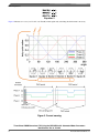
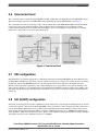
FlexTimer0 is configured to trigger an internal hardware signal when its counter is reset after overflow to the initialization
value. This signal is fed into the Programmable Delay Block (PDB) that consequently triggers the AD conversion of the
voltage and currents with a predefined delay. On the Kinetis KV10 75 MHz MCU, two ADC modules are implemented. Each
ADC module associates to one channel of the PDB module. Each ADC module has two result registers (two channels), and
they correspond to two programmable pre-trigger delays of the PDB channels. So it is possible to perform four AD
conversions without requesting an interrupt (with respect that the DMA is not used for data transfer). In this application, only
three conversions need to be triggered without CPU intervention (two motor phase currents and the DC-Bus voltage). Figure
1 shows the module interconnections and the ADC interrupt generation.
Three-Phase PMSM Sensorless FOC Using the MKV10Z32 with Automated Motor Parameters
Identification, Rev. 0, 12/2014
4
Freescale Semiconductor, Inc.