1
Errata Sheet
Functional Deviations
Workaround
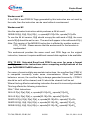
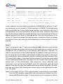
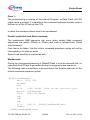
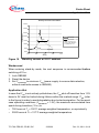
To avoid these timing corner cases the timeout limit of the bus has to be larger
than the maximum response time of the peripherals including possible internal
wait cycles. This leads to a timeout value of the BCU of a minimum of 5
(RBCU_CON.TOUT >= 5) to cover all affected peripherals.
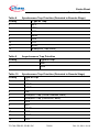
Below, the minimum allowed timeout values for each peripheral are specified
separately.
RBCU_CON.TOUT >= 3 for DMA, FADC & SSC
RBCU_CON.TOUT >= 5 for ADC
BCU_TC.006 Polarity of Bit SVM in Register ECON
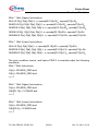
The polarity of bit SVM (State of FPI Bus Supervisor Mode Signal) in the SBCU
Error Control Capture register SBCU_ECON is inverted compared to its
description in the User’s Manual.
Actually, it is implemented as follows:
•
•
SVM = 0B: Transfer was initiated in user modes
SVM = 1B: Transfer was initiated in supervisor mode
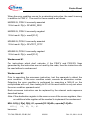
Also, the polarity of bit SVM (State of FPI Bus Supervisor Mode Signal) in the
RBCU Error Control Capture register RBCU_ECON is inverted compared to its
description in the User’s Manual.
Actually, it is implemented as follows:
•
•
SVM = 0B: Transfer was initiated in user modes
SVM = 1B: Transfer was initiated in supervisor mode
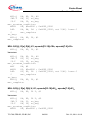
CPU_TC.004 CPU can be halted by writing DBGSR with OCDS Disabled
Contrary to the specification, the TriCore1 CPU can be halted by writing "11" to
the DBGSR.HALT bits, irrespective of whether On-Chip Debug Support (OCDS)
is enabled or not (DBGSR.DE not checked).
TC1796, EES-BC, ES-BC, BC
43/226
Rel. 2.2, 2011-10-10