1
Errata Sheet
V1.0, 13.01.2006
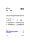
Device
TC1100
Marking/Step
ES-BA
Package
PG-LBGA-208
This Errata Sheet describes the deviations from the current user documentation.
The module oriented classification and numbering system uses an ascending sequence
over several derivatives, including already solved deviations. So gaps inside this
enumeration can occur.
Current Documentation
•
•
•
•
TC1100 User’s Manual System Units
TC1100 User’s Manual Peripheral Units
TC1100 Data Sheet
TriCore Architecture Manual V1.3.5
V1.0
V1.0
V1.0
V1.3.5
Jul. 2004
Jul. 2004
Feb. 2005
Feb. 2005
Note: Devices marked with EES or ES are engineering samples which may not be
completely tested in all functional and electrical characteristics, therefore they
should be used for evaluation only.
Note: This device is equipped with a TriCore “TC1.3” Core. Some of the errata have a
workaround which is possibly supported by the compiler tool vendor. Some
corresponding compiler switches need possibly to be set. Please see the
respective documentation of your compiler.
The specific test conditions for EES and ES are documented in a separate Status Sheet.
Contents
Section . . . . . . . . . . . . . . . . . . . . . . . . . . . . . . . . . . . . . . . . . . . . . . . . . . . . . . . . . . Page
History List / Change Summary . . . . . . . . . . . . . . . . . . . . . . . . . . . . . . . . . . . . . . . . .2
Functional Deviations . . . . . . . . . . . . . . . . . . . . . . . . . . . . . . . . . . . . . . . . . . . . . . . . .7
Deviations from Electrical- and Timing Specification. . . . . . . . . . . . . . . . . . . . . . .53
Application Hints . . . . . . . . . . . . . . . . . . . . . . . . . . . . . . . . . . . . . . . . . . . . . . . . . . . .54
Documentation Update . . . . . . . . . . . . . . . . . . . . . . . . . . . . . . . . . . . . . . . . . . . . . . .55
TC1100, ES-BA
1/55
V1.0, 13.01.2006
Errata Sheet
History List / Change Summary
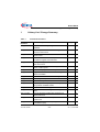
1
History List / Change Summary
Table 1
Functional Deviations
Functional
Deviation
Short Description
CPU_TC.004
CPU can be halted by writing DBGSR with OCDS
Disabled
7
CPU_TC.008
IOPC Trap taken for all un-acknowledged Coprocessor instructions
7
CPU_TC.012
Definition of PACK and UNPACK fail in certain
corner cases
7
CPU_TC.013
Unreliable context load/store operation following
an address register load instruction
8
CPU_TC.014
Wrong rounding in 8000*8000<<1 case for certain
MAC instructions
9
CPU_TC.046
FPI master livelock when accessing reserved
areas of CSFR space
9
CPU_TC.048
CPU fetches program from unexpected address
10
CPU_TC.052
Alignment Restrictions for Accesses using PTEBased Translation
10
CPU_TC.053
PMI line buffer is not invalidated during CPU halt
11
CPU_TC.056
Incorrect probe.i operation in MMU UTLB
11
CPU_TC.059
Idle Mode Entry Restrictions
12
CPU_TC.060
LD.[A,DA] followed by a dependent LD.[DA,D,W]
can produce unreliable results
13
CPU_TC.061
Error in emulator memory protection override
14
CPU_TC.062
Error in circular addressing mode for large buffer
sizes
14
CPU_TC.063
Error in advanced overflow flag generation for
SHAS instruction
15
CPU_TC.064
Co-incident FCU and CDO traps can cause
system-lock
16
CPU_TC.065
Error when unconditional loop targets
unconditional jump
16
TC1100, ES-BA
Change
2/55
Pg
V1.0, 13.01.2006
Errata Sheet
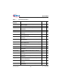
History List / Change Summary
Table 1
Functional Deviations
Functional
Deviation
Short Description
Change
Pg
CPU_TC.066
Incorrect forwarding when dependent CACHEA
follows LD.[D]A
17
CPU_TC.067
Incorrect operation of STLCX instruction
18
CPU_TC.068
Potential PSW corruption by cancelled DVINIT
instructions
18
CPU_TC.069
Potential incorrect operation of RSLCX instruction
19
CPU_TC.070
Error when conditional jump precedes loop
instruction
20
CPU_TC.071
Error when Conditional Loop targets
Unconditional Loop
21
CPU_TC.072
Error when Loop Counter modified prior to Loop
instruction
21
CPU_TC.073
Debug Events on Data Accesses to Segment E/F
Non-functional
22
CPU_TC.074
Interleaved LOOP/LOOPU instructions may
cause GRWP Trap
22
CPU_TC.075
Interaction of CPS SFR and CSFR reads may
cause livelock
23
CPU_TC.077
CACHEA.I instruction executable in User Mode
24
CPU_TC.078
Possible incorrect overflow flag for MSUB.Q
instructions
24
CPU_TC.079
Possible invalid ICR.PIPN when no interrupt
pending
25
CPU_TC.080
No overflow detected by DVINIT instruction for
MAX_NEG / -1
26
CPU_TC.081
Error during Load A[10], Call / Exception
Sequence
26
CPU_TC.082
Data corruption possible when Memory Load
follows Context Store
27
CPU_TC.083
Interrupt may be taken following DISABLE
instruction
28
CPU_TC.085
CPS module may error acknowledge valid read
transactions
29
TC1100, ES-BA
3/55
V1.0, 13.01.2006
Errata Sheet
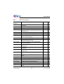
History List / Change Summary
Table 1
Functional Deviations
Functional
Deviation
Short Description
CPU_TC.086
Incorrect Handling of PSW.CDE for CDU trap
generation
29
CPU_TC.087
Exception Prioritisation Incorrect
30
CPU_TC.088
Imprecise Return Address for FCU Trap
32
CPU_TC.089
Interrupt Enable status lost when taking
Breakpoint Trap
33
CPU_TC.090
MMU Page Table Entry Mapping Restrictions
33
CPU_TC.091
Incorrect privilege handling of MMU instructions
34
CPU_TC.092
Upper Memory Segments accessible in User-0
Mode with MMU enabled
35
CPU_TC.093
MMU Instruction Usage Restrictions
35
CPU_TC.094
Potential Performance Loss when CSA
Instruction follows IP Jump
36
CPU_TC.095
Incorrect Forwarding in SAT, Mixed Register
Instruction Sequence
37
CPU_TC.096
Error when Conditional Loop targets Single Issue
Group Loop
38
PMI_TC.001
Deadlock possible during Instruction Cache
Invalidation
38
DMI_TC.005
DSE Trap possible with no corresponding flag set
in DMI_STR
39
DMI_TC.012
Data corruption possible during load from data
cache
39
DMI_TC.013
Data corruption possible when accessing data
cache
43
PORT_TC.H003
Internal pull up is not working during reset
44
FPU_TC.001
FPU flags always update with FPU exception
45
BCU_TC.002
SBCU does not give bus error
45
SSC_TC.006
Leading delay for SLSOx stalls SSCx
45
SSC_TC.007
Unintended switching of slave-selects in SSC0
46
SSC_TC.008
SSC shift register not updated in fractional divider
mode
46
TC1100, ES-BA
Change
4/55
Pg
V1.0, 13.01.2006
Errata Sheet
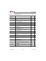
History List / Change Summary
Table 1
Functional Deviations
Functional
Deviation
Short Description
SSC_TC.011
Unexpected phase error
46
OCDS_TC.007
DBGSR writes fail when coincident with a debug
event
47
OCDS_TC.008
Breakpoint interrupt posting fails for ICR
modifying instructions
48
OCDS_TC.009
Data access trigger events unreliable
48
OCDS_TC.010
DBGSR.HALT[0] fails for separate resets
48
OCDS_TC.011
Context lost for multiple breakpoint traps
49
OCDS_TC.012
Multiple debug events on one instruction can be
unpredictable
49
DMA_TC.004
Reset of registers OCDSR and SUSPMR is
connected to FPI reset
49
DMA_TC.005
Do not access MExPR, MExAENR, MExARR with
RMW instructions
50
DMA_TC.007
CHSRmn.LXO bit is not reset by channel reset
50
DMA_TC.010
Channel reset disturbed by pattern found event
50
DMA_TC.011
Pattern search for unaligned data fails on certain
patterns
50
DMA_TC.012
No wrap around interrupt generated
51
MLI_TC.003
MLI handles RETRY on FPI bus incorrectly
51
MLI_TC.004
Read frame data may be corrupt when FPI error
occured
52
MLI_TC.006
Receiver address is not wrapped around in
downward direction
52
MLI_TC.007
Answer frames do not trigger NFR interrupt if
RIER.NFRIE=10 and Move Engine enabled
52
MLI_TC.008
Move engines can not access address
F01E0000H
53
MLI_TC.009
MLI0B and internal loopback option not available
for TC1130.
53
TC1100, ES-BA
Change
5/55
Pg
V1.0, 13.01.2006
Errata Sheet
History List / Change Summary
Table 2
Deviations from Electrical- and Timing Specification
AC/DC/ADC
Deviation
Short Description
Change Pg
-
Table 3
Application Hints
Hint
Short Description
INT_TC.H001
Multiple SRNs can be assigned to the same SRPN
(priority)
54
SSC_TC.H002
Enlarged leading delay in master mode
54
Table 4
Documentation Update
Update
Short Description
TC1100, ES-BA
Change Pg
Change Pg
6/55
V1.0, 13.01.2006
Errata Sheet
Functional Deviations
2
Functional Deviations
CPU_TC.004 CPU can be halted by writing DBGSR with OCDS Disabled
Contrary to the specification, the TriCore1 CPU can be halted by writing "11" to the
DBGSR.HALT bits, irrespective of whether On-Chip Debug Support (OCDS) is enabled
or not (DBGSR.DE not checked).
Workaround:
None.
CPU_TC.008 IOPC Trap taken for all un-acknowledged Co-processor instructions
When the TriCore1.3 CPU encounters a co-processor instruction, the instruction is
routed to the co-processor interface where further decoding of the opcode is performed
in the attached co-processors. If no co-processor acknowledges that this is a valid
instruction, the CPU generates an illegal opcode (IOPC) trap.
Revisions of the TriCore Architecture Manual, up to and including V1.3.3, are unclear
regarding whether Un-Implemented OPCode (UOPC) or Invalid OPCode (IOPC) traps
should be taken for un-acknowledged co-processor instructions. However, the required
behaviour is that instructions routed to a given co-processor, where the co-processor is
present but does not understand the instruction opcode, should result in an IOPC trap.
Co-processor instructions routed to a co-processor, where that co-processor is not
present in the system, should result in a UOPC trap.
Consequently the TriCore1.3 implementation does not match the required behaviour in
the case of un-implemented co-processors.
Workaround:
Where software emulation of un-implemented co-processors is required, the IOPC trap
handler must be written to perform the required functionality.
CPU_TC.012 Definition of PACK and UNPACK fail in certain corner cases
Revisions of the TriCore Architecture Manual, up to and including V1.3.3, do not
consistently describe the behaviour of the PACK and UNPACK instructions. Specifically,
the instruction definitions state that no special provision is made for handling IEEE-754
denormal numbers, infinities, NaNs or Overflow/Underflow situations for the PACK
instruction. In fact, all these special cases are handled and will be documented correctly
in further revisions of the TriCore Architecture Manual.
However, there are two situations where the current TriCore1.3 implementation is noncompliant with the updated definition, as follows:
1. Definition and detection of Infinity/NaN for PACK and UNPACK
TC1100, ES-BA
7/55
V1.0, 13.01.2006
Errata Sheet
Functional Deviations
In order to avoid Infinity/NaN encodings overlapping with arithmetic overflow situations,
the special encoding of un-biased integer exponent = 255 and high order bit of the
normalized mantissa (bit 30 for UNPACK, bit 31 for PACK) = 0 is defined.
In the case of Infinity or NaN, the TriCore1.3 implementation of UNPACK sets the unbiased integer exponent to +255, but sets the high order bit of the normalized mantissa
(bit 30) to 1. In the case of PACK, input numbers with biased exponent of 255 and the
high order bit of the normalized mantissa (bit 31) set are converted to Infinity/NaN.
Unfortunately, small overflows may therefore be incorrectly detected as NaN by the
PACK instruction special case logic and converted accordingly, when an overflow to
Infinity should be detected.
2. Special Case Detection for PACK
In order to detect special cases, the exponent is checked for certain values. In the current
TriCore1.3 implementation this is performed on the biased exponent, i.e. after 128 has
been added to the un-biased exponent. In the case of very large overflows the addition
of 128 to the un-biased exponent can cause the exponent itself to overflow and be
interpreted as a negative number, i.e. underflow, causing the wrong result to be
produced.
Workaround
The corner cases where the PACK instruction currently fails may be detected and the
input number re-coded accordingly to produce the desired result.
CPU_TC.013 Unreliable context load/store operation following an address
register load instruction
When an address register is being loaded by a load/store instruction LD.A/LD.DA and
this address register is being used as address pointer in a following context load/store
instruction LD*CX/ST*CX it may lead to unpredictable behavior.
Example
...
LD.A
LDLCX
...
A3, <any addressing mode> ; load value into A3
[A3]
; context load
Workaround
Insert one NOP instruction between the address register load/store instruction and the
context load/store instruction to allow the "Load Word to Address Register" operation to
be completed first.
TC1100, ES-BA
8/55
V1.0, 13.01.2006
Errata Sheet
Functional Deviations
...
LD.A A3, <any addressing mode>
NOP
LDLCX [A3]
...
CPU_TC.014 Wrong rounding in 8000*8000<<1 case for certain MAC instructions
In the case of "round(acc +/- 8000H * 8000H << 1)" the multiplication and the following
accumulation is carried out correctly. However, rounding is incorrect.
Rounding is done in two steps:
1. Adding of 0000 8000H
2. Truncation
For the before mentioned case the first step during rounding (i.e. the adding operation)
is suppressed - which is wrong - while truncation is carried out correctly.
This bug affects all variants of MADDR.Q, MADDR.H, MSUBR.Q, MSUBR.H.,
MADDSUR.H and MSUBADR.H instructions.
Workaround
None.
CPU_TC.046 FPI master livelock when accessing reserved areas of CSFR space
The Core Special Function Registers (CSFRs) associated with the TriCore1 CPU are
accessible by any FPI bus master, other than the CPU, in the address range F7E1 0000H
- F7E1 FFFFH. Any access to an address within this range which does not correspond
to an existing CSFR within the CPU may result in the livelock of the initiating FPI master.
Accesses to the CPU CSFR space are performed via the CPU’s slave interface (CPS)
module, by any FPI bus master other than the CPU itself. In the case of such an access
the CPS module initially issues a retry acknowledge to the FPI master then injects an
instruction into the CPU pipeline to perform the CSFR access. The initial access is retry
acknowledged to ensure the FPI bus is not blocked and instructions in the CPU pipeline
are able to progress. The CPS module will continue to retry acknowledge further
attempts by the FPI master to read the CSFR until the data is returned by the CPU.
In the case of an access to a reserved CSFR location the CPU treats the instruction
injected by the CPS as a NOP and never acknowledges the CSFR access request. As
such the CPS module continues to retry the CSFR access on the FPI bus, leading to the
lockup of the initiating FPI master.
TC1100, ES-BA
9/55
V1.0, 13.01.2006
Errata Sheet
Functional Deviations
Workaround
Do not access reserved areas of the CPU CSFR space.
CPU_TC.048 CPU fetches program from unexpected address
There is a case which can cause the CPU to fetch program code from an unexpected
address. Although this code will not be executed the program fetch itself can cause side
effects (performance degradation, program fetch bus error trap).
If a load address register instruction LD.A/LD.DA is being followed immediately by an
indirect jump JI, JLI or indirect call CALLI instruction with the same address register as
parameter, the CPU might fetch program from an unexpected address.
Workaround
Insert a NOP instruction or any other load/store instruction between the load and the
indirect jump/call instruction. (See also note "Pipeline Effects", below)
Example
...
LD.A
NOP
A14, <any addressing mode>
; workaround to prevent
; program fetch from
; undefined address
<one optional IP instruction>
CALLI
A14
...
Pipeline Effects
The CPU core architecture allows to decode and execute instructions for the integer
pipeline (IP) and the load/store pipeline (LS) in parallel. Therefore this bug hits also if
there is only (one) IP instruction after the offending LS instruction ("CALLI A14" in above
example). A detailed list of IP instructions can be found in the document "TriCore DSP
Optimization Guide - Part 1: Instruction Set, Chapter 13.1.3, Table of Dual Issue
Instructions".
CPU_TC.052
Alignment Restrictions for Accesses using PTE-Based Translation
Additional alignment restrictions exist for TriCore load-store accesses which undergo
PTE-based translation.
For devices which include the optional Memory Management Unit (MMU), accesses to
a virtual address in one of the lower 8 segments of the address space, where the
processor is operating in virtual mode (MMU enabled), undergo PTE-based translation.
TC1100, ES-BA
10/55
V1.0, 13.01.2006
Errata Sheet
Functional Deviations
For such accesses, the cacheability of the resultant memory access depends upon both
the cacheability attribute of the resultant physical address and the cacheability flag of the
PTE used to perform the translation. Only when the resultant physical address is
cacheable and the PTE cacheability flag is set will the access be cacheable.
For load-store accesses undergoing PTE-based translation the assumption is made that
the resultant access is to a cacheable location and that no special handling of the misaligned access is required. If the resultant access, after PTE transaltion, is noncacheable and not naturally aligned, then a Data Address Alignment (ALN) trap will be
generated.
Workaround:
Natural alignment must be used for accesses undergoing PTE-based translation which
may result in a non-cacheable memory access.
CPU_TC.053 PMI line buffer is not invalidated during CPU halt
Some debug tools provide the feature to modify the code during runtime in order to
realize breakpoints. They exchange the instruction at the breakpoint address by a
’debug’ instruction, so that the CPU goes into halt mode before it passes the instruction.
Thereafter the debugger replaces the debug instruction by the original code again.
This feature no longer works reliably as the line buffer will not be invalidated during a
CPU halt. Instead of the original instruction, the obsolete debug instruction will be
executed again.
Workaround
Debuggers might use the following macro sequence:
1. set PC to other memory address (> 0x20h, which selects new cacheline-refill buffer)
2. execute at least one instruction (e.g. NOP) and stop execution again (e.g. via debug
instruction)
3. set PC back to former debug position
4. proceed execution of user code
CPU_TC.056
Incorrect probe.i operation in MMU UTLB
The TLBPROBE.I instruction takes a data register, D[a], as a parameter and uses it to
probe the MMU Translation Lookaside Buffer (TLB) at a given index. The D[a] register
contains the index for the probe. The results of the TLBPROBE.I instruction are placed
in the TVA and TPA Core Special Function Registers (CSFRs). Under certain
TC1100, ES-BA
11/55
V1.0, 13.01.2006
Errata Sheet
Functional Deviations
circumstances the TLBPROBE.I instruction may fail and return the result from an
incorrect index.
The problem occurs if the unused fields of D[a] match a VPN for a different index in the
TLB. In this case the TLB hit logic is incorrectly activated and the attributes from the
index with the matching VPN read.
Workaround:
The unused fields of D[a] should be set to ’1’ to avoid any erroneous VPN matches in the
UTLB. For example, if the index required to be probed is 0x80, the actual value
0x00000080 should not be placed in D[a], rather 0xFFFFFF80 should be used.
CPU_TC.059
Idle Mode Entry Restrictions
Two related problems exist which lead to unreliable idle mode entry, and possible data
corruption, if the idle request is received whilst the TriCore CPU is in certain states. The
two problems are as follows:
1) When the TriCore CPU receives an idle request, a DSYNC instruction is injected to
flush any data currently held within the CPU to memory. If there is any outstanding
context information to be saved, the clocks may be disabled too early, before the end of
the context save. The CPU is then frozen in an erroneous state where it is instructing the
DMI to make continuous write accesses onto the bus. Because of the pipelined
architecture, the DMI may also see the wrong address for the spurious write accesses,
and therefore memory data corruption can emerge. Another consequence of this is, that
the DMI will not go to sleep and therefore the IDLE-state will not be fully entered.
2) If the idle request is asserted when a DSYNC instruction is already being executed by
the TriCore CPU, the idle request may be masked prematurely and the idle request
never acknowledged.
Workaround
The software workaround consists of ensuring that there is no unsaved context
information within the CPU, and no DSYNC instruction in execution, when receiving an
idle request. This precludes any attempt at sending the TriCore to sleep by third parties
(i.e. Cerberus, PCP). The CPU can only be sent to idle mode by itself by executing the
following code sequence:
...
DISABLE
; Disable Interrupts
NOP
DSYNC
; Flush Buffers, background context
ISYNC
; Ensure DSYNC completes
<Store to SCU to assert idle request>
TC1100, ES-BA
12/55
V1.0, 13.01.2006
Errata Sheet
Functional Deviations
NOP
NOP
...
; Wait on idle request
; Wait on idle request
CPU_TC.060 LD.[A,DA] followed by a dependent LD.[DA,D,W] can produce
unreliable results
An LD.A or LD.DA instruction followed back to back by an unaligned LD.DA, LD.D or
LD.W instruction can lead to unreliable results. This problem is independent of the
instruction formats (16 and 32 bit versions of both instructions are similarly affected)
The problem shows up if the LD.DA, LD.D or LD.W uses an address register which is
loaded by the preceding LD.A or LD.DA and if the LD.DA, LD.D or LD.W accesses data
which leads to a multicycle execution of this second instruction.
A multicycle execution of LD.DA, LD.D or LD.W will be triggered only if the accessed
data spans a 128 bit boundary in the local DSPR space or a 128 bit boundary in the
cached space. In the non cached space an access spanning a 64 bit boundary can lead
to a multicycle execution.
The malfunction is additionally dependent on the previous content of the used address
register - the bug appears if the content points to the unimplemented DSPR space.
In the buggy case the upper portion of the multicycle load is derived from a wrong
address (the address is dependent on the previous content of that address register) and
the buggy case leads to a one cycle FASTER execution of this back to back case. (one
stall bubble is lacking in this case)
The 16 and 32 bit variants of both instructions are affected equally. A single IP instruction
as workaround is NOT sufficient, as it gets dual issued with the LD.[DA,D,W] and
therefore no bubble is seen by the LS pipeline in such a case.
Example:
...
LD.A
LD.W
...
A3,<any addressing mode>
; load pointer into A3
D1,[A3]<any addressing mode> ; load data value from pointer
Workaround
Insert one NOP instruction between the address register load/store instruction and the
data load/store instruction to allow the "Load Word to Address Register" operation to be
completed first. This leads to a slight performance degradation.
...
LD.A
NOP
TC1100, ES-BA
A3, <any addressing mode>
13/55
V1.0, 13.01.2006
Errata Sheet
Functional Deviations
LD.W
...
D1, [A3] <any addressing mode>
Alternative Workaround
To avoid the slight performance degradation, an alternative workaround is to avoid any
data structures that are accessed in an unaligned manner as then the described
instruction sequence does NOT exhibit any problems.
CPU_TC.061 Error in emulator memory protection override
TriCore1 based systems define an area of the system address map for use as an
emulator memory region. Whenever a breakpoint trap is taken, the processor jumps to
the base of this emulator region from where a debug monitor is executed.
In order to allow correct execution of this monitor, in the presence of an enabled
protection system, this emulator region is granted implicit execute permission. Execution
of code from this region is allowed whether the current settings of the memory protection
ranges specifically permit this or not, and no MPX trap will be generated.
In TriCore1.2 based systems, this emulator memory region existed at addresses
0xBExxxxxx. In TriCore1.3 based systems, this emulator region initially was moved to
addresses 0xDExxxxxx before being made fully programmable.
The erroneous behaviour occurs because as this emulator region was moved from
addresses 0xBExxxxxx, the implicit execute permission to this address range was not
moved also. As a result:
1. Code execution from addresses in the range 0xBE000000 - 0xBEFFFFFF is always
permitted, irrespective of the settings of the protection system.
2. Execution of a breakpoint trap may result in the generation of an MPX trap if execution
from the new emulator region is dis-allowed by the current settings of the protection
system.
Workaround
None
CPU_TC.062 Error in circular addressing mode for large buffer sizes
A problem exists in the circular addressing mode when large buffer sizes are used.
Specifically, the problem exists when:
1. The length, L, of the circular buffer is >=32768 bytes, i.e. MSB of L is '1'
AND
2. The offset used to access the circular buffer is negative.
TC1100, ES-BA
14/55
V1.0, 13.01.2006
Errata Sheet
Functional Deviations
In this case the update of the circular buffer index may be calculated incorrectly and the
addressing mode fail.
Each time an instruction using circular addressing mode occurs the next index for the
circular buffer is calculated as current index + offset, where the signed offset is supplied
as part of the instruction. In addition, the situation where the new index lies outside the
bounds of the circular buffer has to be taken care of and the correct wrapping behaviour
performed. In the case of negative offsets, the buffer underflow condition needs to be
checked and, when detected, the buffer size is added to the index in order to implement
the required wrapping.
Due to an error in the way the underflow condition is detected, there are cases where the
buffer size is incorrectly added to the index when there is no buffer underflow. This false
condition is detected when the index is greater than or equal to 32768 and the offset is
negative.
Example:
...
MOVH.A
LEA
LEA
LD.W
A1,
A1,
A0,
D9,
#0xE001
[A1]-0x4000
0xA0000000
[A0/A1+c]-0x4
;
;
;
;
;
Buffer Length 0xE000, Index 0xC000
Buffer Base Address
Circular addressing mode access,
negative offset
...
Workaround
Either limit the maximum buffer size for circular addressing mode to 32768 bytes, or use
only positive offsets where larger circular buffers are required.
CPU_TC.063 Error in advanced overflow flag generation for SHAS instruction
A minor problem exists with the computation of the advanced overflow (AV) flag for the
SHAS (Arithmetic Shift with Saturation) instruction. The TriCore1.3 architecture defines
that for instructions supporting saturation, the advanced overflow flag shall be computed
BEFORE saturation. The implementation of the SHAS instruction is incorrect with the AV
flag computed after saturation.
Example:
...
MOVH D0, #0x4800
MOV.U D1, #0x2
SHAS D2, D0, D1
...
TC1100, ES-BA
; D0 = 0x48000000
; D1 = 0x2
; Arithmetic Shift with Saturation
15/55
V1.0, 13.01.2006
Errata Sheet
Functional Deviations
In the above example, the result of 0x4800_0000 << 2 = 0x1_2000_0000, such that the
expected value for AV = bit31 XOR bit30 = 0. However, after saturation the result is
0x7FFF_FFFF and the AV flag is incorrectly set.
Workaround
None
CPU_TC.064 Co-incident FCU and CDO traps can cause system-lock
A problem exists in the interaction between Free Context Underflow (FCU) and Call
Depth Overflow (CDO) traps. An FCU trap occurs when a context save operation is
attempted and the free context list is empty, or when the context operation encounters
an error. A CDO trap occurs when a program attempts to make a call with call depth
counting enabled and the call depth counter was already at its maximum value.
When an FCU trap occurs with call depth counting enabled (PSW.CDE = ’1’) and the call
depth counter at a value such that the next call will generate a CDO trap, then the FCU
trap causes a co-incident CDO trap. In this case the PC is correctly set to the FCU trap
handler but appears to freeze in this state as a constant stream of FCU traps is
generated.
A related problem occurs when call trace mode is enabled (PSW.CDC = 0x7E). If in call
trace mode a call or return operation encounters an FCU trap, either a CDO (call) or Call
Depth Underflow (CDU, return) trap is generated co-incident with the FCU trap, either of
which situations lead to a constant stream of FCU traps and system lockup.
Note however that FCU traps are not expected during normal operation since this trap is
indicative of software errors.
Workaround
None
CPU_TC.065 Error when unconditional loop targets unconditional jump
An error in the program flow occurs when an unconditional loop (LOOPU) instruction has
as its target an unconditional jump instruction, i.e. as the first instruction of the loop. Such
unconditional jump instructions are J, JA, JI, JL, JLA and JLI.
In this erroneous case the first iteration of the loop executes correctly. However, at the
point the second loop instruction is executed the interaction of the unconditional loop and
jump instructions causes the loop instruction to be resolved as mis-predicted and the
program flow exits the loop incorrectly, despite the loop instruction being unconditional.
Example:
TC1100, ES-BA
16/55
V1.0, 13.01.2006
Errata Sheet
Functional Deviations
...
loop_start_:
J jump_label_
...
LOOPU loop_start_
...
; Loop start label
; Unconditional Jump instruction
Workaround
The first instruction of a loop may not be an unconditional jump. If necessary, precede
this jump instruction with a single NOP.
...
loop_start_:
NOP
J jump_label_
...
LOOPU loop_start_
...
; Loop start label
; Unconditional Jump instruction
CPU_TC.066 Incorrect forwarding when dependent CACHEA follows LD.[D]A
An error can occur when an LD.A or LD.DA instruction is followed back to back by a data
cache management instruction (CACHEA.W, CACHEA.WI or CACHEA.I). The problem
occurs if the addressing mode of the cache management instruction uses the address
register which is being loaded by the preceding LD.A or LD.DA instruction. A problem
exists in the logic required to detect the read after write hazard between these two
instructions, which may lead to the old value of the address register being used
erroneously for the CACHEA instruction.
Example:
...
LD.AA3, <any addressing mode>
CACHEA.W[A3] <any addressing mode>
...
Workaround
Insert one NOP instruction between the address register load instruction and the data
cache management instruction to allow the "Load Word to Address Register" operation
to be completed first.
...
LD.AA3, <any addressing mode>
NOP
CACHEA.W[A3] <any addressing mode>
...
TC1100, ES-BA
17/55
V1.0, 13.01.2006
Errata Sheet
Functional Deviations
CPU_TC.067 Incorrect operation of STLCX instruction
There is an error in the operation of the Store Lower Context (STLCX) instruction. This
instruction stores the current lower context information to a 16-word memory block
specified by the addressing mode associated with the instruction (not to the free context
list). The architectural definition of the STLCX instruction is as follows:
Mem(EA, 16-word) = {PCXI, A[11], A[2:3], D[0:3], A[4:7], D[4:7]}
However, there is an error in the implementation of the instruction, such that the following
operation is actually performed:
Mem(EA, 16-word) = {PCXI, PSW, A[2:3], D[0:3], A[4:7], D[4:7]}
i.e. the PSW is incorrectly stored instead of A11.
During normal operation, the lower context information that has been stored by an
STLCX instruction would be re-loaded using the Load Lower Context (LDLCX)
operation. The architectural definition of the LDLCX instruction is as follows:
{-, -, A[2:3], D[0:3], A[4:7], D[4:7]} = Mem(EA, 16-word)
i.e. the value which is incorrectly stored by STLCX is not re-loaded by LDLCX, such that
the erroneous behaviour is not seen during normal operation.
However, any attempt to reload a lower context stored with STLCX using load
instructions other than LDLCX will exhibit the incorrect behaviour.
Workaround
Any lower context stored using STLCX should only be re-loaded using LDLCX,
otherwise the erroneous behaviour will be visible.
CPU_TC.068 Potential PSW corruption by cancelled DVINIT instructions
A problem exists in the implementation of the Divide Initialisation instructions, which,
under certain circumstances, may lead to corruption of the advanced overflow (AV),
overflow (V) and sticky overflow (SV) flags. These flags are stored in the Program Status
Word (PSW) register, fields PSW.AV, PSW.V and PSW.SV. The divide initialisation
instructions are DVINIT, DVINIT.U, DVINIT.B, DVINIT.BU, DVINIT.H and DVINIT.HU.
The problem is that the DVINIT class instructions do not handle the instruction
cancellation signal correctly, such that cancelled DVINIT instructions still update the
PSW fields. The PSW fields are updated according to the operands supplied to the
cancelled DVINIT instruction. Due to the nature of the DVINIT instructions this can lead
to:
• The AV flag may be negated erroneously.
• The V flag may be asserted or negated erroneously.
• The SV flag may be asserted erroneously.
TC1100, ES-BA
18/55
V1.0, 13.01.2006
Errata Sheet
Functional Deviations
No other fields of the PSW can be affected. A DVINIT class instruction could be
cancelled due to a number of reasons:
• the DVINIT instruction is cancelled due to a mis-predicted branch
• the DVINIT instruction is cancelled due to an unresolved operand dependency
• the DVINIT instruction is cancelled due to an asynchronous event such as an interrupt
Workaround
If the executing program is using the PSW fields to detect overflow conditions, the
correct behaviour of the DVINIT instructions may be guaranteed by avoiding the
circumstances which could lead to a DVINIT instruction being cancelled. This requires
that the DVINIT instruction is preceded by 2 NOPs (to avoid operand dependencies or
the possibility of mis-predicted execution). In addition, the status of the interrupt enable
bit ICR.IE must be stored and interrupts disabled before the 2 NOPs and the DVINIT
instruction are executed, and the status of the ICR.IE bit restored after the DVINIT
instruction is complete.
Alternative Workaround
To avoid the requirement to disable and re-enable interrupts an alternative workaround
is to precede the DVINIT instruction with 2 NOPs and to store the PSW.SV flag before a
DVINIT instruction and check its consistency after the DVINIT instruction. In this case
the values of the PSW flags affected may be incorrect whilst the asynchronous event is
handled, but once the return from exception is complete and the DVINIT instruction reexecuted, only the SV flag can be in error. In this case if the SV flag was previously
negated but after the DVINIT instruction the SV flag is asserted and the V flag is negated,
then the SV flag has been asserted erroneously and should be corrected by software.
CPU_TC.069 Potential incorrect operation of RSLCX instruction
A problem exists in the implementation of the RSLCX instruction, which, under certain
circumstances, may lead to data corruption in the TriCore internal registers. The problem
is caused by the RSLCX instruction incorrectly detecting a dependency to the following
load-store (LS) or loop (LP) pipeline instruction, if that instruction uses either address
register A0 or A1 as a source operand, and erroneous forwarding paths being enabled.
Two failure cases are possible:
1. If the instruction following the RSLCX instruction uses A1 as its source 1 operand, the
PCX value updated by the RSLCX instruction will be corrupted. Instead of restoring
the PCX value from the lower context information being restored, it will restore the
return address (A11).
2. If the instruction following the RSLCX instruction uses either A1 or A0 as source 2
operand, the value forwarded (for the second instruction) will not be the one stored in
the register but the one that has just been loaded from memory for the context restore
(A11/PCX).
TC1100, ES-BA
19/55
V1.0, 13.01.2006
Errata Sheet
Functional Deviations
Note that the problem is triggered whenever the following load-store pipeline instruction
uses A0 or A1 as a source operand. If an integer pipeline instruction is executed between
the RSLCX and the following load-store or loop instruction, the problem may still exist.
Example:
...
RSLCX
LEA
A0, [A0]0x158c
...
Workaround
Any RSLCX instruction should be followed by a NOP to avoid the detection of these false
dependencies.
CPU_TC.070 Error when conditional jump precedes loop instruction
An error in the program flow may occur when a conditional jump instruction is directly
followed by a loop instruction (either conditional or unconditional). Both integer pipeline
and load-store pipeline conditional jumps (i.e. those checking the values of data and
address registers respectively) may cause the erroneous behaviour.
The incorrect behaviour occurs when the two instructions are not dual-issued, such that
the conditional jump is in the execute stage of the pipeline and the loop instruction is at
the decode stage. In this case, both the conditional jump instruction and the loop
instruction will be resolved in the same cycle. The problem occurs because priority is
given to the loop mis-prediction logic, despite the conditional jump instruction being
semantically before the loop instruction in the program flow. In this error case the
program flow continues as if the loop has exited: the PC is taken from the loop misprediction branch. In order for the erroneous behaviour to occur, the conditional jump
must be incorrectly predicted as not taken. Since all conditional jump instructions, with
the exception of 32-bit format forward jumps, are predicted as taken, only 32-bit forward
jumps can cause the problem behaviour.
Example:
...
JNE.A A1, A0, jump_target_1_ ; 32-bit forward jump
LOOP A6, loop_target_1_
...
jump_target_1_:
...
Workaround
A conditional jump instruction may not be directly followed by a loop instruction
(conditional or not). A NOP must be inserted between any load-store pipeline conditional
jump (where the condition is dependent on an address register) and a loop instruction.
TC1100, ES-BA
20/55
V1.0, 13.01.2006
Errata Sheet
Functional Deviations
Two NOPs must be inserted between any integer pipeline conditional jump (where the
condition is dependent on a data register) and a loop instruction
CPU_TC.071 Error when Conditional Loop targets Unconditional Loop
An error in the program flow may occur when a conditional loop instruction (LOOP) has
as its target an unconditional loop instruction (LOOPU). The incorrect behaviour occurs
in certain circumstances when the two instructions are resolved in the same cycle. If the
conditional loop instruction is mis-predicted, i.e. the conditional loop should be exited,
the unconditional loop instruction is correctly cancelled but instead of program execution
continuing at the first instruction after the conditional loop, the program flow is corrupted.
Example:
...
cond_loop_target_:
LOOPU uncond_loop_target_
...
LOOP A6, cond_loop_target_
; Unconditional loop
;Conditional loop targets
;unconditional loop
...
Workaround
The first instruction of a conditional loop may not be an unconditional loop. If necessary,
precede this unconditional loop instruction with a single NOP.
CPU_TC.072 Error when Loop Counter modified prior to Loop instruction
An error in the program flow may occur when an instruction that updates an address
register is directly followed by a conditional loop instruction which uses that address
register as its loop counter. The problem occurs when the address register holding the
loop counter is initially zero, such that the loop will exit, but is written to a non-zero value
by the instruction preceding the conditional loop. In this case the loop prediction logic
fails and the program flow is corrupted.
Example:
...
LD.A
LOOP
...
TC1100, ES-BA
A6, <any addressing mode>
A6, loop_target_1_
21/55
V1.0, 13.01.2006
Errata Sheet
Functional Deviations
Workaround
Insert one NOP instruction between the instruction updating the address register and the
conditional loop instruction dependent on this address register.
CPU_TC.073 Debug Events on Data Accesses to Segment E/F Non-functional
The generation of debug events from data accesses to addresses in Segments 0xE and
0xF is non-functional. As such the setting of breakpoints on data accesses to these
addresses does not operate correctly.
In TriCore1 the memory protection system, consisting of the memory protection register
sets and associated address comparators, is used both for memory protection and
debug event generation for program and data accesses to specific addresses. For
memory protection purposes, data accesses to the internal and external peripheral
segments 0xE and 0xF bypass the range protection system and are protected instead
by the I/O privilege level and protection mechanisms built in to the individual peripherals.
Unfortunately this bypass of the range protection system for segments 0xE and 0xF also
affects debug event generation, masking debug events for data accesses to these
segments.
Workaround
None.
CPU_TC.074 Interleaved LOOP/LOOPU instructions may cause GRWP Trap
If a conditional loop instruction (LOOP) is executed after an unconditional loop
instruction (LOOPU) a Global Register Write Protection (GRWP) Trap may be
generated, even if the LOOP instruction does not use a global address register as its
loop counter.
In order to support zero-overhead loop execution the TriCore1 implementation caches
certain attributes pertaining to loop instructions within the CPU. The TriCore1.3 CPU
contains two loop cache buffers such that two loop (LOOP or LOOPU) instructions may
be cached. One of the attributes cached is whether the loop instruction writes to a global
address register (as its loop variable). For LOOP instructions this attribute is updated
and read as expected. For LOOPU instructions this attribute is set but ignored by the
LOOPU instruction when next encountered.
The problem occurs because there is only one global address register write flag shared
between the two loop caches. As such if LOOP and LOOPU instructions are interleaved,
with the LOOPU instruction encountered and cached after the LOOP instruction, then
the next execution of the LOOP instruction will find the global address register write flag
set and, if global register writes are disabled (PSW.GW = 0), a GRWP trap will be
incorrectly generated.
Example:
TC1100, ES-BA
22/55
V1.0, 13.01.2006
Errata Sheet
Functional Deviations
...
loopu_target_
...
loop_target_
...
LOOP
A5, loop_target_
...
LOOPU
loopu_target_
...
User Workaround
Enable global register write permission, PSW.GW = 1.
Tool Vendor Workaround
The LOOPU instruction sets the global address register write flag when its un-used
opcode bits [15:12] are incorrectly decoded as global address register A0. The problem
may be avoided by assembling these un-used bits to correspond to a non-global register
encoding, such as 0xF.
CPU_TC.075 Interaction of CPS SFR and CSFR reads may cause livelock
Under certain specific circumstances system lockup may occur if the TriCore CPU
attempts to access a Special Function Register (SFR) within the CPS module around the
same time as another master attempts to read a Core Special Function Register (CSFR),
also via the CPS module.
In order to read a CSFR the CPS module injects an instruction into the CPU pipeline to
access the required register. In order for this injected instruction to complete successfully
the CPU pipeline must be allowed to progress. To avoid system lockup the CSFR read
access is initially retry acknowledged on the FPI bus to ensure the FPI bus is not blocked
and any CPU read access to an address mapped to the FPI bus is able to progress. The
CPS then continues the CSFR read in the background, and, once complete, returns the
data to the originating master when the read access is performed again.
The problem occurs if the CPU is attempting to access an SFR accessed via the CPS
module around the time another master is attempting a CSFR read access. Under
normal circumstances this causes no problem since the SFR access is allowed to
complete normally even with an outstanding CSFR access in the background. However,
if the SFR access is pipelined on the FPI bus behind the CSFR access and the CSFR
access is still in progress then the interaction of the two pipelined transactions may
cause the SFR access to be retry acknowledged in error. Thus the CPU pipeline is still
TC1100, ES-BA
23/55
V1.0, 13.01.2006
Errata Sheet
Functional Deviations
frozen and the CSFR access cannot complete. As long as the two transactions, when
re-initiated by their respective masters, continue to be pipelined on the FPI bus then this
livelock situation will continue.
Note however that the only FPI master expected to access the CSFR address range via
the CPS would be the Cerberus module under control of an external debugger. As such
this livelock situation should only be possible whilst debugging, not during normal system
operation.
Workaround
None.
CPU_TC.077 CACHEA.I instruction executable in User Mode
The CACHEA.W and CACHEA.WI instructions which writeback and optionally invalidate
enties from the data cache are user mode executable instructions. The CACHEA.I
instruction which invalidates data cache entries without writeback should be executable
in supervisor mode only. However the current implementation is such that the CACHEA.I
instruction is executable in user mode also.
Workaround
None.
CPU_TC.078 Possible incorrect overflow flag for MSUB.Q instructions
Under certain conditions, certain variants of the MSUB.Q instruction can fail and produce
an incorrect overflow flag, PSW.V. When the problem behaviour occurs, the overflow
flag is always generated incorrectly: if PSW.V should be set it will be cleared, and if it
should be cleared it will be set.
The problem affects two variants of the MSUB.Q instruction, specifically:
msub.q Dc,Dd,Da,Db, #0x1
msub.q Dc,Dd,Da,DbL,#0x1
These instructions are those that match all of the following criteria:
• the instruction has a 32-bit result,
• the instruction has at least one 32-bit multiplicand,
• the instruction is non-saturating (MSUBS.Q not affected),
TC1100, ES-BA
24/55
V1.0, 13.01.2006
Errata Sheet
Functional Deviations
• the instruction includes re-alignment (n=1)
Note: Only the lower half-word variant of the 32*16 bit msub.q instruction is affected.
The conditions under which the erroneous behaviour occurs are as follows:
Case 1) msub.q Dc,Dd,Da,Db, #0x1
If both Da[31:16] and Db[31:16] = 0x8000, then PSW.V will be incorrect.
Case 2) msub.q Dc,Dd,Da,DbL, #0x1
If both Da[31:16] and DbL = 0x8000, then PSW.V will be incorrect.
Workaround
If appropriate to the algorithm, the MSUB.Q instruction may be replaced by the
saturating variant, MSUBS.Q, which is not affected by this erratum.
CPU_TC.079 Possible invalid ICR.PIPN when no interrupt pending
Under certain circumstances the Pending Interrupt Priority Number, ICR.PIPN, may be
invalid when there is no interrupt currently pending. When no interrupt is pending the
ICR.PIPN field is required to be zero.
There are two circumstances where ICR.PIPN may have a non-zero value when no
interrupt is pending:
1. When operating in 2:1 mode between CPU and interrupt bus clocks, the ICR.PIPN
field may not be reset to zero when an interrupt is acknowledged by the CPU.
2. During the interrupt arbitration process the ICR.PIPN is constructed in 1-4 arbitration
rounds where 2 bits of the PIPN are acquired each round. The intermediate PIPN
being used to construct the full PIPN is made available as ICR.PIPN. This is a
potential problem because reading the PIPN can indicate a pending interrupt that is
not actually pending and may not even be valid. e.g. if interrupt 0x81 is the highest
priority pending interrupt, then ICR.PIPN will be read as 0x80 during interrupt
arbitration rounds 2,3 and 4. Only when the arbitration has completed will the valid
PIPN be reflected in ICR.PIPN.
The hardware implementation of the interrupt system for the TriCore1 CPU actually
comprises both the PIPN and a separate, non-architecturally visible, interrupt request
flag. The CPU only considers PIPN when the interrupt request flag is asserted, at which
times the ICR.PIPN will always hold a valid value. As such the hardware implementation
of the interrupt priority scheme functions as expected. However, reads of the ICR.PIPN
field by software may encounter invalid information and should not be used.
TC1100, ES-BA
25/55
V1.0, 13.01.2006
Errata Sheet
Functional Deviations
Workaround
None.
CPU_TC.080 No overflow detected by DVINIT instruction for MAX_NEG / -1
A problem exists in variants of the Divide Initialisation instruction with certain corner case
operands. Only those instruction variants operating on signed operands, DVINIT,
DVINIT.H and DVINIT.B, are affected. The problem occurs when the maximum
representable negative value of a number format is divided by -1.
The Divide Initialisation instructions are required to initialise an integer division sequence
and detect corner case operands which would lead to an incorrect final result (e.g.
division by 0), setting the overflow flag, PSW.V, accordingly.
In the specific case of division of the maximum negative 32-bit signed integer
(0x80000000) by -1 (0xFFFFFFFF), the result is greater than the maximum
representable positive 32-bit signed integer and should flag overflow. However, this
specific case is not detected by the DVINIT instruction and a subsequent division
sequence returns the maximum negative number as a result with no corresponding
overflow flag.
In the cases of division of the maximum negative 16/8-bit signed integers (0x8000/0x80)
by -1 (0xFFFF/0xFF), the result is greater than the maximum representable positive 16/
8-bit signed integer and should again flag overflow. These specific cases are not
detected by the DVINIT.H/.B instructions with no corresponding overflow flag set. In this
case the result of a subsequent division sequence returns the value 0x00008000/
0x00000080 which is the correct value when viewed as a 32-bit number but has
overflowed the original number format.
Workaround
If the executing program is using the PSW fields to detect overflow conditions, the
specific corner case operands described above must be checked for and handled as a
special case in software before the standard division sequence is executed.
CPU_TC.081 Error during Load A[10], Call / Exception Sequence
A problem may occur when an address register load instruction, LD.A or LD.DA,
targeting the A[10] register, is immediately followed by an operation causing a context
switch. The problem may occur in one of two situations:
1) The address register load instruction, targeting A[10], is followed immediately by a call
instruction (CALL, CALLA, CALLI).
TC1100, ES-BA
26/55
V1.0, 13.01.2006
Errata Sheet
Functional Deviations
2) The address register load instruction, targeting A[10], is followed immediately by a
context switch caused by an interrupt or trap being taken, where the interrupt stack is
already in use (PSW.IS = 1).
In both these situations the value of A[10] is required to be maintained across the context
switch. However, where the context switch is preceded by a load to A[10], the address
register dependency is not detected correctly and the called context inherits the wrong
value of A[10]. In this case the value of A[10] before the load instruction is inherited.
Example:
...
LD.A
A10, <any addressing mode>
CALL
call_target_
...
Workaround
The problem only occurs when A[10] is loaded directly from memory. The software
workaround therefore consists of loading another address register from memory and
moving the contents to A[10].
Example:
...
LD.A
A12, <any addressing mode>
MOV.AA
A10, A12
CALL
call_target_
...
CPU_TC.082 Data corruption possible when Memory Load follows Context Store
Data corruption may occur when a context store operation, STUCX or STLCX, is
immediately followed by a memory load operation which reads from the last double-word
address written by the context store.
Context store operations store a complete upper or lower context to a 16-word region of
memory, aligned on a 16-word boundary. If the context store is immediately followed by
a memory load operation which reads from the last double-word of the 16-word context
region just written, the dependency is not detected correctly and the previous value held
in this memory location may be returned by the memory load.
The memory load instructions which may return corrupt data are as follows:
ld.b, ld.bu, ld.h, ld.hu, ld.q, ld.w, ld.d, ld.a, ld.da
Example:
TC1100, ES-BA
27/55
V1.0, 13.01.2006
Errata Sheet
Functional Deviations
...
STLCX
0xD0000040
LD.W
D15, 0xD0000078
...
Note that the TriCore architecture does not require a context save operation (CALL,
SVLCX, etc.) to update the CSA list semantically before the next operation (but does
require the CSA list to be up to date after the execution of a DSYNC instruction). As such
the same problem may occur for context save operations, but the result of such a
sequence is architecturally undefined in any case.
Workaround
One NOP instruction must be inserted between the context store operation and a
following memory load instruction if the memory load may read from the last double-word
of the 16-word context region just written.
Example:
...
STLCX
0xD0000040
NOP
LD.W
D15, 0xD0000078
...
CPU_TC.083 Interrupt may be taken following DISABLE instruction
The TriCore V1.3 architecture requires that the DISABLE instruction gives deterministic
behaviour, i.e. no interrupt may be taken following the execution of the DISABLE
instruction.
However, the current implementation allows an interrupt to be taken immediately
following the execution of the DISABLE instruction, i.e. between the DISABLE and the
following instruction. Once the first instruction after the DISABLE instruction has been
executed its is still guaranteed that no interrupt will be taken.
Workaround
If an instruction sequence must not be interrupted, then the DISABLE instruction must
be followed by a single NOP instruction, before the critical code sequence.
TC1100, ES-BA
28/55
V1.0, 13.01.2006
Errata Sheet
Functional Deviations
CPU_TC.085 CPS module may error acknowledge valid read transactions
A bug exists in the CPS module, which may result in the CPS incorrectly returning an
error acknowledge for a read access to a valid CPS address.
The problem occurs when a read access to a CPS address, in the range 0xF7E00000 0xF7E1FFFF, is followed immediately on the FPI bus by a User mode write access to an
address with FPI address[16] = 1. The problem occurs due to an error in the FPI bus
decoding within the CPS which incorrectly interprets the second transaction, even if to
another slave, as an illegal User mode write to a TriCore CSFR and incorrectly error
acknowledges the valid read. Write accesses to the CPS module are not affected.
Workaround
For devices in which multiple FPI bus masters may operate in User mode, but only the
TriCore CPU and Debug Interface (Cerberus) are expected to access the CPS address
range, the workaround consists of 3 parts:
Tool Vendor
1) The Cerberus module must be configured to operate in Supervisor mode, to reduce
the probability of the TriCore CPU from receiving false error acknowledges.
2) If the Cerberus FPI Master receives an error acknowledge it enters error state, which
is detected by the debugger as a timeout. In this case the debugger should release the
Cerberus from the error state with the io_supervisor command and read out the cause
of the error. Where an error acknowledge is determined to be the cause for a read in the
CPS address range the read request should be re-issued.
User
3) If the TriCore CPU reads from a CPS address, via the LFI bridge, which results in an
error acknowledge being incorrectly generated, the TriCore CPU will take a synchronous
DSE trap. In order to workaround this potential problem the following sequence is
recommended:
i) A flag is set in a specific memory location immediately before the TriCore CPU
attempts a load from a CPS SFR address, and cleared immediately afterwards.
ii) The DSE trap handler is modified to check the status of the flag set in (i). If the flag is
set the DSE handler should clear the error capture mechanisms of the FPI BCU and
LBCU which will have captured the error acknowledge, and then execute an RFE
instruction. This will cause the original load instruction to be re-executed and allow the
program to continue normally.
CPU_TC.086 Incorrect Handling of PSW.CDE for CDU trap generation
An error exists in the CDU (Call Depth Underflow) trap generation logic. CDU traps are
architecturally defined to occur when "A program attempted to execute a RET (Return)
instruction while Call Depth Counting was enabled, and the Call Depth Counter was
TC1100, ES-BA
29/55
V1.0, 13.01.2006
Errata Sheet
Functional Deviations
zero". Call depth counting is enabled when PSW.CDC /= 1111111 and PSW.CDE = 1.
However, the status of PSW.CDE is currently not considered for CDU trap generation,
and CDU traps may be generated when PSW.CDE = 0.
Call depth counting, and generation of the associated CDO and CDU traps, may be
disabled by one of two methods. Setting PSW.CDC = 1111111 globally disables call
depth counting and operates as specified. Setting PSW.CDE = 0 temporarily disables
call depth counting (it is re-enabled by each call instruction) and is used primarily for call/
return tracing.
Workaround
In order to temporarily disable call depth counting for a single return instruction,
PSW.CDC should be set to 1111111 before the return instruction is executed.
CPU_TC.087 Exception Prioritisation Incorrect
The TriCore architecture defines an exception priority order, consisting of the relative
priorities of asynchronous traps, synchronous traps and interrupts, and the prioritisation
of individual trap types.
The current implementation of the TriCore1.3 CPU complies with the general principle
that the older the instruction is in the instruction sequence which caused the trap, the
higher the priority of the trap. However, the relative prioritisation of asynchronous and
synchronous events and the prioritisation between individual trap types does not fully
comply with the architectural definition.
The current TriCore1.3 CPU implements the following priority order between an
asynchronous trap, a synchronous trap, and an interrupt:
1. Synchronous traps detected in Execute pipeline stage (highest priority).
2. Asynchronous trap.
3. Interrupt.
4. Synchronous trap detected in Decode pipeline stage (lowest priority).
Within these groups the following priorities are implemented:
Table 5
Synchronous Trap Priorities (Detected in Execute Stage)
Priority
Type of Trap
1
VAF-D
2
VAP-D
3
MPR
4
MPW
5
MPP
6
MPN
TC1100, ES-BA
30/55
V1.0, 13.01.2006
Errata Sheet
Functional Deviations
Table 5
Synchronous Trap Priorities (Detected in Execute Stage)
7
ALN
8
MEM
9
DSE
10
OVF
11
SOVF
12
Breakpoint Trap (BAM)
Table 6
Asynchronous Trap Priorities
Priority
Type of Trap
1
NMI
2
DAE
Table 7
Synchronous Trap Priorities (Detected in Decode Stage)
Priority
Type of Trap
1
FCD
2
VAF-P
3
VAP-P
4
PSE
5
Breakpoint Trap (Virtual Address, BBM)
6
Breakpoint Trap (Instruction, BBM)
7
PRIV
8
MPX
9
GRWP
10
IOPC
11
UOPC
12
CDO
13
CDU
14
FCU
15
CSU
16
CTYP
TC1100, ES-BA
31/55
V1.0, 13.01.2006
Errata Sheet
Functional Deviations
Table 7
Synchronous Trap Priorities (Detected in Decode Stage)
17
NEST
18
SYSCALL
Although the implemented trap priorities do not match those defined by the TriCore
architecture, this does not cause any problem in the majority of circumstances. The only
circumstance in which the incorrect priority order must be considered is in the individual
trap handlers, which should not be written to be dependent on the architecturally defined
priority order. For instance, according to the architectural definition, a PSE trap handler
could assume that any PSE trap received was as a result of a program fetch access from
a memory region authorised by the memory protection system. However, as a result of
the implemented priorities of PSE and MPX traps, this assumption cannot be made.
Workaround
Trap handlers must be written to take account of the implemented priority and not rely
upon the architecturally defined priority order.
CPU_TC.088 Imprecise Return Address for FCU Trap
The FCU trap is taken when a context save operation is attempted but the free context
list is found to be empty, or when an error is encountered during a context save or restore
operation. In failing to complete the context operation, architectural state is lost, so the
occurrence of an FCU trap is a non-recoverable system error.
Since FCU traps are non-recoverable system errors, having a precise return address is
not important, but can be useful in establishing the cause of the FCU trap. The current
TriCore1 implementation does not generate a precise return address for FCU traps in all
circumstances.
An FCU trap may be generated as a result of 3 situations:
1. An instruction caused a context operation explicitly (CALL, RET etc.), which failed.
The FCU return address should point to the instruction which caused the context
operation.
2. An instruction caused a synchronous trap, which attempted to save context and
encountered an error. The FCU return address should point to the original instruction
which caused the synchronous trap.
3. An asynchronous trap or interrupt occurred, which attempted to save context and
encountered an error. The FCU return address should point to the next instruction to
be executed following a return from the asynchronous event.
In each of these circumstances the return address generated by the current TriCore1
implementation may be up to 8 bytes greater than that intended.
TC1100, ES-BA
32/55
V1.0, 13.01.2006
Errata Sheet
Functional Deviations
Workaround
None
CPU_TC.089 Interrupt Enable status lost when taking Breakpoint Trap
The Breakpoint Trap allows entry to a Debug Monitor without using user resources,
irrespective of whether interrupts are enabled or not.
According to the current TriCore1.3 architecture definition, the actions pertaining to the
ICR.IE bit upon taking a breakpoint trap are:
• Write PCXI to DCX + 0H.
• ICR.IE = 0H.
Upon returning from a breakpoint trap, the corresponding action taken is:
• Restore PCXI from DCX + 0H.
Unfortunately, during such a breakpoint trap, return from monitor sequence the original
status of the interrupt enable bit, ICR.IE, is lost. ICR.IE is cleared to disable interrupts by
the breakpoint trap, but the previous value of ICR.IE is not stored. The desired behaviour
is to store ICR.IE to PCXI.PIE on taking a breakpoint trap, and restore it upon return from
the debug monitor. The current TriCore1.3 implementation matches the current
architecture definition whereby the interrupt enable status is lost on taking a breakpoint
trap.
Workaround
If breakpoint traps are used in conjunction with code where the original status of the
ICR.IE bit is known, then the debug monitor may set ICR.IE to the desired value before
executing the return from monitor.
If the original status of ICR.IE is not known and cannot be predicted, an alternative debug
method must be used, such as an external debugger or breakpoint interrupts.
CPU_TC.090 MMU Page Table Entry Mapping Restrictions
The TriCore V1.3 architecture defines a number of restrictions regarding Page Table
Entries (PTEs) which should not be installed in the MMU (using the TLBMAP instruction).
In addition to these documented restrictions, the current TriCore1.3 implementation
imposes further restrictions on PTEs that should not be installed. Installing a PTE in
contravention of these restrictions will result in undefined behaviour.
General restrictions are as follows:
• A PTE must not contain a VPN where the virtual address is in the upper half of the
address space.
• A PTE must not contain a PPN where the physical address is in a peripheral segment
(segment E or F).
TC1100, ES-BA
33/55
V1.0, 13.01.2006
Errata Sheet
Functional Deviations
• A PTE where the physical address obtained from the PPN is in a non-cacheable
memory region must not have the PTE Cacheability bit (C) set.
Where the physical address obtained from the PPN is in a cacheable memory region and
the PTE Cacheability bit (C) is set, additional restrictions are imposed as follows:
• For a 4KByte cache, either a page size greater than 1KByte must be used, or VPN[0]
must match PPN[0].
• For an 8KByte cache, either a page size greater than 1KByte must be used, or
VPN[1:0] must match PPN[1:0].
• For a 16KByte cache, either a page size greater than 4KByte must be used, or
VPN[2:0] must match PPN[2:0] (assuming 1KByte page size).
For example, the TC1130 device has a 16KByte program cache and a 4KByte data
cache. Any PTE used exclusively for data accesses (PTE.XE = 0) must comply with the
restriction for a 4K cache, whilst any PTE used for program access must comply with the
restriction for a 16KByte cache.
The MMU may also be used to map virtual addresses to physical addresses which are
in the range of the data and program scratchpad memories. In this case a further
restriction applies as follows:
• Either a page size greater than the scratchpad memory size must be used, or for those
address bits used to access the scratchpad memory, the corresponding VPN bits
must equal the PPN bits.
For example, the TC1130 device contains 32KByte Program Scratchpad RAM (PSPR)
and address bits [14:0] are used to access a location within this memory. For a 1KByte
page size, the VPN and PPN contain 22 bits, with VPN/PPN[21:0] mapping to address
bits [31:10]. In order to access the program scratchpad RAM via a PTE-based translation
using a 1KByte page size, VPN[4:0] (address [14:10]) must equal PPN[4:0].
CPU_TC.091 Incorrect privilege handling of MMU instructions
The TriCore V1.3 architecture defines the MMU instructions (TLBMAP, TLBDEMAP etc.)
to be privileged instructions, executable in Supervisor mode only. Any attempt to execute
an MMU instruction in a User mode should result in a PRIV trap.
However, the current TriCore1.3 implementation allows the MMU instructions to be
executed in User-1 mode. Any attempt to execute an MMU instruction in User-0 mode
will result in an MPP trap
Workaround
None.
TC1100, ES-BA
34/55
V1.0, 13.01.2006
Errata Sheet
Functional Deviations
CPU_TC.092 Upper Memory Segments accessible in User-0 Mode with MMU
enabled
The TriCore V1.3 architecture defines that for any system with an MMU, which is
operating in virtual mode (MMU_CON.V = 1), then any User-0 mode access to a virtual
address in the upper segments (which is not a peripheral segment) should result in a
VAP trap.
The current TriCore1.3 implementation does not enforce this restriction and accesses to
such upper memory segments in User-0 mode, with the TriCore operating in virtual
mode, will be permitted.
Workaround
In order to prevent User-0 mode tasks from accessing the upper memory segments
directly, the range-based memory protection system should be used to enforce the
required behaviour.
CPU_TC.093 MMU Instruction Usage Restrictions
The TriCore Memory Management Unit (MMU) contains arbitration logic to handle the
situation where multiple requests to access the UTLB occur concurrently, by instruction
fetches, load-store instructions and/or MMU instructions. In the case of concurrent
instruction fetch and load-store instruction accesses, this arbitration logic operates as
required. However, when MMU instructions (TLBMAP, TLBDEMAP, etc.) require access
to the MMU UTLB concurrent with either instruction fetch or load-store instruction
accesses, the UTLB arbitration logic can fail and give undefined results.
Workaround
In order to avoid the problems in the UTLB arbitration logic, any MMU instruction, which
is not followed by another MMU instruction, must be followed by a NOP and an ISYNC
instruction. Multiple MMU instructions may be executed back-to-back without the need
for intermediate NOP+ISYNC. In addition, all MMU instructions should be executed from
addresses undergoing direct translation, such that instruction fetches do not require the
UTLB.
Example:
...
TLBMAP
E0
TLBMAP
E2
NOP
ISYNC
...
TC1100, ES-BA
35/55
V1.0, 13.01.2006
Errata Sheet
Functional Deviations
CPU_TC.094 Potential Performance Loss when CSA Instruction follows IP Jump
The TriCore1 CPU contains shadow registers for the upper context registers, to optimise
the latency of certain CSA list operations. As such, the latency of instructions operating
on the CSA list is variable dependent on the state of the context system. For instance, a
return instruction will take fewer cycles when the previous upper context is held in the
shadow registers than when the shadow registers are empty and the upper context has
to be re-loaded from memory.
In situations where the CSA list is located in single cycle access memory (i.e. Data
Scratchpad RAM), instructions operating on the upper context (such as call, return) will
have a latency of between 2 and 5 cycles, dependent on the state of the context system.
In the case where the CSA list instruction will take 4 or 5 cycles, the instruction will cause
the instruction fetch request to be negated whilst the initial accesses of the context
operation complete.
A performance problem exists when certain jump instructions which are executed by the
integer pipeline are followed immediately by certain CSA list instructions, such that the
instructions are dual-issued. In this case, where the jump instruction is predicted taken,
the effect of the CSA list instruction on the fetch request is not immediately cancelled,
which can lead to the jump instruction taking 2 cycles longer than expected. This effect
is especially noticeable where the jump instruction is used to implement a short loop,
since the loop may take 2 cycles more than expected. In addition, since the state of the
context system may be modified by asynchronous events such as interrupts, the
execution time of the loop before and after an interrupt is taken may be different.
Integer pipeline jump instructions are those that operate on data register values as
follows:
JEQ, JGE, JGE.U, JGEZ, JGTZ, JLEZ, JLT, JLT.U, JLTZ, JNE, JNED, JNEI, JNZ,
JNZ.T, JZ, JZ.T
CSA list instructions which may cause the performance loss are as follows:
CALL, CALLA, CALLI, SYSCALL, RET, RFE
Workaround
In order to avoid any performance loss, in particular where the IP jump instruction is used
to implement a loop and as such is taken multiple times, a NOP instruction should be
inserted between the IP jump and the CSA list instruction.
Example:
...
JLT.U
D[a], D[b], jump_target_
NOP
RET
...
TC1100, ES-BA
36/55
V1.0, 13.01.2006
Errata Sheet
Functional Deviations
CPU_TC.095 Incorrect Forwarding in SAT, Mixed Register Instruction Sequence
In a small number of very specific instruction sequences, involving Load-Store (LS)
pipeline instructions with data general purpose register (DGPR) operands, the operand
forwarding in the TriCore1 CPU may fail and the data dependency between two
instructions be missed, leading to incorrect operation. The problem may occur in one of
two instruction sequences as follows:
Problem Sequence 1)
LS instruction with DGPR destination {mov.d, eq.a, ne.a, lt.a, ge.a, eqz.a, nez.a, mfcr}(1)
SAT.H instruction (2)
LS instruction with DGPR source {addsc.a, addsc.at, mov.a, mtcr} (3)
If the DGPR source register of (3) is equal to the DGPR destination register of (1), then
the interaction with the SAT.H instruction may cause the dependency to be missed and
the original DGPR value to be passed to (3).
Problem Sequence 2)
1) Load instruction with 64-bit DGPR destination {ld.d, ldlcx, lducx, rslcx, rfe, rfm, ret} (1)
2) SAT.B or SAT.H instruction (2)
3. LS instruction with DGPR source {addsc.a, addsc.at, mov.a, mtcr} (3)
In this case if the DGPR source register of (3) is equal to the high 32-bit DGPR
destination register of (1), then the interaction with the SAT.B/SAT.H instruction may
cause the dependency to be missed and the original DGPR value to be passed to (3).
Example:
...
MOV.D
D2, A12
SAT.H
D7
MOV.A
A4, D2
...
Note that for the second problem sequence the first instruction of the sequence could be
RFE and as such occur asynchronous with respect to the program flow.
Workaround
A single NOP instruction must be inserted between any SAT.B/SAT.H instruction and a
following Load-Store instruction with a DGPR source operand {addsc.a, addsc.at,
mov.a, mtcr}.
TC1100, ES-BA
37/55
V1.0, 13.01.2006
Errata Sheet
Functional Deviations
CPU_TC.096 Error when Conditional Loop targets Single Issue Group Loop
An error in the program flow may occur when a conditional loop instruction (LOOP) has
as its target an instruction which forms part of a single issue group loop. Single issue
group loops consist of an optional Integer Pipeline (IP) instruction, optional Load-Store
Pipeline (LS) instruction and a loop instruction targeting the first instruction of the group.
In order for the problem to occur the outer loop must first be cancelled (for instance due
to a pipeline hazard) before being executed normally. When the problem occurs the loop
counter of the outer loop instruction is not decremented correctly and the loop executed
an incorrect number of times.
Example:
...
loop_target_:
ADD
D2, D1
ADD.A A2, A1
LOOP Ax, loop_target_
...
LD.A Am, <addressing mode>
LD.W Dx, [Am]
LOOP Ay, loop_target_
; Optional IP instruction
: Optional LS instruction
; Single Issue Group Loop
; Address dependency causes cancel
; Conditional loop targets
; single issue group loop
...
Workaround
Single issue group loops should not be used. Where a single issue group loop consists
of an IP instruction and a loop instruction targeting the IP instruction, two NOPs must be
inserted between the IP and loop instructions. Where a single issue group loop consists
of an optional IP instruction, a single LS instruction and a loop instruction targeting the
first instruction of this group, a single NOP must be inserted between the LS instruction
and the loop instruction. Since single issue group loops do not operate optimally on the
current TriCore1 implementation (not zero overhead), no loss of performance is incurred.
PMI_TC.001 Deadlock possible during Instruction Cache Invalidation
Deadlock of the TriCore1 processor is possible under certain circumstances when an
instruction cache invalidation operation is performed. Instruction cache invalidation is
performed by setting the PMI_CON1.CCINV special function register bit, then clearing
this bit via software. Whilst PMI_CON1.CCINV is active the instruction Tag memories
are cleared and new instruction fetches from the LMB are inhibited. Dependent upon the
state of the instruction fetch bus master state machine this may lead to system deadlock,
TC1100, ES-BA
38/55
V1.0, 13.01.2006
Errata Sheet
Functional Deviations
since it may not be possible to fetch the instruction to clear the PMI_CON1.CCINV bit if
this sequence is executed from LMB based memory.
Workaround
The set and clear of the PMI_CON1.CCINV bit must be performed by code executing
from program scratchpad memory.
DMI_TC.005 DSE Trap possible with no corresponding flag set in DMI_STR
Under certain circumstances it is possible for a DSE trap to be correctly taken by the
CPU but no corresponding flag is set in the DMI Synchronous Trap flag Register
(DMI_STR). The problem occurs when an out-of-range access is made to the Data
ScratchPad RAM (DSPR), which would ordinarily set the DMI_STR.LRESTF flag.
If an out-of-range access is made in cycle N, but cancelled, and followed by a second
out-of-range access in cycle N+1, the edge detection logic associated with the DMI_STR
register fails and no flag is set.
Workaround
If a DSE trap occurs with no associated flag set in the DMI_STR register, software should
treat this situation as if the DMI_STR.LRESTF flag was set.
DMI_TC.012 Data corruption possible during load from data cache
In certain specific circumstances data corruption is possible when reading from the
TriCore data cache. When the erroneous behaviour occurs, a data read from a
cacheable location, which should return a miss from the data cache, is incorrectly
detected to be a cache hit and invalid data is returned. The victim instruction which reads
incorrect data from the data cache may be a data load or load-modify-store, context load,
restore or save operation or a cache management instruction.
In order for data corruption to occur, the following specific set of conditions must occur:
• A write operation to the data cache tag memory must be pending from a preceding
load or store operation.
• The victim instruction must perform a read operation from a cacheable location.
• The victim instruction (in the absence of the erroneous behaviour) should cause a
data cache miss.
• The victim instruction must be cancelled for one or more cycles in the TriCore pipeline
before proceeding to execute normally.
• The victim instruction's read address tag (physical memory address [31:10]) and bank
select field (address bit [4]) must match those of the load or store operation which
caused the pending write operation to the data cache tag memory. At least one of the
remaining address bits pertaining to the tag index (address bits [9:5]) must differ.
TC1100, ES-BA
39/55
V1.0, 13.01.2006
Errata Sheet
Functional Deviations
Note that the operation responsible for the pending data cache tag memory write may
have been a store instruction, which may have been buffered inside the TriCore. As such
the pending data cache tag memory write may occur asynchronous to the instruction
stream and cannot be directly avoided.
Example:
...
LD.W Dx, <cacheable address>
ADD.F Dx, Dy, Dz
LD.W Dx, <cacheable address>
...
; Cache miss causes Tag write
; 2-Cycle Integer Pipeline
; Victim load, cache miss
In this example the 2-cycle integer pipeline instruction causes the victim load instruction
to be cancelled for a single cycle before being executed normally, allowing the problem
sequence to occur.
Workaround
In order to avoid the potential data corruption it must be ensured that reads from the data
cache are never cancelled before executing normally. This requires two separate
considerations:
1. Separation of context list and general purpose storage areas
When context storage areas (CSAs) are located in cacheable memory rather than Data
ScrachPad RAM (DSPR), data memory locations must be split into separate context list
storage and general purpose data regions. Following context list initialisation, no data
load or store instructions may access locations within the context storage regions and
conversely, no context list operations may be made to locations within the general
purpose data regions.
The size of both types of data memory region for the workaround is half the size of the
data cache, and each region is aligned to the region size. For devices with a 4 Kbyte
data cache, such as TC1130, each data memory region size is 2 Kbyte.
During context list initialization store operations must be made to the context list region
to link the Context Save Areas. Whilst the context list is being initialized no context
operation may be performed. As such, interrupts must be disabled, traps must be
avoided, and no call or return instructions may be performed. In addition the restrictions
on instruction pairings listed in (2) must be considered.
Context instructions which use the context list operate on the context list storage regions,
i.e. call, calla, calli, ret, rfe, bisr, svlcx, rslcx.
Context instructions which do not use the context list must operate on the general
purpose storage regions, i.e. stucx, stlcx, lducx and ldlcx.
2. Avoid instruction sequences which could cause a data cache read operation to be
cancelled before normal execution.
TC1100, ES-BA
40/55
V1.0, 13.01.2006
Errata Sheet
Functional Deviations
Instruction sequences which could cause the erroneous behaviour consist of an
instruction performing a data cache read, preceded by an instruction which causes the
victim instruction to be cancelled before normal operation. Such instruction sequences
must be split by inserting a NOP between the two instructions to avoid data corruption.
There are 4 classes of instruction pairings which cause the read operation to be
cancelled: certain multicycle integer pipeline instructions, conditional integer pipeline
branch instructions predicted as not taken, Read-after-Write dependencies between two
load-store pipeline instructions and Write-after-Write hazards between an integer
pipeline instruction and the instruction causing the read operation. Instructions which
may cause a data cache read and therefore may be the victim of this erratum if second
in one of the problem instruction pairings are as follows:
Load Instructions :
ld.b, ld.bu, ld.h, ld.hu, ld.q, ld.w, ld.d, ld.a, ld.da
Read-Modify-Write Instructions
ldmst, swap.w, st.t
Context Load Instructions
ldlcx, lducx
Cache Manipulation Instructions
cachea.w, cachea.wi, cachea.i
Details of each class of problematic instruction pairing follows:
2.a) Multicycle integer pipeline / co-processor Instructions
Certain multicycle integer pipeline or co-processor instructions may cause a subsequent
load-store pipeline instruction to be cancelled before progressing normally. For example:
...
ADD.F Dx, Dy, Dz
; 2-Cycle Integer Pipeline
LD.W Dx, <any cacheable address> ; Victim load
...
Integer pipeline / co-processor instructions which may cause a subsequent load-store
pipeline instruction to be cancelled are as follows:
madd, madd.q (32x32), madd.u, madds, madds.q (32x32), madds.u,
msub, msub.q (32x32), msub.u, msubs, msubs.q (32x32), msubs.u,
mul, mul.q (32x32), mul.u, muls, muls.u,
add.f, ftoi, ftoq31, ftou, itof, mul.f, q31tof, sub.f, utof, div.f, madd.f, msub.f,
dvstep, dvstep.u
2.b) Conditional integer pipeline branch instructions predicted as not taken
Conditional integer pipeline branch instructions predicted as not taken may cause a
subsequent load-store pipeline instruction to be cancelled for a single cycle before
TC1100, ES-BA
41/55
V1.0, 13.01.2006
Errata Sheet
Functional Deviations
progressing normally. Only 32-bit format conditional branch instructions with a forward
jump are predicted as not taken and may therefore cause the problem behaviour. For
example:
...
JEQ
Dx, Dy, fwd_jump_label
LD.W Dx, <any cacheable address> ; Victim load
...
fwd_jump_label
...
Conditional integer pipeline branch instructions which may be predicted as not taken are
as follows:
jeq, jge.u, jge, jgez, jgtz, jlez, jlt.u, jlt, jltz, jne, jned, jnei, jnz.t, jnz, jz.t, jz
2.c) Read-after-Write dependencies between two load-store pipeline instructions
Where the result of the first instruction is used as an operand for the second instruction,
and no internal forwarding path exists, the second instruction will be cancelled for a
single cycle to allow the dependency to be resolved before progressing normally. For
example:
...
LD.A
LD.W
...
An, [Ax]
Dx, [An]
; Address register load
; Victim load
Load-store instructions with an address register result and no internal forwarding are the
address register load instructions, ld.a and ld.da. Note that the problem only pertains to
the address register being loaded by the instruction. Any address register updated as a
result of the addressing mode will not cause the second instruction to be cancelled.
Also note that in this case the problem will occur when the two instructions execute
consecutively in the load-store pipeline. An integer pipeline instruction between the two
load-store instructions will not resolve the potential problem and a NOP must still be
inserted.
2.d) Write-after-Write hazard with integer pipeline instruction
Where an integer pipeline instruction and a subsequent load-store pipeline instruction
have the same data register as a result, the load-store pipeline instruction will be
cancelled for a single cycle to allow the hazard to be resolved before progressing
normally. For example:
...
ADD
LD.W
...
TC1100, ES-BA
Dn,Dx
Dn, [An]
; Victim load
42/55
V1.0, 13.01.2006
Errata Sheet
Functional Deviations
DMI_TC.013 Data corruption possible when accessing data cache
Data corruption may occur when a specific access sequence is made to the data cache.
The required access sequence is as follows:
1. Both cache ways of Index N are in use (dirty or not) and an access is made, with a tag
not currently in the cache, to Index N causing entry with tag T to be evicted.
2. One or more accesses are made to a cacheable location, Index !N, which receives a
cache hit.
3. An access is made to a cacheable location with Index N, Tag T, which should cause
a cache miss (line evicted in (1)) but instead gives a cache hit.
This sequence must happen pipelined on the CPU-DMI interface. A single idle will break
the sequence and give correct behaviour.
Example:
...
LD.W
LD.W
LD.W
...
Dx, <address with Index N> ; Miss evicts Tag T
Dx, <address with Index !N> ; Hit, Previous tag write delayed
Dx, <address with Index N> ; Tag T, victim wrongly gets hit
Workaround
• All load instructions must be preceded by a nop.
• All store instructions must be succeeded by a nop.
• Store instructions followed by a load instruction must have two nop instructions
inserted between them.
• Read-Modify-Write instructions are treated as read instructions and must be preceded
by a nop.
• All context list instructions are treated as read instructions and must be preceded by
a nop.
• Cache manipulation instructions are treated as read instructions and must be
preceded by a nop.
Instructions that perform load operations and must be preceded by a nop.
ld.b, ld.bu, ld.h, ld.hu, ld.q, ld.w, ld.d, ld.a, ld.da,
ldlcx, lducx,
ldmst, swap.w, st.t,
call, calla, calli, ret, rfe, bisr, svlcx, rslcx,
cachea.w, cachea.wi, cachea.i.
Store instructions that must be succeeded by a nop.
st.b, st.bu, st.h, st.hu, st.q, st.w, st.d, st.a, st.da,
stucx, stlcx.
TC1100, ES-BA
43/55
V1.0, 13.01.2006
Errata Sheet
Functional Deviations
Example 1:
LD.W
LD.W
LD.W
D15, [A15]
D14, [A14]
D13, [A13]
Becomes:
NOP
LD.W
NOP
LD.W
NOP
LD.W
D15, [A15]
D14, [A14]
D13, [A13]
Example2:
ST.W
ST.W
ST.W
[A15], D15
[A14], D14
[A13], D13
Becomes:
ST.W
NOP
ST.W
NOP
ST.W
NOP
[A15], D15
[A14], D14
[A13], D13
Example3:
ST.W
LD.W
ST.W
[A15], D15
D14, [A14]
[A13], D13
Becomes:
ST.W
NOP
NOP
LD.W
ST.W
NOP
[A15], D15
D14, [A14]
[A13], D13
PORT_TC.H003
Internal pull up is not working during reset
P2.1 signal is low during reset - internal pullup is not working during reset. Internal pull
up works only after reset.
TC1100, ES-BA
44/55
V1.0, 13.01.2006
Errata Sheet
Functional Deviations
Workaround:
External pull up is needed during reset.
FPU_TC.001
FPU flags always update with FPU exception
SCU_STAT latches the value of the FPU flags each time there is an FPU exception. This
will overwrite the information stored in the SCU_STAT, which correspond to the first
exception before the user read the information.
Workaround:
None.
BCU_TC.002 SBCU does not give bus error
SBCU does not give bus error when the following memory
segment is accessed:
0-7
9,B & C
and memory address range of:
0xD0000000 - 0xD0007FFF
Workarounds:
None.
SSC_TC.006 Leading delay for SLSOx stalls SSCx
Programming of the SSC-modules with a leading-delay for SLSOx in conjunction with a
data-bit length less than 16-Bit, activates the corresponding SLSOx line, but no clock
and data is driven. In this case the SSC status is always busy and stalled. This stallsituation can be cleared by resetting the enable-bit of the SSC (bit SSC_CON.EN,
chapter 3.2, TSPU). Programming of 16-Bit data-length works as specified.
TC1100, ES-BA
45/55
V1.0, 13.01.2006
Errata Sheet
Functional Deviations
Workaround
Do not use the SSC with leading-delay in combination with less than 16-Bit data-length.
Bits LEAD [1:0] in the SSC_SSOTC register (chapter 3.2, TSPU), must remain in the
default state if bit-length less than 16-Bits are used.
SSC_TC.007 Unintended switching of slave-selects in SSC0
The usage of leading-delay in the SSC0 can lead to unintended switching of the slaveselect outputs.
Workaround
Do not use leading-delay in the SSC0.
SSC_TC.008 SSC shift register not updated in fractional divider mode
Transmitted data might be corrupted, if the SSC is used together with the fractional
divider mode and a former transmission is not yet finished while new transmission data
is written into the buffered transmit register. Data corruption only may occur, if write
access with new data to the transmit buffer is performed in the last bit time slice, which
is shifting out the last data bit at the end of the previous transmission.
Workaround
1.) Do not use the fractional divider
2.) Wait for the receive interrupt instead of the transmit interrupt for sending the next data
SSC_TC.011 Unexpected phase error
If SSCCON.PH = 1 (Shift data is latched on the first shift clock edge) the data input of
master should change on the second shift clock edge only. Since the slave select signals
change always on the 1st edge and they can trigger a change of the data output on the
slave side, a data change is possible on the 1st clock edge.
As a result of this configuration the master would activate the slave at the same time as
it latches the expected data. Therefore the first data latched might be wrong.
To avoid latching of corrupt data, the usage of leading delay is recommended. But even
so a dummy phase error can be generated during leading, trailing and inactive delay,
since the check for a phase error is done with the internal shift clock, which is running
during leading and trailing delay even if not visible outside the module.
TC1100, ES-BA
46/55
V1.0, 13.01.2006
Errata Sheet
Functional Deviations
If external circuitry (pull devices) delay a data change in slave_out/master_in after
deactivation of the slave select line for n*(shift_clock_perid/2) then a dummy phase error
can also be generated during inactive delay, even if SSCCON.PH = 0.
Workaround
Don't evaluate phase error flag SSCSTAT.PE. This is no restriction for standard
applications (the flag is implemented for test purpose).
OCDS_TC.007 DBGSR writes fail when coincident with a debug event
When a CSFR write to the DBGSR occurs in the same cycle as a debug event, the write
data is lost and the DBGSR updates from the debug event alone.
CSFR writes can occur as the result of a MTCR instruction or an FPI write transaction
from an FPI master such as Cerberus.
Workaround:
Writes to the DBGSR cannot be guaranteed to occur. Following a DBGSR write the
DBGSR should be read to ensure that the write was successful, and take an appropriate
action if it was not. The action of the simultaneous debug event will have to be
considered when determining whether to repeat the DBGSR write, do nothing, or
perform some other sequence.
Writes to the DBGSR are almost always to put the TriCore either into, or out of, halt
mode. Since the TriCore can not release itself from halt mode, and only rarely puts itself
into halt mode, DBGSR writes are usually made by Cerberus.
Example 1 The processor executes a MFCR instruction when a DBGSR write from
Cerberus occurs that attempts to put the core into halt mode. The core register debug
event occurs and CREVT.EVTA = 001B so the breakout signal is pulsed. The write from
Cerberus is unsuccessful and TriCore continues executing. Implementing the
workaround, Cerberus reads the DBGSR to check that halt mode has been entered.
Since this time it has not, the DBGSR write is repeated as is the read. If the read now
indicates that the second DBGSR write was successful and TriCore is now in halt mode,
the process driving Cerberus may continue.
Example 2 The processor executes a DEBUG instruction when a DBGSR write from
Cerberus occurs that attempts to put the core into halt mode. The software debug event
occurs and SWEVT.EVTA = 010B so TriCore enters halt mode and the breakout signal
is pulsed. The write from Cerberus did not occur, but the TriCore does enter halt mode.
Cerberus reads DBGSR and continues since the TriCore is now halted.
Example 3 The processor is halted, an external debug event occurs when a DBGSR
write from Cerberus occurs that attempts to release the core from halt mode. The
external debug event occurs and EXEVT.EVTA = 001B so the breakout signal is pulsed.
The write from Cerberus does not occur and TriCore remains in halt mode. Cerberus
TC1100, ES-BA
47/55
V1.0, 13.01.2006
Errata Sheet
Functional Deviations
reads DBGSR to determine if its write was successful, it was not, so it repeats the write.
This time the write was successful, and TriCore is released from halt. Cerberus reads
the DBGSR to confirm that the second write succeeded and moves on.
OCDS_TC.008 Breakpoint interrupt posting fails for ICR modifying instructions
BAM debug events with breakpoint interrupt actions which occur on instructions which
modify ICR.CCPN or ICR.IE can fail to correctly post the interrupt. The breakpoint
interrupt is either taken or posted based on the ICR contents before the instruction before
the instruction rather than after the instruction, as required for a BAM debug event. The
breakpoint interrupt may be posted when it should be taken or vice versa.
BAM breakpoint interrupts occurring on an MTCR, SYSCALL, RET, RFE, RSLCX,
LDLCX and LDUCX instructions may be affected.
Workaround
None.
OCDS_TC.009 Data access trigger events unreliable
Trigger events set on data accesses do not fire reliably. Whilst they may sometimes
successfully generate trigger events, they often will not.
Workaround:
None.
Debug triggers should only be used to create trigger events on instruction execution.
OCDS_TC.010 DBGSR.HALT[0] fails for separate resets
When TriCore’s main reset and debug reset are not asserted together DBGSR.HALT[0]
can fail to indicate whether the CPU is in halt mode or not. This is because the halt mode
can be entered or exited when a main reset occurs, depending on the boot halt signal.
However DBGSR is reset when debug reset is asserted.
Example 1 TriCore is in halt mode and DBGSR.HALT[0] = ’1’. The main reset signal is
asserted, and boot halt is negated, so TriCore is released from halt mode. However,
because debug reset was not asserted DBGSR.HALT[0] = ’1’ incorrectly.
Example 2 TriCore is executing code (not in halt mode) and DBGSR.HALT[0] = ’0’. The
main reset signal is asserted, and boot halt is asserted, so TriCore enters halt mode.
However, because debug reset was not asserted DBGSR.HALT[0] = ’0’ incorrectly.
Example 3 TriCore is in halt mode and DBGSR.HALT[0] = ’1’. The debug reset signal is
asserted, whilst the main reset is not. TriCore remains in halt mode, however,
DBGSR.HALT[0] = ’0’ incorrectly.
Workaround
None.
TC1100, ES-BA
48/55
V1.0, 13.01.2006
Errata Sheet
Functional Deviations
OCDS_TC.011 Context lost for multiple breakpoint traps
On taking a debug trap TriCore saves a fast context (PCX,PSW,A10,A11) at the location
defined by the DCX register. The DCX location is only able to store a single fast context.
When a debug event has occurred which causes a breakpoint trap to occur TriCore
executes the monitor code. If another debug event with a breakpoint trap action occurs,
a new fast context will be written to the location defined in the DCX and the original fast
context will be lost.
Workaround:
There are two parts of this workaround. Both parts must be adhered to.
4. External debug events must not be setup to have breakpoint trap actions.
5. Do not allow non-external (trigger, software and core register) debug events with
breakpoint trap actions to occur within monitor code. So trigger events, software
debug events, with breakpoint trap actions should not be set on the monitor code. So
long as the debug events have non breakpoint actions they may be set to occur in the
monitor code.
OCDS_TC.012 Multiple debug events on one instruction can be unpredictable
When more than one debug event is set to occur on a single instruction, the
debug event priorities should determine which debug event is actually
generated. However these priorities have not been implemented consistently.
Note: This only affects events from the trigger event unit and events from DEBUG,
MTCR and MFCR instructions. The behaviour of the external debug event is not
modified by this erratum.
Workaround
Trigger events must not be set to occur on DEBUG, MTCR and MFCR instructions, or
on instructions which already have a trigger event set on them.
DMA_TC.004 Reset of registers OCDSR and SUSPMR is connected to FPI reset
The reset of the debug related registers OCDSR and SUSPMR should be connected to
OCDS reset according to the specification. Instead of this, their reset is connected to the
normal FPI reset, i.e. these registers get reset with a normal FPI reset.
Workaround
Re-initialize the (modified) OCDSR and SUSPMR register contents whenever a FPI
reset has been performed.
TC1100, ES-BA
49/55
V1.0, 13.01.2006
Errata Sheet
Functional Deviations
DMA_TC.005 Do not access MExPR, MExAENR, MExARR with RMW instructions
The DMA registers MExPR, MExAENR and MExARR are showing a misbehaviour when
being accessed with LDMST or ST.T instructions.
Workaround
Do not access these registers with RMW-instructions (Read/Modify/Write). Use normal
write instructions instead.
DMA_TC.007 CHSRmn.LXO bit is not reset by channel reset
The software can request a channel reset with register bit CHRSTR.CHmn. In contrast
to the specification the bit CHSRmn.LXO (pattern search result flag) is not reset.
Workaround
Perform a dummy move with a known non-matching pattern to clear it.
DMA_TC.010 Channel reset disturbed by pattern found event
There is a corner case where a software triggered channel reset request collides with a
concurrently running pattern found event. If both operations occur at the same time, the
channel will be reset as usual, but the pattern found event will cause the destination
address in DADR register to be incremented/decremented once more.
Workaround
a) When using pattern matching always issue two channel reset operations.
b) The occurrence of this corner case can be detected by software (incorrect DADR
value). In this case a second channel reset request is needed.
DMA_TC.011 Pattern search for unaligned data fails on certain patterns
The DMA can be programmed to search for a pattern while doing a DMA transfer. It can
search also for pattern which are distributed across 2 separate DMA moves, so called
unaligned pattern. In this case the DMA stores the match result of a move in the bit
CHSRmn.LXO.
Example: search unaligned for byte 0x0D followed by byte 0x0A
first move found 0x0D => CHSRmn.LXO is set to '1'
second move found 0x0A => found & LXO='1' => pattern found
TC1100, ES-BA
50/55
V1.0, 13.01.2006
Errata Sheet
Functional Deviations
Problem description:
Once LXO is set it will be cleared with the next move, no matter if there is another match
or not. This causes pattern not to be found when the first match occurs twice in the DMA
data stream.
Example: search unaligned for byte 0x0D followed by byte 0x0A
first move found 0x0D => CHSRmn.LXO is set to '1'
second move found 0x0D => LXO cleared
third move found 0x0A => pattern NOT found !!
Workaround
Search only for the second half of the pattern. If a match occurs check by software if it is
preceded by the first half of the pattern.
DMA_TC.012 No wrap around interrupt generated
If the buffer size of a DMA channel is set to its maximum value (=32kbytes, bit field
ADRCRmn.CBLx = 0xF), then no address wrap around interrupts will be generated for
this channel.
Workaround
None.
MLI_TC.003 MLI handles RETRY on FPI bus incorrectly
A read access to a MLI transfer window (of the "local system") triggers a read frame to
be sent to another "remote system". When the "remote system" receives the read frame,
it can react in two ways:
1. MLI_RCR.MOD=0, no automatic read/write handling i.e. some other on-chip unit must
perform the read/write access e.g. CPU.
2. MLI_RCR.MOD=1, automatic read/write handling i.e. the MLI itself performs the read/
write access.
In the latter case and where the FPI bus issues a RETRY, the MLI does not handle the
RETRY correctly. The MLI takes the data of the first re-tried FPI read transaction instead
of the final (not any longer re-tried) read transaction. Therefore a wrong data will be
returned with a read answer frame to the "local system".
Workaround
Operate in the first mode (MLI_RCR.MOD=0). Remote R/W-accesses should be
executed by the local CPU.
TC1100, ES-BA
51/55
V1.0, 13.01.2006
Errata Sheet
Functional Deviations
MLI_TC.004 Read frame data may be corrupt when FPI error occured
A read access to a local MLI transfer-window triggers a read frame to be sent to another
"remote system". If the remote system is configured for automatic R/W-handling, the MLI
itself performs these R/W-transactions. Misleadingly, the fetched data can be corrupted
due to an error during FPI access and is retransmitted to the master.
Workaround
Do not use the automatic MLI R/W-mode. Remote R/W-accesses should be executed
by the local CPU.
MLI_TC.006 Receiver address is not wrapped around in downward direction
Overview:
• A MLI receiver performs accesses to an user defined address range, which is
represented as a wrap around buffer.
• "Optimized frames" are frames without address information. The built-in address
prediction defines the target address which is based on the previous address delta.
• If a buffer boundary is exceeded, the address has to be wrapped around to the
opposite boundary, so that the accessed space is always within the buffer.
• A MLI transmitter will stop generating optimized frames if a user performs a wrap
around access sequence in a transfer window.
Problem:
Only if a non-MLI transmitter (for example, software implemented) sends an optimized
frame to a MLI receiver, but crossing the buffer boundaries, the MLI receiver will:
a) Wrap around if the top limit is exceeded (upward direction).
b) Access an address out of the buffer if the bottom limit is exceeded (downward
direction).
The second behaviour is erroneous, as a wrap around should be performed.
Note: The hardware implemented MLI transmitter in the existing Infineon devices will not
use optimized frames if a user performs a wrap around access sequence in a
transfer window.
Workaround
A (software implemented) non-MLI transmitter should use non-optimized frames when
crossing buffer boundaries.
MLI_TC.007 Answer frames do not trigger NFR interrupt if RIER.NFRIE=10 and
Move Engine enabled
If RIER.NFRIE=10, a NFR interrupt is generated whenever a frame is received but, if
Move Engine is enabled (RCR.MOD=1, "automatic mode"), the NFR interrupt is
TC1100, ES-BA
52/55
V1.0, 13.01.2006
Errata Sheet
Deviations from Electrical- and Timing Specification
suppressed for read/write/base frames. However, this interrupt is actually also
supressed for answer frames, which are not serviced by Move Engine.
Workaround
To trigger NFR interrupts for read answer frames, having Move Engine enabled, then:
• Set RIER.NFRIE=00 when no read is pending.
• Set RIER.NFRIE=01 when a read is pending. Any read/write/base/answer frame will
trigger the NFR interrupt. Then, by reading RCR.TF in the interrupt handler, it can be
detected whether the received frame was the expected answer frame or not.
MLI_TC.008 Move engines can not access address F01E0000H
DMA/MLI move engines are not able to access the address F01E0000H, which
represents the first byte of the small transfer window of pipe 0 in MLI0 (MLI0_SP0). If a
DMA/MLI move engine access to this address is performed, the move engine will be
locked.
Workaround
• Use the large transfer window (MLI0_LP0) when performing DMA/MLI accesses to
pipe 0 in MLI0.
• Use a different bus master (TriCore, PCP) to access the small transfer window.
MLI_TC.009 MLI0B and internal loopback option not available for TC1130.
It is mentioned that MLI0B and internal Loopback mode for both MLI0 and MLI1 are
available for TC1130.
However, the pin RxCLK[3], RVALID[3] and RDATA[3] are wired to '0' and thus loopback
mode is not possible.
Likewise, the MLI0_RREADY[1] and MLI0_TVALID[1] are not connected to P4_5 and
P4_2 and thus MLI0B is not available.
.
Workarounds:
none.
3
Deviations from Electrical- and Timing Specification
No deviations from Electrical and Timing specification are known for this step.
TC1100, ES-BA
53/55
V1.0, 13.01.2006
Errata Sheet
Application Hints
4
Application Hints
INT_TC.H001
Multiple SRNs can be assigned to the same SRPN (priority)
Some customers may want to stay with the 3 cycle arbitration they use at the moment,
but more than 63 different interrupt nodes are needed. In this case, multiple SRNs can
be assigned to the same SRPN (priority). As the hardware can only arbitrates the highest priority and its clear that not multiple SRNs can win.
But most peripherals have interrupt flags to show which interrupt occurs inside the status registers. These flags can be used for the software arbitration.
So there are two options:
• Either it doesn't care which SRN wins inside a group with the same priorities.
• Or such groups are built only out of SRNs from peripherals, which have interrupt flags
and perform some kind of software arbitration.
SSC_TC.H002 Enlarged leading delay in master mode
If leading delay > 0 is selected in master mode, the SSC module generates slightly
enlarged leading delay (< 1 shift clock cycle additional time) for a new word transfer if its
TB is loaded with new data just when the former transfer ends.
TC1100, ES-BA
54/55
V1.0, 13.01.2006
Errata Sheet
Documentation Update
5
Documentation Update
System and Concept Engineering Group, Singapore
TC1100, ES-BA
55/55
V1.0, 13.01.2006