1
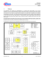
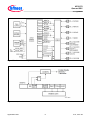
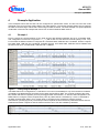
Tri Cor e
AP 3217 2
Queued SSC
Applic atio n N ote
V1.0 2011-09
Mic rocon t rolle rs
Edition 2011-09
Published by
Infineon Technologies AG
81726 Munich, Germany
© 2011 Infineon Technologies AG
All Rights Reserved.
LEGAL DISCLAIMER
THE INFORMATION GIVEN IN THIS APPLICATION NOTE IS GIVEN AS A HINT FOR THE
IMPLEMENTATION OF THE INFINEON TECHNOLOGIES COMPONENT ONLY AND SHALL NOT BE
REGARDED AS ANY DESCRIPTION OR WARRANTY OF A CERTAIN FUNCTIONALITY, CONDITION OR
QUALITY OF THE INFINEON TECHNOLOGIES COMPONENT. THE RECIPIENT OF THIS APPLICATION
NOTE MUST VERIFY ANY FUNCTION DESCRIBED HEREIN IN THE REAL APPLICATION. INFINEON
TECHNOLOGIES HEREBY DISCLAIMS ANY AND ALL WARRANTIES AND LIABILITIES OF ANY KIND
(INCLUDING WITHOUT LIMITATION WARRANTIES OF NON-INFRINGEMENT OF INTELLECTUAL
PROPERTY RIGHTS OF ANY THIRD PARTY) WITH RESPECT TO ANY AND ALL INFORMATION GIVEN IN
THIS APPLICATION NOTE.
Information
For further information on technology, delivery terms and conditions and prices, please contact the nearest
Infineon Technologies Office (www.infineon.com).
Warnings
Due to technical requirements, components may contain dangerous substances. For information on the types in
question, please contact the nearest Infineon Technologies Office.
Infineon Technologies components may be used in life-support devices or systems only with the express written
approval of Infineon Technologies, if a failure of such components can reasonably be expected to cause the
failure of that life-support device or system or to affect the safety or effectiveness of that device or system. Life
support devices or systems are intended to be implanted in the human body or to support and/or maintain and
sustain and/or protect human life. If they fail, it is reasonable to assume that the health of the user or other
persons may be endangered.
AP32172
Queued SSC
TC1782
Revision History: V1.0, 2011-09 Martin Schrape
Previous Version:
Page
Subjects (major changes since last revision)
We Listen to Your Comments
Is there any information in this document that you feel is wrong, unclear or missing?
Your feedback will help us to continuously improve the quality of this document.
Please send your proposal (including a reference to this document) to:
[email protected]
Application Note
3
V1.0, 2011-09
AP32172
Queued SSC
Table of Contents
Table of Contents
1
Preface ................................................................................................................................................ 6
2
Introduction ........................................................................................................................................ 7
3
Configuration ...................................................................................................................................... 7
4
4.1
4.2
4.3
Example Application ........................................................................................................................ 10
Example 1 .......................................................................................................................................... 10
Example 2 .......................................................................................................................................... 12
Example 3 .......................................................................................................................................... 14
5
Tools .................................................................................................................................................. 16
6
Source code ...................................................................................................................................... 16
7
References ........................................................................................................................................ 16
Application Note
4
V1.0, 2011-09
AP32172
Queued SSC
Preface
1
Preface
This application note describes the implementation of a queued serial communication on the TriCore
architecture [1] for the AUDO MAX-family. Queued serial communication is extremely helpful when multiple
external devices are connected to one SSC interface and when the communication should be serviced quickly
and with low or no CPU load. Up to eight slaves are possible on one SSC master. The application note explains
the configuration of the build-in queued Synchronous Serial Communication (SSC) mode as well as alternative
methods which uses the PCP. The document is aimed at developers who write or design real-time applications
on the TriCore which uses the SSC interface to communicate with either multiple similar slave devices like
Digital to Analog Converters (DAC), field bus chips or position encoders or different slave devices on the same
SSC module.
This guide assumes that readers have access to the TriCore Architecture Manual [2] and the TC1782 Users
Manual [3], and have at least some general knowledge of TriCore instruction set, the architectural features and
peripheral modules especially the DMA and the standard SSC functionality.
See References on page 16 for more information on the TriCore and other relevant documentation.
Figure 1
TC1782 Block Diagram
Application Note
6
V1.0, 2011-09
AP32172
Queued SSC
Introduction
2
Introduction
Figure 1 shows the TC1782 block diagram. Modules used in this application note are marked yellow. This
section 2 gives an introduction to the principles of the queued SSC mode. With the queued SSC mode the
TriCore can control multiple SSC slaves with different configurations like baud rates, data width and byte order.
In this case, the control and data handling for an SSC slave is handled by multiple DMA channels. Section 3
explains a configuration and initialization of the DMA and SSC module to use the queued SSC mode. Section 4
illustrates three example applications that are provided with this application note.
The examples are considering slave devices like DAC which has only a a Write interface. The queued SSC
mode does also support Write as well as Read interfaces, so that e.g. field bus chip (R/W) or position encode
(W) could use this mode but these devices are not in the scope of this application note.
3
Configuration
The SSC configuration is controlled by four registers (Table 1): the Control Register CON (see page 10), the
Baud Rate Timer Reload Register BR, the Slave Select Output Control Register SSOC and the Slave Select
Output Timing Control Register SSOTC (see page 10). These registers are located directly behind each other in
the address space. The basic idea of the queued SSC mode is that one DMA channel moves a configuration
from an internal buffer of n × 4 words to these four registers and then issues a request to a second DMA
channel that send the data to the transmit buffer (Figure 2). The four registers can be easily addressed using a
circular 16 byte buffer for the destination of the first DMA channel. During the modification of the SSC
configuration the SSC needs to be disabled and reenabled when the configuration is finished. Therefore the
enable bit is found twice in the module registers. The control register which is accessed first by the DMA holds a
CON.EN bit, so that the first DMA move can disable the module, the subsequent 3 moves modifies the
configuration but the last move to the SSOTC register is also used to re-enable the module. The SSCOTC
register holds another enable bit SSCOTC.EN and a queued SSC Mode control bit SSC0TC.QSMEN. If both bit
are set the module will be enabled (Figure 4).
To service multiple transmission without any CPU interaction the SSC generates a request from the receive
data buffer SSC0_RDR that is used as a hardware request to start the next transfer of the next SSC
configuration by the first DMA channel (Figure 3).
Table 1
SSC Register Overview used for Queued Mode
Register
Short Name
Register Long Name
Offset
Address
CON
Control Register
10H
BR
Baud Rate Timer Reload Register
14H
SSOC
Slave Select Output Control Register
18H
SSOTC
Slave Select Output Timing Control Register
1CH
Figure 2
SSC Interrupt Control
Application Note
7
V1.0, 2011-09
AP32172
Queued SSC
Configuration
Figure 3
SSC0 Module Implementation and Interconnection
Figure 4
Queued SSC Mode Control
Application Note
8
V1.0, 2011-09
AP32172
Queued SSC
Configuration
SSCn_CON
Control Register
31
30
29
[10H]
28
27
26
25
24
Reset Value: 0000 0000H
23
22
21
20
19
18
17
16
0
PAR
EEN
PAR
TYP
PAR
REN
PAR
TEN
r
rw
rw
rw
rw
3
2
1
0
15
14
13
12
11
10
9
8
7
6
5
4
EN
MS
0
A
REN
BEN
PEN
REN
TEN
LB
PO
PH
HB
BM
rw
rw
r
rw
rw
rw
rw
rw
rw
rw
rw
rw
rw
Field
Bits
Type
Description
EN
15
rw
Enable Bit
0B
Transmission and reception are disabled.
1B
Transmission and reception are enabled.
This bit is available as module output line “SSC enabled”. Note that
EN should only be cleared by software while no transfer is in
progress (STAT.BSY = 0). Note that the transmission/reception
enable can also be controlled in queued SSC mode by bit
SSOTC.EN.
SSCn_SSOTC
Slave Select Output Timing Control Register
31
30
29
28
27
26
25
[1CH]
24
Reset Value: 0000 0000H
23
22
21
20
19
18
17
16
7
6
5
4
3
2
1
0
0
r
15
14
13
12
11
EN
QSM
EN
0
rw
w
r
10
9
8
SLS
O7
MOD
r
INACT
TRAIL
LEAD
rw
rw
rw
Field
Bits
Type
Description
QSMEN
14
w
EN
15
rw
Queued SSC Mode Enabled
0B
When QSMEN is written with 0, the state of bit SSOTC.EN is
don’t care. In this case, the enable/disable of the SSC is
controlled by bit CON.EN only. Note that EN should only be
cleared by software while no transfer is in progress
(STAT.BSY = 0).
1B
When QSMEN is written with 1, queued SSC mode is
enabled, and the state of bit SSOTC.EN is copied to
CON.EN.
QSMEN is always read as 0.
Enable Bit
0B
Transmission and reception are disabled.
1B Transmission and reception are enabled.
Note that the transmission/reception enable can also be controlled
in queued SSC mode by bit CON.EN.
Application Note
9
V1.0, 2011-09
AP32172
Queued SSC
Example Application
4
Example Application
Three examples show how the SSC can be configured for queued SSC mode. The first one uses the mode
described in the user’s manual, writing data to four slave devices. The second example shows how to configure
the DMA to transmit larger values than 16 bit using two DMA channels. The third example is a speed optimized
modification of the second example that uses a PCP channel instead of DMA channel.
4.1
Example 1
Figure 5 shows the communicatiuon to four slave devices with different baudrates and up to 16 bit data width.
The configuration is stored in a ring buffer ssc_cfg with a size of of four times four words (Listing 1 Line 1-18).
For SLAVE0 the SSC0 interface is configured for 12 bit data width, MSB first and 1.5 Mbaud, SLAVE1 requires
8 bit data width, LSB first and 1.0 Mbaud, SLAVE2 requires 16 bit data width, MSB first and 2.0 Mbaud and
SLAVE3 is set up to 4 bit data width, LSB first and 1.0 Mbaud.
Figure 5
Timing Diagram Example 1
The DMA channel 0 is configured for a 4 transfers of 4 moves of 32-bit data(Line 37). Each transfer is hardware
controlled by the DMA Request Line SSC receive data request SSC0_RDR. The channel configures the CON,
BR, SSIOC and SSOTC registers (Line 40) and triggers after each transfer, i.e. after the SSC configuration, the
DMA channel 1 using the service request line 9 (Line 42). DMA channel 1 transfers by 1 move a 16 bit data to
the SSC transmit buffer SSC0_TB. A system timer is configured in this example to start the queued
transmission cyclically (Figure 6). The interrupt routine requests the first transfers by software and also sets the
hardware transaction request so that the further transfers’ two to four are handled by hardware.
Figure 6
Cyclical Transmission
Application Note
10
V1.0, 2011-09
AP32172
Queued SSC
Example Application
1
2
3
4
5
6
7
8
9
10
11
12
13
14
15
16
17
18
19
20
21
22
23
24
25
26
27
28
29
30
31
32
33
34
35
36
37
38
39
40
41
42
43
44
45
46
47
48
49
50
51
52
53
54
55
56
57
58
59
unsigned __align(64) ssc_cfg[16] = { //
0x0000401B, // SSC0_CON
master, MSB,
0x0000001D, // SSC0_BR 1.5Mbaud
0x00000100, // SSC0_SSOC slave 0
0x0000C000, // SSC0_SSOTC enable
0x00004007, // SSC0_CON
master, LSB,
0x0000002C, // SSC0_BR 1Mbaud
0x00000200, // SSC0_SSOC slave 1
0x0000C000, // SSC0_SSOTC enable
0x0000401F, // SSC0_CON
master, MSB,
0x00000016, // SSC0_BR ~2Mbaud
0x00000400, // SSC0_SSOC slave 2
0x0000C000, // SSC0_SSOTC enable
0x00004003, // SSC0_CON
master, LSB,
0x0000002C, // SSC0_BR 1Mbaud
0x00000800, // SSC0_SSOC slave 3
0x0000C000 // SSC0_SSOTC enable
};
12-bit
8-bit
16-bit
4-bit
unsigned short __align(64) msg[4] = {0x123, 0x45, 0x6789, 0xA};
void __interrupt(STM_INT) stm_icr(void) {
DMA_STREQ.B.SCH00 = 1;
DMA_HTREQ.B.ECH00 = 1;
STM_ISRR.B.CMP0IRR = 1;
}
int main(void) {
// PORT initialization
P3_IOCR0.U = 0x20900000;
P3_IOCR4.U = 0x90909090;
P2_IOCR0.U = 0x0000A000;
// P3.3 MRST0, P3.2 SCLK0
// P3.7 SLSO02, P3.6 SLSO01,\
P3.5 SLSO00, P3.4 MTSR0
// P2.1 is SLSO03
// DMA initialization
DMA_CHCR00.U = 0x00424004;
// 4x4x32bit, single mode, \
SSC0_RDR request after each transfer
DMA_SADR00.U = (unsigned) ssc_cfg; // Source is cfg[]
DMA_DADR00.U = (unsigned) &SSC0_CON.U; // Destination CON, BR, SSOC, SSOTC
DMA_ADRCR00.U = 0x00004688; // 64Byte source, 16Byte destination buffer
DMA_CHICR00.U = 0x90C;
// DMA request after each transfer by SRN09
DMA_CHCR01.U = 0x00380000; // 1x1x16bit, continuous mode, \
DMA_SR09 request after each transaction
DMA_SADR01.U = (unsigned) msg; // Source is msg[]
DMA_DADR01.U = (unsigned) &SSC0_TB.U; // Destination is SSC0_TB
DMA_ADRCR01.U = 0x00000308; // 8Byte source buffer
DMA_HTREQ.B.ECH01 = 1;
// Enable hardware transfer request
// STM generates an interrupt every 2^13/90MHz = 91us.
STM_CMCON.U = 0x0C00;
// 2^(0xC+1)
STM_CMP0.U = 1;
STM_ICR.U = 1;
STM_SRC0.U = 0x1000 | STM_INT;// Enable STM interrupt to TC
}
__enable();
for (;;)
;
Listing 1
qssc1.c
Application Note
11
V1.0, 2011-09
AP32172
Queued SSC
Example Application
4.2
Example 2
This example is made for three similar slave devices where each slave device is listening to a command stream
of 2 × 24 bit. This command sequence is required for e.g. LTC2602/LTC2612/LTC2622, a dual DAC device. For
a data width larger than 32 bit it is not possible to use the CS output of the SSC but the CS has to be generated
by a standard I/O port pin.
Figure 7 shows the communicatiuon to three slave devices using the same baudrate and 2 × 24 bit data width.
The module frequency is 40 Mhz, the bautrate 20 MBaud. Two DMA channel are used. The first one set/reset
the CS line. The second transfers 12 bit. This sequence is done four times in a row before selecting the next
slave.
Figure 7
Timing Diagram Example 2
1 unsigned short dac[6] = { 0x1122, 0x3344, 0x5566, 0x7788,
2 unsigned __align(64) t[16] = {
3
0x2000C0, 0x2000C0, 0x2000C0, 0x2000C0, // PR5 PS7
P3.5, set P3.7 P3.6
4
0x4000A0, 0x4000A0, 0x4000A0, 0x4000A0, // PR6 PS7
P3.6, set P3.7 P3.5
5
0x800060, 0x800060, 0x800060, 0x800060, // PR7
P3.7, set P3.6 P3.5
6
0x0000E0, 0x0000E0, 0x0000E0, 0x0000E0}; //
PS7
set P3.7 P3.6 P3.5
7 unsigned short __align(32) s[16] = {
8
0x0200, 0x0000, 0x0210, 0x0000,
//
9
0x0200, 0x0000, 0x0210, 0x0000,
//
10
0x0200, 0x0000, 0x0210, 0x0000,
//
11
0x0000, 0x0000, 0x0000, 0x0000 }; //
12
13 void __interrupt(STM_INT) stm_isr(void)
14 {
15
// insert the 4 MSB of dac to LSB of s[0]
16
s[0] = __insert(s[0], __extru(dac[0], 12, 4), 0, 4);
17
// set s[1] the 12 LSB of dac
18
s[1] = __extru(dac[0], 0, 12);
19
s[2] = __insert(s[2], __extru(dac[1], 12, 4), 0, 4);
20
s[3] = __extru(dac[1], 0, 12);
21
s[4] = __insert(s[4], __extru(dac[2], 12, 4), 0, 4);
22
s[5] = __extru(dac[2], 0, 12);
23
s[6] = __insert(s[6], __extru(dac[3], 12, 4), 0, 4);
24
s[7] = __extru(dac[3], 0, 12);
25
s[8] = __insert(s[8], __extru(dac[4], 12, 4), 0, 4);
26
s[9] = __extru(dac[4], 0, 12);
27
s[10] = __insert(s[10], __extru(dac[5], 12, 4), 0, 4);
Application Note
12
0x99AA, 0xBBCC };
PS6
=> reset
PS5 => reset
PS6 PS5 => reset
PS6 PS5 =>
V1.0, 2011-09
AP32172
Queued SSC
Example Application
28
s[11] = __extru(dac[5], 0, 12);
29
30
DMA_STREQ.B.SCH00 = 1;
31
DMA_HTREQ.B.ECH00 = 1;
32
DMA_HTREQ.B.ECH01 = 1;
33
STM_ISRR.B.CMP0IRR = 1;
34 }
35
36 int main(void)
37 {
38
39
// SSC0 initialization
40
SSC0_BR.U = 0x00000001; // baud rate = 22.5Mbaud (max of A1+ pad is 25MHz)
41
SSC0_SSOTC.U = 0xC;
42
SSC0_CON.U = 0x0000C01B; // enable, 12-bit master, MSB first
43
44
// PORT initialization
45
P3_IOCR0.U = 0x20900000; // P3.3 is MRST0, P3.2 is SCLK0
46
P3_IOCR4.U = 0x80808090; // P3.7 is SLSO02, P3.6 is SLSO01, P3.5 is SLSO00,
P3.4 is MTSR0
47
P3_OUT.U = 0xE;
48
49
// DMA initialization
50
DMA_CHCR00.U = 0x00404010; // 16x1x32bit, single mode, SSC0_RDR request
after each transfer
51
DMA_SADR00.U = (unsigned) t;// Source is t[]
52
DMA_DADR00.U = (unsigned) &P3_OMR.U; // Destination P3_OMR
53
DMA_ADRCR00.U = 0x00000608; // 32Byte source buffer
54
DMA_CHICR00.U = 0x90C; // Interrupt after each Transfer to SRN09
55
DMA_CHCR01.U = 0x00200010; // 16x1x16bit, single mode, DMA_SR09 request
after each transfer
56
DMA_SADR01.U = (unsigned) s;// Source is s[]
57
DMA_DADR01.U = (unsigned) &SSC0_TB.U; // Destination is SSC0_TB
58
DMA_ADRCR01.U = 0x00000508; // 16Byte source buffer
59
60
// STM generates an interrupt every 2^13/90MHz = 91us.
61
STM_CMCON.U = 0x0C00; //2^(0xC+1)
62
STM_CMP0.U = 1;
63
STM_ICR.U = 1;
64
STM_SRC0.U = 0x1000 | STM_INT;// Enable STM interrupt to TC
65
__enable();
66
67
for (;;)
68
;
69 }
Listing 2
qssc2.c
Application Note
13
V1.0, 2011-09
AP32172
Queued SSC
Example Application
4.3
Example 3
This example is a performance optimized alternative of example with two similar slave devices. SCLK0 of Figure
8 shows a continous clock signal instead of the interrupted one in Figure 7. This example uses one DMA
channel and one PCP channel
Figure 8
1
2
3
4
5
6
7
8
9
10
11
12
13
14
15
16
17
18
19
20
21
22
23
24
25
26
27
28
29
30
31
32
33
34
35
36
37
38
39
40
41
Timing Diagram Example 3
unsigned short dac[4] = { 0x1122, 0x3344, 0x5566, 0x7788 };
volatile short __far __share __align(32) s[8] =
{0x0200, 0x0000, 0x0210, 0x0000,
0x0200, 0x0000, 0x0210, 0x0000};
void __interrupt(STM_INT) stm_icr(void)
{
s[0] = __insert(s[0],__extru(dac[0],12,4),0,4);
s[1] = __extru(dac[0],0,12);
s[2] = __insert(s[2],__extru(dac[1],12,4),0,4);
s[3] = __extru(dac[1],0,12);
s[4] = __insert(s[4],__extru(dac[2],12,4),0,4);
s[5] = __extru(dac[2],0,12);
s[6] = __insert(s[6],__extru(dac[3],12,4),0,4);
s[7] = __extru(dac[3],0,12);
}
DMA_CHICR02.U = 0x00000008; // Channel 02 Transfer interrupt enabled SRN0
P3_OUT.U = ~0x20;
DMA_STREQ.B.SCH02 = 1;
DMA_HTREQ.B.ECH02 = 1; // Enable Hardware transfer request by SSC0_TDR
STM_ISRR.B.CMP0IRR = 1;
int main(void)
{
// SSC0 initialization
SSC0_BR.U = 0x00000001; // baud rate = 22.5 Mbaud
SSC0_SSOC.U = 3;
SSC0_CON.U = 0x0000C01B; // enable, 12-bit master, MSB first
// PORT initialization
P3_IOCR0.U = 0x20900000; // P3.3 is MRST0, P3.2 is SCLK0
P3_IOCR4.U = 0x00808090; // P3.6 is SLSO01, P3.5 is SLSO00, P3.4 is MTSR0
P3_OUT.U = ~0; // P3.6 is high, P3.5 is high
// DMA initialization
DMA_CHCR02.U = 0xC0204004; // 4 transfers of one 16bit move
DMA_SADR02.U = (unsigned) s; // Channel 02 destination address register
DMA_DADR02.U = (unsigned) &SSC0_TB.U; // Channel 02 destination address
Application Note
14
V1.0, 2011-09
AP32172
Queued SSC
Example Application
register
42
DMA_ADRCR02.U = 0x00000408; // Channel 02 address control register
43
DMA_SRC0.U = 0x1400 | DMA_INT; // Enable DMA interrupt to PCP
44
45
// STM generates an interrupt every 2^13/90MHz = 91us.
46
STM_CMCON.U = 0x0C00; //2^(0xC+1)
47
STM_CMP0.U = 1;
48
STM_ICR.U = 1;
49
STM_SRC0.U = 0x1000 | STM_INT; // Enable STM interrupt to TC
50
__enable();
51
52
for (;;)
53
;
54 }
Listing 3
qssc3.c
1 void __interrupt(DMA_INT) dma_isr(void) {
2
DMA_CHICR02.U = 0x00000000; // Channel 02 Transfer interrupt disabled
3
while (SSC0_STAT.B.BSY)
4
; // alternative for 25Mbaud for(int i=0;i<25;i++) __nop();
5
P3_OUT.U = ~0x40;
6
DMA_STREQ.B.SCH02 = 1;
7
DMA_HTREQ.B.ECH02 = 1; // Enable Hardware transfer request by SSC0_TDR
8
DMA_INTCR.B.CICH02 = 1;
9 }
Listing 4
qssc3.pcp.c
Application Note
15
V1.0, 2011-09
AP32172
Queued SSC
Tools
5
Tools
The examples were build using the Tasking compiler Version 3.5r1. mingw32-make (www.mingw.org) was used
as a make tool. The example code includes a project workspaces for the PLS UDE debugger V3.08.
6
Source code
The source code provided with this application consists of a single Tasking project.
7
References
[1] http://www.infineon.com/tricore
[2] TriCore Architecture V1.3.8 2007-11
[3] TC1784 User’s Manual V1.0 2009-07
Application Note
16
V1.0, 2011-09
w w w . i n f i n e o n . c o m
Published by Infineon Technologies AG