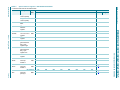
1
P89LPC9201/9211/922A1/9241/
9251
8-bit microcontroller with accelerated two-clock 80C51 core
2 kB/4 kB/8 kB 3 V byte-erasable flash with 8-bit ADC
Rev. 2.1 — 27 August 2012
Product data sheet
1. General description
The P89LPC9201/9211/922A1/9241/9251 is a single-chip microcontroller, available in low
cost packages, based on a high performance processor architecture that executes
instructions in two to four clocks, six times the rate of standard 80C51 devices. Many
system-level functions have been incorporated into the device in order to reduce
component count, board space, and system cost.
2. Features and benefits
2.1 Principal features
2 kB/4 kB/8 kB byte-erasable flash code memory organized into 1 kB sectors and
64-byte pages. Single-byte erasing allows any byte(s) to be used as non-volatile data
storage.
256-byte RAM data memory.
4-input multiplexed 8-bit ADC/single DAC output (P89LPC9241/9251). Two analog
comparators with selectable inputs and reference source.
On-chip temperature sensor integrated with ADC module (P89LPC9241/9251).
Two 16-bit counter/timers (each may be configured to toggle a port output upon timer
overflow or to become a PWM output).
A 23-bit system timer that can also be used as real-time clock consisting of a 7-bit
prescaler and a programmable and readable 16-bit timer.
Enhanced UART with a fractional baud rate generator, break detect, framing error
detection, and automatic address detection; 400 kHz byte-wide I2C-bus
communication port.
2.4 V to 3.6 V VDD operating range. I/O pins are 5 V tolerant (may be pulled up or
driven to 5.5 V).
Enhanced low voltage (brownout) detect allows a graceful system shutdown when
power fails.
20-pin TSSOP and DIP packages with 15 I/O pins minimum and up to 18 I/O pins
while using on-chip oscillator and reset options.
NXP Semiconductors
P89LPC9201/9211/922A1/9241/9251
8-bit microcontroller with 8-bit ADC
2.2 Additional features
A high performance 80C51 CPU provides instruction cycle times of 111 ns to 222 ns
for all instructions except multiply and divide when executing at 18 MHz. This is six
times the performance of the standard 80C51 running at the same clock frequency. A
lower clock frequency for the same performance results in power savings and reduced
EMI.
Serial flash In-Circuit Programming (ICP) allows simple production coding with
commercial EPROM programmers. Flash security bits prevent reading of sensitive
application programs.
Serial flash In-System Programming (ISP) allows coding while the device is mounted
in the end application.
In-Application Programming (IAP) of the flash code memory. This allows changing the
code in a running application.
Watchdog timer with separate on-chip oscillator, nominal 400 kHz, calibrated to 5 %,
requiring no external components. The watchdog prescaler is selectable from
eight values.
High-accuracy internal RC oscillator option, with clock doubler option, allows operation
without external oscillator components. The RC oscillator option is selectable and fine
tunable.
Clock switching on the fly among internal RC oscillator, watchdog oscillator, external
clock source provides optimal support of minimal power active mode with fast
switching to maximum performance.
Idle and two different power-down reduced power modes. Improved wake-up from
Power-down mode (a LOW interrupt input starts execution). Typical power-down
current is 1 A (total power-down with voltage comparators disabled).
Active-LOW reset. On-chip power-on reset allows operation without external reset
components. A software reset function is also available.
Configurable on-chip oscillator with frequency range options selected by user
programmed flash configuration bits. Oscillator options support frequencies from
20 kHz to the maximum operating frequency of 18 MHz.
Oscillator fail detect. The watchdog timer has a separate fully on-chip oscillator
allowing it to perform an oscillator fail detect function.
Programmable port output configuration options: quasi-bidirectional, open drain,
push-pull, input-only.
High current sourcing/sinking (20 mA) on eight I/O pins (P0.3 to P0.7, P1.4, P1.6,
P1.7). All other port pins have high sinking capability (20 mA). A maximum limit is
specified for the entire chip.
Port ‘input pattern match’ detect. Port 0 may generate an interrupt when the value of
the pins match or do not match a programmable pattern.
Controlled slew rate port outputs to reduce EMI. Outputs have approximately 10 ns
minimum ramp times.
Only power and ground connections are required to operate the
P89LPC9201/9211/922A1/9241/9251 when internal reset option is selected.
Four interrupt priority levels.
Eight keypad interrupt inputs, plus two additional external interrupt inputs.
Schmitt trigger port inputs.
Second data pointer.
Emulation support.
P89LPC92X1
Product data sheet
All information provided in this document is subject to legal disclaimers.
Rev. 2.1 — 27 August 2012
© NXP B.V. 2012. All rights reserved.
2 of 75
P89LPC9201/9211/922A1/9241/9251
NXP Semiconductors
8-bit microcontroller with 8-bit ADC
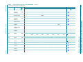
3. Ordering information
Table 1.
Ordering information
Type number
Package
Name
Description
Version
P89LPC9201FDH
TSSOP20
plastic thin shrink small outline package; 20
leads; body width 4.4 mm
SOT360-1
P89LPC9211FDH
TSSOP20
plastic thin shrink small outline package; 20
leads; body width 4.4 mm
SOT360-1
P89LPC922A1FDH
TSSOP20
plastic thin shrink small outline package; 20
leads; body width 4.4 mm
SOT360-1
P89LPC922A1FN
DIP20
plastic dual in-line package; 20 leads (300 mil)
SOT146-1
P89LPC9241FDH
TSSOP20
plastic thin shrink small outline package; 20
leads; body width 4.4 mm
SOT360-1
P89LPC9251FDH
TSSOP20
plastic thin shrink small outline package; 20
leads; body width 4.4 mm
SOT360-1
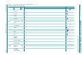
3.1 Ordering options
Table 2.
P89LPC92X1
Product data sheet
Ordering options
Type number
Flash memory
Temperature range
Frequency
P89LPC9201FDH
2 kB
40 C to +85 C
0 MHz to 18 MHz
P89LPC9211FDH
4 kB
40 C to +85 C
0 MHz to 18 MHz
P89LPC922A1FDH
8 kB
40 C to +85 C
0 MHz to 18 MHz
P89LPC922A1FN
8 kB
40 C to +85 C
0 MHz to 18 MHz
P89LPC9241FDH
4 kB
40 C to +85 C
0 MHz to 18 MHz
P89LPC9251FDH
8 kB
40 C to +85 C
0 MHz to 18 MHz
All information provided in this document is subject to legal disclaimers.
Rev. 2.1 — 27 August 2012
© NXP B.V. 2012. All rights reserved.
3 of 75
NXP Semiconductors
P89LPC9201/9211/922A1/9241/9251
8-bit microcontroller with 8-bit ADC
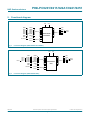
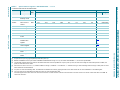
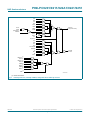
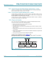
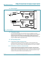
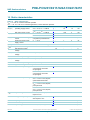
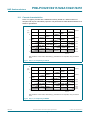
4. Block diagram
P89LPC9201/9211/922A1
HIGH PERFORMANCE
ACCELERATED 2-CLOCK 80C51 CPU
2 kB/4 kB/8 kB
CODE FLASH
TXD
RXD
UART
internal
bus
256-BYTE
DATA RAM
REAL-TIME CLOCK/
SYSTEM TIMER
P3[1:0]
PORT 3
CONFIGURABLE I/Os
I2C-BUS
P1[7:0]
PORT 1
CONFIGURABLE I/Os
WATCHDOG TIMER
AND OSCILLATOR
P0[7:0]
PORT 0
CONFIGURABLE I/Os
TIMER 0
TIMER 1
KEYPAD
INTERRUPT
ANALOG
COMPARATORS
SCL
SDA
T0
T1
CMP2
PROGRAMMABLE
OSCILLATOR DIVIDER
CIN2A
CIN1A
CIN2B
CMP1
CIN1B
CPU
clock
XTAL1
CRYSTAL
OR
RESONATOR
CONFIGURABLE
OSCILLATOR
ON-CHIP RC
OSCILLATOR WITH
CLOCK DOUBLER
POWER MONITOR
(POWER-ON RESET,
BROWNOUT RESET)
XTAL2
002aae421
Fig 1.
Block diagram (P89LPC9201/9211/922A1)
P89LPC92X1
Product data sheet
All information provided in this document is subject to legal disclaimers.
Rev. 2.1 — 27 August 2012
© NXP B.V. 2012. All rights reserved.
4 of 75
NXP Semiconductors
P89LPC9201/9211/922A1/9241/9251
8-bit microcontroller with 8-bit ADC
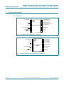
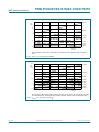
P89LPC9241/9251
HIGH PERFORMANCE
ACCELERATED 2-CLOCK 80C51 CPU
4 kB/8 kB
CODE FLASH
TXD
RXD
UART
internal
bus
256-BYTE
DATA RAM
REAL-TIME CLOCK/
SYSTEM TIMER
P3[1:0]
PORT 3
CONFIGURABLE I/Os
I2C-BUS
P1[7:0]
PORT 1
CONFIGURABLE I/Os
WATCHDOG TIMER
AND OSCILLATOR
P0[7:0]
PORT 0
CONFIGURABLE I/Os
TIMER 0
TIMER 1
KEYPAD
INTERRUPT
ANALOG
COMPARATORS
SCL
SDA
T0
T1
CMP2
PROGRAMMABLE
OSCILLATOR DIVIDER
CPU
clock
ADC1/DAC1
(TEMPERATURE
SENSOR)
CIN2A
CIN1A
CIN2B
CMP1
CIN1B
AD10
AD11
AD12
AD13
DAC1
XTAL1
CRYSTAL
OR
RESONATOR
CONFIGURABLE
OSCILLATOR
ON-CHIP RC
OSCILLATOR WITH
CLOCK DOUBLER
POWER MONITOR
(POWER-ON RESET,
BROWNOUT RESET)
XTAL2
002aae422
Fig 2.
Block diagram (P89LPC9241/9251)
P89LPC92X1
Product data sheet
All information provided in this document is subject to legal disclaimers.
Rev. 2.1 — 27 August 2012
© NXP B.V. 2012. All rights reserved.
5 of 75
P89LPC9201/9211/922A1/9241/9251
NXP Semiconductors
8-bit microcontroller with 8-bit ADC
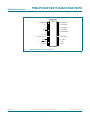
5. Functional diagram
VDD
KBI0
KBI1
KBI2
KBI3
KBI4
KBI5
KBI6
KBI7
CMP2
CIN2B
CIN2A
CIN1B
CIN1A
CMPREF
CMP1
T1
CLKOUT
XTAL2
VSS
PORT 0
PORT 1
P89LPC9201/
9211/922A1
TXD
RXD
T0
INT0
INT1
RST
SCL
SDA
PORT 3
XTAL1
002aae423
Fig 3.
Functional diagram (P89LPC9201/9211/922A1)
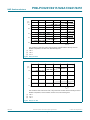
VDD
DAC1
AD10
AD11
AD12
AD13
KBI0
KBI1
KBI2
KBI3
KBI4
KBI5
KBI6
KBI7
CMP2
CIN2B
CIN2A
CIN1B
CIN1A
CMPREF
CMP1
T1
CLKOUT
XTAL2
VSS
PORT 0
PORT 1
P89LPC9241/
9251
TXD
RXD
T0
INT0
INT1
RST
SCL
SDA
PORT 3
XTAL1
002aae424
Fig 4.
Functional diagram (P89LPC9241/9251)
P89LPC92X1
Product data sheet
All information provided in this document is subject to legal disclaimers.
Rev. 2.1 — 27 August 2012
© NXP B.V. 2012. All rights reserved.
6 of 75
P89LPC9201/9211/922A1/9241/9251
NXP Semiconductors
8-bit microcontroller with 8-bit ADC
6. Pinning information
6.1 Pinning
P0.0/CMP2/KBI0
1
20 P0.1/CIN2B/KBI1/AD10
P1.7
2
19 P0.2/CIN2A/KBI2/AD11
P1.6
3
18 P0.3/CIN1B/KBI3/AD12
P1.5/RST
4
17 P0.4/CIN1A/KBI4/AD13/DAC1
VSS
5
P3.1/XTAL1
6
P3.0/XTAL2/CLKOUT
7
14 P0.6/CMP1/KBI6
P1.4/INT1
8
13 P0.7/T1/KBI7
P1.3/INT0/SDA
9
12 P1.0/TXD
P1.2/T0/SCL 10
11 P1.1/RXD
P89LPC9241/9251
16 P0.5/CMPREF/KBI5
15 VDD
002aae425
Fig 5.
P89LPC9241/9251 TSSOP20 pin configuration
P0.0/CMP2/KBI0
1
20 P0.1/CIN2B/KBI1
P1.7
2
19 P0.2/CIN2A/KBI2
P1.6
3
18 P0.3/CIN1B/KBI3
P1.5/RST
4
17 P0.4/CIN1A/KBI4
VSS
5
P3.1/XTAL1
6
P3.0/XTAL2/CLKOUT
7
14 P0.6/CMP1/KBI6
P1.4/INT1
8
13 P0.7/T1/KBI7
P1.3/INT0/SDA
9
12 P1.0/TXD
P1.2/T0/SCL 10
11 P1.1/RXD
P89LPC9201/9211/
922A1
16 P0.5/CMPREF/KBI5
15 VDD
002aae426
Fig 6.
P89LPC92X1
Product data sheet
P89LPC9201/9211/922A1 TSSOP20 pin configuration
All information provided in this document is subject to legal disclaimers.
Rev. 2.1 — 27 August 2012
© NXP B.V. 2012. All rights reserved.
7 of 75
NXP Semiconductors
P89LPC9201/9211/922A1/9241/9251
8-bit microcontroller with 8-bit ADC
P89LPC922A1
P0.0/CMP2/KBI0
1
20 P0.1/CIN2B/KBI1
P1.7
2
19 P0.2/CIN2A/KBI2
P1.6
3
18 P0.3/CIN1B/KBI3
P1.5/RST
4
17 P0.4/CIN1A/KBI4
VSS
5
16 P0.5/CMPREF/KBI5
P3.1/XTAL1
6
15 VDD
P3.0/XTAL2/CLKOUT
7
14 P0.6/CMP1/KBI6
P1.4/INT1
8
13 P0.7/T1/KBI7
P1.3/INT0/SDA
9
12 P1.0/TXD
P1.2/T0/SCL 10
11 P1.1/RXD
002aae427
Fig 7.
P89LPC92X1
Product data sheet
P89LPC922A1 DIP20 pin configuration
All information provided in this document is subject to legal disclaimers.
Rev. 2.1 — 27 August 2012
© NXP B.V. 2012. All rights reserved.
8 of 75
P89LPC9201/9211/922A1/9241/9251
NXP Semiconductors
8-bit microcontroller with 8-bit ADC
6.2 Pin description
Table 3.
Pin description
Symbol
Pin
Type Description
TSSOP20,
DIP20
P0.0 to P0.7
I/O
Port 0: Port 0 is an 8-bit I/O port with a user-configurable output type. During reset
Port 0 latches are configured in the input only mode with the internal pull-up
disabled. The operation of Port 0 pins as inputs and outputs depends upon the port
configuration selected. Each port pin is configured independently. Refer to Section
7.16.1 “Port configurations” and Table 12 “Static characteristics” for details.
The Keypad Interrupt feature operates with Port 0 pins.
All pins have Schmitt trigger inputs.
Port 0 also provides various special functions as described below:
P0.0/CMP2/
KBI0
P0.1/CIN2B/
KBI1/AD10
P0.2/CIN2A/
KBI2/AD11
P0.3/CIN1B/
KBI3/AD12
P0.4/CIN1A/
KBI4/DAC1/AD13
P0.5/CMPREF/
KBI5
P89LPC92X1
Product data sheet
1
20
19
18
17
16
I/O
P0.0 — Port 0 bit 0.
O
CMP2 — Comparator 2 output
I
KBI0 — Keyboard input 0.
I/O
P0.1 — Port 0 bit 1.
I
CIN2B — Comparator 2 positive input B.
I
KBI1 — Keyboard input 1.
I
AD10 — ADC1 channel 0 analog input. (P89LPC9241/9251)
I/O
P0.2 — Port 0 bit 2.
I
CIN2A — Comparator 2 positive input A.
I
KBI2 — Keyboard input 2.
I
AD11 — ADC1 channel 1 analog input. (P89LPC9241/9251)
I/O
P0.3 — Port 0 bit 3. High current source.
I
CIN1B — Comparator 1 positive input B.
I
KBI3 — Keyboard input 3.
I
AD12 — ADC1 channel 2 analog input. (P89LPC9241/9251)
I/O
P0.4 — Port 0 bit 4. High current source.
I
CIN1A — Comparator 1 positive input A.
I
KBI4 — Keyboard input 4.
O
DAC1 — Digital-to-analog converter output 1. (P89LPC9241/9251)
I
AD13 — ADC1 channel 3 analog input. (P89LPC9241/9251)
I/O
P0.5 — Port 0 bit 5. High current source.
I
CMPREF — Comparator reference (negative) input.
I
KBI5 — Keyboard input 5.
All information provided in this document is subject to legal disclaimers.
Rev. 2.1 — 27 August 2012
© NXP B.V. 2012. All rights reserved.
9 of 75
P89LPC9201/9211/922A1/9241/9251
NXP Semiconductors
8-bit microcontroller with 8-bit ADC
Table 3.
Pin description …continued
Symbol
Pin
Type Description
TSSOP20,
DIP20
P0.6/CMP1/KBI6
P0.7/T1/KBI7
14
13
I/O
P0.6 — Port 0 bit 6. High current source.
O
CMP1 — Comparator 1 output.
I
KBI6 — Keyboard input 6.
I/O
P0.7 — Port 0 bit 7. High current source.
I/O
T1 — Timer/counter 1 external count input or overflow output.
I
KBI7 — Keyboard input 7.
I/O, I Port 1: Port 1 is an 8-bit I/O port with a user-configurable output type, except for
[1]
three pins as noted below. During reset Port 1 latches are configured in the input
only mode with the internal pull-up disabled. The operation of the configurable
Port 1 pins as inputs and outputs depends upon the port configuration selected.
Each of the configurable port pins are programmed independently. Refer to
Section 7.16.1 “Port configurations” and Table 12 “Static characteristics” for
details. P1.2 to P1.3 are open drain when used as outputs. P1.5 is input only.
P1.0 to P1.7
All pins have Schmitt trigger inputs.
Port 1 also provides various special functions as described below:
P1.0/TXD
P1.1/RXD
P1.2/T0/SCL
P1.3/INT0/SDA
12
11
10
9
P1.4/INT1
8
P1.5/RST
4
I/O
P1.0 — Port 1 bit 0.
O
TXD — Transmitter output for serial port.
I/O
P1.1 — Port 1 bit 1.
I
RXD — Receiver input for serial port.
I/O
P1.2 — Port 1 bit 2 (open-drain when used as output).
I/O
T0 — Timer/counter 0 external count input or overflow output (open-drain when
used as output).
I/O
SCL — I2C-bus serial clock input/output.
I/O
P1.3 — Port 1 bit 3 (open-drain when used as output).
I
INT0 — External interrupt 0 input.
I/O
SDA — I2C-bus serial data input/output.
I/O
P1.4 — Port 1 bit 4. High current source.
I
INT1 — External interrupt 1 input.
I
P1.5 — Port 1 bit 5 (input only).
I
RST — External Reset input during power-on or if selected via UCFG1. When
functioning as a reset input, a LOW on this pin resets the microcontroller, causing
I/O ports and peripherals to take on their default states, and the processor begins
execution at address 0. Also used during a power-on sequence to force ISP mode.
P1.6
3
I/O
P1.6 — Port 1 bit 6. High current source.
P1.7
2
I/O
P1.7 — Port 1 bit 7. High current source.
I/O
Port 3: Port 3 is a 2-bit I/O port with a user-configurable output type. During reset
Port 3 latches are configured in the input only mode with the internal pull-up
disabled. The operation of Port 3 pins as inputs and outputs depends upon the port
configuration selected. Each port pin is configured independently. Refer to Section
7.16.1 “Port configurations” and Table 12 “Static characteristics” for details.
P3.0 to P3.1
All pins have Schmitt trigger inputs.
Port 3 also provides various special functions as described below:
P89LPC92X1
Product data sheet
All information provided in this document is subject to legal disclaimers.
Rev. 2.1 — 27 August 2012
© NXP B.V. 2012. All rights reserved.
10 of 75
P89LPC9201/9211/922A1/9241/9251
NXP Semiconductors
8-bit microcontroller with 8-bit ADC
Table 3.
Pin description …continued
Symbol
Pin
Type Description
TSSOP20,
DIP20
P3.0/XTAL2/
CLKOUT
P3.1/XTAL1
7
6
I/O
P3.0 — Port 3 bit 0.
O
XTAL2 — Output from the oscillator amplifier (when a crystal oscillator option is
selected via the flash configuration).
O
CLKOUT — CPU clock divided by 2 when enabled via SFR bit (ENCLK -TRIM.6).
It can be used if the CPU clock is the internal RC oscillator, watchdog oscillator or
external clock input, except when XTAL1/XTAL2 are used to generate clock source
for the RTC/system timer.
I/O
P3.1 — Port 3 bit 1.
I
XTAL1 — Input to the oscillator circuit and internal clock generator circuits (when
selected via the flash configuration). It can be a port pin if internal RC oscillator or
watchdog oscillator is used as the CPU clock source, and if XTAL1/XTAL2 are not
used to generate the clock for the RTC/system timer.
VSS
5
I
Ground: 0 V reference.
VDD
15
I
Power supply: This is the power supply voltage for normal operation as well as
Idle and Power-down modes.
[1]
Input/output for P1.0 to P1.4, P1.6, P1.7. Input for P1.5.
P89LPC92X1
Product data sheet
All information provided in this document is subject to legal disclaimers.
Rev. 2.1 — 27 August 2012
© NXP B.V. 2012. All rights reserved.
11 of 75
NXP Semiconductors
P89LPC9201/9211/922A1/9241/9251
8-bit microcontroller with 8-bit ADC
7. Functional description
Remark: Please refer to the P89LPC9201/9211/922A1/9241/9251 User manual for a
more detailed functional description.
7.1 Special function registers
Remark: SFR accesses are restricted in the following ways:
• User must not attempt to access any SFR locations not defined.
• Accesses to any defined SFR locations must be strictly for the functions for the SFRs.
• SFR bits labeled ‘-’, ‘0’ or ‘1’ can only be written and read as follows:
– ‘-’ Unless otherwise specified, must be written with ‘0’, but can return any value
when read (even if it was written with ‘0’). It is a reserved bit and may be used in
future derivatives.
– ‘0’ must be written with ‘0’, and will return a ‘0’ when read.
– ‘1’ must be written with ‘1’, and will return a ‘1’ when read.
P89LPC92X1
Product data sheet
All information provided in this document is subject to legal disclaimers.
Rev. 2.1 — 27 August 2012
© NXP B.V. 2012. All rights reserved.
12 of 75
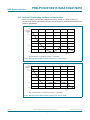
xxxxxxxxxxxxxxxxxxxxx xxxxxxxxxxxxxxxxxxxxxxxxxx xxxxxxx x x x xxxxxxxxxxxxxxxxxxxxxxxxxxxxxx xxxxxxxxxxxxxxxxxxx xx xx xxxxx
xxxxxxxxxxxxxxxxxxxxxxxxxxx xxxxxxxxxxxxxxxxxxx xxxxxx xxxxxxxxxxxxxxxxxxxxxxxxxxxxxxxxxxx xxxxxxxxxxxx x x
xxxxxxxxxxxxxxxxxxxxx xxxxxxxxxxxxxxxxxxxxxxxxxxxxxx xxxxx xxxxxxxxxxxxxxxxxxxxxxxxxxxxxxxxxxxxxxxxxxxxxxxxxx xxxxxxxx
xxxxxxxxxxxxxxxxxxxxxxxxx xxxxxxxxxxxxxxxxxxxx xxx
NXP Semiconductors
P89LPC92X1
Product data sheet
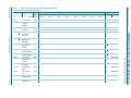
Table 4.
Special function registers - P89LPC9201/9211/922A1
* indicates SFRs that are bit addressable.
Name
Description
SFR Bit functions and addresses
addr.
MSB
Bit address
ACC*
Accumulator
E0H
AUXR1
Auxiliary
function
register
A2H
Bit address
E7
E6
Reset value
LSB
E5
E4
E3
E2
E1
Hex
Binary
00
0000 0000
00
0000 00x0
E0
CLKLP
EBRR
ENT1
ENT0
SRST
0
-
DPS
F7
F6
F5
F4
F3
F2
F1
F0
F0H
00
0000 0000
Baud rate
generator 0
rate low
BEH
00
0000 0000
BRGR1[2]
Baud rate
generator 0
rate high
BFH
00
0000 0000
BRGCON
Baud rate
generator 0
control
BDH
-
-
-
-
-
-
SBRGS
BRGEN
00[2]
xxxx xx00
CMP1
Comparator 1
control register
ACH
-
-
CE1
CP1
CN1
OE1
CO1
CMF1
00[1]
xx00 0000
CMP2
Comparator 2
control register
ADH
-
-
CE2
CP2
CN2
OE2
CO2
CMF2
00[1]
xx00 0000
DIVM
CPU clock
divide-by-M
control
95H
00
0000 0000
DPTR
Data pointer
(2 bytes)
13 of 75
© NXP B.V. 2012. All rights reserved.
DPH
Data pointer
high
83H
00
0000 0000
DPL
Data pointer
low
82H
00
0000 0000
FMADRH
Program flash
address high
E7H
00
0000 0000
FMADRL
Program flash
address low
E6H
00
0000 0000
8-bit microcontroller with 8-bit ADC
B register
BRGR0[2]
P89LPC9201/9211/922A1/9241/9251
Rev. 2.1 — 27 August 2012
All information provided in this document is subject to legal disclaimers.
B*
xxxxxxxxxxxxxxxxxxxxx xxxxxxxxxxxxxxxxxxxxxxxxxx xxxxxxx x x x xxxxxxxxxxxxxxxxxxxxxxxxxxxxxx xxxxxxxxxxxxxxxxxxx xx xx xxxxx
xxxxxxxxxxxxxxxxxxxxxxxxxxx xxxxxxxxxxxxxxxxxxx xxxxxx xxxxxxxxxxxxxxxxxxxxxxxxxxxxxxxxxxx xxxxxxxxxxxx x x
xxxxxxxxxxxxxxxxxxxxx xxxxxxxxxxxxxxxxxxxxxxxxxxxxxx xxxxx xxxxxxxxxxxxxxxxxxxxxxxxxxxxxxxxxxxxxxxxxxxxxxxxxx xxxxxxxx
xxxxxxxxxxxxxxxxxxxxxxxxx xxxxxxxxxxxxxxxxxxxx xxx
Name
FMCON
Description
SFR Bit functions and addresses
addr.
MSB
Reset value
LSB
E4H
BUSY
-
-
-
HVA
HVE
SV
OI
Program flash
control (Write)
E4H
FMCMD.7
FMCMD.6
FMCMD.5
FMCMD.4
FMCMD.3
FMCMD.2
FMCMD.1
FMCMD.0
FMDATA
Program flash
data
E5H
I2ADR
I2C-bus slave
address
register
DBH
I2CON*
I2C-bus
control
D8H
I2ADR.6
I2ADR.5
I2ADR.4
I2ADR.3
I2ADR.2
I2ADR.1
I2ADR.0
GC
DF
DE
DD
DC
DB
DA
D9
D8
-
I2EN
STA
STO
SI
AA
-
CRSEL
Hex
Binary
70
0111 0000
00
0000 0000
00
0000 0000
00
x000 00x0
register
I2C-bus data
register
DAH
I2SCLH
Serial clock
generator/SCL
duty cycle
register high
DDH
00
0000 0000
I2SCLL
Serial clock
generator/SCL
duty cycle
register low
DCH
00
0000 0000
I2STAT
I2C-bus status
register
D9H
F8
1111 1000
IEN0*
Interrupt
enable 0
00
0000 0000
00[1]
00x0 0000
00[1]
x000 0000
Bit address
A8H
Bit address
14 of 75
© NXP B.V. 2012. All rights reserved.
IEN1*
Interrupt
enable 1
E8H
Bit address
IP0*
Interrupt
priority 0
B8H
STA.4
STA.3
STA.2
STA.1
STA.0
0
0
0
AF
AE
AD
AC
AB
AA
A9
A8
EA
EWDRT
EBO
ES/ESR
ET1
EX1
ET0
EX0
EF
EE
ED
EC
EB
EA
E9
E8
-
EST
-
-
-
EC
EKBI
EI2C
BF
BE
BD
BC
BB
BA
B9
B8
-
PWDRT
PBO
PS/PSR
PT1
PX1
PT0
PX0
8-bit microcontroller with 8-bit ADC
I2DAT
P89LPC9201/9211/922A1/9241/9251
Rev. 2.1 — 27 August 2012
All information provided in this document is subject to legal disclaimers.
Program flash
control (Read)
Bit address
NXP Semiconductors
P89LPC92X1
Product data sheet
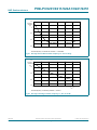
Table 4.
Special function registers - P89LPC9201/9211/922A1
* indicates SFRs that are bit addressable.
xxxxxxxxxxxxxxxxxxxxx xxxxxxxxxxxxxxxxxxxxxxxxxx xxxxxxx x x x xxxxxxxxxxxxxxxxxxxxxxxxxxxxxx xxxxxxxxxxxxxxxxxxx xx xx xxxxx
xxxxxxxxxxxxxxxxxxxxxxxxxxx xxxxxxxxxxxxxxxxxxx xxxxxx xxxxxxxxxxxxxxxxxxxxxxxxxxxxxxxxxxx xxxxxxxxxxxx x x
xxxxxxxxxxxxxxxxxxxxx xxxxxxxxxxxxxxxxxxxxxxxxxxxxxx xxxxx xxxxxxxxxxxxxxxxxxxxxxxxxxxxxxxxxxxxxxxxxxxxxxxxxx xxxxxxxx
xxxxxxxxxxxxxxxxxxxxxxxxx xxxxxxxxxxxxxxxxxxxx xxx
Name
IP0H
Description
Interrupt
priority 0 high
SFR Bit functions and addresses
addr.
MSB
B7H
Bit address
Reset value
LSB
Hex
Binary
00[1]
x000 0000
-
PWDRTH
PBOH
PSH/
PSRH
PT1H
PX1H
PT0H
PX0H
FF
FE
FD
FC
FB
FA
F9
F8
Interrupt
priority 1
F8H
-
PST
-
-
-
PC
PKBI
PI2C
00[1]
00x0 0000
IP1H
Interrupt
priority 1 high
F7H
-
PSTH
-
-
-
PCH
PKBIH
PI2CH
00[1]
00x0 0000
KBCON
Keypad control
register
94H
-
-
-
-
-
-
PATN
_SEL
KBIF
00[1]
xxxx xx00
KBMASK
Keypad
interrupt mask
register
86H
00
0000 0000
KBPATN
Keypad pattern
register
93H
FF
1111 1111
P0*
Port 0
80H
Bit address
P1*
Port 1
90H
Bit address
87
86
85
84
83
82
81
80
T1/KB7
CMP1
/KB6
CMPREF
/KB5
CIN1A
/KB4
CIN1B
/KB3
CIN2A
/KB2
CIN2B
/KB1
CMP2
/KB0
97
96
95
94
93
92
91
90
-
-
RST
INT1
INT0/SDA
T0/SCL
RXD
TXD
B7
B6
B5
B4
B3
B2
B1
B0
[1]
[1]
15 of 75
© NXP B.V. 2012. All rights reserved.
Port 3
B0H
-
-
-
-
-
-
XTAL1
XTAL2
P0M1
Port 0 output
mode 1
84H
(P0M1.7)
(P0M1.6)
(P0M1.5)
(P0M1.4)
(P0M1.3)
(P0M1.2)
(P0M1.1)
(P0M1.0)
FF[1]
1111 1111
P0M2
Port 0 output
mode 2
85H
(P0M2.7)
(P0M2.6)
(P0M2.5)
(P0M2.4)
(P0M2.3)
(P0M2.2)
(P0M2.1)
(P0M2.0)
00[1]
0000 0000
P1M1
Port 1 output
mode 1
91H
(P1M1.7)
(P1M1.6)
-
(P1M1.4)
(P1M1.3)
(P1M1.2)
(P1M1.1)
(P1M1.0)
D3[1]
11x1 xx11
P1M2
Port 1 output
mode 2
92H
(P1M2.7)
(P1M2.6)
-
(P1M2.4)
(P1M2.3)
(P1M2.2)
(P1M2.1)
(P1M2.0)
00[1]
00x0 xx00
P3M1
Port 3 output
mode 1
B1H
-
-
-
-
-
-
(P3M1.1)
(P3M1.0)
03[1]
xxxx xx11
P3M2
Port 3 output
mode 2
B2H
-
-
-
-
-
-
(P3M2.1)
(P3M2.0)
00[1]
xxxx xx00
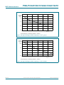
8-bit microcontroller with 8-bit ADC
[1]
P3*
P89LPC9201/9211/922A1/9241/9251
Rev. 2.1 — 27 August 2012
All information provided in this document is subject to legal disclaimers.
IP1*
Bit address
NXP Semiconductors
P89LPC92X1
Product data sheet
Table 4.
Special function registers - P89LPC9201/9211/922A1
* indicates SFRs that are bit addressable.
xxxxxxxxxxxxxxxxxxxxx xxxxxxxxxxxxxxxxxxxxxxxxxx xxxxxxx x x x xxxxxxxxxxxxxxxxxxxxxxxxxxxxxx xxxxxxxxxxxxxxxxxxx xx xx xxxxx
xxxxxxxxxxxxxxxxxxxxxxxxxxx xxxxxxxxxxxxxxxxxxx xxxxxx xxxxxxxxxxxxxxxxxxxxxxxxxxxxxxxxxxx xxxxxxxxxxxx x x
xxxxxxxxxxxxxxxxxxxxx xxxxxxxxxxxxxxxxxxxxxxxxxxxxxx xxxxx xxxxxxxxxxxxxxxxxxxxxxxxxxxxxxxxxxxxxxxxxxxxxxxxxx xxxxxxxx
xxxxxxxxxxxxxxxxxxxxxxxxx xxxxxxxxxxxxxxxxxxxx xxx
Name
Description
SFR Bit functions and addresses
addr.
MSB
Reset value
LSB
Hex
Binary
00
0000 0000
00[1]
0000 0000
Power control
register
87H
SMOD1
SMOD0
-
BOI
GF1
GF0
PMOD1
PMOD0
PCONA
Power control
register A
B5H
RTCPD
-
VCPD
-
I2PD
-
SPD
-
D7
D6
D5
D4
D3
D2
D1
D0
PSW*
Program status
word
D0H
CY
AC
F0
RS1
RS0
OV
F1
P
00
0000 0000
PT0AD
Port 0 digital
input disable
F6H
-
-
PT0AD.5
PT0AD.4
PT0AD.3
PT0AD.2
PT0AD.1
-
00
xx00 000x
RSTSRC
Reset source
register
DFH
-
BOIF
BOF
POF
R_BK
R_WD
R_SF
R_EX
[3]
RTCCON
RTC control
D1H
RTCF
RTCS1
RTCS0
-
-
-
ERTC
RTCEN
Rev. 2.1 — 27 August 2012
All information provided in this document is subject to legal disclaimers.
60[1][6]
011x xx00
0000 0000
RTC register
high
D2H
RTCL
RTC register
low
D3H
00[6]
0000 0000
SADDR
Serial port
address
register
A9H
00
0000 0000
SADEN
Serial port
address enable
B9H
00
0000 0000
SBUF
Serial Port data
buffer register
99H
xx
xxxx xxxx
Bit address
9F
9E
9D
9C
9B
9A
99
98
16 of 75
© NXP B.V. 2012. All rights reserved.
SCON*
Serial port
control
98H
SM0/FE
SM1
SM2
REN
TB8
RB8
TI
RI
00
0000 0000
SSTAT
Serial port
extended
status register
BAH
DBMOD
INTLO
CIDIS
DBISEL
FE
BR
OE
STINT
00
0000 0000
SP
Stack pointer
81H
07
0000 0111
TAMOD
Timer 0 and 1
auxiliary mode
8FH
00
xxx0 xxx0
-
-
-
T1M2
-
-
-
T0M2
8-bit microcontroller with 8-bit ADC
RTCH
00[6]
P89LPC9201/9211/922A1/9241/9251
PCON
Bit address
NXP Semiconductors
P89LPC92X1
Product data sheet
Table 4.
Special function registers - P89LPC9201/9211/922A1
* indicates SFRs that are bit addressable.
xxxxxxxxxxxxxxxxxxxxx xxxxxxxxxxxxxxxxxxxxxxxxxx xxxxxxx x x x xxxxxxxxxxxxxxxxxxxxxxxxxxxxxx xxxxxxxxxxxxxxxxxxx xx xx xxxxx
xxxxxxxxxxxxxxxxxxxxxxxxxxx xxxxxxxxxxxxxxxxxxx xxxxxx xxxxxxxxxxxxxxxxxxxxxxxxxxxxxxxxxxx xxxxxxxxxxxx x x
xxxxxxxxxxxxxxxxxxxxx xxxxxxxxxxxxxxxxxxxxxxxxxxxxxx xxxxx xxxxxxxxxxxxxxxxxxxxxxxxxxxxxxxxxxxxxxxxxxxxxxxxxx xxxxxxxx
xxxxxxxxxxxxxxxxxxxxxxxxx xxxxxxxxxxxxxxxxxxxx xxx
Name
Description
SFR Bit functions and addresses
addr.
MSB
Bit address
Reset value
LSB
8F
8E
8D
8C
8B
8A
89
88
TF1
TR1
TF0
TR0
IE1
IT1
IE0
IT0
Hex
Binary
00
0000 0000
Timer 0 and 1
control
88H
TH0
Timer 0 high
8CH
00
0000 0000
TH1
Timer 1 high
8DH
00
0000 0000
TL0
Timer 0 low
8AH
00
0000 0000
TL1
Timer 1 low
8BH
00
0000 0000
TMOD
Timer 0 and 1
mode
89H
T1GATE
T1C/T
T1M1
T1M0
T0GATE
T0C/T
T0M1
T0M0
00
0000 0000
TRIM
Internal
oscillator trim
register
96H
RCCLK
ENCLK
TRIM.5
TRIM.4
TRIM.3
TRIM.2
TRIM.1
TRIM.0
[5][6]
WDCON
Watchdog
control register
A7H
PRE2
PRE1
PRE0
-
-
WDRUN
WDTOF
WDCLK
[4][6]
WDL
Watchdog load
C1H
WFEED1
Watchdog
feed 1
C2H
WFEED2
Watchdog
feed 2
C3H
FF
1111 1111
All ports are in input only (high-impedance) state after power-up.
BRGR1 and BRGR0 must only be written if BRGEN in BRGCON SFR is logic 0. If any are written while BRGEN = 1, the result is unpredictable.
The RSTSRC register reflects the cause of the P89LPC9201/9211/922A1 reset except BOIF bit. Upon a power-up reset, all reset source flags are cleared except POF and BOF;
the power-on reset value is x011 0000.
[4]
After reset, the value is 1110 01x1, i.e., PRE2 to PRE0 are all logic 1, WDRUN = 1 and WDCLK = 1. WDTOF bit is logic 1 after watchdog reset and is logic 0 after power-on reset.
Other resets will not affect WDTOF.
[5]
On power-on reset and watchdog reset, the TRIM SFR is initialized with a factory preprogrammed value. Other resets will not cause initialization of the TRIM register.
[6]
The only reset sources that affect these SFRs are power-on reset and watchdog reset.
8-bit microcontroller with 8-bit ADC
17 of 75
© NXP B.V. 2012. All rights reserved.
[2]
[3]
P89LPC9201/9211/922A1/9241/9251
Rev. 2.1 — 27 August 2012
All information provided in this document is subject to legal disclaimers.
TCON*
[1]
NXP Semiconductors
P89LPC92X1
Product data sheet
Table 4.
Special function registers - P89LPC9201/9211/922A1
* indicates SFRs that are bit addressable.
xxxxxxxxxxxxxxxxxxxxx xxxxxxxxxxxxxxxxxxxxxxxxxx xxxxxxx x x x xxxxxxxxxxxxxxxxxxxxxxxxxxxxxx xxxxxxxxxxxxxxxxxxx xx xx xxxxx
xxxxxxxxxxxxxxxxxxxxxxxxxxx xxxxxxxxxxxxxxxxxxx xxxxxx xxxxxxxxxxxxxxxxxxxxxxxxxxxxxxxxxxx xxxxxxxxxxxx x x
xxxxxxxxxxxxxxxxxxxxx xxxxxxxxxxxxxxxxxxxxxxxxxxxxxx xxxxx xxxxxxxxxxxxxxxxxxxxxxxxxxxxxxxxxxxxxxxxxxxxxxxxxx xxxxxxxx
xxxxxxxxxxxxxxxxxxxxxxxxx xxxxxxxxxxxxxxxxxxxx xxx
NXP Semiconductors
P89LPC92X1
Product data sheet
Table 5.
Extended special function registers - P89LPC9201/9211/922A1[1]
Description
SFR
addr.
Bit functions and addresses
Reset value
BODCFG
BOD
configuration
register
FFC8H
-
-
-
-
-
-
CLKCON
CLOCK Control
register
FFDEH
CLKOK
-
-
XTALWD
CLKDBL
FOSC2
RTCDATH
Real-time clock
data register
high
FFBFH
00
0000 0000
RTCDATL
Real-time clock FFBEH
data register low
00
0000 0000
MSB
LSB
BOICFG1 BOICFG0
FOSC1
FOSC0
Hex
Binary
[2]
[3]
Rev. 2.1 — 27 August 2012
All information provided in this document is subject to legal disclaimers.
[1]
Extended SFRs are physically located on-chip but logically located in external data memory address space (XDATA). The MOVX A,@DPTR and MOVX @DPTR,A instructions are
used to access these extended SFRs.
[2]
The BOICFG1/0 will be copied from UCFG1.5 and UCFG1.3 when power-on reset.
[3]
CLKCON register reset value comes from UCFG1 and UCFG2. The reset value of CLKCON.2 to CLKCON.0 come from UCFG1.2 to UCFG1.0 and reset value of CLKDBL bit
comes from UCFG2.7.
8-bit microcontroller with 8-bit ADC
18 of 75
© NXP B.V. 2012. All rights reserved.
P89LPC9201/9211/922A1/9241/9251
Name
xxxxxxxxxxxxxxxxxxxxx xxxxxxxxxxxxxxxxxxxxxxxxxx xxxxxxx x x x xxxxxxxxxxxxxxxxxxxxxxxxxxxxxx xxxxxxxxxxxxxxxxxxx xx xx xxxxx
xxxxxxxxxxxxxxxxxxxxxxxxxxx xxxxxxxxxxxxxxxxxxx xxxxxx xxxxxxxxxxxxxxxxxxxxxxxxxxxxxxxxxxx xxxxxxxxxxxx x x
xxxxxxxxxxxxxxxxxxxxx xxxxxxxxxxxxxxxxxxxxxxxxxxxxxx xxxxx xxxxxxxxxxxxxxxxxxxxxxxxxxxxxxxxxxxxxxxxxxxxxxxxxx xxxxxxxx
xxxxxxxxxxxxxxxxxxxxxxxxx xxxxxxxxxxxxxxxxxxxx xxx
NXP Semiconductors
P89LPC92X1
Product data sheet
Table 6.
Special function registers - P89LPC9241/9251
* indicates SFRs that are bit addressable.
Name
Description
SFR Bit functions and addresses
addr.
MSB
Bit address
E7
E6
E5
Reset value
LSB
E4
E3
E2
E1
Hex
Binary
00
0000 0000
E0
E0H
ADCON0
A/D control
register 0
8EH
ENBI0
ENADCI0
TMM0
EDGE0
ADCI0
ENADC0
ADCS01
ADCS00
00
0000 0000
ADCON1
A/D control
register 1
97H
ENBI1
ENADCI1
TMM1
EDGE1
ADCI1
ENADC1
ADCS11
ADCS10
00
0000 0000
ADINS
A/D input
select
A3H
AIN13
AIN12
AIN11
AIN10
AIN03
AIN02
AIN01
AIN00
00
0000 0000
ADMODA
A/D mode
register A
C0H
BNDI1
BURST1
SCC1
SCAN1
BNDI0
BURST0
SCC0
SCAN0
00
0000 0000
ADMODB
A/D mode
register B
A1H
CLK2
CLK1
CLK0
INBND0
ENDAC1
ENDAC0
BSA1
BSA0
00
000x 0000
AD0BH
A/D_0
boundary high
register
BBH
FF
1111 1111
AD0BL
A/D_0
boundary low
register
A6H
00
0000 0000
AD0DAT0
A/D_0 data
register 0
C5H
00
0000 0000
AD0DAT1
A/D_0 data
register 1
C6H
00
0000 0000
AD0DAT2
A/D_0 data
register 2
C7H
00
0000 0000
AD0DAT3
A/D_0 data
register 3
F4H
00
0000 0000
AD1BH
A/D_0
boundary high
register
C4H
FF
1111 1111
AD1BL
A/D_0
boundary low
register
BCH
00
0000 0000
AD1DAT0
A/D_0 data
register 0
D5H
00
0000 0000
8-bit microcontroller with 8-bit ADC
19 of 75
© NXP B.V. 2012. All rights reserved.
Accumulator
P89LPC9201/9211/922A1/9241/9251
Rev. 2.1 — 27 August 2012
All information provided in this document is subject to legal disclaimers.
ACC*
xxxxxxxxxxxxxxxxxxxxx xxxxxxxxxxxxxxxxxxxxxxxxxx xxxxxxx x x x xxxxxxxxxxxxxxxxxxxxxxxxxxxxxx xxxxxxxxxxxxxxxxxxx xx xx xxxxx
xxxxxxxxxxxxxxxxxxxxxxxxxxx xxxxxxxxxxxxxxxxxxx xxxxxx xxxxxxxxxxxxxxxxxxxxxxxxxxxxxxxxxxx xxxxxxxxxxxx x x
xxxxxxxxxxxxxxxxxxxxx xxxxxxxxxxxxxxxxxxxxxxxxxxxxxx xxxxx xxxxxxxxxxxxxxxxxxxxxxxxxxxxxxxxxxxxxxxxxxxxxxxxxx xxxxxxxx
xxxxxxxxxxxxxxxxxxxxxxxxx xxxxxxxxxxxxxxxxxxxx xxx
Name
Description
SFR Bit functions and addresses
addr.
MSB
Reset value
LSB
Hex
Binary
A/D_0 data
register 1
D6H
00
0000 0000
AD1DAT2
A/D_0 data
register 2
D7H
00
0000 0000
AD1DAT3
A/D_0 data
register 3
F5H
00
0000 0000
AUXR1
Auxiliary
function
register
A2H
00
0000 00x0
Rev. 2.1 — 27 August 2012
All information provided in this document is subject to legal disclaimers.
CLKLP
EBRR
ENT1
ENT0
SRST
0
-
DPS
F7
F6
F5
F4
F3
F2
F1
F0
B register
F0H
00
0000 0000
BRGR0[2]
Baud rate
generator 0
rate low
BEH
00
0000 0000
BRGR1[2]
Baud rate
generator 0
rate high
BFH
00
0000 0000
BRGCON
Baud rate
generator 0
control
BDH
-
-
-
-
-
-
SBRGS
BRGEN
00[2]
xxxx xx00
CMP1
Comparator 1
control register
ACH
-
-
CE1
CP1
CN1
OE1
CO1
CMF1
00[1]
xx00 0000
CMP2
Comparator 2
control register
ADH
-
-
CE2
CP2
CN2
OE2
CO2
CMF2
00[1]
xx00 0000
DIVM
CPU clock
divide-by-M
control
95H
00
0000 0000
DPTR
Data pointer
(2 bytes)
DPH
Data pointer
high
83H
00
0000 0000
DPL
Data pointer
low
82H
00
0000 0000
8-bit microcontroller with 8-bit ADC
20 of 75
© NXP B.V. 2012. All rights reserved.
B*
P89LPC9201/9211/922A1/9241/9251
AD1DAT1
Bit address
NXP Semiconductors
P89LPC92X1
Product data sheet
Table 6.
Special function registers - P89LPC9241/9251 …continued
* indicates SFRs that are bit addressable.
xxxxxxxxxxxxxxxxxxxxx xxxxxxxxxxxxxxxxxxxxxxxxxx xxxxxxx x x x xxxxxxxxxxxxxxxxxxxxxxxxxxxxxx xxxxxxxxxxxxxxxxxxx xx xx xxxxx
xxxxxxxxxxxxxxxxxxxxxxxxxxx xxxxxxxxxxxxxxxxxxx xxxxxx xxxxxxxxxxxxxxxxxxxxxxxxxxxxxxxxxxx xxxxxxxxxxxx x x
xxxxxxxxxxxxxxxxxxxxx xxxxxxxxxxxxxxxxxxxxxxxxxxxxxx xxxxx xxxxxxxxxxxxxxxxxxxxxxxxxxxxxxxxxxxxxxxxxxxxxxxxxx xxxxxxxx
xxxxxxxxxxxxxxxxxxxxxxxxx xxxxxxxxxxxxxxxxxxxx xxx
Name
Description
SFR Bit functions and addresses
addr.
MSB
Reset value
LSB
Hex
Binary
Program flash
address high
E7H
00
0000 0000
FMADRL
Program flash
address low
E6H
00
0000 0000
FMCON
Program flash
control (Read)
E4H
BUSY
-
-
-
HVA
HVE
SV
OI
70
0111 0000
Program flash
control (Write)
E4H
FMCMD.7
FMCMD.6
FMCMD.5
FMCMD.4
FMCMD.3
FMCMD.2
FMCMD.1
FMCMD.0
FMDATA
Program flash
data
E5H
00
0000 0000
I2ADR
I2C-bus slave
address
register
DBH
00
0000 0000
I2CON*
I2C-bus
00
x000 00x0
control
D8H
I2ADR.6
I2ADR.5
I2ADR.4
I2ADR.3
I2ADR.2
I2ADR.1
I2ADR.0
GC
DF
DE
DD
DC
DB
DA
D9
D8
-
I2EN
STA
STO
SI
AA
-
CRSEL
register
I2C-bus data
register
DAH
I2SCLH
Serial clock
generator/SCL
duty cycle
register high
DDH
00
0000 0000
I2SCLL
Serial clock
generator/SCL
duty cycle
register low
DCH
00
0000 0000
I2STAT
I2C-bus status
register
D9H
F8
1111 1000
IEN0*
Interrupt
enable 0
00
0000 0000
00[1]
00x0 0000
Bit address
A8H
Bit address
IEN1*
Interrupt
enable 1
E8H
STA.4
STA.3
STA.2
STA.1
STA.0
0
0
0
AF
AE
AD
AC
AB
AA
A9
A8
EA
EWDRT
EBO
ES/ESR
ET1
EX1
ET0
EX0
EF
EE
ED
EC
EB
EA
E9
E8
EAD
EST
-
-
-
EC
EKBI
EI2C
8-bit microcontroller with 8-bit ADC
21 of 75
© NXP B.V. 2012. All rights reserved.
I2DAT
P89LPC9201/9211/922A1/9241/9251
Rev. 2.1 — 27 August 2012
All information provided in this document is subject to legal disclaimers.
FMADRH
Bit address
NXP Semiconductors
P89LPC92X1
Product data sheet
Table 6.
Special function registers - P89LPC9241/9251 …continued
* indicates SFRs that are bit addressable.
xxxxxxxxxxxxxxxxxxxxx xxxxxxxxxxxxxxxxxxxxxxxxxx xxxxxxx x x x xxxxxxxxxxxxxxxxxxxxxxxxxxxxxx xxxxxxxxxxxxxxxxxxx xx xx xxxxx
xxxxxxxxxxxxxxxxxxxxxxxxxxx xxxxxxxxxxxxxxxxxxx xxxxxx xxxxxxxxxxxxxxxxxxxxxxxxxxxxxxxxxxx xxxxxxxxxxxx x x
xxxxxxxxxxxxxxxxxxxxx xxxxxxxxxxxxxxxxxxxxxxxxxxxxxx xxxxx xxxxxxxxxxxxxxxxxxxxxxxxxxxxxxxxxxxxxxxxxxxxxxxxxx xxxxxxxx
xxxxxxxxxxxxxxxxxxxxxxxxx xxxxxxxxxxxxxxxxxxxx xxx
Name
Description
SFR Bit functions and addresses
addr.
MSB
Bit address
Reset value
LSB
Hex
Binary
BF
BE
BD
BC
BB
BA
B9
B8
IP0*
Interrupt
priority 0
B8H
-
PWDRT
PBO
PS/PSR
PT1
PX1
PT0
PX0
00[1]
x000 0000
IP0H
Interrupt
priority 0 high
B7H
-
PWDRTH
PBOH
PSH/
PSRH
PT1H
PX1H
PT0H
PX0H
00[1]
x000 0000
FF
FE
FD
FC
FB
FA
F9
F8
Bit address
Interrupt
priority 1
F8H
PAD
PST
-
-
-
PC
PKBI
PI2C
00[1]
00x0 0000
IP1H
Interrupt
priority 1 high
F7H
PADH
PSTH
-
-
-
PCH
PKBIH
PI2CH
00[1]
00x0 0000
KBCON
Keypad control
register
94H
-
-
-
-
-
-
PATN
_SEL
KBIF
00[1]
xxxx xx00
KBMASK
Keypad
interrupt mask
register
86H
00
0000 0000
KBPATN
Keypad pattern
register
93H
FF
1111 1111
Port 0
P1*
Port 1
80H
Bit address
90H
Bit address
86
85
84
83
82
81
80
T1/KB7
CMP1
/KB6
CMPREF
/KB5
CIN1A
/KB4
CIN1B
/KB3
CIN2A
/KB2
CIN2B
/KB1
CMP2
/KB0
97
96
95
94
93
92
91
90
-
-
RST
INT1
INT0/SDA
T0/SCL
RXD
TXD
B7
B6
B5
B4
B3
B2
B1
B0
[1]
[1]
[1]
22 of 75
© NXP B.V. 2012. All rights reserved.
P3*
Port 3
B0H
-
-
-
-
-
-
XTAL1
XTAL2
P0M1
Port 0 output
mode 1
84H
(P0M1.7)
(P0M1.6)
(P0M1.5)
(P0M1.4)
(P0M1.3)
(P0M1.2)
(P0M1.1)
(P0M1.0)
FF[1]
1111 1111
P0M2
Port 0 output
mode 2
85H
(P0M2.7)
(P0M2.6)
(P0M2.5)
(P0M2.4)
(P0M2.3)
(P0M2.2)
(P0M2.1)
(P0M2.0)
00[1]
0000 0000
P1M1
Port 1 output
mode 1
91H
(P1M1.7)
(P1M1.6)
-
(P1M1.4)
(P1M1.3)
(P1M1.2)
(P1M1.1)
(P1M1.0)
D3[1]
11x1 xx11
P1M2
Port 1 output
mode 2
92H
(P1M2.7)
(P1M2.6)
-
(P1M2.4)
(P1M2.3)
(P1M2.2)
(P1M2.1)
(P1M2.0)
00[1]
00x0 xx00
8-bit microcontroller with 8-bit ADC
P0*
87
P89LPC9201/9211/922A1/9241/9251
Rev. 2.1 — 27 August 2012
All information provided in this document is subject to legal disclaimers.
IP1*
Bit address
NXP Semiconductors
P89LPC92X1
Product data sheet
Table 6.
Special function registers - P89LPC9241/9251 …continued
* indicates SFRs that are bit addressable.
xxxxxxxxxxxxxxxxxxxxx xxxxxxxxxxxxxxxxxxxxxxxxxx xxxxxxx x x x xxxxxxxxxxxxxxxxxxxxxxxxxxxxxx xxxxxxxxxxxxxxxxxxx xx xx xxxxx
xxxxxxxxxxxxxxxxxxxxxxxxxxx xxxxxxxxxxxxxxxxxxx xxxxxx xxxxxxxxxxxxxxxxxxxxxxxxxxxxxxxxxxx xxxxxxxxxxxx x x
xxxxxxxxxxxxxxxxxxxxx xxxxxxxxxxxxxxxxxxxxxxxxxxxxxx xxxxx xxxxxxxxxxxxxxxxxxxxxxxxxxxxxxxxxxxxxxxxxxxxxxxxxx xxxxxxxx
xxxxxxxxxxxxxxxxxxxxxxxxx xxxxxxxxxxxxxxxxxxxx xxx
Name
Description
SFR Bit functions and addresses
addr.
MSB
Reset value
LSB
Hex
Binary
xxxx xx11
Port 3 output
mode 1
B1H
-
-
-
-
-
-
(P3M1.1)
(P3M1.0)
P3M2
Port 3 output
mode 2
B2H
-
-
-
-
-
-
(P3M2.1)
(P3M2.0)
00[1]
xxxx xx00
PCON
Power control
register
87H
SMOD1
SMOD0
-
BOI
GF1
GF0
PMOD1
PMOD0
00
0000 0000
PCONA
Power control
register A
B5H
RTCPD
-
VCPD
ADPD
I2PD
-
SPD
-
00[1]
0000 0000
D7
D6
D5
D4
D3
D2
D1
D0
PSW*
Program status
word
D0H
CY
AC
F0
RS1
RS0
OV
F1
P
00
0000 0000
PT0AD
Port 0 digital
input disable
F6H
-
-
PT0AD.5
PT0AD.4
PT0AD.3
PT0AD.2
PT0AD.1
-
00
xx00 000x
RSTSRC
Reset source
register
DFH
-
BOIF
BOF
POF
R_BK
R_WD
R_SF
R_EX
[3]
RTCCON
RTC control
D1H
RTCF
RTCS1
RTCS0
-
-
-
ERTC
RTCEN
Rev. 2.1 — 27 August 2012
All information provided in this document is subject to legal disclaimers.
60[1][6]
011x xx00
0000 0000
RTC register
high
D2H
RTCL
RTC register
low
D3H
00[6]
0000 0000
SADDR
Serial port
address
register
A9H
00
0000 0000
SADEN
Serial port
address enable
B9H
00
0000 0000
SBUF
Serial Port data
buffer register
99H
xx
xxxx xxxx
23 of 75
© NXP B.V. 2012. All rights reserved.
Bit address
9F
9E
9D
9C
9B
9A
99
98
SCON*
Serial port
control
98H
SM0/FE
SM1
SM2
REN
TB8
RB8
TI
RI
00
0000 0000
SSTAT
Serial port
extended
status register
BAH
DBMOD
INTLO
CIDIS
DBISEL
FE
BR
OE
STINT
00
0000 0000
8-bit microcontroller with 8-bit ADC
RTCH
00[6]
P89LPC9201/9211/922A1/9241/9251
P3M1
03[1]
Bit address
NXP Semiconductors
P89LPC92X1
Product data sheet
Table 6.
Special function registers - P89LPC9241/9251 …continued
* indicates SFRs that are bit addressable.
xxxxxxxxxxxxxxxxxxxxx xxxxxxxxxxxxxxxxxxxxxxxxxx xxxxxxx x x x xxxxxxxxxxxxxxxxxxxxxxxxxxxxxx xxxxxxxxxxxxxxxxxxx xx xx xxxxx
xxxxxxxxxxxxxxxxxxxxxxxxxxx xxxxxxxxxxxxxxxxxxx xxxxxx xxxxxxxxxxxxxxxxxxxxxxxxxxxxxxxxxxx xxxxxxxxxxxx x x
xxxxxxxxxxxxxxxxxxxxx xxxxxxxxxxxxxxxxxxxxxxxxxxxxxx xxxxx xxxxxxxxxxxxxxxxxxxxxxxxxxxxxxxxxxxxxxxxxxxxxxxxxx xxxxxxxx
xxxxxxxxxxxxxxxxxxxxxxxxx xxxxxxxxxxxxxxxxxxxx xxx
Name
Description
SFR Bit functions and addresses
addr.
MSB
SP
Stack pointer
81H
TAMOD
Timer 0 and 1
auxiliary mode
8FH
Bit address
Reset value
LSB
Hex
Binary
07
0000 0111
00
xxx0 xxx0
00
0000 0000
-
-
-
T1M2
-
-
-
T0M2
8F
8E
8D
8C
8B
8A
89
88
TF1
TR1
TF0
TR0
IE1
IT1
IE0
IT0
Timer 0 and 1
control
88H
TH0
Timer 0 high
8CH
00
0000 0000
TH1
Timer 1 high
8DH
00
0000 0000
TL0
Timer 0 low
8AH
00
0000 0000
TL1
Timer 1 low
8BH
00
0000 0000
TMOD
Timer 0 and 1
mode
89H
T1GATE
T1C/T
T1M1
T1M0
T0GATE
T0C/T
T0M1
T0M0
00
0000 0000
TRIM
Internal
oscillator trim
register
96H
RCCLK
ENCLK
TRIM.5
TRIM.4
TRIM.3
TRIM.2
TRIM.1
TRIM.0
[5][6]
WDCON
Watchdog
control register
A7H
PRE2
PRE1
PRE0
-
-
WDRUN
WDTOF
WDCLK
[4][6]
WDL
Watchdog load
C1H
WFEED1
Watchdog
feed 1
C2H
WFEED2
Watchdog
feed 2
C3H
FF
1111 1111
24 of 75
© NXP B.V. 2012. All rights reserved.
[2]
BRGR1 and BRGR0 must only be written if BRGEN in BRGCON SFR is logic 0. If any are written while BRGEN = 1, the result is unpredictable.
[3]
The RSTSRC register reflects the cause of the P89LPC9241/9251 reset except BOIF bit. Upon a power-up reset, all reset source flags are cleared except POF and BOF; the
power-on reset value is x011 0000.
[4]
After reset, the value is 1110 01x1, i.e., PRE2 to PRE0 are all logic 1, WDRUN = 1 and WDCLK = 1. WDTOF bit is logic 1 after watchdog reset and is logic 0 after power-on reset.
Other resets will not affect WDTOF.
[5]
On power-on reset and watchdog reset, the TRIM SFR is initialized with a factory preprogrammed value. Other resets will not cause initialization of the TRIM register.
[6]
The only reset sources that affect these SFRs are power-on reset and watchdog reset.
CLKCON register reset value comes from UCFG1 and UCFG2. The reset value of CLKCON.2 to CLKCON.0 come from UCFG1.2 to UCFG1.0 and reset value of CLKDBL bit
comes from UCFG2.7
8-bit microcontroller with 8-bit ADC
All ports are in input only (high-impedance) state after power-up.
P89LPC9201/9211/922A1/9241/9251
Rev. 2.1 — 27 August 2012
All information provided in this document is subject to legal disclaimers.
TCON*
[1]
NXP Semiconductors
P89LPC92X1
Product data sheet
Table 6.
Special function registers - P89LPC9241/9251 …continued
* indicates SFRs that are bit addressable.
xxxxxxxxxxxxxxxxxxxxx xxxxxxxxxxxxxxxxxxxxxxxxxx xxxxxxx x x x xxxxxxxxxxxxxxxxxxxxxxxxxxxxxx xxxxxxxxxxxxxxxxxxx xx xx xxxxx
xxxxxxxxxxxxxxxxxxxxxxxxxxx xxxxxxxxxxxxxxxxxxx xxxxxx xxxxxxxxxxxxxxxxxxxxxxxxxxxxxxxxxxx xxxxxxxxxxxx x x
xxxxxxxxxxxxxxxxxxxxx xxxxxxxxxxxxxxxxxxxxxxxxxxxxxx xxxxx xxxxxxxxxxxxxxxxxxxxxxxxxxxxxxxxxxxxxxxxxxxxxxxxxx xxxxxxxx
xxxxxxxxxxxxxxxxxxxxxxxxx xxxxxxxxxxxxxxxxxxxx xxx
NXP Semiconductors
P89LPC92X1
Product data sheet
Table 7.
Extended special function registers - P89LPC9241/9251[1]
Description
SFR
addr.
Bit functions and addresses
Reset value
BODCFG
BOD
configuration
register
FFC8H
-
-
-
-
-
-
CLKCON
CLOCK Control
register
FFDEH
CLKOK
-
-
XTALWD
CLKDBL
FOSC2
FOSC1
FOSC0
[3]
TPSCON
Temperature
sensor control
register
FFCAH
-
-
-
-
TSEL1
TSEL0
-
-
00
0000 0000
RTCDATH
Real-time clock
data register
high
FFBFH
00
0000 0000
RTCDATL
Real-time clock FFBEH
data register low
00
0000 0000
MSB
LSB
BOICFG1 BOICFG0
Hex
Binary
[2]
[1]
Extended SFRs are physically located on-chip but logically located in external data memory address space (XDATA). The MOVX A,@DPTR and MOVX @DPTR,A instructions are
used to access these extended SFRs.
[2]
The BOICFG1/0 will be copied from UCFG1.5 and UCFG1.3 when power-on reset.
[3]
CLKCON register reset value comes from UCFG1 and UCFG2. The reset value of CLKCON.2 to CLKCON.0 come from UCFG1.2 to UCFG1.0 and reset value of CLKDBL bit
comes from UCFG2.7.
8-bit microcontroller with 8-bit ADC
25 of 75
© NXP B.V. 2012. All rights reserved.
P89LPC9201/9211/922A1/9241/9251
Rev. 2.1 — 27 August 2012
All information provided in this document is subject to legal disclaimers.
Name
NXP Semiconductors
P89LPC9201/9211/922A1/9241/9251
8-bit microcontroller with 8-bit ADC
7.2 Enhanced CPU
The P89LPC9201/9211/922A1/9241/9251 uses an enhanced 80C51 CPU which runs at
six times the speed of standard 80C51 devices. A machine cycle consists of two CPU
clock cycles, and most instructions execute in one or two machine cycles.
7.3 Clocks
7.3.1 Clock definitions
The P89LPC9201/9211/922A1/9241/9251 device has several internal clocks as defined
below:
OSCCLK — Input to the DIVM clock divider. OSCCLK is selected from one of four clock
sources (see Figure 8) and can also be optionally divided to a slower frequency (see
Section 7.11 “CCLK modification: DIVM register”).
Remark: fosc is defined as the OSCCLK frequency.
CCLK — CPU clock; output of the clock divider. There are two CCLK cycles per machine
cycle, and most instructions are executed in one to two machine cycles (two or four CCLK
cycles).
RCCLK — The internal 7.373 MHz RC oscillator output. The clock doubler option, when
enabled, provides an output frequency of 14.746 MHz.
PCLK — Clock for the various peripheral devices and is CCLK⁄2.
7.3.2 CPU clock (OSCCLK)
The P89LPC9201/9211/922A1/9241/9251 provides several user-selectable oscillator
options in generating the CPU clock. This allows optimization for a range of needs from
high precision to lowest possible cost. These options are configured when the flash is
programmed and include an on-chip watchdog oscillator, an on-chip RC oscillator, an
oscillator using an external crystal, or an external clock source.
7.4 Crystal oscillator option
The crystal oscillator can be optimized for low, medium, or high frequency crystals
covering a range from 20 kHz to 18 MHz. It can be the clock source of OSCCLK and RTC.
Low speed oscillator option can be the clock source of WDT.
7.4.1 Low speed oscillator option
This option supports an external crystal in the range of 20 kHz to 100 kHz. Ceramic
resonators are also supported in this configuration.
7.4.2 Medium speed oscillator option
This option supports an external crystal in the range of 100 kHz to 4 MHz. Ceramic
resonators are also supported in this configuration.
7.4.3 High speed oscillator option
This option supports an external crystal in the range of 4 MHz to 18 MHz. Ceramic
resonators are also supported in this configuration.
P89LPC92X1
Product data sheet
All information provided in this document is subject to legal disclaimers.
Rev. 2.1 — 27 August 2012
© NXP B.V. 2012. All rights reserved.
26 of 75
NXP Semiconductors
P89LPC9201/9211/922A1/9241/9251
8-bit microcontroller with 8-bit ADC
7.5 Clock output
The P89LPC9201/9211/922A1/9241/9251 supports a user-selectable clock output
function on the P3.0/XTAL2/CLKOUT pin when crystal oscillator is not being used. This
condition occurs if another clock source has been selected (on-chip RC oscillator,
watchdog oscillator, external clock input on XTAL1) and if the RTC and WDT are not using
the crystal oscillator as their clock source. This allows external devices to synchronize to
the P89LPC9201/9211/922A1/9241/9251. This output is enabled by the ENCLK bit in the
TRIM register.
The frequency of this clock output is 1⁄2 that of the CCLK. If the clock output is not needed
in Idle mode, it may be turned off prior to entering Idle, saving additional power.
7.6 On-chip RC oscillator option
The P89LPC9201/9211/922A1/9241/9251 has a 6-bit TRIM register that can be used to
tune the frequency of the RC oscillator. During reset, the TRIM value is initialized to a
factory preprogrammed value to adjust the oscillator frequency to 7.373 MHz 1 % at
room temperature. End-user applications can write to the TRIM register to adjust the
on-chip RC oscillator to other frequencies. When the clock doubler option is enabled
(UCFG2.7 = 1), the output frequency is 14.746 MHz. If CCLK is 8 MHz or slower, the
CLKLP SFR bit (AUXR1.7) can be set to logic 1 to reduce power consumption. On reset,
CLKLP is logic 0 allowing highest performance access. This bit can then be set in
software if CCLK is running at 8 MHz or slower. When clock doubler option is enabled,
BOE1 bit (UCFG1.5) and BOE0 bit (UCFG1.3) are required to hold the device in reset at
power-up until VDD has reached its specified level.
7.7 Watchdog oscillator option
The watchdog has a separate oscillator which has a frequency of 400 kHz, calibrated to
5 % at room temperature. This oscillator can be used to save power when a high clock
frequency is not needed.
7.8 External clock input option
In this configuration, the processor clock is derived from an external source driving the
P3.1/XTAL1 pin. The rate may be from 0 Hz up to 18 MHz. The P3.0/XTAL2/CLKOUT pin
may be used as a standard port pin or a clock output. When using an oscillator frequency
above 12 MHz, BOE1 bit (UCFG1.5) and BOE0 bit (UCFG1.3) are required to hold the
device in reset at power-up until VDD has reached its specified level.
7.9 Clock sources switch on the fly
P89LPC9201/9211/922A1/9241/9251 can implement clock source switch in any sources
of watchdog oscillator, 7 MHz/14 MHz internal RC oscillator, external clock source
(external crystal or external clock input) during code is running. CLKOK bit in CLKCON
register is used to indicate the clock switch status. CLKOK is cleared when starting clock
source switch and set when completed. Notice that when CLKOK is ‘0’, writing to
CLKCON register is not allowed.
P89LPC92X1
Product data sheet
All information provided in this document is subject to legal disclaimers.
Rev. 2.1 — 27 August 2012
© NXP B.V. 2012. All rights reserved.
27 of 75
P89LPC9201/9211/922A1/9241/9251
NXP Semiconductors
8-bit microcontroller with 8-bit ADC
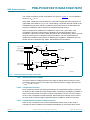
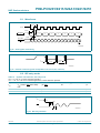
XTAL1
XTAL2
HIGH FREQUENCY
MEDIUM FREQUENCY
LOW FREQUENCY
RTC
ADC
(P89LPC9241/9251)
OSCCLK
RC OSCILLATOR
WITH CLOCK DOUBLER
DIVM
CCLK
CPU
RCCLK
÷2
(7.3728 MHz/14.7456 MHz ± 1 %)
PCLK
WDT
WATCHDOG
OSCILLATOR
PCLK
(400 kHz ± 5 %)
TIMER 0 AND
TIMER 1
I2C-BUS
UART
002aae428
Fig 8.
Block diagram of oscillator control
7.10 CCLK wake-up delay
The P89LPC9201/9211/922A1/9241/9251 has an internal wake-up timer that delays the
clock until it stabilizes depending on the clock source used. If the clock source is any of
the three crystal selections (low, medium and high frequencies) the delay is
1024 OSCCLK cycles plus 60 s to 100 s. If the clock source is the internal RC
oscillator, the delay is 200 s to 300 s. If the clock source is watchdog oscillator or
external clock, the delay is 32 OSCCLK cycles.
7.11 CCLK modification: DIVM register
The OSCCLK frequency can be divided down up to 510 times by configuring a dividing
register, DIVM, to generate CCLK. This feature makes it possible to temporarily run the
CPU at a lower rate, reducing power consumption. By dividing the clock, the CPU can
retain the ability to respond to events that would not exit Idle mode by executing its normal
program at a lower rate. This can also allow bypassing the oscillator start-up time in cases
where Power-down mode would otherwise be used. The value of DIVM may be changed
by the program at any time without interrupting code execution.
7.12 Low power select
The P89LPC9201/9211/922A1/9241/9251 is designed to run at 18 MHz (CCLK)
maximum. However, if CCLK is 8 MHz or slower, the CLKLP SFR bit (AUXR1.7) can be
set to logic 1 to lower the power consumption further. On any reset, CLKLP is logic 0
allowing highest performance access. This bit can then be set in software if CCLK is
running at 8 MHz or slower.
P89LPC92X1
Product data sheet
All information provided in this document is subject to legal disclaimers.
Rev. 2.1 — 27 August 2012
© NXP B.V. 2012. All rights reserved.
28 of 75
P89LPC9201/9211/922A1/9241/9251
NXP Semiconductors
8-bit microcontroller with 8-bit ADC
7.13 Memory organization
The various P89LPC9201/9211/922A1/9241/9251 memory spaces are as follows:
• DATA
128 bytes of internal data memory space (00H:7FH) accessed via direct or indirect
addressing, using instructions other than MOVX and MOVC. All or part of the Stack
may be in this area.
• IDATA
Indirect Data. 256 bytes of internal data memory space (00H:FFH) accessed via
indirect addressing using instructions other than MOVX and MOVC. All or part of the
Stack may be in this area. This area includes the DATA area and the 128 bytes
immediately above it.
• SFR
Special Function Registers. Selected CPU registers and peripheral control and status
registers, accessible only via direct addressing.
• CODE
64 kB of Code memory space, accessed as part of program execution and via the
MOVC instruction. The P89LPC9201/9211/922A1/9241/9251 has 2 kB/4 kB/8 kB of
on-chip Code memory.
7.14 Data RAM arrangement
The 256 bytes of on-chip RAM are organized as shown in Table 8.
Table 8.
On-chip data memory usages
Type
Data RAM
Size (bytes)
DATA
Memory that can be addressed directly and indirectly
128
IDATA
Memory that can be addressed indirectly
256
7.15 Interrupts
The P89LPC9201/9211/922A1/9241/9251 uses a four priority level interrupt structure.
This allows great flexibility in controlling the handling of the many interrupt sources. The
P89LPC9201/9211/922A1/9241/9251 supports 12/13 interrupt sources: external
interrupts 0 and 1, timers 0 and 1, serial port TX, serial port RX, combined serial port
RX/TX, brownout detect, watchdog/RTC, I2C-bus, keyboard, comparators 1 and 2, A/D
Converter (P89LPC9241/9251).
Each interrupt source can be individually enabled or disabled by setting or clearing a bit in
the interrupt enable registers IEN0 or IEN1. The IEN0 register also contains a global
disable bit, EA, which disables all interrupts.
Each interrupt source can be individually programmed to one of four priority levels by
setting or clearing bits in the interrupt priority registers IP0, IP0H, IP1 and IP1H. An
interrupt service routine in progress can be interrupted by a higher priority interrupt, but
not by another interrupt of the same or lower priority. The highest priority interrupt service
cannot be interrupted by any other interrupt source. If two requests of different priority
levels are pending at the start of an instruction, the request of higher priority level is
serviced.
P89LPC92X1
Product data sheet
All information provided in this document is subject to legal disclaimers.
Rev. 2.1 — 27 August 2012
© NXP B.V. 2012. All rights reserved.
29 of 75
NXP Semiconductors
P89LPC9201/9211/922A1/9241/9251
8-bit microcontroller with 8-bit ADC
If requests of the same priority level are pending at the start of an instruction, an internal
polling sequence determines which request is serviced. This is called the arbitration
ranking. Note that the arbitration ranking is only used to resolve pending requests of the
same priority level.
7.15.1 External interrupt inputs
The P89LPC9201/9211/922A1/9241/9251 has two external interrupt inputs as well as the
Keypad Interrupt function. The two interrupt inputs are identical to those present on the
standard 80C51 microcontrollers.
These external interrupts can be programmed to be level-triggered or edge-triggered by
setting or clearing bit IT1 or IT0 in Register TCON.
In edge-triggered mode, if successive samples of the INTn pin show a HIGH in one cycle
and a LOW in the next cycle, the interrupt request flag IEn in TCON is set, causing an
interrupt request.
If an external interrupt is enabled when the P89LPC9201/9211/922A1/9241/9251 is put
into Power-down or Idle mode, the interrupt will cause the processor to wake-up and
resume operation. Refer to Section 7.18 “Power reduction modes” for details.
P89LPC92X1
Product data sheet
All information provided in this document is subject to legal disclaimers.
Rev. 2.1 — 27 August 2012
© NXP B.V. 2012. All rights reserved.
30 of 75
NXP Semiconductors
P89LPC9201/9211/922A1/9241/9251
8-bit microcontroller with 8-bit ADC
IE0
EX0
IE1
EX1
BOIF
EBO
RTCF
ERTC
(RTCCON.1)
WDOVF
wake-up
(if in power-down)
KBIF
EKBI
EWDRT
CMF2
CMF1
EC
EA (IE0.7)
TF0
ET0
TF1
ET1
TI and RI/RI
ES/ESR
TI
EST
interrupt
to CPU
SI
EI2C
ENADCI0(1)
ADCI0(1)
ENADCI1(1)
ADCI1(1)
ENBI0(1)
BNDI0(1)
ENBI1(1)
BNDI1(1)
EAD(1)
002aae429
(1) P89LPC9241/9251.
Fig 9.
Interrupt sources, interrupt enables, and power-down wake-up sources
P89LPC92X1
Product data sheet
All information provided in this document is subject to legal disclaimers.
Rev. 2.1 — 27 August 2012
© NXP B.V. 2012. All rights reserved.
31 of 75
P89LPC9201/9211/922A1/9241/9251
NXP Semiconductors
8-bit microcontroller with 8-bit ADC
7.16 I/O ports
The P89LPC9201/9211/922A1/9241/9251 has four I/O ports: Port 0, Port 1 and Port 3.
Ports 0 and 1 are 8-bit ports, and Port 3 is a 2-bit port. The exact number of I/O pins
available depends upon the clock and reset options chosen, as shown in Table 9.
Table 9.
Number of I/O pins available
Clock source
Reset option
Number of I/O
pins (28-pin
package)
On-chip oscillator or watchdog
oscillator
No external reset (except during
power-up)
18
External RST pin supported
17
External clock input
No external reset (except during
power-up)
17
External RST pin supported
16
No external reset (except during
power-up)
16
External RST pin supported
15
Low/medium/high speed
oscillator (external crystal or
resonator)
7.16.1 Port configurations
All but three I/O port pins on the P89LPC9201/9211/922A1/9241/9251 may be configured
by software to one of four types on a bit-by-bit basis. These are: quasi-bidirectional
(standard 80C51 port outputs), push-pull, open drain, and input-only. Two configuration
registers for each port select the output type for each port pin.
1. P1.5 (RST) can only be an input and cannot be configured.
2. P1.2 (SCL/T0) and P1.3 (SDA/INT0) may only be configured to be either input-only or
open-drain.
7.16.1.1
Quasi-bidirectional output configuration
Quasi-bidirectional output type can be used as both an input and output without the need
to reconfigure the port. This is possible because when the port outputs a logic HIGH, it is
weakly driven, allowing an external device to pull the pin LOW. When the pin is driven
LOW, it is driven strongly and able to sink a fairly large current. These features are
somewhat similar to an open-drain output except that there are three pull-up transistors in
the quasi-bidirectional output that serve different purposes.
The P89LPC9201/9211/922A1/9241/9251 is a 3 V device, but the pins are 5 V tolerant. In
quasi-bidirectional mode, if a user applies 5 V on the pin, there will be a current flowing
from the pin to VDD, causing extra power consumption. Therefore, applying 5 V in
quasi-bidirectional mode is discouraged.
A quasi-bidirectional port pin has a Schmitt trigger input that also has a glitch suppression
circuit.
7.16.1.2
Open-drain output configuration
The open-drain output configuration turns off all pull-ups and only drives the pull-down
transistor of the port driver when the port latch contains a logic 0. To be used as a logic
output, a port configured in this manner must have an external pull-up, typically a resistor
tied to VDD.
P89LPC92X1
Product data sheet
All information provided in this document is subject to legal disclaimers.
Rev. 2.1 — 27 August 2012
© NXP B.V. 2012. All rights reserved.
32 of 75
NXP Semiconductors
P89LPC9201/9211/922A1/9241/9251
8-bit microcontroller with 8-bit ADC
An open-drain port pin has a Schmitt trigger input that also has a glitch suppression
circuit.
7.16.1.3
Input-only configuration
The input-only port configuration has no output drivers. It is a Schmitt trigger input that
also has a glitch suppression circuit.
7.16.1.4
Push-pull output configuration
The push-pull output configuration has the same pull-down structure as both the
open-drain and the quasi-bidirectional output modes, but provides a continuous strong
pull-up when the port latch contains a logic 1. The push-pull mode may be used when
more source current is needed from a port output. A push-pull port pin has a
Schmitt triggered input that also has a glitch suppression circuit. The
P89LPC9201/9211/922A1/9241/9251 device has high current source on eight pins in
push-pull mode. See Table 11 “Limiting values”.
7.16.2 Port 0 analog functions
The P89LPC9201/9211/922A1/9241/9251 incorporates two Analog Comparators. In order
to give the best analog function performance and to minimize power consumption, pins
that are being used for analog functions must have the digital outputs and digital inputs
disabled.
Digital outputs are disabled by putting the port output into the Input-Only
(high-impedance) mode.
Digital inputs on Port 0 may be disabled through the use of the PT0AD register, bits 1:5.
On any reset, PT0AD[1:5] defaults to logic 0s to enable digital functions.
7.16.3 Additional port features
After power-up, all pins are in Input-Only mode. Please note that this is different from
the LPC76x series of devices.
• After power-up, all I/O pins except P1.5, may be configured by software.
• Pin P1.5 is input only. Pins P1.2 and P1.3 are configurable for either input-only or
open-drain.
Every output on the P89LPC9201/9211/922A1/9241/9251 has been designed to sink
typical LED drive current. However, there is a maximum total output current for all ports
which must not be exceeded. Please refer to Table 12 “Static characteristics” for detailed
specifications.
All ports pins that can function as an output have slew rate controlled outputs to limit noise
generated by quickly switching output signals. The slew rate is factory-set to
approximately 10 ns rise and fall times.
7.17 Power monitoring functions
The P89LPC9201/9211/922A1/9241/9251 incorporates power monitoring functions
designed to prevent incorrect operation during initial power-up and power loss or
reduction during operation. This is accomplished with two hardware functions: Power-on
detect and brownout detect.
P89LPC92X1
Product data sheet
All information provided in this document is subject to legal disclaimers.
Rev. 2.1 — 27 August 2012
© NXP B.V. 2012. All rights reserved.
33 of 75
NXP Semiconductors
P89LPC9201/9211/922A1/9241/9251
8-bit microcontroller with 8-bit ADC
7.17.1 Brownout detection
The brownout detect function determines if the power supply voltage drops below a
certain level. Enhanced brownout detection has 3 independent functions: BOD reset,
BOD interrupt and BOD FLASH.
BOD reset is always on except in total Power-down mode. It could not be disabled in
software. BOD interrupt may be enabled or disabled in software. BOD FLASH is always
on, except in Power-down modes and could not be disabled in software.
BOD reset and BOD interrupt, each has four trip voltage levels. BOE1 bit (UCFG1.5) and
BOE0 bit (UCFG1.3) are used as trip point configuration bits of BOD reset. BOICFG1 bit
and BOICFG0 bit in register BODCFG are used as trip point configuration bits of BOD
interrupt. BOD reset voltage should be lower than BOD interrupt trip point. BOD FLASH is
used for flash programming/erase protection and has only 1 trip voltage of 2.4 V. Please
refer to P89LPC9201/9211/922A1/9241/9251 User manual for detail configurations.
If brownout detection is enabled the brownout condition occurs when VDD falls below the
brownout trip voltage and is negated when VDD rises above the brownout trip voltage.
For correct activation of brownout detect, the VDD rise and fall times must be observed.
Please see Table 12 “Static characteristics” for specifications.
7.17.2 Power-on detection
The Power-on detect has a function similar to the brownout detect, but is designed to work
as power comes up initially, before the power supply voltage reaches a level where
brownout detect can work. The POF flag in the RSTSRC register is set to indicate an
initial power-up condition. The POF flag will remain set until cleared by software.
7.18 Power reduction modes
The P89LPC9201/9211/922A1/9241/9251 supports three different power reduction
modes. These modes are Idle mode, Power-down mode, and total Power-down mode.
7.18.1 Idle mode
Idle mode leaves peripherals running in order to allow them to activate the processor
when an interrupt is generated. Any enabled interrupt source or reset may terminate Idle
mode.
7.18.2 Power-down mode
The Power-down mode stops the oscillator in order to minimize power consumption. The
P89LPC9201/9211/922A1/9241/9251 exits Power-down mode via any reset, or certain
interrupts. In Power-down mode, the power supply voltage may be reduced to the data
retention supply voltage VDDR. This retains the RAM contents at the point where
Power-down mode was entered. SFR contents are not guaranteed after VDD has been
lowered to VDDR, therefore it is highly recommended to wake-up the processor via reset in
this case. VDD must be raised to within the operating range before the Power-down mode
is exited.
P89LPC92X1
Product data sheet
All information provided in this document is subject to legal disclaimers.
Rev. 2.1 — 27 August 2012
© NXP B.V. 2012. All rights reserved.
34 of 75
NXP Semiconductors
P89LPC9201/9211/922A1/9241/9251
8-bit microcontroller with 8-bit ADC
Some chip functions continue to operate and draw power during Power-down mode,
increasing the total power used during power-down. These include: Brownout detect,
watchdog timer, comparators (note that comparators can be powered down separately),
and RTC/system timer. The internal RC oscillator is disabled unless both the RC oscillator
has been selected as the system clock and the RTC is enabled.
7.18.3 Total Power-down mode
This is the same as Power-down mode except that the brownout detection circuitry and
the voltage comparators are also disabled to conserve additional power. The internal RC
oscillator is disabled unless both the RC oscillator has been selected as the system clock
and the RTC is enabled. If the internal RC oscillator is used to clock the RTC during
power-down, there will be high power consumption. Please use an external low frequency
clock to achieve low power with the RTC running during power-down.
7.19 Reset
The P1.5/RST pin can function as either a LOW-active reset input or as a digital input,
P1.5. The Reset Pin Enable (RPE) bit in UCFG1, when set to logic 1, enables the external
reset input function on P1.5. When cleared, P1.5 may be used as an input pin.
Remark: During a power-up sequence, the RPE selection is overridden and this pin
always functions as a reset input. An external circuit connected to this pin should not
hold this pin LOW during a power-on sequence as this will keep the device in reset.
After power-up this pin will function as defined by the RPE bit. Only a power-up reset will
temporarily override the selection defined by RPE bit. Other sources of reset will not
override the RPE bit. When this pin functions as a reset input, an internal pull-up
resistance is connected (see Table 12 “Static characteristics”).
Note: During a power cycle, VDD must fall below VPOR before power is reapplied, in order
to ensure a power-on reset (see Table 12 “Static characteristics”).
Reset can be triggered from the following sources:
•
•
•
•
•
•
External reset pin (during power-up or if user configured via UCFG1)
Power-on detect
Brownout detect
Watchdog timer
Software reset
UART break character detect reset
For every reset source, there is a flag in the Reset Register, RSTSRC. The user can read
this register to determine the most recent reset source. These flag bits can be cleared in
software by writing a logic 0 to the corresponding bit. More than one flag bit may be set:
• During a power-on reset, both POF and BOF are set but the other flag bits are
cleared.
• A Watchdog reset is similar to a power-on reset, both POF and BOF are set but the
other flag bits are cleared.
• For any other reset, previously set flag bits that have not been cleared will remain set.
P89LPC92X1
Product data sheet
All information provided in this document is subject to legal disclaimers.
Rev. 2.1 — 27 August 2012
© NXP B.V. 2012. All rights reserved.
35 of 75
NXP Semiconductors
P89LPC9201/9211/922A1/9241/9251
8-bit microcontroller with 8-bit ADC
7.19.1 Reset vector
Following reset, the P89LPC9201/9211/922A1/9241/9251 will fetch instructions from
either address 0000H or the Boot address. The Boot address is formed by using the boot
vector as the high byte of the address and the low byte of the address = 00H.
The boot address will be used if a UART break reset occurs, or the non-volatile boot
status bit (BOOTSTAT.0) = 1, or the device is forced into ISP mode during power-on (see
P89LPC9201/9211/922A1/9241/9251 User manual). Otherwise, instructions will be
fetched from address 0000H.
7.20 Timers/counters 0 and 1
The P89LPC9201/9211/922A1/9241/9251 has two general purpose counter/timers which
are upward compatible with the standard 80C51 Timer 0 and Timer 1. Both can be
configured to operate either as timers or event counters. An option to automatically toggle
the T0 and/or T1 pins upon timer overflow has been added.
In the ‘Timer’ function, the register is incremented every machine cycle.
In the ‘Counter’ function, the register is incremented in response to a 1-to-0 transition at its
corresponding external input pin, T0 or T1. In this function, the external input is sampled
once during every machine cycle.
Timer 0 and Timer 1 have five operating modes (Modes 0, 1, 2, 3 and 6). Modes 0, 1, 2
and 6 are the same for both Timers/Counters. Mode 3 is different.
7.20.1 Mode 0
Putting either Timer into Mode 0 makes it look like an 8048 Timer, which is an 8-bit
Counter with a divide-by-32 prescaler. In this mode, the Timer register is configured as a
13-bit register. Mode 0 operation is the same for Timer 0 and Timer 1.
7.20.2 Mode 1
Mode 1 is the same as Mode 0, except that all 16 bits of the timer register are used.
7.20.3 Mode 2
Mode 2 configures the Timer register as an 8-bit Counter with automatic reload. Mode 2
operation is the same for Timer 0 and Timer 1.
7.20.4 Mode 3
When Timer 1 is in Mode 3 it is stopped. Timer 0 in Mode 3 forms two separate 8-bit
counters and is provided for applications that require an extra 8-bit timer. When Timer 1 is
in Mode 3 it can still be used by the serial port as a baud rate generator.
7.20.5 Mode 6
In this mode, the corresponding timer can be changed to a PWM with a full period of
256 timer clocks.
P89LPC92X1
Product data sheet
All information provided in this document is subject to legal disclaimers.
Rev. 2.1 — 27 August 2012
© NXP B.V. 2012. All rights reserved.
36 of 75
NXP Semiconductors
P89LPC9201/9211/922A1/9241/9251
8-bit microcontroller with 8-bit ADC
7.20.6 Timer overflow toggle output
Timers 0 and 1 can be configured to automatically toggle a port output whenever a timer
overflow occurs. The same device pins that are used for the T0 and T1 count inputs are
also used for the timer toggle outputs. The port outputs will be a logic 1 prior to the first
timer overflow when this mode is turned on.
7.21 RTC/system timer
The P89LPC9201/9211/922A1/9241/9251 has a simple RTC that allows a user to
continue running an accurate timer while the rest of the device is powered down. The RTC
can be a wake-up or an interrupt source. The RTC is a 23-bit down counter comprised of
a 7-bit prescaler and a 16-bit loadable down counter. When it reaches all logic 0s, the
counter will be reloaded again and the RTCF flag will be set. The clock source for this
counter can be either the CPU clock (CCLK) or the XTAL oscillator. Only power-on reset
and watchdog reset will reset the RTC and its associated SFRs to the default state.
The 16-bit loadable counter portion of the RTC is readable by reading the RTCDATL and
RTCDATH registers.
7.22 UART
The P89LPC9201/9211/922A1/9241/9251 has an enhanced UART that is compatible with
the conventional 80C51 UART except that Timer 2 overflow cannot be used as a baud
rate source. The P89LPC9201/9211/922A1/9241/9251 does include an independent baud
rate generator. The baud rate can be selected from the oscillator (divided by a constant),
Timer 1 overflow, or the independent baud rate generator. In addition to the baud rate
generation, enhancements over the standard 80C51 UART include Framing Error
detection, automatic address recognition, selectable double buffering and several
interrupt options. The UART can be operated in four modes: shift register, 8-bit UART,
9-bit UART, and CPU clock/32 or CPU clock/16.
7.22.1 Mode 0
Serial data enters and exits through RXD. TXD outputs the shift clock. 8 bits are
transmitted or received, LSB first. The baud rate is fixed at 1⁄16 of the CPU clock
frequency.
7.22.2 Mode 1
10 bits are transmitted (through TXD) or received (through RXD): a start bit (logic 0),
8 data bits (LSB first), and a stop bit (logic 1). When data is received, the stop bit is stored
in RB8 in special function register SCON. The baud rate is variable and is determined by
the Timer 1 overflow rate or the baud rate generator (described in Section 7.22.5 “Baud
rate generator and selection”).
7.22.3 Mode 2
11 bits are transmitted (through TXD) or received (through RXD): start bit (logic 0), 8 data
bits (LSB first), a programmable 9th data bit, and a stop bit (logic 1). When data is
transmitted, the 9th data bit (TB8 in SCON) can be assigned the value of logic 0 or logic 1.
Or, for example, the parity bit (P, in the PSW) could be moved into TB8. When data is
received, the 9th data bit goes into RB8 in special function register SCON, while the stop
bit is not saved. The baud rate is programmable to either 1⁄16 or 1⁄32 of the CPU clock
frequency, as determined by the SMOD1 bit in PCON.
P89LPC92X1
Product data sheet
All information provided in this document is subject to legal disclaimers.
Rev. 2.1 — 27 August 2012
© NXP B.V. 2012. All rights reserved.
37 of 75
NXP Semiconductors
P89LPC9201/9211/922A1/9241/9251
8-bit microcontroller with 8-bit ADC
7.22.4 Mode 3
11 bits are transmitted (through TXD) or received (through RXD): a start bit (logic 0), 8
data bits (LSB first), a programmable 9th data bit, and a stop bit (logic 1). In fact, Mode 3 is
the same as Mode 2 in all respects except baud rate. The baud rate in Mode 3 is variable
and is determined by the Timer 1 overflow rate or the baud rate generator (described in
Section 7.22.5 “Baud rate generator and selection”).
7.22.5 Baud rate generator and selection
The P89LPC9201/9211/922A1/9241/9251 enhanced UART has an independent baud
rate generator. The baud rate is determined by a baud-rate preprogrammed into the
BRGR1 and BRGR0 SFRs which together form a 16-bit baud rate divisor value that works
in a similar manner as Timer 1 but is much more accurate. If the baud rate generator is
used, Timer 1 can be used for other timing functions.
The UART can use either Timer 1 or the baud rate generator output (see Figure 10). Note
that Timer T1 is further divided by 2 if the SMOD1 bit (PCON.7) is cleared. The
independent baud rate generators use OSCCLK.
timer 1 overflow
(PCLK-based)
SMOD1 = 1
SBRGS = 0
÷2
baud rate modes 1 and 3
SMOD1 = 0
baud rate generator
(CCLK-based)
SBRGS = 1
002aaa897
Fig 10. Baud rate sources for UART (Modes 1, 3)
7.22.6 Framing error
Framing error is reported in the status register (SSTAT). In addition, if SMOD0 (PCON.6)
is logic 1, framing errors can be made available in SCON.7 respectively. If SMOD0 is
logic 0, SCON.7 is SM0. It is recommended that SM0 and SM1 (SCON.7:6) are set up
when SMOD0 is logic 0.
7.22.7 Break detect
Break detect is reported in the status register (SSTAT). A break is detected when
11 consecutive bits are sensed LOW. The break detect can be used to reset the device
and force the device into ISP mode.
7.22.8 Double buffering
The UART has a transmit double buffer that allows buffering of the next character to be
written to SnBUF while the first character is being transmitted. Double buffering allows
transmission of a string of characters with only one stop bit between any two characters,
as long as the next character is written between the start bit and the stop bit of the
previous character.
Double buffering can be disabled. If disabled (DBMOD, i.e., SSTAT.7 = 0), the UART is
compatible with the conventional 80C51 UART. If enabled, the UART allows writing to
SBUF while the previous data is being shifted out. Double buffering is only allowed in
Modes 1, 2 and 3. When operated in Mode 0, double buffering must be disabled
(DBMOD = 0).
P89LPC92X1
Product data sheet
All information provided in this document is subject to legal disclaimers.
Rev. 2.1 — 27 August 2012
© NXP B.V. 2012. All rights reserved.
38 of 75
NXP Semiconductors
P89LPC9201/9211/922A1/9241/9251
8-bit microcontroller with 8-bit ADC
7.22.9 Transmit interrupts with double buffering enabled (modes 1, 2 and 3)
Unlike the conventional UART, in double buffering mode, the TI interrupt is generated
when the double buffer is ready to receive new data.
7.22.10 The 9th bit (bit 8) in double buffering (modes 1, 2 and 3)
If double buffering is disabled TB8 can be written before or after SBUF is written, as long
as TB8 is updated some time before that bit is shifted out. TB8 must not be changed until
the bit is shifted out, as indicated by the TI interrupt.
If double buffering is enabled, TB8 must be updated before SBUF is written, as TB8 will
be double-buffered together with SBUF data.
7.23 I2C-bus serial interface
The I2C-bus uses two wires (SDA and SCL) to transfer information between devices
connected to the bus, and it has the following features:
• Bidirectional data transfer between masters and slaves
• Multi master bus (no central master)
• Arbitration between simultaneously transmitting masters without corruption of serial
data on the bus
• Serial clock synchronization allows devices with different bit rates to communicate via
one serial bus
• Serial clock synchronization can be used as a handshake mechanism to suspend and
resume serial transfer
• The I2C-bus may be used for test and diagnostic purposes.
A typical I2C-bus configuration is shown in Figure 11. The
P89LPC9201/9211/922A1/9241/9251 device provides a byte-oriented I2C-bus interface
that supports data transfers up to 400 kHz.
RP
RP
SDA
I2C-bus
SCL
P1.3/SDA
P1.2/SCL
P89LPC9201/9211/
922A1/9241/9251
OTHER DEVICE
WITH I2C-BUS
INTERFACE
OTHER DEVICE
WITH I2C-BUS
INTERFACE
002aae430
Fig 11. I2C-bus configuration
P89LPC92X1
Product data sheet
All information provided in this document is subject to legal disclaimers.
Rev. 2.1 — 27 August 2012
© NXP B.V. 2012. All rights reserved.
39 of 75
NXP Semiconductors
P89LPC9201/9211/922A1/9241/9251
8-bit microcontroller with 8-bit ADC
8
I2ADR
ADDRESS REGISTER
P1.3
COMPARATOR
INPUT
FILTER
P1.3/SDA
SHIFT REGISTER
OUTPUT
STAGE
ACK
I2DAT
BIT COUNTER /
ARBITRATION
AND SYNC LOGIC
INPUT
FILTER
P1.2/SCL
SERIAL CLOCK
GENERATOR
OUTPUT
STAGE
CCLK
TIMING
AND
CONTROL
LOGIC
interrupt
INTERNAL BUS
8
timer 1
overflow
P1.2
I2CON
I2SCLH
I2SCLL
CONTROL REGISTERS AND
SCL DUTY CYCLE REGISTERS
8
status bus
I2STAT
STATUS
DECODER
STATUS REGISTER
8
002aaa899
Fig 12. I2C-bus serial interface block diagram
7.24 Analog comparators
Two analog comparators are provided on the P89LPC9201/9211/922A1/9241/9251. Input
and output options allow use of the comparators in a number of different configurations.
Comparator operation is such that the output is a logical one (which may be read in a
register and/or routed to a pin) when the positive input (one of two selectable inputs) is
greater than the negative input (selectable from a pin or an internal reference voltage).
Otherwise the output is a zero. Each comparator may be configured to cause an interrupt
when the output value changes.
P89LPC92X1
Product data sheet
All information provided in this document is subject to legal disclaimers.
Rev. 2.1 — 27 August 2012
© NXP B.V. 2012. All rights reserved.
40 of 75
NXP Semiconductors
P89LPC9201/9211/922A1/9241/9251
8-bit microcontroller with 8-bit ADC
The overall connections to both comparators are shown in Figure 13. The comparators
function to VDD = 2.4 V.
When each comparator is first enabled, the comparator output and interrupt flag are not
guaranteed to be stable for 10 s. The corresponding comparator interrupt should not be
enabled during that time, and the comparator interrupt flag must be cleared before the
interrupt is enabled in order to prevent an immediate interrupt service.
When a comparator is disabled the comparator’s output, COn, goes HIGH. If the
comparator output was LOW and then is disabled, the resulting transition of the
comparator output from a LOW to HIGH state will set the comparator flag, CMFn. This will
cause an interrupt if the comparator interrupt is enabled. The user should therefore
disable the comparator interrupt prior to disabling the comparator. Additionally, the user
should clear the comparator flag, CMFn, after disabling the comparator.
CP1
comparator 1
(P0.4) CIN1A
(P0.3) CIN1B
OE1
CO1
(P0.5) CMPREF
Vref(bg)
CMP1 (P0.6)
change detect
CMF1
CN1
interrupt
change detect
EC
CP2
CMF2
comparator 2
(P0.2) CIN2A
(P0.1) CIN2B
CMP2 (P0.0)
CO2
OE2
CN2
002aae433
Fig 13. Comparator input and output connections
7.24.1 Internal reference voltage
An internal reference voltage generator may supply a default reference when a single
comparator input pin is used. The value of the internal reference voltage, referred to as
Vref(bg), is 1.23 V 10 %.
7.24.2 Comparator interrupt
Each comparator has an interrupt flag contained in its configuration register. This flag is
set whenever the comparator output changes state. The flag may be polled by software or
may be used to generate an interrupt. The two comparators use one common interrupt
vector. If both comparators enable interrupts, after entering the interrupt service routine,
the user needs to read the flags to determine which comparator caused the interrupt.
7.24.3 Comparators and power reduction modes
Either or both comparators may remain enabled when Power-down or Idle mode is
activated, but both comparators are disabled automatically in Total Power-down mode.
P89LPC92X1
Product data sheet
All information provided in this document is subject to legal disclaimers.
Rev. 2.1 — 27 August 2012
© NXP B.V. 2012. All rights reserved.
41 of 75
NXP Semiconductors
P89LPC9201/9211/922A1/9241/9251
8-bit microcontroller with 8-bit ADC
If a comparator interrupt is enabled (except in Total Power-down mode), a change of the
comparator output state will generate an interrupt and wake-up the processor. If the
comparator output to a pin is enabled, the pin should be configured in the push-pull mode
in order to obtain fast switching times while in Power-down mode. The reason is that with
the oscillator stopped, the temporary strong pull-up that normally occurs during switching
on a quasi-bidirectional port pin does not take place.
Comparators consume power in Power-down and Idle modes, as well as in the normal
operating mode. This fact should be taken into account when system power consumption
is an issue. To minimize power consumption, the user can disable the comparators via
PCONA.5, or put the device in Total Power-down mode.
7.25 KBI
The Keypad Interrupt function (KBI) is intended primarily to allow a single interrupt to be
generated when Port 0 is equal to or not equal to a certain pattern. This function can be
used for bus address recognition or keypad recognition. The user can configure the port
via SFRs for different tasks.
The Keypad Interrupt Mask Register (KBMASK) is used to define which input pins
connected to Port 0 can trigger the interrupt. The Keypad Pattern Register (KBPATN) is
used to define a pattern that is compared to the value of Port 0. The Keypad Interrupt Flag
(KBIF) in the Keypad Interrupt Control Register (KBCON) is set when the condition is
matched while the Keypad Interrupt function is active. An interrupt will be generated if
enabled. The PATN_SEL bit in the Keypad Interrupt Control Register (KBCON) is used to
define equal or not-equal for the comparison.
In order to use the Keypad Interrupt as an original KBI function like in P87LPC76x series,
the user needs to set KBPATN = 0FFH and PATN_SEL = 1 (not equal), then any key
connected to Port 0 which is enabled by the KBMASK register will cause the hardware to
set KBIF and generate an interrupt if it has been enabled. The interrupt may be used to
wake-up the CPU from Idle or Power-down modes. This feature is particularly useful in
handheld, battery-powered systems that need to carefully manage power consumption
yet also need to be convenient to use.
In order to set the flag and cause an interrupt, the pattern on Port 0 must be held longer
than six CCLKs.
7.26 Watchdog timer
The watchdog timer causes a system reset when it underflows as a result of a failure to
feed the timer prior to the timer reaching its terminal count. It consists of a programmable
12-bit prescaler, and an 8-bit down counter. The down counter is decremented by a tap
taken from the prescaler. The clock source for the prescaler can be the PCLK, the nominal
400 kHz watchdog oscillator or low speed crystal oscillator. The watchdog timer can only
be reset by a power-on reset. When the watchdog feature is disabled, it can be used as
an interval timer and may generate an interrupt. Figure 14 shows the watchdog timer in
Watchdog mode. Feeding the watchdog requires a two-byte sequence. If PCLK is
selected as the watchdog clock and the CPU is powered down, the watchdog is disabled.
The watchdog timer has a time-out period that ranges from a few s to a few seconds.
Please refer to the P89LPC9201/9211/922A1/9241/9251 User manual for more details.
P89LPC92X1
Product data sheet
All information provided in this document is subject to legal disclaimers.
Rev. 2.1 — 27 August 2012
© NXP B.V. 2012. All rights reserved.
42 of 75
P89LPC9201/9211/922A1/9241/9251
NXP Semiconductors
8-bit microcontroller with 8-bit ADC
WDL (C1H)
MOV WFEED1, #0A5H
MOV WFEED2, #05AH
PCLK
0
watchdog
oscillator
1
0
crystal
oscillator
÷32
1
8-BIT DOWN
COUNTER
PRESCALER
reset(1)
XTALWD
SHADOW REGISTER
WDCON (A7H)
PRE2
PRE1
PRE0
-
-
WDRUN
WDTOF
WDCLK
002aae015
(1) Watchdog reset can also be caused by an invalid feed sequence, or by writing to WDCON not immediately followed by a feed
sequence.
Fig 14. Watchdog timer in Watchdog mode (WDTE = 1)
7.27 Additional features
7.27.1 Software reset
The SRST bit in AUXR1 gives software the opportunity to reset the processor completely,
as if an external reset or watchdog reset had occurred. Care should be taken when writing
to AUXR1 to avoid accidental software resets.
7.27.2 Dual data pointers
The dual Data Pointers (DPTR) provides two different Data Pointers to specify the
address used with certain instructions. The DPS bit in the AUXR1 register selects one of
the two Data Pointers. Bit 2 of AUXR1 is permanently wired as a logic 0 so that the DPS
bit may be toggled (thereby switching Data Pointers) simply by incrementing the AUXR1
register, without the possibility of inadvertently altering other bits in the register.
7.28 Flash program memory
7.28.1 General description
The P89LPC9201/9211/922A1/9241/9251 flash memory provides in-circuit electrical
erasure and programming. The flash can be erased, read, and written as bytes. The
Sector and Page Erase functions can erase any flash sector (1 kB) or page (64 bytes).
The Chip Erase operation will erase the entire program memory. ICP using standard
commercial programmers is available. In addition, IAP and byte-erase allows code
memory to be used for non-volatile data storage. On-chip erase and write timing
generation contribute to a user-friendly programming interface. The
P89LPC9201/9211/922A1/9241/9251 flash reliably stores memory contents even after
100,000 erase and program cycles. The cell is designed to optimize the erase and
P89LPC92X1
Product data sheet
All information provided in this document is subject to legal disclaimers.
Rev. 2.1 — 27 August 2012
© NXP B.V. 2012. All rights reserved.
43 of 75
NXP Semiconductors
P89LPC9201/9211/922A1/9241/9251
8-bit microcontroller with 8-bit ADC
programming mechanisms. The P89LPC9201/9211/922A1/9241/9251 uses VDD as the
supply voltage to perform the Program/Erase algorithms. When voltage supply is lower
than 2.4 V, the BOD FLASH is tripped and flash erase/program is blocked.
7.28.2 Features
•
•
•
•
•
Programming and erase over the full operating voltage range.
Byte erase allows code memory to be used for data storage.
Read/Programming/Erase using ISP/IAP/ICP.
Internal fixed boot ROM, containing low-level IAP routines available to user code.
Default loader providing ISP via the serial port, located in upper end of user program
memory.
• Boot vector allows user-provided flash loader code to reside anywhere in the flash
memory space, providing flexibility to the user.
•
•
•
•
•
Any flash program/erase operation in 2 ms.
Programming with industry-standard commercial programmers.
Programmable security for the code in the flash for each sector.
100,000 typical erase/program cycles for each byte.
10 year minimum data retention.
7.28.3 Flash organization
The program memory consists of two/four/eight 1 kB sectors on the
P89LPC9201/9211/922A1/9241/9251 devices. Each sector can be further divided into
64-byte pages. In addition to sector erase, page erase, and byte erase, a 64-byte page
register is included which allows from 1 byte to 64 bytes of a given page to be
programmed at the same time, substantially reducing overall programming time.
7.28.4 Using flash as data storage
The flash code memory array of this device supports individual byte erasing and
programming. Any byte in the code memory array may be read using the MOVC
instruction, provided that the sector containing the byte has not been secured (a MOVC
instruction is not allowed to read code memory contents of a secured sector). Thus any
byte in a non-secured sector may be used for non-volatile data storage.
7.28.5 Flash programming and erasing
Four different methods of erasing or programming of the flash are available. The flash
may be programmed or erased in the end-user application (IAP) under control of the
application’s firmware. Another option is to use the ICP mechanism. This ICP system
provides for programming through a serial clock/serial data interface. As shipped from the
factory, the upper 512 bytes of user code space contains a serial ISP routine allowing for
the device to be programmed in circuit through the serial port. The flash may also be
programmed or erased using a commercially available EPROM programmer which
supports this device. This device does not provide for direct verification of code memory
contents. Instead, this device provides a 32-bit CRC result on either a sector or the entire
user code space.
Remark: When voltage supply is lower than 2.4 V, the BOD FLASH is tripped and flash
erase/program is blocked.
P89LPC92X1
Product data sheet
All information provided in this document is subject to legal disclaimers.
Rev. 2.1 — 27 August 2012
© NXP B.V. 2012. All rights reserved.
44 of 75
NXP Semiconductors
P89LPC9201/9211/922A1/9241/9251
8-bit microcontroller with 8-bit ADC
7.28.6 ICP
ICP is performed without removing the microcontroller from the system. The ICP facility
consists of internal hardware resources to facilitate remote programming of the
P89LPC9201/9211/922A1/9241/9251 through a two-wire serial interface. The NXP ICP
facility has made in-circuit programming in an embedded application - using commercially
available programmers - possible with a minimum of additional expense in components
and circuit board area. The ICP function uses five pins. Only a small connector needs to
be available to interface your application to a commercial programmer in order to use this
feature. Additional details may be found in the P89LPC9201/9211/922A1/9241/9251 User
manual.
7.28.7 IAP
IAP is performed in the application under the control of the microcontroller’s firmware. The
IAP facility consists of internal hardware resources to facilitate programming and erasing.
The NXP IAP has made in-application programming in an embedded application possible
without additional components. Two methods are available to accomplish IAP. A set of
predefined IAP functions are provided in a Boot ROM and can be called through a
common interface, PGM_MTP. Several IAP calls are available for use by an application
program to permit selective erasing and programming of flash sectors, pages, security
bits, configuration bytes, and device ID. These functions are selected by setting up the
microcontroller’s registers before making a call to PGM_MTP at FF03H. The Boot ROM
occupies the program memory space at the top of the address space from FF00H to
FEFFH, thereby not conflicting with the user program memory space.
In addition, IAP operations can be accomplished through the use of four SFRs consisting
of a control/status register, a data register, and two address registers. Additional details
may be found in the P89LPC9201/9211/922A1/9241/9251 User manual.
7.28.8 ISP
ISP is performed without removing the microcontroller from the system. The ISP facility
consists of a series of internal hardware resources coupled with internal firmware to
facilitate remote programming of the P89LPC9201/9211/922A1/9241/9251 through the
serial port. This firmware is provided by NXP and embedded within each
P89LPC9201/9211/922A1/9241/9251 device. The NXP ISP facility has made in-system
programming in an embedded application possible with a minimum of additional expense
in components and circuit board area. The ISP function uses five pins (VDD, VSS, TXD,
RXD, and RST). Only a small connector needs to be available to interface your application
to an external circuit in order to use this feature.
7.28.9 Power-on reset code execution
The P89LPC9201/9211/922A1/9241/9251 contains two special flash elements: the Boot
Vector and the Boot Status bit. Following reset, the P89LPC9201/9211/922A1/9241/9251
examines the contents of the Boot Status bit. If the Boot Status bit is set to zero, power-up
execution starts at location 0000H, which is the normal start address of the user’s
application code. When the Boot Status bit is set to a value other than zero, the contents
of the Boot Vector are used as the high byte of the execution address and the low byte is
set to 00H.
P89LPC92X1
Product data sheet
All information provided in this document is subject to legal disclaimers.
Rev. 2.1 — 27 August 2012
© NXP B.V. 2012. All rights reserved.
45 of 75
P89LPC9201/9211/922A1/9241/9251
NXP Semiconductors
8-bit microcontroller with 8-bit ADC
Table 10 shows the factory default Boot Vector setting for these devices. A
factory-provided bootloader is pre-programmed into the address space indicated and
uses the indicated bootloader entry point to perform ISP functions. This code can be
erased by the user.
Remark: Users who wish to use this loader should take precautions to avoid erasing the
1 kB sector that contains this bootloader. Instead, the page erase function can be used to
erase the first eight 64-byte pages located in this sector.
A custom bootloader can be written with the Boot Vector set to the custom bootloader, if
desired.
Table 10.
Default boot vector values and ISP entry points
Device
Default
boot vector
Default
bootloader
entry point
Default bootloader
code range
1 kB sector
range
P89LPC9201
07H
0700H
0600H to 07FFH
0400H to 07FFH
P89LPC9211/9241
0FH
0F00H
0E00H to 0FFFH
0C00H to 0FFFH
P89LPC922A1/9251
1FH
1F00H
1E00H to 1FFFH
1C00H to 1FFFH
7.28.10 Hardware activation of the bootloader
The bootloader can also be executed by forcing the device into ISP mode during a
power-on sequence (see the P89LPC9201/9211/922A1/9241/9251 User manual for
specific information). This has the same effect as having a non-zero status byte. This
allows an application to be built that will normally execute user code but can be manually
forced into ISP operation. If the factory default setting for the boot vector is changed, it will
no longer point to the factory pre-programmed ISP bootloader code. After programming
the flash, the status byte should be programmed to zero in order to allow execution of the
user’s application code beginning at address 0000H.
7.29 User configuration bytes
Some user-configurable features of the P89LPC9201/9211/922A1/9241/9251 must be
defined at power-up and therefore cannot be set by the program after start of execution.
These features are configured through the use of the flash byte UCFG1 and UCFG2.
Please see the P89LPC9201/9211/922A1/9241/9251 User manual for additional details.
7.30 User sector security bytes
There are two/four/eight User Sector Security Bytes on the
P89LPC9201/9211/922A1/9241/9251. Each byte corresponds to one sector. Please see
the P89LPC9201/9211/922A1/9241/9251 User manual for additional details.
8. ADC (P89LPC9241/9251)
8.1 General description
The P89LPC9241/9251 has two analog-to-digital converter modules: ADC0 and ADC1.
ADC1 is an 8-bit, 4-channel multiplexed successive approximation analog-to-digital
converter. ADC0 is dedicated for on-chip temperature sensor which operates over wide
P89LPC92X1
Product data sheet
All information provided in this document is subject to legal disclaimers.
Rev. 2.1 — 27 August 2012
© NXP B.V. 2012. All rights reserved.
46 of 75
NXP Semiconductors
P89LPC9201/9211/922A1/9241/9251
8-bit microcontroller with 8-bit ADC
temperature. The temperature sensor is measured through Anin03. Anin00, Anin01 and
Anin02 are unused. A block diagram of the ADC is shown in Figure 15 “ADC block
diagram”.
The ADC consists of an 4-input multiplexer which feeds a sample-and-hold circuit
providing an input signal to comparator inputs. The control logic in combination with the
SAR drives a digital-to-analog converter which provides the other input to the comparator.
The output of the comparator is fed to the SAR.
8.2 Features and benefits
P89LPC92X1
Product data sheet
8-bit, 4-channel multiplexed input, successive approximation ADC.
On-chip wide range temperature sensor.
Four result registers for each A/D.
Six operating modes:
Fixed channel, single conversion mode.
Fixed channel, continuous conversion mode.
Auto scan, single conversion mode.
Auto scan, continuous conversion mode.
Dual channel, continuous conversion mode.
Single step mode.
Three conversion start modes:
Timer triggered start.
Start immediately.
Edge triggered.
8-bit conversion time of 1.61 s at an A/D clock of 8.0 MHz.
Interrupt or polled operation.
Boundary limits interrupt.
DAC output to a port pin with high output impedance.
Clock divider.
Power-down mode.
All information provided in this document is subject to legal disclaimers.
Rev. 2.1 — 27 August 2012
© NXP B.V. 2012. All rights reserved.
47 of 75
P89LPC9201/9211/922A1/9241/9251
NXP Semiconductors
8-bit microcontroller with 8-bit ADC
8.3 Block diagram
input MUX
2:1 MUX
Anin00
Anin01
Anin02
Anin03
comp
+
SAR
–
Vref(bg)
Vsen
8
DAC0
AD10
AD11
AD12
AD13
Anin10
Anin11
Anin12
Anin13
CONTROL
LOGIC
input MUX
comp
+
SAR
–
8
DAC1
CCLK
002aae432
Fig 15. ADC block diagram
8.4 Temperature sensor
An on-chip wide-temperature range temperature sensor is integrated. It provides
temperature sensing capability of 40 C ~ 85 C. ADC0 is dedicated for the temperature
sensor, and the temperature sensor is measured through Anin03. To get an accurate
temperature value, it is necessary to get supply voltage by measuring the internal
reference voltage Vref(bg) first. Please see the P89LPC9201/9211/922A1/9241/9251 User
manual for detailed usage of temperature sensor.
8.5 ADC operating modes
8.5.1 Fixed channel, single conversion mode
A single input channel can be selected for conversion. A single conversion will be
performed and the result placed in the result register which corresponds to the selected
input channel. An interrupt, if enabled, will be generated after the conversion completes.
8.5.2 Fixed channel, continuous conversion mode
A single input channel can be selected for continuous conversion. The results of the
conversions will be sequentially placed in the four result register. The user may select
whether an interrupt can be generated after every four conversions. Additional conversion
results will again cycle through the four result register, overwriting the previous results.
Continuous conversions continue until terminated by the user.
P89LPC92X1
Product data sheet
All information provided in this document is subject to legal disclaimers.
Rev. 2.1 — 27 August 2012
© NXP B.V. 2012. All rights reserved.
48 of 75
NXP Semiconductors
P89LPC9201/9211/922A1/9241/9251
8-bit microcontroller with 8-bit ADC
8.5.3 Auto scan, single conversion mode
Any combination of the four input channels can be selected for conversion. A single
conversion of each selected input will be performed and the result placed in the result
register which corresponds to the selected input channel. An interrupt, if enabled, will be
generated after all selected channels have been converted. If only a single channel is
selected this is equivalent to single channel, single conversion mode.
8.5.4 Auto scan, continuous conversion mode
Any combination of the four input channels can be selected for conversion. A conversion
of each selected input will be performed and the result placed in the result register which
corresponds to the selected input channel. An interrupt, if enabled, will be generated after
all selected channels have been converted. The process will repeat starting with the first
selected channel. Additional conversion results will again cycle through the four result
register pairs, overwriting the previous results. Continuous conversions continue until
terminated by the user.
8.5.5 Dual channel, continuous conversion mode
This is a variation of the auto scan continuous conversion mode where conversion occurs
on two user-selectable inputs. The result of the conversion of the first channel is placed in
the result register, AD1DAT0. The result of the conversion of the second channel is placed
in result register, AD1DAT1. The first channel is again converted and its result stored in
AD1DAT2. The second channel is again converted and its result placed in AD1DAT3. An
interrupt is generated, if enabled, after every set of four conversions (two conversions per
channel).
8.5.6 Single step mode
This special mode allows ‘single-stepping’ in an auto scan conversion mode. Any
combination of the four input channels can be selected for conversion. After each channel
is converted, an interrupt is generated, if enabled, and the A/D waits for the next start
condition. May be used with any of the start modes.
8.6 Conversion start modes
8.6.1 Timer triggered start
An A/D conversion is started by the overflow of Timer 0. Once a conversion has started,
additional Timer 0 triggers are ignored until the conversion has completed. The Timer
triggered start mode is available in all ADC operating modes.
8.6.2 Start immediately
Programming this mode immediately starts a conversion. This start mode is available in all
ADC operating modes.
8.6.3 Edge triggered
An A/D conversion is started by rising or falling edge of P1.4. Once a conversion has
started, additional edge triggers are ignored until the conversion has completed. The edge
triggered start mode is available in all ADC operating modes.
P89LPC92X1
Product data sheet
All information provided in this document is subject to legal disclaimers.
Rev. 2.1 — 27 August 2012
© NXP B.V. 2012. All rights reserved.
49 of 75
NXP Semiconductors
P89LPC9201/9211/922A1/9241/9251
8-bit microcontroller with 8-bit ADC
8.7 Boundary limits interrupt
Each of the A/D converters has both a high and low boundary limit register. The user may
select whether an interrupt is generated when the conversion result is within (or equal to)
the high and low boundary limits or when the conversion result is outside the boundary
limits. An interrupt will be generated, if enabled, if the result meets the selected interrupt
criteria. The boundary limit may be disabled by clearing the boundary limit interrupt
enable.
An early detection mechanism exists when the interrupt criteria has been selected to be
outside the boundary limits. In this case, after the four MSBs have been converted, these
four bits are compared with the four MSBs of the boundary high and low registers. If the
four MSBs of the conversion meet the interrupt criteria (i.e., outside the boundary limits)
an interrupt will be generated, if enabled. If the four MSBs do not meet the interrupt
criteria, the boundary limits will again be compared after all 8 bits have been converted.
The boundary status register (BNDSTA0) flags the channels which caused a boundary
interrupt.
8.8 DAC output to a port pin with high output impedance
The DAC block of ADC1 can be output to a port pin. In this mode, the AD1DAT3 register is
used to hold the value fed to the DAC. After a value has been written to the DAC (written
to AD1DAT3), the DAC output will appear on the channel 3 pin.
8.9 Clock divider
The ADC requires that its internal clock source be in the range of 320 kHz to 8 MHz to
maintain accuracy. A programmable clock divider that divides the clock from 1 to 8 is
provided for this purpose.
8.10 Power-down and Idle mode
In Idle mode the ADC, if enabled, will continue to function and can cause the device to exit
Idle mode when the conversion is completed if the A/D interrupt is enabled. In
Power-down mode or Total Power-down mode, the A/D and temperature sensor do not
function. If temperature sensor or the A/D are enabled, they will consume power. Power
can be reduced by disabling temperature sensor and A/D.
P89LPC92X1
Product data sheet
All information provided in this document is subject to legal disclaimers.
Rev. 2.1 — 27 August 2012
© NXP B.V. 2012. All rights reserved.
50 of 75
NXP Semiconductors
P89LPC9201/9211/922A1/9241/9251
8-bit microcontroller with 8-bit ADC
9. Limiting values
Table 11. Limiting values
In accordance with the Absolute Maximum Rating System (IEC 60134).[1]
Symbol
Parameter
Tamb(bias)
Conditions
Min
Max
Unit
bias ambient temperature
55
+125
C
Tstg
storage temperature
65
+150
C
IOH(I/O)
HIGH-level output current per
input/output pin
-
20
mA
IOL(I/O)
LOW-level output current per
input/output pin
-
20
mA
II/Otot(max)
maximum total input/output current
-
100
mA
Vxtal
crystal voltage
on XTAL1, XTAL2 pin to VSS
-
VDD + 0.5
V
Vn
voltage on any other pin
except XTAL1, XTAL2 to VSS
0.5
+5.5
V
Ptot(pack)
total power dissipation (per package)
based on package heat
transfer, not device power
consumption
-
1.5
W
VESD
electrostatic discharge voltage
human body model; all pins
3000
+3000
V
700
+700
V
[2]
charged device model; all
pins
[1]
The following applies to Table 11:
a) This product includes circuitry specifically designed for the protection of its internal devices from the damaging effects of excessive
static charge. Nonetheless, it is suggested that conventional precautions be taken to avoid applying greater than the rated
maximum.
b) Parameters are valid over ambient temperature range unless otherwise specified. All voltages are with respect to VSS unless
otherwise noted.
[2]
Human body model: equivalent to discharging a 100 pF capacitor through a 1.5 k series resistor.
system frequency
(MHz)
18
12
2.4
2.7
3.0
VDD (V)
3.3
3.6
002aae351
Fig 16. Frequency vs. supply voltage
P89LPC92X1
Product data sheet
All information provided in this document is subject to legal disclaimers.
Rev. 2.1 — 27 August 2012
© NXP B.V. 2012. All rights reserved.
51 of 75
NXP Semiconductors
P89LPC9201/9211/922A1/9241/9251
8-bit microcontroller with 8-bit ADC
10. Static characteristics
Table 12. Static characteristics
VDD = 2.4 V to 3.6 V unless otherwise specified.
Tamb = 40 C to +85 C for industrial applications, unless otherwise specified.
Symbol
IDD(oper)
IDD(idle)
Parameter
operating supply current
Idle mode supply current
Min
Typ[1]
Max
Unit
VDD = 3.6 V; fosc = 12 MHz
[2]
-
10
15
mA
VDD = 3.6 V; fosc = 18 MHz
[2]
-
14
23
mA
VDD = 3.6 V; fosc = 12 MHz
[3]
-
3.25
5
mA
VDD = 3.6 V; fosc = 18 MHz
[3]
-
5
7
mA
-
20
40
A
-
1
5
A
Conditions
IDD(pd)
Power-down mode supply
current
VDD = 3.6 V; voltage
comparators powered down
[4]
IDD(tpd)
total Power-down mode
supply current
VDD = 3.6 V
[5]
(dV/dt)r
rise rate
of VDD; to ensure POR signal
5
-
5000
V/S
VPOR
power-on reset voltage
-
-
0.5
V
VDDR
data retention supply
voltage
1.5
-
-
V
Vth(HL)
HIGH-LOW threshold
voltage
except SCL, SDA
0.22VDD
0.4VDD
-
V
VIL
LOW-level input voltage
SCL, SDA only
0.5
-
0.3VDD
V
Vth(LH)
LOW-HIGH threshold
voltage
except SCL, SDA
-
0.6VDD
0.7VDD
V
VIH
HIGH-level input voltage
SCL, SDA only
0.7VDD
-
5.5
V
Vhys
hysteresis voltage
port 1
VOL
VOH
LOW-level output voltage
HIGH-level output voltage
-
0.2VDD
-
V
IOL = 20 mA; VDD = 2.4 V to
3.6 V all ports, all modes
except high-Z
[6]
-
0.6
1.0
V
IOL = 3.2 mA; VDD = 2.4 V to
3.6 V all ports, all modes
except high-Z
[6]
-
0.2
0.3
V
IOH = 20 A;
VDD = 2.4 V to 3.6 V; all ports,
quasi-bidirectional mode
VDD 0.3
VDD 0.2
-
V
IOH = 3.2 mA;
VDD = 2.4 V to 3.6 V; all ports,
push-pull mode
VDD 0.7
VDD 0.4
-
V
IOH = 10 mA;
VDD = 2.4 V to 3.6 V; all ports,
push-pull mode
-
3.2
-
V
0.5
-
+4.0
V
[7]
0.5
-
+5.5
V
Vxtal
crystal voltage
on XTAL1, XTAL2 pins; with
respect to VSS
Vn
voltage on any other pin
except XTAL1, XTAL2, VDD;
with respect to VSS
Ciss
input capacitance
[8]
-
-
15
pF
LOW-level input current
[9]
-
-
80
A
[10]
-
-
1
A
IIL
ILI
input leakage current
P89LPC92X1
Product data sheet
VI = 0.4 V
VI = VIL, VIH, or Vth(HL)
All information provided in this document is subject to legal disclaimers.
Rev. 2.1 — 27 August 2012
© NXP B.V. 2012. All rights reserved.
52 of 75
NXP Semiconductors
P89LPC9201/9211/922A1/9241/9251
8-bit microcontroller with 8-bit ADC
Table 12. Static characteristics …continued
VDD = 2.4 V to 3.6 V unless otherwise specified.
Tamb = 40 C to +85 C for industrial applications, unless otherwise specified.
Symbol
ITHL
Parameter
HIGH-LOW transition
current
RRST_N(int) internal pull-up resistance
on pin RST
Conditions
all ports; VI = 1.5 V at
VDD = 3.6 V
[11]
pin RST
Min
Typ[1]
Max
Unit
30
-
450
A
10
-
30
k
Vref(bg)
band gap reference voltage
1.11
1.23
1.34
V
TCbg
band gap temperature
coefficient
-
10
20
ppm/
C
[1]
Typical ratings are not guaranteed. The values listed are at room temperature, 3 V.
[2]
The IDD(oper) specification is measured using an external clock with code while(1) {} executed from on-chip flash.
[3]
The IDD(idle) specification is measured using an external clock with no active peripherals, with the following functions disabled: real-time
clock and watchdog timer.
[4]
The IDD(pd) specification is measured using internal RC oscillator with the following functions disabled: comparators, real-time clock, and
watchdog timer.
[5]
The IDD(tpd) specification is measured using an external clock with the following functions disabled: comparators, real-time clock,
brownout detect, and watchdog timer.
[6]
See Section 9 “Limiting values” for steady state (non-transient) limits on IOL or IOH. If IOL/IOH exceeds the test condition, VOL/VOH may
exceed the related specification.
[7]
This specification can be applied to pins which have A/D input or analog comparator input functions when the pin is not being used for
those analog functions. When the pin is being used as an analog input pin, the maximum voltage on the pin must be limited to 4.0 V with
respect to VSS.
[8]
Pin capacitance is characterized but not tested.
[9]
Measured with port in quasi-bidirectional mode.
[10] Measured with port in high-impedance mode.
[11] Port pins source a transition current when used in quasi-bidirectional mode and externally driven from logic 1 to logic 0. This current is
highest when VI is approximately 2 V.
P89LPC92X1
Product data sheet
All information provided in this document is subject to legal disclaimers.
Rev. 2.1 — 27 August 2012
© NXP B.V. 2012. All rights reserved.
53 of 75
P89LPC9201/9211/922A1/9241/9251
NXP Semiconductors
8-bit microcontroller with 8-bit ADC
10.1 Current characteristics
Note: The graphs provided are a statistical summary based on a limited number of
samples and only for information purposes. The performance characteristics listed are not
tested or guaranteed.
002aae363
16
18 MHz
IDD
(mA)
12
12 MHz
8
8 MHz
6 MHz
4
0
2.4
4 MHz
2.8
2 MHz
1 MHz
32 kHz
3.6
3.2
VDD (V)
Test conditions: normal mode, code while(1) {} executed from on-chip flash; using an external
clock.
Fig 17. IDD(oper) vs. frequency at +25 C
002aae364
16
18 MHz
IDD
(mA)
12
12 MHz
8
8 MHz
6 MHz
4
0
2.4
4 MHz
2.8
2 MHz
1 MHz
32 kHz
3.6
3.2
VDD (V)
Test conditions: normal mode, code while(1) {} executed from on-chip flash; using an external
clock.
Fig 18. IDD(oper) vs. frequency at 40 C
P89LPC92X1
Product data sheet
All information provided in this document is subject to legal disclaimers.
Rev. 2.1 — 27 August 2012
© NXP B.V. 2012. All rights reserved.
54 of 75
P89LPC9201/9211/922A1/9241/9251
NXP Semiconductors
8-bit microcontroller with 8-bit ADC
002aae365
16
18 MHz
IDD
(mA)
12
12 MHz
8
8 MHz
6 MHz
4
0
2.4
4 MHz
2.8
2 MHz
1 MHz
32 kHz
3.6
3.2
VDD (V)
Test conditions: normal mode, code while(1) {} executed from on-chip flash; using an external
clock.
Fig 19. IDD(oper) vs. frequency at +85 C
002aae366
5.0
18 MHz
IDD
(mA)
4.0
12 MHz
3.0
8 MHz
2.0
6 MHz
4 MHz
1.0
0.0
2.4
2 MHz
1 MHz
32 kHz
2.8
3.2
3.6
VDD (V)
Test conditions: Idle mode entered executing code from on-chip flash; using an external clock with
no active peripherals, with the following functions disabled: real-time clock and watchdog timer.
Fig 20. IDD(idle) vs. frequency at +25 C
P89LPC92X1
Product data sheet
All information provided in this document is subject to legal disclaimers.
Rev. 2.1 — 27 August 2012
© NXP B.V. 2012. All rights reserved.
55 of 75
P89LPC9201/9211/922A1/9241/9251
NXP Semiconductors
8-bit microcontroller with 8-bit ADC
002aae367
5.0
18 MHz
IDD
(mA)
4.0
12 MHz
3.0
8 MHz
2.0
6 MHz
4 MHz
1.0
0.0
2.4
2 MHz
1 MHz
32 kHz
2.8
3.2
3.6
VDD (V)
Test conditions: Idle mode entered executing code from on-chip flash; using an external clock with
no active peripherals, with the following functions disabled: real-time clock and watchdog timer.
Fig 21. IDD(idle) vs. frequency at 40 C
002aae368
5.0
18 MHz
IDD
(mA)
4.0
12 MHz
3.0
8 MHz
2.0
6 MHz
4 MHz
1.0
0.0
2.4
2 MHz
1 MHz
32 kHz
2.8
3.2
3.6
VDD (V)
Test conditions: Idle mode entered executing code from on-chip flash; using an external clock with
no active peripherals, with the following functions disabled: real-time clock and watchdog timer.
Fig 22. IDD(idle) vs. frequency at +85 C
P89LPC92X1
Product data sheet
All information provided in this document is subject to legal disclaimers.
Rev. 2.1 — 27 August 2012
© NXP B.V. 2012. All rights reserved.
56 of 75
P89LPC9201/9211/922A1/9241/9251
NXP Semiconductors
8-bit microcontroller with 8-bit ADC
002aae369
20.0
IDD
(μA)
(1)
18.0
16.0
(2)
14.0
(3)
12.0
10.0
2.4
2.8
3.2
3.6
VDD (V)
Test conditions: Power-down mode, using internal RC oscillator with the following functions
disabled: comparators, real-time clock, and watchdog timer.
(1) +85 C
(2) +25 C
(3) 40 C
Fig 23. IDD(pd) vs. VDD
002aae370
1.2
(1)
IDD
(μA)
0.8
0.4
(2)
(3)
0.0
2.4
2.8
3.2
3.6
VDD (V)
Test conditions: Total Power-down mode, using internal RC oscillator with the following functions
disabled: comparators, brownout detect, real-time clock, and watchdog timer.
(1) +85 C
(2) 40 C
(3) +25 C
Fig 24. IDD(tpd) vs. VDD
P89LPC92X1
Product data sheet
All information provided in this document is subject to legal disclaimers.
Rev. 2.1 — 27 August 2012
© NXP B.V. 2012. All rights reserved.
57 of 75
P89LPC9201/9211/922A1/9241/9251
NXP Semiconductors
8-bit microcontroller with 8-bit ADC
10.2 Internal RC/watchdog oscillator characteristics
Note: The graphs provided are a statistical summary based on a limited number of
samples and only for information purposes. The performance characteristics listed are not
tested or guaranteed.
002aae344
0.2
frequency
deviation
(%)
0.1
0
−0.1
−0.2
2.4
2.8
3.2
3.6
VDD (V)
Central frequency of internal RC oscillator = 7.3728 MHz
Fig 25. Average internal RC oscillator frequency vs. VDD at +25 C
002aae346
0.2
frequency
deviation
(%)
0.1
0
−0.1
−0.2
2.4
2.8
3.2
3.6
VDD (V)
Note: Central frequency of internal RC oscillator = 7.3728 MHz
Fig 26. Average internal RC oscillator frequency vs. VDD at 40 C
P89LPC92X1
Product data sheet
All information provided in this document is subject to legal disclaimers.
Rev. 2.1 — 27 August 2012
© NXP B.V. 2012. All rights reserved.
58 of 75
P89LPC9201/9211/922A1/9241/9251
NXP Semiconductors
8-bit microcontroller with 8-bit ADC
002aae347
0.2
frequency
deviation
(%)
0
−0.2
−0.4
−0.6
2.4
2.8
3.2
3.6
VDD (V)
Central frequency of internal RC oscillator = 7.3728 MHz
Fig 27. Average internal RC oscillator frequency vs. VDD at +85 C
002aae348
2.5
frequency
deviation
(%)
1.5
0.5
−0.5
−1.5
2.4
2.8
3.2
3.6
VDD (V)
Central frequency of watchdog oscillator = 400 kHz
Fig 28. Average watchdog oscillator frequency vs. VDD at +25 C
P89LPC92X1
Product data sheet
All information provided in this document is subject to legal disclaimers.
Rev. 2.1 — 27 August 2012
© NXP B.V. 2012. All rights reserved.
59 of 75
P89LPC9201/9211/922A1/9241/9251
NXP Semiconductors
8-bit microcontroller with 8-bit ADC
002aae349
0.5
frequency
deviation
(%)
−0.5
−1.5
−2.5
−3.5
2.4
2.8
3.2
3.6
VDD (V)
Central frequency of watchdog oscillator = 400 kHz
Fig 29. Average watchdog oscillator frequency vs. VDD at 40 C
002aae350
1.5
frequency
deviation
(%)
0.5
−0.5
−1.5
−2.5
2.4
2.8
3.2
3.6
VDD (V)
Central frequency of watchdog oscillator = 400 kHz
Fig 30. Average watchdog oscillator frequency vs. VDD at +85 C
P89LPC92X1
Product data sheet
All information provided in this document is subject to legal disclaimers.
Rev. 2.1 — 27 August 2012
© NXP B.V. 2012. All rights reserved.
60 of 75
NXP Semiconductors
P89LPC9201/9211/922A1/9241/9251
8-bit microcontroller with 8-bit ADC
10.3 BOD characteristics
Table 13. BOD static characteristics
VDD = 2.4 V to 3.6 V unless otherwise specified.
Tamb = 40 C to +85 C for industrial applications, unless otherwise specified.
Symbol
Parameter
Min
Typ[1]
Max
Unit
BOICFG1, BOICFG0 = 01
2.25
-
2.55
V
BOICFG1, BOICFG0 = 10
2.60
-
2.80
V
BOICFG1, BOICFG0 = 11
3.10
-
3.40
V
BOICFG1, BOICFG0 = 01
2.30
-
2.60
V
BOICFG1, BOICFG0 = 10
2.70
-
2.90
V
BOICFG1, BOICFG0 = 11
3.15
-
3.45
V
BOE1, BOE0 = 01
2.10
-
2.30
V
BOE1, BOE0 = 10
2.25
-
2.55
V
BOE1, BOE0 = 11
2.80
-
3.20
V
BOE1, BOE0 = 01
2.20
-
2.40
V
BOE1, BOE0 = 10
2.30
-
2.60
V
BOE1, BOE0 = 11
2.90
-
3.30
V
falling stage
2.25
-
2.55
V
rising stage
2.30
-
2.60
V
Conditions
BOD interrupt
trip voltage
Vtrip
falling stage
rising stage
BOD reset
trip voltage
Vtrip
falling stage
rising stage
BOD EEPROM/FLASH
trip voltage
Vtrip
[1]
Typical ratings are not guaranteed. The values listed are at room temperature, 3 V.
VDD
Vtrip
(BOF/BOIF
set by hardware)
(BOF/BOIF can be
cleared in software)
BOF/BOIF
002aae352
Fig 31. BOD interrupt/reset characteristics
P89LPC92X1
Product data sheet
All information provided in this document is subject to legal disclaimers.
Rev. 2.1 — 27 August 2012
© NXP B.V. 2012. All rights reserved.
61 of 75
NXP Semiconductors
P89LPC9201/9211/922A1/9241/9251
8-bit microcontroller with 8-bit ADC
11. Dynamic characteristics
Table 14. Dynamic characteristics (12 MHz)
VDD = 2.4 V to 3.6 V unless otherwise specified.
Tamb = 40 C to +85 C for industrial applications, unless otherwise specified.[1][2]
Symbol
Parameter
Conditions
Min
Max
Min
fosc(RC)
internal RC oscillator
frequency
nominal f = 7.3728 MHz
trimmed to 1 % at
Tamb = 25 C; clock
doubler option = OFF
(default)
7.189
7.557
7.189
nominal f = 14.7456 MHz;
clock doubler option = ON,
VDD = 2.7 V to 3.6 V
14.378
15.114
14.378 15.114 MHz
380
420
380
420
kHz
0
12
-
-
MHz
83
-
-
-
ns
0
8
-
-
MHz
P1.5/RST pin
-
50
-
50
ns
any pin except P1.5/RST
-
15
-
15
ns
P1.5/RST pin
125
-
125
-
ns
any pin except P1.5/RST
50
-
50
-
ns
fosc(WD)
internal watchdog
oscillator frequency
fosc
oscillator frequency
Tcy(clk)
clock cycle time
fCLKLP
low-power select clock
frequency
Tamb = 25 C
see Figure 33
Variable clock
fosc = 12 MHz
Unit
Max
7.557 MHz
Glitch filter
glitch rejection time
tgr
signal acceptance time
tsa
External clock
tCHCX
clock HIGH time
see Figure 33
33
Tcy(clk) tCLCX
33
-
ns
tCLCX
clock LOW time
see Figure 33
33
Tcy(clk) tCHCX
33
-
ns
tCLCH
clock rise time
see Figure 33
-
8
-
8
ns
tCHCL
clock fall time
see Figure 33
-
8
-
8
ns
Shift register (UART mode 0)
TXLXL
serial port clock cycle
time
see Figure 32
16Tcy(clk)
-
1333
-
ns
tQVXH
output data set-up to
clock rising edge time
see Figure 32
13Tcy(clk)
-
1083
-
ns
tXHQX
output data hold after
clock rising edge time
see Figure 32
-
Tcy(clk) + 20
-
103
ns
tXHDX
input data hold after
clock rising edge time
see Figure 32
-
0
-
0
ns
tXHDV
input data valid to clock
rising edge time
see Figure 32
150
-
150
-
ns
[1]
Parameters are valid over operating temperature range unless otherwise specified.
[2]
Parts are tested to 2 MHz, but are guaranteed to operate down to 0 Hz.
P89LPC92X1
Product data sheet
All information provided in this document is subject to legal disclaimers.
Rev. 2.1 — 27 August 2012
© NXP B.V. 2012. All rights reserved.
62 of 75
NXP Semiconductors
P89LPC9201/9211/922A1/9241/9251
8-bit microcontroller with 8-bit ADC
Table 15. Dynamic characteristics (18 MHz)
VDD = 3.0 V to 3.6 V unless otherwise specified.
Tamb = 40 C to +85 C for industrial applications, unless otherwise specified.[1][2]
Symbol Parameter
fosc(RC)
internal RC oscillator
frequency
fosc(WD)
internal watchdog
oscillator frequency
fosc
oscillator frequency
Tcy(clk)
clock cycle time
fCLKLP
low-power select clock
frequency
Conditions
Variable clock
fosc = 18 MHz
Unit
Min
Max
Min
nominal f = 7.3728 MHz
trimmed to 1 % at
Tamb = 25 C; clock
doubler option = OFF
(default)
7.189
7.557
7.189
nominal f = 14.7456 MHz;
clock doubler option = ON
14.378
15.114
14.378 15.114 MHz
380
420
380
420
kHz
0
18
-
-
MHz
Tamb = 25 C
see Figure 33
Max
7.557 MHz
55
-
-
-
ns
0
8
-
-
MHz
Glitch filter
tgr
glitch rejection time
signal acceptance time
tsa
P1.5/RST pin
-
50
-
50
ns
any pin except P1.5/RST
-
15
-
15
ns
P1.5/RST pin
125
-
125
-
ns
any pin except P1.5/RST
50
-
50
-
ns
External clock
tCHCX
clock HIGH time
see Figure 33
22
Tcy(clk) tCLCX
22
-
ns
tCLCX
clock LOW time
see Figure 33
22
Tcy(clk) tCHCX
22
-
ns
tCLCH
clock rise time
see Figure 33
-
5
-
5
ns
tCHCL
clock fall time
see Figure 33
-
5
-
5
ns
Shift register (UART mode 0)
TXLXL
serial port clock cycle
time
see Figure 32
16Tcy(clk)
-
888
-
ns
tQVXH
output data set-up to
clock rising edge time
see Figure 32
13Tcy(clk)
-
722
-
ns
tXHQX
output data hold after
clock rising edge time
see Figure 32
-
Tcy(clk) + 20
-
75
ns
tXHDX
input data hold after
clock rising edge time
see Figure 32
-
0
-
0
ns
tXHDV
input data valid to clock
rising edge time
see Figure 32
150
-
150
-
ns
[1]
Parameters are valid over operating temperature range unless otherwise specified.
[2]
Parts are tested to 2 MHz, but are guaranteed to operate down to 0 Hz.
P89LPC92X1
Product data sheet
All information provided in this document is subject to legal disclaimers.
Rev. 2.1 — 27 August 2012
© NXP B.V. 2012. All rights reserved.
63 of 75
P89LPC9201/9211/922A1/9241/9251
NXP Semiconductors
8-bit microcontroller with 8-bit ADC
11.1 Waveforms
TXLXL
clock
tXHQX
tQVXH
output data
0
write to SBUF
input data
1
2
3
4
5
6
tXHDX
set TI
tXHDV
valid
7
valid
valid
valid
valid
valid
valid
valid
clear RI
set RI
002aaa906
Fig 32. Shift register mode timing
tCHCL
tCHCX
tCLCH
tCLCX
Tcy(clk)
002aaa907
Fig 33. External clock timing (with an amplitude of at least Vi(RMS) = 200 mV)
11.2 ISP entry mode
Table 16. Dynamic characteristics, ISP entry mode
VDD = 2.4 V to 3.6 V, unless otherwise specified.
Tamb = 40 C to +85 C for industrial applications, unless otherwise specified.
Symbol
Parameter
Conditions
Min
Typ
Max
Unit
tVR
VDD active to RST active delay
time
pin RST
50
-
-
s
tRH
RST HIGH time
pin RST
1
-
32
s
tRL
RST LOW time
pin RST
1
-
-
s
VDD
tVR
tRH
RST
tRL
002aaa912
Fig 34. ISP entry waveform
P89LPC92X1
Product data sheet
All information provided in this document is subject to legal disclaimers.
Rev. 2.1 — 27 August 2012
© NXP B.V. 2012. All rights reserved.
64 of 75
NXP Semiconductors
P89LPC9201/9211/922A1/9241/9251
8-bit microcontroller with 8-bit ADC
12. Other characteristics
12.1 Comparator electrical characteristics
Table 17. Comparator electrical characteristics
VDD = 2.4 V to 3.6 V, unless otherwise specified.
Tamb = 40 C to +85 C for industrial applications, unless otherwise specified.
Symbol
Parameter
VIO
input offset voltage
VIC
common-mode input voltage
CMRR
common-mode rejection ratio
Conditions
[1]
Min
Typ
Max
Unit
-
-
20
mV
0
-
VDD 0.3
V
-
-
50
dB
tres(tot)
total response time
-
250
500
ns
t(CE-OV)
chip enable to output valid time
-
-
10
s
ILI
input leakage current
-
-
1
A
[1]
0 V < VI < VDD
This parameter is characterized, but not tested in production.
P89LPC92X1
Product data sheet
All information provided in this document is subject to legal disclaimers.
Rev. 2.1 — 27 August 2012
© NXP B.V. 2012. All rights reserved.
65 of 75
P89LPC9201/9211/922A1/9241/9251
NXP Semiconductors
8-bit microcontroller with 8-bit ADC
12.2 ADC/temperature sensor electrical characteristics
Table 18. ADC/temperature sensor electrical characteristics
VDD = 2.4 V to 3.6 V, unless otherwise specified.
Tamb = 40 C to +85 C for industrial applications, unless otherwise specified.
All limits valid for an external source impedance of less than 10 k.
Symbol
Parameter
VDDA(ADC)
ADC analog supply voltage
Conditions
Min
V
VSSA
analog ground voltage
V
VIA
analog input voltage
VSS 0.2 -
VDD + 0.2
V
Cia
analog input capacitance
-
-
15
pF
ED
differential linearity error
-
-
1
LSB
EL(adj)
integral non-linearity
-
-
1
LSB
EO
offset error
-
-
2
LSB
EG
gain error
-
-
1
%
Eu(tot)
total unadjusted error
-
-
2
LSB
MCTC
channel-to-channel matching
-
-
1
LSB
ct(port)
crosstalk between port inputs
-
-
60
dB
0 kHz to 100 kHz
Typ
Max
Unit
SRin
input slew rate
-
-
100
V/ms
Tcy(ADC)
ADC clock cycle time
111
-
2000
ns
tADC
ADC conversion time
-
-
13Tcy(ADC)
s
ADC enabled
Temperature sensor
Tamb = +0 C
Vsen
sensor voltage
-
890
-
mV
TC
temperature coefficient
-
11.3
-
mV/C
tstartup
start-up time
-
200
-
s
start trigger
adc_clk
1
2
3
4
5
6
7
8
9
10
11
12
13
clk
serial_data_out
D7
D6
D5
D4
D3
ADCDATA_REG
D2
D1
D0
ADCDATA
002aae371
Fig 35. ADC conversion timing
P89LPC92X1
Product data sheet
All information provided in this document is subject to legal disclaimers.
Rev. 2.1 — 27 August 2012
© NXP B.V. 2012. All rights reserved.
66 of 75
P89LPC9201/9211/922A1/9241/9251
NXP Semiconductors
8-bit microcontroller with 8-bit ADC
offset
error
EO
gain
error
EG
255
254
253
252
(2)
7
code
out
(1)
6
5
4
3
2
1 LSB
(ideal)
1
0
1
2
3
4
5
6
253
7
254
255
256
VIA (LSBideal)
offset error
EO
1 LSB =
VDDA − VSSA
256
002aae372
(1) Example of an actual transfer curve.
(2) The ideal transfer curve.
Fig 36. ADC characteristics
P89LPC92X1
Product data sheet
All information provided in this document is subject to legal disclaimers.
Rev. 2.1 — 27 August 2012
© NXP B.V. 2012. All rights reserved.
67 of 75
P89LPC9201/9211/922A1/9241/9251
NXP Semiconductors
8-bit microcontroller with 8-bit ADC
13. Package outline
TSSOP20: plastic thin shrink small outline package; 20 leads; body width 4.4 mm
SOT360-1
E
D
A
X
c
HE
y
v M A
Z
11
20
Q
A2
(A 3)
A1
pin 1 index
A
θ
Lp
L
1
10
detail X
w M
bp
e
0
2.5
5 mm
scale
DIMENSIONS (mm are the original dimensions)
UNIT
A
max.
A1
A2
A3
bp
c
D (1)
E (2)
e
HE
L
Lp
Q
v
w
y
Z (1)
θ
mm
1.1
0.15
0.05
0.95
0.80
0.25
0.30
0.19
0.2
0.1
6.6
6.4
4.5
4.3
0.65
6.6
6.2
1
0.75
0.50
0.4
0.3
0.2
0.13
0.1
0.5
0.2
8o
o
0
Notes
1. Plastic or metal protrusions of 0.15 mm maximum per side are not included.
2. Plastic interlead protrusions of 0.25 mm maximum per side are not included.
OUTLINE
VERSION
SOT360-1
REFERENCES
IEC
JEDEC
JEITA
EUROPEAN
PROJECTION
ISSUE DATE
99-12-27
03-02-19
MO-153
Fig 37. TSSOP20 package outline (SOT360-1)
P89LPC92X1
Product data sheet
All information provided in this document is subject to legal disclaimers.
Rev. 2.1 — 27 August 2012
© NXP B.V. 2012. All rights reserved.
68 of 75
P89LPC9201/9211/922A1/9241/9251
NXP Semiconductors
8-bit microcontroller with 8-bit ADC
DIP20: plastic dual in-line package; 20 leads (300 mil)
SOT146-1
ME
seating plane
D
A2
A
A1
L
c
e
Z
b1
w M
(e 1)
b
MH
11
20
pin 1 index
E
1
10
0
5
10 mm
scale
DIMENSIONS (inch dimensions are derived from the original mm dimensions)
UNIT
A
max.
A1
min.
A2
max.
b
b1
c
mm
4.2
0.51
3.2
1.73
1.30
0.53
0.38
0.36
0.23
26.92
26.54
inches
0.17
0.02
0.13
0.068
0.051
0.021
0.015
0.014
0.009
1.060
1.045
D
e
e1
L
ME
MH
w
Z (1)
max.
6.40
6.22
2.54
7.62
3.60
3.05
8.25
7.80
10.0
8.3
0.254
2
0.25
0.24
0.1
0.3
0.14
0.12
0.32
0.31
0.39
0.33
0.01
0.078
(1)
E
(1)
Note
1. Plastic or metal protrusions of 0.25 mm (0.01 inch) maximum per side are not included.
OUTLINE
VERSION
SOT146-1
REFERENCES
IEC
JEDEC
JEITA
MS-001
SC-603
EUROPEAN
PROJECTION
ISSUE DATE
99-12-27
03-02-13
Fig 38. DIP20 package outline (SOT146-1)
P89LPC92X1
Product data sheet
All information provided in this document is subject to legal disclaimers.
Rev. 2.1 — 27 August 2012
© NXP B.V. 2012. All rights reserved.
69 of 75
NXP Semiconductors
P89LPC9201/9211/922A1/9241/9251
8-bit microcontroller with 8-bit ADC
14. Abbreviations
Table 19.
P89LPC92X1
Product data sheet
Abbreviations
Acronym
Description
ADC
Analog-to-Digital Converter
BOD
Brownout Detection
CPU
Central Processing Unit
CRC
Cyclic Redundancy Check
DAC
Digital-to-Analog Converter
EPROM
Erasable Programmable Read-Only Memory
EEPROM
Electrically Erasable Programmable Read-Only Memory
EMI
Electro-Magnetic Interference
PLL
Phase-Locked Loop
PWM
Pulse-Width Modulator
RAM
Random Access Memory
RC
Resistance-Capacitance
RTC
Real-Time Clock
SAR
Successive Approximation Register
SFR
Special Function Register
UART
Universal Asynchronous Receiver/Transmitter
WDT
WatchDog Time
All information provided in this document is subject to legal disclaimers.
Rev. 2.1 — 27 August 2012
© NXP B.V. 2012. All rights reserved.
70 of 75
P89LPC9201/9211/922A1/9241/9251
NXP Semiconductors
8-bit microcontroller with 8-bit ADC
15. Revision history
Table 20.
Revision history
Document ID
Release date
Data sheet status
Change notice
Supersedes
P89LPC92X v.2.1
20120827
Product data sheet
-
P89LPC92X v.2
Modifications:
P89LPC92X v.2
Modifications:
P89LPC92X v.1
P89LPC92X1
Product data sheet
•
•
Section 7.19: Added “When this pin functions as a reset input....”
Table 12: Added VPOR.
20101201
•
•
•
•
•
Product data sheet
-
P89LPC92X v.1
Table 11: Updated table.
Table 17: Updated ILI max value.
Section 7.4: Added low speed oscillator information.
Section 7.26: Added low speed oscillator information.
Changed data sheet status to Product.
20090416
Preliminary data sheet
-
All information provided in this document is subject to legal disclaimers.
Rev. 2.1 — 27 August 2012
-
© NXP B.V. 2012. All rights reserved.
71 of 75
NXP Semiconductors
P89LPC9201/9211/922A1/9241/9251
8-bit microcontroller with 8-bit ADC
16. Legal information
16.1 Data sheet status
Document status[1][2]
Product status[3]
Definition
Objective [short] data sheet
Development
This document contains data from the objective specification for product development.
Preliminary [short] data sheet
Qualification
This document contains data from the preliminary specification.
Product [short] data sheet
Production
This document contains the product specification.
[1]
Please consult the most recently issued document before initiating or completing a design.
[2]
The term ‘short data sheet’ is explained in section “Definitions”.
[3]
The product status of device(s) described in this document may have changed since this document was published and may differ in case of multiple devices. The latest product status
information is available on the Internet at URL http://www.nxp.com.
16.2 Definitions
Draft — The document is a draft version only. The content is still under
internal review and subject to formal approval, which may result in
modifications or additions. NXP Semiconductors does not give any
representations or warranties as to the accuracy or completeness of
information included herein and shall have no liability for the consequences of
use of such information.
Short data sheet — A short data sheet is an extract from a full data sheet
with the same product type number(s) and title. A short data sheet is intended
for quick reference only and should not be relied upon to contain detailed and
full information. For detailed and full information see the relevant full data
sheet, which is available on request via the local NXP Semiconductors sales
office. In case of any inconsistency or conflict with the short data sheet, the
full data sheet shall prevail.
Product specification — The information and data provided in a Product
data sheet shall define the specification of the product as agreed between
NXP Semiconductors and its customer, unless NXP Semiconductors and
customer have explicitly agreed otherwise in writing. In no event however,
shall an agreement be valid in which the NXP Semiconductors product is
deemed to offer functions and qualities beyond those described in the
Product data sheet.
16.3 Disclaimers
Limited warranty and liability — Information in this document is believed to
be accurate and reliable. However, NXP Semiconductors does not give any
representations or warranties, expressed or implied, as to the accuracy or
completeness of such information and shall have no liability for the
consequences of use of such information. NXP Semiconductors takes no
responsibility for the content in this document if provided by an information
source outside of NXP Semiconductors.
In no event shall NXP Semiconductors be liable for any indirect, incidental,
punitive, special or consequential damages (including - without limitation - lost
profits, lost savings, business interruption, costs related to the removal or
replacement of any products or rework charges) whether or not such
damages are based on tort (including negligence), warranty, breach of
contract or any other legal theory.
Notwithstanding any damages that customer might incur for any reason
whatsoever, NXP Semiconductors’ aggregate and cumulative liability towards
customer for the products described herein shall be limited in accordance
with the Terms and conditions of commercial sale of NXP Semiconductors.
Right to make changes — NXP Semiconductors reserves the right to make
changes to information published in this document, including without
limitation specifications and product descriptions, at any time and without
notice. This document supersedes and replaces all information supplied prior
to the publication hereof.
P89LPC92X1
Product data sheet
Suitability for use — NXP Semiconductors products are not designed,
authorized or warranted to be suitable for use in life support, life-critical or
safety-critical systems or equipment, nor in applications where failure or
malfunction of an NXP Semiconductors product can reasonably be expected
to result in personal injury, death or severe property or environmental
damage. NXP Semiconductors and its suppliers accept no liability for
inclusion and/or use of NXP Semiconductors products in such equipment or
applications and therefore such inclusion and/or use is at the customer’s own
risk.
Applications — Applications that are described herein for any of these
products are for illustrative purposes only. NXP Semiconductors makes no
representation or warranty that such applications will be suitable for the
specified use without further testing or modification.
Customers are responsible for the design and operation of their applications
and products using NXP Semiconductors products, and NXP Semiconductors
accepts no liability for any assistance with applications or customer product
design. It is customer’s sole responsibility to determine whether the NXP
Semiconductors product is suitable and fit for the customer’s applications and
products planned, as well as for the planned application and use of
customer’s third party customer(s). Customers should provide appropriate
design and operating safeguards to minimize the risks associated with their
applications and products.
NXP Semiconductors does not accept any liability related to any default,
damage, costs or problem which is based on any weakness or default in the
customer’s applications or products, or the application or use by customer’s
third party customer(s). Customer is responsible for doing all necessary
testing for the customer’s applications and products using NXP
Semiconductors products in order to avoid a default of the applications and
the products or of the application or use by customer’s third party
customer(s). NXP does not accept any liability in this respect.
Limiting values — Stress above one or more limiting values (as defined in
the Absolute Maximum Ratings System of IEC 60134) will cause permanent
damage to the device. Limiting values are stress ratings only and (proper)
operation of the device at these or any other conditions above those given in
the Recommended operating conditions section (if present) or the
Characteristics sections of this document is not warranted. Constant or
repeated exposure to limiting values will permanently and irreversibly affect
the quality and reliability of the device.
Terms and conditions of commercial sale — NXP Semiconductors
products are sold subject to the general terms and conditions of commercial
sale, as published at http://www.nxp.com/profile/terms, unless otherwise
agreed in a valid written individual agreement. In case an individual
agreement is concluded only the terms and conditions of the respective
agreement shall apply. NXP Semiconductors hereby expressly objects to
applying the customer’s general terms and conditions with regard to the
purchase of NXP Semiconductors products by customer.
No offer to sell or license — Nothing in this document may be interpreted or
construed as an offer to sell products that is open for acceptance or the grant,
conveyance or implication of any license under any copyrights, patents or
other industrial or intellectual property rights.
All information provided in this document is subject to legal disclaimers.
Rev. 2.1 — 27 August 2012
© NXP B.V. 2012. All rights reserved.
72 of 75
NXP Semiconductors
P89LPC9201/9211/922A1/9241/9251
8-bit microcontroller with 8-bit ADC
Export control — This document as well as the item(s) described herein
may be subject to export control regulations. Export might require a prior
authorization from competent authorities.
Non-automotive qualified products — Unless this data sheet expressly
states that this specific NXP Semiconductors product is automotive qualified,
the product is not suitable for automotive use. It is neither qualified nor tested
in accordance with automotive testing or application requirements. NXP
Semiconductors accepts no liability for inclusion and/or use of
non-automotive qualified products in automotive equipment or applications.
In the event that customer uses the product for design-in and use in
automotive applications to automotive specifications and standards, customer
(a) shall use the product without NXP Semiconductors’ warranty of the
product for such automotive applications, use and specifications, and (b)
whenever customer uses the product for automotive applications beyond
NXP Semiconductors’ specifications such use shall be solely at customer’s
own risk, and (c) customer fully indemnifies NXP Semiconductors for any
liability, damages or failed product claims resulting from customer design and
use of the product for automotive applications beyond NXP Semiconductors’
standard warranty and NXP Semiconductors’ product specifications.
16.4 Trademarks
Notice: All referenced brands, product names, service names and trademarks
are the property of their respective owners.
I2C-bus — logo is a trademark of NXP B.V.
17. Contact information
For more information, please visit: http://www.nxp.com
For sales office addresses, please send an email to: [email protected]
P89LPC92X1
Product data sheet
All information provided in this document is subject to legal disclaimers.
Rev. 2.1 — 27 August 2012
© NXP B.V. 2012. All rights reserved.
73 of 75
NXP Semiconductors
P89LPC9201/9211/922A1/9241/9251
8-bit microcontroller with 8-bit ADC
18. Contents
1
General description . . . . . . . . . . . . . . . . . . . . . . 1
2
Features and benefits . . . . . . . . . . . . . . . . . . . . 1
2.1
Principal features . . . . . . . . . . . . . . . . . . . . . . . 1
2.2
Additional features . . . . . . . . . . . . . . . . . . . . . . 2
3
Ordering information . . . . . . . . . . . . . . . . . . . . . 3
3.1
Ordering options . . . . . . . . . . . . . . . . . . . . . . . . 3
4
Block diagram . . . . . . . . . . . . . . . . . . . . . . . . . . 4
5
Functional diagram . . . . . . . . . . . . . . . . . . . . . . 6
6
Pinning information . . . . . . . . . . . . . . . . . . . . . . 7
6.1
Pinning . . . . . . . . . . . . . . . . . . . . . . . . . . . . . . . 7
6.2
Pin description . . . . . . . . . . . . . . . . . . . . . . . . . 9
7
Functional description . . . . . . . . . . . . . . . . . . 12
7.1
Special function registers . . . . . . . . . . . . . . . . 12
7.2
Enhanced CPU . . . . . . . . . . . . . . . . . . . . . . . . 26
7.3
Clocks. . . . . . . . . . . . . . . . . . . . . . . . . . . . . . . 26
7.3.1
Clock definitions . . . . . . . . . . . . . . . . . . . . . . . 26
7.3.2
CPU clock (OSCCLK). . . . . . . . . . . . . . . . . . . 26
7.4
Crystal oscillator option. . . . . . . . . . . . . . . . . . 26
7.4.1
Low speed oscillator option . . . . . . . . . . . . . . 26
7.4.2
Medium speed oscillator option . . . . . . . . . . . 26
7.4.3
High speed oscillator option . . . . . . . . . . . . . . 26
7.5
Clock output . . . . . . . . . . . . . . . . . . . . . . . . . . 27
7.6
On-chip RC oscillator option . . . . . . . . . . . . . . 27
7.7
Watchdog oscillator option . . . . . . . . . . . . . . . 27
7.8
External clock input option . . . . . . . . . . . . . . . 27
7.9
Clock sources switch on the fly. . . . . . . . . . . . 27
7.10
CCLK wake-up delay . . . . . . . . . . . . . . . . . . . 28
7.11
CCLK modification: DIVM register . . . . . . . . . 28
7.12
Low power select . . . . . . . . . . . . . . . . . . . . . . 28
7.13
Memory organization . . . . . . . . . . . . . . . . . . . 29
7.14
Data RAM arrangement . . . . . . . . . . . . . . . . . 29
7.15
Interrupts. . . . . . . . . . . . . . . . . . . . . . . . . . . . . 29
7.15.1
External interrupt inputs . . . . . . . . . . . . . . . . . 30
7.16
I/O ports . . . . . . . . . . . . . . . . . . . . . . . . . . . . . 32
7.16.1
Port configurations . . . . . . . . . . . . . . . . . . . . . 32
7.16.1.1 Quasi-bidirectional output configuration . . . . . 32
7.16.1.2 Open-drain output configuration . . . . . . . . . . . 32
7.16.1.3 Input-only configuration . . . . . . . . . . . . . . . . . 33
7.16.1.4 Push-pull output configuration . . . . . . . . . . . . 33
7.16.2
Port 0 analog functions . . . . . . . . . . . . . . . . . . 33
7.16.3
Additional port features. . . . . . . . . . . . . . . . . . 33
7.17
Power monitoring functions . . . . . . . . . . . . . . 33
7.17.1
Brownout detection . . . . . . . . . . . . . . . . . . . . . 34
7.17.2
Power-on detection. . . . . . . . . . . . . . . . . . . . . 34
7.18
Power reduction modes . . . . . . . . . . . . . . . . . 34
7.18.1
Idle mode . . . . . . . . . . . . . . . . . . . . . . . . . . . . 34
7.18.2
Power-down mode . . . . . . . . . . . . . . . . . . . . . 34
7.18.3
7.19
7.19.1
7.20
7.20.1
7.20.2
7.20.3
7.20.4
7.20.5
7.20.6
7.21
7.22
7.22.1
7.22.2
7.22.3
7.22.4
7.22.5
7.22.6
7.22.7
7.22.8
7.22.9
Total Power-down mode . . . . . . . . . . . . . . . .
Reset . . . . . . . . . . . . . . . . . . . . . . . . . . . . . . .
Reset vector. . . . . . . . . . . . . . . . . . . . . . . . . .
Timers/counters 0 and 1 . . . . . . . . . . . . . . . .
Mode 0 . . . . . . . . . . . . . . . . . . . . . . . . . . . . . .
Mode 1 . . . . . . . . . . . . . . . . . . . . . . . . . . . . . .
Mode 2 . . . . . . . . . . . . . . . . . . . . . . . . . . . . . .
Mode 3 . . . . . . . . . . . . . . . . . . . . . . . . . . . . . .
Mode 6 . . . . . . . . . . . . . . . . . . . . . . . . . . . . . .
Timer overflow toggle output . . . . . . . . . . . . .
RTC/system timer . . . . . . . . . . . . . . . . . . . . .
UART . . . . . . . . . . . . . . . . . . . . . . . . . . . . . . .
Mode 0 . . . . . . . . . . . . . . . . . . . . . . . . . . . . . .
Mode 1 . . . . . . . . . . . . . . . . . . . . . . . . . . . . . .
Mode 2 . . . . . . . . . . . . . . . . . . . . . . . . . . . . . .
Mode 3 . . . . . . . . . . . . . . . . . . . . . . . . . . . . . .
Baud rate generator and selection. . . . . . . . .
Framing error . . . . . . . . . . . . . . . . . . . . . . . . .
Break detect. . . . . . . . . . . . . . . . . . . . . . . . . .
Double buffering. . . . . . . . . . . . . . . . . . . . . . .
Transmit interrupts with double buffering
enabled (modes 1, 2 and 3) . . . . . . . . . . . . . .
7.22.10 The 9th bit (bit 8) in double buffering
(modes 1, 2 and 3). . . . . . . . . . . . . . . . . . . . .
7.23
I2C-bus serial interface. . . . . . . . . . . . . . . . . .
7.24
Analog comparators . . . . . . . . . . . . . . . . . . . .
7.24.1
Internal reference voltage . . . . . . . . . . . . . . .
7.24.2
Comparator interrupt . . . . . . . . . . . . . . . . . . .
7.24.3
Comparators and power reduction modes . . .
7.25
KBI . . . . . . . . . . . . . . . . . . . . . . . . . . . . . . . . .
7.26
Watchdog timer . . . . . . . . . . . . . . . . . . . . . . .
7.27
Additional features . . . . . . . . . . . . . . . . . . . . .
7.27.1
Software reset . . . . . . . . . . . . . . . . . . . . . . . .
7.27.2
Dual data pointers . . . . . . . . . . . . . . . . . . . . .
7.28
Flash program memory . . . . . . . . . . . . . . . . .
7.28.1
General description . . . . . . . . . . . . . . . . . . . .
7.28.2
Features. . . . . . . . . . . . . . . . . . . . . . . . . . . . .
7.28.3
Flash organization . . . . . . . . . . . . . . . . . . . . .
7.28.4
Using flash as data storage . . . . . . . . . . . . . .
7.28.5
Flash programming and erasing . . . . . . . . . .
7.28.6
ICP . . . . . . . . . . . . . . . . . . . . . . . . . . . . . . . .
7.28.7
IAP . . . . . . . . . . . . . . . . . . . . . . . . . . . . . . . . .
7.28.8
ISP . . . . . . . . . . . . . . . . . . . . . . . . . . . . . . . . .
7.28.9
Power-on reset code execution . . . . . . . . . . .
7.28.10 Hardware activation of the bootloader . . . . . .
7.29
User configuration bytes . . . . . . . . . . . . . . . .
7.30
User sector security bytes . . . . . . . . . . . . . . .
8
ADC (P89LPC9241/9251) . . . . . . . . . . . . . . . .
35
35
36
36
36
36
36
36
36
37
37
37
37
37
37
38
38
38
38
38
39
39
39
40
41
41
41
42
42
43
43
43
43
43
44
44
44
44
45
45
45
45
46
46
46
46
continued >>
P89LPC92X1
Product data sheet
All information provided in this document is subject to legal disclaimers.
Rev. 2.1 — 27 August 2012
© NXP B.V. 2012. All rights reserved.
74 of 75
NXP Semiconductors
P89LPC9201/9211/922A1/9241/9251
8-bit microcontroller with 8-bit ADC
8.1
8.2
8.3
8.4
8.5
8.5.1
8.5.2
8.5.3
8.5.4
8.5.5
8.5.6
8.6
8.6.1
8.6.2
8.6.3
8.7
8.8
8.9
8.10
9
10
10.1
10.2
10.3
11
11.1
11.2
12
12.1
12.2
13
14
15
16
16.1
16.2
16.3
16.4
17
18
General description . . . . . . . . . . . . . . . . . . . .
Features and benefits . . . . . . . . . . . . . . . . . . .
Block diagram . . . . . . . . . . . . . . . . . . . . . . . . .
Temperature sensor . . . . . . . . . . . . . . . . . . . .
ADC operating modes . . . . . . . . . . . . . . . . . .
Fixed channel, single conversion mode . . . . .
Fixed channel, continuous conversion mode .
Auto scan, single conversion mode . . . . . . . .
Auto scan, continuous conversion mode . . . .
Dual channel, continuous conversion mode . .
Single step mode . . . . . . . . . . . . . . . . . . . . . .
Conversion start modes . . . . . . . . . . . . . . . . .
Timer triggered start . . . . . . . . . . . . . . . . . . . .
Start immediately . . . . . . . . . . . . . . . . . . . . . .
Edge triggered . . . . . . . . . . . . . . . . . . . . . . . .
Boundary limits interrupt . . . . . . . . . . . . . . . . .
DAC output to a port pin with high output
impedance . . . . . . . . . . . . . . . . . . . . . . . . . . .
Clock divider . . . . . . . . . . . . . . . . . . . . . . . . . .
Power-down and Idle mode . . . . . . . . . . . . . .
Limiting values. . . . . . . . . . . . . . . . . . . . . . . . .
Static characteristics. . . . . . . . . . . . . . . . . . . .
Current characteristics . . . . . . . . . . . . . . . . . .
Internal RC/watchdog oscillator
characteristics. . . . . . . . . . . . . . . . . . . . . . . . .
BOD characteristics . . . . . . . . . . . . . . . . . . . .
Dynamic characteristics . . . . . . . . . . . . . . . . .
Waveforms . . . . . . . . . . . . . . . . . . . . . . . . . . .
ISP entry mode . . . . . . . . . . . . . . . . . . . . . . . .
Other characteristics . . . . . . . . . . . . . . . . . . . .
Comparator electrical characteristics . . . . . . .
ADC/temperature sensor electrical
characteristics. . . . . . . . . . . . . . . . . . . . . . . . .
Package outline . . . . . . . . . . . . . . . . . . . . . . . .
Abbreviations . . . . . . . . . . . . . . . . . . . . . . . . . .
Revision history . . . . . . . . . . . . . . . . . . . . . . . .
Legal information. . . . . . . . . . . . . . . . . . . . . . .
Data sheet status . . . . . . . . . . . . . . . . . . . . . .
Definitions . . . . . . . . . . . . . . . . . . . . . . . . . . . .
Disclaimers . . . . . . . . . . . . . . . . . . . . . . . . . . .
Trademarks. . . . . . . . . . . . . . . . . . . . . . . . . . .
Contact information. . . . . . . . . . . . . . . . . . . . .
Contents . . . . . . . . . . . . . . . . . . . . . . . . . . . . . .
46
47
48
48
48
48
48
49
49
49
49
49
49
49
49
50
50
50
50
51
52
54
58
61
62
64
64
65
65
66
68
70
71
72
72
72
72
73
73
74
Please be aware that important notices concerning this document and the product(s)
described herein, have been included in section ‘Legal information’.
© NXP B.V. 2012.
All rights reserved.
For more information, please visit: http://www.nxp.com
For sales office addresses, please send an email to: [email protected]
Date of release: 27 August 2012
Document identifier: P89LPC92X1