1
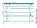
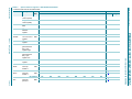
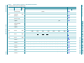
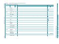
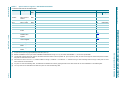
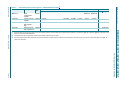
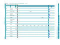
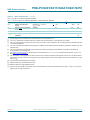
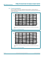
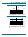
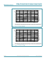
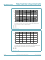
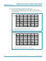
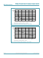
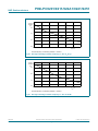
xxxxxxxxxxxxxxxxxxxxx xxxxxxxxxxxxxxxxxxxxxxxxxx xxxxxxx x x x xxxxxxxxxxxxxxxxxxxxxxxxxxxxxx xxxxxxxxxxxxxxxxxxx xx xx xxxxx
xxxxxxxxxxxxxxxxxxxxxxxxxxx xxxxxxxxxxxxxxxxxxx xxxxxx xxxxxxxxxxxxxxxxxxxxxxxxxxxxxxxxxxx xxxxxxxxxxxx x x
xxxxxxxxxxxxxxxxxxxxx xxxxxxxxxxxxxxxxxxxxxxxxxxxxxx xxxxx xxxxxxxxxxxxxxxxxxxxxxxxxxxxxxxxxxxxxxxxxxxxxxxxxx xxxxxxxx
xxxxxxxxxxxxxxxxxxxxxxxxx xxxxxxxxxxxxxxxxxxxx xxx
Name
Description
SFR Bit functions and addresses
addr.
MSB
Reset value
LSB
Hex
Binary
A/D_0 data
register 1
D6H
00
0000 0000
AD1DAT2
A/D_0 data
register 2
D7H
00
0000 0000
AD1DAT3
A/D_0 data
register 3
F5H
00
0000 0000
AUXR1
Auxiliary
function
register
A2H
00
0000 00x0
Rev. 2.1 — 27 August 2012
All information provided in this document is subject to legal disclaimers.
CLKLP
EBRR
ENT1
ENT0
SRST
0
-
DPS
F7
F6
F5
F4
F3
F2
F1
F0
B register
F0H
00
0000 0000
BRGR0[2]
Baud rate
generator 0
rate low
BEH
00
0000 0000
BRGR1[2]
Baud rate
generator 0
rate high
BFH
00
0000 0000
BRGCON
Baud rate
generator 0
control
BDH
-
-
-
-
-
-
SBRGS
BRGEN
00[2]
xxxx xx00
CMP1
Comparator 1
control register
ACH
-
-
CE1
CP1
CN1
OE1
CO1
CMF1
00[1]
xx00 0000
CMP2
Comparator 2
control register
ADH
-
-
CE2
CP2
CN2
OE2
CO2
CMF2
00[1]
xx00 0000
DIVM
CPU clock
divide-by-M
control
95H
00
0000 0000
DPTR
Data pointer
(2 bytes)
DPH
Data pointer
high
83H
00
0000 0000
DPL
Data pointer
low
82H
00
0000 0000
8-bit microcontroller with 8-bit ADC
20 of 75
© NXP B.V. 2012. All rights reserved.
B*
P89LPC9201/9211/922A1/9241/9251
AD1DAT1
Bit address
NXP Semiconductors
P89LPC92X1
Product data sheet
Table 6.
Special function registers - P89LPC9241/9251 …continued
* indicates SFRs that are bit addressable.