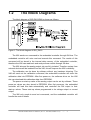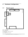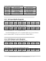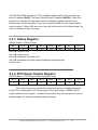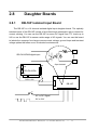
1
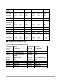
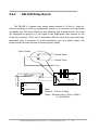
ISO-DA16/DA8
Hardware Manual
Warranty
All products manufactured by ICP DAS are warranted against defective
materials for a period of one year from the date of delivery to the original purchaser.
Warning
ICP DAS assumes no liability for damages consequent to the use of this product.
ICP DAS reserves the right to change this manual at any time without notice. The
information furnished by ICP DAS is believed to be accurate and reliable. However,
no responsibility is assumed by ICP DAS for its use, nor for any infringements of
patents or other rights of third parties resulting from its use.
Copyright
Copyright 1997 by ICP DAS. All rights are reserved.
Trademark
The names used for identification only may be registered trademarks of their
respective companies.
ISO-DA16/DA8 Hardware Manual (Ver.1.2, Jun/2004, IPH-013-12)
----
1
Table of Contents
1. INTRODUCTION ........................................................................................................................3
1.1
GENERAL DESCRIPTION ......................................................................................................3
1.2
THE BLOCK DIAGRAMS.........................................................................................................4
1.3
FEATURES .............................................................................................................................5
1.4
SPECIFICATIONS ....................................................................................................................6
1.5
PRODUCT CHECK LIST ..........................................................................................................7
2. HARDWARE CONFIGURATION ............................................................................................8
2.1
BOARD LAYOUT....................................................................................................................8
2.2
J1 : IRQ CHANNEL SELECTION .............................................................................................9
2.3 I/O BASE ADDRESS SETTING ................................................................................................9
2.3.1
D/I Input Buffer Register ..........................................................................................11
2.3.2
D/O Output Latch Register .......................................................................................11
2.3.3
Status Register ..........................................................................................................12
2.3.4
D/O Output Enable Register.....................................................................................12
2.3.5
Read/Write Command Register ................................................................................13
2.3.6
Clear Interrupt Signal Register ................................................................................13
2.4 CN1 CONNECTOR ...............................................................................................................14
2.5
CN2 CONNECTOR ...............................................................................................................14
2.6
CN3 CONNECTOR ...............................................................................................................15
2.7 SIGNAL CONNECTION..........................................................................................................16
2.7.1
Voltage Output Connection.......................................................................................16
2.7.2
Current Output Connection ......................................................................................16
2.8 DAUGHTER BOARDS ...........................................................................................................17
2.8.1
DB-16P Isolated Input Board...................................................................................17
2.8.2
DB-16R Relay Board ................................................................................................18
2.8.3
DB-24PR Power Relay Board...................................................................................19
2.8.4
DB-8125 Screw Terminal Board...............................................................................20
2.8.5
DB37 .........................................................................................................................20
2.8.6
DN-37 (D-Sub Connector with DIN Rail Mounting) ................................................21
3. FUNCTION OPERATION .......................................................................................................22
3.1
THE ±10V VOLTAGE OUTPUT ............................................................................................22
3.2
THE ±5V VOLTAGE OUTPUT ..............................................................................................23
3.3
THE 0-10V VOLTAGE OUTPUT............................................................................................23
3.4
THE 0-5V VOLTAGE OUTPUT..............................................................................................23
3.5
THE 0-20MA CURRENT OUTPUT .........................................................................................24
3.6
THE 4-20MA CURRENT OUTPUT .........................................................................................24
3.7
NO VR & NO JUMPER DESIGN............................................................................................25
3.8
SOFTWARE CALIBRATION ...................................................................................................26
ISO-DA16/DA8 Hardware Manual (Ver.1.2, Jun/2004, IPH-013-12)
----
2
1.
1.1
Introduction
General
Description
The ISO-DA16/DA8 is bus-type isolated 14-bit D/A card for PC/AT compatible
computers. The optical isolation of the ISO-DA16/DA8 can withstand up to 2500Vrms
of common-mode voltage.
The ISO-DA16/DA8 offers 16/8 channel analog output. The voltage output range
can be configured as ±10V, ±5V, 0-10V, 0-5V and the current output can be
configured as 0 to 20mA or 4 to 20 mA.
The board’s innovative design improves on several drawbacks of the conventional
D/A card. These features are as follows:
Trimless, no jumpers, high channel number and high isolation(2500V) design.
All calibrations can be done by software. The calibration data is stored in the
on-board EEPROM.
The power-on value of the analog output can be pre-defined by the user and is
stored in the on-board EEPROM.
Six different configurations: ±10V, ±5V, 0-10V, 0-5V, 0-20mA or 4-20 mA.
Every channel can be programmed as voltage output or current output
All channel configurations can be selected and changed by software. The user
doesn’t have to change any hardware.
All 16 channels can be configured and used in different configurations at the
same time.(for example, channel_0 = ±10V, channel_1 = 4-20mA, channel_2 = 0
to 5V, ….., at the same time)
The onboard machine independent timer can be programmed from 0.1 ms to 100
ms. When the time is up, a hardware signal can be used to interrupt PC.
16 channels D/I can be directly connected to isolated daughter board, DB-16P
16 channels D/O can be directly connected to relay board, DB-16R, DB-24R
All these features are implemented in a small, compact, reliable and half-size
PCB.
ISO-DA16/DA8 Hardware Manual (Ver.1.2, Jun/2004, IPH-013-12)
----
3
1.2
The Block Diagrams
The block diagram of ISO-DA16/DA8 is shown as follows:
Figure 1: The block diagram of ISO_DA16.
The X86 sends one command to the embedded controller through ISA bus. The
embedded controller will auto read and execute this command. The results of this
command will be stored in the internal data memory of the embedded controller,
therefore the X86 can read back and analyze these results through ISA bus.
The X86 site and the analog output site are fully isolated. Therefore noises from
external devices will be isolated from the X86, this will improve the X86’s reliability.
The calibration can be done by software without any hardware trimming. The
X86 will send out the calibration command, the embedded controller will store this
calibration data into EEPROM. After first power-on, the software driver on the X86
site can download this calibration data from EEPROM.
The power-on start-up value of the analog output can be set by software. These
power-on values are also stored in EEPROM. After first power-on, the embedded
controller will load this data automatically and controller the D/A output to their
start-up values. These start-up values programmed to be voltage output or current
output.
The X86 only needs to send out commands, and the embedded controller will
handle the control details.
ISO-DA16/DA8 Hardware Manual (Ver.1.2, Jun/2004, IPH-013-12)
----
4
1.3
Features
The general features of ISO-DA16/DA8 are given as follows:
AT bus
2500VDC photo-isolation protection
8/16 channel, 14-bit analog output
Unipolar or bipolar outputs available for each channel
Voltage/ current output for each channel
Command set programming
Software Calibration
ISO-DA16/DA8 Hardware Manual (Ver.1.2, Jun/2004, IPH-013-12)
----
5
1.4
Specifications
Analog Outputs
D/A converter : 14-bit DAC
Channels : 8/16 independent
Type : double-buffered, multiplying
Integral linearity : 0.006% FSR ; typical
Differential linearity : 0.006 % FSR ; typical
Voltage Output Range :
Unipolar : 0~5V or 0~10V
Bipolar : +/-10Vor,+/- 5V
Current drive : +/-5mA
Absolute accuracy : 0.01% FSR typical
Power on state : 0V bipolar ; 5V unipolar
Current Output Range :
0-20mA or 4-20mA
Absolute Accuracy : 0.1% FSR typical
Excitation voltage range : + 7 V to +40V
Power On state : 4mA bipolar , 12mA Unipolar
Stability
Offset temperature coefficient : +/- 50µV/°C
Gain temperature coefficient : +/- 10ppm/°C
Power Requirements:
ISO-DA8 : +5VDC @800mA max.
ISO-DA16. : +5VDC @1400mA max.
General Environmental
Operating temp 0-50°C
Storage temp
-20°C to 70°C
Humility
0 to 90% non-condensing
Dimensions
182 mm x 122 mm
ISO-DA16/DA8 Hardware Manual (Ver.1.2, Jun/2004, IPH-013-12)
----
6
1.5
Product Check List
In addition to this manual, the package includes the following items:
ISO_DA16/DA8 multifunction card.
One piece of company floppy diskette or CD.
Attention !
If any of these items is missing or damaged, please contact your local
field agent. Save the shipping materials and carton in case you want to
ship or store the product in the future.
ISO-DA16/DA8 Hardware Manual (Ver.1.2, Jun/2004, IPH-013-12)
----
7
2.
Hardware Configuration
2.1
Board Layout
ISO-DA16/DA8
CN1
CN2
SW1
J1
ISA BUS
ISA BUS
CN3
CN1 : 16 channel D/I
CN2 : 16 channel D/O
CN3 : 16/8 channel voltage/current output
J1 : IRQ selection
SW1 : I/O BASE address selection
ISO-DA16/DA8 Hardware Manual (Ver.1.2, Jun/2004, IPH-013-12)
----
8
2.2
J1 : IRQ Channel Selection
There is one machine independent timer in ISO-DA16/DA8. This timer
is programmable from 0.1mS to 100ms. When the timer is up, the
embedded controller will generate an hardware interrupt signal. This signal
can be used to interrupt PC or can be read back by polling in PC site.
NO Interrupt
(default)
IRQ
3
4
5
6 7
9 10 11 12 14 15 NC
IRQ
3
4
5
6 7
9 10 11 12 14 15 NC
Interrupt 15
2.3
I/O Base Address Setting
The ISO-DA16 occupies 8 consecutive locations in I/O address
space from BASE to BASE+7. The default setting is 0x220 as following :
ON
1
2
3
4
5
6
A8
A7
A6
A5
A4
A3
ISO-DA16/DA8 Hardware Manual (Ver.1.2, Jun/2004, IPH-013-12)
----
9
BASE
ADDR
A8
A7
A6
A5
A4
A3
200-208
ON
ON
ON
ON
ON
ON
208-20F
ON
ON
ON
ON
ON
OFF
ON
ON
ON
OFF
ON
ON
228-22F
ON
ON
ON
OFF
ON
OFF
300-308
OFF
ON
ON
ON
ON
ON
308-30F
OFF
ON
ON
ON
ON
OFF
3F0-3F8
OFF
OFF
OFF
OFF
OFF
ON
3F8-3FF
OFF
OFF
OFF
OFF
OFF
OFF
220-228( )
( ) : default base address is 0x220
The PC I/O port mapping is given below.
ADDRESS Device
ADDRESS DEVICE
000-1FF
PC reserved
320-32F
XT Hard Disk
200-20F
Game/control
378-37F
Parallel Printer
210-21F
XT Expansion Unit
380-38F
SDLC
238-23F
Bus Mouse/Alt. Bus
Mouse
3A0-3AF
SDLC
278-27F
Parallel Printer
3B0-3BF
MDA/Parallel Printer
2B0-2DF
EGA
3C0-3CF
EGA
2E0-2E7
AT GPIB
3D0-3DF
CGA
2E8-2EF
Serial Port
3E8-3EF
Serial Port
2F8-2FF
Serial Port
3F0-3F7
Floppy Disk
300-31F
Prototype Card
3F8-3FF
Serial Port
ISO-DA16/DA8 Hardware Manual (Ver.1.2, Jun/2004, IPH-013-12)
----
10
The I/O control registers are defined as follows:
I/O Address
Input Operation
Output Operation
BASE
D/I low byte read
D/O low byte read
BASE+1
D/I high byte read
D/O high byte read
BASE+2
Read Status
D/O output enable
BASE+3
Read Command
Write Command
BASE+4
Clear Interrupt Signal
Reserved
2.3.1 D/I Input Buffer Register
(READ) Base: D/I Input Buffer Low Byte Data Format
Bit 7
Bit 6
Bit 5
Bit 4
Bit 3
Bit 2
Bit 1
Bit 0
D7
D6
D5
D4
D3
D2
D1
D0
(READ) Base+1: D/I Input Buffer High Byte Data Format
Bit 7
Bit 6
Bit 5
Bit 4
Bit 3
Bit 2
Bit 1
Bit 0
D7
D6
D5
D4
D3
D2
D1
D0
D/I 16bit input data: D15….D0 , D15=MSB,D0=LSB
The ISO-DA16/DA8 provides 16 TTL compatible digital inputs. The low 8 bits are
stored in address BASE. The high 8 bits are stored in address BASE+1.
2.3.2 D/O Output Latch Register
(WRITE) Base: D/O Output Latch Low Byte Data Format
Bit 7
Bit 6
Bit 5
Bit 4
Bit 3
Bit 2
Bit 1
Bit 0
D7
D6
D5
D4
D3
D2
D1
D0
(WRITE) Base+1: D/O Output Latch High Byte Data Format
Bit 7
Bit 6
Bit 5
Bit 4
Bit 3
Bit 2
Bit 1
Bit 0
D7
D6
D5
D4
D3
D2
D1
D0
D/O 16bit output data: D15….D0 , D15=MSB,D0=LSB
ISO-DA16/DA8 Hardware Manual (Ver.1.2, Jun/2004, IPH-013-12)
----
11
The ISO-DA16/DA8 provides 16 TTL compatible digital outputs. The low 8 bits are
stored in address BASE. The high 8 bits are stored in address BASE+1. When first
powered-on, all the D/O output latch ports are disabled, therefore all D/O are in
floating state. All D/O will active if any value output to BASE+2, D/O output enables
control register. If these D/O are active, they will active and can’t be disable again. So
only one enabled output is enough.
2.3.3 Status Register
(READ) Base+2: Status Format
Bit 7
Bit 6
Bit 5
Bit 4
Bit 3
Bit 2
Bit 1
Bit 0
X
X
X
X
D3
D2
D1
D0
D0=1
ready to read
D1=1
ready to write
D2=2
embedded controller error
D3=3
embedded controller sends a hardware interrupt signal
X=don’t care
2.3.4 D/O Output Enable Register
(WRITE) Base+2: D/O Output Enable Register Format
Bit 7
Bit 6
Bit 5
Bit 4
Bit 3
Bit 2
Bit 1
Bit 0
X
X
X
X
X
X
X
X
X=don’t care
When first powered-on, all the D/O output latch ports are disabled,therefore
all D/O are in floating state. All D/O will active if any value output to BASE+2,D/O
output enables control register. If these D/O are active, they will activate and can’t be
disabled again. So only one enabled output is enough.
ISO-DA16/DA8 Hardware Manual (Ver.1.2, Jun/2004, IPH-013-12)
----
12
2.3.5 Read/Write Command Register
(Write) Base+3: Write Command Register
(Read) Base+3: Read Command Register
Refer to chapter 4 for command sets format.
2.3.6 Clear Interrupt Signal Register
(READ) Base+4: Clear Interrupt Signal Register Format
Bit 7
Bit 6
Bit 5
Bit 4
Bit 3
Bit 2
Bit 1
Bit 0
X
X
X
X
X
X
X
X
X=don’t care
The onboard machine independent timer can be programmed from 0.1ms to 100ms.
When the time is up, a hardware signal can be used to interrupt PC. This signal will
be active until access to BASE+3, clear interrupt signal register. The J1 will be in NC
position in the factory setting, but the hardware interrupt signal is also active.
Therefore the software will access or read the clear interrupt signal register after the
timer is up.
ISO-DA16/DA8 Hardware Manual (Ver.1.2, Jun/2004, IPH-013-12)
----
13
2.4 CN1 Connector
CN1 : Digital Input Connector Pin Assignment.
Pin Number Description
Pin Number Description
1
Digital Input 0/TTL
2
Digital Input 1/TTL
3
Digital Input 2/TTL
4
Digital Input 3/TTL
5
Digital Input 4/TTL
6
Digital Input 5/TTL
7
Digital Input 6/TTL
8
Digital Input 7/TTL
9
Digital Input 8/TTL
10
Digital Input 9/TTL
11
Digital Input 10/TTL
12
Digital Input 11/TTL
13
Digital Input 12/TTL
14
Digital Input 13/TTL
15
Digital Input 14/TTL
16
Digital Input 15/TTL
17
PCB‘s GND output
18
PCB‘s GND output
19
PCB‘s +5V output
20
PCB ‘s +12V output
The ISO-DA16/DA8 has 16-channel TTL compatible D/I. The DB-16P(16
channel isolation input board) is designed for directly connecting to these D/I.
2.5 CN2 Connector
CN2 : Digital Output Connector Pin Assignment.
Pin Number Description
Pin Number Description
1
Digital Output 0/TTL
2
Digital Output 1/TTL
3
Digital Output 2/TTL
4
Digital Output 3/TTL
5
Digital Output 4/TTL
6
Digital Output 5/TTL
7
Digital Output 6/TTL
8
Digital Output 7/TTL
9
Digital Output 8/TTL
10
Digital Output 9/TTL
11
Digital Output 10/TTL
12
Digital Output 11/TTL
13
Digital Output 12/TTL
14
Digital Output 13TL
15
Digital Output 14/TTL
16
Digital Output 15/TTL
17
PCB‘s GND output
18
PCB‘s GND output
19
PCB‘s +5V output
20
PCB‘s +12V output
The ISO-DA16/DA8 has 16-channel TTL compatible D/O. The DB-16R(16
channel relay board) and DB-24PR(24 channel power relay board) are designed for
connecting to these D/O
ISO-DA16/DA8 Hardware Manual (Ver.1.2, Jun/2004, IPH-013-12)
----
14
2.6 CN3 Connector
Pin assignment for single-ended analog input
Pin
Name
Pin
Name
1
Voltage Output 0
20
Current Output 0
2
Voltage Output 1
21
Current Output 1
3
Voltage Output 2
22
Current Output 2
4
Voltage Output 3
23
Current Output 3
5
Analog Ground
24
Analog Ground
6
Voltage Output 4
25
Current Output 4
7
Voltage Output 5
26
Current Output 5
8
Voltage Output 6
27
Current Output 6
9
Voltage Output 7
28
Current Output 7
10
Analog Ground
29
Analog Ground
11
Voltage Output 8
20
Current Output 8
12
Voltage Output 9
31
Current Output 9
13
Voltage Output 10
32 Current Output 10
14
Voltage Output 11
33 Current Output 11
15
Analog Ground
34 Current Output 12
16
Voltage Output 12
35 Current Output 13
17
Voltage Output 13
36 Current Output 14
18
Voltage Output 14
37 Current Output 15
19
Voltage Output 15
ISO-DA16/DA8 Hardware Manual (Ver.1.2, Jun/2004, IPH-013-12)
----
15
2.7
Signal Connection
2.7.1
Voltage Output Connection
ISO-DA16/DA
Output Current 8
Max (±5mA)
V
I
Amp
D/A
Converto
Load
DATA
12-Bit
A.GND
The ISO-DA16/DA8 voltage output maximum current: ± 5 mA
2.7.2
Current Output Connection
Current Loop 4~20mA
I
+
+
ISO-DA16/DA8
I. Out
LOAD
D/A 0-10V
External Power
Supply 9V-36V
40.2Ω
-
A.GND
A. GND
ISO-DA16/DA8 Hardware Manual (Ver.1.2, Jun/2004, IPH-013-12)
----
16
2.8
2.8.1
Daughter Boards
DB-16P Isolated Input Board
The DB-16P is a 16 channel isolated digital input daughter board. The optically
isolated inputs of the DB-16P consist of a bi-directional optocoupler with a resistor for
current sensing. You can use the DB-16P to sense DC signal from TTL levels up to
24V or use the DB-16P to sense a wide range of AC signals. You can use this board
to isolate the computer from large common-mode voltage, ground loops and transient
voltage spikes that often occur in industrial environments.
V+
ISO-DA16/DA8 digital input
VOpto-Isolated
D/I
ISO-DA16/DA
8
20Pin cable
DB-16P
AC or DC Signal
0V to 24V
ISO-DA16/DA8 Hardware Manual (Ver.1.2, Jun/2004, IPH-013-12)
----
17
2.8.2
DB-16R Relay Board
The DB-16R 16 channel relay output board consists of 16 form C relays for
efficient switching of loads by programmed control. It is connector and functionally
compatible with 785 series board but with industrial type terminal blocks. The relay
are energized by applying a 5 volt signal to the appropriate relay channel on the
20-pin flat connector. There are 16 enunciator LEDs for each relay, light when their
associated relay is activated. To avoid overloading your PC’s power supply, this
board provides a screw terminal for external power supply.
Form C Relay
Normal Open
Normal Close
Com.
20Pin cable
DB-16R
D/O
ISO-DA16/DA8
Note:
Channel : 16 From C Relay
Relay : Switching up to 0.5A at 110ACV
or 1A at 24DCV
ISO-DA16/DA8 Hardware Manual (Ver.1.2, Jun/2004, IPH-013-12)
----
18
2.8.3
DB-24PR Power Relay Board
The DB-24PR, 24-channel power relay output board consists of 8 form C and 16
form A electromechanical relays for efficient switching of loads by programmed
control. The contact of each relay can control a 5A load at 250ACV/30VDCV. The
relay is energized by applying a 5 volt signal to the appropriate relay channel on the
20-pin flat cable connector(just using 16 relays) or an 50-pin flat cable
connector.(OPTO-22 compatible, for DIO-24 series). Twenty-four enunciator LEDs,
one for each relay, light when their associated relay is activated. To avoid overloading
your PC’s power supply, this board needs a +12VDC or +24VDC external power
supply.
Normal Open
Form A Relay
Com.
20Pin cable
To 20pin connector
DB-24PR
D/O
ISO-DA16/DA
8
Note:
50-Pin connector(OPTO-22 compatible), for DIO-24, DIO-48, DIO-144
20-Pin connector for 16 channel digital output, A-82X, A-62X, DIO-64,
ISO-DA16/DA8
Channel : 16 Form A Relay , 8 Form C Relay
Relay : switching up to 5A at 110ACV / 5A at 30DCV
ISO-DA16/DA8 Hardware Manual (Ver.1.2, Jun/2004, IPH-013-12)
----
19
2.8.4
DB-8125 Screw Terminal Board
The DB-8125 is low cost universal screw terminal board. For 37-pin D-type
connectors or two 20-pin connectors.
37-pin cable
ISO-DA16/DA
8
D/O
Industrial type terminal blocks
permit heavy-duty and reliable
connection of signals.
DB-8125
2.8.5
DB37
The DB-37 is a daughter board that directly connects to a D-sub 37
pins connector. It is designed for easy wire connections.
direct connection
ISO-DA16/DA8 Hardware Manual (Ver.1.2, Jun/2004, IPH-013-12)
----
20
2.8.6
DN-37 (D-Sub Connector with DIN Rail
Mounting)
Termination accessory with 37 screw terminals for easy connection of field I/O
signals to 37-pin boards. Includes one 37-pin D-sub connector for direct connection to
37-pin cables with hardware for mounting on a standard DIN rail.
ISO-DA16/DA
8
37-pin cable
D/O
DN-37
Wire
ISO-DA16/DA8 Hardware Manual (Ver.1.2, Jun/2004, IPH-013-12)
Wire
----
21
3.
Function Operation
3.1
The ±10V Voltage Output
The D/A converter of the ISO-DA16/DA8 is 14-bit, from 0x0000 to 0x3FFF. The
hardware is designed to output voltage about ±10.1V as follows:
0x0000
about -10.1 volt
0x3FFF
about +10.1 volt
Therefore the software can calibrate the voltage output to ±10.000 volt without any
hardware VRs adjustment. For example,
Channel Number Min[n]=-10.000
volt
Max[n]=10.000
volt
0
134
16294
1
132
16296
2
134
16294
3
134
16295
4
137
16297
5
136
16297
6
138
16296
7
135
16295
8
135
16297
9
131
16298
10
136
16299
11
135
16296
12
133
16297
13
127
16302
14
134
16296
15
132
16296
If the user needs to send out VV volt to channel
n voltage output, the hex value,
HH, sent to D/A converter is given as follows:
Delta[n]=20.0/(MAX[n]-Min[n]);
HH = (VV+10.0)/Delta[n]+Min[n];
Delta = volt per count
HH = Hex value sent to D/A converter
ISO-DA16/DA8 Hardware Manual (Ver.1.2, Jun/2004, IPH-013-12)
----
22
3.2
The ±5V Voltage Output
The voltage output hardware of ISO-DA16/DA8 is always in ±10V range. If the
user need to output ±5V range, the software is the same as described in Sec. 3.1.
Because the user wants to output ±5V range, therefore VV will be in the ±5V range,
so the HH will be about from 0x1000 to 0x2FFF. This
means the resolution
is about 13 bits.
3.3
The 0-10V Voltage Output
The voltage output hardware of ISO-DA16/DA8 is always in ±10V range. If
the
user needs to output 0-10V range, the software is the same as described in Sec. 3.1.
Because the user want to output 0-10V range, therefore VV will be in the 0-10V range,
so the HH will be about from 0x2000 to 0x3FFF. This means the resolution
is about 13 bits.
3.4
The 0-5V Voltage Output
The voltage output hardware of ISO-DA16/DA8 is always in ±10V range. If
the
user need to output 0-5V range, the software is the same as described in Sec. 3.1.
Because the user wants to output 0-5V range, therefore VV will be in the 0-5V range,
so the HH will be about from 0x2000 to 0x2FFF. This means the resolution
is about 12 bits.
ISO-DA16/DA8 Hardware Manual (Ver.1.2, Jun/2004, IPH-013-12)
----
23
3.5
The 0-20mA Current Output
The voltage output hardware of ISO-DA16/DA8 is always in ±10V range. The
0-10V voltage output will convert to 0-22mA current output. Therefore the software
can calibrate the current output to 0-20mA without any hardware VRs adjustment. For
example,
Channel Number Min[n]=0 mA
Max[n]=20.000
mA
0
134
16294
1
132
16296
2
134
16294
3
134
16295
4
137
16297
5
136
16297
6
138
16296
7
135
16295
8
135
16297
9
131
16298
10
136
16299
11
135
16296
12
133
16297
13
127
16302
14
134
16296
15
132
16296
If the user need to send out II mA to channel
n voltage output, the hex value,
HH, sent to D/A converter is given as follows:
Delta[n]=20.0/(MAX[n]-Min[n]);
HH = II/Delta[n]+Min[n];
Delta = mA per count
HH = Hex value sent to D/A converter
The resolution is about 13 bit.
3.6
The 4-20mA Current Output
The voltage output hardware of ISO-DA16/DA8 is always in ±10V range. The
0-10V voltage output will convert to 0-22mA current output. If the user needs to output
4-20mA, the software is the same as described in Sec. 3.5. Because the user want to
output 4-20mA, therefore II will be in the 4-20 range, so the HH will be about from
0x2600 to 0x3FFF. This means the resolution is about 13 bits.
ISO-DA16/DA8 Hardware Manual (Ver.1.2, Jun/2004, IPH-013-12)
----
24
3.7
No VR & No Jumper Design
In the conventional 12-bit D/A board, for example A-626/A-628, there are many
jumpers for the following functions:
(1) Select the reference voltage (internal -10/-5/or external)
(2) Select unipolar/bipolar (0-10V or ±10V)
(3) Select different output range (0-10V or 0-5V)
And there are many VRs for the following functions:
(1) Voltage output offset adjustment
(2) Voltage output full-scale adjustment
(3) Current output offset adjustment
(4) Current output full-scale adjustment
There are so many VRs and jumpers, this makes QC and re-calibration very difficult.
Every step must be handled by human hands. It is not a happy job for people to
calibrate these D/A boards.
When we design the ISO-DA16/DA8, we try to remove all these terrible VRs and
jumpers but still maintain the same precision and performance. In the long run, we
selected a 14-bit D/A converter and adapted the software calibration to provide at
least the same performance & precision as A-626/A-628 as follows:
Configuration
Equivalent Bit
-10V to +10V
14 bit
0V to 10V
13 bit
-5V to +5V
13 bit
0V to 5V
12 bit
0mA to 20mA
13 bit
4mA to 20mA
13 bit
Resolution
All the VRs and jumpers are removed.
All calibrations can be done by software.
All channel configurations can be selected by software, no need to change any
hardware.
The precision is at least the same as A-626/A-628.
All 16 channels can be configured and used in different configurations at the
same time.(for example, channel_0 = ±10V, channel_1 = 4-20mA, channel_2 = 0
to 5V, …..)
All these features can be implemented in a small, compact, reliable and half-size
PCB.
ISO-DA16/DA8 Hardware Manual (Ver.1.2, Jun/2004, IPH-013-12)
----
25
3.8
Software Calibration
It is recommended to use a 16-bit A/D card to calibrate the ISO-DA16/DA8. The
ICP Con I-7000 series is a set of precision remote controlled modules. The I-7017 is
8-channel 16-bit precision A/D module(24-bit sigma-delta A/D converter), we use two
I-7017 for voltage output calibration and another two I-7017 for current output
calibration.
The steps for channel_n voltage output calibration are given as follows:
step 1 : HH=0
step 2 : send HH to ISO-DA16/DA8 channel_n
step 3 : measure the I-7017 channel_n,
if this value is just >= -10V, then goto step5
step 4 : increment HH and goto step2
step 5 : Min[n]=HH-1
step 6 : HH=0x3FFF
step 7 : send HH to ISO-DA16/DA8 channel_n
step 8 : measure the I-7017 channel_n,
if this value is just >= +10V, then goto step10
step 9 : increment HH and goto step7
step 10: Max[n]=HH
NOTE : Min[n] & Max[n] are described in Sec. 3.1
The steps for channel_n current output calibration are given as follows:
step 1 : HH=0x2000
step 2 : send HH to ISO-DA16/DA8 channel_n
step 3 : measure the I-7017 channel_n,
if this value is just >= 0mA, then goto step5
step 4 : increment HH and goto step2
step 5 : Min[n]=HH-1
step 6 : HH=0x3FFF
step 7 : send HH to ISO-DA16/DA8 channel_n
step 8 : measure the I-7017 channel_n,
if this value is just >= 20mA, then goto step10
step 9 : increment HH and goto step7
step 10: Max[n]=HH
NOTE : Min[n] & Max[n] are described in Sec. 3.5
ISO-DA16/DA8 Hardware Manual (Ver.1.2, Jun/2004, IPH-013-12)
----
26