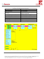
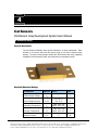
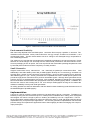
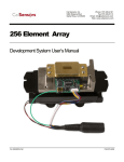
1
Sensor System for Infrared Spectroscopy - Introduction Outline of the Problem Infrared s pectroscopy, particularly in t he ne ar a nd mid-infrared r egion is a n important f ield th at r equires specialized s ensors. T he ind ustry c ontinues to grow with ne w applications developing as the s ensor technology becomes available. In many cases the science required for spectroscopic analysis is understood and th e im plementation waits onl y f or the s upporting t echnology to be d eveloped. Trends ar e, as alwa ys, towards smaller, lower cost systems with improved performance. The i mplementation of s uch a s specialization. • Op • Sens The fundamental purpose of the optical component in a spectroscopic system is to disperse the o ptical i nput s patially b y wavelength. T he g eometry of this d ispersive as pect nee ds to be compatible with the sensor array being used. or o The s ensor is th e c omponent which c onverts an opt ical i nput to an electrical o utput. T he sensor typically incorporates an ar ray of detector elements with some low level multiplexing and biasing electronics. In addition to the g eometric design of the detec tor elements many other parameters need t o be c onsidered including o perating tem perature, s pectral sensitivity, s tability, r esponsivity, nois e, and s peed ( both r eadout s peed a nd detec tor response s peed). O bviously th e pr imary c onsideration is s pectral s ensitivity s ince the sensor must cover the wavelengths of interest. lectronics o • Sof eas of tics o •E pectroscopic s ystem invol ves s everal s ubsystems and ar The s ystem elec tronics ar e r esponsible f or pr oviding the v arious dr ive s ignals r equired b y the s ensor as w ell as ha ndling th e m ultiplexed out put and c onverting it to a s tandard computer interface. In add ition it would be ad vantageous if the elec tronics provided control of aux iliary f unctions s uch as tem perature s tabilization of the detec tor. Al l elec tronic functions should be provided with no additional system noise. tware o With the availability of modern c omputing s ystems most s pectroscopic applications r equire software development for implementation. T his m ay be high level PC programming or low level m icrocontroller c ode. A s traightforward s oftware de velopment p ath is e ssential i n modern spectroscopic systems. Optical Input Optics Sensor Electronics Software Figure 1 Spectrometer Subsystems Germany and other countries: LASER COMPONENTS GmbH, Phone: +49 8142 2864 0, Fax: +49 8142 2864 11, [email protected] Great Britain: LASER COMPONENTS (UK) Ltd., Phone: +44 1245 491 499, Fax: +44 1245 491 801, [email protected] France: LASER COMPONENTS S.A.S., Phone: +33 1 3959 5225, Fax: +33 1 3959 5350, [email protected] Innovation of Solution It w ould be ad vantageous to inc orporate as m any of thes e s ubsystems as pos sible i nto a s ingle spectroscopic s olution while m aintaining the f lexibility nec essary t o be ap plicable to a wide r ange of applications. Since the optical performance and layout is very specific to the particular application the Optics subsystem w ill n ot be included in t he s olution. T he r emaining s ubsystems – Se nsor, E lectronics and Software c an a ll be tightly int egrated and be r elatively independent of the optical d esign. O f c ourse th e sensor material selection will be determinative of the spectral range covered. Since th e g oal is to address inf rared s pectroscopy, and s pecifically n ear t o mid inf rared, on ly d etector materials with r esponse in the 1µm to 6µm r egion will be c onsidered. O f th ese det ectors, ther e are a number which typically operate at very cold temperatures. These include InSb, InAs and HgCdTe. Since the design goal parameters include “small” and “low cost” these detector materials will not be considered due to the s ize an d c ost of the ir cooling s ystems. Thermal detec tors us ing P yroelectric or Bo lometric m aterials could b e c onsidered b ecause of their br oad wavelength r esponse, ho wever th ey h ave lo w s ensitivity and slow r esponse s peed c ompared to ph oton detec tors s o the y would b e ina ppropriate f or a gener al p urpose spectroscopic s ystem. T he det ector m aterials th at r emain f or c onsideration ar e InGaAs p hotodiodes ( both standard a nd ex tended) a nd lea d s alt ph otoconductors ( PbS and P bSe). A ll of thes e detec tors have reasonable c ooling r equirements and good r esponse times. Standar d InG aAs p hotodiodes ha ve ex cellent sensitivity a nd s peed, b ut are lim ited in up per wavelength s ensitivity to 1. 7µm and th erefore c an not be considered f or a ge neral p urpose s olution even in th e near infrared. Extended InG aAs p hotodiodes ha ve reasonable s ensitivity, b ut s till on ly ex tend to 2. 6µm. The r emaining alt ernatives, Pb S an d Pb Se photoconductors have c haracteristics that m ake them excellent candidates. PbS has detectivity values that are at leas t as go od as Ex tended InG aAs with s ensitivity to 3µm . PbSe is appr oximately a n or der o f magnitude less s ensitive than PbS, b ut h as s ensitivity to 5µm. Sinc e both m aterials ar e s imilar photoconductors, th ey c ould be us ed i nterchangeably within th e s ystem to pr ovide s ensitivity through the broad range of 1µm to 5µm .The primary challenge in implementing a PbS or PbSe spectroscopic system is that bec ause thes e d etectors oper ate i n the ph otoconductive m ode the y have l arge dar k c urrents. Often these d ark c urrents ar e d ealt with b y m odulating t he i ncident r adiation and then f iltering out th e DC component. This scheme works well but adds the complexity of source modulation. A bett er solution would be to develop electronics sophisticated enough to deal with the dark current electronically. The s election of the d etector m aterial det ermines many of the f eatures of the e lectronics inter face. In a general s ense th e el ectronics needs to in terface with the s ensor, per form as much c orrection as pos sible and pr esent t he o utput thr ough a s tandard c omputer inter face. I n ad dition th e electronics s hould p erform any control functions, such as temperature control. If the detector array is to contain a significant number of pixels, the multiplexing electronics should be contained within the detector package to improve performance and m inimize pac kage pin c ount. Si nce the g oal is an int egrated s pectroscopic s ystem, the har dware architecture is influenced by the desire for simple software interaction. The software interface should not be language specific to af ford the broadest usability. T his is most easily implemented as a l ibrary of functions to c ontrol and interface with the detector array. T his also implies that the interface hardware is most easily implemented in a microcontroller based architecture. Technical Realization Cal Sensors, Inc . has pr oduced PbS a nd PbSe p hotoconductors f or over 20 years and has r ecently developed ar rays that ar e s pecifically des igned to c over the n ear and m id inf rared s pectrum at r easonable cost w ith hig h s ensitivity. Eac h s ensor c onsist of 2 56 phot oconductive e lements hous ed i n an in dustry standard 28 p in p ackage whic h a lso c ontains a Pe ltier c ooler an d ther mistor for ther mal s tabilization and internal integrating multiplexers. Inter face electronics and software are also provided to eas ily transfer data via USB to a computer. Germany and other countries: LASER COMPONENTS GmbH, Phone: +49 8142 2864 0, Fax: +49 8142 2864 11, [email protected] Great Britain: LASER COMPONENTS (UK) Ltd., Phone: +44 1245 491 499, Fax: +44 1245 491 801, [email protected] France: LASER COMPONENTS S.A.S., Phone: +33 1 3959 5225, Fax: +33 1 3959 5350, [email protected] Optical Input USB Electronics Optics Software Sensor Figure 2 System Implementation Theory of Operation Sensor: Detector and Multiplexing Electronics The array pixels are designed to easily interface with standard dispersive optics. Two geometrically identical photoconductive arrays were developed so the entire 1µm to 5µm region can be covered by selecting either PbS (1µm to 3µm) or PbSe (1µm to 5µm). The 256 pixels are 40 microns wide and 450 microns tall and are spaced at 50 m icrons. I nternal to th e s ensor is a ther moelectric c ooler, the rmal s ensing el ement f or temperature f eedback and s tabilization, an d a n i ntegrated c ircuit s pecifically designed to i nterface with photoconductive elements. T he pr ocess f or m anufacturing the ph otonductive f ilm inv olves wet c hemical deposition onto a s ubstrate and th en delineation of the elements. T his process is relatively straightforward, using standard photolithographic techniques, and can produce arrays of high pixel functionality, often 100%. This is not q uite as e asily achieved with other detector m anufacturing tec hniques and is a n ad vantage f or these detectors. • Array • Multiplexers (ROIC) • • • • – – 256 elements Integration, dark current removal, multiplex to single output Thermistor – Measure tem p. on c ircuit board Circuit Board – Route s ignals to pins & between multiplexers Thermoelectric Cooler Header Figure 3 Sensor Implementation Germany and other countries: LASER COMPONENTS GmbH, Phone: +49 8142 2864 0, Fax: +49 8142 2864 11, [email protected] Great Britain: LASER COMPONENTS (UK) Ltd., Phone: +44 1245 491 499, Fax: +44 1245 491 801, [email protected] France: LASER COMPONENTS S.A.S., Phone: +33 1 3959 5225, Fax: +33 1 3959 5350, [email protected] Figure 4 s hows the o peration of the s ensor. T he bias voltage on th e photoconductive detector generates a current that varies de pending o n th e num ber of pho tons on t he d etector s urface. T he c harge f rom this current is collected in a capacitor called the Charge Well. When the detector is not illuminated the current is called “Dark Current”. T his dark current can be r eferenced and subtracted from all of the pix els, a pr ocess generally r eferred to as F irst O rder, or O ffset Cor rection. Because t he r esistance of eac h elem ent in th e array is n ot i dentical, a g lobal of fset c orrection is t ypically not s atisfactory i n r educing th e dar k c urrent to levels that provide adequate dynamic range. To further improve the of fset correction each pixel is provided with a D /A c onverter whic h when provided with a d igital c orrection va lue will individually a djust the of fset correction value of that pixel. The number of bits available in the D/A converter will determine the resolution of the c orrection a vailable. T he im plemented s cheme pr ovides 8 b its of c orrection, which is t ypically adequate for the pixel-to-pixel non-uniformities encountered. Once the dark current is subtracted from the pixels the remaining current represents the difference in current between the d ark state and the il luminated s tate, which is the s ignal c urrent. Sinc e th is detec tor ar ray is intended f or s pectroscopic appl ications, i ntegration is r equired f or app lications in volving lo w i ncident radiation. T he s ignal c urrent will c ollect on t he c harge well f or a s pecified am ount of tim e, im plementing signal integration. I n order to of fer the m aximum flexibility and dynamic range both the integration time and the well size are adjustable by sending the s ensor digital values to t he IC. T he integration time is hardware limited to a m inimum of 10 µS and a m aximum o f 218m S. In pr actical oper ation the m aximum integr ation time is lim ited b y th e un iformity of the ar ray af ter c orrection. Even with go od u niformity a nd d ark c urrent correction the differences in pix el offsets are am plified as the integration tim e increases. T he result is that the dynamic range of the a rray is reduced as the i ntegration time increases. In practice the integration time may be increased until t he s ystem r eaches the m inimum r equired d ynamic r ange. At th e en d of the integration tim e the vo ltages on the 256 c harge wells ar e c aptured on a s ample-and-hold a nd th e c harge wells ar e r eset t o s tart an other integration c ycle. T he e lectronics a llows f or r ead after in tegrate or r ead during integrate operation. The 256 s ignal voltages are time division multiplexed onto a single output pin which will contain a stream of analog voltage levels which are proportional to t he number of incident photons on eac h pixel. T he readout timing is controlled by a pixel clock which can operate up to 2MHz allowing for a 7.8mS frame rate. Vbias Infrared Energy Multiplex Highway Detector Photo Current Offset Correction Charge Well Instantaneous Well Voltage All multiplexed Signals to output Integration reset Sample And Hold Voltage Time P1 P2 P3 P4 Analog voltage level represents det ector Figure 4 Sensor Operation Diagram Germany and other countries: LASER COMPONENTS GmbH, Phone: +49 8142 2864 0, Fax: +49 8142 2864 11, [email protected] Great Britain: LASER COMPONENTS (UK) Ltd., Phone: +44 1245 491 499, Fax: +44 1245 491 801, [email protected] France: LASER COMPONENTS S.A.S., Phone: +33 1 3959 5225, Fax: +33 1 3959 5350, [email protected] Interface Electronics The task of the inter face e lectronics is to s implify th e inter face bet ween t he c ontrolling c omputer and th e sensor and has been implemented on a small board that plugs directly into the sensor header and provides connections for the USB interface as well as system and thermoelectric cooler power. Figure 5 Interface Electronics The following functions are provided by the interface electronics: • Sensor (detector and multiplexer IC) control and interface • Thermoelectric cooler control • Digitization of the analog detector signal output stream • USB command based interface o Analog conversion of digital control voltages o Command based interface structure for simple software integration The sensor IC requires numerous timing signals to operate. A microcontroller based architecture has been selected to implement the required functions. This makes generation of the timing signals simple and easily modified thr ough th e f irmware int erface por t. All control s oftware as wel l as the s ensor c alibration coefficients ar e s tored in on- board non- volatile m emory. T his als o f acilitates r estoration of the s ensor coefficients through the startup sequence so the process can be transparent to the spectroscopic system. The thermal stability of the photoconductive array is critical for DC operation. T he resistance of a lead salt photoconductor v aries b y approximately 3% p er °C. T he s ensor pr ovides ther mal c ontrol and m onitoring elements so the m icrocontroller is able to m onitor the detector temperature by placing the thermistor within a bridge network with a fixed resistor to set the control resistance. The microcontroller then issues a pulse width m odulated s ignal to a F ET w hich c ontrols the current of the ther moelectric c ooler c ontained in t he sensor pac kage. T he ef ficiency of this s ystem does not r equire an y heatsinking of the F ET an d th e microcontroller synchronizes the tim ing of the hi gh current drive pulses with the pixel clock to elim inate any noise that would result if the system were run asynchronously. The sensor provides a multiplexed analog output stream as previously described. The interface electronics accepts th is an alog s tream b y generating a p ixel c lock which is s ynchronized with a 14 bi t A/D c onverter and provides a d igital r epresentation of the p hoton input o n eac h pix el. T he c onversion r ate is 100k samples/second, which s ets the m aximum digital s ample r ate of the s ystem and is s ufficient f or m ost spectroscopic systems. The inter face elec tronics is c ommand bas ed and a USB interface ar chitecture w as s elected to f acilitate straightforward system hardware/software interface. Digital signals enter through the USB interface and are converted to analog if necessary before communication with the sensor IC. Conversely analog signals from the s ensor ar e di gitized for c ommunication t hrough the US B i nterface to the hos t c omputer. T he microcontroller r esponds t o a dig ital c ommand s tructure to im plement all s ensor IC f unctions as w ell as thermoelectric cooler control and several auxiliary functions. Germany and other countries: LASER COMPONENTS GmbH, Phone: +49 8142 2864 0, Fax: +49 8142 2864 11, [email protected] Great Britain: LASER COMPONENTS (UK) Ltd., Phone: +44 1245 491 499, Fax: +44 1245 491 801, [email protected] France: LASER COMPONENTS S.A.S., Phone: +33 1 3959 5225, Fax: +33 1 3959 5350, [email protected] Software The s pectrometer de veloper r equires a s ensor s ystem that wil l s upply i nformation abo ut th e i ncident, wavelength dis persed phot ons on eac h pix el. A hi gh lev el of har dware a bstraction r eleases the d eveloper from havi ng to understand the p hoton-to-data c onversion pr ocess and a llows c oncentration o n the development of s ystem op tics an d t he s oftware n ecessary to im plement the tar get s ystem. T o this end a software i nterface li brary was dev eloped to im plement al l f unctions r equired to c ontrol and o perate th e infrared s ensor t hrough t he in terface el ectronics. A bal ance between l ow l evel c ontrol and h igh level abstraction was th e g oal a nd was ac hieved thr ough customer feedback thr ough th e d evelopment pr ocess. The libr ary c an be ac cessed thr ough a ny p opular M icrosoft Windows de velopment langua ge, as well as through National Instrument’s LabView. A LabView application has been developed and is supplied with the system to eas ily take data from the ar ray. S etup is as simple as installing the USB drivers and running the application software. Figure 6 Application Software Results The goal of this project was to de velop a core system that would facilitate the rapid development of infrared spectrometer systems to addr ess the growing market and to eliminate the need for experts in s pectroscopy to become experts in detectors and their associated interface hardware. With the addition of the appropriate optics a nd s ome s oftware customization an inf rared spectrometer c an eas ily be de veloped in t he 1µm to 5µm inf rared r ange. T wo geometrically identical p hotoconductive ar rays ha ve been de veloped and c over this ent ire s pectrum. To aid i n the e lectronics har dware des ign a no vel inter face boar d is av ailable th at incorporates a m icrocontroller which c ontrols a ll interface to the internal multiplexers an d per forms temperature s tabilization c ontrol and s ignal d igitization. T his boar d ac cepts c ommands and tr ansfers data through a s tandard USB interface. T he software interface is implemented through a l ibrary of functions and is demonstrated in a Lab View application. T he sensor system is currently available in production quantities from Cal Sensors, Inc. for shipment worldwide. Germany and other countries: LASER COMPONENTS GmbH, Phone: +49 8142 2864 0, Fax: +49 8142 2864 11, [email protected] Great Britain: LASER COMPONENTS (UK) Ltd., Phone: +44 1245 491 499, Fax: +44 1245 491 801, [email protected] France: LASER COMPONENTS S.A.S., Phone: +33 1 3959 5225, Fax: +33 1 3959 5350, [email protected] Important Note: During further technical development an important change has been made. A new 256 channel multiplier did replace in 2008 the two 128 channel multipliers. The advantage is a more homogeneous signal and a simplification of the read-out. All following information in this product file is related to the new version with one 256 channel multiplexer. Germany and other countries: LASER COMPONENTS GmbH, Phone: +49 8142 2864 0, Fax: +49 8142 2864 11, [email protected] Great Britain: LASER COMPONENTS (UK) Ltd., Phone: +44 1245 491 499, Fax: +44 1245 491 801, [email protected] France: LASER COMPONENTS S.A.S., Phone: +33 1 3959 5225, Fax: +33 1 3959 5350, [email protected] 256 Element PbS and PbSe Arrays 256 Element PbS Multiplexed Array Performance Parameter Operating Wavelength Range: Operating Temperature: Number of Elements: Element Size: Peak Detectivity: Response Uniformity (pixel-to-pixel): Integration Range: Pixel Clock: Linearity: Pixel Operability: Detector Rise Time: Input Power Requirement: 1 to 3 Microns (PbSe) -4ºC (TEC stabilized) 256 detector elements Pixel width 40 microns, pixel height 450 microns, and pixel pitch 50 microns D* (PbS): 1x10¹¹ (cm√Hz0.5W-1) @-4ºC ±10% of array signal mean (PbS) .01ms to 200ms (on board) 2MHz max. 90% 98% <1ms 12 VDC main, 5VDC @1.5A cooler Germany and other countries: LASER COMPONENTS GmbH, Phone: +49 8142 2864 0, Fax: +49 8142 2864 11, [email protected] Great Britain: LASER COMPONENTS (UK) Ltd., Phone: +44 1245 491 499, Fax: +44 1245 491 801, [email protected] France: LASER COMPONENTS S.A.S., Phone: +33 1 3959 5225, Fax: +33 1 3959 5350, [email protected] Germany and other countries: LASER COMPONENTS GmbH, Phone: +49 8142 2864 0, Fax: +49 8142 2864 11, [email protected] Great Britain: LASER COMPONENTS (UK) Ltd., Phone: +44 1245 491 499, Fax: +44 1245 491 801, [email protected] France: LASER COMPONENTS S.A.S., Phone: +33 1 3959 5225, Fax: +33 1 3959 5350, [email protected] 5 CSI CONFIDENTAL AND PROPRIETARY INFORMATION MATERIAL: FINISH: 4 THIRD ANGLE PROJECTION ESD HANDLING REQUIRED XXXXX = .00005 XXXX = .0005 XXX = .005 XX = .01 +/- TOLERANCES DIMENSIONS ARE IN INCHES UNLESS OTHERWISE SPECIFIED: C 1. SEE SHEET 2 FOR MECHANICAL OUTLINE AND DIMENSIONS. NOTES: PIN NO. 1 2 3 4 5 6 7 8 9 10 11 12 13 14 3 Q.A. MFG APPR. L.SNYDER R.ASKER J.ELLIOTT ENG APPR. JLR ROYAL W.WHITEHORN DRAWN CHECKED INIT. NAME APPROVALS 2 04-11-06 DATE DATE FUNCTION NC NC Vdd Vss INT CLK NC NC DAC LD CLK PIXEL CLK SERIAL DATA NC TEC (-) THERMISTOR B CASE 07-21-08 07-17-08 10-01-07 OUTLINE & MOUNTING SCALE: 1:1 A 1 63065 UNCLASSIFIED SIZE DWG. NO. C REV A AT1-(.45mm x .04mm) 28T-256 M1 TITLE: PIN NO. 15 16 17 18 19 20 21 22 23 24 25 26 27 28 PDM PDM PDM DRN CAL SENSORS, INC. FUNCTION DETECTOR BIAS THERMISTOR A TEC (+) NC SERIAL CLK CFG LOAD CLK FRAME START RST N BIAS DAC Vh MUX OUT DAC VI GLOBAL SKIM DET BIAS NC DO NOT SCALE DRAWING C PIN FUNCTIONS A B DESCRIPTION ADDED DETAILS TO PART # IN DWG TITLE PIN LENGTH WAS: .230, PIN DIAMETER TOLERANCE TIGHTENED RESTORED ESD HANDLING NOTE REV REVISIONS Germany and other countries: LASER COMPONENTS GmbH, Phone: +49 8142 2864 0, Fax: +49 8142 2864 11, [email protected] Great Britain: LASER COMPONENTS (UK) Ltd., Phone: +44 1245 491 499, Fax: +44 1245 491 801, [email protected] France: LASER COMPONENTS S.A.S., Phone: +33 1 3959 5225, Fax: +33 1 3959 5350, [email protected] 5 MOUNTING SURFACE SEE SHEET 1 FOR NOTES .040 R.060 .400 .200 .243 .150 x 45 .100 4 2 3 4 5 6 7 8 9 10 11 12 13 14 2.080 1.300 .650 3 .250 B .161±.012 .105 .500 B 28X .800 .018±.002 PINS .400 2 1.000 SCALE: 1:1 A UNCLASSIFIED 63065 1 C REV SEE SHEET 1 FOR REVISIONS SIZE DWG. NO. .210 APERTURE .225 .113 .125 .063 .540 APERTURE .270 ARRAY PLANE 1.500 .750 28 27 26 25 24 23 22 21 20 19 18 17 16 15 1 1.040 1.250 2.500 256 Element PbSe Multiplexed Array Performance Parameter Operating Wavelength Range: 1 to 5 Microns (PbSe) Operating Temperature: -4ºC (TEC stabilized) Number of Elements: 256 detector elements Pixel width 40 microns, pixel height 450 microns, Element Size: and pixel pitch 50 microns Peak Detectivity: D* (PbSe): 1x1010 cm√Hz /W) @-4ºC Response Uniformity (pixel-to-pixel): ±15% of array signal mean (PbSe) Integration Range: .01ms to 100ms (on board) Pixel Clock: 2MHz max. Linearity: 90% Pixel Operability: 98% Detector Rise Time: <10µS Input Power Requirement: 12 VDC main, 5VDC @1.5A cooler Germany and other countries: LASER COMPONENTS GmbH, Phone: +49 8142 2864 0, Fax: +49 8142 2864 11, [email protected] Great Britain: LASER COMPONENTS (UK) Ltd., Phone: +44 1245 491 499, Fax: +44 1245 491 801, [email protected] France: LASER COMPONENTS S.A.S., Phone: +33 1 3959 5225, Fax: +33 1 3959 5350, [email protected] Germany and other countries: LASER COMPONENTS GmbH, Phone: +49 8142 2864 0, Fax: +49 8142 2864 11, [email protected] Great Britain: LASER COMPONENTS (UK) Ltd., Phone: +44 1245 491 499, Fax: +44 1245 491 801, [email protected] France: LASER COMPONENTS S.A.S., Phone: +33 1 3959 5225, Fax: +33 1 3959 5350, [email protected] 5 CSI CONFIDENTAL AND PROPRIETARY INFORMATION MATERIAL: FINISH: 4 THIRD ANGLE PROJECTION ESD HANDLING REQUIRED XXXXX = .00005 XXXX = .0005 XXX = .005 XX = .01 +/- TOLERANCES DIMENSIONS ARE IN INCHES UNLESS OTHERWISE SPECIFIED: B 1. SEE SHEET 2 FOR MECHANICAL OUTLINE AND DIMENSIONS. NOTES: DESCRIPTION 3 Q.A. MFG APPR. L.SNYDER R.ASKER J.ELLIOTT ENG APPR. JLR ROYAL W.WHITEHORN DRAWN CHECKED INIT. NAME APPROVALS 2 08-08-07 DATE 07-21-08 07-17-08 DATE FUNCTION NC NC Vdd Vss INT CLK NC NC DAC LD CLK PIXEL CLK SERIAL DATA NC TEC (-) THERMISTOR B CASE PDM PDM DRN OUTLINE & MOUNTING SCALE: 1:1 A 1 63068 UNCLASSIFIED SIZE DWG. NO. B REV BXT1-(.45mm x .04mm) 28T-256 M1 TITLE: CAL SENSORS, INC. PIN NO. FUNCTION PIN NO. 1 DETECTOR BIAS 15 2 THERMISTOR A 16 3 TEC (+) 17 4 NC 18 5 SERIAL CLK 19 6 CFG LOAD CLK 20 7 FRAME START 21 8 RST N BIAS 22 9 DAC Vh 23 10 MUX OUT 24 11 DAC VI 25 12 GLOBAL SKIM 26 13 DET BIAS 27 14 NC 28 PIN LENGTH WAS: .230, PIN DIAMETER TOLERANCE TIGHTENED RESTORED ESD HANDLING NOTE DO NOT SCALE DRAWING B A REV REVISIONS Germany and other countries: LASER COMPONENTS GmbH, Phone: +49 8142 2864 0, Fax: +49 8142 2864 11, [email protected] Great Britain: LASER COMPONENTS (UK) Ltd., Phone: +44 1245 491 499, Fax: +44 1245 491 801, [email protected] France: LASER COMPONENTS S.A.S., Phone: +33 1 3959 5225, Fax: +33 1 3959 5350, [email protected] MOUNTING SURFACE 5 .243 .200 R.060 .400 .040 .150 x 45 SEE SHEET 1 FOR NOTES .100 2 3 4 5 6 7 8 9 2.080 10 11 12 13 14 4 3 A 28X ARRAY PLANE .650 1.300 .270 .250 A .161±.012 .105 .500 .018±.002 PINS .400 .800 1.000 2 .210 APERTURE .113 .125 .063 .225 .540 APERTURE .750 1.500 28 27 26 25 24 23 22 21 20 19 18 17 16 15 1 1.040 1.250 2.500 A SCALE: 1:1 63068 UNCLASSIFIED SIZE DWG. NO. 1 B REV SEE SHEET 1 FOR REVISIONS LIRA5S 256 Element Multiplexed Arrays for Thermography and Thermal Imaging Lead Selenide (PbSe) 1-5 µm PbSe Multiplexed Array Features: The low profile package features a detector with square pixels on 50 micron centers. The internal electronics provide variable integration and dark current correction Temperature stabilization is achieved using an internal thermoelectric cooler and thermistor. This product is designed for thermography and thermal imaging applications in the 1 to 5 micron wavelength region. The internal multiplexer includes a serial readout up to 4 MHz and a global plus 8 bit per pixel dark current correction. Signal integration is variable with adjustable well size and can be generated before or during readout. The array package is supplied with a compact USB controller board (optional) for easy computer interface. Can be supplied as a development system. Germany and other countries: LASER COMPONENTS GmbH, Phone: +49 8142 2864 0, Fax: +49 8142 2864 11, [email protected] Great Britain: LASER COMPONENTS (UK) Ltd., Phone: +44 1245 491 499, Fax: +44 1245 491 801, [email protected] France: LASER COMPONENTS S.A.S., Phone: +33 1 3959 5225, Fax: +33 1 3959 5350, [email protected] 256 Element PbSe Multiplexed Array Performance Parameter: Operating Wavelength Range: Number of Elements: Element Size: Peak Detectivity: Resistance Uniformity (pixel-to-pixel): Integration Range: Pixel Clock: Linearity: Pixel Operability: Detector Rise Time: Input Power Requirement: Typical Performance: 1 to 5 Microns 256 detector elements Pixel size 40 microns square, and pitch 50 microns D*: 1.0 x 10¹º (Jones) ±15% of array signal mean .01mS to 200mS (on board) 2MHz max. for 4 MHz data output 90% 98% minimum <10µS 7 VDC mux, 8VDC cooler 1.7A max PIN FUNCTION 1 DETECTOR BIAS 2 T HERMISTOR A 3 T EC (+) 4 NC 5 SERIAL CLK 6 CFG LOAD CLK 7 FRAME START 8 N BIAS RST 9 DAC Vh 10 MUX OUT 11 DAC VI 12 GLOBAL SKIM 13 DET BIAS 14 NO CONNECTION 15 NO CONNECTION 16 NO CONNECTION 17 Vdd 18 Vss 19 INT CLK 20 NC 21 NC 22 DAC LOAD CLK 23 PIXEL CLK 24 SERIAL DATA 25 NC 26 TEC (-) 27 THERMISTOR B 28 CASE Germany and other countries: LASER COMPONENTS GmbH, Phone: +49 8142 2864 0, Fax: +49 8142 2864 11, [email protected] Great Britain: LASER COMPONENTS (UK) Ltd., Phone: +44 1245 491 499, Fax: +44 1245 491 801, [email protected] France: LASER COMPONENTS S.A.S., Phone: +33 1 3959 5225, Fax: +33 1 3959 5350, [email protected] System Timing Diagrams Serial Control Register Timing Diagram Germany and other countries: LASER COMPONENTS GmbH, Phone: +49 8142 2864 0, Fax: +49 8142 2864 11, [email protected] Great Britain: LASER COMPONENTS (UK) Ltd., Phone: +44 1245 491 499, Fax: +44 1245 491 801, [email protected] France: LASER COMPONENTS S.A.S., Phone: +33 1 3959 5225, Fax: +33 1 3959 5350, [email protected] Cal Sensors 256 Element Multiplexed Array Functional Diagram USB Interface Board Features & Specification USB interface to controller Can be controlled by software commands with supplied driver Simple command structure interface On-board microcontroller controls all multiplexed array functions Cooler control to set point temperature All multiplexed timing and control voltages Detector bias voltage A/D converter control Storage of all control and correction coefficients in no-volatile memory Automatic reload at power-up 16 bit A/D converter at 500k samples/sec Efficient, high current PWM cooler drive FET requires no additional heatsinking Synchronization with A/D conversion ensures low noise Simple power requirements 12V@100 mA 4 to 6 volts @1.5A Small size: 2.1” x 1.4” x 0.4” Direct interface to standard 28 pin package 06/09 / V1 / HW / cal/ lira5s.doc Germany and other countries: LASER COMPONENTS GmbH, Phone: +49 8142 2864 0, Fax: +49 8142 2864 11, [email protected] Great Britain: LASER COMPONENTS (UK) Ltd., Phone: +44 1245 491 499, Fax: +44 1245 491 801, [email protected] France: LASER COMPONENTS S.A.S., Phone: +33 1 3959 5225, Fax: +33 1 3959 5350, [email protected] 256 Element Array Development System User’s Manual CSI 8073 (9/08) Germany and other countries: LASER COMPONENTS GmbH, Phone: +49 8142 2864 0, Fax: +49 8142 2864 11, [email protected] Great Britain: LASER COMPONENTS (UK) Ltd., Phone: +44 1245 491 499, Fax: +44 1245 491 801, [email protected] France: LASER COMPONENTS S.A.S., Phone: +33 1 3959 5225, Fax: +33 1 3959 5350, [email protected] Section 1 Cal Sensors 256 Element Array Development System User’s Manual 1. Getting Started The purpose of the development system is to provide our customers with a convenient method to gain experience using the Cal Sensors 256 Element Multiplexed Array. The components of the development system can then be used within the customer’s system, saving development time and expense. The development system consists of the following items: 1) 256 Element Array 2) USB Interface Electronics Board 3) Copper mounting block 4) Heatsink with integrated fan1 5) USB cable 6) Power supply module (12V @ 1A, 5V @ 4A) 7) Cal Sensors Array Controller Software and USB driver. Before You Start System Precautions The development system has been designed to be robust enough to be used in a laboratory environment; however the following precautions must be observed: Both the USB Interface Electronics Board and the array itself are ESD sensitive. Please exercise typical ESD handling precautions. Use a grounded outlet with the power supply module. The thermal design of this system is not intended to be operated at extreme ambient temperatures. Ensure that the thermoelectric cooler does not overheat and the detector itself does not exceed min/max temperature ratings noted on page sixteen of this manual. CSI 8073 (9/08) Germany and other countries: LASER COMPONENTS GmbH, Phone: +49 8142 2864 0, Fax: +49 8142 2864 11, [email protected] Great Britain: LASER COMPONENTS (UK) Ltd., Phone: +44 1245 491 499, Fax: +44 1245 491 801, [email protected] France: LASER COMPONENTS S.A.S., Phone: +33 1 3959 5225, Fax: +33 1 3959 5350, [email protected] Minimum System Requirements Windows Operating System (The software should work on Windows 98 or greater, although it has not been tested on all configurations.) Pentium processor, or equivalent 32MB of memory 5MB of hard drive space CD-ROM (for installation only) 256-color at 1024 x 768 minimum resolution. One available USB port CSI 8073 (9/08) Germany and other countries: LASER COMPONENTS GmbH, Phone: +49 8142 2864 0, Fax: +49 8142 2864 11, [email protected] Great Britain: LASER COMPONENTS (UK) Ltd., Phone: +44 1245 491 499, Fax: +44 1245 491 801, [email protected] France: LASER COMPONENTS S.A.S., Phone: +33 1 3959 5225, Fax: +33 1 3959 5350, [email protected] Section 2 Cal Sensors 256 Element Array Development System User’s Manual 2. Software Installation To install the CSI256 CDROM application software follow these steps: 1. Open or explore the contents of the Cal Sensors Array CDROM media. 2. Run the Setup.exe program and follow the instructions. 3. After completion of the installation, you must restart your computer. CSI 8073 (9/08) Germany and other countries: LASER COMPONENTS GmbH, Phone: +49 8142 2864 0, Fax: +49 8142 2864 11, [email protected] Great Britain: LASER COMPONENTS (UK) Ltd., Phone: +44 1245 491 499, Fax: +44 1245 491 801, [email protected] France: LASER COMPONENTS S.A.S., Phone: +33 1 3959 5225, Fax: +33 1 3959 5350, [email protected] 4. The CSI256 application program is now installed. It uses the ADICLib_256R4.dll to interface with the array, which is installed in the standard Windows System (or System32) directory. 5. The Cal Sensors 256 Array interface board uses a standard Windows Dynamic Link Library (dll) to access all of the operational functions. This means that custom software can be developed in a variety of languages. An application written with LabView is included to demonstrate many of the array functions. The installation media also includes a DLL directory with information for using the DLL, including a help file that lists all of the DLL functions. The DLL directory also includes a copy of the ADICLib_256R4.dll file. The first time you use the development system you will need to install the USB drivers. To do this, follow these instructions: 1. With the computer on and the USB cable from the MUX Controller Board disconnected from the computer, apply power to the controller board by plugging in the power supply module and then plug the USB cable into the computer. 2. The “Found New Hardware” wizard will pop up requesting to connect to Windows Update. Select “No, not at this time” and click NEXT. 3. Choose “Install from a list or specific location (Advanced)” and click Next. CSI 8073 (9/08) Germany and other countries: LASER COMPONENTS GmbH, Phone: +49 8142 2864 0, Fax: +49 8142 2864 11, [email protected] Great Britain: LASER COMPONENTS (UK) Ltd., Phone: +44 1245 491 499, Fax: +44 1245 491 801, [email protected] France: LASER COMPONENTS S.A.S., Phone: +33 1 3959 5225, Fax: +33 1 3959 5350, [email protected] 4. Select “Search for the best driver in these locations.”, and check “Include this location in the search:”. Browse to “C:\Program Files\CSI256v4\Drivers” directory and click NEXT. 5. You may receive a notice that the driver “has not passed Windows Logo testing…” Please click on “Continue Anyway”. Click “Finish” to complete the hardware driver installation wizard. There will now be an “ADIC Linear MUX Array Controller” entry under the “Universal Serial Bus Controllers” heading in the Windows Device Manager. 6. Once the program has completed installing the driver, click FINISH to proceed to operation of the software. CSI 8073 (9/08) Germany and other countries: LASER COMPONENTS GmbH, Phone: +49 8142 2864 0, Fax: +49 8142 2864 11, [email protected] Great Britain: LASER COMPONENTS (UK) Ltd., Phone: +44 1245 491 499, Fax: +44 1245 491 801, [email protected] France: LASER COMPONENTS S.A.S., Phone: +33 1 3959 5225, Fax: +33 1 3959 5350, [email protected] Operation The CSI256 application is simple to operate since all controls operate like real-world objects. The application is written using National Instruments LabView and utilizes all of the primary functions in the control DLL. When the application starts all of the controls are disabled, except for the Array Communications button. Make sure the array is powered and plugged into the USB port on your computer, then press the Start button. After communications are established with the controller board all of the application controls become enabled and the Windows Close button becomes disabled. The figure below shows the active application acquiring data with the cooler on. CSI 8073 (9/08) Germany and other countries: LASER COMPONENTS GmbH, Phone: +49 8142 2864 0, Fax: +49 8142 2864 11, [email protected] Great Britain: LASER COMPONENTS (UK) Ltd., Phone: +44 1245 491 499, Fax: +44 1245 491 801, [email protected] France: LASER COMPONENTS S.A.S., Phone: +33 1 3959 5225, Fax: +33 1 3959 5350, [email protected] Software Control Descriptions • DATA ACQUISITION: Continuously acquire data by pressing the Data Acquisition button. Press it again to turn off data acquisition. • ARRAY COMMUNICATIONS: Starts or stops communication with the array. If no array is currently available an error message is displayed. The close window icon is only enabled when the array communications is Off. • PIXEL DATA GRAPH: The data display can be manipulated (zoom, scale, etc.) by using the control selectors at the bottom of the graph. Right clicking on the graph elements also brings up a menu to control the graph settings. The data range of the Y axes can be changed by double clicking on the axis data values and typing in new min and max limits. The default Y axis data range is 0V to 5V, which corresponds to the array output limits. • MULTI-BOARD INTERFACE: This feature set (located to the left of the DATA ACQUISITION button) allows the user to connect multiple Array devices to the software by communicating through separate USB ports. SOFTWARE SETTINGS • SOFTWARE REFERENCE: You may set the current input data as a reference by clicking the Ref. button. To subtract the reference from the displayed reading switch the Reference On. • SOFTWARE GAIN CORRECTION: You may correct the gain of the current input data by clicking the Gain Correction Ref. button and then turning the switch to On. This multiplies each pixel by an amount to make the display uniform under illumination. Typically you would do this after establishing a Reference, if you are using that function. • SOFTWARE AVERAGING: You may display the average of a number of readings by entering that number in the Averages box. CONTROL BOARD INFORMATION • SERIAL NUMBER: The control board serial number is displayed. • CHECK SUM: The firmware check sum is displayed. firmware version. This indicates the SETTINGS TO BOARD MEMORY • SAVE / RESTORE SETTINGS: The current calibration settings may be saved to the non-volatile RAM on the controller board by pressing Save. The software does an automatic Restore when it is started. A manual restore may be performed by pressing Restore. All DAC, global skim, well size, bias and bad pixel settings that were previously saved will be restored. CSI 8073 (9/08) Germany and other countries: LASER COMPONENTS GmbH, Phone: +49 8142 2864 0, Fax: +49 8142 2864 11, [email protected] Great Britain: LASER COMPONENTS (UK) Ltd., Phone: +44 1245 491 499, Fax: +44 1245 491 801, [email protected] France: LASER COMPONENTS S.A.S., Phone: +33 1 3959 5225, Fax: +33 1 3959 5350, [email protected] THERMOELECTRIC COOLER • COOLER: Turn the cooler on by clicking on the Cooler switch. The Cooler Control indicator will move towards the set point and the Cooler Power indicator will show the percentage of full power being supplied to the cooler. If the software senses a cooler error, such as insufficient heatsinking, the cooler power will be shut down and the Cooler Error light illuminated. Correct the problem and turn the cooler back on to reset the error. • CALIBRATION: To calibrate the array from the main screen press the calibrate array button. This brings up the calibration window. Adjust the User Settings to their desired values. Preset Values may be recalled by pressing one of the Preset buttons. Preset values may be set by pressing the SET button and corresponding detector type. After the appropriate settings have been selected, cover the array and press the Calibrate button. The software then cycles through the calibration sequence, displaying progress messages (assuming Suppress Messages is Off) and setting correction values for each pixel. Upon completion the DAC voltages for each pixel are displayed in the graph, as well as the High and Low voltage range and the Global Skim value if Global Skim was turned on before calibration. Bad pixels can be marked in this window as they were in the main window. After calibration is finished click OK to return to the main window. If the Quick option is selected in the main window by clicking the LED, the array will be calibrated with the current settings without calling the calibration window. Be sure to cover the array to obtain an accurate calibration. CSI 8073 (9/08) Germany and other countries: LASER COMPONENTS GmbH, Phone: +49 8142 2864 0, Fax: +49 8142 2864 11, [email protected] Great Britain: LASER COMPONENTS (UK) Ltd., Phone: +44 1245 491 499, Fax: +44 1245 491 801, [email protected] France: LASER COMPONENTS S.A.S., Phone: +33 1 3959 5225, Fax: +33 1 3959 5350, [email protected] WINDOWING A subset of the entire array can be read out by adjusting the right and left • white arrows on the pixel graph. BAD PIXELS • TOGGLE CURRENT / CLEAR ALL: A bad pixel can be marked or unmarked by moving the data cursor (yellow crosshair) to the pixel and clicking on Toggle Current. The bad pixel will appear in the Bad Pixel List. All bad pixels can be cleared by clicking on Clear All. To select the current pixel, select the data cursor and drag it to the new position. You may also type the pixel number into the data legend, which shows the data value of the selected pixel. There are also options to change the data cursor appearance. • HIDE: Toggles whether to hide or show the bad pixels. When Hide is selected a bad pixel is given a value of the average of the two adjacent pixels. CSI 8073 (9/08) Germany and other countries: LASER COMPONENTS GmbH, Phone: +49 8142 2864 0, Fax: +49 8142 2864 11, [email protected] Great Britain: LASER COMPONENTS (UK) Ltd., Phone: +44 1245 491 499, Fax: +44 1245 491 801, [email protected] France: LASER COMPONENTS S.A.S., Phone: +33 1 3959 5225, Fax: +33 1 3959 5350, [email protected] ACTIONS • WRITE DATA TO CSV: To write a series of data samples at defined intervals to a file using the comma separated values (.csv) format, Maximum samples 65,000. click the Write Data button and enter the information as requested. • NVRAM: Provides access to 400 bytes of data that can be stored in the non-volatile memory on the USB interface board. This is useful for storing system setup or calibration parameters. This function is intended only to demonstrate the usage of the NVRAM functions. CSI 8073 (9/08) Germany and other countries: LASER COMPONENTS GmbH, Phone: +49 8142 2864 0, Fax: +49 8142 2864 11, [email protected] Great Britain: LASER COMPONENTS (UK) Ltd., Phone: +44 1245 491 499, Fax: +44 1245 491 801, [email protected] France: LASER COMPONENTS S.A.S., Phone: +33 1 3959 5225, Fax: +33 1 3959 5350, [email protected] • TEST ARRAY: This function facilitates testing of the array under known input conditions. After the button is pressed you will be asked for the part serial number and other test conditions. Press OK after the information is entered and you will be asked to cover the array. Pressing OK will initiate the gathering of 100 data samples. You will then be asked to uncover the array, exposing it to the calibrated illumination that you specified, and again 100 data samples will be gathered. Once all the data is gathered the test data sheet will be displayed with both basic and calculated results. You may enter a comment in the appropriate section, and print the data sheet on the system default printer by pressing Print. Close the window when testing is complete to return to the main window. A test report example is shown on the following page. CSI 8073 (9/08) Germany and other countries: LASER COMPONENTS GmbH, Phone: +49 8142 2864 0, Fax: +49 8142 2864 11, [email protected] Great Britain: LASER COMPONENTS (UK) Ltd., Phone: +44 1245 491 499, Fax: +44 1245 491 801, [email protected] France: LASER COMPONENTS S.A.S., Phone: +33 1 3959 5225, Fax: +33 1 3959 5350, [email protected] CSI 8073 (9/08) Germany and other countries: LASER COMPONENTS GmbH, Phone: +49 8142 2864 0, Fax: +49 8142 2864 11, [email protected] Great Britain: LASER COMPONENTS (UK) Ltd., Phone: +44 1245 491 499, Fax: +44 1245 491 801, [email protected] France: LASER COMPONENTS S.A.S., Phone: +33 1 3959 5225, Fax: +33 1 3959 5350, [email protected] • EDIT PASS/FAIL: This feature gives the user the ability to change and save custom Pass/Fail criteria within the test function. Each of the test parameters can be adjusted to provide Min/Max, Average, and Standard Deviation test criteria. CSI 8073 (9/08) Germany and other countries: LASER COMPONENTS GmbH, Phone: +49 8142 2864 0, Fax: +49 8142 2864 11, [email protected] Great Britain: LASER COMPONENTS (UK) Ltd., Phone: +44 1245 491 499, Fax: +44 1245 491 801, [email protected] France: LASER COMPONENTS S.A.S., Phone: +33 1 3959 5225, Fax: +33 1 3959 5350, [email protected] Section 3 Cal Sensors 256 Element Array Development System User’s Manual 3. Interface Electronics Board General Description The interface electronics board contains a microcontroller that supplies all timing and cooler control for the system along with USB interface circuitry and a current switch for powering the cooler. System control is provided by sending commands over the USB interface. The cooler is controlled by Pulse Width Modulating the supplied cooler current based on feedback from the thermistor. The set temperature is determined by a resistor located on the Interface Electronics Board. This set temperature is approximately -4° C. CSI 8073 (9/08) Germany and other countries: LASER COMPONENTS GmbH, Phone: +49 8142 2864 0, Fax: +49 8142 2864 11, [email protected] Great Britain: LASER COMPONENTS (UK) Ltd., Phone: +44 1245 491 499, Fax: +44 1245 491 801, [email protected] France: LASER COMPONENTS S.A.S., Phone: +33 1 3959 5225, Fax: +33 1 3959 5350, [email protected] Power connection Power to the Interface Electronics Board is supplied through a six pin connector. Power supplied to this board also supplies power to the detector array and the thermoelectric cooler. Connector Pin Out: Pin 1: Pin 2: Pin 3 & 4: Pin 5 & 6: BLACK Wire - Ground Return for +12V power (100mA) RED Wire - +12VDC @ 100mA System Power BLUE Wire - Ground Return for TEC Power (approx 2A) YELLOW Wire - +5VDC* @ 2 Amps TEC Power In addition, the Development System powers the system’s fan from the twelve volts power supply. This requires an additional 500 milliamps for a total of 600 milliamps on the twelve volt supply. * This voltage can be reduced to provide greater cooler control stability if the PWM value is below 15%. Note that the Ground Returns for both the +12V power and the TE power (pins 1, 3 and 4) must be connected together at the system common ground point otherwise damage may result to the controller board. CSI 8073 (9/08) Germany and other countries: LASER COMPONENTS GmbH, Phone: +49 8142 2864 0, Fax: +49 8142 2864 11, [email protected] Great Britain: LASER COMPONENTS (UK) Ltd., Phone: +44 1245 491 499, Fax: +44 1245 491 801, [email protected] France: LASER COMPONENTS S.A.S., Phone: +33 1 3959 5225, Fax: +33 1 3959 5350, [email protected] Section 4 Cal Sensors 256 Element Array Development System User’s Manual 4. Detector Array General Description The Cal Sensors PbS/PbSe array has 256 elements in a linear configuration. Each element is 40 microns wide and 450 microns high on 50 micron center-to-center spacing. The 28 pin array package contains the 256 element linear array, integrating multiplexers, a thermoelectric cooler, and a thermistor for temperature control. Absolute Maximum Ratings Parameter Symbol Value Unit Power Supply Voltage VDD 7 V Input Voltage (any pin) VPINMAX VDD + 0.7V Vss - 0.7V V Operating Temperature TOP PbS -40 to +65 PbSe -40 to +55 °C Storage Temperature Tstg PbS -40 to +65 PbSe -40 to +55 °C Detector Current Idmax 6 µA CSI 8073 (9/08) Germany and other countries: LASER COMPONENTS GmbH, Phone: +49 8142 2864 0, Fax: +49 8142 2864 11, [email protected] Great Britain: LASER COMPONENTS (UK) Ltd., Phone: +44 1245 491 499, Fax: +44 1245 491 801, [email protected] France: LASER COMPONENTS S.A.S., Phone: +33 1 3959 5225, Fax: +33 1 3959 5350, [email protected] Functional Block Diagram CSI 8073 (9/08) Germany and other countries: LASER COMPONENTS GmbH, Phone: +49 8142 2864 0, Fax: +49 8142 2864 11, [email protected] Great Britain: LASER COMPONENTS (UK) Ltd., Phone: +44 1245 491 499, Fax: +44 1245 491 801, [email protected] France: LASER COMPONENTS S.A.S., Phone: +33 1 3959 5225, Fax: +33 1 3959 5350, [email protected] 256 Element Array Programming Manual CSI 8085 (8/08) Germany and other countries: LASER COMPONENTS GmbH, Phone: +49 8142 2864 0, Fax: +49 8142 2864 11, [email protected] Great Britain: LASER COMPONENTS (UK) Ltd., Phone: +44 1245 491 499, Fax: +44 1245 491 801, [email protected] France: LASER COMPONENTS S.A.S., Phone: +33 1 3959 5225, Fax: +33 1 3959 5350, [email protected] Section 1 Cal Sensors 256 Element Array Programming Manual 1. Introduction The purpose of this manual is to provide our customers with the basic operating principles of the Cal Sensors 256 Element Multiplexed Array as interfaced through the Electronics Interface Board. With this information and the ADIC Library Documentation the user will be able to write code to operate the array in a variety of programming languages. The ADIC Library Documentation provides detailed information on each function, as well as information regarding specific language interfacing, error code definitions and documentation on working with multiple arrays on a single computer. The 256 Element Array package can be interfaced to directly without the interface board, but requires a significant amount of digital logic and various voltages. The interface board simplifies the operation of the array by providing all necessary voltages, timing and thermoelectric cooler control functions. The array interface is then accomplished by sending commands over a USB interface using a standard Windows dynamic linked library (dll). This manual will first discuss the operation of the array, then the operation of the interface board. CSI 8085 (8/08) Germany and other countries: LASER COMPONENTS GmbH, Phone: +49 8142 2864 0, Fax: +49 8142 2864 11, [email protected] Great Britain: LASER COMPONENTS (UK) Ltd., Phone: +44 1245 491 499, Fax: +44 1245 491 801, [email protected] France: LASER COMPONENTS S.A.S., Phone: +33 1 3959 5225, Fax: +33 1 3959 5350, [email protected] Section 2 Cal Sensors 256 Element Array Programming Manual 2. Array – Principles of Operation Introduction The array consists of the following items, all housed within an industry standard 28 pin package: 1. Thermoelectric cooler – used for thermal stabilization. Note: heatsinking must be provided to prevent damage to the array. Sufficient 2. Thermistor – used to provide feedback to control the temperature of the thermoelectric cooler. 3. Multiplexing Interface IC – used to condition the array output and multiplex all 256 channels onto a single output line. 4. 256 Element Photoconductive Infrared Array – used to convert infrared photons into an electrical output. MUX Array Control Lines 256 Multiplexed Signals Thermistor Cooler Header • Figure 1 - Array Functional Block Diagram CSI 8085 (8/08) Germany and other countries: LASER COMPONENTS GmbH, Phone: +49 8142 2864 0, Fax: +49 8142 2864 11, [email protected] Great Britain: LASER COMPONENTS (UK) Ltd., Phone: +44 1245 491 499, Fax: +44 1245 491 801, [email protected] France: LASER COMPONENTS S.A.S., Phone: +33 1 3959 5225, Fax: +33 1 3959 5350, [email protected] Operation A simplified pictorial representation of the array operation is shown in Figure 2. This should be referred to throughout the following discussion. Vbias Multiplex Highway Infrared Detector Energy Photo Current Offset Correction Charge Well (Capacitor) Instantaneous Well Voltage All multiplexed signals to output To MUX Integration reset Sample And Hold Voltage Time P1 P2 P3 P4 Analog voltage level represents detector current • Figure 2 - Array Operation Summary Each pixel has a bias voltage applied, generating a current which is collected in a charge well (capacitor). The offset current is subtracted from the incoming current, leaving only the signal current on the charge well. The signal current accumulates on the charge well for the integration period, at which time the voltage is sampled, the charge on the capacitor is removed and the accumulation cycle starts again. The value from all 256 sample-and-hold circuits are multiplexed onto a single line and sent out. Detailed Description Each detector element has a bias voltage, Vbias, applied to it. The nature of photoconductive detectors is that they change resistance with incident photons. With an applied bias voltage the electrical current out of a photoconductive detector will consist of two parts. There will be an amount of current that exists when the element has no incident radiation (dark current) and a different amount of current when the element is exposed to the “signal” radiation. A higher bias voltage will produce more overall current. The “signal” current therefore can be determined by subtracting a known dark current from the total current coming from the detector element. The difficulty with Lead Salt photoconductors (PbS and PbSe) is that the dark current is typically quite large compared to the signal current. In addition the bulk resistance of the film changes significantly with changing temperature. To stabilize the temperature the Cal Sensors array contains a thermoelectric cooler and a thermistor, which is strategically located. With feedback from the thermistor, the cooler current can be modulated to accurately control the temperature of the detector array. CSI 8085 (8/08) Germany and other countries: LASER COMPONENTS GmbH, Phone: +49 8142 2864 0, Fax: +49 8142 2864 11, [email protected] Great Britain: LASER COMPONENTS (UK) Ltd., Phone: +44 1245 491 499, Fax: +44 1245 491 801, [email protected] France: LASER COMPONENTS S.A.S., Phone: +33 1 3959 5225, Fax: +33 1 3959 5350, [email protected] With the variability due to temperature removed the task of the multiplexer is to determine the dark current for each pixel and eliminate it so the signal current can be collected. This is performed through a calibration process where the array element is covered, removing all signal photons, and the output current is measured. This dark current can then be “skimmed” from the total current revealing the signal current. In this system there are actually two methods to remove the dark current. The first is Global Skim, where a fixed amount is skimmed from all 256 channels. The second is an individual correction for each pixel, typically required to accommodate the resistance variability of the photoconductive elements. This individual correction is always used, whereas Global Skim is often not used. Both global and individual dark current corrections are included as Offset Correction in Figure 2. The individual pixel correction is implemented through a series of 256 digital to analog converters (DACs). All of the DACs operate between a high and low voltage (DAC Vh and DAC Vl). Each 8 bit DAC divides this voltage range into 256 steps and applies the appropriate correction to each pixel depending on the individual dark currents. The process of determining the DAC correction values for each pixel is referred to as Calibration. The correction values are dependent on other settings (integration time, bias voltage, etc.) so these values must be set and all signal radiation blocked prior to performing a calibration. In theory, if the temperature of the array and all other factors remain constant, a given calibration would never need to be repeated. In practice, because of changing temperature and other factors, the calibration process will need to be repeated at some interval. This needs to be performed more or less often depending on the stability or resolution required by a particular application. The resulting signal current is accumulated on the charge well capacitor. The size of this capacitor can be set to 1pF, 4pF, 7pF, 10pF, 11pF, 14pF, 17pF or 20pF. Decreasing the charge well size effectively increases the gain of the system, in that the resultant voltage on the charge well after a certain integration time will be greater with a smaller capacitor. Since the total charge accumulated depends on bias voltage, detector resistance, dark current subtraction accuracy and integration time it is important to select a capacitor size that can accommodate the charge accumulation without “filling up”, otherwise signal clipping will occur. Once the integration time is completed the charge well is sampled and the resulting voltage held in a sample-and-hold circuit. This sampled voltage is proportional to the signal photons on the detector element. After the sampling is accomplished, the charge well is reset and the charge accumulation repeats. The resulting 256 voltage levels are multiplexed at a fixed clock rate onto the single output line. Figure 3 shows the array pin assignments with the associated functional block diagram. Many of the pins are associated with clocking and control functions and require digital logic to implement. For systems that already contain digital logic or microcontroller functions this may be practical to provide. Many systems, however, are computer based and need to interface through standard ports. This functionality is provided by the Interface Electronics Board described in the next section. CSI 8085 (8/08) Germany and other countries: LASER COMPONENTS GmbH, Phone: +49 8142 2864 0, Fax: +49 8142 2864 11, [email protected] Great Britain: LASER COMPONENTS (UK) Ltd., Phone: +44 1245 491 499, Fax: +44 1245 491 801, [email protected] France: LASER COMPONENTS S.A.S., Phone: +33 1 3959 5225, Fax: +33 1 3959 5350, [email protected] • Figure 3 - Array Pin Functions CSI 8085 (8/08) Germany and other countries: LASER COMPONENTS GmbH, Phone: +49 8142 2864 0, Fax: +49 8142 2864 11, [email protected] Great Britain: LASER COMPONENTS (UK) Ltd., Phone: +44 1245 491 499, Fax: +44 1245 491 801, [email protected] France: LASER COMPONENTS S.A.S., Phone: +33 1 3959 5225, Fax: +33 1 3959 5350, [email protected] Section 3 Cal Sensors 256 Element Array Programming Manual 3. Interface Board – Principles of Operation General Description The interface electronics board contains a microcontroller that supplies all timing and cooler control for the system along with USB interface circuitry and a current switch for powering the cooler. System control is provided by sending commands over the USB interface. The cooler is controlled by Pulse Width Modulating the supplied cooler current based on feedback from the thermistor. The set temperature is determined by a resistor located on the Interface Electronics Board. This set temperature is approximately -4° C. CSI 8085 (8/08) Germany and other countries: LASER COMPONENTS GmbH, Phone: +49 8142 2864 0, Fax: +49 8142 2864 11, [email protected] Great Britain: LASER COMPONENTS (UK) Ltd., Phone: +44 1245 491 499, Fax: +44 1245 491 801, [email protected] France: LASER COMPONENTS S.A.S., Phone: +33 1 3959 5225, Fax: +33 1 3959 5350, [email protected] Features • Standard USB interface using Windows dynamic linked library for interface functions. • Small size (1.4” x 2.1”) • 10 bit linear precision array voltage settings, providing all of the required array voltages from a single 12V input. • 16bit output signal digitization at 500K samples/second • Non-volatile storage of array settings and user data • High efficiency thermoelectric control to fixed temperature • Generation of all required timing and control signals Power connection Power to the Interface Electronics Board is supplied through a six pin connector. Power supplied to this board also supplies power to the detector array and the thermoelectric cooler. Connector Pin Assignment: Pin 1: Pin 2: Pin 3 & 4: Pin 5 & 6: BLACK Wire - Ground Return for +12V power (100mA) RED Wire - +12VDC @ 100mA System Power BLUE Wire - Ground Return for TEC Power (approx 2A) YELLOW Wire - +5VDC @ 2 Amps TEC Power Note that the Ground Returns for both the +12V power and the TE power (pins 1, 3 and 4) must be connected together at the system common ground point otherwise damage may result to the controller board. CSI 8085 (8/08) Germany and other countries: LASER COMPONENTS GmbH, Phone: +49 8142 2864 0, Fax: +49 8142 2864 11, [email protected] Great Britain: LASER COMPONENTS (UK) Ltd., Phone: +44 1245 491 499, Fax: +44 1245 491 801, [email protected] France: LASER COMPONENTS S.A.S., Phone: +33 1 3959 5225, Fax: +33 1 3959 5350, [email protected] Pin 1 Identifier Notch Array Pin 1 USB Connector Power Pin 1 • Figure 4 - Interface Board Connectors Interface Electronics Board Cooler Power PWM Control TEC Control Signals USB Therm MicroController Therm +12V Voltage Sources Precision Voltage Sources • Figure 5 - Interface Board Block Diagram CSI 8085 (8/08) Germany and other countries: LASER COMPONENTS GmbH, Phone: +49 8142 2864 0, Fax: +49 8142 2864 11, [email protected] Great Britain: LASER COMPONENTS (UK) Ltd., Phone: +44 1245 491 499, Fax: +44 1245 491 801, [email protected] France: LASER COMPONENTS S.A.S., Phone: +33 1 3959 5225, Fax: +33 1 3959 5350, [email protected] Section 4 Cal Sensors 256 Element Array Programming Manual 4. Operation Overview Because of the high level of functional integration contained in the Interface Electronics Board, the operation of the array is simply a matter of supplying mechanical connection (including heatsinking), electrical connection (power and USB) and then sending the appropriate commands from the host computer. Therefore, this section is primarily a description of how to implement the software commands. Since a standard Windows interface library is provided any standard programming language may be used. Cal Sensors provides an application written in National Instrument’s LabView with the Development System. Because of the generic nature of the interface library no particular programming language will be targeted in this section. Specific language implementations are shown in the ADIC Library Documentation, and that document should be referred to for details on each of the library commands. Functions ArrayAdd SaveE2Block ArrayPercentDiff SendAllCoeff ArraySubtract SetConversionRef CloseDevice SetConversionRef_Brd DoCalibrate SetDacGSkim Flux_P SetDacReferences Flux_W SetDacReferences_Brd GetBoard_Handle SetDacVH GetData SetDacVL GetData2 SetDetBias GetDeviceHandle SetGlobalSkimVal GetNumBoards SetGlobalSkimVal_Brd GetQuery3 SetIntegration HideBadPixels SetMuxSize HideBadPixels_Brd SetWellSize MarkBadPixel StoreAll ReadE2Block SuppressCalStat ReadPWM SuppressErrors ReadTemp SyncPC RestoreAll TECoolerPower CSI 8085 (8/08) Germany and other countries: LASER COMPONENTS GmbH, Phone: +49 8142 2864 0, Fax: +49 8142 2864 11, [email protected] Great Britain: LASER COMPONENTS (UK) Ltd., Phone: +44 1245 491 499, Fax: +44 1245 491 801, [email protected] France: LASER COMPONENTS S.A.S., Phone: +33 1 3959 5225, Fax: +33 1 3959 5350, [email protected] Several of these functions simply perform calculations that are convenient for a particular application. Calculation Functions ArrayAdd Adds two single dimension arrays. ArrayPercentDiff Percent difference between two single dimension arrays. ArraySubtract Subtracts two single dimension arrays. Flux_P Integrates Plank’s blackbody equation in Photons/(sec•cm2•sr). Flux_W Integrates Plank’s blackbody equation in Watts/(cm2•sr). The remainder of the functions are involved with controlling the array. Many of these have default conditions that are usually left at their default value, so there is another subset of functions that are most commonly used for systems that use a single array connected to a computer. Common Functions CloseDevice Closes communication with the device. This should always be the last command sent. DoCalibrate Calibrates the array, setting the DAC coefficient array of correction values for each pixel. In the default condition Global Skim will not be used and DAC Vh and Vl will be determined. GetData Reads the digital data values for each pixel. GetDeviceHandle Returns an address to the device used in all other function calls. This should always be the first command sent. MarkBadPixel Sends the bad pixel map to the board. The board will not use values from bad pixels, instead returning the average of the two adjacent pixels with GetData. RestoreAll Restores settings from the non-volatile RAM on the board previously saved with the StoreAll command. SetDetBias Sets the bias level for the array. SetIntegration Sets the integration time for the array. SetMuxSize Sets the size of the Mux. This should always be set to 256. SetWellSize Sets the charge well to 1pF, 4pF, 7pF or 10pF. StoreAll Stores array settings to non-volatile RAM on the board. TECoolerPower Turns on or off the cooler. When on the temperature of the array will be held to the set point, (approximately -4°C), Before any functions are called up, there are several data structures that need to be established. These structures are passed to various functions and should be initialized before us in a function. Most functions are passed the Device Handle (obtained from GetDeviceHandle) and return a status variable which is 1 if the function completes successfully. Please see the appendix of ADIC Library Documentation for a list of error codes. Also note that there are specific functions that deal with multiple attached boards. Please refer to the ADIC Library Documentation under the section Working With Multiple Controller Boards. CSI 8085 (8/08) Germany and other countries: LASER COMPONENTS GmbH, Phone: +49 8142 2864 0, Fax: +49 8142 2864 11, [email protected] Great Britain: LASER COMPONENTS (UK) Ltd., Phone: +44 1245 491 499, Fax: +44 1245 491 801, [email protected] France: LASER COMPONENTS S.A.S., Phone: +33 1 3959 5225, Fax: +33 1 3959 5350, [email protected] Data Structures coeffArray bPixMapArray or bpMap MxData BaseSettings The 256 element array of DAC correction coefficients. The 256 element array of bad pixels. Should be 1 at bad pixel locations, otherwise all 0. The 256 element array of pixel values returned from GetData. A 16 element array containing array settings. BaseSettings(0) = Integration Time BaseSettings(1) = NOT USED, value will ALWAYS be 0 BaseSettings(2) = Global Skim value BaseSettings(3) = NOT USED, value will ALWAYS be 0 BaseSettings(4) = DACVh value BaseSettings(5) = NOT USED, value will ALWAYS be 0 BaseSettings(6) = DACVl value BaseSettings(7) = NOT USED, value will ALWAYS be 0 BaseSettings(8) = NOT USED, value will ALWAYS be 0 BaseSettings(9) = Detector Bias BaseSettings(10) = Mux Size BaseSettings(11) = Direction Flag BaseSettings(12) = Number of Bad Pixels BaseSettings(13) = Integration Well Size BaseSettings(14) = Left wndow address BaseSettings(15) = Right window address Sequence of Events The standard sequence of events when interacting with the array is as follows: 1. Call GetDeviceHandle to get the device handle. An error will be returned if there are no devices attached, they are not powered up or there is some other communication problem. Note: The USB drivers must be installed on any system using the array before any communication is possible. 2. Initialize and place all zeros in the bad pixel array. 3. Set the mux size to 256 using SetMuxSize. 4. Set a well size using SetWellSize. (10pF is a good start.) 5. Set the integration time using SetIntegration. (500µS is a good start.) 6. Set the detector bias using SetDetBias. (7V is a good start.) 7. Call TECoolerPower with a teStatus of 1 if required to turn the cooler on. a. Note: Ensure that the array has sufficient heatsinking prior to issuing this command. b. Wait until the temperature has stabilized before calibrating. 8. Call DoCalibrate making sure the parameters passed have all been initialized. a. Remember to cover the array during calibration. b. A value of 1.0 is a good starting point for arraySetVal. 9. Call GetData as necessary making sure the parameters passed have all been initialized. 10. If the cooler has been turned on call TECoolerPower with a teStatus of 0 to turn the cooler off. 11. At the end of communications call CloseDevice. If the array status was previously stored with the StoreAll command, steps 3 – 6 may be skipped by calling RestoreAll. CSI 8085 (8/08) Germany and other countries: LASER COMPONENTS GmbH, Phone: +49 8142 2864 0, Fax: +49 8142 2864 11, [email protected] Great Britain: LASER COMPONENTS (UK) Ltd., Phone: +44 1245 491 499, Fax: +44 1245 491 801, [email protected] France: LASER COMPONENTS S.A.S., Phone: +33 1 3959 5225, Fax: +33 1 3959 5350, [email protected] DoCalibrate Since calibration is one of the most important functions, it is important to understand the process being performed by the interface board. The DoCalibrate function looks at the current being generated by each pixel and attempts to calculate values for all DACs that will make all outputs equal to a target output voltage. The actual target correction value is set by arraySetVal, which is passed to DoCalibrate. Intuitively the correction target should be as low as possible to provide the greatest range of output values. Since the multiplexer cannot operate at the lower voltage rail there must be some minimum voltage that allows the full range of DAC correction values. Typically an array can be calibrated with target values as low as 0.50V or 0.75V. If pixels are marked as bad in the bPixMapArray sent to DoCalibrate, their values are not used to calculate the DAC values. If there is a bad pixel that is not marked typically the DAC Vh or DAC Vl will be at the rail and the bad pixel will be either very high or low. The correction for this is to mark the pixel bad and perform another calibration. Changes in array parameters such as bias or well size will typically require a re-calibration. Changes in array operating temperature will also require a re-calibration. Conclusion With the Interface Electronics Board, operating the Cal Sensors 256 Element Array becomes simply a process of issuing commands through a standard USB port. This manual has provided the hardware and software details necessary to operate the array within this environment. Please refer to the DLL library description in the ADIC Library Documentation for detailed library information. CSI 8085 (8/08) Germany and other countries: LASER COMPONENTS GmbH, Phone: +49 8142 2864 0, Fax: +49 8142 2864 11, [email protected] Great Britain: LASER COMPONENTS (UK) Ltd., Phone: +44 1245 491 499, Fax: +44 1245 491 801, [email protected] France: LASER COMPONENTS S.A.S., Phone: +33 1 3959 5225, Fax: +33 1 3959 5350, [email protected] Recent Developments in Photoconductive Infrared Arrays Purpose The infra red region from 1µm to 5µ is an area of interest for b oth spe ctroscopic an d thermo graphic applications. Lead sulphi de (PbS) a nd lead sele nide (P bSe) a re intrinsically photo conductive materials that cover thi s impo rtant spectral re gion and hav e a long hi story of development and m anufacturing. They have se veral advantages over competing materials, but beca use of their n ature, they have several challenges that need to be address ed. This paper will outline the applic ation of s everal es tablished technologies that have be en appli ed to make PbS and PbSe arrays compatible with mod ern infrare d array applications. An implementation will be shown that takes advantage of these techniques to produce a second generation array. Problem Discussion Selection of Detector Material Comparison of detector materials A variety of detector materials can b e considered for the small, lo w powered, low cost systems required today. Of these d etectors, there are a numb er which typically operate at very cold te mperatures t o reduce thermally generated free ca rriers and a chieve adequate performance. These incl ude InSb, InAs and HgCdTe. These d etector materials cannot be con sidered u nless the system performance requirements wa rrant the i ncreased size, co st an d comp lexity. Therm al dete ctors using py roelectric o r bolometric m aterials could be con sidered be cause of their b road wavel ength re sponse, however they have lo w sensitivity and slo w response speed compared to photo n det ectors so th ey woul d b e inappropriate for a ge neral purpose spectroscopic or thermometric system. T he detector materials that remain fo r consideration are InG aAs p hotodiodes (both standard and extende d) and l ead sa lt photoconductors (PbS and PbSe). All of these detectors have reasonable cooling requirements and good response times. Stan dard InGaA s p hotodiodes have excelle nt sensitivity and speed, but are limited in upper wavelength sensitivity to 1.7µm and therefore can not be considered for a general purpose solution even in the near infrared. Extended InGaAs photodiodes have reasonable sensitivity, but still only extend to 2.6µm. T he remaini ng altern atives, PbS an d Pb Se photo conductors have ch aracteristics that ma ke them excellent candidates. PbS has detectivity values that are at least as good as Extended InGaAs with sensitivity to 3µm. PbS e is app roximately an order of ma gnitude le ss sensitive tha n PbS, but ha s sensitivity to 5µm. History of lead salt photoconductors Lead salt photoconductors have a l ong history of development. The photoconductive properties of le ad sulfide (PbS) were di scovered i n 19 33 by Kutzsche r at the University of Be rlin, althoug h h is work w as performed in great secrecy and not publicly known until after 1945(1). Lead sulfide was also produced by Cashman (Northweste rn University) a nd Gud den (University of Prague ) an d impleme nted for vario us military appli cations at th at time and indicated g ood sen sitivity to 3µm. Robert Cashman was also working with other lea d sa lt compou nds and sh owed that lead sel enide (P bSe) also had p romise a s a photoconductor to 5µm, whi ch wa s p articularly important be cause of the 3 µm – 5µm atmosp heric transmission window. Commercial production of PbS began around 1943 in Germany, 1944 in the United States (Northwestern University) and 1945 in England (Admiralty Research Laboratory). PbS and Pb Se have a l ong hi story of develop ment and hav e take n a dvantage of a dvances i n manufacturing techniq ues to continu e to be imp ortant dete ctors fo r infrare d sen sing. Advances i n photolithography in the 19 60s provided the method ology to creat e arrays of p hotoconductive material s, thereby a dvancing the n umber of appl ications avail able to the se dete ctors particularly in the area of spectroscopy. Germany and other countries: LASER COMPONENTS GmbH, Phone: +49 8142 2864 0, Fax: +49 8142 2864 11, [email protected] Great Britain: LASER COMPONENTS (UK) Ltd., Phone: +44 1245 491 499, Fax: +44 1245 491 801, [email protected] France: LASER COMPONENTS S.A.S., Phone: +33 1 3959 5225, Fax: +33 1 3959 5350, [email protected] Issues and Solutions Principals of photoconductivity Photoconductors are esse ntially resistors whose conductivity cha nges with in cident photo ns. A photon with energy greater than th e material’s band-gap energy is absorbed in the ph otoconductive material t o produce el ectron-hole pai rs, which in creases t he conductivity of the mate rial. To me asure the in cident radiation a simple voltage divider bias circuit is typically used. Th e current through the load resistor, and therfore the voltage across the load resistor varies with incident radiation. In practice the photoconductive change is small com pared to the bulk re sistance of the materi al, so differe ntiating the signal ca n be difficult. An AC coupl ed circuit i s ofte n u sed and the ra diation so urce i s m odulated by mechanical (chopper) o r electronic (pulsed source) me ans. B esides provid ing the abilit y to ea sily di stinguish the photocurrent, this m ethod has the a dded advantage of minimizing the dete ctor noise, including 1/f noi se inherant in t hese d etector mate rials, by use of a band pass filter or lock-in amplifie r centered at th e modulation frequency. T he disadvantage of th e modulated source metho d is the size and complexity of modulating the source and the fact that slow or steady state radiation changes cannot be detected. Because of the nature of photoconductive materials there are several issues that need to be addressed to insure a successful product. This is particularly important in applications that require high sensitivity such as reflective spectroscopy or precision thermography. Thermal Coefficient of Resistance Photoconductive detectors have a bulk re sistance which i s temperature d ependent. For lead salt photoconductive films thi s temperature dependency i s typically on the o rder of 3%/°C. The probl em is that if the bul k resistance is changing due to tempe rature variations it can b e indistinguishable from th e photoconductive signal. M odulation of the signal radiation can help address this issue, but t his requires extra hardware and is not an option where modulation is not compatible or desired in the system solution. Several schemes have been developed to attempt to comp ensate for the chan ge in dete ctor resistance and responsivity that occur as the temperature of the film changes. Som e of the se scheme s in clude elements, such as per-detector thermal compensation elements, that are n ot compatible with large pixel count arrays. Th e most simplistic approach is to hold the detector temperature constant as the ambient temperature changes. Fortunately advances in Peltier cooling technology and cooler control design make it relatively easy to include a thermoelectric cooler, temperature sensing device, and control electronics(2) (3)into any system solution. The solution chosen for this development was a thermoelectric cooler with a surface a rea larg e e nough to e ncompass b oth the dete ctor array and the i nterfacing electronics chip. Holding both the detectors and the electronics in an isothermal condition insures maximum stability in the device. Lo cating the se nsing eleme nt as clo se t o the cente r of the isothermal surface as po ssible improves the feedback to the control circuit. “Dark” Current As previously discussed, in the typical bias arrangement there is a bias or “dark” current generated by the bias voltage being applied across the bulk (dark) resistance of the photoconductor. Because the change in resistance due to photo n generated carriers is small compared to the bulk resi stance of the film, the signal current change is commensurately small. In order to dete ct the incid ent photons o n the film, the bias current must be disposed of in some manner. This i s often done, a gain, by modulati ng the signal radiation and then AC coupling the resultant signal, which is effective but can lead to issues particularly in arrays where timing between elements is often critical. Because the detector resistance can be held relatively constant by thermal stabilization of the detector, a bias current subtractio n schem e can b e use d. The advantage of bias current subtractio n is that the source does not need to b e modulated and a true DC signal system can be implemented. Subtracting a constant current from all of the array elements however does not provide adequate solution because the film fabrication process cannot guarantee highly uniform element-to-element resistances. A scheme h as been developed where both global and per-pixel subtraction of the bias current can be performed. Figure 1 shows data from an array with particularly wide resistance variation, both before dark current correction (Uncalibrated) and after correction using an 8 bit D/A converter on each pixel. The nea rly flat calibrated line shows the effectiveness of this p rocess. Thi s dark current subtraction scheme allows DC o peration of the array, eliminating any mechanical or electronic chopping. Germany and other countries: LASER COMPONENTS GmbH, Phone: +49 8142 2864 0, Fax: +49 8142 2864 11, [email protected] Great Britain: LASER COMPONENTS (UK) Ltd., Phone: +44 1245 491 499, Fax: +44 1245 491 801, [email protected] France: LASER COMPONENTS S.A.S., Phone: +33 1 3959 5225, Fax: +33 1 3959 5350, [email protected] Figure 1 - Effectiveness of Per Pixel Dark Current Subtraction Environmental Sensitivity Wet chemi cally deposite d PbS and PbSe photo conductive films are poly crystalline in structure. The materials u sed in their fabri cation p roduce films that are hyg roscopic, se nsitive to UV radiatio n, an d mechanically fragile. The film charact eristics can al so change o r be destroyed at hig h te mperature or with condensing moisture. The solution is to insure that the components are hermetically maintained in an inert environment. Proper selection of t he ba ckfill ga s can al so h elp with the thermal load presented to the therm oelectric coole r. Vacuum packaging is also an option, but is not req uired for the rea sonable operating temperatures used by lead salt photoconductors and the complexity is usually avoided. Small Geometries Single el ement dete ctors p roduced from wet chemically d eposited ph otoconductive films have traditionally b een delin eated by stand ard ph otolithographic techniqu es. Cu rrent array g eometries a re typically 40µm x 450µm for spe ctroscopic arrays and 40µm x 40 µm for therm ographic arrays, both with inter-element gaps of 1 0µm. These g eometries a re co mpatible with most in frared optical system s and provide enough photon collection area to produce reasonable signals. Although these geometries do not push the limi ts of p hotolithographic te chniques, with traditional deposition m ethods the p olycrystalline films and substrate surface finishes the topographies make fine photolithography difficult. In addition th e films are sen sitive to und ercutting whi ch can occur with ph otolithographic et ching an d in creases the resistance variability in arrays with small geometries. Ion milling provides a method of delineation with finer detail in these situations(4) and eliminates some of the disadvantages of photolithography. Implementation A key to su ccess in producing ro bust prod ucts is t he appli cation of proven processes. The bal ance is between p ushing the tech nical envelo pe to in crease pro duct u sefulness and making sure the ap plied technologies are matu re e nough to yield con sistency and reliabil ity in the en d appli cation. This is a second generation implementation that refines the i nitial work done on l ead salt photoconductive arrays implemented only for spectroscopic applications. This second generation implementation enhances the previous design and expands the application base to thermography and the rmal imaging with a 40µm x 40µm pixel option. Germany and other countries: LASER COMPONENTS GmbH, Phone: +49 8142 2864 0, Fax: +49 8142 2864 11, [email protected] Great Britain: LASER COMPONENTS (UK) Ltd., Phone: +44 1245 491 499, Fax: +44 1245 491 801, [email protected] France: LASER COMPONENTS S.A.S., Phone: +33 1 3959 5225, Fax: +33 1 3959 5350, [email protected] The implementation consists of the following elements that address the stated detector issues: A che mically dep osited d etector a rray whi ch uses a combin ation of ph otolithography a nd ion milling to produce the required geometries in both rectangular and square pixel configurations. A dedicated second gen eration silicon chip to handle the ele ctronic inte rface to the array and provide other features and enhancements. An indu stry stand ard package capable of hou sing the criti cal comp onents in a herm etic environment with a UV/Visible filtering window. A thermoele ctric co oler with physi cal, therma l an d electri cal characteristics matched t o the package and thermal load. A thermal se nsing el ement ca refully positioned to provid e the optimal fe edback to a control circuit. Figure 2 and Figure 3 sh ow the design co ncept, which considers all of the aspects of the desi gn. 3 D modelling was im portant to capture the phy sical, electri cal and thermal aspects of the design. The manufacturability of the design to p roduce a g ood cost/performance ratio was al so a primary consideration and i s shown implemented design is shown in Figure 4. Th e detector pixels can be either rectangular for spectroscopic applications, or square for thermo graphic applications. The e ntire design, including the interface IC, can accommodate either configuration thereby providing a universal solution. A key co mponent is a se cond gen eration rea dout interface chip (ROIC) whi ch has been developed by ADIC, Inc. (Longwood, FL, USA). This chip provides the following features: Both global and 8 bit per pixel dark current subtraction 4MHz data readout speed Signal integration with selectable charge well size Input circuitry specifically designed to interface with PbS and PbSe photoconductors. Advanced functionality including: o Data windowing o Bidire ctional readout o Read while or after integration o Single supply operation Although a seemingly simple component, the lid assembly provides hermetic sealing, UV/Visible blocking for both the silicon chip and detector array with good transmission over the wavelengths of interest, and an optical aperture so careful design and material selection is critical. Figure 5 shows the fully packaged array, inclu ding an AR coated sili con window. T he geo metry of the wi ndow is such th at the weldin g fixture provid es the alig nment necessary to insu re that background radiatio n is reje cted while not vignetting the array elements. Figure 2 - Design Concept Germany and other countries: LASER COMPONENTS GmbH, Phone: +49 8142 2864 0, Fax: +49 8142 2864 11, [email protected] Great Britain: LASER COMPONENTS (UK) Ltd., Phone: +44 1245 491 499, Fax: +44 1245 491 801, [email protected] France: LASER COMPONENTS S.A.S., Phone: +33 1 3959 5225, Fax: +33 1 3959 5350, [email protected] Figure 3 - Design Concept, Exploded Figure 4 - Design Realization, Internal Germany and other countries: LASER COMPONENTS GmbH, Phone: +49 8142 2864 0, Fax: +49 8142 2864 11, [email protected] Great Britain: LASER COMPONENTS (UK) Ltd., Phone: +44 1245 491 499, Fax: +44 1245 491 801, [email protected] France: LASER COMPONENTS S.A.S., Phone: +33 1 3959 5225, Fax: +33 1 3959 5350, [email protected] Figure 5 - Design Realization, Packaged Conclusion Lead salt p hotoconductive films a re a mature te chnology tha t have sh own gen eral usefulness a s detectors in t he ne ar and mid infra red regio ns in both sp ectroscopic and th ermographic applications. Advances in integrated circuit de sign, photolithography, ion milling, hermetic sealing and thermoelectric cooling can be a pplied t o p roduce d etector a rray assemblies that take a dvantage of t he b enefits of photoconductive arrays while compe nsating for th eir va rious characteristics. The se i ssues an d thei r solutions have been presented in theory and practice, showing an economically producible detector array package for easy implementation in both spectroscopic and thermographic applications. Bibliography 1. Rogalski, Antoni. Infrared Photon Detectors. Bellingham : SPIE, 1995. 2. Woodward, W. Stephen. Thermoelectric-cooler unipolar drive achieves stable temperatures. EDN. 3. December 2007, S. 98. 3. Study of a Silicon Photodetector Thermal Stabilization using a Peltier Cell. E. Foschi, C. Guandalini, G. Levi, L. Quadrani, C. Sbarra, M. Zuffa. Grenoble : Proceedings of the COMSOL Users Conference, 2007. 4. MITTAL, V., et al. Ion beam milling of n-type mercury cadmium telluride for photoconductive devices. SPIE Proceedings. 16. September 1997, S. 799 - 802. www.lasercomponents.com 07/09 / V3 / HW / cal/ 256-pbs-pbse-arrays.pdf Germany and other countries: LASER COMPONENTS GmbH, Phone: +49 8142 2864 0, Fax: +49 8142 2864 11, [email protected] Great Britain: LASER COMPONENTS (UK) Ltd., Phone: +44 1245 491 499, Fax: +44 1245 491 801, [email protected] France: LASER COMPONENTS S.A.S., Phone: +33 1 3959 5225, Fax: +33 1 3959 5350, [email protected]