1
Behavioural Simulation of Mixed
Analogue/Digital
Circuits
David Ian Long
A thesis submitted in partial fulfilment öfthe requirements of
Bournemouth Universityfor the degreeof Doctor of Philosophy
April 1996
Bournemouth University
BEHAVIOURAL SIMULATION OF MIXED ANALOGUE/DIGITAL CIRCUITS
ABSTRACT
Continuing improvements in integrated circuit technology have made possible the
implementation of complex electronic systems on a single chip. This often requires both
analogue and digital signal processing. It is essential to simulate such IC's during the
design process to detect errors at an early stage. Unfortunately, the simulators that are
large
to
well-suited
currently available are not
mixed-signal circuits.
This thesis describes the design and development of a new methodology for simulating
integrated
in
digital
components
a single,
environment. The methodology
analogue and
behavioural
as
models that are more efficient than the circuit
represents components
models used in conventional simulators. The signals that flow between models are all
represented as piecewise-linear (PWL) waveforms. Since models representing digital and
analogue components use the same format to represent their signals, they can be directly
connected together.
An object-oriented approach was used to create a class hierarchy to implement the
componentmodels.This supportsrapid developmentof new models since all models are
derived from a commonbaseclassand inherit the methodsand attributesdefined in their
parentclasses.The signal objectsareimplementedwith a similar classhierarchy.
The development and validation of models representing various digital, analogue and
mixed-signal components are described. Comparisons are made between the accuracy and
performance of the proposed methodology and several commercial simulators.
The developmentof a Windows-baseddemonstrationsimulation tool called POISE is also
described.This permitted models to be tested independentlyand multiple models to be
connectedtogetherto form structuralmodelsof complex circuits.
ii
BEHAVIOURAL SIMULATION OF MIXED ANALOGUE/DIGITAL CIRCUITS
TABLE
AND REQUIREMENTS
1. OVERVIEW
OF CONTENTS
SPECIFICATION
. ..............................................................
1-1
1.1 INTRODUCTION
.......................................................................................................................................
1-1
1.2 RATIONALE
1-1
.............................................................................................................................................
1.3 AIMS AND OBJECTIVES
...........................................................................................................................
1-5
1.4 TAXONOMY OF CHAPTERS
......................................................................................................................
1-5
2. REVIEW
OF MIXED-SIGNAL
SIMULATION
2-1
................................................................................
2-1
2.1 INTRODUCTION
.......................................................................................................................................
2.2 BACKGROUND TO COMPUTER SIMULATION OF ICS
................................................................................
2.3 THE NEED FOR MIXED SIGNAL SIMULATION
.........................................................................................
2.4 COMMERCIAL MIXED SIGNAL SIMULATORS AND SIMULATION METHODOLOGIES
................................
MIXED SIGNAL SIMULATORS AND SIMULATION
2.5 EXPERIMENTAL
2-1
METHODOLOGIES
.............................
2-5
.
2-15
2-27
2.6 CONCLUSIONS
.......................................................................................................................................
3. DEVELOPMENT OF MODELLING TECHNIQUES
.
2-4
3-1
..
....................................................................
3.1 INTRODUCTION
.....................................................................................................................................
3-1
..
3-1
3.2 REPRESENTATIONOF SIGNALS
................................................................................................................
3.3 DEVELOPMENT OF BUILDING BLOCKS FOR BEHAVIOURAL MODELS
3.4 CONCLUSIONS
...................................................
.
......................................................................................................................................
4. MODELS AND EXPERIMENTS
.
3-14
3-28
...................................................................................................... ...
4-1
4.1 INTRODUCTION
.......................................................................................................................................
4-1
4.2 CLASS HIERACRCHY
TO IMPLEMENT THE OBJECT ORIENTED SIMULATION
4-1
4.3 MODELS OF DIGITAL
CIRCUITS
METHODOLOGY
.............
....
..
...........................................................................................................
4-14
4.4 MODELS OF ANALOGUE CIRCUITS
........................................................................................................
4-25
4.5 MODELS OF MIXED-SIGNAL CIRCUITS
..................................................................................................
4-46
4.6 CONCLUSIONS
....................................................................................................................................
4-49
S. OVERALL
CONCLUSIONS AND RECOMMENDATIONS
111
FOR FURTHER WORK
...
...............
5-1
BEHAVIOURAL SIMULATION OF MIXED ANALOGUE/DIGITAL CIRCUITS
6. APPENDIX A- POISE: A WINDOWS-BASED
DEMONSTRATION
SIMULATION
SYSTEM. 6-1
6.1 INTRODUCTION
.......................................................................................................................................
6-1
6.2 IDENTIFICATION OF REQUIREMENTSFOR DEMONSTRATION SYSTEM
.....................................................
6-1
6.3 SYSTEM DESIGN
6-4
.....................................................................................................................................
6.4 EVALUATION OF DEMONSTRATION SYSTEM AND RECOMMENDATIONS FOR FUTURE ENHANCEMENTS.6-11
6.5 CONCLUSIONS
.......................................................................................................................................
7. APPENDIX B- IMPLICATIONS
OF VHDL AND VHDL-A TO MIXED-SIGNAL
6-14
SIMULATION.
.....................................................................................................................................................................
7-1
8. REFERENCES
8-1
.......................................................................................................................................
iv
BEHAVIOURAL SIMULATION OF MIXED ANALOGUE/DIGITAL CIRCUITS
LIST OF FIGURES
FIGURE 2-1.
MANUAL
FIGURE 2-2.
DATA FLOW IN SEQUENTIAL MIXED-SIGNAL
MIXED-SIGNAL
SIMULATOR APPROACH
2-6
..................................................................
SIMULATOR
.......................................................
2-7
TECTURE
..............................................................
2-7
FIGURE 2-4. NESTED MIXED-SIGNAL SIMULATOR ARCHITECTURE
..............................................................
2-9
FIGURE 2-3. PAIRED MIXED-SIGNAL SIMULATOR ARc
2-11
FIGuRE2-5. A CAD FRAMEWORK
............................................................................................................
FIGURE 2-6. EXTENDED ANALOGUE CORE MIXED-SIGNAL SIMULATOR
FIGURE 3-1. PIECE-WISE LINEAR (PWL)
....................................................
REPRESENTATION OF A DIGITAL
FIGURE 3-2. A PIECE-WISE CONSTANT (PWC)
SIGNAL
SIGNAL
......................................
2-12
3-2
3-2
................................................................................
FIGURE 3-3. PWL SINEWAVE WITH POINTS AT FIXED TIME STEPS
..............................................................
3-4
FIGURE 3-4. THE RELATIONSHIP BETWEENTHE NUMBER OF POINTS PER CYCLE AND THE MAGNITUDE OF THE
FUNDAMENTAL FREQUENCYOF A SINEWAVE WITH FIXED TIME STEPS
.................... :.........................
FIGURE 3-5. PWL SINEWAVE WITH 8.1 POINTS PERCYCLE
.........................................................................
3-5
3-6
FIGURE 3-6. PWL SINEWAVE USING FIXED MAGNITUDE STEPS
..................................................................
3-7
FIGURE 3-7. PWL SINEWAVE USING VARIABLE TIME AND MAGNITUDE STEPS
..........................................
3-8
FIGURE 3-8. RELATIONSHIP
BETWEEN NUMBER OF POINTS AND MAGNITUDE
OF FUNDAMENTAL
FREQUENCY
FOR A PWL SINEWAVE WITH VARIABLE TIME AND MAGNITUDE STEPS
.............................................
3-9
FIGURE 3-9. PWL, SINEWAVE USING RELATIVE ERROR CRITERION
...........................................................
3-10
FIGURE 3-10. PSEUDOCODE FOR OPTIMISATION ALGORITHM 1
3-12
FIGURE 3-11. PSEUDO CODE FOR OPTIMISATION
3-13
................................................................
FIGURE 3-12. PSEUDO CODE FOR PWC NOT
ALGORITHM
FUNCTION
3
................................................................
............................................................................
FIGURE 3-13. INTERPOLATION OF PWL WAVEFORM TO GENERATE DIGITAL EVENT
FIGURE 3-14. PSEUDO CODE FORPWL
FIGURE 3-15.
INDEPENDENTLY
NOT
FUNCTION
CHANGING DIGITAL
............................................................................
PWL
FIGURE 3-16. ALGORITHM TO SET UP EVENT QUEUE
................................
SIGNALS
..........................................................
................................................................................
FIGURE 3-17. SIMULATION RESULTSFOR PWL XOR MODEL
.........................
FIGURE 3-18. SIMULATION RESULTSFOR PWL. ADDER MODEL
FIGURE 3-19. SIMULATION RESULTS FORMULTIPLIER MODEL
V
......................
..........................................
......................................
..................................................................
3-15
3-15
3-17
3-18
3-19
3-20
3-22
3-23
BEHAVIOURAL SIMULATION OF MIXED ANALOGUE/DIGITAL CIRCUITS
FIGURE 3-20. IDEAL RC INTEGRATOR MODEL
3-24
...........................................................................................
RESULTS FOR INTEGRATOR
FIGURE 3-21. SIMULATION
FIGURE 3-22. IDEAL RC DIFFERENTIATOR
MODEL
3-26
.............................................................................
3-27
....................................................................................
4-2
FIGURE 4-1. ROOT CLASSES FOR REPRESENTING SIGNALS
...........................................................................
FIGURE 4-4. DATASTORE
CLASSES
AND TDATASTORE
FIGURE 4-3. ADATASTORE
MODELS
FIGURE 4-6. CLASSES FOR ANALOGUE
.............................................................................
FIGURE 4-8. CLASSES FOR SINGLE-INPUT
DIGITAL
COMPONENT MODELS
MODELS WITH 2-INPUTS
FIGURE 4-11.
C++ CODE FOR EXCLUSIVE-OR
FIGURE 4-12.
SIMULATION
RESULTS FORPWL
FIGURE 4-13.
SIMULATION
EXECUTION TIMES FOR 2-INPUT NAND
FIGURE 4-14.
SIMULATION
TIMES FOR INVERTER CHAINS OF VARIOUS LENGTHS
FIGURE 4-15.
STRUCTURAL MODEL OF AN XOR
FIGURE 4-16. RING OSCILLATOR
CIRCUIT
GATE
......................................................
4-17
...................................................................
GATE
4-16
4-18
4-20
................................................
4-20
.....................................
4-21
..............................................................................
4-24
..................................................................................................
4-27
FIGURE 4-17.
CLASS HIERARCHY
FIGURE 4-18.
RUN OPERATION FOR SIMPLE Low
FIGURE 4-19.
CLASS HIERARCHY
FIGURE 4-20.
RESULTS OF Low
FIGURE 4-21.
RESPONSE OF LOW PASS FILTER TO DIGITAL
SIMULATOR
4-13
..............................................................................
MODEL
4-11
4-12
................................................................................
RUN OPERATION FOR DIGITAL
XOR
..............................
......................................................................
FIGURE 4-10.
MODEL
4-10
.........................................................................
MODELS
MODELS
FIGURE 4-9. CLASSES FOR 2-INPUT DIGITAL
.................................................................
...............................................................................
FOR ANALOGUE
FIGURE 4-7. EXAMPLE OF CLASS HIERARCHY
4-7
4-9
BLOCKS
BUILDING
.......................................................
4-6
CLASSES FOR SPECIFIC SIGNAL TYPES
FIGURE 4-5. BASE CLASSES FOR SIMULATION
4-4
EVENTS
FIGURE 4-2. ROOT CLASSES FOR REPRESENTING SIMULATION
FOR SIMPLE FILTERS
.............................................................................
PASS FILTER MODEL
FOR 2-INPUT ANALOGUE
PASS FILTER SIMULATION
MODELS
4-28
.....................................................
4-30
.........................................................
IN PSPICE
AND PWL
INPUT WAVEFORM
SIMULATOR
FOR PSPICE
.................
4-32
AND PWL
.......................................................................................................................................
4-32
FIGURE 4-22. LOWPASSMODEL PERFORMANCE
........................................................................................
4-33
FIGURE 4-23. WAVEFORM DISTORTION
.....................................................................................................
4-34
FIGURE 4-24. RESPONSEOF HIGH PASS FILTER TO SINUSOIDAL INPUT WAVEFORM
4-34
FIGURE 4-25. RESPONSEOF HIGH PASSFILTER TO SQUARE WAVE
vi
..................................
............................................................
4-35
BEHAVIOURAL SIMULATION OF MIXED ANALOGUE/DIGITAL CIRCUITS
FIGURE 4-26. CLASSIC FEEDBACK SYSTEM
................................................................................................
4-36
FIGURE 4-27.
4-37
PSEUDO CODE FOR ITERATIVE
OF FEEDBACK CIRCUIT
SIMULATION
FIGURE 4-28. INVERTING AMPLIFIER USING AN OP-AMP
...........................................................................
FIGURE 4-29. INVERTING AMPLIFIER WITH NON-IDEAL OP-AMP
FIGURE 4-30.
SIMULATION
OF NON-IDEAL
OP AMP
...............................................................
...................................................................................
FIGURE 4-31. INVERTING OP AMP MODEL WITH LIMITED BANDWIDTH
.....................................................
FIGURE 4-32. EFFECT OF LIMITED BANDWIDTH ON INVERTING AMPLIFIER
...............................................
FIGURE 4-33. SIMULATION TIMES FORPWL INVERTING OP-AMP MODELS
FIGURE 4-34.
MODELS OF NON-INVERTING
....................................
OP-AMP
CIRCUITS
FIGURE 4-35. FIRST ORDER ACTIVE Low PASS FILTER
...............................................
.................................................................
.............................................................................
FIGURE 4-36. SIMULATION RESULTSFOR ACTIVE LOW PASSFILTER
........................................................
4-38
4-39
4-40
4-41
4-42
4-42
4-43
4-45
4-46
FIGURE 4-37. MODEL OF A 4-BIT DIGITAL TO ANALOGUE CONVERTER
.....................................................
4-47
FIGURE 4-38. SIMULATION OF 4-BIT DIGITAL TO ANALOGUE CONVERTER
................................................
4-48
FIGURE
6-1. PROGRAM
STRUCTURE
6-4
OFPOISE............................................................................................
FIGURE 6-2. STRUCTUREOF CLASS DEFINING MAIN POISE WINDOW
..........................................................
6-5
FIGURE
6-3. CONTAINER
CLASSES
6-7
USEDIN POISE......................................................................................
FIGURE 6-4. NAMING OF SIGNALS AND COMPONENTS
..................................................................................
FIGURE 6-5. SIMULATION ALGORITHM USEDIN POISE
.............................................................................
FIGURE 6-6. EXAMPLE OF USER INTERFACE FORPOISE
vi'
............................................................................
6-9
6-10
6-11
BEHAVIOURALSIMULATIONOFMIXED ANALOGUE/DIGITALCIRCUITS
LIST
TABLE 1-1. LEVELS OF CIRCUIT SIMULATION
OF TABLES
...............................................................................................
1-3
3-11
TABLE 3-1. POINTS REQUIRED TO REPRESENTA SINEWAVE FOR DIFFERENT ERROR CRITERIA
.................
viii
BEHAVIOURAL SIMULATION OF MIXED ANALOGUE/DIGITAL CIRCUITS
Acknowledgement
This research was sponsored by the Department of Electronics at Bournemouth
University.
The author would like to acknowledge the help and support given by his supervisors:
ProfessorSa'adMedhat,ProfessorJohnLidgey and Dr. RandeepSoin.
The author would also like to acknowledgethe support of the fellow researchersand
Department
Electronics
the
members of staff of
of
at Bournemouth University.
ix
BEHAVIOURAL SIMULATION OF MIXED ANALOGUE/DIGITAL CIRCUITS
Author's Declaration
The critical review of the literature presented in Chapter 2 is based on published material.
The views expressedarethe author's own exceptwhere indicatedby references.
The investigation into PWL waveform representationand the developmentof modelling
techniques presented in Chapter 3 are based on the authors own work.
The application of object-oriented techniques to mixed-signal simulation, the model
development and the experiments presented in Chapter 4 are the authors own work. The
library
PWL
the
models
use
of
component
made
parts where suitable models
validation of
were supplied with the commercial simulators.
The Windows simulation demonstration system presented in Appendix A made use of
severalutility classessuppliedwith the compiler used.Theseare indicated in the text. The
development of the demonstration system is the author's own work
X
BEHAVIOURAL SIMULATION OF MIXED ANALOGUE/DIGITAL CIRCUITS
Glossary of Terms
ASIC
Stands for Application Specific Integrated Circuit. This is
is
(IC)
integrated
that
taken
to
to
circuit
usually
refer
an
designed to implement the functionality
for
a
required
particular product as opposed to standard ICs that
implement simpler functions but can be used in a wide
range of products. An ASIC solution reduces the number
of
ICs required for a product and so can reduce costs.
ASICs are one of the major growth areas in electronics.
ASICs are sometimes referred to as "Custom ICs".
CASE
Computer Aided Software Engineering. Computer-based
tools to assist in the application of formal approaches to
the design and development of software.
LC
Integrated Circuit. An electric circuit manufactured on a
single semi-conductor"substrate"- usually silicon.
P..
Personal Computer. (Usually taken to
mean one
compatiblewith an IBM PersonalComputer).
Mixed-Level Simulator.
A simulator that can evaluate systems consisting of
components at more than one abstraction level (e.g. a
mixture of behavioural and circuit-level models).
Mixed-Signal System
A system consisting of both analogue and digital signals.
Mixed-Signal Sim ulator_
A simulator capable of evaluating a mixed-signal system.
Piece-Wise Constant (PWC)
A method of representing a discrete (discontinuous) signal
as a set of points joined by constant magnitude straight
line segments.
Piece-Wise Linear (PWL)
A method of representing a continuous signal as a set of
points joined by straight line segments.
UNIX.
A multi-tasking operating system traditionally used on
mainframe and mini-computers but now also used for
workstations.
xi
BEHAVIOURAL SIMULATION OF MIXED ANALOGUE/DIGITAL CIRCUITS
VHDL
A language for describing digital systems that has been
defined as a standard (1076) by the Institute of Electrical
and Electronics Engineers (IEEE). This language can be
simulated and can be translated into a physical circuit
layout by synthesis tools. VHDL was originally developed
as part of the US Department of Defense's Very High
Speed Integrated Circuit (VHSIC) programme. The letters
for
VHSIC Hardware Description Language.
stand
VHDL-A
A supersetof the VHDL syntax to cover the description of
analogue and mixed-signal systems. An IEEE sponsored
committee has been working on the standardisation of
VHDL-A
since 1992 and has almost completed its task.
VHDL-A is likely to be issued as IEEE standard 1076.1 in
1996.
Y
Very Large-ScaleIntegration. The technology that enables
integratedcircuits (ICs) containing hundredsof thousands
of transistorsto be fabricated.
Workstation.
A powerful, multi-tasking, networked computer (e.g. Sun,
HP-Apollo).
Typically
uses a variant of the UNIX
operating system and a graphical user interface (GUI) such
as X-Windows or Motif.
X11
BEHAVIOURAL SIMULATION OF MIXED ANALOGUEIDIGITAL CIRCUITS
1. Overview and Requirements Specification.
1.1 Introduction.
This thesis describesa project entitled "Behavioural Simulation of Mixed AnalogueDigital Circuits". This chapter describes the background to the project and defines the
It
taxonomy
the
of
other chapters.
a
contains
also
objectives.
project
1.2 Rationale.
As IC technology has improved, allowing higher integration and performance, it has
become possible to implement complete electronic systems on a single chip. In the
implemented
digital
functions
the
circuits.
are mostly
with
system
majority of cases,
However, many systems also require some analogue signal processing capability. This
from
digital
for
interfacing
to
simple
can range
analogue
converters
external transducers
to complex filtering and wave-shaping circuits. There are a number of advantages to be
gained from integrating the analogue functions into the same chip as the rest of the
system. These include a smaller product, lower power consumption, quicker assembly,
lower component counts and increased reliability.
The design of mixed analogue and digital custom integrated circuits (mixed-signal
ASICs) is one of the main growth areas in the field of electronics. Despite the availability
of new products and technologies, the number of new devices that have been designed is
lower than expected. This can be attributed to the lack of good computer-aided design
tools for mixed-signal systems. This project investigates the computer simulation tools
that are available for mixed-signal circuits and aims to develop a better simulation
methodology.
Computer simulation is vital to the design of any integratedcircuit since it is impossible
to correct design errors once a chip has been fabricated. It is therefore vital to establish
that a design is good before manufacture.The majority of simulation tools that are
Page1-1
BEHAVIOURAL SIMULATION OF MIXED ANALOGUE/DIGITAL CIRCUITS
design
ideally
to
the
commercially
available
suited
of mixed-signal
currently
are not
functions
is
digital
both
that
a
simulator
can
and
required.
evaluate
circuits:
analogue
Traditional simulators cannot combine the efficiency required to simulate a complex
VLSI device (with tens or hundreds of thousands of digital gates) with the accuracy
required to simulate low-level analogue functions. A new class of simulator has therefore
been developed to address this problem. These simulators are known as "Mixed-Signal"
simulators since they attempt to combine analogue and digital simulation into a single
process. A number of experimental and commercial mixed-signal simulators have been
announced since the early 1980's when the need first became apparent. They are generally
found
in
the
two
or more of
methods
a combination of
existing simulators.
An ideal mixed-signal simulator should be capable of simultaneously processing the
analogue and digital components of a large, complex system. It should also facilitate
modem design methodologies such as hierarchical (e.g. "top-down") design and use of
`hardware description languages' (HDLs). These require a mixed-signal simulator that
also supports "mixed-mode" modelling: i. e. it must be able to evaluate component models
existing at different levels of abstraction. The levels of abstraction typically required are
compared in Table 1-1. A mixed-mode approach enables trade-offs to be made between
the time taken for the simulation to run and the accuracy of the results: each simulation
level in Table 1-1 is approximately 10 times less efficient than the level above it, except
for electrical simulation, that is about 100 times less efficient than timing simulation.
The approach taken in most mixed signal design environments is to use separate analogue
and digital simulators coupled together. This requires that a mixed signal design is
partitioned into analogue and digital sections before a simulation is run. The methods
describe
to
the component connectivity (`netlists') within the analogue and digital
used
is
different
often
regions
and usually incompatible. The analogue connectivity is typically
expressed as a SPICE [1] netlist whilst the digital connectivity could be expressed in a
proprietary digital simulator netlist format or with a hardware description language such
as VHDL [2] or Verilog. A problem with this approach is that the boundaries between
analogue and digital partitions are likely to change during the design process. The need
for multiple types of netlist at different levels of abstraction complicates the design
Page1-2
BEHAVIOURAL
SIMULATION
OF MIXED ANALOGUE/DIGITAL
CIRCUITS
Simulation
Level
Model Representation
Type of Analysis
Behavioural
Algorithms
Functional verification
RTL
RTL (RegisterTransferLevel)
Functionalverification
primitives e.g. registers,
counters
Gate
Boolean Algebra, State Tables
Functional verification and 1st
order timing
Switch
Signal/node strengths and switch
Functional verification and 1st
position tables
order timing
Timing
Resistance-Voltage Graphs
Detailed PWL waveform timing
Electrical
Non-linear Algebraic Equations
Detailed analogue waveforms,
and ordinary differential
equations(ODE's)
electrical loading, circuit stability,
etc.
Table 1-1. Levels of circuit simulation.
process and provides a potential source of errors for the design integrity. Work is
continuing by an IEEE committee (1076.1) to develop analogue extensions to VHDL to
addressthese issues (see Appendix B). The new language (VHDL-A) will provide a
mechanismto describeanalogue,digital and mixed signal componentsin a compatible
format. It will support hierarchical design and facilitate multiple
views of individual
components (as found in VHDL).
The demand for mixed signal simulation is increasing as the
number of mixed signal IC's
designed each year grows. This trend looks likely to
best
However,
the
continue.
way to
implement a multi-level mixed signal simulator is
development
Research
not clear.
and
of
mixed signal simulators and simulation methodologies are therefore continuing in both
academic and commercial sectors. Issues that must be resolved include:
" How the behaviour of analogue and digital components is described and
evaluated.
" How the connectivity of componentsis describedto the simulator.
interfaces
The
"
requiredbetweendifferent types of component.
" Representation of signals.
Page1-3
BEHAVIOURAL SIMULATION OF MIXED ANALOGUE/DIGITAL CIRCUITS
digital
in
Representation
time
and mixed-signal simulation
of
analogue,
"
algorithms.
in
kept
different
initialised
How
the
and
simulation algorithms are
"
synchronisation.
Object-oriented methods have been used in many fields of simulation since the physical
model of a system can often be best represented in software as a set of objects [3,4,5,6].
This suggeststhat an object-oriented approach could be well-suited to the development of
a mixed signal simulator. There are two potential advantages of using an object-oriented
for
The
first
is the ability to define a set of
circuits.
mixed
signal
simulating
approach
is
describe
This
to
generic models.
significant when simulating circuits
reusable objects
that consist of standard components or standard types of component. Each electrical
be
The
could
associated
with
object.
component
an
object would be an "instance" of a
part from a library of "standard" objects, with additional parameters to reflect the
properties of that particular component. This design philosophy is consistent with the
automated generation of
a simulation model from a circuit description. The second
advantage is due to a characteristic of object-oriented programming languages known as
"overloading". This is a mechanism for identifying the operation a particular function is
going to perform, according to the type of the parameters that invoke the function. It
could be used to automate the selection of the most appropriate model or methodology in
a simulator capable of working concurrently at multiple levels of abstraction.
This project is concerned with behavioural modelling. It uses a more abstract and
therefore efficient type of model than the circuit level models used in most commercial
simulators. Consequently, it should be better suited to simulating large mixed-signal
systems. Behavioural models are inevitably less accurate than circuit level models or else
are only valid over a limited range of operation. To achieve acceptable levels of both
accuracy and efficiency with behavioural models, new techniques of representing signals
and solving circuit equations are proposed. Simulation models based upon these new
techniques are developed using an object-oriented approach. These are used to construct a
demonstration
mixed
signal
simulation
environment
methodology.
Page1-4
to
validate
the
proposed
BEHAVIOURAL SIMULATION OF MIXED ANALOGUE/DIGITAL CIRCUITS
1.3 Aims and Objectives.
To designa new methodologyfor simulating circuits containingboth analogueand digital
IEEE
is
to
the
the
that
standard
components
consistentwith
proposedanalogueextensions
hardwaredescriptionlanguage(VHDL-A).
To develop behaviouralmodels of standardcomponentstypically used in mixed-signal
ASICs in order to investigatethe accuracyand performanceof the proposed simulation
methodology.
1.4 Taxonomy of Chapters.
1.4.1 Chapter 1.
This chapter introduces the work that has been carried out towards this Project. It
describes the aims and objectives of the research and gives a brief rationale for the
approachtaken.
1.4.2 Chapter 2.
A review of the techniquesand approachesthat have beenused for simulating integrated
circuits is presentedin this chapter.This review is basedon material published in a wide
range of technical books, journals and conference proceedings.
1.4.3 Chapter 3.
This chapter describes the modelling techniques developed during this research project.
These techniques are based around a piece-wise linear (PWL) representation of all signals
(both analogueand digital).
1.4.4 Chapter 4.
This chapter describeshow an object-oriented approach was applied to this research
project and the validation of the simulationtechniquesand componentmodels.
Page1-5
BEHAVIOURAL SIMULATION OF MIXED ANALOGUE/DIGITAL CIRCUITS
1.4.5 Chapter 5.
This chapter presents overall conclusions of the outcome of this research project. It also
makes recommendations for areasrequiring further work.
1.4.6 Appendix A.
This describesan experimentalsimulation systemthat has beendevelopedto demonstrate
how a simulatorbasedon the methodsproposedin this thesiscould be implemented.
1.4.7 Appendix B.
This provides an overview of proposed extensions to VHDL to support mixed-signal
circuits.
Page1-6
BEHAVIOURAL
SIMULATION
OF MIXED ANALOGUE/DIGITAL
CIRCUITS
2. Review of Mixed-Signal Simulation.
2.1 Introduction.
A review of the techniques and approachesthat have been used for simulating integrated
circuits is presented in this chapter. This review is based on material published in a wide
range of technical books, journals and conference proceedings. It commences with a
discussion of the development of
simulators for
integrated circuits
and their
development
important
The
the
most
of
shortcomings.
mixed-signal simulators and
is
the
methodologies
within
commercial and academic sectors
mixed-signal simulation
then discussed. The simulation approaches taken reflect the different objectives held by
these two sectors. Consequently, the commercial and academic developments in the area
of mixed-signal simulation are considered in separatesections.
2.2 Background to Computer Simulation of ICs.
Computer simulation has been extensively used since the early 1970's to verify the
behaviour of integrated circuits (IC's) prior to manufacture. It was initially
feasible to
simulate the behaviour of a complete IC by modelling the currents and voltages around
every transistor in the circuit. This is known as analogue or circuit-level simulation. The
early analogue simulators could only model circuits with a few hundred transistors, even
on the most powerful computers available. Advances in mathematical methods led to
more advanced simulators that could process larger circuits. The best known of these
were the SPICEI [1] and SPICE2 [7] simulators developed at the University of Berkeley.
The original SPICE programs were designed to simulate circuits containing a hundred or
so transistors, although they have since been adapted to work with much larger circuits.
SPICE1 and SPICE2 were written in the Fortran programming language: later versions
are almost 18,000 lines long [8]. SPICE3 [9] was written in the C programming language
to increase efficiency and was released in 1986. All of the SPICE simulators were placed
in the public domain. SPICE2 and SPICE3 have since become the basis for most
commercial circuit simulators currently in use
Page2-1
BEHAVIOURAL
SIMULATION
OF MIXED ANALOGUE/DIGITAL
CIRCUITS
SPICE uses a modified "nodal analysis" approach to obtain the value of unknown vectors
from the set of excitation vectors and circuit coefficients. The circuit coefficients are
in
between
in
(sparse)
describes
branch
that
the
every
node
matrix
admittance
arranged a
the system. SPICE provides several types of analysis including non-linear dc analysis,
non-linear transient (time domain) analysis and linear small signal (frequency) analysis.
Transient analysis is the most important verification method for the majority of circuits: it
can be compared to using a signal generator to excite a physical circuit and observing the
results on an oscilloscope. Unfortunately, transient analysis is also the most time
integration
It
methods to convert the (non-linear) differential
consuming. uses numerical
into
linear
describing
the
set
of
system
a
algebraic equations that it solves using
equations
Gaussian elimination. These equations are only valid at the instance in simulation time
about which the integrations were performed (known as the current "time-step"). When
the simulator advancesto the next time-step, the integrations must be repeated to obtain a
new set of linear equations. If the signals are changing rapidly, very small time-steps must
be used to ensure the integrations converge to the correct solution. Transient analysis can
therefore require a large number of mathematical operations to be performed.
The simulation of large circuits using SPICE is very computationally demanding and so is
time consuming and expensive. There are two reasons why the SPICE approach to
transient analysis becomes inefficient for large circuits. The first is that the time taken to
solve the matrix equations grows (approximately exponentially) as the size of the matrix
is increased until it dominates the simulation time [10]. The second is due to the direct
method used to solve for the unknowns: i. e. they are all found at the same time. This
forces every differential equation in the system to be linearised using a common timestep. The integration time-step has to be small enough to represent the fastest changing
signal for all nodes. This becomes inefficient when there are rapidly and slowly changing
in
signals a single circuit (as is often the case in a large system).
As the levels of IC integration increased,a point was reachedwhen it was no longer
viable to simulate the behaviour of a complete IC chip using a circuit-level simulator.
Alternative techniquesthereforehad to be found. Since most ICs only contained digital
functions, the approach generally taken was to model the chip as a collection
of
Page2-2
BEHAVIOURAL
SIMULATION
OF MIXED ANALOGUE/DIGITAL
CIRCUITS
interconnected logic gates. This is known as gate level simulation. Each logic gate input
is assumed to only recognise two states: logic '1' and logic V. An additional state is often
in
gate-level simulators to model the effects of open circuit inputs and conflicting
used
short circuit outputs: the indeterminate state X. A fourth state 'Z' is sometimes used to
represent a high impedance tri-state output. This simplification of the models enabled the
simulation of ICs with thousands of transistors to be performed, at the expense of smallsignal accuracy. The outputs generated by each model are derived via Boolean operations
from input states. These operations are simpler than the arithmetic operations required to
evaluate the voltages and currents associated with transistors. Once the output of a logic
gate has been set to a particular state it is assumed to remain in that state until new input
states are received. A gate-level simulator therefore only needs to evaluate a gate model at
the instant when its inputs change state. This means that each model is only required to be
invoked at discrete time-steps within the simulation. This is very different from circuit
level simulation where every model needs to be evaluated at every time-step in the
simulation. The approach used in digital simulators is known as 'event-driven' while that
used in analogue simulators is known as 'continuous'. The event-driven approach together
with the simplified models enables gate-level simulators to run hundreds of times faster
than the most efficient analogue simulator. Including four logic states instead of two
increases the ability of the simulator to detect
error conditions at the expense of
efficiency. Some gate-level simulators can associate a drive strength with each logic gate
output. A range of drive strengths enables the state of short circuit outputs to be resolved
to a recognised value. The resolution functions increase the number of circuit nodes
whose state can be determined but reduce the simulator efficiency still further. The
combination of multiple
logic states with several drive strengths has led to the
development of digital simulators that
can resolve this "multi-valued"
logic. A typical
present generation digital simulator might work with 28-state logic: i. e. 4 logic states each
with 7 possible drive strengths to represent different types of technologies and
connections. Gate-level simulators provide limited timing information by modelling the
propagation delays associatedwith each logic gate. This is used to detect hazards, glitches
and race conditions.
Page2-3
BEHAVIOURAL SIMULATION OF MIXED ANALOGUE/DIGITAL CIRCUITS
The majority of integrated circuits produced since the early 1970's have used MOS
technology. It is possible to model the MOS transistors in a logic gate as voltagecontrolled switches. The resulting logic gate model can be almost as accurate as the
transistor-based model used in circuit-level simulators. If a drive strength is associated
with each switch in the "ON" state the voltage waveforms can be determined by
considering the parasitic capacitance associated with each node. The state of a switch is
determined by the node voltage on its control port (MOS gate terminal). The efficiency of
this approach is lower than gate-level simulators but still much higher than circuit-level
simulators. It is known as switch-level simulation and has become the preferred form of
simulation for MOS digital IC design. Switch-level simulators are not suitable for bipolar
technologies since the behaviour of bipolar transistors cannot be accurately modelled by
voltage-controlled switches. They are also unsuitable for simulating analogue functions
since the switch models only possesstwo different states (ON and OFF) - simulation of
analogue MOS circuits requires the operating point of each transistor to be determined
since the transistors in an analogue circuit are generally acting as transconductance
amplifiers.
Simulators have also been developed that work at a higher level
of abstraction. These are
known as behavioural-level simulators becausethe
system is modelled as a collection of
functional blocks. Behavioural-level simulators support
simulation of both combinational
and sequential digital logic. Analogue functions are also supported in some behavioural
simulators. A hardware description language (HDL)
is often used to describe the
operation of the system to the simulator. The level of abstraction used for this description
can vary from "black boxes" containing a list of equations to structural representations
that describe the connectivity and timing relationships between collections of functional
blocks.
2.3 The Need for Mixed Signal Simulation.
The designof an IC that containsboth analogueand digital functions (a mixed-signal IC)
requires a simulator that can evaluateboth analogueand digital functions. None of the
simulator types described in the previous section combine the efficiency required to
simulate a complex VLSI device (containing tens or hundreds of thousands of digital
Page2-4
BEHAVIOURAL SIMULATION OF MIXED ANALOGUE/DIGITAL CIRCUITS
low-level
functions.
A new class
the
to
accuracy
required
with
analogue
gates)
simulate
of simulator has therefore been developed to address this problem. These simulators are
known as "Mixed-Signal" simulators since they attempt to combine analogue and digital
simulation into a single process. A number of experimental and commercial mixed-signal
simulators have been announced since the early 1980's when the need first became
apparent. They are generally a combination of two or more of the methods found in
existing simulators. This is an attempt to arrive at the best trade-off between accuracy and
efficiency for both analogue and digital simulation. There is no universally accepted
solution to this trade off. Commercially available mixed signal simulators have tended to
be based on a combination of existing digital and existing analogue simulators.
Researchers have explored new algorithms and techniques that can work with both
digital
functions
to produce experimental simulators. The demand for mixed
analogue and
signal simulation is increasing as the number of mixed signal IC's designed each year
looks
likely to continue. Research and development of mixed signal
This
trend
grows.
simulators and simulation methodologies are therefore continuing in both academic and
commercial sectors. A brief review of the major contributions to these areas is given in
the following sections.
2.4 Commercial Mixed Signal Simulators and Simulation
Methodologies.
Mixed signal simulators can be grouped according to how the
digital
analogue and
simulation methodologies are combined. This gives the following
four categories:
manual; coupled; extended; and integrated. Alternatively, they can be classified by the
architecture of the combined analogue and digital simulators. There are five different
architectures in common use. These are described as: sequential; paired; stand alone;
framework-based.
There is some overlap between these categories. A
and
nested;
sequential architecture must be used for a manual simulation approach but can also be
used with a coupled approach. Coupled simulators can also have paired, nested or
framework-based architectures. Extended and integrated simulators have a stand alone
architecture. These terms are all described below.
Page2-5
SIMULATION
BEHAVIOURAL
Manual
OF MIXED ANALOGUE/DIGITAL
Generation
of Stimulii
Interpretation
1
c_,
Vectors
and
of Results
,I
ý11
Results
CIRCUITS
Results
L
Digital
Analogue
Vectors
Vectors
Analogue Simulator
Digital Simulator
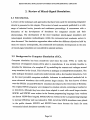
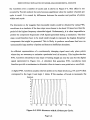
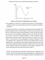
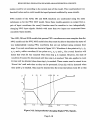
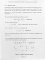
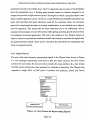
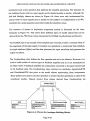
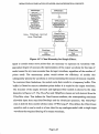
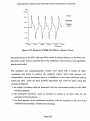
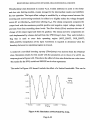
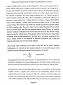
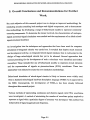
Figure 2-1. Manual
Mixed-Signal
Simulator
Approach
A manual approach to mixed signal simulation uses separate analogue and digital
from
digital
the
logic
the
The
of
part
waveforms
output
simulator
generates
simulators.
for
input
the circuit-level
These
to
then
signals
are
used
produce
waveforms
circuit.
from
The
the analogue
the
the
that
part
of
circuit.
outputs
simulates
analogue
simulator
The
for
digital
input
following
to
circuits.
are
any
used
write
vectors
circuit simulation
logic simulator is then run again with these new inputs. This is illustrated in Figure 2-1.
The manual approach is tedious and unreliable since the signal conversion and simulator
feedback
both
done
if
becomes
This
there
paths
are
control are
even worse
manually.
between the analogue and digital parts of the IC. This methodology is not used very much
design
is
Bx
few
design
An
ASIC
the
system
tools.
example
except with a
entry-level
from MCE. This uses a SPICE derivative simulator (HSPICE) and its native logic
Arrays
Gate
digital
MCE
the
signal
to
the
mixed
parts of
simulator
process
analogue and
respectively.
The coupled approach
implements a mixed signal simulator by connecting a circuit-level
be
into
logic
Coupled
together.
several categories
can
grouped
simulators
simulator
and a
dependingon the strengthand natureof the coupling.
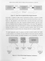
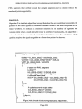
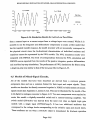
The weakest form of coupling is found in sequential simulators. These are similar to the
manual mixed signal simulators described above except the transfer of data between the
analogue and digital simulators is automated. Each simulator only considers a forward
Page 2-6
BEHAVIOURAL
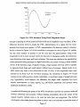
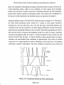
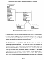
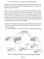
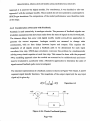
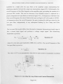
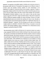
Digital
CircuitCircu
B lock
IB
SIMULATION
D/A
Interface
OF MIXED ANALOGUE/DIGITAL
CIRCUITS
A/D
Interface
Analogue
Digital
Circu
B lock
it
lock
°
Flow
of
Events
it
2
°
ý-
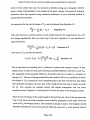
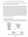
Figure 2-2. Data Flow in sequential Mixed-Signal
Simulator
circuit path: A sequence of input vectors is processed to produce a sequence of output
input
These
the
vectors for the next circuit block as shown in
results are used as
results.
Figure 2-2. This approach is valid provided there is no risk of the input vectors being
later
from
Sequential
by
feedback
best
therefore
simulators
a
stage.
where
altered
work
there is no feedback between analogue and digital parts or vice versa. This approach is
rarely used in practice since most mixed signal IC's include some feedback paths between
digital
and
sections. A commercial sequential simulator called 'A/D Lab' was
analogue
released by Daisy [] 1] as part of their suite of design tools but is no longer available.
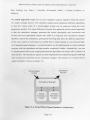
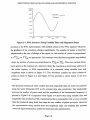
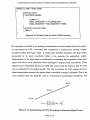
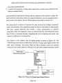
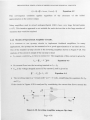
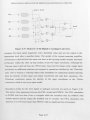
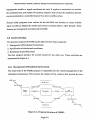
The paired approach couples the analogue and digital simulators together more tightly
to enable feedback to be simulated. The main difference between this and the sequential
approach is that the analogue and digital simulators are run concurrently (i. e. parallel
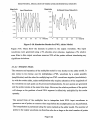
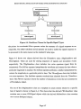
Coupling
Algorithm
and
Interfaces
Digital
Simulator
al
st
Common
Nets
Analogue
Simulator
Analogue
Netlist
%
Library of
Digital
Library of
Analogue
parts
parts
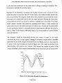
Figure 2-3. Paired Mixed-Signal Simulator Architecture.
Page2-7
BEHAVIOURAL
SIMULATION
OF MIXED ANALOGUE/DIGITAL
CIRCUITS
processes). This requires a computing environment that can support parallel processing:
usually a UNIX based operating system running on a workstation (e.g. Sun, HP-Apollo).
The structure of a typical paired mixed-signal simulator is shown in Figure 2-3.
Since the analogue and digital simulators are both running at the same time, they must be
synchronised whenever data needs to be transferred from one to the other. One simulator
will normally tend to run ahead of the other. Synchronisation therefore requires the fastest
simulator to be stopped and its simulation time reset to the same point as the slower
simulator. The simulator that will process a particular circuit most efficiently depends on
the size and nature of the analogue and digital parts. It is generally easier to stop and
back-track a digital simulator since lists of digital states are simpler to regenerate than
analogue voltage and current waveforms. The ability
to back-track requires all
intermediate results to be stored. This can require large amounts of disk storage and can
produce a very inefficient simulator if a lot of back-tracking is required. There are two
main synchronisation methods used in commercial mixed-signal simulators to address
this problem. One method is known as 'lock step' synchronisation. This locks the
timebases of both analogue and digital simulators tightly together so that neither one can
get substantially ahead of the other. This method is best where there is a large amount of
interaction between the analogue and digital components, i. e. a large number of results
must be passed between the two simulators. It is used in coupled mixed-signal simulators
from Cadence (Verilog + Cadence SPICE), Viewlogic (ViewSim + PSPICE) and Genrad
(SHADO: System Hilo + Eldo). The other method of synchronisation is known as 'leap
frog'. This allows each simulator greater independence:
is
allowed to run
each simulator
until it encounters an'event' from the other one. This looser coupling enables circuits with
less interaction between the digital and analogue sections to be
simulated more
efficiently. It also simplifies the integration of analogue and digital simulators (often from
different CAD vendors) into a single process. The problems associated with back-tracking
limit this method's performance when there is significant interaction between the
analogue and digital sections. The best known example of this technique is the patented
'Calaveras' algorithm [12] that saves information about the previous states of analogue
nodes to reduce the amount of analogue matrix re-evaluation required during backtracking. It is used in mixed-signal simulators based on the Saber analogue simulator
Page2-8
BEHAVIOURAL
from
Analogy
SIMULATION
OF MIXED ANALOGUE/DIGITAL
(e. g. Saber + ViewSim
(Viewlogic),
CIRCUITS
Saber + Verilog
(Cadence
or
Mentor)).
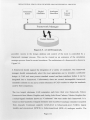
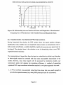
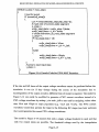
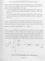
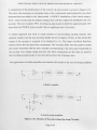
The nested approach couples two or more simulator 'engines' together under the control
of a single manager process. The simulator engines each implement different algorithms
so that the various parts of a mixed-signal system can be analysed using the most
appropriate method. The main difference between this approach and the paired approach
is that the simulation manager processes the circuit description and waveforms and
invokes the most appropriate engine only when it is required. The simulation manager
therefore controls the simulation, passing and receiving data from the different algorithms
in the same manner as subroutines are called from a main program in conventional highlevel programming languages. A nested simulator can be implemented as a self-contained
program with the algorithms and data transfer completely hidden. Alternatively, one can
be implemented with looser coupling between the algorithms by using UNIX 'sockets' for
data transfer. The simulation engines are then implemented as separateprograms although
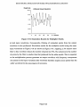
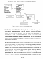
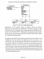
still invoked and controlled by the simulation manager. The structure of a nested mixedis
simulator
shown in Figure 2-4.
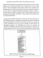
signal
C
Simulation
Results
Mixed-Signal
Netlist
Simulation Manager
Digital
Simulation
Engine
Analogue
Simulation
Engine
Figure 2-4. Nested Mixed-Signal Simulator Architecture.
Page2-9
BEHAVIOURAL
SIMULATION
OF MIXED ANALOGUE/DIGITAL
CIRCUITS
The use of sockets produces a more flexible nested simulator as it is relatively simple to
increase
individual
It
the
can
also
significantly
simulation engines.
add, remove or update
simulation speed if the simulation engines exist across a network of computers. Different
simulation engines can then process different parts of the system simultaneously on
be
hardware
interface
Sockets
to
modelers and
can
also
computers.
used
separate
hardware accelerators to the simulator. These are devices that allow physical (rather than
in
increases
be
in
huge
This
to
used.
can result
software) models of components
in
large,
included
(such
CPU)
a
complex standard parts
as a
are
simulation speed where
for
is
This
an increasing number of CPU cores are
significant since silicon masks
system.
from
in
designs
inclusion
ASIC
for
several vendors.
available
The main disadvantage of using sockets is the time penalty involved whenever data is
transferred. The effect of this is even greater if the data has to be transmitted over a
network. This method is therefore best where the amount of data that needs to be
transferred between the different circuit sections is small, i. e. there is little global
feedback between sections.
An example of a nested mixed-signal simulator is the combination of Meta-Software's
HSPICE analogue simulator with Silicon Compiler Systems' (SCS now part of Mentor
Graphics) LSIM extended digital core simulator [13]. LSIM includes algorithms for
analysing behavioural digital and analogue models. Running LSIM and HSPICE in
parallel on separate CPUs enables the simulation manager to maintain a level of accuracy
comparable to coupled simulators but with a large improvement in execution time. This
technique is therefore better suited to the simulation of entire VLSI devices where the
higher cost of the simulation tools is offset by the reduction in (expensive) CPU time.
A framework approach is the latest technology to appear in commercial CAD tools. The
concept of a framework is that all of the CAD tools required for the design process are
integrated into a single environment and address a common design database [14]. The
ideal framework would allow the end-user to select and integrate tools from any vendor
into a customised design environment with a consistent look
and 'feel'. The concept is
similar to the window-based environments found on personal computers but much more
Page2-10
BEHAVIOURAL
SIMULATION
OF MIXED ANALOGUE/DIGITAL
Digital
Simulator
Schematic
Editor
Analogue
Simulator
CIRCUITS
IC
Layout
Editor
Framework Manager
Figure 2-5. A CAD Framework.
by
is
design
database
Access
to
tools
the
the
a
and control of
controlled
powerful.
framework manager process. This can be viewed as an extension of the simulation
in
is
framework
found
in
The
shown
manager process
architecture of a
nested simulators.
Figure 2-5.
A framework
framework
The
integration
the
should support
of a variety of simulators.
manager should automatically
select the most appropriate one to simulate a particular
design. A CAD tool must possess standard control and data interfaces before it can be
integrated into a framework.
Unfortunately
there are several incompatible
framework
CAD
the
to
in
standards
adopt
vendors
of
reluctance
certain
a
standards currently
use and
by
their competitors.
used
The two largest electronic CAD companies each have their own framework, Falcon
Framework from Mentor Graphics and Analog Artist from Cadence. Mentor Graphics has
is
It
"Continuum"
framework.
known
that
their
runs
as
under
a mixed-signal simulator
based on their QuickSim II digital simulator and AccuSim II analogue simulator (acquired
from Anacad). Continuum supports switch-level to behavioural-level (VHDL)
digital
models and circuit-level (SPICE) to behavioural-level (HDL-A) analogue models. The
Page2-11
BEHAVIOURAL
SIMULATION
OF MIXED ANALOGUE/DIGITAL
CIRCUITS
framework
for
both
has
interface
Continuum
that
a
means
a common user
use of
into
design
the
automates
analogue
engines
and
partitioning
of
a
mixed-signal
simulation
and digital sections. There are currently only a few third party tools that are compatible
is
likely
Graphics
frameworks.
Mentor
Cadence
This
to
the
or
situation
with either
improve as framework standardsare approved and more widely adopted.
Applications that contain predominately analogue or predominately digital circuitry may
be simulated more efficiently by extended core simulators. These are analogue or digital
domain
have
been
"extended"
to
the
that
as
with
algorithms
process
other
simulators
shown in Figure 2-6.
Circuits that are predominantly analogue may be simulated more efficiently by extended
behavioural
digital
These
the
circuitry
models
of
analogue
use
analogue core simulators.
improved
performance over pure analogue simulators whilst still maintaining
offer
and so
the same degree of accuracy. Analogue simulators have the ability to perform frequency
domain analysis, which can be useful for evaluating certain mixed signal designs. The
frequency
is
dependent
domain
the
the
the
models
of
accuracy
on
analysis
of
usefulness
less
become
interface.
The
the
efficient as the
will
simulation
analogue-to-digital
of
digital
is
because
digital
This
increases.
model
to
each
proportion of
analogue circuitry
have
taken
have
be
to
time-step
state
of
changes
will
evaluated at every
even when no
(compared
those
to
The
be
to
time-steps
place.
set a relatively small value
will normally
in
digital
used
simulators) to keep the analogue simulation accurate.
Mixed-Signal
Netlist
ý
Figure 2-6. Extended Analogue Core Mixed-Signal Simulator.
Page 2-12
BEHAVIOURAL
SIMULATION
OF MIXED ANALOGUE/DIGITAL
CIRCUITS
Saber (from Analogy) is an extended analogue core simulator that was first released in
1985. Saber can operate at a behavioural level as well as a SPICE compatible level. The
performance of Saber as a mixed-signal simulator is therefore closer to that of coupled
simulators. Saber models consist of differential equations rather than the voltage sources,
current sources and semiconductor devices used in SPICE. The models are defined using
hardware
description
language (HDL) MAST [15]. Since the
a proprietary analogue
in
integral
differential
defined
terms
and
of
models are
equations they are not limited to
but
can also represent other system components whose behaviour
electronic components
in
behaviour
The
be
terms.
such
of an integrated circuit in its intended
can
expressed
environment can therefore be investigated at the design stage using this tool. Saber and
the MAST
language support simulation of digital components at the behavioural,
levels
structural and gate
so it can claim to be an integrated simulator. Despite this
it
is
in
capability,
used
several coupled mixed-signal simulators as the analogue engine
(e.g. Saber-Verilog, Saber-ViewSim and Saber-QuickSim). This reflects the higher
efficiency that is provided by coupled simulators when evaluating large, predominately
digital circuits.
Extended analogue core simulators based on SPICE have become more common as the
processing power of personal computers (PC's) has approached that of UNIX
workstations. PSPICE (from Microsim)
is one of best known of this category of
simulator. It features digital models with A/D and D/A interfaces. As a mixed-signal
simulator it is best suited to small sub-systems such as phase-locked loops and data
converters. For larger circuits, it is better to couple PSPICE to a digital simulator (such as
ViewSim).
IsSPICE4 (from Intusoft) is another extended core analogue simulator based on the
SPICE 3F [16] algorithms. It has recently been enhancedwith an analogue hardware
description languagecapability. This HDL enablesmodels to be written using the "C"
programming language. The Intusoft HDL enables IsSPICE4 to process behavioural
models of analogue and digital components. It is based on the XSPICE program [17]
Page2-13
BEHAVIOURAL SIMULATION OF MIXED ANALOGUE/DIGITAL CIRCUITS
developedat the Georgia Institute of Technology rather than on the proposedVHDL-A
standard.
The most recently introduced extended analogue core simulator is SMASH from Dolphin
Integration [18]. It is available for both PC's and UNIX workstations. SMASH also has a
language.
It
language
description
based
hardware
C
the
on
programming
proprietary
level
based
behavioural
functions
(e.
Laplace)
transfer
as
models
on
g.
supports analogue
direct
SMASH
SPICE
transient
can
using
models.
perform
analysis
well as standard
less
in
SPICE)
(but
(as
efficient
or more
accurate) relaxation methods.
used
methods
Digital sub-circuits are evaluated using an integrated 12-state, event-driven algorithm.
The digital simulation works at the switch-level for MOS circuits or can use behavioural
have
in
in
digital
C.
Dolphin
Integration
that
announced
models
written
written
models
the Verilog hardware description language will be supported in future releases.
Extended digital core simulators can hold voltage and current values on their time wheel
as well as digital events. Analogue waveforms are therefore represented as a series of
discrete steps. As previously mentioned, LSIM is an extended digital core simulator, it
includes a circuit-level simulation algorithm called 'Adept that uses SPICE 2G. 6 level II
and level III models [19]. Adept trades the accuracy of SPICE simulation against
improved execution time. LSIM also features a behavioural language 'M' based on the C
programming language. This can be used to model both analogue and digital circuits.
LSIM has been used by Sierra Semiconductors (a silicon vendor) as the basis for their
Montage simulator. Montage forms part of their "in-house" design system and has been
used for behavioural simulation of complete ASICs containing over 200,000 gates [20].
The extended digital core approach is better suited to high level behavioural simulation
than the detailed electrical level simulation offered by extended analogue core simulators.
Trading analogue accuracy against execution speed makes chip-level simulation possible.
The approximations inherent in the analogue behavioural models are less significant if
this type of simulator is restricted to standard cell type devices.
Page2-14
BEHAVIOURAL
SIMULATION
OF MIXED ANALOGUE/DIGITAL
CIRCUITS
An ideal integrated mixed-signal simulator processes a single circuit description and
generatesa single output file. All of the processing is done within a single program so no
time is wasted in synchronising separate analogue and digital simulation processes or
programs. This is therefore the most efficient
type of mixed-signal
simulator.
Unfortunately such a simulator has not yet been built and the techniques required to
implement one are still in the research domain. The main problem lies in the different
digital
The
integrated
to
and
models.
of
analogue
algorithms
nature
chosen
realise an
simulator normally give a preference to either analogue or digital models, at the expense
of the other type. Since the models must use an integrated data format, models from
existing simulators will not be compatible with integrated simulators. This means that a
large effort would have to be spent on creating libraries of component models before a
be
could
released. A commercial integrated simulator ANDI was
commercial simulator
released by Silvar-Lisco in the mid 1980's. The performance and capabilities of ANDI
were surpassedwhen coupled simulators became available. As a result, this simulator is
not widely used any more. CAD vendors have since concentrated on coupling existing
simulators together rather than developing new integrated simulators because of reduced
development costs and greater flexibility [21].
2.5 Experimental Mixed Signal Simulators and Simulation
Methodologies.
There has been a substantial amount of research in the field of mixed-signal simulation
since the mid 1970's. Much of the research work has been performed by post-graduate
students working towards Masters degrees and Doctorates in universities and research
laboratories. This has led to a number of new simulation methodologies and experimental
mixed-signal
simulators. Comparatively
few of these methodologies
have been
incorporated into commercial tools. This is a result of the long development times and
huge programming effort required to launch a new commercial simulator rather than a
reflection on the quality of the published research. The major developments in this area of
researchare reviewedbelow.
Page2-15
BEHAVIOURAL
SIMULATION
OF MIXED ANALOGUE/DIGITAL
CIRCUITS
Several researchers have attempted to produce an integrated mixed-signal simulator by
expanding a standard SPICE simulator [1]. Allen and Zuberek [22] expanded a SPICEcompatible circuit simulator to allow the description of parameterized analogue to digital
interfaces.
digital
This was then enhanced by including gate-level eventto
and
analogue
driven digital simulation algorithms. The circuit was described to the simulator using an
enhanced version of the SPICE netlist language that included functions for basic 2- and 3input logic gates. This technique produced a significant reduction in simulation time
compared to conventional circuit simulation for a number of analogue to digital converter
for
is
large
It
the
simulation
of
not
suitable
circuits.
mixed-signal circuits because of the
limitations of the SPICE algorithms.
Chain [23] has integrated a SPICE-type simulator with a switched capacitor simulator
(Spice-SCAN). This is an 'in-house' tool that has been developed for silicon vendor Harris
Semiconductor. It performs transient analysis of switched capacitor circuits. Although
switched capacitor circuits are widely used as building blocks in mixed-signal ASICs they
are not modelled well in conventional mixed-signal simulators. Spice-SCAN uses
algorithms that are much more efficient than SPICE to model charge conservation
between the switched capacitors without loss of accuracy. It is designed to simulate
circuits with non-deterministic clocks that can't be simulated by other switched capacitor
simulators. The example application given in the reference simulated several orders of
magnitude faster than a transistor level SPICE simulation and about ten times faster than
SpiceSPICE
integrate
Chain
it
is
to
a
simulation using macro-models.
claims
possible
SCAN into a Cadence framework using the Verilog digital simulator to give a complete
mixed analogue/digital/switched capacitor simulator.
Other researchers have investigated alternatives to SPICE-type nodal analysis for
performing circuit simulation. This has resulted in new methodologies known as
relaxation
techniques
[24].
These techniques make use of the unidirectional
characteristics of MOS transistors - the gate terminal (input) is insulated from the source
and drain terminals (outputs). This means that the current in the gate circuit is
independent of the voltages at the other terminals (neglecting
parasitic capacitance
Page2-16
BEHAVIOURAL
SIMULATION
OF MIXED ANALOGUE/DIGITAL
CIRCUITS
effects). The gate and source-drainterminals can thereforebe consideredas belonging to
be
that
can
separatecircuits
evaluated independently.
Relaxation techniquesovercomethe problems of the direct solution methods used in
SPICE by allowing a large circuit to be split into smaller blocks that can be processed
separately.The matrices for the separateblocks will be solved more efficiently. The
integration time step is not required to be the same for all blocks since it is only
dependenton thosesignalswithin a block. The optimum step size can thereforebe chosen
for each block without affecting the efficiency of the integration in other blocks. This
makesrelaxationtechniquesmore efficient at evaluatinglarge circuits than SPICE.
The first circuit simulator to use relaxation techniques was MOTIS [25] developed by
Chawla, Gummel and Kozah. This simulator also featured look-up tables to implement
transistor models and was up to two orders of magnitude faster than SPICE-type
simulators. It was designed to verify the timing of signals in MOS circuits and was
therefore referred to as a'timing simulator'. The efficiency of this technique was improved
in the SPLICE series of simulators [26]. SPLICE introduced a selective-trace algorithm
that automatically bypassed inactive circuit nodes during the integration process. The
integration methods were also modified to improve the convergence properties. This class
of relaxation based simulation is known as iterated timing analysis (ITA).
Research into ITA techniques led to a variation known as one step relaxation (OSR) [27].
This was used in the commercial Eldo analogue simulator from Anacad. Benkoski et al.
have integrated Eldo with an industrial multi-level
digital
form
to
an
simulator
experimental tightly coupled mixed signal simulator Mozart-MM
[28]. This uses a
lockstep algorithm to synchronise the analogue and digital simulation engines and
therefore falls into the same category as the SHADO commercial simulator already
mentioned (although it predates SHADO and doesn't directly support VHDL).
Another class of relaxation techniques attempts to directly solve the differential equations
associated with each circuit node. This is known as waveform relaxation (WR) [29].
This method assumesthat the circuit equations can be broken into blocks
such that if the
blocks are solved in the proper order, a good approximate
solution to the entire system is
Page 2-17
BEHAVIOURAL
SIMULATION
OF MIXED ANALOGUE/DIGITAL
CIRCUITS
obtained. The effect of transitions at the inputs of a circuit ripple through successive
blocks and can be considered as a series of wavefronts propagating through the circuit.
The accuracy of the initial approximation can usually be increased by a second iteration.
Subsequent iterations will tend to converge rapidly to the exact solution. Since relaxation
high
between
loose
(e.
coupling
g.
nodes, circuits with strong coupling
methods assume
gain feedback) will converge very slowly. In such cases, the closely coupled nodes are
best evaluated using direct methods. Waveform relaxation simulators such as RELAX2
[24] therefore use partitioning algorithms to group large MOS circuits into suitable blocks
before performing the simulation.
The efficiency of waveform relaxation simulators at simulating digital functions is still
digital
by
less
than
that
achieved
conventional
simulators. They are normally
significantly
for
large
higher
for
is
the
scale analogue simulation and where
accuracy
used
required
digital circuits (e.g. for timing analysis) rather than as the basis for integrated mixedsignal simulators.
Relaxation based techniques are well suited for parallel processing since the decomposed
circuit blocks are loosely coupled and can be simulated independently. Waveform
Relaxation and Waveform Relaxation Newton (a combination of WR with conventional
Newton numerical integration) algorithms have been combined by Odent et al. for use
in
[30].
in
This
with a general purpose parallel computer
a substantial reduction
resulted
is
Parallel
time
processing
execution
compared with standard sequential algorithms.
desirable for large mixed-signal systems with a significant proportion of analogue
circuitry or digital circuitry requiring accurate timing analysis. This would however
require that the architecture of the mixed-signal simulator was well suited to a parallel
processing environment. These techniques are therefore most likely to be of use in
framework based mixed-signal simulators.
Several researchers[26][31] have developed timing simulators to a point where they
could be used as mixed-signal simulators for MOS circuits. Timing simulators are
designed to provide accurate simulation of digital circuits by
using more accurate models
for the transistors than switch-level simulators. They
make use of the event-driven nature
Page2-18
BEHAVIOURAL
SIMULATION
OF MIXED ANALOGUE/DIGITAL
CIRCUITS
increase
digital
to
the performance over SPICE type circuit simulators. The
circuits
of
in
SPLICE
ADEPT
the commercial LSIM
the
simulators
algorithm
experimental
and
have
been
fall
into
both
They
this category.
simulator
already
mentioned.
The MOTIS timing simulator has undergone two major revisions known as MOTIS2 and
MOTIS3 [26]. Each revision has improved the algorithms to increase performance and the
range of circuits that can be simulated. Chadha et al. have developed a unified multilevel
mixed-signal simulation system known as M3 based upon MOTIS3 [31]. This system
consists of a set of tools to create simulator models together with the simulator control
program. M3 is designed to model analogue circuitry at the behavioural level. The models
are 'written in the C programming language. Since this provides considerable scope for
developed
ACME
tool
to test the model behaviour
was also
error, a model verification
prior to use in the simulator. Two automatic model generation tools were developed to
generate models from s-domain and z-domain descriptions
since the behaviour of
filters
is
analogue
often specified in the frequency domain. The behavioural models can
have voltage, current and Boolean terminals. The voltage and current terminals are bidirectional so coupling and loading effects can be simulated. Boolean terminals are
unidirectional, i. e. they are either inputs or outputs. The models consist of controlled and
independent voltage and current sources that are evaluated using the relaxation algorithms
in MOTIS3.
Event-EMU is an experimental timing simulator developed by Ackland and Clark [32]. It
combines a mixture of event driven and relaxation techniques to provide a higher
performance than circuit simulators with no significant loss of accuracy. Event-EMU
doesn't directly support analogue components but could be adapted to do so since it
includes models for MOS transistors, resistors, capacitors and current sources. Events
occur when a node voltage changes by more than some specified threshold. Including an
analogue modelling capability would therefore reduce the efficiency of Event-EMU since
the threshold would inevitably have to be made smaller to preserve the accuracy.
Overhauser et al. developed IDSIM2, a timing simulator that
could operate at multiple
levels of abstraction and included an analogue
modelling capability [33]. Analogue
Page2-19
BEHAVIOURAL
SIMULATION
OF MIXED ANALOGUE/DIGITAL
CIRCUITS
circuits are simulated using detailed circuit simulation. Digital circuits are simulated
using 'fast timing simulation'. Two methods of fast timing simulation are implemented:
the first uses a ramp representation of waveforms while the second uses a more detailed
piecewise linear (PWL) representation. The ramp representation is up to one order of
magnitude faster than the PWL representation. A significant feature of this simulator is
that when the waveforms in any subcircuit are detected to be "not accurate enough"
within a certain time interval, the subcircuit is dynamically changed to a more accurate
model. This means that at the end of a simulation, only those subcircuits that required the
greatest accuracy would have been modelled at that level: the rest would have been
level.
IDSIM2 uses waveform relaxation for simulation of
the
modelled at
most efficient
both analogue and digital functions. PWL waveforms are used to interface subcircuits
having different levels of analysis to each other. Since only (unidirectional) MOS circuits
are considered, feedback loops can be solved more efficiently than with SPICE type
simulators. Feedback loops are processed using one of three windowing techniques:
partial waveform convergence; dynamic windowing; or a combination of both. The
windowing techniques are chosen to provide the most efficient forward processing path
whilst keeping the number of iterations required when feedback occurs to a reasonable
level. The authors [33] report significant increases in performance compared to SPICE2.
ILLIADS
is a timing simulator developed by Shih and Kang [34] that takes a different
approach to IDSIM2.
ILLIADS
uses a new MOS circuit model and approximates
electrical waveforms using PWL segments. The new model has a major advantage over
those used in other timing simulators: parallel circuit branches (such as found in CMOS
NAND and NOR gates) are not required to be merged to preserve accuracy. Improved
waveform relaxation techniques are used to overcome the inefficiencies of standard WR
methods when applied to feedback between strongly coupled components. Windowing
techniques similar to IDSIM2 are also used (ILLIADS and IDSIM2 were both developed
at around the same time in the University of Illinois). The authors report significant
increases in performance compared to SPICE simulations for several digital
No
circuits.
mention is made as to the suitability of this simulator for processing mixed-signal circuits.
Page2-20
BEHAVIOURAL
SIMULATION
OF MIXED ANALOGUE/DIGITAL
CIRCUITS
A mixed-signal simulator based on a timing simulation approach has been developed by
Jun and Hajj [35], also at the University of Illinois. This simulator features logic, timing
and circuit simulation algorithms. The overall architecture is based on waveform
relaxation with dynamic windowing to handle feedback (like IDSIM2 and ILLIADS). The
logic simulation uses two logic states and user defined delay parameters. Timing
simulation uses either empirical or analytical macromodels based on NMOS transistors. If
the timing
simulator detects glitches, it can automatically switch to using circuit
in
for
block
the same way as IDSIM2. The circuit simulation can use
a
simulation
blocks
for
SPICE
analogue
models
or can work at a higher level for digital
standard
blocks using a simplified MOSFET model. The simulator automatically inserts digital to
analogue and analogue to digital converters between analogue and digital circuit blocks.
The digital to analogue conversion is based on ramp waveforms. The analogue to digital,
is
based
four
threshold voltages to simulate noise margins. If an
around
conversion
is
in
between the thresholds for the two logic states, the digital block
analogue waveform
is automatically simulated at a circuit level. The authors report that this simulator runs up
to three orders of magnitude faster than SPICE.
Several of the simulators mentioned above make use of piecewise linear
(PWL)
waveforms to improve the efficiency of signal representation. Piecewise linear techniques
provide a generic and powerful approach to the modelling of electronic components. They
have been used by several other researchers to create mixed-level and mixed-signal
simulators. PWL waveforms support the use of macro models and mixed-levels of
abstraction since all components and signals are modelled in a uniform manner.
Early work on PWL simulation formed a similar set of circuit equations to the nodal
analysis (NA) methods used in SPICE type simulators [36]. These equations were solved
using sparse matrix techniques and multirate integration methods. PWL simulators have
two main advantages over SPICE type simulators. They have better convergence
characteristics and support component modelling at all levels of abstraction.
Van Stiphout et al. implemented a PWL mixed-signal
simulator called PLATO that used
an event-driven approachfor transient analysis [37]. The events are grouped into two
Page2-21
BEHAVIOURAL
SIMULATION
OF MIXED ANALOGUE/DIGITAL
CIRCUITS
dynamic
PL
events and
events. PL events occur when a vector reaches the end of
classes:
for
if
integration
PWL
Dynamic
the
a
step
size
segment.
events
are
generated
a
waveform
invalid
becomes
integration
(the
step sizes are adjusted to maintain
model
particular
accuracy and efficiency as the simulation progresses). The efficiency of this event-driven
by
discretization
increased
was
of the event times thereby reducing the number
approach
improvements
forcing
by
Further
to
related
of separate events.
efficiency were made
blocks
to use the same minimum step size, reducing the recomputation of step
circuit
sizes required. The authors present example applications together with program statistics
but make no comparisons to the performance or accuracy of other simulators.
Kevenaar and Leenaerts use similar methods to PLATO in a PWL simulator called
PLANET that exploits system hierarchy to run more efficiently [38]. Previous PWL
large
the
solved
circuit
equations
using
a
single,
simulators
matrix. PLANET partitions a
large system into a set of subcircuits that can each be represented by a small matrix of
PWL equations. Each subcircuit can be solved independently allowing the optimum
integration timesteps to be used. The subcircuits are connected together by sets of
topological equations that describe the system hierarchy. This approach also enables
subcircuits to be replaced by behavioural models to further increase the efficiency. The
advantages of this approach over non-hierarchical methods increase with the complexity
of the simulated system. The authors show how the accuracy of an op amp macromodel
be
can
comparable to SPICE.
Griffith and Nakhla have used piecewise linear waveforms in a novel simulator for nonlinear frequency dependent circuits [39]. This simulator is designed for transient analysis
high
of
speed circuits where improperly terminated connections can adversely affect the
transmission of signals. These connections cannot be simulated correctly by conventional
lumped impedance interconnect models and must use distributed transmission line models
instead. Unfortunately, these models are only defined in the frequency domain. The
simulator replaces non-linear terms in the circuit equations by a set of piecewise linear
time-dependent waveforms. This reduces the non-linear equations to a linear equation that
can be solved in the frequency domain. The transient response is obtained from the
frequency domain solution using inverse Laplace transforms.
Page2-22
BEHAVIOURAL
SIMULATION
OF MIXED ANALOGUE/DIGITAL
CIRCUITS
Cottrell used piecewise linear waveforms to create a behavioural mixed-signal simulator
[40,41]. This simulator was based on LSI Logic's proprietary event-driven behavioural
logic simulator BSIM. The analogue models represent the transfer functions associated
digital
blocks,
blocks
filter
such as gain
sections, comparators and
with analogue circuit
to analogue converters. The model ports are unidirectional and are either classified as
inputs or outputs. Passive components such as resistors and capacitors can not be
inputs
by
be
their
this
or
connections
simulator since
cannot
classified as
modelled
be
Analogue
PWL
as
voltage
can
or current
signals are classified
waveforms and
outputs.
differential or referred to a common potential (ground). Transfer functions that are
domain
be
frequency
in
the
converted to the time domain using Laplace
must
specified
transforms prior to simulation. They are then solved using the Forward Euler numerical
integration method. The timesteps used by each model are controlled by monitoring the
truncation errors in the PWL signal representations. Each model can therefore use the
formulae
forward
Euler
The
timestep.
truncation
the
appropriate
most
errors arise since
are not perfect approximations of the Taylor series that give the correct results. The
truncation error is proportional to the second derivative of the PWL waveforms. The
simulator was tested with a successive approximation analogue to digital converter
circuit. The results were compared with a simulation of the same circuit using HSPICE.
The HSPICE simulation provided more detailed waveforms but took over 350 times as
long to run. The simulator was also used to test an FM receiver circuit with good results.
Visweswariah and Rohrer have used piecewise linear and piecewise constant waveforms
in a prototype event driven circuit simulator called SPECS [42]. This simulator uses
empirical table models of I-V characteristics to represent electronic devices. Voltages are
represented by PWL waveforms while currents are represented by piecewise constant
waveforms. The simulator assumes that circuits only consist of independent sources,
linear capacitors and non-energy storing two-port elements like resistors and diodes. A
circuit consists of a tree of the independent sources and linear capacitors. Each link of the
tree is unidirectional so a table model can be built to represent its IN characteristics. All
the table models are evaluated with a single event queue. Events correspond to the times
that current waveforms change level and voltage waveforms change gradient. Feedback
Page2-23
BEHAVIOURAL
SIMULATION
OF MIXED ANALOGUE/DIGITAL
CIRCUITS
loops cause events on the queue to be rescheduled in a similar way to event-driven digital
simulators. Rescheduling may require a number of iterations before the circuit reaches a
steady state. The methodology guarantees that the circuit will always converge to the
iterations
dependent
is
The
to
on the
correct state.
number of
required
converge
coarsenessof the steps (number of segments) in the table models. The size of the steps
be
defined
in
different
by the user to trade-off accuracy against
used
parts of a circuit can
digital
from
for
SPECS
favourably
Simulation
SPICE
results
compare
efficiency.
with
MOS circuits. It is shown to run up to 200 times faster than SPICE, depending on the
in
the models.
used
number of segments
Ruan et al. used PWL waveforms to represent voltages in a functional simulator that
formed part of an experimental multi-level simulator [43]. This functional simulator was
designed to operate with both analogue and digital functional blocks. It was intended to
interface
between
the
provide
a logic simulator and a circuit simulator in their multi-level
simulation system. It uses an event-driven approach and predicts the time of each new
from
the gradient of signal waveforms. Logic gates are modelled using a
event
designed
AND,
OR
NOT
These
to work
combination of
and
operations.
operations are
The
logic
directly
they
the
with an arbitrary set of
voltage waveforms.
operate
on
states:
input
in
AND
the
to
the
output of
a set of
operation corresponds
minimum voltage
signals at any instant in time. The OR operation is similarly defined to give the maximum
from
from
input
The
NOT
the
voltage
a set of
signal voltage
signals.
operation subtracts
the sum of the logic 0 and logic 1 voltage levels (e.g. 5V). The voltage gain of a logic gate
is assumedto amplify the rate of change of the output waveform until it reaches a limiting
value. Capacitance in the gate fan out is assumed to attenuate the rate of change of the
output waveform. The gate models generate an output waveform using the logic
operations above. Rate amplification, limiting and attenuation functions are then applied.
The models also apply a delay to the output waveform. This delay is a function of the rate
input
the
of change of
signal waveforms. Conventional digital simulators normally use a
logic state 'X' to represent an unknown initial
value at a logic gate output. Unknown
states are usually created by an incorrect initialisation procedure. It is not possible to
represent an unknown state in a simulator that only recognises voltage values. An algebra
based on interval computation was developed to
overcome this. An unknown state is
Page2-24
BEHAVIOURAL
SIMULATION
OF MIXED ANALOGUE/DIGITAL
CIRCUITS
by
a range of voltage values (an interval). The authors prove that Boolean
represented
has
if
by
is
interval.
This
the
remains
valid
a
single
an
method
algebra
value
replaced
intervals
be
by
The
that
the
operations.
outputs
advantage
can
arithmetic
added
processed
of the models can therefore always be directly passedto analogue functional models. This
interpret
how
with
mixed-signal
simulators:
analogue models
overcomes another problem
'X' states from digital models. The simulator was tested with several high level analogue
in
but
digital
The
SPICE
were
close
ran up to
problems.
results
agreement with
and
faster.
of
magnitude
several orders
Rsim [44] is an experimental switch-level simulator that can simulate large digital MOS
faster
have
SPICE.
linear
Piece-wise
than
to
three
orders
of
magnitude
models
circuits up
been added to Rsim by Kao and Horowitz to form a new simulator called Mom [45]. This
for
digital
Rsim
but
improves
the
the accuracy
efficiency
of
circuits
simulator preserves
for
that
the
simulation
so
results
certain "difficult"
by
those
circuits approach
given
SPICE. The circuits considered included CMOS dynamic RAM sense amplifiers, emitterlogic
coupled
gates and BiCMOS buffers. These are all cases where the analogue
characteristics of the transistors must be considered and so would usually require a
mixed-signal simulator to be used. Mom is not suitable for circuit-level analysis since the
methods used to evaluate the circuit equations loose their efficiency (compared to SPICEtype numerical integration methods) as the complexity of the piecewise linear models is
increased to match the accuracy of SPICE models.
Several researchershave investigated the use of behavioural models of analogue functions
in mixed-signal simulators. Behavioural models can be simulated much faster than the
transistor level models used in both SPICE-type and relaxation based circuit simulators.
Several of the simulators described above make use of analogue behavioural models [31,
40,41,15].
The ability to create behavioural models has been available in SPICE since
the mid 1970's and is known as macro-modelling [46,47,48]. However, the efficiency of
this approach is far less than is possible using a purpose designed behavioural simulator
[49]. It is possible to create behavioural models that feature similar levels of accuracy to
transistor level models. Unfortunately such models require long development times and
are only valid over narrow physical and electrical operating points. There are two main
Page2-25
BEHAVIOURAL
SIMULATION
OF MIXED ANALOGUE/DIGITAL
CIRCUITS
application areas where the model development times can be justified.
application is in top down system design where system functionality
The first
is the main
consideration. This only requires generic models that can be optimised for execution
speed and/or memory requirements. The other application area is ASIC design using cell
libraries. This makes use of ready made analogue modules designed by specialist IC
designers. Exhaustive simulation and testing of these modules will have already been
done using SPICE type circuit analysis tools and physical testing of fabricated devices
respectively. An ASIC vendor will therefore have all the information required to produce
suitable behavioural models of the components in a cell library.
Rumsey and Sackett developed a mixed-signal behavioural simulator called AMP based
around Laplace transforms [50,51].
The simulator uses "black box" models that are
constructed from a set of parameterised building blocks. The models can exist at three
different levels of abstraction. The simplest level uses functional blocks with ideal
behaviour (e.g. an ideal op amp). The next level represents parameterised macro-models.
A model of an op amp at this level would include standard data sheet parameters such as
offset, common mode gain, differential gain, etc. The most complex level uses models
with tuned behaviours. This means that the parameters associated with the model would
change to reflect the actual physical and electrical environment being simulated (e.g. the
offset voltage parameter of an op amp changing with the simulated temperature and
power supply). The simulator includes a tool called NETTOLA
that automatically
generates Laplace transforms from a netlist description of a network containing resistors,
capacitors and inductors. AMP was designed to interface to an in-house Texas
Instruments event-driven simulator. A linker (AML) was also developed to interface the
models to commercial digital simulators.
Gielen et al. developed an analogue behavioural simulator intended for use in simulation
and synthesis of mixed-signal systems [52]. A simulator for a synthesis environment must
use generic models. The models are required to fully describe the behaviour of each
system block as a black box. No assumptions can be made about the internal architecture
of the black box. This simulator therefore consists of a general simulation engine and a
library of behavioural models. Each model
represents a distinctive function such as
Page2-26
BEHAVIOURAL
SIMULATION
OF MIXED ANALOGUEIDIGITAL
CIRCUITS
sampling, quantizing, filtering, phase-locking, etc. The models can be parameterised to
reflect the effect of using particular technologies. Most of the parameters are statistical
and require information about average values, variance and covariance to be supplied. The
simulator and models are implemented using object-oriented techniques. The models are
objects that are instantiated and interconnected for each particular application. The
behaviour of each model is described in the form of input-output functions, differential or
difference equations and transfer functions in the frequency domain. The models are
invoked and the simulation controlled by a simple event driven process. The authors plan
to ultimately integrate this with a commercial simulator such as Saber. The performance
of the simulator is illustrated by a statistical minimum-rank model of a Nyquist-rate
analogue to digital converter. This showed the effect of signal amplitude and channel
mismatches on the noise performance of the converter.
2.6 Conclusions.
There has been much research and development activity in the area of mixed-signal
simulators since the need for such tools became apparent. This activity has been driven by
developments
in microelectronics technology that have enabled progressively
continuing
larger and more complex mixed-signal systems to be implemented on a single integrated
circuit. Developments in computer technology and programming languages have enabled
highly complex simulation methodologies and tools to be developed that would not have
been possible at the time when simulators such as SPICE were being developed (e.g.
parallel processing, distributed systems and CAD Framework environments). Despite
these developments, an integrated mixed-signal simulator that is well-suited to the design
of large mixed-signal circuits has yet to be released.
Commercial CAD tool vendors have tended to create mixed-signal simulators by coupling
an existing digital simulator to an existing analogue simulator using a variety of
approaches. This approach has the advantage of being able to reuse existing component
models but it does not produce the most efficient simulator. Extending a circuit-level
simulator to include digital models has become popular in recent years but is only suitable
for relatively small circuits (not large, predominately digital ASICs). Experimental
Page2-27
BEHAVIOURAL
SIMULATION
OF MIXED ANALOGUE/DIGITAL
CIRCUITS
have
been developed using techniques originally devised for
simulators
mixed-signal
digital MOS circuits such as Waveform Relaxation. These have achieved promising
results for a limited range of applications but cannot claim to be universal mixed-signal
simulators.
Several researchershave investigatedthe use of piecewise linear (PWL) waveforms to
representsignals.PWL waveformscan representboth analogueand digital signals and so
data
format
in
integrated
an
could provide a uniform
mixed-signal simulator. This might
overcomethe problemsof signal conversionandtime synchronisationthat exist in current
lead
PWL
to very efficient numerical integration
also
waveforms
mixed signal simulators.
methods and so have the potential to reduce the time taken to solve the differential
describe
that
most analoguecircuits.
equations
Behavioural-level simulators offer a way of investigating a large-scale design since they
functional
blocks rather than individual transistors. Behavioural
with
are concerned
simulators have become common for digital system design using hardware description
languages such as VHDL or Verilog. There are several analogue simulators that currently
support behavioural-level modelling using proprietary HDLs. Analogue behavioural
further
that
modelling methods
can match the accuracy of circuit-level simulation require
development. Analogue extensions to VHDL will lead to mixed-signal simulators that can
work at a behavioural level for analogue and digital blocks using a common modelling
language. However, for the foreseeable future these will still not be "integrated" mixedsignal simulators but based on existing coupled-simulator approaches.
Page2-28
BEHAVIOURAL
SIMULATION
OF MIXED ANALOGUE/DIGITAL
CIRCUITS
3. Development of Modelling Techniques.
3.1 Introduction.
The efficiency of any simulator depends on the nature of the simulation models and the
discrete
between
Digital
them.
that
simulators are only concerned with
are passed
signals
voltage levels (logic states). They can therefore represent signals much more efficiently
than analogue simulators which require signals to be continuous. An ideal mixed signal
simulator would represent analogue voltages and currents as efficiently as the logic states
in a digital simulator. Piece-wise linear (PWL) waveforms provide an efficient method of
be
digital
to
signals
can
also
used
represent
and
states. This chapter
representing analogue
describes the development of modelling techniques for analogue, digital and mixed-signal
based
on optimised PWL waveforms.
components
3.2 Representation of Signals.
3.2.1 PWL Representation of Digital Signals.
Piece-wise linear (PWL) waveforms represent changing signals as a series of connected
linear segments. They are commonly used in SPICE-type simulators to represent digital
signals as a series of pulses with finite rise and fall times. A typical PWL representation
of a digital signal is shown in Figure 3-1. This waveform would be defined by the
following set of points:
(0,0), (5,0), (6,5), (10,5), (11,0), (15,0), (16,5), (25,5), (26,0), (30,0).
The first ordinate in each pair defines a point in simulation time whilst the second defines
the signal magnitude at that time. The time ordinate must increase between every point in
the PWL waveform: since the waveform is represented by linear segments joining
adjacent points, a decreasein the time would have no physical meaning. Two co-ordinates
are associated with each signal transition, these specify the beginning and the end of the
transition period. The PWL representation requires twice the amount of data to be stored
compared to a conventional representation of a digital signal (a series of transition times
and logic states). Consequently, PWL waveforms are not usually used in digital
Page3-1
BEHAVIOURAL SIMULATION OF MIXED ANALOGUE/DIGITAL CIRCUITS
M agnltuda
6.00
5
-
00
4.00
3.00
2.00
1
.
00
0.00
0
T Im e
Figure 3-1. Piece-wise Linear (PWL) Representation of a Digital Signal.
information
though
they
more
provide
even
simulators,
about the switching
characteristics.
Digital signals are usually assumed to have a discontinuous nature, i. e. changes between
logic states occur instantaneously. To represent this as a PWL waveform the requirement
for time to increasebetween points must be relaxed to allow the time to also remain
constant between a pair of points. Digital signals only exist in discrete states. The
PWL
digital
A
between
transitions.
therefore
magnitudeof a
signal
state
remainsconstant
representationthat allows instantaneouschangesof magnitudeand where the magnitude
remains constantbetweenchangesis known as a Piece-wiseConstant(PWC) waveform.
A PWC representationof the signal in Figure 3-1 is given in Figure 3-2.
The Piece-wiseconstantwaveform in Figure 3-2 has redundantpoints: since signals are
Mapn
Ilu
6.00
da
5.00
4.00
3.00
2.00
1
.
00
0.00
0
T Im
9
Figure 3-2. A Piece-wiseConstant (PWC) Signal.
Page3-2
BEHAVIOURAL SIMULATION OF MIXED ANALOGUE/DIGITAL CIRCUITS
be
to
constant within each segment, the co-ordinates defining the end of a
assumed
segment can be derived from the magnitude at the start of the segment and the time at the
start of the next segment. The amount of data required to represent a signal in a PWC
format is therefore comparable to that required by conventional digital representations.
The effects of capacitance are significant in microelectronic systems. A piece-wise
constant waveform will therefore provide a poor representation of voltage signals.
However, since the effects of inductance are negligible for most semiconductor devices,
PWC waveforms can provide an accurate representation of the currents that flow in a
digital system [42].
Two methodsof representingdigital signalswere investigated:
1. An efficient representationfor use within completely digital blocks using a PWC
is
This
representation.
compatible with digital event-driven simulation methodologies.
2. An accuraterepresentationfor use where the analogue characteristicsare important
PWL
a
representation.
using
A piece-wiseconstantrepresentationcannotbe usedwith analoguesimulation algorithms
that require signalsto be continuous.However it is simple to convert a PWC waveform to
fall
PWL
finite
The
is
a
waveform.
rise and
most efficient conversionmethod to assign
times to eachtransition in the PWC waveform. A more accurateconversiontechnique is
to consider the PWC waveform to representthe output current of a digital model. The
correspondingPWL voltage waveform can then be obtainedby consideringthe equivalent
RC circuit of the output stage.
3.2.2 PWL Representation of Analogue Signals.
The selection of an optimum set of points to representa constantly varying signal is a
more complex operation than the assignmentof points to representa digital signal. A
sinusoidalwaveform is the most extremeexampleof a varying signal for representationin
a PWL form since the rate at which it changesis never constant, i. e. it has no linear
segments.
Page3-3
BEHAVIOURAL
SIMULATION
OF MIXED ANALOGUE/DIGITAL
CIRCUITS
One method of placing the points representing a continuously varying waveform is to use
a fixed time interval (time step) delta between each point. This is analogous to sampling
the waveform in the time domain with a sampling frequency of 1/delta. The Sampling
Theorem states that a signal of frequency fh can be completely specified by a uniform
half
less
delta
be
2fh.
This
time
than
than
the
to
of the
requires
step
sampling rate greater
period of the highest frequency component of any signals represented. However, accurate
be
far
the
time
to
will
require
steps
smaller than those
representation of a sine wave
suggested by the Sampling Theorem since the points are connected by linear segments: a
PWL representation of a sinusoidal waveform with only two points per cycle leads to a
triangular waveform.
A PWL representation of part of a sinewave with 14 points per cycle is given in Figure 33. Comparison with a true sinewave shows that the PWL representation has introduced
significant distortion into the waveform, most noticeably at the extremes where the
from
is
least
linear.
deviation
The
PWL
the
a
sinewave
representation
variation of
of a
deviation
The
decreases
increased.
is
the
sinewave
pure
as
number of points per cycle
becomes insignificant if more than 100 points per cycle are used.
The distortion resulting from the representation of a continuously varying signal by a
Magnitude
6.00
4.00
2.00
0.00
-2.00
-4.00
-6.00
-8.00
Time
Figure 3-3. PWL Sinewave with Points at Fixed Time Steps.
Page3-4
BEHAVIOURAL SIMULATION OF MIXED ANALOGUEIDIGITAL CIRCUITS
finite number of linear segments can be studied using Fourier analysis. A series of PWL
waveforms representing 10 cycles of a sinewave with various numbers of points per cycle
(from 6 to 100) and uniform time steps between points was analysed using a 1024-point
Fast Fourier Transform (FFT). The analysis found that the distortion mostly existed as a
increased,
harmonics.
As
the
the
was
of
number
of
points
cycle
per
small number
harmonics
dominant
harmonics
decreased
these
the
the
whilst
order of
magnitude of
increased. When 6 points per cycle were used, the significant harmonics were the 5th (4%
of fundamental magnitude), the 7th (2%) and the 11th and 13th (approximately 1% each).
When the number of points per cycle was increased to 25, the significant harmonics were
the 24th and 26th (approximately 0.02% of the fundamental magnitude each).
The closeness of the PWL representation to a true sinewave is represented by the
fundamental
by
between
frequency
FFT.
The
the
the
magnitude of
produced
relationship
the number of points per cycle and the magnitude of the fundamental frequency is shown
in Figure 3-4. The graph in Figure 3-4 gives an indication of how trade-offs could be
between
the accuracy required and the efficiency of a PWL representation.
made
There is another form of distortion that can occur if there are not an integral number of
time points representingeach cycle. This distortion appearsas amplitude modulation of
100
99
98
97
96
95
94
93
92
91
1-
0
10
20
30
40
Points/Cycle
50
60
70
80
Figure 3-4. The Relationship between the Number
of Points per Cycle and the
Magnitude of the Fundamental Frequency
of a Sinewave with Fixed Time Steps.
Page3-5
BEHAVIOURAL
SIMULATION
OF MIXED ANALOGUE/DIGITAL
CIRCUITS
the waveform over a number of cycles and is shown in Figure 3-5. This effect is not
by
but
becomes
Fourier
analysis
only
significant when the number of points per
revealed
is
by
is
It
differences
between
the number and position of points
caused
small.
cycle
within eachcycle.
The discussion so far suggests that reasonable results could be obtained by using PWL
less
in
if
be
25
than the
to
times
the
time
steps were chosen
about
a simulator
waveforms
impossible
it
is
highest
frequency
Unfortunately,
to
the
signal.
often
sinusoidal
period of
during
The
frequencies
time
the
of
all
signals
generated
a
simulation.
component
predict
frequency
highest
have
be
to
to
the
therefore
small
made
enough
represent
steps would
is
likely
have
be
This
to
that
that
an
produce waveforms
might
generated.
components
hence
inefficient
large
an
and
simulator.
number
of
points
unnecessarily
An efficient representation of a continuously changing signal must only place points
where they are necessary to maintain a particular level of accuracy. This implies that the
PWL waveform should have time steps of varying length (as was the case for the digital
signal represented in Figure 3-1). A simulator that generates PWL waveforms must
therefore provide a mechanism to determine when to insert a new point into a waveform.
A digital PWL waveform usually only has points at two finite levels (e.g. OV and 5V) that
1
logic
logic
0
to
the
states.If the number of levels is increased,the
correspond
and
Magnitude
5m
4
3
2
1
0
-1
-2
-4
-50
10
20
30
40
50
60
70 Time
Figure 3-5. PWL Sinewavewith 8.1 Points per Cycle.
Page3-6
BEHAVIOURAL
SIMULATION
OF MIXED ANALOGUE/DIGITAL
CIRCUITS
MpnNud"
6.00
4.00
2.00
0.00
-2.00
-4.0C
-6.0C
-8.0(
nom.
Figure 3-6. PWL SinewaveUsing Fixed Magnitude Steps.
finite
levels
be
If
the
the
to
can
of
at
applied
of
placing
all
points
any
waveform.
concept
difference between levels is small, the PWL representation of a signal will be more
discrete
but
A
PWL
14
more
representation
require
points.
accurate
of a sinewave using
levels is shown in Figure 3-6. If this waveform is compared to that in Figure 3-3 (which
has the same number of points) it can be seen that the representation using fixed
is
levels
introduces
but
is
the
more accurate where
sinewave changing rapidly
magnitude
distortion
more
at the upper and lower extremes. The errors are similar to the quantisation
digital
during
to
conversion as a result of using a finite number
errors generated
analogue
of bits. If the dynamic range of signals is large, a large number of levels will be required
to represent both large and small signals without loss of accuracy. Signal levels in an
ASIC could vary from a few microvolts to tens of volts. If the magnitude steps were
selected to be about 1µV for low-level accuracy, the waveform in Figure 3-6 would
contain several million points, clearly undesirable. A non-linear range of magnitude steps
(e.g. logarithmic) could improve the efficiency but might mask important low level
signals superimposed on large signals, e.g. DC-biased amplifiers and systems using
amplitude modulation (AM).
A method of allocating the points of the PWL waveform to provide the optimum trade-off
between efficiency and accuracywithout making assumptionsabout the nature of the
signals requires variable steps to be used for both time and magnitude. The method
developedin this thesisplacesthe points in sucha way as to maintain a particular level of
Page3-7
SIMULATION
BEHAVIOURAL
OF MIXED ANALOGUE/DIGITAL
CIRCUITS
Magnitude
6.00
4.00
2.00
0.00
-2.00
-4.00
-6.0C
-8.0c
Figure 3-7. PWL Sinewave Using Variable Time and Magnitude Steps.
in
accuracy the PWL representation. This method creates a new PWL segment whenever
the gradient of the waveform changes significantly. The number of points is therefore
proportional to the rate of change of the signal, i. e. the number of points is proportional
Vdt2
d2Ydt2
d2
to
or
as appropriate. This contrasts with the fixed magnitude step method
d
/dt
dVdt
This new method places
where the number of points are proportional to
or
"
in
less
linear
is
least
the
the
extremes of a sinewave where
and
more points at
waveform
the centre regions. A PWL representation of a sinewave using variable time and
magnitude steps is shown in Figure 3-7. This waveform contains the same number of
points as those in Figure 3-3 and Figure 3-6 but provides a closer match to the true
sinewave.
The distortion introduced when variable time and magnitude steps are used was analysed
using the same 1024-point FFT as the constant time step waveforms. The relationship
between the number of points used and the magnitude of the fundamental frequency is
in
Figure 3-8. Comparison with Figure 3-4 shows that using variable time and
plotted
magnitude steps produces a PWL representation that is comparable with, or more accurate
than that produced using fixed time steps for any number of points per cycle. However,
the representation using variable time and magnitude steps can maintain this accuracy
across all signal frequencies, unlike the fixed time step representation.
Page3-8
BEHAVIOURAL
SIMULATION
OF MIXED ANALOGUE/DIGITAL
CIRCUITS
100
99
-
98
97
96
95
94
93
92
0
10
20
30
40
Points/Cycle
50
60
70
80
Figure 3-8. Relationship between Number of Points and Magnitude of Fundamental
Frequency for a PWL Sinewave with Variable Time and Magnitude Steps.
3.2.3 Implementation
of an Optimised PWL Representation.
Having determined that placing the PWL points where the signal gradient changes
significantly using variable time and magnitude steps produces a representation that is
both accurate and efficient, a suitable algorithm, capable of processing any signal must be
developed. The principal issue is the criterion to use in determining when a new PWL
segment becomes necessary.
The representation of signals that form the input to a simulation is critical: any distortion
in these signals cannot be corrected and may cause unacceptable inaccuracies in the
results. However, since these signals will
unnecessary points will
be processed by simulation models, any
degrade the simulation efficiency. A method of generating
optimised PWL input waveforms is therefore required. A two-phase approach was used:
1. A PWL waveform was generated using fixed time steps that
were small enough to
provide the requiredaccuracy(e.g. using 1000points per cycle for a sinewave).
Page3-9
BEHAVIOURAL
SIMULATION
OF MIXED ANALOGUE/DIGITAL
CIRCUITS
MsgnlWd.
6.00
4.00
2.00
0.00
-2.00
-4. O0
-6.0C
-8.0C
Time
Figure 3-9. PWL SinewaveUsing Relative Error Criterion.
2. The contribution of each point was assessed.If the removal of a point produced a
be
less
deemed
that
that
the
to
than
redundant
allowed,
was
point was
magnitudeerror
and removed.
The maximum allowable error was specified as a percentage of the peak magnitude. This
dynamic
large
for
If
has
range
signals.
acceptable
results
sinusoidal
produced
a signal
a
based
behaviour
definition,
low
level
its
on
accurate
criterion
a second error
and
requires
the error relative to the instantaneous magnitude could be used. Absolute and relative
large
in
to
of
analogue simulators
error criteria are often used
overcome problems
dynamic ranges. The effect of using a relative error criterion on a sinewave is shown in
Figure 3-9. This waveform is a closer representation of a sinewave than Figure 3-7 (both
in
have
but
5%)
has
the zero
to
were specified
a maximum error of
redundant points
magnitude region. The mechanism for generating input signals supports both error criteria
so that the most appropriate method can be chosen according to the nature of the signals
and the simulation models used. The efficiency of each method is illustrated by the
number of points generated for a single sinewave given in Table 3-1.
The PWL waveforms generatedby simulation models should also be optimised. This is
especiallyimportant if the characteristicsof the output signals are very different from the
input (the output waveform from a linear amplifier for example could probably have the
Page3-10
BEHAVIOURAL
SIMULATION
OF MIXED ANALOGUE/DIGITAL
CIRCUITS
Maximum Allowable
No. Points/Cycle using
No. Points/Cycle using
Error %
Absolute Error
Relative Error
0.2
77
101
0.1
50
65
1
35
47
2
24
35
5
14
23
10
10
17
15
8
15
20
7
13
Table 3-1. Points Required to Represent a Sinewave for Different Error Criteria.
input
for
is
distribution
the
this
the
a comparator
waveform,
case
of
points
as
not
same
is
in
input
2)
The
the
optimisation method used step of
waveform processing also
circuit).
suitablefor theseoutput waveforms.
There are severalpossiblealgorithmsthat could be usedto optimise the waveform to meet
the given error criterion. Threepossiblealgorithms are discussedbelow.
The aim of the optimisation is to reducethe numberof PWL segmentsusedand hencethe
number of points that must be stored.This algorithm attemptsto extend a PWL segment
until such time as the error condition is exceeded, at which point a new segment is
created. A PWL segment is defined by its starting point and its gradient. In an event-
driven simulator, the creation of a segmentwould be classified as an event. Representing
the PWL segment as an initial value plus a gradient enables subsequentmodels to
evaluatethe signal at any time, without having to wait until the end of the segment.This
algorithm is described by the Pseudo code in Figure 3-10. Unfortunately, this algorithm
becomesunstablewhen the allowable error is small: in thesesituations it producessmall
Page3-11
BEHAVIOURAL
SIMULATION
OF MIXED ANALOGUE/DIGITAL
CIRCUITS
PWL segments that oscillate around the original segments and so doesn't reduce the
number of points appreciably.
Algorithm 2.
Algorithm 2 is similar to algorithm 1 exceptthat when the error condition is exceeded,the
in
from
the
is
two
the
the
the
points
values
next
of
next segment calculated
gradient of
input waveform. It produces a consistent reduction in the number of segments and
is
is
Unfortunately,
this
algorithm
remains stablewhen a small allowable error specified.
not well suited to conventional event-driven simulators since the calculation of the
future
known.
be
time
to
the
point
gradientrequires signal magnitudeat a
WHILE (i-step < max-step)
{
delta t= in time[i_step] - out time[o step];
vpredict = out_data[o_step] + (dvdt * delta t);
vdiff = lin_data[i_step] - vpredicti;
IF (vdiff > verror)
{
// start new PWL segment
o step++;
I
out_data[o_step] = in_data[i step];
out_time[o step] = in_data[i_step];
// calculate new dvdt
dvdt = (out_data[o_step] - out data[o_step-1]) /
(out time[o_step] - out time[o_step-1 ]);
ELSE
{
update current output state
out data[o_step]= vpredict;
out_time[o_step]=in time[i step];
}
i_step++;
Figure 3-10. Pseudo Code for Optimisation Algorithm 1.
Page3-12
BEHAVIOURAL SIMULATION OF MIXED ANALOGUE/DIGITAL CIRCUITS
Algorithm 3.
This algorithm is similar to algorithms 1 and 2 in that it attempts to extend PWL segments
it
Unlike
the
the
stores the
segment
start
value
and
a
gradient.
other
algorithms,
using
input
It
the
the
time
waveform
of
at
previous
step.
uses this value to correct the
value
is
description
A
Pseudo
the
of this
waveform
when
error
condition
code
output
exceeded.
is
in
is
Figure
3-11.
Algorithm
3
given
always stable and produces the closest
algorithm
This
input
it
backwards
technique.
the
to
waveform since uses a
error correcting
match
method was used to generate the PWL waveforms that were analysed in the previous
is
is
Since
the
the
corrected when a new segment
value of
current output point
section.
created, the gradient of the current segment is not fixed until this time. Consequently,
there is always a delay of one time step before the output results can be processed by
it
This
makes unsuitable for conventional event-driven
subsequent simulation models.
simulation techniques. However, since it provides the best accuracy and is always stable,
WHILE (i-step < max-step)
{
vprev = in data[i_step-1];
delta t= in time[i_step] - out time[o_step];
vpredict = out data[o_step] + (dvdt * delta-t);
vdiff = lin_data[i_step] - vpredictl;
IF (vdiff > verror)
{
last
estimated value
correct
out_data[o_step] = vprev;
// start new PWL segment
o_step++;
out data[o_step] = in data[i_step];
out time[o_step] = in data[i_step];
// calculate new dvdt
}
dvdt = (in_data[i_step]- vprev) /
(in time[i step] - in time[i_step-1]);
ELSE
{
update current output state
outdata[o step] = vpredict;
out__time[o_step]= in time[i step];
}
i_step++;
}
Figure 3-11. Pseudo Code for Optimisation Algorithm
Page3-13
3.
BEHAVIOURAL
SIMULATION
OF MIXED ANALOGUE/DIGITAL
CIRCUITS
it was decided to use this algorithm as the basis for the simulation methodology
developed in this thesis. This would require the simulation models to be designed in such
being
it
delay
between
time
that
a
of one
step
an output signal changing and
a way
following
inefficiencies.
by
models
would
cause
not
significant
evaluated
3.3 Development of Building Blocks for Behavioural Models.
The modelling approachdevelopedin this thesis is basedon a small number of building
blocks representingcommonly occurring digital and analogueoperations.Each operation
is implemented by a function that is called from a library of generic functions. The
invoked
for
functions
behaviour
desired
to
the
each
are
with
parameters
set
generic
instance. The identification of the required operations and the creation of the
building
blocks
in
following
discussed
the
are
corresponding
sections.
3.3.1 Digital Building Blocks.
There are three logical operations that can be combined to implement any Boolean
building
These
functions.
OR
NOT,
form
AND
They
the
the
three
are
expression.
and
of
blocks used for digital models. A fourth building block that implements the XOR function
was also created. Although it is not a primitive operation, the XOR building block
simplifies the construction of models for many arithmetic circuits. The NOT function is
the simplest since it has one input and one output. The other functions each have two
inputs and one output.
If the models are used in a digital-only simulation they must process and produce PWC
waveforms. Since PWC waveforms represent logic states the models can perform logical
operations on the waveforms directly. This can be done continuously or using an eventdriven approach. An event-driven approach is preferable since it involves less processing
time. A Pseudo code description of an event-driven NOT operation for PWC waveforms
is given in Figure 3-12. An event is a change of logic state
function
by
is
detected
a
and
eventO. The propagation delay of a physical logic gate is modelled by delta so that the
output signal doesn't change at the same instant as the input changes. This model assumes
that only the logic 0 and logic 1 states are possible.
Page3-14
BEHAVIOURAL
SIMULATION
OF MIXED ANALOGUE/DIGITAL
CIRCUITS
WHILE (i-step < max-step)
{
test for event
IF (event(in[i_step]))
{
o_step++;
out[o_step]. data =I in[istep]. data;
out[o_step]. time = in[i_step]. time + delta;
}
I/ jump to next input step
i_step++;
}
Figure 3-12. Pseudo Code for PWC NOT Function.
The operation of models in an analogue environment is more complex since the signals
by
PWL waveforms that correspond to continuously varying voltage
are represented
logic
A
logic
determine
than
therefore
the
states
rather
states.
model
must
waveforms
input
before
by
its
it
waveforms
can generate the appropriate output.
represented
Determination of the logic states is performed by comparing the magnitude of the input
signal with one or more threshold values (analogue to digital (A/D) conversion). If the
signal crosses a threshold, the time at which this occurs must be found so that an event
can be scheduled for the digital model. The A/D conversion for PWL signals involves
linear interpolation between two points when a threshold crossing is detected. This is far
The
in
than
the
efficient
used
more
methods
conventional mixed-signal simulators.
(V2, t2)
(Viti)
trh
-
t'+
Vh-Vl
I\Y2-VJI
X(2
-tt
Figure 3-13. Interpolation of PWL Waveform to Generate Digital Event.
Page 3-15
BEHAVIOURALSIMULATIONOFMIXED ANALOGUE/DIGITALCIRCUITS
interpolation method is illustrated in Figure 3-13.
The operation of the NOT function for PWL waveforms is similar to that for PWC
A
logic
interpolation.
is
from
the
transition
the
time
state
obtained
waveforms except
Pseudo code description of the NOT function is given in Figure 3-14. This model creates
two PWL points. The first point marks the end of the PWL segment defining the current
logic state. This point is delayed by delta that represents the propagation delay through
the logic gate after the input threshold voltage is crossed. The second point defines the
PWL segment representing the transition to the next logic state. This point is delayed by
t
or t_fall that model the rise and fall times of the output voltage. The event0
-rise
function detects if the input waveform has crossed the threshold voltage withsince the last
time step. The model is therefore only evaluated when an event has occurred.
The interpolation routine (inside the model) determines the exact time of the event. This
approach is different from conventional event driven simulation where the event times
(and hence the times when models are evaluated) are controlled by a global event
schedule mechanism.
fall
If t
t_
and
are zero, the model in Figure 3-14 will generate a PWC waveform with
-rise
redundant points as shown in Figure 3-2. The interpolation routine will generate the
correct event time with this type of waveform since the expression in Figure 3-13 reduces
to tl when tl and t2 are equal (i. e. when there is an instantaneous change of state). This
model therefore generates the same results as the model in Figure 3-12 when both are
driven by a PWC waveform with redundant points (except the PWL model retains the
redundant points in the output waveform whereas the PWC model removes them). This
consistency between different forms of the same function is essential in any mixed-signal
simulator.
Page3-16
SIMULATION
BEHAVIOURAL
OF MIXED ANALOGUE/DIGITAL
CIRCUITS
WHILE (i-step < max-step)
{
test for event
IF (event(in[i_step]))
{
t th = interpolate(in[i_step], in[i_step-1]);
/// mark end of current state segment
o_step++;
out[o_step]. data = out[o_step-1 ]. data;
out[o_step]. time =t th + delta;
// create transition to_next_state segment
o_step++;
IF in[i_step]. data > with
{
out[o_step]. data = Vlow;
out[o_step]. time =t th +t
-fall;
}
ELSE
{
out[o_step]. data = Vhigh;
out[o_step]. time =t th + t_rise;
}
}
jump to next input step
i_step++;
}
Figure 3-14. Pseudo Code for PWL NOT Function.
If the rise and fall times of the output voltage waveform cannot be predicted before the
simulation is run (or if they change during the course of the simulation due to
reconfiguration of the output circuit) a different form of model is required. The model in
Figure 3-14 can easily be modified to generate a PWC current waveform instead of a
PWL voltage waveform by setting t_rise and tr fall to zero and by assigning values other
than Now and VHigh to out[o stepJ.data (e.g.
The
PWC
+1mA).
current
and
-1mA
waveform would then provide the input to the following RC stages (see later sections)
that would generate the correct PWL voltage waveforms.
The model in Figure 3-14 assumesthat only a single voltage threshold is
used and that
only two output states are possible. The threshold voltage used by the interpolation
Page3-17
BEHAVIOURAL
SIMULATION
OF MIXED ANALOGUE/DIGITAL
CIRCUITS
be
This
to
the
the
set
according
could
current
of
would produce two
state
model.
routine
threshold values and so could model the input hysteresis exhibited by some circuits.
PWC models of the AND, OR and XOR functions are constructed using the same
techniques as for the PWC NOT model. Since these models generate an output from a
pair of input waveforms the event0 function must be sensitive to two independently
from
input
PWC
Models
inputs
than
two
signals.
with more
are constructed
changing
cascaded2-input models.
The AND, OR and XOR models that process PWL waveforms are more complex than the
PWC models and the PWL NOT model since they must be able to determine the states of
two independently varying PWL waveforms that are not defined using common time
steps. Two such waveforms are shown in Figure 3-15. Waveform A has points at to, t1, t2,
t3, t4 and t6 whilst waveform B has points at to, ti, t5 and t6. The event() function will
detect that event El has occurred when time step t2 is reached. However, the state of
be
determined
B
cannot
waveform
until time step t5 is reached. This also applies to event
E3 that will be detected when time step t4 is reached. These events must be stored in an
`Event List' until such time as they can be processed. Event E2 will be detected when
time point t5 is reached. This must be inserted into the event list before event E3 so that
V
m
V
Q
time
Figure 3-15. Independently Changing Digital PWL Signals.
Page3-18
BEHAVIOURAL
SIMULATION
OF MIXED ANALOGUE/DIGITAL
CIRCUITS
the events are processed in the correct sequence. Since the interpolation function (that
is
its
is
the
the
to
own
events)
part
of
model, each model
maintain
required
generates
is
list:
for
list
The
the
shown
a
queue
of
pending
events.
algorithm
setting up
event
event
in Figure 3-16 where a and b refer to the two input waveforms. Finding the next a
-event
involves stepping through the input waveform points until a threshold crossing
or b
_event
is detected (using the same event0 function as before). The time of the event is then
determined by the interpolation routine.
Events E2 and E3 in Figure 3-15 occur in close proximity. If different propagation delays
inputs,
it
A
is possible that event E2 could generate an
B
the
with
and
are associated
output state that is over-ridden by that generated by event E3 and so would not be
detected at the output of a physical circuit. Any glitches or invalid outputs should
therefore be detected and removed before the output waveform is passed to other model
Find next a_event;
Find next b_event;
IF (b_event before a
_event)
{
WHILE (b_event before a_event)
{
Write b event to event list;
Find next b_event;
}
Write a_event to event list;
}
WHILE (b event before a[step]. time)
{
Write b_event to event-list;
Find next b_event;
}
Set event pointer to 1st b
in event list;
-event
ELSE
{
WHILE (a_event before b
_event)
etc...
}
Figure 3-16. Algorithm to Set Up Event Queue.
Page3-19
BEHAVIOURAL SIMULATION OF MIXED ANALOGUE/DIGITAL CIRCUITS
inputs. The simulation methodology developed in this thesis allows models to free run for
a fixed simulation period, subject to the availability of valid outputs from preceding
models. The correction of output waveforms is therefore performed by each simulation
is
before
control
passed to subsequent models. The control and co-ordination of
model
this process and the implications for feedback systems are discussed in Chapter 4.
Sample simulation results of the XOR PWL model are shown in Figure 3-17. This shows
the XOR model generating correct results for a variety of input signal transitions
including fast rise and fall times, slow rise and fall times, short-lived glitches and
coincident events on both waveforms. The input signals deliberately contain unnecessary
in
by
filtered-out
Three
delay
the
that
model.
parameters are used
are successfully
points
this particular model to represent the propagation delay for a logic 0 to logic 1 transition
(2.4ns); the propagation delay for a logic 1 to logic 0 transition (1.6ns); and the rise and
fall time (2.Ons). Since the logic 1 to logic 0 transition is faster than the logic 0 to logic 1
transition, the near-incident input transitions at approximately 70ns cause an invalid
output (the 0->1 output transition would be scheduled to occur after the 1-+0 transition
producing a negative width glitch). This error condition is detected by the model and
V
.e
1
i.
7
OR
itput
..
,
.e
..e
v
`a
4 .6
e..
put B
, .s
ý .s
7 ..
ut A
z..
9
.9
i ime
Figure 3-17. Simulation Results for PWL XOR Model.
Page3-20
BEHAVIOURAL
SIMULATION
OF MIXED ANALOGUE/DIGITAL
CIRCUITS
initial
before
is
The
the
control of
relinquished.
output waveform
automatically corrected
is
2.5V.
X-state
This
to
the
the
of conventional
output
waveform
corresponds
of
value
digital simulators. Like conventional simulators, this value is not set to a value
logic
first
to
the
state
a
until
event occurs.
corresponding
3.3.2 Analogue Building Blocks.
It is possibleto simulateany analoguefunction in the time domain using a combination of
four basic functions: addition, multiplication, integration and differentiation. These
blocks
be
implemented
for
PWL
Building
very efficiently
waveforms.
operations can
functions.
implement
designed
They
these
that
each
of
such that they
created
were
were
canbe easily combinedto constructmodelsof physical components.
3.3.2.1 Adder Model.
Two forms of adder are required. The first adds a scalar quantity to a PWL waveform.
This addsthe scalarquantity to the magnitudeof every PWL point. It is a very simple
function since each point in the PWL waveform can be processedindependently: the
relative positions of the points andthe gradientof eachsegmentare not affected.
The second form adds two PWL waveforms. This is more complex than the first form
since direct addition of two PWL waveforms is not possible unless all of the points occur
at the same times in both waveforms. Interpolation of both waveforms is required to align
the points at common times, the magnitudes can then be added together. The positioning
of the points in each waveform will have been optimised when the waveforms were
generated to provide a given level of accuracy. The interpolation process is therefore only
determine
to
the magnitude of each waveform at the time steps corresponding to
required
points in the other waveform. The resultant waveform is likely to contain more points
than either of the input waveforms: if signal A contained na points and signal B contained
nb points, signal (A + B) could contain up to (n8 + nb) points. It is therefore beneficial to
filter the output waveform to remove unnecessary
be
likely
is
The
to
points.
adder model
used with a wide range of signal magnitudes. This suggests that a relative error criterion
is most suitable for the output filter. Simulation
for
in
the
are
given
results
adder model
Page3-21
BEHAVIOURAL SIMULATION OF MIXED ANALOGUE/DIGITAL CIRCUITS
Magnitude
6.00a
Magnitude
Input Waveforms
Unfiltered Output Waveform
10.00
4.00
5.00
2.00
0.00
0 00
-2.00
- 5.00
-4,00
-10.00
-6.00
TTrrrrrr"
-8.00
0
0.2
0.4
0.6
0.8
-15.00
to time(ms)
0
0.2
0.4
0.6
0.8
1.o
time(ms)
Figure 3-18. Simulation Results for PWL Adder Model.
Figure 3-18. These show the increase in points in the output waveform. The input
waveforms were generated using a 5% absolute error criterion. Applying a 5% relative
filter
to this output waveform removes 25% of the points without introducing any
error
deviations.
significant
3.3.2.2 Multiplier Model.
The structure and operation of the multiplier model is very similar to the adder model. It
also exists in two forms: one for multiplying
a PWL waveform by a scalar quantity
(amplification) and the other for multiplying two PWL waveforms together (modulation).
As with the scalar adder, scalar multiplication only requires alteration of the magnitude of
the waveform so each point can be processed independently. No new points are generated
and the points remain at the same time steps. However, the relative positions of the points
will change as the gradient of each PWL segment is effectively multiplied by the scalar
quantity.
The second form of the multiplier has to interpolate both PWL input
waveforms to
generate a set of points at common time steps before the multiplication can be performed.
The interpolation is performed using the same
method as the adder model. The number of
points in the output waveform can therefore also be as large as the total number of points
Page3-22
BEHAVIOURAL
SIMULATION
Magnitude
OF MIXED ANALOGUE/DIGITAL
CIRCUITS
UnfilteredOutputWaveform
20.00
10.00
0.00
-10.00
-20.00
-30.00
4
0
0.2
0.4
0.8
0.8
9.o
time(ms)
Figure 3-19. Simulation Results for Multiplier
Model.
in both input waveforms. Consequently, filtering of redundant points from the output
waveform is also performed. Simulation results for the multiplier model using the same
input waveforms as Figure 3-18 are shown in Figure 3-19. Applying a 5% relative error
filter to this waveform reduces the number of points by 19%. The reduction in the number
of points by the filter is smaller than that produced for the adder model. This is expected
as the multiplication process generates an output waveform with frequency components
not present in the input waveforms (the waveform therefore requires more points than the
for
the same degree of accuracy).
adder waveform
Page3-23
BEHAVIOURAL
SIMULATION
OF MIXED ANALOGUE/DIGITAL
CIRCUITS
3.3.2.3 Integrator Mode!.
The integrator model is based on the behaviour of the ideal passive RC integrator network
shown in Figure 3-20. It generates a PWL output waveform from a single PWL input
waveform. The value of the RC time constant is chosen to implement the required
behaviour. It is used to build models of components that have frequency dependent
characteristics.
The current that flows into the input terminals is given by:
dVt"'
i(t) =C
V"
=
Equation 3-1
RV""
This has a solution of the form:
V,,,,,=VI,? + Ae RC
where A is determined by the initial conditions.
If Vot =0 at time t=0, A= -V;,,. V,,,,,is then given by:
Equation 3-2
eke'I
When t is much greater than RC, the effect of the -t/RCterm becomes negligible and so
Vout = Vin.
If V;,,is continuously varying, the previous values of V;,,must be considered as well as the
present value. The solution for V0 1is then given by:
V,,,,(t)=
It
RC
V,
(t).
-Q-t )
RC
dt
e
.
Equation 3-3
R
Vout
Vin
"
__
Figure 3-20. Ideal RC Integrator Model.
Page3-24
Z--
ý,
BEHAVIOURAL SIMULATION OF MIXED ANALOGUE/DIGITAL CIRCUITS
is
The
is
the
time
therefore acting as an integrator with the
current
step.
r
network
where
integral
input
to
the
the
corresponding
voltage
of
voltage. Conventional analogue
output
is
A
this
techniques.
solve
equation
using
numerical
method
more
efficient
simulators
for
this simulator.
required
An expressionfor the rate of changeof V0,,,can be obtainedfrom Equation 3-1:
dV,,,,,
(y
Vo
_1
dt
RC
Equation 3-4
If the time between waveform points is much smaller than RC, the magnitude of Vor will
from
be
Equation
3-4
time
to
the
therefore
step
next.
one
can
not changesignificantly
by:
approximated
dVý, (t)
(t 1))
u, _1 (Vn(t) _ Vou1
dt
RC
Equation 3-5
The value of Vor can then be derived:
/dt(t)
x
(t_t(f_l))]
Equation 3-6
This is equivalent to assuming that V;,,behaves in a piece-wise constant manner. A step
change occurs at each new time point creating a potential difference between V;,,and V«
.
The magnitude of this potential difference determines the rate at which V0 attempts to
,
change to V,,,.The rate of change predicted by this method will be over optimistic because
the change in V, is assumed to occur instantaneously at the start of each time step rather
than gradually throughout the time step. If the length of the time step is much less than
the RC time constant (as assumed above) this further assumption will
not cause
significant errors. Equation 3-5 and Equation 3-6 form the basis of the integrator model.
Since the rate of change of the output signal is derived from the value at the
previous time
step, it was discovered that overshoot errors could be generated at time steps where the
value of dV0,,fdt changes polarity. This condition is simple to detect. The integrator model
therefore monitors the value of dV0,,fdt and limits the value
of V0 1to the present value of
Page3-25
BEHAVIOURAL SIMULATION OF MIXED ANALOGUE/DIGITAL CIRCUITS
V;,,(its theoretical maximum) at time stepswhere a change of polarity is detected.This
found
to eliminate the overshoot errors.
was
Equation 3-5 and Equation 3-6 assume that the time between every time point in the
is
less
If
is
invalid
RC.
becomes
than
this
the
and
much
not
so
model
waveform
output
integrator
detects
inserts
The
this
model
produced.
condition
are
and
automatically
errors
intervals
into
time
the output waveform. Placing the extra points
at
a
suitable
extra points
found
input
intervals
RC/5
level
If
to
time
maintain
of
was
a suitable
an
of accuracy.
at
large
insert
this
constant,
correction
remains
method
could
a
number of
signal
unnecessary points as the output converges to a steady state. The number of points added
to such waveforms is kept to a reasonable level by monitoring the difference between Vt
has
become
further
Vo,
V;,,,
it
is
Once
V;,,
Vour.
to
to
sufficiently
close
set
and
no
equal
and
inserted.
are
points
The integrator model can dramatically increase the number of points in the output
waveform for slowly varying signals. Filtering of redundant output points is therefore
by
Sample
this
model.
performed
simulation results for a 10kHz sinewaveinput signal for
a variety of RC time constantsare shown in Figure 3-21. The output results have been
filtered using a 5% relative error criterion. This reduced the number of points in the
output waveform by 92% when the time constantwas ten times lessthan the wave period.
Magnluda
6.00
4 00
2.00
0.00
-2.00
-4.00
-6.00
-8.00
8.00
Time
-003
Figure 3-21. Simulation Results for Integrator.
Page3-26
BEHAVIOURAL
SIMULATION
OF MIXED ANALOGUE/DIGITAL
CIRCUITS
3.3.2.4 Differentiator Model.
The model of the differentiator is based on an ideal passive RC network in a similar way
to the integrator. It also generates a PWL output waveform from a single PWL input
signal. The RC network is shown in Figure 3-22.
The input current is given by:
I=C
d (fr -V
V'u'
"") =
dt
R
Equation 3-7
If 1 is eliminated, Equation 3-7 can be re-written as:
dV,,,,(t)
dV.,,(t)
_
dt
dt
(t)
V,,,,,
_
Equation 3-8
RC
If the time steps in the output waveform are much less than RC, Equation 3-8 can be
by:
approximated
(t)
dV,,,,,,
dV.,,(t)
_
dt
dt
Vu,(t -1)
_
RC
Equation 3-9
The output waveform canthen be derived:
(t)
dV,,,,,,
+
dt
x `t - t(,
_1)
Equation 3-10
This model predicts that the rate of change of Vou,will follow the rate of change of V;,,
subject to a decay that is proportional to the previous magnitude of Vor and RC. When
Vin is changing rapidly, the term in RC in Equation 3-9 becomes insignificant and Vor
Vin
0-
RIl
Vout
"iQ
Figure 3-22. Ideal RC Differentiator
Page 3-27
Model.
BEHAVIOURAL
SIMULATION
OF MIXED ANALOGUE/DIGITAL
CIRCUITS
will change in the same manner as V,, V0,, will not necessarily equal V,,, in these
circumstances since Equation 3-10 shows that the value of Vor at any time step is
dependent on its value at the previous time step. When the rate of change of V,,, is less
than the time constant then V0, will decay until it reaches zero.
If the time steps in the input waveform are not much less than RC Equation 3-9 becomes
invalid. This condition is detected by the model and extra time steps inserted into the
is
intervals
(e.
RC/10)
in
input
the
the
waveform
g. at
of
until
next point
output waveform
integrator
(zero).
As
to
the
the
model,
magnitude
converges
a
steady
state
with
reached or
filtering of redundant points from the output waveform is required.
I
3.3.3 Mixed Signal Building Blocks.
One additional building block is required to construct mixed signal models. This
implements a non-linear function that forces the output waveform to a particular level
(e.g. +5 volts) according to the magnitude of its input signals (i. e. it is not a simple gain or
function).
is
It
addition
used to implement models such as digitally-controlled
analogue
switches and sample-and-hold devices. This block is also useful to enable non-linear
effects such as power-supply signal clamping to be implemented in analogue models.
3.4 Conclusions.
The representation of digital and analogue signals by piece-wise linear and piece-wise
constant waveforms has been investigated and shown to provide good accuracy when
sufficient points are used. Conventional approaches using fixed time steps are inefficient
for simulations where the frequency range of signals is
A
method of
unknown.
wide or
placing the points using variable time and data intervals controlled by an error monitoring
process has been developed. It provides a more efficient representation that doesn't
depend on signal frequency. This new method 'maintains
level
the
of
or surpasses
accuracy that could be achieved using fixed time steps and the same number of points.
Page3-28
BEHAVIOURAL SIMULATION OF MIXED ANALOGUE/DIGITAL CIRCUITS
A small set of model building blocks has been developed to work with the new PWL
These
be
can
combined to construct behavioural models of any
signal representation.
digital
or mixed-signal component. The models each contain a mechanism to
analogue,
local
is
intended
This
to improve the efficiency
a
event-queue
of
pending events.
maintain
be
impaired by the need to wait until the end of
that
the
would
simulation
otherwise
of
PWL segments before event-times can be determined.
Certain analogue models can generate output waveforms that include more points than are
level
to
maintain
a
particular
of accuracy. These models include a filter to
required
before
the waveforms are passedto subsequent models.
points
such
redundant
remove
Integration and differentiation are frequently used operations in analogue simulation. It
has been shown how these operations could be implemented by models based on the
behaviour of ideal RC networks provided the time between points is relatively small. The
time between points is monitored and new points automatically inserted when required.
This approach is much simpler than the iterative numerical methods used in conventional
analogue simulators since the variation of a signal between time points is always linear.
This should enable the integration and differentiation operations to run more efficiently
than conventional techniques.
Page3-29
BEHAVIOURAL SIMULATION OF MIXED ANALOGUE/DIGITAL CIRCUITS
4. Models and Experiments.
4.1 Introduction.
During the development of the simulation methodology it became apparent that an objectoriented approaach was well-suited to a mixed-signal simulator. Models of physical
PWL
levels
that
processed
signals
were
created
at
various
of abstraction to
components
test the validity of the modelling approach proposed in Chapter 3. These models were
POISE
developed
an
simulation
using
object-oriented
as part of
environment
evaluated
this project and described in Appendix A. Each model's behaviour was compared against
the observed behaviour of physical components and that predicted by commercial
between
Comparisons
for
PWL
the
times
the
were
also
made
execution
simulators.
models and those of conventional simulators.
The creation of a range of models revealedareaswhere the original PWL approachwas
not suitable. New techniques were developed to overcome these limitations.
The developmentand validation of the object-orientedmodels and modelling techniques
are describedin this chapter.
4.2 Class Hieracrchy to Implement the Object Oriented Simulation
Methodology.
The C++ language was chosen to implement the object-oriented simulator. C++ is a
superset of C, simplifying the task of recoding functions created during the early stages of
the project. The analysis and design of the classeswas carried out with the aid of the
Select CASE tool (based on the methods developed by Rumbaugh [53] ).
A true object oriented environment consists entirely of interconnectedclasseswith all
derived
from a single abstractbaseclass. This enablesweak type checking to be
classes
used by the compiler so providing maximum flexibility for the programmer. The C++
languagesupports00 designbut isn't a pure 00 language it
as usesstrong type checking
Page4-1
iBOURNEMOUM
NIVYWrry
5°
LIBRARY
BEHAVIOURAL SIMULATION OF MIXED ANALOGUE/DIGITAL CIRCUITS
and doesn't provide a root object class. The C++ approach removes some of the flexibility
from the programmer (e.g. a floating point number cannot be directly assigned to an
integer) but provides a high execution speed. The degree to which a program adopts a true
be
flexibility
between
trade-off
oriented
approach
can
viewed
as
object
a
(decisions not
by
(decisions
the compiler). Since the execution
run-time)
and
speed
until
made
made
decided
is
it
of
a
mixed-signal
simulator
a
major
not to adopt a
consideration,
was
speed
true 00 approach. This meant that the class hierarchy had to be sufficiently rich to
00
the
true
system whilst giving operating speedsclose to those
of
a
advantages
maintain
distinct
This
led
to
the
two
traditional,
creation
classes of
of
structured
approaches.
of
objects: classesto represent the simulation models and classes to represent the signals that
be
between
These
can
viewed as the equivalents of components and
models.
are passed
wires in a physical system.
4.2.1 Signal Classes.
The root of the class hierarchy representing signals is the TSignal class shown in Figure
4-1. The rectangle representing each class is split into three sections: the first section
contains the class name; the second section contains the class attributes (i. e. data items);
the third section contains the class operators (i. e. methods or functions). The TSignal class
represents a single PWL or PWC point. It contains two attributes, DataP and TimeP,
TSignal
TimeP
Data
Inc
operator+
operator+=
operator-=
operator=
Point
Time
TSignal
I
PWLSignal
BitSignal
Figure 4-1. Root Classes for Representing
Page4-2
Signals.
BEHAVIOURAL SIMULATION OF MIXED ANALOGUE/DIGITAL CIRCUITS
corresponding to the magnitude and time of the point respectively, together with operators
required to perform commonly required processing of the point. The attributes are private
to the TSignal class. This means that they can only be accessed via TSignal's public
it
and
makes
simple to change the internal representation used. The initial
operators
DataP
TimeP
of
and
are set when the TSignal constructor function is called. The
values
other operators enable the values of DataP and TimeP to be retrieved and updated. The
Point operator is used to write new values to DataP and TimeP while the Inc operator is
used to increment their existing values. The Data and Time operators are used to accessor
change the values of DataP and TimeP respectively. They make use of the C++
overloading facility to implement different functions that exhibit intuitive behaviours.
Thus the statements:
a_data_item = a_signal. Data(;
a time =a signal. Time(;
retrieve the valuesof DataP and TimePfrom the object a
while:
_signal
a_sig nal. Data (a_data_item);
a_signal. Time(atime);
write new valuesto DataP and TimePto the object a signal.
The other operators overload the standard C++ operators "+", "+=", "-_" and "_" so that
TSignals (i. e. PWL and PWC points) can be directly added, subtracted and copied. This
simplifies the coding of functions that process TSignals (e.g. interpolation between
points).
The TSignal class is not directly instantiated to form objects. Instead it is
used as a C++
template for objects belonging to the PWLSignal or BitSignal classes. Figure 4-1 shows
that the PWLSignal and BitSignal classes add no new attributes or operations to the
TSignal class. They are only required in order to differentiate between
objects
representing PWL and PWC signals. The definitions of some attributes and operations
vary between the PWLSignal and BitSignal classes. In a pure 00 environment, this would
cause poor cohesion in the class hierarchy. However, the template feature of C++
provides a way around this. All declarations in the TSignal class that depend on the signal
Page4-3
BEHAVIOURAL SIMULATION OF MIXED ANALOGUE/DIGITAL CIRCUITS
Event
DataPl
DataP2
TimeP
Datal
Data2
Event
Point
Time
PWLEvent
II
BitEvent
Figure 4-2. Root Classes for Representing Simulation Events.
type are defined using a template parameter <class T>. Objects of PWLSignal and
BitSignal classescan then be createdusing the TSignal constructorfunction with T set to
PWLType or BitType respectively.
Simulation models that process two independently changing input signals are required to
form events containing the values of each input at significant time points as described in
Chapter 3. An Event class to store such an event was therefore created. This is illustrated
in Figure 4-2. The Event class is similar to the TSignal class except that it contains two
data values for each time point. It is also used as a template to form objects representing
events involving two PWLSignal inputs or two BitSignal inputs.
The PWLSignal and BitSignal classesprovide the storage for a pair of signal co-ordinates
(time, magnitude). These co-ordinates have to be stored in a form that can be accessed
sequentially to be of use in a simulator. Classes were therefore designed to create and
manipulate sequencesof co-ordinates existing in PWLSignal or BitSignal classes. These
classes provide the interface between component model classes and the signal points.
Rather than design classes to directly implement sequencesof PWLSignals or BitSignals,
it was decided to create a class hierarchy where these classes were derived from a
common base class. If the component models are written in such a way that their input
and output signal sequences belong to the base class, they can also process signal
sequencesbelonging to any of the derived classes.
Page4-4
BEHAVIOURAL SIMULATION OF MIXED ANALOGUE/DIGITAL CIRCUITS
The base class used for storing sequencesof signals (ADataStore) is shown in Figure 4-3
together with the derived TDataStore class. The ADataStore class is abstract, i. e. it cannot
be used to directly create any objects. It defines some of the attributes and operations that
derived
for
A
to
the
classes
all
and
provides
outlines
some of
others. unique
are common
in
is
POISE
is
(see
Appendix
6.3.2),
A,
the
this
with
each
signal
section
name associated
in
SPICE type simulators. The Identify operator
the
node
name/number
used
equivalent of
is used to return this name. The datastore classes are designed to be read and written to
independently. The ADataStore class therefore has attributes ReadCount and Write Count
that store the address of the last location read from or written to respectively. The Next
increments
ReadCount
the
attribute while ReRead and ReWrite reset ReadCount
operator
and WriteCount to the start of the signal sequencerespectively. The DSize attribute stores
the number of points in the signal sequence and is accessed with the Size operator. It is
used by POISE to ensure sufficient memory is allocated for related signal sequences. The
EndData and AtEnd operators in ADataStore are virtual functions. This means that they
but
defined
declared
not
within the ADataStore class. All derived classes must
are
therefore include a definition of these operators (or an error is reported by the compiler).
These operators mark and detect the end of a signal sequence respectively. They cannot
be defined in the base class since their implementation depends on the signal type.
The nature of the proposed simulator (see Appendix A, Figure 6-5) allows the processing
be
to
of a model
suspendedand control passedto subsequent models before the end of the
input waveforms has been reached. This situation must be flagged so that subsequent
models do not attempt to process signals occurring after this simulation time point. The
SuspendData operator marks the end point of the output waveform when a model is
suspended. The AtSuspend operator is used by subsequent models to detect the
corresponding flag in their input waveforms. Both of these operators are also virtual
functions since their definition depends on the signal type.
Page4-5
BEHAVIOURAL SIMULATION OF MIXED ANALOGUE/DIGITAL CIRCUITS
ADataStore
Dsize
Name
ReadCount
WriteCount
AtEnd
AtMark
TDataStore
AtStart
AtSuspend
DStart
EndData
GoToMark
AtEnd
AtSuspend
Identify
EndData
MarkPoint
operator[]
Next
Previous
ReRead
Read
SuspendData
TDataStore
ReWrite
Size
Update
Write
SusDendData
-TDataStore
TEventQueuel
EndData
NEventa
TEventQueue
TSigDataStorf
EvData
EvTime
TSigDataStore
Figure 4-3. ADataStore and TDataStore Classes.
A waveform might be read by a number of models during the courseof a simulation (e.g.
if an output has a fan-out greaterthan one). A model must thereforebe able to locate the
correct points of its input waveformswhen it resumesprocessingafter suspension.This is
achievedwith the MarkPoint, AtMark and GoToMark operators.
The TDataStore class is a specialisation of the ADataStore class and includes the
attributes and operators that depend on the signal class type. It has constructor and
destructor functions to enable dynamic creation and destruction of objects based on the
TDataStore class (TDataStore is used as a template for classes containing specific signal
types like the TSignal class). The constructor function is overloaded so it can create an
empty datastore of a given size or can build a datastore from an input file given a
filename. The Read, Update and Write operators return the address of the appropriate
point and are used in conjunction with the operators from the TSignal class to manipulate
Page4-6
BEHAVIOURAL SIMULATION OF MIXED ANALOGUE/DIGITAL CIRCUITS
TSigDataStorý
EvData
EvTime
TSigDataStore
BitDataStore
PWLDataStore
Contains
Contains
i+
1+
Bitsignal
PWLSignal
Figure 4-4. DataStore Classes for Specific Signal Types.
the points. An overloaded Write operator writes the contents of a signal sequence to an
[J
file.
DStart
The
attribute
and
operatorare used to enablethe signal sequenceto
output
be processed in the same manner as the standard C array type.
Figure 4-3 shows two classes derived from the TDataStore class: TSigDataStore and
TEventQueue. These are used for storing sequences of signals and simulation events
its
from
includes
The
TSigDataStore
(apart
two
class
extra operators
respectively.
interpolates
The
EvTime
the waveform and returns the time when a
constructor).
operator
but
EvData
is
The
interpolation
operator performs a similar
particular magnitude reached.
in
includes
The
TEventQueue
the
time.
magnitude
point
returns
at a particular
class also
two extra operators. The EndData operator overloads that inherited from the TDataStore
class. The NEvents operator returns the number of simulation events that are contained in
a TEventQueue object.
The use of the TSigDataStore class as a template to create classes related to a specific
type of signal is shown in Figure 4-4. This shows that the derived PWLDataStore class
contains one or more PWLSignal objects while the derived BitDataStore class contains
one or more BitSignal objects.
Page4-7
BEHAVIOURAL SIMULATION OF MIXED ANALOGUE/DIGITAL CIRCUITS
4.2.2 Simulation
Model Classes.
The hierarchy of classes representing simulation models has an abstract base class that
defines the attributes and services that are common to all models. This is the
TGenComponent class shown in Figure 4-5. It has two attributes: Name and Status. The
Name attribute is used to store an instance name for each model object. It is set by the
TGenComponent constructor and is retrieved with the Identity operation. The Status
is
indicate
is
flag
that
to
the state of a model. It is initialised to the
a
used
attribute
START MODEL state once a model object has been created to indicate that the model is
detects
for
its
is
input
Status
When
the
a
model
end
of one of
set to
use.
ready
waveforms,
the END MODEL state to prevent further processing. The GetStatus operation returns the
Status.
state of
The TGenComponent class contains several other operations: Reset, Run, SaveState,
SetState and SuspendTime. These are all virtual functions. Specialised classes based on
TGenComponent must provide definitions for these operations in order to be instantiated
as objects. This ensures consistency of the interface provided by derived classes
regardless of the signal types used.
The TGenCompl and TGenComp2 classes also shown in Figure 4-5 provide the base
classes for component models that process one and two input signals respectively. The
InVectorPTRi and ResultPTR attributes of TGenCompl store pointers to the datastore
objects for the input and result signals respectively. The TGenCompl class provides
definitions for the SuspendTime and Reset operations: SuspendTime returns the time of
the last point written to a model's output waveform when execution is suspended and
control passed to subsequent models. It is used by the subsequent models to ensure they
don't attempt to process further points once this time is
reached. The Reset operation is
provided so that the simulator can ensure that all waveforms are reset to time zero prior to
a new simulation commencing. The SaveState and SetState operations save and restore
respectively the location of the last point in the input waveform to be processed before the
operation of a model is suspended(using Markerl ).
Page4-8
BEHAVIOURAL
SIMULATION
TGenComponent
Name
Status
CIRCUITS
TGenCompi
EvList
InVectorPTR1
GetStatus
Marked
Identify
Reset
Run
SaveState
SetState
SuspendTime
TGenCom
OF MIXED ANALOGUE/DIGITAL
ResultPTR
TempRes
Reset
SaveState
SetState
SuspendTime
onent
TGen Com 1
TGenComp2
TPWLCompl
BitCompl
InVectorPTR2
Marker2
Reset
SaveState
SetState
BitComp2
TPWLComp2
Figure 4-5. Base Classes for Simulation Models.
The TGenComp2 class is derived from TGenCompl and so inherits all of its properties.
TGenComp2 has additional attributes to store the address of the second input signal
datastore (InVectorPTR2) and the location of the last point in this waveform to be
processed when a model is suspended (Marker2). It provides Reset, SaveState and
SetState operations that hide these operations in its parent class. These new operations are
required to process the datastore corresponding to InVectorPTR2 as well as InVectorPTR1
(inherited from TGenCompl).
The TGenCompl and TGenComp2 classes are C++ templates that are used to build the
signal-dependent classes PWLCompl, BitCompl, PWLComp2 and BitComp2. These form
the base classes for model building blocks and component models that require interfaces
to specific types of signals. None of the classes in Figure 4-5 provide a definition for the
Run operation. They are all therefore abstract classes. Concrete classes (i. e. capable of
forming objects) derived from the PIWLCompl class that represent analogue model
building blocks are shown in Figure 4-6. These correspond to the building blocks
discussedin Chapter 3. Each classhas an attribute that controls its behaviour (set by its
Page4-9
BEHAVIOURAL
SIMULATION
OF MIXED ANALOGUE/DIGITAL
CIRCUITS
Run
operation that performs the required processing. The structure of
and
a
constructor)
the building blocks with two input signals and for digital models is similar. Although the
Add and Multiply classes are shown in Figure 4-6, these were only implemented for
input
facility
PWL
for
two
the
of
a
signals since a
addition or multiplication
classeswith
is
by
quantity
a scalar
provided within the DataStore class.
waveform
The structure of classes to implement component models is illustrated by the class
hierarchy in Figure 4-7. This shows three different types of model classesthat can be
derivedfrom the PWLCompl classrepresentedby DCShift, FeedbackAmpand Resistor.
The DCShift classis an exampleof the simplesttype of model. It addsa constantoffset to
the magnitudeof the input signal. It containstwo operations:a constructorthat initialises
its single attribute (Offset) and Run that processesthe input waveform and generatesthe
output waveform.
The FeedbackAmp class defines the Run operation and so is not abstract. However, it is
build
to
models of various types of feedback amplifier and so is not instantiated as
used
feedback
itself.
has
A
an object
amplifier
components connected to its input terminal and
in the feedback path. The FeedbackAmp class contains two attributes, InputModelPTR
and FbackModelPTR that point to the model objects representing these components.
These pointers are used by the Run operation to invoke the Run operations in each of the
constituent models. Objects created from classes derived from FeedbackAmp are
TPWLCompl
Add
Offset
Add
Run
II
Integrate
TimeConstant
Integrate
Run
II
Multiply
Differentiate
TimeConstant
Differentiate
Run
Figure 4-6. Classes for Analogue Building Blocks.
Page4-10
Gaii
Mul
Run
BEHAVIOURAL SIMULATION OF MIXED ANALOGUE/DIGITAL CIRCUITS
The
for
initialisation
the
their
of
objects.
and operation
constituent model
responsible
Reset operation is therefore redefined in the FeedbackAmp class to invoke the Reset
operationsof the constituentclasses.
Figure 4-7 shows two examples of classes derived from the FeedbackAmp class: Filter
that is used to build active filters and ResAmp that implements a resistive negative
feedback amplifier. The ResAmp class doesn't have any additional operators from its
function.
its
input
for
its
It
constructor
creates objects representing
parent except
feedback
Res
VI
Since
ResIV
the
resistance
using
and
and
classes
respectively.
resistance
these classes are both derived from the TGenComponent class, the pointers inherited from
the FeedbackAmp class can be used without redefinition.
The Resistor class in Figure 4-7 is abstract since it doesn't define the Run operation. It is
different
form
two
types of resistor model where one terminal is connected to a
to
used
reference voltage source:
1. A resistor that generatesa current output signal from a secondvoltage source applied
TPWLCompl
DCShift
Offset
DCShift
Run
Feedbackamp
Resistor
FbackModelPTR
InputModelPTR
FeedbackAmp
Reset
Run
Resistance
VRefNode
Resistor
Contain
ResVI
ResVI
Run
ResAmp
Filter
Contain
Filter
I
[Re
ResIV
n
ResIV
Run
Figure 4-7. Example of Class Hierarchy for Analogue Component Models.
Page4-11
BEHAVIOURAL
SIMULATION
OF MIXED ANALOGUE/DIGITAL
CIRCUITS
to the other terminal (ResVI);
2. A resistor that generates a voltage output signal from a current source attached to the
(ResI
).
terminal
reference
It has attributesto representthe resistanceand the magnitudeof the referencevoltage. The
ResVI and ResIV child classes define the required behaviour in the Run operation and so
form
is
The
described
in
4.4.4.
be
these
to
use
of
objects.
classes
section
can used
The classesshown in Figure 4-7 representthe upper levels of the analogue component
derived
build
hierarchy.
More
from
to
these
classes
models
specialised
are
model class
behaviour
that
provide a closer approximation to physical
complex
more
with
derived
from
TGenComponent
Since
the
class,
classes
component
are
all
components.
they all have a consistent interface, simplifying the task of replacing one model with
level
different
of abstraction.
a
anotherat
The structure of the simplest class for digital models is shown in Figure 4-8. The
TPWLDCompl class forms an abstract base class for all single-input digital models with
PWL input waveforms. The Delay, TFall and TRise attributes control the dynamic
behaviour of the model whilst the VThresh, VCC and VDD attributes determine the DC
TPWLCompl
TPWLDcompl
/ý
Delay
TFall
TRise
Vcc
VDD
VThresh
Evaluate
GenEvList
NextEv
Run
1
TNOT
Evaluate
TNOT
II
TBuf
Evaluate
TBuf
Figure 4-8. Classes for Single-Input Digital Models.
Page4-12
BEHAVIOURAL
SIMULATION
OF MIXED ANALOGUE/DIGITAL
CIRCUITS
TPWLDComp2
TPWLC o mp 2
Delay
TF a ll
TRise
GenEvList
TPWLComp2
»TPWLCom
V
VDD
VThresh
Evaluate
GenEvList
2
NextEv
Run
TAND
11
Evaluate
TAND
TOR
Evaluate
TOR
TXOR
Evaluate
TXOR
Figure 4-9. Classes for 2-Input Digital Models
invokes
The
Run
the GenEvList, NextEv and Evaluate
operation
characteristics.
operations for any class derived from TPWLDCompl. The Evaluate operation is a pure
is
function
implemented by the Evaluate operation in each child class. The
so
and
virtual
in
operation the child class (TNOT or TBuj) generatesthe appropriate output waveform
from the event-list. The event-list is generatedby the GenEvListoperation:this is suitable
for all single-input digital gatemodels.
The classesfor representingtwo-input digital gate models are shown in Figure 4-9. The
TPWLDComp2 class has attributes and operations with the same name as the
TPWLDComp1class. Whilst the meaning of these attributes and operationsis the same,
their natures are different. The operations in particular are more complex that for the
TPWLDCompl
class since they must process two independently changing input
waveforms. Figure 4-9 shows three classesthat are derived from the TPWLDComp2 class.
These each include an Evaluate operation that generates the appropriate output waveform
whilst their parent class generatesthe event list, output levels and output timing (as with
the single-input digital gatemodels.
Page4-13
BEHAVIOURAL
SIMULATION
OF MIXED ANALOGUE/DIGITAL
CIRCUITS
4.3 Models of Digital Circuits.
4.3.1 Structure of Simple Models.
Models of logic gates that process and produce PWL signals were created using the
digital building blocks described in Chapter 3 (AND, OR,NOT and XOR). These models
4-8
for
in
Figure
digital
two-input
the
single-input and
class structures
models shown
use
inherits
its
4-9
Each
Figure
the
of
respectively.
model
all
operations and attributes
and
inputs
for
TPWLDComp2
PWL
TPWLDCompl
two
or
models
with one or
parent class:
defined
digital
initial
The
the
classes
were
and refined as
parent
models were
respectively.
developed and tested. The reuse of common parent classes reduced the development of
further models to a trivial task since the only differences between models are in their
Evaluate operations. Consequently, models were also created for other one- and two-input
logic
(non-inverting
gates
combinational
buffer, NAND,
NOR and XNOR). These
building
blocks
to simplify the construction of more
provide
models
extra
additional
complex models.
Each model inherits Reset, SuspendTime, SetState and SaveState operations from its
TGenCompl or TGenComp2 parent class. These operations provide the only mechanism
for controlling the execution of the models by a simulator program. The Run operation is
inherited from a model's TPWLDCompl or TPWLDComp2 parent class. The GenEvList,
NextEv and Evaluate operations are only invoked by the Run operation and are not visible
to the simulator. The Run operation must therefore be invoked to simulate a model. As the
Run operation is inherited from an abstract parent class, it follows that all models provide
a consistent interface to the simulator. This approach simplifies the investigation of
various simulation strategies and modelling techniques: changes can be made to the
operation of the simulator and the models independently so long as the behaviour of the
interface remains consistent.
The Run operation processes the input waveforms for a set time (FreeRunTime) and
produces a corresponding output waveform. The steps performed by the Run operation are
shown in Figure 4-10. The event list (EvList) is generated by the GenEvList operation
from the input waveforms as described in Chapter 3. This uses the NextEv operation to
Page4-14
BEHAVIOURAL
SIMULATION
OF MIXED ANALOGUE/DIGITAL
CIRCUITS
find the next event on each input waveform. The GenEvList operation detects the
EndData and SuspendData flags in the input waveforms and sets the model's Status flag
if either is found. It also sets the Status flag if the FreeRunTime is exceeded. The Status
flag is monitored by the Run operation which will only process the input waveforms
is
The
RUN
MODEL.
Status
to
set
results of the Evaluate operation are written to a
while
temporary data store (TempRes) contained within the model. TempRes has one point
from
inputs.
TempRes
The
to
the
event
are
each
generated
contents of
corresponding
compared to the output waveform so that new points are only written to the output when
invalid
(glitches)
be
momentary
results
and
can
removed.
necessary
Every output transition requires two points to be written to produce finite rise and fall
times. The propagation delay from the input to output is added by the Evaluate function.
The time of the start of each output transition can therefore be obtained from TempRes.
The rise or fall times are then added to TempRes and the point defining the end of the
transition written.
The Evaluate operations are simple and only require a few lines of C++ code. This can be
illustrated by the Evaluate operation for an exclusive-OR gate model shown in Figure 411. The first two lines of code set a flag (dig] or dig2) to a1 or 0 according to whether the
value of the current event in the event queue is greater than a threshold value (VThresh).
The next line of code determines whether the output should be set to VCC or VDD. The
is
output value then written to the internal output buffer (TempRes) after the propagation
delay.
The Run and Evaluate operations for digital models with one input are similar to those for
two input models. The GenEvList operation is much simpler since it only has to find an
event in one signal. The EvList and TempResattributes are therefore only required to store
a single point and so can make more efficient use of memory as their exact size is known
at compile time.
Page4-15
BEHAVIOURAL
SIMULATION
OF MIXED ANALOGUE/DIGITAL
CIRCUITS
int TPWLDComp2:: Run(TimeType FreeRunTime)
{
if (Inputl or lnput2 at start) write initial value to Results;
ResumeTime= last time point written to Results;
if (Status == SUSPEND_MODEL)Status = RUN_MODEL;
RUN_MODEL)
(Status
==
while
{
// loop until FreeRunTimeor end of data
Generate EvList;
Reset TempRes;
for (all events found) Evaluate(EvList,TempRes);
Mark end of TempRes;
for (all points in TempRes)
{
if (TempResdifferent from Results)
{
if (glitch detected) update previous point to remove glitch
else
write previous value to Results;
add delay for TRise or Wall to TempRes;
Results = TempRes;
}
switch(Status)
{
case END_MODEL:
write last point to end of Results;
Results = EndData flag;
break;
case SUSPEND_MODEL:
Results = SuspendData flag;
break;
default:
continue;
}
return Status;
}
Figure 4-10. Run Operation for Digital Models with 2-inputs.
Page4-16
BEHAVIOURAL
SIMULATION
OF MIXED ANALOGUE/DIGITAL
CIRCUITS
void TXOR:: Evaluate(PWLEvStore* EvQ, PTADataStore TempRes)
{
int digl = (EvQ->Read(). Data 1() > VThresh) ? 1:0;
int dig2 = (EvQ->Read(). Data2() > VThresh) ? 1:0;
PWLType out = ((digl && !dig2)II(!digl && dig2)) ? VCC:VDD;
TempRes->Write().Point(EvQ->Read().Time()+ Delay,out);
Figure 4-11. C++ Code for Exclusive-OR Model.
4.3.2 Validation of Simple Models.
Models were written for the simple logic gates discussed in the previous section. These
PWL
function
be
initially
that
tested
their
short
waveforms
with
so
verified
could
were
detected
design
errors
and corrected. Most errors were related to the
or
coding
and any
identification
input
for
the
the models with two
waveforms
and
of events
processing of
inputs. The input waveforms are not required to be synchronised, do not usually contain
the same number of points and do not have to end at the same time. Events will not
both
on
waveforms at coincident times but if they do, the correct states
usually occur
should be written to the event queue. These characteristics require the GenEvList
operation to be fairly complex (about 40 C++ statements). Fortunately, this operation is
inherited by all two-input digital models from the TPWLDComp2 class so modifications
were only required in the parent class and not individual models.
The proposed simulation methodology permits each model in turn to process its input
for
waveforms
a given time interval (see Appendix A, section 6.3.3). It is possible that
during a particular time interval, a number of events could be detected in one input
waveform of a two-input model whilst none are detected in the other. It is not possible to
evaluate the model until such time as an event is detected on the second input waveform
its
and
state can be determined. If no events are detected in the second waveform before
the end of the simulation, the output waveform would be incomplete. This is undesirable.
It is also unnecessary if the lack of further events in an input waveform
can be assumed to
indicate that the waveform maintains its previous
state until the end of the simulation.
This assumption makes it possible to determine the
effects of events on the other
waveform and so generate the appropriate output waveform up to the end of the
Page4-17
BEHAVIOURAL SIMULATION OF MIXED ANALOGUE/DIGITAL CIRCUITS
Magnitude
...
XOR ' `,
0
,
...
.10..
4
Input
B
.6
i
..
:..
..
...
.
..
Input
A
$
..
:..
..
.. f'
.
Time
IS
..
Figure 4-12. Simulation Results for PWL XOR Model.
GenEvList
The
operation was modified to make use of this assumption
period.
simulation
to generate the appropriate event queue when the EndData flag was detected in either
input waveform.
The output waveforms from the modified models produce the expected results. Sample
delay
in
Figure
4-12.
had
its
for
XOR
This
an
model are given
model
propagation
results
6MHz
fall
5ns.
The
input
5ns
times
to
and
and
of
are
waveforms
with output rise
set
10MHz square waves, also with rise and fall times of 5ns. The output waveform would be
expected to consist of groups of narrow pulses corresponding to the times when the states
of the input signals were different. However, Figure 4-12 shows occasions where two
into
built
form
intentional
feature
have
This
is
to
a single wider pulse.
pulses
merged
an
the models to reflect observed physical behaviour: very short pulses are unlikely to be
logic
through
the
of
a
passed
gate. For this model, the minimum output pulse
output stage
width was taken to be 5ns. When pulses of shorter duration are detected, their points are
removed as the output waveform is written.
Page4-18
BEHAVIOURAL
SIMULATION
OF MIXED ANALOGUE/DIGITAL
CIRCUITS
4.3.3 Comparison of Simple Model Performance.
The performance of the digital models described in the previous sections was investigated
by a series of tests using the Windows-based demonstration simulator (POISE) described
in Appendix A. This enabled direct comparisons to be made with a widely-used
commercial mixed-signal
simulator (PSPICE) that ran in the same environment
(Windows version 3.11 on a 486 DX4-100 or DX2-66 personal computer with 16 Mbytes
PSPICE
is
The
RAM).
of
potential
performance
with
significantly
simple models
of
degraded by writing the state of all internal nodes to an output file at every print step (the
default behaviour). To make a fair comparison of both simulators' performance, the
files
disk
(relatively
to
the
was
suppressed
output
prevent
access
of
slow)
generation
times from dominating the PSPICE simulation execution time. Only digital models were
levels
Voltage
by
into
logic
for
PSPICE
tests.
therefore
translated
these
were
states
used
fall
loading
times
of
signal
rise
and
consideration
and
other
without
effects.
The first performance test investigated how the execution time of a simulation was related
to the number of cycles in the input waveform. A periodic square-wave signal was applied
to both inputs of a two-input NAND gate. The time taken for the simulation to complete
for
input
signals of varying lengths. The test results are shown in Figure 4was recorded
13. The relationship between the execution time and the number of cycles is
linear
for
both simulators. The deviations from a linear characteristic in
approximately
Figure 4-13 a) reflect the difficulties encountered in obtaining accurate execution times
for simulations that took much less than a second to complete. This test showed that
POISE completed each simulation approximately 90 times faster than PSPICE.
Comparisons were also made with the Viewlogic version 5.1 digital simulator (ViewSim)
and the SMASH mixed-signal simulator. Both of these simulators also ran in the same
environment. The performance of ViewSim depended greatly on whether it was required
to produce output waveforms. With no output waveforms produced, the execution times
were too small to be recorded accurately (a time-logging facility was not available in this
version of the simulator so timing was done by hand using a stop watch). However, when
the output from ViewSim was sent to a waveform file or monitor, its performance was
similar to PSPICE. The performance of SMASH was similar to that of POISE provided
Page4-19
BEHAVIOURAL
OF MIXED ANALOGUE/DIGITAL
SIMULATION
250
3
200
2.5
Execution
Time
(in seconds
at66MHz)
CIRCUITS
2
150
1.5
100
1
50
0.5
00
1
0.5
2
1.5
Number of Cycles
00
3
2.5
0.5
1
1.5
2
Number of Cycles
x 10
3
2.5
X10
b) PSPICE
(POISE)
Simulator
PWL
a)
Figure 4-13. Simulation Execution Times for 2-Input NAND Gate.
If
the
performance
waveforms
are
enabled,
output
generated.
are
signals
no output
becomes similar to that of Viewlogic and PSPICE.
Tests were also made to investigate how the simulation time was related to the number of
logic gates in a circuit for POISE and PSPICE. A periodic square-wave signal was
in
hundred
inverters
to
together
a single
connected
applied to circuits consisting of up one
for
1000
The
these
time
the
of
waveform
cycles
recorded.
results
simulation
and
chain
tests are plotted in Figure 4-14. The execution time for the PWL simulation varies almost
linearly with the number of inverters (approximately 53ms per gate per 1000 cycles).
Since each gate model is evaluated sequentially, a linear relationship was expected.
The execution time for PSPICE increases sharply as the number of gates is increased
45
6
5
4
Execution
Time
(sec) 3
2
1
00
20
60
40
Number of Inverters
80
100
0
20
40
60
80
Number of Inverters
a) PWL Simulator (POISE)
b) PSPICE
Figure 4-14. Simulation Times for Inverter Chains of Various Lengths.
Page4-20
100
BEHAVIOURAL
SIMULATION
OF MIXED ANALOGUE/DIGITAL
CIRCUITS
is
(less
15).
However,
than
total
of
the
gates
small
number
as the total number of
when
is
increased
beyond
increase
this
the
in
time
the
the
point
rate
of
of
execution
circuit
gates
is reduced. When there are more than 20 gates in total, the execution time increases by
is
1000
This
higher
PWL
5
260ms
times
than
the
per
cycles.
about
per
gate
approximately
PWL
is
PSPICE
It
the
that
than
simulation
approach
more
efficient
confirms
simulation.
digital
linear
behavioural
However,
the
of
models
circuits.
almost
when evaluating
inverters
for
disagrees
between
PSPICE
time
the
and
execution
number
of
relationship
be
this
that
relationship
should
suggest
approximately exponential
results
with published
[54]. This difference might be due to the untypical nature of these test circuits since each
input.
to
output
a
single
model
model
a
single
node only connects
4.3.4 Construction and Validation of Complex Models.
Models of complex digital components can be constructed by connecting the simple
illustrate
To
this, a structural model of an exclusive-OR gate was created
together.
models
from simple models as shown in Figure 4-15 and the simulation results and execution
times compared to those for the simple behavioural model.
The development of this model revealed the need for the SaveState and SetState
The
described
in
4.2.2.
simulation methodology activates each model
section
operations
in turn for an allocated simulation interval. Each model must therefore be able to resume
its
input
The
the
at
correct
point.
waveforms
structure of the signals are hidden
processing
from the models to maintain the principle of encapsulation. The location of the last point
to be processed is stored within the signal object. If a signal is only processed by one
NAND1
A
c>
f
"
ý,
AND1
NA
- -- - ,ý
NAB
OR1
`
NAND2
B
>
AND2
lI
1
NB
NBA
Figure 4-15. Structural Model of an XOR Gate.
Page 4-21
XOR
BEHAVIOURAL SIMULATION OF MIXED ANALOGUE/DIGITAL CIRCUITS
be
by
However,
is
input,
A
the
always
point
will
correct
retrieved.
signal
processed
model
both the NAND1 and AND2 models at different points in the simulation. Consequently, if
NANDI
the
AND2
after
activated
the
model was
model, it would incorrectly resume
by
SaveState
be
NAND
1.
The
last
to
A
the
processed
the
point
signal at
processing
in
last
Marker
the
location
the
within
a
attribute
the
point
processed
of
operation stores
location
The
SetState
is
this
a
when
operation
restores
suspended.
model
a
model when
Marker
break
the
does
This
the
is
since
principle
of
encapsulation
not
reactivated.
model
does
SetState
by
the
be
with
the
models
and
not
provide
operation
used
attribute can only
the
information
structure of signal objects.
about
any
for
in
POISE
initially
to
a set
run
allowed each model
used
The simulation methodology
input
time,
the
When
this
value of
(FreeRunTime).
waveforms
reached
a
model's
time
FreeRunTime was updated to reflect the last point written to the output waveform. This
didn't
beyond
to
this
attempt
that
read
models
non-existent
points
subsequent
ensured
time. When all models had been evaluated, the value of FreeRunTime was incremented
This
input
the
the
continued
until
the
end
repeated.
of
waveforms was
simulation
and
detected. The structural XOR gate model revealed problems with this approach. These
in
by
the
order
which models of parallel circuit elements were
problems were caused
before
it
1
AND2
AND
If
the
the
evaluated
model,
was
would always
model
evaluated.
beyond
last
from
AND2
the
time
the
the
of
running
point written to the
model
prevent
NAB waveform. This would prevent the AND2 model from evaluating any events in its
input signals occurring after this time. In this case, the simulation would never complete.
These problems were solved by defining a SuspendData flag to mark the last point written
to an output waveform when the model generating it is suspended. This flag is detected
when models process their input waveforms, removing the requirement for models to alter
the value of FreeRunTime used by subsequentmodels.
ThesealterationsenabledPOISE to processthe structural XOR gatemodel correctly. The
results generatedby this model were inspected and found to agree with those of the
behavioural
simple
model. There were small differences in the timing of the output
waveforms since each component of the structural model had finite propagation delays,
rise and fall times. This is expected and reflects the more detailed behaviour that is
Page4-22
BEHAVIOURAL
SIMULATION
OF MIXED ANALOGUE/DIGITAL
CIRCUITS
for
by
The
the structural
structural models.
simulation performance
generally produced
in
two
PSPICE
of
using
clock
waveforms
with
a
similar
model
compared
was
model
different frequencies for the input signals. With a 10MHz and 6MHz input clock and a
(200
6MHz
PWL
33.2µs
took
the
the
time
simulation
waveform)
cycles
of
of
simulation
0.109 seconds whilst PSPICE required 49.87 seconds (with 100MHz CPU). The PWL
faster
450
The
PSPICE.
therefore
times
than
execution
was
approximately
simulation
time varied linearly with the simulation time (number of cycles) for both simulators. The
it
for
POISE
that
to
the
time
was
corresponded
expected value assuming
execution
linearly related to the number of events and the number of models. The execution time for
PSPICE was much higher than that found when simulating inverter chains. This suggests
that the exponential increase in the execution time of SPICE-type simulators with circuit
in
literature
does
the
occur when the circuits are more complex than simple
size reported
inverter chains.
4.3.5 Considerations for Circuits with Feedback.
The simulation methodology adopted in the demonstration system allows each model to
for
independently
duration
it
interval,
the
time
of
a
run
specified simulation
or until
its
input
the
end
of
one
of
encounters
waveforms. This approach removes the need for a
global event queue and aims to increase the simulation efficiency by reducing the number
of times that each model is invoked. This approach assumes that the models representing
be
can
ordered in such a way that if they are evaluated in a particular sequence,
a system
every model will have its input signals defined for most (if not all) of each simulation
interval. Unfortunately, if there is feedback between models, the feedback signal can
significantly reduce the number of events in input waveforms that can be processed by
models in the forward path in a single iteration, regardless of the length of the simulation
interval. In the worst case, where the feedback signal is sensitive to any change in the
inputs, the models could only process a single input event on each iteration. Each model
would then have to be invoked for every event in its input waveforms (as with
conventional approaches).
Page4-23
BEHAVIOURAL
SIMULATION
circuit
feedback
simulation
the
TPWLDCompl
CIRCUITS
shown in Figure 4-16 was used to investigate
The ring oscillator
on
OF MIXED ANALOGUE/DIGITAL
The
performance.
TNOT
class is not suitable for this circuit:
model
the waveform
the effect of
from
derived
for Node]
the
initially
from
Inv]
events,
preventing
generating any points in its output waveform.
contains no
was created for digital
new class (TPWLDCompJF)
models with a single input used
inside feedback loops. This class was derived from the TPWLDCompl
GenEvList
the
redefines
input waveform
(changes of logic
waveform
operation. The revised GenEvList
point to the model's
class and only
operation writes the current
event list if it does not detect any new events
state). The model will
and the simulation
insert a corresponding
point
can proceed. This process is less efficient
in its output
than the event-
driven approach but does not result in any more points in the output waveform
redundant points are still removed when each new point
input
the
the
times
of
also
monitors
waveform
operation
to END_MODEL
A
when a specified simulation
END_FLAG
to
this
the
state
when
normally set
is written.
since
The GenEvList
points and sets the model status
end time is reached (the model status is
is detected in the input waveforms).
A TNOTF model class was derived from the TPWLDCompl F class and used for each
inverter in the ring oscillator circuit. This class was identical to the TNOT class but with a
different parent class. Simulation over 1000 cycles produced the expected waveforms and
took 1.21 seconds. If an execution time of 53ms per inverter model is assumed, the
overhead incurred by only processing single events on each iteration is approximately
170µs per event. This value was confirmed by the simulation of a ring oscillator
1000
five
1.98
inverters
that
took
cycles
over
seconds. Digital simulation of a
containing
three-gate ring oscillator in PSPICE took 46 seconds for a 1000 cycles. The PWL
approach is approximately 40 times faster.
Inv1
Node1
Inv2
}Node2
Inv3
Node3
osc_out
Figure 4-16. Ring Oscillator Circuit.
Page 4-24
BEHAVIOURAL
SIMULATION
OF MIXED ANALOGUE/DIGITAL
CIRCUITS
Simulation of circuits with feedback requires correct initialisation of all signals. POISE
does not set the initial state of an output waveform until the model producing it is first
is
in
initialisation
The
the
a
of
signals
mixed analogue-digital circuits
correct
evaluated.
for
The
mixed-signal
simulators.
selection of the most appropriate
problem
major
initialisation mechanism requires further investigation (see Appendix A, section 6.4).
The impact of feedback signals on the simulation can be reduced if a circuit is partitioned
into blocks whose outputs only depend on the correct propagation of block input signals.
This approach would require the development of a suitable partitioning algorithm, similar
to those found in simulators based on relaxation methods [24]. Circuit partitioning should
future
investigation.
by
be
any
considered
also
4.4 Models of Analogue Circuits.
4.4.1 Structure of Simple Models.
Models of simple analogue components were created using the one- and two-input
building
blocks described in Chapters 3 (addition, multiplication,
integration and
differentiation). These models are built from objects defined as part of an object-oriented
hierarchy
digital
in
the
the
model class
same way as
component models. They make
extensive use of the object-oriented inheritance mechanism to simplify their construction
and to ensure consistent interfaces between models.
The simplest models are those based on addition or multiplication of a waveform by a
scalar quantity. A DCShift model was created to perform a signal level shifting function
and so represent signal biasing networks. This model adds a scalar quantity to the
magnitude of each point in its input waveform. Its output waveform therefore contains the
same number of points as the input waveform with the points in both waveforms
occurring at coincident time steps. The steps required for the operation of this model are
trivial since every point in the input waveform can be processed independently. The scalar
quantity (Offset) is set when a DCShift model object is instantiated.
Page4-25
BEHAVIOURAL SIMULATION OF MIXED ANALOGUE/DIGITAL CIRCUITS
A Scale model was created to represent simple signal gain or attenuation stages (i. e.
frequency-dependency,
non-linearity
neglecting
and other deviations from the ideal
behaviour). The characteristics of this model are very similar to those of the DCShift
is
difference
input
that
the
the
the
magnitudes
main
of
waveform points are
model:
incremented
by
by
is
it.
The
(Gain)
than
rather
a
scalar
quantity
scalar
quantity
multiplied
is
instantiated.
Scale
model
object
set when a
The integration and differentiation building blocks were used to create models of ideal
first order low-pass and high-pass filters respectively. These models also process a single
input waveform using a scalar quantity (TimeConstant). However, their operation is more
described
Scale
DCShift
factors
There
the
than
two
models
and
above.
are
main
complex
for this increase in complexity:
1. The magnitude of each point in the output waveform does not depend only on the
input
the
corresponding
waveform point. The magnitudeand time step of
of
magnitude
the precedingpoint in the output waveform must also be considered.
2. The approximation of the ideal integrator and differentiator transfer functions assume
that the time stepsin the input waveform are much smaller than the time constant.If
this is not the case,extra time stepsmust be insertedinto the input waveform before it
is processed.
These factors prevent each point from being processed independently. The models must
monitor the time steps in the input waveform and generate additional points using
interpolation if the time steps are not much smaller than the time constant. These extra
points must be stored in a local event queue if they are not processed immediately after
their generation. The number of extra points inserted should not be fixed as the time taken
for the output to converge to a static state depends on the rate of change of the input
signal: generating sufficient extra points to cater for all possible input signals would lead
to the processing of unnecessary points in many cases. Every extra point inserted into the
input waveform will result in an additional point being generated in the
output waveform.
These additional points in the output waveform are
required to maintain the accuracy of
the integration and differentiation processes.However, they are likely to cause the output
Page4-26
BEHAVIOURAL
SIMULATION
TGenCompl
OF MIXED ANALOGUE/DIGITAL
II
TPWLComp1
InVectorPTR1
Markerl
ResultPTR
TempRes
Reset
SaveState
SetState
SuspendTime
Note:
TPWLComp1F
rc error
FilterPoints
TPWLComp1F
TGenFilter
TPWLComp1 derived
from
CIRCUITS
MaxTimeStep
TimeConstant
GenEvList
TGenFilter
TGenCompl
THighPass
TLowPass
Rim I
Run
TLowPass
Figure 4-17. Class Hierarchy for Simple Filters.
its
than
to
to
many
more
points
contain
are
necessary
signal
represent
waveform with
degree
(the
for
the
this type of
of
accuracy
representation
of
output
waveform
appropriate
its
input
be
than
any more accurate
waveform, regardless of the number of
model cannot
The
unnecessary points would reduce the efficiency
used).
points
of models that
increasing
the amount of memory required.
the
process
waveform as well as
subsequently
To overcome these limitations, the models write their results to a temporary buffer. This
buffer is filtered to remove redundant points before it is copied to the output waveform.
The structure of the simple low-pass and high-pass filter models is shown by the class
hierarchy in Figure 4-17. The TLowPass and THighPass classes are both derived from the
TGenFilter class. This defines the TimeConstant attribute, the corresponding maximum
allowable input time step (MaxTimeStep) and the GenEvList operation. The TGenFilter
class is derived from another abstract class: TPWLComp1F. This defines the FilterPoints
base
for
be
operation and so can
class
used as a
any analogue model with a single input
waveform that requires filtering of its output waveform.
Page4-27
BEHAVIOURAL
SIMULATION
OF MIXED ANALOGUE/DIGITAL
CIRCUITS
int TLowPass:: Run(TimeType FreeRunTime)
{
ResumeTime = last time point written to Results;
if (Status == SUSPEND_MODEL) Status = RUN_MODEL;
RUN_MODEL)
(Status
==
while
{
// loop until FreeRunTime or end of data
if (Input 1=previous Result)
{
GenEvList; //generates EvList, inserting extra points if req'd.
Reset TempRes;
for (all points in EvList)
{
delta;
dvdt
and
calculate
write new point to TempRes;
detect and correct overshoot;
if ((ITempResi- llnputi) < IMAX_ERRORI)GoToEnd EvList;
Mark end of TempRes;
FilterPoints; // writes required points from TempRes to Result
}
else
Result = Input;
Get next Input;
if (((Input - ResumTime) > FreeRunTime) II (Input == SuspendData flag))
{
Step back to previous Input;
Results = SuspendDataflag;
Status = SUSPEND_MODEL;
}
flag)
if
(Input
EndData
else
==
{
Results = EndData flag;
Status = ENDMODEL;
}
return Status;
}
Figure 4-18. Run Operation for Simple Low Pass Filter Model.
Page4-28
BEHAVIOURAL SIMULATION OF MIXED ANALOGUE/DIGITAL CIRCUITS
The steps performed in the low pass filter model are illustrated by the pseudo code of its
Run operation in Figure 4-18. The GenEvList operation compares the size of each time
input
MaxTimeStep
(set
in
TimeConstant
to
the
.5
waveform
against
step
for the
integrator and TimeConstant = 10 for the differentiator during object instantiation). If the
time step is less than MaxTimeStep then GenEvList writes the input point to EvList and
EvList
(i.
However,
if
is
the
time
only
contain
a
single
will
point).
e.
step greater
returns
than MaxTimeStep, extra points will be generated and inserted into EvList. These extra
intervals
MaxTimeStep
inserted
have
of
at
and
magnitudes corresponding to the
points are
interpolated input signal at these times. Extra steps are inserted until FreeRunTime is
is
full.
input
If
is
EvList
the
signal
changing slowly relative to the time
exceeded or
likely
be
its
(optimised)
intervals
far
to
points
are
spaced
at
constant
greater than
MaxTimeStep. In these cases, the output value will converge to a known state (equal to
the input signal magnitude for a low pass filter and zero for a high pass filter) after a
period of several time constants so EvList can safely be made a finite size. When EvList is
known
to
the
the
convergence
evaluated,
state is checked to avoid processing of
Generating
the extra steps is a simple operation so filling EvList with
points.
unnecessary
points that are subsequently not used does not make a large impact on the simulation
efficiency.
The algorithm used for the integration function is susceptible to overshoot whenever the
gradient changes sign. The low pass model therefore checks for possible overshoot (i. e. if
the magnitude of the output is larger than the input) and restricts the output value in these
does
This
cases.
not occur with the differentiation function.
The FilterPoints
operation copies TempRes to the output waveform, removing any
redundantpoints. It useserror criteria basedon the relative signal magnitude so produces
reasonableresults for most waveforms.
The models of simple analoguecomponentswith two inputs are similar to the low pass
and high pass filters in so far as they use an input event queue and write results to a
temporarybuffer that is filtered to removeredundantpoints before the output waveform is
Page4-29
BEHAVIOURAL SIMULATION OF MIXED ANALOGUE/DIGITAL CIRCUITS
junction
These
Only
two
are
and a multiplier.
models are required: a summing
written.
basedon the Add and Multiply building blocks respectively.
The classhierarchy of the two-input analoguemodels is similar to the simple two-input
digital models and is shown in Figure 4-19. The TPWLAComp2 class defines most of the
behaviour of both TAMult and TASummodel classes.The NextEv, GenEvList and Run
in
found
TPWLDComp2
but
less
the
to
those
complex since
class
operations are similar
is
into
digital
be
Evaluate
The
to
converted
states.
operation
waveforms are not required
invoked during the Run operation. It generatesand writes points to the TempResbuffer
from the values in the event queue.The Evaluate operation is defined in the TAMult and
TASummodels.It is simple since it is only required to multiply or add the magnitudesof
buffer
TempRes
filtered
The
the
together.
of
and written to the
two points
contents
are
is
This
by
FilterPoints
the
the sameoperation as used with
operation.
output waveform
the low-passand high-passfilter models.
4.4.2 Validation of Simple Models.
The DCShift and Scale models were tested and found to produce the expected results.
However, sincethesedo not correspondto actualcomponents,no comparisonswere made
TPWLComp2
EvList
InVectorPTRl
InVectorPTR2
Marked
Marker2
ResultPTR
Tern Res
TPWLAComp2
erc error
Evaluate
FilterPoints
GenEvList
NextEv
GenEvList
Reset
Run
TPWLACom
SaveState
SetState
TPWLComp2
2
Comn2
-TPWT.
II
TAMu1t
Evaluate
TAMult
TASum
Evaluate
TASum
Figure 4-19. Class Hierarchy for 2-Input Analogue Models.
Page4-30
BEHAVIOURAL SIMULATION OF MIXED ANALOGUE/DIGITAL CIRCUITS
this
at
stage.
simulators
other
with
The first order low pass model was tested with a variety of input waveforms and the
The
filter
in
RC
PSPICE.
to
the
of
simulation
an
unloaded
passive
compared
results
four
different
for
input
filters
simulations
with
sinusoidal
a
and
generated
with
waveforms
time constants are shown in Figure 4-20. This shows close agreement between the two
by
PWL
higher
have
The
the
waveforms
generated
models
peak
a
slightly
simulators.
is
because
PWL
integrator
This
the
to
the
approximation
assumes that the
magnitude.
input signal changes to its next level at the start of each time step rather than continuously
throughout it. The rate of change of the output signal predicted by the PWL model is
therefore slightly over-optimistic. Setting the maximum input time step to a period of one
fifth of the time constant (as described in the previous section) kept the errors small.
The PWL model and PSPICE both assume an initial output level of 0 volts. The
be
for
therefore
to
may
need
performed
simulation
some time before the output signal
converges to its steady state value (i. e. the value assuming the input has been applied for
an infinite length of time prior to the start of the simulation). The PWL simulator and
PSPICE both take the same number of cycles to converge to the steady state.
The responseof the low pass filter models to a train of pulses is given in Figure 4-21.
This also shows close agreementbetween the PWL model and PSPICE. The overoptimistic rate of change of the PWL model can be seen more clearly with the pulse
waveform. It causesthe output to reachthe steadystateslightly earlier.
Page4-31
BEHAVIOURAL SIMULATION OF MIXED ANALOGUE/DIGITAL CIRCUITS
6.00
1_[-
4.00
-
2.00
Volts
Vol
0.00
-2
Input Signal
00
PSPICE Output
-4.00
-6
0.004
0 005
00
0.
Time (seconds)
93
0.004
0.005
Time (seconds)
`o
b. UI
PWL Simulator
Output
4.0
2.0
vc
Volts
0. C
-2.1
-4.
-6
Time (seconds)
Time (seconds)
Figure 4-20. Results of Low Pass Filter Simulation in PSPICE and PWL Simulator.
Volts
6.00
5.00
InputSignal
4.00
PSPICEOutput
RNL Simulator
3.00
Put
2.00
1.oc
0.0(
05
Time(Sew)ds)
Figure 4-21. Responseof Low PassFilter to Digital Input Waveform for PSPICE
and PWL Simulator.
Page4-32
BEHAVIOURAL SIMULATION OF MIXED ANALOGUE/DIGITAL CIRCUITS
40
35
30
Execution
Time
25
(seconds)
20
15
10
5
0
0
500
1000
1500
2000
No. of Cycles Simulated
Figure 4-22. Lowpass Model Performance.
To test the performance of POISE against PSPICE, each model was driven by a sinewave
large
POISE
for
input
of
cycles.
number
used
a
waveforms with a relative
simulated
and
filter
The
0.1%.
0.1%.
PSPICE
less
to
than
waveform
output
was
also
set
used the
error of
default settings with the simulator output waveform file disabled. The simulation
in
Figure
4-22.
This
times
and
are
recorded
plotted
were
shows that the
execution
linearly
increases
time
approximately
with the number of cycles. The execution
execution
time of PSPICE increases by approximately 20ms per waveform cycle while for the PWL
Repeating
PSPICE
Ims
increase
is
less
the
than
the
per
cycle.
simulation with
simulator
the output enabled revealed gross distortion of the sinusoid. This is a result of the time
fraction
in
time
PSPICE
the
to
sets
minimum
step
of the
which
a
step control mechanism
total simulation time. The waveform distortion was reduced by reducing the RELTOL
0.001
0.00001.
A
from
its
default
to
of
portion of the PSPICE output
value
parameter
in
is
Figure
distortion
4-23. A PWL output waveform
the
given
reduced
waveform with
is
1%
for
also
shown
of
comparison. The PSPICE
with a maximum relative error
275
for
(with
file
disabled)
2000 cycles. This is
took
the
seconds
simulation
output
approximately 150 times longer than a PWL simulation with 0.1% maximum relative
errors.
Page4-33
BEHAVIOURAL SIMULATION OF MIXED ANALOGUE/DIGITAL CIRCUITS
4
wits
3
2
PSPICE
PAL
0
J
1.99
1.992
1.994
1.996
1.998
2
Time
Figure 4-23. Waveform Distortion.
The high pass filter model was tested against an unloaded passive RC filter in PSPICE
for
Results
in
input
input
a
sinusoidal
are
given
waveforms.
waveform
using a variety of
Figure 4-24 and for a series of pulses in Figure 4-25. These show close agreement
between the PWL simulator (POISE) and PSPICE. The PWL high pass filter predicts a
it
be
low
is
higher
(for
than
the
the
that
should
same
slightly
reason
pass
as
rate of change
filter) and so also over-estimates the peak magnitudes.
Volts
6.00 -
InptA
sib
4.00
PsPICEOutptt
*
2.00
-IK . --*
PM SIrmiator
ou4"
0.00
O(
-2.
-4.01
-6.0
5
Time(Se(=ds)
Figure 4-24. Responseof High PassFilter to Sinusoidal Input Waveform.
Page4-34
BEHAVIOURAL SIMULATION OF MIXED ANALOGUE/DIGITAL CIRCUITS
voks
6.00 InputSignal
4.00
PSPICEOutput
2.00
PVN.Simulator
0,00
-2.00
-4. OC
-6.0(
Time(Seconds)
Figure 4-25. Response of High Pass Filter to Square Wave.
The performance of the PWL high pass filter model is almost identical to the PWL low
due
in
is
to
the
This
filter
the
similarity
structure and algorithms
expected
model.
pass
in
used eachmodel.
The multiplier and summing-junction models were tested with a variety of input
found
both
Since
the
to
and
expected
results.
produce
process two
waveforms
independentlyvarying waveforms there is a likelihood of one input waveform ending
before the other. There are three possible approachesthat could be taken when this
detected:
is
situation
1. the output waveform could be terminated and any unprocessedpoints on the other
waveform ignored;
2. the terminated waveform could be assumedto remain at its final value for the
remainderof the simulation;
3. the final segmentof the terminated waveform could be extendedto the end of the
simulation by assuminga constantrate of change.
Page4-35
BEHAVIOURAL SIMULATION OF MIXED ANALOGUE/DIGITAL CIRCUITS
it
decided
For
digital
for
to also use
the
is
2
consistency,
was
models.
Approach
used
in
do
have
These
2
models
not
primitive
counterparts
the
models.
analogue
with
approach
SPICE-type simulators. No comparisons of the model performance were therefore made
at this stage.
Feedback.
Circuits
Consideration
4.4.3
with
of
Feedbackis used extensively in analoguecircuits. The presenceof feedback signals can
invalidate assumptionsthat havebeenmadeabout the stateof signals in the forward path.
The inherent delays that occur with digital models enable event-driven approachesto
Analogue
to
models
are
assumed
change state
the
responses.
correct
generate
inputs
delays
between
This
time
and
no
outputs.
requires the
with
continuously,
feedback
be
determined
for
input
to
path
a
around
signals
each
all
magnitude of
SPICE-type
by
this
time
overcome
simulators
step.
problem
simultaneously
waveform
This
be
done
time
step.
at
each
cannot
circuit
equation
with the proposed
solving every
PWL modelling approach since the models are assumed to be unidirectional and hence
Alternative
determine
in
to
be
the state of
order.
approaches
a
particular
evaluated
must
investigated.
feedback
were
paths
signals around
The classicalrepresentationof a feedbacksystemis shown in Figure 4-26 where A and B
functions.
The
for
input
transfer
the
magnitude
of
signal
output signal y(t)
any
represent
is
by:
signalx(t) given
(-f
YO =
`4
x(t)
+1AB)
Equation 4-1
x(t)
+
Figure 4-26. Classic Feedback System.
Page4-36
BEHAVIOURAL SIMULATION OF MIXED ANALOGUE/DIGITAL CIRCUITS
"loop
is
known
be
Equation
4-1
the
AB
term
gain".
as
used
cannot
product
where the
directly to model the behaviour if A and B contain frequency dependent terms. It is
Simulators
Laplace
facilitate
the
that
transfer
using
operator
s.
therefore usually solved
function modelling such as SMASH can model a circuit with feedback using Equation 4-1
if the circuit can be represented in the form of Figure 4-26. Unfortunately, obtaining
itself
be
for
B
is
A
This
technique
can
a
and
complex
operation.
not
correct expressions
PWL
the
to
using
simulation
waveforms:
waveforms would
mixed-signal
well-suited
have to be converted to the frequency domain before they could be evaluated and the
for
by
domain
inputs.
back
time
to
the
use
subsequent
results converted
It is possible to simulate a circuit with the structure of Figure 4-26 entirely in the time
domain if an iterative approach is used. A simulation method using this approach was
developed. The algorithm is shown in pseudo code in Figure 4-27. It starts by calculating
the output level assuming no feedback signal (Y Target). This is compared with the
if
different,
(Y_Inst)
is
increased
the
output
and
value
value
or reduced by a
present output
fraction of the difference (set by Iterate Factor). The feedback signal is then calculated
from the new output value. This is subtracted from the input signal to form the input for
for
This
iteration.
systems with small forward
the next
algorithm generatescorrect results
iterations
for
it
found
large
forward
Unfortunately,
the
that
was
systems
with
gains
gains.
if
Algebraic
the
steps
were
converge
output
small.
only
analysis of the algorithm
would
iterations
the
that
would only converge when:
showed
FOR each point in input waveform
{
V1=X;
WHILE (Iteration < Max Allowed_Iteration)
{
Y Target = V1 *A;
Output_Step= (Y Target -Y_Inst) / Iterate-Factor;
Y_Inst += Output_Step;
V2 = Y_Inst * B;
V1=X-V2;
}
}
Figure 4-27. Pseudo Code for Iterative Simulation
of Feedback Circuit.
Page4-37
BEHAVIOURAL
SIMULATION
OF MIXED ANALOGUE/DIGITAL
(A x B) < ((2 x Iterate_ Factor)-1)
This
convergence
approximation
condition
applies
regardless
of
CIRCUITS
Equation
the
closeness
4-2
of
the
initial
to the correct output.
Many amplifiers used in mixed analogue/digital ASICs have very large forward gains
(> 103).This iterative approach is not suitable for such devices due to the large number of
iterations that would be required.
4.4.4 Models of Operational Amplifier Circuits.
It is common to use op-amp circuits to implement feedback amplifiers.
In many
be
be
ideal
device.
to
the
can
assumed
a
good
op-amp
approximation
of
an
applications,
One of the simplest op-amp circuits is the inverting amplifier shown in Figure 4-28. The
if
is
is
ideal:
the
this
op-amp
simple
circuit
analysis of
[',,, causesa current IRI to flow in resistor RI. The magnitude of this current is given by
"
)IRI
(V;,,
VI =
RI
Equation 4-3
IF
inverting
into
flows
terminal
No
the
so
=1R,
current
"
"
ý',,,,is the voltage dropped across R2 by current IF and is given by
Equation 4-4
I,,. - R2
V=0
input
is
"virtual
inverting
The
earth"
so
volts, simplifying the equations for IR,
a
"
and V0 1.
If the circuit in Figure 4-28 is analysed by considering the current that flows around the
R2
IR1
No.
IF
10k
R1
"
1k
f
Vin
vlt
e 4-28. Inverting Amplifier
Page4-38
using an Op-Amp.
BEHAVIOURAL
SIMULATION
OF MIXED ANALOGUE/DIGITAL
CIRCUITS
feedback path, the output voltage can be determined directly from the input voltage: an
iterative approach is not required. A PWL model was constructed for this circuit. It
be
to
two
models
component
created:
new
required
1. A resistor that generated a PWL current output waveform from a PWL voltage input
waveform assuming the output terminal was connected to a reference voltage source
(TResistorVI).
2. A resistor that generated a PWL voltage output waveform from a PWL current input
input
the
terminal was connected to a reference voltage source
assuming
waveform
(TResistorlV).
The first resistor model was used to represent RI whilst the second represented R2. The
be
0
Since
be
ideal,
to
taken
the
to
was
volts.
op-amp
voltage
was
assumed
reference
no
its
to
model
were
required
effect on the circuit. The PWL model
additional components
R2
(i.
when
e.
results
simulated
produced correct
V;,,).
In many cases, it is desirable for op-amp models to include some of the effects resulting
from the limitations
of practical
op-amps with
non-ideal
behaviour.
Typical
effects
include input offset voltage, limited output voltage swing and limited output voltage slew
be
ideal
The
easily
modified to take account of these effects. A
op-amp model can
rate.
model of the inverting amplifier with non-ideal behaviour is shown in Figure 4-29. A new
class (TOpAmp) representing op-amp models with this structure was derived from the
R2
L,,
º
IF
10k
i,
R1
""
.
1k
Clamp,
H"
SLim
0
V.
VdW
VIA
I"
Figure 4-29. Inverting
Amplifier
Page 4-39
with Non-Ideal
Op-Amp.
SIMULATION
BEHAVIOURAL
OF MIXED ANALOGUE/DIGITAL
CIRCUITS
TFeedbackAmp class discussed in section 4.2.2. It adds attributes to point to the clamp
for
intermediate
limiting
the
results and redefines
models, creates storage
and slew rate
is
by
between
input
The
the
offset voltage
modelled
a voltage source
the run operation.
inverting and non-inverting terminals. Its effect is to slightly reduce the voltage dropped
hence
(and
V0).
The
IRI
the
RI
altering
clamp
component
compares
so
reducing
across
It
level
the
and
negative
positive
output
voltage
swings.
possible
maximum
with
output
levels.
block
The
Slew
(SLim)
from
Vout
these
the
rate of
monitors
exceeding
prevents
its
limits
The
the
gradient.
clamp and slew components are
signal
and
output
change of
from
TPWLCompl
include
derived
They
by
the
implemented
a
class.
each
classes
each
flag that is used to store their
operating region
POS LIMIT,
(NOT LIMIT,
NEG LIMIT). Interpolation of the input waveforms is required to determine when the
boundary between two operating regions is crossed.
A model of a non-ideal inverting op-amp (TlnvOpAmp) was derived from the TOpAmp
for
Simulation
this model with the parameters set to those of a uA741 opresults
class.
4-30.
This
in
Figure
distortion
the
shows
effect
of
slew-rate
on a sine wave.
given
are
amp
The results for the PWL model and PSPICE are in close agreement.
The model in Figure 4-29 doesn't include the effect of a limited bandwidth. This can be
Volts
10.00
PWL Sim
PSPICE
5.00
*-
Ideal Output
0.00
-5.00
-10. OC
-15.0C
0
Time
Figure 4-30. Simulation of Non-Ideal Op Amp.
Page4-40
BEHAVIOURAL
SIMULATION
OF MIXED ANALOGUE/DIGITAL
CIRCUITS
low
filter
by
single
pole
a
pass
at the amplifier output (representing the
modelled
between
intermediate
[55].
Unfortunately,
the
the
capacitor
output
and
stages)
stabilising
filter
depends
frequency
this
of
on the amplifier gain, preventing the creation of a
cut-off
be
This
if
feedback
PWL
the
can
model.
overcome
resistor is replaced by a
universal
filter)
in
integrator
frequencies
(low
Figure
4-31.
At
as
shown
pass
well below the
passive
filter cut-off frequency the circuit behaves the same as Figure 4-29 with a gain of -RF/R1.
At frequencies above the cut-off frequency, the gain is reduced by 6dB per octave by the
low pass filter, independently of any subsequent limiting
by the Clamp and SLim
elements.
The low pass filter model differs from the passive integrator discussed previously since it
has a current input signal and produces a voltage output signal. The closed-loop
bandwidth is given by:
B(I _B_B_
1+IA,.,, (ideal )I
BR,
1+R,.,
R,
R, + R,;
Equation 4-5
for
(1
MHz
bandwidth
is
B
the
a uA741). The cut-off frequency of the
unity gain
where
low pass filter is given by:
r° =
2nR,:C,,
.
Equation 4-6
The value of' ('I' is set automatically when the low pass model is instantiated to produce
RF
"
CF
r100k
LQW
61
"
Rk
"
Clamp 4IS"
SLim
V.
V. #
Figure 4-31. Inverting Op Amp Model with Limited Bandwidth.
Page4-41
SIMULATION
BEHAVIOURAL
OF MIXED ANALOGUE/DIGITAL
CIRCUITS
vats
1.00
Ideal O/P
PSPICE O/P
0.50
PWL O/P
0.00
-0.50
-1.00
50
-1 .
nFi000
1F
004
7F
004
Figure 4-32. Effect of Limited
3E
004
4E
Bandwidth
004
5F-0L
on Inverting
Time (s)
Amplifier.
is
R1.
It
from:
for
bandwidth
the
value
of
given
calculated
the appropriate
CF =
R,;
Equation 4-7
27tß x1R,
R, + R,,
Simulation results for the circuit in Figure 4-31 are given in Figure 4-32 together with
ideal
PWL
This
PSPICE
from
an
amplifier
model.
and
shows close
simulation
a
results
PWL
PSPICE.
for
between
the
the
and
model
non-ideal
results
agreement
0.8
0.7
0.6 0.5
-
Execution time for
1000 Sinewave
cycles (seconds)
0.4
0.3
0.2
0.1
v
Ideal
+ Slew Limit ++
VoClam p
Slew Limit +
VoClam p+ gay
limit
Figure 4-33. Simulation Times for PWL Inverting Op-Amp Models.
Page4-42
BEHAVIOURAL
SIMULATION
OF MIXED ANALOGUE/DIGITAL
CIRCUITS
A comparison of the performance of the various op-amp models is given in Figure 4-33.
This shows the increases in simulation time as the components representing the non-ideal
ideal
the
to
model. A PSPICE simulation
characteristics are added
of this circuit using a
level 1 macro-model and the default settings (but with the output file disabled) took 256
inverting
The
PWL
is
therefore approximately
most
complex
op-amp
model
seconds.
360
faster than the PSPICE macro-model with no significant loss of accuracy.
A similar approach was used to create models of non-inverting
is
for
the non-inverting
model
simplest
op-amp circuits.
The
buffer shown in Figure 4-34(a). In this model the
be
identical
is
input
V;,,.
The
to
to
the
assumed
op-amp
waveform
of
output
therefore
directly drives the low-pass filter component. The low-pass filter uses the passive model
previously described with the time constant corresponding to the unity-gain
bandwidth of
the op-amp. The voltage clamp and slew rate limit components are the same as used for
the inverting op-amp model. It was also derived from the TOpAmp class.
The applications of buffer amplifiers are limited, the model of the non-inverting amplifier
"-+
fýý_
Vh
Clamp
LPass
SLim
___
a) Buffer
Amplifier
LPass
*_
V- 1
Clamp -
SLim
----i
1k
R1
1k
IF
Im
b) Non-Inverting
Amplifier
Figure 4-34. Models of Non-Inverting
Page4-43
Op-Amp
Circuits.
BEHAVIOURAL SIMULATION OF MIXED ANALOGUE/DIGITAL CIRCUITS
is
block.
building
This
4-34(b)
Figure
more complex than the
in
provides a more useful
buffer amplifier model since it requires models for the two resistors. The voltage at the
inverting input terminal is assumed to be the same as the non-inverting input terminal
between
d.
include
be
to
(the
a c. offset voltage source
modified
model can easily
voltage
is
d.
(or
input
The
if
version)
voltage waveform
a c. shifted
required).
the terminals
it
(i.
is
by
TResistorVI
This
RI.
e.
to
object
a
resistor modelled
resistor
therefore applied
feedback
input
The
from
and
a
voltage
reference
voltage).
a
generates a current output
input
its
based
input
by
(set
RI)
and
on
current
resistor model generates a voltage
be
input
to
terminal
the
This
voltage
created
since
model
a
new
required
terminal voltage.
derived
is
d.
The
(TResistorlVP)
than
new model
is a PWL waveform rather
a c. value.
junction
Evaluate
Its
TASum).
(like
the
TPiVLAComp2
from the
summing
model
class
input
from
the
the
then
this
and
voltage
current
with
sums
a
voltage
operation calculates
input to generate a voltage output. This approach allows the current and voltage input
in
is
independently.
Although
be
this
this
to
not
strictly
necessary
varying
wavcforms
by
be
high
R1
(e.
it
to
replaced
alternative
pass
components g. a
case, enablesresistor
filter) to model other types of non-inverting amplifier.
for
buffer
is
filter
the
that
the
low-pass
amplifier.
The
same as
used
component
Unfortunately, the value of the time constant dependson the closed-loop gain of the
RF:
from
determined
R1
be
This
the
and
valuesof
can easily
amplifier.
BIV =
RF
Equation 4-8
1+ R1
The appropriatevalue of the time-constantis set automatically when the low-pass filter
limiter
instantiated.
The
is
and
voltage
slew
rate
models are the sameas
clamp
component
derived
from
TOpAmp
This
in
the
the
was
class.
model
also
op-amp
models.
other
used
The performanceof the non-inverting amplifier model is not as efficient as the inverting
amplifier model: it requires more memory for its intermediate results and took
approximately twice as long to processa 1kHz sine waveform with 1000 cycles (1.48
seconds).The increasedexecutiontime is due to the increasein the number components
usedand the complexity of the TResistorIVVmodel that maintains an interpolated event
Page4-44
BEHAVIOURAL SIMULATION OF MIXED ANALOGUE/DIGITAL CIRCUITS
from
input
filters
independently
its
signals
and
for
points
changing
redundant
two
queue
faster
is
150
PSPICE.
PWL
times
The
than
over
still
simulation
its output waveform.
Other
Models.
Validation
Construction
of
4.4.5
and
in
blocks
building
A
important
filters
many
mixed-signal
applications.
simple
Active
are
integrator
is
in
Figure
4-35.
Since
based
the
filter
low
shown
op-amp
an
on
pass
active
by
be
to
this
circuit
input
signals,
can
represented
terminal acts as a virtual earth
inverting
in
4-31.
in
CF
Figure
However,
integrator
this
case
shown
PWL
the
model with a passive
is
CF
The
than
observed
an
of
effect.
value
rather
representsa physical circuit component
is
instantiated.
The
limited
RF
the
together
model
effect
of
when
op-amp
with
specified
frequency
filter
be
by
is
the
cut-off
so
can
bandwidth
neglected without
usually masked
introducing significant errors: if a uA741 op-amp is used for the circuit in Figure 4-35 it
frequency
but
be
by
500kHz
this
bandwidth
have
any
signals
of
will
of
attenuated
a
will
frequency
1kHz.
has
Simulation
filter
for
by
50dB
the
the
of
cut-off
a
which
results
over
PWL model and PSPICE for this filter are shown in Figure 4-36. When the filter was
driven by a 1kHz sinewave over 1000 cycles, the PSPICE simulation took approximately
330 times longer than POISE.
Various first and secondorder active filter models can be constructedusing the inverting
and non-inverting
op-amp models and replacing the resistors with
integrator or
differentiator components.Versions of these componentsthat produced a voltage output
RF
0
Figure 4-35. First Order Active Low Pass Filter.
Page4-45
BEHAVIOURAL
SIMULATION
OF MIXED ANALOGUE/DIGITAL
CIRCUITS
f- a 500Hz
PWL Sim
PSPICE
). 010
Time
Time
Figure 4-36. Simulation Results for Active Low Pass Filter.
from a current input or a current output from a voltage input were created. Whilst it is
integrator
differentiator
filter
the
to
to
components
and
use
create
a
model that
possible
has the requiredtransfer response,the model structurewill not necessarilycorrespondto
the physical circuit since the bi-directional characteristics of individual resistors and
be
by
PWL
The
PWL simulation results were
the
represented
models.
cannot
capacitors
level
The
between
PSPICE.
the PWL simulation and
correspondence
of
with
compared
PSPICE was as expected from the results of the passive integrator, passive differentiator
The
PWL
for
filters
simulations.
performance
of
op-amp
simulations
non-ideal
and
using
low-pass
filter
in
Figure 4-35.
to
that
the
was
similar
of
op-amp
a single
4.5 Models of Mixed-Signal Circuits.
All of the models that have been described are derived from a common generic
component class and use a common format for their input and output signals. These
be
directly
therefore
connectedtogether in POISE to build models of mixedmodelscan
signal circuits (seeAppendix A, section6.3.2). This can be illustrated by the model of the
4-bit digital to analogue converter in Figure 4-37. Two new components were
required to
create this model: a digitally-controlled switch and a current-summing amplifier. The
switch model (TSwitchl) was derived from the same root class as digital logic gate
models with a single input (TPWLDCompl ). It has two additional attributes that
correspondto the voltage levels correspondingto the switch's open and closed states.
These attributes are set when a TSwitchl object is instantiated. Its Evaluate
operation
Page4-46
BEHAVIOURAL
SIMULATION
OF MIXED ANALOGUE/DIGITAL
CIRCUITS
Vref = -2.5V
B3
B2
)Ut
B1
BO ,
Figure 4-37. Model of a 4-bit Digital to Analogue
Converter.
input
threshold
the
with
a
magnitude
value and sets the output to the
signal
compares
delay.
The
level
the
model
of
after
a
specified
current-summing amplifier
appropriate
(7SumAmp) is derived from the same root class as the op-amp models already discussed
it
has
input
Unlike
two
the
(TOpAmp).
waveforms. Although the
other op-amp models,
TüpAmp class is derived from the TPWLCompl class (root for classes with a single input
by
TSumAmp
the
additional
attributes
are
required
or
operations
no
redefined
waveform)
its
instantiates
because
is
TOpAmp
This
only
a
object
component models (passing
class.
them the identity of their input and output waveforms) and calls their operations. The
T' umAmp constructor passes the identity of the input waveforms to the TASum
input
it
its
model.
which
uses
as
constructor
Simulation results for the 4-bit digital to analogue converter are given in Figure 4-38.
This shows close agreement between the PWL model and PSPICE. The PWL simulation
in POISE took less than 55ms to complete while the execution time for PSPICE with
default options and the output file disabled was 37 seconds. The PWL simulation was
therefore over 670 times faster than PSPICE with no significant loss of accuracy.
Page4-47
BEHAVIOURAL SIMULATION OF MIXED ANALOGUE/DIGITAL CIRCUITS
nn ýý1ýJýJ11ý
5.001
Plum
IM
tat
PGICE
t 00
-1.00
0.000
ors
0.020
Tirýe(secý
Figure 4-38. Simulation of 4-bit Digital to Analogue Converter.
The 4-bit digital to analogueconverterwas also simulated using SMASH. This used a
behaviouralmodel (compiled C code) for the op-amp.The switcheswere each modelled
by an equation statement of the form:
IF V(control) > 2.5V
THEN output = -2.5V
ELSE output = OV
The transient analysis results were similar to PSPICE and the PWL model. The execution
time for SMASH was approximately 7 seconds: significantly faster than PSPICE as
is
100
behavioural
However,
be
from
this
the
modelling.
still
over
of
use
expected
would
times longer than the PWL simulation.
Page4-48
BEHAVIOURAL SIMULATION OF MIXED ANALOGUE/DIGITAL CIRCUITS
4.6 Conclusions.
be
to
developed
been
has
to enable an object-oriented approach
A hierarchy of classes
implement
language
these
The
C++
to
was
selected
for
mixed-signal simulation.
used
designof the classhierarchy.
influenced
decision
the
This
classes.
base
from
derived
be
design
to
class.
a
single
requires all classes
A pure object-oriented
design
imposes
C++
to
type-checking
ensure
strong
This approach was not used since
in
inefficiencies
base
to
Forcing
class
result
would
a
common
use
objects
all
consistency.
from
derived
Instead,
were
objects
all
principal
advantages.
significant
without offering
base
that
and
respectively.
signals
models
generic
represent
two
classes
one of
The class hierarchies were designed using software engineering methods and a related
designed
be
to
This
the
suchthat the correlation and cohesion
classes
CASE tool.
enabled
betweenclasseswas optimised.
hierarchy
branch
the
top
of
class
are abstract and are never
of each
The classesnear the
descended,
hierarchies
As
directly.
the
form
specialisations
are
are
class
to
objects
used
form
information
to
derived
they
signal
or
sufficient
contain
to
the
classes
until
added
its
inherits
derived
Each
the
parent
attributesand operationsof
all of
class
model objects.
for
This
the
example,an accuratemodel of a
creation of new models:
simplifies
classes.
by
from
ideal
be
an
amplifier class adding extra
particular type of amplifier could created
The
typically
the
of
a
child
operations.
creation
class
of
some
redefining
and
attributes
how
its
behaviour
is
different
from
define
its
few
lines
to
parent.
of code
only requiresa
This approachmakes the processof writing new models more efficient and less errorpronethan conventionaltechniques.
Object-orientedmodels have been createdfor a variety of digital, analogue and mixedsignal componentsusing the methodsdevelopedin Chapter3. The models were evaluated
using the Windows-basedsimulation environment(POISE) describedin Appendix A by
comparingthe results againstthe observedbehaviour of physical circuits and the output
of commercialsimulators.
Page4-49
BEHAVIOURAL
SIMULATION
OF MIXED ANALOGUE/DIGITAL
CIRCUITS
in
inadequacies
the
identified
errors
and
of
minor
a
number
initial
small
The
simulations
hierarchy
hierarchy.
Consequently,
through
the
went
class
object-oriented component
As
development
the class
during
the
process.
iterations
validation
and
model
several
decrease
to
tended
to
the
became
alterations
effort
required
make
mature,
more
structures
hierarchy
the
top
the
those
and
so
to
of
or
near
classes
at,
confined
were
the
changes
since
derived classes.
by
inherited
all
were automatically
developing
task
the
of
It was shown that the object-orientedapproachgreatly simplified
for
This
the
was
case
all
classes
exist.
parent
suitable
once
models
new component
derived
from
logic
the
a
common
class
are
all
parent
models
two-input
gates:
of
models
The
its
inherit
of
a
new
model
only
construction
requires one simple
properties.
and so
be
defined.
to
(Evaluate)
operation
Sinceall componentclassessharea commonbaseclass,they also have consistentexternal
interfaces(although not necessarilyidentical). This simplified the construction of testdifferent
for
(one
be
be
models
model
could
a
number
of
harnesseswhich could
reused
it
for
It
interfaces
the
for
the
same). also made possible
simple
were
substituted anotheras
form
directly
be
to
together
of
more
complex
models
structural
to
connected
models
This
digital
to
approach was
analogue
converter.
circuits e.g. an exclusive-OR gate or
for
that
purpose
circuits
to
structural
models
of
general
classes
create
extended
instantiated several component classese.g. the TOpAmp class. These classes invoked
in
to
in
the
their
appropriate
order
produce the required
classes
constituent
operations
behaviour.The interfacesof these structural model classeswas also consistent with the
it
hierarchical
This
to
the
use
models with
and
also makes possible
simpler classes.
mixed-level simulation methodologies.
The unidirectional characteristicsof PWL models limit their application for circuits
limitations
feedback.
how
be
for
digital
It
these
could
shown
containing
was
overcome
circuits and for analoguecircuits with low gains. Analogue circuits with high open-loop
gains require alternative techniques. Unidirectional models were shown to produce
Page4-50
BEHAVIOURAL
SIMULATION
OF MIXED ANALOGUE/DIGITAL
CIRCUITS
feedback
loops
if
instead
the
the
current
around
was
considered
of
results
satisfactory
voltage.
The PWL models produced results with a level of accuracy similar to PSPICE and other
for
digital,
The
analogue
and
mixed-signal
circuits.
performance
simulators
commercial
be
faster
found
PSPICE
for
to
than
PWL
significantly
was
all types of
simulator
of the
faster).
For
digital
400
40
(typically
to
times
pure
circuits, the performance of the
circuit
PWL simulator was comparable to SMASH (a commercial behavioural mixed-signal
faster
SMASH
(over
100
PWL
than
The
times) when
much
was
simulator
simulator).
digital
(4-bit
to
analogue converter).
circuit
a
mixed-signal
simulating
Models of digital components using PWC waveforms were not produced since these are
directly
compatible with
not
the analogue and mixed-signal
PWL
models. The
be
higher
PWL
PWC
less
than
should
models
of
models
as
waveform points
performance
interpolation
between
is
to
and
no
signal
a
given
represent
points
necessary.
are required
Page4-51
BEHAVIOURAL
SIMULATION
OF MIXED ANALOGUE/DIGITAL
CIRCUITS
5. Overall Conclusions and Recommendations for Further
Work.
The main objective of this research project was to design an improved methodology for
digital
both
demonstrate
to
and
analogue
components,
and
containing
simulating circuits
behavioural
developing
by
of
models to represent commonly
a range
this methodology
issues
involved,
determine
To
the
the
characteristics of analogue,
components.
occurring
digital and mixed-signal simulation were studied and the requirements of an ideal mixedidentified.
signal simulator
An investigation into the techniques and approaches that have been used for computer
It
despite
integrated
that
out.
circuits
was
carried
revealed
much research
simulation of
integrated
is
development
that
mixed-signal
simulator
an
activity,
well-suited to the
and
design of large mixed-signal circuits has yet to be released. Several approaches that
development
for
identified
further
the
of
such
a
simulator
were
and
seemed promising
behavioural
included
These
the
to
use
of
models
represent circuit elements
researched.
(PWL)
These
two
the
of
as
piecewise-linear
waveforms.
signals
representation
and
approacheswere selected to create the new simulation methodology.
Behavioural simulation of mixed-signal circuits is likely to become more widely used
hardware
description
language
(VHDL-A) is approved by
mixed-signal
when a standard
the IEEE. Consequently, the development of VHDL-A has been closely followed
throughoutthis researchproject.
Various methodsof representingcontinuousand discrete signals with PWL waveforms
were investigated.A method of minimising the number of waveform points required to
representa signal with a particular degreeof accuracywas developed.This method was
independentof signal magnitudeand frequency.
Page5-1
BEHAVIOURAL
SIMULATION
OF MIXED ANALOGUEIDIGITAL
CIRCUITS
blocks
be
building
determined
that
could
used to construct
set
of
It was
a small
building
These
digital,
analogue or mixed-signal circuit.
behavioural models of any
PWL
PWL
Using
the
developed
tested
waveforms.
same
using optimised
blocks were
and
format to represent input and output signals for digital and analogue models enabled any
This
this
directly
to
be
approach
particularly
any
other.
makes
connected
to
model
integrated
for
simulator.
mixed-signal
an
suitable
few,
in
that
PWL
a
relatively
only contained
waveforms resulted models
The nature of the
frequency-dependent
those
The
with
models
were
complex
most
operations.
simple
(computationally expensive) methods to
Rather
than
conventional
use
characteristics.
in
behaviour
domain,
to
the
time
the
waveforms
circuits
determine the response of such
integrator
differentiator
The
ideal
by
and
output
passive
circuits.
equivalent
was modelled
from
directly
PWL
by
the
these
circuits
were
obtained
equivalent
waveforms produced
input waveform segment at the current time step and the magnitude of the output at the
iterations
for
Since
time
the
time
were
no
required,
execution
step.
end of the previous
This
the
accurate
provided
results
method
when
waveform points
small.
was
model
each
lengths
The
PWL
the
models
monitored
of
were appropriately-spaced.
waveform
Certain
inserted
where
necessary.
extra
points
models could
segments and automatically
to
than
strictly
represent
a
signal
required
points
more
with
waveforms
output
generate
detected
The
these
redundant points and automatically
the
models
accuracy.
required
with
PWL
the
the
of
efficiency
representation.
them,
maintaining
removed
Conventionalevent-drivensimulatorsuse a global control mechanismto invoke models
(known
input
This
the
technique
their
state
as
changes
event
queue).
signals
when one of
in
it
in
thesis
this
the
since
would restrict the times at
methodologyproposed
was not used
Instead,
for
be
each
model
was responsible reading
which waveform points could placed.
the points from its input waveform within an allowed simulation time interval or window
its
internal
This
queue.
allowed the input waveforms for a
event
and generating own
independently
inputs
be
two
to
with
or
model
more
generated
and to have asynchronous
points.
Page5-2
BEHAVIOURAL
SIMULATION
OF MIXED ANALOGUE/DIGITAL
CIRCUITS
Object-oriented methods were identified as being well-suited for the development of
hierarchy
A
for
to
the
class
created
was
methodology.
proposed
simulation models
implement the required objects. Two distinct types of object were created: objects
have
Each
these
quite
models.
of
and
objects
representing
waveforms
signal
representing
different characteristics and can be thought of as the equivalents of wires and components
in
One
the
this
the
approach was
principal advantages of
reduction
in a physical circuit.
of
development time for new models: a new model class could be derived from existing, less
definition.
the
the
aspects
of
new
model
unique
requiring
specific classeswith only
Models were createdfor a range of digital, analogueand mixed-signal circuits. It was
directly
be
form
together
how
to
connected
these
could
structural models
models
shown
In
the
case,
models were simulated and the results
each
circuits.
complex
of more
from
This
level
those
simulators.
conventional
showed
a
close
of
compared with
PWL
between
techniques,
the
thereby
and
conventional
models
validating the
agreement
The
PWL
the
typically
performance
of
methodology.
models
was
simulation
proposed
between40 and 400 times faster than conventionalsimulators with comparablelevels of
accuracy.
Circuits containing feedbackrevealeda potential limitation of the proposedmethodology.
This is relatedto the unidirectional characteristicsof behaviouralmodels and the nature of
PWL waveforms. It was shown how these limitations could be overcome for circuits
feedback
least
digital
loop (it provides a time delay
the
within
one
model
containing at
feedback
from
being
loop
the
the
and
so
prevents
continuous). The conditions
around
determine
iterative
technique
to
the magnitude of continuous feedback
an
under which
derived.
This
iterative
be
that
technique was not
showed
also
an
signalscould usedwere
for
involving
high
signal gains (e.g. with operational
analogue circuits
suitable
for
An
technique
amplifiers).
alternative
modelling circuits involving operational
amplifiers by considering PWL current waveforms was developedand tested. This was
shown to produce results that were in close agreementwith conventional analogue
simulators.The performanceof the PWL operationalamplifier circuit models was up to
400 times fasterthan the conventionalsimulators.
Page5-3
BEHAVIOURAL SIMULATION OF MIXED ANALOGUEIDIGITAL CIRCUITS
A demonstration simulation system called POISE that ran in a 32-bit Windows
PC
to
computer
was
created
validate the models and to test their
on
a
environment
be
independently
This
to
tested
any
model
enabled
and multiple models to
performance.
be connected together to form structural models of more complex circuits. A relatively
be
used to specify the required models whilst POISE was
simple mechanism could
had
interface,
being
derived
from
base
a
consistent
models
all
since
a
common
running
display
to
POISE
utilities
manipulate
provided
and
also
waveforms.
class.
A number of recommendations for future enhancementshave been made. Key
development
include
initialise
the
to
of
algorithms
a mixed-signal
recommendations
into
loosely-coupled
blocks
to
the
to
state,
partition
a
circuit
that can be
correct
circuit
in
independently
the
to
and
models
re-order
a circuit so that they are evaluated
simulated
in the optimum order.
The amount of memory required by complex PWL waveforms limits the size of circuits
that can be simulated. Since the waveforms are implemented by C++ classes, it is possible
for them to be created and destroyed dynamically, i. e. during the course of a simulation.
A mechanism to manage the creation and destruction of waveform objects during a
dramatically
reduce the memory required to simulate large circuits since
simulation could
only those waveforms related to the model currently running would need to be held in
memory. The inclusion of such a mechanism should be a priority
for any future
development of the demonstration simulation environment.
The objects representing the component models can also be created and destroyed
dynamically. This would make it possiblefor the model of a particular componentto be
by
replaced
an alternative one, perhapsat a different level of abstraction, whilst the
simulator was running (i. e. an adaptive simulation approach).This could improve the
efficiency of certaintypes of circuit that do not alwaysneedto be modelled at a low level.
Alternatively, this techniquecould be usedfor circuits whose behaviour varies according
to the input signals (e.g. a digitally-controlled potentiometer). This would enable a
complex model to be implementedby severalsimpler (thereforerequiring less memory)
alternativemodels.
Page5-4
BEHAVIOURAL
SIMULATION
OF MIXED ANALOGUEIDIGITAL
CIRCUITS
It has been shown how some non-linear op-amp circuits could be modelled using the
There
based
for
are
many
other
op-amp
circuits
which
proposed simulation methodology.
develop
It
be
been
to
has
time
models.
may
also
possible to apply the
there
not
MOS
diodes,
transistors,
types
to
component,
e.
g.
of
zener
switched
other
methodology
for
future
investigations.
These
wide
scope
a
provide
capacitor circuits.
The models each process their input and output waveforms during the given simulation
input
interaction
long
No
is
for
the
waveforms
contain
valid
as
points.
as
time window
during
Since
between
this
from
the
process.
the
program
coupling
simulator
required
it
be
is
implement
to
this simulation
the
weak,
may
very
possible
simulator
models and
i.
in
computing
environment,
e. each model could exist on
a multi-processor
methodology
This
would
computer.
a separate
allow models to be evaluated and the simulation to
The
between
to
transmit
in
taken
is
likely
time
waveforms
to
parallel.
computers
proceed
be a major consideration, however, this might still be a practical approach if the models
is
little
interaction
between
large,
there
the models.
circuits
and
complex
represent
Page5-5
BEHAVIOURAL
SIMULATION
OF MIXED ANALOGUEIDIGITAL
CIRCUITS
Demonstration
Windows-based
APOISE:
Appendix
6.
a
Simulation System.
6.1 Introduction.
during
development
the
bench"
"test
of the models and
Various
programs were written
benches
These
in
the
described
test
chapters.
controlled
earlier
techniques
modelling
input
for
suitable
waveforms
model
and
each
provided
the
code,
model
of
execution
be
"debugged",
benches
The
the
to
test
allowed
models
saved the output waveforms.
for
Other
tasks
such
as
programs
were
written
assessed.
their
performance
and
validated
format
input
the
to
converting
and
waveforms
output
waveforms
a
generating the required
from
(e.
SPICE).
directly
the
be
with
results
standard
simulators
compared
g.
that could
The object-orientednatureof the simulation models meant that the external interfacesof
lead
identical).
This
(if
between
to
the test
strong
not
similarities
the modelswere similar
benches.It becameapparentthat if a simulation environment was createdthat could be
it
large
the
to
test
would
remove
need
a
circuit,
write
number
of
or
model
usedwith any
benchprograms.The acronymPOISEwas chosento describethis simulation environment
Environment.
Integrated
Simulation
POISE
Object-oriented
for
Piccewise-linear
standing
for
in
Its
demonstration
thesis.
the
this
approaches
proposed
modelling
system
servedas a
developmentis describedin this appendix.
6.2 Identification
for
Demonstration
Requirements
System.
of
The original test bench programs were written in C or C++ and ran in an MS-DOS
from
input
into
The
PC
waveforms
were
computer.
read
memory
a
environment on a
binary file (as opposedto a text file) at the start of eachsimulation and the resultswritten
to a binary output file at the end of each simulation. This approach enabled the
simulations to run as quickly as possible, without having to wait while data was
transferred between disk and memory. A timer routine was invoked once the input
had
been
waveforms
read and stoppedbefore the output waveforms were written. This
provided an accuratemeasureof how long a simulation took to run - comparisonscould
Page6-1
BEHAVIOURAL
SIMULATION
OF MIXED ANALOGUE/DIGITAL
CIRCUITS
This
timer
be
the
and
other
simulators.
other
models
of
performance
then
made with
bench
the
test
time
often
the
was
of
programs
execution
since
required
routine was
files.
to
by
write
waveform
time
the
dominated
required read and
different
between
the
fair
models and modelling
performance of
To make
comparisons
large
be
to
out
waveform
carried
over
number
of
a
simulations
required
often
approaches
benches
in
for
MS-DOS
test
environment
This
running
an
problem
a
presented
cycles.
be
PWL
(e.
to
data
waveform
of
points)
was
required
array
g.
an
element
each
where
in
kilobyte
The
64
number
segment
memory.
maximum
single
a
within
contained
wholly
for
limited
1500
in
be
to
single
simulation
was
about
a
processed
of cycles that could
for
decision
150
A
waveforms.
sinusoidal
was made to use a
digital waveforms and about
different operating environment for POISE to overcome this limitation. The Windows
development
tool was available
since
a
suitable
selected
WIN32S environment was
(Borland C++ V4.5). The size of waveforms that could be loaded into memory in a
is
limited
by
WIN32S
the
only
practically
amount of memory on
under
simulator running
in
Windows
that
Several
simulators
run
commercial
a
environment were
the computer.
be
therefore
the
these
Direct
made
with
could
performances
of
comparisons
available.
in
they
all ran a common environment.
simulators as
POISE required a user interface to enable input waveforms to be selected and the
bench
MS-DOS
The
(as
displayed
the
test
time
with
programs).
other
simulation
different
POISE.
Three
to
the
nature
approaches
universal
of
requirements are related
could be adopted to facilitate a simulation environment that could work with any model:
1. Use conditional compilation to automatically generate an executable environment
uniqueto themodelundertest.
2. Generate linkable object code for each model (e.g. a Windows "Dynamic Link
Library" (DLL)) and call the appropriatecode when the simulation environment is
loaded.
3. Generatea single executablesimulation environmentcontaining all models. Selectthe
requiredmodel when the simulation environmentis running.
Page6-2
BEHAVIOURAL
SIMULATION
OF MIXED ANALOGUEIDIGITAL
CIRCUITS
Approach I can generate an executable program containing only instructions relevant to
be
in
Consequently,
this
terms of
test.
program
can
efficient
the particular model under
Its
disadvantage
is
the
computer
resources
required.
main
and
speed
execution
before
Approach
2
the
to
simulation.
environment
each
requires a
compile
requirement
large number of object modules to be created. Since an object-oriented hierarchy has been
in
be
identical.
the
these
code
the
of
each
of
modules
much
will
models,
used to create
in
inefficient
is
terms of the number of files and disk storage
therefore
This approach
larger
in
be
loaded
into
3
Approach
executable
a
program
which
result
must
will
required.
for
However,
the objectthe
storing
waveforms.
available
resources
memory, reducing
few
lines
in
Therefore
hierarchy
only
requiring
a
most
models
of
code.
an
results
oriented
be
larger
this
than
approach
might
not
using
created
significantly
one
program
executable
has
3
1.
Approach
the
by
advantage over the other two of allowing
approach
produced
in
having
be
to recompile or reload the
to
without
succession
simulated
multiple models
it
is
flexibility
increased
for
demonstration
The
offers
advantageous
a
system.
program.
Approach 3 was therefore adopted for POISE.
be
limited
demonstration
The
of
use if it could only simulate one model at
systemwould
interconnected
process
circuits
consisting
simulators
time:
of
many
models.
commercial
a
The simulation environmentmust thereforeallow similarly complex circuits to be defined
This
be
invoked
(i.
to
to
the
correctly.
mechanisms
requires
select
models
processed
e.
and
instantiate)
to
and to specify the parametersand signals associatedwith
the model objects
instance.
These
by
the possibilities of having
mechanisms
are
complicated
model
each
multiple instancesof any model and of output waveforms driving multiple inputs. The
define
introduces
to
consisting
circuits
of
multiple
models
ability
problems related to the
feedback
in
betweenmodels. These problems
the
are
evaluated
and
models
order which
were discussedin Chapter 4. The developmentof an algorithm to correctly handle all
types of feedback is outside the scope of this project. It was therefore decided that
feedbackbetweenanaloguemodels would not be supportedby POISE and that models
would be evaluatedin the order in which they were specified.Feedbackbetweenmodels
of digital gates (where there is a delay betweenthe input and output signals changing
state)would be supportedprovided the modelsare specifiedin an appropriateorder. This
approach introduces the possibility of a simulation entering an indefinite loop if
Page6-3
SIMULATION
BEHAVIOURAL
OF MIXED ANALOGUE/DIGITAL
CIRCUITS
inappropriatemodels or signal waveforms are used. It requires a mechanismto monitor
iterations
loop
time
number
of
a
and
around
so that the simulation process
the simulation
in
if
be
terminated
controlled
manner
a
an error condition arises.
can
Several utility programs were written for the MS-DOS test benches to create suitable
input waveforms,display the results and convert waveform files to other formats. These
features are incorporated and enhanced in POISE.
6.3 System Design.
The functions required of POISE can be split into three main categories:
1. Management of Simulation Environment.
2. Specificationof circuits and waveforms.
3. Simulationof specifiedcircuit.
The first category provides the overall control for the other two. These activities are
6-1.
Figure
in
summarised
6.3.1 Management of Simulation Environment.
The main body of the POISE program is responsiblefor the overall managementof the
involves
This
the creation of the windows that provide the user
simulation environment.
Read
File
DataStor.
"
Got waveform
Add Wevelorm
select
Model
s
--GIUMod.
I
Read Waveform
TS IrrAp Wnd
CMURun
Run
Simulation
1
2
9
Add
Model
Got
Model
CompononIs
Figure 6-1. Program Structure of POISE.
Page6-4
S. v.
Waveform
k---
Writ.
FI1.
BEHAVIOURAL
SIMULATION
OF MIXED ANALOGUE/DIGITAL
CIRCUITS
interface and the servicing of menu commands associated with the main window. Writing
be
it
in
Windows
involves
task
to
a
complex
environment
can
a
as
calling
programs run
interpret
to
various
manipulate
windows,
mouse commands, select
create and
routines
items from menus, etc. The routines that Windows provides for these tasks are written at a
low level and do not support object-oriented programming techniques. Libraries of
interface routines are available to simplify the task of writing Windows programs and
Borland
The
C++
Object
Window
Library
(OWL)
methods.
version
object-oriented
using
2.5 was used to create POISE.
A program written using OWL consists of two main classes. The first is derived from the
OWL TApplication class. It is instantiated by the main function (called "OwlMain) and
instantiates
This
InitMainlWindoiv
derived
from
the
operation.
second
an
class,
contains
These
in
POISE are called TSimApp and
TFramelVindow
OWL
class.
classes
the
TSimApplVnd respectively. The
TSimAppWVnd class defines the operations that
POISE
form
the
that
attributes
and
contains
are required to control them. Its
collectively
in
Figure
6-2.
This
TSimAppWnd
is
that
the
shows
shown
class contains a large
structure
TFrameWindow
TSimAppWnd
Components
DataStores
Mode1PTR
SimAppWndPTR
Sto Time
CMUC1ear
CMUConvInVec
CMUExit
CMUGenSinVec
CMUHelpAbout
CMUIVector
CMUModel
CMURun
CMUTranwave
CMUWaveDisplay
NewComponent
OpenFileDS
ValidateDS
Figure 6-2. Structure of class defining
main POISE Window.
Page6-5
BEHAVIOURAL
SIMULATION
OF MIXED ANALOGUEIDIGITAL
CIRCUITS
in
invoked
"CMU..
"
The
starting
are
with
names
operations
operations.
of
number
The
from
can
a
pull-down
menu.
simulation
option
an
the
to
selecting
user
response
interactively.
be
therefore set up and performed
Waveforms.
Circuits
Specification
and
6.3.2
of
form
POISE
to
the
design
in
used
method
create
of a
issue
was
an
executable
the
of
A key
One
the
description
of
or
more
models.
one
of
major
advantages
of
consisting
circuit
destroy
is
to
the
the
create
and
objects
while
program
capability
programs
object-oriented
is
done
Destructor
In
C++
Constructor
"run
this
time").
(i.
with
and
is executing e. at
invoked
by
the "new" and "delete" operators
that
are
functions associatedwith eachclass
implemented
Since
and
waveforms
models
are
each
as classes,
component
respectively.
("instances")
be
waveforms
and
models
specific
can
created and
objects representing
destroyedwhilst POISE is running.
instantiated
of
model and waveform objects as an
In order to process a collection
identify
how
to
the
exist
must
mechanism
objects are connected
some
electrical circuit,
be
The
C++
in
they
evaluated.
new
operator
should
returns
a
pointer
and the order which
The
been
has
type of this pointer will reflect the
created.
successfully
to an object that
be
is
if
TSumAmp
type
the
of
the
pointer
will
object
a
created
e.
g.
created,
object
classof
TSunMnip'. The strongtype checkingusedin C++ preventsthis pointer being assignedto
However,
derived
TXOR*).
different
(e.
type
since
all
model
classes
are
g.
of
a
a pointer
from the TGenComponentbase class, the pointer returned by the new operator when a
legally
be
is
instantiated
assigned to a pointer of type
can
model object
TGenComponent*.A collection of pointers of type TGenComponent*can therefore be
be
These
identify
been
have
then
to
the
that
used to
created.
pointers
can
used
models
invoke the appropriateoperationswithin eachmodel to simulate the circuit (e.g. Resets,
RunO).Similarly, all signal waveform classesare derived from the TDataStorebaseclass
so a collection of pointersof type TDataStore*can identify all waveformsthat exist.
A library of utility classes,written in C++ was provided with the Borland C++ compiler
A container class templatefrom the Borland C++ Class Library (TiDoubleListlmp) was
Page6-6
BEHAVIOURAL
SIMULATION
OF MIXED ANALOGUEIDIGITAL
CIRCUITS
This
be
to
the
to
the
the
to
container
class
models.
enabled
pointers
pointers
used store
held in a "linked list" i. e. the pointers were stored in the order that they were added with
list
being
to
the
the
end of
and extra memory allocated
appended
new pointers
is
"iterator"
(TiDoubleListlteratorlmp)
Associated
this
class
class
with
an
automatically.
in
in
be
the
turn
to
the
through
container
pointer
and
so
allows
each
models
that steps
iterator
includes
The
Restart
in
the
sequence.
a
operation that enables
correct
evaluated
be
Rather
through
than
list
to
than store the model
more
once.
stepped
the
of models
first
into
in
(TModellnfo)
directly
they
the
copied
were
container,
a
new
class
pointers
instance
(e.
"OpAmpl").
This
the
the
name
of
model
containing
g.
string
together with a
for
be
instance
be
to
then
searched
a
named
model
the
which
can
container
enables
The
is
illustrated
in
6-3:
Figure
these
the
the
of
structure
classes
pointer.
accessedvia
TModelList class is formed from the TiDoubleListlmp template while the
TModelListlterator is formed from the TiDoubleListlteratorlmp template.
A similar approach was used to record the identities of waveform objects: a
TDataStoreListcontainer class stores pointers to TDStorelnfo objects, each of which
its
The
TDataStoreList
does
together
to
waveform
with
a
name.
class
containsa pointer
TDataStoreLiBý
I
TModelList
Current
operator
Restart
Detach
Detatch
FiretThat
FiratThat
ForEach
Flush
LastThat
ForEach
GetItemsInConta
LaatThat
r
l+
1+
TDStorelnfo
address
Name
Address
Identify
operator
TModelListltera
".
TDataStore
TModellnfo
address
Name
Address
Identify
operator
no
TGenComponen
Figure 6-3. Container Classes used in POISE.
Page6-7
++
BEHAVIOURAL
SIMULATION
OF MIXED ANALOGUE/DIGITAL
CIRCUITS
it
is
iterator
when
waveforms
used
only
are created: when a
since
an
require
not
is
discover
if
TDataStoreList
is
to
the
searched
a waveform of
waveform name specified,
is
its
details
if
the
and
waveform
created
added to the end of
that name already exists, not
is
in
6-3.
TDataStoreList
Figure
The
the
TDataStoreList.
class
also
shown
of
structure
the
instantiate
TAlodelList
to
the DataStores and
TDataSloreList
classes
are
The
used
and
Components objects respectively as shown in Figure 6-1 and Figure 6-2.
The specificationof a circuit involves the selectionof appropriatemodels, customisation
input
This
of
and
output
and
allocation
signal
waveforms.
of the model parameters
interactive
forms.
in
POISE
The
first
form
is
"listbox"
is
via
several
a
performed
process
item
(this
is
implemented
Model"
"Add
by
by the CMUMode1
invoked
is
menu
an
that
listbox
The
6-2).
list
in
Figure
the
to
through
allows
user
scroll
a
of available
operation
form
is
invoked
A
then
that allows the user to enter
second
types
one.
select
and
model
input
and
and output waveform names.Each model
the model name,model parameters
instance and each waveform is required to have a unique name. POISE checks the
DataSlores container for input waveforms with the given names. If it finds one, the
input
If
have
been
the
is
the
to
waveforms
constructor.
model
not
already
address passed
loadedinto POISE,anotherinteractiveform is invoked that permits a waveform file to be
input
New
waveforms and the output waveforms are added to the
selectedand opened.
DataStorescontainerwhen the model is created.A pointer to the model and its name are
Components
to
the
container.
added
The forms were created using the Borland Resource Workshop tool. This provides
buttons
bars.
interfaces
The
selectable
and
to the forms
such
as
scroll
graphical symbols
individual
derived
from
base classesin the Borland
implemented
classes
and
as
were
object windows library.
Page6-8
BEHAVIOURAL SIMULATION OF MIXED ANALOGUE/DIGITAL CIRCUITS
6.3.3 Simulation
of Specified Circuit.
The simulation is started by a "Run" menu item that invokes the CMURun
operation in
Figure 6-2. The simulation process essentially consists of running each model in turn, in
for
input
in
If
(the
the
a
the order specified
signal
an
order
which
models were selected).
is
generated as an output waveform
model
by another model, the model providing
the
before
it
drives.
The
have
been
the
model creation
created
model
output waveform must
process will then automatically
input
driven
in
the
the
model to the
waveform pointer
set
be
This
both
have
the
the
can
same
name.
waveforms
output signal provided
address of
illustrated by the circuit shown in Figure 6-4: the model for Inv] must be created first, this
When
DataStores
Node]
Inl
the
to
the
the
to
container.
waveforms
and
will add pointers
ANDI
be
for
Out].
In2
is
will
created
and
new
waveforms
created,
model
The Node]
input
be
AND].
its
to
the
of
passed
appropriate
address
can
exists
so
already
waveform
When the simulation is performed, the Inv1 model will be allowed to run for a specified
simulation time interval; the ANDI
model will then be allowed to run for the same time
interval, provided the In2 and Node] waveforms both contain valid points. This process
has
if
be
time
the
not reached the specified simulation
simulation
repeated
can
(circuits
iteration
feedback
an
may
require
with
feedback
in
the
generated
of this loop for each event that is
The operation
waveform).
run time
of the simulation
algorithm
implemented in POISE is illustrated by the pseudo code in Figure 6-5 (the SetState and
SaveState operations enable an output waveform to drive inputs on more than one model
and were described in Chapter 4).
A timer routine is started when the CMURun operation is invoked and stopped when the
simulation has completed (but before the waveform files are written to disk). This was
used to measure the simulation times.
Inv1
Inl
Nodel
"
AND1
Out1
In2
Figure 6-4. Naming of Signals and Components.
Page6-9
BEHAVIOURAL
SIMULATION
OF MIXED ANALOGUEIDIGITAL
CIRCUITS
WHILE (Model PTR->GetStatus() l=END_MODEL && LoopCount < Maxiteration)
{
WHILE (iterator valid)
{
ModeIPTR = iterator. Current()->Address();
Model PTR->SetStateo;
ModeIPTR->Run(FreeRunTime);
Model PTR->SaveStateo;
iterator++;
}
iterator. Restart(); //go back to 1st model
LoopCount ++;
}
Figure 6-5. Simulation Algorithm used in POISE.
6.3.4 Other Facilities.
The other facilities provided by POISE fall into two categories: on-line help and
waveform conversion.
Windows applicationscan supportcomprehensiveon-line help featuresto assistthe end
demonstration
for
is
intended
developed
POISE
the
As
as
a
only
system
algorithms
user.
little
developing
help
time
the
this
was
comparatively
spent
project,
on-line
of
as part
help
(written
help
Microsoft
The
to
a
was
used
generate
program
using
compiler
system.
information
to
about how the model parameterforms
a commonword processor) provide
by
is
This
button
be
activated
a
on the "edit model parameter" form.
should completed.
Other help files could be producedin the sameway if POISE were to be developedto a
level where it was run by inexperiencedusers.
The waveform conversion facilities were written as stand-aloneprograms that were
"spawned"as "child processes"from within POISE (i. e. eachprogram createsand runs in
a new window). Theseprogramsgeneratebinary waveform files correspondingto various
types of waveform; convert binary waveform files to formats supportedby other tools
(e.g. Matlab) and draw waveformsinside a window.
These utility programs complete the graphical user interface (GUI) for POISE. An
exampleof the user interfaceis given in Figure 6-6.
Page6-10
BEHAVIOURAL
SIMULATION
OF MIXED ANALOGUE/DIGITAL
CIRCUITS
Figure 6-6. Example of User Interface for POISE.
6.4 Evaluation
Demonstration
of
System and Recommendations
for
Future Enhancements.
POISE enabled component models to be tested both independently and as interconnected
bench
for
test
to
the
a
program
produce
each case. It permitted
need
circuits without
complex models to be simulated with waveforms containing a large number of points (the
major weakness with the MS-DOS test bench programs). It was used for the validation of
the models and evaluation of their performance discussed in Chapter 4 and so met its
basic requirements.
Page 6-11
BEHAVIOURAL
SIMULATION
OF MIXED ANALOGUE/DIGITAL
CIRCUITS
During the model validation process, various issues related to the limitations of POISE
limitations
One
it
features
the
of
major
was concerned
the
were
revealed.
provided
and
for
for
POISE
the
all
the
waveforms.
allocates memory
allocation of memory
with
This
is
to
the
the
circuit
specified, prior
running
simulation.
waveforms and models when
being
held
from
the
the
of
simulation
up while waveform
execution
approach prevents
files are transferred between disk and memory (a comparatively
slow process).
Unfortunately, the memory for each waveform is only allocated when the waveform
for
be
This
instantiated.
the
is
to
a
relatively
simple
used
allows
structure
object
from
being
increased.
its
Sufficient
but
memory
subsequently
size
prevents
waveform
it
be
the
to
to
points
ensure
all
therefore
waveform
can
contain
each
allocated
must
file
for
input
from
is
that
This
waveforms
are
read
a
and whose
not a problem
required.
However,
in
in
known
is
the
therefore
advance.
number
of
an output waveform
points
size
has
finished.
The
determined
be
required size of output
until
a
simulation
cannot
instantiated.
be
Writing
they
are
estimated
when
points to a waveform
must
waveforms
beyond the end of its allocated memory is not prevented by C++ but will result in
is
likely
data
A
the
to
to
cause
program
crash.
and
worst-case estimate of the
unreliable
be
digital
the
two-input
therefore
used:
e.
g.
output
waveform
of
a
must
waveform size
in
both
input
total
the
as
points
number
of
points
model could contain as many
increase
This
to
to
the
waveforms
allocated
output
space
approach
causes
waveforms.
in
between
inputs
the
the
models
a
signal
circuit
number of
path
and
significantly as
in
Over
increases.
the number of points written to an
cautious
estimates
can
result
outputs
output waveform only occupying a small proportion of the memory allocated for it.
Models that can generate output waveforms containing many more points than their input
integrator
differentiator
blocks)
high
(e.
require
estimates of their size to
and
waveforms g.
lead
This
inefficient
to
can
very
use of memory. Since a
provide a margin of safety.
limited amountof memory is available,thereis a limit to the size of circuit and associated
waveformsthat can be simulated.The approachfor allocating memory doesnot make the
best use of the resourcesavailable.Dynamic allocation and de-allocation of memory as
the simulation is run could improve this situation.
The waveform objects follow the principle of encapsulationand hide the details their
of
internal structure and operationfrom the models that processthem. An input
waveform
Page6-12
BEHAVIOURAL
SIMULATION
OF MIXED ANALOGUEIDIGITAL
CIRCUITS
to
the
the
so
when
or
moves
point
point
next
current
with
model
a
provides
object
by
is
input
This
that
by
one
waveform
only
processed
an
the
requires
model.
requested
in
independently,
in
POISE
the
The
each
model
simulates
time.
used
approach
model at a
by
than
at
model
the
waveform
one
of
processing
a
more
possibility
so
sequence
specified
inputs
both
However,
two-input
that
does
model
could
specify
of
a
user
a
arise.
time
not
a
be
This
to
the
by
driven
would cause
waveform points
a common waveform.
were
inputs
both
if
is
for
detects
POISE
incorrectly.
a common waveform
interpreted
specified
is
the
that
of
a
second
creates
waveform
a
copy
automatically
and
of two-input models
input.
be
Each
drive
then
the
to
processed
waveform
can
second
waveform
specified
independently by the model. This technique works correctly with waveforms that are read
from files since all of the points are fixed prior to the simulation. It does not work with
by
in
the
the
models
since
points
other
second waveform are copied
generated
waveforms
during
is
There
instantiated
is
it
a
updated
simulation.
no elegant
and are not
when
be
better
it
from
to
the
prevent
this
to
would
user
specifying a common
problem,
solution
input waveform. Alternatively, a functionally equivalent model with a single input could
be substituted.
POISE usesan event-drivenapproachwith each model maintaining its own local event
digital
feedback
loop
feedback
the
It
or
models
containsone more
where
queue. supports
(since there is a time delay between input and output events for digital models). The
feedback
initialisation
with
of all nodes.
requires correct
simulation of complex circuits
POISE does not attempt to determinethe initial state of all circuit nodes. Its simulation
if
be
initialisation
therefore
expanded
a
suitable
algorithm was
capabilities could
developedand incorporated.
The order that modelsare invoked during a simulation is fixed by the order in which they
are created.The user must know the optimum order to specify the componentsto obtain
the correct results. This requirement could be removed by adding an algorithm to
derive
from
the specified model and signal names.
the
automatically
circuit connectivity
This algorithm should also be able to partition a large circuit into suitable blocks that
could eachbe simulatedindependentlyto preventfeedbackfrom forcing all modelsto use
small simulation intervals.
Page6-13
BEHAVIOURAL
SIMULATION
OF MIXED ANALOGUE/DIGITAL
CIRCUITS
forms.
This
interactive
in
POISE
provides a simple
several
using
Circuits are specified
but
a
requires
number
of
models
interface
a
small
of
consists
circuit
a
when
user
description
for
Support
textual
a
of
a
to
circuits.
complex
more
enter
considerable effort
it
file
to
from
be
this
reand
make
possible
effort
would
reduce
a
that
read
could
circuit
VHDL-A
The
having
the
to
standard
emerging
circuit.
re-specify
without
run a simulation
it
direct
description
for
the
comparisons
be
as
would
enable
circuit
choice
a
good
would
is
VHDL-A
development
The
of
to be made with other mixed-signal simulators.
discussed in Appendix B.
it
to
the
POISE
was of
models
validate
component
Although
provided an environment
due
in
This
WIN32S
identifying
the
to
the
for
was
environment
models.
errors
limited use
benches
debugger
C++
A
Borland
that
by
test
tool.
ran
the
number
of
being
supported
not
in a standard 16-bit windows environment were therefore required for debugging models.
be
to
stepped through and the contents of variables
the
These allowed
model code
displayed. This problem should be resolved in future releases of the Borland tools
POISE.
debugged
be
to
within
allowing the models
6.5 Conclusions.
in
32-bit
Windows
known
POISE
that
demonstration
a
runs
A
as
simulation system
be
This
been
developed.
to
has
the
validated
models
enabled
simulation
environment
dedicated
The
large
test-bench
having
to
programs.
circuits
of
number
a
produce
without
by
POISE
from
be
within
selecting appropriate models and
tested are specified
to
is
by
limited
the
the
The
circuit
and
waveforms
only
of
complexity
and
size
waveforms.
been
has
POISE
used to correctly simulate circuits
computer memory available:
120,000
logic
100
waveforms
containing
with
and
points.
models
gate
containing
POISE also provides integratedtools for creating,displaying and converting waveforms.
The user interfaceconsistsof pull-down menusand interactivepop-up forms. Limited online help is provided.
Page6-14
BEHAVIOURAL
SIMULATION
OF MIXED ANALOGUE/DIGITAL
CIRCUITS
POISE was written using the C++ language and an object-oriented approach. This
development
the
and enabled utility classes supplied by the compiler
program
simplified
from
library
be
Classes
(OWL)
to
another
used.
supplied
were used to generate the
vendor
interface
Windows
interface
the
to
to
the
and
provide
operating environment.
user
Several limitations were found whilst POISE was being used to validate the models.
These limitations have been discussedand suggestionsmade as to how they might be
for
future
have
been
Recommendations
enhancements
also
made.
overcome.
Page6-15
BEHAVIOURAL SIMULATION OF MIXED ANALOGUEIDIGITAL CIRCUITS
7. Appendix B- Implications of VHDL and VHDL-A
to Mixed-
Signal Simulation.
The VHDL hardware description language was primarily designed for the specification
and simulation of digital systems [56]. VHDL simulation is now supported by all the
major CAD vendors. It is becoming the preferred manner to describe digital circuits at the
chip level [57]. One reason for the increasing popularity of VHDL is the availability of
synthesis tools that can generate a chip layout from a VHDL description [58].
Unfortunately, VHDL has very limited
capabilities for analogue and mixed-signal
circuits. It has been demonstrated that VHDL could be used for modelling and simulating
analogue functional blocks [59] but it cannot be used to represent discrete analogue
components (e.g. resistors, capacitors, etc.). During the 1992 re-standardisation process it
be
facilitate
description
to
the
decided
VHDL
extended
of any analogue
that
was
should
be
to
Due
that
to
the
were already proposed
number of other modifications
circuit.
incorporated into the 1992 standard, it was decided to create a sub-committee (1076.1)
language
interim
the
standard
analogue extensions and produce an
that would consider
VHDL-A [60]. This interim language will exist in parallel with VHDL until the next rebe
interim
The
VHDL-A
in
1997
they
merged.
will
standard
when
standardisation process
is due to be approved in 1996.
The release of VHDL-A will enable designers of mixed-signal systems to take advantage
of the hierarchical design methodologies that are currently used in digital designs. At the
present time, synthesis tools for mixed-signal ASICs are mostly experimental. VHDL-A
will provide a standard format for the definition of mixed-signal circuits and so will
enable commercial synthesis tools to be developed that can be used with CAD tools from
has
happened
(This
already
with VHDL
any vendor.
based synthesis tools). The
availability of good tools will encourage more designers to choose mixed-signal ASIC
solutions since it will
simplify the design process (one of the biggest barriers to
implementing a mixed-signal ASIC).
Page7-1
BEHAVIOURAL
SIMULATION OF MIXED ANALOGUE/DIGITAL
CIRCUITS
The AHDL-A standard will take a different approach to VHDL for simulation. VHDL
defines a standard simulator so that a VHDL circuit description will produce an identical
VHDL-A
define
desirable
is
It
to
standard
a
set of results with any vendor's simulator.
not
discussed.
due
in
to
the
simulator
wide range of simulation methodologies use, as already
Neither is it possible to define a standard performance or level of accuracy for a VHDL-A
simulator since these two parameters are frequently traded against each other to suit
VHDL-A
applications.
particular
will therefore only specify the types of analogue
be
i.
that
supported,
should
e.
analysis
"
DC operating point computation
"
transient analysis
"
small-signal AC analysis
"
noise analysis
"
distortion analysis
These are the minimum types of analysis that
must be supported in the language. This
does not imply that a simulator should
support every type of analysis. VHDL-A is a
superset of VHDL. A VHDL-A simulator must therefore be able to
process a VHDL
description and produce the same results as a VHDL simulator. This
may be impossible
for some mixed-signal simulator types.
Since VHDL-A will not be linked to a single simulator type, designers
of mixed-signal
have
will
systems
a choice of alternative simulators to use. This is significant as it will
enable a VHDL-A file to be simulated by different simulators at different stages of the
design process. For example, the behaviour of a complex analogue block
could be
simulated with a high accuracy simulator to verify its operation. The validated VHDL-A
description of the block could then be used in a large design
and simulated with a more
efficient but less accurate simulator. This approach will encourage the creation of VHDLA models that can be reused in future designs.
Page7-2
BEHAVIOURAL
SIMULATION
OF MIXED ANALOGUE/DIGITAL
CIRCUITS
8. References.
1
L. W. Nagel and D. O. Pederson, "Simulation program with integrated circuit
ERL-M382,
California,
University
1973.
"
Memo
Berkeley,
(SPICE),
of
emphasis
2
"IEEE Standard VHDL Language Reference Manual", IEEE Std. 1076-1993,
IEEE ComputerSocietyPress,1993.
3
J. Bellorin and C. Fishbourne, "Object-Oriented analysis of a flexible batch
Control
Engineering
Journal,
4,
NO.
"
Vol.
IEE
Computing
and
production system,
5, October 1993, pp.223-238.
4
C. Ausfelder, E. Castelain and J-C. Gentina, "An Object-Oriented Simulation Tool
to Validate the Dynamic Behaviour of Flexible Manufacturing Systems," in
Modeling and Simulation 1992, J. Stephenson (Ed), Society for Computer
Simulation International (SCS), 1992, pp.528-532.
5
D. Koch and J. Warschat, "Object-Oriented Management of Product Information
for Concurrent/Simultaneous Engineering, " International Conference on
Concurrent Engineering and Electronic Design Automation (CEEDA'94), Poole,
1994, pp.343-348.
6
J.M Baveco and A. M. W. Smeulders,"Objects for Simulation: Smalltalk and
Ecology," Simulation, Vol. 62, No. 1, January1994,pp.42-56.
7
L. W. Nagel, "SPICE2, A Computer Program to Simulate Semiconductor
Circuits," TechnicalReportERL-M520, University of California, Berkeley, 1975.
8
R.L. Geiger, P.E. Allen, N.R. Strader,"VLSI Design Techniquesfor Analog and
Digital Circuits," McGraw-Hill, New York, 1990.
9
W. Christopher, "SPICE 3A7 Users Manual," Department of Electrical
Engineeringand ComputerSciences,University of California, Berkeley, 1986.
10
K. S. Kundert, "Sparse Matrix Techniques," Circuit Analysis, Simulation and
Design(Part 1), Ed. A. E. Ruehli, Elsevier SciencePublishersB.V, 1986.
11
F.G. Aldridge, "Analogue/Digital Laboratory (A/D Lab) A solution for the
analogue digital design environment, " Electronic Design Automation Conference,
London, 1987.
12
D. Johnson, "Mixed-mode simulator accurately models real-world designs,"
ComputerDesign,August 1,1988,pp.65-67.
Page8-1
BEHAVIOURAL
SIMULATION
OF MIXED ANALOGUE/DIGITAL
CIRCUITS
13
E. Meyer, "Mixed-signal simulators take divergent paths," Computer Design,
January 1,1990.
14
T. J. Barnes, D. Harrison, A. R. Newton, R.L. Spickelmier, "Electronic CAD
Frameworks," Klewer Academic Publishers, 1992, ISBN 0 7923 9252 3.
15
"
Saber
Simulator,
Blocks
Analog
Modeling
the
"Behavioral
Getreu,
I. E.
using
of
IEEE 32nd Midwest Symposium on Circuits and Systems, Urbana-Champaign,
USA, August 1989.
16
B. Johnson, T. Quarles, A. R. Newton, D. O. Pederson, A. Sangiovanni-Vincentelli,
"SPICE3 Version 3F User's Manual, " Department of Electrical Engineering and
Computer Sciences,University of California, Berkeley, 1992.
17
F.L. Cox, W. B. Kuhn, J. Murray, S. Tynor, "Code-Level Modeling in XSPICE, "
IEEE International Symposium on Circuits and Systems (ISCAS'92, San Diego,
1992.
18
P.J Mayo, "SMASH: A mixed signal, multi-level simulator, " ECAD Educational
User Group Meeting, Bristol, January 5,1995.
19
M. Bloom, "Mixed-mode simulators bridge the gap between analog
and digital
design," ComputerDesign,January15,1987, pp.51-65.
20
G. Lindsay, "A Mixed Mode ASIC Design Tool for System Engineers,"
International Conference on Concurrent Engineering and Electronic Design
Automation (CEEDA), Bournemouth,March 1991.
21
H.W. Klein, "Mixed analog-digitaldesign in the 1990s," Technology Information
Publishing,Aptos, CA, USA, 1991.
22
P.E. Allen and W.M. Zuberek, "Mixed-mode, analogue-digital simulation using
SPICE-like circuit analysis programs," Journal of SemicustomICs Vol. 8, No. 1,
Elsevier SciencePub,England, 1990.
23
M. C. Chain, "Simulation of Mixed Switched-Capacitor/Analog/DigitalCircuits
Signals,
IEEE
Clocks
"
34th
Midwest
Arbitrary
Symposium
and
with
on Circuits
USA,
Monterey,
14-17th
May,
Systems,
1991,
Vol. 2, pp.566-571.
and
24
J. White and A. Sangiovanni-Vincentelli, "Relaxation Techniques for the
Simulation of VLSI Circuits," Kluwer Academic Publishers, The Netherlands,
1987.
25
B.R. Chawla,H.K. Gummel and P. Kozah, "MOTIS- an MOS Timing Simulator,"
IEEE Transactions on Circuits and Systems, Vol. CAS-22, December 1975,
pp.901-909.
Page8-2
BEHAVIOURAL
SIMULATION
OF MIXED ANALOGUEIDIGITAL
CIRCUITS
Simulation, " Kluwer Academic
26
R.A Saleh and A. R. Newton, "Mixed-Mode
Publishers, The Netherlands, 1990.
27
Circuit
Generation
for
Third
"A
New
Algorithm
Senn,
P.
B. Hennion and
Design
IEEE/ACM
22nd
"
Method,
Relaxation
One-Step
Simulators: the
Automation Conference (DAC), Las Vegas, USA, June 1985.
28
J. Benoski, J. Besnard, S. Gai, M. Magni and E. Profumo, "Mozart-MM: A mixedCircuits
International
Symposium
"
on
mode and multi-level simulation system,
2387-2390.
Vol.
4,
1991,
Singapore,
(ISCAS'91),
Systems
pp.
and
29
E. Lelarasmee and A. Sangiovanni-Vincentelli, "The Waveform Relaxation
Method for Time Domain Analysis of Large Scale Integrated Circuits, " IEEE
Transactions on CAD of IC and Systems, Vol. 1, No. 3, July 1982, pp. 131-145.
30
P. Odent, L. Claesen and H. De Man, "A combined Waveform Relaxation
Waveform Relaxation Newton algorithm for efficient parallel circuit simulation, "
IEEE European Design Automation Conference (EDAC), 1990, pp.244-248.
31
R. Chadha, C. Visweswariah and C.
Chen,
"M3-A Multilevel Mixed-Mode
-F.
Mixed A/D Simulator, " IEEE Transactions on Computer-Aided Design, Vol. 11,
No. 5, May 1992, pp.575-585.
32
B.D. Ackland and R.A. Clark, "Event-EMU: An Event Driven Timing Simulator
for MOS VLSI Circuits," IEEE International Conference on Computer Aided
Design, 1989,pp.80-83.
33
D. Overhauser, I. Hajj and Y. -F. Hsu, "Automatic Mixed-Mode Timing
Simulation," IEEE International Conferenceon Computer Aided Design, 1989,
pp.84-87.
34
Y. -H. Shih and S.M. Kang, "ILLIADS: A New Fast MOS Timing Simulator
Using Direct Equation-SolvingApproach," 28th ACM/IEEE Design Automation
Conference(DAC), 1991,pp.20-25.
35
Y: H. Jun and I.N. Hajj, "A Mixed-Mode Simulator for Digital/Analog VLSI
Circuits Using an Efficient Timing Simulation Approach," IEEE International
Symposium on Circuits and Systems (ISCAS'91), Singapore, 1991, Vol. 4,
pp.2383-2386.
36
W.M. G. Bokhoven, "Piecewise Linear Analysis and Simulation," in Circuit
Analysis, Simulation and Design Part 2, A. E. Ruehli (Ed), Elsevier SciencePub.
1987.
Page8-3
BEHAVIOURAL
SIMULATION
OF MIXED ANALOGUEIDIGITAL
CIRCUITS
37
M. T. van Stiphout, J.T. J. van Eijndhoven and H. W. Buurman, "PLATO: A New
Piecewise Linear Simulation Tool, " IEEE European Design Automation
Conference (EDAC), 1990.
38
T. A. M Kevenaar and D. M. W. Leenaerts, "A flexible hierarchical piecewise linear
VLSI
Pub,
1991,
Journal,
Science
Integration,
No.
Elsevier
"
12,
the
simulator,
pp.211-235.
39
R. Griffith and M. S. Nakhla, "Mixed Frequency/Time Domain Analysis of Nonlinear Circuits, " IEEE Transactions on Computer-Aided Design, Vol. 11, No. 8,
August 1992, pp. 1032-1043.
40
R.A. Cottrell, "Event-Driven Behavioural Simulation of Analogue Transfer
Functions, " IEEE European Design Automation Conference (EDAC), 1990.
41
R.A. Cottrell, "Mixed analogue-digital simulation of ASICs using transfer
function models," Journal of Semicustom ICs, Vol. 7, No. 4, Elsevier Science
Publishers, 1990, pp.21-25.
42
C. Visweswariah and R.A. Rohrer, "Piecewise Approximate Circuit Simulation,
"
IEEE Transactions on Computer-Aided Design, Vol. 10, No. 7, July 1991,
pp. 861870.
43
G. Ruan, J. Vlach, J.A. Barby and A. Opal, "Analog Functional Simulator for
Multilevel Systems," IEEE Transactions on Computer-Aided Design, Vol. 10,
No.5, May 1991,pp.565-76.
44
C.J. Terman,"Simulation tools for digital LSI design," PhD. thesis,Massachusetts
Institute of Technology,September1983.
45
R. Kao and M. Horowitz, "Timing Analysis for Piecewise Linear Rsim," IEEE
Transactions on Computer-Aided Design, Vol. 13, No. 12, December 1994,
pp.1498-1512.
46
G.R. Boyle, B.M. Cohn, D.O. Pedersonand J.E. Solomon, "Macromodeling
of
Integrated Circuit OperationalAmplifiers, " IEEE Journal of Solid-state circuits,
Vol. SC-9,No.6, December1974.
47
G. Krajewska and F. E. Holmes, "Macromodeling of FETBipolar Operational
Amplifiers," IEEE Journal of Solid-StateCircuits, Vol. SC-14, No. 6, December
1979,pp 1083-1087.
48
C. Turchetti and G. Masetti, "A Macromodel for IntegratedAll-MOS Operational
Amplifiers," IEEE Journal of Solid-State Circuits, Vol. SC-18, No. 4, August
1983,pp. 389-394.
Page8-4
BEHAVIOURAL
SIMULATION
OF MIXED ANALOGUE/DIGITAL
CIRCUITS
49
V. M. Ma, J. Singh and R. Saleh, "Modeling, Simulation and Optimization of
Analog Macromodels, " IEEE Custom Integrated Circuits Conference, Boston,
USA, 3-6 May 1992, pp. 12.1.1-4.
50
M. Rumsey, "Behavioural Modelling of Mixed Analog-Digital Circuits, " 7th
International Conference on Custom and Semi-Custom ICs, London, 1987.
51
M. Rumsey and J. Sackett, "An ASIC Methodology for Mixed Analog-Digital
Simulation, " 26th ACM/IEEE Design Automation Conference (DAC), 1989,
618-621.
pp.
52
G. Gielen, E. Liu, A. Sangiovanni-Vincentelliand P. Gray, "Analog Behavioural
Models for Simulation and Synthesisof Mixed-Signal Systems," IEEE European
DesignAutomation Conference(EDAC), 1992.
53
J. Rumbaugh,M. Blaha, W. Premerlani, F. Eddy and W. Lorenson, "ObjectOrientedModeling and Design," Prentice-Hall, 1991.
54
R. A. Saleh, T. Inoue and S. Ido, "Enhanced Circuit Simulation: Expectations,
Problems,Implementationand Integration," Electronics and Communications in
Japan,Part 3, Vol. 74, No. 11,1991, pp. 101-111.
55
W. D. Stanley, "Operational Amplifiers with Linear Integrated Circuits," 3rd
Edition, Macmillan CollegePublishing Company,New York, 1994.
56
R. Lipsett, C.F. Schaefer and C. Ussery, "VHDL: Hardware Description and
Design," Kluwer AcademicPublishers,The Netherlands,1989.
57
J. Hillawi, "VHDL's survival depends on constancy and evolution," New
Electronics,January1991,pp.26-27.
58
G. Hale and S. Redmond, "VHDL and synthesis - living up to the promises, "
Electronic Product Design, October 1993, pp.47-49.
59
B.R. Stanisic and M. W. Brown, "VHDL Modeling for Analog-Digital Hardware
Designs," IEEE International Conference on Computer-Aided Design, Santa
Clara,USA, 1989.
60
J. Hillawi, "VHDL 92 deals with past criticisms," New Electronics, September
1991,pp.17-18.
Page8-5