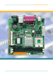
1
EmETX-i2900
Intel® Atom™ N450/D510 ETX® CPU Module
User’s Manual
Version 1.1
2014.06
Revision History
Version
Date
Description
1.0
2013/04/11
initial release
1.1
2014/06/30
2.1 update Board Dimensions P.8
Table of Contents
Preface....................................................................... iii
Copyright Notice..............................................................iii
Declaration of Conformity...............................................iii
Warning..............................................................................v
Replacing the Lithium Battery.........................................v
Technical Support.............................................................v
Warranty............................................................................vi
Chapter 1 - Introduction............................................. 1
1.1
1.2
1.3
1.4
1.5
1.6
The Product................................................................2
About This Manual.....................................................2
Specifications.............................................................3
Inside the Package.....................................................4
Ordering Information.................................................4
The Installation Paths of CD Driver..........................5
Chapter 2 - Board Overview...................................... 7
2.1 Board Dimensions.....................................................8
2.2 Block Diagram ...........................................................9
2.3 Jumpers and Connectors.......................................10
Chapter 3 - BIOS....................................................... 15
3.1 BIOS Main Setup......................................................16
3.2 Advanced Settings...................................................18
3.2.1 CPU Configuration.............................................19
3.2.2 IDE Configuration..............................................20
3.2.3 Floppy Configuration.........................................22
3.2.4 Super IO Configuration.....................................23
3.2.5 Hardware Health Configuration........................25
3.2.5 USB Configuration.............................................26
3.3 Chipset.......................................................................28
3.3.1 North Bridge Chipset Configuration................29
3.3.2 South Bridge Chipset Configuration................30
-i-
3.4 PCIPnP.......................................................................31
3.5 Boot............................................................................32
3.5.1 Boot Setting Configuration...............................33
3.6 Security.....................................................................34
3.7 Exit...........................................................................35
Appendix................................................................... 47
Appendix A: I/O Port Address Map...............................48
Appendix B: Interrupt Request Lines (IRQ).................51
Appendix C: Watchdog Timer (WDT) Setting..............52
- ii -
Preface
Copyright Notice
All Rights Reserved.
The information in this document is subject to change without prior notice in
order to improve the reliability, design and function. It does not represent a
commitment on the part of the manufacturer.
Under no circumstances will the manufacturer be liable for any direct, indirect,
special, incidental, or consequential damages arising from the use or inability
to use the product or documentation, even if advised of the possibility of such
damages.
This document contains proprietary information protected by copyright.
All rights are reserved. No part of this manual may be reproduced by any
mechanical, electronic, or other means in any form without prior written
permission of the manufacturer.
Declaration of Conformity
CE
The CE symbol on your product indicates that it is in compliance with the
directives of the Union European (EU). A Certificate of Compliance is available
by contacting Technical Support.
This product has passed the CE test for environmental specifications when
shielded cables are used for external wiring. We recommend the use of
shielded cables. This kind of cable is available from ARBOR. Please contact
your local supplier for ordering information.
This product has passed the CE test for environmental specifications. Test
conditions for passing included the equipment being operated within an
industrial enclosure. In order to protect the product from being damaged by
ESD (Electrostatic Discharge) and EMI leakage, we strongly recommend the
use of CE-compliant industrial enclosure products.
Warning
This is a class A product. In a domestic environment this product may cause
radio interference in which case the user may be required to take adequate
measures.
FCC Class A
This device complies with Part 15 of the FCC Rules. Operation is subject to
the following two conditions:
- iii -
Preface
(1)This device may not cause harmful interference, and
(2)This device must accept any interference received, including interference
that may cause undesired operation.
NOTE:
This equipment has been tested and found to comply with the limits for a
Class A digital device, pursuant to Part 15 of the FCC Rules. These limits are
designed to provide reasonable protection against harmful interference when
the equipment is operated in a commercial environment. This equipment
generates, uses, and can radiate radio frequency energy and, if not installed
and used in accordance with the instruction manual, may cause harmful
interference to radio communications. Operation of this equipment in a
residential area is likely to cause harmful interference in which case the user
will be required to correct the interference at his own expense.
RoHS
ARBOR Technology Corp. certifies that all components in its products are in
compliance and conform to the European Union’s Restriction of Use of Hazardous Substances in Electrical and Electronic Equipment (RoHS) Directive
2002/95/EC.
The above mentioned directive was published on 2/13/2003. The main purpose of the directive is to prohibit the use of lead, mercury, cadmium, hexavalent chromium, polybrominated biphenyls (PBB), and polybrominated diphenyl
ethers (PBDE) in electrical and electronic products. Member states of the EU
are to enforce by 7/1/2006.
ARBOR Technology Corp. hereby states that the listed products do not contain
unintentional additions of lead, mercury, hex chrome, PBB or PBDB that exceed a maximum concentration value of 0.1% by weight or for cadmium exceed
0.01% by weight, per homogenous material. Homogenous material is defined
as a substance or mixture of substances with uniform composition (such as solders, resins, plating, etc.). Lead-free solder is used for all terminations (Sn(9696.5%), Ag(3.0-3.5%) and Cu(0.5%)).
SVHC / REACH
To minimize the environmental impact and take more responsibility to the
earth we live, Arbor hereby confirms all products comply with the restriction
of SVHC (Substances of Very High Concern) in (EC) 1907/2006 (REACH
--Registration, Evaluation, Authorization, and Restriction of Chemicals)
regulated by the European Union.
All substances listed in SVHC < 0.1 % by weight (1000 ppm)
- iv -
Preface
Warning
Single Board Computers and their components contain very delicate
Integrated Circuits (IC). To protect the Single Board Computer and its
components against damage from static electricity, you should always follow
the following precautions when handling it :
1. Disconnect your Single Board Computer from the power source when you
want to work on the inside.
2. Hold the board by the edges and try not to touch the IC chips, leads or circuitry.
3. Use a grounded wrist strap when handling computer components.
4. Place components on a grounded antistatic pad or on the bag that comes
with the Single Board Computer, whenever components are separated from
the system.
Replacing the Lithium Battery
Incorrect replacement of the lithium battery may lead to a risk of explosion.
The lithium battery must be replaced with an identical battery or a battery type
recommended by the manufacturer.
Do not throw lithium batteries into the trash-can. It must be disposed of in
accordance with local regulations concerning special waste.
Technical Support
If you have any technical difficulties, please consult the user’s manual first
at: ftp://ftp.arbor.com.tw/pub/manual
Please do not hesitate to call or e-mail our customer service when you still cannot find out the answer.
http://www.arbor.com.tw
E-mail:[email protected]
-v-
Preface
Warranty
This product is warranted to be in good working order for a period of two years
from the date of purchase. Should this product fail to be in good working order
at any time during this period, we will, at our option, replace or repair it at no
additional charge except as set forth in the following terms. This warranty does
not apply to products damaged by misuse, modifications, accident or disaster.
Vendor assumes no liability for any damages, lost profits, lost savings or any
other incidental or consequential damage resulting from the use, misuse of,
or inability to use this product. Vendor will not be liable for any claim made by
any other related party.
Vendors disclaim all other warranties, either expressed or implied, including
but not limited to implied warranties of merchantability and fitness for a
particular purpose, with respect to the hardware, the accompanying product’s
manual(s) and written materials, and any accompanying hardware. This limited
warranty gives you specific legal rights.
Return authorization must be obtained from the vendor before returned
merchandise will be accepted. Authorization can be obtained by calling or
faxing the vendor and requesting a Return Merchandise Authorization (RMA)
number. Returned goods should always be accompanied by a clear problem
description.
- vi -
Introduction
1
Chapter 1
Introduction
Chapter 1 - Introduction
-1-
Introduction
1.1 The Product
EmETX-i2900 needs another carrier board, PBE-1000, to work with to deliver
best performance. The I/O cabling from boards to chassis, or the daughter
boards are not needed. Money spent on these parts can be saved. Cost is
substantially reduced.
Enabling easier system upgrade, EmETX-i2900 actually reduces the risk
resulted from previous wrong assessment of system performance. It decreases
design requirements and eases technical complexity, and therefore reduces
business risk. It has these features:
•
•
•
•
•
Fanless Design
ETX 3.0 w/ SATA Connectors
Soldered Onboard Intel® Atom™ N450/D510 Processor
Single Channel 18-bit LVDS, and Analog RGB
Extended Operating Temp.: -20 ~ 70ºC
1.2 About This Manual
This user’s manual provides general information and installation instructions
about the product. This User’s Manual is intended for experienced users and
integrators with hardware knowledge of personal computers. If you are not
sure about any description in this booklet. please consult your vendor before
further handling.
-2-
Introduction
1.3 Specifications
Form Factor
CPU
ETX CPU Module
Intel® Atom™ N450 1.6GHz/D510 1.66GHz CPU
Chipset
Intel® ICH8M
System Memory
1 x 200-pin DDR2 SO-DIMM socket, supporting
667MHz SDRAM up to 2GB
Integrated Intel® Graphics Media Accelerator 3150
with Analog RGB/ Single Channel 18-bit LVDS
Analog RGB supports resolution up to:
- 1400 x 1050 @60Hz (N450)
VGA/ LCD Controller - 2048 x 1536 @60Hz (D510)
Single channel 18-bit LVDS supports resolution up
to:
- 1280 x 800 or 1366 x 768 (N450)
- 1366 x 768 (D510)
Ethernet
1 x Realtek 8103EL PCIe 10/100 Base-T Ethernet
BIOS
AMI PnP Flash BIOS
Serial ATA
2 x Serial ATA with 300MB/s HDD transfer rate
IDE Interface
1 x Ultra ATA, support 2 IDE devices
I/O Chip
Winbond W83627HG
Serial Port
2 x RS-232 ports
Parallel Port
1 x SPP/EPP/ECP mode selectable
KBMS
Supports PS/2 interface Keyboard and Mouse
Universal Serial Bus
4 x USB 2.0 ports
Expansion Interface
4 x PCI masters, ISA Bus, LPC interface
Power Requirement
+5V, 5VSB
Operation Temp.
-20 ~ 70ºC (-4 ~ 158ºF)
Watchdog Timer
1~255 levels reset
Dimension (L x W)
114 x 95 mm (4.5” x 3.7”)
-3-
Introduction
1.4 Inside the Package
Before you begin installing your single board, please make sure that the
following materials have been shipped:
1 x EmETX-i2900 ETX® CPU Module
1 x Driver CD
1 x Quick Installation Guide
If any of the above items is damaged or missing, contact your vendor
immediately.
1.5 Ordering Information
EmETX-i2900-N4
EmETX-i2900-D5
Intel® Atom™ N450 1.6GHz ETX CPU Module
Intel® Atom™ D510 1.66GHz ETX CPU Module
Optional Accessories
HS-0742-F3
(2631140951100P)
HS-0000-W4
(2631250952202P)
PBE-1000 R2.1
CBK-05-1000-00
(6910510000010P)
Heat spreader, 114 x 95 x 8 mm
Universal evaluation heatsink kit w/ thermal pad
(dimension: 125x95x22mm, only used on a flat type
heatspreader)
ETX® evaluation board in ATX form factor
Cable kit for PBE-1000 R2.1
1 x FDD cable
1 x USB cable
3 x COM port cables
2 x IDE cables
1 x TV-out
-4-
Introduction
1.6 The Installation Paths of CD Driver
Windows 2000 & XP
Driver
Path
CHIPSET
\CHIPSET\INF 9.11
VGA
\GRAPHICS\INTEL_2K_XP_32\5182
AUDIO
\AUDIO\REALTEK_HD\WIN2K_XP_x86x64_R252
LAN
\ETHERNET\REALTEK\8103EL_WIN5736
Windows 7
Driver
Path
CHIPSET
\CHIPSET\INF 9.11
VGA
\GRAPHICS\INTEL_WIN7_32\2230
\GRAPHICS\INTEL_WIN7_64\2214
AUDIO
\AUDIO\REALTEK_HD\Win7_R257
LAN
\ETHERNET\REALTEK\8103EL_Win7_7040
-5-
Introduction
This page is intentionally left blank.
-6-
Board Overview
2
Chapter 2
Board Overview
Chapter 2 - Board Overview
-7-
Board Overview
2.1 Board Dimensions
SODIMM
4.00
55.63
51.06
08
ø5.
2.50
40.13
44.45
42.16
90.00
ø2.50
3.00
108.00
33.78
72.90
114.00
-8-
95.00
5.30
SATA
Board Overview
2.2 Block Diagram
Single Channel DDR2
667MHz
Intel®
Atom
N450 at
1.6GHz/
D510 at
1.66GHz
Processor
Analog
R.G.B.
Single Channel 18-bit LVDS
COM1
DMIx4
Super IO
W83627HG
4 x USB ports
Audio
LPC I/F
HD CODEC HD Link
ALC888
PCI Bus
COM2
LPT1/ FDD
IrDA,
Connector ETX3
Connector ETX1
1 x 200-pin DDR2
SO-DIMM
KB, MS
Intel®
ICH8M
LPC I/F
LPC Conn.
Serial ATA I/F
2 x SATA
Primary IDE ATA I/F
ISA Bus
PCI to ISA
bridge
-9-
PCIex1
PATA Host
Controller
JMB368
PCIex1
10/100 LAN
controller
8103EL
Secondary
IDE ATA I/F
10/100
Mbps
Connector ETX4
Connector ETX2
PCI Bus
108.00
3.00
2.50
33.78
Board Overview
72.90
Unit: mm
114.00
2.3 Jumpers and Connectors
IDE1
IDE2
LAN
SMbus
Miscellaneous
ISA bus
VGA
LCD
IrDA
Serial Ports
Parallel Port
Floppy
Keyboard
Mouse
PCI bus
USB
Audio
SATA1, SATA2 Connectors (Top side)
Pin
Description
1
GND
2
TX+
3
TX-
4
GND
5
RX-
6
RX+
7
GND
1
7
- 10 -
Board Overview
LPC1 Connector
Connector type: FPC12-14P-P0.5 (Hirose)
Pin
Description
1
LAD0
2
LAD1
3
LAD2
4
LAD3
5
GND
6
LFRAME#
7
INT_SERIRQ
8
BUF_PLT_RST#
9
GND
10
PCLK_CONN
11
GND
12
GND
13
+3.3V
14
+3.3V
1
14
- 11 -
Board Overview
ETX1 Connector
A1
A3
A5
A7
A9
A11
A13
A15
A17
A19
A21
A23
A25
A27
A29
A31
A33
A35
A37
A39
A41
A43
A45
A47
A49
A51
A53
A55
A57
A59
A61
A63
A65
A67
A69
A71
A73
A75
A77
A79
A81
A83
A85
A87
A89
A91
A93
A95
A97
A99
GND
PCICLK3
GND
PCICLK1
REQ#3
GNT#2
REQ#2
REQ#1
GNT#0
VCC
SERIRQ
AD0
AD1
AD4
AD6
CBE#0
AD8
GND
AD10
AD11
AD12
AD13
AD14
AD15
CBE#1
VCC
PAR
PERR#
PME#
LOCK#
TRDY#
IRDY#
FRAME#
GND
AD16
AD17
AD19
AD20
AD22
AD23
AD24
VCC
AD25
AD28
AD27
AD30
PCIRST#
INTR#C
INTR#A
GND
ETX2 Connector
GND
PCICLK4
GND
PCICLK2
GNT#3
VCC3
GNT#1
VCC3
N.C
VCC
REQ#0
VCC3
AD2
AD3
AD5
AD7
AD9
GND
AUXAL
MIC
AUXAR
ASVCC
SNDL
ASGND
SNDR
VCC
SERR#
N.C
USB2DEVSEL#
USB3STOP#
USB2+
GND
CBE#2
USB3+
AD18
USB0AD21
USB1CBE#3
VCC
AD26
USB0+
AD29
USB1+
AD31
INTR#D
INTR#B
GND
A2
A4
A6
A8
A10
A12
A14
A16
A18
A20
A22
A24
A26
A28
A30
A32
A34
A36
A38
A40
A42
A44
A46
A48
A50
A52
A54
A56
A58
A60
A62
A64
A66
A68
A70
A72
A74
A76
A78
A80
A82
A84
A86
A88
A90
A92
A94
A96
A98
A100
B1
B3
B5
B7
B9
B11
B13
B15
B17
B19
B21
B23
B25
B27
B29
B31
B33
B35
B37
B39
B41
B43
B45
B47
B49
B51
B53
B55
B57
B59
B61
B63
B65
B67
B69
B71
B73
B75
B77
B79
B81
B83
B85
B87
B89
B91
B93
B95
B97
B99
- 12 -
GND
SD14
SD13
SD12
SD11
SD10
SD9
SD8
MEMW#
MEMR#
LA17
LA18
LA19
LA20
LA21
LA22
LA23
GND
SBHE#
SA0
SA1
SA2
SA3
SA4
SA5
VCC
SA6
SA7
SA8
SA9
SA10
SA11
SA12
GND
SA13
SA14
SA15
SA16
SA18
SA19
IOCHRDY
VCC
SD0
SD2
SD3
DREQ2
SD5
SD9
IOCHK#
GND
GND
SD15
MASTER#
DREQ7
DACK#7
DREQ6
DACK#6
DREQ5
DACK#5
DREQ0
DACK#5
IRQ14
IRQ15
IRQ12
IRQ11
IRQ10
IO16#
GND
M16#
OSC
BALE
TC
DACK#2
IRQ3
IRQ4
VCC
IRQ5
IRQ6
IRQ7
SYSCLK
REFCH#
DREQ1
DACK#1
GND
DREQ3
DACK#3
IOR#
IOW#
SA17
SMEMR#
AEN
VCC
SMEMW#
SD1
NOWS#
SD4
IRQ9
SD7
RSTDRV
GND
B2
B4
B6
B8
B10
B12
B14
B16
B18
B20
B22
B24
B26
B28
B30
B32
B34
B36
B38
B40
B42
B44
B46
B48
B50
B52
B54
B56
B58
B60
B62
B64
B66
B68
B70
B72
B74
B76
B78
B80
B82
B84
B86
B88
B90
B92
B94
B96
B98
B100
Board Overview
ETX3 Connector
C1
C3
C5
C7
C9
C11
C13
C15
C17
C19
C21
C23
C25
C27
C29
C31
C33
C35
C37
C39
C41
C43
C45
C47
C49
C51
C53
C55
C57
C59
C61
C63
C65
C67
C69
C71
C73
C75
C77
C79
C81
C83
C85
C87
C89
C91
C93
C95
C97
C99
GND
R
HSY
VSY
DETECT#
TX2CLK#
TX2CLK
GND
TX2D1
TX2D1#
GND
N.C.
N.C.
GND
TX1D2#
TX1D2
GND
TX1D0
TX1D0#
VCC
DDC_DATA
DDC_CLK
BKLTCTL
TV_DATA_COMP
N.C.
LPT/FLPY#
VCC
STB#
N.C.
IRRX
IRTX
RXD2
GND
RTS#2
DTR#2
DCD#2
DSR#2
CTS#2
TXD#2
RI#2
VCC
RXD1
RTS#1
DTR#1
DCD#1
DSR#1
CTS#1
TXD#1
RI#1
GND
GND
B
G
Analog RGB_DDC_CLK
Analog RGB_DDC_DATA
N.C.
N.C.
GND
TX2D2
TX2D2#
GND
TX2D0
TX2D0#
GND
TX1CLK
TX1CLK#
GND
TX1D1
TX1D1#
VCC
N.C.
BLON#
VDDEN
Y
C
N.C.
GND
AFD#/DENSEL
PD7/N.C
ERR#/HDSEL#
PD6/N.C
INIT#/DIR#
GND
PD5/N.C
SLIN#/STEP#
PD4/DSKCHG#
PD3/RDATA#
PD2/WP#
PD1/TRK0#
PD0/INDEX#
VCC
ACK#/DRV
BUSY#/MOT
PE/WDATA#
SLCT#/WGATE#
MSCLK
MSDAT
KBCLK
KBDAT
GND
ETX4 Connector
C2
C4
C6
C8
C10
C12
C14
C16
C18
C20
C22
C24
C26
C28
C30
C32
C34
C36
C38
C40
C42
C44
C46
C48
C50
C52
C54
C56
C58
C60
C62
C64
C66
C68
C70
C72
C74
C76
C78
C80
C82
C84
C86
C88
C90
C92
C94
C96
C98
C100
D1
D3
D5
D7
D9
D11
D13
D15
D17
D19
D21
D23
D25
D27
D29
D31
D33
D35
D37
D39
D41
D43
D45
D47
D49
D51
D53
D55
D57
D59
D61
D63
D65
D67
D69
D71
D73
D75
D77
D79
D81
D83
D85
D87
D89
D91
D93
D95
D97
D99
- 13 -
GND
5V_SB
PS_ON
PWERBTN#
KBINH
RSMRST#
N.C
N.C
VCC
OVCR#
EXTSMI#
SMBCLK
SIDE_CS3#
SIDE_CS1#
SIDE_A2
SIDE_A0
GND
PDIAG_S
SIDE_A1
SIDE_INTRQ
BATLOW#
SIDE_ACK#
SIDE_RDY
SIDE_IOR#
VCC
SIDE_IOW#
SIDE_DRQ
SIDE_D15
SIDE_D0
SIDE_D14
SIDE_D1
SIDE_D13
GND
SIDE_D2
SIDE_D12
SIDE_D3
SIDE_D11
SIDE_D4
SIDE_D10
SIDE_D5
VCC
SIDE_D9
SIDE_D6
SIDE_D8
GPE2#
RXDRXD+
TXDTXD+
GND
GND
PWGIN
SPEAKER
BATT
LILED
ACTLED
SPEEDLED
I2CLK
VCC
N.C
I2DAT
SMBDAT
SMBALRT#
DASP_S
PIDE_CS3#
PIDE_CS1#
GND
PIDE_A2
PIDE_A0
PIDE_A1
N.C
PIDE_INTRQ
PIDE_ACK#
PIDE_RDY
VCC
PIDE_IOR#
PIDE_IOW#
PIDE_DRQ
PIDE_D15
PIDE_D0
PIDE_D14
PIDE_D1
GND
PIDE_D13
PIDE_D2
PIDE_D12
PIDE_D3
PIDE_D11
PIDE_D4
PIDE_D10
VCC
PIDE_D5
PIDE_D9
PIDE_D6
CBLID_P#
PIDE_D8
SIDE_D7
PIDE_D7
HDRST#
GND
D2
D4
D6
D8
D10
D12
D14
D16
D18
D20
D22
D24
D26
D28
D30
D32
D34
D36
D38
D40
D42
D44
D46
D48
D50
D52
D54
D56
D58
D60
D62
D64
D66
D68
D70
D72
D74
D76
D78
D80
D82
D84
D86
D88
D90
D92
D94
D96
D98
D100
Board Overview
This page is intentionally left blank.
- 14 -
BIOS
3
Chapter 3
BIOS
Chapter 3 - BIOS
- 15 -
BIOS
3.1 BIOS Main Setup
The AMI BIOS provides a Setup utility program for specifying the system
configurations and settings. The BIOS RAM of the system stores the Setup
utility and configurations.
When you turn on the computer, the AMI BIOS is immediately activated.
To enter the BIOS SETUP UTILILTY, press “Delete” once the power is
turned on.
When the computer is shut down, the battery on the motherboard supplies the
power for BIOS RAM.
The Main Setup screen lists the following information
System Overview
BIOS Version: displays the current version information of the BIOS
Build Date: the date that the BIOS version was made/updated
Processor (auto-detected if installed)
Speed: displays the processor speed
System Memory (auto-detected if installed)
Size: lists the memory size information
- 16 -
BIOS
Key Commands
BIOS Setup Utility is mainly a key-based navigation interface. Please refer to
the following key command instructions for navigation process.
“←”“→”
Move to highlight a particular configuration screen from
the top menu bar / Move to highlight items on the screen
“↓” “↑”
Move to highlight previous/next item
Enter
Select and access a setup item/field
Esc:
On the Main Menu – Quit the setup and not save
changes into CMOS (a message screen will display
and ask you to select “OK” or “Cancel” for exiting and
discarding changes. Use “←” and “→” to select and press
“Enter” to confirm)
On the Sub Menu – Exit current page and return to main
menu
Page Up / +
Increase the numeric value on a selected setup item /
make change
Page Down -:
Decrease the numeric value on a selected setup item /
make change
F1
Activate “General Help” screen
F10:
Save the changes that have been made in the setup and
exit. (a message screen will display and ask you to select
“OK” or “Cancel” for exiting and saving changes. Use “←”
and “→” to select and press “Enter” to confirm)
System Time
Set the system time.
The time format is:
Hour : 00 to 23
Minute : 00 to 59
Second : 00 to 59
System Date
Set the system date. Note that the ‘Day’ automatically changes when you set
the date.
The date format is:
Day : Sun to Sat
Month : 1 to 12
Date : 1 to 31
Year : 1999 to 2099
- 17 -
BIOS
3.2 Advanced Settings
The “Advanced” screen provides the setting options to configure CPU, IDE,
Super IO and other peripherals. You can use “←” and “→” keys to select
“Advanced” and use the “↓” and “↑” to select a setup item.
Note: please pay attention to the “WARNING” part at the left frame before you
decide to configure any setting of an item.
- 18 -
BIOS
3.2.1 CPU Configuration
Press “Enter” on “CPU Configuration” and you will be able to configure the
CPU on the “Configure advanced CPU settings” screen.
CPU Details
Manufacturer: shows the name of the CPU manufacturer
Frequency: indicates the processor speed
FSB Speed: the data flow speed of FSB (Front Side Bus)
Cache L1: shows the Cache L1 size for the CPU
Cache L2: shows the Cache L2 size for the CPU
Ratio Actual Value: actual value of clock ratio for the CPU
Hyper-Threading Technology
Options
Enabled: Enabled the Hyper-Threading Technology for higher CPU threading
speed. (recommended)
Disabled: Disabled the Hyper-Threading Technology.
- 19 -
BIOS
3.2.2 IDE Configuration
Select the “IDE Configuration to configure the IDE settings. When an item
is selected, there is a status description appearing at the right. You can use
“Page Up/+” and “Page Down/-” keys to change the value of a selected item.
ATA/IDE Configuration
Configures the options of ATA/IDE controllers connected to the board
Disabled: disables the ATA/IDE controllers connected to the board
Compatible: sets the ATA/IDE controllers to be compatible
Enhanced: sets the ATA/IDE controllers to be in enhanced mode
Legacy IDE Channels (SATA Pri, PATA Sec): specifies SATA or PATA
controllers to be primary or secondary.
- 20 -
BIOS
Primary IDE Master/Slave, Secondary IDE Master/Slave, Third
IDE Maser/Slave, Fourth IDE Master/Slave
The BIOS Setup displays all the available, connected IDE devices as well
as the IDE status. You may enter a specific IDE device to do particular
configurations. Press “Enter” to access the submenu of an IDE device on the
list.
Hard Disk Write Protect
Enable or disable Hard Disk Write Protect. If you select “Enabled”, the hard
disk will turn into a “write-protected” mode.
IDE Detect Time-out (sec)
Specifies the delay time for initializing IDE devices. The default value is 0.
ATA (PI) 80Pin Cable Detection
You can set it as “Host & Device”, “Host” or “Device”. Host refers to the
capability of IDE controllers to be able to detect connected IDE cable, while
Device is defined as the ability of IDE devices to recognize the connected IDE
cable.
- 21 -
BIOS
3.2.3 Floppy Configuration
On the “Floppy” screen, you can enable or disable the floppy drive connected
to your system.
- 22 -
BIOS
3.2.4 Super IO Configuration
Use “Super IO Configuration to specify address and modes for Serial Port and
Parallel Port.
Serial Port1 / Port2 Address
Select an address and corresponding interrupt for the first and second serial
ports.
3F8/IRQ4
2F8/IRQ3
2E8/IRQ3
3E8/IRQ4
Disabled
Auto
- 23 -
BIOS
Serial Port2 Mode
Allows BIOS to select mode for serial Port2.
Parallel Port Address
Select an address for the parallel port.
3BC
378
278
Disabled
Parallel Port Mode
Select an operating mode for the onboard parallel port. Select Normal,
Compatible or SPP unless you are certain your hardware and software both
support one of the other available modes.
SPP
EPP
ECP
ECP + EPP
Normal
Parallel Port IRQ
Select an interrupt for the parallel port.
IRQ5
IRQ7
- 24 -
BIOS
3.2.5 Hardware Health Configuration
The “Hardware Health Configuration” lists out the temperature and voltage
information that is being monitored. The default for “H/W Health Function” is
“Enabled.
System Temperature
Show you the currently monitored system temperature.
CPU Temperature
Show you the currently monitored CPU temperature.
+1.5V/+3.3Vin / +5Vin / +5VSB/VBAT
Show you the voltage level of the +1.5V, +3.3Vin, +5Vin, +5VSB, or VBAT
standby and battery.
- 25 -
BIOS
3.2.5 USB Configuration
Legacy USB Support
Enables support for legacy USB. AUTO option disables legacy support if no
USB devices are connected.
USB 2.0 Controller Mode
Configures the USB 2.0 controller in High Speed (480Mbps) or Full Speed
(12MBPS).
BIOS EHCI Hand-Off
Enabled: enables the EHCI Hand-Off function by BIOS
Disabled: disables the EHCI Hand-Off function by BIOS
Note: this setting potion allows you to enable EHCI Hand Off if your computer
operating system does not support it.
EHCI is the abbreviation for Enhanced Host Controller Interface which is
necessary for high speed USB operation.
- 26 -
BIOS
USB Mass Storage Device Configuration
USB Mass Storage Reset Delay:
Number of seconds POST (Power-On Self-Test) waits for the USB mass
storage device after start unit command.
Emulation Type
Sets the value for the system to select the emulation type for USB devices. In
general, options include “Auto”, “FDD” and “HDD” (HDD stands for Hard Disk
Drive, while FDD is also known as 3 1/2 floppy).
Please keep in mind that options such as “FDD” might not always be available
as some computers are not built with this type of connectors.
Note
If “Auto” is selected, USB device with storage less than 530MB will be emulated
as Floppy and remain as hard drive. Forced FDD option can be used to force
a HDD formatted drive to “BOOT” as FDD (for example, ZIP drive)
- 27 -
BIOS
3.3 Chipset
Select “Chipset” to access to “North Bridge Configuration” and “South Bridge
Configuration”. You can enter the sub menu of the two configuration options.
- 28 -
BIOS
3.3.1 North Bridge Chipset Configuration
Initiate Graphic Adapter:
Selects which graphics controller to be used as the primary boot device.
Internal Graphic Mode Select:
Selects the amount of the system memory to enable the internal graphic
mode
DVMT Mode
Setting: FIXED, DVMT (Default), BOTH.
DVMT/FIXED Memory Size
Setting: 64MB, 128MB (Default), 224MB.
Boot Display Device: boot setting for the display device connected to the
computer, such as “External CRT” monitor.
Flat Panel Type: the resolution types of the connected flat panel display
device.
- 29 -
BIOS
3.3.2 South Bridge Chipset Configuration
Normally, the south bridge controls the basic I/O functions, such as USB and
audio. This screen allows you to access to the configurations of the I/Os.
- 30 -
BIOS
3.4 PCIPnP
The “PCIPnP” screen provides advanced setting options for your PCI or PnP
(plug and play) peripherals.
Allocate IRQ to PCI VGA:
[Yes]: assigns IRQ to PCI VGA card if card requests IRQ
[No]: does not assign IRQ to PCI VGA card even if card requests IRQ
[Available]: if an item is specified “Available”, the particular item can be
used by PCI or PnP peripherals/devices
[Reserved]: if an item is specified as “Reserved”, the particular item can
only be used by legacy ISA peripherals/devices
Note: please pay attention to the “WARNING” part at the left frame before
you decide to configure any setting of an item.
- 31 -
BIOS
3.5 Boot
The “Boot” screen provides the access to configure the settings for system
boot.
Boot Setting Configuration: enter the sub menu for boot setting.
Boot Device Priority: access to the sub menu for boot device priority.
Hard Disk Drives: configure the boot settings for the Hard Disk Drives
connected to the system.
- 32 -
BIOS
3.5.1 Boot Setting Configuration
Quiet Boot: displays normal POST messages when it’s selected as “Disabled”.
When it is set as “Enabled”, OEM messages will be displayed instead of POST
messages. The default is “Disabled”.
Bootup Num-Lock: modifies Number Lock setting when the system boots
up. Select “On” to automatically enable the Number Lock on keyboard when
the system is booting up.
- 33 -
BIOS
3.6 Security
The “Security Settings” screen allows you to set password.
Change Supervisor Password: the default is “Not Installed”, but you can
change the Supervisor Password and then it will appear “Installed”. Please
always remember your password or else you will have to reset the whole
system.
- 34 -
BIOS
3.7 Exit
Select “Exit” to set exit options, save changes or load default values.
Save Changes and Exit
When you press “Enter” on this option, a message described as the one
below will appear:
“Save configuration changes and exit setup?”
Pressing <OK> stores the configuration changes made in BIOS in CMOS
menu - a special section of memory that stays on after you turn your
system off, and then exit. The next time you boot your system up, the new
configured system values will take place.
Note: you can also press <F10> to enable this operation.
- 35 -
BIOS
Discard Changes and Exit
Exit system setup without saving any changes.
You can also press <ESC> to activate this function.
Load Optimal Defaults
When you press <Enter> on this option, a message dialog box will appear
asking for your confirmation:
Load Optimal Defaults?
[OK]
[Cancel]
Press [OK] to load the BIOS Optimal Default values for all the setup options.
You can also press <F9> key to enable this operation.
- 36 -
BIOS
3.8 AMI BIOS Checkpoints
3.8.1 Checkpoint Ranges
Status Code Range
Description
0x01 – 0x0B
SEC execution
0x0C – 0x0F
SEC errors
0x10 – 0x2F
PEI execution up to and including memory
detection
0x30 – 0x4F
PEI execution after memory detection
0x50 – 0x5F
PEI errors
0x60 – 0x8F
DXE execution up to BDS
0x90 – 0xCF
BDS execution
0xD0 – 0xDF
DXE errors
0xE0 – 0xE8
S3 Resume (PEI)
0xE9 – 0xEF
S3 Resume errors (PEI)
0xF0 – 0xF8
Recovery (PEI)
0xF9 – 0xFF
Recovery errors (PEI)
- 37 -
BIOS
3.8.2 Standard Checkpoints
SEC Phase
Status Code
0x00
Description
Not used
Progress Codes
0x01
Power on. Reset type detection (soft/hard).
0x02
AP initialization before microcode loading
0x03
North Bridge initialization before microcode loading
0x04
South Bridge initialization before microcode loading
0x05
OEM initialization before microcode loading
0x06
Microcode loading
0x07
AP initialization after microcode loading
0x08
North Bridge initialization after microcode loading
0x09
South Bridge initialization after microcode loading
0x0A
OEM initialization after microcode loading
0x0B
Cache initialization
SEC Error Codes
0x0C – 0x0D
Reserved for future AMI SEC error codes
0x0E
Microcode not found
0x0F
Microcode not loaded
- 38 -
BIOS
PEI Phase
Status Code
Description
Progress Codes
0x10
PEI Core is started
0x11
Pre-memory CPU initialization is started
0x12
Pre-memory CPU initialization (CPU module specific)
0x13
Pre-memory CPU initialization (CPU module specific)
0x14
Pre-memory CPU initialization (CPU module specific)
0x15
Pre-memory North Bridge initialization is started
0x16
Pre-Memory North Bridge initialization (North Bridge
module specific)
0x17
Pre-Memory North Bridge initialization (North Bridge
module specific)
0x18
Pre-Memory North Bridge initialization (North Bridge
module specific)
0x19
Pre-memory South Bridge initialization is started
0x1A
Pre-memory South Bridge initialization (South Bridge
module specific)
0x1B
Pre-memory South Bridge initialization (South Bridge
module specific)
0x1C
Pre-memory South Bridge initialization (South Bridge
module specific)
0x1D – 0x2A
OEM pre-memory initialization codes
0x2B
Memory initialization. Serial Presence Detect (SPD) data
reading
0x2C
Memory initialization. Memory presence detection
0x2D
Memory initialization. Programming memory timing
information
0x2E
Memory initialization. Configuring memory
0x2F
Memory initialization (other).
0x30
Reserved for ASL (see ASL Status Codes section below)
0x31
Memory Installed
- 39 -
BIOS
0x32
CPU post-memory initialization is started
0x33
CPU post-memory initialization. Cache initialization
0x34
CPU post-memory initialization. Application Processor(s)
(AP) initialization
0x35
CPU post-memory initialization. Boot Strap Processor
(BSP) selection
0x36
CPU post-memory initialization. System Management
Mode (SMM) initialization
0x37
Post-Memory North Bridge initialization is started
0x38
Post-Memory North Bridge initialization (North Bridge
module specific)
0x39
Post-Memory North Bridge initialization (North Bridge
module specific)
0x3A
Post-Memory North Bridge initialization (North Bridge
module specific)
0x3B
Post-Memory South Bridge initialization is started
0x3C
Post-Memory South Bridge initialization (South Bridge
module specific)
0x3D
Post-Memory South Bridge initialization (South Bridge
module specific)
0x3E
Post-Memory South Bridge initialization (South Bridge
module specific)
0x3F-0x4E
0x4F
OEM post memory initialization codes
DXE IPL is started
PEI Error Codes
0x50
Memory initialization error. Invalid memory type or
incompatible memory speed
0x51
Memory initialization error. SPD reading has failed
0x52
Memory initialization error. Invalid memory size or
memory modules do not match.
0x53
Memory initialization error. No usable memory detected
0x54
Unspecified memory initialization error.
- 40 -
BIOS
0x55
Memory not installed
0x56
Invalid CPU type or Speed
0x57
CPU mismatch
0x58
CPU self test failed or possible CPU cache error
0x59
CPU micro-code is not found or micro-code update is
failed
0x5A
Internal CPU error
0x5B
reset PPI is not available
0x5C-0x5F
Reserved for future AMI error codes
S3 Resume Progress Codes
0xE0
S3 Resume is stared (S3 Resume PPI is called by the
DXE IPL)
0xE1
S3 Boot Script execution
0xE2
Video repost
0xE3
OS S3 wake vector call
0xE4-0xE7
Reserved for future AMI progress codes
S3 Resume Error Codes
0xE8
S3 Resume Failed
0xE9
S3 Resume PPI not Found
0xEA
S3 Resume Boot Script Error
0xEB
S3 OS Wake Error
0xEC-0xEF
Reserved for future AMI error codes
Recovery Progress Codes
0xF0
Recovery condition triggered by firmware (Auto recovery)
0xF1
Recovery condition triggered by user (Forced recovery)
0xF2
Recovery process started
0xF3
Recovery firmware image is found
0xF4
Recovery firmware image is loaded
0xF5-0xF7
Reserved for future AMI progress codes
Recovery Error Codes
0xF8
Recovery PPI is not available
- 41 -
BIOS
0xF9
Recovery capsule is not found
0xFA
Invalid recovery capsule
0xFB – 0xFF
Reserved for future AMI error codes
DXE Phase
Status Code
Description
0x60
DXE Core is started
0x61
NVRAM initialization
0x62
Installation of the South Bridge Runtime Services
0x63
CPU DXE initialization is started
0x64
CPU DXE initialization (CPU module specific)
0x65
CPU DXE initialization (CPU module specific)
0x66
CPU DXE initialization (CPU module specific)
0x67
CPU DXE initialization (CPU module specific)
0x68
PCI host bridge initialization
0x69
North Bridge DXE initialization is started
0x6A
North Bridge DXE SMM initialization is started
0x6B
North Bridge DXE initialization (North Bridge module
specific)
0x6C
North Bridge DXE initialization (North Bridge module
specific)
0x6D
North Bridge DXE initialization (North Bridge module
specific)
0x6E
North Bridge DXE initialization (North Bridge module
specific)
0x6F
North Bridge DXE initialization (North Bridge module
specific)
0x70
South Bridge DXE initialization is started
0x71
South Bridge DXE SMM initialization is started
0x72
South Bridge devices initialization
0x73
South Bridge DXE Initialization (South Bridge module
specific)
- 42 -
BIOS
0x74
South Bridge DXE Initialization (South Bridge module
specific)
0x75
South Bridge DXE Initialization (South Bridge module
specific)
0x76
South Bridge DXE Initialization (South Bridge module
specific)
0x77
South Bridge DXE Initialization (South Bridge module
specific)
0x78
ACPI module initialization
0x79
CSM initialization
0x7A – 0x7F
Reserved for future AMI DXE codes
0x80 – 0x8F
OEM DXE initialization codes
0x90
Boot Device Selection (BDS) phase is started
0x91
Driver connecting is started
0x92
PCI Bus initialization is started
0x93
PCI Bus Hot Plug Controller Initialization
0x94
PCI Bus Enumeration
0x95
PCI Bus Request Resources
0x96
PCI Bus Assign Resources
0x97
Console Output devices connect
0x98
Console input devices connect
0x99
Super IO Initialization
0x9A
USB initialization is started
0x9B
USB Reset
0x9C
USB Detect
0x9D
USB Enable
0x9E – 0x9F
Reserved for future AMI codes
0xA0
IDE initialization is started
0xA1
IDE Reset
0xA2
IDE Detect
0xA3
IDE Enable
- 43 -
BIOS
0xA4
SCSI initialization is started
0xA5
SCSI Reset
0xA6
SCSI Detect
0xA7
SCSI Enable
0xA8
Setup Verifying Password
0xA9
Start of Setup
0xAA
Reserved for ASL (see ASL Status Codes section below)
0xAB
Setup Input Wait
0xAC
Reserved for ASL (see ASL Status Codes section below)
0xAD
Ready To Boot event
0xAE
Legacy Boot event
0xAF
Exit Boot Services event
0xB0
Runtime Set Virtual Address MAP Begin
0xB1
Runtime Set Virtual Address MAP End
0xB2
Legacy Option ROM Initialization
0xB3
System Reset
0xB4
USB hot plug
0xB5
PCI bus hot plug
0xB6
Clean-up of NVRAM
0xB7
Configuration Reset (reset of NVRAM settings)
0xB8 – 0xBF
Reserved for future AMI codes
0xC0 – 0xCF OEM BDS initialization codes
DXE Error Codes
0xD0
CPU initialization error
0xD1
North Bridge initialization error
0xD2
South Bridge initialization error
0xD3
Some of the Architectural Protocols are not available
0xD4
PCI resource allocation error. Out of Resources
0xD5
No Space for Legacy Option ROM
0xD6
No Console Output Devices are found
- 44 -
BIOS
0xD7
No Console Input Devices are found
0xD8
Invalid password
0xD9
Error loading Boot Option (LoadImage returned error)
0xDA
Boot Option is failed (StartImage returned error)
0xDB
Flash update is failed
0xDC
Reset protocol is not available
ACPI/ASL Checkpoints
Status Code
Description
0x01
System is entering S1 sleep state
0x02
System is entering S2 sleep state
0x03
System is entering S3 sleep state
0x04
System is entering S4 sleep state
0x05
System is entering S5 sleep state
0x10
System is waking up from the S1 sleep state
0x20
System is waking up from the S2 sleep state
0x30
System is waking up from the S3 sleep state
0x40
System is waking up from the S4 sleep state
0xAC
System has transitioned into ACPI mode. Interrupt
controller is in PIC mode.
0xAA
System has transitioned into ACPI mode. Interrupt
controller is in APIC mode.
- 45 -
BIOS
This page is intentionally left blank.
- 46 -
Appendix
Appendix
Appendix
- 47 -
Appendix
Appendix A: I/O Port Address Map
Each peripheral device in the system is assigned a set of I/O port addresses
which also becomes the identity of the device.
The following table lists the I/O port addresses used.
Address
Device Description
00000000 - 00000007
DMA Controller
00000000 - 00000CF7
PCI bus
00000010 - 0000001F
Motherboard Resource
00000020 - 00000021
Programmable Interrupt Controller
00000022 - 0000003F
Motherboard Resource
00000040 - 00000043
System Timer
00000044 - 0000005F
Motherboard Resource
00000060 - 00000060
Standard 101/102-Key or Microsoft Natural PS/2
Keyboard
00000061 - 00000061
System Speaker
00000062 - 00000063
Motherboard Resource
00000064 - 00000064
Standard 101/102-Key or Microsoft Natural PS/2
Keyboard
00000065 - 0000006F
Motherboard Resource
00000070 - 00000073
System CMOS/real time clock
00000074 - 0000007F
Motherboard Resource
00000080 - 00000090
DMA Controller
00000091 - 00000093
Motherboard Resource
00000094 - 0000009F
DMA Controller
000000A0 - 000000A1
Programmable Interrupt Controller
000000A2 - 000000BF
Motherboard Resource
000000C0 - 000000DF
DMA Controller
000000E0 - 000000EF
Motherboard Resource
000000F0 - 000000FF
Numeric Data Processor
000001F0 - 000001F7
Primary IDE Channel
00000274 - 00000277
ISAPNP Read Data Port
- 48 -
Appendix
00000279 - 00000279
ISAPNP Read Data Port
00000294 - 00000297
Motherboard Resource
000002E8 - 000002EF
Communications Port (COM4)
000002F8 - 000002FF
Communications Port (COM2)
00000378 - 0000037F
Printer Port (LPT1)
000003B0 - 000003BB
Mobile Intel® 945 Express Chipset Family
000003C0 - 000003DF
Mobile Intel® 945 Express Chipset Family
000003E8 - 000003EF
Communications Port (COM3)
000003F6 - 000003F6
Primary IDE Channel
000003F8 - 000003FF
Communications Port (COM1)
00000400 - 000004BF
Motherboard Resource
000004D0 - 000004D1
Motherboard Resource
00000500 - 0000051F
Intel® 82801G (ICH7 Family) SMBus Controller
- 27DA
00000680 - 000006FF
Motherboard Resource
00000778 - 0000077B
Printer Port (LPT1)
00000880 - 0000088F
Motherboard Resource
00000A78 - 00000A7B
Motherboard Resource
00000BBC - 00000BBF
Motherboard Resource
00000BBC - 00000BBF
Motherboard Resource
00000D00 - 0000FFFF
PCI bus
00000E78 - 00000E7B
Motherboard Resource
00000F78 - 00000F7B
Motherboard Resource
00000FBC - 00000FBF
Motherboard Resource
0000B000 - 0000BFFF
Intel® 82801G (ICH7 Family) PCI Express Root
Port - 27D4
0000C000 - 0000CFFF
Intel® 82801G (ICH7 Family) PCI Express Root
Port - 27D0
0000DF00 - 0000DF3F
Intel® PRO/100 VE Network Connection
0000F000 - 0000F0FF
Realtek AC’97 Audio
0000F300 - 0000F30F
Intel® 82801GBM/GHM (ICH7-M Family) Serial
ATA Storage Controller - 27C4
- 49 -
Appendix
0000F400 - 0000F40F
Intel® 82801GBM/GHM (ICH7-M Family) Serial
ATA Storage Controller - 27C4
0000F500 - 0000F50F
Intel® 82801GBM/GHM (ICH7-M Family) Serial
ATA Storage Controller - 27C4
- 50 -
Appendix
Appendix B: Interrupt Request Lines (IRQ)
Peripheral devices use interrupt request lines to notify CPU for the service
required. The following table shows the IRQ used by the devices on board.
Level
Function
IRQ 01
Standard 101/102-Key or Microsoft Natural PS/2 Keyboard
IRQ 03
Communications Port
IRQ 04
Communications Port
IRQ 08
System CMOS/real time clock
IRQ 09
Microsoft ACPI-Compliant System
IRQ 10
Communications Port
IRQ 11
Communications Port
IRQ 12
PS/2 Compatible Mouse
IRQ 13
Math Coprocessor
IRQ 14
Primary IDE Channel
IRQ 15
Intel® 82801G (ICH7 Family) SMBus Controller - 27DA
IRQ 16
Intel® 82801G (ICH7 Family PCI Express Root Port - 27D0
IRQ 16
Intel® 82801G (ICH7 Family) USB Universal Host Controller - 27CB
IRQ 16
Mobile Intel 945GM Express Chipset Family
IRQ 17
Realtek AC’97 Audio
IRQ 18
Intel® 82801G (ICH7 Family) PCI Express Root Port - 27D4
IRQ 18
Intel® 82801G (ICH7 Family) USB Universal Host Controller - 27CA
IRQ 19
Intel® 82801G (ICH7 Family) USB Universal Host Controller - 27C9
IRQ 19
Intel® 82801G (ICH7-M Family) Serial ATA Storage Controller - 27C4
IRQ 19
Intel® 82801G (ICH7 Family) USB Universal Host Controller - 27C9
IRQ 20
Intel® PRO/100 VE Network Connection
IRQ 23
Intel® 82801G (ICH7 Family) USB Universal Host Controller - 27C8
IRQ 23
Intel® 82801G (ICH7 Family) USB2 Enhanced Host Controller 27CC
- 51 -
Appendix
Appendix C: Watchdog Timer (WDT) Setting
WDT is widely used for industry application to monitoring the activity of
CPU. Application software depends on its requirement to trigger WDT with
adequate timer setting. Before WDT time out, the functional normal system
will reload the WDT. The WDT never time out for a normal system. Then, WDT
will time out and reset the system automatically to avoid abnormal operation.
This board supports 255 levels watchdog timer by software programming.
Below are the source codes written in assembly & C, please take them for
WDT application examples.
/*-----
#include
#include
#include
Include Header Area -----*/
“math.h”
“stdio.h”
“dos.h”
/*----- routing, sub-routing -----*/
void main()
{
outportb(0x2e, 0x87);
outportb(0x2e, 0x87);
/* initial IO port twice */
outportb(0x2e, 0x2B);
outportb(0x2e+1, 0x00);
/* select CR2B */
/* update CR2B bit4 to 00h */
/* Set PIN89 as WDTO */
outportb(0x2e, 0x07);
outportb(0x2e+1, 0x08);
outportb(0x2e, 0x30);
outportb(0x2e+1, 0x01);
outportb(0x2e, 0xf0);
outportb(0x2e+1, 0x00);
outportb(0x2e, 0xf5);
outportb(0x2e+1, 0x00);
outportb(0x2e, 0xF6);
outportb(0x2e+1, 0x05);
/*
/*
/*
/*
/*
/*
/*
/*
/*
/*
}
outportb(0x2e, 0xAA);
/* stop program W83627, Exit */
point to logical device selector */
select logical device 8 */
select CR30 */
update CR30 to 01h */
select CRF0 */
update CRF0 to 00h */
select CRF5 to set timer unit */
update CRF5 bit2, 0:sec; 1:Min. */
select CRF6 */
update CRF6 to 05h (5 sec) */
- 52 -
Appendix
This page is intentionally left blank.
- 53 -