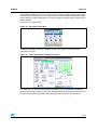
1
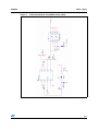
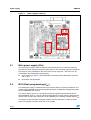
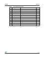
UM0240
User manual
ST Industrial Communication Board - EVALCOMMBOARD
Introduction
ST Industrial Communication Board (order code: EVALCOMMBOARD) is a platform for
Communication, Command and Control exchange with Industrial reference design boards.
Its goal is to provide ST Industrial customers a reliable and easily accessible communication
channel, between a controlling PC and Industrial reference design boards.
It is a unique platform that allows evaluating a wide range of Industrial products in their
application environment.
Application fields covered by this platform are:
●
Power line communication
●
Motor control and gate driving
●
Intelligent power switches
Industrial Communication Board
June 2006
Rev 1
1/39
www.st.com
Contents
UM0240
Contents
1
System overview . . . . . . . . . . . . . . . . . . . . . . . . . . . . . . . . . . . . . . . . . . . . 6
2
Power supply . . . . . . . . . . . . . . . . . . . . . . . . . . . . . . . . . . . . . . . . . . . . . . . 7
3
2.1
Main power supply (VDD) . . . . . . . . . . . . . . . . . . . . . . . . . . . . . . . . . . . . 10
2.2
MCU Flash programming (VPP) . . . . . . . . . . . . . . . . . . . . . . . . . . . . . . . . 10
2.3
OpAmp negative supply (-5V) . . . . . . . . . . . . . . . . . . . . . . . . . . . . . . . . . 11
Microcontroller . . . . . . . . . . . . . . . . . . . . . . . . . . . . . . . . . . . . . . . . . . . . 12
3.1
Microcontroller features . . . . . . . . . . . . . . . . . . . . . . . . . . . . . . . . . . . . . . 12
3.2
RS-232 Interface . . . . . . . . . . . . . . . . . . . . . . . . . . . . . . . . . . . . . . . . . . . 12
3.3
Internal time base generation . . . . . . . . . . . . . . . . . . . . . . . . . . . . . . . . . . 12
4
10-bit digital-to-analog converter (DAC) . . . . . . . . . . . . . . . . . . . . . . . . 13
5
Operational amplifiers (OpAmp) . . . . . . . . . . . . . . . . . . . . . . . . . . . . . . 14
6
Interfaces and connectors . . . . . . . . . . . . . . . . . . . . . . . . . . . . . . . . . . . 15
6.1
USB . . . . . . . . . . . . . . . . . . . . . . . . . . . . . . . . . . . . . . . . . . . . . . . . . . . . . 16
6.2
RS-232 Interface . . . . . . . . . . . . . . . . . . . . . . . . . . . . . . . . . . . . . . . . . . . 17
6.3
Motor control . . . . . . . . . . . . . . . . . . . . . . . . . . . . . . . . . . . . . . . . . . . . . . 17
6.4
Power line communication . . . . . . . . . . . . . . . . . . . . . . . . . . . . . . . . . . . . 18
6.5
In-circuit communication . . . . . . . . . . . . . . . . . . . . . . . . . . . . . . . . . . . . . . 19
6.6
Power supply . . . . . . . . . . . . . . . . . . . . . . . . . . . . . . . . . . . . . . . . . . . . . . 19
6.7
Jumpers . . . . . . . . . . . . . . . . . . . . . . . . . . . . . . . . . . . . . . . . . . . . . . . . . . 19
7
Switches . . . . . . . . . . . . . . . . . . . . . . . . . . . . . . . . . . . . . . . . . . . . . . . . . . 22
8
LEDs . . . . . . . . . . . . . . . . . . . . . . . . . . . . . . . . . . . . . . . . . . . . . . . . . . . . . 23
9
Applications . . . . . . . . . . . . . . . . . . . . . . . . . . . . . . . . . . . . . . . . . . . . . . . 24
10
2/39
9.1
Power line communication . . . . . . . . . . . . . . . . . . . . . . . . . . . . . . . . . . . . 24
9.2
Motor control . . . . . . . . . . . . . . . . . . . . . . . . . . . . . . . . . . . . . . . . . . . . . . 25
Firmware . . . . . . . . . . . . . . . . . . . . . . . . . . . . . . . . . . . . . . . . . . . . . . . . . 26
UM0240
11
Contents
10.1
Device firmware upgrade . . . . . . . . . . . . . . . . . . . . . . . . . . . . . . . . . . . . . 26
10.2
Applications . . . . . . . . . . . . . . . . . . . . . . . . . . . . . . . . . . . . . . . . . . . . . . . 27
10.2.1
Power Line Communication (PLC) . . . . . . . . . . . . . . . . . . . . . . . . . . . . . 27
10.2.2
Motor control . . . . . . . . . . . . . . . . . . . . . . . . . . . . . . . . . . . . . . . . . . . . . 27
Software . . . . . . . . . . . . . . . . . . . . . . . . . . . . . . . . . . . . . . . . . . . . . . . . . . 28
11.1
PLC ST7538/40 DEMOKIT software evaluation tool . . . . . . . . . . . . . . . . 28
11.1.1
11.2
12
13
The user interface . . . . . . . . . . . . . . . . . . . . . . . . . . . . . . . . . . . . . . . . . 28
Motor control . . . . . . . . . . . . . . . . . . . . . . . . . . . . . . . . . . . . . . . . . . . . . . 30
Appendix . . . . . . . . . . . . . . . . . . . . . . . . . . . . . . . . . . . . . . . . . . . . . . . . . 32
12.1
Reference . . . . . . . . . . . . . . . . . . . . . . . . . . . . . . . . . . . . . . . . . . . . . . . . . 32
12.2
Schematics . . . . . . . . . . . . . . . . . . . . . . . . . . . . . . . . . . . . . . . . . . . . . . . . 33
12.3
PCB . . . . . . . . . . . . . . . . . . . . . . . . . . . . . . . . . . . . . . . . . . . . . . . . . . . . . 35
12.4
Bill of materials . . . . . . . . . . . . . . . . . . . . . . . . . . . . . . . . . . . . . . . . . . . . . 35
Revision history . . . . . . . . . . . . . . . . . . . . . . . . . . . . . . . . . . . . . . . . . . . 38
3/39
List of tables
UM0240
List of tables
Table 1.
Table 2.
Table 3.
Table 4.
Table 5.
Table 6.
Table 7.
Table 8.
Table 9.
4/39
Voltages present on board . . . . . . . . . . . . . . . . . . . . . . . . . . . . . . . . . . . . . . . . . . . . . . . . . . 7
Motor control interface pins . . . . . . . . . . . . . . . . . . . . . . . . . . . . . . . . . . . . . . . . . . . . . . . . 17
PLC interface digital signals . . . . . . . . . . . . . . . . . . . . . . . . . . . . . . . . . . . . . . . . . . . . . . . . 18
PLC interface analog signals . . . . . . . . . . . . . . . . . . . . . . . . . . . . . . . . . . . . . . . . . . . . . . . 18
PLC interface control signals . . . . . . . . . . . . . . . . . . . . . . . . . . . . . . . . . . . . . . . . . . . . . . . 19
Power connections . . . . . . . . . . . . . . . . . . . . . . . . . . . . . . . . . . . . . . . . . . . . . . . . . . . . . . . 19
ST motor control evaluation boards . . . . . . . . . . . . . . . . . . . . . . . . . . . . . . . . . . . . . . . . . . 25
Bil of materials . . . . . . . . . . . . . . . . . . . . . . . . . . . . . . . . . . . . . . . . . . . . . . . . . . . . . . . . . . 35
Revision history . . . . . . . . . . . . . . . . . . . . . . . . . . . . . . . . . . . . . . . . . . . . . . . . . . . . . . . . . 38
UM0240
List of figures
List of figures
Figure 1.
Figure 2.
Figure 3.
Figure 4.
Figure 5.
Figure 6.
Figure 7.
Figure 8.
Figure 9.
Figure 10.
Figure 11.
Figure 12.
Figure 13.
Figure 14.
Figure 15.
Figure 16.
Figure 17.
Figure 18.
Figure 19.
Figure 20.
Figure 21.
Figure 22.
Main power supply . . . . . . . . . . . . . . . . . . . . . . . . . . . . . . . . . . . . . . . . . . . . . . . . . . . . . . . . 8
Flash programming and OpAmp power supply . . . . . . . . . . . . . . . . . . . . . . . . . . . . . . . . . . 9
Power supplies PCB area . . . . . . . . . . . . . . . . . . . . . . . . . . . . . . . . . . . . . . . . . . . . . . . . . . 10
Industrial Communication Board connectors schematic . . . . . . . . . . . . . . . . . . . . . . . . . . . 15
Industrial Communication Board connectors pcb . . . . . . . . . . . . . . . . . . . . . . . . . . . . . . . . 16
USB cable plugs . . . . . . . . . . . . . . . . . . . . . . . . . . . . . . . . . . . . . . . . . . . . . . . . . . . . . . . . . 16
Industrial Communication Board jumpers and switches on PCB . . . . . . . . . . . . . . . . . . . . 20
General purpose switches . . . . . . . . . . . . . . . . . . . . . . . . . . . . . . . . . . . . . . . . . . . . . . . . . 22
General purpose switches voltages and decisions level . . . . . . . . . . . . . . . . . . . . . . . . . . 22
Industrial Communication Board leds on PCB . . . . . . . . . . . . . . . . . . . . . . . . . . . . . . . . . . 23
ST7538 dual channel reference design board (Rev 3.1) . . . . . . . . . . . . . . . . . . . . . . . . . . 24
ST7540 reference design board (Rev 2.0) . . . . . . . . . . . . . . . . . . . . . . . . . . . . . . . . . . . . . 24
Motor control evaluation board EVAL6207N . . . . . . . . . . . . . . . . . . . . . . . . . . . . . . . . . . . 25
DFU graphic user interface . . . . . . . . . . . . . . . . . . . . . . . . . . . . . . . . . . . . . . . . . . . . . . . . . 26
A simple schematic of the PLC application environment . . . . . . . . . . . . . . . . . . . . . . . . . . 28
The main window . . . . . . . . . . . . . . . . . . . . . . . . . . . . . . . . . . . . . . . . . . . . . . . . . . . . . . . . 29
Stepper motor GUI . . . . . . . . . . . . . . . . . . . . . . . . . . . . . . . . . . . . . . . . . . . . . . . . . . . . . . . 30
DC motor driving GUI . . . . . . . . . . . . . . . . . . . . . . . . . . . . . . . . . . . . . . . . . . . . . . . . . . . . . 31
Power dissipation and thermal analysis . . . . . . . . . . . . . . . . . . . . . . . . . . . . . . . . . . . . . . . 31
Industrial Communication Board. . . . . . . . . . . . . . . . . . . . . . . . . . . . . . . . . . . . . . . . . . . . . 33
Power supply . . . . . . . . . . . . . . . . . . . . . . . . . . . . . . . . . . . . . . . . . . . . . . . . . . . . . . . . . . . 34
Industrial Communication Board and power supply . . . . . . . . . . . . . . . . . . . . . . . . . . . . . . 35
5/39
System overview
1
UM0240
System overview
The ST Industrial Communication Board is a general purpose board developed around the
following principles:
●
Provide a reliable communication channel between a controlling PC and Industrial
reference design boards
●
Provide flexibility, one board to control all Industrial reference designs
●
Run dedicated firmware (FW) available for all reference designs
●
Interact with dedicated software (SW) implementing reference design Graphical User
Interface (GUI)
This enables ST Industrial customers to control and test all products using the same
controlling platform.
The ST Industrial Communication Board is based on a ST72F651AR6 USB microcontroller,
providing as main interface to controlling Personal Computer a standard 12 Mbs USB,
available on all modern PCs. This provides very easy interconnections to globally available
laboratory equipment. An RS232 interface is present too, and can be used as spare
communication port.
Specific interfaces to reference design boards are present to provide flexibility towards
different applications.
A 10-bit Digital to Analog Converter (DAC) and high gain, high bandwidth amplifiers are
present on board.
Jumpers, switches and LEDs give further adaptability and visualization tools.
A full range of dedicated FW, GUIs and reference design boards are available for every ST
Industrial product, fully compatible with the ST Industrial Communication Board.
6/39
UM0240
2
Power supply
Power supply
Board components require the following voltage supplies.
Table 1.
Voltages present on board
Function
Supply
Converter
Device
Input Range
Output Value
Main Power
Supply
VDD
Switching
Converter
(Buck)
L5973D
5V ÷ 35V
5V
MCU Flash
Programming
VPP
Regulated
Charge Pump
Converter
ST662A (pin VOUT)
Vdd
12V
OpAmp negative
supply
-5V
Non regulated
Charge Pump
ST662A (pin C1-)
Vdd
-5
These supplies are all derived from an input power supply that can be taken from four
different sources:
1.
PLM 10V: connected to the 10V line of the PLM connector
2.
5V Motor: connected to the 5V line of the Motor connector
3.
Phone Jack: external connector, compatible with common notebook power supply
connectors, bringing power supply in the 5V÷ 35V range
4.
USB 5V: connected to the 5V line of the USB supply
This enhanced flexibility of source and source voltage selection coexists due to diodes D7,
D8, D10 and D12, which prevent the reverse current flowing in the supply inputs, keeping
different sources independent.
The higher voltage input will be the dominant supply.
LED D11 is turned on when the power supply is active.
7/39
Power supply
Figure 1.
8/39
UM0240
Main power supply
UM0240
Power supply
Figure 2.
Flash programming and OpAmp power supply
9/39
Power supply
UM0240
Figure 3.
2.1
Power supplies PCB area
Main power supply (VDD)
The main power supply system of Industrial Com Board consists of a DC-DC switching
converter based on step-down regulator L5973 from ST. The switching regulator is designed
to provide 5V (VDD) stabilized on the output with an input range 5V ÷ 35V and it can be
assembled in the two following configurations:
2.2
●
Buck: referring to Figure 1, the N-MOS M1 is removed and the diode D9 is replaced
with a short
●
Buck-Boost (not optimized)
MCU Flash programming (VPP)
A second power supply is implemented in the Industrial board, in order to provide the 12V
voltage supply required by the microcontroller during the In-Application Programming (IAP)
of the embedded Flash memory.
This power supply consists in a charge pump DC-DC regulator implemented by the ST
device ST662A, which is a step-up converter designed for the Flash memory programming.
Note that the charge pump converter is itself supplied by the switching regulator output VDD.
The device can be shut down through line PD3 of the microcontroller, in order to reduce
power consumption and noise when IAP is not needed.
10/39
UM0240
Power supply
The connection between the charge pump output and the Vpp line is switched by the PMOS STS5DPF20L controlled by pin PF1 of the microcontroller.
This separates the IAP and In-Circuit Programming (ICP) and delivers VPP with a shorter
rising time.
The switch is closed when PF1 is low.
2.3
OpAmp negative supply (-5V)
The last power supply consists of a non-regulated negative charge pump derived from the
pin C1- of the ST622A, which works as an oscillator between 0V and VCC for the negative
charge pump composed by the two diodes, D14 and D15, and the two capacitors, C35 and
C36. This supply is used as negative supply for the two OPAMP U3A and U3B of LM358, in
order to provide them a complete rail-to-rail output range between -5V and VDD.
11/39
Microcontroller
UM0240
3
Microcontroller
3.1
Microcontroller features
The board is based on the ST72F651AR6 USB microcontroller, its mains features are:
●
Up to 8MHz ST7 control unit
●
32 KBytes embedded Flash program memory
●
5 KBytes embedded RAM memory
●
UVLO
●
Up to 47 general purpose IOs with 3 Interrupt sources, two separated IO banks (one
supplied at 5V and one between 2.7V and 5V).
This microcontroller embeds several on-chip peripherals:
3.2
●
Programmable watchdog timer/counter
●
Programmable DMA controller (DTC) with 256 bytes dedicated memory
●
Full-speed USB controller with 5 endpoints and a 1280 bytes dedicated memory for
buffers
●
One 16-bit timer with 2 Output Compare units
●
A 10-bit PWM generator with 2 channels
●
A full-duplex SPI peripheral (master / slave)
●
I²C bus interface (single master)
●
8-channels, 8-bit A/D Converter
RS-232 Interface
The RS-232 interface is emulated by software using:
●
One general purpose IO () as TxD signal
●
One Interrupt source IO () as RxD signal.
●
One Output compare unit to generate the correct timing for transmission and reception.
The firmware implements a half-duplex RS-232 interface, whenever a simultaneous
reading/writing operation occurs the writing operation is aborted and the reading operation
is performed without loss of data.
3.3
Internal time base generation
An internal 1ms time base is generated using one output compare resource and a free
counter. The free counter is then used to generate up to 10 programmable timeout counters
(with 1ms resolution).
12/39
UM0240
4
10-bit digital-to-analog converter (DAC)
10-bit digital-to-analog converter (DAC)
The Industrial Communication Board embeds a 10(12)-bit buffered voltage-output DAC
implemented by the AD5317 (AD5327) converter from Analog Devices. The IC provides four
buffered rail-to-rail outputs, in the range 0 ÷ Vcc, with a slew rate of 0.7 V/µs.
The DAC is controlled by the Microcontroller (PC2, PC3, PC4) through a 3-wires serial
interface and is compatible with SPI, QSPI, MICROWIRE and DSP interface standards.
The AD5317 is connected to the microcontroller through its SPI interface (MOSI to DIN and
SCK to SCLK). The references for the four DACs are derived from two reference pins:
VrefAB for VoutA and VoutB, VrefCD for VoutC and VoutD. These reference inputs can be
configured as buffered or unbuffered inputs, through interface command.
On the Industrial board the reference for the output pair AB is connected directly to Vcc
supply, while the VrefCD is available in a double option configuration, thanks to the jumper
JP3:
1.
Connected to the VCC supply
2.
Connected to the DAC output VoutB. This option is designed in order to provide a fine
voltage adjustment for the CD output pair DAC reference: this function is suitable, e.g.,
in Motor Control Applications using Micro-stepping technique, for the synthesis of
discrete sinusoidal waveforms. In fact, while the DAC output VoutC or VoutD can
generate a discrete sinusoidal waveform, the DAC output VoutB is able to control the
amplitude of the said signal, in order to control finely the torque of the stepper motor.
The AD5317(AD5327) DACs incorporate a power-on reset circuit, which ensures that the
DAC outputs power up to 0 V and remain there until a valid write to the device takes place.
There is also an asynchronous active low CLR pin, connected to the RES line of Industrial
board, that clears all DACs to 0 V. The outputs of all DACs may be updated simultaneously
using the asynchronous LDAC input, controlled by the MCU pin PD1.
The DAC IC contains a power-down feature that reduces the current consumption of the
devices to 300 nA @ 5 V, by setting all outputs in high impedance state. The devices goes
into power-down mode when the pin PD connected to the PD2 MCU line is tied low.
On the PLM connector, the four DAC outputs VOUTA, VOUTB, VOUTC and VOUTD are
available directly, while on the Motor connector, VREF_A and VREF_B are available. These
two signals are provided by the two difference amplifiers U3A and U3B implemented by
LM358.
13/39
Operational amplifiers (OpAmp)
5
UM0240
Operational amplifiers (OpAmp)
The LM358 consists of two independent, high gain (100 dB), high bandwidth (1.1 MHz) and
internally compensated operational amplifiers. In the Industrial Communication Board the
two amplifiers are designed in differential configuration, with a bipolar power supply 5V ÷ 5V. The output signals consists of the difference signals VREF_A and VREF_B, obtained by:
●
VREF_A = VOUTC - VOUTA
●
VREF_B = VOUTD - VOUTA
The main purpose of the two OPAMPs is then to provide an analog voltage shifting of the
two signals VOUTC and VOUTD, with a voltage shift equal to VOUTA. The bipolar power
supply of the OPAMPs guarantees an output swing both positive and negative to the
resulting signals VREF_A and VREF_B.
This feature is important, for example in Motor Control Applications using Micro-stepping
techniques, for the synthesis of discrete sinusoidal waveforms: the OPAMPs analog shifting
provides the centering of the sinusoidal signal generated by the DACs around the 0 voltage
level.
14/39
UM0240
6
Interfaces and connectors
Interfaces and connectors
The ST Industrial Communication Board has 6 connectors to interface with power supply
(J9), Personal Computer (CON1 and J10), In Circuit Communication (J8) and ST Devices
Evaluation Boards (J6 and J7).
Figure 4.
Industrial Communication Board connectors schematic
15/39
Interfaces and connectors
Figure 5.
6.1
UM0240
Industrial Communication Board connectors pcb
USB
The main communication channel with the controlling PC is through the ST72F651 Full
Speed USB interface, based on a Vendor Specific Class embedded in the Industrial
Communication Board firmware and a dedicated driver, part of the controlling software.
Once the USB cable is plugged to connector CON1, the Industrial Communication Board
takes its power supply from the 5V USB interface of the PC.
A second function of the USB interface is to provide the DFU (Device Firmware Upgrade)
functionality used to upgrade firmware.
The connecting cable should have a USB-B plug toward Industrial Communication Board
and a USB-A plug toward the PC as shown in Figure 6.
Figure 6.
16/39
USB cable plugs
UM0240
6.2
Interfaces and connectors
RS-232 Interface
The RS-232 interface can be used as a communication channel to a PC running control
software. It consists of female connector J10, where only three pins are connected with the
DCE connections:
●
5 →Ground
●
3 →DCE TX
●
2 →DCE RX
So the connection to a PC RS-232 port (DTE) must be done by a direct cable connecting:
●
DTE pin3 to DCE pin 3
●
DTE pin 2 to DCE pin 2
RS-232 signals are obtained and adapted to 5V circuitry by means of the ST232 multichannel RS-232 driver and receiver connected to two general purpose IOs (PD7 and PF0).
The microcontroller emulates the RS-232 interface by software.
The ST232 can be powered down, to reduce power consumption when RS232 interface is
not used, by opening jumper J11. In this case, two microcontroller pins (#44 and #52) can
be used as General Purpose IOs (PD7 and PF0).
6.3
Motor control
Communication with Motor Control boards is possible through connector J7. This is a 34-pin
connector providing the following signals, in the EVAL6207N case:
Table 2.
Motor control interface pins
Pin number
Signal name
Description
1
VCC_REF
5V Supply Voltage
EVAL6207N
3
SENSE_A
Channel A Sense Voltage
EVAL6207N
7
SENSE_B
Channel B Sense Voltage
EVAL6207N
11
+5V
23
Ground
Ground
27
LIMIT_A
Channel A Over Current Flag
EVAL6207N
29
LIMIT_B
Channel B Over Current Flag
EVAL6207N
31
VREFA
Ch A PWM Current Control Ref Voltage
MCU
33
VREFB
Ch B PWM Current Control Ref Voltage
MCU
4
LIMIT_B
Channel A Over Current Flag
EVAL6207N
8
LIMIT_A
Channel B Over Current Flag
EVAL6207N
10
RCA
Ch A RC Monostable Voltage
EVAL6207N
14
ENA
Ch A Enable Signal
MCU
20
IN1
Ch A Input 1
MCU
22
IN4
Ch B Input 2
MCU
26
IN3
Ch B Input 1
MCU
5V Supply Voltage
Generated by
MCU
17/39
Interfaces and connectors
Table 2.
6.4
UM0240
Motor control interface pins (continued)
Pin number
Signal name
Description
Generated by
28
IN2
Ch A Input 2
MCU
32
ENB
Ch B Enable Signal
MCU
Power line communication
The board can communicate with a Power Line Communication Board through its 50-pin J6
connector providing four kinds of signals: digital signals, analog signals, control signals and
power signals.
Table 3.
Pin number
Signal name
11
REGOK
14
!CH2
Secondary channel select (active low).
MCU
18
CH2
Secondary channel select (active high).
MCU
35
CDPD
Description
37
REG/DATA
39
Register Ok signal.
Generated by
Modem
Carrier or preamble detected signal.
Modem
Register or Data access.
Modem
RxD
Serial Data Out.
Modem
41
RxTx
Reception or Transmission select signal.
43
ZCOUT
Zero crossing detection output.
Modem
45
CLR/T
Serial Data Clock.
Modem
46
WD
47
TOUT
Timeout event signal (even Thermal
event on ST7538).
Modem
48
BU/THERM
Band in Use detection signal (even
Thermal event on ST7540).
Modem
49
TxD
Serial Data Input.
50
PG
Power good signal.
Table 4.
18/39
PLC interface digital signals
Watchdog counter reset.
MCU
MCU
MCU
Modem
PLC interface analog signals
Pin number
Signal name
Description
Generated by
3
MCLK
Oscillator output (programmable)
Modem
5
VDDF_Force
Force MCU digital level to VDDF.
Modem
8
RESET
Reset Out for microcontroller
Modem
16
SMeter
Analog Signal Peak Meter output.
Modem
UM0240
Interfaces and connectors
Table 5.
PLC interface control signals
Pin number
Signal name
Description
Generated by
20
B_ID_PLM_1
Board ID for PLM Applications (MSB)
Modem
28
B_ID_PLM_0
Board ID for PLM Applications (LSB)
Modem
The two PLC interface control signals are connected in the PLM board either to the GND or
to VDD and are used to detect which modem is mounted on the board. There are four
possible configurations but only two are, at present, in use:
●
00 (GND,GND) for the ST7538
●
10 (GND,VDD) for the ST7540
Table 6.
6.5
Power connections
Pin number
Signal name
2
PLM_10V
4
Description
Generated by
10V power supply
Modem
VDD
3.3V/5V power supply
Modem
6
VDDF
Digital power supply
Modem
22,34
GND
Ground
Ground
In-circuit communication
The In Circuit Communication connector provides access to several debug features and to
the In Circuit Programming function that enables complete writing to the MCU Flash
memory.
6.6
Power supply
As described in Section 2: Power supply, the ST Industrial Communication Board can take
is power supply from different sources. If an external dedicated power supply is selected, it
must be in the 5V ÷ 35V range.
Taking into account that the board has a power consumption in steady state of
approximately 50mW, a value of 500mW is suggested.
The external power supply connector is a standard 2.5-mm phone jack that is compatible
with common PC notebook power supply connectors.
6.7
Jumpers
Five jumpers are present on the board to give flexibility on the use of reset management,
DAC reference voltage; In Circuit Communication and RS232 interface power supply.
19/39
Interfaces and connectors
Figure 7.
UM0240
Industrial Communication Board jumpers and switches on PCB
Jumper JP2 connects the ST72F651 reset pin to a reset signal coming from the PLM board.
This is used to reset the MCU after a Power Line Modem reset event.
Setting:
●
Open = MCU reset not connected to PLM reset
●
Closed = MCU reset connected to PLM reset
Jumper JP3 selects the DAC voltage reference for the C-D output pair. Section 4: 10-bit
digital-to-analog converter (DAC) describes JP3 use.
Setting:
●
1-2 = Reference from VDD
●
2-3 = Reference from AB output
Jumpers JP4 and JP5 disconnect LED DL3 and DL4 loads from the MCU for use with In
Circuit Communication.
20/39
UM0240
Interfaces and connectors
Setting:
●
Open = for ICC use
●
Closed = for LEDs use
Jumper J11 disconnects the RS-232 level shifter from the power supply.
This reduces power consumption if the RS-232 interface is not used and frees MCU pins for
another use. (Level shifter pins output are in Tri-state mode when device is off.)
Setting:
●
Open = RS-232 off
●
Closed = RS-232 on
21/39
Switches
7
UM0240
Switches
The board is equipped with five switches: a microcontroller reset switch (RES), and four
general purpose switches (SW1, SW2, SW3 and SW4).
The RES switch is directly connected with the microcontroller RESET pin used to perform a
hardware reset of the MCU. In order to guarantee the correct timing for the RESET negative
pulse, an RC network is connected to the switch.
General purpose switches are connected to the AD converter embedded on the
microcontroller (Channel 0 is used) through a resistor divider network.
Figure 8.
General purpose switches
Each time a key is pressed, the corresponding resistor divider is activated. Then the voltage
read by the ADC tells the microcontroller which button has been pressed.
Figure 9.
22/39
General purpose switches voltages and decisions level
UM0240
8
LEDs
LEDs
Five LEDs are present on the board for visual communication with the user. DL1, DL2, DL3,
DL4 are general purpose LEDs that are User Application configurable. LED D11 is power
supply (5V) on indicator.
Figure 10. Industrial Communication Board leds on PCB
23/39
Applications
9
UM0240
Applications
The ST Industrial Communication Board is designed to be a general purpose control board
for all Industrial applications. Currently two application fields are supported: Power Line
Communication and Motor Control. Soon Intelligent Power Switch and Gate Driver
applications will be covered too. Contact your local ST sales office for availability dates.
9.1
Power line communication
The PLC connector allows the use of the Communication Board with two different PLC
Evaluation Boards:
●
ST7538 Dual Channel Reference Design (Rev 3.1)
●
ST7540 Reference Design (Rev 2.0)
Figure 11. ST7538 dual channel reference design board (Rev 3.1)
Figure 12. ST7540 reference design board (Rev 2.0)
The two Reference Design boards, based respectively on ST7538 and ST7540 FSK
transceivers for Power Lines, are developed as useful tools for evaluating Power Line
Communication as a solution in Automatic Meter Reading and Home Automation
24/39
UM0240
Applications
applications. Both PLC Reference Design boards include a Power Supply section,
specifically tailored for matching Power Line coupling requirements, and a Transceiver
section designed around the ST PLC chipset, including a 16-MHz crystal oscillator and an
external passive coupling filter for impedance adapting and noise filtering.
The Industrial Communication Board plus a PLC Reference Design board form a complete
PLC node. With the two boards together, and using the ST7538/40 Demo SW Tool, it is
possible to evaluate ST PLC chipset features and their transmitting and receiving
performances through an actual communication interface on the Power Line.
9.2
Motor control
ST Motor Control devices deal with many different applications, each of them having a
specific evaluation board controlled by means of the ST Industrial Communication Board.
Figure 13. Motor control evaluation board EVAL6207N
Table 7 summarizes the ST Motor Control Evaluation Board family.
Table 7.
ST motor control evaluation boards
Device
Evaluation Board
L6205 PowerDIP
EVAL6205N
L6206 PowerDIP
EVAL6206N
L6206 PowerSO
EVAL6206PD
L6207N PowerDIP
EVAL6207N
L6208 PowerDIP
EVAL6208N
L6208 PowerSO
EVAL6208PD
L6235 PowerDIP
EVAL6235N
L6225 PowerSO
EVAL6225PD
L6227 PowerSO
EVAL6227PD
L6229 PowerSO
EVAL6229PD
All Motor Control evaluation boards can be connected to the Industrial Communication
Board via connector J7.
25/39
Firmware
10
UM0240
Firmware
The ST Industrial Communication Board FirmWare provides two main functions:
10.1
1.
Upgrading the on-board firware stored in the Flash memory
2.
Providing application-specific code that enables communication with different
application boards
Device firmware upgrade
The DFU (Device Firmware Upgrade) feature enables the user to upgrade the applicationspecific firmware on the Industrial Communication Board through the PC USB port.
The DFU procedure is performed, on the PC side, by a DFU application. The application
lists all the connected DFU devices. Once selected, the DFU USB device to be upgraded
and loaded (through the command File→Open) using a DFU firmware image, the device can
be upgraded by pressing the Upgrade button.
Figure 14. DFU graphic user interface
In normal operation mode, the Industrial Communication Board is not DFU capable. In order
to enable the DFU capability of the device, the following two procedures are available:
26/39
●
Hardware DFU Mode setting: Press and release the RES button on the Industrial
Communication Board while holding the SW1 switch down.
●
Software DFU Mode Setting: Send a SetDFUMode command using the applicationspecific software. (See the application specific software description to check the
availability of this command).
UM0240
10.2
Firmware
Applications
Beside the DFU, application-specific firmware has been developed to enable the Industrial
Communication Board to control and communicate with different application boards.
10.2.1
Power Line Communication (PLC)
Dedicated firmware is available to use in conjunction with Power Line Communication (PLC)
Boards.
Power Line Communication Boards, based on ST7538 and ST7540 power line transceivers,
allow communication over the main AC voltage plugs at a low baud rate. These products are
designed for Home Automation, Building Automation, Automatic Meter Reading, and Street
Lighting control applications as well as other applications that do not require a broad band
communication link.
The PLC dedicated firmware performs basic functions such as:
10.2.2
●
Program transceiver control parameters: channel frequency, baud rate and so on (for
more options see the transceiver datasheet or the dedicated firmware application
note).
●
Transmit a user-defined data stream through the AC line either as single or multiple
repetition.
●
Receive data from the AC line either in free-running mode or after synchronization with
a programmable known sequence (frame header).
●
Perform a communication channel reliability test with a Client-Server application that
can calculate the reachability of each node by sending messages and retrieving
answers. This function implements a Forward Error Correction algorithm to detect if the
network under test requires a FEC algorithm or not.
Motor control
Dedicated FW is available to control different Motor Control boards. In operating a stepper
motor system one of the most common requirements is to execute a relative move. The
move is usually specified as a fixed number of basic motor steps in the clockwise or counterclockwise direction. It is common practice to execute this move along a trapezoidal shaped
velocity vs. time profile. FW calculate moving profiles to be used as command signals to
move the controlled motor in a defined position. Given the move distance, acceleration,
deceleration, and peak speed requirement, a profile can be determined. The control
structure is designed such that the velocity and acceleration/deceleration rate can be
changed at will, the task of pre-calculating the velocity profile boils down to determining the
position values where operation switches from acceleration to constant speed and then from
constant speed to deceleration. Execution time for these calculations is not critical since
they are done only once per move and are completed before the move begins. The heart of
the stepper motor control mechanism is the 20-kHz interrupt. This interrupt invokes an
Interrupt Service Routine (ISR) which executes repeatedly on a fixed time interval of 50
microseconds called TICK.
The ISR calculates real time values for velocity and position given the commanded
acceleration (or deceleration) and the present values for velocity and position.
A complete description of algorithms and formulas used by the FW is present in AN2044
Operating principles for Practispin Stepper Motor Motion Control.
27/39
Software
11
UM0240
Software
Users can interact with application boards by means of specific control SW, developed to
give user-friendly Graphical User Interfaces (GUIs).
GUIs are specific for the different supported applications.
11.1
PLC ST7538/40 DEMOKIT software evaluation tool
The "ST7538/40 DEMOKIT Software Evaluation Tool" allows interfacing one or more ST
Power Line Modem Demo Boards with a Personal Computer. Supported Demo Boards are
those equipped with devices ST7538 and ST7540. The Software automatically recognizes
which type of device is connected to the PC and looks slightly different depending on the
connected device.
Figure 15. A simple schematic of the PLC application environment
MAINS
ST7538 or ST7540
DEMO BOARD
uC
RS-232
CTRL REGISTER PROGRAMMING
PERSONAL
COMPUTER
RX SESSION
TX SESSION
PING SESSION
ST7538/40 DEMOKIT
Software Evaluation Tool
With the "ST7538/40 Software Evaluation tool" it is possible to:
11.1.1
●
write/read ST7538 or ST7540 Control Register
●
open a Tx session
●
open a Rx session
●
open a Ping session (two or more devices required)
The user interface
The Main Window of the "ST7538/40 DEMOKIT Software Evaluation Tool" Program has the
following appearance:
28/39
UM0240
Software
Figure 16. The main window
P RO G RA M SECTIO NS:
1
1
M EN U B AR
2
2
TO O LB AR
3
STA TUS BA R
3
1
Through the Main Window it is possible to access all software functions. Four different
panels are available:
●
Control Register Panel
Controls present on Control Register Panel allow to modify all the Control Register
Parameters and to write/read the ST7538/ST7540 Control Register.
●
Transmission Panel
Two method of transmission are available: Sequence and Continuous. With Sequence
method a message can be transmitted across the Mains for n Times, with a delay
between transmissions of 300ms.
Selecting Continuous transmission mode a unique transmission session is performed
and the message to transmit is sent repeatedly across the Mains until the transmission
is interrupted by user or by a Time Out event.
On Industrial Communication Board the transmission session is notified by means of
orange led DL4 that is turned on when the line Rx/Tx is put to "0" logic (i.e. TX session
is on going). When a Time Out Event occurs, the red led DL2 is turned on too.
●
Receiving Panel
When the device is in Reception mode the green led DL3 of Industrial Communication
Board is turned on.
Two reception methods are available:
–
Reception with synchronization
Due to fact that is not possible to know when the ST7538/ST7540 begins to
demodulate data incoming from the mains, frame synchronization can be required
in order to know when data flow begins. When Frame synchronization is enabled,
the data flow from modem is filtered from the MCU and only when a header is
recognized the data are sent to PC. In this way is assured that, if the transmitted
message is preceded by a preamble (i.e. 0xAAAA o 0x5555) and a header (i.e.
0x9B58), all the following bits are correctly sent to PC. In ST7540 this function can
be performed directly by the modem itself programming the Control register so no
controls are present on the reception window.
–
Reception without synchronization
With this method, data incoming from the modem are sent directly to the PC.
●
Ping Panel
In order to evaluate the reliability of a communication between two or more devices a
Ping session can be performed. A full variety of statistical data can be collected and an
algorithm of error correction is also included. The ping session consists of a Master that
29/39
Software
UM0240
sends a sequence of messages to one or more Slaves. If the messages are correctly
received from Slaves, they are re-sent to the Master.
11.2
Motor control
Motor Control FW loaded on Industrial Communication Board can be accessed by the user
through a dedicated GUI.
SW is able to recognize the attached evaluation board and automatically set up the specific
controls.
Using the control panel, the operating conditions for the application can be selected. For
example for Stepper Motors, there is stepping mode selection.
From the control panel, full step (normal), half step or micro stepping mode (micro stepping
is only supported for the L6208) can be selected.
Other controls on the top line let the user select the direction of rotation and the decay mode
during recirculation.
Figure 17. Stepper motor GUI
The actual movement parameters are selected in the second and third row of controls. The
controls on the second row allow the user to set the top speed and the acceleration and
deceleration rate.
The typical run profile for a movement includes an acceleration ramp, constant velocity run
and deceleration ramp as shown here. All of these parameters are set on the control panel.
In many applications, the torque needed to accelerate and decelerate is significantly larger
than that required for the constant speed running so the designer may want to drive the
motor with a higher current during the acceleration and deceleration time and then drop the
current to a lower level during the constant speed portion of the movement to reduce the
dissipation.
30/39
UM0240
Software
The control panel allows the user to set the current, as a percentage of the maximum value
determined by the hardware, for each portion of the movement and the holding time. When
motor settings have been defined one can start and stop the motor by simply clicking on the
RUN and STOP.
DC motors are supported too.
Figure 18. DC motor driving GUI
In addition to driving the motors, a program to assist in the thermal evaluation of the
application is present.
Figure 19. Power dissipation and thermal analysis
The software is set up to take the operating conditions from the application including the
power supply voltage, motor characteristics and information about the movement profile and
use this to calculate the dissipation and operating junction temperature of the device.
31/39
Appendix
UM0240
12
Appendix
12.1
Reference
●
●
●
Datasheets:
–
ST232 5V Powered Multi-channel RS-232 Drivers and Receivers
–
STS4DPF20L Dual P-channel 20V - 0.07 W - 4A SO-8 STripFET™ Power
MOSFET
–
LM158,A-LM258,A, LM358, A Low Power Dual Operational Amplifiers
–
AD5307/AD5317/AD5327 8-/10-/12-Bit DACs
–
ST662A DC-DC Converter from 5V to 12V, 0.03A for Flash Memory Programming
Supply
–
ST7265x Low-power, Full-speed USB 8-bit MCU with 32K Flash, 5K RAM, Flash
Card I/F, Timer, PWM, ADC, I2C, SPI
–
L5973D 2.5A Switch Step Down Switching Regulator
User manuals:
–
UM0239 ST7540 Power line modem Demokit GUI
–
UM0241 ST7538 Power line modem Demokit GUI
Application note:
–
32/39
AN2044 Operating principles for Practispin stepper motor motion control
5
R9
0
URES
switch
SW1
switch
VDD
VDD
R8
4k7
R10
33k
VPP
100nF
C16
C15
4
4
R11
100k
SW3
switch
8
PE5
100nF
12
13
14
15
16
PB0
PB1
PB2
PB3
PB4
PB5
SW4
switch
11
PE7
PF2
9
10
PE6
7
VSSF
C10
100nF
6
VDDF
5
3
USBDP
2
USBVCC
USBDM
1
C11
R12
300k
47pF
USBVSS
C8
47pF
12MHz
Y1
C14
100nF
VPP
USB_5V
+ C17
4.7uF 10V
R16
33k
ICCDATA
ICCCLK
!RES
VDD
SW2
switch
R7
100k
+ C9
4.7uF 10V
VDD
100nF
C5
4
!RES
2
4
6
8
10
GND
HE10 CONN
1
3
5
7
9
J8
+Data
USBVCC
3
R13
1k5
USBDP
USB_5V
DTC/PB5
DTC/PB4
DTC/PB3
DTC/PB2
DTC/PB1
DTC/PB0
DTC/PE7(HS)
DTC/PE6(HS)
DTC/PE5(HS)
Vssf
Vddf
USBVdd
USBVCC
USBDP
USBDM
USBVss
JP4
100nF
PD0
VDD
VDD
JP5
100nF
C4
VDD
CLOSE
R5
100k
R2
560
YELLOW
DL3
VDDF_5/3.3
R3
680
C3
RED
DL4
R4
100k
VDDF_FORCE
VDD
VDD
ST72F651
R1
560
ORANGE
DL1
4
3
2
VOUTA
VOUTC
R17
10k
R14
10k
R15
10k
VDD
R18
10k
2 -
3 +
C18
100nF
17
PB6
1
1
18
+5
100nF
C1
19
PB7
C23
1
R6
560
GREEN
DL2
5
6
7
8
VDD
3
VREF_A
PC4
PC5
PC6
PC7
PD0
PD1
PD2
PD3
PD4/OCMP1
PD5/OCMP2
PD6/AIN2
PD7/AIN3
PE0(HS)/AIN4/DTC
PE1(HS)/AIN5/DTC
PE2(HS)/AIN6/DTC
PE3/PWM0/AIN7/DTC
U3A
LM358 SO8
100nF
-5V
D2
D2
D1
D1
STS5DPF20L SO-8
G2
S2
G1
S1
U1
!RES
-Data
61
20
PA0
PE4
2
ICCDATA
PA1
VPP
USBDM
62
OSCOUT
DTC/PB6
64
OSCIN
DTC/PB7
63
Vss2
DTC/PA0
ICCCLK
PA2
Vssa
60
DTC/PA1
59
21
Vdd2
22
PA3
VddA
23
DTC/PA2
PF4
24
PA4
DTC/PA4
25
PA5
DTC/PA5
PF2
PA6
DTC/PA6
PF1
PF1
26
PA7
DTC/PA3
57
PF5(HS)/ICCCLK
56
PF4(HS)/!USBEN
58
PF6(HS)/ICCDATA
PF3
55
PF3/AIN1
53
PC0
DTC/PA7
PF0
52
PF0(HS)/SCL
PF1(HS)/SDA
54
PF2/AIN0
!SS/MCO/(HS)PC0
27
MISO/DTC/(HS)PC1
29
PC2
MOSI/DTC/(HS)PC2
28
PC1
8
4
51
!RESET
49
PE4/PWM1
50
Vpp/ICCSEL
Vdd1
31
Vss1
32
SCK/DTC/(HS)PC3
30
PC3
PE2
PE3
PE0
PD7
PD6
PD5
PD4
PD3
PD2
PD1
PD0
PC7
PC6
PC5
PC4
47
46
45
44
43
42
41
40
39
38
37
36
35
34
33
-5V
PE1
48
C19
100nF
VDDF_FORCE
PD3
VDDF
100nF
C2
C22
VOUTA
VOUTD
1uF Ceramic
R21
10k
R19
10k
VDD
C24
+ C20
R20
10k
1uF Ceramic
10uF 10V
VDD
VDD
1
8
7
6
5
4
3
2
1
CLOSE 2-3
JP3
VOUTC
VOUTB
VOUTA
PD1
!RES
PA6
PE3
PE4
PA1
PA2
PA3
PA4
PA5
T1_OUT_A
R1_IN_A
2
VDD
R22
10k
6 -
5 +
5
9
4
8
3
7
2
6
1
-5V
SDO
U4
DCEN
!PD
VoutD
GND
DIN
SCLK
!SYNC
VREF_B
3 VOUTB
VrefCD
VrefAB
VoutC
VoutB
VoutA
VDD
!LDAC
!CLR
U3B
LM358 SO8
7
2
4
6
8
10
12
14
16
18
20
22
24
26
28
30
32
34
J7
MOTOR_CONN
50
48
46
44
42
40
38
36
34
32
30
28
26
24
22
20
18
16
14
12
10
8
6
4
2
AD5317 TSSOP
1
3
5
7
9
11
13
15
17
19
21
23
25
27
29
31
33
J6
CON50A
J10
RS-232 CONNECTOR FEMALE
VDD
C21
100nF
VREF_A
VREF_B
49
47
45
43
41
39
37
35
33
31
29
27
25
23
21
19
17
15
13
11
9
7
5
3
1
5V_MOTOR
PC5
PC6
PC7
PA0
Vsupply
STPS340U
D6
5V_MOTOR
VSUPPLY
VOUTA
VOUTD
PC3
VOUTC
VOUTB
PD4
PD5
PD7
PE2
PE1
PB0
PE6
PF0
VDDF_FORCE
PA3
PA4
PA5
PA6
PA2
PA1
PA0
PA7
2
VDD
8
4
16
15
9
10
11
12
13
14
PC2
PC3
PC4
PD2
VOUTD
PE0
PB1
PA7
PB0
PE1
PD6
PB2
PD3
PE2
PB4
PB5
PC0
PB6
PB7
PD4
PB3
PD5
VDDF
VDD
PD6
PE3
PE0
PE4
PE7
PE5
PC5
PC6
PC7
PC1
PC0
PB2
PB1
PB3
PB4
PB5
PB6
PB7
PC2
Date:
Size
C
Title
C13
100nF
C12
100nF
C7
100nF
JP2
8
7
6
5
4
3
2
1
C6
100nF
U8
R1IN
T1OUT
GND
R2OUT
T2IN
T1IN
R1OUT
ST232
R2IN
T2OUT
V-
C2-
C2+
C1-
V+
C1+
VCC
!RES
LEAVE OPENED
9
10
11
12
13
14
15
16
VDD
PF0
PD7
R1_IN_A
Document Number
1
Sheet
2
T1_OUT_A
J11
JUMPER
EVALCOMMBOARD - IBU Communication Board
PLM_10V
2
1
of
2
Rev
1.
C41
100nF
12.2
CON1
UM0240
Appendix
Schematics
Figure 20. Industrial Communication Board
33/39
34/39
PD3
PD3
1
2
3
D14
BAT47
C35
220 nF
C25
220nF
USB_5V
PHONEJACK
J9
5V_MOTOR
PLM_10V
7
8
1
2
BAT47
D15
GND
SHUTDN
C1-
C1+
VCC
C2+
C3+
VOUT
STPS340U
U6
ST662A SO8
USB_5V
D12
STPS340U
STPS340U
D10
STPS340U
D8
D7
C36
1 uF
6
5
4
3
-5V
C28
+ C33
4.7uF 16V
+
VDD
C30
100nF
+
VSUPPLY
10uF 50V
C27
220nF
Vsupply
10k
R27
C26
4.7uF 10V
D16
C29
100nF 50V
PF1
U7
D2
D2
D1
D1
COMP
INH
SYNC
STS5DPF20L SO-8
G2
S2
G1
U5
OUT
L5973D HSOP8
FB
VREF
GND
VCC
S1
PF1
BZX284C7V5
4
3
2
1
5
6
7
8
220pF
R25
5
6
7
8
4k7
C34
22nF
C31
4
3
2
1
VPP
L1
VPP
D13
STPS340U
0
R28
15uH
PWR-PAK-SO8
M1
STSJ2NF03LL
STPS340U
D9
R26
2k7
R23
8k2
+
100uF 16V
C32
D11
R24
560
GREEN
VDD
Appendix
UM0240
Figure 21. Power supply
UM0240
12.3
Appendix
PCB
Figure 22. Industrial Communication Board and power supply
12.4
Bill of materials
Table 8.
Bil of materials
Qty
Reference
Description
1
CON1
19
C1:C7, C10:C13, C15, C16,
C18, C19, C21, C23, C29, Ceramic Capacitor 100nF 50V
C30, C41
Pkg
Molex Connector 67068 USB tipe B
0603
35/39
Appendix
UM0240
Table 8.
Bil of materials (continued)
Qty
36/39
Reference
Description
Pkg
1
C31
Ceramic Capacitor 22nF 50V
0603
2
C8, C14
Ceramic Capacitor 47pF 50V
0603
4
C9, C17, C26, C33
Tantalum Capacitor 4,7uF 16V
3528
1
C20
Tantalum Capacitor 10uF 16V
3528
3
C22, C24, C36
Ceramic Capacitor 1uF 16V
0805
2
C25, C27
Ceramic Capacitor 220nF 16V
0805
1
C28
Electrolytic Capacitor 10uF 50V P.2,54
THT
1
C32
Tantalum Capacitor 100uF 16V
7243
1
C34
Ceramic Capacitor 220pF 50V
0603
1
DL4
Red Led Diode
0603
2
DL2, D11
Green Led Diode
0603
1
DL1
Orange Led Diode
0603
1
DL3
Yellow Led Diode
0603
6
D6:D8, D10, D12, D13
Diode STPS340U
SMB
1
D9
Diode STPS340U (Not Equipped, Shorted)
SMB
2
D14, D15
Diode BAT47
DO35
1
D16
Diode BZX284C7V5
SOT23
1
JP2
Open
1
JP3
Closed 2-3
1
JP4, JP5
Closed
1
J6
50 pins Male Connector ERNI SMC-B
1
J7
Male Connector Flat 17x2
1
J8
Male Connector Flat 5x2
1
J9
Power Supply 2,5mm Jack Connector
1
J10
RS232 Female Connector with Grounded Shield
1
J11
Jumper 2X1
1
L1
Inductor 15uH D03316P COILCRAFT
1
M1
Mosfet STSJ25NF3LL (Not Equipped)
SO8
4
R1, R2, R6, R24
Resistance 560R 1%
0603
1
R3
Resistance 680R 1%
0603
4
R4, R5, R7, R11
Resistance 100K 1%
0603
2
R8, R25
Resistance 4K7 1%
0603
1
R9
Resistance 0R 1%
0603
1
R28
Resistance 0R 1% (Not Equipped)
0603
2
R10, R16
Resistance 33K 1%
0603
SMT
UM0240
Appendix
Table 8.
Bil of materials (continued)
Qty
Reference
Description
Pkg
1
R12
Resistance 300K 1%
0603
1
R13
Resistance 1K5 1%
0603
9
R14, R15, R17:R22, R27
Resistance 10K 1%
0603
1
R23
Resistance 8K25 1%
0603
1
R26
Resistance 2K7
0603
1
SW1:SW5
Button
PTH
2
U1, U7
STS5DPF20L
SO8
1
U2
ST72F651
1
U3
LM358
SO8
1
U4
AD5317
TSSOP
1
U5
L5973D
HSOP8
1
U6
ST662A
SO8
1
U8
ST232B
1
Y1
12MHz Oscillator
TQFP
HC49SR
37/39
Revision history
13
UM0240
Revision history
Table 9.
38/39
Revision history
Date
Revision
28-Jun-2006
1
Changes
Initial release.
UM0240
Please Read Carefully:
Information in this document is provided solely in connection with ST products. STMicroelectronics NV and its subsidiaries (“ST”) reserve the
right to make changes, corrections, modifications or improvements, to this document, and the products and services described herein at any
time, without notice.
All ST products are sold pursuant to ST’s terms and conditions of sale.
Purchasers are solely responsible for the choice, selection and use of the ST products and services described herein, and ST assumes no
liability whatsoever relating to the choice, selection or use of the ST products and services described herein.
No license, express or implied, by estoppel or otherwise, to any intellectual property rights is granted under this document. If any part of this
document refers to any third party products or services it shall not be deemed a license grant by ST for the use of such third party products
or services, or any intellectual property contained therein or considered as a warranty covering the use in any manner whatsoever of such
third party products or services or any intellectual property contained therein.
UNLESS OTHERWISE SET FORTH IN ST’S TERMS AND CONDITIONS OF SALE ST DISCLAIMS ANY EXPRESS OR IMPLIED
WARRANTY WITH RESPECT TO THE USE AND/OR SALE OF ST PRODUCTS INCLUDING WITHOUT LIMITATION IMPLIED
WARRANTIES OF MERCHANTABILITY, FITNESS FOR A PARTICULAR PURPOSE (AND THEIR EQUIVALENTS UNDER THE LAWS
OF ANY JURISDICTION), OR INFRINGEMENT OF ANY PATENT, COPYRIGHT OR OTHER INTELLECTUAL PROPERTY RIGHT.
UNLESS EXPRESSLY APPROVED IN WRITING BY AN AUTHORIZE REPRESENTATIVE OF ST, ST PRODUCTS ARE NOT DESIGNED,
AUTHORIZED OR WARRANTED FOR USE IN MILITARY, AIR CRAFT, SPACE, LIFE SAVING, OR LIFE SUSTAINING APPLICATIONS,
NOR IN PRODUCTS OR SYSTEMS, WHERE FAILURE OR MALFUNCTION MAY RESULT IN PERSONAL INJURY, DEATH, OR
SEVERE PROPERTY OR ENVIRONMENTAL DAMAGE.
Resale of ST products with provisions different from the statements and/or technical features set forth in this document shall immediately void
any warranty granted by ST for the ST product or service described herein and shall not create or extend in any manner whatsoever, any
liability of ST.
ST and the ST logo are trademarks or registered trademarks of ST in various countries.
Information in this document supersedes and replaces all information previously supplied.
The ST logo is a registered trademark of STMicroelectronics. All other names are the property of their respective owners.
© 2006 STMicroelectronics - All rights reserved
STMicroelectronics group of companies
Australia - Belgium - Brazil - Canada - China - Czech Republic - Finland - France - Germany - Hong Kong - India - Israel - Italy - Japan Malaysia - Malta - Morocco - Singapore - Spain - Sweden - Switzerland - United Kingdom - United States of America
www.st.com
39/39