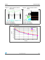
1
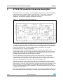
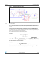
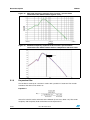
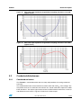
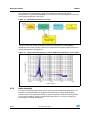
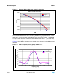
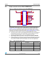
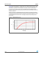
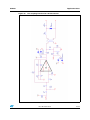
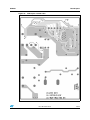
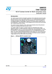
AN2451
Application note
ST7540 FSK powerline transceiver
design guide for AMR
Introduction
The ST7540 reference design has been developed as a useful tool to demonstrate how a
small, high-performance powerline node can be built using the ST7540 FSK transceiver.
With this reference design, it is possible to evaluate the ST7540 features, in particular, its
transmitting and receiving performances through actual communication on the power line.
The ST7540 reference design may be considered to be composed of three main sections:
●
Power supply section, specifically tailored to match powerline coupling requirements
and to operate within a wide range of the input mains voltage
●
Modem and crystal oscillator section
●
Line coupling interface section
The coupling interface is designed to allow the ST7540 FSK transceiver to transmit and
receive on the mains using 72 kHz carrier frequencies, within the European CENELEC
standard A-band specified for automatic meter reading.
ST7540 reference design board with outline dimensions
52 mm
Figure 1.
76 mm
As it can be seen from the picture above, a special effort has been made to obtain a very
compact reference design board, while keeping the focus on transmission and receiving
performances.
Note:
January 2010
The information provided in this application note refers to EVALST7540-2 reference design
board.
Doc ID 12791 Rev 3
1/55
www.st.com
Contents
AN2451
Contents
1
Electrical characteristics . . . . . . . . . . . . . . . . . . . . . . . . . . . . . . . . . . . . . 7
2
Safety precautions . . . . . . . . . . . . . . . . . . . . . . . . . . . . . . . . . . . . . . . . . . 9
3
ST7540 FSK powerline transceiver description . . . . . . . . . . . . . . . . . . 10
4
Evaluation tools description . . . . . . . . . . . . . . . . . . . . . . . . . . . . . . . . . 11
5
Board description . . . . . . . . . . . . . . . . . . . . . . . . . . . . . . . . . . . . . . . . . . 13
5.1
5.2
Coupling interface . . . . . . . . . . . . . . . . . . . . . . . . . . . . . . . . . . . . . . . . . . 18
5.1.1
Tx active filter . . . . . . . . . . . . . . . . . . . . . . . . . . . . . . . . . . . . . . . . . . . . . 19
5.1.2
Tx passive filter . . . . . . . . . . . . . . . . . . . . . . . . . . . . . . . . . . . . . . . . . . . 20
5.1.3
Rx passive filter . . . . . . . . . . . . . . . . . . . . . . . . . . . . . . . . . . . . . . . . . . . 22
5.1.4
Input impedance . . . . . . . . . . . . . . . . . . . . . . . . . . . . . . . . . . . . . . . . . . 24
Conducted disturbances . . . . . . . . . . . . . . . . . . . . . . . . . . . . . . . . . . . . . . 25
5.2.1
Conducted emissions . . . . . . . . . . . . . . . . . . . . . . . . . . . . . . . . . . . . . . 25
5.2.2
Noise immunity . . . . . . . . . . . . . . . . . . . . . . . . . . . . . . . . . . . . . . . . . . . 26
5.3
Thermal design . . . . . . . . . . . . . . . . . . . . . . . . . . . . . . . . . . . . . . . . . . . . 29
5.4
Oscillator section . . . . . . . . . . . . . . . . . . . . . . . . . . . . . . . . . . . . . . . . . . . 32
5.5
Surge and burst protection . . . . . . . . . . . . . . . . . . . . . . . . . . . . . . . . . . . . 32
5.6
50-pin connector for the EVALCOMMBOARD . . . . . . . . . . . . . . . . . . . . . 35
5.7
Power supply . . . . . . . . . . . . . . . . . . . . . . . . . . . . . . . . . . . . . . . . . . . . . . 36
6
Performance and ping tests . . . . . . . . . . . . . . . . . . . . . . . . . . . . . . . . . . 41
7
Application ideas . . . . . . . . . . . . . . . . . . . . . . . . . . . . . . . . . . . . . . . . . . . 42
8
2/55
7.1
Three-phase architecture . . . . . . . . . . . . . . . . . . . . . . . . . . . . . . . . . . . . . 42
7.2
Zero crossing detector . . . . . . . . . . . . . . . . . . . . . . . . . . . . . . . . . . . . . . . 42
7.3
Received Signal Strength Indicator (RSSI) . . . . . . . . . . . . . . . . . . . . . . . 44
7.4
Non-isolated coupling . . . . . . . . . . . . . . . . . . . . . . . . . . . . . . . . . . . . . . . . 45
7.5
DC powerline applications . . . . . . . . . . . . . . . . . . . . . . . . . . . . . . . . . . . . 46
7.6
110 and 132.5 kHz coupling circuit . . . . . . . . . . . . . . . . . . . . . . . . . . . . . 46
Troubleshooting . . . . . . . . . . . . . . . . . . . . . . . . . . . . . . . . . . . . . . . . . . . 49
Doc ID 12791 Rev 3
AN2451
Contents
Appendix A Board layout . . . . . . . . . . . . . . . . . . . . . . . . . . . . . . . . . . . . . . . . . . . . 51
List of normative references . . . . . . . . . . . . . . . . . . . . . . . . . . . . . . . . . . . . . . . . . . 54
Revision history . . . . . . . . . . . . . . . . . . . . . . . . . . . . . . . . . . . . . . . . . . . . . . . . . . . . 54
Doc ID 12791 Rev 3
3/55
List of figures
AN2451
List of figures
Figure 1.
ST7540 reference design board with outline dimensions . . . . . . . . . . . . . . . . . . . . . . . . . . . 1
Figure 2.
Typical curve for output current limit vs. RCL value . . . . . . . . . . . . . . . . . . . . . . . . . . . . . . . 8
Figure 3.
ST7540 Transceiver block diagram . . . . . . . . . . . . . . . . . . . . . . . . . . . . . . . . . . . . . . . . . . 10
Figure 4.
Complete evaluation system including a PC, an EVALCOMMBOARD and the EVALST75402 board
. . . . . . . . . . . . . . . . . . . . . . . . . . . . . . . . . . . . . . . . . . . . . . . . . . . . . . . . . . . . . . . . . . . . . . 11
Figure 5.
ST7540 powerline modem demonstration kit with control register window . . . . . . . . . . . . 12
Figure 6.
Positioning of the various sections of the board . . . . . . . . . . . . . . . . . . . . . . . . . . . . . . . . . 13
Figure 7.
Modem and coupling interface schematic . . . . . . . . . . . . . . . . . . . . . . . . . . . . . . . . . . . . . 14
Figure 8.
Power supply schematic . . . . . . . . . . . . . . . . . . . . . . . . . . . . . . . . . . . . . . . . . . . . . . . . . . . 15
Figure 9.
Schematic of Rx and Tx filters . . . . . . . . . . . . . . . . . . . . . . . . . . . . . . . . . . . . . . . . . . . . . . 19
Figure 10. Measured frequency response of the Tx active filter (typical curve). . . . . . . . . . . . . . . . . . 20
Figure 11. Simulated frequency response of the Tx active filter with components tolerance effect. . . 20
Figure 12. Measured frequency response of the Tx active + passive filters connected to the CISPR network (typical curve) . . . . . . . . . . . . . . . . . . . . . . . . . . . . . . . . . . . . . . . . . . . . . . . . . . . . . . . . . . . . . . . . . 22
Figure 13. Simulated frequency response of the Tx active + passive filters connected to the CISPR network with the components tolerance effect22
Figure 14. Measured frequency response of the Rx passive filter (typical curve) . . . . . . . . . . . . . . . . 23
Figure 15. Simulated frequency response of the Rx passive filter with components tolerance effect . 24
Figure 16. Measured input impedance magnitude of coupling interface in Tx mode (typical curve) . . 25
Figure 17. Measured input impedance magnitude of coupling interface in Rx mode (typical curve) . . 25
Figure 18. Conducted emissions test setup . . . . . . . . . . . . . . . . . . . . . . . . . . . . . . . . . . . . . . . . . . . . . 26
Figure 19. Output spectrum (typical) at 72 kHz, 2400 baud, deviation 1, mains 220Vac . . . . . . . . . . 26
Figure 20. Narrow-band conducted interference test setup . . . . . . . . . . . . . . . . . . . . . . . . . . . . . . . . . 27
Figure 21. Measured BER vs. SNR curve (typical), white noise . . . . . . . . . . . . . . . . . . . . . . . . . . . . . 28
Figure 22. SNR vs. frequency curve (typical) at BER = 10-3. . . . . . . . . . . . . . . . . . . . . . . . . . . . . . . . 28
Figure 23. PCB copper dissipating area for ST7540 reference design board . . . . . . . . . . . . . . . . . . . 29
Figure 24. Packet-fragmented transmission . . . . . . . . . . . . . . . . . . . . . . . . . . . . . . . . . . . . . . . . . . . . 30
Figure 25. Equivalent model of the thermal impedance qJA of the HTSSOP28 package with exposed
pad
. . . . . . . . . . . . . . . . . . . . . . . . . . . . . . . . . . . . . . . . . . . . . . . . . . . . . . . . . . . . . . . . . . . . . . 30
Figure 26. Output current vs. supply current typical curve for ST7540 in Tx mode . . . . . . . . . . . . . . . 31
Figure 27. Dissipated power vs. load impedance modulus typical curve for ST7540 reference design
board
. . . . . . . . . . . . . . . . . . . . . . . . . . . . . . . . . . . . . . . . . . . . . . . . . . . . . . . . . . . . . . . . . . . . . . 31
Figure 28. A recommended oscillator section layout for noise shielding . . . . . . . . . . . . . . . . . . . . . . . 32
Figure 29. Common mode disturbances protection - positive disturbance . . . . . . . . . . . . . . . . . . . . . 33
Figure 30. Common mode disturbances protection - negative disturbance. . . . . . . . . . . . . . . . . . . . . 34
Figure 31. Differential mode disturbances protection . . . . . . . . . . . . . . . . . . . . . . . . . . . . . . . . . . . . . 34
Figure 32. Scheme of the connector for the EVALCOMMBOARD . . . . . . . . . . . . . . . . . . . . . . . . . . . 35
Figure 33. Typical waveforms at 230 Vac: open load . . . . . . . . . . . . . . . . . . . . . . . . . . . . . . . . . . . . . 38
Figure 34. Typical waveforms at 230 Vac: full load . . . . . . . . . . . . . . . . . . . . . . . . . . . . . . . . . . . . . . . 38
Figure 35. Typical waveforms at 265 Vac: short-circuit . . . . . . . . . . . . . . . . . . . . . . . . . . . . . . . . . . . . 39
Figure 36. Typical waveforms at 265 Vac: startup . . . . . . . . . . . . . . . . . . . . . . . . . . . . . . . . . . . . . . . . 39
Figure 37. Load regulation . . . . . . . . . . . . . . . . . . . . . . . . . . . . . . . . . . . . . . . . . . . . . . . . . . . . . . . . . . 39
Figure 38. SMPS efficiency curve . . . . . . . . . . . . . . . . . . . . . . . . . . . . . . . . . . . . . . . . . . . . . . . . . . . . 40
Figure 39. ST7540 powerline modem demonstration kit window for the master board . . . . . . . . . . . . 41
Figure 40. Scheme of principle for three-phase architecture . . . . . . . . . . . . . . . . . . . . . . . . . . . . . . . . 42
Figure 41. Schematic of a zero crossing detection circuit for non-isolated coupling . . . . . . . . . . . . . . 43
Figure 42. Schematic of a zero crossing detection circuit for isolated coupling. . . . . . . . . . . . . . . . . . 44
Figure 43. ZC_OUT vs. AC mains waveforms . . . . . . . . . . . . . . . . . . . . . . . . . . . . . . . . . . . . . . . . . . . 44
4/55
Doc ID 12791 Rev 3
AN2451
Figure 44.
Figure 45.
Figure 46.
Figure 47.
Figure 48.
Figure 49.
Figure 50.
Figure 51.
List of figures
Peak detector electrical schematic . . . . . . . . . . . . . . . . . . . . . . . . . . . . . . . . . . . . . . . . . . . 45
Measured DC_OUT Vs. AC_IN peak detector response . . . . . . . . . . . . . . . . . . . . . . . . . . 45
Example schematic for non-isolated solution . . . . . . . . . . . . . . . . . . . . . . . . . . . . . . . . . . . 46
Line coupling interface for 110 kHz channel . . . . . . . . . . . . . . . . . . . . . . . . . . . . . . . . . . . . 47
Line coupling interface for 132.5 kHz channel . . . . . . . . . . . . . . . . . . . . . . . . . . . . . . . . . . 48
PCB layout - component placing . . . . . . . . . . . . . . . . . . . . . . . . . . . . . . . . . . . . . . . . . . . . 51
PCB layout - top view . . . . . . . . . . . . . . . . . . . . . . . . . . . . . . . . . . . . . . . . . . . . . . . . . . . . . 52
PCB layout - bottom view . . . . . . . . . . . . . . . . . . . . . . . . . . . . . . . . . . . . . . . . . . . . . . . . . . 53
Doc ID 12791 Rev 3
5/55
List of tables
AN2451
List of tables
Table 1.
Table 2.
Table 3.
Table 4.
Table 5.
Table 6.
Table 7.
Table 8.
Table 9.
Table 10.
Table 11.
Table 12.
6/55
Electrical characteristics of the ST7540 reference design . . . . . . . . . . . . . . . . . . . . . . . . . . 7
Output voltage level setting through Vsense partitioning - typical values . . . . . . . . . . . . . . . 8
Bill of materials . . . . . . . . . . . . . . . . . . . . . . . . . . . . . . . . . . . . . . . . . . . . . . . . . . . . . . . . . . 16
ST parts on the ST7540 reference design board . . . . . . . . . . . . . . . . . . . . . . . . . . . . . . . . 18
Line coupling transformer specifications. . . . . . . . . . . . . . . . . . . . . . . . . . . . . . . . . . . . . . . 21
Noise immunity test settings . . . . . . . . . . . . . . . . . . . . . . . . . . . . . . . . . . . . . . . . . . . . . . . . 27
50-pin connector digital signals . . . . . . . . . . . . . . . . . . . . . . . . . . . . . . . . . . . . . . . . . . . . . 35
50-pin connector analog signals . . . . . . . . . . . . . . . . . . . . . . . . . . . . . . . . . . . . . . . . . . . . . 36
50-pin connector power connections . . . . . . . . . . . . . . . . . . . . . . . . . . . . . . . . . . . . . . . . . 36
SMPS specifications . . . . . . . . . . . . . . . . . . . . . . . . . . . . . . . . . . . . . . . . . . . . . . . . . . . . . . 37
SMPS transformer specifications . . . . . . . . . . . . . . . . . . . . . . . . . . . . . . . . . . . . . . . . . . . . 37
Document revision history . . . . . . . . . . . . . . . . . . . . . . . . . . . . . . . . . . . . . . . . . . . . . . . . . 54
Doc ID 12791 Rev 3
AN2451
Electrical characteristics
1
Electrical characteristics
Table 1.
Electrical characteristics of the ST7540 reference design
Value
Parameter
Test conditions
Unit
Min
Typ
Max
Operating conditions
If ST7540 junction temperature
exceeds 180 °C device shuts
down
Ambient operating temperature
85
°C
Transceiver section transmitting specifications (Tx mode)
Selected channel frequency
FSK carrier
72
kHz
Transmitting output voltage level at mains output
R7 = 47kΩ, R8 = 15kΩ – See
Table 2
2
Transmitting output current limit
R6=1.1kΩ – See Figure 2
2nd
harmonic distortion
at mains output
Loaded with CISPR 16-1
network
-55
3rd harmonic distortion
at mains output
Loaded with CISPR 16-1
network
-61
2.25
500
V rms
mA rms
dBC
50Hz attenuation
100
dB
48
dBµV rms
Receiving specifications (Rx mode)
Minimum detectable Rx signal
BER<10-3, negligible noise
Auxiliary supply
5 V regulated voltage
ST7540 internally generated
-5%
5.05
5 V current capability
3.3 V regulated voltage
ST7540 internally generated
-5%
3.3
3.3 V current capability
+5%
V
50
mA
+5%
V
50
mA
265
V
Power supply section
AC mains voltage range
85
Mains frequency
50-60
Output voltage
Green led ON
Output voltage ripple
Iout = 500 mA, Vin=85 Vac
+10%
V
1
%
Peak output current
500
mA
Output power
5.6
W
Efficiency at Pout=3.5W
Nominal transformer isolation*
Primary to secondary/
secondary to auxiliary
Doc ID 12791 Rev 3
-10%
12.3
Hz
70
%
4
kV
7/55
Electrical characteristics
Table 1.
AN2451
Electrical characteristics of the ST7540 reference design (continued)
Value
Parameter
Test conditions
Unit
Min
Number of holdup cycles
Typ
Max
0
Input power
100
mW
Switching frequency
Transceiver section in Tx mode -10%
65
+10%
kHz
Switching frequency
Transceiver section in Rx
mode
21
+10%
kHz
Table 2.
Output voltage level setting through Vsense partitioning - typical values
V(PA_OUT)
[dBuVRMS]
R7
R8
[VP-P]
V(PA_OUT)
[VRMS]
[kΩ]
[kΩ]
2.830
1.000
120
16
15
3.170
1.120
121
20
15
3.560
1.260
122
24
15
3.990
1.410
123
27
15
4.470
1.580
124
33
15
5.030
1.780
125
39
15
5.660
2.000
126
47
15
6.340
2.240
127
51
15
7.100
2.510
128
56
15
7.980
2.820
129
68
15
V(PA_OUT)
Figure 2.
8/55
-10%
Typical curve for output current limit vs. RCL value
Doc ID 12791 Rev 3
AN2451
2
Safety precautions
Safety precautions
The board must be used only by expert technicians. Due to the high voltage (220 V ac)
present on the parts which are not isolated, special care should be taken with regard to
people's safety.
There is no protection against high voltage accidental human contact.
After disconnection of the board from the mains, none of the live parts should be touched
immediately because of the energized capacitors.
It is mandatory to use a mains insulation transformer to perform any tests on the high
voltage sections (see circuit sections highlighted in Figure 7 and Figure 8) in which test
instruments like Spectrum Analyzers or Oscilloscopes are used.
Do not connect any oscilloscope probes to high voltage sections in order to avoid damaging
instruments and demonstration tools.
Warning:
ST assumes no responsibility for any consequences which
may result from the improper use of this tool.
Doc ID 12791 Rev 3
9/55
ST7540 FSK powerline transceiver description
3
AN2451
ST7540 FSK powerline transceiver description
ST7540 transceiver uses frequency shift keying (FSK) modulation to perform a half-duplex
communication on a powerline network. It operates from a 7.5 to 13.5 V single supply
voltage (Vcc) and integrates a power amplifier (PA), which is able to drive low line
impedance, and two linear regulators providing 5 V and 3.3 V.
Figure 3.
ST7540 Transceiver block diagram
The ST7540 can communicate using eight different communication channels (60, 66, 72,
76, 82.05, 86, 110, 132.5 kHz), four baud rates (600, 1200, 2400, 4800) and two deviations
(1 and 0.5). Additional functions are included, such as watchdog, automatic control on PA
output voltage and current, carrier/preamble detection and band-in-use signaling,
transmission time-out, and thermal shutdown.
The transceiver, which is dedicated only to physical communication, operates with a
microcontroller whose aim is to manage the communication protocol stack. A reset output
(RSTO) and a programmable clock (MCLK) can be provided to the microcontroller by the
ST7540 in order to simplify the external logic and circuitry.
The host controller can exchange data with the transceiver through a serial interface,
programmable to operate either in UART (CLR/T data clock not used) or in SPI mode.
Communication on the power line can be either synchronous or asynchronous to the data
clock that is provided by the transceiver at the programmed baud rate.
When in transmission mode (i.e. RxTx line at low level), the ST7540 samples the digital
signal on the TxD line at the programmed baud rate and modulates it in a FSK sinusoidal
output on the Tx_OUT line. This signal is then externally fed into the power amplifier to add
current capability. The power amplifier can also introduce gain and active filtering to the
signal, just using few external passive components. The resulting signal on the PA_OUT line
is coupled to the power line.
When in receiving mode (i.e. RxTx line at high level), an incoming FSK signal on the Rx_IN
line is demodulated and the digital output is available for the microcontroller on the RxD pin.
10/55
Doc ID 12791 Rev 3
AN2451
Evaluation tools description
The device also recovers the synchronism of the received signal using an internal PLL. The
recovered clock is present on CLR/T output.
The ST7540 operating parameters can be set by means of an internal control register,
accessible only through the SPI host interface.
4
Evaluation tools description
The complete evaluation system for the ST7540 powerline communication consists of:
●
a PC using the "ST7540 power line modem demo kit" software tool
●
one EVALCOMMBOARD hosting the ST7 microcontroller
●
one ST7540 reference design board (EVALST7540-2).
The correct procedure for connecting the EVALST7540-2 and the EVALCOMMBOARD is as
follows:
1.
Connect the EVALST7540-2 and the EVALCOMMBOARD
2.
Connect the ac mains cable to the EVALST7540-2 and the USB cable to the
EVALCOMMBOARD
3.
Connect the EVALST7540-2 to the ac mains supply
4.
Connect the EVALCOMMBOARD to the PC via the USB cable.
Warning:
Figure 4.
Follow the connection procedure to avoid damaging the
boards.
Complete evaluation system including a PC, an EVALCOMMBOARD and
the EVALST7540-2 board
USB /
RS232
Doc ID 12791 Rev 3
11/55
Evaluation tools description
Figure 5.
AN2451
ST7540 powerline modem demonstration kit with control register window
The complete chain, controlled by the ST7540 powerline modem demonstration kit, can set
up real communication at bit level, simply by sending or receiving a user-defined bit stream.
It is possible to establish a half-duplex communication with two of these communication
nodes (two chains) connected to each other. In order to better evaluate communication
between two nodes, the ST7540 powerline modem demonstration kit has some particular
features, including:
12/55
●
Frame synchronization: a byte synchronization header can be added to the to the
exchanged data to set up a simple protocol, intended to test the capability of the
system to correctly receive the exact transmitted bit sequence. This can be done in two
ways: via the ST7540 control register settings (the internal configuration register of the
modem has a frame header field, in which an 8- or 16-bit header can be set) or via the
Rx panel of the ST7540 powerline modem demonstration kit (setting a synchronization
at SW level). A bit synchronization can be introduced as a simpler feature by enabling
the preamble detection method in the control register panel and then inserting at least
one “0101” or one “1010” sequence at the beginning of the transmitted bit stream.
●
Ping session: a master-slave communication with automatic statistics calculation can
be very useful to test a point-to-point or a point-to-multipoint powerline communication
network, thus providing a method to evaluate reachability of each node in the network.
For further details about the ST7540 powerline modem demonstration kit, please refer
to the user manual UM0239 “ST7540 power line modem demo kit graphical user
interface”.
Doc ID 12791 Rev 3
AN2451
5
Board description
Board description
The ST7540 reference design is composed of the following sections:
●
Power supply section, based on ST’s VIPer12A-E IC
●
ST7540 modem and crystal oscillator section
●
Line coupling interface section, with three subsections:
–
Transmission active filter
–
Transmission passive filter
–
Receiving passive filter.
The board also has two connectors, which allow the user to plug the mains supply on one
side of it and the I.B.U. communication board on the other side.
Figure 6.
Positioning of the various sections of the board
The schematics of the whole reference design appear in Figure 7 and 8. Figure 7 shows
the modem and the coupling Interface circuits, while Figure 8 represents the power supply
circuit. In both the schematics, high voltage regions are highlighted.
Table 3 lists the components used to develop the reference design board. All parts have
been selected to give optimal performances.
The layout of the printed circuit is given in Appendix A - Figure 49, Figure 50 and Figure 51.
Doc ID 12791 Rev 3
13/55
Board description
Figure 7.
AN2451
Modem and coupling interface schematic
HIGH VOLTAGE SECTION 14/55
Doc ID 12791 Rev 3
3
1
2
85 V ac to 256 V ac
AC INPUT
CN1
N
P
F1
T - 2A
L1
1 mH
C1
33nF X2
R1
10R 1W
1
5
L2
10
6
C6
10 uF
2
-
C7
47 nF
+
D1
BRIDGE
Doc ID 12791 Rev 3
U1
4 Vdd
3 FB
2
1 S
1
5
6
7
8
+ C3
10uF 400V
1
3
D3
+
C2
10uF 400V
L3
470uH
3
Q1
D2
R2
220k
1
4
3
4
R3
10 K
2
C5
220 pF
470pF 630V
C4
U2
2
4
C10
2.2 nF
5
8
2
D4
1
T1
3
4
3
2
1
1
3
D5
10V
560
R4
+
C9
47uF 16V
C8
470uF 16V
L4
33 uH
Vcc
12 V dc
Vcc
LED
D6
R5
1k5
DC OUTPUT
C29
47uF 16V
Vss
Vcc
TEST PADS
Figure 8.
1
2
AN2451
Board description
Power supply schematic
DRAIN
HIGH
VOLTAGE
SECTION
15/55
Board description
AN2451
Table 3.
Item Qty
16/55
Bill of materials
Part
Value
Description
1
1
CN1
HEADER 2
2
1
CN2
CON50A
50 pins SMT right angle female p=1.27mm
3
1
C1
33nF X2
Murata GA355XR7-GB333K
4
2
C2,C3
10uF / 400V
Yageo SE-K / Nichicon VK 20%
5
1
C4
470pF / 1kV
TDK C4520X7R-3A471K
6
1
C5
220pF / 50V
TDK C0603C0G-1E220J
7
4
C6,C15,C17,C24
10uF / 16V
TDK C3216X7R-1C106MT
8
1
C7
47nF / 25V
Murata GRM188R7-1E473K
9
1
C8
470uF / 16V
Rubycon 3M0319 / Yageo SE-K 20%
10
2
C9,C29
47uF / 16V
Murata GRM32ER6-1C476K
11
1
C10
2.2nF Y1
TDK CD12-E2GA222MYNS /
Murata DE1E3-KX222M
12
2
C11,C12
33pF
TDK C1005C0G-1H330J
13
2
C14,C27
10nF
Murata GRM188R7-1H103K
14
4
C16,C18,C19,C25
100nF
TDK C1608X7R-1H104K
15
2
C21,C33
150pF
Murata GRM1885C-1H151J
16
1
C22
10uF
Murata GRM21BR6-1A106K /
TDK C2012X5R-0J106K
17
1
C23
100nF X2
18
1
C26
22nF
Murata GRM21B5C-1H223J /
TDK C3216C0G1H223J
19
1
C30
15pF
Murata GRM1555C-1H150J
20
1
C31
22pF
Murata GRM1555C-1H220J
21
1
C32
390pF
Murata GRM1885C-1H391J
22
1
D1
DF06S
600 V - 1.5 A bridge rectifier
23
1
D2
STTH1L06A
24
1
D3
BAS16 / BAS21
25
1
D4
STPS1H100
26
1
D5
BZX84C10
27
1
D6
LED
28
2
D8, D10
BAT54S
29
1
D9
SM6T12CA
30
1
F1
2A - T
31
1
JP4
CLOSE
32
1
J1
CONNECTOR
Doc ID 12791 Rev 3
Mains supply connector
EPCOS B32922-A2104K
SMA ultra-fast Schottky diode
SOT23
SMA Schottky diode
SOT23 10V zener diode
Green LED
SOT23 low drop Schottky diode
12V bidirectional transil diode
Time-lag fuse
AN2451
Board description
Table 3.
Item Qty
Bill of materials (continued)
Part
Value
Description
33
1
L1
1mH
34
1
L2
2x10mH 0.3A
35
1
L3
470uH
Epcos B82442-A1474K
36
1
L4
33uH
Epcos B82462-A4333K
37
1
L5
47uH
Epcos B82464-A4473K /
WE 744-775-147
38
1
L6
220uH
Epcos B82462-A4224K /
WE 744-774-222
39
1
Q1
BC857BL
40
1
R1
10R 1W
41
1
R2
220K
0603 1%
42
1
R3
10K
0603 1%
43
1
R4
560
0603 1%
44
1
R5
1K5
0603 1%
45
1
R6
1K1
0603 1%
46
1
R7
47K
0603 1%
47
1
R8
15K
0603 1%
48
1
R9
4K7
0603 1%
49
1
R10
12K
0603 1%
50
1
R12
1K
0603 1%
51
1
R14
1K8
0603 1%
52
1
R17
470
0603 1%
53
1
R19
3K9
0603 1%
54
1
R20
56K
0603 1%
55
1
R21
2K7
0603 1%
56
1
T1
SMPS
transformer
TDK SRW12.6EF-E07H013 /
WE S06-100-057
57
1
T2
Line
transformer
VAC T60403-K5024-X044 /
Radiohm 69H14-2101
58
1
U1
VIPER12AS
SMPS controller / switch
59
1
U2
SFH610-A
60
1
U3
ST7540
61
1
X1
16 MHz
Doc ID 12791 Rev 3
Epcos B82442-H1105K
Radiohm 42V15
SOT23
Metal oxide type - radial
Opto-switch
Powerline transceiver
17/55
Board description
Table 4.
5.1
AN2451
ST parts on the ST7540 reference design board
Value
Description
ST7540
Powerline transceiver
VIPER12AS
SMPS controller / switch
STTH1L06A
Ultrafast diode
STPS1H100
Schottky diode
SM6T12CA
12V bidirectional transil diode
Coupling interface
The mains coupling interface is composed of three different filters: the Tx active filter, the Tx
passive filter and the Rx passive filter.
All three filters are described in the sections Section 5.1.1, 5.1.2, and 5.1.3. In each section,
calculations and measured frequency responses are given.
The filters are quite sensitive to the components' value tolerance. Actual components used
in the ST7540 reference design have the following tolerances:
●
+/- 10% for coils and for the X2 capacitor
●
+/- 1% for SMD resistors
●
+/- 5% for SMD ceramic capacitors.
To evaluate sensitivity of the filters to the tolerances listed above, the following sections
include simulated responses of the filters with Montecarlo statistical analysis. Statistical
simulation helps understanding the relationship between components' value tolerance and
variations on the responses of the filters. In simulation curves, the ideal response is drawn in
blue, while red curves indicate statistical variations generated through simulation.
18/55
Doc ID 12791 Rev 3
AN2451
Board description
Figure 9.
5.1.1
Schematic of Rx and Tx filters
Tx active filter
The Tx active filter is based on the ST7540 internal power amplifier (PA), whose input and
output pins are available externally to allow a filtering network to be tailored around the
amplifier.
For the ST7540 reference design board, a 3-pole low-pass filter has been developed by
cascading a simple R-C low-pass stage and a Sallen-Key 2-pole cell with 9dB gain. The
R19-C32 low-pass stage is aimed at introducing attenuation starting from approximately an
octave above the transmission channel frequency.
The transfer function of the 2nd order Sallen-Key cell is:
Equation 1
A0
A ( s ) = -------------------------------------------2
s - + ----------------s -+1
--------2 ω •Q
C
ω
C
R 14⎞
1
where A0 = ⎛⎝ 1 + -------- , ω = --------------------------------------------------------R 12⎠ C
R 9 • R 10 • C 33 • C 21
R •R •C •C
R 9 C 33 + R 10 C 21 + R 9 C 21 ( 1 – A 0 )
9
10
33
21
and Q = ---------------------------------------------------------------------------------------
The corner frequency may be calculated as:
Equation 2
1
f c = ---------------------------------------------------------------------- = 135.7kHz
2π • R 9 • R 10 • C 33 • C 21
Figure 10 represents the measured transfer function of the Tx active filter. It shows good
rejection on both the 2nd and 3rd harmonic frequencies for the 72 kHz signal.
Doc ID 12791 Rev 3
19/55
Board description
AN2451
Figure 10. Measured frequency response of the Tx active filter (typical curve)
Simulation of the Tx active filter response against components' tolerance, depicted in
Figure 11, shows +/- 1 dB variation in gain module at 72 kHz.
Figure 11. Simulated frequency response of the Tx active filter with components
tolerance effect
+/‐ 1 dB 5.1.2
Tx passive filter
Coupling to the power line requires some passive components in addition to the active
filtering stage. In particular, Tx passive filter section is made of the decoupling capacitor
C22, line transformer T2, inductor L5 and X2 safety capacitor C23.
L5 has been accurately chosen to have a high saturation current (>1 A) and a very low
equivalent series resistance (<0.2 Ω), to limit distortion and insertion losses even with heavy
line load. Center frequency for the series resonance is calculated as:
Equation 3
1
f c = -------------------------------2π L 5 • C 23
20/55
Doc ID 12791 Rev 3
AN2451
Board description
provided that the dc-decoupling capacitor C22 is much greater than C23 (in this case, 100
times greater) and that parasitic components of the transformer have negligible effects on
the filtering action.
Particular attention has been paid in choosing the line transformer. The required
characteristics are listed in Table 5.
In order to have a good power transfer and to minimize the insertion losses, it is
recommended to choose a transformer with a primary (shunt) inductance greater than 1mH
and a series resistance lower than 0.5 Ω.
Another important parameter is the leakage inductance. If it has a relevant value (10 to 50
uH), this can be used to design the coupling filter without inserting series inductance (L5,
L6). The drawback, however, is the poor accuracy of this parameter, which can lead to a
shift of the filter response and to bad coupling. Consequently, a low leakage inductance
value (<1 µH) has been chosen, fixing the series inductance through a discrete component
with greater accuracy.
The last specified parameter, the 4 kV insulation voltage requirement, is described and
coded in the EN50065-4-2 CENELEC document.
Table 5.
Line coupling transformer specifications
Parameter
Value
Turn ratio
1:1
Magnetizing inductance
>1 mH
Leakage inductance
<1 µH
DC resistance
<0.5 Ω
DC saturation current
>2 mA
Interwinding capacitance
< 50 pF
Withstanding voltage
4 kV
Figure 12 shows the measured response of the Tx active and passive filters, loaded with the
CISPR network. The figure highlights a further filtering effect added by the passive L-C
series resonant combined with the CISPR reactive load.
Doc ID 12791 Rev 3
21/55
Board description
AN2451
Figure 12. Measured frequency response of the Tx active + passive filters
connected to the CISPR network (typical curve)
Figure 13. Simulated frequency response of the Tx active + passive filters
connected to the CISPR network with the components tolerance effect
+/‐ 1 dB 5.1.3
Rx passive filter
The Rx filter is made up of a resistor in series with a parallel L-C resonant. The transfer
function of the filter can be written as:
Equation 4
s • L6 + RL
---------------------------R 17 L 6 C 26
R ( s ) = --------------------------------------------------------------------------------------------R 17 + R L
2 R 17 R L C 26 + L 6
--------------------------------------• s + -------------------------s +
R 17 L 6 C 26
R 17 L 6 C 26
where RL is the DC series resistance of the inductor (in our case, about 2 Ω). The center
frequency and the quality factor of the filter can be expressed as:
22/55
Doc ID 12791 Rev 3
AN2451
Board description
Equation 5
R 17 L 6 C 26
1
1 R 17 + R L
1
fc = ------ • ω C = ------ ------------------------- ≅ ---------------------------, Q = --------------------------------------- • ω C
2π
2π R 17 L 6 C 26 2π L C
R 17 R L C 26 + L 6
6 26
The simplification made on fc formula is possible because R17>RL. Consequently, the
quality factor and filter selectivity depend not only on R17, but also on RL. A higher RL
produces a lower steepness of the resonance, while a higher R17 gives a higher selectivity.
Actual values of the components give a Q equal to 4.3.
The RL value impacts in a clearer way on insertion losses. To evaluate the relationship
between RL and the losses on the received signal, the following simplified expression of
R ( s ) at f=fc may be used:
Equation 6
ωC • L6
1
R ( j • 2πf c ) ≅ Q • ------------------- = ----------------------------------------------R 17
C 26
1 + R L • R 17 • --------L6
With actual values of the components, we get a loss of about 1 dB. The same calculation
gives unitary transfer if RL is set to zero.
Looking at the first way to express the module of the transfer function, it is possible to notice
that a higher value of Q can help keeping the losses small. Nevertheless, a high value of Q
would bring a higher sensitivity of the filter to the components tolerance.
Figure 14 shows the measured frequency response of the Rx passive filter. The filter has an
actual -3 dB bandwidth equal to 17 kHz and an attenuation of about 1 dB at center
frequency, just as expected.
Figure 14. Measured frequency response of the Rx passive filter (typical curve)
Figure 15 represents a simulation of the response of the Rx passive filter with the
components tolerance effect. A worst case loss of nearly 1.5 dB can be observed at 72 kHz
due to a shift on center frequency.
Doc ID 12791 Rev 3
23/55
Board description
AN2451
Figure 15. Simulated frequency response of the Rx passive filter with components
tolerance effect
‐ 1.5 dB
5.1.4
Input impedance
The input impedance of a powerline communication node is another critical point. Figure 16
and Figure 17 show the input impedance magnitude vs. frequency curves in both Tx and Rx
mode. In both figures channel impedance point and the minimum impedance point are
indicated.
The impedance magnitude values prove that the ST7540 reference design board is
compliant with the EN50065-7 document, which sets the following minimum impedance
constraints for this kind of equipment:
●
●
24/55
Tx mode:
–
free in the range 3 to 95 kHz
–
3 Ω from 95 to 148.5 kHz
Rx mode:
–
10 Ω from 3 to 9 kHz
–
50 Ω between 9 and 95 kHz only inside signal bandwidth (free for frequencies
outside signal bandwidth)
–
5 Ω from 95 to 148.5 kHz
Doc ID 12791 Rev 3
AN2451
Board description
Figure 16. Measured input impedance magnitude of coupling interface in Tx mode
(typical curve)
Figure 17. Measured input impedance magnitude of coupling interface in Rx mode
(typical curve)
5.2
Conducted disturbances
5.2.1
Conducted emissions
The EN50065-1 standard describes the test setup and procedures for testing conducted
emissions.
The conducted emissions measurements have been taken with 220 Vac mains voltage. The
test pattern consists of a continuous transmission of a “1010” continuous sequence at 2400
baud, deviation 1. The output signal measured at the CISPR artificial network has a value of
120 dBuVRMS which means a signal of 2 VRMS on the mains output.
Doc ID 12791 Rev 3
25/55
Board description
AN2451
The spectrum analyzer performs a peak measurement instead of a quasi-peak
measurement, as specified by EN50065-1. For continuous sinusoidal signals the two types
of measurement give the same result.
Figure 18. Conducted emissions test setup
EVALST7540-2
Figure 19 shows the results for the output spectrum measurement. The EN50065-1
disturbance limits mask (traced in red) may be compared to the typical output spectrum of
the ST7540 reference design board.
Figure 19. Output spectrum (typical) at 72 kHz, 2400 baud, deviation 1, mains 220Vac
5.2.2
Noise immunity
The tests on immunity against white noise and narrow-band conducted interferences are
based on two ST7540 reference design boards performing a simplex (unidirectional)
communication. The first board transmits a given bit sequence, while the receiving board
passes the received bit stream to a BER tester software on a PC, which evaluates the
percentage of correctly received bits.
26/55
Doc ID 12791 Rev 3
AN2451
Board description
The noise (white noise or sinusoidal interferer) is produced by a waveform generator and
injected into the artificial network through an AC coupling circuit. Figure 20 shows the test
environment used to perform noise immunity tests.
Figure 20. Narrow-band conducted interference test setup
Spectrum Analyzer
AGILENT
4395A
ST7540 Board
STIMULUS
PC with
Demo SW
ST7540
ST7540 Board
Under Test
PC with
BER Tester
SW
Coupling
Circuit
Table 6 reports the parameters for the test conditions settings.
The received signal and noise levels are measured at the mains connector of the board
under test. The 3 kHz resolution bandwidth chosen for the Spectrum Analyzer allows
measurement of the actual signal and noise levels as seen by the receiving ST7540 internal
circuitry, programmed for 2400 baud.
Table 6.
Noise immunity test settings
Parameter
Value
Received signal
86 dBuVrms
Frequency
72 kHz
Baud rate
2400
Deviation
1
Detection method
Carrier with conditioning
Detection time
3 ms
Sensitivity
High
Input filter
Off
Transmitted sequence
AACC h
S.A. resolution BW
3 kHz
Figure 21 represents the BER vs. SNR curve in the presence of white noise. It may be noted
that a BER of 10-3 corresponds to a SNR around 12 dB, as expected from a nonideal FSK
demodulator.
Doc ID 12791 Rev 3
27/55
Board description
AN2451
Figure 21. Measured BER vs. SNR curve (typical), white noise
BER vs. Signal to Noise Ratio
1.00E-01
S/N @ CISPR
S/N @ Rx_IN
1.00E-02
BER
1.00E-03
1.00E-04
1.00E-05
1.00E-06
6.0
7.0
8.0
9.0
10.0
11.0
12.0
13.0
14.0
15.0
16.0
17.0
18.0
S/N
For narrow-band interference tests, two types of interfering noise have been used: a pure
sinusoidal tone and an amplitude-modulated signal (modulating signal 1 kHz, modulation
depth 80%). In both cases, the amplitude of the noise signal (of the carrier, for modulated
signal) has been decreased until the measured BER was lower than 10-3 (one error every
1000 transmitted bits).
Figure 22 shows SNR vs. frequency curves for both a pure sinusoidal and an AM modulated
interferer.
Figure 22. SNR vs. frequency curve (typical) at BER = 10-3
15
10
No modulation
AM 1kHz 80%
5
0
SNR [dB]
-5
-10
-15
-20
-25
-30
-35
-40
-45
-50
-55
30
40
50
60
70
80
frequency [kHz]
28/55
Doc ID 12791 Rev 3
90
100
110
120
AN2451
5.3
Board description
Thermal design
All heat dissipation is based on the heat exchange between the ST7540 IC, the PCB and the
surrounding environment.
A large PCB copper area under the device is recommended to make an easier heat transfer
from the ST7540 to the environment. The metallic slug under the device (exposed pad of
HTSSOP28 package) must be properly soldered to the copper area on the PCB top side, as
recommended in the datasheet.
The large ground layer on the bottom side of the board must be connected to the top side
layer through multiple via holes.
In the case of ST7540 reference design, an area of about 0.2 cm2 is put on the PCB top side
for exposed pad soldering, while ground layer dissipating area on the bottom side is nearly
1.5 cm2.
Figure 23. PCB copper dissipating area for ST7540 reference design board
Top layer
Copper area
Bottom layer
Soldering area
Multiple Via Holes
Large GND layer
Even if the ST7540 features a built-in thermal shutdown circuitry which turns off the power
amplifier (PA) when the die temperature (TJ) exceeds 170 °C. It is however recommended
not to exceed 125 °C during normal operating conditions to ensure the functionality of the
IC.
The relationship between junction temperature TJ and power dissipation during
transmission PD is described by the following formula:
Equation 7
T J ( t TX, d ) = T A – P D • θ JA ( t TX, d )
where TA is the ambient temperature (from -45 to +85 °C) and θJA is the junction to ambient
thermal impedance of the ST7540 IC, which is related to the length of the transmission (tTX)
and to the duty cycle d = tPKT / (tPKT + tIDLE), assuming a packet-fragmented transmission
as illustrated by Figure 24.
Doc ID 12791 Rev 3
29/55
Board description
AN2451
Figure 24. Packet-fragmented transmission
Transmission
in progress
tPKT
Idle
state
tIDLE
tTX
When soldered to a proper copper area on the PCB as explained above, the IC is
characterized by a steady-state thermal impedance of about 35 °C/W. The transient of the
thermal impedance θJA can be estimated by simulating a 6-cell equivalent model, as shown
in Figure 25. The simulated curve vs. the transmission duration and the duty cycle is also
given. It can be noticed that the transient of θJA takes several hundreds of seconds, after
which the static value of 35 °C/W is reached.
Figure 25. Equivalent model of the thermal impedance θJA of the HTSSOP28
package with exposed pad
PD
R1
0.4
R2
1
R3
8
C1
5e-4
C2
6e-3
C3
17e-3
R4
11
R5
9.5
R6
6
C4
0.09
C5
0.8
C6
15
R ĺ °C/W
C ĺ W*s/°C
șJA(tTX, d) ( [ºC/W]
j )
40
30
20
d = 100%
d = 75%
d = 50%
d = 25%
10
TA
0
1E-2
1E-1
1
1E1
1E2
1E3
tTX [s]
This means that during the transient phase (i.e. if the transmission time tTX is some seconds
or even less) the IC is able to dissipate power that is well above the one sustainable at
steady state. For this reason, a complete thermal analysis requires taking into account the
characteristics of the transmission, i.e. duty cycle and duration, determining the value
reached by the thermal impedance and then the allowed power dissipation.
Actual dissipated power PD can be calculated as:
Equation 8
P D = P IN – P OUT
where PIN=VCC*ICC and POUT=VOUT rms * IOUT rms. Note that power consumption by
receiving circuitry and linear regulators is considered negligible for thermal analysis
purposes. The relationship between current absorption from the power supply (ICC) and PA
output current to the load (IOUT) is shown in Figure 26. The value of Vin can be deduced
from the load regulation curve of the SMPS, given in Figure 37.
30/55
Doc ID 12791 Rev 3
AN2451
Board description
Figure 26. Output current vs. supply current typical curve for ST7540 in Tx mode
The transmission output level VOUT rms of 2 V and the current limit IOUT rms(LIMIT) of 500 mA,
fixed for the ST7540 reference design, correspond to a maximum output power POUT of 1 W
over a 4 Ω load. In these conditions, the required dissipation results equal:
Equation 9
P D ( LIMIT ) = P IN ( LIMIT ) – P OUT ( LIMIT ) ≅ ( 11.7V • 0.25A ) – ( 2V • 0.5A ) ≅ 2W
Figure 27 shows the curve of PD vs. the load impedance modulus according to the VOUT rms
and IOUT rms(LIMIT) set for the ST7540 reference design.
Figure 27. Dissipated power vs. load impedance modulus typical curve for ST7540
reference design board
Referring to the relationship between dissipated power and temperature, it can be proven
that in a continuous transmission, i.e. with θJA at its steady-state value of 35 °C/W, a 2 W
dissipation can be sustained in safe conditions if the ambient temperature remains below 55
°C. Instead, supposing a transmission time tTX of 1 s and a duty cycle d of 50%, according
to the graph of Figure 25 the θJA would be 15 °C/W only. In this case a power dissipation of
2.7 W (corresponding to a 1 Ω load) is allowed over the entire ambient temperature range of
the ST7540.
Doc ID 12791 Rev 3
31/55
Board description
5.4
AN2451
Oscillator section
The ST7540 crystal oscillator circuitry is based on a MOS amplifier working in inverter
configuration.
This circuitry requires a crystal with a maximum load capacitance of 16 pF and a maximum
ESR of 40 Ω.
It is very important to keep the crystal oscillator and the load capacitors as close as possible
to the device.
The resonant circuit should be far away from noise sources such as:
●
Power supply circuitry
●
Burst and surge protections
●
Mains coupling circuits
●
Any PCB track or via carrying a signal.
To properly shield and separate the oscillator section from the rest of the board, it is
recommended to use a ground plane on both sides of the PCB, filling all the area below the
crystal oscillator and its load capacitors. No tracks or vias should cross the ground plane
except for the crystal connections.
It is also recommended to use a large clearance on the oscillator related tracks, to minimize
humidity problems (see Figure 28).
Connecting the case to ground is also a good practice to reduce the effect of radiated
signals on the oscillator.
Figure 28. A recommended oscillator section layout for noise shielding
5.5
Surge and burst protection
The specific structure of the coupling interface circuit of the application is a weak point
against high voltage disturbances that can come from the external environment. In fact an
efficient coupling circuit with low insertion losses consequently allows a very low impedance
path from the mains to the powerline interface of the device.
For this reason it is recommended to add some specific protection devices on the mains
coupling path, to prevent high energy disturbances coming from the mains from damaging
the internal circuitry of the ST7540.
32/55
Doc ID 12791 Rev 3
AN2451
Board description
The possible environments for this kind of application can be both indoor and outdoor:
residential, commercial and light-industrial locations. To verify the immunity of the system to
environmental electrical phenomena, a series of immunity specification standards and tests
must be applied to the powerline application.
The requirements for ac-connected ports, fixed by the EN50065-2-3 document (part 7immunity specifications), include EN610000-4-4 (electric fast transients), EN610000-4-5
(surges), EN610000-4-6 (RF out-of-band disturbances), EN610000-4-11 (voltage dips).
In particular, surge tests are specified as both common and differential modes at level +/- 4
kV, with pulse shape 1.2 x 50 µs. Fast transient burst tests are specified at level +/- 2 kV, with
pulse shape 5 x 50 ns and pulse frequency 5 kHz.
Figure 29, Figure 30 and Figure 31 illustrate the protection criteria implemented in the
ST7540 reference design.
Figure 29 and Figure 30 show the protection against common mode disturbances. The
BAT54S diodes are intended to prevent the voltage on PA_OUT and Rx_IN lines from going
above the supply rail (Vcc for PA_OUT and VDC for Rx_IN) or below ground, with a
tolerance equal to the forward voltage of the diodes, that is nearly 0.3 V.
Figure 31 describes the protection intervention in case of differential mode disturbances. A
differential voltage higher than 12 V is shorted by the bidirectional power transil, which is the
most robust protection and also the one capable to absorb most of the energy of incoming
disturbances.
Figure 29. Common mode disturbances protection - positive disturbance
Doc ID 12791 Rev 3
33/55
Board description
AN2451
Figure 30. Common mode disturbances protection - negative disturbance
Figure 31. Differential mode disturbances protection
34/55
Doc ID 12791 Rev 3
AN2451
5.6
Board description
50-pin connector for the EVALCOMMBOARD
Figure 32. Scheme of the connector for the EVALCOMMBOARD
VDC
VDDF_FORCE
CD/PD
REG_DATA
RxD
Rx/Tx
CLR/T
TxD
1
3
5
7
9
11
13
15
17
19
21
23
25
27
29
31
33
35
37
39
41
43
45
47
49
Vcc
CN2
2
4
6
8
10
12
14
16
18
20
22
24
26
28
30
32
34
36
38
40
42
44
46
48
50
Vcc
Vdd
VDDF
ANALOG_IN
B_ID_PLM1
GND
VDC
B_ID_PLM0
GND
RSTO
UART/SPI
WD
BU/THERM
CON50A
The ST7540 transceiver requires external digital control to communicate. This is done
through an ST7 microcontroller which is accommodated on the EVALCOMMBOARD (see
Chapter 4 on page 11). Communication with the ST7 microcontroller involves several
signals, which can be gathered into 3 groups: Digital signals, Analog signals and Power
connections. The signals for each group are listed in Table 8, Table 9 and Table 10. Besides
the ST7540 input and output signals, the link to the EVALCOMMBOARD includes:
●
A 2-bit (B_ID_PLM_1 and B_ID_PLM_0) Board Identification Code, which identifies the
hosted powerline transceiver. The microcontroller is able to recognize the ST7540
reference design board through a “10” binary configuration of this code.
●
An Analog Input (ANALOG_IN), which is a line intended to implement a Received
Signal Strength Indicator (a peak meter used to give an Rx signal level estimation).
●
A VDDF_FORCE signal, which forces the microcontroller to refer digital interface levels
to the VDDF (VDD) supply voltage provided by the ST7540 reference design board.
This way both the modem and the microcontroller “talk” on the same digital levels.
Table 7.
50-pin connector digital signals
Pin number
Signal name
Description
Generated by
20
B_ID_PLM_1
Board ID for PLM applications (MSB)
PLC Board (VDC)
28
B_ID_PLM_0
Board ID for PLM applications (LSB)
PLC Board (GND)
35
CD/PD
Carrier or preamble detected signal
Modem
37
REG_DATA
Data communication or register access
µC
39
RxD
Serial data output
Modem
40
RSTO
Reset output
Modem
Doc ID 12791 Rev 3
35/55
Board description
AN2451
Table 7.
Pin number
Signal name
Description
Generated by
41
RxTx
Receiving or transmission selection
µC
44
UART/SPI
Host Interface selection
µC
45
CLR/T
Serial data clock
Modem
46
WD
Watchdog timer reset
µC
48
BU/THERM
- Rx mode: band-in-use detection signal
- Tx mode: thermal event signal
Modem
49
TxD
Serial data input
µC
Table 8.
50-pin connector analog signals
Pin number
Signal name
Description
Generated by
8
ANALOG_IN
Analog input (for μC processing)
-
Table 9.
5.7
50-pin connector digital signals
50-pin connector power connections
Pin number
Signal name
Description
Generated by
2
PLM_10 V
12 V power supply
PLC Board
4
VDD
3.3 V / 5 V power supply
Modem
5
VDDF_Force
Force microcontroller digital level to VDDF
PLC Board (VDC)
6
VDDF
Digital power supply
Modem (VDD)
22,34
GND
Ground
-
Power supply
The ST7540 reference design includes a specifically designed Switching Mode Power
Supply (SMPS) circuit, based on the ST VIPer12AS-E device.
The VIPer12AS-E is a smart power device with a current mode PWM controller, a startup
circuit and protections integrated in a monolithic chip using VIPower M0 technology. It
includes a 27 Ω Mosfet with 730 V breakdown voltage and a 400 mA peak drain current
limitation. The switching frequency is internally fixed at 60 kHz, in order to provide a good
compromise between EMI performances and magnetic parts dimensioning.
The internal control circuit offers the following benefits:
●
large input voltage range on VDD pin accommodates changes in supply voltage
●
automatic burst mode in low-load condition
●
overload and short-circuit protection in hiccup mode
The power supply is designed in isolated flyback configuration. Secondary regulation,
implemented through an optocoupler and a Zener diode, takes the requested output
tolerance for the specified application into account.
The main specifications are listed in Table 10.
36/55
Doc ID 12791 Rev 3
AN2451
Board description
Table 10.
SMPS specifications
Parameter
Value
Input voltage range, Vin
85-265 Vac
Output voltage, VOUT
12 V±10%
Peak output current, IOUT(MAX)
500 mA
In the input stage, an EMI filter is implemented (C1-L2 plus C3-L3-C2) for both differential and
common mode noise, in order to fit the requested standard.
The blocking diode D2 and the clamping network (R2-C4) clamp the peak of the leakage
inductance voltage spike, assuring reliable operation of the VIPer12AS-E. D2 must be very
fast recovery and very fast turn-on to avoid additional drain overvoltage. The clamp
capacitor C4 must be low-loss (with polypropylene or polystyrene film dielectric) to reduce
power dissipation and prevent overheating, since it is charged with high peak currents by the
energy stored in the leakage inductance.
A Leading Edge Blanking (LEB) circuit for leakage inductance spikes filtering has also been
implemented (Q1 - C5 - R3). It blanks the spike appearing at the leading edges of the voltage
generated by the self-supply winding, greatly improving short circuit behavior.
The output rectifiers have been selected to take the maximum reverse voltage and the RMS
secondary current into account. A STPS1H100 Power Schottky rectifier has been chosen
for this purpose.
A LC filter has been added on the output (consisting of L4, C9 and C29) in order to filter the
high frequency ripple without increasing the output capacitors size or quality.
The transformer used for this application has three windings, since one of them is needed to
supply the VIPer12AS-E. The primary inductance has been chosen as 2.7 mH and the
reflected voltage has been set to 80 V.
A layer type has been chosen with EF12.6 or E13/7/4 core.
The characteristics are listed in Table 11.
Table 11.
SMPS transformer specifications
Parameter
Value
Core geometry
SRW12.6ES or E13/7/4
Primary inductance
2.7 mH±10%
Leakage inductance
180 μH max
NP
224 turns – 0.1 mm
NAUX
39 turns – 0.1 mm
NSEC
31 turns – 0.2 mm (TEX-E wire)
Withstanding voltage
4 kVRMS
Some significant waveforms are represented in the following figures. Figure 33 and
Figure 34 show typical waveforms in both open-load and full-load conditions.
Doc ID 12791 Rev 3
37/55
Board description
AN2451
In any SMPS, protection against an output short-circuit is very important. All tests have been
done by shorting the SMPS output at maximum input voltage. The results are given in
Figure 35.
The main parameters are the drain-source voltage (VDS), the output current (IOUT) and the
supply voltage (VDD).
The output current is an important parameter to be checked during shorts. Although the
output current peaks are quite high, the mean value is very low, thus preventing component
melting for excessive dissipation. In this way, the output rectifier, transformer windings and
PCB traces don't get overstressed. This assures system reliability against long-term shorts.
In case of device overheating, the integrated thermal protection stops the device operation
until the device temperature falls.
The startup phase could be critical for the SMPS. Output overshoot occurs if the circuit is
not properly designed. Care must be taken in designing a proper clamp network in order to
prevent voltage spikes, due to leakage inductance, from exceeding the breakdown voltage
of the device (730 V minimum value).
The startup transient is shown in Figure 36. It may be noted that the maximum drain-source
voltage doesn't exceed the minimum breakdown voltage BVDSS, with a reasonable safety
margin.
Finally, load regulation is presented in Figure 37, for different input voltages. With 230Vac,
the output voltage ranges from 12.3V to 11.1 V, within the requested tolerance.
Figure 33. Typical waveforms at 230 Vac: open Figure 34. Typical waveforms at 230 Vac: full
load
load
VDD
IOUT
VDD
VDS
VDS
IOUT
Ch1 freq - 9.62 kHz (black)
Ch2 mean - 9.90 V (green)
38/55
Ch1 freq - 57.71 kHz (black)
Ch2 mean - 13.79 V (green)
Ch4 max - 503 mA (light blue)
Doc ID 12791 Rev 3
AN2451
Board description
Figure 35. Typical waveforms at 265 Vac:
short-circuit
Figure 36. Typical waveforms at 265 Vac:
startup
VDS
VDD
IOUT
Ch1 freq - 23.50 Hz (green)
Ch4 max - 2.08 A (light blue)
Ch4 mean - 383 mA (light blue)
Ch1 max - 702 V (black)
Ch2 mean - 19.72 V (green)
Ch4 max - 500 mA (light blue)
Vout [V]
Figure 37. Load regulation
12.5
12.4
12.3
12.2
12.1
12
11.9
11.8
11.7
11.6
11.5
11.4
11.3
11.2
11.1
11
185 V ac
230 V ac
265 V ac
0
100
200
300
400
500
Iout [mA]
Doc ID 12791 Rev 3
39/55
Board description
AN2451
Figure 38 shows the efficiency vs. output current curve. Minimum efficiency occurs at lowload condition, as expected from any SMPS. This is not an issue for our application, since
low efficiency corresponds also to low power consumption and thus to low dissipation.
On the other hand, at output current values over 500 mA (full-load condition), both the
transformer and the VIPer are forced to operate close to their current limitations and thus the
efficiency is reduced.
In general, efficiency is affected by the losses which are due to R1 (series input resistor
limiting in-rush current) and to the filtering on both the primary and secondary side. Filtering
is more important than efficiency because a powerline communication appliance has very
restrictive EM disturbance limits and it is also highly sensitive to noise coming from the
power supply.
Figure 38. SMPS efficiency curve
0.73
0.71
0.69
0.67
Ș
0.65
0.63
0.61
0.59
0.57
50
100
150
200
250
300
Iout [mA]
40/55
Doc ID 12791 Rev 3
350
400
450
500
AN2451
6
Performance and ping tests
Performance and ping tests
Our evaluation system includes a ping test embedded into the ST7540 powerline modem
demonstration kit and the FW of the EVALCOMMBOARD. This feature allows the user to
perform in-field communication tests and to evaluate reachability of PLC network nodes.
A ping session is based on a master board sending a sequence of messages to one or more
slave boards. if the messages are correctly received by the slave boards, they are resent
one by one to the master.
The PC connected to the master keeps statistics of the messages sent and correctly
received by the slave boards, thus making it possible to get a numerical evaluation of the
reachability of each node corresponding to a slave.
Figure 39 represents the ping window of the ST7540 powerline modem demonstration kit for
the master node. The main characteristics of this tool are indicated in red.
Figure 39. ST7540 powerline modem demonstration kit window for the master board
Number of
Messages
Number of
Slaves
(up to 255)
Repetition
Control
Graphical
Statistics
Medium
Access
Control
Numerical
Statistics
Last
Message
Status
Special controls are included in the ping test:
●
Repetition control: may be used to improve communication reliability. When repetition
control is enabled, a message not responded by a slave is resent up to three times
before sending a new message
●
Medium access control: defines what type of medium access has to be used. Choices
are “none”, “BU” or “PD”. In the last two cases, messages are sent to the slave only if
the BU or CD/PD lines of the ST7540 modem are not active. If the PD setting is
selected, the content of the ST7540 internal control register is changed to select
“Preamble” as the detection method.
For further details about ST7540 powerline modem demonstration kit, please refer to the
user manual UM0239 “ST7540 power line modem demo kit graphical user interface”.
Doc ID 12791 Rev 3
41/55
Application ideas
AN2451
7
Application ideas
7.1
Three-phase architecture
Figure 40. Scheme of principle for three-phase architecture
VC C
VC C
2
3
R21
2 k7
C36
100 nF X2
1
P1
D8
BAT 54S/ SOT
L5
47 uH
C 23
15 0nF X2
C34
100 nF X2
PA _OU T
P2
C22
1 0uF
R x _IN
C 27
1 0 nF
1
T2
8
R 17
47 0
C35
100 nF X2
D9
S M6T1 2C A
4
P3
5
N
VD C
L6
220 u H
2
C 26
22 n F
3
1
D 10
BAT 54S/ SOT
The ST7540 modem can be used to communicate on a three-phase network. The coupling
solution depicted in Figure 40 can be used.
In that topology, the total impedance that the ST7540 power amplifier is required to drive is
equal to the parallel of the impedance seen on each of the three phases, so probably the
device will be required to force an higher output current.
For concentrator nodes in metering networks (usually put at the low voltage substations),
the impedance per each phase is higher, so the suggested solution will give better
performance.
7.2
Zero crossing detector
Often, in AMR (Automatic Meter Reading) applications, it is necessary to know which phase
each meter is placed on. This information is mainly useful at system level in order to check
for unexpected losses on the distribution line due to failures or energy theft.
Since the three phases on the mains are sinusoidal waveforms with a phase shift of 120°
from each other (equal to 6.67 ms at 50 Hz / 5.5 ms at 60 Hz), the simplest way to associate
the meter to its correct phase is to synchronize the transmission to the phase itself. To do
that, the meter should always start its transmission synchronously with zero voltage
transitions on its phase and the concentrator should measure the delay between the
beginning of the incoming frame and the transition on its reference phase. The act of
detecting the zero voltage transitions on the mains phase is called zero crossing detection.
42/55
Doc ID 12791 Rev 3
AN2451
Application ideas
Figure 41 and Figure 42 show two possible zero crossing detector circuit implementations.
N and P mean neutral and phase lines respectively at the meter/concentrator side, while
ZC_OUT is a digital output to the application microcontroller.
Particular attention should be paid to current rating (see solution in Figure 42) The
maximum allowable current for 1W dissipation, sustainable by two ½ W resistors in a series,
is 4.5 mA rms = 6.4 mA peak.
Such a current flowing into the LED of the optocoupler can minimize the delay between the
actual zero crossing of the mains voltage and the edge of the ZC_OUT signal, if the
optocoupler has been chosen to have an activation current IF about 10 times smaller than
the peak current.
Figure 43 shows the behavior of the ZC_OUT digital signal versus the AC Mains Input for
both circuits.
Warning:
The circuit in Figure 41 is only applicable to a non-isolated
board topology. It is not possible to implement it directly on
the ST7540 reference design.
Figure 41. Schematic of a zero crossing detection circuit for non-isolated coupling
VDC
Q1
BS170F/SOT
R1
N
ZC_OUT
3
470k
D1
BZX79C12A
R3
450
1
R2
220k
P
Doc ID 12791 Rev 3
43/55
Application ideas
AN2451
Figure 42. Schematic of a zero crossing detection circuit for isolated coupling
VDC
R1A
R1B
25k 1/2W
25k 1/2W
If<1m A
5
2
N
OPTOCOUPLER
4
1
ISO1
D1
1N4148
P
ZC_OUT
R2
100k
Figure 43. ZC_OUT vs. AC mains waveforms
AC Mains
5V
ZC_out
ZC OUT
7.3
Received signal strength indicator (RSSI)
In many application fields, measuring the strength of the incoming signal is useful to:
●
Evaluate the SNR (signal to noise ratio) at the node
●
Choose the best routing through the network (if repeaters are allowed)
One possible implementation for the received signal strength indicator (RSSI) is the one
depicted in Figure 44, where a peak detector is used to measure the amplitude of the
incoming signal.
44/55
Doc ID 12791 Rev 3
AN2451
Application ideas
Figure 44. Peak detector electrical schematic
5V
8
3
Rx_IN
2
R4
4.7k
D1
U1A
+
1
DC_OUT
4
1N4148
LM393
R1
100k
C1
100n
R3
R2
18k
82k
The schematic above is based on a simple diode-capacitor (D1-C1) circuit improved with an
LM393 comparator so that:
●
The comparator eliminates the diode reverse voltage.
●
The feedback network (R3/R2) introduces a gain of 4 to improve performance against
low amplitude signals.
In the end this circuit gives, on DC_OUT line, a DC voltage proportional to the AC peak-topeak level at the input. Figure 45 shows the measured behavior of this circuit with a given
pure sinusoidal waveform at the input. The DC_OUT signal should be converted through an
integrated A/D converter by the application microcontroller.
Figure 45. Measured DC_OUT Vs. AC_IN peak detector response
3000
2500
DC_OUT [mV]
2000
1500
1000
500
0
0
200
400
600
800
1000
1200
AC_IN [mVpp]
7.4
Non-isolated coupling
A possible alternative solution for line coupling is a non-isolated circuit. An example is
shown in Figure 46, in which the transformer T2 has been substituted with the shunt
inductor L7. The value of the inductor has been chosen to give about 100 dB rejection to the
mains voltage through a C23-L7 high pass filter. Advantages arising from non-isolated
Doc ID 12791 Rev 3
45/55
Application ideas
AN2451
topologies mainly include cost optimization, eliminating the need for isolation components,
and circuit simplicity.
Figure 46. Example schematic for non-isolated solution
VC C
VC C
2
3
R21
2 k7
1
D8
BAT 54S/ SOT
L5
4 7 uH
C 23
10 0nF
PA_ OU T
N
C22
1 0uF
R x _I N
C 27
10 nF
R 17
47 0
L7
1 mH
D9
S M6T12 C A
P
VD C
L6
220 u H
2
C 26
22 n F
3
1
7.5
D10
BA T54S /SOT
DC powerline applications
The ST7540 reference design can be adapted to communicate over a DC power line. In this
case, the schematic of Figure 46 has to be referred to as line coupling, with two
modifications: L7 can be removed and the C23 capacitor can be substituted with a lower
voltage ceramic component.
A DC-DC converter will substitute the ac-dc SMPS. For example, the L5970 DC-DC stepdown switching regulator can be used in case of 24 V bus to obtain the 12 V supply for the
ST7540 device.
7.6
110 and 132.5 kHz coupling circuit
In this paragraph application circuits for CENELEC band B and C are provided. The 110 and
132.5 kHz channels of the ST7540 transceiver are suitable for home automation
applications and in general for applications not subject to the European AMR regulations.
Figure 47 and Figure 48 show the schematics for the line coupling interface tuned
respectively to the 110 and 132.5 kHz channels.
46/55
Doc ID 12791 Rev 3
AN2451
Application ideas
Figure 47. Line coupling interface for 110 kHz channel
Doc ID 12791 Rev 3
47/55
Application ideas
AN2451
Figure 48. Line coupling interface for 132.5 kHz channel
48/55
Doc ID 12791 Rev 3
AN2451
8
Troubleshooting
Troubleshooting
In this section the most frequently asked questions are described.
1.
Problem: the ST7540 reference design board does not work at all.
What to check:
2.
a)
Check that the AC mains supply cable is well connected to CN1.
b)
Check if the green LED D6 is on.
c)
Check the voltage on the Vcc test pad. The value must be about 12 V.
Problem: the ST7540 reference design board is not responding.
What to check:
3.
a)
Check the VDC voltage. The value must be about 5 V. In a noisy environment,
spurious voltage spikes could compromise the internal linear regulator startup.
b)
If Vdd is not externally connected to the VDC line, verify the Vdd voltage. The
value must be about 3.3 V.
c)
Check if the MCLK selected frequency is present.
d)
Check the connection between the reference design board and the
EVALCOMMBOARD and the connection between the EVALCOMMBOARD and
the PC.
Problem: the ST7540 reference design board does not transmit.
What to check:
a)
Check the voltage on the PA_OUT test pad with the oscilloscope ground probe
connected to the SVss signal ground. The programmed carrier frequency must be
present on the PA_OUT line.
b)
Check there is no short-circuit impedance on the mains at the transmitting
frequency.
c)
Check the CL voltage. It fixes the current limiting threshold. It has to be lower than
1.9 V, otherwise the IC is put in current-limit mode.
If the current-limit mode is forced on the transceiver, modify the value of the R6 feedback
resistor to exit from limitation according to the actual load forced by the mains network.
4.
Problem: the ST7540 reference design board transmits only for a short time.
What to check:
5.
a)
Check the transmission timeout setting. It has to be disabled for continuous
transmission.
b)
Check if continuous or single sequence transmission is selected in the Tx panel of
the ST7540 powerline modem demonstration kit window. Select continuous mode
to be able to force a lasting transmission.
c)
Check there is no short-circuit impedance on the mains at the selected
transmitting channel.
Problem: the ST7540 reference design board does not receive.
Doc ID 12791 Rev 3
49/55
Troubleshooting
AN2451
What to check:
6.
Note:
a)
Check if the carrier frequency is present on the RAI pin voltage with the
oscilloscope ground probe connected to the DVss signal ground pin.
b)
Check that the transmitting frequency matches the carrier frequency selected
through the control register panel of the ST7540 powerline modem demonstration
kit window.
c)
Check the preamble detection setting on the control register panel of the ST7540
powerline modem demonstration kit window.
d)
Check if data are present on the RxD pin.
Problem: during a ping test or a transmission test, the ST7540 reference design board
shows high bit error rate.
This point refers to a half-duplex communication involving two ST7540 reference design
boards communicating with each other.
What to check:
50/55
a)
Check that both reference design boards are programmed to transmit/receive on
the same carrier frequency.
b)
Check preamble detection setting on the control register panel of the ST7540
powerline modem demonstration kit window.
c)
Check if the carrier frequency is present on the RAI pin voltage with the
oscilloscope ground probe connected to the DVss signal ground pin.
d)
Check if data are present on the RxD pin.
Doc ID 12791 Rev 3
AN2451
Board layout
Appendix A
Board layout
Figure 49. PCB layout - component placing
Doc ID 12791 Rev 3
51/55
Board layout
AN2451
Figure 50. PCB layout - top view
52/55
Doc ID 12791 Rev 3
AN2451
Board layout
Figure 51. PCB layout - bottom view
Doc ID 12791 Rev 3
53/55
List of normative references
AN2451
List of normative references
EN50065: Signaling on low voltage electrical installations in the frequency range 3 kHz to
148.5 kHz.
●
Part 1: General requirements, frequency bands and electromagnetic disturbances
●
Part 2-1: Immunity requirements
●
Part 4-2: Low voltage decoupling filters - safety requirements
●
Part 7: Equipment impedance
Revision history
Table 12.
54/55
Document revision history
Date
Revision
Changes
10-Jan-2007
1
First issue
28-Jan-2008
2
Figure 2, 7, 8, 9, 23, 46, 49, 50 and 51 modified
Figure 47 inserted
Table 3, 4 and 5 modified
Section 7.5 and 7.6 inserted
Equation 2 modified
19-Jan-2010
3
Updated Figure 1, 2, 5, 6, 7, 9, 10, 11, 12, 13, 14, 15, 16, 17, 18, 19,
29, 30, 31, 40, 46, 47, 48, 49, 50 and 51
Updated Table 1, 3 and 4
Doc ID 12791 Rev 3
AN2451
Please Read Carefully:
Information in this document is provided solely in connection with ST products. STMicroelectronics NV and its subsidiaries (“ST”) reserve the
right to make changes, corrections, modifications or improvements, to this document, and the products and services described herein at any
time, without notice.
All ST products are sold pursuant to ST’s terms and conditions of sale.
Purchasers are solely responsible for the choice, selection and use of the ST products and services described herein, and ST assumes no
liability whatsoever relating to the choice, selection or use of the ST products and services described herein.
No license, express or implied, by estoppel or otherwise, to any intellectual property rights is granted under this document. If any part of this
document refers to any third party products or services it shall not be deemed a license grant by ST for the use of such third party products
or services, or any intellectual property contained therein or considered as a warranty covering the use in any manner whatsoever of such
third party products or services or any intellectual property contained therein.
UNLESS OTHERWISE SET FORTH IN ST’S TERMS AND CONDITIONS OF SALE ST DISCLAIMS ANY EXPRESS OR IMPLIED
WARRANTY WITH RESPECT TO THE USE AND/OR SALE OF ST PRODUCTS INCLUDING WITHOUT LIMITATION IMPLIED
WARRANTIES OF MERCHANTABILITY, FITNESS FOR A PARTICULAR PURPOSE (AND THEIR EQUIVALENTS UNDER THE LAWS
OF ANY JURISDICTION), OR INFRINGEMENT OF ANY PATENT, COPYRIGHT OR OTHER INTELLECTUAL PROPERTY RIGHT.
UNLESS EXPRESSLY APPROVED IN WRITING BY AN AUTHORIZED ST REPRESENTATIVE, ST PRODUCTS ARE NOT
RECOMMENDED, AUTHORIZED OR WARRANTED FOR USE IN MILITARY, AIR CRAFT, SPACE, LIFE SAVING, OR LIFE SUSTAINING
APPLICATIONS, NOR IN PRODUCTS OR SYSTEMS WHERE FAILURE OR MALFUNCTION MAY RESULT IN PERSONAL INJURY,
DEATH, OR SEVERE PROPERTY OR ENVIRONMENTAL DAMAGE. ST PRODUCTS WHICH ARE NOT SPECIFIED AS "AUTOMOTIVE
GRADE" MAY ONLY BE USED IN AUTOMOTIVE APPLICATIONS AT USER’S OWN RISK.
Resale of ST products with provisions different from the statements and/or technical features set forth in this document shall immediately void
any warranty granted by ST for the ST product or service described herein and shall not create or extend in any manner whatsoever, any
liability of ST.
ST and the ST logo are trademarks or registered trademarks of ST in various countries.
Information in this document supersedes and replaces all information previously supplied.
The ST logo is a registered trademark of STMicroelectronics. All other names are the property of their respective owners.
© 2010 STMicroelectronics - All rights reserved
STMicroelectronics group of companies
Australia - Belgium - Brazil - Canada - China - Czech Republic - Finland - France - Germany - Hong Kong - India - Israel - Italy - Japan Malaysia - Malta - Morocco - Philippines - Singapore - Spain - Sweden - Switzerland - United Kingdom - United States of America
www.st.com
Doc ID 12791 Rev 3
55/55