1
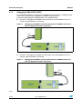
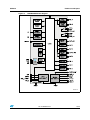
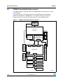
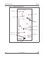
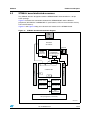
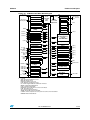
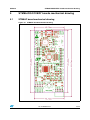
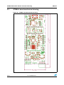
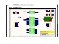
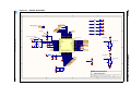
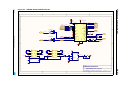
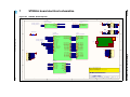
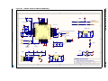
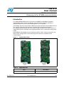
UM1574 User manual STM8A-DISCOVERY Discovery kit for STM8A microcontrollers Introduction The STM8A-DISCOVERY helps you discover the STM8AF and STM8AL automotive microcontroller family features and develop your applications through two dedicated application boards that can be connected together via a LIN network. The STM8AF board can perform both CAN and LIN communications with the MCU powered at 5 V and is ready to be connected into a network with its integrated transceiver. The STM8AL board manages LIN slave communication through its transceiver and uses a 4-digit alphanumeric LCD display with the MCU powered at 3.3 V, offering low energy power modes. Both STM8AF and STM8AL boards include push buttons, LEDs, external connectors and allow various configurations to take advantage of the numerous capabilities of the microcontrollers. Figure 1. STM8A-DISCOVERY STM8AF board Figure 2. November 2012 STM8AL board Applicable tools Type Part number Evaluation tools STM8A-DISCOVERY Doc ID 023645 Rev 1 1/48 www.st.com Contents UM1574 Contents 1 Conventions . . . . . . . . . . . . . . . . . . . . . . . . . . . . . . . . . . . . . . . . . . . . . . . . 6 2 Quick start . . . . . . . . . . . . . . . . . . . . . . . . . . . . . . . . . . . . . . . . . . . . . . . . . 7 2.1 Getting started . . . . . . . . . . . . . . . . . . . . . . . . . . . . . . . . . . . . . . . . . . . . . . 7 2.2 System requirements . . . . . . . . . . . . . . . . . . . . . . . . . . . . . . . . . . . . . . . . . 7 2.3 Development toolchains supporting the STM8A-DISCOVERY . . . . . . . . . 7 3 Features . . . . . . . . . . . . . . . . . . . . . . . . . . . . . . . . . . . . . . . . . . . . . . . . . . . 8 4 Hardware and layout . . . . . . . . . . . . . . . . . . . . . . . . . . . . . . . . . . . . . . . . . 9 4.1 4.2 4.3 5 4.1.1 Embedded ST-LINK/V2 . . . . . . . . . . . . . . . . . . . . . . . . . . . . . . . . . . . . . . 9 4.1.2 Debugging STM8A-DISCOVERY . . . . . . . . . . . . . . . . . . . . . . . . . . . . . 10 4.1.3 Power supply . . . . . . . . . . . . . . . . . . . . . . . . . . . . . . . . . . . . . . . . . . . . . 11 4.1.4 L99PM62GXP power management IC with LIN and high speed CAN . 11 STM8AF board dedicated resources . . . . . . . . . . . . . . . . . . . . . . . . . . . . 14 4.2.1 STM8AF5288T microcontroller . . . . . . . . . . . . . . . . . . . . . . . . . . . . . . . 17 4.2.2 STM8AF board LEDs . . . . . . . . . . . . . . . . . . . . . . . . . . . . . . . . . . . . . . . 19 4.2.3 STM8AF board Push buttons . . . . . . . . . . . . . . . . . . . . . . . . . . . . . . . . 19 4.2.4 STM8AF board solder bridges . . . . . . . . . . . . . . . . . . . . . . . . . . . . . . . . 20 4.2.5 STM8AF board jumpers selection . . . . . . . . . . . . . . . . . . . . . . . . . . . . . 21 4.2.6 STM8AF board extension connection . . . . . . . . . . . . . . . . . . . . . . . . . . 21 STM8AL board dedicated resources . . . . . . . . . . . . . . . . . . . . . . . . . . . . 23 4.3.1 STM8AL3L68T microcontroller . . . . . . . . . . . . . . . . . . . . . . . . . . . . . . . 26 4.3.2 STM8AL board LEDs . . . . . . . . . . . . . . . . . . . . . . . . . . . . . . . . . . . . . . . 28 4.3.3 STM8AL board Push buttons . . . . . . . . . . . . . . . . . . . . . . . . . . . . . . . . . 28 4.3.4 STM8AL board built-in IDD measurement circuit . . . . . . . . . . . . . . . . . . 28 4.3.5 STM8AL board LCD (16 segments, 4 commons) . . . . . . . . . . . . . . . . . 31 4.3.6 STM8AL board solder bridges . . . . . . . . . . . . . . . . . . . . . . . . . . . . . . . . 33 4.3.7 STM8AL board jumpers selection . . . . . . . . . . . . . . . . . . . . . . . . . . . . . 33 4.3.8 STM8AL board extension connection . . . . . . . . . . . . . . . . . . . . . . . . . . 34 STM8A-DISCOVERY boards mechanical drawing . . . . . . . . . . . . . . . . 35 5.1 2/48 STM8A-DISCOVERY common resources . . . . . . . . . . . . . . . . . . . . . . . . . 9 STM8AF board mechanical drawing . . . . . . . . . . . . . . . . . . . . . . . . . . . . 35 Doc ID 023645 Rev 1 UM1574 Contents 5.2 STM8AL board mechanical drawing . . . . . . . . . . . . . . . . . . . . . . . . . . . . 36 6 STM8AF board electrical schematics . . . . . . . . . . . . . . . . . . . . . . . . . . 37 7 STM8AL board electrical schematics . . . . . . . . . . . . . . . . . . . . . . . . . . 41 8 Revision history . . . . . . . . . . . . . . . . . . . . . . . . . . . . . . . . . . . . . . . . . . . 47 Doc ID 023645 Rev 1 3/48 List of tables UM1574 List of tables Table 1. Table 2. Table 3. Table 4. Table 5. Table 6. Table 7. Table 8. Table 9. Table 10. Table 11. Table 12. 4/48 ON/OFF conventions . . . . . . . . . . . . . . . . . . . . . . . . . . . . . . . . . . . . . . . . . . . . . . . . . . . . . . 6 STM8AF board solder bridges . . . . . . . . . . . . . . . . . . . . . . . . . . . . . . . . . . . . . . . . . . . . . . 20 STM8AF board jumper selection . . . . . . . . . . . . . . . . . . . . . . . . . . . . . . . . . . . . . . . . . . . . 21 STM8AF board P1 pinout microcontroller connectivity . . . . . . . . . . . . . . . . . . . . . . . . . . . . 21 STM8AF board P2 pinout microcontroller connectivity . . . . . . . . . . . . . . . . . . . . . . . . . . . . 22 STM8AF board P3 pinout L99PM62GXP connectivity . . . . . . . . . . . . . . . . . . . . . . . . . . . . 22 LCD connections . . . . . . . . . . . . . . . . . . . . . . . . . . . . . . . . . . . . . . . . . . . . . . . . . . . . . . . . 32 STM8AL board solder bridges . . . . . . . . . . . . . . . . . . . . . . . . . . . . . . . . . . . . . . . . . . . . . . 33 STM8AL board jumpers selection. . . . . . . . . . . . . . . . . . . . . . . . . . . . . . . . . . . . . . . . . . . . 33 STM8AL board P1 pinout Microcontroller connectivity . . . . . . . . . . . . . . . . . . . . . . . . . . . . 34 STM8AL board P2 pinout L99PM62GXP connectivity . . . . . . . . . . . . . . . . . . . . . . . . . . . . 34 Document revision history . . . . . . . . . . . . . . . . . . . . . . . . . . . . . . . . . . . . . . . . . . . . . . . . . 47 Doc ID 023645 Rev 1 UM1574 List of figures List of figures Figure 1. Figure 2. Figure 3. Figure 4. Figure 5. Figure 6. Figure 7. Figure 8. Figure 9. Figure 10. Figure 11. Figure 12. Figure 13. Figure 14. Figure 15. Figure 16. Figure 17. Figure 18. Figure 19. Figure 20. Figure 21. Figure 22. Figure 23. Figure 24. Figure 25. Figure 26. Figure 27. Figure 28. Figure 29. Figure 30. STM8A-DISCOVERY . . . . . . . . . . . . . . . . . . . . . . . . . . . . . . . . . . . . . . . . . . . . . . . . . . . . . . 1 Applicable tools. . . . . . . . . . . . . . . . . . . . . . . . . . . . . . . . . . . . . . . . . . . . . . . . . . . . . . . . . . . 1 Debugging the STM8AF microcontroller when the STM8AL board or an external application board is connected . . . . . . . . . . . . . . . . . . . . . . . . . . . . . . . . . . . . . . . 10 Debugging the STM8AL microcontroller when the STM8AF board or an external application board is connected . . . . . . . . . . . . . . . . . . . . . . . . . . . . . . . . . . . . . . . 10 L99PM62GXP block diagram . . . . . . . . . . . . . . . . . . . . . . . . . . . . . . . . . . . . . . . . . . . . . . . 13 STM8AF board hardware block diagram . . . . . . . . . . . . . . . . . . . . . . . . . . . . . . . . . . . . . . 14 STM8AF board top layout . . . . . . . . . . . . . . . . . . . . . . . . . . . . . . . . . . . . . . . . . . . . . . . . . . 15 STM8AF board bottom layout . . . . . . . . . . . . . . . . . . . . . . . . . . . . . . . . . . . . . . . . . . . . . . . 16 STM8AF5288T package . . . . . . . . . . . . . . . . . . . . . . . . . . . . . . . . . . . . . . . . . . . . . . . . . . . 17 STM8AF5288T block diagram . . . . . . . . . . . . . . . . . . . . . . . . . . . . . . . . . . . . . . . . . . . . . . 18 STM8AL board hardware block diagram . . . . . . . . . . . . . . . . . . . . . . . . . . . . . . . . . . . . . . 23 STM8AL board top layout . . . . . . . . . . . . . . . . . . . . . . . . . . . . . . . . . . . . . . . . . . . . . . . . . . 24 STM8AL board bottom layout . . . . . . . . . . . . . . . . . . . . . . . . . . . . . . . . . . . . . . . . . . . . . . . 25 STM8AL3L68T package . . . . . . . . . . . . . . . . . . . . . . . . . . . . . . . . . . . . . . . . . . . . . . . . . . . 26 STM8AL3L68T MCU block diagram . . . . . . . . . . . . . . . . . . . . . . . . . . . . . . . . . . . . . . . . . 27 STM8AL board IDD measurement circuit . . . . . . . . . . . . . . . . . . . . . . . . . . . . . . . . . . . . . . 29 STM8AL board IDD Low power mode measurement timing diagram . . . . . . . . . . . . . . . . . 30 LCD segment mapping . . . . . . . . . . . . . . . . . . . . . . . . . . . . . . . . . . . . . . . . . . . . . . . . . . . . 31 STM8AF board mechanical drawing. . . . . . . . . . . . . . . . . . . . . . . . . . . . . . . . . . . . . . . . . . 35 STM8AL board mechanical drawing . . . . . . . . . . . . . . . . . . . . . . . . . . . . . . . . . . . . . . . . . . 36 STM8AF board top level . . . . . . . . . . . . . . . . . . . . . . . . . . . . . . . . . . . . . . . . . . . . . . . . . . . 37 STM8AF board ST-LINK/V2 (SWIM only). . . . . . . . . . . . . . . . . . . . . . . . . . . . . . . . . . . . . . 38 STM8AF board MCU . . . . . . . . . . . . . . . . . . . . . . . . . . . . . . . . . . . . . . . . . . . . . . . . . . . . . 39 STM8AF board CAN/LIN and 12V . . . . . . . . . . . . . . . . . . . . . . . . . . . . . . . . . . . . . . . . . . . 40 STM8AL board top level . . . . . . . . . . . . . . . . . . . . . . . . . . . . . . . . . . . . . . . . . . . . . . . . . . . 41 STM8AL board ST-LINK/V2 (SWIM only). . . . . . . . . . . . . . . . . . . . . . . . . . . . . . . . . . . . . . 42 STM8AL board MCU . . . . . . . . . . . . . . . . . . . . . . . . . . . . . . . . . . . . . . . . . . . . . . . . . . . . . 43 STM8AL board LCD . . . . . . . . . . . . . . . . . . . . . . . . . . . . . . . . . . . . . . . . . . . . . . . . . . . . . . 44 STM8AL board IDD_measurement . . . . . . . . . . . . . . . . . . . . . . . . . . . . . . . . . . . . . . . . . . 45 STM8AL board LIN and 12V. . . . . . . . . . . . . . . . . . . . . . . . . . . . . . . . . . . . . . . . . . . . . . . . 46 Doc ID 023645 Rev 1 5/48 Conventions 1 UM1574 Conventions Table 1 provides the definitions of some conventions used in the present document. Table 1. ON/OFF conventions Convention 6/48 Definition Jumper JPx ON Jumper fitted Jumper JPx OFF Jumper not fitted Jumper JPx 1-2 Jumper is fitted between pins 1 and 2 Jumper JPx 2-3 Jumper is fitted between pins 2 and 3 Solder bridge SBx ON SBx connections closed by solder Solder bridge SBx OFF SBx connections left open Doc ID 023645 Rev 1 UM1574 2 Quick start Quick start The STM8A-DISCOVERY is a low-cost and easy-to-use development kit to quickly evaluate and start a development with STM8AF and STM8AL microcontrollers family devices. STM8AF devices offer high performance and full automotive network connectivity with high speed CAN and LIN master/slave modes communications. STM8AL devices offer high performance with ultra-low power management. Both comply with automotive qualification and conform to AEC-Q100 rev G. For more information on the STM8A-DISCOVERY and for demonstration software, visit www.st.com/stm8a-discovery. 2.1 Getting started 1. Connect CN3 and CN4 on the STM8AF board to CN3 and CN4 on the STM8AL board. 2. Connect both type A connectors of the USB cable to a PC. 3. Then connect the mini-B connector of the USB cable to the STM8AF board. 4. All LEDs blink once on the STM8AF board and twice on the STM8AL board, then the LIN communication between both boards starts. 5. Turn the RV1 trimmer on the STM8AF board to adjust the value from 0 to 100 on the STM8AL board LCD through the LIN bus. 6. Push button USER1 on the STM8AF board to sequentially display the LCD bars on the STM8AL board through the LIN bus. Push button USER2 on the STM8AF board to sequentially switch them off one by one. 7. Push button USER1 on the STM8AL board to sequentially switch on green LEDs LD4, LD5, LD6 and LD7 on the STM8AF board through the LIN bus. Push button USER2 on the STM8AL board to sequentially switch them off one by one. 8. To perform or modify the Discover project related to this demo, visit www.st.com/stm8adiscovery. 9. You can discover the STM8AF and STM8AL features, download and execute programs proposed in the list of projects. 10. You can then develop your own application using the available examples. 2.2 2.3 System requirements ● Windows PC (XP, Vista, 7) ● USB cable (dual type A to mini-B) - included Development toolchains supporting the STM8A-DISCOVERY ● IAR: EWSTM8 ● STMicroelectronics: STVD Doc ID 023645 Rev 1 7/48 Features 3 UM1574 Features The STM8A-DISCOVERY offers different features combined with STM8AF and STM8AL boards: STM8AF and STM8AL common board features: ● On-board ST-LINK/V2 included for debugging and programming ● Board power supply: through 5 V USB bus ● Internal dual ST662A step-up converter building the 12 Vdc when powered by USB port ● External application power supply VBAT (up to 14 Vdc) ● 16 MHz HSE XTAL crystal oscillator ● L99PM62GXP power management IC with LIN and high speed CAN with SPI control interface and high-side drivers ● Two push buttons (USER1 and USER2) ● Extension header for L99PM62GXP including relays, high-side outputs and wake-up capabilities STM8AF dedicated board features: ● STM8AF5288T microcontroller featuring 64 Kbytes Flash, 2 Kbytes data EEPROM, LIN, CAN in an 48-pin package ● Seven LEDs: – LD1 (red/green) for USB communication – LD2 (red) for 5 V power ON – Five user LEDs LD3 (red) and LD4 to LD7 (green) ● RV1 potentiometer connected to the ADC peripheral ● Extension headers for MCU connectivity (full Port B, free ports pins, RESET) STM8AL dedicated board features: 8/48 ● STM8AL3L68T microcontroller featuring 32 Kbytes Flash, 1 Kbytes data EEPROM, LCD in an 48-pin package ● Four LEDs: – LD1 (red/green) for USB communication – LD2 (red) for 3.3 V power ON – 2 user LEDs LD3 (red) and LD4 (green) ● 4-digit alphanumeric LCD display including 4 bars display ● Extension header for MCU connectivity (free ports pins, RESET) Doc ID 023645 Rev 1 UM1574 4 Hardware and layout Hardware and layout This section describes STM8A-DISCOVERY hardware and layout which can be broken down into common resources used both in STM8AF and STM8AL boards and the special features belonging to each of them. 4.1 STM8A-DISCOVERY common resources 4.1.1 Embedded ST-LINK/V2 The ST-LINK/V2 programming and debugging tool is integrated both in STM8AF and STM8AL boards. The embedded ST-LINK/V2 can be used to program/debug the MCU on the board and supports SWIM for STM8 devices. The ST-LINK/V2 must be connected with the dual type A to mini-B USB cable provided in the blister. Caution: First connect the dual type A on the PC side (both type A connectors must be plugged in) then connect the mini-B USB to the board (STM8AF or STM8AL boards). For programming or debugging the STM8A-DISCOVERY, the PC can be either connected to the mini-B USB connector of the STM8AF or STM8AL board. The connection on both mini-B usb of the STM8AF and STM8AL boards is not supported. This operation can damage the boards. For information about debugging and programming features refer to user manual UM1075 (ST-LINK/V2 in-circuit debugger/programmer for STM8 and STM32) which describes in detail all the ST-LINK/V2 features. Doc ID 023645 Rev 1 9/48 Hardware and layout 4.1.2 UM1574 Debugging STM8A-DISCOVERY The STM8A-DISCOVERY is composed by a STM8AF board connected to a STM8AL board. A PC can be connected to the STM8AF or STM8AL board side while programming/debugging the STM8AF5288T or the STM8AL3L68T. ● Example 1: Debugging the STM8AF microcontroller when the STM8AL board or an external application board is connected. Figure 3. ● Example 2: Debugging the STM8AL microcontroller when the STM8AF board or an external application board is connected. Figure 4. Note: 10/48 Debugging the STM8AF microcontroller when the STM8AL board or an external application board is connected Debugging the STM8AL microcontroller when the STM8AF board or an external application board is connected All other configuration are not supported and could damage the boards or the PC. Doc ID 023645 Rev 1 UM1574 4.1.3 Hardware and layout Power supply The power supply is provided by the host PC through the dual type A to mini-B USB cable or by an external VBAT power supply (12 Vdc typical, 14 Vdc max). One dual type A to mini-B USB is needed to provide the current required by the STM8AF and STM8AL boards when they are connected together. Reminder: First connect the dual type A on the PC side (both type A connectors must be plugged in) then connect the mini-B USB to one of the STM8Ax boards. When the STM8AF board is connected to the STM8AL board, different schemes are possible: ● The USB cable is used to simply provide the power supply to the STM8A-DISCOVERY. In that case, it can be connected either to the STM8AF or STM8AL board side. ● While programming/debugging the STM8AF or STM8AL board with your PC, the USB cable must be placed on the appropriate side of the board depending on which board is being debugged (see Figure 3 and Figure 4). ● If no programming/debugging operations are needed (no PC connected) or if a larger amount of current is required (higher than 200 mA @5 V), then the power supply must be wired between the VBAT and GND pins of the STM8AF or STM8AL board. VBAT is indeed internally distributed through the two boards. Therefore, VBAT can be wired indifferently on the STM8AF or STM8AL board (not on both). On the other hand, if the STM8AF or STM8AL board is used in standalone (not connected together), they can be supplied either by the USB cable or by the external VBAT. As for instance, this configuration can be used when the boards are inserted in an automotive network. The STM8AF and STM8AL boards include an internal 5 V to 12 V step-up converter that is needed to build the voltages required for LIN or CAN networks. The 5 V USB is then converted into 12 V voltage that supplies the integrated L99PM62GXP power management IC. This device includes a 5 V regulator which is connected directly to the STM8AF5288T microcontroller or transformed subsequently into 3.3 V to supply the STM8AL3L68T microcontroller. The power supplies of STM8AF5288T and STM8AL3L68T are provided by the L99PM62GXP power management IC on condition that the microcontrollers sequentially refresh the watchdog included in the L99PM62GXP devices. This functionality exists when the L99PM62GXP is in Active mode (standard operation). In that case, if the L99PM62GXP device is not refreshed periodically, the 5 V power supply is provisionally shutdown until a next start-up sequence is performed. This behavior can generate some issues when the SWIM communication tries to establish a connection with the microcontroller and when the latter is not power supplied. To remedy to this situation and to avoid caring about L99PM62GXP watchdog refresh, the L99PM62GXP can be placed in Flash mode by configuring some dedicated jumpers (see Section 4.2.5). This prevents to cut the power supply to the microcontroller as for instance for software debugging. This behavior is only present on the STM8AF board as the STM8AL board is always put in Flash mode by design. 4.1.4 L99PM62GXP power management IC with LIN and high speed CAN The L99PM62GXP is a power management system IC that provides electronic control units with enhanced system power supply functionality, including various standby modes, as well as LIN and HS CAN physical communication layers. The device's two low-drop voltage regulators supply the system microcontroller and external peripheral loads such as sensors Doc ID 023645 Rev 1 11/48 Hardware and layout UM1574 and provide enhanced system standby functionality with programmable local and remote wake-up capability. The microcontrollers of the STM8AF and STM8AL boards communicate with the L99PM62GXP IC through the SPI interface, that allows control and diagnosis of the device. A lot of features are offered to control low and high-side drivers using the embedded and configurable PWM timers, window watchdog, wake-up capability. Some of their outputs are available at external headers of the STM8AF and STM8AL boards. This device is a power SS0-36-pin package. Figure 5 illustrates the L99PM62GXP block diagram. For further information on the L99PM62GXP device and to explore its numerous capabilities, please refer to datasheet available at www.st.com. 12/48 Doc ID 023645 Rev 1 UM1574 Hardware and layout Figure 5. L99PM62GXP block diagram y MS31061V1 Doc ID 023645 Rev 1 13/48 Hardware and layout 4.2 UM1574 STM8AF board dedicated resources The STM8AF board is designed around the STM8AF5288T microcontroller in a 48-pin LQFP package. Figure 6 illustrates the connections between the STM8AF5288T and the different peripherals (ST-LINK/V2, L99PM62GXP IC, push buttons, LED and connectors). Figure 6 and Figure 7 help you locate these features on the STM8AF board. Figure 6. STM8AF board hardware block diagram Mini USB Embedded ST-LINK/V2 DC/DC converter 5V to 12V L99PM62GXP Power Management LIN transceiver LIN CAN CN3/CN4 P1 Header SWIM SPI 5V P3 Header STM8AF5288T I/O I/O P2 Header VBAT 5V USER1 button Red LED LD3 Green LED LD4 USER2 button Green LED LD5 RV1 potentiometer Green LED LD6 Green LED LD7 MS31074V1 14/48 Doc ID 023645 Rev 1 UM1574 Hardware and layout Figure 7. STM8AF board top layout ST-LINK/V2 LD1 (red/green LED) COM LD2 (red LED) PWR (red LED) LD3, (green LED) LD4, (green LED) LD5, (green LED) LD6, (green LED) LD7 STM8AF5288T JP3 (I DD measurement) L99PM62GXP JP1 (FLASH/LIN) VBAT ST662A B1 USER1 button JP2 (FLASH/CAN) B2 USER2 button CN3 Female external CN4 Male external RV1 potentiometer MS31065V2 Doc ID 023645 Rev 1 15/48 Hardware and layout Figure 8. UM1574 STM8AF board bottom layout SB1 (RESERVED) SB2 (STM_RST) SB3 (MCO) SB4, SB5 (RESERVED) SB6 (L99PM62GXP) SB7 (CAN supply) SB8 (Start-up delay) SB9 (CAN terminating resistor) SB10, SB11 (USB5V) SB12, SB13 (RESERVED) 16/48 Doc ID 023645 Rev 1 MS31063V1 UM1574 4.2.1 Hardware and layout STM8AF5288T microcontroller This automotive 8-bit MCU has 64 Kbytes Flash, 2 Kbytes data EEPROM, 10-bit ADC, timers, LIN, CAN, USART, SPI, I2C and operates from 3 to 5.5 V. Figure 9. STM8AF5288T package STM8AF5288T 64 Kbytes of Flash memory 2 Kbytes of EEPROM 4 Kbytes of RAM LQFP48 7x7 The STM8AF5288T automotive 8-bit microcontroller offers 64 Kbytes of non-volatile memory and integrated true data EEPROM. The STM8AF52xx series feature a CAN interface. All devices of the STM8A product line provide the following benefits: reduced system cost, performance and robustness, short development cycles, and product longevity. ● ● ● ● Reduced system cost – Integrated true data EEPROM for up to 300 k write/erase cycles – High system integration level with internal clock oscillators, watchdog and brownout reset Performance and robustness – Peak performance 20 MIPS at 24 MHz and average performance 10 MIPS at 16 MHz CPU clock frequency – Robust I/O, independent watchdogs with separate clock source – Clock security system Short development cycles – Applications scalability across a common family product architecture with compatible pinout, memory map and modular peripherals. – Full documentation and a wide choice of development tools Product longevity – Advanced core and peripherals made in a state-of-the art technology – Native automotive product family operating both at 3.3 V and 5 V supply The STM8AF and STM8AL boards are supported by the same tools including STVD/STVP development environment. Doc ID 023645 Rev 1 17/48 Hardware and layout UM1574 Figure 10. STM8AF5288T block diagram Reset block XTAL 1-24 MHz Clock controller Reset Reset RC int. 16 MHz Detector POR RC int. 128 kHz BOR Clock to peripherals and core Window WDG STM8A CORE IWDG Master/slave automatic resynchronization Up to 128 Kbyte high density program Flash Debug/SWIM LINUART 400 Kbit/s I2C 10 Mbit/s SPI Address and data bus Single wire debug interf. Up to 2 Kbytes data EEPROM Up to 6 Kbytes RAM Boot ROM LIN master SPI emul. USART 16-bit advanced control timer (TIM1) 1 Mbit/s beCAN 16-bit general purpose (TIM2, TIM3) Up to 16 channels 10-bit ADC Up to 9 CAPCOM channels 8-bit AR timer (TIM4) AWU timer MS31062V1 18/48 Doc ID 023645 Rev 1 UM1574 4.2.2 Hardware and layout STM8AF board LEDs The STM8AF board includes the following LEDs: 4.2.3 ● LD1 COM: LD1 default status is red. LD1 turns to green to indicate that communications are in progress between the PC and the ST-LINK/V2. ● LD2 PWR: red LED indicates that the board is powered and that 5 V is output from L99PM62GXP power management IC. ● User LD3: red LED is a user LED connected to the I/O PA3 of the STM8AF5288T. ● User LD4: green LED is a user LED connected to the I/O PD3 of the STM8AF5288T. ● User LD5: green LED is a user LED connected to the I/O PD0 of the STM8AF5288T. ● User LD6: green LED is a user LED connected to the I/O PE3 of the STM8AF5288T. ● User LD7: green LED is a user LED connected to the I/O PC3 of the STM8AF5288T. STM8AF board Push buttons STM8AF board includes two push buttons: ● USER1: User button connected to the I/O PE2 of STM8AF5288T. ● USER2: User button connected to the I/O PE1 of STM8AF5288T. Doc ID 023645 Rev 1 19/48 Hardware and layout UM1574 4.2.4 STM8AF board solder bridges Table 2. STM8AF board solder bridges Bridge State(1) SB1 (Reserved) ON Reserved, do not modify. SB2 (STM_RST) OFF NRST signal of STM32F103C8T6 (ST-LINK/V2) is not connected to GND. ON NRST signal of STM32F103C8T6 (ST-LINK/V2) is connected to GND. OFF MCO clock from STM32F103C8T6 is not connected to PA1 (OSC_IN) of STM8AF5288T. ON MCO clock from STM32F103C8T6 is connected to PA1 (OSC_IN) of STM8AF5288T. OFF Reserved, do not modify. SB6 (L99PM62GXP Reset) OFF NRESET of L99PM62GXP is not connected to the STM8AF5288T Reset pin (external watchdog disable). ON NRESET of L99PM62GXP is connected to the STM8AF5288T Reset pin (external watchdog enable). SB7 (CAN supply) ON CAN transceiver is powered ON. OFF CAN transceiver is OFF. This selection saves power consumption. OFF If the STM8AF board is connected to another STM8AF board, then one of them must have SB8 OFF. ON The STM8AF board is connected to the STM8AL board (standard demo package). ON The CAN terminating 120 Ohms resistor is connected on the CAN bus. OFF The CAN terminating 120 Ohms resistor is not connected on the CAN bus. ON USB5V is available on CN3/CN4 connectors for powering an external board through CN3/CN4. OFF USB5V is not available on CN3/CN4 connectors. ON Reserved, do not modify. SB3 (MCO) SB4,5 (Reserved) SB8 (Start-up delay) SB9 (CAN terminating resistor) SB10,11 (USB5V) SB12,13 (Reserved) Description 1. Default SBx state is shown in bold. 20/48 Doc ID 023645 Rev 1 UM1574 4.2.5 Hardware and layout STM8AF board jumpers selection Table 3. STM8AF board jumper selection Jumper State(1) JP1 (LIN/FLASH) 1-2 Flash mode selected (2). 2-3 LIN communication enabled. JP2 (CAN/FLASH) 1-2 Flash mode selected (2). 2-3 CAN communication enabled. ON Standard operation, 5 V connected to the VDD of the microcontroller. OFF An ammeter can be connected between JP3 pins to measure the current sunk by the MCU. OFF Reserved, do not modify. JP3 (IDD) JP4 (Reserved) Description 1. Default jumper state is shown in bold. 2. The Flash mode is activated if at least JP1 or JP2 selects Flash mode. 4.2.6 STM8AF board extension connection Male headers P1, P2 and P3 connectors can connect the STM8AF board to a standard prototyping/wrapping board. Free GPI/Os of the STM8AF5288T are available on P1 and P2. L99PM62GXP device I/Os are connected to P3. P1, P2 and P3 can also be probed by an oscilloscope, a logic analyzer or a voltmeter. P1 connector contains the full port B GPI/Os and the alternate functions are the first 8 ADC channel inputs. Its standard HE10 format complies with some additional modules or resources that are pin-to-pin equivalent. Table 4. STM8AF board P1 pinout microcontroller connectivity Pin number P1 Pin number STM8AF MCU Board pin name Type Main function Alternate function 1 22 PB0 I/O Port B0 Analog input AIN0 2 21 PB1 I/O Port B1 Analog input AIN1 3 20 PB2 I/O Port B2 Analog input AIN2 4 19 PB3 I/O Port B3 Analog input AIN3 5 18 PB4 I/O Port B4 Analog input AIN4 6 17 PB5 I/O Port B5 Analog input AIN5 7 16 PB6 I/O Port B6 Analog input AIN6 8 15 PB7 I/O Port B7 Analog input AIN7 9 VDD Microcontroller Digital power supply 10 GND Digital ground Doc ID 023645 Rev 1 21/48 Hardware and layout Table 5. Pin number P2 UM1574 STM8AF board P2 pinout microcontroller connectivity Pin number STM8AF MCU 1 Board pin name Type Main function GND Alternate function Digital ground 2 1 NRST I/O 3 48 PD7 I/O Port D7 TLI 4 45 PD4 I/O Port D4 Timer 2 - channel 1 5 43 PD2 I/O Port D2 Timer 3 - channel 1 6 12 PA6 I/O Port A6 USART synchronous clock 7 40 PE0 I/O Port E0 CCO Configurable clock output 8 24 PE6 I/O Port E6 Analog input AIN9 9 29 PC4 I/O Port C4 Timer 1 - channel 4 10 27 PC2 I/O Port C2 Timer 1 - channel 2 11 26 PC1 I/O Port C1 Timer 1 - channel 1 12 Table 6. Pin number P3 Reset Microcontroller Digital power supply VDD STM8AF board P3 pinout L99PM62GXP connectivity(1) Pin number Board pin STM8AF Type name MCU 1 Main function 5 V board power supply (output 5V1 from L99PM62GXP) 5V 2 20 WU1 I Wake-up input 1 3 28 OUT2 O High-side driver output (7 , typ.) 4 29 OUT1 O High-side driver output (7 , typ.) 5 30 O_HS O High-side driver (1 , typ.) 6 34 REL1 O Low-side driver output (2 typ.) 7 35 REL2 O Low-side driver output (2 typ.) 8 GND 9 VBAT Digital ground I External power supply (12 Vdc typ.) 1. For additional information on L99PM62GXP device connectivity, please refer to product datasheet available at www.st.com. 22/48 Doc ID 023645 Rev 1 UM1574 STM8AL board dedicated resources The STM8AL board is designed around the STM8AL3L68T microcontroller in a 48-pin LQFP package. Figure 11 illustrates the connections between the STM8AL3L68T and the different peripherals (ST-LINK/V2, L99PM62GXP IC, push buttons, LED, IDD measurement circuitry, LCD and connectors). Figure 11 and Figure 12 help you to locate these features on the STM8AL board. Figure 11. STM8AL board hardware block diagram Mini USB Embedded ST-LINK/V2 LIN CN3/CN4 DC/DC converter 5V to 12V L99PM62GXP Power Management LIN transceiver 5V SWIM SPI 3V3 VBAT 5V to 3V3 P2 Header STM8AL3L68T P1 Header 4.3 Hardware and layout I/O I/O USER1 button Red LED LD3 USER2 button Green LED LD4 IDD measurement LCD (16 segments, 4 commons) MS31075V1 Doc ID 023645 Rev 1 23/48 Hardware and layout UM1574 Figure 12. STM8AL board top layout LD1 (red/green LED) COM ST-LINK/V2 LD2 (red LED) PWR LCD 24 segments IDD module JP2 (I DD ) (red LED) LD3 STM8AL3L68T (green LED) LD4 JP3 (RESERVED) L99PM62GXP VBAT B1 USER1 button B2 USER2 button ST662A CN3 Male external CN4 Female external MS31065V1 24/48 Doc ID 023645 Rev 1 UM1574 Hardware and layout Figure 13. STM8AL board bottom layout SB1 (RESERVED) SB2 (STM_RST) SB4, SB5 (RESERVED) SB3 (MCO) SB6, SB7, SB8 (IDD circuitry) SB9, SB10 (Xtal 32.768 kHZ) SB11 (L99M62GXP Reset) SB12 (RESERVED) SB13, SB14 (USB5V) SB15, SB16 (RESERVED) Doc ID 023645 Rev 1 MS31064V1 25/48 Hardware and layout 4.3.1 UM1574 STM8AL3L68T microcontroller This automotive 8-bit ultralow power MCU has 32 Kbytes Flash, 1 Kbytes data EEPROM, RTC, LCD, timers, USART, I2C, SPI, ADC, DAC and comparators. Figure 14. STM8AL3L68T package STM8AL3L68T 32 Kbytes of Flash memory 1 Kbytes of EEPROM 2 Kbytes of RAM LQFP48 7x7 This microcontroller belongs to the STM8AL family and provides the following benefits: ● ● ● ● Integrated system – Up to 32 Kbytes of medium-density embedded Flash program memory – 1 Kbyte of data EEPROM – Internal high speed and low-power low speed RC. – Embedded reset Ultralow power consumption – 195 µA/MHZ + 440 µA (consumption) – 0.9 µA with LSI in Active-halt mode – Clock gated system and optimized power management – Capability to execute from RAM for Low power wait mode and Low power run mode Advanced features – Up to 16 MIPS at 16 MHz CPU clock frequency – Direct memory access (DMA) for memory-to-memory or peripheral-to-memory access. Short development cycles – Application scalability across a common family product architecture with compatible pinout, memory map and modular peripherals. – Wide choice of development tools This device offers 12-bit ADC, DAC, two comparators, real-time clock, three 16-bit timers, one 8-bit timer as well as standard communication interfaces such as SPI, I2C and USART. A 4x28-segment LCD is available on the medium-density STM8AL3L68T device. 26/48 Doc ID 023645 Rev 1 UM1574 Hardware and layout Figure 15. STM8AL3L68T MCU block diagram OSC_IN, OSC_OUT 16 MHz internal RC OSC32_IN, OSC32_OUT @VDD 1-16 MHz oscillator 32 kHz oscillator Clock controller and CSS 38 kHz internal RC VDD18 Clocks to core and peripherals Interrupt controller Debug module (SWIM) BOR 16-bit Timer 2 2 channels 16-bit Timer 3 3 channels 16-bit Timer 1 8-bit Timer 4 Infrared interface DMA1 (4 channels) SCL, SDA, SMB I²C1 MOSI, MISO, SCK, NSS SPI1 RX, TX, CK VDDA VSSA ADC1_INx VREF+ VREF- VREFINT out COMP1_INP COMP2_INP COMP2_INM DAC_OUT VREF+ VLCD = 2.5 V to 3.6 V RESET POR/PDR 2 channels IR_TIM VOLT. REG. STM8 Core USART1 @VDDA/VSSA PVD Address, control and data buses SWIM Power 12-bit ADC1 VDD1 =1.65 V to 3.6 V VSS1 NRST PVD_IN 32 Kbytes Program memory 1 Kbyte Data EEPROM 2 Kbytes RAM Port A PA[7:0] Port B PB[7:0] Port C PC[7:0] Port D PD[7:0] Port E PE[7:0] Port F PF0 Temp sensor Internal reference voltage COMP 1 Beeper BEEP RTC ALARM, CALIB IWDG (38 kHz clock) WWDG COMP 2 12-bitDAC DAC 12-bit LCD driver 4x28 LCD booster SEGx, COMx 1. Legend: ADC: Analog-to-Digital Converter BOR: Brownout Reset DMA: Direct Memory Access DAC: Digital-to-Analog Converter I²C: Inter-Integrated Circuit multimaster interface IWDG: Independent WatchDoG LCD: Liquid Crystal Display POR/PDR: Power On Reset / Power Down Reset RTC: Real-Time Clock SPI: Serial Peripheral Interface SWIM: Single Wire Interface Module USART: Universal Synchronous Asynchronous Receiver Transmitter WWDG: Window WatchDoG Doc ID 023645 Rev 1 27/48 Hardware and layout 4.3.2 UM1574 STM8AL board LEDs The STM8AL board includes the following LEDs and their description is: LD1 COM: LD1 default status is red. LD1 turns to green to indicate that communications are in progress between the PC and the ST-LINK/V2. LD2 PWR: red LED indicates that the board is powered and that 3.3 V is generated by the regulator supplied by the L99PM62GXP power management IC. User LD3: red LED is a user LED connected to the I/O PE7 of the STM8AL3L68T. User LD4: green LED is a user LED connected to the I/O PC7 of the STM8AL3L68T. 4.3.3 STM8AL board Push buttons The STM8AL board includes two push buttons: 4.3.4 ● USER1: User button connected to the I/O PE1 of STM8AL3L68T. ● USER2: User button connected to the I/O PE2 of STM8AL3L68T. STM8AL board built-in IDD measurement circuit The STM8AL board built-in IDD measurement circuit allows the consumption of the STM8AL3L68T to be measured and displayed on the LCD Glass while the MCU is in Run or Low power saving modes. ● JP2 in ON position: STM8AL3L68T is powered through IDD measurement circuit (default). ● JP2 in OFF position: STM8AL3L68T is powered directly by +3V3, IDD measurement circuit is bypassed. Note: When jumper JP2 is removed the current consumption of the STM8AL3L68T can be measured by connecting an ammeter between jumper JP2 pin 1 and pin 2. For IDD measurement by the MCU itself, the circuit below is implemented on the STM8AL board. Solder bridges SB6, SB7 and SB8 must be closed and a jumper must be plugged between JP2 pin 2 and pin 3. 28/48 Doc ID 023645 Rev 1 UM1574 Hardware and layout Figure 16. STM8AL board IDD measurement circuit IDD Measure V DD on JP2 5 3V3 1 1 3 2 off 4 2 R23 2(1%) U8 MAX9938FEUK+ U9 1 3 I/O 4 C 3 GND R24 O/I VCC 2 5 R25 R22 10K 0 C14 1uF 3V3 PF0 SB6 IDD_Measurement 74H1G66STR 4 2K(1%) 5 U4 74LX1G04CTR 3V3 U7 U5 S1 G1 S2 G2 D1 D1 D2 D2 8 7 6 5 SB8 STS4 DPF20L R28 47K PE6 IDD_WAKEUP Q12 VCC Q13 Q10 Q14 Q8 Q6 Q9 Q5 CLR Q7 CI Q4 CO GND CO 16 15 14 13 12 11 10 9 C15 100nF 3V3 R26 10K M74HC4060TTR PC4 SB7 C16 1nF R29 15K I DD_CNT_EN R27 30K Oscillator frequency 30 KHz ● Run mode AF 3V3 1 2 3 4 1 2 3 4 5 6 7 8 T 2 3 MS31059V1 In Run mode, IDD current is measured using the operational amplifier MAX9938FEUK+ (U8) connected to the 2 shunt resistor (R23). In this case IDD_CNT_EN remains high during measurement, so R24 remains in short-circuit during the measurement because of switch U5 which remains ON permanently. The jumper JP2 must be connected between pins 2 and 3 of JP2. The measurement range in this case can be up to 30 mA. ● Low power mode In Low power modes (Halt or Active halt), IDD current is measured using the operational amplifier MAX9938FEUK+ (U8) connected to the 2 K shunt resistor (R24), controlled by the switch STS4DPF20L (U5). In this case the counter 74HC4060 (U7) enabled by IDD_CNT_EN manages the measurement timing according to Figure 17. The measurement range in this case can be up to 30 µA. ● Low power mode IDD measurement principle The principle used to measure a current when the STM8AL3L68T is in Low power mode is: 1. Configure ADC to measure voltage on the IDD_Measurement pin. 2. Configure PE6 to serve as wakeup pin. 3. Enter Low power mode after setting IDD_CNT_EN (PC4) signal low. 4. IDD_WAKEUP rising edge wakes up the MCU after around 300 ms. 5. Start ADC conversion as soon as possible after wakeup in order to measure the voltage corresponding to Low power mode on capacitor C14. 6. Reset the counter by programming IDD_CNT_EN high (in less than 70 ms after the wakeup) to avoid the R24 2 K resistor being connected later in Run mode. Doc ID 023645 Rev 1 29/48 Hardware and layout UM1574 The measurement timing is given in Figure 17. In Low power modes, the 2 K resistor is connected when the U5 switch goes off after entering Low power mode. The Q13 output of the counter allows connection of the 2 K resistor when the current IDD becomes very low. Figure 17 shows how the counter and U5 ensure that, 150 ms after IDD_CNT_EN falling edge, the shunt resistor R24 is connected between VDD_MCU and the power supply in order to reduce the measurement range to 30 µA full scale (instead of 30 mA in Run mode). Then after another 150 ms for current stabilization, R24 is shorted, the IDD measurement is stored in C14, and the MCU is woken up. After wakeup, the MCU can measure the IDD current corresponding to the Low power mode stored in C14. Figure 17. STM8AL board IDD Low power mode measurement timing diagram Wake-up period IDD measurement Wake-up event MCU mode Run Clear CNT event Low power 5 IDD_CNT_EN 3 6 Q13 = LOW_POWER_EN 4 Q14 = IDD_WAKEUP Q14n = U4 pin 4 0 ms ● 150 ms 300 ms Ibias current measurement procedure In Low power mode the bias current of operational amplifier input (U8 pin 4) is not negligible compared to IDD current (typical Ibias is ~240 nA). To obtain a reliable STM8AL3L68T IDD measurement, it is mandatory to subtract the bias current from the IDD low power measurement since MCU is not sinking the current. Ibias is measured during production test and stored in the MCU EPROM. The demonstration software, Discover, uses this value to display the correct IDD. The Ibias measurement procedure is part of the demonstration software and can be launched if required. The procedure for Ibias measurement (implemented in the package demo) is: 30/48 1. Power off the board (disconnect the USB cable). 2. Set jumper JP2 to OFF position (pins 1 and 2). 3. Push down USER2 button while powering on the board from the USB. 4. Wait at least 1 second before releasing USER2, the LCD displays the Ibias measurement. 5. Power off the board (disconnect the USB cable). 6. Set jumper JP2 to ON position (pins 2 and 3). The Ibias value is now stored. The bias current is then subtracted from the IDD measurement performed in Low power mode. Doc ID 023645 Rev 1 UM1574 4.3.5 Hardware and layout STM8AL board LCD (16 segments, 4 commons) This LCD allows the STM8AL3L68T to display any information on four 14-segment digits and 4 BARs, using all COMs. (See the LCD segment mapping in Figure 18 and pin connections in Table 7). The two first left digits of the LCD display are not used in this application. Characteristics overview: Note: ● 16 segments and 4 commons ● Drive method: multiplexed 1/4 duty, 1/3 bias ● Operating voltage: 3 V ● Operating temperature: 0 to 50°C ● Connector: 28-pin DIL 2.54 mm pitch When the LCD is plugged in, all I/O ports listed in Table 7 are unavailable. To use one of these as I/O, you must remove the LCD Figure 18. LCD segment mapping Doc ID 023645 Rev 1 31/48 Hardware and layout Table 7. UM1574 LCD connections STM8AL3L68T Pin Name 32/48 LCD PIN COM3 COM2 COM1 COM0 1 1N 1P 1D 1E 2 1DP 1COLON 1C 1M 3 2N 2P 2D 2E 4 2DP 2COLON 2C 2M PE3_LCDSEG4 5 3N 3P 3D 3E PE4_LCDSEG5 6 3DP 3COLON 3C 3M PE5_LCDSEG6 7 4N 4P 4D 4E PD0_LCDSEG7 8 4DP 4COLON 4C 4M PD2_LCDSEG8 9 5N 5P 5D 5E PD3_LCDSEG9 10 BAR2 BAR3 5C 5M PB0_LCDSEG10 11 6N 6P 6D 6E PB1_LCDSEG11 12 BAR0 BAR1 6C 6M PD1_LCDCOM3 13 COM3 PA6_LCDCOM2 14 PA5_LCDCOM1 15 PA4_LCDCOM0 16 PB2_LCDSEG12 17 6J 6K 6A 6B PB3_LCDSEG13 18 6H 6Q 6F 6G PA7_LCDSEG0 19 5J 5K 5A 5B PE0_LCDSEG1 20 5H 5Q 5F 5G PD6_LCDSEG20 21 4J 4K 4A 4B PD7_LCDSEG21 22 4H 4Q 4F 4G PD4_LCDSEG18 23 3J 3K 3A 3B PD5_LCDSEG19 24 3H 3Q 3F 3G 25 2J 2K 2A 2B 26 2H 2Q 2F 2G 27 1J 1K 1A 1B 28 1H 1Q 1F 1G COM2 COM1 COM0 Doc ID 023645 Rev 1 UM1574 Hardware and layout 4.3.6 STM8AL board solder bridges Table 8. STM8AL board solder bridges Bridge State SB1 (Reserved) ON Description Reserved, do not modify. OFF NRST signal of STM32F103C8T6 (ST-LINK/V2) is not connected to GND. SB2 (STM_RST) ON NRST signal of STM32F103C8T6 (ST-LINK/V2) is connected to GND. OFF MCO clock from STM32F103C8T6 is not connected to PA2 (OSC_IN) of STM8AL3L68T. ON MCO clock from STM32F103C8T6 is connected to PA2 (OSC_IN) of STM8AL3L68T. SB3 (MCO) SB4, 5 (Reserved) SB6, 7, 8 (IDD circuitry) OFF Reserved, do not modify. ON IDD measurement circuitry and features connected. OFF IDD measurement circuitry and features are not connected (freeing PF0, PC4 and PE6). OFF PC5 and PC6 of STM8AL3L68T are free for general purpose I/Os. SB9, 10 (Xtal 32.768 kHz) ON PC5 and PC6 of STM8AL3L68T are connected to 32.768 kHz crystal oscillator (if fitted on board). SB11 (L99PM62GXP Reset) OFF NRESET of L99PM62GXP is not connected to STM8AL3L68T Reset pin (external watchdog disable). ON NRESET of L99PM62GXP is connected to STM8AL3L68T Reset pin (external watchdog enable). SB12 (Reserved) ON Reserved, do not modify. ON USB5V is distributed on CN3/CN4 connectors (USB5V can drive an external board connected to CN3 and CN4). SB13, 14 (USB5V) OFF USB5V is not distributed on CN3/CN4 connectors. SB15, 16 (Reserved) ON Reserved, do not modify. 1. Default SBx state is shown in bold. 4.3.7 STM8AL board jumpers selection Table 9. STM8AL board jumpers selection Jumper State(1) JP1 (Reserved) OFF Description Reserved, do not modify. 1-2 OFF Ibias measurement selection. JP2 (IDD) JP3 (Reserved) 2-3 ON IDD measurement selection. 2-3 Reserved, do not modify. 1. Default jumper state is shown in bold. Doc ID 023645 Rev 1 33/48 Hardware and layout 4.3.8 UM1574 STM8AL board extension connection Male headers P1 and P2 connectors can connect the STM8AL board to a standard prototyping/wrapping board. Free GPI/Os of STM8AL3L68T are available on P1. L99PM62GXP device I/Os are connected to P2. P1 and P2 can also be probed by an oscilloscope, a logic analyzer or a voltmeter. Table 10. Pin number P1 STM8AL board P1 pinout Microcontroller connectivity Pin number STM8AL MCU 1 Board pin name Type GND Main function Alternate function Digital ground 2 2 NRST I/O Reset PA1 3 45 PC6 I/O Port C6 OSC32_OUT 4 44 PC5 I/O Port C5 OSC32_IN 5 38 PC1 I/O Port C1 I2C1_SCL 6 37 PC0 I/O Port C0 I2C1_SDA 7 10 VDD Microcontroller Digital power supply 5V 5V board power supply (output 5V1 from L99PM62GXP) 8 Table 11. Pin number P2 STM8AL board P2 pinout L99PM62GXP connectivity(1) Pin number L99PM62GXP 1 Board pin name Type Main function 3.3 V board power supply (output 3.3 V from U11 PWR_STM8) 3V3 2 20 WU1 I Wake-up input 1 3 28 OUT2 O High-side driver output (7 , typ.) 4 29 OUT1 O High-side driver output (7 , typ.) 5 30 O_HS O High-side driver (1 , typ.) 6 34 REL1 O Low-side driver output (2 typ.) 7 35 REL2 O Low-side driver output (2 typ.) 8 GND 9 VBAT Digital ground I External power supply (12Vdc typ.) 1. For additional information on L99PM62GXP device connectivity, please refer to product datasheet available at www.st.com. 34/48 Doc ID 023645 Rev 1 UM1574 STM8A-DISCOVERY boards mechanical drawing 5 STM8A-DISCOVERY boards mechanical drawing 5.1 STM8AF board mechanical drawing Figure 19. STM8AF board mechanical drawing Doc ID 023645 Rev 1 35/48 STM8A-DISCOVERY boards mechanical drawing 5.2 STM8AL board mechanical drawing Figure 20. STM8AL board mechanical drawing 36/48 Doc ID 023645 Rev 1 UM1574 STM8AF board electrical schematics UM1574 6 Figure 21. STM8AF board top level 1 2 3 4 CN3 VBAT U_ST_LINK ST_LINK_V2.SCHDOC P1 PB0 PB2 PB4 PB6 A 1 3 5 7 9 VDD 2 4 6 8 10 PB1 PB3 PB5 PB7 PA4 PA5 STM8AF_USART_RX STM8AF_USART_TX USB5V MCO PA4 PA5 ST_LINK_SWIM NRST MCO SB13 LIN SB11 CANL CANH ST_LINK_SWIM NRST 2 4 6 8 10 1 3 5 7 9 A Header F 90° 5x2H CN4 CANH CANL Header 5X2 USB5V SB10 LIN SB12 VBAT 10 8 6 4 2 9 7 5 3 1 Header M 90° 5X2H GND Test Point U_STM8AF STM8AF.SchDoc Doc ID 023645 Rev 1 LIN_TX LIN_RX TP1 TP4 B SPI_MISO SPI_MOSI SPI_SCK SPI_NSS TP5 TP3 TP2 CAN_TX CAN_RX PD2 PD4 PD7 P2 NRST PD7 PD4 PD2 PA6 PE0 PE6 PC4 PC2 PC1 PC1 PC2 PC4 LIN_TX LIN_RX NRST ST_LINK_SWIM SPI_MISO SPI_MOSI SPI_SCK SPI_NSS CAN_TX CAN_RX PD2 PD4 PD7 PC1 PC2 PC4 MCO PA4 PA5 PA6 PB0 PB1 PB2 PB3 PB4 PB5 PB6 PB7 PE0 PE6 ST_LINK_SWIM USB B MCO PA4 PA5 PA6 Male STM8AF_USART_RX STM8AF_USART_TX PB0 PB1 PB2 PB3 PB4 PB5 PB6 PB7 P3 5V PE0 PE6 VDD WU1 OUT2 OUT1 OUT_HS REL1 REL2 VBAT Header 12 1 2 3 4 5 6 7 8 9 C Header 9 U_CAN_LIN CAN_LIN.SchDoc LIN_TX LIN_RX SPI_MISO SPI_MOSI SPI_SCK SPI_NSS CAN_TX CAN_RX D LIN_TX LIN_RX SPI_MISO SPI_MOSI SPI_SCK SPI_NSS CAN_TX CAN_RX NRST REL1 REL2 WU1 OUT1 OUT2 OUT_HS CANH CANL LIN NRST REL1 REL2 WU1 OUT1 OUT2 OUT_HS RevA.0 --> PCB label MB1036 A-00 RevB.0 --> PCB label MB1036 B-00 - Add capacitor for consumption delay when step-up start - Adjust few values of components CANH CANL LIN Title: STM8AF BOARD 37/48 Number:MB1036 Rev: B.0(PCB.SCH) 1 2 D STMicroelectronics 3 Date: 10/3/2012 4 Sheet 1 of 4 STM8AF board electrical schematics C 1 2 3 4 5 6 7 8 9 10 11 12 Female NRST 1 2 SWIM_IN SWIM 10K 8MHz R16 100K B C10 100nF 3V R19 4K7 R18 4K7 AIN_1 SB2 48 47 46 45 44 43 42 41 40 39 38 37 VBAT PC13 PC14 PC15 OSCIN OSCOUT NRST VSSA VDDA PA0 PA1 PA2 STLINK_TX STM8AF_USART_RX PA4 SB4 TX RX JP4 STLINK_RX PA5 VDD_2 VSS_2 JTMS/SWDIO PA12 PA11 PA10 PA9 PA8 PB15 PB14 PB13 PB12 36 35 34 33 32 31 30 29 28 27 26 25 ST_LINK_SWIM 47 R12 SWIM_RST 220 NRST 47 STM8AF_RESET 3V STM_JTMS USB_DP USB_DM T_SWO LED_STLINK R17 100 T_JTMS T_JTCK RC Must be very close to STM32F103 pin 29 MCO B MCO C11 20pF R20 100 Not Fitted 5V T_SWDIO_IN JP3 R2 1K Idd 3V C8 100nF C13 100nF C12 100nF 1 2 3 4 C6 100nF STM_JTCK 3V PWR LD2 RED CN2 3V SB5 STM8AF_USART_TX R21 SWIM R13 SWIM_RST_IN ST_LINK_SWIM VDD STM_JTMS C C Close to JP Not Fitted Not Fitted LD1 USB5V USB COM 5V D1 D2 D3 BAT60JFILM BAT60JFILM BAT60JFILM R4 Red 2 1 510 LED_STLINK PWR R3 3 4 510 R1 0 3V _Green 2 USB5V U1 1 U2 ESDA5V3L 3V Vin Vout LD_BICOLOR_CMS 5 3 INH C4 C1 GND BYPASS 1μF_X5R_0603 1μF_X5R_0603 LD3985M33R C3 C2 C5 10nF_X7R_0603 100nF 100nF 4 1K5 3V 0 USB_DM 0 USB_DP 100K 2 R7 R8 R6 R5 GND IO2 1 2 3 4 5 0 3 D VCC DD+ ID GND SHELL 1 SB1 CN1 IO1 Doc ID 023645 Rev 1 OSC_IN OSC_OUT STM_RST 1 2 3 4 5 6 7 8 9 10 11 12 U3 STM32F103C8T6 A R9 680 220 VDD_3 VSS_3 PB9 PB8 BOOT0 PB7 PB6 PB5 PB4/JNTRST PB3/JTDO PA15/JTDI JTCK/SWCLK C7 20pF 2 R10 SWIM_IN PA3 PA4 PA5 PA6 PA7 PB0 PB1 PB2/BOOT1 PB10 PB11 VSS_1 VDD_1 X1 13 14 15 16 17 18 19 20 SWIM_IN 21 22 SWIM 23 24 1 3V T_JTCK T_JTDO T_JTDI T_NRST T_JRST Not Fitted SWIM STM_JTCK Board Ident: PC13=0 C9 20pF 3V 5V 100K R15 4 R11 10K SWIM_IN SWIM_RST SWIM_RST_IN R14 A 3 STM8AF board electrical schematics 38/48 Figure 22. STM8AF board ST-LINK/V2 (SWIM only) 5075BMR-05-SM Title: STM8AF BOARD ST-LINK/V2 (SWIM only) 2 3 Date: 10/3/2012 4 Sheet 2 of 4 UM1574 Number:MB1036 Rev: B.0(PCB.SCH) 1 D STMicroelectronics 1 2 3 4 R25 PA3 1K A R29 PC3 510 PA4 PA5 ST_LINK_SWIM PA4 PA5 PD4 LIN_TX LIN_RX PD7 5V Not Fitted R24 10K R27 PD0 PD2 510 PD7 LIN_RX LIN_TX PD4 PD3 PD2 ST_LINK_SWIM PD0 PE0 PE1 PE2 PE3 STM8AF_USART_RX STM8AF_USART_TX R26 PD3 510 PE0 R28 PE3 510 NRST 48 47 46 45 44 43 42 41 40 39 38 37 C14 VCAP 680nF VDD PA6 PA3 PA4 PA5 PA6 L1 green LD4 green LD6 green VDD BEAD PD7 PD6 PD5 PD4 PD3 PD2 PD1 PD0 PE0 PE1 PE2 PE3 PG1 PG0 PC7 PC6 Vddio_2 Vssio_2 PC5 PC4 PC3 PC2 PC1 PE5 CAN_RX CAN_TX SPI_MISO SPI_MOSI User Button 2 CAN_RX CAN_TX SPI_MISO SPI_MOSI C21 100nF SW-PUSH-CMS B2 C36 SPI_SCK 100nF SPI_NSS 5V VDDA C15 1uF B PE1 VDD SPI_SCK PC4 PC4 PC3 PC2 PC2 PC1 PC1 SPI_NSS R30 4K7 User Button 1 PE6 5V PE2 1 PB0 PB1 PB2 PB3 PB4 PB5 PB6 PB7 RV1 10K 2 SW-PUSH-CMS B1 C30 3 PE7 C R42 4K7 3 2 100nF VDD C22 100nF C16 100nF C20 100nF D D STMicroelectronics Title: STM8AF BOARD MCU Number:MB1036 Rev: B.0(PCB.SCH) 1 2 3 Date: 10/3/2012 4 Sheet 3 of 4 39/48 STM8AF board electrical schematics C NRST OSCIN/PA1 OSCOUT/PA2 Vssio_1 Vss VCAP Vdd Vddio_1 PA3 PA4 PA5 PA6 36 35 34 33 32 31 30 29 28 27 26 25 Vdda Vssa PB7 PB6 PB5 PB4 PB3 PB2 PB1 PB0 PE7 PE6 60 LD5 13 14 15 16 17 18 19 20 21 22 23 24 R22 A green 4 1 0 X2 16MHz 20pF LD7 4 1 R23 C17 1 2 3 4 5 6 7 8 9 10 11 12 NRST PA1 PA2 U4 STM8AF5288T PB7 PB6 PB5 PB4 PB3 PB2 PB1 PB0 PE7 PE6 Doc ID 023645 Rev 1 SB3 C18 20pF red 3 2 C19 10nF MCO MCO LD3 5V Close to XTAL & MCU B UM1574 Figure 23. STM8AF board MCU 1 2 3 4 12V SPI_NSS SPI_SCK SPI_MOSI SPI_MISO FLASH Mode 1 12V LIN_TX LIN_TX R36 1K 8 SPI_NSS SPI_SCK SPI_MOSI SPI_MISO SB6 R31 R32 R34 R33 1K 1K 1K 1K 19 18 16 17 23 24 25 2 3 15 14 13 JP1 LIN ON CAN_TX CAN_TX R41 1K LIN_RX LIN_RX FLASH Mode 1 12V R35 1K 12 11 2 3 CAN_RX CAN_RX 3 2 R38 1K 31 VS NRESET CSN CLK DI DO OUT1 OUT2 OUT3/FSO OUT4 OP1OUT OP1OP1+ WU1 WU2 WU3 OP2OUT OP2OP2+ CAN_Supply TxDC RxDC JP2 U7 1 C34 220nF 2 7 USB5V 5 C2- C1+ C2+ VCC SHDN VOUT 3 1 C35 220nF 4 8 C32 220nF SHDN 2 7 6 5 ST662A C27 10uF/25V A 34 35 REL1 REL2 REL1 REL2 30 OUT_HS 29 28 27 26 OUT1 OUT2 20 21 22 WU1 OUT_HS OUT1 OUT2 WU1 SB7 7 4 6 5 5V CANH CANH SB9 B R43 CANL 120 D4 LINPU LIN 32 33 CANL R37 1K BAT60JFILM LIN LIN U6 C1- GND CANH SPLIT CANL RxDL/NINT TxDL CAN ON C OUT_HS 36 Doc ID 023645 Rev 1 B REL1 REL2 AGND NRST NRST 5V1 5V2 1 5V U5 L99PM62GXP GND C23 220nF 9 10 A C25 220nF C1- C2- C1+ C2+ GND SHDN VCC VOUT ST662A VBAT 3 8 D5 BAT60JFILM SHDN D6 12V R40 22K 6 SHDN BAT60JFILM C24 100nF C26 10uF/25V C C33 220nF 4 C28 10uF/25V C29 220nF SB8 USB5V C31 220nF R39 10K D D STMicroelectronics Title: STM8AF BOARD CAN / LIN & 12V 2 3 Date: 10/3/2012 4 Sheet 4 of 4 UM1574 Number:MB1036 Rev: B.0(PCB.SCH) 1 STM8AF board electrical schematics 40/48 Figure 24. STM8AF board CAN/LIN and 12V STM8AL board electrical schematics UM1574 7 Figure 25. STM8AL board top level 1 2 3 U_ST_LINK ST_LINK_V2.SCHDOC STM8AL_USART_RX STM8AL_USART_TX IDD_measurement.SchDoc U_Power MCO PC2 PC3 PC2 PC3 ST_LINK_SWIM NRST A 4 CN4 VBAT MCO IDD_CNT_EN IDD_Measurement IDD_WAKEUP ST_LINK_SWIM NRST IDD_CNT_EN IDD_Measurement IDD_WAKEUP USB5V SB16 LIN SB15 CANL CANH 2 4 6 8 10 1 3 5 7 9 A Header F 90° 5x2H CN3 CANH CANL USB5V GND Test Point U_STM8AL STM8AL.SchDoc TP1 NRST ST_LINK_SWIM MCO Doc ID 023645 Rev 1 STM8AL_USART_RX STM8AL_USART_TX B TP5 TP4 TP3 TP2 PC2 PC3 SPI_MISO SPI_MOSI SPI_SCK SPI_NSS IDD_CNT_EN IDD_Measurement IDD_WAKEUP PC0 PC1 PC5 PC6 P1 PD7_LCDSEG21 PD6_LCDSEG20 PD5_LCDSEG19 PD4_LCDSEG18 PB3_LCDSEG13 PB2_LCDSEG12 PB1_LCDSEG11 PB0_LCDSEG10 PD3_LCDSEG9 PD2_LCDSEG8 PD0_LCDSEG7 PE5_LCDSEG6 PE4_LCDSEG5 PE3_LCDSEG4 PB3_LCDSEG13 PB2_LCDSEG12 PB1_LCDSEG11 PB0_LCDSEG10 PD3_LCDSEG9 PD2_LCDSEG8 PD0_LCDSEG7 PE5_LCDSEG6 PE4_LCDSEG5 PE3_LCDSEG4 PE0_LCDSEG1 PA7_LCDSEG0 PD1_LCDCOM3 PA6_LCDCOM2 PA5_LCDCOM1 PA4_LCDCOM0 PE0_LCDSEG1 PA7_LCDSEG0 PD1_LCDCOM3 PA6_LCDCOM2 PA5_LCDCOM1 PA4_LCDCOM0 10 8 6 4 2 9 7 5 3 1 Header M 90° 5X2H Female USART1_RX USART1_TX B USB SPI_MISO SPI_MOSI SPI_SCK SPI_NSS IDD_CNT_EN IDD_Measurement IDD_WAKEUP PC0 PC1 PC5 PC6 NRST PC6 PC5 PC1 PC0 Male P2 3V3 1 2 3 4 5 6 7 8 9 WU1 OUT2 OUT1 OUT_HS REL1 REL2 VBAT C Header 9 VDD 5V Header 8 U_LIN LIN.SchDoc PC2 PC3 SPI_MISO SPI_MOSI SPI_SCK SPI_NSS LIN_RX LIN_TX NRST REL1 REL2 WU1 OUT1 OUT2 OUT_HS SPI_MISO SPI_MOSI SPI_SCK SPI_NSS LIN NRST REL1 REL2 WU1 OUT1 OUT2 OUT_HS RevA.0 --> PCB label MB1037 A-00 RevB.0 --> PCB label MB1037 B-00 - Add capacitor for consumption delay when step-up start - Adjust few values of components LIN D D STMicroelectronics Title: STM8AL BOARD 41/48 Number:MB1037 Rev: B.0(PCB.SCH) 1 2 3 Date: 10/3/2012 4 Sheet 1 of 6 STM8AL board electrical schematics C 1 2 3 4 5 6 7 8 PD7_LCDSEG21 PD6_LCDSEG20 PD5_LCDSEG19 PD4_LCDSEG18 SB14 VBAT U_LCD GH08172_buttons.SchDoc NRST ST_LINK_SWIM MCO SB13 LIN 1 2 R16 100K OSC_IN OSC_OUT STM_RST C10 100nF 3V R20 4K7 R19 4K7 AIN_1 SB2 48 47 46 45 44 43 42 41 40 39 38 37 STLINK_TX STM8AL_USART_RX PC2 SB5 TX RX JP1 STLINK_RX PC3 VDD_2 VSS_2 JTMS/SWDIO PA12 PA11 PA10 PA9 PA8 PB15 PB14 PB13 PB12 36 35 34 33 32 31 30 29 28 27 26 25 R14 R7 SWIM_RST 220 NRST 47 STM8AF_RESET 3V PWR_STM8 STM_JTMS USB_DP USB_DM T_SWO LED_STLINK 5V U11 1 R18 100 T_JTMS T_JTCK RC Must be very close to STM32F103 pin 29 MCO 3V3 Vin Vout B 3 INH C31 C28 GND BYPASS 1μF_X5R_0603 1μF_X5R_0603 LD3985M33R C32 C29 C30 10nF_X7R_0603 100nF 100nF MCO C11 20pF R17 100 5 Not Fitted T_SWDIO_IN CN2 1 2 3 4 3V STM_JTCK 3V3 3V R2 820 STM_JTMS 3V C13 100nF SB4 STM8AL_USART_TX C9 100nF C12 100nF C6 100nF LD2 RED PWR C C Close to JP Not Fitted Not Fitted USB5V D1 USB 5V D2 BAT60JFILM LD1 D3 BAT60JFILM COM BAT60JFILM PWR 2 1 U2 ESDA5V3L 3V Vin Vout Red 2 1 R3 3 4 510 5 D STMicroelectronics Title: STM8AL BOARD ST-LINK/V2 (SWIM only) 3 Date: 10/3/2012 4 Sheet 2 of 6 UM1574 Number:MB1037 Rev: B.0(PCB.SCH) 2 3V LD_BICOLOR_CMS 3 INH C4 C1 GND BYPASS 1μF_X5R_0603 1μF_X5R_0603 LD3985M33R C3 C2 C5 10nF_X7R_0603 100nF 100nF 5075BMR-05-SM 1 R1 0 _Green 4 1K5 3V 0 USB_DM 0 USB_DP 100K U1 2 R9 R11 R10 R8 GND IO2 1 2 3 4 5 0 USB5V 3 D VCC DD+ ID GND SHELL 1 CN1 R4 510 LED_STLINK SB1 IO1 Doc ID 023645 Rev 1 B VBAT PC13 PC14 PC15 OSCIN OSCOUT NRST VSSA VDDA PA0 PA1 PA2 SWIM_RST_IN ST_LINK_SWIM 47 4 8MHz 1 2 3 4 5 6 7 8 9 10 11 12 VDD_3 VSS_3 PB9 PB8 BOOT0 PB7 PB6 PB5 PB4/JNTRST PB3/JTDO PA15/JTDI JTCK/SWCLK C7 20pF 2 U3 STM32F103C8T6 ST_LINK_SWIM R21 SWIM 220 PA3 PA4 PA5 PA6 PA7 PB0 PB1 PB2/BOOT1 PB10 PB11 VSS_1 VDD_1 X1 13 14 15 16 17 18 19 20 SWIM_IN 21 22 SWIM 23 24 1 3V T_JTCK T_JTDO T_JTDI T_NRST T_JRST Not Fitted R13 SWIM_IN A R5 680 2 SWIM_IN SWIM 10K SWIM STM_JTCK Board Ident: PC13=0 C8 20pF 3V 3V3 100K R15 4 R6 10K SWIM_IN SWIM_RST SWIM_RST_IN R12 A 3 STM8AL board electrical schematics 42/48 Figure 26. STM8AL board ST-LINK/V2 (SWIM only) 1 2 3 UM1574 Figure 27. STM8AL board MCU 4 ST_LINK_SWIM LD3 R30 PE7 820 red 3V3 A Not Fitted A LD4 R35 PC7 R31 10K 330 green NRST NRST C17 10nF Close to XTAL & MCU X3 C24 6.8pF MCO MCO SB3 C23 Doc ID 023645 Rev 1 C22 60 PA4 PA5 PA6 PA7 PA4_LCDCOM0 PA5_LCDCOM1 PA6_LCDCOM2 PA7_LCDSEG0 VDD VDDA VDD Not Fitted R36 0 C25 1uF PE0 PE1 PE2 PE3 PE4 PE5 PD0 PD1 PD2 PD3 PB0 PE0_LCDSEG1 PE3_LCDSEG4 PE4_LCDSEG5 PE5_LCDSEG6 PD0_LCDSEG7 PD1_LCDCOM3 PD2_LCDSEG8 PD3_LCDSEG9 PB0_LCDSEG10 1 2 3 4 5 6 7 8 9 10 11 12 13 14 15 16 17 18 19 20 21 22 23 24 PA0 NRST/PA1 PA2 PA3 PA4 PA5 PA6 PA7 AVSS VDD VDDA VREF+ VLCD PE0 PE1 PE2 PE3 PE4 PE5 PD0 PD1 PD2 PD3 PB0 PE7 PE6 PC7 PC6 PC5 PC4 PC3 PC2 VSSIO VDDIO PC1 PC0 PD7 PD6 PD5 PD4 PF0 PB7 PB6 PB5 PB4 PB3 PB2 PB1 48 47 46 45 44 43 42 41 40 39 38 37 36 35 34 33 32 31 30 29 28 27 26 25 PE7 PE6 PC7 PC6 PC5 PC4 PC3 PC2 PC1 PC0 PD7 PD6 PD5 PD4 PF0 PB7 PB6 PB5 PB4 PB3 PB2 PB1 Must be close to the Crystal and ON IDD_WAKEUP B PC6 PC5 SB9 SB10 IDD_CNT_EN USART1_TX USART1_RX VDD PC1 PC0 PD7_LCDSEG21 PD6_LCDSEG20 PD5_LCDSEG19 PD4_LCDSEG18 IDD_Measurement SPI_MISO SPI_MOSI SPI_SCK SPI_NSS PB3_LCDSEG13 PB2_LCDSEG12 PB1_LCDSEG11 PC6 PC5 3V3 User Button 1 3V3 User Button 2 R45 4K7 C R48 4K7 STM8AL3L68T C21 100nF BEAD C19 1uF 100nF C20 100nF D 4 1 B2 C42 100nF SW-PUSH-CMS C26 100nF C37 3 2 C18 1uF VDDA L1 3 2 B1 VDD SW-PUSH-CMS PE2 4 1 PE1 D STMicroelectronics Title: STM8AL BOARD MCU Number:MB1037 Rev: B.0(PCB.SCH) 43/48 1 2 3 Date: 10/3/2012 4 Sheet 3 of 6 STM8AL board electrical schematics C 3 R34 0 U10 PA0 R32 20pF C27 6.8pF MC306-G-06Q-32.768 (manufacturer JFVNY) 0 X2 16MHz B 4 2 R33 20pF 1 1 2 3 4 A A LCD 15 U6 GH08172T COM1 17 16 COM0 SEG12 18 SEG13 20 21 19 SEG14 SEG15 SEG16 23 22 SEG17 SEG18 24 PD6_LCDSEG20 PE0_LCDSEG1 PA7_LCDSEG0 PB3_LCDSEG13 PB2_LCDSEG12 PA4_LCDCOM0 PA5_LCDCOM1 SEG19 26 27 25 SEG20 SEG21 SEG22 SEG23 28 PD7_LCDSEG21 PD4_LCDSEG18 PD5_LCDSEG19 D COM2 14 SEG11 SEG10 COM3 13 12 11 SEG9 10 SEG8 SEG7 PA6_LCDCOM2 PD1_LCDCOM3 PB1_LCDSEG11 PB0_LCDSEG10 PD3_LCDSEG9 PD2_LCDSEG8 PD0_LCDSEG7 PE3_LCDSEG4 PE4_LCDSEG5 PE5_LCDSEG6 C 9 8 SEG6 7 SEG4 SEG5 6 5 SEG3 4 SEG1 SEG2 3 2 SEG0 B 1 Doc ID 023645 Rev 1 B STM8AL board electrical schematics 44/48 Figure 28. STM8AL board LCD C D STMicroelectronics Title: STM8AL BOARD LCD 1 2 3 Date: 10/3/2012 4 Sheet 4 of 6 UM1574 Number:MB1037 Rev: B.0(PCB.SCH) 1 2 3 UM1574 Figure 29. STM8AL board IDD_measurement 4 A A IDD Measure VDD JP2 5 3V3 1 2 on 3 1 off 4 2 R23 2(1%) U8 MAX9938FEUK+ U9 3 1 I/O O/I 4 C 3 GND VCC R24 R25 2 5 PF0 R22 10K C14 1uF 3V3 SB6 0 IDD_Measurement 74H1G66STR 2K(1%) 4 B 3 U4 5 74LX1G04CTR 3V3 U7 2 Doc ID 023645 Rev 1 B U5 3V3 1 2 3 4 S1 G1 S2 G2 D1 D1 D2 D2 8 7 6 5 PE6 IDD_WAKEUP SB8 STS4DPF20L 1 2 3 4 5 6 7 8 Q12 VCC Q13 Q10 Q14 Q8 Q6 Q9 Q5 CLR Q7 CI Q4 CO GND CO M74HC4060TTR R28 47K 16 15 14 13 12 11 10 9 C15 100nF 3V3 R26 10K PC4 SB7 C16 1nF R29 15K IDD_CNT_EN R27 30K D C D STMicroelectronics Title: STM8AL BOARD IDD_Measurement Number:MB1037 Rev: B.0(PCB.SCH) 1 2 3 Date: 10/3/2012 4 Sheet 5 of 6 45/48 STM8AL board electrical schematics Oscillator frequency 30KHz C 1 2 3 4 12V FLASH Mode 1 12V LIN_TX LIN_TX R44 1K 8 SPI_NSS SPI_SCK SPI_MOSI SPI_MISO D4 SB11 R37 R38 R39 R40 1K 1K 1K 1K 19 18 16 17 23 24 25 3V3 2 3 BAT60JFILM D5 JP3 LIN ON 15 14 13 3V3 LIN_RX BAT60JFILM LIN_RX 12V R41 1K 12 11 R43 0 3 2 31 VS NRESET OUT_HS CSN CLK DI DO OUT1 OUT2 OUT3/FSO OUT4 OP1OUT OP1OP1+ WU1 WU2 WU3 OP2OUT OP2OP2+ CAN_Supply U14 1 C C45 220nF 2 7 USB5V 5 U13 C1- C2- C1+ C2+ GND SHDN VCC VOUT 3 1 C46 220nF 4 8 SHDN 2 7 6 5 C38 220nF ST662A C36 10uF/25V C43 220nF CANH SPLIT CANL RxDL/NINT TxDL TxDC RxDC 36 Doc ID 023645 Rev 1 B REL1 REL2 AGND NRST NRST SPI_NSS SPI_SCK SPI_MOSI SPI_MISO 5V1 5V2 A 34 35 REL1 REL2 30 OUT_HS 29 28 27 26 OUT1 OUT2 20 21 22 WU1 REL1 REL2 OUT_HS OUT1 OUT2 WU1 7 4 6 5 B D6 LINPU LIN 32 33 R42 1K BAT60JFILM LIN LIN 1 5V U12 L99PM62GXP GND C33 220nF 9 10 A VBAT C1- C2- C1+ C2+ GND SHDN VCC VOUT ST662A 3 4 8 C C44 220nF D8 BAT60JFILM SHDN D7 R46 22K 12V 6 SHDN BAT60JFILM C39 100nF C34 10uF/25V C41 220nF SB12 R47 10K USB5V C40 220nF C35 10uF/25V D D STMicroelectronics Title: STM8AL BOARD LIN & 12V 2 3 Date: 10/3/2012 4 Sheet 6 of 6 UM1574 Number:MB1037 Rev: B.0(PCB.SCH) 1 STM8AL board electrical schematics 46/48 Figure 30. STM8AL board LIN and 12V UM1574 8 Revision history Revision history Table 12. Document revision history Date Revision 15-Nov-2012 1 Changes Initial release. Doc ID 023645 Rev 1 47/48 UM1574 Please Read Carefully: Information in this document is provided solely in connection with ST products. STMicroelectronics NV and its subsidiaries (“ST”) reserve the right to make changes, corrections, modifications or improvements, to this document, and the products and services described herein at any time, without notice. All ST products are sold pursuant to ST’s terms and conditions of sale. Purchasers are solely responsible for the choice, selection and use of the ST products and services described herein, and ST assumes no liability whatsoever relating to the choice, selection or use of the ST products and services described herein. No license, express or implied, by estoppel or otherwise, to any intellectual property rights is granted under this document. If any part of this document refers to any third party products or services it shall not be deemed a license grant by ST for the use of such third party products or services, or any intellectual property contained therein or considered as a warranty covering the use in any manner whatsoever of such third party products or services or any intellectual property contained therein. UNLESS OTHERWISE SET FORTH IN ST’S TERMS AND CONDITIONS OF SALE ST DISCLAIMS ANY EXPRESS OR IMPLIED WARRANTY WITH RESPECT TO THE USE AND/OR SALE OF ST PRODUCTS INCLUDING WITHOUT LIMITATION IMPLIED WARRANTIES OF MERCHANTABILITY, FITNESS FOR A PARTICULAR PURPOSE (AND THEIR EQUIVALENTS UNDER THE LAWS OF ANY JURISDICTION), OR INFRINGEMENT OF ANY PATENT, COPYRIGHT OR OTHER INTELLECTUAL PROPERTY RIGHT. UNLESS EXPRESSLY APPROVED IN WRITING BY TWO AUTHORIZED ST REPRESENTATIVES, ST PRODUCTS ARE NOT RECOMMENDED, AUTHORIZED OR WARRANTED FOR USE IN MILITARY, AIR CRAFT, SPACE, LIFE SAVING, OR LIFE SUSTAINING APPLICATIONS, NOR IN PRODUCTS OR SYSTEMS WHERE FAILURE OR MALFUNCTION MAY RESULT IN PERSONAL INJURY, DEATH, OR SEVERE PROPERTY OR ENVIRONMENTAL DAMAGE. ST PRODUCTS WHICH ARE NOT SPECIFIED AS "AUTOMOTIVE GRADE" MAY ONLY BE USED IN AUTOMOTIVE APPLICATIONS AT USER’S OWN RISK. Resale of ST products with provisions different from the statements and/or technical features set forth in this document shall immediately void any warranty granted by ST for the ST product or service described herein and shall not create or extend in any manner whatsoever, any liability of ST. ST and the ST logo are trademarks or registered trademarks of ST in various countries. Information in this document supersedes and replaces all information previously supplied. The ST logo is a registered trademark of STMicroelectronics. All other names are the property of their respective owners. © 2012 STMicroelectronics - All rights reserved STMicroelectronics group of companies Australia - Belgium - Brazil - Canada - China - Czech Republic - Finland - France - Germany - Hong Kong - India - Israel - Italy - Japan Malaysia - Malta - Morocco - Philippines - Singapore - Spain - Sweden - Switzerland - United Kingdom - United States of America www.st.com 48/48 Doc ID 023645 Rev 1