1
27292101.qxd
9/16/96 4:25 PM
Page 1
8X930Ax Universal Serial Bus
Microcontroller User’s Manual
8X930Ax
Universal Serial Bus
Microcontroller
User’s Manual
July 1996
Information in this document is provided in connection with Intel products. No license, express or implied, by estoppel or otherwise, to any intellectual property rights is granted by this document. Except as provided in Intel’s Terms and Conditions of
Sale for such products, Intel assumes no liability whatsoever, and Intel disclaims any express or implied warranty, relating to
sale and/or use of Intel products including liability or warranties relating to fitness for a particular purpose, merchantability, or
infringement of any patent, copyright or other intellectual property right. Intel products are not intended for use in medical, life
saving, or life sustaining applications.
Intel retains the right to make changes to specifications and product descriptions at any time, without notice.
Contact your local Intel sales office or your distributor to obtain the latest specifications and before placing your product order.
*Third-party brands and names are the property of their respective owners.
Copies of documents which have an ordering number and are referenced in this document, or other Intel literature, may be
obtained from:
Intel Corporation
Literature Sales
P.O. Box 7641
Mt. Prospect, IL 60056-7641
or call 1-800-879-4683
© INTEL CORPORATION, July 1996
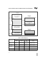
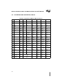
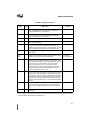
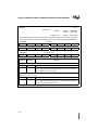
CONTENTS
CHAPTER 1
GUIDE TO THIS MANUAL
1.1
MANUAL CONTENTS ................................................................................................... 1-1
1.2
NOTATIONAL CONVENTIONS AND TERMINOLOGY ................................................ 1-3
1.3
RELATED DOCUMENTS .............................................................................................. 1-5
1.3.1
Data Sheet ................................................................................................................1-6
1.3.2
Application Notes ......................................................................................................1-6
1.4
APPLICATION SUPPORT SERVICES.......................................................................... 1-7
1.4.1
World Wide Web .......................................................................................................1-7
1.4.2
CompuServe Forums ................................................................................................1-7
1.4.3
FaxBack Service .......................................................................................................1-8
1.4.4
Bulletin Board System (BBS) ....................................................................................1-9
CHAPTER 2
INTRODUCTION
2.1
PRODUCT OVERVIEW................................................................................................. 2-3
2.1.1
8X930Ax Features ....................................................................................................2-4
2.2
MCS 251 MICROCONTROLLER CORE ....................................................................... 2-6
2.2.1
CPU ..........................................................................................................................2-6
2.2.2
Clock and Reset Unit ................................................................................................2-7
2.2.3
Interrupt Handler .......................................................................................................2-8
2.3
ON-CHIP MEMORY....................................................................................................... 2-8
2.4
UNIVERSAL SERIAL BUS MODULE .......................................................................... 2-10
2.5
ON-CHIP PERIPHERALS............................................................................................ 2-10
2.5.1
Timer/Counters and Watchdog Timer .....................................................................2-10
2.5.2
Programmable Counter Array (PCA) ......................................................................2-10
2.5.3
Serial I/O Port .........................................................................................................2-11
2.6
OPERATING CONDITIONS ........................................................................................ 2-11
CHAPTER 3
MEMORY PARTITIONS
3.1
ADDRESS SPACES FOR 8X930Ax.............................................................................. 3-1
3.1.1
Compatibility with the MCS® 51 Architecture ...........................................................3-2
3.2
8X930Ax MEMORY SPACE .......................................................................................... 3-5
3.2.1
On-chip General-purpose Data RAM ........................................................................3-8
3.2.2
On-chip Code Memory ..............................................................................................3-8
3.2.2.1
Accessing On-chip Code Memory in Region 00: ..................................................3-9
3.2.3
External Memory .......................................................................................................3-9
3.3
8X930Ax REGISTER FILE ............................................................................................ 3-9
3.4
BYTE, WORD, AND DWORD REGISTERS................................................................ 3-12
3.4.1
Dedicated Registers ................................................................................................3-12
3.4.1.1
Accumulator and B Register ..............................................................................3-12
3.4.1.2
Extended Data Pointer, DPX ..............................................................................3-13
iii
8X930Ax UNIVERSAL SERIAL BUS MICROCONTROLLER USER’S MANUAL
3.4.1.3
Extended Stack Pointer, SPX ............................................................................3-14
3.5
SPECIAL FUNCTION REGISTERS (SFRS) ............................................................... 3-15
CHAPTER 4
DEVICE CONFIGURATION
4.1
CONFIGURATION OVERVIEW .................................................................................... 4-1
4.2
DEVICE CONFIGURATION .......................................................................................... 4-1
4.3
THE CONFIGURATION BITS........................................................................................ 4-4
4.4
CONFIGURING THE EXTERNAL MEMORY INTERFACE........................................... 4-7
4.4.1
Page Mode and Nonpage Mode (PAGE#) ................................................................4-7
4.4.2
Configuration Bits RD1:0 ..........................................................................................4-8
4.4.2.1
RD1:0 = 00 (18 External Address Bits) ..............................................................4-10
4.4.2.2
RD1:0 = 01 (17 External Address Bits) ..............................................................4-10
4.4.2.3
RD1:0 = 10 (16 External Address Bits) ..............................................................4-10
4.4.2.4
RD1:0 = 11 (Compatible with MCS 51 Microcontrollers) ....................................4-11
4.4.3
Wait State Configuration Bits ..................................................................................4-11
4.4.3.1
Configuration Bits WSA1:0#, WSB1:0# .............................................................4-11
4.4.3.2
Configuration Bit XALE# ....................................................................................4-11
4.5
OPCODE CONFIGURATIONS (SRC)......................................................................... 4-12
4.5.1
Selecting Binary Mode or Source Mode ..................................................................4-12
4.6
MAPPING ON-CHIP CODE MEMORY TO DATA MEMORY (EMAP#) ...................... 4-14
4.7
INTERRUPT MODE (INTR)......................................................................................... 4-14
CHAPTER 5
INSTRUCTIONS AND ADDRESSING
5.1
SOURCE MODE OR BINARY MODE OPCODES ........................................................ 5-1
5.2
PROGRAMMING FEATURES OF THE 8X930Ax ARCHITECTURE............................ 5-1
5.2.1
Data Types ................................................................................................................5-2
5.2.1.1
Order of Byte Storage for Words and Double Words ...........................................5-2
5.2.2
Register Notation ......................................................................................................5-2
5.2.3
Address Notation ......................................................................................................5-2
5.2.4
Addressing Modes ....................................................................................................5-4
5.3
DATA INSTRUCTIONS ................................................................................................. 5-4
5.3.1
Data Addressing Modes ............................................................................................5-4
5.3.1.1
Register Addressing .............................................................................................5-5
5.3.1.2
Immediate ............................................................................................................5-5
5.3.1.3
Direct ....................................................................................................................5-5
5.3.1.4
Indirect .................................................................................................................5-6
5.3.1.5
Displacement .......................................................................................................5-7
5.3.2
Arithmetic Instructions ...............................................................................................5-8
5.3.3
Logical Instructions ...................................................................................................5-9
5.3.4
Data Transfer Instructions .........................................................................................5-9
5.4
BIT INSTRUCTIONS ................................................................................................... 5-10
5.4.1
Bit Addressing .........................................................................................................5-10
iv
CONTENTS
5.5
CONTROL INSTRUCTIONS ....................................................................................... 5-11
5.5.1
Addressing Modes for Control Instructions .............................................................5-12
5.5.2
Conditional Jumps ..................................................................................................5-13
5.5.3
Unconditional Jumps ...............................................................................................5-14
5.5.4
Calls and Returns ...................................................................................................5-14
5.6
PROGRAM STATUS WORDS .................................................................................... 5-15
CHAPTER 6
INTERRUPT SYSTEM
6.1
OVERVIEW ................................................................................................................... 6-1
6.2
8X930Ax INTERRUPT SOURCES ................................................................................ 6-3
6.2.1
External Interrupts .....................................................................................................6-3
6.2.2
Timer Interrupts .........................................................................................................6-5
6.3
PROGRAMMABLE COUNTER ARRAY (PCA) INTERRUPT........................................ 6-5
6.4
SERIAL PORT INTERRUPT.......................................................................................... 6-6
6.5
USB INTERRUPTS........................................................................................................ 6-6
6.5.1
USB Function Interrupt .............................................................................................6-6
6.5.2
USB Start of Frame Interrupt ....................................................................................6-9
6.5.3
USB Global Suspend/Resume Interrupt .................................................................6-10
6.5.3.1
Global Suspend ..................................................................................................6-10
6.5.3.2
Global Resume ..................................................................................................6-10
6.5.3.3
USB Remote Wake-up .......................................................................................6-10
6.6
INTERRUPT ENABLE ................................................................................................. 6-11
6.7
INTERRUPT PRIORITIES ........................................................................................... 6-13
6.8
INTERRUPT PROCESSING ....................................................................................... 6-16
6.8.1
Minimum Fixed Interrupt Time ................................................................................6-17
6.8.2
Variable Interrupt Parameters .................................................................................6-17
6.8.2.1
Response Time Variables ..................................................................................6-17
6.8.2.2
Computation of Worst-case Latency With Variables ..........................................6-19
6.8.2.3
Latency Calculations ..........................................................................................6-20
6.8.2.4
Blocking Conditions ............................................................................................6-21
6.8.2.5
Interrupt Vector Cycle ........................................................................................6-21
6.8.3
ISRs in Process ......................................................................................................6-22
CHAPTER 7
UNIVERSAL SERIAL BUS
7.1
USB FUNCTION INTERFACE....................................................................................... 7-1
7.1.1
Serial Bus Interface Engine (SIE) .............................................................................7-1
7.1.2
Function Interface Unit (FIU) .....................................................................................7-1
7.1.3
Special Function Registers (SFRs) ...........................................................................7-2
7.1.4
USB Function FIFO’s ................................................................................................7-4
7.1.5
The FIU SFR Set ......................................................................................................7-4
7.2
TRANSMIT FIFOS ....................................................................................................... 7-14
7.2.1
Transmit FIFO Overview .........................................................................................7-14
v
8X930Ax UNIVERSAL SERIAL BUS MICROCONTROLLER USER’S MANUAL
7.2.2
Transmit FIFO Registers .........................................................................................7-15
7.2.3
Transmit Data Register (TXDAT) ............................................................................7-15
7.2.4
Transmit Byte Count Registers (TXCNTL/TXCNTH) ..............................................7-15
7.2.5
Transmit Data Set Management .............................................................................7-17
7.3
RECEIVE FIFOs .......................................................................................................... 7-24
7.3.1
Receive FIFO Overview ..........................................................................................7-24
7.3.2
Receive FIFO Registers ..........................................................................................7-25
7.3.2.1
Receive Data Register (RXDAT) ........................................................................7-25
7.3.2.2
Receive Byte Count Registers (RXCNTL/RXCNTH) ..........................................7-25
7.3.3
Receive FIFO Data Set Management .....................................................................7-26
7.4
SIE DETAILS ............................................................................................................... 7-33
7.5
SETUP TOKEN RECEIVE FIFO HANDLING .............................................................. 7-33
7.6
ISO DATA MANAGEMENT ......................................................................................... 7-34
7.6.1
Transmit FIFO ISO Data Management ...................................................................7-34
7.6.2
Receive FIFO ISO Data Management ....................................................................7-35
CHAPTER 8
USB PROGRAMMING MODELS
8.1
OVERVIEW OF PROGRAMMING MODELS ................................................................ 8-1
8.1.1
Unenumerated State .................................................................................................8-2
8.1.2
Idle State ...................................................................................................................8-2
8.1.3
Transmit and Receive Routines ................................................................................8-2
8.1.4
USB Interrupts ..........................................................................................................8-2
8.2
TRANSMIT OPERATIONS ............................................................................................ 8-3
8.2.1
Overview ...................................................................................................................8-3
8.2.2
Pre-transmit Operations ............................................................................................8-5
8.2.3
Post-transmit Operations ..........................................................................................8-6
8.3
RECEIVE OPERATIONS............................................................................................... 8-8
8.3.1
Overview ...................................................................................................................8-8
8.3.2
Post-receive Operations ...........................................................................................8-9
8.4
SETUP TOKEN ........................................................................................................... 8-12
8.5
START OF FRAME (SOF) TOKEN ............................................................................. 8-14
CHAPTER 9
INPUT/OUTPUT PORTS
9.1
INPUT/OUTPUT PORT OVERVIEW ............................................................................. 9-1
9.2
I/O CONFIGURATIONS................................................................................................. 9-2
9.3
PORT 1 AND PORT 3 ................................................................................................... 9-2
9.4
PORT 0 AND PORT 2 ................................................................................................... 9-2
9.5
READ-MODIFY-WRITE INSTRUCTIONS ..................................................................... 9-4
9.6
QUASI-BIDIRECTIONAL PORT OPERATION.............................................................. 9-5
9.7
PORT LOADING............................................................................................................ 9-6
9.8
EXTERNAL MEMORY ACCESS ................................................................................... 9-6
vi
CONTENTS
CHAPTER 10
TIMER/COUNTERS AND WATCHDOG TIMER
10.1 TIMER/COUNTER OVERVIEW................................................................................... 10-1
10.2 TIMER/COUNTER OPERATION................................................................................. 10-1
10.3 TIMER 0....................................................................................................................... 10-4
10.3.1 Mode 0 (13-bit Timer) .............................................................................................10-5
10.3.2 Mode 1 (16-bit Timer) .............................................................................................10-5
10.3.3 Mode 2 (8-bit Timer With Auto-reload) ....................................................................10-5
10.3.4 Mode 3 (Two 8-bit Timers) ......................................................................................10-6
10.4 TIMER 1....................................................................................................................... 10-6
10.4.1 Mode 0 (13-bit Timer) .............................................................................................10-7
10.4.2 Mode 1 (16-bit Timer) .............................................................................................10-7
10.4.3 Mode 2 (8-bit Timer with Auto-reload) ...................................................................10-10
10.4.4 Mode 3 (Halt) ........................................................................................................10-10
10.5 TIMER 0/1 APPLICATIONS....................................................................................... 10-10
10.5.1 Auto-load Setup Example .....................................................................................10-10
10.5.2 Pulse Width Measurements ..................................................................................10-11
10.6 TIMER 2..................................................................................................................... 10-11
10.6.1 Capture Mode .......................................................................................................10-12
10.6.2 Auto-reload Mode .................................................................................................10-13
10.6.2.1 Up Counter Operation ......................................................................................10-13
10.6.3 Up/Down Counter Operation .................................................................................10-14
10.6.4 Baud Rate Generator Mode ..................................................................................10-15
10.6.5 Clock-out Mode .....................................................................................................10-15
10.7 WATCHDOG TIMER ................................................................................................. 10-17
10.7.1 Description ............................................................................................................10-17
10.7.2 Using the WDT ......................................................................................................10-19
10.7.3 WDT During Idle Mode .........................................................................................10-19
10.7.4 WDT During PowerDown ......................................................................................10-19
CHAPTER 11
PROGRAMMABLE COUNTER ARRAY
11.1 PCA DESCRIPTION .................................................................................................... 11-1
11.1.1 Alternate Port Usage ...............................................................................................11-2
11.2 PCA TIMER/COUNTER............................................................................................... 11-2
11.3 PCA COMPARE/CAPTURE MODULES ..................................................................... 11-5
11.3.1 16-bit Capture Mode ...............................................................................................11-5
11.3.2 Compare Modes .....................................................................................................11-6
11.3.3 16-bit Software Timer Mode ....................................................................................11-7
11.3.4 High-speed Output Mode ........................................................................................11-8
11.3.5 PCA Watchdog Timer Mode ...................................................................................11-9
11.3.6 Pulse Width Modulation Mode ..............................................................................11-10
vii
8X930Ax UNIVERSAL SERIAL BUS MICROCONTROLLER USER’S MANUAL
CHAPTER 12
SERIAL I/O PORT
12.1 OVERVIEW ................................................................................................................. 12-1
12.2 MODES OF OPERATION............................................................................................ 12-2
12.2.1 Synchronous Mode (Mode 0) ..................................................................................12-2
12.2.1.1 Transmission (Mode 0) ......................................................................................12-2
12.2.1.2 Reception (Mode 0) ............................................................................................12-3
12.2.2 Asynchronous Modes (Modes 1, 2, and 3) .............................................................12-7
12.2.2.1 Transmission (Modes 1, 2, 3) .............................................................................12-7
12.2.2.2 Reception (Modes 1, 2, 3) ..................................................................................12-7
12.3 FRAMING BIT ERROR DETECTION (MODES 1, 2, AND 3)...................................... 12-7
12.4 MULTIPROCESSOR COMMUNICATION (MODES 2 AND 3).................................... 12-8
12.5 AUTOMATIC ADDRESS RECOGNITION ................................................................... 12-8
12.5.1 Given Address ........................................................................................................12-8
12.5.2 Broadcast Address ..................................................................................................12-9
12.5.3 Reset Addresses ...................................................................................................12-10
12.6 BAUD RATES ............................................................................................................ 12-10
12.6.1 Baud Rate for Mode 0 † .........................................................................................12-10
12.6.2 Baud Rates for Mode 2 .........................................................................................12-11
12.6.3 Baud Rates for Modes 1 and 3 † ...........................................................................12-11
12.6.3.1 Timer 1 Generated Baud Rates (Modes 1 and 3) † ..........................................12-11
12.6.3.2 Selecting Timer 1 as the Baud Rate Generator † .............................................12-11
12.6.3.3 Timer 2 Generated Baud Rates (Modes 1 and 3) ............................................12-12
12.6.3.4 Selecting Timer 2 as the Baud Rate Generator † .............................................12-12
CHAPTER 13
MINIMUM HARDWARE SETUP
13.1 MINIMUM HARDWARE SETUP.................................................................................. 13-1
13.2 ELECTRICAL ENVIRONMENT ................................................................................... 13-1
13.2.1 Power and Ground Pins ..........................................................................................13-2
13.2.2 Unused Pins ............................................................................................................13-2
13.2.3 Noise Considerations ..............................................................................................13-2
13.3 CLOCK SOURCES...................................................................................................... 13-2
13.3.1 On-chip Oscillator (Crystal) .....................................................................................13-2
13.3.2 On-chip Oscillator (Ceramic Resonator) .................................................................13-3
13.3.3 External Clock .........................................................................................................13-3
13.4 RESET ......................................................................................................................... 13-4
13.4.1 Externally Initiated Resets ......................................................................................13-5
13.4.2 WDT Initiated Resets ..............................................................................................13-5
13.4.3 USB Initiated Resets ...............................................................................................13-5
13.4.4 Reset Operation ......................................................................................................13-6
13.4.5 Power-on Reset ......................................................................................................13-6
viii
CONTENTS
CHAPTER 14
SPECIAL OPERATING MODES
14.1 GENERAL.................................................................................................................... 14-1
14.2 POWER CONTROL REGISTERS ............................................................................... 14-1
14.2.1 Serial I/O Control Bits .............................................................................................14-1
14.2.2 Power Off Flag ........................................................................................................14-1
14.3 IDLE MODE ................................................................................................................. 14-5
14.3.1 Entering Idle Mode ..................................................................................................14-5
14.3.2 Exiting Idle Mode ....................................................................................................14-5
14.4 USB POWER CONTROL ............................................................................................ 14-6
14.4.1 Global Suspend Mode ............................................................................................14-6
14.4.1.1 Powerdown Mode ..............................................................................................14-6
14.4.1.2 Entering Powerdown Mode ................................................................................14-7
14.4.1.3 Exiting Powerdown Mode ...................................................................................14-7
14.4.2 Global Resume Mode .............................................................................................14-8
14.4.3 USB Remote Wake-up ............................................................................................14-8
14.5 LOW CLOCK MODE.................................................................................................... 14-8
14.5.1 Entering Low Clock Mode .......................................................................................14-8
14.5.2 Exiting Low Clock Mode ..........................................................................................14-9
14.6 ON-CIRCUIT EMULATION (ONCE) MODE ................................................................ 14-9
14.6.1 Entering ONCE Mode .............................................................................................14-9
14.6.2 Exiting ONCE Mode ................................................................................................14-9
CHAPTER 15
EXTERNAL MEMORY INTERFACE
15.1 OVERVIEW ................................................................................................................. 15-1
15.2 EXTERNAL BUS CYCLES .......................................................................................... 15-3
15.2.1 Bus Cycle Definitions ..............................................................................................15-3
15.2.2 Nonpage Mode Bus Cycles ....................................................................................15-3
15.2.3 Page Mode Bus Cycles ...........................................................................................15-6
15.3 WAIT STATES ............................................................................................................. 15-8
15.4 EXTERNAL BUS CYCLES WITH CONFIGURABLE WAIT STATES.......................... 15-8
15.4.1 Extending RD#/WR#/PSEN# ..................................................................................15-8
15.4.2 Extending ALE ......................................................................................................15-10
15.5 EXTERNAL BUS CYCLES WITH REAL-TIME WAIT STATES................................. 15-11
15.5.1 Real-time WAIT# Enable (RTWE) .........................................................................15-12
15.5.2 Real-time WAIT CLOCK Enable (RTWCE) ...........................................................15-12
15.5.3 Real-time Wait State Bus Cycle Diagrams ............................................................15-12
15.6 CONFIGURATION BYTE BUS CYCLES................................................................... 15-15
15.7 PORT 0 AND PORT 2 STATUS ................................................................................ 15-15
15.7.1 Port 0 and Port 2 Pin Status in Nonpage Mode ....................................................15-16
15.7.2 Port 0 and Port 2 Pin Status in Page Mode ..........................................................15-16
15.8 EXTERNAL MEMORY DESIGN EXAMPLES............................................................ 15-17
ix
8X930Ax UNIVERSAL SERIAL BUS MICROCONTROLLER USER’S MANUAL
15.8.1 Example 1: RD1:0 = 00, 18-bit Bus, External Flash and RAM ..............................15-18
15.8.2 Example 2: RD1:0 = 01, 17-bit Bus, External Flash and RAM ..............................15-20
15.8.3 Example 3: RD1:0 = 01, 17-bit Bus, External RAM ..............................................15-22
15.8.4 Example 4: RD1:0 = 10, 16-bit Bus, External RAM ..............................................15-24
15.8.5 Example 5: RD1:0 = 11, 16-bit Bus, External EPROM and RAM .........................15-26
15.8.5.1 An Application Requiring Fast Access to the Stack .........................................15-26
15.8.5.2 An Application Requiring Fast Access to Data .................................................15-26
15.8.6 Example 6: RD1:0 = 11, 16-bit Bus, External EPROM and RAM .........................15-29
15.8.7 Example 7: RD1:0 = 01, 17-bit Bus, External Flash ..............................................15-30
CHAPTER 16
VERIFYING NONVOLATILE MEMORY
16.1 GENERAL.................................................................................................................... 16-1
16.1.1 Considerations for On-chip Program Code Memory ...............................................16-1
16.2 VERIFY MODES.......................................................................................................... 16-3
16.3 GENERAL SETUP....................................................................................................... 16-3
16.4 VERIFY ALGORITHM.................................................................................................. 16-4
16.5 LOCK BIT SYSTEM..................................................................................................... 16-5
16.5.1 Encryption Array .....................................................................................................16-5
16.6 SIGNATURE BYTES ................................................................................................... 16-6
APPENDIX A
INSTRUCTION SET REFERENCE
A.1
NOTATION FOR INSTRUCTION OPERANDS ............................................................ A-2
A.2
OPCODE MAP AND SUPPORTING TABLES ............................................................. A-4
A.3
INSTRUCTION SET SUMMARY ................................................................................ A-11
A.3.1
Execution Times for Instructions Accessing the Port SFRs .................................. A-11
A.3.2
Instruction Summaries .......................................................................................... A-14
A.4
INSTRUCTION DESCRIPTIONS ............................................................................... A-26
APPENDIX B
SIGNAL DESCRIPTIONS
APPENDIX C
REGISTERS
C.1
SFRS BY FUNCTIONAL CATEGORY ......................................................................... C-2
C.2
SFR DESCRIPTIONS................................................................................................... C-6
x
CONTENTS
APPENDIX D
DATA FLOW MODEL
GLOSSARY
INDEX
xi
8X930Ax UNIVERSAL SERIAL BUS MICROCONTROLLER USER’S MANUAL
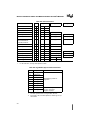
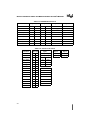
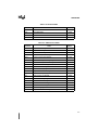
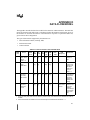
FIGURES
Figure
2-1
2-2
2-3
2-4
2-5
2-6
3-1
3-2
3-3
3-4
3-5
3-6
3-7
3-8
4-1
4-2
4-3
4-4
4-5
4-6
4-7
4-8
5-1
5-2
5-3
6-1
6-2
6-3
6-4
6-5
6-6
6-7
6-8
6-9
6-10
6-11
6-12
7-1
7-2
7-3
7-4
7-5
7-6
7-7
xii
Page
8X930Ax in a Universal Serial Bus System..................................................................2-1
Functional Block Diagram of the 8X930Ax ...................................................................2-2
8X930Ax USB Module Block Diagram .........................................................................2-3
The CPU.......................................................................................................................2-6
Clocking Definitions (PLL off) .......................................................................................2-9
Clocking Definitions (PLL on) .......................................................................................2-9
Address Spaces for the 8X930Ax ................................................................................3-1
Address Spaces for the MCS® 51 Architecture ...........................................................3-3
Address Space Mappings MCS® 51 Architecture to MCS® 251 Architecture.............3-4
8X930Ax Address Space .............................................................................................3-6
Hardware Implementation of the 8X930Ax Address Space .........................................3-7
The Register File ........................................................................................................3-10
Register File Locations 0–7........................................................................................3-11
Dedicated Registers in the Register File and their Corresponding SFRs...................3-13
Configuration Array (On-chip).......................................................................................4-2
Configuration Array (External) ......................................................................................4-3
User Configuration Byte 0 (UCONFIG0) ......................................................................4-5
User Configuration Byte 1 (UCONFIG1) ......................................................................4-6
Internal/External Address Mapping (RD1:0 = 00 and 01).............................................4-8
Internal/External Address Mapping (RD1:0 = 10 and 11).............................................4-9
Binary Mode Opcode Map..........................................................................................4-13
Source Mode Opcode Map ........................................................................................4-13
Word and Double-word Storage in Big Endien Form ...................................................5-3
Program Status Word Register...................................................................................5-17
Program Status Word 1 Register................................................................................5-18
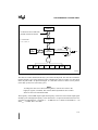
Interrupt Control System ..............................................................................................6-2
USB Function Interrupt Enable Register ......................................................................6-7
USB Function Interrupt Flag Register...........................................................................6-9
Interrupt Enable Register 0 ........................................................................................6-11
USB Interrupt Enable Register ...................................................................................6-12
IPH0: Interrupt Priority High Register 0 ......................................................................6-14
IPL0: Interrupt Priority Low Register 0........................................................................6-14
IPH1: Interrupt Priority High Register 1 ......................................................................6-15
IPL1: Interrupt Priority Low Register 1........................................................................6-15
The Interrupt Process .................................................................................................6-16
Response Time Example #1 ......................................................................................6-18
Response Time Example #2 ......................................................................................6-19
EPINDEX: Endpoint Index Register .............................................................................7-5
EPCON: Control Endpoint Register..............................................................................7-7
TXSTAT: Transmit FIFO Status Register .....................................................................7-9
RXSTAT: Receive FIFO Status Register....................................................................7-11
SOFH: Start of Frame High Register..........................................................................7-12
SOFL: Start of Frame Low Register ...........................................................................7-13
FADDR: Function Address Register...........................................................................7-13
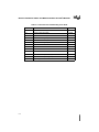
CONTENTS
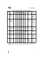
FIGURES
Figure
7-8
7-9
7-10
7-11
7-12
7-13
7-14
7-15
7-16
7-17
7-18
8-1
8-2
8-3
8-4
8-5
8-6
8-7
8-8
8-9
8-10
9-1
9-2
9-3
9-4
10-1
10-2
10-3
10-4
10-5
10-6
10-7
10-8
10-9
10-10
10-11
10-12
11-1
11-2
11-3
11-4
11-5
11-6
11-7
Page
Transmit FIFO Outline ................................................................................................7-14
Transmit Byte Count Registers...................................................................................7-16
TXDAT: Transmit FIFO Data Register........................................................................7-18
TXCNTH/TXCNTL Transmit FIFO Byte Count Registers...........................................7-19
TXCON: Transmit FIFO Control Register...................................................................7-21
TXFLG: Transmit FIFO Flag Register ........................................................................7-23
Receive FIFO .............................................................................................................7-25
RXDAT: Receive FIFO Data Register ........................................................................7-27
RXCNTH/RXCNTL: Receive FIFO Byte Count Registers ..........................................7-28
RXCON: Receive FIFO Control Register ...................................................................7-30
RXFLG: Receive FIFO Flag Register .........................................................................7-32
Program Flow ...............................................................................................................8-1
High-level View of Transmit Operations .......................................................................8-4
Pre-transmit ISR (Non-Isochronous) ............................................................................8-5
Post-transmit ISR (Non-isochronous)...........................................................................8-6
Post-transmit ISR (Isochronous) ..................................................................................8-7
High-level View of Receive Operations ........................................................................8-9
Post-receive ISR (Non-isochronous) ..........................................................................8-10
Receive SOF ISR (Isochronous) ................................................................................8-11
Post-receive ISR (Control)..........................................................................................8-13
Hardware Operations for SOF Token.........................................................................8-14
Port 1 and Port 3 Structure...........................................................................................9-3
Port 0 Structure ............................................................................................................9-3
Port 2 Structure ............................................................................................................9-4
Internal Pullup Configurations ......................................................................................9-6
Basic Logic of the Timer/Counters .............................................................................10-3
Timer 0/1 in Mode 0 and Mode 1 ...............................................................................10-5
Timer 0/1 in Mode 2, Auto-Reload..............................................................................10-6
Timer 0 in Mode 3, Two 8-bit Timers..........................................................................10-7
TMOD: Timer/Counter Mode Control Register ...........................................................10-8
TCON: Timer/Counter Control Register .....................................................................10-9
Timer 2: Capture Mode ............................................................................................10-12
Timer 2: Auto Reload Mode (DCEN = 0)..................................................................10-13
Timer 2: Auto Reload Mode (DCEN = 1)..................................................................10-14
Timer 2: Clock Out Mode..........................................................................................10-16
T2MOD: Timer 2 Mode Control Register..................................................................10-17
T2CON: Timer 2 Control Register ............................................................................10-18
Programmable Counter Array.....................................................................................11-3
PCA 16-bit Capture Mode ..........................................................................................11-6
PCA Software Timer and High-speed Output Modes.................................................11-8
PCA Watchdog Timer Mode.....................................................................................11-10
PCA 8-bit PWM Mode ..............................................................................................11-11
PWM Variable Duty Cycle ........................................................................................11-12
CMOD: PCA Timer/Counter Mode Register.............................................................11-13
xiii
8X930Ax UNIVERSAL SERIAL BUS MICROCONTROLLER USER’S MANUAL
FIGURES
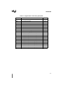
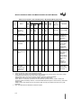
Figure
11-8
11-9
12-1
12-2
12-3
12-4
12-5
13-1
13-2
13-3
13-4
13-5
14-1
14-2
14-3
14-4
15-1
15-2
15-3
15-4
15-5
15-6
15-7
15-8
15-9
15-10
15-11
15-12
15-13
15-14
15-15
15-16
15-17
15-18
15-19
15-20
15-21
15-22
15-23
15-24
15-25
15-26
15-27
15-28
xiv
Page
CCON: PCA Timer/Counter Control Register...........................................................11-14
CCAPMx: PCA Compare/Capture Module Mode Registers.....................................11-15
Serial Port Block Diagram ..........................................................................................12-3
SCON: Serial Port Control Register ...........................................................................12-5
Mode 0 Timing............................................................................................................12-6
Data Frame (Modes 1, 2, and 3) ................................................................................12-6
Timer 2 in Baud Rate Generator Mode ....................................................................12-14
Minimum Setup ..........................................................................................................13-1
CHMOS On-chip Oscillator.........................................................................................13-3
External Clock Connection for the 8X930Ax ..............................................................13-4
External Clock Drive Waveforms................................................................................13-4
Reset Timing Sequence .............................................................................................13-7
Power Control (PCON) Register.................................................................................14-2
USB Power Control (PCON1) Register ......................................................................14-3
Idle and Powerdown Clock Control ............................................................................14-4
Suspend/Resume Program with/without Remote Wake-up .....................................14-10
Bus Structure in Nonpage Mode and Page Mode ......................................................15-1
External Code Fetch (Nonpage Mode).......................................................................15-4
External Data Read (Nonpage Mode) ........................................................................15-5
External Data Write (Nonpage Mode) ........................................................................15-5
External Code Fetch (Page Mode) .............................................................................15-7
External Data Read (Page Mode) ..............................................................................15-7
External Data Write (Page Mode)...............................................................................15-8
External Code Fetch (Nonpage Mode, One RD#/PSEN# Wait State) .......................15-9
External Data Write (Nonpage Mode, One WR# Wait State) .....................................15-9
External Code Fetch (Nonpage Mode, One ALE Wait State)...................................15-10
Real-time Wait State Control Register (WCON).......................................................15-11
External Code Fetch/Data Read (Nonpage Mode, Real-time Wait State)................15-13
External Data Write (Nonpage Mode, Real-time Wait State) ...................................15-13
External Data Read (Page Mode, Real-time Wait State) .........................................15-14
External Data Write (Page Mode, Real-time Wait State)..........................................15-14
Configuration Byte Bus Cycles .................................................................................15-15
Bus Diagram for Example 1: 80930AD in Page Mode .............................................15-18
Address Space for Example 1 ..................................................................................15-19
Bus Diagram for Example 2: 80930AD in Page Mode .............................................15-20
Address Space for Example 2 ..................................................................................15-21
Bus Diagram for Example 3: 83930AE in Nonpage Mode .......................................15-22
Memory Space for Example 3 ..................................................................................15-23
Bus Diagram for Example 4: 83930AE in Nonpage Mode .......................................15-24
Address Space for Example 4 ..................................................................................15-25
Bus Diagram for Example 5: 80930AD in Nonpage Mode .......................................15-27
Address Space for Examples 5 and 6 ......................................................................15-28
Bus Diagram for Example 6: 80930AD in Page Mode .............................................15-29
Bus Diagram for Example 7: 80930AD in Page Mode .............................................15-30
CONTENTS
FIGURES
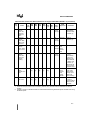
Figure
Page
16-1
Setup for Verifying Nonvolatile Memory .....................................................................16-4
16-2
Verify Bus Cycles .......................................................................................................16-4
B-1
8X930Ax 68-pin PLCC Package ................................................................................. B-1
xv
8X930Ax UNIVERSAL SERIAL BUS MICROCONTROLLER USER’S MANUAL
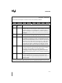
TABLES
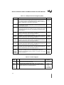
Table
1-1
2-1
2-2
3-1
3-2
3-3
3-4
3-5
3-6
3-7
3-8
3-9
3-10
3-11
4-1
4-2
4-3
4-4
5-1
5-2
5-3
5-4
5-5
5-6
5-7
5-8
5-9
5-10
6-1
6-2
6-3
6-4
6-5
6-6
6-7
6-8
7-1
7-2
7-3
7-4
7-5
7-6
7-7
9-1
xvi
Page
Intel Application Support Services................................................................................1-7
8X930Ax Features Summary .......................................................................................2-5
8X930Ax Operating Frequency ....................................................................................2-8
Address Mappings........................................................................................................3-4
Minimum Times to Fetch Two Bytes of Code...............................................................3-9
Register Bank Selection .............................................................................................3-11
Dedicated Registers in the Register File and their Corresponding SFRs...................3-14
8X930Ax SFR Map.....................................................................................................3-16
Core SFRs..................................................................................................................3-17
USB Function SFRs ...................................................................................................3-18
I/O Port SFRs .............................................................................................................3-19
Serial I/O SFRs ..........................................................................................................3-19
Timer/Counter and Watchdog Timer SFRs ................................................................3-19
Programmable Counter Array (PCA) SFRs................................................................3-20
External Addresses for Configuration Array .................................................................4-2
Memory Signal Selections (RD1:0) ..............................................................................4-7
RD#, WR#, PSEN# External Wait States ...................................................................4-11
Examples of Opcodes in Binary and Source Modes ..................................................4-14
Data Types ...................................................................................................................5-2
Notation for Byte Registers, Word Registers, and Dword Registers ............................5-3
Addressing Modes for Data Instructions in the MCS® 51 Architecture ........................5-5
Addressing Modes for Data Instructions in the MCS 251 Architecture.........................5-7
Bit-addressable Locations ..........................................................................................5-11
Addressing Two Sample Bits......................................................................................5-11
Addressing Modes for Bit Instructions ........................................................................5-11
Addressing Modes for Control Instructions.................................................................5-13
Compare-conditional Jump Instructions .....................................................................5-14
The Effects of Instructions on the PSW and PSW1 Flags..........................................5-16
Interrupt System Input Signals .....................................................................................6-1
Interrupt System Special Function Registers ...............................................................6-3
Interrupt Control Matrix.................................................................................................6-4
USB Interrupt Control Matrix ........................................................................................6-5
Level of Priority...........................................................................................................6-13
Interrupt Priority Within Level .....................................................................................6-13
Interrupt Latency Variables ........................................................................................6-20
Actual vs. Predicted Latency Calculations..................................................................6-20
Signal Descriptions.......................................................................................................7-2
USB Function SFRs .....................................................................................................7-3
8X930Ax FIFO Configurations .....................................................................................7-4
Writing to the Byte Count Register .............................................................................7-17
Truth Table for Transmit FIFO Management..............................................................7-18
Status of the Receive FIFO Data Sets .......................................................................7-26
Truth Table for Receive FIFO Management...............................................................7-27
Input/Output Port Pin Descriptions ...............................................................................9-1
CONTENTS
TABLES
Table
9-2
10-1
10-2
10-3
11-1
11-2
11-3
12-1
12-2
12-3
12-4
12-5
12-6
14-1
15-1
15-2
15-3
16-1
16-2
16-3
16-4
16-5
A-1
A-2
A-3
A-4
A-5
A-6
A-7
A-8
A-9
A-10
A-11
A-12
A-13
A-14
A-15
A-16
A-17
A-18
A-19
A-20
A-21
A-22
Page
Instructions for External Data Moves............................................................................9-7
External Signals .........................................................................................................10-2
Timer/Counter and Watchdog Timer SFRs ................................................................10-4
Timer 2 Modes of Operation.....................................................................................10-16
PCA Special Function Registers (SFRs) ....................................................................11-4
External Signals .........................................................................................................11-4
PCA Module Modes .................................................................................................11-14
Serial Port Signals ......................................................................................................12-2
Serial Port Special Function Registers .......................................................................12-2
Summary of Baud Rates ..........................................................................................12-11
Timer 1 Generated Baud Rates for Serial I/O Modes 1 and 3..................................12-12
Selecting the Baud Rate Generator(s) .....................................................................12-13
Timer 2 Generated Baud Rates ...............................................................................12-14
Pin Conditions in Various Modes................................................................................14-4
External Memory Interface Signals.............................................................................15-2
Bus Cycle Definitions (No Wait States) ......................................................................15-4
Port 0 and Port 2 Pin Status In Normal Operating Mode..........................................15-16
Signal Descriptions.....................................................................................................16-2
Verify Modes .............................................................................................................16-3
Lock Bit Function........................................................................................................16-5
Contents of the Signature Bytes.................................................................................16-6
Timing Definitions .......................................................................................................16-6
Notation for Register Operands................................................................................... A-2
Notation for Direct Addresses...................................................................................... A-3
Notation for Immediate Addressing ............................................................................. A-3
Notation for Bit Addressing.......................................................................................... A-3
Notation for Destinations in Control Instructions ......................................................... A-3
Instructions for MCS® 51 Microcontrollers.................................................................. A-4
Instructions for the 8X930Ax Architecture .................................................................. A-5
Data Instructions ......................................................................................................... A-6
High Nibble, Byte 0 of Data Instructions...................................................................... A-6
Bit Instructions ............................................................................................................. A-7
Byte 1 (High Nibble) for Bit Instructions....................................................................... A-7
PUSH/POP Instructions .............................................................................................. A-8
Control Instructions .................................................................................................... A-8
Displacement/Extended MOVs.................................................................................... A-9
INC/DEC.................................................................................................................... A-10
Encoding for INC/DEC .............................................................................................. A-10
Shifts ......................................................................................................................... A-10
State Times to Access the Port SFRs ....................................................................... A-12
Summary of Add and Subtract Instructions ............................................................... A-14
Summary of Compare Instructions............................................................................ A-15
Summary of Increment and Decrement Instructions ................................................. A-15
Summary of Multiply, Divide, and Decimal-adjust Instructions.................................. A-16
xvii
8X930Ax UNIVERSAL SERIAL BUS MICROCONTROLLER USER’S MANUAL
TABLES
Table
A-23
A-24
A-25
A-26
A-27
A-28
B-1
B-2
B-3
B-4
C-1
C-2
C-3
C-4
C-5
C-6
C-7
D-1
D-2
D-3
D-4
D-5
xviii
Page
Summary of Logical Instructions ............................................................................... A-17
Summary of Move Instructions .................................................................................. A-19
Summary of Exchange, Push, and Pop Instructions ................................................. A-22
Summary of Bit Instructions....................................................................................... A-23
Summary of Control Instructions ............................................................................... A-24
Flag Symbols............................................................................................................. A-26
8X930Ax Pin Assignments Arranged by Functional Categories.................................. B-2
Signal Descriptions...................................................................................................... B-3
Memory Signal Selections (RD1:0) ............................................................................. B-6
8X930Ax Operating Frequency ................................................................................... B-6
8X930Ax SFR Map...................................................................................................... C-1
Core SFRs................................................................................................................... C-2
I/O Port SFRs .............................................................................................................. C-2
Serial I/O SFRs ........................................................................................................... C-3
USB Function SFRs .................................................................................................... C-3
Timer/Counter and Watchdog Timer SFRs ................................................................. C-4
Programmable Counter Array (PCA) SFRs................................................................. C-5
Non-isochronous Transmit Data Flow ......................................................................... D-1
Isochronous Transmit Data Flow in Dual-packet Mode............................................... D-5
Non-isochronous Receive Data Flow in Single-packet Mode (RXSPM = 1) ............... D-8
Non-isochronous Receive Data Flow in Dual-packet Mode (RXSPM = 0)................ D-11
Isochronous Receive Data Flow in Dual-packet Mode (RXSPM = 0) ....................... D-18
1
Guide to this Manual
CHAPTER 1
GUIDE TO THIS MANUAL
This manual describes the 8X930Ax microcontroller; a new family of products for universal serial bus (USB) applications. This manual is intended for use by both software and hardware designers familiar with the principles of microcontroller architecture.
1.1
MANUAL CONTENTS
This chapter provides an overview of the manual with brief summaries of the chapters and appendices. It also explains the terminology and notational conventions used throughout the manual,
provides references to related documentation, and tells how to contact Intel for additional information.
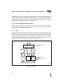
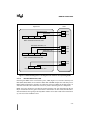
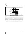
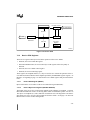
Chapter 2, “Introduction” — provides an overview of device hardware. It covers core functions
(pipelined CPU, clock and reset unit, and interrupts), I/O ports, on-chip memory, and on-chip peripherals (USB, timer/counters, watchdog timer, programmable counter array, and serial I/O
port).
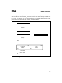
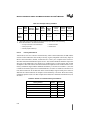
Chapter 3, “Memory Partitions” — describes the three address spaces of the 8X930Ax: memory address space, special function register (SFR) space, and the register file. It also provides a
map of the SFR space showing the location of the SFRs and their reset values and explains the
mapping of the address spaces relative to the MCS® 51 and MCS® 251 architectures into the address spaces of the 8X930Ax.
Chapter 4, “Device Configuration” — describes microcontroller features that are configured at
device reset, including the external memory interface (the number of external address bits, the
number of wait states, page mode, memory regions for asserting RD#, WR#, and PSEN#), binary/source opcodes, interrupt mode, and the mapping of a portion of on-chip code memory to data
memory. It describes the configuration bytes and how to program them for the desired configuration. It also describes how internal memory maps into external memory.
Chapter 5, “Instructions and Addressing” — provides an overview of the instruction set. It describes each instruction type (control, arithmetic, logical, etc.) and lists the instructions in tabular
form. This chapter also discusses the addressing modes, bit instructions, and the program status
words. Appendix A, “Instruction Set Reference” provides a detailed description of each instruction.
Chapter 6, “Interrupt System” — describes the 8X930Ax interrupt circuitry which provides a
TRAP instruction interrupt and ten maskable interrupts: two external interrupts, three timer interrupts, a PCA interrupt, a serial port interrupt, and three USB interrupts. This chapter also discusses the interrupt priority scheme, interrupt enable, interrupt processing, and interrupt response
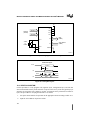
time.
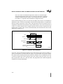
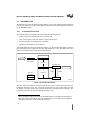
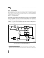
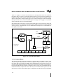
Chapter 7, “Universal Serial Bus” — describes the operation of the 8X930Ax serving as a USB
function. The USB function interface manages communications between the USB host and the
embedded function. The USB module consists of a serial bus interface engine (SIE), a function
interface unit (FIU), a differential transceiver and FIFO data buffers.
1-1
8X930Ax UNIVERSAL SERIAL BUS MICROCONTROLLER USER’S MANUAL
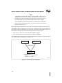
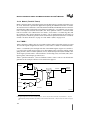
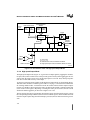
Chapter 8, “USB Programming Models” — describes the programming models of the
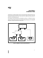
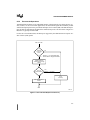
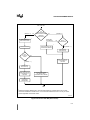
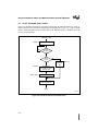
8X930Ax USB function interface. This chapter provides flow charts of suggested firmware routines for using the transmit and receive FIFOs to perform data transfers between the host PC and
the embedded function and describes how the firmware interacts with the USB module hardware.
Chapter 9, “Input/Output Ports”— describes the four 8-bit I/O ports (ports 0–3) and discusses
their configuration for general-purpose I/O. This chapter also discusses external memory accesses (ports 0, 2) and alternative special functions.
Chapter 10, “Timer/Counters and WatchDog Timer” — describes the three on-chip timer/counters and discusses their application. This chapter also provides instructions for using the
hardware watchdog timer (WDT) and describes the operation of the WDT during the idle and
powerdown modes.
Chapter 11, “Programmable Counter Array” — describes the PCA on-chip peripheral and explains how to configure it for general-purpose applications (timers and counters) and special applications (programmable WDT and pulse-width modulator).
Chapter 12, “Serial I/O Port” — describes the full-duplex serial I/O port and explains how to
program it to communicate with external peripherals. This chapter also discusses baud rate generation, framing error detection, multiprocessor communications, and automatic address recognition.
Chapter 13, “Minimum Hardware Setup” — describes the basic requirements for operating
the 8X930Ax in a system. It also discusses on-chip and external clock sources and describes device resets, including power-on reset.
Chapter 14, “Special Operating Modes” — provides an overview of the idle, powerdown, and
on-circuit emulation (ONCE) modes and describes how to enter and exit each mode. This chapter
also describes the power control (PCON) special function register and lists the status of the device
pins during the special modes and reset.
Chapter 15, “External Memory Interface” — describes the external memory signals and bus
cycles and provides examples of external memory design. It provides waveform diagrams for the
bus cycles, bus cycles with wait states, and the configuration byte bus cycles. It also provides bus
cycle diagrams with AC timing symbols and definitions of the symbols.
Chapter 16, “Verifying Nonvolatile Memory” — provides instructions for verifying on-chip
program memory, configuration bytes, signature bytes, and lock bits.
Appendix A, “Instruction Set Reference” — provides reference information for the instruction
set. It describes each instruction; defines the bits in the program status word registers (PSW,
PSW1); shows the relationships between instructions and PSW flags; and lists hexadecimal opcodes, instruction lengths, and execution times.
Appendix B, “Signal Descriptions” — describes the function(s) of each device pin. Descriptions are listed alphabetically by signal name. This appendix also provides a list of the signals
grouped by functional category.
Appendix C, “Registers” — accumulates, for convenient reference, copies of the register definition figures that appear throughout the manual.
1-2
GUIDE TO THIS MANUAL
Appendix D, “Data Flow Model”— describes the data flow model for the 8X930Ax USB transactions.
Glossary — a glossary of terms has been provided for reference of technical terms.
Index — an index has been included for your convenience.
1.2
NOTATIONAL CONVENTIONS AND TERMINOLOGY
The following notations and terminology are used in this manual. The Glossary defines other
terms with special meanings.
#
The pound symbol (#) has either of two meanings, depending on the
context. When used with a signal name, the symbol means that the
signal is active low. When used with an instruction pneumonic, the
symbol prefixes an immediate value in immediate addressing mode.
italics
Italics identify variables and introduce new terminology. The context
in which italics are used distinguishes between the two possible
meanings.
Variables in registers and signal names are commonly represented by
x and y, where x represents the first variable and y represents the
second variable. For example, in register Px.y, x represents the
variable [1–4] that identifies the specific port, and y represents the
register bit variable [7:0]. Variables must be replaced with the correct
values when configuring or programming registers or identifying
signals.
XXXX
Uppercase X (no italics) represents an unknown value or a “don’t
care” state or condition. The value may be either binary or
hexadecimal, depending on the context. For example, 2XAFH (hex)
indicates that bits 11:8 are unknown; 10XX in binary context
indicates that the two LSBs are unknown.
Assert and Deassert
The terms assert and deassert refer to the act of making a signal
active (enabled) and inactive (disabled), respectively. The active
polarity (high/low) is defined by the signal name. Active-low signals
are designated by a pound symbol (#) suffix; active-high signals have
no suffix. To assert RD# is to drive it low; to assert ALE is to drive it
high; to deassert RD# is to drive it high; to deassert ALE is to drive it
low.
Instructions
Instruction mnemonics are shown in upper case to avoid confusion.
When writing code, either upper case or lower case may be used.
1-3
8X930Ax UNIVERSAL SERIAL BUS MICROCONTROLLER USER’S MANUAL
Logic 0 (Low)
An input voltage level equal to or less than the maximum value of
VIL or an output voltage level equal to or less than the maximum
value of VOL. See data sheet for values.
Logic 1 (High)
An input voltage level equal to or greater than the minimum value of
VIH or an output voltage level equal to or greater than the minimum
value of VOH. See data sheet for values.
Numbers
Hexadecimal numbers are represented by a string of hexadecimal
digits followed by the character H. Decimal and binary numbers are
represented by their customary notations. That is, 255 is a decimal
number and 1111 1111 is a binary number. In some cases, the letter B
is added for clarity.
Register Bits
Bit locations are indexed by 7:0 for byte registers, 15:0 for word
registers, and 31:0 for double-word (dword) registers, where bit 0 is
the least-significant bit and 7, 15, or 31 is the most-significant bit. An
individual bit is represented by the register name, followed by a
period and the bit number. For example, PCON.4 is bit 4 of the
power control register. In some discussions, bit names are used. For
example, the name of PCON.4 is POF, the power-off flag.
Register Names
Register names are shown in upper case. For example, PCON is the
power control register. If a register name contains a lowercase
character, it represents more than one register. For example,
CCAPMx represents the five registers: CCAPM0 through CCAPM4.
Reserved Bits
Some registers contain reserved bits. These bits are not used in this
device, but they may be used in future implementations. Do not write
a “1” to a reserved bit. The value read from a reserved bit is indeterminate.
Set and Clear
The terms set and clear refer to the value of a bit or the act of giving
it a value. If a bit is set, its value is “1”; setting a bit gives it a “1”
value. If a bit is clear, its value is “0”; clearing a bit gives it a “0”
value.
Signal Names
Signal names are shown in upper case. When several signals share a
common name, an individual signal is represented by the signal name
followed by a number. Port pins are represented by the port abbreviation, a period, and the pin number (e.g., P0.0, P0.1). A pound
symbol (#) appended to a signal name identifies an active-low signal.
1-4
GUIDE TO THIS MANUAL
Units of Measure
1.3
The following abbreviations are used to represent units of measure:
A
amps, amperes
DCV
direct current volts
Kbyte
kilobytes
KΩ
kilo-ohms
mA
milliamps, milliamperes
Mbyte
megabytes
MHz
megahertz
ms
milliseconds
mW
milliwatts
ns
nanoseconds
pF
picofarads
W
watts
V
volts
µA
microamps, microamperes
µF
microfarads
µs
microseconds
µW
microwatts
RELATED DOCUMENTS
The following documents contain additional information that is useful in designing systems that
incorporate the 8X930Ax. To order documents, please call Intel Literature Fulfillment (1-800548-4725 in the U.S. and Canada; +44(0) 793-431155 in Europe).
Embedded Microcontrollers
Order Number 270646
Embedded Processors
Order Number 272396
Embedded Applications
Order Number 270648
Packaging
Order Number 240800
Universal Serial Bus Specification
Order Number 272904
1-5
8X930Ax UNIVERSAL SERIAL BUS MICROCONTROLLER USER’S MANUAL
1.3.1
Data Sheet
The data sheet is included in Embedded Microcontrollers and is also available individually.
8X930Ax Universal Serial Bus Microcontroller
1.3.2
Order Number 272917
Application Notes
The following MCS 251 application notes apply to the 8X930Ax.
AP-125, Designing Microcontroller Systems
for Electrically Noisy Environments
Order Number 210313
AP-155, Oscillators for Microcontrollers
Order Number 230659
AP-708, Introducing the MCS® 251 Microcontroller
—the 8XC251SB
Order Number 272670
AP-709, Maximizing Performance Using MCS® 251 Microcontroller
—Programming the 8XC251SB
Order Number 272671
AP-710, Migrating from the MCS® 51 Microcontroller to the
MCS 251 Microcontroller (8XC251SB)—Software and Hardware
Considerations
Order Number 272672
The following MCS 51 microcontroller application notes also apply to the 8X930Ax.
AP70, Using the Intel MCS® 51 Boolean Processing Capabilities
Order Number 203830
AP-223, 8051 Based CRT Terminal Controller
Order Number 270032
AP-252, Designing With the 80C51BH
Order Number 270068
AP-425, Small DC Motor Control
Order Number 270622
AP-410, Enhanced Serial Port on the 83C51FA
Order Number 270490
AP-415, 83C51FA/FB PCA Cookbook
Order Number 270609
AP-476, How to Implement I2C Serial Communication
Using Intel MCS® 51 Microcontrollers
Order Number 272319
1-6
GUIDE TO THIS MANUAL
1.4
APPLICATION SUPPORT SERVICES
You can get up-to-date technical information from a variety of electronic support systems: the
World Wide Web, CompuServe, the FaxBack* service, and Intel’s Brand Products and Applications Support bulletin board service (BBS). These systems are available 24 hours a day, 7 days a
week, providing technical information whenever you need it.
In the U.S. and Canada, technical support representatives are available to answer your questions
between 5 a.m. and 5 p.m. Pacific Standard Time (PST). Outside the U.S. and Canada, please contact your local distributor. You can order product literature from Intel literature centers and sales
offices.
Table 1-1 lists the information you need to access these services.
Table 1-1. Intel Application Support Services
Service
U.S. and Canada
Asia-Pacific and Japan
Europe
World Wide Web
URL: http://www.intel.com/
URL: http://www.intel.com/
URL: http://www.intel.com/
CompuServe
go intel
go intel
go intel
FaxBack*
800-525-3019
503-264-6835
+44(0)1793-496646
916-356-3105
BBS
503-264-7999
503-264-7999
916-356-3600
916-356-3600
+44(0)1793-432955
Help Desk
800-628-8686
916-356-7999
Please contact your local
distributor.
Please contact your local
distributor.
Literature
800-548-4725
708-296-9333
+44(0)1793-431155 England
+81(0)120 47 88 32
+44(0)1793-421777 France
+44(0)1793-421333 Germany
1.4.1
World Wide Web
We offer a variety of technical and product information through the World Wide Web (URL: http://www.intel.com/design/mcs96). Also visit Intel’s Web site for financials, history, and news.
1.4.2
CompuServe Forums
Intel maintains several CompuServe forums that provide a means for you to gather information,
share discoveries, and debate issues. Type “go intel” for access. The INTELC forum is set up to
support designers using various Intel components. For information about CompuServe access and
service fees, call CompuServe at 1-800-848-8199 (U.S.) or 614-529-1340 (outside the U.S.).
1-7
8X930Ax UNIVERSAL SERIAL BUS MICROCONTROLLER USER’S MANUAL
1.4.3
FaxBack Service
The FaxBack service is an on-demand publishing system that sends documents to your fax machine. You can get product announcements, change notifications, product literature, device characteristics, design recommendations, and quality and reliability information from FaxBack 24
hours a day, 7 days a week.
Think of the FaxBack service as a library of technical documents that you can access with your
phone. Just dial the telephone number and respond to the system prompts. After you select a document, the system sends a copy to your fax machine.
Each document is assigned an order number and is listed in a subject catalog. The first time you
use FaxBack, you should order the appropriate subject catalogs to get a complete listing of document order numbers. Catalogs are updated twice monthly. In addition, daily update catalogs list
the title, status, and order number of each document that has been added, revised, or deleted during the past eight weeks. The daily update catalogs are numbered with the subject catalog number
followed by a zero. For example, for the complete microcontroller and flash catalog, request document number 2; for the daily update to the microcontroller and flash catalog, request document
number 20.
The following catalogs and information are available at the time of publication:
1.
Solutions OEM subscription form
2.
Microcontroller and flash catalog
3.
Development tools catalog
4.
Systems catalog
5.
Multimedia catalog
6.
Multibus and iRMX® software catalog and BBS file listings
7.
Microprocessor, PCI, and peripheral catalog
8.
Quality and reliability and change notification catalog
9.
iAL (Intel Architecture Labs) technology catalog
1-8
GUIDE TO THIS MANUAL
1.4.4
Bulletin Board System (BBS)
Intel’s Brand Products and Applications Support bulletin board system (BBS) lets you download
files to your PC. The BBS has the latest ApBUILDER software, hypertext manuals and
datasheets, software drivers, firmware upgrades, application notes and utilities, and quality and
reliability data.
Any customer with a PC and modem can access the BBS. The system provides automatic configuration support for 1200- through 19200-baud modems. Use these modem settings: no parity, 8
data bits, and 1 stop bit (N, 8, 1).
To access the BBS, just dial the telephone number (see Table 1-1 on page 1-7) and respond to the
system prompts. During your first session, the system asks you to register with the system operator by entering your name and location. The system operator will set up your access account
within 24 hours. At that time, you can access the files on the BBS.
NOTE
In the U.S. and Canada, you can get a BBS user’s guide, a master list of BBS
files, and lists of FaxBack documents by calling 1-800-525-3019. Use these
modem settings: no parity, 8 data bits, and 1 stop bit (N, 8, 1).
1-9
2
Introduction
CHAPTER 2
INTRODUCTION
The 8X930Ax is a peripheral interface chip for Universal Serial Bus (USB) applications. It supports the connection of a PC peripheral, such as a keyboard or a modem, to a host PC via the USB.
The USB is specified by the Universal Serial Bus Specification. Much of the material in this document rests on this USB specification.
In the language of the USB specification, the 8X930Ax is a USB device. A USB device can serve
as a function by providing an interface for a peripheral, and it can serve as a hub by providing
additional connections to the USB. The 8X930Ax described in this manual serves as a USB function. Figure 2-1 depicts the 8X930Ax in a USB system.
Host
PC
USB Hub
8X930Ax
8X930Ax
8X930Ax
Mouse
Modem
Printer
Function
Function
Function
A4395-01
Figure 2-1. 8X930Ax in a Universal Serial Bus System
2-1
8X930Ax UNIVERSAL SERIAL BUS MICROCONTROLLER USER’S MANUAL
I/O Ports and
Peripheral Signals
System Bus and I/O Ports
P0.7:0
P2.7:0
Port 0
Drivers
Port 2
Drivers
RAM
ROM
P1.7:0
P3.7:0
Port 1
Drivers
Port 3
Drivers
Memory Data (16)
Watchdog
Timer
Memory Address (16)
Peripheral
Interface
Bus Interface
Code Bus (16)
Timer/
Counters
Code Address (24)
Interrupt
Handler
SRC2 (8)
PCA
IB Bus (8)
Data Bus (8)
SRC1 (8)
Data Address (24)
Instruction Sequencer
Serial I/O
ALU
Register
File
Data
Memory
Interface
Clock
&
Reset
USB†
DST (16)
Microcontroller Core
USB Ports
† For details, see the USB module block diagram.
A4340-01
Figure 2-2. Functional Block Diagram of the 8X930Ax
2-2
INTRODUCTION
2.1
PRODUCT OVERVIEW
The 8X930Ax can be briefly described as an MCS® 251 microcontroller with an on-chip USB
module, and additional pinouts provided for USB operations. As shown in the functional block
diagram (Figure 2-2), the 8X930Ax consists of a microcontroller core, on-chip ROM (optional)
and RAM, I/O ports, the on-chip USB module, and on-chip peripherals.
The microcontroller core together with the USB module provide the capabilities of a USB device.
The block diagram in Figure 2-3 shows the main components of the USB module and how they
interface with the CPU. The other microcontroller peripherals are not essential to operation as a
USB device.
DM0
USB
Wires
DP0
The 8X930Ax uses the standard instruction set of the MCS 251 architecture.
Transceiver
Serial Bus
Interface Engine
(SIE)
Data Bus
Function
Interface Unit
(FIU)
To
CPU
Control
Control
FIFOs
Transmit/Receive Bus
Control
A4231-02
Figure 2-3. 8X930Ax USB Module Block Diagram
2-3
8X930Ax UNIVERSAL SERIAL BUS MICROCONTROLLER USER’S MANUAL
2.1.1
8X930Ax Features
The major features of the 8X930Ax are listed below and summarized in Table 2-1. The 8X930Ax
is derived from the 8XC251Sx microcontroller which provides the following features:
•
•
•
•
•
•
256 Kbytes of external memory addressability
On-chip RAM (512 or 1024 bytes)
On-chip ROM (0, 8 or 16 Kbytes)
Four 8-bit I/O ports: one open drain port, three quasi-bidirectional ports
Code compatibility with MCS® 51 microcontrollers
On-chip peripherals:
— Serial I/O port: standard MCS 51 microcontroller Universal Asynchronous Receiver
Transmitter (UART)
— Programmable counter array (PCA): 5 capture/compare modules configurable for
timing, counting, or PWM
— Three general-purpose timer/counters
— Dedicated 14-bit hardware watchdog timer
In addition, the 8X930Ax has an on-chip USB module which provides the USB capability. The
major features of the USB module include:
•
•
•
•
Standard universal serial bus interface
Four USB function endpoints.
Three pairs of 16-byte transmit/receive FIFO data buffers for endpoints 0, 2, 3.
One pair of configurable transmit/receive FIFO data buffers for endpoint 1. (Sizes: 256/256,
512/512, 0/1024, or 1024/0 bytes)
• Phase-locked loop (1.5 Mbps and 12 Mbps USB data rates)
You can configure the 8X930Ax to specify binary mode or source mode as the opcode arrangement. Either mode executes all of the MCS 51 architecture instructions and all of the MCS 251
architecture instructions. However, source mode is more efficient for MCS 251 architecture instructions, and binary mode is more efficient for MCS 51 architecture instructions. In binary
mode, object code for an MCS 51 microcontroller runs on the 8X930Ax without recompiling. For
details see “Opcode Configurations (SRC)” on page 4-12.
Certain instructions operate on 8-, 16-, or 32-bit operands, providing easier and more efficient
programming in high-level languages such as C. Additional features include the TRAP instruction, a displacement addressing mode, and several conditional jump instructions. Chapter 5, “Instructions and Addressing,” describes the instruction set and compares it with the instruction set
for MCS 51 microcontrollers.
2-4
INTRODUCTION
Table 2-1. 8X930Ax Features Summary
On-chip Memory
Device
Number
ROM
(Kbytes)
RAM
(Bytes)
80930AA
0
512
83930AA
8
512
83930AB
16
512
80930AD
0
1024
83930AD
8
1024
83930AE
16
1024
General features:
Address space
256 Kbytes
External bus (multiplexed)
Address
16, 17, or 18 bits
Data
8 bits
Register file
40 bytes
Interrupt sources
11
I/O ports
Four 8-bit I/O ports
On-chip Peripherals:
Serial I/O port
Programmable counter array (5 modules)
Three general-purpose timer/counters
Hardware WDT.
USB features:
Standard Universal Serial Bus Interface
4 function endpoints – one pair of configurable
transmit/receive FIFOs (up to 1023 bytes total)
and three 16 byte transmit/receive FIFO pairs
On-chip clock/PLL
USB rates
1.5 and 12 Mbps
MCS 251 microcontrollers store both code and data in a single, linear 16-Mbyte memory space.
The usable memory space of the 8X930Ax consists of four 64-Kbyte regions (256 Kbytes). The
external bus provides up to 256 Kbytes of external memory addressability. The special function
registers (SFRs) and the register file have separate address spaces. Refer to Chapter 3, “Memory
Partitions” for a description of the address modes.
Each pin of the four 8-bit I/O ports can be individually programmed as a general I/O signal or as
a special-function signal that supports the external bus or one of the on-chip peripherals. Ports P0
and P2 comprise a 16-line external bus, which transmits a 16-bit address multiplexed with 8 data
bits. (You can also configure the 8X930Ax to have a 17-bit or an 18-bit external address bus. Refer to “Configuring the External Memory Interface” on page 4-7.) Ports P1 and P3 carry bus-control and peripheral signals.
2-5
8X930Ax UNIVERSAL SERIAL BUS MICROCONTROLLER USER’S MANUAL
The 8X930Ax has two power-saving modes. In idle mode, the CPU clock is stopped, while clocks
to the peripherals continue to run. In global suspend mode (powerdown), the on-chip oscillator is
stopped, and the chip enters a static state. An enabled interrupt or a hardware reset can bring the
chip back to its normal operating mode from idle or powerdown. Refer to Chapter 14, “Special
Operating Modes,” for details on the power-saving modes.
2.2
MCS 251 MICROCONTROLLER CORE
The MCS 251 microcontroller core contains the CPU, the clock and reset unit, the interrupt handler, the bus interface, and the peripheral interface. The CPU contains the instruction sequencer,
ALU, register file, and data memory interface.
2.2.1
CPU
Figure 2-4 is a functional block diagram of the CPU (central processor unit). The 8X930Ax fetches instructions from on-chip code memory two bytes at a time, or from external memory in single
bytes. The instructions are sent over the 16-bit code bus to the execution unit. You can configure
the 8X930Ax to operate in page mode for accelerated instruction fetches from external memory.
In page mode, if an instruction fetch is to the same 256-byte “page” as the previous fetch, the
fetch requires one state (two clocks) rather than two states (four clocks).
Code Bus (16)
Code Address (24)
Instruction Sequencer
Interrupt Handler
SRC1 (8)
SRC2 (8)
ALU
Register
File
Data
Memory
Interface
Data Bus (8)
Data Address (24)
DST (16)
A4272-01
Figure 2-4. The CPU
2-6
INTRODUCTION
The 8X930Ax register file has forty registers, which can be accessed as bytes, words, and double
words. As in the MCS 51 architecture, registers 0–7 consist of four banks of eight registers each,
where the active bank is selected by the program status word (PSW) for fast context switches.
The 8X930Ax is a single-pipeline machine. When the pipeline is full and code is executing from
on-chip code memory, an instruction is completed every state time. When the pipeline is full and
code is executing from external memory (with no wait states and no extension of the ALE signal),
an instruction is completed every two state times.
2.2.2
Clock and Reset Unit
The timing signal for the 8X930Ax can be provided by:
• an external frequency source connected to XTAL1
• an on-chip oscillator employing an external crystal/resonator connected across XTAL1 and
XTAL2.
• an on-chip oscillator phase-locked to one of the above sources.
Device pins PLLSEL2:0 select the operating rate of the USB module and turn the PLL on and
off. Table 2-2 lists the USB operating rates and crystal frequencies as a function of the phaselocked loop select code. “Clock Sources” on page 13-2 discusses the requirements for externalclock signals and on-chip oscillators.
The basic unit of time for 8X930Ax microcontrollers is the state time (or state). States are divided
into two phases identified as phase 1 and phase 2. See Figures 2-5 and 2-6. The 8X930Ax peripherals operate on a peripheral cycle, which is six state times. A specific time within a peripheral
cycle is denoted by its state and phase. For example, the PCA timer is incremented once each peripheral cycle in phase 2 of state 5 (denoted as S5P2).
When the PLL is on, the frequency of the internal clock distributed to the CPU and peripherals is
twice as great as for the case of PLL off (at FOSC = 12 MHz).
As shown in Table 2-2 and Figure 2-5, when the PLL is off (PLLSEL2:0 = 001 or 100), there are
2 TOSC/state. As shown in Table 2-2 and Figure 2-6, when the PLL is on (PLLSEL2:0 = 110), there
is 1 TOSC/state.
The reset unit places the 8X930Ax into a known state. A chip reset is initiated by asserting the
RST pin, by a USB initiated reset, or by allowing the watchdog timer to time out (refer to Chapter
13, “Minimum Hardware Setup”).
2-7
8X930Ax UNIVERSAL SERIAL BUS MICROCONTROLLER USER’S MANUAL
Table 2-2. 8X930Ax Operating Frequency
Internal
Frequency
for CPU
and
Peripherals
(1/TCLK) (3)
XTAL1
Frequency
FOSC
XTAL1
Clocks
per
State
TOSC /State
(5)
PLLSEL2
Pin 43
(1)
PLLSEL1
Pin 42
(1)
PLLSEL0
Pin 44
(1)
USB Rate
(2)
0
0
1
1.5 Mbps
(Low Speed)
3 Mhz
6 Mhz
2
PLL Off
1
0
0
1.5 Mbps
(Low Speed)
6 Mhz (4)
12 Mhz
2
PLL Off
1
1
0
12 Mbps
(Full Speed)
12 Mhz (4)
12 Mhz
1
PLL On
Comments
NOTES:
1. Other PLLSELx combinations are not valid.
2. The sampling rate is 4X the USB rate.
3. The 8X930Ax datasheet AC timing specification defines the following symbols: CPU frequency = FCLK
= 1/TCLK.
4. The 8X930Ax CPU and peripherals frequency is 3 Mhz (low clock mode) until the LC bit in PCON is
cleared.
5. The number of XTAL1 clocks per state (TOSC/state) depends on the PLLSEL2:0 selection. When the
CPU is operating in low clock mode (3 MHz), there are four TOSC/state for PLLSEL2:0 = 100 or 110.
2.2.3
Interrupt Handler
The interrupt handler can receive interrupt requests from eleven maskable sources and the TRAP
instruction. When the interrupt handler grants an interrupt request, the CPU discontinues the normal flow of instructions and branches to a routine that services the source that requested the interrupt. You can enable or disable the interrupts individually (except for TRAP) and you can
assign one of four priority levels to each interrupt. Refer to Chapter 6, “Interrupt System,” for a
detailed description.
2.3
ON-CHIP MEMORY
For ROM devices, the 8X930Ax provides on-chip program memory beginning at location
FF:0000H. See Table 2-1 for memory options. Following a reset, the first instruction is fetched
from location FF:0000H. For devices without ROM, instruction fetches are always from external
memory.
The 8X930Ax provides on-chip data RAM beginning at location 00:0020H (i.e., just above the
four banks of registers R0–R7 which occupy the first 32 bytes of the memory space). See Table
2-1 for memory options. Data RAM locations can be accessed with direct, indirect, and displacement addressing. Ninety-six of these locations (20H–7FH) are bit addressable.
2-8
INTRODUCTION
Phase 1
Phase 2
P1
P2
XTAL1
TOSC
2 TOSC = State Time
State 1
P1 P2
State 2
P1 P2
State 3
P1 P2
State 4
P1 P2
State 5
P1 P2
State 6
P1 P2
XTAL1
Peripheral Cycle
A2604-02
Figure 2-5. Clocking Definitions (PLL off) †
P1
P2
XTAL1
TOSC
1 TOSC = State Time
State
1
2
3
4
5
6
P1 P2 P1 P2 P1 P2 P1 P2 P1 P2 P1 P2
XTAL1
Peripheral Cycle
(6 States)
A5086-01
Figure 2-6. Clocking Definitions (PLL on) ††
†
Figure
††
2-5 shows timing for PLL off (PLLSEL2:0 = 001 or 100) and 8X930Ax not in low-clock mode. 2 TOSC./State.
Figure 2-6 shows timing for PLL on (PLLSEL2:0 = 110) and 8X930Ax not in low-clock mode. 1 TOSC./State.
2-9
8X930Ax UNIVERSAL SERIAL BUS MICROCONTROLLER USER’S MANUAL
2.4
UNIVERSAL SERIAL BUS MODULE
The universal serial bus module provides a USB interface between the host PC and the product
in which the 8X930Ax is embedded. Data port 0 (DP0, DM0) provides the upstream connection.
Figure 2-3 shows the main components of the USB module.
The serial interface engine (SIE) handles the communication protocol of universal serial bus. The
function interface unit (FIU) manages data received and transmitted by the USB module. The
8X930Ax supports four function endpoints. Each endpoint contains a transmit FIFO and a receive
FIFO. See Table 2-1. Transmit FIFOs are written by the CPU, then read by the FIU for transmission. Receive FIFOs are written by the FIU following reception, then read by the CPU. All transmit FIFOs have the same architecture, and all receive FIFOs have the same architecture.
Operation of the USB module is described in detail in Chapter 7, “Universal Serial Bus,” and
Chapter 8, “USB Programming Models.”
2.5
ON-CHIP PERIPHERALS
The on-chip peripherals, which reside outside the microcontroller core, perform specialized functions. Software accesses the peripherals via their special function registers (SFRs). The 8X930Ax
has four peripherals: the watchdog timer, the timer/counters, the programmable counter array
(PCA), and the serial I/O port.
2.5.1
Timer/Counters and Watchdog Timer
The timer/counter unit has three timer/counters, which can be clocked by the oscillator (for timer
operation) or by an external input (for counter operation). You can set up an 8-bit, 13-bit, or 16bit timer/counter, and you can program them for special applications, such as capturing the time
of an event on an external pin, outputting a programmable clock signal on an external pin, or generating a baud rate for the serial I/O port. Timer/counter events can generate interrupt requests.
The watchdog timer is a circuit that automatically resets the 8X930Ax in the event of a hardware
or software upset. When enabled by software, the watchdog timer begins running, and unless
software intervenes, the timer reaches a maximum count and initiates a chip reset. In normal operation, software periodically clears the timer register to prevent the reset. If an upset occurs and
software fails to clear the timer, the resulting chip reset disables the timer and returns the system
to a known state. The watchdog and the timer/counters are described in Chapter 10, “Timer/Counters and WatchDog Timer.”
2.5.2
Programmable Counter Array (PCA)
The programmable counter array (PCA) has its own timer and five capture/compare modules that
perform several functions: capturing (storing) the timer value in response to a transition on an input pin; generating an interrupt request when the timer matches a stored value; toggling an output
pin when the timer matches a stored value; generating a programmable PWM (pulse width modulator) signal on an output pin; and serving as a software watchdog timer. Chapter 11, “Programmable Counter Array,” describes this peripheral in detail.
2-10
INTRODUCTION
2.5.3
Serial I/O Port
The serial I/O port provides one synchronous and three asynchronous communication modes.
The synchronous mode (mode 0) is half-duplex: the serial port outputs a clock signal on one pin
and transmits or receives data on another pin.
The asynchronous modes (modes 1–3) are full-duplex (i.e., the port can send and receive simultaneously). Mode 1 uses a serial frame of 10 bits: a start bit, 8 data bits, and a stop bit. The baud
rate is generated by overflow of timer 1 or timer 2. Modes 2 and 3 use a serial frame of 11 bits: a
start bit, eight data bits, a programmable ninth data bit, and a stop bit. The ninth bit can be used
for parity checking or to specify that the frame contains an address and data. In mode 2, you can
use a baud rate of 1/32 or 1/64 of the oscillator frequency. In mode 3, you can use the overflow
from timer 1 or timer 2 to determine the baud rate.
In its synchronous modes (modes 1–3) the serial port can operate as a slave in an environment
where multiple slaves share a single serial line. It can accept a message intended for itself or a
message that is being broadcast to all of the slaves, and it can ignore a message sent to another
slave.
2.6
OPERATING CONDITIONS
The 8X930Ax is designed for a commercial operating environment and to accommodate the operating rates of the USB interface. For detailed specifications, refer to the current 8X930Ax Universal Serial Bus Microcontroller datasheet. For USB module operating rates see “Clock and
Reset Unit” on page 2-7.
2-11
3
Memory Partitions
CHAPTER 3
MEMORY PARTITIONS
The 8X930Ax has three address spaces: a memory space, a special function register (SFR) space,
and a register file. This chapter describes these address spaces as they apply to the 8X930Ax. It
also discusses the compatibility of the MCS® 251 architecture and the MCS® 51 architecture in
terms of their address spaces.
3.1
ADDRESS SPACES FOR 8X930Ax
Figure 3-1 shows the memory space, the SFR space, and the register file for 8X930Ax. (The address spaces are depicted as being eight bytes wide with addresses increasing from left to right
and from bottom to top.)
Memory Address Space
16 Mbytes
FF:FFFFH
SFR Space
512 Bytes
S:1FFH
S:007H
S:000H
Register File
64 Bytes
63
00:0000H
00:0007H
0
7
A4100-01
Figure 3-1. Address Spaces for the 8X930Ax
3-1
8X930Ax UNIVERSAL SERIAL BUS MICROCONTROLLER USER’S MANUAL
It is convenient to view the unsegmented, 16-Mbyte memory space as consisting of 256 64-Kbyte
regions, numbered 00: to FF:.
NOTE
The memory space in the 8X930Ax is unsegmented. The 64-Kbyte “regions”
00:, 01:, ..., FF: are introduced only as a convenience for discussions.
Addressing in the 8X930Ax is linear; there are no segment registers.
On-chip RAM is located at the bottom of the memory space, beginning at location 00:0000H. The
first 32 bytes (00:0000H–00:001FH) provide storage for a part of the register file. The on-chip,
general-purpose data RAM resides just above this, beginning at location 00:0020H.
On-chip ROM (code memory) is located in the top region of the memory space, beginning at location FF:0000H. Following device reset, execution begins at this address. The top eight bytes of
region FF: are reserved for the configuration array.
The register file has its own address space (Figure 3-1). The 64 locations in the register file are
numbered decimally from 0 to 63. Locations 0–7 represent one of four switchable register banks,
each having eight registers. The 32 bytes required for these banks occupy locations 00:0000H–
00:001FH in the memory space. Register file locations 8–63 do not appear in the memory space.
See “8X930Ax Register File” on page 3-9 for a further description of the register file.
The SFR space accommodates up to 512 8-bit special function registers with addresses S:000H–
S:1FFH. SFRs implemented in the 8X930Ax are shown in Table 3-6 on page 3-10. In the MCS
251 architecture, use the prefix “S:” with SFR addresses to distinguish them from the memory
space addresses 00:0000H–00:01FFH. See “Special Function Registers (SFRs)” on page 3-15 for
details on the SFR space.
3.1.1
Compatibility with the MCS® 51 Architecture
The address spaces in the MCS 51 architecture† are mapped into the address spaces in the MCS
251 architecture. This mapping allows code written for MCS 51 microcontrollers to run on MCS
251 microcontrollers. (Chapter 5, “Instructions and Addressing” discusses the compatibility of
the two instruction sets.)
Figure 3-2 shows the address spaces for the MCS 51 architecture. Internal data memory locations
00H–7FH can be addressed directly and indirectly. Internal data locations 80H–FFH can only be
addressed indirectly. Directly addressing these locations accesses the SFRs. The 64-Kbyte code
memory has a separate memory space. Data in the code memory can be accessed only with the
MOVC instruction. Similarly, the 64-Kbyte external data memory can be accessed only with the
MOVX instruction.
The register file (registers R0–R7) comprises four switchable register banks, each having eight
registers. The 32 bytes required for the four banks occupy locations 00H–1FH in the on-chip data
memory.
Figure 3-3 shows how the address spaces in the MCS 51 architecture map into the address spaces
in the MCS 251 architecture; details are listed in Table 3-1.
†
3-2
MCS®51 Microcontroller Family User’s Manual (Order Number: 272383)
MEMORY PARTITIONS
The 64-Kbyte code memory for MCS 51 microcontrollers maps into region FF: of the memory
space for MCS 251 microcontrollers. Assemblers for MCS 251 microcontrollers assemble code
for MCS 51 microcontrollers into region FF:, and data accesses to code memory are directed to
this region. The assembler also maps the interrupt vectors to region FF:. This mapping is transparent to the user; code executes just as before, without modification.
FFFFH
Code
(MOVC)
0000H
FFFFH
Register File
R0
R7
External Data
(MOVX)
0000H
FFH
FFH
Internal Data
(indirect)
SFRs
(direct)
80H
80H
7FH
Internal Data
(direct, indirect)
00H
A4139-01
Figure 3-2. Address Spaces for the MCS® 51 Architecture
3-3
8X930Ax UNIVERSAL SERIAL BUS MICROCONTROLLER USER’S MANUAL
Memory Address Space
16 Mbytes
FFFFH
SFR Space
512 Bytes
MCS 51 Architecture
Code Memory
S:1FFH
FF:0000H 0000H
S:100H
FFH
80H
MCS 51 Architecture
SFRs
S:07FH
02:0000H
S:000H
FFFFH
MCS 51 Architecture
External Data Memory
01:0000H 0000H
Register File
64 Bytes
63
00:0000H 00H
MCS 51 Architecture
Internal Data Memory
FFH
8
0 0
MCS 51 Architecture R. F.
7
A4133-01
Figure 3-3. Address Space Mappings MCS® 51 Architecture to MCS® 251 Architecture
Table 3-1. Address Mappings
MCS® 51 Architecture
Memory Type
Size
Location
MCS® 251 Architecture
Data
Addressing
Location
Code
64 Kbytes
0000H–FFFFH
Indirect using
MOVC instr.
FF:0000H–FF:FFFFH
External Data
64 Kbytes
0000H–FFFFH
Indirect using
MOVX instr.
01:0000H–01:FFFFH
128 bytes
00H–7FH
Direct, Indirect
00:0000H–00:007FH
Internal Data
128 bytes
80H–FFH
Indirect
00:0080H–00:00FFH
SFRs
128 bytes
S:80H–S:FFH
Direct
S:080H–S:0FFH
Register File
8 bytes
R0–R7
Register
R0–R7
3-4
MEMORY PARTITIONS
The 64-Kbyte external data memory for MCS 51 microcontrollers is mapped into the memory
region specified by bits 16–23 of the data pointer DPX, i.e., DPXL. DPXL is accessible as register
file location 57 and also as the SFR at S:084H (see “Dedicated Registers” on page 3-12). The reset value of DPXL is 01H, which maps the external memory to region 01: as shown in Figure 3-3.
You can change this mapping by writing a different value to DPXL. A mapping of the MCS 51
microcontroller external data memory into any 64-Kbyte memory region in the MCS 251 architecture provides complete run-time compatibility because the lower 16 address bits are identical
in the two address spaces.
The 256 bytes of on-chip data memory for MCS 51 microcontrollers (00H-FFH) are mapped to
addresses 00:0000H-00:00FFH to ensure complete run-time compatibility. In the MCS 51 architecture, the lower 128 bytes (00H-7FH) are directly and indirectly addressable; however the upper 128 bytes are accessible by indirect addressing only. In the MCS 251 architecture, all
locations in region 00: are accessible by direct, indirect, and displacement addressing (see
“8X930Ax Memory Space” on page 3-5).
The 128-byte SFR space for MCS 51 microcontrollers is mapped into the 512-byte SFR space of
the MCS 251 architecture starting at address S:080H, as shown in Figure 3-3. This provides complete compatibility with direct addressing of MCS 51 microcontroller SFRs (including bit addressing). The SFR addresses are unchanged in the new architecture. In the MCS 251
architecture, SFRs A, B, DPL, DPH, and SP (as well as the new SFRs DPXL and SPH) reside in
the register file for high performance. However, to maintain compatibility, they are also mapped
into the SFR space at the same addresses as in the MCS 51 architecture.
3.2
8X930Ax MEMORY SPACE
Figure 3-4 shows the logical memory space for the 8X930Ax microcontroller. The usable memory space of the 8X930Ax consists of four 64-Kbyte regions: 00:, 01:, FE:, and FF:. Code can
execute from all four regions; code execution begins at FF:0000H. Regions 02:-FD are reserved.
Reading a location in the reserved area returns an unspecified value. Software can execute a write
to the reserved area, but nothing is actually written.
All four regions of the memory space are available at the same time. The maximum number of
external address lines is 18, which limits external memory to a maximum of four regions (256
Kbytes). See “Configuring the External Memory Interface” on page 4-7, and “External Memory
Design Examples” on page 15-17.
Locations FF:FFF8H–FF:FFFFH are reserved for the configuration array (see Chapter 4, “Device
Configuration”). The two configuration bytes for the 8X930Ax are accessed at locations
FF:FFF8H and FF:FFF9H; locations FF:FFFAH–FF:FFFFH are reserved for configuration bytes
in future products. Do not attempt to execute code from locations FF:FFF8H–FF:FFFFH. Also,
see the caution on page 4-3 regarding execution of code from locations immediately below the
configuration array.
Figure 3-4 also indicates the addressing modes that can be used to access different areas of memory. The first 64 Kbytes can be directly addressed. The first 96 bytes of general-purpose RAM
(00:0020H–00:007FH) are bit addressable. Chapter 5, “Instructions and Addressing,” discusses
addressing modes.
3-5
8X930Ax UNIVERSAL SERIAL BUS MICROCONTROLLER USER’S MANUAL
Memory Address Space
16 Mbytes
FF:FFFFH
FF:0000H
FE:FFFFH
FE:0000H
Indirect and
Displacement
Addressing
(16 Mbytes)
Regions 02–FD
are Reserved
01:FFFFH
01:0000H
00:FFFFH
Direct Addressing
(64 Kbytes)
00:007FH
Bit Addressing
(96 Bytes)
00:0080H
Register Addressing
(32 Bytes)
00:0020H
00:0000H
00:001FH
A4385-01
Figure 3-4. 8X930Ax Address Space
3-6
MEMORY PARTITIONS
†
FF:FFF7H
External Memory
FF:0000H
On-chip ROM
8 or 16 Kbytes
FE:FFFFH
External Memory
FE:0000H
Regions 02–FD
are Reserved
01:FFFFH
External Memory
01:0000H
00:FFFFH
External Memory
On-chip RAM
512 or 1024 Bytes
†† 00:0000H Registers R0-R7
† Eight-byte configuration array (FF:FFF8H - FF:FFFFH)
†† Four banks of registers R0-R7 (32 bytes, 00:0000H - 00:001FH)
A4382-02
Figure 3-5. Hardware Implementation of the 8X930Ax Address Space
3-7
8X930Ax UNIVERSAL SERIAL BUS MICROCONTROLLER USER’S MANUAL
Figure 3-5 shows how areas of the memory space are implemented by on-chip RAM and external
memory. The first 32 bytes of on-chip RAM store banks 0–3 of the register file (see “8X930Ax
Register File” on page 3-9).
3.2.1
On-chip General-purpose Data RAM
On-chip RAM (512 or 1024 bytes) provides general data storage (Figure 3-5). Instructions cannot
execute from on-chip data RAM. The data is accessible by direct, indirect, and displacement addressing. Locations 00:0020H–00:007FH are also bit addressable.
3.2.2
On-chip Code Memory
The 8X930Ax is available with 0, 8 or 16 Kbytes of on-chip ROM located in memory region FF:.
(Figure 3-5). Table 2-1 on page 2-5 lists the amount of on-chip code memory for each device. Onchip ROM is intended primarily for code storage, although its contents can also be read as data
with the indirect and displacement addressing modes. Following a chip reset, program execution
begins at FF:0000H. Chapter 16, “Verifying Nonvolatile Memory,” describes the procedure for
verifying the contents of on-chip ROM.
A code fetch within the address range of the on-chip ROM accesses the on-chip ROM only if
EA# = 1. For EA# = 0, a code fetch in this address range accesses external memory. The value of
EA# is latched when the chip leaves the reset state. Code is fetched faster from on-chip code
memory than from external memory. Table 3-2 lists the minimum times to fetch two bytes of code
from on-chip memory and external memory.
NOTE
If your program executes exclusively from on-chip ROM (not from external
memory), beware of executing code from the upper eight bytes of the on-chip
ROM (FF:1FF8H–FF:1FFFH for 8 Kbytes, FF:3FF8H–FF:3FFFH for 16
Kbytes). Because of its pipeline capability, the 8XC251Sx may attempt to
prefetch code from external memory (at an address above FF:1FFFH/
FF:3FFFH) and thereby disrupt I/O ports 0 and 2. Fetching code constants
from these eight bytes does not affect ports 0 and 2.
If your program executes from both on-chip ROM and external memory, code
can be placed in the upper eight bytes of on-chip ROM. As the 8XC251Sx
fetches bytes above the top address in the on-chip ROM, code fetches automatically become external bus cycles. In other words, the rollover from on-chip
ROM to external code memory is transparent to the user.
3-8
MEMORY PARTITIONS
Table 3-2. Minimum Times to Fetch Two Bytes of Code
Type of Code Memory
3.2.2.1
State Times
On-chip Code Memory
1
External Memory (page mode)
2
External Memory (nonpage mode)
4
Accessing On-chip Code Memory in Region 00:
Devices with 16 Kbytes of on-chip code memory can be configured so that the upper half of the
on-chip code memory can also be read as data at locations at the top of region 00: (see “Mapping
On-chip Code Memory to Data Memory (EMAP#)” on page 4-14). That is, locations FF:2000H–
FF:3FFFH can also be accessed at locations 00:E000H–00:FFFFH. This is useful for accessing
code constants stored in ROM. Note, however, that all of the following three conditions must hold
for this mapping to be effective:
• The device is configured with EMAP# = 0 in the UCONFIG1 register (See Figure 4-3 on
page 4-5).
• EA# = 1.
• The access to this area of region 00: is a data read, not a code fetch.
If one or more of these conditions do not hold, accesses to the locations in region 00: are referred
to external memory.
3.2.3
External Memory
Regions 01:, FE:, and portions of regions 00: and FF: of the memory space are implemented as
external memory (Figure 3-5). For discussions of external memory, see “Configuring the External Memory Interface” on page 4-7, and Chapter 15, “External Memory Interface.”
3.3
8X930Ax REGISTER FILE
The 8X930Ax register file consists of 40 locations: 0–31 and 56–63, as shown in Figure 3-6.
These locations are accessible as bytes, words, and dwords, as described in “Byte, Word, and
Dword Registers” on page 3-12.” Several locations are dedicated to special registers (see “Dedicated Registers” on page 3-12); the remainder are general-purpose registers.
Register file locations 0–7 actually consist of four switchable banks of eight registers each, as illustrated in Figure 3-7 on page 3-11. The four banks are implemented as the first 32 bytes of onchip RAM and are always accessible as locations 00:0000H–00:001FH in the memory address
space.† Only one of the four banks is accessible via the register file at a given time. The accessi†
Because these locations are dedicated to the register file, they are not considered a part of the general-purpose,
1-Kbyte, on-chip RAM (locations 00:0020H–00:041FH).
3-9
8X930Ax UNIVERSAL SERIAL BUS MICROCONTROLLER USER’S MANUAL
ble, or “active,” bank is selected by bits RS1 and RS0 in the PSW register, as shown in Table 3-3.
(The PSW is described in “Program Status Words” on page 5-15.”) This bank selection can be
used for fast context switches.
Register file locations 8–31 and 56–63 are always accessible. These locations are implemented
as registers in the CPU. Register file locations 32–55 are reserved and cannot be accessed.
Byte Registers
Note: R10 = B
R11 = ACC
R8 R9 R10 R11 R12 R13 R14 R15
R0 R1 R2 R3 R4 R5 R6 R7
Register File
56
57
58
59
60
Word Registers
61
62
63
Locations 32-55 are Reserved
24
16
8
25
17
9
26
18
10
27
19
11
28
20
12
29
21
13
30
22
14
31
23
15
0
1
2
3
4
5
6
7
WR24
WR16
WR26
WR18
WR28
WR20
WR30
WR22
WR8
WR0
WR10
WR2
WR12
WR4
WR14
WR6
Dword Registers
0
1
2
3
4
5
6
DR56 = DPX
DR60 = SPX
DR24
DR16
DR28
DR20
DR8
DR0
DR12
DR4
7
Banks 0-3
A4099-01
Figure 3-6. The Register File
3-10
MEMORY PARTITIONS
Register File
Memory Address Space
FF:FFFFH
63
8
0 1 2 3 4 5 6 7
PSW bits RS1:0
select one bank
to be accessed via
the register file.
0 1 2 3 4 5 6 7
0 1 2 3 4 5 6 7
0 1 2 3 4 5 6 7
0 1 2 3 4 5 6 7
00:0020H
18H
10H
08H
00H
Banks 0–3
1FH
17H
0FH
07H
Banks 0–3
accessible
in memory
address space
A4215-01
Figure 3-7. Register File Locations 0–7
Table 3-3. Register Bank Selection
PSW Selection Bits
Bank
Bank 0
Address Range
00H–07H
RS1
RS0
0
0
Bank 1
08H–0FH
0
1
Bank 2
10H–17H
1
0
Bank 3
18H–1FH
1
1
3-11
8X930Ax UNIVERSAL SERIAL BUS MICROCONTROLLER USER’S MANUAL
3.4
BYTE, WORD, AND DWORD REGISTERS
Depending on its location in the register file, a register is addressable as a byte, a word, and/or a
dword, as shown on the right side of Figure 3-6. A register is named for its lowest numbered byte
location. For example:
R4 is the byte register consisting of location 4.
WR4 is the word register consisting of registers 4 and 5.
DR4 is the dword register consisting of registers 4–7.
Locations R0–R15 are addressable as bytes, words, or dwords. Locations 16–31 are addressable
only as words or dwords. Locations 56–63 are addressable only as dwords. Registers are addressed only by the names shown in Figure 3-6 — except for the 32 registers that comprise the
four banks of registers R0–R7, which can also be accessed as locations 00:0000H–00:001FH in
the memory space.
3.4.1
Dedicated Registers
The register file has four dedicated registers:
•
•
•
•
R10 is the B-register
R11 is the accumulator (ACC)
DR56 is the extended data pointer, DPX
DR60 is the extended stack pointer, SPX
These registers are located in the register file; however, R10; R11; the DPXL, DPH, and DPL
bytes in DR56; and the SPH and SP bytes in DR60 are also accessible as SFRs. The bytes of DPX
and SPX can be accessed in the register file only by addressing the dword registers. The dedicated
registers in the register file and their corresponding SFRs are illustrated in Figure 3-8 and listed
in Table 3-4.
3.4.1.1
Accumulator and B Register
The 8-bit accumulator (ACC) is byte register R11, which is also accessible in the SFR space as
ACC at S:E0H (Figure 3-8). The B register, used in multiplies and divides, is register R10, which
is also accessible in the SFR space as B at S:F0H. Accessing ACC or B as a register is one state
faster than accessing them as SFRs.
Instructions in the MCS 51 architecture use the accumulator as the primary register for data
moves and calculations. However, in the MCS 251 architecture, any of registers R1–R15 can
serve for these tasks†. As a result, the accumulator does not play the central role that it has in MCS
51 microcontrollers.
†
Bits in the PSW and PSW1 registers reflect the status of the accumulator. There are no equivalent status indicators for
the other registers.
3-12
MEMORY PARTITIONS
Register File
SFRs
Stack Pointer, High
Stack Pointer
SPH
SPH
S:BEH
SP
S:81H
SP
60
62
63
61
DR60 = Extended Stack Pointer, SPX
Data Pointer Extended, Low
Data Pointer, High
Data Pointer, Low
56
DPXL
DPH
DPL
57
58
59
DPXL S:84H
DPH
S:83H
DPL
S:82H
B
S:F0H
ACC
S:E0H
DR56 = Extended Data Pointer, DPX
B
ACC
R10, B Register R11, Accumulator, ACC
A4152-02
Figure 3-8. Dedicated Registers in the Register File and their Corresponding SFRs
3.4.1.2
Extended Data Pointer, DPX
Dword register DR56 is the extended data pointer, DPX (Figure 3-8). The lower three bytes of
DPX (DPL, DPH, DPXL) are accessible as SFRs. DPL and DPH comprise the 16-bit data pointer
DPTR. While instructions in the MCS 51 architecture always use DPTR as the data pointer, instructions in the MCS 251 architecture can use any word or dword register as a data pointer.
DPXL, the byte in location 57, specifies the region of memory (00:–FF:) that maps into the 64Kbyte external data memory space in the MCS 51 architecture. In other words, the MOVX instruction addresses the region specified by DPXL when it moves data to and from external memory. The reset value of DPXL is 01H.
3-13
8X930Ax UNIVERSAL SERIAL BUS MICROCONTROLLER USER’S MANUAL
3.4.1.3
Extended Stack Pointer, SPX
Dword register DR60 is the stack pointer, SPX (Figure 3-8). The byte at location 63 is the 8-bit
stack pointer, SP, in the MCS 51 architecture. The byte at location 62 is the stack pointer high,
SPH. The two bytes allow the stack to extend to the top of memory region 00:. SP and SPH can
be accessed as SFRs.
Two instructions, PUSH and POP directly address the stack pointer. Subroutine calls (ACALL,
ECALL, LCALL) and returns (ERET, RET, RETI) also use the stack pointer. To preserve the
stack, do not use DR60 as a general-purpose register.
Table 3-4. Dedicated Registers in the Register File and their Corresponding SFRs
Register File
Name
Stack
Pointer
(SPX)
Data
Pointer
(DPX)
SFRs
Mnemonic
Reg.
Location
Mnemonic
Address
—
—
60
—
—
—
—
61
—
—
62
SPH
S:BEH
63
SP
S:81H
Stack Pointer, High
SPH
Stack Pointer, Low
SP
DR60
—
—
56
—
—
Data Pointer Extended, Low
DPXL
57
DPXL
S:84H
Data Pointer, High
DPH
Data Pointer, Low
DPL
DPTR
DR56
58
DPH
S:83H
59
DPL
S:82H
Accumulator (A Register)
A
R11
11
ACC
S:E0H
B Register
B
R10
10
B
S:F0H
3-14
MEMORY PARTITIONS
3.5
SPECIAL FUNCTION REGISTERS (SFRS)
The special function registers (SFRs) reside in their associated on-chip peripherals or in the core.
The SFR memory map in Table 3-5 gives the addresses and reset values of the 8X930Ax SFRs.
SFR addresses are preceded by “S:” to differentiate them from addresses in the memory space.
Shaded locations in Table 3-5 and locations below S:80H and above S:FFH are unimplemented,
i.e., no register exists. If an instruction attempts to write to an unimplemented SFR location, the
instruction executes, but nothing is actually written. If an unimplemented SFR location is read, it
returns an unspecified value. Descriptive tables for the SFRs are presented in alphabetical order
in Appendix C.
NOTE
SFRs may be accessed only as bytes; they may not be accessed as words or
dwords.
The following tables list the mnemonics, names, and addresses of the SFRs:
Table 3-6 — Core SFRs
Table 3-7 — USB Function SFRs
Table 3-8 — I/O Port SFRs
Table 3-9 — Serial I/O SFRs
Table 3-10 — Timer/Counter and Watchdog Timer SFRs
Table 3-11 — Programmable Counter Array (PCA) SFRs
3-15
8X930Ax UNIVERSAL SERIAL BUS MICROCONTROLLER USER’S MANUAL
Table 3-5. 8X930Ax SFR Map
0/8
F8
F0
B
00000000
E8
1/9
2/A
3/B
4/C
5/D
6/E
CH
00000000
CCAP0H
xxxxxxxx
CCAP1H
xxxxxxxx
CCAP2H
xxxxxxxx
CCAP3H
xxxxxxxx
CCAP4H
xxxxxxxx
EPINDEX
1xxxxx00
TXSTAT
0xxx0000
TXDAT
xxxxxxxx
TXCON
000x0100
TXFLG
00xx1000
TXCNTL
xxxxxxxx
CL
00000000
CCAP0L
xxxxxxxx
CCAP1L
xxxxxxxx
CCAP2L
xxxxxxxx
CCAP3L
xxxxxxxx
CCAP4L
xxxxxxxx
7/F
FF
TXCNTH
xxxxxxxx
F7
EF
E0
ACC
00000000
EPCON
00x1xxxx
RXSTAT
00000000
RXDAT
xxxxxxxx
RXCON
0x000100
RXFLG
00xx1000
RXCNTL
xxxxxxxx
RXCNTH
xxxxxxxx
E7
D8
CCON
00x00000
CMOD
00xxx000
CCAPM0
x0000000
CCAPM1
x0000000
CCAPM2
x0000000
CCAPM3
x0000000
CCAPM4
x0000000
PCON1
xxxx0000
DF
D0
PSW
00000000
PSW1
00000000
SOFL
00000000
SOFH
00000000
C8
T2CON
00000000
T2MOD
xxxxxx00
RCAP2L
00000000
RCAP2H
00000000
C0
FIFLG
00000000
B8
IPL0
x0000000
SADEN
00000000
B0
P3
11111111
IEN1
00000000
A8
IEN0
00000000
SADDR
00000000
A0
P2
11111111
98
SCON
00000000
90
P1
11111111
88
TCON
00000000
TMOD
00000000
TL0
00000000
TL1
00000000
TH0
00000000
80
P0
11111111
SP
00000111
DPL
00000000
DPH
00000000
DPXL
00000001
0/8
TL2
00000000
TH2
00000000
CF
C7
SPH
0000000
IPL1
00000000
IPH1
00000000
BF
IPH0
x0000000
B7
AF
FIE
00000000
WDTRST
xxxxxxxx
WCON
xxxxxx00
SBUF
xxxxxxxx
A7
9F
97
1/9
2/A
3/B
MCS 251 microcontroller SFRs
3-16
D7
4/C
TH1
00000000
5/D
6/E
Endpoint-indexed SFRs
FADDR
00000000
8F
PCON
00XX0000
87
7/F
MEMORY PARTITIONS
Table 3-6. Core SFRs
Mnemonic
Name
Address
ACC†
Accumulator
B†
B Register
S:F0H
PSW
Program Status Word
S:D0H
PSW1
Program Status Word 1
S:D1H
SP†
Stack Pointer – LSB of SPX
S:81H
SPH†
Stack Pointer High – MSB of SPX
S:BEH
DPTR†
Data Pointer (2 bytes)
S:E0H
—
DPL†
Low Byte of DPTR
S:82H
DPH†
High Byte of DPTR
S:83H
DPXL†
Data Pointer Extended, Low
S:84H
PCON
Power Control
S:87H
PCON1
USB Power Control.
S:DFH
IEN0
Interrupt Enable Control 0
S:A8H
IEN1
Interrupt Enable Register 1.
S:B1H
IPH0
Interrupt Priority Control High 0
S:B7H
IPL0
Interrupt Priority Control Low 0
S:B8H
IPH1
Interrupt Priority High Control Register 1.
S:B3H
IPL1
Interrupt Priority Low Control Register 1.
S:B2H
†
These SFRs can also be accessed by their corresponding registers in the register
file (see Table 3-4).
3-17
8X930Ax UNIVERSAL SERIAL BUS MICROCONTROLLER USER’S MANUAL
Table 3-7. USB Function SFRs
Mnemonic
EPCON
3-18
Name
Endpoint Control Register.
Address
S:E1H
EPINDEX
Endpoint Index Register.
S:F1H
FADDR
Function Address Register.
S:8FH
FIE
Function Interrupt Enable Register.
S:A2H
FIFLG
Function Interrupt Flag Register.
S:C0H
RXCNTH
Receive FIFO Byte-Count High Register.
S:E7H
RXCNTL
Receive FIFO Byte-Count Low Register.
S:E6H
RXCON
Receive FIFO Control Register.
S:E4H
RXDAT
Receive FIFO Data Register.
S:E3H
RXFLG
Receive FIFO Flag Register.
S:E5H
RXSTAT
Endpoint Receive Status Register.
S:E2H
SOFH
Start of Frame High Register.
S:D3H
SOFL
Start of Frame Low Register.
S:D2H
TXCNTH
Transmit Count High Register.
S:F7H
TXCNTL
Transmit Count Low Register.
S:F6H
TXCON
Transmit FIFO Control Register.
S:F4H
TXDAT
Transmit FIFO Data Register.
S:F3H
TXFLG
Transmit Flag Register.
S:F5H
TXSTAT
Endpoint Transmit Status Register.
S:FAH
MEMORY PARTITIONS
Table 3-8. I/O Port SFRs
Mnemonic
Name
Address
P0
Port 0
S:80H
P1
Port 1
S:90H
P2
Port 2
S:A0H
P3
Port 3
S:B0H
Table 3-9. Serial I/O SFRs
Mnemonic
Name
Address
SCON
Serial Control
S:98H
SBUF
Serial Data Buffer
S:99H
SADEN
Slave Address Mask
S:B9H
SADDR
Slave Address
S:A9H
Table 3-10. Timer/Counter and Watchdog Timer SFRs
Mnemonic
Name
Address
TL0
Timer/Counter 0 Low Byte
S:8AH
TH0
Timer/Counter 0 High Byte
S:8CH
TL1
Timer/Counter 1 Low Byte
S:8BH
TH1
Timer/Counter 1 High Byte
S:8DH
TL2
Timer/Counter 2 Low Byte
S:CCH
TH2
Timer/Counter 2 High Byte
S:CDH
TCON
Timer/Counter 0 and 1 Control
S:88H
TMOD
Timer/Counter 0 and 1 Mode Control
S:89H
T2CON
Timer/Counter 2 Control
S:C8H
T2MOD
Timer/Counter 2 Mode Control
S:C9H
RCAP2L
Timer 2 Reload/Capture Low Byte
S:CAH
RCAP2H
Timer 2 Reload/Capture High Byte
S:CBH
WDTRST
WatchDog Timer Reset
S:A6H
3-19
8X930Ax UNIVERSAL SERIAL BUS MICROCONTROLLER USER’S MANUAL
Table 3-11. Programmable Counter Array (PCA) SFRs
3-20
Mnemonic
Name
Address
CCON
PCA Timer/Counter Control
CMOD
PCA Timer/Counter Mode
S:D9H
CCAPM0
PCA Timer/Counter Mode 0
S:DAH
CCAPM1
PCA Timer/Counter Mode 1
S:DBH
CCAPM2
PCA Timer/Counter Mode 2
S:DCH
CCAPM3
PCA Timer/Counter Mode 3
S:DDH
CCAPM4
PCA Timer/Counter Mode 4
S:DEH
CL
PCA Timer/Counter Low Byte
S:E9H
CH
PCA Timer/Counter High Byte
S:F9H
CCAP0L
PCA Compare/Capture Module 0 Low Byte
S:EAH
CCAP1L
PCA Compare/Capture Module 1 Low Byte
S:EBH
CCAP2L
PCA Compare/Capture Module 2 Low Byte
S:ECH
CCAP3L
PCA Compare/Capture Module 3 Low Byte
S:EDH
CCAP4L
PCA Compare/Capture Module 4 Low Byte
S:EEH
CCAP0H
PCA Compare/Capture Module 0 High Byte
S:FAH
CCAP1H
PCA Compare/Capture Module 1 High Byte
S:FBH
CCAP2H
PCA Compare/Capture Module 2 High Byte
S:FCH
CCAP3H
PCA Compare/Capture Module 3 High Byte
S:FDH
CCAP4H
PCA Compare/Capture Module 4 High Byte
S:FEH
S:D8H
4
Device Configuration
CHAPTER 4
DEVICE CONFIGURATION
The 8X930Ax provides design flexibility by configuring certain operating features during device
reset. These features fall into the following categories:
• external memory interface (page mode, address bits, wait states, range for RD#, WR#, and
PSEN#)
• source mode/binary mode opcodes
• selection of bytes stored on the stack by an interrupt
• mapping of the upper portion of on-chip code memory to region 00:
You can specify a 16-bit, 17-bit, or 18-bit external addresses bus (256 Kbyte external address
space). Wait state selection provides 0, 1, 2, or 3 wait states.
This chapter provides a detailed discussion of device configuration. It describes the configuration
bytes and provides information to aid you in selecting a suitable configuration for your application. It discusses the choices involved in configuring the external memory interface and shows
how the internal memory space maps into external memory. See “Configuring the External Memory Interface” on page 4-7. “Opcode Configurations (SRC)” on page 4-12 discusses the choice
of source mode or binary mode opcode arrangements.
4.1
CONFIGURATION OVERVIEW
The configuration of the 8X930Ax is established by the reset routine based on information stored
in configuration bytes. The 8X930Ax stores configuration information in two user configuration
bytes (UCONFIG0 and UCONFIG1) located in code memory. Devices with no on-chip code
memory fetch configuration data from external memory. Factory programmed ROM devices use
customer-provided configuration data supplied on floppy disk.
4.2
DEVICE CONFIGURATION
The 8X930Ax reserves the top eight bytes of the memory address space (FF:FFF8H–FF:FFFFH)
for an eight-byte configuration array (Figure 4-1). The two lowest bytes of the configuration array
are assigned to the two configuration bytes UCONFIG0 (FF:FFF8H) and UCONFIG1
(FF:FFF9H). Bit definitions of UCONFIG0 and UCONFIG1 are provided in Figures 4-3 and 4-4.
The upper six bytes of the configuration array are reserved for future use.
When EA# = 1, the 8XC251Sx obtains configuration information at reset from on-chip nonvolatile memory at addresses FF:FFF8H and FF:FFF9H. For ROM devices, configuration information is entered at these addresses during fabrication. The user can verify configuration
information stored on-chip using the procedures presented in Chapter 16, “Verifying Nonvolatile
Memory.”
4-1
8X930Ax UNIVERSAL SERIAL BUS MICROCONTROLLER USER’S MANUAL
For devices without on-chip program memory, configuration information is accessed from external memory using these same addresses. The designer must store configuration information in an
eight-byte configuration array located at the highest addresses implemented in external code
memory. See Table 4-1 and Figure 4-2. When EA# = 0, the microcontroller obtains configuration
information at reset from external memory using internal addresses FF:FFF8H and FF:FFF9H.
8-Kbyte
Devices
16-Kbyte
Devices
FF:
FF:
FF:FFFFH
FF:0000H
FF:0000H
FF:FFFEH
FF:FFFDH
FF:FFFCH
Reserved
FF:FFFBH
FF:FFFAH
For EA# = 1, configuration information is obtained from the
on-chip configuration array located in non-volatile memory
at addresses FF:FFF8H - FF:FFFFH.
FF:FFF9H
UCONFIG1
FF:FFF8H
UCONFIG0
Detail. On-chip configuration array.
A4393-01
Figure 4-1. Configuration Array (On-chip)
Table 4-1. External Addresses for Configuration Array
Size of External
Address Bus
(Bits)
Address of
Configuration Array on
External Bus (2)
Address of
Configuration Bytes
on External Bus (1)
16
FFF8H–FFFFH
UCONFIG1: FFF9H
UCONFIG0: FFF8H
17
1FFF8H–1FFFFH
UCONFIG1: 1FFF9H
UCONFIG0: 1FFF8H
18
3FFF8H–3FFFFH
UCONFIG1: 3FFF9H
UCONFIG0: 3FFF8H
NOTES:
1. When EA# = 0, the reset routine retrieves UCONFIG0 and UCONFIG1 from
external memory using the internal addresses FF:FFF8H and FF:FFF9H
which appear on the external address bus (A17, A16, A15:0) as shown in this
table. See Figure 4-2.
2. The upper six bytes of the configuration array are reserved for future use.
4-2
DEVICE CONFIGURATION
8 Kbytes
1:FFF9H
1:FFF8H
128 Kbytes
3:FFF9H
3:FFF8H
64 Kbytes
FFF9H
FFF8H
7FF9H
7FF8H
3FF9H
3FF8H
1FF9H
1FF8H
32 Kbytes
16 Kbytes
256 Kbytes
x:xFFFH
x:xFFEH
x:xFFDH
x:xFFCH
Reserved
x:xFFBH
x:xFFAH
x:xFF9H
UCONFIG1
x:xFF8H
UCONFIG0
Detail.
Configuration array in external memory.
This figure shows the addresses of configuration bytes UCONFIG1 and UCONFIG0 in external memory for
several memory implementations. For EA# = 0, configuration information is obtained from configuration bytes
in external memory using internal addresses FF:FFF8H and FF:FFF9H. In external memory, the eight-byte
configuration array is located at the highest addresses implemented.
A4394-01
Figure 4-2. Configuration Array (External)
CAUTION
The eight highest addresses in the memory address space (FF:FFF8H–
FF:FFFFH) are reserved for the configuration array. Do not read or write
application code at these locations. These address are also used to access the
configuration array in external memory, so the same restrictions apply to the
eight highest addresses implemented in external memory. Instructions that
might inadvertently cause these addresses to be accessed due to call returns or
prefetches should not be located at addresses immediately below the
configuration array. Use an EJMP instruction, five or more addresses below
the configuration array, to continue execution in other areas of memory.
4-3
8X930Ax UNIVERSAL SERIAL BUS MICROCONTROLLER USER’S MANUAL
4.3
THE CONFIGURATION BITS
This following list briefly describes the configuration bits contained in configuration bytes
UCONFIG0 and UCONFIG1 (Figures 4-3 and 4-4):
• SRC. Selects source mode or binary mode opcode configuration.
• INTR. Selects the bytes pushed onto the stack by interrupts.
• EMAP#. Maps on-chip code memory (16 Kbyte devices only) to memory region 00:.
The following bits configure the external memory interface:
• PAGE#. Selects page/nonpage mode and specifies the data port.
• RD1:0. Selects the number of external address bus pins and the address range for RD#, WR,
and PSEN#.
•
•
•
•
4-4
XALE#. Extends the ALE pulse.
WSA1:0#. Selects 0, 1, 2, or 3 wait states for all memory regions except 01:.
WSB1:0#. Selects 0, 1, 2, or 3 wait states for memory region 01:.
EMAP#. Affects the external memory interface in that, when asserted, addresses in the
range 00:E000H–00:FFFFH access on-chip memory.
DEVICE CONFIGURATION
Address:
UCONFIG0
(1), (3)
FF:FFF8H (2)
7
0
—
WSA1#
Bit
Number
Bit
Mnemonic
WSA0#
XALE#
RD1
RD0
PAGE#
SRC
Function
7
—
Reserved:
Reserved for internal or future use. Set this bit when programming
UCONFIG0.
6:5
WSA1:0#
Wait State A (all regions except 01:):
For external memory accesses, selects the number of wait states for RD#,
WR#, and PSEN#.
WSA1#
0
0
1
1
4
XALE#
WSA0#
0
1
0
1
Inserts 3 wait states for all regions except 01:
Inserts 2 wait states for all regions except 01:
Inserts 1 wait state for all regions except 01:
Zero wait states for all regions except 01:
Extend ALE:
Set this bit for ALE = TOSC.
Clear this bit for ALE = 3TOSC (adds one external wait state).
3:2
RD1:0
Memory Signal Selection:
RD1:0 bit codes specify an 18-bit, 17-bit, or 16-bit external address bus and
address ranges for RD#, WR#, and PSEN#. See Table 4-2 on page 4-7.
1
PAGE#
Page Mode Select:
Clear this bit for page mode enabled with A15:8/D7:0 on P2 and A7:0 on P0.
Set this bit for page mode disabled with A15:8 on P2 and A7:0/D7:0 on P0.
0
SRC
Source Mode/Binary Mode Select:
Set this bit for source mode.
Clear this bit for binary mode (opcodes compatible with MCS 51 microcontrollers).
NOTES:
1. User configuration bytes UCONFIG0 and UCONFIG1 define the configuration of the 8X930Ax.
2. Address. UCONFIG0 is the lowest byte of the 8-byte configuration array. When EA# = 1, the 8X930Ax
fetches configuration information from an on-chip configuration array located in nonvolatile memory at
the top of region FF:. When EA# = 0, the 8X930Ax fetches configuration information from a configuration array located at the highest addresses implemented in external memory using addresses
FF:FFF8H and FF:FFF9H. The physical location of the configuration array in external memory
depends on the size and decode arrangement of the external memory (Table 4-1 and Figure 4-2).
3. Instructions for verifying on-chip configuration bytes are given in Chapter 16.
Figure 4-3. User Configuration Byte 0 (UCONFIG0)
4-5
8X930Ax UNIVERSAL SERIAL BUS MICROCONTROLLER USER’S MANUAL
Address:
UCONFIG1
(1),(3)
FF:FFF9H (2)
7
0
—
—
Bit
Number
Bit
Mnemonic
7:5
—
—
INTR
—
WSB1#
WSB0#
EMAP#
Function
Reserved:
Reserved for internal or future use. Set these bits when programming
UCONFIG1.
4
INTR
Interrupt Mode:
If this bit is set, interrupts push 4 bytes onto the stack (the 3 bytes of the PC
and PSW1). If this bit is clear, interrupts push the 2 lower bytes of the PC
onto the stack. See “Interrupt Mode (INTR)” on page 4-14.
3
—
Reserved. Write a ‘1’ to this bit.
2:1
WSB1:0#
External Wait State B (Region 01:):
WSB1#
0
0
1
1
0
EMAP#
WSB0#
0
1
0
1
Inserts 3 wait states for region 01:
Inserts 2 wait states for region 01:
Inserts 1 wait state for region 01:
Zero wait states for region 01:
EPROM Map:
For devices with 16 Kbytes of on-chip code memory, clear this bit to map the
upper half of on-chip code memory to region 00: (data memory). This maps
FF:2000H–FF:3FFFH to 00:E000H–00:FFFFH. If this bit is set, mapping
does not occur and addresses in the range 00:E000H–00:FFFFH access
external RAM. See “Mapping On-chip Code Memory to Data Memory
(EMAP#)” on page 14.
NOTES:
1. User configuration bytes UCONFIG0 and UCONFIG1 define the configuration of the 8X930Ax.
2. Address. UCONFIG1 is the second lowest byte of the 8-byte configuration array. When EA# = 1, the
8X930Ax fetches configuration information from an on-chip configuration array located in nonvolatile
memory at the top of region FF:. When EA# = 0, the 8X930Ax fetches configuration information from a
configuration array located at the highest addresses implemented in external memory using addresses
FF:FFF8H and FF:FFF9H. The physical location of the configuration array in external memory
depends on the size and decode arrangement of the external memory (Table 4-1 and Figure 4-2).
3. Instructions for verifying on-chip configuration bytes are given in Chapter 16.
Figure 4-4. User Configuration Byte 1 (UCONFIG1)
4-6
DEVICE CONFIGURATION
Table 4-2. Memory Signal Selections (RD1:0)
RD1:0
A17/P1.7/
CEX4/WCLK
A16/P3.7/RD#
PSEN#
P3.6/WR#
Features
0 0
A17
A16
Asserted for
all addresses
Asserted for writes to
all memory locations
256 Kbyte external
memory
0 1
P1.7/CEX4/
WCLK
A16
Asserted for
all addresses
Asserted for writes to
all memory locations
128 Kbyte external
memory
1 0
P1.7/CEX4/
WCLK
P3.7 only
Asserted for
all addresses
Asserted for writes to
all memory locations
64 Kbyte external
memory. One
additional port pin.
1 1
P1.7/CEX4/
WCLK
RD# asserted
for addresses
≤ 7F:FFFFH
Asserted for
≥ 80:0000H
Asserted only for
writes to MCS® 51
microcontroller data
memory locations.
64 Kbyte external
memory. Compatible
with MCS 51
microcontrollers.
NOTE:
4.4
RD1:0 are bits 3:2 of configuration byte UCONFIG0 (Figure 4-3).
CONFIGURING THE EXTERNAL MEMORY INTERFACE
This section describes the configuration options that affect the external memory interface. The
configuration bits described here determine the following interface features:
•
•
•
•
•
page mode or nonpage mode (PAGE#)
the number of external address pins — 16, 17, or 18 (RD1:0)
the memory regions assigned to the read signals RD# and PSEN# (RD1:0)
the external wait states (WSA1:0#, WSB1:0#, XALE#)
mapping a portion of on-chip code memory to data memory (EMAP#)
4.4.1
Page Mode and Nonpage Mode (PAGE#)
The PAGE# bit (UCONFIG0.1) selects page-mode or nonpage-mode code fetches and determines whether data is transmitted on P2 or P0. See Figure 15-1 on page 15-1 and “Page Mode
Bus Cycles” on page 15-6 for a description of the bus structure and page mode operation.
• Nonpage mode: PAGE# = 1. The bus structure is the same as for the MCS 51 architecture
with data D7:0 multiplexed with A7:0 on P0. External code fetches require two state times
(4TOSC).
• Page mode: PAGE# = 0. The bus structure differs from the bus structure in MCS 51
controllers. Data D7:0 is multiplexed with A15:8 on P2. Under certain conditions, external
code fetches require only one state time (2TOSC).
4-7
8X930Ax UNIVERSAL SERIAL BUS MICROCONTROLLER USER’S MANUAL
4.4.2
Configuration Bits RD1:0
The RD1:0 configuration bits (UCONFIG0.3:2) determine the number of external address lines
and the address ranges for asserting the read signals PSEN#/RD# and the write signal WR#.
These selections offer different ways of addressing external memory. Figures 4-5 and 4-6 show
how internal memory space maps into external memory space for the four values of RD1:0. Chapter 15, “External Memory Interface,” provides examples of external memory designs for each
choice of RD1:0.
RD1:0 = 00
18 external address bits:
P0, P2, A16, A17
External
Memory
Internal Memory with
Read/Write Signals
256 Kbytes
Notes:
1. Maximum external
memory
2. Single read signal
PSEN#, WR#
FF:
FE:
PSEN#, WR#
01:
00:
A17:16
11
FF:
10
FE:
01
01
00
00
RD1:0 = 01
17 external address bits:
P0, P2, A16
Note:
Single read signal
External
Memory
Internal Memory with
Read/Write Signals
128 Kbytes
PSEN#, WR#
FF:
FE:
PSEN#, WR#
01:
A16
1
01:, FF:
0
00:, FE:
00:
A4218-02
Figure 4-5. Internal/External Address Mapping (RD1:0 = 00 and 01)
4-8
DEVICE CONFIGURATION
RD1:0 = 10
16 external address bits:
P0, P2
Internal Memory with
Read/Write Signals
External
Memory
64 Kbytes
Notes:
1. Single read signal
2. P3.7/RD#/A16 functions
only as P3.7
PSEN#, WR#
FF:
FE:
00:, 01:, FE:, FF:
PSEN#, WR#
01:
00:
RD1:0 = 11
16 external address bits:
P0, P2
Note:
1. Compatible with MCS® 51
microcontrollers
2. Cannot write to regions FC:–FF:
Internal Memory with
Read/Write Signals
External
Memory
128 Kbytes
PSEN#
FF:
FE:
FE:, FF:
00:, 01:
RD#, WR#
01:
00:
A4217-02
Figure 4-6. Internal/External Address Mapping (RD1:0 = 10 and 11)
4-9
8X930Ax UNIVERSAL SERIAL BUS MICROCONTROLLER USER’S MANUAL
A key to the memory interface is the relationship between internal memory addresses and external memory addresses. While the 8X930Ax has 24 internal address bits, the number of external
address lines is less than 24 (i.e., 16, 17, or 18, depending on the values of RD1:0). This means
that reads/writes to different internal memory addresses can access the same location in external
memory.
For example, if the 8X930Ax is configured for 18 external address lines, a write to location
01:6000H and a write to location FF:6000H accesses the same 18-bit external address (1:6000H)
because A16 = 1 and A17 = 1 for both internal addresses. In other words, regions 00: and FE:
map into the same 64 Kbyte region in external memory.
In some situations, however, a multiple mapping from internal memory to external memory does
not preclude using more than one region. For example, for a device with on-chip ROM configured
for 17 address bits and with EA# = 1, an access to FF:0000H–FF:3FFFH (16 Kbytes) accesses
the on-chip ROM, while an access to 01:0000H–01:3FFFH is to external memory. In this case,
you could execute code from these locations in region FF: and store data in the corresponding
locations in region 01: without conflict. See Figure 4-5 and “Example 1: RD1:0 = 00, 18-bit Bus,
External Flash and RAM” on page 15-18.”
4.4.2.1
RD1:0 = 00 (18 External Address Bits)
The selection RD1:0 = 00 provides 18 external address bits: A15:0 (ports P0 and P2), A16 (from
P3.7/RD#/A16), and A17 (from P1.7/CEX4/A17/WCLK). Bits A16 and A17 can select four 64
Kbyte regions of external memory for a total of 256 Kbytes (top half of Figure 4-5). This is the
largest possible external memory space. See “Example 1: RD1:0 = 00, 18-bit Bus, External Flash
and RAM” on page 15-18.
4.4.2.2
RD1:0 = 01 (17 External Address Bits)
The selection RD1:0 = 01 provides 17 external address bits: A15:0 (ports P0 and P2) and A16
(from P3.7/RD#/A16). Bit A16 can select two 64 Kbyte regions of external memory for a total of
128 Kbytes (bottom half of Figure 4-5). Regions 00: and FE: (each having A16 = 0) map into the
same 64 Kbyte region in external memory. This duplication also occurs for regions 01: and FF:.
This selection provides a 128 Kbyte external address space. The advantage of this selection, in
comparison with the 256 Kbyte external memory space with RD1:0 = 00, is the availability of pin
P1.7/CEX4/A17/WCLK for general I/O, PCA I/O or real-time wait clock output. I/O P3.7 is unavailable. All four 64 Kbyte regions are strobed by PSEN# and WR#. Chapter 15, “External
Memory Interface,” shows examples of memory designs with this option.
4.4.2.3
RD1:0 = 10 (16 External Address Bits)
For RD1:0 = 10, the 16 external address bits (A15:0 on ports P0 and P2) provide a single 64 Kbyte
region in external memory (top of Figure 4-6). This selection provides the smallest external memory space; however, pin P3.7/RD#/A16 is available for general I/O and pin P1.7/CEX4/A17 is
available for general I/O or PCA I/O. This selection is useful when the availability of these pins
is required and/or a small amount of external memory is sufficient.
4-10
DEVICE CONFIGURATION
4.4.2.4
RD1:0 = 11 (Compatible with MCS 51 Microcontrollers)
The selection RD1:0 = 11 provides only 16 external address bits (A15:0 on ports P0 and P2).
However, PSEN# is the read signal for regions FE:–FF:, while RD# is the read signal for regions
00:–01: (bottom of Figure 4-6). The two read signals effectively expand the external memory
space to two 64 Kbyte regions. WR# is asserted only for writes to regions 00:–01:. This selection
provides compatibility with MCS 51 microcontrollers, which have separate external memory
spaces for code and data.
4.4.3
Wait State Configuration Bits
You can add wait states to external bus cycles by extending the RD#/WR#/PSEN# pulse and/or
extending the ALE pulse. Each additional wait state extends the pulse by 2TOSC. A separate wait
state specification for external accesses via region 01: permits a slow external device to be addressed in region 01: without slowing accesses to other external devices. Table 4-3 summarizes
the wait state selections for RD#,WR#,PSEN#. For waveform diagrams showing wait states, see
“External Bus Cycles With Configurable Wait States” on page 15-8.
4.4.3.1
Configuration Bits WSA1:0#, WSB1:0#
The WSA1:0# wait state bits (UCONFIG0.6:5) permit RD#, WR#, and PSEN# to be extended by
1, 2, or 3 wait states for accesses to external memory via all regions except region 01:. The
WSB1:0# wait state bits (UCONFIG1.2:1) permit RD#, WR#, and PSEN# to be extended by 1,
2, or 3 wait states for accesses to external memory via region 01:.
4.4.3.2
Configuration Bit XALE#
Clearing XALE# (UCONFIG0.4) extends the time ALE is asserted from TOSC to 3TOSC. This accommodates an address latch that is too slow for the normal ALE signal. Figure 15-10 on page
15-10 shows an external bus cycle with ALE extended.
Table 4-3. RD#, WR#, PSEN# External Wait States
8X930Ax
Regions
00: FE: FF:
WSA1# WSA0#
0
0
0
1
1
0
1
1
3 Wait States
2 Wait States
1 Wait State
0 Wait States
Region 01:
WSB1# WSB0#
0
0
0
1
1
0
1
1
3 Wait States
2 Wait States
1 Wait State
0 Wait States
4-11
8X930Ax UNIVERSAL SERIAL BUS MICROCONTROLLER USER’S MANUAL
4.5
OPCODE CONFIGURATIONS (SRC)
The SRC configuration bit (UCONFIG0.0) selects the source mode or binary mode opcode arrangement. Opcodes for the 8X930Ax architecture are listed in Table A-6 on page A-4 and Table
A-7 on page A-5. Note that in Table A-6 every opcode (00H–FFH), is used for an instruction except A5H (ESC), which provides an alternative set of opcodes for columns 6H through FH. The
SRC bit selects which set of opcodes is assigned to columns 6H through FH and which set is the
alternative.
Binary mode and source mode refer to two ways of assigning opcodes to the instruction set for
the 8X930Ax architecture. One of these modes must be selected when the chip is configured. Depending on the application, binary mode or source mode may produce more efficient code. This
section describes the binary and source modes and provides some guidelines for selecting the
mode for your application.
The 8X930Ax architecture has two types of instructions:
• instructions that originate in the MCS® 51 architecture
• instructions that are common with the MCS® 251 architecture
Figure 4-7 shows the opcode map for binary mode. Area I (columns 1 through 5 in Table A-7)
and area II (columns 6 through F) make up the opcode map for the instructions that originate in
the MCS 51 architecture. Area III in Figure 4-7 represents the opcode map for the instructions
that are common with the MCS 251 architecture (Table A-7). Some of these opcodes are reserved
for future instructions. Note that the opcode values for areas II and III are identical (06H–FFH).
To distinguish between the two areas in binary mode, the opcodes in area III are given the prefix
A5H. The area III opcodes are thus A506H–A5FFH.
Figure 4-8 shows the opcode map for source mode. Areas II and III have switched places (compare with Figure 4-7). In source mode, opcodes for instructions in area II require the A5F escape
prefix while opcodes for instructions in area III do not.
To illustrate the difference between the binary-mode and source-mode opcodes, Table 4-4 shows
the opcode assignments for three sample instructions.
4.5.1
Selecting Binary Mode or Source Mode
If a system was originally developed using an MCS 51 microcontroller, and if the new 8X930Axbased system will run code written for the MCS 51 microcontroller, performance will be better
with the 8X930Ax running in binary mode. Object code written for the MCS 51 microcontroller
runs faster on the 8X930Ax.
However, if most of the code is rewritten using the MCS 251 instruction set, performance will be
better with the 8X930Ax running in source mode. In this case, the 8X930Ax can run significantly
faster than the MCS 51 microcontroller.
If you have code that was written for an MCS 51 microcontroller and you want to run it unmodified on an 8X930Ax, choose binary mode. You can use the object code without reassembling the
source code. You can also assemble the source code with an assembler for the MCS 251 architecture and have it produce object code that is binary-compatible with MCS 51 microcontrollers.
4-12
DEVICE CONFIGURATION
A5H Prefix
0H
5H 6H
6H
FH
FH
0H
0H
I
II
III
FH
FH
MCS® 51
Architecture
MCS 251
Architecture
MCS 51
Architecture
A4131-01
Figure 4-7. Binary Mode Opcode Map
A5H Prefix
0H
5H 6H
6H
FH
FH
0H
0H
I
III
II
FH
FH
MCS® 51
Architecture
MCS 251
Architecture
MCS 51
Architecture
A4130-01
Figure 4-8. Source Mode Opcode Map
4-13
8X930Ax UNIVERSAL SERIAL BUS MICROCONTROLLER USER’S MANUAL
Table 4-4. Examples of Opcodes in Binary and Source Modes
Opcode
Instruction
Binary Mode
Source Mode
DEC A
14H
14H
SUBB A,R4
9CH
A59CH
SUB R4,R4
A59CH
9CH
If a program uses only instructions from the MCS 51 architecture, the binary-mode code is more
efficient because it uses no prefixes. On the other hand, if a program uses many more new instructions than instructions from the MCS 51 architecture, source mode is likely to produce more efficient code. For a program where the choice is not clear, the better mode can be found by
experimenting with a simulator.
For both architectures, an instruction with a prefixed opcode requires one more byte for code storage, and if an additional fetch is required for the extra byte, the execution time is increased by
one state. This means that using fewer prefixed opcodes produces more efficient code.
4.6
MAPPING ON-CHIP CODE MEMORY TO DATA MEMORY (EMAP#)
For devices with 16 Kbytes of on-chip code memory (83930AB), the EMAP# bit (UCONFIG1.0)
provides the option of accessing the upper half of on-chip code memory as data memory. This
allows code constants to be accessed as data in region 00: using direct addressing. See “Accessing
On-chip Code Memory in Region 00:” on page 3-9 for the exact conditions required for this mapping to be effective.
EMAP# = 0. For the 83930AB, the upper eight Kbytes of on-chip code memory (FF:2000–
FF:3FFFH are mapped to locations 00:E000H–00:FFFFH.
EMAP# = 1. Mapping of on-chip code memory to region 00: does not occur. Addresses in the
range 00:E000H–00:FFFFH access external RAM.
4.7
INTERRUPT MODE (INTR)
The INTR bit (UCONFIG1.4) determines what bytes are stored on the stack when an interrupt
occurs and how the RETI (Return from Interrupt) instruction restores operation.
For INTR = 0, an interrupt pushes the two lower bytes of the PC onto the stack in the following
order: PC.7:0, PC.15:8. The RETI instruction pops these two bytes in the reverse order and uses
them as the 16-bit return address in region FF:.
For INTR = 1, an interrupt pushes the three PC bytes and the PSW1 register onto the stack in the
following order: PSW1, PC.23:16, PC.7:0, PC.15:8. The RETI instruction pops these four bytes
and then returns to the specified 24-bit address, which can be anywhere in the 16 Mbyte address
space.
4-14
5
Instructions and
Addressing
CHAPTER 5
INSTRUCTIONS AND ADDRESSING
The instruction set for the architecture supports the instruction set for the MCS® 51 architecture
and MCS® 251 architecture. This chapter describes the addressing modes and summarizes the instruction set, which is divided into data instructions, bit instructions, and control instructions. The
program status word registers PSW and PSW1 are also described. Appendix A, “Instruction Set
Reference,” contains an opcode map and a detailed description of each instruction.
NOTE
The instruction execution times given in Appendix A are for code executing
from external memory and for data that is read from and written to on-chip
RAM. Execution times are increased by accessing peripheral SFRs, accessing
data in external memory, using a wait state, or extending the ALE pulse.
For some instructions, accessing the port SFRs (Px, x = 3:0) increases the
execution time. These cases are noted in the tables in Appendix A.
5.1
SOURCE MODE OR BINARY MODE OPCODES
Source mode and Binary mode refer to the two ways of assigning opcodes to the instruction set
of the 8X930Ax. Depending on the application, one mode or the other may produce more efficient
code. The mode is established during device reset based on the value of the SRC bit in configuration byte UCONFIG0. For information regarding the selection of the opcode mode, see “Opcode Configurations (SRC)” on page 4-12.
5.2
PROGRAMMING FEATURES OF THE 8X930Ax ARCHITECTURE
The instruction set for 8X930Ax microcontrollers provides the user with instructions that exploit
the features of the MCS 251 architecture while maintaining compatibility with the instruction set
for MCS 51 microcontrollers. Many of the MCS 251 architecture instructions operate on 8-bit,
16-bit, or 32-bit operands. (In comparison with 8-bit and 16-bit operands, 32-bit operands are accessed with fewer addressing modes.) This capability increases the ease and efficiency of programming the 8X930Ax microcontroller in a high-level language such as C.
The instruction set is divided into data instructions, bit instructions, and control instructions.
These are described in this chapter. Data instructions process 8-bit, 16-bit, and 32-bit data; bit instructions manipulate bits; and control instructions manage program flow.
5-1
8X930Ax UNIVERSAL SERIAL BUS MICROCONTROLLER USER’S MANUAL
5.2.1
Data Types
Table 5-1 lists the data types that are addressed by the instruction set. Words or dwords (double
words) can be in stored memory starting at any byte address; alignment on two-byte or four-byte
boundaries is not required. Words and dwords are stored in memory and the register file in big
endien form.
Table 5-1. Data Types
Data Type
Bit
5.2.1.1
Number of Bits
1
Byte
8
Word
16
Dword (Double Word)
32
Order of Byte Storage for Words and Double Words
The 8X930Ax microcontroller stores words (2 bytes) and double words (4 bytes) in memory and
in the register file in big endien form. In memory storage, the most significant byte (MSB) of the
word or double word is stored in the memory byte specified in the instruction; the remaining bytes
are stored at higher addresses, with the least significant byte (LSB) at the highest address. Words
and double words can be stored in memory starting at any byte address. In the register file, the
MSB is stored in the lowest byte of the register specified in the instruction. For a description of
the register file, see “8X930Ax Register File” on page 3-9. The code fragment in Figure 5-1 illustrates the storage of words and double words in big endien form.
5.2.2
Register Notation
In register-addressing instructions, specific indices denote the registers that can be used in that
instruction. For example, the instruction ADD A,Rn uses “Rn” to denote any one of R0, R1, ...,
R7; i.e., the range of n is 0–7. The instruction ADD Rm,#data uses “Rm” to denote R0, R1, ...,
R15; i.e., the range of m is 0–15. Table 5-2 summarizes the notation used for the register indices.
When an instruction contains two registers of the same type (e.g., MOV Rmd,Rms) the first index
“d” denotes “destination” and the second index “s” denotes “source.”
5.2.3
Address Notation
In the 8X930Ax architecture, memory addresses include a region number (00:, 01:, ..., FF:) (Figure 3-5 on page 3-7). SFR addresses have a prefix “S:” (S:000H–S:1FFH). The distinction between memory addresses and SFR addresses is necessary because memory locations 00:0000H–
00:01FFH and SFR locations S:000H–S:1FFH can both be directly addressed in an instruction.
5-2
INSTRUCTIONS AND ADDRESSING
Memory
200H 201H
202H
A3H
B6H
203H
MOV WR0,#A3B6H
MOV 00:0201H,WR0
MOV DR4,#0000C4D7H
Register File
1
0
A3H
2
4
5
6
7
00H
00H
C4H
D7H
3
B6H
WR0
DR4
Contents of register file and memory after execution
A4242-01
Figure 5-1. Word and Double-word Storage in Big Endien Form
Table 5-2. Notation for Byte Registers, Word Registers, and Dword Registers
Register
Type
Byte
Register
Symbol
Destination
Register
Source
Register
Ri
—
—
R0, R1
Register Range
Rn
—
—
R0–R7
Rm
Rmd
Rms
R0–R15
Word
WRj
WRjd
WRjs
WR0, WR2, WR4, ..., WR30
Dword
DRk
DRkd
DRks
DR0, DR4, DR8, ..., DR28, DR56, DR60
Instructions in the MCS 51 architecture use 80H–FFH as addresses for both memory locations
and SFRs, because memory locations are addressed only indirectly and SFR locations are addressed only directly. For compatibility, software tools for 8X930Ax microcontrollers recognize
this notation for instructions in the 8X930Ax architecture. No change is necessary in any code
written for MCS 51 controllers.
For the MCS 251 architecture instructions, the memory region prefixes (00:, 01, ..., FF:) and the
SFR prefix (S:) are required. Also, software tools for the 8X930Ax architecture permit 00: to be
used for memory addresses 00H–FFH and permit the prefix S: to be used for SFR addresses in
instructions in the 8X930Ax architecture.
5-3
8X930Ax UNIVERSAL SERIAL BUS MICROCONTROLLER USER’S MANUAL
5.2.4
Addressing Modes
The 8X930Ax architecture supports the following addressing modes:
•
•
•
•
register addressing: The instruction specifies the register that contains the operand.
immediate addressing: The instruction contains the operand.
direct addressing: The instruction contains the operand address.
indirect addressing: The instruction specifies the register that contains the operand
address.
• displacement addressing: The instruction specifies a register and an offset. The operand
address is the sum of the register contents (the base address) and the offset.
• relative addressing: The instruction contains the signed offset from the next instruction to
the target address (the address for transfer of control, e.g., the jump address).
• bit addressing: The instruction contains the bit address.
More detailed descriptions of the addressing modes are given in “Data Addressing Modes” on
page 5-4, “Bit Addressing” on page 5-10, and “Addressing Modes for Control Instructions” on
page 5-12.
5.3
DATA INSTRUCTIONS
Data instructions consist of arithmetic, logical, and data-transfer instructions for 8-bit, 16-bit, and
32-bit data. This section describes the data addressing modes and the set of data instructions.
5.3.1
Data Addressing Modes
This section describes the data-addressing modes, which are summarized in two tables: Table 5-4
for the instructions that are native to the MCS 51 architecture, and Table 5-4 for the data instructions in the MCS 251architecture.
NOTE
References to registers R0–R7, WR0–WR6, DR0, and DR2 always refer to the
register bank that is currently selected by the PSW and PSW1 registers (see
“Program Status Words” on page 5-15). Registers in all banks (active and
inactive) can be accessed as memory locations in the range 00H–1FH.
Instructions from the MCS 51 architecture access external memory through the
region of memory specified by byte DPXL in the extended data pointer
register, DPX (DR56). Following reset, DPXL contains 01H, which maps the
external memory to region 01:. You can specify a different region by writing to
DR56 or the DPXL SFR (see “Dedicated Registers” on page 3-12).
5-4
INSTRUCTIONS AND ADDRESSING
5.3.1.1
Register Addressing
Both architectures address registers directly:
• MCS 251 architecture. In the register addressing mode, the operand(s) in a data instruction
are in byte registers (R0–R15), word registers (WR0, WR2, ..., WR30), or dword registers
(DR0, DR4, ..., DR28, DR56, DR60).
• MCS 51 architecture. Instructions address registers R0–R7 only.
5.3.1.2
Immediate
Both architectures use immediate addressing.
• MCS 251 architecture. In the immediate addressing mode, the instruction contains the data
operand itself. Byte operations use 8-bit immediate data (#data); word operations use 16-bit
immediate data (#data16). Dword operations use 16-bit immediate data in the lower word,
and either zeros in the upper word (denoted by #0data16), or ones in the upper word
(denoted by #1data16). MOV instructions that place 16-bit immediate data into a dword
register (DRk), place the data either into the upper word while leaving the lower word
unchanged, or into the lower word with a sign extension or a zero extension.
The increment and decrement instructions contain immediate data (#short = 1, 2, or 4) that
specifies the amount of the increment/decrement.
• MCS 51 architecture. Instructions use only 8-bit immediate data (#data).
5.3.1.3
Direct
• MCS 251 architecture. In the direct addressing mode, the instruction contains the address of
the data operand. The 8-bit direct mode addresses on-chip RAM (dir8 = 00:0000H–
00:007FH) as both bytes and words, and addresses the SFRs (dir8 = S:080H–S:1FFH) as
bytes only. (See the second note in “Data Addressing Modes” on page 5-4 regarding SFRs
in the MCS 251 architecture.) The 16-bit direct mode addresses both bytes and words in
memory (dir16 = 00:0000H–00:FFFFH).
• MCS 51 architecture. The 8-bit direct mode addresses 256 bytes of on-chip RAM (dir8 =
00H–7FH) as bytes only and the SFRs (dir8 = 80H–FFH) as bytes only.
Table 5-3. Addressing Modes for Data Instructions in the MCS® 51 Architecture
Mode
Address Range of
Operand
Assembly Language
Reference
Comments
Register
00H–1FH
R0–R7
(Bank selected by PSW)
Immediate
Operand in Instruction
#data = #00H–#FFH
00H–7FH
dir8 = 00H–7FH
On-chip RAM
SFRs
dir8 = 80H–FFH
or SFR mnemonic.
SFR address
Direct
5-5
8X930Ax UNIVERSAL SERIAL BUS MICROCONTROLLER USER’S MANUAL
Table 5-3. Addressing Modes for Data Instructions in the MCS® 51
Mode
Indirect
5.3.1.4
Address Range of
Operand
Assembly Language
Reference
Comments
00H–FFH
@R0, @R1
Accesses on-chip RAM or the
lowest 256 bytes of external
data memory (MOVX).
0000H–FFFFH
@DPTR, @A+DPTR
Accesses external data
memory (MOVX).
0000H–FFFFH
@A+DPTR, @A+PC
Accesses region FF: of code
memory (MOVC).
Indirect
In arithmetic and logical instructions that use indirect addressing, the source operand is always a
byte, and the destination is either the accumulator or a byte register (R0–R15). The source address
is a byte, word, or dword. The two architectures do indirect addressing via different registers:
• MCS 251 architecture. Memory is indirectly addressed via word and dword registers:
— Word register (@WRj, j = 0, 2, 4, ..., 30). The 16-bit address in WRj can access
locations 00:0000H–00:FFFFH.
— Dword register (@DRk, k = 0, 4, 8, ..., 28, 56, and 60). The 24 least significant bits can
access the entire 16-Mbyte address space. The upper eight bits of DRk must be 0. (If
you use DR60 as a general data pointer, be aware that DR60 is the extended stack
pointer register SPX.)
• MCS 51 architecture. Instructions use indirect addressing to access on-chip RAM, code
memory, and external data RAM. (See the second note in “Data Addressing Modes” on
page 5-4 regarding the region of external data RAM that is addressed by instructions in the
MCS 51 architecture.)
— Byte register (@Ri, i = 1, 2). Registers R0 and R1 indirectly address on-chip memory
locations 00H–FFH and the lowest 256 bytes of external data RAM.
— 16-bit data pointer (@DPTR or @A+DPTR). The MOVC and MOVX instructions use
these indirect modes to access code memory and external data RAM.
— 16-bit program counter (@A+PC). The MOVC instruction uses this indirect mode to
access code memory.
5-6
INSTRUCTIONS AND ADDRESSING
Table 5-4. Addressing Modes for Data Instructions in the MCS 251 Architecture
Address Range of
Operand
Mode
00:0000H–00:001FH
Assembly Language
Notation
Comments
R0–R15, WR0–WR30,
DR0–DR28, DR56, DR60
R0–R7, WR0–WR6, DR0, and
DR2 are in the register bank
currently selected by the
PSW and PSW1.
Used only in increment and
decrement instructions.
Register
(R0–R7, WR0–WR3,
DR0, DR2) (1)
Immediate,
2 bits
N.A. (Operand is in the
instruction)
#short = 1, 2, or 4
Immediate,
8 bits
N.A. (Operand is in the
instruction)
#data8 = #00H–#FFH
Immediate,
16 bits
N.A. (Operand is in the
instruction)
#data16 = #0000H–#FFFFH
00:0000H–00:007FH
dir8 = 00:0000H–00:007FH
On-chip RAM
SFRs
dir8 = S:080H–S:1FFH (2)
or SFR mnemonic
SFR address
Direct,
16 address bits
00:0000H–00:FFFFH
dir16 = 00:0000H–00:FFFFH
Indirect,
16 address bits
00:0000H–00:FFFFH
@WR0–@WR30
Indirect,
24 address bits
00:0000H–FF:FFFFH
@DR0–@DR30, @DR56,
@DR60
Displacement,
16 address bits
00:0000H–00:FFFFH
Direct,
8 address bits
@WRj + dis16 =
@WR0 + 0H through
@WR30 + FFFFH
Upper 8 bits of DRk must be
00H.
Offset is signed; address
wraps around in region 00:.
@DRk + dis24 =
Displacement,
24 address bits
00:0000H–FF:FFFFH
@DR0 + 0H through
@DR28 + FFFFH,
@DR56 + (0H–FFFFH),
@DR60 + (0H–FFFFH)
Offset is signed, upper 8 bits
of DRk must be 00H.
NOTES:
1. These registers are accessible in the memory space as well as in the register file (see
“8X930Ax
Register File” on page 3-9).
2.
The MCS 251 architecture supports SFRs in locations S:000H–S:1FFH; however, in the 8X930Ax all
SFRs are in the range S:080H–S:0FFH.
5.3.1.5
Displacement
Several move instructions use displacement addressing to move bytes or words from a source to
a destination. Sixteen-bit displacement addressing (@WRj+dis16) accesses indirectly the lowest
64 Kbytes in memory. The base address can be in any word register WRj. The instruction contains
a 16-bit signed offset which is added to the base address. Only the lowest 16 bits of the sum are
used to compute the operand address. If the sum of the base address and a positive offset exceeds
FFFFH, the computed address wraps around within region 00: (e.g. F000H + 2005H becomes
5-7
8X930Ax UNIVERSAL SERIAL BUS MICROCONTROLLER USER’S MANUAL
1005H). Similarly, if the sum of the base address and a negative offset is less than zero, the computed address wraps around the top of region 00: (e.g., 2005H + F000H becomes 1005H).
Twenty-four-bit displacement addressing (@DRk+dis24) accesses indirectly the entire 16-Mbyte
address space. The base address must be in DR0, DR4, ..., DR24, DR28, DR56, or DR60. The
upper byte in the dword register must be zero. The instruction contains a 16-bit signed offset
which is added to the base address.
5.3.2
Arithmetic Instructions
The set of arithmetic instructions is greatly expanded in the MCS 251 architecture. The ADD and
SUB instructions (Table A-19 on page A-14) operate on byte and word data that is accessed in
several ways:
• as the contents of the accumulator, a byte register (Rn), or a word register (WRj)
• in the instruction itself (immediate data)
• in memory via direct or indirect addressing
The ADDC and SUBB instructions (Table A-19) are the same as those for MCS 51 microcontrollers.
The CMP (compare) instruction (Table A-20 on page A-15) calculates the difference of two bytes
or words and then writes to flags CY, OV, AC, N, and Z in the PSW and PSW1 registers. The
difference is not stored. The operands can be addressed in a variety of modes. The most frequent
use of CMP is to compare data or addresses preceding a conditional jump instruction.
Table A-21 on page A-15 lists the INC (increment) and DEC (decrement) instructions. The instructions for MCS 51 microcontrollers are supplemented by instructions that can address byte,
word, and dword registers and increment or decrement them by 1, 2, or 4 (denoted by #short).
These instructions are supplied primarily for register-based address pointers and loop counters.
The 8X930Ax architecture provides the MUL (multiply) and DIV (divide) instructions for unsigned 8-bit and 16-bit data (Table A-22 on page A-16). Signed multiply and divide are left for
the user to manage through a conversion process. The following operations are implemented:
•
•
•
•
eight-bit multiplication: 8 bits × 8 bits → 16 bits
sixteen-bit multiplication: 16 bits × 16 bits → 32 bits
eight-bit division: 8 bits ÷ 8 bits → 16 bits (8-bit quotient, 8-bit remainder)
sixteen-bit division: 16 bits ÷ 16 bits → 32 bits (16-bit quotient, 16-bit remainder)
These instructions operate on pairs of byte registers (Rmd,Rms), word registers (WRjd,WRjs), or
the accumulator and B register (A,B). For 8-bit register multiplies, the result is stored in the word
register that contains the first operand register. For example, the product from an instruction
MUL R3,R8 is stored in WR2. Similarly, for 16-bit multiplies, the result is stored in the dword
register that contains the first operand register. For example, the product from the instruction
MUL WR6,WR18 is stored in DR4.
5-8
INSTRUCTIONS AND ADDRESSING
For 8-bit divides, the operands are byte registers. The result is stored in the word register that contains the first operand register. The quotient is stored in the lower byte, and the remainder is stored
in the higher byte. A 16-bit divide is similar. The first operand is a word register, and the result is
stored in the double word register that contains that word register. If the second operand (the divisor) is zero, the overflow flag (OV) is set and the other bits in PSW and PSW1 are meaningless.
5.3.3
Logical Instructions
The 8X930Ax architecture provides a set of instructions that perform logical operations. The
ANL, ORL, and XRL (logical AND, logical OR, and logical exclusive OR) instructions operate
on bytes and words that are accessed via several addressing modes (Table A-23 on page A-17).
A byte register, word register, or the accumulator can be logically combined with a register, immediate data, or data that is addressed directly or indirectly. These instructions affect the Z and N
flags.
In addition to the CLR (clear), CPL (complement), SWAP (swap), and four rotate instructions that
operate on the accumulator, 8X930Ax microcontroller has three shift commands for byte and
word registers:
• SLL (Shift Left Logical) shifts the register one bit left and replaces the LSB with 0
• SRL (Shift Right Logical) shifts the register one bit right and replaces the MSB with 0
• SRA (Shift Right Arithmetic) shifts the register one bit right; the MSB is unchanged
5.3.4
Data Transfer Instructions
Data transfer instructions copy data from one register or memory location to another. These instructions include the move instructions (Table A-24 on page A-19) and the exchange, push, and
pop instructions (Table A-25 on page A-22). Instructions that move only a single bit are listed
with the other bit instructions in Table A-26 on page A-23.
MOV (Move) is the most versatile instruction, and its addressing modes are expanded in the
8X930Ax architecture. MOV can transfer a byte, word, or dword between any two registers or
between a register and any location in the address space.
The MOVX (Move External) instruction moves a byte from external memory to the accumulator
or from the accumulator to memory. The external memory is in the region specified by DPXL,
whose reset value is 01H (see “Dedicated Registers” on page 3-12).
The MOVC (Move Code) instruction moves a byte from code memory (region FF:) to the accumulator.
MOVS (Move with Sign Extension) and MOVZ (Move with Zero Extension) move the contents
of an 8-bit register to the lower byte of a 16-bit register. The upper byte is filled with the sign bit
(MOVS) or zeros (MOVZ). The MOVH (Move to High Word) instruction places 16-bit immediate data into the high word of a dword register.
The XCH (Exchange) instruction interchanges the contents of the accumulator with a register or
memory location. The XCHD (Exchange Digit) instruction interchanges the lower nibble of the
5-9
8X930Ax UNIVERSAL SERIAL BUS MICROCONTROLLER USER’S MANUAL
accumulator with the lower nibble of a byte in on-chip RAM. XCHD is useful for BCD (binary
coded decimal) operations.
The PUSH and POP instructions facilitate storing information (PUSH) and then retrieving it
(POP) in reverse order. Push can push a byte, a word, or a dword onto the stack, using the immediate, direct, or register addressing modes. POP can pop a byte or a word from the stack to a register or to memory.
5.4
BIT INSTRUCTIONS
A bit instruction addresses a specific bit in a memory location or SFR. There are four categories
of bit instructions:
• SETB (Set Bit), CLR (Clear Bit), CPL (Complement Bit). These instructions can set,
clear or complement any addressable bit.
• ANL (And Logical), ANL/ (And Logical Complement), ORL (OR Logical), ORL/ (Or
Logical Complement). These instructions allow ANDing and ORing of any addressable bit
or its complement with the CY flag.
• MOV (Move) instructions transfer any addressable bit to the carry (CY) bit or vice versa.
• Bit-conditional jump instructions execute a jump if the bit has a specified state. The bitconditional jump instructions are classified with the control instructions and are described
in “Conditional Jumps” on page 5-13.
5.4.1
Bit Addressing
The bits that can be individually addressed are in the on-chip RAM and the SFRs (Table 5-5). The
bit instructions that are unique to the MCS 251 architecture can address a wider range of bits than
the instructions from the MCS 51 architecture.
There are some differences in the way the instructions from the two architectures address bits. In
the MCS 51 architecture, a bit (denoted by bit51) can be specified in terms of its location within
a certain register, or it can be specified by a bit address in the range 00H–7FH. The 8X930Ax
architecture does not have bit addresses as such. A bit can be addressed by name or by its location
within a certain register, but not by a bit address.
Table 5-6 illustrates bit addressing in the two architectures by using two sample bits:
• RAMBIT is bit 5 in RAMREG, which is location 23H. “RAMBIT” and “RAMREG” are
assumed to be defined in user code.
• IT1 is bit 2 in TCON, which is an SFR at location 88H.
5-10
INSTRUCTIONS AND ADDRESSING
Table 5-5. Bit-addressable Locations
Bit-addressable Locations
Architecture
On-chip RAM
MCS®
251 Architecture
MCS 51 Architecture
SFRs
20H–7FH
All defined SFRs
20H–2FH
SFRs with addresses ending in 0H or 8H:
80H, 88H, 90H, 98H, ..., F8H
Table 5-7 lists the addressing modes for bit instructions and Table A-26 on page A-23 summarizes
the bit instructions. “Bit” denotes a bit that is addressed by an instruction in the MCS 251 architecture and “bit51” denotes a bit that is addressed by an instruction in the MCS 51 architecture.
Table 5-6. Addressing Two Sample Bits
Addressing
Mode
Location
Register Name
On-chip RAM
SFR
MCS® 51
Architecture
RAMREG.5
MCS 251
Architecture
RAMREG.5
Register Address
23H.5
23H.5
Bit Name
RAMBIT
RAMBIT
Bit Address
1DH
NA
Register Name
TCON.2
TCON.2
Register Address
88.2H
S:88.2H
Bit Name
IT1
IT1
Bit Address
8A
NA
Table 5-7. Addressing Modes for Bit Instructions
Architecture
MCS® 251
Architecture
(bit)
MCS 51
Architecture
(bit51)
5.5
Variants
Bit Address
Memory/SFR Address
Memory
NA
20H.0–7FH.7
SFR
NA
All defined SFRs
Memory
00H–7FH
20H.0–7FH.7
SFR
80H–F8H
XXH.0–XXH.7, where XX = 80,
88, 90, 98, ..., F0, F8.
Comments
SFRs are not defined
at all bit-addressable
locations.
CONTROL INSTRUCTIONS
Control instructions—instructions that change program flow—include calls, returns, and conditional and unconditional jumps (see Table A-27 on page A-24). Instead of executing the next instruction in the queue, the processor executes a target instruction. The control instruction provides
5-11
8X930Ax UNIVERSAL SERIAL BUS MICROCONTROLLER USER’S MANUAL
the address of a target instruction either implicitly, as in a return from a subroutine, or explicitly,
in the form of a relative, direct, or indirect address.
The 8X930Ax has a 24-bit program counter (PC), which allows a target instruction to be anywhere in the 16-Mbyte address space. However, as discussed in this section, some control instructions restrict the target address to the current 2-Kbyte or 64-Kbyte address range by allowing only
the lowest 11 or lowest 16 bits of the program counter to change.
5.5.1
Addressing Modes for Control Instructions
Table 5-8 lists the addressing modes for the control instructions.
• Relative addressing: The control instruction provides the target address as an 8-bit signed
offset (rel) from the address of the next instruction.
• Direct addressing: The control instruction provides a target address, which can have 11 bits
(addr11), 16 bits (addr16), or 24 bits (addr24). The target address is written to the PC.
— addr11: Only the lower 11 bits of the PC are changed; i.e., the target address must be in
the current 2-Kbyte block (the 2-Kbyte block that includes the first byte of the next
instruction).
— addr16: Only the lower 16 bits of the PC are changed; i.e., the target address must be in
the current 64-Kbyte region (the 64-Kbyte region that includes the first byte of the next
instruction).
— addr24: The target address can be anywhere in the 16-Mbyte address space.
• Indirect addressing: There are two types of indirect addressing for control instructions:
— For the instructions LCALL @WRj and LJMP @WRj, the target address is in the
current 64-Kbyte region. The 16-bit address in WRj is placed in the lower 16 bits of the
PC. The upper eight bits of the PC remain unchanged from the address of the next
instruction.
— For the instruction JMP @A+DPTR, the sum of the accumulator and DPTR is placed in
the lower 16 bits of the PC, and the upper eight bits of the PC are FF:, which restricts
the target address to the code memory space of the MCS 51 architecture.
5-12
INSTRUCTIONS AND ADDRESSING
Table 5-8. Addressing Modes for Control Instructions
Address Bits
Provided
Address Range
Relative, 8-bit relative address (rel)
8
-128 to +127 from first byte of next instruction
Direct, 11-bit target address (addr11)
11
Current 2 Kbytes
Direct, 16-bit target address (addr16)
16
Current 64 Kbytes
Description
(addr24)†
24
00:0000H–FF:FFFFH
Indirect (@WRj)†
16
Current 64 Kbytes
Indirect (@A+DPTR)
16
64-Kbyte region specified by DPXL (reset
value = 01H)
Direct, 24-bit target address
†These
5.5.2
modes are not used by instructions in the MCS® 51 architecture.
Conditional Jumps
The 8X930Ax architecture supports bit-conditional jumps, compare-conditional jumps, and
jumps based on the value of the accumulator. A bit-conditional jump is based on the state of a bit.
In a compare-conditional jump, the jump is based on a comparison of two operands. All conditional jumps are relative, and the target address (rel) must be in the current 256-byte block of
code. The instruction set includes three kinds of bit-conditional jumps:
• JB (Jump on Bit): Jump if the bit is set.
• JNB (Jump on Not Bit): Jump if the bit is clear.
• JBC (Jump on Bit then Clear it): Jump if the bit is set; then clear it.
“Bit Addressing” on page 5-10 describes the bit addressing used in these instructions.
Compare-conditional jumps test a condition resulting from a compare (CMP) instruction that is
assumed to precede the jump instruction. The jump instruction examines the PSW and PSW1 registers and interprets their flags as though they were set or cleared by a compare (CMP) instruction.
Actually, the state of each flag is determined by the last instruction that could have affected that
flag.
The condition flags are used to test one of the following six relations between the operands:
• equal (=), not equal (≠)
• greater than (>), less than (<)
• greater than or equal (≥), less than or equal (≤)
For each relation there are two instructions, one for signed operands and one for unsigned operands (Table 5-9).
5-13
8X930Ax UNIVERSAL SERIAL BUS MICROCONTROLLER USER’S MANUAL
Table 5-9. Compare-conditional Jump Instructions
Operand
Type
Unsigned
Signed
5.5.3
Relation
=
≠
JE
JNE
>
<
Š
£
JG
JL
JGE
JLE
JSG
JSL
JSGE
JSLE
Unconditional Jumps
There are five unconditional jumps. NOP and SJMP jump to addresses relative to the program
counter. AJMP, LJMP, and EJMP jump to direct or indirect addresses.
• NOP (No Operation) is an unconditional jump to the next instruction.
• SJMP (Short Jump) jumps to any instruction within -128 to 127 of the next instruction.
• AJMP (Absolute Jump) changes the lowest 11 bits of the PC to jump anywhere within the
current 2-Kbyte block of memory. The address can be direct or indirect.
• LJMP (Long Jump) changes the lowest 16 bits of the PC to jump anywhere within the
current 64-Kbyte region.
• EJMP (Extended Jump) changes all 24 bits of the PC to jump anywhere in the 16-Mbyte
address space. The address can be direct or indirect.
5.5.4
Calls and Returns
The 8X930Ax architecture provides relative, direct, and indirect calls and returns.
ACALL (Absolute Call) pushes the lower 16 bits of the next instruction address onto the stack
and then changes the lower 11 bits of the PC to the 11-bit address specified by the instruction.
The call is to an address that is in the same 2-Kbyte block of memory as the address of the next
instruction.
LCALL (Long Call) pushes the lower 16 bits of the next-instruction address onto the stack and
then changes the lower 16 bits of the PC to the 16-bit address specified by the instruction. The
call is to an address in the same 64-Kbyte block of memory as the address of the next instruction.
ECALL (Extended Call) pushes the 24 bits of the next instruction address onto the stack and then
changes the 24 bits of the PC to the 24-bit address specified by the instruction. The call is to an
address anywhere in the 16-Mbyte memory space.
RET (Return) pops the top two bytes from the stack to return to the instruction following a subroutine call. The return address must be in the same 64-Kbyte region.
ERET (Extended Return) pops the top three bytes from the stack to return to the address following a subroutine call. The return address can be anywhere in the 16-Mbyte address space.
5-14
INSTRUCTIONS AND ADDRESSING
RETI (Return from Interrupt) provides a return from an interrupt service routine. The operation
of RETI depends on the INTR bit in the UCONFIG1 or CONFIG1 configuration byte:
• For INTR = 0, an interrupt pushes the two lower bytes of the PC onto the stack in the
following order: PC.7:0, PC.15:8. The RETI instruction pops these two bytes and uses them
as the 16-bit return address in region FF:. RETI also restores the interrupt logic to accept
additional interrupts at the same priority level as the one just processed.
• For INTR = 1, an interrupt pushes the three PC bytes and PSW1 onto the stack in the
following order: PSW1, PC.23:16, PC.7:0, PC.15:8. The RETI instruction pops these four
bytes and then returns to the specified 24-bit address, which can be anywhere in the 16Mbyte address space. RETI also clears the interrupt request line. (See the note in Table 5-8
regarding compatibility with code written for MCS 51 microcontrollers.)
The TRAP instruction is useful for the development of emulations of an 8X930Ax microcontroller.
5.6
PROGRAM STATUS WORDS
The Program Status Word (PSW) register (Figure 5-2) and the Program Status Word 1 (PSW1)
register (Figure 5-3) contain four types of bits:
• CY, AC, OV, N, and Z are flags set by hardware to indicate the result of an operation.
• The P bit indicates the parity of the accumulator.
• Bits RS0 and RS1 are programmed by software to select the active register bank for
registers R0–R7.
• F0 and UD are available to the user as general-purpose flags.
The PSW and PSW1 registers are read/write registers; however, the parity bit in the PSW is not
affected by a write. Individual bits can be addressed with the bit instructions (see “Bit Addressing” on page 5-10). The PSW and PSW1 bits are used implicitly in the conditional jump instructions (see “Conditional Jumps” on page 5-13).
The PSW register is identical to the PSW register in MCS 51 microcontrollers. The PSW1 register exists only in MCS 251 microcontrollers. Bits CY, AC, RS0, RS1, and OV in PSW1 are identical to the corresponding bits in PSW; i.e., the same bit can be accessed in either register. Table
5-10 lists the instructions that affect the CY, AC, OV, N, and Z bits.
5-15
8X930Ax UNIVERSAL SERIAL BUS MICROCONTROLLER USER’S MANUAL
Table 5-10. The Effects of Instructions on the PSW and PSW1 Flags
Flags Affected (1), (5)
Instruction Type
Instruction
ADD, ADDC, SUB,
SUBB, CMP
Arithmetic
Logical
Program Control
CY
OV
AC (2)
N
Z
X
X
X
X
X
X
X
X
X
X
X
X
X
INC, DEC
MUL, DIV (3)
0
DA
X
ANL, ORL, XRL, CLR A,
CPL A, RL, RR, SWAP
X
RLC, RRC, SRL, SLL,
SRA (4)
X
X
X
CJNE
X
X
X
X
X
DJNE
NOTES:
1. X = the flag can be affected by the instruction.
0 = the flag is cleared by the instruction.
2. The AC flag is affected only by operations on 8-bit operands.
3. If the divisor is zero, the OV flag is set, and the other bits are meaningless.
4. For SRL, SLL, and SRA instructions, the last bit shifted out is stored in the CY bit.
5. The parity bit (PSW.0) is set or cleared by instructions that change the contents of the
accumulator (ACC, Register R11).
5-16
INSTRUCTIONS AND ADDRESSING
.
PSW
Address:
Reset State:
S:D0H
0000 0000B
7
0
CY
Bit
Number
7
AC
F0
RS1
RS0
Bit
Mnemonic
CY
OV
UD
P
Function
Carry Flag:
The carry flag is set by an addition instruction (ADD, ADDC) if there is a
carry out of the MSB. It is set by a subtraction (SUB, SUBB) or compare
(CMP) if a borrow is needed for the MSB. The carry flag is also affected
by logical bit, bit move, multiply, decimal adjust, and some rotate and
shift instructions (see Table 5-10).
6
AC
Auxiliary Carry Flag:
The auxiliary carry flag is affected only by instructions that address 8-bit
operands. The AC flag is set if an arithmetic instruction with an 8-bit
operand produces a carry out of bit 3 (from addition) or a borrow into bit
3 (from subtraction). Otherwise, it is cleared. This flag is useful for BCD
arithmetic (see Table 5-10).
5
F0
Flag 0:
4:3
RS1:0
Register Bank Select Bits 1 and 0:
This general-purpose flag is available to the user.
These bits select the memory locations that comprise the active bank of
the register file (registers R0–R7).
2
OV
RS1
RS0
Bank Address
0
0
1
1
0
1
0
1
0
1
2
3
00H–07H
08H–0FH
10H–17H
18H–1FH
Overflow Flag:
This bit is set if an addition or subtraction of signed variables results in
an overflow error (i.e., if the magnitude of the sum or difference is too
great for the seven LSBs in 2’s-complement representation). The
overflow flag is also set if a multiplication product overflows one byte or if
a division by zero is attempted.
1
UD
User-definable Flag:
This general-purpose flag is available to the user.
0
P
Parity Bit:
This bit indicates the parity of the accumulator. It is set if an odd number
of bits in the accumulator are set. Otherwise, it is cleared. Not all
instructions update the parity bit. The parity bit is set or cleared by
instructions that change the contents of the accumulator (ACC, Register
R11).
Figure 5-2. Program Status Word Register
5-17
8X930Ax UNIVERSAL SERIAL BUS MICROCONTROLLER USER’S MANUAL
.
PSW1
Address:
Reset State:
S:D1H
0000 0000B
7
0
CY
AC
Bit
Number
7
N
RS1
Bit
Mnemonic
CY
RS0
OV
Z
—
Function
Carry Flag:
Identical to the CY bit in the PSW register.
6
AC
Auxiliary Carry Flag:
Identical to the AC bit in the PSW register.
5
N
Negative Flag:
This bit is set if the result of the last logical or arithmetic operation was
negative (i.e., bit 15 = 1). Otherwise it is cleared.
4–3
RS1:0
2
OV
Register Bank Select Bits 0 and 1:
Identical to the RS1:0 bits in the PSW register.
Overflow Flag:
Identical to the OV bit in the PSW register.
1
Z
Zero Flag:
This flag is set if the result of the last logical or arithmetic operation is
zero. Otherwise it is cleared.
0
—
Reserved:
The value read from this bit is indeterminate. Write a zero to this bit.
Figure 5-3. Program Status Word 1 Register
5-18
6
Interrupt System
CHAPTER 6
INTERRUPT SYSTEM
6.1
OVERVIEW
The 8X930Ax, like other control-oriented microcontroller architectures†, employs a program interrupt method. This operation branches to a subroutine and performs some service in response
to the interrupt. When the subroutine completes, execution resumes at the point where the interrupt occurred. Interrupts may occur as a result of internal 8X930Ax activity (e.g., timer overflow)
or at the initiation of electrical signals external to the microcontroller (e.g., serial port communication). In all cases, interrupt operation is programmed by the system designer, who determines
priority of interrupt service relative to normal code execution and other interrupt service routines.
Ten of the eleven interrupts are enabled or disabled by the system designer and may be manipulated dynamically.
A typical interrupt event chain occurs as follows. An internal or external device initiates an interrupt-request signal. This signal, connected to an input pin (see Table 6-1) and periodically sampled by the 8X930Ax, latches the event into a flag buffer. The priority of the flag (see Table 6-2)
is compared to the priority of other interrupts by the interrupt handler. A high priority causes the
handler to set an interrupt flag. This signals the instruction execution unit to execute a context
switch. This context switch breaks the current flow of instruction sequences. The execution unit
completes the current instruction prior to a save of the program counter (PC) and reloads the PC
with the start address of a software service routine. The software service routine executes assigned tasks and as a final activity performs a RETI (return from interrupt) instruction. This instruction signals completion of the interrupt, resets the interrupt-in-progress priority, and reloads
the program counter. Program operation then continues from the original point of interruption.
Table 6-1. Interrupt System Input Signals
Signal
Name
INT1:0#
NOTE:
†
Type
Description
I
External Interrupts 0 and 1. These inputs set bits IE1:0 in the
TCON register. If bits IT1:0 in the TCON register are set, bits IE1:0
are controlled by a negative-edge trigger on INT1#/INT0#. If bits
INT1:0# are clear, bits IE1:0 are controlled by a low level trigger on
INT1:0#.
Multiplexed
With
P3.3:2
Other signals are defined in their respective chapters and in Appendix B, “Signal Descriptions.”
A non-maskable interrupt (NMI#) is not included on the 8X930Ax.
6-1
8X930Ax UNIVERSAL SERIAL BUS MICROCONTROLLER USER’S MANUAL
Interrupt Enable
Priority Enable
IEN0
IPH0/IPL0
EA
Highest
Priority
Interrupt
0
IE0
IT0
INT0#
EX0
1
Timer 0
TF0
ET0
0
INT1#
IE1
IT1
EX1
Timer 1
PCA
Counter
Overflow
PCA
Match or
Capture
TF1
ET1
0
ECF
CF
1
0
5
1
RI
Transmit
TI
Timer 2
TF2
T2EX
EC
ECCFx
CCFx
Receive
ES
ET2
EXF2
USB Endpoint Done
Receive
0
IEN1
FRXIEx
FRXDx
1
4
1
Any Start
of Frame
USB
Resume
USB
Suspend
EF
FTXIEx
FTXDx
4
0
ASOF
SOFH.6
GRSM
PCON1.1
GSUS
PCON1.0
IPH1/IPL1
1
0
Transmit
Interrupt Polling Sequence
1
1
SOFIE
SOFH.5
0
ESOF
2
ESR
Lowest Priority Interrupt
A5042-01
Figure 6-1. Interrupt Control System
6-2
INTERRUPT SYSTEM
Table 6-2. Interrupt System Special Function Registers
Mnemonic
Description
Address
FIE
USB Function Interrupt Enable Register. Enables and disables the receive
and transmit done interrupts for the four function endpoints.
S:A2H
FIFLG
USB Function Interrupt Flag Register. Contains the USB Function’s
Transmit and Receive Done interrupt flags for non-isochronous endpoints.
S:C0H
IEN0
Interrupt Enable Register 0. Enables individual programmable interrupts.
Also provides a global enable for the programmable interrupts. The reset value
for this register is zero (interrupts disabled).
S:A8H
IEN1
Interrupt Enable Register1. Enables individual programmable interrupts for
the USB interrupts. The reset value of this register is zero (interrupts disabled).
S:B1H
IPL0
Interrupt Priority Low Register 0. Establishes relative priority for programmable interrupts. Used in conjunction with IPH0.
S:B8H
IPH0
Interrupt Priority High Register 0. Establishes relative priority for programmable interrupts. Used in conjunction with IPL0.
S:B7H
IPL1
Interrupt Priority Low Register 1. Establishes relative priority for programmable interrupts. Used in conjunction with IPH1.
S:B2H
IPH1
Interrupt Priority High Register 1. Establishes relative priority for programmable interrupts. Used in conjunction with IPL1.
S:B3H
NOTE:
6.2
Other SFRs are described in their respective chapters and in Appendix C, “Registers.”
8X930Ax INTERRUPT SOURCES
Figure 6-1 illustrates the interrupt control system. The 8X930Ax has eleven interrupt sources; ten
maskable sources and the TRAP instruction (always enabled). The maskable sources include two
external interrupts (INT0# and INT1#), three timer interrupts (timers 0, 1, and 2), one programmable counter array (PCA) interrupt, one serial port interrupt, and three USB interrupts. Each interrupt (except TRAP) has an interrupt request flag, which can be set by software as well as by
hardware (see Table 6-3). For some interrupts, hardware clears the request flag when it grants an
interrupt. Software can clear any request flag to cancel an impending interrupt.
6.2.1
External Interrupts
External interrupts INT0# and INT1# (INTx#) pins may each be programmed to be level-triggered or edge-triggered, dependent upon bits IT0 and IT1 in the TCON register (see Figure 10-6
on page 10-9). If ITx = 0, INTx# is triggered by a detected low at the pin. If ITx = 1, INTx# is
negative-edge triggered. External interrupts are enabled with bits EX0 and EX1 (EXx) in the
IEN0 register (see Figure 6-4). Events on the external interrupt pins set the interrupt request flags
IEx in TCON. These request bits are cleared by hardware vectors to service routines only if the
interrupt is negative-edge triggered. If the interrupt is level-triggered, the interrupt service routine
must clear the request bit. External hardware must deassert INTx# before the service routine completes, or an additional interrupt is requested. External interrupt pins must be deasserted for at
least four state times prior to a request.
6-3
8X930Ax UNIVERSAL SERIAL BUS MICROCONTROLLER USER’S MANUAL
External interrupt pins are sampled once every four state times (a frame length of 666.4 ns at 12
MHz). A level-triggered interrupt pin held low or high for any five-state time period guarantees
detection. Edge-triggered external interrupts must hold the request pin low for at least five state
times. This ensures edge recognition and sets interrupt request bit EXx. The CPU clears EXx automatically during service routine fetch cycles for edge-triggered interrupts.
Table 6-3. Interrupt Control Matrix
Global
Enable
PCA
Timer
2
Serial
Port
Timer
1
INT1#
Timer
0
INT0#
Bit Name in IEN0
Register
EA
EC
ET2
ES
ET1
EX1
ET0
EX0
Interrupt PriorityWithin-Level
(10 = Low Priority,
1 = High Priority)
NA
7
6
5
4
3
2
1
Reserved
Reserved
IPH0.6
IPL0.6
IPH0.5
IPL0.5
IPH0.4
IPL0.4
IPH0.3
IPL0.3
IPH0.2
IPL0.2
IPH0.1
IPL0.1
IPH0.0
IPL0.0
Programmable for
Negative-edge
Triggered or Leveltriggered Detect?
NA
Edge
No
No
No
Yes
No
Yes
Interrupt Request
Flag in CCON,
T2CON, SCON, or
TCON Register
NA
CF,
CCFx
TF2,
EXF2
RI, TI
TF1
IE1
TF0
IE0
Interrupt Request
Flag Cleared by
Hardware?
No
No
No
No
Yes
Edge
Yes,
Level No
Yes
Edge
Yes,
Level No
NA
FF:
0033H
FF:
002BH
FF:
0023H
FF:
001BH
FF:
0013H
FF:
000BH
FF:
0003H
Interrupt Name†
Bit Names in:
IPH0
IPL0
ISR Vector Address
†
The 8X930Ax also contains a TRAP interrupt, not cleared by hardware, with a vector address of
FF007BH. For a discussion of TRAP and other interrupt sources, see “8X930Ax Interrupt Sources” on
page 6-3.
Additional interrupts specific to USB operation appear in Table 6-4.
6-4
INTERRUPT SYSTEM
Table 6-4. USB Interrupt Control Matrix
USB Global
Suspend/Resume
USB Function
[Non-Isochronous
Endpoint]
Any SOF
[Isochronous
Endpoint]
Bit Name in IEN1
Register
ESR
EF
ESOF
Interrupt PriorityWithin-Level
(10 = Low Priority,
1 = High Priority)
10
9
8
IPH1.2
IPL1.2
IPH1.1
IPL1.1
IPH1.0
IPL1.0
N/A
N/A
N/A
Interrupt Request
Flag in PCON1,
FIFLG, or SOFH
Register
GSUS
GRSM
FTXDx, FRXDx
x=0,1,2,3
ASOF
Interrupt Request
Flag Cleared by
Hardware?
No
No
No
FF:0053H
FF:004BH
FF:0043H
Interrupt Name
Bit Names in:
IPH1
IPL1
Programmable for
Negative-edge
Triggered or Leveltriggered Detect?
ISR Vector Address
6.2.2
Timer Interrupts
Two timer-interrupt request bits TF0 and TF1 (see TCON register, Figure 10-6 on page 10-9) are
set by timer overflow (the exception is Timer 0 in Mode 3, see Figure 10-4 on page 10-7). When
a timer interrupt is generated, the bit is cleared by an on-chip hardware vector to an interrupt service routine. Timer interrupts are enabled by bits ET0, ET1, and ET2 in the IEN0 register (see
Figure 6-4).
Timer 2 interrupts are generated by a logical OR of bits TF2 and EXF2 in register T2CON (see
Figure 10-12 on page 10-18). Neither flag is cleared by a hardware vector to a service routine. In
fact, the interrupt service routine must determine if TF2 or EXF2 generated the interrupt, and then
clear the bit. Timer 2 interrupt is enabled by ET2 in register IEN0.
6.3
PROGRAMMABLE COUNTER ARRAY (PCA) INTERRUPT
The programmable counter array (PCA) interrupt is generated by the logical OR of five event
flags (CCFx) and the PCA timer overflow flag (CF) in the CCON register (see Figure 11-8 on
page 11-14). All PCA interrupts share a common interrupt vector. Bits are not cleared by hardware vectors to service routines. Normally, interrupt service routines resolve interrupt requests
and clear flag bits. This allows the user to define the relative priorities of the five PCA interrupts.
6-5
8X930Ax UNIVERSAL SERIAL BUS MICROCONTROLLER USER’S MANUAL
The PCA interrupt is enabled by bit EC in the IEN0 register (see Figure 6-1). In addition, the CF
flag and each of the CCFx flags must also be individually enabled by bits ECF and ECCFx in registers CMOD and CCAPMx, respectively, for the flag to generate an interrupt (see Figure 11-7 on
page 11-13 and Figure 11-9 on page 11-15).
NOTE
CCFx refers to five separate bits, one for each PCA module (CCF0, CCF1,
CCF2, CCF3, CCF4). CCAPMx refers to 5 separate registers, one for each
PCA module (CCAPM0, CCAPM1, CCAPM2, CCAPM3, CCAPM4).
6.4
SERIAL PORT INTERRUPT
Serial port interrupts are generated by the logical OR of bits RI and TI in the SCON register (see
Figure 12-2 on page 12-5). Neither flag is cleared by a hardware vector to the service routine. The
service routine resolves RI or TI interrupt generation and clears the serial port request flag. The
serial port interrupt is enabled by bit ES in the IEN0 register (see Figure 6-4).
6.5
USB INTERRUPTS
There are three types of USB interrupts: The USB function interrupt, to control the flow of nonisochronous data; the start of frame interrupt (SOF), to monitor the transfer of isochronous data;
and the global suspend/resume interrupt, to allow USB power control. These interrupts are enabled using the IEN1 register. See Table 6-4 and Figure 6-5.
6.5.1
USB Function Interrupt
The USB function generates two types of interrupts to control the transfer of non-isochronous data: the receive done interrupt and the transmit done interrupt. Individual USB Function interrupts
are enabled by setting the corresponding bits in the FIE register (Figure 6-2).
NOTE
In order to use any of the USB function interrupts, the EF bit in the IEN1
register must be enabled.
6-6
INTERRUPT SYSTEM
Address:
Reset State:
FIE
S:A2H
0000 0000B
7
0
FRXIE3
FTXIE3
Bit
Number
Bit
Mnemonic
7
FRXIE3
FRXIE2
FTXIE2
FRXIE1
FTXIE1
FRXIE0
FTXIE0
Function
Function Receive Interrupt Enable 3:
Enables receive done interrupt for endpoint 3 (FRXD3).
6
FTXIE3
Function Transmit Interrupt Enable 3:
Enables transmit done interrupt for endpoint 3 (FTXD3).
5
FRXIE2
Function Receive Interrupt Enable 2:
Enables the receive done interrupt for endpoint 2 (FRXD2).
4
FTXIE2
Function Transmit Interrupt Enable 2:
Enables the transmit done interrupt for endpoint 2 (FTXD2).
3
FRXIE1
Function Receive Interrupt Enable 1:
Enables the receive done interrupt for endpoint 1 (FRXD1).
2
FTXIE1
Function Transmit Interrupt Enable 1:
Enables the transmit done interrupt for endpoint 1 (FTXD1).
1
FRXIE0
Function Receive Interrupt Enable 0:
Enables the receive done interrupt for endpoint 0 (FRXD0).
0
FTXIE0
Function Transmit Interrupt Enable 0:
Enables the transmit done interrupt for endpoint0 (FTXD0).
NOTE:
For all bits, a ‘1’ means the interrupt is enabled and will cause an interrupt to be signaled to
the microcontroller. A ‘0’ means the associated interrupt source is disabled and cannot
cause an interrupt, even though the interrupt bit’s value will still be reflected in the FIFLG
register.
Figure 6-2. USB Function Interrupt Enable Register
The USB Function Interrupt Flag Register (FIFLG, as shown in Figure 6-3) is used to indicate
pending function interrupts. For all bits in FIFLG, a ‘1’ indicates that an interrupt is actively
pending; a ‘0’ indicates that the interrupt is not active. The interrupt status is shown in the FIFLG
register regardless of the state of the corresponding interrupt enable bit in the FIE Register (Figure
6-2).
The USB function generates a receive done interrupt for an endpoint x (x = 0–3) by setting the
FRXDx bit in the FIFLG register (Figure 6-3). Only non-isochronous transfer can cause a receive
done interrupt. Receive done interrupts are generated only when all of the following are true:
1.
A valid SETUP or OUT token is received to function endpoint x, and
2.
Endpoint x is enabled for reception (RXEPEN in EPCON = ‘1’), and
6-7
8X930Ax UNIVERSAL SERIAL BUS MICROCONTROLLER USER’S MANUAL
3.
Receive is enabled (RXIE = ‘1’) and STALL is disabled (RXSTL = ‘0’) for OUT tokens
(or the token received is a SETUP token), and
4.
A data packet is received with no time-out — regardless of transmission errors (CRC, bitstuffing) or FIFO errors (overrun, underrun), and
5.
There is no data sequence PID error.
Because the FRXDx bit is set and a receive done interrupt is generated regardless of transmission
errors, this condition means either:
1.
Valid data is waiting to be serviced in the receive FIFO for function endpoint x and that the
data was received without error and has been acknowledged; or
2.
Data was received with a receive data error and requires firmware intervention to be
cleared. This could be either a transmission error or a FIFO-related error. You must check
for these conditions and respond accordingly in the interrupt service routine (ISR).
The USB function generates a transmit done interrupt for an endpoint x (x = 0–3) by setting the
FTXDx bit in the FIFLG register (Figure 6-3). Only non-isochronous transfer can cause a transmit
done interrupt. Transmit done interrupts are generated only when all of the following are true:
1.
A valid IN token is received to function endpoint x, and
2.
Endpoint x is enabled for transmission (TXEPEN = ‘1’), and
3.
Transmit is enabled (TXIE = ‘1’) and STALL is disabled (TXSTL = ‘0’), and
4.
A data packet/byte count has been loaded in the transmit FIFO and was transmitted in
response to the IN token — regardless of whether or not a FIFO error occurs, and
5.
An ACK is received from the host or there was a time-out in the SIE.
Because the FTXDx bit is set and a transmit done interrupt is generated regardless of transmission
errors, this condition means either:
1.
The transmit data has been transmitted and the host has sent an acknowledgment to
indicate that is was successfully received; or
2.
A transmit data error occurred during transmission of the data packet, which requires
servicing by firmware to be cleared. You must check for these conditions and respond
accordingly in the ISR.
NOTE
Setting an endpoint interrupt’s bit in the Function Interrupt Enable register
(FIE register, as shown in Figure 6-2) means that the interrupt is enabled and
will cause an interrupt to be signaled to the microcontroller. Clearing a bit in
the FIE register disables the associated interrupt source, which can no longer
cause an interrupt even though its value will still be reflected in the FIFLG
register.
6-8
INTERRUPT SYSTEM
Address:
Reset State:
FIFLG
S:C0H
0000 0000B
7
0
FRXD3
FTXD3
Bit
Number
Bit
Mnemonic
FRXD2
FTXD2
FRXD1
FTXD1
FTXD0
Function
7
FRXD3
Function Receive Done Flag, Endpoint 3
6
FTXD3
Function Transmit Done Flag, Endpoint 3
5
FRXD2
Function Receive Done Flag, Endpoint 2
4
FTXD2
Function Transmit Done Flag, Endpoint 2
3
FRXD1
Function Receive Done Flag, Endpoint 1
2
FTXD1
Function Transmit Done Flag, Endpoint 1
1
FRXD0
Function Receive Done Flag, Endpoint 0
0
FTXD0
Function Transmit Done Flag, Endpoint 0
NOTE:
FRXD0
For all bits in the Interrupt Flag Register, a ‘1’ indicates that an interrupt is actively pending; a
‘0’ indicates that the interrupt is not active. The interrupt status is shown regardless of the
state of the corresponding interrupt enable bit in the FIE. Bits are set-only by hardware and
clearable in software. Software can also set the bits for text purposes, allowing the interrupt
to be generated in software.
Figure 6-3. USB Function Interrupt Flag Register
6.5.2
USB Start of Frame Interrupt
The USB start of frame interrupt (SOF) is used to control the transfer of isochronous data. The
8X930Ax frame timer attempts to synchronize to the frame time automatically. When the frame
timer is locked to the USB frame time, hardware sets the FTLOCK bit in SOFH (Figure 7-5 on
page 7-12). To enable the start of frame interrupt, set the SOFIE bit in SOFH. The 8X930Ax generates a SOF interrupt whenever a start of frame packet is received from the USB lines (or whenever an SOF packet should have been received — i.e., an artificial SOF) by setting the ASOF bit
in SOFH.
The 8X930Ax uses the SOF interrupt to signal either of two complementary events:
1.
When transmitting: The next isochronous data packet needs to be retrieved from memory
and loaded into the transmit FIFO in preparation for transmission in the next frame; or
2.
When receiving: An isochronous packet has been received in the previous frame and
needs to be retrieved from the receive FIFO.
Since the SOF packet could be corrupted, there is a chance that a new frame could be started without successful reception of the SOF packet. For this reason, an artificial SOF is provided. The
frame timer signals a time-out when an SOF packet has not been received within the allotted
amount of time. In this fashion, the 8X930Ax generates an SOF interrupt reliably once each frame
6-9
8X930Ax UNIVERSAL SERIAL BUS MICROCONTROLLER USER’S MANUAL
within 1 µs of accuracy, except when this interrupt is suspended or when the frame timer gets outof-sync with the USB bus frame time.
In summary, in order to utilize the USB start of frame functionality for isochronous data transfer,
the following must all be true:
1.
The global enable bit must be set (i.e., the EA bit must be set in the IEN0 register)
2.
The isochronous endpoint any SOF interrupt must be enabled (the ESOF bit must be set in
the IEN1 register)
3.
The SOF interrupt must be enabled (the SOFIE bit must be set in the SOFH Register)
NOTE
The SOF interrupt is brought out to an external pin (SOF#) in order to provide
a 1 ms pulse, subject to the accuracy of the USB SOF. This pin is enabled by
clearing the SOFODIS bit in the SOFH register.
6.5.3
USB Global Suspend/Resume Interrupt
The 8X930Ax supports USB power control through firmware. The USB power control register
(PCON1, as shown in Figure 14-2 on page 14-3) facilitates USB power control of the 8X930Ax,
including global suspend/resume and USB function resume.
6.5.3.1
Global Suspend
When a global suspend is detected by the 8X930Ax, the global suspend bit (GSUS of PCON1) is
set and the GS/Resume interrupt is generated. Global suspend is defined as bus inactivity for
more than 3 ms on the USB lines. For additional information, see “Global Suspend Mode” on
page 14-6.
6.5.3.2
Global Resume
When a global resume is detected by the 8X930Ax, the global resume bit (GRSM of PCON1) is
set and the Global Suspend/Resume interrupt is generated. As soon as resume signaling is detected on the USB lines, the oscillator is restarted. After executing the resume interrupt service routine, the 8X930Ax resumes operation from where it was when it was interrupted by the suspend
interrupt. For additional information, see “Global Resume Mode” on page 14-8.
6.5.3.3
USB Remote Wake-up
The 8X930Ax can also initiate resume signaling to the USB lines through remote wakeup of the
USB function while it is in powerdown/idle mode. While in powerdown mode, remote wakeup
has to be initiated through assertion of an enabled external interrupt. The external interrupt has to
be enabled and it must be configured with level trigger and with higher priority than a suspend/resume interrupt. An external interrupt restarts the clocks to the 8X930Ax and program execution
branches to the external interrupt service routine.
Within this external interrupt service routine, you must set the remote wakeup bit (RWU in
PCON1) to drive resume signaling on the USB lines to the host or upstream hub. After executing
the external ISR, the program continues execution from where it was put into powerdown mode
6-10
INTERRUPT SYSTEM
and the 8X930Ax resumes normal operation. For additional information, see “USB Remote
Wake-up” on page 14-8.
6.6
INTERRUPT ENABLE
Each interrupt source (with the exception of TRAP) may be individually enabled or disabled by
the appropriate interrupt enable bit in the IEN0 register at S:A8H (see Figure 6-4) or the IEN1
register at S:B1H (see Figure 6-5). Note IEN0 also contains a global disable bit (EA). If EA is
set, interrupts are individually enabled or disabled by bits in IEN0 and IEN1. If EA is clear, all
interrupts are disabled.
Address:
Reset State:
IEN0
S:A8H
0000 0000B
7
0
EA
Bit
Number
7
EC
ET2
ES
ET1
Bit
Mnemonic
EA
EX1
ET0
EX0
Function
Global Interrupt Enable:
Setting this bit enables all interrupts that are individually enabled by bits
0–6. Clearing this bit disables all interrupts, except the TRAP interrupt,
which is always enabled.
6
EC
PCA Interrupt Enable:
Setting this bit enables the PCA interrupt.
5
ET2
Timer 2 Overflow Interrupt Enable:
4
ES
Serial I/O Port Interrupt Enable:
Setting this bit enables the timer 2 overflow interrupt.
Setting this bit enables the serial I/O port interrupt.
3
ET1
2
EX1
Timer 1 Overflow Interrupt Enable:
Setting this bit enables the timer 1 overflow interrupt.
External Interrupt 1 Enable:
Setting this bit enables external interrupt 1.
1
ET0
0
EX0
Timer 0 Overflow Interrupt Enable:
Setting this bit enables the timer 0 overflow interrupt.
External Interrupt 0 Enable:
Setting this bit enables external interrupt 0.
Figure 6-4. Interrupt Enable Register 0
6-11
8X930Ax UNIVERSAL SERIAL BUS MICROCONTROLLER USER’S MANUAL
Address:
Reset State:
IEN1
S:B1H
XXXX X000H
7
0
—
Bit
Number
—
—
—
Bit
Mnemonic
7:3
—
—
ESR
EF
ESOF
Function
Reserved:
Values read from these bits are indeterminate. Write zeros to these bits.
2
ESR
Enable Suspend/Resume:
USB Global Suspend/Resume Interrupt Enable bit.
1
EF
Enable Function:
Transmit/Receive Done interrupt enable bit for non-isochronous USB
function endpoints.
0
ESOF
Enable Start of Frame:
Any start of frame interrupt enable bit for isochronous endpoints.
Figure 6-5. USB Interrupt Enable Register
6-12
INTERRUPT SYSTEM
6.7
INTERRUPT PRIORITIES
Ten of the eleven 8X930Ax interrupt sources (TRAP excluded) may be individually programmed
to one of four priority levels. This is accomplished with the IPHX.x/IPLX.x bit pairs in the interrupt priority high (IPH1/IPH0 in Figure 6-6 and 6-8) and interrupt priority low (IPL1/IPL0) registers (Figures 6-7 and 6-9). Specify the priority level as shown in Table 6-5 using IPH0.x (or
IPH1.x) as the MSB and IPL0.x (or IPL1.x) as the LSB.
Table 6-5. Level of Priority
Priority Level
IPH1.x, IPL1.x
IPH0.x, IPL0.x
0 Lowest Priority
00
00
1
01
01
2
10
10
3 Highest Priority
11
11
A low-priority interrupt is always interrupted by a higher priority interrupt but not by another interrupt of equal or lower priority. The highest priority interrupt is not interrupted by any other interrupt source. Higher priority interrupts are serviced before lower priority interrupts. The
response to simultaneous occurrence of equal priority interrupts (i.e., sampled within the same
four-state interrupt cycle) is determined by a hardware priority-within-level resolver (see Table
6-6).
Table 6-6. Interrupt Priority Within Level
Priority Number
Interrupt Name
1 (Highest Priority)
INT0#
2
Timer 0
3
INT1#
4
Timer 1
5
Serial Port
6
Timer 2
7
PCA
8
USB Any SOF
9
USB Function
10
USB Global Suspend/Resume
6-13
8X930Ax UNIVERSAL SERIAL BUS MICROCONTROLLER USER’S MANUAL
Address:
Reset State:
IPH0
S:B7H
X000 0000B
7
0
—
Bit
Number
IPH0.6
IPH0.5
IPH0.4
IPH0.3
Bit
Mnemonic
IPH0.2
IPH0.1
IPH0.0
Function
7
—
Reserved. The value read from this bit is indeterminate. Write a zero to
this bit.
6
IPH0.6
PCA Interrupt Priority Bit High
5
IPH0.5
Timer 2 Overflow Interrupt Priority Bit High
4
IPH0.4
Serial I/O Port Interrupt Priority Bit High
3
IPH0.3
Timer 1 Overflow Interrupt Priority Bit High
2
IPH0.2
External Interrupt 1 Priority Bit High
1
IPH0.1
Timer 0 Overflow Interrupt Priority Bit High
0
IPH0.0
External Interrupt 0 Priority Bit High
Figure 6-6. IPH0: Interrupt Priority High Register 0
Address:
Reset State:
IPL0
S:B8H
X000 0000B
7
0
—
Bit
Number
IPL0.6
IPL0.5
IPL0.4
IPL0.3
Bit
Mnemonic
IPL0.2
IPL0.1
IPL0.0
Function
7
—
Reserved. The value read from this bit is indeterminate. Write a zero to
this bit.
6
IPL0.6
PCA Interrupt Priority Bit Low
5
IPL0.5
Timer 2 Overflow Interrupt Priority Bit Low
4
IPL0.4
Serial I/O Port Interrupt Priority Bit Low
3
IPL0.3
Timer 1 Overflow Interrupt Priority Bit Low
2
IPL0.2
External Interrupt 1 Priority Bit Low
1
IPL0.1
Timer 0 Overflow Interrupt Priority Bit Low
0
IPL0.0
External Interrupt 0 Priority Bit Low
Figure 6-7. IPL0: Interrupt Priority Low Register 0
6-14
INTERRUPT SYSTEM
Address:
Reset State:
IPH1
S:B3H
X000 0000B
7
0
—
Bit
Number
7:3
—
—
—
—
Bit
Mnemonic
—
IPH1.2
IPH1.1
IPH1.0
Function
Reserved:
Values read from these bits are indeterminate. Write zeros to these bits.
2
IPH1.2
Global Suspend/Resume Interrupt Priority Bit High
1
IPH1.1
USB Function Interrupt Priority Bit High
0
IPH1.0
USB Any SOF Interrupt Priority Bit High
Figure 6-8. IPH1: Interrupt Priority High Register 1
Address:
Reset State:
IPL1
S:B2H
X000 0000B
7
0
—
Bit
Number
7:3
—
—
Bit
Mnemonic
—
—
—
IPL1.2
IPL1.1
IPL1.0
Function
Reserved:
Values read from these bits are indeterminate. Write zeros to these bits.
2
IPL1.2
Global Suspend/Resume Interrupt Priority Bit Low
1
IPL1.1
USB Function Interrupt Priority Bit Low
0
IPL1.0
USB Any SOF Interrupt Priority Bit Low
Figure 6-9. IPL1: Interrupt Priority Low Register 1
6-15
8X930Ax UNIVERSAL SERIAL BUS MICROCONTROLLER USER’S MANUAL
6.8
INTERRUPT PROCESSING
Interrupt processing is a dynamic operation that begins when a source requests an interrupt and
lasts until the execution of the first instruction in the interrupt service routine (see Figure 6-10).
Response time is the amount of time between the interrupt request and the resulting break in the
current instruction stream. Latency is the amount of time between the interrupt request and the
execution of the first instruction in the interrupt service routine. These periods are dynamic due
to the presence of both fixed-time sequences and several variable conditions. These conditions
contribute to total elapsed time.
Response Time
OSC
State
Time
External
Interrupt
Request
Push PC
Ending Instructions
Call ISR
ISR
Latency
A4153-01
Figure 6-10. The Interrupt Process
Both response time and latency begin with the request. The subsequent minimum fixed sequence
comprises the interrupt sample, poll, and request operations. The variables consist of (but are not
limited to): specific instructions in use at request time, internal versus external interrupt source
requests, internal versus external program operation, stack location, presence of wait states, pagemode operation, and branch pointer length.
NOTE
In the following discussion, external interrupt request pins are assumed to be
inactive for at least four state times prior to assertion. In this chapter all
external hardware signals maintain some setup period (i.e., less than one state
time). Signals must meet VIH and VIL specifications prior to any state time
under discussion. This setup state time is not included in examples or calculations for either response or latency.
6-16
INTERRUPT SYSTEM
6.8.1
Minimum Fixed Interrupt Time
All interrupts are sampled or polled every four state-times (see Figure 6-10). Two of eight interrupts are latched and polled per state time within any given window of four state-times. One additional state time is required for a context switch request. For code branches to jump locations
in the current 64-Kbyte memory region (compatible with MCS 51 microcontrollers), the context
switch time is 11 states. Therefore, the minimum fixed poll and request time is 16 states (4 poll
states + 1 request state + 11 states for the context switch = 16 state times).
Therefore, this minimum fixed period rests upon four assumptions:
• The source request is an internal interrupt with high enough priority to take precedence over
other potential interrupts,
• The request is coincident with internal execution and needs no instruction completion time,
• The program uses an internal stack location, and
• The ISR is in on-chip ROM.
6.8.2
Variable Interrupt Parameters
Both response time and latency calculations contain fixed and variable components. By definition, it is often difficult to predict exact timing calculations for real-time requests. One large variable is the completion time of an instruction cycle coincident with the occurrence of an interrupt
request. Worst-case predictions typically use the longest-executing instruction in an architecture’s
code set. In the case of the 8X930Ax, the longest-executing instruction is a 16-bit divide (DIV).
However, even this 21- state instruction may have only 1 or 2 remaining states to complete before
the interrupt system injects a context switch. This uncertainty affects both response time and latency.
6.8.2.1
Response Time Variables
Response time is defined as the start of a dynamic time period when a source requests an interrupt
and lasts until a break in the current instruction execution stream occurs (see Figure 6-10). Response time (and therefore latency) is affected by two primary factors: the incidence of the request relative to the four-state-time sample window and the completion time of instructions in the
response period (i.e., shorter instructions complete earlier than longer instructions).
NOTE
External interrupt signals require one additional state time in comparison to
internal interrupts. This is necessary to sample and latch the pin value prior to
a poll of interrupts. The sample occurs in the first half of the state time and the
poll/request occurs in the second half of the next state time. Therefore, this
sample and poll/request portion of the minimum fixed response and latency
6-17
8X930Ax UNIVERSAL SERIAL BUS MICROCONTROLLER USER’S MANUAL
time is five states for internal interrupts and six states for external interrupts.
External interrupts must remain active for at least five state times to guarantee
interrupt recognition when the request occurs immediately after a sample has
been taken (i.e., requested in the second half of a sample state time).
If the external interrupt goes active one state after the sample state, the pin is not resampled for
another three states. After the second sample is taken and the interrupt request is recognized, the
interrupt controller requests the context switch. The programmer must also consider the time to
complete the instruction at the moment the context switch request is sent to the execution unit. If
9 states of a 10-state instruction have completed when the context switch is requested, the total
response time is 6 states, with a context switch immediately after the final state of the 10-state
instruction (see Figure 6-11).
Response Time = 6
OSC
State Time
INT0#
Sample INT0#
Request
Ten State
Instruction
Push PC
A4155-02
Figure 6-11. Response Time Example #1
Conversely, if the external interrupt requests service in the state just prior to the next sample, response is much quicker. One state asserts the request, one state samples, and one state requests
the context switch. If at that point the same instruction conditions exist, one additional state time
is needed to complete the 10-state instruction prior to the context switch (see Figure 6-12). The
total response time in this case is four state times. The programmer must evaluate all pertinent
conditions for accurate predictability.
6-18
INTERRUPT SYSTEM
Response Time = 4
OSC
State Time
INT0#
Sample INT0#
Request
Ten State
Instruction
Push PC
A4154-02
Figure 6-12. Response Time Example #2
6.8.2.2
Computation of Worst-case Latency With Variables
Worst-case latency calculations assume that the longest 8X930Ax instruction used in the program
must fully execute prior to a context switch. The instruction execution time is reduced by one
state with the assumption the instruction state overlaps the request state (therefore, 16-bit DIV is
21 state times - 1 = 20 states for latency calculations). The calculations add fixed and variable
interrupt times (see Table 6-7) to this instruction time to predict latency. The worst-case latency
(both fixed and variable times included) is expressed by a pseudo-formula:
FIXED_TIME + VARIABLES + LONGEST_INSTRUCTION = MAXIMUM LATENCY PREDICTION
6-19
8X930Ax UNIVERSAL SERIAL BUS MICROCONTROLLER USER’S MANUAL
Table 6-7. Interrupt Latency Variables
Variable
INT0#,
INT1#,
T2EX
External
Execution
Page
Mode
>64K
Jump to
ISR (1)
External
Memory
Wait
State
External
Stack
<64K (1)
External
Stack
>64K (1)
External
Stack
Wait State
Number
of
States
Added
1
2
1
8
1 per
bus cycle
4
8
1 per
bus cycle
NOTES:
1. <64K/>64K means inside/outside the 64-Kbyte memory region where code is executing.
2. Base-case fixed time is 16 states and assumes:
— A 2-byte instruction is the first ISR byte.
— Internal execution
— <64K jump to ISR
— Internal stack
— Internal peripheral interrupt
6.8.2.3
Latency Calculations
Assume the use of a zero-wait-state external memory where current instructions, the ISR, and the
stack are located within the same 64-Kbyte memory region (compatible with memory maps for
MCS 51 microcontrollers.) Further, assume there are 3 states yet to complete in the current 21state DIV instruction when INT0# requests service. Also assume INT0# has made the request one
state prior to the sample state (as in Figure 6-12). Unlike Figure 6-12, the response time for this
assumption is three state times as the current instruction completes in time for the branch to occur.
Latency calculations begin with the minimum fixed latency of 16 states. From Table 6-7, one state
is added for an INT0# request from external hardware; two states are added for external execution; and four states for an external stack in the current 64-Kbyte region. Finally, three states are
added for the current instruction to complete. The actual latency is 26 states. Worst-case latency
calculations predict 43 states for this example due to inclusion of total DIV instruction time (less
one state).
Table 6-8. Actual vs. Predicted Latency Calculations
Latency Factors
6-20
Actual
Predicted
Base Case Minimum Fixed Time
16
16
INT0# External Request
1
1
External Execution
2
2
<64K Byte Stack Location
4
4
Execution Time for Current DIV Instruction
3
20
TOTAL
26
43
INTERRUPT SYSTEM
6.8.2.4
Blocking Conditions
If all enable and priority requirements have been met, a single prioritized interrupt request at a
time generates a vector cycle to an interrupt service routine (see CALL instructions in Appendix
A, “Instruction Set Reference”). There are three causes of blocking conditions with hardwaregenerated vectors:
1.
An interrupt of equal or higher priority level is already in progress (defined as any point
after the flag has been set and the RETI of the ISR has not executed).
2.
The current polling cycle is not the final cycle of the instruction in progress.
3.
The instruction in progress is RETI or any write to the IEN0, IEN1, IPH0, IPH1, IPL0 or
IPL1 registers.
Any of these conditions blocks calls to interrupt service routines. Condition two ensures the instruction in progress completes before the system vectors to the ISR. Condition three ensures at
least one more instruction executes before the system vectors to additional interrupts if the instruction in progress is a RETI or any write to IEN0, IEN1, IPH0, IPH1, IPL0 or IPL1. The complete polling cycle is repeated every four state-times.
6.8.2.5
Interrupt Vector Cycle
When an interrupt vector cycle is initiated, the CPU breaks the instruction stream sequence, resolves all instruction pipeline decisions, and pushes multiple program counter (PC) bytes onto the
stack. The CPU then reloads the PC with a start address for the appropriate ISR. The number of
bytes pushed to the stack depends upon the INTR bit in the UCONFIG1 (Figure 4-4 on page 4-6)
configuration byte. The complete sample, poll, request and context switch vector sequence is illustrated in the interrupt latency timing diagram (Figure 6-10).
NOTE
If the interrupt flag for a level-triggered external interrupt is set but denied for
one of the above conditions and is clear when the blocking condition is
removed, then the denied interrupt is ignored. In other words, blocked interrupt
requests are not buffered for retention.
6-21
8X930Ax UNIVERSAL SERIAL BUS MICROCONTROLLER USER’S MANUAL
6.8.3
ISRs in Process
ISR execution proceeds until the RETI instruction is encountered. The RETI instruction informs
the processor that the interrupt routine is completed. The RETI instruction in the ISR pops PC
address bytes off the stack (as well as PSW1 for INTR = 1) and execution resumes at the suspended instruction stream.
NOTE
Some programs written for MCS 51 microcontrollers use RETI instead of RET
to return from a subroutine that is called by ACALL or LCALL (i.e., not an
interrupt service routine (ISR)). In the 8X930Ax, this causes a compatibility
problem if INTR = 1 in configuration byte CONFIG1. In this case, the CPU
pushes four bytes (the three-byte PC and PSW1) onto the stack when the
routine is called and pops the same four bytes when the RETI is executed. In
contrast, RET pushes and pops only the lower two bytes of the PC. To
maintain compatibility, configure the 8X930Ax with INTR = 0.
With the exception of TRAP, the start addresses of consecutive interrupt service routines are eight
bytes apart. If consecutive interrupts are used (IE0 and TF0, for example, or TF0 and IE1), the
first interrupt routine (if more than seven bytes long) must execute a jump to some other memory
location. This prevents overlap of the start address of the following interrupt routine.
6-22
7
Universal Serial Bus
CHAPTER 7
UNIVERSAL SERIAL BUS
This chapter and Chapter 8, “USB Programming Models,” describe the operation of the 8X930Ax
serving as a USB function. For an overview of the USB module, see Chapter 2, “Introduction.”
Table 7-1 lists device signals associated with the USB. Pin assignments are shown in Appendix B.
A data flow model for the USB transactions, intended to bridge the hardware and firmware layers
of the 8X930Ax, is presented in truth table form in Appendix D. The data flow model describes
8X930Ax behavior in response to a particular USB event, given a known state/configuration.
7.1
USB FUNCTION INTERFACE
The USB function interface manages communications between the USB host and the embedded
function. It consists of a serial bus interface engine (SIE), which handles the communication protocol of the universal serial bus, and a function interface unit (FIU), which handles data transfer
and provides the interface between the SIE and the 8X930Ax CPU. These units, along with the
differential transceiver and the FIFO data buffers, comprise the USB module. The block diagram
in Figure 2-3 on page 2-3 shows the relationships between these components and how they interface with the CPU.
The USB module interfaces with the USB by means of the differential USB root port, DP0 and
DM0.
7.1.1
Serial Bus Interface Engine (SIE)
The SIE is the universal serial bus protocol interpreter. It serves as the communicator between the
8X930Ax and the host PC through the USB lines. For additional information on the SIE, see “SIE
Details” on page 7-33.
A complete description of the USB can be found in Universal Serial Bus Specification. For a description of the transceiver see the “Driver Characteristics” and “Receiver Characteristics” sections of the “Electrical” chapter of the Universal Serial Bus Specification. For electrical
characteristics and data signal timing, see the “Bus Timing/Electrical Characteristics” and “Timing Diagram” sections of the same chapter.
7.1.2
Function Interface Unit (FIU)
The FIU manages USB data transactions for the 8X930Ax. It controls the operation of the FIFOs,
monitors the status of the data transaction, and at the appropriate moment transfers event control
to the CPU through an interrupt request. The exact nature of a data transaction depends on the
type of data transfer and the initial conditions of the transmit and receive FIFOs.
The 8X930Ax supports four types of data transfer: control transfer (endpoint 0), interrupt transfer,
isochronous transfer, and bulk transfer. The 8X930Ax provides a pair of FIFO data buffers — a
transmit FIFO and a receive FIFO — dedicated to each endpoint.
7-1
8X930Ax UNIVERSAL SERIAL BUS MICROCONTROLLER USER’S MANUAL
Table 7-1. Signal Descriptions
Alternate
Function
Signal
Name
Type
Description
PLLSEL2:0
I
Phase Lock Loop Select. Three-bit code selects the USB data
rate (see Table 2-2 on page 2-8).
—
SOF#
O
Start of Frame. The SOF# pin is asserted for eight states when
an SOF token is received.
—
DP0, DM0
I/O
USB Port 0. DP0 and DM0 are the data plus and data minus
lines of differential USB port 0. These lines do not have internal
pullup resistors. For low-speed devices, provide an external 1.5
KΩ pullup resistor at DM0. For full-speed devices, provide an
external 1.5 KΩ pullup resistor at DP0.
—
NOTE: Either DP0 or DM0 must be pulled high. Otherwise a
continuous SEO (USB reset) will be applied to these inputs
causing the 8X930Ax to stay in reset.
ECAP
7.1.3
I
External Capacitor. Must be connected to a 0.1µF capacitor
(or larger) to ensure proper operation of the differential line
driver. The other lead of the capacitor must be connected to
VSS.
—
SPECIAL FUNCTION REGISTERS (SFRs)
The FIU controls operations through the use of four sets of special functions registers (SFRs): the
FIU SFRs, the transmit FIFO SFRs, the receive FIFO SFRs, and the USB interrupt SFRs. Table
7-2 lists the special function registers (SFRs) described in this chapter. USB interrupt SFRs are
described in Chapter 6, “Interrupt System.” Table 3-5 on page 3-16 is an address map of all the
8X930Ax SFRs.
The registers in the FIU SFR set are: EPINDEX, EPCON, TXSTAT, RXSTAT, SOFL, SOFH, and
FADDR. These registers are defined in Figures 7-1 through Figure 7-7.
The registers in the transmit FIFO SFR set are TXDAT, TXCON, TXFLG, TXCNTL, and
TXCNTH. These registers are defined in Figures 7-10 through 7-13 beginning on page 7-18.
The registers in the receive FIFO SFR set are RXDAT, RXCON, RXFLG, RXCNTL, and
RXCNTH. These registers are defined in Figures 7-15 through 7-18 beginning on page 7-27.
The transmit SFR set, the receive SFR set, EPCON, TXSTAT, and RXSTAT are endpoint-indexed, i.e., they are assigned to operate in conjunction with the FIFO pair associated with the selected endpoint.
The endpoint index SFR (EPINDEX) specifies the current endpoint (index value x = 0, 1, 2, 3).
CAUTION
Unless otherwise noted in the bit definition, SFR bits can be read and written
by software. All SFRs should be written using read-modify-write instructions
only, due to the possibility of simultaneous writes by hardware and firmware.
7-2
UNIVERSAL SERIAL BUS
Table 7-2. USB Function SFRs
Mnemonic
Description
Address
EPCON
Endpoint Control Register. Configures the operation of the endpoint
specified by EPINDEX.
S:E1H
EPINDEX
Endpoint Index Register. Selects the appropriate endpoint.
S:F1H
FADDR
Function Address Register. Stores the USB function address for the
device. The host PC assigns the address and informs the device via
endpoint 0.
S:8FH
RXCNTH
Receive FIFO Byte-Count High Register. High register in a two-register
ring buffer used to store the byte count for the data packets received in the
receive FIFO specified by EPINDEX.
S:E7H
RXCNTL
Receive FIFO Byte-Count Low Register. Low register in a two-register
ring buffer used to store the byte count for the data packets received in the
receive FIFO specified by EPINDEX.
S:E6H
RXCON
Receive FIFO Control Register. Controls the receive FIFO specified by
EPINDEX.
S:E4H
RXDAT
Receive FIFO Data Register. Receive FIFO data is read from this register
(specified by EPINDEX).
S:E3H
RXFLG
Receive FIFO Flag Register. These flags indicate the status of data
packets in the receive FIFO specified by EPINDEX.
S:E5H
RXSTAT
Endpoint Receive Status Register. Contains the endpoint status of the
receive FIFO specified by EPINDEX.
S:E2H
SOFH
Start of Frame High Register. Contains isochronous data transfer enable
and interrupt bits and the upper three bits of the 11-bit time stamp received
from the host.
S:D3H
SOFL
Start of Frame Low Register. Contains the lower eight bits of the 11-bit
time stamp received from the host.
S:D2H
TXCNTH
Transmit Count High Register. High register in a two-register ring buffer
used to store the byte count for the data packets in the transmit FIFO
specified by EPINDEX.
S:F7H
TXCNTL
Transmit Count Low Register. Low register in a two-register ring buffer
used to store the byte count for the data packets in the transmit FIFO
specified by EPINDEX.
S:F6H
TXCON
Transmit FIFO Control Register. Controls the transmit FIFO specified by
EPINDEX.
S:F4H
TXDAT
Transmit FIFO Data Register. Transmit FIFO data is written to this register
(specified by EPINDEX).
S:F3H
TXFLG
Transmit Flag Register. These flags indicate the status of data packets in
the transmit FIFO specified by EPINDEX.
S:F5H
TXSTAT
Endpoint Transmit Status Register. Contains the endpoint status of the
transmit FIFO specified by EPINDEX.
S:FAH
7-3
8X930Ax UNIVERSAL SERIAL BUS MICROCONTROLLER USER’S MANUAL
7.1.4
USB Function FIFO’s
The 8X930Ax provides eight FIFOs in support of the four USB function endpoints — a transmit/
receive FIFO pair for each endpoint. Table 7-3 lists the 8X930Ax FIFOs and gives the byte capacity of each. The FIFOs associated with function endpoints 0, 2, and 3 have capacities of 16
bytes. As shown in the table, bits FFSZ.1:0 of the TXCON SFR permit the endpoint 1 transmit/receive FIFO pair to be partitioned as follows: 256/256, 512/512, 1024/0, or 0/1024 bytes.
Transmit FIFOs are written by the 8X930Ax CPU and then read by the function interface for
transmission. Receive FIFOs are written by the function interface following reception and then
read by the CPU. All transmit FIFOs have the same architecture, and all receive FIFOs have the
same architecture.
Table 7-3. 8X930Ax FIFO Configurations
Endpoint Select
(EPINDEX.1:0)
†
7.1.5
00
Endpoint 0
(Control)
01
Endpoint 1
Transmit FIFOs
Receive FIFOs
FIFO Size
(FFSZ.1:0)†
16 bytes
16 bytes
XX
256 bytes
256 bytes
00
512 bytes
512 bytes
01
1024 bytes
0 bytes
10
0 bytes
1024 bytes
11
10
Endpoint 2
16 bytes
16 bytes
XX
11
Endpoint 3
16 bytes
16 bytes
XX
Bits FFSZ.1:0 are bits 7:6 of register TXCON, and are accessible for endpoint 1
only (EPINDEX = 01).
The FIU SFR Set
The two low-order bits of the endpoint index register (EPINDEX, bits EPINX1:0) contain the
current endpoint index value (x = 0, 1, 2, 3). The index value indicates the endpoint. Use the binary form 0xxxxxyyB to write the index value to the EPINDEX register, where yy is the encoded
endpoint address (i.e., 00 for endpoint 0, 01 for endpoint 1, etc.). See Table 7-3.
It is recommended that programmers set the contents of EPINDEX once, at the start of each routine, instead of writing the EPINDEX register prior to each access of an endpoint-indexed SFR.
This means that interrupt service routines must save the contents of the EPINDEX register at the
start of the routine and restore the contents at the end of the routine to prevent the EPINDEX register from being corrupted.
7-4
UNIVERSAL SERIAL BUS
EPINDEX
Address
S:F1H
Reset State 1XXX XX00B
7
0
—
—
Bit
Number
Bit
Mnemonic
7:2
—
—
—
—
—
EPINX1
EPINX0
Function
Reserved:
Write zeros to these bits.
Note: Although the reset state for bit 7 is ‘1’, always write zeros to bits 7:2 of
this register.
1:0
EPINX1:0
Endpoint Index Select:
Used to select the function endpoint number to be indexed. The 8X930Ax is
set up accordingly: the USB SFR definitions for TXDAT, TXCON, TXFLG,
TXCNTH/L, RXDAT, RXCON, RXFLG, RXCNTH/L, EPCON, TXSTAT, and
RXSTAT are adjusted for the selected endpoint. The SFRs are connected to
the appropriate transmit/receive FIFO pair. This register is hardware readonly.
EPINX1 EPINX0
0
0
0
1
1
0
1
1
Endpoint 0. Control Transfer
Endpoint 1.
Endpoint 2.
Endpoint 3.
Figure 7-1. EPINDEX: Endpoint Index Register
7-5
8X930Ax UNIVERSAL SERIAL BUS MICROCONTROLLER USER’S MANUAL
EPCON
Address
Reset State
x = 0†
x = 1, 2, 3†
S:E1H
0011 0101B
0001 0000B
7
0
RXSTL
TXSTL
Bit
Number
Bit
Mnemonic
7
RXSTL
CTLEP
RXSPM
RXIE
RXEPEN
TXOE
TXEPEN
Function
Stall Receive Endpoint:
Set this bit to stall the receive endpoint. Clear this bit only when the host has
intervened through commands sent down endpoint 0. When this bit is set
and RXSETUP is clear, the receive endpoint will respond with a STALL
handshake to a valid OUT token. This bit does not affect the reception of
SETUP tokens by a control endpoint. The state of this bit is sampled on a
valid OUT token.
6
TXSTL
Stall Transmit Endpoint:
Set this bit to stall the transmit endpoint. This bit should only be cleared
when the host has intervened through commands sent down endpoint 0.
When this bit is set and RXSETUP is clear, the receive endpoint will respond
with a STALL handshake to a valid IN token.The state of this bit is sampled
on a valid IN token.
5
CTLEP
Control Endpoint:
Set this bit to configure the endpoint as a control endpoint. Only control
endpoints are capable of receiving SETUP tokens. The state of this bit is
sampled on a valid SETUP token.
4
RXSPM
Receive Single Packet Mode:
Set this bit to configure the receive endpoint for single data packet
operation. When enabled, only a single data packet is allowed to reside in
the receive FIFO. The state of this bit is sampled on a valid OUT token.
Note: For control endpoints (CTLEP=1), this bit should be set for single
packet mode operation as the recommended firmware model. However, it is
acceptable to have a control endpoint with dual packet mode configuration
as long as the firmware handles the endpoint correctly.
3
RXIE
Receive Input Enable:
Set this bit to enable data from the USB to be written into the receive FIFO.
If cleared, the endpoint will not write the received data into the receive FIFO
and at the end of reception, it returns a NAK handshake on a valid OUT
token if the RXSTL bit is not set.This bit does not affect a valid SETUP
token.
2
RXEPEN
Receive Endpoint Enable:
Set this bit to enable the receive endpoint. When disabled, the endpoint
does not respond to a valid OUT or SETUP token. The state of this bit is
sampled on a valid OUT or SETUP token. This bit is hardware read-only and
has the highest priority among RXIE and RXSTL. Note that endpoint 0 is
enabled for reception upon reset.
†
x = endpoint index. See EPINDEX.
7-6
UNIVERSAL SERIAL BUS
EPCON (Continued)
Address
Reset State
x = 0†
x = 1, 2, 3†
S:E1H
0011 0101B
0001 0000B
7
0
RXSTL
TXSTL
CTLEP
Bit
Number
Bit
Mnemonic
1
TXOE
RXSPM
RXIE
RXEPEN
TXOE
TXEPEN
Function
Transmit Output Enable.
This bit is used to enable the data in the transmit FIFO to be transmitted. If
cleared, the endpoint returns a NAK handshake to a valid IN token if the
TXSTL bit is not set. The state of this bit is sampled on a valid IN token.
0
TXEPEN
Transmit Endpoint Enable:
This bit is used to enable the transmit endpoint. When disabled, the
endpoint does not respond to a valid IN token. The state of this bit is
sampled on a valid IN token. This bit is hardware read only. Note that
endpoint 0 is enabled for transmission upon reset.
†
x = endpoint index. See EPINDEX.
Figure 7-2. EPCON: Control Endpoint Register
7-7
8X930Ax UNIVERSAL SERIAL BUS MICROCONTROLLER USER’S MANUAL
TXSTAT
Address:
Reset State:
S:F2H
0000 0000B
7
0
TXSEQ
—
Bit
Number
Bit
Mnemonic
7
TXSEQ
—
TXFLUSH
TXSOVW
TXVOID
TXERR
TXACK
Function
Transmitter’s Current Sequence Bit (read, conditional write): †
This bit will be transmitted in the next PID and toggled on a valid ACK
handshake. This bit is toggled by hardware on a valid SETUP token. This bit
can be written by firmware if the TXSOVW bit is set when written together
with the new TXSEQ value.
6:5
—
Reserved:
Values read from these bits are indeterminate. Write zeros to these bits.
4
TXFLUSH
Transmit FIFO Packet Flushed:
When set, this bit indicates that hardware flushed a stale ISO data packet
from the transmit FIFO due to a TXFIF = ‘11’ at SOF. This bit is set by
hardware, but can also be set by software with the same effect.†
3
TXSOVW
Transmit Data Sequence Overwrite Bit: †
Write a ‘1’ to this bit to allow the value of the TXSEQ bit to be overwritten.
Writing a ‘0’ to this bit has no effect on TXSEQ. This bit always returns ‘0’
when read. ††
2
TXVOID
Transmit Void (read-only):
A void condition has occurred in response to a valid IN token. Transmit void
is closely associated with the NAK/STALL handshake returned by function
after a valid IN token, due to the conditions that cause the transmit FIFO to
be unenabled or not ready to transmit.
Use this bit to check any NAK/STALL handshake ever returned by function.
This bit does not affect the FTXDx, TXERR or TXACK bits. This bit is
updated by hardware at the end of a non-isochronous transaction in
response to a valid IN token. For isochronous transactions, this bit is not
updated until the next SOF.
†
Under normal operation, this bit should not be modified by the user.
††
The SIE will handle all sequence bit tracking. This bit should only be used when initializing a new
configuration or interface.
7-8
UNIVERSAL SERIAL BUS
TXSTAT (Continued)
Address:
Reset State:
S:F2H
0000 0000B
7
0
TXSEQ
—
Bit
Number
Bit
Mnemonic
1
—
TXERR
TXFLUSH
TXSOVW
TXVOID
TXERR
TXACK
Function
Transmit Error (read-only):
An error condition has occurred with the transmission. Complete or partial
data has been transmitted. The error can be one of the following:
1. Data transmitted successfully but no handshake received.
2. Transmit FIFO goes into underrun condition while transmitting.
The corresponding transmit done bit (FTXDx in FIFLG) is set when active.
For non-isochronous transactions, this bit is updated by hardware together
with the TXACK bit at the end of the data transmission (this bit is mutually
exclusive with TXACK). For isochronous transactions, this bit is not updated
until the next SOF.
0
TXACK
Transmit Acknowledge (read-only):
Data transmission completed and acknowledged successfully. The
corresponding transmit done bit (FTXDx in FIFLG) is set when active. For
non-isochronous transactions, this bit is updated by hardware together with
the TXERR bit at the end of data transmission (this bit is mutually exclusive
with TXERR). For isochronous transactions, this bit is not updated until the
next SOF.
†
Under normal operation, this bit should not be modified by the user.
††
The SIE will handle all sequence bit tracking. This bit should only be used when initializing a new
configuration or interface.
Figure 7-3. TXSTAT: Transmit FIFO Status Register
7-9
8X930Ax UNIVERSAL SERIAL BUS MICROCONTROLLER USER’S MANUAL
RXSTAT
Address:
Reset State:
S:E2H
0000 0000B
7
0
RXSEQ
RXSETUP
Bit
Number
Bit
Mnemonic
7
RXSEQ
STOVW
EDOVW
RXSOVW
RXVOID
RXERR
RXACK
Function
Receiver Endpoint Sequence Bit (read, conditional write): †
This bit will be toggled on completion of an ACK handshake in response to
an OUT token. This bit will be set (or cleared) by hardware after reception of
a SETUP token.
This bit can be written by firmware if the RXSOVW bit is set when written
together with the new RXSEQ value.
Note: Always verify this bit after writing to ensure that there is no conflict with
hardware, which could occur if a new SETUP token is received.
6
RXSETUP
Received Setup Token:
This bit is set by hardware when a valid SETUP token has been received.
When set, this bit causes received IN or OUT tokens to be NAKed until the
bit is cleared to allow proper data management for the transmit and receive
FIFOs from the previous transaction.
IN or OUT tokens are NAKed even if the endpoint is stalled (RXSTL or
TXSTL) to allow a control transaction to clear a stalled endpoint.
Clear this bit upon detection of a SETUP token after the firmware is ready to
complete the status stage of a control transaction.
5
STOVW
Start Overwrite Flag (read-only):
Set by hardware upon receipt of a SETUP token for any control endpoint to
indicate that the receive FIFO is being overwritten with new SETUP data.
When set, the FIFO state (FIF and read pointer) resets and is locked for this
endpoint until EDOVW is set. This prevents a prior, ongoing firmware read
from corrupting the read pointer as the receive FIFO is being cleared and
new data is being written into it. This bit is cleared by hardware during the
handshake phase of the setup stage.
This bit is only used for control endpoints.
4
EDOVW
End Overwrite Flag:
This flag is set by hardware during the handshake phase of a SETUP stage.
It is set after every SETUP packet is received and must be cleared prior to
reading the contents of the FIFO. When set, the FIFO state (FIF and read
pointer) remains locked for this endpoint until this bit is cleared. This
prevents a prior, ongoing firmware read from corrupting the read pointer
after the new data has been written into the receive FIFO.
This bit is only used for control endpoints.
†
Under normal operation, this bit should not be modified by the user.
††
The SIE will handle all sequence bit tracking. This bit should only be used when initializing a new
configuration or interface.
7-10
UNIVERSAL SERIAL BUS
RXSTAT (Continued)
Address:
Reset State:
S:E2H
0000 0000B
7
0
RXSEQ
RXSETUP
Bit
Number
Bit
Mnemonic
3
RXSOVW
STOVW
EDOVW
RXSOVW
RXVOID
RXERR
RXACK
Function
Receive Data Sequence Overwrite Bit: †
Write a ‘1’ to this bit to allow the value of the RXSEQ bit to be overwritten.
This is needed to clear a STALL on a control endpoint. Writing a ‘0’ to this bit
has no effect on RXSEQ. This bit always returns ‘0’ when read. ††
2
RXVOID
Receive Void Condition (read-only):
This bit is set when no valid data is received in response to a SETUP or
OUT token due to one of the following conditions:
1. The receive FIFO is still locked.
2. The EPCON register’s RXSTL bit is set for a non-control endpoint.
This bit is set and cleared by hardware. For non-isochronous transactions,
this bit is updated by hardware at the end of the transaction in respond to a
valid OUT token. For isochronous transactions, it is not updated until the
next SOF.
1
RXERR
Receive Error (read-only):
Set when an error condition has occurred with the reception. Complete or
partial data has been written into the receive FIFO. No handshake is
returned. The error can be one of the following conditions:
1. Data failed CRC check.
2. Bit stuffing error.
3. A receive FIFO goes into overrun or underrun condition while receiving.
This bit is updated by hardware at the end of a valid SETUP or OUT token
transaction (non-isochronous) or at the next SOF on each valid OUT token
transaction (isochronous).
The corresponding FRXDx bit of FIFLG is set when active. This bit is
updated with the RXACK bit at the end of data reception and is mutually
exclusive with RXACK.
0
RXACK
Receive Acknowledged (read-only):
This bit is set when data is received completely into a receive FIFO and an
ACK handshake is sent. This read-only bit is updated by hardware at the
end of a valid SETUP or OUT token transaction (non-isochronous) or at the
next SOF on each valid OUT token transaction (isochronous).
The corresponding FRXDx bit of FIFLG is set when active. This bit is
updated with the RXERR bit at the end of data reception and is mutually
exclusive with RXERR.
†
Under normal operation, this bit should not be modified by the user.
††
The SIE will handle all sequence bit tracking. This bit should only be used when initializing a new
configuration or interface.
Figure 7-4. RXSTAT: Receive FIFO Status Register
7-11
8X930Ax UNIVERSAL SERIAL BUS MICROCONTROLLER USER’S MANUAL
SOFH
Address:
Reset State:
S:D3H
0000 0000B
7
0
SOFACK
ASOF
Bit
Number
Bit
Mnemonic
7
SOFIE
SOFACK
FTLOCK
SOFODIS
TS10
TS9
TS8
Function
SOF Token Received without Error (read-only):
When set, this bit indicates that the 11-bit time stamp stored in SOFL and
SOFH is valid. This bit is updated every time a SOF token is received from
the USB bus, and it is cleared when an artificial SOF is generated by the
frame timer. This bit is set and cleared by hardware.
6
ASOF
Any Start-of-Frame:
This bit is set by hardware to indicate that a new frame has started. The
interrupt can result either from reception of an actual SOF packet or from an
artificially-generated SOF from the frame timer. This interrupt is asserted in
hardware even if the frame timer is not locked to the USB bus frame timing.
When set, this bit is an indication that either an actual SOF packet was
received or an artificial SOF was generated by the frame timer. This bit must
be cleared by software or inverted and driven to the SOF# pin. The effect of
setting this bit by software is the same as hardware: the external pin will be
driven with an inverted ASOF value for eight TCLKs.
This bit also serves as the SOF interrupt flag. This interrupt is only asserted
in hardware if the SOF interrupt is enabled (SOFIE set) and the interrupt
channel is enabled.
5
SOFIE
SOF Interrupt Enable:
When this bit is set, setting the ASOF bit causes an interrupt request to be
generated if the interrupt channel is enabled. Hardware reads but does not
write this bit.
4
FTLOCK
Frame Timer Locked (read-only):
When set, this bit indicates that the frame timer is presently locked to the
USB bus’ frame time. When cleared, this bit indicates that the frame timer is
attempting to synchronize to the frame time.
3
SOFODIS
SOF# Pin Output Disable:
When set, no low pulse will be driven to the SOF# pin in response to setting
the ASOF bit. The SOF# pin will be driven to ‘1’ when SOFODIS is set.
When this bit is clear, setting the ASOF bit causes the SOF# pin to be
toggled with a low pulse for eight TCLKs.
2:0
TS10:8
Time stamp received from host:
TS10:8 are the upper three bits of the 11-bit frame number issued with an
SOF token. This time stamp is valid only if the SOFACK bit is set.
Figure 7-5. SOFH: Start of Frame High Register
7-12
UNIVERSAL SERIAL BUS
Address:
Reset State:
SOFL
S:D2H
0000 0000B
7
0
TS7:0
Bit
Number
7:0
Bit
Mnemonic
TS7:0
Function
Time stamp received from host:
This time stamp is valid only if the SOFACK bit in the SOFH register is set.
TS7:0 are the lower eight bits of the 11-bit frame number issued with a SOF
token. If an artificial SOF is generated, the time stamp remains at its
previous value and it is up to firmware to update it. These bits are set and
cleared by hardware.
Figure 7-6. SOFL: Start of Frame Low Register
FADDR
Address:
Reset State:
S:8FH
0000 0000B
7
0
—
Bit
Number
7
A6:0
Bit
Mnemonic
—
Function
Reserved:
The value read from this bit is indeterminate. Write a zero to this bit.
6:0
A6:0
7-bit Programmable Function Address:
This register is programmed through the commands received via endpoint 0
on configuration, which should be the only time the firmware should change
the value of this register. This register is read-only by hardware.
Figure 7-7. FADDR: Function Address Register
7-13
8X930Ax UNIVERSAL SERIAL BUS MICROCONTROLLER USER’S MANUAL
7.2
TRANSMIT FIFOS
The 8X930Ax has four USB function transmit FIFOs, one for each endpoint. In this manual, the
term transmit FIFO refers to the transmit FIFO associated with the current endpoint as specified
by the EPINDEX register.
7.2.1
Transmit FIFO Overview
The transmit FIFOs are circulating data buffers with the following features:
•
•
•
•
support for up to two separate data sets of variable sizes†
a byte count register to store the number of bytes in the data sets
protection against overwriting data in a full FIFO
capability to retransmit the current data set
All transmit FIFOs have the same architecture (Figure 7-8). The transmit FIFO and its associated
logic can manage up to two data sets, data set 0 (ds0) and data set 1 (ds1). The ability to have two
data sets in the FIFO supports back-to-back transmissions.
From CPU
Write Pointer
8X930 CPU
Writes to FIFO
Data Set 1
FIU Reads FIFO
Read Pointer
Byte Count
Registers
Data Set 0
REVRP
To USB Interface
ADVRM
TXCNTH
TXCNTL
Read Marker
A4258-02
Figure 7-8. Transmit FIFO Outline
The CPU writes to the FIFO location specified by the write pointer, which increments by one automatically following a write. The read marker points to the first byte of data written to a data
set, and the read pointer points to the next FIFO location to be read by the function interface. The
read pointer increments by one automatically following a read.
†
When operating in dual packet mode, the maximum packet size should be at most half the
FIFO size to ensure that both packets will simultaneously fit in the FIFO (see the Endpoint
description in the Universal Serial Bus Specification).
7-14
UNIVERSAL SERIAL BUS
When a good transmission is completed, the read marker can be advanced to the position of the
read pointer to set up for reading the next data set. When a bad transmission is completed, the
read pointer can be reversed to the position of the read marker to enable the function interface to
re-read the last data set for retransmission. The read marker advance and read pointer reversal can
be accomplished two ways: explicitly by software or automatically by hardware, as specified by
bits in the transmit FIFO control register (TXCON).
7.2.2
Transmit FIFO Registers
There are five registers directly involved in the operation of the transmit FIFOs:
• TXDAT, the transmit FIFO data register
• TXCNTH and TXCNTL, the transmit FIFO byte count registers referred to jointly as
TXCNT
• TXCON, the transmit FIFO control register
• TXFLG, the transmit FIFO flag register
These registers are endpoint indexed, i.e., they are used as a set to control the operation of the
transmit FIFO associated with the current endpoint specified by the EPINDEX register. Figures
7-10 through 7-13 beginning on page 7-18 describe the transmit FIFO registers and provide bit
definitions.
7.2.3
Transmit Data Register (TXDAT)
Bytes are written to the transmit FIFO via the transmit FIFO data register (TXDAT).
7.2.4
Transmit Byte Count Registers (TXCNTL/TXCNTH)
The format of the transmit byte count register depends on the endpoint. For endpoint 1, registers
TXCNTH and TXCNTL form a two-register, ten-bit ring buffer which accommodates packet sizes of 0 to 1023 bytes. For endpoints 0, 2, and 3, TXCNTL is used alone as a five-bit ring buffer
to accommodate packet sizes of 0 to 16 bytes. These formats are shown in Figure 7-11 on page
7-19. The term TXCNT refers to either of these arrangements.
The transmit FIFO byte count register (TXCNT) stores the number of bytes in either of the two
data sets, data set 0 (ds0) and data set 1 (ds1). The FIFO logic for maintaining the data sets assumes that data is written to the FIFO in the following sequence:
1.
The CPU first writes data bytes to TXDAT.
2.
The CPU writes the number of bytes that were written to TXDAT to the byte count
register TXCNT. TXCNT must be written after the write to TXDAT to guarantee data
integrity. For function endpoint 1, TXCNTL should be written after TXCNTH. Writing to
TXCNTH does not affect the TXFIF bits, however writing to TXCNTHL does set the
associated TXFIF bits.
7-15
8X930Ax UNIVERSAL SERIAL BUS MICROCONTROLLER USER’S MANUAL
NOTE
TXCNTH does not need to be written if it is always 00H, as the reset value is
00H. However, if TXCNTH is not 00H, it should always be written even
though the value does not change from the previous cycle; this is because the
byte count registers are 2-byte circular buffers and not “static” registers.
For all endpoints except function endpoint 1, TXCNTH is not available and
TXCNTL only contains BC4:0. Bits 7:5 are reserved in this case and should
always be written with ‘0’.
The function interface reads the byte count register to determine the number of bytes in the set.
The transmit byte count register has a read/write index to allow it to access the byte count for either of the two data sets (see Figure 7-9). After reset, the read/write index points to data set 0.
Thereafter, the following logic determines the position of the read/write index:
• After a write to TXCNT, the read/write index (TXFIF) is toggled
• After a read of TXCNT, the read/write index (TXFIF) is unchanged
The position of the read/write index can also be determined from the data set index bits, FIF1:0
(see “Transmit Data Set Management” on page 7-17).
Byte Count, ds0
Byte Count, ds1
Read/Write Select
Byte Count
Byte Count Register
Endpoint 1:
TXCNTL/TXCNTH
Endpoint 0,2,3: TXCNTL
A4261-02
Figure 7-9. Transmit Byte Count Registers
7-16
UNIVERSAL SERIAL BUS
7.2.5
Transmit Data Set Management
Two read-only data set index bits, FIF1:0 in the TXFLG register, indicate which data sets (ds0
and/or ds1) have been written into the FIFO (see the left side of Table 7-4). FIFx = 1 indicates
that data set x has been written. Following reset, FIF1:0 = 00, signifying an empty FIFO. FIF1:0
also determine which data set is written next. Note that FIF0 specifies the next data set to be written, except for the case of FIF1:0 = 11. In this case further writes to TXDAT or TXCNT are ignored.
NOTE
To simplify firmware development, it is recommended that you utilize control
endpoints in single-packet mode only.
Two events cause the data set index bits to be updated:
• A new data set is written to the FIFO: the 8X930Ax writes bytes to the FIFO via TXDAT
and writes the number of bytes to TXCNT. The data set index bits are updated after the
write to TXCNT. This process is illustrated in Table 7-4.
• A data set in the FIFO is successfully transmitted: the function interface reads a data set
from the FIFO, and when a good transmission is acknowledged, the read marker is
advanced to the read pointer. The data set index bits are updated after the read marker is
advanced. Note that in ISO mode, this happens at the next SOF.
Table 7-4. Writing to the Byte Count Register
Data Sets Written
FIF1:0
ds1
ds0
(Empty)
Set for Next Write
to TXCNT
0
0
No
No
ds0
0
1
No
Yes
(1 set)
ds1
1
0
Yes
No
(1 set)
ds0
1
1
Yes
Yes
(2 sets)
Write ignored
Write bytes
to TXDAT.
—>
Write byte
count to
TXCNT
FIF1:0
—>
0
1
1
1
1
1
1
1
7-17
8X930Ax UNIVERSAL SERIAL BUS MICROCONTROLLER USER’S MANUAL
Table 7-5 summarizes how the actions following a transmission depend on the TXISO bit, the
ATM bit, the TXACK bit, and the TXERR bit.
Table 7-5. Truth Table for Transmit FIFO Management
TXISO
(TXCON.3)
ATM
(TXCON.2)
TXERR
(TXSTAT.1)
TXACK
(TXSTAT.0)
X
X
0
0
No operation.
X
0
0
1
Read marker, read pointer, and TXFIF bits
remain unchanged. Managed by software.
X
0
1
0
Read marker, read pointer, and TXFIF bits
remain unchanged. Managed by software.
0
1
0
1
Read marker advanced automatically.The
TXFIF bit for the corresponding data set is
cleared.
0
1
1
0
Read pointer reversed automatically. The
TXFIF bit for the corresponding data set
remains unchanged.
1
1
X
X
Read marker advanced automatically.The
TXFIF bit for the corresponding data set is
cleared at the SOF.
Action at End of Transfer Cycle
NOTE
For normal operation, set the ATM bit in TXCON. Hardware will
automatically control the read pointer and read marker, and track the TXFIF
bits.
TXDAT
Address:
Reset State:
S:F3H
xxxx xxxxB
7
0
Transmit Data Byte
Bit
Number
Bit
Mnemonic
7:0
TXDAT[7:0]
Function
Transmit Data Byte (write-only):
To write data to the transmit FIFO, write to this register. The write pointer
and read pointer are incremented automatically after a write and read
respectively.
Figure 7-10. TXDAT: Transmit FIFO Data Register
7-18
UNIVERSAL SERIAL BUS
TXCNTH,
TXCNTL
Address:
S:F7H
S:F6H
Reset States:
Endpoint 1
Endpoints 0, 2, 3
15 (TXCNTH)
—
TXCNTH XXXX XX00B
TXCNTL 0000 0000B
TXCNTL
XXX0 0000B
Endpoint 1
8
—
—
—
—
—
BC9
BC8
BC6
BC5
BC4
BC3
BC2
BC1
BC0
7 (TXCNTL)
0
BC7
7 (TXCNTL)
Endpoints 0, 2, 3
—
—
Bit
Number
Bit
Mnemonic
—
BC4
BC3
0
BC2
BC1
BC0
Function
Endpoint 1 (x = 1)†
15:10
—
Reserved.
Write zeros to these bits.
9:0
BC9:0
Transmit Byte Count.
Ten-bit, ring buffer byte count register stores transmit byte count (TXCNT)
of 0 to 1023 bytes for endpoint 1 only.
Endpoints 0, 2, 3. (x = 0, 2, 3)†
7:0
—
Reserved.
Write zeros to these bits.
4:0
†
BC4:0
Transmit Byte Count.
Five-bit, ring buffer byte count register stores transmit byte count (TXCNT)
of 0 to 16 bytes for endpoints 0, 2, and 3.
x = endpoint index. See the EPINDEX register.
Figure 7-11. TXCNTH/TXCNTL Transmit FIFO Byte Count Registers
NOTE
To send a status stage after a control write or no data control command or a
null packet, write 0 to TXCNT.
7-19
8X930Ax UNIVERSAL SERIAL BUS MICROCONTROLLER USER’S MANUAL
TXCON
Address:
Reset State:
x = 1†
x = 0, 2, 3†
S:F4H
000X 0100B
0XXX 0100B
7
0
TXCLR
FFSZ.1
Bit
Number
Bit
Mnemonic
7
TXCLR
FFSZ.0
—
TXISO
ATM
ADVRM
REVRP
Function
Transmit Clear:
Setting this bit flushes the transmit FIFO, sets the EMPTY bit in TXFLG, and
clears all other bits in TXFLG. After the flush, hardware clears this bit.
Setting this bit does not affect the ATM, TXISO, and FFSZ bits, or the
TXSEQ bit in the TXSTAT register.
6:5
FFSZ[1:0]
FIFO Size:
These two bits are used for FIFO size configuration by function endpoint 1
only (EPINDEX = 01). The endpoint 1 FIFO size configurations (in bytes)
are:
FFSZ[1:0]
00
01
10
11
Transmit Size Receive Size
256
512
1024
0
256
512
0
1024
These bits are not reset when the TXCLR bit is set in the TXCON register.
NOTE: The receive FIFO size is also set by the TXCON FFSZ bits.
Therefore, there are no corresponding FFSZ bits in RXCON.
4
—
Reserved:
Values read from this bit are indeterminate. Write zero to this bit.
3
TXISO
Transmit Isochronous Data:
Software sets this bit to indicate that the transmit FIFO contains isochronous
data. The FIU uses this bit to set up the handshake protocol at the end of a
transmission. This bit is not reset when TXCLR is set and must be cleared
by software.
†
††
x = endpoint index. See EPINDEX.
The read marker and read pointer should only be controlled manually for testing (when the ATM bit is
clear). At all other times the ATM bit should be set and the ADVRM and REVRP bits should be left alone.
7-20
UNIVERSAL SERIAL BUS
TXCON (Continued)
Address:
Reset State:
x = 1†
x = 0, 2, 3†
S:F4H
000X 0100B
0XXX 0100B
7
0
TXCLR
FFSZ.1
Bit
Number
Bit
Mnemonic
2
ATM
FFSZ.0
—
TXISO
ATM
ADVRM
REVRP
Function
Automatic Transmit Management:
Setting this bit (the default value) causes the read pointer and read marker
to be adjusted automatically as indicated:
ISO
X
0
1
TX Status
ACK
NAK
NAK
Read Pointer
Unchanged
Reversed**
Unchanged
* to origin of next data set
Read Marker
Advanced*
Unchanged
Advanced*
** to origin of the data set last read
When this bit is set, setting REVRP or ADVRM has no effect. This is a sticky
bit that is not reset when TXCLR is set, but can be set and cleared by
software. Hardware neither clears nor sets this bit.
Note: This bit should always be set, except as a testability feature.
1
ADVRM
Advance Read Marker Control (non-ATM mode only) ††:
Setting this bit advances the read marker to point to the origin of the next
data packet (the position of the read pointer) to prepare for the next packet
transmission. Hardware clears this bit after the read marker is advanced.
Setting this bit is effective only when the REVRP, ATM, and TXCLR bits are
all clear.
0
REVRP
Reverse Read Pointer Control (non-ATM mode only) ††:
In the case of bad transmission, the same data stack may need to be
available for retransmit. Setting this bit reverses the read pointer to point to
the origin of the last data set (the position of the read marker) so that the FIU
can reread the last set for retransmission. Hardware clears this bit after the
read pointer is reversed. Setting this bit is effective only when the ADVRM,
ATM, and TXCLR bits are all clear.
†
††
x = endpoint index. See EPINDEX.
The read marker and read pointer should only be controlled manually for testing (when the ATM bit is
clear). At all other times the ATM bit should be set and the ADVRM and REVRP bits should be left alone.
Figure 7-12. TXCON: Transmit FIFO Control Register
7-21
8X930Ax UNIVERSAL SERIAL BUS MICROCONTROLLER USER’S MANUAL
TXFLG
Address:
Reset State:
S:F5H
00XX 1000B
7
0
TXFIF1
TXFIF0
Bit
Number
Bit
Mnemonic
7:6
TXFIF[1:0]
—
—
TXEMP
TXFULL
TXURF
TXOVF
Function
FIFO Index Flags (read-only):
These flags indicate which data sets are present in the transmit FIFO. The
FIF bits are set in sequence after each write to TXCNT to reflect the addition
of a data set. Likewise, TXFIF1 and TXFIF0 are cleared in sequence after
each advance of the read marker to indicate that the set is effectively
discarded. The bit is cleared whether the read marker is advanced by
software (setting ADVRM) or automatically by hardware (ATM = 1). The
next-state table for the TXFIF bits is shown below:
TXFIF[1:0]
Operation
Flag
00
01
10
11
Wr TXCNT
Wr TXCNT
Wr TXCNT
Wr TXCNT
X
X
X
X
Next TXFIF[1:0]
01
11
11
11
Unchanged
Unchanged
Unchanged
TXOVF = 1
Next Flag
00
01
11
10
Adv RM
Adv RM
Adv RM
Adv RM
X
X
X
X
00
00
10/01
00
Unchanged
Unchanged
Unchanged
Unchanged
XX
Rev RP
X
Unchanged
Unchanged
In ISO mode, TXOVF, TXURF, and TXFIF are handled using the following
rule: Firmware events cause status change immediately, while USB events
cause status change only at SOF. TXFIF is “incremented” by firmware and
“decremented” by the USB.Therefore, writes to TXCNT “increment” TXFIF
immediately. However, a successful USB transaction any time within a
frame “decrements” TXFIF only at SOF.
You must check the TXFIF flags before and after writes to the transmit FIFO
and TXCNT for traceability.
NOTE: To simplify firmware development, configure control endpoints in
single-packet mode.
5:4
—
Reserved:
Values read from these bits are indeterminate. Write zeros to these bits.
3
TXEMP
Transmit FIFO Empty Flag (read-only):
Hardware sets this bit when the write pointer has not rolled over and is at the
same location as the read pointer. Hardware clears this bit when the
pointers are at different locations.
Regardless of ISO or non-ISO mode, this bit always tracks the current
transmit FIFO status.
†
When set, all transmissions are NAKed.
7-22
UNIVERSAL SERIAL BUS
TXFLG (Continued)
Address:
Reset State:
S:F5H
00XX 1000B
7
0
TXFIF1
TXFIF0
Bit
Number
Bit
Mnemonic
2
TXFULL
—
—
TXEMP
TXFULL
TXURF
TXOVF
Function
Transmit FIFO Full Flag (read-only):
Hardware sets this bit when the write pointer has rolled over and equals the
read marker. Hardware clears this bit when the full condition no longer
exists.
Regardless of ISO or non-ISO mode, this bit always tracks the current
transmit FIFO status. Check this bit to avoid causing a TXOVF condition.
1
TXURF
Transmit FIFO Underrun Flag:
Hardware sets this flag when an additional byte is read from an empty
transmit FIFO or TXCNT [This is caused when the value written to TXCNT is
greater than the number of bytes written to TXDAT.]. This is a sticky bit that
must be cleared through software. When this flag is set, the FIFO is in an
unknown state, thus it is recommended that you reset the FIFO in your error
management routine using the TXCLR bit in TXCON.
When the transmit FIFO underruns, the read pointer will not advance — it
remains locked in the empty position.†
In ISO mode, TXOVF, TXURF, and TXFIF are handled using the following
rule: Firmware events cause status change immediately, while USB events
cause status change only at SOF. Since underrun can only be caused by
USB, TXURF is updated at the next SOF regardless of where the underrun
occurs in the frame.
0
TXOVF
Transmit FIFO Overrun Flag:
This bit is set when an additional byte is written to a full FIFO or full TXCNT
with TXFIF1:0 = 11. This is a sticky bit that must be cleared through
software. When this bit is set, the FIFO is in an unknown state, thus it is
recommended that you reset the FIFO in your error management routine
using the TXCLR bit in TXCON.
When the receive FIFO overruns, the write pointer will not advance — it
remains locked in the full position. Check this bit after loading the FIFO prior
to writing the byte count register.†
In ISO mode, TXOVF, TXURF, and TXFIF are handled using the following
rule: Firmware events cause status change immediately, while USB events
cause status change only at SOF. Since overrun can only be caused by
firmware, TXOVF is updated immediately. Check the TXOVF flag after
writing to the transmit FIFO before writing to TXCNT.
†
When set, all transmissions are NAKed.
Figure 7-13. TXFLG: Transmit FIFO Flag Register
7-23
8X930Ax UNIVERSAL SERIAL BUS MICROCONTROLLER USER’S MANUAL
7.3
RECEIVE FIFOs
The 8X930Ax has four USB function receive FIFOs — one for each endpoint. In this manual, the
term receive FIFO refers to the receive FIFO associated with the current endpoint as specified by
the EPINDEX register.
7.3.1
Receive FIFO Overview
The receive FIFOs are circulating data buffers with the following features:
•
•
•
•
support for up to two separate data sets of variable sizes†
a byte count register that accesses the number of bytes in the data sets
flags to signal a full FIFO and an empty FIFO
capability to re-receive the last data set
Figure 7-14 illustrates a receive FIFO. A receive FIFO and its associated logic can manage up to
two data sets, data set 0 (ds0) and data set 1 (ds1). The ability to have two data sets in the FIFO
supports back-to-back receptions.
In many ways the receive FIFO is symmetrical to the transmit FIFO. The FIU writes to the FIFO
location specified by the write pointer, which increments by one automatically following a write.
The write marker points to the first byte of data written to a data set, and the read pointer points
to the next FIFO location to be read by the 8X930Ax. The read pointer increments by one automatically following a read.
When a good reception is completed, the write marker can be advanced to the position of the write
pointer to set up for writing the next data set. When a bad reception is completed, the write pointer
can be reversed to the position of the write marker to enable the FIU to rewrite the last data set
after receiving the data again. The write marker advance and write pointer reversal can be accomplished two ways: explicitly by software or automatically by hardware, as specified by bits in the
receive FIFO control register.
It is not practical for the 8X930Ax to begin scooping the receive FIFO before all bytes are received and successfully acknowledged because the reception may be bad. Once it begins scooping the FIFO, the 8X930Ax can use the FIFO empty flag to signal an end to reading data.
The FIU can monitor the FIFO full flag (RXFULL bit in RXFLG) to avoid overwriting data in
the receive FIFO. The 8X930Ax can monitor the FIFO empty flag (RXEMP bit in RXFLG) to
avoid reading a byte when the FIFO is empty.
†
When operating in dual packet mode, the maximum packet size should be at most half the
FIFO size to ensure that both packets will simultaneously fit in the FIFO (see the endpoint
descriptor in the Universal Serial Bus Specification).
7-24
UNIVERSAL SERIAL BUS
FIU Writes to FIFO
Write Pointer
From USB Interface
Data Set 1
To CPU
Read Pointer
Write Marker
8X930 CPU
Reads FIFO
Data Set 0
Byte Count
Registers
RXCNTH
RXCNTL
A4259-02
Figure 7-14. Receive FIFO
7.3.2
Receive FIFO Registers
There are five registers directly involved in the operation of the receive FIFOs:
• RXDAT, the receive FIFO data register
• RXCNTH and RXCNTL, the receive FIFO byte count registers referred to jointly as
RXCNT
• RXCON, the receive FIFO control register
• RXFLG, the receive FIFO flag register
These registers are endpoint indexed, i.e., they are used as set to control the operation of the receive FIFO associated with the current endpoint specified by the EPINDEX register. Figures 7-15
through 7-13 beginning on page 7-27 describe the receive FIFO registers and provide bit definitions.
7.3.2.1
Receive Data Register (RXDAT)
Bytes read from the receive FIFO via the receive FIFO data register (RXDAT).
7.3.2.2
Receive Byte Count Registers (RXCNTL/RXCNTH)
The format of the receive byte count register depends on the endpoint. For endpoint 1, registers
RXCNTH and RXCNTL form a ten-bit ring buffer which accommodates packet sizes of 0 to
1023 bytes. For endpoints 0, 2, and 3, RXCNTL is used alone as five-bit ring buffer to accommodate packet sizes of 0 to 16 bytes. These formats are shown in Table 7-16 on page 7-28. The term
RXCNT refers to either of these arrangements.
7-25
8X930Ax UNIVERSAL SERIAL BUS MICROCONTROLLER USER’S MANUAL
The receive FIFO byte count register (RXCNT) stores the number of bytes in either of the two
data sets, data set 0 (ds0) and data set 1 (ds1). The FIFO logic for maintaining the data sets assumes that data is written to the FIFO in the following sequence:
1.
The USB interface first writes the received data packet into the receive FIFO.
2.
The USB interface then writes the number of bytes that were written into the receive FIFO
to the byte count register RXCNT. RXCNTL must be written after the data packet has
been received into the receive FIFO to guarantee data integrity.
NOTE
For all endpoints except function endpoint 1, RXCNTH is not available and
RXCNTL only contains BC4:0. Bits 7:5 are reserved in this case and will
always be read as ‘0’.
The CPU reads the byte count register to determine the number of bytes in the set.
The receive byte count register has a read/write index to allow it to access the byte count for either
of the two data sets. This is similar to the methodology used for the transmit byte count register
— see Figure 7-9 on page 7-16. After reset, the read/write index points to data set 0. Thereafter,
the following logic determines the position of the read/write index:
• After a read of RXCNT, the read/write index (RXFIF) is unchanged
• After a write of RXCNT, the read/write index (RXFIF) is toggled
The position of the read/write index can also be determined from the data set index bits, FIF1:0
(see “Receive FIFO Data Set Management” on page 7-26).
NOTE
RXCNT should only be read if FIF1:0 ≠ 00.
7.3.3
Receive FIFO Data Set Management
As in the transmit FIFO, the receive FIFO uses a pair of bits (FIF1:0 in the RXFLG register) to
indicate which data sets are present in the receive FIFO (see Table 7-6).
Table 7-6. Status of the Receive FIFO Data Sets
Data Sets Written
FIF1:0
ds1
ds0
No
No
0
0
(Empty)
0
1
No
Yes
(1 set)
1
0
Yes
No
(1 set)
1
1
Yes
Yes
(2 sets)
Table 7-7 summarizes how the actions following a reception depend on the RXISO bit, the ARM
bit, and the handshake issued by the 8X930Ax.
7-26
UNIVERSAL SERIAL BUS
Table 7-7. Truth Table for Receive FIFO Management
RXISO
(RXCON.3)
ARM
(RXCON.2)
RXERR
(RXSTAT.1)
RXACK
(RXSTAT.0)
X
X
0
0
No operation.
X
0
0
1
Write marker, write pointer, and RXFIF bits
remain unchanged. Managed by software.
X
0
1
0
Write marker, write pointer, and RXFIF bits
remain unchanged. Managed by software.
0
1
0
1
Write marker advanced automatically. The
RXFIF bit for the corresponding data set is
set.
0
1
1
0
Write pointer reversed automatically.The
RXFIF bit for the corresponding data set is
cleared.
1
1
X
X
Write marker advanced automatically. If data
was written to the receive FIFO, the RXFIF bit
for the corresponding data set is set.
Action at End of Transfer Cycle
NOTE
For normal operation, set the ARM bit in RXCON: hardware will
automatically control the write pointer and write marker and track the RXFIF
bits.
RXDAT
Address:
S:E3H
Reset: XXXX XXXXB
7
0
RXDAT.7:0
Bit
Number
7:0
Bit
Mnemonic
RXDAT.7:0
Function
To write data to the receive FIFO, the FIU writes to this register. To read
data from the receive FIFO, the 8X930Ax reads from this register. The
write pointer and read pointer are incremented automatically after a write
and read, respectively.
Figure 7-15. RXDAT: Receive FIFO Data Register
7-27
8X930Ax UNIVERSAL SERIAL BUS MICROCONTROLLER USER’S MANUAL
RXCNTH,
RXCNTL
Address:
S:E7H
S:E6H
Reset States:
Endpoint 1
Endpoints 0, 2, 3
15 (RXCNT)
RXCNTH XXXX XX00B
RXCNTL 0000 0000B
RXCNTL
XXX0 0000B
Endpoint 1
—
8
—
—
—
—
—
BC9
BC8
BC6
BC5
BC4
BC3
BC2
BC1
BC0
7 (RXCNTL)
0
BC7
7 (RXCNTL)
Endpoints 0, 2, 3
—
—
Bit
Number
Bit
Mnemonic
—
BC4
BC3
0
BC2
BC1
BC0
Function
Endpoint 1 (x = 1)†
15:10
—
Reserved. Write zeros to these bits.
9:0
BC9:0
Receive Byte Count.
Ten-bit, ring buffer byte count register stores receive byte count (RXCNT)
of 0 to 1023 bytes for endpoint 1 only.
Endpoints 0, 2, 3. (x = 0, 2, 3)†
†
7:0
—
Reserved. Write zeros to these bits.
4:0
BC4:0
Receive Byte Count.
Five-bit, ring buffer byte count register stores receive byte count (RXCNT)
of 0 to 16 bytes for endpoints 0, 2, and 3.
x = endpoint index. See the EPINDEX register.
Figure 7-16. RXCNTH/RXCNTL: Receive FIFO Byte Count Registers
CAUTION
Do not read RXCNT to determine if data is present in the receive FIFO.
Always read the FIF bits in the RXFLG register. RXCNT contains random
data during a receive operation. A read attempt to RXCNT during the time the
receive FIFO is empty causes the RXURF flag in RXFLG to be set. Always
read the FIF bits to determine if data is present in the receive FIFO. The
RXFLG FIF bits are updated after RXCNT is written (at the end of the receive
operation).
7-28
UNIVERSAL SERIAL BUS
RXCON
Address:
Reset State:
S:E4H
0X00 0100B
7
0
RXCLR
—
Bit
Number
Bit
Mnemonic
7
RXCLR
RXWS
RXFFRC
RXISO
ARM
ADVWM
REVWP
Function
Clear the Receive FIFO:
Set this bit to flush the entire receive FIFO. All flags in RXFLG revert to their
reset states (RXEMP is set; all other flags clear). The ARM, RXISO and
RXWS bits in this register and the RXSEQ bit in the RXSTAT register are not
affected by this operation. Hardware clears this bit when the flush operation
is completed.
6
—
Reserved:
Values read from this bit are indeterminate. Write zero to this bit.
5
RXWS
Receive FIFO Wait-state Read:
At the 8X930Ax core frequency of 12 MHz, not all instructions that access
the receive FIFO are guaranteed to work due to critical paths inherent in the
8X930Ax architecture.While all MOV instructions from the receive FIFO are
guaranteed to work at 12 MHz, arithmetic instructions (e.g., ADD, SUB, etc.)
where the receive FIFO is the source and the register file the destination
may not work at this speed. For applications using arithmetic instructions,
set the RXWS bit to read the receive FIFO with one wait state — this will
eliminate the critical path. This bit is not reset when the RXCLR bit is set.
4
RXFFRC
FIFO Read Complete:
Set this bit to release the receive FIFO when a data set read is complete.
Setting this bit “clears” the RXFIF “bit” (in the RXFLG register)
corresponding to the data set that was just read. Hardware clears this bit
after the RXFIF bit is cleared. All data from this data set must have been
read. Note that FIFO Read Complete only works if STOVW and EDOVW are
cleared.
3
RXISO
Isochronous Data Type:
Set this bit to indicate that the receive FIFO is programmed to receive
isochronous data and to set up the USB Interface to handle an isochronous
data transfer. This bit is not reset when the RXCLR bit is set; it must be
cleared by software.
†
The write marker and write pointer should only be controlled manually for testing (when the ARM bit is
clear). At all other times the ARM bit should be set and the ADVWM and REVWP bits should be left alone.
7-29
8X930Ax UNIVERSAL SERIAL BUS MICROCONTROLLER USER’S MANUAL
RXCON
Address:
Reset State:
S:E4H
0X00 0100B
7
0
RXCLR
—
Bit
Number
Bit
Mnemonic
2
RXWS
ARM
RXFFRC
RXISO
ARM
ADVWM
REVWP
Function
Auto Receive Management:
When set, the write pointer and write marker are adjusted automatically
based on the following conditions:
RXISO
RX Status
X
ACK
Unchanged
Write Pointer
Write Marker
0
NAK
Reversed
Unchanged
1
NAK
Unchanged
Advanced
Advanced
When this bit is set, setting REVWP or ADVWM has no effect. Hardware
neither clears nor sets this bit. This is a sticky bit that is not reset when
RXCLR is set.
Note: This bit should always be set, except for testing.
1
ADVWM
Advance Write Marker: †
(For non-ARM mode only) Set this bit to advance the write marker to the
origin of the next data set. Advancing the write marker is used for back-toback receptions. Hardware clears this bit after the write marker is advanced.
Setting this bit is effective only when the REVWP, ARM and RXCLR bits are
clear.
0
REVWP
Reverse Write Pointer: †
(For non-ARM mode only) Set this bit to return the write pointer to the origin
of the last data set received, as identified by the write marker. The FIU can
then re-receive the last data packet and write to the receive FIFO starting
from the same origin when the host re-sends the same data packet.
Hardware clears this bit after the write pointer is reversed. Setting this bit is
effective only when the ADVWM, ARM, and RXCLR bits are all clear.
REVWP is used when a data packet is bad. When the function interface
receives the data packet again, the write starts at the origin of the previous
(bad) data set.
†
The write marker and write pointer should only be controlled manually for testing (when the ARM bit is
clear). At all other times the ARM bit should be set and the ADVWM and REVWP bits should be left alone.
Figure 7-17. RXCON: Receive FIFO Control Register
7-30
UNIVERSAL SERIAL BUS
RXFLG
Address:
Reset State:
S:E5H
00XX 1000B
7
0
RXFIF1
RXFIF0
Bit
Number
Bit
Mnemonic
7:6
RXFIF[1:0]
—
—
RXEMP
RXFULL
RXURF
RXOVF
Function
Receive FIFO Index Flags: (read-only)
These read-only flags indicate which data packets are present in the receive
FIFO (see Table 7-6 on page 7-26). The RXFIF bits are updated after each
write to RXCNT to reflect the addition of a data packet. Likewise, the RXFIF
bits are cleared in sequence after each setting of the RXFFRC bit. The nextstate table for RXFIF bits is shown below for operation in dual packet mode.
RXFIF[1:0] Operation
Flag Next RXFIF[1:0] Next Flag
00
01
10
Adv WM
Adv WM
Adv WM
X
X
X
01
01
11
Unchanged
Unchanged
Unchanged
00
01
11
10
Set RXFFRC
Set RXFFRC
Set RXFFRC
Set RXFFRC
X
X
X
X
00
00
10/01
00
Unchanged
Unchanged
Unchanged
Unchanged
XX
Rev WP
X
Unchanged
Unchanged
When the receive FIFO is programmed to operate in single packet mode
(RXSPM set in EPCON), valid RXFIF states are 00 and 01 only.
In ISO mode, RXOVF, RXURF, and RXFIF are handled using the following
rule: Firmware events cause status change immediately, while USB events
cause status change only at SOF. RXFIF is “incremented” by the USB and
“decremented” by firmware.Therefore, setting RXFFRC “decrements”
RXFIF immediately. However, a successful USB transaction within a frame
“increments” RXFIF only at SOF. For traceability, you must check the RXFIF
flags before and after reads from the receive FIFO and the setting of
RXFFRC in RXCON.
NOTE: To simplify firmware development, it is recommended that you utilize
control endpoints in single-packet mode only.
5:4
3
—
RXEMP
Reserved:
Values read from these bits are indeterminate. Write zeros to these bits.
Receive FIFO Empty Flag (read-only):
Hardware sets this flag when the write pointer is at the same location as the
read pointer AND the write pointer equals the write marker and neither
pointer has rolled over. Hardware clears the bit when the empty condition no
longer exists. This is not a sticky bit and always tracks the current status of
the receive FIFO, regardless of ISO or non-ISO mode.
†
When set, all transmissions are NAKed.
7-31
8X930Ax UNIVERSAL SERIAL BUS MICROCONTROLLER USER’S MANUAL
RXFLG (Continued)
Address:
Reset State:
S:E5H
00XX 1000B
7
0
RXFIF1
RXFIF0
Bit
Number
Bit
Mnemonic
2
RXFULL
—
—
RXEMP
RXFULL
RXURF
RXOVF
Function
Receive FIFO Full Flag (read-only):
Hardware sets this flag when the write pointer has rolled over and equals
the read pointer. Hardware clears the bit when the full condition no longer
exists. This is not a sticky bit and always tracks the current status of the
receive FIFO, regardless of ISO or non-ISO mode.
1
RXURF
Receive FIFO Underrun Flag:
Hardware sets this bit when an additional byte is read from an empty receive
FIFO or RXCNT. Hardware does not clear this bit, so you must clear it in
firmware. When the receive FIFO underruns, the read pointer will not
advance — it remains locked in the empty position.†
In ISO mode, RXOVF, RXURF, and RXFIF are handled using the following
rule: Firmware events cause status change immediately, while USB events
cause status change only at SOF. Since underrun can only be caused by
firmware, RXURF is updated immediately. You must check the RXURF flag
after reads from the receive FIFO before setting the RXFFRC bit in RXCON.
NOTE: When this bit is set, the FIFO is in an unknown state. It is
recommended that you reset the FIFO in the error management routine
using the RXCLR bit in the RXCON register.
0
RXOVF
Receive FIFO Overrun Flag.
This bit is set when the FIU writes an additional byte to a full receive FIFO or
writes a byte count to RXCNT with FIF1:0 = 11. This is a sticky bit that must
be cleared through software, although it can be cleared by hardware if a
SETUP packet is received after an RXOVF error had already occurred.†
When this bit is set, the FIFO is in an unknown state, thus it is
recommended that you reset the FIFO in the error management routine
using the RXCLR bit in the RXCON register. When the receive FIFO
overruns, the write pointer will not advance — it remains locked in the full
position.
In ISO mode, RXOVF, RXURF, and RXFIF are handled using the following
rule: Firmware events cause status change immediately, while USB events
cause status change only at SOF. Since overrun can only be caused by the
USB, RXOVF is updated only at the next SOF regardless of where the
overrun occurred during the current frame.†
†
When set, all transmissions are NAKed.
Figure 7-18. RXFLG: Receive FIFO Flag Register
7-32
UNIVERSAL SERIAL BUS
7.4
SIE DETAILS
The USB employs differential data signaling; refer to the signaling levels table in the “Electrical”
chapter of Universal Serial Bus Specification. The specification defines: differential’1’, differential’0’, idle (’J’ state), non-idle (’K’ state), start of packet, end of packet, disconnect, connect,
reset, and resume. The USB employs NRZI data encoding when transmitting packets. Refer to
“Data Encoding/Decoding” in the Universal Serial Bus Specification for a description of NRZI
data encoding and decoding. To ensure adequate signal transitions, bit stuffing is employed by
the SIE when transmitting data. The SIE also does bit unstuffing when receiving data. Consult
the “Flow Diagram for Bit Stuffing” figure in the “Bit Stuffing” section of the “Electrical” chapter for more information on bit stuffing.
Bits are sent out onto the bus, least significant bit (LSb) first, followed by the next LSb, and so
on. Bytes are sent out onto the bus least significant byte (LSB) first, followed by the next LSB
and so on. The SIE ensures that the LSb is first, but the 8X930Ax programmer must order the
bytes.
The SIE decodes and takes care of all packet types and packet fields mentioned in “Protocol Layer” chapter of Universal Serial Bus Specification. The FIU communicates data information and
handshaking instructions to the SIE. Programmers should consult the “Interconnect Description,”
“USB Devices,” and “USB Host” chapters of Universal Serial Bus Specification for detailed information on how the host and function communicate.
7.5
SETUP TOKEN RECEIVE FIFO HANDLING
SETUP tokens received by a control endpoint must be ACKed even though the receive FIFO is
not empty. When a SETUP token is detected by the FIU, the FIU sets the STOVW bit of RXSTAT
and then flushes the receive FIFO by hardware, setting the RXCLR bit of RXCON. The STOVW
indicates a SETUP initiated over-write (flush) is in progress. After the SETUP transaction is completed (i.e., ACK handshake), the FIU clears STOVW and sets EDOVW, indicating the receive
FIFO over-write is complete and FIFO contents are stable. Reception of any SETUP packet, regardless of whether the receive FIFO is full or empty always sequences through the STOVW,
EDOVW sequence described above.
Note that if the receive FIFO flush occurs in the middle of an 8X930Ax CPU data read cycle
(from a previous USB transaction), the receive FIFO may underrun, thus setting the RXURF bit
of RXFLG and positioning the read pointer in an unknown state. To prevent this, STOVW resets
and locks the read pointer. Firmware can monitor the STOVW and EDOVW flags to determine
whether the underrun was due to a SETUP token received. If so, firmware needs to clear the
EDOVW bit. Clearing the EDOVW bit will also clear the RXURF bit and revert the read pointer
to the reset position. At this point, firmware is ready to read the SETUP data packet.
CAUTION
For SETUP packets, firmware must clear EDOVW prior to reading data from
the FIFO. If this is not done, data read from the FIFO will be invalid.
After processing a data packet, firmware should always check the STOVW and EDOVW flags
before setting the RXFFRC bit. When a SETUP packet either has been or is being received, setting of RXFFRC does not occur if either STOVW or EDOVW is set. It is up to the user to clear
7-33
8X930Ax UNIVERSAL SERIAL BUS MICROCONTROLLER USER’S MANUAL
EDOVW which disables the RXFFRC blocking mechanism. Also note that the RXSETUP=1
condition will cause IN tokens to automatically be NAKed until RXSETUP is cleared. This is true
even if the transmit and/or receive endpoint is stalled (TXSTL=1, RXSTL=1), and is done to allow the clearing of a stall condition on a control endpoint.
NOTE
To simplify firmware development, it is recommended that you utilize control
endpoints in single-packet mode only.
7.6
ISO DATA MANAGEMENT
ISO data management must always be performed in dual-packet mode. Interrupts are not generated when an ISO transmit or receive cycle is completed; ISO protocols should always be synchronized to the SOF interrupt. When transmitting, data written into the transmit FIFO at frame
n is pre-buffered to be transmitted in frame n+1. This guarantees that data is always available to
the host when requested anytime in a frame. When receiving, data written into the receive FIFO
at frame n is pre-buffered to be read-out in frame n+1. This guarantees that data from the host is
always available to the function every frame.
Isochronous data transfer is always guaranteed if the OUT or IN tokens from the host are not corrupted. When IN or OUT tokens to a function are corrupted, the host does not re-send the token.
The function will need to recognize this error condition and reconfigure the endpoints accordingly.
7.6.1
Transmit FIFO ISO Data Management
When an IN token is corrupted, the data to be transmitted from the transmit FIFO for an isochronous endpoint in the current frame will be flushed. Due to latency concerns, this is handled by
hardware. This error condition can be detected by checking TXFIF = “11” at SOF. When this occurs, the first data packet will be flushed and the transmit FIFO read-pointers and read-markers
will be advanced to the start “address” of the second data packet. The TXFIF will also be updated.
Therefore, the second packet will be ready to be transmitted for the next frame. The first data
packet is lost.
For firmware traceability of FIFO status flags, some flags are updated immediately while others
are updated only at SOF. TXOVF, TXURF and TXFIF are handled using the following rule: firmware events cause status change immediately while USB events only cause status change at SOF.
For example:
• TXOVF: Since overrun can only be caused by firmware, TXOVF is updated immediately.
• TXURF: Since underrun can only be caused by SIE, TXURF is updated at SOF.
• TXFIF: TXFIF is “incremented” by firmware and “decremented” by hardware. Therefore,
writes to TXCNT will “increment” TXFIF immediately. However, a successful USB
transaction anytime in a frame will only “decrement” TXFIF at SOF.
7-34
UNIVERSAL SERIAL BUS
The following bits do not follow the above rule:
• TXEMP/TXFULL: These always reflect the current status of the FIFO.
• TXFLUSH: Firmware can detect a flush by monitoring this bit.
7.6.2
Receive FIFO ISO Data Management
When an OUT token is corrupted, the data to be received by the receive FIFO for an isochronous
endpoint in the current frame will be lost. There is no hardware implementation to track this error
condition and should be managed by firmware. This condition can be detected by checking
RXFIF = “00” at SOF. “Reconstruction” of the lost data is application specific and should be
managed by firmware.
For firmware traceability of FIFO status flags, some flags are updated immediately while others
are updated only at SOF. RXOVF, RXURF and RXFIF are handled using the following rule: firmware events cause status change immediately while USB events only cause status change at SOF.
• RXURF: Since underrun can only be caused by firmware, RXURF is updated immediately.
• RXOVF: Since overrun can only be caused by SIE, RXOVF is updated at SOF.
• RXFIF: RXFIF is “incremented” by hardware and “decremented” by firmware. Therefore,
setting RXFFRC will “decrement” RXFIF immediately. However, a successful USB
transaction anytime in a frame will only “increment” RXFIF at SOF.
• RXEMP/RXFULL: The rule does not apply to the RXEMP and RXFULL flags, which
always reflect the current status of the FIFO.
7-35
8
USB Programming
Models
CHAPTER 8
USB PROGRAMMING MODELS
This chapter describes the programming models of the USB function interface. It provides flow
charts of suggested firmware routines for using the transmit and receive FIFOs to perform data
transfers between the host PC and the embedded function. It also describes briefly how the firmware interacts with the USB module hardware during these operations. For a description of the
USB function interface as well as its FIFOs and special functions registers (SFRs), refer to Chapter 7, “Universal Serial Bus.” Data operations refer to data transfers over the USB, whereas event
operations are hardware operations such as attach and detach. For details on data flow in USB
transactions refer to Appendix D.
8.1
OVERVIEW OF PROGRAMMING MODELS
The USB function interface employs four types of routines: receive, transmit, setup, and receive
SOF. Program flow is depicted in Figure 8-1 along with the type of token associated with each
routine. Following device reset, the USB function enters the unenumerated state and after enumeration by the host, the idle state. From the idle state, it can enter any of the four routines.
Reset
Unenumerated
Idle/Application Code
IN
token
OUT
token
SETUP
token
Transmit
SOF
token
Receive SOF
Receive
Setup
A4260-02
Figure 8-1. Program Flow
8-1
8X930Ax UNIVERSAL SERIAL BUS MICROCONTROLLER USER’S MANUAL
8.1.1
Unenumerated State
Following device reset, the USB function enters the unenumerated state. Initially the function address register FADDR contains the default value 00H. The host PC performs bus enumeration in
which it identifies and addresses devices attached to the bus. During enumeration, a unique address assigned by the host is written to FADDR. The bus enumeration process has four steps:
1.
Get descriptor. The host requests and reads the device descriptor to determine such
information as device class, USB specification compliance level, maximum packet size
for endpoint 0, vendor id, product id, etc. For detailed information on device descriptors,
see the “Device Framework” chapter in Universal Serial Bus Specification.
2.
Set address. The host sends the 8X930Ax’s function address in a data packet using
endpoint 0. Device firmware interprets the data and instructs the CPU to write the function
address to FADDR.
3.
Get configuration. The host requests and reads the device configuration descriptor to
determine such information as the number of interfaces and endpoints; endpoint transfer
type, packet size, and direction; power source; maximum power; etc. For detailed
information on configuration descriptors, see the “Device Framework” chapter in
Universal Serial Bus Specification. When the host requests the configuration descriptor,
all related interface and endpoint descriptors are returned.
4.
Set configuration. The host assigns a configuration value to the device to establish the
current configuration. Devices can have multiple configurations.
8.1.2
Idle State
Following bus enumeration, the USB function enters the idle state. In this state, the 8X930Ax executes application code associated with the embedded function. Upon receipt of a token with the
assigned address, the module enters the designated routine.
8.1.3
Transmit and Receive Routines
When the 8X930Ax is sending and receiving packets in the transmit and receive modes, its operation depends on the type of data that is transferred—isochronous or non-isochronous—and the
adjustment of the FIFO markers and pointers—automatic or manual. These differences affect
both the 8X930Ax firmware and the operation of the 8X930Ax hardware. For isochronous data,
a failed transfer is not retried (lossy data). For non-isochronous data, a failed transfer can be repeated. Data that can be repeated is considered lossless data. Automatic adjustment of the FIFO
markers and pointers is accomplished by the function interface hardware. Manual adjustment is
accomplished by the 8X930Ax firmware.
8.1.4
USB Interrupts
For an explanation of the USB global suspend/resume, function, and SOF interrupts, see Chapter
6, “Interrupt System.”
8-2
USB PROGRAMMING MODELS
8.2
TRANSMIT OPERATIONS
8.2.1
Overview
A transmit operation occurs in three major steps:
1.
Pre-transmit data preparation by firmware
2.
Data packet transmission by function interface hardware
3.
Post-transmit management by firmware
These steps are depicted in a high-level view of transmit operations (Figure 8-2). The pre-transmit and post-transmit operations are executed by the two firmware routines shown on the left side
of the figure. Function interface hardware (right side of the figure) transmits the data packet over
the USB line. Details of these operations are described in “Pre-transmit Operations” on page 8-5
and “Post-transmit Operations” on page 8-6.
Transmit operations for non-isochronous data begin with an interrupt request from the embedded
function (e.g., a keyboard entry). The pre-transmit routine (ISR) for the function writes the data
from the function to the transmit FIFO where it is held until the next IN token. Upon receipt of
the next valid IN token, the function interface shifts the data out of the FIFO and transmits it over
the USB. If the data packet is not ready for transmission, 8X930Ax hardware responds to the IN
token with a NAK. The post-transmit routine checks the transmission status and performs data
management tasks.
Completion of data transmission is indicated by a handshake returned by the host. This is then
used to generate a transmit done interrupt to signal the end of data transmission to the CPU. The
interrupt can also be used for activity tracking and fail-safe management. Fail-safe management
permits recovery from lockups that can only be cleared by software.
For ISO data transmission, the cycle is similar. The significant differences are: the cycle is initiated by a start of frame (SOF) interrupt, there is no handshake associated with ISO transfer, and
a transmit done interrupt is not generated. For ISO data transfers, the transaction status is updated
at the end of the USB frame. The 8X930Ax supports one ISO packet per frame per endpoint.
Two bits in the transmit FIFO control register (TXCON, Figure 7-12 on page 7-21) have a major
influence on transmit operation:
• The TXISO bit (TXCON.3) determines whether the transmission is for isochronous data
(TXISO = 1) or non-isochronous data (TXISO = 0). For non-isochronous data only, the
function interface receives a handshake from the host, toggles or does not toggle the
sequence bit, and generates a transmission done interrupt (Figure 8-2). Also, for nonisochronous data, the post-transmit routine is an ISR; for isochronous data the post-transmit
routine is an ISR initiated by an SOF token.
• The ATM bit (TXCON.2) determines whether the FIFO read marker and read pointer are
managed automatically by the FIFO hardware (ATM = 1) or manually by the second
firmware routine (ATM = 0). Use of the ATM mode is recommended. The ADVRM and
REVRP bits, which control the read marker and read pointer when ATM = 0, are used
primarily for test purposes. See bit definitions in TXCON (Figure 7-12).
8-3
8X930Ax UNIVERSAL SERIAL BUS MICROCONTROLLER USER’S MANUAL
Firmware
Hardware
(SIE, FIU, FIFOs)
Interrupt
(keyboard, joystick, modem)
ISR
Pre-transmit
Routine
• Write data to transmit FIFO
• Write TXCNT
RETI
TXISO = 0: Transmit done interrupt
TXISO = 1: SOF interrupt
IN Token
• Send data over USB
• If ATM = 1:
– Adjust FIFO read marker and
read pointer
• If TXISO = 0:
– Receive host handshake
– Manage TXSEQ bit
• Generate transmit done interrupt
or SOF interrupt
ISR
PostTransmit
Routine
• Check status
• If ATM = 0:
– Adjust FIFO read
marker and read pointer
RETI
A4262-02
Figure 8-2. High-level View of Transmit Operations
8-4
USB PROGRAMMING MODELS
8.2.2
Pre-transmit Operations
Transmitted data originates in the embedded function, which might be a keyboard, mouse, joystick, scanner, etc. In event-control applications, the end function signals the availability of data
with an interrupt request for the pre-transmit interrupt service routine (ISR). The ISR should prepare the data for transmission and initiate the transmission process. The flow chart in Figure 8-3
illustrates a typical pre-transmit ISR.
For the case of isochronous data, the interrupt is triggered by the USB function in response to a
start of frame (SOF) packet.
Start: Non-ISO
No
Vacancy
in Transmit
FIFO?
Yes
TXFIF1:0 = 11 in Dual-packet Mode
TXFIF1:0 = 00 in Single-packet Mode
Transfer Packet to
Transmit FIFO through
TXDAT
Error in
Transmit FIFO?
No
Yes
TXOVF = 1 (overflow)
Error
Recovery
Write Packet Size to
TXCNT
RETI
A5071-01
Figure 8-3. Pre-transmit ISR (Non-Isochronous)
8-5
8X930Ax UNIVERSAL SERIAL BUS MICROCONTROLLER USER’S MANUAL
8.2.3
Post-transmit Operations
Transmission status is updated at the end of data transmission based on the handshake received
from the host (non-isochronous data) or based on the transmission process itself (isochronous
data). For a non-isochronous transfer, the function interface generates a transmit done interrupt.
The purpose of the post-transmit service routines is to manage the transmitter’s state and to ensure
data integrity for the next transmission. For isochronous data, the post-transmit routine should be
embedded within the transfer request routine because both are triggered by an SOF. The flow of
operations of typical post-transmit ISRs is illustrated in Figure 8-4 (non-isochronous data) and
Figure 8-5 (isochronous data).
Start: Transmit Done ISR
Identify Interrupt and Endpoint
(check FTXDx bits in FIFLG register)
Clear Interrupt Flag
(FTXDx Bit)
Read Transaction Status
(TXSTAT Register)
(TXACK = 1)
No
Yes
Transmit
Error?
Failed CRC,
Bit-stuffing, or
Timeout from Host
(TXERR = 1)
No
Error in
Transmit
FIFO?
(Underrun Flag
TXURF = 1?)
Yes
Data Error recovery
†
†
Advance Transmit FIFO to
Next Packet Transmit
Reverse Transmit FIFO to
Current Packet Retry
RETI
† Buffer Segmentation Management. Executed automatically by hardware, based on transaction
status, if ATM bit in TXCON is set.
A5072-01
Figure 8-4. Post-transmit ISR (Non-isochronous)
8-6
USB PROGRAMMING MODELS
Start: SOF ISR
No
(TXACK = 1)
For
Each Endpoint,
Read Transaction Status
(TXSTAT)
Transmit Error?
Yes
(TXERR = 1)
(Failed CRC, Bit
Stuffing, or Timeout
from Host)
No
†
Advance Transmit
FIFO to next packet
Error in
Transmit FIFO?
Write Next Packet
to Transmit FIFO
Yes (TXURF = 1)
Transmit FIFO
Error Recovery
†
Overflow
Error in Transmit
FIFO?
Yes
Advance Transmit
FIFO to Next Packet
(TXOVF = 1)
Write Next Packet
to Transmit FIFO
No
Write Packet Size
to TXCNT
Yes
(TXOVF = 1)
Overflow
Error in Transmit
FIFO?
No
Error Recovery
Write Packet Size
to TXCNT
RETI
†
Buffer Segmentation Management. Executed automatically by hardware at the end of a data transaction if ATM bit
in TXCON is set. For isochronous transactions, there is no retry of current packet regardless of transaction status.
A5073-01
Figure 8-5. Post-transmit ISR (Isochronous)
8-7
8X930Ax UNIVERSAL SERIAL BUS MICROCONTROLLER USER’S MANUAL
8.3
RECEIVE OPERATIONS
8.3.1
Overview
A receive operation is always initiated by the host, which sends an OUT token to the 8X930Ax.
The operation occurs in two major steps:
1.
Data packet reception by the function interface (hardware)
2.
Post-receive management by firmware
These steps are depicted in a high-level view of the receive operations in Figure 8-6. The postreceive operations are executed by the firmware routine shown on the left side of the figure. For
details see “Post-receive Operations” on page 8-9. Function interface hardware (right side of figure) receives the data packet over the USB line.
Receive operations for non-isochronous data begin when the 8X930Ax receives a valid OUT token from the host. The received data is written to a data buffer FIFO. The 8X930Ax indicates
completion of data received by returning a handshake to the host.
At the end of the receive cycle, the 8X930Ax generates a receive done interrupt to notify the CPU
that a receive operation has occurred. Program execution branches to the interrupt service routine
and transfers the data packet from the receive FIFO to its destination. The interrupt can also be
used for fail-safe management and activity tracking.
For isochronous data, receive cycles are somewhat different. Data transactions are initiated by an
OUT token. At the end of the OUT transaction, the 8x930Ax does not return handshake to the
host and the receive done interrupt is not generated. Instead, the SOF interrupt is used for post
receive management. The data reception status is updated at the next SOF. The 8X930Ax supports
one ISO packet per frame per endpoint.
Two bits in the receive FIFO control register (RXCON, Figure 7-17 on page 7-30) have a major
influence on receive operation:
• The ISO bit (RXCON.3) determines whether the reception is for isochronous data (ISO = 1)
or non-isochronous data (ISO = 0). For non-isochronous data only, the function interface
sends a handshake to the host, checks the sequence bit, and generates a receive-done
(FRXDx) interrupt. Also, for non-isochronous data, the post-receive routine is an ISR; for
isochronous data the post-receive routine can be a normal subroutine or ISR initiated by an
SOF token.
• The ARM bit (RXCON.2) determines whether the FIFO write marker and write pointer are
managed automatically by the FIFO hardware (ARM = 1) or manually by the firmware
routine (ARM = 0). Use of the ARM mode is recommended. The ADVWM and REVWP
bits, which control the write marker and write pointer when ARM = 0, are used primarily
for test purposes. See bit definitions in RXCON (Figure 7-17).
8-8
USB PROGRAMMING MODELS
Hardware
(SIE, FIU, FIFOs)
OUT Token
Firmware
RXISO = 0: Receive done interrupt
RXISO = 1: SOF interrupt
• Send data over USB
• If ARM = 1:
– Adjust FIFO write marker and
write pointer
• If ISO = 0:
– Send host handshake
– Adjust RXSEQ bit
• Generate receive done interrupt
or SOF interrupt
ISR
PostReceive
Routine
• Check status and read data
• If ARM = 0:
– Adjust FIFO write marker
and write pointer
RETI
A4265-02
Figure 8-6. High-level View of Receive Operations
8.3.2
Post-receive Operations
Reception status is updated at the end of data reception based on the handshake received from the
host (non-isochronous data) or based on the transmission process itself (isochronous data). For a
non-isochronous transfer, the function interface generates a receive done interrupt (FRXDx). The
purpose of the post-receive service routine is to manage the receiver’s state to ensure data integrity and latency for the next reception. The post-receive routine also transfers the data in the receive FIFO to the end function. For isochronous data, the post-receive routine should be called
by the SOF ISR.
Flow diagrams for typical post-receive routines are presented in Figure 8-7 (non-isochronous data) and Figure 8-8 (isochronous data).
8-9
8X930Ax UNIVERSAL SERIAL BUS MICROCONTROLLER USER’S MANUAL
Start: Receive Done ISR
Identify Function Interrupt and Endpoint
(Check FRXDx Bits in FIFLG Register)
Clear Interrupt Flag
Check
RXSTAT for
Receive
Error
No
(RXACK=1)
Yes
(RXERR=1)
(RXOVF=1)
†
Advance Receive FIFO
to next packet
(Failed CRC or Bit Stuffing)
No
Error in
Receive FIFO?
†
Reverse Receive FIFO
to current packet retry
Yes (RXOVF=1)
Yes
Check for
Another Packet in
Receive FIFO
(RXFIF1:0 = 00 in Dual
Port Mode)
Read Data Packet(s)
Receive FIFO
Error Recovery
No
Error in
Receive
FIFO?
No
Yes (RXURF = 1)
Receive FIFO
Error Recovery
Unlock Current Packet from
Receive FIFO (set RXFFRC
Bit in RXCON)
RETI
†
Buffer Segmentation Management. Executed automatically by hardware at the end of a data transaction
if ARM bit in RXCON is set.
A5070-01
Figure 8-7. Post-receive ISR (Non-isochronous)
8-10
USB PROGRAMMING MODELS
Start: SOF ISR
No
(RXACK = 1)
For
Each Endpoint,
Read Transaction Status
(RXSTAT)
Transmit Error?
†
Yes
(RXERR = 1)
(Failed CRC
or Bit Stuffing)
Advance Receive
FIFO to Next Packet
No
Error in
Receive FIFO?
†
Advance Receive FIFO
to Next Packet Receive
Read Data Packet
Yes (RXOVF = 1)
Receive FIFO
Error Recovery
Error
in Receive
FIFO?
No
Data Reconstruction
by Application for
Lost Data
Yes
(RXURF = 1)
Receive FIFO
Error Recovery
Data Reconstruction
by Application for
Lost Data
Unlock Current Packet
from Receive FIFO
(set RXFFRC bit in RXCON)
Unlock FIFO
(set RXFFRC)
RETI
†
Buffer Segmentation Management. Executed automatically by hardware at the end of a data
transaction if ARM bit in TXCON is set. For isochronous transactions, there is no retry of current
packet regardless of transaction status.
A5074-01
Figure 8-8. Receive SOF ISR (Isochronous)
8-11
8X930Ax UNIVERSAL SERIAL BUS MICROCONTROLLER USER’S MANUAL
8.4
SETUP TOKEN
An endpoint must be configured as a control endpoint in order to respond to SETUP tokens. (This
will only be endpoint 0, since it must serve as a control endpoint.) Refer to the “Protocol Layer”
section of the Universal Serial Bus Specification for details of SETUP token transactions and protocol.
A control data transfer is initiated by a valid SETUP token (i.e., the token PID received is good).
Receive data transfer operations for a control endpoint are very similar to data transfers on noncontrol endpoints for non-setup tokens. However, the response of a control endpoint is different
when it receives a setup token.
USB protocol specifies that setup tokens must be received and ACKed. Following receipt of a
setup token, a control endpoint flushes the contents of the receive FIFO before writing it with received setup data. This may create an error condition in the FIFO due to the asynchronous nature
of FIFO reads by the CPU and simultaneous writes by the function interface. Figure 8-9 illustrates
the operations of a typical post-receive routine for a control endpoint.
8-12
USB PROGRAMMING MODELS
Start: Receive Done ISR
Identify Interrupt Endpoint
(check FRXDx bits in the FIFLG register)
Clear Interrupt Flag
No
(RXACK = 1)
Setup
Token?
Check
RXSTAT for
Receive
Error
Yes
(RXERR = 1)
No
Normal
Error
Handling
Yes (RXSETUP = 1)
Setup Token Received
Clear EDOVW
OUT Token
Received
Read Data Packet
Receive FIFO
Overwrite?
(STOVW = 0 and
EDOVW = 0)
No
Yes
(STOVW = 1 or
EDOVW = 1)
Overwrite
Completed
Yes
(RXURF = 1)
No
No
†
Yes
(STOVW = 0 and
EDOVW = 1)
Clear Overwrite Bit
(EDOVW)
Error in
Receive FIFO?
Unlock Current Packet
from Receive FIFO
(set RXFFRC bit in RXCON)
Receive FIFO
Overwrite?
(STOVW = 1 or
EDOVW = 1)
(STOVW = 0 and
EDOVW = 0)
Yes
Overwrite
Completed?
(STOVW = 0 and
EDOVW = 1)
No
Error
Recovery
No
Clear Firmware
Setup Flag
Yes
Clear Overwrite Bit
(EDOVW)
†
Inhibited in hardware if STOVW or EDOVW are asserted.
RETI
A5075-01
Figure 8-9. Post-receive ISR (Control)
8-13
8X930Ax UNIVERSAL SERIAL BUS MICROCONTROLLER USER’S MANUAL
8.5
START OF FRAME (SOF) TOKEN
Figure 8-10 illustrates the hardware operations performed by the function interface for a start of
frame (SOF) token. The host issues an SOF token at a nominal rate of once every 1.0 ms. An SOF
token is valid if the PID is good. The SOF token is not endpoint-specific; it should be received
by every node on the bus.
Valid SOF Token
(SOFH.6)
Set ASOF Bit
No
End of
Transfer
Yes
Pass
CRC?
No
Yes
(SOFH.7)
Set SOFACK.
(SOF token received
without error)
(SOFH, SOFL)
Write SOF Registers
Clear
SOFACK
Bit
(SOFH.7)
Generate SOF Pulse
by Asserting SOF# Pin
Done
A4267-02
Figure 8-10. Hardware Operations for SOF Token
8-14
9
Input/Output Ports
CHAPTER 9
INPUT/OUTPUT PORTS
The 8X930Ax has four 8-bit input/output (I/O) ports for general-purpose I/O, external memory
operations, and specific alternate functions (see Table 9-1). This chapter describes the ports and
provides information on port loading, read-modify-write instructions, and external memory accesses.
9.1
INPUT/OUTPUT PORT OVERVIEW
All four 8X930Ax I/O ports are bidirectional. Each port contains a latch, an output driver, and an
input buffer. Port 0 and port 2 output drivers and input buffers facilitate external memory operations. Port 0 drives the lower address byte onto the parallel address bus, and port 2 drives the upper address byte onto the bus. In nonpage mode, the data is multiplexed with the lower address
byte on port 0. In page mode, the data is multiplexed with the upper address byte on port 2. Port
1 and port 3 provide both general-purpose I/O and special alternate functions.
Table 9-1. Input/Output Port Pin Descriptions
Alternate
Pin Name
Pin
Type
Name
P0.7:0
I/O
Alternate Description
Alternate
Type
AD7:0
Address/Data (Nonpage Mode), Address (Page Mode)
I/O
I/O
P1.0
I/O
T2
Timer 2 Clock Input/Output
P1.1
I/O
T2EX
Timer 2 External Input
P1.2
I/O
ECI
PCA External Clock Input
P1.3
I/O
CEX0
PCA Module 0 I/O
I/O
P1.4
I/O
CEX1
PCA Module 1 I/O
I/O
P1.5
I/O
CEX2
PCA Module 2 I/O
I/O
I
I
P1.6
I/O
CEX3/WAIT#
PCA Module 3 I/O
P1.7
I/O
CEX4/A17/WCLK
PCA Module 4 I/O or 18th Address Bit
I/O
P2.7:0
I/O
A15:8
Address (Nonpage Mode), Address/Data (Page Mode)
P3.0
I/O
RXD
Serial Port Receive Data Input
I (I/O)
P3.1
I/O
TXD
Serial Port Transmit Data Output
O (O)
P3.2
I/O
INT0#
External Interrupt 0
P3.3
I/O
INT1#
External Interrupt 1
I
P3.4
I/O
T0
Timer 0 Input
I
I/O(O)
I/O
I
P3.5
I/O
T1
Timer 1 Input
I
P3.6
I/O
WR#
Write Signal to External Memory
O
P3.7
I/O
RD#/A16
Read Signal to External Memory or 17th Address Bit
O
9-1
8X930Ax UNIVERSAL SERIAL BUS MICROCONTROLLER USER’S MANUAL
9.2
I/O CONFIGURATIONS
Each port SFR operates via type-D latches, as illustrated in Figure 9-1 for ports 1 and 3. A CPU
“write to latch” signal initiates transfer of internal bus data into the type-D latch. A CPU “read
latch” signal transfers the latched Q output onto the internal bus. Similarly, a “read pin” signal
transfers the logical level of the port pin. Some port data instructions activate the “read latch” signal while others activate the “read pin” signal. Latch instructions are referred to as read-modifywrite instructions (see “Read-Modify-Write Instructions” on page 9-4). Each I/O line may be independently programmed as input or output.
9.3
PORT 1 AND PORT 3
Figure 9-1 shows the structure of ports 1 and 3, which have internal pullups. An external source
can pull the pin low. Each port pin can be configured either for general-purpose I/O or for its alternate input or output function (Table 9-1).
To use a pin for general-purpose output, set or clear the corresponding bit in the Px register (x =
1, 3). To use a pin for general-purpose input, set the bit in the Px register. This turns off the output
driver FET.
To configure a pin for its alternate function, set the bit in the Px register. When the latch is set, the
“alternate output function” signal controls the output level (Figure 9-1). The operation of ports 1
and 3 is discussed further in “Quasi-bidirectional Port Operation” on page 9-5.
9.4
PORT 0 AND PORT 2
Ports 0 and 2 are used for general-purpose I/O or as the external address/data bus. Port 0, shown
in Figure 9-2, differs from the other ports in not having internal pullups. Figure 9-3 on page 9-4
shows the structure of port 2. An external source can pull a port 2 pin low.
To use a pin for general-purpose output, set or clear the corresponding bit in the Px register (x =
0, 2). To use a pin for general-purpose input set the bit in the Px register to turn off the output
driver FET.
9-2
INPUT/OUTPUT PORTS
VCC
Alternate
Output
Function
Read
Latch
Internal
Pullup
P3.x
Internal
Bus
D
Write to
Latch
CL
P3.x
Latch
Q
Q#
Read
Pin
Alternate
Input
Function
A2239-01
Figure 9-1. Port 1 and Port 3 Structure
Address/
Data
Read
Latch
Control
VCC
P0.x
Internal
Bus
Write to
Latch
D
CL
P0.x
Latch
Q
1
Q#
0
Read
Pin
A2238-01
Figure 9-2. Port 0 Structure
9-3
8X930Ax UNIVERSAL SERIAL BUS MICROCONTROLLER USER’S MANUAL
VCC
Address
Control
Internal
Pullup
Read
Latch
1
Internal
Bus
D
Write to
Latch
CL
P2.x
0
Q
P2.x
Latch
Q#
Read
Pin
A2240-01
Figure 9-3. Port 2 Structure
When port 0 and port 2 are used for an external memory cycle, an internal control signal switches
the output-driver input from the latch output to the internal address/data line. “External Memory
Access” on page 9-6 discusses the operation of port 0 and port 2 as the external address/data bus.
NOTE
Port 0 and port 2 are precluded from use as general purpose I/O ports when
used as address/data bus drivers.
Port 0 internal pullups assist the logic-one output for memory bus cycles only.
Except for these bus cycles, the pullup FET is off. All other port 0 outputs are
open drain.
9.5
READ-MODIFY-WRITE INSTRUCTIONS
Some instructions read the latch data rather than the pin data. The latch based instructions read
the data, modify the data, and then rewrite the latch. These are called “read-modify-write” instructions. Below is a complete list of these special instructions. When the destination operand is
a port, or a port bit, these instructions read the latch rather than the pin:
ANL
ORL
XRL
JBC
CPL
INC
9-4
(logical AND, e.g., ANL P1, A)
(logical OR, e.g., ORL P2, A)
(logical EX-OR, e.g., XRL P3, A)
(jump if bit = 1 and clear bit, e.g., JBC P1.1, LABEL)
(complement bit, e.g., CPL P3.0)
(increment, e.g., INC P2)
INPUT/OUTPUT PORTS
DEC
DJNZ
MOV PX.Y, C
CLR PX.Y
SETB PX.Y
(decrement, e.g., DEC P2)
(decrement and jump if not zero, e.g., DJNZ P3, LABEL)
(move carry bit to bit Y of port X)
(clear bit Y of port X)
(set bit Y of port x)
It is not obvious that the last three instructions in this list are read-modify-write instructions.
These instructions read the port (all 8 bits), modify the specifically addressed bit, and write the
new byte back to the latch. These read-modify-write instructions are directed to the latch rather
than the pin in order to avoid possible misinterpretation of voltage (and therefore, logic) levels at
the pin. For example, a port bit used to drive the base of an external bipolar transistor cannot rise
above the transistor’s base-emitter junction voltage (a value lower than VIL). With a logic one
written to the bit, attempts by the CPU to read the port at the pin are misinterpreted as logic zero.
A read of the latch rather than the pin returns the correct logic-one value.
9.6
QUASI-BIDIRECTIONAL PORT OPERATION
Port 1, port 2, and port 3 have fixed internal pullups and are referred to as “quasi-bidirectional”
ports. When configured as an input, the pin impedance appears as logic one and sources current
(see the 8X930Ax datasheet) in response to an external logic-zero condition. Port 0 is a “true bidirectional” pin. The pin floats when configured as input. Resets write logical one to all port
latches. If logical zero is subsequently written to a port latch, it can be returned to input conditions
by a logical one written to the latch. For additional electrical information, refer to the current
8X930Ax datasheet.
NOTE
Port latch values change near the end of read-modify-write instruction cycles.
Output buffers (and therefore the pin state) update early in the instruction after
the read-modify-write instruction cycle.
Logical zero-to-one transitions in port 1, port 2, and port 3 utilize an additional pullup to aid this
logic transition (see Figure 9-4). This increases switch speed. The extra pullup briefly sources 100
times the normal internal circuit current. The internal pullups are field-effect transistors rather
than linear resistors. Pullups consist of three p-channel FET (pFET) devices. A pFET is on when
the gate senses logical zero and off when the gate senses logical one. pFET #1 is turned on for
two oscillator periods immediately after a zero-to-one transition in the port latch. A logic one at
the port pin turns on pFET #3 (a weak pullup) through the inverter. This inverter and pFET pair
form a latch to drive logic one. pFET #2 is a very weak pullup switched on whenever the associated nFET is switched off. This is a traditional CMOS switch convention. Current strengths are
1/10 that of pFET #3.
9-5
8X930Ax UNIVERSAL SERIAL BUS MICROCONTROLLER USER’S MANUAL
2 Osc. Periods
VCC
VCC
P1
P2
VCC
P3
Port
Q#
From
Port
Latch
n
Input Data
Read Port Pin
A2242-01
Figure 9-4. Internal Pullup Configurations
9.7
PORT LOADING
Output buffers of port 1, port 2, and port 3 can each sink 1.6 mA at logic zero (see VOL specifications in the 8X930Ax data sheet). These port pins can be driven by open-collector and open-drain
devices. Logic zero-to-one transitions occur slowly as limited current pulls the pin to a logic-one
condition (Figure 9-4 on page 9-6). A logic-zero input turns off pFET #3. This leaves only pFET
#2 weakly in support of the transition. In external bus mode, port 0 output buffers each sink 3.2
mA at logic zero (see VOL1 in the 8X930Ax data sheet). However, the port 0 pins require external
pullups to drive external gate inputs. See the latest revision of the 8X930Ax datasheet for complete electrical design information. External circuits must be designed to limit current requirements to these conditions.
9.8
EXTERNAL MEMORY ACCESS
The external bus structure is different for page mode and nonpage mode. In nonpage mode (used
by MCS 51 microcontrollers), port 2 outputs the upper address byte; the lower address byte and
the data are multiplexed on port 0. In page mode, the upper address byte and the data are multiplexed on port 2, while port 0 outputs the lower address byte.
The 8X930Ax CPU writes FFH to the P0 register for all external memory bus cycles. This overwrites previous information in P0. In contrast, the P2 register is unmodified for external bus cycles. When address bits or data bits are not on the port 2 pins, the bit values in P2 appear on the
port 2 pins.
9-6
INPUT/OUTPUT PORTS
In nonpage mode, port 0 uses a strong internal pullup FET to output ones or a strong internal pulldown FET to output zeros for the lower address byte and the data. Port 0 is in a high-impedance
state for data input.
In page mode, port 0 uses a strong internal pullup FET to output ones or a strong internal pulldown FET to output zeros for the lower address byte or a strong internal pulldown FET to output
zeros for the upper address byte.
In nonpage mode, port 2 uses a strong internal pullup FET to output ones or a strong internal pulldown FET to output zeros for the upper address byte. In page mode, port 2 uses a strong internal
pullup FET to output ones or a strong internal pulldown FET to output zeros for the upper address
byte and data. Port 2 is in a high-impedance state for data input.
NOTE
In external bus mode port 0 outputs do not require external pullups.
There are two types of external memory accesses: external program memory and external data
memory (see Chapter 15, “External Memory Interface”). External program memories utilize signal PSEN# as a read strobe. MCS 51 microcontrollers use RD# (read) or WR# (write) to strobe
memory for data accesses. Depending on its RD1:0 configuration bits, the 8X930Ax uses PSEN#
or RD# for data reads (See “Configuration Bits RD1:0” on page 4-8).
During instruction fetches, external program memory can transfer instructions with 16-bit addresses for binary-compatible code or with the external bus configured for extended memory addressing (17-bit or 18-bit).
External data memory transfers use an 8-, 16-, 17-, or 18-bit address bus, depending on the instruction and the configuration of the external bus. Table 9-2 lists the instructions that can be used
for these bus widths.
Table 9-2. Instructions for External Data Moves
Bus Width
Instructions
8
MOVX @Ri; MOV @Rm; MOV dir8
16
MOVX @DPTR; MOV @WRj; MOV @WRj+dis; MOV dir16
17
MOV @DRk; MOV @DRk+dis
18
MOV @DRk; MOV @DRk+dis
NOTE
Avoid MOV P0 instructions for external memory accesses. These instructions
can corrupt input code bytes at port 0.
External signal ALE (address latch enable) facilitates external address latch capture. The address
byte is valid after the ALE pin drives VOL. For write cycles, valid data is written to port 0 just prior
to the write (WR#) pin asserting VOL. Data remains valid until WR# is undriven. For read cycles,
data returned from external memory must appear at port 0 before the read (RD#) pin is undriven
(refer to the 8X930Ax datasheet for specifications). Wait states, by definition, affect bus-timing.
9-7
10
Timer/Counters and
WatchDog Timer
CHAPTER 10
TIMER/COUNTERS AND WATCHDOG TIMER
This chapter describes the timer/counters and the watchdog timer (WDT) included as peripherals
on the 8X930Ax. When operating as a timer, a timer/counter runs for a programmed length of
time, then issues an interrupt request. When operating as a counter, a timer/counter counts negative transitions on an external pin. After a preset number of counts, the counter issues an interrupt
request.
The watchdog timer provides a way to monitor system operation. It causes a system reset if a software malfunction allows it to expire. The watchdog timer is covered in “Watchdog Timer” on
page 10-17.
10.1 TIMER/COUNTER OVERVIEW
The 8X930Ax contains three general-purpose, 16-bit timer/counters. Although they are identified
as timer 0, timer 1, and timer 2, you can independently configure each to operate in a variety of
modes as a timer or as an event counter. Each timer employs two 8-bit timer registers, used separately or in cascade, to maintain the count. The timer registers and associated control and capture
registers are implemented as addressable special function registers (SFRs). Four of the SFRs provide programmable control of the timers as follows:
• Timer/counter mode control register (TMOD) and timer/counter control register (TCON)
control timer 0 and timer 1
• Timer/counter 2 mode control register (T2MOD) and timer/counter 2 control register
(T2CON) control timer 2
Table 10-1 describes the external signals referred to in this chapter. Table 10-2 briefly describes
the SFRs referred to in this chapter. For a map of the SFR address space, see Table 3-5 on page
3-16. Timer/Counter Operation
10.2 TIMER/COUNTER OPERATION
The block diagram in Figure 10-1 depicts the basic logic of the timers. Here timer registers THx
and TLx (x = 0, 1, and 2) connect in cascade to form a 16-bit timer. Setting the run control bit
(TRx) turns the timer on by allowing the selected input to increment TLx. When TLx overflows
it increments THx; when THx overflows it sets the timer overflow flag (TFx) in the TCON or
T2CON register. Setting the run control bit does not clear the THx and TLx timer registers. The
timer registers can be accessed to obtain the current count or to enter preset values. Timer 0 and
timer 1 can also be controlled by external pin INTx# to facilitate pulse width measurements.
The C\Tx# control bit selects timer operation or counter operation by selecting the divided-down
system clock or external pin Tx as the source for the counted signal.
For timer operation (C/Tx# = 0), the timer register counts the divided-down system clock. The
timer register is incremented once every peripheral cycle, i.e., once every six states (see “Clock
and Reset Unit” on page 2-7). Since six states equals 12 clock cycles, the timer clock rate is
10-1
8X930Ax UNIVERSAL SERIAL BUS MICROCONTROLLER USER’S MANUAL
FOSC/12. Exceptions are the timer 2 baud rate and clock-out modes, where the timer register is
incremented by the system clock divided by two.
NOTE
For the case of PLL on (PLLSEL2:0 =110), a peripheral cycle equals six TOSC
so the timer clock rate is FOSC /6. For the timer 2 baud rate and clock-out
modes, the timer register is incremented at the PLL rate (12 MHz). See “Clock
and Reset Unit” on page 2-7.
For counter operation (C/Tx# = 1), the timer register counts the negative transitions on the Tx external input pin. The external input is sampled during every S5P2 state. “Clock and Reset Unit”
on page 2-7 describes the notation for the states in a peripheral cycle. When the sample is high in
one cycle and low in the next, the counter is incremented. The new count value appears in the
register during the next S3P1 state after the transition was detected. Since it takes 12 states (24
oscillator periods) to recognize a negative transition, the maximum count rate is 1/24 of the oscillator frequency. There are no restrictions on the duty cycle of the external input signal, but to
ensure that a given level is sampled at least once before it changes, it should be held for at least
one full peripheral cycle.
Table 10-1. External Signals
Signal
Name
T2
Alternate
Function
Type
Description
I/O
Timer 2 Clock Input/Output. This signal is the external clock input
for the timer 2 capture mode; and it is the timer 2 clock-output for the
clock-out mode.
P1.0
T2EX
I
Timer 2 External Input. In timer 2 capture mode, a falling edge
initiates a capture of the timer 2 registers. In auto-reload mode, a
falling edge causes the timer 2 registers to be reloaded. In the updown counter mode, this signal determines the count direction:
high = up, low = down.
P1.1
INT1:0#
I
External Interrupts 1:0. These inputs set the IE1:0 interrupt flags in
the TCON register. TCON bits IT1:0 select the triggering method:
IT1:0 = 1 selects edge-triggered (high-to-low);IT1:0 = 0 selects leveltriggered (active low). INT1:0# also serves as external run control for
timer 1:0 when selected by TCON bits GATE1:0#.
P3.3:2
T1:0
I
Timer 1:0 External Clock Inputs. When timer 1:0 operates as a
counter, a falling edge on the T1:0 pin increments the count.
P3.5:4
10-2
TIMER/COUNTERS AND WATCHDOG TIMER
XTAL1
12
0
Overflow
THx
TLx
(8 Bits) (8 Bits)
1
Interrupt
Request
TFx
Tx
C/Tx #
x = 0, 1, or 2
TRx
A4121-02
Figure 10-1. Basic Logic of the Timer/Counters †
† This
figure depicts the case of PLL off (PLLSEL2:0 = 001 or 100). For the case of PLL on (PLLSEL2:0 = 110), the
clock frequency at input 0 of the C/Tx# selector is twice that for PLLSEL2:0 = 100 (PLL off). See Table 2-2 on page
2-8.
10-3
8X930Ax UNIVERSAL SERIAL BUS MICROCONTROLLER USER’S MANUAL
Table 10-2. Timer/Counter and Watchdog Timer SFRs
Mnemonic
Description
Address
TL0
TH0
Timer 0 Timer Registers. Used separately as 8-bit counters or in cascade
as a 16-bit counter. Counts an internal clock signal with frequency FOSC/12
(timer operation) or an external input (event counter operation).
S:8AH
S:8CH
TL1
TH1
Timer 1 Timer Registers. Used separately as 8-bit counters or in cascade
as a 16-bit counter. Counts an internal clock signal with frequency FOSC/12
(timer operation) or an external input (event counter operation).
S:8BH
S:8DH
TL2
TH2
Timer 2 Timer Registers. TL2 and TH2 connect in cascade to provide a
16-bit counter. Counts an internal clock signal with frequency FOSC/12
(timer operation) or an external input (event counter operation).
S:CCH
S:CDH
TCON
Timer 0/1 Control Register. Contains the run control bits, overflow flags,
interrupt flags, and interrupt-type control bits for timer 0 and timer 1.
S:88H
TMOD
Timer 0/1 Mode Control Register. Contains the mode select bits,
counter/timer select bits, and external control gate bits for timer 0 and
timer 1.
S:89H
T2CON
Timer 2 Control Register. Contains the receive clock, transmit clock, and
capture/reload bits used to configure timer 2. Also contains the run control
bit, counter/timer select bit, overflow flag, external flag, and external enable
for timer 2.
S:C8H
T2MOD
Timer 2 Mode Control Register. Contains the timer 2 output enable and
down count enable bits.
S:C9H
RCAP2L
RCAP2H
Timer 2 Reload/Capture Registers (RCAP2L, RCAP2H). Provide values
to and receive values from the timer registers (TL2,TH2).
S:CAH
S:CBH
WDTRST
Watchdog Timer Reset Register (WDTRST). Used to reset and enable
the WDT.
S:A6H
10.3 TIMER 0
Timer 0 functions as either a timer or event counter in four modes of operation. Figures 10-2,
10-3, and 10-4 show the logical configuration of each mode.
Timer 0 is controlled by the four low-order bits of the TMOD register (Figure 10-5) and bits 5, 4,
1, and 0 of the TCON register (Figure 10-6). The TMOD register selects the method of timer gating (GATE0), timer or counter operation (T/C0#), and mode of operation (M10 and M00). The
TCON register provides timer 0 control functions: overflow flag (TF0), run control (TR0), interrupt flag (IE0), and interrupt type control (IT0).
For normal timer operation (GATE0 = 0), setting TR0 allows TL0 to be incremented by the selected input. Setting GATE0 and TR0 allows external pin INT0# to control timer operation. This
setup can be used to make pulse width measurements. See “Pulse Width Measurements” on page
10-11.
Timer 0 overflow (count rolls over from all 1s to all 0s) sets the TF0 flag generating an interrupt
request.
10-4
TIMER/COUNTERS AND WATCHDOG TIMER
10.3.1 Mode 0 (13-bit Timer)
Mode 0 configures timer 0 as a 13-bit timer which is set up as an 8-bit timer (TH0 register) with
a modulo 32 prescalar implemented with the lower five bits of the TL0 register (Figure 10-2). The
upper three bits of the TL0 register are indeterminate and should be ignored. Prescalar overflow
increments the TH0 register.
10.3.2 Mode 1 (16-bit Timer)
Mode 1 configures timer 0 as a 16-bit timer with TH0 and TL0 connected in cascade (Figure
10-2). The selected input increments TL0.
10.3.3 Mode 2 (8-bit Timer With Auto-reload)
Mode 2 configures timer 0 as an 8-bit timer (TL0 register) that automatically reloads from the
TH0 register (Figure 10-3). TL0 overflow sets the timer overflow flag (TF0) in the TCON register
and reloads TL0 with the contents of TH0, which is preset by software. When the interrupt request is serviced, hardware clears TF0. The reload leaves TH0 unchanged. See “Auto-load Setup
Example” on page 10-10.
XTAL1
12
0
1
Overflow
THx
TLx
(8 Bits) (8 Bits)
Interrupt
Request
TFx
Tx
C/Tx #
TRx
GATEx
Mode 0: 13-bit Timer/Counter
Mode 1: 16-bit Timer/Counter
x = 0 or 1
INTx #
A4110-02
Figure 10-2. Timer 0/1 in Mode 0 and Mode 1 †
† This
figure depicts the case of PLL off (PLLSEL2:0 = 001 or 100). For the case of PLL on (PLLSEL2:0 = 110), the
clock frequency at input 0 of the C/Tx# selector is twice that for PLLSEL2:0 = 100 (PLL off). See Table 2-2 on page
2-8.
10-5
8X930Ax UNIVERSAL SERIAL BUS MICROCONTROLLER USER’S MANUAL
10.3.4 Mode 3 (Two 8-bit Timers)
Mode 3 configures timer 0 such that registers TL0 and TH0 operate as separate 8-bit timers (Figure 10-4). This mode is provided for applications requiring an additional 8-bit timer or counter.
TL0 uses the timer 0 control bits C/T0# and GATE0 in TMOD, and TR0 and TF0 in TCON in the
normal manner. TH0 is locked into a timer function (counting FOSC /12) and takes over use of the
timer 1 interrupt (TF1) and run control (TR1) bits. Thus, operation of timer 1 is restricted when
timer 0 is in mode 3. See “When timer 0 is in mode 3, it uses timer 1’s overflow flag (TF1) and
run control bit (TR1). For this situation, use timer 1 only for applications that do not require an
interrupt (such as a baud rate generator for the serial interface port) and switch timer 1 in and out
of mode 3 to turn it off and on.” on page 10-7 and “Mode 3 (Halt)” on page 10-10.
10.4 TIMER 1
Timer 1 functions as either a timer or event counter in three modes of operation. Figures 10-2 and
10-3 show the logical configuration for modes 0, 1, and 2. Timer 1’s mode 3 is a hold-count mode.
Timer 1 is controlled by the four high-order bits of the TMOD register (Figure 10-5) and bits 7,
6, 3, and 2 of the TCON register (Figure 10-6). The TMOD register selects the method of timer
gating (GATE1), timer or counter operation (T/C1#), and mode of operation (M11 and M01). The
TCON register provides timer 1 control functions: overflow flag (TF1), run control (TR1), interrupt flag (IE1), and interrupt type control (IT1).
Timer 1 operation in modes 0, 1, and 2 is identical to timer 0. Timer 1 can serve as the baud rate
generator for the serial port. Mode 2 is best suited for this purpose.
XTAL1
12
0
Overflow
TLx
(8 Bits)
1
Interrupt
Request
TFx
Tx
C/Tx#
Reload
TRx
THx
(8 Bits)
GATEx
INTx #
x = 0 or 1
A4111-02
Figure 10-3. Timer 0/1 in Mode 2, Auto-Reload †
† This
figure depicts the case of PLL off (PLLSEL2:0 = 001 or 100). For the case of PLL on (PLLSEL2:0 = 110), the
clock frequency at input 0 of the C/Tx# selector is twice that for PLLSEL2:0 = 100 (PLL off). See Table 2-2 on page
2-8.
10-6
TIMER/COUNTERS AND WATCHDOG TIMER
For normal timer operation (GATE1 = 0), setting TR1 allows timer register TL1 to be incremented by the selected input. Setting GATE1 and TR1 allows external pin INT1# to control timer operation. This setup can be used to make pulse width measurements. See “Pulse Width
Measurements” on page 10-11.
Timer 1 overflow (count rolls over from all 1s to all 0s) sets the TF1 flag, generating an interrupt
request.
When timer 0 is in mode 3, it uses timer 1’s overflow flag (TF1) and run control bit (TR1). For
this situation, use timer 1 only for applications that do not require an interrupt (such as a baud rate
generator for the serial interface port) and switch timer 1 in and out of mode 3 to turn it off and on.
10.4.1 Mode 0 (13-bit Timer)
Mode 0 configures timer 0 as a 13-bit timer, which is set up as an 8-bit timer (TH1 register) with
a modulo-32 prescalar implemented with the lower 5 bits of the TL1 register (Figure 10-2). The
upper 3 bits of the TL1 register are ignored. Prescalar overflow increments the TH1 register.
10.4.2 Mode 1 (16-bit Timer)
Mode 1 configures timer 1 as a 16-bit timer with TH1 and TL1 connected in cascade (Figure
10-2). The selected input increments TL1.
.
XTAL1
1/12 FOSC
12
0
1
T0
TL0
(8 Bits)
Overflow
TH0
(8 Bits)
Overflow
Interrupt
Request
TF0
C/T0#
TR0
GATE0
INT0#
1/12 FOSC
Interrupt
Request
TF1
TR1
A4112-02
Figure 10-4. Timer 0 in Mode 3, Two 8-bit Timers †
† This
figure depicts the case of PLL off (PLLSEL2:0 = 001 or 100). For the case of PLL on (PLLSEL2:0 = 110), the
clock frequency at input 0 of the C/Tx# selector is twice that for PLLSEL2:0 = 100 (PLL off). See Table 2-2 on page
2-8.
10-7
8X930Ax UNIVERSAL SERIAL BUS MICROCONTROLLER USER’S MANUAL
Address:
Reset State:
TMOD
S:89H
0000 0000B
7
0
GATE1
Bit
Number
7
C/T1#
M11
M01
GATE0
Bit
Mnemonic
GATE1
C/T0#
M10
M00
Function
Timer 1 Gate:
When GATE1 = 0, run control bit TR1 gates the input signal to the timer
register. When GATE1 = 1 and TR1 = 1, external signal INT1 gates the
timer input.
6
C/T1#
Timer 1 Counter/Timer Select:
C/T1# = 0 selects timer operation: timer 1 counts the divided-down
system clock. C/T1# = 1 selects counter operation: timer 1 counts
negative transitions on external pin T1.
5, 4
M11, M01
Timer 1 Mode Select:
M11 M01
0
0 Mode 0: 8-bit timer/counter (TH1) with 5-bit prescalar (TL1)
0
1 Mode 1: 16-bit timer/counter
1
0 Mode 2: 8-bit auto-reload timer/counter (TL1). Reloaded
from TH1 at overflow.
1
1 Mode 3: Timer 1 halted. Retains count.
3
GATE0
Timer 0 Gate:
When GATE0 = 0, run control bit TR0 gates the input signal to the timer
register. When GATE0 = 1 and TR0 = 1, external signal INT0 gates the
timer input.
2
C/T0#
Timer 0 Counter/Timer Select:
C/T0# = 0 selects timer operation: timer 0 counts the divided-down
system clock. C/T0# = 1 selects counter operation: timer 0 counts
negative transitions on external pin T0.
1, 0
M10, M00
Timer 0 Mode Select:
M10 M00
0
0
0
1
1
0
1
1
Mode 0: 8-bit timer/counter (T0) with 5-bit prescalar (TL0)
Mode 1: 16-bit timer/counter
Mode 2: 8-bit auto-reload timer/counter (TL0). Reloaded
from TH0 at overflow.
Mode 3: TL0 is an 8-bit timer/counter. TH0 is an 8-bit
timer using timer 1’s TR1 and TF1 bits.
Figure 10-5. TMOD: Timer/Counter Mode Control Register
10-8
TIMER/COUNTERS AND WATCHDOG TIMER
Address:
Reset State:
TCON
S:88H
0000 0000B
7
0
TF1
Bit
Number
7
TR1
TF0
TR0
IE1
Bit
Mnemonic
TF1
IT1
IE0
IT0
Function
Timer 1 Overflow Flag:
Set by hardware when the timer 1 register overflows. Cleared by
hardware when the processor vectors to the interrupt routine.
6
TR1
Timer 1 Run Control Bit:
5
TF0
Timer 0 Overflow Flag:
Set/cleared by software to turn timer 1 on/off.
Set by hardware when the timer 0 register overflows. Cleared by
hardware when the processor vectors to the interrupt routine.
4
TR0
3
IE1
Timer 0 Run Control Bit:
Set/cleared by software to turn timer 1 on/off.
Interrupt 1 Flag:
Set by hardware when an external interrupt is detected on the INT1# pin.
Edge- or level- triggered (see IT1). Cleared when interrupt is processed
if edge-triggered.
2
IT1
Interrupt 1 Type Control Bit:
Set this bit to select edge-triggered (high-to-low) for external interrupt 1.
Clear this bit to select level-triggered (active low).
1
IE0
Interrupt 1 Flag:
Set by hardware when an external interrupt is detected on the INT0# pin.
Edge- or level- triggered (see IT0). Cleared when interrupt is processed
if edge-triggered.
0
Interrupt 0 Type Control Bit:
Set this bit to select edge-triggered (high-to-low) for external interrupt 0.
Clear this bit to select level-triggered (active low).
Figure 10-6. TCON: Timer/Counter Control Register
10-9
8X930Ax UNIVERSAL SERIAL BUS MICROCONTROLLER USER’S MANUAL
10.4.3 Mode 2 (8-bit Timer with Auto-reload)
Mode 2 configures timer 1 as an 8-bit timer (TL1 register) with automatic reload from the TH1
register on overflow (Figure 10-3). Overflow from TL1 sets overflow flag TF1 in the TCON register and reloads TL1 with the contents of TH1, which is preset by software. The reload leaves
TH1 unchanged. See “Auto-load Setup Example” on page 10-10.
10.4.4 Mode 3 (Halt)
Placing timer 1 in mode 3 causes it to halt and hold its count. This can be used to halt timer 1
when the TR1 run control bit is not available (i.e., when timer 0 is in mode 3). See the final paragraph of “Timer 1” on page 10-6.
10.5 TIMER 0/1 APPLICATIONS
Timer 0 and timer 1 are general purpose timers that can be used in a variety of ways. The timer
applications presented in this section are intended to demonstrate timer setup, and do not represent the only arrangement nor necessarily the best arrangement for a given task. These examples
employ timer 0, but timer 1 can be set up in the same manner using the appropriate registers.
10.5.1 Auto-load Setup Example
Timer 0 can be configured as an eight-bit timer (TL0) with automatic reload as follows:
1.
Program the four low-order bits of the TMOD register (Figure 10-5) to specify: mode 2
for timer 0, C/T0# = 0 to select FOSC/12 (with PLL on, PLLSEL2:0 = 110, this becomes
FOSC/6) as the timer input, and GATE0 = 0 to select TR0 as the timer run control.
2.
Enter an eight-bit initial value (n0) in timer register TL0, so that the timer overflows after
the desired number of peripheral cycles.
3.
Enter an eight-bit reload value (nR) in register TH0. This can be the same as n0 or
different, depending on the application.
4.
Set the TR0 bit in the TCON register (Figure 10-6) to start the timer. Timer overflow
occurs after FFH + 1 - n0 peripheral cycles, setting the TF0 flag and loading nR into TL0
from TH0. When the interrupt is serviced, hardware clears TF0.
5.
The timer continues to overflow and generate interrupt requests every FFH + 1 - nR
peripheral cycles.
6.
To halt the timer, clear the TR0 bit.
10-10
TIMER/COUNTERS AND WATCHDOG TIMER
10.5.2 Pulse Width Measurements
For timer 0 and timer 1, setting GATEx and TRx allows an external waveform at pin INTx# to
turn the timer on and off. This setup can be used to measure the width of a positive-going pulse
present at pin INTx#. Pulse width measurements using timer 0 in mode 1 can be made as follows:
1.
Program the four low-order bits of the TMOD register (Figure 10-5) to specify: mode 1
for timer 0, C/T0# = 0 to select FOSC/12 as the timer input (with PLL on, PLLSEL2:0 =
110, this becomes FOSC/6), and GATE0 = 1 to select INT0 as timer run control.
2.
Enter an initial value of all zeros in the 16-bit timer register TH0/TL0, or read and store
the current contents of the register.
3.
Set the TR0 bit in the TCON register (Figure 10-6) to enable INT0.
4.
Apply the pulse to be measured to pin INT0. The timer runs when the waveform is high.
5.
Clear the TR0 bit to disable INT0.
6.
Read timer register TH0/TL0 to obtain the new value.
7.
Calculate pulse width as follows:
a. For PLL off, pulse width = 12 TOSC × (new value - initial value)
b. For PLL on (PLLSEL2:0 = 110), pulse width = 24 TOSC × (new value - initial value)
8.
Example (with PLL off, PLLSEL2:0 = 100): FOSC = 12 MHz and 12TOSC = 1 µs. If the new
value = 10,00010 and the initial value = 0, the pulse width = 1 µs × 10,000 = 10 ms.
10.6 TIMER 2
Timer 2 is a 16-bit timer/counter. The count is maintained by two 8-bit timer registers, TH2 and
TL2, connected in cascade. The timer/counter 2 mode control register (T2MOD) as shown in Figure 10-11 on page 10-17) and the timer/counter 2 control register (T2CON) as shown in Figure
10-12 on page 10-18) control the operation of timer 2.
Timer 2 provides the following operating modes: capture mode, auto-reload mode, baud rate generator mode, and programmable clock-out mode. Select the operating mode with T2MOD and
TCON register bits as shown in Table 10-3 on page 10-16. Auto-reload is the default mode. Setting RCLK and/or TCLK selects the baud rate generator mode.
Timer 2 operation is similar to timer 0 and timer 1. C/T2# selects the divided-down system clock
(timer operation) or external pin T2 (counter operation) as the timer register input. Setting TF2
allows TL2 to be incremented by the selected input.
The operating modes are described in the following paragraphs. Block diagrams in Figures 10-7
through 10-10 show the timer 2 configuration for each mode.
10-11
8X930Ax UNIVERSAL SERIAL BUS MICROCONTROLLER USER’S MANUAL
10.6.1 Capture Mode
In the capture mode, timer 2 functions as a 16-bit timer or counter (Figure 10-7). An overflow
condition sets bit TF2, which you can use to request an interrupt. Setting the external enable bit
EXEN2 allows the RCAP2H and RCAP2L registers to capture the current value in timer registers
TH2 and TL2 in response to a 1-to-0 transition at external input T2EX. The transition at T2EX
also sets bit EXF2 in T2CON. The EXF2 bit, like TF2, can generate an interrupt.
XTAL1
12
0
TH2
(8 Bits)
1
TL2
(8 Bits)
Overflow
TF2
T2
TR2
C/T2#
Capture
Interrupt
Request
RCAP2H RCAP2L
T2EX
EXF2
EXEN2
A4113-02
Figure 10-7. Timer 2: Capture Mode †
† This
figure depicts the case of PLL off (PLLSEL2:0 = 001 or 100). For the case of PLL on (PLLSEL2:0 = 110), the
clock frequency at input 0 of the C/Tx# selector is twice that for PLLSEL2:0 = 100 (PLL off). See Table 2-2 on page
2-8.
10-12
TIMER/COUNTERS AND WATCHDOG TIMER
10.6.2 Auto-reload Mode
The auto-reload mode configures timer 2 as a 16-bit timer or event counter with automatic reload.
The timer operates an as an up counter or as an up/down counter, as determined by the down
counter enable bit (DCEN). At device reset, DCEN is cleared, so in the auto-reload mode, timer
2 defaults to operation as an up counter.
10.6.2.1
Up Counter Operation
When DCEN = 0, timer 2 operates as an up counter (Figure 10-8). The external enable bit EXEN2
in the T2CON register provides two options (Figure 10-12). If EXEN2 = 0, timer 2 counts up to
FFFFH and sets the TF2 overflow flag. The overflow condition loads the 16-bit value in the reload/capture registers (RCAP2H, RCAP2L) into the timer registers (TH2, TL2). The values in
RCAP2H and RCAP2L are preset by software.
If EXEN2 = 1, the timer registers are reloaded by either a timer overflow or a high-to-low transition at external input T2EX. This transition also sets the EXF2 bit in the T2CON register. Either
TF2 or EXF2 bit can generate a timer 2 interrupt request.
XTAL1
12
0
TH2
(8 Bits)
1
T2
TL2
(8 Bits)
Overflow
TR2
C/T2#
Reload
RCAP2H RCAP2L
TF2
Interrupt
Request
T2EX
EXF2
EXEN2
A4115-02
Figure 10-8. Timer 2: Auto Reload Mode (DCEN = 0) †
† This
figure depicts the case of PLL off (PLLSEL2:0 = 001 or 100). For the case of PLL on (PLLSEL2:0 = 110), the
clock frequency at input 0 of the C/T2# selector is twice that for PLLSEL2:0 = 100 (PLL off). See Table 2-2 on page
2-8.
10-13
8X930Ax UNIVERSAL SERIAL BUS MICROCONTROLLER USER’S MANUAL
10.6.3 Up/Down Counter Operation
When DCEN = 1, timer 2 operates as an up/down counter (Figure 10-9). External pin T2EX controls the direction of the count (Table 10-1 on page 10-2). When T2EX is high, timer 2 counts up.
The timer overflow occurs at FFFFH which sets the timer 2 overflow flag (TF2) and generates an
interrupt request. The overflow also causes the 16-bit value in RCAP2H and RCAP2L to be loaded into the timer registers TH2 and TL2.
When T2EX is low, timer 2 counts down. Timer underflow occurs when the count in the timer
registers (TH2, TL2) equals the value stored in RCAP2H and RCAP2L. The underflow sets the
TF2 bit and reloads FFFFH into the timer registers.
The EXF2 bit toggles when timer 2 overflows or underflows, changing the direction of the count.
When timer 2 operates as an up/down counter, EXF2 does not generate an interrupt. This bit can
be used to provide 17-bit resolution.
(Down Counting Reload Value)
FFH
FFH
Toggle
XTAL1
12
EXF2
0
TH2
(8 Bits)
1
T2
Overflow
TL2
(8 Bits)
TF2
Interrupt
Request
TR2
Count
Direction
1 = Up
0 = Down
C/T2#
RCAP2H RCAP2L
T2EX
(Up Counting Reload Value)
A4114-01
Figure 10-9. Timer 2: Auto Reload Mode (DCEN = 1) †
† This
figure depicts the case of PLL off (PLLSEL2:0 = 001 or 100). For the case of PLL on (PLLSEL2:0 = 110), the
clock frequency at input 0 of the C/T2# selector is twice that for PLLSEL2:0 = 100 (PLL off). See Table 2-2 on page
2-8.
10-14
TIMER/COUNTERS AND WATCHDOG TIMER
10.6.4 Baud Rate Generator Mode
This mode configures timer 2 as a baud rate generator for use with the serial port. Select this mode
by setting the RCLK and/or TCLK bits in T2CON. See Table 10-3. For details regarding this
mode of operation, refer to “Baud Rates” on page 12-10.
10.6.5 Clock-out Mode
In the clock-out mode, timer 2 functions as a 50%-duty-cycle, variable-frequency clock (Figure
10-10). The input clock increments TL0 at FOSC/2 for PLL off or FOSC for PLL on. The timer repeatedly counts to overflow from a preloaded value. At overflow, the contents of the RCAP2H
and RCAP2L registers are loaded into TH2/TL2. In this mode, timer 2 overflows do not generate
interrupts. The formula gives the clock-out frequency as a function of the system oscillator frequency and the value in the RCAP2H and RCAP2L registers:
F OSC
For PLL off, Clock-out Frequency = -------------------------------------------------------------------------------------4 × (65535 - RCAP2H, RCAP2L)
F OSC
For PLL on, Clock-out Frequency = -------------------------------------------------------------------------------------2 × (65535 - RCAP2H, RCAP2L)
For a 12 MHz system clock with PLL off, timer 2 has a programmable frequency range of 47.8
Hz to 3 MHz. The generated clock signal is brought out to the T2 pin.
Timer 2 is programmed for the clock-out mode as follows:
1.
Set the T2OE bit in T2MOD. This gates the timer register overflow to the ÷2 counter.
2.
Clear the C/T2# bit in T2CON to select FOSC/2 (PLL off) or FOSC (PLL on) as the timer
input signal. This also gates the output of the ÷2 counter to pin T2.
3.
Determine the 16-bit reload value from the formula and enter in the RCAP2H/RCAP2L
registers.
4.
Enter a 16-bit initial value in timer register TH2/TL2. This can be the same as the reload
value, or different, depending on the application.
5.
To start the timer, set the TR2 run control bit in T2CON.
Operation is similar to timer 2 operation as a baud rate generator. It is possible to use timer 2 as
a baud rate generator and a clock generator simultaneously. For this configuration, the baud rates
and clock frequencies are not independent since both functions use the values in the RCAP2H
and RCAP2L registers.
10-15
8X930Ax UNIVERSAL SERIAL BUS MICROCONTROLLER USER’S MANUAL
XTAL1
0
2
TL2
(8 Bits)
TH2
(8 Bits)
1
T2
TR2
RCAP2H RCAP2L
C/T2#
2
T2OE
T2EX
Interrupt
Request
EXF2
EXEN2
A4116-02
Figure 10-10. Timer 2: Clock Out Mode †
.
Table 10-3. Timer 2 Modes of Operation
Mode
† This
RCLK OR TCLK
(in T2CON)
CP/RL2#
(in T2CON)
T2OE
(in T2MOD)
Auto-reload Mode
0
0
0
Capture Mode
0
1
0
Baud Rate Generator Mode
1
X
X
Programmable Clock-Out
X
0
1
figure depicts the case of PLL off (PLLSEL2:0 = 001 or 100). For the case of PLL on (PLLSEL2:0 = 110), the
clock frequency at input 0 of the C/T2# selector is twice that for PLLSEL2:0 = 100 (PLL off). See Table 2-2 on page
2-8.
10-16
TIMER/COUNTERS AND WATCHDOG TIMER
Address:
Reset State:
T2MOD
S:C9H
XXXX XX00B
7
0
—
Bit
Number
—
—
—
Bit
Mnemonic
—
—
T2OE
DCEN
Function
7:2
—
Reserved:
1
T2OE
Timer 2 Output Enable Bit:
Values read from these bits are indeterminate. Write zeros to these bits.
In the timer 2 clock-out mode, connects the programmable clock output
to external pin T2.
0
DCEN
Down Count Enable Bit:
Configures timer 2 as an up/down counter.
Figure 10-11. T2MOD: Timer 2 Mode Control Register
10.7 WATCHDOG TIMER
The peripheral section of the 8X930Ax contains a dedicated, hardware watchdog timer (WDT)
that automatically resets the chip if it is allowed to time out. The WDT provides a means of recovering from routines that do not complete successfully due to software malfunctions. The WDT
described in this section is not associated with the PCA watchdog timer, which is implemented
in software.
10.7.1 Description
The WDT is a 14-bit counter that counts peripheral cycles, i.e., (FOSC/12 with PLL off; FOSC/6
with PLL on). The WDTRST special function register at address S:A6H provides control access
to the WDT. Two operations control the WDT:
• Device reset clears and disables the WDT (see “Reset” on page 13-4).
• Writing a specific two-byte sequence to the WDTRST register clears and enables the WDT.
If it is not cleared, the WDT overflows on count 3FFFH + 1. With PLL off and FOSC = 12 MHz,
a peripheral cycle is 1 µs and the WDT overflows in 1 µs × 16384 = 16.384 ms. With PLL on and
FOSC = 12 MHz, a peripheral cycle is 0.5 µs and the WDT overflows in 0.5 µs × 16384 = 8.192 ms.
The WDTRST is a write-only register. Attempts to read it return FFH. The WDT itself is not read
or write accessible. The WDT does not drive the external RESET pin.
10-17
8X930Ax UNIVERSAL SERIAL BUS MICROCONTROLLER USER’S MANUAL
Address:
Reset State:
T2CON
S:C8H
0000 0000B
7
0
TF2
Bit
Number
7
EXF2
RCLK
TCLK
EXEN2
Bit
Mnemonic
TF2
TR2
C/T2#
CP/RL2#
Function
Timer 2 Overflow Flag:
Set by timer 2 overflow. Must be cleared by software. TF2 is not set if
RCLK = 1 or TCLK = 1.
6
EXF2
Timer 2 External Flag:
If EXEN2 = 1, capture or reload caused by a negative transition on T2EX
sets EFX2. EXF2 does not cause an interrupt in up/down counter mode
(DCEN = 1).
5
RCLK
Receive Clock Bit:
Selects timer 2 overflow pulses (RCLK = 1) or timer 1 overflow pulses
(RCLK = 0) as the baud rate generator for serial port modes 1 and 3.
4
TCLK
Transmit Clock Bit:
Selects timer 2 overflow pulses (TCLK = 1) or timer 1 overflow pulses
(TCLK = 0) as the baud rate generator for serial port modes 1 and 3.
3
EXEN2
Timer 2 External Enable Bit:
Setting EXEN2 causes a capture or reload to occur as a result of a
negative transition on T2EX unless timer 2 is being used as the baud
rate generator for the serial port. Clearing EXEN2 causes timer 2 to
ignore events at T2EX.
2
TR2
Timer 2 Run Control Bit:
Setting this bit starts the timer.
1
C/T2#
Timer 2 Counter/Timer Select:
C/T2# = 0 selects timer operation: timer 2 counts the divided-down
system clock. C/T2# = 1 selects counter operation: timer 2 counts
negative transitions on external pin T2.
0
CP/RL2#
Capture/Reload Bit:
When set, captures occur on negative transitions at T2EX if EXEN2 = 1.
When cleared, auto-reloads occur on timer 2 overflows or negative
transitions at T2EX if EXEN2 = 1. The CP/RL2# bit is ignored and timer 2
forced to auto-reload on timer 2 overflow, if RCLK = 1 or TCLK = 1.
Figure 10-12. T2CON: Timer 2 Control Register
10-18
TIMER/COUNTERS AND WATCHDOG TIMER
10.7.2 Using the WDT
To use the WDT to recover from software malfunctions, the user program should control the
WDT as follows:
1.
Following device reset, write the two-byte sequence 1EH-E1H to the WDTRST register to
enable the WDT. The WDT begins counting from 0.
2.
Repeatedly for the duration of program execution, write the two-byte sequence 1EH-E1H
to the WDTRST register to clear and enable the WDT before it overflows. The WDT
starts over at 0.
If the WDT overflows, it initiates a device reset (see “Reset” on page 13-4). Device reset clears
the WDT and disables it.
10.7.3 WDT During Idle Mode
Operation of the WDT during the power reduction modes deserves special attention. The WDT
continues to count while the microcontroller is in idle mode. This means the user must service the
WDT during idle. One approach is to use a peripheral timer to generate an interrupt request when
the timer overflows. The interrupt service routine then clears the WDT, reloads the peripheral
timer for the next service period, and puts the microcontroller back into idle.
10.7.4 WDT During PowerDown
The powerdown mode stops all phase clocks. This causes the WDT to stop counting and to hold
its count. The WDT resumes counting from where it left off if the powerdown mode is terminated
by INT0/INT1. To ensure that the WDT does not overflow shortly after exiting the powerdown
mode, clear the WDT just before entering powerdown. The WDT is cleared and disabled if the
powerdown mode is terminated by a reset.
10-19
11
Programmable
Counter Array
CHAPTER 11
PROGRAMMABLE COUNTER ARRAY
This chapter describes the programmable counter array (PCA), an on-chip peripheral of the
8X930Ax that performs a variety of timing and counting operations, including pulse width modulation (PWM). The PCA provides the capability for a software watchdog timer (WDT).
11.1 PCA DESCRIPTION
The programmable counter array (PCA) consists of a 16-bit timer/counter and five 16-bit compare/capture modules. The timer/counter serves as a common time base and event counter for the
compare/capture modules, distributing the current count to the modules by means of a 16-bit bus.
A special function register (SFR) pair, CH/CL, maintains the count in the timer/counter, while
five SFR pairs, CCAPxH/CCAPxL, store values for the modules (see Figure 11-1). Additional
SFRs provide control and mode select functions as follows:
• The PCA timer/counter mode register (CMOD) and the PCA timer/counter control register
(CCON) control the operation of the timer/counter. See Figure 11-7 on page 11-13 and
Figure 11-8 on page 11-14.
• Five PCA module mode registers (CCAPMx) specify the operating modes of the
compare/capture modules. See Figure 11-9 on page 11-15.
For a list of SFRs associated with the PCA, see Table 11-1. For an SFR address map, see Table
3-5 on page 3-16. Port 1 provides external I/O for the PCA on a shared basis with other functions.
Table 11-2 identifies the port pins associated with the timer/counter and compare/capture modules. When not used for PCA I/O, these pins can be used for standard I/O functions.
The operating modes of the five compare/capture modules determine the functions performed by
the PCA. Each module can be independently programmed to provide input capture, output compare, or pulse width modulation. Module 4 only also has a watchdog-timer mode.
The PCA timer/counter and the five compare/capture modules share a single interrupt vector. The
EC bit in the IEN0 special function register is a global interrupt enable for the PCA. Capture
events, compare events in some modes, and PCA timer/counter overflows set flags in the CCON
register. Setting the overflow flag (CF) generates a PCA interrupt request if the PCA timer/counter interrupt enable bit (ECF) in the CMOD register is set (Figure 11-1). Setting a compare/capture flag (CCFx) generates a PCA interrupt request if the ECCFx interrupt enable bit in
the corresponding CCAPMx register is set (Figures 11-2 and 11-3). For a description of the
8X930Ax interrupt system see Chapter 6, “Interrupt System.”
11-1
8X930Ax UNIVERSAL SERIAL BUS MICROCONTROLLER USER’S MANUAL
11.1.1 Alternate Port Usage
PCA modules 3 and 4 share port pins with the real-time wait state and address functions as follows:
• PCA module 3 — P1.6/CEX3/WAIT#
• PCA module 4 — P1.7/CEX4/A17/WCLK
When the real-time wait state functions are enabled (using the WCON register), the corresponding PCA modules are automatically disabled. Configuring the 8X930Ax to use address line A17
(specified by UCONFIG0, bits RD1:0) overrides the PCA module 3 and WCLK functions. When
a real-time wait state function is enabled, do not use the corresponding PCA module.
NOTE
It is not advisable to alternate between PCA operations and real-time wait state
operations at port 1.6 (CEX3/WAIT#) or port 1.7 (CEX4/WCLK). See
“External Bus Cycles with Real-time Wait States” on page 15-11.
11.2 PCA TIMER/COUNTER
Figure 11-1 depicts the basic logic of the timer/counter portion of the PCA. The CH/CL special
function register pair operates as a 16-bit timer/counter. The selected input increments the CL
(low byte) register. When CL overflows, the CH (high byte) register increments after two oscillator periods; when CH overflows it sets the PCA overflow flag (CF in the CCON register) generating a PCA interrupt request if the ECF bit in the CMOD register is set.
The CPS1 and CPS0 bits in the CMOD register select one of four signals as the input to the
timer/counter (Figure 11-7 on page 11-13):
• FOSC/12. Provides a clock pulse at S5P2 of every peripheral cycle. With PLLSEL2:0 = 100
and FOSC = 12 MHz, the timer/counter increments every 1000 nanoseconds. With
PLLSEL2:0 = 110 and FOSC = 12 MHz, the timer/counter increments every 500
nanoseconds.
• FOSC/4. Provides clock pulses at S1P2, S3P2, and S5P2 of every peripheral cycle. With
PLLSEL2:0 = 100 and FOSC = 12 MHz, the timer/counter increments every 333 1/3
nanoseconds. With PLLSEL2:0 = 110 and FOSC = 12 MHz, the timer/counter increments
every 166 2/3 nanoseconds.
• Timer 0 overflow. The CL register is incremented at S5P2 of the peripheral cycle when
timer 0 overflows. This selection provides the PCA with a programmable frequency input.
• External signal on P1.2/ECI. The CPU samples the ECI pin at S1P2, S3P2, and S5P2 of
every peripheral cycle. The first clock pulse (S1P2, S3P2, or S5P2) that occurs following a
high-to-low transition at the ECI pin increments the CL register. The maximum input
frequency for this input selection is FOSC/8.
For a description of peripheral cycle timing, see “Clock and Reset Unit” on page 2-7.
11-2
PROGRAMMABLE COUNTER ARRAY
Setting the run control bit (CR in the CCON register) turns the PCA timer/counter on, if the output of the NAND gate (Figure 11-1) equals logic 1. The PCA timer/counter continues to operate
during idle mode unless the CIDL bit of the CMOD register is set. The CPU can read the contents
of the CH and CL registers at any time. However, writing to them is inhibited while they are
counting (i.e., when the CR bit is set).
Compare/Capture
Modules
16-bit
Bus
FOSC /12
FOSC /4
Timer 0 Overflow
P1.2/ECI
Module 0
P1.3/CEX0
Module 1
P1.4/CEX1
Module 2
P1.5/CEX2
Module 3
P1.6/CEX3/WAIT#
Module 4
P1.7/CEX4/
A17/WCLK
(16 Bits)
00
Interrupt
Request
01
10
CH
CL
(8 Bits) (8 Bits)
CF
PCA
Timer/Counter
CCON.7
Overflow
11
ECF
CPS1
CPS0
CIDL
CMOD.2 CMOD.1 CMOD.7
IDL
CR
CMOD.0
Enable
PCON.0
CCON.6
Idle Mode Run Control
A4162-04
Figure 11-1. Programmable Counter Array†
† This
figure depicts the case of PLL off (PLLSEL2:0 = 001 or 100). For the case of PLL on (PLLSEL2:0 = 110), the
clock frequencies at inputs 00 and 01 of the CPSx selector are twice that for PLLSEL2:0 = 100 (PLL off). See Table
2-2 on page 2-8.
11-3
8X930Ax UNIVERSAL SERIAL BUS MICROCONTROLLER USER’S MANUAL
Table 11-1. PCA Special Function Registers (SFRs)
Mnemonic
Description
Address
CL
CH
PCA Timer/Counter. These registers serve as a common 16-bit timer or
event counter for the five compare/capture modules. Counts FOSC/12,
FOSC/4, timer 0 overflow, or the external signal on P1.2/ECI, as selected by
CMOD. In PWM mode CL operates as an 8-bit timer.
S:E9H
S:F9H
CCON
PCA Timer/Counter Control Register. Contains the run control bit and
the overflow flag for the PCA timer/counter, and interrupt flags for the five
compare/capture modules.
S:D8H
CMOD
PCA Timer/Counter Mode Register. Contains bits for disabling the PCA
timer/counter during idle mode, enabling the PCA watchdog timer (module
4), selecting the timer/counter input, and enabling the PCA timer/counter
overflow interrupt.
S:D9H
CCAP0H
CCAP0L
PCA Module 0 Compare/Capture Registers. This register pair stores the
comparison value or the captured value. In the PWM mode, the low-byte
register controls the duty cycle of the output waveform.
S:FAH
S:EAH
CCAP1H
CCAP1L
PCA Module 1 Compare/Capture Registers. This register pair stores the
comparison value or the captured value. In the PWM mode, the low-byte
register controls the duty cycle of the output waveform.
S:FBH
S:EBH
CCAP2H
CCAP2L
PCA Module 2 Compare/Capture Registers. This register pair stores the
comparison value or the captured value. In the PWM mode, the low-byte
register controls the duty cycle of the output waveform.
S:FCH
S:ECH
CCAP3H
CCAP3L
PCA Module 3 Compare/Capture Registers. This register pair stores the
comparison value or the captured value. In the PWM mode, the low-byte
register controls the duty cycle of the output waveform.
S:FDH
S:EDH
CCAP4H
CCAP4L
PCA Module 4 Compare/Capture Registers. This register pair stores the
comparison value or the captured value. In the PWM mode, the low-byte
register controls the duty cycle of the output waveform.
S:FEH
S:EEH
CCAPM0
CCAPM1
CCAPM2
CCAPM3
CCAPM4
PCA Compare/Capture Module Mode Registers. Contain bits for
selecting the operating mode of the compare/capture modules and
enabling the compare/capture flag. See Table 11-3 on page 11-14 for mode
select bit combinations.
S:DAH
S:DBH
S:DCH
S:DDH
S:DEH
Table 11-2. External Signals
Signal
Name
ECI
CEX0
CEX1
CEX2
CEX3
CEX4
11-4
Type
I
I/O
Description
PCA Timer/counter External Input. This signal is the external
clock input for the PCA timer/counter.
Compare/Capture Module External I/O. Each compare/capture
module connects to a Port 1 pin for external I/O. When not used by
the PCA, these pins can handle standard I/O.
Alternate
Function
P1.2
P1.3
P1.4
P1.5
P1.6/WAIT#
P1.7/A17/WCLK
PROGRAMMABLE COUNTER ARRAY
11.3 PCA COMPARE/CAPTURE MODULES
Each compare/capture module is made up of a compare/capture register pair
(CCAPxH/CCAPxL), a 16-bit comparator, and various logic gates and signal transition selectors.
The registers store the time or count at which an external event occurred (capture) or at which an
action should occur (comparison). In the PWM mode, the low-byte register controls the duty cycle of the output waveform.
The logical configuration of a compare/capture module depends on its mode of operation (Figures 11-2 through 11-5). Each module can be independently programmed for operation in any of
the following modes:
• 16-bit capture mode with triggering on the positive edge, negative edge, or either edge.
• Compare modes: 16-bit software timer, 16-bit high-speed output, 16-bit WDT (module 4
only), or 8-bit pulse width modulation.
• No operation.
Bit combinations programmed into a compare/capture module’s mode register (CCAPMx) determine the operating mode. Figure 11-9 on page 11-15 provides bit definitions and Table 11-3 lists
the bit combinations of the available modes. Other bit combinations are invalid and produce undefined results.
The compare/capture modules perform their programmed functions when their common time
base, the PCA timer/counter, runs. The timer/counter is turned on and off with the CR bit in the
CCON register. To disable any given module, program it for the no operation mode. The occurrence of a capture, software timer, or high-speed output event in a compare/capture module sets
the module’s compare/capture flag (CCFx) in the CCON register and generates a PCA interrupt
request if the corresponding enable bit in the CCAPMx register is set.
The CPU can read or write the CCAPxH and CCAPxL registers at any time.
11.3.1 16-bit Capture Mode
The capture mode (Figure 11-2) provides the PCA with the ability to measure periods, pulse
widths, duty cycles, and phase differences at up to five separate inputs. External I/O pins CEX0
through CEX4 are sampled for signal transitions (positive and/or negative as specified). When a
compare/capture module programmed for the capture mode detects the specified transition, it
captures the PCA timer/counter value. This records the time at which an external event is detected, with a resolution equal to the timer/counter clock period.
To program a compare/capture module for the 16-bit capture mode, program the CAPPx and
CAPNx bits in the module’s CCAPMx register as follows:
• To trigger the capture on a positive transition, set CAPPx and clear CAPNx.
• To trigger the capture on a negative transition, set CAPNx and clear CAPPx.
• To trigger the capture on a positive or negative transition, set both CAPPx and CAPNx.
11-5
8X930Ax UNIVERSAL SERIAL BUS MICROCONTROLLER USER’S MANUAL
Table 11-3 on page 11-14 lists the bit combinations for selecting module modes. For modules in
the capture mode, detection of a valid signal transition at the I/O pin (CEXx) causes hardware to
load the current PCA timer/counter value into the compare/capture registers (CCAPxH/CCAPxL)
and to set the module’s compare/capture flag (CCFx) in the CCON register. If the corresponding
interrupt enable bit (ECCFx) in the CCAPMx register is set (Figure 11-9 on page 11-15), the PCA
sends an interrupt request to the interrupt handler.
Since hardware does not clear the event flag when the interrupt is processed, the user must clear
the flag in software. A subsequent capture by the same module overwrites the existing captured
value. To preserve a captured value, save it in RAM with the interrupt service routine before the
next capture event occurs.
PCA Timer/Counter
Count
Input
CH
(8 Bits)
CL
(8 Bits)
Capture
CEXx
External I/O
CCAPx H CCAPx L
x = 0,1,2,3 or 4
X = Don't Care
Interrupt
Request
CCFx
CCON Register
X
CAPPx
O
CAPNx
O
O
Enable
O
CCAPMx Mode Register
7
ECCFx
0
A4163-02
Figure 11-2. PCA 16-bit Capture Mode
11.3.2 Compare Modes
The compare function provides the capability for operating the five modules as timers, event
counters, or pulse width modulators. Four modes employ the compare function: 16-bit software
timer mode, high-speed output mode, WDT mode, and PWM mode. In the first three of these, the
compare/capture module continuously compares the 16-bit PCA timer/counter value with the 16bit value pre-loaded into the module’s CCAPxH/CCAPxL register pair. In the PWM mode, the
module continuously compares the value in the low-byte PCA timer/counter register (CL) with
an 8-bit value in the CCAPxL module register. Comparisons are made three times per peripheral
11-6
PROGRAMMABLE COUNTER ARRAY
cycle to match the fastest PCA timer/counter clocking rate (FOSC/4). For a description of peripheral cycle timing, see “Clock and Reset Unit” on page 2-7.
Setting the ECOMx bit in a module’s mode register (CCAPMx) selects the compare function for
that module (Figure 11-9 on page 11-15). To use the modules in the compare modes, observe the
following general procedure:
1.
Select the module’s mode of operation.
2.
Select the input signal for the PCA timer/counter.
3.
Load the comparison value into the module’s compare/capture register pair.
4.
Set the PCA timer/counter run control bit.
5.
After a match causes an interrupt, clear the module’s compare/capture flag.
11.3.3 16-bit Software Timer Mode
To program a compare/capture module for the 16-bit software timer mode (Figure 11-3), set the
ECOMx and MATx bits in the module’s CCAPMx register. Table 11-3 lists the bit combinations
for selecting module modes.
A match between the PCA timer/counter and the compare/capture registers (CCAPxH/CCAPxL)
sets the module’s compare/capture flag (CCFx in the CCON register). This generates an interrupt
request if the corresponding interrupt enable bit (ECCFx in the CCAPMx register) is set. Since
hardware does not clear the compare/capture flag when the interrupt is processed, the user must
clear the flag in software. During the interrupt routine, a new 16-bit compare value can be written
to the compare/capture registers (CCAPxH/CCAPxL).
NOTE
To prevent an invalid match while updating these registers, user software
should write to CCAPxL first, then CCAPxH. A write to CCAPxL clears the
ECOMx bit disabling the compare function, while a write to CCAPxH sets the
ECOMx bit re-enabling the compare function.
11-7
8X930Ax UNIVERSAL SERIAL BUS MICROCONTROLLER USER’S MANUAL
Count
Input
PCA Timer/Counter
CH
(8 Bits)
CL
(8 Bits)
Compare/Capture
Module
CCAPx H CCAPx L
(8 Bits) (8 Bits)
Toggle
Match
16-Bit
Comparator
CEXx
Interrupt
Request
Enable
CCFx
Enable
CCON
X
ECOMx
0
7
0
MATx
TOGx
CCAPMx Mode Register
0
ECCFx
0
"0"
Reset
Write to
CCAPx L
"1"
Write to CCAPx H
X = Don't Care
x = 0, 1, 2, 3, 4
For software timer mode, set ECOMx and MATx.
For high speed output mode, set ECOMx, MATx, and TOGx.
A4164-01
Figure 11-3. PCA Software Timer and High-speed Output Modes
11.3.4 High-speed Output Mode
The high-speed output mode (Figure 11-3) generates an output signal by toggling the module’s
I/O pin (CEXx) when a match occurs. This provides greater accuracy than toggling pins in software because the toggle occurs before the interrupt request is serviced. Thus, interrupt response
time does not affect the accuracy of the output.
To program a compare/capture module for the high-speed output mode, set the ECOMx, MATx,
TOGx bits in the module’s CCAPMx register. Table 11-3 on page 11-14 lists the bit combinations
for selecting module modes. A match between the PCA timer/counter and the compare/capture
registers (CCAPxH/CCAPxL) toggles the CEXx pin and sets the module’s compare/capture flag
(CCFx in the CCON register). By setting or clearing the CEXx pin in software, the user selects
whether the match toggles the pin from low to high or vice versa.
The user also has the option of generating an interrupt request when the match occurs by setting
the corresponding interrupt enable bit (ECCFx in the CCAPMx register). Since hardware does not
clear the compare/capture flag when the interrupt is processed, the user must clear the flag in software.
11-8
PROGRAMMABLE COUNTER ARRAY
If the user does not change the compare/capture registers in the interrupt routine, the next toggle
occurs after the PCA timer/counter rolls over and the count again matches the comparison value.
During the interrupt routine, a new 16-bit compare value can be written to the compare/capture
registers (CCAPxH/CCAPxL).
NOTE
To prevent an invalid match while updating these registers, user software
should write to CCAPxL first, then CCAPxH. A write to CCAPxL clears the
ECOMx bit disabling the compare function, while a write to CCAPxH sets the
ECOMx bit re-enabling the compare function.
11.3.5 PCA Watchdog Timer Mode
A watchdog timer (WDT) provides the means to recover from routines that do not complete successfully. A WDT automatically invokes a device reset if it does not regularly receive hold-off
signals. WDTs are used in applications that are subject to electrical noise, power glitches, electrostatic discharges, etc., or where high reliability is required.
In addition to the 8X930Ax’s 14-bit hardware WDT, the PCA provides a programmable-frequency 16-bit WDT as a mode option on compare/capture module 4. This mode generates a device
reset when the count in the PCA timer/counter matches the value stored in the module 4 compare/capture registers. A PCA WDT reset has the same effect as an external reset. Module 4 is
the only PCA module that has the WDT mode. When not programmed as a WDT, it can be used
in the other modes.
To program module 4 for the PCA WDT mode (Figure 11-4), set the ECOM4 and MAT4 bits in
the CCAPM4 register and the WDTE bit in the CMOD register. Table 11-3 lists the bit combinations for selecting module modes. Also select the desired input for the PCA timer/counter by programming the CPS0 and CPS1 bits in the CMOD register (see Figure 11-7 on page 11-13). Enter
a 16-bit comparison value in the compare/capture registers (CCAP4H/CCAP4L). Enter a 16-bit
initial value in the PCA timer/counter (CH/CL) or use the reset value (0000H). The difference
between these values multiplied by the PCA input pulse rate determines the running time to “expiration.” Set the timer/counter run control bit (CR in the CCON register) to start the PCA WDT.
The PCA WDT generates a reset signal each time a match occurs. To hold off a PCA WDT reset,
the user has three options:
• periodically change the comparison value in CCAP4H/CCAP4L so a match never occurs
• periodically change the PCA timer/counter value so a match never occurs
• disable the module 4 reset output signal by clearing the WDTE bit before a match occurs,
then later re-enable it
The first two options are more reliable because the WDT is not disabled as in the third option.
The second option is not recommended if other PCA modules are in use, since the five modules
share a common time base. Thus, in most applications the first option is the best one.
11-9
8X930Ax UNIVERSAL SERIAL BUS MICROCONTROLLER USER’S MANUAL
Count
Input
PCA Timer/Counter
CH
(8 Bits)
CL
(8 Bits)
Compare/Capture
Module
CCAP4H CCAP4L
(8 Bits) (8 Bits)
16-Bit
Comparator
Match
PCA WDT Reset
WDTE
Enable
CMOD.6
X
ECOM4
7
0
0
1
X
CCAPM4 Mode Register
0
X
0
"0"
Reset
Write to
CCAP4L
X = Don't Care
"1"
Write to CCAP4H
A4165-01
Figure 11-4. PCA Watchdog Timer Mode
11.3.6 Pulse Width Modulation Mode
The five PCA comparator/capture modules can be independently programmed to function as
pulse width modulators (Figure 11-5). The modulated output, which has a pulse width resolution
of eight bits, is available at the CEXx pin. The PWM output can be used to convert digital data to
an analog signal with simple external circuitry.
In this mode the value in the low byte of the PCA timer/counter (CL) is continuously compared
with the value in the low byte of the compare/capture register (CCAPxL). When CL < CCAPxL,
the output waveform (Figure 11-6) is low. When a match occurs (CL = CCAPxL), the output
waveform goes high and remains high until CL rolls over from FFH to 00H, ending the period.
At rollover the output returns to a low, the value in CCAPxH is loaded into CCAPxL, and a new
period begins.
11-10
PROGRAMMABLE COUNTER ARRAY
CCAPx H
CL rollover from FFH to 00H loads
CCAPx H contents into CCAPx L
CCAPx L
X = Don't Care
x = 0, 1, 2, 3, 4.
8
"0"
CL
(8 Bits)
8
8-Bit
Comparator
CL < CCAPx L
CEXx
CL ≥ CCAPx L
"1"
Enable
X
7
ECOMx
0
0
0
0
PWMx
CCAPMx Mode Register
0
0
A4166-01
Figure 11-5. PCA 8-bit PWM Mode
The value in CCAPxL determines the duty cycle of the current period. The value in CCAPxH determines the duty cycle of the following period. Changing the value in CCAPxL over time modulates the pulse width. As depicted in Figure 11-6, the 8-bit value in CCAPxL can vary from 0
(100% duty cycle) to 255 (0.4% duty cycle).
NOTE
To change the value in CCAPxL without glitches, write the new value to the
high byte register (CCAPxH). This value is shifted by hardware into CCAPxL
when CL rolls over from FFH to 00H.
The frequency of the PWM output equals the frequency of the PCA timer/counter input signal
divided by 256. The highest frequency occurs when the FOSC/4 input is selected for the PCA timer/counter. For PLLSEL2:0 = 100 and FOSC = 12 MHz, this is 11.7 KHz. For PLLSEL2:0 = 110
and FOSC = 12 MHz, this is 23.4 KHz.
11-11
8X930Ax UNIVERSAL SERIAL BUS MICROCONTROLLER USER’S MANUAL
To program a compare/capture module for the PWM mode, set the ECOMx and PWMx bits in
the module’s CCAPMx register. Table 11-3 on page 11-14 lists the bit combinations for selecting
module modes. Also select the desired input for the PCA timer/counter by programming the
CPS0 and CPS1 bits in the CMOD register (see Figure 11-7). Enter an 8-bit value in CCAPxL to
specify the duty cycle of the first period of the PWM output waveform. Enter an 8-bit value in
CCAPxH to specify the duty cycle of the second period. Set the timer/counter run control bit (CR
in the CCON register) to start the PCA timer/counter.
CCAPxL
Duty
Cycle
255
0.4%
230
10%
128
50%
25
90%
0
100%
Output Waveform
1
0
1
0
1
0
1
0
1
0
A4161-01
Figure 11-6. PWM Variable Duty Cycle
11-12
PROGRAMMABLE COUNTER ARRAY
Address:
Reset State:
CMOD
S:D9H
00XX X000B
7
0
CIDL
Bit
Number
7
WDTE
—
—
Bit
Mnemonic
CIDL
—
CPS1
CPS0
ECF
Function
PCA Timer/Counter Idle Control:
CIDL = 1 disables the PCA timer/counter during idle mode. CIDL = 0
allows the PCA timer/counter to run during idle mode.
6
WDTE
Watchdog Timer Enable:
WDTE = 1 enables the watchdog timer output on PCA module 4.
WDTE = 0 disables the PCA watchdog timer output.
5:3
—
Reserved:
2:1
CPS1:0
PCA Timer/Counter Input Select:
Values read from these bits are indeterminate. Write zeros to these bits.
CPS1 CPS0
0
0
1
1
0
ECF
0
1
0
1
FOSC /12
FOSC /4
Timer 0 overflow
External clock at ECI pin (maximum rate = FOSC /8 )
PCA Timer/Counter Interrupt Enable:
ECF = 1 enables the CF bit in the CCON register to generate an interrupt
request.
Figure 11-7. CMOD: PCA Timer/Counter Mode Register
11-13
8X930Ax UNIVERSAL SERIAL BUS MICROCONTROLLER USER’S MANUAL
Address:
Reset State:
CCON
S:D8H
00X0 0000B
7
0
CF
CR
Bit
Number
—
CCF4
CCF3
Bit
Mnemonic
7
CF
CCF2
CCF1
CCF0
Function
PCA Timer/Counter Overflow Flag:
Set by hardware when the PCA timer/counter rolls over. This generates
an interrupt request if the ECF interrupt enable bit in CMOD is set. CF
can be set by hardware or software but can be cleared only by software.
6
CR
PCA Timer/Counter Run Control Bit:
Set and cleared by software to turn the PCA timer/counter on and off.
5
—
Reserved:
4:0
CCF4:0
PCA Module Compare/Capture Flags:
The value read from this bit is indeterminate. Write a zero to this bit.
Set by hardware when a match or capture occurs. This generates a PCA
interrupt request if the ECCFx interrupt enable bit in the corresponding
CCAPMx register is set. Must be cleared by software.
Figure 11-8. CCON: PCA Timer/Counter Control Register
Table 11-3. PCA Module Modes
ECOMx
CAPPx
CAPNx
MATx
TOGx
PWMx
ECCFx
Module Mode
0
0
0
0
0
0
0
No operation
X
1
0
0
0
0
X
16-bit capture on positive-edge
trigger at CEXx
X
0
1
0
0
0
X
16-bit capture on negative-edge
trigger at CEXx
X
1
1
0
0
0
X
16-bit capture on positive- or
negative-edge trigger at CEXx
1
0
0
1
0
0
X
Compare: software timer
1
0
0
1
1
0
X
Compare: high-speed output
1
0
0
0
0
1
0
Compare: 8-bit PWM
1
0
0
1
X
0
X
Compare: PCA WDT
(CCAPM4 only) (Note 3)
NOTES:
1. This table shows the CCAPMx register bit combinations for selecting the operating modes of the PCA
compare/capture modules. Other bit combinations are invalid. See Figure 11-9 for bit definitions.
2. x = 0–4, X = Don’t care.
3. For PCA WDT mode, also set the WDTE bit in the CMOD register to enable the reset output signal.
11-14
PROGRAMMABLE COUNTER ARRAY
Address: CCAPM0
CCAPM1
CCAPM2
CCAPM3
CCAPM4
CCAPMx (x = 0–4)
S:DAH
S:DBH
S:DCH
S:DDH
S:DEH
Reset State: X000 0000B
7
0
ECOMx
—
Bit
Number
7
CAPPx
CAPNx
MATx
Bit
Mnemonic
—
TOGx
PWMx
ECCFx
Function
Reserved:
The value read from this bit is indeterminate. Write a zero to this bit.
6
ECOMx
Compare Modes:
ECOMx = 1 enables the module comparator function. The comparator is
used to implement the software timer, high-speed output, pulse width
modulation, and watchdog timer modes.
5
CAPPx
Capture Mode (Positive):
CAPPx = 1 enables the capture function with capture triggered by a
positive edge on pin CEXx.
4
CAPNx
Capture Mode (Negative):
CAPNx = 1 enables the capture function with capture triggered by a
negative edge on pin CEXx.
3
MATx
Match:
Set ECOMx and MATx to implement the software timer mode. When
MATx = 1, a match of the PCA timer/counter with the compare/capture
register sets the CCFx bit in the CCON register, flagging an interrupt.
2
TOGx
Toggle:
Set ECOMx, MATx, and TOGx to implement the high-speed output
mode. When TOGx = 1, a match of the PCA timer/counter with the
compare/capture register toggles the CEXx pin.
1
PWMx
Pulse Width Modulation Mode:
PWMx = 1 configures the module for operation as an 8-bit pulse width
modulator with output waveform on the CEXx pin.
0
ECCFx
Enable CCFx Interrupt:
Enables compare/capture flag CCFx in the CCON register to generate
an interrupt request.
Figure 11-9. CCAPMx: PCA Compare/Capture Module Mode Registers
11-15
12
Serial I/O Port
CHAPTER 12
SERIAL I/O PORT
The serial input/output port supports communication with modems and other external peripheral
devices. This chapter provides instructions for programming the serial port and generating the serial I/O baud rates with timer 1 and timer 2.
12.1 OVERVIEW
The serial I/O port provides both synchronous and asynchronous communication modes. It operates as a universal asynchronous receiver and transmitter (UART) in three full-duplex modes
(modes 1, 2, and 3). Asynchronous transmission and reception can occur simultaneously and at
different baud rates. The UART supports framing-bit error detection, multiprocessor communication, and automatic address recognition. The serial port also operates in a single synchronous
mode (mode 0).
The synchronous mode (mode 0) operates at a single baud rate. Mode 2 operates at two baud
rates. Modes 1 and 3 operate over a wide range of baud rates, which are generated by timer 1 and
timer 2. Baud rates are detailed in “Baud Rates” on page 12-10.
NOTE
The baud rate calculations in this chapter are for PLL off. For the case of PLL
on (PLLSEL2:0 = 110), the internal clock distributed to the CPU and the
peripherals is twice as fast, so all baud rates are two times greater than shown
(PLLSEL2:0 = 100). See Table 2-2 on page 2-8.
The serial port signals are defined in Table 12-1, and the serial port special function registers are
described in Table 12-2. Figure 12-1 is a block diagram of the serial port.
For the three asynchronous modes, the UART transmits on the TXD pin and receives on the RXD
pin. For the synchronous mode (mode 0), the UART outputs a clock signal on the TXD pin and
sends and receives messages on the RXD pin (Figure 12-1). The SBUF register, which holds received bytes and bytes to be transmitted, actually consists of two physically different registers.
To send, software writes a byte to SBUF; to receive, software reads SBUF. The receive shift register allows reception of a second byte before the first byte has been read from SBUF. However,
if software has not read the first byte by the time the second byte is received, the second byte will
overwrite the first. The UART sets interrupt bits TI and RI on transmission and reception, respectively. These two bits share a single interrupt request and interrupt vector.
The serial port control (SCON) register (Figure 12-2) configures and controls the serial port.
12-1
8X930Ax UNIVERSAL SERIAL BUS MICROCONTROLLER USER’S MANUAL
Table 12-1. Serial Port Signals
Multiplexed
With
Function
Name
Type
TXD
O
Transmit Data. In mode 0, TXD transmits the clock signal. In
modes 1, 2, and 3, TXD transmits serial data.
P3.1
RXD
I/O
Receive Data. In mode 0, RXD transmits and receives serial
data. In modes 1, 2, and 3, RXD receives serial data.
P3.0
Description
Table 12-2. Serial Port Special Function Registers
Mnemonic
Description
Address
SBUF
Serial Buffer. Two separate registers, accessed with same address
comprise the SBUF register. Writing to SBUF loads the transmit buffer;
reading SBUF accesses the receive buffer.
S:99H
SCON
Serial Port Control. Selects the serial port operating mode. SCON enables
and disables the receiver, framing bit error detection, multiprocessor
communication, automatic address recognition, and the serial port interrupt
bits.
S:98H
SADDR
Serial Address. Defines the individual address for a slave device.
S:A8H
SADEN
Serial Address Enable. Specifies the mask byte that is used to define the
given address for a slave device.
S:B8H
12.2 MODES OF OPERATION
The serial I/O port can operate in one synchronous and three asynchronous modes.
12.2.1 Synchronous Mode (Mode 0)
Mode 0 is a half-duplex, synchronous mode, which is commonly used to expand the I/O capabilities of a device with shift registers. The transmit data (TXD) pin outputs a set of eight clock pulses while the receive data (RXD) pin transmits or receives a byte of data. The eight data bits are
transmitted and received least-significant bit (LSB) first. Shifts occur in the last phase (S6P2) of
every peripheral cycle, which corresponds to a baud rate of FOSC/12. Figure 12-3 on page 12-6
shows the timing for transmission and reception in mode 0.
12.2.1.1
Transmission (Mode 0)
Follow these steps to begin a transmission:
1.
Write to the SCON register, clearing bits SM0, SM1, and REN.
2.
Write the byte to be transmitted to the SBUF register. This write starts the transmission.
Hardware executes the write to SBUF in the last phase (S6P2) of a peripheral cycle. At S6P2 of
the following cycle, hardware shifts the LSB (D0) onto the RXD pin. At S3P1 of the next cycle,
the TXD pin goes low for the first clock-signal pulse. Shifts continue every peripheral cycle. In
the ninth cycle after the write to SBUF, the MSB (D7) is on the RXD pin. At the beginning of the
12-2
SERIAL I/O PORT
tenth cycle, hardware drives the RXD pin high and asserts TI (S1P1) to indicate the end of the
transmission.
12.2.1.2
Reception (Mode 0)
To start a reception in mode 0, write to the SCON register. Clear bits SM0, SM1, and RI and set
the REN bit.
Hardware executes the write to SCON in the last phase (S6P2) of a peripheral cycle (Figure 12-3).
In the second peripheral cycle following the write to SCON, TXD goes low at S3P1 for the first
clock-signal pulse, and the LSB (D0) is sampled on the RXD pin at S5P2. The D0 bit is then shifted into the shift register. After eight shifts at S6P2 of every peripheral cycle, the LSB (D7) is shifted into the shift register, and hardware asserts RI (S1P1) to indicate a completed reception.
Software can then read the received byte from SBUF.
IB Bus
Write SBUF
TxD
Read SBUF
SBUF
(Transmit)
SBUF
(Receive)
Mode 0
Transmit
Load SBUF
Receive
Shift Register
RxD
Interrupt
Request
RI
Serial I/O
Control
TI
SCON
A4123-01
Figure 12-1. Serial Port Block Diagram
12-3
8X930Ax UNIVERSAL SERIAL BUS MICROCONTROLLER USER’S MANUAL
Address:
Reset State:
SCON
S:98H
0000 0000B
7
0
FE/SM0
Bit
Number
7
SM1
SM2
REN
Bit
Mnemonic
FE
TB8
RB8
TI
RI
Function
Framing Error Bit:
To select this function, set the SMOD0 bit in the PCON register. Set by
hardware to indicate an invalid stop bit. Cleared by software, not by valid
frames.
SM0
Serial Port Mode Bit 0:
To select this function, clear the SMOD0 bit in the PCON register.
Software writes to bits SM0 and SM1 to select the serial port operating
mode. Refer to the SM1 bit for the mode selections.
6
SM1
Serial Port Mode Bit 1:
Software writes to bits SM1 and SM0 (above) to select the serial port
operating mode.
SM0
0
0
1
1
†For
SM1 Mode
0
0
1
1
0
2
1
3
Description
Shift register
8-bit UART
9-bit UART
9-bit UART
Baud Rate†
FOSC/12
Variable
FOSC/32†† or FOSC/64††
Variable
the case of PLL on, see note on page page 12-1.
††Select
by programming the SMOD bit in the PCON register (see
section “Baud Rates” on page 12-10).
5
SM2
Serial Port Mode Bit 2:
Software writes to bit SM2 to enable and disable the multiprocessor
communication and automatic address recognition features. This allows
the serial port to differentiate between data and command frames and to
recognize slave and broadcast addresses.
4
REN
3
TB8
Receiver Enable Bit:
To enable reception, set this bit. To enable transmission, clear this bit.
Transmit Bit 8:
In modes 2 and 3, software writes the ninth data bit to be transmitted to
TB8. Not used in modes 0 and 1.
2
RB8
Receiver Bit 8:
Mode 0: Not used.
Mode 1 (SM2 clear): Set or cleared by hardware to reflect the stop bit
received.
Modes 2 and 3 (SM2 set): Set or cleared by hardware to reflect the ninth
data bit received.
12-4
SERIAL I/O PORT
Address:
Reset State:
SCON (Continued)
S:98H
0000 0000B
7
0
FE/SM0
Bit
Number
1
SM1
SM2
REN
TB8
Bit
Mnemonic
TI
RB8
TI
RI
Function
Transmit Interrupt Flag Bit:
Set by the transmitter after the last data bit is transmitted. Cleared by
software.
0
RI
Receive Interrupt Flag Bit:
Set by the receiver after the last data bit of a frame has been received.
Cleared by software.
Figure 12-2. SCON: Serial Port Control Register
12-5
8X930Ax UNIVERSAL SERIAL BUS MICROCONTROLLER USER’S MANUAL
Transmit
TXD
S3P1 S6P1
Write to
SBUF
S6P2
Shift
S6P2
D0
RXD
S6P2
D1
D2
S6P2
S6P2
D7
D6
S6P2
S6P2
TI
S1P1
Receive
TXD
S3P1 S6P1
Write to
SCON
Set REN, Clear RI
S6P2
Shift
S6P2
S6P2
D1
D0
S6P2
S6P2
D6
D7
RXD
S6P2
S6P2
S5P2
RI
S1P1
A4124-02
Figure 12-3. Mode 0 Timing
D0
D1
D2
D3
D4
D5
D6
D7
D8
Data Byte
Start Bit
Ninth Data Bit (Modes 2 and 3 only)
Stop Bit
A2261-01
Figure 12-4. Data Frame (Modes 1, 2, and 3)
12-6
SERIAL I/O PORT
12.2.2 Asynchronous Modes (Modes 1, 2, and 3)
The serial port has three asynchronous modes of operation:
• Mode 1. Mode 1 is a full-duplex, asynchronous mode. The data frame (Figure 12-4)
consists of 10 bits: one start bit, eight data bits, and one stop bit. Serial data is transmitted
on the TXD pin and received on the RXD pin. When a message is received, the stop bit is
read in the RB8 bit in the SCON register. The baud rate is generated by overflow of timer 1
or timer 2 (see “Baud Rates” on page 12-10).
• Modes 2 and 3. Modes 2 and 3 are full-duplex, asynchronous modes. The data frame
(Figure 12-4) consists of 11 bits: one start bit, eight data bits (transmitted and received LSB
first), one programmable ninth data bit, and one stop bit. Serial data is transmitted on the
TXD pin and received on the RXD pin. On receive, the ninth bit is read from the RB8 bit in
the SCON register. On transmit, the ninth data bit is written to the TB8 bit in the SCON
register. Alternatively, you can use the ninth bit as a command/data flag.
— In mode 2, the baud rate is programmable to 1/32 or 1/64 of the oscillator frequency.
— In mode 3, the baud rate is generated by overflow of timer 1 or timer 2.
12.2.2.1
Transmission (Modes 1, 2, 3)
Follow these steps to initiate a transmission:
1.
Write to the SCON register. Select the mode with the SM0 and SM1 bits, and clear the
REN bit. For modes 2 and 3, also write the ninth bit to the TB8 bit.
2.
Write the byte to be transmitted to the SBUF register. This write starts the transmission.
12.2.2.2
Reception (Modes 1, 2, 3)
To prepare for a reception, set the REN bit in the SCON register. The actual reception is then initiated by a detected high-to-low transition on the RXD pin.
12.3 FRAMING BIT ERROR DETECTION (MODES 1, 2, AND 3)
Framing bit error detection is provided for the three asynchronous modes. To enable the framing
bit error detection feature, set the SMOD0 bit in the PCON register (see Figure 14-1 on page
14-2). When this feature is enabled, the receiver checks each incoming data frame for a valid stop
bit. An invalid stop bit may result from noise on the serial lines or from simultaneous transmission
by two CPUs. If a valid stop bit is not found, the software sets the FE bit in the SCON register
(see Figure 12-2).
Software may examine the FE bit after each reception to check for data errors. Once set, only software or a reset can clear the FE bit. Subsequently received frames with valid stop bits cannot clear
the FE bit.
12-7
8X930Ax UNIVERSAL SERIAL BUS MICROCONTROLLER USER’S MANUAL
12.4 MULTIPROCESSOR COMMUNICATION (MODES 2 AND 3)
Modes 2 and 3 provide a ninth-bit mode to facilitate multiprocessor communication. To enable
this feature, set the SM2 bit in the SCON register (see Figure 12-2). When the multiprocessor
communication feature is enabled, the serial port can differentiate between data frames (ninth bit
clear) and address frames (ninth bit set). This allows the microcontroller to function as a slave
processor in an environment where multiple slave processors share a single serial line.
When the multiprocessor communication feature is enabled, the receiver ignores frames with the
ninth bit clear. The receiver examines frames with the ninth bit set for an address match. If the
received address matches the slave’s address, the receiver hardware sets the RB8 bit and the RI
bit in the SCON register, generating an interrupt.
NOTE
The ES bit must be set in the IEN0 register to allow the RI bit to generate an
interrupt. The IEN0 register is described in Chapter 8, Interrupts.
The addressed slave’s software then clears the SM2 bit in the SCON register and prepares to receive the data bytes. The other slaves are unaffected by these data bytes because they are waiting
to respond to their own addresses.
12.5 AUTOMATIC ADDRESS RECOGNITION
The automatic address recognition feature is enabled when the multiprocessor communication
feature is enabled (i.e., the SM2 bit is set in the SCON register).
Implemented in hardware, automatic address recognition enhances the multiprocessor communication feature by allowing the serial port to examine the address of each incoming command
frame. Only when the serial port recognizes its own address does the receiver set the RI bit in the
SCON register to generate an interrupt. This ensures that the CPU is not interrupted by command
frames addressed to other devices.
If desired, you may enable the automatic address recognition feature in mode 1. In this configuration, the stop bit takes the place of the ninth data bit. The RI bit is set only when the received
command frame address matches the device’s address and is terminated by a valid stop bit.
NOTE
The multiprocessor communication and automatic address recognition features
cannot be enabled in mode 0 (i.e., setting the SM2 bit in the SCON register in
mode 0 has no effect).
To support automatic address recognition, a device is identified by a given address and a broadcast address.
12.5.1 Given Address
Each device has an individual address that is specified in the SADDR register; the SADEN register is a mask byte that contains don't-care bits (defined by zeros) to form the device’s given ad-
12-8
SERIAL I/O PORT
dress. These don’t-care bits provide the flexibility to address one or more slaves at a time. To
address a device by its individual address, the SADEN mask byte must be 1111 1111 The following example illustrates how a given address is formed:
SADDR
= 0101 0110
SADEN
= 1111 1100
Given
= 0101 01XX
The following is an example of how to use given addresses to address different slaves:
Slave A:
Slave B:
SADDR
= 1111 0001
SADDR
= 1111 0010
SADEN
= 1111 1010
SADEN
= 1111 1101
Given
= 1111 0X0X
Given
= 1111 00X1
SADDR
= 1111 0011
SADEN
= 1111 1001
Given
= 1111 0XX1
Slave C:
The SADEN byte is selected so that each slave may be addressed separately. For Slave A, bit 0
(the LSB) is a don’t-care bit; for Slaves B and C, bit 0 is a 1. To communicate with Slave A only,
the master must send an address where bit 0 is clear (e.g., 1111 0000).
For Slave A, bit 1 is a 0; for Slaves B and C, bit 1 is a don’t-care bit. To communicate with Slaves
B and C, but not Slave A, the master must send an address with bits 0 and 1 both set (e.g.,
1111 0011).
For Slaves A and B, bit 2 is a don’t-care bit; for Slave C, bit 2 is a 0. To communicate with Slaves
A and B, but not Slave C, the master must send an address with bit 0 set, bit 1 clear, and bit 2 set
(e.g., 1111 0101).
To communicate with Slaves A, B, and C, the master must send an address with bit 0 set, bit 1
clear, and bit 2 clear (e.g., 1111 0001).
12.5.2 Broadcast Address
A broadcast address is formed from the logical OR of the SADDR and SADEN registers with
zeros defined as don't-care bits, e.g.:
SADDR
= 0101 0110
SADEN
= 1111 1100
(SADDR) OR (SADEN)
= 1111 111X
The use of don't-care bits provides flexibility in defining the broadcast address, however, in most
applications, a broadcast address is 0FFH.
12-9
8X930Ax UNIVERSAL SERIAL BUS MICROCONTROLLER USER’S MANUAL
The following is an example of using broadcast addresses:
Slave A:
Slave B:
SADDR
= 1111 0001
SADDR
= 1111 0010
SADEN
= 1111 1010
Slave C:
SADEN
= 1111 1101
Broadcast
= 1111 1X11
Broadcast
= 1111 1111
SADDR
= 1111 0011
SADEN
= 1111 1001
Broadcast
= 1111 1X11
For Slaves A and B, bit 2 is a don’t-care bit; for Slave C, bit 2 is set. To communicate with all of
the slaves, the master must send an address FFH.
To communicate with Slaves A and B, but not Slave C, the master can send an address FBH.
12.5.3 Reset Addresses
On reset, the SADDR and SADEN registers are initialized to 00H, i.e., the given and broadcast
addresses are XXXX XXXX (all don't-care bits). This ensures that the serial port is backwardscompatible with MCS® 51 microcontrollers that do not support automatic address recognition.
12.6 BAUD RATES †
You must select the baud rate for the serial port transmitter and receiver when operating in modes
1, 2, and 3. (The baud rate is preset for mode 0.) In its asynchronous modes, the serial port can
transmit and receive simultaneously. Depending on the mode, the transmission and reception
rates can be the same or different. Table 12-3 summarizes the baud rates that can be used for the
four serial I/O modes.
12.6.1 Baud Rate for Mode 0 †
With the PLL on, the baud rate for mode 0 is fixed at FOSC/12. For the case of PLL on (PLLSEL2:0
= 110), the baud rate for mode 0 is fixed at FOSC/6.
† See
note on page 12-1
12-10
SERIAL I/O PORT
Table 12-3. Summary of Baud Rates
††
Mode
No. of
Baud Rates
Send and Receive
at the Same Rate
Send and Receive
at Different Rates
0
1
N/A
N/A
1
Many ††
Yes
Yes
2
2
Yes
No
3
Many ††
Yes
Yes
Baud rates are determined by overflow of timer 1 and/or timer 2.
12.6.2 Baud Rates for Mode 2 †
Mode 2 has two baud rates, which are selected by the SMOD1 bit in the PCON register (Figure
14-1 on page 14-2). The following expression defines the baud rate:
Serial I/O Mode 2 Baud Rate = 2
SMOD1
F OSC
× -------------64
12.6.3 Baud Rates for Modes 1 and 3 †
In modes 1 and 3, the baud rate is generated by overflow of timer 1 (default) and/or timer 2. You
may select either or both timer(s) to generate the baud rate(s) for the transmitter and/or the receiver.
12.6.3.1
Timer 1 Generated Baud Rates (Modes 1 and 3) †
Timer 1 is the default baud rate generator for the transmitter and the receiver in modes 1 and 3.
The baud rate is determined by the timer 1 overflow rate and the value of SMOD, as shown in the
following formula:
Serial I/O Modes 1 and 3 Baud Rate = 2
12.6.3.2
SMOD1
Timer 1 Overflow Rate
× -----------------------------------------------------------32
Selecting Timer 1 as the Baud Rate Generator †
To select timer 1 as the baud rate generator:
• Disable the timer interrupt by clearing the ET1 bit in the IEN0 register (Figure 6-4 on page
6-11).
• Configure timer 1 as a timer or an event counter (set or clear the C/T# bit in the TMOD
register, Figure 10-5 on page 10-8).
• Select timer mode 0–3 by programming the M1 and M0 bits in the TMOD register.
† See
note on page 12-1.
12-11
8X930Ax UNIVERSAL SERIAL BUS MICROCONTROLLER USER’S MANUAL
In most applications, timer 1 is configured as a timer in auto-reload mode (high nibble of TMOD
= 0010B). The resulting baud rate is defined by the following expression:
Serial I/O Modes 1 and 3 Baud Rate = 2
SMOD1
F OSC
× -----------------------------------------------------------------32 × 12 × [ 256 – ( TH1 ) ]
Timer 1 can generate very low baud rates with the following setup:
• Enable the timer 1 interrupt by setting the ET1 bit in the IEN0 register.
• Configure timer 1 to run as a 16-bit timer (high nibble of TMOD = 0001B).
• Use the timer 1 interrupt to initiate a 16-bit software reload.
Table 12-4 lists commonly used baud rates and shows how they are generated by timer 1.
Table 12-4. Timer 1 Generated Baud Rates for Serial I/O Modes 1 and 3
Baud
Rate
62.5 Kbaud (Max) †
110.0 Baud
110.0 Baud
12.6.3.3
†
Oscillator
Frequency
(FOSC)
Timer 1
SMOD1
C/T#
Mode
Reload
Value
12.0 MHz
1
0
2
FFH
6.0 MHz
0
0
2
72H
12.0 MHz
0
0
1
FEEBH
Timer 2 Generated Baud Rates (Modes 1 and 3) †
Timer 2 may be selected as the baud rate generator for the transmitter and/or receiver (Figure
12-5). The timer 2 baud rate generator mode is similar to the auto-reload mode. A rollover in the
TH2 register reloads registers TH2 and TL2 with the 16-bit value in registers RCAP2H and
RCAP2L, which are preset by software.
The timer 2 baud rate is expressed by the following formula:
Timer 2 Overflow Rate
Serial I/O Modes 1 and 3 Baud Rate = -----------------------------------------------------------16
12.6.3.4
Selecting Timer 2 as the Baud Rate Generator †
To select timer 2 as the baud rate generator for the transmitter and/or receiver, program the
RCLCK and TCLCK bits in the T2CON register as shown in Table 12-5. (You may select different baud rates for the transmitter and receiver.) Setting RCLK and/or TCLK puts timer 2 into its
baud rate generator mode (Figure 12-5). In this mode, a rollover in the TH2 register does not set
the TF2 bit in the T2CON register. Also, a high-to-low transition at the T2EX pin sets the EXF2
†
See note on page 12-1.
12-12
SERIAL I/O PORT
bit in the T2CON register but does not cause a reload from (RCAP2H, RCAP2L) to (TH2, TL2).
You can use the T2EX pin as an additional external interrupt by setting the EXEN2 bit in T2CON.
NOTE
Turn the timer off (clear the TR2 bit in the T2CON register) before accessing
registers TH2, TL2, RCAP2H, and RCAP2L.
You may configure timer 2 as a timer or a counter. In most applications, it is configured for timer
operation (i.e., the C/T2# bit is clear in the T2CON register).
Table 12-5. Selecting the Baud Rate Generator(s)
RCLCK
Bit
TCLCK
Bit
Receiver
Baud Rate Generator
Transmitter
Baud Rate Generator
0
0
Timer 1
Timer 1
0
1
Timer 1
Timer 2
1
0
Timer 2
Timer 1
1
1
Timer 2
Timer 2
Note that timer 2 increments every state time (2TOSC) when it is in the baud rate generator mode.
In the baud rate formula that follows, “RCAP2H, RCAP2L” denotes the contents of RCAP2H
and RCAP2L taken as a 16-bit unsigned integer:
F OSC
Serial I/O Modes 1 and 3 Baud Rate = ------------------------------------------------------------------------------------------------------32 × [ 65536 – ( RCAP2H, RCAP2L ) ]
NOTE
When timer 2 is configured as a timer and is in baud rate generator mode, do
not read or write the TH2 or TL2 registers. The timer is being incremented
every state time, and the results of a read or write may not be accurate. In
addition, you may read, but not write to, the RCAP2 registers; a write may
overlap a reload and cause write and/or reload errors.
Table 12-6 lists commonly used baud rates and shows how they are generated by timer 2.
12-13
8X930Ax UNIVERSAL SERIAL BUS MICROCONTROLLER USER’S MANUAL
Note:
Oscillator frequency
is divided by 2, not 12.
0
2
Timer 1
Overflow
1
SMOD1
XTAL1
2
0
TH2
(8 Bits)
1
TL2
(8 Bits)
1
0
T2
TR2
16
RX
Clock
16
TX
Clock
RCLCK
C/T2#
1
0
RCAP2H RCAP2L
TCLCK
EXF2
T2EX
Interrupt
Request
EXEN2
Note availability of additional external interrupt.
A4120-01
Figure 12-5. Timer 2 in Baud Rate Generator Mode †
Table 12-6. Timer 2 Generated Baud Rates
Baud Rate
Oscillator
Frequency
(FOSC)
RCAP2H
RCAP2L
375.0 Kbaud ††
12 MHz
FFH
FFH
††
12 MHz
FFH
D9H
4.8 Kbaud ††
12 MHz
FFH
B2H
††
12 MHz
FFH
64H
1.2 Kbaud ††
12 MHz
FEH
C8H
300.0 baud ††
12 MHz
FBH
1EH
110.0 baud ††
12 MHz
F2H
AFH
300.0 baud
6 MHz
FDH
8FH
110.0 baud
6 MHz
F9H
57H
9.6 Kbaud
2.4 Kbaud
††
† For
See note on page page 12-1.
the case of PLL on, the clock frequency at the 0 input of the C/T2# selector is FOSC. See note on page 12-1.
12-14
13
Minimum Hardware
Setup
CHAPTER 13
MINIMUM HARDWARE SETUP
This chapter discusses the basic operating requirements of the 8X930Ax and describes a minimum hardware setup. Topics covered include power, ground, clock source, and device reset. For
parameter values, refer to the device data sheet.
13.1 MINIMUM HARDWARE SETUP
Figure 13-1 shows a minimum hardware setup that employs the on-chip oscillator for the system
clock and provides power-on reset. Control signals; Ports 0, 1, 2, and 3; and the USB port are not
shown. See section “Clock Sources” on page 13-2 and section “Power-on Reset” on page 13-6.
PLLSEL.2:0 select the USB operating rate. Refer to Table 2-2 on page 2-8.
VCC
8X930
Microcontroller
VCC
AVCC
+
XTAL1
1µF
RST
C1
PLLSEL0
C2
PLLSEL1
XTAL2
VSS
USB Rate Select
PLLSEL2
EA#
A4291-03
Figure 13-1. Minimum Setup
13.2 ELECTRICAL ENVIRONMENT
The 8X930Ax is a high-speed CHMOS device. To achieve satisfactory performance, its operating
environment should accommodate the device signal waveforms without introducing distortion or
noise. Design considerations relating to device performance are discussed in this section. See the
device data sheet for voltage and current requirements, operating frequency, and waveform timing.
13-1
8X930Ax UNIVERSAL SERIAL BUS MICROCONTROLLER USER’S MANUAL
13.2.1 Power and Ground Pins
Power the 8X930Ax from a well-regulated power supply designed for high-speed digital loads.
Use short, low impedance connections to the power (VCC) and ground (VSS) pins.
13.2.2 Unused Pins
To provide stable, predictable performance, connect unused input pins to VSS or VCC. Unterminated input pins can float to a mid-voltage level and draw excessive current. Unterminated interrupt inputs may generate spurious interrupts.
13.2.3 Noise Considerations
The fast rise and fall times of high-speed CHMOS logic may produce noise spikes on the power
supply lines and signal outputs. To minimize noise and waveform distortion follow good board
layout techniques. Use sufficient decoupling capacitors and transient absorbers to keep noise
within acceptable limits. Connect 0.01 µF bypass capacitors between VCC and each VSS pin. Place
the capacitors close to the device to minimize path lengths.
Multi-layer printed circuit boards with separate VCC and ground planes help minimize noise. For
additional information on noise reduction, see Application Note AP-125, “Designing Microcontroller Systems for Electrically Noisy Environments.”
13.3 CLOCK SOURCES
The 8X930Ax can use an external clock (Figure 13-3), an on-chip oscillator with crystal or ceramic resonator (Figure 13-2), or an on-chip phase-locked oscillator (locked to the external clock
or the on-chip oscillator) as its clock source. For USB operating rates, see Table 2-2 on page 2-8.
13.3.1 On-chip Oscillator (Crystal)
This clock source uses an external quartz crystal connected from XTAL1 to XTAL2 as the frequency-determining element (Figure 13-2). The crystal operates in its fundamental mode as an
inductive reactance in parallel resonance with capacitance external to the crystal. Oscillator design considerations include crystal specifications, operating temperature range, and parasitic
board capacitance. Consult the crystal manufacturer’s data sheet for parameter values. With high
quality components, C1 = C2 = 30 pF is adequate for this application.
Pins XTAL1 and XTAL2 are protected by on-chip electrostatic discharge (ESD) devices, D1 and
D2, which are diodes parasitic to the RF FETs. They serve as clamps to VCC and VSS. Feedback
resistor RF in the inverter circuit, formed from paralleled n- and p- channel FETs, permits the PD
bit in the PCON register (Figure 14-1 on page 14-2) to disable the clock during powerdown.
Noise spikes at XTAL1 and XTAL2 can disrupt microcontroller timing. To minimize coupling
between other digital circuits and the oscillator, locate the crystal and the capacitors near the chip
and connect to XTAL1, XTAL2, and VSS with short, direct traces. To further reduce the effects of
noise, place guard rings around the oscillator circuitry and ground the metal crystal case.
13-2
MINIMUM HARDWARE SETUP
For a more in-depth discussion of crystal specifications, ceramic resonators, and the selection of
C1 and C2 see Applications Note AP-155, “Oscillators for Microcontrollers,” in the Embedded
Applications handbook.
13.3.2 On-chip Oscillator (Ceramic Resonator)
Quartz Crystal
or Ceramic Resonator
XTAL1
C1
C2
To Internal
Timing Circuit
Internal
External
In cost-sensitive applications, you may choose a ceramic resonator instead of a crystal. Ceramic
resonator applications may require slightly different capacitor values and circuit configuration.
Consult the manufacturer’s data sheet for specific information.
VCC
D1
PD#
D2
RF
XTAL2
A4143-03
Figure 13-2. CHMOS On-chip Oscillator
13.3.3 External Clock
To operate the 8X930Ax from an external clock, connect the clock source to the XTAL1 pin as
shown in Figure 13-3. Leave the XTAL2 pin floating. The external clock driver can be a CMOS
gate. If the clock driver is a TTL device, its output must be connected to VCC through a 4.7 kΩ
pullup resistor.
For external clock drive requirements, see the device data sheet. Figure 13-4 shows the clock
drive waveform. The external clock source must meet the minimum high and low times (TCHCX
and TCLCX) and the maximum rise and fall times (TCLCH and TCHCL) to minimize the effect of external noise on the clock generator circuit. Long rise and fall times increase the chance that external noise will affect the clock circuitry and cause unreliable operation.
The external clock driver may encounter increased capacitance loading at XTAL1 when power is
applied, due to the interaction between the internal amplifier and its feedback capacitance (i.e.,
the Miller effect). Once the input waveform requirements are met, the input capacitance remains
under 20 pF.
13-3
8X930Ax UNIVERSAL SERIAL BUS MICROCONTROLLER USER’S MANUAL
External
Clock
XTAL1
CMOS
Clock Driver
N/C
XTAL2
VSS
Note: If TTL clock driver is used, connect a 4.7kΩ pullup resistor from driver output to VCC.
A4142-03
Figure 13-3. External Clock Connection for the 8X930Ax
TCLCH
VCC – 0.5
TCHCX
0.7 VCC
TCLCX
0.45 V
0.2 VCC – 0.1
TCHCL
TCLCL
A4119-01
Figure 13-4. External Clock Drive Waveforms
13.4 RESET
A device reset initializes the 8X930Ax and vectors the CPU to address FF:0000H. A reset is required after applying power. A reset is a means of exiting the idle and powerdown modes or recovering from software malfunctions.
To achieve a valid reset, VCC must be within its normal operating range (see device data sheet)
and the reset signal must be maintained for 64 clock cycles (64TOSC) after the oscillator has stabilized.
13-4
MINIMUM HARDWARE SETUP
Device reset is initiated in three ways:
• externally, by asserting the RST pin
• internally, if the hardware WDT or the PCA WDT expires
• over the bus, by a USB-initiated reset
These three reset mechanisms are ORed to create a single reset signal for the 8X930Ax.
The power off flag (POF) in the PCON register indicates whether a reset is a warm start or a cold
start. A cold start reset (POF = 1) is a reset that occurs after power has been off or VCC has fallen
below 3 V, so the contents of volatile memory are indeterminate. POF is set by hardware when
VCC rises from less than 3 V to its normal operating level. See “Power Off Flag” on page 14-1. A
warm start reset (POF = 0) is a reset that occurs while the chip is at operating voltage, for example, a reset initiated by a WDT overflow or an external reset used to terminate the idle or powerdown modes.
13.4.1 Externally Initiated Resets
To reset the 8X930Ax, hold the RST pin at a logic high for at least 64 clock cycles (64TOSC) while
the oscillator is running. Reset can be accomplished automatically at the time power is applied
by capacitively coupling RST to VCC (see Figure 13-1 and “Power-on Reset” on page 13-6). The
RST pin has a Schmitt trigger input and a pulldown resistor.
13.4.2 WDT Initiated Resets
Expiration of the hardware WDT (overflow) or the PCA WDT (comparison match) generates a
reset signal. WDT initiated resets have the same effect as an external reset. See “Watchdog Timer” on page 10-17 and section “PCA Watchdog Timer Mode” on page 11-9.
13.4.3 USB Initiated Resets
The 8X930Ax can be reset by the host or upstream hub if a reset signal is detected by the SIE.
This reset signal is defined as an SE0 held longer than 2.5 µs. A USB-initiated reset will reset all
of the 8X930Ax hardware, even if the device is suspended (in which case it would first wake-up,
then reset. See “USB Power Control” on page 14-6 for additional information about USB-related
suspend and resume.
In the USB system, an 8X930Ax chip reset must be communicated to the host to ensure that the
host is aware of the state of the 8X930Ax to avoid being disabled. This requires board-level emulation of a detach and attach signalling upstream whenever there is a chip reset.
NOTE
You must ensure that the time from connection of this USB device to the bus
until the entire reset process is complete (including firmware initialization of
the 8X930Ax) is less than 10 ms. After 10 ms, the host may attempt to
communicate with the 8X930Ax to set its device address. If the 8X930Ax
firmware cannot respond to the host at this time, the host may disable the
device after three attempts to communicate.
13-5
8X930Ax UNIVERSAL SERIAL BUS MICROCONTROLLER USER’S MANUAL
13.4.4 Reset Operation
When a reset is initiated, whether externally, over the bus, or by a WDT, the port pins are immediately forced to their reset condition as a fail-safe precaution, whether the clock is running or not.
The external reset signal and the WDT- and USB-initiated reset signals are combined internally.
For an external reset the voltage on the RST pin must be held high for 32 internal clock cycles
(TCLK) after the oscillator and on-chip PLL stabilize (approximately 5 ms). For WDT- and USBinitiated resets, a 5-bit counter in the reset logic maintains the signal for the required 32 clock cycles (TCLK). Refer to Table 2-2 on page 2-8.
The CPU checks for the presence of the combined reset signal every 2TOSC. When a reset is detected, the CPU responds by triggering the internal reset routine. The reset routine loads the SFRs,
including the ACC, B, stack pointer, and data pointer registers, with their reset values (see Table
3-5 on page 3-16). Reset does not affect on-chip data RAM or the register file. (However, following a cold start reset, these are indeterminate because VCC has fallen too low or has been off.) Following a synchronizing operation and the configuration fetch, the CPU vectors to address
FF:0000. Figure 13-5 shows the reset timing sequence.
While the RST pin is high ALE, PSEN#, and the port pins are weakly pulled high. The first ALE
occurs 16 internal clock cycles (TCLK) after the reset signal goes low. For this reason, other devices
can not be synchronized to the internal timings of the 8X930Ax.
NOTE
Externally driving the ALE and/or PSEN# pins to 0 during the reset routine
may cause the device to go into an indeterminate state.
Powering up the 8X930Ax without a reset may improperly initialize the
program counter and SFRs and cause the CPU to execute instructions from an
undetermined memory location.
13.4.5 Power-on Reset
To automatically generate a reset when power is applied, connect the RST pin to the VCC pin
through a 1-µF capacitor as shown in Figure 13-1 on page 13-1.
When VCC is applied, the RST pin rises to VCC, then decays exponentially as the capacitor charges. The time constant must be such that RST remains high (above the turn-off threshold of the
Schmitt trigger) long enough for the oscillator to start and stabilize, plus 64TOSC. At power up,
VCC should rise within approximately 10 ms. Oscillator start-up time is a function of the crystal
frequency.
During power up, the port pins are in a random state until forced to their reset state by the asynchronous logic.
Reducing VCC quickly to 0 causes the RST pin voltage to momentarily fall below 0 V. This voltage is internally limited and does not harm the device.
13-6
MINIMUM HARDWARE SETUP
≥ 64 TOSC
RST
XTAL
1
2
3
32
Internal Reset
Routine
PSEN#
ALE
First ALE
A4103-01
Figure 13-5. Reset Timing Sequence
13-7
14
Special Operating
Modes
CHAPTER 14
SPECIAL OPERATING MODES
This chapter describes the idle, powerdown, low clock, and on-circuit emulation (ONCE) device
operating modes and the USB function suspend and resume operations. The SFRs associated with
these operations (PCON and PCON1) are also described.
14.1 GENERAL
The idle and powerdown modes are power reduction modes for use in applications where power
consumption is a concern. User instructions activate these modes by setting bits in the PCON register. Program execution halts, but resumes when the mode is exited by an interrupt. While in idle
or powerdown modes, the VCC pin is the input for backup power.
ONCE is a test mode that electrically isolates the 8X930Ax from the system in which it operates.
14.2 POWER CONTROL REGISTERS
The PCON special function register (Figure 14-1) provides two control bits for the serial I/O
function, bits for selecting the idle, low clock, and powerdown modes, the power off flag, and two
general purpose flags.
The PCON1 SFR (Figure 14-2) provides USB power control, including the USB global suspend/resume and USB function suspend. The PCON1 SFR is discussed further in “USB Power
Control” on page 14-6.
14.2.1 Serial I/O Control Bits
The SMOD1 bit in the PCON register is a factor in determining the serial I/O baud rate. See Figure 14-1 and “Baud Rates” on page 12-10.
The SMOD0 bit in the PCON register determines whether bit 7 of the SCON register provides
read/write access to the framing error (FE) bit (SMOD0 = 1) or to SM0, a serial I/O mode select
bit (SMOD0 = 0). See Figure 14-1 and Figure 12-2 on page 12-5 (SCON).
14.2.2 Power Off Flag
Hardware sets the Power Off Flag (POF) in PCON when VCC rises from < 3 V to > 3 V to indicate
that on-chip volatile memory is indeterminate (e.g., at power-on). The POF can be set or cleared
by software. After a reset, check the status of this bit to determine whether a cold start reset or a
warm start reset occurred (see “Reset” on page 13-4). After a cold start, user software should clear
the POF. If POF = 1 is detected at other times, do a reset to re-initialize the chip, since for VCC <
3 V data may have been lost or some logic may have malfunctioned.
14-1
8X930Ax UNIVERSAL SERIAL BUS MICROCONTROLLER USER’S MANUAL
PCON
Address:
Reset State:
S:87H
00XX 0000B
7
0
SMOD1
SMOD0
Bit
Number
Bit
Mnemonic
7
SMOD1
LC
POF
GF1
GF0
PD
IDL
Function
Double Baud Rate Bit:
When set, doubles the baud rate when timer 1 is used and mode 1, 2, or
3 is selected in the SCON register. See “Baud Rates” on page 12-10.
6
SMOD0
SCON.7 Select:
When set, read/write accesses to SCON.7 are to the FE bit.
When clear, read/write accesses to SCON.7 are to the SM0 bit.
See the SCON register (Figure 12-2 on page 12-5).
5
LC
Low Clock Enable:
When this bit is set, the CPU and peripherals (except the USB module)
operate at 3 MHz. This bit is automatically set after a reset. Clearing this
bit through firmware causes the operating clock to return to the hardware
selection speed.
4
POF
Power Off Flag:
Set by hardware as VCC rises above 3 V to indicate that power has been
off or VCC had fallen below 3 V and that on-chip volatile memory is
indeterminate. Set or cleared by software.
3
GF1
General Purpose Flag:
Set or cleared by software. One use is to indicate whether an interrupt
occurred during normal operation or during idle mode.
2
GF0
General Purpose Flag:
Set or cleared by software. One use is to indicate whether an interrupt
occurred during normal operation or during idle mode.
1
PD
Powerdown Mode Bit:
When set, activates powerdown mode.
Cleared by hardware when an interrupt or reset occurs.
0
IDL
Idle Mode Bit:
When set, activates idle mode.
Cleared by hardware when an interrupt or reset occurs.
If IDL and PD are both set, PD takes precedence.
Figure 14-1. Power Control (PCON) Register
14-2
SPECIAL OPERATING MODES
Address:
Reset State:
PCON1
S:DFH
XXXX X000B
7
0
—
Bit
Number
—
—
Bit
Mnemonic
7:3
—
—
—
RWU
GRSM
GSUS
Function
Reserved:
The value read from these bits are indeterminate. Write zeroes to these
bits.
2
RWU
Remote Wake-up Bit: (Cleared by hardware)
1 = wake-up. This bit is used by the USB function to initiate a remote
wake-up. Set by firmware to drive resume signaling on the USB lines to
the host or upstream hub. Cleared by hardware. Note: do not set this bit
unless the USB function is suspended (GSUS = 1). See Figure 14-4 on
page 14-10.
1
GRSM
Global Resume Bit: (Set by hardware)
1 = resume. Set by hardware when a global resume is detected on the
USB lines. This bit is ORed with GSUS to generate the interrupt.†
Cleared by software when servicing the GRSM interrupt. (This bit can
also be set/cleared by software for testability.) This bit is not set if remote
wakeup is used (see RWU). See Figure 14-4 on page 14-10.
0
GSUS
Global Suspend Bit: (Set and cleared by hardware)
1 = suspend. This bit is set by hardware when global suspend is
detected on the USB lines. This bit is ORed with the GRSM bit to
generate the interrupt.† During this ISR, software should set the PD bit
to enter the suspend mode. Cleared by firmware when a resume occurs.
See Figure 14-4 on page 14-10.
†
Software should prioritize GRSM over GSUS if both bits are set simultaneously.
Figure 14-2. USB Power Control (PCON1) Register
14-3
8X930Ax UNIVERSAL SERIAL BUS MICROCONTROLLER USER’S MANUAL
Table 14-1. Pin Conditions in Various Modes
Mode
Program
Memory
ALE
Pin
PSEN#
Pin
Port 0
Pins
Port 1
Pins
Port 2
Pins
Port 3
Pins
SOF#
Pin
DP0
D M0
Reset
Don’t
Care
Weak
High
Weak
High
Float
Weak
High
Weak
High
Weak
High
Weak
High
Float
Float
Idle
Internal
1
1
Data
Data
Data
Data
Data
Data
Data
Idle
External,
page
mode
1
1
Float
Data
Float
Data
Data
Data
Data
Idle
External,
nonpage
mode
1
1
Float
Data
Weak
High
Data
Data
Data
Data
Power
down
Internal
0
0
Data
Data
Data
Data
Data
Float
Float
Power
down
External,
page
mode
0
0
Float
Data
Float
Data
Data
Float
Float
Power
down
External
nonpage
mode
0
0
Float
Data
Weak
High
Data
Data
Float
Float
ONCE
Don’t
Care
Float
Float
Float
Weak
High
Weak
High
Weak
High
Weak
High
Weak
High
Float
XTAL1
Interrupt,
Serial Port,
Timer Block,
USB Module
Clock
Gen
C1
OSC
C2
XTAL2
CPU
PD#
IDL#
A5088-01
Figure 14-3. Idle and Powerdown Clock Control
14-4
SPECIAL OPERATING MODES
14.3 IDLE MODE
Idle mode is a power reduction mode that reduces power consumption to about 40% of normal.
In this mode, program execution halts. Idle mode freezes the clocks to the CPU at known states
while the peripherals continue to be clocked (Figure 14-3). The CPU status before entering idle
mode is preserved; i.e., the program counter, program status word register, and register file retain
their data for the duration of idle mode. The contents of the SFRs and RAM are also retained. The
status of the port pins depends upon the location of the program memory:
• Internal program memory: the ALE and PSEN# pins are pulled high and the ports 0, 1, 2,
and 3 pins are driving the port SFR value (Table 14-1).
• External program memory: the ALE and PSEN# pins are pulled high; the port 0 pins are
floating; and the pins of ports 1, 2, and 3 are driving the port SFR value (Table 14-1).
NOTE
If desired, the PCA may be instructed to pause during idle mode by setting the
CIDL bit in the CMOD register (Figure 11-7 on page 11-13).
14.3.1 Entering Idle Mode
To enter idle mode, set the PCON register IDL bit. The 8X930Ax enters idle mode upon execution
of the instruction that sets the IDL bit. The instruction that sets the IDL bit is the last instruction
executed.
CAUTION
If the IDL bit and the PD bit are set simultaneously, the 8X930Ax enters
powerdown mode.
14.3.2 Exiting Idle Mode
There are two ways to exit idle mode:
• Generate an enabled interrupt. Hardware clears the PCON register IDL bit which restores
the clocks to the CPU. Execution resumes with the interrupt service routine. Upon
completion of the interrupt service routine, program execution resumes with the instruction
immediately following the instruction that activated idle mode. The general purpose flags
(GF1 and GF0 in the PCON register) may be used to indicate whether an interrupt occurred
during normal operation or during idle mode. When idle mode is exited by an interrupt, the
interrupt service routine may examine GF1 and GF0.
• Reset the chip. See “Reset” on page 13-4. A logic high on the RST pin clears the IDL bit in
the PCON register directly and asynchronously. This restores the clocks to the CPU.
Program execution momentarily resumes with the instruction immediately following the
instruction that activated the idle mode and may continue for a number of clock cycles
before the internal reset algorithm takes control. Reset initializes the 8X930Ax and vectors
the CPU to address FF:0000H.
14-5
8X930Ax UNIVERSAL SERIAL BUS MICROCONTROLLER USER’S MANUAL
NOTE
During the time that execution resumes, the internal RAM cannot be accessed;
however, it is possible for the port pins to be accessed. To avoid unexpected
outputs at the port pins, the instruction immediately following the instruction
that activated idle mode should not write to a port pin or to the external RAM.
14.4 USB POWER CONTROL
The 8X930Ax supports USB power control through firmware, including global suspend/resume
and remote wake-up. For flow charts of these operations, see Figure 14-4 on page 14-10.
14.4.1 Global Suspend Mode
When a global suspend is detected by the 8X930Ax, the global suspend bit (GSUS in PCON1) is
set and the GS/Resume interrupt is generated. Global suspend is defined as bus inactivity for
more than 3 ms on the USB lines. A device that is already in suspend mode will not change state.
Hardware does not invoke any particular power-saving mode on detection of a global suspend.
You must implement power control through firmware within the global suspend/resume ISR.
NOTE
Firmware must set the PD bit (PCON.1 in Figure 14-1 on page 14-2).
For global suspend on a bus powered device, firmware must put the 8X930Ax into powerdown
mode to meet the USB limit of 500 µA. For consistency, it is recommended that you put self-powered devices into powerdown mode as well.
14.4.1.1
Powerdown Mode
The powerdown mode places the 8X930Ax in a very low power state. Powerdown mode stops
the oscillator and freezes all clocks at known states (Figure 14-3). The CPU status prior to entering powerdown mode is preserved, i.e., the program counter, program status word register, and
register file retain their data for the duration of powerdown mode. In addition, the SFRs and RAM
contents are preserved. The status of the port pins depends on the location of the program memory:
• Internal program memory: the ALE and PSEN# pins are pulled low and the ports 0, 1, 2,
and 3 pins are reading data (Table 14-1 on page 14-4).
• External program memory: the ALE and PSEN# pins are pulled low; the port 0 pins are
floating; and the pins of ports 1, 2, and 3 are reading data (Table 14-1).
NOTE
VCC may be reduced to as low as 2 V during powerdown to further reduce
power dissipation. Take care, however, that VCC is not reduced until powerdown is invoked.
14-6
SPECIAL OPERATING MODES
14.4.1.2
Entering Powerdown Mode
To enter powerdown mode, set the PCON register PD bit. The 8X930Ax enters powerdown mode
upon execution of the instruction that sets the PD bit. The instruction that sets the PD bit is the
last instruction executed.
CAUTION
Do not put the 8X930Ax into powerdown mode unless the USB suspend signal
is detected on the USB lines (GSUS = 1). Otherwise, the device will not be
able to wake up from powerdown mode by a resume signal sent through the
USB lines. See “USB Power Control” on page 14-6.
14.4.1.3
Exiting Powerdown Mode
CAUTION
If VCC was reduced during the powerdown mode, do not exit powerdown until
VCC is restored to the normal operating level.
There are two ways to exit the powerdown mode:
1.
Generate an enabled external interrupt. The interrupt signal must be held active long
enough of the oscillator to restart and stabilize (normally less than 10 ms). Hardware
clears the PD bit in the PCON register which starts the oscillator and restores the clocks to
the CPU and peripherals. Execution resumes with the interrupt service routine. Upon
completion of the interrupt service routine, program execution resumes with the
instruction immediately following the instruction that activated powerdown mode.
NOTE
To enable an external interrupt, set the IEN0 register EX0 and/or EX1 bit[s].
The external interrupt used to exit powerdown mode must be configured as
level sensitive and must be assigned the highest priority. Holding the interrupt
pin (INT0# or INT1#) low restarts the oscillator and bringing the pin high
completes the exit. The duration of the interrupt signal must be long to allow
the oscillator to stabilize (normally less than 10 ms).
2.
Generate a reset. See “Reset” on page 13-4. A logic high on the RST pin clears the PD bit
in the PCON register directly and asynchronously. This starts the oscillator and restores
the clocks to the CPU and peripherals. Program execution momentarily resumes with the
instruction immediately following the instruction that activated powerdown and may
continue for a number of clock cycles before the internal reset algorithm takes control.
Reset initializes the 8X930Ax and vectors the CPU to address FF:0000H.
NOTE
During the time that execution resumes, the internal RAM cannot be accessed;
however, it is possible for the port pins to be accessed. To avoid unexpected
outputs at the port pins, the instruction immediately following the instruction
14-7
8X930Ax UNIVERSAL SERIAL BUS MICROCONTROLLER USER’S MANUAL
that activated the powerdown mode should not write to a port pin or to the
external RAM.
14.4.2 Global Resume Mode
When a global resume is detected by the 8X930Ax, the global resume bit (GRSM of PCON1) is
set and the GS/Resume interrupt is generated. As soon as resume signaling is detected on the USB
lines, the oscillator is restarted. A resume condition is defined as a “J to anything” transition (K
transition or reset signaling on the USB lines).
Upon detection of a resume condition, the 8X930Ax applies power to the USB transceivers, the
crystal oscillator, and the PLL. After the clocks are restarted, the CPU program continues execution from where it was when the device was put into powerdown mode. The device then services
the Resume interrupt service routine. After executing the Resume ISR, the 8X930Ax resumes operation from where it was when it was interrupted by the suspend interrupt.
14.4.3 USB Remote Wake-up
The 8X930Ax can initiate resume signaling to the USB lines through remote wake-up of the USB
function while it is in powerdown/idle mode. While in powerdown mode, remote wake-up has to
be initiated through assertion of an enabled external interrupt. The external interrupt has to be enabled and it must be configured with level trigger and with higher priority than a Suspend/Resume
interrupt. A function resume restarts the clocks to the 8X930Ax and program execution branches
to an external interrupt service routine.
Within this external ISR, you must set the remote wake-up bit (RWU in PCON1) to drive resume
signaling on the USB lines to the host or upstream hub. After executing the external ISR, the program continues execution from where it was put into powerdown mode and the 8X930Ax resumes normal operation.
14.5 LOW CLOCK MODE
Low clock mode is the default operation mode for the 8X930Ax upon reset. After reset, the CPU
and peripherals (excluding the USB module) default to a 3 MHz clock rate while the USB module
always operates at the hardware-selected clock rate. Low clock mode ensures that the ICC drawn
by the 8X930Ax upon reset and in the unconfigured state is less than one unit load (100 mA) for
the whole USB device.
After configuration (and given that the request for more than one unit load of I CC is granted), you
may switch the clock of the CPU and the peripherals back to the hardware-selected clock rate for
performance reasons.
14.5.1 Entering Low Clock Mode
Low clock mode can be invoked through firmware anytime the device is unconfigured by the
host. To invoke low clock Mode, set the LC bit in the PCON Register (Figure 14-1).
14-8
SPECIAL OPERATING MODES
NOTE
After reset, the 8X930Ax automatically switches to low clock mode,
regardless of whether the LC bit has been set.
14.5.2 Exiting Low Clock Mode
To switch the clock of the CPU and the peripherals to the hardware-selected clock rate, clear the
LC bit in the PCON SFR (Figure 14-1). The hardware clock rate selection determines the highest
operating clock rate for the 8X930Ax.
14.6 ON-CIRCUIT EMULATION (ONCE) MODE
The on-circuit emulation (ONCE) mode permits external testers to test and debug 8X930Axbased systems without removing the chip from the circuit board. A clamp-on emulator or test
CPU is used in place of the 8X930Ax which is electrically isolated from the system.
14.6.1 Entering ONCE Mode
To enter the ONCE mode:
1.
Assert RST to initiate a device reset. See “Externally Initiated Resets” on page 13-5 and
the reset waveforms in Figure 13-5 on page 13-7.
2.
While holding RST asserted, apply and hold logic levels to I/O pins as follows: PSEN# =
low, P0.7:5 = low, P0.4 = high, P0.3:0 = low (i.e., port 0 = 10H).
3.
Deassert RST, then remove the logic levels from PSEN# and port 0.
These actions cause the 8X930Ax to enter the ONCE mode. Port 1, 2, and 3 pins are weakly
pulled high and port 0, ALE, and PSEN# pins are floating (Table 14-1 on page 14-4). Thus the
device is electrically isolated from the remainder of the system which can then be tested by an
emulator or test CPU. Note that in the ONCE mode the device oscillator remains active.
14.6.2 Exiting ONCE Mode
To exit ONCE mode, reset the device.
14-9
8X930Ax UNIVERSAL SERIAL BUS MICROCONTROLLER USER’S MANUAL
Suspend Command
Remote Wake-up using
an external interrupt
Resume Command
from Host
Host sends Suspend
down USB
Hold external interrupt pin
(INT0# or INT1#) low until
oscillator stabilizes.
Normally 10ms or less
Host sends Resume
down bus
Suspend is detected by
8X930 setting GSUS
and causes interrupt
Suspend ISR should
shut down all
external peripherals
External ISR entered
External ISR serviced
RET1 (from external ISR)
Suspend ISR sets PD bit
† (GSUS must not
be cleared)
Setting PD bits causes
8X930 to enter
powerdown mode.
Entire function must draw
less than 500 µA from USB.
8X930 detects resume,
hardware sets GRSM,
clears GSUS and
starts oscillator
When oscillator stabilizes,
program begins execution
at location immediately
following the
'setb PD' command.
Program returns to
command immediately
following the 'setb PD'
command in the original
Suspend ISR
..
.
..
.
Suspend Mode Entered
† If GSUS is cleared, the 8X930 will not be able to detect resume signaling from the host.
A5089-01
Figure 14-4. Suspend/Resume Program with/without Remote Wake-up
14-10
SPECIAL OPERATING MODES
(continued)
(continued)
..
.
GRSM bit = 0?
†
..
.
GRSM = 1
GRSM = 0
Software sets RWU bit
Resume already applied by
host. GSUS cleared by
hardware. No need to send
Remote Wake-up to host.
Software clears GRSM
Software clears GSUS bit
RWU will clear
automatically when
RESUME signaling is done
Software enables
external peripherals
RETI
(from suspend ISR)
† Check to see if host has driven a resume onto the bus before function drives resume onto bus.
A5090-01
Figure 14-4. Suspend/Resume Program with/without Remote Wake-up (Continued)
14-11
15
External Memory
Interface
CHAPTER 15
EXTERNAL MEMORY INTERFACE
This chapter covers various aspects of the external memory interface. It describes the signals associated with external memory operations, page mode/nonpage mode operation, and external bus
cycle timing (for normal accesses, accesses with configurable wait states, accesses with real-time
wait states, and configuration byte accesses). This chapter also describes the real-time wait state
register (WCON), gives the status of the pins for ports P0 and P2 during bus cycles and bus idle,
and includes several external memory design examples.
15.1 OVERVIEW
The 8X930Ax interfaces with a variety of external memory devices. It can be configured to have
a 16-bit, 17-bit, or 18-bit external address bus. Data transfer operations (8 bits) are multiplexed
on the address bus.
The external memory interface comprises the external bus (ports 0 and 2, and when so configured,
address bits A17 and A16) and the bus control signals described in Table 15-1. Chip configuration
bytes (see Chapter 4, “Device Configuration”) provide several interface options: page mode or
nonpage mode for external code fetches; the number of external address bits (16, 17, or 18); the
address ranges for RD#, WR#, and PSEN#; and the number of preprogrammed external wait
states to extend RD#, WR#, PSEN#, or ALE. Real-time wait states can be enabled with special
function register WCON.1:0. You can use these options to tailor the interface to your application.
For additional information refer to “Configuring the External Memory Interface” on page 4-7.
The external memory interface operates in either page mode or nonpage mode. Figure 15-1 shows
the structure of the external address bus for page mode and nonpage mode operation. Page mode
provides increased performance by reducing the time for external code fetches. Page mode does
not apply to code fetches from on-chip memory.
RAM/
EPROM/
Flash
8X930
Microcontroller
RAM/
EPROM/
Flash
8X930
Microcontroller
D7:0
A15:8
P2
A15:8
AD7:0
P0
A7:0
Latch
P2
A7:0
D7:0
Nonpage Mode
A15:8
Latch
A15:8/D7:0
A15.8
P0
A7:0
A7:0
Page Mode
A4273-02
Figure 15-1. Bus Structure in Nonpage Mode and Page Mode
15-1
8X930Ax UNIVERSAL SERIAL BUS MICROCONTROLLER USER’S MANUAL
Table 15-1. External Memory Interface Signals
Signal
Name
A17
Type
Alternate
Function
Description
O
Address Line 17.
P1.7/CEX4/WCLK
A16
O
Address Line 16. See RD#.
P3.7/RD#
A15:8†
O
Address Lines. Upper address for external bus (non-page mode).
P2.7:0
AD7:0†
I/O
Address/Data Lines. Multiplexed lower address and data for the
external bus (non-page mode).
P0.7:0
ALE
O
Address Latch Enable. ALE signals the start of an external bus
cycle and indicates that valid address information is available on
lines A15:8 and AD7:0.
PROG#
EA#
I
External Access. Directs program memory accesses to on-chip
or off-chip code memory. For EA# strapped to ground, all program
memory accesses are off-chip. For EA# = strapped to VCC, an
access is to on-chip ROM if the address is within the range of the
on-chip ROM; otherwise the access is off-chip. The value of EA# is
latched at reset. For devices without on-chip ROM, EA# must be
strapped to ground.
VPP
PSEN#
O
Program Store Enable. Read signal output. This output is
asserted for a memory address range that depends on bits RD0
and RD1 in the configuration byte (see also RD#):
—
RD1 RD0
0
0
0
1
1
0
1
1
RD#
O
Address Range for Assertion
All addresses
All addresses
All addresses
All addresses Š 80:0000H
Read or 17th Address Bit (A16). Read signal output to external
data memory or 17th external address bit (A16), depending on the
values of bits RD0 and RD1 in configuration byte. (See PSEN#):
RD1 RD0
0
0
0
1
1
0
1
1
P3.7/A16
Function
The pin functions as A16 only.
The pin functions as A16 only.
The pin functions as P3.7 only.
RD# asserted for reads at all addresses ≤7F:FFFFH.
WAIT#
I
Real-time Wait State Input. The real-time WAIT# input is enabled
by writing a logical ‘1’ to the WCON.0 (RTWE) bit at S:A7H. During
bus cycles, the external memory system can signal ‘system ready’
to the microcontroller in real time by controlling the WAIT# input
signal on the port 1.6 input.
P1.6/CEX3
WCLK
O
Wait Clock Output. The real-time WCLK output is driven at port
1.7 (WCLK) by writing a logical ‘1’ to the WCON.1 (RTWCE) bit at
S:A7H. When enabled, the WCLK output produces a square wave
signal with a period of one-half the oscillator frequency.
A17/P1.7/CEX4
WR#
O
Write. Write signal output to external memory. WR# is asserted for
writes to all valid memory locations.
P3.6
†
If the chip is configured for page-mode operation, port 0 carries the lower address bits (A7:0), and port 2 carries the
upper address bits (A15:8) and the data (D7:0).
15-2
EXTERNAL MEMORY INTERFACE
The reset routine configures the 8X930Ax for operation in page mode or nonpage mode according to bit 1 of configuration byte UCONFIG0. P0 carries address A7:0 while P2 carries address
A15:8. Data D7:0 is multiplexed with A7:0 on P0 in nonpage mode and with A15:8 on P2 in page
mode.
Table 15-1 describes the external memory interface signals. The address and data signals (AD7:0
on port 0 and A15:8 on port 2) are defined for nonpage mode.
15.2 EXTERNAL BUS CYCLES
This section describes the bus cycles the 8X930Ax executes to fetch code, read data, and write
data in external memory. Both page mode and nonpage mode are described and illustrated. For
simplicity, the accompanying figures depict the bus cycle waveforms in idealized form and do not
provide precise timing information. This section does not cover wait states (see “External Bus
Cycles With Configurable Wait States” on page 15-8) or configuration byte bus cycles (see “Configuration Byte Bus Cycles” on page 15-15). For bus cycle timing parameters refer to the
8X930Ax datasheet.
An “inactive external bus” exists when the 8X930Ax is not executing external bus cycles. This
occurs under any of the three following conditions:
• Bus Idle (The chip is in normal operating mode but no external bus cycles are executing.)
• The chip is in idle mode
• The chip is in powerdown mode
15.2.1 Bus Cycle Definitions
Table 15-2 lists the types of external bus cycles. It also shows the activity on the bus for nonpage
mode and page mode bus cycles with no wait states. There are three types of nonpage mode bus
cycles: code fetch, data read, and data write. There are four types of page mode bus cycles: code
fetch (page miss), code fetch (page hit), data read, and data write. The data read and data write
cycles are the same for page mode and nonpage mode (except the multiplexing of D7:0 on ports
0 and 2).
15.2.2 Nonpage Mode Bus Cycles
In nonpage mode, the external bus structure is the same as for MCS 51 microcontrollers. The upper address bits (A15:8) are on port 2, and the lower address bits (A7:0) are multiplexed with the
data (D7:0) on port 0. External code read bus cycles execute in approximately two state times.
See Table 15-2 and Figure 15-2. External data read bus cycles (Figure 15-3) and external write
bus cycles (Figure 15-4) execute in approximately three state times. For the write cycle (Figure
15-4), a third state is appended to provide recovery time for the bus. Note that the write signal
WR# is asserted for all memory regions, except for the case of RD1:0 = 11, where WR# is asserted for regions 00:–01: but not for regions FE:–FF:.
15-3
8X930Ax UNIVERSAL SERIAL BUS MICROCONTROLLER USER’S MANUAL
Table 15-2. Bus Cycle Definitions (No Wait States)
Bus Activity
Mode
Bus Cycle
State 1
Nonpage
Mode
Page
Mode
State 2
State 3
Code Read
ALE
RD#/PSEN#, code in
Data Read (2)
ALE
RD#/PSEN#
data in
Data Write (2)
ALE
WR#
WR# high, data out
Code Read, Page Miss
ALE
RD#/PSEN#, code in
Code Read, Page Hit (3)
PSEN#, code in
Data Read (2)
ALE
RD#/PSEN#
data in
Data Write (2)
ALE
WR#
WR# high, data out
NOTES:
1. Signal timing implied by this table is approximate (idealized).
2. Data read (page mode) = data read (nonpage mode) and write (page mode) = write (nonpage mode)
except that in page mode data appears on P2 (multiplexed with A15:0), whereas in nonpage mode
data appears on P0 (multiplexed with A7:0).
3. The initial code read page hit bus cycle can execute only following a code read page miss cycle.
State 1
State 2
ALE
RD#/PSEN#
P0
A17/A16/P2
A7:0
D7:0
A17/A16/A15:8
A4282-02
Figure 15-2. External Code Fetch (Nonpage Mode)
15-4
EXTERNAL MEMORY INTERFACE
State 1
State 2
State 3
ALE
RD#/PSEN#
P0
A7:0
D7:0
A17/A16/A15:8
A17/A16/P2
A4283-02
Figure 15-3. External Data Read (Nonpage Mode)
State 1
State 2
State 3
ALE
WR#
P0
A17/A16/P2
A7:0
D7:0
A17/A16/A15:8
A4284-02
Figure 15-4. External Data Write (Nonpage Mode)
15-5
8X930Ax UNIVERSAL SERIAL BUS MICROCONTROLLER USER’S MANUAL
15.2.3 Page Mode Bus Cycles
Page mode increases performance by reducing the time for external code fetches. Under certain
conditions the controller fetches an instruction from external memory in one state time instead of
two (Table 15-2). Page mode does not affect internal code fetches.
The first code fetch to a 256-byte “page” of memory always uses a two-state bus cycle. Subsequent successive code fetches to the same page (page hits) require only a one-state bus cycle.
When a subsequent fetch is to a different page (a page miss), it again requires a two-state bus cycle. The following external code fetches are always page-miss cycles:
•
•
•
•
the first external code fetch after a page rollover†
the first external code fetch after an external data bus cycle
the first external code fetch after powerdown or idle mode
the first external code fetch after a branch, return, interrupt, etc.
In page mode, the 8X930Ax bus structure differs from the bus structure in MCS 51 controllers
(Figure 15-1). The upper address bits A15:8 are multiplexed with the data D7:0 on port 2, and the
lower address bits (A7:0) are on port 0.
Figure 15-5 shows the two types of external bus cycles for code fetches in page mode. The pagemiss cycle is the same as a code fetch cycle in nonpage mode (except D7:0 is multiplexed with
A15:8 on P2.). For the page-hit cycle, the upper eight address bits are the same as for the preceding cycle. Therefore, ALE is not asserted, and the values of A15:8 are retained in the address
latches. In a single state, the new values of A7:0 are placed on port 0, and memory places the instruction byte on port 2. Notice that a page hit reduces the available address access time by one
state. Therefore, faster memories may be required to support page mode.
Figure 15-6 and Figure 15-7 show the bus cycles for data reads and data writes in page mode.
These cycles are identical to those for nonpage mode, except for the different signals on ports 0
and 2.
†
A page rollover occurs when the address increments from the top of one 256-byte page to the bottom of the next (e.g.,
from FF:FAFFH to FF:FB00H).
15-6
EXTERNAL MEMORY INTERFACE
Cycle 1, Page-Miss
State 1
Cycle 2, Page-Hit
State 2
State 1
ALE
†
PSEN#
A17/A16/P0
A17/A16/A7:0
A17/A16/A7:0
P2
A15:8
D7:0
D7:0
† During a sequence of page hits, PSEN# remains low until the end of the last page-hit cycle.
A4274-02
Figure 15-5. External Code Fetch (Page Mode)
State 1
State 2
State 3
ALE
PSEN#
A17/A16/P0
P2
A17/A16/A7:0
A15:8
D7:0
A4275-02
Figure 15-6. External Data Read (Page Mode)
15-7
8X930Ax UNIVERSAL SERIAL BUS MICROCONTROLLER USER’S MANUAL
State 1
State 2
State 3
ALE
WR#
A17/A16/P0
P2
A17/A16/A7:0
A15:8
D7:0
A4276-02
Figure 15-7. External Data Write (Page Mode)
15.3 WAIT STATES
The 8X930Ax provides three types of wait state solutions to external memory problems: realtime, RD#/WR#/PSEN#, and ALE wait states. The 8X930Ax supports traditional real-time wait
state operations for dynamic bus control. Real-time wait state operations are controlled by means
of the WCON special function register. See “External Bus Cycles with Real-time Wait States” on
page 15-11.
In addition, the 8X930Ax device can be configured at reset to add wait states to external bus cycles by extending the ALE or RD#/WR#/PSEN# pulses. See “Wait State Configuration Bits” on
page 4-11.
You can configure the chip to use multiple types of wait states. Accesses to on-chip code and data
memory always use zero wait states. The following sections demonstrate wait state usage.
15.4 EXTERNAL BUS CYCLES WITH CONFIGURABLE WAIT STATES
This section describes the code fetch, read data, and write data external bus cycles with configurable wait states. Both page mode and nonpage mode operation are described and illustrated. For
simplicity, the accompanying figures depict the bus cycle waveforms in idealized form and do not
provide precise timing information.
15.4.1 Extending RD#/WR#/PSEN#
You can use bits WSA1:0# in configuration byte UCONFIG0 (Figure 4-3 on page 4-5) and
WSB1:0# in UCONFIG1 (Figure 4-4 on page 4-6) to add 0, 1, 2, or 3 wait states to the
RD#/WR#/PSEN pulses. Figure 15-8 shows the nonpage mode code fetch bus cycle with one
RD#/PSEN# wait state. The wait state extends the bus cycle to three states. Figure 15-9 shows
the nonpage mode data write bus cycle with one WR# wait state. The wait state extends the bus
cycle to four states. The waveforms in Figure 15-9 also apply to the nonpage mode data read external bus cycle if RD#/PSEN# is substituted for WR#.
15-8
EXTERNAL MEMORY INTERFACE
State 1
State 2
State 3
ALE
RD#/PSEN#
P0
A7:0
A17/A16/P2
D7:0
A17/A16/A15:8
A4277-02
Figure 15-8. External Code Fetch (Nonpage Mode, One RD#/PSEN# Wait State)
State 1
State 2
State 3
State 4
ALE
WR#
P0
A17/A16/P2
A7:0
D7:0
A17/A16/A15:8
A4278-02
Figure 15-9. External Data Write (Nonpage Mode, One WR# Wait State)
15-9
8X930Ax UNIVERSAL SERIAL BUS MICROCONTROLLER USER’S MANUAL
15.4.2 Extending ALE
Use the XALE# bit of configuration byte UCONFIG0 to extend the ALE pulse 1 wait state. Figure 15-10 shows the nonpage mode code fetch external bus cycle with ALE extended. The wait
state extends the bus cycle from two states to three. For read and write external bus cycles, the
extended ALE extends the bus cycle from three states to four.
State 1
State 2
State 3
ALE
RD#/PSEN#
P0
A17/A16/P2
A7:0
D7:0
A17/A18/A15:8
A4279-02
Figure 15-10. External Code Fetch (Nonpage Mode, One ALE Wait State)
15-10
EXTERNAL MEMORY INTERFACE
15.5 EXTERNAL BUS CYCLES WITH REAL-TIME WAIT STATES
There are two ways of using real-time wait states: the WAIT# pin used as an input bus control and
the WAIT# signal used in conjunction with the WCLK output signal. These two signals are enabled with the WCON special function register in the SFR space at S:0A7H. Refer to Figure
15-11.
NOTE
The WAIT# and WCLK signals are alternate functions for the port 1.6:7 input
and output buffers. Use of the alternate functions may conflict with wait state
operation.
When WAIT# is enabled, PCA module 3 is disabled on port 1.6 (CEX3) and
resumes operation only when the WAIT# function is disabled. The same
relationship exists between WCLK on port 1.7 (CEX4) and PCA module 4. It
is not advisable to alternate between PCA operations and real-time wait-state
operations at port 1.6 (CEX3/WAIT#) or port 1.7 (CEX4/WCLK).
Port 1.7 can also be enabled to drive address signal A17 in some memory
designs. The A17 address signal always takes priority over the alternate
functions (CEX4 and WCLK). Even if RTWCE is enabled in WCON.1, the
WCLK output does not appear during bus cycles enabled to drive address A17.
The use of WAIT# as an input on port 1.6 is unaffected by address signals.
Address:
Reset:
WCON
S:A7H
XXXX XX00B
7
0
—
Bit
Number
7:2
—
—
Bit
Mnemonic
—
—
—
—
RTWCE
RTWE
Function
Reserved:
The values read from these bits are indeterminate. Write “0” to these
bits.
1
RTWCE
Real-time WAIT CLOCK enable. Write a ‘1’ to this bit to enable the WAIT
CLOCK on port 1.7 (WCLK). The square wave output signal is one-half
the oscillator frequency.
0
RTWE
Real-time WAIT# enable. Write a ‘1’ to this bit to enable real-time wait
state input on port 1.6 (WAIT#).
Figure 15-11. Real-time Wait State Control Register (WCON)
15-11
8X930Ax UNIVERSAL SERIAL BUS MICROCONTROLLER USER’S MANUAL
15.5.1 Real-time WAIT# Enable (RTWE)
The real-time WAIT# input is enabled by writing a logical ‘1’ to the WCON.0 (RTWE) bit at
S:A7H. During bus cycles, the external memory system can signal “system ready” to the microcontroller in real time by controlling the WAIT# input signal on the port 1.6 input. Sampling of
WAIT# is coincident with the activation of RD#/PSEN# or WR# signals driven low during a bus
cycle. A “not-ready” condition is recognized by the WAIT# signal held at VIL by the external
memory system. Use of PCA module 3 may conflict with your design. Do not use the PCA module 3 I/O (CEX3) interchangeably with the WAIT# signal on the port 1.3 input. Setup and hold
times are illustrated in the current datasheet.
15.5.2 Real-time WAIT CLOCK Enable (RTWCE)
The real-time WAIT CLOCK output is driven at port 1.7 (WCLK) by writing a logical ‘1’ to the
WCON.1 (RTWCE) bit at S:A7H. When enabled, the WCLK output produces a square wave signal with a period of one-half the oscillator frequency. Use of PCA module 4 may conflict with
your design. Do not use the PCA module 4 I/O (CEX4) interchangeably with the WCLK output.
Use of address signal A17 inhibits both WCLK and PCA module 4 usage of port 1.7.
15.5.3 Real-time Wait State Bus Cycle Diagrams
Figure 15-12 shows the code fetch/data read bus cycle in nonpage mode. Figure 15-14 depicts the
data read cycle in page mode.
CAUTION
The real-time wait function has critical external timing for code fetch. For this
reason, it is not advisable to use the real-time wait feature for code fetch in
page mode.
The data write bus cycle in nonpage mode is shown in Figure 15-13. Figure 15-15 shows the data
write bus cycle in page mode.
15-12
EXTERNAL MEMORY INTERFACE
State 1
State 2
State 3
State 1 (next cycle)
WCLK
ALE
RD#/PSEN#
RD#/PSEN#
stretched
WAIT#
P0
A0-A7
P2
D0-D7
stretched
A8-A15
stretched
A0-A7
A8-A15
A5007-01
Figure 15-12. External Code Fetch/Data Read (Nonpage Mode, Real-time Wait State)
State 1
State 2
State 3
State 4
WCLK
ALE
WR#
WR# stretched
WAIT#
P0
P2
D0-D7
A0-A7
A8-A15
stretched
stretched
A5009-01
Figure 15-13. External Data Write (Nonpage Mode, Real-time Wait State)
15-13
8X930Ax UNIVERSAL SERIAL BUS MICROCONTROLLER USER’S MANUAL
State 1
State 2
State 3
State 1 (next cycle)
WCLK
ALE
RD#/PSEN#
RD#/PSEN#
stretched
WAIT#
P2
A8-A15
P0
D0-D7
stretched
A0-A7
stretched
A8-A15
A0-A7
A5008-01
Figure 15-14. External Data Read (Page Mode, Real-time Wait State)
State 1
State 2
State 3
State 4
WCLK
ALE
WR#
WR# stretched
WAIT#
P2
P0
A8-A15
D0-D7
A0-A7
stretched
stretched
A5010-01
Figure 15-15. External Data Write (Page Mode, Real-time Wait State)
15-14
EXTERNAL MEMORY INTERFACE
15.6 CONFIGURATION BYTE BUS CYCLES
If EA# = 0, devices obtain configuration information from a configuration array in external memory. This section describes the bus cycles executed by the reset routine to fetch user configuration
bytes from external memory. Configuration bytes are discussed in Chapter 4, “Device Configuration.”
To determine whether the external memory is set up for page mode or nonpage mode operation,
the 8X930Ax accesses external memory using internal address FF:FFF8H (UCONFIG0). See
states 1–4 in Figure 15-16. If the external memory is set up for page mode, it places UCONFIG0
on P2 as D7:0, overwriting A15:8 (FFH). If external memory is set up for nonpage mode, A15:8
is not overwritten. The 8X930Ax examines P2 bit 1. Subsequent configuration byte fetches are
in page mode if P2.1 = 0 and in nonpage mode if P2.1 = 1. The 8X930Ax fetches UCONFIG0
again (states 5–8 in Figure 15-16) and then UCONFIG1 via internal address FF:FFF9H.
The configuration byte bus cycles always execute with ALE extended and one PSEN# wait state.
State 1
State 2
State 3
State 4
State 5
State 6
State 7
State 8
XTAL
ALE
PSEN#
P0
A7:0 = F8H
A7:0 = F8H
P2
A15:8 = FFH
D7:0
A7:0 = F8H
A15:8 = FFH
D7:0
A7:0 = F8H
D7:0
Page Mode
P0
P2
A15:8 = FFH
Nonpage Mode
A4228-01
Figure 15-16. Configuration Byte Bus Cycles
15.7 PORT 0 AND PORT 2 STATUS
This section summarizes the status of the port 0 and port 2 pins when these ports are used as the
external bus. A more comprehensive description of the ports and their use is given in Chapter 9,
“Input/Output Ports.”
15-15
8X930Ax UNIVERSAL SERIAL BUS MICROCONTROLLER USER’S MANUAL
When port 0 and port 2 are used as the external memory bus, the signals on the port pins can originate from three sources:
• the 8X930Ax CPU (address bits, data bits)
• the port SFRs: P0 and P2 (logic levels)
• an external device (data bits)
The port 0 pins (but not the port 2 pins) can also be held in a high-impedance state. Table 15-3
lists the status of the port 0 and port 2 pins when the chip in is the normal operating mode and the
external bus is idle or executing a bus cycle.
Table 15-3. Port 0 and Port 2 Pin Status In Normal Operating Mode
Port
Port 0
Port 2
8-bit/16-bit
Addressing
Nonpage Mode
Page Mode
Bus Cycle
Bus Idle
Bus Cycle
Bus Idle
8 or 16
AD7:0 (1)
High Impedance
A7:0 (1)
High Impedance
8
P2 (2)
P2
P2/D7:0 (2)
High Impedance
16
A15:8
P2
A15:8/D7:0
High Impedance
NOTES:
1. During external memory accesses, the CPU writes FFH to the P0 register and the register
contents are lost.
2. The P2 register can be used to select 256-byte pages in external memory.
15.7.1 Port 0 and Port 2 Pin Status in Nonpage Mode
In nonpage mode, the port pins have the same signals as those on the 8XC51FX. For an external
memory instruction using a 16-bit address, the port pins carry address and data bits during the bus
cycle. However, if the instruction uses an 8-bit address (e.g., MOVX @Ri), the contents of P2 are
driven onto the pins. These pin signals can be used to select 256-bit pages in external memory.
During a bus cycle, the CPU always writes FFH to P0, and the former contents of P0 are lost. A
bus cycle does not change the contents of P2. When the bus is idle, the port 0 pins are held at high
impedance, and the contents of P2 are driven onto the port 2 pins.
15.7.2 Port 0 and Port 2 Pin Status in Page Mode
In a page-mode bus cycle, the data is multiplexed with the upper address byte on port 2. However,
if the instruction uses an 8-bit address (e.g., MOVX @Ri), the contents of P2 are driven onto the
pins when data is not on the pins. These logic levels can be used to select 256-bit pages in external
memory. During bus idle, the port 0 and port 2 pins are held at high impedance. For port pin status
when the chip in is idle mode, powerdown mode, or reset, see Chapter 14, “Special Operating
Modes.”
15-16
EXTERNAL MEMORY INTERFACE
15.8 EXTERNAL MEMORY DESIGN EXAMPLES
This section presents several external memory designs for 8X930Ax systems. These examples illustrate the design flexibility provided by the configuration options, especially for the PSEN# and
RD# signals. Many designs are possible. The examples employ the 80930AD and 83930AE but
also apply to the other 8X930Ax devices if the differences in on-chip memory are allowed for.
For a general discussion on external memory see “Configuring the External Memory Interface”
on page 4-7. Figure 4-5 on page 4-8 and Figure 4-6 on page 4-9 depict the mapping of internal
memory space into external memory.
15-17
8X930Ax UNIVERSAL SERIAL BUS MICROCONTROLLER USER’S MANUAL
15.8.1 Example 1: RD1:0 = 00, 18-bit Bus, External Flash and RAM
In this example, an 80930AD operates in page mode with an 18-bit external address bus interfaced to 128 Kbytes of external flash memory and 128 Kbytes of external RAM (Figure 15-17).
Figure 15-18 shows how the external flash and RAM are addressed in the internal memory space.
On-chip data RAM (1056 bytes) occupies the lowest addresses in region 00:.
CE#
RAM
(128 Kbytes)
D7:0
CE#
Flash
(128 Kbytes)
D7:0
A15:8
A15:8
P0
A7:0
A7:0
A16
A16
A16
Microcontroller
(without on-chip
code memory)
A17
P2
Latch
EA#
WR#
PSEN#
OE#
WE#
OE#
WE#
A4285-02
Figure 15-17. Bus Diagram for Example 1: 80930AD in Page Mode
15-18
EXTERNAL MEMORY INTERFACE
Address Space
(256 Kbytes)
FFFFH
FF:
0000H
128 Kbytes External Flash
FE:
01:
FFFFH
128 Kbytes –1056 Bytes
External RAM
00:
0420H
00:0000H
1056 Bytes On-chip RAM
A4220-02
Figure 15-18. Address Space for Example 1
15-19
8X930Ax UNIVERSAL SERIAL BUS MICROCONTROLLER USER’S MANUAL
15.8.2 Example 2: RD1:0 = 01, 17-bit Bus, External Flash and RAM
In this example, an 80930AD operates in page mode with a 17-bit external address bus interfaced
to 64 Kbytes of flash memory for code storage and 32 Kbytes of external RAM (Figure 15-19).
The 80930AD is configured so that PSEN# is asserted for all reads, and RD# functions as A16
(RD1:0 = 01). Figure 15-20 shows how the external flash and RAM are addressed in the internal
memory space. Addresses 0420H–7FFFH in external RAM are addressed in region 00:. On-chip
data RAM (1056 bytes) occupies the lowest addresses in region 00:.
Microcontroller
(without on-chip
code memory)
CE#
CE#
RAM
(32 Kbytes)
A16
P2
Latch
A15:8/D7:0
P0
FLASH
(64 Kbytes)
D7:0
D7:0
A15:8
A15:8
A15:8
Code
Data
A7:0
A7;0
A7:0
EA#
WR#
PSEN#
OE#
WE#
OE#
WE#
A4286-02
Figure 15-19. Bus Diagram for Example 2: 80930AD in Page Mode
15-20
EXTERNAL MEMORY INTERFACE
Address Space
(256 Kbytes)
FFFFH
FF:
64 Kbytes External Flash
0000H
FE:
01:
00:
0420H
00:0000H
7FFFH
32 Kbytes –1056 Bytes External RAM
1056 Bytes On-chip RAM
A4168-03
Figure 15-20. Address Space for Example 2
15-21
8X930Ax UNIVERSAL SERIAL BUS MICROCONTROLLER USER’S MANUAL
15.8.3 Example 3: RD1:0 = 01, 17-bit Bus, External RAM
In this example, an 83930AE operates in nonpage mode with a 17-bit external address bus interfaced to 128 Kbytes of external RAM (Figure 15-21). The 83930AE is configured so that RD#
functions as A16, and PSEN# is asserted for all reads. Figure 15-22 shows how the external RAM
is addressed in the internal memory space.
Microcontroller
(with on-chip
code memory)
RAM
(128 Kbytes)
VCC
EA#
CE#
A16
A16
A16
Data
A15:8
A15:8
P2
AD7:0
P0
A7:0
Latch
A7:0
D7:0
WR#
PSEN#
OE#
WE#
A5004-01
Figure 15-21. Bus Diagram for Example 3: 83930AE in Nonpage Mode
15-22
EXTERNAL MEMORY INTERFACE
Address Space
(256 Kbytes)
FFFFH
FF:
0000H
3FFFH
16 Kbytes On-chip Code Memory
FE:
128 Kbytes –1056 Bytes External RAM
01:
FFFFH
00:
0420H
00:0000H
1056 Bytes On-chip RAM
A4169-03
Figure 15-22. Memory Space for Example 3
15-23
8X930Ax UNIVERSAL SERIAL BUS MICROCONTROLLER USER’S MANUAL
15.8.4 Example 4: RD1:0 = 10, 16-bit Bus, External RAM
In this example, an 83930AE operates in nonpage mode with a 16-bit external address bus interfaced to 64 Kbytes of RAM (Figure 15-23). This configuration leaves P3.7/RD#/A16 available
for general I/O (RD1:0 = 10). A maximum of 64 Kbytes of external memory can be used and all
regions of internal memory map into the single 64-Kbyte region in external memory (see Figure
4-6 on page 4-9). Figure 15-24 shows how the external RAM is addressed in the internal memory
space. User code is stored in on-chip ROM.
Microcontroller
(with on-chip
code memory)
RAM
(64 Kbytes)
VCC
EA#
CE#
A15:8
P2
P0
Latch
A7:0
D7:0
WR#
PSEN#
OE#
WE#
A5005-01
Figure 15-23. Bus Diagram for Example 4: 83930AE in Nonpage Mode
15-24
EXTERNAL MEMORY INTERFACE
Address Space
(256 Kbytes)
FFFFH
FF:
0000H
3FFFH 16 Kbytes On-chip Code Memory
FE:
01:
FFFFH
00:
External RAM 64 Kbytes – 1056 Bytes
0420H
00:0000H
1056 Bytes On-chip RAM
A4224-02
Figure 15-24. Address Space for Example 4
15-25
8X930Ax UNIVERSAL SERIAL BUS MICROCONTROLLER USER’S MANUAL
15.8.5 Example 5: RD1:0 = 11, 16-bit Bus, External EPROM and RAM
In this example, an 80930AD operates in nonpage mode with a 16-bit external address bus interfaced to 64 Kbytes of EPROM and 64 Kbytes of RAM (Figure 15-25). The 80930AD is configured so that RD# is asserted for addresses ≤ 7F:FFFFH and PSEN# is asserted for addresses ≥
80:0000H. Figure 15-26 shows two ways to address the external memory in the internal memory
space.
Addressing external RAM locations in either region 00: or region 01: produces the same address
at the external bus pins. However, if the external EPROM and the external RAM require different
numbers of wait states, the external RAM must be addressed entirely in region 01:. Recall that
the number of wait states for region 01: is independent of the remaining regions and always have
the same number of wait states (see Table 4-3 on page 4-11) unless the real-time wait states are
selected (see Figure 15-11 on page 15-11).
The examples that follow illustrate two possibilities for addressing the external RAM.
15.8.5.1
An Application Requiring Fast Access to the Stack
If an application requires fast access to the stack, the stack can reside in the fast on-chip data
RAM (00:0020H–00:041FH) and, when necessary, roll out into the slower external RAM. See
the left side of Figure 15-26. In this case, the external RAM can have wait states only if the
EPROM has wait states. Otherwise, if the stack rolls out above location 00:041FH, the external
RAM would be accessed with no wait state.
15.8.5.2
An Application Requiring Fast Access to Data
If fast access to a block of data is more important than fast access to the stack, the data can be
stored in the on-chip data RAM, and the stack can be located entirely in external memory. If the
external RAM requires a different number of wait states than the EPROM, address the external
RAM entirely in region 01:. See the right side of Figure 15-26. Addresses above 00:041FH roll
out to external memory beginning at 0420H.
15-26
EXTERNAL MEMORY INTERFACE
EPROM
(64 Kbytes)
Microcontroller
(without on-chip
code memory)
EA#
RAM
(64 Kbytes)
CE#
CE#
A15:8
A15:8
A15:8
P2
Code
P0
WR#
RD# PSEN#
Data
A7:0
A/D7:0
Latch
A7:0
A7:0
D7:0
D7:0
OE#
OE#
WE#
A4287-02
Figure 15-25. Bus Diagram for Example 5: 80930AD in Nonpage Mode
15-27
8X930Ax UNIVERSAL SERIAL BUS MICROCONTROLLER USER’S MANUAL
Address Space
(256 Kbytes)
Address Space
(256 Kbytes)
FFFFH
FF:
64 Kbytes
External EPROM
FE:
FE:
01:
01:
FFFFH
0420H
64 Kbytes
External
EPROM
FFFFH
64 Kbytes
External
RAM
0000H
0000H
00:
FFFFH
FF:
External RAM
64 Kbytes –
1056 Bytes
1056 Bytes
On-chip RAM
0000H
00:
0420H
00:0000H
1056 Bytes
On-chip RAM
4175-03
Figure 15-26. Address Space for Examples 5 and 6
15-28
EXTERNAL MEMORY INTERFACE
15.8.6 Example 6: RD1:0 = 11, 16-bit Bus, External EPROM and RAM
In this example, an 80930AD operates in page mode with a 16-bit external address bus interfaced
to 64 Kbytes of EPROM and 64 Kbytes of RAM (Figure 15-27). The 80930AD is configured so
that RD# is asserted for addresses ≤ 7F:FFFFH, and PSEN# is asserted for addresses ≥ 80:0000.
This system is the same as Example 5 (Figure 15-25) except that it operates in page mode. Accordingly, the two systems have the same memory map (Figure 15-26), and the comments on addressing external RAM apply here also.
EPROM
(64 Kbytes)
Microcontroller
(without on-chip
code memory)
P2
Latch
A15:8/D7:0
P0
A15:8
RAM
(64 Kbytes)
D7:0
D7:0
A15:8
A15:8
Code
Data
A7:0
A7;0
CE#
CE#
A7:0
EA#
WR#
RD# PSEN#
OE#
OE#
WE#
A4288-02
Figure 15-27. Bus Diagram for Example 6: 80930AD in Page Mode
15-29
8X930Ax UNIVERSAL SERIAL BUS MICROCONTROLLER USER’S MANUAL
15.8.7 Example 7: RD1:0 = 01, 17-bit Bus, External Flash
In this example, an 80930AD operates in page mode with a 17-bit external address bus interfaced
to 128 Kbytes of flash memory (Figure 15-28). Port 2 carries both the upper address bits (A15:0)
and the data (D7:0), while port 0 carries only the lower address bits (A7:0). The 80930AD is configured for a single read signal (PSEN#). The 128 Kbytes of external flash are accessed via internal memory regions FE: and FF: in the internal memory space.
Microcontroller
(without on-chip
code memory)
FLASH
(128 Kbytes)
EA#
CE#
A16
A16
A16
Code
D7:0
P2
A15:8
Latch
A15:8/D7:0
P0
A15:8
A7:0
A7:0
WR#
PSEN#
OE#
WE#
A4289-02
Figure 15-28. Bus Diagram for Example 7: 80930AD in Page Mode
15-30
16
Verifying Nonvolatile
Memory
CHAPTER 16
VERIFYING NONVOLATILE MEMORY
This chapter provides instructions for verifying on-chip nonvolatile memory on the 8X930Ax.
The verify instructions permit reading memory locations to verify their contents. Features covered in this chapter are:
•
•
•
•
•
verifying the on-chip program code memory
(8 Kbytes, 16 Kbytes)
verifying the on-chip configuration bytes
(8 bytes)
verifying the lock bits
(3 bits)
using the encryption array
(128 bytes)
verifying the signature bytes
(3 bytes)
16.1 GENERAL
The 8X930Ax is verified in the same manner as the 87C51FX and 87C251Sx microcontrollers.
Verify operations differ from normal operation. Memory accesses are made one byte at a time,
input/output port assignments are different, and ALE, EA#, and PSEN# are held high or low externally. See Tables 16-1 and 16-2 for lead usage during verify operations. For a complete list of
device signal descriptions, see Appendix B.
In some applications, it is desirable that program code be secure from unauthorized access. The
8X930Ax offers two types of protection for program code stored in the on-chip array:
• Program code in the on-chip code memory area is encrypted when read out for verification
if the encryption array is programmed.
• A three-level lock bit system restricts external access to the on-chip program code memory.
16.1.1 Considerations for On-chip Program Code Memory
On-chip, nonvolatile code memory is located at the lower end of the FF: region. (Example: for
devices with 16 Kbytes of ROM, code memory is located at FF:0000H-FF:3FFFH.) The first instruction following device reset is fetched from FF:0000H. It is recommended that user program
code start at address FF:0100H. Use a jump instruction to FF:0100H to begin execution of the
program. For information on address spaces, see Chapter 3, “Memory Partitions.”
Addresses outside the range of on-chip code memory access external memory. With EA# = 1 and
both on-chip and external code memory implemented, you can place program code at the highest
on-chip memory addresses. When the highest on-chip address is exceeded during execution, program code fetches automatically rollover from on-chip memory to external memory. See the dual
note on page 3-8.
The top eight bytes of the memory address space (FF:FFF8H–FF:FFFFH) are reserved for device
configuration. Do not read or write program code at these locations. For EA# = 1, the reset routine obtains configuration information from a configuration array located these addresses. (For
16-1
8X930Ax UNIVERSAL SERIAL BUS MICROCONTROLLER USER’S MANUAL
EA# = 0, the reset routine obtains configuration information from a configuration array in external memory using these internal addresses.) For a detailed discussion of device configuration, see
Chapter 4.
With EA# = 1 and only on-chip program code memory, multi-byte instructions and instructions
that result in call returns or prefetches should be located a few bytes below the maximum address
to avoid inadvertently exceeding the top address. Use an EJMP instruction, five or more addresses below the top of memory, to continue execution in other areas of memory. See the dual note
on page 3-8
CAUTION
Execution of program code located in the top few bytes of the on-chip memory
may cause prefetches from the next higher addresses (i.e. external memory).
External memory fetches make use of port 0 and port 3 and may disrupt
program execution if the program uses port 0 or port 3 for a different purpose.
Table 16-1. Signal Descriptions
Signal
Name
Type
Alternate
Function
Description
P0.7:0
I/O
Port 0. Eight-bit, open-drain, bidirectional I/O port. For verify
operations, use to specify the verify mode. See Table 16-2 and
Figures 16-1 and 16-2.
AD7:0
P1.0
P1.1
P1.2
P1.5:3
P1.6
P1.7
I/O
Port 1. Eight-bit, bidirectional I/O port with internal pullups. For
verify operations, use for high byte of address. See Table 16-2 and
Figures 16-1 and 16-2.
T2
T2EX
ECI
CEX2:0
CEX3/WAIT#
CEX4/A17\WCLK
P2.7:0
I/O
Port 2. Eight-bit, bidirectional I/O port with internal pullups. For
verify operations, use as the data port. See Table 16-2 and Figures
16-1 and 16-2.
A15:8
P3.0
P3.1
P3.3:2
P3.5:4
P3.6
P3.7
I/O
Port 3. Eight-bit, bidirectional I/O port with internal pullups. For
verify operations, use for low byte of address. See Table 16-2 and
Figures 16-1 and 16-2.
RXD
TXD
INT1:0#
T1:0
WR#
RD#/A16
ALE
—
Address Latch Enable. For verify operations, connect this pin to
VCC
—
EA#
—
External Enable. For verify operations, connect this pin to VCC
—
PSEN#
—
Program Store Enable. For verify operations, connect this pin to
VSS
—
.
16-2
VERIFYING NONVOLATILE MEMORY
16.2 VERIFY MODES
Table 16-2 lists the verify modes and provides details about the setup. The value applied to port
0 determines the mode. The upper digit specifies verify and the lower digit selects the memory
function to verify (e.g., on-chip program code memory, configuration bytes, etc.). The addresses
applied to port 1 and port 3 address locations in the selected memory function. The encryption
array, lock bits, and signature bytes reside in nonvolatile memory outside the memory address
space. Configuration bytes, UCONFIG0 and UCONFIG1, reside in nonvolatile memory at top of
the memory address space (Figure 4-1 on page 4-2) for devices with on-chip ROM, and in external memory as shown in (Figure 4-2 on page 4-3) for devices without on-chip ROM.
16.3 GENERAL SETUP
Figure 16-1 shows the general setup for verifying nonvolatile memory on the 8X930Ax. The controller must be running with an oscillator frequency of 4 MHz to 6 MHz. Set up the controller as
shown in Table 16-2 with the mode of operation specified on port 0 and the address with respect
to the starting address of the memory area applied to ports 1 and 3. Data appears on port 2. Connect RST, ALE, and EA# to VCC and PSEN# to ground.
Figure 16-2 shows the bus cycle waveforms for the verify operations. Timing symbols are defined
in Table 16-5 on page 16-6.
Table 16-2. Verify Modes
RST
PSEN#
EA#
ALE
Port
0
Port
2
Address
Port 1 (high)
Port 3 (low)
Notes
Verify Mode. On-chip
program code Memory
High
Low
5V
High
28H
data
0000H-3FFFH
1
Verify Mode. Configuration
Bytes (UCONFIG0,
UCONFIG1)
High
Low
5V
High
29H
data
FFF8H-FFFFH
1
Verify Mode. Lock bits
High
Low
5V
High
2BH
data
0000H
2
Verify Mode. Signature
Bytes
High
Low
5V
High
29H
data
Mode
0030H, 0031H,
0060H, 0061H
NOTES:
1. For these modes, the internal address is FF:xxxxH.
2. The three lock bits are verified in a single operation. The states of the lock bits appear simultaneously
at port 2 as follows: LB3 - P2.3, LB2 - P2.2. LB1 - P2.1. High = programmed.
16-3
8X930Ax UNIVERSAL SERIAL BUS MICROCONTROLLER USER’S MANUAL
VCC
VCC
A0 - A7
P3
RST
Address
(16 Bits)
EA#
A8 - A15
P1
ALE
P2
Data
(8 Bits)
P1
Verify Modes
(8 Bits)
XTAL1
4 MHz
to
6 MHz
XTAL2
PSEN#
VSS
A4376-01
Figure 16-1. Setup for Verifying Nonvolatile Memory
Verification Cycle
P1, P3
Address
TAVQV
P2
Data Out
TELQV
P0
TEHQV
Mode
A4377-01
Figure 16-2. Verify Bus Cycles
16.4 VERIFY ALGORITHM
Use this procedure to verify program code, signature bytes, configuration bytes, and lock bits
stored in nonvolatile memory on the 8X930Ax. To preserve the secrecy of the encryption key byte
sequence, the encryption array cannot be verified. Verification can be performed on a block of
bytes. The procedure for verifying the 8X930Ax is as follows:
1.
Set up the microcontroller for operation in the appropriate mode according to Table 16-2.
2.
Input the 16-bit address on ports P1 and P3.
16-4
VERIFYING NONVOLATILE MEMORY
3.
Wait for the data on port P2 to become valid (TAVQV = 48 clock cycles, Figure 16-5), then
compare the data with the expected value.
4.
Repeat steps 1 through 3 until all memory locations are verified.
16.5 LOCK BIT SYSTEM
The 8X930Ax provides a three-level lock system for protecting program code stored in the onchip program code memory from unauthorized access. To verify that the lock bits are correctly
programmed, perform the procedure described in “Verify Algorithm” on page 16-4 using the verify lock bits mode (Table 16-2).
Table 16-3. Lock Bit Function
Lock Bits Programmed
Protection Type
LB3
LB2
LB1
Level 1
U
U
U
No program lock features are enabled. On-chip program code
is encrypted when verified, if encryption array is programmed.
Level 2
U
U
P
External program code is prevented from fetching program
code bytes from on-chip code memory.
Level 3
U
P
P
Same as level 2, plus on-chip program code memory verify is
disabled.
P
P
P
Same as level 3, plus external memory execution is disabled.
Level 4
NOTE:
Other combinations of the lock bits are not defined.
16.5.1 Encryption Array
The 8X930Ax includes a 128-byte encryption array located in nonvolatile memory outside the
memory address space. During verification of the on-chip program code memory, the seven loworder address bits also address the encryption array. As the byte of the program code memory is
read, it is exclusive-NORed (XNOR) with the key byte from the encryption array. If the encryption array is not programmed (still all 1s), the program code is placed on the data bus in its original, unencrypted form. If the encryption array is programmed with key bytes, the program code
is encrypted and can not be used without knowledge of the key byte sequence.
CAUTION
If the encryption feature is implemented, the portion of the on-chip program
code memory that does not contain program code should be filled with
“random” byte values other than FFH to prevent the encryption key sequence
from being revealed.
To preserve the secrecy of the encryption key byte sequence, the encryption array can not be verified.
16-5
8X930Ax UNIVERSAL SERIAL BUS MICROCONTROLLER USER’S MANUAL
16.6 SIGNATURE BYTES
The 8X930Ax contains factory-programmed signature bytes. These bytes are located in nonvolatile memory outside the memory address space at 30H, 31H, 60H, and 61H. To read the signature
bytes, perform the procedure described in “Verify Algorithm” on page 16-4 using the verify signature mode (Table 16-2). Signature byte values are listed in Table 16-4.
Table 16-4. Contents of the Signature Bytes
ADDRESS
CONTENTS
DEVICE TYPE
30H
89H
Indicates Intel Devices
31H
41H
Indicates USB core product
60H
7BH
Indicates 8X930Ax device
Table 16-5. Timing Definitions
Symbol
1/TCLCL
Oscillator Frequency
TAVQV
Address to Data Valid
TEHQZ
Data Float after ENABLE
TELQV
NOTE:
16-6
Definition
ENABLE Low to Data Valid
A = Address, E = Enable, H = High, L = Low,
Q = Data out, V = Valid, Z = Floating
A
Instruction Set
Reference
APPENDIX A
INSTRUCTION SET REFERENCE
This appendix contains reference material for the 8X930Ax instruction set, which is identical to
instruction set for the MCS® 251 architecture. The appendix includes an opcode map, a detailed
description of each instruction, and the following tables that summarize notation, addressing, instructions types, instruction lengths and execution times:
• Tables A-1 through A-4 describe the notation used for the instruction operands. Table A-5
describes the notation used for control instruction destinations.
• Table A-6 and Table A-7 on page A-5 comprise the opcode map for the instruction set.
• Table A-8 on page A-6 through Table A-17 on page A-10 contain supporting material for
the opcode map.
• Table A-18 on page A-12 lists execution times for a group of instructions that access the
port SFRs.
• The following tables list the instructions giving length (in bytes) and execution time:
Add and Subtract Instructions, Table A-19 on page A-14
Compare Instructions, Table A-20 on page A-15
Increment and Decrement Instructions, Table A-21 on page A-15
Multiply, Divide, and Decimal-adjust Instructions, Table A-22 on page A-16
Logical Instructions, Table A-23 on page A-17
Move Instructions, Table A-24 on page A-19
Exchange, Push, and Pop Instructions, Table A-25 on page A-22
Bit Instructions, Table A-26 on page A-23
Control Instructions, Table A-27 on page A-24
“Instruction Descriptions” on page A-26 contains a detailed description of each instruction.
NOTE
The instruction execution times given in this appendix are for an internal
BASE_TIME using data that is read from and written to on-chip RAM. These
times do not include your application’s system bus performance time
necessary to fetch and execute code from external memory, accessing
peripheral SFRs, using wait states, or extending the ALE pulse.
For some instructions, accessing the port SFRs, Px, x = 0–3, increases the
execution time beyond that of the BASE_TIME. These cases are listed in
Table A-18 and are noted in the instruction summary tables and the instruction
descriptions.
A-1
8X930Ax UNIVERSAL SERIAL BUS MICROCONTROLLER USER’S MANUAL
A.1
NOTATION FOR INSTRUCTION OPERANDS
Table A-1. Notation for Register Operands
Register Notation
@Ri
A memory location (00H–FFH) addressed indirectly via byte register
R0 or R1
Rn
Byte register R0–R7 of the currently selected register bank
n
Byte register index: n = 0–7
rrr
Binary representation of n
Rm
Byte register R0–R15 of the currently selected register file
Rmd
Destination register
Rms
Source register
m, md, ms
Byte register index: m, md, ms = 0–15
ssss
Binary representation of m or md
SSSS
Binary representation of ms
WRj
Word register WR0, WR2, ..., WR30 of the currently selected register
file
WRjd
Destination register
WRjs
Source register
@WRj
A memory location (00:0000H–00:FFFFH) addressed indirectly
through word register WR0–WR30
@WRj
+dis16
Data RAM location (00:0000H–00:FFFFH) addressed indirectly
through a word register (WR0–WR30) + displacement value, where
the displacement value is from 0 to 64 Kbytes.
j, jd, js
Word register index: j, jd, js = 0–30
tttt
Binary representation of j or jd
TTTT
Binary representation of js
DRk
Dword register DR0, DR4, ..., DR28, DR56, DR60 of the currently
selected register file
DRkd
Destination Register
DRks
Source Register
@DRk
A memory location (00:0000H–FF:FFFFH) addressed Indirectly
through dword register DR0–DR28, DR56, DR60
@DRk
+dis24
Data RAM location (00:0000H–FF:FFFFH) addressed indirectly
through a dword register (DR0–DR28, DR56, DR60) + displacement
value, where the displacement value is from 0 to 64 Kbytes
k, kd, ks
Dword register index: k, kd, ks = 0, 4, 8, ..., 28, 56, 60
uuuu
Binary representation of k or kd
UUUU
Binary representation of ks
A-2
8X930Ax
MCS 51
Arch.
✔
✔
✔
✔
✔
INSTRUCTION SET REFERENCE
Table A-2. Notation for Direct Addresses
Direct
Address.
Description
8X930Ax
Arch.
MCS 51
Arch.
✔
dir8
An 8-bit direct address. This can be a memory address
(00:0000H–00:007FH) or an SFR address (S:00H - S:FFH).
✔
dir16
A 16-bit memory address (00:0000H–00:FFFFH) used in direct
addressing.
✔
Table A-3. Notation for Immediate Addressing
Immediate
Data
Description
8X930Ax
Arch.
MCS 51
Arch.
✔
#data
An 8-bit constant that is immediately addressed in an instruction.
✔
#data16
A 16-bit constant that is immediately addressed in an instruction.
✔
#0data16
#1data16
A 32-bit constant that is immediately addressed in an instruction. The
upper word is filled with zeros (#0data16) or ones (#1data16).
✔
#short
A constant, equal to 1, 2, or 4, that is immediately addressed in an
instruction.
vv
Binary representation of #short.
✔
Table A-4. Notation for Bit Addressing
Description
8X930Ax
Arch.
A directly addressed bit in memory locations 00:0020H–00:007FH or in
any defined SFR.
A binary representation of the bit number (0–7) within a byte.
✔
Bit
Address
bit
yyy
bit51
A directly addressed bit (bit number = 00H–FFH) in memory or an SFR.
Bits 00H–7FH are the 128 bits in byte locations 20H–2FH in the on-chip
RAM. Bits 80H–FFH are the 128 bits in the 16 SFR’s with addresses
that end in 0H or 8H: S:80H, S:88H, S:90H, . . . , S:F0H, S:F8H.
MCS 51
Arch.
✔
Table A-5. Notation for Destinations in Control Instructions
Description
8X930Ax
Arch.
MCS 51
Arch.
rel
A signed (two's complement) 8-bit relative address. The destination is
-128 to +127 bytes relative to first byte of the next instruction.
✔
✔
addr11
An 11-bit destination address. The destination is in the same 2-Kbyte
block of memory as the first byte of the next instruction.
✔
✔
addr16
A 16-bit destination address. A destination can be anywhere within
the same 64-Kbyte region as the first byte of the next instruction.
✔
✔
addr24
A 24-bit destination address. A destination can be anywhere within
the 16-Mbyte address space.
✔
Destination
Address
A-3
8X930Ax UNIVERSAL SERIAL BUS MICROCONTROLLER USER’S MANUAL
A.2
OPCODE MAP AND SUPPORTING TABLES
Table A-6. Instructions for MCS® 51 Microcontrollers
Bin.
0
1
2
3
4
5
6-7
8-F
Src.
0
1
2
3
4
5
A5x6–A5x7
A5x8–A5xF
0
NOP
AJMP
addr11
LJMP
addr16
RR
A
INC
A
INC
dir8
INC
@Ri
INC
Rn
1
JBC
bit,rel
ACALL
addr11
LCALL
addr16
RRC
A
DEC
A
DEC
dir8
DEC
@Ri
DEC
Rn
2
JB
bit,rel
AJMP
addr11
RET
RLA
ADD
A,#data
ADD
A,dir8
ADD
A,@Ri
ADD
A,Rn
3
JNB
bit,rel
ACALL
addr11
RETI
RLCA
ADDC
A,#data
ADDC
A,dir8
ADDC
A,@Ri
ADDC
A,Rn
4
JC
rel
AJMP
addr11
ORL
dir8,A
ORL
dir8,#data
ORL
A,#data
ORL
A,dir8
ORL
A,@Ri
ORL
A,Rn
5
JNC
rel
ACALL
addr11
ANL
dir8,A
ANL
dir8,#data
ANL
A,#data
ANL
A,dir8
ANL
A,@Ri
ANL
A,Rn
6
JZ
rel
AJMP
addr11
XRL
dir8,A
XRL
dir8,#data
XRL
A,#data
XRL
A,dir8
XRL
A,@Ri
XRL
A,Rn
7
JNZ
rel
ACALL
addr11
ORL
CY,bit
JMP
@A+DPTR
MOV
A,#data
MOV
dir8,#data
MOV
@Ri,#data
MOV
Rn,#data
8
SJMP
rel
AJMP
addr11
ANL
CY,bit
MOVC
A,@A+PC
DIV
AB
MOV
dir8,dir8
MOV
dir8,@Ri
MOV
dir8,Rn
9
MOV
DPTR,#data16
ACALL
addr11
MOV
bit,CY
MOVC
A,@A+DPTR
SUBB
A,#data
SUBB
A,dir8
SUBB
A,@Ri
SUBB
A,Rn
A
ORL
CY,bit
AJMP
addr11
MOV
CY,bit
INC
DPTR
MUL
AB
ESC
MOV
@Ri,dir8
MOV
Rn,dir8
B
ANL
CY,bit
ACALL
addr11
CPL
bit
CPL
CY
CJNE
A,#data,rel
CJNE
A,dir8,rel
CJNE
@Ri,#data,rel
CJNE
Rn,#data,rel
C
PUSH
dir8
AJMP
addr11
CLR
bit
CLR
CY
SWAP
A
XCH
A,dir8
XCH
A,@Ri
XCH
A,Rn
D
POP
dir8
ACALL
addr11
SETB
bit
SETB
CY
DA
A
DJNZ
dir8,rel
XCHD
A,@Ri
DJNZ
Rn,rel
E
MOVX
A,@DPTR
AJMP
addr11
MOVX
A,@Ri
CLR
A
MOV
A,dir8
MOV
A,@Ri
MOV
A,Rn
F
MOV
@DPTR,A
ACALL
addr11
MOVX
@Ri,A
CPL
A
MOV
dir8,A
MOV
@Ri,A
MOV
Rn,A
A-4
INSTRUCTION SET REFERENCE
Table A-7. Instructions for the 8X930Ax Architecture
Bin.
A5x 8
A5x9
A5x A
A5xB
A5 xC
A5x D
A5 xE
A5x F
Src.
x8
x9
xA
xB
xC
xD
xE
xF
0
JSLE
rel
MOV
Rm,@WRj+dis
MOVZ
WRj,Rm
INC R,#short (1)
MOV reg,ind
SRA
reg
1
JSG
rel
MOV
@WRj+dis,Rm
MOVS
WRj,Rm
DEC R,#short (1)
MOV ind,reg
SRL
reg
2
JLE
rel
MOV
Rm,@DRk+dis
3
JG
rel
MOV
@DRk+dis,Rm
4
JSL
rel
MOV
WRj,@WRj+dis
ORL
Rm,Rm
ORL
WRj,WRj
ORL
reg,op2 (2)
5
JSGE
rel
MOV
@WRj+dis,WRj
ANL
Rm,Rm
ANL
WRj,WRj
ANL
reg,op2 (2)
6
JE
rel
MOV
WRj,@DRk+dis
XRL
Rm,Rm
XRL
WRj,WRj
XRL
reg,op2 (2)
7
JNE
rel
MOV
@DRk+dis,WRj
MOV
op1,reg (2)
MOV
Rm,Rm
MOV
WRj,WRj
MOV
reg,op2 (2)
MOV
DRk,DRk
8
LJMP @WRj
EJMP @DRk
EJMP
addr24
DIV
Rm,Rm
DIV
WRj,WRj
9
LCALL@WRj
ECALL @DRk
ECALL
addr24
SUB
Rm,Rm
SUB
WRj,WRj
SUB
reg,op2 (2)
SUB
DRk,DRk
A
Bit
Instructions (3)
ERET
MUL
Rm,Rm
MUL
WRj,WRj
B
TRAP
CMP
Rm,Rm
CMP
WRj,WRj
CMP
reg,op2 (2)
CMP
DRk,DRk
ADD
Rm,Rm
ADD
WRj,WRj
ADD
reg,op2 (2)
ADD
DRk,DRk
SLL
reg
C
PUSH op1 (4)
MOV DRk,PC
D
POP
op1 (4)
E
F
NOTES:
1. R = Rm/WRj/DRk.
2. op1, op2 are defined in Table A-8.
3. See Tables A-10 and A-11.
4. See Table A-12.
A-5
8X930Ax UNIVERSAL SERIAL BUS MICROCONTROLLER USER’S MANUAL
Table A-8. Data Instructions
Instruction
Byte 0
Byte 1
Oper Rmd,Rms
x
C
md
ms
Oper WRjd,WRjs
x
D
jd/2
js/2
Oper DRkd,DRks
x
F
kd/4
ks/4
Oper Rm,#data
x
E
m
0000
Byte 2
Byte 3
#data
Oper WRj,#data16
x
E
j/2
0100
#data (high)
#data (low)
Oper DRk,#data16
x
E
k/4
1000
#data (high)
#data (low)
MOV DRk(h),#data16
7
A
k/4
1100
#data (high)
#data (low)
MOV DRk,#1data16
7
E
CMP DRk,#1data16
B
E
Oper Rm,dir8
x
E
m
0001
dir8 addr
Oper WRj,dir8
x
E
j/2
0101
dir8 addr
Oper DRk,dir8
x
E
k/4
1101
dir8 addr
Oper Rm,dir16
x
E
m
0011
dir16 addr (high)
dir16 addr (low)
Oper WRj,dir16
x
E
j/2
0111
dir16 addr (high)
dir16 addr (low)
dir16 addr (high)
dir16 addr (low)
Oper DRk,dir16 (1)
x
E
k/4
1111
Oper Rm,@WRj
x
E
j/2
1001
m
00
Oper Rm,@DRk
x
E
k/4
1011
m
00
NOTE:
1. For this instruction, the only valid operation is MOV.
Table A-9. High Nibble, Byte 0 of Data Instructions
x
Operation
2
ADD reg,op2
9
SUB reg,op2
B
CMP reg,op2 (1)
4
ORL reg,op2 (2)
5
ANL reg,op2 (2)
6
XRL reg,op2 (2)
7
MOV reg,op2
8
DIV reg,op2
A
MUL reg,op2
Notes
All addressing modes are
supported.
Two modes only:
reg,op2 = Rmd,Rms
reg,op2 = Wjd,Wjs
NOTES:
1. The CMP operation does not support DRk, direct16.
2. For the ORL, ANL, and XRL operations, neither reg nor op2
can be DRk.
A-6
INSTRUCTION SET REFERENCE
All of the bit instructions in the 8X930Ax architecture (Table A-7) have opcode A9, which serves
as an escape byte (similar to A5). The high nibble of byte 1 specifies the bit instruction, as given
in Table A-10.
Table A-10. Bit Instructions
Instruction
1
Bit Instr (dir8)
Byte 0(x)
A
9
Byte 1
xxxx
0
bit
Byte 2
Byte 3
dir8 addr
rel addr
Table A-11. Byte 1 (High Nibble) for Bit Instructions
xxxx
0001
Bit Instruction
JBC bit
0010
JB bit
0011
JNB bit
0111
ORL CY,bit
1000
ANL CY,bit
1001
MOV bit,CY
1010
MOV CY,bit
1011
CPL bit
1100
CLR bit
1101
SETB bit
1110
ORL CY, /bit
1111
ANL CY, /bit
A-7
8X930Ax UNIVERSAL SERIAL BUS MICROCONTROLLER USER’S MANUAL
Table A-12. PUSH/POP Instructions
Instruction
Byte 0(x)
Byte 1
Byte 2
PUSH #data
C
A
0000
0010
#data
PUSH #data16
C
A
0000
0110
#data16 (high)
PUSH Rm
C
A
m
1000
PUSH WRj
C
A
j/2
1001
PUSH DRk
C
A
k/4
1011
MOV DRk,PC
C
A
k/4
0001
POP Rm
D
A
m
1000
POP WRj
D
A
j/2
1001
POP DRk
D
A
k/4
1011
Byte 3
#data16 (low)
Table A-13. Control Instructions
Instruction
A-8
Byte 0(x)
Byte 1
Byte 2
Byte 3
EJMP addr24
8
A
addr[23:16]
addr[15:8]
addr[7:0]
ECALL addr24
9
A
addr[23:16]
addr[15:8]
addr[7:0]
LJMP @WRj
8
9
j/2
0100
LCALL @WRj
9
9
j/2
0100
EJMP @DRk
8
9
k/4
1000
ECALL @DRk
9
9
k/4
1000
ERET
A
A
JE rel
8
8
rel
JNE rel
7
8
rel
JLE rel
2
8
rel
JG rel
3
8
rel
JSL rel
4
8
rel
JSGE rel
5
8
rel
JSLE rel
0
8
rel
rel
JSG rel
1
8
TRAP
B
9
INSTRUCTION SET REFERENCE
Table A-14. Displacement/Extended MOVs
Instruction
Byte 0
Byte 1
Byte 2
Byte 3
MOV Rm,@WRj+dis
0
9
m
j/2
dis[15:8]
dis[7:0]
MOV WRk,@WRj+dis
4
9
j/2
k2
dis[15:8]
dis[7:0]
MOV Rm,@DRk+dis
2
9
m
k/4
dis[15:8]
dis[7:0]
MOV WRj,@DRk+dis
6
9
j/2
k/4
dis[15:8]
dis[7:0]
MOV @WRj+dis,Rm
1
9
m
j/2
dis[15:8]
dis[7:0]
MOV @WRj+dis,WRk
5
9
j/2
k2
dis[15:8]
dis[7:0]
MOV @DRk+dis,Rm
3
9
m
k/4
dis[15:8]
dis[7:0]
MOV @DRk+dis,WRj
7
9
j/2
k/4
dis[15:8]
dis[7:0]
MOVS WRj,Rm
1
A
j/2
m
MOVZ WRj,Rm
0
A
j/2
m
MOV WRj,@WRj
0
B
j/2
1000
j/2
0000
MOV WRj,@DRk
0
B
k/4
1010
j/2
0000
MOV @WRj,WRj
1
B
j/2
1000
j/2
0000
MOV @DRk,WRj
1
B
k/4
1010
j/2
0000
MOV dir8,Rm
7
A
m
0001
dir8 addr
MOV dir8,WRj
7
A
j/2
0101
dir8 addr
MOV dir8,DRk
7
A
k/4
1101
dir8 addr
MOV dir16,Rm
7
A
m
0011
dir16 addr (high)
dir16 addr (low)
MOV dir16,WRj
7
A
j/2
0111
dir16 addr (high)
dir16 addr (low)
MOV dir16,DRk
7
A
k/4
1111
dir16 addr (high)
dir16 addr (low)
MOV @WRj,Rm
7
A
j/2
1001
m
0000
MOV @DRk,Rm
7
A
k/4
1011
m
0000
A-9
8X930Ax UNIVERSAL SERIAL BUS MICROCONTROLLER USER’S MANUAL
Table A-15. INC/DEC
Instruction
Byte 0
Byte 1
1
INC Rm,#short
0
B
m
00
ss
2
INC WRj,#short
0
B
j/2
01
ss
3
INC DRk,#short
0
B
k/4
11
ss
4
DEC Rm,#short
1
B
m
00
ss
5
DEC WRj,#short
1
B
j/2
01
ss
6
DEC DRk,#short
1
B
k/4
11
ss
Table A-16. Encoding for INC/DEC
ss
#short
00
1
01
2
10
4
Table A-17. Shifts
1
A-10
Instruction
Byte 0
SRA Rm
0
Byte 1
E
m
0000
2
SRA WRj
0
E
j/2
0100
3
SRL Rm
1
E
m
0000
4
SRL WRj
1
E
j/2
0100
5
SLL Rm
3
E
m
0000
6
SLL WRj
3
E
j/2
0100
INSTRUCTION SET REFERENCE
A.3
INSTRUCTION SET SUMMARY
This section contains tables that summarize the instruction set. For each instruction there is a
short description, its length in bytes, and its execution time in states.
NOTE
Execution times are increased by executing code from external memory,
accessing peripheral SFRs, accessing data in external memory, using a wait
state, or extending the ALE pulse.
For some instructions, accessing the port SFRs, Px, x = 0–3, increases the
execution time. These cases are noted individually in the tables.
A.3.1
Execution Times for Instructions Accessing the Port SFRs
Table A-18 lists these instructions and the execution times.
• Case 1. Code executes from external memory with no wait state and a short ALE (not
extended) and accesses a port SFR.
• Case 2. Code executes from external memory with one wait state and a short ALE (not
extended) and accesses a port SFR.
• Case 3. Code executes from external memory with one wait state and an extended ALE, and
accesses a port SFR.
Times for each case are expressed as the number of state times to be added to the BASE_TIME.
A-11
8X930Ax UNIVERSAL SERIAL BUS MICROCONTROLLER USER’S MANUAL
Table A-18. State Times to Access the Port SFRs
BASE_TIME
Instruction
A-12
Additional State Times
(Add to the BASE_TIME column)
Binary
Source
Case 1
Case 2
Case 3
ADD A,dir8
1
1
2
3
4
ADD Rm,dir8
3
2
2
3
4
ADDC A,dir8
1
1
2
3
4
ANL A,dir8
1
1
2
3
4
ANL CY,bit
3
2
2
3
4
ANL CY,bit51
1
1
2
3
4
ANL CY,/bit
3
2
2
3
4
ANL CY,/bit51
1
1
2
3
4
ANL dir8,#data
3
3
4
6
8
ANL dir8,A
2
2
4
6
8
ANL Rm,dir8
3
2
2
3
4
CLR bit
4
3
4
6
8
CLR bit51
2
2
4
6
8
CMP Rm,dir8
3
2
2
3
4
CPL bit
4
3
4
6
8
CPL bit51
2
2
4
6
8
DEC dir8
2
2
4
6
8
INC dir8
2
2
4
6
8
MOV A,dir8
1
1
2
3
4
MOV bit,CY
4
3
4
6
8
MOV bit51,CY
2
2
4
6
8
MOV CY,bit
3
2
2
3
4
MOV CY,bit51
1
1
2
3
4
MOV dir8,#data
3
3
2
3
4
MOV dir8,A
2
2
2
3
4
MOV dir8,Rm
4
3
2
3
4
MOV dir8,Rn
2
3
2
3
4
MOV Rm,dir8
3
2
2
3
4
MOV Rn,dir8
1
2
2
3
4
ORL A,dir8
1
1
2
3
4
ORL CY,bit
3
2
2
3
4
ORL CY,bit51
1
1
2
3
4
ORL CY,/bit
3
2
2
3
4
INSTRUCTION SET REFERENCE
Table A-18. State Times to Access the Port SFRs (Continued)
BASE_TIME
Instruction
ORL CY,/bit51
Additional State Times
(Add to the BASE_TIME column)
Binary
Source
Case 1
Case 2
Case 3
1
1
2
3
4
ORL dir8,#data
3
3
2
3
4
ORL dir8,A
2
2
4
6
8
ORL Rm,dir8
3
2
2
3
4
SETB bit
4
3
4
6
8
SETB bit51
2
2
4
6
8
SUB Rm,dir8
3
2
2
3
4
SUBB A,dir8
1
1
2
3
4
XCH A,dir8
3
3
4
6
8
XRL A,dir8
1
1
2
3
4
XRL dir8,#data
3
3
4
6
8
XRL dir8,A
2
2
4
6
8
XRL Rm,dir8
3
2
2
3
4
A-13
8X930Ax UNIVERSAL SERIAL BUS MICROCONTROLLER USER’S MANUAL
A.3.2
Instruction Summaries
Table A-19. Summary of Add and Subtract Instructions
Add
Subtract
Add with Carry
Subtract with Borrow
ADD <dest>,<src>
SUB <dest>,<src>
ADDC <dest>,<src>
SUBB <dest>,<src>
dest opnd ← dest opnd + src opnd
dest opnd ← dest opnd - src opnd
(A) ← (A) + src opnd + carry bit
(A) ← (A) - src opnd - carry bit
Binary Mode
Mnemonic
<dest>,<src>
A,Rn
ADD
ADD;
SUB
Source Mode
Notes
Reg to acc
Bytes
States
Bytes
States
1
1
2
2
A,dir8
Dir byte to acc
2
1 (2)
2
1 (2)
A,@Ri
Indir addr to acc
1
2
2
3
A,#data
Immediate data to acc
2
1
2
1
Rmd,Rms
Byte reg to/from byte reg
3
2
2
1
WRjd,WRjs
Word reg to/from word reg
3
3
2
2
DRkd,DRks
Dword reg to/from dword reg
3
5
2
4
Rm,#data
Immediate 8-bit data to/from byte reg
4
3
3
2
WRj,#data16
Immediate 16-bit data to/from word reg
5
4
4
3
DRk,#0data16
16-bit unsigned immediate data to/from
dword reg
5
6
4
5
Rm,dir8
Dir addr to/from byte reg
4
3 (2)
3
2 (2)
WRj,dir8
Dir addr to/from word reg
4
4
3
3
Rm,dir16
Dir addr (64K) to/from byte reg
5
3
4
2
WRj,dir16
Dir addr (64K) to/from word reg
5
4
4
3
Rm,@WRj
Indir addr (64K) to/from byte reg
4
3
3
2
Rm,@DRk
Indir addr (16M) to/from byte reg
4
4
3
3
A,Rn
Reg to/from acc with carry
1
1
2
2
ADDC;
A,dir8
Dir byte to/from acc with carry
2
1 (2)
2
1 (2)
SUBB
A,@Ri
Indir RAM to/from acc with carry
1
2
2
3
A,#data
Immediate data to/from acc with carry
2
1
2
1
NOTES:
1. A shaded cell denotes an instruction in the MCS® 51 architecture.
2. If this instruction addresses an I/O port (Px, x = 3:0), add 1 to the number of states.
A-14
INSTRUCTION SET REFERENCE
Table A-20. Summary of Compare Instructions
Compare
CMP <dest>,<src>
dest opnd – src opnd
Binary Mode
Mnemonic
CMP
†
<dest>,<src>
Source Mode
Notes
Bytes
States
Bytes
States
Rmd,Rms
Reg with reg
3
2
2
1
WRjd,WRjs
Word reg with word reg
3
3
2
2
DRkd,DRks
Dword reg with dword reg
3
5
2
4
Rm,#data
Reg with immediate data
4
3
3
2
WRj,#data16
Word reg with immediate 16-bit data
5
4
4
3
DRk,#0data16
Dword reg with zero-extended 16-bit
immediate data
5
6
4
5
DRk,#1data16
Dword reg with one-extended 16-bit
immediate data
5
6
4
5
Rm,dir8
Dir addr from byte reg
4
3†
3
2†
WRj,dir8
Dir addr from word reg
4
4
3
3
Rm,dir16
Dir addr (64K) from byte reg
5
3
4
2
WRj,dir16
Dir addr (64K) from word reg
5
4
4
3
Rm,@WRj
Indir addr (64K) from byte reg
4
3
3
2
Rm,@DRk
Indir addr (16M) from byte reg
4
4
3
3
If this instruction addresses an I/O port (Px, x = 3:0), add 1 to the number of states.
Table A-21. Summary of Increment and Decrement Instructions
Increment
Increment
Increment
Decrement
Decrement
INC DPTR
INC byte
INC <dest>,<src>
DEC byte
DEC <dest>,<src>
(DPTR) ← (DPTR) + 1
byte ← byte + 1
dest opnd ← dest opnd + src opnd
byte ← byte – 1
dest opnd ← dest opnd - src opnd
Binary Mode
Mnemonic
INC;
DEC
<dest>,<src>
Source Mode
Notes
Bytes
States
Bytes
States
1
1
1
A
acc
1
Rn
Reg
1
1
2
2
dir8
Dir byte
2
2 (2)
2
2 (2)
@Ri
Indir RAM
1
3
2
4
Rm,#short
Byte reg by 1, 2, or 4
3
2
2
1
WRj,#short
Word reg by 1, 2, or 4
3
2
2
1
DRk,#short
Double word reg by 1, 2, or 4
3
4
2
3
NOTES:
1. A shaded cell denotes an instruction in the MCS® 51 architecture.
2. If this instruction addresses an I/O port (Px, x = 0–3), add 2 to the number of states.
A-15
8X930Ax UNIVERSAL SERIAL BUS MICROCONTROLLER USER’S MANUAL
Table A-21. Summary of Increment and Decrement Instructions
Increment
Increment
Increment
Decrement
Decrement
(DPTR) ← (DPTR) + 1
byte ← byte + 1
dest opnd ← dest opnd + src opnd
byte ← byte – 1
dest opnd ← dest opnd - src opnd
INC DPTR
INC byte
INC <dest>,<src>
DEC byte
DEC <dest>,<src>
Binary Mode
Mnemonic
INC
<dest>,<src>
DPTR
Source Mode
Notes
Data pointer
Bytes
States
Bytes
States
1
1
1
1
NOTES:
1. A shaded cell denotes an instruction in the MCS® 51 architecture.
2. If this instruction addresses an I/O port (Px, x = 0–3), add 2 to the number of states.
Table A-22. Summary of Multiply, Divide, and Decimal-adjust Instructions
Multiply
Divide
Decimal-adjust ACC
for Addition (BCD)
MUL <reg1,reg2>
MUL AB
DIV <reg1>,<reg2>
DIV AB
DA A
(2)
(B:A) = A x B
(2)
(A) = Quotient; (B) =Remainder
(2)
Binary Mode
Mnemonic
MUL
DIV
DA
<dest>,<src>
Bytes
States
Bytes
States
AB
Multiply A and B
1
5
1
5
Rmd,Rms
Multiply byte reg and byte reg
3
6
2
5
WRjd,WRjs
Multiply word reg and word reg
3
12
2
11
AB
Divide A by B
1
10
1
10
Rmd,Rms
Divide byte reg by byte reg
3
11
2
10
WRjd,WRjs
Divide word reg by word reg
3
21
2
20
A
Decimal adjust acc
1
1
1
1
NOTES:
1. A shaded cell denotes an instruction in the MCS® 51 architecture.
2. See “Instruction Descriptions” on page A-26.
A-16
Source Mode
Notes
INSTRUCTION SET REFERENCE
Table A-23. Summary of Logical Instructions
Logical AND
Logical OR
Logical Exclusive OR
Clear
Complement
Rotate
Shift
SWAP
ANL <dest>,<src>
ORL <dest>,<src>
XRL <dest>,<src>
CLR A
CPL A
RXX A
SXX Rm or Wj
A
dest opnd ←dest opnd Λ src opnd
dest opnd ← dest opnd V src opnd
dest opnd ← dest opnd ∀ src opnd
(A) ← 0
(Ai) ← Ø(Ai)
(1)
(1)
A3:0 ↔ A7:4
Binary Mode
Mnemonic
<dest>,<src>
A,Rn
ANL;
ORL;
XRL;
Source Mode
Notes
Reg to acc
Bytes
States
Bytes
States
1
1
2
2
A,dir8
Dir byte to acc
2
1 (3)
2
1 (3)
A,@Ri
Indir addr to acc
1
2
2
3
A,#data
Immediate data to acc
2
1
2
1
dir8,A
Acc to dir byte
2
2 (4)
2
2 (4)
dir8,#data
Immediate data to dir byte
3
3 (4)
3
3 (4)
Rmd,Rms
Byte reg to byte reg
3
2
2
1
WRjd,WRjs
Word reg to word reg
3
3
2
2
Rm,#data
8-bit data to byte reg
4
3
3
2
WRj,#data16
16-bit data to word reg
5
4
4
3
Rm,dir8
Dir addr to byte reg
4
3 (3)
3
2 (3)
WRj,dir8
Dir addr to word reg
4
4
3
3
Rm,dir16
Dir addr (64K) to byte reg
5
3
4
2
WRj,dir16
Dir addr (64K) to word reg
5
4
4
3
Rm,@WRj
Indir addr (64K) to byte reg
4
3
3
2
Rm,@DRk
Indir addr (16M) to byte reg
4
4
3
3
CLR
A
Clear acc
1
1
1
1
CPL
A
Complement acc
1
1
1
1
RL
A
Rotate acc left
1
1
1
1
RLC
A
Rotate acc left through the carry
1
1
1
1
RR
A
Rotate acc right
1
1
1
1
RRC
A
Rotate acc right through the carry
1
1
1
1
Rm
Shift byte reg left
3
2
2
1
WRj
Shift word reg left
3
2
2
1
SLL
NOTES:
1. See “Instruction Descriptions” on page A-26.
2. A shaded cell denotes an instruction in the MCS® 51 architecture.
3. If this instruction addresses an I/O port (Px, x = 0–3), add 1 to the number of states.
4. If this instruction addresses an I/O port (Px, x = 0–3), add 2 to the number of states.
A-17
8X930Ax UNIVERSAL SERIAL BUS MICROCONTROLLER USER’S MANUAL
Table A-23. Summary of Logical Instructions (Continued)
Logical AND
Logical OR
Logical Exclusive OR
Clear
Complement
Rotate
Shift
SWAP
ANL <dest>,<src>
ORL <dest>,<src>
XRL <dest>,<src>
CLR A
CPL A
RXX A
SXX Rm or Wj
A
dest opnd ←dest opnd Λ src opnd
dest opnd ← dest opnd V src opnd
dest opnd ← dest opnd ∀ src opnd
(A) ← 0
(Ai) ← Ø(Ai)
(1)
(1)
A3:0 ↔ A7:4
Binary Mode
Mnemonic
SRA
SRL
SWAP
<dest>,<src>
Bytes
States
Bytes
States
Shift byte reg right through the MSB
3
2
2
1
WRj
Shift word reg right through the MSB
3
2
2
1
Rm
Shift byte reg right
3
2
2
1
Rm
WRj
Shift word reg right
3
2
2
1
A
Swap nibbles within the acc
1
2
1
2
NOTES:
1. See “Instruction Descriptions” on page A-26.
2. A shaded cell denotes an instruction in the MCS® 51 architecture.
3. If this instruction addresses an I/O port (Px, x = 0–3), add 1 to the number of states.
4. If this instruction addresses an I/O port (Px, x = 0–3), add 2 to the number of states.
A-18
Source Mode
Notes
INSTRUCTION SET REFERENCE
Table A-24. Summary of Move Instructions
Move (2)
Move with Sign Extension
Move with Zero Extension
Move Code Byte
Move to External Mem
Move from External Mem
MOV <dest>,<src>
MOVS <dest>,<src>
MOVZ <dest>,<src>
MOVC <dest>,<src>
MOVX <dest>,<src>
MOVX <dest>,<src>
destination ← src opnd
destination ← src opnd with sign extend
destination ← src opnd with zero extend
A ← code byte
external mem ← (A)
A ← source opnd in external mem
Binary Mode
Mnemonic
<dest>,<src>
Bytes
MOV
Source Mode
Notes
States
Bytes
States
A,Rn
Reg to acc
1
1
2
2
A,dir8
Dir byte to acc
2
1 (3)
2
1 (3)
A,@Ri
Indir RAM to acc
1
2
2
3
A,#data
Immediate data to acc
2
1
2
1
Rn,A
Acc to reg
1
1
2
2
Rn,dir8
Dir byte to reg
2
1 (3)
3
2 (3)
Rn,#data
Immediate data to reg
2
1
3
2
dir8,A
Acc to dir byte
2
2 (3)
2
2 (3)
dir8,Rn
Reg to dir byte
2
2 (3)
3
3 (3)
dir8,dir8
Dir byte to dir byte
3
3
3
3
dir8,@Ri
Indir RAM to dir byte
2
3
3
4
dir8,#data
Immediate data to dir byte
3
3 (3)
3
3 (3)
@Ri,A
Acc to indir RAM
1
3
2
4
@Ri,dir8
Dir byte to indir RAM
2
3
3
4
@Ri,#data
Immediate data to indir RAM
2
3
3
4
DPTR,#data16
Load Data Pointer with a 16-bit const
3
2
3
2
Rmd,Rms
Byte reg to byte reg
3
2
2
1
WRjd,WRjs
Word reg to word reg
3
2
2
1
DRkd,DRks
Dword reg to dword reg
3
3
2
2
Rm,#data
8-bit immediate data to byte reg
4
3
3
2
WRj,#data16
16-bit immediate data to word reg
5
3
4
2
DRk,#0data16
zero-extended 16-bit immediate data
to dword reg
5
5
4
4
DRk,#1data16
one-extended 16-bit immediate data
to dword reg
5
5
4
4
NOTES:
1. A shaded cell denotes an instruction in the MCS® 51 architecture.
2. Instructions that move bits are in Table A-26.
3. If this instruction addresses an I/O port (Px, x = 0–3), add 1 to the number of states.
4. External memory addressed by instructions in the MCS 51 architecture is in the region specified by
DPXL (reset value = 01H). See “Compatibility with the MCS® 51 Architecture” on page 3-2.
A-19
8X930Ax UNIVERSAL SERIAL BUS MICROCONTROLLER USER’S MANUAL
Table A-24. Summary of Move Instructions (Continued)
Move (2)
Move with Sign Extension
Move with Zero Extension
Move Code Byte
Move to External Mem
Move from External Mem
MOV <dest>,<src>
MOVS <dest>,<src>
MOVZ <dest>,<src>
MOVC <dest>,<src>
MOVX <dest>,<src>
MOVX <dest>,<src>
destination ← src opnd
destination ← src opnd with sign extend
destination ← src opnd with zero extend
A ← code byte
external mem ← (A)
A ← source opnd in external mem
Binary Mode
Mnemonic
<dest>,<src>
Bytes
MOV
Source Mode
Notes
States
Bytes
States
DRk,dir8
Dir addr to dword reg
4
6
3
5
DRk,dir16
Dir addr (64K) to dword reg
5
6
4
5
Rm,dir8
Dir addr to byte reg
4
3 (3)
3
2 (3)
WRj,dir8
Dir addr to word reg
4
4
3
3
Rm,dir16
Dir addr (64K) to byte reg
5
3
4
2
WRj,dir16
Dir addr (64K) to word reg
5
4
4
3
Rm,@WRj
Indir addr (64K) to byte reg
4
2
3
2
Rm,@DRk
Indir addr (16M) to byte reg
4
4
3
3
WRjd,@WRjs
Indir addr(64K) to word reg
4
4
3
3
WRj,@DRk
Indir addr(16M) to word reg
4
5
3
4
dir8,Rm
Byte reg to dir addr
4
4 (3)
3
3 (3)
dir8,WRj
Word reg to dir addr
4
5
3
4
dir16,Rm
Byte reg to dir addr (64K)
5
4
4
3
dir16,WRj
Word reg to dir addr (64K)
5
5
4
4
@WRj,Rm
Byte reg to indir addr (64K)
4
4
3
3
@DRk,Rm
Byte reg to indir addr (16M)
4
5
3
4
@WRjd,WRjs
Word reg to indir addr (64K)
4
5
3
4
@DRk,WRj
Word reg to indir addr (16M)
4
6
3
5
dir8,DRk
Dword reg to dir addr
4
7
3
6
dir16,DRk
Dword reg to dir addr (64K)
5
7
4
6
Rm,@WRj+dis16
Indir addr with disp (64K) to byte reg
5
6
4
5
WRj,@WRj+dis16
Indir addr with disp (64K) to word reg
5
7
4
6
Rm,@DRk+dis16
Indir addr with disp (16M) to byte reg
5
7
4
6
WRj,@DRk+dis16
Indir addr with disp (16M) to word reg
5
8
4
7
@WRj+dis16,Rm
Byte reg to Indir addr with disp (64K)
5
6
4
5
NOTES:
1. A shaded cell denotes an instruction in the MCS® 51 architecture.
2. Instructions that move bits are in Table A-26.
3. If this instruction addresses an I/O port (Px, x = 0–3), add 1 to the number of states.
4. External memory addressed by instructions in the MCS 51 architecture is in the region specified by
DPXL (reset value = 01H). See “Compatibility with the MCS® 51 Architecture” on page 3-2.
A-20
INSTRUCTION SET REFERENCE
Table A-24. Summary of Move Instructions (Continued)
Move (2)
Move with Sign Extension
Move with Zero Extension
Move Code Byte
Move to External Mem
Move from External Mem
MOV <dest>,<src>
MOVS <dest>,<src>
MOVZ <dest>,<src>
MOVC <dest>,<src>
MOVX <dest>,<src>
MOVX <dest>,<src>
destination ← src opnd
destination ← src opnd with sign extend
destination ← src opnd with zero extend
A ← code byte
external mem ← (A)
A ← source opnd in external mem
Binary Mode
Mnemonic
MOV
MOVH
MOVS
MOVZ
MOVC
MOVX
<dest>,<src>
Source Mode
Notes
Bytes
States
Bytes
States
@WRj+dis16,WRj
Word reg to Indir addr with disp (64K)
5
7
4
6
@DRk+dis16,Rm
Byte reg to Indir addr with disp (16M)
5
7
4
6
@DRk+dis16,WRj
Word reg to Indir addr with disp
(16M)
5
8
4
7
DRk(hi), #data16
16-bit immediate data into upper
word of dword reg
5
3
4
2
WRj,Rm
Byte reg to word reg with sign
extension
3
2
2
1
WRj,Rm
Byte reg to word reg with zeros
extension
3
2
2
1
A,@A+DPTR
Code byte relative to DPTR to acc
1
6
1
6
A,@A+PC
Code byte relative to PC to acc
1
6
1
6
A,@Ri
External mem (8-bit addr) to acc (4)
1
4
2
5
A,@DPTR
External mem (16-bit addr) to acc (4)
1
5
1
5
@Ri,A
Acc to external mem (8-bit addr) (4)
1
4
1
4
@DPTR,A
Acc to external mem (16-bit addr) (4)
1
5
1
5
NOTES:
1. A shaded cell denotes an instruction in the MCS® 51 architecture.
2. Instructions that move bits are in Table A-26.
3. If this instruction addresses an I/O port (Px, x = 0–3), add 1 to the number of states.
4. External memory addressed by instructions in the MCS 51 architecture is in the region specified by
DPXL (reset value = 01H). See “Compatibility with the MCS® 51 Architecture” on page 3-2.
A-21
8X930Ax UNIVERSAL SERIAL BUS MICROCONTROLLER USER’S MANUAL
Table A-25. Summary of Exchange, Push, and Pop Instructions
Exchange Contents
Exchange Digit
Push
Pop
XCH <dest>,<src>
XCHD <dest>,<src>
PUSH <src>
POP <dest>
A ↔ src opnd
A3:0 ↔ on-chip RAM bits 3:0
SP ← SP + 1; (SP) ← src
dest ← (SP); SP ← SP – 1
Binary Mode
Mnemonic
<dest>,<src>
A,Rn
XCH
XCHD
Acc and reg
Bytes
States
Bytes
States
1
3
2
4
A,dir8
Acc and dir addr
2
3 (2)
2
3 (2)
A,@Ri
Acc and on-chip RAM (8-bit addr)
1
4
2
5
A,@Ri
Acc and low nibble in on-chip RAM
(8-bit addr)
1
4
2
5
dir8
Push dir byte onto stack
2
2
2
2
#data
Push immediate data onto stack
4
4
3
3
#data16
Push 16-bit immediate data onto
stack
5
5
4
5
Rm
Push byte reg onto stack
3
4
2
3
WRj
Push word reg onto stack
3
6
2
5
DRk
Push double word reg onto stack
3
10
2
9
PUSH
POP
Dir
Pop dir byte from stack
2
3/3
2
3/3
Rm
Pop byte reg from stack
3
3
2
2
WRj
Pop word reg from stack
3
5
2
4
DRk
Pop double word reg from stack
3
9
2
8
NOTES:
1. A shaded cell denotes an instruction in the MCS® 51 architecture.
2. If this instruction addresses an I/O port (Px, x = 0–3), add 2 to the number of states.
A-22
Source Mode
Notes
INSTRUCTION SET REFERENCE
Table A-26. Summary of Bit Instructions
Clear Bit
Set Bit
Complement Bit
AND Carry with Bit
AND Carry with Complement of Bit
OR Carry with Bit
ORL Carry with Complement of Bit
Move Bit to Carry
Move Bit from Carry
CLR bit
SETB bit
CPL bit
ANL CY,bit
ANL CY,/bit
ORL CY,bit
ORL CY,/bit
MOV CY,bit
MOV bit,CY
bit ← 0
bit ← 1
bit← Øbit
CY ← CY Λ bit
CY ← CY Λ Øbit
CY ← CY V bit
CY ← CY V Øbit
CY ← bit
bit ← CY
Binary Mode
Mnemonic
<src>,<dest>
Bytes
CLR
SETB
CPL
ANL
ANL/
ORL
ORL/
MOV
Source Mode
Notes
States
Bytes
States
CY
Clear carry
1
1
1
1
bit51
Clear dir bit
2
2 (2)
2
2 (2)
bit
Clear dir bit
4
4
3
3
CY
Set carry
1
1
1
1
bit51
Set dir bit
2
2 (2)
2
2 (2)
bit
Set dir bit
4
4 (2)
3
3 (2)
CY
Complement carry
1
1
1
1
bit51
Complement dir bit
2
2 (2)
2
2 (2)
bit
Complement dir bit
4
4 (2)
3
3 (2)
CY,bit51
AND dir bit to carry
2
1 (3)
2
1 (3)
CY,bit
AND dir bit to carry
4
3 (3)
3
2 (3)
CY,/bit51
AND complemented dir bit to carry
2
1 (3)
2
1 (3)
CY,/bit
AND complemented dir bit to carry
4
3 (3)
3
2 (3)
CY,bit51
OR dir bit to carry
2
1 (3)
2
1 (3)
CY,bit
OR dir bit to carry
4
3 (3)
3
2 (3)
CY,/bit51
OR complemented dir bit to carry
2
1 (3)
2
1 (3)
CY,/bit
OR complemented dir bit to carry
4
3 (3)
3
2 (3)
CY,bit51
Move dir bit to carry
2
1 (3)
2
1 (3)
CY,bit
Move dir bit to carry
4
3 (3)
3
2 (3)
bit51,CY
Move carry to dir bit
2
2 (2)
2
2 (2)
bit,CY
Move carry to dir bit
4
4 (2)
3
3 (2)
NOTES:
1. A shaded cell denotes an instruction in the MCS® 51 architecture.
2. If this instruction addresses an I/O port (Px, x = 0–3), add 2 to the number of states.
3. If this instruction addresses an I/O port (Px, x = 0–3), add 1 to the number of states.
A-23
8X930Ax UNIVERSAL SERIAL BUS MICROCONTROLLER USER’S MANUAL
Table A-27. Summary of Control Instructions
Binary Mode
Mnemonic
ACALL
ECALL
LCALL
<dest>,<src>
Source Mode
Notes
Bytes
States (2)
Bytes
States (2)
2
9
2
9
addr11
Absolute subroutine call
@DRk
Extended subroutine call, indirect
3
12
2
11
addr24
Extended subroutine call
5
14
4
13
@WRj
Long subroutine call, indirect
3
9
2
8
addr16
Long subroutine call
3
9
3
9
RET
Return from subroutine
1
6
1
6
ERET
Extended subroutine return
3
10
2
9
RETI
AJMP
EJMP
LJMP
addr11
Return from interrupt
1
6
1
6
Absolute jump
2
3
2
3
addr24
Extended jump
5
6
4
5
@DRk
Extended jump, indirect
3
7
2
6
@WRj
Long jump, indirect
3
6
2
5
addr16
Long jump
3
4
3
4
SJMP
rel
Short jump (relative addr)
2
3
2
3
JMP
@A+DPTR
Jump indir relative to the DPTR
1
5
1
5
JC
rel
Jump if carry is set
2
1/4
2
1/4
JNC
rel
Jump if carry not set
2
1/4
2
1/4
JB
JNB
bit51,rel
Jump if dir bit is set
3
2/5
3
2/5
bit,rel
Jump if dir bit of 8-bit addr location
is set
5
4/7
4
3/6
bit51,rel
Jump if dir bit is not set
3
2/5
3
2/5
bit,rel
Jump if dir bit of 8-bit addr location
is not set
5
4/7
4
3/6
bit51,rel
Jump if dir bit is set & clear bit
3
4/7
3
4/7
JBC
bit,rel
Jump if dir bit of 8-bit addr location
is set and clear bit
5
7/10
4
6/9
JZ
rel
Jump if acc is zero
2
2/5
2
2/5
JNZ
rel
Jump if acc is not zero
2
2/5
2
2/5
JE
rel
Jump if equal
3
2/5
2
1/4
JNE
rel
Jump if not equal
3
2/5
2
1/4
JG
rel
Jump if greater than
3
2/5
2
1/4
JLE
rel
Jump if less than or equal
3
2/5
2
1/4
JSL
rel
Jump if less than (signed)
3
2/5
2
1/4
NOTES:
1. A shaded cell denotes an instruction in the MCS® 51 architecture.
2. For conditional jumps, times are given as not-taken/taken.
A-24
INSTRUCTION SET REFERENCE
Table A-27. Summary of Control Instructions (Continued)
Binary Mode
Mnemonic
JSLE
<dest>,<src>
rel
Source Mode
Notes
Jump if less than or equal (signed)
Bytes
States (2)
Bytes
States (2)
3
2/5
2
1/4
JSG
rel
Jump if greater than (signed)
3
2/5
2
1/4
JSGE
rel
Jump if greater than or equal
(signed)
3
2/5
2
1/4
A,dir8,rel
Compare dir byte to acc and jump
if not equal
3
2/5
3
2/5
A,#data,rel
Compare immediate to acc and
jump if not equal
3
2/5
3
2/5
Rn,#data,rel
Compare immediate to reg and
jump if not equal
3
2/5
4
3/6
@Ri,#data,rel
Compare immediate to indir and
jump if not equal
3
3/6
4
4/7
Rn,rel
Decrement reg and jump if not
zero
2
2/5
3
3/6
dir8,rel
Decrement dir byte and jump if not
zero
3
3/6
3
3/6
CJNE
DJNZ
TRAP
—
Jump to the trap interrupt vector
2
10
1
9
NOP
—
No operation
1
1
1
1
NOTES:
1. A shaded cell denotes an instruction in the MCS® 51 architecture.
2. For conditional jumps, times are given as not-taken/taken.
A-25
8X930Ax UNIVERSAL SERIAL BUS MICROCONTROLLER USER’S MANUAL
A.4
INSTRUCTION DESCRIPTIONS
This section describes each instruction in the 8X930Ax architecture. See the note on page A-11
regarding execution times.
Table A-28 defines the symbols (—, ✓, 1, 0,?) used to indicate the effect of the instruction on the
flags in the PSW and PSW1 registers. For a conditional jump instruction, “!” indicates that a flag
influences the decision to jump.
Table A-28. Flag Symbols
Symbol
Description
—
The instruction does not modify the flag.
✓
The instruction sets or clears the flag, as appropriate.
1
The instruction sets the flag.
0
The instruction clears the flag.
?
The instruction leaves the flag in an indeterminate state.
!
For a conditional jump instruction: The state of the flag before the
instruction executes influences the decision to jump or not jump.
ACALL <addr11>
Function:
Absolute call
Description:
Unconditionally calls a subroutine at the specified address. The instruction increments the 3byte PC twice to obtain the address of the following instruction, then pushes bytes 0 and 1 of
the result onto the stack (byte 0 first) and increments the stack pointer twice. The destination
address is obtained by successively concatenating bits 15–11 of the incremented PC,
opcode bits 7–5, and the second byte of the instruction. The subroutine called must
therefore start within the same 2-Kbyte “page” of the program memory as the first byte of the
instruction following ACALL.
Flags:
Example:
CY
AC
OV
N
Z
—
—
—
—
—
The stack pointer (SP) contains 07H and the label "SUBRTN" is at program memory location
0345H. After executing the instruction
ACALL SUBRTN
at location 0123H, SP contains 09H; on-chip RAM locations 08H and 09H contain 01H
and 25H, respectively; and the PC contains 0345H.
Binary Mode
Source Mode
Bytes:
2
2
States:
9
9
A-26
INSTRUCTION SET REFERENCE
[Encoding]
a10 a9 a8 1
0001
Hex Code in:
Binary Mode = [Encoding]
Source Mode = [Encoding]
Operation:
ACALL
(PC) ← (PC) + 2
(SP) ← (SP) + 1
((SP)) ← (PC.7:0)
(SP) ← (SP) + 1
((SP)) ← (PC.15:8)
(PC.10:0) ← page address
a7 a6 a5 a4
a3 a2 a1 a0
ADD <dest>,<src>
Function:
Add
Description:
Adds the source operand to the destination operand, which can be a register or the accumulator, leaving the result in the register or accumulator. If there is a carry out of bit 7 (CY), the
CY flag is set. If byte variables are added, and if there is a carry out of bit 3 (AC), the AC flag
is set. For addition of unsigned integers, the CY flag indicates that an overflow occurred.
If there is a carry out of bit 6 but not out of bit 7, or a carry out of bit 7 but not bit 6, the OV
flag is set. When adding signed integers, the OV flag indicates a negative number produced
as the sum of two positive operands, or a positive sum from two negative operands.
Bit 6 and bit 7 in this description refer to the most significant byte of the operand (8, 16, or 32
bit).
Four source operand addressing modes are allowed: register, direct, register-indirect, and
immediate.
Flags:
Example:
CY
AC
OV
N
Z
✓
✓
✓
✓
✓
Register 1 contains 0C3H (11000011B) and register 0 contains 0AAH (10101010B). After
executing the instruction
ADD R1,R0
register 1 contains 6DH (01101101B), the AC flag is clear, and the CY and OV flags are set.
Variations
ADD A,#data
Binary Mode
Source Mode
Bytes:
2
2
States:
1
1
[Encoding]
0010
0100
immed. data
A-27
8X930Ax UNIVERSAL SERIAL BUS MICROCONTROLLER USER’S MANUAL
Hex Code in:
Binary Mode = [Encoding]
Source Mode = [Encoding]
Operation:
ADD
(A) ← (A) + #data
ADD A,dir8
Binary Mode
Source Mode
Bytes:
2
2
States:
1†
1†
†If this instruction addresses a port (Px, x = 0–3), add 1 state.
[Encoding]
0010
0101
Hex Code in:
Binary Mode = [Encoding]
Source Mode = [Encoding]
Operation:
ADD
(A) ← (A) + (dir8)
direct addr
ADD A,@Ri
Binary Mode
Source Mode
Bytes:
1
2
States:
2
3
[Encoding]
0010
011i
Hex Code in:
Binary Mode = [Encoding]
Source Mode = [A5][Encoding]
Operation:
ADD
(A) ← (A) + ((Ri))
ADD A,Rn
Binary Mode
Source Mode
Bytes:
1
2
States:
1
2
[Encoding]
0010
1rrr
Hex Code in:
Binary Mode = [Encoding]
Source Mode = [A5][Encoding]
Operation:
ADD
(A) ← (A) + (Rn)
ADD Rmd,Rms
Binary Mode
Source Mode
Bytes:
3
2
States:
2
1
A-28
INSTRUCTION SET REFERENCE
[Encoding]
0010
1100
Hex Code in:
Binary Mode = [A5][Encoding]
Source Mode = [Encoding]
Operation:
ADD
(Rmd) ← (Rmd) + (Rms)
ssss
SSSS
tttt
TTTT
uuuu
UUUU
ADD WRjd,WRjs
Binary Mode
Source Mode
Bytes:
3
2
States:
3
2
[Encoding]
0010
1101
Hex Code in:
Binary Mode = [A5][Encoding]
Source Mode = [Encoding]
Operation:
ADD
(WRjd) ← (WRjd) + (WRjs)
ADD DRkd,DRks
Binary Mode
Source Mode
Bytes:
3
2
States:
5
4
[Encoding]
0010
1111
Hex Code in:
Binary Mode = [A5][Encoding]
Source Mode = [Encoding]
Operation:
ADD
(DRkd) ← (DRkd) + (DRks)
ADD Rm,#data
Binary Mode
Source Mode
Bytes:
4
3
States:
3
2
[Encoding]
0010
1110
Hex Code in:
Binary Mode = [A5][Encoding]
Source Mode = [Encoding]
Operation:
ADD
(Rm) ← (Rm) + #data
ssss
0000
#data
A-29
8X930Ax UNIVERSAL SERIAL BUS MICROCONTROLLER USER’S MANUAL
ADD WRj,#data16
Binary Mode
Source Mode
Bytes:
5
4
States:
4
3
[Encoding]
0010
1110
tttt
Hex Code in:
Binary Mode = [A5][Encoding]
Source Mode = [Encoding]
Operation:
ADD
(WRj) ← (WRj) + #data16
0100
#data hi
#data low
1000
#data hi
#data low
ADD DRk,#0data16
Binary Mode
Source Mode
Bytes:
5
4
States:
6
5
[Encoding]
0010
1110
uuuu
Hex Code in:
Binary Mode = [A5][Encoding]
Source Mode = [Encoding]
Operation:
ADD
(DRk) ← (DRk) + #data16
ADD Rm,dir8
Binary Mode
Source Mode
Bytes:
4
3
States:
3†
2†
†If this instruction addresses a port (Px, x = 0–3), add 1 state.
[Encoding]
0010
1110
Hex Code in:
Binary Mode = [A5][Encoding]
Source Mode = [Encoding]
Operation:
ADD
(Rm) ← (Rm) + (dir8)
ssss
0001
direct addr
tttt
0101
direct addr
ADD WRj,dir8
Binary Mode
Source Mode
Bytes:
4
3
States:
4
3
[Encoding]
A-30
0010
1110
INSTRUCTION SET REFERENCE
Hex Code in:
Binary Mode = [A5][Encoding]
Source Mode = [Encoding
Operation:
ADD
(WRj) ← (WRj) + (dir8)
ADD Rm,dir16
Binary Mode
Source Mode
Bytes:
5
4
States:
3
2
[Encoding]
0010
1110
ssss
Hex Code in:
Binary Mode = [A5][Encoding]
Source Mode = [Encoding]
Operation:
ADD
(Rm) ← (Rm) + (dir16)
0011
direct addr
direct add
0111
direct addr
direct addr
ADD WRj,dir16
Binary Mode
Source Mode
Bytes:
5
4
States:
4
3
[Encoding]
0010
1110
tttt
Hex Code in:
Binary Mode = [A5][Encoding]
Source Mode = [Encoding]
Operation:
ADD
(WRj) ← (WRj) + (dir16)
ADD Rm,@WRj
Binary Mode
Source Mode
Bytes:
4
3
States:
3
2
[Encoding]
0010
1110
tttt
Hex Code in:
Binary Mode = [A5][Encoding]
Source Mode = [Encoding]
Operation:
ADD
(Rm) ← (Rm) + ((WRj))
1001
ssss
0000
A-31
8X930Ax UNIVERSAL SERIAL BUS MICROCONTROLLER USER’S MANUAL
ADD Rm,@DRk
Binary Mode
Source Mode
Bytes:
4
3
States:
4
3
[Encoding]
0010
1110
uuuu
Hex Code in:
Binary Mode = [A5][Encoding]
Source Mode = [Encoding]
Operation:
ADD
(Rm) ← (Rm) + ((DRk))
1011
ssss
0000
ADDC A,<src>
Function:
Add with carry
Description:
Simultaneously adds the specified byte variable, the CY flag, and the accumulator contents,
leaving the result in the accumulator. If there is a carry out of bit 7 (CY), the CY flag is set; if
there is a carry out of bit 3 (AC), the AC flag is set. When adding unsigned integers, the CY
flag indicates that an overflow occurred.
If there is a carry out of bit 6 but not out of bit 7, or a carry out of bit 7 but not bit 6, the OV
flag is set. When adding signed integers, the OV flag indicates a negative number produced
as the sum of two positive operands, or a positive sum from two negative operands.
Bit 6 and bit 7 in this description refer to the most significant byte of the operand (8, 16, or 32
bit)
Four source operand addressing modes are allowed: register, direct, register-indirect, and
immediate.
Flags:
Example:
CY
AC
OV
N
Z
✓
✓
✓
✓
✓
The accumulator contains 0C3H (11000011B), register 0 contains 0AAH (10101010B), and
the CY flag is set. After executing the instruction
ADDC A,R0
the accumulator contains 6EH (01101110B), the AC flag is clear, and the CY and OV flags
are set.
Variations
ADDC A,#data
Binary Mode
Source Mode
Bytes:
2
2
States:
1
1
A-32
INSTRUCTION SET REFERENCE
[Encoding]
0011
0100
Hex Code in:
Binary Mode = [Encoding]
Source Mode = [Encoding]
Operation:
ADDC
(A) ← (A) + (CY) + #data
immed. data
ADDC A,dir8
Binary Mode
Source Mode
Bytes:
2
2
States:
1†
1†
†If this instruction addresses a port (Px, x = 0–3), add 1 state.
[Encoding]
0011
0101
Hex Code in:
Binary Mode = [Encoding]
Source Mode = [Encoding]
Operation:
ADDC
(A) ← (A) + (CY) + (dir8)
direct addr
ADDC A,@Ri
Binary Mode
Source Mode
Bytes:
1
2
States:
2
3
[Encoding]
0011
011i
Hex Code in:
Binary Mode = [Encoding]
Source Mode = [A5][Encoding]
Operation:
ADDC
(A) ← (A) + (CY) + ((Ri))
ADDC A,Rn
Binary Mode
Source Mode
Bytes:
1
2
States:
1
2
[Encoding]
0011
1rrr
Hex Code in:
Binary Mode = [Encoding]
Source Mode = [A5][Encoding]
Operation:
ADDC
(A) ← (A) + (CY) + (Rn)
A-33
8X930Ax UNIVERSAL SERIAL BUS MICROCONTROLLER USER’S MANUAL
AJMP addr11
Function:
Absolute jump
Description:
Transfers program execution to the specified address, which is formed at run time by
concatenating the upper five bits of the PC (after incrementing the PC twice), opcode bits 7–
5, and the second byte of the instruction. The destination must therefore be within the same
2-Kbyte “page” of program memory as the first byte of the instruction following AJMP.
Flags:
Example:
CY
AC
OV
N
Z
—
—
—
—
—
The label "JMPADR" is at program memory location 0123H. After executing the instruction
AJMP JMPADR
at location 0345H, the PC contains 0123H.
Binary Mode
Source Mode
Bytes:
2
2
States:
3
3
[Encoding]
a10 a9 a8 0
0001
Hex Code in:
Binary Mode = [Encoding]
Source Mode = [Encoding]
Operation:
AJMP
(PC) ← (PC) + 2
(PC.10:0) ← page address
a7 a6 a5 a4
a3 a2 a1 a0
ANL <dest>,<src>
Function:
Logical-AND
Description:
Performs the bitwise logical-AND (Λ) operation between the specified variables and stores
the results in the destination variable.
The two operands allow 10 addressing mode combinations. When the destination is the
register or accumulator, the source can use register, direct, register-indirect, or immediate
addressing; when the destination is a direct address, the source can be the accumulator or
immediate data.
Note: When this instruction is used to modify an output port, the value used as the original
port data is read from the output data latch, not the input pins.
Flags:
A-34
CY
AC
OV
N
Z
—
—
—
✓
✓
INSTRUCTION SET REFERENCE
Example:
Register 1 contains 0C3H (11000011B) and register 0 contains 55H (01010101B). After
executing the instruction
ANL R1,R0
register 1 contains 41H (01000001B).
When the destination is a directly addressed byte, this instruction clears combinations of bits
in any RAM location or hardware register. The mask byte determining the pattern of bits to
be cleared would either be an immediate constant contained in the instruction or a value
computed in the register or accumulator at run time. The instruction
ANL P1,#01110011B
clears bits 7, 3, and 2 of output port 1.
Variations
ANL dir8,A
Binary Mode
Source Mode
Bytes:
2
2
States:
2†
2†
†If this instruction addresses a port (Px, x = 0–3), add 2 states.
[Encoding]
0101
0010
Hex Code in:
Binary Mode = [Encoding]
Source Mode = [Encoding]
Operation:
ANL
(dir8) ← (dir8) Λ (A)
direct addr
ANL dir8,#data
Binary Mode
Source Mode
Bytes:
3
3
States:
3†
3†
†If this instruction addresses a port (Px, x = 0–3), add 1 state.
[Encoding]
0101
0011
Hex Code in:
Binary Mode = [Encoding]
Source Mode = [Encoding]
Operation:
ANL
(dir8) ← (dir8) Λ #data
direct addr
immed. data
ANL A,#data
Binary Mode
Source Mode
Bytes:
2
2
States:
1
1
[Encoding]
0101
0100
immed. data
A-35
8X930Ax UNIVERSAL SERIAL BUS MICROCONTROLLER USER’S MANUAL
Hex Code in:
Binary Mode = [Encoding]
Source Mode = [Encoding]
Operation:
ANL
(A) ← (A) Λ #data
ANL A,dir8
Binary Mode
Source Mode
Bytes:
2
2
States:
1†
1†
†If this instruction addresses a port (Px, x = 0–3), add 1 state.
[Encoding]
0101
0101
Hex Code in:
Binary Mode = [Encoding]
Source Mode = [Encoding]
Operation:
ANL
(A) ← (A) Λ (dir8)
direct addr
ANL A,@Ri
Binary Mode
Source Mode
Bytes:
1
2
States:
2
3
[Encoding]
0101
011i
Hex Code in:
Binary Mode = [Encoding]
Source Mode = [A5][Encoding]
Operation:
ANL
(A) ← (A) Λ ((Ri))
ANL A,Rn
Binary Mode
Source Mode
Bytes:
1
2
States:
1
2
[Encoding]
0101
1rrr
Hex Code in:
Binary Mode = [Encoding]
Source Mode = [A5][Encoding]
Operation:
ANL
(A) ← (A) Λ (Rn)
ANL Rmd,Rms
Binary Mode
Source Mode
Bytes:
3
2
States:
2
1
[Encoding]
A-36
0101
1100
ssss
SSSS
INSTRUCTION SET REFERENCE
Hex Code in:
Binary Mode = [A5][Encoding]
Source Mode = [Encoding]
Operation:
ANL
(Rmd) ← (Rmd) Λ (Rms)
ANL WRjd,WRjs
Binary Mode
Source Mode
Bytes:
3
2
States:
3
2
[Encoding]
0101
1101
Hex Code in:
Binary Mode = [A5][Encoding]
Source Mode = [Encoding]
Operation:
ANL
(WRjd) ← (WRjd) Λ (WRjs)
tttt
TTTT
ssss
0000
ANL Rm,#data
Binary Mode
Source Mode
Bytes:
4
3
States:
3
2
[Encoding]
0101
1110
Hex Code in:
Binary Mode = [A5][Encoding]
Source Mode = [Encoding]
Operation:
ANL
(Rm) ← (Rm) Λ #data
#data
ANL WRj,#data16
Binary Mode
Source Mode
Bytes:
5
4
States:
4
3
[Encoding]
0101
1110
tttt
0100
Hex Code in:
Binary Mode = [A5][Encoding]
Source Mode = [Encoding]
Operation:
ANL
(WRj) ← (WRj) Λ #data16
#data hi
#data low
ANL Rm,dir8
Binary Mode
Source Mode
Bytes:
4
3
States:
3†
2†
†If this instruction addresses a port (Px, x = 0–3), add 1 state.
[Encoding]
0101
1110
ssss
0001
direct addr
A-37
8X930Ax UNIVERSAL SERIAL BUS MICROCONTROLLER USER’S MANUAL
Hex Code in:
Binary Mode = [A5][Encoding]
Source Mode = [Encoding]
Operation:
ANL
(Rm) ← (Rm) Λ (dir8)
ANL WRj,dir8
Binary Mode
Source Mode
Bytes:
4
3
States:
4
3
[Encoding]
0101
1 1 10
tttt
Hex Code in:
Binary Mode = [A5][Encoding]
Source Mode = [Encoding]
Operation:
ANL
(WRj) ← (WRj) Λ (dir8)
0101
direct addr
ANL Rm,dir16
Binary Mode
Source Mode
Bytes:
5
4
States:
3
2
[Encoding]
0101
1110
ssss
Hex Code in:
Binary Mode = [A5][Encoding]
Source Mode = [Encoding]
Operation:
ANL
(Rm) ← (Rm) Λ (dir16)
0011
direct
direct
0111
direct
direct
ANL WRj,dir16
Binary Mode
Source Mode
Bytes:
5
4
States:
4
3
[Encoding]
0101
1110
tttt
Hex Code in:
Binary Mode = [A5][Encoding]
Source Mode = [Encoding]
Operation:
ANL
(WRj) ← (WRj) Λ (dir16)
A-38
INSTRUCTION SET REFERENCE
ANL Rm,@WRj
Bytes:
Binary Mode
Source Mode
4
3
States:
3
2
[Encoding]
0101
1110
tttt
Hex Code in:
Binary Mode = [A5][Encoding]
Source Mode = [Encoding]
Operation:
ANL
(Rm) ← (Rm) Λ ((WRj))
1001
ssss
0000
1011
ssss
0000
ANL Rm,@DRk
Binary Mode
Source Mode
Bytes:
4
3
States:
4
3
[Encoding]
0101
1110
uuuu
Hex Code in:
Binary Mode = [A5][Encoding]
Source Mode = [Encoding]
Operation:
ANL
(Rm) ← (Rm) Λ ((DRk))
ANL CY,<src–bit>
Function:
Logical-AND for bit variables
Description:
If the Boolean value of the source bit is a logical 0, clear the CY flag; otherwise leave the CY
flag in its current state. A slash ("/") preceding the operand in the assembly language
indicates that the logical complement of the addressed bit is used as the source value, but
the source bit itself is not affected.
Only direct addressing is allowed for the source operand.
Flags:
Example:
CY
AC
OV
N
Z
✓
—
—
—
—
Set the CY flag if, and only if, P1.0 = 1, ACC. 7 = 1, and OV = 0:
MOV CY,P1.0 ;Load carry with input pin state
ANL CY,ACC.7 ;AND carry with accumulator bit 7
ANL CY,/OV
;AND with inverse of overflow flag
A-39
8X930Ax UNIVERSAL SERIAL BUS MICROCONTROLLER USER’S MANUAL
ANL CY,bit51
Binary Mode
Source Mode
Bytes:
2
2
States:
1†
1†
†If this instruction addresses a port (Px, x = 0–3), add 1 state.
[Encoding]
1000
0010
Hex Code in:
Binary Mode = [Encoding]
Source Mode = [Encoding]
Operation:
ANL
(CY) ← (CY) Λ (bit51)
bit addr
ANL CY,/bit51
Binary Mode
Source Mode
Bytes:
2
2
States:
1†
1†
†If this instruction addresses a port (Px, x = 0–3), add 1 state.
[Encoding]
1011
0000
Hex Code in:
Binary Mode = [Encoding]
Source Mode = [Encoding]
Operation:
ANL
(CY) ← (CY) Λ Ø (bit51)
bit addr
ANL CY,bit
Binary Mode
Source Mode
Bytes:
4
3
States:
3†
2†
†If this instruction addresses a port (Px, x = 0–3), add 1 state.
[Encoding]
1010
1001
1000
Hex Code in:
Binary Mode = [A5][Encoding]
Source Mode = [Encoding]
Operation:
ANL
(CY) ← (CY) Λ (bit)
0
yyy
ANL CY,/bit
Binary Mode
Source Mode
Bytes:
4
3
States:
3†
2†
†If this instruction addresses a port (Px, x = 0–3), add 1 state.
A-40
dir addr
INSTRUCTION SET REFERENCE
[Encoding]
1010
1001
1111
Hex Code in:
Binary Mode = [A5][Encoding]
Source Mode = [Encoding]
Operation:
ANL
(CY) ← (CY) Λ Ø (bit)
0
yyy
dir addr
CJNE <dest>,<src>,rel
Function:
Compare and jump if not equal.
Description:
Compares the magnitudes of the first two operands and branches if their values are not
equal. The branch destination is computed by adding the signed relative displacement in the
last instruction byte to the PC, after incrementing the PC to the start of the next instruction. If
the unsigned integer value of <dest-byte> is less than the unsigned integer value of <srcbyte>, the CY flag is set. Neither operand is affected.
The first two operands allow four addressing mode combinations: the accumulator may be
compared with any directly addressed byte or immediate data, and any indirect RAM
location or working register can be compared with an immediate constant.
Flags:
Example:
CY
AC
OV
N
Z
✓
—
—
✓
✓
The accumulator contains 34H and R7 contains 56H. After executing the first instruction in
the sequence
CJNE
R7,#60H,NOT_EQ
;
...
...
;R7 = 60H
NOT_EQ:
JC
REQ_LOW
; IF R7 < 60H
;
...
...
;R7 > 60H
the CY flag is set and program execution continues at label NOT_EQ. By testing the CY flag,
this instruction determines whether R7 is greater or less than 60H.
If the data being presented to Port 1 is also 34H, then executing the instruction,
WAIT: CJNE A,P1,WAIT
clears the CY flag and continues with the next instruction in the sequence, since the
accumulator does equal the data read from P1. (If some other value was being input on P1,
the program loops at this point until the P1 data changes to 34H.)
Variations
A-41
8X930Ax UNIVERSAL SERIAL BUS MICROCONTROLLER USER’S MANUAL
CJNE A,#data,rel
Binary Mode
Not Taken
Taken
Source Mode
Not Taken
Taken
Bytes:
3
3
3
3
States:
2
5
2
5
[Encoding]
1011
0100
Hex Code in:
Binary Mode = [Encoding]
Source Mode = [Encoding]
Operation:
(PC) ← (PC) + 3
IF (A) ≠ #data
THEN
(PC) ← (PC) + relative offset
IF (A) < #data
THEN
(CY) ← 1
ELSE
(CY) ← 0
immed. data
rel. addr
CJNE A,dir8,rel
Binary Mode
Source Mode
Not Taken
Taken
Not Taken
Taken
Bytes:
3
3
3
3
States:
3
6
3
6
[Encoding]
1011
0101
Hex Code in:
Binary Mode = [Encoding]
Source Mode = [Encoding]
Operation:
(PC) ← (PC) + 3
IF (A) ≠ dir8
THEN
(PC) ← (PC) + relative offset
IF (A) < dir8
THEN
(CY) ← 1
ELSE
(CY) ← 0
A-42
direct addr
rel. addr
INSTRUCTION SET REFERENCE
CJNE @Ri,#data,rel
Binary Mode
Source Mode
Not Taken
Taken
Not Taken
Taken
Bytes:
3
3
4
4
States:
3
6
4
7
[Encoding]
1011
011i
Hex Code in:
Binary Mode = [Encoding]
Source Mode = [A5][Encoding]
Operation:
(PC) ← (PC) + 3
IF ((Ri)) ≠ #data
THEN
(PC) ← (PC) + relative offset
IF ((Ri)) < #data
THEN
(CY) ← 1
ELSE
(CY) ← 0
immed. data
rel. addr
CJNE Rn,#data,rel
Binary Mode
Source Mode
Not Taken
Taken
Not Taken
Bytes:
3
3
4
4
States:
2
5
3
6
[Encoding]
1 01 1
1rrr
Hex Code in:
Binary Mode = [Encoding]
Source Mode = [A5][Encoding]
Operation:
(PC) ← (PC) + 3
IF (Rn) ≠ #data
THEN
(PC) ← (PC) + relative offset
IF (Rn) < #data
THEN
(CY) ← 1
ELSE
(CY) ← 0
immed. data
Taken
rel. addr
CLR A
Function:
Clear accumulator
Description:
Clears the accumulator (i.e., resets all bits to zero).
Flags:
CY
AC
OV
N
Z
—
—
—
✓
✓
A-43
8X930Ax UNIVERSAL SERIAL BUS MICROCONTROLLER USER’S MANUAL
Example:
The accumulator contains 5CH (01011100B). The instruction
CLR A
clears the accumulator to 00H (00000000B).
Binary Mode
Source Mode
Bytes:
1
1
States:
1
1
[Encoding]
1110
0100
Hex Code in:
Binary Mode = [Encoding]
Source Mode = [Encoding]
Operation:
CLR
(A) ← 0
CLR bit
Function:
Clear bit
Description:
Clears the specified bit. CLR can operate on the CY flag or any directly addressable bit.
Flags:
Only for instructions with CY as the operand.
Example:
CY
AC
OV
N
Z
✓
—
—
—
—
Port 1 contains 5DH (01011101B). After executing the instruction
CLR P1.2
port 1 contains 59H (01011001B).
Variations
CLR bit51
Binary Mode
Source Mode
Bytes:
4
3
States:
2†
2†
†If this instruction addresses a port (Px, x = 0–3), add 2 states.
[Encoding]
1100
0010
Hex Code in:
Binary Mode = [Encoding]
Source Mode = [Encoding]
Operation:
CLR
(bit51) ← 0
A-44
Bit addr
INSTRUCTION SET REFERENCE
CLR CY
Binary Mode
Source Mode
Bytes:
1
1
States:
1
1
[Encoding]
1100
0011
Hex Code in:
Binary Mode = [Encoding]
Source Mode = [Encoding]
Operation:
CLR
(CY) ← 0
CLR bit
Binary Mode
Source Mode
Bytes:
4
4
States:
4†
3†
†If this instruction addresses a port (Px, x = 0–3), add 2 states.
[Encoding]
1010
1001
1100
Hex Code in:
Binary Mode = [A5][Encoding]
Source Mode = [Encoding]
Operation:
CLR
(bit) ← 0
0
yyy
dir addr
CMP <dest>,<src>
Function:
Compare
Description:
Subtracts the source operand from the destination operand. The result is not stored in the
destination operand. If a borrow is needed for bit 7, the CY (borrow) flag is set; otherwise it is
clear.
When subtracting signed integers, the OV flag indicates a negative result when a negative
value is subtracted from a positive value, or a positive result when a positive value is
subtracted from a negative value.
Bit 7 in this description refers to the most significant byte of the operand (8, 16, or 32 bit)
The source operand allows four addressing modes: register, direct, immediate and indirect.
Flags:
CY
AC
OV
N
Z
✓
✓
✓
✓
✓
A-45
8X930Ax UNIVERSAL SERIAL BUS MICROCONTROLLER USER’S MANUAL
Example:
Register 1 contains 0C9H (11001001B) and register 0 contains 54H (01010100B). The
instruction
CMP R1,R0
clears the CY and AC flags and sets the OV flag.
Variations
CMP Rmd,Rms
Binary Mode
Source Mode
Bytes:
3
2
States:
2
1
[Encoding]
1011
1100
Hex Code in:
Binary Mode = [A5][Encoding]
Source Mode = [Encoding]
Operation:
CMP
(Rmd) – (Rms)
ssss
SSSS
tttt
TTTT
uuuu
UUUU
CMP WRjd,WRjs
Binary Mode
Source Mode
Bytes:
3
2
States:
3
2
[Encoding]
1011
1110
Hex Code in:
Binary Mode = [A5][Encoding]
Source Mode = [Encoding]
Operation:
CMP
(WRjd) – (WRjs)
CMP DRkd,DRks
Binary Mode
Source Mode
Bytes:
3
2
States:
5
4
[Encoding]
1011
1111
Hex Code in:
Binary Mode = [A5][Encoding]
Source Mode = [Encoding]
Operation:
CMP
(DRkd) – (DRks)
A-46
INSTRUCTION SET REFERENCE
CMP Rm,#data
Binary Mode
Source Mode
Bytes:
4
3
States:
3
2
[Encoding]
1011
1110
ssss
Hex Code in:
Binary Mode = [A5][Encoding]
Source Mode = [Encoding]
Operation:
CMP
(Rm) – #data
0000
# data
CMP WRj,#data16
Binary Mode
Source Mode
Bytes:
5
4
States:
4
3
[Encoding]
1011
1110
tttt
Hex Code in:
Binary Mode = [A5][Encoding]
Source Mode = [Encoding]
Operation:
CMP
(WRj) – #data16
0100
#data hi
#data low
1000
#data hi
#data low
1100
#data hi
#data hi
CMP DRk,#0data16
Binary Mode
Source Mode
Bytes:
5
4
States:
6
5
[Encoding]
1011
1110
uuuu
Hex Code in:
Binary Mode = [A5][Encoding]
Source Mode = [Encoding]
Operation:
CMP
(DRk) – #0data16
CMP DRk,#1data16
Binary Mode
Source Mode
Bytes:
5
4
States:
6
5
[Encoding]
1011
1110
uuuu
A-47
8X930Ax UNIVERSAL SERIAL BUS MICROCONTROLLER USER’S MANUAL
Hex Code in:
Binary Mode = [A5][Encoding]
Source Mode = [Encoding]
Operation:
CMP
(DRk) – #1data16
CMP Rm,dir8
Binary Mode
Source Mode
Bytes:
4
3
States:
3†
2†
†If this instruction addresses a port (Px, x = 0–3), add 1 state.
[Encoding]
1011
1110
Hex Code in:
Binary Mode = [A5][Encoding]
Source Mode = [Encoding]
Operation:
CMP
(Rm) – (dir8)
ssss
0001
dir addr
tttt
0101
dir addr
CMP WRj,dir8
Binary Mode
Source Mode
Bytes:
4
3
States:
4
3
[Encoding]
Hex Code in:
Operation:
1011
1 1 10
Binary Mode = [A5][Encoding]
Source Mode = [Encoding]
CMP
(WRj) – (dir8)
CMP Rm,dir16
Binary Mode
Source Mode
Bytes:
5
4
States:
3
2
[Encoding]
1011
1110
ssss
Hex Code in:
Binary Mode = [A5][Encoding]
Source Mode = [Encoding]
Operation:
CMP
(Rm) – (dir16)
A-48
0011
dir addr
dir addr
INSTRUCTION SET REFERENCE
CMP WRj,dir16
Binary Mode
Source Mode
Bytes:
5
4
States:
4
3
[Encoding]
1011
1110
tttt
Hex Code in:
Binary Mode = [A5][Encoding]
Source Mode = [Encoding]
Operation:
CMP
(WRj) – (dir16)
0111
dir addr
dir addr
1001
ssss
0000
1011
ssss
0000
CMP Rm,@WRj
Binary Mode
Source Mode
Bytes:
4
3
States:
3
2
[Encoding]
1011
1110
tttt
Hex Code in:
Binary Mode = [A5][Encoding]
Source Mode = [Encoding]
Operation:
CMP
(Rm) – ((WRj))
CMP Rm,@DRk
Binary Mode
Source Mode
Bytes:
4
3
States:
4
3
[Encoding]
1011
1110
uuuu
Hex Code in:
Binary Mode = [A5][Encoding]
Source Mode = [Encoding]
Operation:
CMP
(Rm) – ((DRk))
CPL A
Function:
Complement accumulator
Description:
Logically complements (Ø) each bit of the accumulator (one's complement). Clear bits are
set and set bits are cleared.
A-49
8X930Ax UNIVERSAL SERIAL BUS MICROCONTROLLER USER’S MANUAL
Flags:
Example:
CY
AC
OV
N
Z
—
—
—
✓
✓
The accumulator contains 5CH (01011100B). After executing the instruction
CPL A
the accumulator contains 0A3H (10100011B).
Binary Mode
Source Mode
Bytes:
1
1
States:
1
1
[Encoding]
1111
0100
Hex Code in:
Binary Mode = [Encoding]
Source Mode = [Encoding]
Operation:
CPL
(A) ← Ø(A)
CPL bit
Function:
Description:
Complement bit
Complements (Ø) the specified bit variable. A clear bit is set, and a set bit is cleared. CPL
can operate on the CY or any directly addressable bit.
Note: When this instruction is used to modify an output pin, the value used as the original
data is read from the output data latch, not the input pin.
Flags:
Example:
Only for instructions with CY as the operand.
CY
AC
OV
N
Z
✓
—
—
—
—
Port 1 contains 5BH (01011101B). After executing the instruction sequence
CPL P1.1
CPL P1.2
port 1 contains 5BH (01011011B).
Variations
CPL bit51
Binary Mode
Source Mode
Bytes:
2
2
States:
2†
2†
†If this instruction addresses a port (Px, x = 0–3), add 2 states.
[Encoding]
A-50
1011
0010
bit addr
INSTRUCTION SET REFERENCE
Hex Code in:
Binary Mode = [Encoding]
Source Mode = [Encoding]
Operation:
CPL
(bit51) ← Ø(bit51)
CPL CY
Binary Mode
Source Mode
Bytes:
1
1
States:
1
1
[Encoding]
1011
0011
Hex Code in:
Binary Mode = [Encoding]
Source Mode = [Encoding]
Operation:
CPL
(CY) ← Ø(CY)
CPL bit
Binary Mode
Source Mode
Bytes:
4
3
States:
4†
3†
†If this instruction addresses a port (Px, x = 0–3), add 2 states.
[Encoding]
1010
1001
1011
Hex Code in:
Binary Mode = [A5][Encoding]
Source Mode = [Encoding]
Operation:
CPL
(bit) ← Ø(bit)
0
yyy
dir addr
DA A
Function:
Decimal-adjust accumulator for addition
Description:
Adjusts the 8-bit value in the accumulator that resulted from the earlier addition of two
variables (each in packed-BCD format), producing two 4-bit digits. Any ADD or ADDC
instruction may have been used to perform the addition.
If accumulator bits 3:0 are greater than nine (XXXX1010–XXXX1111), or if the AC flag is set,
six is added to the accumulator, producing the proper BCD digit in the low nibble. This
internal addition sets the CY flag if a carry out of the lowest 4 bits propagated through all
higher bits, but it does not clear the CY flag otherwise.
If the CY flag is now set, or if the upper four bits now exceed nine (1010XXXX–1111XXXX),
these four bits are incremented by six, producing the proper BCD digit in the high nibble.
A-51
8X930Ax UNIVERSAL SERIAL BUS MICROCONTROLLER USER’S MANUAL
Again, this sets the CY flag if there was a carry out of the upper four bits, but does not clear
the carry. The CY flag thus indicates if the sum of the original two BCD variables is greater
than 100, allowing multiple-precision decimal addition. The OV flag is not affected.
All of this occurs during one instruction cycle. Essentially, this instruction performs the
decimal conversion by adding 00H, 06H, 60H, or 66H to the accumulator, depending on
initial accumulator and PSW conditions.
Note: DA A cannot simply convert a hexadecimal number in the accumulator to BCD
notation, nor does DA A apply to decimal subtraction.
Flags:
Example:
CY
AC
OV
N
Z
✓
—
—
✓
✓
The accumulator contains 56H (01010110B), which represents the packed BCD digits of the
decimal number 56. Register 3 contains 67H (01100111B), which represents the packed
BCD digits of the decimal number 67. The CY flag is set. After executing the instruction
sequence
ADDC A,R3
DA A
the accumulator contains 0BEH (10111110) and the CY and AC flags are clear. The
Decimal Adjust instruction then alters the accumulator to the value 24H (00100100B),
indicating the packed BCD digits of the decimal number 24, the lower two digits of the
decimal sum of 56, 67, and the carry-in. The CY flag is set by the Decimal Adjust instruction,
indicating that a decimal overflow occurred. The true sum of 56, 67, and 1 is 124.
BCD variables can be incremented or decremented by adding 01H or 99H. If the
accumulator contains 30H (representing the digits of 30 decimal), then the instruction
sequence,
ADD A,#99H
DA A
leaves the CY flag set and 29H in the accumulator, since 30 + 99 = 129. The low byte of the
sum can be interpreted to mean 30 – 1 = 29.
Binary Mode
Source Mode
Bytes:
1
1
States:
1
1
[Encoding]
1101
0100
Hex Code in:
Binary Mode = [Encoding]
Source Mode = [Encoding]
Operation:
DA
(Contents of accumulator are BCD)
IF
[[(A.3:0) > 9] V [(AC) = 1]]
THEN (A.3:0) ← (A.3:0) + 6
AND
IF
[[(A.7:4) > 9] V [(CY) = 1]]
THEN (A.7:4) ← (A.7:4) + 6
A-52
INSTRUCTION SET REFERENCE
DEC byte
Function:
Decrement
Description:
Decrements the specified byte variable by 1. An original value of 00H underflows to 0FFH.
Four operands addressing modes are allowed: accumulator, register, direct, or registerindirect.
Note: When this instruction is used to modify an output port, the value used as the original
port data is read from the output data latch, not the input pins.
Flags:
Example:
CY
AC
OV
N
Z
—
—
—
✓
✓
Register 0 contains 7FH (01111111B). On-chip RAM locations 7EH and 7FH contain 00H
and 40H, respectively. After executing the instruction sequence
DEC @R0
DEC R0
DEC @R0
register 0 contains 7EH and on-chip RAM locations 7EH and 7FH are set to 0FFH and 3FH,
respectively.
Variations
DEC A
Binary Mode
Source Mode
Bytes:
1
1
States:
1
1
[Encoding]
0001
0100
Hex Code in:
Binary Mode = [Encoding]
Source Mode = [Encoding]
Operation:
DEC
(A) ← (A) – 1
DEC dir8
Binary Mode
Source Mode
Bytes:
2
2
States:
2†
2†
†If this instruction addresses a port (Px, x = 0–3), add 2 states.
[Encoding]
0001
0101
dir addr
A-53
8X930Ax UNIVERSAL SERIAL BUS MICROCONTROLLER USER’S MANUAL
Hex Code in:
Binary Mode = [Encoding]
Source Mode = [Encoding]
Operation:
DEC
(dir8) ← (dir8) – 1
DEC @Ri
Binary Mode
Source Mode
Bytes:
1
2
States:
3
4
[Encoding]
0001
011i
Hex Code in:
Binary Mode = [Encoding]
Source Mode = [A5][Encoding]
Operation:
DEC
((Ri)) ← ((Ri)) – 1
DEC Rn
Binary Mode
Source Mode
Bytes:
1
2
States:
1
2
[Encoding]
0001
1rrr
Hex Code in:
Binary Mode = [Encoding]
Source Mode = [A5][Encoding]
Operation:
DEC
(Rn) ← (Rn) – 1
DEC <dest>,<src>
Function:
Decrement
Description:
Decrements the specified variable at the destination operand by 1, 2, or 4. An original value
of 00H underflows to 0FFH.
Flags:
Example:
CY
AC
OV
N
Z
—
—
—
✓
✓
Register 0 contains 7FH (01111111B). After executing the instruction sequence
DEC R0,#1
register 0 contains 7EH.
Variations
A-54
INSTRUCTION SET REFERENCE
DEC Rm,#short
Binary Mode
Source Mode
Bytes:
3
2
States:
2
1
[Encoding]
0001
1011
Hex Code in:
Binary Mode = [A5][Encoding]
Source Mode = [Encoding]
Operation:
DEC
(Rm) ← (Rm) – #short
ssss
01
vv
tttt
01
vv
uuuu
11
vv
DEC WRj,#short
Binary Mode
Source Mode
Bytes:
3
2
States:
2
1
[Encoding]
0001
1011
Hex Code in:
Binary Mode = [A5][Encoding]
Source Mode = [Encoding]
Operation:
DEC
(WRj) ← (WRj) – #short
DEC DRk,#short
Binary Mode
Source Mode
Bytes:
3
2
States:
5
4
[Encoding]
0001
1011
Hex Code in:
Binary Mode = [A5][Encoding]
Source Mode = [Encoding]
Operation:
DEC
(DRk) ← (DRk) – #short
DIV <dest>,<src>
Function:
Divide
Description:
Divides the unsigned integer in the register by the unsigned integer operand in register
addressing mode and clears the CY and OV flags.
A-55
8X930Ax UNIVERSAL SERIAL BUS MICROCONTROLLER USER’S MANUAL
For byte operands (<dest>,<src> = Rmd,Rms) the result is 16 bits. The 8-bit quotient is
stored in the higher byte of the word where Rmd resides; the 8-bit remainder is stored in the
lower byte of the word where Rmd resides. For example: Register 1 contains 251 (0FBH or
11111011B) and register 5 contains 18 (12H or 00010010B). After executing the instruction
DIV R1,R5
register 1 contains 13 (0DH or 00001101B); register 0 contains 17 (11H or 00010001B),
since 251 = (13 X 18) + 17; and the CY and OV bits are clear (see Flags).
Flags:
The CY flag is cleared. The N flag is set if the MSB of the quotient is set. The Z flag is set if
the quotient is zero.
CY
AC
OV
N
Z
0
—
✓
✓
✓
Exception: if <src> contains 00H, the values returned in both operands are undefined; the
CY flag is cleared, OV flag is set, and the rest of the flags are undefined.
CY
AC
OV
N
Z
0
—
1
?
?
Variations
DIV Rmd Rms
Binary Mode
Source Mode
Bytes:
3
2
States:
11
10
[Encoding]
1000
1100
ssss
SSSS
Hex Code in:
Binary Mode = [A5][Encoding]
Source Mode = [Encoding]
Operation:
DIV (8-bit operands)
(Rmd) ← remainder (Rmd) / (Rms) if <dest> md = 0,2,4,..,14
(Rmd+1) ← quotient (Rmd) / (Rms)
(Rmd–1) ← remainder (Rmd) / (Rms) if <dest> md = 1,3,5,..,15
(Rmd) ← quotient (Rmd) / (Rms)
DIV WRjd,WRjs
Binary Mode
Source Mode
Bytes:
3
2
States:
22
21
[Encoding]
Hex Code in:
A-56
1000
1101
Binary Mode = [A5][Encoding]
Source Mode = [Encoding]
tttt
TTTT
INSTRUCTION SET REFERENCE
Operation:
DIV (16-bit operands)
(WRjd) ← remainder (WRjd) / (WRjs) if <dest> jd = 0, 4, 8,... 28
(WRjd+2) ← quotient (WRjd) / (WRjs)
(WRjd–2) ← remainder (WRjd) / (WRjs) if <dest> jd = 2, 6, 10,... 30
(WRjd) ← quotient (WRjd) / (WRjs)
For word operands (<dest>,<src> = WRjd,WRjs) the 16-bit quotient is in WR(jd+2), and the
16-bit remainder is in WRjd. For example, for a destination register WR4, assume the
quotient is 1122H and the remainder is 3344H. Then, the results are stored in these register
file locations:
Location
4
5
6
7
Contents
33H
44H
11H
22H
DIV AB
Function:
Divide
Description:
Divides the unsigned 8-bit integer in the accumulator by the unsigned 8-bit integer in register
B. The accumulator receives the integer part of the quotient; register B receives the integer
remainder. The CY and OV flags are cleared.
Exception: if register B contains 00H, the values returned in the accumulator and register B
are undefined; the CY flag is cleared and the OV flag is set.
Flags:
CY
AC
OV
N
Z
0
—
✓
✓
✓
CY
AC
OV
N
Z
0
—
1
?
?
For division by zero:
Hex Code in:
Binary Mode = [Encoding]
Source Mode = [Encoding]
Example:
The accumulator contains 251 (0FBH or 11111011B) and register B contains 18 (12H or
00010010B). After executing the instruction
DIV AB
the accumulator contains 13 (0DH or 00001101B); register B contains 17 (11H or
00010001B), since 251 = (13 X 18) + 17; and the CY and OV flags are clear.
Binary Mode
Source Mode
Bytes:
1
1
States:
10
10
[Encoding]
1000
0100
A-57
8X930Ax UNIVERSAL SERIAL BUS MICROCONTROLLER USER’S MANUAL
Hex Code in:
Binary Mode = [Encoding]
Source Mode = [Encoding]
Operation:
DIV
(A) ← quotient (A)/(B)
(B) ← remainder (A)/(B)
DJNZ <byte>,<rel–addr>
Function:
Decrement and jump if not zero
Description:
Decrements the specified location by 1 and branches to the address specified by the second
operand if the resulting value is not zero. An original value of 00H underflows to 0FFH. The
branch destination is computed by adding the signed relative-displacement value in the last
instruction byte to the PC, after incrementing the PC to the first byte of the following
instruction.
The location decremented may be a register or directly addressed byte.
Note: When this instruction is used to modify an output port, the value used as the original
port data is read from the output data latch, not the input pins.
Flags:
Example:
CY
AC
OV
N
Z
—
—
—
✓
✓
The on-chip RAM locations 40H, 50H, and 60H contain 01H, 70H, and 15H, respectively.
After executing the following instruction sequence
DJNZ 40H,LABEL1
DJNZ 50H,LABEL2
DJNZ 60H,LABEL
on-chip RAM locations 40H, 50H, and 60H contain 00H, 6FH, and 14H, respectively, and
program execution continues at label LABEL2. (The first jump was not taken because the
result was zero.)
This instruction provides a simple way of executing a program loop a given number of times,
or for adding a moderate time delay (from 2 to 512 machine cycles) with a single instruction.
The instruction sequence,
TOGGLE:
MOV R2,#8
CPL P1.7
DJNZ R2,TOGGLE
toggles P1.7 eight times, causing four output pulses to appear at bit 7 of output Port 1. Each
pulse lasts three states: two for DJNZ and one to alter the pin.
Variations
A-58
INSTRUCTION SET REFERENCE
DJNZ dir8,rel
Binary Mode
Source Mode
Not Taken
Taken
Not Taken
Taken
Bytes:
3
3
3
3
States:
3
6
3
6
[Encoding]
1101
0101
Hex Code in:
Binary Mode = [Encoding]
Source Mode = [Encoding]
Operation:
DJNZ
(PC) ← (PC) + 2
(dir8) ← (dir8) – 1
IF (dir8) > 0 or (dir8) < 0
THEN
(PC) ← (PC) + rel
direct addr
rel. addr
DJNZ Rn,rel
Binary Mode
Source Mode
Not Taken
Taken
Not Taken
Taken
Bytes:
2
2
3
3
States:
2
5
3
6
[Encoding]
1101
1rrr
Hex Code in:
Binary Mode = [Encoding]
Source Mode = [A5][Encoding]
Operation:
DJNZ
(PC) ← (PC) + 2
(Rn) ← (Rn) – 1
IF (Rn) > 0 or (Rn) < 0
THEN
(PC) ← (PC) + rel
rel. addr
ECALL <dest>
Function:
Extended call
Description:
Calls a subroutine located at the specified address. The instruction adds four to the program
counter to generate the address of the next instruction and then pushes the 24-bit result
onto the stack (high byte first), incrementing the stack pointer by three. The 8 bits of the high
word and the 16 bits of the low word of the PC are then loaded, respectively, with the
second, third and fourth bytes of the ECALL instruction. Program execution continues with
the instruction at this address. The subroutine may therefore begin anywhere in the full 16Mbyte memory space.
Flags:
CY
AC
OV
N
Z
—
—
—
—
—
A-59
8X930Ax UNIVERSAL SERIAL BUS MICROCONTROLLER USER’S MANUAL
Example:
The stack pointer contains 07H and the label “SUBRTN” is assigned to program memory
location 123456H. After executing the instruction
ECALL SUBRTN
at location 012345H, SP contains 0AH; on-chip RAM locations 08H, 09H and 0AH contain
01H, 23H and 45H, respectively; and the PC contains 123456H.
Variations
ECALL addr24
Binary Mode
Source Mode
Bytes:
5
4
States:
14
13
[Encoding]
1001
1010
addr23–
addr16
Hex Code in:
Binary Mode = [A5][Encoding]
Source Mode = [Encoding]
Operation:
ECALL
(PC) ← (PC) + 4
(SP) ← (SP) + 1
((SP)) ← (PC.23:16)
(SP) ← (SP) + 1
((SP)) ← (PC.15:8)
(SP) ← (SP) + 1
((SP)) ← (PC.7:0)
(PC) ← (addr.23:0)
ECALL @DRk
Binary Mode
Source Mode
Bytes:
3
2
States:
12
11
[Encoding]
1001
1001
Hex Code in:
Binary Mode = [A5][Encoding]
Source Mode = [Encoding]
Operation:
ECALL
(PC) ← (PC) + 4
(SP) ← (SP) + 1
((SP)) ← (PC.23:16)
(SP) ← (SP) + 1
((SP)) ← (PC.15:8)
(SP) ← (SP) + 1
((SP)) ← (PC.7:0)
(PC) ← ((DRk))
EJMP <dest>
Function:
A-60
Extended jump
uuuu
addr15–addr8
addr7–addr0
INSTRUCTION SET REFERENCE
Description:
Causes an unconditional branch to the specified address by loading the 8 bits of the high
order and 16 bits of the low order words of the PC with the second, third, and fourth
instruction bytes. The destination may be therefore be anywhere in the full 16-Mbyte
memory space.
Flags:
Example:
CY
AC
OV
N
Z
—
—
—
—
—
The label "JMPADR" is assigned to the instruction at program memory location 123456H.
The instruction is
EJMP JMPADR
Variations
EJMP addr24
Binary Mode
Source Mode
Bytes:
5
4
States:
6
5
[Encoding]
1000
1010
addr23–
addr16
Hex Code in:
Binary Mode = [A5][Encoding]
Source Mode = [Encoding]
Operation:
EJMP
(PC) ← (addr.23:0)
addr15–addr8
addr7–addr0
EJMP @DRk
Binary Mode
Source Mode
Bytes:
3
2
States:
7
6
[Encoding]
1000
1001
Hex Code in:
Binary Mode =[A5][Encoding]
Source Mode = [Encoding]
Operation:
EJMP
(PC) ← ((DRk))
uuuu
ERET
Function:
Extended return
Description:
Pops byte 2, byte 1, and byte 0 of the 3-byte PC successively from the stack and
decrements the stack pointer by 3. Program execution continues at the resulting address,
which normally is the instruction immediately following ECALL.
Flags:
No flags are affected.
A-61
8X930Ax UNIVERSAL SERIAL BUS MICROCONTROLLER USER’S MANUAL
Example:
The stack pointer contains 0BH. On-chip RAM locations 08H, 09H and 0AH contain 01H,
23H and 49H, respectively. After executing the instruction
ERET
the stack pointer contains 08H and program execution continues at location 012349H.
Binary Mode
Source Mode
Bytes:
3
2
States:
10
9
[Encoding]
1010
1010
Hex Code in:
Binary Mode = [A5][Encoding]
Source Mode = [Encoding]
Operation:
ERET
(PC.23:16) ← ((SP))
(SP) ← (SP) – 1
(PC.15:8) ← ((SP))
(SP) ← (SP) – 1
(PC.7:0) ← ((SP))
(SP) ← (SP) – 1
INC <Byte>
Function:
Increment
Description:
Increments the specified byte variable by 1. An original value of FFH overflows to 00H.
Three addressing modes are allowed for 8-bit operands: register, direct, or register-indirect.
Note: When this instruction is used to modify an output port, the value used as the original
port data is read from the output data latch, not the input pins.
Flags:
Example:
CY
AC
OV
N
Z
—
—
—
✓
✓
Register 0 contains 7EH (011111110B) and on-chip RAM locations 7EH and 7FH contain
0FFH and 40H, respectively. After executing the instruction sequence
INC @R0
INC R0
INC @R0
register 0 contains 7FH and on-chip RAM locations 7EH and 7FH contain 00H and 41H,
respectively.
Variations
INC A
Binary Mode
Source Mode
Bytes:
1
1
States:
1
1
[Encoding]
A-62
0000
0100
INSTRUCTION SET REFERENCE
Hex Code in:
Operation:
Binary Mode = [Encoding]
Source Mode = [Encoding]
INC
(A) ← (A) + 1
INC dir8
Binary Mode
Source Mode
Bytes:
2
2
States:
2†
2†
†If this instruction addresses a port (Px, x = 0–3), add 2 states.
[Encoding]
0000
0101
Hex Code in:
Binary Mode = [Encoding]
Source Mode = [Encoding]
Operation:
INC
(dir8) ← (dir8) + 1
direct addr
INC @Ri
Binary Mode
Source Mode
Bytes:
1
2
States:
3
4
[Encoding]
0000
011i
Hex Code in:
Binary Mode = [Encoding]
Source Mode = [A5][Encoding]
Operation:
INC
((Ri) ← ((Ri)) + 1
INC Rn
Binary Mode
Source Mode
Bytes:
1
2
States:
1
2
[Encoding]
0000
1rrr
Hex Code in:
Binary Mode = [Encoding]
Source Mode = [A5][Encoding]
Operation:
INC
(Rn) ← (Rn) + 1
INC <dest>,<src>
Function:
Increment
Description:
Increments the specified variable by 1, 2, or 4. An original value of 0FFH overflows to 00H.
A-63
8X930Ax UNIVERSAL SERIAL BUS MICROCONTROLLER USER’S MANUAL
Flags:
Example:
CY
AC
OV
N
Z
—
—
—
✓
✓
Register 0 contains 7EH (011111110B). After executing the instruction
INC R0,#1
register 0 contains 7FH.
Variations
INC Rm,#short
Binary Mode
Source Mode
Bytes:
3
2
States:
2
1
[Encoding]
0000
1011
Hex Code in:
Binary Mode = [A5][Encoding]
Source Mode = [Encoding]
Operation:
INC
(Rm) ← (Rm) + #short
ssss
00
vv
tttt
01
vv
uuuu
11
vv
INC WRj,#short
Binary Mode
Source Mode
Bytes:
3
2
States:
2
1
[Encoding]
0000
1011
Hex Code in:
Binary Mode = [A5][Encoding]
Source Mode = [Encoding]
Operation:
INC
(WRj) ← (WRj) + #short
INC DRk,#short
Binary Mode
Source Mode
Bytes:
3
2
States:
4
3
[Encoding]
0000
1011
Hex Code in:
Binary Mode = [A5][Encoding]
Source Mode = [Encoding]
Operation:
INC
(DRk) ← (DRk) + #shortdata pointer
A-64
INSTRUCTION SET REFERENCE
INC DPTR
Function:
Increment data pointer
Description:
Increments the 16-bit data pointer by one. A 16-bit increment (modulo 216) is performed; an
overflow of the low byte of the data pointer (DPL) from 0FFH to 00H increments the high
byte of the data pointer (DPH) by one. An overflow of the high byte (DPH) does not
increment the high word of the extended data pointer (DPX = DR56).
Flags:
Example:
CY
AC
OV
N
Z
—
—
—
✓
✓
Registers DPH and DPL contain 12H and 0FEH, respectively. After the instruction
sequence
INC DPTR
INC DPTR
INC DPTR
DPH and DPL contain 13H and 01H, respectively.
Binary Mode
Source Mode
Bytes:
1
1
States:
1
1
[Encoding]
1010
0011
Hex Code in:
Binary Mode = [Encoding]
Source Mode = [Encoding]
Operation:
INC
(DPTR) ← (DPTR) + 1
JB bit51,rel
JB bit,rel
Function:
Jump if bit set
Description:
If the specified bit is a one, jump to the address specified; otherwise proceed with the next
instruction. The branch destination is computed by adding the signed relative displacement
in the third instruction byte to the PC, after incrementing the PC to the first byte of the next
instruction. The bit tested is not modified.
Flags:
CY
AC
OV
N
Z
—
—
—
—
—
A-65
8X930Ax UNIVERSAL SERIAL BUS MICROCONTROLLER USER’S MANUAL
Example:
Input port 1 contains 11001010B and the accumulator contains 56 (01010110B). After the
instruction sequence
JB P1.2,LABEL1
JB ACC.2,LABEL2
program execution continues at label LABEL2.
Variations
JB bit51,rel
Binary Mode
Source Mode
Not Taken
Taken
Not Taken
Taken
Bytes:
3
3
3
3
States:
2
5
2
5
[Encoding]
0010
0000
Hex Code in:
Binary Mode = [Encoding]
Source Mode = [Encoding]
Operation:
JB
(PC) ← (PC) + 3
IF (bit51) = 1
THEN
(PC) ← (PC) + rel
bit addr
rel. addr
JB bit,rel
Binary Mode
Source Mode
Not Taken
Taken
Not Taken
Taken
Bytes:
5
5
4
4
States:
4
7
3
6
1001
0010
[Encoding]
1010
Hex Code in:
Binary Mode = [A5][Encoding]
Source Mode = [Encoding]
Operation:
JB
(PC) ← (PC) + 3
IF (bit) = 1
THEN
(PC) ← (PC) + rel
A-66
0
yy
direct addr
rel. addr
INSTRUCTION SET REFERENCE
JBC bit51,rel
JBC bit,rel
Function:
Description:
Jump if bit is set and clear bit
If the specified bit is one, branch to the specified address; otherwise proceed with the next
instruction. The bit is not cleared if it is already a zero. The branch destination is computed
by adding the signed relative displacement in the third instruction byte to the PC, after incrementing the PC to the first byte of the next instruction.
Note: When this instruction is used to test an output pin, the value used as the original data
is read from the output data latch, not the input pin.
Flags:
Example:
CY
AC
OV
N
Z
—
—
—
—
—
The accumulator contains 56H (01010110B). After the instruction sequence
JBC ACC.3,LABEL1
JBC ACC.2,LABEL2
the accumulator contains 52H (01010010B) and program execution continues at label
LABEL2.
Variations
JBC bit51,rel
Binary Mode
Source Mode
Not Taken
Taken
Not Taken
Taken
Bytes:
3
3
3
3
States:
4
7
4
7
[Encoding]
0001
0000
Hex Code in:
Binary Mode = [Encoding]
Source Mode = [Encoding]
Operation:
JBC
(PC) ← (PC) + 3
IF (bit51) = 1
THEN
(bit51) ← 0
(PC) ← (PC) + rel
bit addr
rel. addr
JBC bit,rel
Binary Mode
Source Mode
Not Taken
Taken
Not Taken
Taken
Bytes:
5
5
4
4
States:
4
7
3
6
A-67
8X930Ax UNIVERSAL SERIAL BUS MICROCONTROLLER USER’S MANUAL
[Encoding]
1010
1001
0001
Hex Code in:
Binary Mode = [A5][Encoding]
Source Mode = [Encoding]
Operation:
JBC
(PC) ← (PC) + 3
IF (bit51) = 1
THEN
(bit51) ← 0
(PC) ← (PC) + rel
0
yyy
direct addr
rel. addr
JC rel
Function:
Jump if carry is set
Description:
If the CY flag is set, branch to the address specified; otherwise proceed with the next
instruction. The branch destination is computed by adding the signed relative displacement
in the second instruction byte to the PC, after incrementing the PC twice.
Flags:
Example:
CY
AC
OV
N
Z
!
—
—
—
—
The CY flag is clear. After the instruction sequence
JC
CPL CY
JC LABEL 2
LABEL1
the CY flag is set and program execution continues at label LABEL2.
Binary Mode
Source Mode
Not Taken
Taken
Not Taken
Taken
Bytes:
2
2
2
2
States:
1
4
1
4
[Encoding]
0100
0000
Hex Code in:
Binary Mode = [Encoding]
Source Mode = [Encoding]
Operation:
JC
(PC) ← (PC) + 2
IF (CY) = 1
THEN
(PC) ← (PC) + rel
A-68
rel. addr
INSTRUCTION SET REFERENCE
JE rel
Function:
Jump if equal
Description:
If the Z flag is set, branch to the address specified; otherwise proceed with the next
instruction. The branch destination is computed by adding the signed relative displacement
in the second instruction byte to the PC, after incrementing the PC twice.
Flags:
Example:
CY
AC
OV
N
Z
—
—
—
—
!
The Z flag is set. After executing the instruction
JE LABEL1
program execution continues at label LABEL1.
Binary Mode
Source Mode
Not Taken
Taken
Not Taken
Bytes:
3
3
2
2
States:
2
5
1
4
[Encoding]
0110
1000
Hex Code in:
Binary Mode = [A5][Encoding]
Source Mode = [Encoding]
Operation:
JE
(PC) ← (PC) + 2
IF (Z) = 1
THEN (PC) ← (PC) + rel
Taken
rel. addr
JG rel
Function:
Jump if greater than
Description:
If the Z flag and the CY flag are both clear, branch to the address specified; otherwise
proceed with the next instruction. The branch destination is computed by adding the signed
relative displacement in the second instruction byte to the PC, after incrementing the PC
twice.
Flags:
Example:
CY
AC
OV
N
Z
—
—
—
!
—
The instruction
JG LABEL1
causes program execution to continue at label LABEL1 if the Z flag and the CY flag are both
clear.
A-69
8X930Ax UNIVERSAL SERIAL BUS MICROCONTROLLER USER’S MANUAL
Binary Mode
Source Mode
Not Taken
Taken
Not Taken
Taken
Bytes:
3
3
2
2
States:
2
5
1
4
[Encoding]
0011
1000
Hex Code in:
Binary Mode = [A5][Encoding]
Source Mode = [Encoding]
Operation:
JG
(PC) ← (PC) + 2
IF (Z) = 0 AND (CY) = 0
THEN (PC) ← (PC) + rel
rel. addr
JLE rel
Function:
Jump if less than or equal
Description:
If the Z flag or the CY flag is set, branch to the address specified; otherwise proceed with the
next instruction. The branch destination is computed by adding the signed relative
displacement in the second instruction byte to the PC, after incrementing the PC twice.
Flags:
Example:
CY
AC
OV
N
Z
—
—
—
!
!
The instruction
JLE LABEL1
causes program execution to continue at LABEL1 if the Z flag or the CY flag is set.
Binary Mode
Source Mode
Not Taken
Taken
Not Taken
Taken
Bytes:
3
3
2
2
States:
2
5
1
4
[Encoding]
0010
1000
Hex Code in:
Binary Mode = [A5][Encoding]
Source Mode = [Encoding]
Operation:
JLE
(PC) ← (PC) + 2
IF (Z) = 1 OR (CY) = 1
THEN (PC) ← (PC) + rel
A-70
rel. addr
INSTRUCTION SET REFERENCE
JMP @A+DPTR
Function:
Jump indirect
Description:
Add the 8-bit unsigned contents of the accumulator with the 16-bit data pointer and load the
resulting sum into the lower 16 bits of the program counter. This is the address for
subsequent instruction fetches. The contents of the accumulator and the data pointer are
not affected.
Flags:
Example:
CY
AC
OV
N
Z
—
—
—
—
—
The accumulator contains an even number from 0 to 6. The following sequence of instructions branch to one of four AJMP instructions in a jump table starting at JMP_TBL:
DPTR,#JMP_TBL
@A+DPTR
LABEL0
LABEL1
LABEL2
LABEL3
MOV
JMP
AJMP
AJMP
AJMP
AJMP
JMP_TBL:
If the accumulator contains 04H at the start this sequence, execution jumps to LABEL2.
Remember that AJMP is a two-byte instruction, so the jump instructions start at every other
address.
Binary Mode
Source Mode
Bytes:
1
1
States:
5
5
[Encoding]
0111
0011
Hex Code in:
Binary Mode = [Encoding]
Source Mode = [Encoding]
Operation:
JMP
(PC.15:0) ← (A) + (DPTR)
JNB bit51,rel
JNB bit,rel
Function:
Jump if bit not set
Description:
If the specified bit is clear, branch to the specified address; otherwise proceed with the next
instruction. The branch destination is computed by adding the signed relative displacement
in the third instruction byte to the PC, after incrementing the PC to the first byte of the next
instruction. The bit tested is not modified.
A-71
8X930Ax UNIVERSAL SERIAL BUS MICROCONTROLLER USER’S MANUAL
Flags:
Example:
CY
AC
OV
N
Z
—
—
—
—
—
Input port 1 contains 11001010B and the accumulator contains 56H (01010110B). After
executing the instruction sequence
JNB P1.3,LABEL1
JNB ACC.3,LABEL2
program execution continues at label LABEL2.
Variations
JNB bit51,rel
Binary Mode
Source Mode
Not Taken
Taken
Not Taken
Taken
Bytes:
3
3
3
3
States:
2
5
2
5
[Encoding]
0011
0000
Hex Code in:
Binary Mode = [Encoding]
Source Mode = [Encoding]
Operation:
JNB
(PC) ← (PC) + 3
IF (bit51) = 0
THEN (PC) ← (PC) + rel
bit addr
rel. addr
JNB bit,rel
Binary Mode
Source Mode
Not Taken
Taken
Not Taken
Taken
Bytes:
5
5
4
4
States:
4
7
3
6
1001
0011
[Encoding]
1010
Hex Code in:
Binary Mode = [A5][Encoding]
Source Mode = [Encoding]
Operation:
JNB
(PC) ← (PC) + 3
IF (bit) = 0
THEN
(PC) ← (PC) + rel
A-72
0
yy
direct addr
rel. addr
INSTRUCTION SET REFERENCE
JNC rel
Function:
Jump if carry not set
Description:
If the CY flag is clear, branch to the address specified; otherwise proceed with the next
instruction. The branch destination is computed by adding the signed relative displacement
in the second instruction byte to the PC, after incrementing the PC twice to point to the next
instruction. The CY flag is not modified.
Flags:
Example:
CY
AC
OV
N
Z
!
—
—
—
—
The CY flag is set. The instruction sequence
JNC LABEL1
CPL CY
JNC LABEL2
clears the CY flag and causes program execution to continue at label LABEL2.
Binary Mode
Source Mode
Not Taken
Taken
Not Taken
Bytes:
2
2
2
2
States:
1
4
1
4
[Encoding]
0101
0000
Hex Code in:
Binary Mode = [Encoding]
Source Mode = [Encoding]
Operation:
JNC
(PC) ← (PC) + 2
IF (CY) = 0
THEN (PC) ← (PC) + rel
Taken
rel. addr
JNE rel
Function:
Jump if not equal
Description:
If the Z flag is clear, branch to the address specified; otherwise proceed with the next
instruction. The branch destination is computed by adding the signed relative displacement
in the second instruction byte to the PC, after incrementing the PC twice.
Flags:
Example:
CY
AC
OV
N
Z
—
—
—
—
!
The instruction
JNE LABEL1
causes program execution to continue at LABEL1 if the Z flag is clear.
A-73
8X930Ax UNIVERSAL SERIAL BUS MICROCONTROLLER USER’S MANUAL
Binary Mode
Source Mode
Not Taken
Taken
Not Taken
Taken
Bytes:
3
3
2
2
States:
2
5
1
4
[Encoding]
0111
1000
Hex Code in:
Binary Mode = [A5][Encoding]
Source Mode = [Encoding]
Operation:
JNE
(PC) ← (PC) + 2
IF (Z) = 0
THEN (PC) ← (PC) + rel
rel. addr
JNZ rel
Function:
Jump if accumulator not zero
Description:
If any bit of the accumulator is set, branch to the specified address; otherwise proceed with
the next instruction. The branch destination is computed by adding the signed relative
displacement in the second instruction byte to the PC, after incrementing the PC twice. The
accumulator is not modified.
Flags:
Example:
CY
AC
OV
N
Z
—
—
—
—
!
The accumulator contains 00H. After executing the instruction sequence
JNZ LABEL1
INC A
JNZ LABEL2
the accumulator contains 01H and program execution continues at label LABEL2.
Binary Mode
Source Mode
Not Taken
Taken
Not Taken
Taken
Bytes:
2
2
2
2
States:
2
5
2
5
[Encoding]
0111
0000
Hex Code in:
Binary Mode = [Encoding]
Source Mode = [Encoding]
Operation:
JNZ
(PC) ← (PC) + 2
IF (A) ≠ 0
THEN (PC) ← (PC) + rel
A-74
rel. addr
INSTRUCTION SET REFERENCE
JSG rel
Function:
Jump if greater than (signed)
Description:
If the Z flag is clear AND the N flag and the OV flag have the same value, branch to the
address specified; otherwise proceed with the next instruction. The branch destination is
computed by adding the signed relative displacement in the second instruction byte to the
PC, after incrementing the PC twice.
Flags:
Example:
CY
AC
OV
N
Z
—
—
!
!
!
The instruction
JSG LABEL1
causes program execution to continue at LABEL1 if the Z flag is clear AND the N flag and
the OV flag have the same value.
Binary Mode
Source Mode
Not Taken
Taken
Not Taken
Taken
Bytes:
3
3
2
2
States:
2
5
1
4
[Encoding]
0001
1000
Hex Code in:
Binary Mode = [A5][Encoding]
Source Mode = [Encoding]
Operation:
JSG
(PC) ← (PC) + 2
IF [(N) = 0 AND (N) = (OV)]
THEN (PC) ← (PC) + rel
rel. addr
JSGE rel
Function:
Jump if greater than or equal (signed)
Description:
If the N flag and the OV flag have the same value, branch to the address specified;
otherwise proceed with the next instruction. The branch destination is computed by adding
the signed relative displacement in the second instruction byte to the PC, after incrementing
the PC twice.
Flags:
CY
AC
OV
N
Z
—
—
!
!
!
A-75
8X930Ax UNIVERSAL SERIAL BUS MICROCONTROLLER USER’S MANUAL
Example:
The instruction
JSGE LABEL1
causes program execution to continue at LABEL1 if the N flag and the OV flag have the
same value.
Binary Mode
Source Mode
Not Taken
Taken
Not Taken
Taken
Bytes:
3
3
2
2
States:
2
5
1
4
[Encoding]
0101
1000
Hex Code in:
Binary Mode = [A5][Encoding]
Source Mode = [Encoding]
Operation:
JSGE
(PC) ← (PC) + 2
IF [(N) = (OV)]
THEN (PC) ← (PC) + rel
rel. addr
JSL rel
Function:
Jump if less than (signed)
Description:
If the N flag and the OV flag have different values, branch to the address specified;
otherwise proceed with the next instruction. The branch destination is computed by adding
the signed relative displacement in the second instruction byte to the PC, after incrementing
the PC twice.
Flags:
Example:
CY
AC
OV
N
Z
—
—
!
!
!
The instruction
JSL LABEL1
causes program execution to continue at LABEL1 if the N flag and the OV flag have different
values.
Binary Mode
Source Mode
Not Taken
Taken
Not Taken
Taken
Bytes:
3
3
2
2
States:
2
5
1
4
[Encoding]
Hex Code in:
A-76
0100
1000
Binary Mode = [A5][Encoding]
Source Mode = [Encoding]
rel. addr
INSTRUCTION SET REFERENCE
Operation:
JSL
(PC) ← (PC) + 2
IF (N) ≠ (OV)
THEN (PC) ← (PC) + rel
JSLE rel
Function:
Jump if less than or equal (signed)
Description:
If the Z flag is set OR if the the N flag and the OV flag have different values, branch to the
address specified; otherwise proceed with the next instruction. The branch destination is
computed by adding the signed relative displacement in the second instruction byte to the
PC, after incrementing the PC twice.
Flags:
Example:
CY
AC
OV
N
Z
—
—
!
!
!
The instruction
JSLE LABEL1
causes program execution to continue at LABEL1 if the Z flag is set OR if the the N flag and
the OV flag have different values.
Binary Mode
Source Mode
Not Taken
Taken
Not Taken
Taken
Bytes:
3
3
2
2
States:
2
5
1
4
[Encoding]
0000
1000
Hex Code in:
Binary Mode = [A5][Encoding]
Source Mode = [Encoding]
Operation:
JSLE
(PC) ← (PC) + 2
IF {(Z) = 1 OR [(N) ≠ (OV)]}
THEN (PC) ← (PC) + rel
rel. addr
JZ rel
Function:
Jump if accumulator zero
Description:
If all bits of the accumulator are clear (zero), branch to the address specified; otherwise
proceed with the next instruction. The branch destination is computed by adding the signed
relative displacement in the second instruction byte to the PC, after incrementing the PC
twice. The accumulator is not modified.
Flags:
CY
AC
OV
N
Z
—
—
—
—
!
A-77
8X930Ax UNIVERSAL SERIAL BUS MICROCONTROLLER USER’S MANUAL
Example:
The accumulator contains 01H. After executing the instruction sequence
JZ LABEL1
DEC A
JZ LABEL2
the accumulator contains 00H and program execution continues at label LABEL2.
Binary Mode
Source Mode
Not Taken
Taken
Not Taken
Taken
Bytes:
2
2
2
2
States:
2
5
2
5
[Encoding]
0110
0000
Hex Code in:
Binary Mode = [Encoding]
Source Mode = [Encoding]
Operation:
JZ
(PC) ← (PC) + 2
IF (A) = 0
THEN (PC) ← (PC) + rel
rel. addr
LCALL <dest>
Function:
Long call
Description:
Calls a subroutine located at the specified address. The instruction adds three to the
program counter to generate the address of the next instruction and then pushes the 16-bit
result onto the stack (low byte first). The stack pointer is incremented by two. The high and
low bytes of the PC are then loaded, respectively, with the second and third bytes of the
LCALL instruction. Program execution continues with the instruction at this address. The
subroutine may therefore begin anywhere in the 64-Kbyte region of memory where the next
instruction is located.
Flags:
Example:
CY
AC
OV
N
Z
—
—
—
—
—
The stack pointer contains 07H and the label "SUBRTN" is assigned to program memory
location 1234H. After executing the instruction
LCALL SUBRTN
at location 0123H, the stack pointer contains 09H, on-chip RAM locations 08H and 09H
contain 01H and 26H, and the PC contains 1234H.
LCALL addr16
Binary Mode
Source Mode
Bytes:
3
3
States:
9
9
[Encoding]
A-78
0001
0010
addr15–addr8
addr7–addr0
INSTRUCTION SET REFERENCE
Hex Code in:
Binary Mode = [Encoding]
Source Mode = [Encoding]
Operation:
LCALL
(PC) ← (PC) + 3
(SP) ← (SP) + 1
((SP)) ← (PC.7:0)
(SP) ← (SP) + 1
((SP)) ← (PC.15:8)
(PC) ← (addr.15:0)
LCALL @WRj
Binary Mode
Source Mode
Bytes:
3
2
States:
9
8
[Encoding]
1001
1001
Hex Code in:
Binary Mode = [A5][Encoding]
Source Mode = [Encoding]
Operation:
LCALL
(PC) ← (PC) + 3
(SP) ← (SP) + 1
((SP)) ← (PC.7:0)
(SP) ← (SP) + 1
((SP)) ← (PC.15:8)
(PC) ← ((WRj))
tttt
0100
LJMP <dest>
Function:
Long Jump
Description:
Causes an unconditional branch to the specified address, by loading the high and low bytes
of the PC (respectively) with the second and third instruction bytes. The destination may
therefore be anywhere in the 64-Kbyte memory region where the next instruction is located.
Flags:
Example:
CY
AC
OV
N
Z
—
—
—
—
—
The label "JMPADR" is assigned to the instruction at program memory location 1234H. After
executing the instruction
LJMP JMPADR
at location 0123H, the program counter contains 1234H.
A-79
8X930Ax UNIVERSAL SERIAL BUS MICROCONTROLLER USER’S MANUAL
LJMP addr16
Binary Mode
Source Mode
Bytes:
3
3
States:
5
5
[Encoding]
0000
0010
Hex Code in:
Binary Mode = [Encoding]
Source Mode = [Encoding]
Operation:
LJMP
(PC) ← (addr.15:0)
addr15–addr8
addr7–addr0
LJMP @WRj
Binary Mode
Source Mode
Bytes:
3
2
States:
6
5
[Encoding]
1000
1001
Hex Code in:
Binary Mode = [A5][Encoding]
Source Mode = [Encoding]
Operation:
LJMP
(PC) ← ((WRj))
tttt
0100
MOV <dest>,<src>
Function:
Move byte variable
Description:
Copies the byte variable specified by the second operand into the location specified by the
first operand. The source byte is not affected.
This is by far the most flexible operation. Twenty-four combinations of source and
destination addressing modes are allowed.
Flags:
A-80
CY
AC
OV
N
Z
—
—
—
—
—
INSTRUCTION SET REFERENCE
Example:
On-chip RAM location 30H contains 40H, on-chip RAM location 40H contains 10H, and
input port 1 contains 11001010B (0CAH). After executing the instruction sequence
;R0 < = 30H
;A < = 40H
;R1 < = 40H
;B < = 10H
;RAM (40H) < = 0CAH
;P2 #0CAH
R0,#30H
A,@R0
R1,A
B,@R1
@R1,P1
P2,P1
MOV
MOV
MOV
MOV
MOV
MOV
register 0 contains 30H, the accumulator and register 1 contain 40H, register B contains
10H, and on-chip RAM location 40H and output port 2 contain 0CAH (11001010B).
Variations
MOV A,#data
Binary Mode
Source Mode
Bytes:
2
2
States:
1
1
[Encoding]
0111
0100
Hex Code in:
Binary Mode = [Encoding]
Source Mode = [Encoding]
Operation:
MOV
(A) ← #data
immed. data
MOV dir8,#data
Binary Mode
Source Mode
Bytes:
3
3
States:
3†
3†
†If this instruction addresses a port (Px, x = 0–3), add 1 state.
[Encoding]
0111
0101
Hex Code in:
Binary Mode = [Encoding]
Source Mode = [Encoding]
Operation:
MOV
(dir8) ← #data
direct addr
immed. data
MOV @Ri,#data
Binary Mode
Source Mode
Bytes:
2
3
States:
3
4
[Encoding]
Hex Code in:
0111
011i
immed. data
Binary Mode = [Encoding]
Source Mode = [A5][Encoding]
A-81
8X930Ax UNIVERSAL SERIAL BUS MICROCONTROLLER USER’S MANUAL
Operation:
MOV
((Ri)) ← #data
MOV Rn,#data
Binary Mode
Source Mode
Bytes:
2
3
States:
1
2
[Encoding]
0111
1rrrr
immed. data
Hex Code in:
Binary Mode = [Encoding]
Source Mode = [A5][Encoding]
Operation:
MOV
(Rn) ← #data
MOV dir8,dir8
Binary Mode
Source Mode
Bytes:
3
3
States:
3
3
[Encoding]
1000
0101
Hex Code in:
Binary Mode = [Encoding]
Source Mode = [Encoding]
Operation:
MOV
(dir8) ← (dir8)
direct addr
direct addr
MOV dir8,@Ri
Binary Mode
Source Mode
Bytes:
2
3
States:
3
4
[Encoding]
1000
011i
direct addr
Hex Code in:
Binary Mode = [Encoding]
Source Mode = [A5][Encoding]
Operation:
MOV
(dir8) ← ((Ri))
MOV dir8,Rn
Binary Mode
Source Mode
Bytes:
2
3
States:
2†
3†
†If this instruction addresses a port (Px, x = 0–3), add 1 state.
[Encoding]
A-82
1000
1rrr
direct addr
INSTRUCTION SET REFERENCE
Hex Code in:
Binary Mode = [Encoding]
Source Mode = [A5][Encoding]
Operation:
MOV
(dir8) ← (Rn)
MOV @Ri,dir8
Binary Mode
Source Mode
Bytes:
2
3
States:
3
4
[Encoding]
1010
011i
direct addr
Hex Code in:
Binary Mode = [Encoding]
Source Mode = [A5][Encoding]
Operation:
MOV
((Ri)) ← (dir8)
MOV Rn,dir8
Binary Mode
Source Mode
Bytes:
2
3
States:
1†
2†
†If this instruction addresses a port (Px, x = 0–3), add 1 state.
[Encoding]
1010
1rrr
direct addr
Hex Code in:
Binary Mode = [Encoding]
Source Mode = [A5][Encoding]
Operation:
MOV
(Rn) ← (dir8)
MOV A,dir8
Binary Mode
Source Mode
Bytes:
2
2
States:
1†
1†
†If this instruction addresses a port (Px, x = 0–3), add 1 state.
[Encoding]
1110
0101
Hex Code in:
Binary Mode = [Encoding]
Source Mode = [Encoding]
Operation:
MOV
(A) ← (dir8)
direct addr
A-83
8X930Ax UNIVERSAL SERIAL BUS MICROCONTROLLER USER’S MANUAL
MOV A,@Ri
Binary Mode
Source Mode
Bytes:
1
2
States:
2
3
[Encoding]
1110
011i
Hex Code in:
Binary Mode = [Encoding]
Source Mode = [A5][Encoding]
Operation:
MOV
(A) ← ((Ri))
MOV A,Rn
Binary Mode
Source Mode
Bytes:
1
2
States:
1
2
[Encoding]
1110
1rrr
Hex Code in:
Binary Mode = [Encoding]
Source Mode = [A5][Encoding]
Operation:
MOV
(A) ← (Rn)
MOV dir8,A
Binary Mode
Source Mode
Bytes:
2
2
States:
2†
2†
†If this instruction addresses a port (Px, x = 0–3), add 1 state.
[Encoding]
1111
0101
Hex Code in:
Binary Mode = [Encoding]
Source Mode = [Encoding]
Operation:
MOV
(dir8) ← (A)
direct addr
MOV @Ri,A
Binary Mode
Source Mode
Bytes:
1
2
States:
3
4
[Encoding]
A-84
1111
011i
INSTRUCTION SET REFERENCE
Hex Code in:
Binary Mode = [Encoding]
Source Mode = [A5][Encoding]
Operation:
MOV
((Ri)) ← (A)
MOV Rn,A
Binary Mode
Source Mode
Bytes:
1
2
States:
1
2
[Encoding]
1111
111r
Hex Code in:
Binary Mode = [Encoding]
Source Mode = [A5][Encoding]
Operation:
MOV
(Rn) ← (A)
MOV Rmd,Rms
Binary Mode
Source Mode
Bytes:
3
2
States:
2
1
[Encoding]
0111
1100
Hex Code in:
Binary Mode = [A5][Encoding]
Source Mode = [Encoding]
Operation:
MOV
(Rmd) ← (Rms)
ssss
SSSS
tttt
TTTT
MOV WRjd,WRjs
Binary Mode
Source Mode
Bytes:
3
2
States:
2
1
[Encoding]
0111
1101
Hex Code in:
Binary Mode = [A5][Encoding]
Source Mode = [Encoding]
Operation:
MOV
(WRjd) ← (WRjs)
A-85
8X930Ax UNIVERSAL SERIAL BUS MICROCONTROLLER USER’S MANUAL
MOV DRkd,DRks
Binary Mode
Source Mode
Bytes:
3
2
States:
3
2
[Encoding]
0111
1111
Hex Code in:
Binary Mode = [A5][Encoding]
Source Mode = [Encoding]
Operation:
MOV
(DRkd) ← (DRks)
uuuu
UUUU
ssss
0000
MOV Rm,#data
Binary Mode
Source Mode
Bytes:
4
3
States:
3
2
[Encoding]
0111
1110
Hex Code in:
Binary Mode = [A5][Encoding]
Source Mode = [Encoding]
Operation:
MOV
(Rm) ← #data
#data
MOV WRj,#data16
Binary Mode
Source Mode
Bytes:
5
4
States:
3
2
[Encoding]
0111
1110
tttt
Hex Code in:
Binary Mode = [A5][Encoding]
Source Mode = [Encoding]
Operation:
MOV
(WRj) ← #data16
0100
#data hi
#data low
1000
#data hi
#data low
MOV DRk,#0data16
Binary Mode
Source Mode
Bytes:
5
4
States:
5
4
[Encoding]
0111
A-86
1110
uuuu
INSTRUCTION SET REFERENCE
Hex Code in: Binary Mode = [A5][Encoding]
Source Mode = [Encoding]
Operation:
MOV
(DRk) ← #0data16
MOV DRk,#1data16
Binary Mode
Source Mode
Bytes:
5
4
States:
5
4
[Encoding]
0111
1110
uuuu
1100
#data hi
#data low
Hex Code in: Binary Mode = [A5][Encoding]
Source Mode = [Encoding]
Operation:
MOV
(DRk) ← #1data16
MOV Rm,dir8
Binary Mode
Source Mode
Bytes:
4
3
States:
3†
2†
†If this instruction addresses a port (Px, x = 0–3), add 1 state.
[Encoding]
0111
1110
Hex Code in:
Binary Mode = [A5][Encoding]
Source Mode = [Encoding]
Operation:
MOV
(Rm) ← (dir8)
ssss
0001
direct addr
tttt
0101
direct addr
MOV WRj,dir8
Binary Mode
Source Mode
Bytes:
4
3
States:
4
3
[Encoding]
0111
1110
Hex Code in:
Binary Mode = [A5][Encoding]
Source Mode = [Encoding]
Operation:
MOV
(WRj) ← (dir8)
A-87
8X930Ax UNIVERSAL SERIAL BUS MICROCONTROLLER USER’S MANUAL
MOV DRk,dir8
Binary Mode
Source Mode
Bytes:
4
3
States:
6
5
[Encoding]
0111
1110
uuuu
Hex Code in:
Binary Mode = [A5][Encoding]
Source Mode = [Encoding]
Operation:
MOV
(DRk) ← (dir8)
1101
direct addr
MOV Rm,dir16
Binary Mode
Source Mode
Bytes:
5
4
States:
3
2
[Encoding]
0111
1110
ssss
Hex Code in:
Binary Mode = [A5][Encoding]
Source Mode = [Encoding]
Operation:
MOV
(Rm) ← (dir16)
0011
direct addr
direct addr
0111
direct addr
direct addr
1111
direct addr
direct addr
MOV WRj,dir16
Binary Mode
Source Mode
Bytes:
5
4
States:
4
3
[Encoding]
0111
1110
tttt
Hex Code in:
Binary Mode = [A5][Encoding]
Source Mode = [Encoding]
Operation:
MOV
(WRj) ← (dir16)
MOV DRk,dir16
Binary Mode
Source Mode
Bytes:
5
4
States:
6
5
[Encoding]
0111
A-88
1110
uuuu
INSTRUCTION SET REFERENCE
Hex Code in:
Binary Mode = [A5][Encoding]
Source Mode = [Encoding]
Operation:
MOV
(DRk) ← (dir16)
MOV Rm,@WRj
Binary Mode
Source Mode
Bytes:
4
3
States:
2
2
[Encoding]
0111
1110
tttt
Hex Code in:
Binary Mode = [A5][Encoding]
Source Mode = [Encoding]
Operation:
MOV
(Rm) ← ((WRj))
1001
ssss
0000
1011
ssss
0000
1000
tttt
0000
MOV Rm,@DRk
Binary Mode
Source Mode
Bytes:
4
3
States:
4
3
[Encoding]
0111
1110
uuuu
Hex Code in:
Binary Mode = [A5][Encoding]
Source Mode = [Encoding]
Operation:
MOV
(Rm) ← ((DRk))
MOV WRjd,@WRjs
Binary Mode
Source Mode
Bytes:
4
3
States:
4
3
[Encoding]
0000
1011
TTTT
Hex Code in:
Binary Mode = [A5][Encoding]
Source Mode = [Encoding]
Operation:
MOV
(WRjd) ← ((WRjs))
A-89
8X930Ax UNIVERSAL SERIAL BUS MICROCONTROLLER USER’S MANUAL
MOV WRj,@DRk
Binary Mode
Source Mode
Bytes:
4
3
States:
5
4
[Encoding]
0000
1011
uuuu
Hex Code in:
Binary Mode = [A5][Encoding]
Source Mode = [Encoding]
Operation:
MOV
(WRj) ← ((DRk))
1010
tttt
0000
MOV dir8,Rm
Binary Mode
Source Mode
Bytes:
4
3
States:
4†
3†
†If this instruction addresses a port (Px, x = 0–3), add 1 state.
[Encoding]
Hex Code in:
Operation:
0111
1010
ssss
0011
direct addr
tttt
0101
direct addr
uuuu
1101
direct addr
Binary Mode = [A5][Encoding]
Source Mode = [Encoding]
MOV
(dir8) ← (Rm)
MOV dir8,WRj
Binary Mode
Source Mode
Bytes:
4
3
States:
5
4
[Encoding]
0111
1010
Hex Code in:
Binary Mode = [A5][Encoding]
Source Mode = [Encoding]
Operation:
MOV
(dir8) ← (WRj)
MOV dir8,DRk
Binary Mode
Source Mode
Bytes:
4
3
States:
7
6
[Encoding]
A-90
0111
1010
INSTRUCTION SET REFERENCE
Hex Code in:
Binary Mode = [A5][Encoding]
Source Mode = [Encoding]
Operation:
MOV
(dir8) ← (DRk)
MOV dir16,Rm
Binary Mode
Source Mode
Bytes:
5
4
States:
4
3
[Encoding]
0111
1010
ssss
Hex Code in:
Binary Mode = [A5][Encoding]
Source Mode = [Encoding]
Operation:
MOV
(dir16) ← (Rm)
0011
direct addr
direct addr
0111
direct addr
direct addr
1111
direct addr
direct addr
MOV dir16,WRj
Binary Mode
Source Mode
Bytes:
5
4
States:
5
4
[Encoding]
0111
1010
tttt
Hex Code in:
Binary Mode = [A5][Encoding]
Source Mode = [Encoding]
Operation:
MOV
(dir16) ← (WRj)
MOV dir16,DRk
Binary Mode
Source Mode
Bytes:
5
4
States:
7
6
[Encoding]
0111
1010
uuuu
Hex Code in:
Binary Mode = [A5][Encoding]
Source Mode = [Encoding]
Operation:
MOV
(dir16) ← (DRk)
A-91
8X930Ax UNIVERSAL SERIAL BUS MICROCONTROLLER USER’S MANUAL
MOV @WRj,Rm
Binary Mode
Source Mode
Bytes:
4
3
States:
4
3
[Encoding]
0111
1010
tttt
Hex Code in:
Binary Mode = [A5][Encoding]
Source Mode = [Encoding]
Operation:
MOV
((WRj)) ← (Rm)
1001
ssss
0000
1011
ssss
0000
1000
TTTT
0000
MOV @DRk,Rm
Binary Mode
Source Mode
Bytes:
4
3
States:
5
4
[Encoding]
0111
1010
uuuu
Hex Code in:
Binary Mode = [A5][Encoding]
Source Mode = [Encoding]
Operation:
MOV
((DRk)) ← (Rm)
MOV @WRjd,WRjs
Binary Mode
Source Mode
Bytes:
4
3
States:
5
4
[Encoding]
0001
1011
tttt
Hex Code in:
Binary Mode = [A5][Encoding]
Source Mode = [Encoding]
Operation:
MOV
((WRjd)) ← (WRjs)
MOV @DRk,WRj
Binary Mode
Source Mode
Bytes:
4
3
States:
6
5
A-92
INSTRUCTION SET REFERENCE
[Encoding]
0001
1011
uuuu
Hex Code in:
Binary Mode = [A5][Encoding]
Source Mode = [Encoding]
Operation:
MOV
((DRk)) ← (WRj)
1010
tttt
0000
MOV Rm,@WRj + dis16
Binary Mode
Source Mode
Bytes:
5
4
States:
6
5
[Encoding]
0000
1001
ssss
Hex Code in:
Binary Mode = [A5][Encoding]
Source Mode = [Encoding]
Operation:
MOV
(Rm) ← ((WRj)) + (dis)
tttt
dis hi
dis low
TTTT
dis hi
dis low
uuuu
dis hi
dis low
MOV WRj,@WRj + dis16
Binary Mode
Source Mode
Bytes:
5
4
States:
7
6
[Encoding]
0100
1001
tttt
Hex Code in:
Binary Mode = [A5][Encoding]
Source Mode = [Encoding]
Operation:
MOV
(WRj) ← ((WRj)) + (dis)
MOV Rm,@DRk + dis16
Binary Mode
Source Mode
Bytes:
5
4
States:
7
6
[Encoding]
0010
Hex Code in:
Operation:
1001
ssss
Binary Mode = [A5][Encoding]
Source Mode = [Encoding]
MOV
(Rm) ← ((DRk)) + (dis)
A-93
8X930Ax UNIVERSAL SERIAL BUS MICROCONTROLLER USER’S MANUAL
MOV WRj,@DRk + dis16
Binary Mode
Source Mode
Bytes:
5
4
States:
8
7
[Encoding]
0110
1001
tttt
Hex Code in:
Binary Mode = [A5][Encoding]
Source Mode = [Encoding]
Operation:
MOV
(WRj) ← ((DRk)) + (dis)
uuuu
dis hi
dis low
ssss
dis hi
dis low
TTTT
dis hi
dis low
ssss
dis hi
dis low
MOV @WRj + dis16,Rm
Binary Mode
Source Mode
Bytes:
5
4
States:
6
5
[Encoding]
0001
1001
tttt
Hex Code in:
Binary Mode = [A5][Encoding]
Source Mode = [Encoding]
Operation:
MOV
((WRj)) + (dis) ← (Rm)
MOV @WRj + dis16,WRj
Binary Mode
Source Mode
Bytes:
5
4
States:
7
6
[Encoding]
0101
1001
tttt
Hex Code in:
Binary Mode = [A5][Encoding]
Source Mode = [Encoding]
Operation:
MOV
((WRj)) + (dis) ← (WRj)
MOV @DRk + dis16,Rm
Binary Mode
Source Mode
Bytes:
5
4
States:
7
6
[Encoding]
0011
A-94
1001
uuuu
INSTRUCTION SET REFERENCE
Hex Code in:
Binary Mode = [A5][Encoding]
Source Mode = [Encoding]
Operation:
MOV
((DRk)) + (dis) ← (Rm)
MOV @DRk + dis16,WRj
Binary Mode
Source Mode
Bytes:
5
4
States:
8
7
[Encoding]
0111
1001
uuuu
tttt
Hex Code in:
Binary Mode = [A5][Encoding]
Source Mode = [Encoding]
Operation:
MOV
((DRk)) + (dis) ← (WRj)
dis hi
dis low
MOV <dest–bit>,<src–bit>
Function:
Move bit data
Description:
Copies the Boolean variable specified by the second operand into the location specified by
the first operand. One of the operands must be the CY flag; the other may be any directly
addressable bit. Does not affect any other register.
Flags:
Example:
CY
AC
OV
N
Z
✓
—
—
—
—
The CY flag is set, input Port 3 contains 11000101B, and output Port 1 contains 35H
(00110101B). After executing the instruction sequence
MOV P1.3,CY
MOV CY,P3.3
MOV P1.2,CY
the CY flag is clear and Port 1 contains 39H (00111001B).
Variations
MOV bit51,CY
Binary Mode
Source Mode
Bytes:
2
2
States:
2†
2†
†If this instruction addresses a port (Px, x = 0–3), add 2 states.
[Encoding]
Hex Code in:
1001
0010
bit addr
Binary Mode = [Encoding]
Source Mode = [Encoding]
A-95
8X930Ax UNIVERSAL SERIAL BUS MICROCONTROLLER USER’S MANUAL
Operation:
MOV
(bit51) ← (CY)
MOV CY,bit51
Binary Mode
Source Mode
Bytes:
2
2
States:
1†
1†
†If this instruction addresses a port (Px, x = 0–3), add 1 state.
[Encoding]
1010
0010
Hex Code in:
Binary Mode = [Encoding]
Source Mode = [Encoding]
Operation:
MOV
(CY) ← (bit51)
bit addr
MOV bit,CY
Binary Mode
Source Mode
Bytes:
4
3
States:
4†
3†
†If this instruction addresses a port (Px, x = 0–3), add 2 states.
[Encoding]
1010
1001
1001
Hex Code in:
Binary Mode = [A5][Encoding]
Source Mode = [Encoding]
Operation:
MOV
(bit) ← (CY)
0
yyy
direct addr
MOV CY,bit
Binary Mode
Source Mode
Bytes:
4
3
States:
3†
2†
†If this instruction addresses a port (Px, x = 0–3), add 1 state.
[Encoding]
1010
1001
1010
Hex Code in:
Binary Mode = [A5][Encoding]
Source Mode = [Encoding]
Operation:
MOV
(CY) ← (bit)
A-96
0
yyy
direct addr
INSTRUCTION SET REFERENCE
MOV DPTR,#data16
Function:
Load data pointer with a 16-bit constant
Description:
Loads the 16-bit data pointer (DPTR) with the specified 16-bit constant. The high byte of the
constant is loaded into the high byte of the data pointer (DPH). The low byte of the constant
is loaded into the low byte of the data pointer (DPL).
Flags:
Example:
CY
AC
OV
N
Z
—
—
—
—
—
After executing the instruction
MOV DPTR,#1234H
DPTR contains 1234H (DPH contains 12H and DPL contains 34H).
Binary Mode
Source Mode
Bytes:
3
3
States:
2
2
[Encoding]
1001
0000
Hex Code in:
Binary Mode = [Encoding]
Source Mode = [Encoding]
Operation:
MOV
(DPTR) ← #data16
data hi
data low
MOVC A,@A+<base–reg>
Function:
Move code byte
Description:
Loads the accumulator with a code byte or constant from program memory. The address of
the byte fetched is the sum of the original unsigned 8-bit accumulator contents and the
contents of a 16-bit base register, which may be the 16 LSBs of the data pointer or PC. In
the latter case, the PC is incremented to the address of the following instruction before being
added with the accumulator; otherwise the base register is not altered. Sixteen-bit addition is
performed.
Flags:
CY
AC
OV
N
Z
—
—
—
—
—
A-97
8X930Ax UNIVERSAL SERIAL BUS MICROCONTROLLER USER’S MANUAL
Example:
The accumulator contains a number between 0 and 3. The following instruction sequence
translates the value in the accumulator to one of four values defined by the DB (define byte)
directive.
RELPC:
A
A,@A+PC
INC
MOVC
RET
DB
DB
DB
DB
66H
77H
88H
99H
If the subroutine is called with the accumulator equal to 01H, it returns with 77H in the
accumulator. The INC A before the MOVC instruction is needed to “get around” the RET
instruction above the table. If several bytes of code separated the MOVC from the table, the
corresponding number would be added to the accumulator instead.
Variations
MOVC A,@A+PC
Binary Mode
Source Mode
Bytes:
1
1
States:
6
6
[Encoding]
1000
0011
Hex Code in:
Binary Mode = [Encoding]
Source Mode = [Encoding]
Operation:
MOVC
(PC) ← (PC) + 1
(A) ← ((A) + (PC))
MOVC A,@A+DPTR
Binary Mode
Source Mode
Bytes:
1
1
States:
6
6
[Encoding]
1001
0011
Hex Code in:
Binary Mode = [Encoding]
Source Mode = [Encoding]
Operation:
MOVC
(A) ← ((A) + (DPTR))
MOVH DRk,#data16
Function:
Move immediate 16-bit data to the high word of a dword (double-word) register
Description:
Moves 16-bit immediate data to the high word of a dword (32-bit) register. The low word of
the dword register is unchanged.
A-98
INSTRUCTION SET REFERENCE
Flags:
Example:
CY
AC
OV
N
Z
—
—
—
—
—
The dword register DRk contains 5566 7788H. After the instruction
MOVH DRk,#1122H
executes, DRk contains 1122 7788H.
Variations
MOVH DRk,#data16
Binary Mode
Source Mode
Bytes:
5
4
States:
3
2
[Encoding]
0111
1010
uuuu
Hex Code in:
Binary Mode = [A5][Encoding]
Source Mode = [Encoding]
Operation:
MOVH
(DRk).31:16 ← #data16
1100
#data hi
#data low
MOVS WRj,Rm
Function:
Move 8-bit register to 16-bit register with sign extension
Description:
Moves the contents of an 8-bit register to the low byte of a 16-bit register. The high byte of
the 16-bit register is filled with the sign extension, which is obtained from the MSB of the 8bit source register.
Flags:
Example:
CY
AC
OV
N
Z
—
—
—
—
—
Eight-bit register Rm contains 055H (01010101B) and the 16-bit register WRj contains
0FFFFH (11111111 11111111B). The instruction
MOVS WRj,Rm
moves the contents of register Rm (01010101B) to register WRj (i.e., WRj contains
00000000 01010101B).
Variations
A-99
8X930Ax UNIVERSAL SERIAL BUS MICROCONTROLLER USER’S MANUAL
MOVS WRj,Rm
Binary Mode
Source Mode
Bytes:
3
2
States:
2
1
[Encoding]
Hex Code in:
Operation:
0001
1010
tttt
ssss
Binary Mode = [A5][Encoding]
Source Mode = [Encoding]
MOVS
(WRj).7–0 ← (Rm).7–0
(WRj).15–8 ← MSB
MOVX <dest>,<src>
Function:
Move external
Description:
Transfers data between the accumulator and a byte in external data RAM. There are two
types of instructions. One provides an 8-bit indirect address to external data RAM; the
second provides a 16-bit indirect address to external data RAM.
In the first type of MOVX instruction, the contents of R0 or R1 in the current register bank
provides an 8-bit address on port 0. Eight bits are sufficient for external I/O expansion
decoding or for a relatively small RAM array. For larger arrays, any port pins can be used to
output higher address bits. These pins would be controlled by an output instruction
preceding the MOVX.
In the second type of MOVX instruction, the data pointer generates a 16-bit address. Port 2
outputs the upper eight address bits (from DPH) while port 0 outputs the lower eight address
bits (from DPL).
For both types of moves in nonpage mode, the data is multiplexed with the lower address
bits on port 0. In page mode, the data is multiplexed with the contents of P2 on port 2 (8-bit
address) or with the upper address bits on port 2 (16-bit address).
It is possible in some situations to mix the two MOVX types. A large RAM array with its
upper address lines driven by P2 can be addressed via the data pointer, or with code to
output upper address bits to P2 followed by a MOVX instruction using R0 or R1.
Flags:
Example:
CY
AC
OV
N
Z
—
—
—
—
—
The 8X930Ax controller is operating in nonpage mode. An external 256-byte RAM using
multiplexed address/data lines (e.g., an Intel 8155 RAM/I/O/Timer) is connected to port 0.
Port 3 provides control lines for the external RAM. ports 1 and 2 are used for normal I/O. R0
and R1 contain 12H and 34H. Location 34H of the external RAM contains 56H. After
executing the instruction sequence
MOVX A,@R1
MOVX @R0,A
the accumulator and external RAM location 12H contain 56H.
Variations
A-100
INSTRUCTION SET REFERENCE
MOVX A,@DPTR
Binary Mode
Source Mode
Bytes:
1
1
States:
5
5
[Encoding]
1110
0000
Hex Code in:
Binary Mode = [Encoding]
Source Mode = [Encoding]
Operation:
MOVX
(A) ← ((DPTR))
MOVX A,@Ri
Binary Mode
Source Mode
Bytes:
1
1
States:
3
3
[Encoding]
1110
001i
Hex Code in:
Binary Mode = [Encoding]
Source Mode = [A5][Encoding]
Operation:
MOVX
(A) ← ((Ri))
MOVX @DPTR,A
Binary Mode
Source Mode
Bytes:
1
1
States:
5
5
[Encoding]
1111
0000
Hex Code in:
Binary Mode = [Encoding]
Source Mode = [Encoding]
Operation:
MOVX
((DPTR)) ← (A)
MOVX @Ri,A
Binary Mode
Source Mode
Bytes:
1
1
States:
4
4
[Encoding]
Hex Code in:
1111
001i
Binary Mode = [Encoding]
Source Mode = [A5][Encoding]
A-101
8X930Ax UNIVERSAL SERIAL BUS MICROCONTROLLER USER’S MANUAL
Operation:
MOVX
((Ri)) ← (A)
MOVZ WRj,Rm
Function:
Move 8-bit register to 16-bit register with zero extension
Description:
Moves the contents of an 8-bit register to the low byte of a 16-bit register. The upper byte of
the 16-bit register is filled with zeros.
Flags:
Example:
CY
AC
OV
N
Z
—
—
—
—
—
Eight-bit register Rm contains 055H (01010101B) and 16-bit register WRj contains 0FFFFH
(11111111 11111111B). The instruction
MOVZ WRj,Rm
moves the contents of register Rm (01010101B) to register WRj. At the end of the operation,
WRj contains 00000000 01010101B.
Variations
MOVZ WRj,Rm
Binary Mode
Source Mode
Bytes:
3
2
States:
2
1
[Encoding]
0000
1010
Hex Code in:
Binary Mode = [A5][Encoding]
Source Mode = [Encoding]
Operation:
MOVZ
(WRj)7–0 ← (Rm)7–0
(WRj)15–8 ← 0
tttt
ssss
MUL <dest>,<src>
Function:
Multiply
Description:
Multiplies the unsigned integer in the source register with the unsigned integer in the
destination register. Only register addressing is allowed.
For 8-bit operands, the result is 16 bits. The most significant byte of the result is stored in the
low byte of the word where the destination register resides. The least significant byte is
stored in the following byte register. The OV flag is set if the product is greater than 255
(0FFH); otherwise it is cleared.
For 16-bit operands, the result is 32 bits. The most significant word is stored in the low word
of the dword where the destination register resides. The least significant word is stored in
the following word register. In this operation, the OV flag is set if the product is greater than
0FFFFH, otherwise it is cleared. The CY flag is always cleared. The N flag is set when the
MSB of the result is set. The Z flag is set when the result is zero.
A-102
INSTRUCTION SET REFERENCE
Flags:
Example:
CY
AC
OV
N
Z
0
—
✓
✓
✓
Register R1 contains 80 (50H or 10010000B) and register R0 contains 160 (0A0H or
10010000B). After executing the instruction
MUL R1,R0
which gives the product 12,800 (3200H), register R0 contains 32H (00110010B), register R1
contains 00H, the OV flag is set, and the CY flag is clear.
MUL Rmd,Rms
Binary Mode
Source Mode
Bytes:
3
2
States:
6
5
[Encoding]
1010
1100
Hex Code in:
Binary Mode = [A5][Encoding]
Source Mode = [Encoding]
Operation:
MUL (8-bit operands)
if <dest> md = 0, 2, 4, .., 14
Rmd ← high byte of the Rmd X Rms
Rmd+1 ← low byte of the Rmd X Rms
if <dest> md = 1, 3, 5, .., 15
Rmd–1 ← high byte of the Rmd X Rms
Rmd ← low byte of the Rmd X Rms
ssss
SSSS
tttt
tttt
MUL WRjd,WRjs
Binary Mode
Source Mode
Bytes:
3
2
States:
12
11
[Encoding]
1010
1101
Hex Code in:
Binary Mode = [A5][Encoding]
Source Mode = [Encoding]
Operation:
MUL (16-bit operands)
if <dest> jd = 0, 4, 8, .., 28
WRjd ← high word of the WRjd X WRjs
WRjd+2 ← low word of the WRjd X WRjs
if <dest> jd = 2, 6, 10, .., 30
WRjd–2 ← high word of the WRjd X WRjs
WRjd ← low word of the WRjd X WRjs
A-103
8X930Ax UNIVERSAL SERIAL BUS MICROCONTROLLER USER’S MANUAL
MUL AB
Function:
Multiply
Description:
Multiplies the unsigned 8-bit integers in the accumulator and register B. The low byte of the
16-bit product is left in the accumulator, and the high byte is left in register B. If the product is
greater than 255 (0FFH) the OV flag is set; otherwise it is clear. The CY flag is always clear.
Flags:
Example:
CY
AC
OV
N
Z
0
—
✓
✓
✓
The accumulator contains 80 (50H) and register B contains 160 (0A0H). After executing the
instruction
MUL AB
which gives the product 12,800 (3200H), register B contains 32H (00110010B), the
accumulator contains 00H, the OV flag is set, and the CY flag is clear.
Binary Mode
Source Mode
Bytes:
1
1
States:
5
5
[Encoding]
1010
0100
Hex Code in:
Binary Mode = [Encoding]
Source Mode = [Encoding]
Operation:
MUL
(A) ← low byte of (A) X (B)
(B) ← high byte of (A) X (B)
NOP
Function:
No operation
Description:
Execution continues at the following instruction. Affects the PC register only.
Flags:
A-104
CY
AC
OV
N
Z
—
—
—
—
—
INSTRUCTION SET REFERENCE
Example:
You want to produce a low-going output pulse on bit 7 of Port 2 that lasts exactly 11 states. A
simple CLR-SETB sequence generates an eight-state pulse. (Each instruction requires four
states to write to a port SFR.) You can insert three additional states (if no interrupts are
enabled) with the following instruction sequence:
CLR P2.7
NOP
NOP
NOP
SETB P2.7
Binary Mode
Source Mode
Bytes:
1
1
States:
1
1
[Encoding]
0000
0000
Hex Code in:
Binary Mode = [Encoding]
Source Mode = [Encoding]
Operation:
NOP
(PC) ← (PC) + 1
ORL <dest> <src>
Function:
Logical-OR for byte variables
Description:
Performs the bitwise logical-OR operation (V) between the specified variables, storing the
results in the destination operand.
The destination operand can be a register, an accumulator or direct address.
The two operands allow twelve addressing mode combinations. When the destination is the
accumulator, the source can be register, direct, register-indirect, or immediate addressing;
when the destination is a direct address, the source can be the accumulator or immediate
data. When the destination is register the source can be register, immediate, direct and
indirect addressing.
Note: When this instruction is used to modify an output port, the value used as the original
port data is read from the output data latch, not the input pins.
Flags:
Example:
CY
AC
OV
N
Z
—
—
—
✓
✓
The accumulator contains 0C3H (11000011B) and R0 contains 55H (01010101B). After
executing the instruction
ORL A,R0
the accumulator contains 0D7H (11010111B).
A-105
8X930Ax UNIVERSAL SERIAL BUS MICROCONTROLLER USER’S MANUAL
When the destination is a directly addressed byte, the instruction can set combinations of
bits in any RAM location or hardware register. The pattern of bits to be set is determined by
a mask byte, which may be a constant data value in the instruction or a variable computed in
the accumulator at run time. After executing the instruction
ORL P1,#00110010B
sets bits 5, 4, and 1 of output Port 1.
ORL dir8,A
Binary Mode
Source Mode
Bytes:
2
2
States:
2†
2†
†If this instruction addresses a port (Px, x = 0–3), add 2 states.
[Encoding]
0100
0010
Hex Code in:
Binary Mode = [Encoding]
Source Mode = [Encoding]
Operation:
ORL
(dir8) ← (dir8) V (A)
direct addr
ORL dir8,#data
Binary Mode
Source Mode
Bytes:
3
3
States:
3†
3†
†If this instruction addresses a port (Px, x = 0–3), add 1 state.
[Encoding]
0100
0011
Hex Code in:
Binary Mode = [Encoding]
Source Mode = [Encoding]
Operation:
ORL
(dir8) ← (dir8) V #data
direct addr
ORL A,#data
Binary Mode
Source Mode
Bytes:
2
2
States:
1
1
[Encoding]
0100
0100
Hex Code in:
Binary Mode = [Encoding]
Source Mode = [Encoding]
Operation:
ORL
(A) ← (A) V #data
A-106
immed. data
immed. data
INSTRUCTION SET REFERENCE
ORL A,dir8
Binary Mode
Source Mode
Bytes:
2
2
States:
1†
1†
†If this instruction addresses a port (Px, x = 0–3), add 1 state.
[Encoding]
0100
0101
Hex Code in:
Binary Mode = [Encoding]
Source Mode = [Encoding]
Operation:
ORL
(A) ← (A) V (dir8)
direct addr
ORL A,@Ri
Binary Mode
Source Mode
Bytes:
1
2
States:
2
3
[Encoding]
0100
011i
Hex Code in:
Binary Mode = [Encoding]
Source Mode = [A5][Encoding]
Operation:
ORL
(A) ← (A) V ((Ri))
ORL A,Rn
Binary Mode
Source Mode
Bytes:
1
2
States:
1
2
[Encoding]
0100
1rrr
Hex Code in:
Binary Mode = [Encoding]
Source Mode = [A5][Encoding]
Operation:
ORL
(A) ← (A) V (Rn)
ORL Rmd,Rms
Binary Mode
Source Mode
Bytes:
3
2
States:
2
1
[Encoding]
0100
1100
ssss
SSSS
A-107
8X930Ax UNIVERSAL SERIAL BUS MICROCONTROLLER USER’S MANUAL
Hex Code in:
Binary Mode = [A5][Encoding]
Source Mode = [Encoding]
Operation:
ORL
(Rmd) ← (Rmd) V (Rms)
ORL WRjd,WRjs
Binary Mode
Source Mode
Bytes:
3
2
States:
3
2
[Encoding]
0100
1101
Hex Code in:
Binary Mode = [A5][Encoding]
Source Mode = [Encoding]
Operation:
ORL
(WRjd)←(WRjd) V (WRjs)
tttt
TTTT
ssss
0000
ORL Rm,#data
Binary Mode
Source Mode
Bytes:
4
3
States:
3
2
[Encoding]
0100
1110
Hex Code in
Binary Mode = [A5][Encoding]
Source Mode = [Encoding]
Operation:
ORL
(Rm) ← (Rm) V #data
#data
ORL WRj,#data16
Binary Mode
Source Mode
Bytes:
5
4
States:
4
3
[Encoding]
0100
1110
tttt
Hex Code in:
Binary Mode = [A5][Encoding]
Source Mode = [Encoding]
Operation:
ORL
(WRj) ← (WRj) V #data16
A-108
0100
#data hi
#data low
INSTRUCTION SET REFERENCE
ORL Rm,dir8
Binary Mode
Source Mode
Bytes:
4
3
States:
3†
2†
†If this instruction addresses a port (Px, x = 0–3), add 1 state.
[Encoding]
0100
1110
Hex Code in:
Binary Mode = [A5][Encoding]
Source Mode = [Encoding]
Operation:
ORL
(Rm) ← (Rm) V (dir8)
ssss
0001
direct addr
tttt
0101
direct addr
ORL WRj,dir8
Binary Mode
Source Mode
Bytes:
4
3
States:
4
3
[Encoding]
0100
1111
Hex Code in:
Binary Mode = [A5][Encoding]
Source Mode = [Encoding]
Operation:
ORL
(WRj) ← (WRj) V (dir8)
ORL Rm,dir16
Binary Mode
Source Mode
Bytes:
5
4
States:
3
2
[Encoding]
0100
1110
ssss
Hex Code in:
Binary Mode = [A5][Encoding]
Source Mode = [Encoding]
Operation:
ORL
(Rm) ← (Rm) V (dir16)
0011
direct addr
direct addr
ORL WRj,dir16
Binary Mode
Source Mode
Bytes:
5
4
States:
4
3
A-109
8X930Ax UNIVERSAL SERIAL BUS MICROCONTROLLER USER’S MANUAL
[Encoding]
0100
1110
tttt
0111
Hex Code in:
Binary Mode = [A5][Encoding]
Source Mode = [Encoding]
Operation:
ORL
(WRj) ← (WRj) V (dir16)
direct addr
direct addr
ORL Rm,@WRj
Binary Mode
Source Mode
Bytes:
4
3
States:
3
2
[Encoding]
0100
1110
tttt
Hex Code in:
Binary Mode = [A5][Encoding]
Source Mode = [Encoding]
Operation:
ORL
(Rm) ← (Rm) V ((WRj))
1001
ssss
0000
1011
ssss
0000
ORL Rm,@DRk
Binary Mode
Source Mode
Bytes:
4
3
States:
4
3
[Encoding]
0100
1110
uuuu
Hex Code in:
Binary Mode = [A5][Encoding]
Source Mode = [Encoding]
Operation:
ORL
(Rm) ← (Rm) V ((DRk))
ORL CY,<src–bit>
Function:
Logical-OR for bit variables
Description:
Sets the CY flag if the Boolean value is a logical 1; leaves the CY flag in its current state
otherwise . A slash ("/") preceding the operand in the assembly language indicates that the
logical complement of the addressed bit is used as the source value, but the source bit itself
is not affected.
Flags:
A-110
CY
AC
OV
N
Z
✓
—
—
—
—
INSTRUCTION SET REFERENCE
Example:
Set the CY flag if and only if P1.0 = 1, ACC. 7 = 1, or OV = 0:
MOV CY,P1.0
;LOAD CARRY WITH INPUT PIN P10
ORL CY,ACC.7 ;OR CARRY WITH THE ACC. BIT 7
ORL CY,/OV
;OR CARRY WITH THE INVERSE OF OV.
Variations
ORL CY,bit51
Binary Mode
Source Mode
Bytes:
2
2
States:
1†
1†
†If this instruction addresses a port (Px, x = 0–3), add 1 state.
[Encoding]
0111
0010
Hex Code in:
Binary Mode = [Encoding]
Source Mode = [Encoding]
Operation:
ORL
(CY) ← (CY) V (bit51)
bit addr
ORL CY,/bit51
Binary Mode
Source Mode
Bytes:
2
2
States:
1†
1†
†If this instruction addresses a port (Px, x = 0–3), add 1 state.
[Encoding]
1010
0000
Hex Code in:
Binary Mode = [Encoding]
Source Mode = [Encoding]
Operation:
ORL
(CY) ← (CY) V¬ (bit51)
bit addr
ORL CY,bit
Binary Mode
Source Mode
Bytes:
4
3
States:
3†
2†
†If this instruction addresses a port (Px, x = 0–3), add 1 state.
[Encoding]
1010
1001
0111
Hex Code in:
Binary Mode = [A5][Encoding]
Source Mode = [Encoding]
Operation:
ORL
(CY) ← (CY) V (bit)
0
yyy
direct addr
A-111
8X930Ax UNIVERSAL SERIAL BUS MICROCONTROLLER USER’S MANUAL
ORL CY,/bit
Binary Mode
Source Mode
Bytes:
4
3
States:
3†
2†
†If this instruction addresses a port (Px, x = 0–3), add 1 state.
[Encoding]
1010
1001
1110
0
Hex Code in:
Binary Mode = [A5][Encoding]
Source Mode = [Encoding]
Operation:
ORL
(CY) ← (CY) V ¬ (bit)
POP <src>
Function:
Description:
yyy
direct addr
Pop from stack
Reads the contents of the on-chip RAM location addressed by the stack pointer, then
decrements the stack pointer by one. The value read at the original RAM location is
transferred to the newly addressed location, which can be 8-bit or 16-bit.
Flags:
Example:
CY
AC
OV
N
Z
—
—
—
—
—
The stack pointer contains 32H and on-chip RAM locations 30H through 32H contain 01H,
23H, and 20H, respectively. After executing the instruction sequence
POP DPH
POP DPL
the stack pointer contains 30H and the data pointer contains 0123H. After executing the
instruction
POP SP
the stack pointer contains 20H. Note that in this special case the stack pointer was
decremented to 2FH before it was loaded with the value popped (20H).
Variations
POP dir8
Binary Mode
Source Mode
Bytes:
2
2
States:
3
3
[Encoding]
Hex Code in:
A-112
1101
0000
Binary Mode = [Encoding]
Source Mode = [Encoding]
direct addr
INSTRUCTION SET REFERENCE
Operation:
POP
(dir8) ← ((SP))
(SP) ← (SP) – 1
POP Rm
Bytes:
3
2
States:
3
2
[Encoding]
Hex Code in:
Operation:
1101
1010
ssss
1000
tttt
1001
uuuu
1011
Binary Mode = [A5][Encoding]
Source Mode = [Encoding]
POP
(Rm) ← ((SP))
(SP) ← (SP) – 1
POP WRj
Binary Mode
Source Mode
Bytes:
3
2
States:
5
4
[Encoding]
1101
1010
Hex Code in:
Binary Mode = [A5][Encoding]
Source Mode = [Encoding]
Operation:
POP
(SP) ← (SP) – 1
(WRj) ← ((SP))
(SP) ← (SP) – 1
POP DRk
Binary Mode
Source Mode
Bytes:
3
2
States:
10
9
[Encoding]
1101
1010
Hex Code in:
Binary Mode = [A5][Encoding]
Source Mode = [Encoding]
Operation:
POP
(SP) ← (SP) – 3
(DRk) ← ((SP))
(SP) ← (SP) – 1
PUSH <dest>
Function:
Description:
Push onto stack
Increments the stack pointer by one. The contents of the specified variable are then copied
into the on-chip RAM location addressed by the stack pointer.
A-113
8X930Ax UNIVERSAL SERIAL BUS MICROCONTROLLER USER’S MANUAL
Flags:
Example:
CY
AC
OV
N
Z
—
—
—
—
—
On entering an interrupt routine, the stack pointer contains 09H and the data pointer
contains 0123H. After executing the instruction sequence
PUSH DPL
PUSH DPH
the stack pointer contains 0BH and on-chip RAM locations 0AH and 0BH contain 01H and
23H, respectively.
Variations
PUSH dir8
Binary Mode
Source Mode
Bytes:
2
2
States:
4
4
[Encoding]
1100
0000
Hex Code in:
Binary Mode = [Encoding]
Source Mode = [Encoding]
Operation:
PUSH
(SP) ← (SP) + 1
((SP)) ← (dir8)
direct addr
PUSH #data
Binary Mode
Source Mode
Bytes:
4
3
States:
4
3
[Encoding]
1100
1010
Hex Code in:
Binary Mode = [Encoding]
Source Mode = [Encoding]
Operation:
PUSH
(SP) ← (SP) + 1
((SP)) ← #data
0000
0010
#data
PUSH #data16
Binary Mode
Source Mode
Bytes:
5
4
States:
6
5
[Encoding]
1100
Hex Code in:
A-114
1010
0000
Binary Mode = [A5][Encoding]
Source Mode = [Encoding]
0110
#data hi
#data lo
INSTRUCTION SET REFERENCE
Operation:
PUSH
(SP) ← (SP) + 2
((SP)) ← MSB of #data16
((SP)) ← LSB of #data16
PUSH Rm
Binary Mode
Source Mode
Bytes:
3
2
States:
4
3
[Encoding]
1100
1010
Hex Code in:
Binary Mode = [A5][Encoding]
Source Mode = [Encoding]
Operation:
PUSH
(SP) ← (SP) + 1
((SP)) ← (Rm)
ssss
1000
tttt
1001
uuuu
1011
PUSH WRj
Binary Mode
Source Mode
Bytes:
3
2
States:
5
4
[Encoding]
1100
1010
Hex Code in:
Binary Mode = [A5][Encoding]
Source Mode = [Encoding]
Operation:
PUSH
(SP) ← (SP) + 1
((SP)) ← (WRj)
(SP) ← (SP) + 1
PUSH DRk
Binary Mode
Source Mode
Bytes:
3
2
States:
9
8
[Encoding]
1100
1010
Hex Code in:
Binary Mode = [A5][Encoding]
Source Mode = [Encoding]
Operation:
PUSH
(SP) ← (SP) + 1
((SP)) ← (DRk)
(SP) ← (SP) + 3
RET
Function:
Description:
Return from subroutine
Pops the high and low bytes of the PC successively from the stack, decrementing the stack
pointer by two. Program execution continues at the resulting address, which normally is the
instruction immediately following ACALL or LCALL.
A-115
8X930Ax UNIVERSAL SERIAL BUS MICROCONTROLLER USER’S MANUAL
Flags:
Example:
CY
AC
OV
N
Z
—
—
—
—
—
The stack pointer contains 0BH and on-chip RAM locations 0AH and 0BH contain 01H and
23H, respectively. After executing the instruction,
RET
the stack pointer contains 09H and program execution continues at location 0123H.
Binary Mode
Source Mode
Bytes:
1
1
States:
7
7
[Encoding]
0010
0010
Hex Code in:
Binary Mode = [Encoding]
Source Mode = [Encoding]
Operation:
RET
(PC).15:8 ← ((SP))
(SP) ← (SP) – 1
(PC).7:0 ← ((SP))
(SP) ← (SP) – 1
RETI
Function:
Return from interrupt
Description:
This instruction pops two or four bytes from the stack, depending on the INTR bit in the
CONFIG1 register.
If INTR = 0, RETI pops the high and low bytes of the PC successively from the stack and
uses them as the 16-bit return address in region FF:. The stack pointer is decremented by
two. No other registers are affected, and neither PSW nor PSW1 is automatically restored to
its pre-interrupt status.
If INTR = 1, RETI pops four bytes from the stack: PSW1 and the three bytes of the PC. The
three bytes of the PC are the return address, which can be anywhere in the 16-Mbyte
memory space. The stack pointer is decremented by four. PSW1 is restored to its preinterrupt status, but PSW is not restored to its pre-interrupt status. No other registers are
affected.
For either value of INTR, hardware restores the interrupt logic to accept additional interrupts
at the same priority level as the one just processed. Program execution continues at the
return address, which normally is the instruction immediately after the point at which the
interrupt request was detected. If an interrupt of the same or lower priority is pending when
the RETI instruction is executed, that one instruction is executed before the pending
interrupt is processed.
Flags:
A-116
CY
AC
OV
N
Z
—
—
—
—
—
INSTRUCTION SET REFERENCE
Example:
INTR = 0. The stack pointer contains 0BH. An interrupt was detected during the instruction
ending at location 0122H. On-chip RAM locations 0AH and 0BH contain 01H and 23H,
respectively. After executing the instruction
RETI
the stack pointer contains 09H and program execution continues at location 0123H.
Binary Mode
Source Mode
Bytes:
1
1
States (INTR = 0):
9
9
States (INTR = 1):
12
12
[Encoding]
Hex Code in:
0011
0010
Binary Mode = [Encoding]
Source Mode = [Encoding]
Operation for INTR = 0:
RETI
(PC).15:8 ←((SP))
(SP) ← (SP) – 1
(PC).7:0 ¨ ((SP))
(SP) ←(SP) – 1
Operation for INTR = 1:
RETI
(PC).15:8 ← ((SP))
(SP) ← (SP) – 1
PC).7:0 ← ((SP))
(SP) ← (SP) – 1
(PC).23:16 ← ((SP))
(SP) ← (SP) – 1
PSW1 ← ((SP))
(SP) ← (SP) – 1
RL A
Function:
Rotate accumulator left
Description:
Rotates the eight bits in the accumulator one bit to the left. Bit 7 is rotated into the bit 0
position.
Flags:
Example:
CY
AC
OV
N
Z
—
—
—
✓
✓
The accumulator contains 0C5H (11000101B). After executing the instruction,
RL A
the accumulator contains 8BH (10001011B); the CY flag is unaffected.
A-117
8X930Ax UNIVERSAL SERIAL BUS MICROCONTROLLER USER’S MANUAL
Binary Mode
Source Mode
Bytes:
1
1
States:
1
1
[Encoding]
Hex Code in:
Operation:
0010
0011
Binary Mode = [Encoding]
Source Mode = [Encoding]
RL
(A).a+1 ← (A).a
(A).0 ← (A).7
RLC A
Function:
Rotate accumulator left through the carry flag
Description:
Rotates the eight bits in the accumulator and the CY flag one bit to the left. Bit 7 moves into
the CY flag position and the original state of the CY flag moves into bit 0 position.
Flags:
Example:
CY
AC
OV
N
Z
✓
—
—
✓
✓
The accumulator contains 0C5H (11000101B) and the CY flag is clear. After executing the
instruction
RLC A
the accumulator contains 8AH (10001010B) and the CY flag is set.
Binary Mode
Source Mode
Bytes:
1
1
States:
1
1
[Encoding]
0011
0011
Hex Code in:
Binary Mode = [Encoding]
Source Mode = [Encoding]
Operation:
RLC
(A).a+1 ← (A).a
(A).0 ← (CY)
(CY) ← (A).7
RR A
Function:
Rotate accumulator right
Description:
Rotates the 8 or 16 bits in the accumulator one bit to the right. Bit 0 is moved into the bit 7 or
15 position.
Flags:
A-118
CY
AC
OV
N
Z
—
—
—
✓
✓
INSTRUCTION SET REFERENCE
Example:
The accumulator contains 0C5H (11000101B). After executing the instruction
RR A
the accumulator contains 0E2H (11100010B) and the CY flag is unaffected.
Binary Mode
Source Mode
Bytes:
1
1
States:
1
1
[Encoding]
0000
0011
Hex Code in:
Binary Mode = [Encoding]
Source Mode = [Encoding]
Operation:
RR
(A).a ← (A).a+1
(A).7 ← (A) .0
RRC A
Function:
Rotate accumulator right through carry flag
Description:
Rotates the eight bits in the accumulator and the CY flag one bit to the right. Bit 0 moves into
the CY flag position; the original value of the CY flag moves into the bit 7 position.
Flags:
Example:
CY
AC
OV
N
Z
✓
—
—
✓
✓
The accumulator contains 0C5H (11000101B) and the CY flag is clear. After executing the
instruction
RRC A
the accumulator contains 62 (01100010B) and the CY flag is set.
Binary Mode
Source Mode
Bytes:
1
1
States:
1
1
[Encoding]
0001
0011
Hex Code in:
Binary Mode = [Encoding]
Source Mode = [Encoding]
Operation:
RRC
(A).a ← (A).a+1
(A).7 ← (CY)
(CY) ← (A).0
SETB <bit>
Function:
Set bit
A-119
8X930Ax UNIVERSAL SERIAL BUS MICROCONTROLLER USER’S MANUAL
Description:
Sets the specified bit to one. SETB can operate on the CY flag or any directly addressable
bit.
Flags:
No flags are affected except the CY flag for instruction with CY as the operand.
Example:
CY
AC
OV
N
Z
✓
—
—
—
—
The CY flag is clear and output Port 1 contains 34H (00110100B). After executing the
instruction sequence
SETB CY
SETB P1.0
the CY flag is set and output Port 1 contains 35H (00110101B).
SETB bit51
Binary Mode
Source Mode
Bytes:
2
2
States:
2†
2†
†If this instruction addresses a port (Px, x = 0–3), add 2 states.
[Encoding]
1101
0010
Hex Code in:
Binary Mode = [Encoding]
Source Mode = [Encoding]
Operation:
SETB
(bit51) ← 1
bit addr
SETB CY
Binary Mode
Source Mode
Bytes:
1
1
States:
1
1
[Encoding]
1101
0011
Hex Code in:
Binary Mode = [Encoding]
Source Mode = [Encoding]
Operation:
SETB
(CY) ← 1
SETB bit
Binary Mode
Source Mode
Bytes:
4
3
States:
4†
3†
†If this instruction addresses a port (Px, x = 0–3), add 2 states.
[Encoding]
1010
A-120
1001
1101
0
yyy
direct addr
INSTRUCTION SET REFERENCE
Hex Code in:
Binary Mode = [A5][Encoding]
Source Mode = [Encoding]
Operation:
SETB
(bit) ← 1
SJMP rel
Function:
Short jump
Description:
Program control branches unconditionally to the specified address. The branch destination
is computed by adding the signed displacement in the second instruction byte to the PC,
after incrementing the PC twice. Therefore, the range of destinations allowed is from 128
bytes preceding this instruction to 127 bytes following it.
Flags:
Example:
CY
AC
OV
N
Z
—
—
—
—
—
The label "RELADR" is assigned to an instruction at program memory location 0123H. The
instruction
SJMP RELADR
assembles into location 0100H. After executing the instruction, the PC contains 0123H.
(Note: In the above example, the instruction following SJMP is located at 102H. Therefore,
the displacement byte of the instruction is the relative offset (0123H–0102H) = 21H. Put
another way, an SJMP with a displacement of 0FEH would be a one-instruction infinite loop.)
Binary Mode
Source Mode
Bytes:
2
2
States:
4
4
[Encoding]
1000
0000
Hex Code in:
Binary Mode = [Encoding]
Source Mode = [Encoding]
Operation:
SJMP
(PC) ← (PC) + 2
(PC) ← (PC) + rel
rel. addr
SLL <src>
Function:
Shift logical left by 1 bit
Description:
Shifts the specified variable to the left by 1 bit, replacing the LSB with zero. The bit shifted
out (MSB) is stored in the CY bit.
Flags:
CY
AC
OV
N
Z
✓
—
—
✓
✓
A-121
8X930Ax UNIVERSAL SERIAL BUS MICROCONTROLLER USER’S MANUAL
Example:
Register 1 contains 0C5H (11000101B). After executing the instruction
SLL register 1
Register 1 contains 8AH (10001010B) and CY = 1.
Variations
SLL Rm
Binary Mode
Source Mode
Bytes:
3
2
States:
2
1
[Encoding]
0011
1110
Hex Code in:
Binary Mode = [A5][Encoding]
Source Mode = [Encoding]
Operation:
SLL
(Rm).a+1 ← (Rm).a
(Rm).0 ← 0
CY ← (Rm).7
ssss
0000
tttt
0100
SLL WRj
Binary Mode
Source Mode
Bytes:
3
2
States:
2
1
[Encoding]
0011
1110
Hex Code in:
Binary Mode = [A5][Encoding]
Source Mode = [Encoding]
Operation:
SLL
WRj).b+1 ← (WRj).b
(WRj).0 ← 0
CY← (WRj).15
SRA <src>
Function:
Shift arithmetic right by 1 bit
Description:
Shifts the specified variable to the arithmetic right by 1 bit. The MSB is unchanged. The bit
shifted out (LSB) is stored in the CY bit.
Flags:
A-122
CY
AC
OV
N
Z
✓
—
—
✓
✓
INSTRUCTION SET REFERENCE
Example:
Register 1 contains 0C5H (11000101B). After executing the instruction
SRA register 1
Register 1 contains 0E2H (11100010B) and CY = 1.
Variations
SRA Rm
Binary Mode
Source Mode
Bytes:
3
2
States:
2
1
[Encoding]
0000
1110
Hex Code in:
Binary Mode = [A5][Encoding]
Source Mode = [Encoding]
Operation:
SRA
(Rm).7 ← (Rm).7
(Rm).a ← (Rm).a+1
CY← (Rm).0
ssss
0000
tttt
0100
SRA WRj
Binary Mode
Source Mode
Bytes:
3
2
States:
2
1
[Encoding]
Hex Code in:
Operation:
0000
1110
Binary Mode = [A5][Encoding]
Source Mode = [Encoding]
SRA
(WRj).15 ← (WRj).15
(WRj).b ← (WRj).b+1
CY← (WRj).0
SRL <src>
Function:
Shift logical right by 1 bit
Description:
SRL shifts the specified variable to the right by 1 bit, replacing the MSB with a zero. The bit
shifted out (LSB) is stored in the CY bit.
Flags:
Example:
CY
AC
OV
N
Z
✓
—
—
✓
✓
Register 1 contains 0C5H (11000101B). After executing the instruction
SRL register 1
Register 1 contains 62H (01100010B) and CY = 1.
A-123
8X930Ax UNIVERSAL SERIAL BUS MICROCONTROLLER USER’S MANUAL
SRL Rm
Binary Mode
Source Mode
Bytes:
3
2
States:
2
1
[Encoding]
0001
1110
Hex Code in:
Binary Mode = [A5][Encoding]
Source Mode = [Encoding]
Operation:
SRL
(Rm).7 ← 0
(Rm).a ← (Rm).a+1
CY← (Rm).0
ssss
0000
tttt
0100
SRL WRj
Binary Mode
Source Mode
Bytes:
3
2
States:
2
1
[Encoding]
0001
1110
Hex Code in:
Binary Mode = [A5][Encoding]
Source Mode = [Encoding]
Operation:
SRL
(WRj).15 ← 0
(WRj).b ← (WRj).b+1
CY← (WRj).0
SUB <dest>,<src>
Function:
Subtract
Description:
Subtracts the specified variable from the destination operand, leaving the result in the
destination operand. SUB sets the CY (borrow) flag if a borrow is needed for bit 7.
Otherwise, CY is clear.
When subtracting signed integers, the OV flag indicates a negative number produced when
a negative value is subtracted from a positive value, or a positive result when a positive
number is subtracted from a negative number.
Bit 7 in this description refers to the most significant byte of the operand (8, 16, or 32 bit).
The source operand allows four addressing modes: immediate, indirect, register and direct.
Flags:
CY
AC
OV
N
Z
✓
✓†
✓
✓
✓
†For word and dword subtractions, AC is not affected.
A-124
INSTRUCTION SET REFERENCE
Example:
Register 1 contains 0C9H (11001001B) and register 0 contains 54H (01010100B). After
executing the instruction
SUB R1,R0
register 1 contains 75H (01110101B), the CY and AC flags are clear, and the OV flag is set.
Variations
SUB Rmd,Rms
Binary Mode
Source Mode
Bytes:
3
2
States:
2
1
[Encoding]
1001
1100
Hex Code in:
Binary Mode = [A5][Encoding]
Source Mode = [Encoding]
Operation:
SUB
(Rmd) ← (Rmd) – (Rms)
ssss
SSSS
tttt
TTTT
uuuu
UUUU
SUB WRjd,WRjs
Binary Mode
Source Mode
Bytes:
3
2
States:
3
2
[Encoding]
1001
1101
Hex Code in:
Binary Mode = [A5][Encoding]
Source Mode = [Encoding]
Operation:
SUB
(WRjd) ← (WRjd) – (WRjs)
SUB DRkd,DRks
Binary Mode
Source Mode
Bytes:
3
2
States:
5
4
[Encoding]
1001
1111
Hex Code in:
Binary Mode = [A5][Encoding]
Source Mode = [Encoding]
Operation:
SUB
(DRkd) ← (DRkd) – (DRks)
A-125
8X930Ax UNIVERSAL SERIAL BUS MICROCONTROLLER USER’S MANUAL
SUB Rm,#data
Binary Mode
Source Mode
Bytes:
4
3
States:
3
2
[Encoding]
1001
1110
ssss
Hex Code in:
Binary Mode = [A5][Encoding]
Source Mode = [Encoding]
Operation:
SUB
(Rm) ← (Rm) – #data
0000
#data
SUB WRj,#data16
Binary Mode
Source Mode
Bytes:
5
4
States:
4
3
[Encoding]
1001
Hex Code in:
Operation:
1110
tttt
0100
#data hi
#data low
1000
#data hi
#data low
Binary Mode = [A5][Encoding]
Source Mode = [Encoding]
SUB
(WRj) ← (WRj) – #data16
SUB DRk,#data16
Binary Mode
Source Mode
Bytes:
5
4
States:
6
5
[Encoding]
1001
1110
uuuu
Hex Code in:
Binary Mode = [A5][Encoding]
Source Mode = [Encoding]
Operation:
SUB
(DRk) ← (DRk) – #data16
SUB Rm,dir8
Binary Mode
Source Mode
Bytes:
4
3
States:
3†
2†
†If this instruction addresses a port (Px, x = 0–3), add 1 state.
[Encoding]
Hex Code in:
A-126
1001
1110
Binary Mode = [A5][Encoding]
Source Mode = [Encoding]
ssss
0001
direct addr
INSTRUCTION SET REFERENCE
Operation:
SUB
(Rm) ← (Rm) – (dir8)
SUB WRj,dir8
Binary Mode
Source Mode
Bytes:
4
3
States:
4
3
[Encoding]
1001
1110
tttt
Hex Code in:
Binary Mode = [A5][Encoding]
Source Mode = [Encoding]
Operation:
SUB
(WRj) ← (WRj) – (dir8)
0101
direct addr
SUB Rm,dir16
Binary Mode
Source Mode
Bytes:
5
4
States:
3
2
[Encoding]
1001
1110
ssss
Hex Code in:
Binary Mode = [A5][Encoding]
Source Mode = [Encoding]
Operation:
SUB
(Rm) ← (Rm) – (dir16)
0011
direct addr
direct addr
0111
direct addr
direct addr
1001
ssss
SUB WRj,dir16
Binary Mode
Source Mode
Bytes:
5
4
States:
4
3
[Encoding]
1001
1110
tttt
Hex Code in:
Binary Mode = [A5][Encoding]
Source Mode = [Encoding]
Operation:
SUB
(WRj) ← (WRj) – (dir16)
SUB Rm,@WRj
Binary Mode
Source Mode
Bytes:
4
3
States:
3
2
[Encoding]
1001
1110
tttt
0000
A-127
8X930Ax UNIVERSAL SERIAL BUS MICROCONTROLLER USER’S MANUAL
Hex Code in:
Binary Mode = [A5][Encoding]
Source Mode = [Encoding]
Operation:
SUB
(Rm) ← (Rm) – ((WRj))
SUB Rm,@DRk
Binary Mode
Source Mode
Bytes:
4
3
States:
4
3
[Encoding]
1001
1110
uuuu
Hex Code in:
Binary Mode = [A5][Encoding]
Source Mode = [Encoding]
Operation:
SUB
(Rm) ← (Rm) – ((DRk))
1011
ssss
0000
SUBB A,<src–byte>
Function:
Subtract with borrow
Description:
SUBB subtracts the specified variable and the CY flag together from the accumulator,
leaving the result in the accumulator. SUBB sets the CY (borrow) flag if a borrow is needed
for bit 7, and clears CY otherwise. (If CY was set before executing a SUBB instruction, this
indicates that a borrow was needed for the previous step in a multiple precision subtraction,
so the CY flag is subtracted from the accumulator along with the source operand.) AC is set
if a borrow is needed for bit 3, and cleared otherwise. OV is set if a borrow is needed into bit
6, but not into bit 7, or into bit 7, but not bit 6.
When subtracting signed integers the OV flag indicates a negative number produced when a
negative value is subtracted from a positive value, or a positive result when a positive
number is subtracted from a negative number.
Bit 6 and bit 7 in this description refer to the most significant byte of the operand (8, 16, or 32
bit).
The source operand allows four addressing modes: register, direct, register-indirect, or
immediate.
Flags:
Example:
CY
AC
OV
N
Z
✓
✓
✓
✓
✓
The accumulator contains 0C9H (11001001B), register 2 contains 54H (01010100B), and
the CY flag is set. After executing the instruction
SUBB A,R2
the accumulator contains 74H (01110100B), the CY and AC flags are clear, and the OV flag
is set.
A-128
INSTRUCTION SET REFERENCE
Notice that 0C9H minus 54H is 75H. The difference between this and the above result is due
to the CY (borrow) flag being set before the operation. If the state of the carry is not known
before starting a single or multiple-precision subtraction, it should be explicitly cleared by a
CLR CY instruction.
Variations
SUBB A,#data
Binary Mode
Source Mode
Bytes:
2
2
States:
1
1
[Encoding]
1001
0100
Hex Code in:
Binary Mode = [Encoding]
Source Mode = [Encoding]
Operation:
SUBB
(A) ← (A) – (CY) – #data
immed. data
SUBB A,dir8
Binary Mode
Source Mode
Bytes:
2
2
States:
1†
1†
†If this instruction addresses a port (Px, x = 0–3), add 1 state.
[Encoding]
1001
0101
Hex Code in:
Binary Mode = [Encoding]
Source Mode = [Encoding]
Operation:
SUBB
(A) ← (A) – (CY) – (dir8)
direct addr
SUBB A,@Ri
Binary Mode
Source Mode
Bytes:
1
2
States:
2
3
[Encoding]
1001
011i
Hex Code in:
Binary Mode = [Encoding]
Source Mode = [A5][Encoding]
Operation:
SUBB
(A) ← (A) – (CY) – ((Ri))
SUBB A,Rn
Binary Mode
Source Mode
Bytes:
1
2
States:
1
2
[Encoding]
1001
1rrr
A-129
8X930Ax UNIVERSAL SERIAL BUS MICROCONTROLLER USER’S MANUAL
Hex Code in:
Binary Mode = [Encoding]
Source Mode = [A5][Encoding]
Operation:
SUBB
(A) ← (A) – (CY) – (Rn)
SWAP A
Function:
Swap nibbles within the accumulator
Description:
Interchanges the low and high nibbles (4-bit fields) of the accumulator (bits 3–0 and bits 7–
4). This operation can also be thought of as a 4-bit rotate instruction.
Flags:
Example:
CY
AC
OV
N
Z
—
—
—
—
—
The accumulator contains 0C5H (11000101B). After executing the instruction
SWAP A
the accumulator contains 5CH (01011100B).
Binary Mode
Source Mode
Bytes:
1
1
States:
2
2
[Encoding]
1100
0100
Hex Code in:
Binary Mode = [Encoding]
Source Mode = [Encoding]
Operation:
SWAP
(A).3:0 → ← (A).7:4
TRAP
Function:
Causes interrupt call
Description:
Causes an interrupt call that is vectored through location 0FF007BH. The operation of this
instruction is not affected by the state of the interrupt enable flag in PSW0 and PSW1.
Interrupt calls can not occur immediately following this instruction. This instruction is
intended for use by Intel-provided development tools. These tools do not support user
application of this instruction.
Flags:
Example:
CY
AC
OV
N
Z
—
—
—
—
—
The instruction
TRAP
causes an interrupt call to location 0FF007BH during normal operation.
A-130
INSTRUCTION SET REFERENCE
Binary Mode
Source Mode
Bytes:
2
1
States (2 bytes):
11
10
States (4 bytes):
16
15
[Encoding]
1011
1001
Hex Code in:
Binary Mode = [A5][Encoding]
Source Mode = [Encoding]
Operation:
TRAP
SP ← SP – 2
(SP) ← PC
PC ← (0FF007BH)
XCH A,<byte>
Function:
Exchange accumulator with byte variable
Description:
Loads the accumulator with the contents of the specified variable, at the same time writing
the original accumulator contents to the specified variable. The source/destination operand
can use register, direct, or register-indirect addressing.
Flags:
Example:
CY
AC
OV
N
Z
—
—
—
—
—
R0 contains the address 20H, the accumulator contains 3FH (00111111B) and on-chip RAM
location 20H contains 75H (01110101B). After executing the instruction
XCH A,@R0
RAM location 20H contains 3FH (00111111B) and the accumulator contains 75H
(01110101B).
Variations
XCH A,dir8
Binary Mode
Source Mode
Bytes:
2
2
States:
3†
3†
†If this instruction addresses a port (Px, x = 0–3), add 2 states.
[Encoding]
1100
0101
Hex Code in:
Binary Mode = [Encoding]
Source Mode = [Encoding]
Operation:
XCH
(A) → ← (dir8)
direct addr
A-131
8X930Ax UNIVERSAL SERIAL BUS MICROCONTROLLER USER’S MANUAL
XCH A,@Ri
Binary Mode
Source Mode
Bytes:
1
2
States:
4
5
[Encoding]
1100
011i
Hex Code in:
Binary Mode = [Encoding]
Source Mode = [A5][Encoding]
Operation:
XCH
(A) → ← ((Ri))
XCH A,Rn
Binary Mode
Source Mode
Bytes:
1
2
States:
3
4
[Encoding]
1100
1rrr
Hex Code in:
Binary Mode = [Encoding]
Source Mode = [A5][Encoding]
Operation:
XCH
(A) → ← (Rn)
Variations
XCHD A,@Ri
Function:
Exchange digit
Description:
Exchanges the low nibble of the accumulator (bits 3-0), generally representing a
hexadecimal or BCD digit, with that of the on-chip RAM location indirectly addressed by the
specified register. Does not affect the high nibble (bits 7-4) of either register.
Flags:
Example:
CY
AC
OV
N
Z
—
—
—
—
—
R0 contains the address 20H, the accumulator contains 36H (00110110B), and on-chip RAM
location 20H contains 75H (01110101B). After executing the instruction
XCHD A,@R0
on-chip RAM location 20H contains 76H (01110110B) and 35H (00110101B) in the accumulator.
Binary Mode
Source Mode
Bytes:
1
2
States:
4
5
A-132
INSTRUCTION SET REFERENCE
[Encoding]
1101
011i
Hex Code in:
Binary Mode = [Encoding]
Source Mode = [Encoding]
Operation:
XCHD
(A).3:0 → ← ((Ri)).3:0
XRL <dest>,<src>
Function:
Logical Exclusive-OR for byte variables
Description:
Performs the bitwise logical Exclusive-OR operation (∀) between the specified variables,
storing the results in the destination. The destination operand can be the accumulator, a
register, or a direct address.
The two operands allow 12 addressing mode combinations. When the destination is the
accumulator or a register, the source addressing can be register, direct, register-indirect, or
immediate; when the destination is a direct address, the source can be the accumulator or
immediate data.
(Note: When this instruction is used to modify an output port, the value used as the original
port data is read from the output data latch, not the input pins.)
Flags:
Example:
CY
AC
OV
N
Z
—
—
—
✓
✓
The accumulator contains 0C3H (11000011B) and R0 contains 0AAH (10101010B). After
executing the instruction
XRL A,R0
the accumulator contains 69H (01101001B).
When the destination is a directly addressed byte, this instruction can complement combinations of bits in any RAM location or hardware register. The pattern of bits to be complemented is then determined by a mask byte, either a constant contained in the instruction or
a variable computed in the accumulator at run time. The instruction
XRL P1,#00110001B
complements bits 5, 4, and 0 of output Port 1.
Variations
XRL dir8,A
Binary Mode
Source Mode
Bytes:
2
2
States:
2†
2†
†If this instruction addresses a port (Px, x = 0–3), add 2 states.
[Encoding]
0110
0010
direct addr
A-133
8X930Ax UNIVERSAL SERIAL BUS MICROCONTROLLER USER’S MANUAL
Hex Code in:
Binary Mode = [Encoding]
Source Mode = [Encoding]
Operation:
XRL
(dir8) ← (dir8) ∀ (A)
XRL dir8,#data
Binary Mode
Source Mode
Bytes:
3
3
States:
3†
3†
†If this instruction addresses a port (Px, x = 0–3), add 1 state.
[Encoding]
0110
0011
Hex Code in:
Binary Mode = [Encoding]
Source Mode = [Encoding]
Operation:
XRL
(dir8) ← (dir8) ∀ #data
direct addr
immed. data
XRL A,#data
Binary Mode
Source Mode
Bytes:
2
2
States:
1
1
[Encoding]
0110
0100
Hex Code in:
Binary Mode = [Encoding]
Source Mode = [Encoding]
Operation:
XRL
(A) ← (A) ∀ #data
immed. data
XRL A,dir8
Binary Mode
Source Mode
Bytes:
2
2
States:
1†
1†
†If this instruction addresses a port (Px, x = 0–3), add 1 state.
[Encoding]
0110
0101
Hex Code in:
Binary Mode = [Encoding]
Source Mode = [Encoding]
Operation:
XRL
(A) ← (A) ∀ (dir8)
direct addr
XRL A,@Ri
Binary Mode
Source Mode
Bytes:
1
2
States:
2
3
A-134
INSTRUCTION SET REFERENCE
[Encoding]
0110
011i
Hex Code in:
Binary Mode = [Encoding]
Source Mode = [A5][Encoding]
Operation:
XRL
(A) ← (A) ∀ ((Ri))
XRL A,Rn
Binary Mode
Source Mode
Bytes:
1
2
States:
1
2
[Encoding]
0110
1rrr
Hex Code in:
Binary Mode = [Encoding]
Source Mode = [A5][Encoding]
Operation:
XRL
(A) ← (A) ∀ (Rn)
XRL Rmd,Rms
Binary Mode
Source Mode
Bytes:
3
2
States:
2
1
[Encoding]
0110
1100
Hex Code in:
Binary Mode = [A5][Encoding]
Source Mode = [Encoding]
Operation:
XRL
(Rmd) ← (Rmd) ∀ (Rms)
ssss
SSSS
tttt
TTTT
XRL WRjd,WRjs
Binary Mode
Source Mode
Bytes:
3
2
States:
3
2
[Encoding]
0110
1101
Hex Code in:
Binary Mode = [A5][Encoding]
Source Mode = [Encoding]
Operation:
XRL
(WRds) ← (WRjd) ∀ (WRjs)
XRL Rm,#data
Binary Mode
Source Mode
Bytes:
4
3
States:
3
2
A-135
8X930Ax UNIVERSAL SERIAL BUS MICROCONTROLLER USER’S MANUAL
[Encoding]
0110
1110
ssss
Hex Code in:
Binary Mode = [A5][Encoding]
Source Mode = [Encoding]
Operation:
XRL
(Rm) ← (Rm) ∀ #data
0000
#data
XRL WRj,#data16
Binary Mode
Source Mode
Bytes:
5
4
States:
4
3
[Encoding]
0110
1110
tttt
0100
Hex Code in:
Binary Mode = [A5][Encoding]
Source Mode = [Encoding]
Operation:
XRL
(WRj) ← (WRj) ∀ #data16
#data hi
#data low
XRL Rm,dir8
Binary Mode
Source Mode
Bytes:
4
3
States:
3†
2†
†If this instruction addresses a port (Px, x = 0–3), add 1 state.
[Encoding]
0110
1110
Hex Code in:
Binary Mode = [A5][Encoding]
Source Mode = [Encoding]
Operation:
XRL
(Rm) ← (Rm) ∀ (dir8)
ssss
0001
direct addr
tttt
0101
direct addr
XRL WRj,dir8
Binary Mode
Source Mode
Bytes:
4
3
States:
4
3
[Encoding]
0110
1110
Hex Code in:
Binary Mode = [A5][Encoding]
Source Mode = [Encoding]
Operation:
XRL
(WRj) ← (WRj) ∀ (dir8)
A-136
INSTRUCTION SET REFERENCE
XRL Rm,dir16
Binary Mode
Source Mode
Bytes:
5
4
States:
3
2
[Encoding]
0110
1110
ssss
Hex Code in:
Binary Mode = [A5][Encoding]
Source Mode = [Encoding]
Operation:
XRL
(Rm) ← (Rm) ∀ (dir16)
0011
direct addr
dir8 addr
0111
direct addr
direct addr
1001
ssss
1011
ssss
\XRL WRj,dir16
Binary Mode
Source Mode
Bytes:
5
4
States:
4
3
[Encoding]
0110
1110
tttt
Hex Code in:
Binary Mode = [A5][Encoding]
Source Mode = [Encoding]
Operation:
XRL
(WRj) ← (WRj) ∀ (dir16)
XRL Rm,@Wrj
Binary Mode
Source Mode
Bytes:
4
3
States:
3
2
[Encoding]
0110
1110
tttt
Hex Code in:
Binary Mode = [A5][Encoding]
Source Mode = [Encoding]
Operation:
XRL
(Rm) ← (Rm) ∀ ((WRj))
0000
XRL Rm,@Drk
Binary Mode
Source Mode
Bytes:
4
3
States:
4
3
[Encoding]
0110
1110
uuuu
0000
A-137
8X930Ax UNIVERSAL SERIAL BUS MICROCONTROLLER USER’S MANUAL
Hex Code In:
Binary Mode = [A5][Encoding]
Source Mode = [Encoding]
Operation:
XRL
(Rm) ← (Rm) ∀ ((DRk))
A-138
B
Signal Descriptions
APPENDIX B
SIGNAL DESCRIPTIONS
This appendix provides reference information for the external signals of the 8X930Ax. Pin assignments for the 68-pin 8X930Ax are shown in Figure B-1 and listed by functional category in
Table B-1.
9
8
7
6
5
4
3
2
1
68
67
66
65
64
63
62
61
A8 / P2.0
A9 / P2.1
A10 / P2.2
A11 / P2.3
A12 / P2.4
A13 / P2.5
A14 / P2.6
A15 / P2.7
VSS
VCC
EA#
ALE
PSEN#
Reserved
Reserved
Reserved
Reserved
Table B-2 describes each of the signals. It lists the signal type (input, output, power, or ground)
and the alternative functions of multi-function pins. Table B-3 shows how configuration bits
RD1:0 (referred to in Table B-2) configure the A17, A16, RD#, WR# and PSEN# pins for external memory accesses. Table B-4 gives the USB rates and the 8X930Ax operating frequencies as
a function of PLLSEL2:0.
10
11
12
13
14
15
16
17
18
19
20
21
22
23
24
25
26
View of component as
mounted on PC board
60
59
58
57
56
55
54
53
52
51
50
49
48
47
46
45
44
Reserved
Reserved
Reserved
Reserved
Reserved
DP0
DM0
ECAP
VSSP
VCCP
SOF#
Reserved
Reserved
Reserved
Reserved
Reserved
PLLSEL0
A16 / P3.7 / RD#
P1.0 / T2
P1.1 / T2EX
P1.2 / ECI
P1.3 / CEX0
P1.4 / CEX1
P1.5 / CEX2
P1.6 / CEX3 / WAIT#
A17 / P1.7 / CEX4 / WCLK
VCC
VSS
XTAL1
XTAL2
AVCC
RST
PLLSEL1
PLLSEL2
27
28
29
30
31
32
33
34
35
36
37
38
39
40
41
42
43
AD7 / P0.7
AD6 / P0.6
AD5 / P0.5
AD4 / P0.4
AD3 / P0.3
AD2 / P0.2
AD1 / P0.1
AD0 / P0.0
VSSP
VCCP
P3.0 / RXD
P3.1 / TXD
P3.2 / INT0#
P3.3 / INT1#
P3.4 / T0
P3.5 / T1
P3.6 / WR#
A4392-01
Figure B-1. 8X930Ax 68-pin PLCC Package
B-1
8X930Ax UNIVERSAL SERIAL BUS MICROCONTROLLER USER’S MANUAL
Table B-1. 8X930Ax Pin Assignments Arranged by Functional Categories
Address & Data
Name
Input/Output
Pin
Name
USB Signals
Pin
Name
Pin
AD0/P0.0
17
P1.0/T2
28
ECAP
53
AD1/P0.1
16
P1.1/T2EX
29
DP0
54
AD2/P0.2
15
P1.2/ECI
30
DM 0
55
AD3/P0.3
14
P1.3/CEX0
31
PLLSEL0
44
AD4/P0.4
13
P1.4/CEX1
32
PLLSEL1
42
AD5/P0.5
12
P1.5/CEX2
33
PLLSEL2
43
SOF#
50
AD6/P0.6
11
P1.6/CEX3/WAIT#
34
AD7/P0.7
10
P1.7/CEX4/A17/WCLK
35
A8/P2.0
9
P3.0/RXD
20
A9/P2.1
8
P3.1/TXD
21
A10/P2.2
7
P3.2/INT0#
22
A11/P2.3
6
P3.3/INT1#
23
A12/P2.4
5
P3.4/T0
24
A13/P2.5
4
P3.5/T1
25
A14/P2.6
3
P3.6/WR#
26
A15/P2.7
2
P3.7/RD#/A16
27
A16/P3.7/RD#
27
A17/P1.7/CEX4/WCLK
35
Processor Control
Name
P3.2/INT0#
Power & Ground
Pin
22
Name
Bus Control & Status
Pin
VCC
36, 68
Name
Pin
P3.6/WR#
26
P3.3/INT1#
23
VCCP
19, 51
A16/P3.7/RD#
27
EA#
67
VSS
1, 37
ALE
66
RST
41
VSSP
18, 52
PSEN#
65
XTAL1
38
AVCC
40
XTAL2
39
B-2
SIGNAL DESCRIPTIONS
Table B-2. Signal Descriptions
Signal
Name
Type
Alternate
Function
Description
A17
O
Address Line 17. Eighteenth external address bit (A17) in
extended bus applications. Selected by configuration bits
RD1:0 (UCONFIG0.3:2). See Table B-3.
P1.7/CEX4/WCLK
A16
O
Address Line 16. Seventeenth external address bit (A16) in
extended bus applications. Selected by configuration bits
RD1:0 (UCONFIG0.3:2). See Table B-3.
RD#
A15:8†
O
Address Lines. Upper address lines of the external bus.
P2.7:0
AD7:0†
I/O
Address/Data Lines. Multiplexed lower address lines and data
lines of the external bus.
P0.7:0
ALE
O
Address Latch Enable. ALE signals the start of an external
bus cycle and indicates that valid address information is
available on lines A15:8 and AD7:0. An external latch can use
ALE to demultiplex the address from the address/data bus.
—
AVCC
PWR
Analog VCC. A separate VCC input for the USB phase-locked
loop circuitry.
—
CEX2:0
CEX3
CEX4
I/O
Programmable Counter Array (PCA) Input/Output Pins.
These are input signals for the PCA capture mode and output
signals for the PCA compare and PWM modes.
P1.5:3
P1.6/WAIT#
P1.7/A17/WCLK
DP0, DM0
I/O
USB Port 0. Root USB port. DP0 and DM0 are the data plus and
data minus lines of differential USB port 0. These lines do not
have internal pullup resistors. For low-speed devices, provide
an external 1.5 KΩ pullup resistor at DM0. For full-speed
devices, provide external 1.5 KΩ pullup resistor at DP0.
—
NOTE: Either DP0 or DM0 must be pulled high. Otherwise a
continuous SEO (USB reset) will be applied to these inputs
causing the 8X930Ax to stay in reset.
EA#
I
External Access. Directs program memory accesses to onchip or off-chip code memory. EA# = 1 directs program memory
accesses to on-chip code memory if the address is within the
range of the on-chip code memory; otherwise the access is to
external memory. EA# = 0 directs program memory accesses to
external memory. Devices without on-chip program memory
should have EA# strapped to VSS. The value of EA# is latched
at reset.
—
ECAP
I
External Capacitor. Must be connected to a 0.1µF capacitor
(or larger) to ensure proper operation of the differential line
driver. The other lead of the capacitor must be connected to
VSS.
—
ECI
I
PCA External Clock Input. External clock input to the 16-bit
PCA timer.
P1.2
†
The descriptions of A15:8/P2.7:0 and AD7:0/P0.7:0 are for the nonpage mode chip configuration. If the
chip is configured for page mode operation, port 0 carries the lower address bits (A7:0), and port 2 carries
the upper address bits (A15:8) and the data (D7:0).
B-3
8X930Ax UNIVERSAL SERIAL BUS MICROCONTROLLER USER’S MANUAL
Table B-2. Signal Descriptions (Continued)
Signal
Name
INT1:0#
Alternate
Function
Type
Description
I
External Interrupts 0 and 1. These inputs set bits IE1:0 in the
TCON register. If bits IT1:0 in the TCON register are set, bits
IE1:0 are set by a falling edge on INT1#/INT0#. If bits INT1:0
are clear, bits IE1:0 are set by a low level on INT1:0#.
P3.3:2
P0.7:0
I/O
Port 0. This is an 8-bit, open-drain, bidirectional I/O port.
AD7:0
P1.0
P1.1
P1.2
P1.5:3
P1.6
P1.7
I/O
Port 1. This is an 8-bit, bidirectional I/O port with internal
pullups.
T2
T2EX
ECI
CEX2:0
CEX3/WAIT#
CEX4/A17/WCLK
P2.7:0
I/O
Port 2. This is an 8-bit, bidirectional I/O port with internal
pullups.
A15:8
P3.0
P3.1
P3.3:2
P3.5:4
P3.6
P3.7
I/O
Port 3. This is an 8-bit, bidirectional I/O port with internal
pullups.
RXD
TXD
INT1:0#
T1:0
WR#
RD#/A16
PLLSEL.2:0
I
Phase Locked Loop Select. Three-bit code selects USB data
rate (see Table B-4).
—
PSEN#
O
Program Store Enable. Read signal output to external
memory. Asserted for the memory address range specified by
configuration bits RD1:0 (UCONFIG0.3:2) See Table B-3. Also
see RD#.
—
RD#
O
Read. Read signal output to external data memory. Asserted
for the memory address range specified by configuration bits
RD1:0 (UCONFIG0.3:2). See Table B-3. Also see PSEN#.
P3.7/A16
RST
I
Reset. Reset input to the chip. Holding this pin high for 64
oscillator periods while the oscillator is running resets the
device. The port pins are driven to their reset conditions when a
voltage greater than VIH1 is applied, whether or not the
oscillator is running. This pin has an internal pulldown resistor,
which allows the device to be reset by connecting a capacitor
between this pin and VCC.
—
Asserting RST when the chip is in idle mode or powerdown
mode returns the chip to normal operation.
RXD
I/O
Receive Serial Data. RXD sends and receives data in serial
I/O mode 0 and receives data in serial I/O modes 1, 2, and 3.
P3.0
SOF#
O
Start of Frame. This pin is asserted for eight states when an
SOF token is received.
—
T1:0
I
Timer 1:0 External Clock Inputs. When timer 1:0 operates as
a counter, a falling edge on the T1:0 pin increments the count.
P3.5:4
†
The descriptions of A15:8/P2.7:0 and AD7:0/P0.7:0 are for the nonpage mode chip configuration. If the
chip is configured for page mode operation, port 0 carries the lower address bits (A7:0), and port 2 carries
the upper address bits (A15:8) and the data (D7:0).
B-4
SIGNAL DESCRIPTIONS
Table B-2. Signal Descriptions (Continued)
Signal
Name
Alternate
Function
Type
Description
I/O
Timer 2 Clock Input/Output. For the timer 2 capture mode,
this signal is the external clock input. For the clock-out mode, it
is the timer 2 clock output.
P1.0
T2EX
I
Timer 2 External Input. In timer 2 capture mode, a falling edge
initiates a capture of the timer 2 registers. In auto-reload mode,
a falling edge causes the timer 2 registers to be reloaded. In the
up-down counter mode, this signal determines the count
direction: 1 = up, 0 = down.
P1.1
TXD
O
Transmit Serial Data. TXD outputs the shift clock in serial I/O
mode 0 and transmits serial data in serial I/O modes 1, 2, and
3.
P3.1
VCC
PWR
Supply Voltage. Connect this pin to the +5V supply voltage.
—
VCCP
PWR
Supply Voltage. Connect this pin to the +5V supply voltage.
—
VSS
GND
Circuit Ground. Connect this pin to ground.
—
VSSP
GND
T2
Circuit Ground. Connect this pin to ground.
—
WAIT#
I
Real-time Wait State Input. The real-time WAIT# input is enabled
by writing a logical ‘1’ to the WCON.0 (RTWE) bit at S:A7H.
During bus cycles, the external memory system can signal
‘system ready’ to the microcontroller in real time by controlling
the WAIT# input signal on the port 1.6 input.
P1.6/CEX3
WCLK
O
Wait Clock Output. The real-time WCLK output is driven at port
1.7 (WCLK) by writing a logical ‘1’ to the WCON.1 (RTWCE) bit
at S:A7H. When enabled, the WCLK output produces a square
wave signal with a period of one-half the oscillator frequency.
P1.7/CEX4/A17
WR#
O
Write. Write signal output to external memory. Asserted for the
memory address range specified by configuration bits RD1:0
(UCONFIG0.3:2) See RD# and Table B-3.
P3.6
XTAL1
I
Input to the On-chip, Inverting, Oscillator Amplifier. To use
the internal oscillator, a crystal/resonator circuit is connected to
this pin. If an external oscillator is used, its output is connected
to this pin. XTAL1 is the clock source for internal timing.
—
XTAL2
O
Output of the On-chip, Inverting, Oscillator Amplifier. To
use the internal oscillator, a crystal/resonator circuit is
connected to this pin. If an external oscillator is used, leave
XTAL2 unconnected.
—
†
The descriptions of A15:8/P2.7:0 and AD7:0/P0.7:0 are for the nonpage mode chip configuration. If the
chip is configured for page mode operation, port 0 carries the lower address bits (A7:0), and port 2 carries
the upper address bits (A15:8) and the data (D7:0).
B-5
8X930Ax UNIVERSAL SERIAL BUS MICROCONTROLLER USER’S MANUAL
Table B-3. Memory Signal Selections (RD1:0)
A17/P1.7/
CEX4/WCLK
RD1:0
A16/P3.7/RD#
PSEN#
P3.6/WR#
Features
0 0
A17
A16
Asserted for
all addresses
Asserted for writes to
all memory locations
256-Kbyte external
memory
0 1
P1.7/CEX4/
WCLK
A16
Asserted for
all addresses
Asserted for writes to
all memory locations
128-Kbyte external
memory
1 0
P1.7/CEX4/
WCLK
P3.7 only
Asserted for
all addresses
Asserted for writes to
all memory locations
64-Kbyte external
memory. One
additional port pin.
1 1
P1.7/CEX4/
WCLK
RD# asserted
for addresses
≤ 7F:FFFFH
Asserted for
addresses
≥ 80:0000H
Asserted only for
writes to MCS® 51
microcontroller data
memory locations.
64-Kbyte external
memory. Compatible
with MCS 51
microcontrollers.
NOTE:
RD1:0 are bits 3:2 of configuration byte UCONFIG0 (Figure 4-3 on page 4-5).
Table B-4. 8X930Ax Operating Frequency
Internal
Frequency
for CPU
and
Peripherals
(1/TCLK) (3)
XTAL1
Frequency
FOSC
XTAL1
Clocks
per
State
TOSC /State
(5)
PLLSEL2
Pin 43
(1)
PLLSEL1
Pin 42
(1)
PLLSEL0
Pin 44
(1)
USB Rate
(2)
0
0
1
1.5 Mbps
(Low Speed)
3 Mhz
6 Mhz
2
PLL Off
1
0
0
1.5 Mbps
(Low Speed)
6 Mhz (4)
12 Mhz
2
PLL Off
1
1
0
12 Mbps
(Full Speed)
12 Mhz (4)
12 Mhz
1
PLL On
Comments
NOTES:
1. Other PLLSELx combinations are not valid.
2. The sampling rate is 4X the USB rate.
3. The 8X930Ax datasheet AC timing specification defines the following symbols: CPU frequency = FCLK
= 1/TCLK.
4. The 8X930Ax CPU and peripherals frequency is 3 Mhz (low clock mode) until the LC bit in PCON is
cleared.
5. The number of XTAL1 clocks per state (TOSC/state) depends on the PLLSEL2:0 selection. When the
CPU is operating in low clock mode (3 MHz), there are four TOSC/state for PLLSEL2:0 = 100 or 110.
B-6
C
Registers
APPENDIX C
REGISTERS
This appendix is a reference source of information on the 8X930Ax special function registers
(SFRs). The SFR map in Table C-1 provides the address and reset value for each SFR. SFRs with
double borders are endpoint-indexed. For additional information, see “Special Function Registers
(SFRs)” on page 3-15. Tables C-2 through C-7 list the SFRs by functional category. The remainder of the appendix contains descriptive tables of the SFRs arranged in alphabetical order. Use
the prefix “S:” with SFR addresses to distinguish them from other addresses.
Table C-1. 8X930Ax SFR Map
0/8
F8
F0
B
00000000
E8
1/9
2/A
3/B
4/C
5/D
6/E
CH
00000000
CCAP0H
xxxxxxxx
CCAP1H
xxxxxxxx
CCAP2H
xxxxxxxx
CCAP3H
xxxxxxxx
CCAP4H
xxxxxxxx
EPINDEX
1xxxxx00
TXSTAT
0xxx0000
TXDAT
xxxxxxxx
TXCON
000x0100
TXFLG
00xx1000
TXCNTL
xxxxxxxx
CL
00000000
CCAP0L
xxxxxxxx
CCAP1L
xxxxxxxx
CCAP2L
xxxxxxxx
CCAP3L
xxxxxxxx
CCAP4L
xxxxxxxx
7/F
FF
TXCNTH
xxxxxxxx
F7
EF
E0
ACC
00000000
EPCON
00x1xxxx
RXSTAT
00000000
RXDAT
xxxxxxxx
RXCON
0x000100
RXFLG
00xx1000
RXCNTL
xxxxxxxx
RXCNTH
xxxxxxxx
E7
D8
CCON
00x00000
CMOD
00xxx000
CCAPM0
x0000000
CCAPM1
x0000000
CCAPM2
x0000000
CCAPM3
x0000000
CCAPM4
x0000000
PCON1
xxxx0000
DF
D0
PSW
00000000
PSW1
00000000
SOFL
00000000
SOFH
00000000
C8
T2CON
00000000
T2MOD
xxxxxx00
RCAP2L
00000000
RCAP2H
00000000
C0
FIFLG
00000000
B8
IPL0
x0000000
SADEN
00000000
B0
P3
11111111
IEN1
00000000
A8
IEN0
00000000
SADDR
00000000
A0
P2
11111111
98
SCON
00000000
90
P1
11111111
88
TCON
00000000
TMOD
00000000
TL0
00000000
TL1
00000000
TH0
00000000
80
P0
11111111
SP
00000111
DPL
00000000
DPH
00000000
DPXL
00000001
0/8
D7
TL2
00000000
TH2
00000000
CF
C7
SPH
0000000
IPL1
00000000
IPH1
00000000
BF
IPH0
x0000000
B7
AF
FIE
00000000
WDTRST
xxxxxxxx
WCON
xxxxxx00
SBUF
xxxxxxxx
A7
9F
97
1/9
2/A
3/B
MCS 251 microcontroller SFRs
4/C
TH1
00000000
5/D
6/E
FADDR
00000000
8F
PCON
00XX0000
87
7/F
Endpoint-indexed SFRs
C-1
8X930Ax UNIVERSAL SERIAL BUS MICROCONTROLLER USER’S MANUAL
C.1
SFRS BY FUNCTIONAL CATEGORY
Table C-2. Core SFRs
Mnemonic
ACC
†
Name
Address
Accumulator
†
S:E0H
B register
S:F0H
Program Status Word
S:D0H
PSW1
Program Status Word 1
S:D1H
SP†
Stack Pointer – LSB of SPX
S:81H
Stack Pointer High – MSB of SPX
S:BEH
B
PSW
SPH
†
DPTR†
DPL
Data Pointer (2 bytes)
†
DPH†
†
—
Low Byte of DPTR
S:82H
High Byte of DPTR
S:83H
Data Pointer Extended, Low
S:84H
PCON
Power Control
S:87H
PCON1
USB Power Control.
S:DFH
IEN0
Interrupt Enable Control Register 0
S:A8H
IEN1
Interrupt Enable Control Register 1
S:B1H
IPH0
Interrupt Priority Control High 0
S:B7H
IPL0
Interrupt Priority Control Low 0
S:B8H
IPH1
Interrupt Priority High Control Register 1.
S:B3H
IPL1
Interrupt Priority Low Control Register 1.
S:B2H
DPXL
†These
SFRs can also be accessed by their corresponding registers in the
register file.
Table C-3. I/O Port SFRs
C-2
Mnemonic
Name
Address
P0
Port 0
S:80H
P1
Port 1
S:90H
P2
Port 2
S:A0H
P3
Port 3
S:B0H
REGISTERS
Table C-4. Serial I/O SFRs
Mnemonic
Name
Address
SCON
Serial Control
SBUF
Serial Data Buffer
S:99H
SADEN
Slave Address Mask
S:B9H
SADDR
Slave Address
S:A9H
S:98H
Table C-5. USB Function SFRs
Mnemonic
Name
Address
EPCON
Endpoint Control Register.
S:E1H
EPINDEX
Endpoint Index Register.
S:F1H
FADDR
Function Address Register.
S:8FH
FIE
Function Interrupt Enable Register.
S:A2H
FIFLG
Function Interrupt Flag Register.
S:C0H
RXCNTH
Receive FIFO Byte-Count High Register.
S:E7H
RXCNTL
Receive FIFO Byte-Count Low Register.
S:E6H
RXCON
Receive FIFO Control Register.
S:E4H
RXDAT
Receive FIFO Data Register.
S:E3H
RXFLG
Receive FIFO Flag Register.
S:E5H
RXSTAT
Endpoint Receive Status Register.
S:E2H
SOFH
Start of Frame High Register.
S:D3H
SOFL
Start of Frame Low Register.
S:D2H
TXCNTH
Transmit Count High Register.
S:F7H
TXCNTL
Transmit Count Low Register.
S:F6H
TXCON
Transmit FIFO Control Register.
S:F4H
TXDAT
Transmit FIFO Data Register.
S:F3H
TXFLG
Transmit Flag Register.
S:F5H
TXSTAT
Endpoint Transmit Status Register.
S:FAH
C-3
8X930Ax UNIVERSAL SERIAL BUS MICROCONTROLLER USER’S MANUAL
Table C-6. Timer/Counter and Watchdog Timer SFRs
C-4
Mnemonic
Name
Address
TL0
Timer/Counter 0 Low Byte
S:8AH
TH0
Timer/Counter 0 High Byte
S:8CH
TL1
Timer/Counter 1 Low Byte
S:8BH
TH1
Timer/Counter 1 High Byte
S:8DH
TL2
Timer/Counter 2 Low Byte
S:CCH
TH2
Timer/Counter 2 High Byte
S:CDH
TCON
Timer/Counter 0 and 1 Control
S:88H
TMOD
Timer/Counter 0 and 1 Mode Control
S:89H
T2CON
Timer/Counter 2 Control
S:C8H
T2MOD
Timer/Counter 2 Mode Control
S:C9H
RCAP2L
Timer 2 Reload/Capture Low Byte
S:CAH
RCAP2H
Timer 2 Reload/Capture High Byte
S:CBH
WDTRST
WatchDog Timer Reset
S:A6H
REGISTERS
Table C-7. Programmable Counter Array (PCA) SFRs
Mnemonic
Name
Address
CCON
PCA Timer/Counter Control
CMOD
PCA Timer/Counter Mode
S:D9H
CCAPM0
PCA Timer/Counter Mode 0
S:DAH
CCAPM1
PCA Timer/Counter Mode 1
S:DBH
CCAPM2
PCA Timer/Counter Mode 2
S:DCH
CCAPM3
PCA Timer/Counter Mode 3
S:DDH
CCAPM4
PCA Timer/Counter Mode 4
S:DEH
CL
PCA Timer/Counter Low Byte
S:E9H
CH
PCA Timer/Counter High Byte
S:F9H
CCAP0L
PCA Compare/Capture Module 0 Low Byte
S:EAH
CCAP1L
PCA Compare/Capture Module 1 Low Byte
S:EBH
CCAP2L
PCA Compare/Capture Module 2 Low Byte
S:ECH
CCAP3L
PCA Compare/Capture Module 3 Low Byte
S:EDH
CCAP4L
PCA Compare/Capture Module 4 Low Byte
S:EEH
CCAP0H
PCA Compare/Capture Module 0 High Byte
S:FAH
CCAP1H
PCA Compare/Capture Module 1 High Byte
S:FBH
CCAP2H
PCA Compare/Capture Module 2 High Byte
S:FCH
CCAP3H
PCA Compare/Capture Module 3 High Byte
S:FDH
CCAP4H
PCA Compare/Capture Module 4 High Byte
S:FEH
S:D8H
C-5
8X930Ax UNIVERSAL SERIAL BUS MICROCONTROLLER USER’S MANUAL
C.2
SFR DESCRIPTIONS
This section contains a complete description of all 8X930Ax SFRs in alphabetical order.
NOTE
All SFR bits are software read/write unless otherwise noted in the bit
definition.
Address:
Reset State:
ACC
S:E0H
0000 0000B
Accumulator. ACC provides SFR access to the accumulator, which resides in the register file as byte
register R11 (also named ACC). Instructions in the MCS® 51 architecture use the accumulator as both
source and destination for calculations and moves. Instructions in the MCS 251 architecture assign no
special significance to R11. These instructions can use byte registers Rm (m = 0–15) interchangeably.
7
0
Accumulator Contents
Bit
Number
7:0
Bit
Mnemonic
ACC.7:0
Function
Accumulator.
Address:
Reset State:
B
S:F0H
0000 0000B
B Register. The B register provides SFR access to byte register R10 (also named B) in the register
file. The B register is used as both a source and destination in multiply and divide operations. For all
other operations, the B register is available for use as one of the byte registers Rm, m = 0–15.
7
0
B Register Contents
Bit
Number
7:0
C-6
Bit
Mnemonic
B.7:0
Function
B Register.
REGISTERS
CCAPxH, CCAPxL (x = 0–4)
Address: CCAP0H,L
CCAP1H,L
CCAP2H,L
CCAP3H,L
CCAP4H,L
Reset State:
S:FAH, S:EAH
S:FBH, S:EBH
S:FCH, S:ECH
S:FDH, S:EDH
S:FEH, S:EEH
XXXX XXXXB
PCA Module Compare/Capture Registers. These five register pairs store the 16-bit comparison value
or captured value for the corresponding compare/capture modules. In the PWM mode, the low-byte
register controls the duty cycle of the output waveform.
7
0
High/Low Byte of Compare/Capture Values
Bit
Number
7:0
Bit
Mnemonic
Function
CCAPxH.7:0
High byte of PCA comparison or capture values.
CCAPxL.7:0
Low byte of PCA comparison or capture values.
C-7
8X930Ax UNIVERSAL SERIAL BUS MICROCONTROLLER USER’S MANUAL
CCAPMx (x = 0–4)
Address:
CCAPM0
CCAPM1
CCAPM2
CCAPM3
CCAPM4
Reset State:
S:DAH
S:DBH
S:DCH
S:DDH
S:DEH
X000 0000B
PCA Compare/Capture Module Mode Registers. These five registers select the operating mode of the
corresponding compare/capture module. Each register also contains an enable interrupt bit (ECCFx)
for generating an interrupt request when the module’s compare/capture flag (CCFx in the CCON
register) is set. See Table 11-3 on page 11-14 for mode select bit combinations.
7
0
—
Bit
Number
7
ECOMx
CAPPx
CAPNx
MATx
Bit
Mnemonic
—
TOGx
PWMx
ECCFx
Function
Reserved:
The value read from this bit is indeterminate. Write a zero to this bit
6
ECOMx
Compare Modes:
ECOMx = 1 enables the module comparator function. The comparator is
used to implement the software timer, high-speed output, pulse width
modulation, and watchdog timer modes.
5
CAPPx
Capture Mode (Positive):
CAPPx = 1 enables the capture function with capture triggered by a
positive edge on pin CEXx.
4
CAPNx
Capture Mode (Negative):
CAPNx = 1 enables the capture function with capture triggered by a
negative edge on pin CEXx.
3
MATx
Match:
Set ECOMx and MATx to implement the software timer mode. When
MATx = 1, a match of the PCA timer/counter with the compare/capture
register sets the CCFx bit in the CCON register, flagging an interrupt.
2
TOGx
Toggle:
Set ECOMx, MATx, and TOGx to implement the high-speed output
mode. When TOGx = 1, a match of the PCA timer/counter with the
compare/capture register toggles the CEXx pin.
1
PWMx
Pulse Width Modulation Mode:
PWMx = 1 configures the module for operation as an 8-bit pulse width
modulator with output waveform on the CEXx pin.
0
ECCFx
Enable CCFx Interrupt:
Enables compare/capture flag CCFx in the CCON register to generate
an interrupt request.
C-8
REGISTERS
Address:
Reset State:
CCON
S:D8H
00X0 0000B
PCA Timer/Counter Control Register. Contains the run control bit and overflow flag for the PCA
timer/counter, and the compare/capture flags for the five PCA compare/capture modules.
7
0
CF
Bit
Number
7
CR
—
CCF4
Bit
Mnemonic
CF
CCF3
CCF2
CCF1
CCF0
Function
PCA Timer/Counter Overflow Flag:
Set by hardware when the PCA timer/counter rolls over. This generates
an interrupt request if the ECF interrupt enable bit in CMOD is set. CF
can be set by hardware or software but can be cleared only by software.
6
CR
PCA Timer/Counter Run Control Bit:
Set and cleared by software to turn the PCA timer/counter on and off.
5
—
Reserved:
The value read from this bit is indeterminate. Write a zero to this bit.
4:0
CCF4:0
PCA Module Compare/Capture Flags:
Set by hardware when a match or capture occurs. This generates a PCA
interrupt request if the ECCFx interrupt enable bit in the corresponding
CCAPMx register is set. Must be cleared by software.
Address:
CH, CL
Reset State:
S:F9H
S:E9H
0000 0000B
CH, CL Registers. These registers operate in cascade to form the 16-bit PCA timer/counter.
7
0
High/Low Byte PCA Timer/Counter
Bit
Number
7:0
Bit
Mnemonic
Function
CH.7:0
High byte of the PCA timer/counter
CL.7:0
Low byte of the PCA timer/counter
C-9
8X930Ax UNIVERSAL SERIAL BUS MICROCONTROLLER USER’S MANUAL
Address:
Reset State:
CMOD
S:D9H
00XX X000B
PCA Timer/Counter Mode Register. Contains bits for selecting the PCA timer/counter input, disabling
the PCA timer/counter during idle mode, enabling the PCA WDT reset output (module 4 only), and
enabling the PCA timer/counter overflow interrupt.
7
0
CIDL
Bit
Number
7
WDTE
—
—
—
Bit
Mnemonic
CIDL
CPS1
CPS0
ECF
Function
PCA Timer/Counter Idle Control:
CIDL = 1 disables the PCA timer/counter during idle mode. CIDL = 0
allows the PCA timer/counter to run during idle mode.
6
WDTE
Watchdog Timer Enable:
WDTE = 1 enables the watchdog timer output on PCA module 4.
WDTE = 0 disables the PCA watchdog timer output.
5:3
—
Reserved:
Values read from these bits are indeterminate. Write zeros to these bits.
2:1
CPS1:0
PCA Timer/Counter Input Select:
CPS1 CPS0
0
0
1
1
0
ECF
0
1
0
1
FOSC /12
FOSC /4
Timer 0 overflow
External clock at ECI pin (maximum rate = FOSC /8)
PCA Timer/Counter Interrupt Enable:
ECF = 1 enables the CF bit in the CCON register to generate an interrupt
request.
C-10
REGISTERS
Address:
Reset State:
DPH
S:83H
0000 0000B
Data Pointer High. DPH provides SFR access to register file location 58 (also named DPH). DPH is
the upper byte of the 16-bit data pointer, DPTR. Instructions in the MCS® 51 architecture use DPTR
for data moves, code moves, and for a jump instruction (JMP @A+DPTR). See also DPL and DPXL.
7
0
DPH Contents
Bit
Number
7:0
Bit
Mnemonic
DPH.7:0
Function
Data Pointer High:
Bits 8–15 of the extended data pointer, DPX (DR56).
Address:
Reset State:
DPL
S:82H
0000 0000B
Data Pointer Low. DPL provides SFR access to register file location 59 (also named DPL). DPL is the
low byte of the 16-bit data pointer, DPTR. Instructions in the MCS® 51 architecture use the 16-bit data
pointer for data moves, code moves, and for a jump instruction (JMP @A+DPTR). See also DPH and
DPXL.
7
0
DPL Contents
Bit
Number
7:0
Bit
Mnemonic
DPL.7:0
Function
Data Pointer Low:
Bits 0–7 of the extended data pointer, DPX (DR56).
C-11
8X930Ax UNIVERSAL SERIAL BUS MICROCONTROLLER USER’S MANUAL
Address:
Reset State:
DPXL
S:84H
0000 0001B
Data Pointer Extended Low. DPXL provides SFR access to register file location 57 (also named
DPXL). Location 57 is the lower byte of the upper word of the extended data pointer, DPX = DR56,
whose lower word is the 16-bit data pointer, DPTR. See also DPH and DPL.
7
0
DPXL Contents
Bit
Number
7:0
Bit
Mnemonic
DPXL.7:0
Function
Data Pointer Extended Low:
Bits 16–23 of the extended data pointer, DPX (DR56).
EPCON
Address
Reset State
x = 0†
x = 1, 2, 3†
S:E1H
0011 0101B
0001 0000B
Endpoint Control Register. This SFR configures the operation of the endpoint referenced by EPINDEX.
The reset value is 00110101B for endpoint 1 and 00010000B for endpoints 1, 2, and 3.
7
0
RXSTL
TXSTL
Bit
Number
Bit
Mnemonic
7
RXSTL
CTLEP
RXSPM
RXIE
RXEPEN
TXOE
TXEPEN
Function
Stall Receive Endpoint:
Set this bit to stall the receive endpoint. Clear this bit only when the host has
intervened through commands sent down endpoint 0. When this bit is set
and RXSETUP is clear, the receive endpoint will respond with a STALL
handshake to a valid OUT token. This bit does not affect the reception of
SETUP tokens by a control endpoint. The state of this bit is sampled on a
valid OUT token.
6
TXSTL
Stall Transmit Endpoint:
Set this bit to stall the transmit endpoint. This bit should only be cleared
when the host has intervened through commands sent down endpoint 0.
When this bit is set and RXSETUP is clear, the receive endpoint will respond
with a STALL handshake to a valid IN token.The state of this bit is sampled
on a valid IN token.
†
x = endpoint index. See EPINDEX.
C-12
REGISTERS
EPCON (Continued)
Address
Reset State
x = 0†
x = 1, 2, 3†
S:E1H
0011 0101B
0001 0000B
Endpoint Control Register. This SFR configures the operation of the endpoint referenced by EPINDEX.
The reset value is 00110101B for endpoint 1 and 00010000B for endpoints 1, 2, and 3.
7
0
RXSTL
TXSTL
Bit
Number
Bit
Mnemonic
5
CTLEP
CTLEP
RXSPM
RXIE
RXEPEN
TXOE
TXEPEN
Function
Control Endpoint:
Set this bit to configure the endpoint as a control endpoint. Only control
endpoints are capable of receiving SETUP tokens. The state of this bit is
sampled on a valid SETUP token.
4
RXSPM
Receive Single Packet Mode:
Set this bit to configure the receive endpoint for single data packet
operation. When enabled, only a single data packet is allowed to reside in
the receive FIFO. The state of this bit is sampled on a valid OUT token.
Note: For control endpoints (CTLEP=1), this bit should be set for single
packet mode operation as the recommended firmware model. However, it is
acceptable to have a control endpoint with dual packet mode configuration
as long as the firmware handles the endpoint correctly.
3
RXIE
Receive Input Enable:
Set this bit to enable data from the USB to be written into the receive FIFO.
If cleared, the endpoint will not write the received data into the receive FIFO
and at the end of reception, it returns a NAK handshake on a valid OUT
token if the RXSTL bit is not set.This bit does not affect a valid SETUP
token.
2
RXEPEN
Receive Endpoint Enable:
Set this bit to enable the receive endpoint. When disabled, the endpoint
does not respond to a valid OUT or SETUP token. The state of this bit is
sampled on a valid OUT or SETUP token. This bit is hardware read-only and
has the highest priority among RXIE and RXSTL. Note that endpoint 0 is
enabled for reception upon reset.
1
TXOE
Transmit Output Enable.
This bit is used to enable the data in the transmit FIFO to be transmitted. If
cleared, the endpoint returns a NAK handshake to a valid IN token if the
TXSTL bit is not set. The state of this bit is sampled on a valid IN token.
0
TXEPEN
Transmit Endpoint Enable:
This bit is used to enable the transmit endpoint. When disabled, the
endpoint does not respond to a valid IN token. The state of this bit is
sampled on a valid IN token. This bit is hardware read only. Note that
endpoint 0 is enabled for transmission upon reset.
†
x = endpoint index. See EPINDEX.
C-13
8X930Ax UNIVERSAL SERIAL BUS MICROCONTROLLER USER’S MANUAL
EPINDEX
Address
S:F1H
Reset State 1XXX XX00B
Endpoint Index Register. This SFR selects the endpoint to use as an index to endpoint-specific SFRs.
7
0
—
—
Bit
Number
Bit
Mnemonic
7:2
—
—
—
—
—
EPINX1
EPINX0
Function
Reserved:
Write zeros to these bits.
Note: Although the reset state for bit 7 is ‘1’, always write zeros to bits 7:2 of
this register.
1:0
EPINX1:0
Endpoint Index Select:
Used to select the function endpoint number to be indexed. The 8X930Ax is
set up accordingly: the USB SFR definitions for TXDAT, TXCON, TXFLG,
TXCNTH/L, RXDAT, RXCON, RXFLG, RXCNTH/L, EPCON, TXSTAT, and
RXSTAT are adjusted for the selected endpoint. The SFRs are connected to
the appropriate transmit/receive FIFO pair. This register is hardware readonly.
EPINX1 EPINX0
0
0
0
1
1
0
1
1
Endpoint 0. Control Transfer
Endpoint 1.
Endpoint 2.
Endpoint 3.
FADDR
Address:
Reset State:
S:8FH
0000 0000B
Function Address Register. This SFR holds the address for the USB device. During bus enumeration it
is written with a unique value assigned by the host.
7
0
—
Bit
Number
7
A6:0
Bit
Mnemonic
—
Function
Reserved:
The value read from this bit is indeterminate. Write a zero to this bit.
6:0
A6:0
7-bit Programmable Function Address:
This register is programmed through the commands received via endpoint 0
on configuration, which should be the only time the firmware should change
the value of this register. This register is read-only by hardware.
C-14
REGISTERS
Address:
Reset State:
FIE
S:A2H
0000 0000B
Function Interrupt Enable Register. Enables and disables the receive and transmit done interrupts for
the four function endpoints.
7
0
FRXIE3
FTXIE3
Bit
Number
Bit
Mnemonic
7
FRXIE3
FRXIE2
FTXIE2
FRXIE1
FTXIE1
FRXIE0
FTXIE0
Function
Function Receive Interrupt Enable 3:
Enables receive done interrupt for endpoint 3 (FRXD3).
6
FTXIE3
Function Transmit Interrupt Enable 3:
Enables transmit done interrupt for endpoint 3 (FTXD3).
5
FRXIE2
Function Receive Interrupt Enable 2:
Enables the receive done interrupt for endpoint 2 (FRXD2).
4
FTXIE2
Function Transmit Interrupt Enable 2:
Enables the transmit done interrupt for endpoint 2 (FTXD2).
3
FRXIE1
Function Receive Interrupt Enable 1:
Enables the receive done interrupt for endpoint 1 (FRXD1).
2
FTXIE1
Function Transmit Interrupt Enable 1:
Enables the transmit done interrupt for endpoint 1 (FTXD1).
1
FRXIE0
Function Receive Interrupt Enable 0:
Enables the receive done interrupt for endpoint 0 (FRXD0).
0
FTXIE0
Function Transmit Interrupt Enable 0:
Enables the transmit done interrupt for endpoint0 (FTXD0).
NOTE:
For all bits, a ‘1’ means the interrupt is enabled and will cause an interrupt to be signaled to
the microcontroller. A ‘0’ means the associated interrupt source is disabled and cannot
cause an interrupt, even though the interrupt bit’s value will still be reflected in the FIFLG
register.
C-15
8X930Ax UNIVERSAL SERIAL BUS MICROCONTROLLER USER’S MANUAL
Address:
Reset State:
FIFLG
S:C0H
0000 0000B
Function Interrupt Flag Register. Contains the USB Function’s Transmit and Receive Done interrupt
flags for non-isochronous endpoints.
7
0
FRXD3
FTXD3
Bit
Number
Bit
Mnemonic
7
FRXD3
FRXD2
FTXD2
FRXD1
FTXD1
FRXD0
FTXD0
Function
Function Receive Done Flag, Endpoint 3:
This bit is set by hardware to indicate that there is either:
1. Valid data waiting to be serviced in the receive FIFO for function
endpoint 3 and that the data was received without error and has been
acknowledged; or
2. Data was received with a Receive Data Error requiring firmware
intervention to be cleared.
6
FTXD3
Function Transmit Done Flag, Endpoint 3:
Hardware sets this bit to indicate that one of two conditions exists in the
transmit FIFO for function endpoint 3:
1. The transmit data has been transmitted and the Host has sent an
acknowledgment which was successfully received; or
2. A transmit data-related error occurred during transmission of the data
packet, which requires servicing by firmware to be cleared.
5
FRXD2
Function Receive Done Flag, Endpoint 2:
This bit is similar to FRXD3, above, except that it applies to function
endpoint 2.
4
FTXD2
Function Transmit Done Flag, Endpoint 2:
This bit is similar to FTXD3, above, except that it applies to function
endpoint 2.
3
FRXD1
Function Receive Done Flag, Endpoint 1:
This bit is similar to FRXD3, above, except that it applies to endpoint 1.
2
FTXD1
Function Transmit Done Flag, Endpoint 1:
This bit is similar to FTXD3, above, except that it applies to endpoint 1.
1
FRXD0
Function Receive Done Flag, Endpoint 0:
This bit is similar to FRXD3, above, except that it applies to endpoint 0.
0
FTXD0
Function Transmit Done Flag, Endpoint 0:
This bit is similar to FTXD3, above, except that it applies to endpoint 0.
NOTE:
C-16
For all bits in the Interrupt Flag Register, a ‘1’ indicates that an interrupt is actively pending; a
‘0’ indicates that the interrupt is not active. The interrupt status is shown regardless of the
state of the corresponding interrupt enable bit in the FIE. Bits are set-only by hardware and
clearable in software. Software can also set the bits for text purposes, allowing the interrupt
to be generated in software.
REGISTERS
Address:
Reset State:
IEN0
S:A8H
0000 0000B
Interrupt Enable Register 0. IEN0 contains two types of interrupt enable bits. The global enable bit
(EA) enables/disables all of the interrupts (including those in IEN1), except the TRAP interrupt, which
is always enabled. The remaining bits enable/disable the other individual interrupts.
7
0
EA
Bit
Number
7
EC
ET2
ES
ET1
Bit
Mnemonic
EA
EX1
ET0
EX0
Function
Global Interrupt Enable:
Setting this bit enables all interrupts that are individually enabled by bits
0–6. Clearing this bit disables all interrupts, except the TRAP interrupt,
which is always enabled.
6
EC
PCA Interrupt Enable:
Setting this bit enables the PCA interrupt.
5
ET2
Timer 2 Overflow Interrupt Enable:
4
ES
Serial I/O Port Interrupt Enable:
Setting this bit enables the timer 2 overflow interrupt.
Setting this bit enables the serial I/O port interrupt.
3
ET1
2
EX1
Timer 1 Overflow Interrupt Enable:
Setting this bit enables the timer 1 overflow interrupt.
External Interrupt 1 Enable:
Setting this bit enables external interrupt 1.
1
ET0
0
EX0
Timer 0 Overflow Interrupt Enable:
Setting this bit enables the timer 0 overflow interrupt.
External Interrupt 0 Enable:
Setting this bit enables external interrupt 0.
C-17
8X930Ax UNIVERSAL SERIAL BUS MICROCONTROLLER USER’S MANUAL
Address:
Reset State:
IEN1
S:B1H
XXXX X000H
Interrupt Enable Register 1. Contains the enable bits for the USB interrupts.
7
0
—
Bit
Number
—
—
—
Bit
Mnemonic
7:3
—
—
ESR
EF
ESOF
Function
Reserved:
Values read from these bits are indeterminate. Write zeros to these bits.
2
ESR
Enable Suspend/Resume:
USB Global Suspend/Resume Interrupt Enable bit.
1
EF
Enable Function:
Transmit/Receive Done interrupt enable bit for non-isochronous USB
function endpoints.
0
ESOF
Enable Start-of-Frame:
Any Start-of-Frame interrupt enable bit for isochronous endpoints.
C-18
REGISTERS
Address:
Reset State:
IPH0
S:B7H
X000 0000B
Interrupt Priority High Control Register 0. IPH0, together with IPL0, assigns each interrupt in IEN0 a
priority level from 0 (lowest) to 3 (highest):
IPH0.x
IPL0.x
Priority Level
0
0
0 (lowest priority)
0
1
1
1
0
2
1
1
3 (highest priority)
7
0
—
Bit
Number
7
IPH0.6
IPH0.5
IPH0.4
IPH0.3
Bit
Mnemonic
—
IPH0.2
IPH0.1
IPH0.0
Function
Reserved:
The value read from this bit is indeterminate. Write a zero to this bit.
6
IPH0.6
PCA Interrupt Priority Bit High
5
IPH0.5
Timer 2 Overflow Interrupt Priority Bit High
4
IPH0.4
Serial I/O Port Interrupt Priority Bit High
3
IPH0.3
Timer 1 Overflow Interrupt Priority Bit High
2
IPH0.2
External Interrupt 1 Priority Bit High
1
IPH0.1
Timer 0 Overflow Interrupt Priority Bit High
0
IPH0.0
External Interrupt 0 Priority Bit High
C-19
8X930Ax UNIVERSAL SERIAL BUS MICROCONTROLLER USER’S MANUAL
Address:
Reset State:
IPL0
S:B8H
X000 0000B
Interrupt Priority Low Control Register 0. IPL0, together with IPH0, assigns each interrupt in IEN0 a
priority level from 0 (lowest) to 3 (highest):
IPH0.x
IPL0.x
Priority Level
0
0
0 (lowest priority)
0
1
1
1
0
2
1
1
3 (highest priority)
7
0
—
Bit
Number
7
IPL0.6
IPL0.5
IPL0.4
IPL0.3
Bit
Mnemonic
—
IPL0.2
Function
Reserved:
The value read from this bit is indeterminate.
Write a zero to this bit.
6
IPL0.6
5
IPL0.5
Timer 2 Overflow Interrupt Priority Bit Low
4
IPL0.4
Serial I/O Port Interrupt Priority Bit Low
3
IPL0.3
Timer 1 Overflow Interrupt Priority Bit Low
2
IPL0.2
External Interrupt 1 Priority Bit Low
1
IPL0.1
Timer 0 Overflow Interrupt Priority Bit Low
0
IPL0.0
External Interrupt 0 Priority Bit Low
C-20
PCA Interrupt Priority Bit Low
IPL0.1
IPL0.0
REGISTERS
Address:
Reset State:
IPH1
S:B3H
X000 0000B
Interrupt Priority High Control Register 1. IPH1, together with IPL1, assigns each interrupt in IEN1 a
priority level from 0 (lowest) to 3 (highest):
IPH1.x
IPL1.x
Priority Level
0
0
0 (lowest priority)
0
1
1
1
0
2
1
1
3 (highest priority)
7
0
—
Bit
Number
7:3
—
—
Bit
Mnemonic
—
—
—
IPH1.2
IPH1.1
IPH1.0
Function
Reserved:
Values read from these bits are indeterminate. Write zeros to these bits.
2
IPH1.2
Global Suspend/Resume Interrupt Priority Bit High
1
IPH1.1
USB Function Interrupt Priority Bit High
0
IPH1.0
USB Any SOF Interrupt Priority Bit High
C-21
8X930Ax UNIVERSAL SERIAL BUS MICROCONTROLLER USER’S MANUAL
Address:
Reset State:
IPL1
S:B2H
X000 0000B
Interrupt Priority Low Control Register 1. IPL1, together with IPH1, assigns each interrupt in IEN1 a
priority level from 0 (lowest) to 3 (highest):
IPH1.x
IPL1.x
Priority Level
0
0
0 (lowest priority)
0
1
1
1
0
2
1
1
3 (highest priority)
7
0
—
Bit
Number
7:3
—
—
—
—
Bit
Mnemonic
—
IPL1.2
IPL1.1
IPL1.0
Function
Reserved:
Values read from these bits are indeterminate. Write zeros to these bits.
2
IPL1.2
Global Suspend/Resume Interrupt Priority Bit Low
1
IPL1.1
USB Function Interrupt Priority Bit Low
0
IPL1.0
USB Any SOF Interrupt Priority Bit Low
Address:
Reset State:
P0
S:80H
1111 1111B
Port 0. P0 is the SFR that contains data to be driven out from the port 0 pins. Read-modify-write
instructions that read port 0 read this register. The other instructions that read port 0 read the port 0
pins. When port 0 is used for an external bus cycle, the CPU always writes FFH to P0, and the former
contents of P0 are lost.
7
0
P0 Contents
Bit
Number
7:0
Bit
Mnemonic
P0.7:0
Function
Port 0 Register:
Write data to be driven onto the port 0 pins to these bits.
C-22
REGISTERS
Address:
Reset State:
P1
S:90H
1111 1111B
Port 1. P1 is the SFR that contains data to be driven out from the port 1 pins. Read-modify-write
instructions that read port 1 read this register. Other instructions that read port 1 read the port 1 pins.
7
0
P1 Contents
Bit
Number
7:0
Bit
Mnemonic
P1.7:0
Function
Port 1 Register:
Write data to be driven onto the port 1 pins to these bits.
Address:
Reset State:
P2
S:A0H
1111 1111B
Port 2. P2 is the SFR that contains data to be driven out from the port 2 pins. Read-modify-write
instructions that read port 2 read this register. Other instructions that read port 2 read the port 2 pins.
7
0
P2 Contents
Bit
Number
7:0
Bit
Mnemonic
P2.7:0
Function
Port 2 Register:
Write data to be driven onto the port 2 pins to these bits.
C-23
8X930Ax UNIVERSAL SERIAL BUS MICROCONTROLLER USER’S MANUAL
Address:
Reset State:
P3
S:B0H
1111 1111B
Port 3. P3 is the SFR that contains data to be driven out from the port 3 pins. Read-modify-write
instructions that read port 3 read this register. Other instructions that read port 3 read the port 3 pins.
7
0
P3 Contents
Bit
Number
7:0
Bit
Mnemonic
P3.7:0
Function
Port 3 Register:
Write data to be driven onto the port 3 pins to these bits.
C-24
REGISTERS
Address:
Reset State:
PCON
S:87H
00XX 0000B
Power Control Register. Contains the power off flag (POF) and bits for enabling the idle and
powerdown modes. Also contains two general-purpose flags and two bits that control serial I/O
functions—the double baud rate bit and a bit that selects whether accesses to SCON.7 are to the FE
bit or the SM0 bit.
7
0
SMOD1
SMOD0
Bit
Number
Bit
Mnemonic
7
SMOD1
LC
POF
GF1
GF0
PD
IDL
Function
Double Baud Rate Bit:
When set, doubles the baud rate when timer 1 is used and mode 1, 2, or
3 is selected in the SCON register. See “Baud Rates” on page 12-10.
6
SMOD0
SCON.7 Select:
When set, read/write accesses to SCON.7 are to the FE bit.
When clear, read/write accesses to SCON.7 are to the SM0 bit.
See Figure 12-2 on page 12-5.
5
LC
Low Clock Enable:
When this bit is set, the CPU and peripherals (except the USB module)
operate at 3 MHz. This bit is automatically set after a reset. Clearing this
bit through firmware causes the operating clock to return to the hardware
selection speed.
4
POF
Power Off Flag:
Set by hardware as VCC rises above 3 V to indicate that power has been
off or VCC had fallen below 3 V and that on-chip volatile memory is
indeterminate. Set or cleared by software.
3
GF1
General Purpose Flag:
Set or cleared by software. One use is to indicate whether an interrupt
occurred during normal operation or during idle mode.
2
GF0
General Purpose Flag:
Set or cleared by software. One use is to indicate whether an interrupt
occurred during normal operation or during idle mode.
1
PD
Powerdown Mode Bit:
When set, activates powerdown mode.
Cleared by hardware when an interrupt or reset occurs.
0
IDL
Idle Mode Bit:
When set, activates idle mode.
Cleared by hardware when an interrupt or reset occurs.
If IDL and PD are both set, PD takes precedence.
C-25
8X930Ax UNIVERSAL SERIAL BUS MICROCONTROLLER USER’S MANUAL
Address:
Reset State:
PCON1
S:DFH
XXXX X000B
USB Power Control Register. Facilitates USB power control of the 8X930Ax, including global
suspend/resume and USB function resume.
7
0
—
Bit
Number
—
—
Bit
Mnemonic
7:3
—
—
—
RWU
GRSM
GSUS
Function
Reserved:
The value read from these bits are indeterminate. Write zeroes to these
bits.
2
RWU
Remote Wake-up Bit: (Cleared by hardware)
1 = wake-up. This bit is used by the USB function to initiate a remote
wake-up. Set by firmware to drive resume signaling on the USB lines to
the host or upstream hub. Cleared by hardware. Note: do not set this bit
unless the USB function is suspended (GSUS = 1). See Figure 14-4 on
page 14-10.
1
GRSM
Global Resume Bit: (Set by hardware)
1 = resume. Set by hardware when a global resume is detected on the
USB lines. This bit is ORed with GSUS to generate the interrupt.†
Cleared by software when servicing the GRSM interrupt. (This bit can
also be set/cleared by software for testability.) This bit is not set if remote
wakeup is used (see RWU). See Figure 14-4 on page 14-10.
0
GSUS
Global Suspend Bit: (Set and cleared by hardware)
1 = suspend. This bit is set by hardware when global suspend is
detected on the USB lines. This bit is ORed with the GRSM bit to
generate the interrupt.† During this ISR, software should set the PD bit
to enter the suspend mode. Cleared by firmware when a resume occurs.
See Figure 14-4 on page 14-10.
†
C-26
Software should prioritize GRSM over GSUS if both bits are set simultaneously.
REGISTERS
.
Address:
Reset State:
PSW
S:D0H
0000 0000B
Program Status Word. PSW contains bits that reflect the results of operations, bits that select the
register bank for registers R0–R7, and two general-purpose flags that are available to the user.
7
0
CY
Bit
Number
7
AC
F0
RS1
RS0
Bit
Mnemonic
CY
OV
UD
P
Function
Carry Flag:
The carry flag is set by an addition instruction (ADD, ADDC) if there is a
carry out of the MSB. It is set by a subtraction (SUB, SUBB) or compare
(CMP) if a borrow is needed for the MSB. The carry flag is also affected
by logical bit, bit move, multiply, decimal adjust, and some rotate and
shift instructions (see Table 5-10 on page 5-16).
6
AC
Auxiliary Carry Flag:
The auxiliary carry flag is affected only by instructions that address 8-bit
operands. The AC flag is set if an arithmetic instruction with an 8-bit
operand produces a carry out of bit 3 (from addition) or a borrow into bit
3 (from subtraction). Otherwise it is cleared. This flag is useful for BCD
arithmetic (see Table 5-10 on page 5-16).
5
F0
Flag 0:
4:3
RS1:0
Register Bank Select Bits 1 and 0:
This general-purpose flag is available to the user.
These bits select the memory locations that comprise the active bank of
the register file (registers R0–R7).
2
OV
RS1
RS0
Bank
Address
0
0
1
1
0
1
0
1
0
1
2
3
00H–07H
08H–0FH
10H–17H
18H–1FH
Overflow Flag:
This bit is set if an addition or subtraction of signed variables results in
an overflow error (i.e., if the magnitude of the sum or difference is too
great for the seven LSBs in 2’s-complement representation). The
overflow flag is also set if a multiplication product overflows one byte or if
a division by zero is attempted.
1
UD
User-definable Flag:
This general-purpose flag is available to the user.
0
P
Parity Bit:
This bit indicates the parity of the accumulator. It is set if an odd number
of bits in the accumulator are set. Otherwise, it is cleared. Not all
instructions update the parity bit. The parity bit is set or cleared by
instructions that change the contents of the accumulator (ACC, Register
R11).
C-27
8X930Ax UNIVERSAL SERIAL BUS MICROCONTROLLER USER’S MANUAL
Address:
Reset State:
PSW1
S:D1H
0000 0000B
Program Status Word 1. PSW1 contains bits that reflect the results of operations and bits that select
the register bank for registers R0–R7.
7
0
CY
AC
Bit
Number
N
RS1
Bit
Mnemonic
7
CY
6
AC
RS0
OV
Z
—
Function
Carry Flag:
Identical to the CY bit in the PSW register.
Auxiliary Carry Flag:
Identical to the AC bit in the PSW register.
5
N
Negative Flag:
This bit is set if the result of the last logical or arithmetic operation was
negative. Otherwise it is cleared.
4:3
RS1:0
Register Bank Select Bits 0 and 1:
Identical to the RS1:0 bits in the PSW register.
2
OV
Overflow Flag:
1
Z
Zero Flag:
Identical to the OV bit in the PSW register.
This flag is set if the result of the last logical or arithmetic operation is
zero. Otherwise it is cleared.
0
—
Reserved:
The value read from this bit is indeterminate. Write a zero to this bit.
C-28
REGISTERS
RCAP2H, RCAP2L
Address:
RCAP2H
RCAP2L
Reset State:
S:CBH
S:CAH
0000 0000B
Timer 2 Reload/Capture Registers. This register pair stores 16-bit values to be loaded into or captured
from the timer register (TH2/TL2) in timer 2.
7
0
High/Low Byte of Timer 2 Reload/Capture Value
Bit
Number
7:0
Bit
Mnemonic
Function
RCAP2H.7:0
High byte of the timer 2 reload/recapture register
RCAP2L.7:0
Low byte of the timer 2 reload/recapture register
C-29
8X930Ax UNIVERSAL SERIAL BUS MICROCONTROLLER USER’S MANUAL
RXCNTH,
RXCNTL
Address:
S:E7H
S:E6H
Reset States:
Endpoint 1
Endpoints 0, 2, 3
RXCNTH XXXX XX00B
RXCNTL 0000 0000B
RXCNTL
XXX0 0000B
Receive FIFO Byte-count High and Low Registers. High and low register in a two-register ring buffer
used to store the byte count for the data packets received in the receive FIFO specified by EPINDEX.
15 (RXCNT)
Endpoint 1
—
8
—
—
—
—
—
BC9
BC8
BC6
BC5
BC4
BC3
BC2
BC1
BC0
7 (RXCNTL)
0
BC7
7 (RXCNTL)
Endpoints 0, 2, 3
—
—
Bit
Number
Bit
Mnemonic
—
BC4
BC3
0
BC2
BC1
BC0
Function
Endpoint 1 (x = 1)†
15:10
—
Reserved. Write zeros to these bits.
9:0
BC9:0
Receive Byte Count.
Ten-bit, ring buffer byte count register stores receive byte count (RXCNT)
of 0 to 1023 bytes for endpoint 1 only.
Endpoints 0, 2, 3. (x = 0, 2, 3)†
†
7:0
—
Reserved. Write zeros to these bits.
4:0
BC4:0
Receive Byte Count.
Five-bit, ring buffer byte count register stores receive byte count (RXCNT)
of 0 to 16 bytes for endpoints 0, 2, and 3.
x = endpoint index. See the EPINDEX register.
C-30
REGISTERS
RXCON
Address:
Reset State:
S:E4H
0X00 0100B
Receive FIFO Control Register. Controls the receive FIFO specified by EPINDEX.
7
0
RXCLR
—
Bit
Number
Bit
Mnemonic
7
RXCLR
RXWS
RXFFRC
RXISO
ARM
ADVWM
REVWP
Function
Clear the Receive FIFO:
Set this bit to flush the entire receive FIFO. All flags in RXFLG revert to their
reset states (RXEMP is set; all other flags clear). The ARM, RXISO and
RXWS bits in this register and the RXSEQ bit in the RXSTAT register are not
affected by this operation. Hardware clears this bit when the flush operation
is completed.
6
—
Reserved:
Values read from this bit are indeterminate. Write zero to this bit.
5
RXWS
Receive FIFO Wait-state Read:
At the 8X930Ax core frequency of 12 MHz, not all instructions that access
the receive FIFO are guaranteed to work due to critical paths inherent in the
8X930Ax architecture.While all MOV instructions from the receive FIFO are
guaranteed to work at 12 MHz, arithmetic instructions (e.g., ADD, SUB, etc.)
where the receive FIFO is the source and the register file the destination
may not work at this speed. For applications using arithmetic instructions,
set the RXWS bit to read the receive FIFO with one wait state — this will
eliminate the critical path. This bit is not reset when the RXCLR bit is set.
4
RXFFRC
FIFO Read Complete:
Set this bit to release the receive FIFO when a data set read is complete.
Setting this bit “clears” the RXFIF “bit” (in the RXFLG register)
corresponding to the data set that was just read. Hardware clears this bit
after the RXFIF bit is cleared. All data from this data set must have been
read. Note that FIFO Read Complete only works if STOVW and EDOVW are
cleared.
3
RXISO
Isochronous Data Type:
Set this bit to indicate that the receive FIFO is programmed to receive
isochronous data and to set up the USB Interface to handle an isochronous
data transfer. This bit is not reset when the RXCLR bit is set; it must be
cleared by software.
†
The write marker and write pointer should only be controlled manually for testing (when the ARM bit is
clear). At all other times the ARM bit should be set and the ADVWM and REVWP bits should be left alone.
C-31
8X930Ax UNIVERSAL SERIAL BUS MICROCONTROLLER USER’S MANUAL
RXCON
Address:
Reset State:
S:E4H
0X00 0100B
Receive FIFO Control Register. Controls the receive FIFO specified by EPINDEX.
7
0
RXCLR
—
Bit
Number
Bit
Mnemonic
2
ARM
RXWS
RXFFRC
RXISO
ARM
ADVWM
REVWP
Function
Auto Receive Management:
When set, the write pointer and write marker are adjusted automatically
based on the following conditions:
RXISO
RX Status
X
ACK
Unchanged
Write Pointer
Write Marker
0
NAK
Reversed
Unchanged
1
NAK
Unchanged
Advanced
Advanced
When this bit is set, setting REVWP or ADVWM has no effect. Hardware
neither clears nor sets this bit. This is a sticky bit that is not reset when
RXCLR is set.
Note: This bit should always be set, except for testing.
1
ADVWM
Advance Write Marker: †
(For non-ARM mode only) Set this bit to advance the write marker to the
origin of the next data set. Advancing the write marker is used for back-toback receptions. Hardware clears this bit after the write marker is advanced.
Setting this bit is effective only when the REVWP, ARM and RXCLR bits are
clear.
0
REVWP
Reverse Write Pointer: †
(For non-ARM mode only) Set this bit to return the write pointer to the origin
of the last data set received, as identified by the write marker. The FIU can
then re-receive the last data packet and write to the receive FIFO starting
from the same origin when the host re-sends the same data packet.
Hardware clears this bit after the write pointer is reversed. Setting this bit is
effective only when the ADVWM, ARM, and RXCLR bits are all clear.
REVWP is used when a data packet is bad. When the function interface
receives the data packet again, the write starts at the origin of the previous
(bad) data set.
†
The write marker and write pointer should only be controlled manually for testing (when the ARM bit is
clear). At all other times the ARM bit should be set and the ADVWM and REVWP bits should be left alone.
C-32
REGISTERS
RXDAT
Address:
S:E3H
Reset: XXXX XXXXB
Receive FIFO Data Register. Receive FIFO data specified by EPINDEX is stored and read from this
register.
7
0
RXDAT.7:0
Bit
Number
7:0
Bit
Mnemonic
RXDAT.7:0
Function
To write data to the receive FIFO, the FIU writes to this register. To read
data from the receive FIFO, the 8X930Ax reads from this register. The
write pointer and read pointer are incremented automatically after a write
and read, respectively.
C-33
8X930Ax UNIVERSAL SERIAL BUS MICROCONTROLLER USER’S MANUAL
RXFLG
Address:
Reset State:
S:E5H
00XX 1000B
Receive FIFO Flag Register. These flags indicate the status of data packets in the receive FIFO
specified by EPINDEX.
7
0
RXFIF1
RXFIF0
Bit
Number
Bit
Mnemonic
7:6
RXFIF[1:0]
—
—
RXEMP
RXFULL
RXURF
RXOVF
Function
Receive FIFO Index Flags: (read-only)
These read-only flags indicate which data packets are present in the receive
FIFO (see Table 7-6 on page 7-26). The RXFIF bits are updated after each
write to RXCNT to reflect the addition of a data packet. Likewise, the RXFIF
bits are cleared in sequence after each setting of the RXFFRC bit. The nextstate table for RXFIF bits is shown below for operation in dual packet mode.
RXFIF[1:0] Operation
Flag Next RXFIF[1:0] Next Flag
00
01
10
Adv WM
Adv WM
Adv WM
X
X
X
01
01
11
Unchanged
Unchanged
Unchanged
00
01
11
10
Set RXFFRC
Set RXFFRC
Set RXFFRC
Set RXFFRC
X
X
X
X
00
00
10/01
00
Unchanged
Unchanged
Unchanged
Unchanged
XX
Rev WP
X
Unchanged
Unchanged
When the receive FIFO is programmed to operate in single packet mode
(RXSPM set in EPCON), valid RXFIF states are 00 and 01 only.
In ISO mode, RXOVF, RXURF, and RXFIF are handled using the following
rule: Firmware events cause status change immediately, while USB events
cause status change only at SOF. RXFIF is “incremented” by the USB and
“decremented” by firmware.Therefore, setting RXFFRC “decrements”
RXFIF immediately. However, a successful USB transaction within a frame
“increments” RXFIF only at SOF. For traceability, you must check the RXFIF
flags before and after reads from the receive FIFO and the setting of
RXFFRC in RXCON.
NOTE: To simplify firmware development, it is recommended that you utilize
control endpoints in single-packet mode only.
5:4
3
—
RXEMP
Reserved:
Values read from these bits are indeterminate. Write zeros to these bits.
Receive FIFO Empty Flag (read-only):
Hardware sets this flag when the write pointer is at the same location as the
read pointer AND the write pointer equals the write marker and neither
pointer has rolled over. Hardware clears the bit when the empty condition no
longer exists. This is not a sticky bit and always tracks the current status of
the receive FIFO, regardless of ISO or non-ISO mode.
C-34
REGISTERS
RXFLG (Continued)
Address:
Reset State:
S:E5H
00XX 1000B
Receive FIFO Flag Register. These flags indicate the status of data packets in the receive FIFO
specified by EPINDEX.
7
0
RXFIF1
RXFIF0
Bit
Number
Bit
Mnemonic
2
RXFULL
—
—
RXEMP
RXFULL
RXURF
RXOVF
Function
Receive FIFO Full Flag (read-only):
Hardware sets this flag when the write pointer has rolled over and equals
the read pointer. Hardware clears the bit when the full condition no longer
exists. This is not a sticky bit and always tracks the current status of the
receive FIFO, regardless of ISO or non-ISO mode.
1
RXURF
Receive FIFO Underrun Flag.
Hardware sets this bit when an additional byte is read from an empty receive
FIFO or RXCNT. Hardware does not clear the bit, so you must clear it in
firmware. When the receive FIFO underruns, the read pointer will not
advance — it remains locked in the empty position.
n ISO mode, RXOVF, RXURF, and RXFIF are handled using the following
rule: Firmware events cause status change immediately, while USB events
cause status change only at SOF. Since underrun can only be caused by
firmware, RXURF is updated immediately. You must check the RXURF flag
after reads from the receive FIFO before setting the RXFFRC bit in RXCON.
NOTE: When this bit is set, the FIFO is in an unknown state. It is
recommended that you reset the FIFO in the error management routine
using the RXCLR bit in the RXCON register.
0
RXOVF
Receive FIFO Overrun Flag.
This bit is set when the FIU writes an additional byte to a full receive FIFO or
writes a byte count to RXCNT with FIF1:0 = 11. This is a sticky bit that must
be cleared through software, although it can be cleared by hardware if a
SETUP packet is received after an RXOVF error had already occurred.
When this bit is set, the FIFO is in an unknown state, thus it is
recommended that you reset the FIFO in the error management routine
using the RXCLR bit in the RXCON register. When the receive FIFO
overruns, the write pointer will not advance — it remains locked in the full
position.
n ISO mode, RXOVF, RXURF, and RXFIF are handled using the following
rule: Firmware events cause status change immediately, while USB events
cause status change only at SOF. Since overrun can only be caused by the
USB, RXOVF is updated only at the next SOF regardless of where the
overrun occurred during the current frame.
C-35
8X930Ax UNIVERSAL SERIAL BUS MICROCONTROLLER USER’S MANUAL
RXSTAT
Address:
Reset State:
S:E2H
0000 0000B
Endpoint Receive Status Register. Contains the current endpoint status of the receive FIFO specified
by EPINDEX.
7
0
RXSEQ
RXSETUP
Bit
Number
Bit
Mnemonic
7
RXSEQ
STOVW
EDOVW
RXSOVW
RXVOID
RXERR
RXACK
Function
Receiver Endpoint Sequence Bit (read, conditional write):
This bit will be toggled on completion of an ACK handshake in response to
an OUT token. This bit will be set (or cleared) by hardware after reception of
a SETUP token.
This bit can be written by firmware if the RXSOVW bit is set when written
together with the new RXSEQ value. †
Note: Always verify this bit after writing to ensure that there is no conflict with
hardware, which could occur if a new SETUP token is received.
6
RXSETUP
Received Setup Token:
This bit is set by hardware when a valid SETUP token has been received.
When set, this bit causes received IN or OUT tokens to be NAKed until the
bit is cleared to allow proper data management for the transmit and receive
FIFOs from the previous transaction.
IN or OUT tokens are NAKed even if the endpoint is stalled (RXSTL or
TXSTL) to allow a control transaction to clear a stalled endpoint.
Clear this bit upon detection of a SETUP token after the firmware is ready to
complete the status stage of a control transaction.
5
STOVW
Start Overwrite Flag (read-only):
Set by hardware upon receipt of a SETUP token for any control endpoint to
indicate that the receive FIFO is being overwritten with new SETUP data.
When set, the FIFO state (FIF and read pointer) resets and is locked for this
endpoint until EDOVW is set. This prevents a prior, ongoing firmware read
from corrupting the read pointer as the receive FIFO is being cleared and
new data is being written into it. This bit is cleared by hardware during the
handshake phase of the setup stage.
This bit is only used for control endpoints.
4
EDOVW
End Overwrite Flag:
This flag is set by hardware during the handshake phase of a SETUP stage.
It is set after every SETUP packet is received and must be cleared prior to
reading the contents of the FIFO. When set, the FIFO state (FIF and read
pointer) remains locked for this endpoint until this bit is cleared. This
prevents a prior, ongoing firmware read from corrupting the read pointer
after the new data has been written into the receive FIFO.
This bit is only used for control endpoints.
†
Under normal operation, this bit should not be modified by the user.
††
The SIE will handle all sequential bit tracking. This bit should only be used when initializing a new
configuration or interface.
C-36
REGISTERS
RXSTAT (Continued)
Address:
Reset State:
S:E2H
0000 0000B
Endpoint Receive Status Register. Contains the current endpoint status of the receive FIFO specified
by EPINDEX.
7
0
RXSEQ
RXSETUP
Bit
Number
Bit
Mnemonic
3
RXSOVW
STOVW
EDOVW
RXSOVW
RXVOID
RXERR
RXACK
Function
Receive Data Sequence Overwrite Bit:
Write a ‘1’ to this bit to allow the value of the RXSEQ bit to be overwritten.
This is needed to clear a STALL on a control endpoint. Writing a ‘0’ to this bit
has no effect on RXSEQ. This bit always returns ‘0’ when read. †, ††
2
RXVOID
Receive Void Condition (read-only):
This bit is set when no valid data is received in response to a SETUP or
OUT token due to one of the following conditions:
1. The receive FIFO is still locked.
2. The EPCON register’s RXSTL bit is set for a non-control endpoint.
This bit is set and cleared by hardware. For non-isochronous transactions,
this bit is updated by hardware at the end of the transaction in respond to a
valid OUT token. For isochronous transactions, it is not updated until the
next SOF.
1
RXERR
Receive Error (read-only):
Set when an error condition has occurred with the reception. Complete or
partial data has been written into the receive FIFO. No handshake is
returned. The error can be one of the following conditions:
1. Data failed CRC check.
2. Bit stuffing error.
3. A receive FIFO goes into overrun or underrun condition while receiving.
This bit is updated by hardware at the end of a valid SETUP or OUT token
transaction (non-isochronous) or at the next SOF on each valid OUT token
transaction (isochronous).
The corresponding FRXDx bit of FIFLG is set when active. This bit is
updated with the RXACK bit at the end of data reception and is mutually
exclusive with RXACK.
0
RXACK
Receive Acknowledged (read-only):
This bit is set when data is received completely into a receive FIFO and an
ACK handshake is sent. This read-only bit is updated by hardware at the
end of a valid SETUP or OUT token transaction (non-isochronous) or at the
next SOF on each valid OUT token transaction (isochronous).
The corresponding FRXDx bit of FIFLG is set when active. This bit is
updated with the RXERR bit at the end of data reception and is mutually
exclusive with RXERR.
†
Under normal operation, this bit should not be modified by the user.
††
The SIE will handle all sequential bit tracking. This bit should only be used when initializing a new
configuration or interface.
C-37
8X930Ax UNIVERSAL SERIAL BUS MICROCONTROLLER USER’S MANUAL
Address:
Reset State:
SADDR
S:A9H
0000 0000B
Slave Individual Address Register. SADDR contains the device’s individual address for multiprocessor
communication.
7
0
Slave Individual Address
Bit
Number
7:0
Bit
Mnemonic
Function
SADDR.7:0
Address:
Reset State:
SADEN
S:B9H
0000 0000B
Mask Byte Register. This register masks bits in the SADDR register to form the device’s given address
for multiprocessor communication.
7
0
Mask for SADDR
Bit
Number
7:0
Bit
Mnemonic
Function
SADEN.7:0
Address:
S:99H
Reset State: XXXX XXXXB
SBUF
Serial Data Buffer. Writing to SBUF loads the transmit buffer of the serial I/O port. Reading SBUF
reads the receive buffer of the serial I/O port.
7
0
Data Sent/Received by Serial I/O Port
Bit
Number
7:0
C-38
Bit
Mnemonic
SBUF.7:0
Function
REGISTERS
Address:
Reset State:
SCON
S:98H
0000 0000B
Serial Port Control Register. SCON contains serial I/O control and status bits, including the mode
select bits and the interrupt flag bits.
7
0
FE/SM0
Bit
Number
7
SM1
SM2
REN
Bit
Mnemonic
FE
TB8
RB8
TI
RI
Function
Framing Error Bit:
To select this function, set the SMOD0 bit in the PCON register. Set by
hardware to indicate an invalid stop bit. Cleared by software, not by valid
frames.
SM0
Serial Port Mode Bit 0:
To select this function, clear the SMOD0 bit in the PCON register.
Software writes to bits SM0 and SM1 to select the serial port operating
mode. Refer to the SM1 bit for the mode selections.
6
SM1
Serial Port Mode Bit 1:
Software writes to bits SM1 and SM0 (above) to select the serial port
operating mode.
SM0
0
0
1
1
SM1 Mode
0
0
1
1
0
2
1
3
Description
Shift register
8-bit UART
9-bit UART
9-bit UART
Baud Rate
FOSC/12
Variable
FOSC/32† or FOSC/64†
Variable
†
Select by programming the SMOD bit in the PCON register (see section
“Baud Rates” on page 12-10).
5
SM2
Serial Port Mode Bit 2:
Software writes to bit SM2 to enable and disable the multiprocessor
communication and automatic address recognition features. This allows
the serial port to differentiate between data and command frames and to
recognize slave and broadcast addresses.
4
REN
Receiver Enable Bit:
To enable reception, set this bit. To enable transmission, clear this bit.
3
TB8
Transmit Bit 8:
In modes 2 and 3, software writes the ninth data bit to be transmitted to
TB8. Not used in modes 0 and 1.
2
RB8
Receiver Bit 8:
Mode 0: Not used.
Mode 1 (SM2 clear): Set or cleared by hardware to reflect the stop bit
received.
Modes 2 and 3 (SM2 set): Set or cleared by hardware to reflect the ninth
data bit received.
C-39
8X930Ax UNIVERSAL SERIAL BUS MICROCONTROLLER USER’S MANUAL
Address:
Reset State:
SCON (Continued)
S:98H
0000 0000B
Serial Port Control Register. SCON contains serial I/O control and status bits, including the mode
select bits and the interrupt flag bits.
7
0
FE/SM0
Bit
Number
1
SM1
SM2
REN
TB8
Bit
Mnemonic
TI
RB8
TI
RI
Function
Transmit Interrupt Flag Bit:
Set by the transmitter after the last data bit is transmitted. Cleared by
software.
0
RI
Receive Interrupt Flag Bit:
Set by the receiver after the last data bit of a frame has been received.
Cleared by software.
C-40
REGISTERS
SOFH
Address:
Reset State:
S:D3H
0000 0000B
Start of Frame High Register. Contains isochronous data transfer enable and interrupt bits and the
upper three bits of the 11-bit time stamp received from the host.
7
0
SOFACK
ASOF
Bit
Number
Bit
Mnemonic
7
SOFACK
SOFIE
FTLOCK
SOFODIS
TS10
TS9
TS8
Function
SOF Token Received without Error (read-only):
When set, this bit indicates that the 11-bit time stamp stored in SOFL and
SOFH is valid. This bit is updated every time a SOF token is received from
the USB bus, and it is cleared when an artificial SOF is generated by the
frame timer. This bit is set and cleared by hardware.
6
ASOF
Any Start-of-Frame:
This bit is set by hardware to indicate that a new frame has started. The
interrupt can result either from reception of an actual SOF packet or from an
artificially-generated SOF from the frame timer. This interrupt is asserted in
hardware even if the frame timer is not locked to the USB bus frame timing.
When set, this bit is an indication that either an actual SOF packet was
received or an artificial SOF was generated by the frame timer. This bit must
be cleared by software or inverted and driven to the SOF# pin. The effect of
setting this bit by software is the same as hardware: the external pin will be
driven with an inverted ASOF value for eight TCLKs.
This bit also serves as the SOF interrupt flag. This interrupt is only asserted
in hardware if the SOF interrupt is enabled (SOFIE set) and the interrupt
channel is enabled.
5
SOFIE
SOF Interrupt Enable:
When this bit is set, setting the ASOF bit causes an interrupt request to be
generated if the interrupt channel is enabled. Hardware reads but does not
write this bit.
4
FTLOCK
Frame Timer Locked (read-only):
When set, this bit indicates that the frame timer is presently locked to the
USB bus’ frame time. When cleared, this bit indicates that the frame timer is
attempting to synchronize to the frame time.
3
SOFODIS
SOF# Pin Output Disable:
When set, no low pulse will be driven to the SOF# pin in response to setting
the ASOF bit. The SOF# pin will be driven to ‘1’ when SOFODIS is set.
When this bit is clear, setting the ASOF bit causes the SOF# pin to be
toggled with a low pulse for eight TCLKs.
2:0
TS10:8
Time stamp received from host:
TS10:8 are the upper three bits of the 11-bit frame number issued with an
SOF token. This time stamp is valid only if the SOFACK bit is set.
C-41
8X930Ax UNIVERSAL SERIAL BUS MICROCONTROLLER USER’S MANUAL
Address:
Reset State:
SOFL
S:D2H
0000 0000B
Start-of-Frame Low Register. Contains the lower eight bits of the 11-bit time stamp received from the
host.
7
0
TS7:0
Bit
Number
7:0
Bit
Mnemonic
TS7:0
Function
Time stamp received from host:
This time stamp is valid only if the SOFACK bit in the SOFH register is set.
TS7:0 are the lower eight bits of the 11-bit frame number issued with a SOF
token. IF an artificial SOF is generated, the time stamp remains at its
previous value and it is up to firmware to update it. These bits are set and
cleared by hardware.
Address:
Reset State:
SP
S:81H
0000 0111B
Stack Pointer. SP provides SFR access to location 63 in the register file (also named SP). SP is the
lowest byte of the extended stack pointer (SPX = DR60). The extended stack pointer points to the
current top of stack. When a byte is saved (PUSHed) on the stack, SPX is incremented, and then the
byte is written to the top of stack. When a byte is retrieved (POPped) from the stack, it is copied from
the top of stack, and then SPX is decremented.
7
0
SP Contents
Bit
Number
7:0
Bit
Mnemonic
SP.7:0
Function
Stack Pointer:
Bits 0–7 of the extended stack pointer, SPX (DR60).
C-42
REGISTERS
Address:
Reset State:
SPH
S:BEH
0000 0000B
Stack Pointer High. SPH provides SFR access to location 62 in the register file (also named SPH).
SPH is the upper byte of the lower word of DR60, the extended stack pointer (SPX). The extended
stack pointer points to the current top of stack. When a byte is saved (PUSHed) on the stack, SPX is
incremented, and then the byte is written to the top of stack. When a byte is retrieved (POPped) from
the stack, it is copied from the top of stack, and then SPX is decremented.
7
0
SPH Contents
Bit
Number
7:0
Bit
Mnemonic
SPH.7:0
Function
Stack Pointer High:
Bits 8–15 of the extended stack pointer, SPX (DR(60)).
C-43
8X930Ax UNIVERSAL SERIAL BUS MICROCONTROLLER USER’S MANUAL
Address:
Reset State:
T2CON
S:C8H
0000 0000B
Timer 2 Control Register. Contains the receive clock, transmit clock, and capture/reload bits used to
configure timer 2. Also contains the run control bit, counter/timer select bit, overflow flag, external flag,
and external enable for timer 2.
7
0
TF2
Bit
Number
7
EXF2
RCLK
TCLK
EXEN2
Bit
Mnemonic
TF2
TR2
C/T2#
CP/RL2#
Function
Timer 2 Overflow Flag:
Set by timer 2 overflow. Must be cleared by software. TF2 is not set if
RCLK = 1 or TCLK = 1.
6
EXF2
Timer 2 External Flag:
If EXEN2 = 1, capture or reload caused by a negative transition on T2EX
sets EFX2. EXF2 does not cause an interrupt in up/down counter mode
(DCEN = 1).
5
RCLK
Receive Clock Bit:
Selects timer 2 overflow pulses (RCLK = 1) or timer 1 overflow pulses
(RCLK = 0) as the baud rate generator for serial port modes 1 and 3.
4
TCLK
Transmit Clock Bit:
Selects timer 2 overflow pulses (TCLK = 1) or timer 1 overflow pulses
(TCLK = 0) as the baud rate generator for serial port modes 1 and 3.
3
EXEN2
Timer 2 External Enable Bit:
Setting EXEN2 causes a capture or reload to occur as a result of a
negative transition on T2EX unless timer 2 is being used as the baud
rate generator for the serial port. Clearing EXEN2 causes timer 2 to
ignore events at T2EX.
2
TR2
Timer 2 Run Control Bit:
Setting this bit starts the timer.
1
C/T2#
Timer 2 Counter/Timer Select:
C/T2# = 0 selects timer operation: timer 2 counts the divided-down
system clock. C/T2# = 1 selects counter operation: timer 2 counts
negative transitions on external pin T2.
0
CP/RL2#
Capture/Reload Bit:
When set, captures occur on negative transitions at T2EX if EXEN2 = 1.
When cleared, auto-reloads occur on timer 2 overflows or negative
transitions at T2EX if EXEN2 = 1. The CP/RL2# bit is ignored and timer 2
forced to auto-reload on timer 2 overflow, if RCLK = 1 or TCLK = 1.
C-44
REGISTERS
Address:
Reset State:
T2MOD
S:C9H
XXXX XX00B
Timer 2 Mode Control Register. Contains the timer 2 down count enable and clock-out enable bits for
timer 2 .
7
0
—
Bit
Number
7:2
—
—
—
Bit
Mnemonic
—
—
—
T2OE
DCEN
Function
Reserved:
Values read from these bits are indeterminate. Write zeros to these bits.
1
T2OE
Timer 2 Output Enable Bit:
In the timer 2 clock-out mode, connects the programmable clock output
to external pin T2.
0
DCEN
Down Count Enable Bit:
Configures timer 2 as an up/down counter.
C-45
8X930Ax UNIVERSAL SERIAL BUS MICROCONTROLLER USER’S MANUAL
Address:
Reset State:
TCON
S:88H
0000 0000B
Timer/Counter Control Register. Contains the overflow and external interrupt flags and the run control
and interrupt transition select bits for timer 0 and timer 1.
7
0
TF1
Bit
Number
7
TR1
TF0
TR0
IE1
Bit
Mnemonic
TF1
IT1
IE0
IT0
Function
Timer 1 Overflow Flag:
Set by hardware when the timer 1 register overflows. Cleared by
hardware when the processor vectors to the interrupt routine.
6
TR1
Timer 1 Run Control Bit:
Set/cleared by software to turn timer 1 on/off.
5
TF0
Timer 0 Overflow Flag:
Set by hardware when the timer 0 register overflows. Cleared by
hardware when the processor vectors to the interrupt routine.
4
TR0
3
IE1
Timer 0 Run Control Bit:
Set/cleared by software to turn timer 1 on/off.
Interrupt 1 Flag:
Set by hardware when an external interrupt is detected on the INT1# pin.
Edge- or level- triggered (see IT1). Cleared when interrupt is processed
if edge-triggered.
2
IT1
Interrupt 1 Type Control Bit:
Set this bit to select edge-triggered (high-to-low) for external interrupt 1.
Clear this bit to select level-triggered (active low).
1
IE0
Interrupt 1 Flag:
Set by hardware when an external interrupt is detected on the INT0# pin.
Edge- or level- triggered (see IT0). Cleared when interrupt is processed
if edge-triggered.
0
IT0
Interrupt 0 Type Control Bit:
Set this bit to select edge-triggered (high-to-low) for external interrupt 0.
Clear this bit to select level-triggered (active low).
C-46
REGISTERS
Address:
Reset State:
TMOD
S:89H
0000 0000B
Timer/Counter Mode Control Register. Contains mode select, run control select, and counter/timer
select bits for controlling timer 0 and timer 1.
7
0
GATE1
Bit
Number
7
C/T1#
M11
M01
GATE0
Bit
Mnemonic
GATE1
C/T0#
M10
M00
Function
Timer 1 Gate:
When GATE1 = 0, run control bit TR1 gates the input signal to the timer
register. When GATE1 = 1 and TR1 = 1, external signal INT1 gates the
timer input.
6
C/T1#
Timer 1 Counter/Timer Select:
C/T1# = 0 selects timer operation: timer 1 counts the divided-down
system clock. C/T1# = 1 selects counter operation: timer 1 counts
negative transitions on external pin T1.
5, 4
M11, M01
Timer 1 Mode Select:
M11 M01
0
0 Mode 0: 8-bit timer/counter (TH1) with 5-bit prescalar (TL1)
0
1 Mode 1: 16-bit timer/counter
1
0 Mode 2: 8-bit auto-reload timer/counter (TL1). Reloaded
from TH1 at overflow.
1
1 Mode 3: Timer 1 halted. Retains count.
3
GATE0
Timer 0 Gate:
When GATE0 = 0, run control bit TR0 gates the input signal to the timer
register. When GATE0 = 1 and TR0 = 1, external signal INT0 gates the
timer input.
2
C/T0#
Timer 0 Counter/Timer Select:
C/T0# = 0 selects timer operation: timer 0 counts the divided-down
system clock. C/T0# = 1 selects counter operation: timer 0 counts
negative transitions on external pin T0.
1, 0
M10, M00
Timer 0 Mode Select:
M10 M00
0
0
0
1
1
0
1
1
Mode 0: 8-bit timer/counter (T0) with 5-bit prescalar (TL0)
Mode 1: 16-bit timer/counter
Mode 2: 8-bit auto-reload timer/counter (TL0). Reloaded
from TH0 at overflow.
Mode 3: TL0 is an 8-bit timer/counter. TH0 is an 8-bit
timer using timer 1’s TR1 and TF1 bits.
C-47
8X930Ax UNIVERSAL SERIAL BUS MICROCONTROLLER USER’S MANUAL
TH0, TL0
Address:
TH0
TL0
Reset State:
S:8CH
S:8AH
0000 0000B
TH0, TL0 Timer Registers. These registers operate in cascade to form the 16-bit timer register in timer
0 or separately as 8-bit timer/counters.
7
0
High/Low Byte of Timer 0 Register
Bit
Number
7:0
Bit
Mnemonic
Function
TH0.7:0
High byte of the timer 0 timer register.
TL0.7:0
Low byte of the timer 0 timer register.
TH1, TL1
Address:
Reset State:
TH1
TL1
S:8DH
S:8BH
0000 0000B
TH1, TL1 Timer Registers. These registers operate in cascade to form the 16-bit timer register in timer
1 or separately as 8-bit timer/counters.
7
0
High/Low Byte of Timer 1 Register
Bit
Number
7:0
C-48
Bit
Mnemonic
Function
TH1.7:0
High byte of the timer 1 timer register.
TL1.7:0
Low byte of the timer 1 timer register.
REGISTERS
TH2, TL2
Address:
Reset State:
TH2
TL2
S:CDH
S:CCH
0000 0000B
TH2, TL2 Timer Registers. These registers operate in cascade to form the 16-bit timer register in timer
2.
7
0
High/Low Byte of Timer 2 Register
Bit
Number
7:0
Bit
Mnemonic
Function
TH2.7:0
High byte of the timer 2 timer register.
TL2.7:0
Low byte of the timer 2 timer register.
C-49
8X930Ax UNIVERSAL SERIAL BUS MICROCONTROLLER USER’S MANUAL
TXCNTH,
TXCNTL
Address:
S:F7H
S:F6H
Reset States:
Endpoint 1
Endpoints 0, 2, 3
TXCNTH XXXX XX00B
TXCNTL 0000 0000B
TXCNTL
XXX0 0000B
Transmit FIFO Byte-count High and Low Registers. High and low register in a two-register ring buffer
used to store the byte count for the data packets in the transmit FIFO specified by EPINDEX. Note that
TXCNTH exists only for function endpoint 1 and is unavailable for all other endpoints. During normal
operations, these registers should only be written by the 8X930Ax CPU.
15 (TXCNTH)
—
Endpoint 1
—
—
—
8
—
—
BC9
BC8
7 (TXCNTL)
0
BC7
BC6
BC5
BC4
—
—
—
BC4
Bit
Number
Bit
Mnemonic
7 (TXCNTL)
BC3
BC2
BC1
BC0
BC2
BC1
BC0
Endpoints 0, 2, 3
BC3
0
Function
Endpoint 1 (x = 1)†
15:10
—
Reserved.
Write zeros to these bits.
9:0
BC9:0
Transmit Byte Count.
Ten-bit, ring buffer byte count register stores transmit byte count (TXCNT)
of 0 to 1023 bytes for endpoint 1 only.
Endpoints 0, 2, 3. (x = 0, 2, 3)†
7:0
—
Reserved.
Write zeros to these bits.
4:0
BC4:0
Transmit Byte Count.
Five-bit, ring buffer byte count register stores transmit byte count (TXCNT)
of 0 to 16 bytes for endpoints 0, 2, and 3.
†
x = endpoint index. See the EPINDEX register.
NOTE: To send a status stage after a CNTL write or no data control command or a null packet, write 0 to
TXCNT.
C-50
REGISTERS
TXCON
Address:
Reset State:
x = 1†
x = 0, 2, 3†
S:F4H
000X 0100B
0XXX 0100B
USB Transmit FIFO Control Register. Controls the transmit FIFO specified by EPINDEX.
7
0
TXCLR
FFSZ.1
Bit
Number
Bit
Mnemonic
7
TXCLR
FFSZ.0
—
TXISO
ATM
ADVRM
REVRP
Function
Transmit Clear:
Setting this bit flushes the transmit FIFO, sets the EMPTY bit in TXFLG, and
clears all other bits in TXFLG. After the flush, hardware clears this bit.
Setting this bit does not affect the ATM, TXISO, and FFSZ bits.
6:5
FFSZ[1:0]
FIFO Size:
These two bits are used for FIFO size configuration by function endpoint 1
only. The endpoint 1 FIFO size configurations (in bytes) are:
FFSZ[1:0]
00
01
10
11
Transmit Size Receive Size
256
512
1024
0
256
512
0
1024
These bits are not reset when the TXCLR bit is set in the TXCON register.
NOTE: The receive FIFO size is also set by the TXCON FFSZ bits.
Therefore, there are no corresponding FFSZ bits in RXCON.
4
—
Reserved:
Values read from this bit are indeterminate. Write zero to this bit.
3
TXISO
Transmit Isochronous Data:
Software sets this bit to indicate that the transmit FIFO contains isochronous
data. The FIU uses this bit to set up the handshake protocol at the end of a
transmission. This bit is not reset when TXCLR is set and must be cleared
by software.
†
††
x = endpoint index. See EPINDEX.
The read marker and read pointer should only be controlled manually for testing (when the ATM bit is
clear). At all other times the ATM bit should be set and the ADVRM and REVRP bits should be left alone.
C-51
8X930Ax UNIVERSAL SERIAL BUS MICROCONTROLLER USER’S MANUAL
TXCON (Continued)
Address:
Reset State:
x = 1†
x = 0, 2, 3†
S:F4H
000X 0100B
0XXX 0100B
USB Transmit FIFO Control Register. Controls the transmit FIFO specified by EPINDEX.
7
0
TXCLR
FFSZ.1
Bit
Number
Bit
Mnemonic
2
ATM
FFSZ.0
—
TXISO
ATM
ADVRM
REVRP
Function
Automatic Transmit Management:
Setting this bit (the default value) causes the read pointer and read marker
to be adjusted automatically as indicated:
ISO
X
0
1
TX Status
Read Pointer
Read Marker
ACK
NAK
NAK
Unchanged
Reversed**
Unchanged
Advanced*
Unchanged
Advanced*
* to origin of next data set
** to origin of the data set last read
When this bit is set, setting REVRP or ADVRM has no effect. This is a sticky
bit that is not reset when TXCLR is set, but can be set and cleared by
software. Hardware neither clears nor sets this bit.
Note: This bit should always be set, except for testing.
1
ADVRM
Advance Read Marker Control (non-ATM mode only) ††:
Setting this bit advances the read marker to point to the origin of the next
data packet (the position of the read pointer) to prepare for the next packet
transmission. Hardware clears this bit after the read marker is advanced.
Setting this bit is effective only when the REVRP, ATM, and TXCLR bits are
all clear.
0
REVRP
Reverse Read Pointer Control (non-ATM mode only) ††:
In the case of bad transmission, the same data stack may need to be
available for retransmit. Setting this bit reverses the read pointer to point to
the origin of the last data set (the position of the read marker) so that the FIU
can reread the last set for retransmission. Hardware clears this bit after the
read pointer is reversed. Setting this bit is effective only when the ADVRM,
ATM, and TXCLR bits are all clear.
†
††
x = endpoint index. See EPINDEX.
The read marker and read pointer should only be controlled manually for testing (when the ATM bit is
clear). At all other times the ATM bit should be set and the ADVRM and REVRP bits should be left alone.
C-52
REGISTERS
TXDAT
Address:
S:F3H
Reset State: XXXX XXXXB
USB Transmit FIFO Data Register. Data from the transmit FIFO specified by EPINDEX is written to and
stored in this register.
7
0
Transmit Data Byte
Bit
Number
Bit
Mnemonic
7:0
TXDAT[7:0]
Function
Transmit Data Byte (write-only)†:
To write data to the transmit FIFO, write to this register. The write pointer
and read pointer are incremented automatically after a write and read
respectively.
†
This register can be read by firmware, but it should only be read if FIF1:0 ≠ 00.
C-53
8X930Ax UNIVERSAL SERIAL BUS MICROCONTROLLER USER’S MANUAL
TXFLG
Address:
Reset State:
S:F5H
00XX 1000B
Transmit FIFO Flag Register. These flags indicate the status of data packets in the transmit FIFO
specified by EPINDEX.
7
0
TXFIF1
TXFIF0
Bit
Number
Bit
Mnemonic
7:6
TXFIF[1:0]
—
—
TXEMP
TXFULL
TXURF
TXOVF
Function
FIFO Index Flags (read-only):
These flags indicate which data sets are present in the transmit FIFO. The
FIF bits are set in sequence after each write to TXCNT to reflect the addition
of a data set. Likewise, TXFIF1 and TXFIF0 are cleared in sequence after
each advance of the read marker to indicate that the set is effectively
discarded. The bit is cleared whether the read marker is advanced by
software (setting ADVRM) or automatically by hardware (ATM = 1). The
next-state table for the TXFIF bits is shown below:
TXFIF[1:0]
Operation
Flag
00
01
10
11
Wr TXCNT
Wr TXCNT
Wr TXCNT
Wr TXCNT
X
X
X
X
Next TXFIF[1:0]
01
11
11
11
Unchanged
Unchanged
Unchanged
TXOVF = 1
Next Flag
00
01
11
10
Adv RM
Adv RM
Adv RM
Adv RM
X
X
X
X
00
00
10/01
00
Unchanged
Unchanged
Unchanged
Unchanged
XX
Rev RP
X
Unchanged
Unchanged
In ISO mode, TXOVF, TXURF, and TXFIF are handled using the following
rule: Firmware events cause status change immediately, while USB events
cause status change only at SOF. TXFIF is “incremented” by firmware and
“decremented” by the USB.Therefore, writes to TXCNT “increment” TXFIF
immediately. However, a successful USB transaction any time within a
frame “decrements” TXFIF only at SOF.
You must check the TXFIF flags before and after writes to the transmit FIFO
and TXCNT for traceability.
NOTE: To simplify firmware development, configure control endpoints in
single-packet mode.
5:4
—
Reserved:
Values read from these bits are indeterminate. Write zeros to these bits.
3
TXEMP
Transmit FIFO Empty Flag (read-only):
Hardware sets this bit when the write pointer has not rolled over and is at the
same location as the read pointer. Hardware clears this bit when the
pointers are at different locations.
Regardless of ISO or non-ISO mode, this bit always tracks the current
transmit FIFO status.
†
When set, all transmissions are NAKed.
C-54
REGISTERS
TXFLG (Continued)
Address:
Reset State:
S:F5H
00XX 1000B
Transmit FIFO Flag Register. These flags indicate the status of data packets in the transmit FIFO
specified by EPINDEX.
7
0
TXFIF1
TXFIF0
Bit
Number
Bit
Mnemonic
2
TXFULL
—
—
TXEMP
TXFULL
TXURF
TXOVF
Function
Transmit FIFO Full Flag (read-only):
Hardware sets this bit when the write pointer has rolled over and equals the
read marker. Hardware clears this bit when the full condition no longer
exists.
Regardless of ISO or non-ISO mode, this bit always tracks the current
transmit FIFO status. Check this bit to avoid causing a TXOVF condition.
1
TXURF
Transmit FIFO Underrun Flag:
Hardware sets this flag when an additional byte is read from an empty
transmit FIFO or TXCNT [This is caused when the value written to TXCNT is
greater than the number of bytes written to TXDAT.]. This is a sticky bit that
must be cleared through software. When this flag is set, the FIFO is in an
unknown state, thus it is recommended that you reset the FIFO in your error
management routine using the TXCLR bit in TXCON.
When the transmit FIFO underruns, the read pointer will not advance — it
remains locked in the empty position.†
In ISO mode, TXOVF, TXURF, and TXFIF are handled using the following
rule: Firmware events cause status change immediately, while USB events
cause status change only at SOF. Since underrun can only be caused by
USB, TXURF is updated at the next SOF regardless of where the underrun
occurs in the frame.
0
TXOVF
Transmit FIFO Overrun Flag:
This bit is set when an additional byte is written to a full FIFO or full TXCNT
with TXFIF1:0 = 11. This is a sticky bit that must be cleared through
software. When this bit is set, the FIFO is in an unknown state, thus it is
recommended that you reset the FIFO in your error management routine
using the TXCLR bit in TXCON.
When the receive FIFO overruns, the write pointer will not advance — it
remains locked in the full position. Check this bit after loading the FIFO prior
to writing the byte count register.†
In ISO mode, TXOVF, TXURF, and TXFIF are handled using the following
rule: Firmware events cause status change immediately, while USB events
cause status change only at SOF. Since overrun can only be caused by
firmware, TXOVF is updated immediately. Check the TXOVF flag after
writing to the transmit FIFO before writing to TXCNT.
†
When set, all transmissions are NAKed.
C-55
8X930Ax UNIVERSAL SERIAL BUS MICROCONTROLLER USER’S MANUAL
TXSTAT
Address:
Reset State:
S:F2H
0000 0000B
Endpoint Transmit Status Register. Contains the current endpoint status of the transmit FIFO specified
by EPINDEX.
7
0
TXSEQ
—
Bit
Number
Bit
Mnemonic
7
TXSEQ
—
TXFLUSH
TXSOVW
TXVOID
TXERR
TXACK
Function
Transmitter’s Current Sequence Bit (read, conditional write):
This bit will be transmitted in the next PID and toggled on a valid ACK
handshake. This bit is toggled by hardware on a valid SETUP token. This bit
can be written by firmware if the TXSOVW bit is set when written together
with the new TXSEQ value.†
6:5
—
Reserved:
Values read from these bits are indeterminate. Write zeros to these bits.
4
TXFLUSH
Transmit FIFO Packet Flushed:
When set, this bit indicates that hardware flushed a stale ISO data packet
from the transmit FIFO due to a TXFIF = ‘11’ at SOF. This bit is set by
hardware, but can also be set by software with the same effect.†
3
TXSOVW
Transmit Data Sequence Overwrite Bit:
Write a ‘1’ to this bit to allow the value of the TXSEQ bit to be overwritten.
Writing a ‘0’ to this bit has no effect on TXSEQ. This bit always returns ‘0’
when read.†, ††
2
TXVOID
Transmit Void (read-only):
A void condition has occurred in response to a valid IN token. Transmit void
is closely associated with the NAK/STALL handshake returned by function
after a valid IN token, due to the conditions that cause the transmit FIFO to
be unenabled or not ready to transmit.
Use this bit to check any NAK/STALL handshake ever returned by function.
This bit does not affect the FTXDx, TXERR or TXACK bits. This bit is
updated by hardware at the end of a non-isochronous transaction in
response to a valid IN token. For isochronous transactions, this bit is not
updated until the next SOF.
†
Under normal operation, this bit should not be modified by the user.
††
The SIE will handle all sequential bit tracking. This bit should only be used when initializing a new
configuration or interface.
C-56
REGISTERS
TXSTAT (Continued)
Address:
Reset State:
S:F2H
0000 0000B
Endpoint Transmit Status Register. Contains the current endpoint status of the transmit FIFO specified
by EPINDEX.
7
0
TXSEQ
—
Bit
Number
Bit
Mnemonic
1
TXERR
—
TXFLUSH
TXSOVW
TXVOID
TXERR
TXACK
Function
Transmit Error (read-only):
An error condition has occurred with the transmission. Complete or partial
data has been transmitted. The error can be one of the following:
1. Data transmitted successfully but no handshake received.
2. Transmit FIFO goes into underrun condition while transmitting.
The corresponding transmit done bit (FTXDx in FIFLG) is set when active.
For non-isochronous transactions, this bit is updated by hardware together
with the TXACK bit at the end of the data transmission (this bit is mutually
exclusive with TXACK). For isochronous transactions, this bit is not updated
until the next SOF.
0
TXACK
Transmit Acknowledge (read-only):
Data transmission completed and acknowledged successfully. The
corresponding transmit done bit (FTXDx in FIFLG) is set when active. For
non-isochronous transactions, this bit is updated by hardware together with
the TXERR bit at the end of data transmission (this bit is mutually exclusive
with TXERR). For isochronous transactions, this bit is not updated until the
next SOF.
†
Under normal operation, this bit should not be modified by the user.
††
The SIE will handle all sequential bit tracking. This bit should only be used when initializing a new
configuration or interface.
WDTRST
Address:
S:A6H
Reset State: XXXX XXXXB
Watchdog Timer Reset Register. Writing the two-byte sequence 1EH-E1H to the WDTRST register
clears and enables the hardware WDT. The WDTRST register is a write-only register. Attempts to
read it return FFH. The WDT itself is not read or write accessible. See Chapter 10, “Timer/Counters
and WatchDog Timer.”
7
0
WDTRST Contents (Write-only)
Bit
Number
7:0
Bit
Mnemonic
WDTRST.7:0
Function
Provides user control of the hardware WDT.
C-57
D
Data Flow Model
APPENDIX D
DATA FLOW MODEL
This appendix describes the data flow model for the 8X930Ax USB transactions. This data flow
model, presented in truth table form, is intended to bridge the hardware and firmware layers of
the 8X930Ax. It describes the behavior of the 8X930Ax in response to a particular USB event,
given a known state/configuration.
The types of data transfer supported by the 8X930Ax are:
• Non-isochronous transfer (interrupt, bulk)
• Isochronous transfer
• Control Transfer
Table D-1. Non-isochronous Transmit Data Flow
TXFIF
(1:0)
00
Event
New
TXFIF
(1:0)
TX
ERR
TX
ACK
TX
Void
TX
OVF
(1)
TX
URF
(1)
TX
Interrupt
USB
Response
Comments
Received IN
token, but no
data or
TXOE = 0
00
no
chg
no
chg
1
no
chg
no
chg
None
NAK
No data was
loaded, so
NAK
Received IN
token,
RXSETUP =
1
00
no
chg
no
chg
1
no
chg
no
chg
None
NAK
Control
endpoint only.
Endpoint will
NAK when
RXSETUP =
1 even if
TXSTL = 1
Data loaded
into FIFO
from CPU,
CNT written
01
no
chg
no
chg
no
chg
no
chg
no
chg
None
N/A
Software
should always
check TXFIF
bits before
loading and
TXOVF after
loading.
Data loaded
into FIFO,
FIFO error
occurs
00
no
chg
no
chg
no
chg
1
no
chg
None
NAKs
future transactions
Only overrun
FIFO error can
occur here.
Software
should always
check TXOVF
before write
CNT.
NOTES:
1. These are sticky bits, which must be cleared by firmware. Also, this table assumes TXEPEN and ATM are
enabled.
2. Future transactions are NAKed even if the transmit endpoint is stalled when RXSETUP = 1.
D-1
8X930Ax UNIVERSAL SERIAL BUS MICROCONTROLLER USER’S MANUAL
Table D-1. Non-isochronous Transmit Data Flow (Continued)
TXFIF
(1:0)
01/10
TX
Interrupt
TX
OVF
(1)
TX
URF
(1)
0
no
chg
no
chg
Set
transmit
interrupt
Send data
ACK
received, so
no errors.
Read marker
advanced
0
0
no
chg
no
chg
Set
transmit
interrupt
Send data
SIE times-out.
Read ptr
reversed.
no
chg
no
chg
1
no
chg
no
chg
None
NAK, NAKs
future transactions
except
SETUP.
Received
Setup token
(or transmit
disabled), so
IN tokens are
NAKed. (2)
01/10
1
0
0
no
chg
1
Set
transmit
Interrupt
Send data
with bitstuff error.
NAKs
future transactions.
Only
underrun FIFO
error can
occur here.
Read ptr
reversed.
Received IN
token with
existing
FIFO error
and TXERR
set.
01/10
1
(no
chg)
0 (no
chg)
1
no
chg
1 (no
chg)
None
NAK
Treated like a
“void”
condition.
Received IN
token
without
existing
FIFO error
but TXERR
set, data
retransmitted, host
ACKs
00
0
1
0
no
chg
no
chg
Set
transmit
interrupt
Send data
Data is
retransmitted.
TXACK is set
and TXERR is
cleared. The
TXERR was
set by
previous
transaction
when host
time-out.
New
TXFIF
(1:0)
TX
ERR
TX
ACK
TX
Void
Received IN
token, data
transmitted,
host ACKs
00
0
1
Received IN
token, data
transmitted,
no ACK
(time-out)
01/10
1
Received IN
token, but
RXSETUP =
1 (or TXOE =
0)
01/10
Received IN
token, data
transmitted,
FIFO error
occurs
Event
USB
Response
Comments
NOTES:
1. These are sticky bits, which must be cleared by firmware. Also, this table assumes TXEPEN and ATM are
enabled.
2. Future transactions are NAKed even if the transmit endpoint is stalled when RXSETUP = 1.
D-2
DATA FLOW MODEL
Table D-1. Non-isochronous Transmit Data Flow (Continued)
TXFIF
(1:0)
Event
New
TXFIF
(1:0)
TX
ERR
TX
ACK
TX
Void
TX
OVF
(1)
TX
URF
(1)
TX
Interrupt
USB
Response
Comments
Data loaded
into FIFO
from CPU,
CNT written
11
no
chg
no
chg
no
chg
no
chg
no
chg
None
N/A
Software
should always
check TXFIF
bits before
loading and
TXOVF after
loading.
Data loaded
into FIFO,
FIFO error
occurs. CNT
not written
yet.
01/10
no
chg
no
chg
no
chg
1
no
chg
None
NAKs
future transactions
Only overrun
FIFO error can
occur here.
Software
should always
check TXOVF
before write
CNT
Note: no
TXERR, but
TXOVF set.
11
Received IN
token, data
transmitted,
host ACKs
10 or
01
0
1
0
no
chg
no
chg
Set
transmit
interrupt
Send data
ACK
received, so
no errors.
Read marker
advanced.
Received IN
token, data
transmitted,
no ACK
(time-out)
11
1
0
0
no
chg
no
chg
Set
transmit
interrupt
Send data
SIE times-out.
Read ptr
reversed.
Received IN
token, but
RXSETUP =
1 (or TXOE =
0)
11
0
0
1
no
chg
no
chg
None
NAK, NAKs
future transactions
Received
Setup token
(or transmit
disabled), so
IN tokens are
NAKed. (2)
Received IN
token, data
transmitted,
FIFO error
occurs
11
1
0
0
no
chg
1
Set
transmit
interrupt
Send data
with bitstuff error,
NAK future
transactions
Only FIFO
underrun
error can
occur here.
Read ptr
reversed.
NOTES:
1. These are sticky bits, which must be cleared by firmware. Also, this table assumes TXEPEN and ATM are
enabled.
2. Future transactions are NAKed even if the transmit endpoint is stalled when RXSETUP = 1.
D-3
8X930Ax UNIVERSAL SERIAL BUS MICROCONTROLLER USER’S MANUAL
Table D-1. Non-isochronous Transmit Data Flow (Continued)
TXFIF
(1:0)
Event
New
TXFIF
(1:0)
TX
ERR
TX
ACK
TX
Void
TX
OVF
(1)
TX
URF
(1)
TX
Interrupt
USB
Response
Comments
Received IN
token with
existing
FIFO error
and TXERR
set.
11
1
(no
chg)
0
(no
chg)
1
no
chg
1
(no
chg)
None
NAK
Treated like a
“void”
condition.
Received IN
token
without
existing
FIFO error
but TXERR
set, data
retransmitted, host
ACKs
10 or
01
0
1
0
no
chg
no
chg
Set
transmit
interrupt
Send data
Data is
retransmitted.
TXACK is set
and TXERR is
cleared. The
TXERR was
set by
previous
transaction
when host
time-out.
Data loaded
into FIFO
from CPU,
CNT written
11
no
chg
no
chg
no
chg
1
no
chg
None
N/A
Writing into
CNT when
TXFIF = 11
sets TXOVF
bit. Software
should always
check TXFIF
bits before
loading.
NOTES:
1. These are sticky bits, which must be cleared by firmware. Also, this table assumes TXEPEN and ATM are
enabled.
2. Future transactions are NAKed even if the transmit endpoint is stalled when RXSETUP = 1.
D-4
DATA FLOW MODEL
Table D-2. Isochronous Transmit Data Flow in Dual-packet Mode
TXFIF
(1:0)
00
01/10
Event
New
TX
FIF
(1:0)
(2)
(at next SOF)
TX
ERR
TX
ACK
TX
Void
TX
OVF
(1,2)
TX
URF
(1,2)
TX
Interrupt
USB
Response
Comments
Received IN
token, but no data
or TXOE=0
00
no
chg
no
chg
1
no
chg
no
chg
None
Send null
data packet
No data was
loaded, so send
null data
packet. This
event should
never happen.
Data loaded into
FIFO from CPU,
CNT written
01
no
chg
no
chg
no
chg
no
chg
no
chg
None
N/A
Software
should always
check TXFIF
bits before
loading and
TXOVF after
loading.
Data loaded into
FIFO, FIFO error
00
no
chg
no
chg
no
chg
1
no
chg
None
N/A
Only overrun
FIFO error can
occur here.
Software
should always
check TXOVF
before write
CNT
Received IN
token, data
transmitted with
or without transmission error
00
0
1
0
no
chg
no
chg
None
Send data
No ACK (timeout) for ISO.
Read marker
advanced.
Received IN
token, data transmitted, FIFO
error occurs
00
1
0
0
no
chg
1
None
Send CRC
with bit-stuff
error
Only underrun
FIFO error can
occur here.
Read marker
advanced.
NOTES:
1. These are sticky bits, which must be cleared by firmware.
2. TXFIF, TXOVF and TXURF are handled with the following golden rule: Firmware events cause status change
immediately while USB events only cause status change at SOF.
TXOVF: Since overrun can only be caused by firmware, TXOVF is updated immediately.
TXURF: Since underrun can only be caused by USB, TXURF is updated at SOF.
TXFIF: TXFIF is “incremented” by firmware and “decremented” by USB. Therefore, writes to TXCNT will
“increment” TXFIF immediately. However, a successful USB transaction anytime in a frame will only “decrement”
TXFIF at SOF.
TXERR, TXACK, and TXVOID can only be caused by USB; thus they are updated at the end of every valid
transaction.
3. Note: This table assumes TXEPEN and ATM are enabled.
D-5
8X930Ax UNIVERSAL SERIAL BUS MICROCONTROLLER USER’S MANUAL
Table D-2. Isochronous Transmit Data Flow in Dual-packet Mode (Continued)
TXFIF
(1:0)
Event
New
TX
FIF
(1:0)
(2)
(at next SOF)
TX
ERR
TX
ACK
TX
Void
TX
OVF
(1,2)
TX
URF
(1,2)
TX
Interrupt
USB
Response
Comments
Received IN
token with
existing FIFO
error
01/10
1
(no
chg)
0
(no
chg)
1
no
chg
1
(no
chg)
None
Send null
data packet
Treated like a
“void” condition.
Received IN
token, but TXOE
=0
01/10
0
0
1
no
chg
no
chg
None
Send null
data packet
Endpoint not
enabled for
transmit, but
no NAK for
ISO.
Data loaded into
FIFO from CPU,
CNT written
11
no
chg
no
chg
no
chg
no
chg
no
chg
None
N/A
Software
should always
check TXFIF
bits before
loading and
TXOVF after
loading.
Data loaded into
FIFO, FIFO error
occurs
01/10
no
chg
no
chg
no
chg
1
no
chg
None
N/A
Only overrun
FIFO error can
occur here.
Software
should always
check TXOVF
before write
CNT
Note: no
TXERR, but
TXOVF set.
11
Received IN
token, data
transmitted with
or without transmission error
10 or
01
0
1
0
no
chg
no
chg
None
Send data
No ACK (timeout) for ISO.
Read marker
advanced.
NOTES:
1. These are sticky bits, which must be cleared by firmware.
2. TXFIF, TXOVF and TXURF are handled with the following golden rule: Firmware events cause status change
immediately while USB events only cause status change at SOF.
TXOVF: Since overrun can only be caused by firmware, TXOVF is updated immediately.
TXURF: Since underrun can only be caused by USB, TXURF is updated at SOF.
TXFIF: TXFIF is “incremented” by firmware and “decremented” by USB. Therefore, writes to TXCNT will
“increment” TXFIF immediately. However, a successful USB transaction anytime in a frame will only “decrement”
TXFIF at SOF.
TXERR, TXACK, and TXVOID can only be caused by USB; thus they are updated at the end of every valid
transaction.
3. Note: This table assumes TXEPEN and ATM are enabled.
D-6
DATA FLOW MODEL
Table D-2. Isochronous Transmit Data Flow in Dual-packet Mode (Continued)
TXFIF
(1:0)
Event
New
TX
FIF
(1:0)
(2)
(at next SOF)
TX
ERR
TX
ACK
TX
Void
TX
OVF
(1,2)
TX
URF
(1,2)
TX
Interrupt
USB
Response
Comments
Received IN
token, data transmitted, FIFO
error occurs
10 or
01
1
0
0
no
chg
1
None
Send data
with bit-stuff
error
Only a FIFO
underrun error
can occur
here. Read
marker
advanced.
Received IN
token with
existing FIFO
error
11
1
(no
chg)
0
(no
chg)
1
no
chg
1
(no
chg)
None
Send null
data packet
Treated like a
“void” condition.
Received IN
token, but TXOE
=0
11
0
0
1
no
chg
no
chg
None
Send null
data packet
Endpoint not
enabled for
transmit, but
no NAK for
ISO.
Receive SOF
indication
10 or
01
no
chg
no
chg
no
chg
no
chg
no
chg
None
(SOF
interrupt
set)
None
Host never read
last frame’s
ISO. packet.
Read marker
and ptr
advanced,
oldest packet
is flushed from
FIFO.
N/A
CNT written
when TXFIF=11
will set TXOVF
bit.
ASOF
set.
Data loaded into
FIFO from CPU,
CNT written
11
no
chg
no
chg
no
chg
1
no
chg
None
Software
should always
check TXFIF
bits before
loading.
NOTES:
1. These are sticky bits, which must be cleared by firmware.
2. TXFIF, TXOVF and TXURF are handled with the following golden rule: Firmware events cause status change
immediately while USB events only cause status change at SOF.
TXOVF: Since overrun can only be caused by firmware, TXOVF is updated immediately.
TXURF: Since underrun can only be caused by USB, TXURF is updated at SOF.
TXFIF: TXFIF is “incremented” by firmware and “decremented” by USB. Therefore, writes to TXCNT will
“increment” TXFIF immediately. However, a successful USB transaction anytime in a frame will only “decrement”
TXFIF at SOF.
TXERR, TXACK, and TXVOID can only be caused by USB; thus they are updated at the end of every valid
transaction.
3. Note: This table assumes TXEPEN and ATM are enabled.
D-7
8X930Ax UNIVERSAL SERIAL BUS MICROCONTROLLER USER’S MANUAL
Table D-3. Non-isochronous Receive Data Flow in Single-packet Mode (RXSPM = 1)
FIF
(1:0)
00
Event
New
FIF
(1:0)
RX
ERR
RX
ACK
RX
Void
RX
Setup
RX
OVF
(1)
RX
URF
(1)
RX
Interrupt
USB
Response
Comments
Received
OUT token,
but RXIE = 0
00
no
chg
no
chg
1
no
chg
no
chg
no
chg
None
NAK
FIFO not ready.
Received
OUT token,
but timed-out
waiting for
data
00
no
chg
no
chg
no
chg
no
chg
no
chg
no
chg
None
None
FIFO not
loaded. Write
ptr reversed.
Received
OUT token,
no errors
01
0
1
0
0
no
chg
no
chg
Set
receive
interrupt
ACK
Received, no
errors, advance
write marker.
Received
OUT token,
data CRC or
bit-stuff error
00
1
0
0
0
no
chg
no
chg
Set
receive
interrupt
Time-out
Write ptr
reversed.
(Possible to
have RXERR
cleared by
hardware
before seen by
software.)
Received
OUT token,
FIFO error
occurs
00
1
0
0
0
1
no
chg
Set
receive
interrupt
Time-out,
NAK
future
transactions
Only RXOVF
FIFO error can
occur, requires
firmware intervention.
Received
OUT token
with FIFO
error already
existing
00
1
(no
chg)
0
(no
chg)
1
0
1
(no
chg)
no
chg
None
NAK
Considered to
be a “void”
condition. Will
NAK until
software clears
condition.
Received
OUT token,
but data
sequence
mismatch
00
no
chg
no
chg
1
no
chg
no
chg
no
chg
None
ACK
Last ACK
corrupted, so
send again but
ignore the data.
Received
SETUP
token, no
errors
01
0
1
0
1
0
0
Set
receive
interrupt
ACK
RXIE or RXSTL
has no effect.
(2)
RXSETUP will
be set (control
endpoints only).
NOTE:
1. These are sticky bits, which must be cleared by firmware. Also, this table assumes RXEPEN and ARM are
enabled.
2. STOVW is set after a valid SETUP token is received and cleared during handshake phase. EDOVW is set during
handshake phase.
D-8
DATA FLOW MODEL
Table D-3. Non-isochronous Receive Data Flow in Single-packet Mode (RXSPM = 1) (Continued)
FIF
(1:0)
01
RX
Interrupt
New
FIF
(1:0)
RX
ERR
RX
ACK
RX
Void
RX
Setup
RX
OVF
(1)
RX
URF
(1)
Received
SETUP
token, but
timed-out
waiting for
data
00
1
0
0
0
0
0
Set
receive
interrupt
Time-out
FIFO is reset
automatically
and FIFO data
is invalid. (2)
Received
SETUP
token, data
CRC or bitstuff error
00
1
0
0
1
0
0
Set
receive
interrupt
Time-out
Write ptr
reversed, (2)
Received
SETUP
token, FIFO
error occurs
00
1
0
0
1
1
0
Set
receive
interrupt
Time-out,
NAK
future
transactions
(2)
Received
SETUP
token with
FIFO error
already
existing
01
0
1
0
1
0
0
Set
receive
interrupt
ACK
Causes FIFO
to reset
automatically,
forcing new
SETUP to be
received.RXIE
or RXSTL has
no effect. (2)
RXSETUP will
be set (control
endpoints only).
CPU reads
FIFO,
causes FIFO
error
00
no
chg
no
chg
no
chg
no
chg
no
chg
1
None
NAK
future
transactions,
except
SETUP
FIFO was
empty when
read. Should
always check
RXFIF bits
before reading.
Received
OUT token
01
no
chg
no
chg
1
no
chg
no
chg
no
chg
None
NAK
FIFO not ready,
so data is
ignored (CRC or
FIFO error not
possible)
Event
USB
Response
Comments
NOTE:
1. These are sticky bits, which must be cleared by firmware. Also, this table assumes RXEPEN and ARM are
enabled.
2. STOVW is set after a valid SETUP token is received and cleared during handshake phase. EDOVW is set during
handshake phase.
D-9
8X930Ax UNIVERSAL SERIAL BUS MICROCONTROLLER USER’S MANUAL
Table D-3. Non-isochronous Receive Data Flow in Single-packet Mode (RXSPM = 1) (Continued)
RX
Interrupt
New
FIF
(1:0)
RX
ERR
RX
ACK
RX
Void
RX
Setup
RX
OVF
(1)
RX
URF
(1)
Received
SETUP
token, no
errors
01
0
1
0
1
0
0
Set
receive
interrupt
ACK
Causes FIFO
to reset
automatically,
forcing new
SETUP to be
received. RXIE
or RXSTL has
no effect. (2)
RXSETUP will
be set (control
endpoints only).
Received
SETUP
token, but
timed-out
waiting for
data
01
1
0
0
0
0
0
Set
receive
interrupt
Time-out
FIFO is reset
automatically
and FIFO data
is invalid. (2)
Received
SETUP
token, data
CRC or bitstuff error
00
1
0
0
1
0
0
Set
receive
interrupt
Time-out
Write ptr
reversed. RXIE
or RXSTL has
no effect. (2)
RXSETUP will
be set (control
endpoints only).
Received
SETUP
token, FIFO
error occurs
00
1
0
0
1
1
0
Set
receive
interrupt
Time-out,
NAK
future
transactions
(2) (control
endpoints only).
Received
SETUP
token with
FIFO error
already
existing
01
0
1
0
1
0
0
Set
receive
interrupt
ACK
Causes FIFO
to reset
automatically,
forcing new
SETUP to be
received. RXIE
or RXSTL has
no effect. (2)
RXSETUP will
be set (control
endpoints only).
CPU reads
FIFO, sets
RXFFRC
00
no
chg
no
chg
no
chg
no
chg
no
chg
no
chg
None
None
FIF
(1:0)
Event
USB
Response
Comments
NOTE:
1. These are sticky bits, which must be cleared by firmware. Also, this table assumes RXEPEN and ARM are
enabled.
2. STOVW is set after a valid SETUP token is received and cleared during handshake phase. EDOVW is set during
handshake phase.
D-10
DATA FLOW MODEL
Table D-3. Non-isochronous Receive Data Flow in Single-packet Mode (RXSPM = 1) (Continued)
FIF
(1:0)
Event
New
FIF
(1:0)
RX
ERR
RX
ACK
RX
Void
RX
Setup
RX
OVF
(1)
RX
URF
(1)
RX
Interrupt
USB
Response
Comments
CPU reads
FIFO,
causes FIFO
error.
RXFFRC not
set yet.
01
no
chg
no
chg
no
chg
no
chg
no
chg
1
None
Time-out,
NAK
future
transactions
Software
should check
RXURF bit
before writing
RXFFRC.
CPU reads
FIFO,
causes FIFO
error. Set
RXFFRC.
00
no
chg
no
chg
no
chg
no
chg
no
chg
1
None
Time-out,
NAK
future
transactions
Software
should check
RXURF bit
before writing
RXFFRC.
NOTE:
1. These are sticky bits, which must be cleared by firmware. Also, this table assumes RXEPEN and ARM are
enabled.
2. STOVW is set after a valid SETUP token is received and cleared during handshake phase. EDOVW is set during
handshake phase.
Table D-4. Non-isochronous Receive Data Flow in Dual-packet Mode (RXSPM = 0)
FIF
(1:0)
00
Event
New
FIF
(1:0)
RX
ERR
RX
ACK
RX
Void
RX
Setup
RX
OVF
(1)
RX
URF
(1)
RX
Interrupt
USB
Response
Comments
Received
OUT token,
but RXIE = 0
00
no
chg
no
chg
1
no
chg
no
chg
no
chg
None
NAK
FIFO not ready.
Received
OUT token,
but timed-out
waiting for
data
00
no
chg
no
chg
1
no
chg
no
chg
no
chg
None
None
FIFO not loaded.
Write ptr
reversed.
Received
OUT token,
no errors
01
0
1
0
0
no
chg
no
chg
Set
receive
interrupt
ACK
Received, no
errors, advance
write marker.
NOTES:
1. These are sticky bits, which must be cleared by firmware. Also, this table assumes RXEPEN and ARM are enabled.
2. STOVW is set after a valid SETUP token is received and cleared during handshake phase. EDOVW is set during
handshake phase.
3. Note: Dual-packet mode is NOT recommended for Control endpoints.
D-11
8X930Ax UNIVERSAL SERIAL BUS MICROCONTROLLER USER’S MANUAL
Table D-4. Non-isochronous Receive Data Flow in Dual-packet Mode (RXSPM = 0) (Continued)
RX
OVF
(1)
RX
URF
(1)
RX
Interrupt
0
no
chg
no
chg
Set
receive
interrupt
Time-out
Write ptr
reversed.
(Possible to have
RXERR cleared
by hardware
before seen by
software.)
0
0
1
no
chg
Set
receive
interrupt
Time-out,
NAK
future
transactions
Only RXOVF
FIFO error can
occur, requires
firmware intervention.
0 (no
chg)
1
0
1
(no
chg)
no
chg
None
NAK
Considered to be
a “void”
condition. Will
NAK until
software clears
condition.
no
chg
no
chg
no
chg
no
chg
no
chg
no
chg
None
ACK
Last ACK
corrupted, so
send again but
ignore the data.
01
0
1
0
1
0
0
Set
receive
interrupt
ACK
Causes FIFO to
reset automatically, forcing new
SETUP to be
received. RXIE
or RXSTL has no
effect. (2)
RXSETUP will be
set (control
endpoints only).
00
1
0
0
0
0
0
Set
receive
interrupt
Time-out
FIFO is reset
automatically and
FIFO data is
invalid. (2)
New
FIF
(1:0)
RX
ERR
RX
ACK
RX
Void
RX
Setup
Received
OUT token,
data CRC or
bit-stuff error
00
1
0
0
Received
OUT token,
FIFO error
occurs
00
1
0
Received
OUT token
with FIFO
error already
existing
00
1
(no
chg)
Received
OUT token,
but data
sequence
mismatch
00
Received
SETUP
token, no
errors (dual
packet mode
not recommended!)
Received
SETUP
token, but
timed-out
waiting for
data
FIF
(1:0)
Event
USB
Response
Comments
NOTES:
1. These are sticky bits, which must be cleared by firmware. Also, this table assumes RXEPEN and ARM are enabled.
2. STOVW is set after a valid SETUP token is received and cleared during handshake phase. EDOVW is set during
handshake phase.
3. Note: Dual-packet mode is NOT recommended for Control endpoints.
D-12
DATA FLOW MODEL
Table D-4. Non-isochronous Receive Data Flow in Dual-packet Mode (RXSPM = 0) (Continued)
FIF
(1:0)
01/10
RX
Interrupt
New
FIF
(1:0)
RX
ERR
RX
ACK
RX
Void
RX
Setup
RX
OVF
(1)
RX
URF
(1)
Received
SETUP
token, data
CRC or bitstuff error
(dual packet
mode not
recommended)
00
1
0
0
1
0
0
Set
receive
interrupt
Time-out
Write ptr
reversed, RXIE
or RXSTL has no
effect. (2)
RXSETUP will be
set (control
endpoints only).
Received
SETUP
token, FIFO
error occurs
00
1
0
0
1
1
0
Set
receive
interrupt
Time-out,
NAK
future
transactions
RXIE or RXSTL
has no effect. (2)
RXSETUP will be
set (control
endpoints only).
Received
SETUP
token with
FIFO error
already
existing
01
0
1
0
1
0
0
Set
receive
interrupt
ACK
Causes FIFO to
reset automatically, forcing new
SETUP to be
received. RXIE
or RXSTL has no
effect. (2)
RXSETUP will be
set (control
endpoints only).
CPU reads
FIFO,
causes FIFO
error
00
no
chg
no
chg
no
chg
no
chg
no
chg
1
None
NAK
future
transactions
FIFO was empty
when read.
Should always
check RXFIF bits
before reading.
Received
OUT token,
but RXIE = 0
01/10
no
chg
no
chg
1
no
chg
no
chg
no
chg
None
NAK
FIFO not ready.
Received
OUT token,
but timed-out
waiting for
data
01/10
no
chg
no
chg
1
no
chg
no
chg
no
chg
None
None
FIFO not loaded.
Write ptr
reversed.
Received
OUT token,
no errors
11
0
1
0
0
no
chg
no
chg
Set
receive
interrupt
ACK
Received, no
errors, advance
write marker.
Event
USB
Response
Comments
NOTES:
1. These are sticky bits, which must be cleared by firmware. Also, this table assumes RXEPEN and ARM are enabled.
2. STOVW is set after a valid SETUP token is received and cleared during handshake phase. EDOVW is set during
handshake phase.
3. Note: Dual-packet mode is NOT recommended for Control endpoints.
D-13
8X930Ax UNIVERSAL SERIAL BUS MICROCONTROLLER USER’S MANUAL
Table D-4. Non-isochronous Receive Data Flow in Dual-packet Mode (RXSPM = 0) (Continued)
RX
OVF
(1)
RX
URF
(1)
RX
Interrupt
0
no
chg
no
chg
Set
receive
interrupt
Time-out
Write ptr
reversed.
(Possible to have
RXERR cleared
by hardware
before seen by
software.)
0
0
1
no
chg
Set
receive
interrupt
Time-out,
NAK
future
transactions
Only RXOVF
FIFO error can
occur, requires
firmware intervention.
0 (no
chg)
1
0
1
(no
chg)
no
chg
None
NAK
Considered to be
a “void”
condition. Will
NAK until
software clears
condition.
no
chg
no
chg
no
chg
no
chg
no
chg
no
chg
None
ACK
Last ACK
corrupted, so
send again but
ignore the data.
01/10
0
1
0
1
0
0
Set
receive
interrupt
ACK
Causes FIFO to
reset automatically, forcing new
SETUP to be
received. RXIE
or RXSTL has no
effect. (2)
RXSETUP will be
set (control
endpoints only).
01/10
1
0
0
0
0
0
Set
receive
interrupt
Time-out
FIFO is reset
automatically,
forcing new
SETUP to be
received. (2)
New
FIF
(1:0)
RX
ERR
RX
ACK
RX
Void
RX
Setup
Received
OUT token,
data CRC or
bit-stuff error
01/10
1
0
0
Received
OUT token,
FIFO error
occurs
01/10
1
0
Received
OUT token
with FIFO
error already
existing
01/10
1
(no
chg)
Received
OUT token,
but data
sequence
mismatch
01/10
Received
SETUP
token, no
errors (dualpacket mode
not recommended)
Received
SETUP
token, but
timed-out
waiting for
data
FIF
(1:0)
Event
USB
Response
Comments
NOTES:
1. These are sticky bits, which must be cleared by firmware. Also, this table assumes RXEPEN and ARM are enabled.
2. STOVW is set after a valid SETUP token is received and cleared during handshake phase. EDOVW is set during
handshake phase.
3. Note: Dual-packet mode is NOT recommended for Control endpoints.
D-14
DATA FLOW MODEL
Table D-4. Non-isochronous Receive Data Flow in Dual-packet Mode (RXSPM = 0) (Continued)
FIF
(1:0)
11
RX
Interrupt
New
FIF
(1:0)
RX
ERR
RX
ACK
RX
Void
RX
Setup
RX
OVF
(1)
RX
URF
(1)
Received
SETUP
token, data
CRC or bitstuff error
(dual-packet
mode not
recommended)
00
1
0
0
1
0
0
Set
receive
interrupt
Time-out
Write ptr
reversed. RXIE
or RXSTL has no
effect. (2)
Received
SETUP
token, FIFO
error occurs
00
1
0
0
1
1
0
Set
receive
interrupt
Time-out,
NAK
future
transactions
RXIE or RXSTL
has no effect, (2)
RXSETUP will be
set (control
endpoints only).
Received
SETUP
token with
FIFO error
already
existing
01/10
0
1
0
1
0
0
Set
receive
interrupt
ACK
Causes FIFO to
reset automatically, forcing new
SETUP to be
received. (2)
RXSETUP will be
set (control
endpoints only).
CPU reads
FIFO, sets
RXFFRC
00
no
chg
no
chg
no
chg
no
chg
no
chg
no
chg
None
None
CPU reads
FIFO,
causes FIFO
error.
RXFFRC not
set yet.
01/10
no
chg
no
chg
no
chg
no
chg
no
chg
1
None
Time-out,
NAK
future
transactions
Software should
check RXURF bit
before writing
RXFFRC.
CPU reads
FIFO,
causes FIFO
error. Set
RXFFRC.
00
no
chg
no
chg
no
chg
no
chg
no
chg
1
None
Time-out,
NAK
future
transactions
Software should
check RXURF bit
before writing
RXFFRC.
Received
OUT token
11
no
chg
no
chg
1
no
chg
no
chg
no
chg
None
NAK
FIFO not ready,
so data is
ignored (CRC or
FIFO error not
possible).
Event
USB
Response
Comments
NOTES:
1. These are sticky bits, which must be cleared by firmware. Also, this table assumes RXEPEN and ARM are enabled.
2. STOVW is set after a valid SETUP token is received and cleared during handshake phase. EDOVW is set during
handshake phase.
3. Note: Dual-packet mode is NOT recommended for Control endpoints.
D-15
8X930Ax UNIVERSAL SERIAL BUS MICROCONTROLLER USER’S MANUAL
Table D-4. Non-isochronous Receive Data Flow in Dual-packet Mode (RXSPM = 0) (Continued)
RX
Interrupt
New
FIF
(1:0)
RX
ERR
RX
ACK
RX
Void
RX
Setup
RX
OVF
(1)
RX
URF
(1)
Received
SETUP
token, no
errors (dualpacket mode
not recommended!)
01
0
1
0
1
0
0
Set
receive
interrupt
ACK
Causes FIFO to
reset automatically, forcing new
SETUP to be
received. (2)
RXSETUP will be
set. (control
endpoints only).
Received
SETUP
token, but
timed-out
waiting for
data
11
1
0
0
0
0
0
Set
receive
interrupt
Time-out
FIFO is reset
automatically and
FIFO data is
invalid. (2)
Received
SETUP
token, data
CRC or bitstuff error
(dual-packet
mode not
recommended).
00
1
0
0
1
0
0
Set
receive
interrupt
Time-out
Write ptr
reversed. RXIE
or RXSTL has no
effect. (2)
Received
SETUP
token, FIFO
error (dualpacket mode
not recommended).
00
1
0
0
1
1
0
Set
receive
interrupt
Time-out,
NAK
future
transactions
RXIE or RXSTL
has no effect. (2)
RXSETUP will be
set (control
endpoints only).
Received
SETUP
token with
FIFO error
already
existing
01
0
1
0
1
0
0
Set
receive
interrupt
ACK
Causes FIFO to
reset automatically, forcing new
SETUP to be
received. (2)
RXSETUP will be
set (control
endpoints only).
CPU reads
FIFO, sets
RXFFRC
10/01
no
chg
no
chg
no
chg
no
chg
no
chg
no
chg
None
None
FIF
(1:0)
Event
USB
Response
Comments
NOTES:
1. These are sticky bits, which must be cleared by firmware. Also, this table assumes RXEPEN and ARM are enabled.
2. STOVW is set after a valid SETUP token is received and cleared during handshake phase. EDOVW is set during
handshake phase.
3. Note: Dual-packet mode is NOT recommended for Control endpoints.
D-16
DATA FLOW MODEL
Table D-4. Non-isochronous Receive Data Flow in Dual-packet Mode (RXSPM = 0) (Continued)
FIF
(1:0)
Event
New
FIF
(1:0)
RX
ERR
RX
ACK
RX
Void
RX
Setup
RX
OVF
(1)
RX
URF
(1)
RX
Interrupt
USB
Response
Comments
CPU reads
FIFO,
causes FIFO
error.
RXFFRC not
written yet.
11
no
chg
no
chg
no
chg
no
chg
no
chg
1
None
NAKs
future
transactions
Software should
check RXURF bit
before writing
FFRC
CPU reads
FIFO,
causes FIFO
error. Set
RXFFRC.
10/01
no
chg
no
chg
no
chg
no
chg
no
chg
1
None
NAKs
future
transactions
Software should
check RXURF bit
before writing
FFRC
NOTES:
1. These are sticky bits, which must be cleared by firmware. Also, this table assumes RXEPEN and ARM are enabled.
2. STOVW is set after a valid SETUP token is received and cleared during handshake phase. EDOVW is set during
handshake phase.
3. Note: Dual-packet mode is NOT recommended for Control endpoints.
D-17
8X930Ax UNIVERSAL SERIAL BUS MICROCONTROLLER USER’S MANUAL
Table D-5. Isochronous Receive Data Flow in Dual-packet Mode (RXSPM = 0)
FIF
(1:0)
00
Event
New
RXFIF
(1:0)
(2)
(at next SOF)
RX
ERR
RX
ACK
RX
Void
RX
OVF
(1,2)
RX
URF
(1,2)
RX
Interrupt
USB
Response
Comments
Received OUT
token, but RXIE
=0
00
no
chg
no
chg
1
no
chg
no
chg
None
None/
Time-out
FIFO not ready,
or timed-out
waiting for data
packet, but no
NAK sent
Received OUT
token, but
timed-out
waiting for data
00
no
chg
no
chg
no
chg
no
chg
no
chg
None
None/
Time-out
FIFO not loaded.
Received OUT
token, no errors
01
0
1
0
no
chg
no
chg
None
None/
Time-out
Received, no
errors, advance
write marker
Received OUT
token, data
CRC or bit-stuff
error
01
1
0
0
no
chg
no
chg
None
None/
Time-out
Bad data still
loaded into
FIFO.
Received OUT
token, FIFO
error occurs
01
1
0
0
1
no
chg
None
None/
Time-out
Only RXOVF
FIFO error can
occur, requires
firmware intervention.
Received OUT
token with
FIFO error
already existing
00
1 (no
chg)
0 (no
chg)
1
1 (no
chg)
no
chg
None
None/
Time-out
Treated like a
“void” condition.
CPU reads
FIFO, causes
FIFO error
00
no
chg
no
chg
no
chg
no
chg
1
None
None/
Time-out
FIFO was
empty when
read. Should
always check
RXFIF bits
before reading.
NOTES:
1. These are sticky bits, which must be cleared by firmware. Also, this table assumes RXEPEN and ARM are enabled.
2. RXFIF, RXOVF and RXURF are handled with the following golden rule: Firmware events cause status change
immediately while USB events only cause status change at SOF.
RXURF: Since underrun can only be caused by firmware, RXURF is updated immediately.
RXOVF: Since overrun can only be caused by USB, RXOVF is updated at SOF.
RXFIF: RXFIF is “incremented” by USB and “decremented” by firmware. Therefore, setting RXFFRC will
“decrement” RXFIF immediately. However, a successful USB transaction anytime in a frame will only “increment”
RXFIF at SOF.
RXERR, RXACK, and RXVOID can only be caused by USB, thus they are updated at the end of transaction.
D-18
DATA FLOW MODEL
Table D-5. Isochronous Receive Data Flow in Dual-packet Mode (RXSPM = 0) (Continued)
FIF
(1:0)
01/10
Event
New
RXFIF
(1:0)
(2)
(at next SOF)
RX
ERR
RX
ACK
RX
Void
RX
OVF
(1,2)
RX
URF
(1,2)
RX
Interrupt
USB
Response
Comments
Receive SOF
indication
no
chg/up
dated
updated
updated
updated
updated
no
chg
None
(SOF
interrupt)
None/
Time-out
Flags are
updated at SOF.
Software must
check for RXFIF
= 00 condition
to detect no ISO
packet received
this frame.
Received OUT
token, but RXIE
=0
01/10
no
chg
no
chg
1
no
chg
no
chg
None
None/
Time-out
FIFO not ready.
Received OUT
token, but
timed-out
waiting for data
01/10
no
chg
no
chg
no
chg
no
chg
no
chg
None
None/
Time-out
FIFO not loaded.
Received OUT
token, no errors
11
0
1
0
no
chg
no
chg
None
None/
Time-out
Received, no
errors, advance
write marker.
Received OUT
token, data
CRC or bit-stuff
error
11
1
0
0
no
chg
no
chg
None
None/
Time-out
Possible to
have RXERR
cleared by
hardware
before seen by
software.
Reverse write
pointer.
Received OUT
token, FIFO
error occurs
11
1
0
0
1
no
chg
None
None/
Time-out
Only OVF FIFO
error can occur,
requires
firmware intervention.
Received OUT
token with
FIFO error
already existing
01/10
no
chg
no
chg
1
no
chg
no
chg
None
None/
Time-out
Treated like a
“void” condition.
NOTES:
1. These are sticky bits, which must be cleared by firmware. Also, this table assumes RXEPEN and ARM are enabled.
2. RXFIF, RXOVF and RXURF are handled with the following golden rule: Firmware events cause status change
immediately while USB events only cause status change at SOF.
RXURF: Since underrun can only be caused by firmware, RXURF is updated immediately.
RXOVF: Since overrun can only be caused by USB, RXOVF is updated at SOF.
RXFIF: RXFIF is “incremented” by USB and “decremented” by firmware. Therefore, setting RXFFRC will
“decrement” RXFIF immediately. However, a successful USB transaction anytime in a frame will only “increment”
RXFIF at SOF.
RXERR, RXACK, and RXVOID can only be caused by USB, thus they are updated at the end of transaction.
D-19
8X930Ax UNIVERSAL SERIAL BUS MICROCONTROLLER USER’S MANUAL
Table D-5. Isochronous Receive Data Flow in Dual-packet Mode (RXSPM = 0) (Continued)
FIF
(1:0)
11
Event
New
RXFIF
(1:0)
(2)
(at next SOF)
RX
ERR
RX
ACK
RX
Void
RX
OVF
(1,2)
RX
URF
(1,2)
RX
Interrupt
USB
Response
Comments
CPU reads
FIFO, sets
RXFFRC
00
no
chg
no
chg
no
chg
no
chg
no
chg
None
None/
Time-out
CPU reads
FIFO, causes
FIFO error
00
no
chg
no
chg
no
chg
no
chg
1
None
None/
Time-out
Software should
check RXURF
bit before
writing RXFFRC.
Received OUT
token
11
no
chg
no
chg
1
no
chg
no
chg
None
None/
Time-out
FIFO not ready,
but data must be
taken. This
situation should
never happen.
Received SOF
indication
no
chg/
updated
updated
updated
updated
updated
no
chg
None
(SOF
interrupt)
None/
Time-out
Error condition
(not handled by
hardware).
Software should
not allow this
condition.
CPU reads
FIFO, sets
RXFFRC
10 or
01
no
chg
no
chg
no
chg
no
chg
no
chg
None
None/
Time-out
CPU reads
FIFO, causes
FIFO error.
RXFFRC not
set yet.
11
no
chg
no
chg
no
chg
no
chg
1
None
None/
Time-out
Software should
check RXURF
bit before
writing RXFFRC.
CPU reads
FIFO, causes
FIFO error. Set
RXFFRC.
10 or
01
no
chg
no
chg
no
chg
no
chg
1
None
None/
Time-out
Software should
check RXURF
bit before
writing RXFFRC.
NOTES:
1. These are sticky bits, which must be cleared by firmware. Also, this table assumes RXEPEN and ARM are enabled.
2. RXFIF, RXOVF and RXURF are handled with the following golden rule: Firmware events cause status change
immediately while USB events only cause status change at SOF.
RXURF: Since underrun can only be caused by firmware, RXURF is updated immediately.
RXOVF: Since overrun can only be caused by USB, RXOVF is updated at SOF.
RXFIF: RXFIF is “incremented” by USB and “decremented” by firmware. Therefore, setting RXFFRC will
“decrement” RXFIF immediately. However, a successful USB transaction anytime in a frame will only “increment”
RXFIF at SOF.
RXERR, RXACK, and RXVOID can only be caused by USB, thus they are updated at the end of transaction.
D-20
Glossary
GLOSSARY
This glossary defines acronyms, abbreviations, and terms that have special meaning in this manual. (Chapter 1, “Guide to this Manual,” discusses notational conventions and general terminology.)
#0data16
A 32-bit constant that is immediately addressed in an
instruction. The upper word is filled with zeros.
#1data16
A 32-bit constant that is immediately addressed in an
instruction. The upper word is filled with ones.
#data
An 8-bit constant that is immediately addressed in an
instruction.
#data16
A 16-bit constant that is immediately addressed in an
instruction.
#short
A constant, equal to 1, 2, or 4, that is immediately
addressed in an instruction.
ACK
Acknowledgment. Handshake packet indicating a
positive acknowledgment.
accumulator
A register or storage location that forms the result of
an arithmetic or logical operation.
addr11
An 11-bit destination address. The destination can be
anywhere in the same 2 Kbyte block of memory as the
first byte of the next instruction.
addr16
A 16-bit destination address. The destination can be
anywhere within the same 64 Kbyte region as the first
byte of the next instruction.
addr24
A 24-bit destination address. The destination can be
anywhere within the 16 Mbyte address space.
ALU
Arithmetic-logic unit. The part of the CPU that
processes arithmetic and logical operations.
assert
The term assert refers to the act of making a signal
active (enabled). The polarity (high/low) is defined by
the signal name. Active-low signals are designated by
a pound symbol (#) suffix; active-high signals have no
suffix. To assert RD# is to drive it low; to assert ALE
is to drive it high.
Glossary-1
8X930Ax UNIVERSAL SERIAL BUS MICROCONTROLLER USER’S MANUAL
big endien form
Method of storing data that places the most significant
byte at lower storage addresses.
binary-code compatibility
The ability of an 8X930Ax to execute, without
modification, binary code written for an MCS 51
microcontroller.
binary mode
An operating mode, selected by a configuration bit,
that enables an 8X930Ax to execute, without
modification, binary code written for an MCS 51
microcontroller.
bit
A binary digit.
bit (operand)
An addressable bit in the 8X930Ax architecture.
bit51
An addressable bit in the MCS 51 architecture.
bit stuffing
Insertion of a ‘0’ bit into a data stream to cause an
electrical transition on the data wires allowing a PLL
to remain locked.
bulk transfer
Non-periodic, large, “bursty” communication
typically used for a transfer that can use any available
bandwidth and can also be delayed until bandwidth is
available.
bus enumeration
Detecting and identifying USB devices.
byte
Any 8-bit unit of data.
clear
The term clear refers to the value of a bit or the act of
giving it a value. If a bit is clear, its value is “0”;
clearing a bit gives it a “0” value.
code memory
See program memory.
configuration bytes
Bytes, residing in on-chip non-volatile memory, that
determine a set of operating parameters for the
8X930Ax.
dir8
An 8-bit direct address. This can be a memory address
or an SFR address.
dir16
A 16-bit memory address (00:0000H–00:FFFFH)
used in direct addressing.
DPTR
The 16-bit data pointer. In 8X930Ax microcontrollers,
DPTR is the lower 16 bits of the 24-bit extended data
pointer, DPX.
Glossary-2
GLOSSARY
DPX
The 24-bit extended data pointer in 8X930Ax
microcontrollers. See also DPTR.
deassert
The term deassert refers to the act of making a signal
inactive (disabled). The polarity (high/low) is defined
by the signal name. Active-low signals are designated
by a pound symbol (#) suffix; active-high signals have
no suffix. To deassert RD# is to drive it high; to
deassert ALE is to drive it low.
doping
The process of introducing a periodic table Group III
or Group V element into a Group IV element (e.g.,
silicon). A Group III impurity (e.g., indium or
gallium) results in a p-type material. A Group V
impurity (e.g., arsenic or antimony) results in an ntype material.
double word
A 32-bit unit of data. In memory, a double word
comprises four contiguous bytes.
dword
See double word.
edge-triggered
The mode in which a device or component recognizes
a falling edge (high-to-low transition), a rising edge
(low-to-high transition), or a rising or falling edge of
an input signal as the assertion of that signal. See also
level-triggered.
encryption array
An array of key bytes used to encrypt user code in the
on-chip code memory as that code is read; protects
against unauthorized access to user’s code.
endpoint
A uniquely identifiable portion of a USB device that
is the source or sink of information in a
communication flow between the host and the device.
EPROM
Erasable, programmable read-only memory
external address
A 16-bit or 17-bit address presented on the device
pins. The address decoded by an external device
depends on how many of these address bits the
external system uses. See also internal address.
FET
Field-effect transistor.
FIFO
Circular data buffer associated with an endpoint. Each
endpoint has a transmit FIFO and a receive FIFO.
Transmit FIFOs are written by the 8X930Ax CPU
then read by the FIU for transmission. Receive FIFOs
Glossary-3
8X930Ax UNIVERSAL SERIAL BUS MICROCONTROLLER USER’S MANUAL
are written by the FIU following reception then read
by the CPU.
FIU
Function Interface Unit. Manages data received and
transmitted by the USB module.
function
A USB device that provides a capability to the host.
idle mode
The power conservation mode that freezes the core
clocks but leaves the peripheral clocks running.
input leakage
Current leakage from an input pin to power or ground.
integer
Any member of the set consisting of the positive and
negative whole numbers and zero.
internal address
The 24-bit address that the device generates. See also
external address.
interrupt handler
The module responsible for handling interrupts that
are to be serviced by user-written interrupt service
routines.
interrupt latency
The delay between an interrupt request and the time
when the first instruction in the interrupt service
routine begins execution.
interrupt response time
The time delay between an interrupt request and the
resulting break in the current instruction stream.
interrupt service routine (ISR)
The software routine that services an interrupt.
isochronous data
A stream of data whose timing is implied by its
delivery rate.
isochronous transfer
One of four USB transfer types, isochronous transfers
provide periodic, continuous communication between
host and device.
level-triggered
The mode in which a device or component recognizes
a high level (logic one) or a low level (logic zero) of
an input signal as the assertion of that signal. See also
edge-triggered.
low clock mode
The default mode upon reset, low clock mode ensures
that the ICC drawn by the 8X930Ax is less than one
unit load.
LSB
Least-significant bit of a byte or least-significant byte
of a word.
Glossary-4
GLOSSARY
maskable interrupt
An interrupt that can be disabled (masked) by its
individual mask bit in an interrupt enable register. All
8X930Ax interrupts, except the software trap
(TRAP), are maskable.
MSB
Most-significant bit of a byte or most-significant byte
of a word.
multiplexed bus
A bus on which the data is time-multiplexed with
(some of) the address bits.
n-channel FET
A field-effect transistor with an n-type conducting
path (channel).
n-type material
Semiconductor material with introduced impurities
(doping) causing it to have an excess of negatively
charged carriers.
nonmaskable interrupt
An interrupt that cannot be disabled (masked). The
software trap (TRAP) is the 8X930Ax’s only
nonmaskable interrupt.
npn transistor
A transistor consisting of one part p-type material and
two parts n-type material.
NRZI
Non Return to Zero Invert. A method of encoding
serial data in which ones and zeroes are represented
by opposite and alternating high and low voltages
where there is no return to zero (reference) voltage
between encoded bits. Eliminates the need for clock
pulses.
OTPROM
One-time-programmable read-only memory, a version
of EPROM.
p-channel FET
A field-effect transistor with a p-type conducting
path.
p-type material
Semiconductor material with introduced impurities
(doping) causing it to have an excess of positively
charged carriers.
PC
Program counter.
phase-locked loop
A circuit that acts as a phase detector to keep an
oscillator in phase with an incoming frequency.
PLL
See phase-locked loop.
program memory
A part of memory where instructions can be stored for
fetching and execution.
Glossary-5
8X930Ax UNIVERSAL SERIAL BUS MICROCONTROLLER USER’S MANUAL
powerdown mode
The power conservation mode that freezes both the
core clocks and the peripheral clocks.
PWM
Pulse-width modulated (outputs).
rel
A signed (two’s complement) 8-bit, relative
destination address. The destination is -128 to +127
bytes relative to the first byte of the next instruction.
reserved bits
Register bits that are not used in this device but may
be used in future implementations. Avoid any
software dependence on these bits. In the 8X930Ax,
the value read from a reserved bit is indeterminate; do
not write a “1” to a reserved bit.
resume
Once a device is in the suspend state, its operation can
be resumed by receiving non-idle signaling on the
bus. See also suspend.
RT
Real-time
SIE
Serial Bus Interface Engine. Handles the
communications protocol of the USB.
set
The term set refers to the value of a bit or the act of
giving it a value. If a bit is set, its value is “1”; setting
a bit gives it a “1” value.
SFR
A special function register that resides in its
associated on-chip peripheral or in the 8X930Ax core.
sign extension
A method for converting data to a larger format by
filling the extra bit positions with the value of the
sign. This conversion preserves the positive or
negative value of signed integers.
sink current
Current flowing into a device to ground. Always a
positive value.
SOF
Start of Frame. The SOF is the first transaction in
each frame. SOF allows endpoints to identify the start
of frame and synchronize internal endpoint clocks to
the host.
source-code compatibility
The ability of an 8X930Ax to execute re-compiled
source code written for an MCS 51 microcontroller.
source current
Current flowing out of a device from VCC. Always a
negative value.
Glossary-6
GLOSSARY
source mode
An operating mode that is selected by a configuration
bit. In source mode, an 8X930Ax can execute recompiled source code written for an MCS 51
microcontroller. In source mode, the 8X930Ax cannot
execute unmodified binary code written for an MCS
51 microcontroller. See binary mode.
SP
Stack pointer.
SPX
Extended stack pointer.
state time (or state)
The basic time unit of the device; the combined
period of the two internal timing signals, PH1 and
PH2. (The internal clock generator produces PH1 and
PH2 by halving the frequency of the signal on
XTAL1.) With a 16 MHz crystal, one state time
equals 125 ns. Because the device can operate at
many frequencies, this manual defines time
requirements in terms of state times rather than in
specific units of time.
suspend
A low current mode used when the USB bus is idle.
The 8X930Ax enters suspend when there is a constant
idle state on the bus lines for more than 3.0 msec.
When a device is in suspend state, it draws less than
500 µA from the bus. See also resume.
UART
Universal asynchronous receiver and transmitter. A
part of the serial I/O port.
USB
Universal Serial Bus. An industry-standard extension
to the PC architecture with a focus on Computer
Telephony Integration (CTI), consumer, and
productivity applications.
WDT
Watchdog timer, an internal timer that resets the
device if the software fails to operate properly.
word
A 16-bit unit of data. In memory, a word comprises
two contiguous bytes.
wraparound
The result of interpreting an address whose
hexadecimal expression uses more bits than the
number of available address lines. Wraparound
ignores the upper address bits and directs access to the
value expressed by the lower bits.
Glossary-7
Index
INDEX
#0data16, A-3
#1data16, A-3
#data
definition, A-3
#data16, A-3
#short, A-3
8X930Ax, 1-1
block diagram, 2-2
A
A15:8, 9-1
description, 15-2
A16
description, 15-2
AC flag, 5-17, 5-18
ACALL instruction, 5-14, A-24, A-26
ACC, 3-12, 3-17, C-2, C-6
Accumulator, 3-14
in register file, 3-12
AD7:0, 9-1
description, 15-2
ADD instruction, 5-8, A-14
ADDC instruction, 5-8, A-14
addr11, 5-12, A-3
addr16, 5-12, A-3
addr24, 5-12, A-3
Address spaces, See Memory space, SFRs, Register
file, External memory, Compatibility
Addresses
internal vs external, 4-10
Addressing modes, 3-5, 5-4
See also Data instructions, Bit instructions,
Control instructions
AJMP instruction, 5-14, A-24
ALE
caution, 13-6
description, 15-2
extended, 4-11
following reset, 13-6
idle mode, 14-5
ANL instruction, 5-9, 5-10
for bits, A-23
ANL/ instruction, 5-10
for bits, A-23
Arithmetic instructions, 5-8, 5-9
table of, A-14, A-15, A-16
B
B register, 3-14, C-6
as SFR, 3-17, C-2
in register file, 3-12
Base address, 5-4
Baud rate, See Serial I/O port, Timer 1, Timer 2
Big endien form, 5-2
Binary and source modes, 2-4, 4-12–4-13, 5-1
opcode maps, 4-12
selection guidelines, 4-12
Bit address
addressing modes, 5-11
definition, A-3
examples, 5-10
Bit instructions, 5-10–5-11
addressing modes, 5-4, 5-10
bit51, 5-10, A-3
Broadcast address, See Serial I/O port
Bulletin board service (BBS), 1-7, 1-9
Bus cycles
See External bus cycles
C
Call instructions, 5-14
Capacitors
bypass, 13-2
CCAP1H–CCAP4H, CCAP1L–CCAP4L, 3-20,
C-5, C-7
CCAPM1–4, 3-20, 11-15, C-5, C-8
interrupts, 6-6
CCON, 3-20, 11-14, C-5, C-9
CEX4:0, 9-1
CH, CL, 3-20, C-5, C-9
CJNE instruction, A-25
Clock, 2-7
external, 2-7, 13-3
idle and powerdown modes, 14-5
idle mode, 14-5
on-chip crystal, 2-7
on-chip PLL, 2-7
PLLSEL2:0, 2-8, 13-1
Index-1
8X930Ax UNIVERSAL SERIAL BUS MICROCONTROLLER USER’S MANUAL
powerdown mode, 14-6, 14-7
sources, 13-2
USB rates (table), 2-8, B-6
CLR instruction, 5-9, 5-10, A-17, A-23
CMOD, 3-20, 11-13, C-5, C-10
interrupts, 6-6
CMP instruction, 5-8, 5-13, A-15
Code constants, 4-14
Code fetches
external, 15-1, 15-6
internal, 15-6
page hit and page miss, 15-6
page mode, 15-6
Code memory
MCS 51 architecture, 3-3
See also On-chip code memory, External code
memory
Compatibility (MCS 251 and MCS 51
architectures), 3-2–3-5
address spaces, 3-2, 3-4
external memory, 3-5
instruction set, 5-1
SFR space, 3-5
See also Binary and source modes
CompuServe, 1-7
Configuration
array, 4-1
external, 4-3
on-chip, 4-2
bits, 4-4
external memory, 4-7
overview, 4-1
wait state, 4-11
Configuration bytes
bus cycles, 15-15
UCONFIG0, 4-1
UCONFIG0 (table), 4-5
UCONFIG1, 4-1
UCONFIG1 (table), 4-6
verifying, 16-1
Control instructions, 5-11–5-15
addressing modes, 5-11, 5-13
table of, A-24
Core, 2-6
SFRs, 3-17, C-2
CPL instruction, 5-9, 5-10, A-17, A-23
CPU, 2-6
block diagram, 2-6
Index-2
Crystal
on-chip oscillator, 13-2
CY flag, 5-17, 5-18
D
DA instruction, A-16
Data instructions, 5-4–5-10
addressing modes, 5-4
Data Pointer, C-2
Data pointer, See DPH, DPL, DPTR, DPX, DPXL
Data transfer instructions, 5-9–5-10
table of, A-22
See also Move instructions
Data types, 5-2
Datasheets
on WWW, 1-7
DEC instruction, 5-8, A-15
Destination register, 5-3
dir16, A-3
dir8, A-3
Direct addressing, 5-4
in control instructions, 5-12
Displacement addressing, 5-4, 5-7
DIV instruction, 5-8, A-16
Division, 5-8
DJNZ instruction, A-25
Documents
ordering, 1-7
related, 1-5
DPH, DPL, 3-14, C-11
as SFRs, 3-17, C-2
DPTR, 3-14
in jump instruction, 5-12
DPX, 3-5, 3-12, 3-14, 5-4
DPXL, 3-14, C-12
as SFR, 3-17, C-2
external data memory mapping, 3-5, 5-4, 5-9
reset value, 3-5
E
EA#, 3-8
description, 15-2
ECALL instruction, 5-14, A-24
ECI, 9-1
EJMP instruction, 5-14, A-24
EMAP# bit, 3-9, 4-14
Encryption, 16-1
INDEX
Encryption array, 16-1
key bytes, 16-5
EPCON, 7-6, C-12
EPINDEX, 7-5, C-14
ERET instruction, 5-14, A-24
Escape prefix (A5H), 4-12
Extended ALE, A-1, A-11
Extended stack pointer, See SPX
External address lines
number of, 4-8
See also External bus
External bus
inactive, 15-3
pin status, 15-15, 15-16
structure in page mode, nonpage mode, 15-6
External bus cycles, 15-3–15-16
definitions, 15-3
extended ALE wait state, 15-10
extended RD#/WR#/PSEN# wait state, 15-8
nonpage mode, 15-3, 15-5
page mode, 15-6–15-8
page-hit vs page-miss, 15-6
Real-time wait states, 15-8
External code memory
example, 15-20, 15-30
idle mode, 14-5
powerdown mode, 14-6
External memory, 3-9
design examples, 15-17–15-30
MCS 51 architecture, 3-2, 3-4, 3-5
External memory interface
configuring, 4-7–4-14
signals, 15-3
External RAM
example, 15-26
exiting idle mode, 14-6
F
F0 flag, 5-17
FADDR, 7-13, C-14
FaxBack service, 1-7, 1-8
FIE, 6-3, 6-7, C-15
FIFLG, 6-3, 6-9, C-16
Flash memory
example, 15-18, 15-20, 15-30
Frame Timer, 6-9
G
Given address, See Serial I/O port
Global resume interrupt, 6-10
Global suspend interrupt, 6-10
H
Hardware
application notes, 1-6
Help desk, 1-7
I
I/O ports, 9-1–9-7
external memory access, 9-6, 9-7
latches, 9-2
loading, 9-6
pullups, 9-5
quasi-bidirectional, 9-5
SFRs, 3-15
See also Ports 0–3
Idle mode, 2-6, 14-1, 14-5
entering, 14-5
exiting, 13-5, 14-5
external bus, 15-3
IEN0, 3-17, 6-3, 6-6, 6-11, 6-21, 12-11, 14-7, C-2,
C-17
IEN1, 3-17, 6-3, 6-12, 6-21, C-2, C-18
Immediate addressing, 5-4
INC instruction, 5-8, A-15
Indirect addressing, 5-4
in control instructions, 5-12
in data instructions, 5-6
Instruction set
MCS 251 architecture, A-1–A-138
MCS 51 architecture, 5-1
Instructions
arithmetic, 5-8
bit, 5-10
data, 5-4
data transfer, 5-9
logical, 5-9
INT1:0#, 6-1, 9-1, 10-1, 10-2
pulse width measurements, 10-11
Intel Architecture Labs, 1-8
Interrupt request, 6-1
cleared by hardware, 6-4, 6-5
Interrupt service routine
exiting idle mode, 14-5
Index-3
8X930Ax UNIVERSAL SERIAL BUS MICROCONTROLLER USER’S MANUAL
exiting powerdown mode, 14-7
Interrupts, 6-1–6-22
blocking conditions, 6-21
detection, 6-4
edge-triggered, 6-4, 6-5
enable/disable, 6-11
exiting idle mode, 14-5
exiting powerdown mode, 14-7
external (INT1:0#), 6-1, 6-3, 6-18, 14-7
global enable, 6-11
global resume (GRSM), 14-3, 14-6
global suspend (GSUS), 14-3, 14-6
instruction completion time, 6-17
latency, 6-16–6-20
level-triggered, 6-4, 6-5
PCA, 6-5
polling, 6-16, 6-17
priority, 6-1, 6-3, 6-4, 6-5, 6-13–6-15
priority within level, 6-13
processing, 6-16–6-22
request, See Interrupt request
response time, 6-16, 6-17
sampling, 6-4, 6-17
serial port, 6-6
service routine (ISR), 6-4, 6-5, 6-16, 6-21, 622
sources, 6-3
timer/counters, 6-5
vector cycle, 6-21
vectors, 3-3, 6-4, 6-5
INTR bit
and RETI instruction, 4-14, 5-15
IPH0, 3-17, 6-3, 6-14, 6-21, C-2, C-19
bit definitions, 6-13
IPH1, 3-17, 6-3, 6-15, 6-21, C-2, C-21
bit definitions, 6-13
IPL0, 3-17, 6-3, 6-14, 6-21, C-2, C-20
bit definitions, 6-13
IPL1, 3-17, 6-3, 6-15, C-2, C-22
bit definitions, 6-13
Isochronous RX dataflow
Dual-packet mode, D-18
Isochronous TX dataflow
Dual-packet mode, D-5
ISR, See Interrupts, service routine
Index-4
J
JB instruction, 5-13, A-24
JBC instruction, 5-13, A-24
JC instruction, A-24
JE instruction, A-24
JG instruction, A-24
JLE instruction, A-24
JMP instruction, A-24
JNB instruction, 5-13, A-24
JNC instruction, A-24
JNE instruction, A-24
JNZ instruction, A-24
JSG instruction, A-25
JSGE instruction, A-25
JSL instruction, A-24
JSLE instruction, A-25
Jump instructions
bit-conditional, 5-13
compare-conditional, 5-13, 5-14
unconditional, 5-14
JZ instruction, A-24
K
Key bytes, See Encryption array
L
Latency, 6-16
LCALL instruction, 5-14, A-24
LJMP instruction, 5-14, A-24
Lock bits
protection types, 16-5
verifying, 16-1
Logical instructions, 5-9
table of, A-17
Low clock mode, 14-1, 14-8
entering, 14-8
exiting, 14-9
M
MCS 251 microcontroller
core, 2-6
Memory space, 2-5, 3-1, 3-5–3-9
compatibility, See Compatibility (MCS 251
and MCS 51 architectures)
regions, 3-2, 3-5
reserved locations, 3-5
INDEX
Miller effect, 13-3
MOV instruction, A-19, A-20, A-21
for bits, 5-10, A-23
MOVC instruction, 3-2, 5-9, A-21
Move instructions
table of, A-19
MOVH instruction, 5-9, A-21
MOVS instruction, 5-9, A-21
MOVX instruction, 3-2, 5-9, A-21
MOVZ instruction, 5-9, A-21
MUL instruction, 5-8
Multiplication, 5-8
N
N flag, 5-9, 5-18
Noise reduction, 13-2, 13-3
Non-isochronous RX dataflow
Dual-packet mode, D-11
Single-packet mode, D-8
Non-isochronous TX dataflow, D-1
Nonpage mode
bus cycles, See External bus cycles, Nonpage
mode
bus structure, 15-3
configuration, 4-7
design example, 15-22, 15-26
port pin status, 15-16
Nonvolatile memory
verifying, 16-1–16-6
NOP instruction, 5-14, A-25
O
On-chip code memory, 15-8
accessing in data memory, 4-14
accessing in region 00:, 3-9
idle mode, 14-5
setup for verifying, 16-3–16-4
starting address, 3-8, 16-1
top eight bytes, 3-8, 4-1, 16-2
verifying, 16-1
On-chip oscillator
hardware setup, 13-1
On-chip RAM, 3-8
bit addressable, 3-8, 5-11
bit addressable in MCS 51 architecture, 5-11
idle mode, 14-5
MCS 51 architecture, 3-2, 3-4
reset, 13-6
ONCE mode, 14-1
entering, 14-9
exiting, 14-9
Opcodes
for binary and source modes, 4-12, 5-1
map, A-4
binary mode, 4-13
source mode, 4-13
See also Binary and source modes
ORL instruction, 5-9, 5-10
for bits, A-23
ORL/ instruction, 5-10
for bits, A-23
Oscillator
at startup, 13-6
ceramic resonator, 13-3
during reset, 13-4
on-chip crystal, 2-7, 13-2
on-chip PLL, 2-7
ONCE mode, 14-9
powerdown mode, 14-6, 14-7
verifying nonvolatile memory, 16-3
OV bit, 5-17, 5-18
Overflow See OV bit
P
P bit, 5-17
P0, 3-19, 9-2, C-2, C-22
P1, 3-19, 9-2, C-2, C-23
P2, 3-19, 9-2, C-2, C-23
P3, 3-19, 9-2, C-2, C-24
Page mode, 2-6
address access time, 15-6
bus cycles, See External bus cycles, page
mode
configuration, 4-7
design example, 15-20, 15-29
port pin status, 15-16
PAGE# bit, 4-7
Parity See P bit
PCA
compare/capture modules, 11-1
idle mode, 14-5
pulse width modulation, 11-10
SFRs, 3-20, C-5
timer/counter, 11-1
Index-5
8X930Ax UNIVERSAL SERIAL BUS MICROCONTROLLER USER’S MANUAL
watchdog timer, 11-1, 11-9
PCON, 3-17, 12-7, 14-2, 14-5, 14-6, C-2, C-25
idle mode, 14-5
powerdown mode, 14-7
reset, 13-5
PCON1, 3-17, 14-3, 14-6, C-2, C-26
Peripheral cycle, 2-7
Phase 1 and phase 2, 2-7
Phone numbers, customer support, 1-7
Pin conditions, 14-4
Pins
unused inputs, 13-2
Pipeline, 2-7
POP instruction, 3-14, 5-10, A-22
Port 0, 9-2
and top of on-chip code memory, 16-2
pullups, 9-7
structure, 9-3
See also External bus
Port 1, 9-2
structure, 9-3
Port 2, 9-2
and top of on-chip code memory, 16-2
structure, 9-4
See also External bus
Port 3, 9-2
structure, 9-3
Ports
at power on, 13-6
exiting idle mode, 14-6
exiting powerdown mode, 14-6
extended execution times, 5-1, A-1, A-11
verifying nonvolatile memory, 16-3, 16-4
Power supply, 13-2
Powerdown mode, 2-6, 14-1, 14-6–14-7
accidental entry, 14-5
entering, 14-7
exiting, 13-5, 14-7
external bus, 15-3
Program status word See PSW, PSW1
PSEN#
caution, 13-6
description, 15-2
idle mode, 14-5
regions for asserting, 4-8
PSW, 5-17, A-26
PSW, PSW1, 3-17, 5-15–5-16, C-2, C-27, C-28
conditional jumps, 5-13
Index-6
effects of instructions on flags, 5-16
PSW1, 5-18, A-26, C-2
Pullups, 9-7
ports 1, 2, 3, 9-5
Pulse width measurements, 10-11
PUSH instruction, 3-14, 5-10, A-22
R
RCAP2H, RCAP2L, 3-19, 10-4, 12-12, C-4, C-29
RD#, 9-1
described, 15-2
regions for asserting, 4-8
RD1:0 configuration bits, 4-8
Read-modify-write instructions, 9-2, 9-4
Real-time wait states, 15-11
Register addressing, 5-4, 5-5
Register banks, 3-2, 3-9
accessing in memory address space, 5-4
implementation, 3-9, 3-12
MCS 51 architecture, 3-2
selection bits (RS1:0), 5-17, 5-18
Register file, 2-7, 3-1, 3-5, 3-9–3-14
address space, 3-2
addressing locations in, 3-12
and reset, 13-6
MCS 51 architecture, 3-4
naming registers, 3-12
register types, 3-12
Registers, See Register addressing, Register banks,
Register file
rel, A-3
Relative addressing, 5-4, 5-12
Reset, 13-4–13-7
cold start, 13-5, 14-1
entering ONCE mode, 14-9
exiting idle mode, 14-5
exiting powerdown mode, 14-7
externally initiated, 13-5
need for, 13-6
operation, 13-6
power-on reset, 13-1, 13-6
timing sequence, 13-6, 13-7
USB initiated, 13-5
warm start, 13-5, 14-1
WDT initiated, 13-5
RET instruction, 5-14, A-24
RETI instruction, 5-15, 6-1, 6-21, 6-22, A-24
INDEX
Return instructions, 5-14
RL instruction, A-17
RLC instruction, A-17
Rotate instructions, 5-9
RR instruction, A-17
RRC instruction, A-17
RST, 13-5, 13-6, B-4
ONCE mode, 14-9
See Reset
RTWCE (Real-time WAIT CLOCK Enable) Bit,
15-12
RTWE (Real-time WAIT# Enable) Control Bit,
15-12
RXCNTH, 7-28, C-30
RXCNTL, 7-28, C-30
RXCON, 7-29, C-31
RXD, 9-1, 12-1
mode 0, 12-2
modes 1, 2, 3, 12-7
RXDAT, 7-27, C-33
RXFLG, 7-31, C-34
RXSTAT, 7-10, C-36
S
SADDR, 3-19, 12-2, 12-8, 12-9, 12-10, C-3, C-38
SADEN, 3-19, 12-2, 12-8, 12-9, 12-10, C-3, C-38
SBUF, 3-19, 12-2, 12-3, C-3, C-38
SCON, 3-19, 12-2, 12-3, 12-4, 12-7, C-3, C-39
bit definitions, 12-1
interrupts, 6-6
Security, 16-1
Serial Bus Interface Engine, 7-1
Serial I/O port, 12-1–12-13
asynchronous modes, 12-7
automatic address recognition, 12-8–12-10
baud rate generator, 10-7
baud rate, mode 0, 12-2, 12-10
baud rate, modes 1, 2, 3, 12-7, 12-11–12-13
broadcast address, 12-9
data frame, modes 1, 2, 3, 12-7
framing bit error detection, 12-7
full-duplex, 12-7
given address, 12-8
half-duplex, 12-2
interrupts, 12-1, 12-8
mode 0, 12-2–12-3
modes 1, 2, 3, 12-7
multiprocessor communication, 12-8
SFRs, 3-19, 12-2, C-3
synchronous mode, 12-2
timer 1 baud rate, 12-11, 12-12
timer 2 baud rate, 12-12–12-13
timing, mode 0, 12-6
SETB instruction, 5-10, A-23
SFRs
accessing, 3-15
address space, 3-1, 3-2
idle mode, 14-5
MCS 51 architecture, 3-4
powerdown mode, 14-6
reset initialization, 13-6
reset values, 3-15
tables of, 3-15
unimplemented, 3-15
Shift instruction, 5-9
Signature bytes
values, 16-6
verifying, 16-1, 16-6
SJMP instruction, 5-14, A-24
SLL instruction, 5-9, A-17
SOF# pin, 6-10
SOFH, 7-12, C-41
SOFL, 7-13, C-42
Software
application notes, 1-6
Solutions OEM, 1-8
Source register, 5-3
SP, 3-14, 3-17, C-2, C-42
Special function registers See SFRs
SPH, 3-14, 3-17, C-2, C-43
SPX, 3-12, 3-14
SRA instruction, 5-9, A-18
SRL instruction, 5-9, A-18
State time, 2-7
SUB instruction, 5-8, A-14
SUBB instruction, 5-8, A-14
SWAP instruction, 5-9, A-18
T
T1:0, 9-1, 10-2
T2, 9-1, 10-2
T2CON, 3-19, 10-1, 10-4, 10-11, 10-18, 12-13, C4, C-44
baud rate generator, 12-12
Index-7
8X930Ax UNIVERSAL SERIAL BUS MICROCONTROLLER USER’S MANUAL
T2EX, 9-1, 10-2, 10-12, 12-12
T2MOD, 3-19, 10-1, 10-4, 10-11, 10-17, C-4, C-45
Target address, 5-4
TCON, 3-19, 10-1, 10-4, 10-6, 10-9, C-4, C-46
interrupts, 6-1
Tech support, 1-7
TH2, TL2
baud rate generator, 12-12, 12-13
THx, TLx (x = 0, 1, 2), 3-19, 10-4, C-4, C-48, C-49
Timer 0, 10-4–10-9
applications, 10-10
auto-reload, 10-5
interrupt, 10-4
mode 0, 10-4
mode 1, 10-5
mode 2, 10-5
mode 3, 10-6
pulse width measurements, 10-11
Timer 1
applications, 10-10
auto-reload, 10-10
baud rate generator, 10-6
interrupt, 10-6
mode 0, 10-7
mode 1, 10-7
mode 2, 10-10
mode 3, 10-10
pulse width measurements, 10-11
Timer 2, 10-11–10-18
auto-reload mode, 10-13
baud rate generator, 10-15
capture mode, 10-12
clock out mode, 10-15
interrupt, 10-12
mode select, 10-16
Timer/counters, 10-1–10-18
external input sampling, 10-2
internal clock, 10-1
interrupts, 10-1
overview, 10-1–10-2
registers, 10-4
SFRs, 3-19, C-4
signal descriptions, 10-2
See also Timer 0, Timer 1, Timer 2
TMOD, 3-19, 10-1, 10-4, 10-6, 10-8, 12-11, C-4,
C-47
Tosc, 2-9
TRAP instruction, 5-15, 6-3, 6-11, 6-22, A-25
Index-8
TXCNTH, 7-19, C-50
TXCNTL, 7-19, C-50
TXCON, 7-20, C-51
TXD, 9-1, 12-1
mode 0, 12-2
modes 1, 2, 3, 12-7
TXFLG, 7-22, C-54
TXSTAT, 7-8, C-56
U
UART, 12-1
UCONFIG1:0
See Configuration bytes
UD flag, 5-17
USB
configuration descriptor, 8-2
device descriptor, 8-2
function
suspend and resume, 14-1
function operations
post-receive, 8-9
post-transmit, 8-6
pre-transmit, 8-5
receive, 8-8
transmit, 8-3
function resume interrupt, 6-10
function routines
overview, 8-1
receive, 8-2
receive SOF, 8-1, 8-14
setup, 8-1, 8-12
transmit, 8-2
global resume, 14-8
global suspend, 14-6
idle state, 8-1, 8-2
Interrupts
Any SOF, 6-5
Function, 6-5, 6-6–6-9
Function resume, 6-10
Global suspend/resume, 6-5, 6-10
Start-of-Frame, 6-9–6-10
module, 2-3, 2-10
block diagram, 2-3
power control, 14-6
powerdown, 14-6
programming models, 8-1
remote wake-up, 14-8
INDEX
Transaction dataflow model, 7-1, D-1
unenumerated state, 8-1, 8-2
USB FIFO Information
Receive, 7-24
RXFLG, 7-31, C-34
scooping, 7-24
write marker, 7-24, 8-8
write pointer, 7-24, 8-8
Transmit
Capacities, 7-4
Data Set Management, 7-17
Data/Byte Count Registers, 7-15
read marker, 7-14
read pointer, 7-14, 8-3
Transmit FIFO, 7-14
TXCNTL/TXCNTH, 7-15
write pointer, 8-3
X
XALE# bit, 4-11
XCH instruction, 5-9, A-22
XCHD instruction, 5-9, A-22
XRL instruction, 5-9
XTAL1, XTAL2, 13-2
capacitance loading, 13-3
Z
Z flag, 5-9, 5-18
V
Vcc, 13-2
during reset, 13-4
power off flag, 14-1
power-on reset, 13-6
powerdown mode, 14-7
Verifying nonvolatile memory, 16-1
Vss, 13-2
W
Wait state, 5-1, A-1, A-11
configuration bits, 4-11
extended ALE, 4-11
RD#/WR#/PSEN#, 4-11
WAIT# (Wait State) Input, 15-2
Watchdog timer (hardware), 10-1, 10-17, 10-19
enabling, disabling, 10-17
in idle mode, 10-19
in powerdown mode, 10-19
initiated reset, 13-5
overflow, 10-17
SFR (WDTRST), 3-19, 10-4, C-4
Watchdog Timer (PCA), 11-1, 11-9
WCLK (Wait Clock) Output, 15-2
WCON (Real-time wait state control), 15-11
WDTRST, 3-19, 10-4, 10-17, C-4, C-57
World Wide Web, 1-7
WR#, 9-1
described, 15-2
Index-9