1
APPLICATION NOTE
R32C/100 Series
Using DMAC II with Chained Transfer
1.
REJ05B1415-0100
Rev.1.00
July 30, 2010
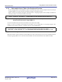
Abstract
This document describes the setting method to perform a chained transfer using DMAC II.
2.
Introduction
The application example described in this document applies to the following microcomputers (MCUs):
• MCUs: R32C/116 Group
R32C/117 Group
R32C/118 Group
This application note can be used with other R32C/100 Series MCUs which have the same special function registers
(SFRs) as the above groups. Check the manuals for any modifications to functions. Careful evaluation is recommended
before using the program described in this application note.
REJ05B1415-0100 Rev.1.00
July 30, 2010
Page 1 of 14
Using DMAC II with Chained Transfer
R32C/100 Series
3.
Outline
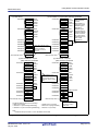
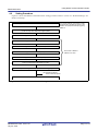
In a chained transfer, a data transfer is sequentially performed according to a DMAC II index (transfer information)
linked with the previous transfer.
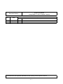
Table 3.1 lists selectable functions when using chained transfer mode, and the settings in this document. Table 3.2 lists
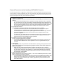
the number of transfers and transfer sources in this document, and the DMAC II triggers. Figure 3.1 shows an
operation example of a chained transfer when using an INT0 interrupt to trigger DMAC II.
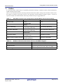
Table 3.1
Selectable Functions when Using Chained Transfer Mode and Document Settings
Item
Selectable Function
8 bits
Transfer sizes
16 bits
Immediate data
Transfer sources
Memory
Non-incrementing addressing
Source addressing
Incrementing addressing
Non-incrementing addressing
Destination addressing
Incrementing addressing
Single transfer
Transfer modes
Burst transfer
Calculation not used
Calculation transfer
Calculation used
Interrupt not generated
DMA II transfer complete interrupt
Interrupt generated
Table 3.2
Setting
8 bits
Memory
Incrementing addressing
Non-incrementing addressing
Single transfer
Calculation not used
Interrupt not generated
Number of Transfers and Transfer Sources, and DMAC II Triggers
Item
Number of transfers
Transfer sources
DMAC II trigger
REJ05B1415-0100 Rev.1.00
July 30, 2010
Settings
5 times + 5 times
DMAC II index (1): 11h, 22h, 33h, 44h, 55h
DMAC II index (2): FFh, EEh, DDh, CCh, BBh
INT0 interrupt
Page 2 of 14
Using DMAC II with Chained Transfer
R32C/100 Series
(1) Initial setting
(2) First DMAC II request (INT0 interrupt) generated
00001000h
0086h
0002h
00002000h
00002800h
00001400h
MOD
COUNT
SADR
DADR
CADR
00001000h
0086h
0001h
00002001h
00002800h
00001400h
00001400h
0086h
0002h
00003000h
00003800h
00001800h
MOD
COUNT
SADR
DADR
CADR
00001400h
0086h
0002h
00003000h
00003800h
00001800h
00002000h
00002001h
11h
22h
00002000h
00002001h
11h
22h
00002800h
XXh
00002800h
11h
00003000h
00003001h
FFh
EEh
00003800h
XXh
00003000h
00003001h
FFh
EEh
00003800h
XXh
INT0 interrupt vector (1)
When DMA II transfer starts,
the DMAC II index setting
allocated to address
00001000h is used for
operation.
INT0 interrupt vector (1)
00001000h
(3) Second DMAC II request
(INT0 interrupt) generated
00001000h
0086h
0000h
00002002h
00002800h
00001400h
MOD
COUNT
SADR
DADR
CADR
00001400h
0086h
0002h
00003000h
00003800h
00001800h
MOD
COUNT
SADR
DADR
CADR
00002000h
00002001h
11h
22h
DMA II
transfer
00002800h
(4) Third DMAC II request
(INT0 interrupt) generated
00001000h
0086h
0000h
00002002h
00002800h
00001400h
MOD
COUNT
SADR
DADR
CADR
00001400h
0086h
0001h
00003001h
00003800h
00001800h
MOD
COUNT
SADR
DADR
CADR
When COUNT is 0, the
value of the DMA II transfer
trigger interrupt vector is
overwritten with the CADR
value.
11h
22h
22h
00002800h
22h
00003000h
00003001h
FFh
EEh
00003000h
00003001h
FFh
EEh
00003800h
XXh
00003800h
FFh
00001400h
The above diagram assumes the following:
• SIZE bit is 0 (8 bits)
• UPDS bit is 1 (incrementing addressing)
• UPDD bit is 0 (non-incrementing addressing)
After performing a
DMA II transfer,
COUNT
decrements by 1.
When the source
addressing and
destination
addressing are
MOD
COUNT incrementing, the
SADR and DADR
SADR
values increment
DADR
by 1 and 2 when
CADR
transferring 8 bits
and 16 bits,
respectively.
DMA II
transfer
00001000h
00002000h
00002001h
INT0 interrupt vector (1)
MOD
COUNT
SADR
DADR
CADR
INT0 interrupt vector (1)
• OPER bit is 0 (not used)
• BRST bit is 0 (single transfer)
• INTE bit is 0 (not used)
DMA II transfer
00001400h
Operated using the
DMAC II index setting
allocated to address
00001400h
Note:
1. Software interrupt number 31 in the relocatable vector table.
Figure 3.1
Operation Example of Chained Transfer Using an INT0 Interrupt to Trigger DMAC II
REJ05B1415-0100 Rev.1.00
July 30, 2010
Page 3 of 14
Using DMAC II with Chained Transfer
R32C/100 Series
4.
Settings
This chapter explains the settings for performing a chained transfer using DMAC II.
4.1
DMAC II Settings
To activate DMAC II, set the following:
• Registers RIPL1 and RIPL2
• DMAC II index
• The interrupt control register of the peripheral function triggering DMAC II
• The relocatable vector of the peripheral function triggering DMAC II
• The IRLT bit in the IIOiIE register if the intelligent I/O interrupt is used (i = 0 to 11). Refer to the hardware
user’s manual for details on the IIOiIE register.
4.1.1
Registers RIPL1 and RIPL2
When the DMAII bits in both the RIPL1 and RIPL2 registers are set to 1 (DMA II transfer selected) and the FSIT
bits are set to 0 (normal interrupt selected), DMAC II is activated by an interrupt request from any peripheral
function with bits ILVL2 to ILVL0 in the corresponding interrupt control register set to 111b (level 7). Registers
RIPL1 and RIPLS should be set with the same value.
Table 4.1 lists the setting values of registers RIPL1 and RIPL2 as used in this document.
Table 4.1
Setting Values of Registers RIPL1 and RIPL2
Register Symbol
Setting Value
RIPL1, RIPL2
20h
REJ05B1415-0100 Rev.1.00
July 30, 2010
Remarks
• Bits RLVL2 to RLVL0 are 000b (level 0)
• FSIT bit is 0 (use interrupt request level 7 for normal interrupt)
• DMAII bit is 1 (use interrupt request level 7 for DMA II transfer)
• b7 and b6 are 0
Page 4 of 14
Using DMAC II with Chained Transfer
R32C/100 Series
4.1.2
DMAC II Index
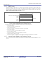
The DMAC II index is a data table of 16 to 24 bytes when performing a chained transfer. The data table stores
parameters for transfer mode, transfer counter, source address, operation address as an address to be calculated,
destination address, chained transfer base address, and DMA II transfer complete interrupt vector address. This
DMAC II index should be allocated on the RAM.
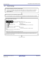
Figure 4.1 shows the DMAC II index as set in this document.
16 bits
DMAC II index starting address (BASE)
BASE + 2
Transfer counter
BASE + 4
Source address
BASE + 8
Destination address
BASE + 12
Figure 4.1
Transfer mode
16 bytes
Chained transfer base address
DMAC II Index Configuration When Using Memory-to-memory Transfer and Chained
Transfer, and Not Using DMA II Transfer Complete Interrupt
The following is an explanation of the DMAC II index contents as shown in Figure 4.1.
• Transfer mode (MOD)
2-byte data is required to set transfer mode.
• Transfer counter (COUNT)
2-byte data is required to set the number of transfers to be performed.
• Source address (SADR)
4-byte data is required to set a source address in a memory.
• Destination address (DADR)
4-byte data is required to set a destination address in a memory.
• Chained transfer base address (CADR)
4-byte data is required to set BASE, the starting address of the DMAC II index for the next transfer.
4.1.3
Interrupt Control Register of the Peripheral Function
Set bits ILVL2 to ILVL0 in the interrupt control register for the peripheral interrupt triggering DMAC II to 111b
(level 7).
REJ05B1415-0100 Rev.1.00
July 30, 2010
Page 5 of 14
Using DMAC II with Chained Transfer
R32C/100 Series
4.1.4
Relocatable Vector Table of the Peripheral Function
Set the starting address of the DMAC II index to the interrupt vector for the peripheral function interrupt
triggering DMAC II. In this document, the DMAC II trigger is the INT0 interrupt.
Figure 4.2 shows an example of setting the asm function in a C language program. In this example, the DMAC II
index (dm_index) is set to the relocatable vector table.
asm( " .rvector 31, _dm_index" );
Figure 4.2
// Define DMAC II Index (Software Interrupt Number 31)
Setting Example for the Relocatable Vector Table of the Peripheral Function When
Using the INT0 Interrupt to Trigger DMAC II
To use the chained transfer, allocate the relocatable vector table on the RAM.
Figure 4.3 shows an example of allocating the relocatable vector on the RAM in a C language program. This
example uses the memcpy function, so include “string.h” in the standard library.
memcpy(ram_vect,S_VECTOR,256*4); // Copy the relocatable vector table on the RAM
asm(" ldc #_ram_vect, intb "); // The relocatable vector table should be located on the RAM
Figure 4.3
Allocating the Relocatable Vector Table on the RAM
When the transfer counter (COUNT) reaches 0000h, the value of the interrupt vector for the peripheral function
interrupt triggering DMAC II is overwritten with the DMAC II index chained transfer base address (CADR).
REJ05B1415-0100 Rev.1.00
July 30, 2010
Page 6 of 14
Using DMAC II with Chained Transfer
R32C/100 Series
4.2
Setting Procedure
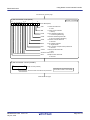
Figure 4.4 shows the DMAC II chained transfer setting procedure. Refer to section 4.3 “Detailed Settings” for
details on each step.
(1) Transfer relocatable vector table on ROM to RAM
The starting address of the DMAC II index
should be set in the interrupt vector on the
ROM for the peripheral interrupt triggering
DMAC II.
(2) Set interrupt vector table base register (INTB)
(3) Set registers RIPL1 and RIPL2
(4) Set transfer method (MOD)
(5) Set transfer counter (COUNT)
(6) Set source address (SADR)
Set number of DMAC II
indexes to be used.
(7) Set destination address (DADR)
(8) Set chained transfer base address (CADR)
(9) Set interrupt control register of the peripheral function triggering DMAC II
(10) Generate peripheral
function interrupt request
(11) Start chained transfer
Figure 4.4
DMAC II Chained Transfer Setting Procedure
REJ05B1415-0100 Rev.1.00
July 30, 2010
Page 7 of 14
Using DMAC II with Chained Transfer
R32C/100 Series
4.3
Detailed Settings
(1) Transfer relocatable vector table on ROM to RAM.
Transfer the relocatable vector table from ROM to RAM. The starting address of the DMAC II
index should be set in the interrupt vector on the ROM for the peripheral function interrupt
triggering DMAC II.
(2) Set the interrupt vector table base register (INTB).
In the INTB register, set the start address of the relocatable vector table allocated on the RAM.
(3) Set registers RIPL1 and RIPL2.
b7
b0
1
0 0 0 0 Wake-up IPL Setting Register i (RIPLi) (i = 1, 2)
RLVL2 to RLVL0
FSIT
Interrupt Priority Level for Wake-up Select Bit
000: Level 0
Fast Interrupt Select Bit
0: Use interrupt request level 7 for normal interrupt
Should be written with 0
DMAII
DMA II Select Bit
1: Use interrupt request level 7 for DMA II transfer
Should be written with 0
Registers RIPL1 and RIPL2 should be set with the same value.
Bits ILVL2 to ILVL0 in the interrupt control register should be set after the DMAII bit is set. DMAC II transfer is not
affected by the I flag or the IPL.
Continued on next page
REJ05B1415-0100 Rev.1.00
July 30, 2010
Page 8 of 14
Using DMAC II with Chained Transfer
R32C/100 Series
Continued from previous page
(4) Set the transfer mode (MOD).
b15
b8 b7
0
Allocate on the RAM.
b0
1 0 0 0 0 1 1 0 Transfer Mode (MOD)
SIZE
Transfer Size Select Bit
0: 8 bits
IMM
Transfer Source Select Bit
1: Memory
Source Addressing Select Bit
UPDS
1: Incrementing addressing
Destination Addressing Select Bit
UPDD
0: Non-incrementing addressing
OPER
Calculation Transfer Select Bit
0: Not used
BRST
Burst Transfer Select Bit
0: Single transfer
INTE
DMA II Transfer Complete Interrupt Select Bit
0: Not used
CHAIN
Chained Transfer Select Bit
1: Used
Should be written with 0
MULT
Multiple Transfer Select Bit
0: Not used
(5) Set the transfer counter (COUNT).
b15
b0
Transfer counter (COUNT)
Set the number of transfers to be performed
Transfers are not performed when
the transfer counter is set to 0000h.
Continued on next page
REJ05B1415-0100 Rev.1.00
July 30, 2010
Page 9 of 14
Using DMAC II with Chained Transfer
R32C/100 Series
Continued from previous page
(6) Set the source address (SADR).
b31
b0
Source Address (SADR)
Set the source address.
(7) Set the destination address (DADR).
b31
b0
Destination Address (DADR)
Set the destination address.
(8) Set the chained transfer base address (CADR).
b31
b0
Chained Transfer Base Address (CADR)
Set the DMAC II index start address (BASE) of the next transfer.
Continued on next page
REJ05B1415-0100 Rev.1.00
July 30, 2010
Page 10 of 14
Using DMAC II with Chained Transfer
R32C/100 Series
Continued from previous page
(9) Set the interrupt control register of the peripheral function triggering DMAC II.
To trigger DMAC II using peripheral function interrupts, set all bits ILVL2 to ILVL0 (level 7) to
111b.
b7
b0
0 1 1 1 Interrupt Control Register
TA0IC to TA4IC, TB0IC to TB5IC, S0TIC to S8TIC, S0RIC to S8RIC,
BCN0IC to BCN6IC, DM0IC to DM3IC, AD0IC, KUPIC, IIO0IC to IIO11IC,
I2CIC, I2CLIC, C0FTIC and C1FTIC, C0FRIC and C1FRIC, C0TIC and C1TIC,
C0RIC and C1RIC, C0EIC and C1EIC, C0WIC and C1WIC
ILV2 to ILV0
Interrupt Request Level Select Bit
111: Level 7
IR
Interrupt Request Flag
0: No interrupt requested
The IR bit should be set to 0.
Should be written with 0
b7
b0
0 1 1 1 Interrupt Control Register (INT0IC to INT8IC)
ILV2 to ILV0
IR
Interrupt Request Level Select Bit
111: Level 7
Interrupt Request Flag
0: No interrupt requested
POL
Polarity Select Bit
0: Select the falling edge or a low
1: Select the rising edge or a high
LVS
Level/Edge Sensitive Select Bit
0: Edge sensitive
1: Level sensitive
The IR bit should be set to 0.
Should be written with 0
The POL bit should be set to 0 (select the falling edge or a low) to set the corresponding bit in registers IFSR0 and
IFSR1 to 1 (both edges).
When using the LVS bit to select the level sensitive, the corresponding bit in registers IFSR0 and IFSR1 should be set
to 0 (one edge).
Continued on next page
REJ05B1415-0100 Rev.1.00
July 30, 2010
Page 11 of 14
Using DMAC II with Chained Transfer
R32C/100 Series
Continued from previous page
(10) Generate peripheral function interrupt request.
Generate an interrupt request for the peripheral function interrupt set to trigger DMAC II.
(11) Start chained transfer.
When the peripheral function interrupt request is received and DMAC II chained transfer starts,
the transfer counter (COUNT) decrements by 1. When COUNT reaches 000h, the peripheral
function interrupt relocatable vector value is overwritten with the chained transfer base address
(CADR), and the next DMAC II index is started.
REJ05B1415-0100 Rev.1.00
July 30, 2010
Page 12 of 14
Using DMAC II with Chained Transfer
R32C/100 Series
5.
Sample Program
A sample program can be downloaded from the Renesas Electronics website.
5.1
Explanation
The following explains the sample program operation.
(1) Allocating the relocatable vector table on the RAM
The relocatable vector table on the ROM is transferred to RAM. After allocating it to RAM, the start address
of the relocatable vector table is set to the interrupt vector table base register (INTB).
(2) Setting the DMAC II index
Two DMAC II indexes are set. One CHAIN bit is set to 1 (used), and the other is set to 0 (not used).
(3) Setting the DMA II trigger
The INT0 interrupt control register is set as the DMA II trigger.
(4) Operation after starting DMA II transfer
After generating a transfer request, when the transfer counter (COUNT) is 0000h, the chained transfer base
address (CADR) value is overwritten by the interrupt vector value. All subsequent transfers follow the
DMAC II index (chained transfers not used) indicated by the overwritten interrupt vector value.
5.2
Program Flowchart
The sample program is configured with the main function. Figure 5.1 shows the main function flowchart.
main function (main)
Figure 5.1
(1)
Disable maskable interrupts
(2)
Set port P8_2 (INT0 pin) as an input port
(3)
Transfer relocatable vector table on ROM to RAM
(4)
Set relocatable vector table start address allocated on
RAM to the interrupt vector table base register (INTB)
(5)
Set registers RIPL1 and RIPL2
(6)
Set DMAC II index (1) (chain transfer used)
(7)
Set DMAC II index (2) (chain transfer not used)
(8)
Set INT0 interrupt control register
main Function Flowchart
REJ05B1415-0100 Rev.1.00
July 30, 2010
Page 13 of 14
R32C/100 Series
6.
Using DMAC II with Chained Transfer
Reference Documents
R32C/116 Group User’s Manual: Hardware Rev.1.00
R32C/117 Group User’s Manual: Hardware Rev.1.00
R32C/118 Group User’s Manual: Hardware Rev.1.00
The latest versions can be downloaded from the Renesas Electronics website.
Technical Update/Technical News
The latest information can be downloaded from the Renesas Electronics website.
C Compiler User’s Manual
R32C/100 Series C Compiler Package V.1.02
C Compiler User’s Manual Rev.2.00
The latest version can be downloaded from the Renesas Electronics website.
Website and Support
Renesas Electronics website
http://www.renesas.com/
Inquiries
http://www.renesas.com/inquiry
REJ05B1415-0100 Rev.1.00
July 30, 2010
Page 14 of 14
R32C/100 Series
Using DMAC II with Chained Transfer
Revision History
Rev.
Date
1.00
July 30, 2010
Description
Page
—
Summary
First edition issued
All trademarks and registered trademarks are the property of their respective owners.
A-1
General Precautions in the Handling of MPU/MCU Products
The following usage notes are applicable to all MPU/MCU products from Renesas. For detailed usage notes
on the products covered by this manual, refer to the relevant sections of the manual. If the descriptions under
General Precautions in the Handling of MPU/MCU Products and in the body of the manual differ from each
other, the description in the body of the manual takes precedence.
1. Handling of Unused Pins
Handle unused pins in accord with the directions given under Handling of Unused Pins in the
manual.
The input pins of CMOS products are generally in the high-impedance state. In operation
with an unused pin in the open-circuit state, extra electromagnetic noise is induced in the
vicinity of LSI, an associated shoot-through current flows internally, and malfunctions occur
due to the false recognition of the pin state as an input signal become possible. Unused
pins should be handled as described under Handling of Unused Pins in the manual.
2. Processing at Power-on
The state of the product is undefined at the moment when power is supplied.
The states of internal circuits in the LSI are indeterminate and the states of register
settings and pins are undefined at the moment when power is supplied.
In a finished product where the reset signal is applied to the external reset pin, the states
of pins are not guaranteed from the moment when power is supplied until the reset
process is completed.
In a similar way, the states of pins in a product that is reset by an on-chip power-on reset
function are not guaranteed from the moment when power is supplied until the power
reaches the level at which resetting has been specified.
3. Prohibition of Access to Reserved Addresses
Access to reserved addresses is prohibited.
The reserved addresses are provided for the possible future expansion of functions. Do
not access these addresses; the correct operation of LSI is not guaranteed if they are
accessed.
4. Clock Signals
After applying a reset, only release the reset line after the operating clock signal has become
stable. When switching the clock signal during program execution, wait until the target clock
signal has stabilized.
When the clock signal is generated with an external resonator (or from an external
oscillator) during a reset, ensure that the reset line is only released after full stabilization of
the clock signal. Moreover, when switching to a clock signal produced with an external
resonator (or by an external oscillator) while program execution is in progress, wait until
the target clock signal is stable.
5. Differences between Products
Before changing from one product to another, i.e. to one with a different part number, confirm
that the change will not lead to problems.
The characteristics of MPU/MCU in the same group but having different part numbers may
differ because of the differences in internal memory capacity and layout pattern. When
changing to products of different part numbers, implement a system-evaluation test for
each of the products.
Notice
1.
All information included in this document is current as of the date this document is issued. Such information, however, is subject to change without any prior notice. Before purchasing or using any Renesas
Electronics products listed herein, please confirm the latest product information with a Renesas Electronics sales office. Also, please pay regular and careful attention to additional and different information to
be disclosed by Renesas Electronics such as that disclosed through our website.
2.
Renesas Electronics does not assume any liability for infringement of patents, copyrights, or other intellectual property rights of third parties by or arising from the use of Renesas Electronics products or
technical information described in this document. No license, express, implied or otherwise, is granted hereby under any patents, copyrights or other intellectual property rights of Renesas Electronics or
others.
3.
You should not alter, modify, copy, or otherwise misappropriate any Renesas Electronics product, whether in whole or in part.
4.
Descriptions of circuits, software and other related information in this document are provided only to illustrate the operation of semiconductor products and application examples. You are fully responsible for
the incorporation of these circuits, software, and information in the design of your equipment. Renesas Electronics assumes no responsibility for any losses incurred by you or third parties arising from the
use of these circuits, software, or information.
5.
When exporting the products or technology described in this document, you should comply with the applicable export control laws and regulations and follow the procedures required by such laws and
regulations. You should not use Renesas Electronics products or the technology described in this document for any purpose relating to military applications or use by the military, including but not limited to
the development of weapons of mass destruction. Renesas Electronics products and technology may not be used for or incorporated into any products or systems whose manufacture, use, or sale is
prohibited under any applicable domestic or foreign laws or regulations.
6.
Renesas Electronics has used reasonable care in preparing the information included in this document, but Renesas Electronics does not warrant that such information is error free. Renesas Electronics
7.
Renesas Electronics products are classified according to the following three quality grades: "Standard", "High Quality", and "Specific". The recommended applications for each Renesas Electronics product
assumes no liability whatsoever for any damages incurred by you resulting from errors in or omissions from the information included herein.
depends on the product's quality grade, as indicated below. You must check the quality grade of each Renesas Electronics product before using it in a particular application. You may not use any Renesas
Electronics product for any application categorized as "Specific" without the prior written consent of Renesas Electronics. Further, you may not use any Renesas Electronics product for any application for
which it is not intended without the prior written consent of Renesas Electronics. Renesas Electronics shall not be in any way liable for any damages or losses incurred by you or third parties arising from the
use of any Renesas Electronics product for an application categorized as "Specific" or for which the product is not intended where you have failed to obtain the prior written consent of Renesas Electronics.
The quality grade of each Renesas Electronics product is "Standard" unless otherwise expressly specified in a Renesas Electronics data sheets or data books, etc.
"Standard":
Computers; office equipment; communications equipment; test and measurement equipment; audio and visual equipment; home electronic appliances; machine tools;
personal electronic equipment; and industrial robots.
"High Quality": Transportation equipment (automobiles, trains, ships, etc.); traffic control systems; anti-disaster systems; anti-crime systems; safety equipment; and medical equipment not specifically
designed for life support.
"Specific":
Aircraft; aerospace equipment; submersible repeaters; nuclear reactor control systems; medical equipment or systems for life support (e.g. artificial life support devices or systems), surgical
implantations, or healthcare intervention (e.g. excision, etc.), and any other applications or purposes that pose a direct threat to human life.
8.
You should use the Renesas Electronics products described in this document within the range specified by Renesas Electronics, especially with respect to the maximum rating, operating supply voltage
range, movement power voltage range, heat radiation characteristics, installation and other product characteristics. Renesas Electronics shall have no liability for malfunctions or damages arising out of the
use of Renesas Electronics products beyond such specified ranges.
9.
Although Renesas Electronics endeavors to improve the quality and reliability of its products, semiconductor products have specific characteristics such as the occurrence of failure at a certain rate and
malfunctions under certain use conditions. Further, Renesas Electronics products are not subject to radiation resistance design. Please be sure to implement safety measures to guard them against the
possibility of physical injury, and injury or damage caused by fire in the event of the failure of a Renesas Electronics product, such as safety design for hardware and software including but not limited to
redundancy, fire control and malfunction prevention, appropriate treatment for aging degradation or any other appropriate measures. Because the evaluation of microcomputer software alone is very difficult,
please evaluate the safety of the final products or system manufactured by you.
10. Please contact a Renesas Electronics sales office for details as to environmental matters such as the environmental compatibility of each Renesas Electronics product. Please use Renesas Electronics
products in compliance with all applicable laws and regulations that regulate the inclusion or use of controlled substances, including without limitation, the EU RoHS Directive. Renesas Electronics assumes
no liability for damages or losses occurring as a result of your noncompliance with applicable laws and regulations.
11. This document may not be reproduced or duplicated, in any form, in whole or in part, without prior written consent of Renesas Electronics.
12. Please contact a Renesas Electronics sales office if you have any questions regarding the information contained in this document or Renesas Electronics products, or if you have any other inquiries.
(Note 1)
"Renesas Electronics" as used in this document means Renesas Electronics Corporation and also includes its majority-owned subsidiaries.
(Note 2)
"Renesas Electronics product(s)" means any product developed or manufactured by or for Renesas Electronics.
http://www.renesas.com
SALES OFFICES
Refer to "http://www.renesas.com/" for the latest and detailed information.
Renesas Electronics America Inc.
2880 Scott Boulevard Santa Clara, CA 95050-2554, U.S.A.
Tel: +1-408-588-6000, Fax: +1-408-588-6130
Renesas Electronics Canada Limited
1101 Nicholson Road, Newmarket, Ontario L3Y 9C3, Canada
Tel: +1-905-898-5441, Fax: +1-905-898-3220
Renesas Electronics Europe Limited
Dukes Meadow, Millboard Road, Bourne End, Buckinghamshire, SL8 5FH, U.K
Tel: +44-1628-585-100, Fax: +44-1628-585-900
Renesas Electronics Europe GmbH
Arcadiastrasse 10, 40472 Düsseldorf, Germany
Tel: +49-211-65030, Fax: +49-211-6503-1327
Renesas Electronics (China) Co., Ltd.
7th Floor, Quantum Plaza, No.27 ZhiChunLu Haidian District, Beijing 100083, P.R.China
Tel: +86-10-8235-1155, Fax: +86-10-8235-7679
Renesas Electronics (Shanghai) Co., Ltd.
Unit 204, 205, AZIA Center, No.1233 Lujiazui Ring Rd., Pudong District, Shanghai 200120, China
Tel: +86-21-5877-1818, Fax: +86-21-6887-7858 / -7898
Renesas Electronics Hong Kong Limited
Unit 1601-1613, 16/F., Tower 2, Grand Century Place, 193 Prince Edward Road West, Mongkok, Kowloon, Hong Kong
Tel: +852-2886-9318, Fax: +852 2886-9022/9044
Renesas Electronics Taiwan Co., Ltd.
7F, No. 363 Fu Shing North Road Taipei, Taiwan
Tel: +886-2-8175-9600, Fax: +886 2-8175-9670
Renesas Electronics Singapore Pte. Ltd.
1 harbourFront Avenue, #06-10, keppel Bay Tower, Singapore 098632
Tel: +65-6213-0200, Fax: +65-6278-8001
Renesas Electronics Malaysia Sdn.Bhd.
Unit 906, Block B, Menara Amcorp, Amcorp Trade Centre, No. 18, Jln Persiaran Barat, 46050 Petaling Jaya, Selangor Darul Ehsan, Malaysia
Tel: +60-3-7955-9390, Fax: +60-3-7955-9510
Renesas Electronics Korea Co., Ltd.
11F., Samik Lavied' or Bldg., 720-2 Yeoksam-Dong, Kangnam-Ku, Seoul 135-080, Korea
Tel: +82-2-558-3737, Fax: +82-2-558-5141
© 2010 Renesas Electronics Corporation. All rights reserved.
Colophon 1.0