1
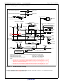
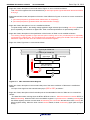
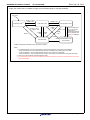
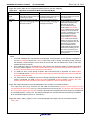
RENESAS TECHNICAL UPDATE TN-16C-A232A/E Date: Sep. 24, 2013 RENESAS TECHNICAL UPDATE 1753, Shimonumabe, Nakahara-ku, Kawasaki-shi, Kanagawa 211-8668 Japan Renesas Electronics Corporation Product Category Title MPU & MCU Document No. Errata to R32C/156 Group User’s Manual: Hardware Information Technical Notification Category TN-16C-A232A/E Rev. 1.00 Lot No. Applicable R32C/156 Group Product Reference Document R32C/156 Group User’s Manual: Hardware Rev. 1.10 (REJ09B0506-0110) This document describes corrections to the R32C/156 Group User’s Manual: Hardware, Rev. 1.10. The corrections are indicated in red in the list below. • Page 16 of 625, register symbol “R3R0” in line 3 of 2.1.1 is corrected as follows: “R3R1” • Page 87 of 625, description of the third paragraph of 6.2.1 is modified as follows: “When the voltage rises to or above Vdet(R) again, the VMF bit becomes 1 (VCC Vdet) and the LVDF bit becomes 1. At this point, an interrupt request is generated when the LVDIEN bit is 1.” ©2013. Renesas Electronics Corporation, All rights reserved. Page 1 of 10 RENESAS TECHNICAL UPDATE Date: Sep. 24, 2013 TN-16C-A232A/E • Page 90 of 625, Figure 7.1 is corrected as follows: WAIT instruction (wait mode) S Q R wait_mode STOP instruction (stop mode) S Q R stop_mode RESET NMI Low speed clock Low voltage detection interrupt Output signal from priority resolver f8 f32 01 10 11 CLKOUT CM01 and CM00 Main clock oscillator XIN CM20 XOUT CM05 Detection enabled Oscillator stop detection interrupt request Main clock stop detector Peripheral clock source Peripheral clocks fAD f1 Main clock f8 PLL clock PLL frequency synthesizer 1/p (Note 1) PM26 BCD PLL oscillator stop CM02 1/b (Note 3) f32 1/2n f2n CST 0 1 BCS CM10 1/4 1/8 (Note 2) BCS 0 Base Clock 1 CCD wait_mode stop_mode 1/m (Note 4) Sub clock oscillator XCIN XCOUT 1/256 f256 PCD CM30 1/q 1 0 (Note 5) CPU clock Peripheral bus clock CPSR = 1 Sub clock fC CM04 stop_mode 1/4 On-chip oscillator (125 kHz) Divider reset CM31 0 1 1/32 fC32 fOCO4 On-chip oscillator clock fOCO CM00 to CM02, CM04, and CM05: Bits in the CM0 register PM26: Bit in the PM2 register CM10: Bit in the CM1 register CST: Bit in the TCSPR register CM20: Bit in the CM2 register CPSR: Bit in the CPSRF register CM30 and CM31: Bits in the CM3 register BCS: Bit in the CCR register Notes: 1. The value of p can be selected by setting bits PM36 and PM35 in the PM3 register (p = 2, 4, 6, 8). 2. The value of n can be selected by setting bits CNT3 to CNT0 in the TCSPR register (n = 0 to 15). When n is 0, the clock is not divided. 3. The value of b can be selected by setting bits BCD1 and BCD0 in the CCR register (b = 2, 3, 4, 6). 4. The value of m can be selected by setting bits CCD1 and CCD0 in the CCR register (m = 1 to 4). 5. The value of q can be selected by setting bits PCD1 and PCD0 in the CCR register (q = 2 to 4). Figure 7.1 Clock Generation Circuitry • Page 92 of 625, bit name “XCIN-XCOUT Drive Power Select Bit” in Figure 7.3 is modified as follows: “XCIN-XCOUT Drive Strength Select Bit” Page 2 of 10 RENESAS TECHNICAL UPDATE TN-16C-A232A/E Date: Sep. 24, 2013 • Page 93 of 625, bit name “XIN-XOUT Drive Power Select Bit” in Figure 7.4 is modified as follows: “XIN-XOUT Drive Strength Select Bit” • Page 93 of 625, description of Note 2 in Figure 7.4 is modified as follows: “When the BCS bit in the CCR register is 0 (PLL clock selected as base clock source), the PLL frequency synthesizer does not stop oscillating even if the CM10 bit is set to 1.” • Page 93 of 625, bit symbol “CM02” in Note 3 of Figure 7.5 is corrected as follows: “CM20” • Page 103 of 625, description of the last paragraph of 7.1.4 is modified as follows: “It starts running when setting any of the following bits to 1; the CM31 bit in the CM3 register or the PM22 bit in the PM2 register. It is not necessary to wait for stabilization because the on-chip oscillator instantly starts oscillating.” • Page 104 of 625, description “(Refer to Figure 7.18 “State Transition (when the sub clock is used)”)” is deleted from 7.2. • Page 113 of 625, description of 7.7.2 is modified as follows: “The base clock stops in wait mode, so clocks generated by the base clock, the CPU clock and peripheral bus clock, stop running as well. Thus the CPU and watchdog timer, operated by these two clocks, also stop.” • Page 122 of 625, “IOBC” is added to description in Function of the PRC1 bit in Figure 9.1 as follows: “Enable writing to registers PM0, PM2, INVC0, INVC1, and IOBC” • Page 122 of 625, description “Bits PRC0 and PRC1 do not automatically become 0. They should be set to 0 by a program.” is deleted from Note 1 of Figure 9.1. • Page 126 of 625, description of Note 1 in Figure 10.1 is modified as follows: “The peripheral interrupts are generated by the corresponding peripherals in the MCU.” • Page 127 of 625, the second paragraph of (5) in 10.2 is modified as follows: “The stack pointer (SP) used for this interrupt differs depending on the software interrupt numbers. For software interrupt numbers 0 to 127, when an interrupt request is accepted, the U flag is saved and set to 0 to select the interrupt stack pointer (ISP) during the interrupt sequence. The saved data of the U flag is restored upon returning from the interrupt handler. For software interrupt numbers 128 to 255, the stack pointer does not change during the interrupt sequence.” • Page 129 of 625, description of 10.5 is corrected as follows: “Each interrupt vector has a 4-byte memory space, in which the start address of the associated interrupt handler is stored. When an interrupt request is accepted, a jump to the address set in the interrupt vector takes place. Figure 10.2 shows an interrupt vector.” • Page 130 of 625, description in the Remarks for the BRK instruction in Table 10.1 is corrected as follows: “If address FFFFFFE7h is FFh, a jump to the interrupt vector of software interrupt number 0 in the relocatable vector table takes place” • Page 137 of 625, description for the IR bit below Figure 10.4 is corrected as follows: “The IR bit becomes 1 (interrupt requested) when an interrupt request is generated; this bit setting is retained until the interrupt request is accepted. When the request is accepted and a jump to the corresponding interrupt vector takes place, the IR bit becomes 0 (no interrupt requested). The IR bit can be set to 0 by a program. This bit should not be set to 1.” Page 3 of 10 RENESAS TECHNICAL UPDATE TN-16C-A232A/E Date: Sep. 24, 2013 • Page 141 of 625, description of Note 1 in Table 10.7 is corrected as follows: “These are the values when the interrupt vectors are aligned to the addresses in multiples of 4 in the internal ROM. However, the condition does not apply to the fast interrupt.” • Page 143 of 625, description in lines 4 to 5 and 7 to 8 of 10.8 as follows: “For maskable interrupts (peripheral interrupts), the interrupt request level select bits (bits ILVL2 to ILVL0) select a request level. If two or more interrupt requests have the same request level, the interrupt with higher priority, predetermined by hardware, is accepted. The priorities of the reset and special interrupts, such as the watchdog timer interrupt, are determined by the hardware. Note that the reset has the highest priority. The following is the priority order determined by the hardware:” • Page 150 of 625, register symbol “IIOiE” in line 16 of 10.13 is corrected as follows: “IIOiIE” • Page 154 of 625, description in lines 4 to 6 of 11. Watchdog Timer is corrected as follows: “Select either an interrupt request or a reset with the CM06 bit in the CM0 register for when the watchdog timer underflows. Once the CM06 bit is set to 1 (reset), it cannot be changed to 0 (watchdog timer interrupt) by a program. It can be set to 0 only by a reset.” • Page 154 of 625, register symbol “WKD” of 11. Watchdog Timer is corrected as follows: “WDK” • Page 159 of 625, expression “a value more than 00000001h” in the Specification of DMA transfer start-up in Table 12.1 is corrected as follows: “a value other than 00000000h” • Page 167 of 625, description of the first paragraph in 12.1 is corrected as follows: “The transfer cycle is composed of bus cycles to read data from (source read) or to write data to (destination write) memory or an SFR.” •Page 173 of 625, source address “FFFFFFFh” in Note 1 of Table 13.1 is corrected as follows: “FFFFFFFFh” • Pages 175 and 176 of 625, expression “DMA II transfer complete interrupt vector address” in lines 3 to 4 and the seventh bullet point of 13.1.2 and Figure 13.2 is corrected as follows: “jump address for the DMA II transfer complete interrupt handler” • Pages 175 and 178 of 625, expression “interrupt vector” in Figure 13.2 and 13.1.4 is corrected as follows: “interrupt vector space” • Page 176 of 625, expression “jump address” in the seventh bullet point of 13.1.2 is corrected as follows: “start address” • Page 177 of 625, bit names of the OPER bit and bits CNT0 to CNT2 in Figure 13.3 are modified as follows: OPER: “Calculation Result Transfer Select Bit” CNT0 to CNT2: “Number of Transfers Setting Bit” • Page 187 of 625, description of the third bullet point of 15.1 is corrected as follows: “One-shot timer mode: The timer outputs pulses after a trigger input until the counter reaches 0000h” • Page 192 of 625, descriptions “b2 b3”, “b4 b5”, and “b6 b7” in Figure 15.9 are corrected as follows: “b3 b2”, “b5 b4”, and “b7 b6” Page 4 of 10 RENESAS TECHNICAL UPDATE Date: Sep. 24, 2013 TN-16C-A232A/E • Page 198 of 625, bit symbols “TAiTGH and TAiTGL” in Note 5 of Figure 15.12 are corrected as follows: “TAjTGH and TAjTGL” • Page 199 of 625, pin name “INT2” in Figures 15.13 and 15.14 is corrected as follows: “INT2” • Page 203 of 625, bit symbol “TAiS” in Function of the MR2 bit in Figures 15.16 is corrected as follows: “TAiOS” • Page 213 of 625, bit symbol “TBjS” and register symbol “TBjMR” in Note 2 of Table15.8 are corrected as follows: “TBiS” and “TBiMR” • Page 218 of 625, description “TBjS bit in the TBjMR register” in the first bullet point of 15.3.3.2 is corrected as follows: “TBjS bit in the TABSR or TBSR register” • Page 222 of 625, description of Note 1 in Figure 16.3 is modified as follows: “Set this register after setting the PRC1 bit in the PRCR register to 1 (write enabled). Also, rewrite this register while timers A1, A2, A4, and B2 are stopped.” • Page 229 of 625, description “The sum of setting values for registers TAi and TAi1 should be identical to the setting value of the TB2 register in this mode.” is deleted from lines 8 to 9 of 16.3. • Page 229 of 625, description in line 11 of 16.3 is corrected as follows: “Figure 16.11 shows registers TA1M, TA2M, TA4M, TA11M, TA21M, and TA41M in this function.” • Page 235 of 625, register symbol “INV1” in Note 2 of Figure 16.18 is corrected as follows: “INVC1” • Pages 243 and 244 of 625, descriptions for the CRD bit in Figures 17.5 and 17.6 are modified as follows: Bit Symbol CRD Bit Name CTS Function Disable Bit Function 0: CTS function enabled 1: CTS function disabled RW RW • Page 245 of 625, description of function of the UiIRS bit in Figure 17.7 is modified as follows: “0: Transmit buffer is empty (TI = 1) 1: Transmission is completed (TXEPT = 1)” • Page 245 of 625, bit name “Logical Inversion Select Bit” in Figure 17.7 is modified as follows: “Logic Inversion Select Bit” • Page 247 of 625, bit name “Clock Synchronous Bit” in Figure 17.11 is modified as follows: “Clock Synchronization Bit” • Page 248 of 625, expression “UiBRG count source” in the function of bits DL0 to DL2 in Figure 17.12 is corrected as follows: “baud rate generator count source” • Page 249 of 625, bit name of the RSTAREQ bit in Figure 17.13 is modified as follows: “Repeated START Condition Generate Bit” Page 5 of 10 RENESAS TECHNICAL UPDATE Date: Sep. 24, 2013 TN-16C-A232A/E • Page 255 of 625, description in the fourth dash of Figure 17.18 is corrected as follows: “The UiIRS bit in registers UiC1 and U34CON is 0 (an interrupt request is generated when the transmit buffer is empty)” • Pages 263 and 264 of 625, descriptions of function of the UiIRS bit in Figures 17.23 and 17.24 are corrected as follows: 1: “(an interrupt request is generated when transmission is completed)” 0: “(an interrupt request is generated when the transmit buffer is empty)” • Page 300 of 625, description of 18.1.5 is modified as follows: “In repeat sweep mode 1, the analog voltage applied to eight selected pins including one to four prioritized pins is repeatedly converted into a digital code. Table 18.6 lists specifications of repeat sweep mode 1.” • Page 300 of 625, description in the specification of the function in Table 18.6 is modified as follows: “The analog voltage applied to eight selected pins including one to four prioritized pins is repeatedly converted into a digital code. The prioritized pins are selected by setting bits SCAN1 and SCAN0 in the AD0CON1 register and bits APS1 and APS0 in the AD0CON2 register” • Page 312 of 625, Figure 20.1 is corrected as follows: Upper byte of data bus Lower byte of data bus Upper byte Lower byte CRCD register CRC generator X16 + X12 + X5 + 1 CRCIN register Figure 20.1 CRC Calculator Block Diagram • Page 334 of 625, description in the second bullet point of the reset conditions in Table 22.2 is modified as follows: “An input of low signal into the external interrupt pin (INT0 or INT1) as follows:” • Page 334 of 625, description of the first bullet point of the selectable functions in Table 22.2 is corrected as follows: “The base timer starts counting when the BTS or BTiS bit is set to 1. When the base timer reaches FFFFh, it starts decrementing. When the RST1 bit in the GiBCR1 register is 1 (the base timer is reset by matching with the GiPO0 register), the timer counter starts decrementing two counts after the base timer value matches the GiPO0 register setting. When the timer counter reaches 0000h, it starts incrementing again (refer to Figure 22.20).” Page 6 of 10 RENESAS TECHNICAL UPDATE Date: Sep. 24, 2013 TN-16C-A232A/E • Pages 345, 347, and 350 of 625, expression “Input to the IIOi_j pin” in Figures 22.24 to 22.26 is corrected as follows: “IIOi_j pin” • Page 369 of 625, description “with bits CKS2 to CKS0” to the first paragraph of 23.1.1 is added as follows: “When the MSS bit in the SSiCRH register is 1 (master mode), select a transmit/receive clock from among seven internal clocks (f(BCLK) divided-by-4, -8, -16, -32, -64, -128, and -256) with bits CKS2 to CKS0.” • Page 383 of 625, bit symbol “MSL” in line 14 of 23.1.7 is corrected as follows: “MLS” • Page 431 of 625, descriptions for the RBOC bit in Figure 25.2 are modified as follows: Bit Symbol RBOC Bit Name Forced Recovery From Bus-off Bit (4) Function 0: Nothing occurred 1: Forced recovery from bus-off (5) RW RW • Page 438 of 625, description in 25.1.4.1 is corrected as follows: “When the EID bit is 0, the corresponding EID bit in a received message is not compared. When this bit is 1, the corresponding EID bit in a received message is compared.” • Page 438 of 625, description in 25.1.4.2 is corrected as follows: “When the SID bit is 0, the corresponding SID bit in a received message is not compared. When this bit is 1, the corresponding SID bit in a received message is compared.” • Page 448 of 625, expression “fCAN (CAN system clock)” in line 5 of 25.1.9.5 is corrected as follows: “the peripheral bus clock” • Page 451 of 625, expression “fCAN” in line 6 of 25.1.10.3 is corrected as follows: “the peripheral bus clock” • Page 457 of 625, description of function of b7 in Figure 25.17 is corrected as follows: b7: “No register bit; the read value is 0” • Page 461 of 625, description of function of b6-b5 in Figure 25.19 is corrected as follows: b6-b5: “No register bits; the read value is 0” • Page 469 of 625, description in 25.1.20.8 is corrected as follows (refer to TN-16C-A229A/E): “The BLIF bit becomes 1 if 32 consecutive dominant bits are detected on the CAN bus while the CAN module is in CAN operation mode. After the BLIF bit becomes 1, bus lock can be detected again after either of the following conditions is satisfied: •After this bit is set to 0 from 1, recessive bits are detected (bus lock is resolved). •After this bit is set to 0 from 1, the CAN module enters CAN reset mode and then enters CAN operation mode again (internal reset).” Page 7 of 10 RENESAS TECHNICAL UPDATE Date: Sep. 24, 2013 TN-16C-A232A/E • Page 478 of 625, Note 3 is added to Figure 25.34 as follows (refer to TN-16C-A229A/E): CPU reset SLPM = 0 when CANM = 01b CAN sleep mode (2) CANM = 00b CAN reset mode SLPM = 1 CANM = 01b CANM = 00b SLPM = 0 when CANM = 10b SLPM = 1 CAN operation mode CANM = 10b CANM = 01b TEC > 255 CANM = 10b (3) CANM = 01b CAN halt mode When the BOM bit is 00b or 11b (no halt request) and 11 consecutive recessive bits are detected 128 times or the RBOC bit is 1. CAN operation mode (bus-off state) CANM = 10b (1) CANM, SLPM, BOM, and RBOC: Bits in the CiCTLR register Notes: 1. The transition timing from the bus-off state to CAN halt mode depends on the setting of the BOM bit. - When the BOM bit is 01b, the state transition timing is immediately after entering the bus-off state. - When the BOM bit is 10b, the state transition timing is at the end of the bus-off state. - When the BOM bit is 11b, the state transition timing is at the setting of the CANM bit to 10b (CAN halt mode). 2. Write only to the SLPM bit to exit/set CAN sleep mode. 3. The CAN module does not enter CAN Halt mode while the CAN bus is locked in dominant state. Enter CAN reset mode instead. Page 8 of 10 RENESAS TECHNICAL UPDATE Date: Sep. 24, 2013 TN-16C-A232A/E • Page 480 of 625, Table 25.9 is corrected as follows (refer to TN-16C-A229A/E): Table 25.9 Mode CAN reset mode CAN halt mode Operation in CAN Reset Mode and CAN Halt Mode Receiver Transmitter CAN module enters CAN reset CAN module enters CAN reset mode without waiting for the end mode after waiting for the end of of message reception message transmission (1, 4) CAN module enters CAN halt CAN module enters CAN halt mode after waiting for the end of mode after waiting for the end of message reception (2, 3) message transmission (1, 2, 4) Bus-off CAN module enters CAN reset mode without waiting for the end of bus-off recovery - When the BOM bit is 00b A halt request from a program will be acknowledged only after bus-off recovery - When the BOM bit is 01b CAN module automatically enters CAN halt mode without waiting for the end of bus-off recovery (regardless of a halt request from a program) - When the BOM bit is 10b CAN module automatically enters CAN halt mode after waiting for the end of bus-off recovery (regardless of a halt request from a program) - When the BOM bit is 11b CAN module enters CAN halt mode (without waiting for the end of bus-off recovery) if a halt is requested by a program during bus-off BOM bit: Bit in the CiCTLR register (i = 0, 1) Notes: 1. If several messages are requested to be transmitted, mode transition occurs after the completion of the first message transmission. When CAN reset mode is being requested during suspend transmission, mode transition occurs when the bus is idle, the next transmission ends, or the CAN module becomes a receiver. 2. If the CAN bus is locked in dominant state, the program can detect this state by monitoring the BLIF bit in the CiEIFR register. The CAN module does not enter CAN Halt mode while the CAN bus is locked in dominant state. Enter CAN reset mode instead. 3. If a CAN bus error occurs during reception after CAN halt mode is requested, the CAN module enters CAN halt mode. However, the CAN module does not enter CAN Halt mode when the CAN bus is locked in dominant state. 4. If a CAN bus error or arbitration lost occurs during transmission after CAN reset mode or CAN halt mode is requested, the CAN module enters the requested operating mode. However, the CAN module does not enter CAN Halt mode when the CAN bus is locked in dominant state. • Page 496 of 625, description in the last paragraph of 26. I/O Pins is corrected as follows: “The input-only port P8_5 shares a pin with NMI and has neither function select register nor the corresponding direction bit. Port P14_1 also functions as an input-only port. The function select register and bit 1 in the PD14 register are reserved. Port P9 is protected from unexpected write accesses by the PRC2 bit in the PRCR register. Ports P3, P7, and P8 are protected from unexpected write accesses by the PRC30 bit in the PRCR3 register (refer to 9. “Protection”).” • Page 502 of 625, “PD3_i register” in line 4 of the paragraph below Figure 26.6 is corrected as follows: “PD3_i bit” Page 9 of 10 RENESAS TECHNICAL UPDATE TN-16C-A232A/E Date: Sep. 24, 2013 • Page 542 of 625, Note 2 of Table 27.12 is corrected as follows: “The program is performed in 64-bit (4-word) units. A sequence of commands consists of commands from the second to fifth. The upper 29 bits of the address WA should be fixed and the lower 3 bits of respective commands from the second to fifth should be set to 000b, 010b, 100b, and 110b for the addresses 0h, 2h, 4h, and 6h, or 8h, Ah, Ch, and Eh.” • Page 556 of 625, description in the first bullet point of 27.6.8 is corrected as follows: “The minimum values of program/erase cycles specified in the electrical characteristics are the maximum values that can guarantee the initial performance of the flash memory. The program/erase operation may still be performed even if the number of program/erase cycles exceeds the guaranteed values.” • Pages 573 and 574 of 625, “Programming and erasure endurance” in Table 29.8 and “Programming and erasure endurance of flash memory” in Table 29.9 are changed as follows: “Program/erase cycles” • Pages 573 and 574 of 625, unit “times” in Tables 29.8 and 29.9 is corrected as follows: “Cycles” • Pages 580 and 591 of 625, expression “Driver power” in Tables 29.18 and 29.38 is modified as follows: “Drive strength” • Page 611 of 625, expression “TBjS bit in the TBjMR register” in 30.6.3.2 is changed as follows: “TBjS bit in the TABSR or TBSR register” • Page 613 of 625, expression “restart condition” in 30.8.3 is changed as follows: “repeated START condition” • Page 619 of 625, description in the first bullet point of 30.11.8 is corrected as follows: “The minimum values of program/erase cycles specified in the electrical characteristics are the maximum values that can guarantee the initial performance of the flash memory. The program/erase operation may still be performed even if the number of program/erase cycles exceeds the guaranteed values.” Page 10 of 10