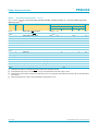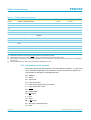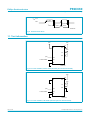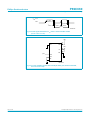
1
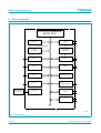
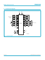
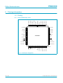
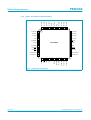
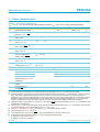
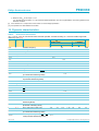
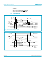
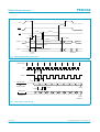
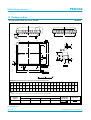
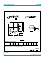
P89C669
80C51 8-bit microcontroller family with extended memory;
96 kB Flash with 2 kB RAM
Rev. 02 — 13 November 2003
Product data
1. General description
The P89C669 represents the first Flash microcontroller based on Philips
Semiconductors’ new 51MX core. The P89C669 features 96 kbytes of Flash program
memory and 2 kbytes of data SRAM. In addition, this device is equipped with a
Programmable Counter Array (PCA), a watchdog timer that can be configured to
different time ranges through SFR bits, as well as two enhanced UARTs and byte
based I2C-bus serial interface.
Philips Semiconductors’ 51MX (Memory eXtension) core is an accelerated 80C51
architecture that executes instructions at twice the rate of standard 80C51 devices.
The linear address range of the 51MX has been expanded to support up to 8 Mbytes
of program memory and 8 Mbytes of data memory. It retains full program code
compatibility to enable design engineers to re-use 80C51 development tools,
eliminating the need to move to a new, unfamiliar architecture. The 51MX core also
retains 80C51 bus compatibility to allow for the continued use of 80C51-interfaced
peripherals and Application Specific Integrated Circuits (ASICs).
The P89C669 provides greater functionality, increased performance and overall lower
system cost. By offering an embedded memory solution combined with the
enhancements to manage the memory extension, the P89C669 eliminates the need
for software work-arounds. The increased program memory enables design
engineers to develop more complex programs in a high-level language like C, for
example, without struggling to contain the program within the traditional 64 kbytes of
program memory. These enhancements also greatly improve C Language efficiency
for code size below 64 kbytes.
The P89C669 device contains a non-volatile Flash program memory that is both
parallel programmable and serial In-System and In-Application Programmable.
In-System Programming (ISP) allows the user to download new code while the
microcontroller sits in the application. In-Application Programming (IAP) means that
the microcontroller fetches new program code and reprograms itself while in the
system. This allows for remote programming over a modem link. A default serial
loader (boot loader) program in ROM allows serial In-System programming of the
Flash memory via the UART without the need for a loader in the Flash code. For
In-Application Programming, the user program erases and reprograms the Flash
memory by use of standard routines contained in ROM.
The 51MX core is described in more detail in the 51MX Architecture Reference.
P89C669
Philips Semiconductors
80C51 8-bit microcontroller family with extended memory
2. Features
2.1 Key features
■ Extended features of the 51MX Core:
◆ 23-bit program memory space and 23-bit data memory space
◆ Linear program and data address range expanded to support up to 8 Mbytes
each
◆ Program counter expanded to 23 bits
◆ Stack pointer extended to 16 bits enabling stack space beyond the 80C51
limitation
◆ New 23-bit extended data pointer and two 24-bit universal pointers greatly
improve C compiler code efficiency in using pointers to access variables in
different spaces
■ 100% binary compatibility with the classic 80C51 so that existing code is
completely reusable
■ Up to 24 MHz CPU clock with 6 clock cycles per machine cycle
■ 96 kbytes of on-chip program Flash
■ 2 kbytes of on-chip data RAM
■ Programmable Counter Array (PCA)
■ Two full-duplex enhanced UARTs
■ Byte based Fast I2C serial interface (400 kbits/s)
2.2 Key benefits
■
■
■
■
■
■
Increases program/data address range to 8 Mbytes each
Enhances performance and efficiency for C programs
Fully 80C51-compatible microcontroller
Provides seamless and compelling upgrade path from classic 80C51
Preserves 80C51 code base, investment/knowledge, and peripherals and ASICs
Supported by wide range of 80C51 development systems and programming tools
vendors
■ The P89C669 makes it possible to develop applications at lower cost and with a
reduced time-to-market
2.3 Complete features
■ Fully static
■ Up to 24 MHz CPU clock with 6 clock cycles per machine cycle
■ 96 kbytes of on-chip Flash with In-System Programming (ISP) and In-Application
Programming (IAP) capability
■ 2 kbytes of on-chip RAM
■ 23-bit program memory space and 23-bit data memory space
■ Four-level interrupt priority
■ 32 I/O lines (4 ports)
■ Three Timers: Timer0, Timer1 and Timer2
■ Two full-duplex enhanced UARTs with baud rate generator
© Koninklijke Philips Electronics N.V. 2003. All rights reserved.
9397 750 12299
Product data
Rev. 02 — 13 November 2003
2 of 33
P89C669
Philips Semiconductors
80C51 8-bit microcontroller family with extended memory
Byte based Fast I2C-bus serial interface (400 kbits/s)
Framing error detection
Automatic address recognition
Power control modes
Clock can be stopped and resumed
Idle mode
Power-down mode
Second DPTR register
Asynchronous port reset
Programmable Counter Array (PCA) (compatible with 8xC51Rx+) with five
Capture/Compare modules
■ Low EMI (inhibit ALE)
■ Watchdog timer with programmable prescaler for different time ranges
(compatible with 8xC66x with added prescaler)
■
■
■
■
■
■
■
■
■
■
3. Ordering information
Table 1:
Ordering information
Type number
Package
Name
Description
Version
P89C669FA
PLCC44
plastic leaded chip carrier; 44 leads
SOT187-2
P89C669BBD
LQFP44
plastic low profile quad flat package; 44 leads;
body 10 × 10 × 1.4 mm
SOT389-1
3.1 Ordering options
Table 2:
Ordering options
Type number
Memory
Temperature range
VDD voltage
range
Frequency
OTP
RAM
P89C669FA
96 kB
2048 B
−40 °C to +85 °C
4.5 to 5.5 V
0 to 24 MHz
P89C669BBD
96 kB
2048 B
0 °C to +70 °C
4.5 to 5.5 V
0 to 24 MHz
© Koninklijke Philips Electronics N.V. 2003. All rights reserved.
9397 750 12299
Product data
Rev. 02 — 13 November 2003
3 of 33
P89C669
Philips Semiconductors
80C51 8-bit microcontroller family with extended memory
4. Block diagram
HIGH PERFORMANCE
80C51 CPU
96 kB
CODE FLASH
UART 0
internal bus
CRYSTAL OR
RESONATOR
2 kB
DATA RAM
BAUD RATE
GENERATOR
PORT 3
UART 1
PORT 2
TIMER 0
TIMER 1
PORT 1
WATCHDOG TIMER
PORT 0
PCA (PROGRAMMABLE
COUNTER ARRAY)
OSCILLATOR
TIMER2
I2C
002aaa405
Fig 1. Block diagram.
© Koninklijke Philips Electronics N.V. 2003. All rights reserved.
9397 750 12299
Product data
Rev. 02 — 13 November 2003
4 of 33
P89C669
Philips Semiconductors
80C51 8-bit microcontroller family with extended memory
5. Functional diagram
PORT1
P89C669
T2
T2EX
ECI
CEX0
CEX1
CEX2
SCL
SDA
Address Bus 8-15
RXD0
TXD0
INT0
INT1
CEX3/T0
CEX4/T1
WR
RD
PORT2
Data Bus
PORT 3
Address bus 0-7
VSS
PORT0
VDD
Address Bus 16-22
RXD1
TXD1
RST
XTAL2
EA/VPP
PSEN
XTAL1
ALE/PROG
002aaa403
Fig 2. Functional diagram.
© Koninklijke Philips Electronics N.V. 2003. All rights reserved.
9397 750 12299
Product data
Rev. 02 — 13 November 2003
5 of 33
P89C669
Philips Semiconductors
80C51 8-bit microcontroller family with extended memory
6. Pinning information
6.1 Pinning
40 P0.3/AD3
41 P0.2/AD2
42 P0.1/AD1
43 P0.0/AD0
44 VDD
1 (NC/VSS)
2 P1.0/T2
3 P1.1/T2EX
4 P1.2/ECI
5 P1.3/CEX0
Plastic leaded chip carrier
6 P1.4/CEX1
6.1.1
P1.5/CEX2
7
39 P0.4/AD4
P1.6/SCL
8
38 P0.5/AD5
P1.7/SDA
9
37 P0.6/AD6
RST 10
36 P0.7/AD7
P3.0/RXD0 11
35 EA/VPP
P89C669FA
RXD1 12
34 TXD1
P3.1/TXD0 13
33 ALE
P3.2/INT0 14
32 PSEN
P3.3/INT1 15
31 P2.7/A15
P2.4/A12/A20 28
P2.3/A11/A19 27
P2.2/A10/A18 26
P2.1/A9/A17 25
P2.0/A8/A16 24
(NC/VDD) 23
VSS 22
XTAL1 21
29 P2.5/A13/A21
XTAL2 20
P3.5/CEX4/T1 17
P3.7/RD 19
30 P2.6/A14/A22
P3.6/WR 18
P3.4/CEX3/T0 16
002aaa404
Fig 3. PLCC44 pin configuration.
© Koninklijke Philips Electronics N.V. 2003. All rights reserved.
9397 750 12299
Product data
Rev. 02 — 13 November 2003
6 of 33
P89C669
Philips Semiconductors
80C51 8-bit microcontroller family with extended memory
34 P0.3/AD3
35 P0.2/AD2
36 P0.1/AD1
37 P0.0/AD0
38 VDD
39 (NC/VSS)
40 P1.0/T2
41 P1.1/T2EX
42 P1.2/ECI
43 P1.3/CEX0
Plastic low profile quad flat package
44 P1.4/CEX1
P1.5/CEX2
1
33 P0.4/AD4
P1.6/SCL
2
32 P0.5/AD5
P1.7/SDA
3
31 P0.6/AD6
RST
4
30 P0.7/AD7
P3.0/RXD0
5
29 EA/VPP
RXD1
6
P3.1/TXD0
7
27 ALE
P3.2/INT0
8
26 PSEN
P3.3/INT1
9
25 P2.7/A15
P89C669BBD
28 TXD1
P2.4/A12/A20 22
P2.3/A11/A19 21
P2.2/A10/A18 20
P2.1/A9/A17 19
P2.0/A8/A16 18
(NC/VDD) 17
VSS 16
23 P2.5/A13/A21
XTAL1 15
P3.5/CEX4/T1 11
XTAL2 14
24 P2.6/A14/A22
P3.6/WR 12
P3.4/CEX3/T0 10
P3.7/RD 13
6.1.2
002aaa406
Fig 4. LQFP44 pin configuration.
© Koninklijke Philips Electronics N.V. 2003. All rights reserved.
9397 750 12299
Product data
Rev. 02 — 13 November 2003
7 of 33
P89C669
Philips Semiconductors
80C51 8-bit microcontroller family with extended memory
6.2 Pin description
Table 3:
Pin description
Symbol
Pin
PLCC
Type
Description
LQFP
P0.0 - P0.7 43 - 36
30 - 37
I/O
Port 0: Port 0 is an open drain, bidirectional I/O port. Port 0 pins that have 1s
written to them float and can be used as high-impedance inputs. Port 0 is also
the multiplexed low-order address and data bus during accesses to external
program and data memory. In this application, it uses strong internal pull-ups
when emitting 1s.
P1.0 - P1.7 2 - 9
1 - 3,
40 - 44
I/O
Port 1: Port 1 is an 8-bit bidirectional I/O port with internal pull-ups on all pins.
Port 1 pins that have 1s written to them are pulled HIGH by the internal pull-ups
and can be used as inputs. As inputs, Port 1 pins that are externally pulled LOW
will source current because of the internal pull-ups.
40
I/O
2
•
P1.0, T2
– Timer/Counter 2 external count input/Clock out
3
41
I
•
P1.1, T2EX
4
42
I
•
P1.2, ECI
– Timer/Counter 2 Reload/Capture/Direction Control
– External Clock Input to the PCA
5
43
I/O
•
P1.3, CEX0
– Capture/Compare External I/O for PCA module 0
6
44
I/O
•
P1.4, CEX1
7
1
I/O
•
P1.5, CEX2
– Capture/Compare External I/O for PCA module 1 (with pull-up on pin)
– Capture/Compare External I/O for PCA module 2 (with pull-up on pin)
8
2
I/O
•
P1.6, SCL
– I2C serial clock (when I2C is used, this pin is open-drain and requires
external pull-up due to I2C-bus specification)
9
3
I/O
•
P1.7, SDA
– I2C serial data (when I2C is used, this pin is open-drain and requires
external pull-up due to I2C-bus specification)
P2.0 - P2.7 24 - 31
18 - 25
I/O
Port 2: Port 2 is a 8-bit bidirectional I/O port with internal pull-ups. Port 2 pins
that have 1s written to them are pulled HIGH by the internal pull-ups and can be
used as inputs. As inputs, port 2 pins that are externally being pulled LOW will
source current because of the internal pull-ups. (See Section 9 “Static
characteristics”, IIL). Port 2 emits the high-order address byte during fetches from
external program memory and during accesses to external data memory that
use 16-bit addresses (MOVX @ DPTR) or 23-bit addresses (MOVX @EPTR,
EMOV). In this application, it uses strong internal pull-ups when emitting 1s.
During accesses to external data memory that use 8-bit addresses (MOV @ Ri),
port 2 emits the contents of the P2 Special Function Register.
Note that when 23-bit address is used, address bits A16-A22 will be outputted to
P2.0-P2.6 when ALE is HIGH, and address bits A8-A14 are outputted to
P2.0-P2.6 when ALE is LOW. Address bit A15 is outputted on P2.7 regardless of
ALE.
© Koninklijke Philips Electronics N.V. 2003. All rights reserved.
9397 750 12299
Product data
Rev. 02 — 13 November 2003
8 of 33
P89C669
Philips Semiconductors
80C51 8-bit microcontroller family with extended memory
Table 3:
Pin description…continued
Symbol
Pin
PLCC
P3.0 - P3.7 11,
13 - 19
11
Type
Description
5,
7 - 13
I/O
Port 3: Port 3 is an 8-bit bidirectional I/O port with internal pull-ups. Port 3 pins
that have 1s written to them are pulled HIGH by the internal pull-ups and can be
used as inputs. As inputs, Port 3 pins that are externally pulled LOW will source
current because of the internal pull-ups.
5
I
LQFP
•
P3.0, RXD0
– Serial input port 0
13
7
O
•
P3.1, TXD0
14
8
I
•
P3.2, INT0
– Serial output port 0
– External interrupt 0
15
9
I
•
P3.3, INT1
– External interrupt 1
16
10
I
•
P3.4, T0/CEX3
17
11
I
•
P3.5, T1/CEX4
– Timer0 external input/capture/compare external I/O for PCA module 3
– Timer1 external input/capture/compare external I/O for PCA module 3
18
12
O
•
P3.6, WR
– External data memory write strobe
19
13
O
•
P3.7, RD
– External data memory read strobe
RXD1
12
6
I
•
RXD1
– Serial input port 1 (with pull-up on pin)
•
TXD1
TXD1
34
28
O
RST
10
4
I
Reset: A HIGH on this pin for two machine cycles, while the oscillator is running,
resets the device. An internal diffused resistor to VSS permits a power-on reset
using only an external capacitor to VDD.
ALE
33
27
O
Address Latch Enable: Output pulse for latching the LOW byte of the address
during an access to external memory. In normal operation, ALE is emitted at a
constant rate of 1⁄6 the oscillator frequency, and can be used for external timing
or clocking. Note that one ALE pulse is skipped during each access to external
data memory. ALE can be disabled by setting SFR AUXR.0. With this bit is set,
ALE will be active only during a MOVX instruction.
PSEN
32
26
O
Program Store Enable: The read strobe to external program memory. When
executing code from the external program memory, PSEN is activated twice each
machine cycle, except that two PSEN activations are skipped during each
access to external data memory. PSEN is not activated during fetches from
internal program memory.
EA/VPP
35
29
I
External Access Enable/Programming Supply Voltage: EA must be
externally held LOW to enable the device to fetch code from external program
memory locations. If EA is held HIGH, the device executes from internal program
memory. The value on the EA pin is latched when RST is released and any
subsequent changes have no effect.
XTAL1
21
15
I
Crystal 1: Input to the inverting oscillator amplifier and input to the internal clock
generator circuits.
– Serial output port 1 (with pull-up on pin)
© Koninklijke Philips Electronics N.V. 2003. All rights reserved.
9397 750 12299
Product data
Rev. 02 — 13 November 2003
9 of 33
P89C669
Philips Semiconductors
80C51 8-bit microcontroller family with extended memory
Table 3:
Pin description…continued
Symbol
Pin
Type
Description
14
O
Crystal 2: Output from the inverting oscillator amplifier.
22
16
I
Ground: 0 V reference.
VDD
44
38
I
Power Supply: This is the power supply voltage for normal operation as well as
Idle and Power-down modes.
(NC/VSS)
1
39
I
No Connect/Ground: This pin is internally connected to VSS on the P89C669. If
connected externally, this pin must only be connected to the same VSS as at
pin 22. (Note: Connecting the second pair of VSS and VDD pins is not required.
However, they may be connected in addition to the primary VSS and VDD pins to
improve power distribution, reduce noise in output signals, and improve
system-level EMI characteristics.)
(NC/VDD)
23
17
I
No Connect/Power Supply: This pin is internally connected to VDD on the
P89C669. If connected externally, this pin must only be connected to the same
VDD as at pin 44. (Note: Connecting the second pair of VSS and VDD pins is not
required. However, they may be connected in addition to the primary VSS and
VDD pins to improve power distribution, reduce noise in output signals, and
improve system-level EMI characteristics.)
PLCC
LQFP
XTAL2
20
VSS
© Koninklijke Philips Electronics N.V. 2003. All rights reserved.
9397 750 12299
Product data
Rev. 02 — 13 November 2003
10 of 33
P89C669
Philips Semiconductors
80C51 8-bit microcontroller family with extended memory
7. Functional description
7.1 Flash memory description
The P89C669 contains 96 kbytes of Flash program memory. It is organized as
12 separate blocks, each block containing 8 kbytes.
The P89C669 Flash memory augments EPROM functionality with in-circuit electrical
erasure and programming. The Flash can be read and written as bytes. The Chip
Erase operation will erase the entire program memory. The Block Erase function can
erase any Flash byte block. In-system programming and standard parallel
programming are both available. On-chip erase and write timing generation contribute
to a user friendly programming interface. The P89C669 Flash reliably stores memory
contents even after 10,000 erase and program cycles. The cell is designed to
optimize the erase and programming mechanisms. In addition, the combination of
advanced tunnel oxide processing and low internal electric fields for erase and
programming operations produces reliable cycling. The P89C669 uses a +5 V VPP
supply to perform the Program/Erase algorithms.
• Flash internal program memory with Block Erase.
• Internal 4 kbytes Boot Flash, containing low-level in-system programming routines
and a default UART loader. User program can call these routines to perform
In-Application Programming (IAP). The BootFlash can be turned off to provide
access to the full 8 Mbytes memory space.
• Boot vector allows user provided Flash loader code to reside anywhere in the
Flash memory space. This configuration provides flexibility to the user.
• Default loader in BootFlash allows programming via the UART interface without the
need for a user provided loader.
• Up to 8 Mbytes of external program memory if the internal program memory is
disabled (EA = 0).
• +5 V programming and erase voltage.
• Read/Programming/Erase using ISP/IAP:
– Byte Programming (20 µs).
– Typical quick erase times (including preprogramming time):
– Block Erase (8 kbytes) in 1 second.
– Full Erase (96 kbytes) in 1 second.
•
•
•
•
Parallel programming with 87C51-like hardware interface to programmer.
Programmable security for the code in the Flash.
10,000 minimum erase/program cycles for each byte.
10 year minimum data retention.
© Koninklijke Philips Electronics N.V. 2003. All rights reserved.
9397 750 12299
Product data
Rev. 02 — 13 November 2003
11 of 33
P89C669
Philips Semiconductors
80C51 8-bit microcontroller family with extended memory
7.2 Memory arrangement
P89C669 has 96 kbytes of Flash (MX universal map range: 80:0000-81:7FFF) and
2 kbytes of on-chip RAM:
Table 4:
Memory arrangement
Data memory
Size (Bytes) and MX
universal memory
map range
Type
Description
P89C669
DATA
memory that can be addressed both directly and
indirectly; can be used as stack
128
(7F:0000-7F:007F)
IDATA
superset of DATA; memory that can be addressed
256
indirectly (where direct address for upper half is for SFR (7F:0000-7F:00FF)
only); can be used as stack
EDATA
superset of DATA/IDATA; memory that can be addressed 1280
indirectly using Universal Pointers (PR0,1); can be used (7F:0000-7F:04FF)
as stack
XDATA
memory (on-chip ‘External Data’) that is accessed via
the MOVX/EMOV instructions using DPTR/EPTR
768
(00:0000-00:02FF)
For more detailed information, please refer to the P89C669 User Manual.
7.3 Special function registers
Special Function Register (SFR) accesses are restricted in the following ways:
• User must not attempt to access any SFR locations not defined.
• Accesses to any defined SFR locations must be strictly for the functions for the
SFRs.
• SFR bits labeled ‘-’, ‘0’, or ‘1’ can only be written and read as follows:
– ‘-’ must be written with ‘0’, but can return any value when read (even if it was
written with ‘0’). It is a reserved bit and may be used in future derivatives.
– ‘0’ must be written with ‘0’, and will return a ‘0’ when read.
– ‘1’ must be written with ‘1’, and will return a ‘1’ when read.
© Koninklijke Philips Electronics N.V. 2003. All rights reserved.
9397 750 12299
Product data
Rev. 02 — 13 November 2003
12 of 33
xxxxxxxxxxxxxxxxxxxxx xxxxxxxxxxxxxxxxxxxxxxxxxx xxxxxxx x x x xxxxxxxxxxxxxxxxxxxxxxxxxxxxxx xxxxxxxxxxxxxxxxxxx xx xx
xxxxx xxxxxxxxxxxxxxxxxxxxxxxxxxx xxxxxxxxxxxxxxxxxxx xxxxxx xxxxxxxxxxxxxxxxxxxxxxxxxxxxxxxxxxx xxxxxxxxxxxx x x
xxxxxxxxxxxxxxxxxxxxx xxxxxxxxxxxxxxxxxxxxxxxxxxxxxx xxxxx xxxxxxxxxxxxxxxxxxxxxxxxxxxxxxxxxxxxxxxxxxxxxxxxxx xxxxxxxx
xxxxxxxxxxxxxxxxxxxxxxxxx xxxxxxxxxxxxxxxxxxxx xxx
Philips Semiconductors
9397 750 12299
Product data
Table 5:
Special function registers
Name
Description
SFR
addr.
Bit functions and addresses
MSB
Bit address E7
LSB
E6
E5
ACC [1]
Accumulator
E0H
AUXR [2]
Auxiliary Function Register
8EH
-
-
-
AUXR1 [2]
Auxiliary Function Register 1
A2H
-
F6
BRGCON [2]
B Register
F0H
Baud Rate Generator Control
85H[3]
E3
E2
E1
E0
00H
Bit address F7
B [1]
E4
Reset
value
-
-
EXTRAM AO
00H[6]
ENBOOT -
GF2
0
-
DPS
00H[6]
F5
F3
F2
F1
F0
F4
00H
-
-
-
-
-
-
S0BRGS
BRGEN
00H[6]
00H[6]
CCAP0H [2]
Module 0 Capture HIGH
FAH
XXH
CCAP1H [2]
Module 1 Capture HIGH
FBH
XXH
CCAP2H [2]
Module 2 Capture HIGH
FCH
XXH
CCAP3H [2]
Module 3 Capture HIGH
FDH
XXH
CCAP4H [2]
Module 4 Capture HIGH
FEH
XXH
CCAP0L [2]
Module 0 Capture LOW
EAH
XXH
CCAP1L [2]
Module 1 Capture LOW
EBH
XXH
CCAP2L [2]
Module 2 Capture LOW
ECH
XXH
CCAP3L [2]
Module 3 Capture LOW
EDH
XXH
CCAP4L [2]
Module 4 Capture LOW
EEH
XXH
CCAPM0 [2]
Module 0 Mode
DAH
-
ECOM_0
CAPP_0
CAPN_0
MAT_0
TOG_0
PWM_0
ECCF_0
00H[6]
CCAPM1 [2]
Module 1 Mode
DBH
-
ECOM_1
CAPP_1
CAPN_1
MAT_1
TOG_1
PWM_1
ECCF_1
00H[6]
CCAPM2 [2]
Module 2 Mode
DCH
-
ECOM_2
CAPP_2
CAPN_2
MAT_2
TOG_2
PWM_2
ECCF_2
00H[6]
CCAPM3 [2]
Module 3 Mode
DDH
-
ECOM_3
CAPP_3
CAPN_3
MAT_3
TOG_3
PWM_3
ECCF_3
00H[6]
CCAPM4 [2]
Module 4 Mode
DEH
-
ECOM_4
CAPP_4
CAPN_4
MAT_4
TOG_4
PWM_4
ECCF_4
00H[6]
DE
DD
DC
DB
DA
D9
D8
CR
-
CCF4
CCF3
CCF2
CCF1
CCF0
Bit address DF
CCON [1] [2]
PCA Counter Control
D8H
CH [2]
PCA Counter HIGH
F9H
CL [2]
PCA Counter LOW
E9H
CMOD [2]
PCA Counter Mode
D9H
DPTR
Data Pointer (2 bytes)
CF
00H[6]
00H
00H
CIDL
WDTE
-
-
-
CPS1
CPS0
ECF
00H[6]
00H
P89C669
13 of 33
© Koninklijke Philips Electronics N.V. 2003. All rights reserved.
00H
BRGR1 [2][5] Baud Rate Generator Rate HIGH 87H[3]
80C51 8-bit microcontroller family with extended memory
Rev. 02 — 13 November 2003
BRGR0 [2][5] Baud Rate Generator Rate LOW 86H[3]
xxxxxxxxxxxxxxxxxxxxx xxxxxxxxxxxxxxxxxxxxxxxxxx xxxxxxx x x x xxxxxxxxxxxxxxxxxxxxxxxxxxxxxx xxxxxxxxxxxxxxxxxxx xx xx
xxxxx xxxxxxxxxxxxxxxxxxxxxxxxxxx xxxxxxxxxxxxxxxxxxx xxxxxx xxxxxxxxxxxxxxxxxxxxxxxxxxxxxxxxxxx xxxxxxxxxxxx x x
xxxxxxxxxxxxxxxxxxxxx xxxxxxxxxxxxxxxxxxxxxxxxxxxxxx xxxxx xxxxxxxxxxxxxxxxxxxxxxxxxxxxxxxxxxxxxxxxxxxxxxxxxx xxxxxxxx
xxxxxxxxxxxxxxxxxxxxxxxxx xxxxxxxxxxxxxxxxxxxx xxx
Name
Special function registers…continued
Description
SFR
addr.
Bit functions and addresses
MSB
LSB
Reset
value
DPH
Data Pointer HIGH
83H
DPL
Data Pointer LOW
82H
00H
EPL [2]
Extended Data Pointer LOW
FCH[3]
00H
EPM [2]
Extended Data Pointer Middle
FDH[3]
00H
EPH [2]
Extended Data Pointer HIGH
FEH[3]
00H
00H
94H
addr.6
addr.5
addr.4
addr.3
addr.2
addr.1
addr.0
GC
00H
I2CON
I2C Control Register
91H
-
I2EN
STA
STO
SI
AA
-
CRSEL
00H
I2DAT
I2C
93H
I2CLH
I2C
Clock Generator HIGH
Register
96H
00H
I2CLL
I2C Clock Generator LOW
Register
95H
00H
I2STA
I2C Status Register
92H
Data Register
code.4
Bit address AF
IEN0 [1]
Interrupt Enable 0
A8H
EA
code.3
code.2
code.1
code.0
0
0
0
AE
AD
AC
AB
AA
A9
A8
EC
ET2
ES0/
ET1
EX1
ET0
EX0
F8H
00H
ES0R
Bit address EF
IEN1 [1]
Interrupt Enable 1
E8H
-
EE
ED
EC
EB
EA
E9
E8
-
-
EI2C
-
ES1T
ES0T
ES1/
00H[6]
ES1R
Bit address BF
IP0 [1]
Interrupt Priority
B8H
-
BE
BD
PPC
PT2
BB
BA
B9
B8
PS0/
PT1
PX1
PT0
PX0
00H
PT1H
PX1H
PT0H
PX0H
00H
PS0R
IP0H
Interrupt Priority 0 HIGH
B7H
-
PPCH
PT2H
PS0H/
PS0RH
Bit address FF
IP1 [1]
Interrupt Priority 1
F8H
-
FE
FD
FC
FB
FA
F9
F8
-
-
PI2C
-
PS1T
PS0T
PS1/
00H[6]
PS1R
IP1H
Interrupt Priority 1 HIGH
F7H
MX Control Register
FFH[3]
-
-
-
PI2CH
-
PS1TH
PS0TH
PS1H/
00H[6]
PS1RH
MXCON [2]
-
-
-
-
-
EAM
ESMM
EIFM
00H[6]
P89C669
14 of 33
© Koninklijke Philips Electronics N.V. 2003. All rights reserved.
BC
80C51 8-bit microcontroller family with extended memory
Rev. 02 — 13 November 2003
I2ADR
I2C
Slave Address Register
Philips Semiconductors
9397 750 12299
Product data
Table 5:
xxxxxxxxxxxxxxxxxxxxx xxxxxxxxxxxxxxxxxxxxxxxxxx xxxxxxx x x x xxxxxxxxxxxxxxxxxxxxxxxxxxxxxx xxxxxxxxxxxxxxxxxxx xx xx
xxxxx xxxxxxxxxxxxxxxxxxxxxxxxxxx xxxxxxxxxxxxxxxxxxx xxxxxx xxxxxxxxxxxxxxxxxxxxxxxxxxxxxxxxxxx xxxxxxxxxxxx x x
xxxxxxxxxxxxxxxxxxxxx xxxxxxxxxxxxxxxxxxxxxxxxxxxxxx xxxxx xxxxxxxxxxxxxxxxxxxxxxxxxxxxxxxxxxxxxxxxxxxxxxxxxx xxxxxxxx
xxxxxxxxxxxxxxxxxxxxxxxxx xxxxxxxxxxxxxxxxxxxx xxx
Special function registers…continued
Name
Description
SFR
addr.
Bit functions and addresses
MSB
Bit address 87
P0 [1]
Port 0
80H
AD7
Bit address 97
P1 [1]
Port 1
90H
CEX4
Bit address A7
P2 [1]
Port 2
A0H
AD15
Bit address B7
LSB
86
85
84
83
82
81
80
AD6
AD5
AD4
AD3
AD2
AD1
AD0
96
95
94
93
92
91
90
CEX3
CEX2/
CEX1/
CEX0
ECI
T2EX
T2
SPICLK
MOSI
A6
A5
A4
A3
A2
A1
A0
AD14/
ADA13/
AD12/
AD11/
AD10/
AD9/
AD8/
AD22
AD21
AD20
AD19
AD18
AD17
AD16
Philips Semiconductors
9397 750 12299
Product data
Table 5:
Reset
value
FFH
FFH
FFH
Rev. 02 — 13 November 2003
B6
B5
B4
B3
B2
B1
B0
P3 [1]
Port 3
B0H
RD
WR
T1
T0
INT1
INT0
TxD0
RxD0
FFH
PCON [2]
Power Control Register
87H
SMOD1
SMOD0
-
POF
GF1
GF0
PD
IDL
00H/
10H[4]
Program Status Word
D0H
RCAP2H [2]
Timer2 Capture HIGH
CBH
RCAP2L [2]
Timer2 Capture LOW
CY
Serial Port 0 Control
D5
D4
D3
D2
D1
D0
AC
F0
RS1
RS0
OV
F1
P
CAH
98H
00H
00H
00H
Bit address 9F
S0CON [1]
D6
SM0_0/
9E
9D
9C
9B
9A
99
98
SM1_0
SM2_0
REN_0
TB8_0
RB8_0
TI_0
RI_0
00H
FE_0
Serial Port 0 Data Buffer
Register
99H
xxH
S0ADDR
Serial Port 0 Address Register
A9H
00H
S0ADEN
Serial Port 0 Address Enable
B9H
00H
Serial Port 0 Status
8CH[3]
S0STAT [2]
DBMOD_0 INTLO_0
Bit address 87[3]
80H[3]
CIDIS_0
DBISEL_ FE_0
0
BR_0
OE_0
STINT_0
86[3]
85[3]
84[3]
83[3]
82[3]
81[3]
80[3]
SM1_1
SM2_1
REN_1
TB8_1
RB8_1
TI_1
RI_1
00H[6]
S1CON [1] [2]
Serial Port 1 Control
S1BUF [2]
Serial Port 1 Data buffer Register 81H[3]
XXH
82H[3]
00H
SM0_1/
00H
FE_1
S1ADDR [2]
Serial Port 1 Address Register
P89C669
15 of 33
© Koninklijke Philips Electronics N.V. 2003. All rights reserved.
S0BUF
80C51 8-bit microcontroller family with extended memory
Bit address D7
PSW [1]
xxxxxxxxxxxxxxxxxxxxx xxxxxxxxxxxxxxxxxxxxxxxxxx xxxxxxx x x x xxxxxxxxxxxxxxxxxxxxxxxxxxxxxx xxxxxxxxxxxxxxxxxxx xx xx
xxxxx xxxxxxxxxxxxxxxxxxxxxxxxxxx xxxxxxxxxxxxxxxxxxx xxxxxx xxxxxxxxxxxxxxxxxxxxxxxxxxxxxxxxxxx xxxxxxxxxxxx x x
xxxxxxxxxxxxxxxxxxxxx xxxxxxxxxxxxxxxxxxxxxxxxxxxxxx xxxxx xxxxxxxxxxxxxxxxxxxxxxxxxxxxxxxxxxxxxxxxxxxxxxxxxx xxxxxxxx
xxxxxxxxxxxxxxxxxxxxxxxxx xxxxxxxxxxxxxxxxxxxx xxx
Special function registers…continued
Name
S1ADEN [2]
Description
SFR
addr.
Bit functions and addresses
MSB
LSB
Reset
value
Serial Port 1 Address Enable
83H[3]
S1STAT [2]
Serial Port 1 Status
84H[3]
SP
Stack Pointer (Stack Pointer
LOW Byte)
81H
07H
SPE [2]
Stack Pointer HIGH
FBH[3]
00H
TCON [1]
Timer Control Register
00H
DBMOD_1 INTLO_1
Bit address 8F
88H
CIDIS_1
DBISEL1 FE_1
BR_1
OE_1
STINT_1
8E
8D
8C
8B
8A
89
88
TF1
TR1
TF0
TR0
IE1
IT1
IE0
IT0
CF
CE
CD
CC
CB
CA
C9
C8
00H[6]
00H
Timer2 Control Register
C8H
TF2
EXF2
RCLK
TCLK
EXEN2
TR2
C/T2
CP/RL2
00H
T2MOD [2]
Timer2 Mode Control
C9H
-
-
-
-
-
-
T2OE
DCEN
00H[6]
TH0
Timer 0 HIGH
8CH
00H
TH1
Timer 1 HIGH
8DH
00H
TH2
Timer 2 HIGH
CDH
00H
TL0
Timer 0 LOW
8AH
00H
TL1
Timer 1 LOW
8BH
00H
TL2
Timer 2 LOW
CCH
00H
TMOD
Timer 0 and 1 Mode
89H
WDTRST [2]
Watchdog Timer Reset
A6H
WDCON [2]
Watchdog Timer Control
8FH[3]
GATE
C/T
M1
M0
GATE
C/T
M1
M0
00H
-
-
-
-
-
WDPRE2 WDPRE1 WDPRE0 00H[6]
FFH
P89C669
16 of 33
© Koninklijke Philips Electronics N.V. 2003. All rights reserved.
SFRs are bit addressable.
SFRs are modified from or added to the 80C51 SFRs.
Extended SFRs accessed by preceding the instruction with MX escape (opcode A5h).
Power-on reset is 10H. Other reset is 00H.
BRGR1 and BRGR0 must only be written if BRGEN in BRGCON SFR is ‘0’. If any of them is written if BRGEN = 1, result is unpredictable.
The unimplemented bits (labeled ‘-’) in the SFRs are X’s (unknown) at all times. ‘1’s should NOT be written to these bits, as they may be used for other purposes in future
derivatives. The reset values shown for these bits are ‘0’s although they are unknown when read.
80C51 8-bit microcontroller family with extended memory
Rev. 02 — 13 November 2003
T2CON [1] [2]
[1]
[2]
[3]
[4]
[5]
[6]
Philips Semiconductors
9397 750 12299
Product data
Table 5:
P89C669
Philips Semiconductors
80C51 8-bit microcontroller family with extended memory
7.4 Security bits
The P89C669 has security bits to protect users’ firmware codes. With none of the
security bits programmed, the code in the program memory can be verified. When
only security bit 1 (see Table 6) is programmed, MOVC instructions executed from
external program memory are disabled from fetching code bytes from the internal
memory. EA is latched on Reset and all further programming of EPROM is disabled.
When security bits 1 and 2 are programmed, in addition to the above, verify mode is
disabled. When all three security bits are programmed, all of the conditions above
apply and all external program memory execution is disabled.
Table 6:
EPROM security bits
Security Bits[1][2]
Bit 1
Bit 2
Bit 3
Protection description
1
U
U
U
No program security features enabled. Flash is
programmable and verifiable.
2
P
U
U
MOVC instructions executed from external
program memory are disabled from fetching code
bytes from internal memory, EA is sampled and
latched on Reset, and further programming of the
EPROM is disabled.
3
P
P
U
Same as 2, also verification is disabled.
4
P
P
P
Same as 3, external execution is disabled.
[1]
[2]
P - programmed. U - unprogrammed.
Any other combination of security bits is not defined.
8. Limiting values
Table 7:
Limiting values
In accordance with the Absolute Maximum Rating System (IEC 60134).
Symbol
Parameter
Conditions
Min
Max
Unit
Tamb
operating temperature
under bias
0
+70
°C
−40
+85
°C
Tstg
storage temperature range
−65
+150
°C
VI
input voltage on EA/VPP pin to VSS
0
+13
V
input voltage on any other pin to VSS
−0.5
VDD + 0.5
V
II, IO
maximum IOL per I/O pin
P
power dissipation
[1]
based on package heat
transfer, not device power
consumption
-
20
mA
-
1.5
W
The following applies to the Limiting values:
a) Stresses above those listed under Limiting values may cause permanent damage to the device. This is a stress rating only and
functional operation of the device at these or any conditions other than those described in Section 9 “Static characteristics” and
Section 10 “Dynamic characteristics” of this specification is not implied.
b) This product includes circuitry specifically designed for the protection of its internal devices from the damaging effects of excessive
static charge. Nonetheless, it is suggested that conventional precautions be taken to avoid applying greater than the rated maxima.
c) Parameters are valid over operating temperature range unless otherwise specified. All voltages are with respect to VSS unless
otherwise noted.
© Koninklijke Philips Electronics N.V. 2003. All rights reserved.
9397 750 12299
Product data
Rev. 02 — 13 November 2003
17 of 33
P89C669
Philips Semiconductors
80C51 8-bit microcontroller family with extended memory
9. Static characteristics
Table 8:
DC electrical characteristics
Tamb = 0 °C to +70 °C for commercial, unless otherwise specified; VDD = 4.5 V to 5.5 V unless otherwise specified.
Symbol Parameter
Conditions
Min
Typ[1] Max
-
VIL
LOW-level input voltage
−0.5
VIH
HIGH-level input voltage
(ports 0, 1, 2, 3, 4, EA)
VIH1
HIGH-level input voltage,
XTAL1, RST
VOL
LOW-level output voltage,
ports 1, 2, 3, 4[8]
VOL1
Unit
0.2VDD − 0.1
V
0.2VDD + 0.9 -
VDD + 0.5
V
0.7VDD
-
VDD + 0.5
V
VDD = 4.5 V; IOL = 1.6 mA
-
-
0.4
V
LOW-level output voltage,
port 0, ALE, PSEN[7][8]
VDD = 4.5 V; IOL = 3.2 mA
-
-
0.4
V
VOH
HIGH-level output voltage,
ports 1, 2, 3, 4
VDD = 4.5 V; IOH = −30 A
VDD − 0.7
-
-
V
VOH1
HIGH-level output voltage
(port 0 in external bus
mode), ALE[9], PSEN[3]
VDD = 4.5 V;
IOH = −3.2 mA
VDD − 0.7
-
-
V
IIL
Logical 0 input current,
ports 1, 2, 3, 4
VIN = 0.4 V
−1
-
−75
µA
ITL
Logical 1-to-0 transition
current, ports 1, 2, 3, 4[8]
4.5 V < VDD < 5.5 V;
VIN = 2.0 V
-
-
−650
µA
IL1
Input leakage current, port 0 0.45 < VIN < VDD − 0.3
-
-
±10
µA
ICC
Power supply current
-
-
-
-
-
7 + 2.7 × fosc[MHz]
mA
-
-
4 + 1.3 × fosc[MHz]
mA
Power-down mode or clock
stopped (see Figure 13 for
conditions)
-
20
100
µA
RRST
Internal reset pull-down
resistor
40
-
225
kΩ
C10
Pin capacitance[10]
(except EA)
-
-
15
pF
Active mode[5]
Idle
[1]
[2]
[3]
[4]
[5]
[6]
[7]
[8]
mode[5]
[4]
[5]
VDD = 5.5 V
Typical ratings are not guaranteed. The values listed are at room temperature (+25 ˚C), 5 V, unless otherwise stated.
Capacitive loading on ports 0 and 2 may cause spurious noise to be superimposed on the VOL of ALE and ports 1, 3 and 4. The noise is
due to external bus capacitance discharging into the Port 0 and Port 2 pins when these pins make 1-to-0 transitions during bus
operations. In the worst cases (capacitive loading >100 pF), the noise pulse on the ALE pin may exceed 0.8 V. In such cases, it may be
desirable to qualify ALE with a Schmitt Trigger, or use an address latch with a Schmitt Trigger STROBE input. IOL can exceed these
conditions provided that no single output sinks more than 5 mA and no more than two outputs exceed the test conditions.
Capacitive loading on ports 0 and 2 may cause the VOH on ALE and PSEN to momentarily fall below the VDD − 0.7 V specification when
the address bits are stabilizing.
Pins of ports 1, 2, 3 and 4 source a transition current when they are being externally driven from ‘1’ to ‘0’. The transition current reaches
its maximum value when VIN is approximately 2 V for 4.5 V < VDD < 5.5 V.
See Figure 10 through Figure 13 for ICC test conditions. fosc is the oscillator frequency in MHz.
This value applies to Tamb = 0 °C to +70 °C.
Load capacitance for port 0, ALE, and PSEN = 100 pF, load capacitance for all other outputs = 80 pF.
Under steady state (non-transient) conditions, IOL must be externally limited as follows:
a) Maximum IOL per port pin: 15 mA
b) Maximum IOL per 8-bit port: 26 mA
© Koninklijke Philips Electronics N.V. 2003. All rights reserved.
9397 750 12299
Product data
Rev. 02 — 13 November 2003
18 of 33
P89C669
Philips Semiconductors
80C51 8-bit microcontroller family with extended memory
c) Maximum total IOL for all outputs: 71 mA
If IOL exceeds the test condition, VOL may exceed the related specification. Pins are not guaranteed to sink current greater than the
listed test conditions.
[9] ALE is tested to VOH1, except when ALE is off then VOH is the voltage specification.
[10] Pin capacitance is characterized but not tested.
10. Dynamic characteristics
Table 9:
AC electrical characteristics
Tamb = 0 °C to +70 °C for commercial unless otherwise specified. Formulae including tCLCL assume oscillator signal with
50/50 duty cycle.[1][2][3]
Symbol
Figure
Parameter
4.5 V < VDD < 5.5 V
Variable
Unit
clock[4]
Min
Max
fOSC
5
Oscillator frequency
0
24
tCLCL
5
Clock cycle
-
-
tLHLL
5
ALE pulse width
tCLCL − 15
tAVLL
5, 6, 7
Address valid to ALE LOW
0.5tCLCL − 15
tLLAX
5, 6, 7
Address hold after ALE LOW
tLLIV
5
tLLPL
tPLPH
fOSC = 24
MHz[4]
Min
Max
-
MHz
41.5
-
ns
-
26
-
ns
-
5
-
ns
0.5tCLCL − 15
-
5
-
ns
ALE LOW to valid instruction in
-
2tCLCL − 30
53
ns
5
ALE LOW to PSEN LOW
0.5tCLCL − 12
-
8
-
ns
5
PSEN pulse width
1.5tCLCL − 20
-
42
-
ns
tPLIV
5
PSEN LOW to valid instruction in
-
1.5tCLCL − 35
27
ns
tPXIX
5
Input instruction hold after PSEN
0
-
0
-
ns
tPXIZ
5
Input instruction float after PSEN
-
0.5tCLCL − 5
-
15
ns
tAVIV
5
Address to valid instruction in
(non-Extended Addressing Mode)
-
2.5tCLCL − 30
-
74
ns
tAVIV1
5
Address (A16-A22) to valid instruction
in (Extended Addressing Mode)
-
1.5tCLCL − 34
-
28
ns
tPLAZ
5
PSEN LOW to address float
-
8
-
8
ns
Data Memory
tRLRH
6
RD pulse width
3tCLCL − 20
-
105
-
ns
tWLWH
7
WR pulse width
3tCLCL − 20
-
105
-
ns
tRLDV
6
RD LOW to valid data in
-
2.5tCLCL − 40
-
64
ns
tRHDX
6
Data hold after RD
0
-
0
-
ns
tRHDZ
6
Data float after RD
-
tCLCL − 15
-
26
ns
tLLDV
6
ALE LOW to valid data in
-
4tCLCL − 35
-
131
ns
tAVDV
6
Address to valid data in (non-Extended
Addressing Mode)
-
4.5tCLCL − 30
-
157
ns
tAVDV1
6
Address (A16-A22) to valid data in
(Extended Addressing Mode)
-
3.5tCLCL − 35
-
110
ns
tLLWL
6, 7
ALE LOW to RD or WR LOW
1.5tCLCL − 10
1.5tCLCL + 20
52
82
ns
tAVWL
6, 7
Address valid to WR or RD LOW
(non-Extended Addressing Mode)
2tCLCL − 5
-
78
-
ns
tAVWL1
6, 7
Address (A16-A22) valid to WR or RD
LOW (Extended Addressing Mode)
tCLCL − 10
-
31
-
ns
© Koninklijke Philips Electronics N.V. 2003. All rights reserved.
9397 750 12299
Product data
Rev. 02 — 13 November 2003
19 of 33
P89C669
Philips Semiconductors
80C51 8-bit microcontroller family with extended memory
Table 9:
AC electrical characteristics…continued
Tamb = 0 °C to +70 °C for commercial unless otherwise specified. Formulae including tCLCL assume oscillator signal with
50/50 duty cycle.[1][2][3]
Symbol
Figure
Parameter
4.5 V < VDD < 5.5 V
Variable
Unit
clock[4]
fOSC = 24
MHz[4]
Min
Max
Min
Max
tQVWX
7
Data valid to WR transition
0.5tCLCL − 15
-
5
-
ns
tWHQX
7
Data hold after WR
0.5tCLCL − 11
-
9
-
ns
tQVWH
7
Data valid to WR HIGH
3.5tCLCL − 10
-
135
-
ns
tRLAZ
6
RD LOW to address float
-
0
-
0
ns
tWHLH
6, 7
RD or WR HIGH to ALE HIGH
0.5tCLCL − 11
0.5tCLCL + 10
9
30
ns
External Clock
tCHCX
9
HIGH time
16
tCLCL − tCLCX
16
-
ns
tCLCX
9
LOW time
16
tCLCL − tCHCX
16
-
ns
tCLCH
9
Rise time
-
4
-
4
ns
tCHCL
9
Fall Time
-
4
-
4
ns
Shift Register
tXLXL
8
Serial port clock cycle time
6tCLCL
-
250
-
ns
tQVXH
8
Output data set-up to clock rising edge
5tCLCL − 10
-
198
-
ns
tXHQX
8
Output data hold after clock rising edge tCLCL − 15
-
26
-
ns
tXHDX
8
Input data hold after clock rising edge
0
-
0
-
ns
tXHDV
8
Clock rising edge to input data valid
-
5tCLCL − 35
-
173
ns
[1]
[2]
[3]
[4]
Parameters are valid over operating temperature range unless otherwise specified.
Load capacitance for port 0, ALE, and PSEN = 100 pF, load capacitance for all other outputs = 80 pF.
Interfacing the microcontroller to devices with float times up to 45 ns is permitted. This limited bus contention will not cause damage to
Port 0 drivers.
Parts are tested down to 2 MHz, but are guaranteed to operate down to 0 Hz.
© Koninklijke Philips Electronics N.V. 2003. All rights reserved.
9397 750 12299
Product data
Rev. 02 — 13 November 2003
20 of 33
P89C669
Philips Semiconductors
80C51 8-bit microcontroller family with extended memory
Table 10:
I2C-bus interface characteristics
Symbol
Parameter
tHD;STA
Conditions
Input
Output
START condition hold time
≥ 7tCLCL
> 4.0 µs
tLOW
SCL LOW time
≥ 8tCLCL
> 4.7 µs
tHIGH
SCL HIGH time
≥ 7tCLCL
> 4.0 µs
tRC
SCL rise time
≤ 1 µs
-
tFC
SCL fall time
≤ 0.3 µs
< 0.3 µs
tSU;DAT1
Data set-up time
≥ 250 ns
> 10tCLCL − tRD
tSU;DAT2
SDA set-up time
before repeated START
condition
≥ 250 ns
> 1 µs
tSU;DAT3
SDA set-up time
before STOP condition
≥ 250 ns
> 4tCLCL
tHD;DAT
Data hold time
≥ 0 ns
> 4tCLCL - tFC
tSU;STA
Repeated START set-up
time
≥ 7tCLCL
> 4.7 µs
tSU;STO
STOP condition set-up time
≥ 7tCLCL
> 4.0 µs
tBUF
Bus free time
≥ 7tCLCL
> 4.7 µs
tRD
SDA rise time
≤ 1 µs
-
tFD
SDA fall time
≤ 300 ns
< 0.3 µs
[1]
[2]
[3]
[4]
Parameters are valid over operating temperature range unless otherwise specified.
Load capacitance for port 0, ALE, and PSEN = 100 pF, load capacitance for all other outputs = 80 pF.
Interfacing the microcontroller to devices with float times up to 45 ns is permitted. This limited bus contention will not cause damage to
Port 0 drivers.
Parts are tested down to 2 MHz, but are guaranteed to operate down to 0 Hz.
10.1 Explanation of AC symbols
Each timing symbol has five characters. The first character is always ‘t’ ( = time). The
other characters, depending on their positions, indicate the name of a signal or the
logical status of that signal. The designations are:
A — Address
C — Clock
D — Input data
H — Logic level HIGH
I — Instruction (program memory contents)
L — Logic level LOW, or ALE
P — PSEN
Q — Output data
R — RD signal
t — Time
V — Valid
W — WR signal
X — No longer a valid logic level
Z — Float
© Koninklijke Philips Electronics N.V. 2003. All rights reserved.
9397 750 12299
Product data
Rev. 02 — 13 November 2003
21 of 33
P89C669
Philips Semiconductors
80C51 8-bit microcontroller family with extended memory
Examples:
tAVLL — Time for address valid to ALE LOW.
tLLPL — Time for ALE LOW to PSEN LOW.
10.2 Timing diagrams
tLHLL
ALE
tLLPL
tPLPH
tLLIV
tPLIV
PSEN
tAVLL
tLLAX
PORT 0
tPLAZ
tPXIZ
tPXIX
INSTR IN
A0-A7
A0-A7
tAVIV1
tAVIV
PORT 2
P2.0-P2.7 OR A8-A15
P2.0-P2.7 OR
A8-A15 OR
A16-A22,P2.7
002aaa150
Fig 5. External program memory read cycle.
ALE
tWHLH
PSEN
tLLDV
tLLWL
tRLRH
RD
tLLAX
tRLAZ
tAVLL
PORT 0
tRLDV
tRHDZ
tRHDX
DATA in
A0-A7
tAVWL
A0-A7 FROM PCL
INSTR IN
tAVWL1
tAVDV1
tAVDV
PORT 2
P2.0-P2.7 OR A8-A15
P2.0-P2.7 OR
A8-A15 OR
A16-A22,P2.7
002aaa151
Fig 6. External data memory read cycle.
© Koninklijke Philips Electronics N.V. 2003. All rights reserved.
9397 750 12299
Product data
Rev. 02 — 13 November 2003
22 of 33
P89C669
Philips Semiconductors
80C51 8-bit microcontroller family with extended memory
ALE
tWHLH
PSEN
tLLWL
tWLWH
WR
tLLAX
tQVWX
tAVLL
PORT 0
tWHQX
tQVWH
DATA OUT
A0-A7
INSTR IN
A0-A7 FROM PCL
tAVWL1
tAVWL
PORT 2
P2.0-P2.7 OR A8-A15
P2.0-P2.7 OR
A8-A15 OR
A16-A22,P2.7
002aaa153
Fig 7. External data memory write cycle.
INSTRUCTION
0
1
2
3
4
5
6
7
8
ALE
tXLXL
CLOCK
tXHQX
tQVXH
OUTPUT DATA
0
1
2
3
4
5
6
7
WRITE TO SBUF
tXHDX
SET TI
tXHDV
INPUT DATA
VALID
VALID
VALID
VALID
VALID
VALID
VALID
VALID
CLEAR RI
SET RI
002aaa155
Fig 8. Shift register mode timing.
© Koninklijke Philips Electronics N.V. 2003. All rights reserved.
9397 750 12299
Product data
Rev. 02 — 13 November 2003
23 of 33
P89C669
Philips Semiconductors
80C51 8-bit microcontroller family with extended memory
VDD -0.5 V
0.7 VDD
0.2 VDD -0.1 V
0.45 V
tCHCX
tCHCL
tCLCX
tCLCH
tCLCL
002aaa160
Fig 9. External clock drive.
11. Test information
VDD
VDD
ICC
RST
VDD
VDD
P0
EA
(NC)
XTAL2
CLOCK SIGNAL
XTAL1
VSS
002aaa161
Fig 10. ICC test condition, active mode (all other pins are disconnected).
VDD
ICC
RST
VDD
VDD
P0
EA
(NC)
XTAL2
CLOCK SIGNAL
XTAL1
VSS
002aaa162
Fig 11. ICC test condition, idle mode (all other pins are disconnected).
© Koninklijke Philips Electronics N.V. 2003. All rights reserved.
9397 750 12299
Product data
Rev. 02 — 13 November 2003
24 of 33
P89C669
Philips Semiconductors
80C51 8-bit microcontroller family with extended memory
VDD -0.5 V
0.7 VDD
0.2 VDD -0.1 V
0.45 V
tCHCL
tCHCX
tCLCX
tCLCH
tCLCL
002aaa163
Fig 12. Clock signal waveform for ICC tests in active and idle modes
(tCLCH = tCHCL = 5 ns).
VDD
ICC
RST
VDD
VDD
P0
EA
(NC)
XTAL2
XTAL1
VSS
002aaa164
Fig 13. ICC test condition, power-down mode (all other pins are disconnected,
VDD = 2.0 V to 5.5 V).
© Koninklijke Philips Electronics N.V. 2003. All rights reserved.
9397 750 12299
Product data
Rev. 02 — 13 November 2003
25 of 33
P89C669
Philips Semiconductors
80C51 8-bit microcontroller family with extended memory
12. Package outline
PLCC44: plastic leaded chip carrier; 44 leads
SOT187-2
eD
eE
y
X
39
A
29
28
40
bp
ZE
b1
w M
44
1
E
HE
pin 1 index
A
A4 A1
e
(A 3)
6
β
18
Lp
k
7
detail X
17
e
v M A
ZD
D
B
HD
v M B
0
5
10 mm
scale
DIMENSIONS (mm dimensions are derived from the original inch dimensions)
A4
A1
UNIT A
A3
D(1) E(1)
e
eD
eE
HD
bp b1
max.
min.
4.57
4.19
mm
0.51
0.180
inches
0.02
0.165
0.53
0.33
0.81
0.66
HE
k
16.66 16.66
16.00 16.00 17.65 17.65 1.22
1.27
16.51 16.51
14.99 14.99 17.40 17.40 1.07
0.25
3.05
0.01
0.021 0.032 0.656 0.656
0.05
0.12
0.013 0.026 0.650 0.650
0.63
0.59
0.63
0.59
Lp
v
w
y
1.44
1.02
0.18
0.18
0.1
ZD(1) ZE(1)
max. max.
2.16
β
2.16
45 o
0.695 0.695 0.048 0.057
0.007 0.007 0.004 0.085 0.085
0.685 0.685 0.042 0.040
Note
1. Plastic or metal protrusions of 0.25 mm (0.01 inch) maximum per side are not included.
REFERENCES
OUTLINE
VERSION
IEC
JEDEC
JEITA
SOT187-2
112E10
MS-018
EDR-7319
EUROPEAN
PROJECTION
ISSUE DATE
99-12-27
01-11-14
Fig 14. SOT187-2.
© Koninklijke Philips Electronics N.V. 2003. All rights reserved.
9397 750 12299
Product data
Rev. 02 — 13 November 2003
26 of 33
P89C669
Philips Semiconductors
80C51 8-bit microcontroller family with extended memory
LQFP44: plastic low profile quad flat package; 44 leads; body 10 x 10 x 1.4 mm
SOT389-1
c
y
X
A
33
23
34
22
ZE
e
E HE
A A2
(A 3)
A1
wM
pin 1 index
θ
bp
44
Lp
12
L
detail X
11
1
wM
bp
e
ZD
v M A
D
B
HD
v M B
0
2.5
5 mm
scale
DIMENSIONS (mm are the original dimensions)
UNIT
A
max.
A1
A2
A3
bp
c
D (1)
E (1)
e
mm
1.6
0.15
0.05
1.45
1.35
0.25
0.45
0.30
0.20
0.12
10.1
9.9
10.1
9.9
0.8
HD
HE
12.15 12.15
11.85 11.85
L
Lp
v
w
y
1
0.75
0.45
0.2
0.2
0.1
Z D (1) Z E (1)
θ
1.14
0.85
7
0o
1.14
0.85
o
Note
1. Plastic or metal protrusions of 0.25 mm maximum per side are not included.
REFERENCES
OUTLINE
VERSION
IEC
JEDEC
SOT389-1
136E08
MS-026
JEITA
EUROPEAN
PROJECTION
ISSUE DATE
00-01-19
02-06-07
Fig 15. SOT389-1.
© Koninklijke Philips Electronics N.V. 2003. All rights reserved.
9397 750 12299
Product data
Rev. 02 — 13 November 2003
27 of 33
P89C669
Philips Semiconductors
80C51 8-bit microcontroller family with extended memory
13. Soldering
13.1 Introduction to soldering surface mount packages
This text gives a very brief insight to a complex technology. A more in-depth account
of soldering ICs can be found in our Data Handbook IC26; Integrated Circuit
Packages (document order number 9398 652 90011).
There is no soldering method that is ideal for all IC packages. Wave soldering can still
be used for certain surface mount ICs, but it is not suitable for fine pitch SMDs. In
these situations reflow soldering is recommended. In these situations reflow
soldering is recommended.
13.2 Reflow soldering
Reflow soldering requires solder paste (a suspension of fine solder particles, flux and
binding agent) to be applied to the printed-circuit board by screen printing, stencilling
or pressure-syringe dispensing before package placement. Driven by legislation and
environmental forces the worldwide use of lead-free solder pastes is increasing.
Several methods exist for reflowing; for example, convection or convection/infrared
heating in a conveyor type oven. Throughput times (preheating, soldering and
cooling) vary between 100 and 200 seconds depending on heating method.
Typical reflow peak temperatures range from 215 to 270 °C depending on solder
paste material. The top-surface temperature of the packages should preferably be
kept:
• below 225 °C (SnPb process) or below 245 °C (Pb-free process)
– for all BGA, HTSSON..T and SSOP..T packages
– for packages with a thickness ≥ 2.5 mm
– for packages with a thickness < 2.5 mm and a volume ≥ 350 mm3 so called
thick/large packages.
• below 240 °C (SnPb process) or below 260 °C (Pb-free process) for packages with
a thickness < 2.5 mm and a volume < 350 mm3 so called small/thin packages.
Moisture sensitivity precautions, as indicated on packing, must be respected at all
times.
13.3 Wave soldering
Conventional single wave soldering is not recommended for surface mount devices
(SMDs) or printed-circuit boards with a high component density, as solder bridging
and non-wetting can present major problems.
To overcome these problems the double-wave soldering method was specifically
developed.
If wave soldering is used the following conditions must be observed for optimal
results:
• Use a double-wave soldering method comprising a turbulent wave with high
upward pressure followed by a smooth laminar wave.
© Koninklijke Philips Electronics N.V. 2003. All rights reserved.
9397 750 12299
Product data
Rev. 02 — 13 November 2003
28 of 33
P89C669
Philips Semiconductors
80C51 8-bit microcontroller family with extended memory
• For packages with leads on two sides and a pitch (e):
– larger than or equal to 1.27 mm, the footprint longitudinal axis is preferred to be
parallel to the transport direction of the printed-circuit board;
– smaller than 1.27 mm, the footprint longitudinal axis must be parallel to the
transport direction of the printed-circuit board.
The footprint must incorporate solder thieves at the downstream end.
• For packages with leads on four sides, the footprint must be placed at a 45° angle
to the transport direction of the printed-circuit board. The footprint must
incorporate solder thieves downstream and at the side corners.
During placement and before soldering, the package must be fixed with a droplet of
adhesive. The adhesive can be applied by screen printing, pin transfer or syringe
dispensing. The package can be soldered after the adhesive is cured.
Typical dwell time of the leads in the wave ranges from 3 to 4 seconds at 250 °C or
265 °C, depending on solder material applied, SnPb or Pb-free respectively.
A mildly-activated flux will eliminate the need for removal of corrosive residues in
most applications.
13.4 Manual soldering
Fix the component by first soldering two diagonally-opposite end leads. Use a low
voltage (24 V or less) soldering iron applied to the flat part of the lead. Contact time
must be limited to 10 seconds at up to 300 °C.
When using a dedicated tool, all other leads can be soldered in one operation within
2 to 5 seconds between 270 and 320 °C.
13.5 Package related soldering information
Table 11:
Suitability of surface mount IC packages for wave and reflow soldering
methods
Package[1]
Soldering method
BGA, HTSSON..T[3], LBGA, LFBGA, SQFP,
SSOP..T[3], TFBGA, USON, VFBGA
Reflow[2]
not suitable
suitable
DHVQFN, HBCC, HBGA, HLQFP, HSO, HSOP, not suitable[4]
HSQFP, HSSON, HTQFP, HTSSOP, HVQFN,
HVSON, SMS
suitable
PLCC[5], SO, SOJ
suitable
suitable
recommended[5][6]
suitable
LQFP, QFP, TQFP
not
SSOP, TSSOP, VSO, VSSOP
not recommended[7]
suitable
CWQCCN..L[8],
not suitable
not suitable
[1]
[2]
PMFP[9],
WQCCN..L[8]
For more detailed information on the BGA packages refer to the (LF)BGA Application Note
(AN01026); order a copy from your Philips Semiconductors sales office.
All surface mount (SMD) packages are moisture sensitive. Depending upon the moisture content, the
maximum temperature (with respect to time) and body size of the package, there is a risk that internal
or external package cracks may occur due to vaporization of the moisture in them (the so called
popcorn effect). For details, refer to the Drypack information in the Data Handbook IC26; Integrated
Circuit Packages; Section: Packing Methods.
© Koninklijke Philips Electronics N.V. 2003. All rights reserved.
9397 750 12299
Product data
Wave
Rev. 02 — 13 November 2003
29 of 33
P89C669
Philips Semiconductors
80C51 8-bit microcontroller family with extended memory
[3]
[4]
[5]
[6]
[7]
[8]
[9]
These transparent plastic packages are extremely sensitive to reflow soldering conditions and must
on no account be processed through more than one soldering cycle or subjected to infrared reflow
soldering with peak temperature exceeding 217 °C ± 10 °C measured in the atmosphere of the reflow
oven. The package body peak temperature must be kept as low as possible.
These packages are not suitable for wave soldering. On versions with the heatsink on the bottom
side, the solder cannot penetrate between the printed-circuit board and the heatsink. On versions with
the heatsink on the top side, the solder might be deposited on the heatsink surface.
If wave soldering is considered, then the package must be placed at a 45° angle to the solder wave
direction. The package footprint must incorporate solder thieves downstream and at the side corners.
Wave soldering is suitable for LQFP, QFP and TQFP packages with a pitch (e) larger than 0.8 mm; it
is definitely not suitable for packages with a pitch (e) equal to or smaller than 0.65 mm.
Wave soldering is suitable for SSOP and TSSOP packages with a pitch (e) equal to or larger than
0.65 mm; it is definitely not suitable for packages with a pitch (e) equal to or smaller than 0.5 mm.
Image sensor packages in principle should not be soldered. They are mounted in sockets or delivered
pre-mounted on flex foil. However, the image sensor package can be mounted by the client on a flex
foil by using a hot bar soldering process. The appropriate soldering profile can be provided on
request.
Hot bar soldering or manual soldering is suitable for PMFP packages.
© Koninklijke Philips Electronics N.V. 2003. All rights reserved.
9397 750 12299
Product data
Rev. 02 — 13 November 2003
30 of 33
P89C669
Philips Semiconductors
80C51 8-bit microcontroller family with extended memory
14. Revision history
Table 12:
Revision history
Rev Date
02
20031113
CPCN
Description
-
Product data (9397 750 12299); ECN 853-2422 01-A14403 of 6 November 2003
•
01
20030508
-
Figure 6 “External data memory read cycle.” on page 22; adjusted drawing.
Product data (9397 750 11359); ECN 853-2422 29812 of 14 April 2003
© Koninklijke Philips Electronics N.V. 2003. All rights reserved.
9397 750 12299
Product data
Rev. 02 — 13 November 2003
31 of 33
P89C669
Philips Semiconductors
80C51 8-bit microcontroller family with extended memory
15. Data sheet status
Level
Data sheet status[1]
Product status[2][3]
Definition
I
Objective data
Development
This data sheet contains data from the objective specification for product development. Philips
Semiconductors reserves the right to change the specification in any manner without notice.
II
Preliminary data
Qualification
This data sheet contains data from the preliminary specification. Supplementary data will be published
at a later date. Philips Semiconductors reserves the right to change the specification without notice, in
order to improve the design and supply the best possible product.
III
Product data
Production
This data sheet contains data from the product specification. Philips Semiconductors reserves the
right to make changes at any time in order to improve the design, manufacturing and supply. Relevant
changes will be communicated via a Customer Product/Process Change Notification (CPCN).
[1]
Please consult the most recently issued data sheet before initiating or completing a design.
[2]
The product status of the device(s) described in this data sheet may have changed since this data sheet was published. The latest information is available on the Internet at
URL http://www.semiconductors.philips.com.
[3]
For data sheets describing multiple type numbers, the highest-level product status determines the data sheet status.
16. Definitions
customers using or selling these products for use in such applications do so
at their own risk and agree to fully indemnify Philips Semiconductors for any
damages resulting from such application.
Short-form specification — The data in a short-form specification is
extracted from a full data sheet with the same type number and title. For
detailed information see the relevant data sheet or data handbook.
Right to make changes — Philips Semiconductors reserves the right to
make changes in the products - including circuits, standard cells, and/or
software - described or contained herein in order to improve design and/or
performance. When the product is in full production (status ‘Production’),
relevant changes will be communicated via a Customer Product/Process
Change Notification (CPCN). Philips Semiconductors assumes no
responsibility or liability for the use of any of these products, conveys no
licence or title under any patent, copyright, or mask work right to these
products, and makes no representations or warranties that these products are
free from patent, copyright, or mask work right infringement, unless otherwise
specified.
Limiting values definition — Limiting values given are in accordance with
the Absolute Maximum Rating System (IEC 60134). Stress above one or
more of the limiting values may cause permanent damage to the device.
These are stress ratings only and operation of the device at these or at any
other conditions above those given in the Characteristics sections of the
specification is not implied. Exposure to limiting values for extended periods
may affect device reliability.
Application information — Applications that are described herein for any
of these products are for illustrative purposes only. Philips Semiconductors
make no representation or warranty that such applications will be suitable for
the specified use without further testing or modification.
17. Disclaimers
18. Licenses
Purchase of Philips I2C components
Life support — These products are not designed for use in life support
appliances, devices, or systems where malfunction of these products can
reasonably be expected to result in personal injury. Philips Semiconductors
Purchase of Philips I2C components conveys a license
under the Philips’ I2C patent to use the components in the
I2C system provided the system conforms to the I2C
specification defined by Philips. This specification can be
ordered using the code 9398 393 40011.
Contact information
For additional information, please visit http://www.semiconductors.philips.com.
For sales office addresses, send e-mail to: [email protected].
Product data
Fax: +31 40 27 24825
© Koninklijke Philips Electronics N.V. 2003. All rights reserved.
9397 750 12299
Rev. 02 — 13 November 2003
32 of 33
P89C669
Philips Semiconductors
80C51 8-bit microcontroller family with extended memory
Contents
1
2
2.1
2.2
2.3
3
3.1
4
5
6
6.1
6.1.1
6.1.2
6.2
7
7.1
7.2
7.3
7.4
8
9
10
10.1
10.2
11
12
13
13.1
13.2
13.3
13.4
13.5
14
15
16
17
18
General description . . . . . . . . . . . . . . . . . . . . . . 1
Features . . . . . . . . . . . . . . . . . . . . . . . . . . . . . . . 2
Key features . . . . . . . . . . . . . . . . . . . . . . . . . . . 2
Key benefits . . . . . . . . . . . . . . . . . . . . . . . . . . . 2
Complete features . . . . . . . . . . . . . . . . . . . . . . 2
Ordering information . . . . . . . . . . . . . . . . . . . . . 3
Ordering options . . . . . . . . . . . . . . . . . . . . . . . . 3
Block diagram . . . . . . . . . . . . . . . . . . . . . . . . . . 4
Functional diagram . . . . . . . . . . . . . . . . . . . . . . 5
Pinning information . . . . . . . . . . . . . . . . . . . . . . 6
Pinning . . . . . . . . . . . . . . . . . . . . . . . . . . . . . . . 6
Plastic leaded chip carrier . . . . . . . . . . . . . . . . 6
Plastic low profile quad flat package. . . . . . . . . 7
Pin description . . . . . . . . . . . . . . . . . . . . . . . . . 8
Functional description . . . . . . . . . . . . . . . . . . 11
Flash memory description . . . . . . . . . . . . . . . 11
Memory arrangement . . . . . . . . . . . . . . . . . . . 12
Special function registers . . . . . . . . . . . . . . . . 12
Security bits . . . . . . . . . . . . . . . . . . . . . . . . . . 17
Limiting values. . . . . . . . . . . . . . . . . . . . . . . . . 17
Static characteristics. . . . . . . . . . . . . . . . . . . . 18
Dynamic characteristics . . . . . . . . . . . . . . . . . 19
Explanation of AC symbols. . . . . . . . . . . . . . . 21
Timing diagrams . . . . . . . . . . . . . . . . . . . . . . . 22
Test information . . . . . . . . . . . . . . . . . . . . . . . . 24
Package outline . . . . . . . . . . . . . . . . . . . . . . . . 26
Soldering . . . . . . . . . . . . . . . . . . . . . . . . . . . . . 28
Introduction to soldering surface mount
packages . . . . . . . . . . . . . . . . . . . . . . . . . . . . 28
Reflow soldering . . . . . . . . . . . . . . . . . . . . . . . 28
Wave soldering . . . . . . . . . . . . . . . . . . . . . . . . 28
Manual soldering . . . . . . . . . . . . . . . . . . . . . . 29
Package related soldering information . . . . . . 29
Revision history . . . . . . . . . . . . . . . . . . . . . . . . 31
Data sheet status . . . . . . . . . . . . . . . . . . . . . . . 32
Definitions . . . . . . . . . . . . . . . . . . . . . . . . . . . . 32
Disclaimers . . . . . . . . . . . . . . . . . . . . . . . . . . . . 32
Licenses . . . . . . . . . . . . . . . . . . . . . . . . . . . . . . 32
© Koninklijke Philips Electronics N.V. 2003.
Printed in the U.S.A.
All rights are reserved. Reproduction in whole or in part is prohibited without the prior
written consent of the copyright owner.
The information presented in this document does not form part of any quotation or
contract, is believed to be accurate and reliable and may be changed without notice. No
liability will be accepted by the publisher for any consequence of its use. Publication
thereof does not convey nor imply any license under patent- or other industrial or
intellectual property rights.
Date of release: 13 November 2003
Document order number: 9397 750 12299