1
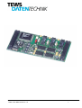
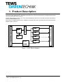
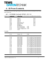
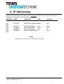
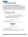
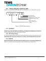
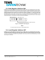
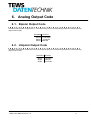
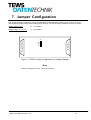
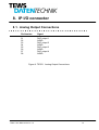
TIP551
Optically Isolated
4 Channel 16 Bit D/A
Version 1.0 Revision A
User Manual
Issue 1.0
08. September 1997
D75551800
TEWS DATENTECHNIK GmbH
Am Bahnhof 7
D-25469 Halstenbek
Germany
Tel +49 (0)4101 4058-0
Fax +49 (0)4101 4058-19
7,3 8VHU 0DQXDO 9HUVLRQ TIP551-10
Optically isolated
4 channel 16 bit D/A
0V to 10V or +/-10V
This document contains information, which is proprietary to TEWS DATENTECHNIK GmbH. Any reproduction
without written permission is forbidden.
TEWS DATENTECHNIK GmbH has made any effort to ensure that this manual is accurate and complete. However TEWS DATENTECHNIK GmbH reserves the right to change the product described in this document at any
time without notice.
This product has been designed to operate with IndustryPack compatible carriers. Connection to incompatible
hardware is likely to cause serious damage.
TEWS DATENTECHNIK GmbH is not liable for any damage arising out of the application or use of the device
described herein.
Issue
Desscription
Preliminary issue
Issue 1.0
Date
20. Aug. 1997
08. Sep. 1997
K1997 by TEWS DATENTECHNIK GmbH
IndustryPack is a registered trademark of GreenSpring Computers, Inc
7,3 8VHU 0DQXDO 9HUVLRQ 1. Product Description . . . . . . . . . . . . . . . . . . . . . . . . . . . . . . .
1
2. Technical Specification . . . . . . . . . . . . . . . . . . . . . . . . . . . .
2
3. Functional Description . . . . . . . . . . . . . . . . . . . . . . . . . . . . .
3
3.1. Analog Output . . . . . . . . . . . . . . . . . . . . . . . . . . . . . . . . . . . . . . . . . . .
3.2. Data Correction . . . . . . . . . . . . . . . . . . . . . . . . . . . . . . . . . . . . . . . . . . .
3.2.1. DAC Correction Formula for 0V - 10V Output Range . . . . . . . . .
3.2.2. DAC Correction Formula for ±10V Output Range . . . . . . . . . . . . .
3
3
4
4
4. ID Prom Contents . . . . . . . . . . . . . . . . . . . . . . . . . . . . . . . . . .
5
4.1. ID PROM Contents TIP551-10 V1.0 . . . . . . . . . . . . . . . . . . . . . . . .
5
5. IP Addressing . . . . . . . . . . . . . . . . . . . . . . . . . . . . . . . . . . . . .
6
5.1. Channel Select Register Address $01 . . . . . . . . . . . . . . . . . . . . . . .
5.1.1. Output Channel Selection . . . . . . . . . . . . . . . . . . . . . . . . . . . . . . . . .
5.1.2. Automatic Load Bit . . . . . . . . . . . . . . . . . . . . . . . . . . . . . . . . . . . . . . .
5.2. Status Register Address $03 . . . . . . . . . . . . . . . . . . . . . . . . . . . . . . .
5.2.1. DACBUSY . . . . . . . . . . . . . . . . . . . . . . . . . . . . . . . . . . . . . . . . . . . . . .
5.2.2. VR Voltage Range . . . . . . . . . . . . . . . . . . . . . . . . . . . . . . . . . . . . . . .
5.2.3. ERROR . . . . . . . . . . . . . . . . . . . . . . . . . . . . . . . . . . . . . . . . . . . . . . . .
5.3. Data Register Address $04 . . . . . . . . . . . . . . . . . . . . . . . . . . . . . . . . .
5.4. Load Register Address $07 . . . . . . . . . . . . . . . . . . . . . . . . . . . . . . . . .
7
7
7
8
8
8
8
9
9
6. Analog Output Code . . . . . . . . . . . . . . . . . . . . . . . . . . . . . . .
10
6.1. Bipolar Output Code . . . . . . . . . . . . . . . . . . . . . . . . . . . . . . . . . . . . . .
6.2. Unipolar Output Code . . . . . . . . . . . . . . . . . . . . . . . . . . . . . . . . . . . . .
10
10
7. Jumper Configuration . . . . . . . . . . . . . . . . . . . . . . . . . . . . . .
11
8. IP I/O connector . . . . . . . . . . . . . . . . . . . . . . . . . . . . . . . . . . . .
12
8.1. Analog Output Connections . . . . . . . . . . . . . . . . . . . . . . . . . . . . . . . .
8.2. Power Input Connections . . . . . . . . . . . . . . . . . . . . . . . . . . . . . . . . . .
12
13
7,3 8VHU 0DQXDO 9HUVLRQ Figure 1: TIP551 Block Diagram . . . . . . . . . . . . . . . . . . . . . . . . . . . . . . . . .
Figure 2: ID PROM Contents TIP551-10 V1.0 . . . . . . . . . . . . . . . . . . . . .
Figure 3: CHANSEL Channel Select Register . . . . . . . . . . . . . . . . . . . . .
Figure 4: Output Channel Select Table . . . . . . . . . . . . . . . . . . . . . . . . . . .
Figure 5: STATREG Status Register . . . . . . . . . . . . . . . . . . . . . . . . . . . . .
Figure 6: DATAREG Data Register . . . . . . . . . . . . . . . . . . . . . . . . . . . . . . .
Figure 7: TIP551 Jumper Configuration for Voltage Ranges . . . . . . . . .
Figure 8: TIP551 Analog Output Connections . . . . . . . . . . . . . . . . . . . .
Figure 9: TIP551 Power Input Connections . . . . . . . . . . . . . . . . . . . . . . .
7,3 8VHU 0DQXDO 9HUVLRQ 1
5
7
7
8
9
11
12
13
1. Product Description
The TIP551 is an IndustryPack9 compatible module with four 16 bit D/A channels which are galvanically isolated
from the IndustryPack logic interface.
Output voltage ranges of ±10 V or 0 V to 10 V are selectable by jumper for the four D/A channels. After RESET
all D/A channels default to 0V.
,' 3520
ELW '$&
ELW '$&
ELW '$&
'& '&
ELW '$&
,QGXVWU\3DFN ,2 LQWHUIDFH
&RQWURO ,QWHUIDFH
RSWRFRXSOHUV
,QGXVWU\3DFN ORJLF LQWHUIDFH
Each TIP551 is calibrated at the factory. Calibration information of the D/A channels is stored in the Identification
PROM unique to each IP.
FRQYHUWHU
Figure 1: TIP551 Block Diagram
7,3 8VHU 0DQXDO 9HUVLRQ 2. Technical Specification
Logic Interface
IndustryPack9 Logic Interface
Size
single wide IP
I/O Interface
50-conductor flat cable
Analog Outputs
4 channels
Isolation
All D/A channels are galvanically isolated from the IP Interface
Output Voltage Range
±10V or 0V to 10V, jumper selectable, common for all 4 channels
Settling Time of DAC’s
to 0.01% typ. 10 ³s
Calibration Data
Calibration data for gain and offset correction of each channel
stored in ID PROM
Output Current
±4mA for each channel
Load Capacitance
typical 1 nF
Accuracy
INL ± 4LSB typ. after calibration
DNL ±0.5 LSB
Monotonicity
16 bits over the specified temperature range
Wait States
IDSEL 1 wait state
IOSEL 0 wait state
Power Requirements
400mA @ 5V no load
430mA @ 5V with 4mA output current for each channel
Temperature Range
Operating -40EC to 85EC
Storage -45EC to 125EC
Humidity
5 - 95% non-condensing
7,3 8VHU 0DQXDO 9HUVLRQ 3. Functional Description
3.1. Analog Output
The TIP551 includes 4 channels of analog outputs with a rtesolution of 16 bits and a voltage range of ±10V or
0V to 10V. The maximum output current for each channel is ±4mA. Each channel has a typical settling time to
0.01% of 10³s .
Two voltage ranges are jumper selectable: ±10V or 0V to 10V. Voltage range selection covers all 4 channels.
The 4 analog outputs of the TIP551 are galvanically isolated from the IndustryPack logic interface by optocoupler. On board DC/DC converters supply the power to the isolated part of the TIP551.
3.2. Data Correction
There are two errors which affect the DC accuracy of the DAC. The first is the zero error (offset). For the DAC
this is the data value required to produce a zero voltage output signal. This error is corrected by subtracting the
known error from all readings.
The second error is the gain error. Gain error is the difference between the ideal gain and the actual gain of the
DAC. It is corrected by multiplying the data value by a correction factor.
The data correction values are obtained during factory calibration and are stored in the modules individual version of the ID PROM. The DAC has a pair of offset and gain correction values for each single output channel.
The correction values are stored in the ID PROM as two’s complement byte wide values in the range -32768
to 32767. For higher accuracy they are scaled to ¼ LSB.
Because offset and gain correction values are dependent on the selected output voltage range the TIP551 has
2 different sets of ID PROM data. Depending on the jumper settings for the voltage range the corresponding set
of correction values is automatically selected.
7,3 8VHU 0DQXDO 9HUVLRQ 3.2.1. DAC Correction Formula for 0V - 10V Output Range
The basic formula for correcting unipolar DAC output value is:
'DWD
9DOXH *DLQFRUU 2IIVHWFRUU Data is the digital value that will be sent to the DAC, Value is the desired output value, Gaincorr and Offsetcorr
are the correction factors from the ID PROM.
3.2.2. DAC Correction Formula for ±10V Output Range
The basic formula for correcting bipolar DAC output value is:
'DWD
9DOXH *DLQFRUU 2IIVHWFRUU Data is the digital value that will be sent to the DAC, Value is the desired output value, Gaincorr and Offsetcorr
are the correction factors from the ID PROM.
Gaincorr and Offsetcorr correction factors are stored separately for each for the four DAC outputs.
1RWH
)ORDWLQJ SRLQW DULWKPHWLFV RU VFDOHG LQWHJHU DULWKPHWLFV LV QHFHVVDU\ WR
DYRLG URXQGLQJ HUURU ZKLOH FRPSXWLQJ DERYH IRUPXOD
7,3 8VHU 0DQXDO 9HUVLRQ 4. ID Prom Contents
The Voltage Range bit of the DAC Status Register is used to select the correct set of ID PROM correction values
and the output code.
4.1. ID PROM Contents TIP551-10 V1.0
ADDRESS
FUNCTION
$ 01
$ 03
$ 05
$ 07
$ 09
$ 0B
$ 0D
$ 0F
$ 11
$ 13
$ 15
$ 17
ASCII ’I’
ASCII ’P’
ASCII ’A’
ASCII ’C’
Manufacturer ID
Model Number
Revision
RESERVED
Driver-ID low-byte
$ 00
Driver-ID high-byte
$ 00
number of bytes used $ 1D
CRC
$ 19
Version -10
$ 0A
$ 1B
$ 1D
$ 1F
$ 21
$ 23
$ 25
$ 27
$ 29
$ 2B
$ 2D
$ 2F
$ 31
$ 33
$ 35
$ 37
$ 39
DAC1 Offset
DAC1 Offset
DAC2 Offset
DAC2 Offset
DAC3 Offset
DAC3 Offset
DAC4 Offset
DAC4 Offset
DAC1 Gain
DAC1 Gain
DAC2 Gain
DAC2 Gain
DAC3 Gain
DAC3 Gain
DAC4 Gain
DAC4 Gain
Ch.1 Low Byte
Ch.1 High Byte
Ch.2 Low Byte
Ch.2 High Byte
Ch.3 Low Byte
Ch.3 High Byte
Ch.4 Low Byte
Ch.4 High Byte
Ch.1 Low Byte
Ch.1 High Byte
Ch.2 Low Byte
Ch.2 High Byte
Ch.3 Low Byte
Ch.3 High Byte
Ch.4 Low Byte
Ch.4 High Byte
$ 49
$ 50
$ 41
$ 43
$ B3
$ 23
$ 10
$ 00
$ variable
7,3 8VHU 0DQXDO 9HUVLRQ $ board dependent
$ board dependent
$ board dependent
$ board dependent
$ board dependent
$ board dependent
$ board dependent
$ board dependent
$ board dependent
$ board dependent
$ board dependent
$ board dependent
$ board dependent
$ board dependent
$ board dependent
$ board dependent
......
$ 3F
Not used
.......
$ 00
Figure 2: ID PROM Contents TIP551-10 V1.0
7,3 8VHU 0DQXDO 9HUVLRQ 5. IP Addressing
The TIP551 is controlled by a set of registers, which are directly accessible in the I/O address space of the IP.
All registers are automatically cleared by assertion of IP_RESET.
ADDRESS
NAME
FUNCTION
SIZE
ACCESS
$ 01
R/W
$ 03
$ 04
$ 07
$ 09
R/W
CHANSEL
DAC Channel Select Register
byte
STATUS
DATAREG
LOADDAC
IDWRENA
DAC Status Register byte
DAC Data Register
word
DAC Load Register
byte
ID Write Enable Register
R/W
R/W
W
byte
1RWH
,':5(1$ LV IRU IDFWRU\ XVH RQO\ GR QRW ZULWH WR WKLV UHJLVWHU
7,3 8VHU 0DQXDO 9HUVLRQ 5.1. Channel Select Register Address $01
The DAC Channel Select Register CHANSEL is used to select an output channel. This is done by writing the
corresponding bit pattern into bit 0 to bit 1. A write access to the CHANSEL register starts the serial datatransfer
to the DAC of the value stored in the DAC Data Register DATAREG. Be sure that the desired value is stored in
the DATAREG before starting the conversion by writing to the DAC Channel Select Register CHANSEL. If Bit
7 is set to ’1’ a load signal is automatically generated after serial data transferto the desired DAC has completed.
The load signal updates all 4 DAC’s with the value of the shift register of each DAC. Write accesses to the DAC
Channel Select Register during DACBUSY active are ignored and set the ERROR flag in the DAC Status Register STATREG.
$/
CS1 CS0
2XWSXW &KDQQHO 6HOHFWLRQ
DOOZD\V UHDG DV ]HUR
D ZULWH WR WKHVH ELWV KDV
QR HIIHFW
$XWRPDWLF /RDG DIWHU 'DWD
7UDQVIHU
Figure 3: CHANSEL Channel Select Register
5.1.1. Output Channel Selection
Bit 0 to bit 2 of the Channel Select Register are used to select the output channel of the TIP551.
CS1
0
0
1
1
CS0
0
1
0
1
CHANNEL
1
2
3
4
Figure 4: Output Channel Select Table
5.1.2. Automatic Load Bit
If bit 7 is set to ’1’ all 4 DAC’s are updated automatically after data transmition to the selected DAC channel.
If bit 7 is set to ’0’ the user can update all DAC’s with a write access to the DAC Load Register immediatly or
with the next channel selection with bit 7 is set to ’1’ after data transmition.
7,3 8VHU 0DQXDO 9HUVLRQ 5.2. Status Register Address $03
ERR
VR DAC
BUS
Y
'$& %86< IODJ
9ROWDJH 5DQJH IODJ
(5525 IODJ HYHU\ ZULWH DFFHVV
WR WKH 6WDWXV 5HJLVWHU FOHDUV
WKLV ELW
DOOZD\V UHDG DV ]HUR
D ZULWH WR WKHVH ELWV KDV
QR HIIHFW
Figure 5: STATREG Status Register
5.2.1. DACBUSY
Reading Bit 0 of the DAC Status Register STATREG as ‘1‘ indicates that a serial data transfer to the DAC is in
progress. Write accesses to the DAC Channel Select Register CHANSEL during DACBUSY active are ignored
and set the ERROR flag in the DAC Status Register STATREG.
5.2.2. VR Voltage Range
Bit 1 of the DAC Status Register indicates the selected Voltage Range according to the jumper setting for the
output voltage ranges of the TIP551. Reading bit 1 as ’0’ means +/- 10V output range and binary two‘s complement as output code , reading bit 1 as’1’ means 0V to 10V output range and straight binary as output code.
5.2.3. ERROR
Write accesses to the DAC Channel Select Register CHANSEL or a write access to the DAC Load Register LOADREG during DACBUSY active are ignored and set the ERROR flag ( bit 2 ) in the DAC Status Register STATREG to ‘1‘. Any write access to the DAC Status Register STATREG clears the ERROR flag.
7,3 8VHU 0DQXDO 9HUVLRQ 5.3. Data Register Address $04
The DAC Data Register DATAREG is a 16 bit wide read/write register. The DAC Data Register contains the desired DAC value. A write access to the DAC Channel Select Register CHANSEL starts the serial data transfer to
the DAC and if selected the conversion into an analog value. Now a new value can be written to the DAC Data
Register DATAREG, or after transfer and conversion are completed ( DACBUSY = ‘0‘ ) the same value of the
DAC Data Register can be written to another channel. The data of the DAC Data Register DATAREG are valid
as long as they are not changed by a new write access to this register. To use the same value for another output
channel just write the new channel to the DAC Channel Select Register.
%LW '$& YDOXH
Figure 6: DATAREG Data Register
1RWH
)RU RXWSXW PRGH ORRN )LJXUH $QDORJ 2XWSXW &RGH
5.4. Load Register Address $07
The DAC Load Register LOADREG is a 8 bit wide write only register. Avery write access to the DAC Load Register updates all 4 DAC output’s with the last value writen into the DAC’s internal shiftregisters. Write accesses
to the DAC Load Register LOADREG during DACBUSY active are ignored and set the ERROR flag in the DAC
Status Register STATREG.
7,3 8VHU 0DQXDO 9HUVLRQ 6. Analog Output Code
6.1. Bipolar Output Code
If the DAC channels are configured for +/- 10V output range by the corresponding jumpers the following analog
output code is valid:
'$7$5(*
287387
$7FFF + Full-Scale
$8000 - Full-Scale
$0000 Midscale
6.2. Unipolar Output Code
If the DAC channels are configured for 0V to10V output range by the corresponding jumpers the following analog
output code is valid:
7,3 8VHU 0DQXDO 9HUVLRQ '$7$5(*
287387
$FFFF
$8000
$0000
Full-Scale
Midscale
Zero-Scale
7. Jumper Configuration
The TIP551 must be configured by a 3 pin jumperfield for the desired output voltage range ±10V or 0V to 10V.
See the following table for the corresponding jumper settings. The jumper seting is valid for all 4 DAC channels.
Voltage range ±10V:
J1 1-2 installed
Voltage range
J1 2-3 installed
0V to 10V:
3
2
1
,2 ,QWHUIDFH
,3 /RJLF ,QWHUIDFH
-
Figure 7: TIP551 Jumper Configuration for Voltage Ranges
1RWH
)DFWRU\ FRQILJXUDWLRQ LV WR 9 IRU DOO FKDQQHOV
7,3 8VHU 0DQXDO 9HUVLRQ 8. IP I/O connector
8.1. Analog Output Connections
Pin-Number
Signal
01
02
03
04
05
06
07
08
DAC output 1
AGND
DAC output 2
AGND
DAC output 3
AGND
DAC output 4
AGND
Figure 8: TIP551 Analog Output Connections
7,3 8VHU 0DQXDO 9HUVLRQ 8.2. Power Input Connections
Pin-Number
Function
44
45
46
47
48
49
50
AGND
-15V
AGND
+15V
AGND
+5V
AGND
Figure 9: TIP551 Power Input Connections
1RWH
7KH SRZHU LQSXW FRQQHFWLRQV DUH UHVHUYHG IRU VSHFLDO YHUVLRQV RI WKH
7,3 ZLWKRXW RQ ERDUG '&'& FRQYHUWHU 'R QRW VXSSO\ DQ\ YROWDJH WR
WKHVH SLQV IRU WKH 7,3 YHUVLRQ
7,3 8VHU 0DQXDO 9HUVLRQ