1
APPENDIX B: Definition of HEART Control
Registers
The Heron Serial Bus is used extensively by the Heart architecture for the configuration of
the high-speed communication channels, and other functions. This configuration may be
carried out by either a processing module, or the host interface. I.e. any HSB Bus Master.
Normally the configuration will be performed by the Host PC using the software tools
provided. This section provides details of the registers and how to access them in case you
need to configure your HEART system from your own software.
Given the 4-bit board address and the 3-bit slot address adopted for directly accessing the
host and module slots themselves, it is clear that some indirect addressing is needed to
access the Heart FPGAs of the HECPCI9. We therefore use a slot address of 7, which is
acknowledged by ALL Heart FPGA devices. A secondary address scheme is then used to
access a particular FPGA that responds to address/data pairs, while all other devices read
the address/data pairs and ignore them.
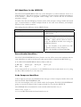
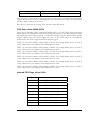
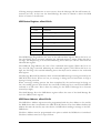
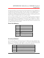
Direct Slot Addresses
0
Reserved
1
Module Slot 1
2
Module Slot 2
3
Module Slot 3
4
Module Slot 4
5
Host
6
External Module Slot
7
ALL Heart FPGA devices
Secondary Addresses
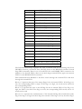
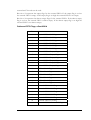
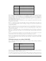
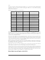
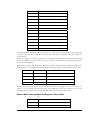
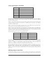
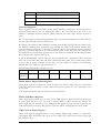
The secondary address is formed from the 4-bit slot address in the least significant 4 bits,
plus 1 bit in bit position 3 to signify whether it is the Heart-to-Module FPGA being
addresses, (0), or the Module-to-Heart FPGA. (1). Bits 5,6 and 7 are reserved and must be
programmed as ‘0’. All valid secondary addresses are listed in the table below.
0x01
Heart-to-Module FPGA for Module Slot 1
0x02
Heart-to-Module FPGA for Module Slot 2
0x03
Heart-to-Module FPGA for Module Slot 3
0x04
Heart-to-Module FPGA for Module Slot 4
0x05
Heart-Host FPGA
76
HUNT ENGINEERING HECPCI9 USER MANUAL