1
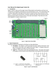
PB-505
Advanced Analog & Digital Design
Workstation
Instruction Manual
Revision: 2/2011
2
Features & Applications
The PB-505 Advanced Circuit Design Workstation is a robust electronics trainer suitable
for all levels of electronics instruction and design. Utilizing the PB-505, students will
learn valuable hands-on breadboarding techniques and build a solid foundation in circuit
experimentation, construction and analysis. Experienced designers will find the PB-505
an invaluable instrument, providing a reliable platform for the most advanced and
demanding design applications. The PB-505 can be used to construct basic series and
parallel circuits to the most complicated multi-stage microcomputer circuits,
incorporating the latest in industrial technology. Use the PB-505 to construct a wide
variety of experiments, including but not limited to.
•
•
•
•
•
•
•
•
•
•
•
•
•
•
•
Opto-Device Circuits
Clocks
Multivibrators
Oscillator Circuits
Timers
Function Generator Circuits
Logic Circuits
Gates
Counters
Flip-Flops
Analog-to-Digital Converters
Digital-to-Analog Converters
Medium Scale Integration Circuits
Phase Lock Loops
Operational Amplifiers
3
PB-505 COURSEWARE
Courseware is available separately through our website or as part of the PB-505 Lab
package.
The PB-505 Lab package offers comprehensive course instruction covering the
following areas:
Electronic Fundamentals
Digital Electronics
Fundamentals of Electricity
Number Systems & Codes
Binary, Decimal, Hexadecimal, Octal &
ASCII
Logic Gates & Boolean Algebra
Combinational Logic Circuits
Flip-Flops
Digital Arithmetic
Counters & Registers
Integrated Circuit Logic Families
TTL Logic
MOSFETS
CMOS
Interfacing CMOS & TTL
Medium Scale Integration
Decoders
Encoders
Data Conversion & Acquisition
Microcomputer Concepts
Ohm’s Law
Series Circuits
Parallel Circuits
Combinational Circuits
Current Control
Closed, open, shorts
Switches
Thevenin’s Theorem
Wheatstone Bridge
Capacitors
Inductors
Phase Shift Circuits
Impedance
Resonant Circuits
Transformers
Rectifiers & Filtering
Integrated Circuits
Transistor Amplifiers
Oscillators
Power Control Circuits
4
ABOUT GLOBAL SPECIALTIES
Thank you for selecting the Model PB-505. Since 1973, Global Specialties has been the
recognized leader in technical education courses, training equipment and tutorial
materials. Our electronics and microcomputer teaching systems have proven to be
effective in secondary schools, technical schools, colleges, universities and industrial
training departments throughout the world.
We have been leaders in the development of integrated teaching systems and
completely packaged courses which include everything required for effective
instruction. Comprehensive textbooks, laboratory manuals and instructor guides
have been written in a comfortable, non-intimidating style by experienced
professional educators, specifically for use with our equipment. Each course is
designed to make selections appropriate for a variety of educational levels and
course goals
The central concept upon which we base our entire product line is education
through application. We believe that relevant scientific and technical education is
best when it involves permitting students to learn by doing.
Global stands behind it products by offering the industry’s best warranties. The
PB-505 comes with a full three-year parts and labor warranty and can be
returned for prompt repair or replacement to our factory in Yorba Linda California.
Low per-student cost, durable and trouble-free hardware and proven tutorial
materials combine to make technical and scientific courses from Global
Specialties the most effective, economical way to upgrade your lab & curriculum.
Please visit www.globalspecialties.com to explore the many options available for
the PB-505, such as such as courseware, pre-formed jumper wire kits, test
probes and prototyping accessories.
5
TABLE OF CONTENTS
SPECIFICATIONS .......................................................................................... Page 7
INTRODUCTION ............................................................................................. Page 9
DESCRIPTION OF INDIVIDUAL FEATURES ................................................. Page 10
CHECKING OUT THE PB-505 ........................................................................ Page 13
BREADBOARDING TECHNIQUES ................................................................ Page 15
SERVICE & WARRANTY INFORMATION........................................................ Page 16
6
SPECIFICATIONS
Input Power Source
AC Line: 115VAC @ 60Hz (typical)
Power Supplies
Fixed DC: +5VDC 1.0A max, current limited
Ripple, <5mV
Variable DC: +1.3V @150mA to +15VDC @ 500mA
Ripple < 5mV
Variable DC: -1.3VDC @ 150mA to -15VDC @ 500mA
Ripple < 5mV
Fixed AC: 12.6VAC center-tapped @100mA
Binding Posts
(7) Ground, +5VDC, Variable +VDC & Variable -DC
Power Supply Outputs, and AC Transformer centertapped output
Pulsers
(2) Pushbutton-operated, open-collector output pulsers.
Each with 1 normally-open, 1 normally-closed output.
Each output can sink up to 250mA.
Logic Probe
Detects Logic High, Logic Low and Single Shot events.
Logic High: 2.2V (nominal) in TTL mode, 70% of Vcc in
CMOS mode.
Logic Low: 0.8V in TTL mode, 30% of Vcc in CMOS
mode.
Memory Mode: Detects single shot events and holds
indication until Pulse/Mem switch is toggled
Function Generator
Frequency Range: 0.1Hz to 100KHz in six ranges
Output Voltage: 0 to + 10Vp-p into 50 Ω Load (20Vp-p
in open circuit), short circuit protected
Output Impedance: 600Ω except TTL
Output waveforms: Sine, Square, Triangle & TTL
Sine Wave Distortion: <3% @ 1Khz Typical
TTL Pulse: Rise & fall time: <25ns, drive 100 TTL
Loads **TTL Pulse available when in Square Wave Mode
Square Wave: Rise and fall times <0.5µs
7
Logic Switches
(8) Logic Switches select Logic High and Logic Low
Logic Low Level: Ground
Logic High Level: Switchable between +5V and the
variable positive power supplies.
Switches
(2) Single Pull Double Throw (SPDT) - uncommitted
Logic Indicators
LEDs: 16 LEDs; (8) red to indicate logic high and (8)
green to indicate logic low
Logic High Threshold: 2.2V (nominal) in TTL/+5V
mode, 70% (nominal) of selected operating voltage in
CMOS mode
Logic Low Threshold: 0.8V (nominal) in TTL/+5V
mode, 30% (nominal) of selected operating voltage in
CMOS mode
Connectors
Potentiometer
Speaker
(1) BNC - uncommitted
(2) 1KΩ and 10KΩ - uncommitted
8Ω, 0.25W - uncommitted
Displays
(2) BCD to 7 Segment Display Circuits include (2) red
LEDs and decoder/driver circuitry
Breadboards
Removable Aluminum Socket Plate (PB-4) with 3360
Tie points with 200 additional bus strip tie points
Weight
Dimensions
10lbs
6.5" x 19" x 11.5"
Specifications subject to change without notice
8
INTRODUCTION
The PB-505 Advanced Analog/Digital Electronic Design Workstation, is a versatile,
time-saving tool for circuit designers engineers, engineering technicians, students, and
hobbyists. A large breadboard area and a wide choice of built-in circuit accessories
allow rapid and accurate construction of virtually any type of analog or digital circuit.
The PB-505 is designed to withstand the toughest treatment. It is constructed with the
highest quality components available. Durable slide switches are mounted below
surface to insure long life. All LED indicators are also sub surface to provide quick
indication and durability. Selector switches are high quality rotary type as are all
potentiometers. Rugged interface sockets securely bolted to the front panel provide
quick connection to the convenient built-in circuits.
Circuit power is provided by three power supplies; two variable, and on fixed. The
circuit breadboard area includes over 3300 contact points. A multiple-waveform
function generator supplies sine, triangle, and square wave output for analog circuits. A
built-in speaker may be used for analog output.
Outputs also include a TTL-level square wave generator, two debounced pushbutton
switches, and a bank of eight logic switches. Eight logic indicators may be used to
display high and low logic levels. A built-in logic probe is useful in circuit
troubleshooting and two BCD to 7 segment decoder/ drivers and LED's may be used in
circuit designs.
Two built-in potentiometers and two SPDT switches are provided for circuit control
and adjustment. Connections to external test equipment or signal source may be
using the BNC connector on the PB-505.
The PB-505 eliminates the clutter and confusion that often results when constructing
sophisticated circuits. Alligator clips and similar connectors are seldom needed.
Sockets on the PB-505 allow insertion of components of wires of up to 20 gauge.
A detailed panel layout and description of the PB-505is given in the section "Description
of Individual Features".
9
DESCRIPTION OF INDIVIDUAL FEATURES
In order to properly use the full capabilities of the PB-505 it is highly recommended that
the user become familiar with the panel layout and the features of the components, (see
Figure 1 below)
PB-505
FIGURE
FIGURE 1.
1. PB-505
PB-505 Front
Front Panel
Panel Layout
Layout
POWER SUPPLIES
By combining the three DC power supplies on the PB-505 the user may work with
virtually any type of integrated circuit or discrete component. The fixed 5V supply has
become an industry standard for powering digital IC's. IC's which require +5V, +12V,
and -5V are easily accommodated by the PB-505. The variable supply output voltages
may be changed by using the adjustment knobs on the front panel. The positive and
negative outputs are continuously variable from +1.3 to +15V and -1.3 to -15V
respectively. Both variable supply outputs are referenced to circuit common. This
creates a split supply which is often used with differential and operational amplifiers (opamps).
10
In addition to the DC power supplies, the PB-505 also provides a 12.6 volt centertapped AC supply. This allows the user to construct any of half-wave and full-wave
rectified power supplies on the breadboarding area and apply power by simply
connecting jumper wires to the three AC supply output pins.
FUNCTION GENERATOR
The multi-waveform function generator provides continuously variable frequency signals
from 0.1Hz (for extra-low frequency work) to radio frequency signals of 100Hz. The
frequency is selected in six decade ranges, with a vernier to adjust frequency within
each range. The sine wave output is factory adjusted for minimum distortion. The
triangle waveform is adjusted for best linearity. The standard square wave and TTL
level outputs are both set at a 50% duty cycle. The TTL output (available when the
function generator is set to square wave), capable of driving up to 10 TTL loads, is
continuously available and in phase with the square wave output. The low output
impedance of the sine, square, and triangle waveforms (600 ohms) assures maximum
coupling of the output signal to the device being driven. All outputs can withstand a
continuous short circuit to ground.
LOGIC INDICATORS
Sixteen LED's, eight red and eight green, make up eight Logic Indicators that will
display logic high and low conditions based on either TTL or CMOS thresholds,
selectable by the user. Operating voltage can also be selected by the user to be either
at +5V, or at the setting of the +1.3 to +15V supply. This selection should be the same
as the operating circuitry that is to be monitored. The red LED's will light when the
voltages at the inputs are 2.2 volts or higher when in the TTL position, or 70% of the
operating voltage or higher when in the CMOS position. The green LED's will light when
the voltages at the inputs are 0.8 volts or less when in the TTL position, or 30% of the
operating voltage or less when in the CMOS position. An unconnected input, or an input
not at valid logic level, will cause both LED's to be extinguished. Note that the
thresholds determined by the TTL positions are only accurate when the +5V range is
selected. The 100K ohm input impedance ensures minimal loading effects of the circuit
under test.
DEBOUNCED PUSHBUTTON (PULSERS)
The PB-505 uses clocked flip-flops to provide debounced pushbutton switch functions.
The pushbutton circuitry has open-collector outputs switch can sink up to 250mA each.
This type of debouncing gives the user a sharp, glitch-free trigger source which assures
reliable operation in digital circuits. Each pushbutton has a normally-open and a
normally-closed output. If necessary, a pull-up resistor can connect any pulser output to
any of the positive voltage sources.
POTENTIOMETERS
Two potentiometers are provided on the PB-505. The resistance values chosen (IK and
10K ohms) may be used in common circuit applications such as volume controls. All
leads for both potentiometers are available and uncommitted.
11
BNC CONNECTOR
The PB-505 may be connected to other pieces of equipment via a BNC connector. This
allows the use of shielded cable to minimize noise and interference.
SWITCHES
Two single pole, double throw (SPDT) switches are provided for general switching
functions. All leads are available and clearly marked on the PB-505 for easy connection.
Eight switches are configured as Logic Switches to provide a convenient source of
digital outputs. These switches will provide logic levels of zero volts (ground) for a logic
low, and logic high levels of either +5V or the voltage setting of the +1.3 to +15V supply.
The high level is determined by the setting of the +5/+V switch. This arrangement
makes connecting special digital circuitry such as an 8-bit input port quick and easy,
and allows compatibility with virtually any logic family.
CAUTION
Integrated circuits can be destroyed if a voltage is applied to their inputs that is
higher than the operating voltage of the IC's. Always insure that the setting of the
+5/ +V high-level switch is in the correct position before making connections to any
device.
12
CHECKING OUT THE PB-505
The PB-505 may be checked out for proper operation by connecting the AC line cord to
a suitable receptacle. The two 7-segment displays should light when the power switch is
turned on.
Using a DC voltmeter, check for +5 volts between the ground terminal and the +5V
terminal. Repeat the measurement for the positive (+) variable supply terminal and the
negative (-) variable supply terminal. Check the variability of each supply by turning the
appropriate adjusting knob. To test the logic indicators, switch the +5/ +V operating
voltage switch to the +5 position. The TTL/CMOS threshold switch can be in either
position. With no input to the logic indicators, all LEDs should be turned off. Connect
one end of a jumper wire to the +5 volts terminal and the other end to logic indicator 1;
the red LED of logic indicator 1 should light. Repeat this test for logic indicators 2
through 8. Disconnect the jumper from the +5 volt terminal and connect it to the ground
terminal. Connect the other end to logic indicator 1; the green LED of logic indicator 1
should light. Repeat this test for logic indicators 2 through 8.
The function generator may be tested by connecting its output to one of the speaker
inputs. Connect the other speaker input to one of the ground terminal. Switch the
function generator range switch to 1KHz. Turn the frequency control pot clockwise.
Move the amplitude control clockwise until you hear a tone coming from the speaker.
Switch the waveform selector to select sine, square, and triangle. A changing but clearly
audible tone should be heard in each position of the frequency control should vary the
pitch of the tone. The TTL Pulse is available when the function generator is set to
Square Wave.
If an oscilloscope is available, you may check the function generator for proper
waveform and frequency using standard measurement techniques.
The debounced push-buttons can be checked by connecting one side of a resistor (20
ohms, to 100K) to +5 volts and the other side to PB-1, the NC point. Then connect PB-1
to LED-1 with the Logic Indicator +5/ +V switch in the +5V position, the red LED should
light when PB1 is pressed and the green LED should light when PB1 is released. Next,
move the connections from PB1-1 to PB2-1, the NO point. Now the red LED should be
lit when PB1 is not pressed, and the green LED should be lit when PB1 is pressed.
Repeat these steps to test PB2.
The logic switches can be tested by connecting the output of logic switches 1 through 8
to the input of logic indicators 1 through 8. Switch the logic switch +5V/ +V operating
voltage switch to +5, and switch the logic indicator +5/+v operating voltage switch to +5.
Select the CMOS position on the logic indicator TTL/CMOS threshold select switch.
Now the logic indicators should reflect the conditions of the logic switches, that is, red
LEDs will indicate switches in the high (logic "\") position and green LEDs will indicate
switches in the low (logic "0") position. Move each switch between its high and low
position to verify proper functioning. Switch the logic +5/ +V high level switch to +V and
13
the logic indicator +5/+V operating voltage switch to +V; indicator display should remain
the same, regardless of the setting of the 1.3-15 volts +V supply.
By using an ohmmeter, you can check the potentiometers. To do so, select an
appropriate range for measuring 10K and connect the ohmmeter leads to R1-1 and R12. With R1 rotated fully counterclockwise a reading of zero ohms should be observed.
As the potentiometer is rotated clockwise, the resistance reading will be seen to
increase linearly up to 10K ±20%. Now move the ohmmeter lead from R1-1 to R1-3;
with R1 fully clockwise the ohmmeter will read zero ohms, and the resistance will
increase linearly to the full value noted previously as the potentiometer is rotated
counterclockwise. Select an ohmmeter range appropriate for IK and repeat these steps
on R2 to verify its function.
To test SPDT switch S9, put S9 in the up position and connect and ohmmeter to S9-1
and S9-2. The ohmmeter should read zero ohms. When the switch is brought to the
down position, an open circuit should be indicated. Move the ohmmeter lead from S9-1
to S9-3 and observe a short circuit with S9 down, and an open with S9 up. These steps
can be repeated on S10 to test its functions.
To test the logic probe, connect a wire from Vcc to +5 terminal. Set mem/pulse switch to
pulse and TTL/CMOS switch to TTL. Connect a wire from input to +V terminal. Connect
the multimeter between GND and +V. Turn the +V pot fully counter-clockwise, read
approx. 1.2V on the meter. Slowly turn the +V pot until the HI LED lights. Read approx.
2.4V on the meter. Set pulse/mem switch to mem. Touch input lead to ground. Observe
low LED lighting and pulse LED lighting and staying on. Move pulse/ mem switch to
mem and observe pulse LED going out. Move TTL/CMOS switch to CMOS, reconnect
input lead to the +V terminal. With the +V pot fully counter clockwise, slowly turn the +V
pot clockwise until the low LED goes out. Read approx. 1.6 volts on the DMM. Continue
turning the +V pot until the HI LED lights read approx. 3.5 volts on the DMM.
To test the BCD to 7 segment displays, jumper together pins 1A, IB, and 1C. Connect a
jumper wire from these points to ground. Connect a second jumper wire from position
10 to +5V. Observe a number 8 showing on the display. Repeat this test for display
number.
14
BREADBOARDING TECHNIQUES
This section contains information which may prove useful when constructing circuits
using the PB-505. While there are no hard and fast rules for breadboarding, the
following tips may save time and trouble.
Unless a circuit is being prepared for a demonstration or display, avoid cutting
component leads very short. While short wires and leads may look neat, the clipped
components will only fit into a limited "span" of connector sockets, limiting the use of the
component. It is perfectly permissible to use untrimmed components while exploring
different circuit possibilities. The only time short leads may be necessary is when
operating at higher frequencies and experiencing mysterious malfunctions. Sometimes
the only way to correct high frequency circuit problems is to shorten all circuit
connections.
Be cautious when using components which have been removed from a tape reel used
in automatic insertion equipment. Suppliers of surplus components often sell
components which are taped together in small batches. Removing the components from
the tape does not always remove the adhesive from the leads of the components.
Placing a formerly taped component into a socket connector may result in a poor
electrical connection and, worse still, leave tape adhesive in the socket. Avoid this
problem by either carefully cleaning taped component leads, clipping the taped portion
of the lead off, or avoiding the use of taped components altogether.
Be especially careful when inserting integrated circuits into the breadboard sockets.
Unless the IC pins are straight, it is very easy to crush the pin into a zigzag shape or
fold the pins underneath the body of the IC. Either way the result is a bad connection or
no connection at all.
Always use solid wire for breadboard connections. When stripping the wire ends, be
careful not to strip more than about three-eighths of an inch of insulation from the wire.
Too much bare wire may result in unintentional connections near the wire end.
After you have built up a few circuits, you will have a good collection of pre-stripped
jumper wires. Save them. By reusing these wires, you can save even more time and
effort in assembling future circuits. Pre-formed wires in various sizes are also available
from Global Specialties (please visit web site for available options and accessories).
15
SERVICE AND WARRANTY INFORMATION
For up-to-date product information, please visit www.globalspecialties.com.
For instructions on how to obtain a return merchandise authorization number (RMA),
please visit our website, or call our customer service department.
GLOBAL SPECIALTIES
22820 Savi Ranch Parkway
Yorba Linda, CA 92887
800-572-1028
globalspecialties.com
Global Specialties will service and repair this instrument free of charge for a period of 3
full years, subject to the warranty conditions below.
WARRANTY
Global Specialties warrants the PB-505 to be free from defective material or
workmanship for a period of 3 full years from date of original purchase. Under this
warranty, Global Specialties is limited to repairing the defective device when returned to
the factory, shipping charges prepaid, within 3 full years from date of original purchase.
Units returned to Global Specialties that have been subject to abuse, misuse, damage
or accident, or have been connected, installed or adjusted contrary to the instructions
furnished by Global Specialties, or that have been repaired by unauthorized persons will
not be covered by this warranty.
Global Specialties reserves the right to discontinue models, change specifications, price
or design of this device at any time without notice and without incurring any obligation
whatsoever.
The purchaser agrees to assume all liabilities for any damages and/or bodily injury
which may result from the use or misuse of this device by the purchaser, his employees,
or agents.
This warranty is in lieu of all other representations or warranties expressed or implied
and no agent or representative of Global Specialties is authorized to assume any other
obligation in connection with the sale and purchase of this device.
All rights reserved. No Part of this book shall be reproduced, stored in a retrieval
system, or transmitted by any means, electronic, mechanical, photocopying recording,
or otherwise, without written permission from the publisher. No patent liability is
assumed with respect to the use of the information contained herein. While every
precaution has been taken in the preparation of this book, the publisher assumes no
responsibility for errors or omissions. Neither is any liability assumed for damages
resulting from the use of the information contained herein.
16