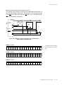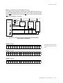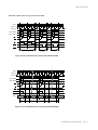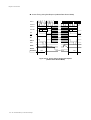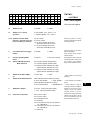
1
MICROCOMPUTER MN102L MN102L610B/F61G LSI User’s Manual Pub.No.22261-011E PanaX Series is a trademark of Matsushita Electric Industrial Co., Ltd. The other corporation names, logotype and product names written in this book are trademarks or registered trademarks of their corresponding corporations. Request for your special attention and precautions in using the technical informaition and semiconductors described in this book (1) An export permit needs to be obtained from the competent authorities of the Japanese Government if any of the products or technologies described in this book and controlled under the "Foreign Exchange and Foreign Trade Law" is to be exported or taken out of Japan. (2) The contents of this book are subject to change without notice in matters of improved function.When finalizing your design, therefore, ask for the most up-to-date version in advance in order to check for any changes. (3) We are not liable for any damage arising out of the use of the contents of this book, or for any infringement of patents or any other rights owned by a third party. (4) No part of this book may be reprinted or reproduced by any means without written permission from our company. (5) This book deals with standard specification. Ask for the latest individual Product Standards or Specifications in advance for more detailsd infomation required for your design, purchasing and applications. If you have any inquiries or questions about this book or our semiconductors, please contact one of our sales offices listed at the back of this book. About This Manual This manual is intended for assembly-language programming engineers. It describes the internal configuration and hardware functions of this microcontroller by block basis. Manual Configuration Each section of this manual consists of a title, summary, main text, key information, precautions and warnings, and references. The layout and definition of each section are shown below. Subtitle Sub-subtitle Chapter5 SerialInterface 5-2 Serial Interface Setup Examples 5-2-1 Serial Transmission in Asynchronous Mode The smallest block in this manual. Summary Introduction to the This section describes the example of serial interface transmission in asynchronous mode with the following settings: Main text l section. Baud rate = 19200 bps ( set transmit clock by timer 5) l 8-bit data transmission l two stop bits l odd parity The next data is transmitted when a transmission end interrupt occurs. P2 CORE ROM, RAM P6 Interrupt Bus Control P5 PC Timer 0 - Timer 15 Serial I/F PA P7 Timer 16 - Timer 20 AD Converter P8 PD Timer 21 ATC P9 P4 SBO0 Precautions and Figure 5-2-1 Asynchronous Transmission Block Diagram Key information Important information warnings Use a 8-bit timer to set the transmit clock. Precautions are listed from the text. in case. [ Chapter 5-2-3 Serial Clock Operation Example ] Be sure to read these Data transmission starts when the data is written to the serial 0 transmit/receive buffer (SC0TRB). The transmission starts synchronizing with timer 5 underflow. When an interrupt occurs, the SC0TRB register is cleared References and then the next data is written to the SC0TRB register. If polling, the data must be written to the SC0TRB register after verifying that the SC0TBY flag of the serial 0 status register (SC0STR) is 0. References for the main text. MN1021617/F1617 About This Manual 1 161 of lost functionality or damage. Finding Desired Information This manual provides four methods for finding desired information quickly and easily. (1) An index for the front of the manual for finding each section. (2) A table of contents at the front of the manual for finding desired titles. (3) A list of figures at the front of the manual for finding illustrations and charts by names. (4) A chapter name is located at the upper corner of each page. Related Manuals MN102L Series LSI User's Manual (Describes the MN102L series specifications) MN102L Series Instruction Manual (Describes the instruction set) MN10200 Series Liner Addressing Version C Compiler User Manual Usage Guide (Describes the installation, commands, and options for the C complier) MN10200 Series Liner Addressing Version C Compiler User Manual Language Description (Describes the syntax for the C complier) MN10200 Series Liner Addressing Version C Compiler User Manual Library Refer ence (Describes the standard libraries for the C complier) MN102L Series Cross Assembler User Manual Language Description (Describes the assembler syntax and notation) MN10200 Series Liner Addressing Version C Source Code Debugger User Manual (Describes the use of the C source code debugger) MN102L Series PanaXSeries Installation Manual (Describes the installation of the C complier, cross-assembler, and C source code debugger and the procedures for using the in-circuit emulator) About This Manual 2 Chapter 0 Contents / List of Figures and Tables Chapter 1 Overview Chapter 2 Bus Interface Chapter 3 Interrupts Chapter 4 Timers/Counters Chapter 5 Serial Interface Chapter 6 Analog Interface Chapter 7 ATC Chapter 8 Ports Chapter 9 Appendices 10 1 2 3 4 5 6 7 8 9 Chapter 0 Contents / List of Figures and Tables 0 Contents Chapter 1 1-1 Overview Overview ...................................................................................................... I-2 1-1-1 Introduction ........................................................................... I-2 1-1-2 Features .................................................................................. I-2 1-1-3 Overview ............................................................................... I-5 1-2 Basic Specifications ..................................................................................... I-8 1-3 Block Diagram ........................................................................................... I-10 1-4 Pin Description ........................................................................................... I-12 1-4-1 List of Pin Functions ........................................................... I-13 1-5 Package Dimension .................................................................................... I-23 Chapter 2 2-1 2-2 Bus Interface Bus Interface ............................................................................................. II-26 2-1-1 Overview ............................................................................ II-26 2-1-2 Control Registers ................................................................ II-32 2-1-3 ROM Burst Mode Timing .................................................. II-36 External Memory Connection Examples ................................................. II-40 2-2-1 Memory Expansion Mode (Address/Data Separated Mode) ........................................ II-40 2-2-2 External Memory Connection Examples (Address/Data Separeted Mode) ........................................ II-42 2-2-3 Memory Expansion Mode (Address/Data Shared Mode) ............................................. II-48 2-2-4 External Memory Connection Examples (Address/Data Shared Mode) ............................................. II-50 Chapter 3 Interrupts 3-1 Interrupt Groups ...................................................................................... III-56 3-1-1 Overview .......................................................................... III-56 3-2 External Interrupts .................................................................................. III-58 3-2-1 External Pin Interrupts ..................................................... III-58 3-2-2 3-3 Interrupt Setup Examples ....................................................................... III-60 3-3-1 External Pin Interrupt Setup ............................................. III-60 3-3-2 ii Contents NMI Pin Interrupts ........................................................... III-58 Watchdog Timer Interrupt ............................................... III-62 Chapter 4 4-1 4-2 4-3 Timers/Counters Timers ...................................................................................................... IV-66 4-1-1 Overview .......................................................................... IV-66 4-1-2 Control Registers .............................................................. IV-74 4-1-3 Timer Block Diagrams ..................................................... IV-75 8-bit Timer Setup Examples ................................................................... IV-80 4-2-1 Event Counter Using 8-bit Timer .................................... IV-80 4-2-2 Clock Output Using 8-bit Timer ...................................... IV-82 4-2-3 Interval Timer Using 8-bit Timer .................................... IV-85 16-bit Timer Setup Examples ................................................................. IV-88 4-3-1 Event Counter Using 16-bit Timer .................................. IV-88 4-3-2 PWM Output Using 16-bit Timer .................................... IV-90 4-3-3 Two-phase PWM Input Using 16-bit Timer .................... IV-93 4-3-4 One-phase Capture Input Using 16-bit Timer ................. IV-96 4-3-5 Two-phase Capture Input Using 16-bit Timer ................ IV-98 4-3-6 Two-phase Encoder Input Using 16-bit Timer (4x) ...... IV-100 4-3-7 One-shot Pulse Output Using 16-bit Timer ................... IV-102 4-3-8 External Count Direction Control Using 16-bit Timer ............. ........................................................................................ IV-104 4-3-9 Chapter 5 5-1 5-2 External Reset Control Using 16-bit Timer ................... IV-106 Serial Interface Serial Interface ........................................................................................ V-110 5-1-1 Overview .......................................................................... V-110 5-1-2 Control Registers .............................................................. V-111 5-1-3 Serial Interface Connection .............................................. V-113 Serial Interface Setup Examples ............................................................. V-116 5-2-1 Serial Transmission in Asynchronous Mode Using Timer 2 .......................................................................................... V-116 5-2-2 Serial Reception in Synchronous Mode Using Timer 2 .......................................................................................... V-120 5-2-3 Serial Transmission/Reception in I2C Mode Using Timer 3 .......................................................................................... V-121 iii Contents Chapter 6 6-1 Analog Interface Analog Interface .................................................................................... VI-124 6-1-1 Overview ........................................................................ VI-124 6-1-2 6-2 Control Registers ............................................................ VI-129 Analog Interface Setup Examples ........................................................ VI-130 6-2-1 One Channel A/D Conversion Using AN2 Pin ............. VI-130 6-2-2 Multiple Channels A/D Conversion Using AN2 to AN0 Pins ................................................ VI-132 Chapter 7 7-1 ATC ATC ...................................................................................................... VII-136 7-1-1 Overview ....................................................................... VII-136 7-1-2 7-2 Chapter 8 8-1 ATC Setup Examples ........................................................................... VII-139 7-2-1 Serial Reception ............................................................ VII-139 Ports Ports ..................................................................................................... VIII-142 8-1-1 Overview ...................................................................... VIII-142 8-1-2 iv Contents Control Registers ........................................................... VII-138 Control Registers .......................................................... VIII-150 8-2 Byte Swap Registers ........................................................................... VIII-158 8-2-1 Overview ...................................................................... VIII-158 8-3 Pull-up Control Register ..................................................................... VIII-159 8-3-1 Overview ...................................................................... VIII-159 Chapter 9 Appendices 9-1 Electrical Characteristics ...................................................................... IX-162 9-1-1 Electrical Characteristics 5 V ........................................ IX-162 9-2 Data Appendix ...................................................................................... IX-189 9-2-1 List of Special Registers ................................................ IX-189 9-2-2 Address Map ................................................................... IX-246 9-2-3 List of Pin Functions ...................................................... IX-248 9-3 MN102L SERIES INSTRUCTION SET ............................................. IX-250 9-4 MN102L SERIES INSTRUCTION MAP ............................................ IX-256 9-5 Initialization Program ........................................................................... IX-260 9-6 EEPROM Version ................................................................................. IX-262 9-6-1 Overview ........................................................................ IX-262 9-6-2 Reprogramming Flow .................................................... IX-263 9-6-3 PROM Writer Programming Mode ................................ IX-263 9-6-4 Onboard Serial Programming Mode .............................. IX-264 9-6-5 Hardware requirements ................................................... IX-264 9-6-6 Pin Configuration in Onboard Serial Programming ..... IX-268 9-6-7 Configuring the System for Onboard Serial Programming ........................................................................................ IX-269 9-6-8 On-board Programming Mode Setup ............................. IX-271 9-6-9 Branching to the User Program ...................................... IX-273 9-6-10 Serial Interface for Onboard Programming .................. IX-274 9-6-11 PROM Writer / Onboard Serial Programming .............. IX-276 v Contents List of Figures Chapter 1 Overview Figure 1-1-1 Figure 1-1-2 Figure 1-1-3 Figure 1-3-1 Figure 1-4-1 Figure 1-4-2 Figure 1-4-3 Figure 1-4-4 Figure 1-4-5 Figure 1-5-1 Address Space ....................................................................................................... I-5 Interrupt Controller Configuration ....................................................................... I-7 Interrupt Serving Sequence .................................................................................. I-7 Block Diagram .................................................................................................... I-10 Pin Configuration ................................................................................................ I-12 OSCI and OSCO Connection Example .............................................................. I-22 XI, XO Connection Example .............................................................................. I-22 Reset Connection Example ................................................................................. I-22 WAIT Signal Control Circuit Example .............................................................. I-22 100-pin LQFP (14 mm square) ........................................................................... I-23 Chapter 2 Bus Interface Figure 2-1-1 Figure 2-1-2 Figure 2-1-3 Figure 2-1-4 Figure 2-1-5 Figure 2-1-6 Figure 2-1-7 Figure 2-1-8 Figure 2-1-9 Figure 2-1-10 Figure 2-2-1 Figure 2-2-2 Figure 2-2-3 Figure 2-2-4 Figure 2-2-5 Figure 2-2-6 Figure 2-2-7 Figure 2-2-8 Figure 2-2-9 Figure 2-2-10 Figure 2-2-11 Figure 2-2-12 Figure 2-2-12 vi Contents Address Space .................................................................................................... II-26 Bus Controller ................................................................................................... II-27 Memory Expansion Mode (Address/Data Shared Pin Configuration) ............. II-28 Memory Expansion Mode (Address/Data Separated Pin Configuration) ........ II-28 Processor Mode (Address/Data Shared Pin Configuration) ............................. II-29 Processor Mode (Address/Data Separated Pin Configuration) ........................ II-29 Single-chip Mode .............................................................................................. II-30 ROM Timing for Burst Mode (4 bytes for Page Size) ..................................... II-36 ROM Burst Mode Access Timing .................................................................... II-37 Access Timing Memory Connection Example during ROM Burst Mode ....... II-38 Memory Connection Example with 16-bit Bus Width (Address/Data Separated Mode) ...................................................................... II-42 Memory Connection Example with 8-bit Bus Width (Address/Data Separated Mode) ...................................................................... II-43 No Wait Access Timing with 16-bit Bus Width .............................................. II-44 1 Wait Access Timing with 16-bit Bus Width ................................................. II-44 Handshake Access Timing with 16-bit Bus Width .......................................... II-45 No Wait Access Timing with 8-bit Bus Width ................................................ II-45 1 Wait Access Timing with 8-bit Bus Width ................................................... II-46 Handshake Access Timing with 8-bit Bus Width ............................................ II-46 Access Timing during Bus Request (Address/Data Separated Mode) ............. II-47 Memory Connection Example with 16-bit Bus Width (Address/Data Shared Mode) ........................................................................... II-50 Memory Connection Example with 8-bit Bus Width (Address/Data Shared Mode) ........................................................................... II-51 Fixed Wait Access Timing with 16-bit Bus Width .......................................... II-52 Handshake Access Timing with 16-bit Bus Width .......................................... II-52 Figure 2-2-14 Fixed Wait Access Timing with 8-bit Bus Width ............................................ II-53 Figure 2-2-15 Handshake Access Timing with 8-bit Bus Width ............................................ II-53 Figure 2-2-16 Access Timing during Bus Request (Address/Data Shared Mode) ................. II-54 Chapter 3 Interrupts Figure 3-3-1 Figure 3-3-2 External Pin Interrupt Timing ......................................................................... III-61 Watchdog Timer Interrupt Timing ................................................................. III-63 Chapter 4 Timers/Counters Figure 4-1-1 Figure 4-1-2 Figure 4-1-3 Figure 4-1-4 Figure 4-1-5 Figure 4-1-6 Figure 4-1-7 Figure 4-1-8 Figure 4-1-9 Figure 4-1-10 Figure 4-1-11 Figure 4-1-12 Event Counter Timing (Timer 0 to Timer 5) .................................................. IV-68 Timer Output, Interval Timer Timing (Timer 0 to Timer 5) ......................... IV-68 PWM Output Timing (Timer 6 and Timer 7) ................................................. IV-68 PWM Output Timing (Data Write) (Timer 6 and Timer 7) ........................... IV-69 Two-phase Timer Output Timing (Timer 6 and Timer 7) ............................. IV-69 One-shot Pulse Output Timing (Timer6 and Timer 7) ................................... IV-69 One-phase Capture Input Timing (Timer6 and Timer 7) ............................... IV-70 Two-phase Capture Input Timing (Timer 6 and Timer 7) ............................. IV-70 Two-phase Encoder (4x) Timing .................................................................... IV-70 Two-phase Encoder (1x) Timing (Timer 6 and Timer 7) .............................. IV-71 External Count Direction Control Timing (Timer 6 and Timer 7) ................ IV-71 External Count Reset Control (Two-phase Encoder) Timing (Timer 6 and Timer 7) .................................................................................... IV-71 Figure 4-1-13 Figure 4-1-14 Figure 4-1-15 Figure 4-1-16 Figure 4-1-17 Figure 4-1-18 Figure 4-1-19 Figure 4-1-20 Timer Configuration ........................................................................................ IV-73 Timer 0 Block Diagram .................................................................................. IV-75 Timer 1 Block Diagram .................................................................................. IV-75 Timer 2 Block Diagram .................................................................................. IV-76 Timer 3 Block Diagram .................................................................................. IV-76 Timer 4 Block Diagram .................................................................................. IV-77 Timer 5 Block Diagram .................................................................................. IV-77 Timer 6 Block Diagram .................................................................................. IV-78 Figure 4-1-21 Timer 7 Block Diagram .................................................................................. IV-78 Figure 4-2-1 Figure 4-2-2 Figure 4-2-3 Figure 4-2-4 Figure 4-2-5 Event Counter Timing ..................................................................................... IV-81 Clock Output Configuration (1) ...................................................................... IV-82 Clock Output Timing ...................................................................................... IV-84 Clock Output Configuration (2) ...................................................................... IV-85 Interval Timer Timing ..................................................................................... IV-87 Figure 4-3-1 Figure 4-3-2 Event Counter Timing ..................................................................................... IV-89 PWM Timing ................................................................................................... IV-92 Figure 4-3-3 Figure 4-3-4 PWM Timing in Double Buffer Mode ........................................................... IV-92 Two-phase PWM Timing ................................................................................ IV-94 vii Contents Figure 4-3-5 Figure 4-3-6 Figure 4-3-7 Figure 4-3-8 Figure 4-3-9 Figure 4-3-10 Figure 4-3-11 Two-phase PWM Timing in Double Buffer Mode ........................................ IV-95 One-phase Capture Timing ............................................................................. IV-97 Two-phase Capture Timing ............................................................................ IV-99 Two-phase Encoder Input Timing ................................................................ IV-101 One-shot Pulse Output Timing ..................................................................... IV-103 External Count Direction Control Timing .................................................... IV-105 External Reset Control Timing ..................................................................... IV-107 Chapter 5 Serial Interface Figure 5-1-1 Figure 5-1-2 Serial Interface Configuration ......................................................................... V-110 SCnSTR Change Timing ................................................................................. V-112 Figure 5-1-3 Figure 5-1-4 Asynchronous Connection .............................................................................. V-113 Synchronous Connection ................................................................................. V-113 Figure 5-1-5 Figure 5-2-1 Figure 5-2-2 Figure 5-2-3 I2C Mode Connection ...................................................................................... V-114 Aynchronous Transmission Configuration ..................................................... V-116 Bit Transmission Timing in Asynchronous Mode ......................................... V-118 Transmission/Reception in I2C Mode ............................................................. V-122 Chapter 6 Analog Interface Figure 6-1-1 Figure 6-1-2 Analog Interface Configuration .................................................................... VI-124 A/D Conversion Timing ................................................................................ VI-125 Figure 6-1-3 Figure 6-1-4 Figure 6-1-5 Figure 6-1-6 One Channel/Single Conversion Timing ...................................................... VI-126 Multiple Channels/Single Conversion Timing ............................................. VI-126 One Channel/Continuous Conversion Timing.............................................. VI-127 Multiple Channels/Continuous Conversion Timing ..................................... VI-127 Figure 6-1-7 Figure 6-2-1 Figure 6-2-2 Figure 6-2-3 Analog Interface Block Diagram .................................................................. VI-128 One Channel A/D Conversion ...................................................................... VI-130 Multiple Channel A/D Conversion ............................................................... VI-132 A/D Conversion Timing (Single Conversion of Channel 2 to Channel 0) .. VI-133 Chapter 7 ATC Figure 7-1-1 Figure 7-2-1 Figure 7-2-2 viii Contents ATC Operations ............................................................................................ VII-137 Serial Reception Data Transfer .................................................................... VII-140 Last Data Transfer Timing ........................................................................... VII-140 Chapter 8 Ports Figure 8-2-1 Byte Swap Register ..................................................................................... VIII-158 Chapter 9 Figure 9-1-1 Figure 9-1-2 Figure 9-1-3 Appendix System Clock Timing .................................................................................... IX-181 Reset Timing ................................................................................................. IX-181 Data Transfer Signal Timing (Address/Data Separate Mode, Without Wait) ........................................... IX-182 Data Transfer Signal Timing (Address/Data Separate Mode, With Wait) ................................................. IX-183 Data Transfer Signal Timing (Address/Data Share Mode, Without Wait) ................................................ IX-184 Data Transfer Signal Timing (Address/Data Share Mode, With Wait) ....... IX-185 Data Transfer Signal Timing (Burst ROM Interface) .................................. IX-186 Figure 9-1-4 Figure 9-1-5 Figure 9-1-6 Figure 9-1-7 Figure 9-1-8 Bus Authority Request Signal Timing .......................................................... IX-187 Figure 9-1-9 Interrupt Signal Timing ................................................................................. IX-187 Figure 9-1-10 Serial Interface Signal Timing 1 (Synchronous Serial Transmission: Transfer in Progress) .......................... IX-187 Figure 9-1-11 Serial Interface Signal Timing 2 (Synchronous Serial Transmission: Transfer End Timing at SBT Input) ............................................................. IX-187 Figure 9-1-12 Serial Interface Signal Timing 3 (Synchronous Serial Transmission: Figure 9-1-13 Figure 9-1-14 Figure 9-6-1 Figure 9-6-2 Figure 9-6-3 Figure 9-6-4 Figure 9-6-5 Figure 9-6-6 Figure 9-6-7 Figure 9-6-8 Figure 9-6-9 Figure 9-6-10 Figure 9-6-11 Figure 9-6-12 Figure 9-6-13 Transfer End Timing at SBT Output) ........................................................... IX-188 Serial Interface Signal Timing 2 (Synchronous Serial Reception) .............. IX-188 Timer/Counter Signal Timing ....................................................................... IX-188 Memory Map of Internal Flash EEPROM .................................................... IX-262 Internal EEPROM Programming Flow ......................................................... IX-263 8-bit Serial Interface Block Diagram ............................................................ IX-264 Internal flash EEPROM address space ......................................................... IX-265 Pin Configuration for Serial Programming ................................................... IX-268 Configuring System for Onboard Serial Programming ................................ IX-269 Pin Configuration on the Target Board ........................................................ IX-269 Timing Waveform during Serial Programming ........................................... IX-271 Start Routine for the Load Program .............................................................. IX-272 Branching to the reset start routine .............................................................. IX-273 Branching to the interrupt start routine ....................................................... IX-273 Data Transfer Timing ................................................................................... IX-274 Reprogramming Flow ................................................................................... IX-276 ix Contents List of Tables Chapter 1 Overview Table 1-1-1 Table 1-2-1 Table 1-2-1 Table 1-3-1 Table 1-4-1 Table 1-4-1 Table 1-4-1 Table 1-4-1 Table 1-4-1 Table 1-4-1 Table 1-4-1 Table 1-4-1 Table 1-4-1 Memory Modes ...................................................................................................... I-5 Basic Specifications (1/2) ...................................................................................... I-8 Basic Specifications (2/2) ...................................................................................... I-9 Basic Functions .................................................................................................... I-11 List of Pin Funactions (1/9) ................................................................................. I-13 List of Pin Funactions (2/9) ................................................................................. I-14 List of Pin Funactions (3/9) ................................................................................. I-15 List of Pin Funactions (4/9) ................................................................................. I-16 List of Pin Funactions (5/9) ................................................................................. I-17 List of Pin Funactions (6/9) ................................................................................. I-18 List of Pin Funactions (7/9) ................................................................................. I-19 List of Pin Funactions (8/9) ................................................................................. I-20 List of Pin Funactions (9/9) ................................................................................. I-21 Chapter 2 Bus Interface Table 2-1-1 Table 2-1-2 CS Signal Generation ......................................................................................... II-27 List of Bus Interface Control Registers ............................................................. II-32 Chapter 3 Interrupts Table 3-1-1 List of Interrupt Control Registers ................................................................... III-56 Chapter 4 Timers Table 4-1-1 Table 4-1-1 Table 4-1-2 Timer Function (1/2) ........................................................................................ IV-66 Timer Function (2/2) ........................................................................................ IV-67 List of Timer Control Registers ....................................................................... IV-74 Chapter 5 Overview Table 5-1-1 Table 5-1-2 Table 5-1-3 Table 5-1-4 Table 5-1-5 Table 5-1-6 Table 5-1-7 Table 5-1-8 Table 5-1-9 Table 5-1-10 x Contents Serial Interface Features ................................................................................... V-110 List of Serial Interface Control registers .......................................................... V-111 Baud Rate Setup Example in Asynchronous Mode ......................................... V-115 Baud Rate Setup Example in Asynchronous Mode ......................................... V-115 Baud Rate Setup Example in Asynchronous Mode ......................................... V-115 Baud Rate Setup Example in Asynchronous Mode ......................................... V-115 Baud Rate Setup Example in Asynchronous Mode ......................................... V-115 Baud Rate Setup Example in Asynchronous Mode ......................................... V-115 Baud Rate Setup Example in Asynchronous Mode ......................................... V-115 Baud Rate Setup Example in Asynchronous Mode ......................................... V-115 Chapter 6 Analog Interface Table 6-1-1 Table 6-1-2 A/D Converter Functions ............................................................................... VI-125 List of A/D Conversion Control Registers ..................................................... VI-129 Chapter 7 ATC Table 7-1-1 Table 7-1-2 ATC Functions ............................................................................................... VII-136 List of ATC Control Registers ...................................................................... VII-138 Chapter 8 Ports Table 8-1-1 Table 8-1-1 Table 8-1-1 Table 8-1-1 Table 8-1-1 Table 8-1-1 Table 8-1-1 Port Functions (1 of 8) .................................................................................. VIII-142 Port Functions (2 of 8) .................................................................................. VIII-143 Port Functions (3 of 8) .................................................................................. VIII-144 Port Functions (4 of 8) .................................................................................. VIII-145 Port Functions (5 of 8) .................................................................................. VIII-146 Port Functions (6 of 8) .................................................................................. VIII-147 Port Functions (7 of 8) .................................................................................. VIII-148 Table 8-1-1 Table 8-1-2 Table 8-3-1 Port Functions (8 of 8) .................................................................................. VIII-149 List of Port Control Registers ....................................................................... VIII-150 Pull-up Control Register ............................................................................... VIII-159 Chapter 9 Appendix Table 9-6-1 Maximum / minimum rating of the Oscillator Frequency ............................ IX-270 xi Contents Chapter 1 Overview 1 2 Chapter 1 Overview 1-1 Overview 1-1-1 Introduction The MN102 series linear addressing version designs the new architecture for Clanguage programming based on a detailed analysis for embedded applications. This improves the system architecture in speed and function to meet the requirements in user systems including miniaturization and low power consumption. The MN102LF61G series contains sufficient peripheral equipments, four CS signals and a memory interface that supports burst ROM, and realize high-efficiency real-time control in variety of systems such as printer, electric musical instruments, audiovisual equipments, home electric appliances, cars, robots and computer peripherals. The MN102L series adapts a load/store architecture method for computing within registers and a harvard architecture method for separating instructions bus and operand bus. Using one byte/one machine cycle basic instructions minimizes code size and improves compiler efficiency. [Model Explanation] MN102 L F 61 G ROM/RAM sizes G : 128 k/4 k 0B: 0 k/4 k Model number Internal ROM P:OTP F: Flash None: Mask ROM Core version 16-bit 102 series 1-1-2 Features The MN102L series contains a flexible and optimized hardware architecture as well as a simple and efficient instruction set. It obtains economical efficiency and high speed. 1. Linear Addressing for Large Systems The MN102L series contains up to 16 Mbytes of linear address space. The CPU provides an effective development environment without detecting borders between address spaces. The hardware architecture is also optimized for large systems. The memory is not divided into instruction space and data space so that operations can share instructions. I-2 Overview Chapter 1 Overview 2. Single-byte Basic Instruction Length The MN102L series has replaced general registers with eight internal CPU registers divided four address registers (A0 to A3) and four data registers (D0 to D3). The register specification fields are four bits or less, and the code sizes of the frequently used basic instructions including register- to-register operations and load/store operations are one byte. Conventional register assignment 8 15 0 Register specification field 7 0 Register specification field New register assignment 3. High-speed Pipeline Processing The MN102L series executes instructions in a 3-stage pipeline: fetch, decode and execute. This allows the MN102 series to execute instructions of single byte in one machine cycle (100 ns at 20 MHz). 7 1 cycle Instruction 1 Fetch Decode Instruction 2 Address calculation Execute Fetch Decode Address calculation Execute 4. Simple Instruction Set The MN102L series uses an instruction set of 36 instructions, designed specially for the programming model for embedded applications. To compress the code size, instructions have a variable length of one byte to five bytes. The most frequently used instructions in C-language compiler are single byte. 5. High-speed Interrupt Response The MN102L series can respond quickly to interrupt handling even during the execution of the instruction with long execution cycles by suspending it. After an interrupt occurs, the program moves to the interrupt handler within 11 cycles or less. The MN102 series enhances real-time control performance using the interrupt handler which adjusts interrupt handling speed depending on user requirements. Mainprogram Instruction 1 Interrupt processing program Instruction 2 Interrupt request Instruction 3 Instruction 4 Overview I-3 Chapter 1 Overview 6. Flexible Interrupt Control Structure The interrupt controller is divided into eight groups (Group 0 is reserved for NMI.) and supports a maximum of four vectors for each group in total of 26 vectors. Each group can be set to one of seven priority levels. This provides the software design flexibility and accurate control. The CPU is compatible with software from previous Panasonic peripheral modules. 7. HIgh-speed, high-functionality external interface The MN102L series provides DMA, handshaking, bus arbitration, and other functions that ensure a fast, efficient interface with other devices. 8. C-Language Development Environment The MN102L series contains highly efficient C compiler and simple hardware optimized for C-language programming. With this advantage, this series improves development environment for C-language embedded applications without expanding the program size. The PanaXSeries development tools support the MN102 series devices. 9. Outstanding Power Savings The MN102L series contains separate buses which distribute and reduce load capacitance. This greatly reduces overall power consumption compared to our conventional models. The MN102L series also supports three modes of SLOW, HALT and STOP for power savings. I-4 Overview Chapter 1 Overview 1-1-3 Overview This section describes the basic configuration and function of this series. Address Space The memory contains up to 16 MB linear address space. The instruction space and data space are not separated so that internal RAM and special function registers for internal peripheral functions are allocated into the first 64 KB in memory as the basic configuration. Table 1-1-1 shows three memory modes that supports each model and size of user program. This is a general example of the memory expansion mode. x'000000' External memory Both the start address and the end address of internal RAM are changed within x”008000” to x”00FBFF” depending on models. x'008000' Internal RAM Max 31 KB x'00FC00' I/O control register 1 KB x'010000' External memory Program start address x'080000' 16 MB x'080000' Interrupt handler start address x'080008' Internal ROM Max 496 KB The start address of internal ROM is fixed at x”080000” while the end address of internal ROM is changed depending on sizes of internal ROM. (The end address in this example is 496 KB.) x'0FC000' External memory x'FFFFFF' Figure 1-1-1 Address Space Table 1-1-1 Memory Modes Mode Address bit width Internal ROM capacity Single chip mode 16 KB or more Memory expansion mode Processor mode Up to 24 bits None Overview I-5 Chapter 1 Overview Internal Registers, Memory and Special Function Registers Program Counter 23 0 PC Address Registers 23 The program counter specifies the address (24 bits) of the program during the execution. 0 The address registers specify the data location on the memory. A3 is assigned as the stack pointer. A0 A1 A2 A3 Data Registers 23 0 The data registers perform all arithmetic and logic operations. When the byte (8-bit) data or the word (16-bit) data is transferred to memory or another register, the instruction adds a zero or a sign extension. D0 D1 D2 D3 Multiplication/Division Register 15 0 MDR Processor Status Word 15 0 PSW The multiplication/division register stores the upper 16 bits of the 32-bit product of the multiplication operations. In division operations, this register stores the upper 16 bits of the 32-bit dividend before the execution and the 16-bit remainder of the quotient after the execution. The processor status word indicates the CPU status. This register stores the operation result flags and interrupt mask levels. Memory, Special Registers, I/O Ports ROM Memory (ROM and RAM), special registers for controlling peripheral functions and I/O ports are assigned to the same address space. RAM CPUM, MEMCTR, IAGR Internal Control Registers GnICR Interrupt Control Registers SCnCTR, SCnTRB, SCnSTR Serial Interface ANCTR, ANBUF A/D Converter TMnMD, TMnBC, TMnBR ... MEMMDn, EXMCTR ATCBC, ATCCTR PnOUT, PnIN, PnDIR, ... I-6 Overview Timers/Counters Memory Control Registers ATC Control Registers I/O Ports Chapter 1 Overview Interrupt Controller The interrupt controller (group 0 to group 7) allocated to the outside of the CPU controls all nonmaskable interrupts and maskable interrupts except reset. Each group contains up to four interrupt vectors and specifies any of seven priority levels. CPU Core Maskable Interrupt Receive Non-maskable Interrupt Receive Reset Receive Reset Interrupt Controller Interrupt Enable Non-maskable Interrupts Non-maskable Interrupt Controller Group 0 (G0ICR) Interrupt Mask 6 5 4 3 2 1 3 0 Watchdog Timers Execution of Undefined Instructions External Pin NMI 3 Maskable Interrupt Controller Group 1 (G1ICR) Maskable Interrupts 26 Vectors 3 Maskable Interrupt Controller Group 7 (G7ICR) External Pin Interrupts Peripheral Interrupts, etc. Figure 1-1-2 Interrupt Controller Configuration The CPU checks the processor status word to determine whether an interrupt request is accepted or not. When an interrupt is accepted, automatic servicing by hardware starts and the program counter and PSW are pushed to the stack. Next, the program moves to the interrupt. After specifying the interrupt vector, it branches to the entry address of the interrupt service for that interrupt. Interrupt preprocessing Push registers, branch to entry address, etc. Main Program x'080008' Interrupt handling routine Reset interrupt vectors at the beginning Hardware processing Push PC, PSW JMP, etc. Interrupt Max. of 4 machine cycles 7 machine cycles Figure 1-1-3 Interrupt Servicing Sequence Overview I-7 Chapter 1 Overview 1-2 Basic Specifications This section describes the basic specification of this series. Please refer to Product Standards for details. Table 1-2-1 Basic Specifications (1/2) CPU Structure Load/store architecture Eight registers: Four 24-bit data registers Four 24-bit address registers : 24-bit program counter Others 16-bit processor status word 16-bit multiplication/division register Instruction 36 instructions 6 addressing modes One-byte primitive instruction length Code assignment: 1 to 2 bytes (Basic) + 0 to 3 bytes (Extension) Basic Performance 10 MHz internal operating frequency with a 20-MHz oscillator and internal 4x-speed Clock cycles: For instruction execution, minimum 1 cycle (100 ns) For register-to-register operations, minimum 1 cycle For load/store operations, minimum 1 cycle For conditional branching operations, 1 to 3 cycles Pipeline 3 stages: Instruction fetch, decode, execute Address Space 16-MB linear address space External Bus Address 24 bits Data 4 CS signals 8/16-bit Minimum bus cycle 1 cycle (at 100 ns / 20 MHz) Bus width and wait cycle is set in 4 MB unit. (Selectable from handshake or fixed bus wait mode) ROM burst mode support Selectable from either address/data separate pin or address/data share pin. I-8 Low-power Mode SLOW mode, STOP mode, HALT mode Frequency Circuit High-speed: max. 22.6 MHz, Low-speed: 32 kHz Basic Specifications Chapter 1 Overview Table 1-2-1 Basic Specifications (2/2) Interrupt 26 vectors 3 non-maskable interrupts 23 maskable interrupts (7 interrupt priority level settings) External interrupts 5 external interrupts (individual IRQ, edge specification) 1 external non-maskable interrupt 20 internal interrupts 12 timer interrupts, 4 serial interrupts, 1 ATC interrupt, 1 A/D interrupt, 1 watchdog timer interrupt, 1 undefined instruction interrupt Timer/Counter Six 8-bit timers (down counters) Reload timer Cascading function ( serve as 16 to 40 bit timers, as well) Timer output (duty of 1:1) Internal clock source or external clock source Serial interface clock generation Start timing generation for A/D converter Two 16-bit timers (two up-down counters) 2 channels compare/capture registers Internal clock source or external clock source Timer output (duty of 1:1) (max: 4) PWM/one-shot pulse output (max.: 2) 2-phase encoder input (x4, x1) 17-bit watchdog timer ATC* 1 channel (Fixed between serial channel 0 to internal RAM ) Transfer request : serial (channel 0) transmission/reception interrupt request Transfer rate : 600 ns (1 byte data transfer rate at 20 MHz oscillating) Serial Interface 2 UART/synchronous (shared) serial interfaces Analog Interface A/D converter Eight 8-bit inputs Auto scanning (1 to 8 channel settings) Byte Swap Register 2-byte, 3-byte and 4-byte swap are available. I/O Port 80 I/O ports (All shared pins except ROM less model) 48 I/O ports (All shared pins of ROM less model) Package 100-pin LQFP pitch: 0.5 mm dimension: 14-mm-square Note) ATC stands for Auto Transfer Control. Refer to chapter 7 ATC for details. Basic Specifications I-9 Chapter 1 Overview 1-3 Block Diagram Figure 1-3-1 shows the block diagram including the CPU core and Table 1-3-1 describes the block functions. Address Registers Data Registers A0 D0 A1 D1 A2 D2 Multiplication/Division Register A3 D3 MDR T1 T2 Clock Generator Clock Source Instruction Execution Controller A B Instruction Decoder Program Counter PSW Increment ALU Instruction Queue Interrupt Controller Operand Address Program Address Interrupt Bus Bus Controller ROM Bus RAM Bus Internal ROM Internal RAM Peripheral Extension Bus External Interface Internal Peripheral Function External Expansion Bus BREQ BRACK Figure 1-3-1 Block Diagram I - 10 Block Diagram Chapter 1 Overview Table 1-3-1 Block Functions Block Functions Clock Generator The clock generator contains the clock oscillation circuit connected to an external crystal and supplies the clock to all CPU blocks. (It has a built-in 4x-speed circuit.) Program Counter The program counter generates addresses for instruction queues. Normally, it gets increments based on the sequencer indication, but for branch instructions and interrupt acceptance, it sets the branch address or ALU operation results. Instruction Queue The instruction queue saves up to 4 bytes of prefetched instructions. Instruction Decoder The instruction decoder decodes the instruction queue content, generates control signals needed for the instruction execution, and executes the instruction by controlling each block in the CPU. Instruction Execution Controller The instruction execution controller controls the operations of each CPU function based on results from the instruction decoder and interrupt requests. ALU The ALU calculates the operand addresses for arithmetic operations, logic operations, shift operations, register relative indirect, indexed addressing and register indirect addressing mode. Internal ROM, Internal RAM Internal ROM and internal RAM are allocated as the execution program, data and stack areas. Address Registers (An) The address registers (An) store the addresses of memory accessed during data transfer. They also store the base addresses in the register relative indirect, indexed addressing and register indirect addressing mode. Operation Registers (Dn, MDR) The data registers (Dn) store the operation results and transfer the data to memory. They also store the offset addresses in indexed addressing and register indirect addressing mode. The multiplication/division register (MDR) stores the data for multiplication/division operations. PSW The processor status word (PSW) stores the flags that indicate the status of the CPU interrupt controller and operation results. Interrupt Controller The interrupt controller detects the interrupt requests from the peripheral functions, and requests the CPU to move to the interrupt handling. Bus Controller The bus controller controls the connection between the CPU internal bus and the CPU external bus. It also contains the bus arbitration function. Internal Peripheral Function This series contains the peripheral functions including timers, serial interface, A/D converter and so on. Block Diagram I - 11 Chapter 1 Overview TM3IO,P83 51 52 53 54 TM6IOB,P87 TM6IC,P90 TM6IOA,P86 VDD TM5IO,P85 TM4IO,P84 55 56 58 57 TM7IC,P93 TM7IOB,P92 TM7IOA,P91 59 60 61 62 63 AN3,P97 AN2,P96 AN1,P95 AN0,P94 VSS 65 64 SBT0,P70 VDD 66 67 68 69 SBI1,P74 SBT1,P73 SBO0,P72 SBI0,P71 71 72 70 * * 73 75 NMI SBO1,P75 74 1-4 Pin Description PA0,IRQ0 76 50 PA1,IRQ1 PA2,IRQ2 PA3,IRQ3 PA4,IRQ4 PA5,ADSEP 77 49 78 48 79 47 80 46 81 45 RST VDD 82 44 83 43 P00,D00,AD00 P01,D01,AD01 84 42 85 41 P02,D02,AD02 P03,D03,AD03 86 P04,D04,AD04 P05,D05,AD05 P06,D06,AD06 P07,D07,AD07 VSS 88 P10,D08,AD08 P11,D09,AD09 P12,D10,AD10 P13,D11,AD11 P14,D12,AD12 P15,D13,AD13 P16,D14,AD14 P17,D15,AD15 40 MN102LF61G/L610B (TOP VIEW) 87 89 90 39 38 37 36 25 24 OSCI OSCO MODE 23 22 21 20 XI XO VDD 19 18 SYSCLK VSS 17 15 16 14 13 12 11 P56,ALE,ALE,BSTRE P57,WORD P20,A00 P21,A01 P22,A02 P23,A03 VDD P51,CS1 P52,CS2 P53,CS3 P54,BREQ P55,BRACK P63,WEH P50,CS0 P60,WAIT 10 26 9 27 100 8 28 99 7 29 98 6 30 97 5 31 96 3 4 32 95 2 33 94 P61,RE 34 93 P62,WEL 35 92 1 91 TM2IO,P82 TM1IO,P81 TM0IO,P80 A23,WDOUT,AN7,P47 A22,STOP,AN6,P46 A21,AN5,P45 A20,AN4,P44 VSS A19,P43 A18,P42 A17,P41 A16,P40 A15,P37 A14,P36 A13,P35 A12,P34 VDD A11,P33 A10,P32 A09,P31 A08,P30 A07,P27 A06,P26 A05,P25 A04,P24 * : Use 33 kΩ to 50 kΩ. Figure 1-4-1 Pin Configuration The unused input pins are connected to VDD/VSS, the unused output pins are opened and the unused I/O pins are connected to VDD/VSS by setting the direction in ports or opened. I - 12 Pin Description Chapter 1 Overview 1-4-1 List of Pin Functions Refer to “9-2-3 List of Pin Functions” for each pin’s input level, and Schmitt and pull-up resistor availability. TTL in the input level column means that the input is determined at TTL level. CMOS in the input level column means that the input is determined at CMOS level. The column with “yes” sign shows Schmitt, while the column with no mark shows no Schmidt. Pull-up resistors are in the column with “yes”. The column with “programmable” can be set by pull-up control registers (PPLU). Please see “Chapter 8 Ports” for details. Table 1-4-1 List of Pin Functions (1/9) Pin Name Input/Output Shared Pin Function Power VDD Description There are six VDD pins. Connect these six pins to a power supply of 4.5 V to 5.5 V. VSS Power (Ground) OSCI Input OSCO Output There are four VSS pins. Connect these four pins to a power supply of 0 V. High-speed Oscillator In- For a self-excited oscillator configuration, connect crystal or ceramic oscillator across these two pins. put (4 to 22.6 MHz) High-speed Oscillator They have a built-in feedback resistor between Output (4 to 22.6 MHz ) them. For stability, insert capacitor of 20 pF to 33 pF between the OSCI or OSCO pin and VSS pin. (For the exact capacitance, consult the oscillator manufacturer.) [ Figure 1-4-2 OSCI and OSCO Connection Example] For an external oscillator configuration, connect the OSCI pin to an oscillator with an amplitude of 4 to 22.6 MHz at the width between VDD and VSS. Leave the OSCO open. Connecting the OSCO pin with the external circuit is not allowed. Select the SYSCLK pin as a synchronous signal. XI XO Input Output Low-speed Oscillator Input (32 kHz to 200 kHz) Low-speed Oscillator Output (32 kHz to 200 kHz) For a self-excited oscillator configuration, connect crystal or ceramic oscillator across these two pins. They have a built-in feedback resistor between them. For stability, insert capacitor of 100 pF to 200 pF between the XI pin or the XO pin and the VSS pin (For the exact capacitance, consult the oscillator manufacturer). [ Figure 1-4-3 ] For an external oscillator configuration, connect the XI pin to an oscillator with an amplitude of 32 kHz to 200 kHz and the width between VDD and VSS. Leave the XO pin open. [ Figure 1-4-3 ] If the XI pin is not used, connect it to VSS or VDD. If the XO pin is not used, leave it open. Select the SYSCLK pin for a synchronous signal. Pin Description I - 13 Chapter 1 Overview Table 1-4-1 List of Pin Functions (2/9) Pin Name RST Input/Output Shared Pin Input Description Function Reset Input This pin resets the chip. With a 20-MHz oscillator, reset starts when the low level is input to this pin for more than 400 ns. Reset may start even when the noise is input to this pin for less than 400 ns, so please pay highly attention to noise. Reset is released when the high level is input to the pin. The oscillation waits of the high-speed oscillation pin (OSCI) are performed (approximately 6 ms to 7 ms with a 20-MHz oscillator). After that, the chip starts executing the instruction from x”080000”. [ Connection Example] SYSCLK System Clock Output Output Figure 1-4-4 Reset This pin provides the system clock. After reset release, the oscillation waits of OSCI are always performed and this pin outputs the clock of 10 MHz at a 20-MHz oscillation. Please keep in mind that this pin holds the high level until the oscillation waits are released after the RST pin becomes the low level. MODE Input Memory Mode Input This pin sets either processor mode or singlechip mode (memory expansion mode). Pulling the pin low sets the processor mode. In processor mode, internal ROM becomes the external memory area. Pulling the pin high sets the singlechip mode (memory expansion mode). [ Chapter 2-1-1, 2-2-3 Memory expansion mode] Do not change the mode setting in this pin during operation. When the setting is changed, proper operation is not guaranteed. For ROM less model, set this pin to “L”. P57 I/O WORD General-purpose port 5 This pin can be used as a general-purpose input/output port (only in single-chip mode.) [ Chapter 8 Ports ] This pin sets the data bus size Data Bus Width Input of block 0 (x’010000’ to x’3FFFFF’), which obtained by dividing 16-byte space into four (0 to 3), to either 8-bit data bus width or 16-bit data bus width in processor mode or memory expansion mode. (Bus width of internal ROM, RAM and special function registers are always 16-bit width.) Setting this pin to “L” level selects 16-bit data bus width, and Setting this pin to “H” level selects 8bit data bus width. In processor mode and memory expansion mode, always use this pin as data bus width input pin. If bus width is changed during operation, proper operation is not guaranteed. I - 14 Pin Description Chapter 1 Overview Table 1-4-1 List of Pin Functions (3/9) Pin Name Input/Output Shared Pin P54 I/O BREQ P55 Input I/O BRACK Function General-purpose Port 5 These pins can be used as general-purpose input/output ports. [ Chapter 8 Ports ] BREQ Bus request General-purpose Port 5 and BRACK pins operate bus arbitration. PullBus request enable output Output Description ing BREQ low suspends the execution of the current instruction, releases bus and sets BRACK to “L” level. While the chip is accessing the bus, the chip releases the bus after the bus access is completed, and sets BRACK to “L” level. Pulling BREQ high at the level detector restores the bus. [ Chapter 2-2-2 Example of External Memory Connection ] P62 I/O Output WEL General-porpose port6 These pins can be used as general-purpose in- Lower Byte Write put/output ports. [ Chapter 8 Ports ] These pins provide a control signal for the Enable Output P63 P61 I/O Output I/O Output General-porpose port6 WEH Upper Byte Write Enable Output General-porpose port6 RE Read Enable Output memory read/write. When connecting SRAM and ROM, connect RE to OE in memory. RE outputs low level during read and read out the data of memory. When connecting SRAM, connect WEL and WEH to WE in memory. WEL and WEH output low level during write and write the data to memory. WEH controls write to D15-D08, WEL controls write to D07-D00. WEL is invalid when 8-bit bus width is selected in memory expansion mode so that it can be used as a general-purpose port. In processor mode these pins serve as WEL, WEH and RE. (cannnot be used as general-purpose ports.) During a bus request (when BREQ is “L”), STOP mode or HALT mode, these pins will be in a high impedance state. (but they do not become high impedance state when used as ports. [ Chapter 2-2-2, 2-2-4 Example of External Memory Connection ] Pin Description I - 15 Chapter 1 Overview Table 1-4-1 List of Pin Functions (4/9) Pin Name P43-P40 Input/Output Shared Pin Description General-purpose Port 4 These pins can be used as general-purpose input/output ports. [ Chapter 8 Ports ] I/O Output Function A19-A16 Address output These pins output memory address (A19-A16) in memory expansion mode and processor mode, and are connected to memory address pin or address decoder circuit. Address output at the timing when these pins do not access to the memory is indifined (it outputs some fixed value). In processor mode, these pins serve as A19A16. (cannnot be used as general-purpose input/output ports. ) During a bus request (when BREQ is “L”), STOP mode or HALT mode, these pins will be in a high impedance state. (but they do not become high impedance state when used as ports.) P45-P44 General-purpose Port 4 When these pins are used as general-purpose input/output ports, I/O direction control is in bit I/O Input AN5-AN4 A/D converter input unit. These serve as input pins for A/D converter. Output A21-A20 Address output [ Chapter 6 Analog interface ]. These pins output memory address (A21-A20) in memory expansion mode and processor mode, and are connected to memory address pin or address decoder circuit. Address output at the timing when these pins do not access to the memory is indifined (it outputs some fixed value). In processor mode, these pins serve as A21A20. (cannnot be used as general-purpose input/output ports. ) During a bus request (when BREQ is “L”), STOP mode or HALT mode, these pins will be in a high impedance state. (but they do not become high impedance state when used as ports.) I - 16 Pin Description Chapter 1 Overview Table 1-4-1 List of Pin Functions (5/9) Pin Name P46 Input/Output Shared Pin Output Output Description AN6 General-purpose Port 4 When this pin is used as general-purpose input/ output ports, I/O direction control is in bit unit. This is a input pin for A/D converter. A/D converter input STOP STOP status signal [ Chapter 6 Analog interface ]. In STOP or HALT mode, This pin becomes “H” Address output level. This pin outputs memory address (A22) in I/O Input Function A22 memory expansion mode and processor mode, and is connected to memory address pin or address decoder circuit. Address output at the timing when this pin does not access to the memory is indifined (it outputs some fixed value). During a bus request (when BREQ is “L”), STOP mode or HALT mode, this pin will be in a high impedance state. (but this pin does not become high impedance state when used as ports. ) P47 General-purpose Port 4 When this pin is used as general-purpose input/ output ports, I/O direction control is in bit unit. I/O Input AN7 A/D converter input This is a input pin for A/D converter. [ Chapter 6 Analog interface ]. Output WDOUT Watchdog Timer Output A23 Overflow Signal Address output When the watchdog timer is overflowed, pulse is output. This pin outputs memory address (A23) in memory expansion mode and processor mode, and is connected to memory address pin or address decoder circuit. Address output at the timing when this pin does not access to the memory is indifined (some fixed value). During a bus request (when BREQ is “L”), STOP mode or HALT mode, this pin will be in a high impedance state. (but this pin does not become high impedance state when used as ports.) Pin Description I - 17 Chapter 1 Overview Table 1-4-1 List of Pin Functions (6/9) Pin Name P37-P30 Input/Output Shared Pin Description General-purpose Port 3 When these pins are used as general-purpose input/output ports, I/O direction control is in bit I/O Output Function A15-A08 Address output unit. [ Chapter 8 Ports ] These pins output memory address (A15-A08) in memory expansion mode and processor mode, and are connected to memory address pin or address decoder circuit. Address output at the timing when these pins do not access to the memory is indifined (it outputs some fixed value). In processor mode, these pins serve as A15A08. (cannnot be used as general-purpose input/output ports. ) During a bus request (when BREQ is “L” level), STOP mode or HALT mode, these pins will be in a high impedance state. (but they do not become high impedance state when used as ports.) P27-P20 I/O Output General-purpose Port 2 When these pins are used as general-purpose input/output ports, I/O direction control is in bit A07-A00 Address output unit. [ Chapter 8 Ports ] These pins output memory address (A07-A00) in memory expansion mode and processor mode, and are connected to memory address pin or address decoder circuit. Address output at the timing when these pins do not access to the memory is indifined (it outputs some fixed value). In processor mode, these pins are A07-A00. (cannnot be used as general-purpose input/output ports. ) During a bus request (when BREQ is “L” level), STOP mode or HALT mode, these pins will be in a high impedance state. (but they do not become high impedance state when used as ports). I - 18 Pin Description Chapter 1 Overview Table 1-4-1 List of Pin Functions (7/9) Pin Name P17-P10 P07-P00 Input/Output Shared Pin General-purpose Port I/O I/O Function D15-D00 (AD15AD00) 1, 0 Data (address/data) Input/output Description When these pins are used as general-purpose input/output ports, I/O direction control is in bit unit. [ Chapter 8 Ports ] In processor mode or memory expansion mode, these pins provide data input or output during address/data separate mode, and provide memory address output (lower 16-bit) and data input or output in time-sharing in address/ data share mode. These pins serve as input pins when the external memory is not accessed. [ Chapter 2-2-2, 2-2-4 Example of External Memory Connection ] During a bus request (when BREQ is “L” level), STOP mode or HALT mode, these pins will be in a high impedance state.(but they do not become high impedance state when used as ports.) P53-P50 I/O Output CS3-CS0 General-purpose Port 5 Chip Select Output When these pins are used as general-purpose input/output ports, I/O direction control is in bit unit. [ Chapter 8 Ports ] When connect ROM and SRAM, connect CS3 -0 to CS pin in the memory. For memory map of CS3-0 in address space, refer to [ Chapter 2 Bus Interface ]. Note that CS0 is not output during internal ROM access. During a bus request (when BREQ is “L” level), STOP mode or HALT mode, these pins will be in a high impedance state.(but they do not become high impedance state when used as ports.) PA5 I/O Input ADSEP General-purpose Port A These pins can be used as general-purpose input or output port. (only in single-chip mode) Chapter 8 Ports ] Address/data separate [ or share mode setup In processor mode or memory expansion mode, this pin selects address/data separate mode or address/data share mode. Setting this pin to “H selects address/data separate mode and setting this pin to “L” selects address/data share mode. Use this pin always as address/data separate mode or address/data share setup pin in processor mode or memory expansion mode. If the setup is changed during operation, proper operation is not guaranteed. Pin Description I - 19 Chapter 1 Overview Table 1-4-1 List of Pin Functions (8/9) Pin Name P56 Input/Output Shared Pin General-purpose Port 5 This pin can be used as general-purpose input/ output port. [ Chapter 8 Ports ] I/O Output Description Function BSTRE (ALE/ALE) Read Enable Output In memory expansion mode, this port provides RE signal for burst ROM in address/data sepafor Burst ROM (address latch enable rate mode. (Note that this pin does not need to be connected to burst ROM with penalty as noroutput ) mal RE pin, instead, can be connected to the burst ROM with penalty. ) [ Chapter 2-1-3 ROM Burst Mode Timing] In address/data share mode, this pin outputs the timing that address output to AD15-0 is latched outside. Note that ALE is positive logic at reset release and can be switched to negative logic with register setting, thus, negative logic cannot be used in processor mode. Note that ALE could be output even in the cycle that does not access to external device. During a bus request (BREQ is “L” level), STOP mode or HALT mode, this pin will be in a high impedance state.(but it does not become high impedance state when used as ports.) P60 I/O General-purpose Port 6 This pin can be used as general-purpose input/ Input Bus Cycle Wait Input output port. [ Chapter 8 Ports ] When external memory is in handshake mode, WAIT this pin provides signal that extend the access cycle to the external memory. When “L” level is input to this signal, external memory access ends. [ P74, P71 I/O Input SBI1-0 General-purpose Port 7 Serial Interface Data Input P75, P72 I/O Output SBT1-0 General-purpose Port 7 Serial Interface Data Output P70 I/O I/O SBT0 General-purpose Port 7 Serial Interface 0 Clock Input/output P73 I/O I/O SBT1 General-purpose Port 7 Serial Interface 1 Clock Input/output I - 20 Pin Description Figure 1-4-5 ] This pin can be used as general-purpose input/ output port. [ Chapter 8 Ports ] These are data input /output pins for serial interface. When these pins are unused, fix the input pin to “H” level and leave the output pin open. [ Chapter 5 serial interface ] This pin can be used as general-purpose input/ output port. [ Chapter 8 Ports ] When used with serial interface, these pins provide synchronous transfer clock signal. When these pins are unused, fix the input pin to “H” level and leave the output pin open. [ Chapter 5 serial interface ] Chapter 1 Overview Table 1-4-1 List of Pin Functions (9/9) Pin Name P85-P80 Input/Output Shared Pin I/O I/O P86 When these pins are used as general-purpose Timer 5-0 Input/output input/output ports, I/O direction control is in bit unit. [ Chapter 8 Ports ] They are input/ouput pins for timer 5-0 This pin can be used as general-purpose input/output port. TM6IOA Timer 6A Input/output This pin serves as timer input capture input pin and ouput compare output pin. This pin can be used as general-purpose in- I/O I/O Description General-purpose Port 8 I/O I/O P87 TM5IOTM0IO Function TM6IOB Timer 6B Input/output put/output port. This pin serves as timer input capture input pin and ouput compare output pin. P90 Input P91 TM6IC Timer 6 Counter Clear This pin serves as timer 6 counter clear. [ Chapter 4 Timer Counter ] This pin can be used as general-purpose input/output port. I/O I/O P92 This pin can be used as general-purpose input/output port. I/O TM7IOA Timer 7A Input/output This pin serves as timer input capture input pin and ouput compare output pin. I/O This pin can be used as general-purpose in- I/O put/output port. This pin serves as timer input capture input pin TM7IOB Timer 7B Input/output and ouput compare output pin. P93 I/O This pin can be used as general-purpose in- Input put/output port, and when used as generalpurpose port, it can be used as LED driver TM7IC Timer 7 Counter Clear port. This pin serves as timer 7 counter clear. [ Chapter 4 Timer Counter ] P97-P94 I/O Input AN3-AN0 General-purpose Port 9 When these pins are used as general-purpose A/D Converter Input input/output ports, I/O direction control is in bit unit. These are A/D converter input pins. [ Chapter 6 Analog Interface ] When P94 is used as a general-purpose port, it can be used as LED driver port. NMI Input NMI An NMI interrupt occurs on the falling edge to low level at negative logic. (When reading the PortA, the pin value can be monitored at bit 6.) PA4-0 I/O Input IRQ4-0 General-purpose Port A When these pins are used as general-purpose External Interrupt input/output ports, I/O direction control is in bit unit. [ Chapter 8 Ports ] Pin Description I - 21 Chapter 1 Overview OSCI OSCO OSCI OSCO 4 MHz to 20 MHz 20 pF to 33 pF 20 pF to 33 pF 4 MHz to 20 MHz Oscillation Circuit (Note)Capacity varies depending on the crystal oscillator. Figure 1-4-2 OSCI and OSCO Connection Example XI XO XI XO 32 kHz - 200 kHz 100 pF - 200 pF 32 kHz to 200 kHz 100 pF - 200 pF Oscillating Circuit Figure 1-4-3 XI, XO Connection Example Di 10 kΩ to 50 kΩ RST + 10 µF to 100µF SW Figure 1-4-4 Reset Connection Example RE WEH WEL RESET Delay circuit WAIT Figure 1-4-5 WAIT Signal Control Circuit Example I - 22 Pin Description Chapter 1 Overview 1-5 Package Dimension Package Code: LQFP100-P-1414 unit: mm Body Material: Epoxy Resin, Lead Material: Cu Alloy, Lead Finish Method: Pd Plating Figure 1-5-1 100-pin LQFP (14 mm square) The package dimension is subject to change. Before using this product, please obtain product specifications from the sales office. Package Demension I - 23 0 1 Chapter 2 Bus Interface 2 3 4 5 6 7 8 9 Chapter 2 Bus Interface 2-1 Bus Interface 2-1-1 Overview The MN102L610B has only processor mode. This series contains three memory modes of single-chip mode, memory expansion mode and processor mode. The chip of this series connects to the external memory or I/O consisted of gate array in the expansion mode or processor mode. The address space is divided into four fixed areas (Block 0 to Block 3). Each block has approximately 4 MB area and generates four chip-select signals to its corresponding external space. (The address space is optionally divided when the chip-select signals are generated externally.) 16-bit bus width or 8-bit bus width is selected for each block. The WORD pin sets the 16-bit bus width or 8-bit bus width for Block 0 where the reset handler exists. On the other hand, the MEMMDn register sets the bus width for Block 1 to Block 3. See 1-4 Pin Functions for pin setting. x'000000' Virtual Image (32 KB) External Memory x'008000' x'009000' Internal RAM (4 KB) Access Prohibited Area * MN102L610B does not contain internal ROM. x'00FC00' x'010000' (27 KB) Special Registers (1 KB) External Memory Block 0 (448 KB) x'080000' * Accessing the virtual area using the program means accessing the real area in this series. Internal ROM (128 KB) x'0A0000' External Memory Burst ROM Support Area (384 KB) x'100000' External Memory CS0 Area (3072 KB) x'400000' External Memory (4 MB) x'800000' CS1 Area Block 1 CS2 Area Block 2 CS3 Area Block 3 Actual Image (32 KB) External Memory (4 MB) x'C00000' External Memory (4 MB) x'FFFFFF' Figure 2-1-1 Address Space II - 26 Bus Interface Chapter 2 Bus Interface x'000000' Processor Mode Single-chip Mode Memory Expansion Mode Access Prohibited Area External Memory External Memory Internal RAM Internal RAM Internal RAM Access Prohibited Area Access Prohibited Area Access Prohibited Area Special Registers Special Registers Special Registers Figure 2-1-2 shows the bus controller of the MN102LF61G. x'008000' x'009000' x'00FC00' x'010000' External Memory Access Prohibited Area External Memory x'080000' Internal ROM Reset Handler Interrupt Handler Internal ROM Reset Handler Interrupt Handler Reset Handler Interrupt Handler External Memory x'0A0000' Access Prohibited Area External Memory x'FFFFFF' Pin Mode = 'H' Pin Mode = 'H' After reset, set ports 0,1,2,3,4,5,6 to A23 -A00, D15 - D00 and Bus interface signals using software. Pin Mode = 'L' Bus controller of the MN102LF61G Figure 2-1-2 Bus Controller In this series, the addresses of x’000000’ to x’007FFF’ replaces the addresses of x’800000’ to x’807FFF’. Beacuse of this, the CS2 signal is generated even though the program accesses the address of x’000000’ to x’007FFF’ shown in Figure 21-1. The CS1 pin, CS2 pin and CS3 pin are allocated into Block1, Block2 and Block 3 respectively, and these pins become low level. CS0 x’010000’ to x’3FFFFF’ (The CS0 signal is not generated in the internal ROM area.) CS1 CS2 x’400000’ to x’7FFFFF’ x’000000’ to x’007FFF’ x’800000’ to x’BFFFFF’ CS3 The CS0 signal is generated even in the internal ROM area during processor mode. x’C00000’ to x’FFFFFF’ Accessing the logical addresses of x’000000’ to x’007FFF’ means accessing the addresses of x’800000’ to x’807FFF’. Table 2-1-1 CS Signal Generation This series has two modes of address/data shared mode and address/data separated mode. The ADSEP pin selects each mode. Figure 2-1-3 to Figure 2-1-7 show the pin configuration in each mode. Bus Interface II - 27 TM3IO,P83 91 52 TM6IOB,P87 TM6IC,P90 TM6IOA,P86 VDD TM5IO,P85 TM4IO,P84 53 54 55 56 58 57 TM7IC,P93 TM7IOB,P92 TM7IOA,P91 59 60 61 62 AN3,P97 AN2,P96 AN1,P95 AN0,P94 VSS 65 63 64 SBT0,P70 VDD 66 67 68 69 SBI1,P74 SBT1,P73 SBO0,P72 SBI0,P71 70 SBO1,P75 72 73 NMI 74 75 71 Chapter 2 Bus Interface PA0,IRQ0 76 50 PA1,IRQ1 77 49 PA2,IRQ2 PA3,IRQ3 PA4,IRQ4 78 48 79 47 80 46 81 45 RST VDD 82 44 83 43 AD00 AD01 84 42 85 41 AD02 AD03 86 AD04 AD05 AD06 AD07 VSS AD08 AD09 AD10 AD11 AD12 AD13 AD14 AD15 88 40 MN102LF61G 87 39 38 (TOP VIEW) 89 90 37 36 35 91 92 34 100 pim LQFP 93 33 25 24 OSCI OSCO 23 22 21 20 XI XO VDD 19 18 SYSCLK VSS 17 15 16 14 13 12 11 10 9 P54,BREQ P55,BRACK ALE,ALE WORD P20 P21 P22 P23 VDD 8 WEH P50,CS0 P51,CS1 P52,CS2 P53,CS3 P62,WEL 7 26 6 27 100 5 28 99 3 4 29 98 2 30 97 1 31 96 RE 32 95 P60,WAIT 94 TM2IO,P82 TM1IO,P81 TM0IO,P80 A23,WDOUT,AN7,P47 A22,STOP,AN6,P46 A21,AN5,P45 A20,AN4,P44 VSS A19,P43 A18,P42 A17,P41 A16,P40 P37 P36 P35 P34 VDD P33 P32 P31 P30 P27 P26 P25 P24 TM3IO,P83 91 52 53 TM6IOA,P86 VDD TM5IO,P85 TM4IO,P84 54 TM6IC,P90 TM6IOB,P87 55 56 58 57 59 TM7IC,P93 TM7IOB,P92 TM7IOA,P91 60 61 62 AN3,P97 AN2,P96 AN1,P95 AN0,P94 VSS 65 63 64 66 SBT0,P70 VDD 67 68 69 SBI1,P74 SBT1,P73 SBO0,P72 SBI0,P71 71 70 SBO1,P75 72 73 74 75 NMI Figure 2-1-3 Memory Expansion Mode (Address/Data Shared Pin Configuration) PA0,IRQ0 76 50 PA1,IRQ1 PA2,IRQ2 PA3,IRQ3 PA4,IRQ4 77 49 78 48 79 47 80 46 81 45 RST VDD P00,D00 P01,D01 82 44 83 43 84 42 85 41 P02,D02 P03,D03 86 P04,D04 P05,D05 P06,D06 P07,D07 VSS D08 D09 D10 D11 D12 D13 D14 88 39 38 (TOP VIEW) 89 90 37 36 35 91 92 34 100 pin LQFP 93 33 25 23 24 OSCI OSCO 22 21 20 XI XO VDD 19 18 SYSCLK VSS 17 15 16 14 12 WORD P20,A00 P21,A01 P22,A02 P23,A03 VDD 13 11 P56,BSTRE 10 9 8 P52,CS2 P53,CS3 P54,BREQ P55,BRACK WEH P50,CS0 P51,CS1 7 26 6 27 100 5 28 99 3 4 29 98 P62,WEL 30 97 2 31 96 1 32 95 RE 94 P60,WAIT D15 40 MN102LF61G 87 Figure 2-1-4 Memory Expansion Mode (Address/Data Separated Pin Configuration) II - 28 Bus Interface TM2IO,P82 TM1IO,P81 TM0IO,P80 A23,WDOUT,AN7,P47 A22,STOP,AN6,P46 A21,AN5,P45 A20,AN4,P44 VSS A19,P43 A18,P42 A17,P41 A16,P40 A15,P37 A14,P36 A13,P35 A12,P34 VDD A11,P33 A10,P32 A09,P31 A08,P30 A07,P27 A06,P26 A05,P25 A04,P24 TM3IO,P83 91 52 TM6IOB,P87 TM6IOA,P86 VDD TM5IO,P85 TM4IO,P84 53 54 55 TM6IC,P90 56 57 58 TM7IC,P93 TM7IOB,P92 TM7IOA,P91 60 59 AN0,P94 VSS 62 61 AN3,P97 AN2,P96 AN1,P95 63 64 SBT0,P70 VDD 66 67 65 68 69 SBI1,P74 SBT1,P73 SBO0,P72 SBI0,P71 70 SBO1,P75 72 73 NMI 74 75 71 Chapter 2 Bus Interface PA0,IRQ0 76 50 PA1,IRQ1 PA2,IRQ2 PA3,IRQ3 PA4,IRQ4 77 49 78 48 79 47 80 46 81 45 RST VDD 82 44 83 43 AD00 AD01 84 42 85 41 AD02 AD03 86 AD04 AD05 AD06 AD07 VSS 88 AD08 AD09 AD10 AD11 AD12 AD13 AD14 AD15 93 40 MN102LF61G/L610B 87 39 38 (TOP VIEW) 89 90 37 36 35 91 92 34 100 pin LQFP 33 Pin configurations of MN102L610B are Figure.2-1-5, and 2-16. 25 ALE is not generated during processor mode. OSCI OSCO 24 23 22 21 20 XI XO VDD 19 18 SYSCLK VSS 17 15 16 14 13 12 11 10 9 8 7 CS2 CS3 P54,BREQ P55,BRACK ALE WORD P20 P21 P22 P23 VDD WEH CS0 CS1 6 26 5 27 100 3 4 28 99 WEL 29 98 2 30 97 1 31 96 RE 32 95 P60,WAIT 94 TM2IO,P82 TM1IO,P81 TM0IO,P80 A23,WDOUT,AN7,P47 A22,STOP,AN6,P46 A21 A20 VSS A19 A18 A17 A16 P37 P36 P35 P34 VDD P33 P32 P31 P30 P27 P26 P25 P24 TM3IO,P83 91 52 53 TM6IOA,P86 VDD TM5IO,P85 TM4IO,P84 54 55 TM6IC,P90 TM6IOB,P87 56 58 57 59 TM7IC,P93 TM7IOB,P92 TM7IOA,P91 60 61 62 63 64 AN3,P97 AN2,P96 AN1,P95 AN0,P94 VSS 65 66 SBT0,P70 VDD 67 68 69 70 SBI1,P74 SBT1,P73 SBO0,P72 SBI0,P71 SBO1,P75 72 73 NMI 74 75 71 Figure 2-1-5 Processor Mode (Address/Data Shared Pin Configuration) PA0,IRQ0 76 50 PA1,IRQ1 PA2,IRQ2 PA3,IRQ3 PA4,IRQ4 77 49 78 48 79 47 80 46 81 45 RST VDD P00,D00 P01,D01 82 44 83 43 84 42 85 41 P02,D02 P03,D03 86 P04,D04 P05,D05 P06,D06 P07,D07 VSS D08 D09 D10 D11 D12 D13 D14 D15 88 40 MN102LF61G/L610B 87 39 38 (TOP VIEW) 89 90 37 36 35 91 92 34 100 pin LQFP 93 33 25 24 23 OSCI OSCO 22 21 19 20 XI XO VDD 17 15 16 14 13 12 11 10 9 8 7 18 SYSCLK VSS WEL WEH CS0 CS1 CS2 CS3 P54,BREQ P55,BRACK BSTRE WORD A00 A01 A02 A03 VDD 6 26 5 27 100 4 28 99 3 29 98 2 30 97 1 31 96 RE 32 95 P60,WAIT 94 TM2IO,P82 TM1IO,P81 TM0IO,P80 A23,WDOUT,AN7,P47 A22,STOP,AN6,P46 A21 A20 VSS A19 A18 A17 A16 A15 A14 A13 A12 VDD A11 A10 A09 A08 A07 A06 A05 A04 Figure 2-1-6 Processor Mode (Address/Data Separated Pin Configuration) Bus Interface II - 29 TM3IO,P83 76 50 PA1,IRQ1 PA2,IRQ2 PA3,IRQ3 PA4,IRQ4 PA5 77 49 78 48 79 47 80 46 81 45 RST VDD P00 P01 82 44 83 43 84 42 85 41 P02 P03 86 P04 P05 P06 P07 VSS 88 P10 P11 P12 P13 P14 P15 P16 P17 93 40 MN102LF61G 87 39 38 (TOP VIEW) 89 90 37 36 35 91 92 34 100 pin LQFP 33 25 23 24 OSCI OSCO 20 XI XO VDD 22 19 21 18 VSS 17 15 16 14 13 12 11 P56 P57 P20 P21 P22 P23 VDD SYSCLK 10 P52 P53 P54 P55 P63 P50 P51 P62 9 26 8 27 100 7 28 99 6 29 98 5 30 97 3 4 31 96 2 32 95 1 94 P60 P61 Bus Interface 91 PA0,IRQ0 Figure 2-1-7 Single-chip Mode II - 30 52 TM6IOB,P87 TM6IC,P90 TM6IOA,P86 VDD TM5IO,P85 TM4IO,P84 53 54 55 56 58 57 TM7IC,P93 TM7IOB,P92 TM7IOA,P91 59 60 61 62 63 AN3,P97 AN2,P96 AN1,P95 AN0,P94 VSS 65 64 SBT0,P70 VDD 66 67 68 SBI1,P74 SBT1,P73 SBO0,P72 SBI0,P71 69 70 SBO1,P75 72 73 NMI 74 75 71 Chapter 2 Bus Interface TM2IO,P82 TM1IO,P81 TM0IO,P80 WDOUT,AN7,P47 STOP,AN6,P46 AN5,P45 AN4,P44 VSS P43 P42 P41 P40 P37 P36 P35 P34 VDD P33 P32 P31 P30 P27 P26 P25 P24 Chapter 2 Bus Interface Bus Interface II - 31 Chapter 2 Bus Interface 2-1-2 Control Registers These registers control the bus interface: the memory control register (MEMCTR), the memory moode control register (MEMMDn) and the external memory control register (EXMCTR). Table 2-1-2 List of Bus Interface Control Registers Register Address R/W Function MEMCTR x'00FC02' R/W Memory Control Register MEMMD0 x'00FC30' R/W Memory Mode Control Register 0 MEMMD1 x'00FC32' R/W Memory Mode Control Register 1 MEMMD2 x'00FC34' R/W Memory Mode Control Register 2 MEMMD3 x'00FC36' R/W EXMCTR x'00FD00' R/W Memory Mode Control Register 3 External Memory Control Register The MEMCTR register and the MEMMDn register need to set the conditions matched the system configuration during the initialization program. [See “9-4 Initialization Program“] The MEMCTR register sets x’04n0’ (n = 0 to 3, the wait cycle of special registers is normally 1) during the initialization program. The MEMMD0 register sets the wait cycle for the device connected to Block 0. The bits for selecting bus mode do noe exist in the MEMMD0 register like other MEMMDn registers because the bus width for Block 0 is selected using the pin. Setting the WAIT[1:0] is ignored in the burst ROM support area when using burst ROM. MEMMD0: x’00FC30’ 15 14 13 12 11 10 9 8 7 6 5 4 3 2 - - - - - - - - - - - - - - 1 0 WAIT1 WAIT0 Wait cycle for Block 0 00: No wait 01: 1 wait 10: 2 wait 11: Handshake II - 32 Bus Interface Chapter 2 Bus Interface The MEMMD1 register sets the wait cycles and bus mode for Block 1. MEMMD1: x’00FC32’ 15 14 13 12 11 10 9 8 7 6 5 4 3 2 RESHT - - - - - - BSMOD - - - - - - RE pulse width shortening 0: 1/2 cyc + wait cycle 1: 1/4 cyc + wait cycle 1 0 WAIT1 WAIT0 Wait cycle for Block 1 00: No wait 01: 1 wait 10: 2 wait 11: Handshake Bus mode for Block 1 0: 16 bit bus mode 1: 8 bit bus mode The MEMMD2 register sets the wait cycles and bus mode for Block 2. When using the address converted area (x’000000’ to x’00DFFF’), set the bus width for block 2 as the same as the bus width for block 0. MEMMD2: x’00FC34’ 15 14 13 12 11 10 9 RESHT 8 7 6 5 4 3 2 1 0 WAIT WAIT 1 0 BSMOD RE pulse width shortening 0: 1/2 cyc + WAIT cycle 1: 1/4 cyc + WAIT cycle Wait Cycle Setting for Block 2 00: None 01: 1 cycle 10: 2 cycles 11: Handshake Bus Width Setting for Block 2 0: 16-bit Bus Width 1: 8-bit Bus Width The MEMMD3 register sets the wait cycles and bus mode for Block 3. MEMMD3: x’00FC36’ 15 14 13 12 RESHT RE pulse width shortening 0: 1/2 cyc + WAIT cycle 1: 1/4 cyc + WAIT cycle 11 10 9 8 BSMOD 7 6 5 4 3 2 1 0 WAIT WAIT 1 0 Wait Cycle Setting for Block 3 00: None 01: 1 cycle 10: 2 cycles 11: Handshake Bus Width Setting for Block 3 0: 16-bit Bus Width 1: 8-bit Bus Width Bus Interface II - 33 Chapter 2 Bus Interface The EXMCTR register sets the burst mode for ROM, the polarity of ALE signal during the address/data shared mode, and the pulse width of WEH signal and WEL signal. EXMCTR: x’00FD00’ 15 WE SHT *2 See “2-1-3 ROM Burst Mode Timing” for the penalty availability of burst mode. ROM burst mode without penalty is not allowed during processor mode. *1 Setting the WESHT bit to 1 makes the rising edge of WEH and WEL 1/4 cycle (25 ns with a 20 MHz oscillator) forward and the hold time of address/data longer. 14 13 12 11 10 9 8 NALE EN 7 6 5 4 BRPG BRPG 0 1 3 2 1 0 BREN BREN 1 0 (*2) ROM Burst Mode 00: Disable 01: Reserved 10: Enable (Without penalty) 11: Enable (With penalty) Page Size of ROM Burst Mode 00: 4 bytes 01: 8 bytes 10: 16 bytes 11: Reserved ALE Siganl Polarity 0: Pogitive logic 1: Negative logic No Wait cycle is forbidden in handshake mode (address/data separate mode) 0: Disable 1: Enable (*1) WEH, WEL Pulse Width Shortening 0: Disable 1: Enable II - 34 Bus Interface Chapter 2 Bus Interface Bus Interface II - 35 Chapter 2 Bus Interface 2-1-3 ROM Burst Mode Timing This LSI series supports interface for ROM corresponding to burst mode accesses. The burst mode is a mode which reads the data of consecutive few bytes (only few lower bits are changed) at highspeed (access twice faster than normal access). Use burst mode only during the address/data separated mode. (Do not use burst mode during the address/data shared mode.) Access area for burst mode is x’080000’ to x’0FFFFF’. The access cycle in x’080000’ to x’0FFFFF’ is 1 wait cycle outside the page and no wait cycle in the page. (Bits[1:0] of the MEMMD0 register are ignored.) This series supports the lower 2 bits (4 bytes for page size), the lower 3 bits (8 bytes for page size), and the lower 4 bits (16 bytes for page size). An - A02 CE OE A01 - 00 D07 - 00 Figure 2-1-8 ROM Timing for Burst Mode (4 bytes for Page Size) II - 36 Bus Interface Chapter 2 Bus Interface This series has the access cycle with penalty and without penalty when the chip accesses to devices except ROM after it accesses to ROM during the burst mode. Figure 2-1-9 shows their timings and Figure 2-1-10 shows the connection example. The ROM burst mode is used only during the address/data separated mode and the WAIT pin is ignored even though handshake mode us selected. (Figure 2-19 shows the timing of 8 bytes/page during the 16-bit bus mode.) With Penalty OSCI SYSCLK (A2-0=000) (A2-0=010)(A2-0=100)(A2-0=110) (A2-0=000) (Penarty)(Not ROM) A23-00 D15-00 CS0 CSn RE WEH WEL Without Penalty OSCI SYSCLK (A2-0=000) (A2-0=010)(A2-0=100)(A2-0=110) (A2-0=000) (Not ROM) (A2-0=010) A23-00 When the access without penalty is selected, accessing x’010000’Y to x’07FFFF’ and x’100000’ to x’3FFFFF’ is not allowed. D15-00 CS0 CSn BRE RE WEH WEL Figure 2-1-9 ROM Burst Mode Access Timing Bus Interface II - 37 Chapter 2 Bus Interface MN102LF61G MN102LF61G A23-00 A23-00 D15-00 D15-00 OE *Note A D ROM OE CE A A D ROM RAM OE WR D OE CE RE BSTRE RE WEH (WEL) WEH (WEL) CS0 CS0 CSn CSn CE A D RAM OE WR CE *Note: When using ROM with longer output data hold time, you may need to equip the 3-state buffer (for example, 74ALS541) in the broken line. Figure 2-1-10 Access Timing Memory Connection Example During ROM Burst Mode As Figure 2-1-10 shows, the access is fast but RE signal (BSTRE) for burst ROM is required when access without penalty cycle is selected. In addition, the external 3-state buffer (for example, 74ALS541) may be required when the ROM data hold time is long. II - 38 Bus Interface Chapter 2 Bus Interface Bus Interface II - 39 Chapter 2 Bus Interface 2-2 External Memory Connection Examples 2-2-1 Memory Expansion Mode (Address/Data Separated Mode) In this LSI series, the control registers for address or data setting need to be set as follows during address/data separated mode. [See Chapter 8 Ports.] No. 1 Up to 16 bytes (A03 to A00) 8 bit (D15 to D08) 16 bit (D15 to D00) P0DIR= - - - - - - - * P0MD= - - - - - - - * P1DIR= - - - - - - - 0 P1MD= - - - - - - - 1 P2DIR= - - - * - - - 0 P2MD= - - - 0 - - - 1 P3DIR= * * * * * * * * P3MD= 0 0 0 0 0 0 0 0 P4DIR= * * * * * * * * P4MD= 0 0 0 0 0 0 0 0 P0DIR= - - - - - - - 0 P0MD= - - - - - - - 1 Use A23 to A04 as general-purpose ports. Use D07 to D00 as general-purpose ports. Use A23 to A04 as general-purpose ports. P1DIR to P4DIR and P1MD to P4MD are same as those in the above 8-bit bus width of No. 1. No. 2 Up to 256 bytes (A07 to A00) 8 bit (D15 to D08) P0DIR= - - - - - - - * P0MD= - - - - - - - * Use D07 to D00 as general-purpose ports. P1DIR= - - - - - - - 0 P1MD= - - - - - - - 1 Use A23 to A08 as general-purpose ports. P2DIR= - - - 0 - - - 0 P2MD= - - - 1 - - - 1 - - 1 0 1 P3DIR to P4DIR and P1MD to P4MD are same as those in the above 8-bit bus width of No. 1. 16 bit (D15 to D00) No.3 Up to 512 bytes (A08 to A00) 8 bit (D15 to D08) P0DIR= P3DIR= 16 bit (D15 to D00) No.4 Up to 1k bytes (A09 to A00) 8bit (D15 to D08) No.5 Up to 2k bytes (A10 to A00) 8bit (D15 to D08) 16bit (D15 to D00) No.6 Up to 4k bytes (A11 to A00) 8bit (D15 to D08) 16bit (D15 to D00) No.7 Up to 8k bytes (A12 to A00) 8bit (D15 to D08) 16bit (D15 to D00) II - 40 External Memory Connection Example - - - - - - 0 P0MD= - - - - - * * * * * * * 0 P3MD= 0 0 0 0 0 0 * * * * * * 0 0 P3MD= 0 0 0 0 0 0 * * * * * 0 0 0 P3MD= 0 0 0 0 0 1 Use D07 to D00 as general-purpose ports. 1 1 P3DIR= * * * 0 0 0 0 P3MD= 0 0 0 0 1 1 Use D07 to D00 as general-purpose ports. 1 1 * * * 0 0 0 0 0 P3MD= 0 0 0 1 1 1 P0DIR to P2DIR, P4DIR and P0MD to P2MD, P4MD are same as those in the above 16-bit bus width of No. 1. P3DIR and P3MD are same as those in the above 8-bit bus width. Use A23 to A11 as general-purpose ports. Use A23 to A11 as general-purpose ports. Use D07 to D00 as general-purpose ports. 1 1 P0DIR to P2DIR, P4DIR and P0MD to P2MD, P4MD are same as those in the above 16-bit bus width of No. 1. P3DIR and P3MD are same as those in the above 8-bit bus width. P0DIR to P2DIR, P4DIR and P0MD to P2MD, P4MD are same as those in the above 8-bit bus width of No. 1. P3DIR= Use A23 to A10 as general-purpose ports. Use A23 to A10 as general-purpose ports. P0DIR to P2DIR, P4DIR and P0MD to P2MD, P4MD are same as those in the above 16-bit bus width of No. 1. P3DIR and P3MD are same as those in the above 8-bit bus width. P0DIR to P2DIR, P4DIR and P0MD to P2MD, P4MD are same as those in the above 8-bit bus width of No. 1. * Use A23 to A09 as general-purpose ports. Use A23 to A09 as general-purpose ports. P0DIR to P2DIR, P4DIR and P0MD to P2MD, P4MD are same as those in the above 16-bit bus width of No. 1. P3DIR and P3MD are same as those in the above 8-bit bus width. P0DIR to P2DIR, P4DIR and P0MD to P2MD, P4MD are same as those in the above 8-bit bus width of No. 1. P3DIR= Use A23 to A08 as general-purpose ports. Use D07 to D00 as general-purpose ports. P0DIR to P2DIR, P4DIR and P0MD to P2MD, P4MD are same as those in the above 16-bit bus width of No. 1. P3DIR and P3MD are same as those in the above 8-bit bus width. P0DIR to P2DIR, P4DIR and P0MD to P2MD, P4MD are same as those in the above 8-bit bus width of No. 1. P3DIR= 16bit (D15 to D00) - P1DIR to P4DIR and P1MD to P4MD are same as those in the above 8-bit bus width. P0DIR to P2DIR, P4DIR and P0MD to P2MD, P4MD are same as those in the above 8-bit bus width of No. 1. Use A23 to A12 as general-purpose ports. Use A23 to A12 as general-purpose ports. Use D07 to D00 as general-purpose ports. 1 1 Use A23 to A13 as general-purpose ports. Use A23 to A13 as general-purpose ports. Chapter 2 Bus Interface No.8 Up to 16k bytes (A13 to A00) 8bit (D15 to D08) 16bit (D15 to D00) No.9 Up to 32k bytes (A14 to A00) 8bit (D15 to D08) 16bit (D15 to D00) No.10 Up to 64k bytes (A15 to A00) 8bit (D15 to D08) 16bit (D15 to D00) No.11 Up to 128k bytes (A16 to A00) 8bit (All Spaces) (D15 to D08) 16bit (D15 to D00) No.12 Up to 256k bytes (A17 to A00) 8bit (All Spaces) (D15 to D08) 16bit (D15 to D00) No.13 Up to 512k bytes (A18 to A00) 8bit (All Spaces) (D15 to D08) 16bit (D15 to D00) No.14 Up to 1M bytes (A18 to A00) 8bit (All Spaces) (D15 to D08) 16bit (D15 to D00) No.15 Up to 2M bytes (A19 to A00) 8bit (All Spaces) (D15 to D08) 16bit (D15 to D00) No.16 Up to 4M bytes (A20 to A00) 8bit (All Spaces) (D15 to D08) 16bit (D15 to D00) No.17 Up to 8M bytes (A21 to A00) Or (/CS2 to /CS0, A21 to A00) 8bit (All Spaces) (D15 to D08) 16bit (D15 to D00) No.18 Up to 16M bytes (A23 to A00) Or (/CS3 to /CS0, A23 to A00) 8bit (All Spaces) (D15 to D08) 16bit (D15 to D00) P0DIR to P2DIR, P4DIR and P0MD to P2MD, P4MD are same as those in the above 8-bit bus width of No. 1. P3DIR= * * 0 0 0 0 0 0 P3MD= 0 0 1 Use D07 to D00 as general-purpose ports. 1 1 1 1 1 P0DIR to P2DIR, P4DIR and P0MD to P2MD, P4MD are same as those in the above 16-bit bus width of No. 1. P3DIR and P3MD are same as those in the above 8-bit bus width. P0DIR to P2DIR, P4DIR and P0MD to P2MD, P4MD are same as those in the above 8-bit bus width of No. 1. P3DIR= * 0 0 0 0 0 0 0 P3MD= 0 1 1 Use A23 to A14 as general-purpose ports. Use D07 to D00 as general-purpose ports. 1 1 1 1 1 P0DIR to P2DIR, P4DIR and P0MD to P2MD, P4MD are same as those in the above 16-bit bus width of No. 1. P3DIR and P3MD are same as those in the above 8-bit bus width. P3DIR= 0 0 0 0 0 0 0 P3MD= 1 1 1 Use D07 to D00 as general-purpose ports. 1 1 1 1 1 P0DIR to P2DIR, P4DIR and P0MD to P2MD, P4MD are same as those in the above 16-bit bus width of No. 1. P3DIR and P3MD are same as those in the above 8-bit bus width. * * * * * * * 0 P4MD= 0 0 0 Use D07 to D00 as general-purpose ports. 0 0 0 0 1 P0DIR to P3DIR and P0MD to P3MD are same as those in the above 16-bit bus width of No. 10. P4DIR and P4MD are same as those in the above 8-bit bus width. * * * * * * 0 0 P4MD= 0 0 0 Use D07 to D00 as general-purpose ports. 0 0 0 1 1 P0DIR to P3DIR and P0MD to P3MD are same as those in the above 16-bit bus width of No. 10. P4DIR and P4MD are same as those in the above 8-bit bus width. * * * * * 0 0 0 P4MD= 0 0 0 Use D07 to D00 as general-purpose ports. 0 0 1 1 1 P0DIR to P3DIR and P0MD to P3MD are same as those in the above 16-bit bus width of No. 10. P4DIR and P4MD are same as those in the above 8-bit bus width. * * * * 0 0 0 0 P4MD= 0 0 0 Use D07 to D00 as general-purpose ports. 0 1 1 1 1 P0DIR to P3DIR and P0MD to P3MD are same as those in the above 16-bit bus width of No. 10. P4DIR and P4MD are same as those in the above 8-bit bus width. * * * 0 0 0 0 0 P4MD= 0 0 0 Use D07 to D00 as general-purpose ports. 1 1 1 1 1 P0DIR to P3DIR and P0MD to P3MD are same as those in the above 16-bit bus width of No. 10. P4DIR and P4MD are same as those in the above 8-bit bus width. * * 0 0 0 0 0 0 P4MD= 0 0 1 Use D07 to D00 as general-purpose ports. 1 1 1 1 1 P0DIR to P3DIR and P0MD to P3MD are same as those in the above 16-bit bus width of No. 10. P4DIR and P4MD are same as those in the above 8-bit bus width. * 0 0 0 0 0 0 0 Use D07 to D00 as general-purpose ports. P4MD= 0 1 1 1 1 1 1 1 P6MD= * 0 - - * * * - P0DIR to P3DIR and P0MD to P3MD are same as those in the above 16-bit bus width of No. 10. P4DIR and P4MD are same as those in the above 8-bit bus width. 0 0 0 0 0 0 0 0 Use D07 to D00 as general-purpose ports. P4MD= 1 1 1 1 1 1 1 1 P6MD= 0 0 - - * * * - P0DIR to P3DIR and P0MD to P3MD are same as those in the above 16-bit bus width of No. 10. P4DIR and P4MD are same as those in the above 8-bit bus width. In addition, use A22 as a general-purpose port when the address is determined by /CS2 to /CS0. Use A23 as a general-purpose port. In addition, use A22 as a general-purpose port when the address is determined by /CS2 to /CS0. P0DIR to P3DIR and P0MD to P3MD are same as those in the above 8-bit bus width of No. 10. P4DIR= Use A23 to A22 as general-purpose ports. Use A23 to A22 as general-purpose ports. P0DIR to P3DIR and P0MD to P3MD are same as those in the above 8-bit bus width of No. 10. P4DIR= Use A23 to A21 as general-purpose ports. Use A23 to A21 as general-purpose ports. P0DIR to P3DIR and P0MD to P3MD are same as those in the above 8-bit bus width of No. 10. P4DIR= Use A23 to A20 as general-purpose ports. Use A23 to A20 as general-purpose ports. P0DIR to P3DIR and P0MD to P3MD are same as those in the above 8-bit bus width of No. 10. P4DIR= Use A23 to A19 as general-purpose ports. Use A23 to A19 as general-purpose ports. P0DIR to P3DIR and P0MD to P3MD are same as those in the above 8-bit bus width of No. 10. P4DIR= Use A23 to A18 as general-purpose ports. Use A23 to A18 as general-purpose ports. P0DIR to P3DIR and P0MD to P3MD are same as those in the above 8-bit bus width of No. 10. P4DIR= Use A23 to A17 as general-purpose ports. Use A23 to A17 as general-purpose ports. P0DIR to P3DIR and P0MD to P3MD are same as those in the above 8-bit bus width of No. 10. P4DIR= Use A23 to A16 as general-purpose ports. Use A23 to A16 as general-purpose ports. P0DIR to P3DIR and P0MD to P3MD are same as those in the above 8-bit bus width of No. 10. P4DIR= Use A23 to A15 as general-purpose ports. Use A23 to A15 as general-purpose ports. P0DIR to P2DIR, P4DIR and P0MD to P2MD, P4MD are same as those in the above 8-bit bus width of No. 1. 0 Use A23 to A14 as general-purpose ports. In addition, use A23 to A22 as generalpurpose ports when the address is determined by /CS3 to CS0. Use /CS3 to /CS0 as general-purpose ports. In addition, use A23 to A22 as generalpurpose ports when the address is determined by /CS3 to CS0. External Memory Connection Example II - 41 Chapter 2 Bus Interface 2-2-2 External Memory Connection Examples (Address/Data Separeted Mode) This section describes the external memory connection examples. Memory System with 16-bit Bus Width The following is the example of connecting the 4-Mbit ROM (256 kilowords × 16 bits), the 1-Mbit SRAM (128 kilo words × 8 bits) and the ASIC with 16-bit bus width to the CS0 area (1 wait cycle fixed), the CS1 area (no wait cycle fixed) and the CS3 area (handshake), respectively. A18-A00 D15-D00 18:1 16:0 15:0 15:8 D15-D00 A17-A00 A23-A19 Port 15:0 I/O7-0 A16-A00 D A ROM CS0 CS SRAM OE CS CS1 ADSEP WAIT WORD CS3 ASIC OE WE WAIT CS OE WEH WEL RE WEH WEL Figure 2-2-1 Memory Connection Example with 16-bit Bus Width (Address/Data Separated Mode) MEMMD0: x’00FC30’ 15 14 13 12 11 10 9 8 7 6 5 4 3 2 1 0 - - - - - - - - - - - - - - - - - - - - - - - - - - - - 0 1 1 0 WAIT1 WAIT0 MEMMD1: x’00FC32’ 15 14 13 12 11 10 9 8 7 6 5 4 3 2 - - - - - - - BMOD - - - - - - - - - - - - - 1 - - - - - - 0 0 1 0 WAIT1 WAIT0 MEMMD3: x’00FC36’ II - 42 15 14 13 12 11 10 9 8 7 6 5 4 3 2 - - - - - - - BMOD - - - - - - - - - - - - - 0 - - - - - - External Memory Connection Example WAIT1 WAIT0 1 1 Chapter 2 Bus Interface Memory System with 8-bit Bus Width in All Areas The following is the example of connecting the 4-Mbit ROM (512 kilowords × 8 bits), the 1-Mbit SRAM (128 kilowords × 8 bits) and the ASIC with 8-bit bus width to the CS0 area (2 wait cycles fixed), the CS1 area (1 wait cycle fixed) and the CS3 area (handshake), respectively. A18-A00 D15-D08 18:0 16:0 15:8 15:8 D15-D00 A18-A00 A23-A19 D07-D00 15:8 I/O7-0 A16-A00 D ROM Port CS0 CS SRAM OE CS CS1 ADSEP A ASIC OE WE WAIT WAIT CS3 CS WORD OE WE RE WEH Figure 2-2-2 Memory Connection Example with 8-bit Bus Width (Address/Data Separated Mode) MEMMD0: x’00FC30’ 15 14 13 12 11 10 9 8 7 6 5 4 3 2 1 0 - - - - - - - - - - - - - - - - - - - - - - - - - - - - 1 0 1 0 WAIT1 WAIT0 In the MN102L series, the data is input to the upper pins of D15 to D08. MEMMD1: x’00FC32’ 15 14 13 12 11 10 9 8 7 6 5 4 3 2 - - - - - - - BMOD - - - - - - - - - - - - - 1 - - - - - - 0 1 1 0 WAIT1 WAIT0 MEMMD3: x’00FC36’ 15 14 13 12 11 10 9 8 7 6 5 4 3 2 - - - - - - - BMOD - - - - - - - - - - - - - 1 - - - - - - WAIT1 WAIT0 1 1 External Memory Connection Example II - 43 Chapter 2 Bus Interface ROM, RAM Access Timing with 16-bit Bus Width OSCI SYSCLK Dotted lines, WEH and WEL show waveforms when WE width shortening (EXMCTR) bit15 is set. A23-00 (A00=H) (A00=L)) D15-08 D07-00 CS RE WEH WEL Read 16-bit Write 8-bit Write High Side 8-bit Write Low side Figure 2-2-3 No Wait Access Timing with 16-bit Bus Width OSCI SYSCLK A23-00 D15-08 D07-00 CS RE WEH WEL Read 16-bit Write 8-bit Write Low Side Figure 2-2-4 1 Wait Access Timing with 16-bit Bus Width II - 44 External Memory Connection Example Chapter 2 Bus Interface ROM, RAM Access Timing with 16-bit Bus Width OSCI SYSCLK A23-00 D15-08 D07-00 CS RE WEH WEL WAIT 16-bit Read 16-bit Write Figure 2-2-5 Handshake Access Timing with 16-bit Bus Width ROM, RAM Access Timing with 8-bit Bus Width OSCI SYSCLK A23-00 (A00=0) (A00=1) D15-08 CS RE WEH 16-bit Read 8-bit Write Figure 2-2-6 No Wait Access Timing with 8-bit Bus Width External Memory Connection Example II - 45 Chapter 2 Bus Interface ROM, RAM Access Timing with 8-bit Bus Width OSCI SYSCLK A23-00 (A00=0) (A00=1) D15-08 CS RE WEH 8-bit Write 16-bit Read Figure 2-2-7 1 Wait Access Timing with 8-bit Bus Width OSCI SYSCLK A23-00 D15-08 CS WE WAIT 16-bit Write Figure 2-2-8 Handshake Access Timing with 8-bit Bus Width II - 46 External Memory Connection Example Chapter 2 Bus Interface Access Timing during Bus Request (Address/Data Separated Mode) OSCO SYSCLK FLOATING A23-16 D15-00 D FLOATING CSn FLOATING BRE FLOATING RE FLOATING WEH,WEL FLOATING A D WAIT BREQ BRACK Bus Master CPU External Device CPU Figure 2-2-9 Access Timing during Bus Request (Address/Data Separated Mode) External Memory Connection Example II - 47 Chapter 2 Bus Interface 2-2-3 Memory Expansion Mode (Address/Data Shared Mode) In this LSI series, the control registers for address or data setting need to be set as follows during address/data shared mode. [See Chapter 8 Ports.] No.1 No.2 No.3 No.4 No.5 No.6 No.7 No.8 Up to 64 Kbytes Up to 128 Kbytes Up to 256 Kbytes Up to 512 Kbytes Up to 1 Mbyte Up to 2 Mbytes Up to 4 Mbytes Up to 8 Mbytes 8/16bit 8/16bit 8/16bit 8/16bit 8/16bit 8/16bit 8/16bit 8/16bit P0DIR= - - - - - - - 0 P0MD= - - - - - - - 1 P1DIR= - - - - - - - 0 P1MD= - - - - - - - 1 P4DIR= * * * * * * * 0 P4MD= 0 0 0 0 0 0 0 0 P0DIR to P1DIR and P0MD and P1MD are set as same as those in the above. P4MD= 0 0 0 0 0 0 P4DIR= * * * * * * * 1 P0DIR to P1DIR and P0MD and P1MD are set as same as those in the above. P4MD= 0 0 0 0 0 0 P4DIR= * * * * * * 1 1 P0DIR to P1DIR and P0MD and P1MD are set as same as those in the above. P4MD= 0 0 0 0 0 1 P4DIR= * * * * * 1 1 1 P0DIR to P1DIR and P0MD and P1MD are set as same as those in the above. P4MD= 0 0 0 0 1 1 P4DIR= * * * * 1 1 1 1 P0DIR to P1DIR and P0MD and P1MD are set as same as those in the above. P4MD= 0 0 0 1 1 1 P4DIR= * * * 1 1 1 1 1 P0DIR to P1DIR and P0MD and P1MD are set as same as those in the above. P4MD= 0 0 1 1 1 1 P4DIR= * * 1 1 1 1 1 1 P0DIR to P1DIR and P0MD and P1MD are set as same as those in the above. P4MD= 0 1 1 1 1 1 P4DIR= * 1 1 1 1 1 1 1 P6MD= No.9 Up to 16 Mbytes 8/16bit 0 - - * * P0DIR to P1DIR and P0MD and P1MD are set as same as those in the above. P4MD= 1 1 1 1 1 1 P4DIR= 1 1 1 1 1 1 1 1 P6MD= II - 48 * External Memory Connection Example 0 0 - - * * Use A23 to A16 as general-purpose ports. Use A23 to A17 as general-purpose ports. 0 1 Use A23 to A18 as general-purpose ports. 1 1 Use A23 to A19 as general-purpose ports. 1 1 Use A23 to A20 as general-purpose ports. 1 1 Use A23 to A21 as general-purpose ports. 1 1 Use A23 to A22 as general-purpose ports. 1 1 Use A23 as a general-purpose port. 1 1 * - 1 1 * - Chapter 2 Bus Interface External Memory Connection Example II - 49 Chapter 2 Bus Interface 2-2-4 External Memory Connection Examples (Address/Data Shared Mode) This section describes the external memory connection examples. Memory System with 16-bit Bus Width The following is the example of connecting the 4-Mbit ROM (256 kilo words × 16 bits), the 1-Mbit SRAM (128 kilo words × 8 bits) and the ASIC with 16-bit bus width to the CS0 area (1 wait cycle fixed), the CS1 area (1 wait cycle fixed) and the CS3 area (handshake), respectively. 15:8 A18-A16 15:0 18:16 D Q E 15:8 AD15-AD08 Port 7:0 A23-A19 AD07-A00 D Q E 15:8 15:0 18:1 16:0 D15-D00 A17-A00 7:0 I/O7-0 A16-A00 D ROM ALE SRAM CS0 CS OE ASIC CS CS1 ADSEP OE WE WAIT WAIT WORD A CS3 CS OE WEH WEL RE WEH WEL Figure 2-2-10 Memory Connection Example with 16-bit Bus Width (Address/Data Shared Mode) MEMMD0: x’00FC30’ During the address/data shared mode, this LSI series operates in 1 wait cycle even though WAIT[1:0] are set to ‘00’. 15 14 13 12 11 10 9 8 7 6 5 4 3 2 1 0 - - - - - - - - - - - - - - - - - - - - - - - - - - - - 0 1 1 0 WAIT1 WAIT0 MEMMD1: x’00FC32’ 15 14 13 12 11 10 9 8 7 6 5 4 3 2 - - - - - - - BMOD - - - - - - - - - - - - - 1 - - - - - - 0 1 1 0 WAIT1 WAIT0 MEMMD3: x’00FC36’ II - 50 15 14 13 12 11 10 9 8 7 6 5 4 3 2 - - - - - - - BMOD - - - - - - - - - - - - - 0 - - - - - - External Memory Connection Example WAIT1 WAIT0 1 1 Chapter 2 Bus Interface Memory System with 8-bit Bus Width in All Areas The following is the example of connecting the 4-Mbit ROM (512 kilo words × 8 bits), the 1-Mbit SRAM (128 kilo words × 8 bits) and the ASIC with 8-bit bus width to the CS0 area (2 wait cycles fixed), the CS1 area (1 wait cycle fixed) and the CS3 area (handshake), respectively. A18-A16 AD15-AD08 18:16 D Q E 15:8 18:0 I/O7-0 A18-A00 I/O7-0 A16-A00 A D AD07-AD00 7:0 ROM ALE SRAM CS0 CS OE ASIC CS CS1 OE WE WAIT WAIT CS3 CS OE WE RE WEH Figure 2-2-11 Memory Connection Example with 8-bit Bus Width (Address/Data Shared Mode) MEMMD0: x’00FC30’ 15 14 13 12 11 10 9 8 7 6 5 4 3 2 1 0 - - - - - - - - - - - - - - - - - - - - - - - - - - - - 1 0 1 0 WAIT1 WAIT0 In the MN102 series, the data is input to the upper pins of D15 to D08. MEMMD1: x’00FC32’ 15 14 13 12 11 10 9 8 7 6 5 4 3 2 - - - - - - - BMOD - - - - - - - - - - - - - 1 - - - - - - 0 1 1 0 WAIT1 WAIT0 MEMMD3: x’00FC36’ 15 14 13 12 11 10 9 8 7 6 5 4 3 2 - - - - - - - BMOD - - - - - - - - - - - - - 1 - - - - - - WAIT1 WAIT0 1 1 External Memory Connection Example II - 51 Chapter 2 Bus Interface ROM, RAM Access Timing with 16-bit Bus Width OSCI SYSCLK A23-A16 (Address) (Data) (Address)(Data) (Address)(Data) (Address) (Address) (Data) (Address)(Data) (Address) (Address)(Data) (AD00=0) (AD00=1) (AD00=0) AD15-AD08 AD07-AD00 (AD00=0) ALE CS RE WEH WEL Read 16-bit Write 8-bit Write Low Side 8-bit Write High Side Figure 2-2-12 Fixed Wait Access Timing with 16-bit Bus Width OSCI SYSCLK A23-A16 (Address) (Data) (Address) (Data) (Address) (Data) (Address) (Data) AD15-AD08 AD07-AD00 ALE CS RE WEH WEL WAIT Read Write Figure 2-2-13 Handshake Access Timing with 16-bit Bus Width II - 52 External Memory Connection Example Chapter 2 Bus Interface ROM, RAM Access Timing with 8-bit Bus Width OSCI SYSCLK A23-A16 (Address)(Data) (Address)(Data) (Address) (Address) (Address) (AD00=1) (AD00=1) (AD00=0) (Address) (Data) (Address) (Address) (AD00=0) (Data) AD15-AD08 AD07-AD00 ALE CS RE WEH WEL Lower 8-bit Access Upper 8-bit Access 16-bit Read 8-bit Write Low Side 8-bit Write High Side Figure 2-2-14 Fixed Wait Access Timing with 8-bit Bus Width OSCI SYSCLK A23-A16 (Address) (Data) (Address) (Data) AD15-AD08 (Address) (Address) (AD00=0) (AD00=1) AD07-AD00 ALE CS RE WEH WEL WAIT Upper 8-bit Access Lower 8-bit Access 16-bit Write Figure 2-2-15 Handshake Access Timing with 8-bit Bus Width External Memory Connection Example II - 53 Chapter 2 Bus Interface Access Timing during Bus Request (Address/Data Shared Mode) OSCO SYSCLK FLOATING A23-A16 D15-D00 A D FLOATING ALE FLOATING CSn FLOATING RE FLOATING WEH,L FLOATING A D WAIT BREQ BRACK Bus Master CPU External Device Figure 2-2-16 Access Timing during Bus Request (Address/Data Shared Mode) II - 54 External Memory Connection Example CPU Chapter 3 Interrupts 2 3 4 Chapter 3 Interrupts 3-1 Interrupt Groups 3-1-1 Overview The interrupt controller contains eight groups. Each group has some interrupt vectors . When an interrupt occurs, the CPU receives an interrupt request. [ MN102L Series LSI User’s Manual] Table 3-1-1 List of Interrupt Control Registers Interrupt Vector (Number is IDTn bit position) Interrupt Group Group 0 2 Undefined Instruction Interrupt 1 Watchdog Timer Interrupt 0 NMI Interrupt Non-maskable Interrupt Control Register 0 G0ICR: x'00FC40' Group 1 3 2 1 0 Reserved Timer/Counter 5 Underflow Timer/Counter 0 Underflow External Interrupt IRQ0 Maskable Interrupt Control Register 1 G1ICR: x'00FC42' Group 2 3 2 1 0 Reserved A/D Conversion End Timer/Counter 1 Underflow External Interrupt IRQ1 Maskable Interrupt Control Register 2 G2ICR: x'00FC44' Group 3 3 2 1 0 Serial Ch0 Reception End Serial Ch0 Transmission End Timer/Counter 2 Underflow External Interrupt IRQ2 Maskable Interrupt Control Register 3 G3ICR: x'00FC46' Group 4 3 2 1 0 Serial Ch1 Reception End Serial Ch1 Transmission End Timer/Counter 3 Underflow External Interrupt IRQ3 Maskable Interrupt Control Register 4 G4ICR: x'00FC48' Maskable Interrupt Control Register 5 G5ICR: x'00FC4A' Group 5 3 Reserved (Set the corresponding enable flag always to 0.) 2 Reserved (Set the corresponding enable flag always to 0.) 1 Timer/Counter 4 Underflow 0 External Interrupt IRQ4 Group 6 3 2 1 0 ATC Completion Timer/Counter 6 Compare Capture B Timer/Counter 6 Compare Capture A Timer/Counter 6 Underflow Maskable Interrupt Control Register 6 G6ICR: x'00FC4C' Group 7 3 2 1 0 Reserved Timer/Counter 7 Compare Capture B Timer/Counter 7 Compare Capture A Timer/Counter 7 Underflow Maskable Interrupt Control Register 7 G7ICR: x'00FC4E' Reserved: A corresponding flag does not actually exist. III-56 Control Register Interrupt Groups Chapter 3 Interrupts The control registers are assigned to each corresponding interrupt group except Group 0 and control the assigned interrupt vectors. For example, in the MN102LF 53G, when timer 0 becomes underflow, the interrupt request flag (IRF1=TM0IR) of the maskable interrupt control register 1 (G1ICR) becomes 1. At this point, an interrupt request is output to the CPU core if the corresponding interrupt enable flag (IEN1=TM0IE) is 1. Comparing the interrupt mask level (IM2 to 0 ) of the processor status word (PSW) with the group interrupt level (ILVn=G1LV[2:0]) of the G1ICR register and the interrupt enable flag (IE) of PSW determine whether the CPU core receives the interrupt or not. G1ICR: x’00FC42’ 15 14 13 12 G1 LV2 G1 LV1 G1 LV0 ↓ Group interrupt level ILVn Setup of interrupt level 11 10 9 8 7 6 5 4 3 2 1 0 TM5 TM0 IRQ0 IE IE IE TM5 TM0 IRQ0 IR IR IR ↓ ↓ ↓ Interrupt demand flag IRFn Occurrence of interrupt factor Interrupt detective flag IDTn Detection of interrupt demand Interrupt enable flag IENn Setup of interrupt permission TM5 ID TM0 IRQ0 ID ID Please refer to “2-5 Interrupt Controller” in the MN102L Series LSI User’s Manual for detail operations, and the MN102L Series Instruction Manual for interrupt handling flow and handler programming. Set the interrupt enable flags IEN [3:2] (bits [11:10]) of the G7ICR always to 0. Interrupt Groups III-57 Chapter 3 Interrupts 3-2 External Interrupts 3-2-1 External Pin Interrupts Group 1 to Group 5 control external pin interrupts. The EXTMD register sets the interrupt conditions. The EXTMD register sets the interrupt levels and timing of external interrupts, and specifies each pins’ level or edge. EXTMD: x’00FC56’ 15 14 13 12 11 10 9 8 7 6 5 4 3 2 1 0 IRQ4 IRQ4 IRQ3 IRQ3 IRQ2 IRQ2 IRQ1 IRQ1 IRQ0 IRQ0 TG1 TG0 TG1 TG0 TG1 TG0 TG1 TG0 TG1 TG0 ↑ EIRQ4 ↑ EIRQ3 ↑ EIRQ2 ↑ EIRQ1 ↑ EIRQ0 00: An interrupt occurs at low level. 01: An interrupt occurs at high level. 10: An interrupt occurs at negative edge. 11: An interrupt occurs at positive edge. 3-2-2 NMI Pin Interrupts This series supports an NMI interrupt. The NMI interrupt occurs on the negative edge of NMI pin. NMI does not occur when microcontroller is in bus release status. III-58 External Interrupts Chapter 3 Interrupts External Interrupts III-59 Chapter 3 Interrupts 3-3 Interrupt Setup Examples 3-3-1 External Pin Interrupt Setup An interrupt occurs on the negative (falling) edge from the external interrupt pin IRQ0 (PA0). The external interrupt edge specification register (EXTMD) is set to the interrupt request generation at low level after reset release, and the IRQ0IR bit of the maskable interrupt control register 1 (G1ICR) becomes 0. Interrupt Enable Setup (1) Set the interrupt conditions of the interrupt pin IRQ0 (PA0). In this case, set the IRQ0TG of the EXTMD register to 2 (bit string 10:negative edge). EXTMD: x’00FC50’ 15 14 13 12 11 10 9 8 7 6 5 4 3 2 1 0 IRQ4 IRQ4 IRQ3 IRQ3 IRQ2 IRQ2 IRQ1 IRQ1 IRQ0 IRQ0 TG1 TG0 TG1 TG0 TG1 TG0 TG1 TG0 TG1 TG0 - In this example, the interrupt level is 4. - - - - - 0 0 0 0 0 0 0 0 1 0 (2) Enable interrupts. At this point, clear all prior interrupt requests. To do this, set G1LV[2:0], IRQ0IR and IRQ0IE of the maskable interrupt control register 1 (G1ICR) to an interrupt level, 0 and 1, respectively. G1ICR: x’00FC42’ 15 - 14 13 12 G1 LV2 G1 LV1 G1 LV0 0 0 1 11 10 9 8 7 TM5 TM0 IRQ0 IE IE IE - 0 0 1 6 5 4 3 TM5 TM0 IRQ0 IR IR IR - 0 0 0 2 TM5 ID - 0 1 0 TM0 IRQ0 ID ID 0 0 (3) Enable interrupts by setting the interrupt enable flag (IE) of the processor status Word (PSW) to 1 and the interrupt mask level (IMn) to 7 (bit string 111). III-60 Interrupt Setup Examples Chapter 3 Interrupts Thereafter, an interrupt occurs when the negative (falling) edge is generated on the interrupt pin IRQ0 (PA0). The program branches to x’080008’ when the interrupt is accepted. Interrupt Handling (4) Specify the interrupt group by reading the interrupt accept group register (IAGR) during interrupt prehandling. (5) Specify the interrupt vector in the group by reading the G1ICR register. Check the IRQ0ID with the bit test instruction (BTST). If IRQ0ID is 1, execute the interrupt handling. (6) Clear the IRQ0IR bit of the G1ICR register. (7) Return to the main program with the interrupt return instruction (RTI) after the interrupt handling ends. Normally, the program generates the interrupt start address and branches to that address. During interrupt service routine, the IM and IE of PSW become the interrupt level and 0 respectively. The multiple interrupts are not allowed. It means that other interrupts except the non-maskable interrupt are not accepted during interrupt service routine unless the PSW is set. PA0 (IRQ0) EXTMD Low Level Negative Edge IRQ0IE IRQ0IR Interrupt Handling Registers [R/W] Procedure EXTMD(W) G1ICR(R) (1) (2) G1ICR(R/W) (3)(4)(5)(6)(7) G1ICR(R/W) (4)(5)(6)(7) Figure 3-3-1 External Pin Interrupt Timing Interrupt Setup Examples III-61 Chapter 3 Interrupts 3-3-2 Watchdog Timer Interrupt An interrupt occurs by using the watchdog timer. When the watchdog fanction is used, operation is started by setting the WDRST flag of the CPU mode control register (CPUM) to enable (‘0’) after reset. The watchdog timer needs to be cleared during the main program because a nonmaskable interrupt occurs when the watchdog counter overflows. Interrupt Enable Setup When the watchdog timer counts 65536 cycles of SYSCLK (6.5536 ms with a 20 MHz oscillator), a watchdog interrupt occurs. (1) Enable interrupts by setting the interrupt enable flag (IE) of the processor status Word (PSW) to 1 and the interrupt mask level (IMn) to 7 (bit string 111). (2) Clear the WDRST flag of the CPUM register. This starts the watchdog timer. CPUM: x’00FC00’ 15 14 13 12 11 10 9 8 7 6 5 3 2 1 0 OSC STOP HALT OSC1 OSC2 ID WD RST 0 4 - - - - - - - - - - 0 0 0 0 0 Watchdog Timer Clear Normally, clear the watchdog timer before an interrupt occurs. Normally, the program generates the interrupt start address and branches to that address. The IM of PSW becomes the highest level during interrupt handling and other interrupts are not accepted. III-62 Interrupt Setup Examples (3) Set the WDRST flag of the CPUM register to 1 and then immediately clear to 0. The watchdog timer is cleared to 0 when the WDRST flag is 1. Interrupt Handling The program branches to x’080008’ when an interrupt is generated and accepted. (4) Specify the interrupt group by reading the interrupt accept group register (IAGR) during interrupt prehandling. (5) Verify a watchdog interrupt by reading the nonmaskable interrupt control register (G0ICR). Check the WDIF with the bit test instruction (BTST). If WDIF is 1, execute the interrupt service routine. Chapter 3 Interrupts (6) Clear the WDIF flag of the G0ICR register. (7) Return to the main program with the interrupt return instruction (RTI) after the interrupt handling ends. The watchdog timer and the oscillation stabilization wait counter are shared. The watchdog timer operates as the oscillation stabilization wait counter when the CPU returns from the STOP mode. Because of this, the WDIF flag is cleared to 0 when the CPU moves to the STOP mode. The WDIF flag is cleared to 0 again after the CPU moves to the normal mode. [ “2-6 Standby Function” in the MN102L Series LSI User’s Manual ] Overflow RST Pin Clear WD Count WDRST(CPUM) WDIF(G0ICR) Interrupt Handling Registers [R/W] Procedure (1) CPUM(W) (2) CPUM(W) (3) CPUM(W) (3) G0ICR(R/W) (4)(5)(6)(7) Figure 3-3-2 Watchdog Timer Interrupt Timing Interrupt Setup Examples III-63 Chapter 4 Timers/Counters 3 4 5 Chapter 4 Timers/Counters 4-1 Timers 4-1-1 Overview This LSI series contains six 8-bit timers (timer 0 to timer 5) and two 16-bit timers (timer 6 and timer 7). Table 4-1-1 Timer Function (1/2) 8-bit Timer Timer Function Timer 0 Timer 1 Timer 2 Interrupt Request Destination Group 1 (G1ICR) TM0IR Group 2 (G2ICR) TM1IR Group 3 (G3ICR) TM2IR Group 4 (G4ICR) TM3IR Interrupt Source Timer 0 underflow Timer 1 underflow Timer 2 underflow Timer 3 underflow Clock Source Counting Method TM0IO pin φ/128(*1) φ(*2) fxi/4(*3) Down counting TM1IO pin fxi/4 Timer 0 φ Down counting TM2IO pin Timer 1 Timer 0 φ Down counting Timer 3 TM3IO pin Timer 2 Timer 0 φ Down counting Interval Timer Event Counter Timer Output PWM - - - - Two-phase Timer Output - - - - One-shot Pulse Output - - - - One-phase Capture Input - - - - Two-phase Capture Input - - - - Two-phase Encoder - - - - External Count Direction Control - - - - External Count Reset Control - - - - Serial Interface Transfer Clock Generation A/D Conversion Timing Generation - - - IV-66 Timers - Chapter 4 Timers/Counters Table 4-1-1 Timer Function (2/2) 8-bit Timer Timer Function Timer 4 16-bit Timer Timer 5 Interrupt Request Destination Group 5 (G5ICR) TM4IR Group 1 (G1ICR) TM5IR Interrupt Source Timer 4 underflow Timer 5 underflow Clock Source Counting Method TM4IO pin Timer 3 Timer 0 fxi/4 Down counting TM5IO pin Timer 4 Timer 0 fxi/4 Down counting Timer 6 Timer 7 Group 6 (G6ICR) TM6UIR TM6AIR TM6BIR Group 7 (G7ICR) TM7UIR TM7AIR TM7BIR Timer 6 underflow Timer 6 compare A or capture A match Timer 6 compare B or capture B match Timer 7 underflow Timer 7 compare A or capture A match Timer 7 compare B or capture B match SYSCLK Timer 4 Timer 5 TM6IOB pin Two-phase encoder SYSCLK Timer 4 Timer 5 TM7IOB pin Two-phase encoder Up/Down counting Up/Down counting Arbitrary duty Arbitrary duty 4x, 1x 4x, 1x Interval Timer Event Counter Timer Output PWM - - Two-phase Timer Output - - One-shot Pulse Output - - One-phase Capture Input - - Two-phase Capture Input - - Two-phase Encoder - - External Count Direction Control - - External Count Reset Control - - Serial Interface Transfer Clock Generation A/D Conversion Timing Generation - - - - - - - - *1 System Clock (10 MHz with a 20-MHz ocillator)/128 *2 System Clock (10 MHz with a 20-MHz ocillator) *3 Low-speed Clock (32 kHz)/4 Timers IV-67 Chapter 4 Timers/Counters TMnBC Value TMnBR Value Time TMnIO (Input) Figure 4-1-1 Event Counter Timing (Timer 0 to Timer 5) TMnBC Value TMnBR Value Time Interrupts TMnIO (Output) Figure 4-1-2 Timer Output, Interval Timer Timing (Timer 0 to Timer 5) TMnBC Value TMnCA TMnCB Time TMnIOA (Output) Figure 4-1-3 PWM Output Timing (Timer 6 and Timer 7) IV-68 Timers Chapter 4 Timers/Counters TMnBC Value Rewrite the TMnCB value Keep in the current cycle Reflect the result from the next cycle TMnCA TMnCB Time TMnIOA (Output) Figure 4-1-4 PWM Output Timing (Data Write) (Timer 6 and Timer 7) TMnBC Value TMnCA TMnCB Time TMnOA (Output) TMnOB (Output) Figure 4-1-5 Two-phase Timer Output Timing (Timer 6 and Timer 7) TMnBC Value TMnCA Time TMnIB (Input) TMnOA (Output) Figure 4-1-6 One-shot Pulse Output Timing (Timer6 and Timer 7) Timers IV-69 Chapter 4 Timers/Counters TMnBC Value FFFF Time TMnIB (Input) TMnIA (Input) 0033 (Example) TMnCA (Register value) 5A87(Example) TMnCB (Register value) Figure 4-1-7 One-phase Capture Input Timing (Timer6 and Timer 7) TMnBC Value FFFF Time TMnIB (Input) TMnIA (Input) 0033(Example) TMnCA 5A87(Example) TMnCB Figure 4-1-8 Two-phase Capture Input Timing (Timer 6 and Timer 7) TMnBC Value Time TMnIA (Input) TMnIB (Input) Figure 4-1-9 Two-phase Encoder (4x) Timing IV-70 Timers Chapter 4 Timers/Counters TMnBC Value Time TMnIA (Input) TMnIB (Input) Figure 4-1-10 Two-phase Encoder (1x) Timing (Timer 6 and Timer 7) TMnBC Value Time TMnIB (Input) TMnIA (Input) Figure 4-1-11 External Count Direction Control Timing (Timer 6 and Timer 7) TMnBC Value TMnCA Time TMnIA TMnIB (Input) TMnIC (Input) Figure 4-1-12 External Count Reset Control (Two-phase Encoder) Timing (Timer 6 and Timer 7) Timers IV-71 Chapter 4 Timers/Counters Timer 1 to timer 5 can cascade. For example, cascading timer 1 and timer 2 can form as a 16-bit timer. cascading timer 3, timer 4 and timer 5 can form as a 24-bit timer. Cascading these timers can form a 40-bit timer at most. An underflow interrupt occurs only when these timers are down counting. IV-72 Timers Timer 0 to Timer 5 Timer 0 to Timer 5 are 8-bit timers. They are down counting and are divided by the 8-bit value set in the base register (TMnBR) plus one. (Do not set 0 to TMnBR). An interrupt occurs when each timer underflows (the binary counter changes from xÕ00Õ to the 8-bit value). They can function as interval timers, event counters, clock output, base clock for serial interface and A/D conversion start timing. Timer 6 and Timer 7 Timer 6 and Timer 7 are 16-bit timers. They are up/down counting. Each timer has two compare/capture registers (TMnCA and TMnCB). These registers capture and compare the up/down counter value, generate PWM and interrupts. The PWM contains the double buffer mode that changes the cycle and transition from the next cycle. This prevents the PWM waveform losses and distorts during timing changes. These timers can function as interval timers, event counters (at clock oscillation), one-phase PWM, two-phase PWM, two capture input, dual two-phase encoders, one-shot pulse generators and external count direction controllers. Chapter 4 Timers/Counters Figure 4-1-13 shows the timer configuration. Combining timers serves as various interval timers. 8-bit Timer Timer 2 (Divided by 2 to 256) SYSCLK (10 MHz) 8-bit Timer Timer 0 (Divided by 2 to 256) 8-bit Timer Timer 1 (Divided by 2 to 256) 16-bit Timer Timer 3 Timer 4 (Divided by 2 to 65536) fxi/4 (8 kHz) 8-bit Timer Timer 5 (Divided by 2 to 256) Clock Synchronous Serial Timer Output Long-term Interval Timer Clock Figure 4-1-13 Timer Configuration Each timer n (n=2 to 5) cascade inputs cascade output of timer n-1. Therefore, timer does not function as a 8-bit counter but it functions as a 16-bit counter. SYSCLK is a signal of dividing the clock from OSCI pin by 2 (10 MHz with a 20MHz oscillator) during normal mode or HALT0 mode. SYSCLK becomes a signal of dividing the clock from XI pin by 2 (16 kHz with a 32 kHz oscillator) during SLOW mode or HALT1 mode. SYSCLK stops during STOP0 mode or STOP1 mode. SYSCLK outputs to the external SYSCLK pin. The fxi/4 means a signal of dividing the clock from XI pin by 4 (18 kHz with a 32 kHz oscillator) during modes except STOP0 and STOP1 modes. The fxi/4 stops during STOP0 or STOP1 mode. Timers IV-73 Chapter 4 Timers/Counters 4-1-2 Control Registers The following table shows timer control registers. Table 4-1-2 List of Timer Control Registers Register The TM6CAX register, the TM6CBX register, the TM7CAX register and the TM7CBX register are dummy registers to specify the double buffer mode when the PWM is output. Timers R/W Function Timer 0 TM0MD TM0BC TM0BR x'00FE20' x'00FE00' x'00FE10' R/W R R/W Timer 0 Mode Register Timer 0 Binary Counter Timer 0 Base Register Timer 1 TM1MD TM1BC TM1BR x'00FE21' x'00FE01' x'00FE11' R/W R R/W Timer 1 Mode Register Timer 1 Binary Counter Timer 1 Base Register Timer 2 TM2MD TM2BC TM2BR x'00FE22' x'00FE02' x'00FE12' R/W R R/W Timer 2 Mode Register Timer 2 Binary Counter Timer 2 Base Register Timer 3 TM3MD TM3BC TM3BR x'00FE23' x'00FE03' x'00FE13' R/W R R/W Timer 3 Mode Register Timer 3 Binary Counter Timer 3 Base Register Timer 4 TM4MD TM4BC TM4BR x'00FE24' x'00FE04' x'00FE14' R/W R R/W Timer 4 Mode Register Timer 4 Binary Counter Timer 4 Base Register Timer 5 TM5MD TM5BC TM5BR x'00FE25' x'00FE05' x'00FE15' R/W R R/W Timer 5 Mode Register Timer 5 Binary Counter Timer 5 Base Register TM6MD TM6BC TM6CA TM6CAX x'00FE30' x'00FE32' x'00FE34' x'00FE36' R/W R R/W - TM6CB TM6CBX x'00FE38' x'00FE3A' R/W - TM7MD TM7BC TM7CA TM7CAX x'00FE40' x'00FE42' x'00FE44' x'00FE46' R/W R R/W - TM7CB TM7CBX x'00FE48' x'00FE4A' R/W - Timer 6 Timer 6 Timer 6 Timer 6 Set A Timer 6 Timer 6 Set B Timer 7 Timer 7 Timer 7 Timer 7 Set A Timer 7 Timer 7 Set B Timer 6 Timer 7 IV-74 Address Mode Register Binary Counter Compare/Capture Register A Compare/Capture Register Compare/Capture Register B Compare/Capture Register Mode Register Binary Counter Compare/Capture Register A Compare/Capture Register Compare/Capture Register B Compare/Capture Register Chapter 4 Timers/Counters 4-1-3 Timer Block Diagram This section describes block diagrams of timer 0 to timer 7. Data Bus 8 8 8 (x'00FE10') Timer 0 Base Register TM0BR Load Reload 8 (x'00FE20') (x'00FE00') TM0S0 TM0S1 TM0LD TM0EN Timer 0 Binary Counter TM0BC TM0MD Underflow Count Interrupt Controller Clock Source for Timer1 to Timer 5 1/2 Reset TM0IO pin 0 SYSCLK/128 1 TM0IO pin 2 SYSCLK 3 Low-speed clock/4 Selector Figure 4-1-14 Timer 0 Block Diagram Data Bus 8 8 8 (x'00FE11') Timer 1 Base Register TM1BR Load Reload 8 (x'00FE21') A/D Conversion Controller (x'00FE01') TM1S0 TM1S1 TM1LD TM1EN Timer 1 Binary Counter TM1BC Underflow TM1MD Interrupt Controller Count Timer 1 cascade signal Reset TM1IO pin 0 Low-speed Clock/4 1 Timer 0 2 SYSCLK 1/2 TM1IO pin 3 Selector Figure 4-1-15 Timer 1 Block Diagram Timers IV-75 Chapter 4 Timers/Counters Data Bus 8 8 8 (x'00FE12') Timer 2 Base Register TM2BR Load Reload 8 (x'00FE22') Serial I/F Controller (x'00FE02') TM2S1 TM2S0 TM2LD TM2EN Timer 2 Binary Counter TM2BC Underflow TM2MD Interrupt Controller Count Timer 2 cascade signal Reset TM2IO pin 0 Timer 1 cascade 1 Timer 0 2 1/2 TM2IO pin 3 SYSCLK Selector Figure 4-1-16 Timer 2 Block Diagram Data Bus 8 8 8 (x'00FE13') Timer 3 Base Register TM3BR Load Reload 8 (x'00FE23') TM3S0 TM3S1 TM3LD TM3EN TM3MD Serial I/F Controller (x'00FE03') Timer 3 Binary Counter TM3BC Underflow Count Interrupt Controller Timer 3 cascade signal Reset TM3IO pin 0 Timer 2 cascade 1 Timer 0 2 SYSCLK 1/2 3 Selector Figure 4-1-17 Timer 3 Block Diagram IV-76 Timers TM3IO pin Chapter 4 Timers/Counters Data Bus 8 8 8 (x'00FE14') Timer 4 Base Register TM4BR Load Reload (x'00FE04') (x'00FE24') TM4S1 TM4S0 TM4LD TM4EN Timer 4 Binary Counter TM4BC TM4MD Underflow Count Interrupt Controller Timer 4 cascade signal Reset TM4IO pin 0 Timer 3 cascade 1 Timer 0 2 1/2 TM4IO pin 3 Low-speed Clock/4 Selector Figure 4-1-18 Timer 4 Block Diagram Data Bus 8 8 8 (x'00FE15') Timer 5 Base Register TM5BR Reload Load 8 (x'00FE25') TM5S0 TM5S1 TM5LD TM5EN TM5MD (x'00FE05') Timer 5 Binary Counter TM5BC Underflow Count Reset TM5IO pin (P30) 0 Timer 4 cascade 1 Timer 0 2 Low-speed Clock/4 Interrupt Controller 1/2 TM5IO pin (P30) 3 Selector Figure 4-1-19 Timer 5 Block Diagram Timers IV-77 Chapter 4 Timers/Counters [ECLR] TM6IC Selector Timer 4 Timer 5 SYSCLK Clear TM6BC(x'00FE32') [EN] U/D Control Load (When TM6BC=0) [S] [LP] [ASEL] [UD] T R TM6CAX (x'00FE36') Capture Control Capture R Q SR TM6CB(x'00FE38') Match TM6CBX (x'00FE3A') [MD] Q Selector TM6CA(x'00FE34') TM6IOB TM6IOA TM6IOB Q T TM6IOA R [ONE] [NLD] TM6MD(x'00FE30') [TGE] Figure 4-1-20 Timer 6 Block Diagram [ECLR] TM7IC Selector Timer 4 Timer 5 SYSCLK [S] Clear TM7BC(x'00FE42') [EN] U/D Control Load (When TM7BC=0) [UD] T TM7CA(x'00FE44') Q Capture TM7CAX (x'00FE46') Control Q R S R Capture TM7CB(x'00FE48') Match TM7CBX (x'00FE4A') [MD] [NLD] Q T R [ONE] TM7MD (x'00FE40') Figure 4-1-21 Timer 7 Block Diagram IV-78 Timers Selector R TM7IOB TM7IOA [TGE] [ASEL] [LP] TM7IOA TM7IOB Chapter 4 Timers/Counters Timers IV-79 Chapter 4 Timers/Counters 4-2 8-bit Timer Setup Examples 4-2-1 Event Counter Using 8-bit Timer The event counter setup procedures for Timer 0 to Timer 5 are the same. In this example, timer 2 counts the rising edge of the TM2IO pin input four times and generates an interrupt at underflow. (1) Set the interrupt enable flag (IE) of the processor status word (PSW) to 1. This verification is unnecessary immediately after a reset. (2) Verify that counting is stopped using the timer 2 mode register (TM2MD). TM2MD: x’00FE22’ 7 6 TM2 TM2 EN LD 0 0 5 4 3 2 - - - - - - - - 1 0 TM2 TM2 S1 S0 0 0 (3) Enable interrupts. At the same time, clear all prior interrupt requests. Set G3LV[2:0] bits of the maskable interrupt control register 3 (G3ICR) to the interrupt level of 6 to 0, TM2IR and TM2IE to 0 and 1, respectively. For example, write x’4200’ to the G3ICR register. Thereafter, an interrupt occurs when timer 2 underflows. G3ICR: x’00FC46’ IV-80 8-bit Timer Setup Examples 15 14 13 - G3 LV2 G3 LV1 - 1 0 12 11 10 9 8 7 6 5 4 3 2 1 0 G3 SC0R SC0T TM2 IRQ2 SC0R SC0T TM2 IRQ2 SC0R SC0T TM2 IRQ2 LV0 IE IE IE IE IR IR IR IR ID ID ID ID 0 0 0 1 0 0 0 0 0 0 0 0 0 Chapter 4 Timers/Counters (4) Set the timer divisor. Since timer 2 divides the TM2IO pin by 4, set the timer 2 base register (TM2BR) to 3. (The valid range for TM2BR is 1 to 255.) TM2BR: x’00FE12’ 7 6 5 4 3 2 1 0 TM2 TM2 TM2 TM2 TM2 TM2 TM2 TM2 BR7 BR6 BR5 BR4 BR3 BR2 BR1 BR0 0 0 0 0 0 0 1 1 (5) Load the TM2BR value to the TM2BC register. To do this, set TM2LD and TM2EN of the TM2MD register to 1 and 0 respectively. At the same time, select the clock source. Set TM2S[1:0] to 00. (6) Set both TM2LD and TM2EN of the TM2MD register to 0. If this setting is omitted, the timer 2 binary counter may not start at the first cycle. Changing the clock source while controlling count operation will corrupt the binary counter value. (7) Set both TM2LD and TM2EN to 0. This starts timer 2. Counting starts at the beginning of the next cycle. When the timer 2 binary counter value reaches 0 and loads the value of 3 from the timer 2 base register (TM2BR), a timer 2 underflow interrupt request occurs. Interrupt Enable TM2BR 00 03 00 TM2BC 03 02 01 00 03 Timer 2 Underflow Interrupt TM2IO Procedure TM2MD(W) G3ICR(W) TM2BR(W) (2) (3) (4) TM2MD(W) TM2MD(W) TM2MD(W) (5) (6) (7) Figure 4-2-1 Event Counter Timing 8-bit Timer Setup Examples IV-81 Chapter 4 Timers/Counters 4-2-2 Clock Output Using 8-bit Timer Timer 0 to timer 5 contain clock output functions. The setup procedures for timer 0 to timer 5 are same. In this example, timer 0 and timer 1 output 12 clock cycles (SYSCLK/6). 8-bit Timer SYSCLK (10 MHz) 8-bit Timer Timer 0 Timer 1 (Divided by 2) (Divided by 3) Clock Output Figure 4-2-2 Clock Output Configuration (1) This verification is unnecessary immediately after a reset. Timer 0 Setup (1) Verify that timer 0 counting is stopped using the timer 0 mode register (TM0MD). TM0MD: x’00FE20’ 7 6 TM0 TM0 EN LD 0 5 - 4 - 3 - 2 - 1 1 0 TM0 TM0 S1 S0 1 0 (2) Set the timer 0 divisor. Since timer 0 divides SYSCLK by 2, set the timer 0 base register (TM0BR) to 1. (The valid range for TM0BR is 1 to 255.) If setting 1 of divisor, write the dummy value (for example, x’0F’) once. TM0BR: x’00FE10’ 7 6 5 4 3 2 1 0 TM0 TM0 TM0 TM0 TM0 TM0 TM0 TM0 BR7 BR6 BR5 BR4 BR3 BR2 BR1 BR0 0 0 0 0 0 0 0 1 (3) Load the TM0BR value to TM0BC. To do this, set TM0LD and TM0EN to 1 and 0 resepctively. TM0MD: x’00FE20’ 7 6 TM0 TM0 EN LD 0 IV-82 8-bit Timer Setup Examples 1 5 4 3 2 - - - - 1 0 TM0 TM0 S1 S0 1 0 Chapter 4 Timers/Counters (4) Set both TM0LD and TM0EN of the TM0MD register to 0. If this setting is omitted, the timer 0 binary counter may not start at the first cycle. (5) Set TM0LD and TM0EN to 0 and 1 respectively. This starts timer 0. Counting starts at the beginning of the next cycle. When the timer 0 binary counter value reaches 0 and loads the value of 1 from the timer 0 base register (TM0BR), a timer 0 underflow interrupt request occurs. Pin Setup (6) Select the TM1IO pin to output using the port 8 I/O control register (P8DIR) and the port 8 output mode register (P8MD). (The set value is 2.) P8MD: x’00FFF8’ P8DIR: x’00FFE8’ 7 6 5 4 3 2 1 0 P8 P8 P8 P8 P8 P8 P8 P8 DIR7 DIR6 DIR5 DIR4 DIR3 DIR2 DIR1 DIR0 0 0 0 If selecting 1 of divisor, set 0 to the timer 0 base register (TM0BR) once again after step (5). The first count is the value set in step (2), but the second count becomes 1. For example, if 0 is set to TM0BR in step (2), the first count is 257 and the second count becomes 1. 0 0 0 1 0 7 6 5 4 3 2 1 0 P8 P8 P8 P8 P8 P8 P8 P8 MD7 MD6 MD5 MD4 MD3 MD2 MD1 MD0 0 0 0 0 0 0 1 0 Timer 1 Setup (7) Verify that timer 1 counting is stopped using the timer 1 mode register (TM1MD). This verification is unnecessary immediately after a reset. TM1MD: x’00FE21’ 7 6 TM1 TM1 EN LD 0 5 4 3 2 - - - - 0 1 0 TM1 TM1 S1 S0 1 0 (8) Set the timer 1 divisor. Since timer 1 divides timer 0 output by 3, set the timer 1 base register (TM1BR) to 2. (The valid range for TM0BR is 1 to 255.) TM1BR: x’00FE11’ 7 6 5 4 3 2 1 0 TM1 TM1 TM1 TM1 TM1 TM1 TM1 TM1 BR7 BR6 BR5 BR4 BR3 BR2 BR1 BR0 0 0 0 0 0 0 1 0 (9) Load the TM1BR value to TM1BC. To do this, set TM1LD and TM1EN to 1 and 0 resepctively. At the same time, select the clock source. Changing the clock source while controlling count operation will corrupt the binary counter value. 8-bit Timer Setup Examples IV-83 Chapter 4 Timers/Counters (10) Set both TM1LD and TM1EN of the TM1MD register to 0. If this setting is omitted, the timer 0 binary counter may not start at the first cycle. (11) Set TM1LD and TM1EN to 0 and 1 respectively. This starts timer 1. Counting starts at the beginning of the next cycle. When the TM1BC value reaches 0, TM1IO output is inverted as soon as the value of 2 from the timer 1 base register (TM1BR) is loaded. Immediately after TM1BC starts counting, the TM1IO output pin outputs 0. The TM1IO output pin outputs 1 at the beginning of the next cycle when TM1BC becomes 0. Then the TM1IO output pin outputs 0 again at the beginning of the next cycle. This repeated operation results in 12 clock cycles. SYSCLK TM0BR TM0BC 00 00 01 01 00 01 00 01 00 01 00 01 00 01 00 01 00 01 00 01 00 01 TM0 Output TM1BR TM1BC 00 00 02 02 01 00 02 TM1IO Output Procedure (1) (2) (3) (4) (5)(6)(7)(8) (9) (10)(11) Figure 4-2-3 Clock Output Timing IV-84 8-bit Timer Setup Examples 01 00 02 Chapter 4 Timers/Counters 4-2-3 Interval Timer Using 8-bit Timer The interval timer setup procedures for timer 0 to timer 5 are same. In this example, timer 0, timer 2 and timer 3 generate an interrupt at regular intervals (1 second). (To divide SYSCLK by 10,000,000, timer 0 divides SYSCLK by 250 and timer 2 and timer 3 divide SYSCLK by 40,000.) SYSCLK (10 MHz) 8-bit Timer 16-bit Timer Timer 0 Timer 2 Timer 3 (Divided by 40000) (Divided by 250) Interrupt Request Figure 4-2-4 Clock Output Configuration (2) (1) Set the interrupt enable flag (IE) of the processor status word (PSW) to 1. (2) Enable interrupts. At the same time, clear all prior interrupt requests. Set G4LV[2:0] bits of the maskable interrupt control register 4 (G4ICR) to the interrupt level of 6 to 0, TM3IR and TM3IE to 0 and 1, respectively. For example, write x’4200’ to the G4ICR register. Thereafter, an interrupt occurs when timer 3 underflows. G4ICR: x’00FC48’ 15 14 13 - G4 LV2 G4 LV1 - 1 0 12 11 10 9 8 7 6 5 4 3 2 1 0 G4 SC1R SC1T TM3 IRQ3 SC1R SC1T TM3 IRQ3 SC1R SC1T TM3 IRQ3 LV0 IE IE IE IE IR IR IR IR ID ID ID ID 0 0 0 1 0 0 0 0 0 0 0 0 0 Timer 0 Setup (3) Verify that timer 0 counting is stopped using the timer 0 mode register (TM0MD). This verification is unnecessary immediately after a reset. TM0MD: x’00FE20’ 7 6 TM0 TM0 EN LD 0 5 - 4 - 3 - 2 - 0 1 0 TM0 TM0 S1 S0 1 0 (2) Set the timer 0 divisor. Since timer 0 divides SYSCLK by 250, set the timer 0 base register (TM0BR) to 249. (The valid range for TM0BR is 1 to 255.) TM0BR: x’00FE10’ 7 6 5 4 3 2 1 0 If setting 1 of divisor, write the dummy value (for example, x’0F’) once. TM0 TM0 TM0 TM0 TM0 TM0 TM0 TM0 BR7 BR6 BR5 BR4 BR3 BR2 BR1 BR0 1 1 1 1 1 0 0 1 8-bit Timer Setup Examples IV-85 Chapter 4 Timers/Counters (5) Load the TM0BR value to TM0BC. To do this, set TM0LD and TM0EN to 1 and 0 resepctively. TM0MD: x’00FE20’ 7 6 TM0 TM0 EN LD 0 5 4 3 2 - - - - 0 1 0 TM0 TM0 S1 S0 1 0 (6) Set both TM0LD and TM0EN of the TM0MD register to 0. If this setting is omitted, the timer 0 binary counter may not start at the first cycle. If selecting 1 of divisor, set 0 to the timer 0 base register (TM0BR) once again after step (7). The first count is the value set in step (4), but the second count becomes 1. For example, if 0 is set to TM0BR in step (4), the first count is 257 and the second count becomes 1. (7) Set TM0LD and TM0EN to 0 and 1 respectively. This starts timer 0. Counting starts at the beginning of the next cycle. When the timer 0 binary counter (TM0BC) reaches 0 and loads the value of 1 from the timer 0 base register (TM0BR), a timer 0 underflow interrupt request occurs. This verification is unnecessary immediately after a reset. Timer 2 and Timer 3 Setup (8) Verify that counting is stopped using the timer 2 mode register (TM2MD) and the timer 3 mode register (TM3MD). TM3MD: x’00FE23’ TM2MD: x’00FE22’ 7 6 TM2 TM2 EN LD 0 0 5 4 3 2 - - - - - - - - 1 0 TM2 TM2 S1 S0 0 0 7 6 TM3 TM3 EN LD 0 5 4 3 2 - - - - 0 1 0 TM3 TM3 S1 S0 0 1 (9) Set the timer divisor. Since the divisor is 40000 (x’9C40’), set the timer 2 base register (TM2BR) and the timer 3 base register (TM3BR) to x’3F’ and x’9C’. (The valid range is 1 to 255.) TM3BR: x’00FE13’ TM2BR: x’00FE12’ 7 6 5 4 3 2 1 0 TM2 TM2 TM2 TM2 TM2 TM2 TM2 TM2 BR7 BR6 BR5 BR4 BR3 BR2 BR1 BR0 0 Changing the clock source while controlling count operation will corrupt the binary counter value. IV-86 8-bit Timer Setup Examples 0 1 1 1 1 1 1 7 6 5 4 3 2 1 0 TM3 TM3 TM3 TM3 TM3 TM3 TM3 TM3 BR7 BR6 BR5 BR4 BR3 BR2 BR1 BR0 1 0 0 1 1 1 0 0 (10) Load the TM2BR value to TM2BC and the TM3BR to TM3BC. To do this, set both TM2LD and TM3LD to 1, and both TM2EN and TM3EN to 0. At the same time, select the clock sources. (Select timer 0 for the timer 2 clock source and timer 2 cascade for the timer 3 clock source.) Chapter 4 Timers/Counters (11) Set both TM2LD and TM3LD to 0, and both TM2EN and TM3EN to 0. If this setting is omitted, the binary counter may not start at the first cycle. (12) Set TM2LD and TM3LD to 0, and TM2EN and TM3EN to 1. This starts the timer. Counting starts at the beginning of the next cycle. When the TM2BC value and the TM3BC value reache 0, a timer 3 underflow interrupt request occurs as soon as the TM2BR value x’3F’ and the TM3BR value x’9C’ are loaded. SYSCLK TM0BR TM0BC 00 00 F9 F9 F8 F7 F6 F5 F4 F3 00 F9 F8 F7 00 F9 F8 00 F9 F8 F7 TM0 Output TM2BR TM2BC 00 00 3F 3F 00 FF 00 FF 00 3F 02 00 00 9C Timer 2 Cascade Signal TM3BR 9C 00 TM3BC 00 9C 9C 9B 01 Procedure (1)(2)(3)(4) (5) (6) (7) (8) (9) (10)(11) (12) Figure 4-2-5 Interval Timer Timing 8-bit Timer Setup Examples IV-87 Chapter 4 Timers/Counters 4-3 16-bit Timer Setup Examples 4-3-1 Event Counter Using 16-bit Timer The event counter setup procedures for Timer 6 and Timer 7 are same except the up/down counting selection. In this example, timer 6 counts TM6IOB pin input (SYSCLK/2 or less, 5 MHz or less with a 20-MHz oscillaor) and generates an interrupt on the second cycle and fifth cycle. Use the MOV instruction to set the data and always use 16-bit write operations. Stop TM6BC counting and initialize (clear) TM6BC and RS.F.F. Interrupt Enable Setup (1) Enable interrupts. At the same time, clear all prior interrupt requests. Set G6LV[2:0] bits of the G6ICR to the interrupt level of 6 to 0, TM6AIR and TM6BIR to 0, and TM6AIE and TM6BIE to 1. For example, write xÕ4600Õ to the G6ICR register. Thereafter, an interrupt occurs when the timer 6 capture A and the timer 6 capture B occur. Timer 6 Setup (2) Set the operating mode to the timer 6 mode register (TM6MD). Verify that counting is stopped and an interrupt is disabled. Select up counting or down counting. Select TM6IOB as the timer 6 clock source. TM6MD: x’00FE30’ 15 14 TM6 TM6 EN NLD 0 0 13 12 - - - - 11 10 9 8 7 6 5 4 3 2 1 0 TM6 TM6 TM6 TM6 TM6 TM6 TM6 TM6 TM6 TM6 TM6 TM6 UD1 UD0 TGE ONE MD1 MD0 ECLR LP ASEL S2 S1 S0 0 0 0 0 0 0 0 1 0 0 1 0 (3) Set the timer 6 divisor. Since timer 6 divides TM6IOB pin input by 5, set 4 to the timer 6 compare/capture register A (TM6CA). (The valid range for TM6CA is 1 to x’FFFE’.) TM6CA: x’00FE34’ 15 14 13 12 11 10 9 8 7 6 5 4 3 2 1 0 TM6 TM6 TM6 TM6 TM6 TM6 TM6 TM6 TM6 TM6 TM6 TM6 TM6 TM6 TM6 TM6 CA15 CA14 CA13 CA12 CA11 CA10 CA9 CA8 CA7 CA6 CA5 CA4 CA3 CA2 CA1 CA0 0 In the single buffer mode, both TM6CA and TM6CB are compared to TM6BC. The TM6CB value is set to ’-1’ by writing x’FFFF’ to TM6CB. When TM6CB is not compared to TM6BC, the TM6CB value is set to ’-1’. IV-88 16-bit Timer Setup Examples 0 0 0 0 0 0 0 0 0 0 0 0 1 0 0 (4) Set the phase difference for timer 6. Since the phase difference is 2 cycles, set 1 to the timer 6 compare/capture register B (TM6CB). (The valid range for TM6CB is -1 ² TM6CB < TM6CA.) TM6CB: x’00FE38’ 15 14 13 12 11 10 9 8 7 6 5 4 3 2 1 0 TM6 TM6 TM6 TM6 TM6 TM6 TM6 TM6 TM6 TM6 TM6 TM6 TM6 TM6 TM6 TM6 CB15 CB14 CB13 CB12 CB11 CB10 CB9 CB8 CB7 CB6 CB5 CB4 CB3 CB2 CB1 CB0 0 0 0 0 0 0 0 0 0 0 0 0 0 0 0 1 Chapter 4 Timers/Counters (5) Set TM6NLD and TM6EN of the timer 6 mode register (TM6MD) to 1 and 0 respectively. This enables TM6BC, T.F.F and RS.F.F. TM6MD: x’00FE30’ 15 14 TM6 TM6 EN NLD 0 1 13 12 - - - - 11 10 9 8 7 6 5 4 3 2 1 0 TM6 TM6 TM6 TM6 TM6 TM6 TM6 TM6 TM6 TM6 TM6 TM6 UD1 UD0 TGE ONE MD1 MD0 ECLR LP ASEL S2 S1 S0 0 0 0 0 0 0 0 1 0 0 1 0 (6) Set both TM6NLD and TM6EN to 1. This starts the timer 6. Counting starts at the beginning of the next cycle. If this step is omitted, TM6BC may not count during the first cycle. Do not change other bits in the TM6MD register at the same time. When SYSCLK operates (in normal and halt modes), the external TM6IOB input is sampled on SYSCLK. When SYSCLK stops (in STOP mode), TM6BC counts on the TM6IOB input. Select the oscillation clock/4 (5 MHz with a 20-MHz oscillator) or less as the event counter clock. Figure 4-3-1 shows the example of generating an interrupt during up counting. 0004 TM6CA TM6CB TM6BC 0001 0000 0001 0002 0003 0004 0000 0001 0002 0003 0004 TM6IOB B A B A Interrupts Figure 4-3-1 Event Counter Timing 16-bit Timer Setup Examples IV-89 Chapter 4 Timers/Counters 4-3-2 PWM Output Using 16-bit Timer The PWM output setup procedures for Timer 6 and Timer 7 are same except the up/down counting selection. In this example, timer 6 divides SYSCLK by 5 and outputs PWM signal on the fifth cycle. The duty is 2:3. Therefore, set the divisor of 5 (the set value is ’4’) to the timer 6 compare/capture register A and the cycle of 2 (the set value is ’1’) to the timer 6 compare/capture B. Pin Setup (1) Set the TM6IOA pin to output using the port 8 I/O control register (P8DIR) and the port 8 output mode register (P8MD). P8MD: x’00FFF8’ P8DIR: x’00FFE8’ 7 6 5 4 3 2 1 7 0 Use the MOV instruction to set the data and always use 16-bit write operations. 0 0 0 0 0 4 3 2 1 0 0 0 1 0 0 0 0 0 0 Timer 6 Setup (2) Set the operating mode to the timer 6 mode register (TM6MD). Verify that counting is stopped and an interrupt is disabled. Select up counting or down counting. Select SYSCLK as the timer 6 clock source. Select the double buffer operating mode. TM6MD: x’00FE30’ 15 Stop TM6BC counting and initialize (clear) TM6BC and RS.F.F. 1 5 P8 P8 P8 P8 P8 P8 P8 P8 MD7 MD6 MD5 MD4 MD3 MD2 MD1 MD0 P8 P8 P8 P8 P8 P8 P8 P8 DIR7 DIR6 DIR5 DIR4 DIR3 DIR2 DIR1 DIR0 0 6 14 TM6 TM6 EN NLD 0 0 13 12 - - - - 11 10 9 8 7 6 5 4 3 2 1 0 TM6 TM6 TM6 TM6 TM6 TM6 TM6 TM6 TM6 TM6 TM6 TM6 UD1 UD0 TGE ONE MD1 MD0 ECLR LP ASEL S2 S1 S0 0 0 0 0 0 1 0 1 0 0 1 1 (3) Set the timer 6 divisor. Since timer 6 divides SYSCLK by 5, set 4 to the timer 6 compare/capture register A (TM6CA). (The valid range for TM6CA is 1 to x’FFFE’.) TM6CA: x’00FE34’ 15 14 13 12 11 10 9 8 7 6 5 4 3 2 1 0 TM6 TM6 TM6 TM6 TM6 TM6 TM6 TM6 TM6 TM6 TM6 TM6 TM6 TM6 TM6 TM6 CA15 CA14 CA13 CA12 CA11 CA10 CA9 CA8 CA7 CA6 CA5 CA4 CA3 CA2 CA1 CA0 0 IV-90 16-bit Timer Setup Examples 0 0 0 0 0 0 0 0 0 0 0 0 1 0 0 Chapter 4 Timers/Counters (4) Set the timer 6 duty. Since the duty is 2/5 of SYSCLK, set 1 to the timer 6 compare/capture register B (TM6CB). (The valid range for TM6CB is -1 ² TM6CB < TM6CA.) TM6CB: x’00FE38’ 15 14 13 12 11 10 9 8 7 6 5 4 3 2 1 The TM6CB value is set to ’-1’ by writing x’FFFF’ to TM6CB. When TM6CB is not compared to TM6BC, the TM6CB value is set to ’-1’. 0 TM6 TM6 TM6 TM6 TM6 TM6 TM6 TM6 TM6 TM6 TM6 TM6 TM6 TM6 TM6 TM6 CB15 CB14 CB13 CB12 CB11 CB10 CB9 CB8 CB7 CB6 CB5 CB4 CB3 CB2 CB1 CB0 0 0 0 0 0 0 0 0 0 0 0 0 0 0 0 1 (5) In the double buffer mode, compare TM6BC to TM6CAX. The TM6CAX is updated when TM6CAX = TM6BC, so that TM6CAX remains x’0000’ before TM6BC starts counting. Therefore, to load the TM6CA value to TM6CAX, write the dummy data to TM6CAX. (The dummy data can be any values.) TM6CAX and TM6CBX are valid only when the timer 6 compare/ capture register is set to double buffer mode. TM6CAX: x’00FE36’ 15 14 13 12 11 10 9 8 7 6 5 4 3 2 1 0 TM6 TM6 TM6 TM6 TM6 TM6 TM6 TM6 TM6 TM6 TM6 TM6 TM6 TM6 TM6 TM6 CAX15 CAX14 CAX13 CAX12 CAX11 CAX10 CAX9 CAX8 CAX7 CAX6 CAX5 CAX4 CAX3 CAX2 CAX1 CAX0 (6) In the double buffer mode, compare TM6BC to TM6CBX. The TM6CBX is updated when TM6CBX = TM6BC, so that TM6CBX remains x’0000’ before TM6BC starts counting. Therefore, to load the TM6CA value to TM6CBX, write the dummy data to TM6CBX. (The dummy data can be any values.) TM6CBX: x’00FE3A’ 15 14 13 12 11 10 9 8 7 6 5 4 3 2 1 0 TM6 TM6 TM6 TM6 TM6 TM6 TM6 TM6 TM6 TM6 TM6 TM6 TM6 TM6 TM6 TM6 CBX15 CBX14 CBX13 CBX12 CBX11 CBX10 CBX9 CBX8 CBX7 CBX6 CBX5 CBX4 CBX3 CBX2 CBX1 CBX0 The setup steps after step (6) are the same as steps (5) and (6) in ‘4-3-1 Event Counter Using 16-bit Timer’. 16-bit Timer Setup Examples IV-91 Chapter 4 Timers/Counters TM6EN TM6BC 0 0 0 0 1 2 3 4 0 1 2 3 4 0 1 2 3 SYSCLK TM6CA 0004 TM6CB 0001 TM6IOA A B A B B Interrupts Figure 4-3-2 PWM Timing When timer n changes the duty of PWM output waveforms dynamically, the PWM output waveforms and interrupts may corrupt at the timing of changing the TMnCB value in the single buffer mode. In the double buffer mode, the corrupt of PWM output waveforms and interrupts does not occur at any timing of changing the TMnCB value. This corrupt does not occur even when the output waveforms consist of 1s and 0s. TMnEN TMnCB Write TMnBC 0 0 1 2 3 4 0 1 2 3 4 0 1 2 3 4 0 1 2 SYSCLK CLRBC TMnCB 3 1 TMnCBX 3 1 S R TMnIOA B A B A B Interrupts Figure 4-3-3 PWM Timing in Double Buffer Mode IV-92 16-bit Timer Setup Examples A B 3 Chapter 4 Timers/Counters 4-3-3 Two-phase PWM Output Using 16-bit Timer The two-phase PWM output setup procedures for Timer 6 and Timer 7 are same except the up/down counting selection. In this example, timer 6 divides SYSCLK by 5 and outputs two-phase PWM signal on the fifth cycle. The phase difference is 2 cycles. Therefore, set the divisor of 5 (the set value is ‘4’) to the timer 6 compare/capture register A and the cycle of 2 (the set value is ‘1’) to the timer 6 compare/ capture B. Pin Setup (1) Set the TM6IOA pin to output using the port 8 I/O control register (P8DIR) and the port 8 output mode register (P8MD). P8MD: x’00FFF8’ P8DIR: x’00FFE8’ 7 6 5 4 3 2 1 7 0 1 0 0 0 0 0 6 5 4 3 2 1 0 P8 P8 P8 P8 P8 P8 P8 P8 MD7 MD6 MD5 MD4 MD3 MD2 MD1 MD0 P8 P8 P8 P8 P8 P8 P8 P8 DIR7 DIR6 DIR5 DIR4 DIR3 DIR2 DIR1 DIR0 0 0 0 1 0 0 0 0 0 0 Timer 6 Setup (2) Set the operating mode to the timer 6 mode register (TM6MD). Verify that counting is stopped and an interrupt is disabled. Select up counting or down counting. Select TM6IOB as the timer 6 clock source. TM6MD: x’00FE30’ 15 14 TM6 TM6 EN NLD 0 0 This verification is unnecessary immediately after a reset. 13 12 - - - - 11 10 9 8 7 6 5 4 3 2 1 0 TM6 TM6 TM6 TM6 TM6 TM6 TM6 TM6 TM6 TM6 TM6 TM6 UD1 UD0 TGE ONE MD1 MD0 ECLR LP ASEL S2 S1 S0 0 0 0 0 0 1 0 1 0 0 1 Use the MOV instruction to set the data and always use 16-bit write operations. Stop TM6BC counting and initialize (clear) TM6BC and RS.F.F. 0 (3) Set the timer 6 divisor. Since timer 6 divides TM6IOB pin input by 5, set 4 to the timer 6 compare/capture register A (TM6CA). (The valid range for TM6CA is 1 to x’FFFE’.) TM6CA: x’00FE34’ 15 14 13 12 11 10 9 8 7 6 5 4 3 2 1 0 TM6 TM6 TM6 TM6 TM6 TM6 TM6 TM6 TM6 TM6 TM6 TM6 TM6 TM6 TM6 TM6 CA15 CA14 CA13 CA12 CA11 CA10 CA9 CA8 CA7 CA6 CA5 CA4 CA3 CA2 CA1 CA0 0 0 0 0 0 0 0 0 0 0 0 0 0 1 0 0 16-bit Timer Setup Examples IV-93 Chapter 4 Timers/Counters (4) Set the phase difference of timer 6. Since the phase difference is two cycles of prescaler 0, set 1 to the timer 6 compare/capture register B (TM6CB). (The valid range for TM6CB is -1 < TM6CB < TM6CA.) TM6CB: x’00FE38’ 15 14 13 12 11 10 9 8 7 6 5 4 3 2 1 0 TM6 TM6 TM6 TM6 TM6 TM6 TM6 TM6 TM6 TM6 TM6 TM6 TM6 TM6 TM6 TM6 CB15 CB14 CB13 CB12 CB11 CB10 CB9 CB8 CB7 CB6 CB5 CB4 CB3 CB2 CB1 CB0 0 TM6CAX and TM6CBX are valid only when the timer 6 compare/ capture register is set to double buffer mode. 0 0 0 0 0 0 0 0 0 0 0 0 0 0 1 (5) In the double buffer mode, compare TM6BC to TM6CAX. The TM6CAX is updated when TM6CAX = TM6BC, so that TM6CAX remains x’0000’ before TM6BC starts counting. Therefore, to load the TM6CA value to TM6CAX, write the dummy data to TM6CAX. (The dummy data can be any values.) TM6CAX: x’00FE36’ 15 14 13 12 11 10 9 8 7 6 5 4 3 2 1 0 TM6 TM6 TM6 TM6 TM6 TM6 TM6 TM6 TM6 TM6 TM6 TM6 TM6 TM6 TM6 TM6 CAX15 CAX14 CAX13 CAX12 CAX11 CAX10 CAX9 CAX8 CAX7 CAX6 CAX5 CAX4 CAX3 CAX2 CAX1 CAX0 (6) In the double buffer mode, compare TM6BC to TM6CBX. The TM6CBX is updated when TM6CBX = TM6BC, so that TM6CBX remains x’0000’ before TM6BC starts counting. Therefore, to load the TM6CA value to TM6CBX, write the dummy data to TM6CBX. (The dummy data can be any values.) TM6CBX: x’00FE3A’ 15 14 13 12 11 10 9 8 7 6 5 4 3 2 1 0 TM6 TM6 TM6 TM6 TM6 TM6 TM6 TM6 TM6 TM6 TM6 TM6 TM6 TM6 TM6 TM6 CBX15 CBX14 CBX13 CBX12 CBX11 CBX10 CBX9 CBX8 CBX7 CBX6 CBX5 CBX4 CBX3 CBX2 CBX1 CBX0 The setup steps after step (6) are the same as steps (5) and (6) in ’4-3-1 Event Counter Using 16-bit Timer’. TM6EN TM6BC 0 0 0 0 1 2 3 4 0 1 2 3 4 0 1 2 SYSCLK TM6CA 0004 TM6CB 0001 TM6IOA TM6IOB B A B Interrupts Figure 4-3-4 Two-phase PWM Timing IV-94 16-bit Timer Setup Examples A B 3 Chapter 4 Timers/Counters When timer n changes the duty of PWM output waveforms dynamically, the PWM output waveforms and interrupts may corrupt at the timing of changing the TMnCB value in the single buffer mode. In the double buffer mode, the corrupt of PWM output waveforms and interrupts does not occur at any timing of changing the TMnCB value. This corruption does not occur even when the output waveforms consist of 1 and 0. TMnEN TMnCB Write TMnBC 0 0 1 2 3 4 0 1 2 3 4 0 1 2 3 4 0 1 2 3 Clock Output CLRBC TMnCB 3 1 TMnCBX 3 1 S R TMnIOA TMnIOB Interrupts B A B A B A B Figure 4-3-5 Two-phase PWM Timing in Double Buffer Mode 16-bit Timer Setup Examples IV-95 Chapter 4 Timers/Counters 4-3-4 One-phase Capture Input Using 16-bit Timer The one-phase capture input setup procedures for timer 6 and timer 7 are same except the up/down counting selection. In this example, timer 7 divides SYSCLK by 65536 and measures how long the TM7IOA input is high. An interrupt occurs on the capture B and the width where the TM7IOA input is high is calculated by the instruction (TMnCB - TMnCA). Use the MOV instruction to set the data and always use 16-bit write operations. Stop TM7BC counting and initialize (clear) TM7BC and RS.F.F. Interrupt Enable Setup (1) Enable interrupts. At the same time, clear all prior interrupt requests. Set G7LV[2:0] bits of the G7ICR to the interrupt level of 6 to 0, TM7BIR 7 and TM7BIE to 0 and 1 respectively. For example, write x’4400’ to the G7ICR register. Thereafter, an interrupt occurs when the timer 7 capture B occurs. Timer 7 Setup (2) Set the operating mode to the timer 7 mode register (TM7MD). Verify that counting is stopped and an interrupt is disabled. Select up counting or down counting. Set TM7LP to 0 to count the loop of 0 to x’FFFF’. Select SYSCLK as the timer 7 clock source. TM7MD: x’00FE40’ 15 14 TM7 TM7N EN LD 0 If this step is omitted, TM7BC may not count during the first cycle. 0 13 12 - - - - 11 10 9 8 7 6 5 4 3 2 TM7 TM7 TM7 TM7 TM7 TM7 TM7 TM7 TM7 TM7 UD1 UD0 TGE ONE MD1 MD0 ECLR LP ASEL S2 0 0 0 0 1 0 0 0 0 0 1 0 TM7 S1 TM7 S0 1 1 (3) Set TM7NLD and TM7EN of the TM7MD register to 1 and 0 respectively. This enables TM7BC, T.F.F and RS.F.F. (4) Set both TM7NLD and TM7EN to 1. This starts the timer 7. Counting starts at the beginning of the next cycle. IV-96 16-bit Timer Setup Examples Chapter 4 Timers/Counters Compare/Capture Register Setup (5) When TM7MD[1:0] = ’10’ (the capture is selected), TM7CA and TM7CB are reserved for read operations. When setting TM7CA and TM7CB is required, first set TM7MD[1:0] to ’00’. TM7CA: x’00FE44’ 15 14 13 12 11 10 9 8 7 6 5 4 3 2 1 0 TM7 TM7 TM7 TM7 TM7 TM7 TM7 TM7 TM7 TM7 TM7 TM7 TM7 TM7 TM7 TM7 CA15 CA14 CA13 CA12 CA11 CA10 CA9 CA8 CA7 CA6 CA5 CA4 CA3 CA2 CA1 CA0 TM7CB: x’00FE48’ 15 14 13 12 11 10 9 8 7 6 5 4 3 2 1 0 TM7 TM7 TM7 TM7 TM7 TM7 TM7 TM7 TM7 TM7 TM7 TM7 TM7 TM7 TM7 TM7 CB15 CB14 CB13 CB12 CB11 CB10 CB9 CB8 CB7 CB6 CB5 CB4 CB3 CB2 CB1 CB0 TM7CA is captured on the rising edge of TM7IOA and TM7CB is captured on the falling edge of TM7IOA. Interrupt Processing and Width Calculation (6) Execute interrupt processing. The interrupt processing specifies the interrupt group and vector, and clears IRFn. (7) Calculate the width. Store the TM7CA value and TM7CB value to the data register and subtract TM7CA from TM7CB. Ignore C and V flags. The width is calculated correctly even though the TM7CA value is greater than the TM7CB value by setting TM7LP to 0. The following figure shows 000A - 0007 = 0003 or 3 cycles. Load the TM7CA value and TM7CB value during interrupt processing. The width is calculated by ignoring flags even though the TM7CA value is greater than the TM7CB value. TM7EN TM7BC 0 0 1 2 3 4 5 6 7 8 9 A B C D E F 10 11 12 SYSCLK TM7CA 0 7 TM7CB 0 A A-7=3 TM7IOA B Interrupts 3 Cycles Figure 4-3-6 One-phase Capture Timing 16-bit Timer Setup Examples IV-97 Chapter 4 Timers/Counters 4-3-5 Two-phase Capture Input Using 16-bit Timer The two-phase capture input setup procedures for timer 6 and timer 7 are same except the up/down counting selection. In this example, timer 7 divides SYSCLK by 65536 and measures the width from positive edge of the TM7IOA input to the positive edge of TM7IOB input. An interrupt occurs on the capture B and the width is calculated by the instruction (TMnCB - TMnCA). Use the MOV instruction to set the data and always use 16-bit write operations. Stop TM7BC counting and initialize (clear) TM7BC and RS.F.F. Interrupt Enable Setup (1) Enable interrupts. At the same time, clear all prior interrupt requests. Set G7LV[2:0] bits of the G7ICR to the interrupt level of 6 to 0, TM7BIR and TM7BIE to 0 and 1 respectively. For example, write x’4400’ to the G7ICR register. Thereafter, an interrupt occurs when the timer 7 capture B occurs. Timer 7 Setup (2) Set the operating mode to the timer 7 mode register (TM7MD). Verify that counting is stopped and an interrupt is disabled. Select up counting or down counting. Set TM7LP to 0 to count the loop of 0 to x’FFFF’. Select SYSCLK as the timer 7 clock source. TM7MD: x’00FE40’ 15 14 TM7 TM7N EN LD 0 0 13 12 - - - - 11 10 9 8 7 6 5 4 3 2 TM7 TM7 TM7 TM7 TM7 TM7 TM7 TM7 TM7 TM7 UD1 UD0 TGE ONE MD1 MD0 ECLR LP ASEL S2 0 0 0 0 1 1 0 0 0 0 1 0 TM7 S1 TM7 S0 1 1 TM7CA is captured on the rising edge of TM7IOA and TM7CB is captured on the rising edge of TM7IOB. The setup steps after step (2) are the same as steps (3) to (7) in ’4-3-4 Onephase Capture Input Using 16-bit Timer’. The Figure 4-3-7 shows 000A - 0007 = 0003 or 3 cycles. IV-98 16-bit Timer Setup Examples Chapter 4 Timers/Counters TM7EN TM7BC 0 0 1 2 3 4 5 6 7 8 9 A B C D E F 10 11 12 SYSCLK TM7CA 0 7 TM7CB 0 A TM7IOA TM7IOB A-7=3 B Interrrupts 3 Cycles Figure 4-3-7 Two-phase Capture Timing 16-bit Timer Setup Examples IV-99 Chapter 4 Timers/Counters 4-3-6 Two-phase Encoder Input Using 16-bit Timer (4x) The two-phase encoder input setup procedures for timer 6 and timer 7 are same. In this example, timer 7 inputs the two-phase encoder (4x) and counts up/down. An interrupt occurs when the TM7BC reaches the set value. Use the MOV instruction to set the data and always use 16-bit write operations. Stop TM7BC counting and initialize (clear) TM7BC and RS.F.F. Interrupt Enable Setup (1) Enable interrupts. At the same time, clear all prior interrupt requests. Set G7LV[2:0] bits of the G7ICR to the interrupt level of 6 to 0, TM7BIR and TM7BIE to 0 and 1 respectively. For example, write x’4400’ to the G7ICR register. Thereafter, an interrupt occurs when the timer 7 capture B occurs. Timer 7 Setup (2) Set the operating mode to the timer 7 mode register (TM7MD). Verify that counting is stopped and an interrupt is disabled. Select up counting or down counting. Set TM7LP to 1 when TM7BC starts loop counting from the TM7CA value. Set TM7LP to 0 when TM7BC counts the loop of 0 to x’FFFF’. Select two-phase encoder (4x) as the timer 7 clock source. TM7MD: x’00FE40’ 15 14 TM7 TM7N EN LD 0 0 13 12 - - - - 11 10 9 8 7 6 5 4 3 2 TM7 TM7 TM7 TM7 TM7 TM7 TM7 TM7 TM7 TM7 UD1 UD0 TGE ONE MD1 MD0 ECLR LP ASEL S2 0 0 0 0 0 0 0 1 0 1 1 0 TM7 S1 TM7 S0 0 0 (3) Set the timer 7 looping value (the valid range is 1 to x’FFFF’). When writing x’1FFF’ to TM7CA, The TM7BC counts from 0 to x’1FFF’. TM7CA: x’00FE44’ 15 14 13 12 11 10 9 8 7 6 5 4 3 2 1 0 TM7 TM7 TM7 TM7 TM7 TM7 TM7 TM7 TM7 TM7 TM7 TM7 TM7 TM7 TM7 TM7 CA15 CA14 CA13 CA12 CA11 CA10 CA9 CA8 CA7 CA6 CA5 CA4 CA3 CA2 CA1 CA0 0 0 0 1 1 1 1 1 1 1 1 1 1 1 1 1 Whenever the up or down counter reaches the TM7CA value, a compare/capture A interrupt occurs at the beginning of the next cycle. IV-100 16-bit Timer Setup Examples Chapter 4 Timers/Counters (4) Set the value for a timer 7 interrupt when the interrupt occurs at the TM7CB value. (The valid range is 0 to TM7CA.) When the up or down counter reaches this value, a compare/capture B interrupt occurs at the beginning of the next cycle. Set the value for timer 7 interrupt when the TM7BC counts from 0 to x’FFFF’. (The valid range is 0 to x’FFFF’.) (5) Set TM7NLD and TM7EN to 1 and 0 respectively. This enables TM7BC, T.F.F and RS.F.F. Do not change other bits of the TM7MD register. If this step is omitted, TM7BC may not count during the first cycle. (6) Set both TM7NLD and TM7EN to 1. This starts timer 7. Counting starts at the beginning of the next cycle. Interrupt Processing (6) Execute interrupt processing. The interrupt processing specifies the interrupt group and vector, and clears IRFn. The following figure shows the count direction. Up Counting Down Counting 1 0 0 1 TM7IOA TM7IOB 0 1 TM7CA 1FFF TM7CB 1000 TM7BC 0000 1FFF 1FFE 1FFD 1 0 1FFE 1FFF 0000 0001 0FFF 1000 1001 TM7IOA TM7IOB B Interrupts Figure 4-3-8 Two-phase Encoder Input Timing 16-bit Timer Setup Examples IV-101 Chapter 4 Timers/Counters 4-3-7 One-shot Pulse Output Using 16-bit Timer The one-shot pulse setup procedures for timer 6 and timer 7 are same. In this example, timer 7 generates a one-shot pulse. The pulse width is 2 cycles of SYSCLK. Use the MOV instruction to set the data and always use 16-bit write operations. Timer 7 Setup (1) Set the operating mode to the timer 7 mode register (TM7MD). Verify that counting is stopped and an interrupt is disabled. Select up counting. Select SYSCLK as the timer 7 clock source. TM7MD: x’00FE40’ 15 Stop TM7BC counting and initialize (clear) TM7BC and RS.F.F. 14 TM7 TM7N EN LD 0 0 13 12 - - - - 11 10 9 8 7 6 5 4 3 2 TM7 TM7 TM7 TM7 TM7 TM7 TM7 TM7 TM7 TM7 UD1 UD0 TGE ONE MD1 MD0 ECLR LP ASEL S2 0 0 0 1 0 0 0 1 0 0 1 0 TM7 S1 TM7 S0 1 1 (2) Set the timer 7 pulse width to TM7CA. (The valid range is 1 to x’FFFF’.) Since the timer 7 pulse width is 2 cycles of SYSCLK, write ‘3’ to TM7CA. TM7BC counts from 0 to 3, and TM7IOA outputs high while TM7BC counts from 2 to 3. TM7CA: x’00FE44’ 15 14 13 12 11 10 9 8 7 6 5 4 3 2 1 0 TM7 TM7 TM7 TM7 TM7 TM7 TM7 TM7 TM7 TM7 TM7 TM7 TM7 TM7 TM7 TM7 CA15 CA14 CA13 CA12 CA11 CA10 CA9 CA8 CA7 CA6 CA5 CA4 CA3 CA2 CA1 CA0 0 0 0 0 0 0 0 0 0 0 0 0 0 0 1 1 10 9 8 7 6 5 4 3 2 1 0 (3) Write ‘1’ to TM7CB. TM7CB: x’00FE48’ 15 Do not output athe first one-shot pulse when TM7CB is set to ‘0‘. 14 13 12 11 TM7 TM7 TM7 TM7 TM7 TM7 TM7 TM7 TM7 TM7 TM7 TM7 TM7 TM7 TM7 TM7 CB15 CB14 CB13 CB12 CB11 CB10 CB9 CB8 CB7 CB6 CB5 CB4 CB3 CB2 CB1 CB0 0 0 0 0 0 0 0 0 0 0 0 0 0 0 0 1 If this step is omitted, TM7BC may not count during the first cycle. (4) Set TM7NLD and TM7EN to 1 and 0 respectively. This enables TM7BC, T.F.F and RS.F.F. TM7EN is substitute for the BUSY flag for one-shot pulse. (5) Set TM7EN to 1 when TM7IOB rises. Counting starts at the beginning of the next cycle after TM7IOB rises. IV-102 16-bit Timer Setup Examples Chapter 4 Timers/Counters Figure 4-3-9 shows the one-shot pulse output timing. Set TM7EN on the falling edge of TM7IOB and start counting from the next cycle. Before counting starts, TM7BC is 0, the initial value of TM7IOA is 0, and a reset (R) signal and a set (S) signal cannot be output. When counting starts, TM7BC changes from 0 to 1 and the S signal is output. TM7IOA becomes 1 and the pulse is output. TM7BC reaches 3, TM7BC resets and changes from 3 to 0. At the same time, the R signal is output and TM7IOA outputs 0. Because TM7ONE is set to 1, the TM7EN flag is also reset and counting stops. When TM7IOB rises again, TM7EN is set and the same operation is repeated. As a result, the one-shot pulse is output. TM7CA 0003 TM7CB 0001 TM7BC 0000 0001 0002 0003 0000 0001 0002 0003 0000 SYSCLK TM7EN TM7IOB Input S R TM7IOA Output Figure 4-3-9 One-shot Pulse Output Timing 16-bit Timer Setup Examples IV-103 Chapter 4 Timers/Counters 4-3-8 External Count Direction Control Using 16-bit Timer The external count direction control setup procedures for timer 6 and timer 7 are same. In this example, timer 7 counts SYSCLK and controls the counting direction using TM7IOA. An interrupt occurs when TM7BC reaches the set value. Use the MOV instruction to set the data and always use 16-bit write operations. Stop TM7BC counting and initialize (clear) TM7BC and RS.F.F. Interrupt Enable Setup (1) Enable interrupts. At the same time, clear all prior interrupt requests. Set G7LV[2:0] bits of the G7ICR to the interrupt level of 6 to 0, TM7BIR and TM7BIE to 0 and 1 respectively. For example, write x’4400’ to the G7ICR register. Thereafter, an interrupt occurs when the timer 7 capture B occurs. Timer 7 Setup (2) Set the operating mode to the timer 7 mode register (TM7MD). Verify that counting is stopped and an interrupt is disabled. The count direction is up when TM7IOA pin is 1 while the count direction is down when TM7IOA is 0. Select SYSCLK as the timer 7 clock source. (3) Set the timer 7 looping value (the valid range is 1 to x’FFFF’). When writing x’1FFF’ to TM7CA, The TM7BC counts from 0 to x’1FFF’. The up or down counter reaches the TM7CA value, a compare/capture A interrupt occurs at the beginning of the next cycle. TM7MD: x’00FE40’ 15 14 TM7 TM7N EN LD 0 0 13 12 - - - - 11 10 TM7 TM7 UD1 UD0 1 0 9 TM7 TGE 0 8 7 6 5 4 3 2 TM7 TM7 TM7 TM7 TM7 TM7 TM7 ONE MD1 MD0 ECLR LP ASEL S2 0 0 0 0 1 0 0 1 0 TM7 S1 TM7 S0 1 1 (4) Set the value for a timer 7 interrupt when the interrupt occurs at the TM7CB value. (The valid range is 0 to TM7CA.) When the up or down counter reaches this value, a compare/capture B interrupt occurs at the beginning of the next cycle. Set the value for timer 7 interrupt when the TM7BC counts from 0 to x’FFFF’. (The valid range is 0 to x’FFFF’.) TM7CA: x’00FE44’ 15 14 13 12 11 10 9 8 7 6 5 4 3 2 1 0 TM7 TM7 TM7 TM7 TM7 TM7 TM7 TM7 TM7 TM7 TM7 TM7 TM7 TM7 TM7 TM7 CA15 CA14 CA13 CA12 CA11 CA10 CA9 CA8 CA7 CA6 CA5 CA4 CA3 CA2 CA1 CA0 0 IV-104 16-bit Timer Setup Examples 0 0 1 1 1 1 1 1 1 1 1 1 1 1 1 Chapter 4 Timers/Counters (5) Set TM7NLD and TM7EN to 1 and 0 respectively. This enables TM7BC, T.F.F and RS.F.F. Do not change other bits of the TM7MD register. If this step is omitted, TM7BC may not count during the first cycle. (6) Set both TM7NLD and TM7EN to 1. This starts timer 7. Counting starts at the beginning of the next cycle. Interrupt Processing (6) Execute interrupt processing. The interrupt processing specifies the interrupt group and vector, and clears IRFn. The following figure shows the count direction. Timer 7 controls the count direction using TM7IOA or TM7IOB. The count direction becomes the opposite edge of the count edge (shown as in Figure 4-310). Figure 4-3-10 shows the external count direction control timing and the example of becoming down counting from up counting and generating an interrupt. TM7CA 1FFF TM7CB 1000 TM7BC 0000 1FFF 1FFE 1FFD 1FFE 1FFF 0000 0001 0002 0003 1000 1001 SYSCLK TM7IOA B Interrupts Count Direction Down Down Up Up Up Up Up Up Up Up Up Figure 4-3-10 External Count Direction Control Timing 16-bit Timer Setup Examples IV-105 Chapter 4 Timers/Counters 4-3-9 External Reset Control Using 16-bit Timer The external reset control setup procedures for timer 6 and timer 7 are same. In this example, timer 7 is reset by an external signal while counting up. Use the MOV instruction to set the data and always use 16-bit write operations. Timer 7 Setup (1) Set the operating mode to the timer 7 mode register (TM7MD). Verify that counting is stopped and an interrupt is disabled. Select up counting. Set TM7ECLR to 1 becuase TM7BC is reset by TM7IC pin asynchronously. Select SYSCLK as the timer 7 clock source. TM7MD: x’00FE40’ 15 Stop TM7BC counting and initialize (clear) TM7BC and RS.F.F. 14 TM7 TM7N EN LD 0 0 13 12 - - - - 11 10 TM7 TM7 UD1 UD0 0 0 9 TM7 TGE 0 8 7 6 5 4 3 2 TM7 TM7 TM7 TM7 TM7 TM7 TM7 ONE MD1 MD0 ECLR LP ASEL S2 0 0 0 1 1 0 0 1 0 TM7 S1 TM7 S0 1 1 (2) Set the timer 7 looping value (the valid range is 1 to x’FFFF’). When writing x’1FFF’ to TM7CA, The TM7BC counts from 0 to x’1FFF’. TM7CA: x’00FE44’ 15 14 13 12 11 10 9 8 7 6 5 4 3 2 1 0 TM7 TM7 TM7 TM7 TM7 TM7 TM7 TM7 TM7 TM7 TM7 TM7 TM7 TM7 TM7 TM7 CA15 CA14 CA13 CA12 CA11 CA10 CA9 CA8 CA7 CA6 CA5 CA4 CA3 CA2 CA1 CA0 0 If this step is omitted, TM7BC may not count during the first cycle. 0 0 1 1 1 1 1 1 1 1 1 1 1 1 1 (3) Set TM7NLD and TM7EN to 1 and 0 respectively. This enables TM7BC, T.F.F and RS.F.F. Do not change other bits of the TM7MD register. (4) Set both TM7NLD and TM7EN to 1. This starts timer 7. Counting starts at the beginning of the next cycle. IV-106 16-bit Timer Setup Examples Chapter 4 Timers/Counters Thereafter, timer 7 is reset asynchronously when TM7IC is high. This allows external synchronization easily. It can be used to adjust the motor or to initialize the timer by hardware. TM7BC 0000 0001 0002 0003 0004 0000 0001 0002 0003 SYSCLK TM7IC Figure 4-3-11 External Reset Control Timing 16-bit Timer Setup Examples IV-107 Chapter 4 Timers/Counters IV-108 16-bit Timer Setup Examples 0 1 2 3 4 Chapter 5 Serial Interface 5 6 7 8 9 Chapter 5 Serial Interface 5-1 Serial Interface 5-1-1 Overview This LSI series contains two serial interfaces. Each serial interface transmits and receives the data in the synchronous mode, asynchronous mode and I2C mode. The maximum baud speed in synchronous mode is SYSCLK/4. The maximum baud speed in asynchronous mode is 312,500 bps with a 20-MHz oscillator. (The baud speed can be set to 312,500 bps or more by changing the oscillation frequency.) Timer 2 Underflow Transmission End Interrupt 0 Timer 3 Underflow Transmitter SBO0 TXD TXC Reception End Interrupt 0 Receiver Transmission End Interrupt 0 Transmitter Reception End Interrupt 0 receiver SBT0 RXC RXD SBI0 TXD SBO1 TXC SBT1 RXC RXD SBI1 Figure 5-1-1 Serial Interface Configuration Table 5-1-1 Serial Interface Features Synchronous Serial Interface Parity I2C Asynchronous Serial Interface None, 0, 1, Even, Odd Character Length — 7-bit, 8-bit 8-bit Bit Order LSB first, MSB first LSB MSB Clock Source Timer 2/16 or Timer 3/16 Timer 2/16 or Timer 3/16 Timer 2/16 or Timer 3/16 312,500 bps 100,000 bps External Clock Timer 2/2 (Ch0) Timer 3/2 (Ch1) Max. Transfer Speed 2,500,000 bps Error Detect (with a 20-MHz Oscillator) (with a 20-MHz Oscillator) Parity Error Parity Error Overrun Error Overrun Error Slave Response Framing Error Buffer Interrupt V-110 Serial Interface Independent Transmit/Receive buffer (Single Transmit Buffer, Double Receive ← Transmission End Interrupt, Reception End Interrupt ← Chapter 5 Serial Interface 5-1-2 Control Registers Three registers control the serial interface: serial control register (SCnCTR), serial transmit/receive register (SCnTRB) and serial status register (SCnSTR). Table 5-1-2 List of Serial Interface Control registers Serial Control Register Serial Transmit/Receive Register Serial Status Register Serial Interface 0 Serial 0 Control Register (SC0CTR), x'00FD80' Serial 0 Transmit/Receive Register (SC0TRB), x'00FD82' Serial 0 Status Register (SC0STR), x'00FD83' Serial Interface 1 Serial 1 Control Register (SC1CTR), x'00FD90' Serial 1 Transmit/Receive Register (SC1TRB), x'00FD92' Serial 1 Status Register (SC1STR), x'00FD93' The serial control register (SCnCTR) sets the operating conditions for serial interface. This register controls clock source selection, parity bit selection, protocol selection and transmit/receive enable. The transmit data is written to the serial transmit/receive register (SCnTRB), while the receive data is written to the SCnTRB register. The transmission starts at the end of the first cycle or second cycle of the transfer clock (timer 2 underflow or timer 3 udnerflow) after the data is written to SCnTRB. The serial transmission is operated in double buffer mode. After the reception is completed, the data is set to the SCnTRB register. The receive data is loaded when an interrupt occurs or the SCnRXA flag of the SCnSTR register is 1. The serial status register (SCnSTR) reads the status of error detection of serial interface. An overrun error occurs when the next data is received before the received data is loaded by SCnTRB. An error does not occur on the next cycle by reading the SCnTRB register. The overrun error data is updated when the last bit (the 7th bit or the 8th bit) of the data is received. A parity error occurs when the parity bit is 1 although it is supposed to 0, when the parity bit is 0 although it is supposed to 1, when the parity bit is odd although it is even and when the parity bit is even although it is supposed to set odd. The parity error data is updated when the parity bit is received. A framing error occurs when the stop bit is 0. The framing error data is updated when the stop bit is received. Figure 5-1-2 shows the timing when each bit of the serial status register (SCnSTR). Igonore MSB (bit 7) in the 7-bit transmission. Write the data to the serial transmit/receive register after verifying the data is not in transmission by checking the SCnTBSY of the SCnSTR register or a transmission end interrupt. The serial transmission may not occur if writing to the serial transmit/receive register during the transmission is operated. The MSB (bit 7) becomes 0 in the 7-bit reception. Serial Interface V-111 Chapter 5 Serial Interface Asynchronous/Synchronous Timing Transmission SBO b0 b1 b2 b3 b4 b5 b6 PTY ST Write Data to SCnTRB Reset even when transmission is disabled. SCnTBSY Transmission Interrupt Reception SBI b0 b1 b2 b3 b4 b5 b6 PTY ST Reset even when reception is disabled. SCnRBSY Reception Interrupt Reset even when reception is disabled. RXA Read Data of SCnTRB SCnOE (Overrun Error) Update SCnPE (Parity Error) Update SCnFE (Framing Error) Update I2C Timing SBO SBT SCnSTS Start Detect SCnTRB Write SCnSPS After reset, the signal is low during the first I 2 C transmission. The signal is high during other transmission. Figure 5-1-2 SCnSTR Change Timing V-112 Serial Interface Chapter 5 Serial Interface 5-1-3 Serial Interface Connection There are six serial interface connecting methods. Transmit SBI Receive SBI SBI Transmit/Receive SBI Transmit/Receive Asynchronous Mode The serial interface can connect using either simplex transfer or duplex transfer mode. SBO SBO SBO SBO Duplex Connection Simplex Connection Figure 5-1-3 Asynchronous Connection Synchronous Mode The serial interface can connect using either simplex transfer, duplex transfer or half-duplex transfer mode. SBI SBI SBT Transmit SBT Receive SBI SBI SBT SBT SBI SBI SBT SBT See ‘Chapter 7’ for SBT port setup. Transmit/Receive Transmit/Receive SBO SBO Duplex Connection Simplex Connection SBO SBO Transmit/Receive SBO Transmit/Receive SBO Half-duplex Connection Figure 5-1-4 Synchronous Connection When the data cannot be transmitted in half-duplex mode, both SBT pins become input so that they need pull-up resistors. The SBT pins connect a pull-up resistor externally or a built-in pull-up resistor by the PPLU register. Serial Interface V-113 Chapter 5 Serial Interface I2C Mode The serial interface can connect to the devices which can slave transmit and receive. The SBO pin and SBT pin connect pull-up resistors (externally or internally). Master Transmition/Reception The I2C mode is used only as the master transmission/reception in the single master system. Because I2C mode do not control the protocol, setting the transfer baud rate and controlling the transfer start are required to function the slave transmission/reception. SBO SBT This LSI Series Slave Transmit/Receive Slave Transmit/Receive Figure 5-1-5 I2C Mode Connection The acknowledge (ACK) bit is substituted for a parity bit. In the system requiring the ACK, fix the parity bit to 1 (SCnPTY[2:0] = 101) when this LSI master transmits the data. In that case, a parity error occurs when the ACK (low level) returns from the slave. Therefore, the parity bit of the SCnSTR register becomes 1 when the transmission is completed normally. On the other hand, when this LSI master receives the data, fix the parity bit to 0 (SCnPTY[2:0] = 100) if the ACK returns from the slave and set the parity bit to 1 (SCnPTY[2:0] = 101) if the ACK does not return. During I2C transmission/reception, the transmit state flag of the SCnSTR register shows the transmission/reception in progress. Asynchronous Serial Transfer Speed In asynchronous mode, set the serial transfer clock to 16 times of transfer baud rate. The following is the baud rate calculation. Baud Rate (bps) = OSCI, OSCO x 1/32 x 1/timer divisor The transmission is possible if the baud rate error is within 2 %. Table 5-1-3 to Table 5-1-10 show the baud rates with frequently used oscillators. V-114 Serial Interface Chapter 5 Serial Interface Table 5-1-3 Baud Rate Setup Example in Asynchronous Mode External Oscillator at 20 MHz Baud Rate Divisor Real Time Error 1200 520 * 1201.92 0.16 2400 260 * 2403.85 0.16 4800 130 4807.69 0.16 9600 65 9615.38 0.16 19200 33 18939.39 -1.36 28800 22 28409.09 -1.36 31250 20 31250.00 0.00 38400 16 39062.50 1.73 48000 13 48076.92 0.16 57600 11 56818.18 -1.36 76800 8 78125.00 1.73 153600 4 156250.00 1.73 307200 2 312500.00 1.73 312500 2 312500.00 0.00 (Max) * : Available with Timer 0 in case of the divisor of 256 or greater. Table 5-1-4 Baud Rate Setup Example in Asynchronous Mode External Oscillator at 19.6608 MHz Baud Rate Divisor Real Time Error 1200 520 * 1181.54 -1.54 2400 260 * 2363.08 -1.54 4800 130 4726.15 -1.54 9600 65 9452.31 -1.54 19200 32 19200.00 0.00 28800 21 29257.14 1.59 31250 20 30720.00 -1.70 38400 16 38400.00 0.00 48000 13 47261.54 -1.54 57600 11 55854.55 -3.03 76800 8 76800.00 0.00 153600 4 153600.00 0.00 307200 2 307200.00 0.00 (Max) * : Available with Timer 0 in case of the divisor of 256 or greater. Table 5-1-5 Baud Rate Setup Example in Asynchronous Mode Table 5-1-6 Baud Rate Setup Example in Asynchronous Mode External Oscillator at 17.2032 MHz Baud Rate Divisor Real Time Error 1200 448 * 1200.00 0.00 2400 224 2400.00 0.00 4800 112 4800.00 0.00 9600 56 9600.00 0.00 19200 28 19200.00 0.00 28800 19 28294.74 -1.75 31250 17 31623.53 1.20 38400 14 38400.00 0.00 48000 11 48872.73 1.82 57600 9 59733.33 3.70 76800 7 76800.00 0.00 153600 3 179200.00 16.67 268800 2 268800.00 0.00 (Max) * : Available with Timer 0 in case of the divisor of 256 or greater. External Oscillator at 16 MHz Baud Rate Divisor Real Time Error 1200 417 * 1199.04 -0.08 2400 208 2403.85 0.16 4800 104 4807.69 0.16 9600 52 9615.38 0.16 19200 26 19230.77 0.16 28800 17 29411.76 2.12 31250 16 31250.00 0.00 38400 13 38461.54 0.16 48000 10 50000.00 4.17 57600 9 55555.56 -3.55 76800 7 71428.57 -6.99 153600 3 166666.67 8.51 250000 2 250000.00 0.00 (Max) * : Available with Timer 0 in case of the divisor of 256 or greater. Table 5-1-7 Baud Rate Setup Example in Asynchronous Mode Table 5-1-8 Baud Rate Setup Example in Asynchronous Mode External Oscillator at 14 MHz Baud Rate Divisor Real Time Error 1200 368 * 1188.86 -0.93 2400 184 2377.72 -0.93 4800 92 4755.43 -0.93 9600 46 9510.87 -0.93 19200 23 19021.74 -0.93 28800 15 29166.67 1.27 31250 14 31250.00 0.00 38400 11 39772.73 3.57 48000 9 48611.11 1.27 57600 8 54687.50 -5.06 76800 6 72916.67 -5.06 153600 3 145833.33 -5.06 218750 2 218750.00 0.00 (Max) * : Available with Timer 0 in case of the divisor of 256 or greater. External Oscillator at 12 MHz Baud Rate Divisor Real Time Error 1200 312 * 1201.92 0.16 2400 156 2403.85 0.16 4800 78 4807.69 0.16 9600 39 9615.38 0.16 19200 20 18750.00 -2.34 28800 13 28846.15 0.16 31250 12 31250.00 0.00 38400 10 37500.00 -2.34 48000 8 46875.00 -2.34 57600 7 53571.43 -6.99 76800 5 75000.00 -2.34 153600 3 125000.00 -18.62 187500 2 187500.00 0.00 (Max) * : Available with Timer 0 in case of the divisor of 256 or greater. Table 5-1-9 Baud Rate Setup Example in Asynchronous Mode Table 5-1-10 Baud Rate Setup Example in Asynchronous Mode External Oscillator at 10 MHz Baud Rate Divisor Real Time Error 1200 260 * 1201.92 0.16 2400 130 2403.85 0.16 4800 65 4807.69 0.16 9600 33 9469.70 -1.36 19200 16 19531.25 1.73 28800 11 28409.09 -1.36 31250 10 31250.00 0.00 38400 8 39062.50 1.73 48000 7 44642.86 -6.99 57600 5 62500.00 8.51 76800 4 78125.00 1.73 153600 2 156250.00 1.73 156250 2 156250.00 0.00 (Max) * : Available with Timer 0 in case of the divisor of 256 or greater. External Oscillator at 8 MHz Baud Rate Divisor Real Time 1200 208 1201.92 2400 104 2403.85 4800 52 4807.69 9600 26 9615.38 19200 13 19230.77 28800 9 27777.78 31250 8 31250.00 38400 7 35714.29 48000 5 50000.00 57600 4 62500.00 76800 3 83333.33 125000 2 125000.00 Error 0.16 0.16 0.16 0.16 0.16 -3.55 0.00 -6.99 4.17 8.51 8.51 0.00 (Max) Serial Interface V-115 Chapter 5 Serial Interface 5-2 Serial Interface Setup Examples 5-2-1 Serial Transmission in Asynchronous Mode Using Timer 2 This section describes the example of serial interface 0 transmission asynchronous mode with the following settings: x 20 MHz oscillation x Baud Rate = 9600 bps (SYSCLK/65 by timer 2) x Bit Order: LSB x 8-bit data transfer x Two stop bits x Odd parity The next data is transmitted when a transmission end interrupt occurs. Serial Interface SYSCLK (10 MHz) 8-bit Timer Timer 2 (Divided by 65) Divider (Divided by 16) Serial I/F Transfer Clock Figure 5-2-1 Aynchronous Transmission Configuration The transmission starts when the data is written to the SC0TRB register. The transmission starts synchronizing with timer 2 underflow. An interrupt occurs after the transmission is completed and the new data is written to the SC0TRB register during the interrupt service routine. The SC0TBSY flag of the SC0STR register polls if an interrupt does not occur. Setting timer is required during serial reception in asynchronous mode. The serial interface generates the serial transfer baud rate with timer 2 or timer 3 divided by 16. With a 20-MHz oscillator (SYSCLK is 10 MHz) and 9600 bps, 10 MHz/16/9600 = 65.10 Therefore, set the timer 2 or timer 3 underflow to 65. Pin Setup Set P72 pin to data output of serial interface 0. [See Chapter 8 Ports] V-116 Serial Interface Setup Examples Chapter 5 Serial Interface Timer 2 Setup (1) Verify that counting is stopped with the timer 2 mode register (TM2MD). This verification is unnecessary immediately after a reset. TM2MD: x’00FE22’ 7 6 TM2 TM2 EN LD 0 0 5 4 3 2 - - - - - - - - 1 0 TM2 TM2 S1 S0 1 1 (2) Set the timer 2 divisor. Since the timer 2 divisor is SYSCLK/65, set the timer 2 base register (TM2BR) to 64. (The valid range is 1 to 255.) TM2BR: x’00FE12’ 7 6 5 4 3 2 1 0 TM2 TM2 TM2 TM2 TM2 TM2 TM2 TM2 BR7 BR6 BR5 BR4 BR3 BR2 BR1 BR0 0 1 0 0 0 0 0 0 (4) Set both TM2LD and TM2EN to 0. Do not change the clock source once you have selected it. Changing the clock source while controlling count operation will corrupt the binary counter value. (5) Set TM2LD and TM2EN to 0 and 1 respectively. This starts timer 2. If this step is omitted, TM2BC may not count during the first cycle. (3) Load the TM2BR value to TM2BC. To do this, set TM2LD and TM2EN to 1 and 0 respectively. At the same time, select the clock source. Serial Interface 0 Setup (6) Enable interrupts. At this point, clear all prior interrupt requests. Set the G3ICR register to the interrupt level (level 6 to 0), SC0TIR and SC0TIE to 0 and 1 respectively. For example, write the G3ICR register to xÕ4400Õ. Thereafter, a serial transmission end interrupt occurs when the data written to the serial transmit/receive register is transferred. G3ICR: x’00FC46’ 15 14 13 - G3 LV2 G3 LV1 0 1 0 12 11 10 9 8 7 6 5 4 3 2 1 0 G3 SC0R SC0T TM2 IRQ2 SC0R SC0T TM2 IRQ2 SC0R SC0T TM2 IRQ2 LV0 IE IE IE IE IR IR IR IR ID ID ID ID 0 0 1 0 0 0 0 0 0 0 0 0 0 Serial Interface Setup Examples V-117 Chapter 5 Serial Interface (7) Set the operating control conditions to the serial 0 control register (SC0CTR). Set asynchronous mode, LSB for bit order, timer 2/16, 8-bit data transfer, 2 stop bits and odd parity. SC0CTR: x’00FD80’ 15 14 13 12 11 SC0 SC0 SC0 SC0 SC0 TEN REN BRE I2CS PTL 1 1 0 0 0 10 - 9 8 7 6 5 4 3 2 1 0 SC0 SC0 SC0 SC0 SC0 SC0 SC0 SC0 SC0 SC0 OD I2CM LN PTY2 PTY1 PTY0 SB POD S1 S0 0 0 1 1 1 1 1 0 0 1 (8) Set the first data to be transferred to the serial 0 transmit/receive register (SC0TRB). When the data to be transferred is set to the SC0TRB register, the transmission starts synchronizing with timer 2. Execute the interrupt service routine and transfer the next data when an interrupt occurs. Timer 2 underflow/16 SC0TRB Write SBO0 ST b0 b1 b2 b3 b4 b5 b6 b7 PT SP SP ST b0 b1 b2 b3 b4 Interrupt Request Interrupt Service Routine SC0TBSY Figure 5-2-2 Bit Transmission Timing in Asynchronous Mode V-118 Serial Interface Setup Examples Chapter 5 Serial Interface Serial Interface Setup Examples V-119 Chapter 5 Serial Interface 5-2-2 Serial Reception in Synchronous Mode Using Timer 2 This section describes the example of serial interface 0 reception in synchronous mode with the following settings: x Bit Order: MSB x 8-bit data transfer x Even parity The next data is read when a reception end interrupt occurs. Pin Setup Set P70 pin and P71 pin to serial clock input and data input of serial interface 0 respectively. [See Chapter 8 Ports] Serial Interface 0 Setup (1) Set the operating control conditions to the serial 0 control register (SC0CTR). Set synchronous mode, MSB for bit order, the external clock source, 8-bit data transfer and even parity. SC0CTR: x’00FD80’ 15 14 13 12 11 SC0 SC0 SC0 SC0 SC0 TEN REN BRE I2CS PTL 1 1 0 0 1 10 - 9 8 7 6 5 4 3 2 1 0 SC0 SC0 SC0 SC0 SC0 SC0 SC0 SC0 SC0 SC0 OD I2CM LN PTY2 PTY1 PTY0 SB POD S1 S0 1 0 1 1 1 0 0 0 0 0 (2) Enable interrupts. At this point, clear all prior interrupt requests. Set the G3ICR register to the interrupt level (level 6 to 0), SC0RIR and SC0RIE to 0 and 1 respectively. For example, write the G3ICR register to xÕ4800Õ. Thereafter, a serial reception end interrupt occurs when the data is transferred to the serial transmit/receive register. G3ICR: x’00FC46’ After specifying the interrupt group and vector, and clearing IRFn, program the interrupt service routine. 15 14 13 - G3 LV2 G3 LV1 0 1 0 12 11 10 9 8 7 6 5 4 3 Serial Interface Setup Examples 1 0 G3 SC0R SC0T TM2 IRQ2 SC0R SC0T TM2 IRQ2 SC0R SC0T TM2 IRQ2 LV0 IE IE IE IE IR IR IR IR ID ID ID ID 0 1 0 0 0 0 0 0 0 0 Thereafter, an interrupt occurs when the serial data is received. V-120 2 0 0 0 Chapter 5 Serial Interface 5-2-3 Serial Transmission/Reception in I2C Mode Using Timer 3 This section describes the example of serial interface 0 transmission/reception in I2C mode explaining I2C start sequence transmission, data transmission, data reception and I2C stop sequence transmission in order. Pin Setup Set P70 pin and P72 pin to serial clock input and port input respectively. If P70 pin and P72 pin do not equip a pull-up resistor externally, set the pull-up resistor by the pull-up control register. [See Chapter 8 Ports] Serial Interface 0 Setup <Initial Setup> (1) Set the operating conditions to the serial 0 control register (SC0CTR). In I2C mode, select open-drain, 8-bit data transfer, MSB as the bit order. In the system with the response from slave (ACK), set parity bit to 1. (In the system without ACK, select no parity.) Select timer 3 underflow/16 as the clock source. SC0CTR: x’00FD80’ 15 14 13 12 11 SC0 SC0 SC0 SC0 SC0 TEN REN BRE I2CS PTL 1 1 0 0 1 10 - 9 8 7 6 5 4 3 2 1 0 SC0 SC0 SC0 SC0 SC0 SC0 SC0 SC0 SC0 SC0 OD I2CM LN PTY2 PTY1 PTY0 SB POD S1 S0 1 1 1 1 0 1 0 1 1 When selecting P70 and P72 to I2C mode by the serial 0 control register, these pins becomes output mode. Therefore, they should be set to input when they are used as ports. In this example, select the slave response. Set both the transmission enable flag and the reception enable flag to 1. 1 <Start Sequence> (2) Set the I2C sequence output bit of the serial 0 control register (SC0CTR) to 1. This makes the SBO pin output low and generates the start sequence. SC0CTR: x’00FD80’ 15 14 13 12 11 SC0 SC0 SC0 SC0 SC0 TEN REN BRE I2CS PTL 1 1 0 1 1 10 - 9 8 7 6 5 4 3 2 1 0 SC0 SC0 SC0 SC0 SC0 SC0 SC0 SC0 SC0 SC0 OD I2CM LN PTY2 PTY1 PTY0 SB POD S1 S0 1 1 1 1 0 1 0 1 1 1 <Data Transmission> (3) Load the data to the serial 0 transmit/receive register. This allows the data to output. The SBO pin output changes with 1/8 cycles delay of the falling edge of the SBT pin output. After transmission, both SBO pin output and SBT pin output stay low. Serial Interface Setup Examples V-121 Chapter 5 Serial Interface (4) After transmission ends, read the dummy data of the serial 0 transmit/ receive register (SC0TRB). An interrupt (a serial 0 transmission end interrupt or a serial 0 reception end interrupt) or polling the serial status register identifies the transmission end. (Polling the reception state flag during I2C mode is prohibited.) (5) Read the serial 0 status register and verify the parity error. If a parity error occurs, the response is obtained from the slave correctly. If a parity error does not occur, the response is not obtained from the slave. (This step is not required in the system without ACK.) When the data is transmitted continuously, repeat the steps (3) to (5). <Data Reception> (6) Load the dummy data x’FF’ to the serial 0 transmit/receive register (SC0TRB). This allows the SBO pin to output resistive high (because the SBO pin is an open-drain pin) and input low when the slave outputs low. An interrupt (a serial 0 transmission end interrupt or a serial 0 reception end interrupt) or polling the serial status register identifies the reception end. (7) After reception ends, retrieve the received data by reading the serial 0 transmit/receive register (SC0TRB). (Polling the reception state flag during I2C mode is prohibited.) <Stop Sequence> (8) Set the I2C sequence output bit of the serial 0 control register (SC0CTR) to 0. This makes the SBT pin output high and generates the stop sequence. When the data is received continuously, repeat the steps (6) and (7). SC0CTR: x’00FD80’ 15 14 13 12 11 SC0 SC0 SC0 SC0 SC0 TEN REN BRE I2CS PTL 1 1 0 0 1 10 9 8 7 6 5 4 3 2 1 0 SC0 SC0 SC0 SC0 SC0 SC0 SC0 SC0 SC0 SC0 OD I2CM LN PTY2 PTY1 PTY0 SB POD S1 S0 - 1 1 1 1 0 1 0 1 0 1 (9) Disable the reception enable flag once immediately after the stop sequence is generated. 2 I C Sequence Output Bit Write to SC0TRB Register Transmitting the dummy data for reception SBO Pin Output b7 b6 b5 b4 b3 b2 b1 b0 ACK b7 b6 b4 b5 b3 b2 b1 b0 Transmit Interrupt Request ACK Transmit Interrupt Request SBT Pin Output START Detect Bit = 1 (2) (3) (6) Figure 5-2-3 Transmission/Reception in I2C Mode V-122 Serial Interface Setup Examples STOP Detect Bit = 1 (8) 0 1 2 3 4 5 Chapter 6 Analog Interface 6 7 8 9 Chapter 6 Analog Interface 6-1 Analog Interface 6-1-1 Overview This LSI series contains a 8-bit charge redistribution A/D converter. The A/D converter supports digital signal processing in the voice and audio frequency ranges with a 8-bit resolution, a maximum conversion frequency of 208 kHz (4.8 µs per channel with a 20-MHz oscillator) and a low current. VDD A/Dn Conversion Data Buffer AN0 AN1 AN2 AN3 AN4 AN5 AN6 AN7 M U X S/H 8-bit Successive Approximation ADC AN0BUF AN1BUF AN2BUF AN3BUF AN4BUF AN5BUF AN6BUF AN7BUF VSS Figure 6-1-1 Analog Interface Configuration Notices When Using A/D Converter (1) Set the impedance of the analog signal for A/D conversion to 8 kΩ or less. (2) Connect the A/D input pin to the condenser of 2000 pF or more to control the voltage change of the A/D input pin if the impedance of the analog signal cannot be set to 8 kΩ or less. (3) To prevent the power potential fluctuation, do not change the chip output level from high level to low level or vice verse, or do not switch the peripheral load circuit on/off during A/D conversion. Equivalent Circuit Block Outputs Analog Signal Microcontroller R A/D Input Pin C (AVss) R < 8 kΩ Or C ≥ 2000 pF VI-124 Analog Interface Connect to Vss in the chip model which has no AVss. Chapter 6 Analog Interface Table 6-1-1 A/D Converter Functions Feature Description S/H Built-in Conversion Resolution 8-bit ± 3 LSB (AN3 to AN0) 8-bit ± 4 LSB (AN7 to AN4) The A/D converter converts the voltage between VDD and Vss divided into 256 and this converted result is tored in AN7BUF to AN0BUF. Conversion Time 4.8 µs or more per channel (sample time of 400 ns with a 20-MHz oscillator) Clock Source Internal System Clock SYSCLK divided by 1, 2, 4, 8 Operating Mode 30 operating modes: Single conversion of single channel (channel 0 to channel 7) Single conversion of multiple channels (channel 0 to channel 1, channel o to channel 2, channel 0 to channel 3, channel 0 to channel 4, channel 0 to channel 5, channel 0 to channel 6, channel 0 to channel 7) Continuous conversion of single channel (channel 0 to channel 7) Continuous conversion of multiple channels (channel 0 to channel 1, channel o to channel 2, channel 0 to channel 3, channel 0 to channel 4, channel 0 to channel 5, channel 0 to channel 6, channel 0 to channel 7) Conversion Start Timer 1 underflow or register setting Interrupt An interrupt occurs each time the conversion sequence ends. Selecting the A/D Converter Clock Source The A/D converter clock source is selected to SYSCLK, SYSCLK/2, SYSCLK/4 or SYSCLK/8 as the conversion time is 4.8 µs or more. Select the A/D converter clock source as follows: SYSCLK frequency/divisor ≤ 5 MHz For example, select the A/D converter clock source as SYSCLK/4 (the conversion speed of 4.8 µs) or SYSCLK/8 (the conversion time of 9.6 µs) with a 20-MHz oscillator. Select SYSCLK/2, SYSCLK/4 or SYSCLK/8 with a 10-MHz oscillator. Select SYSCLK. SYSCLK/2, SYSCLK/4, SYSCLK/8 with a 5-MHz oscillator or less. The conversion time is 12 cycles of the A/D converter clock source as Figure 6-1-2 shows. For example, the conversion time is calculated as follows when SYSCLK/4 is selected. [SYSCLK cycle (s) × 4 (divisor) × 12 (cycle)] State S/H bit7 bit6 bit5 bit4 bit3 bit2 bit1 ‘Ch’ stands for channel. ANn pin corresponds to the channel number. For example, the AN3 pin corresponds to channel 3. bit0 transfer A/D Conversion Clock Start Figure 6-1-2 A/D Conversion Timing Analog Interface VI-125 Chapter 6 Analog Interface One Channel/Single Conversion The A/D converter converts one A/D input signal of 1 channel once. An interrupt occurs as soon as the conversion ends. Set the channel to be converted to AN1CH[2:0] bits. Set the ANTM1 flag and the ANEN flag to 0 and 1 respectively when the conversion starts using the ANEN flag. The ANEN flag becomes 1 during the conversion and 0 when the conversion ends. Interrupt Ch n Conversion State ANEN Figure 6-1-3 One Channel/Single Conversion Timing Multiple Channels/Single Conversion The A/D converter converts A/D input signals of continuous channels from channel 0 once. An interrupt occurs as soon as the conversion for all channels ends. Set AN1CH[2:0] bits to channel 0 and the ANNCH flag to the last channel to be converted. Set the ANTM1 flag and the ANEN flag to 0 and 1 respectively when the conversion starts using the ANEN flag. The ANEN flag becomes 1 during the conversion and 0 when the conversion sequence ends. In addition, the AN1CH[2:0] bits are set to the channel number during the conversion and channel 0 after the conversion sequence ends. Interrupt State Ch5 Ch4 Ch0 Ch1 Ch2 Ch3 Conversion Conversion Conversion Conversion Conversion Conversion ANEN Figure 6-1-4 Multiple Channels/Single Conversion Timing VI-126 Analog Interface Chapter 6 Analog Interface One Channel/Continuous Conversion The A/D converter converts one A/D input signal continuously. An interrupt occurs each time the conversion ends. Set AN1CH[2:0] bits to the channel number to be converted. Set the ANTM1 flag and the ANEN flag to 0 and 1 respectively when the conversion starts using the ANEN flag. Setting the ANEN flag to 0 ends the conversion forcibly. Interrupt Ch n Ch n Ch n Conversion Conversion Conversion State ANEN Figure 6-1-5 One Channel/Continuous Conversion Timing Multiple Channels/Continuous Conversion The A/D converter converts A/D input signals of continuous channels from channel 0 continuously. An interrupt occurs each time the continuous conversion ends. Set AN1CH[2:0] bits to channel 0 and the ANNCH flag to the last channel to be converted. (The conversion starts from channel 0.) Set the ANTM1 flag and the ANEN flag to 0 and 1 respectively when the conversion starts using the ANEN flag. The ANEN flag becomes 1 during the conversion and 0 when the conversion sequence ends. Setting the ANEN flag to 0 ends the conversion forcibly. The AN1CH[2:0] bits are set to the channel number during the conversion and channel 0 after the conversion sequence ends. Interrupts State Ch0 Ch0 Ch1 Ch2 Ch0 Ch1 Ch2 Conversion Conversion Conversion Conversion Conversion Conversion Conversion ANEN Figure 6-1-6 Multiple Channels/Continuous Conversion Timing Analog Interface VI-127 Chapter 6 Analog Interface AN0 AN1 AN2 AN3 AN4 AN5 AN6 AN7 128 64 32 16 8 4 2 1 1 M U X VDD VSS Storage for Data Conversion Shift Registers for State Information VDD ANCTR Data Bus ANNCH AN1CH VSS AN7BUF-AN0BUF SYSCLK Divider comp INC Eight 8-bit Registers Figure 6-1-7 Analog Interface Block Diagram VI-128 Analog Interface Chapter 6 Analog Interface 6-1-2 Control Registers The A/D converter contains the A/D conversion control register (ANCTR) and the A/D conversion data buffers (ANnBUF) corresponding to channel 7 to channel 0 (AN7 pin to AN0 pin). Table 6-1-2 List of A/D Conversion Control Registers Control Register Data Buffers A/D Conversion Control Register (ANCTR), x'00FDA0' A/D0 Conversion Data Buffer (AN0BUF), x'00FDA8' A/D1 Conversion Data Buffer (AN1BUF), x'00FDA9' A/D2 Conversion Data Buffer (AN2BUF), x'00FDAA' A/D3 Conversion Data Buffer (AN3BUF), x'00FDAB' A/D4 Conversion Data Buffer (AN4BUF), x'00FDAC8' A/D5 Conversion Data Buffer (AN5BUF), x'00FDAD' A/D6 Conversion Data Buffer (AN6BUF), x'00FDAE' A/D7 Conversion Data Buffer (AN7BUF), x'00FDAF' The A/D conversion control register (ANCTR) sets the A/D conversion operating conditions. The A/D conversion results for channel 7 to channel 0 are input to the A/D conversion data buffers (ANnBUF). Analog Interface VI-129 Chapter 6 Analog Interface 6-2 Analog Interface Setup Examples 6-2-1 One Channel A/D Conversion Using AN2 Pin This section describes the one channel A/D conversion setup by software. The AN2 pin inputs the analog voltage (0 V to 5 V) and obtains the A/D conversion result. This LSI Series 5V P96/AN2 1000 pF 0V Figure 6-2-1 One Channel A/D Conversion Pin Setup (1) Set AN2 pin (P96) of the port 9 to input (P9DIR6 = ‘0’). ANNCH[2:0] are ignored. A/D Conversion Control Register Setup (2) Set the operating conditions to the A/D conversion control register (ANCTR). Set ANMD to 1ch/single conversion and select the clock source to SYSCLK/ 4 (10 MHz/4 with a 20-MHz oscillator). Set ANEN to ‘0’ and AN1CH[2:0] to the channel number to be converted. ANCTR: x’00FDA0’ 15 - VI-130 Analog Interface Setup Examples 14 13 12 AN AN AN NCH2 NCH1 NCH0 0 0 0 11 - 10 9 8 7 AN AN AN AN 1CH2 1CH1 1CH0 EN 0 1 0 0 6 5 4 AN TM1 - - 0 - - 3 2 1 0 AN AN AN AN CK1 CK0 MD1 MD0 1 0 0 0 Chapter 6 Analog Interface (3) Set the ANEN flag to ‘1’ to start the conversion. Conversion starts on the falling edge of the A/D conversion clock source after ANEN is set to 1. The conversion time is 12 cycles of the A/D conversion clock source (4.8 µs, 4.8 µs to 5.2 µs after ANEN is set). (4) Wait for the conversion to end. Set the ANEN flag to 1 during the conversion and 0 after the conversion ends. The program waits until the ANEN flag is cleared to 0. (5) Read the A/D 2 conversion data buffer (AN2BUF). The converter divides 0 V to 5 V into 256 and the conversion result is the value from 0 to 255. Set the ANEN flag to 1 when starting the conversion by software. The CPU can read the conversion result by generating an interrupt. In this case, the CPU does not need to wait until the ANEN flag is set because an interrupt occurs after the conversion result is stored in AN2BUF. AN2BUF: x’00FDAA’ 7 6 5 4 3 2 1 0 AN2 AN2 AN2 AN2 AN2 AN2 AN2 AN2 BUF7 BUF6 BUF5 BUF4 BUF3 BUF2 BUF1 BUF0 Analog Interface Setup Examples VI-131 Chapter 6 Analog Interface 6-2-2 Multiple Channels A/D Conversion Using AN2 to AN0 pins The AN2, AN1 and AN0 pins input the analog voltage of 0 V to 5 V and obtains the A/D conversion results. The converter performs periodically using timer 1. Volume 1 Volume 2 Volume 3 10 10 10 5 5 5 0 0 0 This series ch0 ch1 ch2 A/D Conversion Data Buffers CPU Underflow Timer 1 Figure 6-2-2 Multiple Channel A/D Conversion A/D Conversion Control Register Setup (1) Set the operating conditions to the A/D conversion control register (ANCTR). Set ANMD to multiple channel/single conversion and select the ANCK[1:0] bits to SYSCLK/4 (10 MHz/4 with a 20-MHz oscillator). Set ANEN and ANTM1 to ‘0’ and ‘1’ respectively. Set AN1CH[2:0] to the first channel number to be converted (channel 0) and ANNCH[2:0] to the last channel number to be converted (channel 2). ANCTR: x’00FDA0’ 15 - VI-132 Analog Interface Setup Examples 14 13 12 AN AN AN NCH2 NCH1 NCH0 0 0 0 11 - 10 9 8 7 AN AN AN AN 1CH2 1CH1 1CH0 EN 0 1 0 0 6 5 4 AN TM1 - - 0 - - 3 2 1 0 AN AN AN AN CK1 CK0 MD1 MD0 1 0 0 0 Chapter 6 Analog Interface Timer 1 Setup (2) Set the timer 1 divisor. Since timer 1 divides SYSCLK by 256, set the timer 1 base register (TM1BR) to 255. (The valid range for TM1BR is 1 to 255.) TM1BR: x’00FE11’ 7 6 5 4 3 2 1 0 TM1 TM1 TM1 TM1 TM1 TM1 TM1 TM1 BR7 BR6 BR5 BR4 BR3 BR2 BR1 BR0 1 1 1 1 1 1 1 1 (3) Load the TM1BR value to TM1BC. To do this, set TM1LD and TM1EN to 1 and 0 resepctively. At the same time, select the clock source. TM1MD: x’00FE21’ 7 6 TM1 TM1 EN LD 0 1 5 4 3 2 - - - - - - - - 1 Do not change the clock source after this step. Changing the clock source while controlling count operation will corrupt the binary counter value. 0 TM1 TM1 S1 S0 1 0 If this setting is omitted, the timer 1 binary counter may not start at the first cycle. (4) Set both TM1LD and TM1EN of the TM1MD register to 0. (5) Set TM1LD and TM1EN to 0 and 1 respectively. This starts timer 1. Counting starts at the beginning of the next cycle. The periodical conversion saves the power consumption compared to the continuous conversion. When the timer 1 binary counter (TM1BC) reaches 0 and loads the value of 255 from the timer 1 base register (TM1BR), a timer 1 underflow interrupt request occurs. The A/D converter converts each AN2, AN1, and AN0 once when timer 1 underflows. Timer 1 Underflow Conversion Ch0 Ch1 Ch2 Ch0 Ch1 Ch2 Interrupt Figure 6-2-3 A/D Conversion Timing (Single Conversion of Channel 2 to Channel 0) Analog Interface Setup Examples VI-133 Chapter 6 Analog Interface VI-134 Analog Interface Setup Examples 0 1 2 3 4 5 6 Chapter 7 ATC 7 8 9 Chapter 7 ATC 7-1 ATC 7-1-1 Overview This series contains an Auto Transfer Control (ATC) which activates by an interrupt request. This series can transfer the data of serial interface 0 and internal RAM speedily without using the CPU. Table 7-1-1 ATC Functions Start A serial 0 transmission end interrupt or serial 0 reception end interrupt Transfer Direction Internal RAM Æ Serial 0 Transmit/Receive Buffer (SC0TRB) Æ Internal RAM Transfer Mode The address for Internal RAM is x'008000' to x'0083FF' (1 KB) * One-word Transfer Transfer End Internal RAM Address Setting Transfer Unit Byte Transfer Speed 600 ns / byte (with a 20 MHz Oscillator) Transfer Addressing Increment The following is four serial interface 0 modes that the ATC can operate. 1. Synchronous Transmission Internal Clock Master (when this LSI series generates the synchronous clock) 2. Synchronous Reception External Clock Master (when this LSI series receives the synchronous clock externally) 3. Asynchronous Transmission 4. Asynchronous Reception * Setting bi-direction of transmission and reception does not allow. VII-136 ATC When Overrun Error Occurs When a Serial Interrupt is Disabled. When a Serial Interrupt is Enabled Normal Operations Chapter 7 ATC Serial Interrupt Serial Interrupt ATC Transfer End Interrupt Main Program ATC Transfer (B) (A) Internal RAM Interrupt Service Routine SC0TRB ATC Transfer End Interrupt Service Routine Serial Interrupt A Serial Interrupt ATC Transfer End Interrupt End Address (ATCEND) B Main Program ATC Transfer Interrupt Service Routine (B) (A) Serial Interrupt Service Routine Serial Interrupt Identify that both a serial interrupt and an ATC transfer end interrupt occur. Serial Interrupt Internal RAM SC0TRB ATC Transfer End Interrupt Main Program C ATCBC Value ATC Transfer Interrupt Service Routine (C) End Address (ATCEND) ATC Transfer End Interrupt Service Routine The value of C is invalid. Figure 7-1-1 ATC Operations ATC VII-137 Chapter 7 ATC 7-1-2 Control Registers The ATC contains the ATC control register (ATCCTR) and the ATC binary counter (ATCBC). Table 7-1-2 List of ATC Control Registers Set the value of the internal RAM address for ATC end greater than the value of the ATCBC counter. Control Register ATC Control Register (ATCCTR), x'00FD10' Counter ATC Binary Counter (ATCBC), x'00FD12' The ATC control register (ATCCTR) sets the transfer direction, the internal RAM address for the ATC end and ATC enable. In addition, the ATC monitors the overrun error (*) generation. Overrun Error * An overrun error occurs when a next serial 0 reception end interrupt occurs before the ATC operation is completed after the serial 0 reception end interrupt occurred during the serial 0 reception (ATCDIR = ‘0’). When this error occurs, setting bit 14 (OVREF) of the ATCCTR register to 1 as well as negating bit 15 (ATCEN) ends the ATC operation forcibly. At this point, the data stored in the address which subtracted by 1 from the internal RAM address the ATCBC counter shows is invalid. (No data is stored in the address the ATCBC counter shows.) First, the ATC binary counter (ATCBC) sets the start address of internal RAM. Next the ATCBC counter shows the RAM address to write (or read) during ATC operation. The internal RAM area where the ATC can transfer the data is 1 k byte of x’008000’ to x’0083FF’. The upper 14 bits are fixed at ‘00000000111000’. Therefore, the lower 10 bits are read when the ATCBC counter is read. The address in the ATCCTR register or the ATCBC counter is set to only lower 10 bits. VII-138 ATC Chapter 7 ATC 7-2 ATC Setup Examples 7-2-1 Serial Reception The ATC transfers the serial transmit/receive buffer contents to internal RAM automatically after the serial reception is completed. The ATC generates an ATC transfer end interrupt after the ATC transfers 5 times, and starts software processing. The start address of the ATC destination is x’00E0A0’. Serial Interface 0 Setup (1) Enable an ATC transfer end interrupt. G6ICR: x’00FC40’ 15 14 13 12 - G6 LV2 G6 LV1 G6 LV0 - 0 0 0 11 10 9 8 7 6 5 4 3 2 1 0 ATC TM6B TM6A TM6U ATC TM6B TM6A TM6U ATC TM6B TM6A TM6U IE IE IE IE IR IR IR IR ID ID ID ID 1 0 0 0 0 0 0 0 0 0 0 When a serial reception end interrupt is enabled, a serial reception end interrupt occurs each time the 1-word transfer ends. 0 ATC Setup (2) Set the lower 10 bits of the internal RAM start address for ATC destination to the ATC binary counter (ATCBC). ATCBC: x’00FD12’ 15 14 13 12 11 10 - - - - - - 9 8 7 6 5 4 3 2 1 0 ATCBC ATCBC ATCBC ATCBC ATCBC ATCBC ATCBC ATCBC ATCBC ATCBC 9 8 7 6 8 4 3 2 1 0 0 0 1 0 1 0 0 0 0 0 (3) Set the internal RAM end address (x’00E0A4’) and the transfer direction (serial → internal RAM) and clear the overrun error flag. ATCCTR: x’00FD10’ 15 14 13 12 11 10 ATC EN OVR EF - ATC DIR - - 0 0 0 9 8 7 6 5 4 3 2 1 0 ATCBC ATCBC ATCBC ATCBC ATCBC ATCBC ATCBC ATCBC ATCBC ATCBC 9 8 7 6 8 4 3 2 1 0 0 0 1 0 1 0 0 1 0 0 2 1 0 (4) Set ATCEN to enable. Keep the same setting as step (3). ATCCTR: x’00FD10’ 15 14 ATC OVR EN EF 1 0 13 12 11 10 - ATC DIR - - 0 9 8 7 6 5 4 3 ATC ATC ATC ATC ATC ATC ATC ATC ATC ATC END9 END8 END7 END6 END5 END4 END3 END2 END1 END0 0 0 1 0 1 0 0 1 0 0 ATC Setup Examples VII-139 Chapter 7 ATC (5) Set the mode of serial interface 0. See ‘5-2 Serial Interface Setup Examples’ for detail. With the above setting, when the serial reception is completed, the ATC transfer the received data to memory automatically. When the ATC transfers repeatedly until the set number of operation is reached, an ATC transfer end interrupt occurs and the ATC transfer end interrupt service routine is executed. A Serial Reception ATC Transfer B E D C Transfer Transfer Transfer Transfer Transfer A A A A A B B B B C C C ATC Tranfer End Interrupt Processing Destination Memory x'00E0A0' A, B, C, D and E means 1-byte data. x'00E0A1' x'00E0A2' D x'00E0A3' D E x'00E0A4' Figure 7-2-1 Serial Reception Data Transfer OSCI SYSCLK Serial Reception Serial Reception Serial End Interrupt Address Data Bus Authority ATC Transfer Content x'00E0A4' x'00FDA8' CPU CPU E CPU ATC Start Serial Reception Buffer CPU CPU E Internal RAM Write CPU End Figure 7-2-2 Last Data Transfer Timing VII-140 ATC Setup Examples 0 1 2 3 4 5 6 7 Chapter 8 Ports 8 9 Chapter 8 Ports 8-1 Ports 8-1-1 Overview This LSI series contains ten I/O ports. Of ports 0 to 5, port 8 and port 9 are 8 bits. Port 7 and port A are 6 bits. Port 6 is 4 bits. All ports are bidirectional. Port 0 and Port 1 control the I/O direction in 8-bit unit. Port 2 controls the I/O direction in 4-bit unit while ports 3 to A control the I/O direction in bit unit. Table 8-1-1 Port Functions (1 of 8) Pin Port Function (Shared Pin) Port 0 P07 to P00 (D07 to D00) Port 0 is used as the port 0 general-purpose port, data (address/data separated) input/output, or address/data (address/data shared) input/output. At reset, this port (AD07 to AD00) operates as a general-purpose port input during other modes except processor mode and as D07 to D00 (AD07 to AD00) pins during processor mode. However, this port operates as a general-purpose port during processor mode when 8-bit bus width is selected for all spaces in address/data separated mode. The mode for port 0 is selected in 8-bit unit. During processor mode (without 8-bit bus width setting for all spaces), P0MD is invalid. During memory expansion mode, set P0MD and P0DIR to 1 and 0 respectively. DLP Address/Data Output Control (Bus Controller) P0DIR0 P0MD0 P0OUT7 to 0 Address/Data Output (Bus Controller) P0IN7 to 0 Data Input (Bus Controller) VIII-142 Ports 0 MUX 1 P07 to 00 (D07 to 00) (AD07 to 00) Chapter 8 Ports Table 8-1-1 Port Functions (2 of 8) Port Port 1 Pin (Shared Pin) Function P17 to P10 Port 1 is used as the port 1 general-purpose port, data (address/data separated) (D15 to D08) (AD15 to AD08) input/output, or address/data (address/data shared) input/output. At reset, this port operates as a general-purpose port input during other modes except processor mode and as D15 to D08 (AD15 to AD08) pins during processor mode. The mode for port 1 (either port, data or address/data mode) is selected in 8-bit unit. During processor mode (without 8-bit bus width setting for all spaces), P1MD is invalid. During memory expansion mode, set P1MD and P1DIR to 1 and 0 respectively. DHP Address/Data Output Control (Bus Controller) P1DIR0 P1MD0 P1OUT7 to 0 Address/Data (Bus Controller) P1IN7 to 0 0 MUX 1 P17 to 10 (AD15 to 08) Data Input (Bus Controller) Port 2 P27 to P20 Port 2 is used as the port 2 general-purpose port or address output. At reset, this (A07 to A00) port operates as a general-purpose port input during other modes except processor mode and as A07 to A00 pins during processor mode. During processor mode, P2MD is invalid. See ‘2-2-1 Memory Expansion Mode (Address/Data Separated Mode)’ and ‘2-2-3 Memory Expansion Mode (Address/Data Shared Mode)’ for port setting during memory expansion mode. ALP Address/Data Output Control (Bus Controller) P2DIR4,P2DIR0 P2MD4,P2MD0 P2OUT7 to 0 Address/Data Output Control (Bus Controller) P2IN7 to 0 P27 to 24 (A07 to04) P23 to 20 (A03 to 00) 0 MUX 1 Ports VIII-143 Chapter 8 Ports Table 8-1-1 Port Functions (3 of 8) Pin (Shared Pin) Port Port 3 Function P37 to P30 Port 3 is used as the port 3 general-purpose port or address output. At reset, this (A15 to A08) port operates as a general-purpose port input during other modes except processor mode and as A15 to A08 pins during processor mode. During processor mode, P3MD is invalid. See ‘2-2-1 Memory Expansion Mode (Address/Data Separated Mode)’ and ‘2-2-3 Memory Expansion Mode (Address/Data Shared Mode)’ for port setting during memory expansion mode. AMP Address/Data Output Control (Bus Controller) P3DIR7 to 0 P3MD7 to 0 P3OUT7 to 0 Address/Data (Bus Controller) P3IN7 to 0 Port 4 0 MUX 1 P37 to 30 (A15 to 08) P43 to P40 Port 4 is used as the port 4 general-purpose port, address output, A/D converter (A19 to A16) P45 to P44 input pin or CPU status signal pin. At reset, this port operates as a general-purpose port input during other modes except processor mode and as A21 to A16 pins (P47 (A21 to A20, AN5 to AN4) and P46 operate as general-purpose input) during processor mode. During processor mode, P4MD of P45 to P40 is invalid. See ‘2-2-1 Memory Expansion Mode P46 (A22, AN6, (Address/Data Separated Mode)’ and ‘2-2-3 Memory Expansion Mode (Address/ Data Shared Mode)’ for port setting during memory expansion mode. STOP) P47 (A23, AN7, WDOUT) AMP Address/Data Output Control (Bus Controller) P4DIR3 to 0 P4MD3 to 0 P4OUT3 to 0 Address/Data (Bus Controller) P4IN3 to 0 VIII-144 Ports 0 MUX 1 P43 to 40 (A19 to 16) Chapter 8 Ports Table 8-1-1 Port Functions (4 of 8) Port Pin (Shared Pin) Function Port 4 AHP Address/Data Output Control (Bus Controller) P4DIR5 to 4 P4MD5 to 4 P4OUT5 to 4 Address 0 MUX 1 P45 to 44 (A21 to 20) (AN5 to 4) P4IN5 to 4 To A/D Converter AHP Address/Data Output Control (Bus Controller) P4DIR7 to 6 P6MD7 to 6 P4MD7 to 6 A P4OUT7 to 6 (A , B) 0 * Address 1 0 Watchdog overflow,STOP 1 1 B P47 to 46 (A23 to 22) (AN7 to 6) (WDOUT,STOP) P4IN7 to 6 To A/D Converter Ports VIII-145 Chapter 8 Ports Table 8-1-1 Port Functions (5 of 8) Port Pin (Shared Pin) Port 5 P57 to P50 Port 5 is used as the port 5 general-purpose port or external memory interface (WORD, BSTRE, signals pins (WORD, BSTRE, ALE, ALE, BRACK, BREQ, CS3 to CS0). At reset, this port operates as a general-purpose port input during other modes except pro- ALE, ALE, BRACK, cessor mode while P56, P53 to P50 pins operate as BSTRE, ALE, ALE, BRACK, BREQ, CS3 to CS0 pins during processor mode. During processor mode, P5MD6, BREQ, CS3 to CS0) Function P5MD3 to P5MD0 are invalid. BIFP1 to 0 P57,P55,P54do not contain pull-up resistors. External memory Interface Signal Output Control (Bus Controller) P5DIR7 to 0 P5MD6 to 0 P5OUT7 to 0 External Memory Interface Signal (Bus Controller) P5IN7 to 0 0 MUX 1 P57 does not have MUX. P57 to 50 (WORD,CS3 to 0 BSTRE/ALE/ALE) (WORD,BREQ) (Bus Controller) Port 6 P63 to P60 Port 6 is used as the port 6 general-purpose port or external memory interface (WEL, WEH, RE, WAIT) signals pins (WAIT, RE, WEH, WEL). At reset, this port operates as a generalpurpose port input during other modes except processor mode while P63 to P61 pins operate as WEH, WEL and RE pins during processor mode. During processor mode, P6MD3 to P6MD1 are invalid. BIFP0,WAITP External memory Interface Signal Output Control (Bus Controller) P6DIR3 to 0 P6MD3 to 0 P6OUT3 to 0 External memory Interface Signal (Bus Controller) P6IN3 to 0 WAIT (Bus Controller) VIII-146 Ports 0 MUX 1 P60 does not have MUX. P63 to 60 (WEH,WEL, RE,WAIT) Chapter 8 Ports Table 8-1-1 Port Functions (6 of 8) Port Port 7 Pin (Shared Pin) P75 (SBO1) P74 Function Port 7 is used as the port 7 general-purpose port or serial interface signal pins. At reset, this port operates as a general-purpose port input. (SBI1) P73 SB1P,SB0P (SBT1) P72 Serial I/F Data Enable (SBO0) P71 (SBI0) P70 (SBT0) P7DIR5,P7DIR2 P7MD5,P7MD2 P7OUT5,P7OUT2 0 Serial I/F Data Output 1 MUX P75 (SBO1) P72 (SBO0) P7IN5,P7IN2 SB1P,SB0P P7DIR4,P7DIR1 P74 (SBI1) P71 (SBI0) P7OUT4,P7OUT1 P7IN4,P7IN1 Serial I/F Data Input SB1P,SB0P Serial I/F Clock Enable P7DIR3,P7DIR0 A P7MD3,P7MD0 B (Note) C=A*B Decoder(note) C P7OUT3,P7OUT0 Serial I/F Clock Output 0 1 A MUX P73 (SBT1) P70 (SBT0)) P7IN3,P7IN0 Serial I/F Clock Input Ports VIII-147 Chapter 8 Ports Table 8-1-1 Port Functions (7 of 8) Pin (Shared Pin) Port Port 8 Function P87 Port 8 is used as the port 8 general-purpose port or timer input/output pins (TM0IO (TM6IOB) P86 to TM5IO, TM6IOA, TM6IOB). At reset, this port operates as a general-purpose port input. (TM6IOA) P85 to P80 (TM5IO to TM0IO) P8DIR7 to 0 P8MD7 to 0 P8OUT7 to 0 Timer Output 0 MUX 1 P8IN7 to 0 P87 (TM6IOB) P86 (TM6IOA) P85 to 80(TM5IO to TM0IO) Timer Input Port 9 P97 to P94 (AN3 to AN0) P93 (TM7IC) P92 (TM7IOB) P91 (TM7IOA) Port 9 is used as the port 9 general-purpose port, timer input/output pins or A/D converter input pins (AN3 to AN0, TM7IC, TM7IOB, TM7IOA, TM6IC). At reset, this port operates as a general-purpose port input. P9DIR3 to 0 P9MD2,P9MD1 P90 (TM6IC) P9OUT3 to 0 Timer Output P9IN3 to 0 0 MUX 1 P93 and P90do not have MUX. P92 (TM7IOB) P91 (TM7IOA) P90 (TM6IC) Timer Input P9DIR3 P9OUT3 P93 (TM7IC) P9IN3 Timer Input P9MD3 P9DIR3 VIII-148 Ports n Chapter 8 Ports Table 8-1-1 Port Functions (8 of 8) Port Pin (Shared Pin) Port 9 Function P9DIR4 P9OUT4 P94 (AN0) P9IN4 To A/D Converter P9MD3 n P9DIR3 P9DIR7 to 4 P9OUT7 to 4 P97 (AN3) P96 (AN2) P95 (AN1) P9IN7 to 4 To A/D Converter Port A PA5 (ADSEP) Port A is used as the port A general-purpose port or interrupt related signal pins (ADSEP, IRQ4 to IRQ0). At reset, this port operates as a general-purpose port PA4 to PA0 (IRQ4 to IRQ0) input. This port can read the level of NMI pin by operating as the port input pin (PAIN6), and verify an error due to chattering using software. PA4P,PA3P,PA2P, PA1P,PA0P PA4 does not have a pull-up resistor. PADIR5 to 0 PAOUT5 to 0 PA5 (ADSEP) PA4 to 0 (IRQ4 to 0) PAIN5 to 0 (IRQ4 to 0) ADSEP PAIN6 NMI NMI Ports VIII-149 Chapter 8 Ports 8-1-2 Control Registers This section describes the port control registers. Table 8-1-2 List of Port Control Registers VIII-150 Ports Port 0 Port 0 Port 0 Port 0 Port 0 Output Register Input Register Input/Output Control Register Output Mode Register P0OUT P0IN P0DIR P0MD x'00FFC0' x'00FFD0' x'00FFE0' x'00FFF0' Port 1 Port 1 Port 1 Port 1 Port 1 Output Register Input Register Input/Output Control Register Output Mode Register P1OUT P1IN P1DIR P1MD x'00FFC1' x'00FFD1' x'00FFE1' x'00FFF1' Port 2 Port 2 Port 2 Port 2 Port 2 Output Register Input Register Input/Output Control Register Output Mode Register P2OUT P2IN P2DIR P2MD x'00FFC2' x'00FFD2' x'00FFE2' x'00FFF2' Port 3 Port 3 Port 3 Port 3 Port 3 Output Register Input Register Input/Output Control Register Output Mode Register P3OUT P3IN P3DIR P3MD x'00FFC3' x'00FFD3' x'00FFE3' x'00FFF3' Port 4 Port 4 Port 4 Port 4 Port 4 Output Register Input Register Input/Output Control Register Output Mode Register P4OUT P4IN P4DIR P4MD x'00FFC4' x'00FFD4' x'00FFE4' x'00FFF4' Port 5 Port 5 Port 5 Port 5 Port 5 Output Register Input Register Input/Output Control Register Output Mode Register P5OUT P5IN P5DIR P5MD x'00FFC5' x'00FFD5' x'00FFE5' x'00FFF5' Port 6 Port 6 Port 6 Port 6 Port 6 Output Register Input Register Input/Output Control Register Output Mode Register P6OUT P6IN P6DIR P6MD x'00FFC6' x'00FFD6' x'00FFE6' x'00FFF6' Port 7 Port 7 Port 7 Port 7 Port 7 Output Register Input Register Input/Output Control Register Output Mode Register P7OUT P7IN P7DIR P7MD x'00FFC7' x'00FFD7' x'00FFE7' x'00FFF7' Chapter 8 Ports Port 8 Port 8 Port 8 Port 8 Port 8 Output Register Input Register Input/Output Control Register Output Mode Register P8OUT P8IN P8DIR P8MD x'00FFC8' x'00FFD8' x'00FFE8' x'00FFF8' Port 9 Port 9 Port 9 Port 9 Port 9 Output Register Input Register Input/Output Control Register Output Mode Register P9OUT P9IN P9DIR P9MD x'00FFC9' x'00FFD9' x'00FFE9' x'00FFF9' Port A Output Register Port A Input Register Port A Input/Output Control Register PAOUT PAIN PADIR x'00FFCA' x'00FFDA' x'00FFEA' Port Pull-up Control Register Word Data Byte Swap Register Pointer Data Byte Swap Register L Pointer Data Byte Swap Register H Long-word data Byte Swap Register L Long-word data Byte Swap Register H PPLU WBSWP PBSWPL PBSWPH LBSWPL LBSWPH x'00FFB0' x'00FFA0' x'00FFA2' x'00FFA4' x'00FFA6' x'00FFA8' Port A Other Ports VIII-151 Chapter 8 Ports The port output register (PnOUT) sets the data to be output. The port input register (PnIN) reads the pin values. The port input/output control register (PnDIR) sets the input or output of all bits or each bit. The output mode register (PnMD) selects the port output. The port pull-up control register (PPLU) selects on/off of each pin. The pullup resistor is approximately 30 kΩ. See the product specifications for the exact value. P07 to P00 Pins Selection Port Input Description P0DIR0 P0MD0 0 0 Select the port input or the port output only when 8-bit bus width for all spaces is selected during single-chip mode or address/data separated mode (the word pin is high and all 8th bits of the MEMMD3 to MEMMD1 registers are high). Port Output 1 0 D07 to D00/ AD07 to AD00 0 1 Reserved 1 1 Select D07 to D00 during address/data separated mode, AD07 to AD00 during address/data shared mode. - Note: Set only in 8-bit unit. P17 to P10 Pins Selection P1DIR0 Description P1MD0 Port Input 0 0 Port Output 1 0 D15 to D08/ AD15 to AD08 0 1 Reserved 1 1 Select the port input or the port output only when single-chip mode is selected. Select D15 to D08 during address/data separated mode, AD15 to AD08 during address/data shared mode. - Note: Set only in 8-bit unit. P23 to P20 Pins Selection P2DIR0 P2MD0 Description Port Input 0 0 Port Output 1 0 A03 to A00 0 1 - Reserved 1 1 - Do not select the port input or the port output in address/data separated mode during processor mode. Note: Set only in 4-bit unit. P27 to P24 Pins Selection P2DIR4 P2MD4 Description Port Input 0 0 Port Output 1 0 A07 to A04 0 1 - Reserved 1 1 - Note: Set only in 4-bit unit. VIII-152 Ports Do not select the port input or the port output in address/data separated mode during processor mode. Chapter 8 Ports P37 to P30 Pins Selection P3DIRn P3MDn (n=7 to 0) (n=7 to 0) Description Port Input 0 0 Do not select the port input or the port output in address/data separated Port Output 1 0 mode during processor mode. A15 to A08 0 1 - Reserved 1 1 - P43 to P40 Pins Selection P4DIRn (n=3 to 0) P4MDn (n=3 to 0) Description Port Input 0 0 Port Output 1 0 A19 to A16 0 1 - Reserved 1 1 - Do not select the port input or the port output during processor mode. P45 to P44 Pins Selection P4DIRn (n=5, 4) P4MDn (n=5, 4) Port Input Description Do not select the port input or the port output during processor mode. 0 0 Port Output 1 0 A21, A20 0 1 - Reserved 1 1 - AN5, 4 Input P46 Pin P4MD6 P6MD6 0 0 * Port Output 1 0 * A22 Output 0 1 0 STOP Output 1 1 1 Reserved 1 1 0 Selection Port Input P4DIR6 AN6 Input Ports VIII-153 Chapter 8 Ports P47 Pin Selection Port Input P4DIR7 P4MD7 P6MD7 0 0 * Port Output 1 0 * A23 Output 0 1 0 WDOUT Output 0 1 1 1 1 0 AN7 Input Reserved P53 to P50 Pins Selection P5DIRn P5MDn (n=3 to 0) (n=3 to 0) Description Port Input 0 0 Port Output 1 0 /CS Output 0 1 - Reserved 1 1 - P55 Pin P54 Pin Selection Do not select the port input or the port output during processor mode. P5DIR4 P5MD4 Selection P5DIR5 P5MD5 Port Input 0 0 Port Input 0 0 Port Output 1 0 Port Output 1 0 /BREQ Output 0 1 /BREQ Output 1 1 1 1 0 1 Reserved Reserved P56 Pin Selection P5DIR6 Description P5MD6 Port Input 0 0 Port Output 1 0 BSTRE, ALE, ALE 0 1 Reserved 1 1 Do not select the port input or the port output during processor mode. Select BSTRE during address/data separated mode, ALE (ALE) during address/data shared mode. - P57 Pin Selection P5DIR7 Port Input 0 WORD Input Port Output VIII-154 Ports 1 Description Select the port input during single-chip mode. Otherwise, select WORD input. Chapter 8 Ports P60 Pin Selection P6DIR0 Port Input Select WAIT input when the clock is set to handshake mode. Otherwise, select the 0 port input. WAIT Input Port Output Description 1 - P63 to P61 Pins Selection P6DIRn (n=3 to 1) P6MDn (n=3 to 1) Description Port Input 0 0 Port Output 1 0 WEH, WEL. RE Output 0 1 - Reserved 1 1 - Do not select the port input or the port output during processor mode. P73 and P70 Pins P7DIRn (n=3,0) P7MDn (n=3,0) Port Input Serial Clock Input 0 0 Operate as a serial clock input pin when setting the serial clock source to the SBT pin (including I2C mode). Serial Clock I/O (Half-duplex) 0 1 Become output only when this LSI series output during bidirectional synchronous transfer. Port Output 1 0 - 1 1 - Selection Serial Clock Output Description P74 and P71 Pins Selection Port Input Serial Input Port Output P7DIRn (n=4, 1) 0 Description Operate as a serial data input pin when the serial reception is enabled. - 1 P75 and P72 Pins Selection P7DIRn (n=5, 2) P7MDn (n=5, 2) Description Port Input 0 * Port Output 1 0 - Serial Output 1 1 - Select the port input during I2C mode. Ports VIII-155 Chapter 8 Ports P87 to P80 Pins Selection P8DIRn (n=7 to 0) P8MDn (n=7 to 0) Port Input Description Operate as a timer input pin when selecting the timer closk source to the pin. 0 * Port Output 1 0 - Timer Output 1 1 - Timer Input P90 Pin Selection Port Input 0 Serial Input Port Output Description P9DIR0 Operate as a serial data input pin when selecting the 16-bit timer binary counter clear condition 2 (5th bit of TM6MD). 1 - P92 and P91 Pins Selection P9DIRn (n=2, 1) P9MDn (n=2, 1) Port Input Description Operate as a timer input pin when setting the timer closk source, capture, trigger and encoder. 0 * Port Output 1 0 - Timer Output 1 1 - Timer Input P93 Pin Selection P9DIR3 P9MD3 Port Input 0 Operate as a serial data input pin when selecting the 16-bit timer binary * counter clear condition 2 (5th bit of TM6MD). Timer Input Port Output LED Output VIII-156 Ports Description 0 1 1 LED drive is enabled when P9MD3 is set to 1. P9OUT3 selects light ON or OFF. Chapter 8 Ports P93 Pin Selection P9DIR4 P9MD4 Description 0 * - 0 LED drive is enabled when P9MD4 is set to 1. P9OUT4 selects light ON or OFF. Port Input Timer Input Port Output LED Output 1 1 P97 to P95 Pins Selection PA4 to PA0 Pins P9DIRn (n=7 to 4) Selection Port Input PADIRn (n=4 to 0) Port Input 0 0 AN3 to 0 Input Port Output Interrupt Input Port Output 1 1 PA5 Pin Selection PADIR5 Port Input 0 ADSEP Input Port Output 1 Description Operate as the port input only during single-chip mode. Otherwise, operate as the ADSEP input. Operate as the port output only during single-chip mode. This operation is not guaranteed in other modes. Ports VIII-157 Chapter 8 Ports 8-2 Byte Swap Registers 8-2-1 Overview This LSI series contains a word byte swap register, point byte swap registers and long word swap registers. The data is swapped and read as Figure 8-2-1 shows. Point Byte Swap Register PBSWPH(x'00FFA4') PBSWPL(x'00FFA2') (All initial values are 0.) Word Byte Swap Register WBSWP(x'00FFA0') (All initial values are 0.) bp15 8 7 bp23 0 16 15 8 7 A B WRITE A B C WRITE B A READ C B A READ Long-word Byte Swap Register LBSWPH(x'00FFA8') LBSWPL(x'00FFA6') (All initial values are 0.) bp31 24 23 16 15 8 7 0 A B C D WRITE D C B A READ Figure 8-2-1 Byte Swap Register VIII-158 Byte Swap Registers 0 Chapter 8 Ports 8-3 Pull-up Control Register 8-3-1 Overview This LSI series contains a pin which sets a pull-up resistor using the program. See ‘9-2-3 List of Pin Functions’. Table 8-3-1 Pull-up Control Register Bit Corresponded Pin Number 0 1 2 3 4 5 6 7 8 9 10 11 12 13 14 15 84 to 91 93 to 100 13 to 16, 26 to 29 30 to 33, 35 to 38 39 to 42, 44 to 47 1 2 to 4, 11 5 to 8 76 77 78 79 80 67 to 69 70 to 72 Reserved Description D07 to D00, AD07 to AD00, P07 to P00 D15 to D08, AD15 to AD08, P17 to P11 A07 to A00, P27 to P20 A15 to A08, P37 to P30 A23 to A16, P47 to P40 WAIT, P60 /RE, /WEH, /WEL, /BSTRE, P63 to P61, P56 /CS3 to /CS0, P53 to P50 /IRQ0, PA0 /IRQ1, PA1 /IRQ2, PA2 /IRQ3, PA3 /IRQ4, PA4 SBT0, SBI0, SBO0, P72 to P70 SBT1, SBI1, SBO1, P75 to P73 Always set to 0. Pull-up Control Register VIII-159 Chapter 8 Ports VIII-160 Byte Swap Registers 0 1 2 3 4 5 6 7 8 Chapter 9 Appendix 9 Chapter 9 Appendix 9-1 Electrical Characteristics 9-1-1 Electrical Characteristics 5 V Structure Application Function CMOS integrated circuit General purpose 16-bit microcontroller Pin Configuration Figure 1-4-1 External Dimensions Figure 1-5-1 A. Absolute Maximum Ratings VSS = 0 V Parameter A1 Power supply voltage A2 Input pin voltage A3 Symbol VDD Rating Unit - 0.3 to + 7.0 V VI - 0.3 to V DD + 0.3 V Output pin voltage VO - 0.3 to V DD + 0.3 V A4 Input/output pin voltage V IO - 0.3 to V DD + 0.3 V A5 Operating ambient temperature Topr - 40 to + 85 C A6 Storage temperature Tstg -55 to + 125 C Note: 1. Absolute Maximum Ratings are stress ratings not to cause damage to the device. Operation at these ratings is not guaranteed. 2. All of the VDD and Vss pins are external pins. Connect them directly to the power source and ground. 3. To prevent latch-up tolerance, connect more than one by-pass condenser between power supply pins and ground. Use at least 0.2 mF condenser. IX-162 Electrical Characteristics Chapter 9 Appendix B. Operating Conditions VSS = 0 V Ta = -40 C to +85 C Capacitance Parameter Symbol B1 Power supply voltage Conditions Unit Min Typ Max V DD 4.5 5 5.5 V Fosc1 4 22.6 MHz Fosc2 32 200 kHz Crystal Oscillator 1 (OSCI) B2 Oscillator frequency Crystal Oscillator 2 (XI) B3 Oscillator frequency MN102L610B does not B. Flash Programming Operating Conditions contain flash memory VSS = 0 V Ta = 0 C to +70 C Capacitance Parameter B4 Power supply voltage B5 Guaranteed programming time Symbol V DD Conditions During programming Unit Min Typ Max 4.5 5 5.5 V 100 time To each block B6 Oscillator frequency 128 KB entirely erase 1 2.5 s B7 Write time 4 Byte write VDD=5.0 V T=25 C 50 250 µs/4Byte Electrical Characteristics IX-163 Chapter 9 Appendix C. Electrical Characteristics 1. DC Characteristics VDD = 5.0 V VSS = 0 V Ta = -40 C to +85 C Capacitance Parameter Symbol Conditions Unit Min Power supply C1 current during IDD 1 operation Power supply C2 current during slow IDD 2 mode Power supply C3 current in STOP Electrical Characteristics 10 mA µA IDD 4 Fosc1 = 22.6 MHz Fosc2 = 32 kHz 30 mA IDD 5 Fosc1 = Oscillator stop Fosc2 = 32 kHz 1 mA Power supply IX-164 mA 50 mode mode 75 Oscillator stop All functions stop Power supply C5 current in HALT1 Max IDD 3 mode C4 current in HALT0 V I = VDD or V SS Fosc1 = 22.6 MHz Output pins open V I = VDD or V SS Fosc2 = 32 kHz Output pins open Typ Chapter 9 Appendix VDD = 4.5 V to 5.5 V VSS = 0 V Ta = -40 C to +85 C Capacitance Parameter Symbol Conditions Unit Min Typ Max Input/Output Pins 1 < Output pushpull/Input TTL level schmidt trigger > TMnIO(n=0 to 5), TMnIOA(n=6, 7), TMnIOB(n=6, 7), TM6IC, ADSEP C6 Input high voltage VIH1 2.4 C7 Input high voltage VIL1 Other than above C8 Output high voltage VOH1 VDD = 5.0 V IOH = -4.0 mA C9 Output low voltage VOL1 VDD = 5.0 V IOL = 4.0 mA C10 Output leakage current ILO1 Vo = Hi-z V 0.8 VDD -0.6 V V 0.4 V ± 10 µA Input/Output Pins 2 < Output pushpull/Input TTL level schmitt trigger/Programmable pullup > SBO1, SBI1, SBT1, SBO0, SBI0, SBT0 C11 Input high voltage VIH2 2.4 V C12 Input low voltage VIL2 C13 Output high voltage VOH2 VDD = 5.0 V IOH = -4.0 mA C14 Output low voltage VOL2 VDD = 5.0 V IOL = 4.0 mA 0.4 V C15 Output leakage current ILO2 Vo = Hi-z ±10 µA C16 Pullup resistance PPU1 VDD = 5.0 V VI = 1.5 V 50 kΩ 0.8 VDD -0.6 10 V V 30 Electrical Characteristics IX-165 Chapter 9 Appendix VDD = 4.5 V to 5.5 V VSS = 0 V Ta = -40 C to +85 C Capacitance Parameter Symbol Conditions Unit Min Typ Max Input/Output Pins 3 < Output pushpull/Input TTL level schmitt trigger/Programmable pullup > WAIT, /RE, /WEL, /WEH, /CS3 to /CS0, ALE, A19 to A0, /IRQ4 to /IRQ0 C17 Input high voltage VIH3 2.4 C18 Input low voltage VIL3 C19 Output high voltage VOH3 VDD = 5.0 V IOH = -2.0 mA C20 Output low voltage VOL3 VDD = 5.0 V IOL = 4.0 mA C21 Output leakage current ILO3 Vo = Hi-z C22 Pullup resistance PPU2 VDD = 5.0 V VI = 1.5 V V 0.8 VDD -0.6 V 0.4 10 V 30 V ± 10 µA 50 kΩ Input/Output Pins 4 < Output pushpull/Input TTL level schmitt trigger > /BREQ, /BRACK, /WORD IX-166 Electrical Characteristics C23 Input high voltage VIH4 2.4 C24 Input low voltage VIL4 C25 Output high voltage VOH4 VDD = 5.0 V IOH = -2.0 mA C26 Output low voltage VOL4 VDD = 5.0 V IOL = 4.0 mA C27 Output leakage current ILO4 Vo = Hi-z V 0.8 VDD -0.6 V V 0.4 V ±10 µA Chapter 9 Appendix VDD = 4.5 V to 5.5 V VSS = 0 V Ta = -40 C to +85 C Capacitance Parameter Symbol Conditions Unit Min Typ Max Input/Output Pins 5 < Output pushpull/Input TTL level schmitt trigger/Programmable pullup > D15 to D0 C28 Input high voltage VIH5 2.4 C29 Input low voltage VIL5 C30 Output high voltage VOH5 VDD = 5.0 V IOH = -2.0 mA C31 Output low voltage VOL5 VDD = 5.0 V IOL = 4.0 mA C32 Output leakage current ILO5 Vo = Hi-z C33 Pullup resistance PPU3 VDD = 5.0 V VI = 1.5 V V 0.8 VDD -0.6 10 V V 30 0.4 V ±10 µA 50 kΩ Input/Output Pins 5 < Output pushpull/Analog Input > AN3 to AN1 C34 Input high voltage VIH6 VDD x0.8 C35 Input low voltage VIL6 C36 Output high voltage VOH6 VDD = 5.0 V IOH = -4.0 mA C37 Output low voltage VOL6 VDD = 5.0 V IOL = 4.0 mA C38 Output leakage current ILO6 Vo = Hi-z V VDD x0.2 VDD -0.6 V V 0.4 V ±10 µ) Electrical Characteristics IX-167 Chapter 9 Appendix VDD = 4.5 V to 5.5 V VSS = 0 V Ta = -40 C to +85 C Capacitance Parameter Symbol Conditions Unit Min Typ Max Input/Output Pins 7 < Output pushpull/Analog Input/Programmable pullup > A23 to A20 C39 Input high voltage VIH7 VDD x0.8 C40 Input low voltage VIL7 C41 Output high voltage VOH7 VDD = 5.0 V IOH = -4.0 mA C42 Output low voltage VOL7 VDD = 5.0 V IOL = 4.0 mA C43 Output leakage current ILO7 Vo = Hi-z C44 Pullup resistance PPU4 VDD = 5.0 V VI = 1.5 V V VDD x0.2 VDD -0.6 10 V V 30 0.4 V ±10 µ) 50 kΩ Input/Output Pins 8 < Input CMOS level schmitt trigger/Output open-drain/Pullup > /RST IX-168 Electrical Characteristics C45 Input high voltage VIH8 C46 Input low voltage VIL8 C47 Pullup resistance PPU5 VDD x0.9 VDD = 5.0 V VI = 1.5 V 10 V 30 VDD x0.1 V 50 kΩ Chapter 9 Appendix V DD = 4.5 V to 5.5 V V SS = 0 V Ta = -40 C to +85 C Capacitance Parameter Symbol Conditions Unit Min Typ Max I/O Pin 9 < Output pushpull / Input TTL level shumitt > TM7IC C48 Input high voltage VIH9 C49 Input low voltage VIL9 C50 Output high voltage VOH8 VDD = 5.0 V IOH = -4.0 mA C51 Output low voltage1 VOL8 VDD = 5.0 V IOL = 4.0 mA 0.4 V C52 Output low voltage2 VOL9 During LED ouput VDD = 5.0 V IOH = 34.0 mA 0.8 V Output leakage current ILO8 VO = Hi-z ±10 µA C53 2.4 V 0.8 VDD -0.6 V V I/O Pin 10 < Output pushpull / Analog input > AN0 C54 Input high voltage VIH10 C55 Input low voltage VIL10 C56 Output high voltage VOH9 VDD = 5.0 V IOH = -4.0 mA C57 Output low voltage1 VOL10 VDD = 5.0 V IOL = 4.0 mA 0.4 V C58 Output low voltage2 During LED ouput VOL11 VDD = 5.0 V IOH = 34.0 mA 0.8 V ±10 µA C59 Output leakage current ILO9 VDD x0.8 V VDD x0.2 VO = Hi-z VDD -0.6 V V Electrical Characteristics IX-169 Chapter 9 Appendix VDD = 4.5 V to 5.5 V VSS = 0 V Ta = -40 C to +85 C Capacitance Parameter Symbol Conditions Unit Min Typ Max Output Pin < Output pushpull > SYSCLK C60 Output high voltage VOH8 VDD = 5.0 V IOH = -4.0 mA C61 Output low voltage VOL8 VDD = 5.0 V IOL = 4.0 mA VDD -0.6 V 0.4 V Input Pins < Input CMOS level schmitt trigger > MODE C62 Input high voltage VIH9 C63 Input low voltage VIL9 C64 Input leakage current VLO9 VDD x0.9 V VDD = 5.5 V VI = VSS to VDD VDD x0.1 V ±10 µA Input Pins 2 < Input TTL level schmitt trigger > /NMI C65 Input high voltage VIH10 C66 Input low voltage VIL10 C67 Input leakage current VLO10 2.4 V 0.8 VDD = 5.5 V VI = VSS to VDD ±10 V µA OSCI pin, XI pin (at external clock input) : crystal, ceramic self-excited oscillation See Figure 1-4-2 to Figure 1-4-3 C68 Input high voltage VIH11 VDD x0.8 VDD V C69 Input low voltage VIL11 VSS VDD x0.2 V 7 15 pF 7 15 pF 7 15 pF Pin Capacitance C70 Input pin IX-170 CIN C71 Output pin COUT C72 Input/output pin CI/O Electrical Characteristics VIN = 0 V Ta=25 C Chapter 9 Appendix D. A/D Converter Characteristics VDD = 5.0 V VSS = 0 V Ta = 25 C Capacitance Parameter Symbol Conditions Unit Min D1 Resolution D2 A/D conversion relative precision Typ Max 8 Bits VDD = 5 V AN3-0 ±3 LSB AN7-4 ±4 LSB VSS = 0 V D3 A/D conversion time Fosc = 22.6 MHz 4.24 µs D4 A/D conversion cycle Fosc = 22.6 MHz 4.24 µs D5 Analog input voltage VIA VSS VDD V Electrical Characteristics IX-171 Chapter 9 Appendix E. AC Characteristics VDD = 4.5 V to 5.5 V VSS = 0 V Ta = -40 C to +85 C Input Timing Conditions Capacitance Parameter Symbol Conditions Unit Min Typ Max External Clock Input Timing (Fosc1 = 22.6 MHz) E1 External clock input cycle time tEXCcy c E2 external clock input high pulse width tEXCH E3 External clock input low pulse width tEXCL ns 44.25 tEXCY C -5 ns tEXCY C -5 ns 2 Fig 9-1 2 E4 External clock input rise time tEXCR 5 ns E5 External clock input fall time tEXCF 5 ns Reset Input Timing E6 Reset signal pulse width (/RST) IX-172 Electrical Characteristics tRSTW Fig 9-2 4 tEXCcy c Chapter 9 Appendix VDD = 4.5 V to 5.5 V VSS = 0 V Ta = -40 C to +85 C Input Timing Conditions Capacitance Parameter Symbol Conditions Unit Min Typ Max Data Transfer Signal Input Timing E7 Data acknowledge signal setup time (WAIT) tWAITS E8 Data acknowledge signal hold time (WAIT) tWAITH Fig 9-4 Fig 9-6 20 ns 0 ns 20 ns 0 ns 0 ns Data Transfer Signal Input Timing E9 Read data setup time (D15-00) tRDS E10 Read data hold time (D15-00) tRDH Fig Fig Fig Fig 9-3 9-4 9-5 9-6 Bus Authority Request Input Timing E11 Bus authority request signal setup time (/BREQ) tBREQS E12 Bus authority request signal hold time (/BREQ) tBREQH 0 ns 5 (Note) t cy c 2 (Note) t cy c Fig 9-8 Interrupt Signal Input Timing E13 Nonmaskable interrupt signal pulse width (NMI) tNMIW E14 External interrupt signal pulse width (/IRQ4-0) tIRQW Fig 9-9 Note : An interrupt may occur when the noise of the specified time or less is input. Electrical Characteristics IX-173 Chapter 9 Appendix VDD = 4.5 V to 5.5 V VSS = 0 V Ta = -40 C to +85 C Input Timing Conditions Capacitance Parameter Symbol Conditions Unit Min Typ Max Serial Interface Related Signal Timing (Synchronous Serial Reception) E15 Data reception setup time (SBI1-0) tRXDS E16 Data reception hold time (SBI1-0) tRXDH 25 ns 25 ns Fig 9-13 E17 Serial clock input high pulse width (SBT1-0) tSCH t cyc+100 ns E18 Serial clock input low pulse width (SBT1-0) tSCL t cyc+100 ns Timer external input clock low E19 pulse width (TMnIO: n=5-0) (TMnIOA, TMnIOB, TMnIC: n=6,7) tTCCLKL t cy c ns Timer external input clock high E20 pulse width (TMnIO: n=5-0) (TMnIOA, TMnIOB, TMnIC: n=6,7) tTCCLKH t cy c ns Timer/Counter Signal Input Timing IX-174 Electrical Characteristics Fig 9-14 Chapter 9 Appendix F. AC Characteristics (Output) VDD = 4.5 V to 5.5 V VSS = 0 V Ta = -40 C to +85 C CL = 70 pF Output Signal Characteristics Capacitance Parameter Symbol Conditions Unit Min Typ Max System Clock Output Timing F1 System clock output cycle time (SYSCLK) tcy c 88.5 ns F2 System clock output low pulse width (SYSCLK) tCL 39.25 ns F3 System clock output high pulse width (SYSCLK) tCH 29.25 ns F4 System clock output rise time (SYSCLK) tCR 10 ns F5 System clock output fall time (SYSCLK) tCF 10 ns Fig 9-1 Electrical Characteristics IX-175 Chapter 9 Appendix VDD = 4.5 V to 5.5 V VSS = 0 V Ta = -40 C to +85 C CL = 70 pF Output Signal Characteristics Capacitance Parameter Symbol Conditions Unit Min Typ Max Data Transfer Signal Output Timing 1 F6 Address delay time 1 (A23-0), (A23-16) tAD1 Fig 9-3 to Fig 9-6 F7 Address delay time 2 (AD15-0) tAD2 Fig 9-5 Fig 9-6 tcyC F8 Address hold time 1 (A23-0), (A23-16) tAH1 Fig 9-3 Fig 9-4 5 ns F9 Address hold time 2 (A23-0), (A23-16) tAH2 Fig 9-5 Fig 9-6 tcyC ns Address hold time 3 (AD15-0) tAH3 F10 ns tcyc+15 ns 4 4 tcyc-10 ns 4 Fig 9-5 Fig 9-6 F11 Address/Data hold time 1 (AD15-0) tADH1 F12 Address/Data hold time 2 (AD15-0) tADH2 F13 Data delay time 1 (D15-0) tDD1 Fig 9-3 Fig 9-4 15 ns F14 Data delay time 2 (AD15-0) tDD2 Fig 9-5 Fig 9-6 tcyC ns Data delay time 3 (D15-0) tDD3 Data hold time 1 (D15-0) tDH1 Data hold time 2 (D15-0) tDH2 F15 F16 F17 IX-176 4 30 Electrical Characteristics 5 ns tcyC ns 4 Fig 9-7 2 tcyC ns 4 5 Fig 9-3 Fig 9-4 tcyC 4 ns Chapter 9 Appendix VDD = 4.5 V to 5.5 V VSS = 0 V Ta = -40 C to +85 C CL = 70 pF Output Signal Characteristics Capacitance Parameter Symbol Conditions Unit Min Typ Max Data Transfer Signal Output Timing 2 F18 Chip-select signal fall delay time 1 (/CS3-0), (/CS3-1) tCSDF1 F19 Chip-select signal rise delay time 1 (/CS3-0), (/CS3-1) tCSDR1 F20 Chip-select signal fall delay time 2 (/CS0) tCSDF2 Chip-select signal rise delay time 2 (/CS0) tCSDR2 F22 Chip-select signal hold time 1 (/CS3-0) tCSH1 F23 Chip-select signal hold time 2 (/CS3-0) tCSH2 Address latch signal fall delay time (ALE) tALEDF Address latch signal pulse width (ALE) tALEPW F26 Address latch signal hold time 1 (ALE) tALEH1 5 ns F27 Address latch signal hold time 2 (ALE) tALEH2 tcyC ns F21 F24 F25 Fig 9-3 to Fig 9-7 20 ns 20 ns tcyc Fig 9-7 +10 ns +10 ns 4 tcyc 4 Fig Fig Fig Fig 9-3 9-4 9-5 9-6 5 ns tcyC ns 4 tcyc -10 ns -10 ns 4 tcyc Fig 9-5 Fig 9-6 2 4 Electrical Characteristics IX-177 Chapter 9 Appendix V DD = 4.5 V to 5.5 V V SS = 0 V Ta = -40 C to +85 C CL = 70 pF Output Signal Characteristics Capacitance Parameter Symbol Conditions Unit Min Typ Max Data Transfer Signal Output Timing 3 F28 Read enable signal fall delay time 1 (/RE) tREDF1 Fig 9-3 Fig 9-4 10 ns F29 Read enable signal fall delay time 2 (/RE) tREDF2 Fig 9-5 Fig 9-6 15 ns F30 Read enable signal fall delay time 3 (/RE) tREDF3 Fig 9-7 20 ns F31 Read enable signal rise delay time 1 (/RE) tREDR1 Fig 9-3 to Fig 9-6 15 ns F32 Read enable signal rise delay time 2 (/RE) tREDR2 F33 Read enable signal hold time (/RE) tREH tcyc +10 tcyc Fig 9-7 ns 4 F34 Burst ROM read enable signal fall delay time (/BSTRE) tBREDF F35 Burst ROM read enable signal fall delay time (/BSTRE) tBREDR Read enable signal pulse width time 1 (/RE) tREPW1 Read enable signal pulse width time 2 (/RE) tREPW2 F38 Read enable signal pulse width time 3 (/RE) tREPW1 F39 Read enable signal pulse width time 4 (/RE) tREPW3 F40 Write enable signal fall delay time 1 (/WEH, WEL) tWEDF4 Fig 9-3 Fig 9-4 15 ns F41 Write enable signal fall delay time 2 (/WEH, WEL) tWEDF2 Fig 9-5 Fig 9-6 20 ns F42 Write enable signal fall delay time 3 (/WEH, WEL) tWEDF3 Fig 9-7 Write enable pulse width time 1 (/WEH, WEL) tWEPW1 Write enable pulse width time 2 (/WEH, WEL) tWEPW2 Write enable pulse width time 3 (/WEH, WEL) tWEPW3 Write enable pulse width time 4 (/WEH, WEL) tWEPW4 F36 F37 F43 F44 F45 F46 20 tcyc +10 Electrical Characteristics ns ns 4 Fig 9-3 Fig 9-4 tcyc -20 * ns 2 tcyc -20 * ns 2 Fig 9-5 Fig 9-6 tcyc -10 * ns 3 x tcyc * 4 ns -10 tcyc ns 4 tcyc -20 * Fig 9-3 Fig 9-4 ns 2 tcyc -20 * ns 4 Fig 9-5 Fig 9-6 tcyc -10 * ns 3 x tcyc * 4 ns * is standaard value in no wait cycle. It is (listed value)+N*tCYC in N wait cycle. IX-178 ns 4 -10 Chapter 9 Appendix VDD = 4.5 V to 5.5 V VSS = 0 V Ta = -40 C to +85 C CL = 70 pF Output Signal Characteristics Capacitance Parameter Symbol Conditions Unit Min Typ Max Serial Interface Signal Output Timing (Synchronous Serial Transmission) Transfer data delay time F47 (SBO1-0) tTXDD Fig 9-10 Fig 9-11 Fig 9-12 2 I2C Transfer data hold time (transfer in progress) (SBO1-0) tTXDH1 Transfer data hold time F49 (Transfer end timing at SBT input) (SBO1-0) tTXDH2 Fig 9-11 Transfer data hold time F50 (Transfer end timing at SBT output) (SBO1-0) tTXDH3 Fig 9-12 F48 tcyc Normal Fig 9-10 t cy c x2 10 tcyc 2 ns ns ns ns t SCH+tSCL 2 ns Electrical Characteristics IX-179 Chapter 9 Appendix AC Timing Voltage Level Cycle Time Input Signal VDD × 0.1 VDD × 0.9 VDD × 0.9 VDD × 0.1 Pulse Width High VDD × 0.1 VDD × 0.9 Pulse Width Low Fall Time Rise Time Cycle Time Output Signal VDD × 0.1 VDD × 0.9 VDD × 0.9 VDD × 0.1 Pulse Width High VDD × 0.1 Pulse Width Low Fall Time VDD × 0.5 Output Signal Delay Time VDD × 0.5 (Both setup time and hold time are VDD × 0.5) IX-180 Electrical Characteristics VDD × 0.9 Rise Time Chapter 9 Appendix t EXCcyc FOSC1 t EXCH tEXCL t EXCR tEXCF t cyc SYSCLK tCH t CL t CF t CR Fig. 9-1-1 System Clock Timing RST t RSTW Fig. 9-1-2 Reset Timing Electrical Characteristics IX-181 Chapter 9 Appendix tcyc SYSCLK t CH tCL A23-00 t AD1 t AH1 tAH2 t AD1 CS3-0 tCSDR1 tCSH1 tCSH2 t CSDF1 <read> Data D15-00 t RDS t RDH RE tREDR1 t REDF1 t REPW 1 RE (RE short mode) tREPW2 <write> D15-00 Data tDH1 tDH2 tDD1 WEL,WEH (Normal) t WEPW1 WEL,WEH (WE short mode) tWEDF1 tWEPW2 Fig. 9-1-3 Data Transfer Signal Timing (Address/Data Separate Mode, Without Wait) IX-182 Electrical Characteristics Chapter 9 Appendix * : N is wait cycle (N ³ 1) tcyc tcyc t cyc x (N-1)* SYSCLK t CL tCH t CL tCH A23-00 tAD1 tAH1 t AH2 t AD1 CS3-0 t CSDR1 t CSH1 t CSH2 t CSDF1 WAIT t WAITS t WAITH t WAITS t WAITH tWAITS tWAITH <read> Data D15-00 tRDS tRDH RE tREDF1 t REDR1 tREPW1 RE (RE short mode) tREPW2 <write> D15-00 Data tDH1 tDH2 t DD1 WEL,WEH (Normal) WEL,WEH (WE short mode) t WEPW1 tWEDF1 tWEPW2 Fig. 9-1-4 Data Transfer Signal Timing (Address/Data Separate Mode, With Wait) Electrical Characteristics IX-183 Chapter 9 Appendix tcyc tcyc SYSCLK tCH t CL tCH t CL A23-16 tAD1 tAH1 t AH2 t AD1 CS3-0 t CSDR1 t CSH1 t CSH2 t CSDF1 t ALEPW ALE ALEH1 t ALEDF AD07-00 (8bit bus mode) t ALEH2 Address t ADH1 t AD2 t ADH2 <read> t AH3 AD15-08 AD07-00 (16bit bus mode) Data Address t AD2 tRDS tRDH RE t REPW3 t REDR1 tREDF2 RE (RE short mode) <write> t AH3 AD15-08 AD07-00 (16bit bus mode) t REPW4 Data Address t AD2 tADH1 t DD2 tADH2 WEL,WEH (Normal) tWEPW3 WEL,WEH (WE short mode) t WEDF2 tWEPW4 Fig. 9-1-5 Data Transfer Signal Timing (Address/Data Share Mode, Without Wait) IX-184 Electrical Characteristics Chapter 9 Appendix *: N is wait cycle (N≥1) t cyc x (N-1)* tcyc tcyc SYSCLK t CL tCH t CL tCH A23-16 tAD1 tAH1 t AH2 t AD1 CS3-0 t CSDR1 t CSH1 t CSH2 t CSDF1 WAIT tWAITS ALE tWAITH t WAITS t WAITH t ALEPW tALEH1 tALEH2 t ALEDF AD07-00 (8-bit bus mode) Address t ADH2 t AH3 <read> AD15-08 AD07-00 (16-bit bus mode) t ADH1 t AD2 Data Address t AD2 tRDS tRDH RE tREDF2 RE (WE short mode) <write> AD15-08 AD07-00 (16-bit bus mode) tREPW3 t REDR1 tAH3 tREPW4 Address Data t AD2 tADH1 t DD2 tADH2 WEL,WEH (Normal) tWEPW3 WEL,WEH (WE short mode) t WEDF2 tWEPW4 Fig. 9-1-6 Data Transfer Signal Timing (Address/Data Share Mode, With Wait) Electrical Characteristics IX-185 Chapter 9 Appendix t cyc t cyc tcyc tcyc xN tcyc t cyc SYSCLK t CL t CH tCL tCH t CL t CH t CL t CH tCL tCH t CL t CH <With Penalty> A23-00 (ROM-read) (ROM-read) (ROM-read) (Penarty-cyc.)(NotROM-read) CS0 t CSDF2 tCSDR2 CS3-1 t CSDF1 t CSDR1 RE tREDF3 t REDR2 t REDF1 t REDR1 <Without Penalty> A23-00 (ROM-read) (ROM-read) (ROM-read) (ROM-read) (NotROM-access) CS0 t CSDR2 t CSDF2 CS3-1 t CSDF1 t CSDR1 BSTRE (read) t BREDF t BREDR RE t REH (write) D15-00 t DD3 WEL,WEH t WEDF3 Fig. 9-1-7 Data Transfer Signal Timing (Burst ROM Interface) IX-186 Electrical Characteristics Chapter 9 Appendix BRACK BREQ tBREQS tBREQH Fig. 9-1-8 Bus Authority Request Signal Timing IRQ3-0 t IRQW NMI t NMIW Fig. 9-1-9 Interrupt Signal Timing SBT1-0 SBO1-0 t TXDH 1 tTXDD Fig. 9-1-10 Serial Interface Signal Timing 1 (Synchronous Serial Transmission: Transfer in Progress) SBT1-0 SBI1-0 tTXDD t TXDH 2 Fig. 9-1-11 Serial Interface Signal Timing 2 (Synchronous Serial Transmission: Transfer End Timing at SBT Input) Electrical Characteristics IX-187 Chapter 9 Appendix SBT1-0 SBI1-0 t TXDH 3 tTXDD Fig. 9-1-12 Serial Interface Signal Timing 3 (Synchronous Serial Transmission: Transfer End Timing at SBT Output) SBT1-0 tSCL t SCH SBI1-0 t RXDS t RXDH Fig. 9-1-13 Serial Interface Signal Timing 2 (Synchronous Serial Reception) TMnIO(n=5-0) TMnIOA(n=6,7) TMnIOB(n=6,7) TMnIC(n=6,7) tTCCLKL t TCCLKH Fig. 9-1-14 Timer/Counter Signal Timing IX-188 Electrical Characteristics Chapter 9 Appendix A B 9-2 Data Appendix C D 9-2-1 E List of Special Registers F G H I J K L M N O P Q R S T U V W X Y Z Data Appendix IX-189 Chapter 9 Appendix About This Section Description of Each Page Each page of this chapter describes one or more registers. Each page lists the register name, address, register access, bit map, flag explanation of each bit number and supplementary explanation. The following is the layout and definition of this section. Register Name Bit Map Bit Number Flag Name Chapter 9 Appendix Access A B R: Read only 15 W: Write only AT3 EN R/W: Read/Write R/W 14 13 12 11 10 9 8 7 6 5 4 3 2 1 0 AT3 AT3 MD1 MD0 AT3 BW AT3 DB8 AT3 DI AT3 SB8 AT3 SI - - - - AT3 IQ3 AT3 IQ2 AT3 IQ1 AT3 IQ0 R/W R/W R/W R/W R/W R/W R R R R R/W R/W R/W R/W R/W 0 0 0 0 0 0 0 0 0 0 0 0 0 0 0 0 0/1 0/1 0/1 0/1 0/1 0/1 0/1 0/1 0 0 0 0 0/1 0/1 0/1 0/1 Value at reset Read value 0: Always 0 AT3CTR : x'00FD30' Transfer Busy/Start Flag 0: Disable 1: Transfer start/transfer in progress 14,13 Transfer Mode 1: Always 1 00: One byte/word transfer 01: Burst transfer 10: Two bytes/words transfer 11: Reserved 12 Transfer Units 0: Byte E Sets the ATC3 operating control conditions. Selecting the two bytes/words transfer mode is valid only in byte access. The LSB of the address in the first word forcibly becomes 0, and the LSB of the address in the second word forcibly becomes 1. Flag Description 11 Destination Bus Width 0: 16-bit 1: 8-bit 10 Destination Pointer 0: Fixed Increment 1: Increment to 0 by the ATC3 transfer end G H Supplemental I Explanation J 9 Source Bus Width 0: 16-bit 1: 8-bit 8 Source Pointer Increment 0: Fixed 1: Increment 3-0 ATC Activation Factor Setup 0000: Software Initialization Selecting word as the unit is not allowed when 8-bit bus width is K allowed in the external memory space. L Selecting 8-bit desitination bus width or 8-bit source bus width is allowed only when 8-bit bus width is selected in the external memory space. 0010: External interrupt 2 N O Q The AT3IQ0 ~ 3 bits are cleared R 0011: External interrupt 3 0100: Timer 2 underflow interrupt M When destination pointer increment or source pointer increment is selected, the pointer increments by 1 in byte access and by 2 in word access. 0001: /DMAREQ1 pin input P S interrupt. 0101: Timer 6 underflow interrupt T 0110: Timer 8 capture B interrupt 0111: Timer 10 underflow interrupt U 1000: Timer 11 capture A interrupt 1001: Timer 12 capture B interrupt V 1010: Serial 2 transmission end interrupt 1011: Serial 2 reception end interrupt W 1100: Serial 3 transmission end interrupt 1101: Serial 3 reception end interrupt X 1110: A/D conversion end interrupt 1111: Key interrupt Y Z MN102H55D/55G/F55G IX-190 Data Appendix 9-69 Register Access F 1: Word Bit Number Address D ATC 3 Control Register 16-bit access register 15 C Chapter 9 Appendix A B 15 14 13 12 11 10 9 8 7 6 5 WD WD WD - - - - - - - - 4 3 2 1 0 RST lng1 lng0 R/W 1 R/W 0 R/W 0 R 0 R 0 R 1 R 1 R 1 R 0 R 0 R 1 R 1 R/W 0 R/W 1 R/W 1 R/W 1 0/1 0/1 0/1 0 0 0 0 0 0 0 0 0/1 0/1 0/1 0/1 0/1 OSC STOP HALT OSC1 OSC0 ID CPUM : x'00FC00' CPU Mode Control Register 16-bit access register 15 Watchdog Timer Enable 14:13 Watchdog Timer Count * 0: Enable 1: Disable and clear 16 00: 2 01: 24 10: 28 11: Reserved 4 System Clock Monitor 0: High-speed 1: Low-speed 3 CPU Operating Control 0000: NORMAL mode (STOP tranfer request) 0001: IDLE mode 0011: SLOW mode 2 CPU Operating Control 0100: HALT0 mode (HALT tranfer request) 0111: HALT1 mode 1000: STOP0 mode 1:0 Oscillator Control 1011: STOP1 mode Setting WDRST to '0' after setting it to '1' clears the watchdog timer counting value and starts counting. The watchdog timer consists of a 17-bit binary counter counting on the oscillation clock. Therefore, clear the watchdog timer counting value within 2 16 (65,536) machine cycles. Changing the set value reduces the wait time for oscillation stabilization when returning from STOP mode. (At reset release, the wait time for oscillation stabilization is 216 (65,536) machine cycles. C D E F G H I J K L M N O The following describes programming rules and precautions in the STOP/HALT mode. Points for Programming P (1) Setting the CPUM address in the address register in advance, set the CPUM register using the MOV instruction with the register indirect addressing mode. Q (2) Immediately after the MOV instruction, locate three NOPs consecutively. (3) Immediately before the MOV instruction, locate the JMP instruction and align to the even address. This avoids the effects by the differences of the bus widths in the memory mode or expansion mode and provides the same result when operating in any conditions. R Programming Coding Example in Assembler (as 102Ver.1.0, Ver.2.0) STP_HLT MOV CPUM, A0 ; Set A0 to the CPUM address. MOV (A0), D0 ; Transfer the contents of CPUM to D0. OR x'000*', D0 ; Generate the data to set the STOP/HALT mode. JMP ALIGN STP_HLT 2 ; Branch unconditionally to the even address to ; eliminate the difference of operating conditions. MOV D0, (A0) S T U ; Set the STOP/HALT mode to CPUM. NOP ; Dummy NOP ; Dummy NOP ; Dummy V W Precautions (1) * of OR instruction varies depending on the STOP or HALT mode. (2) Set the ALIGN value to '2' or more in the above file when the ALIGN value is set using SECTION dummy instruction before this programming coding is described. X (3) Code the above programming in another file of the assembler source file when the program is developed with C complier cc 102. Y Z Data Appendix IX-191 Chapter 9 Appendix 15 14 13 12 11 - - - - - 10 9 8 7 HSWT NWAIT WAIT ARB IOE IOE SET SZ 6 - 5 4 WAIT WAIT IO1 IO0 3 - 2 1 0 WAIT WAIT WAIT 2 1 0 R 0 R 0 R 0 R 0 R 0 R/W 1 R/W 1 R/W 1 R/W 0 R 0 R/W 1 R/W 1 R 0 R/W 1 R/W 1 R/W 1 0 0 0 0 0 0/1 0/1 0/1 0/1 0 0/1 0/1 0 0/1 0/1 0/1 MEMCTR : x'00FC02' Memory Control Register 16-bit access register 10 9 Peripheral Fixed Wait Cycle 0: No Wait Enable Flag 1: Peripheral Fixed Wait Cycle During Handshake Mode (Always set '1' in this series.) Peripheral Fixed Wait Cycle Enable Flag 0: Enable 1: Disable (Always set '0' in this series.) 8 Fixed Wait Mode/ Handhsake 0: Handshake Mode Mode Switch 1: Fixed Wait Mode (Always set '0' in this series.) 7 Bus Width Setup Flag 0: Based on WORD pin for Fixed Area (x'040000' to 1: 8-bit Bus Access regardless of x'07FFFF') 5:4 Peripheral Fixed Wait Cycle WORD pin 00: No wait 01: 1 wait cycle 10: 2 wait cycles 11: 3 wait cycles (Always set '01' in this series.) 2:0 Fixed Wait Cycle 000: No wait cycle 001: 1 wait cycle 010: 2 wait cycles 011: 3 wait cycles 100: 4 wait cycles 101: 5 wait cycles 110: 6 wait cycles 111: 7 wait cycles (Don't care in this series.) IX-192 Data Appendix In this series, set MEMCTR to x'0410' or x'0490'. Chapter 9 Appendix A B 15 14 13 12 11 10 9 8 7 6 5 4 3 2 1 - - - - - - - - - - R 0 R 0 R 0 R 0 R 0 R 0 R 0 R 0 R 0 R 0 R 0 R 0 R 0 R 0 R 0 R 0 0 0 0 0 0 0 0 0 0 0 0/1 0/1 0/1 0/1 0/1 0 GN4 GN3 GN2 GN1 GN0 0 - IAGR : x'00FC0E' Interrupt Accept Group Register 8/16-bit access register 5:1 Group Number of Accepted IAGR is a read-only register. Interrupt C D E F G H I J K L M 15 14 13 12 11 10 9 8 7 6 5 4 3 2 - - - - - - - - - - - - - - WAIT WAIT 1 0 R 0 R 0 R 0 R 0 R 0 R 0 R 0 R 0 R 0 R 0 R 0 R 0 R 0 R 0 R/W 0 R/W 0 0 0 0 0 0 0 0 0 0 0 0 0 0 0 0/1 0/1 1:0 Wait Cycle for Block 0 1 0 N MEMMD0 : x'00FC30' Memory Mode Control Register 0 P 16-bit access register Q 00: No Wait 01: 1 Wait Cycle 10: 2 Wait Cycles O Set any values when block 0 is unused. 11: Handshake R S T U V W X Y Z Data Appendix IX-193 Chapter 9 Appendix 15 14 13 12 11 10 9 8 7 6 5 4 3 2 1 RESHT - - - - - - BMOD - - - - - - WAIT WAIT 0 R/W 0 0/1 R/W 0 R 0 R 0 R 0 R 0 R 0 R 0 R/W 0 R 0 R 0 R 0 R 0 R 0 R 0 1 R/W 0 0/1 0 0 0 0 0 0 0/1 0 0 0 0 0 0 0/1 0 MEMMD1 : x'00FC32' Memory Mode Control Register 1 16-bit access register 15 8 Block 1 RE pulse width 0: Disable shortening 1: Enable Bus Mode for Block 1 0: 16-bit Bus Mode Set any values when block 1 is unused. 1: 8-bit Bus Mode 1:0 00: No Wait Wait Cycle for Block 1 01: 1 Wait Cycle 10: 2 Wait Cycles 11: Handshake 15 14 13 12 11 10 9 8 7 6 5 4 3 2 1 0 RESHT - - - - - - BMOD - - - - - - WAIT WAIT 1 0 R/W 0 R 0 R 0 R 0 R 0 R 0 R 0 R/W 0 R 0 R 0 R 0 R 0 R 0 R 0 R/W 0 R/W 0 0/1 0 0 0 0 0 0 0/1 0 0 0 0 0 0 0/1 0/1 MEMMD2 : x'00FC34' Memory Mode Control Register 2 16-bit access register 15 8 Block 2 RE pulse width shortening 0: Disable Bus Mode for Block 2 0: 16-bit Bus Mode 1: Enable 1: 8-bit Bus Mode (Select the same bus width as the bus width set by WORD pin.) 1:0 Wait Cycle for Block 2 00: No Wait 01: 1 Wait Cycle 10: 2 Wait Cycles 11: Handshake IX-194 Data Appendix Set any values when block 2 is unused. Chapter 9 Appendix A B 15 14 13 12 11 10 9 8 7 6 5 4 3 2 1 0 RESHT - - - - - - BMOD - - - - - - WAIT WAIT 1 0 R/W 0 R 0 R 0 R 0 R 0 R 0 R 0 R/W 0 R 0 R 0 R 0 R 0 R 0 R 0 R/W 0 R/W 0 0/1 0 0 0 0 0 0 0/1 0 0 0 0 0 0 0/1 0/1 MEMMD3 : x'00FC36' Memory Mode Control Register 3 16-bit access register 15 8 Block 3 RE pulse width 0: Disable shortening 1: Enable Bus Mode for Block 3 0: 16-bit Bus Mode Set any values when block 3 is unused. E F G I 00: No Wait Wait Cycle for Block 3 D H 1: 8-bit Bus Mode 1:0 C 01: 1 Wait Cycle J 10: 2 Wait Cycles 11: Handshake K L M 2 15 14 13 12 11 10 9 8 7 6 5 4 3 - - - - - - - - - - - - - UNIF WDIF NMIF R 0 R 0 R 0 R 0 R 0 R 0 R 0 R 0 R 0 R 0 R 0 R 0 R 0 R/W 0 R/W 0 R/W 0 0 0 0 0 0 0 0 0 0 0 0 0 0 0/1 0/1 0/1 Nonmaskable Interrupt Request Flag by Executing 2 1 0 N G0ICR : x'00FC40' Nonmaskable Interrupt Control Register 0 P 8/16-bit access register Q 0: No interrupt requested R 1: Interrupt requested Undefined Instruction 1 0 O S Nonmaskable Interrupt 0: No interrupt requested Request Flag by Overflowing Watchdog Timer 1: Interrupt requested Nonmaskable Interrupt Request Flag by NMI Pin 0: No interrupt requested T U V 1: Interrupt requested W X Y Z Data Appendix IX-195 Chapter 9 Appendix 15 14 13 12 11 10 - G1 LV2 G1 LV1 G1 LV0 - TM5 IE R 0 R/W 0 R/W 0 R/W 0 R 0 0 0/1 0/1 0/1 0 9 8 7 6 TM0 IRQ0 IE IE - TM5 IR R/W 0 R/W 0 R/W 0 R 0 0/1 0/1 0/1 0 5 4 3 2 1 0 TM0 IRQ0 IR IR - TM5 ID R/W 0 R/W 0 R/W 0 R 0 R 0 R 0 R 0 0/1 0/1 0/1 0 0/1 0/1 0/1 TM0 IRQ0 ID ID G1ICR : x'00FC42' Maskable Interrupt Control Register 1 8/16-bit access register 14:12 Group 1 Interrupt 000 (level 0) to 110 (level 6) Priority Level 10 Timer 5 Underflow Interrupt Enable Flag 0: Disable 1: Enable 9 Timer 0 Underflow Interrupt Enable Flag 0: Disable 1: Enable 8 IRQ0 Interrupt Enable Flag 0: Disable 1: Enable 6 Timer 5 Underflow Interrupt Request Flag 0: No interrupt requested Set '1' when timer 5 underflows. 1: Interrupt requested Set '1' when timer 0 underflows. Timer 0 Underflow Interrupt Request Flag 0: No interrupt requested Set '1' when an external interrupt occurs from IRQ0 pin. IRQ0 Interrupt Request Flag 0: No interrupt requested 5 4 1: Interrupt requested 1: Interrupt requested 2 1 0 Timer 5 Underflow Interrupt Detect Flag 0: No interrupt detected Timer 0 Underflow 0: No interrupt detected Interrupt Detect Flag 1: Interrupt detected IRQ0 Interrupt Detect Flag 0: No interrupt detected 1: Interrupt detected 1: Interrupt detected IX-196 Data Appendix Chapter 9 Appendix A B 15 14 13 12 11 10 - G2 LV2 G2 LV1 G2 LV0 - AN IE R 0 R/W 0 R/W 0 R/W 0 R 0 0 0/1 0/1 0/1 0 9 8 7 6 TM1 IRQ1 IE IE - AN IR R/W 0 R/W 0 R/W 0 R 0 0/1 0/1 0/1 0 5 4 3 2 1 0 TM1 IRQ1 IR IR - AN ID R/W 0 R/W 0 R/W 0 R 0 R 0 R 0 R 0 0/1 0/1 0/1 0 0/1 0/1 0/1 TM1 IRQ1 ID ID G2ICR : x'00FC44' Maskable Interrupt Control Register 2 8/16-bit access register 14:12 Group 2 Interrupt 000 (level 0) to 110 (level 6) Priority Level C D E F G 10 A/D Conversion End Interrupt Enable Flag 0: Disable 1: Enable 9 Timer 1 Underflow Interrupt Enable Flag 0: Disable 1: Enable 8 IRQ1 Interrupt Enable Flag 0: Disable 1: Enable 6 A/D Conversion End Interrupt Request Flag 0: No interrupt requested H I J 1: Interrupt requested K Set '1' when the A/D conversion ends. L Set '1' when timer 1 underflows. 5 4 2 1 0 Timer 1 Underflow Interrupt Request Flag 0: No interrupt requested IRQ1 Interrupt Request Flag 0: No interrupt requested 1: Interrupt requested Set '1' when an external interrupt occurs from IRQ1 pin. M N 1: Interrupt requested O A/D Conversion End Interrupt Detect Flag 0: No interrupt detected P Timer 1 Underflow 0: No interrupt detected Interrupt Detect Flag 1: Interrupt detected R IRQ1 Interrupt Detect Flag 0: No interrupt detected S 1: Interrupt detected Q 1: Interrupt detected T U V W X Y Z Data Appendix IX-197 Chapter 9 Appendix 15 14 13 12 11 10 9 8 7 6 5 4 3 2 1 0 - G3 LV2 G3 LV1 G3 SC0R SC0T TM2 IRQ2 SC0R SC0T TM2 IRQ2 SC0R SC0T TM2 IRQ2 LV0 IE IE IE IE IR IR IR IR ID ID ID ID R 0 R/W 0 R/W 0 R/W 0 R/W 0 R/W 0 R/W 0 R/W 0 R/W 0 R/W 0 R/W 0 R/W 0 R 0 R 0 R 0 R 0 0 0/1 0/1 0/1 0/1 0/1 0/1 0/1 0/1 0/1 0/1 0/1 0 0/1 0/1 0/1 G3ICR : x'00FC46' Maskable Interrupt Control Register 3 8/16-bit access register 14:12 Group 3 Interrupt 000 (level 0) to 110 (level 6) Priority Level 11 Serial 0 Reception End 0: Disable 1: Enable Interrupt Enable Flag 10 Serial 0 Transmission End Interrupt Enable Flag 0: Disable 1: Enable 9 Timer 2 Underflow Interrupt Enable Flag 0: Disable 1: Enable 8 IRQ2 Interrupt Enable Flag 0: Disable 1: Enable 7 Serial 0 Reception End 0: No interrupt requested Interrupt Request Flag 1: Interrupt requested 6 5 4 Serial 0 Transmission End Interrupt Request Flag 0: No interrupt requested Timer 2 Underflow Interrupt Request Flag 0: No interrupt requested IRQ2 Interrupt Request Flag 0: No interrupt requested 1: Interrupt requested 1: Interrupt requested 1: Interrupt requested 3 2 1 0 Serial 0 Reception End 0: No interrupt detected Interrupt Detect Flag 1: Interrupt detected Serial 0 Transmission End Interrupt Detect Flag 0: No interrupt detected Timer 2 Underflow 0: No interrupt detected Interrupt Detect Flag 1: Interrupt detected IRQ2 Interrupt Detect Flag 0: No interrupt detected 1: Interrupt detected 1: Interrupt detected IX-198 Data Appendix Set '1' when the serial 0 reception ends. Set '1' when the serial 0 transmission ends. Set '1' when timer 2 underflows. Set '1' when an external interrupt occurs from IRQ2 pin. Chapter 9 Appendix A B 15 14 13 12 11 10 9 8 7 6 5 4 3 2 1 0 - G4 LV2 G4 LV1 G4 SC1R SC1T TM3 IRQ3 SC1R SC1T TM3 IRQ3 SC1R SC1T TM3 IRQ3 LV0 IE IE IE IE IR IR IR IR ID ID ID ID R 0 R/W 0 R/W 0 R/W 0 R/W 0 R/W 0 R/W 0 R/W 0 R/W 0 R/W 0 R/W 0 R/W 0 R 0 R 0 R 0 R 0 0 0/1 0/1 0/1 0/1 0/1 0/1 0/1 0/1 0/1 0/1 0/1 0/1 0/1 0/1 0/1 G4ICR : x'00FC48' Maskable Interrupt Control Register 4 8/16-bit access register 14:12 Group 4 Interrupt 000 (level 0) to 110 (level 6) Priority Level 11 Serial 1 Reception End 0: Disable 1: Enable 10 Serial 1 Transmission End Interrupt Enable Flag 0: Disable 1: Enable 9 Timer 3 Underflow Interrupt Enable Flag 0: Disable 1: Enable 8 IRQ3 Interrupt Enable Flag 0: Disable 1: Enable 7 Serial 1 Reception End 0: No interrupt requested Interrupt Request Flag 1: Interrupt requested 5 4 3 2 1 0 D E F G H Interrupt Enable Flag 6 C I J Serial 1 Transmission End Interrupt Request Flag 0: No interrupt requested Timer 3 Underflow Interrupt Request Flag 0: No interrupt requested IRQ3 Interrupt Request Flag 0: No interrupt requested 1: Interrupt requested K L Set '1' when the serial 1 reception ends. M Set '1' when the serial 1 transmission ends. N Set '1' when timer 3 underflows. Set '1' when an external interrupt occurs from IRQ3 pin. O P 1: Interrupt requested Q 1: Interrupt requested R Serial 1 Reception End 0: No interrupt detected Interrupt Detect Flag 1: Interrupt detected S Serial 1 Transmission End Interrupt Detect Flag 0: No interrupt detected T Timer 3 Underflow 0: No interrupt detected Interrupt Detect Flag 1: Interrupt detected V IRQ3 Interrupt Detect Flag 0: No interrupt detected W 1: Interrupt detected U 1: Interrupt detected X Y Z Data Appendix IX-199 Chapter 9 Appendix 15 14 13 - G5 LV2 G5 LV1 R 0 R/W 0 0 0/1 12 11 10 9 8 7 6 5 4 3 2 1 0 G5 *Note *Note TM4 IRQ4 *Note *Note TM4 IRQ4 LV0 IE IE IR IR - - R/W 0 R/W 0 R/W 0 R/W 0 R/W 0 R/W 0 R/W 0 R/W 0 R/W 0 R/W 0 R 0 R 0 R 0 R 0 0/1 0/1 0 0 0/1 0/1 0 0 0/1 0/1 0 0 0/1 0/1 TM4 IRQ4 ID ID G5ICR : x'00FC4A' Maskable Interrupt Control Register 5 *Note: Always set 0. 8/16-bit access register 14:12 Group 5 Interrupt 000 (level 0) to 110 (level 6) Priority Level 9 Timer 4 Underflow Interrupt Enable Flag 0: Disable 1: Enable 8 IRQ4 Interrupt Enable Flag 0: Disable 1: Enable 5 Timer 4 Underflow Interrupt Request Flag 0: No interrupt requested IRQ4 Interrupt Request Flag 0: No interrupt requested 1: Interrupt requested Set '1' when timer 4 underflows. 4 1: Interrupt requested 1 0 Timer 4 Underflow Interrupt Detect Flag 0: No interrupt detected IRQ4 Interrupt Detect Flag 0: No interrupt detected 1: Interrupt detected 1: Interrupt detected IX-200 Data Appendix Set '1' when an external interrupt occurs from IRQ4 pin. Chapter 9 Appendix A B 15 14 13 12 11 10 9 8 7 6 5 4 3 2 1 0 - G6 LV2 G6 LV1 G6 LV0 ATC TM6B TM6A TM6U ATC TM6B TM6A TM6U ATC TM6B TM6A TM6U IE IE IE IE IR IR IR IR ID ID ID ID R 0 R/W 0 R/W 0 R/W 0 R/W 0 R/W 0 R/W 0 R/W 0 R/W 0 R/W 0 R/W 0 R/W 0 R 0 R 0 R 0 R 0 0 0/1 0/1 0/1 0/1 0/1 0/1 0/1 0/1 0/1 0/1 0/1 0/1 0/1 0/1 0/1 G6ICR : x'00FC4C' Maskable Interrupt Control Register 6 8/16-bit access register 14:12 Group 6 Interrupt 000 (level 0) to 110 (level 6) Priority Level 11 ATC Transfer End 0: Disable 1: Enable 10 Timer 6 Compare/Capture Interrupt B Enable Flag 0: Disable 1: Enable 9 Timer 6 Compare/Capture Interrupt A Enable Flag 0: Disable 1: Enable Timer 6 Underflow 0: Disable 1: Enable 5 4 3 2 1 0 F I J Interrupt Enable Flag 6 E H K Set '1' when ATC transfer ends. 7 D G Interrupt Enable Flag 8 C Set '1' when a timer 6 underflow interrupt or compare/capture interrupt occurs. L M ATC Transfer End Interrupt Request Flag 0: No interrupt requested 1: Interrupt requested N Timer 6 Compare/Capture 0: No interrupt requested Interrupt B Request Flag 1: Interrupt requested O Timer 6 Compare/Capture 0: No interrupt requested Interrupt A Request Flag 1: Interrupt requested Q Timer 6 Underflow 0: No interrupt requested Interrupt Request Flag 1: Interrupt requested R ATC Transfer End 0: No interrupt detected S Interrupt Detect Flag 1: Interrupt detected Timer 6 Compare/Capture Interrupt B Detect Flag 0: No interrupt detected 1: Interrupt detected U Timer 6 Compare/Capture Interrupt A Detect Flag 0: No interrupt detected V Timer 6 Underflow 0: No interrupt detected Interrupt Detect Flag 1: Interrupt detected P T 1: Interrupt detected W X Y Z Data Appendix IX-201 Chapter 9 Appendix 15 14 13 12 11 10 9 8 - G7 LV2 G7 LV1 G7 LV0 - R R/W R/W R/W R R/W R/W R/W R R/W R/W R/W R R R R 0 0 0 0 0 0 0 0 0 0 0 0 0 0 0 0 0 0/1 0/1 0/1 0 0/1 0/1 0/1 0 0/1 0/1 0/1 0 0/1 0/1 0/1 TM7B TM7A TM7U IE IE IE 7 - 6 5 4 TM7B TM7A TM7U IR IR IR 3 - 2 1 0 TM7B TM7A TM7U ID ID ID G7ICR : x'00FC4E' Maskable Interrupt Control Register 7 8/16-bit access register 14:12 Group 7 Interrupt 000 (level 0) to 110 (level 6) Priority Level 10 Timer 7 Compare/Capture Interrupt B Enable Flag 0: Disable 1: Enable 9 Timer 7 Compare/Capture Interrupt A Enable Flag 0: Disable 1: Enable 8 Timer 7 Underflow 0: Disable 1: Enable Interrupt Enable Flag 6 5 4 2 1 0 Timer 7 Compare/Capture Interrupt B Request Flag 0: No interrupt requested Timer 7 Compare/Capture 0: No interrupt requested Interrupt A Request Flag 1: Interrupt requested Timer 7 Underflow 0: No interrupt requested Interrupt Request Flag 1: Interrupt requested Timer 7 Compare/Capture 0: No interrupt detected Interrupt B Detect Flag 1: Interrupt detected Timer 7 Compare/Capture 0: No interrupt detected Interrupt A Detect Flag 1: Interrupt detected Timer 7 Underflow 0: No interrupt detected Interrupt Detect Flag 1: Interrupt detected IX-202 Data Appendix 1: Interrupt requested Set '1' when a timer 7 underflow interrupt or compare/capture interrupt occurs. Chapter 9 Appendix A B 15 14 13 12 11 10 9 8 7 6 5 4 3 2 1 0 - - - - - - IRQ4 IRQ4 IRQ3 IRQ3 IRQ2 IRQ2 IRQ1 IRQ1 IRQ0 IRQ0 TG1 TG0 TG1 TG0 TG1 TG0 TG1 TG0 TG1 TG0 R R R R R R R/W R/W R/W R/W R/W R/W R/W R/W R/W R/W 0 0 0 0 0 0 0 0 0 0 0 0 0 0 0 0 0 0 0 0 0 0 0/1 0/1 0/1 0/1 0/1 0/1 0/1 0/1 0/1 0/1 EXTMD : x'00FC50' External Interrupt Edge Setup Register 8/16-bit access register 9:8 Set Trigger Conditions 00: Low level for IRQ4 Pin Interrupt 01: High level 10: Negative edge 11: Positive edge 7:6 Set Trigger Conditions 00: Low level for IRQ3 Pin Interrupt 01: High level D E F When this is used at STOP, "L" level or "R" level should be set. At STOP, edge interrupt is not available. (Even if edge is set, interrupt occurs by level.) G H I 10: Negative edge 5:4 C 11: Positive edge J Set Trigger Conditions 00: Low level K for IRQ2 Pin Interrupt 01: High level L 10: Negative edge 11: Positive edge 3:2 Set Trigger Conditions 00: Low level for IRQ1 Pin Interrupt 01: High level M N 10: Negative edge 1:0 11: Positive edge O Set Trigger Conditions 00: Low level for IRQ0 Pin Interrupt 01: High level P 10: Negative edge Q 11: Positive edge R S T U V W X Y Z Data Appendix IX-203 Chapter 9 Appendix 15 14 13 12 11 10 9 8 7 6 5 4 WE SHT - - - - - - NALE EN - - R/W 0 R 0 R 0 R 0 R 0 R 0 R 0 R/W 0 R 0 R 0 R/W 0 0/1 0 0 0 0 0 0 0/1 0 0 0/1 3 2 - - R/W 0 R 0 R 0 R/W 0 R/W 0 0/1 0 0 0/1 0/1 BRPG BRPG 1 0 15 WEH, WEL Pulse Width Shortening 0: Disbale 8 ALE Signal Polarity 0: Positive logic 1 0 BREN BREN 1 0 EXMCTR : x'00FD00' External Memory Control Register 8/16-bit access register 1: Enable 1: Negative logic No wait cycle in handshake mode is forbidden (address/ 0: Disbale Setting a page size of ROM burst mode is invalid when ROM burst mode is disabled. 1: Enable data separate mode) 5:4 Page Size of ROM Burst 00: 4 bytes Mode 01: 8 bytes 10: 16 bytes 11: Reserved 1:0 ROM Burst Mode 00: Disable 01: Reserved 10: Enable (without penalty) 11: Enable (with penalty) 15 14 13 12 11 10 9 8 7 6 5 4 3 2 1 0 ATC OVR EN EF - ATC DIR - - ATC ATC ATC ATC ATC ATC ATC ATC ATC ATC END9 END8 END7 END6 END5 END4 END3 END2 END1 END0 R/W 0 R/W 0 R 0 R/W 0 R 0 R 0 R/W 0 R/W 0 R/W 0 R/W 0 R/W 0 R/W 0 R/W 0 R/W 0 R/W 0 R/W 0 0/1 0/1 0 0/1 0 0 0/1 0/1 0/1 0/1 0/1 0/1 0/1 0/1 0/1 0/1 ATCCTR : x'00FD10' ATC Control Register 8/16-bit access register 15 ATC Enable 0: Disbale 1: Enable 14 Overrun Error Flag 0: No error 1: Error 13 ATC Transfer Direction 0: From serial ch 0 to Internal RAM 1: From Internal RAm to serial ch 0 9:0 ATC End Address Set the ATC end address (the lower 10 bits of the internal RAM area) IX-204 Data Appendix The upper 14 bits are fixed at '00000000100000' because the internal RAM addresses for TC operation are x'008000' to x'0083FF'. Set the larger value than the ATCBC value. Chapter 9 Appendix A B 15 14 13 12 11 10 - - - - - - R 0 R 0 R 0 R 0 R 0 0 0 0 0 0 9 8 7 6 5 4 3 2 1 0 ATC ATC ATC ATC ATC BC9 BC8 BC7 BC6 BC5 ATC BC4 ATC BC3 ATC ATC ATC BC2 BC1 BC0 R 0 R/W 0 R/W 0 R/W 0 R/W 0 R/W 0 R/W 0 R/W 0 R/W 0 R/W 0 R/W 0 0 0/1 0/1 0/1 0/1 0/1 0/1 0/1 0/1 0/1 0/1 ATCBC : x'00FD12' ATC Binary Counter ATC Transfer Address D E 8/16-bit access register 9:0 C Set the ATC start address F (the lower 10 bits of the internal RAM area) (Read the internal RAm address G where the chip accesses next during ATC operation.) H I J K L M N O P Q R S T U V W X Y Z Data Appendix IX-205 Chapter 9 Appendix 15 14 13 12 11 10 9 8 7 6 5 4 3 2 1 0 SC0 SC0 SC0 SC0 SC0 TEN REN BRE I2CS PTL - SC0 SC0 SC0 SC0 SC0 SC0 SC0 SC0 SC0 OD I2CM LN PTY2 PTY1 PTY0 SB POD S1 SC0 S0 R/W R/W R/W R/W R/W R R/W R/W R/W R/W R/W R/W R/W R/W R/W R/W 0 0 0 0 0 0 0 0 0 0 0 0 0 0 0 0 0/1 0/1 0/1 0/1 0/1 0 0/1 0/1 0/1 0/1 0/1 0/1 0/1 0/1 0/1 0/1 SC0CTR : x'00FD80' Serial 0 Control Register 8/16-bit access register 15 Transmit Enable 0: Disable 1: Enable 14 Receive Enable 0: Disable 1: Enable 13 Break Transmission 0: Don't break 1: Break (Set SBO to 0) 12 I2C Start or Stop Sequence 0: Stop sequence output when changing this bit from 1 to 0. 1: Start sequence output when changing this bit from 0 to 1. 0: Asynchronous mode 11 Protocol Selection 9 Bit Order Selection 1: Clock synchronous mode, I2C mode 0: LSB first 1: MSB first (select only when the character length is 8-bit.) 0: I2C mode off 8 When 7-bit transfer is selected, the bit order is set only to 'LSB first'. 1: I2C mode on 2 I C mode Selection 0: 7-bit 7 Character Length 6:4 Parity Bit Selection 1: 8-bit 000: None 100: 0 (output low) 101: 1 (output high) 110: Even (1s are even) 111: Odd (1s are odd) Others: Reserved 3 2 0: 1-bit 1: 2-bit 0: Off 1: On Stop Bit Selection Open-drain Control for I2C pin 00: SBT0 pin 1:0 Serial 0 Clock Source Selection 01: Timer 2 underflow/16 10: Timer 2 underflow/2 11: Timer 3 underflow/16 IX-206 Data Appendix The stop bit is set only during asynchronous mode. Chapter 9 Appendix A B 7 6 5 4 3 2 1 0 SC0 SC0 SC0 SC0 SC0 SC0 SC0 SC0 TRB7 TRB6 TRB5 TRB4 TRB3 TRB2 TRB1 TRB0 R/W R/W R/W R/W R/W R/W R/W R/W 0 0 0 0 0 0 0 0 0/1 0/1 0/1 0/1 0/1 0/1 0/1 0/1 SC0TRB : x'00FD82' Serial 0 Transmit/ Receive Buffer 8-bit access register 7:0 Serial Transmit/Receive Data Transmission starts by writing the data into this register. The transmission starts after 1 cycle or 2 cycles of the transmission clock. In 7-bit transfer, the MSB (bit 7) is ignored. Writing to SC0TRB register must be operated after verifying that the transmission is not in progress. The data is received by reading this register. The data is read when an interrupt occurs or the SC0RXA flag of the SC0STR register is 1. In 7-bit transfer, the MSB (bit 7) becomes 0. C D E F G H I J K L M N O P Q R S T U V W X Y Z Data Appendix IX-207 Chapter 9 Appendix 7 6 5 4 SC0 SC0 SC0 SC0 TBSY RBSY SPS RXA 7 3 2 1 0 SC0 STS SC0 FE SC0 PE SC0 OE R R R R R R R R 0 0 0 0 0 0 0 0 0/1 0/1 0/1 0/1 0/1 0/1 0/1 0/1 Transmission Busy Flag SC0STR : x'00FD83' Serial 0 Status Register 0: Ready to transmit 1: Transmission in progress 6 Reception Busy Flag 8-bit access register (16-bit access is possible from even address) 0: Ready to receive 1: Reception in progress 5 I2C Stop Sequence Detect 0: Undetected 1: Detected 4 Received Data 0: No received data 1: Received data 3 I2C Start Sequence Detect 0: Undetected 1: Detected 2 Framing Error 0: No error 1: Error 1 Parity Error 0: No error 1: Error 0 Overrun Error A framing error occurs when the stop bit is 0. Framing error data is updated whenever the stop bit is received. 0: No error 1: Error A parity error occurs when the parity bit is 1 although it is set to 0, when the parity bit is 0 although it is set to 1, when the parity bit is odd although it is set to even, and when the parity bit is even although it is set to odd. Parity error data is updated whenever the parity bit is received. An overrun error occurs when the next data is received completely before the CPU reads the received data (SC0TRB). Overrun error data is updated whenever the last data bit (seventh or eighth bit) is received. IX-208 Data Appendix Chapter 9 Appendix A B 15 14 13 12 11 10 9 8 7 6 5 4 3 2 1 0 SC1 SC1 SC1 SC1 SC1 TEN REN BRE I2CS PTL - SC1 SC1 SC1 SC1 SC1 SC1 SC1 SC1 SC1 OD I2CM LN PTY2 PTY1 PTY0 SB POD S1 SC1 S0 R/W R/W R/W R/W R/W R R/W R/W R/W R/W R/W R/W R/W R/W R/W R/W 0 0 0 0 0 0 0 0 0 0 0 0 0 0 0 0 0/1 0/1 0/1 0/1 0/1 0 0/1 0/1 0/1 0/1 0/1 0/1 0/1 0/1 0/1 0/1 SC1CTR : x'00FD90' Serial 1 Control Register 8/16-bit access register C D E 15 Transmit Enable 0: Disable 1: Enable F 14 Receive Enable 0: Disable 1: Enable G 13 Break Transmission 0: Don't break H 1: Break (Set SBO to 0) 12 2 I C Start or Stop Sequence I 0: Stop sequence output when changing this J bit from 1 to 0. 1: Start sequence output when changing this 11 Protocol Selection bit from 0 to 1. K 0: Asynchronous mode L 1: Clock synchronous mode, I2C mode 9 Bit Order Selection 0: LSB first 1: MSB first (select only when the character length is 8-bit.) 8 I2C mode Selection 0: I2C mode off 7 Character Length 0: 7-bit 6:4 Parity Bit Selection 000: None When 7-bit transfer is selected, the bit order is set only to 'LSB first'. P 1: 8-bit Q R 101: 1 (output high) 110: Even (1s are even) S 111: Odd (1s are odd) Others: Reserved 3 Stop Bit Selection 0: 1-bit 1: 2-bit 2 Open-drain Control 0: Off 1: On T The stop bit is set only during asynchronous mode. U V for I2C pin Serial 1 Clock Source Selection N O 1: I2C mode on 100: 0 (output low) 1:0 M W 00: SBT1 pin 01: Timer 2 underflow/16 X 10: Timer 2 underflow/2 11: Timer 3 underflow/16 Y Z Data Appendix IX-209 Chapter 9 Appendix 7 6 5 4 3 2 1 0 SC1 SC1 SC1 SC1 SC1 SC1 SC1 SC1 TRB7 TRB6 TRB5 TRB4 TRB3 TRB2 TRB1 TRB0 R/W R/W R/W R/W R/W R/W R/W R/W 0 0 0 0 0 0 0 0 0/1 0/1 0/1 0/1 0/1 0/1 0/1 0/1 SC1TRB : x'00FD92' Serial 1 Transmit/ Receive Buffer 8-bit access register 7:0 Serial Transmit/Receive Data Transmission starts by writing the data into this register. The transmission starts after 1 cycle or 2 cycles of the transmission clock. In 7-bit transfer, the MSB (bit 7) is ignored. Writing to SC1TRB register must be operated after verifying that the transmission is not in progress. The data is received by reading this register. The data is read when an interrupt occurs or the SC1RXA flag of the SC1STR register is 1. In 7-bit transfer, the MSB (bit 7) becomes 0. IX-210 Data Appendix Chapter 9 Appendix A B 7 6 5 4 SC1 SC1 SC1 SC1 TBSY RBSY SPS RXA 7 3 2 1 0 SC1 STS SC1 FE SC1 PE SC1 OE R R R R R R R R 0 0 0 0 0 0 0 0 0/1 0/1 0/1 0/1 0/1 0/1 0/1 0/1 Transmission Busy Flag SC1STR : x'00FD93' 1: Transmission in progress 6 Reception Busy Flag D Serial 1 Status Register 0: Ready to transmit E 8-bit access register (16-bit access is possible from even address) I2C Stop Sequence Detect 0: Ready to receive H I 0: Undetected 1: Detected 4 3 Received Data I2C Start Sequence Detect F G 1: Reception in progress 5 C J 0: No received data 1: Received data K 0: Undetected L 1: Detected 2 Framing Error 0: No error 1: Error 1 Parity Error 0: No error 1: Error 0 Overrun Error A framing error occurs when the stop bit is 0. Framing error data is updated whenever the stop bit is received. 0: No error 1: Error A parity error occurs when the parity bit is 1 although it is set to 0, when the parity bit is 0 although it is set to 1, when the parity bit is odd although it is set to even, and when the parity bit is even although it is set to odd. Parity error data is updated whenever the parity bit is received. An overrun error occurs when the next data is received completely before the CPU reads the received data (SC1TRB). Overrun error data is updated whenever the last data bit (seventh or eighth bit) is received. M N O P Q R S T U V W X Y Z Data Appendix IX-211 Chapter 9 Appendix 15 - 14 13 12 AN AN AN NCH2 NCH1 NCH0 11 10 9 8 7 6 5 4 3 2 1 0 - AN AN AN 1CH2 1CH1 1CH0 AN EN AN TM1 - - AN CK1 AN AN AN CK0 MD1 MD0 R R/W R/W R/W R R/W R/W R/W R/W R/W R R R/W R/W R/W R/W 0 0 0 0 0 0 0 0 0 0 0 0 0 0 0 0 0 0/1 0/1 0/1 0 0/1 0/1 0/1 0/1 0/1 0 0 0/1 0/1 0/1 0/1 ANCTR : x'00FDA0' A/D Converter Control Register 8/16-bit access register 14:12 Channel Selection for Multiple Channel Conversion 000: Convert AN0 001: Convert from AN0 to AN1 010: Convert from AN0 to AN2 011: Convert from AN0 to AN3 100: Convert from AN0 to AN4 101: Convert from AN0 to AN5 110: Convert from AN0 to AN6 111: Convert from AN0 to AN7 10:8 Channel Selection for 000: Convert AN0 Single Channel Conversion 001: Convert AN1 010: Convert AN2 011: Convert AN3 100: Convert AN4 101: Convert AN5 110: Convert AN6 111: Convert AN7 7 6 3:2 Conversion Start/Execution 0: Reserved Flag 1: Conversion start/Conversion in progress Conversion Start at Timer 1 0: Disable underflow 1: Enable Clock Source Selection 00: SYSCLK 01: SYSCLK/2 10: SYSCLK/4 11: SYSCLK/8 1:0 Operating Mode Selection 00: Single channel, single conversion 01: Multiple channels, single conversion 10: Single channel, continuous conversion 11: Multiple channels, continuous conversion IX-212 Data Appendix At 1.0 MHz to 20 MHz oscillation, b'10' and b'11' are available. At 5 MHz to 10 MHz oscillation, b'01', b'10' and b'11' are available. At under 5 MHz oscillation, all of these are available. Chapter 9 Appendix A B 7 6 5 4 3 2 1 0 AN0 AN0 AN0 AN0 AN0 AN0 AN0 AN0 BUF7 BUF6 BUF5 BUF4 BUF3 BUF2 BUF1 BUF0 R R R R R R R R *Note *Note *Note *Note *Note *Note *Note *Note 0/1 0/1 0/1 0/1 0/1 0/1 0/1 0/1 *Note: Undefined 7:0 A/D Conversion Result of Ch 0 (AN0 Pin) AN0BUF : x'00FDA8' A/D 0 Conversion Data Buffer C D 8/16-bit access register E AN0BUF is a read-only buffer. F G H I J K 7 6 5 4 3 2 1 0 AN1 AN1 AN1 AN1 AN1 AN1 AN1 AN1 BUF7 BUF6 BUF5 BUF4 BUF3 BUF2 BUF1 BUF0 R R R R R R R R *Note *Note *Note *Note *Note *Note *Note *Note 0/1 0/1 0/1 0/1 0/1 0/1 0/1 0/1 *Note: Undefined 7:0 A/D Conversion Result of Ch 1 (AN1 Pin) AN1BUF : x'00FDA9' A/D 1 Conversion Data Buffer 8-bit access register (16-bit access is possible from even address) AN1BUF is a read-only buffer. L M N O P Q R S T 7 6 5 4 3 2 1 0 AN2 AN2 AN2 AN2 AN2 AN2 AN2 AN2 BUF7 BUF6 BUF5 BUF4 BUF3 BUF2 BUF1 BUF0 R R R R R R R R *Note *Note *Note *Note *Note *Note *Note *Note 0/1 0/1 0/1 0/1 0/1 0/1 0/1 0/1 *Note: Undefined 7:0 A/D Conversion Result of Ch 2 (AN2 Pin) AN2BUF : x'00FDAA' U A/D 2 Conversion Data Buffer V 8/16-bit access register W AN2BUF is a read-only buffer. X Y Z Data Appendix IX-213 Chapter 9 Appendix 7 6 5 4 3 2 1 0 AN3 AN3 AN3 AN3 AN3 AN3 AN3 AN3 BUF7 BUF6 BUF5 BUF4 BUF3 BUF2 BUF1 BUF0 R R R R R R R R *Note *Note *Note *Note *Note *Note *Note *Note 0/1 0/1 0/1 0/1 0/1 0/1 0/1 0/1 *Note: Undefined 7:0 A/D Conversion Result of Ch 3 (AN3 Pin) AN3BUF : x'00FDAB' A/D 3 Conversion Data Buffer 8-bit access register (16-bit access is possible from even address) AN3BUF is a read-only buffer. 7 6 5 4 3 2 1 0 AN4 AN4 AN4 AN4 AN4 AN4 AN4 AN4 BUF7 BUF6 BUF5 BUF4 BUF3 BUF2 BUF1 BUF0 R R R R R R R R *Note *Note *Note *Note *Note *Note *Note *Note 0/1 0/1 0/1 0/1 0/1 0/1 0/1 0/1 *Note: Undefined 7:0 8/16-bit access register AN4BUF is a read-only buffer. 6 AN5BUF : x'00FDAD' 5 4 3 2 1 0 AN5 AN5 AN5 AN5 AN5 AN5 AN5 AN5 BUF7 BUF6 BUF5 BUF4 BUF3 BUF2 BUF1 BUF0 R R R R R R R R *Note *Note *Note *Note *Note *Note *Note *Note 0/1 0/1 0/1 0/1 0/1 0/1 0/1 *Note: Undefined 7:0 A/D 4 Conversion Data Buffer A/D Conversion Result of Ch 4 (AN4 Pin) 7 0/1 AN4BUF : x'00FDAC' A/D Conversion Result of Ch 5 (AN5 Pin) A/D 5 Conversion Data Buffer 8-bit access register (16-bit access is possible from even address) AN5BUF is a read-only buffer. IX-214 Data Appendix Chapter 9 Appendix A B 7 6 5 4 3 2 1 0 AN6 AN6 AN6 AN6 AN6 AN6 AN6 AN6 BUF7 BUF6 BUF5 BUF4 BUF3 BUF2 BUF1 BUF0 R R R R R R R R *Note *Note *Note *Note *Note *Note *Note *Note 0/1 0/1 0/1 0/1 0/1 0/1 0/1 0/1 *Note: Undefined 7:0 A/D Conversion Result of Ch 6 (AN6 Pin) AN6BUF : x'00FDAE' A/D 6 Conversion Data Buffer C D 8/16-bit access register E AN6BUF is a read-only buffer. F G H I J K 7 6 5 4 3 2 1 0 AN7 AN7 AN7 AN7 AN7 AN7 AN7 AN7 BUF7 BUF6 BUF5 BUF4 BUF3 BUF2 BUF1 BUF0 R R R R R R R R *Note *Note *Note *Note *Note *Note *Note *Note 0/1 0/1 0/1 0/1 0/1 0/1 0/1 0/1 *Note: Undefined 7:0 A/D Conversion Result of Ch 7 (AN7 Pin) AN7BUF : x'00FDAF' A/D 7 Conversion Data Buffer 8-bit access register (16-bit access is possible from even address) AN7BUF is a read-only buffer. L M N O P Q R S T U V W X Y Z Data Appendix IX-215 Chapter 9 Appendix 7 6 5 4 3 2 1 0 TM0 BC7 TM0 BC6 TM0 BC5 TM0 BC4 TM0 BC3 TM0 BC2 TM0 BC1 TM0 BC0 R R R R R R R R 0 0 0 0 0 0 0 0 0/1 0/1 0/1 0/1 0/1 0/1 0/1 0/1 TM0BC : x'00FE00' Timer 0 Binary Counter 8/16-bit access register 7:0 Timer 0 Count Value TM0BC is a read-only register. 7 6 5 4 3 2 1 0 TM1 BC7 TM1 BC6 TM1 BC5 TM1 BC4 TM1 BC3 TM1 BC2 TM1 BC1 TM1 BC0 R R R R R R R R 0 0 0 0 0 0 0 0 0/1 0/1 0/1 0/1 0/1 0/1 0/1 0/1 7:0 TM1BC : x'00FE01' Timer 1 Binary Counter 8-bit access register (16-bit access is possible from even address) Timer 1 Count Value TM1BC is a read-only register. 7 6 5 4 3 2 1 0 TM2 BC7 TM2 BC6 TM2 BC5 TM2 BC4 TM2 BC3 TM2 BC2 TM2 BC1 TM2 BC0 R R R R R R R R 0 0 0 0 0 0 0 0 0/1 0/1 0/1 0/1 0/1 0/1 0/1 0/1 TM2BC : x'00FE02' Timer 2 Binary Counter 8/16-bit access register 7:0 IX-216 Timer 2 Count Value Data Appendix TM2BC is a read-only register. Chapter 9 Appendix A B 7 6 5 4 3 2 1 0 TM3 BC7 TM3 BC6 TM3 BC5 TM3 BC4 TM3 BC3 TM3 BC2 TM3 BC1 TM3 BC0 R R R R R R R R 0 0 0 0 0 0 0 0 0/1 0/1 0/1 0/1 0/1 0/1 0/1 0/1 7:0 TM3BC : x'00FE03' D Timer 3 Binary Counter 8-bit access register (16-bit access is possible from even address) Timer 3 Count Value C TM3BC is a read-only register. E F G H I J K 7 6 5 4 3 2 1 0 TM4 BC7 TM4 BC6 TM4 BC5 TM4 BC4 TM4 BC3 TM4 BC2 TM4 BC1 TM4 BC0 R R R R R R R R 0 0 0 0 0 0 0 0 0/1 0/1 0/1 0/1 0/1 0/1 0/1 0/1 TM4BC : x'00FE04' M Timer 4 Binary Counter 8/16-bit access register 7:0 Timer 4 Count Value L TM4BC is a read-only register. N O P Q R S 7 6 5 4 3 2 1 0 TM5 BC7 TM5 BC6 TM5 BC5 TM5 BC4 TM5 BC3 TM5 BC2 TM5 BC1 TM5 BC0 R R R R R R R R 0 0 0 0 0 0 0 0 0/1 0/1 0/1 0/1 0/1 0/1 0/1 0/1 7:0 Timer 5 Count Value T TM5BC : x'00FE05' U Timer 5 Binary Counter V 8-bit access register (16-bit access is possible from even address) W X TM5BC is a read-only register. Y Z Data Appendix IX-217 Chapter 9 Appendix 7 6 5 4 3 2 1 0 TM0 BR7 TM0 BR6 TM0 BR5 TM0 BR4 TM0 BR3 TM0 BR2 TM0 BR1 TM0 BR0 R/W R/W R/W R/W R/W R/W R/W R/W 0 0 0 0 0 0 0 0 0/1 0/1 0/1 0/1 0/1 0/1 0/1 0/1 TM0BR : x'00FE10' Timer 0 Base Register 8/16-bit access register 7:0 Timer 0 Count Cycle Set the count cycle (2 to 256). Timer 0 counts the set value plus 1. The valid range for TM0BR is 0 to 255. 7 6 5 4 3 2 1 0 TM1 BR7 TM1 BR6 TM1 BR5 TM1 BR4 TM1 BR3 TM1 BR2 TM1 BR1 TM1 BR0 R/W R/W R/W R/W R/W R/W R/W R/W 0 0 0 0 0 0 0 0 0/1 0/1 0/1 0/1 0/1 0/1 0/1 0/1 7:0 TM1BR : x'00FE11' Timer 1 Base Register Set the count cycle (2 to 256). Timer 1 Timer 1 Count Cycle counts the set value plus 1. The valid range for TM1BR is 0 to 255. 7 6 5 4 3 2 1 0 TM2 BR7 TM2 BR6 TM2 BR5 TM2 BR4 TM2 BR3 TM2 BR2 TM2 BR1 TM2 BR0 R/W R/W R/W R/W R/W R/W R/W R/W 0 0 0 0 0 0 0 0 0/1 0/1 0/1 0/1 0/1 0/1 0/1 0/1 TM0BR is set to 0 after timer 0 starts. See "4-2 8-bit Timer Setup Examples" for details. 8-bit access register (16-bit access is possible from even address) TM1BR is set to 0 after timer 1 starts. See "4-2 8-bit Timer Setup Examples" for details. TM2BR : x'00FE12' Timer 2 Base Register 8/16-bit access register 7:0 Timer 2 Count Cycle Set the count cycle (2 to 256). Timer 2 counts the set value plus 1. The valid range for TM2BR is 0 to 255. IX-218 Data Appendix TM2BR is set to 0 after timer 2 starts. See "4-2 8-bit Timer Setup Examples" for details. Chapter 9 Appendix A B 7 6 5 4 3 2 1 0 TM3 BR7 TM3 BR6 TM3 BR5 TM3 BR4 TM3 BR3 TM3 BR2 TM3 BR1 TM3 BR0 R/W R/W R/W R/W R/W R/W R/W R/W 0 0 0 0 0 0 0 0 0/1 0/1 0/1 0/1 0/1 0/1 0/1 0/1 7:0 Timer 3 Count Cycle TM3BR : x'00FE13' Timer 3 Base Register Set the count cycle (2 to 256). Timer 3 counts the set value plus 1. The valid range for TM3BR is 0 to 255. 8-bit access register (16-bit access is possible from even address) TM3BR is set to 0 after timer 3 starts. See "4-2 8-bit Timer Setup Examples" for details. C D E F G H I J K 7 6 5 4 3 2 1 0 TM4 BR7 TM4 BR6 TM4 BR5 TM4 BR4 TM4 BR3 TM4 BR2 TM4 BR1 TM4 BR0 R/W R/W R/W R/W R/W R/W R/W R/W 0 0 0 0 0 0 0 0 0/1 0/1 0/1 0/1 0/1 0/1 0/1 0/1 7:0 TM4BR : x'00FE14' Set the count cycle (2 to 256). Timer 4 Timer 4 Count Cycle counts the set value plus 1. The valid range for TM4BR is 0 to 255. L Timer 4 Base Register M 8/16-bit access register N TM4BR is set to 0 after timer 4 starts. See "4-2 8-bit Timer Setup Examples" for details. O P Q R S 7 6 5 4 3 2 1 0 TM5 BR7 TM5 BR6 TM5 BR5 TM5 BR4 TM5 BR3 TM5 BR2 TM5 BR1 TM5 BR0 R/W R/W R/W R/W R/W R/W R/W R/W 0 0 0 0 0 0 0 0 0/1 0/1 0/1 0/1 0/1 0/1 0/1 0/1 7:0 Timer 5 Count Cycle T TM5BR : x'00FE15' Timer 5 Base Register Set the count cycle (2 to 256). Timer 5 counts the set value plus 1. The valid range for TM4BR is 0 to 255. U V 8-bit access register (16-bit access is possible from even address) W TM5BR is set to 0 after timer 5 starts. See "4-2 8-bit Timer Setup Examples" for details. Y X Z Data Appendix IX-219 Chapter 9 Appendix 7 6 5 4 3 2 1 0 TM0 EN TM0 LD - - - - TM0 S1 TM0 S0 R/W R/W R R R R R/W R/W 0 0 0 0 0 0 0 0 0/1 0/1 0 0 0 0 0/1 0/1 TM0MD : x'00FE20' Timer 0 Mode Register 8/16-bit access register 7 TM0BC Count 0: Disable 1: Enable 6 TM0BR Setup 0: Disable 1: Load TM0BR to TM0BC, Reset the 1/2 divisor circuit, Fix TMIO output to 0. 1:0 Clock Source Selection 00: TM0IO pin clock (Event timer) 01: System clock/128 10: System clock 11: Low-speed clock (32 kHz)/4 7 6 5 4 3 2 1 0 TM1 EN TM1 LD - - - - TM1 S1 TM1 S0 R/W R/W R R R R R/W R/W 0 0 0 0 0 0 0 0 0/1 0/1 0 0 0 0 0/1 0/1 7 TM1BC Count TM1MD : x'00FE21' Timer 1 Mode Register 0: Disable 1: Enable 6 TM1BR Setup 0: Disable 1: Load TM1BR to TM1BC, Reset the 1/2 divisor circuit, Fix TMIO output to 0. 1:0 Clock Source Selection 00: TM1IO pin clock (Event timer) 01: Low-speed clock (32 kHz)/4 10: Timer 0 output clock 11: System clock IX-220 Data Appendix 8-bit access register (16-bit access is possible from even address) Chapter 9 Appendix A B 7 6 5 4 3 2 1 0 TM2 EN TM2 LD - - - - TM2 S1 TM2 S0 R/W R/W R R R R R/W R/W 0 0 0 0 0 0 0 0 0/1 0/1 0 0 0 0 0/1 0/1 7 TM2BC Count TM2MD : x'00FE22' C Timer 2 Mode Register D 8/16-bit access register E F 0: Disable 1: Enable 6 TM2BR Setup G 0: Disable H 1: Load TM2BR to TM2BC, Reset the 1/2 divisor circuit, I Fix TMIO output to 0. 1:0 Clock Source Selection J 00: TM2IO pin clock (Event timer) 01: Timer 1 cascade K 10: Timer 0 output clock 11: System clock L M 7 6 5 4 3 2 1 0 TM3 EN TM3 LD - - - - TM3 S1 TM3 S0 R/W R/W R R R R R/W R/W 0 0 0 0 0 0 0 0 0/1 0/1 0 0 0 0 0/1 0/1 7 6 TM3BC Count TM3BR Setup N TM3MD : x'00FE23' 0: Disable Timer 3 Mode Register P 8-bit access register (16-bit access is possible from even address) Q 1: Enable R 0: Disable S 1: Load TM3BR to TM3BC, T Reset the 1/2 divisor circuit, Fix TMIO output to 0. 1:0 Clock Source Selection O U 00: TM3IO pin clock (Event timer) V 01: Timer 2 cascade 10: Timer 0 output clock W 11: System clock X Y Z Data Appendix IX-221 Chapter 9 Appendix 7 6 5 4 3 2 1 0 TM4 EN TM4 LD - - - - TM4 S1 TM4 S0 R/W R/W R R R R R/W R/W 0 0 0 0 0 0 0 0 0/1 0/1 0 0 0 0 0/1 0/1 TM4MD : x'00FE24' Timer 4 Mode Register 8/16-bit access register 7 TM4BC Count 0: Disable 1: Enable 6 TM4BR Setup 0: Disable 1: Load TM4BR to TM4BC, Reset the 1/2 divisor circuit, Fix TMIO output to 0. 1:0 Clock Source Selection 00: TM4IO pin clock (Event timer) 01: Timer 3 cascade 10: Timer 0 output clock 11: Low-speed clock (32 kHz)/4 7 6 5 4 3 2 1 0 TM5 EN TM5 LD - - - - TM5 S1 TM5 S0 R/W R/W R R R R R/W R/W 0 0 0 0 0 0 0 0 0/1 0/1 0 0 0 0 0/1 0/1 7 TM5BC Count TM5MD : x'00FE25' Timer 5 Mode Register 0: Disable 1: Enable 6 TM5BR Setup 0: Disable 1: Load TM5BR to TM5BC, Reset the 1/2 divisor circuit, Fix TMIO output to 0. 1:0 Clock Source Selection 00: TM5IO pin clock (Event timer) 01: Timer 4 cascade 10: Timer 0 output clock 11: Low-speed clock (32 kHz)/4 IX-222 Data Appendix 8-bit access register (16-bit access is possible from even address) Chapter 9 Appendix A B 15 14 13 12 11 TM6 EN TM6 NLD - - TM6 UD1 R/W R/W R R 0 0 0 0 0/1 0/1 0 0 10 9 8 7 6 5 4 3 2 1 0 TM6 TM6 TM6 TM6 TM6 TM6 TM6 TM6 TM6 UD0 TGE ONE MD1 MD0 ECLR LP ASEL S2 TM6 S1 TM6 S0 R/W R/W R/W R/W R/W R/W R/W R/W R/W R/W R/W R/W 0 0 0 0 0 0 0 0 0 0 0 0 0/1 0/1 0/1 0/1 0/1 0/1 0/1 0/1 0/1 0/1 0/1 0/1 15 TM6BC Count 0: Disable 14 TM6BC, T.F.F., RS.F.F. 0: Set TM6BC, T.F.F., RS.F.F. to 0 Operation 1: Operate TM6BC, T.F.F., RS.F.F. 11:10 Up/Down Counter Mode Selection (Ignored when twophase encoding is selected.) TM6MD : x'00FE30' Timer 6 Mode Register D 16-bit access register E F 1: Enable 00: Up counter 01: Down counter 10: Up when TM6IOA pin is high, C G H Selecting up/down counting mode is ignored when two-phase encoding is slected. I J down when TM6IOA pin is low 11: Up when TM6IOB pin is high, K down when TM6IOB pin is low 9 Count Start External Trigger Enable 0: Disable 8 Counter Operating Mode Select 0: Repeat 7:6 TM6CA, TM6CB Operating Mode Selection 00: Compare register (single buffer) 1: Enable Counting starts on the falling edge of TM6IOB pin. Clear TM6EN when TM6BC matches TM6CA. 1: One-shot counting 01: Compare register (double buffer) During repeat counting, hold the TM6EN flag state. During oneshot counting, set the TM6EN flag to 0 when TM6BC=TM6CA. 10: Capture A when TM6IOA pin is high, Capture B when TM6IOA pin is low Capture B when TM6IOB pin is high TM6BC Clear When TM6IC 0: Don't clear 1: Clear* is 1 4 TM6BC Clear/TM6CA Reload 1: Clear TM6BC** When TM6BC=0 while down counting 0: Don't reload TM6CA 3 TM6IOA Pin Output 1: T.F.F. output (two-phase PWM) 2:0 Clock Source Selection * Clear TM6BC synchronizing externally. ** Clear TM6BC when PWM is output. 1: Reload TM6CA*** *** When TM6LP is 1 and up- 0: RS.F.F. output (one-phase PWM) 000: Timer 4 output 001: Timer 5 output 010: TM6IOB pin clock N O Q When TM6BC=TM6CA while up counting 0: Don't clear TM6BC M P 11: Capture A when TM6IOA pin is high, 5 L counting is selected, TM6BC is cleared to 0 on the next cycle if TM6BC counts until TM6BC matches TM6CA or x'FFFF'. When down counting is selected, TM6BC is set to TM6CA on the next cycle regardless of this bit setting if TM6BC becomes 0. R S T U V W X 011: SYSCLK 100: Two-phase encoder (4x) of TM6IOA pin, TM6IOB pin Y 101: Two-phase encoder (1x) of TM6IOA pin, TM6IOB pin Z 11*: Reserved Data Appendix IX-223 Chapter 9 Appendix 15 14 13 12 11 10 9 TM6 TM6 TM6 TM6 TM6 TM6 TM6 BC15 BC14 BC13 BC12 BC11 BC10 BC9 8 7 6 5 4 3 2 1 0 TM6 BC8 TM6 BC7 TM6 BC6 TM6 BC5 TM6 BC4 TM6 BC3 TM6 BC2 TM6 BC1 TM6 BC0 R R R R R R R R R R R R R R R R 0 0 0 0 0 0 0 0 0 0 0 0 0 0 0 0 0/1 0/1 0/1 0/1 0/1 0/1 0/1 0/1 0/1 0/1 0/1 0/1 0/1 0/1 0/1 0/1 TM6BC : x'00FE32' Timer 6 Binary Counter 16-bit access register 15:0 Timer 6 Count Value 15 14 13 12 11 10 TM6BC is a read-only register. 9 8 7 6 5 4 3 2 1 0 TM6 TM6 TM6 TM6 TM6 TM6 TM6 CA15 CA14 CA13 CA12 CA11 CA10 CA9 TM6 CA8 TM6 CA7 TM6 CA6 TM6 CA5 TM6 CA4 TM6 CA3 TM6 CA2 TM6 CA1 TM6 CA0 R/W R/W R/W R/W R/W R/W R/W R/W R/W R/W R/W R/W R/W R/W R/W R/W 0 0 0 0 0 0 0 0 0 0 0 0 0 0 0 0 0/1 0/1 0/1 0/1 0/1 0/1 0/1 0/1 0/1 0/1 0/1 0/1 0/1 0/1 0/1 0/1 TM6CA : x'00FE34' Timer 6 Compare/ Capture Register A 16-bit access register 15:0 15 14 13 12 11 10 When capture is selected, TM6CA reads the captured values and a timer 6 capture A interrupt is generated when capture occurs. When compare is selected, set the PWM cycle. When this register matches the timer 6 binary counter, a timer 6 capture A interrupt occurs. Set the count cycle minus 1. Timer 6 Count Cycle 9 8 7 6 5 4 3 2 1 0 TM6 TM6 TM6 TM6 TM6 TM6 TM6 CB15 CB14 CB13 CB12 CB11 CB10 CB9 TM6 CB8 TM6 CB7 TM6 CB6 TM6 CB5 TM6 CB4 TM6 CB3 TM6 CB2 TM6 CB1 TM6 CB0 R/W R/W R/W R/W R/W R/W R/W R/W R/W R/W R/W R/W R/W R/W R/W R/W 0 0 0 0 0 0 0 0 0 0 0 0 0 0 0 0 0/1 0/1 0/1 0/1 0/1 0/1 0/1 0/1 0/1 0/1 0/1 0/1 0/1 0/1 0/1 0/1 TM6CB : x'00FE38' Timer 6 Compare/ Capture Register B 16-bit access register 15:0 IX-224 Timer 6 PWM Change or Interrupt Generation Data Appendix When capture is selected, TM6CB reads the captured values and a timer 6 capture B interrupt is generated when capture occurs. When compare is selected, set the PWM cycle. When this register matches the timer 6 binary counter, a timer 6 capture B interrupt occurs. Chapter 9 Appendix A B 15 14 13 12 11 TM7 EN TM7 NLD - - TM7 UD1 R/W R/W R R 0 0 0 0 0/1 0/1 0 0 10 9 8 7 6 5 4 3 2 1 0 TM7 TM7 TM7 TM7 TM7 TM7 TM7 TM7 TM7 UD0 TGE ONE MD1 MD0 ECLR LP ASEL S2 TM7 S1 TM7 S0 R/W R/W R/W R/W R/W R/W R/W R/W R/W R/W R/W R/W 0 0 0 0 0 0 0 0 0 0 0 0 0/1 0/1 0/1 0/1 0/1 0/1 0/1 0/1 0/1 0/1 0/1 0/1 15 TM7BC Count 0: Disable 14 TM7BC, T.F.F., RS.F.F. 0: Set TM7BC, T.F.F., RS.F.F. to 0 Operation 1: Operate TM7BC, T.F.F., RS.F.F. 11:10 Up/Down Counter Mode Selection (Ignored when twophase encoding is selected.) TM7MD : x'00FE40' Timer 7 Mode Register D 16-bit access register E F 1: Enable 00: Up counter 01: Down counter 10: Up when TM7IOA pin is high, C G H Selecting up/down counting mode is ignored when two-phase encoding is slected. I J down when TM7IOA pin is low 11: Up when TM7IOB pin is high, K down when TM7IOB pin is low 9 Count Start External Trigger Enable 0: Disable 8 Counter Operating Mode Select 0: Repeat 7:6 TM7CA, TM7CB Operating Mode Selection 00: Compare register (single buffer) 1: Enable Counting starts on the falling edge of TM7IOB pin. Clear TM7EN when TM7BC matches TM7CA. 1: One-shot counting 01: Compare register (double buffer) During repeat counting, hold the TM7EN flag state. During oneshot counting, set the TM7EN flag to 0 when TM7BC=TM7CA. 10: Capture A when TM7IOA pin is high, Capture B when TM7IOA pin is low Capture B when TM7IOB pin is high TM7BC Clear When TM6IC 0: Don't clear 1: Clear* is 1 4 TM7BC Clear/TM7CA Reload 1: Clear TM7BC** When TM7BC=0 while down counting 0: Don't reload TM7CA 3 TM7IOA Pin Output 1: T.F.F. output (two-phase PWM) 2:0 Clock Source Selection * Clear TM7BC synchronizing externally. ** Clear TM7BC when PWM is output. 1: ReloadTM7CA*** *** When TM7LP is 1 and up- 0: RS.F.F. output (one-phase PWM) 000: Timer 4 output 001: Timer 5 output 010: TM7IOB pin clock N O Q When TM7BC=TM7CA while up counting 0: Don't clear TM7BC M P 11: Capture A when TM7IOA pin is high, 5 L counting is selected, TM7BC is cleared to 0 on the next cycle if TM7BC counts until TM7BC matches TM7CA or x'FFFF'. When down counting is selected, TM7BC is set to TM7CA on the next cycle regardless of this bit setting if TM7BC becomes 0. R S T U V W X 011: SYSCLK 100: Two-phase encoder (4x) of TM7IOA pin, TM7IOB pin Y 101: Two-phase encoder (1x) of TM7IOA pin, TM7IOB pin Z 11*: Reserved Data Appendix IX-225 Chapter 9 Appendix 15 14 13 12 11 10 9 TM7 TM7 TM7 TM7 TM7 TM7 TM7 BC15 BC14 BC13 BC12 BC11 BC10 BC9 8 7 6 5 4 3 2 1 0 TM7 BC8 TM7 BC7 TM7 BC6 TM7 BC5 TM7 BC4 TM7 BC3 TM7 BC2 TM7 BC1 TM7 BC0 R R R R R R R R R R R R R R R R 0 0 0 0 0 0 0 0 0 0 0 0 0 0 0 0 0/1 0/1 0/1 0/1 0/1 0/1 0/1 0/1 0/1 0/1 0/1 0/1 0/1 0/1 0/1 0/1 TM7BC : x'00FE42' Timer 7 Binary Counter 16-bit access register 15:0 Timer 7 Count Value 15 14 13 12 11 10 TM7BC is a read-only register. 9 8 7 6 5 4 3 2 1 0 TM7 TM7 TM7 TM7 TM7 TM7 TM7 CA15 CA14 CA13 CA12 CA11 CA10 CA9 TM7 CA8 TM7 CA7 TM7 CA6 TM7 CA5 TM7 CA4 TM7 CA3 TM7 CA2 TM7 CA1 TM7 CA0 R/W R/W R/W R/W R/W R/W R/W R/W R/W R/W R/W R/W R/W R/W R/W R/W 0 0 0 0 0 0 0 0 0 0 0 0 0 0 0 0 0/1 0/1 0/1 0/1 0/1 0/1 0/1 0/1 0/1 0/1 0/1 0/1 0/1 0/1 0/1 0/1 TM7CA : x'00FE44' Timer 7 Compare/ Capture Register A 16-bit access register 15:0 15 14 13 12 11 10 When capture is selected, TM7CA reads the captured values and a timer 7 capture A interrupt is generated when capture occurs. When compare is selected, set the PWM cycle. When this register matches the timer 7 binary counter, a timer 7 capture A interrupt occurs. Set the count cycle minus 1. Timer 7 Count Cycle 9 8 7 6 5 4 3 2 1 0 TM7 TM7 TM7 TM7 TM7 TM7 TM7 CB15 CB14 CB13 CB12 CB11 CB10 CB9 TM7 CB8 TM7 CB7 TM7 CB6 TM7 CB5 TM7 CB4 TM7 CB3 TM7 CB2 TM7 CB1 TM7 CB0 R/W R/W R/W R/W R/W R/W R/W R/W R/W R/W R/W R/W R/W R/W R/W R/W 0 0 0 0 0 0 0 0 0 0 0 0 0 0 0 0 0/1 0/1 0/1 0/1 0/1 0/1 0/1 0/1 0/1 0/1 0/1 0/1 0/1 0/1 0/1 0/1 TM7CB : x'00FE48' Timer 7 Compare/ Capture Register B 16-bit access register 15:0 IX-226 Timer 7 PWM Change or Interrupt Generation Data Appendix When capture is selected, TM7CB reads the captured values and a timer 7 capture B interrupt is generated when capture occurs. When compare is selected, set the PWM cycle. When this register matches the timer 7 binary counter, a timer 7 capture B interrupt occurs. Chapter 9 Appendix A B 15 14 13 12 11 10 9 8 7 6 5 4 3 2 1 0 WBSWP WBSWP WBSWP WBSWP WBSWP WBSWP WBSWP WBSWP WBSWP WBSWP WBSWP WBSWP WBSWP WBSWP WBSWP WBSWP 15 14 13 12 11 10 9 8 7 6 5 4 3 2 1 0 R/W R/W R/W R/W R/W R/W R/W R/W R/W R/W R/W R/W R/W R/W R/W R/W 0 0 0 0 0 0 0 0 0 0 0 0 0 0 0 0 WBSWP WBSWP WBSWP WBSWP WBSWP WBSWP WBSWP WBSWP WBSWP WBSWP WBSWP WBSWP WBSWP WBSWP- WBSWP WBSWP 7 6 5 4 3 2 1 0 15 14 13 12 11 10 9 8 WBSWP : x'00FFA0' Word Data Byte Swap Register 8/16-bit access register 15:0 and the lower 8 bits are swapped. 15 14 13 12 11 10 9 8 7 6 5 4 3 2 1 0 R/W R/W R/W R/W R/W R/W R/W R/W R/W R/W R/W R/W R/W R/W R/W R/W 0 0 0 0 0 0 0 0 0 0 0 0 0 0 0 0 PBSWP PBSWP PBSWP PBSWP PBSWP PBSWP PBSWP PBSWP PBSWP PBSWP PBSWP PBSWP PBSWP PBSWP PBSWP PBSWP 15 14 13 12 11 10 9 8 23 22 21 20 19 18 17 16 15 14 13 12 11 10 9 8 - - - - - - - - - - - - - - - - - - - - - - - - 7:0 x'00FFA2' - - - - - - - 7 6 5 4 3 2 1 0 PBSWP PBSWP PBSWP PBSWP PBSWP PBSWP PBSWP PBSWP 23 22 21 20 19 18 17 16 R/W R/W R/W R/W R/W R/W R/W R/W 0 0 0 0 0 0 0 0 PBSWP PBSWP PBSWP PBSWP PBSWP PBSWP PBSWP PBSWP 7 6 5 4 3 2 1 0 J 8/16-bit access register K L M N PBSWPH : x'00FFA4' P 8/16-bit access register Q R PBSWPL are read out in the upper 8 bits. Data O Pointer Data Byte Swap Register (Upper) During read operations, the lower 8 bits of Pointer Data Byte Swap I Pointer Data Byte Swap Register (Lower) are remain and the lower 8 bits of PBSWPH are read out in the lower 8 bits. Data - H PBSWPL : During read operations, the upper 8 bits Pointer Data Byte Swap E G PBSWP PBSWP PBSWP PBSWP PBSWP PBSWP PBSWP PBSWP PBSWP PBSWP PBSWP PBSWP PBSWP PBSWP PBSWP PBSWP 15 14 13 12 11 10 9 8 7 6 5 4 3 2 1 0 15:0 D F During read operations, the upper 8 bits Word Data Byte Swap Data C S 15 14 13 12 11 10 9 8 7 6 5 4 3 2 1 0 LBSWP LBSWP LBSWP LBSWP LBSWP LBSWP LBSWP LBSWP LBSWP LBSWP LBSWP LBSWP LBSWP LBSWP LBSWP LBSWP 15 14 13 12 11 10 9 8 7 6 5 4 3 2 1 0 R/W R/W R/W R/W R/W R/W R/W R/W R/W R/W R/W R/W R/W R/W R/W R/W 0 0 0 0 0 0 0 0 0 0 0 0 0 0 0 0 LBSWP LBSWP LBSWP LBSWP LBSWP LBSWP LBSWP LBSWP LBSWP LBSWP LBSWP LBSWP LBSWP LBSWP LBSWP LBSWP 23 22 21 20 19 18 17 16 31 30 29 28 27 26 25 24 15:0 Long-word Data Byte Swap Data T LBSWPL : x'00FFA6' U Long-word Data Byte Swap Register (Lower) V 8/16-bit access register W During read operations, the lower 8 bits of LBSWPH are read out in the upper 8 bits X and the upper 8 bits of LBSWPH are read out in the lower 8 bits. Y Z Data Appendix IX-227 Chapter 9 Appendix 15 14 13 12 11 10 9 8 7 6 5 4 3 2 1 0 LBSWP LBSWP LBSWP LBSWP LBSWP LBSWP LBSWP LBSWP LBSWP LBSWP LBSWP LBSWP LBSWP LBSWP LBSWP LBSWP 31 30 29 28 27 26 25 24 23 22 21 20 19 18 17 16 R/W R/W R/W R/W R/W R/W R/W R/W R/W R/W R/W R/W R/W R/W R/W R/W 0 0 0 0 0 0 0 0 0 0 0 0 0 0 0 0 LBSWP LBSWP LBSWP LBSWP LBSWP LBSWP LBSWP LBSWP LBSWP LBSWP LBSWP LBSWP LBSWP LBSWP LBSWP LBSWP 7 6 5 4 3 2 1 0 15 14 13 12 11 10 9 8 LBSWPH : x'00FFA8' Long-word Data Byte Swap Register (Upper) 8/16-bit access register 15:0 Long-word Data Byte Swap Data During read operations, the lower 8 bits of LBSWPL are read out in the upper 8 bits and the upper 8 bits of LBSWPL are read out in the lower 8 bits. IX-228 Data Appendix Chapter 9 Appendix A B 15 14 13 12 11 10 9 8 7 6 5 4 3 2 *Note SB1P SB0P PA4P PA3P PA2P PA1P PA0P CSP REWEP P60P AHP AMP ALP 1 0 DHP DLP R R/W R/W R/w R/W R/W R/W R/W R/W R/W R/W R/W R/W R/W R/W R/W 0 0 0 0 0 0 0 0 0 0 0 0 0 0 0 0 0 0/1 0/1 0/1 0/1 0/1 0/1 0/1 0/1 0/1 0/1 0/1 0/1 0/1 0/1 0/1 *Note: Always set 0. 14 Pullup Resistors of Serial 1 0: Off 1: On PPLU : x'00FFB0' Port Pullup Control Register C D 16-bit access register E Always set bit 15 to 0. F Related Pins (SBT1, SBI1, SBO1) G 13 Pullup Resistors of Serial 0 Related Pins (SBT0, SBI0, SBO0) 0: Off 1: On 12 Pullup Resistor of IRQ4 (PA4) 0: Off 1: On I 11 Pullup Resistor of IRQ3 (PA3) 0: Off 1: On J 10 Pullup Resistor of IRQ2 (PA2) 0: Off 1: On K 9 Pullup Resistor of IRQ1 (PA1) 0: Off 1: On L 8 Pullup Resistor of IRQ0 (PA0) 0: Off 1: On M 7 Pullup Resistors of /CS3 to /CS0 0: Off 1: On N 6 Pullup Resistors of External Memory Related Pins (/RE, 0: Off 1: On O H /BSTRE, /WEH, /WEL) P 5 Pullup Resistor of WAIT (P60) 0: Off 1: On Q 4 Pullup Resistors of A23 to A16 0: Off 1: On R 3 Pullup Resistors of A15 to A8 0: Off 1: On 2 Pullup Resistors of A7 to A0 0: Off 1: On 1 Pullup Resistors of D15 to D8 0: Off 1: On 0 Pullup Resistors of D7 to D0 0: Off 1: On S T U V W X Y Z Data Appendix IX-229 Chapter 9 Appendix 7 6 5 4 3 2 1 0 P0 P0 P0 P0 P0 P0 P0 P0 OUT7 OUT6 OUT5 OUT4 OUT3 OUT2 OUT1 OUT0 R/W R/W R/W R/W R/W R/W R/W R/W 0 0 0 0 0 0 0 0 0/1 0/1 0/1 0/1 0/1 0/1 0/1 0/1 P0OUT : x'00FFC0' Port 0 Output Register 8/16-bit access register 7:0 Port 0 Output 7 6 5 4 3 2 1 0 P1 P1 P1 P1 P1 P1 P1 P1 OUT7 OUT6 OUT5 OUT4 OUT3 OUT2 OUT1 OUT0 R/W R/W R/W R/W R/W R/W R/W R/W 0 0 0 0 0 0 0 0 0/1 0/1 0/1 0/1 0/1 0/1 0/1 0/1 7:0 6 5 x'00FFC1' Port 1 Output Register 8-bit access register (16-bit access is possible from even address) Port 1 Output 7 P1OUT : 4 3 2 1 0 P2 P2 P2 P2 P2 P2 P2 P2 OUT7 OUT6 OUT5 OUT4 OUT3 OUT2 OUT1 OUT0 R/W R/W R/W R/W R/W R/W R/W R/W 0 0 0 0 0 0 0 0 0/1 0/1 0/1 0/1 0/1 0/1 0/1 0/1 P2OUT : x'00FFC2' Port 2 Output Register 8/16-bit access register 7:0 Port 2 Output 7 6 5 4 3 2 1 0 P3 P3 P3 P3 P3 P3 P3 P3 OUT7 OUT6 OUT5 OUT4 OUT3 OUT2 OUT1 OUT0 R/W R/W R/W R/W R/W R/W R/W R/W 0 0 0 0 0 0 0 0 0/1 0/1 0/1 0/1 0/1 0/1 0/1 0/1 7:0 IX-230 Port 3 Output Data Appendix P3OUT : x'00FFC3' Port 3 Output Register 8-bit access register (16-bit access is possible from even address) Chapter 9 Appendix A B 7 6 5 4 3 2 1 0 P4 P4 P4 P4 P4 P4 P4 P4 OUT7 OUT6 OUT5 OUT4 OUT3 OUT2 OUT1 OUT0 R/W R/W R/W R/W R/W R/W R/W R/W 0 0 0 0 0 0 0 0 0/1 0/1 0/1 0/1 0/1 0/1 0/1 0/1 P4OUT : x'00FFC4' Port 4 Output Register C D E 8/16-bit access register 7:0 F Port 4 Output G 7 6 5 4 3 2 1 0 P5 P5 P5 P5 P5 P5 P5 P5 OUT7 OUT6 OUT5 OUT4 OUT3 OUT2 OUT1 OUT0 R/W R/W R/W R/W R/W R/W R/W R/W 0 0 0 0 0 0 0 0 0/1 0/1 0/1 0/1 0/1 0/1 0/1 0/1 7:0 H P5OUT : x'00FFC5' Port 5 Output Register J 8-bit access register (16-bit access is possible from even address) Port 5 Output I K L M 7 6 5 4 - - - - R R R R R/W R/W R/W R/W 0 0 0 0 0 0 0 0 0 0 0 0 0/1 0/1 0/1 0/1 3:0 3 2 1 0 P6 P6 P6 P6 OUT3 OUT2 OUT1 OUT0 N P6OUT : x'00FFC6' O Port 6 Output Register P 8/16-bit access register Q Port 6 Output R S T U V W X Y Z Data Appendix IX-231 Chapter 9 Appendix 7 6 - - R R R/W R/W R/W R/W R/W R/W 0 0 0 0 0 0 0 0 0 0 0/1 0/1 0/1 0/1 0/1 0/1 5:0 5 4 3 2 1 0 P7 P7 P7 P7 P7 P7 OUT5 OUT4 OUT3 OUT2 OUT1 OUT0 6 5 x'00FFC7' Port 7 Output Register 8-bit access register (16-bit access is possible from even address) Port 7 Output 7 P7OUT : 4 3 2 1 0 P8 P8 P8 P8 P8 P8 P8 P8 OUT7 OUT6 OUT5 OUT4 OUT3 OUT2 OUT1 OUT0 R/W R/W R/W R/W R/W R/W R/W R/W 0 0 0 0 0 0 0 0 0/1 0/1 0/1 0/1 0/1 0/1 0/1 0/1 P8OUT : x'00FFC8' Port 8 Output Register 8/16-bit access register 7:0 Port 8 Output 7 6 5 4 - - - - R R R R R/W R/W R/W R/W 0 0 0 0 0 0 0 0 0 0 0 0 0/1 0/1 0/1 0/1 3:0 3 2 1 0 P9 P9 P9 P9 OUT3 OUT2 OUT1 OUT0 x'00FFC9' Port 9 Output Register 8-bit access register (16-bit access is possible from even address) Port 9 Output 5 P9OUT : 7 6 4 3 2 1 0 - - R R R/W R/W R/W R/W R/W R/W 0 0 0 0 0 0 0 0 0 0 0/1 0/1 0/1 0/1 0/1 0/1 PA PA PA PA PA PA OUT5 OUT4 OUT3 OUT2 OUT1 OUT0 PAOUT : x'00FFCA' Port A Output Register 8/16-bit access register 5:0 IX-232 Port A Output Data Appendix Chapter 9 Appendix A B 7 6 5 4 3 2 1 0 P0 IN7 P0 IN6 P0 IN5 P0 IN4 P0 IN3 P0 IN2 P0 IN1 P0 IN0 R R R R R R R R Port Port Port Port Port Port Port Port 0/1 0/1 0/1 0/1 0/1 0/1 0/1 0/1 P0IN : x'00FFD0' Port 0 Input Register C D E 8/16-bit access register 7:0 F Port 0 Input G H 7 6 5 4 3 2 1 0 P1 IN7 P1 IN6 P1 IN5 P1 IN4 P1 IN3 P1 IN2 P1 IN1 P1 IN0 R R R R R R R R Port Port Port Port Port Port Port Port 0/1 0/1 0/1 0/1 0/1 0/1 0/1 0/1 7:0 P1IN : x'00FFD1' J Port 1 Input Register 8-bit access register (16-bit access is possible from even address) Port 1 Input I K L M 7 6 5 4 3 2 1 0 P2 IN7 P2 IN6 P2 IN5 P2 IN4 P2 IN3 P2 IN2 P2 IN1 P2 IN0 R R R R R R R R Port Port Port Port Port Port Port Port 0/1 0/1 0/1 0/1 0/1 0/1 0/1 0/1 7:0 N P2IN : x'00FFD2' O Port 2 Input Register P 8/16-bit access register Q Port 2 Input R S T U V W X Y Z Data Appendix IX-233 Chapter 9 Appendix 7 6 5 4 3 2 1 0 P3 IN7 P3 IN6 P3 IN5 P3 IN4 P3 IN3 P3 IN2 P3 IN1 P3 IN0 R R R R R R R R Port Port Port Port Port Port Port Port 0/1 0/1 0/1 0/1 0/1 0/1 0/1 0/1 7:0 P3IN : x'00FFD3' Port 3 Input Register 8-bit access register (16-bit access is possible from even address) Port 3 Input 7 6 5 4 3 2 1 0 P4 IN7 P4 IN6 P4 IN5 P4 IN4 P4 IN3 P4 IN2 P4 IN1 P4 IN0 R R R R R R R R Port Port Port Port Port Port Port Port 0/1 0/1 0/1 0/1 0/1 0/1 0/1 0/1 P4IN : x'00FFD4' Port 4 Input Register 8/16-bit access register 7:0 Port 4 Input 7 6 5 4 3 2 1 0 P5 IN7 P5 IN6 P5 IN5 P5 IN4 P5 IN3 P5 IN2 P5 IN1 P5 IN0 R R R R R R R R Port Port Port Port Port Port Port Port 0/1 0/1 0/1 0/1 0/1 0/1 0/1 0/1 7:0 IX-234 Port 5 Input Data Appendix P5IN : x'00FFD5' Port 5 Input Register 8-bit access register (16-bit access is possible from even address) Chapter 9 Appendix A B 7 6 5 4 3 2 1 0 - - - - P6 IN3 P6 IN2 P6 IN1 P6 IN0 R R R R R R R R 0 0 0 0 Port Port Port Port 0 0 0 0 0/1 0/1 0/1 0/1 P6IN : x'00FFD6' C D Port 6 Input Register E 8/16-bit access register 3:0 F Port 6 Input G H 7 6 5 4 3 2 1 0 - - P7 IN5 P7 IN4 P7 IN3 P7 IN2 P7 IN1 P7 IN0 R R R R R R R R 1 1 Port Port Port Port Port Port 1 1 0/1 0/1 0/1 0/1 0/1 0/1 5:0 P7IN : x'00FFD7' Port 7 Input Register 8-bit access register (16-bit access is possible from even address) Port 7 Input I J K L M 7 6 5 4 3 2 1 0 P8 IN7 P8 IN6 P8 IN5 P8 IN4 P8 IN3 P8 IN2 P8 IN1 P8 IN0 R R R R R R R R Port Port Port Port Port Port Port Port 0/1 0/1 0/1 0/1 0/1 0/1 0/1 0/1 7:0 N P8IN : x'00FFD8' O Port 8 Input Register P 8/16-bit access register Q Port 8 Input R S 7 6 5 4 3 2 1 0 P9 IN7 P9 IN6 P9 IN5 P9 IN4 P9 IN3 P9 IN2 P9 IN1 P9 IN0 R R R R R R R R Port Port Port Port Port Port Port Port 0/1 0/1 0/1 0/1 0/1 0/1 0/1 0/1 7:0 Port 9 Input T P9IN : x'00FFD9' Port 9 Input Register U V 8-bit access register (16-bit access is possible from even address) W X Y Z Data Appendix IX-235 Chapter 9 Appendix 7 6 5 4 3 2 1 0 - NMI PA IN5 PA IN4 PA IN3 PA IN2 PA IN1 PA IN0 R R R R R R R R 0 NMI Port Port Port Port Port Port 0 0/1 0/1 0/1 0/1 0/1 0/1 0/1 5:0 PAIN : x'00FFDA' Port A Input Register 8-bit access register (16-bit access is possible from even address) Port A Input Bit 6 is the level of /NMI pin. 7 6 5 4 3 2 1 0 - - - - - - - P0 DIR0 R R R R R R R R/W 0 0 0 0 0 0 0 0 0 0 0 0 0 0 0 0/1 P0DIR : x'00FFE0' Port 0 Input/Output Control Register 8/16-bit access register 0 All Pin Input/Output of Port 0 0: Input 1: Output 7 6 5 4 3 2 1 0 - - - - - - - P1 DIR0 R R R R R R R R/W 0 0 0 0 0 0 0 0 0 0 0 0 0 0 0 0/1 0 All Pin Input/Output of Port 1 Setting 1 is allowed only when port 0 is used. P1DIR : x'00FFE1' Port 1 Input/Output Control Register 0: Input 1: Output 8-bit access register (16-bit access is possible from even address) Setting 1 is allowed only when port 1 is used. IX-236 Data Appendix Chapter 9 Appendix A B 7 6 5 4 3 2 1 0 - - - P2 DIR4 - - - P2 DIR0 R R R R/W R R R R/W 0 0 0 0 0 0 0 0 0 0 0 0/1 0 0 0 0/1 P2DIR : x'00FFE2' Port 2 Input/Output Control Register C D E 8/16-bit access register 4 F Bits [7:4] Input/Output of Port 2 0: Input 1: Output 0 Bits [3:0] Input/Output of Port 2 0: Input Selecting 1 is not allowed in address/data separated mode during processor mode. G H 1: Output I 7 6 5 4 3 2 1 0 P3DIR : x'00FFE3' P3 P3 P3 P3 P3 P3 P3 P3 DIR7 DIR6 DIR5 DIR4 DIR3 DIR2 DIR1 DIR0 R/W R/W R/W R/W R/W R/W R/W R/W 0 0 0 0 0 0 0 0 0/1 0/1 0/1 0/1 0/1 0/1 0/1 0/1 7:0 Port 3 Input/Output Control Register Each Pin Input/Output of Port 3 0: Input 1: Output 8-bit access register (16-bit access is possible from even address) Selecting 1 is not allowed in address/data separated mode during processor mode. J K L M N O P 7 6 5 4 3 2 1 0 P4DIR : x'00FFE4' P4 P4 P4 P4 P4 P4 P4 P4 DIR7 DIR6 DIR5 DIR4 DIR3 DIR2 DIR1 DIR0 R/W R/W R/W R/W R/W R/W R/W 0 0 0 0 0 0 0 0 0/1 0/1 0/1 0/1 0/1 0/1 0/1 0/1 7:0 Port 4 Input/Output Control Register R/W Each Pin Input/Output of Port 4 0: Input 1: Output Q R S 8/16-bit access register T Selecting 1 is not allowed in address/data separated mode during processor mode. U V W X Y Z Data Appendix IX-237 Chapter 9 Appendix 7 6 5 4 3 2 1 0 P5DIR : P5 P5 P5 P5 P5 P5 P5 P5 DIR7 DIR6 DIR5 DIR4 DIR3 DIR2 DIR1 DIR0 R/W R/W R/W R/W R/W R/W R/W R/W 0 0 0 0 0 0 0 0 0/1 0/1 0/1 0/1 0/1 0/1 0/1 0/1 7:0 x'00FFE5' Port 5 Input/Output Control Register Each Pin Input/Output of Port 5 0: Input 1: Output 8-bit access register (16-bit access is possible from even address) Setting 1 to bits[7:6] and bits[3:0] of this register is not allowed during processor mode. 7 6 5 4 - - - - P6 P6 P6 P6 DIR3 DIR2 DIR1 DIR0 3 2 1 0 R R R R R/W R/W R/W R/W 0 0 0 0 0 0 0 0 0 0 0 0 0/1 0/1 0/1 0/1 P6DIR : x'00FFE6' Port 6 Input/Output Control Register 8/16-bit access register 3:0 Each Pin Input/Output of Port 0: Input 1: Output Setting 1 to bits[3:1] of this register is not allowed during processor mode. 7 6 *Note *Note 5 4 3 2 1 0 P7DIR : x'00FFE7' P7 P7 P7 P7 P7 P7 DIR5 DIR4 DIR3 DIR2 DIR1 DIR0 R R R/W R/W R/W R/W R/W R/W 0 0 0 0 0 0 0 0 0 0 0/1 0/1 0/1 0/1 0/1 0/1 Port 7 Input/Output Control Register *Note: Always set 0. 5:0 Each Pin Input/Output of Port 0: Input 1: Output IX-238 Data Appendix 8-bit access register (16-bit access is possible from even address) Chapter 9 Appendix A B 7 6 5 4 3 2 1 0 P8DIR : P8 P8 P8 P8 P8 P8 P8 P8 DIR7 DIR6 DIR5 DIR4 DIR3 DIR2 DIR1 DIR0 R/W R/W R/W R/W R/W R/W R/W R/W 0 0 0 0 0 0 0 0 0/1 0/1 0/1 0/1 0/1 0/1 0/1 0/1 x'00FFE8' Port 8 Input/Output Control Register C D E 8/16-bit access register 7:0 F Each Pin Input/Output of Port 8 0: Input 1: Output G H I 7 6 5 4 3 2 1 0 P9DIR : x'00FFE9' P9 P9 P9 P9 P9 P9 P9 P9 DIR7 DIR6 DIR5 DIR4 DIR3 DIR2 DIR1 DIR0 R/W R/W R/W R/W R/W R/W R/W R/W 0 0 0 0 0 0 0 0 0/1 0/1 0/1 0/1 0/1 0/1 0/1 0/1 7:0 Each Pin Input/Output of Port Port 9 Input/Output Control Register 0: Input 1: Output 8-bit access register (16-bit access is possible from even address) J K L M N O P 7 6 5 4 - - PA PA PA PA PA PA DIR5 DIR4 DIR3 DIR2 DIR1 DIR0 R R R/W 0 0 0 0 0 0 0 0 0 0 0/1 0/1 0/1 0/1 0/1 0/1 R/W 3 R/W 2 R/W 1 R/W 0 PADIR : x'00FFEA' Port A Input/Output Control Register R/W 8/16-bit access register 5:0 Each Pin Input/Output of Port Q R S T 0: Input U 1: Output V W X Y Z Data Appendix IX-239 Chapter 9 Appendix 7 6 5 4 3 2 1 0 - - - - - - - P0 MD0 R R R R R R R R/W 0 0 0 0 0 0 0 0 0 0 0 0 0 0 0 0/1 P0MD : x'00FFF0' Port 0 Output Mode Register 8/16-bit access register 0 Port 0 Output 0: P07 to P00 Output 1: D7 to D0 (AD7 to AD0) I/O P0MD is valid and used as a port when /WORD pin = 'H' and MEMMDn[8] (n=1 to 3) = 'H'. 7 6 5 4 3 2 1 0 - - - - - - - P1 MD0 R R R R R R R R/W 0 0 0 0 0 0 0 0 0 0 0 0 0 0 0 0/1 0 Port 1 Output P1MD : x'00FFF1' Port 1 Output Mode Register 0: P17 to P10 Output 1: D15 to D8 (AD15 to AD8) I/O 8-bit access register (16-bit access is possible from even address) P1MD is invalid during processor mode. 7 6 5 4 3 2 1 0 - - - P2 MD4 - - - P2 MD0 R R R R/W R R R R/W 0 0 0 0 0 0 0 0 0 0 0 0/1 0 0 0 0/1 P2MD : x'00FFF2' Port 2 Output Mode Register 8/16-bit access register 4 Port 2 Output 0: P27 to P24 Output 1: A07 to A04 Output 0 Port 2 Output 0: P23 to P20 Output 1: A03 to A00 Output IX-240 Data Appendix P2MD is invalid in address/data separated mode during processor mode. Chapter 9 Appendix A B 7 6 5 4 3 2 1 0 P3MD : P3 P3 P3 P3 P3 P3 P3 P3 MD7 MD6 MD5 MD4 MD3 MD2 MD1 MD0 R/W R/W R/W R/W R/W R/W R/W R/W 0 0 0 0 0 0 0 0 0/1 0/1 0/1 0/1 0/1 0/1 0/1 0/1 x'00FFF3' Port 3 Output Mode Register 8-bit access register (16-bit access is possible from even address) C D E F 7 Port 3 Output 0: P37 output 1: A15 output 6 Port 3 Output 0: P36 output 1: A14 output 5 Port 3 Output 0: P35 output 1: A13 output 4 Port 3 Output 0: P34 output 1: A12 output I 3 Port 3 Output 0: P33 output 1: A11 output J 2 Port 3 Output 0: P32 output 1: A10 output K 1 Port 3 Output 0: P31 output 1: A09 output L 0 Port 3 Output 0: P30 output 1: A08 output M 7 6 5 4 3 2 1 0 R/W R/W R/W R/W R/W R/W R/W 0 0 0 0 0 0 0 0 0/1 0/1 0/1 0/1 0/1 0/1 0/1 0/1 7 Port 4 Output x'00FFF4' Port 4 Output 8/16-bit access register Q R Bits[5:0] of P4MD are invalid during processor mode. 1: A22 output or STOP output* 5 Port 4 Output 0: P45 output 1: A21 output 4 Port 4 Output 0: P44 output 1: A20 output 3 Port 4 Output 0: P43 output 1: A19 output 2 Port 4 Output 0: P42 output 1: A18 output 1 Port 4 Output 0: P41 output 1: A17 output 0 Port 4 Output 0: P40 output 1: A16 output O P 0: P47 output 0: P46 output H Port 4 Output Mode Register 1: A23 output or WDOUT output* 6 G N P4MD : P4 P4 P4 P4 P4 P4 P4 P4 MD7 MD6 MD5 MD4 MD3 MD2 MD1 MD0 R/W P3MD is invalid in address/data separated mode during processor mode. * Selection is determined by set ting with P6MD. S T U V W X Y Z Data Appendix IX-241 Chapter 9 Appendix 7 6 5 4 3 2 1 0 - P5 P5 P5 P5 P5 P5 P5 MD6 MD5 MD4 MD3 MD2 MD1 MD0 R R/W R/W R/W R/W R/W R/W R/W 0 0 0 0 0 0 0 0 0 0/1 0/1 0/1 0/1 0/1 0/1 0/1 6 Port 5 Output P5MD : x'00FFF5' Port 5 Output Mode Register 0: P56 output 1: /BSTRE output (address/data separated mode) 0: P56 output 5 Port 5 Output 1: ALE (/ALE) output (address/data shared mode) 4 Port 5 Output 0: P55 output 1: BRACK output 3 Port 5 Output 0: P54 output 1: BREQ Input 2 Port 5 Output 0: P53 output 1: CS3 output 1 Port 5 Output 0: P52 output 1: CS2 output 0 Port 5 Output 0: P51 output 1: CS1 output 0: P50 output 1: CS0 output 5 4 P6 P6 MD7 MD6 7 6 - - P6 P6 P6 MD3 MD2 MD1 3 2 1 0 - R/W R/W R R R/W R/W R/W R 0 0 0 0 0 0 0 0 0/1 0/1 0 0 0/1 0/1 0/1 0 8-bit access register (16-bit access is possible from even address) Bits[6, 3:0] of P5MD are invalid during processor mode. P6MD : x'00FFF6' Port 6 Output Mode Register 8/16-bit access register 7 Selection When P6MD7 is High 0: A23 output 1: WDOUT output 6 Selection When P6MD6 is High 0: A22 output 1: STOP output 3 Port 6 Output 0: P63 output 1: WEH output 2 Port 6 Output 0: P62 output 1: WEL output 1 Port 6 Output 0: P61 output 1: RE output IX-242 Data Appendix Bits[3:1] of P6MD are invalid during processor mode. Chapter 9 Appendix A B 7 6 5 4 - - P7 MD5 - R R R/W 0 0 0 0 0 0/1 3 2 1 0 P7 P7 MD3 MD2 - P7 MD0 R R/W R/W R R/W 0 0 0 0 0 0 0/1 0/1 0 0/1 P7MD : x'00FFF7' Port 7 Output Mode Register 8-bit access register (16-bit access is possible from even address) C D E F 5 Port 7 Output 0: P75 output 1: SBO1 output 3 Port 7 Output 0: P73 output 1: SBT1 output G 2 Port 7 Output 0: P72 output 1: SBO0 output H 0 Port 7 Output 0: P70 output 1: SBT0 output I J K L M 7 6 5 4 3 2 1 0 P8 P8 P8 P8 P8 P8 P8 P8 MD7 MD6 MD5 MD4 MD3 MD2 MD1 MD0 R/W R/W R/W R/W R/W R/W R/W R/W 0 0 0 0 0 0 0 0 0/1 0/1 0/1 0/1 0/1 0/1 0/1 0/1 N P8MD : x'00FFF8' O Port 8 Output Mode Register P 8/16-bit access register Q 7 Port 8 Output 0: P87 output 1: TM6IOB output R 6 Port 8 Output 0: P86 output 1: TM6IOA output S 5 Port 8 Output 0: P85 output 1: TM5IO output T 4 Port 8 Output 0: P84 output 1: TM4IO output 3 Port 8 Output 0: P83 output 1: TM3IO output 2 Port 8 Output 0: P82 output 1: TM2IO output 1 Port 8 Output 0: P81 output 1: TM1IO output 0 Port 8 Output 0: P80 output 1: TM0IO output U V W X Y Z Data Appendix IX-243 Chapter 9 Appendix 7 6 5 4 3 2 1 0 - - - P9 P9 P9 P9 MD4 MD3 MD2 MD1 - R R R R/W R/W R/W R/W R 0 0 0 0 0 0 0 0 0 0 0 0/1 0/1 0/1 0/1 0 P9MD : x'00FFF9' Port 9 Output Mode Register 4 LED Drive Selection 0: Disable 1: Enable 3 LED Drive Selection 0: Disable 1: Enable 2 Port 9 Output 0: P92 output 1: TM7IOB output 1 Port 9 Output 0: P91 output 1: TM7IOA output IX-244 Data Appendix 8-bit access register (16-bit access is possible from even address) Chapter 9 Appendix A B C D E F G H I J K L M N O P Q R S T U V W X Y Z Data Appendix IX-245 IX-246 Data Appendix IAGR E ◆ D C A 9 8 ❍ 4 ❍ MEMMD2 ◆ G2ICR (VCT=4) 5 2 ❍ ❍ CPUM 0 MEMMD0 1 ◆ ◆ ✼ ◆ ◆ Serial interfaces 2 channels ATC registers TM7CB x'00FE40' ❍ ❍ TM7CA TM6CA ❍ ❍ TM7BC TM6BC ❍ ❍ TM7MD TM6MD ❍ ❍ ❍ =16-bit access ✼ =8-bit access (16-bit access is possible from an even address.) No symbol = 8-bit access ◆ =8/16-bit access Note: x'00FD72' and x'00FD73' are the system reserved area. Accessing those addresses is not allowed. If accessing those areas, the system operation cannot be guaranteed. TM6CB ✼ ✼ ◆ ◆ ◆ ✼ TM5MD TM4MD TM3MD TM2MD TM1MD TM0MD Timer 8 channels x'00FE20' x'00FE30' ✼ ✼ ◆ ✼ ◆ ◆ TM5BR TM4BR TM3BR TM2BR TM1BR TM0BR x'00FE10' ANCTR ◆ A/D converter SC1CTR SC0CTR ATCCTR ◆ External memory Control register Interrupt control registers ◆ ✼ ◆ ✼ ◆ ✼ TM5BC TM4BC TM3BC TM2BC TM1BC TM0BC SC1STR SC1TRB SC0STR SC0TRB ✼ No Access See Note ATCBC ◆ ◆ ◆ Memory register Internal control reg. Remarks (1/2) x'00FE00' x'00FDA0' x'00FD90' x'00FD80' x'00FD70' x'00FD10' ❍ ❍ ◆ ◆ G0ICR G1ICR (VCT=2) (VCT=0) MEMMD1 MEMCTR 3 EXMCTR ✼ ✼ ✼ ✼ ◆ ◆ ◆ ◆ AN7BUF AN6BUF AN5BUF AN4BUF AN3BUF AN2BUF AN1BUF AN0BUF 6 MEMMD3 G3ICR ◆ (VCT=6) 7 x'00FD00' ◆ G4ICR G5ICR ◆ (VCT=10) (VCT=8) B EXTMD ◆ G6ICR ◆ G7ICR (VCT=14) (VCT=12) F x'00FC50' x'00FC40' x'00FC30' x'00FC00' Upper 20bit Lower 4bit 9-2-2 Address Map Chapter 9 Appendix Lower 4bit C B 8 ✼ LBSWPH 9 ◆ ◆ 6 ✼ LBSWPL 7 ◆ 5 ✼ PB SWPH 4 2 ✼ PBSWPL 3 ◆ ◆ 0 ✼ PPLU WBSWP 1 ◆ ❍ ◆ ✼ ✼ ◆ ◆ ✼ P7IN ✼ P8N ✼ ◆ = 8/16-bit access x'00FFF0' P6IN ✼ P5IN P4IN ✼ P3IN ◆ P2IN ✼ P1IN ◆ P0IN ✼ P7MD P6MD P5MD ✼ ✼ P4MD P3MD ✼ ◆ ✼ ✼ ◆ ◆ P2MD P1MD P0MD ◆ ✼ = 8-bit access (16-bit access is possible from an even address.) No symbol = 8-bit access P9MD P8MD P9IN ✼ ◆ PAOUT P9OUT P8OUT P7OUT P6OUT P5OUT P4OUT P3OUT P2OUT P1OUT P0OUT A PADIR P9DIR P8DIR P7DIR P6DIR P5DIR P4DIR P3DIR P2DIR P1DIR P0DIR ❍ = 16-bit access D x'00FFE0' E PAIN F x'00FFD0' x'00FFC0' x'00FFB0' x'00FFA0' Upper 20bit I/O port Remarks (2/2) Chapter 9 Appendix Data Appendix IX-247 Chapter 9 Appendix 9-2-3 List of Pin Functions Pin Name 1 Output level Schmitt trigger Pull-up register RESET RESET RESET 1 * 2 * 3 * BREQ="L" STOP/HALT P60,WAIT TTL CMOS Yes Programmable Hi-Z Hi-Z Hi-Z 2 P61,RE TTL CMOS Yes Programmable Hi-Z High High Hi-Z at RE Hi-Z at RE 3 P62,WEL TTL CMOS Yes Programmable Hi-Z High High Hi-Z at WEL Hi-Z at WEL * * 4 P63,WEH TTL CMOS Yes Programmable Hi-Z High High Hi-Z at WEH Hi-Z at WEH 5 P50,CS0 TTL CMOS Yes Programmable Hi-Z High High Hi-Z at CS0 Hi-Z at CS0 6 P51,CS1 TTL CMOS Yes Programmable Hi-Z High High Hi-Z at CS1 Hi-Z at CS1 7 P52,CS2 TTL CMOS Yes Programmable Hi-Z High High Hi-Z at CS2 Hi-Z at CS2 8 P53,CS3 TTL CMOS Yes Programmable Hi-Z High High Hi-Z at CS3 Hi-Z at CS3 9 P54,BREQ TTL CMOS Yes No Hi-Z Hi-Z Hi-Z Low * P55,BRACK TTL CMOS Yes No Hi-Z Hi-Z Hi-Z Low * High 10 11 P56,ALE,ALE,BSTRE TTL CMOS Yes Programmable Hi-Z High 12 P57,WORD TTL CMOS Yes No Hi-Z Hi-Z Hi-Z * * 13 P20,A00 TTL CMOS Yes Programmable Hi-Z Hi-Z Hi-Z Hi-Z at A00 Hi-Z at A00 14 P21,A01 TTL CMOS Yes Programmable Hi-Z Hi-Z Hi-Z Hi-Z at A01 Hi-Z at A01 15 P22,A02 TTL CMOS Yes Programmable Hi-Z Hi-Z Hi-Z Hi-Z at A02 Hi-Z at A02 16 P23,A03 TTL CMOS Yes Programmable Hi-Z Hi-Z Hi-Z Hi-Z at A03 Hi-Z at A03 17 VDD - - - - - - - - - 18 SYSCLK - CMOS - No High High High * *4 19 VSS - - - - - - - - - 20 XI - - - - - - - - - 21 XO - - - - * *4 22 VDD - - - - - - - - - 23 OSCI - - - - - - - - - 24 OSCO - - - - High(EE) High(EE) High(EE) * *5 25 MODE CMOS - Yes No High(Input) Low(Input) Low(Input) MODE MODE 26 P24,A04 TTL CMOS Yes Programmable Hi-Z Hi-Z Hi-Z Hi-Z at A04 Hi-Z at A04 27 P25,A05 TTL CMOS Yes Programmable Hi-Z Hi-Z Hi-Z Hi-Z at A05 Hi-Z at A05 28 P26,A06 TTL CMOS Yes Programmable Hi-Z Hi-Z Hi-Z Hi-Z at A06 Hi-Z at A06 29 P27,A07 TTL CMOS Yes Programmable Hi-Z Hi-Z Hi-Z Hi-Z at A07 Hi-Z at A07 30 P30,A08 TTL CMOS Yes Programmable Hi-Z Hi-Z Hi-Z Hi-Z at A08 Hi-Z at A08 31 P31,A09 TTL CMOS Yes Programmable Hi-Z Hi-Z Hi-Z Hi-Z at A09 Hi-Z at A09 32 P32,A10 TTL CMOS Yes Programmable Hi-Z Hi-Z Hi-Z Hi-Z at A10 Hi-Z at A10 33 P33,A11 TTL CMOS Yes Programmable Hi-Z Hi-Z Hi-Z Hi-Z at A11 Hi-Z at A11 34 VDD - - - - - - - - - 35 P34,A12 TTL CMOS Yes Programmable Hi-Z Hi-Z Hi-Z Hi-Z at A12 Hi-Z at A12 36 P35,A13 TTL CMOS Yes Programmable Hi-Z Hi-Z Hi-Z Hi-Z at A13 Hi-Z at A13 37 P36,A14 TTL CMOS Yes Programmable Hi-Z Hi-Z Hi-Z Hi-Z at A14 Hi-Z at A14 38 P37,A15 TTL CMOS Yes Programmable Hi-Z Hi-Z Hi-Z Hi-Z at A15 Hi-Z at A15 39 P40,A16 TTL CMOS Yes Programmable Hi-Z Hi-Z Undefined Hi-Z at A16 Hi-Z at A16 40 P41,A17 TTL CMOS Yes Programmable Hi-Z Hi-Z Undefined Hi-Z at A17 Hi-Z at A17 41 P42,A18 TTL CMOS Yes Programmable Hi-Z Hi-Z Undefined Hi-Z at A18 Hi-Z at A18 42 P43,A19 TTL CMOS Yes Programmable Hi-Z Hi-Z Undefined Hi-Z at A19 Hi-Z at A19 43 VSS - - - - - - 44 P44,A20,AN4 Analog CMOS No Programmable Hi-Z Hi-Z Undefined Hi-Z at A20 Hi-Z at A20 45 P45,A21,AN5 Analog CMOS No Programmable Hi-Z Hi-Z Undefined Hi-Z at A21 Hi-Z at A21 46 P46,A22,STOP,AN6 Analog CMOS No Programmable Hi-Z Hi-Z Hi-Z Hi-Z at A22 Hi-Z at A22 Analog CMOS No Programmable Hi-Z Hi-Z Hi-Z Hi-Z at A23 Hi-Z at A23 47 P47,A23,WDOUT,AN7 IX-248 Input level EE = External excitation High(EE) High(EE) High(EE) - Hi-Z except P56 Hi-Z except P56 - - 48 P80,TM0IO TTL CMOS Yes No Hi-Z Hi-Z Hi-Z * * 49 P81,TM1IO TTL CMOS Yes No Hi-Z Hi-Z Hi-Z * * 50 P82,TM2IO TTL CMOS Yes No Hi-Z Hi-Z Hi-Z * * Data Appendix Chapter 9 Appendix 51 P83,TM3IO TTL CMOS Yes No Hi-Z Hi-Z Hi-Z * * 52 P84,TM4IO TTL CMOS Yes No Hi-Z Hi-Z Hi-Z * * 53 P85,TM5IO TTL CMOS Yes No Hi-Z Hi-Z Hi-Z * * 54 VDD - - - - - - - - - 55 P86,TM6IOA TTL CMOS Yes No Hi-Z Hi-Z Hi-Z * * 56 P87,TM6IOB TTL CMOS Yes No Hi-Z Hi-Z Hi-Z * * 57 P90,TM6IC TTL CMOS Yes No Hi-Z Hi-Z Hi-Z * * 58 P91,TM7IOA TTL CMOS Yes No Hi-Z Hi-Z Hi-Z * * 59 P92,TM7IOB TTL CMOS Yes No Hi-Z Hi-Z Hi-Z * * 60 P93,TM7IC TTL CMOS Yes No Hi-Z Hi-Z Hi-Z * * 61 VSS - - - - - - - - - 62 P94,AN0 Analog CMOS No No Hi-Z Hi-Z Hi-Z * * 63 P95,AN1 Analog CMOS No No Hi-Z Hi-Z Hi-Z * * 64 P96,AN2 Analog CMOS No No Hi-Z Hi-Z Hi-Z * * 65 P97,AN3 Analog CMOS No No Hi-Z Hi-Z Hi-Z * * 66 VDD(VPP) - - - - - - - - - 67 P70,SBT0 TTL CMOS Yes Programmable Hi-Z Hi-Z Hi-Z * * 68 P71,SBI0 TTL CMOS Yes Programmable Hi-Z Hi-Z Hi-Z * * 69 P72,SBO0 TTL CMOS Yes Programmable Hi-Z Hi-Z Hi-Z * * 70 P73,SBT1 TTL CMOS Yes Programmable Hi-Z Hi-Z Hi-Z * * 71 P74,SBI1 TTL CMOS Yes Programmable Hi-Z Hi-Z Hi-Z * * 72 P75,SBO1 TTL CMOS Yes Programmable Hi-Z Hi-Z Hi-Z * * 73 Pull-up - - - - - - - - - 74 Pull-up - - - - - - - - - 75 NMI TTL - Yes No NMI NMI NMI NMI NMI 76 PA0,IRQ0 TTL CMOS Yes Programmable Hi-Z Hi-Z Hi-Z * * 77 PA1,IRQ1 TTL CMOS Yes Programmable Hi-Z Hi-Z Hi-Z * * PA2,IRQ2 TTL CMOS Yes Programmable Hi-Z Hi-Z Hi-Z * * CMOS Yes Programmable Hi-Z Hi-Z Hi-Z * * Programmable Hi-Z Hi-Z Hi-Z * * 78 79 PA3,IRQ3 TTL 80 PA4,IRQ4 TTL CMOS Yes 81 PA5,ADSEP CMOS CMOS Yes No 82 RST CMOS - Yes Always Hi-Z HighInput) Low(Input) Low(Input) Low(Input) Low(Input) * * High High - - 83 VDD - - - - - - - 84 P00,D00,AD00 TTL CMOS No Programmable Hi-Z Hi-Z Hi-Z Hi-Z except P00 Hi-Z except P00 85 P01,D01,AD01 TTL CMOS No Programmable Hi-Z Hi-Z Hi-Z Hi-Z except P01 Hi-Z except P01 86 P02,D02,AD02 TTL CMOS No Programmable Hi-Z Hi-Z Hi-Z Hi-Z except P02 Hi-Z except P02 87 P03,D03,AD03 TTL CMOS No Programmable Hi-Z Hi-Z Hi-Z Hi-Z except P03 Hi-Z except P03 88 P04,D04,AD04 TTL CMOS No Programmable Hi-Z Hi-Z Hi-Z Hi-Z except P04 Hi-Z except P04 89 P05,D05,AD05 TTL CMOS No Programmable Hi-Z Hi-Z Hi-Z Hi-Z except P05 Hi-Z except P05 90 P06,D06,AD06 TTL CMOS No Programmable Hi-Z Hi-Z Hi-Z Hi-Z except P06 Hi-Z except P06 91 P07,D07,AD07 TTL CMOS No Programmable Hi-Z Hi-Z Hi-Z Hi-Z except P07 Hi-Z except P07 92 VSS - - - - - - - 93 P10,D08,AD08 TTL CMOS No Programmable Hi-Z Hi-Z Hi-Z Hi-Z except P10 Hi-Z except P10 94 P11,D09,AD09 TTL CMOS No Programmable Hi-Z Hi-Z Hi-Z Hi-Z except P11 Hi-Z except P11 95 P12,D10,AD10 TTL CMOS No Programmable Hi-Z Hi-Z Hi-Z Hi-Z except P12 Hi-Z except P12 96 P13,D11,AD11 TTL CMOS No Programmable Hi-Z Hi-Z Hi-Z Hi-Z except P13 Hi-Z except P13 97 P14,D12,AD12 TTL CMOS No Programmable Hi-Z Hi-Z Hi-Z Hi-Z except P14 Hi-Z except P14 98 P15,D13,AD13 TTL CMOS No Programmable Hi-Z Hi-Z Hi-Z Hi-Z except P15 Hi-Z except P15 99 P16,D14,AD14 TTL CMOS No Programmable Hi-Z Hi-Z Hi-Z Hi-Z except P16 Hi-Z except P16 100 P17,D15,AD15 TTL CMOS No Programmable Hi-Z Hi-Z Hi-Z Hi-Z except P17 Hi-Z except P17 *: Depends on pin setting - - *1: Single-chip mode *2:Processor mode (Address/Data separated mode) *3: Processor mode (Address/Data share mode) *4: High during STOP mode *5:High during STOP and HALT 1 mode Data Appendix IX-249 Chapter 9 Appendix 9-3 Instruction Set MN102L SERIES INSTRUCTION SET Instruction MOV MOVX MOVB Notes: *1 *2 *3 *4 *5 Mnemonic Operation Flag OP EX. VX CX NX ZX VF CF NF ZF Size Code Cycle Machine Code MOV Dm,An Dm→An — — — — — — — — — 2 2 MOV An,Dm An→Dm — — — — — — — — — 2 2 F2:F0+An<<2+Dm MOV Dn,Dm Dn→Dm — — — — — — — — — 1 1 80+Dn<<2+Dm MOV An,Am An→Am — — — — — — — — — 2 2 F2:70+An<<2+Am — — — — — — — — MOV PSW,Dn PSW→Dn 0 MOV Dn,PSW Dn→PSW — MOV MDR,Dn MDR→Dn 0 — — — — — — — MOV Dn,MDR Dn→MDR — — — — — — — — MOV (An),Dm mem16(An)→Dm S — — — — — — MOV (d8,An),Dm mem16(An+d8)→Dm S — — — — — F2:30+Dm<<2+An 2 2 F3:F0+Dn 2 3 F3:D0+Dn<<2 — 2 2 F3:E0+Dn — 2 2 F3:C0+Dn<<2 — — 1 1 20+An<<2+Dm — — — 2 1 60+An<<2+Dm:d8 F7:C0+An<<2+Dm:d16-l:d16-h *1 MOV (d16,An),Dm mem16(An+d16)→Dm S — — — — — — — — 4 2 MOV (d24,An),Dm mem16(An+d24)→Dm S — — — — — — — — 5 3 F4:80+An<<2+Dm:d24-l:d24-m:d24-h MOV (Di,An),Dm mem16(An+Di)→Dm S — — — — — — — — 2 2 F1:40+Di<<4+An<<2+Dm MOV (abs16),Dn mem16(abs16)→Dn S — — — — — — — — 3 1 C8+Dn:abs16-l:abs16-h MOV (abs24),Dn mem16(abs24)→Dn S — — — — — — — — 5 3 F4:C0+Dn:abs24-l:abs24-m:abs24-h MOV (An),Am mem24(An)→Am — — — — — — — — — 2 2 70+An<<2+Am:00 MOV (d8,An),Am mem24(An+d8)→Am — — — — — — — — — 2 2 70+An<<2+Am:d8 F7:B0+An<<2+Am:d16-l:d16-h *2 MOV (d16,An),Am mem24(An+d16)→Am — — — — — — — — — 4 3 MOV (d24,An),Am mem24(An+d24)→Am — — — — — — — — — 5 4 F4:F0+An<<2+Am:d24-l:d24-m:d24-h MOV (abs16),An mem24(abs16)→An — — — — — — — — — 4 3 F7:30+An:abs16-l:abs16-h MOV (abs24),An mem24(abs24)→An — — — — — — — — — 5 4 F4:D0+An:abs24-l:abs24-m:abs24-h MOV Dm,(An) Dm→mem16(An) — — — — — — — — — 1 1 00+An<<2+Dm MOV Dm,(d8,An) Dm→mem16(An+d8) — — — — — — — — — 2 1 40+An<<2+Dm:d8 MOV Dm,(d16,An) Dm→mem16(An+d16) — — — — — — — — — 4 2 F7:80+An<<2+Dm:d16-l:d16-h MOV Dm,(d24,An) Dm→mem16(An+d24) — — — — — — — — — 5 3 F4:00+An<<2+Dm:d24-l:d24-m:d24-h MOV Dm,(Di,An) Dm→mem16(An+Di) — — — — — — — — — 2 2 F1:C0+Di<<4+An<<2+Dm MOV Dn,(abs16) Dn→mem16(abs16) — — — — — — — — — 3 1 C0+Dn:abs16-l:abs16-h MOV Dn,(abs24) Dn→mem16(abs24) — — — — — — — — — 5 3 F4:40+Dn:abs24-l:abs24-m:abs24-h MOV Am,(An) Am→mem24(An) — — — — — — — — — 2 2 50+An<<2+Am:00 MOV Am,(d8,An) Am→mem24(An+d8) — — — — — — — — — 2 2 50+An<<2+Am:d8 *3 MOV Am,(d16,An) Am→mem24(An+d16) — — — — — — — — — 4 3 F7:A0+An<<2+Am:d16-l:d16-h MOV Am,(d24,An) Am→mem24(An+d24) — — — — — — — — — 5 4 F4:10+An<<2+Am:d24-l:d24-m:d24-h MOV An,(abs16) An→mem24(abs16) — — — — — — — — — 4 3 F7:20+An:abs16-l:abs16-h MOV An,(abs24) An→mem24(abs24) — — — — — — — — — 5 4 F4:50+An:abs24-l:abs24-m:abs24-h 80+Dn<<2+Dn:imm8 MOV imm8,Dn imm8→Dn S — — — — — — — — 2 1 MOV imm16,Dn imm16→Dn S — — — — — — — — 3 1 F8+Dn:imm16-l:imm16-h MOV imm24,Dn imm24→Dn — — — — — — — — — 5 3 F4:70+Dn:imm24-l:imm24-m:imm24-h MOV imm16,An imm16→An 0 — — — — — — — — 3 1 DC+An:imm16-l:imm16-h MOV imm24,An imm24→An — — — — — — — — — 5 3 F4:74+An:imm24-l:imm24-m:imm24-h MOVX (d8,An),Dm mem24(An+d8)→Dm — — — — — — — — — 3 3 F5:70+An<<2+Dm:d8 MOVX (d16,An),Dm mem24(An+d16)→Dm — — — — — — — — — 4 3 F7:70+An<<2+Dm:d16-l:d16-h MOVX (d24,An),Dm mem24(An+d24)→Dm — — — — — — — — — 5 4 F4:B0+An<<2+Dm:d24-l:d24-m:d24-h MOVX Dm,(d8,An) Dm→mem24(An+d8) — — — — — — — — — 3 3 F5:50+An<<2+Dm:d8 MOVX Dm,(d16,An) Dm→mem24(An+d16) — — — — — — — — — 4 3 F7:60+An<<2+Dm:d16-l:d16-h MOVX Dm,(d24,An) Dm→mem24(An+d24) — — — — — — — — — 5 4 F4:30+An<<2+Dm:d24-l:d24-m:d24-h MOVB (An),Dm mem8(An)→Dm S — — — — — — — — 2 2 30+An<<2+Dm:B8+Dm MOVB (d8,An),Dm mem8(An+d8)→Dm S — — — — — — — — 3 2 F5:20+An<<2+Dm:d8 MOVB (d16,An),Dm mem8(An+d16)→Dm S — — — — — — — — 4 2 F7:D0+An<<2+Dm:d16-l:d16-h MOVB (d24,An),Dm mem8(An+d24)→Dm S — — — — — — — — 5 3 F4:A0+An<<2+Dm:d24-l:d24-m:d24-h F0:40+Di<<4+An<<2+Dm *4 MOVB (Di,An),Dm mem8(An+Di)→Dm S — — — — — — — — 2 2 MOVB (abs16),Dn mem8(abs16)→Dn S — — — — — — — — 4 2 CC+Dn:abs16-l:abs16--h:B8+Dn MOVB (abs24),Dn mem8(abs24)→Dn S — — — — — — — — 5 3 F4:C4+Dn:abs24-l:abs24-m:abs24-h 10+Dm<<2+An *5 MOVB Dm,(An) Dm→mem8(An) — — — — — — — — — 1 1 MOVB Dm,(d8,An) Dm→mem8(An+d8) — — — — — — — — — 3 2 F5:10+An<<2+Dm:d8 MOVB Dm,(d16,An) Dm→mem8(An+d16) — — — — — — — — — 4 2 F7:90+An<<2+Dm:d16-l:d16-h MOVB Dm,(d24,An) Dm→mem8(An+d24) — — — — — — — — — 5 3 F4:20+An<<2+Dm:d24-l:d24-m:d24-h MOVB Dm,(Di,An) Dm→mem8(An+Di) — — — — — — — — — 2 2 F0:C0+Di<<4+An<<2+Dm It is not possible to specify that Dn=Dm. This instruction is supported by the assembler. For "MOV (d8,An),Am" the assembler will generate a bit pattern for d8=0. This instruction is supported by the assembler. For "MOV Am,(d8,An)" the assembler will generate a bit pattern for d8=0. This instruction is supported by the assembler. The assembler generates bit patterns for the two instructions "MOVBU (An),Dm" and "EXTXB Dm". This instruction is supported by the assembler. The assembler generates bit patterns for the two instructions "MOVBU (abs16),Dn" and "EXTXB Dn". IX - 250 Instruction Set Chapter 9 Instruction MOVB MOVBU EXT Mnemonic Operation OP EX. VX Flag Code CX NX ZX VF CF NF ZF Size — — — — — — Cycle Appendix Machine Code Dn→mem8(abs16) — MOVB Dn,(abs24) Dn→mem8(abs24) — — — — — — — — — 5 3 F4:44+Dn:abs24-l:abs24-m:abs24-h MOVBU (An),Dm mem8(An)→Dm 0 — — — — — — — — 1 1 30+An<<2+Dm MOVB Dn,(abs16) — — 3 1 C4+Dn:abs16-l:abs16-h MOVBU (d8,An),Dm mem8(An+d8)→Dm 0 — — — — — — — — 3 2 F5:30+An<<2+Dm:d8 MOVBU (d16,An),Dm mem8(An+d16)→Dm 0 — — — — — — — — 4 2 F7:50+An<<2+Dm:d16-l:d16-h MOVBU (d24,An),Dm mem8(An+d24)→Dm 0 — — — — — — — — 5 3 F4:90+An<<2+Dm:d24-l:d24-m:d24-h MOVBU (Di,An),Dm mem8(An+Di)→Dm 0 — — — — — — — — 2 2 F0:80+Di<<4+An<<2+Dm MOVBU (abs16),Dn mem8(abs16)→Dn 0 — — — — — — — — 3 1 CC+Dn:abs16-l:abs16-h MOVBU (abs24),Dn mem8(abs24)→Dn 0 — — — — — — — — 5 3 F4:C8+Dn:abs24-l:abs24-m:abs24-h EXT Dn IF Dn.bp15=0 S — — — — — — — — 2 3 F3:C1+Dn<<2 *6 S — — — — — — — — 1 1 B0+Dn *7 x'0000'→MDR IF Dn.bp15=1 x'FFFF'→MDR EXTX EXTX Dn IF Dn.bp15=0 Dn&x'00FFFF'→Dn IF Dn.bp15=1 Dn|x'FF0000'→Dn EXTXU EXTXU Dn Dn&x'00FFFF'→Dn 0 — — — — — — — — 1 1 B4+Dn *8 EXTXB EXTXB Dn IF Dn.bp7=0 S — — — — — — — — 1 1 B8+Dn *9 — — — — — — — — *10 Dn&x'0000FF'→Dn IF Dn.bp7=1 Dn|x'FFFF00'→Dn EXTXBU EXTXBU Dn Dn&x'0000FF'→Dn 0 1 1 BC+Dn ADD Dm+Dn→Dm — 1 1 90+Dn<<2+Dm ADD Dn,Dm ADD Dm,An An+Dm→An — 2 2 F2:00+Dm<<2+An ADD An,Dm Dm+An→Dm — 2 2 F2:C0+An<<2+Dm ADD An,Am Am+An→Am — 2 2 F2:40+An<<2+Am ADD imm8,Dn Dn+imm8→Dn S 2 1 D4+Dn:imm8 F7:18+Dn:imm16-l:imm16-h ADD imm16,Dn Dn+imm16→Dn S 4 2 ADD imm24,Dn Dn+imm24→Dn — 5 3 F4:60+Dn:imm24-l:imm24-m:imm24-h ADD imm8,An An+imm8→An S 2 1 D0+An:imm8 ADD imm16,An An+imm16→An S 4 2 F7:08+An:imm16-l:imm16-h ADD imm24,An An+imm24→An — 5 3 F4:64+An:imm24-l:imm24-m:imm24-h ADDC ADDC Dn,Dm Dm+Dn+CF→Dm — 2 2 F2:80+Dn<<2+Dm ADDNF ADDNF imm8,An An+imm8→An S 3 2 F5:0C+An:imm8 SUB SUB Dn,Dm Dm-Dn→Dm — 1 1 A0+Dn<<2+Dm SUB Dm,An An-Dm→An — 2 2 F2:10+Dm<<2+An SUB An,Dm Dm-An→Dm — 2 2 F2:D0+An<<2+Dm SUB An,Am Am-An→Am — 2 2 F2:50+An<<2+Am SUB imm16,Dn Dn-imm16→Dn S 4 2 F7:1C+Dn:imm16-l:imm16-h SUB imm24,Dn Dn-imm24→Dn — 5 3 F4:68+Dn:imm24-l:imm24-m:imm24-h SUB imm16,An An-imm16→An S 4 2 F7:0C+An:imm16-l:imm16-h — — — — — — — — *11 SUB imm24,An An-imm24→An — 5 3 F4:6C+An:imm24-l:imm24-m:imm24-h SUBC SUBC Dn,Dm Dm-Dn-CF→Dm — 2 2 F2:90+Dn<<2+Dm MUL MUL Dn,Dm →Dm * Dn Dn)>>16→MDR * Dm Dn→Dm * (Dm Dn)>>16→MDR * (MDR<<16+Dm)/Dn→Dm — ? ? ? ? 0 ? 2 12 F3:40+Dn<<2+Dm *12 — ? ? ? ? 0 ? 2 12 F3:50+Dn<<2+Dm *13 — ? ? 0/? 2 13 F3:60+Dn<<2+Dm *14 Dm (Dm MULU MULU Dn,Dm DIVU DIVU Dn,Dm /? 0/1 ? /? /? ...MDR Notes: *6 *7 *8 *9 *10 *11 *12 *13 *14 32-bit sign extended word data 24-bit sign extended word data 24-bit zero extended word data 24-bit sign extended byte data 24-bit zero extended byte data Addition without changing flag 16x16 = 32 (signed) 16x16 = 32 (unsigned) 32 16 =16...16(unsigned) Instruction Set IX - 251 Chapter 9 Appendix Instruction CMP AND OR Mnemonic Operation OP EX. VX Flag CX NX ZX VF Code CF NF ZF Size Cycle Machine Code CMP Dn,Dm Dm-Dn — 2 2 F3:90+Dn<<2+Dm CMP Dm,An An-Dm — 2 2 F2:20+Dm<<2+An CMP An,Dm Dm-An — 2 2 F2:E0+An<<2+Dm CMP An,Am Am-An — 2 2 F2:60+An<<2+Am CMP imm8,Dn Dn-imm8 S 2 1 D8+Dn:imm8 CMP imm16,Dn Dn-imm16 S 4 2 F7:48+Dn:imm16-l:imm16-h CMP imm24,Dn Dn-imm24 — 5 3 F4:78+Dn:imm24-l:imm24-m:imm24-h CMP imm16,An An-imm16 0 3 1 EC+An:imm16-l:imm16-h CMP imm24,An An-imm24 — 5 3 F4:7C+An:imm24-l:imm24-m:imm24-h AND Dn,Dm Dm&(x'FF0000' |Dn)→Dm — — — — — 0 0 2 2 F3:00+Dn<<2+Dm AND imm8,Dn Dn&(x'FF0000' |imm8)→Dn 0 — — — — 0 0 3 2 F5:00+Dn:imm8 *15 AND imm16,Dn Dn&(x'FF0000' |imm16)→Dn — — — — — 0 0 4 2 F7:00+Dn:imm16-l:imm16-h *15 AND imm16,PSW PSW&imm16→PSW — 4 3 F7:10:imm16-l:imm16-h *15 OR Dn,Dm Dm|(Dn&x'00FFFF')→Dm — — — — — 0 0 2 2 F3:10+Dn<<2+Dm *15 OR imm8,Dn Dn|imm8→Dn 0 — — — — 0 0 3 2 F5:08+Dn:imm8 *15 OR imm16,Dn Dn|imm16→Dn — — — — — 0 0 4 2 F7:40+Dn:imm16-l:imm16-h *15 *15 *15 OR imm16,PSW PSW|imm16→PSW — 4 3 F7:14:imm16-l:imm16-h XOR Dn,Dm Dm^(x'00FFFF'&Dn)→Dm — — — — — 0 0 2 2 F3:20+Dn<<2+Dm *15 XOR imm16,Dn Dn^imm16→Dn — — — — — 0 0 4 2 F7:4C+Dn:imm16-l:imm16-h *15 NOT NOT Dn Dn^x'00FFFF'→Dn — — — — — 0 0 2 2 F3:E4+Dn *15 ASR ASR Dn Dn.lsb→CF — — — — — 0 2 2 F3:38+Dn *15 — — — — — 0 2 2 F3:3C+Dn *15 — — — — — 0 2 2 F3:34+Dn *15 — — — — — 0 2 2 F3:30+Dn *15 XOR Dn.bp→Dn.bp-1(bp15~1) Dn.bp15→Dn.bp15 LSR LSR Dn Dn.lsb→CF 0 Dn.bp→Dn.bp-1(bp15~1) 0→Dn.bp15 ROR ROR Dn Dn.lsb→temp Dn.bp→Dn.bp-1(bp15~1) CF→Dn.bp15 temp→CF ROL ROL Dn Dn.bp15→temp Dn.bp→Dn.bp+1(bp14~0) CF→Dn.lsb temp→CF BTST BSET BTST imm8,Dn Dn&imm8 ... PSW 0 — — — — 0 0 BTST imm16,Dn Dn&imm16 ... PSW 0 — — — — 0 0 BSET Dm,(An) mem8(An)&Dm ... PSW 0 — — — — 0 0 0 — — — — 0 — — — — — — — — — — — — — 0 3 2 F5:04+Dn:imm8 4 2 F7:04+Dn:imm16-l:imm16-h 0 2 5 F0:20+An<<2+Dm *16 0 0 2 5 F0:30+An<<2+Dm *16 — — — — 2 2/1 E8:d8 *17 — — — — — 2 2/1 E9:d8 *18 — — — — — 2 2/1 E0:d8 *19 mem8(An)|Dm→mem8(An) BCLR BCLR Dm,(An) mem8(An)&Dm ... PSW mem8(An)&( ~Dm)→mem8(An) Bcc BEQ label IF ZF=1 PC+2+d8(label)→PC IF ZF=0 PC+2→PC BNE label IF ZF=0 PC+2+d8(label)→PC IF ZF=1 PC+2→PC BLT label IF (VF^NF)=1 PC+2+d8(label)→PC IF (VF^NF)=0 PC+2→PC Notes: *15 16-bit computation *16 *17 *18 *19 Performed under the conditions of bus lock and disabled interrupts. src=dest (lower 16 bits) src=dest (lower 16 bits) src>dest (lower 16 bits, signed) IX - 252 Instruction Set Chapter 9 Instruction Bcc Mnemonic BLE label Operation IF ((VF^NF)|ZF)=1 Flag Appendix OP EX. VX CX NX ZX VF CF NF ZF Size — — — — — — — — — 2 2/1 E3:d8 *20 — — — — — — — — — 2 2/1 E2:d8 *21 — — — — — — — — — 2 2/1 E1:d8 *22 — — — — — — — — — 2 2/1 E4:d8 *23 — — — — — — — — — 2 2/1 E7:d8 *24 — — — — — — — — — 2 2/1 E6:d8 *25 — — — — — — — — — 2 2/1 E5:d8 *26 — — — — — — — — — 3 3/2 F5:FC:d8 *27 — — — — — — — — — 3 3/2 F5:FD:d8 *28 — — — — — — — — — 3 3/2 F5:FE:d8 *29 — — — — — — — — — 3 3/2 F5:FF:d8 *30 Code Cycle Machine Code PC+2+d8(label)→PC IF ((VF^NF)|ZF)=0 PC+2→PC BGE label IF (VF^NF)=0 PC+2+d8(label)→PC IF (VF^NF)=1 PC+2→PC BGT label IF ((VF^NF)|ZF)=0 PC+2+d8(label)→PC IF ((VF^NF)|ZF)=1 PC+2→PC BCS label IF CF=1 PC+2+d8(label)→PC IF CF=0 PC+2→PC BLS label IF (CF|ZF)=1 PC+2+d8(label)→PC IF (CF|ZF)=0 PC+2→PC BCC label IF CF=0 PC+2+d8(label)→PC IF CF=1 PC+2→PC BHI label IF (CF|ZF)=0 PC+2+d8(label)→PC IF (CF|ZF)=1 PC+2→PC BVC label IF VF=0 PC+3+d8(label)→PC IF VF=1 PC+3→PC BVS label IF VF=1 PC+3+d8(label)→PC IF VF=0 PC+3→PC BNC label IF NF=0 PC+3+d8(label)→PC IF NF=1 PC+3→PC BNS label IF NF=1 PC+3+d8(label)→PC IF NF=0 PC+3→PC Bccx BRA label PC+2+d8(label)→PC — — — — — — — — — 2 2 BEQX label IF ZX=1 — — — — — — — — — 3 3/2 F5:E8:d8 *31 — — — — — — — — — 3 3/2 F5:E9:d8 *32 EA:d8 PC+3+d8(label)→PC IF ZX=0 PC+3→PC BNEX label IF ZX=0 PC+3+d8(label)→PC IF ZX=1 PC+3→PC Notes: *20 *21 *22 *23 *24 *25 *26 *27 *28 *29 *30 *31 *32 src≥dest (lower 16 bits, signed) src≤dest (lower 16 bits, signed) src<dest (lower 16 bits, signed) src>dest (lower 16 bits, unsigned) src≥dest (lower 16 bits, unsigned) src≤dest (lower 16 bits, unsigned) src<dest (lower 16 bits, unsigned) VF=0 VF=1 NF=0 NF=1 src=dest (24 bits) src=dest (24 bits) Instruction Set IX - 253 Chapter 9 Appendix Instruction Bccx Mnemonic BLTX label Operation IF (VX^NX)=1 Flag OP EX. VX CX NX ZX VF CF NF ZF Size — — — — — — — — — 3 3/2 F5:E0:d8 *33 — — — — — — — — — 3 3/2 F5:E3:d8 *34 — — — — — — — — — 3 3/2 F5:E2:d8 *35 — — — — — — — — — 3 3/2 F5:E1:d8 *36 — — — — — — — — — 3 3/2 F5:E4:d8 *37 — — — — — — — — — 3 3/2 F5:E7:d8 *38 — — — — — — — — — 3 3/2 F5:E6:d8 *39 — — — — — — — — — 3 3/2 F5:E5:d8 *40 — — — — — — — — — 3 3/2 F5:EC:d8 *41 — — — — — — — — — 3 3/2 F5:ED:d8 *42 — — — — — — — — — 3 3/2 F5:EE:d8 *43 — — — — — — — — — 3 3/2 F5:EF:d8 *44 Code Cycle Machine Code PC+3+d8(label)→PC IF (VX^NX)=0 PC+3→PC BLEX label IF ((VX^NX)|ZX)=1 PC+3+d8(label)→PC IF ((VX^NX)|ZX)=0 PC+3→PC BGEX label IF (VX^NX)=0 PC+3+d8(label)→PC IF (VX^NX)=1 PC+3→PC BGTX label IF ((VX^NX)|ZX)=0 PC+3+d8(label)→PC IF ((VX^NX)|ZX)=1 PC+3→PC BCSX label IF CX=1 PC+3+d8(label)→PC IF CX=0 PC+3→PC BLSX label IF (CX|ZX)=1 PC+3+d8(label)→PC IF (CX|ZX)=0 PC+3→PC BCCX label IF CX=0 PC+3+d8(label)→PC IF CX=1 PC+3→PC BHIX label IF (CX|ZX)=0 PC+3+d8(label)→PC IF (CX|ZX)=1 PC+3→PC BVCX label IF VX=0 PC+3+d8(label)→PC IF VX=1 PC+3→PC BVSX label IF VX=1 PC+3+d8(label)→PC IF VX=0 PC+3→PC BNCX label IF NX=0 PC+3+d8(label)→PC IF NX=1 PC+3→PC BNSX label IF NX=1 PC+3+d8(label)→PC IF NX=0 PC+3→PC JMP JMP label16 PC+3+d16(label16)→PC — — — — — — — — — 3 2 FC:d16-l:d16-h JMP label24 PC+5+d24(label24)→PC — — — — — — — — — 5 4 F4:E0:d24-l:d24-m:d24-h JMP (An) An→PC — — — — — — — — — 2 3 F0:An<<2 Notes: *33 *34 *35 *36 *37 *38 *39 *40 *41 *42 *43 *44 src>dest (24 bits, signed) src≥dest (24 bits, signed) src≤dest (24 bits, signed) src<dest (24 bits, signed) src>dest (24 bits, unsigned) src≥dest (24 bits, unsigned) src≤dest (24 bits, unsigned) src<dest (24 bits, unsigned) VX=0 VX=1 NX=0 NX=1 IX - 254 Instruction Set Chapter 9 Instruction JSR Mnemonic Operation A3-4→A3 JSR label16 Flag OP EX. VX CX NX ZX VF CF NF ZF Size — — — — — — — — — 3 4 FD:d16-l:d16-h — — — — — — — — — 5 5 F4:E1:d24-l:d24-m:d24-h — — — — — — — — — 2 5 F0:01+An<<2 Code Cycle Appendix Machine Code PC+3→mem24(A3) PC+3+d16(label16)→PC A3-4→A3 JSR label24 PC+5→mem24(A3) PC+5+d24(label24)→PC A3-4→A3 JSR (An) PC+2→mem24(A3) An→PC NOP NOP PC+1→PC — — — — — — — — — 1 1 F6 RTS RTS mem24(A3)→PC — — — — — — — — — 1 5 FE 1 6 EB A3+4→A3 RTI mem16(A3)→PSW RTI — mem24(A3+2)→PC A3+6→A3 Ver.2.2 (2002.03.31) Reading the instruction set Symbols used in tables Dn, Dm, Di An, Am MDR, PSW, PC imm8, imm16, imm16-l, imm16-h imm24, imm24-l, imm24-m, imm24-h d8, d16, d16-l, d16-h d24, d24-l, d24-m, d24-h abs16, abs16-l, abs16-h abs24, abs24-l, abs24-m, abs24-h mem8 (An), mem8 (abs16), mem8 (abs24) mem16 (An), mem16 (abs16), mem16 (abs24) mem24 (Am), mem24 (abs16), mem24 (abs24) .bp,.lsb, .msb &, l , ^ ~, << VX, CX, NX, ZX, VF, CF, NF, ZF temp → , ... OP EX. (Operand Extensions) 0 S — Zero-extension Sign-extension Not applicable Cycle Minimum cycle count is shown. Units : machine cycles a/b : a cycles if branch taken b cycles if branch not taken Data register Address register Multiply/Divide Register, Processor Status Word, Program Counter Constant Displacement Absolute address 8-bit memory data which is determined by the address inside parentheses () 16-bit memory data which is determined by the address inside parentheses ( ) 24-bit memory data which is determined by the address inside parentheses ( ) Bit specification Logical AND, logical OR, exclusive OR Bit inversion, bit shift Extended overflow flag, carry flag, negative flag, zero flag (24-bit data) Overflow flag, carry flag, negative flag, zero flag (16-bit data) CPU internal temporary register Substitution, reflects calculation results Code Size Flag — 0 1 ? Changes No change Always 0 Always 1 Undefined Unit : bytes Machine Code ":" indicates a delimiter between bytes.<<2 indicates a 2-bit shift. Dn, Dm, Di, An, Am : Register numbers D0 00 A0 00 D1 01 A1 01 D2 10 A2 10 D3 11 A3 11 Notes 16-bit or 24-bit access instruction must not access odd memory addresses. 8-bit displacements (d8) and 16-bit displacements (d16) are all sign-extended. Instruction Set IX - 255 Chapter 9 Appendix 9-4 Instruction Map MN102L SERIES INSTRUCTION MAP First byte Upper/Lower 0 1 2 3 4 5 6 0 MOV Dm, (An) 1 MOVB Dm, (An) 2 MOV (An), Dm 3 MOVBU (An), Dm 4 MOV Dm, (d8, An) 5 MOV Am, (d8, An) 6 MOV (d8, An), Dm 7 MOV (d8, An), Am 8 MOV Dn, Dm, (when src=dest,MOV imm8, Dn) 9 ADD Dn, Dm A SUB Dn, Dm 7 8 9 A B C D E B EXTX Dn EXTXU Dn EXTXB Dn EXTXBU Dn C MOV Dn, (abs16) MOVB Dn, (abs16) MOV (abs16),Dn MOVBU (abs16),Dn CMP imm8, Dn MOV imm16, An ADD imm8, Dn ADD imm8, An D BLT label E BGT label BGE label BLE label BHI label Extended code Extended code Extended code (2 bytes) F BCS label (5 bytes) (3 bytes) 4 5 BCC label NOP BLS label BEQ label Extended code BNE label BRA label CMP imm16, An RTI MOV imm16, Dn (4 bytes) F JMP label16 JSR label16 RTS C D E 2-byte instructions (Byte 1: F0) Second byte Upper/Lower 0 0 1 2 3 JMP (A0) JSR (A0) 1 2 BSET Dm, (An) 3 BCLR Dm, (An) 4 5 MOVB (Di, An), Dm 6 7 8 9 MOVBU (Di, An), Dm A B C D MOVB Dm, (Di, An) E F IX - 256 Instruction Map JMP (A1) JSR (A1) 6 7 8 9 JMP (A2) JSR (A2) A B JMP (A3) JSR (A3) F Chapter 9 Appendix 2-byte instructions (Byte 1: F1) Second byte Upper/Lower 0 1 2 3 4 5 6 7 8 9 A B C D E F 3 4 5 6 7 8 9 A B C D E F 0 1 2 3 4 5 MOV (Di, An), Dm 6 7 8 9 A B C D MOV Dm, (Di, An) E F 2-byte instructions (Byte 1: F2) Second byte Upper/Lower 0 1 2 0 ADD Dm, An 1 SUB Dm, An 2 CMP Dm, An 3 MOV Dm, An 4 ADD An, Am 5 SUB An, Am 6 CMP An, Am 7 MOV An, Am 8 ADDC Dn, Dm 9 SUBC Dn, Dm A B C ADD An, Dm D SUB An, Dm E CMP An, Dm F MOV An, Dm Instruction Map IX - 257 Chapter 9 Appendix 2-byte instructions (Byte 1: F3) Second byte Upper/Lower 0 2 1 0 AND Dn, Dm 1 OR Dn, Dm 2 XOR Dn, Dm 3 4 4 MUL Dn, Dm 5 MULU Dn, Dm 6 DIVU Dn, Dm 6 7 8 9 ROR Dn ROL Dn 3 5 A B C ASR Dn D E F E F LSR Dn 7 8 CMP Dn, Dm 9 A B C MOV D0, MDR D MOV D0, PSW MOV D1, MDR EXT D0 MOV D2, MDR EXT D1 MOV D1, PSW E MOV MDR, Dn F MOV PSW, Dn MOV D3, MDR EXT D2 MOV D2, PSW EXT D3 MOV D3, PSW NOT Dn 5-byte instructions (Byte 1: F4) Second byte Upper/Lower 0 1 2 3 0 MOV Dm, (d24, An) 1 MOV Am, (d24, An) 2 MOVB Dm, (d24, An) 3 MOVX Dm, (d24, An) 4 5 6 7 8 9 A B C D MOVB Dn, (abs24) 4 MOV Dn, (abs24) 5 MOV An, (abs24) 6 ADD imm24, Dn ADD imm24, An SUB imm24, Dn SUB imm24, An 7 MOV imm24, Dn MOV imm24, An CMP imm24, Dn CMP imm24, An MOVB (abs24), Dn MOVBU (abs24), Dn 8 MOV (d24, An), Dm 9 MOVBU (d24, An), Dm A MOVB (d24, An), Dm B MOVX (d24, An), Dm MOV (abs24), Dn C MOV (abs24), An D E JSR JMP label24 label24 F IX - 258 MOV (d24, An), Am Instruction Map Chapter 9 Appendix 3-byte instructions (Byte 1: F5) Second byte Upper/Lower 0 1 2 3 4 AND imm8, Dn 0 5 6 7 8 BTST imm8, Dn 1 MOVB Dm, (d8, An) 2 MOVB (d8, An), Dm 3 MOVBU (d8, An), Dm 9 A B C OR imm8, Dn E D F ADDNF imm8, An 4 MOVX Dm, (d8, An) 5 6 MOVX (d8, An), Dm 7 8 9 A B C D BLTX label E BGTX label BGEX label BLEX label BCSX label BHIX label BCCX label BLSX label BEQX label BNEX label F BVCX label BVSX label BNCX label BNSX label BVC label BVS label BNC label BNS label C D E F 4-byte instructions (Byte 1: F7) Second byte Upper/Lower 0 2 3 4 AND imm16 PSW OR imm16 PSW 2 MOV An, (abs16) 3 MOV (abs16), An 4 OR imm16, Dn 5 MOVBU (d16, An), Dm 6 MOVX Dm ,(d16, An) 7 MOVX (d16, An), Dm 8 MOV Dm, (d16, An) 9 MOVB Dm, (d16, An) A MOV Am, (d16, An) B MOV (d16, An), Am C MOV (d16, An), Dm D MOVB (d16, An), Dm 5 6 BTST imm16, Dn AND imm16, Dn 0 1 1 7 8 9 A B ADD imm16, An SUB imm16, An ADD imm16, Dn SUB imm16, Dn CMP imm16, Dn XOR imm16, Dn E F Ver.2.1 (2001.03.15) Instruction Map IX - 259 Chapter 9 Appendix 9-5 Initialization Program After reset, the initialization program must be located in the CS0 area (x'010000' to x'3FFFFF). In the initialization program, set the number of wait cycles for Block 0 to the MEMMD0 register. Next, set the MEMCTR register. Always set bits [8:0] of the MEMCTR register to '100'. The number of wait cycles set in the MEMMD0 register is valid after setting the MEMCTR register. ; Initialization Program init equ * Setting the MEMMD0 register and the MEMCTR register must follow this step. If this step is not followed, writing to the MEMCTR register cannot be guaranteed. Recommend to write x'0410' to MEMCTR_INIT. In the program, the following symbols and register addresses are equivalent. (Amemctr) = (x'FC02') (Amemmd0) = (x'FC30') (Amemmd1) = (x'FC32') (Amemmd2) = (x'FC34') (Amemmd3) = (x'FC36') (Aexmctr) = (x'FD00') (Ap01md) = (x'FFF0') (Ap01dir) = (x'FFE0') (Ap23md) = (x'FFF2') (Ap23dir) = (x'FFE2') (Ap45md) = (x'FFF4') (Ap45dir) = (x'FFE4') (Ap6md) = (x'FFF6') (Ap6dir) = (x'FFE6') IX-260 Initialization Program ; Memory Mode Setting for Block 0 mov MEM0_INIT,d0 mov d0,(Amemmd0) ; Handshake Mode Setting mov MEMCTR_INIT,d0 mov d0,(Amemctr) ; Pin Setting in Memory Expansion Mode or Processor Mode mov P01M_INIT,d0 mov d0,(Ap01md) mov P01D_INIT,d0 mov d0,(Ap01dir) mov P23M_INIT,d0 mov d0,(Ap23md) mov P23D_INIT,d0 mov d0,(Ap23dir) mov P45M_INIT,d0 mov d0,(Ap45md) mov P45D_INIT,d0 mov d0,(Ap45dir) mov P6M_INIT,d0 movb d0,(Ap6md) mov P6D_INIT,d0 movb d0,(Ap6dir) ; Memory Mode Setting for Block1, Block2, Block 3 mov MEM1_INIT,d0 mov d0,(Amemmd1) mov MEM2_INIT,d0 mov d0,(Amemmd2) mov MEM3_INIT,d0 mov d0,(Amemmd3) ; Burst ROM Setting mov EXMEM_INIT,d0 mov d0,(Aexmctr) Set the number of wait cycles for block 0 to the MEMMD0 register. Set bit 10 (HSWTIOE), bit 9 ( N WA I T I O E ) a n d b i t 8 (WAITSET) of the MEMCTR register to 1, 0 and 0 respectively. Set pins. Set the number of wait cycles for each block to the associated MEMMDn register. (n=1,2,3) Set the EXMCTR register when the burst ROM is used, the ALE signal polarity is changed, the pulse width of write enable signal is shortened. Chapter 9 Appendix ; Register Initialization mov d0,d0 mov d0,d1 mov d0,d2 mov d0,d3 mov d0,a0 mov d0,a1 mov d0,a2 mov STACK_TOP,a3 ; Interrupt Enable mov INIT_PSW,d0 mov d0,psw Clear register to 0. Execute this operation although this step is not always required. Set the initial value of the stack pointer. (Always set the even address.) When using an interrupt, set the interrupt mode and set the interrupt enable flag of PSW to 1 after setting the stack. Initialization Program IX-261 Chapter 9 Appendix 9-6 Flash EEPROM Version 9-6-1 Overview MN102LF61G is equivalent to MN102L610B with 128 KB of internal Flash EEPROM, which is capable of being programmed /erased electrically. MN102LF61G is programmed in one of two modes; PROM writer mode, which uses a dedicated PROM writer for a microcontroller's stand-alone programming. Onboard programming mode, which the CPU controls programming of a microcontroller on a target board. The 128 KB flash EEPROM is divided into two main areas. Load program area (6 KB : #0x80000 to #0x817FF) This area stores a load program for onboard programming mode. This area is overwritten only in PROM writer mode. This area is write/erase-protected in the hardware during onboard programming mode. User program area (122 KB : #0x81800 to #0x9FFFF) This area stores an user program. It is overwritten in both programming modes. Normal operation is guaranteed with up to ten programmings. x'80000 Block1 : 6 K Load Program Area Block2 : 10 K Block3 : 8 K Block4 : 8 K Block5 : 16 K Block6 : 15 K Block7 : 1 K User Program Area Block8 : 1 K Block9 : 15 K Block10:16 K x'9FFFF Block11: 32 K Figure 9-6-1 Memory Map of Internal Flash EEPROM IX-262 Flash EEPROM Version Chapter 9 Appendix 9-6-2 Reprogramming Flow Figure 9-6-2 shows the flow for reprogramming (erasing and programming) the flash memory. Write 0s to entire memory Erase routine ERASE Reverse Write user program Figure 9-6-2 Internal EEPROM Programming Flow As the figure shows, the write occurs after the memory is completely erased. The erase routine consists of three steps, first writing all zeros to the entire memory space, next erasing the memory, and finally reversing. 9-6-3 PROM Writer Programming Mode In PROM writer mode, the CPU is halted for Internal flash EEPROM to be programed. Use the dedicated adaptor socket, which connects to the dedicated PROM writer. When the mocrocontroller connects to the adaptor socket, it automatically enters PROM writer mode. Flash EEPROM Version IX-263 Chapter 9 Appendix 9-6-4 Onboard Serial Programming Mode The onboard serial programming mode is primarily used to program the flash EEPROM in devices that are already installed on a PCB board with internal serial interface. Use the dedicated serial writer for programming controlled by the load program. In this mode, load program is write/erase-protected in the hardware. When you use the YDC serial writer, follow the instructions. Standard onboard serial programming writer comes with load program. 9-6-5 Hardware requirements 1. I/F Hardware for flash ROM programming on this LSI are as follows. 8-bit serial interface : 1 set Data transmission/reception Transfer bit LSB first Clock speed over 10 MHz (max.) Input/output through positive logic Input/output pin : 2 pins SBT and SBD pins for serial I/F 2. I/F Block Diagram RXD TXD SBD (74pin) RXC,TXC SBT (73pin) 8-bit serial I/F Figure 9-6-3 8-bit Serial Interface Block Diagram IX-264 Flash EEPROM Version Chapter 9 Appendix 3. Internal flash EEPROM address space Address 0x80000 Size Description 6 KB Serial writer load program area 0x817FF 0x81800 8 bytes Reserved 0x81808 8 bytes Reset start 0x81810 8 bytes Interrupt address 121 KB User program area 0x81807 0x81818 0x9FFFF Figure 9-6-4 Internal flash EEPROM address space 1) Serial writer load program area These 6 KB of ROM, starting at address 0x80000, holds the load program for the serial writer. This area is write/erase-protected in the hardware. 2) Branch instruction to reset service routine Normally, reset servicing starts at address 0x80000, but the soft branch instruction in the serial writer load program branches to 0x81808. This adress must hold a JMP instruction pointing to the real start address for the reset service routine. 3) Branch instruction to interrupt service routine Normally, interrupt servicing starts at address 0x80008, but the soft branch instruction in the serial writer load program branches to 0x81810. This adress must hold a JMP instruction pointing to the real start address for the reset service routine. 4) User program area This area holds user program. Flash EEPROM Version IX-265 Chapter 9 Appendix 4. Internal flash EEPROM address space nFlash serial programming control register Register: Address : Use : Bit No. Bit Access At reset Read Bit 0 1 2 3 4 5 15-6 FCREG x'00FF70' Control of internal flash EEPROM programming 15 14 13 12 11 10 9 8 7 6 5 4 NRE RST IO 3 2 1 0 EE NPG NOE NCE M R/W R/W R/W R/W R/W R/W R/W R/W R/W R/W R/W R/W R/W R/W R/W R/W 0 0 0 0 0 0 0 0 0/1 0/1 0/1 0/1 0/1 0/1 0/1 0/1 0 0 0/1 0/1 0 0 0 0 0 0 0/1 0/1 0/1 0/1 0/1 0/1 1 0 Description Chip enable Output enable Programming Erase enable Flash EEPROM reset Programming enable Reserved nFlash serial programming enable register Register: Address : Use : Bit No. Bit Access At reset Read Bit 7-0 FBEWER x'00FF78' Enabling of internal flash EPROM programming 15 14 13 12 11 10 9 8 7 6 5 4 3 R R R R R R R R 0 0 0 0 0 0 0 0 R/W R/W R/W R/W R/W R/W R/W R/W 0 0 0 0 0 0 0 0 0 0 0 0 0 0 0 0 0/1 0/1 0/1 0/1 0/1 0/1 0/1 0/1 Description Serial programming is enable when "01001011" is set Serial programming is disable with other than this setup 15-8 Unpopulated IX-266 Flash EEPROM Version 2 BEW BEW BEW BEW BEW BEW BEW BEW 7 6 5 4 3 2 1 0 Chapter 9 Appendix nFlash address register Register: Address : Use : Bit No. Bit Access At reset Read FAREG x'00FF74' Addressing register for internal flash EEPROM serial programming. It addresses erase block 15 14 13 12 11 10 9 8 7 6 5 4 3 2 1 0 FAR FAR FAR FAR FAR FAR FAR FAR FAR FAR FAR FAR FAR FAR FAR FAR EG15 EG14 EG13 EG15 EG11 EG10 EG9 EG8 EG7 EG6 EG5 EG4 EG3 EG2 EG1 EG0 R/W R/W R/W R/W R/W R/W R/W R/W R/W R/W R/W R/W R/W R/W R/W 0 0 0 0 0 0 0 0 0 0 0 0 0 0 0 0/1 0/1 0/1 0/1 0/1 0/1 0/1 0/1 0/1 0/1 0/1 0/1 0/1 0/1 0/1 R 0 0 bit Description 0 Unpopulated 15-1 Address 15 to 1 bit Register: Address : Use : Bit No. Bit Access At reset Read bit 0 7-1 15-8 FAREGEX x'00FF76' Addressing register for internal flash EEPROM serial programming. 15 14 13 12 11 10 9 8 7 6 5 4 3 2 1 0 FAR EG16 R R R R R R R R 0 0 0 0 0 0 0 0 R/W R/W R/W R/W R/W R/W R/W R/W 0 0 0 0 0 0 0 0 0 0 0 0 0 0 0 0 0/1 0/1 0/1 0/1 0/1 0/1 0/1 0/1 Description Address 16 bit Reserved Unpopulated nFlash data register Register: Address : Use : Bit No. Bit Access At reset Read FDREG x'00FF72' Addressing register for internal flash EEPROM serial programming. 15 14 13 12 11 10 9 8 7 6 5 4 3 2 1 0 FDR FDR FDR FDR FDR FDR FDR FDR FDR FDR FDR FDR FDR FDR FDR FDR EG15 EG14 EG13 EG15 EG11 EG10 EG9 EG8 EG7 EG6 EG5 EG4 EG3 EG2 EG1 EG0 R/W R/W R/W R/W R/W R/W R/W R/W R/W R/W R/W R/W R/W R/W R/W R/W 0 0 0 0 0 0 0 0 0 0 0 0 0 0 0 0 0/1 0/1 0/1 0/1 0/1 0/1 0/1 0/1 0/1 0/1 0/1 0/1 0/1 0/1 0/1 0/1 bit Description 15-0 Address 15 to 0 bit Flash EEPROM Version IX-267 Chapter 9 Appendix 9-6-6 Pin Configuration in Onboard Serial Programming This section describes pin configuration for YDC serial writer. All input/output pins are input pins at reset release. Pin 73 and 74 should be connected to pull-up resistors even when writer is not used. MN102LF61G (TOP VIEW) 100 pin QFH 50 49 48 47 46 45 44 43 42 41 40 39 38 37 36 35 34 33 32 31 30 29 28 27 26 1 2 3 4 5 6 7 8 9 10 11 12 13 14 15 16 17 18 19 20 21 22 23 24 25 76 77 78 79 80 81 82 83 84 85 86 87 88 89 90 91 92 93 94 95 96 97 98 99 100 TM2IO,P82 TM1IO,P81 TM0IO,P80 WDOUT,P47 STOP,P46 P45 P44 VSS P43 P42 P41 P40 P37 P36 P35 P34 VDD P33 P32 P31 P30 P27 P26 P25 P24 P60 P61 P62 P63 P50 P51 P52 P53 P54 P55 P56 P57 P20 P21 P22 P23 VDD SYSCLK VSS XI XO VDD OSCI OSCO MODE RESET (connected with writer) PA0,IRQ0 PA1,IRQ1 PA2,IRQ2 PA3,IRQ3 PA4,IRQ4 PA5 RST VDD P00 P01 P02 P03 P04 P05 P06 P07 VSS P10 P11 P12 P13 P14 P15 P16 P17 75 74 73 72 71 70 69 68 67 66 65 64 63 62 61 60 59 58 57 56 55 54 53 52 51 NMI SBD,P77 SBT,P76 SBO1,P75 SBI1,P74 SBT1,P73 SBO0,P72 SBI0,P71 SBT0,P70 VDD AN3,P97 AN2,P96 AN1,P95 AN0,P94 VSS TM7IC,P93 TM7IOB,P92 TM7IOA,P91 TM6IC,P90 TM6IOB,P87 TM6IOA,P86 VDD TM5IO,P85 TM4IO,P84 TM3IO,P83 SBD(connected with writer) SBT(connected with writer) self-excited or externaly excited (1 MHz to 22.6 MHz) Figure 9-6-5 Pin Configuration for Serial Programming Connect 73, 74 and 82 pins to the serial writer. Connect VDD and Vss to 5 V and 0 V power supply. Output VDD and Vss to the writer, which determines the voltage level. Set OSCI and OSCO to self-excited or separately externaly excited. Input pins without connection instruction are ‘Don’t care’ pins, and fix these pins to VDD or Vss. Leave output pins without connection instruction to OPEN. IX-268 Flash EEPROM Version Chapter 9 Appendix 9-6-7 Configuring the System for Onboard Serial Programming 1. Entire system configuration Target board power source AC adapter VDD Target board RS232C Serial writer Figure 9-6-6 Configuring System for Onboard Serial Programming The pc containing the program data sends the program to the serial writer through RS-232C. Through serial communication, the serial writer programs the flash memory inside the microcontroller on the target board. VDD source is necessary only when it supplied to the target board. 2. Target board - serial writer connection Target board Serial writer VDD=+5 V /RST SBT SBD GND 4.7 k to 10 k /RST SCL1 SDA1 Microcontroller Figure 9-6-7 Pin Configuration on the Target Board 3.Pins VDD : 4.5 V to 5.5 V power supply (External power) VDD (level detection) Target board VDD level detection pin RST : Reset SBT : Clock supply pin for serial interface SBD : Data input pin for serial interface GND : Ground When VDD is too low, serial writer supplies power to the target board for programming. When VDD level is too low, serial writer generates error message. NRST pin outputs microcontroller reset signal. Connect pull-up resistors on the target board to NRST, SBT, SBD pins, which are connected to the power supply. The pull-up resistance should be 4.7 kΩ ± 0.47 kΩ (min) to 10 kΩ ± 1 kΩ (max). NRST, SBT, SBD pins are output from the serial writer through an open connection. Flash EEPROM Version IX-269 Chapter 9 Appendix 4.Microcontroller clock on the target board ⋅ For the clock supply to the microcontroler on the target board, use the existing target board clock. Therefore, each user uses different oscillator frequency for the microcontroller clock. ⋅ Following table shows maximum / minimum rating of the oscillator frequency for the microcontroller clock. Clock frequency Max. Clock frequency Min. Target power 22.6 MHz 1.0 MHz 4.5 V to 5.5 V Table 9-6-1 Maximum / minimum rating of the Oscillator Frequency IX-270 Flash EEPROM Version Chapter 9 Appendix 9-6-8 On-board Programming Mode Setup 1. Onboard programming mode setup To enter serial programming mode, the microcontroller must be in write mode. This section describes the pin setup for the serial writer interface. A B C Normal timing waveform D VDD /RST SBT SBD Timing waveform during serial programming VDD /RST SBT SBD T1 T2 T3 Figure 9-6-8 Timing Waveform during Serial Programming Flash EEPROM Version IX-271 Chapter 9 Appendix To set up the serial writer interface: 1. At timing A, serial interface writer supplies VDD, and at this time, it outputs NRST=SBD=Low. 2. Through the serial writer, drive the NRST pin from timing B, when SBT goes high on microcontroller power-up, for T2 cycles. The microcontroller initializes. 3. Through the serial writer, drive the NRST pin Low from time C, when SBD goes high on microcontroller power-up, for T3 cycles. This signals the microcontroller that it is connected to the serial writer. 4. Make T3 long enough to allow the microcontroller oscillator to stabilize. Start routine for the load program Reset start SBT pin==High && SBO pin==Low? No Yes Wait tWAIT1 SBT pin==High && SBD pin==Low? No Yes Wait tWAIT2 No SBT pin==High && SBD pin==High? Yes Start serial writer load program Execute user program Figure 9-6-9 Start Routine for the Load Program Conditions: (1) After the load program initiates a reset start, SBD must be low and SBT high. (2) Wait tWAIT1. (3) SBD must be low and SBT high. (4) Within tWAIT2, both SBD and SBT must be high. If any of these conditions is not met, control returns to the user program. IX-272 Flash EEPROM Version Chapter 9 Appendix 9-6-9 Branching to the User Program 1. Branching to the reset start routine Reset start Serial writer? No Yes Start serial writer load program Branch to address 81808 Execute user program Figure 9-6-10 Branching to the reset start routine When the reset starts, the serial writer load program initializes only if SBD is low. Otherwise, the program branches to the user program at address 0x81810. 2. Branching to the interrupt start routine Interrupt start address 80008 Branch to address 81810 jmp 81810 instruction (3 bytes / 2 cycle) Write a branch instruction to address 81810. Execute user interrupt service routine (2 cycle delay is generated) Figure 9-6-11 Branching to the interrupt start routine In the interrupt start address, place a simple branch instruction pointing to address 0x81810. Flash EEPROM Version IX-273 Chapter 9 Appendix 9-6-10 Serial Interface for Onboard Programming Features [Fixed length serial interface] ⋅ Character length : 8 bits ⋅ Transfer bit : LSB first ⋅ Source clock : External clock ⋅ Maximum transfer rate : 5 Mbps (at 20 MHz oscillating) ⋅ Error detection : Overrun error ⋅ Buffer : Transmission / reception buffer, transfer single buffer / reception double buffer Data timing SBD LSB SBT Figure 9-6-12 Data Transfer Timing Serial data is transferred in 8 bits / LSB first. IX-274 Flash EEPROM Version MSB Chapter 9 Appendix nRegister Configuration Fixed length serial transmission/reception buffer Register :SFTRB Address :x'00FD72' Use :Holding of serial transmission/reception data Bit No. Bit Access At reset Read bit 7-0 7 6 5 4 3 2 1 0 SFT SFT SFT SFT SFT SFT SFT SFT RB7 RB6 RB5 RB4 RB3 RB2 RB1 RB0 R/W R/W R/W R/W R/W R/W R/W R/W 0 0 0/1 0/1 0 0 0 0 0 0 0/1 0/1 0/1 0/1 0/1 0/1 Description Transmission/reception buffer 8 bits Fixed length serial status register Register :SFSTR Address :x'00FD73' Use :Display of serial transmission/reception status Bit No. Bit Access At reset Read bit 0 1 2 3 4 5 6 7 7 6 5 SFT SFR EN EN R/W R/W 0 0 0/1 0/1 4 3 2 1 0 SFB SFT SFR SFT SFR SY XA XA OE OE R R R R R R 0 0 0 0 0 0 0/1 0/1 0/1 0/1 0/1 0/1 Description With/without reception overrun error With/without transmission overrun error With/without reception data With/without untransmission data Transfer status flag transfer enable/ transfer in progress Reserved Reception disable/enable Transmission disable/enable Flash EEPROM Version IX-275 Chapter 9 Appendix 9-6-11 PROM Writer / Onboard Serial Programming Reprogramming flow START VDD=5.0 V All"0"Program Erase User Data Program END Figure 9-6-13 Reprogramming Flow IX-276 Flash EEPROM Version MN102L610B/F61G LSI User's Manual May, 2002 1st Edition 1st Printing Issued by Matsushita Electric Industrial Co., Ltd. © Matsushita Electric Industrial Co., Ltd. Semiconductor Company, Matsushita Electric Industrial Co., Ltd. Nagaokakyo, Kyoto 617-8520, Japan Tel: (075) 951-8151 http://www.panasonic.co.jp/semicon/ SALES OFFICES ■ NORTH AMERICA ●U.S.A. Sales Office: Panasonic Industrial Company [PIC] • New Jersey Office: Two Panasonic Way Secaucus, New Jersey 07094 U.S.A. Tel: 1-201-348-5257 Fax:1-201-392-4652 • Chicago Office: 1707 N. Randall Road Elgin, Illinois 60123-7847 U.S.A. Tel: 1-847-468-5720 Fax:1-847-468-5725 • Milpitas Office: 1600 McCandless Drive Milpitas, California 95035 U.S.A. Tel: 1-408-942-2912 Fax:1-408-946-9063 • Atlanta Office: 1225 Northbrook Parkway Suite 1-151 Suwanee, GA 30024 U.S.A. Tel: 1-770-338-6953 Fax:1-770-338-6849 • San Diego Office: 9444 Balboa Avenue, Suite 185, San Diego, California 92123 U.S.A. Tel: 1-619-503-2903 Fax:1-858-715-5545 ●Canada Sales Office: Panasonic Canada Inc. [PCI] 5770 Ambler Drive 27 Mississauga, Ontario, L4W 2T3 CANADA Tel: 1-905-238-2101 Fax:1-905-238-2414 ■ LATIN AMERICA ●Mexico Sales Office: Panasonic de Mexico, S.A. de C.V. [PANAMEX] Amores 1120 Col. Del Valle Delegacion Benito Juarez C.P. 03100 Mexico, D.F. MEXICO Tel: 52-5-488-1000 Fax:52-5-488-1073 • Guadalajara Office: SUCURSAL GUADALAJARA Av. Lazaro Cardenas 2305 Local G-102 Plaza Comercial Abastos; Col. Las Torres Guadalajara, Jal. 44920 MEXICO Tel: 52-3-671-1205 Fax:52-3-671-1256 ●Brazil Sales Office: Panasonic do Brasil Ltda. [PANABRAS] Caixa Postal 1641, Sao Jose dos Campos, Estado de Sao Paulo Tel: 55-12-335-9000 Fax:55-12-331-3789 ■ EUROPE ●Europe Sales Office: Panasonic Industrial Europe GmbH [PIE] • U.K. Sales Office: Willoughby Road, Bracknell, Berks., RG12 8FP, THE UNITED KINGDOM Tel: 44-1344-85-3671 Fax:44-1344-85-3853 • Germany Sales Office: Hans-Pinsel-Strasse 2 85540 Haar, GERMANY Tel: 49-89-46159-119 Fax:49-89-46159-195 ■ ASIA ●Singapore Sales Office: Panasonic Semiconductor of South Asia [PSSA] 300 Beach Road, #16-01, The Concourse, Singapore 199555 THE REPUBLIC OF SINGAPORE Tel: 65-6390-3688 Fax:65-6390-3689 ●Malaysia Sales Office: Panasonic Industrial Company (M) Sdn. Bhd. [PICM] • Head Office: Tingkat 16B, Menara PKNS Petaling Jaya, No.17, Jalan Yong Shook Lin 46050 Petaling Jaya, Selangor Darul Ehsan, MALAYSIA Tel: 60-3-7951-6601 Fax:60-3-7954-5968 • Penang Office: Suite 20-07,20th Floor, MWE Plaza, No.8, Lebuh Farquhar,10200 Penang, MALAYSIA Tel: 60-4-201-5113 Fax:60-4-261-9989 • Johore Sales Office: Menara Pelangi, Suite8.3A, Level8, No.2, Jalan Kuning Taman Pelangi, 80400 Johor Bahru, Johor, MALAYSIA Tel: 60-7-331-3822 Fax:60-7-355-3996 ●Thailand Sales Office: Panasonic Industrial (THAILAND) Ltd. [PICT] 252-133 Muang Thai-Phatra Complex Building, 31st Fl. Rachadaphisek Rd., Huaykwang, Bangkok 10320, THAILAND Tel: 66-2-693-3428 Fax:66-2-693-3422 ●Philippines Sales Office: [PISP] Panasonic Indsutrial Sales Philippines Division of Matsushita Electric Philippines Corporation 102 Laguna Boulevard,Bo.Don Jose Laguna Technopark, Santa. Rosa, Laguna 4026 PHILIPPINES Tel: 63-2-520-8615 Fax:63-2-520-8629 ●India Sales Office: National Panasonic India Ltd. [NPI] E Block, 510, International Trade Tower Nehru Place, New Delhi_110019 INDIA Tel: 91-11-629-2870 Fax:91-11-629-2877 ●Indonesia Sales Office: P.T.MET & Gobel [M&G] JL. Dewi Sartika (Cawang 2) Jakarta 13630, INDONESIA Tel: 62-21-801-5666 Fax:62-21-801-5675 ●China Sales Office: Panasonic Industrial (Shanghai) Co., Ltd. [PI(SH)] Floor 6, Zhong Bao Mansion, 166 East Road Lujian Zui, PU Dong New District, Shanghai, 200120 CHINA Tel: 86-21-5866-6114 Fax:86-21-5866-8000 Panasonic Industrial (Tianjin) Co., Ltd. [PI(TJ)] Room No.1001, Tianjin International Building 75, Nanjin Road, Tianjin 300050, CHINA Tel: 86-22-2313-9771 Fax:86-22-2313-9770 Panasonic SH Industrial Sales (Shenzhen) Co., Ltd. [PSI(SZ)] 7A-107, International Bussiness & Exhibition Centre, Futian Free Trade Zone, Shenzhen 518048, CHINA Tel: 86-755-359-8500 Fax:86-755-359-8516 Panasonic Shun Hing Industrial Sales (Hong Kong) Co., Ltd. [PSI(HK)] 11th Floor, Great Eagle Center 23 Harbour Road, Wanchai, HONG KONG Tel: 852-2529-7322 Fax:852-2865-3697 ●Taiwan Sales Office: Panasonic Industrial Sales (Taiwan) Co.,Ltd. [PIST] • Head Office: 6F, 550, Sec. 4, Chung Hsiao E. RD. Taipei, 110, TAIWAN Tel: 886-2-2757-1900 Fax:886-2-2757-1906 • Kaohsiung Office: 6th Floor, Hsin Kong Bldg. No.251, Chi Hsien 1st Road Kaohsiung 800, TAIWAN Tel: 886-7-346-3815 Fax:886-7-236-8362 ●Korea Sales Office: Panasonic Industrial Korea Co., Ltd. [PIKL] Kukje Center Bldg. 11th Fl., 191 Hangangro 2ga, Youngsan-ku, Seoul 140-702, KOREA Tel: 82-2-795-9600 Fax:82-2-795-1542 050402 Matsushita Electric Industrial Co., Ltd. 2002 Printed in JAPAN