1
MICROCOMPUTER MN102H00
MN102H55D/55G/F55G
LSI User's Manual
Pub.No.22355-020E
PanaXSeries is a trademark of Matsushita Electric Industrial Co., Ltd.
The other corporation names, logotypes and product names written in this manual are trademarks or registered trademarks
of their corresponding corporations.
The MN102HF55G is manufactured and sold under the License Agreement with BULL CP8 Inc., and the use of
the MN102HF55G into the IC card is not allowed.
Request for your special attention and precautions in using the technical information and semiconductors described in this manual.
(1)
The approval of the Japanese Government is required for the export of any products and
technologies listed in this manual which are subjected to the provisions of the Foreign
Exchange and Foreign Trade Law.
(2)
The contents of this manual are subject to change without notice to improve design, function, or performance.
(3)
Matsushita Electronics assumes no responsibility or liability for damages or for infringements of patents or other rights arising from use of the information in this manual.
(4)
The contents of this manual may not be copied or reproduced without permission in writing from Matsushita Electronics.
(5)
This manual describes standard specifications. Obtain the latest product standard specifications before you design, purchase, or use.
For inquiries regarding this manual or any Matsushita semiconductor, please contact one of the sales offices listed at
the end of this manual or the sales department of Matsushita Electronics Corporation.
About This Manual
This manual is intended for assembly-language programming engineers.
It describes the internal configuration and hardware functions of the
MN102H55D/55G/F55G microcontrollers.
Text Conventions
This manual contains titles, sub-titles, special notes and warnings.
Supplementary comments appear in the sidebar.
Warning
Please read and follow these instructions to prevent damage or
reduced performance.
Finding Desired Information
This manual provides four methods for finding desired information quickly and easily.
(1) An index for the front of the manual for finding each section.
(2) A table of contents at the front of the manual for finding desired titles.
(3) A list of figures at the front of the manual for finding illustrations and charts by
names.
(4) A chapter name is located at the upper corner of each page.
Related Manuals
■ MN10200 Series Linear Addressing High-speed Version LSI User Manual
(Describes the MN10200 series specifications)
■ MN10200 Series Linear Addressing High-speed Version Instruction Manual
(Describes the instruction set)
■ MN10200 Series Linear Addressing High-speed Version C Compiler User Manual
Usage Guide (Describes the installation, commands, and options for the C complier)
■ MN10200 Series Linear Addressing High-speed Version C Compiler User Manual
Language Description (Describes the syntax for the C complier)
■ MN10200 Series Linear Addressing High-speed Version C Compiler User Manual
Library Reference (Describes the standard libraries for the C complier)
■ MN10200 Series Linear Addressing High-speed Version Cross Assembler User
Manual Language Description (Describes the assembler syntax and notation)
■ MN10200 Series Linear Addressing Version C Source Code Debugger User Manual
(Describes the use of the C source code debugger)
■ MN10200 Series Linear Addressing Version PanaXSeries Installation Manual
(Describes the installation of the C complier, cross-assembler, and C source code
debugger and the procedures for using the in-circuit emulator)
Questions and Comments
Please send your questions, comments and suggestions to the semiconductor design
center closest to you. See the last page of this manual for a list of addresses and telephone numbers.
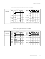
Contents
Chapter 1 General Description
Chapter 2 Bus Interface
Chapter 3 Interrupts
Chapter 4 Timers
Chapter 5 Serial Interface
Chapter 6 Analog Interface
Chapter 7 ATC, ETC
Chapter 8 Ports
Chapter 10 System Control
Chapter 11 Low-power Modes
Chapter 11 Appendix
0
1
2
3
4
5
6
7
8
9
10
11
Contents
0
1
2
3
4
5
6
7
8
9
10
11
Contents
Chapter 1
1-1
General Description
General Description ....................................................................................
2
1-1-1
Introduction .............................................................................
2
1-1-2
1-1-3
Feature ...................................................................................
Overview ................................................................................
2
5
1-2
Basic Specifications ...................................................................................
9
1-3
Block Diagram ............................................................................................
11
1-4
Pin Description ...........................................................................................
13
1-4-1
Single-chip Mode ...................................................................
13
1-4-2
Memory Expansion Mode with 8-bit Bus Address/Data
Separate Mode .......................................................................
14
1-4-3
Memory Expansion Mode with 16-bit Bus Address/Data
1-4-4
Memory Expansion Mode with 8-bit Bus Address/Data
16
1-4-5
Shared Mode ..........................................................................
Memory Expansion Mode with 16-bit Bus Address/Data
Address/Data Shared Mode ...................................................
17
1-4-6
Processor Mode with 8-bit Bus Address/Data
Separate Mode .......................................................................
Separate Mode .......................................................................
Processor Mode with 16-bit Bus Address/Data
19
1-4-8
Separate Mode .......................................................................
Processor Mode with 8-bit Bus Address/Data
Shared Mode ..........................................................................
20
1-4-10
Chapter 2
2-2
18
1-4-7
1-4-9
2-1
15
Processor Mode with 16-bit Bus Address/Data
Shared Mode ..........................................................................
21
List of Pin Functions ...............................................................
22
Bus Interface
Summary of Bus Interface ..........................................................................
52
2-1-1
Overview ................................................................................
52
2-1-2
Control Registers ...................................................................
53
2-1-3
2-1-4
Memory Connection Examples ..............................................
Access to External Memory ...................................................
62
67
Control Signals ...........................................................................................
75
2-2-1
2-3
2-4
Overview ................................................................................
75
Handshake Wait Control .............................................................................
80
2-3-1
Overview ................................................................................
80
Activation Sequence ...................................................................................
82
2-4-1
82
Chapter 3
3-1
3-2
4-2
4-3
4-4
Interrupts
Interrupt Groups .........................................................................................
84
3-1-1
Overview ................................................................................
84
3-1-2
Control Registers ...................................................................
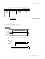
Interrupt Setup Examples ...........................................................................
88
94
3-2-1
External Pin Interrupt Setup Examples ..................................
94
3-2-2
Key Input Interrupt Setup Examples .......................................
96
3-2-3
Watchdog Timer Interrupt Setup Examples (1) ......................
100
3-2-4
Watchdog Timer Interrupt Setup Examples (2) ......................
102
Chapter 4
4-1
Activation Sequence of Each Mode .......................................
Timers
Summary of 8-bit Timer Functions ..............................................................
106
4-1-1
Overview ................................................................................
106
4-1-2
4-1-3
8-bit Timer Control Registers .................................................
8-bit Timer Block Diagrams ....................................................
110
112
8-bit Timer Setup Examples .......................................................................
116
4-2-1
Event Counter Using 8-bit Timer ............................................
116
4-2-2
Clock Output Using 8-bit Timer ..............................................
119
4-2-3
Interval Timer Using 8-bit Timer .............................................
122
Summary of 16-bit Timer Functions ............................................................
4-3-1
Overview ................................................................................
126
126
4-3-2
16-bit Timer Control Registers ...............................................
132
4-3-3
16-bit Timer Block Diagrams ..................................................
135
16-bit Timer Setup Examples .....................................................................
137
4-4-1
Event Counter Using 16-bit Timer ..........................................
137
4-4-2
4-4-3
One-phase PWM Output Using 16-bit Timer .........................
Two-phase PWM Output Using 16-bit Timer ..........................
140
145
4-4-4
One-phase Capture Output Using 16-bit Timer ......................
151
4-5
4-4-5
Two-phase Capture Input Using 16-bit Timer .........................
154
4-4-6
Two-phase Encoder Input (4x) Using 16-bit Timer ..................
158
4-4-7
Two-phase Encoder Input (1x) Using 16-bit Timer .................
161
4-4-8
One-shot Pulse Using 16-bit Timer ........................................
164
4-4-9
4-4-10
External Count Direction Control Using 16-bit Timer .............
External Reset Control Using 16-bit Timer .............................
167
170
Summary of 8-bit PWM Functions ..............................................................
173
4-5-1
Overview ................................................................................
173
4-5-2
Control Registers ....................................................................
175
4-6
8-bit PWM Setup Examples ........................................................................
177
4-7
4-6-1
8-bit PWM Output ...................................................................
16-bit Pulse Width Measure Functions .......................................................
177
181
4-7-1
Overview ................................................................................
181
4-7-2
4-8
Control Registers ...................................................................
183
16-bit Pulse Width Counter Setup ..............................................................
184
4-8-1
184
Chapter 5
5-1
5-2
6-2
Serial Interface
Serial Interface ............................................................................................
188
5-1-1
Overview .................................................................................
188
5-1-2
5-1-3
Control Registers ....................................................................
Serial Interface Connection ....................................................
190
194
Serial Interface Setup Examples .................................................................
197
5-2-1
Serial Transmission in Asynchronous Mode ..........................
197
5-2-2
Serial Reception in Synchronous Mode .................................
200
5-2-3
Serial Clock Operation Example ............................................
203
5-2-4
5-2-5
I2C Transmission ....................................................................
I2C Reception .........................................................................
207
209
Chapter 6
6-1
16-bit Pulse Width Measure Counter .....................................
Analog Interface
Summary of A/D Converter ........................................................................
212
6-1-1
6-1-2
Overview ................................................................................
Control Registers ....................................................................
212
219
A/D Converter Setup Examples ..................................................................
222
6-3
6-4
6-2-1
Single Channel A/D Conversion .............................................
222
6-2-2
Three Channel A/D Conversion .............................................
224
Summary of D/A Converter .........................................................................
227
6-3-1
Overview ................................................................................
227
6-3-2
Control Registers ....................................................................
D/A Converter Setup Examples ..................................................................
228
229
Chapter 7
7-1
7-2
7-3
7-4
Summary of ATC ........................................................................................
232
7-1-1
7-1-2
Overview ................................................................................
Control Registers ....................................................................
232
234
ATC Setup Examples .................................................................................
237
7-2-1
Serial Reception .....................................................................
237
Summary of ETC ........................................................................................
241
7-3-1
7-3-2
241
244
ETC Setup Examples .................................................................................
247
Transfer from External Memory to External Device ...............
247
7-4-2
Transfer from External Device to External Memory
Chapter 8
8-2
8-3
Overview ................................................................................
Control Registers ....................................................................
7-4-1
7-4-3
8-1
ATC, ETC
(Burst Transfer) ......................................................................
251
Transfer from External Device to External Memory
(One Byte Transfer) ................................................................
255
Ports
Summary of Ports .......................................................................................
260
8-1-1
8-1-2
Overview ................................................................................
Control Registers ....................................................................
260
261
8-1-3
Port Block Diagram .................................................................
262
Port Setup Examples ..................................................................................
274
8-2-1
General-purpose Port Setup ..................................................
274
Summary of Byte-swapped Registers ........................................................
276
8-3-1
276
Overview ................................................................................
Chapter 9
9-1
9-2
System Control
Address Break ............................................................................................
280
9-1-1
Overview ................................................................................
280
9-1-2
9-1-3
Control Registers ....................................................................
Address Break Setup Examples .............................................
281
282
System Related Register Protection ...........................................................
284
9-2-1
Overview ................................................................................
284
9-2-2
Control Registers ....................................................................
284
Chapter 10 Low-power Modes
10-1 Summary of Low-power Modes ..................................................................
286
10-1-1
Overview .................................................................................
286
10-1-2
CPU Mode Control Registers .................................................. 288
10-1-3
10-1-4
Transferring between SLOW Mode and NORMAL Mode ........
Switching to Standby Mode ....................................................
289
291
Chapter 11 Appendix
11-1 Electrical Characteristics ............................................................................
11-1-1
11-1-2
294
MN102H55D/55G ...................................................................
MN102HF55G ........................................................................
294
310
11-2 Data Appendix ............................................................................................
339
11-2-1
List of Special Registers .........................................................
339
11-2-2
MN102H55D/55G/F55G Address Map ...................................
518
11-2-3
List of Pin Functions ...............................................................
520
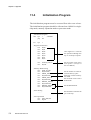
11-3 Initialization Program ..................................................................................
11-4 Flash EEPROM Version .............................................................................
522
524
11-4-1
Overview ................................................................................
524
11-4-2
Flash EEPROM Programming ...............................................
525
11-4-3
PROM Writer Mode ................................................................
525
11-4-4
Onboard Serial Programming Mode .......................................
526
11-4-5
11-4-6
Hardware Used in Serial Programming Mode ........................
Connecting Onboard Serial Programming Mode ....................
526
529
11-4-7
System Configuration for Onboard Serial Programming ........
530
11-4-8
Onboard Serial Programming Mode Setup ............................
532
11-4-9
Branch to User Program .........................................................
534
11-4-10
Serial Interface for Onboard Serial Programming .................
535
11-4-11
PROM Writer/Onboard Serial Programming ..........................
536
11-5 List of MN102H00 Series Linear Address High-speed Edition
Instructions .................................................................................................
538
List of Figures
Figure 1-1-1
Processor Status Word (PSW) ...............................................
5
Figure 1-1-2
Address Space (Memory Expansion Mode) ...........................
7
Figure 1-1-3
Interrupt Controller Configuration ...........................................
8
Figure 1-1-4
Interrupt Servicing Sequence .................................................
8
Figure 1-3-1
Figure 1-4-1
Block Diagram ........................................................................
Pin Configuration in Single-chip Mode ...................................
11
13
Figure 1-4-2
Pin Configuration in Memory Expansion Mode
with 8-bit Bus Address/Data Separate Mode .........................
Figure 1-4-3
Figure 1-4-4
Figure 1-4-5
14
Pin Configuration in Memory Expansion Mode
with 16-bit Bus Address/Data Separate Mode .......................
15
Pin Configuration in Memory Expansion Mode
with 8-bit Bus Address/Data Shared Mode ............................
16
Pin Configuration in Memory Expansion Mode
with 16-bit Bus Address/Data Shared Mode ...........................
17
Figure 1-4-6
Pin Configuration in Processor Mode
18
Figure 1-4-7
with 8-bit Bus Address/Data Separate Mode ..........................
Pin Configuration in Processor Mode
with 16-bit Bus Address/Data Separate Mode ........................
19
Figure 1-4-8
Pin Configuration in Processor Mode
with 8-bit Bus Address/Data Shared Mode ............................
20
Figure 1-4-9
Pin Configuration in Processor Mode
Figure 1-4-10
with 16-bit Bus Address/Data Shared Mode ..........................
OSCI, OSCO Connection Example ........................................
21
48
Figure 1-4-11
XI, XO Connection Example ...................................................
48
Figure 1-4-12
Reset Pin Connection Example ..............................................
48
Figure 1-4-13
WAIT Signal Control Circuit Connection Example ..................
48
Figure 1-4-14
External Dimensions ..............................................................
49
Figure 2-1-1
Address Space .......................................................................
52
Figure 2-1-2
SRAM (Mask ROM) Connection Example
(16-bit Bus Width) ...................................................................
Figure 2-1-3
Figure 2-1-4
Figure 2-1-5
62
SRAM (Mask ROM) Connection Example
(8-bit Bus Width) .....................................................................
63
DRAM (2WE Method) Connection Example
(16-bit Bus Width) ..................................................................
64
Burst ROM Connection Example (8-bit Bus Width) ................
65
Figure 2-1-6
DRAM Connection Example (8-bit Bus Width) ......................
66
Figure 2-1-7
External Access (No Wait Cycle) ...........................................
67
Figure 2-1-8
External Access (0.5 Wait Cycle) ...........................................
67
Figure 2-3-1
Handshake Wait Control Timing
(1 Wait Cycles, Data Write) ....................................................
Fixed Wait and Handshake Wait Control Timing (1 Wait Cycle
80
Figure 2-3-2
as Fixed Wait, 2 Wait Cycles as Whole Wait, Data Write) ....
81
Figure 2-4-1
Activation Sequence of Each Mode .......................................
82
Figure 3-1-1
Interrupt Controller Block Diagram .........................................
85
Figure 3-1-2
Figure 3-1-3
Watchdog Timer Block Diagram .............................................
Interrupt Servicing Time .........................................................
85
87
Figure 3-2-1
External Pin Interrupt Block Diagram .....................................
94
Figure 3-2-2
External Pin Interrupt Timing ..................................................
95
Figure 3-2-3
Key Input Interrupt Block Diagram .........................................
96
Figure 3-2-4
Figure 3-2-5
4×4 Key Input Interrupt Timing ..............................................
Key Input Interrupt Timing ......................................................
96
99
Figure 3-2-6
Watchdog Timer Interrupt Block Diagram ..............................
100
Figure 3-2-7
Watchdog Timer Interrupt Timing ...........................................
101
Figure 3-2-8
Extended Watchdog Timer Interrupt Timing ...........................
102
Figure 4-1-1
Figure 4-1-2
8-bit Timer Block Diagram ......................................................
Timer Configuration ................................................................
107
109
Figure 4-1-3
8-bit Event Counter Input Timing ............................................
109
Figure 4-1-4
8-bit Timer Output and Interval Timer Timing .........................
109
Figure 4-1-5
Timer 0 Block Diagram ...........................................................
112
Figure 4-1-6
Timer 1 Block Diagram ...........................................................
112
Figure 4-1-7
Figure 4-1-8
Timer 2 Block Diagram ...........................................................
Timer 3 Block Diagram ...........................................................
113
113
Figure 4-1-9
Timer 4 Block Diagram ...........................................................
114
Figure 4-1-10
Timer 5 Block Diagram ...........................................................
114
Figure 4-1-11
Timer 6 Block Diagram ...........................................................
115
Figure 4-1-12
Timer 7 Block Diagram ...........................................................
115
Figure 4-2-1
Figure 4-2-2
Event Counter Block Diagram ................................................
Event Counter Timing .............................................................
116
118
Figure 4-2-3
Clock Output Configuration Example (8-bit Timer) ................
119
Figure 4-2-4
Clock Output Block Diagram (8-bit Timer) .............................
119
Figure 4-2-5
Clock Output Timing (8-bit Timer) ..........................................
121
Figure 4-2-6
Interval Timer Configuration Example (8-bit Timer) ...............
122
Figure 4-2-7
Interval Timer Block Diagram (8-bit Timer) ............................
122
Figure 4-2-8
Figure 4-3-1
Interval Timer Timing (8-bit Timer) .........................................
16-bit Timer Block Diagram ....................................................
125
126
Figure 4-3-2
One-phase PWM Output Timing ............................................
128
Figure 4-3-3
One-phase PWM Output Timing (with Data Rewrite) .............
128
Figure 4-3-4
Two-phase PWM Output Timing ............................................
128
Figure 4-3-5
One-shot Pulse Output Timing ...............................................
129
Figure 4-3-6
Figure 4-3-7
External Control Timing ..........................................................
Event Counter Input Timing ....................................................
129
129
Figure 4-3-8
Input Capture 1 Timing ...........................................................
130
Figure 4-3-9
Input Capture 2 Timing ...........................................................
130
Figure 4-3-10
Two-phase Encoder (4x) Timing ............................................
131
Figure 4-3-11
Figure 4-3-12
Two-phase Encoder (1x) Timing ............................................
Timer 8 Block Diagram ...........................................................
131
135
Figure 4-3-13
Timer 9 Block Diagram ...........................................................
135
Figure 4-3-14
Timer 10 Block Diagram .........................................................
136
Figure 4-3-15
Timer 11 Block Diagram .........................................................
136
Figure 4-3-16
Timer 12 Block Diagram .........................................................
136
Figure 4-4-1
Figure 4-4-2
Event Counter Block Diagram ................................................
Event Counter Timing (16-bit Timer) ......................................
137
139
Figure 4-4-3
One-phase PWM Output Block Diagram (16-bit Timer) ..........
140
Figure 4-4-4
One-phase PWM Output Timing (16-bit Timer) ......................
143
Figure 4-4-5
One-phase PWM Output Timing (16-bit Timer)
(Dynamical Duty Change) ......................................................
144
Two-phase PWM Output Block Diagram
(16-bit Timer) ...........................................................................
145
Figure 4-4-7
Two-phase PWM Output Timing (16-bit Timer) ......................
149
Figure 4-4-8
Two-phase PWM Output Timing (16-bit Timer)
Figure 4-4-6
(Dynamical Duty Change) ......................................................
150
Figure 4-4-9
One-phase Capture Input Block Diagram (16-bit Timer) ........
151
Figure 4-4-10
Figure 4-4-11
One-phase Capture Input Timing (16-bit Timer) .....................
Two-phase Capture Input Block Diagram (16-bit Timer) ........
153
154
Figure 4-4-12
Two-phase Capture Input Timing (16-bit Timer) .....................
157
Figure 4-4-13
Two-phase Encoder Input (4x) Block Diagram (16-bit Timer) .
158
Figure 4-4-14
Two-phase Encoder Input (4x) Configuration Example 1 .......
158
Figure 4-4-15
Two-phase Encoder Input (4x) Configuration Example 2 ......
158
Figure 4-4-16
Two-phase Encoder Input Timing (4x) (16-bit Timer) .............
160
Figure 4-4-17
Figure 4-4-18
Two-phase Encoder Input (1x) Block Diagram (16-bit Timer) .
Two-phase Encoder Input (1x) Configuration Example 1 .......
161
161
Figure 4-4-19
Two-phase Encoder Input (1x) Configuration Example 2 .......
161
Figure 4-4-20
Two-phase Encoder Input Timing (1x) (16-bit Timer) .............
163
Figure 4-4-21
One-shot Pulse Output Block Diagram (16-bit Timer) ............
164
Figure 4-4-22
One-shot Pulse Output Timing (16-bit Timer) ........................
166
Figure 4-4-23
External Count Direction Control Block Diagram
(16-bit Timer) ..........................................................................
167
Figure 4-4-24
External Count Direction Control Configuration Example ......
167
Figure 4-4-25
External Count Direction Control Timing (16-bit Timer) .........
169
Figure 4-4-26
External Reset Control Block Diagram (16-bit Timer) ............
170
Figure 4-4-27
Figure 4-5-1
External Reset Control Timing (16-bit Timer) .........................
8-bit PWM Function ................................................................
172
173
Figure 4-5-2
PWM Output Waveform .........................................................
174
Figure 4-6-1
8-bit PWM Block Diagram ......................................................
177
Figure 4-6-2
Timer 0 Timing .......................................................................
178
Figure 4-6-3
8-bit PWM Timing ...................................................................
180
Figure 4-7-1
Figure 4-7-2
16-bit Pulse Width Measure Counter .....................................
16-bit Pulse Width Measure Counter Operation Example ......
181
182
Figure 4-8-1
16-bit Pulse Width Measure Counter Block Diagram .............
184
Figure 4-8-2
16-bit Pulse Width Measure Counter Timing ..........................
186
Figure 5-1-1
Serial Interface Configuration ................................................
188
Figure 5-1-2
Figure 5-1-3
Synchronous Mode Connections ...........................................
Asynchronous Mode Connections ..........................................
194
194
Figure 5-1-4
I2C Mode Connections ............................................................
194
Figure 5-1-5
Asynchronous Serial Timing (Transmission) ..........................
195
Figure 5-1-6
Asynchronous Serial Timing (Reception) ...............................
195
Figure 5-1-7
Synchronous Serial Timing (Transmission) ............................
196
Figure 5-1-8
Figure 5-2-1
Synchronous Serial Timing (Reception) .................................
Asynchronous Transmission Block Diagram ..........................
196
197
Figure 5-2-2
Asynchronous Transmission Timing .......................................
199
Figure 5-2-3
Synchronous Reception Block Diagram .................................
200
Figure 5-2-4
Clock Generation in Synchronous Reception .........................
201
Figure 5-2-5
Serial Clock Block Diagram ....................................................
203
Figure 5-2-6
Serial Clock Timing ................................................................
206
Figure 5-2-7
Figure 5-2-8
Master Transmission Timing (with ACK) ................................
Master Reception Timing ........................................................
208
210
Figure 6-1-1
Analog Interface Configuration ...............................................
212
Figure 6-1-2
A/D Converter Timing .............................................................
213
Figure 6-1-3
Single Channel/Single Conversion Timing .............................
214
Figure 6-1-4
Figure 6-1-5
Multiple Channels/Single Conversion Timing ......................... 215
Single Channel/Continuous Conversion Timing ....................... 216
Figure 6-1-6
Multiple Channels/Continuous Conversion Timing ................... 217
Figure 6-1-7
A/D Converter Block Diagram ................................................
218
Figure 6-2-1
Analog Voltage Input Example ...............................................
222
Figure 6-2-2
Figure 6-2-3
Single Channel A/D Conversion Block Diagram ....................
Single Channel A/D Conversion Timing .................................
222
223
Figure 6-2-4
3-channel A/D Conversion Configuration ...............................
224
Figure 6-2-5
3-channel A/D Conversion Block Diagram .............................
224
Figure 6-2-6
3-channel A/D Conversion Timing ..........................................
226
Figure 6-3-1
D/A Converter Configuration ..................................................
227
Figure 6-4-1
Figure 6-4-2
Analog Voltage Output Example ............................................
D/A Conversion Block Diagram Using DA0 Channel .............
229
229
Figure 7-1-1
ATC Bus Acquisition Timing ...................................................
232
Figure 7-2-1
ATC Serial Reception Block Diagram ....................................
237
Figure 7-2-2
Serial Reception Sequence ....................................................
237
Figure 7-3-1
Figure 7-4-1
ETC Bus Acquisition Timing ...................................................
ETC External Memory → External Device
241
Transfer Block Diagram ..........................................................
247
Figure 7-4-2
ETC External Memory → External Device
Transfer Connection ...............................................................
247
Figure 7-4-3
ETC External Memory → External Device
250
Figure 7-4-4
Burst Transfer Timing .............................................................
ETC External Device → External Memory
(Burst) Transfer Block Diagram ..............................................
251
Figure 7-4-5
ETC External Device → External Memory
(Burst) Transfer Configuration ................................................
Figure 7-4-6
Figure 7-4-7
Figure 7-4-8
ETC External Device → External Memory
Burst Transfer Timing .............................................................
254
ETC External Device → External Memory
(One Byte) Transfer Block Diagram .......................................
255
ETC External Device → External Memory
(One Byte) Transfer Connection ............................................
Figure 7-4-9
251
255
ETC External Device → External Memory
(One Byte) Transfer Timing ....................................................
258
Figure 8-1-1
I/O Port Configuration ............................................................
260
Figure 8-2-1
General-purpose Port Setup Example ...................................
276
Figure 8-2-2
Basic Flowchart of General-purpose Port Input .....................
277
Figure 8-2-3
Basic Flowchart of General-purpose Port Output ...................
277
Figure 8-3-1
Byte-swapped Register ..........................................................
278
Figure 9-1-1
Address Break Block Diagram ................................................
280
Figure 9-1-2
Address Break Operation Example ........................................
280
Figure 9-1-3
Program Flow of Address Break Setup ..................................
282
Figure 9-1-4
Stack State after NMI Interrupt ...............................................
283
Figure 10-1-1
CPU Operating Mode Changes ..............................................
286
Figure 10-1-2
Operating Mode Control and Clock Oscillation On/Off ...........
288
Figure 10-1-3
Sequence of Switching to/from Standby Mode .......................
291
Figure 11-1-1
System Clock Timing .............................................................
327
Figure 11-1-2
Figure 11-1-3
Reset Timing ..........................................................................
Voltage Rise Timing ...............................................................
327
327
Figure 11-1-4
Data Transfer Signal Timing (Address/Data
Separate, without Wait, Read/Write) ......................................
Figure 11-1-5
Figure 11-1-6
Figure 11-1-7
328
Data Transfer Signal Timing (Address/Data
Separate, with Wait (1.5 or More), Read/Write) .....................
329
Data Transfer Signal Timing (Address/Data Separate,
with Wait (1.5 or More), /RE Late, Short Mode) .....................
330
Data Transfer Signal Timing (Address/Data Separate,
with Wait (1.5 or More), /WE Late, Short Mode) ....................
331
Figure 11-1-8
Data Transfer Signal Timing (Address/Data Shared,
without Wait, Read/Write) ......................................................
Figure 11-1-9
Data Transfer Signal Timing (Address/Data Shared,
Figure 11-1-10
with Wait (1.5 or More), Read/Write) .......................................
Data Transfer Signal Timing (Address/Data Shared,
332
333
with Wait (1.5 or More), ALE Late, Long Mode, /AD
Long Mode, Read) .................................................................
Figure 11-1-11
334
Data Transfer Signal Timing (Address/Data Shared,
with Wait (1.5 or More), ALE Late, Long Mode, /AD
Figure 11-1-12
Long Mode, Write) .................................................................
Bus Authority Request Signal Timing .....................................
335
336
Figure 11-1-13
Interrupt Signal Timing ...........................................................
336
Figure 11-1-14
Serial Interface Signal Timing 1 (Synchronous
Figure 11-1-15
Figure 11-1-16
Serial Transmission: Transfer in Progress) ............................
336
Serial Interface Signal Timing 2 (Synchronous Serial
Transmission: Transfer End Timing at SBT Input) .................
336
Serial Interface Signal Timing 3 (Synchronous Serial
Transmission: Transfer End Timing at SBT Output) ..............
Figure 11-1-17
337
Serial Interface Signal Timing 4 (Synchronous Serial
Reception: Transfer End Timing at SBT Input) ......................
337
Figure 11-1-18
Figure 11-4-1
Timer/Counter Signal Timing ..................................................
Memory Map for Flash EEPROM Version ..............................
337
524
Figure 11-4-2
Flash EEPROM Program Flow ...............................................
525
Figure 11-4-3
8-bit Serial Interface Block Diagram for Serial Writer .............
526
Figure 11-4-4
Flash EEPROM Memory Space .............................................
527
Figure 11-4-5
Pin Configuration During Serial Programming .......................
529
Figure 11-4-6
Figure 11-4-7
System Configuration for Onboard Serial Writer ....................
Target Board-Serial Writer Connection ..................................
530
530
Figure 11-4-8
Timing for Onboard Serial Programming Mode ......................
532
Figure 11-4-9
Load Program Start Flow .......................................................
533
Figure 11-4-10
Reset Service Routine Flow ...................................................
534
Figure 11-4-11
Interrupt Service Routine Flow ...............................................
534
Figure 11-4-12
Figure 11-4-13
Data Transfer Timing ..............................................................
Programming Flow .................................................................
535
536
List of Tables
Table 1-1-1
Memory Modes .......................................................................
7
Table 1-2-1
Basic Specifications ...............................................................
9
Table 1-3-1
Block Functions ......................................................................
12
Table 1-4-1
List of Pin Functions ...............................................................
22
Table 2-1-1
Mode Setting ..........................................................................
52
Table 2-1-2
List of Bus Interface Control Registers ...................................
61
Table 2-1-3
Address/Data Multiplex Mode (16-bit Bus Data Access) .......
68
Table 2-1-4
Address/Data Multiplex Mode (8-bit Bus Data Access) .........
69
Table 2-1-5
Table 2-1-6
Address/Data Separate Mode (16-bit Bus Data Access) .......
Address/Data Separate Mode (8-bit Bus Data Access) .........
70
71
Table 2-1-7
Address/Data Separate Mode (16-bit Bus DRAM
WEH and WEL Method) .......................................................
72
Table 2-1-8
Address/Data Separate Mode (8-bit Bus DRAM
WEH and WEL Method) .......................................................
Address/Data Separate Mode
73
Table 2-1-9
(16-bit Bus Burst ROM Access) .............................................
74
Table 2-1-10
Address/Data Separate Mode
(8-bit Bus Burst ROM Access) ...............................................
74
Table 2-2-1
External Memory Control Signal Timing .................................
75
Table 2-2-2
Table 2-2-3
RE Late and Short Modes (Address/Data Shared Mode) .....
WE Late and Short Modes (Address/Data Shared Mode) ....
76
77
Table 2-2-4
RE Late and Short Modes (Address/Data Separate Mode) ..
78
Table 2-2-5
WE Late and Short Modes (Address/Data Separate Mode) .
78
Table 2-2-6
ALE Late and Long Modes (Address/Data Shared Mode) .....
79
Table 2-2-7
AD Long Mode (Address/Data Shared Mode) ........................
79
Table 3-1-1
Comparison of MN102H55D/55G/F55G and
MN102B00/MN102L00 ...........................................................
84
Table 3-1-2
Interrupt Vector and Class Assignment ..................................
86
Table 3-1-3
Handler Preprocessing ...........................................................
87
Table 3-1-4
Handler Postprocessing .........................................................
87
Table 3-1-5
List of Interrupt Control Registers ...........................................
91
Table 4-1-1
8-bit Timer Functions ..............................................................
108
Table 4-1-2
Table 4-3-1
List of 8-bit Timer Control Registers .......................................
16-bit Timer Functions ............................................................
111
127
Table 4-3-2
List of 16-bit Timer Control Registers .....................................
134
Table 4-5-1
8-bit PWM Functions ..............................................................
174
Table 4-5-2
List of 8-bit PWM Registers ....................................................
176
Table 4-7-1
List of 16-bit Pulse Width Measure Registers ........................
183
Table 5-1-1
Serial Interface Functions .......................................................
189
Table 5-1-2
List of Serial Interface Control Registers ................................
193
Table 5-1-3
Baud Rate Setting Example in Asynchronous Mode ..............
195
Table 5-2-1
Transfer Clock Setup Example ...............................................
203
Table 6-1-1
A/D Converter Functions ........................................................
213
Table 6-1-2
List of A/D Converter Control Registers .................................
221
Table 6-3-1
D/A Converter Functions ........................................................
227
Table 6-3-2
List of D/A Converter Control Registers .................................
228
Table 7-1-1
Table 7-1-2
ATC Functions ........................................................................
List of ATC Control Registers .................................................
233
236
Table 7-3-1
ETC Connection Examples ....................................................
242
Table 7-3-2
List of ETC Control Registers .................................................
246
Table 8-1-1
List of Port Control Registers .................................................
262
Table 8-1-2
Port Block Diagrams ...............................................................
264
Table 10-1-1
Watchdog Interrupt Interval ....................................................
288
Table 11-4-1
Clock Frequency .....................................................................
531
Chapter 1 General Description
0
1
2
3
4
5
6
7
8
9
10
11
Chapter 1 General Description
1-1
General Description
1-1-1
Introduction
The 16-bit MN102 series high-speed linear addressing version designs
the new architecture for C-language programming based on a detailed
analysis for embedded applications. This improves the previous system
architecture in speed and function to meet the requirements in user systems including miniaturization to power consumption.
This series adapts a load/store architecture method for computing within registers instead of the accumulator system for computing within the memory space in the previous series. The basic instructions are one byte/one machine cycle. This reduces code
size and improves compiler efficiency. This series uses the circuit designed for submicron technology providing optimized hardware and low system power consumption.
This series has up to 16 Mbytes of linear address space and can develop the highly
efficient programs. The optimized hardware architecture allows lower power consumption even in large systems.
1-1-2
Features
This series contains a flexible and optimized hardware architecture as
well as a simple and efficient instruction set. This allows economy and
speed. This section describes the features of this series CPU.
1. High-speed Signal Processing
An internal multiplier operates 16-bit x16-bit = 32-bit in a single cycle. In addition,
the hardware contains a saturation calculator which must be used in signal processing
and increases the signal processing speed.
2. Linear Addressing for Large Systems
The MN102H series contains up to 16 Mbytes of linear address space. The CPU does
not detect borders between address spaces, which provides an effective development
environment. The hardware architecture is also optimized for large systems. The
memory is not divided into instruction areas and data areas so that operations can share
instructions.
2
MN102H55D/55G/F55G
Chapter 1 General Description
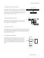
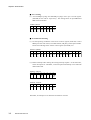
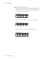
3. Single-byte Basic Instruction Length
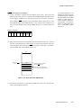
Conventional Register Assignment
7
15
The MN102H series has replaced general registers with eight internal
CPU registers divided four address registers (A0-A3) and four data registers (D0-D3). The register specification fields are four bits or less, and
the code size of the basic instructions including register-to register operations and load/store operations is one byte.
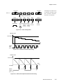
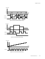
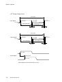
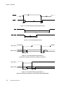
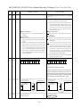
4. High-speed Pipeline Processing
0
Register Specification Field
7
0
Register Specification Field
New Register Assignement
1 Machine Cycle
Instruction 1
The MN102H series executes instructions in a 3-stage pipeline: fetch,
decode, execute. This allows the MN102H series to execute instructions of single byte in one machine cycle.
Fetch
Instruction 2
Decode
Address
calculation
Execute
Fetch
Decode
Address
calculation
Execute
5. Simple Instruction Set
The MN102H series uses an instruction set of 41 instructions, designed specially for
the programming model for embedded applications. To shrink code size, instructions
have a variable length of one to seven bytes. The most frequently used instructions in
C-language compiler are single byte.
6. High-speed Interrupt Response
Main Program
The MN102H series halts the instructions execution even during the
execution of the instruction with long execution cycles. After an interrupt occurs, the program moves to the interrupt service routine within
six cycles or less. The MN102H series improves real-time control performance using the interrupt handler which adjusts interrupt servicing
speed.
Instruction 1
Interrupt Service Routine
Instruction 2
Interrupt Request
Instruction 3
Instruction 4
MN102H55D/55G/F55G
3
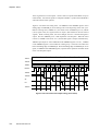
Chapter 1 General Description
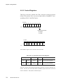
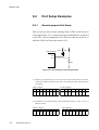
7. Flexible Interrupt Control Structure
The interrupt controller supports a maximum of 64 interrupt vectors (of them, interrupt vectors 0 to 3 are reserved for nonmaskable interrupts). In addition, groups of up
to four vectors are assigned to classes. Each class can be set to one of seven priority
levels. This provides the software design flexibility and control. The CPU is compatible with software from previous Panasonic peripheral modules.
8. High-speed, High-functional External Interface
The MN102H series supports external interface functions including DMA, handshake
function and bus arbitration.
9. C-language Development Environment
The MN102H series has simple hardware optimized for C-language programming and
highly efficient C compiler. With this advantage, this series improves development
environment for C-language embedded applications without expanding the program
size. The PanaXSeries development tools support the MN102H series devices.
10. Outstanding Power Savings
The MN102H series contains separate buses for instructions, data and peripheral functions, which distribute and reduce load capacitance. This reduces overall power consumption. The MN102H series also supports three modes of SLOW, HALT and
STOP for power savings.
PanaXSeries is a trademark of the Matsushita Electric Industrial Co., Ltd.
4
MN102H55D/55G/F55G
Chapter 1 General Description
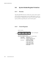
1-1-3
Overview
This section describes the basic configuration and functions of the
MN102H55D/55G/F55G.
Note 1: These bits change depending on all 24 bits of the operation result.
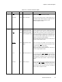
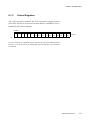
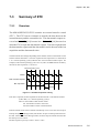
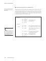
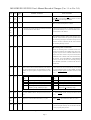
■ Processor Status Word (PSW)
Note 2: These bits change depending on the lower 16 bits of
the operation result.
The PSW register contains the operating result flags and interrupt mask level flags.
Note 1
15
8
PSW
-
ST
Reset :
-
0
Note 2
0
7
The IE flag should be set to 0
before the IM[2:0] flags of PSW
are changed.
S1 S0 IE IM2 IM1 IM0 VX CX NX ZX VF CF NF ZF
0
0
0
0
0
0
0
0
0
0
0
0
0
0
Zero flag (ZF) is set if the lower 16 bits
of the operation result are 0; otherwise
it is reset.
Negative flag (NF) is set if bit 15 of the operation result is 0; otherwise it is reset.
Carry flag (CF) is set if the operation resulted in
a carry or a borrow out of bit 15; otherwise it is
reset.
Overflow flag (VF) is set if the operation causes the
sign bit to change in a 16-bit signed number; otherwise it is reset.
Extension zero flag (ZX) is set if all bits of the operation
result are 0; otherwise it is reset.
Extension negative flag (NX) is set if the MSB of the operation
result is 1, and it is reset if the MSB is 0.
Extension carry flag (CX) is set if the operation resulted in a carry or a
borrow out of the MSB; otherwise it is reset.
Extension overflow flag (VX) is set if the operation causes the sign bit to
change in a 24-bit signed number; otherwise it is reset.
IM[2:0] indicate the mask level (from 0 to 7) of interrupts that the CPU will accept
from its seven interrupt input pins. The CPU will not accept any interrupt at a higher
level than the indicated level here.
Interrupt enable flag (IE) controls maskable interrupt enable. The flag is set if IE=1, and it is
reset if IE=0.
S[1:0] are OS software control bits. These are reserved for the OS.
Saturation flag controls whether or not the CPU performs a saturation operation. When this bit is 1, the CPU
execute a saturate operation. When this bit is 0, the CPU operates a normal operation. The PXST instruction
can reserve the meaning of this bit for the next instruction.
Figure 1-1-1 Processor Status Word (PSW)
Please refer to "11-5 MN102H00 series High-speed Linear Address Instruction Set" for the flags reflected by instructions.
MN102H55D/55G/F55G
5
Chapter 1 General Description
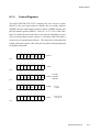
■ Internal Registers, Memory, and Special Function Registers
Program Counter
23
0
PC
The program counter specifies the 24-bit address of the program
during the execution.
Address Registers
23
0
A0
The address registers specify the data location on memory. Of
four registers, A3 is assigned as the stack pointer.
A1
A2
A3
Data Registers
23
0
D0
D1
D2
The data registers perform all arithmetic and logic operations.
When the byte-length (8-bit) or word-length (16-bit) data is transferred to memory or to another register, an instruction adds a
zero or sign extension.
D3
Multiplication/Division Register
15
0
MDR
The multiplication/division register stores the upper 16 bits of the
32-bit product of multiplication operations. In division operations,
this register stores the upper 16 bits of the 32-bit dividend before
execution, and the 16-bit remainder of the quotient after execution.
Processor Status Word
15
0
PSW
Memory, Special Function Registers, I/O Ports
ROM
Memory (ROM, RAM), special function registers for peripheral
function control and I/O ports are assigned to the same address
space.
RAM
CPUM, EFCR, IAGR
Internal Control Registers *
NMICR, xxICR
Interrupt Control Registers *
SCCTRn, TRXBUFn, SCSTRn
Serial Interfacel Registers *
ANCTR, ANnBUF
A/D Converter Registers *
TMn, BCn, BRn
Timer/Counter Registers *
MEMMD
PnOUT, PnIN, PnDIR
6
MN102H55D/55G/F55G
Memory Control Registers *
I/O Port Registers *
* This allocation is an example.
Actual memory, peripheral functions, special function registers
and I/O port allocation depends
on the model.
Chapter 1 General Description
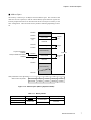
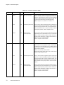
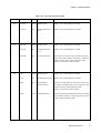
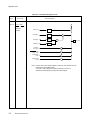
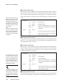
■ Address Space
;;
;
;
;;
The memory contains up to 16 Mbytes of linear address space. The instruction and
data areas are not separated, so that the internal RAM, special function registers for
internal peripheral functions are allocated into the first 64 kbytes in memory as the
basic configuration. There are three memory modes as following depending on models.
x'000000'
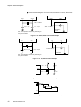
External Memory
x'008000'
Internal RAM
x'009000'
(*4)
Reserved
x'00FC00'
4 Kbytes
(*3)
I/O Control Registers
x'010000'
1 Kbyte
External Memory
Program start address
x'080000'
16 Mbytes
x'080000'
Interrupt handler start address
x'080008'
Internal ROM
x'0A0000'
(*2)
Reserved
x'200000'
128 Kbytes
(*1)
External Memory
x'FFFFFF'
Note*) Parameters on the right table
differ on each chip model.
*2
*1
MN102HF55G 128 KBytes
MN102H55G 128 KBytes
MN102H55D
64 KBytes
x'0A0000'
x'0A0000'
x'090000'
*3
*4
4096 Bytes
4096 Bytes
4096 Bytes
x'009000'
x'009000'
x'009000'
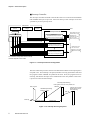
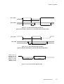
Figure 1-1-2 Address Space (Memory Expansion Mode)
Table 1-1-1 Memory Modes
Mode
Address Bit Width
Processor mode
External Memory Access
Not accessible
Single-chip mode
Memory expansion mode
ROM Capacity
64 k/128 kbytes
Accessible
Up to 24 bits
None
MN102H55D/55G/F55G
7
Chapter 1 General Description
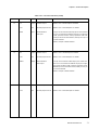
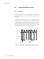
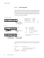
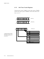
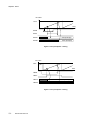
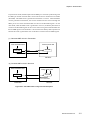
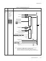
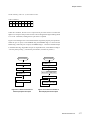
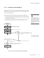
■ Interrupt Controller
The interrupt controller allocated to the outside of the core controls all nonmaskable
and maskable interrupts except reset. Each class has up to four interrupt vectors and
specifies any of seven priority levels.
CPU Core
Maskable Interrupt
Receive
Nonmaskable Interrupt
Receive
Reset
Receive
Reset
Interrupt Controller
Interrupt Enable
Nonmaskable interrupts
4
Groups 0 to 3
Nonmaskable Interrupt Controllers
Interrupt Masking
6
5
4
3
2
1
0
Nonmaskable Interrupt Control Register (NMICR)
(WDICR)
(UNICR)
(EIICR)
Group 4
Maskable Interrupt Controller
External NMI pin input
Watchdog timer
Undefined instruction
No vector exists
when interrupt occurs.
4
Maskable Interrupt Control Register (xxICH)
Group 63
Maskable Interrupt Controller
Maskable interrupts
Max. 240 vectors
External pin interrupts
Peripheral interrupts
4
Maskable Interrupt Control Register (xxICH)
The hardware configuration of the interrupt
controller depends on the model.
Figure 1-1-3 Interrupt Controller Configuration
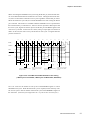
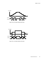
The CPU checks the processor status word to determine whether an interrupt request is
accepted or not. If an interrupt is accepted, automatic servicing by hardware starts and
the program counter and PSW are pushed to the stack. Next, the program moves to
interrupt, searches the interrupt vector and branches to the entry address of the interrupt service routine for that interrupt.
Interrupt preprocessing
Push registers, branch to entry address, etc.
Main program
x'080008'
Interrupt service routine
Resets interrupt vector
at the beginning
Hardware processing
Push PC, PSW
JMP, etc.
Interrupt
Max. 6 machine cycles
7 machine cycles
Figure 1-1-4 Interrupt Servicing Sequence
8
MN102H55D/55G/F55G
Chapter 1 General Description
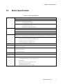
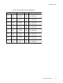
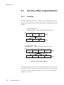
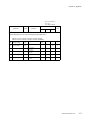
1-2
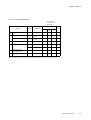
Basic Specification
Table 1-2-1 Basic Specifications
Structure
Internal multiplier (16-bit×16-bit=32-bit) and internal saturate operation calculator
Load/store architecture
Eight registers: Four 24-bit data registers
Four 24-bit address registers
Others:
24-bit program counter
16-bit processor status word
16-bit multiplication/division register
Instruction Set
41 instructions
6 addressing modes
1-byte basic instruction length
Code assignment: 1 byte (basic) + 0 to 6 bytes (extension)
Performance
Maximum of 17-MHz internal operating frequency with a 34-MHz external oscillator MN102H55D/55G
Maximum of 15-MHz internal operating frequency with a 30-MHz external oscillator MN102HF55G
Instruction execution clock cycles:
For register-to-register operations, minimum 1 cycle
For branch operations, minimum 2 cycles
For load/store operations, minimum 1 cycle
Pipeline
3 stage: instruction fetch, decode, execute
Address Space
Up to 16-Mbyte linear address space
Shared instruction/data space
Interrupt
1 external nonmaskable interrupt
46 maskable interrupts
7 priority level settings
Low-power Mode
SLOW, STOP, HALT
Oscillation
Up to 34 MHz
Frequency
Timer/Counter
Eight 8-bit timers (TM0 to TM7) :
Cascading function (form as 16-bit to 64-bit timer)
Timer output
Internal clock source or external clock source
Serial Interface clock generation
Start timing generation for A/D converter
MN102H55D/55G/F55G
9
Chapter 1 General Description
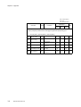
Table 1-2-1 Basic Specifications
Timer/Counter
Five 16-bit timers (TM8 to TM12) :
Two channels of compare/capture registers
Selectable internal or external clock
PWM/one-shot pulse output
Two-phase encoder input (4x or 1x method)
Two 8-bit PWM (TM13, TM14) :
Two internal compare registers for each channel
Two pattern outputs
One 16-bit pulse width counter (TM15) :
Capture the counter value whenever the input pulse rises
16-bit watchdog timer
ATC
Four Channels
Automatic transfer is possible between memories, memory and peripheral I/O for each interrupt vector.
Transfer unit: byte or word
Transfer mode: single-chip or burst mode
Transfer addressing: source, destination pointer, increment
Up to 4096 words can be transferred
Access to 16-Mbyte address space
ETC
Two Channels
Automatic transfer is possible between external device and external memory.
Transfer unit: byte or word
Transfer mode: single-chip or burst mode
Transfer addressing: source, destination pointer, increment
Up to 4096 words can be transferred
Access to 16-Mbyte address space
Serial Interface
Three Synchronous Interfaces (ASCI0 to ASCI2)
Two shared UART/Synchronous/I2C (single master only) Interfaces (ASCI3, ASCI4)
A/D Converter
10-bit with 8 channels (can be used as 8-bit)
Automatic Scanning
D/A Converter
Two 8-bit channels
External Expansion
Address/data multiplex port function
Address/data separate port function
Memory Interface
DRAM Interface (8-bit/16-bit width)
Burst ROM Interface
I/O Port
Maximum of 82 I/O ports in single-chip mode
Maximum of 47 I/O ports in address/data multiplex mode
Maximum of 40 I/O ports in address/data separate mode
Package
10
100-pin LQFP
MN102H55D/55G/F55G
Chapter 1 General Description
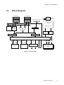
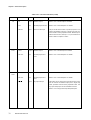
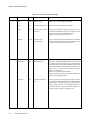
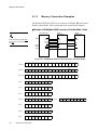
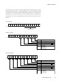
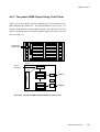
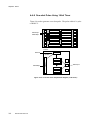
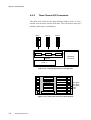
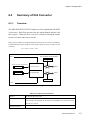
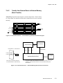
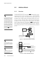
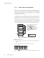
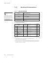
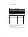
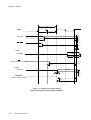
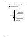
1-3
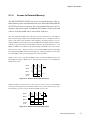
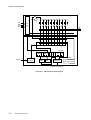
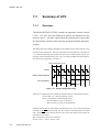
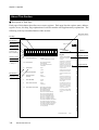
Block Diagram
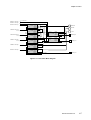
Address Registers
Data Registers
A0
D0
A1
D1
A2
D2
Multiplication/Division Register
A3
D3
MDR
T1
T2
Clock
Generator
Clock
Source
Instruction Execution
Controller
A
B
Multiplier
Instruction Decoder
Program
Counter
PSW
Incrementer
ALU
Instruction
Queue
Program Address
Interrupt
Controller
Operand Address
Interrupt Bus
Bus Controller
ROM Bus
RAM Bus
Internal ROM
Internal RAM
Peripheral Execution Bus
External Interface
Internal Peripheral
Functions
External Extension Bus
BR BG
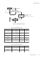
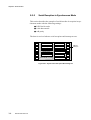
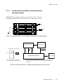
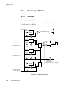
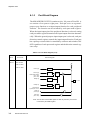
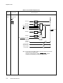
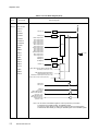
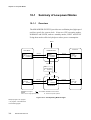
Figure 1-3-1 Block Diagram
MN102H55D/55G/F55G
11
Chapter 1 General Description
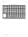
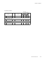
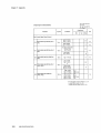
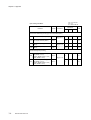
Table 1-3-1 Block Functions
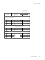
Function
Blcok
Clock Generator
An oscillation circuit connected to an external crystal supplies the clock to all blocks
in the CPU.
Program Counter
The program counter generates addresses for instruction queues. Normally it increments based on the sequencer indications, but for branch instructions and interrupt
acceptance, it sets the branch address and the ALU operation result.
Instruction Queue
The instruction queue contains up to four bytes of prefetched instructions.
Instruction Decoder
The instruction decoder decodes the contents of instruction queue and generates control signals needed for the instruction execution. The instruction executes by controlling each block in the CPU.
Quick Decoder
The quick decoder decodes the 2-byte or larger instruction at faster speed.
Instruction Execution
Controller
ALU
The instruction execution controller controls the CPU operations based on results
from the instruction decoder and interrupt requests.
The ALU calculates the operand addresses for arithmetic operations, logic operations,
shift operations, register relative indirect addressing, indexed addressing, register indirect addressing.
Multiplier
The multiplier calculates 16 bits × 16 bits = 32 bits.
Internal ROM and RAM
These memory allocate the program, data and stack areas.
Address Registers (An)
The address registers (An) store the addresses in memory accessed during data transfer. They also store the base addresses in register relative indirect addressing, indexed
addressing and register indirect addressing modes.
Operation Registers
The data registers (Dn) store data transferred to memory and results of arithmetic operations. They also store the offset addresses in indexed addressing and register indirect addressing modes.
The multiplication/division register (MDR) stores data for multiplication/division operations.
The processor status word register stores the flags that indicate the status of the CPU
interrupt controller and operation results.
PSW
12
Interrupt Controller
The interrupt controller detects interrupt requests from the peripheral functions, and
requests the CPU to move to the interrupt servicing routine.
Bus Controller
The bus Controller controls the connection between the CPU internal bus and the CPU
external bus. It also contains the bus arbitration function.
Internal Peripheral
Function
The MN102H55D/55G/F55G contains internal peripheral functions including timers,
serial interface, A/D converter and D/A converters. Internal peripheral functions vary
depending on the chip models.
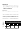
MN102H55D/55G/F55G
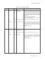
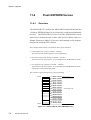
P83,TM4IO,SBI3
51
52
53
P90,TM8IOA,BIBT1
P86,TM9IOB,SBI4
VREF+
P85,TM9IOA,SBT4,SCL4,SBO2
P84,TM7IO,SBO3,SDA3
54
55
56
58
57
P93,TM10IC
P92,TM10IOB
P91,TM10IOA,BIBT2
59
60
61
P96,AN2
P95,AN1
P94,AN0
AVSS
62
P97,AN3
65
64
63
P70,SBT0
VDD (Vpp)
66
67
68
69
70
72
73
NMI
74
75
76
50
77
49
78
48
79
47
80
46
81
45
82
44
83
43
P00
P01
84
P02
P03
86
P04
P05
P06
P07
VSS
P10,TM8IOB
P11,TM8IC
P12,TM11IOA
P13,TM11IOB
P14,TM11IC
P15,TM12IOA
P16,TM12IOB
P17,TM12IC
88
87
89
90
41
40
39
38
37
36
25
23
24
OSCI
OSCO
(MODE)
22
21
20
XI,PB1
XO
VDD
19
18
BOSC,PB0,BIBT1,BIBT2
VSS
17
15
16
14
13
12
11
P56,BSTRE,TM15IA
P57
P20,SBT2
P21,SBI2
P22,SBO2
P23
VDD
P54
P55
10
26
9
27
100
8
28
99
7
29
98
6
30
97
P51,TM13OB
P52,TM14OA
P53,TM14OB
31
96
P50,TM13OA
32
95
5
33
94
3
4
34
93
P62
P63
35
92
2
91
1
P82,TM0IO,SBT3,SCL3,SBI2
P81,DAC1
P80,DAC0
P47,AN7,WDOUT
P46,AN6,STOP
P45,AN5
P44,AN4
VREFP43
P42
P41
P40
P37, KI7
P36, KI6
P35, KI5
P34, KI4
AVDD
P33, KI3
P32, KI2
P31, KI1
P30, KI0
P27
P26
P25
P24,TM15IA
42
MN102H55D
MN102H55G
MN102HF55G
(TOP VIEW)
85
P61
PA1,IRQ1
PA2,IRQ2
PA3,IRQ3
PA4,IRQ4,TM15IB
PA5
RST
VDD
P60,SBT2
PA0,IRQ0
P74,SBI1
P73,SBT1
P72,SBO0
P71,SBI0
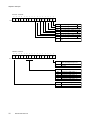
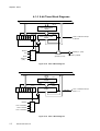
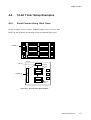
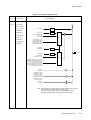
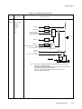
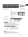
Single-chip Mode
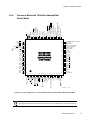
P75,SBO1
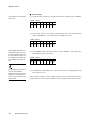
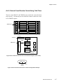
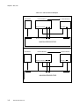
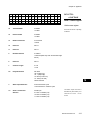
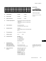
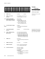
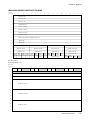
1-4-1
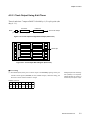
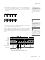
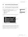
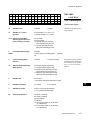
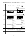
71
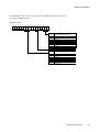
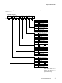
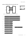
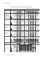
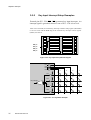
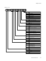
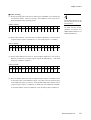
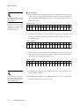
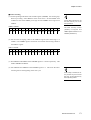
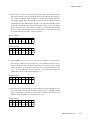
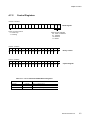
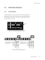
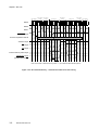
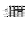
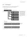
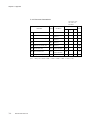
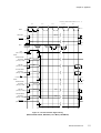
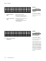
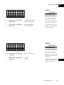
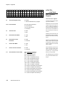
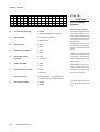
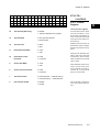
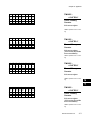
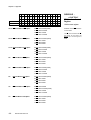
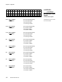
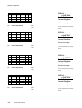
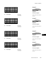
Pin Description
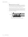
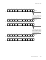
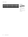
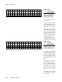
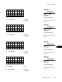
*
*
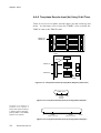
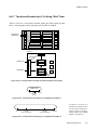
1-4
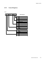
P87,TM9IC,SBO4,SDA4
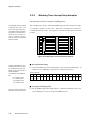
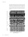
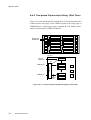
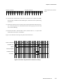
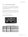
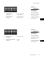
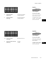
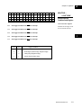
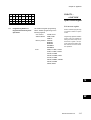
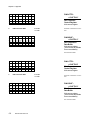
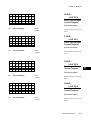
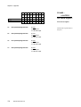
Chapter 1 General Description
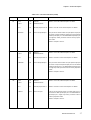
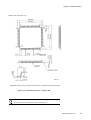
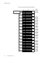
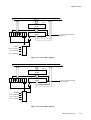
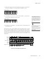
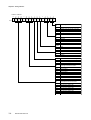
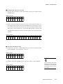
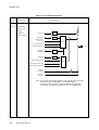
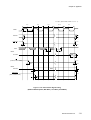
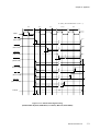
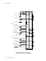
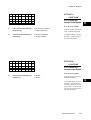
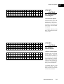
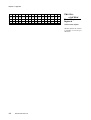
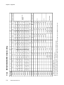
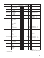
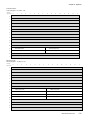
* : Use 33 kΩ - 50 kΩ
Figure 1-4-1 Pin Configuration in Single-chip Mode
Unused pins require handling in the circuit (input pins are connected to VDD/VSS, output pins leave
open, input/output pins are connected to VDD/VSS or leave open depending on pin direction setting).
MN102H55D/55G/F55G
13
Chapter 1 General Description
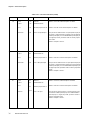
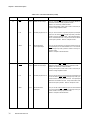
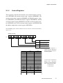
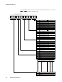
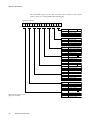
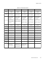
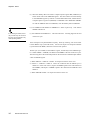
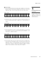
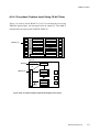
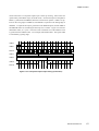
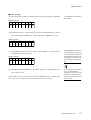
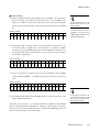
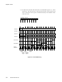
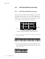
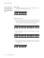
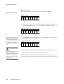
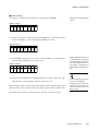
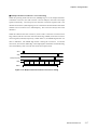
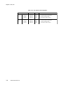
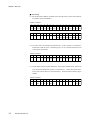
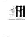
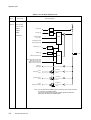
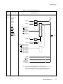
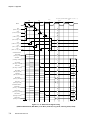
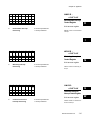
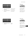
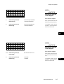
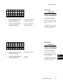
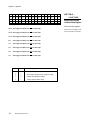
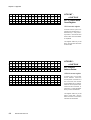
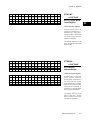
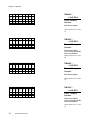
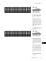
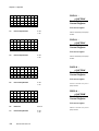
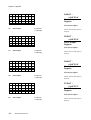
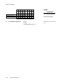
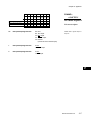
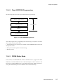
PA0,IRQ0
P83,TM4IO,SBI3
51
52
53
54
P87,TM9IC,SBO4,SDA4
P86,TM9IOB,SBI4
VREF+
P85,TM9IOA,SBT4,SCL4,SBO2
P84,TM7IO,SBO3,SDA3
55
P90,TM8IOA,BIBT1,DMAREQ1
56
57
58
P93,TM10IC,DMAACK0
P92,TM10IOB,DMAREQ0
P91,TM10IOA,BIBT2,DMAACK1
59
60
61
P96,AN2
P95,AN1
P94,AN0
AVSS
62
P97,AN3
65
64
63
P70,SBT0,RAS
VDD (Vpp)
66
67
68
69
P74,SBI1
P73,SBT1,DMUX
P72,SBO0
P71,SBI0,LCAS,CAS
70
P75,SBO1
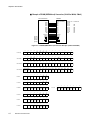
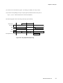
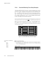
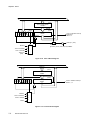
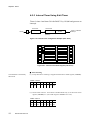
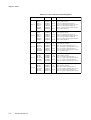
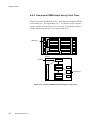
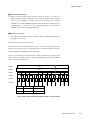
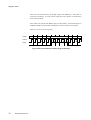
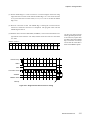
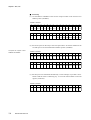
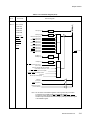
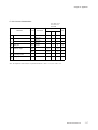
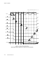
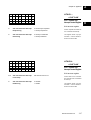
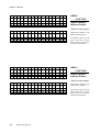
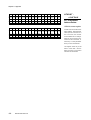
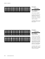
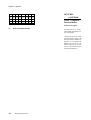
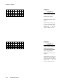
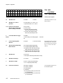
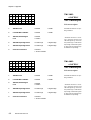
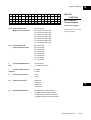
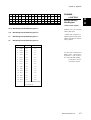
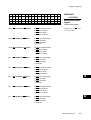
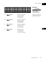
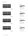
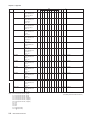
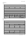
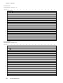
Memory Expansion Mode with 8-bit Bus Address/
Data Separate Mode
71
72
73
74
75
NMI
*
*
1-4-2
76
50
PA1,IRQ1
PA2,IRQ2
PA3,IRQ3
PA4,IRQ4,TM15IB
(ADSEP)
77
49
78
48
79
47
80
46
81
45
RST
VDD
82
44
83
43
D0
D1
84
D2
D3
86
D4
D5
D6
D7
VSS
P10,TM8IOB
P11,TM8IC
P12,TM11IOA
P13,TM11IOB
P14,TM11IC
P15,TM12IOA
P16,TM12IOB
P17,TM12IC
88
42
MN102H55D
MN102H55G
MN102HF55G
(TOP VIEW)
85
87
89
90
41
40
39
38
37
36
25
24
22
23
OSCI
OSCO
(MODE)
21
XI,PB1
XO
VDD
20
19
18
BOSC,PB0,BIBT1,BIBT2
VSS
17
15
16
14
13
12
11
10
P51,CS1,TM13OB
P52,CS2,TM14OA
P53,CS3,TM14OB
P54,BREQ
P55,BRACK
P56,BSTRE,TM15IA
(WORD)
A0,P20,SBT2
A1,P21,SBI2
A2,P22,SBO2
A3,P23
VDD
9
26
8
27
100
7
28
99
6
29
98
P50,CS0,TM13OA
30
97
5
31
96
3
4
32
95
WEL,P62
WE,P63
33
94
2
34
93
1
35
92
P60,WAIT,SBT2
RE,P61
91
P82,TM0IO,SBT3,SCL3,SBI2
P81,DAC1
P80,DAC0
A23,P47,AN7,WDOUT
A22,P46,AN6,STOP
A21,P45,AN5
A20,P44,AN4
VREFA19,P43
A18,P42
A17,P41
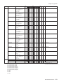
A16,P40
A15,P37, KI7
A14,P36, KI6
A13,P35, KI5
A12,P34, KI4
AVDD
A11,P33, KI3
A10,P32, KI2
A9,P31, KI1
A8,P30, KI0
A7,P27
A6,P26
A5,P25
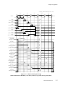
A4,P24,TM15IA
* : Use 33 kΩ - 50 kΩ
Figure 1-4-2 Pin Configuration in Memory Expansion Mode with 8-bit Bus Address/Data Separate Mode
Unused pins require handling in the circuit (input pins are connected to VDD/VSS, output pins leave
open, input/output pins are connected to VDD/VSS or leave open depending on pin direction setting).
14
MN102H55D/55G/F55G
Chapter 1 General Description
P83,TM4IO,SBI3
51
52
53
54
P87,TM9IC,SBO4,SDA4
P86,TM9IOB,SBI4
VREF+
P85,TM9IOA,SBT4,SCL4,SBO2
P84,TM7IO,SBO3,SDA3
55
P90,TM8IOA,BIBT1,DMAREQ1
56
57
58
P93,TM10IC,DMAACK0
P92,TM10IOB,DMAREQ0
P91,TM10IOA,BIBT2,DMAACK1
59
60
61
P96,AN2
P95,AN1
P94,AN0
AVSS
62
P97,AN3
65
64
63
P70,SBT0,RAS
VDD (Vpp)
66
67
68
69
P74,SBI1
P73,SBT1,DMUX
P72,SBO0,UCAS
P71,SBI0,LCAS,CAS
70
P75,SBO1
72
73
NMI
74
75
PA0,IRQ0
71
Memory Expansion Mode with 16-bit Bus
Address/Data Separate Mode
*
*
1-4-3
76
50
PA1,IRQ1
PA2,IRQ2
PA3,IRQ3
PA4,IRQ4,TM15IB
(ADSEP)
77
49
78
48
79
47
80
46
81
45
RST
VDD
82
44
83
43
D0
D1
84
D2
D3
86
D4
D5
D6
D7
VSS
D8
D9
D10
D11
D12
D13
D14
D15
88
42
MN102H55D
MN102H55G
MN102HF55G
(TOP VIEW)
85
87
89
90
41
40
39
38
37
36
25
24
22
23
OSCI
OSCO
(MODE)
21
20
XI,PB1
XO
VDD
19
18
BOSC,PB0,BIBT1,BIBT2
VSS
17
15
16
14
13
12
11
10
P51,CS1,TM13OB
P52,CS2,TM14OA
P53,CS3,TM14OB
P54,BREQ
P55,BRACK
P56,BSTRE,TM15IA
(WORD)
A0,P20,SBT2
A1,P21,SBI2
A2,P22,SBO2
A3,P23
VDD
9
26
8
27
100
7
28
99
6
29
98
5
30
97
P50,CS0,TM13OA
31
96
3
4
32
95
WEL,P62
WE,WEH,P63
33
94
2
34
93
1
35
92
P60,WAIT,SBT2
RE,P61
91
P82,TM0IO,SBT3,SCL3,SBI2
P81,DAC1
P80,DAC0
A23,P47,AN7,WDOUT
A22,P46,AN6,STOP
A21,P45,AN5
A20,P44,AN4
VREFA19,P43
A18,P42
A17,P41
A16,P40
A15,P37, KI7
A14,P36, KI6
A13,P35, KI5
A12,P34, KI4
AVDD
A11,P33, KI3
A10,P32, KI2
A9,P31, KI1
A8,P30, KI0
A7,P27
A6,P26
A5,P25
A4,P24,TM15IA
* : Use 33 kΩ - 50 kΩ
Figure 1-4-3 Pin Configuration in Memory Expansion Mode with 16-bit Bus Address/Data Separate Mode
Unused pins require handling in the circuit (input pins are connected to VDD/VSS, output pins leave
open, input/output pins are connected to VDD/VSS or leave open depending on pin direction setting).
MN102H55D/55G/F55G
15
Chapter 1 General Description
PA0,IRQ0
P83,TM4IO,SBI3
51
52
53
54
P87,TM9IC,SBO4,SDA4
P90,TM8IOA,BIBT1,DMAREQ1
P86,TM9IOB,SBI4
VREF+
P85,TM9IOA,SBT4,SCL4,SBO2
P84,TM7IO,SBO3,SDA3
55
56
58
57
P93,TM10IC,DMAACK0
P92,TM10IOB,DMAREQ0
P91,TM10IOA,BIBT2,DMAACK1
59
60
61
P96,AN2
P95,AN1
P94,AN0
AVSS
62
P97,AN3
65
64
63
P70,SBT0,RAS
VDD (Vpp)
66
67
68
69
P74,SBI1
P73,SBT1,DMUX
P72,SBO0
P71,SBI0,LCAS,CAS
70
P75,SBO1
Memory Expansion Mode with 8-bit Bus
Address/Data Shared Mode
71
72
73
74
75
NMI
*
*
1-4-4
76
50
PA1,IRQ1
PA2,IRQ2
PA3,IRQ3
PA4,IRQ4,TM15IB
(ADSEP)
77
49
78
48
79
47
80
46
81
45
RST
VDD
AD0
AD1
82
44
AD2
AD3
86
AD4
AD5
AD6
AD7
VSS
88
P10,TM8IOB
P11,TM8IC
P12,TM11IOA
P13,TM11IOB
P14,TM11IC
P15,TM12IOA
P16,TM12IOB
P17,TM12IC
43
83
84
42
MN102H55D
MN102H55G
MN102HF55G
(TOP VIEW)
85
87
89
90
41
40
39
38
37
36
25
24
22
23
OSCI
OSCO
(MODE)
21
XI,PB1
XO
VDD
20
19
18
BOSC,PB0,BIBT1,BIBT2
VSS
17
15
16
14
13
11
12
(WORD)
P20,SBT2
P21,SBI2
P22,SBO2
P23
VDD
10
P51,CS1,TM13OB
P52,CS2,TM14OA
P53,CS3,TM14OB
P54,BREQ
P55,BRACK
ALE,ALE
9
26
8
27
100
7
28
99
6
29
98
P50,CS0,TM13OA
30
97
5
31
96
3
4
32
95
WEL,P62
WE,P63
33
94
2
34
93
1
35
92
P60,WAIT,SBT2
RE,P61
91
P82,TM0IO,SBT3,SCL3,SBI2
P81,DAC1
P80,DAC0
A23,P47,AN7,WDOUT
A22,P46,AN6,STOP
A21,P45,AN5
A20,P44,AN4
VREFA19,P43
A18,P42
A17,P41
A16,P40
A15,P37, KI7
A14,P36, KI6
A13,P35, KI5
A12,P34, KI4
AVDD
A11,P33, KI3
A10,P32, KI2
A9,P31, KI1
A8,P30, KI0
P27
P26
P25
P24,TM15IA
* : Use 33 kΩ - 50 kΩ
Figure 1-4-4 Pin Configuration in Memory Expansion Mode with 8-bit Bus Address/Data Shared Mode
Unused pins require handling in the circuit (input pins are connected to VDD/VSS, output pins leave
open, input/output pins are connected to VDD/VSS or leave open depending on pin direction setting).
16
MN102H55D/55G/F55G
Chapter 1 General Description
P83,TM4IO,SBI3
51
52
53
P86,TM9IOB,SBI4
VREF+
P85,TM9IOA,SBT4,SCL4,SBO2
P84,TM7IO,SBO3,SDA3
54
55
P90,TM8IOA,BIBT1,DMAREQ1
P87,TM9IC,SBO4,SDA4
56
58
57
P93,TM10IC,DMAACK0
P92,TM10IOB,DMAREQ0
P91,TM10IOA,BIBT2,DMAACK1
59
60
61
P96,AN2
P95,AN1
P94,AN0
AVSS
62
P97,AN3
65
64
63
P70,SBT0,RAS
VDD (Vpp)
66
67
68
69
P74,SBI1
P73,SBT1,DMUX
P72,SBO0,UCAS
P71,SBI0,LCAS,CAS
70
P75,SBO1
72
73
NMI
74
75
PA0,IRQ0
71
Memory Expansion Mode with 16-bit Bus
Address/Data Shared Mode
*
*
1-4-5
76
50
PA1,IRQ1
PA2,IRQ2
PA3,IRQ3
PA4,IRQ4,TM15IB
(ADSEP)
77
49
78
48
79
47
80
46
81
45
RST
VDD
82
44
83
43
AD0
AD1
AD2
AD3
AD4
AD5
AD6
AD7
84
91
35
VSS
AD8
AD9
AD10
AD11
AD12
AD13
AD14
AD15
92
34
93
33
94
32
95
31
96
30
97
29
98
28
99
27
100
26
42
40
39
38
37
25
23
24
OSCI
OSCO
(MODE)
22
21
XI,PB1
XO
VDD
20
36
19
18
41
BOSC,PB0,BIBT1,BIBT2
VSS
17
15
16
14
8
7
5
P50,CS0,TM13OA
P51,CS1,TM13OB
P52,CS2,TM14OA
P53,CS3,TM14OB
P54,BREQ
P55,BRACK
ALE,ALE
(WORD)
A0,P20,SBT2
A1,P21,SBI2
A2,P22,SBO2
A3,P23
VDD
3
4
WEL,P62
WE,WEH,P63
6
2
1
P60,WAIT,SBT2
RE,P61
90
13
89
12
88
11
87
10
86
9
MN102H55D
MN102H55G
MN102HF55G
(TOP VIEW)
85
P82,TM0IO,SBT3,SCL3,SBI2
P81,DAC1
P80,DAC0
A23,P47,AN7,WDOUT
A22,P46,AN6,STOP
A21,P45,AN5
A20,P44,AN4
VREFA19,P43
A18,P42
A17,P41
A16,P40
P37, KI7
P36, KI6
P35, KI5
P34, KI4
AVDD
P33, KI3
P32, KI2
P31, KI1
P30, KI0
P27
P26
P25
P24,TM15IA
* : Use 33 kΩ - 50 kΩ
Figure 1-4-5 Pin Configuration in Memory Expansion Mode with 16-bit Bus Address/Data Shared Mode
Unused pins require handling in the circuit (input pins are connected to VDD/VSS, output pins leave
open, input/output pins are connected to VDD/VSS or leave open depending on pin direction setting).
MN102H55D/55G/F55G
17
Chapter 1 General Description
PA0,IRQ0
P83,TM4IO,SBI3
51
52
53
54
P87,TM9IC,SBO4,SDA4
P86,TM9IOB,SBI4
VREF+
P85,TM9IOA,SBT4,SCL4,SBO2
P84,TM7IO,SBO3,SDA3
55
P90,TM8IOA,BIBT1,DMAREQ1
56
57
58
P93,TM10IC,DMAACK0
P92,TM10IOB,DMAREQ0
P91,TM10IOA,BIBT2,DMAACK1
59
60
61
P96,AN2
P95,AN1
P94,AN0
AVSS
62
P97,AN3
65
64
63
P70,SBT0,RAS
VDD (Vpp)
66
67
68
69
P74,SBI1
P73,SBT1,DMUX
P72,SBO0
P71,SBI0,LCAS,CAS
70
P75,SBO1
Processor Mode with 8-bit Bus Address/Data
Separate Mode
71
72
73
74
75
NMI
*
*
1-4-6
76
50
PA1,IRQ1
PA2,IRQ2
PA3,IRQ3
PA4,IRQ4,TM15IB
(ADSEP)
77
49
78
48
79
47
80
46
81
45
RST
VDD
D0
D1
82
44
83
43
D2
D3
D4
D5
D6
D7
VSS
P10,TM8IOB
P11,TM8IC
P12,TM11IOA
P13,TM11IOB
P14,TM11IC
P15,TM12IOA
P16,TM12IOB
P17,TM12IC
86
84
42
MN102H55D
MN102H55G
MN102HF55G
(TOP VIEW)
85
87
88
89
90
41
40
39
38
37
36
25
24
22
23
OSCI
OSCO
(MODE)
21
20
XI,PB1
XO
VDD
19
18
BOSC,PB0,BIBT1,BIBT2
VSS
17
15
16
14
12
11
13
A0
A1
A2
A3
VDD
CS0
CS1,P51,TM13OB
CS2,P52,TM14OA
CS3,P53,TM14OB
P54,BREQ
P55,BRACK
P56,BSTRE,TM15IA
(WORD)
10
26
9
27
100
8
28
99
7
29
98
6
30
97
5
31
96
3
4
32
95
WEL,P62
WE,P63
33
94
2
34
93
1
35
92
P60,WAIT,SBT2
RE
91
P82,TM0IO,SBT3,SCL3,SBI2
P81,DAC1
P80,DAC0
A23,P47,AN7,WDOUT
A22,P46,AN6,STOP
A21,P45,AN5
A20,P44,AN4
VREFA19,P43
A18,P42
A17,P41
A16,P40
A15
A14
A13
A12
AVDD
A11
A10
A9
A8
A7
A6
A5
A4
* : Use 33 kΩ - 50 kΩ
Figure 1-4-6 Pin Configuration in Processor Mode with 8-bit Bus Address/Data Separate Mode
Unused pins require handling in the circuit (input pins are connected to VDD/VSS, output pins leave
open, input/output pins are connected to VDD/VSS or leave open depending on pin direction setting).
18
MN102H55D/55G/F55G
Chapter 1 General Description
P83,TM4IO,SBI3
51
52
53
54
P87,TM9IC,SBO4,SDA4
P86,TM9IOB,SBI4
VREF+
P85,TM9IOA,SBT4,SCL4,SBO2
P84,TM7IO,SBO3,SDA3
55
P90,TM8IOA,BIBT1,DMAREQ1
56
57
58
P93,TM10IC,DMAACK0
P92,TM10IOB,DMAREQ0
P91,TM10IOA,BIBT2,DMAACK1
59
60
61
P96,AN2
P95,AN1
P94,AN0
AVSS
62
P97,AN3
65
64
63
P70,SBT0,RAS
VDD (Vpp)
66
67
68
69
P74,SBI1
P73,SBT1,DMUX
P72,SBO0,UCAS
P71,SBI0,LCAS,CAS
70
P75,SBO1
72
73
NMI
74
75
PA0,IRQ0
71
Processor Mode with 16-bit Bus Address/Data
Separate Mode
*
*
1-4-7
76
50
PA1,IRQ1
PA2,IRQ2
PA3,IRQ3
PA4,IRQ4,TM15IB
(ADSEP)
77
49
78
48
79
47
80
46
81
45
RST
VDD
D0
D1
82
44
83
43
D2
D3
86
D4
D5
D6
D7
VSS
D8
D9
D10
D11
D12
88
D13
D14
D15
84
42
MN102H55D
MN102H55G
MN102HF55G
(TOP VIEW)
85
87
89
90
41
40
39
38
37
36
25
24
22
23
OSCI
OSCO
(MODE)
21
20
XI,PB1
XO
VDD
19
18
BOSC,PB0,BIBT1,BIBT2
VSS
17
15
16
14
13
12
11
10
CS1,P51,TM13OB
CS2,P52,TM14OA
CS3,P53,TM14OB
P54,BREQ
P55,BRACK
BSTRE,P56,TM15IA
(WORD)
A0
A1
A2
A3
VDD
9
26
8
27
100
7
28
99
6
29
98
CS0
30
97
5
31
96
3
4
32
95
WEL,P62
WE,WEH,P63
33
94
2
34
93
1
35
92
P60,WAIT,SBT2
RE
91
P82,TM0IO,SBT3,SCL3,SBI2
P81,DAC1
P80,DAC0
A23,P47,AN7,WDOUT
A22,P46,AN6,STOP
A21,P45,AN5
A20,P44,AN4
VREFA19,P43
A18,P42
A17,P41
A16,P40
A15
A14
A13
A12
AVDD
A11
A10
A9
A8
A7
A6
A5
A4
* : Use 33 kΩ - 50 kΩ
Figure 1-4-7 Pin Configuration in Processor Mode with 16-bit Bus Address/Data Separate Mode
Unused pins require handling in the circuit (input pins are connected to VDD/VSS, output pins leave
open, input/output pins are connected to VDD/VSS or leave open depending on pin direction setting).
MN102H55D/55G/F55G
19
Chapter 1 General Description
PA0,IRQ0
P83,TM4IO,SBI3
51
52
53
54
P87,TM9IC,SBO4,SDA4
P90,TM8IOA,BIBT1,DMAREQ1
P86,TM9IOB,SBI4
VREF+
P85,TM9IOA,SBT4,SCL4,SBO2
P84,TM7IO,SBO3,SDA3
55
56
58
57
P93,TM10IC,DMAACK0
P92,TM10IOB,DMAREQ0
P91,TM10IOA,BIBT2,DMAACK1
59
60
61
P96,AN2
P95,AN1
P94,AN0
AVSS
62
P97,AN3
65
64
63
P70,SBT0,RAS
VDD (Vpp)
66
67
68
69
P74,SBI1
P73,SBT1,DMUX
P72,SBO0
P71,SBI0,LCAS,CAS
70
P75,SBO1
Processor Mode with 8-bit Bus Address/Data
Shared Mode
71
72
73
74
75
NMI
*
*
1-4-8
76
50
PA1,IRQ1
PA2,IRQ2
PA3,IRQ3
PA4,IRQ4,TM15IB
(ADSEP)
77
49
78
48
79
47
80
46
81
45
RST
VDD
82
44
83
43
AD0
AD1
84
AD2
AD3
86
AD4
AD5
AD6
AD7
VSS
AD8
AD9
AD10
AD11
AD12
AD13
AD14
AD15
88
42
MN102H55D
MN102H55G
MN102HF55G
(TOP VIEW)
85
87
89
90
41
40
39
38
37
36
25
24
22
23
OSCI
OSCO
(MODE)
21
20
XI,PB1
XO
VDD
19
18
BOSC,PB0,BIBT1,BIBT2
VSS
17
P22,SBO2
P23
VDD
15
16
14
13
P20,SBT2
P21,SBI2
12
11
10
9
8
CS1,P51,TM13OB
CS2,P52,TM14OA
CS3,P53,TM14OB
P54,BREQ
P55,BRACK
ALE
(WORD)
7
26
6
27
100
5
28
99
4
29
98
CS0
30
97
WEL,P62
WE,P63
31
96
3
32
95
2
33
94
1
34
93
RE
35
92
P60,WAIT,SBT2
91
P82,TM0IO,SBT3,SCL3,SBI2
P81,DAC1
P80,DAC0
A23,P47,AN7,WDOUT
A22,P46,AN6,STOP
A21,P45,AN5
A20,P44,AN4
VREFA19,P43
A18,P42
A17,P41
A16,P40
P37, KI7
P36, KI6
P35, KI5
P34, KI4
AVDD
P33, KI3
P32, KI2
A9,P31, KI1
A8,P30, KI0
P27
P26
P25
P24,TM15IA
* : Use 33 kΩ - 50 kΩ
Figure 1-4-8 Pin Configuration in Processor Mode with 8-bit Bus Address/Data Shared Mode
Unused pins require handling in the circuit (input pins are connected to VDD/VSS, output pins leave
open, input/output pins are connected to VDD/VSS or leave open depending on pin direction setting).
20
MN102H55D/55G/F55G
Chapter 1 General Description
P83,TM4IO,SBI3
51
52
53
54
P87,TM9IC,SBO4,SDA4
P86,TM9IOB,SBI4
VREF+
P85,TM9IOA,SBT4,SCL4,SBO2
P84,TM7IO,SBO3,SDA3
55
P90,TM8IOA,BIBT1,DMAREQ1
56
57
58
P93,TM10IC,DMAACK0
P92,TM10IOB,DMAREQ0
P91,TM10IOA,BIBT2,DMAACK1
59
60
61
P96,AN2
P95,AN1
P94,AN0
AVSS
62
P97,AN3
65
64
63
P70,SBT0,RAS
VDD (Vpp)
66
67
68
69
P74,SBI1
P73,SBT1,DMUX
P72,SBO0,UCAS
P71,SBI0,LCAS,CAS
70
P75,SBO1
72
73
NMI
74
75
PA0,IRQ0
71
Processor Mode with 16-bit Bus Address/Data
Shared Mode
*
*
1-4-9
76
50
PA1,IRQ1
PA2,IRQ2
PA3,IRQ3
PA4,IRQ4,TM15IB
(ADSEP)
77
49
78
48
79
47
80
46
81
45
RST
VDD
82
44
83
43
AD0
AD1
84
AD2
AD3
86
AD4
AD5
AD6
AD7
VSS
AD8
AD9
AD10
AD11
AD12
AD13
88
AD14
AD15
42
MN102H55D
MN102H55G
MN102HF55G
(TOP VIEW)
85
87
89
90
41
40
39
38
37
36
25
24
22
23
OSCI
OSCO
(MODE)
21
20
XI,PB1
XO
VDD
19
18
BOSC,PB0,BIBT1,BIBT2
VSS
17
15
16
14
13
P20,SBT2
P21,SBI2
P22,SBO2
P23
VDD
12
9
8
7
6
(WORD)
CS0
11
26
10
27
100
CS1,P51,TM13OB
CS2,P52,TM14OA
CS3,P53,TM14OB
P54,BREQ
P55,BRACK
ALE
28
99
5
29
98
4
30
97
3
31
96
WEL,P62
WE,WEH,P63
32
95
2
33
94
1
34
93
RE
35
92
P60,WAIT,SBT2
91
P82,TM0IO,SBT3,SCL3,SBI2
P81,DAC1
P80,DAC0
A23,P47,AN7,WDOUT
A22,P46,AN6,STOP
A21,P45,AN5
A20,P44,AN4
VREFA19,P43
A18,P42
A17,P41
A16,P40
P37, KI7
P36, KI6
P35, KI5
P34, KI4
AVDD
P33, KI3
P32, KI2
P31, KI1
P30, KI0
P27
P26
P25
P24,TM15IA
* : Use 33 kΩ - 50 kΩ
Figure 1-4-9 Pin Configuration in Processor Mode with 16-bit Bus Address/Data Shared Mode
Unused pins require handling in the circuit (input pins are connected to VDD/VSS, output pins leave
open, input/output pins are connected to VDD/VSS or leave open depending on pin direction setting).
MN102H55D/55G/F55G
21
Chapter 1 General Description
1-4-10
List of Pin Functions
Refer to "11-2-3 List of Pin Functions" for each pin's input level and Schmidt availability. TTL in the input level column means that the input is determined at TTL level.
CMOS in the input level column means that the input is determined at CMOS level.
The column with "yes" sign shows Schmidt, while the column with no mark shows no
Schmidt. Pull-up can be programmable with the pull-up control registers. Please refer
to "Chapter 8 Ports" for details. The unused pins require handling on the board. The
input pins are connected to VDD or VSS. The output pins leave open. The lack of this
handling causes the increase of current and unstable operation.
Table 1-4-1 List of Pin Functions (1/26)
Pin Number
Pin Name
I/O
Function
17
VDD
-
Power
22
VDD
-
Power
66
VDD (VPP)
-
Power
83
VDD
-
Power
19
VSS
-
Power (Ground)
92
VSS
-
Power (Ground)
34
AVDD
-
Analog Voltage
Description
There are four V DD pins. The mask ROM chip
(MN102H55D/55G) must connect these four pins to a
power supply of 3.0 V to 3.6 V. The flash ROM chip
(MN102HF55G) must connect pin 66 to a power supply of
4.5 V to 5.5 V because the pin 66 becomes the power pin
for the flash ROM programming. During the normal operation, the pin 66 must be input the same voltage of other
pins.
There are two Vss pins. They must be connected to a
power supply of 0 V.
There is one AVDD. It must be connected to the same voltage as VDD.
61
22
AVSS
-
(Ground)
There is one AVSS. It must be connected to the same voltage as VSS.
Analog Voltage
43
Vref -
-
Analog Basic
Voltage
There is one Vref -. It must be connected with relation of
VSS <= Vref - < Vref + <= VDD.
54
Vref +
-
Analog Basic
Voltage
There is one Vref +. It must be connected with relation of
VSS <= Vref - < Vref + <= VDD.
MN102H55D/55G/F55G
Chapter 1 General Description
Table 1-4-1 List of Pin Functions (2/26)
Pin Number
Pin Name
I/O
Function
23
OSCI
Input
High-speed Oscillator
Input
24
OSCO
Output
High-speed Oscillator
Output
Description
For a self-excited oscillator configuration, connect crystal
or ceramic oscillator across these two pins. They have a
built-in feedback resistor between them. For stability, insert capacitor of 20 pF to 33 pF between the OSCI pin or
the OSCO pin and the VSS pin (For the exact capacitance,
consult the oscillator manufacturer).
For an external oscillator configuration, connect the OSCI
pin to an oscillator with an amplitude of 4 MHz to 34 MHz
and the width between VDD and VSS. Leave the OSCO pin
open. Refer to "Figure 1-4-10".
Connecting the OSCO pin with the external circuit directly
is not allowed when the oscillator clock is taken from the
chip. Select the BOSC pin for a synchronous signal.
20
XI
Input
Low-speed Oscillator
Input
21
XO
Output
Low-speed Oscillator
Output
For a self-excited oscillator configuration, connect crystal or
ceramic oscillator across these two pins. They have a builtin feedback resistor between them. For stability, insert capacitor of 100 pF to 200 pF between the XI pin or the XO pin
and the VSS pin (For the exact capacitance, consult the oscillator manufacturer).
For an external oscillator configuration, connect the XI pin
to an oscillator with an amplitude of 32 kHz to 166 kHz and
the width between VDD and VSS. Leave the XO pin open.
Refer to "Figure 1-4-11".
If the XI pin is not used as the low-speed oscillator input pin,
connect the XI pin to VSS or VDD. If the XO pin is not used
as the low-speed oscillator output pin, leave the XO pin
open. When the oscillation clock is taken from the chip,
connecting the XO pin with the external circuit directly is not
allowed. Select the BOSC pin for a synchronous signal.
PB1
I/O
General-purpose port B1
pin
If pin 20 is not used as the XI pin, this pin can be used as
the general-purpose I/O port. The PBMD register switches
the function. The input/output direction is controlled in bit
units. The pin has a built-in software control pull-up resistor. Refer to "Chapter 8 Ports".
MN102H55D/55G/F55G
23
Chapter 1 General Description
Table 1-4-1 List of Pin Functions (3/26)
Pin Number
Pin Name
82
RST
18
BOSC
BIBT1
BIBT2
PB0
25
MODE
I/O
Function
Description
Reset Input
This pin resets the chip. With a 34-MHz oscillator, reset
starts when the low level is input to this pin for more than
117 ns. Reset starts even when the noise is input to this pin
for 117 ns. When the high level is input to the pin, reset is
released. After the reset pin becomes high level, the oscillation waits of the high-speed oscillation pins (OSCI and
OSCO) are performed (approximately 3.855 ms with a 34MHz oscillator). After that, the chip starts executing the instruction from x'080000'. Refer to "Figure 1-4-12".
Output
System Clock Output
This pin provides the system clock. After reset release, the
pin outputs BOSC. When the high-speed oscillation pin is
operating at 34 MHz, the pin outputs the clock of 34 MHz.
Output
Output
Internal System
Pin 18 can output BIBT1 or BIBT2 signal of the internal
system clock by setting the PBMD register. These signals
are inverted signals.
Input
I/O
Input
Clock Output
General-purpose Port B0
If pin 18 is not used as the BOSC pin, it can be used as a
general-purpose input/output port. The PBMD register
switches the function. The input/output direction is controlled in bit units. The pin has a built-in software control
pull-up resistor. Refer to "Chapter 8 Ports".
Mode Setup Input
This pin sets either processor mode or single-chip mode
(memory expansion mode). Pulling the pin low sets the
processor mode. In processor mode, Internal ROM becomes the external memory area, and the chip executes
the instruction from x'080000' in memory connected externally. Pulling the pin high sets the single-chip mode
(memory expansion mode). The chip executes the instruction from x'080000' of Internal ROM. In memory expansion
mode, the port mode register is set to address output and
data output by instruction.
Do not change the mode setting in this pin during operation.
When the setting is changed, proper operation cannot be
guaranteed. Refer to "2-1 Summary of Bus Interface".
24
MN102H55D/55G/F55G
Chapter 1 General Description
Table 1-4-1 List of Pin Functions (4/26)
Pin Number
12
Pin Name
WORD
I/O
Function
Input
Data Bus Width Setup
Input
Description
This pin sets either 8-bit data bus width or 16-bit data bus
width in the external memory space 0 immediately after reset release in processor mode or memory expansion mode.
Pulling the pin high sets 8-bit bus width while pulling the pin
low sets 16-bit bus width. In processor mode or memory
expansion mode, this pin must be used as the data bus
width setup pin. The MEMMD1 register determines the
data bus width for the external memory spaces 1 to 3. The
MEMMD1 register can reset the data bus width for the external memory space 0 after reset release, regardless the
level of this pin.
Refer to "2-1 Summary of Bus Interface".
P57
I/O
General-purpose Port 57
This pin can be used as a general-purpose input/output port
in single-chip mode. The input/output direction is controlled
in bit units. The pin has a built-in software control pull-up
resistor. Refer to "Chapter 8 Ports".
81
ADSEP
Input
Address/Data Separate,
Shared Mode Setup
This pin sets either address/data separate mode or address/data shared mode in processor mode or memory
expansion mode. Pulling the pin high sets the address/
data separate mode while pulling the pin low sets the address/data shared mode. In processor mode or memory
expansion mode, this pin must be used as the address/
data separate, shared mode setup pin. Do not change this
pin's input during operation. When the setting is changed,
proper operation cannot be guaranteed.
Refer to "2-1 Summary of Bus Interface".
PA5
I/O
General-purpose Port A5
This pin can be used as a general-purpose input/output
port in single-chip mode. The input/output direction is controlled in bit units. The pin has a built-in software control
pull-up resistor. Refer to "Chapter 8 Ports".
MN102H55D/55G/F55G
25
Chapter 1 General Description
Table 1-4-1 List of Pin Functions (5/26)
Pin Number
9
Pin Name
BREQ
I/O
Input
Function
Bus Request Input
Description
BREQ and BRACK pins operate bus arbitration. Pulling
BREQ low suspends the execution of the current instruction, makes addresses, data and control signals high impedance, and then releases bus. After that, pull BRACK
low. While the chip is accessing the bus, the chip releases
the bus after the bus access is completed. Pulling BREQ
high at the level detector restores the bus.
P54
10
BRACK
P55
2
RE
I/O
Output
I/O
Output
General-purpose Port 54
This pin can be used as a general-purpose input/output
port in single-chip mode. The input/output direction is controlled in bit units. The pin has a built-in software control
pull-up resistor. Refer to "Chapter 8 Ports".
Bus Request Enable
Output
BREQ and BRACK pins operate bus arbitration. Refer to
"Pin 9 BREQ Description" for details.
General-purpose Port 55
This pin can be used as a general-purpose input/output port
in single-chip mode. The input/output direction is controlled
in bit units. The pin has a built-in software control pull-up
resistor. Refer to "Chapter 8 Ports".
Read Enable Output
This pin provides a control signal for the external memory
read in processor mode or memory expansion mode.
When connecting SRAM and ROM, connect RE to OE in
memory. RE outputs low level during read operation and
the chip reads the contents of the memory.
Refer to "2-1 Summary of Bus Interface".
During a bus request, STOP mode or HALT mode, this pin
will be in a high impedance state.
Refer to "11-2-3 List of Pin Functions".
P61
26
MN102H55D/55G/F55G
I/O
General-purpose Port 61
This pin can be used as a general-purpose input/output port
if it is not used as RE in single-chip mode, processor mode
or memory expansion mode. The input/output direction is
controlled in bit units. The pin has a built-in software control
pull-up resistor. Refer to "Chapter 8 Ports".
Chapter 1 General Description
Table 1-4-1 List of Pin Functions (6/26)
Pin Number
3
Pin Name
WEL
I/O
Output
Function
Lower Byte Write Enable
Output
Description
This pin provides a control signal for the external memory
write in processor mode or memory expansion mode.
When connecting SRAM and ROM, connect WEL to WE in
memory. WEL outputs low level when writing the lower
bytes (bits 0 to 7 of data) and writes the data to memory.
Refer to "2-1 Summary of Bus Interface".
During a bus request, STOP mode or HALT mode, this pin
will be in a high impedance state.
Refer to "11-2-3 List of Pin Functions".
P62
I/O
General-purpose Port 62
This pin can be used as a general-purpose input/output
port if it is not used as WEL in single-chip mode, processor
mode or memory expansion mode. The input/output direction is controlled in bit units. The pin has a built-in software
control pull-up resistor. Refer to "Chapter 8 Ports".
4
WEH
Output
Upper Byte Write Enable
Output
This pin provides a control signal for the external memory
write in processor mode or memory expansion mode.
When connecting SRAM and ROM, connect WEH to WE in
memory. WEH outputs low level when writing the upper
bytes (bits 8 to 15 of data) and writes the data to memory.
WEH is invalid when 8-bit bus width is selected in processor mode or memory expansion mode so that it can be
used as a general-purpose port 63 pin.
Refer to "2-1 Summary of Bus Interface".
During a bus request, STOP mode or HALT mode, this pin
will be in a high impedance state.
Refer to "11-2-3 List of Pin Functions".
WE
Output
Write Enable Output for
DRAM Connection
This pin provides a write enable pin when connecting
DRAM in processor mode or memory expansion mode.
When connecting DRAM with 2CAS method, connect this
pin to WE in DRAM. WE outputs low during write operation
and writes the data to DRAM.
Refer to "2-1 Summary of Bus Interface".
During a bus request, STOP mode or HALT mode, this pin
will be in a high impedance state.
Refer to "11-2-3 List of Pin Functions".
MN102H55D/55G/F55G
27
Chapter 1 General Description
Table 1-4-1 List of Pin Functions (7/26)
Pin Number
5
Pin Name
I/O
P63
I/O
CS0
Output
Function
Description
General-purpose Port 63
This pin can be used as a general-purpose input/output port
when 8-bit bus width is selected in single-chip mode, processor mode or memory expansion mode. The input/output direction is controlled in bit units. The pin has a built-in
software control pull-up resistor. Refer to "Chapter 8
Ports".
Chip Select Output
This pin provides a chip select signal corresponding to
each external memory space when accessing SRAM and
ROM connected to the external memory spaces 0 to 3 in
processor mode or memory expansion mode. Connect
CS0 - CS3 to CS pins in external memory. CS0 cannot be
output when accessing Internal ROM or Internal RAM.
Refer to "2-1 Summary of Bus Interface".
During a bus request, STOP mode or HALT mode, this pin
will be in a high impedance state.
Refer to "11-2-3 List of Pin Functions".
TM13OA
Output
Timer 13A Output
This pin can be used as a timer 13 PWM output pin if it is
not used as a chip select output pin in single-chip mode,
processor mode or memory expansion mode.
Refer to "Chapter 4 Timers".
6
7
CS1
Output
Chip Select Output
Refer to "Pin 5 CS0 Description" for details.
TM13OB
Output
Timer 13B Output
This pin can be used as a timer 13 PWM output pin if it is
not used as a chip select output pin in single-chip mode,
processor mode or memory expansion mode.
Refer to "Chapter 4 Timers".
CS2
Output
Chip Select Output
Refer to "Pin 5 CS0 Description" for details.
TM14OA
Output
Timer 14A Output
This pin can be used as a timer 14 PWM output pin if it is
not used as a chip select output pin in single-chip mode,
processor mode or memory expansion mode.
Refer to "Chapter 4 Timers".
28
MN102H55D/55G/F55G
Chapter 1 General Description
Table 1-4-1 List of Pin Functions (8/26)
Pin Number
8
Pin Name
I/O
Function
Description
CS3
Output
Chip Select Output
Refer to "Pin 5 CS0 Description" for details.
TM14OB
Output
Timer 14B Output
This pin can be used as a timer 14 PWM output pin if it is
not used as a chip select output pin in single-chip mode,
processor mode or memory expansion mode.
Refer to "Chapter 4 Timers".
11
ALE
Output
Address Latch Enable
Output (Positive Logic)
ALE
Output
Address Latch Enable
Output (Negative Logic)
This pin provides a timing signal of latching the address
which outputs to AD0 to AD15 pins during address/data
shared mode in processor mode or memory expansion
mode. ALE outputs at positive logic at reset release, but
the P5HMD changes to negative logic. Because of this,
ALE cannot be used at negative logic in processor mode.
Refer to "2-1 Summary of Bus Interface".
During a bus request, STOP mode or HALT mode, this pin
will be in a high impedance state.
BSTRE
Output
Read Enable for Burst
ROM
When connecting burst ROM to the external memory
space in processor mode or memory expansion mode,
connect this pin to RE in burst ROM.
Refer to "2-1 Summary of Bus Interface".
During a bus request, STOP mode or HALT mode, this pin
will be in a high impedance state.
P56
TM15IA
I/O
Input
General-purpose Port 56
This pin can be used as a general-purpose input/output port
if it is not used as ALE, ALE or BSTRE in single-chip mode,
processor mode or memory expansion mode. The input/
output direction is controlled in bit units. The pin has a builtin software control pull-up resistor. Refer to "Chapter 8
Ports".
Timer 15A Input
This pin can be used as a timer 15 pulse input pin if it is not
used as ALE, ALE or BSTRE in single-chip mode, processor mode or memory expansion mode. Because pin 26
has the same function, either pin 26 or pin 11 must be selected. Refer to "Chapter 4 Timers".
MN102H55D/55G/F55G
29
Chapter 1 General Description
Table 1-4-1 List of Pin Functions (9/26)
Pin Number
1
Pin Name
WAIT
I/O
Input
Function
Bus Cycle Wait Input
Description
This pin extends or shortens the cycle of accessing to the
external memory based on the signal inputted to this pin
when the external memory wait is set to the handshake
mode in processor mode or memory expansion mode. Pulling this pin low ends access to the external memory.
Refer to "Figure 1-4-13, Table 2-1-3 to Table 2-1-6".
P60
I/O
General-purpose Port 60
This pin can be used as a general-purpose input/output port
if it is not used as WAIT in single-chip mode, processor
mode or memory expansion mode. The input/output direction is controlled in bit units. The pin has a built-in software
control pull-up resistor. Refer to "Chapter 8 Ports".
SBT2
I/O
Serial Interface 2
Clock Input/Output
This pin can be used as a synchronous transfer clock signal
input/output pin for serial interface 2 if it is not used as
WAIT in single-chip mode, processor mode or memory expansion mode. Because pin 13 has the same function, either pin 13 or pin 1 must be selected.
Refer to "Chapter 5 Serial Interface".
13
A0
Output
Address Output
This pin outputs the address of the external memory in processor mode or memory expansion mode. Connect this pin
to address pin of the external memory or address decode
circuit. When it is not accessing the external memory, the
output value is undefined.
Refer to "2-1 Summary of Bus Interface".
During a bus request, STOP mode or HALT mode, this pin
will be in a high impedance state.
P20
I/O
General-purpose Port 20
This pin can be used as a general-purpose input/output
port if it is not used as the address output pin in single-chip
mode, processor mode or memory expansion mode. The
input/output direction is controlled in bit units. The pin has a
built-in software control pull-up resistor. Refer to "Chapter
8 Ports".
SBT2
I/O
Serial Interface 2
This pin can be used as a synchronous transfer clock signal input/output pin for serial interface 2 if it is not used as
WAIT in single-chip mode, processor mode or memory expansion mode. Because pin 13 has the same function, either pin 13 or pin 1 must be selected.
Clock Input/Output
Refer to "Chapter 5 Serial Interface".
30
MN102H55D/55G/F55G
Chapter 1 General Description
Table 1-4-1 List of Pin Functions (10/26)
Pin Number
14
Pin Name
A1
I/O
Output
P21
I/O
SBI2
Input
Function
Address Output
Description
Refer to "Pin 13 A0 Description" for details.
General-purpose Port 21
Refer to "Pin 13 P20 Description" for details.
Serial Interface 2
This pin can be used as a data input pin for serial interface
2 if it is not used as the address output pin in single-chip
mode, processor mode or memory expansion mode. Because pin 50 has the same function, either pin 50 or pin 14
must be selected.
Data Input
Refer to "Chapter 5 Serial Interface".
15
A2
P22
SBO2
Output
I/O
Output
Address Output
Refer to "Pin 13 A0 Description" for details.
General-purpose Port 21
Refer to "Pin 13 P20 Description" for details.
Serial Interface 2
This pin can be used as a data output pin for serial interface 2 if it is not used as the address output pin in singlechip mode, processor mode or memory expansion mode.
Because pin 53 has the same function, either pin 53 or pin
15 must be selected.
Data Output
Refer to "Chapter 5 Serial Interface".
16
A3
P23
Output
I/O
Address Output
General-purpose Port 23
Refer to "Pin 13 A0 Description" for details.
Refer to "Pin 13 P20 Description" for details.
MN102H55D/55G/F55G
31
Chapter 1 General Description
Table 1-4-1 List of Pin Functions (11/26)
Pin Number
26
Pin Name
A4
P24
27-29
Output
I/O
Function
Address Output
Description
Refer to "Pin 13 A0 Description" for details.
General-purpose Port 24
Refer to "Pin 13 P20 Description" for details.
TM15IA
Input
Timer 15 Pulse Input
This pin can be used as a timer 15 pulse input pin if it is not
used as the address output pin in single-chip mode, processor mode or memory expansion mode. Because pin 11
has the same function, either pin 11 or pin 26 must be selected. Refer to "Chapter 4 Timers".
A5-A7
Output
Address Output
Refer to "Pin 13 A0 Description" for details.
P25-P27
30-33,
35-38
I/O
A8-A15
I/O
Output
General-purpose Port
25-27
Address Output
Refer to "Pin 13 P20 Description" for details.
Refer to "Pin 13 A0 Description" for details.
P30-P37
I/O
General-purpose Port
30-37
Refer to "Pin 13 P20 Description" for details.
KI0-KI7
Input
Key Input Interrupt
These pins can be used as key input interrupt pins if they
are not used as the address output pins in single-chip
mode, processor mode or memory expansion mode. The
key input interrupt pins can be controlled in bit units.
Refer to "3-2-2 Key Input Interrupt Setup Examples".
32
MN102H55D/55G/F55G
Chapter 1 General Description
Table 1-4-1 List of Pin Functions (12/26)
Pin Number
39-42
Pin Name
A16-A19
P40-P43
44-45
A20-A21
I/O
Output
I/O
Output
Function
Address Output
Description
Refer to "Pin 13 A0 Description" for details.
General-purpose Port
40-43
Refer to "Pin 13 P20 Description" for details.
Address Output
Refer to "Pin 13 A0 Description" for details.
P44-P45
I/O
General-purpose Port
44-45
Refer to "Pin 13 P20 Description" for details.
AN4-AN5
Input
A/D Conversion Input
These pins can be used as A/D conversion input pins if
they are not used as address output pins in single-chip
mode, processor mode or memory expansion mode.
Refer to "6-1 Summary of A/D Converter".
46
A22
Output
P46
I/O
AN6
Input
Address Output
Refer to "Pin 13 A0 Description" for details.
General-purpose Port 46
Refer to "Pin 13 P20 Description" for details.
A/D Converter 6
Conversion Input
This pin can be used as a A/D conversion input pin if it is
not used as the address output pin in single-chip mode,
processor mode or memory expansion mode.
Refer to "6-1 Summary of A/D Converter".
STOP
Output
STOP Status Output
This pin outputs high to indicate STOP status if it is not used
as the address output pin in single-chip mode, processor
mode or memory expansion mode.
MN102H55D/55G/F55G
33
Chapter 1 General Description
Table 1-4-1 List of Pin Functions (13/26)
Pin Number
47
Pin Name
A23
I/O
Output
Function
Address Output
Description
Refer to "Pin 13 A0 Description" for details.
P47
I/O
General-purpose Port 47
Refer to "Pin 13 P20 Description" for details.
AN7
Input
A/D Converter 7 Conversion Input
This pin can be used as a A/D conversion input pin if it is
not used as the address output pin in single-chip mode,
processor mode or memory expansion mode.
Refer to "6-1 Summary of A/D Converter".
WDOUT
Output
Watchdog Timer
Overflow Output
84-91
D0-D7
I/O
AD0-AD7
I/O
Data I/O
Address/Data I/O
This pin outputs high when the watchdog timer overflows if
it is not used as the address output pin in single-chip mode,
processor mode or memory expansion mode.
These pins input or output the lower 8-bit data of the external memory during address/data separate mode in processor mode or memory expansion mode. During address/
data shared mode, these pins time-divides input or output
the lower 8-bit address and the lower 8-bit data of the external memory. They become input when the external
memory is not accessed.
Refer to "2-1 Summary of Bus Interface".
During a bus request, STOP mode or HALT mode, this pin
will be in a high impedance state.
P00-P07
34
MN102H55D/55G/F55G
I/O
General-purpose Ports
00-07
These pins can be used as general-purpose ports if they
are not used as data input/output pins or address/data input/output pins in single-chip mode, processor mode or
memory expansion mode. The input/output direction is
controlled in bit units. The pin has a built-in software control pull-up resistor. Refer to "Chapter 8 Ports".
Chapter 1 General Description
Table 1-4-1 List of Pin Functions (14/26)
Pin Number
93
Pin Name
I/O
Function
D8
I/O
Data I/O
AD8
I/O
Address/Data I/O
Description
This pin inputs or outputs the upper 8-bit data of the external memory during address/data separate mode in processor mode or memory expansion mode. During address/
data shared mode, this pin time-divides input or output the
upper 8-bit address and the upper 8-bit data of the external
memory. It becomes input when the external memory is
not accessed.
Refer to "2-1 Summary of Bus Interface".
During a bus request, STOP mode or HALT mode, this pin
will be in a high impedance state.
P10
I/O
General-purpose Port 10
Refer to "Pins 84-91 P00-P07 Description" for details.
TM8IOB
I/O
Timer 8B Input/Output
This pin can be used as a timer 8 input capture B input pin
or a timer 8 output compare B output pin if it is not used as
a data input/output pin or an address/data input/output pin
in single-chip mode, processor mode or memory expansion mode.
Refer to "Chapter 4 Timers".
94
D9
AD9
I/O
P11
I/O
General-purpose Port 11
Refer to "Pins 84-91 P00-P07 Description" for details.
TM8IC
Input
Timer 8C Input
This pin can be used as a timer 8 counter clear pin if it is not
used as a data input/output pin or an address/data input/
output pin in single-chip mode, processor mode or memory
expansion mode.
I/O
Data I/O
Address/Data I/O
Refer to "Pin 93 D8, AD8 Description" for details.
Refer to "Chapter 4 Timers".
MN102H55D/55G/F55G
35
Chapter 1 General Description
Table 1-4-1 List of Pin Functions (15/26)
Pin Number
95
Pin Name
I/O
Function
Description
D10
AD10
I/O
Data I/O
I/O
Address/Data I/O
P12
I/O
General-purpose Port 12
Refer to "Pins 84-91 P00-P07 Description" for details.
TM11IOA
I/O
Timer 11A Input/Output
This pin can be used as a timer 11 input capture A input pin
or a timer 11 output compare A output pin if it is not used as
a data input/output pin or an address/data input/output pin
in single-chip mode, processor mode or memory expansion mode.
Refer to "Pin 93 D8, AD8 Description" for details.
Refer to "Chapter 4 Timers".
96
97
D11
I/O
Data I/O
AD11
I/O
Address/Data I/O
P13
I/O
General-purpose Port 13
Refer to "Pins 84-91 P00-P07 Description" for details.
TM11IOB
I/O
Timer 11B Input/Output
This pin can be used as a timer 11 input capture B input pin
or a timer 11 output compare B output pin if it is not used as
a data input/output pin or an address/data input/output pin
in single-chip mode, processor mode or memory expansion
mode.
Refer to "Chapter 4 Timers".
D12
I/O
I/O
Data I/O
Refer to "Pin 93 D8, AD8 Description" for details.
AD12
P14
I/O
General-purpose Port 14
Refer to "Pins 84-91 P00-P07 Description" for details.
TM11IC
Input
Timer 11C Input
This pin can be used as a timer 11 counter clear pin if it is
not used as a data input/output pin or an address/data input/output pin in single-chip mode, processor mode or
memory expansion mode.
Refer to "Pin 93 D8, AD8 Description" for details.
Address/Data I/O
Refer to "Chapter 4 Timers".
36
MN102H55D/55G/F55G
Chapter 1 General Description
Table 1-4-1 List of Pin Functions (16/26)
Pin Number
98
Pin Name
I/O
Function
Description
D13
I/O
I/O
Data I/O
Address/Data I/O
Refer to "Pin 93 D8, AD8 Description" for details.
AD13
P15
I/O
General-purpose Port 15
Refer to "Pins 84-91 P00-P07 Description" for details.
TM12IOA
I/O
Timer 12A Input/Output
This pin can be used as a timer 12 input capture A input pin
or a timer 12 output compare A output pin if it is not used as
a data input/output pin or an address/data input/output pin
in single-chip mode, processor mode or memory expansion mode.
Refer to "Chapter 4 Timers".
99
D14
I/O
Data I/O
AD14
I/O
Address/Data I/O
P16
I/O
General-purpose Port 16
Refer to "Pins 84-91 P00-P07 Description" for details.
TM12IOB
I/O
Timer 12B Input/Output
This pin can be used as a timer 12 input capture B input pin
or a timer 12 output compare B output pin if it is not used as
a data input/output pin or an address/data input/output pin
in single-chip mode, processor mode or memory expansion
mode.
Refer to "Pin 93 D8, AD8 Description" for details.
Refer to "Chapter 4 Timers".
100
D15
I/O
Data I/O
AD15
I/O
Address/Data I/O
P17
I/O
General-purpose Port 17
Refer to "Pins 84-91 P00-P07 Description" for details.
TM12IC
Input
Timer 12C Input
This pin can be used as a timer 12 counter clear pin if it is
not used as a data input/output pin or an address/data input/output pin in single-chip mode, processor mode or
memory expansion mode.
Refer to "Pin 93 D8, AD8 Description" for details.
Refer to "Chapter 4 Timers".
MN102H55D/55G/F55G
37
Chapter 1 General Description
Table 1-4-1 List of Pin Functions (17/26)
Pin Number
67
Pin Name
RAS
I/O
Function
Description
Output
DRAM Control Output
This pin outputs RAS signal when connecting DRAM in
processor mode or memory expansion mode.
Refer to "2-1 Summary of Bus Interface".
During a bus request, STOP mode or HALT mode, this pin
will be in a high impedance state.
P70
I/O
General-purpose Port 70
This pin can be used as a general-purpose input/output
port if it is not used as RAS in single-chip mode, processor
mode or memory expansion mode. The input/output direction is controlled in bit units. The pin has a built-in software
control pull-up resistor. Refer to "Chapter 8 Ports".
SBT0
I/O
Serial Interface 0
This pin can be used as a synchronous transfer clock signal input/output pin for serial interface 0 if it is not used as
Clock Input/Output
RAS in single-chip mode, processor mode or memory expansion mode.
Refer to "Chapter 5 Serial Interface".
68
CAS
LCAS
Output
Output
DRAM Control Output
DRAM Control Output
This pin outputs CAS or LCAS signal when connecting
DRAM in processor mode or memory expansion mode.
Refer to "2-1 Summary of Bus Interface".
During a bus request, STOP mode or HALT mode, this pin
will be in a high impedance state.
P71
I/O
SBI0
Input
General-purpose Port 71
This pin can be used as a general-purpose input/output port
if it is not used as CAS or LCAS in single-chip mode, processor mode or memory expansion mode. The input/output
direction is controlled in bit units. The pin has a built-in software control pull-up resistor. Refer to "Chapter 8 Ports".
Serial Interface 0
This pin can be used as a data input pin for serial interface
0 if it is not used as CAS or LCAS in single-chip mode, processor mode or memory expansion mode.
Refer to "Chapter 5 Serial Interface".
Data Input
38
MN102H55D/55G/F55G
Chapter 1 General Description
Table 1-4-1 List of Pin Functions (18/26)
Pin Number
69
Pin Name
UCAS
I/O
Function
Output
DRAM Control Output
Description
This pin outputs UCAS signal when connecting DRAM in
processor mode or memory expansion mode.
Refer to "2-1 Summary of Bus Interface".
During a bus request, STOP mode or HALT mode, this pin
will be in a high impedance state.
P72
I/O
SBO0
Output
General-purpose Port 72
This pin can be used as a general-purpose input/output port
if it is not used as UCAS in single-chip mode, processor
mode or memory expansion mode. The input/output direction is controlled in bit units. The pin has a built-in software
control pull-up resistor. Refer to "Chapter 8 Ports".
Serial Interface 0
This pin can be used as a data output pin for serial interface
0 if it is not used as UCAS in single-chip mode, processor
mode or memory expansion mode.
Data Output
Refer to "Chapter 5 Serial Interface".
70
DMUX
Output
DRAM Control Output
This pin outputs DMUX signal when connecting DRAM in
processor mode or memory expansion mode.
Refer to "2-1 Summary of Bus Interface".
During a bus request, STOP mode or HALT mode, this pin
will be in a high impedance state.
P73
I/O
General-purpose Port 73
This pin can be used as a general-purpose input/output port
if it is not used as DMUX in single-chip mode, processor
mode or memory expansion mode. The input/output direction is controlled in bit units. The pin has a built-in software
control pull-up resistor. Refer to "Chapter 8 Ports".
SBT1
I/O
Serial Interface 1
This pin can be used as a synchronous transfer clock signal
input/output pin for serial interface 1 if it is not used as
DMUX in single-chip mode, processor mode or memory expansion mode.
Clock Input/Output
Refer to "Chapter 5 Serial Interface".
MN102H55D/55G/F55G
39
Chapter 1 General Description
Table 1-4-1 List of Pin Functions (19/26)
Pin Number
71
Pin Name
P74
I/O
I/O
Function
General-purpose Port 74
Description
This pin can be used as a general-purpose input/output
port. The input/output direction is controlled in bit units.
The pin has a built-in software control pull-up resistor.
Refer to "Chapter 8 Ports".
SBI1
72
P75
Input
I/O
Serial Interface 1
This pin can be used as a data input pin for serial interface 1.
Data Input
Refer to "Chapter 5 Serial Interface".
General-purpose Port 75
This pin can be used as a general-purpose input/output
port. The input/output direction is controlled in bit units.
The pin has a built-in software control pull-up resistor.
Refer to "Chapter 8 Ports".
SBO1
Output
Serial Interface 1
Data Output
48
P80
I/O
General-purpose Port 80
This pin can be used as a data output pin for serial interface
1. Refer to "Chapter 5 Serial Interface".
This pin can be used as a general-purpose input/output
port. The input/output direction is controlled in bit units.
The pin has a built-in software control pull-up resistor.
Refer to "Chapter 8 Ports".
DAC0
Output
D/A Converter 0 Conversion Output
This pin can be used as a pin to output the D/A conversion
results.
Refer to "6-3 Summary of D/A Converter".
49
P81
I/O
General-purpose Port 81
This pin can be used as a general-purpose input/output
port. The input/output direction is controlled in bit units.
The pin has a built-in software control pull-up resistor.
Refer to "Chapter 8 Ports".
DAC1
Output
D/A Converter 1 Conversion Output
This pin can be used as a pin to output the D/A conversion
results.
Refer to "6-3 Summary of D/A Converter".
40
MN102H55D/55G/F55G
Chapter 1 General Description
Table 1-4-1 List of Pin Functions (20/26)
Pin Number
50
Pin Name
P82
I/O
I/O
Function
General-purpose Port 82
Description
This pin can be used as a general-purpose input/output
port. The input/output direction is controlled in bit units.
The pin has a built-in software control pull-up resistor.
Refer to "Chapter 8 Ports".
TM0IO
I/O
Timer 0 Input/Output
This pin can be used as a timer 0 input/output pin.
Refer to "Chapter 4 Timers".
SBI2
Input
Serial Interface 2
Data Input
This pin can be used as a data input pin for serial interface
2. Because pin 14 has the same function, either pin 14 or
pin 50 must be selected.
Refer to "Chapter 5 Serial Interface".
SBT3
I/O
Serial Interface 3
Clock Input/Output
This pin can be used as a synchronous transfer clock signal input/output pin for serial interface 3.
Refer to "Chapter 5 Serial Interface".
SCL3
Output
Serial Interface 3
Clock Output
This pin can be used as an I2C clock signal output pin for
serial interface 3.
Refer to "Chapter 5 Serial Interface".
51
P83
I/O
General-purpose Port 83
This pin can be used as a general-purpose input/output
port. The input/output direction is controlled in bit units.
The pin has a built-in software control pull-up resistor.
Refer to "Chapter 8 Ports".
TM4IO
I/O
Timer 4 Input/Output
This pin can be used as a timer 4 input/output pin.
Refer to "Chapter 4 Timers".
SBI3
Input
Serial Interface 3
Data Input
This pin can be used as a data input pin for serial interface
3. Refer to "Chapter 5 Serial Interface".
MN102H55D/55G/F55G
41
Chapter 1 General Description
Table 1-4-1 List of Pin Functions (21/26)
Pin Number
52
Pin Name
P84
I/O
I/O
Function
General-purpose Port 84
Description
This pin can be used as a general-purpose input/output
port. The input/output direction is controlled in bit units.
The pin has a built-in software control pull-up resistor.
Refer to "Chapter 8 Ports".
TM7IO
I/O
Timer 7 Input/Output
This pin can be used as a timer 7 input/output pin.
Refer to "Chapter 4 Timers".
SBO3
Output
Serial Interface 3
Data Output
This pin can be used as a data output pin for serial interface 3. Refer to "Chapter 5 Serial Interface".
SDA3
I/O
Serial Interface 3
This pin can be used as an I2C data input/output pin for
serial interface 3.
Data Input/Output
Refer to "Chapter 5 Serial Interface".
53
P85
I/O
General-purpose Port 85
This pin can be used as a general-purpose input/output
port. The input/output direction is controlled in bit units.
The pin has a built-in software control pull-up resistor.
Refer to "Chapter 8 Ports".
TM9IOA
I/O
Timer 9A Input/Output
This pin can be used as a timer 9 input/output pin.
Refer to "Chapter 4 Timers".
SBO2
Output
Serial Interface 2
Data Output
This pin can be used as a data output pin for serial interface 2. Because pin 15 has the same function, either pin
15 or pin 53 must be selected.
Refer to "Chapter 5 Serial Interface".
SBT4
I/O
Serial Interface 4
Clock Input/Output
This pin can be used as a synchronous transfer clock signal
input/output pin for serial interface 4.
Refer to "Chapter 5 Serial Interface".
SCL4
Output
Serial Interface 4
Clock Output
42
MN102H55D/55G/F55G
This pin can be used as an I2C clock signal output pin for
serial interface 4.
Refer to "Chapter 5 Serial Interface".
Chapter 1 General Description
Table 1-4-1 List of Pin Functions (22/26)
Pin Number
55
Pin Name
P86
I/O
I/O
Function
General-purpose Port 86
Description
This pin can be used as a general-purpose input/output
port. The input/output direction is controlled in bit units.
The pin has a built-in software control pull-up resistor.
Refer to "Chapter 8 Ports".
TM9IOB
I/O
Timer 9B Input/Output
This pin can be used as a timer 9 input/output pin.
Refer to "Chapter 4 Timers".
SBI4
56
P87
Input
I/O
Serial Interface 4
Data Input
This pin can be used as a data input pin for serial interface
4. Refer to "Chapter 5 Serial Interface".
General-purpose Port 87
This pin can be used as a general-purpose input/output
port. The input/output direction is controlled in bit units.
The pin has a built-in software control pull-up resistor.
Refer to "Chapter 8 Ports".
TM9IC
Input
SBO4
Output
Timer 9C Input
Serial Interface 4
Data Output
This pin can be used as a timer 9 count clear input pin.
Refer to "Chapter 4 Timers".
This pin can be used as a data output pin for serial interface 4.
Refer to "Chapter 5 Serial Interface".
SDA4
I/O
Serial Interface 4
Data Input/Output
This pin can be used as an I2C data input/output pin for serial interface 4.
Refer to "Chapter 5 Serial Interface".
MN102H55D/55G/F55G
43
Chapter 1 General Description
Table 1-4-1 List of Pin Functions (23/26)
Pin Number
57
Pin Name
P90
I/O
I/O
Function
General-purpose Port 90
Description
This pin can be used as a general-purpose input/output
port. The input/output direction is controlled in bit units.
The pin has a built-in software control pull-up resistor.
Refer to "Chapter 8 Ports".
TM8IOA
I/O
Timer 8A Input/Output
This pin can be used as a timer 8 input/output pin.
Refer to "Chapter 4 Timers".
BIBT1
DMAREQ1
58
P91
Internal System Clock
Output
Refer to "Pin 18 BIBT1 Description" for details.
Input
ETC1 Activation Request
Input
This pin is an ETC activation request pin. When ETC
starts, the data is transferred automatically between the
external memory and the external device which requires
no address specification.
Refer to "Chapter 7 ATC, ETC".
I/O
General-purpose Port 91
This pin can be used as a general-purpose input/output
port. The input/output direction is controlled in bit units.
The pin has a built-in software control pull-up resistor.
Output
Refer to "Chapter 5 Serial Interface".
Refer to "Chapter 8 Ports".
TM10IOA
BIBT2
DMAACK1
I/O
Output
Output
Timer 10A Input/Output
This pin can be used as a timer 10 input/output pin.
Refer to "Chapter 4 Timers".
Internal System Clock
Output
Refer to "Pin 18 BIBT1 Description" for details.
ETC1 Acknowledge
Output
Refer to "Chapter 5 Serial Interface".
This pin is an acknowledge signal output pin for ETC activation request.
Refer to "Chapter 7 ATC, ETC".
44
MN102H55D/55G/F55G
Chapter 1 General Description
Table 1-4-1 List of Pin Functions (24/26)
Pin Number
59
Pin Name
P92
I/O
I/O
Function
General-purpose Port 92
Description
This pin can be used as a general-purpose input/output
port. The input/output direction is controlled in bit units.
The pin has a built-in software control pull-up resistor.
Refer to "Chapter 8 Ports".
TM10IOB
I/O
Timer 10B Input/Output
This pin can be used as a timer 10 input/output pin.
Refer to "Chapter 4 Timers".
DMAREQ0
Input
ETC0 Activation Request
Input
This pin is an ETC activation request pin. When ETC
starts, the data is transferred automatically between the
external memory and the external device which requires no
address specification.
Refer to "Chapter 7 ATC, ETC".
60
P93
I/O
General-purpose Port 93
This pin can be used as a general-purpose input/output
port. The input/output direction is controlled in bit units.
The pin has a built-in software control pull-up resistor.
Refer to "Chapter 8 Ports".
TM10IC
Input
Timer 10C Input
This pin can be used as a timer 10 counter clear input pin.
Refer to "Chapter 4 Timers".
DMAACK0
Output
ETC0 Acknowledge
Output
This pin is an acknowledge signal output pin for ETC activation request.
Refer to "Chapter 7 ATC, ETC".
62
P94
I/O
General-purpose Port 94
This pin can be used as a general-purpose input/output
port. The input/output direction is controlled in bit units.
The pin has a built-in software control pull-up resistor.
Refer to "Chapter 8 Ports".
AN0
Input
A/D Converter 0
Conversion Input
This pin can be used as an A/D conversion input pin.
Refer to "6-1 Summary of A/D Converter".
MN102H55D/55G/F55G
45
Chapter 1 General Description
Table 1-4-1 List of Pin Functions (25/26)
Pin Number
63
Pin Name
P95
I/O
I/O
Function
General-purpose Port 95
Description
This pin can be used as a general-purpose input/output port.
The input/output direction is controlled in bit units. The pin
has a built-in software control pull-up resistor.
Refer to "Chapter 8 Ports".
AN1
64
P96
Input
I/O
A/D Converter 1
Conversion Input
This pin can be used as an A/D conversion input pin.
General-purpose Port 96
This pin can be used as a general-purpose input/output port.
The input/output direction is controlled in bit units. The pin
has a built-in software control pull-up resistor.
Refer to "6-1 Summary of A/D Converter".
Refer to "Chapter 8 Ports".
AN2
65
P97
Input
I/O
A/D Converter 2
Conversion Input
This pin can be used as an A/D conversion input pin.
General-purpose Port 97
This pin can be used as a general-purpose input/output port.
The input/output direction is controlled in bit units. The pin
has a built-in software control pull-up resistor.
Refer to "6-1 Summary of A/D Converter".
Refer to "Chapter 8 Ports".
76
AN3
Input
PA0
I/O
A/D Converter 3
Conversion Input
This pin can be used as an A/D conversion input pin.
Refer to "6-1 Summary of A/D Converter".
General-purpose Port A0
This pin can be used as a general-purpose input/output port.
The input/output direction is controlled in bit units. The pin
has a built-in software control pull-up resistor.
Refer to "Chapter 8 Ports".
77
IRQ0
Input
PA1
I/O
External Interrupt 0
Input
This pin can be used as an external interrupt request input
pin. Refer to "Chapter 3 Interrupts".
General-purpose Port A1
This pin can be used as a general-purpose input/output port.
The input/output direction is controlled in bit units. The pin
has a built-in software control pull-up resistor.
Refer to "Chapter 8 Ports".
IRQ1
46
MN102H55D/55G/F55G
Input
External Interrupt 1
Input
This pin can be used as an external interrupt request input
pin. Refer to "Chapter 3 Interrupts".
Chapter 1 General Description
Table 1-4-1 List of Pin Functions (26/26)
Pin Number
78
Pin Name
PA2
I/O
I/O
Function
General-purpose Port A2
Description
This pin can be used as a general-purpose input/output port.
The input/output direction is controlled in bit units. The pin
has a built-in software control pull-up resistor.
Refer to "Chapter 8 Ports".
79
IRQ2
Input
PA3
I/O
External Interrupt 2
Input
This pin can be used as an external interrupt request input
pin. Refer to "Chapter 3 Interrupts".
General-purpose Port A3
This pin can be used as a general-purpose input/output port.
The input/output direction is controlled in bit units. The pin
has a built-in software control pull-up resistor.
Refer to "Chapter 8 Ports".
80
External Interrupt 3
Input
This pin can be used as an external interrupt request input
pin. Refer to "Chapter 3 Interrupts".
General-purpose Port A4
This pin can be used as a general-purpose input/output port.
The input/output direction is controlled in bit units. The pin
has a built-in software control pull-up resistor.
Refer to "Chapter 8 Ports".
Input
External Interrupt 4
Input
This pin can be used as an external interrupt request input
pin. Refer to "Chapter 3 Interrupts".
Input
Timer 15B Input
This pin can be used as a base clock input pin for timer 15
pulse width measurement.
IRQ3
Input
PA4
I/O
IRQ4
TM15IB
Refer to "Chapter 4 Timers".
75
NMI
Input
Nonmaskable Interrupt
Input
This pin can be used as a NMI interrupt pin. The /NMI interrupt occurs on the falling edge of low level. In addition, this
pin can reads the pin state as the general-purpose input port
P76.
Refer to "Chapter 3 Interrupts".
73-74
PULLUP
Input
Pull-up
These pins must be pullde up with 33 kΩ - 50 kΩ.
MN102H55D/55G/F55G
47
Chapter 1 General Description
■ Connection Examples of Power Pins, Oscillator Circuits, Reset Pins
OSCI
OSCO
OSCI
OSCO
4 MHz - 34 MHz
4 MHz - 34 MHz
20 pF - 33 pF
20 pF - 33 pF
Oscillation
Circuit
Note : The capacitance values vary depending on
the crystal oscillator.
Figure 1-4-10 OSCI, OSCO Connection Example
XI
XI
XO
XO
32 kHz - 166 kHz
32 kHz-166 kHz
100 pF - 200 pF
100 pF - 200 pF
Oscillation
Circuit
Note : The capacitance values vary depending on
the crystal oscillator.
Figure 1-4-11 XI, XO Connection Example
Di
10 kΩ - 50 kΩ
RST
10 µF - 100 µF
+
-
SW
Figure 1-4-12 Reset Pin Connection Example
RE
WEH
WEL
RESET
Delay Circuit
WAIT
Figure 1-4-13 WAIT Signal Control Circuit Connection Example
48
MN102H55D/55G/F55G
Chapter 1 General Description
Package Code: LQFP100-P-1414
Unit: mm
Body Material: Epoxy Resin, Lead Material: FeNi42 Alloy, Lead Finish Method: Solder Plating
Figure 1-4-14 External Dimensions : 100-pin LQFP
External dimensions are subject to change. Before using, please contact your
nearest sales office for the latest product specifications.
MN102H55D/55G/F55G
49
Chapter 1 General Description
50
MN102H55D/55G/F55G
Chapter 2 Bus Interface
0
1
2
3
4
5
6
7
8
9
10
11
Chapter 2 Bus Interface
2-1
Summary of Bus Interface
2-1-1
Overview
The MN102H55D/55G/F55G has a function to expand memory to external devices. Table 2-1-1 shows memory modes. 8 or 16-bit data bus
width can be selected by setting pins.
Table 2-1-1 Mode Setting
Modes
Single-chip mode
External Connecting Modes
External Data Bus Width
-
Memory Expansion Address/data separate mode
Address/data shared mode
Processor mode
Address/data separate mode
Address/data shared mode
MODE ADSEP WORD
P0MD-P6MD
Registers
-
H
-
-
-
8-bit
H
H
H
Note 1
16-bit
H
H
L
Note 1
8-bit
H
L
H
Note 1
16-bit
H
L
L
Note 1
8-bit
L
H
H
Note 2
16-bit
L
H
L
Note 2
8-bit
L
L
H
Note 2
16-bit
L
L
L
Note 2
Note 1: Set each mode register to input or output an address/data control signal from single-chip mode
using user program on internal ROM becuase the CPU starts in single-chip mode after reset.
Note 2: Initialize the setting to input or output an address/data control signal after reset release.
Memory Expansion Mode
Processor Mode
x'000000'
x'000000'
External Device
x'008000'
External Device
x'008000'
Internal RAM
(4096 bytes (*3))
x'009000'(*4)
x'009000'(*4)
x'00FC00'
x'00FC00'
Peripheral Register
x'010000'
External Device
Reset Start
Internal RAM
(4096 bytes (*3))
x'080000'
Peripheral Register
External Memory Space 0
(CS0 output)
Reset Start
x'010000'
External Memory Space 0
(CS0 output)
x'080000'
Internal ROM
(128K bytes (*1))
External Device
x'0A0000'(*2)
x'200000'
x'400000'
External Device
x'800000'
x'C00000'
External Memory Space 1
(CS1 output)
External Memory Space 2
(CS2 output)
x'400000'
External Memory Space 1
(CS1 output)
External Memory Space 2
(CS2 output)
x'800000'
x'C00000'
External Memory Space 3
(CS3 output)
x'FFFFFF'
Up to 16M space
expansion is possible.
External Memory Space 3
(CS3 output)
x'FFFFFF'
Up to 16M space
exapnsion is possible.
*4
*3
*2
*1
MN102HF55G 128K bytes x'0A0000' 4096 bytes x'009000'
MN102H55G 128Kbytes x'0A0000' 4096 bytes x'009000'
MN102H55D 64Kbytes x'090000' 4096 bytes x'009000'
Figure 2-1-1 Address Space
52
MN102HF55G/H55G/H55D
Chapter 2 Bus Interface
2-1-2
Control Registers
These registers control the bus interface: the external memory wait register (EXWMD), the memory mode setup 1 register (MEMMD1), the
memory mode setup 2 register (MEMMD2), the DRAM control 1 register (DRAMMD1), the DRAM control 2 register (DRAMMD2), the RE
waveform control register (REEDGE), the WE waveform control register (WEEDGE), the ALE waveform control register (ALEEDGE) and
the address output time control register (MPXADR).
The EXWMD register sets the number of waits for devices in the external memory
spaces 0 to 3.
EXWMD: x'00FF80'
15
14
13
12
11
10
9
8
7
6
5
4
3
2
1
0
EW33 EW32 EW31 EW30 EW23 EW22 EW21 EW20 EW13 EW12 EW11 EW10 EW03 EW02 EW01 EW00
Reset:
1
1
1
0
1
1
1
0
1
1
1
0
1
1
1
0
EW[03:00]
EW[13:10]
Set the number of wait
for external memory space 0*
Set the number of wait
for external memory space 1*
EW[23:20]
Set the number of wait
for external memory space 2*
EW[33:30]
Set the number of wait
for external memory space 3*
Wait
Cycle
0000
0.0
1.0
1.5
0001
0.5
0010
1.0
2.0
0011
1.5
2.5
0100
2.0
3.0
0101
2.5
3.5
0110
3.0
4.0
* Please refer to Figure 2-1-1
Address Space on page 52 for
address allocation of the external memory spaces.
0.5 wait cycle corresponds to
BOSC 1 cycle. 1 wait corresponds to 1 cycle of instruction.
0111
3.5
4.5
1000
4.0
5.0
1001
4.5
5.5
With a 34-MHz external oscillator,
0.5 wait: 29.4 ns
1.0 wait: 58.8 ns
1010
5.0
6.0
1011
5.5
6.5
1100
6.0
7.0
1101
6.5
7.5
1110
7.0
8.0
1111
perform handshake
mode by WAIT pin
MN102HF55G/H55G/H55D
53
Chapter 2 Bus Interface
The MEMMD1 register sets the wait cycles for internal peripherals, the bus widths
and ROM burst modes for the external memory spaces 0 to 3.
MEMMD1: x'00FF82'
15
14
13
12
11
10
9
8
7
6
5
4
3
2
1
0
EB31 EB30 EB21 EB20 EB11 EB10 EB01 EB00 BRS1 BRS0 BRC3 BRC2 BRC1 BRC0 IOW1 IOW0
Reset
0
0
0
0
0
0
0
0
0
0
0
0
1
1
IOW[1:0] Wait Setting for Internal I/O Space
00
01
10
11
1 wait cycle
1.5 wait cycles
2 wait cycles
3 wait cycles
BRC[3:0] Burst ROM Setting for External Memory Space 3-0
0
1
Disable
Enable
BRS[1:0] Address Setting
16-bit Bus Width 8-bit Bus Width
for Burst Operation
2 words
A0, A1
4 bytes
00
4 words
A0, A1, A2
8 bytes
01
8 words
A0, A1, A2, A3
16 bytes
10
A0, A1, A2, A3, A4 16 words
32 bytes
11
EB[01:00] Bus Width Setting for External Memory Space 0 (*1,*2)
00
01
10
11
16-bit bus width
8-bit bus width
Reserved
8-bit bus width when A8 pin is high
16-bit bus width when A8 pin is low
*2 The reset value is '00' when /WORD pin is low
while the reset value is '01' when /WORD pin is high.
EB[11:10] Bus Width Setting for External Memory Space 1 (*1)
00
01
10
11
16-bit bus width
8-bit bus width
Reserved
8-bit bus width when A8 pin is high
16-bit bus width when A8 pin is low
EB[21:20] Bus Width Setting for External Memory Space 2 (*1)
00
01
10
11
16-bit bus width
8-bit bus width
Reserved
8-bit bus width when A8 pin is high
16-bit bus width when A8 pin is low
EB[31:30] Bus Width Setting for External Memory Space 3 (*1)
*1 Please refer to Figure 2-1-1
Memory Space on page 52 for
address allocation of the external memory spaces.
00
01
10
11
16-bit bus width
8-bit bus width
Reserved
8-bit bus width when A8 pin is high
16-bit bus width when A8 pin is low
Do not access the burst ROM area and other areas consecutively.
54
MN102HF55G/H55G/H55D
Chapter 2 Bus Interface
The MEMMD2 register sets the cycles during burst ROM mode and the fixed wait
cycles during handshake mode.
MEMMD2: x'00FF84'
15
Reset
0
14
0
13
0
12
0
11
0
10
9
8
HS2
HS1
HS0
0
0
0
7
6
5
4
3
reser reser
ved ved
0
0
0
0
2
1
0
BST2 BST1 BST0
0
0
0
0
BST[2:0] Cycle Setting for Burst ROM Shortening
(First Cycle Setting at Burst Access)
000
001
010
011
100
101
110
111
Reserved
HS[2:0]
000
001
010
011
100
101
110
111
0.5 cycle
1.0 cycle
1.5 cycles
2.0 cycles
2.5 cycles
3.0 cycles
3.5 cycles
4.0 cycles
Set to 0
Fixed Wait Setting When Controlling Wait Cycles
in WAIT Pin Handshake Mode
No wait
0.5 wait cycle
1 wait cycle
1.5 wait cycles
2 wait cycles
2.5 wait cycles
3 wait cycles
3.5 wait cycles
MN102HF55G/H55G/H55D
55
Chapter 2 Bus Interface
The DRAMMD1 register sets the external memory DRAM operation, the timing of
RAS and CAS, and the size of address shift.
DRAMMD1: x'00FF90'
15
14
13
12
11
10
9
8
7
6
5
4
3
2
1
0
ARE3 ARE2 ARE1 ARE0 MMD1 MMD0 ASFN SEL2 SEL1 SEL0 CAS2 CAS1 CAS0 RAS2 RAS1 RAS0
Reset
0
0
0
0
0
0
0
0
0
0
0
0
0
0
0
0
RAS[2:0]
000
001
010
011
100
101
110
111
CAS[2:0]
000
001
010
011
100
101
110
111
SEL[2:0]
000
001
010
011
100
101
110
111
ASFN
0
1
Timing Setting of the RAS's Falling Edge
At the beginning of 0.5 cycle
At the beginning of 1.0 cycle
At the beginning of 1.5 cycles
At the beginning of 2.0 cycles
At the beginning of 2.5 cycles
At the beginning of 3.0 cycles
At the beginning of 3.5 cycles
At the beginning of 4.0 cycles
Timing Setting of the CAS's Falling Edge
At the beginning of 0.5 cycle
At the beginning of 1.0 cycle
At the beginning of 1.5 cycles
At the beginning of 2.0 cycles
At the beginning of 2.5 cycles
At the beginning of 3.0 cycles
At the beginning of 3.5 cycles
At the beginning of 4.0 cycles
Timing Setting of Shifting
from Row address to Column Address
At the beginning of 0.5 cycle
At the beginning of 1.0 cycle
At the beginning of 1.5 cycles
At the beginning of 2.0 cycles
At the beginning of 2.5 cycles
At the beginning of 3.0 cycles
At the beginning of 3.5 cycles
At the beginning of 4.0 cycles
Shift Setting from Row Address of
AD15 - AD0 pins to Column Address
Do not shift
Shift
MMD[1:0] Shift Size of DRAM Address
00
01
10
11
8-bit
9-bit
10-bit
Reserved
MMD(1:0) Setting
Pin Name
P46
P45
P44
P43
P42
P41
P40
P37
P36
P35
P34
P33
P32
P31
P30
00
01
10
Shift 8 Shift 9 Shift 10
ROW Address Output COL Address Output
A22
(A11) (A11)
A21
(A10) (A10)
A20
(Lo)
A10
A19
(Lo)
A9
A18
A9
A8
A17
A8
A7
A16
A8
A7
A6
A15
A7
A6
A5
A14
A6
A5
A4
A13
A5
A4
A3
A12
A4
A3
A2
A11
A3
A2
A1
A10
A2
A1
A0
A9
A1
A0
(A0)
A8
A0
-
ARE[3:0] DRAM Operation for External Memory Space 3-0*
0
1
Disable
Enable
* Please refer to Figure 2-1-1 Memory Space on page 52 for address
allocation of the external memory spaces.
56
MN102HF55G/H55G/H55D
Chapter 2 Bus Interface
The DRAMMD2 register sets the DRAM refresh operation, the refresh timing and the
access method.
DRAMMD2: x'00FF92'
15
14
13
12
11
10
9
8
7
6
5
4
3
2
1
0
DRAM DRAM reserv reserv reserv RON RCY3 RCY2 RCY1 RCY0 RCS2 RCS1 RCS0 RRS2 RRS1 RRS0
ed
ed
ACC TM
ed
Reset
0
0
0
0
0
0
0
0
0
0
0
0
0
0
0
0
RRS[2:0]
000
001
010
011
100
101
110
111
RCS[2:0]
000
001
010
011
100
101
110
111
RCY[3:0]
0000
0001
0010
0011
0100
0101
0110
0111
1000
1001
Others
RON
0
1
Timing Setting of the RAS's Falling
Edge at Refresh
At the beginning of 0.5 cycle
At the beginning of 1.0 cycle
At the beginning of 1.5 cycles
At the beginning of 2.0 cycles
At the beginning of 2.5 cycles
At the beginning of 3.0 cycles
At the beginning of 3.5 cycles
At the beginning of 4.0 cycles
Timing Setting of the CAS's Falling Edge
at Refresh
At the beginning of 0.5 cycle
At the beginning of 1.0 cycle
At the beginning of 1.5 cycles
At the beginning of 2.0 cycles
At the beginning of 2.5 cycles
At the beginning of 3.0 cycles
At the beginning of 3.5 cycles
At the beginning of 4.0 cycles
Cycle Setting at Refresh
2.0 cycles
2.5 cycles
3.0 cycles
3.5 cycles
4.0 cycles
4.5 cycles
5.0 cycles
5.5 cycles
6.0 cycles
6.5 cycles
7.0 cycles
DRAM Refresh Enable *
Disable
Enable
* DRAM is refreshed once when the timer 10/12 underflow
interrupt is generated.
At 256 times/8 ms, the refresh interval is 31.25 µs or less.
Reserved Set to 0.
DRAMTM Clock Source Selection for DRAM Refresh
0
1
Timer 12 underflow
Timer 10 underflow
DRAMACC DRAM Access Method Selection
0
1
2WE method
Reserved
MN102HF55G/H55G/H55D
57
Chapter 2 Bus Interface
The REEDGE register sets the /RE waveform control modes for the external memory
spaces 0 to 3.
REEDGE: x'00FF86'
15
Reset
14
13
12
11
10
9
8
7
6
5
4
3
2
1
0
REES REES REEL REEL REES REES REEL REEL REES REES REEL REEL REES REES REEL REEL
30
20
21
20
11
10
11
10
01
00
01
00
31
31
30
21
0
0
0
0
0
0
0
0
0
0
0
0
0
1
0
0
REEL[01:00] RE Late Mode in CS0 Area
00
01
10
11
RE late 0.5 mode ( at reset)
RE late 1 mode
RE late 2 mode
RE late 3 mode
REES[01:00] RE Short Mode in CS0 Area
00
01
10
11
RE short 0 mode
RE short 0.5 mode (at reset)
RE short 1 mode
RE short 1.5 mode
REEL[11:10] RE Late Mode in CS1 Area
00
01
10
11
RE late 0.5 mode ( at reset)
RE late 1 mode
RE late 2 mode
RE late 3 mode
REES[11:10] RE Short Mode in CS1 Area
00
01
10
11
RE short 0 mode (at reset)
RE short 0.5 mode
RE short 1 mode
RE short 1.5 mode
REEL[21:20] RE Late Mode in CS2 Area
00
01
10
11
RE late 0.5 mode ( at reset)
RE late 1 mode
RE late 2 mode
RE late 3 mode
REES[21:20] RE Short Mode in CS2 Area
00
01
10
11
RE short 0 mode (at reset)
RE short 0.5 mode
RE short 1 mode
RE short 1.5 mode
REEL[31:30] RE Late Mode in CS3 Area
00
01
10
11
RE late 0.5 mode ( at reset)
RE late 1 mode
RE late 2 mode
RE late 3 mode
REES[31:30] RE Short Mode in CS3 Area
Please refer to Table 2-2-2 on
page 76 and Table 2-2-4 on
page 78 for the timing.
58
MN102HF55G/H55G/H55D
00
01
10
11
RE short 0 mode (at reset)
RE short 0.5 mode
RE short 1 mode
RE short 1.5 mode
Chapter 2 Bus Interface
The WEEDGE register sets the WE waveform control modes for the external memory
spaces 0 to 3.
WEEDGE: x'00FF88'
15
14
13
12
11
10
9
8
7
6
5
4
3
2
1
0
WEESWEESWEEL WEELWEESWEESWEEL WEELWEESWEESWEEL WEELWEESWEESWEEL WEEL
30
20
21
20
11
10
11
10
01
00
01
00
31
31
30
21
Reset
0
0
0
0
0
0
0
0
0
0
0
0
0
0
0
0
WEEL[01:00] WE Late Mode in CS0 Area
00
01
10
11
WE late 1 mode ( at reset)
WE late 2 mode
WE late 3 mode
Reserved
WEES[01:00] WE Short Mode in CS0 Area
00
01
10
11
WE short 0 mode (at reset)
WE short 0.5 mode
WE short 1 mode
WE short 1.5 mode
WEEL[11:10] WE Late Mode in CS1 Area
00
01
10
11
WE late 1 mode ( at reset)
WE late 2 mode
WE late 3 mode
Reserved
WEES[11:10] WE Short Mode in CS1 Area
00
01
10
11
WE short 0 mode (at reset)
WE short 0.5 mode
WE short 1 mode
WE short 1.5 mode
WEEL[21:20] WE Late Mode in CS2 Area
00
01
10
11
WE late 1 mode ( at reset)
WE late 2 mode
WE late 3 mode
Reserved
WEES[21:20] WE Short Mode in CS2 Area
00
01
10
11
WE short 0 mode (at reset)
WE short 0.5 mode
WE short 1 mode
WE short 1.5 mode
WEEL[31:30] WE Late Mode in CS3 Area
00
01
10
11
WE late 1 mode ( at reset)
WE late 2 mode
WE late 3 mode
Reserved
WEES[31:30] WE Short Mode in CS3 Area
00
01
10
11
WE short 0 mode (at reset)
WE short 0.5 mode
WE short 1 mode
WE short 1.5 mode
Please refer to Table 2-2-3 on
page 77 and Table 2-2-5 on
page 78 for the timing.
MN102HF55G/H55G/H55D
59
Chapter 2 Bus Interface
The ALEEDGE register sets the /RE waveform control modes for the external
memory spaces 0 to 3 during address/data shared mode.
ALEEDGE: x'00FF8A'
15
14
13
12
11
10
9
8
7
6
5
4
3
2
1
0
ALEG ALEG ALEL ALEL ALEG ALEG ALEL ALEL ALEG ALEG ALEL ALEL ALEG ALEG ALEL ALEL
30
20
21
20
11
10
11
10
01
00
01
00
31
31
30
21
Reset
0
0
0
0
0
0
0
0
0
0
0
0
1
0
1
0
ALEL[01:00]
00
01
10
11
ALEG[01:00]
00
01
10
11
ALEL[11:10]
00
01
10
11
ALEG[11:10]
00
01
10
11
ALEL[21:20]
00
01
10
11
ALEG[21:20]
00
01
10
11
ALEL[31:30]
00
01
10
11
ALEG[31:30]
Please refer to Table 2-2-6 on
page 79 for the timing.
60
MN102HF55G/H55G/H55D
00
01
10
11
ALE Late Mode in CS0 Area
ALE late 0 mode
ALE late 0.5 mode
ALE late 1 mode (at reset)
ALE late 1.5 mode
ALE Long Mode in CS0 Area
ALE long 0 mode
ALE long 0.5 mode
ALE long 1 mode (at reset)
ALE long 1.5 mode
ALE Late Mode in CS1 Area
ALE late 0 mode (at reset)
ALE late 0.5 mode
ALE late 1 mode
ALE late 1.5 mode
ALE Long Mode in CS1 Area
ALE long 0 mode (at reset)
ALE long 0.5 mode
ALE long 1 mode
ALE long 1.5 mode
ALE Late Mode in CS2 Area
ALE late 0 mode (at reset)
ALE late 0.5 mode
ALE late 1 mode
ALE late 1.5 mode
ALE Long Mode in CS2 Area
ALE long 0 mode (at reset)
ALE long 0.5 mode
ALE long 1 mode
ALE long 1.5 mode
ALE Late Mode in CS3 Area
ALE late 0 mode (at reset)
ALE late 0.5 mode
ALE late 1 mode
ALE late 1.5 mode
ALE Long Mode in CS3 Area
ALE long 0 mode (at reset)
ALE long 0.5 mode
ALE long 1 mode
ALE long 1.5 mode
Chapter 2 Bus Interface
The MPXADR register sets the address output timing for the external memory spaces
0 to 3 during address/data shared mode.
MPXADR: x'00FF8C'
15
14
13
12
11
10
9
8
0
0
0
0
0
0
0
0
7
6
5
4
3
2
1
0
ADL ADL ADL ADL ADL ADL ADL ADL
31
30
21
20
11
10
01
00
Reset
0
0
0
0
0
0
1
1
ADL[01:00] Address Long Mode in CS0 Area
00
01
10
11
AD long 1 mode
AD long 1.5 mode
AD long 2 mode
AD long 3 mode (at reset)
ADL[11:10] Address Long Mode in CS1 Area
00
01
10
11
AD long 1 mode (at reset)
AD long 1.5 mode
AD long 2 mode
AD long 3 mode
ADL[21:20] Address Long Mode in CS2 Area
00
01
10
11
AD long 1 mode (at reset)
AD long 1.5 mode
AD long 2 mode
AD long 3 mode
ADL[31:30] Address Long Mode in CS2 Area
00
01
10
11
AD long 1 mode (at reset)
AD long 1.5 mode
AD long 2 mode
AD long 3 mode
Table 2-1-2 List of Bus Interface Control Registers
Register
EXWMD
Address
R/W
x'00FF80'
R/W
Function
External Memory Wait Register
MEMMD1
x'00FF82'
R/W
Memory Mode Setup 1 Register
MEMMD2
x'00FF84'
R/W
Memory Mode Setup 2 Register
DRAMMD1
x'00FF90'
R/W
DRAM Control 1 Register
DRAMMD2
x'00FF92'
R/W
DRAM Control 2 Register
REEDGE
x'00FF86'
R/W
RE Waveform Control Register
WEEDGE
x'00FF88'
R/W
WE Waveform Control Register
ALEEDGE
x'00FF8A'
R/W
ALE Waveform Control Register
MPXADR
x'00FF8C'
R/W
Address Output Time Control Register
Please refer to Table 2-2-7 on
page 79 for the timing.
MN102HF55G/H55G/H55D
61
Chapter 2 Bus Interface
2-1-3
Memory Connection Examples
The MN102H55D/55G/F55G can connect to SRAM, DRAM, mask
ROM or burst ROM. This section shows the connection Examples.
■ Example of SRAM (Mask ROM) Connection (16-bit Bus Width, 1 Wait)
MN102HF55G
(P50)
CS0
A19-1
D15-8
D7-0
RE
WEH
WEL
When connecting to mask ROM,
do not need to connect WEH
and WEL.
(P61)
(P63)
(P62)
SRAM
(256 K*8bit)
SRAM
(256 K*8bit)
CS
A18-0
D7-0
CS
A18-0
D7-0
OE
OE
WE
WE
Figure 2-1-2 SRAM (Mask ROM) Connection Example (16-bit Bus Width)
15
14
13
12
11
10
9
8
7
6
5
4
EXWMD
15
14
13
12
11
10
MEMMD1
15
14
13
12
11
10
3
2
9
8
EB
01
EB
00
0
0
9
8
7
6
5
4
3
2
1
0
EW
03
EW
02
EW
01
EW
00
0
0
1
0
3
2
1
0
1
0
BRC
0
0
7
6
5
4
3
2
ARE
0
DRAMMD1
0
7
6
5
4
P0MD
7
6
5
4
3
2
1
0
P0
MD1
P0
MD0
0
1
1
0
P1
P1
LMD1 LMD0
P1LMD
7
6
5
4
3
2
0
1
1
0
P2
MD0
P2MD
1
7
P3HMD
6
5
4
3
2
0
1
0
1
0
1
0
1
7
6
5
4
3
2
1
0
P4
P4
P4
P4
LMD3 LMD2 LMD1 LMD0
7
6
5
4
1
1
1
1
3
2
1
0
P5
P5
LMD1 LMD0
P5LMD
7
62
0
P3
P3
P3
P3
P3
P3
P3
P3
HMD7 HMD6 HMD5 HMD4 HMD3 HMD2 HMD1 HMD0
P4LMD
P6MD
1
6
5
4
3
P6
MD5
P6
MD4
P6
MD3
1
1
1
MN102HF55G/H55G/H55D
2
0
1
1
0
7
P3LMD
6
5
4
3
2
1
0
P3
P3
P3
P3
P3
P3
P3
P3
LMD7 LMD6 LMD5 LMD4 LMD3 LMD2 LMD1 LMD0
0
1
0
1
0
1
0
1
Chapter 2 Bus Interface
■ Example of SRAM (Mask ROM) Connection (8-bit Bus Width, 1 Wait)
MN102HF55G
(P50)
SRAM
(256 K*8bit)
CS0
A18-0
CS
A18-0
(P61)
D7-0
RE
D7-0
OE
(P62)
WEL
WE
When connecting to mask ROM,
do not need to connect WEH
and WEL.
Figure 2-1-3 SRAM (Mask ROM) Connection Example (8-bit Bus Width)
15
14
13
12
11
10
9
8
7
6
5
4
EXWMD
15
14
13
12
11
10
MEMMD1
15
14
13
12
11
10
3
2
7
1
0
EW
01
EW
00
0
0
1
0
2
1
0
1
0
9
8
EB
00
BRC
0
0
1
0
9
8
6
5
2
EW
02
EB
01
7
6
3
EW
03
4
5
3
4
3
2
ARE
0
DRAMMD1
0
7
6
5
4
P0MD
7
6
5
4
3
2
1
0
P0
MD1
P0
MD0
0
1
1
0
P1
P1
LMD1 LMD0
P1LMD
0
7
6
5
4
3
2
1
0
0
P2
MD0
P2MD
1
7
P3HMD
6
5
4
3
2
0
P3
P3
P3
P3
P3
P3
P3
P3
HMD7 HMD6 HMD5 HMD4 HMD3 HMD2 HMD1 HMD0
0
1
0
1
0
7
6
5
4
3
1
0
1
2
1
0
7
P3LMD
6
5
4
3
2
1
0
P3
P3
P3
P3
P3
P3
P3
P3
LMD7 LMD6 LMD5 LMD4 LMD3 LMD2 LMD1 LMD0
0
1
0
1
0
1
0
1
P4
P4
P4
LMD2 LMD1 LMD0
P4LMD
1
7
6
5
4
3
2
1
1
1
0
P5
P5
LMD1 LMD0
P5LMD
7
P6MD
1
6
5
4
3
P6
MD5
P6
MD4
P6
MD3
0
1
1
2
0
1
1
0
MN102HF55G/H55G/H55D
63
Chapter 2 Bus Interface
■ Example of DRAM (2WE Method) Connection (16-bit Bus Width, 2 Wait)
DRAM
MN102HF55G
MN41V4170
(256 K*16bit)
A9
A8
A7
A6
A5
A4
A3
A2
A1
A0
D15-8
D7-0
RAS
CAS
OE
UWE
LWE
A18
A17
A16
A15
A14
A13
A12
A11
A10
A9
D15-8
D7-0
RAS
CAS
RE
WEH
WEL
(P70)
(P71)
(P61)
(P63)
(P62)
Row=10
A18
A17
A16
A15
A14
A13
A12
A11
A10
A9
Colum=8
A8
A7
A6
A5
A4
A3
A2
A1
Figure 2-1-4 DRAM (2WE Method) Connection Example (16-bit Bus Width)
15
14
13
12
EXWMD
15
14
MEMMD1
15
14
15
14
9
8
EW
21
EW
20
0
1
0
0
11
10
9
8
6
5
3
2
1
0
4
3
2
1
0
0
0
0
13
12
11
10
MMD MMD
1
0
13
12
7
6
5
4
3
2
1
0
SEL
1
SEL
0
CAS
2
CAS
1
CAS
0
RAS
2
RAS
1
RAS
0
1
0
1
0
0
1
1
0
0
1
11
10
9
8
7
6
5
4
3
2
1
0
R
ON
RCY
3
RCY
2
RCY
1
RCY
0
RCS
2
RCS
1
RCS
0
RRS
2
RRS
1
RRS
0
0
0
1
0
0
0
0
0
0
1
0
0
0
1
7
6
5
4
3
2
4
8
SEL
2
0
?
5
9
AS
EN
0
3
2
1
0
P0
MD1
P0
MD0
0
1
1
0
P1
P1
LMD1 LMD0
P1LMD
7
6
5
4
3
2
0
1
1
0
P3
P3
P3
P3
P3
P3
P3
P3
HMD7 HMD6 HMD5 HMD4 HMD3 HMD2 HMD1 HMD0
0
1
0
1
0
7
6
5
4
3
1
0
1
2
1
0
P4
P4
P4
LMD2 LMD1 LMD0
P4LMD
7
6
P6MD
7
6
P7LMD
5
4
3
P6
MD5
P6
MD4
P6
MD3
1
1
1
5
4
3
MN102HF55G/H55G/H55D
1
1
1
2
1
0
2
1
0
P7
P7
P7
P7
P7
LMD4 LMD3 LMD2 LMD1 LMD0
1
64
7
4
BRC
2
P0MD
P3HMD
5
12
0
6
6
EB
20
DRAM DRAM
ACC TM
7
7
13
1
DRAMMD2
10
EW
22
EB
21
ARE
2
DRAMMD1
11
EW
23
1
1
0
1
7
P3LMD
6
5
4
3
2
P3
P3
P3
P3
P3
P3
LMD7 LMD6 LMD5 LMD4 LMD3 LMD2
0
1
0
1
0
1
1
0
Chapter 2 Bus Interface
■ Example of Burst ROM Connection (8-bit Bus Width, 4-3-3-3 Waits, Lower 2 bits of Address)
MICOM
MN102HF55G
(P50)
Burst ROM
(256 K*8bit)
CS0
A18-0
CS
A18-0
D7-0
BSTRE
(P56)
D7-0
OE
Figure 2-1-5 Burst ROM Connection Example (8-bit Bus Width)
15
14
13
12
11
10
9
8
7
6
5
4
EXWMD
15
14
13
12
11
10
MEMMD1
15
14
13
12
11
10
5
3
2
1
0
EW
03
EW
02
EW
01
EW
00
1
0
0
0
2
1
0
9
8
7
6
EB
01
EB
00
BRS
1
BRS
0
4
BRC
0
0
1
0
0
1
9
8
7
6
5
3
4
3
MEMMD2
7
6
5
4
3
2
P0MD
7
6
5
4
3
2
1
0
P0
MD1
P0
MD0
0
1
1
0
2
1
0
BST
2
BST
1
BST
0
0
0
1
P1
P1
LMD1 LMD0
P1LMD
0
7
6
5
4
3
2
1
1
0
P2
MD0
P2MD
1
7
P3HMD
6
5
4
3
2
0
P3
P3
P3
P3
P3
P3
P3
P3
HMD7 HMD6 HMD5 HMD4 HMD3 HMD2 HMD1 HMD0
0
1
0
1
0
7
6
5
4
3
1
0
1
2
1
0
7
P3LMD
6
5
4
3
2
1
0
P3
P3
P3
P3
P3
P3
P3
P3
LMD7 LMD6 LMD5 LMD4 LMD3 LMD2 LMD1 LMD0
0
1
0
1
0
1
0
1
P4
P4
P4
LMD2 LMD1 LMD0
P4LMD
1
7
6
5
4
3
2
1
1
1
0
P5
P5
LMD1 LMD0
P5LMD
7
P5HMD
1
6
5
4
3
2
0
1
1
0
P5
P5
P5
HMD4 HMD3 HMD2
0
1
1
MN102HF55G/H55G/H55D
65
Chapter 2 Bus Interface
■ Example of DRAM Connection (8-bit Bus Width, 2 Wait)
MN102HF55G
DRAM
MN41V4800
(512 K*8bit)
A9
A8
A7
A6
A5
A4
A3
A2
A1
A0
A18
A17
A16
A15
A14
A13
A12
A11
A10
A9
(P70)
(P71)
(P61)
D7-0
RAS
CAS
RE
D7-0
RAS
CAS
OE
(P62)
WEL
WE
Row=10
A18
A17
A16
A15
A14
A13
A12
A11
A10
A9
Colum=9
A8
A7
A6
A5
A4
A3
A2
A1
A0
Figure 2-1-6 DRAM Connection Example (8-bit Bus Width)
15
14
13
12
EXWMD
15
14
MEMMD1
15
14
13
12
EB
21
EB
20
0
1
13
12
ARE
2
DRAMMD1
DRAMMD2
14
10
9
8
EW
22
EW
21
EW
20
0
1
0
0
11
10
9
8
13
12
7
6
5
7
6
5
4
3
2
1
0
4
3
2
1
0
BRC
2
0
11
10
MMD MMD
1
0
1
15
11
EW
23
9
8
7
6
5
4
3
2
1
0
AS
EN
SEL
2
SEL
1
SEL
0
CAS
2
CAS
1
CAS
0
RAS
2
RAS
1
RAS
0
0
1
1
0
1
0
0
1
1
0
0
1
11
10
9
8
7
6
5
4
3
2
1
0
R
ON
RCY
3
RCY
2
RCY
1
RCY
0
RCS
2
RCS
1
RCS
0
RRS
2
RRS
1
RRS
0
1
0
0
1
0
0
0
0
0
1
DRAM DRAM
ACC TM
1
?
0
0
0
1
7
6
5
4
3
2
P0MD
1
0
P0
MD1
P0
MD0
0
1
7
6
5
4
3
2
1
0
7
6
5
4
3
2
1
P1LMD
0
P2
MD0
P2MD
0
7
P3HMD
6
5
4
3
1
0
P3
P3
P3
P3
P3
P3
P3
P3
HMD7 HMD6 HMD5 HMD4 HMD3 HMD2 HMD1 HMD0
0
1
0
1
0
7
6
5
4
3
1
0
1
2
1
0
P4
P4
P4
LMD2 LMD1 LMD0
P4LMD
7
6
5
P6MD
7
6
P7LMD
5
4
3
P6
MD4
P6
MD3
1
1
4
3
MN102HF55G/H55G/H55D
1
1
1
2
1
0
2
1
0
P7
P7
P7
P7
P7
LMD4 LMD3 LMD2 LMD1 LMD0
1
66
2
1
1
0
1
7
P3LMD
6
5
4
3
2
P3
P3
P3
P3
P3
P3
LMD7 LMD6 LMD5 LMD4 LMD3 LMD2
0
1
0
1
0
1
1
0
Chapter 2 Bus Interface
2-1-4
Access to External Memory
The MN102H55D/55G/F55G can access to external memory. The external memory space is divided into four areas. When the MN102H55D/
55G/F55G accesses to each area, the corresponded CSn pin (n=0 to 3)
outputs a chip select signal. In addition, the number of wait cycles and
8-bit or 16-bit bus width can be selected for each area.
The clock output from BOSC pin is the base clock at external access. The address,
data or control signals output synchronizing with BOSC clock. The BOSC clock frequency is the same as the oscillation clock frequency input from OSCI pin. For example, the BOSC clock frequency become 40 MHz with a 40-MHz external oscillator.
(The clock input from OSCI pin and BOSC clock have the phase difference.) The
BIBT1 or BIBT2 is the internal clock synchronizing with BOSC clock, and it shows
memory access cycle. During 1 memory access, first the BIBT2 clock becomes high
level and then the BIBT1 clock becomes high level. When the number of wait cycles
is set, the BIBT1 clock cycle being high level will be extended.
When no wait cycle is selected, the BIBT2 clock cycle and the BIBT1 clock cycle
being high level equals 1 BOSC cycle. The necessary cycle for 1 access should be 2
BOSC clock cycles.
BOSC
BIBT2
BIBT1
Access
Cycle
Figure 2-1-7 External Access (No Wait Cycle)
When the number of wait cycles (0.5 wait cycle to 7 wait cycles) is set, the BIBT1
clock cycle being high level is extended 1 BOSC clock cycle in each 0.5 wait cycle.
The necessary cycle for 1 access should be 3 BOSC clock cycles.
BOSC
BIBT2
BIBT1
Access
Cycle
Figure 2-1-8 External Access (0.5 Wait Cycle)
MN102HF55G/H55G/H55D
67
Chapter 2 Bus Interface
Table 2-1-3 Address/Data Multiplex Mode (16-bit Bus Data Access)
The length of wait cycle can be set in 0.5-cycle units.
1 Wait
No Wait
BOSC
Base Clock
BIBT2
BIBT1
16-bit Data Read
A23-A16
A23-16
A23-16
A23-16
A23-16
AD15-AD0
A15-0
A15-0 D15-0
A15-0
A15-0
A23-16
A15-0
A23-16
D15-0
A15-0
(The CPU selects
ALE
the necessary data
RE
of H-side or L-side
under 8-bit bus width) WEH
WEL
16-bit Data Write
A23-A16
A23-16
A23-16
A23-16
A23-16
AD15-AD0
A15-0
A15-0 D15-0
A15-0
A15-0
A23-16
A15-0
A23-16
D15-0
A15-0
ALE
RE
WEH
WEL
8-bit H-side
Data Write
A23-A16
A23-16
A23-16
A23-16
A23-16
AD15-AD0
A15-0
A15-0 D15-0
A15-0
A15-0
A23-16
A15-0
D15-8 valid output
ALE
A23-16
D15-0
A15-0
D15-8 valid output
RE
WEH
WEL
8-bit L-side
Data Write
A23-A16
A23-16
A23-16
A23-16
A23-16
AD15-AD0
A15-0
A15-0 D15-0
A15-0
A15-0
A23-16
A15-0
D7-0 valid output
ALE
A23-16
D15-0
A15-0
D7-0 valid output
RE
WEH
WEL
A23-A16
A23-16
AD15-AD0
A15-0
Hold the last
output address
A23-16
Hold the last
output address
A15-0
ALE
No Access
RE
WEH
WEL
(No external access, internal ROM,RAM access)
External Wait
WAIT
next
Bus Request
A23-A16
A23-16
AD15-AD0
A15-0
don't care
Hi-Z
Hi-Z
ALE
Hi-Z
RE
Hi-Z
WEH
Hi-Z
WEL
Hi-Z
BREQ
BRACK
68
((Internal peripheral register access)
MN102HF55G/H55G/H55D
wait
wait
next
don't care
A23-16
A15-0
Chapter 2 Bus Interface
Table 2-1-4 Address/Data Multiplex Mode (8-bit Bus Data Access)
The length of wait cycle can be set in 0.5-cycle units.
No Wait
1 Wait
BOSC
Base Clock
BIBT2
BIBT1
A23-A8
8-bit Data Read
AD7-AD0
A23-8
A23-8
A23-8
A23-8
A7-0
A7-0 D7-0
A7-0
A7-0
A23-8
A7-0
A23-8
D7-0
A7-0
ALE
RE
WEH
WEL
8-bit Data Write*
A23-A8
A23-8
A23-8
A23-8
A23-8
AD7-AD0
A7-0
A7-0 D7-0
A7-0
A7-0
A23-8
A7-0
A23-8
D7-0
A7-0
ALE
RE
WEH
WEL
* WEH can be set as the general-purpose port in 8-bit bus width mode.
8-bit H-side
Data Write
(N/A)
(N/A)
8-bit L-side
Data Write
(N/A)
(N/A)
A23-A8
A23-8
AD7-AD0
A7-0
Hold the last
output address.
A23-8
Hold the last
output address.
A7-0
ALE
No Access
RE
WEH
WEL
(No external access, Internal ROM,RAM access)
External Wait
WAIT
next
Bus Request
(Internal peripheral register access)
A23-A8
A23-8
AD7-AD0
A7-0
don't care
Hi-Z
Hi-Z
ALE
Hi-Z
RE
Hi-Z
WEH
Hi-Z
WEL
Hi-Z
wait
wait
next
don't care
A23-8
A7-0
BREQ
BRACK
MN102HF55G/H55G/H55D
69
Chapter 2 Bus Interface
Table 2-1-5 Address/Data Separate Mode (16-bit Bus Data Access)
The length of wait cycle can be set in 0.5-cycle units.
1 Wait
No Wait
Base Clock
BOSC
BIBT2
BIBT1
CS3-CS0
16-bit Data Read
(The CPU selects
the necessary data
of H-side or L-side
in 8-bit bus width.)
A23-A0
A23-0
A23-0
D15-D0
A23-0
A23-0
A23-0
D15-0
A23-0
D15-0
RE
WEH
WEL
CS3-CS0
A23-A0
16-bit Data Write
A23-0
A23-0
D15-D0
A23-0
A23-0
A23-0
A23-0
D15-0
D15-0
RE
WEH
WEL
CS3-CS0
A23-A0
8-bit H-side
Data Write
A23-0
A23-0
D15-D0
A23-0
A23-0
A23-0
A23-0
D15-8
D15-8
RE
WEH
WEL
CS3-CS0
A23-A0
8-bit L-side
Data Write
A23-0
A23-0
D15-D0
A23-0
A23-0
A23-0
D7-0
A23-0
D7-0
RE
WEH
WEL
CS3-CS0
A23-A0
Hold the last
output address.
A23-0
Hold the last
output address.
D15-D0
No Access
RE
WEH
WEL
(No external access, Internal ROM, RAM access)
External Wait
WAIT
next
CS3-CS0
A23-A0
Bus Request
don't care
Hi-Z
Hi-Z
RE
Hi-Z
WEH
Hi-Z
WEL
Hi-Z
BRACK
MN102HF55G/H55G/H55D
wait
wait
next
don't care
Hi-Z
A23-0
D15-D0
BREQ
70
(Internal peripheral register access)
A23-0
Chapter 2 Bus Interface
Table 2-1-6 Address/Data Separate Mode (8-bit Bus Data Access)
The length of wait cycle can be set in 0.5-cycle units.
No Wait
Base Clock
1 Wait
BOSC
BIBT2
BIBT1
CS3-CS0
A23-A0
8-bit Data Read
A23-0
A23-0
D7-D0
A23-0
A23-0
A23-0
D7-0
A23-0
D7-0
RE
WEH
WEL
CS3-CS0
A23-A0
8-bit Data Write* D7-D0
A23-0
A23-0
A23-0
A23-0
A23-0
D7-0
A23-0
D7-0
RE
WEH
WEL
* WEH can be set as the general-purpose port in 8-bit bus width mode.
(N/A)
(N/A)
(N/A)
(N/A)
CS3-CS0
A23-A0
A23-0
Hold the last
output address.
Hold the last
output address.
D15-D0
No Access
RE
WEH
WEL
(No external access, internal ROM,RAM access)
External Wait
WAIT
next
CS3-CS0
A23-A0
Bus Reqeust
(Internal peripheral register access)
don't care
wait
wait
next
don't care
Hi-Z
A23-0
Hi-Z
D15-D0
Hi-Z
RE
Hi-Z
WEH
Hi-Z
WEL
Hi-Z
A23-0
BREQ
BRACK
MN102HF55G/H55G/H55D
71
Chapter 2 Bus Interface
Table 2-1-7 Address/Data Separate Mode (16-bit Bus DRAM, WEH and WEL Method)
The length of wait cycle can be set in 0.5-cycle units.
2 Waits
1 Wait
Base Clock
BOSC
BIBT2
BIBT1
A22-A8
16-bit Data Read
(The CPU selects
the necessary data
of H-side or L-side
in 8-bit bus width.)
A22-8
ROW
D15-D0
COLUMN
A22-8
ROW
COLUMN
D15-0
D15-0
RAS
*
CAS
OE(RE)
WEH
WEL
A22-A8
16-bit Data Write
(The CPU outputs
the necessary /WE
signal of H-side or
L-side in 8-bit bus
width.)
A22-8
ROW
D15-D0
COLUMN
A22-8
ROW
COLUMN
D15-0
D15-0
RAS
CAS
*
OE(RE)
WEH
WEL
Wait, RAS, CAS and address switch timing can be controlled by registers at BOSC level.
No Wait
Base Clock
1 Wait
BOSC
BIBT2
BIBT1
A22-A8
A22-8
A22-8
D15-D0
RAS
CAS
No Access
OE(RE)
WEH
WEL
(No external access, Internal ROM, RAM access)
Refresh
Bus Request
A22-A8
A22-8
Hi-Z
D15-D0
Hi-Z
RAS
Hi-Z
CAS
Hi-Z
OE(RE)
Hi-Z
WEH
Hi-Z
WEL
Hi-Z
A22-8
(Internal peripheral register access)
A22-8
A22-8
Undefined
Undefined
Undefined
BREQ
BRACK
(At auto refresh)
* CAS must be delayed externally to hold the setup time of the COLUMN address.
72
MN102HF55G/H55G/H55D
A22-8
Chapter 2 Bus Interface
Table 2-1-8 Address/Data Separate Mode (8-bit Bus DRAM, WEH and WEL Method)
The length of wait cycle can be set in 0.5-cycle units.
1 Wait
Base Clock
2 Waits
BOSC
BIBT2
BIBT1
A22-A8
A22-8
ROW
D7-D0
COLUMN
A22-8
ROW
COLUMN
D7-0
D7-0
RAS
8-bit Data Read
*
CAS
OE(RE)
WEH
WEL
A22-A8
A22-8
ROW
D7-D0
COLUMN
A22-8
ROW
COLUMN
D7-0
D15-0
RAS
8-bit Data Write
CAS
*
OE(RE)
WEH
WEL
Wait, RAS, CAS and address switch timing can be controlled by registers at BOSC level.
No Wait
Base Clock
1 Wait
BOSC
BIBT2
BIBT1
A22-A8
A22-8
A22-8
D7-D0
RAS
CAS
No Access
OE(RE)
WEH
WEL
(No external access, Internal ROM, RAM access)
Refresh
Bus Request
A22-A8
A22-8
Hi-Z
D7-D0
Hi-Z
RAS
Hi-Z
CAS
Hi-Z
OE(RE)
Hi-Z
WEH
Hi-Z
WEL
Hi-Z
A22-8
(Internal peripheral register access)
A22-8
A22-8
A22-8
Undefined
Undefined
Undefined
BREQ
BRACK
(At auto refresh)
* CAS must be delayed externally to hold the setup time of the COLUMN address.
MN102HF55G/H55G/H55D
73
Chapter 2 Bus Interface
Table 2-1-9 Address/Data Separate Mode (16-bit Bus Burst ROM Access)
The length of wait cycle can be set in 0.5-cycle units.
4-3-3-3 Waits
BOSC
Base Clock
16-bit Data Read
(CPU select and
read the necessary
8-bit data of either
D15-D8 or D7-D0.)
BIBT2
BIBT1
CS3-CS0
A23-A0
D15-D0
A23-0
D15-0
A23-0
A23-0
D15-0
D15-0
A23-0
D15-0
A23-0
D15-0
BSTRE
CS3-CS0
No Access
Hold the last
output data.
A23-A0
D15-D0
BSTRE
Table 2-1-10 Address/Data Separate Mode (8-bit Bus Burst ROM Access)
The length of wait cycle can be set in 0.5-cycle units.
4-3-3-3 Waits
Base Clock
BOSC
BIBT2
BIBT1
CS3-CS0
8-bit Data Read
A23-A0
D7-D0
A23-0
D7-0
A23-0
A23-0
D7-0
D7-0
BSTRE
CS3-CS0
No Access
A23-A0
D7-D0
BSTRE
74
MN102HF55G/H55G/H55D
Hold the last
output data.
A23-0
D7-0
A23-0
D7-0
Chapter 2 Bus Interface
2-2
Control Signals
2-2-1
Overview
The MN102H55D/55G/F55G can delay or hasten the rising timing and
the falling timing of RE, WE and ALE waveforms in the external
memory extension mode. In addition, it can delay the switching timing
of address and data in the address/data shared mode. The RE short
mode and the RE late mode do not affect the BSTRE pin connecting
burst ROM.
The following table shows settings.
Table 2-2-1 External Memory Control Signal Timing
Signal
Mode
Late
0.5 1, 2, 3
Function
Delay the falling timing of RE.
(Reset)
RE
Short
Late
WE
Timing
0, 0.5, 1, 1.5
Hasten the rising timing of RE.
1, 2, 3
Delay the falling timing of WE.
(Reset)
Short
0, 0.5, 1, 1.5
Hasten the rising timing of WE.
(Reset)
Late
0, 0.5, 1, 1.5
Delay the rising timing of ALE.
Short
0, 0.5, 1, 1.5
Hasten the falling timing of ALE.
Long
1, 1.5, 2, 3
Delay the switch timing of address and
data in the address/data shared mode.
ALE
Address
Data
Please refer to page 76 to page 79 for the waveform in each mode.
MN102HF55G/H55G/H55D
75
Chapter 2 Bus Interface
Table 2-2-2 RE Late and Short Modes (Address/Data Shared Mode)
Late Mode
Base Clock
Short Mode
BOSC
BOSC
BIBT2
BIBT2
BIBT1
BIBT1
AD15-AD8
(AD long 1 mode)
RE
(Late 0.5 mode)
Address Long 1 Mode
RE
(Late 1 mode)
RE
(Late 2 mode)
RE
(Late 3 mode)
RE
(Short 0 mode)
RE
(Short 0.5 mode)
RE
(Short 1 mode)
RE
(Short 1.5 mode)
AD15-AD8
(AD long 1.5 mode)
RE
(Late 0.5 mode)
Address Long 1.5 Mode
RE
(Late 1 mode)
RE
(Late 2 mode)
RE
(Late 3 mode)
RE
(Short 0 mode)
RE
(Short 0.5 mode)
RE
(Short 1 mode)
RE
(Short 1.5 mode)
AD15-AD8
(AD long 2 mode)
RE
(Late 0.5 mode)
Address Long 2 Mode
RE
(Late 1 mode)
RE
(Late 2 mode)
RE
(Late 3 mode)
RE
(Short 0 mode)
RE
(Short 0.5 mode)
RE
(Short 1 mode)
RE
(Short 1.5 mode)
AD15-AD8
(AD long 3 mode)
Address Long 3 Mode
76
RE
RE
(Late 0.5 mode)
(Short 0 mode)
RE
RE
(Late 1 mode)
(Short 0.5 mode)
RE
RE
(Late 2 mode)
(Short 1 mode)
RE
RE
(Late 3 mode)
(Short 1.5 mode)
MN102HF55G/H55G/H55D
Chapter 2 Bus Interface
Table 2-2-3 WE Late and Short Modes (Address/Data Shared Mode)
Late Mode
Base Clock
Short Mode
BOSC
BOSC
BIBT2
BIBT2
BIBT1
BIBT1
AD15-AD8
(AD long 1 mode)
WE
WE
(Late 1 mode)
(Short 0 mode)
WE
Address Long 1 Mode
(Late 2 mode)
WE
(Short 0.5 mode)
WE
WE
(Late 3 mode)
(Short 1 mode)
WE
(Short 1.5 mode)
AD15-AD8
(AD long 1.5 mode)
WE
(Late 1 mode)
Address Long 1.5 Mode
WE
(Late 2 mode)
WE
(Late 3 mode)
WE
(Short 0 mode)
WE
(Short 0.5 mode)
WE
(Short 1 mode)
WE
(Short 1.5 mode)
AD15-AD8
(AD long 2 mode)
Address Long 2 Mode
WE
WE
(Late 1 mode)
(Short 0 mode)
WE
(Late 2 mode)
WE
(Short 0.5 mode)
WE
WE
(Late 3 mode)
(Short 1 mode)
WE
(Short 1.5 mode)
AD15-AD8
(AD long 3 mode)
WE
(Late 1 mode)
Address Long 3 Mode
WE
(Late 2 mode)
WE
(Late 3 mode)
WE
(Short 0 mode)
WE
(Short 0.5 mode)
WE
(Short 1 mode)
WE
(Short 1.5 mode)
MN102HF55G/H55G/H55D
77
Chapter 2 Bus Interface
Table 2-2-4 RE Late and Short Modes (Address/Data Separate Mode)
Late Mode
Base Clock
Short Mode
BOSC
BOSC
BIBT2
BIBT2
BIBT1
BIBT1
A23-A0
RE
RE
(Late 0.5 mode)
(Short 0 mode)
RE
RE
(Late 1 mode)
(Short 0.5 mode)
RE
RE
(Late 2 mode)
(Short 1 mode)
RE
RE
(Late 3 mode)
(Short 1.5 mode)
Table 2-2-5 /WE Late and Short Modes (Address/Data Separate Mode)
Short Mode
Late Mode
Base Clock
BOSC
BOSC
BIBT2
BIBT2
BIBT1
BIBT1
A23-0
/WE
/WE
(Late 1 mode)
(Short 0 mode)
/WE
/WE
(Late 2 mode)
(Short 0.5 mode)
/WE
(Late 3 mode)
/WE
(Short 1 mode)
/WE
(Short 1.5 mode)
78
MN102HF55G/H55G/H55D
Chapter 2 Bus Interface
Table 2-2-6 ALE Late and Long Modes (Address/Data Shared Mode)
Late Mode
Base Clock
Long Mode
BOSC
BOSC
BIBT2
BIBT2
BIBT1
BIBT1
ALE
ALE
(Late 0 mode)
(Long 0 mode)
ALE
ALE
(Late 0.5 mode)
(Long 0.5 mode)
ALE
ALE
(Late 1 mode)
(Long 1 mode)
ALE
ALE
(Late 1.5 mode)
(Long 1.5 mode)
(The above waveforms are ones in the ALE long 1.5 mode.)
(The above waveforms are ones in the ALE late 0 mode.)
Table 2-2-7 AD Long Mode (Address/Data Shared Mode)
16-bit Bus
8-bit Bus
Base Clock
BOSC
BOSC
BIBT2
BIBT2
BIBT1
BIBT1
AD15-8
AD7-0
A
A
AD15-0
D
AD15-8
AD7-0
A
A
D
AD15-0
(Long 2 mode)
AD15-8
AD7-0
(Long 3 mode)
D
A
(Long 1 mode)
(Long 1 mode)
D
A
(Long 2 mode)
A
A
D
AD15-0
A
D
(Long 3 mode)
MN102HF55G/H55G/H55D
79
Chapter 2 Bus Interface
2-3
Handshake Wait Control
2-3-1
Overview
The MN102H55D/55G/F55G controls handshake wait cycles using
WAIT pin when reading or writing the data for external memory or
other devices.
The MN102H55D/55G/F55G determines the wait cycles using WAIT pin when reading or writing the data. When starting read/write access, input high level to the WAIT
pin. High level must be input until BOSC signal falls in T2 interval shown in Figure 23-1 because the WAIT pin input level is checked every time BOSC signal falls. While
the WAIT pin is high level, the access cycle for the external memory or other devices
is continued. On the other hand, when the WAIT pin becomes low level, the access
cycle ends 1.5 BOSC cycles later after the next BOSC signal falls.
T2
T1
T1
T1
T1
T2
BOSC
Address
Data
WEL, WEH
WAIT
Access Cycle
Input high level
to the WAIT pin
before this timing.
Verify that the WAIT pin is low,
and access cycle ends
1.5 BOSC cycle later
Figure 2-3-1 Handshake Wait Control Timing (1.5 Wait Cycles, Data Write)
80
MN102HF55G/H55G/H55D
Chapter 2 Bus Interface
When controlling the handshake wait cycles using the WAIT pin, the fixed wait interval can be determined when the read/write access starts. During the fixed wait interval, waits are inserted to read/write access cycles regardless of the WAIT pin status.
When the fixed wait cycle ends, the normal handshake wait control using the WAIT
pin is selected. This function is available when the handshake access is performed to
the external memory or other devices. After low level is input to the WAIT pin to end
the access cycle, high level must be input to the WAIT pin until BOSC signal of the
next access cycle falls. If this interval is short, timing to input high level cannot be
made. In this case, the next access cycle becomes no wait cycle. Using this function
prevents such errors.
T2
T1
T1
T1
T1
T1
T2
T1
T1
T1
T1
T1
T2
BOSC
Address
Data
WEL, WEH
WAIT
Fixed Wait
Fixed Wait
Access Cycle
Access Cycle
If WAIT pin is high before this timing,
wait cycle continues.
If WAIT pin is low at this timing,
access cycle ends 1.5 BOSC
cycle later.
If WAIT pin is high before this timing,
wait cycle continues.
If WAIT pin is low at this timing,
access cycle ends 1.5 BOSC
cycle later.
Figure 2-3-2 Fixed Wait and Handshake Wait Control Timing
(1 Wait Cycle as Fixed Wait, 2 Wait Cycles as Whole Wait, Data Write)
Set '1111' to bits for the number of wait cycles of the EXWMD register to control
handshake wait cycles. When the fixed wait cycle is required, set the necessary number of wait cycles to bits for number of fixed wait cycles of the MEMMD 2 register at
the same time. (The wait cycle range from 0 to 3.5 cycles is set in 0.5 wait cycle.)
MN102HF55G/H55G/H55D
81
Chapter 2 Bus Interface
2-4
Activation Sequence
2-4-1
Activation Sequence of Each Mode
This section describes the activation sequence and the pin state after
power turns on in single-chip mode, memory expansion mode and processor mode. The activation sequences and pin states in mask ROM
version (MN102H55G) and those in flash version (MN102HF55G) are
same.
Single-chip Mode
Pin State
All ports are input
Undefined
External oscillation
4 clock cycle or more
Power
Self-excited Oscillation
Start
The external oscillation starts
supplying clock from external
device to the CPU.
Set RST pin
to low level
Wait for Oscillation
Stability
Fetch the instruction
at x'80000' of Internal ROM.
Set RST pin
to high level
Hereafter, execute
programs
Memory Expansion Mode
Pin State
External oscillation
4 clock cycle or more
Power
Valid address pins, data pins
and control signal pins (Note)
All ports are input
Undefined
Self-excited Oscillation
Set RST pin
Start
to low level
The external oscillation starts
supplying clock from external
device to the CPU.
Wait for Oscillation
Stability
Set RST pin
to high level
Fetch the
instruction
at x'80000'
of Internal
ROM.
Switch P0 - P5
to address pins,
data pins or
control signal pins
as needed
using program.
Hereafter, execute
programs
Processor Mode
Pin State
Valid address pins, data pins and control signal pins (Note)
Other ports are undefined
External oscillation
4 clock cycle or more
Power
Self-excited Oscillation
Set RST pin
Start
to low level
The external oscillation starts
supplying clock from external
device to the CPU.
The ports except address pins, data pins and
control signal pins are input
Wait for Oscillation
Stability
Set RST pin
to high level
Fetch the
instruction
at x'80000'
of External
ROM.
(Note) The CSn pin, RE pin, WEL pin and WEH pin are high level.
The initial values of the address pins and data pins are undefined.
Figure 2-4-1 Activation Sequence of Each Mode
82
MN102HF55G/H55G/H55D
Hereafter, execute
programs
Chapter 3 Interrupts
0
1
2
3
4
5
6
7
8
9
10
11
Chapter 3 Interrupts
3-1
Interrupt Groups
3-1-1
Overview
The most important factor in the real time control is how fast the program moves to the interrupt handler processing. The MN102H55D/
55G/F55G improves the interrupt response by aborting instructions, including the multiply and divide instruction, which require multiple
clock cycles. The aborted instruction is executed once again after it is
returned from the interrupt service routine.
This section describes the overview of the interrupt system. The MN102H55D/55G/
F55G contains 56 interrupt groups. Each interrupt group controls interrupts. An interrupt is generated speedily because one interrupt vector is assigned to each interrupt
group. Interrupt groups are classified into 14 classes, which set its interrupt level. All
interrupts from the peripheral circuits (such as timers) and external pins, except reset
interrupts, are registered into interrupt group controller. Once interrupts are registered, interrupt requests are sent to the CPU according to the interrupt priority level
(level 0 to 6) set in interrupt group controller. Groups 0 to 3 are interrupts for the
system. Table 3-1-1 shows the comparison between this LSI series and the previous
16-bit series.
Table 3-1-1 Comparison of MN102H55D/55G/F55G and MN102B00/MN102L00
Parameters
Interrupt Groups
(IAGR group numbers)
Interrupt Response Time
Interrupt Level Setup
Software Compatibility
MN102B00/MN102L00
4 vectors per group
(separated by interrupt
service routine)
Good
4 vectors per level
MN102H55D/55G/F55G
1 vector per group
(Generated the group
number for each interrupt)
Excellent
4 vectors per level
Easily modified
The MN102H55D/55G/F55G has five external interrupt pins and eight key interrupt
pins. The IRQTRG register, the KEYTRG register and the KEYCTR register set the
interrupt conditions (positive edge, negative edge, both edges or low level).
84
MN102H55D/55G/F55G
Chapter 3 Interrupts
KEYTRG
KI0
KI1
Edge/Level
Edge/Level
KI7
Edge/Level
KEYCTR
Interrupt
to CPU
MASK
MASK
OR
MASK
Interrupt
Arbitration
IRQTRG
IRQ0
IRQ1
Edge/Level
Edge/Level
IRQ4
Edge/Level
Internal
interrupt
Figure 3-1-1 Interrupt Controller Block Diagram
The MN102H55D/55G/F55G contains the watchdog timer and the extended watchdog timer. The CPUM register and the WDREG register sets the interval until a
watchdog interrupt occurs, watchdog timer/extended watchdog timer clear, the chip
reset when a watchdog interrupt occurs.
CPUM Register
Control
BOSC
Watchdog Timer
Generate pulse signal of
BOSC divisor of 2 5 , 213, 215,
2 17 (see note)
WDREG register
Control
Chip Reset
Control
Extended Watchdog Timer
Watchdog Interrupt
Generate Watchdog interrupt
of watchdog timer output divisor
of 1, 2 2, 2 4 , 2 6 , 2 8 , 210, 212
* In the MN102HF55G, use only
the BOSC divisor of 217.
Figure 3-1-2 Watchdog Timer Block Diagram
■ Notices When Using Watchdog Interrupt
The watchdog interrupt is used to detect error operations. Because of this, the CPU
normal operation cannot be guaranteed after the watchdog interrupt service routine.
Therefore, do not return the old program from the watchdog interrupt service routine.
The watchdog interrupt occurs in the following cases.
(1) The program cannot be executed using the normal algorithm due to the infinity
loop or error operations.
(2) The CPU hangs up due to the device errors or system errors. (The CPU hangs up
the response signal without recognizing during the access to the external device.)
Especially, in case of (2), the instruction in progress enters the interrupt service routine
without completing the instruction execution because the CPU terminates the bus
cycles forcibly. In addition, the data may not be transferred correctly during the ATC
operation. Due to this, the normal program operation cannot be guaranteed even
though the program returns from the interrupt service routine.
MN102H55D/55G/F55G
85
Chapter 3 Interrupts
Table 3-1-2 Interrupt Vector and Class Assignment
Group
MN102H00
CPU Core
Level 0 to 6
86
MN102H55D/55G/F55G
NMI
Interrupt Vector
Class
Register
Address
GROUP
GROUP
GROUP
GROUP
0
1
2
3
Non mascable
Watchdog
Undefined instruction
Error interrupt
CLASS
0
00FC40[R/W]
00FC42[R/W]
00FC44[R/W]
00FC46[R/W]
GROUP
GROUP
GROUP
GROUP
4
5
6
7
Reserved
Reserved
Reserved
Reserved
CLASS
1
-
GROUP
GROUP
GROUP
GROUP
8
9
10
11
External interrupt 0
Timer 0 underflow
Timer 8 underflow
Timer 8 capture A
CLASS
2
00FC50[R/W]
00FC52[R/W]
00FC54[R/W]
00FC56[R/W]
GROUP
GROUP
GROUP
GROUP
12
13
14
15
External interrupt 1
Timer 1 underflow
Timer 8 capture B
Timer 9 underflow
CLASS
3
00FC58[R/W]
00FC5A[R/W]
00FC5C[R/W]
00FC5E[R/W]
GROUP
GROUP
GROUP
GROUP
16
17
18
19
External interrupt 2
Timer 2 underflow
Timer 9 capture A
Timer 9 capture B
CLASS
4
00FC60[R/W]
00FC62[R/W]
00FC64[R/W]
00FC66[R/W]
GROUP
GROUP
GROUP
GROUP
20
21
22
23
External interrupt 3
Timer 3 underflow
Timer 10 underflow
Timer 10 capture A
CLASS
5
00FC68[R/W]
00FC6A[R/W]
00FC6C[R/W]
00FC6E[R/W]
GROUP
GROUP
GROUP
GROUP
24
25
26
27
External interrupt 4
Timer 4 underflow
Timer 10 capture B
Timer 11 underflow
CLASS
6
00FC70[R/W]
00FC72[R/W]
00FC74[R/W]
00FC76[R/W]
GROUP
GROUP
GROUP
GROUP
28
29
30
31
External key interrupt
Timer 5 underflow
Timer 11 capture A
Timer 11 capture B
CLASS
7
00FC78[R/W]
00FC7A[R/W]
00FC7C[R/W]
00FC7E[R/W]
GROUP
GROUP
GROUP
GROUP
32
33
34
35
AD conversion end
Timer 6 underflow
Timer 12 underflow
Timer 12 capture A
CLASS
8
00FC80[R/W]
00FC82[R/W]
00FC84[R/W]
00FC86[R/W]
GROUP
GROUP
GROUP
GROUP
36
37
38
39
Timer 7 underflow
Timer 12 capture B
Reserved
Reserved
CLASS
9
00FC88[R/W]
00FC8A[R/W]
-
GROUP
GROUP
GROUP
GROUP
40
41
42
43
Serial 0 transmission end
Serial 0 reception end
Serial 1 transmission end
Serial 1 reception end
CLASS
10
00FC90[R/W]
00FC92[R/W]
00FC94[R/W]
00FC96[R/W]
GROUP
GROUP
GROUP
GROUP
44
45
46
47
Serial 2 transmission end
Serial 2 reception end
Serial 3 transmission end
Serial 3 reception end
CLASS
11
00FC98[R/W]
00FC9A[R/W]
00FC9C[R/W]
00FC9E[R/W]
GROUP
GROUP
GROUP
GROUP
48
49
50
51
Serial 4 transmission end
Serial 4 reception end
ETC0 transfer end
ETC1 transfer end
CLASS
12
00FCA0[R/W]
00FCA2[R/W]
00FCA4[R/W]
00FCA6[R/W]
GROUP
GROUP
GROUP
GROUP
52
53
54
55
ATC0 transfer end
ATC1 transfer end
ATC2 transfer end
ATC3 transfer end
CLASS
13
00FCA8[R/W]
00FCAA[R/W]
00FCAC[R/W]
00FCAE[R/W]
pr
oc
es
si
ng
Chapter 3 Interrupts
Interrupt
max. 6 cycles
In
te
rru
pt
7
cy
ha
cl
rd
es
w
ar
e
Program
Address 80008
Handler
(preprocessing)
jsr (5
7 machine cycles
)
cycles
Release the interrupt request
Interrupt service at the beginning
routine
(included in the cycle shown to the left)
rti
(6
rts (5 cy
Handler
cles)
(postprocessing)
cle
cy
Pop register
s)
Figure 3-1-3 Interrupt Servicing Time
Table 3-1-3 Handler Preprocessing
Sequence
Assembler
Byte
Cycle
Push register
add
mov
movx
-8, A3
A0, (A3)
D0, (4, A3)
2
2
3
1
2
3
Read group number
mov
(FC0E), D0
3
1
Generate the first
address for interrupt
service routine
mov
mov
BASE, A0
(D0, A0), A0
3
2
1
2
jsr
(A0)
2
5
17
15
Branch
Total
Table 3-1-4 Handler Postprocessing
Sequence
Pop register
Total
Assembler
mov
movx
add
(A3), A0
(4, A3), D0
8, A3
Byte
Cycle
2
3
2
2
3
1
7
6
MN102H55D/55G/F55G
87
Chapter 3 Interrupts
3-1-2
Control Registers
These registers control the interrupt function: the interrupt accept group
register (IAGR), the interrupt condition setup register (IRQTRG), the
external key interrupt condition setup register (KEYTRG), the external
key interrupt enable register (KEYCTR) and the watchdog interrupt
extension control register (WDREG).
CLASS 0 (System Interrupt)
7
6
5
4
3
2
1
0
ID
Interrupt detect flag
0: Interrupt undetected
1: Interrupt detected
Nonmaskable interrupt
Watchdog overflow
NMICR
WDICR
Undefined instruction
UNICR
Interrupt arbitriation (error interrupt)
EIICR
CLASS 1~13
7
6
5
4
3
2
1
0
IE
LV
6
5
4
3
2
1
External interrupt
TM or T Timer interrupt
SC
Serial interrupt
Interrupt enable flag (IE)
0: Disable
1: Enable
Interrupt priority level
LV[2:0]
7
X: IQ
XnICH
AT
ATC transfer end interrupt
AD
AD conversion end interrupt
KI
Key interrupt
0
ID
IR
* Some registers do not have LV flags. These
bits are read to 0.
XnICL
Interrupt detect flag (ID)
Interrupt request flag (IR)
0: Interrupt undetected
0: No interrupt requested
1: Interrupt detected
1: Interrupt requested
The following is an example of setting the interrupt level (LV) and the interrupt enable
(IE) in the interrupt control register (XnICH). Interrupts must be disabled during this
routine.
88
MN102H55D/55G/F55G
.....
;
and 0xf7ff,psw
; Clear IE flag of PSW
nop
;
nop
mov d0, (XnICH)
;
after clearing IE flag completely
; Write LV/IE
or 0x0800, psw
; Set IE flag of PSW
Inserted to ensure that XnICH is accessible
Chapter 3 Interrupts
The program does not need to clear the IE flag of PSW to disable interrupts during
interrupt servicing, since IE = 0 unless the IE flag is set. The nop instructions can be
any instructions except those which write the IE flag of PSW or LV and IE flags of
XnICH register. Two nop instructions are inserted in the example to keep the minimum number of cycles to change the IE flag. More than two nop instructions can be
inserted.
IAGR: x'00FC0E'
15
14
13
12
11
10
9
8
7
6
5
4
3
2
1
0
0
0
GN5 GN4 GN3 GN2 GN1 GN0
Reset
0
0
0
0
0
0
0
0
0
0
0
0
0
0
Group number
IRQTRG: x'00FCB0'
15
14
13
12
11
10
9
8
7
6
5
4
3
2
1
0
IQ4 IQ4 IQ3 IQ3 IQ2 IQ2 IQ1 IQ1 IQ0 IQ0
TG1 TG0 TG1 TG0 TG1 TG0 TG1 TG0 TG1 TG0
Reset
0
0
0
0
0
0
0
0
0
0
0
0
0
0
0
0
IQ0TG[1:0] Interrupt trigger condition for IRQ0 pin
IQ1TG[1:0] Interrupt trigger condition for IRQ1 pin
IQ2TG[1:0] Interrupt trigger condition for IRQ2 pin
IQ3TG[1:0] Interrupt trigger condition for IRQ3 pin
IQ4TG[1:0] Interrupt trigger condition for IRQ4 pin
Low level
00
Both edges
01
Negative edge
10
Positive edge
11
KEYTRG: x'00FCB2'
15
14
13
12
11
10
9
8
7
6
5
4
3
2
1
0
KI7 KI7 KI6 KI6 KI5 KI5 KI4 KI4 KI3 KI3 KI2 KI2 KI1 KI1 KI0 KI0
TG1 TG0 TG1 TG0 TG1 TG0 TG1 TG0 TG1 TG0 TG1 TG0 TG1 TG0 TG1 TG0
Reset
0
0
0
0
0
0
0
0
0
0
0
0
0
0
0
0
KI0TG[1:0] Interrupt trigger condition for KI0 pin
KI1TG[1:0] Interrupt trigger condition for KI1 pin
KI2TG[1:0] Interrupt trigger condition for KI2 pin
KI3TG[1:0] Interrupt trigger condition for KI3 pin
KI4TG[1:0] Interrupt trigger condition for KI4 pin
KI5TG[1:0] Interrupt trigger condition for KI5 pin
KI6TG[1:0] Interrupt trigger condition for KI6 pin
KI7TG[1:0] Interrupt trigger condition for KI7 pin
00
01
10
11
Low level
Both edges
Negative edge
Positive edge
MN102H55D/55G/F55G
89
Chapter 3 Interrupts
KEYCTR: x'00FCB4'
15
Reset
0
14
0
13
0
12
0
11
0
10
0
9
0
8
0
7
6
5
4
3
2
1
0
KI7
EN
KI6
EN
KI5
EN
KI4
EN
KI3
EN
KI2
EN
KI1
EN
KI0
EN
0
0
0
0
0
0
0
0
KI0EN
OR interrupt trigger condition for KI0 pin
KI1EN
OR interrupt trigger condition for KI1 pin
KI2EN
OR interrupt trigger condition for KI2 pin
KI3EN
OR interrupt trigger condition for KI3 pin
KI4EN
OR interrupt trigger condition for KI4 pin
KI5EN
OR interrupt trigger condition for KI5 pin
KI6EN
OR interrupt trigger condition for KI6 pin
KI7EN
OR interrupt trigger condition for KI7 pin
Do not set
Set
0
1
WDREG: x'00FC88'
15
14
13
12
11
WD
CLR
Reset:
0
0
0
0
0
10
9
8
WD
P2
WD
P1
WD
P0
0
0
0
7
6
5
4
3
2
1
0
WD
RST
0
0
0
0
0
0
0
0
WDRST
Disable
Enable
0
1
WDP[2:0]
000
001
010
011
100
110
WDCLR
0
1
90
MN102H55D/55G/F55G
Reset the chip
when watchdog interrupt occurs
Watchdog Interrupt Interval
Interval set in CPUM register × 1
Interval set in CPUM register × 2 2
Interval set in CPUM register × 2 4
Interval set in CPUM register × 2 6
Interval set in CPUM register × 2 8
Interval set in CPUM register × 2 10
Extended Watchdog Counter Clear
Do not clear
Clear
Chapter 3 Interrupts
Table 3-1-5 List of Interrupt Control Registers
Address
R/W
IARG
Register
x'00FC0E'
R
Function
NMICR
x'00FC40'
R/W
Nonmaskable Interrupt Control Register
WDICR
x'00FC42'
R/W
Watchdog Interrupt Control Register
UNICR
x'00FC44'
R/W
Undefined Instruction Interrupt Control Register
EIICR
x'00FC46'
R
IRQTRG
x'00FCB0'
R/W
External Interrupt Condition Setup Register
IQ0ICL
x'00FC50'
R/W
External Interrupt 0 Control Register
IQ0ICH
x'00FC51'
R/W
External Interrupt 0 Control Register
IQ1ICL
x'00FC58'
R/W
External Interrupt 1 Control Register
IQ1ICH
x'00FC59'
R/W
External Interrupt 1 Control Register
IQ2ICL
x'00FC60'
R/W
External Interrupt 2 Control Register
IQ2ICH
x'00FC61'
R/W
External Interrupt 2 Control Register
IQ3ICL
x'00FC68'
R/W
External Interrupt 3 Control Register
IQ3ICH
x'00FC69'
R/W
External Interrupt 3 Control Register
IQ4ICL
x'00FC70'
R/W
External Interrupt 4 Control Register
IQ4ICH
x'00FC71'
R/W
External Interrupt 4 Control Register
TM0UICL
x'00FC52'
R/W
Timer 0 Underflow Interrupt Control Register
TM0UICH
x'00FC53'
R/W
Timer 0 Underflow Interrupt Control Register
TM1UICL
x'00FC5A'
R/W
Timer 1 Underflow Interrupt Control Register
TM1UICH
x'00FC5B'
R/W
Timer 1 Underflow Interrupt Control Register
Interrupt Accepted Group Number Register
Error Interrupt Control Register
TM2UICL
x'00FC62'
R/W
Timer 2 Underflow Interrupt Control Register
TM2UICH
x'00FC63'
R/W
Timer 2 Underflow Interrupt Control Register
TM3UICL
x'00FC6A'
R/W
Timer 3 Underflow Interrupt Control Register
TM3UICH
x'00FC6B'
R/W
Timer 3 Underflow Interrupt Control Register
TM4UICL
x'00FC72'
R/W
Timer 4 Underflow Interrupt Control Register
TM4UICH
x'00FC73'
R/W
Timer 4 Underflow Interrupt Control Register
TM5UICL
x'00FC7A'
R/W
Timer 5 Underflow Interrupt Control Register
TM5UICH
x'00FC7B'
R/W
Timer 5 Underflow Interrupt Control Register
TM6UICL
x'00FC82'
R/W
Timer 6 Underflow Interrupt Control Register
TM6UICH
x'00FC83'
R/W
Timer 6 Underflow Interrupt Control Register
TM7UICL
x'00FC88'
R/W
Timer 7 Underflow Interrupt Control Register
TM7UICH
x'00FC89'
R/W
Timer 7 Underflow Interrupt Control Register
TM8UICL
x'00FC54'
R/W
Timer 8 Underflow Interrupt Control Register
TM8UICH
x'00FC55'
R/W
Timer 8 Underflow Interrupt Control Register
TM8AICL
x'00FC56'
R/W
Timer 8 Capture A Interrupt Control Register
TM8AICH
x'00FC57'
R/W
Timer 8 Capture A Interrupt Control Register
TM8BICL
x'00FC5C'
R/W
Timer 8 Capture B Interrupt Control Register
TM8BICH
x'00FC5D'
R/W
Timer 8 Capture B Interrupt Control Register
TM9UICL
x'00FC5E'
R/W
Timer 9 Underflow Interrupt Control Register
TM9UICH
x'00FC5F'
R/W
Timer 9 Underflow Interrupt Control Register
TM9AICL
x'00FC64'
R/W
Timer 9 Capture A Interrupt Control Register
TM9AICH
x'00FC65'
R/W
Timer 9 Capture A Interrupt Control Register
TM9BICL
x'00FC66'
R/W
Timer 9 Capture B Interrupt Control Register
TM9BICH
x'00FC67'
R/W
Timer 9 Capture B Interrupt Control Register
MN102H55D/55G/F55G
91
Chapter 3 Interrupts
92
MN102H55D/55G/F55G
TM10UICL
x'00FC6C'
R/W
Timer 10 Underflow Interrupt Control Register
TM10UICH
x'00FC6D'
R/W
Timer 10 Underflow Interrupt Control Register
TM10AICL
x'00FC6E'
R/W
Timer 10 Capture A Interrupt Control Register
TM10AICH
x'00FC6F'
R/W
Timer 10 Capture A Interrupt Control Register
TM10BICL
x'00FC74'
R/W
Timer 10 Capture B Interrupt Control Register
TM10BICH
x'00FC75'
R/W
Timer 10 Capture B Interrupt Control Register
TM11UICL
x'00FC76'
R/W
Timer 11 Underflow Interrupt Control Register
TM11UICH
x'00FC77'
R/W
Timer 11 Underflow Interrupt Control Register
TM11AICL
x'00FC7C'
R/W
Timer 11 Capture A Interrupt Control Register
TM11AICH
x'00FC7D'
R/W
Timer 11 Capture A Interrupt Control Register
TM11BICL
x'00FC7E'
R/W
Timer 11 Capture B Interrupt Control Register
TM11BICH
x'00FC7F'
R/W
Timer 11 Capture B Interrupt Control Register
TM12UICL
x'00FC84'
R/W
Timer 12 Underflow Interrupt Control Register
TM12UICH
x'00FC85'
R/W
Timer 12 Underflow Interrupt Control Register
TM12AICL
x'00FC86'
R/W
Timer 12 Capture A Interrupt Control Register
TM12AICH
x'00FC87'
R/W
Timer 12 Capture A Interrupt Control Register
TM12BICL
x'00FC8A'
R/W
Timer 12 Capture B Interrupt Control Register
TM12BICH
x'00FC8B'
R/W
Timer 12 Capture B Interrupt Control Register
SC0TICL
x'00FC90'
R/W
Serial 0 Transmission End Interrupt Control Register
SC0TICH
x'00FC91'
R/W
Serial 0 Transmission End Interrupt Control Register
SC0RICL
x'00FC92'
R/W
Serial 0 Reception End Interrupt Control Register
SC0RICH
x'00FC93'
R/W
Serial 0 Reception End Interrupt Control Register
SC1TICL
x'00FC94'
R/W
Serial 1 Transmission End Interrupt Control Register
SC1TICH
x'00FC95'
R/W
Serial 1 Transmission End Interrupt Control Register
SC1RICL
x'00FC96'
R/W
Serial 1 Reception End Interrupt Control Register
SC1RICH
x'00FC97'
R/W
Serial 1 Reception End Interrupt Control Register
SC2TICL
x'00FC98'
R/W
Serial 2 Transmission End Interrupt Control Register
SC2TICH
x'00FC99'
R/W
Serial 2 Transmission End Interrupt Control Register
SC2RICL
x'00FC9A'
R/W
Serial 2 Reception End Interrupt Control Register
SC2RICH
x'00FC9B'
R/W
Serial 2 Reception End Interrupt Control Register
SC3TICL
x'00FC9C'
R/W
Serial 3 Transmission End Interrupt Control Register
SC3TICH
x'00FC9D'
R/W
Serial 3 Transmission End Interrupt Control Register
SC3RICL
x'00FC9E'
R/W
Serial 3 Reception End Interrupt Control Register
SC3RICH
x'00FC9F'
R/W
Serial 3 Reception End Interrupt Control Register
SC4TICL
x'00FCA0'
R/W
Serial 4 Transmission End Interrupt Control Register
SC4TICH
x'00FCA1'
R/W
Serial 4 Transmission End Interrupt Control Register
SC4RICL
x'00FCA2'
R/W
Serial 4 Reception End Interrupt Control Register
SC4RICH
x'00FCA3'
R/W
Serial 4 Reception End Interrupt Control Register
AT0ICL
x'00FCA8'
R/W
ATC 0 Transfer End Interrupt Control Register
AT0ICH
x'00FCA9'
R/W
ATC 0 Transfer End Interrupt Control Register
AT1ICL
x'00FCAA'
R/W
ATC 1 Transfer End Interrupt Control Register
AT1ICH
x'00FCAB'
R/W
ATC 1 Transfer End Interrupt Control Register
AT2ICL
x'00FCAC'
R/W
ATC 2 Transfer End Interrupt Control Register
AT2ICH
x'00FCAD'
R/W
ATC 2 Transfer End Interrupt Control Register
AT3ICL
x'00FCAE'
R/W
ATC 3 Transfer End Interrupt Control Register
AT3ICH
x'00FCAF'
R/W
ATC 3 Transfer End Interrupt Control Register
Chapter 3 Interrupts
ETC0ICL
x'00FCA4'
R/W
ETC 0 Transfer End Interrupt Control Register
ETC0ICH
x'00FCA5'
R/W
ETC 0 Transfer End Interrupt Control Register
ETC1ICL
x'00FCA6'
R/W
ETC 1 Transfer End Interrupt Control Register
ETC1ICH
x'00FCA7'
R/W
ETC 1 Transfer End Interrupt Control Register
ADICL
x'00FC80'
R/W
AD Conversion End Interrupt Control Register
ADICH
x'00FC81'
R/W
AD Conversion End Interrupt Control Register
KIICL
x'00FC78'
R/W
External Key Interrupt Control Register
KIICH
x'00FC79'
R/W
External Key Interrupt Control Register
KEYTRQ
x'00FCB2'
R/W
External Key Interrupt Condition Setup Register
KEYCTR
x'00FCB4'
R/W
External Key Interrupt Enable Register
WDREG
x'00FCB6'
R/W
Watchdog Interrupt Extension Control Register
The error interrupt control register does not exist in the hardware. The CPU write 'C'
to the IAGR register to indicate that it detected an error interrupt if the interrupt cannot
be matched.
All registers except IAGR, IRQTRG, KEYTRG, KEYCTR and WDREG allow only
byte-accesses. Use the MOVB instruction to set the data.
MN102H55D/55G/F55G
93
Chapter 3 Interrupts
3-2
Interrupt Setup Examples
3-2-1
External Pin Interrupt Setup Examples
In this example, an interrupt occurs on the negative edge from the external interrupt pin IRQ0 (PA0).
On reset, all bits of the external interrupt condition setup register (IRQTRG) are set to
0 and the IRQ0IR flag of the external interrupt 0 control register (IQ0ICL) is set to 0.
P0
CORE
D/A Converter
P6
P1
Interrupt
A/D Converter
P7
P2
8-bit Timers
Serial I/F
P8
P3
16-bit Timers
ATC
P9
P4
8-bit PWM
ETC
PA
P5
Pulse Width Counter
ROM, RAM
PB
IRQ0 Pin
Figure 3-2-1 External Pin Interrupt Block Diagram
■ Interrupt Enable Setting
(1) Set the interrupt conditions for the IRQ0 (PA0) pin. In this example, set
IQ0TG[1:0] of the IRQTRG register to '2' (bit setting: 10).
IRQTRG: x'00FCB0'
15
14
13
12
11
10
-
-
-
-
-
-
0
0
0
0
0
0
9
7
6
5
4
3
2
1
0
IQ4 IQ4 IQ3 IQ3 IQ2 IQ2 IQ1 IQ1 IQ0 IQ0
TG1 TG0 TG1 TG0 TG1 TG0 TG1 TG0 TG1 TG0
0
0
0
0
0
0
0
0
1
0
(2) Enable interrupts after clearing all prior interrupt requests. To do this, set the
IQ0IR flag of the external interrupt 0 control register (IQ0ICL) to 0, the
IQ0LV[2:0] flags of the external interrupt 0 control register (IQ0ICH) to the interrupt level 0 to 6, the IQ0IE flag to '1'.
The interrupt level is 5 in this
example.
IQ0ICH: x'00FC51'
IQ0ICL: x'00FC50'
7
94
8
MN102H55D/55G/F55G
6
5
4
3
2
1
0
IQ0
IR
IQ0
ID
0
0
7
6
5
4
IQ0 IQ0 IQ0
LV2 LV1 LV0
1
0
1
3
2
1
0
IQ0
IE
1
Chapter 3 Interrupts
(3) Enable interrupts by writing the IE flag of PSW to 1 and the IMn flag to 7 (bit
setting: 111).
Thereafter, an interrupt occurs on the negative edge of the IRQ0 (PA0) pin. The program branches to x'080008' when the interrupt is accepted.
■ Interrupt Service Routine
(4) Specify the interrupt group by reading the IAGR register during interrupt preprocessing.
(5) Execute the interrupt service routine.
(6) Clear the IQ0IR flag of the IQ0ICL register.
(7) Return to the main program with the RTI instruction after the interrupt service
routine ends.
After the program branches to
x'080008', the program generates the interrupt service routine
start address and then branches
to that address.
During the interrupt service routine, disable an interrupt by setting the IM flag of PSW register
to the interrupt level and the IE
flag to 0. In addition, other interrupts except nonmaskable interrupts are not accepted unless
PSW register is set.
PA0(IRQ0)
IRQTRG
Low level
Negative Edge
IQ0IE
IQ0IR
Interrupt Servicing
Registers [R/W]
IRQTRG(W) IQ0ICH(W)
(1)
IQ0ICL(W)
(2)(3)
IQ0ICL(W)
(4)(5)(6)(7)
IQ0ICL(W)
(4)(5)(6)(7)
Figure 3-2-2 External Pin Interrupt Timing
MN102H55D/55G/F55G
95
Chapter 3 Interrupts
3-2-2
Key Input Interrupt Setup Examples
External pins P33 - P30 (KI3 - KI0) generates key input interrupts. An
interrupt signal is generated whenever one of P33 - P30 is low level.
After reset is released, the external key interrupt condition setup register (KEYTRG)
is sets low level and the KIIR flag of the external key interrupt control register
(KIICL) becomes 0.
KI0 pin
KI1 pin
KI2 pin
KI3 pin
P0
CORE
D/A Converter
P6
P1
Interrupt
A/D Converter
P7
P2
8-bit Timers
Serial I/F
P8
P3
16-bit Timers
ATC
P9
P4
8-bit PWM
ETC
PA
P5
Pulse Width Counter
ROM, RAM
PB
Figure 3-2-3 Key Input Interrupt Block Diagram
P37
P36
P35
P34
C
D
E
F
8
9
A
B
4
5
6
7
0
1
2
3
P33
P32
Key interrupt
P31
P30
Figure 3-2-4 4×4 Key Matrix Example
96
MN102H55D/55G/F55G
Chapter 3 Interrupts
■ Interrupt Enable Setting
(1) Set the port functions to the port 3 mode register L and the port 3 mode register H
(P3LMD and P3HMD). Set P33 - P30 pins to KI input, select all P37 - P34 pins as
ports .
P3HMD: x'00FFF5'
P3LMD: x'00FFF4'
7
6
5
4
3
2
1
7
0
6
5
4
3
2
1
0
P3
P3
P3
P3
P3
P3
P3
P3
P3
P3
P3
P3
P3
P3
P3
P3
LMD7 LMD6 LMD5 LMD4 LMD3 LMD2 LMD1 LMD0 HMD7HMD6HMD5HMD4HMD3HMD2HMD1HMD0
1
0
1
0
1
0
1
0
0
0
0
0
0
0
0
0
(2) Set the port 3 input/output control register (P3DIR) to the I/O direction. Set P37 P34 pins to output. P33 - P30 pins are selected as input regardless of the set value
of P3DIR because these pins are set to KI input by the port 3 mode register L.
P3DIR: x'00FFE3'
7
6
5
4
3
2
1
0
P3
P3
P3
P3
P3
P3
P3
P3
DIR7 DIR6 DIR5 DIR4 DIR3 DIR2 DIR1 DIR0
1
1
1
1
0
0
0
0
(3) Set P33 - P30 pins to pull-up by the port 3 pull-up control register (P3PUL) not to
generate an interrupt when the key is not pushed. Set P37 - P34 pins to output low
to generate an interrupt when one of any keys is pushed. Generate a key interrupt
signal when any of P33 - P30 pins becomes 0 if one of keys is pushed.
P3PUL: x'00FFB3'
7
6
5
P3OUT: x'00FFC3'
4
3
2
1
0
7
P3
P3
P3
P3
P3
P3
P3
P3
PLU7 PLU6 PLU5 PLU4 PLU3 PLU2 PLU1 PLU0
0
0
0
0
1
1
1
6
5
4
3
2
1
0
P3
P3
P3
P3
P3
P3
P3
P3
OUT7 OUT6 OUT5 OUT4 OUT3 OUT2 OUT1 OUT0
0
1
0
0
0
0
0
0
0
(4) Set the key input pin to low by the KEYTRG register. Enable P33 - P30 key
interrupts of the KEYCTR register.
KEYTRG: x'00FCB2'
15
14
13
12
11
10
9
8
7
6
5
4
3
2
1
0
KI7 KI7 KI6 KI6 KI5 KI5 KI4 KI4 KI3 KI3 KI2 KI2 KI1 KI1 KI0 KI0
TG1 TG0 TG1 TG0 TG1 TG0 TG1 TG0 TG1 TG0 TG1 TG0 TG1 TG0 TG1 TG0
0
0
0
0
0
0
11
10
0
0
0
0
0
0
0
0
0
0
KEYCTR: x'00FCB4'
15
14
13
12
9
8
7
6
5
4
3
2
1
0
KI7
EN
KI6
EN
KI5
EN
KI4
EN
KI3
EN
KI2
EN
KI1
EN
KI0
EN
0
0
0
0
1
1
1
1
MN102H55D/55G/F55G
97
Chapter 3 Interrupts
When applying to a remote controller, the CPU moves to the
STOP mode to reduce power
consumption. When an interrupt occurs during the STOP
mode, the CPU waits for oscillation stabilization. The CPU
waits for up to 4.369 ms with a
30-MHz oscillator. After that,
the program branches to
x'080008.
(5) Enable interrupts after clearing all prior interrupt requests. To do this, set the KIIR
flag of the external key interrupt control register (KIICL) to 0, the KILV2-0 flags
of the external key interrupt control register (KIICH) to the interrupt level 0 to 6,
and the KIIE flag to '1'.
(6) Enable interrupts by writing the IE flag of PSW to 1 and the IMn flag to 7 (bit
setting: 111).
Thereafter, an interrupt occurs when one of any keys is pushed.
■ Interrupt Service Routine
After the program branches to
x'080008', the program generates the interrupt service routine
start address and then branches
to that address.
(7) Specify the interrupt group by reading the IAGR register during interrupt preprocessing.
During the interrupt service routine, disable an interrupt by setting the IM flag of PSW register
to the interrupt level and the IE
flag to 0. In addition, other interrupts except nonmaskable interrupts are not accepted unless
PSW register is set.
(9) Clear the KIIR flag of the KIICL register.
(8) Execute the key interrupt service routine.
(10) Execute the key determination routine.
(11) Return to the main program with the RTI instruction after the interrupt service
routine ends.
■ Key Determination Routine
(12) Write x'E0' to the port 3 output register (P3OUT). (bit setting: 11100000 (set 0 to
only P34)).
Key determination is performed
by reading the port 3 input register (P3IN).
(13) The bit corresponding to the port 3 input register (P3IN) becomes 0 if any one of
keys 0, 4, 8, C. Check with the bit test instruction (BTST).
(14) Write x'D0' to the P3OUT register. (bit setting: 11010000, set 0 only to P35)
(15) The bit corresponding to the port 3 input register (P3IN) becomes 0 if any one of
keys 1, 5, 9, D. Check with the bit test instruction (BTST).
(16) Write x'B0' to the P3OUT register. (bit setting: 10110000, set 0 only to P36)
(17) The bit corresponding to the port 3 input register (P3IN) becomes 0 if any one of
keys 2, 6, A, E. Check with the bit test instruction (BTST).
98
MN102H55D/55G/F55G
Chapter 3 Interrupts
(18) Write x'70' to the P3OUT register. (bit setting: 01110000, set 0 only in P37)
(19) The bit corresponding to the port 3 input register (P3IN) becomes 0 if any one of
keys 3, 7, B, F. Check with the bit test instruction (BTST).
The following figure shows the timing of the key input interrupt.
STOP mode
KEYTRG
Low level
KIIR
KIIE
CPUM
Normal mode
Oscillation
STOP mode stability wait
Normal mode
Interrupt Servicing
Figure 3-2-5 Key Input Interrupt Timing
MN102H55D/55G/F55G
99
Chapter 3 Interrupts
3-2-3
Watchdog Timer Interrupt Setup Examples
An interrupt occurs by using the watchdog timer.
The watchdog interrupt is used
to detect the CPU errors. The
CPU cannot return to the previous operation before the watchdog interrupt occurred after interrupt service routine is executed. Therefore, the CPU
must reset after the watchdog
interrupt occurred.
The watchdog timer starts by setting the WDRST flag of the CPU mode control register (CPUM) to enable ('0') after reset. When the watchdog timer overflows, a
nonmaskable interrupt occurs. This requires to clear the watchdog timer in the main
program.
P0
CORE
D/A Converter
P6
P1
Interrupt
A/D Converter
P7
P2
8-bit Timers
Serial I/F
P8
P3
16-bit Timers
ATC
P9
P4
8-bit PWM
ETC
PA
P5
Pulse Width Counter
ROM, RAM
PB
Figure 3-2-6 Watchdog Timer Interrupt Block Diagram
If WDM1 and WDM0 are 00, a
watchdog interrupt occurs when
the watchdog timer counts 217
BOSC cycles (4.369 ms with a
30-MHz oscillator).
The following is the WDM setting.
00: 217 BOSC cycles
5
01: 2 BOSC cycles
10: 213 BOSC cycles
■ Interrupt Enable Setting
(1) Clear the WDRST flag of the CPUM register. This starts the watchdog timer. In
addition, set the WDM flags to the time for error detection function.
CPUM: x'00FC00'
15
14
13
WD WD WD
RST M1 M0
0
0
0
12
11
10
9
8
7
6
5
-
-
-
-
-
-
-
-
0
0
0
0
0
0
0
0
4
3
2
1
0
OSC
STOP HALT OSC1 OSC0
ID
0
0
0
0
0
15
11: 2 BOSC cycles
■ Clearing the Watchdog Timer
Normally, clear the watchdog
timer before an interrupt occurs.
100
MN102H55D/55G/F55G
(2) Set the WDRST flag of the CPUM register to 1 and then immediately clear it to 0.
The watchdog timer clears to 0 when the WDRST flag is 1.
Chapter 3 Interrupts
■ Interrupt Service Routine
When an interrupt is generated and accepted, the program branches to x'080008'.
(3) Specify the interrupt group by reading the IAGR register during interrupt preprocessing.
(4) Verify a watchdog interrupt by reading the watchdog interrupt control register
(WDICR). Check the WDID flag with the bit test instruction (BTST). If the
WDID flag is 1, execute the interrupt service routine.
After the program branches to
x'080008', the program generates the interrupt service routine
start address and then branches
to that address.
During the interrupt service routine, other interrupts are not accepted because IM of PSW becomes the highest level.
(5) Clear the WDID flag of the WDICR register.
(6) Return to the main program with the RTI instruction after the interrupt service
routine ends.
The watchdog timer shares the oscillation stabilization wait counter. The WDID flag
is cleared to 0 when the program moves to the STOP mode, because the watchdog
timer operates as the oscillation stabilization wait counter when the program returns
from the STOP mode. The WDID flag is cleared to 0 again after moving to the normal
mode. ["2-6 Standby Function" in the MN10200 Series Linear Addressing Highspeed Version LSI User Manual]
Overflow
RST pin
Watchdog Count
NWDEN(CPUM)
WDIF(WDICR)
Interrupt Servicing
Registers [R/W]
Clear
CPUM(W)
(1)
CPUM(W)
(2)
CPUM(W)
(2)
CPUM(W)
(3)(4)(5)(6)
Figure 3-2-7 Watchdog Timer Interrupt Timing
■ Watchdog Timer in STOP Mode
When the watchdog timer is enabled and the CPU switches to STOP mode, the watchdog timer starts counting after it operates as the oscillation stabilization wait counter if
the CPU returns to the previous mode (either NORMAL mode or SLOW mode) from
STOP mode by an interrupt. In the MN102HF55G ( Flash EEPROM version), 217
must be selected as the watchdog interrupt cycle (WDM0='0', WDM1='1') when the
CPU moves to STOP mode.
MN102H55D/55G/F55G
101
Chapter 3 Interrupts
3-2-4
Extended Watchdog Timer Setup Examples
The MN102H55D/55G/F55G has the extended watchdog timer which
generates a longer watchdog interrupt than the normal watchdog timer
does. In addition, the CPU resets itself instead of generating an interrupt. In this example, if the CPU does not clear the watchdog timer and
the extended watchdog timer for 4.47 s with 30-MHz external oscillator, the CPU judges error operation and resets.
The CPU operation when the chip resets using the watchdog timer is the same as the
CPU operation when low level is input to RST pin. Generate a pulse signal of 217
BOSC cycles using the CPUM register, and then set 210 using the WDREG register.
Since BOSC cycle at 30-MHz external oscillator is approximately 33.3 ns,
33.3ns×210×217=4.47 s and the watchdog timer the extended watchdog timer should be
cleared during this interval.
CORE
D/A Converter
P6
P1
Interrupt
A/D Converter
P7
P2
8-bit Timer
Serial I/F
P8
P3
16-bit Timer
ATC
P9
P4
8-bit PWM
ETC
PA
P5
Pulse Width Counter
ROM, RAM
PB
P0
Reset
Figure 3-2-8 Extended Watchdog Timer Block Diagram
The following is the WDP[2:0]
setting.
000: 1
001: 22
010: 24
011: 26
100: 28
101: 210
110: 212
102
MN102H55D/55G/F55G
■ Interrupt Enable Setting
(1) Set WDP[2:0] bits of the WDREG register to the time for error detection function.
In this example, set 210. Since the chip is reset as soon as a watchdog interrupt
occurs, set the WDRST flag to 1.
WDREG: x'00FCB6'
15
14
13
12
11
WD
CLR
-
-
-
-
0
0
0
0
0
10
9
8
WD WD WD
P2
P1
P0
1
0
1
7
6
5
4
3
2
1
0
-
-
-
-
-
-
-
WD
RST
0
0
0
0
0
0
0
1
Chapter 3 Interrupts
(2) Clear the WDRST flag of the CPUM register. This starts the watchdog timer and
the extended watchdog timer. In addition, set the WDM flags to the time for error
detection function. In this example, select 217 .
CPUM: x'00FC00'
15
14
13
WD WD WD
RST M1 M0
0
0
0
12
11
10
9
8
7
6
5
-
-
-
-
-
-
-
-
0
0
0
0
0
0
0
0
4
3
2
1
0
OSC
STOP HALT OSC1 OSC0
ID
0
0
0
0
0
If WDM1 and WDM0 are 00, a
watchdog interrupt occurs when
the watchdog timer counts 217
BOSC cycles (4.369 ms with a
30-MHz oscillator).
The following is the WDM setting.
00: 217 BOSC cycles
01: 25 BOSC cycles
10: 213 BOSC cycles
When the above steps complete, genertae a watchdog interrupt after 4.47 s and reset
the chip.
11: 215 BOSC cycles
■ Clearing the Watchdog Timer
(3) Set the WDCLR flag of the WDREG register and the WDRST flag of the CPUM
register to 1 and then immediately clear them to 0. This clears the watchdog timer
and the extended watchdog timer. The watchdog timer is continuously cleared
while the WDRST flag is 1 and the extended watchdog timer is continuously
cleared while the WDCLR flag is 1. Normally, clear the watchdog timer and the
extended watchdog timer before a watchdog interrupt occurs.
MN102H55D/55G/F55G
103
Chapter 3 Interrupts
104
MN102H55D/55G/F55G
Chapter 4 Timers
0
1
2
3
4
5
6
7
8
9
10
11
Chapter 4 Timers
4-1
Summary of 8-bit Timer Functions
4-1-1
Overview
The MN102H55D/55G/F55G contains eight 8-bit down counters that
can serve as interval timers, event counters, clock outputs (underflow
divided by 2), base clocks for serial interface, or start timing for A/D
conversion. The internal clocks (oscillation frequency (BOSC)/2, lowspeed frequency (XI)/4) or the external clocks (less than BOSC/4) can
be selected as clock sources. Interrupts are generated when timers
underflow.
Up to eight 8-bit timers can cascade. For example, cascading timers 4 and 5 forms a
16-bit timer, while cascading timers 0, 1, 2, 3 forms a 32-bit timer. When cascading
timers, the clock source of the lowest cascaded timer should be selected as the clock
source.
Timers 0 and 4 function as prescalars. They can supply to timers 1 to 3 and timers 5 to
7 as clock sources. This allows low-speed frequency generation and synchronization
between timers easily. In addition, they can supply to 16-bit timers as clock sources.
The BOSC frequency is the same as the high-speed oscillation frequency in the normal
mode, while the BOSC frequency is the same as the low-speed oscillation frequency
in the slow mode. The XI frequency becomes the low-speed oscillation frequency
under any modes.
106
MN102H55D/55G/F55G
Chapter 4 Timers
TM0ICL Interrupt
TM4ICL Interrupt
TM1ICL Interrupt
To 16-bit Timer
16-bit Timer, Serial 2, 3
Serial 0, 1, 4
TM1
Input0
Input1
Input2
Input3
TM2
Input0
Input1
Input2
Input3
Underflow
Cascade
BOSC/2
BOSC
TM2ICL Interrupt
Underflow
Serial 0, 1
Cascade
TM3ICR Interrupt
Underflow
TM3
AD Converter Activation
Cascade
TM5ICL Interrupt
Underflow
TM5
Serial 2, 3, 4
Cascade
TM6ICL Interrupt
Underflow
TM6
Cascade
TM7ICL Interrupt
Underflow
TM7
Cascade
Underflow
TM0
Cascade
Input0
Input1
Input2
Input3
XI/4
Input0
Input1
Input2
Input3
TM0IO pin
Timer Output
Underflow
Input0
Input1
Input2
Input3
Cascade
TM4
Input0
Input1
Input2
Input3
TM4IO pin
Timer Output
Input0
Input1
Input2
Input3
Input0
Input1
Input2
Input3
TM7IO pin
Timer Output
Figure 4-1-1 8-bit Timer Block Diagram
MN102H55D/55G/F55G
107
Chapter 4 Timers
Table 4-1-1 8-bit Timer Functions
Timer 0
TM0ICL
Timer 1
TM1ICL
Timer 2
TM2ICL
Timer 3
TM3ICL
Timer 4
TM4ICL
Timer 5
TM5ICL
Timer 6
TM6ICL
Timer 7
TM7ICL
Interrupt Request
Timer 0
Interrupt Source
underflow
Timer 1
Timer 2
Timer 3
Timer 4
Timer 5
Timer 6
Timer 7
underflow
underflow
underflow
underflow
underflow
underflow
underflow
Interval Timer
✔
✔
✔
✔
✔
✔
✔
✔
Event Counter
✔
-
-
-
✔
-
-
✔
✔
-
-
-
✔
-
-
-
✔
TM0IO pin
-
-
-
✔
TM4IO pin
-
-
✔
TM7IO pin
-
✔
✔
-
✔
✔
-
-
Clock Source
for 16-bit Timer
Timer Output
Clock Source
for Serial Interface
A/D Conversion Trigger
Clock Sources
0
1
-
2
BOSC
3
TM0IO pin
MN102H55D/55G/F55G
BOSC/2
-
BOSC/2
BOSC/2
-
-
XI/4
XI/4
TM0
TM0
TM0
TM0
underflow
underflow
underflow
underflow
underflow
underflow
Cascade
Cascade
Cascade
Cascade
Cascade
Cascade
Cascade
TM4
underflow
TM4
underflow
TM4IO pin
BOSC
TM4
underflow
TM7IO pin
✔
TM0
BOSC/2
underflow
TM4
underflow
✔
✔
-
BOSC/2
XI/4
Cascade
108
-
BOSC/2
✔
✔
✔
TM0
✔
TM0
✔
Chapter 4 Timers
Cascading
Cascading
8-bit × 8
Configuration Example
16-bit
8-bit
Timer Ouput
8-bit
8-bit
8-bit
Interval Synchronous UART
Event
Timer
Transfer Transfer Counter
Clock
Clock
(for serial)
Cascading 8-bit counters forms
a 16-bit timer, 24-bit timer, 32-bit
timer, 40-bit timer, 48-bit timer,
56-bit timer, or 64-bit timer.
16-bit
Event
Counter
(for serial)
Figure 4-1-2 Timer Configuration
TMnBC Value
Load Value
Time
TMnIO
Input
(n=0, 4, 7)
Figure 4-1-3 8-bit Event Counter Input Timing
TMnBC Value
Load Value
Time
Interrupts
TMnIO
Output
(n=0, 4, 7)
Figure 4-1-4 8-bit Timer Output and Interval Timer Timing
MN102H55D/55G/F55G
109
Chapter 4 Timers
4-1-2
8-bit Timer Control Registers
The timer binary counters (TMnBC), the timer base registers (TMnBR)
and the timer mode registers (TMnMD) control timer/counter functions. (n=0 to 7)
TMn TMn TMn TMn TMn TMn TMn TMn
BC7 BC6 BC5 BC4 BC3 BC2 BC1 BC0
Reset
0
0
0
0
0
0
0
0
TMn TMn TMn TMn TMn TMn TMn TMn
BR7 BR6 BR5 BR4 BR3 BR2 BR1 BR0
Reset
0
TMn TMn
EN
LD
Reset
0
0
0
0
0
0
0
0
TMnBR [R/W]
0
TMn TMn
S1
S0
0
TMnBC [R]
TMnMD [R/W]
0
TMnS[1:0] Clock Source Selection
*1 Since the settings may differ
depending on timers, check
each register explanation in Appendix Section.
00
01
10
11
TMnLD
0
1
TMnEN
0
1
110
MN102H55D/55G/F55G
BOSC divided by 2, XI divided by 4 *1
Timer 0 underflow, XI divided by 4 *1
Cascading, BOSC *1
Pin input, Timer 4 underflow, BOSC *1
Read TMnBR value to TMnBC
No operation
Read TMnBR value to TMnBC
Reset 2 divisor circuit for timer output
Timer n Counting Operation
Counting stop
Count operation
Chapter 4 Timers
Table 4-1-2 List of 8-bit Timer Control Registers
Register
Address
R/W
Function
Timer 0
TM0BC
TM0BR
TM0MD
x'00FE00'
x'00FE10'
x'00FE20'
R
R/W
R/W
Timer 0 Binary Counter
Timer 0 Base Register
Timer 0 Mode Register
Timer 1
TM1BC
TM1BR
TM1MD
x'00FE01'
x'00FE11'
x'00FE21''
R
R/W
R/W
Timer 1 Binary Counter
Timer 1 Base Register
Timer 1 Mode Register
Timer 2
TM2BC
TM2BR
TM2MD
x'00FE02'
x'00FE12'
x'00FE22'
R
R/W
R/W
Timer 2 Binary Counter
Timer 2 Base Register
Timer 2 Mode Register
Timer 3
TM3BC
TM3BR
TM3MD
x'00FE03'
x'00FE13'
x'00FE23'
R
R/W
R/W
Timer 3 Binary Counter
Timer 3 Base Register
Timer 3 Mode Register
Timer 4
TM4BC
TM4BR
TM4MD
x'00FE04'
x'00FE14'
x'00FE24'
R
R/W
R/W
Timer 4 Binary Counter
Timer 4 Base Register
Timer 4 Mode Register
Timer 5
TM5BC
TM5BR
TM5MD
x'00FE05'
x'00FE15'
x'00FE25'
R
R/W
R/W
Timer 5 Binary Counter
Timer 5 Base Register
Timer 5 Mode Register
Timer 6
TM6BC
TM6BR
TM6MD
x'00FE06'
x'00FE16'
x'00FE26'
R
R/W
R/W
Timer 6 Binary Counter
Timer 6 Base Register
Timer 6 Mode Register
Timer 7
TM7BC
TM7BR
TM7MD
x'00FE07'
x'00FE17'
x'00FE27'
R
R/W
R/W
Timer 7 Binary Counter
Timer 7 Base Register
Timer 7 Mode Register
MN102H55D/55G/F55G
111
Chapter 4 Timers
4-1-3 8-bit Timer Block Diagrams
Data bus
8
8
8
(FE10)
Timer 0 base register
TM0BR
Load
(FE20)
TM0S0
TM0S1
TM0LD
TM0EN
TM0MD
Reload
8
(FE00)
Timer 0 binary counter
TM0BC
Underflow
Timer 0 underflow interrupt
16-bit timer
Count
BOSC/2
0
XI/4
1
BOSC
2
TM0IO pin
(P82)
3
Reset
TM0IO pin (P82)
Timer output
underflow/2
Set output by P8LMD
generator (circuit)
1/2
Multiplex
Figure 4-1-5 Timer 0 Block Diagram
Data bus
8
8
8
(FE11)
Timer 1 base register
TM1BR
Load
(FE21)
TM1S0
TM1S1
TM1LD
TM1EN
TM1MD
Reload
8
(FE01)
Timer 1 binary counter
TM1BC
Underflow
Count
BOSC/2
0
Timer 0 underflow
1
Timer 0 cascade
2
Timer 4 underflow
3
Multiplex
Figure 4-1-6 Timer 1 Block Diagram
112
MN102H55D/55G/F55G
Timer 1 underflow interrupt
Serial 0, 1, 4
Chapter 4 Timers
Data bus
8
8
8
(FE12)
Timer 2 base register
TM2BR
Load
(FE22)
TM2S0
TM2S1
TM2LD
TM2EN
TM2MD
Reload
8
(FE02)
Timer 2 binary counter
TM2BC
Underflow
Count
BOSC/2
0
Timer 0 underflow
1
Timer 1 cascade
2
Timer 4 underflow
3
Timer 2 underflow interrupt
Serial 0, 1
Multiplex
Figure 4-1-7 Timer 2 Block Diagram
Data bus
8
8
(FE13)
8
Timer 3 base register
TM3BR
Load
TM3S0
TM3S1
TM3LD
TM3EN
BOSC/2
0
Timer 0 underflow
1
Timer 2 cascade
2
Timer 4 underflow
3
(FE03)
Timer 3 binary counter
TM3BC
Count
TM3MD
Reload
8
(FE23)
Underflow
Timer 3 underflow interrupt
A/D activation
Mutliplex
Figure 4-1-8 Timer 3 Block Diagram
MN102H55D/55G/F55G
113
Chapter 4 Timers
Data bus
8
8
8
(FE14)
Timer 4 base register
TM4BR
Load
Reload
(FE24)
TM4S0
TM4S1
TM4LD
TM4EN
TM4MD
(FE04)
Timer 4 binary counter
TM4BC
Underflow
Count
Reset
BOSC/2
0
Timer 0 underflow
1
Timer 3 cascade
2
TM4IO pin
(P83)
3
Timer 4 underflow interrupt
16-bit timer
Serial 2, 3
1/2
TM4O pin (P83)
Timer output
underflow/2
generator (circuit) Set output by P8MMD
Multiplex
Figure 4-1-9 Timer 4 Block Diagram
Data bus
8
8
8
(FE15)
Timer 5 base register
TM5BR
Load
TM5S0
TM5S1
TM5LD
TM5EN
TM5MD
Reload
8
(FE25)
(FE05)
Timer 5 binary counter
TM5BC
Underflow
Count
BOSC/2
0
Timer 0 underflow
1
Timer 4 cascade
2
BOSC
3
Multiplex
Figure 4-1-10 Timer 5 Block Diagram
114
MN102H55D/55G/F55G
Timer 5 underflow interrupt
Serial 2, 3, 4
Chapter 4 Timers
Data bus
8
8
8
(FE16)
Timer 6 base register
TM6BR
Load
Reload
8
(FE26)
(FE06)
TM6S0
TM6S1
TM6LD
TM6EN
Timer 6 binary counter
TM6BC
Timer 6 underflow interrupt
Underflow
Count
TM6MD
XI/4
0
Timer 0 underflow
1
Timer 5 cascade
2
Timer 4 underflow
3
Multiplex
Figure 4-1-11 Timer 6 Block Diagram
Data bus
8
8
8
(FE17)
Timer 7 base register
TM7BR
Load
Reload
8
(FE27)
(FE07)
TM7S0
TM7S1
TM7LD
TM7EN
Timer 7 binary counter
TM7BC
Timer 7 underflow interrupt
Underflow
Count
TM7MD
Reset
XI/4
0
Timer 0 underflow
1
Timer 6 cascade
2
TM7IO pin input
(P84)
3
TM7IO pin (P84)
Timer output
underflow/2
generator (circuit)
Set output by P8MMD
1/2
Multiplex
Figure 4-1-12 Timer 7 Block Diagram
MN102H55D/55G/F55G
115
Chapter 4 Timers
4-2
8-bit Timer Setup Examples
4-2-1
Event Counter Using 8-bit Timer
Timer 0 divides TM0IO pin input by 4 and generates an underflow interrupt.
When the pulse is output by the
event counter, the change timing is quantized (synchronized
with BOSC).
Event counter operates even while the CPU stops. The event counter samples TMnIO
pin input on BOSC when the CPU operates. On the other hand, the event counter
counts when TMnIO pin input changes during the CPU stop. The CPU transfers to the
normal mode after oscillation stability wait when an interrupt is generated. At this
point, the event counter counts TMnIO pin input at the change timing until the oscillation stability wait is completed. The event counter, however, starts counting TMnIO
pin input at the timing the event counter samples on BOSC.
P0
CORE
D/A Converter
P6
P1
Interrupt
A/D Converter
P7
P2
8-bit Timers
Serial I/F
P8
P3
16-bit Timers
ATC
P9
P4
8-bit PWM
ETC
PA
P5
Pulse Width Counter
ROM, RAM
PB
TM0IO pin
Figure 4-2-1 Event Counter Block Diagram
(1) Set the interrupt enable flag (IE) of the processor status word (PSW) to 1.
This verification is unnecessary
after a reset.
(2) Verify that timer 0 counting is stopped with the timer 0 mode register (TM0MD).
TM0MD: x'00FE20'
7
6
TM0 TM0
EN LD
0
116
MN102H55D/55G/F55G
5
4
3
2
1
0
TM0 TM0
S1
S0
Chapter 4 Timers
(3) Enable interrupts after clearing all existing interrupt requests. To do this, set
IQ0LV[2:0] of the external interrupt 0 control register (IQ0ICH) to interrupt level
0-6, set TM0IR to 0, and set TM0IE to 1. Thereafter, an interrupt will be generated whenever timer 0 underflows.
IQ0ICH/TM0ICL/TM0ICH use
only byte access. Use the
MOVB instruction.
IQ0ICH: x'00FC50'
7
6
5
4
3
2
1
IQ0 IQ0 IQ0
LV2 LV1 LV0
1
0
0
IQ0
IE
0
IQ0ICH sets the timer 0 interrupt
level. [ See "3-1 Interrupt
Group"]
0
The interrupt level is 4 in this example.
TM0ICL: x'00FC52'
7
6
5
4
3
2
1
0
-
-
-
TM0
IR
-
-
-
TM0
ID
0
0
TM0ICH: x'00FC53'
7
-
6
-
5
-
4
-
3
-
2
-
1
0
-
TM0
IE
1
(4) Set the timer 0 divisor. Since timer 0 divides TM0IO pin by 4, set the timer 0 base
register (TM0BR) to 3. (The valid range for TM0BR is 0 to 255.)
TM0BR: x'00FE10'
7
6
5
4
3
2
1
0
TM0 TM0 TM0 TM0 TM0 TM0 TM0 TM0
BR7 BR6 BR5 BR4 BR3 BR2 BR1 BR0
0
0
0
0
0
0
1
1
(5) Load TM0BR value to the timer 0 binary counter (TM0BC). At the same time,
select TM0IO pin input as the clock source.
TM0MD: x'00FE20'
7
6
TM0 TM0
EN LD
0
1
5
4
3
2
1
0
TM0 TM0
S1
S0
1
Set the value of timer 0 divisor -1
in the timer 0 base register
(TM0BR). If 0 is set in the
TM0BR register, the TM0BC
value remains 0, but the cycle of
the timer 0 underflow and the
cycle of the clock source are
same.
Setting TM0EN and TM0LD to 0
is required between (5) and (6)
in the bank address version and
the linear address version, but
this setting is not required in the
linear address high-speed version.
1
MN102H55D/55G/F55G
117
Chapter 4 Timers
(6) Set TM0LD to 0 and TM0EN to 1. This starts the timer. Counting begins at the
start of the next cycle.
Do not change the clock source
once you have selected it.
Selecting the clock source while
setting the count operation control will corrupt the value in the
binary counter.
When the binary counter reaches 0 and loads the value 3 from the base register at the
next count, a timer 0 underflow interrupt request will be sent to the CPU.
Interrupt enable
TM0BR
00
TM0BC
03
00
03
02
Timer 0
underflow interrupt
TM0IO pin
(2)
(5)
(6)
(4) TM0MD(W) TM0MD(W)
TM0BR(W)
(3)
IQ0LV(W)
Figure 4-2-2 Event Counter Timing (8-bit Timer)
118
MN102H55D/55G/F55G
01
00
03
Chapter 4 Timers
4-2-2 Clock Output Using 8-bit Timer
Timer 0 and timer 7 output a BOSC/2 divided by 6 (12-cycle) pulse (the
duty is 1:1).
1/2
BOSC
8-bit Timer
8-bit Timer
Timer 0
Timer 7
(Divided by 2) (Divided by 2)
Timer Pulse Output
(Divided by 3)
Figure 4-2-3 Clock Output Configuration Example (8-bit Timer)
P0
CORE
D/A Converter
P6
P1
Interrupt
A/D Converter
P7
P2
8-bit Timer
Serial I/F
P8
P3
16-bit Timer
ATC
P9
P4
8-bit PWM
ETC
PA
P5
Pulse Wdith Counter
ROM, RAM
PB
TM7IO pin
Figure 4-2-4 Clock Output Block Diagram (8-bit Timer)
■ Port Setting
(1) Set TM7IO (P84) of the port 8 to timer output. Set P8MMD[4:2] flags of the port
8 mode control register (P8MMD) to '010' (TM7IO output). With this setting, the
direction control of P84 switches to output.
Setting the port 8 I/O control register (P8DIR) is not required.
P8DIR operates only when it is
used as the port input or output.
P8MMD: x'00FFFD'
7
6
5
4
3
2
1
0
P8
P8
P8
P8
P8
P8
P8
P8
MMD7 MMD6 MMD5 MMD4 MMD3 MMD2 MMD1 MMD0
0
0
0
0
1
0
0
0
MN102H55D/55G/F55G
119
Chapter 4 Timers
This verification is unnecessary
after a reset.
■ Timer 0 Setting
(2) Verify that timer 0 counting is stopped with the timer 0 mode register (TM0MD).
TM0MD: x'00FE20'
7
6
5
4
3
2
TM0 TM0
EN LD
1
0
TM0 TM0
S1
S0
0
(3) Set the timer 0 divisor. Since timer 0 divides BOSC/2 by 2, set the timer 0 base
register (TM0BR) to 1. (The valid range for TM0BR is 0 to 255.)
TM0BR: x'00FE10'
7
6
5
4
3
2
1
0
TM0 TM0 TM0 TM0 TM0 TM0 TM0 TM0
BR7 BR6 BR5 BR4 BR3 BR2 BR1 BR0
0
Setting TM0EN and TM0LD to 0
is required between (4) and (5)
in the bank address version and
the linear address version, but
this setting is not required in the
linear address high-speed version.
Selecting the clock source while
setting the count operation control will corrupt the value in the
binary counter.
This verification is unnecessary
after a reset.
0
0
0
0
0
1
(4) Load TM0BR value to the timer 0 binary counter (TM0BC). At the same time,
select BOSC/2 as the clock source.
TM0MD: x'00FE20'
7
6
5
4
3
2
TM0 TM0
EN LD
0
Do not change the clock source
once you have selected it.
0
1
0
TM0 TM0
S1
S0
0
1
0
(5) Set TM0LD and TM0EN of the TM0MD register to 0 and 1 respectively. This
starts the timer. Counting begins at the start of the next cycle.
When the binary counter reaches 0 and loads the value 1 from the base register at the
next count, a timer 0 underflow interrupt request will be sent to the CPU.
■ Timer 7 Setting
(6) Verify that timer 7 counting is stopped with the timer 7 mode register (TM7MD).
TM7MD: x'00FE27'
7
6
TM7 TM7
EN LD
0
120
MN102H55D/55G/F55G
5
4
3
2
1
0
TM7 TM7
S1
S0
Chapter 4 Timers
(7) Set the timer 7 divisor. Since timer 7 divides timer 0 output by 3, set the timer 7
base register (TM7BR) to 2. (The valid range for TM7BR is 0 to 255.)
TM7BR: x'00FE17'
7
6
5
4
3
2
1
0
TM7 TM7 TM7 TM7 TM7 TM7 TM7 TM7
BR7 BR6 BR5 BR4 BR3 BR2 BR1 BR0
0
0
0
0
0
0
1
0
(8) Load TM7BR value to the timer 7 binary counter (TM7BC). At the same time,
select the timer 0 underflow as the clock source.
Setting TM0EN and TM0LD to 0
is required between (8) and (9)
in the bank address version and
the linear address version, but
this setting is not required in the
linear address high-speed version.
TM7MD: x'00FE27'
7
6
5
4
3
2
1
TM7 TM7
EN LD
0
0
TM7 TM7
S1
S0
0
1
1
(9) Set TM7LD to 0 and TM7EN to 1. This starts the timer. Counting begins at the
start of the next cycle.
Do not change the clock source
once you have selected it.
Selecting the clock source while
setting the count operation control will corrupt the value in the
binary counter.
When the timer 7 binary counter (TM7BC) reaches 0 and loads the value 1 from the
timer 7 base register (TM7BR) at the next count, the TM7IO output signal is simultaneously inverted. The TM7IO signal starts 0, and then transfer to 1 at the start of the
next count cycle. The TM7IO output signal backs to 0 at the start of the following
count cycle. By repeating this inversion, the timers generate a 12-cycle (BOSC) clock
output signal.
BOSC/2
TM0BR
TM0BC
00
01
00
01
00 01 00 01 00 01 00 01 00 01 00 01 00 01 00 01 00 01
TM0 underflow
TM7BR
00
TM7BC
00
02
02
01
00
02
01
00
02
TM7IO pin output
(1) (2) (3) (4)
(6)
(5)
(7) (8)
(9)
Figure 4-2-5 Clock Output Timing (8-bit Timer)
MN102H55D/55G/F55G
121
Chapter 4 Timers
4-2-3 Interval Timer Using 8-bit Timer
Timer 0, timer 4 and timer 5 divide BOSC/2 by 120,000 and generate an
interrupt.
8-bit Timer
BOSC
1/2
16-bit Timer
Timer 4
Timer 0
(Divided by 2) (Divided by 2)
Timer 5 underflow
interrupt
Timer 5
(Divided by 60000)
(x'EA60')
Figure 4-2-6 Interval Timer Configuration Example (8-bit Timer)
P0
CORE
D/A Converter
P6
P1
Interrupt
A/D Converter
P7
P2
8-bit Timer
Serial I/F
P8
P3
16-bit Timer
ATC
P9
P4
8-bit PWM
ETC
PA
P5
Pulse Width Counter
ROM, RAM
PB
Figure 4-2-7 Interval Timer Block Diagram (8-bit Timer)
■ Timer 0 Setting
This verification is unnecessary
after a reset.
(1) Verify that timer 0 counting is stopped with the timer 0 mode register (TM0MD).
TM0MD: x'00FE20'
7
6
5
4
3
2
TM0 TM0
EN LD
1
0
TM0 TM0
S1
S0
0
(2) Set the timer 0 divisor. Since timer 0 divides BOSC/2 by 2, set the timer 0 base
register (TM0BR) to1. (The valid range for TM0BR is 0 to 255.)
TM0BR: x'00FE10'
7
6
5
4
3
2
1
0
TM0 TM0 TM0 TM0 TM0 TM0 TM0 TM0
BR7 BR6 BR5 BR4 BR3 BR2 BR1 BR0
0
122
MN102H55D/55G/F55G
0
0
0
0
0
0
1
Chapter 4 Timers
(3) Load TM0BR value to the timer 0 binary counter (TM0BC). At the same time,
select BOSC/2 as the clock source.
TM0MD: x'00FE20'
7
6
5
4
3
2
TM0 TM0
EN LD
0
1
0
TM0 TM0
S1
S0
0
1
Setting TM0EN and TM0LD to 0
is required between (3) and (4)
in the bank address version and
the linear address version, but
this setting is not required in the
linear address high-speed version.
0
(4) Set TM0LD to 0 and TM0EN to 1. This starts the timer. Counting begins at the
start of the next cycle.
When the timer 0 binary counter (TM0BC) reaches 0 and loads the value 1 from the
base register at the next count, a timer 0 underflow interrupt request will be sent to the
CPU.
Do not change the clock source
once you have selected it.
Selecting the clock source while
setting the count operation control will corrupt the value in the
binary counter.
■ Timer 4, Timer 5 Settings
(5) Verify that timer counting is stopped with the timer 4 mode register (TM4MD)
and the timer 5 mode register (TM5MD).
This verification is unnecessary
after a reset.
TM4MD: x'00FE24'
7
6
5
4
3
2
TM4 TM4
EN LD
1
0
TM4 TM4
S1
S0
0
TM5MD: x'00FE25'
7
6
5
4
3
2
TM5 TM5
EN LD
1
0
TM5 TM5
S1
S0
0
(6) Enable interrupts after clearing all existing interrupt requests. To do this, set
KILV[2:0] of the external key interrupt control register (KIICH) to interrupt level
0 to 6, set TM5IR to 0, TM5IE to 1, TM4IR to 0, and TM4IE to 0. Thereafter, an
interrupt will be generated whenever timer 5 underflows. The timer 4 underflow
is not required.
The timer 5 underflow interrupt
level and the external key interrupt level should be the same.
The interrupt level is 4 in this example.
KIICH: x'00FC79'
7
6
5
4
KI
KI
KI
LV2 LV1 LV0
1
0
3
2
1
0
KI
IE
0
MN102H55D/55G/F55G
123
Chapter 4 Timers
TM4UICL: x'00FC72'
7
6
5
4
3
2
1
TM4U
IR
0
TM4U
ID
0
TM4UICH: x'00FC73'
7
6
5
4
3
2
1
0
TM4U
IE
0
TM5UICL: x'00FC7A'
7
6
5
4
3
2
1
TM5U
IR
0
TM5U
ID
0
TM5UICH: x'00FC7B'
7
6
5
4
3
2
1
0
TM5U
IE
1
(7) Set the timer divisor. Since timer divides timer output by 60,000 (x'EA60'), set the
timer 4 base register (TM4BR) and the timer 5 base register (TM5BR) to x'5F' and
x'EA' respectively. (The valid range is 0 to 255.)
When cascading timers, set the
lowest timer divisor -1 to the lowest timer base register.
TM4BR: x'00FE14'
7
6
5
4
3
2
1
0
TM4 TM4 TM4 TM4 TM4 TM4 TM4 TM4
BR7 BR6 BR5 BR4 BR3 BR2 BR1 BR0
0
1
0
1
1
1
1
1
4
3
2
1
0
TM5BR: x'00FE15'
7
6
5
TM5 TM5 TM5 TM5 TM5 TM5 TM5 TM5
BR7 BR6 BR5 BR4 BR3 BR2 BR1 BR0
1
124
MN102H55D/55G/F55G
1
1
0
1
0
1
0
Chapter 4 Timers
(8) Load TM4BR value and TM5BR to the timer 4 binary counter (TM4BC) and the
timer 5 binary counter (TM5BC) respectively. At the same time, select the timer
0 underflow and the timer 4 cascade as the clock source for timer 4 and timer 5
respectively.
Setting TM0EN and TM0LD to 0
is required between (8) and (9)
in the bank address version and
the linear address version, but
this setting is not required in the
linear address high-speed version.
TM4MD: x'00FE24'
7
6
5
4
3
2
1
TM4 TM4
EN LD
0
0
TM4 TM4
S1
S0
1
0
1
1
0
TM5MD: x'00FE25'
7
6
5
4
3
2
TM5 TM5
EN LD
0
TM5 TM5
S1
S0
1
1
0
Do not change the clock source
once you have selected it.
(9) Set TM5LD to 0, TM5EN to 1, TM4LD to 0 and TM4EN to 1. This starts the
timer. Counting begins at the start of the next cycle.
When both TM4BC value and TM5BC value reach 0 and the values from TM4BR
register and TM5BR register are loaded at the next count, a timer 5 underflow interrupt request will be sent to the CPU. The timer 4 underflow interrupt request can not
be used.
Selecting the clock source while
setting the count operation control will corrupt the value in the
binary counter.
When starting the timer, use the
MOV instruction to set TM5MD
and TM4MD and only use 16-bit
write operations. Or set TM5MD
first and then set TM4MD.
BOSC/2
TM0BR
TM0BC
00
01
00
01
00 01 00 01 00 01 00 01 00
01 00 01 00 01 00 01 00 01
TM0 underflow
TM5,4BR
00
TM5,4BC
EA5F
00
EA5F
EA5E
EA5D
0002
0001
0000
EA60
Timer 5
underflow(interrupt)
Interrupt enable
(1) (2) (3)
(5)
(4)
(6) (7) (8)
(9)
Figure 4-2-8 Interval Timer Timing (8-bit Timer)
MN102H55D/55G/F55G
125
Chapter 4 Timers
4-3
Summary of 16-bit Timer Functions
4-3-1
Overview
The MN102H55D/55G/F55G has five 16-bit up/down counters. Each
counter has two compare/capture registers which capture and compare
the up/down counter value, generate PWM and interrupts. The PWM
has a mode that changes cycle and transition at the beginning of the next
cycle. This prevents PWM losses and waveform distortion.
16-bit timer underflow interrupts
occur only during down counting.
These counters can serve as interval timers, event counters (in clock oscillation mode),
one-phase PWMs, two-phase PWMs, two input captures, two-phase encoders (1x and
4x), one-shot pulse generators, and external count direction controllers. They select
internal clocks, external pins, timer 0 underflow or timer 4 underflow as their clock
sources.
TMnIC
Timer 0 underflow
Timer 4 underflow
BOSC/2
Two-phase encoder
TMnIOB
CLR
Up/down Counter
Match
16-bit compare/capture A
T
Q
TMnIOA
Capture
TMnIOA
R
Q
S
16-bit compare/capture B
Capture
Match
Figure 4-3-1 16-bit Timer Block Diagram
126
MN102H55D/55G/F55G
T
Q
TMnIOB
Chapter 4 Timers
Table 4-3-1 16-bit Timer Functions
Interrupt
Requests
Interrupt
Sources
Timer 8
Timer 9
Timer 10
Timer 11
Timer 12
T8UICL
T8AICL
T8BICL
T9UICL
T9AICL
T9BICL
T10UICL
T10AICL
T10BICL
T11UICL
T11AICL
T11BICL
T12UICL
T12AICL
T12BICL
• Timer 8 underflow
• Timer 8 capture A
• Timer 8 capture B
• Timer 0 underflow
• Timer 4 underflow
• TM8IB pin
• 1/2 of BOSC
• Two-phase encoder of
Clock Sources TM8IOA, TM8IOB (4x)
• Two-phase encoder of
TM8IOA, TM8IOB (1x)
• TM8IC pin
• Timer 9 underflow
• Timer 9 capture A
• Timer 9 capture B
• Timer 10 underflow
• Timer 10 capture A
• Timer 10 capture B
• Timer 11 underflow
• Timer 11 capture A
• Timer 11 capture B
• Timer 12 underflow
• Timer 12 capture A
• Timer 12 capture B
• Timer 0 underflow
• Timer 4 underflow
• TM9IOB pin
• 1/2 of BOSC
• Two-phase encoder of
TM9IOA, TM9IOB (4x)
• Two-phase encoder of
TM9IOA, TM9IOB (1x)
• Timer 0 underflow
• Timer 4 underflow
• TM10IOB pin
• 1/2 of BOSC
• Two-phase encoder of
TM10IOA, TM10IOB
(4x)
• Two-phase encoder of
TM10IOA, TM10IOB
(1x)
• Timer 0 underflow
• Timer 4 underflow
• TM11IOB pin
• 1/2 of BOSC
• Two-phase encoder of
TM11IOA, TM11IOB
(4x)
• Two-phase encoder of
TM11IOA, TM11IOB
(1x)
• Timer 0 underflow
• Timer 4 underflow
• TM12IOB pin
• 1/2 of BOSC
• Two-phase encoder of
TM12IOA, TM12IOB
(4x)
• Two-phase encoder of
TM12IOA, TM12IOB
(1x)
Count
Direction
Up/Down
Up/Down
Up/Down
Up/Down
Up/Down
Interval Timer
✓
✓
✓
✓
✓
Event Counter
✓
✓
✓
✓
✓
PWM
✓
✓
✓
✓
✓
One-shot Pulse
Output
✓
✓
✓
✓
✓
1-phase
Capture Input
✓
✓
✓
✓
✓
2-phase
Capture Input
✓
✓
✓
✓
✓
2-phase
Encoder (4x)
✓
✓
✓
✓
✓
2-phase
Encoder (1x)
✓
✓
✓
✓
✓
External Count
Direction
Control
✓
✓
✓
✓
✓
• Switch edge polarity of
TM8IC pin input
• Switch polarity of
TM8IOA,TM8IOB output
• Switch edge polarity of
TM9IOB pin input
• Clear BC with TM9IOB
pin input (Pulse phase
difference detection)
• Switch edge polarity of
TM10IOB pin input
(rising edge, falling edge,
or both edges)
Other
MN102H55D/55G/F55G
127
Chapter 4 Timers
BC Value
CA
CB
Time
TMnIOA
TMnOA
Figure 4-3-2 One-phase PWM Output Timing
BC Value
Write CB value
Change reflected
in next cycle
CA
CB
Time
TMnIOA
TMnOA
Figure 4-3-3 One-phase PWM Output Timing (with Data Rewrite)
BC Value
CA
CB
Time
TMnOA
TMnOB
Figure 4-3-4 Two-phase PWM Output Timing
128
MN102H55D/55G/F55G
Chapter 4 Timers
BC Value
CA
Time
TMnIB
TMnOA
Figure 4-3-5 One-shot Pulse Output Timing
BC Value
CA
Time
TMnIB
TMnIA
Figure 4-3-6 External Control Timing
BC Value
Time
TMnIB
Figure 4-3-7 Event Counter Input Timing
MN102H55D/55G/F55G
129
Chapter 4 Timers
BC Value
FFFF
Time
TMnIB
TMnIA
TMnCA
TMnCB
0033 (Example)
5A87 (Example)
Figure 4-3-8 Input Capture 1 Timing
BC Value
FFFF
Time
TMnIB
TMnIA
TMnCA
TMnCB
0033 (Example)
5A87 (Example)
Figure 4-3-9 Input Capture 2 Timing
130
MN102H55D/55G/F55G
Chapter 4 Timers
BC Value
TMnIA
TMnIB
Figure 4-3-10 Two-phase Encoder (4x) Timing
BC Value
Time
TMnIA
TMnIB
Figure 4-3-11 Two-phase Encoder (1x) Timing
MN102H55D/55G/F55G
131
Chapter 4 Timers
4-3-2
16-bit Timer Control Registers
The timer binary counter (TMnBC), the timer compare/capture register
A (TMnCA), the timer compare/capture register B (TMnCB) and the
timer mode register (TMnMD) control 16-bit timer/counter functions.
TMn TMn TMn TMn TMn TMn TMn TMn TMn TMn TMn TMn TMn TMn TMn TMn
BC15 BC14 BC13 BC12 BC11 BC10 BC9 BC8 BC7 BC6 BC5 BC4 BC3 BC2 BC1 BC0
TMnBC [R]
TMn TMn TMn TMn TMn TMn TMn TMn TMn TMn TMn TMn TMn TMn TMn TMn
CA15 CA14 CA13 CA12 CA11 CA10 CA9 CA8 CA7 CA6 CA5 CA4 CA3 CA2 CA1 CA0
TMnCA [R/W]
TMn TMn TMn TMn TMn TMn TMn TMn TMn TMn TMn TMn TMn TMn TMn TMn
CB15 CB14 CB13 CB12 CB11 CB10 CB9 CB8 CB7 CB6 CB5 CB4 CB3 CB2 CB1 CB0
TMnCB [R/W]
Use the MOV instruction to set
TMnCA register and TMnCB
register and only use 16-bit write
operations.
132
MN102H55D/55G/F55G
The timer compare/capture register set AX (TMnCAX) and the timer compare/capture
register set BX (TMnCBX) are valid only when double buffer mode is selected in the
compare register. These registers prevent PWM losses. The value cannot be written
directly in these registers by software. TMnCA value and TMnCB value can write to
TMnCAX and TMnCBX respectively by writing dummy data to TMnCAX and
TMnCBX. TMnCAX and TMnCBX registers cannot be read.
Chapter 4 Timers
TMnMD (n: 8 to 12)
TMn TMn
EN NLD
Reset
0
0
-
-
0
0
TMn TMn TMn TMn TMn TMn TMn TMn TMn TMn TMn TMn
UD1 UD0 TGE ONE MD1 MD0 ECLR LP ASEL S2
S1
S0
0
0
0
0
0
0
0
0
0
0
0
0
TMnS[2:0] Clock Source Selection
000
001
010
011
100
101
110
Other
Timer 0 underflow
Timer 4 underflow
TMnIOB
BOSC/2
Two-phase encoder (4x)
Two-phase encoder (1x)
TM8IC (only timer 8)
Reserved
TMnASEL TMnIOA Pin Output
0
1
TMnLP
0
1
RS.F.F output (One-phase PWM)
T.F.F output (Two-phase PWM)
TMnBC Count Range
0000 to FFFF
0000 to TMnCA value
TMnECLR TMnBC Clear
0
1
TMnMD
[1:0]
00
01
10
11
Don't clear
Clear TMnBC when TMnIC=1
(Only timer 8 clear unconditionally)
TMnCA, TMnCB Operating Mode Selection
Compare register (single buffer)
Compare register (double buffer)
Capture register (TMnIOA pin high or low)
Capture register
(TMnIOA pin or TMnIOB pin high)
TMnONE Counter Operating Mode Selection
0
1
Repeat (example: in PWM output mode)
One-shot counting (counting stops at the next cycle
when TMnBC=TMnCA)
TMnTGE Count Start External Trigger Enable
0
1
TMnUD
[1:0]
00
01
10
11
Disable
Start counting on the falling edge of TMnIOB
Up/Down Operating Mode Selection
Up counter
Down counter
Up when TMnIOA is high;
down when TMnIOA is low
Up when TMnIOB is high;
down when TMnIOB is low
TMnNLD TMnBC, T.F.F, and RS.F.F for Pin Output
0
1
TMnEN
0
1
Clear all (initialization)
Enable
TMnBC Count
Disable
Enable
MN102H55D/55G/F55G
133
Chapter 4 Timers
Table 4-3-2 List of 16-bit Timer Control Registers
Register
134
MN102H55D/55G/F55G
Address
R/W
Function
Timer 8
TM8MD
TM8BC
TM8CA
TM8CAX
TM8CB
TM8CBX
TM8MD2
x'00FE80'
x'00FE82'
x'00FE84'
x'00FE86'
x'00FE88'
x'00FE8A'
x'00FE8E'
R/W
R
R/W
R/W
R/W
Timer 8 Mode Register
Timer 8 Binary Counter
Timer 8 Compare/Capture Register A
Timer 8 Compare/Capture Register Set AX
Timer 8 Compare/Capture Register B
Timer 8 Compare/Capture Register Set BX
Timer 8 Mode Register 2
Timer 9
TM9MD
TM9BC
TM9CA
TM9CAX
TM9CB
TM9CBX
TM9MD2
x'00FE90'
x'00FE92'
x'00FE94'
x'00FE96'
x'00FE98'
x'00FE9A'
x'00FE9E'
R/W
R
R/W
R/W
R/W
Timer 9 Mode Register
Timer 9 Binary Counter
Timer 9 Compare/Capture Register A
Timer 9 Compare/Capture Register Set AX
Timer 9 Compare/Capture Register B
Timer 9 Compare/Capture Register Set BX
Timer 9 Mode Register 2
Timer 10
TM10MD
TM10BC
TM10CA
TM10CAX
TM10CB
TM10CBX
TM10MD2
x'00FEA0'
x'00FEA2'
x'00FEA4'
x'00FEA6'
x'00FEA8'
x'00FEAA'
x'00FEAE'
R/W
R
R/W
R/W
R/W
Timer 10 Mode Register
Timer 10 Binary Counter
Timer 10 Compare/Capture Register A
Timer 10 Compare/Capture Register Set AX
Timer 10 Compare/Capture Register B
Timer 10 Compare/Capture Register Set BX
Timer 10 Mode Register 2
Timer 11
TM11MD
TM11BC
TM11CA
TM11CAX
TM11CB
TM11CBX
x'00FEB0'
x'00FEB2'
x'00FEB4'
x'00FEB6'
x'00FEB8'
x'00FEBA'
R/W
R
R/W
R/W
-
Timer 11 Mode Register
Timer 11 Binary Counter
Timer 11 Compare/Capture Register A
Timer 11 Compare/Capture Register Set AX
Timer 11 Compare/Capture Register B
Timer 11 Compare/Capture Register Set BX
Timer 12
TM12MD
TM12BC
TM12CA
TM12CAX
TM12CB
TM12CBX
x'00FEC0'
x'00FEC2'
x'00FEC4'
x'00FEC6'
x'00FEC8'
x'00FECA''
R/W
R
R/W
R/W
-
Timer 12 Mode Register
Timer 12 Binary Counter
Timer 12 Compare/Capture Register A
Timer 12 Compare/Capture Register Set AX
Timer 12 Compare/Capture Register B
Timer 12 Compare/Capture Register Set BX
Chapter 4 Timers
16-bit Timer Block Diagrams
Timer 0 underflow
Timer 4 underflow
TM8IOB pin
BOSC/2
TM8IC pin
[S]
Selector
4-3-3
[ASEL]
CLR
CLK
[ECLR]
[LP]
TM8BC
[EN]
Q
T
R
U/D
Control
TM8IOA pin
LOAD
[UD]
Set by P9LMD,TM8MD2
Set by TM8MD2
TM8CA
TM8CAX
Control
Capture
TM8IOB pin
Match
TM8IOA pin
Q
SR
Match
TM8CB
TM8CBX
Capture
R
TM8IOB pin
Q
T
R
Set by P1LMD,TM8MD2
[MD]
[LD]
TM8MD
[TGE]
[ONE]
Figure 4-3-12 Timer 8 Block Diagram
[S]
Selector
TM9IC pin
Timer 0 underflow
Timer 4 underflow
TM9IOB pin
BOSC/2
TM9IOA pin
Control
TM9IOB pin
Set by TM9MD2
TM9BC
[EN]
U/D
Control
[UD]
Capture
Capture
[ASEL]
[ECLR]
[LP]
Q
T
R
TM9IOA pin
LOAD
Match
TM9CA
TM9CAX
Match
TM9CB
TM9CBX
[MD]
[TGE]
[BC]
CLR
CLK
R Q
SR
Q
T
TM9IOB pin
R
[LD]
TM9MD
[ONE]
Figure 4-3-13 Timer 9 Block Diagram
MN102H55D/55G/F55G
135
Chapter 4 Timers
[S]
Selector
TM10IC pin
Timer 0 underflow
Timer 4 underflow
TM10IOB pin
BOSC/2
Control
Q
T
R
U/D
Control
TM10IOA pin
LOAD
Match
TM10CA
TM10CAX
TM10IOB pin
Set by TM10MD2
[ECLR]
[LP]
TM10BC
[UD]
Capture
(Select the rise, fall
or both edges)
[ASEL]
CLR
CLK
[EN]
Match
TM10CB
TM10CBX
Capture
TM10IOA pin
Set by P9LMD
R Q
SR
TM10IO pin
Q
T
R
Set by P9LMD
[MD]
[LD]
TM10MD
[TGE]
[ONE]
Figure 4-3-14 Timer 10 Block Diagram
[S]
Selector
TM11IC pin
Timer 0 underflow
Timer 4 underflow
TM11IOB pin
BOSC/2
Control
[ECLR]
[LP]
TM11BC
T
Q
R
TM11IOA
LOAD
[UD]
Capture
TM11IOB pin
[ASEL]
CLR
CLK
[EN]
U/D
Control
Capture
TM11IOA pin
Match
TM11CA
TM11CAX
R Q
SR
Match
TM11CB
TM11CBX
Set by P1LMD
Q
T
TM11IOB
R
Set by P1HMD
[MD]
[LD]
TM11MD
[ONE]
Figure 4-3-15 Timer 11 Block Diagram
TM12IC pin
[S]
Selector
Timer 0 underflow
Timer 4 underflow
TM12IOB pin
BOSC/2
TM12IOB pin
TM12IOA pin
Control
[UD]
Capture
Capture
[ASEL]
CLR
CLK
[ECLR]
[LP]
TM12BC
[EN]
U/D
Control
Q
T
R
TM12IOA
LOAD
Match
TM12CA
TM12CAX
R
Q
Set by P1HMD
Q
TM12IOB
S R
Match
TM12CB
TM12CBX
T
R
Set by P1HMD
[MD]
[LD]
TM12MD
Figure 4-3-16 Timer 12 Block Diagram
136
MN102H55D/55G/F55G
[ONE]
Chapter 4 Timers
4-4
16-bit Timer Setup Examples
4-4-1
Event Counter Using 16-bit Timer
In this example, timer 8 counts TM8IOB input (cycles of more than
BOSC/4) and generates an interrupt on the second and fifth cycles.
TM8IOB pin
P0
CORE
D/A Converter
P6
P1
Interrupt
A/D Converter
P7
P2
8-bit Timers
Serial I/F
P8
P3
16-bit Timers
ATC
P9
P4
8-bit PWM
ETC
PA
P5
Pulse Width Counter
ROM, RAM
PB
Timer 8
BOSC/2
TM8BC
Capture A
interrupt
up
TM8IOB pin
Control
TM8CA
T
Q
R Q
S
TM8CB
T
Q
Capture B
interrupt
Figure 4-4-1 Event Counter Block Diagram
MN102H55D/55G/F55G
137
Chapter 4 Timers
Use the MOV instruction to set
the data and only use 16-bit
write operations.
The timer 8 binary counter
(TM8BC) is stopped, and
TM8BC register and RS.F.F. are
initialized (cleared to 0).
■ Timer 8 Setting
(1) Set the operating mode in the timer 8 mode register (TM8MD). Set counting stop
and interrupt disable. Select up counting. Then, select TM8IOB pin as the clock
source.
TM8MD: x'00FE80'
15
14
13
12
TM8 TM8
EN NLD
0
11
10
9
8
7
6
5
4
3
2
1
0
TM8 TM8 TM8 TM8 TM8 TM8 TM8 TM8 TM8 TM8 TM8 TM8
UD1 UD0 TGE ONE MD1 MD0 ECLR LP ASEL S2
S1
S0
0
0
0
0
0
0
0
0
1
0
0
1
0
(2) Set the timer 8 divisor. Since timer 8 divides TM8IOB pin by 5, set the timer 8
compare/capture register A (TM8CA) to 4. (The valid range is 1 to x'FFFE'.)
TM8CA: x'00FE84'
15
14
13
12
11
10
9
8
7
6
5
4
3
2
1
0
TM8 TM8 TM8 TM8 TM8 TM8 TM8 TM8 TM8 TM8 TM8 TM8 TM8 TM8 TM8 TM8
CA15 CA14 CA13 CA12 CA11 CA10 CA9 CA8 CA7 CA6 CA5 CA4 CA3 CA2 CA1 CA0
0
0
0
0
0
0
0
0
0
0
0
0
0
1
0
0
(3) Set the phase difference for timer 8. Since the phase difference is 2 cycles of
TM8IOB, set the timer 8 compare/capture register B (TM8CB) to 1. (The valid
range is 0 ≤ TM8CB < TM8CA.)
TM8CB: x'00FE88'
15
14
13
12
11
10
9
8
7
6
5
4
3
2
1
0
TM8 TM8 TM8 TM8 TM8 TM8 TM8 TM8 TM8 TM8 TM8 TM8 TM8 TM8 TM8 TM8
CB15 CB14 CB13 CB12 CB11 CB10 CB9 CB8 CB7 CB6 CB5 CB4 CB3 CB2 CB1 CB0
0
If this setting is omitted, the binary counter may not count the
first cycle. Do not change to any
other operating modes.
138
MN102H55D/55G/F55G
0
0
0
0
0
0
0
0
0
0
0
0
0
0
1
(4) Set TM8NLD and TM8EN of TM8MD register to 1 and 0 respectively. This
enables TM8BC and RS.F.F.
(5) Set TM8NLD and TM8EN to 1. This starts the timer. Counting begins at the start
of the next cycle.
Chapter 4 Timers
■ Interrupt Enable Setting
(6) Enable interrupts after clearing all prior interrupt requests. To do this, set
IQ0LV[2:0] of the external interrupt 0 control register (IQ0ICH) to the interrupt
level 0 to 6), TM8AIR of the timer 8 capture A interrupt control register
(TM8AICL) to 0, TM8BIR of the timer 8 capture B interrupt control register
(TM8BICL) to 0, TM8AIE of TM8AICH register to 1 and TM8BIE of TM8BICH
register to 1. Thereafter, a timer 8 capture A or B interrupt occurs when TM8BC
counter matches TM8CA register or TM8CB register is generated.
Timer 8 functions as an event counter. Timer 8 does not operate stably when BOSC
stops (in STOP mode). All external inputs are sampled on BOSC (synchronized with
BOSC) when the external clock operates. The event counter frequency should be less
than BOSC/4 (8.5 MHz with a 34-MHz oscillator).
Figure 4-4-2 shows an example of interrupt timing with an up counter.
TM8CA
0004
TM8CB
0002
TM8BC
0000
0001
0002
0003
0004
0000
0001
0002
0003
0004
TM8IOB
Interrupts
B
A
B
A
Figure 4-4-2 Event Counter Timing (16-bit Timer)
MN102H55D/55G/F55G
139
Chapter 4 Timers
4-4-2 One-phase PWM Output Using 16-bit Timer
Timer 8 is used to divide BOSC/2 by 5 and outputs a one-phase PWM
on the fifth cycle. The signal duty is 2:3. To do this, set the compare/
capture register A to the divisor of 5 (set value is 4) and the compare/
capture register B to the cycle of 2 (the set value is 1).
TM8IOA pin
P0
CORE
D/A Converter
P6
P1
Interrupt
A/D Converter
P7
P2
8-bit Timers
Serial I/F
P8
P3
16-bit Timers
ATC
P9
P4
8-bit PWM
ETC
PA
P5
Pulse Width Counter
ROM, RAM
PB
Timer 8
BOSC/2
TM8BC
up
TM8CA
T
Q
Control
TM8CAX
R
Q
S
TM8IOA pin
TM8CB
T
Q
TM8CBX
Figure 4-4-3 One-phase PWM Output Block Diagram (16-bit Timer)
140
MN102H55D/55G/F55G
Chapter 4 Timers
■ Timer 8 Setting
(1) Set the operating mode in the timer 8 mode register (TM8MD). Set counting stop
and interrupt disable. Select up counting. Select BOSC/2 as the clock source.
Select the double buffer operating mode.
TM8MD: x'00FE80'
15
14
13
12
TM8 TM8
EN NLD
0
11
10
9
8
7
6
5
4
3
2
1
0
TM8 TM8 TM8 TM8 TM8 TM8 TM8 TM8 TM8 TM8 TM8 TM8
UD1 UD0 TGE ONE MD1 MD0 ECLR LP ASEL S2
S1
S0
0
0
0
0
0
0
1
0
1
0
0
1
Use the MOV instruction to set
the data and only use 16-bit
write operations.
1
The timer 8 binary counter
(TM8BC) is stopped, and
TM8BC register and RS.F.F. are
initialized (cleared to 0).
(2) Set the timer 8 divisor. Since the divisor is BOSC/2 divided by 5, set the timer 8
compare/capture register A (TM8CA) to 4. (The valid range is 1 to x'FFFE'.)
TM8CA: x'00FE84'
15
14
13
12
11
10
9
8
7
6
5
4
3
2
1
0
TM8 TM8 TM8 TM8 TM8 TM8 TM8 TM8 TM8 TM8 TM8 TM8 TM8 TM8 TM8 TM8
CA15 CA14 CA13 CA12 CA11 CA10 CA9 CA8 CA7 CA6 CA5 CA4 CA3 CA2 CA1 CA0
0
0
0
0
0
0
0
0
0
0
0
0
0
1
0
0
(3) Set the phase difference for timer 8. Since the phase difference is 2/5 cycles of
BOSC/2, set the timer 8 compare/capture register B (TM8CB) to 1. (The valid
range is 0 ≤ TM8CB < TM8CA.)
TM8CB: x'00FE88'
15
14
13
12
11
10
9
8
7
6
5
4
3
2
1
0
TM8 TM8 TM8 TM8 TM8 TM8 TM8 TM8 TM8 TM8 TM8 TM8 TM8 TM8 TM8 TM8
CB15 CB14 CB13 CB12 CB11 CB10 CB9 CB8 CB7 CB6 CB5 CB4 CB3 CB2 CB1 CB0
0
0
0
0
0
0
0
0
0
0
0
0
0
0
0
1
(4) Write the dummy data to the timer 8 compare/capture register AX (TM8CAX) to
set the initial value in the TM8CAX register. The value cannot be written directly
in the TM8CAX register by software. In the double buffer mode, read the timer 8
compare/capture register A (TM8CA) to TM8CAX when TM8CAX=TM8BC.
To read the TM8CA value into TM8CAX, write the dummy data to TM8CAX.
MN102H55D/55G/F55G
141
Chapter 4 Timers
(5) Write the dummy data to the timer 8 compare/capture register BX (TM8CAX) to
set the initial value in the TM8CBX register. The value cannot be written directly
in the TM8CBX register by software. In the double buffer mode, read the timer 8
compare/capture register B (TM8CB) to TM8CBX when TM8CBX=TM8BC.
To read the TM8CB value into TM8CBX, write the dummy data to TM8CBX.
(6) Set TM8NLD and TM8EN of TM8MD to 1 and 0 respectively. This enables
TM8BC and RS.F.F.
If this setting is omitted, the binary counter may not count the
first cycle. Do not change to any
other operating modes.
(7) Set TM8NLD and TM8EN to 1. This starts the timer. Counting begins at the start
of the next cycle.
Timer 8 outputs a one-phase PWM at any duty. Select up counting. Do not use timer
8 when BOSC stops (in STOP mode). All external inputs are sampled on BOSC
(synchronized with BOSC) when the external clock operates.
Set the cycle (0 to x'FFFE') to the TM8CA register, and the duty to the TM8CB register. When TM8BC = TM8CB, reset RS.F.F and TM8BC at the start of the next cycle.
The following shows the relationship between the waveforms of PWM output and the
value of TM8CB register.
1) When TM8CA ≤ TM8CB ≤ x'FFFE': all output waveforms consist of 0.
2) When 0 ≤ TM8CB < TM8CA: under the condition that the PWM cycle is
TM8CA+1 of the clock source, output 0 if TM8BC equals to the value between 0
and TM8BC, and output 1 if TM8BC equals to the value between TM8CB+1 and
TM8CA.
3) When TM8CB=x'FFFF': all output waveforms consist of 1.
142
MN102H55D/55G/F55G
Chapter 4 Timers
Figure 4-4-4 shows the TM8IOA pin output waveforms when TM8CA=4. A capture
A interrupt or a capture B interrupt occurs. A capture B interrupt occurs only when
TM8CB is set to 0 to TM8CA, and does not occur when TM8CB is set to any other
values. (TM8BC and the value cannot be matched.) In Figure 4-4-4, CLRBC8 means
an internal signal which clears TM8BC, S8 means an internal signal which sets
RS.F.F. for TM8IOA pin output. R8 shows an internal signal which resets RS.F.F. for
TM8IOA pin output.
TM8MD write
TM8EN
TM8BC
0
0
1
2
3
4
0
1
2
3
4
0
1
2
3
4
0
1
2
3
BOSC/2
CLRBC8
(1) When TM8CB=4 (ALL0)
S8
R8
TM8IOA
AB
AB
AB
Interrupts
(2) When TM8CB=2
S8
R8
TM8IOA
B
A
B
A
B
A
B
Interrupts
(3) When TM8CB=FFFF (ALL1)
S8
R8
TM8IOA
A
Interrupts
A
A
0 is output because S8
does not rise on the first
cycle
Figure 4-4-4 One-phase PWM Output Timing (16-bit Timer)
MN102H55D/55G/F55G
143
Chapter 4 Timers
When outputting the PWM waveform, the timer may change the duty of the PWM
output dynamically and may invert '1' and '0' due to the circuit configuration. This is
caused when the trigger to be changed is lost based on the T.F.F output circuit. The
RS.F.F. configuration in timer 8 prevents this error of inverting '1' and '0' at the trigger loss. In addition, the PWM waveform may be corrupted and interrupts are lost
depending on the timing of changing the duty dynamically (in the single buffer mode
on the figure below). In the double buffer mode, the duty can be changed from the
next cycle, and the PWM loss does not occur at any timing of changing TMnCB.
This loss does not occur even when the output waveforms consist of 1s or 0s. Use
double buffer mode normally when the PWM is used. Select single buffer mode
based on applications.
TM8EN
TM8CB write
3
TM8CB
TM8BC
0
0
1
2
1
3
4
0
1
2
3
4
0
1
2
3
4
0
1
2
BOSC/2
CLRBC8
(1) In Double Buffer Mode
3
TM8CB
1
3
TM8CBX
1
S8
R8
TM8IOA
B
A
B
A
B
A
B
A
B
Interrupts
No PWM and interrupt distortion
(2) In Single Buffer Mode
TM8CB
3
1
S8
R8
TM8IOA
Interrupts
B
A
A
B
PWM and interrupt losses
Figure 4-4-5 One-phase PWM Output Timing (16-bit Timer)
(Dynamical Duty Change)
144
MN102H55D/55G/F55G
3
Chapter 4 Timers
4-4-3 Two-phase PWM Output Using 16-bit Timer
Timer 8 is used to divide timer 0 underflow by 5 and outputs a twophase PWM on the fifth cycle. The phase difference is two cycles. To
do this, set the timer 8 compare/capture register A to the divisor of 5 (set
value is 4) and the timer 8 compare/capture register B to the cycle of 2
(the set value is 1).
TM8IOA pin
TM8IOB pin
P0
CORE
D/A Converter
P6
P1
Interrupt
A/D Converter
P7
P2
8-bit Timers
Serial I/F
P8
P3
16-bit Timers
ATC
P9
P4
8-bit PWM
ETC
PA
P5
Pulse Width Counter
ROM, RAM
PB
Timer 8
Timer 0
underflow
TM8BC
up
TM8CA
T
Q
TM8IOA
Control
TM8CAX
R
Q
S
TM8CB
T
Q
TM8IOB
TM8CBX
Figure 4-4-6 Two-phase PWM Output Block Diagram (16-bit Timer)
MN102H55D/55G/F55G
145
Chapter 4 Timers
This verification is unnecessary
after a reset.
■ Timer 0 Setting
(1) Verify that timer 0 counting is stopped with the timer 0 mode register (TM0MD).
TM0MD: x'00FE20'
7
6
TM0 TM0
EN LD
5
4
3
2
-
-
-
-
1
0
TM0 TM0
S1
S0
0
(2) Set the timer 0 divisor. Since timer 0 divides BOSC/2 by 2, set the timer 0 base
register (TM0BR) to1. (The valid range for TM0BR is 0 to 255.)
TM0BR: x'00FE10'
7
6
5
4
3
2
1
0
TM0 TM0 TM0 TM0 TM0 TM0 TM0 TM0
BR7 BR6 BR5 BR4 BR3 BR2 BR1 BR0
0
Setting TM0EN and TM0LD to 0
is required between (3) and (4)
in the bank address version and
the linear address version, but
this setting is not required in the
linear address high-speed version.
146
MN102H55D/55G/F55G
0
0
0
0
0
1
(3) Load TM0BR value to the timer 0 binary counter (TM0BC). At the same time,
select BOSC/2 as the clock source.
TM0MD: x'00FE20'
7
6
TM0 TM0
EN LD
0
Do not change the clock source
once you have selected it.
Selecting the clock source while
setting the count operation control will corrupt the value in the
binary counter.
0
1
5
4
3
2
-
-
-
-
1
0
TM0 TM0
S1
S0
0
0
(4) Set TM0LD to 0 and TM0EN to 1. This starts the timer. Counting begins at the
start of the next cycle.
When the timer 0 binary counter reaches 0 and the value 1 from the base register is
loaded at the next count, a timer 0 underflow interrupt request will be sent to the CPU.
Chapter 4 Timers
■ Timer 8 Setting
(1) Set the operating mode in the timer 8 mode register (TM8MD). Set counting stop.
Select up counting. Select the timer 0 underflow as the clock source. Set T.F.F. as
TM8IOA pin output. Select the double buffer mode in the compare register.
TM8MD: x'00FE80'
15
14
13
12
TM8 TM8
EN NLD
0
11
10
9
8
7
6
5
4
3
2
1
0
TM8 TM8 TM8 TM8 TM8 TM8 TM8 TM8 TM8 TM8 TM8 TM8
UD1 UD0 TGE ONE MD1 MD0 ECLR LP ASEL S2
S1
S0
0
0
0
0
0
0
1
0
1
1
0
0
0
Use the MOV instruction to set
the data and only use 16-bit
write operations.
The timer 8 binary counter
(TM8BC) is stopped, and
TM8BC register and RS.F.F. are
initialized (cleared to 0).
(2) Set the timer 8 divisor. Since the divisor is the timer 0 underflow divided by 5, set
the timer 8 compare/capture register A (TM8CA) to 4. (The valid range is 1 to
x'FFFE'.)
TM8CA: x'00FE84'
15
14
13
12
11
10
9
8
7
6
5
4
3
2
1
0
TM8 TM8 TM8 TM8 TM8 TM8 TM8 TM8 TM8 TM8 TM8 TM8 TM8 TM8 TM8 TM8
CA15 CA14 CA13 CA12 CA11 CA10 CA9 CA8 CA7 CA6 CA5 CA4 CA3 CA2 CA1 CA0
0
0
0
0
0
0
0
0
0
0
0
0
0
1
0
0
(3) Set the phase difference for timer 8. Since the phase difference is 2 cycles of the
timer 0 underflow, set the timer 8 compare/capture register B (TM8CB) to 1. (The
valid range is 0 ≤ TM8CB < TM8CA.)
TM8CB: x'00FE88'
15
14
13
12
11
10
9
8
7
6
5
4
3
2
1
0
TM8 TM8 TM8 TM8 TM8 TM8 TM8 TM8 TM8 TM8 TM8 TM8 TM8 TM8 TM8 TM8
CB15 CB14 CB13 CB12 CB11 CB10 CB9 CB8 CB7 CB6 CB5 CB4 CB3 CB2 CB1 CB0
0
0
0
0
0
0
0
0
0
0
0
0
0
0
0
1
(4) Write the dummy data to the timer 8 compare/capture register AX (TM8CAX) to
set the initial value in the TM8CAX register. The value cannot be written in the
TM8CAX by software. In the double buffer mode, read the timer 8 compare/
capture register A (TM8CA) to TM8CAX when TM8CAX=TM8BC. To read the
TM8CA value into TM8CAX, write the dummy data to TM8CAX.
MN102H55D/55G/F55G
147
Chapter 4 Timers
(5) Write the dummy data to the timer 8 compare/capture register BX (TM8CAX) to
set the initial value in the TM8CBX register. The value cannot be written in the
TM8CBX by software. In the double buffer mode, read the timer 8 compare/
capture register B (TM8CB) to TM8CBX when TM8CBX=TM8BC. To read the
TM8CB value into TM8CBX, write the dummy data to TM8CBX.
(6) Set TM8NLD and TM8EN of TM8MD to 1 and 0 respectively. This enables
TM8BC and RS.F.F.
If this setting is omitted, the binary counter may not count the
first cycle. Do not change to any
other operating modes.
(7) Set TM8NLD and TM8EN to 1. This starts the timer. Counting begins at the start
of the next cycle.
Timer 8 outputs a one-phase PWM at any duty. Select up counting. Do not use timer
8 when BOSC stops (in STOP mode). All external inputs are sampled on BOSC
(synchronized with BOSC) when the external clock operates.
Set the cycle (0 to x'FFFE') to the TM8CA register, and the phase difference to the
TM8CB register. When TM8BC = TM8CB, generate a B8 pulse signal and invert
T.F.F. for TM8IOB pin output at the start of the next cycle. When TM8BC = TM8CA,
generate an A8 pulse signal, invert T.F.F. for TM8IOA pin output and reset TM8BC at
the start of the next cycle. (A8 and B8 are internal control signals.)
148
MN102H55D/55G/F55G
Chapter 4 Timers
Figure 4-4-7 shows the TM8IOA pin and TM8IOB pin output waveforms when
TM8CA=4. A capture A interrupt and a capture B interrupt occur. Both interrupts
occur at the start of the next cycle when TM8CA and TM8CB match. A capture B
interrupt occurs only when TM8CB is set to 0 to TM8CA, and does not occur when
TM8CB is set to any other value. (TM8BC and the value cannot be matched.)
TM8MD write
TM8EN
TM8BC
0
0
1
2
3
4
0
1
2
3
4
0
1
2
3
4
0
1
2
3
BOSC/2
CLRBC8
When TM8CB=2
B8
A8
TM8IOA
TM8IOB
B
A
B
A
B
A
B
Interrupts
Figure 4-4-7 Two-phase PWM Output Timing (16-bit Timer)
MN102H55D/55G/F55G
149
Chapter 4 Timers
When outputting the PWM waveform, the timer may change the duty of the PWM
output dynamically. The PWM waveform may be corrupted and interrupts are lost
depending on the timing of changing the duty dynamically (in the single buffer mode
on the figure below). In the double buffer mode, the duty can be changed from the
next cycle, and the PWM loss does not occur at any timing of changing TM8CB.
This loss does not occur even when the output waveforms consist of 1s or 0s. Use
double buffer mode when the PWM is used. Select single buffer mode depending on
applications.
TM8EN
TM8CB write
3
TM8CB
TM8BC
0
0
1
2
1
3
4
0
1
2
3
4
0
1
2
3
4
0
1
2
BOSC/2
CLRBC8
(1) In Double Buffer Mode
3
TM8CB
1
3
TM8CBX
1
B8
A8
TM8IOA
TM8IOB
B
A
B
A
B
A
B
A
B
Interrupts
No PWM and interrupt distortion
(2) In Single Buffer Mode
TM8CB
3
1
B8
A8
TM8IOA
TM8IOB
Interrupts
B
A
A
B
PWM and interrupt losses
Figure 4-4-8 Two-phase PWM Output Timing (16-bit Timer)
(Dynamical Duty Change)
150
MN102H55D/55G/F55G
3
Chapter 4 Timers
4-4-4 One-phase Capture Input Using 16-bit Timer
Timer 8 is used to divide BOSC/2 by 65,536 and measure how long
TM8IOA input is high. An interrupt occurs on capture B. The width is
calculated by the instruction (TM8CB-TM8CA).
TM8IOA pin
P0
CORE
D/A Converter
P6
P1
Interrupt
A/D Converter
P7
P2
8-bit Timers
Serial I/F
P8
P3
16-bit Timers
ATC
P9
P4
8-bit PWM
ETC
PA
P5
Pulse Width Counter
ROM, RAM
PB
Timer 8
BOSC/2
TM8BC
up
TM8CA
TM8IOA pin
Control
T
Q
R
Q
S
TM8CB
T
Q
Capture B
interrupt
Figure 4-4-9 One-phase Capture Input Block Diagram (16-bit Timer)
MN102H55D/55G/F55G
151
Chapter 4 Timers
Use the MOV instruction to set
the data and only use 16-bit
write operations.
The timer 8 binary counter
(TM8BC) is stopped, and
TM8BC register and RS.F.F. are
initialized (cleared to 0).
■ Timer 8 Setting
(1) Set the operating mode in the timer 8 mode register (TM8MD). Set counting stop.
Select up counting. Select BOSC/2 as the clock source. Set the operating mode of
the capture register to capture on both edges of TM8IOA pin.
TM8MD: x'00FE80'
15
14
13
12
TM8 TM8
EN NLD
0
0
11
10
9
8
7
6
5
4
3
2
1
0
TM8 TM8 TM8 TM8 TM8 TM8 TM8 TM8 TM8 TM8 TM8 TM8
UD1 UD0 TGE ONE MD1 MD0 ECLR LP ASEL S2
S1
S0
0
0
0
0
1
0
0
0
1or0
0
1
1
(2) Set TM8NLD and TM8EN of TM8MD to 1 and 0 respectively. This enables
TM8BC and RS.F.F.
If this setting is omitted, the binary counter may not count the
first cycle. Do not change to any
other operating modes.
(3) Set TM8NLD and TM8EN to 1. This starts the timer. Counting begins at the start
of the next cycle.
■ Interrupt Enable Setting
When TM8MD0=0 and
TM8MD1=1 (in capture mode),
TM8CA and TM8CB become
read-only registers. If TM8CB
must be set, TM8MD0 and
TM8MD1 must be set to 0.
(4) Enable interrupts after clearing all prior interrupt requests. To do this, set
IQ0LV[2:0] of the external interrupt 0 control register (IQ0ICH) to the interrupt
level 0 to 6), TM8BIR of the timer 8 capture B interrupt control register
(TM8BICL) to 0, and TM8BIE of the timer 8 capture B interrupt control register
(TM8BICH) to 1. Thereafter, a timer 8 capture B interrupt occurs when the capture to the TM8CB register is generated on the rising edge of TM8IOA pin.
■ Interrupt Processing and Signal Width Calculation
(5) Execute the interrupt service routine. The interrupt service routine determines the
interrupt group and factor, and clears TM8BIR flag.
(6) Calculate the signal width. Save the TM8CA value and the TM8CB value to the
data registers (DR0 to DR3), and subtract the TM8CA value from the TM8CB
value. The width will be calculated correctly even if the TM8CA value is greater
than the TM8CB value by setting TM8LP to 0. Figure 4-4-10 shows 000A0007=0003, or 3 cycles.
152
MN102H55D/55G/F55G
Chapter 4 Timers
Timer 8 functions as a one-phase capture input. Select up counting. Timer 8 does not
operate stably when BOSC stops (in STOP mode). All external inputs are sampled on
BOSC ( synchronized with BOSC) when the external clock operates. TM8CA is captured on the rising edge of TM8IOA, and TM8CB is captured on the falling edge of
TM8IOA. A capture B interrupt is generated on the TM8CB capture, and the TM8CA
and TM8CB values are read during the interrupt service routine. Figure 4-4-10 shows
000A-0007=0003, or 3 cycles. The same result is obtained even if the TM8CA value
is greater than the TM8CB value. For example, 0003-FFFE=0005. The signal width
is calculated by ignoring flags.
TM8EN
TM8BC
0
0
1
2
3
4
5
6
7
8
9
A
B
C
D
E
F
10
11
12
BOSC/2
TM8CA
0
TM8CB
0
7
A
A-7=3
TM8IOA
B
Interrupt
Figure 4-4-10 One-phase Capture Input Timing (16-bit Timer)
MN102H55D/55G/F55G
153
Chapter 4 Timers
4-4-5 Two-phase Capture Input Using 16-bit Timer
Timer 8 is used to divide timer 0 underflow by 65,536 and measures the
width from the rising edge of the TM8IOA input to the rising edge of
TM8IOB input. An interrupt occurs on capture B. The width is calculated by the instruction (TM8CB-TM8CA).
TM8IOA pin
TM8IOB pin
P0
CORE
D/A Converter
P6
P1
Interrupt
A/D Converter
P7
P2
8-bit Timers
Serial I/F
P8
P3
16-bit Timers
ATC
P9
P4
8-bit PWM
ETC
PA
P5
Pulse Width Counter
ROM, RAM
PB
Timer 8
Timer 0
underflow
TM8BC
up
TM8CA
TM8IOA pin
Control
T
Q
R
Q
S
TM8CB
TM8IOB pin
T
Q
Capture B
interrupt
Figure 4-4-11 Two-phase Capture Input Block Diagram (16-bit Timer)
154
MN102H55D/55G/F55G
Chapter 4 Timers
■ Timer 0 Setting
(1) Verify that timer 0 counting is stopped with the timer 0 mode register (TM0MD).
This verification is unnecessary
after a reset.
TM0MD: x'00FE20'
7
6
TM0 TM0
EN LD
5
4
3
2
-
-
-
-
1
0
TM0 TM0
S1
S0
0
(2) Set the timer 0 divisor. In this example, since timer 0 divides BOSC/2 by 2, set the
timer 0 base register (TM0BR) to1. (The valid range for TM0BR is 0 to 255.)
TM0BR: x'00FE10'
7
6
5
4
3
2
1
0
TM0 TM0 TM0 TM0 TM0 TM0 TM0 TM0
BR7 BR6 BR5 BR4 BR3 BR2 BR1 BR0
0
0
0
0
0
0
0
1
(3) Load TM0BR value to the timer 0 binary counter (TM0BC). At the same time,
select BOSC/2 as the clock source.
TM0MD: x'00FE20'
7
6
TM0 TM0
EN LD
0
1
5
4
3
2
-
-
-
-
1
0
TM0 TM0
S1
S0
0
Setting TM0EN and TM0LD to 0
is required between (3) and (4)
in the bank address version and
the linear address version, but
this setting is not required in the
linear address high-speed version.
0
(4) Set TM0LD to 0 and TM0EN to 1. This starts the timer. Counting begins at the
start of the next cycle.
When TM0BC reaches 0 and the value 1 from the TM0BR register is loaded at the
next count, a timer 0 underflow interrupt request will be sent to the CPU.
Do not change the clock source
once you have selected it.
Selecting the clock source while
setting the count operation control will corrupt the value in the
binary counter.
MN102H55D/55G/F55G
155
Chapter 4 Timers
Use the MOV instruction to set
the data and only use 16-bit
write operations.
The timer 8 binary counter
(TM8BC) is stopped, and
TM8BC register and RS.F.F. are
initialized (cleared to 0).
■ Timer 8 Setting
(1) Set the operating mode in the timer 8 mode register (TM8MD). Set counting stop.
Select up counting. By setting TM8NLD of the TM8MD register to 1, select
repeat counting from 0 to x'FFFF'. Select timer 0 underflow as the clock source.
Set the operating mode of the capture register to the rising edge of TM8IOA pin
and the rising edge of TM8IOB pin.
TM8MD: x'00FE80'
15
14
13
12
TM8 TM8
EN NLD
0
If this setting is omitted, the binary counter may not count the
first cycle. Do not change to any
other operating modes.
0
11
10
9
8
7
6
5
4
3
2
1
0
TM8 TM8 TM8 TM8 TM8 TM8 TM8 TM8 TM8 TM8 TM8 TM8
UD1 UD0 TGE ONE MD1 MD0 ECLR LP ASEL S2
S1
S0
0
0
0
0
1
1
0
0
1or0
0
0
0
(2) Set TM8NLD and TM8EN of TM8MD to 1 and 0 respectively. This enables
TM8BC and RS.F.F.
(3) Set TM8NLD and TM8EN to 1. This starts the timer. Counting begins at the start
of the next cycle.
■ Interrupt Enable Setting
When TM8MD0=0 and
TM8MD1=1 (in capture mode),
TM8CA and TM8CB become
read-only registers. If TM8CB
must be set, TM8MD0 and
TM8MD1 must be set to 0.
(4) Enable interrupts after clearing all prior interrupt requests. To do this, set
IQ0LV[2:0] of the external interrupt 0 control register (IQ0ICH) to the interrupt
level 0 to 6), TM8BIR of the timer 8 capture B interrupt control register
(TM8BICL) to 0, and TM8BIE of the timer 8 capture B interrupt control register
(TM8BICH) to 1. Thereafter, a timer 8 capture B interrupt occurs when the capture to TM8CB register is generated on the rising edge of TM8IOB pin.
■ Interrupt Processing and Signal Width Calculation
(5) Execute the interrupt service routine. The interrupt service routine determines the
interrupt group and factor, and clears TM8BIR flag.
(6) Calculate the signal width. Save the TM8CA value and the TM8CB value to the
data registers (DR0 to DR3), and subtract the TM8CA value from the TM8CB
value. The width will be calculated correctly even if the TM8CA value is greater
than the TM8CB value by setting TM8LP to 0. Figure 4-4-12 shows 000A0007=0003, or 3 cycles.
156
MN102H55D/55G/F55G
Chapter 4 Timers
Timer 8 functions as a one-phase capture input. Select up counting. Timer 8 does not
operate stably when BOSC stops (in STOP mode). All external inputs are sampled on
BOSC (synchronized with BOSC) when the external clock operates. The TM8CA
register is captured on the rising edge of TM8IOA pin, and the TM8CB register is
captured on the rising edge of TM8IOB pin. A capture B interrupt is generated on the
TM8CB capture, and the TM8CA and TM8CB values are read during the interrupt
processing routine. Figure 4-4-12 shows 000A-0007=0003, or 3 cycles. The same
result is obtained even if the TM8CA value is greater than the TM8CB value. For
example, 0003-FFFE=0005. The signal width is calculated by ignoring flags.
TM8EN
TM8BC
0
0
1
2
3
4
5
6
7
8
9
A
B
C
D
E
F
10
11
12
BOSC/2
TM8CA
0
TM8CB
0
7
A
TM8IOA
TM8IOB
A-7=3
B
Interrupt
Figure 4-4-12 Two-phase Capture Input Timing (16-bit Timer)
MN102H55D/55G/F55G
157
Chapter 4 Timers
4-4-6 Two-phase Encoder Input (4x) Using 16-bit Timer
Timer 8 receives a two-phase encoder input (4x) and counts up and
down. An interrupt occurs when the TM8BC value reached the
TM8CA value or the TM8CB value.
TM8IOA pin
TM8IOB pin
P0
CORE
D/A Converter
P6
P1
Interrupt
A/D Converter
P7
P2
8-bit Timers
Serial I/F
P8
P3
16-bit Timers
ATC
P9
P4
8-bit PWM
ETC
PA
P5
Pulse Width Counter
ROM, RAM
PB
Timer 8
TM8BC
up/down
TM8CA
TM8IOA pin
Control
T
Q
R
Q
S
TM8CB
TM8IOB pin
T
Q
Capture B
interrupt
Figure 4-4-13 Two-phase Encoder Input (4x) Block Diagram (16-bit Timer)
TM8BC Value
0
x'1000'
x'1FFF'
Capture B
interrupt
Figure 4-4-14 Two-phase Encoder Input (4x) Configuration Example 1
As Figure 4-4-15 shown, it is
possible to set capture A
interupt and capture B interrupt
in different places separately.
(Setting TM8LP of the TM8MD
register to 0 is required.)
0
x'1000'
x'FF00'
Capture A interrupt
Capture B interrupt
x'FFFF'
Figure 4-4-15 Two-phase Encoder Input (4x) Configuration Example 2
158
MN102H55D/55G/F55G
Chapter 4 Timers
■ Timer 8 Setting
(1) Set the operating mode in the timer 8 mode register (TM8MD). Set counting stop.
Count setting is ignored. Since counting is performed by looping on the TM8CA
value, set TM8LP of the TM8MD register to 1. Select the two-phase encoder (4x)
as the clock source.
TM8MD: x'00FE80'
15
14
13
12
TM8 TM8
EN NLD
0
11
10
9
8
7
6
5
4
3
2
1
0
TM8 TM8 TM8 TM8 TM8 TM8 TM8 TM8 TM8 TM8 TM8 TM8
UD1 UD0 TGE ONE MD1 MD0 ECLR LP ASEL S2
S1
S0
0
0
0
0
0
0
0
0
1
1or0
1
0
0
Use the MOV instruction to set
the data and only use 16-bit
write operations.
The timer 8 binary counter
(TM8BC) is stopped, and
TM8BC register and RS.F.F. are
initialized (cleared to 0).
(2) Set the timer 8 looping value to the TM8CA register (the valid range: 1 to
x'FFFF'). The TM8BC counter counts from 0 to x'1FFF' when writing x'1FFF' to
the TM8CA register.
TM8CA: x'00FE84'
15
14
13
12
11
10
9
8
7
6
5
4
3
2
1
0
TM8 TM8 TM8 TM8 TM8 TM8 TM8 TM8 TM8 TM8 TM8 TM8 TM8 TM8 TM8 TM8
CA15 CA14 CA13 CA12 CA11 CA10 CA9 CA8 CA7 CA6 CA5 CA4 CA3 CA2 CA1 CA0
0
0
0
1
1
1
1
1
1
1
1
1
1
1
1
1
(3) Set the timer 8 interrupt value to the TM8CB register (the valid range: 0 to
TM8CA). In this example, write x'1000'. Whenever the up or down counter
reaches this value, a capture B interrupt occurs at the beginning of the next cycle.
TM8CB: x'00FE88'
15
14
13
12
11
10
9
8
7
6
5
4
3
2
1
0
TM8 TM8 TM8 TM8 TM8 TM8 TM8 TM8 TM8 TM8 TM8 TM8 TM8 TM8 TM8 TM8
CB15 CB14 CB13 CB12 CB11 CB10 CB9 CB8 CB7 CB6 CB5 CB4 CB3 CB2 CB1 CB0
0
0
0
1
0
0
0
0
0
0
0
0
0
0
0
0
(4) Set TM8NLD and TM8EN of the TM8MD register to 1 and 0 respectively. This
enables TM8BC and RS.F.F.
(5) Set TM8NLD and TM8EN of the TM8MD register to 1. This starts the timer.
Counting begins at the start of the next cycle.
If this setting is omitted, the binary counter may not count the
first cycle. Do not change to any
other operating modes.
MN102H55D/55G/F55G
159
Chapter 4 Timers
■ Interrupt Enable Setting
(6) Enable interrupts after clearing all prior interrupt requests. To do this, set
IQ0LV[2:0] of the external interrupt 0 control register (IQ0ICH) to the interrupt
level 0 to 6), TM8BIR of the timer 8 capture B interrupt control register
(TM8BICL) to 0, and TM8BIE of the timer 8 capture B interrupt control register
(TM8BICH) to 1. Thereafter, a timer 8 capture B interrupt occurs when the
TM8BC counter matches TM8CB register.
■ Interrupt Processing
(7) First, determine the interrupt group and factor, and clear TM8BIR flag during the
interrupt service routine.
(8) Execute the interrupt service routine.
Timer 8 functions as a two-phase encoder input. Timer 8 does not operate stably when
BOSC stops (in STOP mode). All external inputs are sampled on BOSC (synchronized with BOSC) when the external clock operates.
Figure 4-4-16 shows the counting direction. When counting down, the next value
after 0 becomes the TM8CA value. When the TM8BC value matches the TM8CB
value, a capture B interrupt occurs.
TM8CA
1FFF
TM8CB
1000
TM8BC
0000
1FFF
1FFE
1FFD
1FFE
1FFF
0000
0001
0FFF
1000
1001
TM8IOA
TM8IOB
B
Interrupt
Up Counting
Down Counting
TM8IOA
↑
1
↓
0
↑
0
↓
1
TM8IOB
0
↑
1
↓
1
↑
0
↓
Figure 4-4-16 Two-phase Encoder Input Timing (4x) (16-bit Timer)
160
MN102H55D/55G/F55G
Chapter 4 Timers
4-4-7 Two-phase Encoder Input (1x) Using 16-bit Timer
Timer 8 receives a two-phase encoder input (4x) and counts up and
down. An interrupt occurs when the preset value is reached.
TM8IOA pin
TM8IOB pin
P0
CORE
D/A Converter
P6
P1
Interrupt
A/D Converter
P7
P2
8-bit Timers
Serial I/F
P8
P3
16-bit Timers
ATC
P9
P4
8-bit PWM
ETC
PA
P5
Pulse Width Counter
ROM, RAM
PB
Timer 8
TM8BC
up/down
TM8CA
TM8IOA pin
Control
T
Q
R
Q
S
TM8CB
TM8IOB pin
T
Q
Capture B
interrupt
Figure 4-4-17 Two-phase Encoder Input (1x) Block Diagram (16-bit Timer)
TM8BC Value
0
x'1000'
x'1FFF'
Capture B
interrupt
Figure 4-4-18 Two-phase Encoder Input (1x) Configuration Example 1
0
x'1000'
x'FF00'
Capture A interrupt
Capture B interrupt
x'FFFF'
As Figure 4-4-19 shown, it is
possible to set capture A interrupt and capture B interrput in
different places separately.
(Setting TM8LP of the TM8MD
register to 0 is required.)
Figure 4-4-19 Two-phase Encoder Input (1x) Configuration Example 2
MN102H55D/55G/F55G
161
Chapter 4 Timers
Use the MOV instruction to set
the data and only use 16-bit
write operations.
The timer 8 binary counter
(TM8BC) is stopped, and
TM8BC register and RS.F.F. are
initialized (cleared to 0).
■ Timer 8 Setting
(1) Set the operating mode in the timer 8 mode register (TM8MD). Set counting stop.
Count setting is ignored. Since counting is performed by looping on the TM8CA
value, set TM8LP of the TM8MD register to 1. Select the two-phase encoder (1x)
as the clock source.
TM8MD: x'00FE80'
15
14
13
12
TM8 TM8
EN NLD
0
11
10
9
8
7
6
5
4
3
2
1
0
TM8 TM8 TM8 TM8 TM8 TM8 TM8 TM8 TM8 TM8 TM8 TM8
UD1 UD0 TGE ONE MD1 MD0 ECLR LP ASEL S2
S1
S0
0
0
0
0
0
0
0
0
1
1or0
1
0
1
(2) Set the timer 8 looping value to the TM8CA register (the valid range: 1 to
x'FFFF'). The TM8BC register counts from 0 to x'1FFF' when writing x'1FFF' to
the TM8CA register.
TM8CA: x'00FE84'
15
14
13
12
11
10
9
8
7
6
5
4
3
2
1
0
TM8 TM8 TM8 TM8 TM8 TM8 TM8 TM8 TM8 TM8 TM8 TM8 TM8 TM8 TM8 TM8
CA15 CA14 CA13 CA12 CA11 CA10 CA9 CA8 CA7 CA6 CA5 CA4 CA3 CA2 CA1 CA0
0
0
0
1
1
1
1
1
1
1
1
1
1
1
1
1
(3) Set the timer 8 interrupt value to the TM8CB register (the valid range: 0 to
TM8CA). Whenever the up or down counter reaches this value, a capture B interrupt occurs at the beginning of the next cycle.
TM8CB: x'00FE88'
15
14
13
12
11
10
9
8
7
6
5
4
3
2
1
0
TM8 TM8 TM8 TM8 TM8 TM8 TM8 TM8 TM8 TM8 TM8 TM8 TM8 TM8 TM8 TM8
CB15 CB14 CB13 CB12 CB11 CB10 CB9 CB8 CB7 CB6 CB5 CB4 CB3 CB2 CB1 CB0
0
0
0
1
0
0
0
0
0
0
0
0
0
0
0
0
(4) Set TM8NLD and TM8EN of the TM8MD register to 1 and 0 respectively. This
enables TM8BC and RS.F.F.
If this setting is omitted, the binary counter may not count the
first cycle. Do not change to any
other operating modes.
162
MN102H55D/55G/F55G
(5) Set TM8NLD and TM8EN of the TM8MD register to 1. This starts the timer.
Counting begins at the start of the next cycle.
Chapter 4 Timers
■ Interrupt Enable Setting
(6) Enable interrupts after clearing all prior interrupt requests. To do this, set
IQ0LV[2:0] of the external interrupt 0 control register (IQ0ICH) to the interrupt
level 0 to 6), TM8BIR of the timer 8 capture B interrupt control register
(TM8BICL) to 0, and TM8BIE of the timer 8 capture B interrupt control register
(TM8BICH) to 1. Thereafter, a timer 8 capture B interrupt occurs when the
TM8BC counter matches the TM8CB register.
■ Interrupt Processing
(7) First, determine the interrupt group and factor, and clear TM8BIR flag during the
interrupt service routine.
(8) Execute the interrupt service routine.
Timer 8 functions as a two-phase encoder input. Timer 8 does not operate when
BOSC stops (in STOP mode). All external inputs are sampled on BOSC (synchronized with BOSC) when the external clock operates.
Figure 4-4-20 shows the counting direction. When counting down, the next value
after 0 becomes the TM8CA value. When the TM8BC value matches the TM8CB
value, a capture B interrupt occurs.
TM8CA
1FFF
TM8CB
1000
TM8BC
0000
1FFF
1FFE
1FFD
1FFE
1FFF
0000
0001
0FFF
1000
1001
TM8IOA
TM8IOB
A
A
B
Interrupts
Up Counting
Down Counting
TM8IOA
↓
↑
TM8IOB
1
1
Figure 4-4-20 Two-phase Encoder Input Timing (1x) (16-bit Timer)
MN102H55D/55G/F55G
163
Chapter 4 Timers
4-4-8 One-shot Pulse Using 16-bit Timer
Timer 8 is used to generate a one-shot pulse. The pulse width is 2 cycles
of BOSC/2.
TM8IOA pin
TM8IOB pin
P0
CORE
D/A Converter
P6
P1
Interrupt
A/D Converter
P7
P2
8-bit Timers
Serial I/F
P8
P3
16-bit Timers
ATC
P9
P4
8-bit PWM
ETC
PA
P5
Pulse Width Counter
ROM, RAM
PB
Timer 8
BOSC/2
TM8BC
up/down
TM8CA
T
Q
TM8IOB pin
Control
TM8CAX
R
Q
S
TM8IOA pin
TM8CB
T
Q
TM8CBX
Figure 4-4-21 One-shot Pulse Output Block Diagram (16-bit Timer)
164
MN102H55D/55G/F55G
Chapter 4 Timers
■ Timer 8 Setting
(1) Set the operating mode in the timer 8 mode register (TM8MD). Set counting stop.
Select up counting. Select BOSC/2 as the clock source. Set the TM8BC count
range to 0 to TM8CA. Select one-shot operation as the counter operating mode.
Set the count start external trigger to start counting on the falling edge of TM8IOB
pin.
TM8MD: x'00FE80'
15
14
13
12
TM8 TM8
EN NLD
0
11
10
9
8
7
6
5
4
3
2
1
0
TM8 TM8 TM8 TM8 TM8 TM8 TM8 TM8 TM8 TM8 TM8 TM8
UD1 UD0 TGE ONE MD1 MD0 ECLR LP ASEL S2
S1
S0
0
0
0
1
1
0
0
0
1
1or0
0
1
Use the MOV instruction to set
the data and only use 16-bit
write operations.
The timer 8 binary counter
(TM8BC) is stopped, and
TM8BC register and RS.F.F. are
initialized (cleared to 0).
1
(2) Set the pulse width. Since the width is 2 cycles of BOSC/2, set the timer 8 compare/capture register A (TM8CA) to 3 (the valid range is 1 to x'FFFE'). TM8BC
counts from 0 to 3, and TM8IOA pin outputs 'H' while TM8BC counts from 2 to 3
by setting TM8CB in the next procedure (3). The operation is the same as that of
the two-phase PWM output.
TM8CA: x'00FE84'
15
14
13
12
11
10
9
8
7
6
5
4
3
2
1
0
TM8 TM8 TM8 TM8 TM8 TM8 TM8 TM8 TM8 TM8 TM8 TM8 TM8 TM8 TM8 TM8
CA15 CA14 CA13 CA12 CA11 CA10 CA9 CA8 CA7 CA6 CA5 CA4 CA3 CA2 CA1 CA0
0
0
0
0
0
0
0
0
0
0
0
0
0
0
1
1
(3) Write 1 to the timer 8 compare/capture register B (TM8CB). When TM8BC
reaches TM8CB (TM8BC = 2), TM8IOA pin outputs 'H' at the start of the next
cycle.
TM8CB: x'00FE88'
15
14
13
12
11
10
9
8
7
6
5
4
3
2
1
0
TM8 TM8 TM8 TM8 TM8 TM8 TM8 TM8 TM8 TM8 TM8 TM8 TM8 TM8 TM8 TM8
CB15 CB14 CB13 CB12 CB11 CB10 CB9 CB8 CB7 CB6 CB5 CB4 CB3 CB2 CB1 CB0
0
0
0
0
0
0
0
0
0
0
0
0
0
0
0
1
(4) Set TM8NLD and TM8EN of the TM8MD register to 1 and 0 respectively. This
enables TM8BC and RS.F.F.
If this setting is omitted, the binary counter may not count the
first cycle. Do not change to any
other operating modes.
During the count operation, '1' is written automatically to TM8EN of the TM8MD
register on the falling edge of TM8IOB pin. Therefore, counting starts at the beginning of the next cycle after TM8IOB pin falls. TM8EN of the TM8MD register can
replace as the busy flag for one-shot operation.
MN102H55D/55G/F55G
165
Chapter 4 Timers
Timer 8 generates a one-shot pulse. Timer 8 does not operate when BOSC stops (in
STOP mode). All external inputs are sampled on BOSC ( synchronized with BOSC)
when the external clock operates.
Figure 4-4-22 shows the timing chart. Set TM8EN of the TM8MD register on the
falling edge of TM8IOB pin, and counting starts at the beginning of the next cycle.
Before counting starts, TM8BC is 0, the initial value of TM8IOA pin is 0, and R8
(reset) signal or S8 (set) signal cannot be output. (R8 and S8 are internal control
signals.) When counting starts, the count changes from 0 to 1 and the S8 signal is
output. This sets TM8IOA pin to 1 and outputs the one-shot pulse. When the count
reaches 3, TM8BC resets from 3 to 0, and the R8 signal is output simultaneously.
TM8IOA pin outputs 0. Since TM8ONE of the TM8MD register is set to 1, TM8EN
of the TM8MD register is resets and then counting stops. The state is the same state
before the falling edge of TM8IOB pin. When the falling edge of TM8IOB pin occurs
again, set TM8EN of the TM8MD register, repeat the same operations and then results
in the one-shot pulse output.
TM8CA
0003
TM8CB
0001
TM8BC
0000
0001
0002
0003
0000
0001
0002
BOSC/2
TM8EN
TM8IOB
S8
R8
TM8IOA
Figure 4-4-22 One-shot Pulse Output Timing (16-bit Timer)
166
MN102H55D/55G/F55G
0003
0000
Chapter 4 Timers
4-4-9 External Count Direction Control Using 16-bit Timer
Timer 8 counts BOSC/2 and TM8IOA pin controls the count direction
(up or down). An interrupt occurs when the counter reaches the value
set in TM8CB register.
TM8IOA pin
P0
CORE
D/A Converter
P6
P1
Interrupt
A/D Converter
P7
P2
8-bit Timers
Serial I/F
P8
P3
16-bit Timers
ATC
P9
P4
8-bit PWM
ETC
PA
P5
Pulse Width Counter
ROM, RAM
PB
Timer 8
BOSC/2
TM8BC
up/down
TM8CA
TM8IOA pin
Control
T
Q
R
Q
S
TM8CB
T
Q
Capture B
interrupt
Figure 4-4-23 External Count Direction Control Block Diagram (16-bit Timer)
TM8BC Value
0
x'1000'
x'1FFF'
Capture B
interrupt
Figure 4-4-24 External Count Direction Control Configuration Example
MN102H55D/55G/F55G
167
Chapter 4 Timers
Use the MOV instruction to set
the data and only use 16-bit
write operations.
The timer 8 binary counter
(TM8BC) is stopped, and
TM8BC register and RS.F.F. are
initialized (cleared to 0).
■ Timer 8 Setting
(1) Set the operating mode in the timer 8 mode register (TM8MD). Set counting stop.
The count direction is up when TM8IOA is 1, while the direction is down when
TM8IOA is 0. Select BOSC/2 as the clock source. Set the TM8BC count range to
0 to TM8CA.
TM8MD: x'00FE80'
15
14
13
12
TM8 TM8
EN NLD
0
11
10
9
8
7
6
5
4
3
2
1
0
TM8 TM8 TM8 TM8 TM8 TM8 TM8 TM8 TM8 TM8 TM8 TM8
UD1 UD0 TGE ONE MD1 MD0 ECLR LP ASEL S2
S1
S0
0
1
0
0
0
0
0
0
1
1or0
0
1
1
(2) Set the timer 8 looping value to the TM8CA register (the valid range: 1 to
x'FFFE'). The TM8BC counter counts from 0 to x'1FFF' when writing x'1FFF' to
the TM8CA register.
TM8CA: x'00FE84'
15
14
13
12
11
10
9
8
7
6
5
4
3
2
1
0
TM8 TM8 TM8 TM8 TM8 TM8 TM8 TM8 TM8 TM8 TM8 TM8 TM8 TM8 TM8 TM8
CA15 CA14 CA13 CA12 CA11 CA10 CA9 CA8 CA7 CA6 CA5 CA4 CA3 CA2 CA1 CA0
0
0
0
1
1
1
1
1
1
1
1
1
1
1
1
1
(3) Set the timer 8 interrupt value to the TM8CB register (the valid range: 0 to
TM8CA). In this example, write x'1000'. Whenever the up or down counter
reaches this value, a capture B interrupt occurs at the beginning of the next cycle.
TM8CB: x'00FE88'
15
14
13
12
11
10
9
8
7
6
5
4
3
2
1
0
TM8 TM8 TM8 TM8 TM8 TM8 TM8 TM8 TM8 TM8 TM8 TM8 TM8 TM8 TM8 TM8
CB15 CB14 CB13 CB12 CB11 CB10 CB9 CB8 CB7 CB6 CB5 CB4 CB3 CB2 CB1 CB0
0
0
0
1
0
0
0
0
0
0
0
0
0
0
0
0
(4) Set TM8NLD and TM8EN of the TM8MD register to 1 and 0 respectively. This
enables TM8BC and RS.F.F.
If this setting is omitted, the binary counter may not count the
first cycle. Do not change to any
other operating modes.
168
MN102H55D/55G/F55G
(5) Set TM8NLD and TM8EN of the TM8MD register to 1. This starts the timer.
Counting begins at the start of the next cycle.
Chapter 4 Timers
■ Interrupt Enable Setting
(6) Enable interrupts after clearing all prior interrupt requests. To do this, set
IQ0LV[2:0] of the external interrupt 0 control register (IQ0ICH) to the interrupt
level 0 to 6), TM8BIR of the timer 8 capture B interrupt control register
(TM8BICL) to 0, and TM8BIE of the timer 8 capture B interrupt control register
(TM8BICH) to 1. Thereafter, a timer 8 capture B interrupt occurs when the
TM8BC counter matches the TM8CB register.
■ Interrupt Processing
(7) First, determine the interrupt group and factor, and clear TM8BIR flag during the
interrupt service routine.
(8) Execute the interrupt service routine.
TM8IOA pin can control the timer 8 count direction. The count direction is controlled
on the rising edge of the clock source (BOSC/2).
Timer 8 does not operate when BOSC stops (in STOP mode). All external inputs are
sampled on BOSC (synchronized with BOSC) when the external clock operates.
Figure 4-4-25 shows the timing chart. In the example, an interrupt occurs when timer
8 changes from down counting to up counting.
TM8CA
1FFF
TM8CB
1000
TM8BC
0000
1FFF
1FFE
1FFD
1FFE
1FFF
0000
0001
0002
0FFF
1000
1001
BOSC/2
TM8IOA
B
Interrupt
Figure 4-4-25 External Count Direction Control Timing (16-bit Timer)
MN102H55D/55G/F55G
169
Chapter 4 Timers
4-4-10 External Reset Control Using 16-bit Timer
Timer 8 is reset by an external signal while counting up.
TM8IC pin
P0
CORE
D/A Converter
P6
P1
Interrupt
A/D Converter
P7
P2
8-bit Timers
Serial I/F
P8
P3
16-bit Timers
ATC
P9
P4
8-bit PWM
ETC
PA
P5
Pulse Width Counter
ROM, RAM
PB
Timer 8
BOSC/2
TM8BC
Reset
TM8CA
Control
T
TM8IC pin
Q
R
Q
S
TM8CB
T
Q
Figure 4-4-26 External Reset Control Block Diagram (16-bit Timer)
170
MN102H55D/55G/F55G
Chapter 4 Timers
■ Timer 8 Setting
(1) Set the operating mode in the timer 8 mode register (TM8MD). Set counting stop.
Select up counting. Select BOSC/2 as the clock source. Set the TM8BC clear
condition to clear when TM8IC pin is high. Set the TM8BC count range to 0 to
TM8CA.
TM8MD: x'00FE80'
15
14
13
12
TM8 TM8
EN NLD
0
11
10
9
8
7
6
5
4
3
2
1
0
TM8 TM8 TM8 TM8 TM8 TM8 TM8 TM8 TM8 TM8 TM8 TM8
UD1 UD0 TGE ONE MD1 MD0 ECLR LP ASEL S2
S1
S0
0
0
0
0
0
0
0
1
1
1or0
0
1
1
Use the MOV instruction to set
the data and only use 16-bit
write operations.
The timer 8 binary counter
(TM8BC) is stopped, and
TM8BC register and RS.F.F. are
initialized (cleared to 0).
(2) Set the timer 8 looping value to the TM8CA register (the valid range: 1 to
x'FFFE'). The TM8BC register counts from 0 to x'1FFF' when writing x'1FFF' to
the TM8CA register.
TM8CA: x'00FE84'
15
14
13
12
11
10
9
8
7
6
5
4
3
2
1
0
TM8 TM8 TM8 TM8 TM8 TM8 TM8 TM8 TM8 TM8 TM8 TM8 TM8 TM8 TM8 TM8
CA15 CA14 CA13 CA12 CA11 CA10 CA9 CA8 CA7 CA6 CA5 CA4 CA3 CA2 CA1 CA0
0
0
0
1
1
1
1
1
1
1
1
1
1
1
1
1
(3) Set TM8NLD and TM8EN of the TM8MD register to 1 and 0 respectively. This
enables TM8BC and RS.F.F.
(4) Set TM8NLD and TM8EN of the TM8MD register to 1. This starts the timer.
Counting starts at the beginning of the next cycle.
If this setting is omitted, the binary counter may not count the
first cycle. Do not change to any
other operating modes.
MN102H55D/55G/F55G
171
Chapter 4 Timers
Timer 8 is reset asynchronously while high is input from TM8IC pin. This allows to
synchronize externally. It can be used to adjust the motor speed or to initialize the
timer by the hardware.
Timer 8 does not operate when BOSC stops (in STOP mode). All external inputs are
sampled on BOSC (synchronized with BOSC) when the external clock operates.
Figure 4-4-27 shows the timing chart.
TM8BC
0000
0001
0002
0003 0004
0000
0001
BOSC/2
TM8IC
Figure 4-4-27 External Reset Control Timing (16-bit Timer)
172
MN102H55D/55G/F55G
0002
0003
Chapter 4 Timers
4-5
Summary of 8-bit PWM Functions
4-5-1
Overview
The MN102H55D/55G/F55G has two 8-bit PWM waveform counters
(timer 13 and timer 14). A timer can output two waveforms using two
output pins.
BOSC/2 or timer 0 underflow is selected as the clock source. Each counter sets the
PWM cycle. Each counter can output two PWM waveforms with the different duties
since each counter has two output compare registers. The PWM counters can not
generate interrupts.
8-bit Base Register
BOSC/2
Timer 0 underflow
Selector
Reload
8-bit Binary Counter
Port output
Overflow
S Q
R
TMnOA
Selector
Port output
Output Compare Register A
S Q
R
TMnOB
Selector
Output Compare Register B
Figure 4-5-1 8-bit PWM Function
MN102H55D/55G/F55G
173
Chapter 4 Timers
PWM cycle set
in the base register
Binary Counter
Output
compare A
Output
compare B
Time
TMnOA pin
TMnOB pin
Figure 4-5-2 PWM Output Waveform
When the value in the output compare register matches the value in the binary counter,
high level is output. When the binary counter underflows, low level is output. Counting starts when the value in the base register is read into the binary counter again.
High and low signals are output by switching TMnOA pin or TMnOB pin to a general
purpose port without using the PWM function. Figure 4-5-2 shows the waveforms
which the PWM outputs. The PWM cycle is fixed and two waveforms with the
different duties can be output. The binary counter is down counting.
Table 4-5-1 8-bit PWM Functions
Timer 13
Clock Source
Output Compare Register
Output Pin
174
MN102H55D/55G/F55G
Timer 14
0: BOSC/2
0: BOSC/2
1: Timer 0 underflow
1: Timer 0 underflow
TM13CA
TM14CA
TM13CB
TM14CB
TM13OA
TM14OA
TM13OB
TM14OB
Chapter 4 Timers
4-5-2
Control Registers
TMnMD
7
6
5
TMn TMn TMn
EN
LD CLR
4
3
2
1
0
TMn TMn TMn
OB OA
S
Mode Register
TMnS
0
1
TMnOA
0
1
TMnOB
0
1
TMnCLR
0
1
TMnLD
0
1
TMnEN
0
1
Clock Source Selection
BOSC/2
Timer 0 underflow
TMnOA Output Edge Selection
Positive logic
Negative logic
TMnOB Output Edge Selection
Positive logic
Negative logic
TMnBC and RS.F.F. Clear
No operation
Clear
Read TMnBR value to TMnBC
No operation
Read
TMnBC Counting Operation
Count stop
Count operation
MN102H55D/55G/F55G
175
Chapter 4 Timers
TMnBC
7
6
5
4
3
2
1
0
TMn TMn TMn TMn TMn TMn TMn TMn
BC7 BC6 BC5 BC4 BC3 BC2 BC1 BC0
Binary Counter
TMnBR
7
6
5
4
3
2
1
0
TMn TMn TMn TMn TMn TMn TMn TMn
BR7 BR6 BR5 BR4 BR3 BR2 BR1 BR0
Base Register
TMnCA
7
6
5
4
3
2
1
0
TMn TMn TMn TMn TMn TMn TMn TMn
CA7 CA6 CA5 CA4 CA3 CA2 CA1 CA0
Output Compare Register A
TMnCB
7
6
5
4
3
2
1
0
TMn TMn TMn TMn TMn TMn TMn TMn
CB7 CB6 CB5 CB4 CB3 CB2 CB1 CB0
Output Compare Register B
Table 4-5-2 List of 8-bit PWM Registers
Register
176
MN102H55D/55G/F55G
Address
Function
TM13BC
x'00FE08'
Timer 13 Binary Counter
TM13CA
x'00FE0A'
Timer 13 Output Compare Register A
TM13BR
x'00FE18'
Timer 13 Base Register
TM13CB
x'00FE1A'
Timer 13 Output Compare Register B
TM13MD
x'00FE28'
Timer 13 Mode Register
TM14BC
x'00FE09'
Timer 14 Binary Counter
TM14CA
x'00FE0B'
Timer 14 Output Compare Register A
TM14BR
x'00FE19'
Timer 14 Base Register
TM14CB
x'00FE1B'
Timer 14 Output Compare Register B
TM14MD
x'00FE29'
Timer 14 Mode Register
Chapter 4 Timers
4-6
8-bit PWM Setup Examples
4-6-1
8-bit PWM Output
Timer 13 is used to output PWM from TM13OA pin and TM13OB pin.
The PWM cycle is timer 0 underflow/9. The TM13OA pin duty is 1:2,
and the TM13OB pin duty is 2:1. The PWM output starts low. Set
timer 0 to underflow at BOSC/2 divided by 2.
TM13OA pin
TM13OB pin
P0
CORE
D/A Converter
P6
P1
Interrupt
A/D Converter
P7
P2
8-bit Timers
Serial I/F
P8
P3
16-bit Timers
ATC
P9
P4
8-bit PWM
ETC
PA
P5
Pulse Width Counter
ROM, RAM
PB
Figure 4-6-1 8-bit PWM Block Diagram
(1) Set the timer 0 divisor. Since timer 0 divides BOSC/2 by 2, set the timer 0 base
register (TM0BR) to 1. (The valid range for TM0BR is 0 to 255, and the actual
setting is the divisor to be set-1.)
TM0BR: x'00FE10'
7
6
5
4
3
2
1
0
TM0 TM0 TM0 TM0 TM0 TM0 TM0 TM0
BR7 BR6 BR5 BR4 BR3 BR2 BR1 BR0
0
0
0
0
0
0
0
1
(2) Load TM0BR value to the timer 0 binary counter (TM0BC). At the same time,
select BOSC/2 as the clock source.
TM0MD: x'00FE20'
7
6
TM0 TM0
EN LD
0
1
5
4
3
2
1
0
TM0 TM0
S1
S0
0
0
MN102H55D/55G/F55G
177
Chapter 4 Timers
(3) Set TM0LD and TM0EN of the TM0MD register to 0 and 1 respectively. This
starts the timer. Counting begins at the start of the next cycle. When the timer 0
binary counter reaches 0, the value 1 of the timer 0 base register is loaded automatically to the TM8BC counter at the next count.
00
TM0BR
01
01
00
TM0BC
01
00
BOSC/2
BOSC
(3)
(1)
TM0MD(W)
TM0BR(W)
(2)
TM0MD(W)
Figure 4-6-2 Timer 0 Timing
(4) Set the PWM cycle to the timer 13 base register. Since the PWM cycle is timer 0
underflow/9, set '8' to the TM13BR register.
TM13BR: x'00FE18'
7
6
5
4
3
2
1
0
TM13 TM13 TM13 TM13 TM13 TM13 TM13 TM13
BR7 BR6 BR5 BR4 BR3 BR2 BR1 BR0
0
178
MN102H55D/55G/F55G
0
0
0
1
0
0
0
Chapter 4 Timers
(5) Set the duty to the timer 13 output compare register. When the TM13BC counter
matches the TM13CA register, the PWM output of the TM13OA pin changes to
low. When the TM13BC counter underflows, the PWM output of the TM13OA
pin changes to high. When the TM13BC counter matches the TM13CB register,
the PWM output of the TM13OB pin changes to low. When the TM13BC counter
underflows, the PWM output of the TM13OB pin changes to high. The PWM
output starts low at first. The TM13OA pin duty is 1:2, while the TM13OB pin
duty is 2:1. Since the TM13BC counter is down counting, set the TM13CA register and the TM13CB register to 5 and 2 respectively.
TM13CA: x'00FE0A'
7
6
5
4
3
2
1
0
TM13 TM13 TM13 TM13 TM13 TM13 TM13 TM13
CA7 CA6 CA5 CA4 CA3 CA2 CA1 CA0
0
0
0
0
0
1
0
3
2
1
1
TM13CB: x'00FE1A'
7
6
5
4
0
TM13 TM13 TM13 TM13 TM13 TM13 TM13 TM13
CB7 CB6 CB5 CB4 CB3 CB2 CB1 CB0
0
0
0
0
0
0
1
0
(6) Load TM0BR value to the timer 13 binary counter (TM13BC). At the same time,
select timer 0 underflow as the clock source. Set the PWM waveform polarity,
which is output from TM13OA pin and TM13OB pin, to the positive logic. (When
setting the polarity to the negative logic, an error of inverting high and low occurs.) To clear TM13BC counter or RS.F.F. for TM13OA pin output and
TM13OB pin output, set the TM13CLR flag to 1.
TM13MD: x'00FE28'
7
6
5
4
3
TM13 TM13 TM13
EN LD CLR
0
1
2
1
0
TM13 TM13 TM13
OB OA
S
0
1
0
1
(7) Set TM13OA pin and TM13OB pin. Since TM13OA pin and TM13OB pin function as P50 and P51 respectively, set the port 5 mode register L (P5LMD) to PWM
output. Setting the port 5 direction control register (P5DIR) is not required. The
PWM is output regardless of the P5DIR register value.
P5LMD: x'00FFF8'
7
6
5
4
3
2
1
0
P5
P5
P5
P5
P5
P5
P5
P5
LMD7 LMD6 LMD5 LMD4 LMD3 LMD2 LMD1 LMD0
0
0
0
0
1
0
1
0
MN102H55D/55G/F55G
179
Chapter 4 Timers
(8) Set TM13LD, TM13EN and TM13CLR of the TM13MD register to 0, 1 and 0
respectively. This starts the timer. When the timer 0 binary counter reaches 0, the
value 1 of the timer 0 base register is loaded automatically to the TM8BC counter
at the next count.
TM13MD: x'00FE28'
7
6
5
4
3
TM13 TM13 TM13
EN LD CLR
1
TM13BR
0
2
1
0
TM13 TM13 TM13
OB OA
S
0
0
0
1
08
00
TM13BC
00
TM13CA
00
TM13CB
00
08 08
08
07 06
05
04
03 02
01 00
05
02
TM13OA pin
1
2
TM13OB pin
2
Timer 0
underflow
(4)
(5)
(8)
TM13BR TM13CB
TM13MD
(W)
(W)
(W)
(5)
(6)
TM13CA TM13MD
(W)
(W)
Figure 4-6-3 8-bit PWM Timing
180
MN102H55D/55G/F55G
1
08
07 06
05 04
Chapter 4 Timers
4-7
16-bit Pulse Width Measure Functions
4-7-1
Overview
The MN102H55D/55G/F55G has one 16-bit pulse width measure
counter.
Timer 0 underflow
TM15IB pin
BOSC/2
BOSC
TM15IA pin
(Capture at ↑)
Selector
The 16-bit binary counter value is read into the 16-bit capture register on the rising
edge of the pulse waveform which inputs to TM15IA pin. Timer 0 underflow,
TM15IB pin, BOSC/2 or BOSC is selected as the clock source.
16-bit Binary Counter
CLK
Clear
Delay of BOSC 1 clock
16-bit Capture Register
Capture
Figure 4-7-1 16-bit Pulse Width Measure Counter
MN102H55D/55G/F55G
181
Chapter 4 Timers
TM15IA
Binary
Counter
Time
Capture
Register
417 (Example)
418 (Example)
Figure 4-7-2 16-bit Pulse Width Measure Counter Operation Example
The binary counter is up counting. The contents of the binary counter are loaded into
the capture register on the rising edge of TM15IA pin. The binary counter is cleared
after BOSC 1 clock. The pulse width is always stored in the capture register.
182
MN102H55D/55G/F55G
Chapter 4 Timers
4-7-2
Control Registers
TM15MD: x'00FED0'
TM15
EN
TM15 TM15
CLK1 CLK0
Timer 15 Count Control
0: Count stop
1: Counting
Mode Register
Clock Source Selection
00: Timer 0 underflow
01: TM15IB
10: BOSC/2
11: BOSC
TM15BC: x'00FED2'
15
14
13
12
11
10
9
8
7
6
5
4
3
2
1
0
TM15 TM15 TM15 TM15 TM15 TM15 TM15 TM15 TM15 TM15 TM15 TM15 TM15 TM15 TM15 TM15
BC15 BC14 BC13 BC12 BC11 BC10 BC9 BC8 BC7 BC6 BC5 BC4 BC3 BC2 BC1 BC0
Binary Counter
TM15CA: x'00FED4'
15
14
13
12
11
10
9
8
7
6
5
4
3
2
1
0
TM15 TM15 TM15 TM15 TM15 TM15 TM15 TM15 TM15 TM15 TM15 TM15 TM15 TM15 TM15 TM15
CA15 CA14 CA13 CA12 CA11 CA10 CA9 CA8 CA7 CA6 CA5 CA4 CA3 CA2 CA1 CA0
Capture Register
Table 4-7-1 List of 16-bit Pulse Width Measure Registers
Register
TM15MD
Address
x'00FED0'
Function
Timer 15 Mode Register
TM15BC
x'00FED2'
Timer 15 Binary Counter
TM15CA
x'00FED4'
Timer 15 Capture Register A
MN102H55D/55G/F55G
183
Chapter 4 Timers
4-8
16-bit Pulse Width Counter Setup
4-8-1
16-bit Pulse Width Measure Counter
Timer 15 is used to measure the pulse width which is input from
TM15IA pin. The pulse width is stored in the TM15CA register. Select
TM15IB input as the clock source. Set the pulse width input from
TM15IA pin to more than the width of the selected clock source. Set the
pulse width input from TM15IB pin to more than BOSC/2.
TM15IA pin
P0
CORE
D/A Converter
P6
P1
Interrupt
A/D Converter
P7
P2
8-bit Timers
Serial I/F
P8
P3
16-bit Timers
ATC
P9
P4
8-bit PWM
ETC
PA
P5
Pulse Width Counter
ROM, RAM
PB
TM15IB pin
Figure 4-8-1 16-bit Pulse Width Measure Counter Block Diagram
(1) Set the timer 15 mode register (TM15MD). Select TM15IB pin input as the clock
source. Set counting stop.
TM15MD: x'00FED0'
15
14
13
12
11
10
9
8
TM15
EN
7
6
5
4
3
2
1
0
TM15 TM15
CLK1 CLK0
0
0
1
(2) Set TM15IA pin and TM15IB pin. By writing x'100' to P5HMD[4:2] flags of the
port 5 mode register H (P5HMD), set P56 pin to TM15IA pin input. The P56
direction control becomes input automatically. Setting the port 5 direction control
register (P5DIR) is invalid.
P5HMD: x'00FFF9'
7
6
5
4
3
2
1
0
P5
P5
P5
P5
P5
HMD4 HMD3 HMD2 HMD1 HMD0
1
184
MN102H55D/55G/F55G
0
0
Chapter 4 Timers
Set PA4 pin to TM15IB pin input by writing '1' to bit 4 of the port A mode register
(PAMD). The PA4 pin direction control becomes input automatically. Setting
the port A direction control register (PADIR) is invalid.
PAMD: x'00FFDC'
7
6
5
4
3
2
1
0
PA PA PA PA PA
MD4 MD3 MD2 MD1 MD0
1
(3) Set TM15EN flag of the TM15MD register to 1. This starts the timer.
TM15MD: x'00FED0'
15
TM15
EN
1
14
13
12
11
10
9
8
7
6
5
4
3
2
1
0
TM15 TM15
CLK1 CLK0
0
1
Thereafter, the TM15BC counter starts counting up on the rising edge of TM15IB pin
input. The TM15BC counter value is loaded to the timer 15 capture register
(TM15CA) on the rising edge of TM15IA pin. When TM15IA pin rises, clear
TM15BC counter after BOSC 1 clock. This operation allows to store the pulse width,
which is input from TM15IA pin, to the TM15CA register.
MN102H55D/55G/F55G
185
Chapter 4 Timers
TM15BC
00
00 00
TM15CA
01
02 03
00
04
05 06
07
00
01 02
03 04
07
TM15IA
TM15IB
(3)
TM15MD
(W)
Figure 4-8-2 16-bit Pulse Width Measure Counter Timing
186
MN102H55D/55G/F55G
05
06 00
06
01
Chapter 5 Serial Interface
0
1
2
3
4
5
6
7
8
9
10
11
Chapter 5 Serial Interface
5-1
Serial Interface
5-1-1
Overview
The MN102H55D/55G/F55G contains two serial interfaces (serial 3
and serial 4) with asynchronous mode, clock synchronous mode and I2C
mode. It also has three serial interfaces (serial 0, serial 1 and serial 2)
reserved for clock synchronous mode. The maximum baud rate in clock
synchronous mode is 8.5 Mbps. The maximum baud rate in asynchronous mode is 28800 bps with a 34-MHz oscillator. (1228800 bps is
possible by setting the oscillation frequency to 19.6608 MHz.)
(Signal from 8-bit Timer)
Timer 1 underflow Timer 2 underflow
Transmitter
TXD
(Signal from 8-bit Timer)
Timer 4 underflow Timer 5 underflow
SBO0
TXC
Transmitter TXD
TXC
SBT0
Receiver
Transmitter
RXC
SBI0
TXD
SBO1
Transmitter
TXC
RXD
SBI1
Receiver
Receiver
RXD
SBI2
TXD
SBO3
(SDA3)
TXC
RXC
Transmitter
RXC
SBT3
(SCL3)
RXD
SBI3
Figure 5-1-1 Serial Interface Configuration
188
MN102H55D/55G/F55G
TXD
TXC
RXC
SBT1
Receiver
SBO2
SBO4
(SDA4)
RXC
SBT4
(SCL4)
RXD
SBI4
SBT2
Receiver
RXD
(Signal from 8-bit Timer)
Timer 1 underflow Timer 5 underflow
Chapter 5 Serial Interface
Table 5-1-1 Serial Interface Functions
Clock Synchronous Mode
Asynchronous Mode
None, 0, 1, Even, Odd
Parity
7-bit, 8-bit
Character Length
Bit Order
LSB first or MSB first(8-bit only)
Clock Source
1/2, 1/8 of timers 1, 2, 4, 5
underflow
1/8 of timers 1, 2, 4, 5
underflow
External clock
Maximum Baud Rate
Error Detection
Buffers
I2C Mode
8.5 Mbps
28800 bps
(with a 34-MHz oscillator)
(1228800 bps) *
Parity error
Overrun error
Parity error
Master transmission
and reception are
possible. ( No start
sequence detection
function)
Overrun error
Framing error
Independent transmit/receive buffers
(single tranmit buffer, double receive buffer)
Interrupts
Transmission or reception end interrupt
* When the oscillation frequency of 19.6608 MHz is selected.
MN102H55D/55G/F55G
189
Chapter 5 Serial Interface
5-1-2
Control Registers
Three registers control the serial interface: the serial transmit/receive
buffers (SCnTRB), the serial port status registers (SCnSTR) and the
serial control registers (SCnCTR).
7
6
5
4
3
2
1
0
SCn SCn SCn SCn SCn SCn SCn SCn
TRB7 TRB6 TRB5 TRB4 TRB3 TRB2 TRB1 TRB0
Reset
0
0
0
0
0
0
0
SCnTRB
0
Transmission starts when the data is written to the SCnTRB register. The CPU reads
the received data by reading the SCnTRB register. During 7-bit data reception, the
MSB (bit 7) is set to 0. When an serial 0 reception end interrupt occurs, or the
SCnRXA flag of the SCnSTR register is 1, the CPU can read the SCnTRB register.
190
MN102H55D/55G/F55G
Chapter 5 Serial Interface
SCnSTR
7
6
5
4
3
2
1
0
SCn SCn SCn SCn SCn SCn SCn SCn
TBY RBY ISP RXA IST
FE
PE OE
Reset
0
0
0
0
0
0
0
0
SCnOE
0
1
SCnPE
0
1
SCnFE
0
1
SCnIST
0
1
SCnRXA
0
1
SCnISP
0
1
SCnRBY
0
1
SCnTBY
0
1
Overrun Error *1
No error
Error
Parity Error *2
No error
Error
Framing Error *3
No error
Error
I 2 C Start Sequence Detect
(cleared by read or write operation of SCnTRB)
For Serial 0, 1, 2
For Serial 3, 4
Reserved (set to 0)
No start sequence detected
Start sequence detected
Received Data
No received data
Received data
I 2 C Stop Sequence Detect
(cleared by read or write operation of SCnTRB)
For Serial 0, 1, 2
For Serial 3, 4
Reserved (set to 0)
No stop sequence detected
Stop sequence detected
Reception Busy Flag *4
Ready to receive
Reception in progress
Transmission Busy Flag
Ready to transmit
Transmission in progress
*1 An overrun error occurs when the next data is received completely before the
CPU reads the received data (SCnTRB). Overrun error data is updated whenever
the last data bit (seventh or eighth bit) is received.
*2 A parity error occurs when the parity bit is 1 although it is set to 0, when the
parity bit is 0 although it is set to 1, when the parity bit is odd although it is set to
even, and when the parity bit is even although it is set to odd. Parity error data is
updated whenever the parity bit is received.
*3 A framing error occurs when the stop bit is 0. Framing error data is updated
whenever the stop bit is received.
*4 Do not use the SCnRBY flag to set polling for the received data wait in clock
synchronous mode. Use the interrupt service routine, the serial interrupt flag or the
SCnRXA flag.
MN102H55D/55G/F55G
191
Chapter 5 Serial Interface
SCnCTR
15
14
13
12
11
10
SCn SCn SCn SCn SCn
TEN REN BRE IIC PTL
Reset
0
0
0
0
0
9
8
7
6
5
4
3
2
SCn SCn SCn SCn SCn SCn SCn
OD ICM LN PTY2 PTY1 PTY0 SB
0
0
0
0
0
0
0
0
1
0
SCn SCn
S1 S0
0
0
0
SCnS[1:0]
Clock Source Selection *
For Serial 0, 1
00
01
10
11
For Serial 2, 3
SBTn pin
SBTn pin
Timer 1 underflow (1/8) Timer 4 underflow (1/8)
Timer 2 underflow (1/2) Timer 5 underflow (1/2)
Timer 2 underflow (1/8) Timer 5 underflow (1/8)
For Serial 4
SBTn pin
Timer 1 underflow (1/8)
Timer 5 underflow (1/2)
Timer 5 underflow (1/8)
* Some selections cannot be made in each mode (asynchronous/synchronous/I C).
Please refer to list of special registers in appendix for setting. Always select 1/8 of clock
in asynchronous mode.
SCnSB
0
1
Stop Bit Selection
(asynchronous mode)
SBO Output Hold Time
(clock synchronous mode by SBTn pin)
1-bit
2-bit
More than BOSC cycles
More than Timer 1 or 4 underflow cycles
SCnPTY[2:0] Parity Bit Selection
000
100
101
110
111
Others
SCnLN
0
1
SCnICM
None
0 (output low)
1 (output high)
Even (1s are even)
Odd (1s are odd)
Reserved
Character Length
7-bit
8-bit
I 2 C Mode Selection
For Serial 0, 1, 2
0
1
SCnOD
0
1
SCnPTL
Reserved (set to 0)
Bit Order Selection
LSB first
MSB first (select only when the character length is 8-bit.)
Protocol Selection
0
1
Asynchronous mode
Clock synchronous mode, I 2C mode
SCnIIC
I 2 C Start or Stop Sequence Output
For Serial 0, 1, 2
0
1
SCnBRE
0
1
SCnREN
0
1
SCnTEN
0
1
192
MN102H55D/55G/F55G
For Serial 3, 4
I 2 C mode off
I 2 C mode on
Reserved (set to 0)
Break Transmission
Don't break
Break
Receive Enable
Disable
Enable
Transmit Enable
Disable
Enable
For Serial 3, 4
Stop sequence output when changing from 1 to 0
Start sequence output when changing from 0 to 1
Chapter 5 Serial Interface
Table 5-1-2 List of Serial Interface Control Registers
Register
Address
R/W
Serial 0
SC0CTR
SC0TRB
SC0STR
x'00FD80'
x'00FD82'
x'00FD83'
R/W
R/W
R
Serial 0 Control Register
Serial 0 Transmit/Receive Buffer
Serial 0 Status Register
Function
Serial 1
SC1CTR
SC1TRB
SC1STR
x'00FD88
x'00FD8A'
x'00FD8B'
R/W
R/W
R
Serial 1 Control Register
Serial 1 Transmit/Receive Buffer
Serial 1 Status Register
Serial 2
SC2CTR
SC2TRB
SC2STR
x'00FD90'
x'00FD92'
x'00FD93'
R/W
R/W
R
Serial 2 Control Register
Serial 2 Transmit/Receive Buffer
Serial 2 Status Register
Serial 3
SC3CTR
SC3TRB
SC3STR
x'00FD98
x'00FD9A'
x'00FD9B'
R/W
R/W
R
Serial 3 Control Register
Serial 3 Transmit/Receive Buffer
Serial 3 Status Register
Serial 4
SC4CTR
SC4TRB
SC4STR
x'00FDA0'
x'00FDA2'
x'00FDA3'
R/W
R/W
R
Serial 4 Control Register
Serial 4 Transmit/Receive Buffer
Serial 4 Status Register
MN102H55D/55G/F55G
193
Chapter 5 Serial Interface
5-1-3
In half-duplex connection mode,
the SBT pin requires a pullup resistor externally or an internal
pullup resistor.
Serial Interface Connection
[ Clock Synchronous Mode ]
SBI
SBT
SBT
Transmit
Receive
Simplex Connection
SBO
SBI
SBI
SBT
SBT
Full-Duplex Connection
SBO
SBO
SBI
SBI
SBT
SBT
Transmit/Receive
SBI
SBO
Transmit/Receive
SBO
Transmit/Receive
SBO
Transmit/Receive
The serial interface can connect using either simplex or duplex synchronous transfer.
Half-Duplex Connection
Figure 5-1-2 Synchronous Mode Connections
[ Asynchronous Mode ]
SBO
SBO
SBI
SBI
Receive
Transmit
Simplex Connection
SBO
SBO
SBI
SBI
Full-Duplex Connection
Figure 5-1-3 Asynchronous Mode Connections
[ I2C Mode ]
The SDA and SCL pins connect
a pullup resistor externally or an
internal pullup resistor by setting
the register.
The serial interface can connect to slave transmitters or slave receivers.
SDA
SCL
Master
Transmit/
Receive
Slave
Transmit/
Receive
Slave
Transmit/
Receive
Figure 5-1-4 I2C Mode Connection
194
MN102H55D/55G/F55G
Transmit/Receive
The serial interface can connect using either simplex or duplex asynchronous transfer.
Transmit/Receive
In the duplex (half-duplex) asynchronous mode, both SBT pins
become input when they are not
selected to transmit, so they required pullup resistors.
Chapter 5 Serial Interface
Table 5-1-3 Baud Rate Setting Example in Asynchronous Mode
When BOSC = 15 MHz
Baud Rate
19200
9600
4800
2400
1200
600
300
Timer 5 Divisor
49
98
98
98
Timer 4 Divisor
Unused
Unused
Unused
Unused
781
1562
3125
Timer 1 Divisor
Unused
Unused
2
4
Unused
Unused
Unused
BOSC (Hz)
Baud Rate =
16×(Timer Divisor)
Transmission/reception is possible within +/- 2 % of baud rate
errors.
Asynchronous Serial Timing Charts
8-bit charater length, no parity, two stop bits
Transmission
SBO
ST b0 b1 b2 b3 b4 b5 b6 b7 SP SP
Data write
TXBUSY
Transmission
end interrupt
Figure 5-1-5 Asynchronous Serial Timing (Transmission)
Reception
SBI
ST b0 b1 b2 b3 b4 b5 b6 b7 SP SP
RXBUSY
Reception end interrupt
RXA
(High when data is received)
Data read
Figure 5-1-6 Asynchronous Serial Timing (Reception)
MN102H55D/55G/F55G
195
Chapter 5 Serial Interface
Synchronous Serial Timing Charts
8-bit charater length, parity
Transmission
SBO
b0 b1 b2 b3 b4 b5 b6 b7 PTY
SBT
Data write
TXBUSY
Transmission
end interrupt
Figure 5-1-7 Synchronous Serial Timing (Transmission)
Reception
SBI
b0 b1 b2 b3 b4 b5 b6 b7 PTY
SBT
Reception end interrupt
RXA
(High when data is received)
Data read
Figure 5-1-8 Synchronous Serial Timing (Reception)
196
MN102H55D/55G/F55G
Chapter 5 Serial Interface
5-2
Serial Interface Setup Examples
5-2-1
Serial Transmission in Asynchronous Mode
This section describes the example of serial interface 3 transmission in
asynchronous mode with the following settings:
● Baud rate = 19200 bps ( set transmit clock by timer 5)
● 8-bit data transmission
● two stop bits
Use a 8-bit timer to set the transmit clock.
See "5-2-3 Serial Clock Operation Example".
● odd parity
The next data is transmitted when a transmission end interrupt occurs.
P0
CORE
D/A Converter
P6
P1
Interrupt
A/D Converter
P7
P2
8-bit Timer
Serial I/F
P8
P3
16-bit Timer
ATC
P9
P4
8-bit PWM
ETC
PA
P5
Pulse Width Counter
ROM, RAM
PB
SBO3 pin
Figure 5-2-1 Asynchronous Transmission Block Diagram
Data transmission starts when the data is written to the serial 3 transmit/receive buffer
(SC3TRB). The transmission starts synchronizing with timer 5 underflow. When an
interrupt occurs, the SC3TRB register is cleared and then the next data is written to the
SC3TRB register. If polling, the data must be written to the SC3TRB register after
verifying that the SC3TBY flag of the serial 3 status register (SC3STR) is 0.
MN102H55D/55G/F55G
197
Chapter 5 Serial Interface
Setting the P8MMD to SBO3
output slects the P84 direction to
output. Setting the port 8 I/O
control register (P8DIR) is not
required. P8DIR operates only
when it is used as the port input
or output.
■ Port Setting
(1) Set P8MMD[4:2] flags of the port 8 mode control register (P8MMD) to '011'. This
setting allows to output SBO0 of serial interface.
P8MMD: x'00FFFD'
7
6
5
4
3
2
1
0
P8
P8
P8
P8
P8
P8
P8
P8
MMD7 MMD6 MMD5 MMD4 MMD3 MMD2 MMD1 MMD0
0
0
0
0
1
1
0
0
■ Serial Interface Setting
(1) Select timer 5 underflow (1/8) as the serial 3 clock source because the transfer base
clock is 1/8 of timer 5. Select asynchronous mode, odd parity, two stop bits, 8-bit
transmission and LSB first bit order. Set the SC3REN and SC3TEN flags of the
serial 3 control register (SC3CTR) to disable and the reserved flags to 0.
SC3CTR: x'00FD98'
15
14
13
12
11
SC3 SC3 SC3 SC3 SC3
TEN REN BRE IIC PTL
0
0
0
0
10
-
0
9
8
7
6
5
4
3
SC3 SC3 SC3 SC3 SC3 SC3 SC3
OD ICM LN PTY2 PTY1 PTY0 SB
0
0
1
1
1
1
2
-
1
1
0
SC3 SC3
S1
S0
1
1
(2) Enable serial transmission. To do this, set the SC3TEN flag of the serial 3 control
register (SC3CTR) to 1.
SC3CTR: x'00FD98'
15
14
13
12
11
SC3 SC3 SC3 SC3 SC3
TEN REN BRE IIC PTL
1
0
0
0
10
-
0
9
8
7
6
5
4
3
SC3 SC3 SC3 SC3 SC3 SC3 SC3
OD ICM LN PTY2 PTY1 PTY0 SB
0
0
1
1
1
1
1
2
-
1
0
SC3 SC3
S1
S0
1
1
(3) Enable interrupts after clearing all existing interrupt requests. At the same time,
set the interrupt level. Thereafter, a serial transmission end interrupt occurs when
the data transfer ends.
SC3TICL: x'00FC9C'
7
6
5
4
3
2
1
0
-
-
-
SC3T
IR
-
-
-
SC3T
ID
0
198
MN102H55D/55G/F55G
0
Chapter 5 Serial Interface
SC2TICH: x'00FC98'
7
-
6
5
SC3TICH: x'00FC9D'
4
SC2T SC2T SC2T
LV2 LV1 LV0
1
0
1
3
2
1
0
7
6
5
4
3
2
1
0
-
-
-
SC2T
IE
-
-
-
-
-
-
-
SC3T
IE
0
0
0
0
0
0
0
0
1
The interrupt level is 5 in this example.
(4) Load the first transfer data to the serial 3 transmit/receive register (SC3TRB).
Once the data is loaded to the SC3TRB register, transmission starts synchronizing
with timer 5.
(5) Execute the interrupt service routine when a serial transmission end interrupt occurs. The interrupt service routine determines the interrupt group and vector and
clears the SC3TIR flag.
(6) Write the next data. After the data is written, transfer starts in 1 - 2 cycles of the
transfer base clock (timer 5 underflow).
Figure 5-2-2 illustrates the timing of asynchronous transmission.
Timer 5 underflow
SC3TRB write
SBO3
ST b0 b1 b2 b3 b4 b5 b6 b7 PT SP SP
ST b0 b1 b2 b3 b4
Interrupt request
Interrupt routine
SC3TBSY
Figure 5-2-2 Serial 3 Asynchronous Transmission Timing
MN102H55D/55G/F55G
199
Chapter 5 Serial Interface
5-2-2
Serial Reception in Synchronous Mode
This section describes the example of serial interface 0 reception in synchronous mode with the following settings:
● LSB first bit order
● 8-bit data transfer
● odd parity
The data is received when a serial reception end interrupt occurs.
P0
CORE
D/A Converter
P6
P1
Interrupt
A/D Converter
P7
P2
8-bit Timer
Serial I/F
P8
P3
16-bit Timer
ATC
P9
P4
8-bit PWM
ETC
PA
P5
Pulse Width Counter
ROM, RAM
PB
Figure 5-2-3 Synchronous Reception Block Diagram
200
MN102H55D/55G/F55G
SBI0 pin
SBT0 pin
Chapter 5 Serial Interface
In synchronous mode, the data input from the SBIn pin is received synchronizing with
the SBTn pin and the received data is stored into the serial n transmit/receive buffer
(SCnTRB). The SBTn clock is generated in transmitter or receiver. When the SBTn
clock is generated in transmitter, the clock is transferred to the receiver through the
SBTn pin as soon as the transmitted data is written to the SCnTRB register. On the
other hand, when the SBTn clock is generated in receiver, the dummy data must be
written to the SCnTRB register in the receiver after writing the transmitted data into
the SCnTRB register in the transmitter. The reason for the dummy data requirement is
because the clock is generated as soon as the data is written to the SCnTRB register.
(1) Generate SBTn Clock in Transmitter
Write transmitted data
SCnTRB
Clock Generation
Read received data
SBOn
SBIn
SBTn
SBTn
SCnTRB
Receiver
Transmitter
(2) Generate SBTn Clock in Receiver
Read received data after
writing dummy data
Write transmitted data
SCnTRB
Transmitter
SBOn
SBIn
SBTn
SBTn
SCnTRB
Clock Generation
Receiver
Figure 5-2-4 Clock Generation in Synchronous Reception
MN102H55D/55G/F55G
201
Chapter 5 Serial Interface
■ Port 7 Setting
(1) Set P7LMD[2:0] flags and P7LMD[4:3] flags of the port 7 mode register
(P7LMD) to '001' and '01' respectively. This setting allows to input SBT0 and
SBI0 of serial interface.
P7LMD: x'00FFFA'
7
6
5
4
3
2
1
0
P7
P7
P7
P7
P7
P7
P7
P7
LMD7 LMD6 LMD5 LMD4 LMD3 LMD2 LMD1 LMD0
0
0
0
0
1
0
0
1
■ Serial Interface 0 Setting
(1) Set the operating conditions in the serial 0 control register (SC0CTR). Select
SBT0 pin as the clock source, 8-bit data transfer, odd parity, and reception enable.
Set the reserved flags of the serial 0 control register (SC0CTR) to 0.
SC0CTR: x'00FD80'
15
14
13
12
11
SC0 SC0 SC0 reser reser
TEN REN BRE ved ved
0
1
0
0
0
10
9
8
7
6
5
4
3
-
SC0 reser SC0 SC0 SC0 SC0 SC0
OD ved LN PTY2 PTY1 PTY0 SB
-
0
0
1
1
1
1
0
2
-
-
1
0
SC0 SC0
S1
S0
0
0
(2) Enable interrupts after clearing all existing interrupt requests. At the same time,
set the interrupt level. Thereafter, a serial reception end interrupt occurs when the
data transfer ends.
SC0RICL: x'00FC92'
7
6
5
4
3
2
1
0
-
-
-
SC0R
IR
-
-
-
SC0R
ID
0
0
SC0RICH: x'00FC93'
7
6
5
4
3
2
1
0
-
-
-
-
-
-
-
SC0R
IE
1
Thereafter, an interrupt occurs when the serial data is received.
202
MN102H55D/55G/F55G
Chapter 5 Serial Interface
5-2-3
Serial Clock Operation Example
This section describes how to set 19200 bps transfer clock for asynchronous serial interface by using timer 0 and timer 5 to divide BOSC/2 by
98. In this example, select 1/8 as the serial clock source and 8 times of
baud rate as the transfer clock.
The serial Interface determines the baud rate with the 8-bit timer underflow. Select the
transfer clock to make the timer 5 underflow twice or eight times of the baud rate. The
serial interface divides the timer underflow by 2 or 8. (Always select 1/8 in asynchronous mode.) For a baud rate of 19200 bps, since BOSC/2 = 15 MHz with a 30-MHz
oscillator,
15 MHz/98/8 = 19132.65 bps
This means the timer 5 underflow is divided by 98.
In this example, timer 0 is divided by 49 and timer 5 by 2.
P0
CORE
D/A Converter
P6
P1
Interrupt
A/D Converter
P7
P2
8-bit Timer
Serial I/F
P8
P3
16-bit Timer
ATC
P9
P4
8-bit PWM
ETC
PA
P5
Pulse Width Counter
ROM, RAM
PB
Figure 5-2-5 Serial Clock Block Diagram
Table 5-2-1 Transfer Clock Setup Example
Transfer Clock
Setting Examples
Divisor at 30 MHz
38400 bps
49
Set divisor of 49 using timer 5.
19200 bps
98
Set divisor of 98 using timer 5.
Set divisor of 49 using timer 0 and divisor
of 2 using timer 5.
9600 bps
196
Set divisor of 196 using timers 4 and 5.
Set divisor of 49 using timer 0 and divisor
of 4 using timer 5.
Divisor Setting Method
MN102H55D/55G/F55G
203
Chapter 5 Serial Interface
This setting is unnecessary after
a reset.
■ Timer 0 Setting
(1) Set timer 0 counting stop with the timer 0 mode register (TM0MD).
TM0MD: x'00FE20'
7
6
5
4
3
2
TM0 TM0
EN LD
1
0
TM0 TM0
S1
S0
0
(2) Set the timer 0 divisor. Since timer 0 divides BOSC/2 by 49, set the timer 0 base
register (TM0BR) to 48 (x'30'). (The valid range for TM0BR is 0 to 255.)
TM0BR: x'00FE10'
7
6
5
4
3
2
1
0
TM0 TM0 TM0 TM0 TM0 TM0 TM0 TM0
BR7 BR6 BR5 BR4 BR3 BR2 BR1 BR0
0
Setting TM0EN and TM0LD to 0
is required between (3) and (4)
in the bank address version and
the linear address version, but
this setting is not required in the
linear address high-speed version.
Selecting the clock source while
setting the count operation control will corrupt the value in the
binary counter.
204
MN102H55D/55G/F55G
1
1
0
0
0
0
(3) Load TM0BR value to the timer 0 binary counter (TM0BC). At the same time,
select BOSC/2 as the clock source.
TM0MD: x'00FE20'
7
6
TM0 TM0
EN LD
0
Do not change the clock source
once you have selected it.
0
1
5
4
3
2
1
0
TM0 TM0
S1
S0
0
0
(4) Set TM0LD and TM0EN of the TM0MD register to 0 and 1 respectively. This
starts the timer. Counting begins at the start of the next cycle.
When the timer 0 binary counter reaches 0 and loads the value 1 from the timer 0 base
register at the next count, a timer 0 underflow interrupt request will be sent to the CPU.
Chapter 5 Serial Interface
■ Timer 5 Setting
(5) Set timer 5 counting stop with the timer 5 mode register (TM5MD).
This setting is unnecessary after
a reset.
TM5MD: x'00FE25'
7
6
5
4
3
2
TM5 TM5
EN LD
1
0
TM5 TM5
S1
S0
0
(6) Set the timer 5 divisor. Since timer 5 divides BOSC/2 by 2, set the timer 5 base
register (TM5BR) to 1. (The valid range for TM5BR is 0 to 255.)
TM5BR: x'00FE15'
7
6
5
4
3
2
1
0
TM5 TM5 TM5 TM5 TM5 TM5 TM5 TM5
BR7 BR6 BR5 BR4 BR3 BR2 BR1 BR0
0
0
0
0
0
0
0
1
(7) Load TM5BR value to the timer 5 binary counter (TM5BC). At the same time,
select the timer 0 underflow as the clock source.
TM5MD: x'00FE25'
7
6
TM5 TM5
EN LD
0
1
5
4
3
2
1
0
TM5 TM5
S1
S0
0
Setting TM5EN and TM5LD to 0
is required between (7) and (8)
in the bank address version and
the linear address version, but
this setting is not required in the
linear address high-speed version.
1
(8) Set TM5LD and TM5EN of the TM5MD register to 0 and 1 respectively. This
starts the timer. Counting begins at the start of the next cycle.
When the timer 5 binary counter reaches 0 and loads the value 1 from the timer 5 base
register at the next count, a timer 5 underflow interrupt request will be sent to the CPU.
Do not change the clock source
once you have selected it.
Selecting the clock source while
setting the count operation control will corrupt the value in the
binary counter.
The serial interface operates synchronizing with the timer 5 underflow output.
MN102H55D/55G/F55G
205
Chapter 5 Serial Interface
BOSC/2
TM0BR
00
TM0BC
00
40
40
00 40 00 40 00 40 00 40 00 40 00 40 00 40 00 40 00 40 00 40
TM0 output
TM5BR
00
01
TM5BC
00
01
00
01
00
01
00
Timer 5 underflow
(to serial I/F)
means the omission.
Figure 5-2-6 Serial Clock Timing
206
MN102H55D/55G/F55G
01
00
Chapter 5 Serial Interface
I2C Transmission
5-2-4
This section describes the I2C transmission using the serial interface 3.
Master transmission is operated using SDA3 and SCL3 pins.
■ Initial Setting
(1) Set the SDA and SCL pins to open drain with the port 8 mode control registers
(P8MMD, P8LMD).
P8LMD: x'00FFFC'
P8MMD: x'00FFFD'
7
6
5
4
3
2
1
0
P8
P8
P8
P8
P8
P8
P8
P8
MMD7 MMD6 MMD5 MMD4 MMD3 MMD2 MMD1 MMD0
0
0
0
1
0
0
0
0
7
6
5
-
-
-
0
0
0
4
3
2
1
0
P8
P8
P8
P8
P8
LMD4 LMD3 LMD2 LMD1 LMD0
1
0
1
0
0
(2) Set the serial 3 control register (SC3CTR). Select 8-bit character length, I2C
protocol, I2C mode on. The parity bit is set to 1 to enable both transmission and
reception enable flags, disable the break and set the ACK output to 1.
SC3CTR: x'00FD98'
15
14
13
12
11
SC3 SC3 SC3 SC3 SC3
TEN REN BRE IIC PTL
1
1
0
0
1
10
-
9
8
7
6
5
4
3
SC3 SC3 SC3 SC3 SC3 SC3 SC3
OD ICM LN PTY2 PTY1 PTY0 SB
1
1
1
1
0
1
0
2
-
1
ACK is set by the parity bits. To
output '1' to ACK, select 1 by the
parity bits. To output '0' to ACK,
select 0 by the parity bits. To
output none to ACK, select none
by the parity bits.
0
SC3 SC3
S1
S0
0
1
■ Start Sequence Transmission
(3) Write 1 to the I2C sequence output flag (SC3IIC) of the SC3CTR register. This
sets the SDA3 pin output to low. When the start sequence occurs correctly, the
I2C detection flag (SC3IST) of the serial 3 status register (SC3STR) becomes 1.
The arbitration lost detection cannot be performed even though the start sequence
exists.
Enabling transmission detects
the start sequence.
■ Data Transmission 1
(4) Load the data to the serial 3 transmit/receive buffer (SC3TRB). This allows the
data to output. The SDA3 pin output changes with a 1/8 cycle delay of the falling
edge of the SCL3 pin output.
(5) After transmission ends, SDA3 pin output and SCL3 pin output stay low.
MN102H55D/55G/F55G
207
Chapter 5 Serial Interface
(6) Read the dummy data of the serial 3 transmit/receive buffer (SC3TRB) after transmission ends.
Verify that transmission ends by
an interrupt (either a serial 3
transmission end interrupt or a
serial 3 reception end interrupt)
or polling the received data flag
of the serial 3 status register.
Polling the reception busy flag is
not allowed during I2C mode.
(7) Verify that a parity error occurs by reading the serial 3 status register (SC3STR).
When a parity error occurs, this means the slave responds normally. When a
parity error does not occur, this means the slave does not respond. (This step is
unnecessary for the system without ACK.)
■ Data Transmission 2
(8) Repeat steps (4) to (7) if the data is transmitted continuously.
■ Stop Sequence
(9) Write 0 to the SC3IIC flag of the SC3CTR register to end the data transmission.
Do not write during transmission.
(10) Set the SCL3 pin output to high as soon as the SC3IIC flag is written. One cycle
later, set the SDA3 pin output to high to start the stop sequence transmission. The
SC3ISP flag of the SC3STR register becomes 1. (Reception must be enabled to
detect the stop sequence.) Clear the SC3IST and SC3ISP flags of the SC3STR
register by writing to or reading from the SC3TRB register.
(11) Set the SC3REN flag to disable once immediately after the stop sequence occurs.
I2C sequence
output bit
Write to SC3TRB
SDA3 pin output
b7 b6 b5 b4 b3 b2 b1 b0 ACK
b7 b6 b5 b4 b3 b2 b1 b0 ACK
Transmission
interrupt request
Transmission
interrupt request
SCL3 pin output
STOP detection bit =1
START detection bit =1
Start sequence transmission
Data Transmisssion 1
Data Transmission 2
Figure 5-2-7 Master Transmission Timing (With ACK)
208
MN102H55D/55G/F55G
Stop bit output
Chapter 5 Serial Interface
I2C Reception
5-2-5
This section describes the I2C reception using the serial interface 3.
Master reception is operated using SDA3 and SCL3 pins.
To enter the master reception mode, the first 1 byte must be transmitted during master
transmission. Therefore, master reception is performed during the interrupt service
routine which runs after the data has been transferred. Please refer to "5-2-4 I2C
Transmission" for master transmission.
■ Initial Setting
(1) Enable the reception enable flag (SC3REN) of the serial 3 control register
(SC3CTR) during the serial transmission end interrupt service routine.
SC3CTR: x'00FD98'
15
14
13
12
11
SC3 SC3 SC3 SC3 SC3
TEN REN BRE IIC PTL
1
1
0
0
1
10
-
9
8
7
6
5
4
3
SC3 SC3 SC3 SC3 SC3 SC3 SC3
OD ICM LN PTY2 PTY1 PTY0 SB
1
1
1
1
0
1
0
2
-
1
0
SC3 SC3
S1
S0
0
1
■ Data Reception
(2) Load the dummy data x'FF' to the serial 3 transmit/receive buffer (SC3TRB). This
starts master reception by setting SDA3 pin output to high.
(3) Retrieve the data by reading the SC3TRB register during the serial reception interrupt service routine. (A serial transmission end interrupt can be served as a serial
reception end interrupt.)
(4) Load the dummy data x'FF' to the SC3TRB register if the next data is received
continuously.
This step is not required when
reception is enabled by the initial
setting.
This step can be omitted if it is
the same setting in transmission.
ACK is set by the parity bits. To
output '1' to ACK, select 1 by the
parity bits. To output '0' to ACK,
select 0 by the parity bits. To
output none to ACK, select none
by the parity bits.
Write the dummy data x'FF' always.
Verify that reception ends by an
interrupt (either a serial 3 transmission end interrupt or a serial
3 reception end interrupt) or polling the received data flag of the
serial 3 status register. Polling
the reception busy flag is not allowed during I2C mode.
■ Stop Sequence
(5) Write 0 to the SC3IIC flag of the SC3CTR register to start the stop sequence.
(6) The stop sequence output makes the data reception in progress. After the stop
sequence is output, disable the reception enable flag and initialize the reception.
MN102H55D/55G/F55G
209
Chapter 5 Serial Interface
I2C sequence
output bit
Write to SC3TRB
Dummay data transmission for reception
SDA3 pin output
b7 b6 b5 b4 b3 b2 b1 b0 ACK
b7 b6 b5 b4 b3 b2 b1 b0 ACK
Transmission
interrupt request
Transmission
interrupt request
SCL3 pin output
START detection bit =1
STOP detection bit =1
Data Transmission
Reception Setting
Data Reception
Figure 5-2-8 Master Reception Timing
210
MN102H55D/55G/F55G
Stop sequence
Chapter 6 Analog Interface
0
1
2
3
4
5
6
7
8
9
10
11
Chapter 6 Analog Interface
6-1
Summary of A/D Converter
6-1-1
Overview
The MN102H55D/55G/F55G contains a 10-bit charge redistribution A/
D converter which processes up to 8 channels. Using the clock selection bits, the clock source for A/D converter is selected to BOSC/2,
BOSC/4, BOSC/8 or BOSC/16. When BOSC is 30 MHz, the clock
source must be set to BOSC/8 (conversion time = 3.73 µs) or higher.
The voltage between Vref+ and Vref- must be input to each analog input pin. Set the
voltages of Vref+ pin and Vref- pin as follows:
Vss ≤ Vref- < Vref+ ≤ VDD
Vref+
AN0
AN1
AN2
AN3
AN4
AN5
AN6
AN7
M
U
10-bit
S/H successiveapproximation
ADC
X
AN0BUF
AN1BUF
AN2BUF
AN3BUF
AN4BUF
AN5BUF
AN6BUF
AN7BUF
Vref-
Figure 6-1-1 Analog Interface Configuration
■ Notices When Using A/D Converter
(1) Set the impedance of the analog signal for A/D conversion to 8 kΩ or less.
(2) If the impedance of the analog signal cannot be set to 8 kΩ or less, connect the A/
D input pin to the condenser of 2000 pF or more to control the voltage change of
the A/D input pin.
(3) To prevent the power potential fluctuation, do not change the chip output level
from high level to low level or vice verse, or do not switch the peripheral load
circuit on/off during A/D conversion.
Equivalent Circuit Block
Outputs Analog Signal
MN102H55D/55G/F55G
R
A/D Input Pin
C
AVss
R < 8 kΩ Or C ≥ 2000 pF
212
MN102H55D/55G/F55G
Chapter 6 Analog Interface
Table 6-1-1 A/D Converter Functions
Description
Feature
Sample and Hold
Built-in
Conversion Resolution
10-bit
The A/D converter converts the voltage between Vref+ and Vref- divided into 1024,
and this converted result is stored in ANnBUF.
Conversion Time
2.83 µs or more per channel, 3.73 µs per channel with a 30-MHz external oscillator
Clock Source
Internal Clock BOSC divided by 2, 4, 8, 16
Operating Mode
30 operating modes:
Single conversion of channel 0 to n (n=1 to 7)
Single conversion of channel m (m=0 to 7)
Continous conversion of channel 0 to n (n=1 to 7)
Continous conversion of channel m (m=0 to 7)
Converstion Start
Timer 3 underflow or register setting
Interrupts
An interrupt occurs each time the conversion sequence ends
■ Selecting the A/D Converter Clock Source
The A/D converter clock source is selected to BOSC/2, BOSC/4, BOSC/8 or BOSC/
16 as the A/D conversion time is 2.8 µs or more at 10-bit resolution and 2.4 µs or more
at 8-bit resolution.
Calculate the A/D conversion time as follows:
Conversion time (s) (10-bit resolution) = [14 × BOSC cycle/Clock Source]/ch
Conversion time (s) (8-bit resolution) = [12 × BOSC cycle/Clock Source]/ch
For example, when the A/D converter clock source is selected to BOSC/8, the conversion time is BOSC×112 cycles (10-bit resolution). Figure 6-1-2 shows the A/D Converter timing.
Generate an interrupt
Write to register
State
S/H
bp9 bp8 bp7 bp6 bp5 bp4 bp3 bp2 bp1 bp0 Transfer
In continous conversion mode
S/H
bp9
A/D Converter
Base Clock
14 Cycles
Figure 6-1-2 A/D Converter Timing
Therefore, select the A/D converter clock source as follows:
[Clock Source ≤ 5 MHz/BOSC frequency]
For example, select BOSC/8 or BOSC/16 with a 30-MHz external oscillator since
Clock Source ≤ 5 MHz/30 MHz.
MN102H55D/55G/F55G
213
Chapter 6 Analog Interface
■ Single Channel/Single Conversion Timing
When the operating mode selection bits (ANMD[1:0]) are set to single channel/single
conversion, the A/D converter converts one AN input signal once. An interrupt occurs
when the conversion ends. The number of channel to be converted is set to the channel
selection bits (AN1CH[2:0]). (ANNCH[2:0] are ignored.)
When the software starts the conversion, write 0 and 1 to the timer conversion start
flag (ANTC) and the conversion start/execution flag (ANEN) of the A/D converter
control register (ANCTR) respectively. When ANTC=1, the ANEN flag becomes 1 at
timer 3 underflow. The ANEN flag remains 1 during the conversion and clears 0 when
the conversion ends.
Start
Stop
Interrupt request
State
Nch
conversion
ANEN
Figure 6-1-3 Single Channel/Single Conversion Timing
214
MN102H55D/55G/F55G
Chapter 6 Analog Interface
■ Multiple Channels/Single Conversion Timing
When the operating mode selection bits (ANMD[1:0]) are set to multiple channels/
single conversion, the A/D converter converts consecutive AN input signals once. An
interrupt occurs when the conversion sequence ends. The channel selection bits
(AN1CH[2:0]) are set to channel 0 and the number of the final channel to be converted
is set to ANNCH[2:0]. The conversion always starts with channel 0.
When the software starts the conversion, write 0 and 1 to the timer conversion start
flag (ANTC) and the conversion start/execution flag (ANEN) of the A/D converter
control register (ANCTR) respectively. When ANTC=1, the ANEN flag becomes 1 at
timer 3 underflow. The ANEN flag remains 1 during the conversion and clears 0 when
the conversion ends. AN1CH[2:0] show the number of channel being converted and
they clear to 0 when the conversion sequence ends.
Start
Stop
Interrupt request
State
0ch
1ch
2ch
conversion conversionconversion
ANEN
Figure 6-1-4 Multiple Channels/Single Conversion Timing
MN102H55D/55G/F55G
215
Chapter 6 Analog Interface
■ Single Channel/Continuous Conversion Timing
When the operating mode selection bits (ANMD[1:0]) are set to single channel/continuous conversion, the A/D converter converts one AN input signal continuously. An
interrupt occurs when the conversion ends. The number of channel to be converted is
set to the channel selection bits (AN1CH[2:0]). (ANNCH[2:0] are ignored.)
When the software starts the conversion, write 0 and 1 to the timer conversion start
flag (ANTC) and the conversion start/execution flag (ANEN) of the A/D converter
control register (ANCTR) respectively. When ANTC=1, the ANEN flag becomes 1 at
timer 3 underflow. The ANEN flag remains 1 during the conversion. To end the
conversion, write 0 to the ANEN flag.
Start
Stop
Interrupt request
State
Nch
Nch
Nch
Nch
Nch
conversion conversion conversion conversion conversion
ANEN
Figure 6-1-5 Single Channel/Continous Conversion Timing
216
MN102H55D/55G/F55G
Chapter 6 Analog Interface
■ Multiple Channels/Continuous Conversion Timing
When the operating mode selection bits (ANMD[1:0]) are set to multiple channels/
continuous conversion, the A/D converter converts multiple, consecutive AN input
signals continuously. An interrupt occurs when the conversion sequence ends. The
channel selection bits (AN1CH[2:0]) are set to channel 0 and the number of the final
channel to be converted is set to ANNCH[2:0]. The conversion always starts with
channel 0.
When the software starts the conversion, write 0 and 1 to the timer conversion start
flag (ANTC) and the conversion start/execution flag (ANEN) of the A/D converter
control register (ANCTR) respectively. When ANTC=1, the ANEN flag becomes 1 at
timer 3 underflow. The ANEN flag remains 1 during the conversion. To end the
conversion, write 0 ti the ANEN flag. AN1CH[2:0] show the number of channel being
converted and they clear to 0 when the conversion sequence ends.
Start
Stop
Interrupt request
State
0ch
1ch
2ch
0ch
1ch
2ch
0ch
conversion conversion conversion conversion conversion conversion conversion
ANEN
Figure 6-1-6 Multiple Channels/Continous Conversion Timing
MN102H55D/55G/F55G
217
Chapter 6 Analog Interface
512 256 128 64
AN4
AN5
AN6
AN7
32
16
8
4
2
1
1
M
U
X
Vref+
Vref-
Shift register for state information
ANCTR
ANNCH
AN1CH
AN AN AN
EN TC DFC
ANCK ANMD
ANnBUF
BOSC
Divider
Comp
INC
Interrupt
A/D interrupt request
Figure 6-1-7 A/D Converter Block Diagram
218
MN102H55D/55G/F55G
Data registers
Eight 10-bit registers
Chapter 6 Analog Interface
6-1-2
Control Registers
The A/D converter contains the A/D converter control register
(ANCTR) and the A/D conversion data buffers (ANnBUF) corresponded to AN7 pin to AN0 pin.
ANnBUF
Reset:
15
14
13
12
11
10
9
8
7
6
5
4
3
2
1
0
-
-
-
-
-
-
ANn
BUF9
ANn
BUF8
ANn
BUF7
ANn
BUF6
ANn
BUF5
ANn
BUF4
ANn
BUF3
ANn
BUF2
ANn
BUF1
ANn
BUF0
0
0
0
0
0
0
ANnBUF
UndefinedUndefinedUndefinedUndefinedUndefinedUndefinedUndefinedUndefinedUndefinedUndefined
At 8-bit resolution, the ANnBUF[7:0] bits hold the data and the ANnBUF[9:8] bits
become 0. At 10-bit resolution, the ANnBUF[9:0] bits hold the data. At reset the data
is undefined.
MN102H55D/55G/F55G
219
Chapter 6 Analog Interface
ANCTR: x'00FF00'
15
14
13
12
11
AN AN AN
NCH2 NCH1 NCH0
Reset:
0
0
0
0
10
9
8
7
AN
AN
AN AN
1CH2 1CH1 1CH0 EN
0
0
0
0
0
6
5
AN
TC
AN
DEC
0
0
4
3
2
1
0
AN AN AN
AN
CK1 CK0 MD1 MD0
0
0
0
0
0
ANMD
[1:0]
00
01
10
11
ANCK
[1:0]
00
01
10
11
ANDEC
0
1
ANTC
0
1
ANEN
0
1
AN1CH
[2:0]
000
001
010
011
100
101
110
111
ANNCH
[2:0]
000
001
010
011
100
101
110
111
220
MN102H55D/55G/F55G
Operating Mode Selection
Single channel, single conversion
Multiple channels, single conversion
Single channel, continuous conversion
Multiple channels, continous conversion
Clock Source Selection
BOSC/2
BOSC/4
BOSC/8
BOSC/16
A/D Converter Resolution
8-bit
10-bit
Conversion Start at Timer 3 Underflow
Disable
Enable
Conversion Start/Execution Flag
No conversion
Conversion in progress
Channel Selection
for Single Channel Conversion
Convert AN0
Convert AN1
Convert AN2
Convert AN3
Convert AN4
Convert AN5
Convert AN6
Convert AN7
Channel Selection
for Multiple Channel Conversion
Convert AN0
Convert from AN0 to AN1
Convert from AN0 to AN2
Convert from AN0 to AN3
Convert from AN0 to AN4
Convert from AN0 to AN5
Convert from AN0 to AN6
Convert from AN0 to AN7
Chapter 6 Analog Interface
Table 6-1-2 List of A/D Converter Control Registers
Register
Address
R/W
ANCTR
AN0BUF
AN1BUF
AN2BUF
AN3BUF
AN4BUF
AN5BUF
AN6BUF
AN7BUF
x'00FF00'
x'00FF08'
x'00FF0A'
x'00FF0C'
x'00FF0E'
x'00FF10'
x'00FF12'
x'00FF14'
x'00FF16'
R/W
R
R
R
R
R
R
R
R
Function
A/D Converter Control Register
A/D 0 Conversion Data Buffer
A/D 1 Conversion Data Buffer
A/D 2 Conversion Data Buffer
A/D 3 Conversion Data Buffer
A/D 4 Conversion Data Buffer
A/D 5 Conversion Data Buffer
A/D 6 Conversion Data Buffer
A/D 7 Conversion Data Buffer
MN102H55D/55G/F55G
221
Chapter 6 Analog Interface
6-2
A/D Converter Setup Examples
6-2-1
Single Channel A/D Conversion
The AN6 pin inputs an analog voltage (Vref- to Vref+) and obtains the
10-bit A/D conversion results.
MN102H55D/55G/F55G
Vref+
P46
VrefFigure 6-2-1 Analog Voltage Input Example
AN6 (P46)
P0
CORE
D/A Converter
P6
P1
Interrupt
A/D Converter
P7
P2
8-bit Timer
Serial I/F
P8
P3
16-bit Timer
ATC
P9
P4
8-bit PWM
ETC
PA
P5
Pulse Width Counter
ROM, RAM
PB
Vref+
Vref-
Figure 6-2-2 Single Channel A/D Conversion Block Diagram
■ Port Input and A/D Converter Setup
The P46 direction is always set
to input regardless of the P4DIR
value.
(1) Set AN6 pin (P46) of the port 4 to AN6 input using the P4HMD register.
(2) Set the operating conditions in the A/D converter control register (ANCTR). Select single channel/single conversion mode by setting ANMD[1:0] to 00, BOSC/8
as the clock source by setting ANCK[1:0] to 10, and 10-bit conversion resolution
by setting ANDEC to 1. Set the conversion start/execute flag (ANEN) to 0 and
AN1CH[2:0] bits to the number of channel to be converted.
ANCTR: x'00FF00'
15
0
222
MN102H55D/55G/F55G
14
13
12
AN AN AN
NCH2 NCH1 NCH0
0
0
0
11
0
10
9
8
7
AN AN AN AN
1CH2 1CH1 1CH0 EN
1
1
0
0
6
5
AN AN
TC DEC
0
1
4
0
3
2
1
0
AN AN AN AN
CK1 CK0 MD1 MD0
1
0
0
0
Chapter 6 Analog Interface
(3) Set the ANEN flag to 1 to start conversion. Conversion begins on the first rising
edge of the A/D converter clock after the ANEN flag is set. The conversion time
is 14 cycles of the A/D converter clock (3.73 µs, 3.73 µs to 4.0 µs after the ANEN
flag is set).
(4) Wait for conversion to end. The ANEN flag is 1 during the conversion and is
cleared to 0 when the conversion is completed. The program waits until the
ANEN flag becomes 0.
(5) Read the AN6 conversion data buffer (AN6BUF). The converter divides the voltage between Vref- and Vref+ into 1024, and the conversion result is a value from
0 to 1023.
AN6BUF: x'00FF14'
15
-
14
-
13
12
-
-
11
10
-
-
9
8
7
6
5
4
3
2
1
0
The CPU can read the result
value by generating an interrupt.
In this case, the program does
not need to wait until the ANEN
flag is 0 because an interrupt
occurs after the result data is
stored in the AN6BUF register.
AN6 AN6 AN6 AN6 AN6 AN6 AN6 AN6 AN6 AN6
BUF9 BUF8 BUF7 BU6F BUF5 BUF4 BUF3 BUF2 BUF1 BUF0
ANCTR Setup
ANEN
AN6 Conversion in Progress
State
Conversion Clock
1
2
3
4
5
6
12
13
14
VALID
AN6BUF
AN6BUF Read
Interrupt
Figure 6-2-3 Single Channel A/D Conversion Timing
MN102H55D/55G/F55G
223
Chapter 6 Analog Interface
6-2-2
Three Channel A/D Conversion
The AN0, AN1 and AN2 pins input analog voltages (Vref+ to Vref-)
and the A/D converter converts 8-bit data. The conversion occurs periodically (when timer 3 underflows).
Slider 1
Slider 2
Slider 3
10
10
10
5
5
5
0
0
0
ch1
ch2
ch0
A/D Conversion Data Buffers
Underflow
MN10200
CPU Core
Timer 3
Figure 6-2-4 3-channel A/D Conversion Configuration
P0
CORE
D/A Converter
P6
P1
Interrupt
A/D Converter
P7
P2
8-bit Timer
Serial I/F
P8
P3
16-bit Timer
ATC
P9
AN2 (P96)
AN1 (P95)
AN0 (P94)
P4
8-bit PWM
ETC
PA
Vref+
Vref-
P5
Pulse Width Counter
ROM, RAM
PB
Figure 6-2-5 3-channel A/D Conversion Block Diagram
224
MN102H55D/55G/F55G
Chapter 6 Analog Interface
■ Port Input and A/D Converter Setup
(1) Set AN0, AN1 and AN2 pins (P94, P95 and P96) of the port 8 to input using the
P9HMD register.
P9HMD: x'00FFED'
7
6
5
4
3
2
1
0
P9
P9
P9
P9
P9
P9
P9
P9
MD7 MD6 MD5 MD4 MD3 MD2 MD1 MD0
0
0
0
1
1
1
0
0
(2) Set the operating conditions in the A/D converter control register (ANCTR). Select multiple channel/single conversion mode, BOSC/8 as the clock source, and 8bit conversion resolution. Set the conversion start/execute flag (ANEN) and the
ANTC flag to 0 and 1 respectively. Set the AN1CH[2:0] flags to channel 0 and
the ANNCH[2:0] flags to the number of the final channel to be converted (2 in this
example).
ANCTR: x'00FF00'
15
0
14
13
12
AN AN AN
NCH2 NCH1 NCH0
0
1
0
11
0
10
9
8
7
AN AN AN AN
1CH2 1CH1 1CH0 EN
0
0
0
0
6
5
AN AN
TC DEC
1
0
4
0
3
2
1
0
AN AN AN AN
CK1 CK0 MD1 MD0
1
0
0
1
■ A/D Conversion Interval Setup
(3) Set the divisor for timer 3. To divide BOSC/2 by 256, write 255 to the timer 3 base
register (TM3BR). (The valid range is 0 to 255.)
TM3BR: x'00FE13'
7
6
5
4
3
2
1
0
TM3 TM3 TM3 TM3 TM3 TM3 TM3 TM3
BR7 BR6 BR5 BR4 BR3 BR2 BR1 BR0
1
1
1
1
1
1
1
1
(4) Load the value of the TM3BR register to the timer 3 binary counter (TM3BC).
TM3MD: x'00FE23'
7
6
TM3 TM3
EN LD
0
1
5
-
4
-
3
-
2
-
1
0
TM3 TM3
S1
S0
0
Do not change the clock source.
Selecting the clock source while
controlling the count operation
will corrupt the value in the binary counter.
0
MN102H55D/55G/F55G
225
Chapter 6 Analog Interface
(5) Set TM3LD and TM3EN of the TM3MD register to 0 and 1 respectively. This
starts the timer. Counting begins at the start of the next cycle.
When the timer 3 binary counter reaches 0 and loads the value 255 from the timer 3
base register at the next count, a timer 3 underflow interrupt request will be sent to the
CPU. The A/D converter converts each AN0 to AN2 a single time at timer 3
underflow.
Timer 3
underflow
Conversion
ch0
ch1
ch2
ch0
ch1
ch2
Interrupts
Figure 6-2-6 3-channel A/D Conversion Timing
226
MN102H55D/55G/F55G
Chapter 6 Analog Interface
6-3
Summary of D/A Converter
6-3-1
Overview
The MN102H55D/55G/F55G contains two 8-bit redistribution R-2R D/
A converters. Each D/A converter has one output channel and one 8-bit
data register. When the D/A converter is unused, turning the ladder
resistor off reduces the power current.
DAC[1:0] pins output the voltage (the difference between Vref+ and Vref-) divided by
256 when the data register changes 1 LSB. Set the voltages of Vref+ pin and Vref- pin
as follows:
Vss ≤ Vref- < Vref+ ≤ VDD
Vref +
D/A Converter Control Registers
DA0CTR
D/A Conversion Data Buffers
DA0BUF
R-2R 8-bit DAC
DAC0
DA1BUF
R-2R 8-bit DAC
DAC1
DA1CTR
Vref -
Figure 6-3-1 D/A Converter Configuration
Table 6-3-1 D/A Converter Functions
Feature
R-2R 8-bit D/A Converter
Conversion Resolution
8-bit
The voltage corresponding to the value set in DAnBUF (n=0,1) between Vref+
and Vref- is output.
Conversion Time
Maximum of 6.0 µs (External load capacitance 70 pF)
MN102H55D/55G/F55G
227
Chapter 6 Analog Interface
6-3-2 Control Registers
The D/A converter contains the D/A converter control registers
(DAnCTR) and the D/A conversion data buffers (DAnBUF) corresponding to DAC1 and DAC0 pins.
DAnCTR
7
6
5
4
3
2
1
0
DA0
ON
Reset:
0
0
0
0
0
0
0
0
D/A Conversion Start
0: Disable
1: Enable
DAnBUF
7
6
5
4
3
2
1
0
DA0 DA0 DA0 DA0 DA0 DA0 DA0 DA0
BUF7 BUF6 BUF5 BUF4 BUF3 BUF2 BUF1 BUF0
Reset:
0
0
0
0
0
0
0
0
The DAnBUF register stores 8-bit D/A conversion data.
Table 6-3-2 List of D/A Converter Control Registers
Register
Address
R/W
Function
D/A0
DA0CTR
DA0BUF
x'00FF40'
x'00FF41'
R/W
R/W
D/A 0 Converter Control Register
D/A 0 Conversion Data Buffer
D/A1
DA1CTR
DA1BUF
x'00FF42'
x'00FF43'
R/W
R/W
D/A 1 Converter Control Register
D/A 1 Conversion Data Buffer
The D/A converter control registers (DAnCTR) set the D/A conversion operating conditions. The D/A conversion data buffers (DAnBUF) input and store the conversion
data for channels 1 and 0 (DAC1 and DAC0 pins).
228
MN102H55D/55G/F55G
Chapter 6 Analog Interface
6-4
D/A Converter Setup Examples
6-4-1
D/A Conversion Using DA0 Channel
This section describes D/A conversion circuit operation. The D/A converter setup procedure is the same for DA0 channel and DA1 channel.
The conversion data is set in the D/A conversion data buffer and the
DAC0 pin (P80) outputs the analog voltage. 1 LSB data set in the D/A
conversion data buffer corresponds to the difference between Vref+
and Vref- divided by 256.
MN102H55D/55G/F55G
Vref+
DAC0(P80)
Vref-
Figure 6-4-1 Analog Voltage Output Example
Vref+
Vref-
P0
CORE
D/A Converter
P6
P1
Interrupt
A/D Converter
P7
P2
8-bit Timer
Serial I/F
P8
P3
16-bit Timer
ATC
P9
P4
8-bit PWM
ETC
PA
P5
Pulse Width Counter
ROM, RAM
PB
DAC0(P80)
Figure 6-4-2 D/A Conversion Block Diagram Using DA0 Channel
MN102H55D/55G/F55G
229
Chapter 6 Analog Interface
■ Port Output and D/A Converter Setup
(1) Set D/A 0 conversion to start in the D/A 0 converter control register (DA0CTR).
This applies the voltage to the ladder resistor for the D/A 0 conversion circuit and
increases the power current. To reduce the power current, this setting is not allowed when the D/A conversion is performed.
DA0CTR: x'00FF40'
7
6
5
4
-
-
-
-
3
2
1
0
-
-
-
DA0
ON
1
(2) Set the data to be converted to the D/A 0 conversion data buffer (DA0BUF).
DA0BUF: x'00FF41'
7
6
5
4
3
2
1
0
DA0 DA0 DA0 DA0 DA0 DA0 DA0 DA0
BUF7 BUF6 BUF5 BUF4 BUF3 BUF2 BUF1 BUF0
(3) Set DAC0 (P80) of the port 8 to DAC0 output using the P8LMD register.
P8LMD: x'00FFFC'
7
6
5
-
-
-
4
3
2
1
0
P8
P8
P8
P8
P8
LMD4 LMD3 LMD2 LMD1 LMD0
1
The DAC0 pin outputs the D/A conversion data.
230
MN102H55D/55G/F55G
Chapter 7 ATC, ETC
(Data Automatic Transfer Function)
0
1
2
3
4
5
6
7
8
9
10
11
Chapter 7 ATC, ETC
7-1
Summary of ATC
7-1-1
Overview
The MN102H55D/55G/F55G contains an automatic transfer control
(ATC). The ATC has four channels to transfer the data between the
memory spaces. The time required from the data transfer request until
the data transfer end is the total of the bus acquisition and the data transfer time.
The data transfer time changes depending on the number of waits in the transfer source
and the transfer destination. The time required for bus acquisition is a minimum of
1.75 × internal operating cycle(s) after the ATC receives a data transfer request. For
example, if the internal operating cycle is 66.7 ns (with a 30-MHz external oscillator),
the time for bus acquisition is 116.725 ns.
Internal Operating Cycle
BOSC
Data Transfer Request
Bus Acquisition
Bus Acquisition
Figure 7-1-1 ATC Bus Acquisition Timing
After bus is acquired, the time required for the data transfer is calculated as follows:
(4+Ws+Wd) × m × internal operating cycle(s)
where m: the number of data transfer words
Ws: the number of waits in the source
Wd: the number of waits in the destination
After the transfer ends, an ATC transfer end interrupt occurs. ATC does not accept an
interrupt except NMI during transfer, but ATC accepts an interrupt after the transfer
ends. When NMI occurs during transfer, ATC stops the transfer and executes the
interrupt service routine.
The bus acquisition priority is as follows:
ATC0 > ATC1 > ATC2 > ATC3 > CPU
232
MN102H55D/55G/F55G
Chapter 7 ATC, ETC
Table 7-1-1 ATC Functions
Mode
One Byte/Word Transfer
ATC
Transfer
Interrupt
Program
Interrupt
Interrupt program
is activated only
when the last transfer
ends.
Main
Program
ATC
Transfer
Interrupt
Program
Burst
DMA Transfer Using Interrupt
Serial Reception
Main
Program
Interrupt
Interrupt program
is activated only
when the transfer
ends.
One Byte/Word Transfer
Main
Program
Data Transfer to FDC
Memory Operation by ATC Transfer
Operation
ATC
Transfer
Interrupt
Program
MOV
Interrupt program activation can be set optionally.
shows one instruction.
MN102H55D/55G/F55G
233
Chapter 7 ATC, ETC
7-1-2
Control Registers
The ATC contains the ATC control registers (ATnCTR) and the ATC
transfer word count registers (ATnCNT), the source address pointers
(ATnSRC) and the destination address pointers (ATnDST).
ATnCTR
15
14
13
12
ATn ATn ATn ATn
EN MD1 MD0 BW
Reset:
0
0
0
0
11
10
9
8
ATn
DB8
ATn
DI
ATn
SB8
ATn
SI
0
0
0
0
7
0
6
0
5
0
4
0
3
2
1
0
ATn
IQ3
ATn
IQ2
ATn
IQ1
ATn
IQ0
0
0
0
0
ATnIQ[3:0] ATC Activation Factor Settings
0000
0001
0010
0011
0100
0101
0110
0111
1000
1001
1010
1011
1100
1101
1110
1111
Software initialization
DMAREQ0 pin input
External interrupt 0
External interrupt 1
External interrupt 4
Timer 3 underflow interrupt
Timer 7 underflow interrupt
Timer 9 underflow interrupt
Timer 10 capture A interrupt
Timer 11 capture A interrupt
Serial 0 transmission end interrupt
Serial 0 reception end interrupt
Serial 3 transmission end interrupt
Serial 3 reception end interrupt
A/D conversion end interrupt
Key interrupt
Note: This example is ATC0. Please refer to List of
Registers for ATC1-ATC3 settings.
ATnSI
0
1
ATnSB8
0
1
ATnDI
0
1
ATnDB8
0
1
ATnBW
0
1
ATnMD
[1:0]
00
01
10
11
Increment Control Flag
for Source Address Pointer
Fixed
Increment by 1 in the byte transfer,
by 2 in the word transfer
Source Bus Width
16-bit
8-bit (only when 8-bit bus width
for external memory is selected)
Increment Control Flag
for Destination Address Pointer
Fixed
Increment by 1 in the byte transfer,
by 2 in the word transfer
Destination Bus Width
16-bit
8-bit (only when 8-bit bus width
for external memory is selected)
Transfer Unit
Word (disable when 8-bit bus width
for external memory is selected)
Byte
Transfer Mode
One byte/word transfer
Burst Transfer
Two bytes/words transfer
(available in the byte transfer)
Reserved
Note: The LSB of address forcibly becomes 0 in the first
byte data transfer and the LSB of address forcibly
becomes 1 in the second byte data transfer.
ATnEN
0
1
Transfer Start/Busy Flag
Disable
Transfer start/Transfer in progress
Note: Do not activate ATC by an interrupt and write 0 to
ATnEN flag by the user program simultaneously.
Omitting this procedure causes the CPU to stop.
Set the applicable register not to generate an interrupt
for ATC activation factor before writing 0 to ATnEN flag.
234
MN102H55D/55G/F55G
Chapter 7 ATC, ETC
15
Reset:
14
13
12
11
10
9
8
7
6
5
4
3
2
1
0
ATn
CNT8
ATn
CNT7
ATn
CNT6
ATn
CNT5
ATn
CNT4
ATn
CNT3
ATn
CNT2
ATn
CNT1
ATn
CNT0
-
-
-
-
ATn
ATn
ATn
CNT11 CNT10 CNT9
0
0
0
0
undefined undefined undefined undefined undefined undefined undefined undefined undefined undefined undefined undefined
ATnCNT
The ATnCNT register writes
only 16-bit data. Use the MOV
instruction to set the data.
15
14
13
12
11
10
9
ATn
ATn
ATn
ATn
ATn
ATn
ATn
SRC15 SRC14 SRC13 SRC12 SRC11 SRC10 SRC9
Reset:
Reset:
8
7
6
5
4
3
2
1
0
ATn
SRC8
ATn
SRC7
ATn
SRC6
ATn
SRC5
ATn
SRC4
ATn
SRC3
ATn
SRC2
ATn
SRC1
ATn
SRC0
ATnSRC
undefined undefined undefined undefined undefined undefined undefined undefined undefined undefined undefined undefined undefined undefined undefined undefined
15
14
13
12
11
10
9
8
7
6
5
4
3
2
1
0
-
-
-
-
-
-
-
-
ATn
ATn
ATn
ATn
ATn
ATn
ATn
ATn
SRC23 SRC22 SRC21 SRC20 SRC19 SRC18 SRC17 SRC16
0
0
0
0
0
0
0
0
undefined undefined undefined undefined undefined undefined undefined undefined
The ATnSRC register and the
ATnDST register write only 24bit data or 16-bit data. Use the
MOV instruction or the MOVX
instruction to set the data.
15
14
13
12
11
10
9
ATn
ATn
ATn
ATn
ATn
ATn
ATn
DST15 DST14 DST13 DST12 DST11 DST10 DST9
Reset:
7
6
5
4
3
2
1
0
ATn
DST7
ATn
DST6
ATn
DST5
ATn
DST4
ATn
DST3
ATn
DST2
ATn
DST1
ATn
DST0
ATnDST
undefined undefined undefined undefined undefined undefined undefined undefined undefined undefined undefined undefined undefined undefined undefined undefined
15
Reset:
8
ATn
DST8
14
13
12
11
10
9
8
7
6
5
4
3
2
1
0
-
-
-
-
-
-
-
-
ATn
ATn
ATn
ATn
ATn
ATn
ATn
ATn
DST23 DST22 DST21 DST20 DST19 DST18 DST17 DST16
0
0
0
0
0
0
0
0
undefined undefined undefined undefined undefined undefined undefined undefined
MN102H55D/55G/F55G
235
Chapter 7 ATC, ETC
Table 7-1-2 List of ATC Control Registers
Register
236
Address
R/W
ATC0
AT0CTR
AT0CNT
AT0SRC
AT0DST
x'00FD00'
x'00FD02'
x'00FD04'
x'00FD08'
R/W
R/W
R/W
R/W
ATC 0 Control Register
ATC 0 Transfer Word Count Register
ATC 0 Source Address Pointer
ATC 0 Destination Address Pointer
ATC1
AT1CTR
AT1CNT
AT1SRC
AT1DST
x'00FD10'
x'00FD12'
x'00FD14'
x'00FD18'
R/W
R/W
R/W
R/W
ATC 1 Control Register
ATC 1 Transfer Word Count Register
ATC 1 Source Address Pointer
ATC 1 Destination Address Pointer
ATC2
AT2CTR
AT2CNT
AT2SRC
AT2DST
x'00FD20'
x'00FD22'
x'00FD24'
x'00FD28'
R/W
R/W
R/W
R/W
ATC 2 Control Register
ATC 2 Transfer Word Count Register
ATC 2 Source Address Pointer
ATC 2 Destination Address Pointer
ATC3
AT3CTR
AT3CNT
AT3SRC
AT3DST
x'00FD30'
x'00FD32'
x'00FD34'
x'00FD38'
R/W
R/W
R/W
R/W
ATC 3 Control Register
ATC 3 Transfer Word Count Register
ATC 3 Source Address Pointer
ATC 3 Destination Address Pointer
MN102H55D/55G/F55G
Function
Chapter 7 ATC, ETC
7-2
ATC Setup Examples
7-2-1
Serial Reception
The serial interface 0 receives the 5-byte data. After the serial reception
is completed, ATC reads the data using the serial reception buffer and
writes the data on the memory. After that, ATC generates an interrupt
and starts software processing.
P0
CORE
D/A Converter
P6
P1
Interrupt
A/D Converter
P7
P2
8-bit Timers
Serial I/F
P8
P3
16-bit Timers
ATC
P9
P4
8-bit PWM
ETC
PA
P5
Pulse Width Counter
ROM, RAM
PB
SBI0 (P71)
Figure 7-2-1 ATC Serial Reception Block Diagram
Interrupt
Service
Routine
dataA
dataB
dataC
Receive the 5-byte data
and store each byte data
on the memory.
dataD
dataE
Interrupt
Service
Routine
dataF
dataG
dataH
dataI
dataJ
dataF
0x'8000'
dataA
0x'8001'
dataB
0x'8002'
dataC
Receive the next 5-byte 0x'8000'
0x'8001'
data and stores each
byte data on the memory. 0x'8002'
0x'8003'
dataD
0x'8003'
dataI
0x'8004'
dataE
0x'8004'
dataJ
dataG
dataH
Figure 7-2-2 Serial Reception Sequence
MN102H55D/55G/F55G
237
Chapter 7 ATC, ETC
■ ATC Setup
(1) Set the address x'00FD82' of the serial 0 reception buffer to the ATC0 source
address pointer (AT0SRC).
AT0SRC: x'00FD04'
15
14
13
12
11
10
9
8
7
6
5
4
3
2
1
0
AT0 AT0 AT0 AT0 AT0 AT0 AT0 AT0 AT0 AT0 AT0 AT0 AT0 AT0 AT0 AT0
SRC15 SRC14 SRC13 SRC12 SRC11 SRC10 SRC9 SRC8 SRC7 SRC6 SRC5 SRC4 SRC3 SRC2 SRC1 SRC0
1
1
1
1
1
1
0
1
1
0
0
0
0
0
1
0
15
14
13
12
11
10
9
8
7
6
5
4
3
2
1
0
-
-
-
-
-
-
-
-
AT0 AT0 AT0 AT0 AT0 AT0 AT0 AT0
SRC23 SRC22 SRC21 SRC20 SRC19 SRC18 SRC17 SRC16
0
0
0
0
0
0
0
0
(2) Secure the space for the 5-byte serial 0 reception data. Set the first address of the
secured space to the ATC0 destination address pointer (AT0DST).
The space for 5 bytes is from
x'008000' to x'008004'.
AT0DST: x'00FD08'
15
14
13
12
11
10
9
8
7
6
5
4
3
2
1
0
AT0 AT0 AT0 AT0 AT0 AT0 AT0 AT0 AT0 AT0 AT0 AT0 AT0 AT0 AT0 AT0
DST15 DST14 DST13 DST12 DST11 DST10 DST9 DST8 DST7 DST6 DST5 DST4 DST3 DST2 DST1 DST0
1
0
0
0
0
0
0
0
0
0
0
0
0
0
0
0
15
14
13
12
11
10
9
8
7
6
5
4
3
2
1
0
-
-
-
-
-
-
-
-
AT0 AT0 AT0 AT0 AT0 AT0 AT0 AT0
DST23 DST22 DST21 DST20 DST19 DST18 DST17 DST16
0
0
0
0
0
0
0
0
(3) Set the bytes to be transferred automatically. In this example, 5-byte data is transferred so that the value '4' subtracting 5 by 1 is set to the ATC0 transfer word count
register (AT0CNT).
AT0CNT: x'00FD02'
238
MN102H55D/55G/F55G
15
14
13
12
-
-
-
-
0
0
0
0
11
10
9
8
7
6
5
4
3
2
1
0
AT0 AT0 AT0 AT0 AT0 AT0 AT0 AT0 AT0 AT0 AT0 AT0
CNT11 CNT10 CNT9 CNT8 CNT7 CNT6 CNT5 CNT4 CNT3 CNT2 CNT1 CNT0
0
0
0
0
0
0
0
0
0
1
0
0
Chapter 7 ATC, ETC
(4) Set the ATC0 control register (AT0CTR). Select a serial 0 reception end interrupt.
Set the source pointer to be fixed and the destination pointer to increment by 1.
Select one byte unit and one byte/word transfer as the transfer mode. Set the
transfer start/busy flag to disable. Select 16-bit as both source bus width and
destination bus width.
AT0CTR: x'00FD00'
15
14
13
12
11
10
9
8
AT0 AT0 AT0 AT0 AT0 AT0 AT0 AT0
EN MD1 MD0 BW DB8 DI SB8 SI
0
0
0
1
0
1
0
0
7
6
5
4
-
-
-
-
0
0
0
0
3
2
1
0
AT0 AT0 AT0 AT0
IQ3 IQ2 IQ1 IQ0
1
0
1
Select 16-bit source bus width
and 16-bit destination bus width.
Select 8-bit source bus width -bit
source bus width and 8-bit destination bus width only when 8-bit
bus width for the external
memory space is selected.
1
(5) Enable an ATC0 transfer end interrupt.
The interrupt level is 5 in this example.
AT0ICH: x'00FCA9'
7
-
6
5
4
AT0 AT0 AT0
LV2 LV1 LV0
1
0
3
2
1
0
-
-
-
AT0
IE
1
1
In this example, an error cannot be detected during the transfer. When an error is
needed to be detected, set the AT0BW flag of the AT0CTR register to 1 to enable the
word transfer. This allows to transfer the data between the SC0TRB register and the
SC0STR register. The 5-word (10-byte) memory space is required. Checking the
contents of the SC0STR register transferred to the memory during the interrupt service
routine indicates each reception status.
■ Serial Setup
(6) Disable a serial 0 reception end interrupt. (If an interrupt is enabled, the serial 0
reception end interrupt is processed after ATC one-byte transfer ends.)
SC0RICH: x'00FC92'
7
6
5
4
3
2
1
0
-
-
-
-
-
-
-
SC0R
IE
0
0
0
0
0
0
0
0
(7) Select serial reception mode. Refer to "Serial Interface Setup Examples" for details.
MN102H55D/55G/F55G
239
Chapter 7 ATC, ETC
■ ATC Reset
(8) Process the 5-byte serial 0 reception data. Each ATC register value is set as
follows:
AT0CTR: x'00FD00'
15
14
13
12
11
10
9
8
AT0 AT0 AT0 AT0 AT0 AT0 AT0 AT0
EN MD1 MD0 BW DB8 DI SB8 SI
0
0
0
1
0
1
0
0
Busy flag
indication
Hold
Hold
Hold
Hold
Hold
Hold
Hold
7
6
5
4
-
-
-
-
0
0
0
0
3
2
1
0
AT0 AT0 AT0 AT0
IQ3 IQ2 IQ1 IQ0
0
0
0
0
Reset after 5-byte data
transfer
AT0CNT: x'0FFF' (This value is always set regardless of the bytes to be transferred.)
AT0SRC: x'00FD82' (The last value is stored.)
AT0DST: x'008005' (The result incremented by 1 is set after the last transfer is completed.)
If this setting is omitted, the
4096-byte data is transferred
because the AT0CNT value is
x'0FFF'.
(9) Secure the space for the 5-byte serial 0 reception data. Reset the first address of
the secured space to the ATC0 destination address pointer (AT0DST).
(10) Set the bytes to be transferred automatically. In this example, 5-byte data is
transferred so that the value '4' subtracting 5 by 1 is set to the ATC0 transfer word
count register (AT0CNT).
AT0CNT: x'00FD02'
15
-
14
-
13
-
12
-
11
10
9
8
7
6
5
4
3
2
1
0
AT0 AT0 AT0 AT0 AT0 AT0 AT0 AT0 AT0 AT0 AT0 AT0
CNT11 CNT10 CNT9 CNT8 CNT7 CNT6 CNT5 CNT4 CNT3 CNT2 CNT1 CNT0
0
0
0
0
0
0
0
0
0
1
0
0
(11) Set the ATC0 control register (AT0CTR). Reselect a serial 0 reception end
interrupt. Select the conditions as set in procedure (4).
(12) Verify that a serial 0 reception end interrupt does not occur. If the serial 0 reception end interrupt occurs, avoid the interrupt by setting the AT0EN flag of the
AT0CTR register to 1 (start the first byte data transfer by software). The data after
the second byte is transferred automatically with the serial reception end interrupt.
240
MN102H55D/55G/F55G
Chapter 7 ATC, ETC
7-3
Summary of ETC
7-3-1
Overview
The MN102H55D/55G/F55G contains an external transfer control
(ETC). The ETC has two channels to transfer the data between the
external memory and the external device. The data transfer request occurs when DMAREQ[1:0] become low. DMAACK[1:0] become low
when the ETC accepts the data transfer request. The time required from
the data transfer request until the data transfer end is the total of the bus
acquisition and the data transfer time.
The data transfer time changes depending on the number of waits in the transfer source
and the transfer destination. The time required for bus acquisition is a minimum of
1.75 × internal operating cycle(s) after the ETC receives a data transfer request. For
example, if the internal operating cycle is 66.7 ns (with a 30-MHz external oscillator),
the time for bus acquisition is 116.725 ns.
Internal Operating Cycle
BOSC
Data Transfer Request
Bus Acquisition
Bus Acquisition
Figure 7-3-1 ETC Bus Acquisition Timing
After bus is acquired, the time required for the data transfer is calculated as follows:
(4+Ws+Wd) × m × internal operating cycle(s)
where m: the number of data transfer words
Ws: the number of waits in the source
Wd: the number of waits in the destination
After the transfer ends, an ETC transfer end interrupt occurs. ETC does not accept an
interrupt except NMI during transfer, but the ETC accepts an interrupt after the transfer ends. When NMI occurs during transfer, the ETC stops the transfer and executes
the interrupt service routine.
The bus acquisition priority is ETC0 > ETC1 > CPU
MN102H55D/55G/F55G
241
Chapter 7 ATC, ETC
Table 7-3-1 ETC Connection Examples
Bus Master
External Memory
External Device
A23-A0 D15-D0 RE CS
DMAREQn
A23-A0 D15-D0 RE
CS
D15-D0 WE
DMAACKn
MN102H55D/55G/F55G
Bus Master
External Memory
A23-A0 D15-D0 WE CS
DMAREQn
A23-A0 D15-D0 WE CS
MN102H55D/55G/F55G
242
MN102H55D/55G/F55G
External Device
D15-D0
RE
DMAACKn
Chapter 7 ATC, ETC
ETC stops executing the CPU's program and transfers the data automatically between
the external memory and the external device when low level is input to DMAREQn
pin from bus master. DMAACKn becomes RE or WE signal for the external device.
After the transfer ends, ETC restarts executing the program.
External memory is a device (such as SRAM) that has address input pins, data input/
output pins, the RE control pin and the WE control pin. The external memory is
connected to the chip in processor mode or address expansion mode with either address/data separate mode or address/data shared mode. The external memory has a
register to set the number of waits.
External device is a device (such as ASIC) that has data input/output pins, the RE
control pin and the WE control pin without using address input pins. The external
device needs to output the data when a signal is input to RE and read the data when a
signal is input to WE. When waits are required for accesses, the number of waits is set
using the register in the external memory.
MN102H55D/55G/F55G
243
Chapter 7 ATC, ETC
7-3-2
Control Registers
The ETC contains the ETC control registers (ETnCTR) and the ETC
transfer word count registers (ETnCNT), the source address pointers
(ETnSRC) and the destination address pointers (ETnDST).
ETnCTR
15
14
ETn
FLG
Reset: 0
13
12
11
10
9
8
7
6
5
4
3
2
ETn ETn ETn ETn ETn ETn
MD0 BW DB8 DI SB8 SI
0
0
0
0
0
0
0
1
0
ETn ETn
DIR EN
0
0
0
0
0
0
0
0
ETnEN
0
1
ETnDIR
0
1
ETnSI
0
1
ETnSB8
0
1
ETnDI
0
1
ETnDB8
0
1
ETnBW
0
1
ETnMD0
0
1
ETnFLG
0
1
244
MN102H55D/55G/F55G
ETC Transfer Enable
Disable
Enable
Transfer Direction between External
Device and External Memory
From External Device
to External Memory
From External Memory
to External Device
Increment Control Flag
for Source Address Pointer
Fixed
Increment by 1 in the byte transfer,
by 2 in the word transfer
Source Bus Width
16-bit
8-bit (only when 8-bit bus width
for external memory is selected)
Increment Control Flag
for Destination Address Pointer
Fixed
Increment by 1 in the byte transfer,
by 2 in the word transfer
Destination Bus Width
16-bit
8-bit (only when 8-bit bus width
for external memory is selected)
Transfer Unit
Word
Byte
Transfer Mode
One byte/word transfer
Burst transfer
Transfer Start/Busy Flag
Disable
Transfer start/Transfer in progress
Chapter 7 ATC, ETC
15
Reset:
14
13
12
11
10
9
8
7
6
5
4
3
2
1
0
ETn
CNT8
ETn
CNT7
ETn
CNT6
ETn
CNT5
ETn
CNT4
ETn
CNT3
ETn
CNT2
ETn
CNT1
ETn
CNT0
-
-
-
-
ETn
ETn
ETn
CNT11 CNT10 CNT9
0
0
0
0
undefined undefined undefined undefined undefined undefined undefined undefined undefined undefined undefined undefined
ETnCNT
The ETnCNT register writes
only 16-bit data. Use the MOV
instruction to set the data.
15
14
13
12
11
10
9
ETn
ETn
ETn
ETn
ETn
ETn
ETn
SRC15 SRC14 SRC13 SRC12 SRC11 SRC10 SRC9
Reset:
Reset:
8
7
6
5
4
3
2
1
0
ETn
SRC8
ETn
SRC7
ETn
SRC6
ETn
SRC5
ETn
SRC4
ETn
SRC3
ETn
SRC2
ETn
SRC1
ETn
SRC0
ETnSRC
undefined undefined undefined undefined undefined undefined undefined undefined undefined undefined undefined undefined undefined undefined undefined undefined
15
14
13
12
11
10
9
8
7
6
5
4
3
2
1
0
-
-
-
-
-
-
-
-
ETn
ETn
ETn
ETn
ETn
ETn
ETn
ETn
SRC23 SRC22 SRC21 SRC20 SRC19 SRC18 SRC17 SRC16
0
0
0
0
0
0
0
0
undefined undefined undefined undefined undefined undefined undefined undefined
The ETnSRC register and the
ETnDST register write only 24bit data or 16-bit data. Use the
MOV instruction or the MOVX
instruction to set the data.
15
14
13
12
11
10
9
ETn
ETn
ETn
ETn
ETn
ETn
ETn
DST15 DST14 DST13 DST12 DST11 DST10 DST9
Reset:
7
6
5
4
3
2
1
0
ETn
DST7
ETn
DST6
ETn
DST5
ETn
DST4
ETn
DST3
ETn
DST2
ETn
DST1
ETn
DST0
ETnDST
undefined undefined undefined undefined undefined undefined undefined undefined undefined undefined undefined undefined undefined undefined undefined undefined
15
Reset:
8
ETn
DST8
14
13
12
11
10
9
8
7
6
5
4
3
2
1
0
-
-
-
-
-
-
-
-
ETn
ETn
ETn
ETn
ETn
ETn
ETn
ETn
DST23 DST22 DST21 DST20 DST19 DST18 DST17 DST16
0
0
0
0
0
0
0
0
undefined undefined undefined undefined undefined undefined undefined undefined
MN102H55D/55G/F55G
245
Chapter 7 ATC, ETC
Table 7-3-2 List of ETC Control Registers
Register
246
Address
R/W
ETC0
ET0CTR
ET0CNT
ET0SRC
ET0DST
x'00FD40'
x'00FD42'
x'00FD44'
x'00FD48'
R/W
R/W
R/W
R/W
ETC 0 Control Register
ETC 0 Transfer Word Count Register
ETC 0 Source Address Pointer
ETC 0 Destination Address Pointer
ETC1
ET1CTR
ET1CNT
ET1SRC
ET1DST
x'00FD50'
x'00FD52'
x'00FD54'
x'00FD58'
R/W
R/W
R/W
R/W
ETC 1 Control Register
ETC 1 Transfer Word Count Register
ETC 1 Source Address Pointer
ETC 1 Destination Address Pointer
MN102H55D/55G/F55G
Function
Chapter 7 ATC, ETC
7-4
ETC Setup Examples
7-4-1
Transfer from External Memory to External Device
DMAREQ0 input from bus master is an activation factor. Each bytedata is transferred from the external memory to the external device.
P0
CORE
D/A Converter
P6
P1
Interrupt
A/D Converter
P7
A7-A0
P2
8-bit Timers
Serial I/F
P8
A15-A8
P3
16-bit Timers
ATC
P9
A23-A16
P4
8-bit PWM
ETC
PA
CS0 (P50)
P5
Pulse Width Counter
ROM, RAM
PB
RE (P61)
DMAREQ0 (P92)
DMAACK0 (P93)
Figure 7-4-1 ETC External Memory → External Device Transfer Block Diagram
External Memory
External Memory
dataA
x'100001'
dataB
External Device
External Device
Address
x'100000'
Data
(8-bit)
RE
CS
DMAACK0(WE)
MN102H55D/55G/F55G
Bus Master
DMAREQ0
Each one-byte data
on external memory is transferred
to external device.
Because each one-byte data is transferred,
the 8-bit bus width mode is selected to connect
the external memory and the CPU.
In addition, 8-bit bus width is selected to connect
the external memory and external device.
Figure 7-4-2 ETC External Memory → External Device Transfer Connection
MN102H55D/55G/F55G
247
Chapter 7 ATC, ETC
■ ETC Setup
(1) Set the source address x'100000' of the external memory to the ETC0 source address pointer (ET0SRC).
ET0SRC: x'00FD44'
15
14
13
12
11
10
9
8
7
6
5
4
3
2
1
0
ET0 ET0 ET0 ET0 ET0 ET0 ET0 ET0 ET0 ET0 ET0 ET0 ET0 ET0 ET0 ET0
SRC15 SRC14 SRC13 SRC12 SRC11 SRC10 SRC9 SRC8 SRC7 SRC6 SRC5 SRC4 SRC3 SRC2 SRC1 SRC0
0
0
0
0
0
0
0
0
0
0
0
0
0
0
0
0
15
14
13
12
11
10
9
8
7
6
5
4
3
2
1
0
-
-
-
-
-
-
-
-
ET0 ET0 ET0 ET0 ET0 ET0 ET0 ET0
SRC23 SRC22 SRC21 SRC20 SRC19 SRC18 SRC17 SRC16
0
0
0
1
0
0
0
0
(2) Set the bytes to be transferred automatically. In this example, 2-byte data is transferred so that the value '1' subtracting 2 by 1 is set to the ETC0 transfer word count
register (ET0CNT).
ET0CNT: x'00FD42'
15
14
13
12
-
-
-
-
0
0
0
0
11
10
9
8
7
6
5
4
3
2
1
0
ET0 ET0 ET0 ET0 ET0 ET0 ET0 ET0 ET0 ET0 ET0 ET0
CNT11 CNT10 CNT9 CNT8 CNT7 CNT6 CNT5 CNT4 CNT3 CNT2 CNT1 CNT0
0
0
0
0
0
0
0
0
0
0
0
1
(3) Set the ETC0 control register (ET0CTR). Select burst transfer mode. Select one
byte unit and the source pointer to increment by 1. Select the transfer direction is
from external memory to external device. Set the transfer start/busy flag to disable.
ET0CTR: x'00FD40'
248
MN102H55D/55G/F55G
15
14
ET0
FLG
-
0
0
13
12
11
10
9
8
ET0 ET0 ET0 ET0 ET0 ET0
MD0 BW DB8 DI SB8 SI
1
1
0
0
1
1
7
6
5
4
3
2
-
-
-
-
-
-
0
0
0
0
0
0
1
0
ET0 ET0
DIR EN
1
1
Chapter 7 ATC, ETC
■ Interrupt Setup
(4) Enable an ETC0 transfer end interrupt.
ET0ICL: x'00FDA5'
7
6
5
4
3
2
1
0
-
-
-
-
-
-
-
ET0
EN
0
0
0
0
0
0
0
1
The interrupt level is set in
SC4TLV[2:0] of the SC4TICH
register.
Under this state, ETC0 starts transferring when DMAREQ0 becomes low by bus master. After the ETC0 transfer ends, an ETC0 transfer end interrupt occurs. Each ETC0
register value is set as follows:
ET0CNT: x'0FFF' (This value is always set regardless the bytes to be transferred.)
ET0SRC: x'100002' (The result incremented by 1 is set after the last transfer is
completed.)
MN102H55D/55G/F55G
249
Chapter 7 ATC, ETC
Chip Operation
ETC Internal
Process
ETC Internal
Process
1 Wait Access
ETC Internal
Process
1 Wait Access
ETC Internal
Process
BOSC
BIBT2
BIBT1
DMAREQn input
ETC bus acquisition interval
Verify
ETC activation
Address output
RE output
CS output
External memory data output
DMAACKn output
(External device WE)
Rise DMAREQn
after falling DMAACKn
Note: the number of external memory waits = 1, the number of data transfer bytes =2
Figure 7-4-3 ETC External Memory → External Device Burst Transfer Timing
250
MN102H55D/55G/F55G
Chip Operation
Chapter 7 ATC, ETC
7-4-2
Transfer from External Device to External Memory
(Burst Transfer)
/DMAREQ0 input from bus master is an activation factor. Each 16 bits
of 4-byte data are transferred from the external device to the external
memory.
P0
CORE
D/A Conversion
P6
P1
Interrupt
A/D Conversion
P7
A7-A0
P2
8-bit Timers
Serial I/F
P8
A15-A8
P3
16-bit Timers
ATC
P9
A23-A16
P4
8-bit PWM
ETC
PA
CS0 (P50)
P5
Pulse Width Counter
ROM, RAM
PB
WEL (P62)
WEH (P63)
DMAREQ0 (P92)
DMAACK0 (P93)
Figure 7-4-4 ETC External Device → External Memory (Burst)Transfer Block Diagram
External Memory
Data
(16-bit)
External Device
External Memory External Device
Address
x'100000'
dataA
x'100002'
dataB
/WE
/CS
/DMAACK0(/RE)
MN102H55D/55G/F55G
Bus Master
/DMAREQ0
Each 16 bits of the data is transferred
from external device to external memory.
The 16-bit bus width mode is selected to connect external memory and the CPU.
In addition, 16-bit bus width is selected to connect the external memory and
external device.
Figure 7-4-5 ETC External Device → External Memory (Burst) Transfer Connection
MN102H55D/55G/F55G
251
Chapter 7 ATC, ETC
■ ETC Setup
(1) Set the destination address x'100000' of the external memory to the ETC0 destination address pointer (ET0SRC).
ET0DST: x'00FD48'
15
14
13
12
11
10
9
8
7
6
5
4
3
2
1
0
ET0 ET0 ET0 ET0 ET0 ET0 ET0 ET0 ET0 ET0 ET0 ET0 ET0 ET0 ET0 ET0
DST15 DST14 DST13 DST12 DST11 DST10 DST9 DST8 DST7 DST6 DST5 DST4 DST3 DST2 DST1 DST0
0
0
0
0
0
0
0
0
0
0
0
0
0
0
0
0
15
14
13
12
11
10
9
8
7
6
5
4
3
2
1
0
-
-
-
-
-
-
-
-
ET0 ET0 ET0 ET0 ET0 ET0 ET0 ET0
DST23 DST22 DST21 DST20 DST19 DST18 DST17 DST16
0
0
0
1
0
0
0
0
(2) Set the words to be transferred automatically. In this example, 2-word data is
transferred so that the value '1' subtracting 2 by 1 is set to the ETC0 transfer word
count register (ET0CNT).
ET0CNT: x'00FD42'
15
14
13
12
-
-
-
-
0
0
0
0
11
10
9
8
7
6
5
4
3
2
1
0
ET0 ET0 ET0 ET0 ET0 ET0 ET0 ET0 ET0 ET0 ET0 ET0
CNT11 CNT10 CNT9 CNT8 CNT7 CNT6 CNT5 CNT4 CNT3 CNT2 CNT1 CNT0
0
0
0
0
0
0
0
0
0
0
0
1
(3) Set the ETC0 control register (ET0CTR). Select burst transfer mode. Select one
byte unit and the destination pointer to increment by 1. Select the transfer direction is from external device to external memory. Set the transfer start/busy flag to
disable.
ET0CTR: x'00FD40'
252
MN102H55D/55G/F55G
15
14
ET0
FLG
-
0
0
13
12
11
10
9
8
ET0 ET0 ET0 ET0 ET0 ET0
MD0 BW DB8 DI SB8 SI
1
0
0
1
0
0
7
6
5
4
3
2
-
-
-
-
-
-
0
0
0
0
0
0
1
0
ET0 ET0
DIR EN
0
1
Chapter 7 ATC, ETC
■ Interrupt Setup
(4) Enable an ETC0 transfer end interrupt.
ET0ICL: x'00FDA5'
7
6
5
4
3
2
1
0
-
-
-
-
-
-
-
ET0
EN
0
0
0
0
0
0
0
1
The interrupt level is set in
SC4TLV[2:0] of the SC4TICH
register.
Under this state, ETC0 starts transferring when DMAREQ0 becomes low by bus master. After the ETC0 transfer ends, an ETC0 transfer end interrupt occurs. Each ETC0
register value is set as follows:
ET0CNT: x'0FFF' (This value is always set regardless of the bytes to be transferred.)
ET0DST: x'100004' (The result incremented by 1 is set after the last transfer is
completed.)
MN102H55D/55G/F55G
253
Chapter 7 ATC, ETC
Chip Operation ETC Internal
Process
ETC Internal
Process
1 Wait Access
ETC Internal
Process
1 Wait Access
ETC Internal
Chip Operation
Process
OSCI
BIBT2
BIBT1
DMAREQn input
ETC bus acquisition interval
Verify
ETC Activation
Address output
WE output
CS output
External device data output
DMAACKn output
(External device RE)
Rise DMAREQn
after falling DMAACKn
Note: the number of external memory waits =1, the number of data transfer bytes =2
Figure 7-4-6 ETC External Device → External Memory Burst Transfer Timing
254
MN102H55D/55G/F55G
Chapter 7 ATC, ETC
7-4-3
Transfer from External Device to External Memory
(One Byte Transfer)
/DMAREQ0 input from bus master is an activation factor. The twobyte data is transferred from the external device to the external memory.
P0
CORE
D/A Converter
P6
P1
Interrupt
A/D Converter
P7
A7-A0
P2
8-bit Timers
Serial I/F
P8
A15-A8
P3
16-bit Timers
ATC
P9
A23-A16
P4
8-bit PWM
ETC
PA
CS0 (P50)
P5
Pulse Width Counter
ROM, RAM
PB
WEL (P62)
WEH (P63)
DMAREQ0 (P92)
DMAACK0 (P93)
Figure 7-4-7 ETC External Device → External Memory (One Byte) Transfer Block Diagram
External Memory
Data
(16-bit)
External Device
External Memory External Device
Address
x'100000'
WE
CS
DMAACK0(RE)
dataA
MN102H55D/55G/F55G
Bus Master
DMAREQ0
Each 16 bits of the data is transferred
from external device to external memory.
The 16-bit bus width mode is selected to connect external memory and the CPU.
In addition, 16-bit bus width is selected to connect the external memory and
external device.
Figure 7-4-8 ETC External Device → External Memory (One Byte) Transfer Connection
MN102H55D/55G/F55G
255
Chapter 7 ATC, ETC
■ ETC Setup
(1) Set the destination address x'100000' of the external memory to the ETC0 destination address pointer (ET0SRC).
ET0DST: x'00FD48'
15
14
13
12
11
10
9
8
7
6
5
4
3
2
1
0
ET0 ET0 ET0 ET0 ET0 ET0 ET0 ET0 ET0 ET0 ET0 ET0 ET0 ET0 ET0 ET0
DST15 DST14 DST13 DST12 DST11 DST10 DST9 DST8 DST7 DST6 DST5 DST4 DST3 DST2 DST1 DST0
0
0
0
0
0
0
0
0
0
0
0
0
0
0
0
0
15
14
13
12
11
10
9
8
7
6
5
4
3
2
1
0
-
-
-
-
-
-
-
-
ET0 ET0 ET0 ET0 ET0 ET0 ET0 ET0
DST23 DST22 DST21 DST20 DST19 DST18 DST17 DST16
0
0
0
1
0
0
0
0
(2) Set the words to be transferred automatically. In this example, 1-word data is
transferred so that the value '0' subtracting 1 by 1 is set to the ETC0 transfer word
count register (ET0CNT).
ET0CNT: x'00FD42'
15
14
13
12
-
-
-
-
0
0
0
0
11
10
9
8
7
6
5
4
3
2
1
0
ET0 ET0 ET0 ET0 ET0 ET0 ET0 ET0 ET0 ET0 ET0 ET0
CNT11 CNT10 CNT9 CNT8 CNT7 CNT6 CNT5 CNT4 CNT3 CNT2 CNT1 CNT0
0
0
0
0
0
0
0
0
0
0
0
0
(3) Set the ETC0 control register (ET0CTR). Select burst transfer mode. Select one
word unit and the destination pointer to be fixed. Select the transfer direction is
from external device to external memory. Set the transfer start/busy flag to enable.
ET0CTR: x'00FD40'
256
MN102H55D/55G/F55G
15
14
ET0
FLG
-
0
0
13
12
11
10
9
8
ET0 ET0 ET0 ET0 ET0 ET0
MD0 BW DB8 DI SB8 SI
0
0
0
0
0
0
7
6
5
4
3
2
-
-
-
-
-
-
0
0
0
0
0
0
1
0
ET0 ET0
DIR EN
0
1
Chapter 7 ATC, ETC
■ Interrupt Setup
(4) Enable an ETC0 transfer end interrupt.
ET0ICL: x'00FDA5'
7
6
5
4
3
2
1
0
-
-
-
-
-
-
-
ET0
EN
0
0
0
0
0
0
0
1
The interrupt level is set in
SC4TLV[2:0] of the SC4TICH
register.
Under this state, ETC0 starts transferring when DMAREQ0 becomes low by bus master. After the ETC0 transfer ends, an ETC0 transfer end interrupt occurs. Each ETC0
register value is set as follows:
ET0CNT: x'0FFF' (This value is always set regardless of the bytes to be transferred.)
ET0DST: x'100000' (The result incremented by 1 is set after the last transfer is
completed.)
MN102H55D/55G/F55G
257
Chapter 7 ATC, ETC
Chip Operation
ETC Internal
Process
Transfer
ETC Internal Chip Operation
Process
BOSC
BIBT2
BIBT1
DMAREQn input
ETC bus acquisition interval
Verify
ETC activation
Address output
WE output
CS output
External device data output
DMAACKn output
(External device RE)
Rsie DMAREQn
after falling DMAACKn
Note: the number of external memory waits =0,
the number of data transfer bytes =1
Figure 7-4-9 ETC External Device → External Memory (One Byte) Transfer Timing
258
MN102H55D/55G/F55G
Chapter 8 Ports
0
1
2
3
4
5
6
7
8
9
10
11
Chapter 8 Ports
8-1
Summary of Ports
8-1-1
Overview
The MN102H55D/55G/F55G contains twelve I/O ports. Functions can
be switched depending on the selected mode pins. Please refer to "11-23 Pin Functions" for details.
Internal Data Bus
PnPLU[W]
Programmable pull-up
PnPLU
PnPLU[R]
PnOUT[W]
PnOUT
Pin
PnOUT[R]
0
MUX
Peripheral Function
Output
1
PnMD[W]
PnMD
PnMD[R]
Peripheral Function
Input
PnIN[R]
Input Level
Schumitt Input
(LVTTL level at 3.3 V of voltage)
PnDIR[W]
PnDIR
0
MUX
PnDIR[R]
1
Peripheral Function
Direction Control
Figure 8-1-1 I/O Port Configuration
260
MN102H55D/55G/F55G
Chapter 8 Ports
8-1-2
Control Registers
The MN102H55D/55G/F55G contains the port output register
(PnOUT), the port input registers (PnIN), the port mode registers
(PnMD), the port input/output control registers (PnDIR) and the port
pull-up control registers (PnPLU). Refer to "11-2-3 List of Pin Functions" for details because some bits are not carried depending on ports.
The port input/output control register is valid only when each port is
used as its port input/output function. The direction is determined by
setting each mode register when each port is used as an input/output pin
of peripheral function.
7
6
5
4
3
2
1
0
Pn
Pn
Pn
Pn
Pn
Pn
Pn
Pn
OUT7 OUT6 OUT5 OUT4 OUT3 OUT2 OUT1 OUT0
Reset:
Reset:
0
0
0
0
0
0
0
0
7
6
5
4
3
2
1
0
Pn
IN7
Pn
IN6
Pn
IN5
Pn
IN4
Pn
IN3
Pn
IN2
Pn
IN1
Pn
IN0
Port
Port
Port
Port
Port
Port
Port
Port
7
6
5
4
3
2
1
0
Pn
Pn
Pn
Pn
Pn
Pn
Pn
Pn
MD7 MD6 MD5 MD4 MD3 MD2 MD1 MD0
Reset:
7
6
5
4
3
2
1
0
0
0
0
0
0
0
0
7
6
5
4
3
2
1
0
Pn
Pn
Pn
Pn
Pn
Pn
Pn
Pn
PLU7 PLU6 PLU5 PLU4 PLU3 PLU2 PLU1 PLU0
Reset:
0
0
0
0
0
0
0
PnIN
PnLMD
PnMD PnMMD
PnHMD
0
Pn
Pn
Pn
Pn
Pn
Pn
Pn
Pn
DIR7 DIR6 DIR5 DIR4 DIR3 DIR2 DIR1 DIR0
Reset:
PnOUT
PnDIR
0: Input
1: Output
PnPLU
0: Pull-up off
1: Pull-up on
0
MN102H55D/55G/F55G
261
Chapter 8 Ports
Table 8-1-1 List of Port Control Registers
Register
262
MN102H55D/55G/F55G
Address
R/W
Function
P0PLU
x'00FFB0'
R/W
Port 0 Pull-up Control Register
P0OUT
x'00FFC0'
R/W
Port 0 Output Register
P0IN
x'00FFD0'
R/W
Port 0 Input Register
P0DIR
x'00FFE0'
R/W
Port 0 Input/Output Control Register
P0MD
x'00FFF0'
R/W
Port 0 Mode Register
P1PLU
x'00FFB1'
R/W
Port 1 Pull-up Control Register
P1OUT
x'00FFC1'
R/W
Port 1 Output Register
P1IN
x'00FFD1'
R/W
Port 1 Input Register
P1DIR
x'00FFE1'
R/W
Port 1 Input/Output Control Register
P1LMD
x'00FFF2'
R/W
Port 1 Mode Register L
P1HMD
x'00FFF3'
R/W
Port 1 Mode Register H
P2PLU
x'00FFB2'
R/W
Port 2 Pull-up Control Register
P2OUT
x'00FFC2'
R/W
Port 2 Output Register
P2IN
x'00FFD2'
R/W
Port 2 Input Register
P2DIR
x'00FFE2'
R/W
Port 2 Input/Output Control Register
P2MD
x'00FFF1'
R/W
Port 2 Mode Register
P3PLU
x'00FFB3'
R/W
Port 3 Pull-up Control Register
P3OUT
x'00FFC3'
R/W
Port 3 Output Register
P3IN
x'00FFD3'
R/W
Port 3 Input Register
P3DIR
x'00FFE3'
R/W
Port 3 Input/Output Control Register
P3LMD
x'00FFF4'
R/W
Port 3 Mode Register L
P3HMD
x'00FFF5'
R/W
Port 3 Mode Register H
P4PLU
x'00FFB4'
R/W
Port 4 Pull-up Control Register
P4OUT
x'00FFC4'
R/W
Port 4 Output Register
P4IN
x'00FFD4'
R/W
Port 4 Input Register
P4DIR
x'00FFE4'
R/W
Port 4 Input/Output Control Register
P4LMD
x'00FFF6'
R/W
Port 4 Mode Register L
P4HMD
x'00FFF7'
R/W
Port 4 Mode Register H
P5PLU
x'00FFB5'
R/W
Port 5 Pull-up Control Register
P5OUT
x'00FFC5'
R/W
Port 5 Output Register
P5IN
x'00FFD5'
R/W
Port 5 Input Register
P5DIR
x'00FFE5'
R/W
Port 5 Input/Output Control Register
P5LMD
x'00FFF8'
R/W
Port 5 Mode Register L
P5HMD
x'00FFF9'
R/W
Port 5 Mode Register H
P6PLU
x'00FFB6'
R/W
Port 6 Pull-up Control Register
P6OUT
x'00FFC6'
R/W
Port 6 Output Register
P6IN
x'00FFD6'
R/W
Port 6 Input Register
P6DIR
x'00FFE6'
R/W
Port 6 Input/Output Control Register
P6MD
x'00FFFF'
R/W
Port 6 Mode Register
Chapter 8 Ports
P7PLU
x'00FFB7'
R/W
Port 7 Pull-up Control Register
P7OUT
x'00FFC7'
R/W
Port 7 Output Register
P7IN
x'00FFD7'
R/W
Port 7 Input Register
P7DIR
x'00FFE7'
R/W
Port 7 Input/Output Control Register
P7LMD
x'00FFFA'
R/W
Port 7 Mode Register L
P7HMD
x'00FFFB'
R/W
Port 7 Mode Register H
P8PLU
x'00FFB8'
R/W
Port 8 Pull-up Control Register
P8OUT
x'00FFC8'
R/W
Port 8 Output Register
P8IN
x'00FFD8'
R/W
Port 8 Input Register
P8DIR
x'00FFE8'
R/W
Port 8 Input/Output Control Register
P8LMD
x'00FFFC'
R/W
Port 8 Mode Register L
P8MMD
x'00FFFD'
R/W
Port 8 Mode Register M
P8HMD
x'00FFFE'
R/W
Port 8 Mode Register H
P9PLU
x'00FFB9'
R/W
Port 9 Pull-up Control Register
P9OUT
x'00FFC9'
R/W
Port 9 Output Register
P9IN
x'00FFD9'
R/W
Port 9 Input Register
P9DIR
x'00FFE9'
R/W
Port 9 Input/Output Control Register
P9LMD
x'00FFEC'
R/W
Port 9 Mode Register L
P9HMD
x'00FFED'
R/W
Port 9 Mode Register H
PAPLU
x'00FFBA'
R/W
Port A Pull-up Control Register
PAOUT
x'00FFCA'
R/W
Port A Output Register
PAIN
x'00FFDA'
R/W
Port A Input Register
PADIR
x'00FFEA'
R/W
Port A Input/Output Control Register
PAMD
x'00FFDC'
R/W
Port A Mode Register
PBPLU
x'00FFBB'
R/W
Port B Pull-up Control Register
PBOUT
x'00FFCB'
R/W
Port B Output Register
PBIN
x'00FFDB'
R/W
Port B Input Register
PBDIR
x'00FFEB'
R/W
Port B Input/Output Control Register
PBMD
x'00FFDD'
R/W
Port B Mode Register
MN102H55D/55G/F55G
263
Chapter 8 Ports
8-1-3
Port Block Diagram
The MN102H55D/55G/F55G contains twelve I/O ports of P0 to PB. A
set consists of two ports to eight ports. Each pin serves as a generalpurpose port function or an input/output function for each peripheral
function. The function can be switched by each port mode register.
When the input/output pin of the peripheral function is selected, setting
each port mode register determines the input/output direction automatically. When the general-purpose input/output port is selected, each port
direction control register controls the input/output direction. Each port
has a pull-up resistor which is controlled by software and switches ON/
OFF regardless of each port mode register and the direction control register setup.
Table 8-1-2 Port Block Diagram (1/12)
Port
Port 0
Pin Name
Block Diagram
P07 to P00
D07 to D00
A07 to A00
P0PLU[7:0]
Register
P0OUT[7:0]
Register
Selector
Address/Data Output
(A07 - A00)
(D07 - D00)
P0MD[1:0]
Register
P07 - P00
P0DIR[7:0]
Register
Selector
Address/Data
Input/Output Control
P0IN[7:0]
(Port Input)
Data Input
(D07 - D00)
Note: The set value of the P0DIR register is valid only when the port function
is selected by the P0MD register.
264
MN102H55D/55G/F55G
Chapter 8 Ports
Table 8-1-2 Port Block Diagram (2/12)
Port
Port 1
Pin Name
Block Diagram
P17 to P10
D15 to D08
A15 to A08
TM8IOB
P1PLU[7:0]
Register
TM11IOA
P1OUT[7:0]
Register
TM11IOB
Address/Data Output
(A15 - A08)
(D15 - D08)
TM11IC
TM12IOA
TM12IOB
TM12IC
Selector
TM8IOB Output (P10)
TM11IOA Output (P12)
TM11IOB Output (P13)
TM12IOA Output (P15)
TM12IOB Output (P16)
P1LMD[6:0]
P1HMD[7:0]
Register
P17 - P10
P1DIR[7:0]
Register
Address/Data
Input/Output Control
Selector
TM8IOB Input/Output Control (P10)
TM11IOA Input/Output Control (P12)
TM11IOB Input/Output Control (P13)
TM11IC Input Control (P14)
TM12IOA Input/Output Control (P15)
TM12IOB Input/Output Control (P16)
TM12IC Input Control (P17)
P1IN[7:0]
(Port Input)
TM8IOB Input (P10)
TM11IOA Input (P12)
TM11IOB Input (P13)
TM11IC Input (P14)
TM12IOA Input (P15)
TM12IOB Input (P16)
TM12IC Input (P17)
Data Input
(D15 - D08)
Note : The set value of the P1DIR register is valid only when the port function
is selected by the P1LMD register or P1HMD register.
The input or output direction of TMnIOA, TMnIOB and TMnIC is
determined by setting the P1LMD register or P1HMD register.
MN102H55D/55G/F55G
265
Chapter 8 Ports
Table 8-1-2 Port Block Diagram (3/12)
Port
Port 2
Pin Name
Block Diagram
P27 to P20
A07 to A00
SBT2
SBO2
SBI2
P2PLU[7:0]
Register
P2OUT[7:0]
Register
TM15IA
Address Output
(A07 - A00)
Selector
SBT2 Output (P20)
SBO2 Output (P22)
P2MD7, [5:2], 0
Register
P2DIR[7:0]
Register
Address Output Control
P27 - P20
Selector
SBT2 Input/Output Control (P20)
SBI2 Input Control (P21)
SBO2 Output Control (P22)
TM15IA Input Control (P24)
P2IN[7:0]
(Port Input)
P6MD[2:0]
SBT2 Input
SBI2 Input
TM15IA Input
(P20)
(P60)
(P21)
(P82)
(P24)
(P56)
P60 Pin
P8LMD[4:2]
P82 Pin
P5HMD[4:2]
P56 Pin
Note : The set value of the P2DIR register is valid only when the port function
is selected by the P2MD register.
The input or output direction of SBT2, SBI2, SBO2 and TM15IA is
determined by setting the P2MD register.
266
MN102H55D/55G/F55G
Chapter 8 Ports
Table 8-1-2 Port Block Diagram (4/12)
Port
Port 3
Pin Name
Block Diagram
P37 to P30
A15 to A08
KI7 to KI0
P3PLU[7:0]
Register
P3OUT[7:0]
Register
Selector
Address Output
(A15 - A08)
P3LMD[7:0]
P3HMD[7:0]
Register
P3DIR[7:0]
Register
P37 - P30
Selector
Address Output Control
P3IN[7:0]
(Port Input)
KI7 - KI0
(Key Input Interrupt)
Note : The set value of the P3DIR register is valid only when the port function
is selected by the P3LMD register or the P3HMD register.
The input or output direction of KI7 to KI0 is determined automatically
by setting the P3LMD register or the P3HMD register.
MN102H55D/55G/F55G
267
Chapter 8 Ports
Table 8-1-2 Port Block Diagram (5/12)
Port
Port 4
Pin Name
Block Diagram
P47 to P40
A23 to A16
STOP
WDOUT
P4PLU[7:0]
Register
P4OUT[7:0]
Register
AN7 to AN4
Address Output
(A23 - A16)
Selector
STOP Output (P46)
P47 - P40
WDOUT Output (P47)
P4LMD[7:0]
P4HMD[3:0]
Register
P4DIR[7:0]
Register
Address Output Control
Selector
STOP Output Control (P46)
WDOUT Output Control (P47)
P4IN[7:0]
(Port Input)
AN7 - AN4
(A/D Input)
Note : The set value of the P4DIR register is valid only when the port function
is selected by the P4LMD register or the P4HMD register.
The input or output direction of STOP and WDOUT is determined
automatically by setting the P4LMD register or the P4HMD register.
268
MN102H55D/55G/F55G
Chapter 8 Ports
Table 8-1-2 Port Block Diagram (6/12)
Port
Port 5
Pin Name
Block Diagram
P57 to P50
TM13OA
TM13OB
TM14OA
P5PLU[7:0]
Register
P5OUT[7:0]
Register
TM14OB
TM15IA
CS3 to CS0
BREQ
BRACK
BSTRE
ALE
ALE
TM13OA Output (P50)
CS0 Output (P50)
TM13OB Output (P51)
CS1 Output (P51)
Selector
TM14OA Output (P52)
CS2 Output (P52)
TM14OB Output (P53)
CS3 Output (P53)
BRACK Output (P55)
BSTRE Output (P56)
ALE,ALE Output (P56)
P57 - P50
P5LMD[7:0]
P5HMD[4:0]
Register
P5DIR[7:0]
Register
CS3 - CS0 Input/Output Control
(P53 - P50)
TM13OA,TM13OB,TM14OA,TM14OB
Input/Output Control (P53 - P50)
Selector
ALE, ALE, BSTRE Output Control (P56)
BRACK, BREQ Input/Output Control
(P55,P54)
TM15IA Input Control (P56)
P5IN[7:0]
(Port Input)
BREQ Input (P54)
TM15IA Input (P56)
(To Port 2 Block)
Note : The set value of the P5DIR register is valid only when the port function
is selected by the P5LMD register or the P5HMD register.
The input or output direction of CS3 to CS0, ALE, ALE, BREQ, BRACK
and timer output is determined automatically by setting the P5LMD register
or the P5HMD register.
MN102H55D/55G/F55G
269
Chapter 8 Ports
Table 8-1-2 Port Block Diagram (7/12)
Port
Port 6
Pin Name
Block Diagram
P63 to P60
SBT2
RE
WEL
P6PLU[3:0]
Register
P6OUT[3:0]
Register
WEH
WAIT
SBT2 Output (P60)
RE Output (P61)
WEL Output (P62)
WEH Output (p63)
Selector
P67 - P60
P6MD[5:0]
Register
P6DIR[3:0]
Register
SBT2 Input/Output Control (P60)
Selector
RE,WEL,WEH Output Control
(P61 - P63)
P6IN[7:0]
(Port Input)
WAIT Input (P60)
(Handshake Input)
SBT2 Input (P60)
(To Port 2 Block)
Note : The set value of the P6DIR register is valid only when the port function
is selected by the P6MD register.
The input or output direction of SBT2, RE, WEL, WEH and WAIT
is determined automatically by setting the P6MD register.
270
MN102H55D/55G/F55G
Chapter 8 Ports
Table 8-1-2 Port Block Diagram (8/12)
Port
Port 7
Pin Name
Block Diagram
P75 to P70
SBT0
SBI0
SBO0
SBT1
P7PLU[5:0]
Register
P7OUT[5:0]
Register
SBI1
SBO1
RAS
LCAS
CAS
UCAS
DMUX
SBT0 Output (P70)
RAS Output (P70)
LCAS Output (P71)
CAS Output (P71)
SBO0 Output (P72)
UCAS Output (P72)
SBT1 Output (P73)
DMUX Output (P73)
SBO1 Output (P74)
Selector
NMI (P76)
P75 - P70
P7LMD[6:0]
P7HMD[6:0]
Register
P7DIR[5:0]
Register
SBT0 Input/Output Control (P70)
RAS Output Control (P70)
LCAS Output Control (P71)
CAS Output Control (P71)
SBI0 Input Control (P71)
SBO0 Output Control(P72)
UCAS Output Control(P72)
SBT1 Input/Output Control (P73)
DMUX Output Control (P73)
SBI1 Input Control (P74)
SBO1 Output Control(P75)
Selector
P7IN[5:0]
(Port Input)
NMI(P7IN6)
(Port Input)
SBT0 Input (P70)
SBI0 Input (P71)
SBT1 Input (P73)
SBI1 Input (P74)
Note : The set value of the P7DIR register is valid only when the port function
is selected by the P7LMD register or the P7HMD register.
The input or output direction of serial and DRAM I/F is determined
automatically by setting the P7LMD register or P7HMD register.
MN102H55D/55G/F55G
271
Chapter 8 Ports
Table 8-1-2 Port Block Diagram (9/12)
Port
Port 8
Pin Name
Block Diagram
P87 to P80
DAC0
DAC1
TM0IO
P8PLU[7:0]
Register
TM4IO
P8OUT[7:0]
Register
TM7IO
TM0IO Output (P82)
SBT3 Output (P82)
SCL3 Output (P82)
TM4IO Output (P83)
TM7IO Output (P84)
SBO3 Output (P84)
SDA3 Output (P84)
TM9IOA Output (P85)
SBT4 Output (P85)
SBL4 Output (P85)
SBO2 Output (P85)
TM9IOB Output (P86)
SBO4 Output (P87)
SDA4 Output (P87)
TM9IOA
TM9IOB
TM9IC
SBI2
SBO2
SBT3
SCL3
SBI3
SBO3
SDA3
SBT4
Selector
P87 - P80
P8LMD[4:0]
P8MMD[7:0]
P8HMD[3:0]
Register
P8DIR7 - 0
Register
SCL4
SBI4
TM0IO,TM4IO,TM7IO,TM9IOA,TM9IOB,TM9IC
Input/Output Control (P82 - P87)
SBO4
SBI2,SBI3,SBI4 SBO2,SBO3,SBO4,
SBT2,SBT3,SBT4,SCL3,SCL4,
SDA3,SDA4 Input/Output Control (P82 - P87)
SDA4
Selector
DAC0, DAC1 Output Control (P80, P81)
DAC0(P80)
DAC1(P81)
Analog Switch
P8IN[7:0]
(Port Input)
TM0IO,TM4IO,TM7IO,
TM9IOA,TM9IOB,TM9IC
Input (P82 - P87)
SBI2,SBI3,SBI4,SBT2,
SBT3,SBT4,SCL3,SCL4
SDA3,SDA4 Input
(P82,P84 - P87)
Note : The set value of the P8DIR register is valid only when the port function
is selected by the P8LMD register, the P8HMD register.
The input or output direction of D/A function, timer function and serial function
is determined automatically by setting the P8LMD register or the P8HMD register.
272
MN102H55D/55G/F55G
Chapter 8 Ports
Table 8-1-2 Port Block Diagram (10/12)
Port
Port 9
Pin Name
Block Diagram
P97 to P90
TM8IOA
TM10IOA
TM10IOB
P9PLU[7:0]
Register
TM10IC
P9OUT[7:0]
Register
BIBT1
BIBT2
TM8IOA Output (P90)
DMAREQ1
BIBT1 Output (P90)
TM10IOA Output (P91)
DMAREQ0
DMAACK1
BIBT2 Output (P91)
DMAACK1 Output (P91)
TM10IOB Output (P92)
DMAACK0
DMAACK0 Output (P93)
Selector
AN3 to AN0
P97 - P90
P9LMD[7:3],[1:0]
P9HMD[5:0]
Register
P9DIR[7:0]
Register
TM8IOA,TM10IOA,TM10IOB,TM10IC
Input/Output Control (P90 - P93)
Selector
BIBT1,BIBT2 Output Control (P90,P91)
DMAREQ0,DMAREQ1,DMAACK0,DMAACK1
Input/Output Control (P90 - P93)
AN3 - AN0 Input Control (P97 - P94)
AN3 - AN0 Input
(P97 - P94)
TM8IOA,TM10IOA,TM10IOB,
TM10IC Input (P90 - P93)
DMAREQ1,DMAREQ0 Input
(P90,P92)
P9IN[7:0] Input
(Port Input)
Note : The set value of the P9DIR register is valid only when the port function
is selected by the P9LMD register or the P9HMD register.
The input or output direction of timer, BIBT1, BIBT2, ETC and A/D is
determined automatically by setting the P9LMD register or P9HMD register.
MN102H55D/55G/F55G
273
Chapter 8 Ports
Table 8-1-2 Port Block Diagram (11/12)
Port
Pin Name
Block Diagram
Port A PA5 to PA0
IRQ4 to IRQ0
TM15IB
ADSEP
PAPLU[5:0]
Register
PAOUT[5:0]
Register
PAMD[4:0]
Register
PA5 - PA0
PADIR[5:0]
Register
PAIN[5:0]
(Port Input)
IRQ4 - IRQ0 Input
(PA4 - PA0)
TM15IB Input
(PA4)
ADSEP Input
(PA5)
Note : The set value of the PADIR register is valid only when the port function
is selected by the PAMD register.
The input or output direction of interrupt and timer function is
determined automatically by setting the PAMD register.
274
MN102H55D/55G/F55G
Chapter 8 Ports
Table 8-1-2 Port Block Diagram (12/12)
Port
Pin Name
Port B
PB1 to PB0
Block Diagram
BIBT1
BIBT2
BOSC
XI
XO
PBPLU[1:0]
Register
PBOUT[1:0]
Register
BIBT1 Output (PB0)
BIBT2 Output (PB0)
BOSC Output (PB0)
Selector
PB1 - PB0
PBMD[2:0]
Register
PBDIR[1:0]
Register
BIBT1,BIBT2,BOSC Output Control
(PB0)
Selector
XI Input Control (PB1)
PBIN[1:0]
(Port Input)
XI Input
(Low-speed Oscillation Input)
STOP Control
XO
Note : The set value of the PBDIR register is valid only when the port function
is selected by the PBMD register.
The input or output direction of BIBT1, BIBT2, BOSC and XI is determined
automatically by setting the PBMD register.
The XI pin can be used as the port B1 when this pin is not used
as the low-speed oscillation pin.
MN102H55D/55G/F55G
275
Chapter 8 Ports
8-2
Port Setup Examples
8-2-1
General-purpose Port Setup
This section describes a light-emitting diode (LED) on/off based on
switch input status. P71 is connected to the switch and P70 is connected
to the LED. In this configuration, the LED is on when the switch is on
while the LED is off when the switch is off.
MN102HF55G
10k Ω
470 Ω
P70
P71
SW
Figure 8-2-1 General-purpose Port Setup Example
(1) Both P71 pin and P70 pin are set to input by the initial values after reset release.
Under this condition, the LED is off. Next, set the P70 pin to the general-purpose
port output.
P7LMD: x'00FFFA'
P7DIR: x'00FFE7'
7
6
5
4
3
2
1
0
P7
P7
P7
P7
P7
P7
P7
P7
DIR7 DIR6 DIR5 DIR4 DIR3 DIR2 DIR1 DIR0
0
0
0
0
0
0
0
1
7
6
5
4
3
2
1
0
P7
P7
P7
P7
P7
P7
P7
P7
LMD7 LMD6 LMD5 LMD4 LMD3 LMD2 LMD1 LMD0
0
0
0
0
0
0
0
0
(2) Read the P71 pin status (P7IN) with the MOVB instruction. If bit 1 is '0', set
P0OUT to x'00'.
P7OUT: x'00FFC7'
7
6
5
P7IN: x'00FFD7'
4
3
2
1
0
P7
P7
P7
P7
P7
P7
P7
P7
OUT7 OUT6 OUT5 OUT4 OUT3 OUT2 OUT1 OUT0
0
276
MN102H55D/55G/F55G
0
0
0
0
0
0
0
7
6
5
4
3
2
1
0
P7
IN7
P7
IN6
P7
IN5
P7
IN4
P7
IN3
P7
IN2
P7
IN1
P7
IN0
Chapter 8 Ports
On the contrary, if bit 1 is '1', set P7OUT to x'01'.
P7OUT: x'00FFC7'
7
6
5
4
3
2
1
0
P7
P7
P7
P7
P7
P7
P7
P7
OUT7 OUT6 OUT5 OUT4 OUT3 OUT2 OUT1 OUT0
0
0
0
0
0
0
0
1
Under this condition, the low level is output to P70 pin if the switch is on while the
high level is output to P70 pin if the switch is off resulting that the light-emitting diode
is on or off. Thereafter, reading the P71 pin status is repeated.
Figure 8-2-2 and Figure 8-2-3 show the flowcharts of general-purpose port operations.
When the port is input, set the PnMDm flag and PnDIRm flag to '0' and read the
PnINm flag. When the port is output, set PnDIRm flag to '1' and write the data output
to the PnOUTm flag. Regardless of input or output direction, set the PnPLUm flag to
'1' for the pull-up setting. (n means the port number, m means bit position.)
Reset Release
PnMDm= 0
PnPLUm= 0 or 1
PnDIRm= 0
Reset Release
PnMDm= 0
PnPLUm= 0 or 1
PnOUTm= Initial Value
PnDIRm= 1
Read PnINm
PnOUTm= Set Value
Figure 8-2-2 Basic Flowchart of
General-purpose Port Input
Figure 8-2-3 Basic Flowchart of
General-purpose Port Output
MN102H55D/55G/F55G
277
Chapter 8 Ports
8-3
Summary of Byte-swapped Registers
8-3-1
Overview
The MN102H55D/55G/F55G contains byte-swapped registers for
pointers and long-word data. Each written data is swapped and read as
follows.
Point byte swap registers
PBSWPH(x'00FFBE') PBSWPL(x'00FFBC') (Initial values are all 0.)
16 15
bp23
8 7
0
A
B
C
WRITE
C
B
A
READ
Long word byte swap registers
LBSWPH(x'00FFCE')
LBSWPL(x'00FFCC') (Initial values are all 0.)
bp31
24 23
16 15
8 7
0
A
B
C
D
WRITE
D
C
B
A
READ
Figure 8-3-1 Byte-swapped Register
The MN102H55D/55G/F55G has no byte-swapped registers for the word data. When
the word data needs to be swapped, use the byte-swapped register for long-word data.
Write the word data to LBSWPH (x'00FFCE') and read the data from LBSWPL
(x'00FFCC') or vice versa.
278
MN102H55D/55G/F55G
Chapter 9 System Control
0
1
2
3
4
5
6
7
8
9
10
11
Chapter 9 System Control
In the MN102HF55G (Flash
ROM version) or ICE, this function cannot be used. In addition,
in the MN102H55D/55G, the address break 0/1 generation flags
of the address break control register cannot be used. Instead,
the function of these flags are
substituted by verifying whether
the PC values (upper or lower
bits) on the stack pointer match
the address break 0/1 address
pointer during NMI interrupt routine service.
9-1
Address Break
9-1-1
Overview
The MN102H55D/55G/F55G generates a NMI interrupt before executing the instruction located on an arbitrary address. The MN102H55D/
55G/F55G has two registers of the address break 0 address pointer and
the address break 1 address pointer specifying the address where an interrupt is generated. When the address of the instruction fetch matches
the address of either the address break 0 address pointer or the address
break 1 address pointer, the CPU generates a NMI interrupt by replacing its instruction code into the undefined instruction (x'FF'). This function can debug the software or correct mask ROM under the production
process.
Instruction Fetch
CPU
Address Break
Address Pointer
Register
Address Bus
Comparison
Circuit
Address Bus
ROM, RAM,
Peripheral Register
Match
Address Break
Control Register
Valid
x'FF' Generator
Circuit
Data Bus
(Instruction Code)
Figure 9-1-1 Address Break Operation Example
Memory Space
Set the first address of the instruction code to be suspended
to the address break address
pointer.
x'800FE'
x'800FF'
x'80100'
x'80101'
x'80102'
The address break function
makes the CPU suspend executing all instructions.
Instruction 1
First address of the next instruction
Instruction 1
Instruction 2
80100
Address Break 0
Address Pointer Register
80200
Address Break 1
Address Pointer Register
Instruction 2
Instruction 2
NMI Interrupt
When the CPU fetches the ope code of the instruction 2 and
the first address of the instruction 2 matches either the address
break 0 address pointer or the address break 1 address pointer,
the CPU operates the undefined instruction (x'FF') instead of the
instruction 2 ope code and generates a NMI interrupt forcibly.
Figure 9-1-2 Address Break Block Diagram
280
MN102H55D/55G/F55G
Chapter 9 System Control
9-1-2
Control Registers
The MN102H55D/55G/F55G contains the address break address pointers (ADBn) and the address break control register (ADBCTL).
ADBCTL: x'00FCDA'
7
6
5
4
3
2
1
0
ADB1 ADB0 ADB1 ADB0
ON ON CK CK
At reset:
0
0
0
0
0
0
0
Address Break Control Register
0
ADB0CK
In the MN102H55D/55G, the
ADB0CK and ADB1CK flags do
not operate correctly. Compare
the return address to the ADB0
register or ADB1 register to
check the address break interrupt generation. The return address is the ADB0 register value
plus 1 or the ADB1 register
value plus 1.
Address Break 0 Generation
Do not generate
Generated
0
1
ADB1CK
0
1
Address Break 1 Generation
Do not generate
Generated
ADB0ON Address Break 0 Operation
OFF
ON
0
1
ADB1ON Address Break 1 Operation
OFF
ON
0
1
ADB0: x'00FCD2'
ADB1: x'00FCD6'
15
14
13
12
11
10
9
8
7
6
5
4
3
2
1
0
ADBn ADBn ADBn ADBn ADBn ADBn ADBn ADBn ADBn ADBn ADBn ADBn ADBn ADBn ADBn ADBn
A15 A14 A13 A12 A11 A10
A9
A8
A7
A6
A5
A4
A3
A2
A1
A0
At reset
At reset
0
0
0
0
0
0
0
0
0
0
0
0
0
0
0
0
15
14
13
12
11
10
9
8
7
6
5
4
3
2
1
0
-
-
-
-
-
-
-
-
0
0
0
0
0
0
0
0
Address Break n
Address Pointer
ADBn ADBn ADBn ADBn ADBn ADBn ADBn ADBn
A23 A22 A21 A20 A19 A18 A17 A16
0
0
0
0
0
0
0
0
MN102H55D/55G/F55G
281
Chapter 9 System Control
9-1-3
Address Break Setup Examples
When an error occurs in the routine on the internal ROM, the program
cannot be corrected normally. An error, however, can be avoided by
storing the solution program on the internal RAM or the external RAM
and setting the address break.
For example, the CPU stores the address where the instruction execution is halted and
the substitute program on the nonvolatile memory connected externally to the
MN102H55D/55G/F55G. Then the CPU accesses the nonvolatile memory from the
main routine after reset. Finally, the CPU loads the address where the instruction
execution is halted and the substitute program on the register or the internal RAM
when the address break function is required. In this example, execute the subroutine
2 on the internal RAM without executing the subroutine 1 on the internal ROM.
Interrupt Service Routine
2
Main Routine
Internal
ROM
1
Subroutine 1
Internal
RAM
3
1. Primarily, the program subroutine calls from
the main routine to the subroutine 1
by the JSR instruction.
2. Use the address break function and
generate a NMI interrupt before
executing the first address of the subroutine 1.
3. Jump from the NMI interrupt service routine
to the subroutine 2 on the internal RAM
using the JMP instruction.
4. Return to the main routine using the RTS
instruction.
4
Subroutine 2
4
Original Flow
Alternative Flow using address
break function
Figure 9-1-3 Program Flow of Address Break Setup
■ Address Break Setup
(1) Set the first address of the subroutine to the address break 0 address pointer
(ADB0).
(2) Set 1 to the ADB0ON bit of the address break control register.
ADBCTL: x'00FCDA'
7
6
5
4
-
-
-
-
0
0
0
0
3
2
1
0
ADB1 ADB0 ADB1 ADB0
ON ON CK CK
0
1
0
0
Thereafter, a NMI interrupt occurs when the CPU executes the address set in the step
(1).
282
MN102H55D/55G/F55G
Chapter 9 System Control
■ NMI Interrupt Service Routine
(3) Jump to the address x'80008' when the address break occurs. The value of the
IAGR register at this point is 8. Verify that the ADB0CK flag of the address break
control register (ADBCTL) is 1 during the interrupt service routine. This determines whether a NMI interrupt occurs by the address break or other factors. Clear
the ADB0CK flag and the ADB1CK flag to '0' by software after verification because both the ADB0CK flag and the ADB1CK flag are not cleared automatically.
In the MN102H55D/55G, the
ADB0CK and ADB1CK flags do
not operate correctly. Compare
the return address to the ADB0
register or ADB1 register to
check the address break interrupt generation. The return address is the ADB0 register value
plus 1 or the ADB1 register
value plus 1.
ADBCTL: x'00FCDA'
7
6
5
4
-
-
-
-
0
0
0
0
3
2
1
0
ADB1 ADB0 ADB1 ADB0
ON ON CK CK
0
1
0
1
(4) Jump into the subroutine 2 developed on the internal RAM in advance. Add 6 to
the value of the stack pointer (AR3 register) to remove the program counter (PC)
value and PSW value stored by the NMI interrupt from the stack. In addition,
clear the NMIF flag of the NMICR register to 0.
16 bits
Stack Pointer
(AR3)
0
PSW
2
Lower PC
4
Upper PC
6
Lower PC
8
Upper PC
Program Counter (PC) and PSW
stored by a NMI interrupt
PC stored when the program jumps
from the main routine to the subroutine 1.
Figure 9-1-4 Stack State after NMI Interrupt
(5) Execute the subroutine 2 on the internal RAM and return to the original main
routine with the RTS instruction.
MN102H55D/55G/F55G
283
Chapter 9 System Control
9-2
System Related Register Protection
9-2-1
Overview
The MN102H55D/55G/F55G contains the system control register
which prohibits programming the system related registers by the erroneous operations. Writing the value except x'7D' to the system control
register prohibits programming the system related registers.
9-2-2
Control Registers
SYSCTL: x'00FCD0'
7
6
5
4
3
2
1
0
SYS SYS SYS SYS SYS SYS SYS SYS
C3 C2
C1
C0
C7 C6
C5
C4
At reset:
0
1
1
1
1
1
0
System Control Register
1
7D: Program all registers (at reset)
Others: Do not program the following the system related registers
CPU Control
: CPUM, EFCR
Address Break : ADB0, ADB1, ADBCTL
Memory Control : EXWMD, MEMMD1, MEMMD2
DRAMMD1, DRAMMD2
Port Control
: P0MD, P1LMD, P1HMD
: P2MD, P3LMD, P3HMD
: P4LMD, P4HMD, P5LMD
: P5HMD, P6MD, P7LMD
: P7HMD, P8LMD, P8MMD
: P8HMD, P9LMD, P9HMD
: PAMD, PBMD
284
MN102H55D/55G/F55G
Chapter 10 Low-power Modes
0
1
2
3
4
5
6
7
8
9
10
11
Chapter 10 Low-power Modes
10-1
Summary of Low-power Modes
10-1-1
Overview
The MN102H55D/55G/F55G provides two oscillation pins (high-speed
and low speed) for system clock. It has two CPU operating modes,
NORMAL and SLOW, and two standby modes, HALT and STOP.
Using these modes effectively helps to reduce power consumption.
Reset
HALT Mode
Interrupt
HALT0
OSCI:Oscillation
XI :Oscillation
STOP Mode
NORMAL Mode
Program *1
Interrupt
NORMAL
OSCI:Oscillation
XI :Oscillation
Program *2
STOP0
OSCI:Halt
XI :Halt
Program *5
IDLE
OSCI:Oscillation
XI :Oscillation
Program *3
Program *4
Interrupt
HALT0
OSCI:Halt
XI :Oscillation
SLOW
OSCI:Halt
XI :Oscillation
Program *1
Interrupt
Program *2
SLOW Mode
: CPU is stopped.
: The oscillation stabilization wait is inserted.
OSCI : Clock for high-speed operation
XI : Clock for low-speed operation
Figure 10-1-1 CPU Operating Mode Changes
Sample programs for program
*1 to program *5 are described
on the following pages.
286
MN102H55D/55G/F55G
STOP1
OSCI:Halt
XI :Halt
Chapter 10 Low-power Modes
The MN102H55D/55G/F55G contains two oscillation circuits for system clock.
OSCI is the pin for high-speed operation (in NORMAL mode) while XI is the pin for
low-speed operation (in SLOW mode). The CPU mode control register (CPUM) controls the transitions between NORMAL mode and SLOW mode or from NORMAL/
SLOW mode to standby mode. A normal reset or an interrupt recovers the CPU from
standby mode. The oscillation stabilization wait occurs when the CPU is reset or
when the CPU returns from STOP mode. The oscillation stabilization wait does not
occur when the CPU returns from HALT mode. when the CPU returns from standby
mode, NORMAL/STOP mode becomes the state before the CPU enters the standby
mode.
The current from pins and the input pin level must not be unstable to reduce power
consumption in STOP mode or HALT mode. For output pins, either match the output
level to the level input to this pin externally or set the pin to input. For input pins, high
or low level is fixed externally.
MN102H55D/55G/F55G
287
Chapter 10 Low-power Modes
10-1-2
Control Registers
The CPU mode control register (CPUM) controls each mode transition.
CPUM: x'00FC00'
15
14
13
WD WDM WDM
1
0
RST
Reset :
1
0
0
12
11
10
9
8
7
6
5
0
0
0
0
0
0
0
0
0
0
0
0
0
0
0
0
4
3
2
1
0
OSCIDSTOP HALT OSC1 OSC0
0
0
0
0
0
System clock monitor flag
Operating
Mode
*1 The CPU transits from NORMAL mode to HALT0 mode and
from SLOW mode to HALT1
mode.
*2 The CPU transits from NORMAL mode to STOP0 mode and
from SLOW mode to STOP1
mode.
STOP HALT OSC1 OSC0
OSCI/
OSCO
XI/XO
System
Clock
CPU
NORMAL
0
0
0
0
Oscillation Oscillation
OSCI/OSCO
Operation
Oscillation Oscillation
XI/XO
Operation
XI/XO
Operation
IDLE
0
0
0
1
SLOW
0
0
1
1
HALT0 (*1)
0
1
0
0
OSCI/OSCO
Stop
HALT1 (*1)
0
1
1
1
Stop
Oscillation
XI/XO
Stop
STOP0 (*2)
1
0
0
0
Stop
Stop
Stop
Stop
STOP1 (*2)
1
0
1
1
Stop
Stop
Stop
Stop
Stop
Oscillation
Oscillation Oscillation
Figure 10-1-2 Operating Mode Control and Clock Oscillation On/Off
Table 10-1-1 Watchdog Interrupt Interval
The program changes the oscillation stabilization wait time.
The oscillation stablization wait
time is 217 at reset. The time for
error detection function changes
as a result of the oscillation
stablization wait time change.
Watchdog Interrupt
Expected Return
Interval (BOSC Signal) Time from STOP
WDM1
WDM0
0
0
217 Cycles
217 × (1/fosc1)
0
1
25 Cycles
25 × (1/fosc1)
1
0
213 Cycles
213 × (1/fosc1)
1
1
215 Cycles
215 × (1/fosc1)
WDM bits reduce the oscillation stabilization wait time from STOP mode. When both
WDM1 and WDM0 are 0, the expected oscillation stabilization time is calculated as
follows.
Set only '00' to the WDM flags in
the MN102HF55G.
Oscillation stabilization wait time (tosciw) of the oscillation frequency fosci is:
tosciw = 217 × (1/fosci)
For example, tosciw = 3.85506 ms when fosci is 34 MHz.
288
MN102H55D/55G/F55G
Chapter 10 Low-power Modes
10-1-3
Transferring between SLOW Mode and NORMAL Mode
The MN102H55D/55G/F55G has two CPU operating modes, NORMAL and SLOW. The CPU needs to go through IDLE mode when
switching from SLOW mode to NORMAL mode.
The system clock monitor flag (OSCID) finds out whether the system clock for the
existing peripheral function is the high-speed oscillation clock or the low-speed oscillation clock. Setting OSCID to 0 means that the high-speed oscillation clock is selected while setting OSCID to 1 means that the low-speed oscillation clock is selected.
■ Transferring from NORMAL mode to SLOW mode
The CPU can switch from NORMAL mode to SLOW mode by setting only the CPU
mode control register because the low-speed oscillation clock operates stably. In this
case, the CPU does not need to go through IDLE mode. The following is the program
example of switching from NORMAL mode to SLOW mode.
Program *3
mov
0xfc00, a1
mov
(a1), d0
; Read CPUM register
or
0x3, d0
; Set SLOW mode
mov
d0, (a1)
MN102H55D/55G/F55G
289
Chapter 10 Low-power Modes
■ Transferring from SLOW mode to NORMAL mode
The CPU operates based on
low-speed oscillation clock in
IDLE mode.
When the CPU transits from SLOW mode to NORMAL mode, the CPU needs to wait
in IDLE mode with the program until the high-speed oscillation clock starts oscillation
and becomes stable (It takes at least 3.9 ms when the CPU switches from SLOW mode
to NORMAL mode (at 34 MHz operation)). The following is the program example of
switching from SLOW mode to NORMAL mode.
Program *4
mov
0xfc00, a1
mov
(a1), d0
; Read CPUM register
and
0xfffd, d0
; Set IDLE mode
mov
d0, (a1)
mov
21, d0
; This is the loop of waiting for 3.9 ms
add
-1, d0
bne
LOOP
; in 32-kHz clock operation to switch
; from 32-kHz clock operation to 34; MHz clock operation.
mov
0xfc00, a1
mov
(a1), d0
; Read CPUM register
and
0xfff0, d0
; Set NORMAL mode
mov
d0, (a1)
Program *5
LOOP
The oscillation stabilization wait
time is required to stabilize oscillation. The program needs to
count the same time as the oscillation stabilization time.
290
MN102H55D/55G/F55G
; Not required when the program
; continues from program *4
Chapter 10 Low-power Modes
10-1-4
Switching to Standby Mode
The program transits the CPU from the CPU operating mode to the
standby mode. An interrupt switches the CPU from the standby mode
to the CPU operating mode.
The following procedures are required before transferring to the standby mode.
(1) Clear the interrupt enable flag (IE) of the processor status word (PSW) and the
interrupt enable flag (xxIE) of the maskable interrupt control register (xxICH) to
disable all interrupts temporarily.
(2) Specify interrupt vector for returning from standby mode to the CPU operating
mode and set only appropriate xxIE. In addition, set the IE flag of PSW.
The CPU cannot recover to the
CPU operating mode when interrupt is enabled and the interrupt priority level is higher than
the mask level set in PSW before switching to the CPU operating mode.
NORMAL/
SLOW Mode
Disable all interrupts
Enable interrupt
for return vector
Set HALT/STOP
Mode
Clear IE flag of PSW and all xxIE flags
of maskable interrupt control registers
Set xxIE for return vector and IE of PSW
HALT/
STOP Mode
HALT: The watchdog timer stops counting.
STOP: The watchdog timer is reset.
The process shown in parentheses is controlled by hardware.
When returning from STOP mode,
wait for oscillation stabilization.
Generate an interrupt for return vector
NORMAL/
SLOW Mode
HALT: The watchdog timer restarts counting.
STOP: The watchdog timer is disabled.
Interrupt Acceptance
Cycle
Figure 10-1-3 Sequence of Switching to/from Standby Mode
MN102H55D/55G/F55G
291
Chapter 10 Low-power Modes
Assign the JMP instruction and
set the CPUM write to an even
address with ALIGN instruction.
This prevents the effects due to
the difference of memory mode
and expansion bus widths and
outcomes the same result under
any conditions.
Note:
The ALIGN value must be set to
more than 2 when the ALIGN
value is set by the quasi-SECTION instruction before this example within the file describing
the program.
■ Switching to HALT mode
The CPU switches from NORMAL mode to HALT0 mode and from SLOW mode to
HALT1 mode. In both cases, only CPU stops keeping oscillation status. When the
CPU switches to HALT mode while the watchdog timer is enabled, the watchdog
timer stops counting. The following is the program example of switching to HALT
mode.
Program *1
mov
(a1), d0
; Read CPUM
or
0x4, d0
; Set HALT mode
jump stp_hlt
align 2
stp_hlt
mov
nop
; Branch unconditionally to an even ad; dress to erase the difference of operating
; conditions.
d0, (a1)
; Insert more than three nops to execute a
; few instructions in the state of pipeline
; after writing to CPUM.
nop
nop
■ Returning from HALT mode
An interrupt or a reset recovers the CPU from HALT mode. Reset proceeds normal
operation. An interrupt returns the previous mode before entering HALT mode and
the watchdog timer restarts counting.
■ Switching to STOP mode
The CPU transits from NORMAL mode to STOP0 mode and from SLOW mode to
STOP1 mode. In both cases, the oscillation and the CPU stop. When the CPU
switches to STOP mode, the watchdog timer is reset. The following is the program
example of switching to STOP mode.
Program *2
When the CPU ends the oscillation stabilization wait and
switches to the CPU operating
mode, the watchdog timer becomes disabled automatically.
When the watchdog timer operation is required, set the
watchdog timer enabled.
mov
0xfc00, a1
mov
(a1), d0
; Read CPUM
or
0x8, d0
; Set STOP mode
jump stp_hlt
align 2
stp_hlt
mov
d0, (a1)
nop
nop
The oscillation stabilization wait
is executed by hardware when
returning from STOP mode.
The program does not need to
count the oscillation stabilization
wait time.
292
MN102H55D/55G/F55G
; Branch unconditionally to an even ad; dress to erase the difference of operating
; conditions.
nop
; Insert more than three nops to execute a
; few instructions in the state of pipeline
; after writing to CPUM.
■ Returning from STOP mode
An interrupt or a reset recovers the CPU from STOP mode. At reset, the watchdog
timer becomes disabled after operating as the oscillation stabilization wait counter.
Chapter 11 Appendix
0
1
2
3
4
5
6
7
8
9
10
11
Chapter 11 Appendix
11-1
11-1-1
Electrical Characteristics
MN102H55D/55G
Structure
Application
This LSI user's manual describes standard specifications.
When using this LSI chip, please
contact one of our sales offices
for product standards.
Function
Pin Configuration
External Dimensions
CMOS integrated circuit
General purpose
16-bit microcontroller
Figure 1-4-1 to Figure 1-4-9
Figure 1-4-14
A. Absolute Maximum Ratings
VSS = 0 V
Parameter
A1
Power supply voltage
A2
Input pin voltage
A3
Symbol
VDD
Rating
Unit
- 0.3 to + 4.6
V
VI
- 0.3 to VDD + 0.3
V
Output pin voltage
VO
- 0.3 to VDD + 0.3
V
A4
Input/output pin
voltage
VIO
- 0.3 to VDD + 0.3
V
A5
Operating ambient
temperature
Topr
- 40 to + 85
°C
A6
Storage temperature
Tstg
-55 to + 125
°C
Note:
1. Absolute Maximum Ratings are stress ratings not to cause damage to the device.
Operation at these ratings is not guaranteed.
2. All of the VDD and Vss pins are external pins. Connect them directly to the power source and ground.
3. To prevent latch-up tolerance, connect more than one by-pass condenser between power supply pins
and ground. Use at least 0.2 µF condenser.
294
MN102H55D/55G/F55G
Chapter 11 Appendix
B. Operating Conditions
VSS = 0 V
Ta = -40 °C to +85 °C
Capacitance
Parameter
B1
Symbol
Conditions
Unit
Min
Typ
Max
VDD
3.0
3.3
3.6
V
Fosc1
4
34
MHz
Fosc2
32
166
kHz
Power supply voltage
Crystal Oscillator 1 (OSCI)
B2
Oscillator frequency
Crystal Oscillator 2 (XI)
B3
Oscillator frequency
MN102H55D/55G/F55G
295
Chapter 11 Appendix
C. Electrical Characteristics
1. DC Characteristics
VDD = 3.3 V
VSS = 0 V
Ta = -40 °C to +85 °C
Capacitance
Parameter
Symbol
Conditions
Unit
Min
Typ
Max
VI = VDD or VSS
C1
Power supply current
during operation
IDD1
Fosc1 = 34 MHz
50
mA
5
mA
70
µA
23
mA
1
mA
Output pins open
VI = VDD or VSS
C2
Power supply current in
SLOW mode
IDD2
Fosc2 = 32 kHz
Output pins open
Oscillator stop
C3
Power supply current in
STOP mode
IDD3
All functions stop
Fosc1 = 34 MHz
C4
Power supply current in
HALT0 mode
IDD4
Fosc2 = 32 kHz
Fosc1 = oscillator stop
C5
Power supply current in
HALT1 mode
IDD5
Fosc2 = 32 kHz
296
MN102H55D/55G/F55G
Chapter 11 Appendix
VDD = 3.0 V to 3.6 V
VSS = 0 V
Ta = -40 °C to +85 °C
Capacitance
Parameter
Symbol
Conditions
Unit
Min
Typ
Max
Input/Output Pins 1
< Output pushpull/Input LVTTL level schmidt trigger/Programmable pullup >
P00-P07, P10-P17, P20-P27, P30-P37, P40-P43, P50-P57
P60-P63, P70-P75, P82-P87, P90-P93, PA0-PA5, PB0(BOSC)
C6 Input high voltage
VIH1
2.2
C7 Input low voltage
VIL1
C8 Output high voltage
VOH1
IOH = -2.0 mA
VDD =3.3 V
C9 Output low voltage
VOL1
IOL = 2.0 mA
VDD =3.3 V
C10 Output leakage current
ILO1
Vo = Hi-z
C11 Pullup resistance
PPU1
V
0.6
VI = VSS
VDD =3.3 V
2.4
V
-10
10
V
30
0.4
V
10
µA
90
kΩ
MN102H55D/55G/F55G
297
Chapter 11 Appendix
VDD = 3.0 V to 3.6 V
VSS = 0 V
Ta = -40 °C to +85 °C
Capacitance
Parameter
Symbol
Conditions
Unit
Min
Typ
Max
Input/Output Pins 2
< Output pushpull/Input CMOS level schmidt trigger/Programmable pullup/Analog pins >
P44-P47(AN4-7), P80-P81(DAC0-1), P94-P97(AN0-3)
298
MN102H55D/55G/F55G
VDD×0.8
C12 Input high voltage
VIH2
C13 Input low voltage
VIL2
C14 Output high voltage
VOH2
IOH = -2.0 mA
VDD = 3.3 V
C15 Output low voltage
VOL2
IOL = 2.0 mA
VDD = 3.3 V
C16 Output leakage current
ILO2
Vo = Hi-Z
-10
C17 Pullup resistance
PPU2
VI = VSS
VDD = 3.3 V
10
V
VDD×0.2
VDD-0.6
V
V
30
0.4
V
10
µA
90
kΩ
Chapter 11 Appendix
VDD = 3.0 V to 3.6 V
VSS = 0 V
Ta = -40 °C to +85 °C
Capacitance
Parameter
Symbol
Conditions
Unit
Min
Typ
Max
Input Pins
< Input CMOS level schmidt trigger >
/NMI, MODE, /RST
C18 Input high voltage
VIH3
C19 Input low voltage
VIL3
C20 Input leakage current
VOH3
VDD×0.9
VDD=3.6 V
VI=VSS to VDD
V
-10
VDD×0.1
V
10
µA
OSCI pin, XI pin (at external clock input) : crystal, ceramic self-excited oscillation
See Figure 1-4-10 to Figure 1-4-11
C21 Input high voltage
VIH4
VDD×0.8
VDD
V
C22 Input low voltage
VIL4
VSS
VDD×0.2
V
7
15
pF
7
15
pF
7
15
pF
Pin Capacitance
C23 Input pin
CIN
C24 Output pin
COUT
C25 Input/output pin
CI/O
Ta=25 °C
MN102H55D/55G/F55G
299
Chapter 11 Appendix
D. A/D Converter Characteristics
VDD = AVDD = 3.3 V
VSS = AVSS = 0 V
Ta = 25 °C
Capacitance
Parameter
Symbol
Conditions
Unit
Min
D1 Resolution
L SB1
D2 Zero-scale transition voltage
VZS
VREF+=3.3 V
VREF-=0 V
D3 Full-scale transition voltage
VFS1
D4 Non-linearity error
NLE1
D5 Differential non-linearity error
DNLE1 VREF-=0 V
D6 A/D conversion time
TSET1 At 10-bit resolution
D7 A/D conversion cycle
TSET2 At 10-bit resolution
D8 Analog input voltage
Max
10
Bits
-16.1
16.1
mV
VREF+=3.3 V
VREF-=0 V
3.28
3.32
V
VREF+=3.3 V
VREF-=0 V
-4
4
LSB
-4
4
LSB
VREF+=3.3 V
Fosc=34 MHz
Fosc=34 MHz
VIA
Typ
3.29
µs
3.29
µs
VREF-
VREF+
Note: 1. Always set in relation of VDD >= AVDD >= VREF+ > VREF- >= AVSS >= VSS.
300
MN102H55D/55G/F55G
V
Chapter 11 Appendix
E. D/A Converter Characteristics
VDD = AVDD = 3.3 V
VSS = AVSS = 0 V
Ta = 25 °C
Capacitance
Parameter
Symbol
Conditions
Unit
Min
E1 Resolution
L SB2
E2 Non-linearity error
NLE2
E3 Differential non-linearity error
Typ
Max
8
Bits
VREF+=3.3 V
VREF-=0 V
±2.0
±3.0
LSB
DNLE2 VREF-=0 V
VREF+=3.3 V
±2.5
±3.5
LSB
E4 Settling time
TSET3 CL=70 pF
3
6
µs
E5 Reference voltage
VREF+
2.0
VDD
V
VREF-
Vss
1.0
V
ILO7
-10
10
µA
ROUT
3
20
kΩ
E6
Reference voltage pin
input leakage current
E7 Analog output resistance
12
Note: The capacitance values of E2, E3 are operational under VDD = VREF+ = 3.3 V, Vss = VREF- = 0 V.
MN102H55D/55G/F55G
301
Chapter 11 Appendix
F. AC Characteristics
VDD = 3.0 V to 3.6 V
VSS = 0 V
Ta = -40 °C to +85 °C
Input Timing Conditions
Capacitance
Parameter
Symbol
Conditions
Unit
Min
Typ
Max
External Clock Input Timing (Fosc1 = 34 MHz)
F1
External clock input cycle time
F2
external clock input high pulse width
tEXCcyc
29.4
tEXCcyc
tEXCH
ns
-3
ns
-3
ns
2
F3
External clock input low pulse width
tEXCL
Fig 11-1-1
tEXCcyc
2
F4
External clock input rise time
tEXCR
3
ns
F5
External clock input fall time
tEXCF
3
ns
Reset Input Timing
F6
Reset signal pulse width (/RST)
tRSTW
Fig 11-1-2
4
tEXCcyc
tVDP
Fig 11-1-3
2
(Note)
ms
Power Rise Timing
F7
VDD-VPP setup time
Note: VDD-VPP setup time (tVDP) is the capacitance only for MN102HF55G.
302
MN102H55D/55G/F55G
Chapter 11 Appendix
VDD = 3.0 V to 3.6 V
VSS = 0 V
Ta = -40 °C to +85 °C
Input Timing Conditions
Capacitance
Parameter
Symbol
Conditions
Unit
Min
Typ
Max
Data Transfer Signal Input Timing
F8
Data acknowledge signal setup time
(WAIT)
tWS
F9
Data acknowledge signal hold time
(WAIT)
tWH
Fig 11-1-5
Fig 11-1-9
12
ns
0
ns
Data Transfer Signal Input Timing
F10 Read data setup time (D15-00)
tRDS
Fig 11-1-4
Fig 11-1-5
FIg 11-1-6
25+tcyc
×SRE*
ns
F11 Read data hold time (D15-00)
tRDH
Fig 11-1-8
Fig 11-1-9
Fig 11-1-10
-tcyc
×SRE*
ns
0
ns
0
ns
10
(Note)
t cyc
4
(Note)
t cyc
Bus Authority Request Input Timing
F12
Bus authority request signal setup time
(/BREQ)
tBREQS
F13
Bus authority request signal hold time
(/BREQ)
tBREQH
Fig 11-1-12
Interrupt Signal Input Timing
F14
Nonmaskable interrupt signal pulse
width (NMI)
tNMIW
F15
External interrupt signal pulse width
(/IRQ4~0)
tIRQW
Fig 11-1-13
Note : An interrupt may occur when the noise of the specified time or less is input.
* SRE means /RE short mode. (SRE=0, 0.5, 1, 1.5)
MN102H55D/55G/F55G
303
Chapter 11 Appendix
VDD = 3.0 V to 3.6 V
VSS = 0 V
Ta = -40 °C to +85 °C
Input Timing Conditions
Capacitance
Parameter
Symbol
Conditions
Unit
Min
Typ
Max
Serial Interface Related Signal Timing (Synchronous Serial Reception)
F16 Data reception setup time (SBI4-0)
tRXDS
F17 Data reception hold time (SBI4-0)
tRXDH
F18
Transfer clock input high pulse width
(SBT4-0)
tSCH
F19
Transfer clock input low pulse width
(SBT4-0)
tSCL
17
ns
17
ns
tcyc×4
ns
tcyc×4
ns
2
t cyc
2
t cyc
FIg 11-1-17
Fig 11-1-16
Fig 11-1-17
Timer/Counter Signal Input Timing
F20
Timer external input clock low pulse
width (TMnIO: n=0, 4, 7)
(TMnIOA, TMnIOB, TMnIC: n=8-12)
(TMnIA, TMnIB: n=13-15)
Timer external input clock high pulse
width (TMnIO: n=0, 4, 7)
F21
(TMnIOA, TMnIOB, TMnIC: n=8-12)
(TMnIA, TMnIB: n=13-15)
304
MN102H55D/55G/F55G
tTCCLKL
Fig 11-1-18
tTCCLKH
Chapter 11 Appendix
G. AC Characteristics (Output)
VDD = 3.0 V to 3.6 V
VSS = 0 V
Ta = -40 °C to +85 °C
CL = 70 pF
Output Signal Characteristics
Capacitance
Parameter
Symbol
Conditions
Unit
Min
Typ
Max
System Clock Output Timing
G1
System clock output cycle time
(BOSC)
tcyc
33.3
ns
G2
System clock output low pulse width
(BOSC)
tCL
11.65
ns
G3
System clock output high pulse width
(BOSC)
tCH
11.65
ns
G4 System clock output rise time (BOSC)
tCR
5
ns
G5 System clock output fall time (BOSC)
tCF
5
ns
Fig 11-1-1
Fig 11-1-4 to 11
MN102H55D/55G/F55G
305
Chapter 11 Appendix
VDD = 3.0 V to 3.6 V
VSS = 0 V
Ta = -40 °C to +85 °C
CL = 70 pF
Output Signal Characteristics
Capacitance
Parameter
Symbol
Conditions
Unit
Min
Typ
Max
Data Transfer Signal Output Timing 2
G11
Chip-select signal fall delay time
(/CS3-0), (/CS3-1)
tCSDF1
G12
Chip-select signal rise delay time
(/CS3-0), (/CS3-1)
tCSDR1
G13
Chip-select signal hold time
(/CS3-0)
G14
G15
6
ns
9
ns
Fig 11-1-4 to 5
Fig 11-1-8 to 9
tCSH
Fig 11-1-4
Address latch signal rise delay time
(ALE)
tALER1
Fig 11-1-8 to 11
10
ns
Address latch signal fall delay time
(ALE)
tALEF1
Fig 11-1-8 to 11
5
ns
ns
tcyc×S*
* S means /WE short mode. (S=0,0.5,1,1.5)
MN102H55D/55G/F55G
307
Chapter 11 Appendix
11-1-2
MN102HF55G
Structure
Application
Function
Pin Configuration
External Dimensions
CMOS integrated circuit
General purpose
16-bit microcontroller
Figure 1-4-1 to Figure 1-4-9
Figure 1-4-14
A. Absolute Maximum Ratings
VSS = 0 V
Parameter
Symbol
Rating
Unit
A1
Power supply voltage
VDD
- 0.3 to + 4.6
V
A2
VPP power supply
voltage
V PP
- 0.3 to + 6.0
V
A3
Input pin voltage
VI
- 0.3 to VDD + 0.3
V
A4
Output pin voltage
VO
- 0.3 to VDD + 0.3
V
VIO
- 0.3 to VDD + 0.3
V
Topr
- 40 to + 85
°C
Tstg
-55 to + 125
°C
A5
A6
A7
Input/output pin
voltage
Operating ambient
temperature
Storage temperature
Note:
1. Absolute Maximum Ratings are stress ratings not to cause damage to the device.
Operation at these ratings is not guaranteed.
2. All of the VDD and Vss pins are external pins. Connect them directly to the power source and ground.
3. To prevent latch-up tolerance, connect more than one by-pass condenser between power supply pins
and ground. Use at least 0.2 µF condenser.
310
MN102H55D/55G/F55G
Chapter 11 Appendix
B. Operating Conditions
VSS = 0 V
Ta = -40 °C to +85 °C
Capacitance
Parameter
B1
Symbol
Conditions
Unit
Min
Typ
Max
VDD
3.0
3.3
3.6
V
Fosc1
4
30
MHz
Fosc2
32
166
kHz
Power supply voltage
Crystal Oscillator 1 (OSCI)
B2
Oscillator frequency
Crystal Oscillator 2 (XI)
B3
Oscillator frequency
Operating Conditions for Flash EEPROM Version
VSS = 0 V
Capacitance
Parameter
B4
B5
B6
B7
Power supply voltage
Vpp power supply
voltage
Operating ambient
temperature
Programming
operations
Symbol
Conditions
Unit
Min
Typ
Max
VDD
3.0
3.3
3.6
V
V PP
4.5
5.0
5.5
V
Ta
0
25
50
°C
10
times
MN102H55D/55G/F55G
311
Chapter 11 Appendix
C. Electrical Characteristics
1. DC Characteristics
VDD = 3.3 V
VSS = 0 V
Ta = -40 °C to +85 °C
Capacitance
Parameter
Symbol
Conditions
Unit
Min
Typ
Max
VI = VDD or VSS
C1
Power supply current
during operation
IDD1
Fosc1 = 30 MHz
50
mA
5
mA
70
µA
23
mA
1
mA
Output pins open
VI = VDD or VSS
C2
Power supply current in
SLOW mode
IDD2
Fosc2 = 32 kHz
Output pins open
Oscillator stop
C3
Power supply current in
STOP mode
IDD3
All functions stop
Fosc1 = 30 MHz
C4
Power supply current in
HALT0 mode
IDD4
Fosc2 = 32 kHz
Fosc1 = oscillator stop
C5
Power supply current in
HALT1 mode
IDD5
Fosc2 = 32 kHz
312
MN102H55D/55G/F55G
Chapter 11 Appendix
VDD = 3.0 V to 3.6 V
VSS = 0 V
Ta = -40 °C to +85 °C
Capacitance
Parameter
Symbol
Conditions
Unit
Min
Typ
Max
Input/Output Pins 1
< Output pushpull/Input LVTTL level schmidt trigger/Programmable pullup >
P00-P07, P10-P17, P20-P27, P30-P37, P40-P43, P50-P57
P60-P63, P70-P75, P82-P87, P90-P93, PA0-PA5, PB0(BOSC)
C6 Input high voltage
VIH1
2.2
C7 Input low voltage
VIL1
C8 Output high voltage
VOH1
IOH = -2.0 mA
VDD =3.3 V
C9 Output low voltage
VOL1
IOL = 2.0 mA
VDD =3.3 V
C10 Output leakage current
ILO1
Vo = Hi-z
-10
C11 Pullup resistance
PPU1
VI = VSS
VDD =3.3 V
10
V
0.6
2.4
V
V
30
0.4
V
10
µA
90
kΩ
MN102H55D/55G/F55G
313
Chapter 11 Appendix
VDD = 3.0 V to 3.6 V
VSS = 0 V
Ta = -40 °C to +85 °C
Capacitance
Parameter
Symbol
Conditions
Unit
Min
Typ
Max
Input/Output Pins 2
< Output pushpull/Input CMOS level schmidt trigger/Programmable pullup/Analog pins >
P44-P47(AN4-7), P80-P81(DAC0-1), P94-P97(AN0-3)
314
MN102H55D/55G/F55G
VDD×0.8
C12 Input high voltage
VIH2
C13 Input low voltage
VIL2
C14 Output high voltage
VOH2
IOH = -2.0 mA
VDD = 3.3 V
C15 Output low voltage
VOL2
IOL = 2.0 mA
VDD = 3.3 V
C16 Output leakage current
ILO2
Vo = Hi-Z
-10
C17 Pullup resistance
PPU2
VI = VSS
VDD = 3.3 V
10
V
VDD×0.2
VDD-0.6
V
V
30
0.4
V
10
µA
90
kΩ
Chapter 11 Appendix
VDD = 3.0 V to 3.6 V
VSS = 0 V
Ta = -40 °C to +85 °C
Capacitance
Parameter
Symbol
Conditions
Unit
Min
Typ
Max
Input Pins
< Input CMOS level schmidt trigger >
/NMI, MODE, /RST
C18 Input high voltage
VIH3
C19 Input low voltage
VIL3
C20 Input leakage current
VOH3
VDD×0.9
VDD=3.6 V
VI=VSS to VDD
V
-10
VDD×0.1
V
10
µA
OSCI pin, XI pin (at external clock input) : crystal, ceramic self-excited oscillation
See Figure 1-4-10 to Figure 1-4-11
C21 Input high voltage
VIH4
VDD×0.8
VDD
V
C22 Input low voltage
VIL4
VSS
VDD×0.2
V
7
15
pF
7
15
pF
7
15
pF
Pin Capacitance
C23 Input pin
CIN
C24 Output pin
COUT
C25 Input/output pin
CI/O
Ta=25 °C
MN102H55D/55G/F55G
315
Chapter 11 Appendix
D. A/D Converter Characteristics
VDD = AVDD = 3.3 V
VSS = AVSS = 0 V
Ta = 25 °C
Capacitance
Parameter
Symbol
Conditions
Unit
Min
D1 Resolution
L SB1
D2 Zero-scale transition voltage
VZS
VREF+=3.3 V
VREF-=0 V
D3 Full-scale transition voltage
VFS1
D4 Non-linearity error
Typ
Max
10
Bits
-16.1
16.1
mV
VREF+=3.3 V
VREF-=0 V
3.28
3.32
V
NLE1
VREF+=3.3 V
VREF-=0 V
-5
5
LSB
D5 Differential non-linearity error
DNLE1
VREF+=3.3 V
VREF-=0 V
-5
5
LSB
D6 A/D conversion time
TSET1
Fosc=30 MHz
At 10-bit resolution
3.73
µs
D7 A/D conversion cycle
TSET2
Fosc=30 MHz
At 10-bit resolution
3.73
µs
D8 Analog input voltage
VIA
VREF-
VREF+
Note: 1. Always set in relation of VDD >= AVDD >= VREF+ > VREF- >= AVSS >= VSS.
316
MN102H55D/55G/F55G
V
Chapter 11 Appendix
E. D/A Converter Characteristics
VDD = AVDD = 3.3 V
VSS = AVSS = 0 V
Ta = 25 °C
Capacitance
Parameter
Symbol
Conditions
Unit
Min
E1 Resolution
L SB2
E2 Non-linearity error
NLE2
E3 Differential non-linearity error
DNLE2
E4 Settling time
TSET3 CL=70 pF
E5 Reference voltage
VREF+
E6
Reference voltage pin
input leakage current
E7 Analog output resistance
Typ
Max
8
Bits
±2.0
±3.0
LSB
±2.5
±3.5
LSB
3
6
µs
2.0
VDD
V
VREF-
Vss
1.0
V
ILO7
-10
10
µA
ROUT
3
20
kΩ
VREF+=3.3 V
VREF-=0 V
VREF+=3.3 V
VREF-=0 V
12
Note: The capacitance values of E2, E3 are operational under VDD = VREF+ = 3.3 V, Vss = VREF- = 0 V.
MN102H55D/55G/F55G
317
Chapter 11 Appendix
F. AC Characteristics
VDD = 3.0 V to 3.6 V
VSS = 0 V
Ta = -40 °C to +85 °C
Input Timing Conditions
Capacitance
Parameter
Symbol
Conditions
Unit
Min
Typ
Max
External Clock Input Timing (Fosc1 = 30 MHz)
F1
External clock input cycle time
F2
external clock input high pulse width
tEXCcyc
33.3
tEXCcyc
tEXCH
ns
-3
ns
-3
ns
2
F3
External clock input low pulse width
tEXCL
Fig 11-1-1
tEXCcyc
2
F4
External clock input rise time
tEXCR
3
ns
F5
External clock input fall time
tEXCF
3
ns
Reset Input Timing
F6
Reset signal pulse width (/RST)
tRSTW
Fig 11-1-2
4
tEXCcyc
tVDP
Fig 11-1-3
2
(Note)
ms
Power Rise Timing
F7
VDD-VPP setup time
Note: VDD-VPP setup time (tVDP) is the capacitance only for MN102HF55G.
318
MN102H55D/55G/F55G
Chapter 11 Appendix
VDD = 3.0 V to 3.6 V
VSS = 0 V
Ta = -40 °C to +85 °C
Input Timing Conditions
Capacitance
Parameter
Symbol
Conditions
Unit
Min
Typ
Max
Data Transfer Signal Input Timing
F8
Data acknowledge signal setup time
(WAIT)
tWS
F9
Data acknowledge signal hold time
(WAIT)
tWH
Fig 11-1-5
Fig 11-1-9
12
ns
0
ns
Data Transfer Signal Input Timing
F10 Read data setup time (D15-00)
tRDS
Fig 11-1-4
Fig 11-1-5
FIg 11-1-6
25+tcyc
×SRE*
ns
F11 Read data hold time (D15-00)
tRDH
Fig 11-1-8
Fig 11-1-9
Fig 11-1-10
-tcyc
×SRE*
ns
0
ns
0
ns
10
(Note)
t cyc
4
(Note)
t cyc
Bus Authority Request Input Timing
F12
Bus authority request signal setup time
(/BREQ)
tBREQS
F13
Bus authority request signal hold time
(/BREQ)
tBREQH
Fig 11-1-12
Interrupt Signal Input Timing
F14
Nonmaskable interrupt signal pulse
width (NMI)
tNMIW
F15
External interrupt signal pulse width
(/IRQ4~0)
tIRQW
Fig 11-1-13
Note : An interrupt may occur when the noise of the specified time or less is input.
* SRE means /RE short mode. (SRE=0, 0.5, 1, 1.5)
MN102H55D/55G/F55G
319
Chapter 11 Appendix
VDD = 3.0 V to 3.6 V
VSS = 0 V
Ta = -40 °C to +85 °C
Input Timing Conditions
Capacitance
Parameter
Symbol
Conditions
Unit
Min
Typ
Max
Serial Interface Related Signal Timing (Synchronous Serial Reception)
F16 Data reception setup time (SBI4-0)
tRXDS
F17 Data reception hold time (SBI4-0)
tRXDH
F18
Transfer clock input high pulse width
(SBT4-0)
tSCH
F19
Transfer clock input low pulse width
(SBT4-0)
tSCL
17
ns
17
ns
tcyc×4
ns
tcyc×4
ns
2
t cyc
2
t cyc
FIg 11-1-17
Fig 11-1-16
Fig 11-1-17
Timer/Counter Signal Input Timing
F20
Timer external input clock low pulse
width (TMnIO: n=0, 4, 7)
(TMnIOA, TMnIOB, TMnIC: n=8-12)
(TMnIA, TMnIB: n=13-15)
Timer external input clock high pulse
width (TMnIO: n=0, 4, 7)
F21
(TMnIOA, TMnIOB, TMnIC: n=8-12)
(TMnIA, TMnIB: n=13-15)
320
MN102H55D/55G/F55G
tTCCLKL
Fig 11-1-18
tTCCLKH
Chapter 11 Appendix
G. AC Characteristics (Output)
VDD = 3.0 V to 3.6 V
VSS = 0 V
Ta = -40 °C to +85 °C
CL = 70 pF
Output Signal Characteristics
Capacitance
Parameter
Symbol
Conditions
Unit
Min
Typ
Max
System Clock Output Timing
G1
System clock output cycle time
(BOSC)
tcyc
33.3
ns
G2
System clock output low pulse width
(BOSC)
tCL
11.65
ns
G3
System clock output high pulse width
(BOSC)
tCH
11.65
ns
G4 System clock output rise time (BOSC)
tCR
5
ns
G5 System clock output fall time (BOSC)
tCF
5
ns
Fig 11-1-1
Fig 11-1-4 to 11
MN102H55D/55G/F55G
321
Chapter 11 Appendix
VDD = 3.0 V to 3.6 V
VSS = 0 V
Ta = -40 °C to +85 °C
CL = 70 pF
Output Signal Characteristics
Capacitance
Parameter
Symbol
Conditions
Unit
Min
Typ
Max
Data Transfer Signal Output Timing 2
G11
Chip-select signal fall delay time
(/CS3-0), (/CS3-1)
tCSDF1
G12
Chip-select signal rise delay time
(/CS3-0), (/CS3-1)
tCSDR1
G13
Chip-select signal hold time
(/CS3-0)
G14
G15
6
ns
9
ns
Fig 11-1-4 to 5
Fig 11-1-8 to 9
tCSH
Fig 11-1-4
Address latch signal rise delay time
(ALE)
tALER1
Fig 11-1-8 to 11
10
ns
Address latch signal fall delay time
(ALE)
tALEF1
Fig 11-1-8 to 11
5
ns
ns
tcyc×S*
* S means /WE short mode. (S=0,0.5,1,1.5)
MN102H55D/55G/F55G
323
Chapter 11 Appendix
AC Timing Voltage Level
Cycle Time
V DD×0.9
V DD×0.1
V DD×0.9
Input Signal
V DD×0.1
Pulse Width High
V DD×0.1
V DD×0.9
Pulse Width Low
Fall Time
Rise Time
Cycle Time
V DD×0.9
V DD×0.1
V DD×0.9
Output Signal
V DD×0.1
Pulse Width High
V DD×0.5
Delay Time
V DD×0.5
(Both setup time and hold time are V DD×0.5)
326
MN102H55D/55G/F55G
V DD×0.9
Pulse Width Low
Fall Time
Output Signal
V DD×0.1
Rise Time
Chapter 11 Appendix
t EXCcyc
FOSC1
t EXCH
tEXCL
t EXCR
tEXCF
t cyc
BOSC
t CH
tCL
tCF
tCR
Figure 11-1-1 System Clock Timing
RST
t RSTW
Figure 11-1-2 Reset Timing
VPP
VDD
t VDP
(Note)
Figure 11-1-3 Voltage Rise Timing
Note: VDD-VPP setup time ( t VDP ) is the capacitance value only for
MN102HF55G.
MN102H55D/55G/F55G
327
Chapter 11 Appendix
tCYC
BOSC
tCL
t CH
A23-A00
t AD1
t AD1
t AH1
CS3-CS0
tCSDR1
t CSDF1
tCSH
<read>
Data
D15-D00
t RDS
t RDH
RE
(Late 0.5, short 0 mode)
tREDR1
t REDF1
<write>
D15-D00
Data
tDH1
tDD1
WEH,WEL
(Late 1, short 0 mode)
t WEDF1
t WEPW
Figure 11-1-4 Data Transfer Signal Timing
(Address/Data Separate, Without Wait, Read/Write)
328
MN102H55D/55G/F55G
Chapter 11 Appendix
N = 2(W-1) (W:the number of waits 1.5, 2, 2.5, ....7)
t CYC
t CYC
t CYC
t CYC
t CYC×N
BOSC
t CH
t CL
A23-A00
tAD1
tAD1
CS3-CS0
tCSDF1
tCSDR1
WAIT
tWS
<Read>
tWH
t WS
t WH
Data
D15-D00
tRDS
tRDH
RE
(Late 0.5, short 0 mode)
t REDR1
tREDF1
<Write>
Data
D15-D00
tDD1
tDH1
WEH, WEL
(Late 1, short 0 mode)
tWEDF1
tWEPW
Figure 11-1-5 Data Transfer Signal Timing
(Address/Data Separate, With Wait (1.5 or More), Read/Write)
MN102H55D/55G/F55G
329
Chapter 11 Appendix
N = 2(W-1) (W:the number of waits 1.5, 2, 2.5, ....7)
t CYC
t CYC
t CYC
t CYC×N
t CYC
BOSC
t CH
t CL
RE
(Late 0.5 mode)
tREDF1
RE
(Late 1 mode)
tREDF1
RE
(Late 2 mode)
tREDF1
RE
(Late 3 mode)
RE
(Short 0 mode)
tREDF1
tREDR1
RE
(Short 0.5 mode)
tREDR1
RE
(Short 1 mode)
t REDR1
RE
(Short 1.5 mode)
t REDR1
Data
D15-D00
t RDS
Figure 11-1-6 Data Transfer Signal Timing
(Address/Data Separate, With Wait (1.5 or More), /RE Late, Short Mode)
330
MN102H55D/55G/F55G
t RDH
Chapter 11 Appendix
N = 2(W-1) (W: the number of waits 1.5, 2, 2.5..., 7)
t CYC
t CYC
t CYC×N
t CYC
t CYC
BOSC
t CH
t CL
WEH,WEL
(Late 1 mode)
WEH,WEL
(Late 2 mode)
t WEPW
t WEDF1
t WEPW
t WEDF1
WEH,WEL
(Late 3 mode)
t WEPW
WEH,WEL
(Short 0 mode)
t WEDF1
WEH,WEL
(Short 0.5 mode)
WEH,WEL
(Short 1 mode)
t WEPW
tDH1
t WEPW
t DH1
t DH1
t WEPW
WEH,WEL
(Short 1.5 mode)
t WEDF1
D15-D00
t DH1
t WEPW
Data
t DD1
Figure 11-1-7 Data Transfer Signal Timing
(Address/Data Separate, With Wait (1.5 or More), /WE Late, Short Mode)
MN102H55D/55G/F55G
331
Chapter 11 Appendix
t CYC
t CYC
BOSC
t CH
t CL
Address
A23-A16
tAD1
tAH1
tAD1
CS3-CS0
tCSDF1
ALE
(Long 0, Late 0 mode)
tALER1
<Read>
tCSDR1
tCSH
tALEF1
t AH2
<8-bit Bus Mode>
AD15-AD8
(AD long 1 mode)
Address
tAD1
AD7-AD0
(AD long 1 mode)
Data
Address
tAD1
tRDS
t RDH
<16-bit Bus Mode>
Address
AD15-AD0
(Late 1, short 0 mode)
Data
tAD1
tRDS
t RDH
RE
(Late 0.5, short 0 mode)
tREDF2
<Write>
t REDR1
<8-bit Bus Mode>
AD15-AD8
(AD long 1 mode)
Address
tAD1
AD7-AD0
(AD long 1 mode)
Data
Address
t DH1
tAD1
<16-bit BUS Mode>
Address
AD15-AD0
(Late 1, short 0 mode)
Data
t DH1
tAD1
WEH,WEL
(Late 0.5, short 0 mode)
t WEDF1
t WEPW
Figure 11-1-8 Data Transfer Signal Timing
(Address/Data Shared, Without Wait, Read/Write)
332
MN102H55D/55G/F55G
Chapter 11 Appendix
N = 2(W-1) (W:the number of waits 1.5, 2, 2.5,..., 7)
t CYC
t CYC
t CYC
t CYC
t CYC×N
BOSC
t CH
t CL
Address
AD23-AD16
tAD1
tAD1
CS3-CS0
tCSDF1
tCSDR1
WAIT
tWS tWH
ALE
(Late 0, long 0 mode)
tALER1
tWS tWH
tALEF1
<Read>
<8-bit Bus Mode>
tAH2
Address
AD15-AD8
(AD long 1 mode)
tAD1
AD7-AD0
(AD long 1 mode)
Address
Data
tAD1
tRDS
tRDH
<16-bit Bus Mode>
AD15-AD0
(AD long 1 mode)
Address
Data
tAD1
tRDS
tRDH
RE
Late 0.5, short 0 mode)
<Write>
<8-bit Bus Mode>
tREDF2
t REDR1
Address
AD15-AD8
(AD long 1 mode)
tAD1
AD7-AD0
(AD long 1 mode)
Address
Data
tAD1
tDH1
<16-bit Bus Mode>
AD15-AD0
(AD long 1 mode)
Data
Address
tAD1
tDH1
WEH,WEL
(Late 1, short 0 mode)
tREDF1
tWEPW
Figure 11-1-9 Data Transfer Signal Timing
(Address/Data Shared, With Wait (1.5 or More), Read/Write)
MN102H55D/55G/F55G
333
Chapter 11 Appendix
N = 2(W-1) (W:the number of waits 1.5, 2, 2.5,..., 7)
t CYC
t CYC
t CYC
t CYC×N
t CYC
BOSC
t CH
t CL
ALE
(Late 0, long 0 mode)
tALEF1
ALE
(Late 0, long 0.5 mode)
tALEF1
ALE
(Late 0, long 1 mode)
ALE
(Late 0, long 1.5 mode)
tALEF1
tALER1
ALE
(Late 0.5, long 1.5 mode)
tALER1
ALE
(Late 1, long 1.5 mode)
tALER1
ALE
(Late 1.5, long 1.5 mode)
tALER1
tALEF1
<8-bit Bus Mode>
Address
AD15-AD8
(AD long 1 mode)
AD7-AD0
(AD long 1 mode)
Address
AD15-AD8
(AD long 1.5 mode)
Address
AD7-AD0
(AD long 1.5 mode)
Address
Data
Data
AD15-AD8
(AD long 2 mode)
Address
AD7-AD0
(AD long 2 mode)
Address
Data
AD15-AD8
(AD long 3 mode)
Address
AD7-AD0
(AD long 3 mode)
Address
Data
<16-bit Bus Mode>
AD15-AD0
(AD long 1 mode)
Data
Address
AD15-AD0
(AD long 1.5 mode)
Data
Address
AD15-AD0
(AD long 2 mode)
Data
Address
AD15-AD0
(AD long 3 mode)
Address
tAD1
Data
tRDS
t RDH
Figure 11-1-10 Data Transfer Signal Timing
(Address/Data Shared, With Wait (1.5 or More), ALE late, long mode, /AD long mode, Read)
334
MN102H55D/55G/F55G
Chapter 11 Appendix
N = 2(W-1) (W: the number of waits 1.5, 2, 2.5,...7)
t CYC
t CYC
t CYC
t CYC
t CYC×N
BOSC
t CH
t CL
ALE
(Late 0, long 0 mode)
tALEF1
ALE
(Late 0, long 0.5 mode)
tALEF1
ALE
(Late 0, long 1 mode)
ALE
(Late 0, long 1.5 mode)
tALEF1
tALER1
ALE
(Late 0.5, long 1.5 mode)
tALER1
ALE
(Late 1, long 1.5 mode)
tALER1
ALE
(Late 1.5, long 1.5 mode)
tALER1
tALEF1
<8-bit Bus Mode>
Address
AD15-AD8
(AD long 1 mode)
AD7-AD0
(AD long 1 mode)
Address
AD15-AD8
(AD long 1.5 mode)
Data
Address
AD7-AD0
(AD long 1.5 mode)
Address
Data
AD15-AD8
(AD long 2 mode)
Address
AD7-AD0
(AD long 2 mode)
Address
Data
AD15-AD8
(AD long 3 mode)
Address
AD7-AD0
(AD long 3 mode)
Address
Data
<16-bit Bus Mode>
AD15-AD0
(AD long 1 mode)
Data
Address
AD15-AD0
(AD long 1.5 mode)
Address
AD15-AD0
(AD long 2 mode)
Data
Data
Address
AD15-AD0
(AD long 3 mode)
Data
Address
tAD1
tDH1
Figure 11-1-11 Data Transfer Signal Timing
(Address/Data Shared, With Wait (1.5 or More), ALE late, long mode, /AD long mode, Write)
MN102H55D/55G/F55G
335
Chapter 11 Appendix
BRACK
BREQ
tBREQS
tBREQH
Figure 11-1-12 Bus Authority Request Signal Timing
NMI
t NMIW
IRQ4-IRQ0
t IRQW
Figure 11-1-13 Interrupt Signal Timing
SBT4-SBT0
SBO4-SBO0
t TXDH 1
tTXDD
Figure 11-1-14 Serial Interface Signal Timing 1
(Synchronous Serial Transmission: Transfer in Progress)
SBT4-SBT0
SBO4-SBO0
tTXDD
t TXDH 2
Figure 11-1-15 Serial Interface Signal Timing 2
(Synchronous Serial Transmission: Transfer End Timing at SBT Input)
336
MN102H55D/55G/F55G
Chapter 11 Appendix
SBT4-SBT0
t SCH
t SCL
SBO4-SBO0
t TXDD
t TXDH 3
Figure 11-1-16 Serial Interface Signal Timing 3
(Synchronous Serial Transmission: Transfer End Timing at SBT Output)
SBT4-SBT0
tSCL
t SCH
SBI4-SBI0
t RXDS
t RXDH
Figure 11-1-17 Serial Interface Signal Timing 4
(Synchronous Serial Reception: Transfer End Timing at SBT Input)
TMnIO (n=0,4,7)
TMnIOA (n=8-12)
TMnIOB(n=8-12)
TMnIA (n=13-15)
TMnIB (n=13-15)
TMnIC (n=8-12)
tTCCLKL
t TCCLKH
Figure 11-1-18 Timer/Counter Signal Timing
MN102H55D/55G/F55G
337
Chapter 11 Appendix
338
MN102H55D/55G/F55G
Chapter 11 Appendix
A
B
11-2
Data Appendix
C
D
11-2-1
E
List of Special Registers
F
G
H
I
J
K
L
M
N
O
P
Q
R
S
T
U
V
W
X
Y
Z
MN102H55D/55G/F55G
339
Chapter 11 Appendix
About This Section
■ Description of Each Page
Each page of this chapter describes one or more registers. Each page lists the register name, address,
register access, bit map, flag explanation of each bit number and supplementary explanation. The
following is the layout and definition of this section.
Register Name
Bit Map
Bit Number
Flag Name
Chapter 9 Appendix
A
B
Access
R: Read only
15
W: Write only
R/W: Read/Write
14
13
12
11
10
9
8
7
6
5
4
3
2
1
0
AT3
EN
AT3 AT3
MD1 MD0
AT3
BW
AT3
DB8
AT3
DI
AT3
SB8
AT3
SI
-
-
-
-
AT3
IQ3
AT3
IQ2
AT3
IQ1
AT3
IQ0
R/W
R/W
R/W
R/W
R/W
R/W
R/W
R
R
R
R
R/W
R/W
R/W
R/W
R/W
0
0
0
0
0
0
0
0
0
0
0
0
0
0
0
0
0/1
0/1
0/1
0/1
0/1
0/1
0/1
0/1
0
0
0
0
0/1
0/1
0/1
0/1
Value at reset
x'00FD30'
Transfer Busy/Start Flag
Read value
0: Disable
1: Transfer start/transfer in progress
14,13 Transfer Mode
E
11: Reserved
0: Byte
address in the second word
forcibly becomes 1.
01: Burst transfer
1: Always 1
10: Two bytes/words transfer
12
Transfer Units
Sets the ATC3 operating control
conditions.
Selecting the two bytes/words
transfer mode is valid only in
byte access. The LSB of the
address in the first word forcibly
becomes 0, and the LSB of the
00: One byte/word transfer
C
Bit Number
Flag Description
Destination Bus Width
0: 16-bit
1: 8-bit
10
9
Destination Pointer
0: Fixed
Increment
1: Increment
Source Bus Width
0: 16-bit
1: 8-bit
8
Source Pointer Increment
0: Fixed
1: Increment
3-0
ATC Activation Factor Setup
0000: Software Initialization
Selecting word as the unit is not
allowed when 8-bit bus width is
allowed in the external memory
G
H
I
J
L
Selecting 8-bit desitination bus
M
width or 8-bit source bus width
is allowed only when 8-bit bus
width is selected in the external
memory space.
N
0001: /DMAREQ1 pin input
0010: External interrupt 2
0011: External interrupt 3
0100: Timer 2 underflow interrupt
K
space.
When destination pointer increment or source pointer increment is selected, the pointer increments by 1 in byte access
and by 2 in word access.
The AT3IQ0 ~ 3 bits are cleared
to 0 by the ATC3 transfer end
interrupt.
0101: Timer 6 underflow interrupt
O
P
Q
R
S
T
0110: Timer 8 capture B interrupt
0111: Timer 10 underflow interrupt
U
1000: Timer 11 capture A interrupt
1001: Timer 12 capture B interrupt
V
1010: Serial 2 transmission end interrupt
1011: Serial 2 reception end interrupt
W
1100: Serial 3 transmission end interrupt
1101: Serial 3 reception end interrupt
X
1110: A/D conversion end interrupt
1111: Key interrupt
Y
Z
MN102H55D/55G/F55G
340
MN102H55D/55G/F55G
9-69
Register Access
F
1: Word
11
Address
D
ATC 3 Control
Register
16-bit access register
15
0: Always 0
AT3CTR :
Supplemental
Explanation
Chapter 11 Appendix
A
B
15
14
13
12
11
10
9
8
7
6
5
WD
WD
WD
-
-
-
-
-
-
-
-
RST
M1
M0
R/W
1
R/W
0
R/W
0
R
0
R
0
R
0
R
0
R
0
R
0
R
0
R
0
R/W
0
R/W
0
R/W
0
R/W
0
R/W
0
0/1
0/1
0/1
0
0
0
0
0
0
0
0
0/1
0/1
0/1
0/1
0/1
15
4
3
2
1
0
CPUM :
OSC STOP HALT OSC1 OSC0
Watchdog Timer Enable
14:13 Watchdog Timer Count *
0: Enable
C
x'00FC00'
ID
CPU Mode Control
Register
16-bit access register
1: Disable and clear
CPUM controls the CPU modes
and oscillator for watchdog
timer.
00: 217
01: 25
10: 213
Shorten the oscillation wait time from
STOP mode and a watchdog timer
bit Watchdog Interrupt Return Time From
13, 14 Cycle (BOSC Signal)
STOP Mode
interrupt cycle. The same counter is
used for setting both values. Set the
WDREG register to extend the
watchdog timer interrupt cycle addi-
217 cycles
25 cycles
213 cycles
215 cycles
00
01
10
11
217× (1/fosci)
25× (1/fosci)
213× (1/fosci)
215× (1/fosci)
* In the MN102HF55G, set
these bits to only '00'.
tionally.
System Clock Monitor
CPU Operating Control
1:0
Oscillator Control
F
G
I
J
K
L
0: OSCI input
M
1: Low-speed clock input
3:2
E
H
11: 215
4
D
STOP HALT OSC1 OSC0
0
0
0
0
0
0
1
1
0
1
0
0
0
1
1
1
1
0
0
0
1
0
1
1
CPU Mode
NORMAL
SLOW
HALT0
HALT1
STOP0
STOP1
CPU
On
On
On
On
Off
Off
Clock
OSCI
XI
OSCI
XI
-
N
OSCID Value
0
1
0
1
-
O
P
The following describes programming rules and precautions in the STOP/HALT mode.
Q
Points for Programming
(1) Setting the CPUM address in the address register in advance, set the CPUM register using
the MOV instruction with the register indirect addressing mode.
R
(2) Immediately after the MOV instruction, locate three NOPs consecutively.
(3) Immediately before the MOV instruction, locate the JMP instruction and align to the even
address. This avoids the effects by the differences of the bus widths in the memory mode
or expansion mode and provides the same result when operating in any conditions.
S
T
Programming Coding Example in Assembler (as 102Ver.1.0, Ver.2.0)
MOV
STP_HLT
CPUM, A0
; Set A0 to the CPUM address.
MOV
(A0), D0
; Transfer the contents of CPUM to D0.
OR
x'000*', D0
; Generate the data to set the STOP/HALT mode.
JMP
ALIGN
STP_HLT
2
; Branch unconditionally to the even address to
; eliminate the difference of operating conditions.
MOV
D0, (A0)
; Set the STOP/HALT mode to CPUM.
NOP
; Dummy
NOP
; Dummy
NOP
; Dummy
U
V
W
X
Precautions
(1) * of OR instruction varies depending on the STOP or HALT mode.
(2) Set the ALIGN value to '2' or more in the above file when the ALIGN value is set using
SECTION dummy instruction before this programming coding is described.
Y
(3) Code the above programming in another file of the assembler source file when the program is
developed with C complier cc 102.
Z
MN102H55D/55G/F55G
341
Chapter 11 Appendix
15
14
13
12
11
10
9
8
7
6
5
4
3
2
1
0
-
-
-
-
-
-
-
-
-
-
-
-
-
-
R
R
R
R
R
R
R
R
R
R
R
R
R
R
R/W
R/W
0
0
0
0
0
0
0
0
0
0
0
0
0
0
0
0
0
0
0
0
0
0
0
0
0
0
0
0
0
0
0/1
0/1
STEN QDEC
EFCR :
x'00FC08'
Expansion Control
Register
16-bit access register
1
0
Saturation Operation
0: Disable (normal operation)
Setup
1: Enable (saturation operation when
the ST flag of the PSW register is 1.)
2 bytes/1 cycle Decode
0: Disable (Decode at the same cycles
in the MN102L00 series.
Setup
EFCR sets 2-byte/1-cycle decode mode.
1: Enable (Decode the 2-byte instruction at high speed.)
15
14
13
12
11
10
9
8
7
6
5
4
3
2
1
0
-
-
-
-
-
-
-
-
GN5
GN4
GN3
GN2
GN1
GN0
-
-
R
0
R
0
R
0
R
0
R
0
R
0
R
0
R
0
R
0
R
0
R
0
R
0
R
0
R
0
R
0
R
0
0
0
0
0
0
0
0
0
0/1
0/1
0/1
0/1
0/1
0/1
0
0
IAGR :
x'00FC0E'
Interrupt Accept
Group Register
16-bit access register
7:2
Returns the group number
multiplied by 4
IAGR returns the group number
of the accepted interrupt.
IAGR stores the group number
of the accepted interrupt. The 6bit GN field indicates the group
number. When the first address
of the interrupt service routine,
add the contents of the IAGR
register to the first address of
the table in which registered
vector address for each interrupt
servicing. The IAGR register is
only read.
342
MN102H55D/55G/F55G
Chapter 11 Appendix
A
B
7
6
5
4
3
2
1
0
-
-
-
-
-
-
-
NMID
R
R
R
R
R
R
R
R/W
0
0
0
0
0
0
0
0
0
0
0
0
0
0
0
0/1
NMICR :
C
x'00FC40'
Nonmaskable Interrupt
Control Register
8-bit access register
0
Nonmaskable Interrupt
0: No interrupt detected
Detect Flag
1: Interrupt detected
NMICR verifies a nonmaskable
interrupt.
D
E
F
G
H
I
J
K
7
6
5
4
3
2
1
0
-
-
-
-
-
-
-
WDID
R
R
R
R
R
R
R
R/W
0
0
0
0
0
0
0
0
0
0
0
0
0
0
0
0/1
WDICR :
L
x'00FC42'
M
Watchdog Interrupt
Control Register
N
8-bit access register
0
Watchdog Interrupt
Detect Flag
0: No interrupt detected
1: Interrupt detected
WDICR verifies a watchdog interrupt.
O
P
Q
R
S
7
6
5
4
3
2
1
0
-
-
-
-
-
-
-
UNID
R
R
R
R
R
R
R
R/W
0
0
0
0
0
0
0
0
0
0
0
0
0
0
0
0/1
T
UNICR :
U
x'00FC44'
Undefined Instruction
Interrupt Control Register
8-bit access register
0
Undefined Instruction
Interrupt Detect Flag
0: No interrupt detected
1: Interrupt detected
UNICR verifies an undefined instruction interrupt.
V
W
X
Y
Z
MN102H55D/55G/F55G
343
Chapter 11 Appendix
7
6
5
4
3
2
1
0
-
-
-
-
-
-
-
-
R
R
R
R
R
R
R
R
0
0
0
0
0
0
0
0
0
0
0
0
0
0
0
0
EIICR :
x'00FC46'
Error Interrupt
Control Register
8-bit access register
EIICR verifies an error interrupt.
This register does not exist.
When an interrupt vector is not
determined, this register indicates an error by writing IAGR
register to 'C'.
344
MN102H55D/55G/F55G
Chapter 11 Appendix
A
B
7
6
5
4
3
2
1
0
-
-
-
IQ0
IR
-
-
-
IQ0
ID
R
0
R
0
R
0
R/W
0
R
0
R
0
R
0
R
0
0
0
0
0/1
0
0
0
0/1
IQ0ICL :
C
x'00FC50'
D
External Interrupt 0
Control Register
E
8-bit access register
4
External Interrupt 0
0
0: No interrupt requested
Request Flag
1: Interrupt requested
External Interrupt 0
0: No interrupt detected
Detect Flag
1: Interrupt detected
IQ0ICL requests and verifies an
external interrupt 0 interrupt.
This register allows only byteaccesses. Use MOVB instruction to set the data.
F
G
H
I
J
K
L
M
7
6
5
4
3
2
1
0
-
IQ0
LV2
IQ0
LV1
IQ0
LV0
-
-
-
IQ0
IE
R
0
R/W
0
R/W
0
R/W
0
R
0
R
0
R
0
R/W
0
0
0/1
0/1
0/1
0
0
0
0/1
N
IQ0ICH :
x'00FC51'
O
External Interrupt 0
Control Register
P
8-bit access register
6:4
External Interrupt 0
Set the level from 0 to 6
Level Setup
0
External Interrupt 0 Interrupt
Enable Flag
IQ0ICH sets an external interrupt 0 interrupt level and enables an interrupt.
0: Disable
1: Enable
This register allows only byteaccesses. Use MOVB instruction to set the data.
Q
R
S
T
U
V
W
X
Y
Z
MN102H55D/55G/F55G
345
Chapter 11 Appendix
7
6
5
4
3
2
1
0
-
-
-
TM0U
IR
-
-
-
TM0U
ID
R
R
R
R/W
R
R
R
R
0
0
0
0
0
0
0
0
0
0
0
0/1
0
0
0
0/1
TM0UICL :
x'00FC52'
Timer 0 Underflow
Interrupt Control Register
8-bit access register
4
0
Timer 0 Underflow Interrupt
0: No interrupt requested
Request Flag
1: Interrupt requested
Timer 0 Underflow Interrupt
Detect Flag
0: No interrupt detected
1: Interrupt detected
7
6
5
4
3
2
1
0
-
-
-
-
-
-
-
TM0U
IE
R
R
R
R
R
R
R
R/W
0
0
0
0
0
0
0
0
0
0
0
0
0
0
0
0/1
TM0UICL requests and verifies
a timer 0 interrupt.
This register allows only byteaccesses. Use MOVB instruction to set the data.
TM0UICH :
x'00FC53'
Timer 0 Underflow
Interrupt Control Register
8-bit access register
0
Timer 0 Underflow Interrupt
Enable Flag
0: Disable
1: Enable
TM0UICH enables a timer 0 interrupt.
This register allows only byteaccesses. Use MOVB instruction to set the data. The interrupt level is the same level set in
the IQ0LV[2:0] bits of the
IQ0ICH register.
346
MN102H55D/55G/F55G
Chapter 11 Appendix
A
B
7
6
5
4
3
2
1
0
-
-
-
TM8U
IR
-
-
-
TM8U
ID
R
R
R
R/W
R
R
R
R
0
0
0
0
0
0
0
0
0
0
0
0/1
0
0
0
0/1
TM8UICL :
C
x'00FC54'
Timer 8 Underflow
Interrupt Control Register
8-bit access register
4
Timer 8 Underflow Interrupt
0
0: No interrupt requested
Request Flag
1: Interrupt requested
Timer 8 Underflow Interrupt
Detect Flag
0: No interrupt detected
1: Interrupt detected
TM8UICL requests and verifies
a timer 8 interrupt.
This register allows only byteaccesses. Use MOVB instruction to set the data.
D
E
F
G
H
I
J
K
L
M
7
6
5
4
3
2
1
0
-
-
-
-
-
-
-
TM8U
IE
R
R
R
R
R
R
R
R/W
0
0
0
0
0
0
0
0
0
0
0
0
0
0
0
0/1
N
TM8UICH :
O
x'00FC55'
Timer 8 Underflow
Interrupt Control Register
8-bit access register
0
Timer 8 Underflow Interrupt
Enable Flag
0: Disable
1: Enable
TM8UICH enables a timer 8 interrupt.
This register allows only byteaccesses. Use MOVB instruction to set the data. The interrupt level is the same level set in
the IQ0LV[2:0] bits of the
IQ0ICH register.
P
Q
R
S
T
U
V
W
X
Y
Z
MN102H55D/55G/F55G
347
Chapter 11 Appendix
7
6
5
4
3
2
1
0
-
-
-
TM8A
IR
-
-
-
TM8A
ID
R
R
R
R/W
R
R
R
R
0
0
0
0
0
0
0
0
0
0
0
0/1
0
0
0
0/1
TM8AICL :
x'00FC56'
Timer 8 Capture A
Interrupt Control Register
8-bit access register
4
0
Timer 8 Capture A Interrupt
0: No interrupt requested
Request Flag
1: Interrupt requested
Timer 8 Capture A Interrupt
Detect Flag
0: No interrupt detected
1: Interrupt detected
7
6
5
4
3
2
1
0
-
-
-
-
-
-
-
TM8A
IE
R
R
R
R
R
R
R
R/W
0
0
0
0
0
0
0
0
0
0
0
0
0
0
0
0/1
TM8AICL requests and verifies
a timer 8 capture A interrupt.
This register allows only byteaccesses. Use MOVB instruction to set the data.
TM8AICH :
x'00FC57'
Timer 8 Capture A
Interrupt Control Register
8-bit access register
0
Timer 8 Capture A Interrupt
Enable Flag
0: Disable
1: Enable
TM8AICH enables a timer 8
capture A interrupt.
This register allows only byteaccesses. Use MOVB instruction to set the data. The interrupt level is the same level set in
the IQ0LV[2:0] bits of the
IQ0ICH register.
348
MN102H55D/55G/F55G
Chapter 11 Appendix
A
B
7
6
5
4
3
2
1
0
-
-
-
IQ1
IR
-
-
-
IQ1
ID
R
0
R
0
R
0
R/W
0
R
0
R
0
R
0
R
0
0
0
0
0/1
0
0
0
0/1
IQ1ICL :
C
x'00FC58'
D
External Interrupt 1
Control Register
E
8-bit access register
4
External Interrupt 1
0
0: No interrupt requested
Request Flag
1: Interrupt requested
External Interrupt 1
0: No interrupt detected
Detect Flag
1: Interrupt detected
IQ1ICL requests and verifies an
external interrupt 1 interrupt.
This register allows only byteaccesses. Use MOVB instruction to set the data.
F
G
H
I
J
K
L
M
7
6
5
4
3
2
1
0
-
IQ1
LV2
IQ1
LV1
IQ1
LV0
-
-
-
IQ1
IE
R
0
R/W
0
R/W
0
R/W
0
R
0
R
0
R
0
R/W
0
0
0/1
0/1
0/1
0
0
0
0/1
N
IQ1ICH :
x'00FC59'
O
External Interrupt 1
Control Register
P
8-bit access register
6:4
External Interrupt 1
Set the level from 0 to 6
Level Setup
0
External Interrupt 1 Interrupt
Enable Flag
IQ1ICH sets an external interrupt 1 interrupt level and enables an interrupt.
0: Disable
1: Enable
This register allows only byteaccesses. Use MOVB instruction to set the data.
Q
R
S
T
U
V
W
X
Y
Z
MN102H55D/55G/F55G
349
Chapter 11 Appendix
7
6
5
4
3
2
1
0
-
-
-
TM1U
IR
-
-
-
TM1U
ID
R
R
R
R/W
R
R
R
R
0
0
0
0
0
0
0
0
0
0
0
0/1
0
0
0
0/1
TM1UICL :
x'00FC5A'
Timer 1 Underflow
Interrupt Control Register
8-bit access register
4
0
Timer 1 Underflow Interrupt
0: No interrupt requested
Request Flag
1: Interrupt requested
Timer 1 Underflow Interrupt
Detect Flag
0: No interrupt detected
1: Interrupt detected
7
6
5
4
3
2
1
0
-
-
-
-
-
-
-
TM1U
IE
R
R
R
R
R
R
R
R/W
0
0
0
0
0
0
0
0
0
0
0
0
0
0
0
0/1
TM1UICL requests and verifies
a timer 1 interrupt.
This register allows only byteaccesses. Use MOVB instruction to set the data.
TM1UICH :
x'00FC5B'
Timer 1 Underflow
Interrupt Control Register
8-bit access register
0
Timer 1 Underflow Interrupt
Enable Flag
0: Disable
1: Enable
TM1UICH enables a timer 1 interrupt.
This register allows only byteaccesses. Use MOVB instruction to set the data. The interrupt level is the same level set in
the IQ1LV[2:0] bits of the
IQ1ICH register.
350
MN102H55D/55G/F55G
Chapter 11 Appendix
A
B
7
6
5
4
3
2
1
0
-
-
-
TM8B
IR
-
-
-
TM8B
ID
R
R
R
R/W
R
R
R
R
0
0
0
0
0
0
0
0
0
0
0
0/1
0
0
0
0/1
TM8BICL :
C
x'00FC5C'
Timer 8 Capture B
Interrupt Control Register
8-bit access register
4
Timer 8 Capture B Interrupt
0
0: No interrupt requested
Request Flag
1: Interrupt requested
Timer 8 Capture B Interrupt
Detect Flag
0: No interrupt detected
1: Interrupt detected
TM8BICL requests and verifies
a timer 8 capture B interrupt.
This register allows only byteaccesses. Use MOVB instruction to set the data.
D
E
F
G
H
I
J
K
L
M
7
6
5
4
3
2
1
0
-
-
-
-
-
-
-
TM8B
IE
R
R
R
R
R
R
R
R/W
0
0
0
0
0
0
0
0
0
0
0
0
0
0
0
0/1
N
TM8BICH :
O
x'00FC5D'
Timer 8 Capture B
Interrupt Control Register
8-bit access register
0
Timer 8 Capture B Interrupt
Enable Flag
0: Disable
1: Enable
TM8BICH enables a timer 8
capture B interrupt.
This register allows only byteaccesses. Use MOVB instruction to set the data. The interrupt level is the same level set in
the IQ1LV[2:0] bits of the
IQ1ICH register.
P
Q
R
S
T
U
V
W
X
Y
Z
MN102H55D/55G/F55G
351
Chapter 11 Appendix
7
6
5
4
3
2
1
0
-
-
-
TM9U
IR
-
-
-
TM9U
ID
R
R
R
R/W
R
R
R
R
0
0
0
0
0
0
0
0
0
0
0
0/1
0
0
0
0/1
TM9UICL :
x'00FC5E'
Timer 9 Underflow
Interrupt Control Register
8-bit access register
4
0
Timer 9 Underflow Interrupt
0: No interrupt requested
Request Flag
1: Interrupt requested
Timer 9 Underflow Interrupt
Detect Flag
0: No interrupt detected
1: Interrupt detected
7
6
5
4
3
2
1
0
-
-
-
-
-
-
-
TM9U
IE
R
R
R
R
R
R
R
R/W
0
0
0
0
0
0
0
0
0
0
0
0
0
0
0
0/1
TM9UICL requests and verifies
a timer 9 interrupt.
This register allows only byteaccesses. Use MOVB instruction to set the data.
TM9UICH :
x'00FC5F'
Timer 9 Underflow
Interrupt Control Register
8-bit access register
0
Timer 9 Underflow Interrupt
Enable Flag
0: Disable
1: Enable
TM9UICH enables a timer 9 interrupt.
This register allows only byteaccesses. Use MOVB instruction to set the data. The interrupt level is the same level set in
the IQ1LV[2:0] bits of the
IQ1ICH register.
352
MN102H55D/55G/F55G
Chapter 11 Appendix
A
B
7
6
5
4
3
2
1
0
-
-
-
IQ2
IR
-
-
-
IQ2
ID
R
0
R
0
R
0
R/W
0
R
0
R
0
R
0
R
0
0
0
0
0/1
0
0
0
0/1
IQ2ICL :
C
x'00FC60'
D
External Interrupt 2
Control Register
E
8-bit access register
4
External Interrupt 2
0
0: No interrupt requested
Request Flag
1: Interrupt requested
External Interrupt 2
0: No interrupt detected
Detect Flag
1: Interrupt detected
IQ2ICL requests and verifies an
external interrupt 2 interrupt.
This register allows only byteaccesses. Use MOVB instruction to set the data.
F
G
H
I
J
K
L
M
7
6
5
4
3
2
1
0
-
IQ2
LV2
IQ2
LV1
IQ2
LV0
-
-
-
IQ2
IE
R
0
R/W
0
R/W
0
R/W
0
R
0
R
0
R
0
R/W
0
0
0/1
0/1
0/1
0
0
0
0/1
N
IQ2ICH :
x'00FC61'
O
External Interrupt 2
Control Register
P
8-bit access register
6:4
External Interrupt 2
Set the level from 0 to 6
Level Setup
0
External Interrupt 2 Interrupt
Enable Flag
IQ2ICH sets an external interrupt 2 interrupt level and enables an interrupt.
0: Disable
1: Enable
This register allows only byteaccesses. Use MOVB instruction to set the data.
Q
R
S
T
U
V
W
X
Y
Z
MN102H55D/55G/F55G
353
Chapter 11 Appendix
7
6
5
4
3
2
1
0
-
-
-
TM2U
IR
-
-
-
TM2U
ID
R
R
R
R/W
R
R
R
R
0
0
0
0
0
0
0
0
0
0
0
0/1
0
0
0
0/1
TM2UICL :
x'00FC62'
Timer 2 Underflow
Interrupt Control Register
8-bit access register
4
0
Timer 2 Underflow Interrupt
0: No interrupt requested
Request Flag
1: Interrupt requested
Timer 2 Underflow Interrupt
Detect Flag
0: No interrupt detected
1: Interrupt detected
7
6
5
4
3
2
1
0
-
-
-
-
-
-
-
TM2U
IE
R
R
R
R
R
R
R
R/W
0
0
0
0
0
0
0
0
0
0
0
0
0
0
0
0/1
TM2UICL requests and verifies
a timer 2 interrupt.
This register allows only byteaccesses. Use MOVB instruction to set the data.
TM2UICH :
x'00FC63'
Timer 2 Underflow
Interrupt Control Register
8-bit access register
0
Timer 2 Underflow Interrupt
Enable Flag
0: Disable
1: Enable
TM2UICH enables a timer 2 interrupt.
This register allows only byteaccesses. Use MOVB instruction to set the data. The interrupt level is the same level set in
the IQ2LV[2:0] bits of the
IQ2ICH register.
354
MN102H55D/55G/F55G
Chapter 11 Appendix
A
B
7
6
5
4
3
2
1
0
-
-
-
TM9A
IR
-
-
-
TM9A
ID
R
R
R
R/W
R
R
R
R
0
0
0
0
0
0
0
0
0
0
0
0/1
0
0
0
0/1
TM9AICL :
C
x'00FC64'
Timer 9 Capture A
Interrupt Control Register
8-bit access register
4
Timer 9 Capture A Interrupt
0
0: No interrupt requested
Request Flag
1: Interrupt requested
Timer 9 Capture A Interrupt
Detect Flag
0: No interrupt detected
1: Interrupt detected
TM9AICL requests and verifies
a timer 9 capture A interrupt.
This register allows only byteaccesses. Use MOVB instruction to set the data.
D
E
F
G
H
I
J
K
L
M
7
6
5
4
3
2
1
0
-
-
-
-
-
-
-
TM9A
IE
R
R
R
R
R
R
R
R/W
0
0
0
0
0
0
0
0
0
0
0
0
0
0
0
0/1
N
TM9AICH :
O
x'00FC65'
Timer 9 Capture A
Interrupt Control Register
8-bit access register
0
Timer 9 Capture A Interrupt
Enable Flag
0: Disable
1: Enable
TM9AICH enables a timer 9
capture A interrupt.
This register allows only byteaccesses. Use MOVB instruction to set the data. The interrupt level is the same level set in
the IQ2LV[2:0] bits of the
IQ2ICH register.
P
Q
R
S
T
U
V
W
X
Y
Z
MN102H55D/55G/F55G
355
Chapter 11 Appendix
7
6
5
4
3
2
1
0
-
-
-
TM9B
IR
-
-
-
TM9B
ID
R
R
R
R/W
R
R
R
R
0
0
0
0
0
0
0
0
0
0
0
0/1
0
0
0
0/1
TM9BICL :
x'00FC66'
Timer 9 Capture B
Interrupt Control Register
8-bit access register
4
0
Timer 9 Capture B Interrupt
0: No interrupt requested
Request Flag
1: Interrupt requested
Timer 9 Capture B Interrupt
Detect Flag
0: No interrupt detected
1: Interrupt detected
7
6
5
4
3
2
1
0
-
-
-
-
-
-
-
TM9B
IE
R
R
R
R
R
R
R
R/W
0
0
0
0
0
0
0
0
0
0
0
0
0
0
0
0/1
TM9BICL requests and verifies
a timer 9 capture B interrupt.
This register allows only byteaccesses. Use MOVB instruction to set the data.
TM9BICH :
x'00FC67'
Timer 9 Capture B
Interrupt Control Register
8-bit access register
0
Timer 9 Capture B Interrupt
Enable Flag
0: Disable
1: Enable
TM9BICH enables a timer 9
capture B interrupt.
This register allows only byteaccesses. Use MOVB instruction to set the data. The interrupt level is the same level set in
the IQ2LV[2:0] bits of the
IQ2ICH register.
356
MN102H55D/55G/F55G
Chapter 11 Appendix
A
B
7
6
5
4
3
2
1
0
-
-
-
IQ3
IR
-
-
-
IQ3
ID
R
0
R
0
R
0
R/W
0
R
0
R
0
R
0
R
0
0
0
0
0/1
0
0
0
0/1
IQ3ICL :
C
x'00FC68'
D
External Interrupt 3
Control Register
E
8-bit access register
4
External Interrupt 3
0
0: No interrupt requested
Request Flag
1: Interrupt requested
External Interrupt 3
0: No interrupt detected
Detect Flag
1: Interrupt detected
IQ3ICL requests and verifies an
external interrupt 3 interrupt.
This register allows only byteaccesses. Use MOVB instruction to set the data.
F
G
H
I
J
K
L
M
7
6
5
4
3
2
1
0
-
IQ3
LV2
IQ3
LV1
IQ3
LV0
-
-
-
IQ3
IE
R
0
R/W
0
R/W
0
R/W
0
R
0
R
0
R
0
R/W
0
0
0/1
0/1
0/1
0
0
0
0/1
N
IQ3ICH :
x'00FC69'
O
External Interrupt 3
Control Register
P
8-bit access register
6:4
External Interrupt 3
Set the level from 0 to 6
Level Setup
0
External Interrupt 3 Interrupt
Enable Flag
IQ3ICH sets an external interrupt 3 interrupt level and enables an interrupt.
0: Disable
1: Enable
This register allows only byteaccesses. Use MOVB instruction to set the data.
Q
R
S
T
U
V
W
X
Y
Z
MN102H55D/55G/F55G
357
Chapter 11 Appendix
7
6
5
4
3
2
1
0
-
-
-
TM3U
IR
-
-
-
TM3U
ID
R
R
R
R/W
R
R
R
R
0
0
0
0
0
0
0
0
0
0
0
0/1
0
0
0
0/1
TM3UICL :
x'00FC6A'
Timer 3 Underflow
Interrupt Control Register
8-bit access register
4
0
Timer 3 Underflow Interrupt
0: No interrupt requested
Request Flag
1: Interrupt requested
Timer 3 Underflow Interrupt
Detect Flag
0: No interrupt detected
1: Interrupt detected
7
6
5
4
3
2
1
0
-
-
-
-
-
-
-
TM3U
IE
R
R
R
R
R
R
R
R/W
0
0
0
0
0
0
0
0
0
0
0
0
0
0
0
0/1
TM3UICL requests and verifies
a timer 3 interrupt.
This register allows only byteaccesses. Use the MOVB instruction to set the data.
TM3UICH :
x'00FC6B'
Timer 3 Underflow
Interrupt Control Register
8-bit access register
0
Timer 3 Underflow Interrupt
Enable Flag
0: Disable
1: Enable
TM3UICH enables a timer 3 interrupt.
This register allows only byteaccesses. Use the MOVB instruction to set the data. The interrupt level is the same level
set in the IQ3LV[2:0] bits of the
IQ3ICH register.
358
MN102H55D/55G/F55G
Chapter 11 Appendix
A
B
7
6
5
4
3
2
1
0
-
-
-
TM10U
IR
-
-
-
TM10U
ID
R
R
R
R/W
R
R
R
R
0
0
0
0
0
0
0
0
0
0
0
0/1
0
0
0
0/1
TM10UICL :
C
x'00FC6C'
Timer 10 Underflow
Interrupt Control Register
8-bit access register
4
Timer 10 Underflow Interrupt
0
0: No interrupt requested
Request Flag
1: Interrupt requested
Timer 10 Underflow Interrupt
Detect Flag
0: No interrupt detected
1: Interrupt detected
TM10UICL requests and verifies a timer 10 interrupt.
This register allows only byteaccesses. Use the MOVB instruction to set the data.
D
E
F
G
H
I
J
K
L
M
7
6
5
4
3
2
1
0
-
-
-
-
-
-
-
TM10U
IE
R
R
R
R
R
R
R
R/W
0
0
0
0
0
0
0
0
0
0
0
0
0
0
0
0/1
N
TM10UICH :
O
x'00FC6D'
Timer 10 Underflow
Interrupt Control Register
8-bit access register
0
Timer 10 Underflow Interrupt
Enable Flag
0: Disable
1: Enable
TM10UICH enables a timer 10
interrupt.
This register allows only byteaccesses. Use the MOVB instruction to set the data. The interrupt level is the same level
set in the IQ3LV[2:0] bits of the
IQ3ICH register.
P
Q
R
S
T
U
V
W
X
Y
Z
MN102H55D/55G/F55G
359
Chapter 11 Appendix
7
6
5
4
3
2
1
0
-
-
-
TM10A
IR
-
-
-
TM10A
ID
R
R
R
R/W
R
R
R
R
0
0
0
0
0
0
0
0
0
0
0
0/1
0
0
0
0/1
TM10AICL :
x'00FC6E'
Timer 10 Capture A
Interrupt Control Register
8-bit access register
4
0
Timer 10 Capture A Interrupt
0: No interrupt requested
Request Flag
1: Interrupt requested
Timer 10 Capture A Interrupt
Detect Flag
0: No interrupt detected
1: Interrupt detected
7
6
5
4
3
2
1
0
-
-
-
-
-
-
-
TM10A
IE
R
R
R
R
R
R
R
R/W
0
0
0
0
0
0
0
0
0
0
0
0
0
0
0
0/1
TM10AICL requests and verifies
a timer 10 capture A interrupt.
This register allows only byteaccesses. Use the MOVB instruction to set the data.
TM10AICH :
x'00FC6F'
Timer 10 Capture A
Interrupt Control Register
8-bit access register
0
Timer 10 Capture A Interrupt
Enable Flag
0: Disable
1: Enable
TM10AICH enables a timer 10
capture A interrupt.
This register allows only byteaccesses. Use the MOVB instruction to set the data. The interrupt level is the same level
set in the IQ3LV[2:0] bits of the
IQ3ICH register.
360
MN102H55D/55G/F55G
Chapter 11 Appendix
A
B
7
6
5
4
3
2
1
0
-
-
-
IQ4
IR
-
-
-
IQ4
ID
R
0
R
0
R
0
R/W
0
R
0
R
0
R
0
R
0
0
0
0
0/1
0
0
0
0/1
IQ4ICL :
C
x'00FC70'
D
External Interrupt 4
Control Register
E
8-bit access register
4
External Interrupt 4
0
0: No interrupt requested
Request Flag
1: Interrupt requested
External Interrupt 4
0: No interrupt detected
Detect Flag
1: Interrupt detected
IQ4ICL requests and verifies an
external interrupt 4 interrupt.
This register allows only byteaccesses. Use the MOVB instruction to set the data.
F
G
H
I
J
K
L
M
7
6
5
4
3
2
1
0
-
IQ4
LV2
IQ4
LV1
IQ4
LV0
-
-
-
IQ4
IE
R
0
R/W
0
R/W
0
R/W
0
R
0
R
0
R
0
R/W
0
0
0/1
0/1
0/1
0
0
0
0/1
N
IQ4ICH :
x'00FC71'
O
External Interrupt 4
Control Register
P
8-bit access register
6:4
External Interrupt 4
Set the level from 0 to 6
Level Setup
0
External Interrupt 4 Interrupt
Enable Flag
IQ4ICH sets an external interrupt 4 interrupt level and enables an interrupt.
0: Disable
1: Enable
This register allows only byteaccesses. Use the MOVB instruction to set the data.
Q
R
S
T
U
V
W
X
Y
Z
MN102H55D/55G/F55G
361
Chapter 11 Appendix
7
6
5
4
3
2
1
0
-
-
-
TM4U
IR
-
-
-
TM4U
ID
R
R
R
R/W
R
R
R
R
0
0
0
0
0
0
0
0
0
0
0
0/1
0
0
0
0/1
TM4UICL :
x'00FC72'
Timer 4 Underflow
Interrupt Control Register
8-bit access register
4
0
Timer 4 Underflow Interrupt
0: No interrupt requested
Request Flag
1: Interrupt requested
Timer 4 Underflow Interrupt
Detect Flag
0: No interrupt detected
1: Interrupt detected
7
6
5
4
3
2
1
0
-
-
-
-
-
-
-
TM4U
IE
R
R
R
R
R
R
R
R/W
0
0
0
0
0
0
0
0
0
0
0
0
0
0
0
0/1
TM4UICL requests and verifies
a timer 4 interrupt.
This register allows only byteaccesses. Use the MOVB instruction to set the data.
TM4UICH :
x'00FC73'
Timer 4 Underflow
Interrupt Control Register
8-bit access register
0
Timer 4 Underflow Interrupt
Enable Flag
0: Disable
1: Enable
TM4UICH enables a timer 4 interrupt.
This register allows only byteaccesses. Use the MOVB instruction to set the data. The interrupt level is the same level
set in the IQ4LV[2:0] bits of the
IQ4ICH register.
362
MN102H55D/55G/F55G
Chapter 11 Appendix
A
B
7
6
5
4
3
2
1
0
-
-
-
TM10B
IR
-
-
-
TM10B
ID
R
R
R
R/W
R
R
R
R
0
0
0
0
0
0
0
0
0
0
0
0/1
0
0
0
0/1
TM10BICL :
C
x'00FC74'
Timer 10 Capture B
Interrupt Control Register
8-bit access register
4
Timer 10 Capture B Interrupt
0
0: No interrupt requested
Request Flag
1: Interrupt requested
Timer 10 Capture B Interrupt
Detect Flag
0: No interrupt detected
1: Interrupt detected
TM10BICL requests and verifies
a timer 10 capture B interrupt.
This register allows only byteaccesses. Use the MOVB instruction to set the data.
D
E
F
G
H
I
J
K
L
M
7
6
5
4
3
2
1
0
-
-
-
-
-
-
-
TM10B
IE
R
R
R
R
R
R
R
R/W
0
0
0
0
0
0
0
0
0
0
0
0
0
0
0
0/1
N
TM10BICH :
O
x'00FC75'
Timer 10 Capture B
Interrupt Control Register
8-bit access register
0
Timer 10 Capture B Interrupt
Enable Flag
0: Disable
1: Enable
TM10BICH enables a timer 10
capture B interrupt.
This register allows only byteaccesses. Use the MOVB instruction to set the data. The interrupt level is the same level
set in the IQ4LV[2:0] bits of the
IQ4ICH register.
P
Q
R
S
T
U
V
W
X
Y
Z
MN102H55D/55G/F55G
363
Chapter 11 Appendix
7
6
5
4
3
2
1
0
-
-
-
TM11U
IR
-
-
-
TM11U
ID
R
R
R
R/W
R
R
R
R
0
0
0
0
0
0
0
0
0
0
0
0/1
0
0
0
0/1
TM11UICL :
x'00FC76'
Timer 11 Underflow
Interrupt Control Register
8-bit access register
4
0
Timer 11 Underflow Interrupt
0: No interrupt requested
Request Flag
1: Interrupt requested
Timer 11 Underflow Interrupt
Detect Flag
0: No interrupt detected
1: Interrupt detected
7
6
5
4
3
2
1
0
-
-
-
-
-
-
-
TM11U
IE
R
R
R
R
R
R
R
R/W
0
0
0
0
0
0
0
0
0
0
0
0
0
0
0
0/1
TM11UICL requests and verifies a timer 11 interrupt.
This register allows only byteaccesses. Use the MOVB instruction to set the data.
TM11UICH :
x'00FC77'
Timer 11 Underflow
Interrupt Control Register
8-bit access register
0
Timer 11 Underflow Interrupt
Enable Flag
0: Disable
1: Enable
TM11UICH enables a timer 11
interrupt.
This register allows only byteaccesses. Use the MOVB instruction to set the data. The interrupt level is the same level
set in the IQ4LV[2:0] bits of the
IQ4ICH register.
364
MN102H55D/55G/F55G
Chapter 11 Appendix
A
B
7
6
5
4
3
2
1
0
-
-
-
KI
IR
-
-
-
KI
ID
R
0
R
0
R
0
R/W
0
R
0
R
0
R
0
R
0
0
0
0
0/1
0
0
0
0/1
KIICL :
C
x'00FC78'
External Key Interrupt
Control Register
8-bit access register
4
External Key Interrupt
0
0: No interrupt requested
Request Flag
1: Interrupt requested
External Key Interrupt
0: No interrupt detected
Detect Flag
1: Interrupt detected
KIICL requests and verifies an
external key interrupt interrupt.
This register allows only byteaccesses. Use the MOVB instruction to set the data.
D
E
F
G
H
I
J
K
L
M
7
6
5
4
3
2
1
0
-
KI
LV2
KI
LV1
KI
LV0
-
-
-
KI
IE
R
0
R/W
0
R/W
0
R/W
0
R
0
R
0
R
0
R/W
0
0
0/1
0/1
0/1
0
0
0
0/1
N
KIICH :
O
x'00FC79'
External Key Interrupt
Control Register
8-bit access register
6:4
External Key Interrupt
Set the level from 0 to 6
Level Setup
0
External Key Interrupt
0: Disable
Enable Flag
1: Enable
KIICH sets an external key interrupt level and enables an interrupt.
This register allows only byteaccesses. Use the MOVB instruction to set the data.
P
Q
R
S
T
U
V
W
X
Y
Z
MN102H55D/55G/F55G
365
Chapter 11 Appendix
7
6
5
4
3
2
1
0
-
-
-
TM5U
IR
-
-
-
TM5U
ID
R
R
R
R/W
R
R
R
R
0
0
0
0
0
0
0
0
0
0
0
0/1
0
0
0
0/1
TM5UICL :
x'00FC7A'
Timer 5 Underflow
Interrupt Control Register
8-bit access register
4
0
Timer 5 Underflow Interrupt
0: No interrupt requested
Request Flag
1: Interrupt requested
Timer 5 Underflow Interrupt
Detect Flag
0: No interrupt detected
1: Interrupt detected
7
6
5
4
3
2
1
0
-
-
-
-
-
-
-
TM5U
IE
R
R
R
R
R
R
R
R/W
0
0
0
0
0
0
0
0
0
0
0
0
0
0
0
0/1
TM5UICL requests and verifies
a timer 5 interrupt.
This register allows only byteaccesses. Use the MOVB instruction to set the data.
TM5UICH :
x'00FC7B'
Timer 5 Underflow
Interrupt Control Register
8-bit access register
0
Timer 5 Underflow Interrupt
Enable Flag
0: Disable
1: Enable
TM5UICH enables a timer 5 interrupt.
This register allows only byteaccesses. Use the MOVB instruction to set the data. The interrupt level is the same level
set in the KILV[2:0] bits of the
KIICH register.
366
MN102H55D/55G/F55G
Chapter 11 Appendix
A
B
7
6
5
4
3
2
1
0
-
-
-
TM11A
IR
-
-
-
TM11A
ID
R
R
R
R/W
R
R
R
R
0
0
0
0
0
0
0
0
0
0
0
0/1
0
0
0
0/1
TM11AICL :
C
x'00FC7C'
Timer 11 Capture A
Interrupt Control Register
8-bit access register
4
Timer 11 Capture A Interrupt
0
0: No interrupt requested
Request Flag
1: Interrupt requested
Timer 11 Capture A Interrupt
Detect Flag
0: Interrupt undetected
1: Interrupt detected
TM11AICL requests and verifies
a timer 11 capture A interrupt.
This register allows only byteaccesses. Use the MOVB instruction to set the data.
D
E
F
G
H
I
J
K
L
M
7
6
5
4
3
2
1
0
-
-
-
-
-
-
-
TM11A
IE
R
R
R
R
R
R
R
R/W
0
0
0
0
0
0
0
0
0
0
0
0
0
0
0
0/1
N
TM11AICH :
O
x'00FC7D'
Timer 11 Capture A
Interrupt Control Register
8-bit access register
0
Timer 11 Capture A Interrupt
Enable Flag
0: Disable
1: Enable
TM11AICH enables a timer 11
capture A interrupt.
This register allows only byteaccesses. Use the MOVB instruction to set the data. The interrupt level is the same level
set in the KILV[2:0] bits of the
KIICH register.
P
Q
R
S
T
U
V
W
X
Y
Z
MN102H55D/55G/F55G
367
Chapter 11 Appendix
7
6
5
4
3
2
1
0
-
-
-
TM11B
IR
-
-
-
TM11B
ID
R
R
R
R/W
R
R
R
R
0
0
0
0
0
0
0
0
0
0
0
0/1
0
0
0
0/1
TM11BICL :
x'00FC7E'
Timer 11 Capture B
Interrupt Control Register
8-bit access register
4
0
Timer 11 Capture B Interrupt
0: No interrupt requested
Request Flag
1: Interrupt requested
Timer 11 Capture B Interrupt
Detect Flag
0: Interrupt undetected
1: Interrupt detected
7
6
5
4
3
2
1
0
-
-
-
-
-
-
-
TM11B
IE
R
R
R
R
R
R
R
R/W
0
0
0
0
0
0
0
0
0
0
0
0
0
0
0
0/1
TM11BICL requests and verifies
a timer 11 capture B interrupt.
This register allows only byteaccesses. Use the MOVB instruction to set the data.
TM11BICH :
x'00FC7F'
Timer 11 Capture B
Interrupt Control Register
8-bit access register
0
Timer 11 Capture B Interrupt
Enable Flag
0: Disable
1: Enable
TM11BICH enables a timer 11
capture B interrupt.
This register allows only byteaccesses. Use the MOVB instruction to set the data. The interrupt level is the same level
set in the KILV[2:0] bits of the
KIICH register.
368
MN102H55D/55G/F55G
Chapter 11 Appendix
A
B
7
6
5
4
3
2
1
0
-
-
-
AD
IR
-
-
-
AD
ID
R
0
R
0
R
0
R/W
0
R
0
R
0
R
0
R
0
0
0
0
0/1
0
0
0
0/1
ADICL :
C
x'00FC80'
AD Conversion End
Interrupt Control Register
8-bit access register
4
AD Conversion End Interrupt
0
0: No interrupt requested
Request Flag
1: Interrupt requested
AD Conversion End Interrupt
Detect Flag
0: Interrupt undetected
1: Interrupt detected
ADICL requests and verifies an
AD conversion end interrupt.
This register allows only byteaccesses. Use the MOVB instruction to set the data.
D
E
F
G
H
I
J
K
L
M
7
6
5
4
3
2
1
0
-
AD
LV2
AD
LV1
AD
LV0
-
-
-
AD
IE
R
0
R/W
0
R/W
0
R/W
0
R
0
R
0
R
0
R/W
0
0
0/1
0/1
0/1
0
0
0
0/1
N
ADICH :
O
x'00FC81'
AD Conversion End
Interrupt Control Register
8-bit access register
6:4
AD Conversion End Interrupt
Level Setup
Set the level from 0 to 6
0
AD Conversion End Interrupt
Enable Flag
0: Disable
1: Enable
ADICH sets an AD conversion
end interrupt level and enables
an interrupt.
This register allows only byteaccesses. Use the MOVB instruction to set the data.
P
Q
R
S
T
U
V
W
X
Y
Z
MN102H55D/55G/F55G
369
Chapter 11 Appendix
7
6
5
4
3
2
1
0
-
-
-
TM6U
IR
-
-
-
TM6U
ID
R
R
R
R/W
R
R
R
R
0
0
0
0
0
0
0
0
0
0
0
0/1
0
0
0
0/1
TM6UICL :
x'00FC82'
Timer 6 Underflow
Interrupt Control Register
8-bit access register
4
0
Timer 6 Underflow Interrupt
0: No interrupt requested
Request Flag
1: Interrupt requested
Timer 6 Underflow Interrupt
Detect Flag
0: Interrupt undetected
1: Interrupt detected
7
6
5
4
3
2
1
0
-
-
-
-
-
-
-
TM6U
IE
R
R
R
R
R
R
R
R/W
0
0
0
0
0
0
0
0
0
0
0
0
0
0
0
0/1
TM6UICL requests and verifies
a timer 6 interrupt.
This register allows only byteaccesses. Use the MOVB instruction to set the data.
TM6UICH :
x'00FC83'
Timer 6 Underflow
Interrupt Control Register
8-bit access register
0
Timer 6 Underflow Interrupt
Enable Flag
0: Disable
1: Enable
TM6UICH enables a timer 6 interrupt.
This register allows only byteaccesses. Use the MOVB instruction to set the data. The interrupt level is the same level
set in the ADLV[2:0] bits of the
ADICH register.
370
MN102H55D/55G/F55G
Chapter 11 Appendix
A
B
7
6
5
4
3
2
1
0
-
-
-
TM12U
IR
-
-
-
TM12U
ID
R
R
R
R/W
R
R
R
R
0
0
0
0
0
0
0
0
0
0
0
0/1
0
0
0
0/1
TM12UICL :
C
x'00FC84'
Timer 12 Underflow
Interrupt Control Register
8-bit access register
4
Timer 12 Underflow Interrupt
0
0: No interrupt requested
Request Flag
1: Interrupt requested
Timer 12 Underflow Interrupt
Detect Flag
0: Interrupt undetected
1: Interrupt detected
TM12UICL requests and verifies a timer 12 interrupt.
This register allows only byteaccesses. Use the MOVB instruction to set the data.
D
E
F
G
H
I
J
K
L
M
7
6
5
4
3
2
1
0
-
-
-
-
-
-
-
TM12U
IE
R
R
R
R
R
R
R
R/W
0
0
0
0
0
0
0
0
0
0
0
0
0
0
0
0/1
N
TM12UICH :
O
x'00FC85'
Timer 12 Underflow
Interrupt Control Register
8-bit access register
0
Timer 12 Underflow Interrupt
Enable Flag
0: Disable
1: Enable
TM12UICH enables a timer 12
interrupt.
This register allows only byteaccesses. Use the MOVB instruction to set the data. The interrupt level is the same level
set in the ADLV[2:0] bits of the
ADICH register.
P
Q
R
S
T
U
V
W
X
Y
Z
MN102H55D/55G/F55G
371
Chapter 11 Appendix
7
6
5
4
3
2
1
0
-
-
-
TM12A
IR
-
-
-
TM12A
ID
R
R
R
R/W
R
R
R
R
0
0
0
0
0
0
0
0
0
0
0
0/1
0
0
0
0/1
TM12AICL :
x'00FC86'
Timer 12 Capture A
Interrupt Control Register
8-bit access register
4
0
Timer 12 Capture A Interrupt
0: No interrupt requested
Request Flag
1: Interrupt requested
Timer 12 Capture A Interrupt
Detect Flag
0: Interrupt undetected
1: Interrupt detected
7
6
5
4
3
2
1
0
-
-
-
-
-
-
-
TM12A
IE
R
R
R
R
R
R
R
R/W
0
0
0
0
0
0
0
0
0
0
0
0
0
0
0
0/1
TM12AICL requests and verifies
a timer 12 capture A interrupt.
This register allows only byteaccesses. Use the MOVB instruction to set the data.
TM12AICH :
x'00FC87'
Timer 12 Capture A
Interrupt Control Register
8-bit access register
0
Timer 12 Capture A Interrupt
Enable Flag
0: Disable
1: Enable
TM12AICH enables a timer 12
capture A interrupt.
This register allows only byteaccesses. Use the MOVB instruction to set the data. The interrupt level is the same level
set in the ADLV[2:0] bits of the
ADICH register.
372
MN102H55D/55G/F55G
Chapter 11 Appendix
A
B
7
6
5
4
3
2
1
0
-
-
-
TM7U
IR
-
-
-
TM7U
ID
R
R
R
R/W
R
R
R
R
0
0
0
0
0
0
0
0
0
0
0
0/1
0
0
0
0/1
TM7UICL :
C
x'00FC88'
Timer 7 Underflow
Interrupt Control Register
8-bit access register
4
Timer 7 Underflow Interrupt
0
0: No interrupt requested
Request Flag
1: Interrupt requested
Timer 7 Underflow Interrupt
Detect Flag
0: Interrupt undetected
1: Interrupt detected
TM7UICL requests and verifies
a timer 7 interrupt.
This register allows only byteaccesses. Use the MOVB instruction to set the data.
D
E
F
G
H
I
J
K
L
M
7
-
6
5
4
TM7U TM7U TM7U
LV2 LV1 LV0
3
2
1
0
-
-
-
TM7U
IE
R
R/W
R/W
R/W
R
R
R
R/W
0
0
0
0
0
0
0
0
0
0/1
0/1
0/1
0
0
0
0/1
N
TM7UICH :
O
x'00FC89'
Timer 7 Underflow
Interrupt Control Register
8-bit access register
6:4
Timer 7 Underflow Interrupt
Set the level from 0 to 6
TM7UICH enables a timer 7 interrupt.
Level Setup
0
Timer 7 Underflow Interrupt
Enable Flag
0: Disable
1: Enable
This register allows only byteaccesses. Use the MOVB instruction to set the data.
P
Q
R
S
T
U
V
W
X
Y
Z
MN102H55D/55G/F55G
373
Chapter 11 Appendix
7
6
5
4
3
2
1
0
-
-
-
TM12B
IR
-
-
-
TM12B
ID
R
R
R
R/W
R
R
R
R
0
0
0
0
0
0
0
0
0
0
0
0/1
0
0
0
0/1
TM12BICL :
x'00FC8A'
Timer 12 Capture B
Interrupt Control Register
8-bit access register
4
0
Timer 12 Capture B Interrupt
0: No interrupt requested
Request Flag
1: Interrupt requested
Timer 12 Capture B Interrupt
Detect Flag
0: Interrupt undetected
1: Interrupt detected
7
6
5
4
3
2
1
0
-
-
-
-
-
-
-
TM12B
IE
R
R
R
R
R
R
R
R/W
0
0
0
0
0
0
0
0
0
0
0
0
0
0
0
0/1
TM12BICL requests and verifies
a timer 12 capture B interrupt.
This register allows only byteaccesses. Use the MOVB instruction to set the data.
TM12BICH :
x'00FC8B'
Timer 12 Capture B
Interrupt Control Register
8-bit access register
0
Timer 12 Capture B Interrupt
Enable Flag
0: Disable
1: Enable
TM12BICH enables a timer 12
capture B interrupt.
This register allows only byteaccesses. Use the MOVB instruction to set the data. The interrupt level is the same level
set in the TM7ULV[2:0] bits of
the TM7UICH register.
374
MN102H55D/55G/F55G
Chapter 11 Appendix
A
B
7
6
5
4
3
2
1
0
-
-
-
SC0T
IR
-
-
-
SC0T
ID
x'00FC90'
R
0
R
0
R
0
R/W
0
R
0
R
0
R
0
R
0
0
0
0
0/1
0
0
0
0/1
Serial 0 Transmission End
Interrupt Control Register
SC0TICL :
C
8-bit access register
4
Serial 0 Transmission End
0
0: No interrupt requested
Interrupt Request Flag
1: Interrupt requested
Serial 0 Transmission End
Interrupt Detect Flag
0: Interrupt undetected
1: Interrupt detected
SC0TICL requests and verifies
a serial 0 transmission end interrupt.
This register allows only byteaccesses. Use the MOVB instruction to set the data.
D
E
F
G
H
I
J
K
L
M
7
6
5
4
3
2
1
0
N
SC0TICH :
-
SC0T SC0T SC0T
LV2 LV1 LV0
-
-
-
SC0T
IE
x'00FC91'
O
R
0
R/W
0
R/W
0
R/W
0
R
0
R
0
R
0
R/W
0
0
0/1
0/1
0/1
0
0
0
0/1
Serial 0 Transmission End
Interrupt Control Register
P
8-bit access register
6:4
Serial 0 Transmission End
Interrupt Level Setup
Set the level from 0 to 6
0
Serial 0 Transmission End
Interrupt Enable Flag
0: Disable
1: Enable
SC0TICH sets a seial 0 transmission end interrupt level and
enables an interrupt.
This register allows only byteaccesses. Use the MOVB instruction to set the data.
Q
R
S
T
U
V
W
X
Y
Z
MN102H55D/55G/F55G
375
Chapter 11 Appendix
7
6
5
4
3
2
1
0
-
-
-
SC0R
IR
-
-
-
SC0R
ID
R
R
R
R/W
R
R
R
R
0
0
0
0
0
0
0
0
0
0
0
0/1
0
0
0
0/1
SC0RICL :
x'00FC92'
Serial 0 Reception End
Interrupt Control Register
8-bit access register
4
0
Serial 0 Reception End
0: No interrupt requested
Interrupt Request Flag
1: Interrupt requested
Serial 0 Reception End
Interrupt Detect Flag
0: Interrupt undetected
1: Interrupt detected
7
6
5
4
3
2
1
0
-
-
-
-
-
-
-
SC0R
IE
R
R
R
R
R
R
R
R/W
0
0
0
0
0
0
0
0
0
0
0
0
0
0
0
0/1
SC0RICL requests and verifies
a seial 0 reception end interrupt.
This register allows only byteaccesses. Use the MOVB instruction to set the data.
SC0RICH :
x'00FC93'
Serial 0 Reception End
Interrupt Control Register
8-bit access register
0
Serial 0 Reception End
Interrupt Enable Flag
0: Disable
1: Enable
SC0RICH enables a serial 0 reception end interrupt.
This register allows only byteaccesses. Use the MOVB instruction to set the data. The interrupt level is the same level
set in the SC0TLV[2:0] bits of
the SC0TICH register.
376
MN102H55D/55G/F55G
Chapter 11 Appendix
A
B
7
6
5
4
3
2
1
0
-
-
-
SC1T
IR
-
-
-
SC1T
ID
x'00FC94'
R
0
R
0
R
0
R/W
0
R
0
R
0
R
0
R
0
0
0
0
0/1
0
0
0
0/1
Serial 1 Transmission End
Interrupt Control Register
SC1TICL :
C
8-bit access register
4
Serial 1 Transmission End
0
0: No interrupt requested
Interrupt Request Flag
1: Interrupt requested
Serial 1 Transmission End
Interrupt Detect Flag
0: Interrupt undetected
1: Interrupt detected
SC1TICL requests and verifies
a serial 1 transmission end interrupt.
This register allows only byteaccesses. Use the MOVB instruction to set the data.
D
E
F
G
H
I
J
K
L
M
N
7
6
5
4
3
2
1
0
-
-
-
-
-
-
-
SC1T
IE
x'00FC95'
O
R
0
R
0
R
0
R
0
R
0
R
0
R
0
R/W
0
0
0
0
0
0
0
0
0/1
Serial 1 Transmission End
Interrupt Control Register
P
SC1TICH :
8-bit access register
0
Serial 1 Transmission End
Interrupt Enable Flag
0: Disable
1: Enable
SC1TICH enables a seial 1
transmission end interrupt.
This register allows only byteaccesses. Use the MOVB instruction to set the data. The interrupt level is the same level
set in the SC0TLV[2:0] bits of
the SC0TICH register.
Q
R
S
T
U
V
W
X
Y
Z
MN102H55D/55G/F55G
377
Chapter 11 Appendix
7
6
5
4
3
2
1
0
-
-
-
SC1R
IR
-
-
-
SC1R
ID
R
R
R
R/W
R
R
R
R
0
0
0
0
0
0
0
0
0
0
0
0/1
0
0
0
0/1
SC1RICL :
x'00FC96'
Serial 1 Reception End
Interrupt Control Register
8-bit access register
4
0
Serial 1 Reception End
0: No interrupt requested
Interrupt Request Flag
1: Interrupt requested
Serial 1 Reception End
Interrupt Detect Flag
0: Interrupt undetected
1: Interrupt detected
7
6
5
4
3
2
1
0
-
-
-
-
-
-
-
SC1R
IE
R
R
R
R
R
R
R
R/W
0
0
0
0
0
0
0
0
0
0
0
0
0
0
0
0/1
SC1RICL requests and verifies
a seial1 reception end interrupt.
This register allows only byteaccesses. Use the MOVB instruction to set the data.
SC1RICH :
x'00FC97'
Serial 1 Reception End
Interrupt Control Register
8-bit access register
0
Serial 1 Reception End
Interrupt Enable Flag
0: Disable
1: Enable
SC1RICH enables a serial 1 reception end interrupt.
This register allows only byteaccesses. Use the MOVB instruction to set the data. The interrupt level is the same level
set in the SC0TLV[2:0] bits of
the SC0TICH register.
378
MN102H55D/55G/F55G
Chapter 11 Appendix
A
B
7
6
5
4
3
2
1
0
-
-
-
SC2T
IR
-
-
-
SC2T
ID
x'00FC98'
R
0
R
0
R
0
R/W
0
R
0
R
0
R
0
R
0
0
0
0
0/1
0
0
0
0/1
Serial 2 Transmission End
Interrupt Control Register
SC2TICL :
C
8-bit access register
4
Serial 2 Transmission End
0
0: No interrupt requested
Interrupt Request Flag
1: Interrupt requested
Serial 2 Transmission End
Interrupt Detect Flag
0: Interrupt undetected
1: Interrupt detected
SC2TICL requests and verifies
a serial 2 transmission end interrupt.
This register allows only byteaccesses. Use the MOVB instruction to set the data.
D
E
F
G
H
I
J
K
L
M
7
6
5
4
3
2
1
0
N
SC2TICH :
-
SC2T SC2T SC2T
LV2 LV1 LV0
-
-
-
SC2T
IE
x'00FC99'
O
R
0
R/W
0
R/W
0
R/W
0
R
0
R
0
R
0
R/W
0
0
0/1
0/1
0/1
0
0
0
0/1
Serial 2 Transmission End
Interrupt Control Register
P
8-bit access register
6:4
Serial 2 Transmission End
Interrupt Level Setup
Set the level from 0 to 6
0
Serial 2 Transmission End
Interrupt Enable Flag
0: Disable
1: Enable
SC2TICH sets a seial 2 transmission end interrupt level and
enables an interrupt.
This register allows only byteaccesses. Use the MOVB instruction to set the data.
Q
R
S
T
U
V
W
X
Y
Z
MN102H55D/55G/F55G
379
Chapter 11 Appendix
7
6
5
4
3
2
1
0
-
-
-
SC2R
IR
-
-
-
SC2R
ID
R
R
R
R/W
R
R
R
R
0
0
0
0
0
0
0
0
0
0
0
0/1
0
0
0
0/1
SC2RICL :
x'00FC9A'
Serial 2 Reception End
Interrupt Control Register
8-bit access register
4
0
Serial 2 Reception End
0: No interrupt requested
Interrupt Request Flag
1: Interrupt requested
Serial 2 Reception End
Interrupt Detect Flag
0: Interrupt undetected
1: Interrupt detected
7
6
5
4
3
2
1
0
-
-
-
-
-
-
-
SC2R
IE
R
R
R
R
R
R
R
R/W
0
0
0
0
0
0
0
0
0
0
0
0
0
0
0
0/1
SC2RICL requests and verifies
a seial 2 reception end interrupt.
This register allows only byteaccesses. Use the MOVB instruction to set the data.
SC2RICH :
x'00FC9B'
Serial 2 Reception End
Interrupt Control Register
8-bit access register
0
Serial 2 Reception End
Interrupt Enable Flag
0: Disable
1: Enable
SC2RICH enables a serial 2 reception end interrupt.
This register allows only byteaccesses. Use the MOVB instruction to set the data. The interrupt level is the same level
set in the SC2TLV[2:0] bits of
the SC2TICH register.
380
MN102H55D/55G/F55G
Chapter 11 Appendix
A
B
7
6
5
4
3
2
1
0
-
-
-
SC3T
IR
-
-
-
SC3T
ID
R
0
R
0
R
0
R/W
0
R
0
R
0
R
0
R
0
0
0
0
0/1
0
0
0
0/1
SC3TICL :
C
x'00FC9C'
Serial 3 Transmission End
Interrupt Control Register
8-bit access register
4
Serial 3 Transmission End
0
0: No interrupt requested
Interrupt Request Flag
1: Interrupt requested
Serial 3 Transmission End
Interrupt Detect Flag
0: Interrupt undetected
1: Interrupt detected
SC3TICL requests and verifies
a serial 3 transmission end interrupt.
This register allows only byteaccesses. Use the MOVB instruction to set the data.
D
E
F
G
H
I
J
K
L
M
7
6
5
4
3
2
1
0
-
-
-
-
-
-
-
SC3T
IE
R
0
R
0
R
0
R
0
R
0
R
0
R
0
R/W
0
0
0
0
0
0
0
0
0/1
N
SC3TICH :
x'00FC9D'
O
Serial 3 Transmission End
Interrupt Control Register
P
8-bit access register
0
Serial 3 Transmission End
Interrupt Enable Flag
0: Disable
1: Enable
SC3TICH enables a seial 3
transmission end interrupt.
This register allows only byteaccesses. Use the MOVB instruction to set the data. The interrupt level is the same level
set in the SC2TLV[2:0] bits of
the SC2TICH register.
Q
R
S
T
U
V
W
X
Y
Z
MN102H55D/55G/F55G
381
Chapter 11 Appendix
7
6
5
4
3
2
1
0
-
-
-
SC3R
IR
-
-
-
SC3R
ID
R
R
R
R/W
R
R
R
R
0
0
0
0
0
0
0
0
0
0
0
0/1
0
0
0
0/1
SC3RICL :
x'00FC9E'
Serial 3 Reception End
Interrupt Control Register
8-bit access register
4
0
Serial 3 Reception End
0: No interrupt requested
Interrupt Request Flag
1: Interrupt requested
Serial 3 Reception End
Interrupt Detect Flag
0: Interrupt undetected
1: Interrupt detected
7
6
5
4
3
2
1
0
-
-
-
-
-
-
-
SC3R
IE
R
R
R
R
R
R
R
R/W
0
0
0
0
0
0
0
0
0
0
0
0
0
0
0
0/1
SC3RICL requests and verifies
a seial 3 reception end interrupt.
This register allows only byteaccesses. Use the MOVB instruction to set the data.
SC3RICH :
x'00FC9F'
Serial 3 Reception End
Interrupt Control Register
8-bit access register
0
Serial 3 Reception End
Interrupt Enable Flag
0: Disable
1: Enable
SC3RICH enables a serial 3 reception end interrupt.
This register allows only byteaccesses. Use the MOVB instruction to set the data. The interrupt level is the same level
set in the SC2TLV[2:0] bits of
the SC2TICH register.
382
MN102H55D/55G/F55G
Chapter 11 Appendix
A
B
7
6
5
4
3
2
1
0
-
-
-
SC4T
IR
-
-
-
SC4T
ID
R
0
R
0
R
0
R/W
0
R
0
R
0
R
0
R
0
0
0
0
0/1
0
0
0
0/1
SC4TICL :
C
x'00FCA0'
Serial 4 Transmission End
Interrupt Control Register
8-bit access register
4
Serial 4 Transmission End
0
0: No interrupt requested
Interrupt Request Flag
1: Interrupt requested
Serial 4 Transmission End
Interrupt Detect Flag
0: Interrupt undetected
1: Interrupt detected
SC4TICL requests and verifies
a serial 4 transmission end interrupt.
This register allows only byteaccesses. Use the MOVB instruction to set the data.
D
E
F
G
H
I
J
K
L
M
7
6
5
4
3
2
1
0
-
SC4T SC4T SC4T
LV2 LV1 LV0
-
-
-
SC4T
IE
R
0
R/W
0
R/W
0
R/W
0
R
0
R
0
R
0
R/W
0
0
0/1
0/1
0/1
0
0
0
0/1
N
SC4TICH :
x'00FCA1'
O
Serial 4 Transmission End
Interrupt Control Register
P
8-bit access register
6:4
Serial 4 Transmission End
Interrupt Level Setup
Set the level from 0 to 6
0
Serial 4 Transmission End
Interrupt Enable Flag
0: Disable
1: Enable
SC4TICH sets a seial 4 transmission end interrupt level and
enables an interrupt.
This register allows only byteaccesses. Use the MOVB instruction to set the data.
Q
R
S
T
U
V
W
X
Y
Z
MN102H55D/55G/F55G
383
Chapter 11 Appendix
7
6
5
4
3
2
1
0
-
-
-
SC4R
IR
-
-
-
SC4R
ID
R
R
R
R/W
R
R
R
R
0
0
0
0
0
0
0
0
0
0
0
0/1
0
0
0
0/1
SC4RICL :
x'00FCA2'
Serial 4 Reception End
Interrupt Control Register
8-bit access register
4
0
Serial 4 Reception End
0: No interrupt requested
Interrupt Request Flag
1: Interrupt requested
Serial 4 Reception End
Interrupt Detect Flag
0: Interrupt undetected
1: Interrupt detected
7
6
5
4
3
2
1
0
-
-
-
-
-
-
-
SC4R
IE
R
R
R
R
R
R
R
R/W
0
0
0
0
0
0
0
0
0
0
0
0
0
0
0
0/1
SC4RICL requests and verifies
a seial 4 reception end interrupt.
This register allows only byteaccesses. Use the MOVB instruction to set the data.
SC4RICH :
x'00FCA3'
Serial 4 Reception End
Interrupt Control Register
8-bit access register
0
Serial 4 Reception End
Interrupt Enable Flag
0: Disable
1: Enable
SC4RICH enables a serial 4 reception end interrupt.
This register allows only byteaccesses. Use the MOVB instruction to set the data. The interrupt level is the same level
set in the SC4TLV[2:0] bits of
the SC4TICH register.
384
MN102H55D/55G/F55G
Chapter 11 Appendix
A
B
7
6
5
4
3
2
1
0
-
-
-
ETC0
IR
-
-
-
ETC0
ID
R
R
R
R/W
R
R
R
R
0
0
0
0
0
0
0
0
0
0
0
0/1
0
0
0
0/1
ETC0ICL :
C
x'00FCA4'
ETC 0 Transfer End
Interrupt Control Register
8-bit access register
4
ETC 0 Transfer End Interrupt
0
0: No interrupt requested
Request Flag
1: Interrupt requested
ETC 0 Transfer End Interrupt
Detect Flag
0: Interrupt undetected
1: Interrupt detected
ETC0ICL requests and verifies
a ETC 0 transfer end interrupt.
This register allows only byteaccesses. Use the MOVB instruction to set the data.
D
E
F
G
H
I
J
K
L
M
7
6
5
4
3
2
1
0
-
-
-
-
-
-
-
ETC0
IE
R
R
R
R
R
R
R
R/W
0
0
0
0
0
0
0
0
0
0
0
0
0
0
0
0/1
N
ETC0ICH :
O
x'00FCA5'
ETC 0 Transfer End
Interrupt Control Register
8-bit access register
0
ETC 0 Transfer End Interrupt
Enable Flag
0: Disable
1: Enable
ETC0ICH enables a ETC 0
transfer end interrupt.
This register allows only byteaccesses. Use the MOVB instruction to set the data. The interrupt level is the same level
set in the SC4TLV[2:0] bits of
the SC4TICH register.
P
Q
R
S
T
U
V
W
X
Y
Z
MN102H55D/55G/F55G
385
Chapter 11 Appendix
7
6
5
4
3
2
1
0
-
-
-
ETC1
IR
-
-
-
ETC1
ID
R
R
R
R/W
R
R
R
R
0
0
0
0
0
0
0
0
0
0
0
0/1
0
0
0
0/1
ETC1ICL :
x'00FCA6'
ETC 1 Transfer End
Interrupt Control Register
8-bit access register
4
0
ETC 1 Transfer End Interrupt
0: No interrupt requested
Request Flag
1: Interrupt requested
ETC 1 Transfer End Interrupt
Detect Flag
0: Interrupt undetected
1: Interrupt detected
7
6
5
4
3
2
1
0
-
-
-
-
-
-
-
ETC1
IE
R
R
R
R
R
R
R
R/W
0
0
0
0
0
0
0
0
0
0
0
0
0
0
0
0/1
ETC1ICL requests and verifies
a ETC 1 transfer end interrupt.
This register allows only byteaccesses. Use the MOVB instruction to set the data.
ETC1ICH :
x'00FCA7'
ETC 1 Transfer End
Interrupt Control Register
8-bit access register
0
ETC 1 Transfer End Interrupt
Enable Flag
0: Disable
1: Enable
ETC1ICH enables a ETC 1
transfer end interrupt.
This register allows only byteaccesses. Use the MOVB instruction to set the data. The interrupt level is the same level
set in the SC4TLV[2:0] bits of
the SC4TICH register.
386
MN102H55D/55G/F55G
Chapter 11 Appendix
A
B
7
6
5
4
3
2
1
0
-
-
-
AT0
IR
-
-
-
AT0
ID
R
0
R
0
R
0
R/W
0
R
0
R
0
R
0
R
0
0
0
0
0/1
0
0
0
0/1
AT0ICL :
C
x'00FCA8'
ATC 0 Transfer End
Interrupt Control Register
8-bit access register
4
ATC 0 Transfer End Interrupt
0
0: No interrupt requested
Request Flag
1: Interrupt requested
ATC 0 Transfer End Interrupt
Detect Flag
0: Interrupt undetected
1: Interrupt detected
AT0ICL requests and verifies an
ATC 0 transfer end interrupt.
This register allows only byteaccesses. Use the MOVB instruction to set the data.
D
E
F
G
H
I
J
K
L
M
7
6
5
4
3
2
1
0
-
AT0
LV2
AT0
LV1
AT0
LV0
-
-
-
AT0
IE
R
0
R/W
0
R/W
0
R/W
0
R
0
R
0
R
0
R/W
0
0
0/1
0/1
0/1
0
0
0
0/1
N
AT0ICH :
O
x'00FCA9'
ATC 0 Transfer End
Interrupt Control Register
8-bit access register
6:4
ATC 0 Transfer End Interrupt
Level Setup
Set the level from 0 to 6
0
ATC 0 Transfer End Interrupt
Enable Flag
0: Disable
1: Enable
AT0ICH sets an ATC 0 transfer
end interrupt level and enables
an interrupt.
This register allows only byteaccesses. Use the MOVB instruction to set the data.
P
Q
R
S
T
U
V
W
X
Y
Z
MN102H55D/55G/F55G
387
Chapter 11 Appendix
7
6
5
4
3
2
1
0
-
-
-
AT1
IR
-
-
-
AT1
ID
R
R
R
R/W
R
R
R
R
0
0
0
0
0
0
0
0
0
0
0
0/1
0
0
0
0/1
AT1ICL :
x'00FCAA'
ATC 1 Transfer End
Interrupt Control Register
8-bit access register
4
0
ATC 1 Transfer End Interrupt
0: No interrupt requested
Request Flag
1: Interrupt requested
ATC 1 Transfer End Interrupt
Detect Flag
0: Interrupt undetected
1: Interrupt detected
7
6
5
4
3
2
1
0
-
-
-
-
-
-
-
AT1
IE
R
R
R
R
R
R
R
R/W
0
0
0
0
0
0
0
0
0
0
0
0
0
0
0
0/1
AT1ICL requests and verifies an
ATC 1 transfer end interrupt.
This register allows only byteaccesses. Use the MOVB instruction to set the data.
AT1ICH :
x'00FCAB'
ATC 1 Transfer End
Interrupt Control Register
8-bit access register
0
ATC 1 Transfer End Interrupt
Enable Flag
0: Disable
1: Enable
AT1ICH enables an ATC 1
transfer end interrupt.
This register allows only byteaccesses. Use the MOVB instruction to set the data. The interrupt level is the same level
set in the AT0LV[2:0] bits of the
AT0ICH register.
388
MN102H55D/55G/F55G
Chapter 11 Appendix
A
B
7
6
5
4
3
2
1
0
-
-
-
AT2
IR
-
-
-
AT2
ID
R
R
R
R/W
R
R
R
R
0
0
0
0
0
0
0
0
0
0
0
0/1
0
0
0
0/1
AT2ICL :
x'00FCAC'
ATC 2 Transfer End
Interrupt Control Register
8-bit access register
4
ATC 2 Transfer End Interrupt
0
0: No interrupt requested
Request Flag
1: Interrupt requested
ATC 2 Transfer End Interrupt
Detect Flag
0: Interrupt undetected
1: Interrupt detected
AT2ICL requests and verifies an
ATC 2 transfer end interrupt.
This register allows only byteaccesses. Use the MOVB instruction to set the data.
C
D
E
F
G
H
I
J
K
L
M
7
6
5
4
3
2
1
0
-
-
-
-
-
-
-
AT2
IE
R
R
R
R
R
R
R
R/W
0
0
0
0
0
0
0
0
0
0
0
0
0
0
0
0/1
N
AT2ICH :
x'00FCAD'
ATC 2 Transfer End
Interrupt Control Register
8-bit access register
0
ATC 2 Transfer End Interrupt
Enable Flag
0: Disable
1: Enable
AT2ICH enables an ATC 2
transfer end interrupt.
This register allows only byteaccesses. Use the MOVB instruction to set the data. The interrupt level is the same level
set in the AT0LV[2:0] bits of the
AT0ICH register.
O
P
Q
R
S
T
U
V
W
X
Y
Z
MN102H55D/55G/F55G
389
Chapter 11 Appendix
7
6
5
4
3
2
1
0
-
-
-
AT3
IR
-
-
-
AT3
ID
R
R
R
R/W
R
R
R
R
0
0
0
0
0
0
0
0
0
0
0
0/1
0
0
0
0/1
AT3ICL :
x'00FCAE'
ATC 3 Transfer End
Interrupt Control Register
8-bit access register
4
0
ATC 3 Transfer End Interrupt
0: No interrupt requested
Request Flag
1: Interrupt requested
ATC 3 Transfer End Interrupt
Detect Flag
0: Interrupt undetected
1: Interrupt detected
7
6
5
4
3
2
1
0
-
-
-
-
-
-
-
AT3
IE
R
R
R
R
R
R
R
R/W
0
0
0
0
0
0
0
0
0
0
0
0
0
0
0
0/1
AT3ICL requests and verifies an
ATC 3 transfer end interrupt.
This register allows only byteaccesses. Use the MOVB instruction to set the data.
AT3ICH :
x'00FCAF'
ATC 3 Transfer End
Interrupt Control Register
8-bit access register
0
ATC 3 Transfer End Interrupt
Enable Flag
0: Disable
1: Enable
AT3ICH enables an ATC 3
transfer end interrupt.
This register allows only byteaccesses. Use the MOVB instruction to set the data. The interrupt level is the same level
set in the AT0LV[2:0] bits of the
AT0ICH register.
390
MN102H55D/55G/F55G
Chapter 11 Appendix
A
B
15
14
13
12
11
10
9
8
7
6
5
4
3
2
1
0
-
-
-
-
-
-
IQ4
TG1
IQ4
TG0
IQ3
TG1
IQ3
TG0
IQ2
TG1
IQ2
TG0
IQ1
TG1
IQ1
TG0
IQ0
TG1
IQ0
TG0
R
R
R
R
R
R
R/W
R/W
R/W
R/W
R/W
R/W
R/W
R/W
R/W
R/W
0
0
0
0
0
0
0
0
0
0
0
0
0
0
0
0
0
0
0
0
0
0
0/1
0/1
0/1
0/1
0/1
0/1
0/1
0/1
0/1
0/1
IRQTRG :
C
x'00FCB0'
External Interrupt
Condition Setup Register
16-bit access register
9:8
Set Trigger Conditions for IRQ4 Pin Interrupt
IRQTRG sets the trigger conditions for external interrupts.
D
E
F
G
7:6
Set Trigger Conditions for IRQ3 Pin Interrupt
5:4
Set Trigger Conditions for IRQ2 Pin Interrupt
H
3:2
Set Trigger Conditions for IRQ1 Pin Interrupt
I
1:0
Set Trigger Conditions for IRQ0 Pin Interrupt
J
K
TG1
TG0
0
0
Low Level
0
1
Both Edges (Positive edge, Negative edge)
1
0
Falling edge (Negative edge)
1
1
Rising edge (Positive edge)
L
Trigger Condition
M
N
O
P
Q
R
S
T
U
V
W
X
Y
Z
MN102H55D/55G/F55G
391
Chapter 11 Appendix
15
14
13
12
11
10
9
8
7
6
5
4
3
2
1
0
KI7
TG1
KI7
TG0
KI6
TG1
KI6
TG0
KI5
TG1
KI5
TG0
KI4
TG1
KI4
TG0
KI3
TG1
KI3
TG0
KI2
TG1
KI2
TG0
KI1
TG1
KI1
TG0
KI0
TG1
KI0
TG0
R/W
R/W
R/W
R/W
R/W
R/W
R/W
R/W
R/W
R/W
R/W
R/W
R/W
R/W
R/W
R/W
0
0
0
0
0
0
0
0
0
0
0
0
0
0
0
0
0/1
0/1
0/1
0/1
0/1
0/1
0/1
0/1
0/1
0/1
0/1
0/1
0/1
0/1
0/1
0/1
KEYTRG :
x'00FCB2'
External Key Interrupt
Condition Setup Register
16-bit access register
15:14 Set Trigger Conditions for KI7 Pin Interrupt
13:12 Set Trigger Conditions for KI6 Pin Interrupt
11:10 Set Trigger Conditions for KI5 Pin Interrupt
9:8
Set Trigger Conditions for KI4 Pin Interrupt
7:6
Set Trigger Conditions for KI3 Pin Interrupt
5:4
Set Trigger Conditions for KI2 Pin Interrupt
3:2
Set Trigger Conditions for KI1 Pin Interrupt
1:0
Set Trigger Conditions for KI0 Pin Interrupt
392
TG1
TG0
Trigger Condition
0
0
Low Level
0
1
Both Edges (Positive edge, Negative edge)
1
0
Falling edge (Negative edge)
1
1
Rising edge (Positive edge)
MN102H55D/55G/F55G
KEYTRG sets the trigger conditions for external key interrupts.
Chapter 11 Appendix
A
B
15
14
13
12
11
10
9
8
7
6
5
4
3
2
1
0
-
-
-
-
-
-
-
-
KI7
EN
KI6
EN
KI5
EN
KI4
EN
KI3
EN
KI2
EN
KI1
EN
KI0
EN
R
R
R
R
R
R
R
R
R/W
R/W
R/W
R/W
R/W
R/W
R/W
R/W
0
0
0
0
0
0
0
0
0
0
0
0
0
0
0
0
0
0
0
0
0
0
0
0
0/1
0/1
0/1
0/1
0/1
0/1
0/1
0/1
KEYCTR :
C
x'00FCB4'
External Key Interrupt
Enable Register
16-bit access register
7
Set OR Pin for KI7 Pin
0: Don't set
1: Set
6
Set OR Pin for KI6 Pin
0: Don't set
1: Set
5
Set OR Pin for KI5 Pin
0: Don't set
KEYCTR enables an external
key interrupt.
When OR pin is selected, a key
interrupt is generated by triggering the condition set in the
KEYTRG register.
1: Set
4
3
Set OR Pin for KI4 Pin
Set OR Pin for KI3 Pin
D
E
F
G
H
I
J
0: Don't set
1: Set
K
0: Don't set
L
1: Set
2
1
Set OR Pin for KI2 Pin
Set OR Pin for KI1 Pin
M
0: Don't set
1: Set
N
0: Don't set
O
1: Set
0
Set OR Pin for KI0 Pin
P
0: Don't set
1: Set
Q
R
S
T
U
V
W
X
Y
Z
MN102H55D/55G/F55G
393
Chapter 11 Appendix
15
14
13
12
11
10
9
8
7
6
5
4
3
2
1
0
WD
CLR
-
-
-
-
WD
P2
WD
P1
WD
P0
-
-
-
-
-
-
-
WD
RST
x'00FCB6'
R/W
R
R
R
R
R/W
R/W
R/W
R
R
R
R
R
R
R
R/W
0
0
0
0
0
0
0
0
0
0
0
0
0
0
0
0
0/1
0
0
0
0
0/1
0/1
0/1
0
0
0
0
0
0
0
0/1
Watchdog Interrupt
Extension Control Register
WDREG :
16-bit access register
15
10:8
Expansion Watchdog
0: Don't clear
Counter Clear
1: Clear
Watchdog Interrupt
Generation Time
000: Watchdog time set in CPUM
register × 1
001: Watchdog time set in CPUM
register × 4
010: Watchdog time set in CPUM
register × 16
011: Watchdog time set in CPUM
register × 64
100: Watchdog time set in CPUM
register × 256
101: Watchdog time set in CPUM
register × 1024
110: Watchdog time set in CPUM
register × 4096
0
Watchdog Timer Reset
0: Don't reset
1: Reset
394
MN102H55D/55G/F55G
WDREG extends the watchdog
interrupt cycles set in the CPUM
register.
The extended watchdog
counter count during those setting time.
Chapter 11 Appendix
A
B
7
6
5
4
3
2
1
0
SYS
C7
SYS
C6
SYS
C5
SYS
C4
SYS
C3
SYS
C2
SYS
C1
SYS
C0
R/W
R/W
R/W
R/W
R/W
R/W
R/W
R/W
0
1
1
1
1
1
0
1
0/1
0/1
0/1
0/1
0/1
0/1
0/1
0/1
SYSCTL :
C
x'00FCD0'
System Control Register
E
8-bit access register
7:0
Programming Disable of
Registers Related to System
Operations
D
7D: Enable all register programming
SYSCTL disables programming
of registers related to system
control.
Others: Disable programming for the
following registers
CPU Control
CPUM, EFCR
Address Break
ADB0, ADB1
Programming registers related to
system control is disabled by
writing the value except x'7D' to
the SYSCTL register. This prevents programming these registers when the CPU runs erroneous operations.
ADBCTL
Memory Control
EXWMD
MEMMD1
MEMMD2
DRAMMD1
DRAMMD2
Ports
F
G
H
I
J
K
P0MD, P1LMD, P1HMD
L
P1MD, P3LMD, P3HMD
P4LMD, P4HMD
M
P5LMD, P5HMD, P6MD
P7LMD, P7HMD
N
P8LMD, P8MMD, P8HMD
P9LMD, P9HMD
PAMD, PBMD
O
P
Q
R
S
T
U
V
W
X
Y
Z
MN102H55D/55G/F55G
395
Chapter 11 Appendix
15
14
13
12
11
10
9
8
7
6
5
4
3
2
1
0
ADB0 ADB0 ADB0 ADB0 ADB0 ADB0 ADB0 ADB0 ADB0 ADB0 ADB0 ADB0 ADB0 ADB0 ADB0 ADB0
A15 A14 A13 A12 A11 A10
A9
A8
A7
A6
A5
A4
A3
A2
A1
A0
R/W
0
R/W
0
R/W
0
R/W
0
R/W
0
R/W
0
R/W
0
R/W
0
R/W
0
R/W
0
R/W
0
R/W
0
R/W
0
R/W
0
R/W
0
R/W
0
0/1
0/1
0/1
0/1
0/1
0/1
0/1
0/1
0/1
0/1
0/1
0/1
0/1
0/1
0/1
0/1
15
14
13
12
11
10
9
8
7
6
5
4
3
2
1
0
-
-
-
-
-
-
-
-
R
0
R
0
R
0
R
0
R
0
R
0
R
0
R
0
R/W
0
R/W
0
R/W
0
R/W
0
R/W
0
R/W
0
R/W
0
R/W
0
0
0
0
0
0
0
0
0
0/1
0/1
0/1
0/1
0/1
0/1
0/1
0/1
15
14
13
12
11
10
9
8
7
6
5
4
3
2
1
0
ADB0 :
x'00FCD2'
Address Break 0
Address Pointer
16/24-bit access register
ADB0 ADB0 ADB0 ADB0 ADB0 ADB0 ADB0 ADB0
A23 A22 A21 A20 A19 A18 A17 A16
ADB1 ADB1 ADB1 ADB1 ADB1 ADB1 ADB1 ADB1 ADB1 ADB1 ADB1 ADB1 ADB1 ADB1 ADB1 ADB1
A15 A14 A13 A12 A11 A10
A9
A8
A7
A6
A5
A4
A3
A2
A1
A0
R/W
0
R/W
0
R/W
0
R/W
0
R/W
0
R/W
0
R/W
0
R/W
0
R/W
0
R/W
0
R/W
0
R/W
0
R/W
0
R/W
0
R/W
0
R/W
0
0/1
0/1
0/1
0/1
0/1
0/1
0/1
0/1
0/1
0/1
0/1
0/1
0/1
0/1
0/1
0/1
15
14
13
12
11
10
9
8
7
6
5
4
3
2
1
0
-
-
-
-
-
-
-
-
R
0
R
0
R
0
R
0
R
0
R
0
R
0
R
0
R/W
0
R/W
0
R/W
0
R/W
0
R/W
0
R/W
0
R/W
0
R/W
0
0
0
0
0
0
0
0
0
0/1
0/1
0/1
0/1
0/1
0/1
0/1
0/1
ADB0 sets the address to stop
address break 0 operation.
This register writes only 24-bit
data or 16-bit data. Use the
MOV instruction or the MOVX
instruction to set the data.
ADB1 :
x'00FCD6'
Address Break 1
Address Pointer
16/24-bit access register
396
MN102H55D/55G/F55G
ADB1 ADB1 ADB1 ADB1 ADB1 ADB1 ADB1 ADB1
A23 A22 A21 A20 A19 A18 A17 A16
ADB1 sets the address to stop
address break 1 operation.
This register writes only 24-bit
data or 16-bit data. Use the
MOV instruction or the MOVX
instruction to set the data.
Chapter 11 Appendix
A
B
7
6
5
4
3
2
1
0
-
-
-
-
R
R
R
R
R/W
R/W
R/W
R/W
0
0
0
0
0
0
0
0
0
0
0
0
0/1
0/1
0/1
0/1
ADBCTL :
ADB1 ADB0 ADB1 ADB0
ON
ON
CK
CK
x'00FCDA'
D
Address Break
Control Register
E
8-bit access register
3
Address Break 1 On/Off
0: Off
1: On
2
Address Break 0 On/Off
ADBCTL selects the address
break function and verifies the
address break is generated.
0: Off
Address Break 1 Generation
Address break 0 Generation
G
I
0: Not generated
1: Generated
0
F
H
1: On
1
C
J
0: Not generated
K
1: Generated
L
M
N
O
P
Q
R
S
T
U
V
W
X
Y
Z
MN102H55D/55G/F55G
397
Chapter 11 Appendix
15
14
13
12
11
10
9
8
7
6
5
4
3
2
1
0
AT0
EN
AT0 AT0
MD1 MD0
AT0
BW
AT0
DB8
AT0
DI
AT0
SB8
AT0
SI
-
-
-
-
AT0
IQ3
AT0
IQ2
AT0
IQ1
AT0
IQ0
R/W
R/W
R/W
R/W
R/W
R/W
R/W
R/W
R
R
R
R
R/W
R/W
R/W
R/W
0
0
0
0
0
0
0
0
0
0
0
0
0
0
0
0
0/1
0/1
0/1
0/1
0/1
0/1
0/1
0/1
0
0
0
0
0/1
0/1
0/1
0/1
AT0CTR :
x'00FD00'
ATC 0 Control
Register
16-bit access register
15
Transfer Busy/Start Flag
0: Disable
1: Transfer start/transfer in progress
14:13 Transfer Mode
00: One byte/word transfer
01: Burst transfer
10: Two bytes transfer
11: Reserved
12
Transfer Units
0: Word
AT0CTR sets the ATC0 operating control conditions.
Selecting the two bytes transfer
mode is valid only in byte access. The LSB of the address in
the first byte forcibly becomes 0,
and the LSB of the address in
the second byte forcibly becomes 1.
1: Byte
11
Destination Bus Width
0: 16-bit
1: 8-bit
10
9
Destination Pointer
0: Fixed
Increment
1: Increment
Source Bus Width
0: 16-bit
1: 8-bit
8
Source Pointer Increment
0: Fixed
1: Increment
3:0
ATC Activation Factor Setup
0000: Software Initialization
Selecting word as the unit is not
allowed when 8-bit bus width is
allowed in the external memory
space.
Selecting 8-bit destination bus
width or 8-bit source bus width
is allowed only when 8-bit bus
width is selected in the external
memory space.
When destination pointer increment or source pointer increment is selected, the pointer increments by 1 in byte access
and by 2 in word access.
0001: DMAREQ0 pin input
0010: External interrupt 0
0011: External interrupt 1
0100: External interrupt 4
0101: Timer 3 underflow interrupt
0110: Timer 7 underflow interrupt
0111: Timer 9 underflow interrupt
1000: Timer 10 capture A interrupt
1001: Timer 11 capture B interrupt
1010: Serial 0 transmission end interrupt
1011: Serial 0 reception end interrupt
1100: Serial 3 transmission end interrupt
1101: Serial 3 reception end interrupt
1110: A/D conversion end interrupt
1111: Key interrupt
398
MN102H55D/55G/F55G
The AT0IQ[3:0] bits are cleared
to 0 by the ATC0 transfer end interrupt.
Chapter 11 Appendix
A
B
15
14
13
12
-
-
-
-
R
R
R
R
0
0
0
0
0
0
0
0
11
10
9
8
7
6
5
4
3
2
1
0
AT0 AT0 AT 0 AT0 AT0 AT0 AT0 AT0 AT0 AT0 AT0 AT0
CNT11CNT10 CNT9 CNT8 CNT7 CNT6 CNT5 CNT4 CNT3 CNT2 CNT1 CNT0
R/W
R/W
R/W
R/W
R/W
R/W
R/W
R/W
R/W
R/W
R/W
R/W
undefined undefined undefined undefined undefined undefined undefined undefined undefined undefined undefined undefined
0/1
0/1
0/1
0/1
0/1
0/1
0/1
0/1
0/1
0/1
0/1
0/1
AT0CNT :
C
x'00FD02'
ATC 0 Transfer Word
Count Register
16-bit access register
AT0CNT sets the bytes to be
transferred subtracted by 1.
Decrement by 1 every time 1byte data is transferred and
reach x'0FFF' when the transfer
is completed.
This register writes only 16-bit
data. Use the MOV instruction
to set the data.
D
E
F
G
H
I
J
K
L
M
15
14
13
12
11
10
9
8
7
6
5
4
3
2
1
0
AT0 AT0 AT0 AT0 AT0 AT0 AT0 AT0 AT0 AT0 AT0 AT0 AT0 AT0 AT0 AT0
SRC15SRC14 SRC13SRC12SRC11SRC10 SRC9 SRC8 SRC7 SRC6 SRC5 SRC4 SRC3 SRC2 SRC1 SRC0
R/W
R/W
R/W
R/W
R/W
R/W
R/W
R/W
R/W
R/W
R/W
R/W
R/W
R/W
R/W
R/W
undefined undefined undefined undefined undefined undefined undefined undefined undefined undefined undefined undefined undefined undefined undefined undefined
0/1
0/1
0/1
0/1
0/1
0/1
0/1
0/1
0/1
0/1
0/1
0/1
0/1
0/1
0/1
0/1
N
AT0SRC :
O
x'00FD04'
ATC 0 Source
Address Pointer
P
16/24-bit access register
15
14
13
12
11
10
9
8
-
-
-
-
-
-
-
-
R
R
R
R
R
R
R
R
0
0
0
0
0
0
0
0
0
0
0
0
0
0
0
0
7
6
5
4
3
2
1
0
AT0 AT0 AT0 AT0 AT0 AT0 AT0 AT0
SRC23 SRC22SRC21SRC20SRC19SRC18SRC17 SRC16
R/W
R/W
R/W
R/W
R/W
R/W
R/W
R/W
undefined undefined undefined undefined undefined undefined undefined undefined
0/1
0/1
0/1
0/1
0/1
0/1
0/1
0/1
AT0SRC sets the transfer
source address. When the
source pointer increment bit is
set to be fixed, the transfer
source address do not change.
When the source pointer increment bit is set to increment, increment by 1 in the byte transfer
and by 2 in the word transfer.
This register writes only 24-bit
data or 16-bit data. Use the
MOV instruction or the MOVX
instruction to set the data.
Q
R
S
T
U
V
W
X
Y
Z
MN102H55D/55G/F55G
399
Chapter 11 Appendix
15
14
13
12
11
10
9
8
7
6
5
4
3
2
1
0
AT0 AT0 AT0 AT0 AT0 AT0 AT0 AT0 AT0 AT0 AT0 AT0 AT0 AT0 AT0 AT0
DST15DST14DST13DST12DST11 DST10 DST9 DST8 DST7 DST6 DST5 DST4 DST3 DST2 DST1 DST0
R/W
R/W
R/W
R/W
R/W
R/W
R/W
R/W
R/W
R/W
R/W
R/W
R/W
R/W
R/W
R/W
undefined undefined undefined undefined undefined undefined undefined undefined undefined undefined undefined undefined undefined undefined undefined undefined
0/1
0/1
0/1
0/1
0/1
0/1
0/1
0/1
0/1
0/1
0/1
0/1
0/1
0/1
0/1
0/1
15
14
13
12
11
10
9
8
7
6
5
4
3
2
1
0
-
-
-
-
-
-
-
-
R
R
R
R
R
R
R
R
0
0
0
0
0
0
0
0
0
0
0
0
0
0
0
0
AT0DST :
x'00FD08'
ATC 0 Destination
Address Pointer
16/24-bit access register
AT0 AT0 AT0 AT0 AT0 AT0 AT0 AT0
DST23DST22DST21DST20DST19 DST18DST17DST16
R/W
R/W
R/W
R/W
R/W
R/W
R/W
R/W
undefined undefined undefined undefined undefined undefined undefined undefined
0/1
0/1
0/1
0/1
0/1
0/1
0/1
0/1
AT0DST sets the transfer destination address. When the destination pointer increment bit is
set to be fixed, the transfer
source address do not change.
When the source pointer increment bit is set to increment, increment by 1 in the byte transfer
and by 2 in the word transfer.
This register writes only 24-bit
data or 16-bit data. Use the
MOV instruction or the MOVX
instruction to set the data.
400
MN102H55D/55G/F55G
Chapter 11 Appendix
A
B
15
14
13
12
11
10
9
8
7
6
5
4
3
2
1
0
AT1
EN
AT1 AT1
MD1 MD0
AT1
BW
AT1
DB8
AT1
DI
AT1
SB8
AT1
SI
-
-
-
-
AT1
IQ3
AT1
IQ2
AT1
IQ1
AT1
IQ0
R/W
R/W
R/W
R/W
R/W
R/W
R/W
R/W
R
R
R
R
R/W
R/W
R/W
R/W
0
0
0
0
0
0
0
0
0
0
0
0
0
0
0
0
0/1
0/1
0/1
0/1
0/1
0/1
0/1
0/1
0
0
0
0
0/1
0/1
0/1
0/1
AT1CTR :
C
x'00FD10'
D
ATC 1 Control
Register
E
16-bit access register
15
Transfer Busy/Start Flag
0: Disable
1: Transfer start/transfer in progress
14:13 Transfer Mode
00: One byte/word transfer
01: Burst transfer
10: Two bytes transfer
11: Reserved
12
Transfer Units
0: Word
AT1CTR sets the ATC1 operating control conditions.
Selecting the two bytestransfer
mode is valid only in byte access. The LSB of the address in
the first byte forcibly becomes 0,
and the LSB of the address in
the second byte forcibly becomes 1.
F
G
H
I
J
1: Byte
11
Destination Bus Width
0: 16-bit
1: 8-bit
10
9
Destination Pointer
0: Fixed
Increment
1: Increment
Source Bus Width
0: 16-bit
1: 8-bit
8
Source Pointer Increment
0: Fixed
1: Increment
3:0
ATC Activation Factor Setup
0000: Software Initialization
Selecting word as the unit is not
allowed when 8-bit bus width is
allowed in the external memory
space.
Selecting 8-bit destination bus
width or 8-bit source bus width
is allowed only when 8-bit bus
width is selected in the external
memory space.
When destination pointer increment or source pointer increment is selected, the pointer increments by 1 in byte access
and by 2 in word access.
0001: DMAREQ1 pin input
0010: External interrupt 2
0011: External interrupt 3
0100: Timer 0 underflow interrupt
The AT1IQ[3:0] bits are cleared
to 0 by the ATC1 transfer end interrupt.
0101: Timer 4 underflow interrupt
K
L
M
N
O
P
Q
R
S
T
0110: Timer 8 underflow interrupt
0111: Timer 9 capture A interrupt
U
1000: Timer 10 capture B interrupt
1001: Timer 12 capture B interrupt
V
1010: Serial 0 transmission end interrupt
1011: Serial 0 reception end interrupt
W
1100: Serial 1 transmission end interrupt
1101: Serial 1 reception end interrupt
X
1110: Serial 4 transmission end interrupt
1111: Serial 4 reception end interrupt
Y
Z
MN102H55D/55G/F55G
401
Chapter 11 Appendix
15
14
13
12
-
-
-
-
R
R
R
R
0
0
0
0
0
0
0
0
11
10
9
8
7
6
5
4
3
2
1
0
AT1 AT1 AT1 AT1 AT1 AT1 AT1 AT1 AT1 AT1 AT1 AT1
CNT11CNT10 CNT9 CNT8 CNT7 CNT6 CNT5 CNT4 CNT3 CNT2 CNT1 CNT0
R/W
R/W
R/W
R/W
R/W
R/W
R/W
R/W
R/W
R/W
R/W
R/W
undefined undefined undefined undefined undefined undefined undefined undefined undefined undefined undefined undefined
0/1
0/1
0/1
0/1
0/1
0/1
0/1
0/1
0/1
0/1
0/1
0/1
AT1CNT :
x'00FD12'
ATC 1 Transfer Word
Count Register
16-bit access register
AT1CNT sets the bytes to be
transferred subtracted by 1.
Decrement by 1 every time 1byte data is transferred and
reach x'0FFF' when the transfer
is completed.
This register writes only 16-bit
data. Use the MOV instruction
to set the data.
15
14
13
12
11
10
9
8
7
6
5
4
3
2
1
0
AT1 AT1 AT1 AT1 AT1 AT1 AT1 AT1 AT1 AT1 AT1 AT1 AT1 AT1 AT1 AT1
SRC15SRC14SRC13SRC12SRC11 SRC10 SRC9 SRC8 SRC7 SRC6 SRC5 SRC4 SRC3 SRC2 SRC1 SRC0
R/W
R/W
R/W
R/W
R/W
R/W
R/W
R/W
R/W
R/W
R/W
R/W
R/W
R/W
R/W
R/W
undefined undefined undefined undefined undefined undefined undefined undefined undefined undefined undefined undefined undefined undefined undefined undefined
0/1
0/1
0/1
0/1
0/1
0/1
0/1
0/1
0/1
0/1
0/1
0/1
0/1
0/1
0/1
0/1
15
14
13
12
11
10
9
8
7
6
5
4
3
2
1
0
-
-
-
-
-
-
-
-
R
R
R
R
R
R
R
R
0
0
0
0
0
0
0
0
0
0
0
0
0
0
0
0
AT1SRC :
x'00FD14'
ATC 1 Source
Address Pointer
16/24-bit access register
AT1 AT1 AT1 AT1 AT1 AT1 AT1 AT1
SRC23SRC22SRC21SRC20SRC19 SRC18SRC17SRC16
R/W
R/W
R/W
R/W
R/W
R/W
R/W
R/W
undefined undefined undefined undefined undefined undefined undefined undefined
0/1
0/1
0/1
0/1
0/1
0/1
0/1
0/1
AT1SRC sets the transfer
source address. When the
source pointer increment bit is
set to be fixed, the transfer
source address do not change.
When the source pointer increment bit is set to increment, increment by 1 in the byte transfer
and by 2 in the word transfer.
This register writes only 24-bit
data or 16-bit data. Use the
MOV instruction or the MOVX
instruction to set the data.
402
MN102H55D/55G/F55G
Chapter 11 Appendix
A
B
15
14
13
12
11
10
9
8
7
6
5
4
3
2
1
0
AT1 AT1 AT1 AT1 AT1 AT1 AT1 AT1 AT1 AT1 AT1 AT1 AT1 AT1 AT1 AT1
DST15DST14DST13DST12DST11 DST10 DST9 DST8 DST7 DST6 DST5 DST4 DST3 DST2 DST1 DST0
R/W
R/W
R/W
R/W
R/W
R/W
R/W
R/W
R/W
R/W
R/W
R/W
R/W
R/W
R/W
R/W
undefined undefined undefined undefined undefined undefined undefined undefined undefined undefined undefined undefined undefined undefined undefined undefined
0/1
0/1
0/1
0/1
0/1
0/1
0/1
0/1
0/1
0/1
0/1
0/1
0/1
0/1
0/1
0/1
15
14
13
12
11
10
9
8
7
6
5
4
3
2
1
0
AT1DST :
C
x'00FD18'
D
ATC 1 Destination
Address Pointer
E
16/24-bit access register
-
-
-
-
-
-
-
-
R
R
R
R
R
R
R
R
0
0
0
0
0
0
0
0
0
0
0
0
0
0
0
0
AT1 AT1 AT1 AT1 AT1 AT1 AT1 AT1
DST23DST22 DST21DST20DST19DST18DST17DST16
R/W
R/W
R/W
R/W
R/W
R/W
R/W
R/W
undefined undefined undefined undefined undefined undefined undefined undefined
0/1
0/1
0/1
0/1
0/1
0/1
0/1
0/1
AT1DST sets the transfer destination address. When the destination pointer increment bit is
set to be fixed, the transfer
source address do not change.
When the source pointer increment bit is set to increment, increment by 1 in the byte transfer
and by 2 in the word transfer.
This register writes only 24-bit
data or 16-bit data. Use the
MOV instruction or the MOVX
instruction to set the data.
F
G
H
I
J
K
L
M
N
O
P
Q
R
S
T
U
V
W
X
Y
Z
MN102H55D/55G/F55G
403
Chapter 11 Appendix
15
14
13
12
11
10
9
8
7
6
5
4
3
2
1
0
AT2
EN
AT2 AT2
MD1 MD0
AT2
BW
AT2
DB8
AT2
DI
AT2
SB8
AT2
SI
-
-
-
-
AT2
IQ3
AT2
IQ2
AT2
IQ1
AT2
IQ0
R/W
R/W
R/W
R/W
R/W
R/W
R/W
R/W
R
R
R
R
R/W
R/W
R/W
R/W
0
0
0
0
0
0
0
0
0
0
0
0
0
0
0
0
0/1
0/1
0/1
0/1
0/1
0/1
0/1
0/1
0
0
0
0
0/1
0/1
0/1
0/1
AT2CTR :
x'00FD20'
ATC 2 Control
Register
16-bit access register
15
Transfer Busy/Start Flag
0: Disable
1: Transfer start/transfer in progress
14:13 Transfer Mode
00: One byte/word transfer
01: Burst transfer
10: Two bytes transfer
11: Reserved
12
Transfer Units
0: Word
AT2CTR sets the ATC2 operating control conditions.
Selecting the two bytes transfer
mode is valid only in byte access. The LSB of the address in
the first byte forcibly becomes 0,
and the LSB of the address in
the second byte forcibly becomes 1.
1: Byte
11
Destination Bus Width
0: 16-bit
1: 8-bit
10
9
Destination Pointer
0: Fixed
Increment
1: Increment
Source Bus Width
0: 16-bit
1: 8-bit
8
Source Pointer Increment
0: Fixed
1: Increment
3:0
ATC Activation Factor Setup
0000: Software Initialization
Selecting word as the unit is not
allowed when 8-bit bus width is
allowed in the external memory
space.
Selecting 8-bit destination bus
width or 8-bit source bus width
is allowed only when 8-bit bus
width is selected in the external
memory space.
When destination pointer increment or source pointer increment is selected, the pointer increments by 1 in byte access
and by 2 in word access.
0001: DMAREQ0 pin input
0010: External interrupt 0
0011: External interrupt 1
0100: Timer 1 underflow interrupt
0101: Timer 5 underflow interrupt
0110: Timer 8 capture A interrupt
0111: Timer 9 capture B interrupt
1000: Timer 11 underflow interrupt
1001: Timer 12 capture A interrupt
1010: Serial 1 transmission end interrupt
1011: Serial 1 reception end interrupt
1100: Serial 2 transmission end interrupt
1101: Serial 2 reception end interrupt
1110: Serial 4 transmission end interrupt
1111: Serial 4 reception end interrupt
404
MN102H55D/55G/F55G
The AT2IQ[3:0] bits are cleared
to 0 by the ATC2 transfer end interrupt.
Chapter 11 Appendix
A
B
15
14
13
12
-
-
-
-
R
R
R
R
0
0
0
0
0
0
0
0
11
10
9
8
7
6
5
4
3
2
1
0
AT2 AT2 AT2 AT2 AT2 AT2 AT2 AT2 AT2 AT2 AT2 AT2
CNT11CNT10 CNT9 CNT8 CNT7 CNT6 CNT5 CNT4 CNT3 CNT2 CNT1 CNT0
R/W
R/W
R/W
R/W
R/W
R/W
R/W
R/W
R/W
R/W
R/W
R/W
undefined undefined undefined undefined undefined undefined undefined undefined undefined undefined undefined undefined
0/1
0/1
0/1
0/1
0/1
0/1
0/1
0/1
0/1
0/1
0/1
0/1
AT2CNT :
C
x'00FD22'
ATC 2 Transfer Word
Count Register
16-bit access register
AT2CNT sets the bytes to be
transferred subtracted by 1.
Decrement by 1 every time 1byte data is transferred and
reach x'0FFF' when the transfer
is completed.
This register writes only 16-bit
data. Use the MOV instruction
to set the data.
D
E
F
G
H
I
J
K
L
M
15
14
13
12
11
10
9
8
7
6
5
4
3
2
1
0
AT2 AT2 AT2 AT2 AT2 AT2 AT2 AT2 AT2 AT2 AT2 AT2 AT2 AT2 AT2 AT2
SRC15SRC14 SRC13SRC12SRC11SRC10 SRC9 SRC8 SRC7 SRC6 SRC5 SRC4 SRC3 SRC2 SRC1 SRC0
R/W
R/W
R/W
R/W
R/W
R/W
R/W
R/W
R/W
R/W
R/W
R/W
R/W
R/W
R/W
R/W
undefined undefined undefined undefined undefined undefined undefined undefined undefined undefined undefined undefined undefined undefined undefined undefined
0/1
0/1
0/1
0/1
0/1
0/1
0/1
0/1
0/1
0/1
0/1
0/1
0/1
0/1
0/1
0/1
N
AT2SRC :
O
x'00FD24'
ATC 2 Source
Address Pointer
P
16/24-bit access register
15
14
13
12
11
10
9
8
-
-
-
-
-
-
-
-
R
R
R
R
R
R
R
R
0
0
0
0
0
0
0
0
0
0
0
0
0
0
0
0
7
6
5
4
3
2
1
0
AT2 AT2 AT2 AT2 AT2 AT2 AT2 AT2
SRC23 SRC22SRC21SRC20SRC19SRC18SRC17 SRC16
R/W
R/W
R/W
R/W
R/W
R/W
R/W
R/W
undefined undefined undefined undefined undefined undefined undefined undefined
0/1
0/1
0/1
0/1
0/1
0/1
0/1
0/1
AT2SRC sets the transfer
source address. When the
source pointer increment bit is
set to be fixed, the transfer
source address do not change.
When the source pointer increment bit is set to increment, increment by 1 in the byte transfer
and by 2 in the word transfer.
This register writes only 24-bit
data or 16-bit data. Use the
MOV instruction or the MOVX
instruction to set the data.
Q
R
S
T
U
V
W
X
Y
Z
MN102H55D/55G/F55G
405
Chapter 11 Appendix
15
14
13
12
11
10
9
8
7
6
5
4
3
2
1
0
AT2 AT2 AT2 AT2 AT2 AT2 AT2 AT2 AT2 AT2 AT2 AT2 AT2 AT2 AT2 AT2
DST15DST14DST13DST12DST11 DST10 DST9 DST8 DST7 DST6 DST5 DST4 DST3 DST2 DST1 DST0
R/W
R/W
R/W
R/W
R/W
R/W
R/W
R/W
R/W
R/W
R/W
R/W
R/W
R/W
R/W
R/W
undefined undefined undefined undefined undefined undefined undefined undefined undefined undefined undefined undefined undefined undefined undefined undefined
0/1
0/1
0/1
0/1
0/1
0/1
0/1
0/1
0/1
0/1
0/1
0/1
0/1
0/1
0/1
0/1
15
14
13
12
11
10
9
8
7
6
5
4
3
2
1
0
-
-
-
-
-
-
-
-
R
R
R
R
R
R
R
R
0
0
0
0
0
0
0
0
0
0
0
0
0
0
0
0
AT2DST :
x'00FD28'
ATC 2 Destination
Address Pointer
16/24-bit access register
AT2 AT2 AT2 AT2 AT2 AT2 AT2 AT2
DST23DST22DST21DST20DST19 DST18DST17DST16
R/W
R/W
R/W
R/W
R/W
R/W
R/W
R/W
undefined undefined undefined undefined undefined undefined undefined undefined
0/1
0/1
0/1
0/1
0/1
0/1
0/1
0/1
AT2DST sets the transfer destination address. When the destination pointer increment bit is
set to be fixed, the transfer
source address do not change.
When the source pointer increment bit is set to increment, increment by 1 in the byte transfer
and by 2 in the word transfer.
This register writes only 24-bit
data or 16-bit data. Use the
MOV instruction or the MOVX
instruction to set the data.
406
MN102H55D/55G/F55G
Chapter 11 Appendix
A
B
15
14
13
12
11
10
9
8
7
6
5
4
3
2
1
0
AT3
EN
AT3 AT3
MD1 MD0
AT3
BW
AT3
DB8
AT3
DI
AT3
SB8
AT3
SI
-
-
-
-
AT3
IQ3
AT3
IQ2
AT3
IQ1
AT3
IQ0
R/W
R/W
R/W
R/W
R/W
R/W
R/W
R/W
R
R
R
R
R/W
R/W
R/W
R/W
0
0
0
0
0
0
0
0
0
0
0
0
0
0
0
0
0/1
0/1
0/1
0/1
0/1
0/1
0/1
0/1
0
0
0
0
0/1
0/1
0/1
0/1
AT3CTR :
C
x'00FD30'
D
ATC 3 Control
Register
E
16-bit access register
15
Transfer Busy/Start Flag
0: Disable
1: Transfer start/transfer in progress
14:13 Transfer Mode
00: One byte/word transfer
01: Burst transfer
10: Two bytes transfer
11: Reserved
12
Transfer Units
0: Word
AT3CTR sets the ATC3 operating control conditions.
Selecting the two bytes transfer
mode is valid only in byte access. The LSB of the address in
the first byte forcibly becomes 0,
and the LSB of the address in
the second byte forcibly becomes 1.
F
G
H
I
J
1: Byte
11
Destination Bus Width
0: 16-bit
1: 8-bit
10
9
Destination Pointer
0: Fixed
Increment
1: Increment
Source Bus Width
0: 16-bit
1: 8-bit
8
Source Pointer Increment
0: Fixed
1: Increment
3:0
ATC Activation Factor Setup
0000: Software Initialization
Selecting word as the unit is not
allowed when 8-bit bus width is
allowed in the external memory
space.
Selecting 8-bit destination bus
width or 8-bit source bus width
is allowed only when 8-bit bus
width is selected in the external
memory space.
When destination pointer increment or source pointer increment is selected, the pointer increments by 1 in byte access
and by 2 in word access.
0001: DMAREQ1 pin input
0010: External interrupt 2
0011: External interrupt 3
0100: Timer 2 underflow interrupt
The AT3IQ[3:0] bits are cleared
to 0 by the ATC3 transfer end interrupt.
0101: Timer 6 underflow interrupt
K
L
M
N
O
P
Q
R
S
T
0110: Timer 8 capture B interrupt
0111: Timer 10 underflow interrupt
U
1000: Timer 11 capture A interrupt
1001: Timer 12 capture B interrupt
V
1010: Serial 2 transmission end interrupt
1011: Serial 2 reception end interrupt
W
1100: Serial 3 transmission end interrupt
1101: Serial 3 reception end interrupt
X
1110: A/D conversion end interrupt
1111: Key interrupt
Y
Z
MN102H55D/55G/F55G
407
Chapter 11 Appendix
15
14
13
12
-
-
-
-
R
R
R
R
0
0
0
0
0
0
0
0
11
10
9
8
7
6
5
4
3
2
1
0
AT3 AT3 AT3 AT3 AT3 AT3 AT3 AT3 AT3 AT3 AT3 AT3
CNT11CNT10 CNT9 CNT8 CNT7 CNT6 CNT5 CNT4 CNT3 CNT2 CNT1 CNT0
R/W
R/W
R/W
R/W
R/W
R/W
R/W
R/W
R/W
R/W
R/W
R/W
undefined undefined undefined undefined undefined undefined undefined undefined undefined undefined undefined undefined
0/1
0/1
0/1
0/1
0/1
0/1
0/1
0/1
0/1
0/1
0/1
0/1
AT3CNT :
x'00FD32'
ATC 3 Transfer Word
Count Register
16-bit access register
AT3CNT sets the bytes to be
transferred subtracted by 1.
Decrement by 1 every time 1byte data is transferred and
reach x'0FFF' when the transfer
is completed.
This register writes only 16-bit
data. Use the MOV instruction
to set the data.
15
14
13
12
11
10
9
8
7
6
5
4
3
2
1
0
AT3 AT3 AT3 AT3 AT3 AT3 AT3 AT3 AT3 AT3 AT3 AT3 AT3 AT3 AT3 AT3
SRC15SRC14SRC13SRC12SRC11 SRC10 SRC9 SRC8 SRC7 SRC6 SRC5 SRC4 SRC3 SRC2 SRC1 SRC0
R/W
R/W
R/W
R/W
R/W
R/W
R/W
R/W
R/W
R/W
R/W
R/W
R/W
R/W
R/W
R/W
undefined undefined undefined undefined undefined undefined undefined undefined undefined undefined undefined undefined undefined undefined undefined undefined
0/1
0/1
0/1
0/1
0/1
0/1
0/1
0/1
0/1
0/1
0/1
0/1
0/1
0/1
0/1
0/1
15
14
13
12
11
10
9
8
7
6
5
4
3
2
1
0
-
-
-
-
-
-
-
-
R
R
R
R
R
R
R
R
0
0
0
0
0
0
0
0
0
0
0
0
0
0
0
0
AT3SRC :
x'00FD34'
ATC 3 Source
Address Pointer
16/24-bit access register
AT3 AT3 AT3 AT3 AT3 AT3 AT3 AT3
SRC23SRC22SRC21SRC20SRC19 SRC18SRC17SRC16
R/W
R/W
R/W
R/W
R/W
R/W
R/W
R/W
undefined undefined undefined undefined undefined undefined undefined undefined
0/1
0/1
0/1
0/1
0/1
0/1
0/1
0/1
AT3SRC sets the transfer
source address. When the
source pointer increment bit is
set to be fixed, the transfer
source address do not change.
When the source pointer increment bit is set to increment, increment by 1 in the byte transfer
and by 2 in the word transfer.
This register writes only 24-bit
data or 16-bit data. Use the
MOV instruction or the MOVX
instruction to set the data.
408
MN102H55D/55G/F55G
Chapter 11 Appendix
A
B
15
14
13
12
11
10
9
8
7
6
5
4
3
2
1
0
AT3 AT3 AT3 AT3 AT3 AT3 AT3 AT3 AT3 AT3 AT3 AT3 AT3 AT3 AT3 AT3
DST15DST14DST13DST12DST11 DST10 DST9 DST8 DST7 DST6 DST5 DST4 DST3 DST2 DST1 DST0
R/W
R/W
R/W
R/W
R/W
R/W
R/W
R/W
R/W
R/W
R/W
R/W
R/W
R/W
R/W
R/W
undefined undefined undefined undefined undefined undefined undefined undefined undefined undefined undefined undefined undefined undefined undefined undefined
0/1
0/1
0/1
0/1
0/1
0/1
0/1
0/1
0/1
0/1
0/1
0/1
0/1
0/1
0/1
0/1
15
14
13
12
11
10
9
8
7
6
5
4
3
2
1
0
AT3DST :
C
x'00FD38'
D
ATC 3 Destination
Address Pointer
E
16/24-bit access register
-
-
-
-
-
-
-
-
R
R
R
R
R
R
R
R
0
0
0
0
0
0
0
0
0
0
0
0
0
0
0
0
AT3 AT3 AT3 AT3 AT3 AT3 AT3 AT3
DST23DST22 DST21DST20DST19DST18DST17DST16
R/W
R/W
R/W
R/W
R/W
R/W
R/W
R/W
undefined undefined undefined undefined undefined undefined undefined undefined
0/1
0/1
0/1
0/1
0/1
0/1
0/1
0/1
AT3DST sets the transfer destination address. When the destination pointer increment bit is
set to be fixed, the transfer
source address do not change.
When the source pointer increment bit is set to increment, increment by 1 in the byte transfer
and by 2 in the word transfer.
This register writes only 24-bit
data or 16-bit data. Use the
MOV instruction or the MOVX
instruction to set the data.
F
G
H
I
J
K
L
M
N
O
P
Q
R
S
T
U
V
W
X
Y
Z
MN102H55D/55G/F55G
409
Chapter 11 Appendix
15
14
13
12
11
10
9
8
7
6
5
4
3
2
1
0
ET0
FLG
-
ET0
MD0
ET0
BW
ET0
DB8
ET0
DI
ET0
SB8
ET0
SI
-
-
-
-
-
-
ET0
DIR
ET0
EN
R/W
R
R/W
R/W
R/W
R/W
R/W
R/W
R
R
R
R
R
R
R/W
R/W
0
0
0
0
0
0
0
0
0
0
0
0
0
0
0
0
0/1
0
0/1
0/1
0/1
0/1
0/1
0/1
0
0
0
0
0
0
0/1
0/1
ET0CTR :
x'00FD40'
ETC 0 Control
Register
16-bit access register
15
Transfer Busy/Start Flag
0: Disable
1: Transfer start/transfer in progress
13
Transfer Mode
0: One byte/word transfer
1: Burst transfer
12
Transfer Units
0: Word
1: Byte
11
Destination Bus Width
0: 16-bit
1: 8-bit
10
9
Destination Pointer
0: Fixed
Increment
1: Increment
Source Bus Width
0: 16-bit
1: 8-bit
8
Source Pointer Increment
0: Fixed
1: Increment
1
Transfer Direction
ET0CTR sets the ETC0 operating control conditions. Transfers the data automatically between the external device with
ACK input function and the external memory.
Selecting word as the unit is not
allowed when 8-bit bus width is
allowed in the external memory
space.
Selecting 8-bit destination bus
width or 8-bit source bus width
is allowed only when 8-bit bus
width is selected in the external
memory space.
When destination pointer increment or source pointer increment is selected, the pointer increments by 1 in byte access
and by 2 in word access.
0: External device → external memory
1: External memory → external device
0
ETC Transfer Enable
0: Disable
1: Enable
410
MN102H55D/55G/F55G
The ET0EN flag is cleared to 0
by the ETC0 transfer end interrupt.
Chapter 11 Appendix
A
B
15
14
13
12
-
-
-
-
R
R
R
R
0
0
0
0
0
0
0
0
11
10
9
8
7
6
5
4
3
2
1
0
ET0 ET0 ET 0 ET0 ET0 ET0 ET0 ET0 ET0 ET0 ET0 ET0
CNT11CNT10 CNT9 CNT8 CNT7 CNT6 CNT5 CNT4 CNT3 CNT2 CNT1 CNT0
R/W
R/W
R/W
R/W
R/W
R/W
R/W
R/W
R/W
R/W
R/W
R/W
undefined undefined undefined undefined undefined undefined undefined undefined undefined undefined undefined undefined
0/1
0/1
0/1
0/1
0/1
0/1
0/1
0/1
0/1
0/1
0/1
0/1
ET0CNT :
C
x'00FD42'
ETC 0 Transfer Word
Count Register
16-bit access register
ET0CNT sets the bytes to be
transferred subtracted by 1.
Decrement by 1 every time 1byte/word data is transferred
and reach x'0FFF' when the
transfer is completed.
This register writes only 16-bit
data. Use the MOV instruction
to set the data.
D
E
F
G
H
I
J
K
L
M
15
14
13
12
11
10
9
8
7
6
5
4
3
2
1
0
ET0 ET0 ET0 ET0 ET0 ET0 ET0 ET0 ET0 ET0 ET0 ET0 ET0 ET0 ET0 ET0
SRC15SRC14 SRC13SRC12SRC11SRC10 SRC9 SRC8 SRC7 SRC6 SRC5 SRC4 SRC3 SRC2 SRC1 SRC0
R/W
R/W
R/W
R/W
R/W
R/W
R/W
R/W
R/W
R/W
R/W
R/W
R/W
R/W
R/W
R/W
undefined undefined undefined undefined undefined undefined undefined undefined undefined undefined undefined undefined undefined undefined undefined undefined
0/1
0/1
0/1
0/1
0/1
0/1
0/1
0/1
0/1
0/1
0/1
0/1
0/1
0/1
0/1
0/1
N
ET0SRC :
O
x'00FD44'
ETC 0 Source
Address Pointer
P
16/24-bit access register
15
14
13
12
11
10
9
8
-
-
-
-
-
-
-
-
R
R
R
R
R
R
R
R
0
0
0
0
0
0
0
0
0
0
0
0
0
0
0
0
7
6
5
4
3
2
1
0
ET0 ET0 ET0 ET0 ET0 ET0 ET0 ET0
SRC23 SRC22SRC21SRC20SRC19SRC18SRC17 SRC16
R/W
R/W
R/W
R/W
R/W
R/W
R/W
R/W
undefined undefined undefined undefined undefined undefined undefined undefined
0/1
0/1
0/1
0/1
0/1
0/1
0/1
0/1
ET0SRC sets the transfer
source address. When the
source pointer increment bit is
set to be fixed, the transfer
source address do not change.
When the source pointer increment bit is set to increment, increment by 1 in the byte transfer
and by 2 in the word transfer.
This register writes only 24-bit
data or 16-bit data. Use the
MOV instruction or the MOVX
instruction to set the data.
Q
R
S
T
U
V
W
X
Y
Z
MN102H55D/55G/F55G
411
Chapter 11 Appendix
15
14
13
12
11
10
9
8
7
6
5
4
3
2
1
0
ET0 ET0 ET0 ET0 ET0 ET0 ET0 ET0 ET0 ET0 ET0 ET0 ET0 ET0 ET0 ET0
DST15DST14DST13DST12DST11 DST10 DST9 DST8 DST7 DST6 DST5 DST4 DST3 DST2 DST1 DST0
R/W
R/W
R/W
R/W
R/W
R/W
R/W
R/W
R/W
R/W
R/W
R/W
R/W
R/W
R/W
R/W
undefined undefined undefined undefined undefined undefined undefined undefined undefined undefined undefined undefined undefined undefined undefined undefined
0/1
0/1
0/1
0/1
0/1
0/1
0/1
0/1
0/1
0/1
0/1
0/1
0/1
0/1
0/1
0/1
15
14
13
12
11
10
9
8
7
6
5
4
3
2
1
0
-
-
-
-
-
-
-
-
R
R
R
R
R
R
R
R
0
0
0
0
0
0
0
0
0
0
0
0
0
0
0
0
ET0DST :
x'00FD48'
ETC 0 Destination
Address Pointer
16/24-bit access register
ET0 ET0 ET0 ET0 ET0 ET0 ET0 ET0
DST23DST22DST21DST20DST19 DST18DST17DST16
R/W
R/W
R/W
R/W
R/W
R/W
R/W
R/W
undefined undefined undefined undefined undefined undefined undefined undefined
0/1
0/1
0/1
0/1
0/1
0/1
0/1
0/1
ET0DST sets the transfer destination address. When the destination pointer increment bit is
set to be fixed, the transfer
source address do not change.
When the source pointer increment bit is set to increment, increment by 1 in the byte transfer
and by 2 in the word transfer.
This register writes only 24-bit
data or 16-bit data. Use the
MOV instruction or the MOVX
instruction to set the data.
412
MN102H55D/55G/F55G
Chapter 11 Appendix
A
B
15
14
13
12
11
10
9
8
7
6
5
4
3
2
1
0
ET1
FLG
-
ET1
MD0
ET1
BW
ET1
DB8
ET1
DI
ET1
SB8
ET1
SI
-
-
-
-
-
-
ET1
DIR
ET1
EN
R/W
R
R/W
R/W
R/W
R/W
R/W
R/W
R
R
R
R
R
R
R/W
R/W
0
0
0
0
0
0
0
0
0
0
0
0
0
0
0
0
0/1
0
0/1
0/1
0/1
0/1
0/1
0/1
0
0
0
0
0
0
0/1
0/1
ET1CTR :
C
x'00FD50'
D
ETC 1 Control
Register
E
16-bit access register
15
Transfer Busy/Start Flag
0: Disable
1: Transfer start/transfer in progress
13
Transfer Mode
0: One byte/word transfer
1: Burst transfer
12
Transfer Units
0: Word
1: Byte
11
Destination Bus Width
0: 16-bit
1: 8-bit
10
9
Destination Pointer
0: Fixed
Increment
1: Increment
Source Bus Width
0: 16-bit
1: 8-bit
8
Source Pointer Increment
0: Fixed
1: Increment
1
Transfer Direction
ET1CTR sets the ETC1 operating control conditions. Transfers the data automatically between the external device with
ACK input function and the external memory.
Selecting word as the unit is not
allowed when 8-bit bus width is
allowed in the external memory
space.
Selecting 8-bit destination bus
width or 8-bit source bus width
is allowed only when 8-bit bus
width is selected in the external
memory space.
When destination pointer increment or source pointer increment is selected, the pointer increments by 1 in byte access
and by 2 in word access.
ETC Transfer Enable
0: Disable
1: Enable
G
H
I
J
K
L
M
N
O
P
0: External device → external memory
1: External memory → external device
0
F
Q
The ET1EN flag is cleared to 0
by the ETC1 transfer end interrupt.
R
S
T
U
V
W
X
Y
Z
MN102H55D/55G/F55G
413
Chapter 11 Appendix
15
14
13
12
-
-
-
-
R
R
R
R
0
0
0
0
0
0
0
0
11
10
9
8
7
6
5
4
3
2
1
0
ET1 ET1 ET1 ET1 ET1 ET1 ET1 ET1 ET1 ET1 ET1 ET1
CNT11CNT10 CNT9 CNT8 CNT7 CNT6 CNT5 CNT4 CNT3 CNT2 CNT1 CNT0
R/W
R/W
R/W
R/W
R/W
R/W
R/W
R/W
R/W
R/W
R/W
R/W
undefined undefined undefined undefined undefined undefined undefined undefined undefined undefined undefined undefined
0/1
0/1
0/1
0/1
0/1
0/1
0/1
0/1
0/1
0/1
0/1
0/1
ET1CNT :
x'00FD52'
ETC 1 Transfer Word
Count Register
16-bit access register
ET1CNT sets the bytes to be
transferred subtracted by 1.
Decrement by 1 every time 1byte/word data is transferred
and reach x'0FFF' when the
transfer is completed.
This register writes only 16-bit
data. Use the MOV instruction
to set the data.
15
14
13
12
11
10
9
8
7
6
5
4
3
2
1
0
ET1 ET1 ET1 ET1 ET1 ET1 ET1 ET1 ET1 ET1 ET1 ET1 ET1 ET1 ET1 ET1
SRC15SRC14SRC13SRC12SRC11 SRC10 SRC9 SRC8 SRC7 SRC6 SRC5 SRC4 SRC3 SRC2 SRC1 SRC0
R/W
R/W
R/W
R/W
R/W
R/W
R/W
R/W
R/W
R/W
R/W
R/W
R/W
R/W
R/W
R/W
undefined undefined undefined undefined undefined undefined undefined undefined undefined undefined undefined undefined undefined undefined undefined undefined
0/1
0/1
0/1
0/1
0/1
0/1
0/1
0/1
0/1
0/1
0/1
0/1
0/1
0/1
0/1
0/1
15
14
13
12
11
10
9
8
7
6
5
4
3
2
1
0
-
-
-
-
-
-
-
-
R
R
R
R
R
R
R
R
0
0
0
0
0
0
0
0
0
0
0
0
0
0
0
0
ET1SRC :
x'00FD54'
ETC 1 Source
Address Pointer
16/24-bit access register
ET1 ET1 ET1 ET1 ET1 ET1 ET1 ET1
SRC23SRC22SRC21SRC20SRC19 SRC18SRC17SRC16
R/W
R/W
R/W
R/W
R/W
R/W
R/W
R/W
undefined undefined undefined undefined undefined undefined undefined undefined
0/1
0/1
0/1
0/1
0/1
0/1
0/1
0/1
ET1SRC sets the transfer
source address. When the
source pointer increment bit is
set to be fixed, the transfer
source address do not change.
When the source pointer increment bit is set to increment, increment by 1 in the byte transfer
and by 2 in the word transfer.
This register writes only 24-bit
data or 16-bit data. Use the
MOV instruction or the MOVX
instruction to set the data.
414
MN102H55D/55G/F55G
Chapter 11 Appendix
A
B
15
14
13
12
11
10
9
8
7
6
5
4
3
2
1
0
ET1 ET1 ET1 ET1 ET1 ET1 ET1 ET1 ET1 ET1 ET1 ET1 ET1 ET1 ET1 ET1
DST15DST14DST13DST12DST11 DST10 DST9 DST8 DST7 DST6 DST5 DST4 DST3 DST2 DST1 DST0
R/W
R/W
R/W
R/W
R/W
R/W
R/W
R/W
R/W
R/W
R/W
R/W
R/W
R/W
R/W
R/W
undefined undefined undefined undefined undefined undefined undefined undefined undefined undefined undefined undefined undefined undefined undefined undefined
0/1
0/1
0/1
0/1
0/1
0/1
0/1
0/1
0/1
0/1
0/1
0/1
0/1
0/1
0/1
0/1
15
14
13
12
11
10
9
8
7
6
5
4
3
2
1
0
ET1DST :
C
x'00FD58'
D
ETC 1 Destination
Address Pointer
E
16/24-bit access register
-
-
-
-
-
-
-
-
R
R
R
R
R
R
R
R
0
0
0
0
0
0
0
0
0
0
0
0
0
0
0
0
ET1 ET1 ET1 ET1 ET1 ET1 ET1 ET1
DST23DST22 DST21DST20DST19DST18DST17DST16
R/W
R/W
R/W
R/W
R/W
R/W
R/W
R/W
undefined undefined undefined undefined undefined undefined undefined undefined
0/1
0/1
0/1
0/1
0/1
0/1
0/1
0/1
ET1DST sets the transfer destination address. When the destination pointer increment bit is
set to be fixed, the transfer
source address do not change.
When the source pointer increment bit is set to increment, increment by 1 in the byte transfer
and by 2 in the word transfer.
This register writes only 24-bit
data or 16-bit data. Use the
MOV instruction or the MOVX
instruction to set the data.
F
G
H
I
J
K
L
M
N
O
P
Q
R
S
T
U
V
W
X
Y
Z
MN102H55D/55G/F55G
415
Chapter 11 Appendix
15
14
13
12
11
10
SC0
TEN
SC0
REN
SC0 reserv reserv
BRE
ed
ed
-
R/W
R/W
R/W
R/W
R/W
0
0
0
0
0
0/1
0/1
0/1
0/1
0/1
9
8
7
6
5
4
3
2
1
0
SC0 reserv SC0 SC0 SC0 SC0 SC0
OD
ed
LN PTY2 PTY1 PTY0 SB
-
SC0
S1
SC0
S0
R
R/W
R/W
R/W
R/W
R/W
R/W
R/W
R
R/W
R/W
0
0
0
0
0
0
0
0
0
0
0
0
0/1
0/1
0/1
0/1
0/1
0/1
0/1
0
0/1
0/1
SC0CTR :
x'00FD80'
Serial 0 Control Register
16-bit access register
15
Transmit Enable
0: Disable
1: Enable
14
Receive Enable
SC0CTR sets serial 0 operating
conditions.
0: Disable
1: Enable
13
Break Transmission
0: Don't break
1: Break
12
Reserved
Set to 0
11
Reserved
Set to 0
9
Bit Order Selection
0: LSB first
1: MSB first (select only when the character length
is 8-bit.)
8
Reserved
Set to 0
7
Character Length
0: 7-bit
1: 8-bit
6:4
Parity Bit Selection
000: None
100: 0 (output low)
101: 1 (output high)
110: Even (1s are even)
111: Odd (1s are odd)
Others: Reserved
3
SBO0 Output Hold Time
0: More than BOSC cycles
1: More than timer 1 underflow cycles
1:0
Serial 0 Clock Source
Selection
00: SBT0 pin
01: Timer 1 underflow (1/8)
10: Timer 2 underflow (1/2)
11: Timer 2 underflow (1/8)
416
MN102H55D/55G/F55G
The SBO0 output hold time is
extended only when SBT0 pin is
selected as serial 0 clock
source.
Chapter 11 Appendix
A
B
7
6
5
4
3
2
1
0
SC0 SC0 SC0 SC0 SC0 SC0 SC0 SC0
TRB7 TRB6 TRB5 TRB4 TRB3 TRB2 TRB1 TRB0
R/W
R/W
R/W
R/W
R/W
R/W
R/W
R/W
0
0
0
0
0
0
0
0
0/1
0/1
0/1
0/1
0/1
0/1
0/1
0/1
SC0TRB :
C
x'00FD82'
Serial 0 Transmit/
Receive Buffer
8-bit access register
7:0
Serial Transmit/Receive Data
D
E
F
SC0TRB writes the serial 0
transmit data and reads the serial 0 receive data.
Transmission starts by writing
the data into this register. The
data is received by reading this
register. In 7-bit transfer, the
MSB (bit 7) becomes 0. The
data is read when an interrupt
occurs or the SC0RXA flag of
the SC0STR register is 1.
G
H
I
J
K
L
M
N
O
P
Q
R
S
T
U
V
W
X
Y
Z
MN102H55D/55G/F55G
417
Chapter 11 Appendix
7
6
5
4
3
2
1
SC0 SC0 reserv SC0 reserv reserv SC0
TBY RBY
ed RXA ed
ed
PE
0
R
R
R
R
R
R
R
R
0
0
0
0
0
0
0
0
0/1
0/1
0/1
0/1
0/1
0/1
0/1
0/1
7
Transmission Busy Flag
SC0STR :
SC0
OE
x'00FD83'
Serial 0 Status
Register
0: Ready to transmit
1: Transmission in progress
6
Reception Busy Flag
8-bit access register
(16-bit access is posible
from even address)
SC0STR reads the status for serial interface 0.
0: Ready to receive
1: Reception in progress
5
Reserved
4
Received Data
0: No received data
1: Received data
3:2
Reserved
1
Parity Error
0: No error
1: Error
0
Overrun Error
0: No error
1: Error
A parity error occurs when the
parity bit is 1 although it is set to
0, when the parity bit is 0 although it is set to 1, when the
parity bit is odd although it is set
to even, and when the parity bit
is even although it is set to odd.
Parity error data is updated
whenever the parity bit is received.
An overrun error occurs when
the next data is received completely before the CPU reads the
received data (SC0TRB). Overrun error data is updated whenever the last data bit (seventh or
eighth bit) is received.
Do not use the SC0RBY flag to
set polling for the received data
wait in clock synchronous mode.
Use the interrupt service routine, the serial interrupt flag or
the SC0RXA flag.
418
MN102H55D/55G/F55G
Chapter 11 Appendix
A
B
15
14
13
12
11
10
SC1
TEN
SC1
REN
SC1 reserv reserv
BRE
ed
ed
-
R/W
R/W
R/W
R/W
R/W
0
0
0
0
0
0/1
0/1
0/1
0/1
0/1
9
8
7
6
5
4
3
2
1
0
SC1 reserv SC1 SC1 SC1 SC1 SC1
OD
ed
LN PTY2 PTY1 PTY0 SB
-
SC1
S1
SC1
S0
R
R/W
R/W
R/W
R/W
R/W
R/W
R/W
R
R/W
R/W
0
0
0
0
0
0
0
0
0
0
0
0
0/1
0/1
0/1
0/1
0/1
0/1
0/1
0
0/1
0/1
SC1CTR :
C
x'00FD88'
Serial 1 Control Register
E
16-bit access register
15
Transmit Enable
F
0: Disable
SC1CTR sets serial 1 operating
conditions.
1: Enable
14
Receive Enable
0: Disable
Break Transmission
I
0: Don't break
1: Break
12
Reserved
Set to 0
11
Reserved
Set to 0
9
Bit Order Selection
0: LSB first
G
H
1: Enable
13
D
J
K
L
M
1: MSB first (select only when the character length
is 8-bit.)
8
Reserved
Set to 0
7
Character Length
0: 7-bit
6:4
Parity Bit Selection
N
O
1: 8-bit
P
000: None
Q
100: 0 (output low)
101: 1 (output high)
R
110: Even (1s are even)
111: Odd (1s are odd)
3
SBO1 Output Hold Time
Others: Reserved
S
0: More than BOSC cycles
T
1: More than timer 1 underflow cycles
1:0
Serial 1 Clock Source
Selection
00: SBT1 pin
01: Timer 1 underflow (1/8)
10: Timer 2 underflow (1/2)
U
The SBO1 output hold time is
extended only when SBT1 pin is
selected as serial 1 clock
source.
11: Timer 2 underflow (1/8)
V
W
X
Y
Z
MN102H55D/55G/F55G
419
Chapter 11 Appendix
7
6
5
4
3
2
1
0
SC1 SC1 SC1 SC1 SC1 SC1 SC1 SC1
TRB7 TRB6 TRB5 TRB4 TRB3 TRB2 TRB1 TRB0
R/W
R/W
R/W
R/W
R/W
R/W
R/W
R/W
0
0
0
0
0
0
0
0
0/1
0/1
0/1
0/1
0/1
0/1
0/1
0/1
SC1TRB :
x'00FD8A'
Serial 1 Transmit/
Receive Buffer
8-bit access register
7:0
Serial Transmit/Receive Data
SC1TRB writes the serial 1
transmit data and reads the serial 1 receive data.
Transmission starts by writing
the data into this register. The
data is received by reading this
register. In 7-bit transfer, the
MSB (bit 7) becomes 0. The
data is read when an interrupt
occurs or the SC1RXA flag of
the SC1STR register is 1.
420
MN102H55D/55G/F55G
Chapter 11 Appendix
A
B
7
6
5
4
3
2
1
SC1 SC1 reserv SC1 reserv reserv SC1
TBY RBY
ed RXA ed
ed
PE
0
R
R
R
R
R
R
R
R
0
0
0
0
0
0
0
0
0/1
0/1
0/1
0/1
0/1
0/1
0/1
0/1
7
Transmission Busy Flag
SC1STR :
SC1
OE
C
x'00FD8B'
D
Serial 1 Status
Register
0: Ready to transmit
E
8-bit access register
(16-bit access is posible
from even address)
1: Transmission in progress
6
Reception Busy Flag
0: Ready to receive
SC1STR reads the status for serial interface 1.
Reserved
4
Received Data
G
H
1: Reception in progress
5
F
I
J
0: No received data
1: Received data
K
3:2
Reserved
1
Parity Error
0: No error
1: Error
0
Overrun Error
0: No error
1: Error
A parity error occurs when the
parity bit is 1 although it is set to
0, when the parity bit is 0 although it is set to 1, when the
parity bit is odd although it is set
to even, and when the parity bit
is even although it is set to odd.
Parity error data is updated
whenever the parity bit is received.
An overrun error occurs when
the next data is received completely before the CPU reads the
received data (SC1TRB). Overrun error data is updated whenever the last data bit (seventh or
eighth bit) is received.
Do not poll the SC1RBY flag to
verify the reception end in clock
synchronous mode. Generate a
serial 1 reception end interrupt
or poll the SC1RXA flag to verify
the reception end.
L
M
N
O
P
Q
R
S
T
U
V
W
X
Y
Z
MN102H55D/55G/F55G
421
Chapter 11 Appendix
15
14
13
12
11
10
SC2
TEN
SC2
REN
SC2 reserv reserv
BRE
ed
ed
-
R/W
R/W
R/W
R/W
R/W
0
0
0
0
0
0/1
0/1
0/1
0/1
0/1
9
8
7
6
5
4
3
2
1
0
SC2 reserv SC2 SC2 SC2 SC2 SC2
OD
ed
LN PTY2 PTY1 PTY0 SB
-
SC2
S1
SC2
S0
R
R/W
R/W
R/W
R/W
R/W
R/W
R/W
R
R/W
R/W
0
0
0
0
0
0
0
0
0
0
0
0
0/1
0/1
0/1
0/1
0/1
0/1
0/1
0
0/1
0/1
SC2CTR :
x'00FD90'
Serial 2 Control Register
16-bit access register
15
Transmit Enable
0: Disable
1: Enable
14
Receive Enable
SC2CTR sets serial 2 operating
conditions.
0: Disable
1: Enable
13
Break Transmission
0: Don't break
1: Break
12
Reserved
Set to 0
11
Reserved
Set to 0
9
Bit Order Selection
0: LSB first
1: MSB first (select only when the character length
is 8-bit.)
8
Reserved
Set to 0
7
Character Length
0: 7-bit
1: 8-bit
6:4
Parity Bit Selection
000: None
100: 0 (output low)
101: 1 (output high)
110: Even (1s are even)
111: Odd (1s are odd)
Others: Reserved
3
SBO2 Output Hold Time
0: More than BOSC cycles
1: More than timer 4 underflow cycles
1:0
Serial 2 Clock Source
Selection
00: SBT2 pin
01: Timer 4 underflow (1/8)
10: Timer 5 underflow (1/2)
11: Timer 5 underflow (1/8)
422
MN102H55D/55G/F55G
The SBO2 output hold time is
extended only when SBT2 pin is
selected as serial 2 clock
source.
Chapter 11 Appendix
A
B
7
6
5
4
3
2
1
0
SC2 SC2 SC2 SC2 SC2 SC2 SC2 SC2
TRB7 TRB6 TRB5 TRB4 TRB3 TRB2 TRB1 TRB0
R/W
R/W
R/W
R/W
R/W
R/W
R/W
R/W
0
0
0
0
0
0
0
0
0/1
0/1
0/1
0/1
0/1
0/1
0/1
0/1
SC2TRB :
C
x'00FD92'
Serial 2 Transmit/
Receive Buffer
8-bit access register
7:0
Serial Transmit/Receive Data
D
E
F
SC2TRB writes the serial 2
transmit data and reads the serial 2 receive data.
Transmission starts by writing
the data into this register. The
data is received by reading this
register. In 7-bit transfer, the
MSB (bit 7) becomes 0. The
data is read when an interrupt
occurs or the SC2RXA flag of
the SC2STR register is 1.
G
H
I
J
K
L
M
N
O
P
Q
R
S
T
U
V
W
X
Y
Z
MN102H55D/55G/F55G
423
Chapter 11 Appendix
7
6
5
4
3
2
1
SC2 SC2 reserv SC2 reserv reserv SC2
TBY RBY
ed RXA ed
ed
PE
0
R
R
R
R
R
R
R
R
0
0
0
0
0
0
0
0
0/1
0/1
0/1
0/1
0/1
0/1
0/1
0/1
7
Transmission Busy Flag
SC2STR :
SC2
OE
x'00FD93'
Serial 2 Status
Register
0: Ready to transmit
1: Transmission in progress
6
Reception Busy Flag
8-bit access register
(16-bit access is possible
from even address)
SC2STR reads the status for serial interface 2.
0: Ready to receive
1: Reception in progress
5
Reserved
4
Received Data
0: No received data
1: Received data
3:2
Reserved
1
Parity Error
0: No error
1: Error
0
Overrun Error
0: No error
1: Error
A parity error occurs when the
parity bit is 1 although it is set to
0, when the parity bit is 0 although it is set to 1, when the
parity bit is odd although it is set
to even, and when the parity bit
is even although it is set to odd.
Parity error data is updated
whenever the parity bit is received.
An overrun error occurs when
the next data is received completely before the CPU reads the
received data (SC2TRB). Overrun error data is updated whenever the last data bit (seventh or
eighth bit) is received.
Do not poll the SC2RBY flag to
verify the reception end in clock
synchronous mode. Generate a
serial 2 reception end interrupt
or poll the SC2RXA flag to verify
the reception end.
424
MN102H55D/55G/F55G
Chapter 11 Appendix
A
B
15
14
13
12
11
10
9
8
SC3
TEN
SC3
REN
SC3
BRE
SC3
IIC
SC3
PTL
-
SC3
OD
SC3
ICM
R/W
R/W
R/W
R/W
R/W
R
R/W
0
0
0
0
0
0
0
0/1
0/1
0/1
0/1
0/1
0
0/1
7
6
5
4
3
2
1
0
SC3 SC3 SC3 SC3 SC3
LN PTY2 PTY1 PTY0 SB
-
SC3
S1
SC3
S0
R/W
R/W
R/W
R/W
R/W
R/W
R
R/W
R/W
0
0
0
0
0
0
0
0
0
0/1
0/1
0/1
0/1
0/1
0/1
0
0/1
0/1
SC3CTR :
C
x'00FD98'
Serial 3 Control Register
E
16-bit access register
15
Transmit Enable
0: Disable
F
1: Enable
14
Receive Enable
0: Disable
1: Enable
13
Break Transmission
0: Don't break
1: Break
12
I2C Start or Stop Sequence
0: Stop sequence output when changing this bit
D
SC3CTR sets serial 3 operating
conditions.
G
H
I
from 1 to 0.
J
1: Start sequence output when changing this bit
from 0 to 1.
K
11
9
Protocol Selection
Bit Order Selection
0: Asynchronous mode
1: Clock synchronous mode, I2C mode
L
0: LSB first
M
1: MSB first (select only when the character length
is 8-bit.)
N
8
I2C mode Selection
0: I2C mode off 1: I2C mode on
O
7
Character Length
0: 7-bit
P
6:4
Parity Bit Selection
000: None
1: 8-bit
Q
100: 0 (output low)
101: 1 (output high)
R
110: Even (1s are even)
111: Odd (1s are odd)
3
Stop Bit Selection
Others: Reserved
S
0: 1-bit
T
1: 2-bit
(asynchronous mode)
1:0
SBO3 Output Hold Time
0: More than BOSC cycles
(clock synchronous mode)
1: More than timer 4 underflow cycles
Serial 3 Clock Source
Selection
Asynchronous mode, I2C mode
The SBO3 output hold time is
extended only when SBT3 pin is
selected as serial 3 clock
source.
U
V
W
01: Timer 4 underflow (1/8)
11: Timer 5 underflow (1/8)
X
Clock synchronous mode
00: SBT3 pin
Y
01: Timer 4 underflow (1/8)
10: Timer 5 underflow (1/2)
Z
11: Timer 5 underflow (1/8)
MN102H55D/55G/F55G
425
Chapter 11 Appendix
7
6
5
4
3
2
1
0
SC3 SC3 SC3 SC3 SC3 SC3 SC3 SC3
TRB7 TRB6 TRB5 TRB4 TRB3 TRB2 TRB1 TRB0
R/W
R/W
R/W
R/W
R/W
R/W
R/W
R/W
0
0
0
0
0
0
0
0
0/1
0/1
0/1
0/1
0/1
0/1
0/1
0/1
SC3TRB :
x'00FD9A'
Serial 3 Transmit/
Receive Buffer
8-bit access register
7:0
Serial Transmit/Receive Data
SC3TRB writes the serial 3
transmit data and reads the serial 3 receive data.
Transmission starts by writing
the data into this register. The
data is received by reading this
register. In 7-bit transfer, the
MSB (bit 7) becomes 0. The
data is read when an interrupt
occurs or the SC3RXA flag of
the SC3STR register is 1.
426
MN102H55D/55G/F55G
Chapter 11 Appendix
A
B
7
6
SC3 SC3
TBY RBY
7
5
4
3
2
1
0
SC3
ISP
SC3
RXA
SC3
IST
SC3
FE
SC3
PE
SC3
OE
R
R
R
R
R
R
R
R
0
0
0
0
0
0
0
0
0/1
0/1
0/1
0/1
0/1
0/1
0/1
0/1
Transmission Busy Flag
SC3STR :
C
x'00FD9B'
D
Serial 3 Status
Register
0: Ready to transmit
E
8-bit access register
(16-bit access is possible
from even address)
1: Transmission in progress
6
Reception Busy Flag
0: Ready to receive
SC3STR reads the status for serial interface 3.
I2C Stop Sequence Detect
0: Undetected
1: Detected
4
Received Data
0: No received data
This bit is cleared by the read or
write operation of the SC3TRB
register. Set 1 to the SC3REN
bit.
I2C Start Sequence Detect
0: Undetected
1: Detected
2
Framing Error
1
Parity Error
This bit is cleared by the read or
write operation of the SC3TRB
register. Set 1 to the SC3REN
bit.
0: No error
1: Error
0: No error
A framing error occurs when the
stop bit is 0. Framing error data
is updated whenever the stop bit
is received.
1: Error
0
Overrun Error
0: No error
1: Error
I
J
K
1: Received data
3
G
H
1: Reception in progress
5
F
A parity error occurs when the
parity bit is 1 although it is set to
0, when the parity bit is 0 although it is set to 1, when the
parity bit is odd although it is set
to even, and when the parity bit
is even although it is set to odd.
Parity error data is updated
whenever the parity bit is received.
An overrun error occurs when
the next data is received completely before the CPU reads the
received data (SC3TRB). Overrun error data is updated whenever the last data bit (seventh or
eighth bit) is received.
Do not poll the SC3RBY flag to
verify the reception end in clock
synchronous mode. Generate a
serial 3 reception end interrupt
or poll the SC3RXA flag to verify
the reception end.
MN102H55D/55G/F55G
427
L
M
N
O
P
Q
R
S
T
U
V
W
X
Y
Z
Chapter 11 Appendix
15
14
13
12
11
10
9
8
SC4
TEN
SC4
REN
SC4
BRE
SC4
IIC
SC4
PTL
-
SC4
OD
SC4
ICM
R/W
R/W
R/W
R/W
R/W
R
R/W
0
0
0
0
0
0
0
0/1
0/1
0/1
0/1
0/1
0
0/1
7
6
5
4
3
2
1
0
SC4 SC4 SC4 SC4 SC4
LN PTY2 PTY1 PTY0 SB
-
SC4
S1
SC4
S0
R/W
R/W
R/W
R/W
R/W
R/W
R
R/W
R/W
0
0
0
0
0
0
0
0
0
0/1
0/1
0/1
0/1
0/1
0/1
0
0/1
0/1
SC4CTR :
x'00FDA0'
Serial 4 Control Register
16-bit access register
15
Transmit Enable
0: Disable
1: Enable
14
Receive Enable
0: Disable
1: Enable
13
Break Transmission
0: Don't break
1: Break
12
I2C Start or Stop Sequence
0: Stop sequence output when changing this
bit from 1 to 0.
SC4CTR sets serial 4 operating
conditions.
Change when transmission or
reception is not in progress.
1: Start sequence output when changing this
bit from 0 to 1.
11
Protocol Selection
0: Asynchronous mode
1: Clock synchronous mode, I2C mode
9
Bit Order Selection
0: LSB first
1: MSB first (select only when the character
length is 8-bit.)
8
I2C mode Selection
0: I2C mode off 1: I2C mode on
7
Character Length
0: 7-bit
6:4
Parity Bit Selection
000: None
1: 8-bit
100: 0 (output low)
101: 1 (output high)
110: Even (1s are even)
111: Odd (1s are odd)
Others: Reserved
3
Stop Bit Selection
0: 1-bit
1: 2-bit
(asynchronous mode)
1:0
SBO4 Output Hold Time
0: More than BOSC cycles
(clock synchronous mode)
1: More than timer 1 underflow cycles
Serial 4 Clock Source
Selection
Asynchronous mode, I2C mode
01: Timer 1 underflow (1/8)
11: Timer 5 underflow (1/8)
Clock synchronous mode
00: SBT4 pin
01: Timer 1 underflow (1/8)
10: Timer 5 underflow (1/2)
11: Timer 5 underflow (1/8)
428
MN102H55D/55G/F55G
The SBO4 output hold time is
extended only when SBT4 pin is
selected as serial 4 clock
source.
Chapter 11 Appendix
A
B
7
6
5
4
3
2
1
0
SC4 SC4 SC4 SC4 SC4 SC4 SC4 SC4
TRB7 TRB6 TRB5 TRB4 TRB3 TRB2 TRB1 TRB0
R/W
R/W
R/W
R/W
R/W
R/W
R/W
R/W
0
0
0
0
0
0
0
0
0/1
0/1
0/1
0/1
0/1
0/1
0/1
0/1
SC4TRB :
C
x'00FDA2'
Serial 4 Transmit/
Receive Buffer
8-bit access register
7:0
Serial Transmit/Receive Data
D
E
F
SC4TRB writes the serial 4
transmit data and reads the serial 4 receive data.
Transmission starts by writing
the data into this register. The
data is received by reading this
register. In 7-bit transfer, the
MSB (bit 7) becomes 0. The
data is read when an interrupt
occurs or the SC4RXA flag of
the SC4STR register is 1.
G
H
I
J
K
L
M
N
O
P
Q
R
S
T
U
V
W
X
Y
Z
MN102H55D/55G/F55G
429
Chapter 11 Appendix
7
6
SC4 SC4
TBY RBY
5
4
3
2
1
0
SC4
ISP
SC4
RXA
SC4
IST
SC4
FE
SC4
PE
SC4
OE
R
R
R
R
R
R
R
R
0
0
0
0
0
0
0
0
0/1
0/1
0/1
0/1
0/1
0/1
0/1
0/1
7
Transmission Busy Flag
SC4STR :
x'00FDA3'
Serial 4 Status
Register
0: Ready to transmit
1: Transmission in progress
6
Reception Busy Flag
8-bit access register
(16-bit access is possible
from even address)
SC4STR reads the status for serial interface 4.
0: Ready to receive
1: Reception in progress
5
I2C Stop Sequence Detect
0: Undetected
1: Detected
4
Received Data
0: No received data
This bit is cleared by the read or
write operation of the SC4TRB
register. Set 1 to the SC4REN
bit.
1: Received data
3
I2C Start Sequence Detect
0: Undetected
1: Detected
2
Framing Error
0: No error
1: Error
1
Parity Error
This bit is cleared by the read or
write operation of the SC4TRB
register. Set 1 to the SC4REN
bit.
0: No error
A framing error occurs when the
stop bit is 0. Framing error data
is updated whenever the stop bit
is received.
1: Error
0
Overrun Error
0: No error
1: Error
A parity error occurs when the
parity bit is 1 although it is set to
0, when the parity bit is 0 although it is set to 1, when the
parity bit is odd although it is set
to even, and when the parity bit
is even although it is set to odd.
Parity error data is updated
whenever the parity bit is received.
An overrun error occurs when
the next data is received completely before the CPU reads the
received data (SC4TRB). Overrun error data is updated whenever the last data bit (seventh or
eighth bit) is received.
Do not poll the SC4RBY flag to
verify the reception end in clock
synchronous mode. Generate a
serial 4 reception end interrupt
or poll the SC4RXA flag to verify
the reception end.
430
MN102H55D/55G/F55G
Chapter 11 Appendix
A
B
7
6
5
4
3
2
1
0
TM0
BC7
TM0
BC6
TM0
BC5
TM0
BC4
TM0
BC3
TM0
BC2
TM0
BC1
TM0
BC0
R
0
R
0
R
0
R
0
R
0
R
0
R
0
R
0
0/1
0/1
0/1
0/1
0/1
0/1
0/1
0/1
TM0BC :
C
x'00FE00'
D
Timer 0 Binary
Counter
E
8-bit access register
F
TM0BC operates timer 0 counting.
G
H
7
6
5
4
3
2
1
0
TM1
BC7
TM1
BC6
TM1
BC5
TM1
BC4
TM1
BC3
TM1
BC2
TM1
BC1
TM1
BC0
R
R
R
R
R
R
R
R
0
0
0
0
0
0
0
0
0/1
0/1
0/1
0/1
0/1
0/1
0/1
0/1
TM1BC :
I
x'00FE01'
J
Timer 1 Binary
Counter
K
8-bit access register
(16-bit access is possible
from even address)
TM1BC operates timer 1 counting.
L
M
N
7
6
5
4
3
2
1
0
TM2
BC7
TM2
BC6
TM2
BC5
TM2
BC4
TM2
BC3
TM2
BC2
TM2
BC1
TM2
BC0
R
R
R
R
R
R
R
R
0
0
0
0
0
0
0
0
0/1
0/1
0/1
0/1
0/1
0/1
0/1
0/1
TM2BC :
O
x'00FE02'
P
Timer 2 Binary
Counter
Q
8-bit access register
R
TM2BC operates timer 2 counting.
S
T
7
6
5
4
3
2
1
0
TM3
BC7
TM3
BC6
TM3
BC5
TM3
BC4
TM3
BC3
TM3
BC2
TM3
BC1
TM3
BC0
R
R
R
R
R
R
R
R
0
0
0
0
0
0
0
0
0/1
0/1
0/1
0/1
0/1
0/1
0/1
0/1
TM3BC :
U
x'00FE03'
V
Timer 3 Binary
Counter
W
8-bit access register
(16-bit access is possible
from even address)
TM3BC operates timer 3 counting.
X
Y
Z
MN102H55D/55G/F55G
431
Chapter 11 Appendix
7
6
5
4
3
2
1
0
TM4
BC7
TM4
BC6
TM4
BC5
TM4
BC4
TM4
BC3
TM4
BC2
TM4
BC1
TM4
BC0
R
R
R
R
R
R
R
R
0
0
0
0
0
0
0
0
0/1
0/1
0/1
0/1
0/1
0/1
0/1
0/1
TM4BC :
x'00FE04'
Timer 4 Binary
Counter
8-bit access register
TM4BC operates timer 4 counting.
7
6
5
4
3
2
1
0
TM5
BC7
TM5
BC6
TM5
BC5
TM5
BC4
TM5
BC3
TM5
BC2
TM5
BC1
TM5
BC0
R
R
R
R
R
R
R
R
0
0
0
0
0
0
0
0
0/1
0/1
0/1
0/1
0/1
0/1
0/1
0/1
TM5BC :
x'00FE05'
Timer 5 Binary
Counter
8-bit access register
(16-bit access is possible
from even address)
TM5BC operates timer 5 counting.
7
6
5
4
3
2
1
0
TM6
BC7
TM6
BC6
TM6
BC5
TM6
BC4
TM6
BC3
TM6
BC2
TM6
BC1
TM6
BC0
R
R
R
R
R
R
R
R
0
0
0
0
0
0
0
0
0/1
0/1
0/1
0/1
0/1
0/1
0/1
0/1
TM6BC :
x'00FE06'
Timer 6 Binary
Counter
8-bit access register
TM6BC operates timer 6 counting.
7
6
5
4
3
2
1
0
TM7
BC7
TM7
BC6
TM7
BC5
TM7
BC4
TM7
BC3
TM7
BC2
TM7
BC1
TM7
BC0
R
R
R
R
R
R
R
R
0
0
0
0
0
0
0
0
0/1
0/1
0/1
0/1
0/1
0/1
0/1
0/1
TM7BC :
x'00FE07'
Timer 7 Binary
Counter
8-bit access register
(16-bit access is possible
from even address)
TM7BC operates timer 7 counting.
432
MN102H55D/55G/F55G
Chapter 11 Appendix
A
B
15
14
13
12
11
10
9
TM8 TM8 TM8 TM8 TM8 TM8 TM8
BC15 BC14 BC13 BC12 BC11 BC10 BC9
8
7
6
5
4
3
2
1
0
TM8
BC8
TM8
BC7
TM8
BC6
TM8
BC5
TM8
BC4
TM8
BC3
TM8
BC2
TM8
BC1
TM8
BC0
R
R
R
R
R
R
R
R
R
R
R
R
R
R
R
R
0
0
0
0
0
0
0
0
0
0
0
0
0
0
0
0
0/1
0/1
0/1
0/1
0/1
0/1
0/1
0/1
0/1
0/1
0/1
0/1
0/1
0/1
0/1
0/1
TM8BC :
C
x'00FE82'
D
Timer 8 Binary
Counter
E
16-bit access register
F
TM8BC operates timer 8 counting.
G
H
15
14
13
12
11
10
9
TM9 TM9 TM9 TM9 TM9 TM9 TM9
BC15 BC14 BC13 BC12 BC11 BC10 BC9
8
7
6
5
4
3
2
1
0
TM9
BC8
TM9
BC7
TM9
BC6
TM9
BC5
TM9
BC4
TM9
BC3
TM9
BC2
TM9
BC1
TM9
BC0
R
R
R
R
R
R
R
R
R
R
R
R
R
R
R
R
0
0
0
0
0
0
0
0
0
0
0
0
0
0
0
0
0/1
0/1
0/1
0/1
0/1
0/1
0/1
0/1
0/1
0/1
0/1
0/1
0/1
0/1
0/1
0/1
TM9BC :
I
x'00FE92'
J
Timer 9 Binary
Counter
K
16-bit access register
L
TM9BC operates timer 9 counting.
15
14
13
12
11
10
9
8
7
6
5
4
3
2
1
0
TM10 TM10 TM10 TM10 TM10 TM10 TM10 TM10 TM10 TM10 TM10 TM10 TM10 TM10 TM10 TM10
BC15 BC14 BC13 BC12 BC11 BC10 BC9 BC8 BC7 BC6 BC5 BC4 BC3 BC2 BC1 BC0
R
R
R
R
R
R
R
R
R
R
R
R
R
R
R
R
0
0
0
0
0
0
0
0
0
0
0
0
0
0
0
0
0/1
0/1
0/1
0/1
0/1
0/1
0/1
0/1
0/1
0/1
0/1
0/1
0/1
0/1
0/1
0/1
M
N
TM10BC :
O
x'00FEA2'
Timer 10 Binary
Counter
P
16-bit access register
Q
TM10BC operates timer 10
counting.
R
S
T
15
14
13
12
11
10
9
8
7
6
5
4
3
2
1
0
TM11 TM11 TM11 TM11 TM11 TM11 TM11 TM11 TM11 TM11 TM11 TM11 TM11 TM11 TM11 TM11
BC15 BC14 BC13 BC12 BC11 BC10 BC9 BC8 BC7 BC6 BC5 BC4 BC3 BC2 BC1 BC0
R
R
R
R
R
R
R
R
R
R
R
R
R
R
R
R
0
0
0
0
0
0
0
0
0
0
0
0
0
0
0
0
0/1
0/1
0/1
0/1
0/1
0/1
0/1
0/1
0/1
0/1
0/1
0/1
0/1
0/1
0/1
0/1
TM11BC :
U
x'00FEB2'
V
Timer 11 Binary
Counter
W
16-bit access register
X
TM11BC operates timer 11
counting.
Y
Z
MN102H55D/55G/F55G
433
Chapter 11 Appendix
15
14
13
12
11
10
9
8
7
6
5
4
3
2
1
0
TM12 TM12 TM12 TM12 TM12 TM12 TM12 TM12 TM12 TM12 TM12 TM12 TM12 TM12 TM12 TM12
BC15 BC14 BC13 BC12 BC11 BC10 BC9 BC8 BC7 BC6 BC5 BC4 BC3 BC2 BC1 BC0
R
R
R
R
R
R
R
R
R
R
R
R
R
R
R
R
0
0
0
0
0
0
0
0
0
0
0
0
0
0
0
0
0/1
0/1
0/1
0/1
0/1
0/1
0/1
0/1
0/1
0/1
0/1
0/1
0/1
0/1
0/1
0/1
TM12BC :
x'00FEC2'
Timer 12 Binary
Counter
16-bit access register
TM12BC operates timer 12
counting.
434
MN102H55D/55G/F55G
Chapter 11 Appendix
A
B
7
6
5
4
3
2
1
0
TM13 TM13 TM13 TM13 TM13 TM13 TM13 TM13
BC7 BC6 BC5 BC4 BC3 BC2 BC1 BC0
R
R
R
R
R
R
R
R
0
0
0
0
0
0
0
0
0/1
0/1
0/1
0/1
0/1
0/1
0/1
0/1
TM13BC :
C
x'00FE08'
D
Timer 8 Binary
Counter
E
8-bit access register
F
TM13BC operates timer 8
counting.
G
H
7
6
5
4
3
2
1
0
TM14 TM14 TM14 TM14 TM14 TM14 TM14 TM14
BC7 BC6 BC5 BC4 BC3 BC2 BC1 BC0
R
R
R
R
R
R
R
R
0
0
0
0
0
0
0
0
0/1
0/1
0/1
0/1
0/1
0/1
0/1
0/1
TM14BC :
I
x'00FE09'
J
Timer 14 Binary
Counter
K
8-bit access register
(16-bit access is possible
from even address)
TM14BC operates timer 14
counting.
L
M
N
O
P
Q
R
S
T
U
V
W
X
Y
Z
MN102H55D/55G/F55G
435
Chapter 11 Appendix
15
14
13
12
11
10
9
8
7
6
5
4
3
2
1
0
TM15 TM15 TM15 TM15 TM15 TM15 TM15 TM15 TM15 TM15 TM15 TM15 TM15 TM15 TM15 TM15
BC15 BC14 BC13 BC12 BC11 BC10 BC9 BC8 BC7 BC6 BC5 BC4 BC3 BC2 BC1 BC0
R
R
R
R
R
R
R
R
R
R
R
R
R
R
R
R
0
0
0
0
0
0
0
0
0
0
0
0
0
0
0
0
0/1
0/1
0/1
0/1
0/1
0/1
0/1
0/1
0/1
0/1
0/1
0/1
0/1
0/1
0/1
0/1
TM15BC :
x'00FED2'
Timer 15 Binary
Counter
16-bit access register
TM15BC operates timer 15
counting.
TM15BC is cleared on the rising
of TM15IA pin.
436
MN102H55D/55G/F55G
Chapter 11 Appendix
A
B
7
6
5
4
3
2
1
0
TM0
BR7
TM0
BR6
TM0
BR5
TM0
BR4
TM0
BR3
TM0
BR2
TM0
BR1
TM0
BR0
R/W
R/W
R/W
R/W
R/W
R/W
R/W
R/W
0
0
0
0
0
0
0
0
0/1
0/1
0/1
0/1
0/1
0/1
0/1
0/1
TM0BR :
C
x'00FE10'
Timer 0 Base Register
D
8-bit access register
E
TM0BR sets the timer 0 counting cycle.
TM0BR sets the counting cycle
(1 to 256). The timer 0 binary
counter counts the cycle of the
TM0BR value +1. When BOSC
is selected as the clock source,
the valid range for TM0BR is 1
to 255. Otherwise, the valid
range for TM0BR is 0 to 255.
F
G
H
I
J
K
L
M
7
6
5
4
3
2
1
0
TM1
BR7
TM1
BR6
TM1
BR5
TM1
BR4
TM1
BR3
TM1
BR2
TM1
BR1
TM1
BR0
R/W
R/W
R/W
R/W
R/W
R/W
R/W
R/W
0
0
0
0
0
0
0
0
0/1
0/1
0/1
0/1
0/1
0/1
0/1
0/1
N
TM1BR :
O
x'00FE11'
Timer 1 Base Register
P
8-bit access register
(16-bit access is possible
from even address)
Q
TM1BR sets the timer 1 counting cycle.
TM1BR sets the counting cycle
(1 to 256). The timer 1 binary
counter counts the cycle of the
TM1BR value +1. The valid
range for TM1BR is 0 to 255.
R
S
T
U
V
W
X
Y
Z
MN102H55D/55G/F55G
437
Chapter 11 Appendix
7
6
5
4
3
2
1
0
TM2
BR7
TM2
BR6
TM2
BR5
TM2
BR4
TM2
BR3
TM2
BR2
TM2
BR1
TM2
BR0
R/W
R/W
R/W
R/W
R/W
R/W
R/W
R/W
0
0
0
0
0
0
0
0
0/1
0/1
0/1
0/1
0/1
0/1
0/1
0/1
TM2BR :
x'00FE12'
Timer 2 Base Register
8-bit access register
TM2BR sets the timer 2 counting cycle.
TM2BR sets the counting cycle
(1 to 256). The timer 2 binary
counter counts the cycle of the
TM2BR value +1. The valid
range for TM2BR is 0 to 255.
7
6
5
4
3
2
1
0
TM3
BR7
TM3
BR6
TM3
BR5
TM3
BR4
TM3
BR3
TM3
BR2
TM3
BR1
TM3
BR0
R/W
R/W
R/W
R/W
R/W
R/W
R/W
R/W
0
0
0
0
0
0
0
0
0/1
0/1
0/1
0/1
0/1
0/1
0/1
0/1
TM3BR :
x'00FE13'
Timer 3 Base Register
8-bit access register
(16-bit access is possible
from even address)
TM3BR sets the timer 3 counting cycle.
TM3BR sets the counting cycle
(1 to 256). The timer 3 binary
counter counts the cycle of the
TM3BR value +1. The valid
range for TM3BR is 0 to 255.
438
MN102H55D/55G/F55G
Chapter 11 Appendix
A
B
7
6
5
4
3
2
1
0
TM4
BR7
TM4
BR6
TM4
BR5
TM4
BR4
TM4
BR3
TM4
BR2
TM4
BR1
TM4
BR0
R/W
R/W
R/W
R/W
R/W
R/W
R/W
R/W
0
0
0
0
0
0
0
0
0/1
0/1
0/1
0/1
0/1
0/1
0/1
0/1
TM4BR :
C
x'00FE14'
Timer 4 Base Register
D
8-bit access register
E
TM4BR sets the timer 4 counting cycle.
TM4BR sets the counting cycle
(1 to 256). The timer 4 binary
counter counts the cycle of the
TM4BR value +1. The valid
range for TM4BR is 0 to 255.
F
G
H
I
J
K
L
M
7
6
5
4
3
2
1
0
TM5
BR7
TM5
BR6
TM5
BR5
TM5
BR4
TM5
BR3
TM5
BR2
TM5
BR1
TM5
BR0
R/W
R/W
R/W
R/W
R/W
R/W
R/W
R/W
0
0
0
0
0
0
0
0
0/1
0/1
0/1
0/1
0/1
0/1
0/1
0/1
N
TM5BR :
O
x'00FE15'
Timer 5 Base Register
P
8-bit access register
(16-bit access is possible
from even address)
Q
TM5BR sets the timer 5 counting cycle.
TM5BR sets the counting cycle
(1 to 256). The timer 5 binary
counter counts the cycle of the
TM5BR value +1. When BOSC
is selected as the clock source,
the valid range for TM5BR is 1
to 255. Otherwise, the valid
range for TM5BR is 0 to 255.
R
S
T
U
V
W
X
Y
Z
MN102H55D/55G/F55G
439
Chapter 11 Appendix
7
6
5
4
3
2
1
0
TM6
BR7
TM6
BR6
TM6
BR5
TM6
BR4
TM6
BR3
TM6
BR2
TM6
BR1
TM6
BR0
R/W
R/W
R/W
R/W
R/W
R/W
R/W
R/W
0
0
0
0
0
0
0
0
0/1
0/1
0/1
0/1
0/1
0/1
0/1
0/1
TM6BR :
x'00FE16'
Timer 6 Base Register
8-bit access register
TM6BR sets the timer 6 counting cycle.
TM6BR sets the counting cycle
(1 to 256). The timer 6 binary
counter counts the cycle of the
TM6BR value +1. The valid
range for TM6BR is 0 to 255.
7
6
5
4
3
2
1
0
TM7
BR7
TM7
BR6
TM7
BR5
TM7
BR4
TM7
BR3
TM7
BR2
TM7
BR1
TM7
BR0
R/W
R/W
R/W
R/W
R/W
R/W
R/W
R/W
0
0
0
0
0
0
0
0
0/1
0/1
0/1
0/1
0/1
0/1
0/1
0/1
TM7BR :
x'00FE17'
Timer 7 Base Register
8-bit access register
(16-bit access is possible
from even address)
TM7BR sets the timer 7 counting cycle.
TM7BR sets the counting cycle
(1 to 256). The timer 7 binary
counter counts the cycle of the
TM7BR value +1. The valid
range for TM7BR is 0 to 255.
440
MN102H55D/55G/F55G
Chapter 11 Appendix
A
B
7
6
5
4
3
2
1
0
TM13 TM13 TM13 TM13 TM13 TM13 TM13 TM13
BR7 BR6 BR5 BR4 BR3 BR2 BR1 BR0
R/W
R/W
R/W
R/W
R/W
R/W
R/W
R/W
0
0
0
0
0
0
0
0
0/1
0/1
0/1
0/1
0/1
0/1
0/1
0/1
TM13BR :
C
x'00FE18'
Timer 13 Base Register
D
8-bit access register
E
Sets the timer 13 counting cycle.
F
Sets the counting cycle (1 to
256). The timer 13 binary
counter counts the cycle of the
TM13BR value +1. The valid
range for TM13BR is 0 to 255.
G
H
I
J
K
L
M
7
6
5
4
3
2
1
0
TM14 TM14 TM14 TM14 TM4 TM14 TM14 TM14
BR7 BR6 BR5 BR4 BR3 BR2 BR1 BR0
R/W
R/W
R/W
R/W
R/W
R/W
R/W
R/W
0
0
0
0
0
0
0
0
0/1
0/1
0/1
0/1
0/1
0/1
0/1
0/1
N
TM14BR :
O
x'00FE19'
Timer 14 Base Register
P
8-bit access register
(16-bit access is possible
from even address)
Q
Sets the timer 14 counting cycle.
Sets the counting cycle (1 to
256). The timer 14 binary
counter counts the cycle of the
TM14BR value +1. The valid
range for TM14BR is 0 to 255.
R
S
T
U
V
W
X
Y
Z
MN102H55D/55G/F55G
441
Chapter 11 Appendix
7
6
5
4
3
2
1
0
TM0
EN
TM0
LD
-
-
-
-
TM0
S1
TM0
S0
R/W
R/W
R
R
R
R
R/W
R/W
0
0
0
0
0
0
0
0
0/1
0/1
0
0
0
0
0/1
0/1
TM0MD :
x'00FE20'
Timer 0 Mode Register
8-bit access register
7
TM0BC Count
0: Disable
1: Enable
6
Load TM0BR to TM0BC
TM0MD sets the timer 0 operating conditions.
0: Disable
1: Enable
Reset the 1/2 divisor circuit.
1:0
Clock Source Selection
00: BOSC/2
01: XI/4
10: BOSC
When BOSC is selected as the
clock source, the valid range for
TM0BR is 1 to 255.
11: TM0IO pin input
7
6
5
4
3
2
1
0
TM1
EN
TM1
LD
-
-
-
-
TM1
S1
TM1
S0
R/W
R/W
R
R
R
R
R/W
R/W
0
0
0
0
0
0
0
0
0/1
0/1
0
0
0
0
0/1
0/1
7
TM1BC Count
TM1MD :
x'00FE21'
Timer 1 Mode Register
0: Disable
1: Enable
6
Load TM1BR to TM1BC
0: Disable
1: Enable
Reset the 1/2 divisor circuit.
1:0
Clock Source Selection
00: BOSC/2
01: Timer 0 underflow
10: Timer 0 cascade
11: Timer 4 underflow
442
MN102H55D/55G/F55G
8-bit access register
(16-bit access is possible
from even address)
TM1MD sets the timer 1 operating conditions.
Chapter 11 Appendix
A
B
7
6
5
4
3
2
1
0
TM2
EN
TM2
LD
-
-
-
-
TM2
S1
TM2
S0
R/W
R/W
R
R
R
R
R/W
R/W
0
0
0
0
0
0
0
0
0/1
0/1
0
0
0
0
0/1
0/1
7
TM2BC Count
TM2MD :
0: Disable
1: Enable
6
Load TM2BR to TM2BC
C
x'00FE22'
Timer 2 Mode Register
D
8-bit access register
E
TM2MD sets the timer 2 operating conditions.
0: Disable
Reset the 1/2 divisor circuit.
Clock Source Selection
G
H
1: Enable
1:0
F
I
00: BOSC/2
J
01: Timer 0 underflow
10: Timer 1 cascade
K
11: Timer 4 underflow
L
M
7
6
5
4
3
2
1
0
TM3
EN
TM3
LD
-
-
-
-
TM3
S1
TM3
S0
R/W
R/W
R
R
R
R
R/W
R/W
0
0
0
0
0
0
0
0
0/1
0/1
0
0
0
0
0/1
0/1
7
TM3BC Count
Load TM3BR to TM3BC
O
x'00FE23'
0: Disable
1: Enable
6
N
TM3MD :
Timer 3 Mode Register
P
8-bit access register
(16-bit access is possible
from even address)
Q
TM3MD sets the timer 3 operating conditions.
0: Disable
1: Enable
Clock Source Selection
S
T
Reset the 1/2 divisor circuit.
1:0
R
U
00: BOSC/2
01: Timer 0 underflow
V
10: Timer 2 cascade
11: Timer 4 underflow
W
X
Y
Z
MN102H55D/55G/F55G
443
Chapter 11 Appendix
7
6
5
4
3
2
1
0
TM4
EN
TM4
LD
-
-
-
-
TM4
S1
TM4
S0
R/W
R/W
R
R
R
R
R/W
R/W
0
0
0
0
0
0
0
0
0/1
0/1
0
0
0
0
0/1
0/1
TM4MD :
x'00FE24'
Timer 4 Mode Register
8-bit access register
7
TM4BC Count
0: Disable
1: Enable
6
Load TM4BR to TM4BC
TM4MD sets the timer 4 operating conditions.
0: Disable
1: Enable
Reset the 1/2 divisor circuit.
1:0
Clock Source Selection
00: BOSC/2
01: Timer 0 underflow
10: Timer 3 cascade
11: TM4IO pin input
7
6
5
4
3
2
1
0
TM5
EN
TM5
LD
-
-
-
-
TM5
S1
TM5
S0
R/W
R/W
R
R
R
R
R/W
R/W
0
0
0
0
0
0
0
0
0/1
0/1
0
0
0
0
0/1
0/1
7
TM5BC Count
TM5MD :
x'00FE25'
Timer 5 Mode Register
0: Disable
1: Enable
6
Load TM5BR to TM5BC
8-bit access register
(16-bit access is possible
from even address)
TM5MD sets the timer 5 operating conditions.
0: Disable
1: Enable
Reset the 1/2 divisor circuit.
1:0
Clock Source Selection
00: BOSC/2
01: Timer 0 underflow
10: Timer 4 cascade
11: BOSC
444
MN102H55D/55G/F55G
When selecting BOSC as the
clock source (set '11'), the valid
range for TM5BR is 1 to 255.
Chapter 11 Appendix
A
B
7
6
5
4
3
2
1
0
TM6
EN
TM6
LD
-
-
-
-
TM6
S1
TM6
S0
R/W
R/W
R
R
R
R
R/W
R/W
0
0
0
0
0
0
0
0
0/1
0/1
0
0
0
0
0/1
0/1
7
TM6BC Count
TM6MD :
0: Disable
1: Enable
6
Load TM6BR to TM6BC
C
x'00FE26'
Timer 6 Mode Register
D
8-bit access register
E
TM6MD sets the timer 6 operating conditions.
0: Disable
Reset the 1/2 divisor circuit.
Clock Source Selection
G
H
1: Enable
1:0
F
I
00: XI/4
J
01: Timer 0 underflow
10: Timer 5 cascade
K
11: Timer 4 underflow
L
M
7
6
5
4
3
2
1
0
TM7
EN
TM7
LD
-
-
-
-
TM7
S1
TM7
S0
R/W
R/W
R
R
R
R
R/W
R/W
0
0
0
0
0
0
0
0
0/1
0/1
0
0
0
0
0/1
0/1
7
TM7BC Count
Load TM7BR to TM7BC
O
x'00FE27'
0: Disable
1: Enable
6
N
TM7MD :
Timer 7 Mode Register
P
8-bit access register
(16-bit access is possible
from even address)
Q
TM7MD sets the timer 7 operating conditions.
0: Disable
1: Enable
Clock Source Selection
S
T
Reset the 1/2 divisor circuit.
1:0
R
U
00: XI/4
01: Timer 0 underflow
V
10: Timer 6 cascade
11: TM7IO pin input
W
X
Y
Z
MN102H55D/55G/F55G
445
Chapter 11 Appendix
15
14
13
12
11
10
TM8 TM8
EN NLD
-
-
TM8
UD1
TM8
UD0
R/W
R/W
R
R
R/W
0
0
0
0
0
0/1
0/1
0
0
0/1
9
8
7
6
5
4
3
2
1
0
TM8 TM8 TM8 TM8 TM8 TM8 TM8 TM8
TGE ONE MD1 MD0 ECLR LP ASEL S2
TM8
S1
TM8
S0
R/W
R/W
R/W
R/W
R/W
R/W
R/W
R/W
R/W
R/W
R/W
0
0
0
0
0
0
0
0
0
0
0
0/1
0/1
0/1
0/1
0/1
0/1
0/1
0/1
0/1
0/1
0/1
TM8MD :
x'00FE80'
Timer 8 Mode Register
16-bit access register
15
14
TM8BC Count
0: Disable
TM8BC, T.F.F., RS.F.F.
0: Set TM8BC, T.F.F., RS.F.F. to 0
Operation
1: Operate TM8BC, T.F.F., RS.F.F.
11:10 Up/Down Counter Mode
Selection (Ignored when twophase encoding is selected.)
1: Enable
TM8MD sets the timer 8 operating conditions.
00: Up counter
01: Down counter
10: Up when TM8IOA pin is high,
down when TM8IOA pin is low
11: Up when TM8IOB pin is high,
down when TM8IOB pin is low
9
Count Start External Trigger
Enable
0: Disable
8
0: Repeat
Counter Operating Mode
1: Start counting on the falling edge of
TM8IOB pin
1: One-shot counting
Selection
7:6
TM8CA, TM8CB Operating
00: Compare register (single buffer)
Mode Selection
01: Compare register (double buffer)
10: Capture A when TM8IOA pin is high,
Capture B when TM8IOA pin is low
11: Capture A when TM8IOA pin is high,
Capture B when TM8IOB pin is high
5
TM8BC Clear
0: Don't clear
1: Clear
4
TM8BC Count Range
0: 0 to FFFF
1: 0 to TM8CA
3
TM8IOA Pin Output
0: RS.F.F. output (one-phase PWM)
1: T.F.F. output (two-phase PWM)
2:0
Clock Source Selection
000: Timer 0 underflow
001: Timer 4 underflow
010: TM8IOB pin
011: BOSC/2
100: Two-phase encoder (4x) of TM8IOA
pin, TM8IOB pin
101: Two-phase encoder (1x) of TM8IOA
pin, TM8IOB pin
110: TM8IC pin
446
MN102H55D/55G/F55G
During repeat counting, hold the
TM8EN flag state. During oneshot counting, set the TM8EN
flag to 0 when TM8BC=TM8CA.
Chapter 11 Appendix
A
B
7
6
5
4
3
2
1
0
-
-
-
-
-
TM8
IC
TM8
IOB
TM8
IOA
R
R
R
R
R
R/W
R/W
R/W
0
0
0
0
0
0
0
0
0
0
0
0
0
0/1
0/1
0/1
TM8MD2 :
C
x'00FE8E'
D
Timer 8 Mode
Register 2
E
8-bit access register
2
TM8IC Pin Input Edge Select
0: Change TM8IOB pin output on the
ing edge
1: Change TM8IOB pin output on the
F
risfall-
TM8MD2 sets the timer 8 operating conditions.
ing edge
1
0
TM8IOB Pin Output
TM8IOA Pin Output
G
H
0: Positive
1: Negative
I
0: Positive
J
1: Negative
K
L
M
N
O
P
Q
R
S
T
U
V
W
X
Y
Z
MN102H55D/55G/F55G
447
Chapter 11 Appendix
15
14
13
12
11
10
TM9 TM9
EN NLD
-
-
TM9
UD1
TM9
UD0
R/W
R/W
R
R
R/W
0
0
0
0
0
0/1
0/1
0
0
0/1
9
8
7
6
5
4
3
2
1
0
TM9 TM9 TM9 TM9 TM9 TM9 TM9 TM9
TGE ONE MD1 MD0 ECLR LP ASEL S2
TM9
S1
TM9
S0
R/W
R/W
R/W
R/W
R/W
R/W
R/W
R/W
R/W
R/W
R/W
0
0
0
0
0
0
0
0
0
0
0
0/1
0/1
0/1
0/1
0/1
0/1
0/1
0/1
0/1
0/1
0/1
TM9MD :
x'00FE90'
Timer 9 Mode Register
16-bit access register
15
14
TM9BC Count
0: Disable
TM9BC, T.F.F., RS.F.F.
0: Set TM9BC, T.F.F., RS.F.F. to 0
Operation
1: Operate TM9BC, T.F.F., RS.F.F.
11:10 Up/Down Counter Mode
Selection (Ignored when twophase encoding is selected.)
1: Enable
TM9MD sets the timer 9 operating conditions.
00: Up counter
01: Down counter
10: Up when TM9IOA pin is high,
down when TM9IOA pin is low
11: Up when TM9IOB pin is high,
down when TM9IOB pin is low
9
Count Start External Trigger
Enable
0: Disable
8
0: Repeat
Counter Operating Mode
1: Start counting on the falling edge of
TM9IOB pin
1: One-shot counting
Selection
7:6
TM9CA, TM9CB Operating
Mode Selection
00: Compare register (single buffer)
01: Compare register (double buffer)
10: Capture A when TM9IOA pin is high,
Capture B when TM9IOA pin is low
11: Capture A when TM9IOA pin is high,
Capture B when TM9IOB pin is high
5
TM9BC Clear
0: Don't clear
1: Clear (when external synchronization is
used)
4
TM9BC Count Range
0: 0 to FFFF
3
TM9IOA Pin Output
0: RS.F.F. output (one-phase PWM)
1: 0 to TM9CA
1: T.F.F. output (two-phase PWM)
2:0
Clock Source Selection
000: Timer 0 underflow
001: Timer 4 underflow
010: TM9IOB pin
011: BOSC/2
100: Two-phase encoder (4x) of TM9IOA
pin, TM9IOB pin
101: Two-phase encoder (1x) of TM9IOA
pin, TM9IOB pin
448
MN102H55D/55G/F55G
During repeat counting, hold the
TM9EN flag state. During oneshot counting, set the TM9EN
flag to 0 when TM9BC=TM9CA.
Chapter 11 Appendix
A
B
7
6
5
4
3
2
1
0
-
-
-
-
-
-
TM9
BC
TM9
IB
R
R
R
R
R
R
R/W
R/W
0
0
0
0
0
0
0
0
0
0
0
0
0
0
0/1
0/1
TM9MD2 :
C
x'00FE9E'
D
Timer 9 Mode
Register 2
E
8-bit access register
1
TM9BC Clear Using TM9IOB
Pin Input
1: Clear
0
0: Positive
TM9IB Pin Input Polarity
F
0: Don't clear
TM9MD2 sets the conditions to
clear the timer 9 binary counter.
G
H
1: Negative
I
J
K
L
M
N
O
P
Q
R
S
T
U
V
W
X
Y
Z
MN102H55D/55G/F55G
449
Chapter 11 Appendix
15
14
TM10 TM10
EN NLD
13
12
-
-
11
10
9
8
7
6
5
4
3
2
1
0
TM10 TM10 TM10 TM10 TM10 TM10 TM10 TM10 TM10 TM10 TM10 TM10
UD1 UD0 TGE ONE MD1 MD0 ECLR LP ASEL S2
S1
S0
R/W
R/W
R
R
R/W
R/W
R/W
R/W
R/W
R/W
R/W
R/W
R/W
R/W
R/W
R/W
0
0
0
0
0
0
0
0
0
0
0
0
0
0
0
0
0/1
0/1
0
0
0/1
0/1
0/1
0/1
0/1
0/1
0/1
0/1
0/1
0/1
0/1
0/1
TM10MD :
x'00FEA0'
Timer 10 Mode Register
16-bit access register
15
14
TM10BC Count
0: Disable
TM10BC, T.F.F., RS.F.F.
0: Set TM10BC, T.F.F., RS.F.F. to 0
Operation
1: Operate TM10BC, T.F.F., RS.F.F.
11:10 Up/Down Counter Mode
Selection (Ignored when twophase encoding is selected.)
1: Enable
TM10MD sets the timer 10 operating conditions.
00: Up counter
01: Down counter
10: Up when TM10IOA pin is high,
down when TM10IOA pin is low
11: Up when TM10IOB pin is high,
down when TM10IOB pin is low
9
Count Start External Trigger
Enable
8
0: Disable
1: Start counting on the falling edge of
pin
Counter Operating Mode
0: Repeat
TM10IOB
1: One-shot counting
Selection
7:6
TM10CA, TM10CB Operating
Mode Selection
00: Compare register (single buffer)
01: Compare register (double buffer)
During repeat counting, hold the
TM10EN flag state. During oneshot counting, set the TM10EN
flag to 0 when TM10BC =
TM10CA.
10: Capture A when TM10IOA pin is high,
Capture B when TM10IOA pin is low
11: Capture A when TM10IOA pin is high,
Capture B when TM10IOB pin is high
5
TM10BC Clear
0: Don't clear
1: Clear (when external synchronization is used)
4
TM10BC Count Range
0: 0 to FFFF
3
TM10IOA Pin Output
0: RS.F.F. output (one-phase PWM)
1: 0 to TM10CA
1: T.F.F. output (two-phase PWM)
2:0
Clock Source Selection
000: Timer 0 underflow
001: Timer 4 underflow
010: TM10IOB pin (Rising, falling, both edges)
011: BOSC/2
100: Two-phase encoder (4x) of TM10IOA
pin, TM10IOB pin
101: Two-phase encoder (1x) of TM10IOA
pin, TM10IOB pin
450
MN102H55D/55G/F55G
The TM10IOB pin edge is set in
the TM10MD2 register.
Chapter 11 Appendix
A
B
7
6
5
4
3
2
1
0
-
-
-
-
-
-
R
R
R
R
R
R
R/W
R/W
0
0
0
0
0
0
0
0
0
0
0
0
0
0
0/1
0/1
TM10MD2 :
TM10 TM10
IB1
IB0
C
x'00FEAE'
Timer 10 Mode
D
Register 2
E
8-bit access register
1:0
TM10IB Pin Input Edge
00: Rising edge
01: Falling edge
10: Both edges
F
TM10MD2 sets the TM10IB pin
input edge.
G
H
I
J
K
L
M
N
O
P
Q
R
S
T
U
V
W
X
Y
Z
MN102H55D/55G/F55G
451
Chapter 11 Appendix
15
14
TM11 TM11
EN NLD
13
12
-
-
11
10
9
8
7
6
5
4
3
2
1
0
TM11 TM11 TM11 TM11 TM11 TM11 TM11 TM11 TM11 TM11 TM11 TM11
UD1 UD0 TGE ONE MD1 MD0 ECLR LP ASEL S2
S1
S0
R/W
R/W
R
R
R/W
R/W
R/W
R/W
R/W
R/W
R/W
R/W
R/W
R/W
R/W
R/W
0
0
0
0
0
0
0
0
0
0
0
0
0
0
0
0
0/1
0/1
0
0
0/1
0/1
0/1
0/1
0/1
0/1
0/1
0/1
0/1
0/1
0/1
0/1
TM11MD :
x'00FEB0'
Timer 11 Mode Register
16-bit access register
15
14
TM11BC Count
0: Disable
TM11BC, T.F.F., RS.F.F.
0: Set TM11BC, T.F.F., RS.F.F. to 0
Operation
1: Operate TM11BC, T.F.F., RS.F.F.
11:10 Up/Down Counter Mode
Selection (Ignored when twophase encoding is selected.)
1: Enable
TM11MD sets the timer 11 operating conditions.
00: Up counter
01: Down counter
10: Up when TM11IOA pin is high,
down when TM11IOA pin is low
11: Up when TM11IOB pin is high,
down when TM11IOB pin is low
9
Count Start External Trigger
Enable
0: Disable
8
0: Repeat
Counter Operating Mode
1: Start counting on the falling edge of
pin
TM11IOB
1: One-shot counting
Selection
7:6
TM11CA, TM11CB Operating
00: Compare register (single buffer)
Mode Selection
01: Compare register (double buffer)
During repeat counting, hold the
TM11EN flag state. During oneshot counting, set the TM11EN
flag to 0 when TM11BC =
TM11CA.
10: Capture A when TM11IOA pin is high,
Capture B when TM11IOA pin is low
11: Capture A when TM11IOA pin is high,
Capture B when TM11IOB pin is high
5
TM11BC Clear
0: Don't clear
1: Clear (when external synchronization is used)
4
TM11BC Count Range
0: 0 to FFFF
3
TM11IOA Pin Output
0: RS.F.F. output (one-phase PWM)
1: 0 to TM11CA
1: T.F.F. output (two-phase PWM)
2:0
Clock Source Selection
000: Timer 0 underflow
001: Timer 4 underflow
010: TM11IOB pin
011: BOSC/2
100: Two-phase encoder (4x) of TM11IOA
pin, TM11IOB pin
101: Two-phase encoder (1x) of TM11IOA
pin, TM11IOB pin
452
MN102H55D/55G/F55G
The TM10IOB pin edge is set in
the TM10MD2 register.
Chapter 11 Appendix
A
B
15
14
TM12 TM12
EN NLD
13
12
-
-
11
10
9
8
7
6
5
4
3
2
1
0
TM12MD :
TM12 TM12 TM12 TM12 TM12 TM12 TM12 TM12 TM12 TM12 TM12 TM12
UD1 UD0 TGE ONE MD1 MD0 ECLR LP ASEL S2
S1
S0
R/W
R/W
R
R
R/W
R/W
R/W
R/W
R/W
R/W
R/W
R/W
R/W
R/W
R/W
R/W
0
0
0
0
0
0
0
0
0
0
0
0
0
0
0
0
0/1
0/1
0
0
0/1
0/1
0/1
0/1
0/1
0/1
0/1
0/1
0/1
0/1
0/1
0/1
15
TM12BC Count
0: Disable
14
TM12BC, T.F.F., RS.F.F.
0: Set TM12BC, T.F.F., RS.F.F. to 0
Operation
1: Operate TM12BC, T.F.F., RS.F.F.
11:10 Up/Down Counter Mode
Selection (Ignored when twophase encoding is selected.)
C
x'00FEC0'
1: Enable
Timer 12 Mode Register
D
16-bit access register
E
TM12MD sets the timer 12 operating conditions.
F
G
H
00: Up counter
I
01: Down counter
10: Up when TM12IOA pin is high,
J
down when TM12IOA pin is low
11: Up when TM12IOB pin is high,
K
down when TM12IOB pin is low
9
Count Start External Trigger
Enable
8
Counter Operating Mode
L
0: Disable
1: Start counting on the falling edge of
pin
0: Repeat
TM12IOB
1: One-shot counting
Selection
7:6
TM12CA, TM12CB Operating
Mode Selection
00: Compare register (single buffer)
01: Compare register (double buffer)
M
During repeat counting, hold the
TM12EN flag state. During oneshot counting, set the TM12EN
flag to 0 when TM12BC =
TM12CA.
Capture B when TM12IOA pin is low
Q
11: Capture A when TM12IOA pin is high,
Capture B when TM12IOB pin is high
TM12BC Clear
O
P
10: Capture A when TM12IOA pin is high,
5
N
R
0: Don't clear
1: Clear (when external synchronization is used)
S
T
4
TM12BC Count Range
0: 0 to FFFF
3
TM12IOA Pin Output
0: RS.F.F. output (one-phase PWM)
1: 0 to TM12CA
U
1: T.F.F. output (two-phase PWM)
V
2:0
Clock Source Selection
000: Timer 0 underflow
W
001: Timer 4 underflow
010: TM12IOB pin
X
011: BOSC/2
100: Two-phase encoder (4x) of TM12IOA
Y
pin, TM12IOB pin
101: Two-phase encoder (1x) of TM12IOA
Z
pin, TM12IOB pin
MN102H55D/55G/F55G
453
Chapter 11 Appendix
7
6
5
TM13 TM13 TM13
EN
LD CLR
4
3
-
-
2
1
0
TM13MD :
TM13 TM13 TM13
OB
OA
S
R/W
R/W
R/W
R
R
R/W
R/W
R/W
0
0
0
0
0
0
0
0
0/1
0/1
0/1
0
0
0/1
0/1
0/1
x'00FE28'
Timer 13 Mode Register
8-bit access register
7
TM13BC Count
0: Disable
1: Enable
6
Load TM13BR to TM13BC
0: Disable
1: Enable
5
TM13OA, TM13OB Signal
Level
0: Disable
2
TM13OB Output Edge Select
0: Positive logic
1: Negative logic
1
TM13OA Output Edge Select
0: Positive logic
1: Negative logic
0
Clock Source Selection
0: BOSC/2
1: Enable *
TM13MD sets the timer 13 operating conditions.
* Whenever the timer 13 counting is stopped, TM13OA and
TM13OB signals go low when
the positive logic is selected as
output edge, while these signals
go high when the negative logic
is selected as output edge.
1: Timer 0 underflow
7
6
5
TM14 TM14 TM14
EN
LD CLR
4
3
-
-
2
1
0
TM14MD :
TM14 TM14 TM14
OB
OA
S
R/W
R/W
R
R
R
R
R/W
R/W
0
0
0
0
0
0
0
0
0/1
0/1
0
0
0
0
0/1
0/1
x'00FE29'
Timer 14 Mode Register
8-bit access register
7
TM14BC Count
0: Disable
1: Enable
6
Load TM14BR to TM14BC
0: Disable
1: Enable
5
TM14OA, TM14OB Signal
Level
0: Disable
2
TM14OB Output Edge Select
0: Positive logic
1: Negative logic
1
TM14OA Output Edge Select
0: Positive logic
1: Negative logic
0
Clock Source Selection
0: BOSC/2
1: Enable *
1: Timer 0 underflow
454
MN102H55D/55G/F55G
TM14MD sets the timer 14 operating conditions.
* Whenever the timer 14 counting is stopped, TM14OA and
TM14OB signals go low when
the positive logic is selected as
output edge, while these signals
go high when the negative logic
is selected as output edge.
Chapter 11 Appendix
A
B
15
14
TM15 reserv
BC
ed
13
12
11
10
9
8
7
6
5
4
3
2
-
-
-
-
-
-
-
-
-
-
-
-
1
0
TM15 TM15
CLK1 CLK0
R/W
R/W
R
R
R
R
R
R
R
R
R
R
R
R
R/W
R/W
0
0
0
0
0
0
0
0
0
0
0
0
0
0
0
0
0/1
0/1
0
0
0
0
0
0
0
0
0
0
0
0
0/1
0/1
TM15MD :
C
x'00FED0'
Timer 15 Mode Register
D
16-bit access register
E
F
15
TM15BC Count
0: Disable
14
Reserved
Set to 0
G
1:0
Clock Source Selection
00: Timer 0 underflow
H
1: Enable
TM15MD sets the timer 15 operating conditions.
01: IRQ4 pin
I
10: BOSC/2
11: BOSC
J
K
L
M
N
O
P
Q
R
S
T
U
V
W
X
Y
Z
MN102H55D/55G/F55G
455
Chapter 11 Appendix
15
14
13
12
11
10
9
8
7
6
5
4
3
2
1
0
TM8 TM8 TM8 TM8 TM8 TM8 TM8
CA15 CA14 CA13 CA12 CA11 CA10 CA9
TM8
CA8
TM8
CA7
TM8
CA6
TM8
CA5
TM8
CA4
TM8
CA3
TM8
CA2
TM8
CA1
TM8
CA0
x'00FE84'
R/W
R/W
R/W
R/W
R/W
R/W
R/W
R/W
R/W
R/W
R/W
R/W
R/W
R/W
R/W
R/W
0
0
0
0
0
0
0
0
0
0
0
0
0
0
0
0
0/1
0/1
0/1
0/1
0/1
0/1
0/1
0/1
0/1
0/1
0/1
0/1
0/1
0/1
0/1
0/1
Timer 8 Compare/
Capture Register A
TM8CA :
16-bit access register
TM8CA sets the timer 8 counting cycle.
The timer 8 binary counter counts
the cycle of the TM8CA value +1.
TM8CA changes PWM and generates a timer 8 capture A interrupt.
When capture is selected, this register is read only. A timer 8 capture
A interrupt is generated when capture occurs. When compare is selected, set the PWM cycle. When
this register matches the timer 8
binary counter, a timer 8 capture A
interrupt occurs.
This register write only 16-bit data.
Use the MOV instruction to set the
data.
15
14
13
12
11
10
9
T8C T8C T8C T8C T8C T8C T8C
AX15 AX14 AX13 AX12 AX11 AX10 AX9
8
7
6
5
4
3
2
1
0
T8C
AX8
T8C
AX7
T8C
AX6
T8C
AX5
T8C
AX4
T8C
AX3
T8C
AX2
T8C
AX1
T8C
AX0
-
-
-
-
-
-
-
-
-
-
-
-
-
-
-
-
0
0
0
0
0
0
0
0
0
0
0
0
0
0
0
0
-
-
-
-
-
-
-
-
-
-
-
-
-
-
-
-
TM8CAX :
x'00FE86'
Timer 8 Compare/
Capture Register Set A
16-bit access register
This register is valid only when
the associated compare register
is set to the double-buffer mode.
The TM8CAX cannot read or
write. The contents of TM8CA
are loaded to TM8CAX by write
signal.
TM8CAX sets the PWM cycle.
When TM8BC=TM8CAX, a
timer 8 capture A interrupt occurs. The contents of TM8CA
are loaded to TM8CAX by a
timer 8 capture A interrupt and
TM8CAX prevents the PWM
loss.
This register writes only 16-bit
data. Use the MOV instruction
to set the data.
456
MN102H55D/55G/F55G
Chapter 11 Appendix
A
B
15
14
13
12
11
10
9
8
7
6
5
4
3
2
1
0
TM8 TM8 TM8 TM8 TM8 TM8 TM8
CB15 CB14 CB13 CB12 CB11 CB10 CB9
TM8
CB8
TM8
CB7
TM8
CB6
TM8
CB5
TM8
CB4
TM8
CB3
TM8
CB2
TM8
CB1
TM8
CB0
x'00FE88'
R/W
R/W
R/W
R/W
R/W
R/W
R/W
R/W
R/W
R/W
R/W
R/W
R/W
R/W
R/W
R/W
0
0
0
0
0
0
0
0
0
0
0
0
0
0
0
0
0/1
0/1
0/1
0/1
0/1
0/1
0/1
0/1
0/1
0/1
0/1
0/1
0/1
0/1
0/1
0/1
Timer 8 Compare/
Capture Register B
TM8CB :
C
D
E
16-bit access register
TM8CB sets the timer 8 PWM
duty, changes PWM and generates a timer 8 capture B interrupt.
When capture is selected, this
register is read only. A timer 8
capture B interrupt is generated
when capture occurs. When
compare is selected, set the
PWM duty. When this register
matches the timer 8 binary
counter, a timer 8 capture B interrupt occurs.
This register write only 16-bit
data. Use the MOV instruction
to set the data.
15
14
13
12
11
10
9
T8C T8C T8C T8C T8C T8C T8C
BX15 BX14 BX13 BX12 BX11 BX10 BX9
8
7
6
5
4
3
2
1
0
T8C
BX8
T8C
BX7
T8C
BX6
T8C
BX5
T8C
BX4
T8C
BX3
T8C
BX2
T8C
BX1
T8C
BX0
-
-
-
-
-
-
-
-
-
-
-
-
-
-
-
-
0
0
0
0
0
0
0
0
0
0
0
0
0
0
0
0
-
-
-
-
-
-
-
-
-
-
-
-
-
-
-
-
G
H
I
J
K
L
M
N
TM8CBX :
O
x'00FE8A'
Timer 8 Compare/
Capture Register Set B
16-bit access register
P
Q
This register is valid only when
the associated compare register
is set to the double-buffer mode.
TM8CBX cannot read or write.
The contents of TM8CB are
loaded to TM8CBX by write signal.
TM8CBX sets the PWM cycle.
When TM8BC=TM8CBX, a
timer 8 capture B interrupt occurs. The contents of TM8CB
are loaded to TM8CBX by a
timer 8 capture B interrupt and
TM8CBX prevents the PWM
loss.
This register writes only 16-bit
data. Use the MOV instruction
to set the data.
MN102H55D/55G/F55G
F
457
R
S
T
U
V
W
X
Y
Z
Chapter 11 Appendix
15
14
13
12
11
10
9
8
7
6
5
4
3
2
1
0
TM9 TM9 TM9 TM9 TM9 TM9 TM9
CA15 CA14 CA13 CA12 CA11 CA10 CA9
TM9
CA8
TM9
CA7
TM9
CA6
TM9
CA5
TM9
CA4
TM9
CA3
TM9
CA2
TM9
CA1
TM9
CA0
x'00FE94'
R/W
R/W
R/W
R/W
R/W
R/W
R/W
R/W
R/W
R/W
R/W
R/W
R/W
R/W
R/W
R/W
0
0
0
0
0
0
0
0
0
0
0
0
0
0
0
0
0/1
0/1
0/1
0/1
0/1
0/1
0/1
0/1
0/1
0/1
0/1
0/1
0/1
0/1
0/1
0/1
Timer 9 Compare/
Capture Register A
TM9CA :
16-bit access register
TM9CA sets the timer 9 counting cycle.
The timer 9 binary counter counts
the cycle of the TM9CA value +1.
TM9CA changes PWM and generates a timer 9 capture A interrupt.
When capture is selected, this register is read only. A timer 9 capture
A interrupt is generated when capture occurs. When compare is selected, set the PWM cycle. When
this register matches the timer 9
binary counter, a timer 9 capture A
interrupt occurs.
This register write only 16-bit data.
Use the MOV instruction to set the
data.
15
14
13
12
11
10
9
T9C T9C T9C T9C T9C T9C T9C
AX15 AX14 AX13 AX12 AX11 AX10 AX9
8
7
6
5
4
3
2
1
0
T9C
AX8
T9C
AX7
T9C
AX6
T9C
AX5
T9C
AX4
T9C
AX3
T9C
AX2
T9C
AX1
T9C
AX0
-
-
-
-
-
-
-
-
-
-
-
-
-
-
-
-
0
0
0
0
0
0
0
0
0
0
0
0
0
0
0
0
-
-
-
-
-
-
-
-
-
-
-
-
-
-
-
-
TM9CAX :
x'00FE96'
Timer 9 Compare/
Capture Register Set A
16-bit access register
This register is valid only when
the associated compare register
is set to the double-buffer mode.
The TM9CAX cannot read or
write. The contents of TM9CA
are loaded to TM9CAX by write
signal.
TM9CAX sets the PWM cycle.
When TM9BC=TM9CAX, a
timer 9 capture A interrupt occurs. The contents of TM9CA
are loaded to TM9CAX by a
timer 9 capture A interrupt and
TM9CAX prevents the PWM
loss.
This register writes only 16-bit
data. Use the MOV instruction
to set the data.
458
MN102H55D/55G/F55G
Chapter 11 Appendix
A
B
15
14
13
12
11
10
9
8
7
6
5
4
3
2
1
0
TM9 TM9 TM9 TM9 TM9 TM9 TM9
CB15 CB14 CB13 CB12 CB11 CB10 CB9
TM9
CB8
TM9
CB7
TM9
CB6
TM9
CB5
TM9
CB4
TM9
CB3
TM9
CB2
TM9
CB1
TM9
CB0
x'00FE98'
R/W
R/W
R/W
R/W
R/W
R/W
R/W
R/W
R/W
R/W
R/W
R/W
R/W
R/W
R/W
R/W
0
0
0
0
0
0
0
0
0
0
0
0
0
0
0
0
0/1
0/1
0/1
0/1
0/1
0/1
0/1
0/1
0/1
0/1
0/1
0/1
0/1
0/1
0/1
0/1
Timer 9 Compare/
Capture Register B
TM9CB :
C
D
E
16-bit access register
TM9CB sets the timer 9 PWM
duty, changes PWM and generates a timer 9 capture B interrupt.
When capture is selected, this
register is read only. A timer 9
capture B interrupt is generated
when capture occurs. When
compare is selected, set the
PWM duty. When this register
matches the timer 9 binary
counter, a timer 9 capture B interrupt occurs.
This register write only 16-bit
data. Use the MOV instruction
to set the data.
15
14
13
12
11
10
9
T9C T9C T9C T9C T9C T9C T9C
BX15 BX14 BX13 BX12 BX11 BX10 BX9
8
7
6
5
4
3
2
1
0
T9C
BX8
T9C
BX7
T9C
BX6
T9C
BX5
T9C
BX4
T9C
BX3
T9C
BX2
T9C
BX1
T9C
BX0
-
-
-
-
-
-
-
-
-
-
-
-
-
-
-
-
0
0
0
0
0
0
0
0
0
0
0
0
0
0
0
0
-
-
-
-
-
-
-
-
-
-
-
-
-
-
-
-
G
H
I
J
K
L
M
N
TM9CBX :
O
x'00FE9A'
Timer 9 Compare/
Capture Register Set B
16-bit access register
P
Q
This register is valid only when
the associated compare register
is set to the double-buffer mode.
TM9CBX cannot read or write.
The contents of TM9CB are
loaded to TM9CBX by write signal.
TM9CBX sets the PWM cycle.
When TM9BC=TM9CBX, a
timer 9 capture B interrupt occurs. The contents of TM9CB
are loaded to TM9CBX by a
timer 9 capture B interrupt and
TM9CBX prevents the PWM
loss.
This register writes only 16-bit
data. Use the MOV instruction
to set the data.
MN102H55D/55G/F55G
F
459
R
S
T
U
V
W
X
Y
Z
Chapter 11 Appendix
15
14
13
12
11
10
9
8
7
6
5
4
3
2
1
0
TM10 TM10 TM10 TM10 TM10 TM10 TM10 TM10 TM10 TM10 TM10 TM10 TM10 TM10 TM10 TM10
CA15 CA14 CA13 CA12 CA11 CA10 CA9 CA8 CA7 CA6 CA5 CA4 CA3 CA2 CA1 CA0
R/W
R/W
R/W
R/W
R/W
R/W
R/W
R/W
R/W
R/W
R/W
R/W
R/W
R/W
R/W
R/W
0
0
0
0
0
0
0
0
0
0
0
0
0
0
0
0
0/1
0/1
0/1
0/1
0/1
0/1
0/1
0/1
0/1
0/1
0/1
0/1
0/1
0/1
0/1
0/1
TM10CA :
x'00FEA4'
Timer 10 Compare/
Capture Register A
16-bit access register
TM10CA sets the timer 10
counting cycle.
The timer 10 binary counter counts
the cycle of the TM10CA value +1.
TM10CA changes PWM and generates a timer 10 capture A interrupt.
When capture is selected, this register is read only. A timer 10 capture A interrupt is generated when
capture occurs. When compare is
selected, set the PWM cycle.
When this register matches the
timer 10 binary counter, a timer 10
capture A interrupt occurs.
This register write only 16-bit data.
Use the MOV instruction to set the
data.
15
14
13
12
11
10
9
8
7
6
5
4
3
2
1
0
T10C T10C T10C T10C T10C T10C T10C T10C T10C T10C T10C T10C T10C T10C T10C T10C
AX15 AX14 AX13 AX12 AX11 AX10 AX9 AX8 AX7 AX6 AX5 AX4 AX3 AX2 AX1 AX0
-
-
-
-
-
-
-
-
-
-
-
-
-
-
-
-
0
0
0
0
0
0
0
0
0
0
0
0
0
0
0
0
-
-
-
-
-
-
-
-
-
-
-
-
-
-
-
-
TM10CAX :
x'00FEA6'
Timer 10 Compare/
Capture Register Set A
16-bit access register
This register is valid only when
the associated compare register
is set to the double-buffer mode.
The TM10CAX cannot read or
write. The contents of TM10CA
are loaded to TM10CAX by write
signal.
TM10CAX sets the PWM cycle.
When TM10BC=TM10CAX, a
timer 10 capture A interrupt occurs. The contents of TM10CA
are loaded to TM10CAX by a
timer 10 capture A interrupt and
TM10CAX prevents the PWM
loss.
This register writes only 16-bit
data. Use the MOV instruction
to set the data.
460
MN102H55D/55G/F55G
Chapter 11 Appendix
A
B
15
14
13
12
11
10
9
8
7
6
5
4
3
2
1
0
TM10 TM10 TM10 TM10 TM10 TM10 TM10 TM10 TM10 TM10 TM10 TM10 TM10 TM10 TM10 TM10
CB15 CB14 CB13 CB12 CB11 CB10 CB9 CB8 CB7 CB6 CB5 CB4 CB3 CB2 CB1 CB0
R/W
R/W
R/W
R/W
R/W
R/W
R/W
R/W
R/W
R/W
R/W
R/W
R/W
R/W
R/W
R/W
0
0
0
0
0
0
0
0
0
0
0
0
0
0
0
0
0/1
0/1
0/1
0/1
0/1
0/1
0/1
0/1
0/1
0/1
0/1
0/1
0/1
0/1
0/1
0/1
TM10CB :
C
x'00FEA8'
D
Timer 10 Compare/
Capture Register B
E
16-bit access register
TM10CB sets the timer10 PWM
duty, changes PWM and generates a timer 10 capture B interrupt.
When capture is selected, this
register is read only. A timer 10
capture B interrupt is generated
when capture occurs. When
compare is selected, set the
PWM duty. When this register
matches the timer 10 binary
counter, a timer 10 capture B interrupt occurs.
This register write only 16-bit
data. Use the MOV instruction
to set the data.
15
14
13
12
11
10
9
8
7
6
5
4
3
2
1
0
T10C T10C T10C T10C T10C T10C T10C T10C T10C T10C T10C T10C T10C T10C T10C T10C
BX15 BX14 BX13 BX12 BX11 BX10 BX9 BX8 BX7 BX6 BX5 BX4 BX3 BX2 BX1 BX0
-
-
-
-
-
-
-
-
-
-
-
-
-
-
-
-
0
0
0
0
0
0
0
0
0
0
0
0
0
0
0
0
-
-
-
-
-
-
-
-
-
-
-
-
-
-
-
-
G
H
I
J
K
L
M
N
TM10CBX :
x'00FEAA'
Timer 10 Compare/
Capture Register Set B
16-bit access register
O
P
Q
This register is valid only when
the associated compare register
is set to the double-buffer mode.
TM10CBX cannot read or write.
The contents of TM10CB are
loaded to TM10CBX by write
signal.
TM10CBX sets the PWM cycle.
When TM10BC=TM10CBX, a
timer 10 capture B interrupt occurs. The contents of TM10CB
are loaded to TM10CBX by a
timer 10 capture B interrupt and
TM10CBX prevents the PWM
loss.
This register writes only 16-bit
data. Use the MOV instruction
to set the data.
MN102H55D/55G/F55G
F
461
R
S
T
U
V
W
X
Y
Z
Chapter 11 Appendix
15
14
13
12
11
10
9
8
7
6
5
4
3
2
1
0
TM11 TM11 TM11 TM11 TM11 TM11 TM11 TM11 TM11 TM11 TM11 TM11 TM11 TM11 TM11 TM11
CA15 CA14 CA13 CA12 CA11 CA10 CA9 CA8 CA7 CA6 CA5 CA4 CA3 CA2 CA1 CA0
R/W
R/W
R/W
R/W
R/W
R/W
R/W
R/W
R/W
R/W
R/W
R/W
R/W
R/W
R/W
R/W
0
0
0
0
0
0
0
0
0
0
0
0
0
0
0
0
0/1
0/1
0/1
0/1
0/1
0/1
0/1
0/1
0/1
0/1
0/1
0/1
0/1
0/1
0/1
0/1
TM11CA :
x'00FEB4'
Timer 11 Compare/
Capture Register A
16-bit access register
TM11CA sets the timer 11
counting cycle.
The timer 11 binary counter counts
the cycle of the TM11CA value +1.
TM11CA changes PWM and generates a timer 11 capture A interrupt.
When capture is selected, this register is read only. A timer 11 capture A interrupt is generated when
capture occurs. When compare is
selected, set the PWM cycle.
When this register matches the
timer 11 binary counter, a timer 11
capture A interrupt occurs.
This register write only 16-bit data.
Use the MOV instruction to set the
data.
15
14
13
12
11
10
9
8
7
6
5
4
3
2
1
0
T11C T11C T11C T11C T11C T11C T11C T11C T11C T11C T11C T11C T11C T11C T11C T11C
AX15 AX14 AX13 AX12 AX11 AX10 AX9 AX8 AX7 AX6 AX5 AX4 AX3 AX2 AX1 AX0
-
-
-
-
-
-
-
-
-
-
-
-
-
-
-
-
0
0
0
0
0
0
0
0
0
0
0
0
0
0
0
0
-
-
-
-
-
-
-
-
-
-
-
-
-
-
-
-
TM11CAX :
x'00FEB6'
Timer 11 Compare/
Capture Register Set A
16-bit access register
This register is valid only when
the associated compare register
is set to the double-buffer mode.
The TM11CAX cannot read or
write. The contents of TM11CA
are loaded to TM11CAX by write
signal.
TM11CAX sets the PWM cycle.
When TM11BC=TM11CAX, a
timer 11 capture A interrupt occurs. The contents of TM11CA
are loaded to TM11CAX by a
timer 11 capture A interrupt and
TM11CAX prevents the PWM
loss.
This register writes only 16-bit
data. Use the MOV instruction
to set the data.
462
MN102H55D/55G/F55G
Chapter 11 Appendix
A
B
15
14
13
12
11
10
9
8
7
6
5
4
3
2
1
0
TM11 TM11 TM11 TM11 TM11 TM11 TM11 TM11 TM11 TM11 TM11 TM11 TM11 TM11 TM11 TM11
CB15 CB14 CB13 CB12 CB11 CB10 CB9 CB8 CB7 CB6 CB5 CB4 CB3 CB2 CB1 CB0
R/W
R/W
R/W
R/W
R/W
R/W
R/W
R/W
R/W
R/W
R/W
R/W
R/W
R/W
R/W
R/W
0
0
0
0
0
0
0
0
0
0
0
0
0
0
0
0
0/1
0/1
0/1
0/1
0/1
0/1
0/1
0/1
0/1
0/1
0/1
0/1
0/1
0/1
0/1
0/1
TM11CB :
C
x'00FEB8'
D
Timer 11 Compare/
Capture Register B
E
16-bit access register
TM11CB sets the timer11 PWM
duty, changes PWM and generates a timer 11 capture B interrupt.
When capture is selected, this
register is read only. A timer 11
capture B interrupt is generated
when capture occurs. When
compare is selected, set the
PWM duty. When this register
matches the timer 11 binary
counter, a timer 11 capture B interrupt occurs.
This register write only 16-bit
data. Use the MOV instruction
to set the data.
15
14
13
12
11
10
9
8
7
6
5
4
3
2
1
0
T11C T11C T11C T11C T11C T11C T11C T11C T11C T11C T11C T11C T11C T11C T11C T11C
BX15 BX14 BX13 BX12 BX11 BX10 BX9 BX8 BX7 BX6 BX5 BX4 BX3 BX2 BX1 BX0
-
-
-
-
-
-
-
-
-
-
-
-
-
-
-
-
0
0
0
0
0
0
0
0
0
0
0
0
0
0
0
0
-
-
-
-
-
-
-
-
-
-
-
-
-
-
-
-
F
G
H
I
J
K
L
M
N
TM11CBX :
x'00FEBA'
Timer 11 Compare/
Capture Register Set B
O
16-bit access register
Q
This register is valid only when
the associated compare register
is set to the double-buffer mode.
TM11CBX cannot read or write.
The contents of TM11CB are
loaded to TM11CBX by write
signal.
TM11CBX sets the PWM cycle.
When TM11BC=TM11CBX, a
timer 11 capture B interrupt occurs. The contents of TM11CB
are loaded to TM11CBX by a
timer 11 capture B interrupt and
TM11CBX prevents the PWM
loss.
This register writes only 16-bit
data. Use the MOV instruction
to set the data.
MN102H55D/55G/F55G
463
P
R
S
T
U
V
W
X
Y
Z
Chapter 11 Appendix
15
14
13
12
11
10
9
8
7
6
5
4
3
2
1
0
TM12 TM12 TM12 TM12 TM12 TM12 TM12 TM12 TM12 TM12 TM12 TM12 TM12 TM12 TM12 TM12
CA15 CA14 CA13 CA12 CA11 CA10 CA9 CA8 CA7 CA6 CA5 CA4 CA3 CA2 CA1 CA0
R/W
R/W
R/W
R/W
R/W
R/W
R/W
R/W
R/W
R/W
R/W
R/W
R/W
R/W
R/W
R/W
0
0
0
0
0
0
0
0
0
0
0
0
0
0
0
0
0/1
0/1
0/1
0/1
0/1
0/1
0/1
0/1
0/1
0/1
0/1
0/1
0/1
0/1
0/1
0/1
TM12CA :
x'00FEC4'
Timer 12 Compare/
Capture Register A
16-bit access register
TM12CA sets the timer 12
counting cycle.
The timer 12 binary counter counts
the cycle of the TM12CA value +1.
TM12CA changes PWM and generates a timer 12 capture A interrupt.
When capture is selected, this register is read only. A timer 12 capture A interrupt is generated when
capture occurs. When compare is
selected, set the PWM cycle.
When this register matches the
timer 12 binary counter, a timer 12
capture A interrupt occurs.
This register write only 16-bit data.
Use the MOV instruction to set the
data.
15
14
13
12
11
10
9
8
7
6
5
4
3
2
1
0
T12C T12C T12C T12C T12C T12C T12C T12C T12C T12C T12C T12C T12C T12C T12C T12C
AX15 AX14 AX13 AX12 AX11 AX10 AX9 AX8 AX7 AX6 AX5 AX4 AX3 AX2 AX1 AX0
-
-
-
-
-
-
-
-
-
-
-
-
-
-
-
-
0
0
0
0
0
0
0
0
0
0
0
0
0
0
0
0
-
-
-
-
-
-
-
-
-
-
-
-
-
-
-
-
TM12CAX :
x'00FEC6'
Timer 12 Compare/
Capture Register Set A
16-bit access register
This register is valid only when
the associated compare register
is set to the double-buffer mode.
The TM12CAX cannot read or
write. The contents of TM12CA
are loaded to TM12CAX by write
signal.
TM12CAX sets the PWM cycle.
When TM12BC=TM12CAX, a
timer 12 capture A interrupt occurs. The contents of TM12CA
are loaded to TM12CAX by a
timer 12 capture A interrupt and
TM12CAX prevents the PWM
loss.
This register writes only 16-bit
data. Use the MOV instruction
to set the data.
464
MN102H55D/55G/F55G
Chapter 11 Appendix
A
B
15
14
13
12
11
10
9
8
7
6
5
4
3
2
1
0
TM12 TM12 TM12 TM12 TM12 TM12 TM12 TM12 TM12 TM12 TM12 TM12 TM12 TM12 TM12 TM12
CB15 CB14 CB13 CB12 CB11 CB10 CB9 CB8 CB7 CB6 CB5 CB4 CB3 CB2 CB1 CB0
R/W
R/W
R/W
R/W
R/W
R/W
R/W
R/W
R/W
R/W
R/W
R/W
R/W
R/W
R/W
R/W
0
0
0
0
0
0
0
0
0
0
0
0
0
0
0
0
0/1
0/1
0/1
0/1
0/1
0/1
0/1
0/1
0/1
0/1
0/1
0/1
0/1
0/1
0/1
0/1
TM12CB :
C
x'00FEC8'
D
Timer 12 Compare/
Capture Register B
E
16-bit access register
TM12CB sets the timer 12 PWM
duty, changes PWM and generates a timer 12 capture B interrupt.
When capture is selected, this
register is read only. A timer 12
capture B interrupt is generated
when capture occurs. When
compare is selected, set the
PWM duty. When this register
matches the timer 12 binary
counter, a timer 12 capture B interrupt occurs.
This register write only 16-bit
data. Use the MOV instruction
to set the data.
15
14
13
12
11
10
9
8
7
6
5
4
3
2
1
0
T12C T12C T12C T12C T12C T12C T12C T12C T12C T12C T12C T12C T12C T12C T12C T12C
BX15 BX14 BX13 BX12 BX11 BX10 BX9 BX8 BX7 BX6 BX5 BX4 BX3 BX2 BX1 BX0
-
-
-
-
-
-
-
-
-
-
-
-
-
-
-
-
0
0
0
0
0
0
0
0
0
0
0
0
0
0
0
0
-
-
-
-
-
-
-
-
-
-
-
-
-
-
-
-
G
H
I
J
K
L
M
N
TM12CBX :
x'00FECA'
Timer 12 Compare/
Capture Register Set B
16-bit access register
O
P
Q
This register is valid only when
the associated compare register
is set to the double-buffer mode.
TM12CBX cannot read or write.
The contents of TM12CB are
loaded to TM12CBX by write
signal.
TM12CBX sets the PWM cycle.
When TM12BC=TM12CBX, a
timer 12 capture B interrupt occurs. The contents of TM12CB
are loaded to TM12CBX by a
timer 12 capture B interrupt and
TM12CBX prevents the PWM
loss.
This register writes only 16-bit
data. Use the MOV instruction
to set the data.
MN102H55D/55G/F55G
F
465
R
S
T
U
V
W
X
Y
Z
Chapter 11 Appendix
7
6
5
4
3
2
1
0
TM13 TM13 TM13 TM13 TM13 TM13 TM13 TM13
CA7 CA6 CA5 CA4 CA3 CA2 CA1 CA0
R/W
R/W
R/W
R/W
R/W
R/W
R/W
R/W
0
0
0
0
0
0
0
0
0/1
0/1
0/1
0/1
0/1
0/1
0/1
0/1
TM13CA :
x'00FE0A'
Timer 13 Capture A
Register
8-bit access register
TM13CA sets the timing of
changing the PWM waveform
output from TM13OA pin from
low level to high level.
The valid range for TM13CA is 1
to TM13BR.
7
6
5
4
3
2
1
0
TM13 TM13 TM13 TM13 TM13 TM13 TM13 TM13
CB7 CB6 CB5 CB4 CB3 CB2 CB1 CB0
R/W
R/W
R/W
R/W
R/W
R/W
R/W
R/W
0
0
0
0
0
0
0
0
0/1
0/1
0/1
0/1
0/1
0/1
0/1
0/1
TM13CB :
x'00FE1A'
Timer 13 Capture B
Register
8-bit access register
TM13CB sets the timing of
changing the PWM waveform
output from TM13OB pin from
low level to high level.
The valid range for TM13CB is 1
to TM13BR.
466
MN102H55D/55G/F55G
Chapter 11 Appendix
A
B
7
6
5
4
3
2
1
0
TM14 TM14 TM14 TM14 TM14 TM14 TM14 TM14
CA7 CA6 CA5 CA4 CA3 CA2 CA1 CA0
R/W
R/W
R/W
R/W
R/W
R/W
R/W
R/W
0
0
0
0
0
0
0
0
0/1
0/1
0/1
0/1
0/1
0/1
0/1
0/1
TM14CA :
C
x'00FE0B'
D
Timer 14 Capture A
Register
E
8-bit access register
F
TM14CA sets the timing of
changing the PWM waveform
output from TM14OA pin from
low level to high level.
The valid range for TM14CA is 1
to TM14BR.
G
H
I
J
K
L
M
7
6
5
4
3
2
1
0
TM14 TM14 TM14 TM14 TM14 TM14 TM14 TM14
CB7 CB6 CB5 CB4 CB3 CB2 CB1 CB0
R/W
R/W
R/W
R/W
R/W
R/W
R/W
R/W
0
0
0
0
0
0
0
0
0/1
0/1
0/1
0/1
0/1
0/1
0/1
0/1
N
TM14CB :
x'00FE1B'
O
Timer 14 Capture B
Register
P
8-bit access register
Q
TM14CB sets the timing of
changing the PWM waveform
output from TM14OB pin from
low level to high level.
The valid range for TM14CB is 1
to TM14BR.
R
S
T
U
V
W
X
Y
Z
MN102H55D/55G/F55G
467
Chapter 11 Appendix
15
14
13
12
11
10
9
8
7
6
5
4
3
2
1
0
TM15 TM15 TM15 TM15 TM15 TM15 TM15 TM15 TM15 TM15 TM15 TM15 TM15 TM15 TM15 TM15
CA15 CA14 CA13 CA12 CA11 CA10 CA9 CA8 CA7 CA6 CA5 CA4 CA3 CA2 CA1 CA0
R/W
R/W
R/W
R/W
R/W
R/W
R/W
R/W
R/W
R/W
R/W
R/W
R/W
R/W
R/W
0
0
0
0
0
0
0
0
0
0
0
0
0
0
0
R/W
0
0/1
0/1
0/1
0/1
0/1
0/1
0/1
0/1
0/1
0/1
0/1
0/1
0/1
0/1
0/1
0/1
TM15CA :
x'00FED4'
Timer 15 Capture
Register A
16-bit access register
TM15CA captures the contents
of TM15BC on the rising of
TM15IA pin.
468
MN102H55D/55G/F55G
Chapter 11 Appendix
A
B
15
-
14
13
12
AN
AN
AN
NCH2 NCH1 NCH0
11
10
9
8
7
6
5
4
3
2
1
0
-
AN
AN
AN
1CH2 1CH1 1CH0
AN
EN
AN
TC
AN
DEC
-
AN
CK1
AN
CK0
AN
AN
MD1 MD0
R
R/W
R/W
R/W
R
R/W
R/W
R/W
R/W
R/W
R/W
R
R/W
R/W
R/W
R/W
0
0
0
0
0
0
0
0
0
0
0
0
0
0
0
0
0
0/1
0/1
0/1
0
0/1
0/1
0/1
0/1
0/1
0/1
0
0/1
0/1
0/1
0/1
ANCTR :
C
x'00FF00'
D
A/D Converter
Control Register
E
16-bit access register
14:12 Channel Selection for
Multiple Channel Conversion
F
000: Convert AN0
001: Convert from AN0 to AN1
010: Convert from AN0 to AN2
ANCTR sets the A/D converter
operating conditions.
011: Convert from AN0 to AN3
H
100: Convert from AN0 to AN4
101: Convert from AN0 to AN5
I
110: Convert from AN0 to AN6
111: Convert from AN0 to AN7
10:8
Channel Selection for
000: Convert AN0
Single Channel Conversion
001: Convert AN1
G
J
K
010: Convert AN2
L
011: Convert AN3
100: Convert AN4
M
101: Convert AN5
110: Convert AN6
7
Conversion Start/Execution
111: Convert AN7
N
0: No conversion
O
Flag
1: Conversion in progress
6
Conversion Start at Timer 3
underflow
0: Disable
1: Enable
Q
5
0: 8-bit
1: 10-bit
R
00: BOSC/2
S
3:2
AD Converter Resolution
Clock Source Selection
P
01: BOSC/4
T
10: BOSC/8
11: BOSC/16
1:0
Operating Mode Selection
U
00: Single channel, single conversion
V
01: Multiple channels, single conversion
10: Single channel, continuous conversion
W
11: Multiple channels, continuous conversion
X
Y
Z
MN102H55D/55G/F55G
469
Chapter 11 Appendix
15
14
13
12
11
10
-
-
-
-
-
-
R
R
R
R
R
R
0
0
0
0
0
0
0
0
0
0
0
0
9
8
7
6
5
4
3
2
1
0
AN0 AN0 AN0 AN0 AN0 AN0 AN0 AN0 AN0 AN0
BUF9 BUF8 BUF7 BUF6 BUF5 BUF4 BUF3 BUF2 BUF1 BUF0
R
R
R
R
R
R
R
R
R
R
Undefined Undefined Undefined Undefined Undefined Undefined Undefined Undefined Undefined Undefined
0/1
0/1
0/1
0/1
0/1
0/1
0/1
0/1
0/1
0/1
AN0BUF :
x'00FF08'
AN0 Conversion Data
Buffer
16-bit access register
AN0 conversion data
When 8-bit is selected as A/D
converter resolution, the
AN0BUF[7:0] bits hold the data
and the AN0BUF[9:8] bits become 0. When 10- bit is selected as A/D converter resolution, the AN0BUF[9:0] bits hold
the data.
15
14
13
12
11
10
-
-
-
-
-
-
R
R
R
R
R
R
0
0
0
0
0
0
0
0
0
0
0
0
9
8
7
6
5
4
3
2
1
0
AN1 AN1 AN1 AN1 AN1 AN1 AN1 AN1 AN1 AN1
BUF9 BUF8 BUF7 BUF6 BUF5 BUF4 BUF3 BUF2 BUF1 BUF0
R
R
R
R
R
R
R
R
R
R
Undefined Undefined Undefined Undefined Undefined Undefined Undefined Undefined Undefined Undefined
0/1
0/1
0/1
0/1
0/1
0/1
0/1
0/1
0/1
0/1
AN1BUF :
x'00FF0A'
AN1 Conversion Data
Buffer
16-bit access register
AN1 conversion data
When 8-bit is selected as A/D
converter resolution, the
AN1BUF[7:0] bits hold the data
and the AN1BUF[9:8] bits become 0. When 10- bit is selected as A/D converter resolution, the AN1BUF[9:0] bits hold
the data.
470
MN102H55D/55G/F55G
Chapter 11 Appendix
A
B
15
14
13
12
11
10
-
-
-
-
-
-
R
R
R
R
R
R
0
0
0
0
0
0
0
0
0
0
0
0
9
8
7
6
5
4
3
2
1
0
AN2 AN2 AN2 AN2 AN2 AN2 AN2 AN2 AN2 AN2
BUF9 BUF8 BUF7 BUF6 BUF5 BUF4 BUF3 BUF2 BUF1 BUF0
R
R
R
R
R
R
R
R
R
R
Undefined Undefined Undefined Undefined Undefined Undefined Undefined Undefined Undefined Undefined
0/1
0/1
0/1
0/1
0/1
0/1
0/1
0/1
0/1
0/1
AN2BUF :
x'00FF0C'
AN2 Conversion Data
Buffer
C
D
16-bit access register
E
AN2 conversion data
F
When 8-bit is selected as A/D
converter resolution, the
AN2BUF[7:0] bits hold the data
and the AN2BUF[9:8] bits become 0. When 10- bit is selected as A/D converter resolution, the AN2BUF[9:0] bits hold
the data.
G
H
I
J
K
L
M
15
14
13
12
11
10
-
-
-
-
-
-
R
R
R
R
R
R
0
0
0
0
0
0
0
0
0
0
0
0
9
8
7
6
5
4
3
2
1
0
AN3 AN3 AN3 AN3 AN3 AN3 AN3 AN3 AN3 AN3
BUF9 BUF8 BUF7 BUF6 BUF5 BUF4 BUF3 BUF2 BUF1 BUF0
R
R
R
R
R
R
R
R
R
R
Undefined Undefined Undefined Undefined Undefined Undefined Undefined Undefined Undefined Undefined
0/1
0/1
0/1
0/1
0/1
0/1
0/1
0/1
0/1
0/1
N
AN3BUF :
x'00FF0E'
AN3 Conversion Data
Buffer
O
16-bit access register
Q
AN3 conversion data
P
R
When 8-bit is selected as A/D
converter resolution, the
AN3BUF[7:0] bits hold the data
and the AN3BUF[9:8] bits become 0. When 10- bit is selected as A/D converter resolution, the AN3BUF[9:0] bits hold
the data.
S
T
U
V
W
X
Y
Z
MN102H55D/55G/F55G
471
Chapter 11 Appendix
15
14
13
12
11
10
-
-
-
-
-
-
R
R
R
R
R
R
0
0
0
0
0
0
0
0
0
0
0
0
9
8
7
6
5
4
3
2
1
0
AN4 AN4 AN4 AN4 AN4 AN4 AN4 AN4 AN4 AN4
BUF9 BUF8 BUF7 BUF6 BUF5 BUF4 BUF3 BUF2 BUF1 BUF0
R
R
R
R
R
R
R
R
R
R
Undefined Undefined Undefined Undefined Undefined Undefined Undefined Undefined Undefined Undefined
0/1
0/1
0/1
0/1
0/1
0/1
0/1
0/1
0/1
0/1
AN4BUF :
x'00FF10'
AN4 Conversion Data
Buffer
16-bit access register
AN4 conversion data
When 8-bit is selected as A/D
converter resolution, the
AN4BUF[7:0] bits hold the data
and the AN4BUF[9:8] bits become 0. When 10- bit is selected as A/D converter resolution, the AN4BUF[9:0] bits hold
the data.
15
14
13
12
11
10
-
-
-
-
-
-
R
R
R
R
R
R
0
0
0
0
0
0
0
0
0
0
0
0
9
8
7
6
5
4
3
2
1
0
AN5 AN5 AN5 AN5 AN5 AN5 AN5 AN5 AN5 AN5
BUF9 BUF8 BUF7 BUF6 BUF5 BUF4 BUF3 BUF2 BUF1 BUF0
R
R
R
R
R
R
R
R
R
R
Undefined Undefined Undefined Undefined Undefined Undefined Undefined Undefined Undefined Undefined
0/1
0/1
0/1
0/1
0/1
0/1
0/1
0/1
0/1
0/1
AN5BUF :
x'00FF12'
AN5 Conversion Data
Buffer
16-bit access register
AN5 conversion data
When 8-bit is selected as A/D
converter resolution, the
AN5BUF[7:0] bits hold the data
and the AN5BUF[9:8] bits become 0. When 10- bit is selected as A/D converter resolution, the AN5BUF[9:0] bits hold
the data.
472
MN102H55D/55G/F55G
Chapter 11 Appendix
A
B
15
14
13
12
11
10
-
-
-
-
-
-
R
R
R
R
R
R
0
0
0
0
0
0
0
0
0
0
0
0
9
8
7
6
5
4
3
2
1
0
AN6 AN6 AN6 AN6 AN6 AN6 AN6 AN6 AN6 AN6
BUF9 BUF8 BUF7 BUF6 BUF5 BUF4 BUF3 BUF2 BUF1 BUF0
R
R
R
R
R
R
R
R
R
R
Undefined Undefined Undefined Undefined Undefined Undefined Undefined Undefined Undefined Undefined
0/1
0/1
0/1
0/1
0/1
0/1
0/1
0/1
0/1
0/1
AN6BUF :
C
x'00FF14'
AN6 Conversion Data
Buffer
D
16-bit access register
E
AN6 conversion data
F
When 8-bit is selected as A/D
converter resolution, the
AN6BUF[7:0] bits hold the data
and the AN6BUF[9:8] bits become 0. When 10- bit is selected as A/D converter resolution, the AN6BUF[9:0] bits hold
the data.
G
H
I
J
K
L
M
15
14
13
12
11
10
-
-
-
-
-
-
R
R
R
R
R
R
0
0
0
0
0
0
0
0
0
0
0
0
9
8
7
6
5
4
3
2
1
0
AN7 AN7 AN7 AN7 AN7 AN7 AN7 AN7 AN7 AN7
BUF9 BUF8 BUF7 BUF6 BUF5 BUF4 BUF3 BUF2 BUF1 BUF0
R
R
R
R
R
R
R
R
R
R
Undefined Undefined Undefined Undefined Undefined Undefined Undefined Undefined Undefined Undefined
0/1
0/1
0/1
0/1
0/1
0/1
0/1
0/1
0/1
0/1
N
AN7BUF :
x'00FF16'
AN7 Conversion Data
Buffer
O
16-bit access register
Q
AN7 conversion data
R
When 8-bit is selected as A/D
converter resolution, the
AN7BUF[7:0] bits hold the data
and the AN7BUF[9:8] bits become 0. When 10- bit is selected as A/D converter resolution, the AN7BUF[9:0] bits hold
the data.
S
P
T
U
V
W
X
Y
Z
MN102H55D/55G/F55G
473
Chapter 11 Appendix
7
6
5
4
3
2
1
0
-
-
-
-
-
-
-
DA0
ON
R
R
R
R
R
R
R
R/W
0
0
0
0
0
0
0
0
0
0
0
0
0
0
0
0/1
DA0CTR :
x'00FF40'
DA0 Converter
Control Register
8-bit access register
0
DA0 Conversion Start
0: Disable
1: Enable
7
6
5
4
3
2
1
DA0BUF :
0
DA0 DA0 DA0 DA0 DA0 DA0 DA0 DA0
BUF7 BUF6 BUF5 BUF4 BUF3 BUF2 BUF1 BUF0
R/W
R/W
R/W
R/W
R/W
R/W
R/W
R/W
0
0
0
0
0
0
0
0
0/1
0/1
0/1
0/1
0/1
0/1
0/1
0/1
DA0CTR controls DA0 conversion.
x'00FF41'
DA0 Conversion
Data Buffer
8-bit access register
(16-bit access is possible
from even address)
DA0 conversion data
7
6
5
4
3
2
1
0
-
-
-
-
-
-
-
DA1
ON
R
0
0
R
0
0
R
0
0
R
0
0
R
0
0
R
0
0
R
0
0
R/W
0
0/1
DA1CTR :
x'00FF42'
DA1 Converter
Control Register
8-bit access register
0
DA1 Conversion Start
0: Disable
1: Enable
7
6
5
4
3
2
1
0
DA1 DA1 DA1 DA1 DA1 DA1 DA1 DA1
BUF7 BUF6 BUF5 BUF4 BUF3 BUF2 BUF1 BUF0
R/W
R/W
R/W
R/W
R/W
R/W
R/W
R/W
0
0
0
0
0
0
0
0
0/1
0/1
0/1
0/1
0/1
0/1
0/1
0/1
DA1CTR controls DA1 conversion.
DA1BUF :
x'00FF43'
DA1 Conversion
Data Buffer
8-bit access register
(16-bit access is possible
from even address)
DA1 conversion data
474
MN102H55D/55G/F55G
Chapter 11 Appendix
A
B
15
14
13
12
11
10
9
8
7
6
5
4
3
2
1
0
EW
33
EW
32
EW
31
EW
30
EW
23
EW
22
EW
21
EW
20
EW
13
EW
12
EW
11
EW
10
EW
03
EW
02
EW
01
EW
00
R/W
R/W
R/W
R/W
R/W
R/W
R/W
R/W
R/W
R/W
R/W
R/W
R/W
R/W
R/W
R/W
1
1
1
0
1
1
1
0
1
1
1
0
1
1
1
0
0/1
0/1
0/1
0/1
0/1
0/1
0/1
0/1
0/1
0/1
0/1
0/1
0/1
0/1
0/1
0/1
EXWMD :
C
x'00FF80'
D
External Memory
Wait Register
E
16-bit access register
15:12 Wait Setting for External Memory Space 3 *
11:8
Wait Setting for External Memory Space 2 *
7:4
Wait Setting for External Memory Space 1 *
3:0
Wait Setting for External Memory Space 0 *
F
EXWMD sets the external
memory wait cycles.
* Please refer to Figure 2-1-1
Address Space on page 52 for
address allocation of external
memory spaces.
G
H
I
J
Setting
Waits
Cycles
0
0000
0.0
1.0
1
0001
0.5
1.5
2
0010
1.0
2.0
3
0011
1.5
2.5
4
0100
2.0
3.0
5
0101
2.5
3.5
6
0110
3.0
4.0
7
0111
3.5
4.5
8
1000
4.0
5.0
9
1001
4.5
5.5
10 1010
5.0
6.0
11 1011
5.5
6.5
12 1100
6.0
7.0
13 1101
6.5
7.5
14 1110
7.0
8.0
15 1111
perform handshake mode
K
0.5 wait cycle corresponds to
BOSC 1 cycle. 1 wait cycle corresponds to 1 cycle of instruction. With a 34-MHz oscillator,
0.5 wait cycle = 29.4 ns
1 wait cycle = 58.8 ns
L
M
N
O
P
Q
R
S
T
by WAIT pin
U
V
W
X
Y
Z
MN102H55D/55G/F55G
475
Chapter 11 Appendix
15
14
13
12
11
10
9
EB
31
EB
30
EB
21
EB
20
EB
11
EB
10
EB
01
8
7
6
5
4
3
2
1
0
R/W R/W R/W R/W R/W R/W R/W R/W R/W R/W R/W R/W R/W R/W R/W R/W
Single-chip Mode
MEMMD1 :
EB BRS BRS BRC BRC BRC BRC IOW IOW
00
1
0
3
2
1
0
1
0
0
0
0
0
0
0
0
undefined
0
0
0
0
0
0
1
1
0
0
0
0
0
0
0
0
0
0
0
0
0
0
1
1
0
0
0
0
0
0
0
1
0
0
0
0
0
0
1
1
0
0
0
0
0
0
0
0
0
0
0
0
0
0
1
1
0
0
0
0
0
0
0
1
0
0
0
0
0
0
1
1
0/1
0/1
0/1
0/1
0/1
0/1
0/1
0/1
0/1
0/1
0/1
0/1
0/1
0/1
0/1
0/1
x'00FF82'
Memory Mode Setup 1
Register
16-bit access register
Memory Expansion Mode
(16-bit bus width)
Memory Expansion Mode
(8-bit bus width)
Processor Mode
MEMMD1 sets the bus width for
external memory and the wait
cycles for internal I/O registers.
(16-bit bus width)
Processor Mode
(8-bit bus width)
15:14 Bus Width Setting
for External Memory Space 3 *
* Please refer to Figure 2-1-1
Address Space on page 52 for
address allocation of external
memory spaces.
00: 16-bit bus width
01: 8-bit bus width
10: Reserved
13:12 Bus Width Setting
for External Memory Space 2 *
Do not access the burst ROM
area and other areas consecutively.
11: 8-bit bus width when A8 is high,
16-bit bus width when A8 is low
11:10 Bus Width Setting
EB[01:00] bits at reset can be
changed depending on WORD
pin input.
for External Memory Space 1 *
9:8
Bus Width Setting
for External Memory Space 0 *
16-bit Bus Width 8-bit Bus Width
7:6
5
4
3
2
1:0
476
Address Setting for Burst
Operation
00: A0, A1
2 words
4 bytes
01: A0, A1, A2
4 words
8 bytes
10: A0, A1, A2, A3
8 words
16 bytes
11: A0, A1, A2, A3, A4
16 words
32 bytes
Burst ROM setting
0: Disable
for External Memory Space 3
1: Enable
Burst ROM setting
for External Memory Space 2
0: Disable
Burst ROM setting
for External Memory Space 1
0: Disable
Burst ROM setting
for External Memory Space 0
0: Disable
Wait Setting for Internal I/O
00: 1.0 wait cycle
Space
01: 1.5 wait cycles
0.5 wait cycle corresponds to
BOSC 1 cycle. 1 wait cycle corresponds to 1 cycle of instruction. With a 34-MHz oscillator,
10: 2.0 wait cycles
0.5 wait cycle = 29.4 ns
11: 3.0 wait cycles
1 wait cycle = 58.8 ns
MN102H55D/55G/F55G
1: Enable
1: Enable
1: Enable
Chapter 11 Appendix
A
B
15
14
13
12
11
10
9
8
7
6
-
-
-
-
-
HS2
HS1
HS0
-
-
R
R
R
R
R
R/W
R/W
R/W
R
0
0
0
0
0
0
0
0
0
0
0
0
0
0
0/1
0/1
0/1
0
5
4
3
2
1
0
reserv reserv
ed
ed
-
BST
2
BST
1
BST
0
R
R/W
R/W
R
R/W
R/W
R/W
0
0
0
0
0
0
0
0
0/1
0/1
0
0/1
0/1
0/1
MEMMD2 :
C
x'00FF84'
Memory Mode Setup 2
Register
16-bit access register
10:8
Fixed Wait Setting
000: No wait
001: 0.5 wait cycle
010: 1 wait cycle
MEMMD2 sets the burst ROM
cycles and changes the pulse
timing of WEH, WEL and RE.
011: 1.5 wait cycles
101: 2.5 wait cycles
111: 3.5 wait cycles
Set to 0
4
Reserved
Set to 0
2:0
Cycle Setting for Burst ROM
Shortening (First Cycle at
000: 0.5 cycle
Burst Access)
010: 1.5 cycles
F
G
I
110: 3 wait cycles
Reserved
E
H
100: 2 wait cycles
5
D
J
K
L
M
001: 1 cycle
N
011: 2 cycles
100: 2.5 cycles
101: 3 cycles
O
110: 3.5 cycles
111: 4 cycles
P
Q
R
S
T
U
V
W
X
Y
Z
MN102H55D/55G/F55G
477
Chapter 11 Appendix
15
14
13
ARE
3
ARE
2
ARE
1
R/W
R/W
0
0
0/1
0/1
12
11
10
9
8
7
6
5
4
3
2
1
0
ARE MMD MMD ASEN SEL
0
1
0
2
SEL
1
SEL
0
CAS
2
CAS
1
CAS
0
RAS
2
RAS
1
RAS
0
x'00FF90'
R/W
R/W
R/W
R/W
R/W
R/W
R/W
R/W
R/W
R/W
R/W
R/W
R/W
R/W
0
0
0
0
0
0
0
0
0
0
0
0
0
0
0/1
0/1
0/1
0/1
0/1
0/1
0/1
0/1
0/1
0/1
0/1
0/1
0/1
0/1
DRAM Control 1
Register
DRAMMD1 :
16-bit access register
15
14
13
12
DRAM Operation
0: Disable
for External Memory Space 3 *
1: Enable
DRAM Operation
0: Disable
for External Memory Space 2 *
1: Enable
DRAM Operation
0: Disable
for External Memory Space 1 *
1: Enable
DRAM Operation
0: Disable
for External Memory Space 0 *
1: Enable
11:10 Shift Size of DRAM Address
00: 8-bit
01: 9-bit
10: 10-bit
11: Reserved
9
Shift Setting from Row
addresses of AD15-AD0 pins
DRAMMD1 sets the DRAM
modes.
* Please refer to Figure 2-1-1
Address Space on page 52 for
address allocation of external
memory spaces.
MMD(1:0) Setting
00
01
Shift 8
Shift 9
Pin Name ROW Address Output COL Address Output
P46
A22
(A11)
P45
A21
(A10)
P44
A20
(Lo)
P43
A19
(Lo)
P42
A18
A9
P41
A17
A8
P40
A16
A8
A7
P37
A15
A7
A6
P36
A14
A6
A5
P35
A13
A5
A4
P34
A12
A4
A3
P33
A11
A3
A2
P32
A10
A2
A1
P31
A9
A1
A0
P30
A8
A0
-
0: Don't shift
1: Shift
to Column addresses
8:6
Shift Timing Setting from Row
000: At the beginning of 0.5 cycle
Address to Column Address
001: At the beginning of 1.0 cycle
010: At the beginning of 1.5 cycles
5:3
Timing Setting of CAS Falling
011: At the beginning of 2.0 cycles
Edge
100: At the beginning of 2.5 cycles
101: At the beginning of 3.0 cycles
2:0
478
Timing Setting of RAS Falling
Edge
MN102H55D/55G/F55G
110: At the beginning of 3.5 cycles
111: At the beginning of 4.0 cycles
10
Shift 10
(A11)
(A10)
A10
A9
A8
A7
A6
A5
A4
A3
A2
A1
A0
(A0)
-
Chapter 11 Appendix
A
B
15
14
13
12
11
10
9
8
7
6
DRAMDRAM reserv reserv reserv RON RCY RCY RCY RCY
ACC TM
ed
ed
ed
3
2
1
0
5
4
3
2
1
0
RCS
2
RCS
1
RCS
0
RRS
2
RRS
1
RRS
0
x'00FF92'
DRAM Control 2
Register
R/W
R/W
R/W
R/W
R/W
R/W
R/W
R/W
R/W
R/W
R/W
R/W
R/W
R/W
R/W
R/W
0
0
0
0
0
0
0
0
0
0
0
0
0
0
0
0
0/1
0/1
0/1
0/1
0/1
0/1
0/1
0/1
0/1
0/1
0/1
0/1
0/1
0/1
0/1
0/1
DRAMMD2 :
C
D
E
16-bit access register
15
DRAM Access Method
Selection
1: Reserved
14
Clock Source Selection for
DRAM Refresh
0: Timer 12 underflow
13:11 Reserved
Set to 0
10
DRAM Refresh Enable
1: Timer 10 underflow
0: Disable
1: Enable *
9:6
Cycle Setting at Refresh
F
0: 2WE method
DRAMMD2 sets the DRAM
modes.
Use only 2WE method in DRAM
mode. Do not use 2CAS
method.
* DRAM is refreshed once when
a timer 10 or 12 underflow interrupt occurs. At 256 times/8 ms,
the refresh interval is 31.25 µs
or less.
G
H
I
J
K
0000: 2.0 cycles
L
0001: 2.5 cycles
0010: 3.0 cycles
M
0011: 3.5 cycles
0100: 4.0 cycles
N
0101: 4.5 cycles
0110: 5.0 cycles
0111: 5.5 cycles
O
1000: 6.0 cycles
1001: 6.5 cycles
P
1010: 7.0 cycles
5:3
Timing Setting of CAS Falling
Edge
Other: 7.0 cycles
Q
000: At the beginning of 0.5 cycle
R
001: At the beginning of 1.0 cycle
010: At the beginning of 1.5 cycles
2:0
Timing Setting of RAS Falling
Edge
S
011: At the beginning of 2.0 cycles
100: At the beginning of 2.5 cycles
T
101: At the beginning of 3.0 cycles
110: At the beginning of 3.5 cycles
U
111: At the beginning of 4.0 cycles
V
W
X
Y
Z
MN102H55D/55G/F55G
479
Chapter 11 Appendix
15
14
13
12
11
10
9
8
7
6
5
4
3
2
1
0
REES REES REEL REEL REES REES REEL REEL REES REES REEL REEL REES REES REEL REEL
31 30 31 30 21 20 21 20 11 10 11 10 01 00 01 00
R/W R/W R/W R/W R/W R/W R/W R/W R/W R/W R/W R/W R/W R/W R/W R/W
Processor Mode
0
0
0
0
0
0
0
0
0
0
0
0
0
1
0
Other Modes
0
0
0
0
0
0
0
0
0
0
0
0
0
0
0
0
0/1
0/1
0/1
0/1
0/1
0/1
0/1
0/1
0/1
0/1
0/1
0/1
0/1
0/1
0/1
0/1
15:14 RE Short Mode in CS3 Space
00: RE Short 0 Mode (Reset)
01: RE Short 0.5 Mode
0
REEDGE :
x'00FF86'
RE Waveform Control
Register
16-bit access register
REEDGE sets the RE waveform
control modes.
10: RE Short 1 Mode
11: RE Short 1.5 Mode
13:12 RE Late Mode in CS3 Space
00: RE Late 0.5 Mode (Reset)
01: RE Late 1 Mode
10: RE Late 2 Mode
11: RE Late 3 Mode
11:10 RE Short Mode in CS2 Space
00: RE Short 0 Mode (Reset)
01: RE Short 0.5 Mode
10: RE Short 1 Mode
11: RE Short 1.5 Mode
9:8
RE Late Mode in CS2 Space
00: RE Late 0.5 Mode (Reset)
01: RE Late 1 Mode
10: RE Late 2 Mode
11: RE Late 3 Mode
7:6
RE Short Mode in CS1 Space
00: RE Short 0 Mode (Reset)
01: RE Short 0.5 Mode
10: RE Short 1 Mode
11: RE Short 1.5 Mode
5:4
RE Late Mode in CS1 Space
00: RE Late 0.5 Mode (Reset)
01: RE Late 1 Mode
10: RE Late 2 Mode
11: RE Late 3 Mode
3:2
RE Short Mode in CS0 Space
00: RE Short 0 Mode
01: RE Short 0.5 Mode (Reset)
10: RE Short 1 Mode
11: RE Short 1.5 Mode
1:0
RE Late Mode in CS0 Space
00: RE Late 0.5 Mode (Reset)
01: RE Late 1 Mode
10: RE Late 2 Mode
11: RE Late 3 Mode
480
MN102H55D/55G/F55G
The RE short mode and the RE
late mode do not affect the
BSTRE pin connecting burst
ROM.
Chapter 11 Appendix
A
B
15
14
13
12
11
10
9
8
7
6
5
4
3
2
1
0
WEES WEES WEEL WEEL WEES WEES WEEL WEEL WEES WEES WEEL WEEL WEES WEES WEEL WEEL
31
30
31
30
21
20
21
20
11
10
11
10
01
00
01
00
R/W
R/W
R/W
R/W
R/W
R/W
R/W
R/W
R/W
R/W
R/W
R/W
R/W
R/W
R/W
R/W
0
0
0
0
0
0
0
0
0
0
0
0
0
0
0
0
0/1
0/1
0/1
0/1
0/1
0/1
0/1
0/1
0/1
0/1
0/1
0/1
0/1
0/1
0/1
0/1
WEEDGE :
C
x'00FF88'
WE Waveform Control
Register
16-bit access register
15:14 WE Short Mode in CS3 Space
00: WE Short 0 Mode (Reset)
01: WE Short 0.5 Mode
WEEDGE sets the WE waveform control modes.
10: WE Short 1 Mode
11: WE Short 1.5 Mode
13:12 WE Late Mode in CS3 Space
E
F
G
H
00: WE Late 1 Mode (Reset)
I
01: WE Late 2 Mode
10: WE Late 3 Mode
11:10 WE Short Mode in CS2 Space
D
11: Reserved
J
00: WE Short 0 Mode (Reset)
K
01: WE Short 0.5 Mode
L
10: WE Short 1 Mode
11: WE Short 1.5 Mode
9:8
WE Late Mode in CS2 Space
M
00: WE Late 1 Mode (Reset)
N
01: WE Late 2 Mode
10: WE Late 3 Mode
7:6
WE Short Mode in CS1 Space
11: Reserved
O
00: WE Short 0 Mode (Reset)
P
01: WE Short 0.5 Mode
10: WE Short 1 Mode
5:4
WE Late Mode in CS1 Space
11: WE Short 1.5 Mode
Q
00: WE Late 1 Mode (Reset)
R
01: WE Late 2 Mode
S
10: WE Late 3 Mode
11: Reserved
3:2
WE Short Mode in CS0 Space
T
00: WE Short 0 Mode (Reset)
U
01: WE Short 0.5 Mode
10: WE Short 1 Mode
1:0
WE Late Mode in CS0 Space
11: WE Short 1.5 Mode
V
00: WE Late 1 Mode (Reset)
W
01: WE Late 2 Mode
X
10: WE Late 3 Mode
11: Reserved
Y
Z
MN102H55D/55G/F55G
481
Chapter 11 Appendix
15
14
13
12
11
10
9
8
7
6
5
4
3
2
1
0
ALEG ALEG ALEL ALEL ALEG ALEG ALEL ALEL ALEG ALEG ALEL ALEL ALEG ALEG ALEL ALEL
31
30
31
30
21
20
21
20
11
10
11
10
01
00
01
00
R/W
R/W
R/W
R/W
R/W
R/W
R/W
R/W
R/W
R/W
R/W
R/W
R/W
R/W
R/W
R/W
0
0
0
0
0
0
0
0
0
0
0
0
1
0
1
0
0/1
0/1
0/1
0/1
0/1
0/1
0/1
0/1
0/1
0/1
0/1
0/1
0/1
0/1
0/1
0/1
ALEEDGE :
x'00FF8A'
ALE Waveform Control
Register
16-bit access register
15:14 ALE Long Mode
in CS3 Space
00: ALE Long 0 Mode (Reset)
01: ALE Long 0.5 Mode
10: ALE Long 1 Mode
11: ALE Long 1.5 Mode
13:12 ALE Late Mode
in CS3 Space
00: ALE Late 0 Mode (Reset)
01: ALE Late 0.5 Mode
10: ALE Late 1 Mode
11: ALE Late 1.5 Mode
11:10 ALE Long Mode
in CS2 Space
00: ALE Long 0 Mode (Reset)
01: ALE Long 0.5 Mode
10: ALE Long 1 Mode
11: ALE Long 1.5 Mode
9:8
ALE Late Mode
00: ALE Late 0 Mode (Reset)
in CS2 Space
01: ALE Late 0.5 Mode
10: ALE Late 1 Mode
11: ALE Late 1.5 Mode
7:6
ALE Long Mode
00: ALE Long 0 Mode (Reset)
in CS1 Space
01: ALE Long 0.5 Mode
10: ALE Long 1 Mode
11: ALE Long 1.5 Mode
5:4
ALE Late Mode
00: ALE Late 0 Mode (Reset)
in CS1 Space
01: ALE Late 0.5 Mode
10: ALE Late 1 Mode
11: ALE Late 1.5 Mode
3:2
ALE Long Mode
in CS0 Space
00: ALE Long 0 Mode
01: ALE Long 0.5 Mode
10: ALE Long 1 Mode (Reset)
11: ALE Long 1.5 Mode
1:0
ALE Late Mode
00: ALE Late 0 Mode
in CS0 Space
01: ALE Late 0.5 Mode
10: ALE Late 1 Mode (Reset)
11: ALE Late 1.5 Mode
482
MN102H55D/55G/F55G
ALEEDGE sets the ALE waveform control modes.
Chapter 11 Appendix
A
B
15
14
13
12
11
10
9
8
7
6
5
4
3
2
1
0
-
-
-
-
-
-
-
-
ADL
31
ADL
30
ADL ADL ADL ADL ADL ADL
21
20
11
10
01
00
R
R
R
R
R
R
R
R
R/W
R/W
R/W
R/W
R/W
R/W
R/W
R/W
0
0
0
0
0
0
0
0
0
0
0
0
0
0
1
1
0
0
0
0
0
0
0
0
0/1
0/1
0/1
0/1
0/1
0/1
0/1
0/1
MPXADR :
C
x'00FF8C'
Address Output Time
Control Register
16-bit access register
7:6
Address Long Mode
00: AD Long 1 Mode (Reset)
in CS3 Space
01: AD Long 1.5 Mode
10: AD Long 2 Mode
MPXADR sets the address output time control modes during
address/data shared mode.
11: AD Long 3 Mode
5:4
Address Long Mode
00: AD Long 1 Mode (Reset)
in CS2 Space
01: AD Long 1.5 Mode
E
F
G
H
I
10: AD Long 2 Mode
3:2
D
11: AD Long 3 Mode
J
Address Long Mode
00: AD Long 1 Mode (Reset)
K
in CS1 Space
01: AD Long 1.5 Mode
L
10: AD Long 2 Mode
11: AD Long 3 Mode
1:0
Address Long Mode
in CS0 Space
M
00: AD Long 1 Mode
N
01: AD Long 1.5 Mode
10: AD Long 2 Mode
11: AD Long 3 Mode (Reset)
O
P
Q
R
S
T
U
V
W
X
Y
Z
MN102H55D/55G/F55G
483
Chapter 11 Appendix
15
14
13
12
11
10
9
8
7
6
5
4
3
2
1
0
PBS
W15
PBS
W14
PBS
W13
PBS
W12
PBS
W11
PBS
W10
PBS
W9
PBS
W8
PBS
W7
PBS
W6
PBS
W5
PBS
W4
PBS
W3
PBS
W2
PBS
W1
PBS
W0
R/W
R/W
R/W
R/W
R/W
R/W
R/W
R/W
R/W
R/W
R/W
R/W
R/W
R/W
R/W
R/W
0
0
0
0
0
0
0
0
0
0
0
0
0
0
0
0
0/1
0/1
0/1
0/1
0/1
0/1
0/1
0/1
0/1
0/1
0/1
0/1
0/1
0/1
0/1
0/1
PBSW :
x'00FFBC'
Pointer Byte Swap
Register
16/24-bit access register
15
14
13
12
11
10
9
8
7
6
5
4
3
2
1
0
-
-
-
-
-
-
-
-
PBS
W23
PBS
W22
PBS
W21
PBS
W20
PBS
W19
PBS
W18
PBS
W17
PBS
W16
R
R
R
R
R
R
R
R
R/W
R/W
R/W
R/W
R/W
R/W
R/W
R/W
0
0
0
0
0
0
0
0
0
0
0
0
0
0
0
0
0
0
0
0
0
0
0
0
0/1
0/1
0/1
0/1
0/1
0/1
0/1
0/1
x'00FFBD'
x'00FFBE'
23
16 15
x'00FFBC'
8 7
0
Write
7
0 15
8 23
16
Read
484
MN102H55D/55G/F55G
PBSW writes 24-bit pointer
data.
During read operations, the upper 8-bit data and the lower 8-bit
data are inverted. The middle 8bit remains.
Chapter 11 Appendix
A
B
15
14
13
12
11
10
9
8
7
6
5
4
3
2
1
0
LBS LBS LBS LBS LBS LBS LBS LBS
WL15 WL14 WL13 WL12 WL11 WL10 WL9 WL8
LBS LBS LBS LBS LBS LBS LBS LBS
WL7 WL6 WL5 WL4 WL3 WL2 WL1 WL0
R/W
R/W
R/W
R/W
R/W
R/W
R/W
R/W
R/W
R/W
R/W
R/W
R/W
R/W
R/W
R/W
0
0
0
0
0
0
0
0
0
0
0
0
0
0
0
0
0/1
0/1
0/1
0/1
0/1
0/1
0/1
0/1
0/1
0/1
0/1
0/1
0/1
0/1
0/1
0/1
LBSWL :
C
x'00FFCC'
Long Word Byte Swap
Register L
8/16-bit access register
D
E
F
LBSWL writes 16-bit data.
G
During read operations, bits
[7:0] read bits[15:8] of the
LBSWH register, and bits 15-8
read bits[7:0] of the LBSWH register. Combining with the
LBSWH register, 24-bit upper
and lower data can swapped in
8-bit unit. In addition, 16-bit upper and lower data can be
swapped by writing the 16-bit
data to the LBSWL register and
reading the data from the
LBSWH register.
H
I
J
K
L
M
15
14
13
12
11
10
9
8
7
6
5
4
3
2
1
0
LBS LBS LBS LBS LBS LBS LBS LBS LBS LBS LBS LBS LBS LBS LBS LBS
WH15 WH14 WH13 WH12 WH11 WH10 WH9 WH8 WH7 WH6 WH5 WH4 WH3 WH2 WH1 WH0
R/W
R/W
R/W
R/W
R/W
R/W
R/W
R/W
R/W
R/W
R/W
R/W
R/W
R/W
R/W
R/W
0
0
0
0
0
0
0
0
0
0
0
0
0
0
0
0
0/1
0/1
0/1
0/1
0/1
0/1
0/1
0/1
0/1
0/1
0/1
0/1
0/1
0/1
0/1
0/1
x'00FFCF'
15
x'00FFCD'
x'00FFCE'
8 7
0 15
x'00FFCC'
8 7
0
Write
LBSWL
LBSWH
N
LBSWH :
O
x'00FFCE'
Long Word Byte Swap
Register H
P
8/16-bit access register
Q
LBSWH writes 16-bit data.
R
During read operations, bits[7:0]
read bits[15:8] of the LBSWL
register, and bits[15:8] read bits
[7:0] of the LBSWL register.
S
T
U
7
0 15
LBSWL
8 7
0 15
LBSWH
V
8
W
Read
X
Y
Z
MN102H55D/55G/F55G
485
Chapter 11 Appendix
7
6
5
4
3
2
1
0
P0PLU :
P0
P0
P0
P0
P0
P0
P0
P0
PLU7 PLU6 PLU5 PLU4 PLU3 PLU2 PLU1 PLU0
R/W
R/W
R/W
R/W
R/W
R/W
R/W
0
0
0
0
0
0
0
0
0/1
0/1
0/1
0/1
0/1
0/1
0/1
0/1
x'00FFB0'
Port 0 Pullup
Control Register
R/W
8-bit access register
7:0
Port 0 Pullup Resistor
0: Off
1: On
7
6
5
4
3
2
1
0
P1PLU :
P1
P1
P1
P1
P1
P1
P1
P1
PLU7 PLU6 PLU5 PLU4 PLU3 PLU2 PLU1 PLU0
R/W
R/W
R/W
R/W
R/W
R/W
R/W
0
0
0
0
0
0
0
0
0/1
0/1
0/1
0/1
0/1
0/1
0/1
0/1
P0PLU controls the port 0 pullup
resistor.
x'00FFB1'
Port 1 Pullup
Control Register
R/W
8-bit access register
7:0
Port 1 Pullup Resistor
0: Off
1: On
7
6
5
4
3
2
1
0
P2PLU :
P2
P2
P2
P2
P2
P2
P2
P2
PLU7 PLU6 PLU5 PLU4 PLU3 PLU2 PLU1 PLU0
R/W
R/W
R/W
R/W
R/W
R/W
R/W
0
0
0
0
0
0
0
0
0/1
0/1
0/1
0/1
0/1
0/1
0/1
0/1
P1PLU controls the port 1 pullup
resistor.
x'00FFB2'
Port 2 Pullup
Control Register
R/W
8-bit access register
7:0
Port 2 Pullup Resistor
0: Off
1: On
7
6
5
4
3
2
1
0
P3PLU :
P3
P3
P3
P3
P3
P3
P3
P3
PLU7 PLU6 PLU5 PLU4 PLU3 PLU2 PLU1 PLU0
R/W
R/W
R/W
R/W
R/W
R/W
R/W
0
0
0
0
0
0
0
0
0/1
0/1
0/1
0/1
0/1
0/1
0/1
0/1
P2PLU controls the port 2 pullup
resistor.
x'00FFB3'
Port 3 Pullup
Control Register
R/W
8-bit access register
7:0
Port 3 Pullup Resistor
0: Off
1: On
486
MN102H55D/55G/F55G
P3PLU controls the port 3 pullup
resistor.
Chapter 11 Appendix
A
B
7
6
5
4
3
2
1
0
P4PLU :
P4
P4
P4
P4
P4
P4
P4
P4
PLU7 PLU6 PLU5 PLU4 PLU3 PLU2 PLU1 PLU0
R/W
R/W
R/W
R/W
R/W
R/W
R/W
R/W
0
0
0
0
0
0
0
0
0/1
0/1
0/1
0/1
0/1
0/1
0/1
0/1
C
x'00FFB4'
Port 4 Pullup
Control Register
D
E
8-bit access register
7:0
Port 4 Pullup Resistor
1: On
7
6
5
4
3
2
1
0
R/W
R/W
R/W
R/W
R/W
R/W
0
0
0
0
0
0
0
0
0/1
0/1
0/1
0/1
0/1
0/1
0/1
I
J
8-bit access register
7:0
Port 5 Pullup Resistor
K
0: Off
1: On
G
H
x'00FFB5'
Port 5 Pullup
Control Register
R/W
0/1
P4PLU controls the port 4 pullup
resistor.
P5PLU :
P5
P5
P5
P5
P5
P5
P5
P5
PLU7 PLU6 PLU5 PLU4 PLU3 PLU2 PLU1 PLU0
R/W
F
0: Off
P5PLU controls the port 5 pullup
resistor.
L
M
7
6
5
4
-
-
-
-
P6
P6
P6
P6
PLU3 PLU2 PLU1 PLU0
R
R
R
R
R/W
R/W
R/W
0
0
0
0
0
0
0
0
0
0
0
0
0/1
0/1
0/1
0/1
3:0
3
2
1
0
R/W
Port 6 Pullup Resistor
N
P6PLU :
x'00FFB6'
Port 6 Pullup
Control Register
O
8-bit access register
Q
P
0: Off
1: On
P6PLU controls the port 6 pullup
resistor.
R
S
7
6
5
4
3
2
1
0
-
-
P7
P7
P7
P7
P7
P7
PLU5 PLU4 PLU3 PLU2 PLU1 PLU0
R
R
R/W
R/W
R/W
R/W
R/W
R/W
0
0
0
0
0
0
0
0
0
0
0/1
0/1
0/1
0/1
0/1
0/1
P7PLU :
T
x'00FFB7'
Port 7 Pullup
Control Register
U
V
8-bit access register
5:0
Port 7 Pullup Resistor
W
0: Off
1: On
P7PLU controls the port 7 pullup
resistor.
X
Y
Z
MN102H55D/55G/F55G
487
Chapter 11 Appendix
7
6
5
4
3
2
1
0
P8PLU :
P8
P8
P8
P8
P8
P8
P8
P8
PLU7 PLU6 PLU5 PLU4 PLU3 PLU2 PLU1 PLU0
R/W
R/W
R/W
R/W
R/W
R/W
R/W
0
0
0
0
0
0
0
0
0/1
0/1
0/1
0/1
0/1
0/1
0/1
0/1
x'00FFB8'
Port 8 Pullup
Control Register
R/W
8-bit access register
7:0
Port 8 Pullup Resistor
0: Off
1: On
7
6
5
4
3
2
1
0
P9PLU :
P9
P9
P9
P9
P9
P9
P9
P9
PLU7 PLU6 PLU5 PLU4 PLU3 PLU2 PLU1 PLU0
R/W
R/W
R/W
R/W
R/W
R/W
R/W
0
0
0
0
0
0
0
0
0/1
0/1
0/1
0/1
0/1
0/1
0/1
0/1
P8PLU controls the port 8 pullup
resistor.
x'00FFB9'
Port 9 Pullup
Control Register
R/W
8-bit access register
7:0
Port 9 Pullup Resistor
0: Off
1: On
7
6
5
4
3
2
1
0
-
-
PA
PA
PA
PA
PA
PA
PLU5 PLU4 PLU3 PLU2 PLU1 PLU0
R
R
R/W
R/W
R/W
R/W
R/W
0
0
0
0
0
0
0
0
0
0
0/1
0/1
0/1
0/1
0/1
0/1
P9PLU controls the port 9 pullup
resistor.
PAPLU :
x'00FFBA'
Port A Pullup
Control Register
R/W
8-bit access register
5:0
Port A Pullup Resistor
0: Off
1: On
7
6
5
4
3
2
1
0
-
-
-
R
R
R/W
R/W
R/W
R/W
R/W
0
0
0
0
0
0
0
0
0
0
0/1
0/1
0/1
0/1
0/1
0/1
PAPLU controls the port A
pullup resistor.
PBPLU :
reserv reserv reserv PB
PB
ed
ed
ed PLU1 PLU0
x'00FFBB'
Port B Pullup
Control Register
R/W
8-bit access register
4:2
1:0
Reserved
Port B Pullup Resistor
Set to 0
0: Off
1: On
488
MN102H55D/55G/F55G
PBPLU controls the port B
pullup resistor.
Chapter 11 Appendix
A
B
7
6
5
4
3
2
1
0
P0OUT :
P0
P0
P0
P0
P0
P0
P0
P0
OUT7 OUT6 OUT5 OUT4 OUT3 OUT2 OUT1 OUT0
R/W
R/W
R/W
R/W
R/W
R/W
R/W
R/W
0
0
0
0
0
0
0
0
0/1
0/1
0/1
0/1
0/1
0/1
0/1
0/1
C
x'00FFC0'
D
Port 0 Output
Register
E
8-bit access register
7:0
Port 0 Output
1: Output high
7
6
5
4
3
2
1
0
R/W
R/W
R/W
R/W
R/W
R/W
R/W
R/W
0
0
0
0
0
0
0
0
0/1
0/1
0/1
0/1
0/1
0/1
0/1
0/1
Port 1 Output
P0OUT sets the data output to
the port 0.
I
x'00FFC1'
Port 1 Output
Register
J
8-bit access register
K
0: Output low
1: Output high
G
H
P1OUT :
P1
P1
P1
P1
P1
P1
P1
P1
OUT7 OUT6 OUT5 OUT4 OUT3 OUT2 OUT1 OUT0
7:0
F
0: Output low
P1OUT sets the data output to
the port 1.
L
M
7
6
5
4
3
2
1
0
P2
P2
P2
P2
P2
P2
P2
P2
OUT7 OUT6 OUT5 OUT4 OUT3 OUT2 OUT1 OUT0
R/W
R/W
R/W
R/W
R/W
R/W
R/W
R/W
0
0
0
0
0
0
0
0
0/1
0/1
0/1
0/1
0/1
0/1
0/1
0/1
7:0
Port 2 Output
N
P2OUT :
O
x'00FFC2'
Port 2 Output
Register
P
8-bit access register
Q
0: Output low
1: Output high
P2OUT sets the data output to
the port 2.
R
S
7
6
5
4
3
2
1
0
P3OUT :
P3
P3
P3
P3
P3
P3
P3
P3
OUT7 OUT6 OUT5 OUT4 OUT3 OUT2 OUT1 OUT0
R/W
R/W
R/W
R/W
R/W
R/W
R/W
R/W
0
0
0
0
0
0
0
0
0/1
0/1
0/1
0/1
0/1
0/1
0/1
0/1
T
x'00FFC3'
U
Port 3 Output
Register
V
8-bit access register
7:0
Port 3 Output
W
0: Output low
1: Output high
P3OUT sets the data output to
the port 3.
X
Y
Z
MN102H55D/55G/F55G
489
Chapter 11 Appendix
7
6
5
4
3
2
1
0
P4OUT :
P4
P4
P4
P4
P4
P4
P4
P4
OUT7 OUT6 OUT5 OUT4 OUT3 OUT2 OUT1 OUT0
R/W
R/W
R/W
R/W
R/W
R/W
R/W
0
0
0
0
0
0
0
0
0/1
0/1
0/1
0/1
0/1
0/1
0/1
0/1
x'00FFC4'
Port 4 Output
Register
R/W
8-bit access register
7:0
Port 4 Output
0: Output low
1: Output high
7
6
5
4
3
2
1
0
P5OUT :
P5
P5
P5
P5
P5
P5
P5
P5
OUT7 OUT6 OUT5 OUT4 OUT3 OUT2 OUT1 OUT0
R/W
R/W
R/W
R/W
R/W
R/W
R/W
R/W
0
0
0
0
0
0
0
0
0/1
0/1
0/1
0/1
0/1
0/1
0/1
0/1
P4OUT sets the data output to
the port 4.
x'00FFC5'
Port 5 Output
Register
8-bit access register
7:0
Port 5 Output
0: Output low
1: Output high
7
6
5
4
3
2
1
0
-
-
-
-
R
R
R
R
R/W
R/W
R/W
R/W
0
0
0
0
0
0
0
0
0
0
0
0
0/1
0/1
0/1
0/1
P5OUT sets the data output to
the port 5.
P6OUT :
P6
P6
P6
P6
OUT3 OUT2 OUT1 OUT0
x'00FFC6'
Port 6 Output
Register
8-bit access register
3:0
Port 6 Output
0: Output low
1: Output high
7
6
5
4
3
2
1
0
-
-
R
R
R/W
R/W
R/W
R/W
R/W
R/W
0
0
0
0
0
0
0
0
0
0
0/1
0/1
0/1
0/1
0/1
0/1
P6OUT sets the data output to
the port 6.
P7OUT :
P7
P7
P7
P7
P7
P7
OUT5 OUT4 OUT3 OUT2 OUT1 OUT0
x'00FFC7'
Port 7 Output
Register
8-bit access register
5:0
Port 7 Output
0: Output low
1: Output high
490
MN102H55D/55G/F55G
P7OUT sets the data output to
the port 7.
Chapter 11 Appendix
A
B
7
6
5
4
3
2
1
0
P8OUT :
P8
P8
P8
P8
P8
P8
P8
P8
OUT7 OUT6 OUT5 OUT4 OUT3 OUT2 OUT1 OUT0
R/W
R/W
R/W
R/W
R/W
R/W
R/W
R/W
0
0
0
0
0
0
0
0
0/1
0/1
0/1
0/1
0/1
0/1
0/1
0/1
C
x'00FFC8'
D
Port 8 Output
Register
E
8-bit access register
7:0
Port 8 Output
1: Output high
7
6
5
4
3
2
1
0
R/W
R/W
R/W
R/W
R/W
R/W
R/W
R/W
0
0
0
0
0
0
0
0
0/1
0/1
0/1
0/1
0/1
0/1
0/1
0/1
Port 9 Output
P8OUT sets the data output to
the port 8.
I
x'00FFC9'
Port 9 Output
Register
J
8-bit access register
K
0: Output low
1: Output high
G
H
P9OUT :
P9
P9
P9
P9
P9
P9
P9
P9
OUT7 OUT6 OUT5 OUT4 OUT3 OUT2 OUT1 OUT0
7:0
F
0: Output low
P9OUT sets the data output to
the port 9.
L
M
7
6
-
-
R
R
R/W
R/W
R/W
R/W
R/W
R/W
0
0
0
0
0
0
0
0
0
0
0/1
0/1
0/1
0/1
0/1
0/1
5:0
5
4
3
2
1
0
PA
PA
PA
PA
PA
PA
OUT5 OUT4 OUT3 OUT2 OUT1 OUT0
Port A Output
N
PAOUT :
O
x'00FFCA'
Port A Output
Register
P
8-bit access register
Q
0: Output low
1: Output high
PAOUT sets the data output to
the port A.
R
S
7
6
5
4
3
2
1
0
-
-
-
R
R
R
R/W
R/W
R/W
R/W
R/W
0
0
0
0
0
0
0
0
0
0
0
0/1
0/1
0/1
0/1
0/1
PBOUT :
reserv reserv reserv PB
PB
ed
ed
ed OUT1 OUT0
T
x'00FFCB'
U
Port B Output
Register
V
8-bit access register
4:2
1:0
Reserved
Port B Output
W
Set to 0
0: Output low
PBOUT sets the data output to
the port B.
1: Output high
X
Y
Z
MN102H55D/55G/F55G
491
Chapter 11 Appendix
7
6
5
4
3
2
1
0
P0
IN7
P0
IN6
P0
IN5
P0
IN4
P0
IN3
P0
IN2
P0
IN1
P0
IN0
R
R
R
R
R
R
R
R
Port
Port
Port
Port
Port
Port
Port
Port
0/1
0/1
0/1
0/1
0/1
0/1
0/1
0/1
P0IN :
x'00FFD0'
Port 0 Input
Register
8-bit access register
7:0
Port 0 Input
0: Input low
1: Input high
7
6
5
4
3
2
1
0
P1
IN7
P1
IN6
P1
IN5
P1
IN4
P1
IN3
P1
IN2
P1
IN1
P1
IN0
R
R
R
R
R
R
R
R
Port
Port
Port
Port
Port
Port
Port
Port
0/1
0/1
0/1
0/1
0/1
0/1
0/1
0/1
P0IN reads the port 0 data.
P1IN :
x'00FFD1'
Port 1 Input
Register
8-bit access register
7:0
Port 1 Input
0: Input low
1: Input high
7
6
5
4
3
2
1
0
P2
IN7
P2
IN6
P2
IN5
P2
IN4
P2
IN3
P2
IN2
P2
IN1
P2
IN0
R
R
R
R
R
R
R
R
Port
Port
Port
Port
Port
Port
Port
Port
0/1
0/1
0/1
0/1
0/1
0/1
0/1
0/1
P1IN reads the port 1 data.
P2IN :
x'00FFD2'
Port 2 Input
Register
8-bit access register
7:0
Port 2 Input
0: Input low
1: Input high
7
6
5
4
3
2
1
0
P3
IN7
P3
IN6
P3
IN5
P3
IN4
P3
IN3
P3
IN2
P3
IN1
P3
IN0
R
R
R
R
R
R
R
R
Port
Port
Port
Port
Port
Port
Port
Port
0/1
0/1
0/1
0/1
0/1
0/1
0/1
0/1
P2IN reads the port 2 data.
P3IN :
x'00FFD3'
Port 3 Input
Register
8-bit access register
7:0
Port 3 Input
0: Input low
1: Input high
492
MN102H55D/55G/F55G
P3IN reads the port 3 data.
Chapter 11 Appendix
A
B
7
6
5
4
3
2
1
0
P4
IN7
P4
IN6
P4
IN5
P4
IN4
P4
IN3
P4
IN2
P4
IN1
P4
IN0
R
R
R
R
R
R
R
R
Port
Port
Port
Port
Port
Port
Port
Port
0/1
0/1
0/1
0/1
0/1
0/1
0/1
0/1
P4IN :
C
x'00FFD4'
Port 4 Input
Register
D
E
8-bit access register
7:0
Port 4 Input
F
0: Input low
1: Input high
P4IN reads the port 4 data.
G
H
7
6
5
4
3
2
1
0
P5
IN7
P5
IN6
P5
IN5
P5
IN4
P5
IN3
P5
IN2
P5
IN1
P5
IN0
R
R
R
R
R
R
R
R
Port
Port
Port
Port
Port
Port
Port
Port
0/1
0/1
0/1
0/1
0/1
0/1
0/1
0/1
P5IN :
I
x'00FFD5'
J
Port 5 Input
Register
K
8-bit access register
7:0
Port 5 Input
1: Input high
7
6
5
4
3
2
1
0
-
-
-
-
P6
IN3
P6
IN2
P6
IN1
P6
IN0
R
R
R
R
R
R
R
R
0
0
0
0
Port
Port
Port
Port
0
0
0
0
0/1
0/1
0/1
0/1
3:0
L
0: Input low
Port 6 Input
P5IN reads the port 5 data.
M
N
P6IN :
O
x'00FFD6'
Port 6 Input
Register
P
8-bit access register
Q
P6IN reads the port 6 data.
R
0: Input low
1: Input high
S
7
6
5
4
3
2
1
0
-
P7
IN6
P7
IN5
P7
IN4
P7
IN3
P7
IN2
P7
IN1
P7
IN0
R
R
R
R
R
R
R
R
0
Port
Port
Port
Port
Port
Port
Port
0
0/1
0/1
0/1
0/1
0/1
0/1
0/1
6:0
Port 7 Input
T
P7IN :
x'00FFD7'
Port 7 Input
Register
U
8-bit access register
W
V
0: Input low
1: Input high
X
P7IN reads the port 7 data.
Reading P76 pin identifys the
status input NMI.
Y
Z
MN102H55D/55G/F55G
493
Chapter 11 Appendix
7
6
5
4
3
2
1
0
P8
IN7
P8
IN6
P8
IN5
P8
IN4
P8
IN3
P8
IN2
P8
IN1
P8
IN0
R
R
R
R
R
R
R
R
Port
Port
Port
Port
Port
Port
Port
Port
0/1
0/1
0/1
0/1
0/1
0/1
0/1
0/1
P8IN :
x'00FFD8'
Port 8 Input
Register
8-bit access register
7:0
Port 8 Input
0: Input low
1: Input high
7
6
5
4
3
2
1
0
P9
IN7
P9
IN6
P9
IN5
P9
IN4
P9
IN3
P9
IN2
P9
IN1
P9
IN0
R
R
R
R
R
R
R
R
Port
Port
Port
Port
Port
Port
Port
Port
0/1
0/1
0/1
0/1
0/1
0/1
0/1
0/1
P8IN reads the port 8 data.
P9IN :
x'00FFD9'
Port 9 Input
Register
8-bit access register
7:0
Port 9 Input
0: Input low
1: Input high
7
6
5
4
3
2
1
0
-
-
PA
IN5
PA
IN4
PA
IN3
PA
IN2
PA
IN1
PA
IN0
R
R
R
R
R
R
R
R
0
0
Port
Port
Port
Port
Port
Port
0
0
0
0
0/1
0/1
0/1
0/1
P9IN reads the port 9 data.
PAIN :
x'00FFDA'
Port A Input
Register
8-bit access register
5:0
Port A Input
0: Input low
1: Input high
7
6
5
4
3
-
-
-
R
R
R
R
R
R
R
R
0
0
0
Port
Port
0
Port
Port
0
0
0
0/1
0/1
0
0/1
0/1
reserv reserv
ed
ed
2
1
0
-
PB
IN1
PB
IN0
PAIN reads the port A data.
PBIN :
x'00FFDB'
Port B Input
Register
8-bit access register
1:0
Port B Input
0: Input low
1: Input high
494
MN102H55D/55G/F55G
PBIN reads the port B data.
Chapter 11 Appendix
A
B
7
6
5
4
3
2
1
0
P0DIR :
P0
P0
P0
P0
P0
P0
P0
P0
DIR7 DIR6 DIR5 DIR4 DIR3 DIR2 DIR1 DIR0
R/W
R/W
R/W
R/W
R/W
R/W
R/W
R/W
0
0
0
0
0
0
0
0
0/1
0/1
0/1
0/1
0/1
0/1
0/1
0/1
C
x'00FFE0'
Port 0 Input/Output
Control Register
8-bit access register
7:0
Port 0 Input/Output
7
6
5
4
3
2
1
0
R/W
R/W
R/W
R/W
R/W
R/W
R/W
R/W
0
0
0
0
0
0
0
0
0/1
0/1
0/1
0/1
0/1
0/1
0/1
0/1
7:0
Port 1 Input/Output
P0DIR controls the port 0 input/
output.
I
x'00FFE1'
Port 1 Input/Output
Control Register
J
8-bit access register
K
0: Input
1: Output
G
H
P1DIR :
P1
P1
P1
P1
P1
P1
P1
P1
DIR7 DIR6 DIR5 DIR4 DIR3 DIR2 DIR1 DIR0
E
F
0: Input
1: Output
D
P1DIR controls the port 1 input/
output.
L
M
7
6
5
4
3
2
1
0
P2
P2
P2
P2
P2
P2
P2
P2
DIR7 DIR6 DIR5 DIR4 DIR3 DIR2 DIR1 DIR0
R/W
R/W
R/W
R/W
R/W
R/W
R/W
R/W
0
0
0
0
0
0
0
0
0/1
0/1
0/1
0/1
0/1
0/1
0/1
0/1
7:0
Port 2 Input/Output
N
P2DIR :
O
x'00FFE2'
Port 2 Input/Output
Control Register
P
8-bit access register
Q
0: Input
1: Output
P2DIR controls the port 2 input/
output.
R
S
7
6
5
4
3
2
1
0
P3DIR :
P3
P3
P3
P3
P3
P3
P3
P3
DIR7 DIR6 DIR5 DIR4 DIR3 DIR2 DIR1 DIR0
R/W
R/W
R/W
R/W
R/W
R/W
R/W
R/W
0
0
0
0
0
0
0
0
0/1
0/1
0/1
0/1
0/1
0/1
0/1
0/1
T
x'00FFE3'
Port 3 Input/Output
Control Register
8-bit access register
7:0
Port 3 Input/Output
V
W
0: Input
1: Output
U
P3DIR controls the port 3 input/
output.
X
Y
Z
MN102H55D/55G/F55G
495
Chapter 11 Appendix
7
6
5
4
3
2
1
0
P4DIR :
P4
P4
P4
P4
P4
P4
P4
P4
DIR7 DIR6 DIR5 DIR4 DIR3 DIR2 DIR1 DIR0
R/W
R/W
R/W
R/W
R/W
R/W
R/W
R/W
0
0
0
0
0
0
0
0
0/1
0/1
0/1
0/1
0/1
0/1
0/1
0/1
x'00FFE4'
Port 4 Input/Output
Control Register
8-bit access register
7:0
Port 4 Input/Output
0: Input
1: Output
7
6
5
4
3
2
1
0
P5DIR :
P5
P5
P5
P5
P5
P5
P5
P5
DIR7 DIR6 DIR5 DIR4 DIR3 DIR2 DIR1 DIR0
R/W
R/W
R/W
R/W
R/W
R/W
R/W
R/W
0
0
0
0
0
0
0
0
0/1
0/1
0/1
0/1
0/1
0/1
0/1
0/1
P4DIR controls the port 4 input/
output.
x'00FFE5'
Port 5 Input/Output
Control Register
8-bit access register
7:0
Port 5 Input/Output
0: Input
1: Output
7
6
5
4
3
2
1
0
-
-
-
-
P6
P6
P6
P6
DIR3 DIR2 DIR1 DIR0
R
R
R
R
R/W
R/W
R/W
R/W
0
0
0
0
0
0
0
0
0
0
0
0
0/1
0/1
0/1
0/1
P5DIR controls the port 5 input/
output.
P6DIR :
x'00FFE6'
Port 6 Input/Output
Control Register
8-bit access register
3:0
Port 6 Input/Output
0: Input
1: Output
7
6
5
4
3
2
1
0
-
-
P7
P7
P7
P7
P7
P7
DIR5 DIR4 DIR3 DIR2 DIR1 DIR0
R
R
R/W
R/W
R/W
R/W
R/W
R/W
0
0
0
0
0
0
0
0
0
0
0/1
0/1
0/1
0/1
0/1
0/1
P6DIR controls the port 6 input/
output.
P7DIR :
x'00FFE7'
Port 7 Input/Output
Control Register
8-bit access register
5:0
Port 7 Input/Output
0: Input
1: Output
496
MN102H55D/55G/F55G
P7DIR controls the port 7 input/
output.
Chapter 11 Appendix
A
B
7
6
5
4
3
2
1
0
P8DIR :
P8
P8
P8
P8
P8
P8
P8
P8
DIR7 DIR6 DIR5 DIR4 DIR3 DIR2 DIR1 DIR0
R/W
R/W
R/W
R/W
R/W
R/W
R/W
R/W
0
0
0
0
0
0
0
0
0/1
0/1
0/1
0/1
0/1
0/1
0/1
0/1
C
x'00FFE8'
Port 8 Input/Output
Control Register
8-bit access register
7:0
Port 8 Input/Output
7
6
5
4
3
2
1
0
R/W
R/W
R/W
R/W
R/W
R/W
R/W
R/W
0
0
0
0
0
0
0
0
0/1
0/1
0/1
0/1
0/1
0/1
0/1
0/1
7:0
Port 9 Input/Output
P8DIR controls the port 8 input/
output.
I
x'00FFE9'
Port 9 Input/Output
Control Register
J
8-bit access register
K
0: Input
1: Output
G
H
P9DIR :
P9
P9
P9
P9
P9
P9
P9
P9
DIR7 DIR6 DIR5 DIR4 DIR3 DIR2 DIR1 DIR0
E
F
0: Input
1: Output
D
P9DIR controls the port 9 input/
output.
L
M
7
6
-
-
PA
PA
PA
PA
PA
PA
DIR5 DIR4 DIR3 DIR2 DIR1 DIR0
R
R
R/W
R/W
R/W
R/W
R/W
R/W
0
0
0
0
0
0
0
0
0
0
0/1
0/1
0/1
0/1
0/1
0/1
5:0
5
4
3
2
1
0
Port A Input/Output
N
PADIR :
O
x'00FFEA'
Port A Input/Output
Control Register
P
8-bit access register
Q
0: Input
1: Output
PADIR controls the port A input/
output.
R
S
7
6
5
4
3
2
1
0
-
-
-
R
R
R
R/W
R/W
R/W
R/W
R/W
0
0
0
0
0
0
0
0
0
0
0
0/1
0/1
0/1
0/1
0/1
PBDIR :
reserv reserv reserv PB
PB
ed
ed
ed DIR1 DIR0
T
x'00FFEB'
Port B Input/Output
Control Register
8-bit access register
4-2
1-0
Reserved
Port B Input/Output
V
W
Set to 0.
0: Input
U
PBDIR controls the port B input/
output.
1: Output
X
Y
Z
MN102H55D/55G/F55G
497
Chapter 11 Appendix
7
6
5
4
3
2
1
0
-
-
-
-
-
-
P0
P0
R
R
R
R
R
R
R/W
R/W
Processor address/data separate mode
0
0
0
0
0
0
0
1
Processor address/data shared mode
0
0
0
0
0
0
1
0
Other modes
0
0
0
0
0
0
0
0
0
0
0
0
0
0
0/1
0/1
MD1 MD0
1:0
P0 Input/Output Signal Switch
00: Port
01: Data
10: Address/data shared mode
498
MN102H55D/55G/F55G
P0MD :
x'00FFF0'
Port 0 Mode Register
8-bit access register
P0MD sets a signal output to the
port 0.
Chapter 11 Appendix
A
B
7
6
5
4
3
2
1
0
-
P1
P1
P1
P1
P1
P1
P1
LMD6 LMD5 LMD4 LMD3 LMD2 LMD1 LMD0
R
R/W
R/W
R/W
R/W
R/W
R/W
R/W
Processor address/data separate mode (16-bit bus width)
0
0
0
0
0
0
0
1
Processor address/data shread mode (8-bit bus width)
0
0
0
0
0
0
1
0
Other modes
0
0
0
0
0
0
0
0
0
0/1
0/1
0/1
0/1
0/1
0/1
0/1
6:5
P12 Input/Output Signal Switch
00: Port
01: TM11IOA input
P1LMD :
C
x'00FFF2'
Port 1 Mode Register L
D
8-bit access register
E
F
P1LMD sets a signal output to
the port 1.
H
10: TM11IOA output
4
P11 Input/Output Signal Switch
G
I
0: Port
1: Reserved
3:2
P10 Input/Output Signal Switch
J
00: Port
K
01: TM8IOB input
10: TM8IOB output
1:0
P1 Input/Output Signal Switch
00: Port/each funtion
01: Data output
10: Address/data shared mode
When P1 is used as a port or an
input/output pin of each peripheral function, always set
P1LMD[1:0] to 00.
L
M
N
O
P
Q
R
S
T
U
V
W
X
Y
Z
MN102H55D/55G/F55G
499
Chapter 11 Appendix
7
6
5
4
3
2
1
0
P1HMD :
P1
P1
P1
P1
P1
P1
P1
P1
HMD7 HMD6 HMD5 HMD4 HMD3 HMD2 HMD1 HMD0
R/W
R/W
R/W
R/W
R/W
R/W
R/W
R/W
0
0
0
0
0
0
0
0
0/1
0/1
0/1
0/1
0/1
0/1
0/1
0/1
x'00FFF3'
Port 1 Mode Register H
8-bit access register
7
P17 Input/Output Signal Switch
0: Port
1: TM12IC input
6:5
P16 Input/Output Signal Switch
00: Port
P1HMD sets a signal output to
the port 1.
01: TM12IOB input
10: TM12IOB output
4:3
P15 Input/Output Signal Switch
00: Port
01: TM12IOA input
10: TM12IOA output
2
P14 Input/Output Signal Switch
0: Port
1: TM11IC input
1:0
P13 Input/Output Signal Switch
00: Port
01: TM11IOB input
10: TM11IOB output
500
MN102H55D/55G/F55G
When P1 is used as a port or an
input/output pin of each peripheral function, always set
P1LMD[1:0] to 00.
Chapter 11 Appendix
A
B
7
6
5
4
3
2
1
0
P2
-
P2
P2
P2
P2
-
P2
MD7
Processor address/data separate mode
Other modes
7
MD5 MD4 MD3 MD2
MD0
R/W
R
R/W
R/W
R/W
R/W
R
R/W
0
0
0
0
0
0
0
1
0
0
0
0
0
0
0
0
0/1
0
0/1
0/1
0/1
0/1
0
0/1
P24 Input/Output Signal Switch
P2MD :
C
x'00FFF1'
Port 2 Mode Register
D
8-bit access register
E
F
0: Port
1: TM15IA input
(cannot use P56 as TM15IA input)
5
P22 Input/Output Signal Switch
P2MD sets a signal output to the
port 2.
H
0: Port
1: SBO2 output
4
P21 Input/Output Signal Switch
G
I
0: Port
J
1: SBI2 input
(cannot use P82 as SBI2 input)
K
3:2
P20 Input/Output Signal Switch
00: Port
L
01: SBT2 input
(cannot use P60 as SBT2 input)
M
10: SBT2 half-duplex output
11: SBT2 output
0
P2 Input/Output Signal Switch
0: Port/each Function
1: Address
P23, P25, P26 and P27 can be
used as ports if P2MD0 is set to
0. When P2 is uesed as a port or
an input/output pin of each peripheral function, P2MD0 is always set to 0.
N
O
P
Q
R
S
T
U
V
W
X
Y
Z
MN102H55D/55G/F55G
501
Chapter 11 Appendix
7
6
5
4
3
2
1
0
P3
P3
P3
P3
P3
P3
P3
P3
LMD7 LMD6 LMD5 LMD4 LMD3 LMD2 LMD1 LMD0
Processor address/data separate mode
Other modes
7:6
R/W
R/W
R/W
R/W
R/W
R/W
R/W
R/W
0
1
0
1
0
1
0
1
0
0
0
0
0
0
0
0
0/1
0/1
0/1
0/1
0/1
0/1
0/1
0/1
P33 Input/Output Signal Switch
10: KI3 input
P32 Input/Output Signal Switch
00: Port
01: A10 output
10: KI2 input
3:2
P31 Input/Output Signal Switch
00: Port
01: A9 output
10: KI1 input
1:0
P30 Input/Output Signal Switch
00: Port
01: A8 output
10: KI0 input
502
MN102H55D/55G/F55G
x'00FFF4'
Port 3 Mode Register L
8-bit access register
00: Port
01: A11 output
5:4
P3LMD :
P3LMD sets a signal output to
the port 3.
Chapter 11 Appendix
A
B
7
6
5
4
3
2
1
0
P3
P3
P3
P3
P3
P3
P3
P3
HMD7 HMD6HMD5 HMD4 HMD3HMD2 HMD1 HMD0
Processor address/data separate mode
Other modes
R/W
R/W
R/W
R/W
R/W
R/W
R/W
R/W
0
1
0
1
0
1
0
1
0
0
0
0
0
0
0
0
0/1
0/1
0/1
0/1
0/1
0/1
0/1
0/1
P3HMD :
C
x'00FFF5'
Port 3 Mode Register H
D
8-bit access register
E
F
7:6
P37 Input/Output Signal Switch
00: Port
01: A15 output
10: KI7 input
5:4
P36 Input/Output Signal Switch
P3HMD sets a signal output to
the port 3.
G
H
00: Port
I
01: A14 output
10: KI6 input
J
3:2
P35 Input/Output Signal Switch
00: Port
K
01: A13 output
10: KI5 input
1:0
P34 Input/Output Signal Switch
L
00: Port
M
01: A12 output
10: KI4 input
N
O
P
Q
R
S
T
U
V
W
X
Y
Z
MN102H55D/55G/F55G
503
Chapter 11 Appendix
7
6
5
4
3
2
1
0
P4
P4
P4
P4
P4
P4
P4
P4
LMD7 LMD6 LMD5 LMD4 LMD3 LMD2 LMD1 LMD0
Processor mode
Other modes
7:6
R/W
R/W
R/W
R/W
R/W
R/W
R/W
R/W
0
1
0
1
1
1
1
1
0
0
0
0
0
0
0
0
0/1
0/1
0/1
0/1
0/1
0/1
0/1
0/1
P45 Input/Output Signal Switch
10: AN5
P44 Input/Output Signal Switch
00: Port
01: A20 output
10: AN4
3
P43 Input/Output Signal Switch
0: Port
1: A19 output
2
P42 Input/Output Signal Switch
0: Port
1: A18 output
1
P41 Input/Output Signal Switch
0: Port
1: A17 output
0
P40 Input/Output Signal Switch
0: Port
1: A16 output
504
MN102H55D/55G/F55G
x'00FFF6'
Port 4 Mode Register L
8-bit access register
00: Port
01: A21 output
5:4
P4LMD :
P4LMD sets a signal output to
the port 4.
Chapter 11 Appendix
A
B
7
6
5
4
3
2
1
0
-
-
-
-
P4
P4
P4
P4
HMD3HMD2 HMD1 HMD0
R
R
R
R
R/W
R/W
R/W
R/W
Processor mode
0
0
0
0
0
1
0
1
Other modes
0
0
0
0
0
0
0
0
0
0
0
0
0/1
0/1
0/1
0/1
P4HMD :
C
x'00FFF7'
Port 4 Mode Register H
D
8-bit access register
E
F
3:2
P47 Input/Output Signal Switch
00: Port
01: A23 output
10: AN7
P4HMD sets a signal output to
the port 4.
H
11: WDOUT output
1:0
P46 Input/Output Signal Switch
G
I
00: Port
01: A22 output
J
10: AN6
11: STOP output
K
L
M
N
O
P
Q
R
S
T
U
V
W
X
Y
Z
MN102H55D/55G/F55G
505
Chapter 11 Appendix
7
6
5
4
3
2
1
0
P5
P5
P5
P5
P5
P5
P5
P5
LMD7 LMD6 LMD5 LMD4 LMD3 LMD2 LMD1 LMD0
Processor mode
Other modes
7:6
R/W
R/W
R/W
R/W
R/W
R/W
R/W
R/W
0
1
0
1
0
1
0
1
0
0
0
0
0
0
0
0
0/1
0/1
0/1
0/1
0/1
0/1
0/1
0/1
P53 Input/Output Signal Switch
10: TM14OB output
P52 Input/Output Signal Switch
00: Port
01: CS2 output
10: TM14OA output
3:2
P51 Input/Output Signal Switch
00: Port
01: CS1 output
10: TM13OB output
1:0
P50 Input/Output Signal Switch
00: Port
01: CS0 output
10: TM13OA output
506
MN102H55D/55G/F55G
x'00FFF8'
Port 5 Mode Register L
8-bit access register
00: Port
01: CS3 output
5:4
P5LMD :
P5LMD sets a signal output to
the port 5.
Chapter 11 Appendix
A
B
7
6
5
4
3
2
1
0
-
-
-
P5
P5
P5
P5
P5
HMD4 HMD3 HMD2 HMD1 HMD0
R
R
R
R/W
R/W
R/W
R/W
R/W
Processor address/data separate mode
0
0
0
0
1
1
0
0
Processor address/data shared mode
0
0
0
0
0
1
0
0
Other modes
0
0
0
0
0
0
0
0
0
0
0
0/1
0/1
0/1
0/1
0/1
4:2
P56 Input/Output Signal Switch
000: Port
001: ALE output
P5HMD :
C
x'00FFF9'
Port 5 Mode Register H
D
8-bit access register
E
F
P5HMD sets a signal output to
the port 5.
G
H
010: ALE output
011: BSTRE output
I
100: TM15IA
(cannot use P24 as TM15IA input)
1
0
P55 Input/Output Signal Switch
P54 Input/Output Signal Switch
J
0: Port
1: BRACK output
K
0: Port
L
1: BREQ input
M
N
O
P
Q
R
S
T
U
V
W
X
Y
Z
MN102H55D/55G/F55G
507
Chapter 11 Appendix
7
6
5
4
3
2
1
0
-
-
P6
P6
P6
P6
P6
P6
MD5 MD4
MD3
MD2 MD1 MD0
R
R
R/W
R/W
R/W
R/W
R/W
R/W
Processor mode (16-bit)
0
0
1
1
1
0
0
0
Processor mode (8-bit)
0
0
0
1
1
0
0
0
Other modes
0
0
0
0
0
0
0
0
0
0
0/1
0/1
0/1
0/1
0/1
0/1
5
P63 Input/Output Signal Switch
0: Port
1: WEH (WE) output
4
P62 Input/Output Signal Switch
0: Port
1: WEL output
3
P61 Input/Output Signal Switch
0: Port
1: RE output
2:0
P60 Input/Output Signal Switch
000: Port
001: WAIT input
010: SBT2 input
(cannot use P20 as SBT2 input)
011: SBT2 output
100: SBT2 half-duplex output
508
MN102H55D/55G/F55G
P6MD :
x'00FFFF'
Port 6 Mode Register
8-bit access register
P6MD sets a signal output to the
port 6.
Chapter 11 Appendix
A
B
7
-
6
5
4
3
2
1
0
R
R/W
R/W
R/W
R/W
R/W
R/W
R/W
0
0
0
0
0
0
0
0
0
0/1
0/1
0/1
0/1
0/1
0/1
0/1
6:5
P7LMD :
P7
P7
P7
P7
P7
P7
P7
LMD6 LMD5 LMD4 LMD3 LMD2 LMD1 LMD0
P72 Input/Output Signal Switch
C
x'00FFFA'
Port 7 Mode Register L
D
8-bit access register
E
F
00: Port
01: SBO0 output
10: UCAS output
4:3
P71 Input/Output Signal Switch
P7LMD sets a signal output to
the port 7.
H
00: Port
01: SBI0 input
I
10: LCAS output
11: CAS output
2:0
P70 Input/Output Signal Switch
G
J
000: Port
K
001: SBT0 input
010: SBT0 output
L
011: SBT0 half-duplex output
101: RAS output
M
N
O
P
Q
R
S
T
U
V
W
X
Y
Z
MN102H55D/55G/F55G
509
Chapter 11 Appendix
7
-
6
5
4
3
2
1
0
P7HMD :
P7
P7
P7
P7
P7
P7
P7
HMD6 HMD5 HMD4 HMD3 HMD2 HMD1 HMD0
R
R/W
R/W
R/W
R/W
R/W
R/W
R/W
0
0
0
0
0
0
0
0
0
0/1
0/1
0/1
0/1
0/1
0/1
0/1
x'00FFFB'
Port 7 Mode Register H
8-bit access register
6:5
P75 Input/Output Signal Switch
00: Port
01: SBO1 output
4:3
P74 Input/Output Signal Switch
00: Port
01: SBI1 input
2:0
P73 Input/Output Signal Switch
000: Port
001: SBT1 input
010: SBT1 output
011: SBT1 half-duplex output
100: DMUX output
510
MN102H55D/55G/F55G
P7HMD sets a signal output to
the port 7.
Chapter 11 Appendix
A
B
7
6
5
-
-
-
R
R
R
R/W
R/W
R/W
R/W
R/W
0
0
0
0
0
0
0
0
0
0
0
0/1
0/1
0/1
0/1
0/1
4:2
4
3
2
1
0
P8LMD :
P8
P8
P8
P8
P8
LMD4 LMD3 LMD2 LMD1 LMD0
P82 Input/Output Signal Switch
C
x'00FFFC'
Port 8 Mode Register L
D
8-bit access register
E
F
000: Port
001: TM0IO input, SBT3 input
010: TM0IO output
011: SBT3 output
P8LMD sets a signal output to
the port 8.
H
100: SBT3 half-duplex output
101: SCL3 open drain output
I
110: SBT2 input
(cannot use P21 as SBI2 input)
1
0
P81 Input/Output Signal Switch
P80 Input/Output Signal Switch
G
J
0: Port
1: DAC1 output
K
0: Port
L
1: DAC0 output
M
N
O
P
Q
R
S
T
U
V
W
X
Y
Z
MN102H55D/55G/F55G
511
Chapter 11 Appendix
7
6
5
4
3
2
1
0
P8MMD :
P8
P8
P8
P8
P8
P8
P8
P8
MMD7MMD6MMD5MMD4MMD3 MMD2MMD1MMD0
R/W
R/W
R/W
R/W
R/W
R/W
R/W
R/W
0
0
0
0
0
0
0
0
0/1
0/1
0/1
0/1
0/1
0/1
0/1
0/1
x'00FFFD'
Port 8 Mode Register M
8-bit access register
7:5
P85 Input/Output Signal Switch
000: Port
001: TM9IOA input, SBT4 input
010: TM9IOA output
011: SBT4 output
100: SBT4 half-duplex output
101: SCL4 open drain output
110: SBO2 output
4:2
P84 Input/Output Signal Switch
000: Port
001: TM7IO input
010: TM7IO output
011: SBO3 output
100: SBD3 open drain input/output
1:0
P83 Input/Output Signal Switch
00: Port
01: TM4IO input, SBI3 input
10: TM4IO output
11: Reserved
512
MN102H55D/55G/F55G
P8MMD sets a signal output to
the port 8.
Chapter 11 Appendix
A
B
7
6
5
4
-
-
-
-
R
R
R
R
R/W
R/W
R/W
R/W
0
0
0
0
0
0
0
0
0
0
0
0
0/1
0/1
0/1
0/1
3:2
3
2
1
0
P8HMD :
P8
P8
P8
P8
HMD3 HMD2 HMD1 HMD0
P87 Input/Output Signal Switch
C
x'00FFFE'
Port 8 Mode Register H
D
8-bit access register
E
F
00: Port
01: SBO4 output
10: SBD4 open drain output, SBD4 input
11: TM9IC input
1:0
P86 Input/Output Signal Switch
P8HMD sets a signal output to
the port 8.
G
H
00: Port
I
01: TM9IOB input, SBI4 input
10: TM9IOB output
J
K
L
M
N
O
P
Q
R
S
T
U
V
W
X
Y
Z
MN102H55D/55G/F55G
513
Chapter 11 Appendix
7
6
5
4
3
P9
P9
P9
P9
P9
LMD7 LMD6 LMD5 LMD4 LMD3
2
-
1
0
P9LMD :
P9
P9
LMD1 LMD0
R/W
R/W
R/W
R/W
R/W
R
R/W
R/W
0
0
0
0
0
0
0
0
0/1
0/1
0/1
0/1
0/1
0
0/1
0/1
x'00FFEC'
Port 9 Mode Register L
8-bit access register
7:6
P92 Input/Output Signal Switch
00: Port
01: TM10IOB input, DMAREQ0 input
10: TM10IOB output
5:3
P91 Input/Output Signal Switch
000: Port
001: TM10IOA input
010: TM10IOA output
011: BIBT2 output
100: DMAACK1 output
1:0
P90 Input/Output Signal Switch
00: Port
01: TM8IOA input, DMAREQ1 input
10: TM8IOA output
11: BIBT1 output
514
MN102H55D/55G/F55G
P9LMD sets a signal output to
the port 9.
Chapter 11 Appendix
A
B
7
6
-
-
R
R
R/W
R/W
R/W
R/W
R/W
R/W
0
0
0
0
0
0
0
0
0
0
0/1
0/1
0/1
0/1
0/1
0/1
5
5
4
3
2
1
0
P9HMD :
P9
P9
P9
P9
P9
P9
HMD5 HMD4 HMD3 HMD2 HMD1 HMD0
P97 Input/Output Signal Switch
C
x'00FFED'
Port 9 Mode Register H
D
8-bit access register
E
F
0: Port
1: AN3 input
4
P96 Input/Output Signal Switch
0: Port
P9HMD sets a signal output to
the port 9.
H
1: AN2 input
3
P95 Input/Output Signal Switch
I
0: Port
1: AN1 input
2
1:0
P94 Input/Output Signal Switch
P93 Input/Output Signal Switch
G
J
0: Port
1: AN0 input
K
00: Port
L
01: TM10IC input
M
10: DMAACK0 output
N
O
P
Q
R
S
T
U
V
W
X
Y
Z
MN102H55D/55G/F55G
515
Chapter 11 Appendix
7
6
5
4
3
2
1
0
-
-
-
PA
PA
PA
PA
PA
MD4 MD3 MD2 MD1 MD0
R
R
R
R/W
R/W
R/W
R/W
R/W
0
0
0
0
0
0
0
0
0
0
0
0/1
0/1
0/1
0/1
0/1
PAMD :
x'00FFDC'
Port A Mode Register
8-bit access register
4
PA4 Input/Output Signal Switch
0: Port
1: IRQ4 input or TM15IB input
3
PA3 Input/Output Signal Switch
0: Port
PAMD sets a signal output to the
port A.
1: IRQ3 input
2
PA2 Input/Output Signal Switch
0: Port
1: IRQ2 input
1
PA1 Input/Output Signal Switch
0: Port
1: IRQ1 input
0
PA0 Input/Output Signal Switch
0: Port
1: IRQ0 input
7
-
6
5
4
3
2
1
0
PBMD :
reserv reserv reserv reserv PB
PB
PB
ed
ed
ed
ed MD2 MD1 MD0
R
R/W
R/W
R/W
R/W
R/W
R/W
R/W
0
0
0
0
1
1
0
1
0
0/1
0/1
0/1
0/1
0/1
0/1
0/1
x'00FFDD'
Port B Mode Register
8-bit access register
6:4
Reserved
Set to 0
3
Reserved
Set to 1
2
PB1 Input/Output Signal Switch
0: Port
1: XI input
1:0
PB0 Input/Output Signal Switch
00: Port
01: BOSC output
10: BIBT1 output
11: BIBT2 output
516
MN102H55D/55G/F55G
PBMD sets a signal output to the
port B.
Chapter 11 Appendix
A
B
C
D
E
F
G
H
I
J
K
L
M
N
O
P
Q
R
S
T
U
V
W
X
Y
Z
MN102H55D/55G/F55G
517
518
MN102H55D/55G/F55G
9
reserved
EFCR
8
❍
❍
❍
❍
❍
❍
❍
❍
❍
❍
❍
❍
❍
❍
❍
❍
❍
❍
❍
❍
❍
ADICH
❍
❍
TM12BICH TM12BICL TM7UICH TM7UICL TM12AICH TM12AICL TM12UICH TM12UICL TM6UICH TM6UICL
❍
❍
ADICL
❍
❍
IQ4ICL
❍
❍
❍
IQ4ICH
❍
❍
❍
TM11UICH TM11UICL TM10BICH TM10BICL TM4UICH TM4UICL
❍
❍
IQ2ICL
❍
❍
❍
IQ2ICH
❍
❍
❍
TM9BICH TM9BICL TM9AICH TM9AICL TM2UICH TM2UICL
❍
❍
❍
❍
❍
❍
reserved
x'00FDA0'
❍
❍
reserved
SC3CTR
SC1CTR
ET1DSTL
ET0DSTL
AT3DSTL
AT2DSTL
AT1DSTL
✽
✽
✽
✽
✽
✽
ADB1H
AT0ICL
AT0DSTL
AT0ICH
❍
❍
❍
❍
❍
❍
❍
❍
✽
ET1SRCH
ET0SRCH
AT3SRCH
AT2SRCH
AT1SRCH
AT0SRCH
ADB1L
WDREG
✽
✽
✽
✽
✽
✽
✽
❍
SC2TRB
❍
SC4TRB
❍
SC2STR
❍
SC4STR
❍
SC0TRB
◆
◆
◆
◆
◆
◆
SC0STR
❍
ET1CNT
ET0CNT
AT3CNT
AT2CNT
AT1CNT
AT0CNT
ADB0L
KEYTRG
❍
SC4CTR
SC2CTR
SC0CTR
ET1CTR
ET0CTR
AT3CTR
AT2CTR
AT1CTR
AT0CTR
◆
◆
◆
◆
◆
◆
SYSCTL
IRQTRG
❑ : This register cannot neither read nor write. This register is used as a double buffer of the compare register when the PWM functions is selected.
ET1SRCL
ET0SRCL
AT3SRCL
AT2SRCL
AT1SRCL
AT0SRCL
ADB0H
KEYCTR
ETC1ICH ETC1ICL ETC0ICH ETC0ICL SC4RICH SC4RICL SC4TICH SC4TICL
✽ : 16-bit or 24-bit access during write operation Use the MOV instruction or the MOVX instruction.
❍ : 8-bit access Use the MOVB instruction.
◆ : 16-bit access during write operation Use the MOV instruction.
reserved
❍
❍
SC1TRB
❍
ET1DSTH
ET0DSTH
AT3DSTH
AT2DSTH
AT1DSTH
AT0DSTH
ADBCTL
❍
AT1ICL
SC1STR
AT1ICH
SC3TRB
AT2ICL
❍
AT2ICH
SC3STR
❍
AT3ICL
❍
AT3ICH
SC3RICH SC3RICL SC3TICH SC3TICL SC2RICH SC2RICL SC2TICH SC2TICL SC1RICH SC1RICL SC1TICH SC1TICL SC0RICH SC0RICL SC0TICH SC0TICL
❍
❍
❍
NMICR
IQ0ICL
reserved
CPUM
0
❍
❍
❍
1
IQ0ICH
❍
❍
2
WDICR
reserved
reserved
3
❍
❍
❍
UNICR
reserved
reserved
4
❍
❍
❍
5
TM8AICH TM8AICL TM8UICH TM8UICL TM0UICH TM0UICL
❍
6
EIICR
reserved
reserved
7
❍
❍
KIICL
❍
❍
KIICH
❍
❍
TM11BICH TM11BICL TM11AICH TM11AICL TM5UICH TM5UICL
❍
❍
IQ3ICL
❍
❍
❍
IQ3ICH
❍
❍
❍
TM10AICH TM10AICL TM10UICH TM10UICL TM3UICH TM3UICL
❍
❍
reserved
reserved
A
IQ1ICL
❍
B
❍
❍
reserved
C
IQ1ICH
❍
D
❍
❍
IAGR
E
TM9UICH TM9UICL TM8BICH TM8BICL TM1UICH TM1UICL
F
MN102H55D/55G/F55G Address Map
x'00FD90'
x'00FD80'
x'00FD50'
x'00FD40'
x'00FD30'
x'00FD20'
x'00FD10'
x'00FD00'
x'00FCD0'
x'00FCB0'
x'00FCA0'
x'00FC90'
x'00FC80'
x'00FC70'
x'00FC60'
x'00FC50'
x'00FC40'
x'00FC00'
Upper 20 bits
Lower 4 bits
11-2-2
Serial Interface
ETC
ATC
System Control
Interrupt Control
Registers
Internal Control Registers
Chapter 11 Appendix
Lower 4 bits
❍
MN102H55D/55G/F55G
◆
P6MD
❍
❍
P8HMD
LBSWH
PBSWH
P8MMD
❍
P9HMD
❍
PBMD
❍
❍
P8LMD
❍
P9LMD
❍
PAMD
LBSWL
PBSWL
P7HMD
❍
PBDIR
❍
PBIN
P7LMD
❍
PADIR
❍
PAIN
❍
❍
PAOUT
❍
PBOUT
❍
PAPLU
❍
◆
PBPLU
❍
ALEEDGE
reserved
❍
❍
P5HMD
❍
P9DIR
P9IN
P9OUT
❍
P9PLU
❍
◆
❍
P5LMD
❍
P8DIR
❍
P8IN
❍
P8OUT
❍
P8PLU
WEEDGE
reserved
AN0BUF
❍
P4HMD
❍
P7DIR
❍
P7IN
❍
P7OUT
❍
P7PLU
❍
◆
❑
❑
❑
❑
❍
❍
❍
P4LMD
❍
P6DIR
P6IN
P6OUT
❍
P6PLU
REEDGE
reserved
AN7BUF
TM12CAX
TM11CAX
TM10CAX
TM9CAX
TM8CAX
❑
TM12CA
TM11CA
TM10CA
TM9CA
TM8CA
❍
❍
❍
P3LMD
❍
P4DIR
❍
P4IN
❍
P4OUT
❍
P4PLU
◆
0
❍
◆
◆
❍
❍
P1HMD
❍
P3DIR
P3IN
P3OUT
❍
P3PLU
❍
❍
P1LMD
❍
P2DIR
❍
P2IN
❍
P2OUT
❍
P2PLU
DRAMMD2
MEMMD1
P2MD
❍
P1DIR
❍
P1IN
❍
P1OUT
❍
P1PLU
❍
❍
◆
◆
P0MD
❍
P0DIR
❍
P0IN
❍
P0OUT
❍
P0PLU
DRAMMD1
EXWMD
reserved
DA0CTR
❍
DA0BUF
❍
DA1CTR
❍
DA1BUF
reserved
❍
AN4BUF
AN5BUF
ANCTR
TM15MD
TM12MD
TM11MD
TM10MD
TM9MD
TM8MD
TM0MD
❍
TM0BR
❍
TM0BC
❑ : This register cannot neither read nor write. This register is used as a double buffer of the compare register when the PWM functions is selected.
P3HMD
❍
P5DIR
P5IN
P5OUT
❍
P5PLU
❍
MEMMD2
reserved
AN6BUF
TM15BC
TM12BC
TM11BC
TM10BC
TM9BC
TM8BC
❍
TM1MD
❍
TM2MD
❍
TM3MD
❍
TM4MD
❍
TM5MD
TM1BR
❍
✽ : 16-bit or 24-bit access during write operation Use the MOV instruction or the MOVX instruction.
◆ : 16-bit access during write operation Use the MOV instruction.
❍ : 8-bit access Use the MOVB instruction.
x'00FFF0'
x'00FFE0'
x'00FFD0'
x'00FFC0'
x'00FFB0'
reserved
reserved
x'00FF90'
reserved
MPXADR
reserved
x'00FF80'
x'00FF70'
x'00FF40'
x'00FF10'
AN1BUF
TM12CB
TM11CB
TM10CB
TM9CB
TM8CB
❍
TM2BR
❍
TM1BC
1
TM6MD
reserved
AN2BUF
❑
❑
❑
❑
❑
❍
TM3BR
❍
TM2BC
2
❍
❍
TM13MD
❍
TM14MD
x'00FF00'
TM12CBX
TM11CBX
TM10CBX
TM9CBX
TM8CBX
❍
TM4BR
❍
TM3BC
3
TM7MD
❍
❍
TM4BC
4
TM5BR
❍
❍
TM5BC
❍
5
TM6BC
6
TM6BR
❍
TM7BR
❍
❍
TM7BC
7
TM13BR
❍
❍
TM13BC
8
TM14BR
❍
TM13CB
❍
TM14CB
❍
TM14BC
❍
TM13CA
9
❍
A
TM14CA
B
TM15CA
AN3BUF
C
x'00FED0'
reserved
reserved
reserved
reserved
D
x'00FEC0'
TM10MD2
❍
TM9MD2
❍
TM8MD2
E
reserved
F
x'00FEB0'
x'00FEA0'
x'00FE90'
x'00FE80'
x'00FE30'
x'00FE20'
x'00FE10'
x'00FE00'
Upper 20 bits
Port Control
CPU Memory
Control
DA Converter
AD Converter
16-bit Timers
8-bit Timers
Chapter 11 Appendix
519
Chapter 11 Appendix
11-2-3
Pin Name
1
Input Level Output Level
List of Pin Functions
Schumitt
Pull-up
RESET
Note 1
RESET
Note 2
EO = External Oscillation
RESET
BREQ="L"
Note 3
✽
STOP/HALT
✽
P60,WAIT
TTL
CMOS
Yes
Programmable
Hi-Z
Hi-Z
Hi-Z
2
P61,/RE
TTL
CMOS
Yes
Programmable
Hi-Z
Hi-Z
Hi-Z
Hi-Z at /RE
Hi-Z at /RE
3
P62,/WEL
TTL
CMOS
Yes
Programmable
Hi-Z
Hi-Z
Hi-Z
Hi-Z at /WEL
Hi-Z at /WEL
4
P63,/WEH
TTL
CMOS
Yes
Programmable
Hi-Z
Hi-Z
Hi-Z
Hi-Z at /WEH
Hi-Z at /WEH
5
P50,/CS0
TTL
CMOS
Yes
Programmable
Hi-Z
Hi-Z
Hi-Z
Hi-Z at /CS0
Hi-Z at /CS0
6
P51,/CS1
TTL
CMOS
Yes
Programmable
Hi-Z
Hi-Z
Hi-Z
Hi-Z at /CS1
Hi-Z at /CS1
7
P52,/CS2
TTL
CMOS
Yes
Programmable
Hi-Z
Hi-Z
Hi-Z
Hi-Z at /CS2
Hi-Z at /CS2
8
P53,/CS3
TTL
CMOS
Yes
Programmable
Hi-Z
Hi-Z
Hi-Z
Hi-Z at /CS3
9
P54,/BREQ
TTL
CMOS
Yes
Programmable
Hi-Z
Hi-Z
Hi-Z
Low
Hi-Z at /CS3
✽
P55,/BRACK
11 P56,ALE,/ALE,/BSTRE
12
P57,/WORD
TTL
CMOS
Yes
Programmable
Hi-Z
Hi-Z
Hi-Z
Low
✽
TTL
CMOS
Yes
Programmable
Hi-Z
Hi-Z
Low
Hi-Z except P56
Hi-Z except P56
TTL
CMOS
Yes
Programmable
Hi-Z
Hi-Z
Hi-Z
✽
✽
13
P20,A00
TTL
CMOS
Yes
Programmable
Hi-Z
Undefined
Hi-Z
Hi-Z at A00
Hi-Z at A00
14
P21,A01
TTL
CMOS
Yes
Programmable
Hi-Z
Undefined
Hi-Z
Hi-Z at A01
Hi-Z at A01
15
P22,A02
TTL
CMOS
Yes
Programmable
Hi-Z
Undefined
Hi-Z
Hi-Z at A02
Hi-Z at A02
16
P23,A03
TTL
CMOS
Yes
Programmable
Hi-Z
Undefined
Hi-Z
Hi-Z at A03
Hi-Z at A03
17
VDD
-
-
-
-
-
-
-
-
-
18
BOSC
TTL
CMOS
Yes
Programmable
Low
Low
Low
✽
Note 4
19
VSS
-
-
-
-
-
-
-
-
-
20
XI
CMOS
-
-
-
-
-
-
-
-
21
XO
-
-
-
-
High (EO)
High (EO)
High (EO)
✽
Note 5
-
10
22
VDD
-
-
-
-
-
-
-
-
23
OSCI
CMOS
-
-
-
-
-
-
-
-
24
OSCO
-
-
-
-
High (EO)
High (EO)
High (EO)
✽
Note 6
25
MODE
CMOS
-
Yes
No
High (Input)
High (Input)
High (Input)
MODE
MODE
26
P24,A04
TTL
CMOS
Yes
Programmable
Hi-Z
Undefined
Hi-Z
Hi-Z at A04
Hi-Z at A04
27
P25,A05
TTL
CMOS
Yes
Programmable
Hi-Z
Undefined
Hi-Z
Hi-Z at A05
Hi-Z at A05
28
P26,A06
TTL
CMOS
Yes
Programmable
Hi-Z
Undefined
Hi-Z
Hi-Z at A06
Hi-Z at A06
29
P27,A07
TTL
CMOS
Yes
Programmable
Hi-Z
Undefined
Hi-Z
Hi-Z at A07
Hi-Z at A07
30
P30,A08
TTL
CMOS
Yes
Programmable
Hi-Z
Undefined
Hi-Z
Hi-Z at A08
Hi-Z at A08
31
P31,A09
TTL
CMOS
Yes
Programmable
Hi-Z
Undefined
Hi-Z
Hi-Z at A09
Hi-Z at A09
32
P32,A10
TTL
CMOS
Yes
Programmable
Hi-Z
Undefined
Hi-Z
Hi-Z at A10
Hi-Z at A10
33
P33,A11
TTL
CMOS
Yes
Programmable
Hi-Z
Undefined
Hi-Z
Hi-Z at A11
Hi-Z at A11
34
AVDD
-
-
-
-
-
-
-
-
-
35
P34,A12
TTL
CMOS
Yes
Programmable
Hi-Z
Undefined
Hi-Z
Hi-Z at A12
Hi-Z at A12
36
P35,A13
TTL
CMOS
Yes
Programmable
Hi-Z
Undefined
Hi-Z
Hi-Z at A13
Hi-Z at A13
37
P36,A14
TTL
CMOS
Yes
Programmable
Hi-Z
Undefined
Hi-Z
Hi-Z at A14
Hi-Z at A14
38
P37,A15
TTL
CMOS
Yes
Programmable
Hi-Z
Undefined
Hi-Z
Hi-Z at A15
Hi-Z at A15
39
P40,A16
TTL
CMOS
Yes
Programmable
Hi-Z
Undefined
Undefined
Hi-Z at A16
Hi-Z at A16
40
P41,A17
TTL
CMOS
Yes
Programmable
Hi-Z
Undefined
Undefined
Hi-Z at A17
Hi-Z at A17
41
P42,A18
TTL
CMOS
Yes
Programmable
Hi-Z
Undefined
Undefined
Hi-Z at A18
Hi-Z at A18
42
P43,A19
TTL
CMOS
Yes
Programmable
Hi-Z
Undefined
Undefined
Hi-Z at A19
Hi-Z at A19
43
Vref-
-
-
-
-
-
-
-
-
-
44
P44,A20,AN4
Analog,CMOS
CMOS
No
Programmable
Hi-Z
Undefined
Undefined
Hi-Z at A20
Hi-Z at A20
45
P45,A21,AN5
Analog,CMOS
CMOS
No
Programmable
Hi-Z
Undefined
Undefined
Hi-Z at A21
Hi-Z at A21
46
P46,A22,STOP,AN6
Analog,CMOS
CMOS
No
Programmable
Hi-Z
Hi-Z
Hi-Z
Hi-Z at A22
Hi-Z at A22
47 P47,A23,WDOUT,AN7 Analog,CMOS
CMOS
No
Programmable
Hi-Z
Hi-Z
Hi-Z
Hi-Z at A23
Hi-Z at A23
48
P80,DAC0
Analog,CMOS
CMOS
Yes
Programmable
Hi-Z
Hi-Z
Hi-Z
✽
✽
49
P81,DAC1
Analog,CMOS
CMOS
Yes
Programmable
Hi-Z
Hi-Z
Hi-Z
✽
✽
50
P82,TM2IO
Analog,CMOS
CMOS
Yes
Programmable
Hi-Z
Hi-Z
Hi-Z
✽
✽
520
MN102H55D/55G/F55G
Chapter 11 Appendix
51
P83,TM3IO
TTL
CMOS
Yes
Programmable
Hi-Z
Hi-Z
Hi-Z
✽
✽
52
P84,TM4IO
TTL
CMOS
Yes
Programmable
Hi-Z
Hi-Z
Hi-Z
✽
✽
53
P85,TM5IO
TTL
CMOS
Yes
Programmable
Hi-Z
Hi-Z
Hi-Z
✽
✽
54
Vref+
-
-
-
-
-
-
-
-
-
55
P86,TM6IOA
TTL
CMOS
Yes
Programmable
Hi-Z
Hi-Z
Hi-Z
✽
✽
56
P87,TM6IOB
TTL
CMOS
Yes
Programmable
Hi-Z
Hi-Z
Hi-Z
✽
✽
✽
57
P90,TM6IC
TTL
CMOS
Yes
Programmable
Hi-Z
Hi-Z
Hi-Z
✽
58
P91,TM7IOA
TTL
CMOS
Yes
Programmable
Hi-Z
Hi-Z
Hi-Z
✽
✽
59
P92,TM7IOB
TTL
CMOS
Yes
Programmable
Hi-Z
Hi-Z
Hi-Z
✽
✽
60
P93,TM7IC
TTL
CMOS
Yes
Programmable
Hi-Z
Hi-Z
Hi-Z
✽
✽
61
AVSS
-
-
-
-
-
-
-
-
-
62
P94,AN0
Analog,CMOS
CMOS
Yes
Programmable
Hi-Z
Hi-Z
Hi-Z
✽
✽
63
P95,AN1
Analog,CMOS
CMOS
Yes
Programmable
Hi-Z
Hi-Z
Hi-Z
✽
✽
64
P96,AN2
Analog,CMOS
CMOS
Yes
Programmable
Hi-Z
Hi-Z
Hi-Z
✽
✽
65
P97,AN3
Analog,CMOS
CMOS
Yes
Programmable
Hi-Z
Hi-Z
Hi-Z
✽
✽
66
VDD(VPP)
-
-
-
-
-
-
-
-
-
67
P70,SBT0
TTL
CMOS
Yes
Programmable
Hi-Z
Hi-Z
Hi-Z
✽
✽
68
P71,SBI0
TTL
CMOS
Yes
Programmable
Hi-Z
Hi-Z
Hi-Z
✽
✽
69
P72,SBO0
TTL
CMOS
Yes
Programmable
Hi-Z
Hi-Z
Hi-Z
✽
✽
Hi-Z
✽
✽
✽
70
P73,SBT1
TTL
CMOS
Yes
Programmable
Hi-Z
Hi-Z
71
P74,SBI1
TTL
CMOS
Yes
Programmable
Hi-Z
Hi-Z
Hi-Z
✽
72
P75,SBO1
TTL
CMOS
Yes
Programmable
Hi-Z
Hi-Z
Hi-Z
✽
✽
73
Pull-up
-
-
-
-
-
-
-
-
-
74
Pull-up
-
-
-
-
-
-
-
-
-
75
/NMI
CMOS
-
Yes
No
/NMI
/NMI
/NMI
/NMI
/NMI
76
PA0,/IRQ0
TTL
CMOS
Yes
Programmable
Hi-Z
Hi-Z
Hi-Z
*
✽
77
PA1,/IRQ1
TTL
CMOS
Yes
Programmable
Hi-Z
Hi-Z
Hi-Z
✽
✽
78
PA2,/IRQ2
TTL
CMOS
Yes
Programmable
Hi-Z
Hi-Z
Hi-Z
✽
✽
79
PA3,/IRQ3
TTL
CMOS
Yes
Programmable
Hi-Z
Hi-Z
Hi-Z
✽
✽
80
PA4,/IRQ4
TTL
CMOS
Yes
Programmable
Hi-Z
Hi-Z
Hi-Z
✽
✽
81
PA5,ADSEP
TTL
CMOS
Yes
Programmable
Hi-Z
High (Input)
Low (Input)
✽
✽
82
/RST
CMOS
-
Yes
No
Low (Input)
Low (Input)
Low (Input)
High
High
83
VDD
-
-
-
-
-
-
-
-
-
84
P00,D00,AD00
TTL
CMOS
Yes
Programmable
Hi-Z
Hi-Z
Hi-Z
Hi-Z excapt P00
Hi-Z excapt P00
85
P01,D01,AD01
TTL
CMOS
Yes
Programmable
Hi-Z
Hi-Z
Hi-Z
Hi-Z excapt P01
Hi-Z excapt P01
86
P02,D02,AD02
TTL
CMOS
Yes
Programmable
Hi-Z
Hi-Z
Hi-Z
Hi-Z excapt P02
Hi-Z excapt P02
87
P03,D03,AD03
TTL
CMOS
Yes
Programmable
Hi-Z
Hi-Z
Hi-Z
Hi-Z excapt P03
Hi-Z excapt P03
88
P04,D04,AD04
TTL
CMOS
Yes
Programmable
Hi-Z
Hi-Z
Hi-Z
Hi-Z excapt P04
Hi-Z excapt P04
89
P05,D05,AD05
TTL
CMOS
Yes
Programmable
Hi-Z
Hi-Z
Hi-Z
Hi-Z excapt P05
Hi-Z excapt P05
90
P06,D06,AD06
TTL
CMOS
Yes
Programmable
Hi-Z
Hi-Z
Hi-Z
Hi-Z excapt P06
Hi-Z excapt P06
91
P07,D07,AD07
TTL
CMOS
Yes
Programmable
Hi-Z
Hi-Z
Hi-Z
Hi-Z excapt P07
Hi-Z excapt P07
92
VSS
-
-
-
-
-
-
-
-
-
93
P10,D08,AD08
TTL
CMOS
Yes
Programmable
Hi-Z
Hi-Z
Hi-Z
Hi-Z excapt P10
Hi-Z excapt P10
94
P11,D09,AD09
TTL
CMOS
Yes
Programmable
Hi-Z
Hi-Z
Hi-Z
Hi-Z excapt P11
Hi-Z excapt P11
95
P12,D10,AD10
TTL
CMOS
Yes
Programmable
Hi-Z
Hi-Z
Hi-Z
Hi-Z excapt P12
Hi-Z excapt P12
96
P13,D11,AD11
TTL
CMOS
Yes
Programmable
Hi-Z
Hi-Z
Hi-Z
Hi-Z excapt P13
Hi-Z excapt P13
97
P14,D12,AD12
TTL
CMOS
Yes
Programmable
Hi-Z
Hi-Z
Hi-Z
Hi-Z excapt P14
Hi-Z excapt P14
98
P15,D13,AD13
TTL
CMOS
Yes
Programmable
Hi-Z
Hi-Z
Hi-Z
Hi-Z excapt P15
Hi-Z excapt P15
99
P16,D14,AD14
TTL
CMOS
Yes
Programmable
Hi-Z
Hi-Z
Hi-Z
Hi-Z excapt P16
Hi-Z excapt P16
100
P17,D15,AD15
TTL
CMOS
Yes
Programmable
Hi-Z
Hi-Z
Hi-Z
Hi-Z excapt P17
Hi-Z excapt P17
✽ : Depends on pin setting
Note 1: Single-chip mode
Note 2: Processor mode (address/data separated mode)
Note 3: Processor mode (address/data shared mode)
Note 4: Low during STOP0/1 mode
Note 5: High during STOP0/1 mode
Note 6: High during STOP0/1, HALT1 mode
MN102H55D/55G/F55G
521
Chapter 11 Appendix
11-3
Initialization Program
The initialization program must be executed first after reset release.
The initialization program should be allocated on x'80000' in singlechip mode, memory expansion mode or processor mode.
; Initialization Program
start equ *
; x'080000'
jmp init
init
equ
*
; Register Initialization
sub d0,d0
mov d0,d1
mov d0,d2
mov d0,d3
mov d0,a0
mov d0,a1
mov d0,a2
mov
mov
STACK_TOP,a3
d0,mdr
; Memory Mode Setting
mov EXW_INT,d0
mov d0,(Exwmd)
mov MEM1_INIT,d0
mov d0,(Memmd1)
mov MEM2_INIT,d0
mov d0,(Memmd2)
mov DRAM1_INIT,d0
mov d0,(Drammd1)
mov DRAM2_INIT,d0
mov d0,(Drammd2)
; Other Setting
...........
; Interrupt Enable
mov INIT_PSW,d0
mov d0,psw
522
MN102H55D/55G/F55G
Clear register to 0. Execute
this operation although this
step is not always required.
Set the initial value of the
stack pointer. (Always set
the even address.)
Set the number of waits for
external memory space.
Select the external memory
bus width.
Set the mode such as burst
ROM mode.
Set the DRAM mode.
Recommend to initialize the
port in this step.
Chapter 11 Appendix
MN102H55D/55G/F55G
523
Chapter 11 Appendix
11-4
11-4-1
Flash EEPROM Version
Overview
The MN102HF55G replaces the MN102H55G mask ROM with the
128-kbyte EEPROM which is an electrically erasable/programmable
memory. The MN102HF55G has two modes: PROM writer mode
which uses a dedicated writer (either a DATA-I/O LabSite writer or a
Minato Electronics Model 1930 writer) and onboard serial programming mode which the CPU controls.
The 128-kbyte flash memory is divided into three spaces as follows:
1. Load program area (1 kbyte: x'80000' - x'803FF')
This area stores the load program for serial programming.
2. Fixed user program area (5 kbytes: x'80400' - x'817FF')
This area stores the user program. It is programmed only in PROM writer mode.
3. User program area (122 kbytes: x'81800' - x'9FFFF')
This area stores the user program. It is programmed in both PROM writer mode
and onboard serial programming mode.
The operation is guaranteed with up to ten programming.
x'80000'
Block1 : 6 kbytes
Load Program Area
Fixed User Program Area
Block2 : 10 kbytes
Block3 : 8 kbytes
Block4 : 8 kbytes
Block5 : 8 kbytes
Block6 : 8 kbytes
Block7 : 8 kbytes
Block8 : 8 kbytes
User Program Area
Block9 : 8 kbytes
Block10: 8 kbytes
Block11: 8 kbytes
Block12: 8 kbytes
Block13: 16 kbytes
Block14: 14 kbytes
Block15: 1 kbyte
x'9FFFF'
Block16: 1 kbyte
Figure 11-4-1 Memory Map for Flash EEPROM Version
524
MN102H55D/55G/F55G
Chapter 11 Appendix
11-4-2
Flash EEPROM Programming
The following figure shows the steps of flash memory programming.
Write '0' to entire memory
Erase
(ERASE Process)
Erase Routine
Reverse
User Data Program
Figure 11-4-2 Flash EEPROM Program Flow
As the above figure shows, programming starts after erasing is completed. The whole
erase routine consists of three steps:
1. Programming process which writes x'0000' to flash EEPROM before the actual
erase process occurs
2. Erase process which operate the actual erasing
3. Reverse process.
11-4-3
PROM Writer Mode
In this mode, the MN102HF55G allows a PROM writer to program the flash
EEPROM. The MN102HF55G uses a dedicated adaptor, which connects to the
DATA-I/O's LabSite PROM writer or the Minato Electronics Model 1930 writer.
(Using the dedicated adaptor selects PROM writer mode automatically.)
MN102H55D/55G/F55G
525
Chapter 11 Appendix
11-4-4
Onboard Serial Programming Mode
The serial programming mode is used to program the flash ROM in the
MN102HF55G that is installed on the board. The following sections describe the
MN102HF55G hardware, system configuration, protocol for this programming mode.
When using YDC dedicated writer, please refer to its user manual. The load program
is attached to the serial writer.
11-4-5
Hardware Used in Serial Programming Mode
■ Interface
The MN102HF55G incorporates the following functions as I/F for serial programming.
● One 8-bit Serial Interface
♦ Data transmission/reception synchronizing external clock or internal clock
♦ Bit order: LSB first, MSB first
♦ Maximum transfer speed: 7.5 Mbps (at 30-MHz oscillation)
♦ Positive input/output logic
● Two Input/Output Pins
♦ SBT, SBD reserved for serial interface
■ I/F Block Diagram
RXD
TXD
SBD (73pin)
8-bit Serail I/F
RXC,TXC
SBT (74pin)
Figure 11-4-3 8-bit Serial Interface Block Diagram for Serial Writer
526
MN102H55D/55G/F55G
Chapter 11 Appendix
■ Memory Space of Internal Flash EEPROM
Address
Size
Area
x'80000' - x'803FF'
1 kbytes
Serial Writer
Load Program Area
x'80400' - x'817FF'
5 kbytes
Fixed User Program Area
x'81800 - x'81807'
8 bytes
Security Code
x'81808' - x'8180F'
8 bytes
Reserved Area
x'81810' - x'81817'
8 Bytes
Branch Instruction
to Reset Service Routine
x'81818' - x'8181F'
8 bytes
Branch Instruction
to Interrupt Service Routine
x'81820' - x'9FFFF'
122 kbytes
to
32 bytes
User Program Area
Figure 11-4-4 Flash EEPROM Memory Space
● Serial Writer Load Program Area
♦ The 1-kbyte area from x'80000' stores the load program for serial writer.
♦ In onboard serial programming mode, the erasing/programming in this area
is protected. (Programming is possible by using the parallel writer.)
● Fixed User Program Area
♦ The 5-kbyte area from x'80400' stores the fixed user program.
♦ In onboard serial programming mode, the erasing/programming in this area
is protected. (Programming is possible by using the parallel writer.)
● Security Code
♦ The area stores the security code for the serial writer password.
♦ Enter 8-character ASCII code.
● Reserved Area
♦ Do not write in this area.
MN102H55D/55G/F55G
527
Chapter 11 Appendix
● Branch Instruction to Reset Start Service Routine
♦ Normally, the reset start address is x'80000', but the program branches into
x'81820' with the soft branch instruction in the serial writer loader. In
this area, the JMP instruction to the actual reset service routine is stored.
● Branch Instruction to Interrupt Service Routine
♦ Normally, the jump address at interrupt is x'80008', but the program
branches into x'81818' with the soft branch instruction in the serial writer
loader. In this area, the JMP instruction to the actual interrupt service
routine is stored.
● User Program Area
♦ This area stores the user program.
♦ Size = 122kbytes - 32 bytes
528
MN102H55D/55G/F55G
Chapter 11 Appendix
11-4-6
Connecting Onboard Serial Programming Mode
Use YDC serial writer for flash microcontroller.
All input/output pins must be set to input at reset release.
SBT (To Writer)
SBD (To Writer)
Pins 73 and 74 must always be
connected pull-up resistors when using writer or not.
MN102HF55G
(TOP VIEW)
100-pin LQFP
50
49
48
47
46
45
44
43
42
41
40
39
38
37
36
35
34
33
32
31
30
29
28
27
26
1
2
3
4
5
6
7
8
9
10
11
12
13
14
15
16
17
18
19
20
21
22
23
24
25
76
77
78
79
80
81
82
83
84
85
86
87
88
89
90
91
92
93
94
95
96
97
98
99
100
P82
P81
P80
WDOUT,P47
STOP,P46
P45
P44
VREFP43
P42
P41
P40
P37
P36
P35
P34
AVDD
P33
P32
P31
P30
P27
P26
P25
P24
P60
P61
P62
P63
P50
P51
P52
P53
P54
P55
P56
P57
P20
P21
P22
P23
VDD
BOSC
VSS
XI
XO
VDD
OSCI
OSCO
MODE
RESET
(To Writer)
PA0,IRQ0
PA1,IRQ1
PA2,IRQ2
PA3,IRQ3
PA4,IRQ4
PA5
RST
VDD
P00
P01
P02
P03
P04
P05
P06
P07
VSS
P10
P11
P12
P13
P14
P15
P16
P17
75
74
73
72
71
70
69
68
67
66
65
64
63
62
61
60
59
58
57
56
55
54
53
52
51
NMI
SBT,P77
SBD,P76
P75
P74
P73
P72
P71
P70
VPP
AN3,P97
AN2,P96
AN1,P95
AN0,P94
AVSS
P93
P92
P91
P90
P87
P86
VREF+
P85
P84
P83
VPP (To Writer)
Self-excited or external-excited
(4 MHz to 30 MHz)
Figure 11-4-5 Pin Configuration During Serial Programming
Pins 73, 74 and 82 connect to the serial writer. VDD and Vss connect to the external
power sources of 3.3 V and 0 V respectively. In addition, the level is detected by the
writer, VDD and Vss must be output to the writer. OSCI and OSCO must be set to the
self-excited oscillation or external excited oscillation. The input pins with no specifications in the above figure are 'don't care'. Fix them to VDD or Vss. The output pins
(BOSC, XI) with no specifications in the above figure must be open.
MN102H55D/55G/F55G
529
Chapter 11 Appendix
11-4-7
System Configuration for Onboard Serial Programming
■ System Configuration
AC Adaptor
Power Source
VDD
Target Board
RS232C
Serial Writer
Figure 11-4-6 System Configuration for Onboard Serial Writer
The PC sends the program data to the serial writer through RS-232C. The serial writer
programs the flash memory through serial communication between the serial writer
and the MN102HF55G on the target board. The power is required only when the
power source is supplied to the target.
■ Pin Connection for Target Board
External Power Source
Target Board
VPP
Serial Writer
VDD
10 K
RST
RST
SBT
VPP
SCL1
SBD
SDA1
GND
Chip
Figure 11-4-7 Target Board-Serial Writer Connection
■ Pin Description
♦ VPP :
5.0 V power supply (supplied from serial writer)
♦ VDD :
3.3 V external power supply
♦ VDD (for level detection) :
VDD level detection pin for target board
♦ RST :
Reset
♦ SBT :
♦ SBD :
Serial interface clock supply
Serial interface data supply
♦ GND :
Ground
• VDD detects the VDD level on the target board using the serial writer. If the VDD
level is not satisfied, the serial writer outputs an error message.
• The serial writer supplies VPP. VPP for the serial writer and VPP for external power
source for operation should be selected using switch.
• RST outputs microcontroller reset.
• Connect pullup resistors to RST, SBT and SBD on the target board. The pullup
resistor value is 10 kΩ ± 1 kΩ.
• RST, SBT and SBD are output from the serial writer through an open collector.
530
MN102H55D/55G/F55G
Chapter 11 Appendix
■ MN102HF55G Clock on the Target Board
• Use the existing clock on the target board for the clock supply to the MN102HF55G
on the target board. Because of this, the clock frequency of the MN102HF55G differs depending on each user purpose.
• The following table shows the clock frequency for the MN102HF55G during serial
programming. The clock frequency for the MN102HF55G is assumed to be 30 MHz
if the clock frequency is not specified in the manual. If the clock frequency for the
MN102HF55G is different from the clock frequency on the target board, the value
should be calculated proportionately depending on the clock frequency of the
MN102HF55G.
Table 11-4-1 Clock Frequency
Max. Clock Frequency
Min. Clock Frequency
30 MHz
4 MHz
MN102H55D/55G/F55G
531
Chapter 11 Appendix
11-4-8
Onboard Serial Programming Mode Setup
■ Programming Mode Setup Timing
To set serial programming mode, the microcontroller must be in write mode.
This section describes the pin setup for the serial writer.
A
B
C
Normal Timing Waveform
D
High
VDD
VPP
RST
SBT
SBD
Timing Waveform
during Serial Programming
VDD
RST
SBT
SBD
T1
T2
T3
Figure 11-4-8 Timing for Onboard Serial Programming Mode
532
MN102H55D/55G/F55G
Chapter 11 Appendix
■ Setup Steps
1. Supply VDD from the external power. At this point, the serial writer detects the
VDD level.
2. Supply VPP at Timing A. At this point, output RST = SBD = Low.
3. Through the serial writer, drive RST for T2 term from Timing B when SBT goes
high while the MN102HF55G is on. The MN102HF55G initializes.
4. Through the serial writer, drive RST for T3 term from Timing C when SBD goes
high while the MN102HF55G is on. This informs that the MN102HF55G is connected to the serial writer.
5. During T3 term, the serial writer makes SBD pin to input low level longer enough
than the MN102HF55G stabilization wait time.
■ Load Program
Reset Start
SBT pin ==High
&&
SBD pin ==Low ?
No
Yes
Wait tWAIT1
SBT pin ==High
&&
SBD pin ==Low ?
No
Yes
Has tWAIT2 passed ?
Yes
No
No
SBT pin ==High
&&
SBD pin ==High ?
Yes
Start serial writer
load program
Execute user program
Figure 11-4-9 Load Program Start Flow
Conditions
1. When the load program initializes a reset start, SBD = low and SBT = high.
2. The program waits for tWAIT1.
3. SBD must still be low and SBT high.
4. Wait that both SBD and SBT become high during tWAIT2.
If any above conditions are not met, the program returns to the user program.
MN102H55D/55G/F55G
533
Chapter 11 Appendix
11-4-9
Branch to User Program
■ Branch to Reset Service Routine
Reset Start
Serial Writer ?
No
Yes
Start serial writer
load program
Branch to x'81810'
Execute User Program
Figure 11-4-10 Reset Service Routine Flow
When the reset starts, the serial writer load program initializes only if SBD is low. The
program branches to the user program at address x'81810'.
■ Branch to Interrupt Service Routine
Interrupt Start Address jmp x'81818' Instruction
x'80008'
(3 bytes/2 cycles)
Branch to x'81818'
Write a branch instruction to x'81818'
Execute user interrupt service routine
(Generate 2-cycle delay)
Figure 11-4-11 Interrupt Service Routine Flow
Write only the instruction branching to address x'81818' at the interrupt start address
(x'80008').
534
MN102H55D/55G/F55G
Chapter 11 Appendix
11-4-10 Serial Interface for Onboard Serial Programming
■ Features
Fixed-length Serial Interface
• Character length
8 bits or 7 bits
• Transmission bit order
LSB/MSB (can be selected only when the character
length is 8 bits.)
External clock, Timer 5 underflow (1/2, 1/8), Timer 1
underflow (1/8)
• Clock source
• Maximum transfer speed 7.5 Mbps ( with a 30-MHz oscillator)
• Error detection
Overrun error
• Buffer
Transmit/receive shared buffer
Single transmit buffer, Double receive buffer
■ Data Timing
SBD
LSB
MSB
SBT
Figure 11-4-12 Data Transfer Timing
MN102H55D/55G/F55G
535
Chapter 11 Appendix
11-4-11 PROM Writer/Onboard Serial Programming
START
VDD=3.0 V,VPP=5.0 V
All"0"Program
Reverse
Erase
User Data Program
END
Figure 11-4-13 Programming Flow
536
MN102H55D/55G/F55G
Chapter 11 Appendix
MN102H55D/55G/F55G
537
Chapter 11 Appendix
11-5 List of MN102H00 Series Linear Address High-speed Edition Instructions
MN102H00 SERIES INSTRUCTION SET
Instruction
MOV
MOVX
MOVB
Mnemonic
Flag
OP
EX. VX
CX NX
ZX
VF
CF
NF
ZF Size
Code
✳
Cycle Cycle
Machine Code
MOV Dm,An
Dm➝An
—
—
—
—
—
—
—
—
—
2
2
1
F2:30+Dm<<2+An
MOV An,Dm
An➝Dm
—
—
—
—
—
—
—
—
—
2
2
1
F2:F0+An<<2+Dm
MOV Dn,Dm
Dn➝Dm
—
—
—
—
—
—
—
—
—
1
1
MOV An,Am
An➝Am
—
—
—
—
—
—
—
—
—
2
2
1
F2:70+An<<2+Am
F3:F0+Dn
80+Dn<<2+Dm
MOV PSW,Dn
PSW➝Dn
0
—
—
—
—
—
—
—
—
2
2
1
MOV Dn,PSW
Dn➝PSW
—
●
●
●
●
●
●
●
●
2
3
2
F3:D0+Dn<<2
MOV MDR,Dn
MDR➝Dn
0
—
—
—
—
—
—
—
—
2
2
1
F3:E0+Dn
1
F3:C0+Dn<<2
*1
MOV Dn,MDR
Dn➝MDR
—
—
—
—
—
—
—
—
—
2
2
MOV (An),Dm
mem16(An)➝Dm
S
—
—
—
—
—
—
—
—
1
1
20+An<<2+Dm
MOV (d8,An),Dm
mem16(An+d8)➝Dm
S
—
—
—
—
—
—
—
—
2
1
60+An<<2+Dm:d8
MOV (d16,An),Dm
mem16(An+d16)➝Dm
S
—
—
—
—
—
—
—
—
4
2
1
F7:C0+An<<2+Dm:d16-l:d16-h
MOV (d24,An),Dm
mem16(An+d24)➝Dm
S
—
—
—
—
—
—
—
—
5
3
2
F4:80+An<<2+Dm:d24-l:d24-m:d24-h
MOV (Di,An),Dm
mem16(An+Di)➝Dm
S
—
—
—
—
—
—
—
—
2
2
1
MOV (abs16),Dn
mem16(abs16)➝Dn
S
—
—
—
—
—
—
—
—
3
1
MOV (abs24),Dn
mem16(abs24)➝Dn
S
—
—
—
—
—
—
—
—
5
3
MOV (An),Am
mem24(An)➝Am
—
—
—
—
—
—
—
—
—
2
2
70+An<<2+Am:00
MOV (d8,An),Am
mem24(An+d8)➝Am
—
—
—
—
—
—
—
—
—
2
2
70+An<<2+Am:d8
MOV (d16,An),Am
mem24(An+d16)➝Am
—
—
—
—
—
—
—
—
—
4
3
2
F7:B0+An<<2+Am:d16-l:d16-h
MOV (d24,An),Am
mem24(An+d24)➝Am
—
—
—
—
—
—
—
—
—
5
4
3
F4:F0+An<<2+Am:d24-l:d24-m:d24-h
MOV (Di,An),Am
mem24(An+Di)➝Am
—
—
—
—
—
—
—
—
—
2
3
2
F1:00+Di<<4+An<<2+Am
MOV (abs16),An
mem24(abs16)➝An
—
—
—
—
—
—
—
—
—
4
3
2
F7:30+An:abs16-l:abs16-h
MOV (abs24),An
mem24(abs24)➝An
—
—
—
—
—
—
—
—
—
5
4
3
MOV Dm,(An)
Dm➝mem16(An)
—
—
—
—
—
—
—
—
—
1
1
MOV Dm,(d8,An)
Dm➝mem16(An+d8)
—
—
—
—
—
—
—
—
—
2
1
MOV Dm,(d16,An)
Dm➝mem16(An+d16)
—
—
—
—
—
—
—
—
—
4
2
1
F7:80+An<<2+Dm:d16-l:d16-h
MOV Dm,(d24,An)
Dm➝mem16(An+d24)
—
—
—
—
—
—
—
—
—
5
3
2
F4:00+An<<2+Dm:d24-l:d24-m:d24-h
1
MOV Dm,(Di,An)
Dm➝mem16(An+Di)
—
—
—
—
—
—
—
—
—
2
2
MOV Dn,(abs16)
Dn➝mem16(abs16)
—
—
—
—
—
—
—
—
—
3
1
F1:40+Di<<4+An<<2+Dm
C8+Dn:abs16-l:abs16-h
2
F4:C0+Dn:abs24-l:abs24-m:abs24-h
*2
F4:D0+An:abs24-l:abs24-m:abs24-h
00+An<<2+Dm
40+An<<2+Dm:d8
F1:C0+Di<<4+An<<2+Dm
C0+Dn:abs16-l:abs16-h
2
MOV Dn,(abs24)
Dn➝mem16(abs24)
—
—
—
—
—
—
—
—
—
5
3
MOV Am,(An)
Am➝mem24(An)
—
—
—
—
—
—
—
—
—
2
2
50+An<<2+Am:00
MOV Am,(d8,An)
Am➝mem24(An+d8)
—
—
—
—
—
—
—
—
—
2
2
50+An<<2+Am:d8
MOV Am,(d16,An)
Am➝mem24(An+d16)
—
—
—
—
—
—
—
—
—
4
3
2
F7:A0+An<<2+Am:d16-l:d16-h
MOV Am,(d24,An)
Am➝mem24(An+d24)
—
—
—
—
—
—
—
—
—
5
4
3
F4:10+An<<2+Am:d24-l:d24-m:d24-h
MOV Am,(Di,An)
Am➝mem24(An+Di)
—
—
—
—
—
—
—
—
—
2
3
2
F1:80+Di<<4+An<<2+Am
MOV An,(abs16)
An➝mem24(abs16)
—
—
—
—
—
—
—
—
—
4
3
2
F7:20+An:abs16-l:abs16-h
MOV An,(abs24)
An➝mem24(abs24)
—
—
—
—
—
—
—
—
—
5
4
3
F4:50+An:abs24-l:abs24-m:abs24-h
MOV imm8,Dn
imm8➝Dn
S
—
—
—
—
—
—
—
—
2
1
80+Dn<<2+Dn:imm8
MOV imm16,Dn
imm16➝Dn
S
—
—
—
—
—
—
—
—
3
1
F8+Dn:imm16-l:imm16-h
MOV imm24,Dn
imm24➝Dn
—
—
—
—
—
—
—
—
—
5
3
MOV imm16,An
imm16➝An
0
—
—
—
—
—
—
—
—
3
1
MOV imm24,An
imm24➝An
—
—
—
—
—
—
—
—
—
5
3
2
F4:74+An:imm24-l:imm24-m:imm24-h
MOVX (d8,An),Dm
mem24(An+d8)➝Dm
—
—
—
—
—
—
—
—
—
3
3
2
F5:70+An<<2+Dm:d8
MOVX (d16,An),Dm
mem24(An+d16)➝Dm
—
—
—
—
—
—
—
—
—
4
3
2
F7:70+An<<2+Dm:d16-l:d16-h
MOVX (d24,An),Dm
mem24(An+d24)➝Dm
—
—
—
—
—
—
—
—
—
5
4
3
F4:B0+An<<2+Dm:d24-l:d24-m:d24-h
MOVX Dm,(d8,An)
Dm➝mem24(An+d8)
—
—
—
—
—
—
—
—
—
3
3
2
F5:50+An<<2+Dm:d8
MOVX Dm,(d16,An)
Dm➝mem24(An+d16)
—
—
—
—
—
—
—
—
—
4
3
2
F7:60+An<<2+Dm:d16-l:d16-h
MOVX Dm,(d24,An)
Dm➝mem24(An+d24)
—
—
—
—
—
—
—
—
—
5
4
3
F4:30+An<<2+Dm:d24-l:d24-m:d24-h
MOVB (An),Dm
mem8(An)➝Dm
S
—
—
—
—
—
—
—
—
2
2
MOVB (d8,An),Dm
mem8(An+d8)➝Dm
S
—
—
—
—
—
—
—
—
3
2
1
F5:20+An<<2+Dm:d8
MOVB (d16,An),Dm
mem8(An+d16)➝Dm
S
—
—
—
—
—
—
—
—
4
2
1
F7:D0+An<<2+Dm:d16-l:d16-h
MOVB (d24,An),Dm
mem8(An+d24)➝Dm
S
—
—
—
—
—
—
—
—
5
3
2
F4:A0+An<<2+Dm:d24-l:d24-m:d24-h
MOVB (Di,An),Dm
mem8(An+Di)➝Dm
S
—
—
—
—
—
—
—
—
2
2
1
MOVB (abs16),Dn
mem8(abs16)➝Dn
S
—
—
—
—
—
—
—
—
4
2
MOVB (abs24),Dn
mem8(abs24)➝Dn
S
—
—
—
—
—
—
—
—
5
3
MOVB Dm,(An)
Dm➝mem8(An)
—
—
—
—
—
—
—
—
—
1
1
MOVB Dm,(d8,An)
Dm➝mem8(An+d8)
—
—
—
—
—
—
—
—
—
3
2
1
F5:10+An<<2+Dm:d8
MOVB Dm,(d16,An)
Dm➝mem8(An+d16)
—
—
—
—
—
—
—
—
—
4
2
1
F7:90+An<<2+Dm:d16-l:d16-h
MOVB Dm,(d24,An)
Dm➝mem8(An+d24)
—
—
—
—
—
—
—
—
—
5
3
2
F4:20+An<<2+Dm:d24-l:d24-m:d24-h
MOVB Dm,(Di,An)
Dm➝mem8(An+Di)
—
—
—
—
—
—
—
—
—
2
2
1
F0:C0+Di<<4+An<<2+Dm
✳ Quick decoder : ON
(This setting cannot be made in this series.)
Notes: 1*
2*
3*
4*
5*
538
Operation
2
F4:40+Dn:abs24-l:abs24-m:abs24-h
*3
F4:70+Dn:imm24-l:imm24-m:imm24-h
DC+An:imm16-l:imm16-h
30+An<<2+Dm:B8+Dn
F0:40+Di<<4+An<<2+Dm
CC+Dn:abs16-l:abs16-h:B8+Dn
2
*4
*5
F4:C4+Dn:abs24-l:abs24-m:abs24-h
10+Dm<<2+An
It is not possible to specify that Dn=Dm.
This instruction is supported by the assembler. For "MOV (d8,An),Am" the assembler will generate a bit pattern for d8=0.
This instruction is supported by the assembler. For "MOV Am,(d8,An)" the assembler will generate a bit pattern for d8=0.
This instruction is supported by the assembler. The assembler generates bit patterns for the two instructions "MOVBU (An),Dm" and "EXTXB Dm".
This instruction is supported by the assembler. The assembler generates bit patterns for the two instructions "MOVBU (abs16),Dn" and "EXTXB Dn".
MN102H55D/55G/F55G
Chapter 11 Appendix
Instruction
MOVB
MOVBU
EXT
Mnemonic
Operation
OP
EX. VX
Flag
CX NX
ZX
VF
✳
Code
CF
NF
Cycle Cycle
ZF Size
MOVB Dn,(abs16)
Dn➝mem8(abs16)
—
—
—
—
—
—
—
—
—
3
1
MOVB Dn,(abs24)
Dn➝mem8(abs24)
—
—
—
—
—
—
—
—
—
5
3
Machine Code
C4+Dn:abs16-l:abs16-h
2
F4:44+Dn:abs24-l:abs24-m:abs24-h
MOVBU (An),Dm
mem8(An)➝Dm
0
—
—
—
—
—
—
—
—
1
1
MOVBU (d8,An),Dm
mem8(An+d8)➝Dm
0
—
—
—
—
—
—
—
—
3
2
1
F5:30+An<<2+Dm:d8
30+An<<2+Dm
MOVBU (d16,An),Dm
mem8(An+d16)➝Dm
0
—
—
—
—
—
—
—
—
4
2
1
F7:50+An<<2+Dm:d16-l:d16-h
MOVBU (d24,An),Dm
mem8(An+d24)➝Dm
0
—
—
—
—
—
—
—
—
5
3
2
F4:90+An<<2+Dm:d24-l:d24-m:d24-h
MOVBU (Di,An),Dm
mem8(An+Di)➝Dm
0
—
—
—
—
—
—
—
—
2
2
1
MOVBU (abs16),Dn
mem8(abs16)➝Dn
0
—
—
—
—
—
—
—
—
3
1
F0:80+Di<<4+An<<2+Dm
CC+Dn:abs16-l:abs16-h
MOVBU (abs24),Dn
mem8(abs24)➝Dn
0
—
—
—
—
—
—
—
—
5
3
2
F4:C8+Dn:abs24-l:abs24-m:abs24-h
EXT Dn
If Dn.bp15=0,
S
—
—
—
—
—
—
—
—
2
3
2
F3:C1+Dn<<2
*6
S
—
—
—
—
—
—
—
—
1
1
B0+Dn
*7
x'0000'➝MDR
If Dn.bp15=1,
x'FFFF'➝MDR
EXTX
EXTX Dn
If Dn.bp15=0,
Dn&x'00FFFF'➝Dn
If Dn.bp15=1,
Dn l x'FF0000'➝Dn
EXTXU
EXTXU Dn
Dn&x'00FFFF'➝Dn
0
—
—
—
—
—
—
—
—
1
1
B4+Dn
*8
EXTXB
EXTXB Dn
If Dn.bp7=0,
S
—
—
—
—
—
—
—
—
1
1
B8+Dn
*9
*10
Dn&x'0000FF'➝Dn
If Dn.bp7=1,
Dn l x'FFFF00'➝Dn
EXTXBU EXTXBU Dn
Dn&x'0000FF'➝Dn
0
—
—
—
—
—
—
—
—
1
1
BC+Dn
ADD
Dm+Dn➝Dm
—
●
●
●
●
●
●
●
●
1
1
90+Dn<<2+Dm
ADD Dn,Dm
ADD Dm,An
An+Dm➝An
—
●
●
●
●
●
●
●
●
2
2
1
F2:00+Dm<<2+An
ADD An,Dm
Dm+An➝Dm
—
●
●
●
●
●
●
●
●
2
2
1
F2:C0+An<<2+Dm
ADD An,Am
Am+An➝Am
—
●
●
●
●
●
●
●
●
2
2
1
ADD imm8,Dn
Dn+imm8➝Dn
S
●
●
●
●
●
●
●
●
2
1
F2:40+An<<2+Am
D4+Dn:imm8
ADD imm16,Dn
Dn+imm16➝Dn
S
●
●
●
●
●
●
●
●
4
2
1
F7:18+Dn:imm16-l:imm16-h
ADD imm24,Dn
Dn+imm24➝Dn
—
●
●
●
●
●
●
●
●
5
3
2
F4:60+Dn:imm24-l:imm24-m:imm24-h
ADD imm8,An
An+imm8➝An
S
●
●
●
●
●
●
●
●
2
1
ADD imm16,An
An+imm16➝An
S
●
●
●
●
●
●
●
●
4
2
1
F7:08+An:imm16-l:imm16-h
ADD imm24,An
An+imm24➝An
—
●
●
●
●
●
●
●
●
5
3
2
F4:64+An:imm24-l:imm24-m:imm24-h
ADDC
ADDC Dn,Dm
Dm+Dn+CF➝Dm
—
●
●
●
●
●
●
●
●
2
2
1
F2:80+Dn<<2+Dm
ADDNF
ADDNF imm8,An
An+imm8➝An
S
—
—
—
—
—
—
—
—
3
2
1
F5:0C+An:imm8
SUB
SUB Dn,Dm
Dm-Dn➝Dm
—
●
●
●
●
●
●
●
●
1
1
D0+An:imm8
*11
A0+Dn<<2+Dm
SUB Dm,An
An-Dm➝An
—
●
●
●
●
●
●
●
●
2
2
1
F2:10+Dm<<2+An
SUB An,Dm
Dm-An➝Dm
—
●
●
●
●
●
●
●
●
2
2
1
F2:D0+An<<2+Dm
SUB An,Am
Am-An➝Am
—
●
●
●
●
●
●
●
●
2
2
1
F2:50+An<<2+Am
SUB imm16,Dn
Dn-imm16➝Dn
S
●
●
●
●
●
●
●
●
4
2
1
F7:1C+Dn:imm16-l:imm16-h
SUB imm24,Dn
Dn-imm24➝Dn
—
●
●
●
●
●
●
●
●
5
3
2
F4:68+Dn:imm24-l:imm24-m:imm24-h
SUB imm16,An
An-imm16➝An
S
●
●
●
●
●
●
●
●
4
2
1
F7:0C+An:imm16-l:imm16-h
SUB imm24,An
An-imm24➝An
—
●
●
●
●
●
●
●
●
5
3
2
F4:6C+An:imm24-l:imm24-m:imm24-h
SUBC
SUBC Dn,Dm
Dm-Dn-CF➝Dm
—
●
●
●
●
●
●
●
●
2
2
1
F2:90+Dn<<2+Dm
MUL
MUL Dn,Dm
Dm ✽ Dn➝Dm
—
?
?
?
?
0
?
●
●
2
12
11
F3:40+Dn<<2+Dm
*12
—
?
?
?
?
0
?
●
●
2
12
11
F3:50+Dn<<2+Dm
*13
—
—
—
—
—
—
—
—
—
3
3
2
F5:60+Dn<<2+Dm:10
(Dm ✽ Dn)>>16➝MDR
MULU
MULU Dn,Dm
Dm ✽ Dn➝Dm
(Dm ✽ Dn)>>16➝MDR
MULQ
MULQ Dn,Dm
Dm ✽ Dn➝Dm (H.M.)
(Dm ✽ Dn)>>16➝MDR
MULQL
MULQL Dn,Dm
Dm ✽ Dn➝Dm (H.M.)
—
—
—
—
—
—
—
—
—
3
2
1
F5:40+Dn<<2+Dm:00
MULQL imm8,Dn
Dn ✽ imm8➝Dn (H.M.)
—
—
—
—
—
—
—
—
—
4
2
1
F5:F0+Dn:04:imm8
Dn ✽ imm16➝Dn (H.M.)
—
—
—
—
—
—
—
—
—
5
3
2
F5:F4+Dn:08:imm16-l:imm16-h
MULQH Dn,Dm
(Dm ✽ Dn)>>16➝Dm (H.M.)
S
—
—
—
—
—
—
—
—
3
2
1
F5:40+Dn<<2+Dm:01
MULQL imm16,Dn
MULQH
DIVU
MULQH imm8,Dn
(Dn ✽ imm8)>>16➝Dn (H.M.)
S
—
—
—
—
—
—
—
—
4
2
1
F5:F0+Dn:05:imm8
MULQH imm16,Dn
(Dn ✽ imm16)>>16➝Dn (H.M.)
S
—
—
—
—
—
—
—
—
5
3
2
F5:F4+Dn:09:imm16-l:imm16-h
DIVU Dn,Dm
(MDR<<16+Dm)/Dn➝Dm
—
?
?
0/? ●/? 0/1
●/? ●/?
2
13
12
F3:60+Dn<<2+Dm
?
*14
...MDR
Notes: 6*
7*
8*
9*
10*
11*
12*
13*
14*
32-bit sign extended word data
24-bit sign extended word data
24-bit zero extended word data
24-bit sign extended byte data
24-bit zero extended byte data
Addition without changing flag
16x16 = 32 (signed)
16x16 = 32 (unsigned)
32÷16 = 16…16 (unsigned)
✳ Quick decoder : ON
(This setting cannot be made in this series.)
MN102H55D/55G/F55G
539
Chapter 11 Appendix
Instruction
CMP
AND
Mnemonic
Operation
OP
EX. VX
Flag
CX NX
ZX
VF
✳
Code
CF
NF
Machine Code
ZF Size Cycle Cycle
CMP Dn,Dm
Dm-Dn...PSW
—
●
●
●
●
●
●
●
●
2
2
1
F3:90+Dn<<2+Dm
CMP Dm,An
An-Dm...PSW
—
●
●
●
●
●
●
●
●
2
2
1
F2:20+Dm<<2+An
CMP An,Dm
Dm-An...PSW
—
●
●
●
●
●
●
●
●
2
2
1
F2:E0+An<<2+Dm
CMP An,Am
Am-An...PSW
—
●
●
●
●
●
●
●
●
2
2
1
F2:60+An<<2+Am
CMP imm8,Dn
Dn-imm8...PSW
S
●
●
●
●
●
●
●
●
2
1
CMP imm16,Dn
Dn-imm16...PSW
S
●
●
●
●
●
●
●
●
4
2
1
CMP imm24,Dn
Dn-imm24...PSW
—
●
●
●
●
●
●
●
●
5
3
2
CMP imm16,An
An-imm16...PSW
0
●
●
●
●
●
●
●
●
3
1
D8+Dn:imm8
F7:48+Dn:imm16-l:imm16-h
F4:78+Dn:imm24-l:imm24-m:imm24-h
EC+An:imm16-l:imm16-h
CMP imm24,An
An-imm24...PSW
—
●
●
●
●
●
●
●
●
5
3
2
AND Dn,Dm
Dm&(x'FF0000' l Dn)➝Dm
—
—
—
—
—
0
0
●
●
2
2
1
F3:00+Dn<<2+Dm
*15
AND imm8,Dn
Dn&(x'FF0000' l imm8)➝Dn
0
—
—
—
—
0
0
●
●
3
2
1
F5:00+Dn:imm8
*15
F4:7C+An:imm24-l:imm24-m:imm24-h
AND imm16,Dn
Dn&(x'FF0000' l imm16)➝Dn
—
—
—
—
—
0
0
●
●
4
2
1
F7:00+Dn:imm16-l:imm16-h
*15
AND imm16,PSW
PSW&imm16➝PSW
—
●
●
●
●
●
●
●
●
4
3
2
F7:10:imm16-l:imm16-h
*15
OR Dn,Dm
Dm l (Dn&x'00FFFF')➝Dm
—
—
—
—
—
0
0
●
●
2
2
1
F3:10+Dn<<2+Dm
*15
OR imm8,Dn
Dn l imm8➝Dn
0
—
—
—
—
0
0
●
●
3
2
1
F5:08+Dn:imm8
*15
OR imm16,Dn
Dn l imm16➝Dn
—
—
—
—
—
0
0
●
●
4
2
1
F7:40+Dn:imm16-l:imm16-h
*15
OR imm16,PSW
PSW l imm16➝PSW
—
●
●
●
●
●
●
●
●
4
3
2
F7:14:imm16-l:imm16-h
*15
XOR Dn,Dm
Dm^(x'00FFFF'&Dn)➝Dm
—
—
—
—
—
0
0
●
●
2
2
1
F3:20+Dn<<2+Dm
*15
XOR imm16,Dn
Dn^imm16➝Dn
—
—
—
—
—
0
0
●
●
4
2
1
F7:4C+Dn:imm16-l:imm16-h
*15
NOT
NOT Dn
Dn^x'00FFFF'➝Dn
—
—
—
—
—
0
0
●
●
2
2
1
F3:E4+Dn
*15
ASR
ASR Dn
Dn.lsb➝CF
—
—
—
—
—
0
●
●
●
2
2
1
F3:38+Dn
*15
—
—
—
—
—
0
●
0
●
2
2
1
F3:3C+Dn
*15
—
—
—
—
—
0
●
●
●
2
2
1
F3:34+Dn
*15
—
—
—
—
—
0
●
●
●
2
2
1
F3:30+Dn
*15
OR
XOR
Dn.bp➝Dn.bp-1(bp15~1)
Dn.bp15➝Dn.bp15
LSR
LSR Dn
Dn.lsb➝CF
Dn.bp➝Dn.bp-1(bp15~1)
0➝Dn.bp15
ROR
ROR Dn
Dn.lsb➝temp
Dn.bp➝Dn.bp-1(bp15~1)
CF➝Dn.bp15
temp➝CF
ROL
ROL Dn
Dn.bp15➝temp
Dn.bp➝Dn.bp+1(bp14~0)
CF➝Dn.lsb
temp➝CF
BTST
BSET
BTST imm8,Dn
Dn&imm8...PSW
0
—
—
—
—
0
0
0
●
3
2
1
F5:04+Dn:imm8
BTST imm16,Dn
Dn&imm16...PSW
0
—
—
—
—
0
0
●
●
4
2
1
F7:04+Dn:imm16-l:imm16-h
BSET Dm,(An)
mem8(An)&Dm...PSW
0
—
—
—
—
0
0
0
●
2
5
4
F0:20+An<<2+Dm
—
—
—
—
—
—
—
—
—
5
4
3
F4:E3:abs16-l:abs16-h:imm8
—
—
—
—
—
—
—
—
—
6
5
4
F4:4B:abs24-l:abs24-m:abs24-h:imm8
—
—
—
—
—
—
—
—
—
4
4
3
F4:E8+An:d8:imm8
—
—
—
—
—
—
—
—
—
4
4
3
F5:D0+bp:abs16-l:abs16-h
—
—
—
—
—
—
—
—
—
6
6
5
F3:FE:D0+bp:abs24-l:abs24-m:abs24-h
—
—
—
—
—
—
—
—
—
3
4
3
F5:90+bp:d8
An=A0
3
4
3
F5:98+bp:d8
An=A1
4
5
4
F3:FF:90+bp:d8 An=A2
4
5
4
F3:FF:98+bp:d8 An=A3
*16
mem8(An) l Dm➝mem8(An)
BSET imm8,(abs16)
mem8(abs16) l imm8
➝mem8(abs16)
BSET imm8,(abs24)
mem8(abs24) l imm8
➝mem8(abs24)
BSET imm8,(d8,An)
mem8(An+d8) l imm8
➝mem8(An+d8)
BSET (abs16)bp
mem8(abs16) l (1<<bp)
➝mem8(abs16)
BSET (abs24)bp
mem8(abs24) l (1<<bp)
➝mem8(abs24)
BSET (d8,An)bp
mem8(An+d8) l (1<<bp)
➝mem8(An+d8)
✳ Quick decoder : ON
Notes:
540
15* 16-bit computation
16* Performed under the conditions of bus lock and disabled interrupts.
MN102H55D/55G/F55G
(This setting cannot be made in this series.)
Chapter 11 Appendix
Instruction
BCLR
Mnemonic
BCLR Dm,(An)
Operation
mem8(An)&Dm...PSW
OP
EX. VX
✳
Flag
CX NX
ZX
VF
CF
NF
Code
Cycle Cycle
ZF Size
Machine Code
0
—
—
—
—
0
0
0
●
2
5
4
F0:30+An<<2+Dm
—
—
—
—
—
—
—
—
—
5
4
3
F4:E7:abs16-l:abs16-h:imm8
—
—
—
—
—
—
—
—
—
6
5
4
F4:4F:abs24-l:abs24-m:abs24-h:imm8
—
—
—
—
—
—
—
—
—
4
4
3
F4:EC+An:d8:imm8
—
—
—
—
—
—
—
—
—
4
4
3
F5:D8+bp:abs16-l:abs16-h
—
—
—
—
—
—
—
—
—
6
6
5
F3:FE:D8+bp:abs24-l:abs24-m:abs24-h
—
—
—
—
—
—
—
—
—
*16
mem8(An)&(~Dm)➝mem8(An)
BCLR imm8,(abs16)
mem8(abs16)&(~imm8)
➝mem8(abs16)
BCLR imm8,(abs24)
mem8(abs24)&(~imm8)
➝mem8(abs24)
BCLR imm8,(d8,An)
mem8(An+d8)&(~imm8)
➝mem8(An+d8)
BCLR (abs16)bp
mem8(abs16)&~(1<<bp)
➝mem8(abs16)
BCLR (abs24)bp
mem8(abs24)&~(1<<bp)
➝mem8(abs24)
BCLR (d8,An)bp
mem8(An+d8)&~(1<<bp)
➝mem8(An+d8)
TBZ
TBZ (abs16)bp,label
mem8(abs16)&(1<<bp)...PSW
3
4
3
F5:B0+bp:d8
An=A0
3
4
3
F5:B8+bp:d8
An=A1
4
5
4
F3:FF:B0+bp:d8
An=A2
4
5
4
F3:FF:B8+bp:d8
An=A3
—
—
—
—
—
0
0
0
●
5
5/4
4/3
—
—
—
—
—
0
0
0
●
7
7/6
6/5
F5:C0+bp:abs16-l:abs16-h:label
If ZF=1,
PC+5+d8(label)➝PC
If ZF=0,
PC+5➝PC
TBZ (abs24)bp,label
mem8(abs24)&(1<<bp)...PSW
If ZF=1,
F3:FE:C0+bp:abs24-l:abs24-m:
abs24-h:label
PC+7+d8(label)➝PC
If ZF=0,
PC+7➝PC
TBZ (d8,An)bp,label
mem8(An+d8)&(1<<bp)...PSW
—
—
—
—
—
0
0
0
●
If ZF=1,
PC+4(5)+d8(label)➝PC
If ZF=0,
4
5/4
4/3
F5:80+bp:d8:label
An=A0
4
5/4
4/3
F5:88+bp:d8:label
An=A1
5
6/5
5/4
F3:FF:80+bp:d8:label An=A2
5
6/5
5/4
F3:FF:88+bp:d8:label An=A3
4/3
F5:C8+bp:abs16-l:abs16-h:label
PC+4(5)➝PC
TBNZ
TBNZ (abs16)bp,label mem8(abs16)&(1<<bp)...PSW
—
—
—
—
—
0
0
0
●
5
5/4
—
—
—
—
—
0
0
0
●
7
7/6 6/5
If ZF=1,
PC+5➝PC
If ZF=0,
PC+5+d8(label)➝PC
TBNZ (abs24)bp,label mem8(abs24)&(1<<bp)...PSW
If ZF=1,
F3:FE:C8+bp:abs24-l:abs24-m:
abs24-h:label
PC+7➝PC
If ZF=0,
PC+7+d8(label)➝PC
TBNZ (d8,An)bp,label mem8(An+d8)&(1<<bp)...PSW
—
—
—
—
—
0
0
0
●
If ZF=1,
PC+4(5)➝PC
If ZF=0,
4
5/4
4/3
F5:A0+bp:d8:label
An=A0
4
5/4
4/3
F5:A8+bp:d8:label
An=A1
5
6/5
5/4
F3:FF:A0+bp:d8:label An=A2
5
6/5
5/4
F3:FF:A8+bp:d8:label An=A3
PC+4(5)+d8(label)➝PC
Bcc
BEQ label
If ZF=1,
—
—
—
—
—
—
—
—
—
2
2/1
E8:d8
*17
—
—
—
—
—
—
—
—
—
2
2/1
E9:d8
*18
—
—
—
—
—
—
—
—
—
2
2/1
E0:d8
*19
PC+2+d8(label)➝PC
If ZF=0,
PC+2➝PC
BNE label
If ZF=0,
PC+2+d8(label)➝PC
If ZF=1,
PC+2➝PC
BLT label
If (VF^NF)=1,
PC+2+d8(label)➝PC
If (VF^NF)=0,
PC+2➝PC
✳ Quick decoder : ON
Notes: 16*
17*
18*
19*
Performed under the conditions of bus lock and disabled interrupts.
src=dest (lower 16 bits)
src=dest (lower 16 bits)
src>dest (lower 16 bits, signed)
(This setting cannot be made in this series.)
MN102H55D/55G/F55G
541
Chapter 11 Appendix
Instruction
Bcc
Mnemonic
BLE label
Operation
If ((VF^NF) l ZF)=1,
OP
EX. VX
Flag
CX NX
✳
Code
ZX
VF
CF
NF
ZF Size Cycle Cycle
Machine Code
—
—
—
—
—
—
—
—
—
2
2/1
E3:d8
*20
—
—
—
—
—
—
—
—
—
2
2/1
E2:d8
*21
—
—
—
—
—
—
—
—
—
2
2/1
E1:d8
*22
—
—
—
—
—
—
—
—
—
2
2/1
E4:d8
*23
—
—
—
—
—
—
—
—
—
2
2/1
E7:d8
*24
—
—
—
—
—
—
—
—
—
2
2/1
E6:d8
*25
—
—
—
—
—
—
—
—
—
2
2/1
E5:d8
*26
—
—
—
—
—
—
—
—
—
3
3/2
2/1 F5:FC:d8
*27
—
—
—
—
—
—
—
—
—
3
3/2
2/1 F5:FD:d8
*28
—
—
—
—
—
—
—
—
—
3
3/2
2/1 F5:FE:d8
*29
—
—
—
—
—
—
—
—
—
3
3/2
2/1 F5:FF:d8
*30
PC+2+d8(label)➝PC
If ((VF^NF) l ZF)=0,
PC+2➝PC
BGE label
If (VF^NF)=0,
PC+2+d8(label)➝PC
If (VF^NF)=1,
PC+2➝PC
BGT label
If ((VF^NF) l ZF)=0,
PC+2+d8(label)➝PC
If ((VF^NF) l ZF)=1,
PC+2➝P
BCS label
If CF=1,
PC+2+d8(label)➝PC
If CF=0,
PC+2➝PC
BLS label
If (CF l ZF)=1,
PC+2+d8(label)➝PC
If (CF l ZF)=0,
PC+2➝PC
BCC label
If CF=0,
PC+2+d8(label)➝PC
If CF=1,
PC+2➝PC
BHI label
If (CF l ZF)=0,
PC+2+d8(label)➝PC
If (CF l ZF)=1,
PC+2➝PC
BVC label
If VF=0,
PC+3+d8(label)➝PC
If VF=1,
PC+3➝PC
BVS label
If VF=1,
PC+3+d8(label)➝PC
If VF=0,
PC+3➝PC
BNC label
If NF=0,
PC+3+d8(label)➝PC
If NF=1,
PC+3➝PC
BNS label
If NF=1,
PC+3+d8(label)➝PC
If NF=0,
PC+3➝PC
Bccx
BRA label
PC+2+d8(label)➝PC
—
—
—
—
—
—
—
—
—
2
2
BEQX label
If ZX=1,
—
—
—
—
—
—
—
—
—
3
3/2
2/1
F5:E8:d8
EA:d8
*31
—
—
—
—
—
—
—
—
—
3
3/2
2/1
F5:E9:d8
*32
PC+3+d8(label)➝PC
If ZX=0,
PC+3➝PC
BNEX label
If ZX=0,
PC+3+d8(label)➝PC
If ZX=1,
PC+3➝PC
✳ Quick decoder : ON
Notes: 20*
21*
22*
23*
24*
25*
26*
27*
28*
29*
30*
31*
32*
542
src≥dest (lower 16 bits, signed)
src≤dest (lower 16 bits, signed)
src<dest (lower 16 bits, signed)
src>dest (lower 16 bits, unsigned)
src≥dest (lower 16 bits, unsigned)
src≤dest (lower 16 bits, unsigned)
src<dest (lower 16 bits, unsigned)
VF=0
VF=1
NF=0
NF=1
src=dest (24 bits)
src=dest (24 bits)
MN102H55D/55G/F55G
(This setting cannot be made in this series.)
Chapter 11 Appendix
Instruction
Bccx
Mnemonic
BLTX label
Operation
If (VX^NX)=1,
OP
EX. VX
Flag
✳
Code
CX NX
ZX
VF
CF
NF
Cycle Cycle
ZF Size
Machine Code
—
—
—
—
—
—
—
—
—
3
3/2
2/1
F5:E0:d8
*33
—
—
—
—
—
—
—
—
—
3
3/2
2/1
F5:E3:d8
*34
—
—
—
—
—
—
—
—
—
3
3/2
2/1
F5:E2:d8
*35
—
—
—
—
—
—
—
—
—
3
3/2
2/1
F5:E1:d8
*36
—
—
—
—
—
—
—
—
—
3
3/2 2/1
F5:E4:d8
*37
—
—
—
—
—
—
—
—
—
3
3/2 2/1
F5:E7:d8
*38
—
—
—
—
—
—
—
—
—
3
3/2 2/1
F5:E6:d8
*39
—
—
—
—
—
—
—
—
—
3
3/2 2/1
F5:E5:d8
*40
—
—
—
—
—
—
—
—
—
3
3/2 2/1
F5:EC:d8
*41
—
—
—
—
—
—
—
—
—
3
3/2 2/1
F5:ED:d8
*42
—
—
—
—
—
—
—
—
—
3
3/2 2/1
F5:EE:d8
*43
—
—
—
—
—
—
—
—
—
3
3/2 2/1
F5:EF:d8
*44
PC+3+d8(label)➝PC
If (VX^NX)=0,
PC+3➝PC
BLEX label
If ((VX^NX) l ZX)=1,
PC+3+d8(label)➝PC
If ((VX^NX) l ZX)=0,
PC+3➝PC
BGEX label
If (VX^NX)=0,
PC+3+d8(label)➝PC
If (VX^NX)=1,
PC+3➝PC
BGTX label
If ((VX^NX) l ZX)=0,
PC+3+d8(label)➝PC
If ((VX^NX) l ZX)=1,
PC+3➝PC
BCSX label
If CX=1,
PC+3+d8(label)➝PC
If CX=0,
PC+3➝PC
BLSX label
If (CX l ZX)=1,
PC+3+d8(label)➝PC
If (CX l ZX)=0,
PC+3➝PC
BCCX label
If CX=0,
PC+3+d8(label)➝PC
If CX=1,
PC+3➝PC
BHIX label
If (CX l ZX)=0,
PC+3+d8(label)➝PC
If (CX l ZX)=1
PC+3➝PC
BVCX label
If VX=0,
PC+3+d8(label)➝PC
If VX=1,
PC+3➝PC
BVSX label
If VX=1,
PC+3+d8(label)➝PC
If VX=0,
PC+3➝PC
BNCX label
If NX=0,
PC+3+d8(label)➝PC
If NX=1,
PC+3➝PC
BNSX label
If NX=1,
PC+3+d8(label)➝PC
If NX=0,
PC+3➝PC
JMP
JMP label16
PC+3+d16(label16)➝PC
—
—
—
—
—
—
—
—
—
3
2
1
FC:d16-l:d16-h
JMP label24
PC+5+d24(label24)➝PC
—
—
—
—
—
—
—
—
—
5
4
3
F4:E0:d24-l:d24-m:d24-h
JMP (An)
An➝PC
—
—
—
—
—
—
—
—
—
2
3
2
Notes: 33*
34*
35*
36*
37*
38*
39*
40*
41*
42*
43*
44*
src>dest (24 bits, signed)
src≥dest (24 bits, signed)
src≤dest (24 bits, signed)
src<dest (24 bits, signed)
src>dest (24 bits, unsigned)
src≥dest (24 bits, unsigned)
src≤dest (24 bits, unsigned)
src<dest (24 bits, unsigned)
VX=0
VX=1
NX=0
NX=1
F0:An<<2
✳ Quick decoder : ON
(This setting cannot be made in this series.)
MN102H55D/55G/F55G
543
Chapter 11 Appendix
Instruction
Mnemonic
JSR
JSR label16
Operation
A3-4➝A3
Flag
✳
Cycle Cycle
OP
EX.
VX
CX NX
ZX
VF
CF
NF
ZF Size
—
—
—
—
—
—
—
—
—
3
4
3
FD:d16-l:d16-h
—
—
—
—
—
—
—
—
—
5
5
4
F4:E1:d24-l:d24-m:d24-h
—
—
—
—
—
—
—
—
—
2
5
4
F0:01+An<<2
Code
Machine Code
PC+3➝mem24(A3)
PC+3+d16(label16)➝PC
A3-4➝A3
JSR label24
PC+5➝mem24(A3)
PC+5+d24(label24)➝PC
A3-4➝A3
JSR (An)
PC+2➝mem24(A3)
An➝PC
NOP
RTS
NOP
PC+1➝PC
—
—
—
—
—
—
—
—
—
1
1
F6
RTS
mem24(A3)➝PC
—
—
—
—
—
—
—
—
—
1
5
FE
—
●
●
●
●
●
●
●
●
1
6
EB
—
—
—
—
—
—
—
—
—
2
2
A3+4➝A3
RTI
mem16(A3)➝PSW
RTI
mem24(A3+2)➝PC
A3+6➝A3
PXST
Prefix instruction reversing
the following instruction of
addition/subtraction on
saturation operation flag of
PSW
PXST
1
F3:FC
✳ Quick decoder : ON
(This setting cannot be made in this series.)
How to Read INSTRUCTION SET
Ver.2.01 (2000.5.16)
■ Explanation of symbols used in the chart
Dn, Dm, Di
An, Am
MDR, PSW, PC
imm8, imm16, imm16-l, imm16-h
imm24, imm24-l, imm24-m, imm24-h
d8, d16, d16-l, d16-h
d24, d24-l, d24-m, d24-h
abs16, abs16-l, abs16-h
abs24, abs24-l, abs24-m, abs24-h
mem8 (An), mem8 (abs16), mem8 (abs24)
mem16 (An), mem16 (abs16), mem16 (abs24)
mem24 (Am), mem24 (abs16), mem24 (abs24)
.bp,.lsb,.msb
&,I,^
Data register
Address register
Multiplication and division register, program status word, program counter
Constant
~
Bit reversal, bit shift
VX, CX, NX, ZX
VF, CF, NF, ZF
temp
Extended overflow flag, extended carry flag, extended negative flag, extended zero flag
Overflow flag, carry flag, negative flag, zero flag
Temporary register inside CPU
,<<
Displacement
Absolute address
8-bit memory data referenced at the address enclosed in parenthesis
16-bit memory data referenced at the address enclosed in parenthesis
24-bit memory data referenced at the address enclosed in parenthesis
Bit specification
Logical AND, logical OR, exclusive OR
➝, ...
Assignment, reflection of computation results
H.M.
High-speed Multiplication
■ OP EX. (Operand Extension)
O
S
–
zero extension
sign extension
not applicable
■ Flag
■ Code Size
●
change
—
0
1
?
no change
normally 0
normally 1
undefined
■ Cycle
■ Machine Code
The minimum number of cycles are specified.
Unit:
machine cycle
a/b:
there are branches in the 'a' cycle
there are no branches in the 'b' cycle
[:] separates the byte units. [<<2] indicates a 2-bit shift.
Dn, Dm, Di, An, Am: register numbers
D0
00
A0
00
D1
01
A1
01
D2
10
A2
10
D3
11
A3
11
■ Notes
•
•
544
Unit: byte
Instructions that access 16-bit and 24-bit data must use an even memory address.
All 8-bit displacements (d8) and 16-bit displacements (d16) are sign extended.
MN102H55D/55G/F55G
Chapter 11 Appendix
MN102H00 SERIES INSTRUCTION MAP
First byte
Upper/Lower
0
1
2
3
4
5
6
0
MOV Dm, (An)
1
MOVB Dm, (An)
2
MOV (An), Dm
3
MOVBU (An), Dm
4
MOV Dm, (d8, An)
5
MOV Am, (d8, An)
6
MOV (d8, An), Dm
7
MOV (d8, An), Am
8
MOV Dn, Dm, (when src=dest,MOV imm8, Dn)
9
ADD Dn, Dm
A
SUB Dn, Dm
7
8
9
A
B
C
D
E
B
EXTX Dn
EXTXU Dn
EXTXB Dn
EXTXBU Dn
C
MOV Dn, (abs16)
MOVB Dn, (abs16)
MOV (abs16),Dn
MOVBU (abs16),Dn
CMP imm8, Dn
MOV imm16, An
ADD imm8, Dn
ADD imm8, An
D
BLT
label
E
BGT
label
BGE
label
BLE
label
BCS
label
BHI
label
Extended code Extended code Extended code Extended code Extended code Extended code
F
A
B
C
D
E
F
BCC
label
NOP
BLS
label
BEQ
label
Extended code
BNE
label
BRA
label
CMP imm16, An
RTI
MOV imm16, Dn
G
F
JMP
label16
JSR
label16
RTS
C
D
E
Extended Code A
Second byte (Byte 1: F0)
Second byte
Upper/Lower
0
0
1
2
3
JMP (A0) JSR (A0)
4
5
JMP (A1) JSR (A1)
6
7
8
9
JMP (A2) JSR (A2)
A
B
F
JMP (A3) JSR (A3)
1
2
BSET Dm, (An)
3
BCLR Dm, (An)
4
5
MOVB (Di, An), Dm
6
7
8
9
MOVBU (Di, An), Dm
A
B
C
D
MOVB Dm, (Di, An)
E
F
MN102H55D/55G/F55G
545
Chapter 11 Appendix
Extended Code B
Second byte (Byte 1: F1)
Second byte
Upper/Lower
0
1
2
3
4
5
6
7
8
9
A
B
C
D
E
F
3
4
5
6
7
8
9
A
B
C
D
E
F
0
1
MOV (Di, An), Am
2
3
4
5
MOV (Di, An), Dm
6
7
8
9
MOV Am, (Di, An)
A
B
C
D
MOV Dm, (Di, An)
E
F
Extended Code C
Second byte (Byte 1: F2)
Second byte
Upper/Lower
0
1
2
0
ADD Dm, An
1
SUB Dm, An
2
CMP Dm, An
3
MOV Dm, An
4
ADD An, Am
5
SUB An, Am
6
CMP An, Am
7
MOV An, Am
8
ADDC Dn, Dm
9
SUBC Dn, Dm
A
B
C
ADD An, Dm
D
SUB An, Dm
E
CMP An, Dm
F
MOV An, Dm
546
MN102H55D/55G/F55G
Chapter 11 Appendix
Extended Code D
Second byte(Byte 1: F3)
Second byte
Upper/Lower
0
2
1
0
AND Dn, Dm
1
OR Dn, Dm
2
XOR Dn, Dm
3
4
5
4
MUL Dn, Dm
5
MULU Dn, Dm
6
DIVU Dn, Dm
7
8
9
ROR Dn
ROL Dn
3
6
A
B
C
E
D
ASR Dn
F
LSR Dn
7
8
CMP Dn, Dm
9
A
B
C
MOV D0,
MDR
D
MOV D0,
PSW
MOV D1,
MDR
EXT D0
MOV D2,
MDR
EXT D1
MOV D1,
PSW
E
MOV MDR, Dn
F
MOV PSW, Dn
MOV D3,
MDR
EXT D2
MOV D2,
PSW
EXT D3
MOV D3,
PSW
NOT Dn
Extended code Extended code
PXST
H
I
Extended Code E
Second byte (Byte 1: F4)
Second byte
Upper/Lower
0
1
2
3
0
MOV Dm, (d24, An)
1
MOV Am, (d24, An)
2
MOVB Dm, (d24, An)
3
MOVX Dm, (d24, An)
4
5
6
7
8
9
A
B
C
D
E
BCLR
imm8,(abs24)
BSET
imm8,(abs24)
MOVB Dn, (abs24)
4
MOV Dn, (abs24)
5
MOV An, (abs24)
6
ADD imm24, Dn
ADD imm24, An
SUB imm24, Dn
SUB imm24, An
7
MOV imm24, Dn
MOV imm24, An
CMP imm24, Dn
CMP imm24, An
MOVB (abs24), Dn
MOVBU (abs24), Dn
8
MOV (d24, An), Dm
9
MOVBU (d24, An), Dm
A
MOVB (d24, An), Dm
B
MOVX (d24, An), Dm
C
MOV (abs24), Dn
D
MOV (abs24), An
E
F
JSR
JMP
label24 label24
BSET
imm8,(abs16)
BCLR
imm8,(abs16)
BSET imm8, (d8,An)
F
BCLR imm8, (d8,An)
MOV (d24, An), Am
MN102H55D/55G/F55G
547
Chapter 11 Appendix
Extended Code F
Second byte(Byte 1: F5)
Second byte
Upper/Lower
0
1
2
3
4
AND imm8, Dn
0
5
6
7
8
9
BTST imm8, Dn
A
MOVB Dm, (d8, An)
2
MOVB (d8, An), Dm
3
MOVBU (d8, An), Dm
4
Extended Code J
5
MOVX Dm, (d8, An)
6
Extended Code K
7
MOVX (d8, An), Dm
8
TBZ(d8, A0) bp,label
TBZ(d8, A1) bp,label
9
BSET(d8, A0) bp
BSET(d8, A1) bp
A
TBNZ(d8, A0) bp,label
TBNZ(d8, A1) bp,label
B
BCLR(d8, A0) bp
BCLR(d8, A1) bp
C
TBZ(abs16) bp,label
TBNZ(abs16) bp,label
D
BSET(abs16) bp
BCLR(abs16) bp
BLTX
label
BGTX
label
BGEX
label
BLEX
label
BCSX
label
BHIX
label
BCCX
label
BLSX
label
BEQX
label
D
E
F
ADDNF imm8, An
BNEX
label
Extended Code L
F
C
OR imm8, Dn
1
E
B
BVCX
label
BVSX
label
BNCX
label
BNSX
label
BVC
label
BVS
label
BNC
label
BNS
label
E
F
Extended Code G
Second byte (Byte 1: F7)
Second byte
Upper/Lower
0
1
3
AND imm16
PSW
MOV An, (abs16)
3
MOV (abs16), An
4
OR imm16, Dn
5
MOVBU (d16, An), Dm
6
MOVX Dm ,(d16, An)
7
MOVX (d16, An), Dm
8
MOV Dm, (d16, An)
9
MOVB Dm, (d16, An)
A
MOV Am, (d16, An)
B
MOV (d16, An), Am
C
MOV (d16, An), Dm
D
MOVB (d16, An), Dm
E
F
MN102H55D/55G/F55G
5
6
BTST imm16, Dn
OR imm16
PSW
2
548
4
AND imm16, Dn
0
1
2
7
8
9
A
B
C
D
ADD imm16, An
SUB imm16, An
ADD imm16, Dn
SUB imm16, Dn
CMP imm16, Dn
XOR imm16, Dn
Chapter 11 Appendix
Extended Code H
Third byte (Byte 1: F3, Byte 2 : FE)
Third byte
Upper/Lower
0
1
2
3
4
5
6
8
7
9
A
B
C
E
D
F
0
1
2
3
4
5
6
7
8
9
A
B
C
TBZ (abs24)bp,label
TBNZ (abs24)bp,label
D
BSET (abs24)bp
BCLR (abs24)bp
E
F
Extended Code I
Third byte (Byte 1: F3, Byte 2 : FF)
Third byte
Upper/Lower
0
1
2
3
4
5
6
7
8
9
A
B
C
D
E
F
0
1
2
3
4
5
6
7
8
TBZ (d8,A2)bp,label
TBZ(d8,A3)bp,label
9
BSET(d8,A2)bp
BSET (d8,A3)bp
A
TBNZ (d8,A2)bp,label
TBNZ(d8,A3)bp,label
B
BCLR(d8,A2)bp
BCLR (d8,A3)bp
C
D
E
F
MN102H55D/55G/F55G
549
Chapter 11 Appendix
Extended Code J
Third byte (Byte 1: F5, Byte 2 : 4n)
0
Upper/Lower
0
1
2
3
4
5
6
7
8
9
A
B
C
D
E
F
3
4
5
6
7
8
9
A
B
C
D
E
F
MULQL MULQH
Dn,Dm Dn,Dm
1
2
3
4
5
6
7
8
9
A
B
C
D
E
F
Extended Code K
Third byte (Byte 1: F5, Byte 2 : 6n)
0
Upper/Lower
1
2
0
MULQ
Dn,Dm
1
2
3
4
5
6
7
8
9
A
B
C
D
E
F
550
MN102H55D/55G/F55G
Chapter 11 Appendix
Extended Code L
Third byte (Byte 1: F5, Byte 2 : Fn)
Upper/Lower
0
0
1
2
3
4
5
MULQL MULQH
imm8,Dn imm8,Dn
6
7
8
9
A
B
C
D
E
F
MULQL MULQH
imm16,Dn imm16,Dn
1
2
3
4
5
6
7
8
9
A
B
C
D
E
F
Ver.1.01 (2000.5.16)
MN102H55D/55G/F55G
551
Chapter 11 Appendix
552
MN102H55D/55G/F55G
MN102H55D/55G/F55G User's Manual Record of Changes (Ver. 1.1 to Ver. 2.0)
Page Line Definition
Former Version
New Version
13 to
21
Note
A
Unused pins require handling in the circuit (input
pins are connected to VDD/VSS, output pins leave
open, input/output pins are connected to VDD/VSS or
leave open depending on pin direction setting).
22
Text
A
The unused pins require handling on the board. The
input pins are connected to VDD or VSS. The output
pins leave open. The lack of this handling causes the
increase of current and unstable operation.
Line 6
25
Table
Line 4
C
Pulling the pin low sets 8-bit bus width while pulling the
pin high sets 16-bit bus width.
Pulling the pin high sets 8-bit bus width while pulling the
pin low sets 16-bit bus width.
39
Table
C
DUMX
DMUX
47
Table
C
... In addition, this pin can reads the pin state as the
general-purpose input port PA6.
... In addition, this pin can reads the pin state as the
general-purpose input port P76.
62
Section
A
65
Section
C
67
Section
A
68,
70,
72
Table
C
The "2-1-3 Memory Connection Examples" is added.
■ Example of DRAM (2CAS Method) Connection
(16-bit Bus Width, 2 Wait)
■ Example of Burst ROM Connection (8-bit Bus
Width, 4-3-3-3 Waits, Lower 2 bits of Address)
The "2-1-4 Access to External Memory" is added.
[Note:Pages 68, 70 and 72 are changed to pages 69,71,and 73.]
Table 2-1-4, Table 2-1-6, Table 2-1-8
Table 2-1-4, Table 2-1-6, Table 2-1-8
.
.
8-bit
Data Write WEH
8-bit
Data Write WEH
.
69,
70
Table
71,
72
Table
C
.
[Note:Pages 69 and 70 are changed to pages 70 and 71.]
A21-0
A23-0
[Note:Pages 71 and 72 are changed to pages 72 and 73.]
C
A21-0
A22-8
[Note: Page 73 is changed to page 74.]
73
Table
C
Table 2-1-9 Address/Data Separate Mode (16-bit Bus
DRAM /UCAS and /LCAS Method)
Table 2-1-9 Address/Data Separate Mode (16-bit Bus
Burst ROM Access)
74
Table
C
Table 2-1-10 Address/Data Separate Mode (8-bit Bus
DRAM /UCAS and /LCAS Method)
Table 2-1-10 Address/Data Separate Mode (8-bit Bus
Burst ROM Access)
<Definition> A: Add
D: Delete
C: Change
Page 1
MN102H55D/55G/F55G User's Manual Record of Changes (Ver. 1.1 to Ver. 2.0)
Page Line Definition
Former Version
New Version
75
Text
Line 4
A
The RE short mode and the RE late mode do not affect
the BSTRE pin connecting burst ROM.
82
Section
A
The "2-4 Activation Sequence" is added.
95,
98,
101
Note
C
100
Note
A
The watchdog interrupt is used to detect the CPU errors.
The CPU cannot return to the previous operation before
the watcchdog interrupt occurred after interrupt service
routine is executed. Therefore, the CPU must reset after
the watchdog interrupt occurred.
101
Text
A
■ Watchdog Timer in STOP Mode
Normally, the program generates the interrupt start address
and then branches to that address.
After the program branches to x'080008', the program
generates the interrupt service routine start address and
then branches to that address.
When the watchdog timer is enabled and the CPU
switches to STOP mode, the watchdog timer starts counting after it operates as the oscillation stabilization wait
counter if the CPU returns to the previous mode (either
NORMAL mode or SLOW mode) from STOP mode by
an interrupt. In the MN102HF55G ( Flash EEPROM
version), 217 must be selected as the watchdog interrupt
cycle (WDM0='0', WDM1='1') when the CPU moves to
STOP mode.
126
Text
C
These counters can serve as interval timers, event counters
(in clock oscillation mode), one-phase PWMs, two-phase
PWMs, one-phase captures, two-phase encoders (1x and
4x), ....
These counters can serve as interval timers, event counters
(in clock oscillation mode), one-phase PWMs, two-phase
PWMs, two input captures, two-phase encoders (1x and
4x), ....
133
Figure
C
TMnMD
[1:0]
00
01
10
11
TMnMD
[1:0]
00
01
10
11
TMnCA, TMnCB Operating Mode Selection
Compare register (single buffer)
Compare register (double buffer)
Capture register (TMnIOA pin high and low)
Capture register
(TMnIOA pin high, TMnIOB pin high)
TMnCA, TMnCB Operating Mode Selection
Compare register (single buffer)
Compare register (double buffer)
Capture register (TMnIOA pin high or low)
Capture register
(TMnIOA pin or TMnIOB pin high)
142
Text
C
3) When TM8BC=x'FFFF': all output waveforms consist
of 1.
3) When TM8CB=x'FFFF': all output waveforms consist
of 1.
156
157
Text
C
Figure 4-4-10 shows 000A-0007=0003, or 3 cycles.
Figure 4-4-12 shows 000A-0007=0003, or 3 cycles.
194
Note
A
<Definition> A: Add
In the duplex (half-duplex) asynchronous mode, both SBT
pins become input when they are not selected to transmit,
so they required pullup resistors.
D: Delete
C: Change
Page 2
MN102H55D/55G/F55G User's Manual Record of Changes (Ver. 1.1 to Ver. 2.0)
Page Line Definition
195
Note
A
208
Text
A
C
Former Version
New Version
Transmission/reception is possible within +/-2 % of baud
rate errors.
(6) Read the dummy data of the serial 3 transmit/receive
buffer (SC3TRB) after transmission ends.
(7) Verify that a parity error occurs by reading the serial 3
status register (SC3STR). When a parity error occurs, this means the slave responds normally. When
a parity error does not occur, this means the slave
does not respond. (This step is unnecessary for the
system without ACK.)
■ Data Transmission 2
■ Data Transmission 2
(6) Repeat steps (4) to (7) if the data is transmitted continuously.
■ Stop Sequence
(8) Repeat steps (4) to (7) if the data is transmitted continuously.
(7) Write 0 to the SC3IIC flag of the SC3CTR register to
end the data transmission. Do not write during transmission.
(9) Write 0 to the SC3IIC flag of the SC3CTR register to
end the data transmission. Do not write during
transmission.
(8) Set the SCL3 pin output to high as soon as the SC3IIC
flag is written. One cycle later, set the SDA3 pin
output to high to start the stop sequence transmission. The SC3ISP flag of the SC3STR register becomes 1. (Reception must be enabled to detect the
stop sequence.) Clear the SC3IST and SC3ISP flags
of the SC3STR register by writing to or reading from
the SC3TRB register.
(10) Set the SCL3 pin output to high as soon as the
SC3IIC flag is written. One cycle later, set the
SDA3 pin output to high to start the stop sequence
transmission. The SC3ISP flag of the SC3STR register becomes 1. (Reception must be enabled to detect the stop sequence.) Clear the SC3IST and
SC3ISP flags of the SC3STR register by writing to
or reading from the SC3TRB register.
■ Stop Sequence
(11) Set the SC3REN flag to disable once immediately
after the stop sequence occurs.
209
Text
C
13
12
11
15
14
SC3 SC3 SC3 reser SC3
TEN REN BRE ved PTL
0
Note
1
0
0
10
-
1
9
8
SC3 reser
OD ved
1
13
15
14
12
11
SC3 SC3 SC3 reser SC3
TEN REN BRE ved PTL
1
1
A
1
0
0
10
-
9
SC3
OD
8
reser
ved
1
1
1
Write the dummy data x'FF' always.
Verify that reception ends by an interrupt (either a
serial 3 transmission end interrupt or a serial 3 reception end interrupt) or polling the received data
flag of the serial 3 status register. Polling the reception busy flag is not allowed during I2C mode.
212
Figure
D
Equivalent Circuit Block
Outputs Analog Signal
MN102H55D/55G/F55G
R
Equivalent Circuit Block
Outputs Analog Signal
MN102H55D/55G/F55G
R
A/D Input Pin
A/D Input Pin
C
C
(AVss)
R < 8 kΩ Or C ≥ 2000 pF
225
Text
C
<Definition> A: Add
AVss
Connect to Vss in the chip model
which has no AVss.
(4) Load the value of .....
TM3BR: x'00FE13'
D: Delete
R < 8 kΩ Or C ≥ 2000 pF
(4) Load the value of .....
TM3MD: x'00FE23'
C: Change
Page 3
MN102H55D/55G/F55G User's Manual Record of Changes (Ver. 1.1 to Ver. 2.0)
Page Line Definition
234
Figure
C
Former Version
ATnBW
0
1
New Version
Transfer Unit
Byte
Word (disable when 8-bit bus width for
external memory is selected)
A
239
Text
C
Text
C
0
C
248
Text
C
252
256
Text
Text
C
C
0
0
0
1
0
0
0
0
0
0
0
1
0
Hold
Hold
Hold
Hold
Hold
ETnBW
0
1
15
ET0
FLG
14
0
0
15
ET0
FLG
14
0
0
15
ET0
FLG
14
0
0
-
-
-
0
0
ETnBW
0
1
13
12
11
10
ET0 ET0 ET0 ET0
MD0 BW DB8 DI
0
0
0
13
12
11
10
ET0 ET0 ET0 ET0
MD0 BW DB8 DI
1
1
0
0
13
12
11
10
ET0 ET0 ET0 ET0
MD0 BW DB8 DI
0
1
0
0
Busy flag Hold
indication
Hold
Transfer Unit
Byte
Word
1
0
0
0
1
0
1
0
13
10
9
12
11
15
14
AT0 AT0 AT0 AT0 AT0 AT0 AT0
EN MD1 MD0 BW DB8 DI SB8
13
12
11
10
9
8
15
14
AT0 AT0 AT0 AT0 AT0 AT0 AT0 AT0
SI
EN MD1 MD0 BW DB8 DI SB8
0
Figure
10
9
13
12
11
15
14
AT0 AT0 AT0 AT0 AT0 AT0 AT0
EN MD1 MD0 BW DB8 DI SB8
13
10
9
8
12
11
15
14
AT0 AT0 AT0 AT0 AT0 AT0 AT0 AT0
SI
EN MD1 MD0 BW DB8 DI SB8
Busy flag Hold
indication
244
1
Transfer Unit
Word (disable when 8-bit bus width for
external memory is selected)
Byte
Do not activate ATC by an interrupt and write 0 to ATnEN
flag by the user program simultaneously. Omitting this
procedure causes the CPU to stop. Set the applicable
register not to generate an interrupt for ATC activation
factor before writing 0 to ATnEN flag.
0
240
ATnBW
0
9
ET0
SB8
8
ET0
SI
15
ET0
FLG
14
1
1
0
0
9
ET0
SB8
8
ET0
SI
15
ET0
FLG
14
1
1
0
0
9
ET0
SB8
8
ET0
SI
15
ET0
FLG
14
1
1
0
0
-
-
-
0
1
Hold
Hold
0
Hold
1
0
Hold
Hold
8
AT0
SI
0
8
AT0
SI
0
Hold
Transfer Unit
Word
Byte
9
13
12
11
10
ET0 ET0 ET0 ET0 ET0
MD0 BW DB8 DI SB8
1
1
0
0
1
9
13
12
11
10
ET0 ET0 ET0 ET0 ET0
MD0 BW DB8 DI SB8
1
0
0
0
1
9
13
12
11
10
ET0 ET0 ET0 ET0 ET0
MD0 BW DB8 DI SB8
0
0
0
0
1
8
ET0
SI
1
8
ET0
SI
1
8
ET0
SI
1
271
Figure
A
Add NMI
275
Figure
A
Add XO in pin name section and add STOP Control
block diagram
Note
A
The XI pin can be used as the port B1 when this pin is not
used as the low-speed oscillation pin.
<Definition> A: Add
D: Delete
C: Change
Page 4
MN102H55D/55G/F55G User's Manual Record of Changes (Ver. 1.1 to Ver. 2.0)
Page Line Definition
Former Version
New Version
281
Note
A
In the MN102H55D/55G, the ADB0CK and ADB1CK
flags do not operate correctly. Compare the return address to the ADB0 register or ADB1 register to check the
address break interrupt generation. The return address is
the ADB0 register value plus 1 or the ADB1 register
value plus 1.
283
Note
A
In the MN102H55D/55G, the ADB0CK and ADB1CK
flags do not operate correctly. Compare the return address to the ADB0 register or ADB1 register to check the
address break interrupt generation. The return address is
the ADB0 register value plus 1 or the ADB1 register
value plus 1.
392
List
C
15:14 Set Triger Conditions for K17 Pin Interrupt
15:14 Set Triger Conditions for KI7 Pin Interrupt
13:12 Set Triger Conditions for K16 Pin Interrupt
13:12 Set Triger Conditions for KI6 Pin Interrupt
11:10 Set Triger Conditions for K15 Pin Interrupt
11:10 Set Triger Conditions for KI5 Pin Interrupt
9:8
7:6
Set Triger Conditions for K14 Pin Interrupt
Set Triger Conditions for K13 Pin Interrupt
9:8
7:6
Set Triger Conditions for KI4 Pin Interrupt
Set Triger Conditions for KI3 Pin Interrupt
5:4
Set Triger Conditions for K12 Pin Interrupt
5:4
Set Triger Conditions for KI2 Pin Interrupt
3:2
Set Triger Conditions for K11 Pin Interrupt
3:2
Set Triger Conditions for KI1 Pin Interrupt
1:0
Set Triger Conditions for K10 Pin Interrupt
1:0
Set Triger Conditions for KI0 Pin Interrupt
7
6
5
4
3
2
1
0
Set OR Pin for K17 Pin
Set OR Pin for K16 Pin
Set OR Pin for K15 Pin
Set OR Pin for K14 Pin
Set OR Pin for K13 Pin
Set OR Pin for K12 Pin
Set OR Pin for K11 Pin
Set OR Pin for K10 Pin
393
List
C
398
401
404
407
410
413
List
C
12 Transfer Units
478
List
D
15 DRAM (PSRAM) Operation
for External Memory Space 3
15 DRAM Operation
for External Memory Space 3
14 DRAM (PSRAM) Operation
for External Memory Space 2
14 DRAM Operation
for External Memory Space 2
13 DRAM (PSRAM) Operation
for External Memory Space 1
13 DRAM Operation
for External Memory Space 1
12 DRAM (PSRAM) Operation
for External Memory Space 0
12 DRAM Operation
for External Memory Space 0
<Definition> A: Add
D: Delete
7
6
5
4
3
2
1
0
Set OR Pin for KI7 Pin
Set OR Pin for KI6 Pin
Set OR Pin for KI5 Pin
Set OR Pin for KI4 Pin
Set OR Pin for KI3 Pin
Set OR Pin for KI2 Pin
Set OR Pin for KI1 Pin
Set OR Pin for KI0 Pin
12 Transfer Units
0: Byte
1: Word
C: Change
Page 5
0: Word
1: Byte
MN102H55D/55G/F55G User's Manual Record of Changes (Ver. 1.1 to Ver. 2.0)
Page Line Definition
479
Former Version
15 DRAM Access Method
Selection
New Version
0: 2WE method
1: 2CAS method
15 DRAM Access Method
Selection
List
C
Note
A
Use only 2WE method in DRAM mode. Do not use
2CAS method.
480
Note
A
The RE short mode and the RE late mode do not affect
the BSTRE pin connecting burst ROM.
493
List
C
7
R
0
0
6
R
0
0
5
4
P7
P7
IN5 IN4
R
R
Port Port
0/1 0/1
3
2
P7
P7
IN3 IN2
R
R
Port Port
0/1 0/1
1
0
P7
P7
IN1 IN0
R
R
Port Port
0/1 0/1
494
A
List
C
6
5
R
0
0
P7
IN6
R
Port
0/1
P7
IN5
R
Port
0/1
4
3
P7
P7
IN4 IN3
R
R
Port Port
0/1 0/1
2
P7
IN2
R
Port
0/1
1
0
P7
P7
IN1 IN0
R
R
Port Port
0/1 0/1
6:0 Port 7 Input
5:0 Port 7 Input
Note
7
0: 2WE method
1: Reserved
Reading P76 pin identifys the status input NMI.
7
R
0
0
6
R
0
0
5
R
0
0
4
R
0
0
3
R
0
0
2
R
0
0
1
7
0
PB PB
IN1 IN0
R
R
Port Port
0/1 0/1
R
0
0
6
R
0
0
5
R
0
0
4
3
reserv reserv
ed
ed
R
R
Port Port
0/1 0/1
2
R
0
0
1
0
PB PB
IN1 IN0
R
R
Port Port
0/1 0/1
4:2 P82 Input/Output Signal Switch 000: Port
001: TM0IO port, SBT3input
010: TM0IO output
011: SBT3 output
100: SBT3 half-duplex output
101: SCL3 open drain output
110: SBT2 input
(cannot use P21 as SBI2 input)
511
List
C
4:2 P82 Input/Output Signal Switch 000: Port
001: TM0IO port, SBT3input
010: TM0IO output
011: SBT3 output
100: SBT3 half-duplex output
101: SBT3 open drain output
110: SBT2 input
(cannot use P21 as SBI2 input)
512
List
C
7:5 P85 Input/Output Signal Switch 000:Port
7:5 P85 Input/Output Signal Switch 000:Port
001:TM9IOA port, SBT4 input
001:TM9IOA port, SBT4 input
010:TM9IOA output
010:TM9IOA output
011:SBT4 output
011:SBT4 output
100:SBT4 half-duplex output
100:SBT4 half-duplex output
101:SBT4 open drain output
101:SCL4 open drain output
110:SBO2 output
110:SBO2 output
522
Text
C
After reset, the initialization program must be located in
the external memory space 0 (x'000000' to x'3FFFFF').
The initialization program must be executed first after
reset release. The initialization program must be allocated on x'080000' in single-chip mode, memory expansion mode or processor mode.
530
Text
C
The pullup resistor value is 10 kΩ ±10 %.
The pullup resistor value is 10 kΩ ±1 kΩ .
C
Descrption of low-active pins /xxx
Descrption of low-active pina xxx
<Definition> A: Add
D: Delete
C: Change
Page 6
MN102H55D/55G/F55G
LSI User's Manual
September, 2000 2nd Edition
Issued by Matsushita Electric Industrial Co., Ltd.
Matsushita Electronics Corporation
© Matsushita Electric Industrial Co., Ltd.
© Matsushita Electronics Corporation
Semiconductor Company, Matsushita Electronics Corporation
Nagaokakyo, Kyoto, 617-8520 Japan
Tel: (075) 951-8151
http://www.mec.panasonic.co.jp
SALES OFFICES
■ U.S.A. SALES OFFICE
■ HONG KONG SALES OFFICE
Panasonic Industrial Company
[PIC]
● New Jersey Office:
2 Panasonic Way, Secaucus, New Jersey 07094
Tel: 201-392-6173
Fax: 201-392-4652
● Milpitas Office:
1600 McCandless Drive, Milpitas, California 95035
Tel: 408-945-5630
Fax: 408-946-9063
● Chicago Office:
1707 N. Randall Road, Elgin, Illinois 60123-7847
Tel: 847-468-5829
Fax: 847-468-5725
● Atlanta Office:
1225 Northbrook Parkway, Suite 1-151,
Suwanee, Georgia 30174
Tel: 770-338-6940
Fax: 770-338-6849
● San Diego Office:
9444 Balboa Avenue, Suite 185
San Diego, California 92123
Tel: 619-503-2940
Fax: 619-715-5545
■ CANADA SALES OFFICE
Panasonic Canada Inc.
[PCI]
5700 Ambler Drive Mississauga, Ontario, L4W 2T3
Tel: 905-624-5010
Fax: 905-624-9880
■ GERMANY SALES OFFICE
Panasonic Industrial Europe G.m.b.H.
● Munich Office:
Hans-Pinsel-Strasse 2 85540 Haar
Tel: 89-46159-156
Fax: 89-46159-195
[PIEG]
Panasonic Industrial Europe Ltd.
[PIEL]
● Electric component Group:
Willoughby Road, Bracknell, Berkshire RG12 8FP
Tel: 1344-85-3773
Fax: 1344-85-3853
■ FRANCE SALES OFFICE
[PIEG]
[PSSA]
■ MALAYSIA SALES OFFICE
Panasonic Industrial Company (Malaysia) Sdn. Bhd.
● Head Office:
[PICM]
Tingkat 16B Menara PKNS PJ No.17,Jalan Yong
Shook Lin 46050 Petaling Jaya Selangor Darul Ehsan
Malaysia
Tel: 03-7516606
Fax: 03-7516666
● Penang Office:
Suite 20-17,MWE PLAZA No.8,Lebuh Farquhar,10200
Penang Malaysia
Tel: 04-2625550
Fax: 04-2619989
● Johore Sales Office:
39-01 Jaran Sri Perkasa 2/1,Taman Tampoi
Utama,Tampoi 81200 Johor Bahru,Johor Malaysia
Tel: 07-241-3822
Fax: 07-241-3996
Panasonic SH Industrial Sales (Shenzhen)
Co., Ltd.
[PSI(SZ)]
7A-107, International Business & Exhibition Centre,
Futian Free Trade Zone, Shenzhen 518048
Tel: 755-359-8500
Fax: 755-359-8516
Panasonic Industrial (Shanghai) Co., Ltd.
[PICS]
1F, Block A, Development Mansion, 51 Ri Jing Street,
Wai Gao Qiao Free Trade Zone, Shanghai 200137
Tel: 21-5866-6114
Fax: 21-5866-8000
Panasonic Industrial (Thailand) Ltd.
[PICT]
252/133 Muang Thai-Phatra Complex Building,31st
Fl.Rachadaphisek Rd.,Huaykwang,Bangkok 10320
Tel: 02-6933407
Fax: 02-6933423
[PIEG]
■ TAIWAN SALES OFFICE
Panasonic Industrial Sales Taiwan Co.,Ltd.
[PIST]
● Head Office:
6th Floor, Tai Ping & First Building No.550. Sec.4,
Chung Hsiao E. Rd. Taipei 10516
Tel: 2-2757-1900
Fax: 2-2757-1906
● Kaohsiung Office:
6th Floor, Hsien 1st Road Kaohsiung
Tel: 7-223-5815
Fax: 7-224-8362
Matsushita Electronics Corporation 2000
Panasonic Semiconductor of South Asia
300 Beach Road # 16-01
The Concourse Singapore 199555
Tel: 390-3688
Fax: 390-3689
■ THAILAND SALES OFFICE
■ ITALY SALES OFFICE
Panasonic Industrial Europe G.m.b.H.
● Milano Office:
Via Lucini N19, 20125 Milano
Tel: 2678-8266
Fax: 2668-8207
■ SINGAPORE SALES OFFICE
■ CHINA SALES OFFICE
■ U.K. SALES OFFICE
Panasonic Industrial Europe G.m.b.H.
● Paris Office:
270, Avenue de President Wilson
93218 La Plaine Saint-Denis Cedex
Tel: 14946-4413
Fax: 14946-0007
Panasonic Shun Hing Industrial Sales (Hong Kong)
Co., Ltd.
[PSI(HK)]
11/F, Great Eagle Centre, 23 Harbour Road,
Wanchai, Hong Kong.
Tel: 2529-7322
Fax: 2865-3697
■ KOREA SALES OFFICE
Panasonic Industrial Korea Co., Ltd.
[PIKL]
Hanil Group Bldg.11th Fl.,191 Hangangro 2ga,
Youngsans-ku,Seoul 140-702,Korea
Tel: 82-2-795-9600
Fax: 82-2-795-1542
■ PHILIPPINES SALES OFFICE
National Panasonic Sales Philippines
[NPP]
102 Laguna Boulevard Laguna Technopark Sta.
Rosa. Laguna 4026 Philippines
Tel: 02-520-3150
Fax: 02-843-2778
080600
Printed in JAPAN