1
PROCESSOR TECHNOLOGY CORPORATION
Sol THEORY OF OPERATION
SECTION VIII
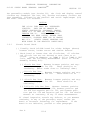
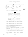
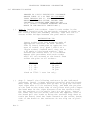
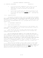
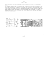
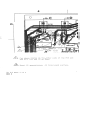
The other two enables on U34 (G2A and G2B) are connected to
SINP and SOUT. These two status signals indicate an input or output
operation during the CPU cycle. U34 is therefore disabled during
these operations.
SINP and SOUT are also fed to pins 5 and 6 of NOR gate U53
which detects an input or output operation. Its output is inverted
by U54 and applied to pin 9 of another U53 NOR gate. The other input
(pin 8) to U53 is MEM_SEL. So during a memory reference, input operation or output operation, pin 10 of U53 is active to enable the PRDY
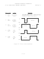
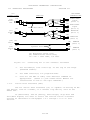
driver, U71. The low on pin 10 of U53 is also clocked by φ2 as a
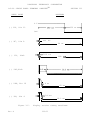
high to pin 7 of U70, a J-!K flip-flop that is connected as a D flipflop. Note that the !(PSYNC & !φ2) signal on pin 5 of U70 forces U70 to
set during the middle of PSYNC (refer to CPU and Bus discussion). U70
cannot clock until pin 5 is released, and this occurs simultaneously
with the low-to-high transition of φ2. PRDY is thus low immediately
after pin 10 of U53 goes low and remains in that state from the middle of PSYNC to the first positive-going φ2 after PSYNC. This is the
time the CPU tests the status of the ready lines (PRDY and XRDY). If
either is low, the CPU enters a WAIT state. U53, 70 and 71 thus
guarantees that the CPU enters one WAIT state during cycles in which
an input, output or memory reference is made.
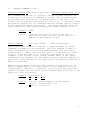
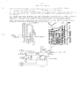
U35 and 36, the Output and Input Port Decoders respectively,
decode the higher order eight address bits (ADR8-15).
All Sol ports have a hexadecimal F (1111) in their high order
four bits (ADR12-15 are 1's). The second hexadecimal digit is also
never less than eight. This means that ADR11 is always
1 for a
port address. These five address bits are thus NAND gated in U23 to
provide one of the enables on U35 and 36. Note that the ADR14-15
combination is derived from the output on pins 3 and 11 of the U22
exclusive OR logic. This is permissible since no I/O operations are
performed during the first four start-up cycles of the CPU.
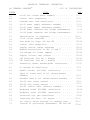
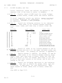
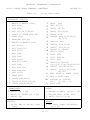
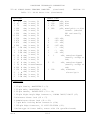
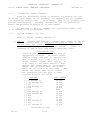
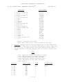
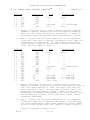
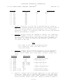
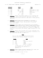
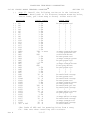
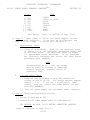
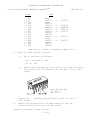
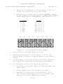
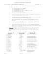
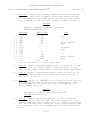
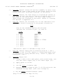
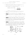
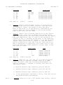
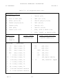
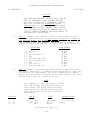
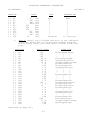
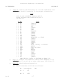
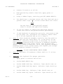
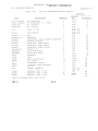
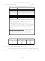
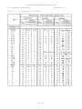
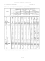
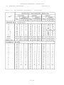
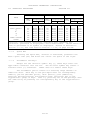
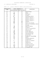
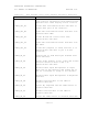
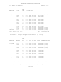
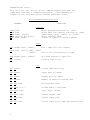
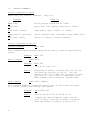
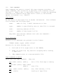
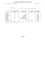
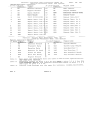
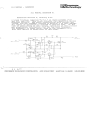
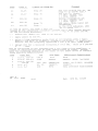
The A, B, and C inputs to U35 and 36 (ADR8, 9 and 10 respectively) specify the second hexadecimal digit in the port address and
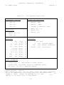
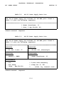
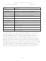
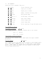
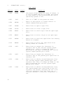
are decoded to supply the indicated outputs. These outputs and their
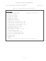
functions are defined in Table 8-1. U36 is enabled to decode when
PDBIN and SINP are active; that is, during an input operation. U35
is enabled when SOUT and !PWR are active; that is, during an output
operation.
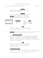
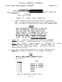
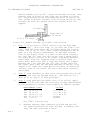
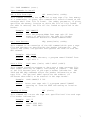
INT_SEL on pin 8 of inverter U83 is the remaining signal generated by the Input Port Decoder circuit. This signal is active when
either input port F8, F9, FA or FB is decoded by U36.
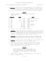
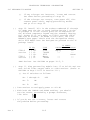
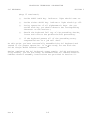
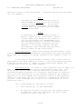
Both the address page and input/output decoders can be disabled by SINTA (S-100 Bus pin 96) when the AE-to-AC and AB-to-AD
jumpers are installed. SINTA is active (high) when the CPU is responding to an interrupt. Should an external device issue addresses
during this time, any memory response would interfere with the
VIII-16