1
Proyecto de Sistemas Informáticos.
Curso 2009-2010.
DSP-Based Implementation of a
Digital Radio Demodulator
on the ultra-low power processor
CoolFlux BSP
Authors:
Elena Pérez-Toril Gracia
Álvaro Martínez López
Project Supervisor:
Luis Piñuel Moreno
Departamento de Arquitectura de Computadores y Automática.
Facultad de Informática.
Universidad Complutense de Madrid.
Contents
1 Preliminary concepts in DAB
2
1.1
Signal Modulation . . . . . . . . . . . . . . . . . . . . . . . . . . . . . . . .
2
1.2
Multipath Propagation . . . . . . . . . . . . . . . . . . . . . . . . . . . . . .
5
1.3
QPSK (Quadrature Phase Shift Keying) . . . . . . . . . . . . . . . . . . . .
10
1.4
FDM (Frequency Division Multiplexing) . . . . . . . . . . . . . . . . . . . .
13
1.5
Orthogonal Frequency-Division Multiplexing (OFDM) . . . . . . . . . . . .
14
1.6
Fast Fourier Transform (FFT) . . . . . . . . . . . . . . . . . . . . . . . . . .
23
1.6.1
Overview . . . . . . . . . . . . . . . . . . . . . . . . . . . . . . . . .
23
1.6.2
Digital Implementation . . . . . . . . . . . . . . . . . . . . . . . . .
24
1.6.3
The Discrete Fourier Transform . . . . . . . . . . . . . . . . . . . . .
24
1.6.4
Computation of the DFT . . . . . . . . . . . . . . . . . . . . . . . .
25
1.6.5
The Fast Fourier Transform . . . . . . . . . . . . . . . . . . . . . . .
26
1.6.6
Applications to DAB . . . . . . . . . . . . . . . . . . . . . . . . . . .
27
1.6.7
Complex Numbers . . . . . . . . . . . . . . . . . . . . . . . . . . . .
28
1.6.8
Negative Frequencies . . . . . . . . . . . . . . . . . . . . . . . . . . .
29
1.6.9
Linearity of the transforms . . . . . . . . . . . . . . . . . . . . . . .
30
1.6.10 Combination of I and Q . . . . . . . . . . . . . . . . . . . . . . . . .
31
1.6.11 Addition of the Guard Interval . . . . . . . . . . . . . . . . . . . . .
33
Finite Impulse Response Filters(FIR)
. . . . . . . . . . . . . . . . . . . . .
34
How to characterize digital FIR filters . . . . . . . . . . . . . . . . .
34
Error Measures . . . . . . . . . . . . . . . . . . . . . . . . . . . . . . . . . .
36
1.7
1.7.1
1.8
i
Contents
1.8.1
Bit Error Rate . . . . . . . . . . . . . . . . . . . . . . . . . . . . . .
36
1.8.2
Modulation Error Rate . . . . . . . . . . . . . . . . . . . . . . . . .
37
Errors Detection and Correction . . . . . . . . . . . . . . . . . . . . . . . .
38
1.9.1
Viterbi Decoder . . . . . . . . . . . . . . . . . . . . . . . . . . . . . .
38
1.9.2
De-puncturing . . . . . . . . . . . . . . . . . . . . . . . . . . . . . .
46
1.10 Digital Signals Processors (DSP) . . . . . . . . . . . . . . . . . . . . . . . .
47
1.9
2 CoolFlux BSP Architecture
49
2.1
Overview . . . . . . . . . . . . . . . . . . . . . . . . . . . . . . . . . . . . .
49
2.2
Registers . . . . . . . . . . . . . . . . . . . . . . . . . . . . . . . . . . . . . .
50
2.3
The Data Path . . . . . . . . . . . . . . . . . . . . . . . . . . . . . . . . . .
50
2.3.1
Multipliers . . . . . . . . . . . . . . . . . . . . . . . . . . . . . . . .
53
2.3.2
Arithmetic and Logic Units (XALU and YALU) . . . . . . . . . . .
54
Move Buses and RSS Units . . . . . . . . . . . . . . . . . . . . . . . . . . .
55
2.4.1
Xbus and Ybus Move Buses . . . . . . . . . . . . . . . . . . . . . . .
55
2.4.2
Moving to an Accumulator . . . . . . . . . . . . . . . . . . . . . . .
56
2.4.3
Moving from an Accumulator . . . . . . . . . . . . . . . . . . . . . .
57
2.4.4
Round, Saturate and Select Units (RSS) . . . . . . . . . . . . . . . .
58
Memories and I/O . . . . . . . . . . . . . . . . . . . . . . . . . . . . . . . .
60
2.5.1
Individual Data Memory (X, Y) . . . . . . . . . . . . . . . . . . . .
60
2.5.2
Dual Precision Memory (XY) . . . . . . . . . . . . . . . . . . . . . .
60
2.5.3
I/O Memory Space . . . . . . . . . . . . . . . . . . . . . . . . . . . .
60
X and Y Addressing Units . . . . . . . . . . . . . . . . . . . . . . . . . . . .
61
2.6.1
Indexed Stack Pointer Addressing
. . . . . . . . . . . . . . . . . . .
62
2.6.2
Indexed Pointer Addressing . . . . . . . . . . . . . . . . . . . . . . .
62
Program Control Unit . . . . . . . . . . . . . . . . . . . . . . . . . . . . . .
62
2.7.1
Hardware Loop Stack . . . . . . . . . . . . . . . . . . . . . . . . . .
63
Hardware Interface . . . . . . . . . . . . . . . . . . . . . . . . . . . . . . . .
63
2.8.1
I/O Memory . . . . . . . . . . . . . . . . . . . . . . . . . . . . . . .
64
2.8.2
DMA . . . . . . . . . . . . . . . . . . . . . . . . . . . . . . . . . . .
64
2.4
2.5
2.6
2.7
2.8
ii
Contents
2.9
Multi-Cycle Instructions and Delay Slots . . . . . . . . . . . . . . . . . . . .
64
2.9.1
Multi-cycle Instructions . . . . . . . . . . . . . . . . . . . . . . . . .
64
2.9.2
Delay Slots . . . . . . . . . . . . . . . . . . . . . . . . . . . . . . . .
65
2.10 Hardware Loops . . . . . . . . . . . . . . . . . . . . . . . . . . . . . . . . .
66
2.11 Debug Mode . . . . . . . . . . . . . . . . . . . . . . . . . . . . . . . . . . .
67
2.12 Interrupts . . . . . . . . . . . . . . . . . . . . . . . . . . . . . . . . . . . . .
67
2.13 BSP C Compiler . . . . . . . . . . . . . . . . . . . . . . . . . . . . . . . . .
67
2.13.1 Optimizations . . . . . . . . . . . . . . . . . . . . . . . . . . . . . . .
70
3 DAB Implementation on the CoolFlux BSP
71
3.1
Automatic Gain Control . . . . . . . . . . . . . . . . . . . . . . . . . . . . .
74
3.2
FFT . . . . . . . . . . . . . . . . . . . . . . . . . . . . . . . . . . . . . . . .
76
3.3
Differential Demodulation . . . . . . . . . . . . . . . . . . . . . . . . . . . .
77
3.4
Frecuency de-interleaving . . . . . . . . . . . . . . . . . . . . . . . . . . . .
78
3.5
Quantization . . . . . . . . . . . . . . . . . . . . . . . . . . . . . . . . . . .
80
3.5.1
Hard Decision . . . . . . . . . . . . . . . . . . . . . . . . . . . . . . .
80
3.5.2
Soft Decision . . . . . . . . . . . . . . . . . . . . . . . . . . . . . . .
82
3.6
Time De-Interleaving . . . . . . . . . . . . . . . . . . . . . . . . . . . . . . .
83
3.7
Errors Detection and Correction . . . . . . . . . . . . . . . . . . . . . . . .
87
3.8
Energy Dispersal Unscrambling . . . . . . . . . . . . . . . . . . . . . . . . .
89
3.9
Synchronization channel . . . . . . . . . . . . . . . . . . . . . . . . . . . . .
90
3.9.1
Null Symbol Detection . . . . . . . . . . . . . . . . . . . . . . . . . .
91
3.9.2
TFPR symbol . . . . . . . . . . . . . . . . . . . . . . . . . . . . . . .
93
3.9.3
Coarse Frequency Correction . . . . . . . . . . . . . . . . . . . . . .
96
3.9.4
Fine Frequency Correction
. . . . . . . . . . . . . . . . . . . . . . .
98
3.9.5
Fine time synchronization . . . . . . . . . . . . . . . . . . . . . . . .
100
3.10 Transport mechanisms . . . . . . . . . . . . . . . . . . . . . . . . . . . . . .
102
3.10.1 Fast Information Channel (FIC) . . . . . . . . . . . . . . . . . . . .
105
3.10.1.1 Fast Information Block (FIB) . . . . . . . . . . . . . . . . .
106
3.10.1.2 Fast Information Group (FIG) . . . . . . . . . . . . . . . .
106
iii
Contents
3.10.1.3 Calculation of the CRC word . . . . . . . . . . . . . . . . .
109
3.10.2 Main Service Channel (MSC) . . . . . . . . . . . . . . . . . . . . . .
110
3.11 Audio Coding . . . . . . . . . . . . . . . . . . . . . . . . . . . . . . . . . . .
111
3.11.1 Formatting of the audio bit stream . . . . . . . . . . . . . . . . . . .
112
3.11.2 CRC check for audio side information . . . . . . . . . . . . . . . . .
114
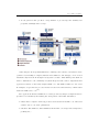
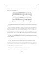
4 Hardware implementation of the DAB demodulator
4.1
4.2
116
An overview to CoolFlux BSP . . . . . . . . . . . . . . . . . . . . . . . . . .
116
4.1.1
Baseband Signal Processor(BSP) . . . . . . . . . . . . . . . . . . . .
119
4.1.2
DAB as a Real Time Application . . . . . . . . . . . . . . . . . . . .
120
4.1.3
DAB hardware definition . . . . . . . . . . . . . . . . . . . . . . . .
120
4.1.4
Components Description . . . . . . . . . . . . . . . . . . . . . . . . .
124
4.1.4.1
Maxim 2172 v1.0.25 . . . . . . . . . . . . . . . . . . . . . .
124
4.1.4.2
Tektronix TDS210 . . . . . . . . . . . . . . . . . . . . . . .
125
4.1.4.3
FPGA Board Virtex XC4VLX100 . . . . . . . . . . . . . .
126
4.1.4.4
PE 1542 DC Power Supply Philips
. . . . . . . . . . . . .
126
4.1.4.5
Hewlett Packard 8596E Oscilloscope . . . . . . . . . . . . .
126
4.1.4.6
CoolFlux simulator, CoolFlux debugger, Chess compiler . .
127
4.1.4.7
Reception Antenna . . . . . . . . . . . . . . . . . . . . . .
127
4.1.4.8
JTAG(Joint Test Action Group) . . . . . . . . . . . . . . .
127
4.1.5
DAB demodulator datapath . . . . . . . . . . . . . . . . . . . . . . .
129
4.1.6
Local memories . . . . . . . . . . . . . . . . . . . . . . . . . . . . . .
131
4.1.7
Debug interface . . . . . . . . . . . . . . . . . . . . . . . . . . . . . .
131
4.1.8
Interrupt interface . . . . . . . . . . . . . . . . . . . . . . . . . . . .
132
4.1.9
Shared Buffers . . . . . . . . . . . . . . . . . . . . . . . . . . . . . .
132
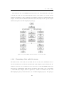
Description of the BSP instances . . . . . . . . . . . . . . . . . . . . . . . .
134
4.2.1
BSP0 : Synchronization, Time correction, Save OFDM symbols . . .
134
4.2.2
BSP1 : FFT, Deinterleaving, Demapping . . . . . . . . . . . . . . . .
139
4.2.3
BSP2 : FIC and MSC Decoding. Audio decoding . . . . . . . . . . .
140
iv
Contents
5 Conclusions
141
5.0.4
Start point . . . . . . . . . . . . . . . . . . . . . . . . . . . . . . . .
142
5.0.5
Proposed and accomplished goals . . . . . . . . . . . . . . . . . . . .
142
5.0.6
Future aspects . . . . . . . . . . . . . . . . . . . . . . . . . . . . . .
142
5.0.7
Difficulties found within the development phase . . . . . . . . . . . .
143
Appendices
144
A The Fourier Transform
145
A.1 Motivation
. . . . . . . . . . . . . . . . . . . . . . . . . . . . . . . . . . . .
145
A.2 Approximation by the minimum mean square error . . . . . . . . . . . . . .
149
A.3 Orthogonality . . . . . . . . . . . . . . . . . . . . . . . . . . . . . . . . . . .
151
A.4 Fourier Transform in Periodic Complex Functions . . . . . . . . . . . . . . .
154
A.5 Integral Fourier Transform . . . . . . . . . . . . . . . . . . . . . . . . . . . .
158
A.6 DFT . . . . . . . . . . . . . . . . . . . . . . . . . . . . . . . . . . . . . . . .
160
A.7 Spectral Analysis . . . . . . . . . . . . . . . . . . . . . . . . . . . . . . . . .
163
A.8 Applications of the Fourier Transform . . . . . . . . . . . . . . . . . . . . .
166
A.8.1 Noise Filter . . . . . . . . . . . . . . . . . . . . . . . . . . . . . . . .
166
A.8.2 Image Compression . . . . . . . . . . . . . . . . . . . . . . . . . . . .
168
B Resumen en español del proyecto
173
B.1 Implementación software de DAB sobre la arquitectura CoolFlux BSP . . .
173
B.2 Control Automático de Ganancia . . . . . . . . . . . . . . . . . . . . . . . .
174
B.3 FFT . . . . . . . . . . . . . . . . . . . . . . . . . . . . . . . . . . . . . . . .
175
B.4 Demodulación diferencial . . . . . . . . . . . . . . . . . . . . . . . . . . . .
176
B.5 Frecuency de-interleaving . . . . . . . . . . . . . . . . . . . . . . . . . . . .
176
B.6 Cuantización . . . . . . . . . . . . . . . . . . . . . . . . . . . . . . . . . . .
177
B.6.1 Hard Decision . . . . . . . . . . . . . . . . . . . . . . . . . . . . . . .
177
B.6.2 Soft Decision . . . . . . . . . . . . . . . . . . . . . . . . . . . . . . .
178
B.7 Time De-Interleaving . . . . . . . . . . . . . . . . . . . . . . . . . . . . . . .
178
B.8 Energy Dispersal Unscrambling . . . . . . . . . . . . . . . . . . . . . . . . .
179
v
Contents
B.9 Canal de Sincronización . . . . . . . . . . . . . . . . . . . . . . . . . . . . .
179
B.9.1 Símbolo Nulo . . . . . . . . . . . . . . . . . . . . . . . . . . . . . . .
180
B.9.2 TFPR symbol . . . . . . . . . . . . . . . . . . . . . . . . . . . . . . .
180
B.10 Implementación hardware del demodulador DAB . . . . . . . . . . . . . . .
181
B.10.1 DAB datapath . . . . . . . . . . . . . . . . . . . . . . . . . . . . . .
184
B.10.2 Memorias locales . . . . . . . . . . . . . . . . . . . . . . . . . . . . .
184
B.10.3 Interfaz de depuración . . . . . . . . . . . . . . . . . . . . . . . . . .
184
B.10.4 Interfaz de interrupciones . . . . . . . . . . . . . . . . . . . . . . . .
185
B.10.5 Buffers Compartidos . . . . . . . . . . . . . . . . . . . . . . . . . . .
185
B.11 Descripción de los módulos BSP . . . . . . . . . . . . . . . . . . . . . . . .
186
B.11.1 BSP0 : Sincronización y buffering de muestras . . . . . . . . . . . . .
186
B.11.2 BSP1 : FFT, Deinterleaving, Demapping . . . . . . . . . . . . . . . .
187
B.11.3 BSP2 : FIC and CIF Decoding, Audio decoding . . . . . . . . . . . .
188
B.12 Conclusiones . . . . . . . . . . . . . . . . . . . . . . . . . . . . . . . . . . .
188
B.12.1 Punto de partida . . . . . . . . . . . . . . . . . . . . . . . . . . . . .
189
B.12.2 Objetivos propuestos y cumplidos
. . . . . . . . . . . . . . . . . . .
190
B.12.3 Aspectos futuros . . . . . . . . . . . . . . . . . . . . . . . . . . . . .
190
B.12.4 Dificultades encontradas . . . . . . . . . . . . . . . . . . . . . . . . .
191
vi
Contents
El presente documento es la memoria del proyecto de fin de
carrera realizado por Álvaro Martínez López y Elena Pérez-Toril
Gracia en la compañía NXP Semiconductors en Lovaina (Bélgica) para la asignatura Sistemas Informáticos de la titulaciíon
de “Ingeniería en Informática” en la Universidad Complutense
de Madrid. Los autores de este proyecto autorizan a la Universidad Complutense de Madrid a difundir esta memoria con
fines académicos, no comerciales y mencionando expresamente
a sus autores.
Álvaro Martínez López
Elena Pérez-Toril Gracia
Universidad Complutense de Madrid, June 2010
1
Acknowledgements
The realization of this project has been possible thanks to the contribution of many
people. In the first place I want to thank Luis Piñuel Moreno, the director of this project,
for giving me the wonderful opportunity of going to Belgium for working on this project.
I want to thank Pancho, my mentor at NXP, for teaching me everything I know about
signal modulation, embedded systems and digital signal processors. Thanks a lot for those
marvelous 6 months in Leuven. I also want to mention my gratitude towards Ludo, Marleen
and Sandrine from NXP for their help and support, specially during the month of august.
Many thanks to Elena, my project colleague and friend, for her companionship.
For me, this is not only a final year project but a symbol that represents all my trajectory during the years I spent as an undergraduate student at university. As such I want to
mention all that people that has contributed to this venture. First of all, thank to my family,
specially my mother, sister and grandmother, for their love, dedication and support while
raising me. Many thanks to my friends Emilio, Pedroche, Cavero, Blasco, Agus and Saul.
Among other things, I will never forget those marvelous days during our summer holidays
in La Marina. I also want to thank you Andrés, for your wisdom and special understanding
towards me.
In Memoriam my father
A.M.L.
Abstract
The new digital radio system Digital Audio Broadcasting (DAB) is a digital radio technology
for broadcasting radio stations, which will likely replace most existing methods for radio
broadcasting in many parts of the world.
Mobile reception without disturbance was the basic requirement for the development
of the DAB system. The special problems of mobile reception are caused by multipath
propagation: the electromagnetic wave will be scattered, diffracted, reflected and reaches
the antenna in various ways as an incoherent superposition of many signals with different
travel times, which in classical radio systems like AM or FM meant a deficit in the quality
of sound, or even complete cancellation.
This document will present the software development of a DAB demodulator for the
CoolFlux BSP and its subsequent implementation on the ultra-low power architecture
CoolFlux BSP, developed by NXP Semiconductors.
For the implementation of the DAB system, a hard work in signal processing and code
optimization techniques has been carried out aimed to get the smallest power and memory
storage. Important correction codes and measures have also been applied to the data for
ensuring a good quality reception.
Once all the algorithms have been introduced, we describe their implementation on a
FPGA in order to perform real time processing of the signal. Although one CoolFlux BSP is
capable of running the whole demodulator in real time on its own, the FPGA is constrained
to 50 MHz (against 300 MHz of an actual BSP). Thus, the demodulation chain had to be
pipelined into three BSP cores, all of which were mapped on one FPGA.
Resumen
Digital Audio Broadcasting (DAB) es un estándar de emisión de radio digital desarrollado por EUREKA como un proyecto de investigación para la Unión Europea (Eureka 147).
Este sistema pronto reemplazará a la mayoría de los métodos existentes de transmisión de
radio en muchas partes del mundo.
El principal motivo para el desarrollo del sistema DAB era conseguir un sistema para la
recepción móvil sin alteraciones de la señal. Los principales problemas de la recepción móvil
provienen de la propagación mutipath: la onda electromagnética está sujeta a fenómenos
de reflexión, dispersión y difracción y llega al receptor como una superposición incoherente
de señales, lo que en sistemas clásicos de radio tales como FM o AM se traduce en una
recepción pobre o incluso en la pérdida total de los datos.
El presente documento mostrará el desarrollo del software de un demodulador de DAB
y su posterior implementación hardware en la arquitectura CoolFlux BSP, el sistema para
aplicaciones de bajo consumo desarrollado por NXP Semiconductors, destinado a dispositivos móviles de consumo energético limitado.
Para la implementación del sistema DAB, se ha realizado un gran trabajo en cuanto a
procesamiento de señales y se han aplicado técnicas de optimización destinadas a conseguir
el menor consumo de potencia posible con el mínimo almacenamiento de memoria y ciclos
de computación. También se han aplicado numerosos códigos de corrección de errores a los
datos, para asegurar una alta calidad del audio emitido.
Anteriormente a este trabajo se realizaron estudios de viabilidad en los que se concluyó
que tan sólo sería necesario un BSP para demodular la señal en tiempo real. Sin embargo,
el prototipado del sistema en una FPGA (cuya frecuencia de reloj es considerablemente más
limitada que un sistema real) exigía la necesidad de utilizar 3 instancias del BSP conectadas
en cascada.
Keywords
• DSP
• BSP
• CoolFlux
• Digital Radio
• DAB
• Demodulator
• FFT
• Digital Signal
• Error correction
• Real Time
• Processor
1
Chapter 1
Preliminary concepts in DAB
Before we introduce the actual implementation of the DAB demodulator on the CoolFlux
BSP we present some theoretical concepts in radio communications. The problem at hand is
that of transmitting information in an efficient manner using the electromagnetic spectrum.
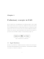
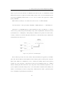
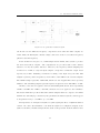
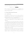
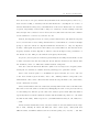
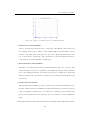
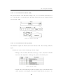
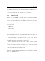
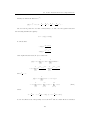
In this scenario we have the broadcaster -that is the agent that transmits the informationand the receiver. The space between them is known as the channel and, as we shall see, a
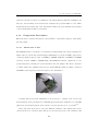
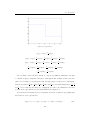
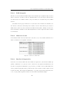
great effort is devoted in DAB to transmit a clean signal through it (figure 1.1).
Figure 1.1: Elements in radio communications
1.1
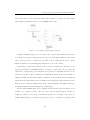
Signal Modulation
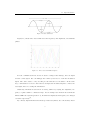
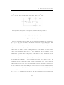
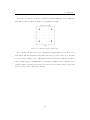
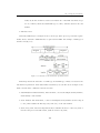
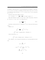
The main concept behind radio communications is that of modulation. An electromagnetic
wave has three main attributes that can be varied in time to convey information: amplitude
(A), frequency (ω) and phase (ψ) (figure 1.2).
2
1.1. Signal Modulation
Figure 1.2: Wave attributes.
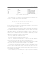
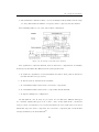
Figure(1.3) shows three waves with the same frequency and amplitude, but different
phases:
Figure 1.3: Three waves with different phase.
In radio communications two waves are used to transport the message, the base signal
and the carrier signal. We can multiply the former by the later to form the modulated
signal. The device used to carry out this process is known as a modulator. In the same
way, a demodulator is a device that takes as its input the modulated signal to extract the
base signal, hence recovering the information.
Classically, information was sent in an analog fashion by varying the amplitude, frequency or phase within a continuous range. As an example let’s mention the well known
FM and AM radio systems (picture 1.4), in which the amplitude and frequency are changed
over time respectively [2] .
By contrast, digital information is made up of discrete symbols, also called bauds, chosen
3
1.1. Signal Modulation
Figure 1.4: Amplitude Modulation and Frequency Modulation.
from a finite alphabet. If the alphabet has 2N symbols then, each symbol carries N bits of
information. The equivalent digital modulation schemes to those presented so far are known
as PSK, FSK (figure 1.5) and ASK for which, in turn, finite values of phase, frequency and
amplitude are employed. A variation of the first one, called DQPSK will be our main
concern later, since it is the standard used in DAB [3] .
Figure 1.5: Frequency-shift keying.
Strictly speaking, even though the information is digitally modulated, the actual signal
that goes out the transmitter is analog since nature does not allow a physical magnitude
to change from one state to another in a finite amount of time without passing through
all intermediate values. An Analog to Digital Convertor (ADC) is a device that takes an
4
1.2. Multipath Propagation
analog signal as its input and converts it to a digital representation in a process known as
sampling [4] . .
Figure 1.6: Sampling of an analog signal.
1.2
Multipath Propagation
Most existing means for radio communication which can use simple omni-directional receiving antennas are affected adversely by multipath propagation, particularly in a changing
environment such as when the receiver is located in a moving vehicle. The effect on broadcast FM radio is well known where, in built-up areas, even if there is sufficient mean field
strength, mobile reception can be severely impaired by bursts of noise and audio distortion,
and sometimes a fluttering effect on the audio signal.
In addition to a direct signal from the transmitter, the receiver is often presented with
signals reflected and diffracted by buildings and the terrain. These can combine constructively or destructively in the receiving antenna as the relative lengths of the propagation
paths change, or as the wavelength changes. Indeed, the sensitivity to the wavelength, or
frequency, is the main reason for the audio distortion with FM signals.
Constructive addition can give up to 6 dB enhancement, for two signals of equal magnitude, but subtraction can cause complete cancellation. This phenomenon is known as
fading, and multipath propagation is one of two mechanisms by which it can be caused;
the other is blocking of the propagation path by obstacles. In the latter case, the problem can often be overcome simply by increasing transmitter powers, but this is not always
true for multipath fading; destructive combination of two signals of equal magnitude causes
complete cancellation regardless of the transmitter power. When an FM receiver is pre-
5
1.2. Multipath Propagation
sented with insufficient signal power its own front-end noise is demodulated giving a burst
of audio noise. In most common environments, reflected and diffracted signals usually have
smaller magnitudes than a direct signal, but a direct line-of-sight path might not always be
available. Most reflections occur by lossy mechanisms (i.e. not large sheets of metal), and
reflected signals often have further to travel so they are subject to greater spreading losses.
On the other hand the phenomenon by which fading affects only a fixed range frequencies
within the signal is called selective fading.
Figure 1.7: Multipath propagation in the environment.
The receiver performance can be enhanced by using a directional antenna, which is only
appropriate to fixed reception, or a diversity system using more than one antenna, which
may be applicable to a more-expensive vehicular installation. Indeed, the audio quality
available from fixed FM receivers with rooftop directional antennas is very good, but the
market for radio consumption has changed from what was anticipated at the start of BBC
FM services. The widespread use of portable and mobile receivers now demands a means
for delivery which offers the highest audio quality, in most environments within a service
area, without the need for a complicated antenna system or one that may need adjustment.
On this basis, there is little that can be done to rescue an FM signal, or any other
analogue signal, in the presence of severe fading or interference. Much of the damage is
done in the receiving antenna, and there is little scope for ‘post-processing’ to rectify the
situation. However, in broadcasting and many other fields of communication, a solution is
being sought in the application of digital techniques, implying a radical departure from the
classical methods of broadcasting. This introduces numerous problems for the broadcasters
and the receiver manufacturers (none of which is technically insurmountable, nowadays),
but it offers the great advantage of ‘post-processing’ in the form of error correction.
6
1.2. Multipath Propagation
The effect of fading and interference on a digital system is to introduce errors into the
received signal, but improvements are possible by virtue of the numerical nature of the
bit-stream. Error detection can be achieved in the receiver by sending a small amount
of additional data derived from the original data, such as checksums. By sending further
additional data, it becomes possible to correct errors. Such additional data are often referred
to as ‘redundant’ data, but this does not imply that they are not needed; only that they
carry no new information. The trivial case would be simply to transmit all of the original
data twice with independent checksums, so with the benefit of error detection a complete
set of good data could be reconstructed. However, this would make relatively inefficient
use of the available bit-rate, as there still remains a probability that some of the same bits
could be in error in both of the received versions. Many more-complicated, and ingenious
methods have been developed for such Forward Error Correction (FEC; ‘forward’ implies
that action is taken at the transmitter), which make more efficient use of a given amount
of redundancy.
Powerful FEC, by whatever method, requires the transmission of substantial amounts
of redundant data which increases the demand for radio frequency spectrum. However, the
Eureka DAB system achieves greatly improved ruggedness without sacrificing efficiency in
its use of radio spectrum by applying in addition what could be called ‘advanced’ digital
techniques. To explain how the DAB system works, we should first look more closely at the
effects of multipath propagation, in both the time and frequency domains.
Incidentally, the word ‘coding’ is used widely in the context of error correction, and
digital communications generally. Sometimes the intended meaning is the whole principle
of encoding and decoding data, and sometimes it is used instead of ‘encoding’. The former
meaning will be applied here, and in order to avoid ambiguity, the terms ‘encoding’ and
‘decoding’ will be used where they are meant.
The time and frequency domains provide different viewpoints for the same effects, a
principle well known to anyone who has used an oscilloscope and a spectrum analyzer to
inspect the same signal. The oscilloscope allows inspection of the way that a signal voltage
changes as time progresses, almost irrespective of the rate at which it is changing, whereas
the spectrum analyzer allows inspection of the content of the signal at different frequencies
7
1.2. Multipath Propagation
(i.e. rates of change), almost irrespective of time. Often, different aspects of a phenomenon
being investigated can be visualized more clearly in one or other of the two domains. For
example, the vestigial sideband in a conventional AM television signal can be inspected
using a spectrum analyzer, but an oscilloscope gives no obvious hint to its existence.
If the effects of a phenomenon are described mathematically in each of the domains, the
two descriptions are related by the Fourier transform. For example, the frequency response
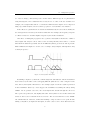
of a filter is related to its time impulse response by the Fourier transform.
One effect of multipath propagation is to generate inter-symbol interference. When a
direct signal and delayed ‘echoes’ arrive at the receiving antenna, there will be occasions
when their modulation represents data from different symbols, previous as well as present.
This is illustrated in figure 1.8 for the case of a single delayed signal, although there may
be many in practice.
Figure 1.8: inter-symbol interference
Returning to figure 1.8, when the combined signal is demodulated and the modulation
state is detected, the effect of the overlapping different symbols is to cause corruption of the
data; that is, inter-symbol interference. For example, figure 1.8 shows a symbol generated
in the transmitter (first row). Let’s suppose the transmitter is sending the binary string
“01000”. As we pointed out before, the actual signal that travels through the air is not
like a perfect step function, but slightly smoother. The symbol is echoed three times and
arrives at the receiver as shown in the second row. The receiver shall not receive “01000”
but “01110” instead. However, rather than making a ‘snap’ decision at one point in time
during each symbol, as implied in the figure, in some cases it can be more efficient for the
8
1.2. Multipath Propagation
detector to integrate the demodulator output signal over the whole of each symbol, with
respect to some timing reference (which may be the direct signal). This makes use of all of
the received signal power.
In that case, as long as the delay is less than the symbol duration, the echo will carry the
same modulation as the direct signal for some portion of integration period. Undoubtedly
this will have some effect because the demodulator output signal represents the phase of
whatever is input; in this case the ‘vector’ sum of the direct and delayed signals. However,
a method is available to prevent this from upsetting the operation of the detector; that is,
differential modulation which will be described later. Entirely different symbols overlap for
the remainder of the integration, so the degree to which the result is corrupted depends on
the magnitudes of the echo signals and on their delays.
When a mobile receiver is traveling in a dense urban environment, which imposes one
of the most difficult multipath conditions, short-delay echoes are often received in greater
numbers than long-delay ones owing to multiple reflections (of a relatively direct signal) from
local buildings and terrain. Very long delay echo signals tend to have smaller magnitudes
because they have travelled greater distances. Therefore, the majority of the collective echo
power arises from short delay echoes, so modulation schemes which use long symbols (or
low symbol rates) provide the greatest tolerance to this effect because the proportion of
each symbol that is corrupted is minimized.
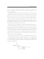
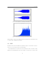
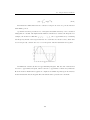
We could measure the collective echo power received with different delays in time. An
idealized result is illustrated in figure 1.9 where the transmitted (i.e. direct) signal is shown
as a single impulse; in practice, more-complicated signals are used in such measurements
to overcome the infinite bandwidth requirement of true impulses, but the results can be
presented in a similar fashion.
Figure 1.9: Delay spread
9
1.3. QPSK (Quadrature Phase Shift Keying)
By taking a large number of measurements in a particular type of environment, the statistical distribution can be built up, and in many cases this is found to approximate to an
exponential curve (see figure 1.9). The distribution is characterized by a single parameter
known as the ‘delay spread’, which can be interpreted as either the mean or the standard
deviation in the case of an exponential distribution. The next equation expresses the statistical distribution of the echo power as a function of the delay ξ. The parameter T is the
delay spread.
P (ξ) =
1 −ξ
e T
T
The incremental effects of greater delay or greater echo power are similar, they both
increase the potential for inter-symbol interference, so the delay spread (interpreted as the
mean) is a guide to the interference potential of a given type of environment. The average
degree of data corruption is proportional to the ratio of the symbol duration to the delayspread. For the case of outdoor reception from a single terrestrial transmitter, the delay
spread can range from less than 0.5s to 5µs, or more; a typical median value (for 50% of
locations) is around 1 µs. Echoes with delays outside this range can be encountered, but
the percentage of locations for which they contribute significantly to the delay spread is
small (less than 1%). Direct reception from a satellite yields values of 0.5 µs, or less.
Thus, it was a pre-requisite for the DAB system that the symbol duration should be much
greater than the values of delay-spread encountered in common broadcasting environments.
In other words, the symbol duration should have a minimum value of at least 50 µs for
terrestrial broadcasting [6] [5] .
1.3
QPSK (Quadrature Phase Shift Keying)
So far, we pointed out that PSK uses a finite set of phases to represent the symbols that
compose the message. QPSK uses four points on the constellation diagram, equispaced
around a circle. With four phases, QPSK can encode two bits per symbol, shown in the
diagram with Gray coding to minimize the Bit Error Ratio (BER).
10
1.3. QPSK (Quadrature Phase Shift Keying)
Figure 1.10: Constellation diagram.
Let Ts be the duration of one symbol. The mathematical expression for each symbol (i
= 1,2,3,4) is:
r
Si (t) =
2Es
π
cos(2πfc t + (2i − 1) )
Ts
4
i = 1, 2, 3, 4
where Es is the energy employed to send the signal. The last equation also shows that
the less the energy employed for the transmission the closer the symbols will be in the
constellation diagram, thus the chance of one symbol becoming another is higher. The
signal constellation consists of the signal-space 4 points:
r
(±
Es
,±
2
r
Es
)
2
The factors of 1/2 indicate that the total power is split equally between the two carriers.
A QPSK signal is actually a composition of two orthogonal basis functions,
r
2
cos(2πfc t)
Ts
r
2
sin(2πfc t)
Ts
φ1 (t) =
φ2 (t) =
where fc is the carrier frequency.
The first and second bases are called the in-phase (I) and quadrature (Q) components
of the signal respectively. From the orthogonality of the I and Q components, it follows
11
1.3. QPSK (Quadrature Phase Shift Keying)
that we can send both signals through a single channel -that is, a single frequency- without
having them interfering with each other.
The following picture shows some random bits mapped in the I and Q components of a
QPSK signal. Both the I and Q components are added together to form the actual QPSK
signal.
Figure 1.11: I and Q components mapped into QPSK signal.
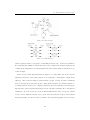
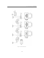
The next picture shows a conceptual transmitter structure for QPSK. The binary data
stream is split into the in-phase and quadrature-phase components. These are then separately modulated onto two orthogonal basis functions. In this implementation, two sinusoids are used. Afterwards, the two signals are superimposed, and the resulting signal is the
QPSK signal. Note the use of polar non-return-to-zero encoding. These encoders can be
placed before for binary data source, but have been placed after to illustrate the conceptual
difference between digital and analog signals involved with digital modulation.
Figure 1.12: QPSK modulator
12
1.4. FDM (Frequency Division Multiplexing)
On the other hand, a receiver might be implemented as follows. The matched filters
can be replaced with correlators. Each detection device uses a reference threshold value to
determine whether a 1 or 0 is detected.
Figure 1.13: QPSK demodulator
Despite its apparent simplicity, QPSK has a major drawback. QPSK uses absolute
phases (e.g 0◦ , 90◦ , 180◦ , 270◦ ) to determine whether the current symbol is ‘00’, ‘01’, ‘11’
or ‘10’. There can happen that due to noise in the channel, the current and future QPSK
symbols suffer a phase shift of say 90◦ , thus rotating the constellation diagram. Of course,
the conveyed digital information would be erroneous.
A better approach would be to differentially encode the phases of two consecutive QPSK
symbols. This scheme is called DQPSK, and it is the standard in DAB. The actual phase is
not that of the current symbol but the difference between the last symbol and the current
one. In this case, all the symbols that pass through the channel will be shifted in time (thus
in phase) by the same offset. Therefore operating with the difference of phases between two
subsequence symbols will cancel out that offset [7] .
1.4
FDM (Frequency Division Multiplexing)
The process by which multiple broadcaster share the radio spectrum is called multiplexing.
If two or more broadcasters want to emit at the same frequency there has to be an agreement
between both to send their signals at different times. Otherwise, their signal would interfere
with each other, destroying the information. This turning on the use of the channel is what
is called in telecommunications TDM (Time Division Multiplexing) [8] .
13
1.5. Orthogonal Frequency-Division Multiplexing (OFDM)
A more common way of sharing the spectrum is to allow each transmitter to emit at a
different frequency. We avoid interference among different frequency carriers by introducing
an additional guard space between them. This process is called FDM (Frequency Division
Multiplexing). As an example, the next picture illustrates the spectra of a signal composed
of 8 subcarriers [9] .
Figure 1.14: Frequency Spectrum
1.5
Orthogonal Frequency-Division Multiplexing (OFDM)
The bandwidth of a digitally modulated signal is proportional to the symbol-rate. The
exact relationship depends on the modulation scheme and factors such as filtering, but
generally for a given modulation scheme, doubling the symbol rate doubles the bandwidth.
The simple way to increase the bandwidth of the DAB signal without compromising its
spectral efficiency would be to make it carry several radio programs at the same time, by
bringing together data representing a number of audio signals and multiplexing them before
transmission.
However, this gives rise to a dilemma: if the DAB signal were to use a single carrier,
then in order to achieve a wide bandwidth, the symbol rate would need to be high, but this
conflicts with the requirement for long symbols.
A solution is to use not one, but a multiplicity of carriers each at a different radio
frequency. By modulating each carrier independently at a low symbol rate by a small
fraction of the data to be transmitted, individually the carriers will then be relatively
resistant to multipath echoes because of their long symbols.
The requirement for mobile reception imposes an upper limit on the symbol duration.
The changing characteristics of the transmission channel can have adverse effects on whatever modulation system is used, and generally, the maximum symbol duration is related to
14
1.5. Orthogonal Frequency-Division Multiplexing (OFDM)
the required maximum vehicle speed. Thus, the maximum symbol duration chosen for the
DAB system is 1 ms. In isolation, this allows good reception at vehicle speeds of at least
100 km/hr.
On the other hand, it is found that the resistance to multipath effects improves as the
bandwidth is increased, accommodating more extreme multipath conditions which could
otherwise cause flat fading. Hence, the actual bandwidth chosen for the DAB signal is
1.537 MHz
Clearly, the greater the number of individually modulated carriers that can be packed
into the given bandwidth, the greater the potential data capacity of the signal, but the upper
limit is set by the requirement for independent demodulation without mutual interference.
The significant bandwidth occupied by each modulated carrier is determined by the chosen
symbol rate and the modulation scheme, and a simple way to avoid mutual interference
would be to separate adjacent carriers by frequency guard bands. However, such a simple Frequency-Division Multiplexing (FDM) approach would be wasteful of RF spectrum.
Without guard bands, the spectra of adjacent modulated carriers are likely to overlap, and
the allowable degree of overlap depends on the method of demodulation, so this establishes
a maximum packing density, or a minimum separation between the carrier frequencies. In
either case, some form of spectrum analysis technique is needed in the receiver.
The DAB system uses a technique known as Orthogonal Frequency-Division Multiplexing (OFDM) which allows the greatest possible packing density consistent with the use of
practicable (mainly digital) processing techniques. This requires the minimum separation
of the carrier frequencies to be equal to the reciprocal of the symbol duration, 1 kHz, so
the spectra of adjacent modulated carriers will certainly overlap. In that case, the maximum number of modulated carriers would be 1537, but in practice one carrier is not used.
Therefore, the maximum number of modulated carriers in the DAB signal is 1536. (See the
appendix about the Fourier Transform for a mathematical explanation of orthogonality)
In this scheme, the possibility arises that data conveyed by some of the individual
carriers will not be received successfully because of selective fading, but in this case the
application of FEC is most efficient (and necessary) because the loss of a small number of
carriers represents the loss of only a small fraction of the total data. Thus, for the same
15
1.5. Orthogonal Frequency-Division Multiplexing (OFDM)
degree of protection, the amount of redundant data that needs to be transmitted is much
smaller than would be required for scheme using a single-carrier. For the DAB system, the
abbreviation OFDM is prefixed with a ‘C’, for coded, to indicate the application of FEC,
giving ‘COFDM’.
With all that at hand, we can deduce the total bit rate of a DAB ensemble:
1536 subcarriers * 2 bits per symbol (DQPSK) * 1000 symbols/sec = 3.072 Mbits/sec
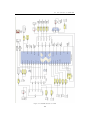
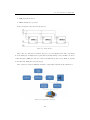
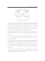
Generation of an OFDM signal is easily visualized because, in principle, it could be
carried out by partly-analogue means using a large bank of synthesized oscillators followed
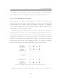
by modulators (i.e. multipliers). This principle is illustrated in picture 1.15 where three,
of many, oscillators are shown although it should not be inferred that such a cumbersome
arrangement is used in practice.
Figure 1.15: generation of an OFDM signal
Each oscillator provides one of the carriers, and the modulation is applied by each multiplier. All of the modulated carrier signals are then added together to make up the composite
signal. The addition (or summation) can be considered as taking effect in the frequency
domain; all of the frequency components produced by the multiplications are combined
without affecting the time-waveform of any component. If the modulation signals are composed of symbols, such that changes only occur at the symbol boundaries then, during each
symbol, each modulated carrier is temporarily a sinusoidal wave with a particular phase
and/or amplitude representing the modulation.
16
1.5. Orthogonal Frequency-Division Multiplexing (OFDM)
However 1536 such oscillators could occupy a large room. The key to compact digital
implementation lies in the recognition that this process parallels the operation of a mathematical process known as the inverse Discrete Fourier Transform (iDFT). The iDFT is
a method of calculating the waveform of a signal for which the spectrum is known. The
iDFT operates with time-domain and frequency-domain variables which must be expressed
as series of discrete samples.
In this case, the array of modulation signals which are to be applied to the carriers
during a single symbol provide a specification of the spectrum of the required composite
signal for that symbol. The modulation of the carriers is intended to remain static during
each symbol, so each modulation signal contains one sampled value per symbol. The array of
modulation signals can then be thought of as a series of samples which make up a ‘function
of frequency’.
The composite OFDM signal will be produced by the iDFT as a series of samples which
follow one another in time, so it can be thought of as a ‘function of time’.
The array of oscillator signals can be thought of as a function of both frequency and
time; the array of different frequencies forms a series with respect to frequency (as with the
modulating signals), and if each oscillator provides a sine wave, a sampled version of this
forms a series with respect to time.
With this nomenclature, the iDFT (and the contents of figure Fig 1.15) can be expressed
as:
f (t) =
highestf
requency
X
f unction of f requency x oscillator signal
lowestf requency
To produce the first sample of the ‘function of time’, each of the modulation ‘samples’
is multiplied by the first time sample of its corresponding oscillator signal, and all of the
products are added together. For the second sample, the second time samples of the oscillator signals are used, and so on. In this way, any number of samples of the ‘function
of time’ can be produced which represent the composite OFDM signal for one symbol. In
practice, this number is minimized in order to constrain the demand for processing, and the
fundamental limit is set by the so-called Nyquist criterion; the time-sampling rate must be
17
1.5. Orthogonal Frequency-Division Multiplexing (OFDM)
at least twice the frequency of the highest frequency component represented in the function
of time to avoid ‘aliasing’ distortion.
The period of time over which the whole calculation is performed can be called the
‘processing time-window’, and it is a requirement for correct operation of the iDFT that
the duration of this window and the interval between the oscillator frequencies should have
a reciprocal relationship. In this case, the required time-window (i.e. symbol) duration is 1
ms, so the oscillator frequencies are separated by 1 kHz. The required number of carriers,
1536, defines the highest frequency represented in the function of time, so the minimum
time-sampling rate is then defined. The iDFT process is repeated for subsequent symbols,
in each case with a new set of values in the array of modulation signals.
It is relatively straightforward to implement this transform in a computer program,
or by means of digital hardware of some other form, where all of the sample values are
represented by digital numbers. Furthermore, the availability of fast ADCs and DACs
means that, nowadays, it is entirely practicable to carry out symbol-by-symbol processing
in real time. With modern VLSI technology, the complexity (i.e. the number of carriers) is
of relatively minor importance.
The recovery of the modulation signals from an OFDM signal (i.e. ‘decomposition’ of the
OFDM signal) is rather less straightforward, but essentially this follows from the generation
process by interchanging time and frequency. It was mentioned earlier that integrating over
each symbol is an efficient way to determine the modulation state of a carrier, and an
extension of this principle provides a useful starting point.
To simplify the explanation, the receiver should initially be visualized as containing a
large bank of local-oscillators, mixers (i.e. multipliers) and integrators although, as before,
such an arrangement is not used in practice. Each oscillator/mixer combination acts as a
demodulator, in the manner of a direct-conversion radio receiver. The incoming signal is
fed equally to all of the demodulators, and each of these is followed by an integrator. Each
integrator operates over a limited period of time before yielding a result. This is illustrated
in Fig. 1.16.
Each modulated carrier is demodulated by the mixer which is fed with a local-oscillator
signal of the corresponding frequency but, since the spectra of adjacent modulated carriers
18
1.5. Orthogonal Frequency-Division Multiplexing (OFDM)
Figure 1.16: generation of an OFDM signal
are allowed to overlap, each integrator will be presented with interference (or crosstalk)
contributions as well as the wanted demodulated signal. However, if the radio frequencies
could be chosen so that over the period of integration, the symbol duration, the integrals of
all the interference signals amounted to zero, then mutual interference would be cancelled.
This condition is known as ‘orthogonality’, and is achieved when the carrier frequencies
and the local-oscillator frequencies are located on a regular comb where the frequency
interval is equal to the reciprocal of the symbol duration.
With reference to Fig. 1.17, take for example the modulated carrier at 200MHz, with
neighbors at ± 1 kHz, ± 2 kHz, etc. either side. The modulation state of each carrier is held
constant over each symbol, so each carrier is temporarily a sinusoidal wave with a particular
phase and/or amplitude representing the modulation. When the incoming signal is acted
upon by the mixer with the 200 MHz local-oscillator, the 200 MHz wave will produce a
DC output signal, and contributions from the neighbors will produce 1 kHz, 2 kHz, etc.
AC components (the 400 MHz products will be neglected). When the composite signal
output by this mixer is integrated over 1 ms, all of the AC components will cancel because
19
1.5. Orthogonal Frequency-Division Multiplexing (OFDM)
they contain whole cycles, but the DC signal will accumulate to produce an output signal
representing the modulation state of the 200 MHz carrier alone.
Figure 1.17: demodulation without mutual interference
A similar argument applies for each of the other carriers, with input frequencies and
local-oscillator frequencies separated by the reciprocal of the symbol duration. The overall
effect of this process is to analyze the spectrum of the incoming signal, and to output
numerous signals each representing the modulation of one of the carriers.
If analogue processing were relied upon, the acceptable complexity of a domestic receiver
would probably limit the maximum number of carriers to as few as 16 but, once again, the
solution is to represent the process digitally. It is probably not surprising that the decomposition process has a direct counterpart in mathematics known as the forward DFT, or
simply the ‘DFT’. The DFT is the digital counterpart of the well-known Fourier Transform
which relates the time and frequency domains, but the input and output functions of the
DFT are series of discrete samples rather than continuous signals. The DFT is related to
the iDFT essentially by interchanging time and frequency.
The incoming OFDM signal can be sampled in time and the series of samples can be
thought of as a ‘function of time’. As before, each of the modulation signals contains one
sample per symbol, so the array of modulation signals can be thought of as a series of
samples which make up a ‘function of frequency’; that is, a description of the spectrum
20
1.5. Orthogonal Frequency-Division Multiplexing (OFDM)
of the incoming composite signal. The array of oscillator signals can be thought of as a
function of both time and frequency, as before.
The action of integrating each output signal corresponds, in discrete terms, to the summation of numerous consecutive discrete samples in time, so the decomposition process (and
the contents of 1.16.) is modeled by the DFT which can be written as:
f (f requency) =
last time
Xsample
f unction of time x oscillator signal
f irst time sample
To produce the first sample of the ‘function of frequency’, that is, the modulation signal
from the first (e.g. the lowest-frequency) carrier, each sample of the incoming ‘function of
time’ is multiplied by the first frequency sample of the array of oscillator signals (e.g. the
lowest-frequency one), and all of the products are added together. To recover the second
modulation signal, the second frequency samples of the oscillator signals are used, and so
on.
As before, the minimum time-sampling rate is set by the Nyquist criterion and the
processing window duration (1 ms) must be equal to the reciprocal of the carrier frequency
separation (1 kHz). Thus, a fixed number of samples of the ‘function of frequency’ can be
produced which represent the modulation signals recovered from the individual carriers. The
process is then repeated for subsequent symbols to yield the subsequent sets of modulation
signals.
It is within the scope of modern VLSI technology to perform this decomposition process
within one integrated circuit and, of course, in such a ‘fully-digital’ system as DAB, it is
unnecessary to provide additional ADCs and DACs purely for these tasks.
In practice, an algorithm (i.e. a means for performing a computation which yields the
same result) is used to perform the DFT in the receiver, and this is known as the Fast
Fourier Transform, or FFT. An inverse FFT is used to generate the OFDM signal in the
transmitter. The advantage of the FFT is increased processing speed for a given level of
complexity. An FFT operates with complex numbers, in digital form, which represent the
amplitudes and phases of its sampled input and output signals; the multiplications to which
the last two sections have referred are actually complex multiplications.
21
1.5. Orthogonal Frequency-Division Multiplexing (OFDM)
A principal difference from the DFT is that the number of time samples must be equal to
the number of frequency samples. This means that if all of the available samples are used,
then the time-sampling rate can only just satisfy the Nyquist criterion. In most practical
implementations of an FFT, the number of time or frequency samples is made equal to 2
raised to some power, so a 2048-sample FFT is used to process the 1536-carrier DAB signal.
In that case, some ‘headroom’ is provided against aliasing.
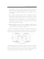
When an FFT processor is presented with a digital representation of a time-domain
signal (i.e. of a voltage varying with time), it has the effect of analyzing the spectrum of the
signal and it outputs numerous baseband signals, each corresponding to a particular range
of input frequencies. Each baseband signal represents the amplitude and phase of whatever
component of the signal is present in that particular frequency range. Thus, the function of
the FFT can also be visualized as that of a bank of band-pass filters, followed by frequency
down-converters. The effective filter bandwidths are contiguous and are each equal to the
reciprocal of the duration of the processing time-window. The centre frequencies of the
pass-bands are integer multiples of this reciprocal. The frequency response of each filter
has a sin f/f shape, where f represents the relative frequency with appropriate scaling. By
making the window 1 ms long, each bandwidth becomes 1 kHz and the centre-frequencies
fall on a regular 1 kHz comb. The frequency response of each filter exhibits nulls at ±1
kHz, ± 2 kHz, etc., and this accounts for the cancellation of inter-carrier interference noted
earlier.
Therefore, it should be clear that the absolute frequencies of the carriers presented
to the FFT processor, and their frequency separation, are intimately related to the symbol
duration, and that any divergence from this relationship will cause some loss of orthogonality
(i.e. crosstalk between carriers).
All of these features apply equally, but in a reversed sense, to the inverse FFT used in the
transmitter. The absolute carrier frequencies and their separation are automatically related
to the reciprocal of the symbol duration. Of course,it is possible to specify the spectrum
of the OFDM signal such that certain carriers are suppressed (i.e. their amplitudes are set
to zero), and this is done for the remainder of the 2048 frequency samples beyond the 1536
that are used for the DAB signal. The spectrum could also be configured such that every
22
1.6. Fast Fourier Transform (FFT)
other carrier was suppressed, so the relationship between the frequency separation and the
reciprocal of the symbol duration need not be 1:1, it could be 2:1 or some other integer
ratio. However, a 1:1 relationship provides the greatest possible packing density consistent
with the facility for independent demodulation and makes the greatest use of the available
processing power [6] .
1.6
Fast Fourier Transform (FFT)
Please, for a better understanding of this section, refer to the appendix in which a mathematical view of the Fourier Transform is given.
1.6.1
Overview
In developing DAB to combat multipath propagation, attention has been paid to the effects
of radio propagation in both the time domain and the frequency domain. As noted in the
first chapter these two domains provide different viewpoints for the same effects. Equally,
when generating or receiving a signal, certain aspects of the processing can be carried out
more easily in one or other of the domains. This is particularly true in the case of DAB,
where the multiple-carrier RF signal is more easily synthesized and analyzed in the frequency
domain, but the symbol-by-symbol modulation is more easily treated in the time domain.
Indeed, if a DAB signal is displayed on an oscilloscope, it appears similar to band-limited
white noise punctuated by the null symbols (every 96 ms in Mode 1), which gives little clue
to the existence of multiple discrete carriers.
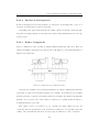
Successive stages of a DAB transmitter, or receiver, operate on constituents of the DAB
signal in both of these domains. In the channel encoder, the spectrum of the signal is
constructed essentially as an array of numbers, each representing the instantaneous amplitude and phase of one of the QPSK carriers. From this frequency-domain spectrum, the
equivalent time-domain signal is produced, which can be up-converted to the final frequency
and transmitted. The changes of modulation states from symbol to symbol are effected by
changing the numbers input to the array. In the receiver, from the incoming time-domain
23
1.6. Fast Fourier Transform (FFT)
signal, the spectrum is re-constructed as an array of numbers representing the individual
modulated carriers, from which their modulation states can be determined.
The link between the time and frequency domains is process of transformation. Bearing
in mind the number of carriers, 1536 in Mode 1, it would be out of the question to perform
this process in a domestic receiver using analogue circuitry (e.g. banks of oscillators and
filters).
The solution is to implement the transformation digitally, and there are several possible
approaches, of which one of the most rapid is the FFT algorithm. The treatment in the
section 1.5, in practical terms, show how the discrete Fourier transform (DFT) can be
developed from a block diagram of the OFDM decomposition process [6] .
1.6.2
Digital Implementation
It is important to impose time limits in order to limit the extent of the summation. In
practice, the number of input samples which are available to be transformed may already
be defined (e.g. by the symbol duration, in the case of DAB), and this automatically imposes
time limits. It is convenient to think of this as the application of a ‘time window’; processing
is only carried out on those samples which appear when the window is ‘open’. This action
also imposes a limit on the range of frequency values which need to be considered in the
summation, which will be explained later.
As is often the case in sampled systems, a compromise has to be made between accuracy
and an acceptable amount of processing. Generally, the sampling frequency must be greater
than twice that of the highest frequency component in the input signal, and this, so- called,
Nyquist criterion is applicable in most cases of time-domain sampling. Frequency components above half the sampling frequency are not represented accurately and may need to
be removed from the input signal by filtering. A frequency component at exactly half the
sampling frequency can be considered to be at the Nyquist limit [6] .
1.6.3
The Discrete Fourier Transform
The result of the DFT provides a series of samples of the spectrum, for negative and
positive frequencies. The time-domain sampling of the input signal gives rise to repetitions
24
1.6. Fast Fourier Transform (FFT)
of this two-sided spectrum at higher frequencies, centered on multiples of the sampling
frequency (i.e. the spectrum is periodic in terms of frequency). If the sampling frequency is
sufficiently great, these can be removed by filtering. Insufficient sampling frequency gives
rise to overlapping spectra, so-called ‘aliasing’, which cannot easily be removed. A spectral
component at the Nyquist limit must, by definition, contain an unwanted alias.
If the Nyquist criterion is just satisfied in the time-domain sampling, then the resulting
sampled spectrum cannot contain useful information at frequencies above half the timesampling frequency. If the time-sampling frequency is fs and the time-window duration is
T, then the number of samples processed N = T fs . The interval between the frequencydomain samples is 1/T and the useful range lies between ±fs /2, so the number of useful
samples is ±(fs /2)/(1/T ) = ±N/2; that is, N/2 samples at positive frequencies and N/2
at negative frequencies. Thus, the total number of useful samples in the result is equal to
the number of samples input. With N time-domain and N frequency-domain samples, a
total of N 2 coefficients are needed in the summation.
The frequency-domain sampling of the result has a similar, although reciprocal, effect
in the time domain; that is, the result of the DFT applies to the time-windowed input
signal as if it were periodic with a period equal to the time-window duration. If the input
signal really is periodic (i.e. it is composed of the same ‘waveform’ during consecutive and
contiguous time windows), the results of consecutive DFT calculations will be the same. If
it is not, subsequent DFT calculations will yield different results [6] .
1.6.4
Computation of the DFT
If a computer program was set up to implement a 16-sample DFT, it would take as its
input 16 complex numbers representing consecutive samples of the time-domain signal to
be transformed. For each sample in turn, the program would perform the complex multiplication of that sample and the appropriate coefficient for the first output frequency; the
results would be added together and stored. This would then be repeated for the remaining
15 output frequencies, giving the result: 16 stored complex numbers representing samples
of the spectrum at different frequencies. It is important to note that each output sample
has contributions from every one of the input samples.
25
1.6. Fast Fourier Transform (FFT)
This would require 162 (i.e. 256) multiplication operations and 16 additions. Multiplications are more time-consuming operations for a computer, and generally the relationship
between the number of multiplications and the number of input or output samples is a
square law. This can lead to excessive computing time for large numbers of samples, which
is a fundamental shortcoming of the DFT when implemented on a computer. However, there
is a significant amount of redundancy in this ‘long-hand’ computation, and algorithms have
been developed to exploit this. Notwithstanding this, in some cases, multiplication speed is
less of a problem than other processes, such as memory access, and specialized integrated
circuits are available which are designed to implement DFTs.
It was noted earlier that the inverse Fourier transform uses an integral which is very
similar to that of the (forward) Fourier transform, so it follows that the inverse DFT uses a
summation which is very similar to that of the (forward) DFT. Also, if the input frequencydomain array, remains static for consecutive inverse DFT calculations, the time-domain
result will be periodic over consecutive time windows. If the window duration is equal
to, or an integer multiple of, the period of this result, then the result will be a sampled
waveform free from discontinuities (i.e. glitches). For example, with a 1 ms window, sinusoidal waves at 1 kHz and harmonics (within the Nyquist limit) can be portrayed without
discontinuities [6] .
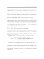
1.6.5
The Fast Fourier Transform
The FFT is a particularly efficient algorithm for implementing the DFT. It increases the
speed of processing by cutting down the number of multiplications from n2 to (n/2)log2 (n),
where n is the number of input or output samples, in cases where n is a power of 2. Thus,
representing a 1536-carrier DAB signal by means of 2048 samples, an FFT would require
11264 multiplications, whereas a DFT would require more than 4 million. The number
log2 (n) has a value of 11 for DAB, and can be called the index of the FFT (i.e. 211 = 2048).
The FFT can be derived from the DFT by expressing the summation using matrix
arithmetic. All of the computations relating the values of the output samples to the input
samples can be expressed in a two-dimensional matrix. Individual elements of this matrix
can be broken down into consecutive stages of simpler arithmetic; that is, they can be
26
1.6. Fast Fourier Transform (FFT)
factorized, just as x2 + 3x + 2 can be factorized into (x + 1)(x + 2). The matrix, as a whole,
can be factorized into a number of matrices containing simpler expressions, and when this
process is taken as far as possible, the number of factored matrices is equal to the index.
This factorization process, sometimes referred to as ‘decimation’, introduces several
simplifications; some expressions always return zeros or ones, so they need not be calculated,
and some others have counterparts in the same matrix which yield the same result but with
the opposite sign. The overall benefit is the reduction in the number of multiplications
required. There are different approaches to decimation which yield the same overall result
but with greater internal complexity towards either the time-domain or frequency-domain
end of the chain of matrices; these are known as ‘decimation in time’ and ‘decimation in
frequency’, respectively. ‘FFT’ is really a generic name for this type of algorithm and
there are many variants, the main differences being in the paths taken through the factored
matrices.
The FFT algorithm is commonly based on a radix of 2; that is, the numbers of input
and output samples are equal to 2 raised to some power. A larger radix (e.g. 4, 8, etc.) is
sometimes used for very large arrays of samples. In the simplest form of FFT, the frequencydomain samples appearing in its output array cover the same frequency range as the ‘parent’
DFT, but their arrangement is rather different. It was noted earlier that the useful samples
output by a DFT cover the range ±fs /2, and it was implied that they are symmetrically
disposed about 0 Hz. However, it was also noted that the spectrum is repeated, centered
about harmonics of fs , so the negative-frequency samples re-appear between fs /2 and fs ;
the sample at exactly fs is a replica of the sample at 0 Hz. By convention, it is the range
0 Hz to one sample below fs which is represented in the output array of the FFT.
The inverse FFT can be derived from the inverse DFT in a similar way, and these
comments apply equally to its input array of frequency-domain samples [6] .
1.6.6
Applications to DAB
The DAB system uses 1536 carriers in Mode 1. This requires a 2048-sample inverse FFT
in the transmitter and a 2048-sample FFT in the receiver.
The way that an FFT is implemented in hardware depends on the required balance of
27
1.6. Fast Fourier Transform (FFT)
speed versus hardware complexity. Clearly, parallel processing should yield the greatest
speed, whilst using several processes consecutively should reduce the amount of arithmetic
hardware, although it may increase the requirement for temporary storage. For DAB, there
are options which are more economical of hardware than using 2048 arithmetic devices in
parallel, and more economical of processing speed than using one arithmetic device for all
computations.
In the DAB channel encoder, the array of complex numbers representing the spectrum
of the signal during each 1 ms symbol is applied to the inverse FFT which produces samples
of the time-domain signal, for that symbol. These can be converted to analogue form, upconverted and transmitted. In this case, full parallel processing is not necessary because the
time-domain samples need to be output consecutively, and not simultaneously, although all
of the frequency-domain samples must be available for each computation.
In the DAB receiver, the frequency-domain spectrum is derived from the incoming timedomain signal, symbol by symbol, using the forward FFT. However, this signal appears via
an ADC as a series of consecutive samples, so a mirror-image of this approach can be used.
This will produce the spectrum for each symbol when all of the samples have been received,
but computations can start when only a small number of time-domain samples are available;
two, for example.
It might seem wasteful to have to use 2048 samples to represent the 1536 carriers, apparently wasting 512, but these can be put to good use by purposely setting their amplitudes
to zero. This can be used in the encoder and the receiver to simulate a band-pass filter
with an amplitude frequency response much steeper at the band edges than can be achieved
using an analogue filter [6] .
1.6.7
Complex Numbers
The Fourier transform operates with complex numbers in both domains, and this applies
to the DFT and FFT derived from it, and their inverses. Whilst it is usually necessary to
consider components of a spectrum as complex, having amplitudes and phases, the waveform
of a radio signal is purely real; simply the variation of a voltage with the passage of time.
This is not to say that such a waveform could not be specified using complex quantities,
28
1.6. Fast Fourier Transform (FFT)
only that division of its specification into real and imaginary parts would require that they
be combined in some way before the final waveform could be generated.
Essentially, the input and output arrays of the FFT can be divided into real and imaginary parts. When complex numbers are represented, each real sample has an imaginary
sample associated with it. Conventionally in this field of engineering, the real and imaginary parts of the time-domain array (i.e. the input array of an FFT, or the output array
of an inverse FFT) are referred to as the ‘I’ and ‘Q’ ports, for ‘In-phase’ and ‘Quadrature’,
respectively [6] .
1.6.8
Negative Frequencies
It was noted earlier that, up to the Nyquist limit, the DFT and the FFT produce as
many output samples as are input, but in each case, half of the frequency-domain samples
represent negative frequencies. Real radio signals are usually thought of as using only
positive frequencies, but the mathematically rigorous definitions of their spectra should
include components at negative, as well as positive, frequencies. All of the transforms being
discussed require these full definitions.
For example, the spectrum of a cosine wave with frequency f contains two positive
impulse functions (i.e. lines in the spectrum) at plus and minus f , each multiplied by
half the amplitude of the wave. Of course, by trigonometry cos(−x) = cos(x), so this is
no different from the simplified view of a single positive impulse function at plus f , having
both halves of the amplitude. In this simplified view, the negative frequencies are effectively
‘folded’ about 0 Hz, over into the positive frequency range. The spectrum is slightly more
complicated for a sine wave of frequency f , because sin(−x) = −sin(x); the two impulse
functions at ±f are each multiplied by half the amplitude but with opposite signs, the
positive-frequency one having negative sign.
When such spectra are calculated using the FFT or DFT, where the input waveform
is expressed as a purely real function of time (i.e. it is presented to the I port, and zero
is presented to the Q port), the transform of the cosine wave is purely real whilst that
of the sine wave is purely imaginary. This might be expected in view of the orthogonal
relationships of cosine and sine waves, or real and imaginary numbers. It can be shown that
29
1.6. Fast Fourier Transform (FFT)
if a sine wave is expressed as a purely imaginary function (i.e. it is presented to the Q port,
and zero is presented to the I port), the resulting transform is purely real.
It follows that for an inverse FFT to output a single sine or cosine wave, it must be
presented with frequency-domain data for the negative-frequency component as well as
for its positive-frequency counterpart, and the relationship between these data and their
real/imaginary status must follow certain rules [6] .
1.6.9
Linearity of the transforms
At first sight, this would appear to imply that an N-sample FFT could only provide N/2
useful frequency-domain samples, so the 1536 carriers used by the DAB system would require
the use of a 4096-sample FFT, and inverse. However, there is a simple way to halve this
requirement by exploiting a useful property of the FFT and its forebears, that of linearity.
If two time-domain waveforms are added and the sum is transformed, the result is the
sum of the two corresponding spectra. By reversing the sign of one of the input waveforms,
the result is the difference between the two spectra. This property also applies, in reverse,
to the inverse transforms.
Therefore, if a real cosine wave and an imaginary sine wave, of equal amplitudes and
the same frequency f, are (complex) added and applied to an FFT, the result is one positive
impulse function at minus f , at the real output port, multiplied by the amplitude of either
wave; the positive-frequency component is cancelled. Since the two input waves are purely
real and imaginary, respectively, the complex addition consists of no more than applying
them simultaneously to the appropriate I and Q input ports. If the sign of the imaginary
sine wave is reversed, the result is one positive-real impulse function at plus f , and the
negative-frequency component is cancelled.
Combinations of two sine waves, or two cosine waves, do not cause cancellation of the
second impulse function. An FFT would output a single impulse function as one sample,
amongst many, having a non-zero value.
By the reverse argument, if a single positive-frequency sample is applied to the real input
port of an inverse FFT, with a positive value, the time-domain result is a cosine wave at
the I output port and a negative sine wave at the Q output port. The amplitudes of these
30
1.6. Fast Fourier Transform (FFT)
sampled time waveforms are equal and are proportional to the input sample value, and their
frequencies correspond to the position of the sample in the input array. With a negativevalue input sample, the result is a negative-real cosine wave and a positive-imaginary sine
wave. These, and other permutations can be derived from the above table by reading right
to left.
Thus, it is possible to use the negative-frequency samples of an inverse FFT, independently of their positive-frequency counterparts, to produce combinations of sine and cosine
waves. What is then needed is a method for combining the sampled waves appearing at the
I and Q output ports to produce the required single output signal, and this can be achieved
using a quadrature modulation system [6] .
1.6.10
Combination of I and Q
The I and Q data are applied separately to a pair of DACs (or one, with time multiplexing)
to produce a pair of sampled baseband signals, which are then applied to low-pass filters to
construct analogue signals (i.e. to remove the artifacts of sampling). Note that these filters
are not used to implement matched filtering (e.g. cosine roll-off), as is used in some other
digital modulation systems; that function is effectively carried out by the inverse FFT and
the FFT in the receiver.
The filtered baseband signals are applied to a pair of mixers (i.e. multipliers), which
are also fed with synchronous local-oscillator signals having 90 degrees (i.e. π/2) phase
difference; that is, cosine and sine waves. The local-oscillator frequency is equal to the
desired centre-frequency of the final signal. The outputs of the two mixers are then added
to give the final signal which, after band-pass filtering to remove harmonics and other
imperfections, can be transmitted. This quadrature modulation system is illustrated in Fig
1.18.
Taking, again, the example of a single positive-frequency sample applied to the real input
port of the inverse FFT, with a positive value, the baseband cosine wave in the I channel is
multiplied by the cosine local-oscillator signal and the baseband negative sine wave in the Q
channel is multiplied by the sine local-oscillator signal. Each multiplication produces sum
and difference-frequency cosine components (i.e. double-sideband suppressed-carrier AM),
31
1.6. Fast Fourier Transform (FFT)
Figure 1.18: the quadrature modulation system
but in this case the difference-frequency components cancel when the mixer outputs are
added. Thus, the final signal contains a single cosine wave at the local-oscillator frequency
plus the baseband frequency.
In the channel encoder protocol, a 2048-sample inverse FFT is, indeed, used to produce
the 1536-carrier Mode 1 signal. The computations are processed with a time- window
duration of 1 ms, the symbol duration. Therefore, the frequency-domain sampling has
an interval of 1 kHz, so adjacent input samples correspond to sinusoidal output waves
separated by 1 kHz. Assuming conventional ordering of the input array, the first 1024
samples represent positive frequencies, from 0 Hz to 1023 kHz in the baseband signals.
The 1024th sample represents ±1024 kHz, which is at the Nyquist limit and is probably
unusable. The remaining samples represent negative frequencies, from -1023 kHz to -1 kHz.
Of these, active data are applied to the 1536 surrounding 0 Hz; that is, those representing
1 kHz to 768 kHz and -1 kHz to -768 kHz, and static zeros are applied to the remainder.
The inverse FFT then produces 2048 time-domain samples which are output to the DACs
within 1 ms. Following up-conversion by the quadrature modulation system, carriers appear
at frequencies from f0 − 768 kHz to f0 + 768 kHz.
The input data are changed from symbol to symbol giving the effect of QPSK modulated
carriers. Of course, discontinuities occur when the signal is re-configured abruptly at the
symbol boundaries, and this changes the fine detail of the spectrum. If the modulation data
32
1.6. Fast Fourier Transform (FFT)
are random, then over many symbols the power spectrum of each modulated carrier takes
on a (sin f/f)2 distribution, as described in the main text.
In this approach, the sample which represents 0 Hz in the baseband signals is not used.
If data were input to this sample, the corresponding I and Q output signals would be static
(DC) voltages, and if the mixers in the quadrature modulation system could handle such
signals, the output signal would be a wave at the local-oscillator frequency. However, the
accuracy with which the phase of this wave could be controlled could be compromised by
drifts in the DACs, and the mixers themselves, so this ‘zero carrier’ is not used to carry
modulation.
The mirror image of this approach is used in the experimental DAB receivers, where
the incoming signal is converted to an IF and band-pass filtered, and then applied to a
similar quadrature modulation system. In this case, the local-oscillator frequency is the
centre-frequency of the IF band and, of course, ADCs are substituted for the DACs.
What has been described is the approach that has been taken, so far, in all successive
generations of experimental DAB transmitter equipment. However, it is worth noting that
the FFT can be applied to multi-carrier signal generation and reception in other ways, some
of which do not require the quadrature modulation system. Also, it is possible to implement
a quadrature modulation system in the digital domain, rather than the analogue domain [6] .
1.6.11
Addition of the Guard Interval
It was noted earlier that if the frequency-domain data input to an inverse DFT remain
static for consecutive time windows, then the time-domain result will be periodic over the
consecutive windows, and this applies equally to the inverse FFT. In the DAB channel
encoder, the window duration is equal to the active symbol duration, 1 ms in Mode 1, and
the signals output by the transform are all sinusoidal waves at harmonics of 1 kHz, so they
are periodic over whole multiples of the active symbol duration. Therefore, consecutive
inverse FFT operations with the same input data would yield continuous waves in the
baseband signals. For example, if the data were held static for two consecutive symbols,
the waves would be continuous over 2 ms.
In the DAB receiver, in order to accomplish a single FFT operation, it would not matter
33
1.7. Finite Impulse Response Filters(FIR)
at what instant the time-window began as long as the input waves were continuous over
1 ms. A time displacement would only change the apparent phase of each of the waves,
which would alter the absolute values of the data output by the FFT, but since the phase
modulation is coded differentially, a slow change would not corrupt the decoded data. Thus,
this example of an ‘oversized’ guard interval would permit time-agility in the receiver and
the simultaneous reception of delayed signals as long as the limit of temporal coherence was
not exceeded (i.e. the maximum vehicle speed would be limited further in this case).
Of course, there is no need to repeat the inverse FFT operation when the output samples
can simply be stored, and read out to the DACs directly after the active symbol. Also, as
noted in the main text, the DAB system actually uses the more-economical compromise of
a 246 µs guard interval, so only about one quarter of the output samples need to be stored.
According to available information, the samples making up the guard-interval appear to be
applied to the DACs before each active symbol, so they are repetitions of the last quarter
of those produced during the active symbol. This alternative arrangement does not imply
additional storage, merely a re-ordering of the inverse FFT; either method is equally valid [6] .
1.7
Finite Impulse Response Filters(FIR)
These filters deserve attention since they are used several times during the implementation
of the demodulator.
In signal processing, there are many instances in which an input signal to a system
contains extra unnecessary content or additional noise which can degrade the quality of the
desired portion. In such cases we may remove or filter out the useless samples.
1.7.1
How to characterize digital FIR filters
There are a few terms used to describe the behavior and performance of FIR filter including
the following:
• Filter Coefficients : The set of constants, also called tap weights, used to multiply
against delayed sample values. For an FIR filter, the filter coefficients are, by definition, the impulse response of the filter.
34
1.7. Finite Impulse Response Filters(FIR)
• Impulse Response : A filter’s time domain output sequence when the input is an
impulse. An impulse is a single unity-valued sample followed and preceded by zerovalued samples. For an FIR filter the impulse response of a FIR filter is the set of
filter coefficients.
• Tap : The number of FIR taps, typically N, tells us a couple things about the filter.
Most importantly it tells us the amount of memory needed, the number of calculations
required, and the amount of "filtering" that it can do. Basically, the more taps in a
filter results in better stopband attenuation (less of the part we want filtered out),
less rippling (less variations in the passband), and steeper rolloff (a shorter transition
between the passband and the stopband).
• Multiply-Accumulate (MAC) : In the context of FIR Filters, a "MAC" is the operation of multiplying a coefficient by the corresponding delayed data sample and
accumulating the result. There is usually one MAC per tap.
There are a couple different basic filter responses. Each will have a unique frequency
response based on its cut-off frequency, the number of taps used, its roll off, and amount of
ripple. The various attributes describing a filter may be seen in the following diagram:
Figure 1.19: FIR filters
While high pass filters remove low frequency contents, low pass filters remove high frequency values. This kind of filters are used for synchronization and also for null symbol
detection and automatic gain control. As we have seen before, these filters could be developed in software just updating properly the values for the filter coefficients [13] .
35
1.8. Error Measures
1.8
Error Measures
Some error detection measures were implemented for testing how precise was the system,
such as BER and MER. These two measures are commonly used in digital modulation
systems.
1.8.1
Bit Error Rate
This algorithm was implemented for measuring the accuracy of Viterbi decoding. Since the
Viterbi algorithm has to recover the missing information during the transmission, it might
be useful to know whether or not this information is reliable.
In digital transmission, the bit error rate or bit error ratio (BER) is the number of
received bits that have been altered due to noise, interference and distortion, divided by
the total number of transferred bits during the studied time interval. BER is a unitless
performance measure, often expressed as a percentage number.
As an example, assume this transmitted bit sequence:
0 1 1 0 0 0 1 0 1 1,
and the following received bit sequence:
0 0 1 0 1 0 1 0 0 1,
The BER is in this case 3 incorrect bits divided by 10 transferred bits, resulting in a
BER of 0.3 or 30%.
The bit error probability ρ is the expectation value of the BER. The BER can be
considered as an approximate estimate of the bit error probability. This estimate is accurate
for a long studied time interval and a high number of bit errors.
In a communication system, the receiver side BER may be affected by transmission
channel noise, interference, distortion, bit synchronization problems, attenuation, wireless
multipath fading, etc.
The BER may be improved by choosing a strong signal strength (unless this causes
cross-talk and more bit errors), by choosing a slow and robust modulation scheme or line
coding scheme, and by applying channel coding schemes such as redundant forward error
correction codes.
36
1.8. Error Measures
The transmission BER is the number of detected bits that are incorrect before error
correction, divided by the total number of transferred bits (including redundant error codes).
The main problem of this algorithm is that the signal has to be decoded before [14] .
The implementation of this error measure algorithm was carried out in the following
way:
Figure 1.20: BER calculation
1.8.2
Modulation Error Rate
The aim of this algorithm is to check if the received data is good enough for ensure a good
reception. The modulation error ratio or MER is a measure used to quantify the performance of a digital radio transmitter or receiver in a communications system using digital
modulation. A signal sent by an ideal transmitter or received by a receiver would have all
the constellation points precisely at the ideal locations, however various imperfections in
the implementation (such as noise, low image rejection ratio, phase noise, carrier suppression, distortion, etc.) or signal path cause the actual constellation points to deviate from
the ideal locations. Transmitter MER can be measured by specialized equipment, which
demodulates the received signal in a similar way to how a real radio demodulator does it.
Demodulated and detected signal can be used as a reasonably reliable estimate for the ideal
37
1.9. Errors Detection and Correction
transmitted signal in MER calculation. It is defined in dB as:
q
M ER(dB) = 10 ∗ log10 ∗ Psignal /Perror
where Psignal is the power of ideal transmitted signal, and Perror is the RMS power of the
error vector. This value was around 29dB, and it is the typical MER figure quoted for
digital radio systems, such as DAB [? ] .
1.9
1.9.1
Errors Detection and Correction
Viterbi Decoder
In telecommunication, a convolutional code is a type of error-correcting code in which each
m-bit information symbol (each m-bit string) to be encoded is transformed into an n-bit
symbol, where m/n is the code rate (n ≥ m) and the transformation is a function of the
last k information symbols, where k is the constraint length of the code.
Convolutional codes are used extensively in numerous applications in order to achieve
reliable data transfer, including digital video, radio, mobile communication, and satellite
communication.
To convolutionally encode data, start with k memory registers, each holding 1 input
bit. Unless otherwise specified, all memory registers start with a value of 0. The encoder
has n modulo-2 adders and n generator polynomials - one for each adder (see figure 1.21
below). An input bit m1 is fed into the leftmost register. Using the generator polynomials
and the existing values in the remaining registers, the encoder outputs n bits. Now bit
shift all register values to the right (m1 moves to m0 , m0 moves to m−1 ) and wait for the
next input bit. If there are no remaining input bits, the encoder continues output until all
registers have returned to the zero state.
The figure 1.21 below is an example of a convolutional encoder. x(n) is the input and
G0 (n) and G1 (n) are the encoded outputs. The rate of the convolution coder is defined as
the number of input bits to output bits. This system has 1 input and 2 outputs thereby
resulting in a coding rate of 1/2. The number of states of a convolution coder is determined
38
1.9. Errors Detection and Correction
by its number of delay units. There are 2 delay units in this system and therefore, there
are 22 = 4 states. For a system with k delay units, there are 2k states.
Figure 1.21: Convolutional Decoder
The system block diagram can be expressed with the following equations.
G0 (n) = x(n) + x(n − 1) + x(n − 2)
G1 (n) = x(n) + x(n − 2)
The state diagram of this system is depicted in Figure 1.22. The states are defined as
x(n − 1), x(n − 2) pairs and the state transitions are defined as G0 (n), G1 (n)/x(n). The
states are indicative of system memory. The state transitions gives you the path and the
outputs associated with a given input. Since a state transition is associated with each
possible input, the number of state transitions depends on the number of possible inputs.
If there are m inputs, then there will be 2m state transitions. The total number of state
transitions at a point in time is the product of the number of state transitions and the
number of states, 2m+k .
The state diagram offers a complete description of the system. However, it shows only
the instantaneous transitions. It does not illustrate how the states change in time. To
include time in state transitions, a trellis diagram is used (Figure 1.23). Each node in the
trellis diagram denotes a state at a point in time. The branches connecting the nodes denote
the state transitions. Notice that the inputs are not labeled on the state transitions. They
are implied since the input, x(n) , is included in the destination states, x(n), x(n − 1) .
Another thing to note is that the state transitions are fixed by the definition of the source,
x(n − 1), x(n − 2) , and the destination states. The state transitions are independent of the
39
1.9. Errors Detection and Correction
Figure 1.22: State Diagram
Figure 1.23: Trellis diagram
system equations. This a consequence of including the input, x(n) , in the state definition.
In certain systems, definition of the states may be more complicated and may require special
considerations. Explanation of such systems (such as the radix 4 trellis) is outside the scope
of this example.
There are two trellis diagrams shown in Figure 1.23. They differ only in the way the
destination states are ordered. The purpose for reordering is to obtain higher computational
efficiency. The reordered trellis is partitioned into groups of states and state transitions
that are isolated from other such groups. This allows realizable, specialized hardware to
be designed that is dedicated to compute parameters associated with the particular group.
The structure of the groups shown in Figure 1.23 is called the “butterfly” due to the physical
resemblance. It is also referred to as the radix-2 trellis structure since each group contains
2 source and 2 destination states. Note, again, that the structure of the reordered trellis
is fixed depending on how the states are defined. Not all trellis diagrams can be reordered
40
1.9. Errors Detection and Correction
into butterflies. Fortunately, a number of commonly used convolution coders have this nice
property.
An important feature of this convolution code is that in each butterfly, there are only two
(out of four possible) distinct outputs: 00 and 11; or 01 and 10. Notice that the hamming
distance of each output pairs is 2. This feature is available to a very small subset of all
possible convolution codes. The usefulness of the this feature will be apparent later on when
Viterbi decoding is described.
Figure 1.24 illustrates the entire process of encoding an input pattern to quantizing
the received signal to decoding the quantized signal. The sample input pattern used is
1011010100. For the purpose of this example, this input pattern is sufficiently long. In
practice, for proper error correction, the input pattern need to be longer than approximately
10 times the number of delay units plus 1, i.e. length of input pattern = 10(k + 1) . (k +
1) is often referred to as the constraint length. For this example, k = 2 which implies 30
input symbols need to be received before decoding to improve the bit error rate.
The first trellis diagram in Figure 1.24 illustrates the state transitions associated with
each input. This trellis diagram is used here to illustrate how the decoder operates. Use
Figure 1.23 to verify the state transitions and the encoder outputs. The encoder outputs
do not have to be generated using the trellis diagram. They can be generated using the
system equations directly.
The encoded outputs are transmitted as signed antipodal analog signals (i.e. 0 is transmitted with a positive voltage and 1 is transmitted with a negative voltage). They are
received at the decoder and quantized with a 3-bit quantizer. The quantized number is
represented in 2’s complement giving it a range of -4 to 3. Soft decision offers better performance results since it provides a better estimate of the noise (i.e. less quantization noise
is introduced). In most circumstances, the noise is strong enough just to tip the signal over
the decision boundary. If hard decision is used, a significant amount of quantization noise
will be introduced. The quantized soft decision values are used to calculate the parameters
for the Viterbi decoder.
Up to this point, no Viterbi decoding has been performed. Viterbi decoding begins after
a certain number of encoded symbols have been received. This length, again, is usually
41
1.9. Errors Detection and Correction
Figure 1.24: Trellis diagram states
42
1.9. Errors Detection and Correction
longer than 10(k + 1) and is application dependent. In this example, 20 encoded symbols
are received before being decoded. In some applications, Viterbi decoding is operated on a
frame of received symbols and is independent of the neighboring frames. Is is also possible
to perform Viterbi decoding on a sliding window in which a block of decoded bits at the
beginning of the window is error free, and the windows will have to overlap. With frame
by frame decoding, a number of trailing zeros equalling to the number of states is added.
This forces the last state of the frame to be zero providing a starting point for traceback.
With sliding window decoding, the starting point for traceback is the state with the optimal
accumulated metric. This starting state may be erroneous. However, the traceback path
will converge to the correct states before reaching the block of error free bits.
Viterbi decoding can be broken down into two major operations, metric update and
traceback. In metric update, two things are done in every symbol interval (1 symbol = 1
input bit = 2 encoded bits): the accumulated (state) metric is calculated for each state and
the optimal incoming path associated with each state is determined. Traceback uses this
information to derive an optimal path through the trellis. Referring to the second trellis in
Figure 1.24, notice that a state at any time instance has exactly one incoming path but the
number of outgoing paths may vary. This results in a unique path tracing backward.
What are state metrics and how are the optimal incoming paths determined? To understand the metrics used in Viterbi decoding, consider the received encoded bit pairs,
(G0(n), G1(n)). Suppose 11 is transmitted, we would expect 11 to be received with a soft
decision pair of (-4,-4). However, channel noise may corrupt the transmitted signal such
that the soft decision pair may be (-0.4,-3.3) resulting in a quantized value of (0,-3) (see
Figure 1.25). Without knowing anything about the encoded bit stream, the detector would
decide that (3,-4) or 01 is transmitted which results in a bit error.
The Viterbi algorithm, on the other hand, exploits the structure of the convolution code
and makes its decision based on previously received data (i.e. this is kept track of using the
“states” ). Referring back to Figure 1.23, observe that an encoded bit pair is associated with
only 2 possible originating states, x(n − 1), x(n − 2) . For example, if 11 is transmitted, then
the originating state must be either state 00 or state 01 (see Figure 1.23). Suppose that the
original state is known to be 00, then it would be impossible for the detected encoded bit
43
1.9. Errors Detection and Correction
Figure 1.25: Decision boundaries.
pairs to be 01. The Viterbi decoder would then have to decide between the two possible
encoded bit pairs, 00 or 11. This decision depends on how far away the received bit pairs
are from the two possible transmitted bit pairs (Figure 1.26). The metric used to measure
this is the Euclidean distance. It is also referred to as the local distance calculation.
local distance(n, i) =
X
[Sj (n) − Gj (n)]2 , j ∈ encoded bits associated with a given input
j
where n denotes the time instance and i denotes the path calculated for. The above
equation can be further simplified by observing the expansion:
local distance(n, i) =
X
[Sj2 (n) − 2Sj (n)Gj (n) + G2j (j)]
j
and noting that Sj2 (n) and G2j (n) are constants in a given symbol period. These terms
can be ignored since we are concerned with finding the minimum local distance path. The
following measure will suffice for determining the local distance: Note that the -2 is taken
out which implies
local distance1 (n, i) =
X
[Sj (n) − Gj (n)]
j
that instead of finding the path with the minimum local distance, we would look for the
path with the maximum local distance1 (n, i) .
Going back to Figure 1.24, the branch metrics can now be calculated using the above
44
1.9. Errors Detection and Correction
Figure 1.26: Decision boundaries for different states.
local distance equation. As an example, the branch metrics for time 0 and 1 is calculated
here. The received quantized soft decision pair is (-3,-4). The branch metric corresponding
to (G0 (n), G1 (n)) = (0, 0) is equal to −3(1) − 4(1) = −7. For (G0 (n), G1(n)) = (0, 1), it
is −3(1) − 4(−1) = 1. For (G0 (n), G1 (n) = (1, 0) , it is −3(−1) − 4(1) = −1. And for
(G0 (n), G1 (n)) = (1, 1), it is −3(−1) − 4(−1) = 7. Notice that the Gj (n)’s used in the
local distance calculation are +1 and -1, rather than +3 and -4 respectively. There are
three reasons. First, using unities makes computation very simple. The branch metrics
can be calculated by adding and subtracting the soft decision values. Second, 3 and -4 can
be scaled to approximately 1 and -1 respectively. As mentioned in the derivation of local
distance 1 , constant scaling can be ignored in determining the maxima and the minima.
Finally, note that there are only two unique metric magnitudes, 1 and 7. Therefore, to
compute the branch metric, you only need to do 1 add, 1 subtract, and 2 negation.
Once the branch metrics are calculated, the state metrics and the best incoming paths
for each destination states can be determined. The state metrics at time 0 are initialized
to 0 except for state 00, which takes on the value of 100. This value is arbitrarily chosen
and is large enough so that the other initial states cannot contribute to the best path. This
basically forces the traceback to converge on state 00 at time 0.
The state metrics are updated in two steps. First, for each of the two incoming paths,
the corresponding branch metric is added to the state metric of the originating state. The
two sums are compared and the larger one is stored as the new state metric and the cor-
45
1.9. Errors Detection and Correction
responding path is stored as the best path. Take state 10 at time instance 2 for example
Figure 1.24. The two paths coming in to this state originates from states 00 and 01 figure
1.23 Looking at the second trellis, we see that state 00 has a value of 93 and state 01 has
a value of 1. The branch metric of the top path (connecting state 00 at time 1 and state
10 at time 2) is 1. The branch metric of the bottom path (between states 01 and 10) is -1.
The top path gives a sum of 93 + 1 = 94 and the bottom path give a sum of 1 + (-1) =
0. As a result, 94 is stored as the state metric for state 10 at time 2 and the top path is
stored as the best path in the transition buffer.
The transition buffer stores the best incoming path for each state. For a radix 2 trellis,
only 1 bit is needed to indicate the chosen path. A value of 0 indicates that the top incoming
path of the given state is chosen as the best path whereas a value of 1 indicates that the
bottom path is chosen. The transition bits for our example is illustrated in Figure 1.24 in
the third trellis.
Traceback begins after completing the metric update of the last symbol in the frame.
For frame by frame Viterbi decoding, all that is needed by the traceback algorithm are the
state transitions. The starting state is state 00. For sliding window decoding, the starting
state is the state with the largest state metric. In our example, the starting state for both
types of decoding is 00 since it has the largest state metric, 158. Looking at the state
transition for state 00, we see that the bottom path is optimal (state transition = 1 implies
bottom path). Two things now happen. First, the transition bit, 1, is sent to the decoder
output. Second, the originating state, state 01, of this optimal path is determined. This
process is repeated until time 2, which corresponds to the first input bit transmitted.
The decoded output is shown in Figure 1.24 in the last row. Notice that the order with
which the decoded output is generated is reversed, i.e. decoded output = 10101101 whereas
the sample input pattern is 10110101. Additional code need to be added to reverse the
ordering of the decoded output to exactly reconstruct the sample input [11] .
1.9.2
De-puncturing
The addition of redundancy to the signal increments the data bandwidth in a 400%. To
palliate this effect some bits of the outgoing signal are removed. Puncturing is the process
46
1.10. Digital Signals Processors (DSP)
of removing some of the parity bits after encoding with an error correction-code. This
has the same effect as encoding with an error-correction code with a higher rate, or less
redundancy. However, with puncturing the same decoder can be used regardless of how
many bits have been punctured, thus puncturing considerably increases the flexibility of
the system without significantly increasing its complexity. In DAB, a pre-defined pattern
of puncturing is used in the encoder. The inverse operation, known as depuncturing, is
implemented by the decoder [10] .
If the code-word which results from puncturing is identical to that produced by a dedicated non-punctured encoder of the same rate, there is no loss of error correction performance. However, if a large range of different rates are required in practice, puncturing can
cause a slight loss of performance relative to a non-punctured code of the same rate; this
depends on the choice of generator polynomials and which bits are punctured.
1.10
Digital Signals Processors (DSP)
Traditionally, during the analog era, the common way to design a radio receptor was to
design a very specific circuit with analog electronic components like operational amplifiers,
resistances, capacitances, inductances, and so on. Everything was done in hardware. Due
to advances in both computer and semiconductor technology, today we can replace that
old-fashioned complicated circuitry by an embedded computer which is much cheaper and
more reliable. The aim of these computers is to achieve the required performance while
maintaining costs at a minimum price. Often, as in the case of this project, the energy
consumption and heat dissipation must be taken into account very carefully, since the final
demodulator will work with batteries and typically, no fan is available on a portable device.
In the context of telecommunications, these embedded processor are used to operate on
digital signals, hence the acronym of DSP (Digital Signal Processors). Typically, algorithms
for signal processing share a lot of features among them, and a specific algorithm will be
used massively during the demodulation process. For example, for sure any algorithm for
audio or video processing will perform the Fast Fourier Transform (FFT) on the input signal. Another common algorithm is the Viterbi decoder for the detection and correction of
47
1.10. Digital Signals Processors (DSP)
errors. Another typical requirement for a DSP is that it cannot spend more than a certain
amount of time to manipulate the input signal, that is, they must run in real time. As we
shall see more deeply below, in DAB, the broadcaster transmits an audio frame each 96ms,
therefore our DSP must be capable of processing the signal (that is, extract the audio) in
less than this time. Otherwise, part of the audio will be missed. For this reason, a DSP has
specialized hardware not available in a general purpose computer to perform such common
tasks. All these constraints is what makes Digital Signal Processing a very motivating and
interesting field of study. Figure 1.27 illustrates the abstract architecture used for any digital signal application [12] .
Figure 1.27: Electromagnetic signal to audio.
48
Chapter 2
CoolFlux BSP Architecture
2.1
Overview
The CoolFlux BSP is a general-purpose high precision, ultra low power, low cost dual
Harvard, dual MAC BSP that has extensive support for fractional arithmetic as well as
highly efficient support for the data types and operations encountered within ANSI C.
In addition, CoolFlux BSP supports complex arithmetic, sub-word parallelism and larger
addressing space.
The CoolFlux BSP is capable of sustaining two MACs, two memory operations and two
pointer updates per cycle, making it highly cycle- efficient for computationally intensive
applications. Many of the arithmetic operations – such as the multiplication, additions,
division etc - can be done in scalar mode or in packed mode. Packed mode can either be
a complex operation or an SIMD operation. This makes it possible for instance to do four
12-bit multiplications in parallel.
The CoolFlux BSP architecture is a load/store architecture, that is:
• All memory operands have to be explicitly moved to the registers.
• All execution units take their input values from registers and write their results back
into a register.
• All results produced in the registers have to be explicitly moved to memory.
49
2.2. Registers
Because of its Instruction Set Architecture design the CoolFlux BSP is also highly
efficient at supporting control code as well, making it very well balanced for complete
embedded applications in which 20/80 (80% of the time is spent for 20% of instructions)
code mix is typical. When designing the CoolFlux BSP at the level of its micro-architecture,
much attention has been paid to efficiently support the operations needed by ANSI C,
making the CoolFlux BSP an excellent compiler target whilst maintaining very low power
consumption [18] .
2.2
Registers
The CoolFlux BSP is a load/store architecture, making registers important. All execution
units take their inputs from registers and write their results back to registers. Memory
accesses are considered to be operations. A store operation takes the data from a register
and writes it to memory, while a load operation reads a value from memory and stores it
in a register.
The registers of the CoolFlux BSP are organized in register files. All registers in a
register file have the same name but a different index. Operations work on individual
registers, but in their syntax description register file names are used. The reason is that all
registers in a register file can be used equally in an operation. Individual registers must be
used as source and destination registers in real operations.
The registers have different data widths. The architecture figures presented above show
the data widths of the registers. They also show how the register files are connected to the
different execution units [18] .
2.3
The Data Path
The data path consists of:
• Four register files A, B, X and Y connected to the arithmetic units
• Two multiplier units XMUL and YMUL (24x24 bits), which can be used in different
50
2.3. The Data Path
Figure 2.1: Addressing Units. Xbus and Ybus move buses,DMA and program control units
51
2.3. The Data Path
Figure 2.2: step function
52
2.3. The Data Path
ways (signed, unsigned, complex, SIMD multiplication) with a pre-add/subtract unit
before the XMUL multiplier
• Two ALU units XALU and YALU: The XALU executes single arithmetic and XMAC
operations and the YALU executes parallel arithmetic and YMAC operations
2.3.1
Multipliers
The CoolFlux BSP contains 2 multiply units, XMUL and YMUL. The both have two inputs
of 24 bits. They read their operands from the X and Y register files. The XMUL can be used
for signed/signed, unsigned/signed, unsigned/unsigned, complex and SIMD multiplications.
The YMUL supports signed/signed, complex and SIMD multiplications.
When doing a complex multiplication, the inputs are considered to contain an imaginary
part and a real part, both 12 bits. A complex multiplication does the following actions:
output_imag = input_a_real ∗ input_b_imag + input_a_imag ∗ input_b_real
output_real = input_a_real ∗ input_b_real − input_a_imag ∗ input_b_imag
It is also possible to get the following different intermediate results.
output_imag = r input_a_real ∗ input_b_imag
output_real = r input_a_real ∗ input_b_real
output_imag = input_a_imag ∗ input_b_real
output_real = −input_a_imag ∗ input_b_imag
When doing an SIMD multiplication, the inputs are considered to contain two subparts
of 12 bits each. A SIMD multiplication does the following actions:
output_SIM D0 = input_a_SIM D0 ∗ input_b_SIM D0
output_SIM D1 = input_a_SIM D1 ∗ input_b_SIM D1
The XMUL unit is preceded by a pre-adder/subtraction unit. This unit can be used in
3 modes: pass, add and subtract. For simple multiplications it is used in pass mode where
it just transfers one of its inputs to the output without doing any operation, this output
is then multiplied in the XMUL unit to another XY register. In case it is used in add (or
subtract) mode, it adds (subtracts) two XY registers and this output is then multiplied
53
2.3. The Data Path
with a third XY register. This pre-adder/subtraction unit is not used in complex or SIMD
mode.
In all cases, the result of a multiplication is a full 48-bit number. Before being used in
the ALUs it is converted to a 56-bit number. This 56-bit value is stored in a temporary
register and in the next processor cycle used as an operand for accumulation through one
of the ALU units (XALU for results of XMUL, YALU for results of YMUL).
The multipliers are always accessed via MAC operations (multiply accumulate), which
take 2 processor cycles to complete. In the first cycle the multiplication is performed on
XMUL or YMUL. In the second cycle the result is accumulated through the XALU or
YALU units. Each processor cycle a new MAC operation can be started for which the
multiplication runs in parallel with the accumulation of the previous MAC operation. This
means that n consecutive MAC operations only take n+1 processor cycles to complete [18] .
2.3.2
Arithmetic and Logic Units (XALU and YALU)
The XALU and the YALU always operate on 56-bit operands, and generate 56-bit results.
They take their inputs from the A, B, X and Y register files or from the temporary registers
at the outputs of the multipliers. All these inputs are converted to 56 bits. The result of
the XALU can be stored in the A, B, X and Y registers; the result of the YALU can be
stored in a B register. The result is converted to 24 bits when it is written to an X or Y
register.
The possible operations in scalar mode for XALU are:
• Add, subtract, (add and divide by 2), (subtract and divide by 2), reduced add, reduced
subtract
• Logic and, logic or, logic xor
• Divide step
• Min, max
• Negate, exponent, absolute value, sign extend
• Logic and arithmetic shift, reduced shift
54
2.4. Move Buses and RSS Units
• Compare operations
• Load immediate value
Additionally, some of these operations can be made conditional. The YALU supports:
add, subtract, (add and divide by 2), (subtract and divide by 2).
• In packed operation, the XALU can perform the following operations:
• Add, subtract, (add and divide by 2), (subtract and divide by 2)
• Divide step Absolute value
• Compare operation
• Logic and arithmetic shift
• Conjugate operation
• Packing operation
• Unpacking operation
• Conditional negate operation
Note that for all these operations, the result is the same, regardless of whether the
operation SIMD or a complex operation [18] .
2.4
2.4.1
Move Buses and RSS Units
Xbus and Ybus Move Buses
Moves between the registers, and also between the memories and the registers are essential
because of the load/store architecture of the CoolFlux BSP.
Two central buses are provided to move the data, in parallel with the operations in the
data path. These buses provide a connection between all registers, and between all registers
and the memories and support the move of data:
• from a source register to a destination register
55
2.4. Move Buses and RSS Units
• from a source register to a memory (store)
• from the memories to a destination register (load)
The buses support single and parallel moves. In a single move operation a single 24-bit
data item is moved in a single processor cycle. With a parallel move operation two 24-bit
data items are moved in a single processor cycle by using the two buses at the same time. In
each move the source value is converted from its data width to a 24-bit value. This 24- bit
value is transferred to the destination register, via the move buses, where it is converted to
the destination data width. The way the conversions are done, depends whether the move
is a scalar or packed move. The 24-bit buses are wide enough to make all 8-bit, 15-bit,
16-bit and 24-bit register and memory moves straightforward, but transferring from and to
a 56-bit accumulator requires special attention [18] .
2.4.2
Moving to an Accumulator
The accumulator can be the destination of a move operation in 2 ways:
The full accumulator is the destination (a0, a1, b0, b1) An accumulator sub-register is
the destination (ao0, ao1, ah0, ah1, al0, al1, bo0, bo1, bh0, bh1, bl0, bl1)
In case a sub-register is the target, its data width is either 8 or 24. So the conversion from
24 bits to the target data width is straightforward (the 8 LSBs are used, or no conversion
is needed).
The full accumulator can be the destination in 4 ways:
• a 24 bit scalar move
• a 48 bit scalar move a 24 bit packed move
• a 48 bit packed move
In a 24-bit scalar move (‘=’ assignment), the 24 bit value is converted to 56 bits by sign
extending the upper 8 bits and padding with 24 zeros at the LSB side. In a 48-bit scalar
move (‘=.l’ assignment), the Xbus and Ybus move buses are combined to move a 48-bit
value. This 48-bit value is converted to 56 bits by sign-extending it with 8 bits. A 48-bit
56
2.4. Move Buses and RSS Units
move operation is only possible between two accumulators, or from the XY- memory to one
of the accumulators.
In a 24-bit packed move (‘=.c’ assignment), the 24 bit value is split into two 12-bit subwords. When converting to 56 bits, each 12 bit sub-word is converted to a 28-bit accumulator sub-word. This is done by sign extending the upper 4 bits and padding with 12 zeros
at the LSB side. The 56-bit accumulator is then made by concatenating both sub-words.
accumulator(55 − 52) = input(23) & input(23) & input(23) & input(23)
accumulator(51 − 40) = input(23 − 12)
accumulator(39 − 28) = 0
accumulator(27 − 24) = input(11) & input(11) & input(11) & input(11)
accumulator(23 − 12) = input(11 − 0)
accumulator(11 − 0) = 0
In a 48-bit packed move (‘=.cl’ assignment), the Xbus and Ybus move buses are combined to move a 48-bit value. This 48-bit value is converted to 56 bits by sign-extending
each of the 24-bit sub-words with 4 bits. A 48-bit move operation is only possible between
two accumulators, or from the XY-memory to one of the accumulators [18] .
accumulator(55 − 52) = input(47) & input(47) & input(47) & input(47)
accumulator(51 − 28) = input(47 − 24)
accumulator(27 − 24) = input(23) & input(23) & input(23) & input(23)
accumulator(23 − 0) = input(23 − 0)
2.4.3
Moving from an Accumulator
The accumulator can be the source of a move operation in 2 ways: as a full accumulator
(a0, a1, b0, b1) through one of its sub-registers (ao0, ao1, ah0, ah1, al0, al1, bo0, bo1, bh0,
bh1, bl0, bl1)
In the case a sub-register is the source of a move operation, the data width is either
8 or 24. So the conversion to 24 bits is straightforward (sign-extension with 16 bits, or
57
2.4. Move Buses and RSS Units
no conversion). The selection of the correct sub-register (with eventual sign extension) is
performed by the select part of an RSS unit.
A full accumulator can be the source of a move operation in 4 ways:
• a 24-bit scalar move
• a 48-bit scalar move
• a 24-bit packed move
• a 48-bit packed move
In 24-bit scalar move (‘=’ assignment), the 56-bit value is converted to 24 bits through
the round and saturate part of the RSS unit and transferred to the destination register via
one of the two move buses.
In a 48-bit scalar move (‘=.l’ assignment), the Xbus and Ybus move buses are combined
to move a 48-bit value in a single processor cycle. The 56-bit source value is converted to
48 bits through the saturation logic of the RSS unit. A 48-bit scalar move operation is only
possible between two accumulators, or from one of the accumulators to the XY- memory.
In a 24-bit packed move (‘=.c’ assignment), the 56-bit value is converted to 24 bits
through the round and saturate part of the RSS unit and transferred to the destination
register via one of the two move buses. In this packed move, both 28-bit sub-words will go
through the round and saturate part of the RSS unit and become two 12-bit sub- words.
In a 48-bit packed move (‘=.cl’ assignment), the Xbus and Ybus move buses are combined
to move a 48-bit value in a single processor cycle. The 56-bit source value is converted to
48 bits through the saturation logic of the RSS unit. In this packed move, both 28-bit
sub-words will go through the saturation logic of the RSS unit and become two 24-bit subwords. A 48-bit packed move operation is only possible between two accumulators, or from
one of the accumulators to the XY-memory [18] .
2.4.4
Round, Saturate and Select Units (RSS)
The CoolFlux BSP has two round, saturate and select units (RSS), one for the A accumulators and one for the B accumulators. They convert between values held in 56- bit precision
58
2.4. Move Buses and RSS Units
in the accumulators and the precision of a particular move operation (24-bit or 48-bit) and
are used when a 56-bit accumulator is the source of a move operation (scalar or packed),
as described above. In case a sub-register is used as source, the RSS unit will select the
correct part (overflow, high, low) of the accumulator and no actual conversion is done. In
case the full accumulator is the source, its value needs to be converted from 56 bits to 24 or
48 bits which requires saturation and rounding. Both are handled by the RSS units which
can operate in different modes.
The modes for the rounding are:
• truncation, simple biased
• truncation, sign-magnitude
• rounding, simple biased
• balanced-bias rounding
The modes for the saturation are:
• saturation
• wrapping
The rounding and saturation is done on the entire word or on the two sub-words, depending on the type of move (scalar or packed). The way the rounding and saturation
works, however, is exactly the same [18] .
The mode of operation is equal for both RSS units and is controlled by setting and
clearing the sr.b, sr.r and sr.s bits in the sr status register. The assignment operator
determines which conversion (24 or 48 bit, scalar or packed) must be executed:
• = 24-bit scalar move
• =.l 48-bit scalar move
• =.c 24-bit packed move
• =.cl 48-bit packed move
59
2.5. Memories and I/O
2.5
Memories and I/O
The CoolFlux BSP is a dual Harvard architecture and has separate X and Y data memories.
Each memory has 16 Mword of 24 bits. In a single processor cycle each memory can be
accessed separately so that up to 2 data items can be read or written in a single cycle.
There is a special mode in which the X and Y memories are combined logically into a single
XY memory that stores and loads 48-bit data items.
Next to the data memories the I/O of the CoolFlux BSP is memory mapped. Also
the I/O- space has 16 Mword of 24 bits. From a software point of view, I/O behaves as a
memory to which data can be written and from which data can be read [18] .
2.5.1
Individual Data Memory (X, Y)
The CoolFlux BSP has 2 separate 16 Mword, 24 bit X and Y data memories. Typically
accesses to both memories are used in parallel for intense BSP code so as to provide sufficient
memory bandwidth for the computations being performed [18] .
2.5.2
Dual Precision Memory (XY)
There are dual precision load and store instructions, which can move a single 48-bit data
item (long) to and from the memory sub-system. For these instructions both X and Y
memories, and both Xbus and Ybus move buses are combined (used in parallel). In the
memory the corresponding locations in both X and Y memory need to be reserved since, in
this mode, both memories get the same address. This memory is referenced as XY- memory.
It uses the X addressing unit for addressing and has the same addressing possibilities as the
X-memory [18] .
2.5.3
I/O Memory Space
The I/O for the CoolFlux BSP is memory mapped. I/O-space is 16 Mwords, 24-bit wide.
The I/O memory space can be addressed as the Y-memory space, using the Y addressing
unit to generate its addresses [18] .
60
2.6. X and Y Addressing Units
2.6
X and Y Addressing Units
The X and Y addressing units generate the addresses for the memory accesses. The following
addressing modes are supported:
• direct addressing
• indirect addressing with post-modification
• indexed stack pointer addressing
Indirect addressing is supported by means of 2 pointer register files: XPTR, YPTR.
These are located in the addressing units. The XPTR register file contains 8 pointers
(xptr0 ... xptr7); the YPTR register file contains 4 pointers (yptr0 ... yptr3). When
the memories are accessed indirectly via one of these pointers, the pointer value can be
updated (post- modified) in parallel with the access. The calculations for this update are
executed on the XAGU and YAGU, the address generation units. The post-modification
operation is specified as part of the memory access. These operations use the registers in the
other register files: XSTEP, YSTEP, XMOD and YMOD. The possible post-modification
operations are:
• nop
• increment
• indexed stack pointer addressing
• decrement
• increment by 2
• decrement by 2
• add the step register
• subtract the step register
• and a special mode which is used for cyclic buffer addressing and bit-reverse addressing.
61
2.7. Program Control Unit
Besides the update operations that are part of the indirect addressing syntax, there are
a number of specific pointer operations that are executed on the XAGU and YAGU. The
operations that execute on the XAGU and YAGU are executed in parallel with the move
operations on the Xbus and Ybus move buses, the accesses to memory, and the operations
on the data path (XMUL, YMUL, XALU and YALU) [18] .
2.6.1
Indexed Stack Pointer Addressing
The X addressing unit contains a stack-pointer sp. This stack-pointer gives full stack
support for the X-memory. The indexed stack pointer addressing mode implements indexed
indirect addressing using the stack pointer as the base pointer, meaning that the address
is calculated using an offset with respect to the stack pointer. In this operation the stack
pointer is not automatically updated. A full range of operations is provided for updating
the stack pointer.
A number of operations allow moving all registers efficiently from and to the stack [18] .
2.6.2
Indexed Pointer Addressing
The indexed pointer addressing mode implements indexed indirect addressing using the a
pointer as the base pointer, meaning that the address is calculated using an offset with
respect to this pointer. In this operation the pointer is not automatically updated. A full
range of operations is provided for updating the pointers [18] .
2.7
Program Control Unit
This unit controls the program counter, the status register and the registers used for interrupt and subroutine linking. It controls the flow of the program and implements branches,
subroutine calls, hardware loops and it handles interrupts. It also keeps track of the status
register. It implements 4 registers that are directly accessible in the code:
The status register contains three flags (zero, negative and overflow), which are set by
the XALU. There are a number of control bits that control the operation of the CoolFlux
BSP. Three bits control the action of both RSS units (sr.b, sr.r, sr.s). The sr.ie bit is the
62
2.8. Hardware Interface
interrupt enable/disable bit. Two bits are used for the packed division operation (sr.div0,
sr.div1). Four bits keep track whether an overflow could occur in a packed move. There
are two bits for the imaginary part (or the first word) and two bits for the real part (or
the second word) (sr.ov_i, sr.ov_r, sr.ov_i2, sr.ov_r2). A last bit differentiates between
an SIMD operation and a complex operation (sr.simd). When this bit is set and a packed
operation is executed, it will always be an SIMD operation. Note that the only difference
between an SIMD operation and a complex operation is in the multiply operation. All other
arithmetic operations and all moves are identical [18] .
2.7.1
Hardware Loop Stack
Hardware loops are implemented through a hardware loop stack. The stack is 4 levels deep,
so that up to 4 nested loops are supported by hardware. When a loop is initiated, the startand end address of the loop, and the number of times the loop must be executed is pushed
onto the loop stack. When a loop finishes, the loop information is popped from the stack.
The stack consists of [18] :
• Four 24-bit start addresses
• Four 24-bit end addresses
• Four 24-bit loop counts (1 ... 16777215)
2.8
Hardware Interface
The CoolFlux BSP has extensive I/O facilities. These include a 16 Mword I/O memory for
mapping peripherals, three hardware interrupts, a data DMA interface to access the data
63
2.9. Multi-Cycle Instructions and Delay Slots
memories and a program DMA interface to access the program memory. The CoolFlux
BSP Interface Manual (See bibliography) outlines the hardware interfaces of the CoolFlux
BSP in more detail including signals and timing [18] .
2.8.1
I/O Memory
There is a 16 Mword (24-bit) I/O memory that can be addressed in the same way as the
Y-memory [18] .
2.8.2
DMA
The CoolFlux BSP has an arbitrated memory access scheme to all memories which is
supported by a fully hand shaken DMA access mechanism. The data DMA port has a
unified address space that can map onto X-memory or Y-memory. The program DMA port
has access to the P-memory. Access to the X-memory, Y-memory and P-memory is possible
when the CoolFlux BSP is running a program. The CoolFlux BSP can support program
and data caches through the usage of core hold signals. Refer to the CoolFlux BSP Interface
Reference Manual for more details of this interface [18] .
2.9
Multi-Cycle Instructions and Delay Slots
The CoolFlux BSP is a pipelined processor using 3 pipeline stages: fetch, decode and
execute. As a consequence all flow control instructions, i.e. instructions that possibly
change the pc (program counter), need to execute in multiple cycles, because the pipeline
needs to be flushed and re-filled on a change in the pc program counter value1 [18] .
2.9.1
Multi-cycle Instructions
The following figures show the working of the pipeline stages for non flow-control instructions: the address of the next instruction is the address of the current instruction + 1, and
the pipeline works perfect [18] .
When instruction i is a flow-control instruction, i.e. a branch, a call, a return from
subroutine, a conditional branch ... the next instruction to be executed after this instruction
64
2.9. Multi-Cycle Instructions and Delay Slots
is not instruction i+1, the pre-fetch scheme fails: the instruction that is already fetched and
decoded is not the instruction that must be executed next. Another instruction (at address
location k, the target of the branch) has to be fetched and decoded, which takes additional
cycles:
The processor has to wait for the correct instruction to be fetched and decoded, it is
idle for a few cycles; it stalls. In the figure above, it is as if instruction i takes three cycles
to execute. Because of pre-decoding in the fetch stage not all flow control instructions take
3 cycles to execute, because the fetching of the correct instruction k can be started a cycle
earlier. Also when a branch is not taken (no jump) the pre-fetching scheme will work,
which means that the number of cycles for a conditional branch is 1 if not taken (when
the condition code evaluates to false) and 3 if the branch is made (when the condition-code
evaluates to true) [18] .
2.9.2
Delay Slots
There is an alternative to stalling the processor in case of flow-control instructions. This is
called executing delay-slots. What happens is that the instructions that have already been
fetched are not flushed but decoded and executed. In cases that useful instructions can
65
2.10. Hardware Loops
be inserted into these delay- slots, there is a benefit. The following diagram shows what
happens:
Some instructions of the CoolFlux BSP have two variants, the first is multi-cycle (no
delay-slots), the other has a number of delay-slots (i.e. the number of cycles – 1). The
option with the delay slots takes as many cycles to execute as the first variant but instead
of stalling, the instructions in the delay-slots are executed [18] .
2.10
Hardware Loops
The CoolFlux BSP supports up to 4 nested hardware loops. When a loop instruction is
executed the start address, the end address and the number of times the loop must be
executed (the loopcount value) are pushed onto the hardware loop stack. This loop stack
is four positions deep. When it is full and the program tries to initiate another loop, the
instruction is ignored. When the address of the instruction that has been fetched last
equals the end address of the loop at the top of the stack, the loopcount value of this loop is
decremented. When this new loopcount value equals 0, the loop is popped from the stack.
When it is not equal to zero, the new loopcount value is saved and the program counter
is set to the start address of the loop and the instruction at the start address is the next
instruction being fetched. Note that the loopcount value at the end of the loop is always 1,
since the new loopcount value is only written if the loop has not ended.
The loop instruction has 2 initial delay slots, which means that the actual start address
of the loop (the program counter value to which the loop jumps back at the end) is the
value of the program counter after 2 processor cycles.
66
2.11. Debug Mode
The loop end address is relative and thus calculated. The loop end address is calculated
in the same way as done for the relative branches.
Loop end address = P C value do instruction + 2 + of f set
Loop end address = P C value do instruction + 1 + of f set
The first one is taken when there are two single cycle instructions in the two delay slots,
while the second one is taken when there is a two cycle instruction in the two delay slots [18] .
2.11
Debug Mode
It is possible to enter debug mode using a software instruction. Whenever the debug instruction is executed, the programs stops and goes into debug mode. This can be useful when
debugging the design on an actual target, for instance on an FPGA. The debug instruction
is a multi-cycle instruction that take 3 cycles to execute. There are no delay slots [18] .
2.12
Interrupts
The CoolFlux BSP supports 3 vectored hardware interrupts as well as 4 software interrupts.
On top, a hardware reset is treated as an interrupt located at interrupt vector table location
0. When an hardware or software interrupt occurs, the status register sr is saved into the
isr register, the interrupts are disabled, the return address of the interrupt is stored in the
interrupt link ilr register and then the processor jumps to an address in the interrupt vector
table. This address is dependent of the source of the interrupt:
2.13
BSP C Compiler
To ease the development of applications on this processor, a very efficient optimizing C
compiler is available, which is based on a retargetable tool called IP Designer TM patented
by the company Target Compiler Technologies.
IP DesignerTM is a retargetable tool-suite for ASIP(Application-Specific Processors
Design) application-specific processors design. The designer can easily describe each ASIP
67
2.13. BSP C Compiler
core in nML, the world’s first commercially available high-level processor description language, that offers an unprecedented architectural breadth. From nML, an efficient SDK is
generated instantaneously, containing:
• An optimizing c compiler that maps algorithm descriptions into highly optimized machine code for the target ASIP. The unique and patented graph-based modeling and
optimization technology in the C compiler enables full exploitation of instruction-level
parallelism and pipelining, and of the heterogeneous aspects of the ASIP architecture.
The C compiler produces machine code in the Elf/Dwarf (Debug With Arbitrary
Record Format) object file format. The C compiler is complemented with an assembler, disassembler, and linker.Executable and Linkable Format
• An instruction-set simulator (ISS) that can execute the compiled machine code both
in an instruction- accurate and a cycle-accurate way. The ISS supports cosimulation,
and can automatically be encapsulated in SystemC ESL models. The ISS comes with
a graphical C source-level debugger, that can connect both to the ISS and to the
hardware target for on- chip debugging. Profiling capabilities are provided, as a basis
for architectural or algorithmic refinement.
• A hardware generator that creates a synthetizable RTL implementation of the ASIP
core, in VHDL and Verilog, for implementation in an ASIC or FPGA. Optionally, the
generated RTL model can contain support for on-chip debugging.
68
2.13. BSP C Compiler
• A test generator that produces a large number of processor-specific assembly test
programs, with high fault coverage.
Under Target’s IP ProgrammerTM service, ASIP-specific versions of all software development tools, including C compiler, instruction-set simulator, and debugger, can be created
instantaneously from the IP Designer retargetable tool-suite. This ASIP-specific SDK can
then be distributed to the community of system integrators who want to implement their
application software on the newly designed ASIP core. The SDK is identical to the one in
IP Designer, except that the processor model is read from a shared library or DLL rather
than from nML source code [20] .
Two applications included within the tool suite provided by Target Compiler Technologies have been extensively used during the development of the DAB demodulator:
• Chess: The C compiler. It directly produces an executable in machine code. Directives
added to the C code allow optimization.
• Checkers: The simulator, which simulates the machine code and produces diagnostics,
profiling info,...
69
2.13. BSP C Compiler
A library of building blocks for complex arithmetic, SIMD acceleration, FFT and modem
functions is available.
To allow bit-true simulation on the host machine of the C code intended for the CoolFlux
BSP, a library has been developed which supports the CoolFlux BSP types, operations and
intrinsic functions (that is, functions that have a direct efficient hardware implementation).
When this library is included, the C code for the CoolFlux BSP can be compiled with a
standard C++ compiler under Windows or linux. This allows you to simulate and functionally debug the C code very fast before it is compiled and optimized for the CoolFlux
BSP using the Chess compiler. The compilation using your standard C compiler is called
“native compilation” [19] .
2.13.1
Optimizations
The directives for the C compiler allow code optimizations and steering, whilst remaining completely within the unified C language environment. You are advised to write the
majority of the code for the CoolFlux BSP in ANSI C, resorting to assembly language
programming only when absolutely necessary [19] .
70
Chapter 3
DAB Implementation on the
CoolFlux BSP
In this chapter we explain the demodulation process of DAB together with its actual implementation under the CoolFlux BSP. The modulation techniques explained in chapter 2
should be fairly enough to understand this chapter.
From an abstract point of view, the input to the DAB demodulator consists of an
OFDM-DQPSK modulated signal, represented numerically by a set of complex numbers.
The output is the actual sound (other kind of data might be also present in the signal, like
textual information).
The DAB demodulation is divided up in a chain of modules, each one performing a
transformation on its data input, thus providing partial results to the following module.
The aim of this chapter is to explain the functionality of each module, together with their
implementation and performance under the CoolFlux BSP.
A simplified DAB transmission chain is processed as follows [6] [1] :
• Audio program signals are digitized and multiplexed together with ancillary data to
produce an ‘un-coded’ bit-stream.
• The bit-stream is then encoded for forward error protection by adding redundant bits
with appropriate, calculated values.
71
• During each consecutive 1 ms symbol, the ‘coded’ bits are divided into 1536 pairs,
and each pair is differentially encoded with respect to its counterpart for the previous
symbol.
• The 1536 differentially encoded bit-pairs are presented to an inverse FFT where each
is used to define the phase of a QPSK carrier; collectively, they specify the spectrum
of a 1536-carrier signal.
• The inverse FFT synthesizes a time-domain signal which has the specified spectrum,
and this signal is converted to analogue form, frequency converted then transmitted.
This is the OFDM generation process, and it is repeated symbol-by-symbol.
• In the receiver, the incoming OFDM signal is frequency-converted to lower frequencies
(appropriate to the hardware), digitized and applied to an FFT. Here the spectrum is
analyzed symbol-by-symbol, and the phases of the 1536 carriers are determined. This
corresponds to OFDM decomposition.
• The high-resolution digital complex number which represents the phase of each carrier
is divided by the value for the previous symbol in order to detect the differential QPSK.
• The resulting 1536 differentially decoded numbers are passed to an error-correction
decoder where the redundant data and the ‘soft-decision’ detail are used to reconstruct
the ‘un-coded’ bit-stream, symbol-by-symbol, as accurately as possible.
• The reconstructed bit-stream is de-multiplexed and the audio program data are converted back to analogue signals, which are reproduced by a loudspeaker.
72
Figure 3.1: A simplified DAB transmission system
73
3.1. Automatic Gain Control
3.1
Automatic Gain Control
Automatic gain control (AGC) is an adaptive system found in many electronic devices. The
average output signal level is fed back to adjust the gain to an appropriate level for a range
of input signal levels. For example, without AGC the sound emitted from an AM receiver
would vary to an extreme extent from a weak to a strong signal; the AGC effectively reduces
the volume if the signal is strong and raises it when it is weaker [36] .
Because of mobile operation, the average signal amplitude constantly varies by about 20
dB. Hence, for COFDM receivers, careful AGC design is a vital feature. A special scheme
called a null symbol, a break in the transmitted signal of 1 ms in DAB transmission mode
I, for example, is used for synchronization [37] .
In the case of the DAB input signal, this must be scaled up or down to make use of
the 24 bits of resolution available within the architecture. The power reference for the
CoolFlux is around -12dB. Initially, the incoming signal is multiplied by a gain factor set to
1 (no amplification is performed). The average power is computed during a fixed window
of IQ-samples. After that the gain is turned up or down depending on whether the average
power of the window is greater or lower respectively than the power reference.
A low pass filter is required in order to avoid the average power to go up or down too
fast due to spurious abrupt ( i.e. high frequency) changes in the power of the incoming
signal. As an example of a possible sharp change in the signal power is the reception of the
null symbol. Without the low pass filter, the null symbol would be amplified up to -12dB,
thus making its detection impossible.
A low pass filter can be implemented in software as follows:
AvgP wr = T av ∗ IQpwr + (1 − T av) ∗ AvgP wr
IQpwr is the power of the current IQ-sample.AvgP wr is the average power of all samples
received so far within the current window. T av is a parameter of the filter related to the
frequency you want to filter. Notice that If you increase T av, you force the power of the
current symbol to contribute stronger to the average power.
Once the average power of a complete window has been calculated it is time to adjust
the gain factor. If the average power is greater than the power reference, the gain factor
74
3.1. Automatic Gain Control
is decreased by a small amount. On the other hand, if it is lower then the gain factor is
increased. Note the word slightly in the last sentence. This is because, in order to avoid
the gain factor to be oscillating over and over again, we define a range of values for which
no change of the gain factor is performed. Typically, this range is around
[0.9 ∗ P owerRef erence, 1.1 ∗ P owerRef erence]
.
With all this at hand, we can write the pseudo-code for the AGC:
while true do
AvgP wr = 0;
gain = 1;
pwrRef = −12dB;
tav = 1/213 ;
for i = 0 to W indowSize do
current IQ − Sample = current IQ − Sample ∗ gain;
AvgP wr = tav ∗ IQpwr + (1 − tav) ∗ AvgP wr;
if (AvgP wr < 0.9 ∗ P wrRef ) then
gain = 1.1 ∗ gain;
end if
if (AvgP wr > 1.1 ∗ P wrRef ) then
gain = 0.9 ∗ gain;
end if
end for
end while
As an example of the workings of the last algorithm, in picture 3.2 we show an example
of a real DAB signal received at NXP Offices in Leuven. It turned out that the power of
the incoming signal was not very good to be subsequently processed. Nevertheless, as can
be seen the AGC performs well its task and amplifies the signal to a amplitude such that
it can be processed with all the available resolution in the CoolFlux architecture (24 bits).
For a better understanding of the AGC block we show in picture 3.3 the average signal
power of the last signal (in blue) in superposition with the gain factor (in red). Presumably
the power of the input signal is increased (maybe due to multipath propagation) at around
point 12 in the x-axis. Consequently, the gain factor is immediately decreased to maintain
the power of input signal at safe levels. As an observation, an excess in power does not
75
3.2. FFT
Figure 3.2: AGC amplifying a real DAB signal. NXP Offices (Leuven)
Figure 3.3: Average signal power in superposition with the gain factor.
make the DSP to blow up, but it might cause some operations in the demodulation chain
to overflow, thus corrupting the information.
3.2
FFT
The FFT and its relation with DAB was explained in chapter 1. Recall that it is used to
extract each of the 1536 subcarriers of the input signal.
Two implementations of the FFT were tested, namely the radix 2, and radix 4. These
FFTs were already implemented by the team of NXP, so we did not have to rewrite it. Our
76
3.3. Differential Demodulation
work was to analyze both the number of MIPS consumed by each FFT and the error of the
output vector. Each input sample to the FFT is a complex number with type complex12.
Thus, both the real part and the imaginary part are represented with 12 bits. Note that
we are in a fixed point architecture, so the precision of the FFT is more limited that say,
a float point implementation. To allow a fast computation of the FT, the size of the input
buffer must be a power of 2. In DAB mode I, there are 1536 subcarriers, so the number
of points of the FFT is 2048. Note that 2048-1536 = 512 output samples are not actually
used.
3.3
Differential Demodulation
The DAB system uses a different method whereby the QPSK modulation on each carrier
is applied differentially; that is, 2 data bits are signaled by the change of phase of a carrier
at each symbol boundary, rather than the absolute phase. Detection can be achieved in
the receiver by storing each output from the FFT for one symbol and comparing, in some
way, the new value with the previous value. This avoids the need for an absolute phase
reference, which can simplify the receiver implementation, and correct operation resumes
quickly after a deep fade as soon as two consecutive symbols have been received successfully.
The disadvantage is impaired performance in the presence of noise and interference (i.e. the
previous received symbol could be in error). Up to 3 dB greater S/N is needed to match
the performance of coherent detection in the absence of fading.
In the DAB system, the chosen method of modulation is ‘π/4 offset D-QPSK’, where
the offset is 45 degrees (i.e. π/4 in radians). The four modulation states are signaled by ±
45 degrees and ± 135 degrees changes of the carrier phase at the start of each new symbol,
and this avoids 180 degrees phase changes. In practice, this requires only a little further
manipulation of the complex numbers. In absolute terms, there are eight possible phase
states, four of which are available in any one symbol, and the phase reference (from the
previous symbol) rotates by multiples of 45 degrees from symbol to symbol. These features
are illustrated in Fig. 3.4, where the phase of one carrier is shown during three consecutive
symbols; the actual phases shown are examples of many possible combinations.
77
3.4. Frecuency de-interleaving
Figure 3.4: π/4 offset QPSK
Recall that the input signal is DQPSK modulated. Therefore, the coded data is the
difference of phases between the current OFDM symbol (1536 carriers) and the previous
one, both of which are held in two buffers in XMEM. Let z[i], z 0 [i] be the i-th sample in
the input buffer and the previous buffer respectively. It can be shown that the phase of
complex number r, where
r[i] = z[i]z 0 [i]
is the difference of phases between z[i] and z 0 [i].
3.4
Frecuency de-interleaving
Apart from the Phase Reference symbol-block, 75 symbol-blocks of data, or 230400 bits
make up each transmission frame. In principle, these can be formed into a serial bit-stream
to be applied to the 1536 carriers by D-QPSK and OFDM during 75 consecutive symbols,
preceded by the null and Phase Reference symbols. By dividing the bit-stream into 75
blocks of 3072 consecutive bits, and associating pairs of bits within a block, 1536 bit-pairs
can be made available during each symbol to be mapped onto the carriers.
Figure 3.5: Transmission frame structure
If the mapping was a simple one-to-one relationship (e.g. the first two incoming bits
78
3.4. Frecuency de-interleaving
were associated as a bit-pair, and this always modulated the lowest-frequency carrier, etc.),
static selective fading or relatively narrow-band interference could impair one or more of
the sub-channels selectively; they could suffer most of the errors. Even in the case of mobile
reception, long strings of bits would be subject to relatively correlated fading events and
this could give rise to bursts of errors. As noted before, this is the least favorable condition
for successful error correction by a Viterbi decoder.
Instead, the mapping is based on a static pseudo-random series, and when the bit-pairs
are recovered in the receiver, fading and interference events which are correlated amongst
groups of adjacent carriers are dispersed within the bit-stream (i.e. they are dispersed
in time). Subsequent bit-pairs are then affected by events which are uncorrelated in the
frequency domain, and the dispersal of clusters of bit-errors improves the performance of
the Viterbi decoder. This process is known as frequency interleaving.
In practice, the bit-pairs are formed by partitioning the incoming bit-stream into blocks
of 3072 consecutive bits and associating the 1st bit with the 1537th bit; the 2nd bit with
the 1538th bit; and so on. This adds a further element of dispersal.
The data carried in the Phase Reference symbol are not subjected to frequency interleaving but are available as a further 1536 bit-pairs mapped to particular carriers.
Each of the 1536 bit-pairs to be transmitted is given an index, 0 to 1535, and each
of the 1536 carriers is given an index, -768 to 768, omitting 0 which corresponds to the
un-modulated centre carrier. The series then relates the bit-pair index to the carrier index,
and is constructed as follows.
First, an intermediate series is constructed, starting with 0 as the value of the first term.
The value of the next term is calculated by multiplying the value of the previous term by
13 and adding 511, with the proviso that if the result is greater than 2047 then 2048 is
repeatedly subtracted from it until the result is less than 2048 but positive (i.e. the result
is taken modulo 2048). This is repeated to yield 2048 different values; 0, 511, 1010, 1353,
..., 1221.
Then, from the intermediate series, only those values are selected which lie in the range
256 to 1792, omitting all others and 1024 (the centre carrier again). This yields 1536
different values, and 1024 is subtracted from each value giving -513, -14, 329, ..., 197. The
79
3.5. Quantization
position of each value in this series gives the bit-pair index, 0, 1, 2, ..., 1535, and the value
gives the carrier index, so the first bit-pair is directed to the carrier indexed -513, and so
on.
Consecutive bit-pairs are separated by widely varying amounts, ranging from about 40
carriers (i.e. their information is transmitted using frequencies separated by at least 40
kHz), up to more than 1400 (i.e. 1.4 MHz separation).
By this process, the resulting dispersal-in-time of errors in the received, de-interleaved
bit-stream is limited to within one symbol-block, but errors are further dispersed by the
time interleaving which is applied ‘outside’ the frequency interleaving [6] .
3.5
Quantization
Once the differential demodulation has been carried on, we must convert the resulting
complex numbers to actual bits. There exists two approaches to this problem, namely hard
decision and soft decision.
3.5.1
Hard Decision
First we present the hard decision algorithm which might be simpler:
for i = 0 to 1535 do
r = real(input[i]);
i = imag(input[i]);
if (r > 0) then
output[i] = 1;
else
output[i] = −1;
end if
if (i > 0) then
output[i + 1536] = 1;
else
output[i + 1536] = −1;
end if
end for
Note that a bit in this case is not represented by ‘1’ and ‘0’ as the reader might have
expected. Instead, the two values ‘1’ and ‘-1’ are used.
80
3.5. Quantization
In picture 3.6 we show a noiseless constellation diagram resulting from the differential
demodulator. This output is the input to the quantization module.
Figure 3.6: Constellation diagram without noise.
As a curiosity, the bits in the above constellation diagram (figure 3.6) belong to a real
audio signal. The first quadrant corresponds to the bits (1,1), the second to (-1,1), the third
to (-1,-1) and the fourth to (1,-1). This signal is absented from noise. This was only shown
with academic purposes. In MATLAB we can add white Gaussian Noise to simulate a more
realistic channel. See that the more noise we add, the more and more away are the points
from each other on the constellation diagram.
81
3.5. Quantization
Figure 3.7: Constellation diagram adding noise.
We see that it is possible for a noisy signal that the values of some bits are flipped (those
close to the quadrant boundaries), thus corrupting the information. We shall see that even
in this case, we can recover the original signal with error correction codes.
3.5.2
Soft Decision
For a transmission channel which introduces only Gaussian noise (such as a satellite downlink), it is found that a 3-bit representation is optimum, giving 2 dB improvement over
hard-decision. In this case, an infinite number of bits would only increase the improvement
to about 2.25 dB. When the channel also introduces fading which cannot be removed by
conventional AGC, there can be value in increasing the resolution to 4 bits .
A multi-bit representation of the demodulator output signal contains an indication of
82
3.6. Time De-Interleaving
the ‘confidence’ with which each bit was demodulated. For example with a three-bit word:
given ‘000’, it can be inferred with great confidence that a ‘0’ was transmitted, but ‘010’
suggests that it was probably a ‘0’, etc. The two less-significant bits of each word can be
considered as a weighting factor, and this can be applied in decisions made within the Viterbi
decoder. A neutral value half-way between ‘000’ and ‘111’ would indicate no confidence at
all, or zero weighting, so no decisions should be made on the basis of this word [6] .
3.6
Time De-Interleaving
We have already seen the functionality of the frequency interleaving. For more tolerance
to burst noise, a time interleaving of output data is also performed in the transmitter.
Instead of sending the bits in the order they are generated in the original data stream, we
introduce some rule for delaying each bit to transmit. In this way we make that close bits in
the original non time de-interleaved stream (that are likely related to each other) be more
dispersed. If some noise affects the channel during a period of time whilst transmitting a
frame, only a group of non-related bits will be actually corrupted. In addition, the Viterbi
decoder, (see below) which was one of the best methods to recover errors in a bit stream
at the time of the DAB specification was written, is able to repair only a corrupted bit
stream lasting less than a critical duration. By delaying some bits at the transmitter and
reordering them at the receiver we avoid the channel to damage segments of the stream
data of longer length than the critical duration [6] .
The bits that compose a frame are each delayed by different amounts of subsequent
frames. The same amount is always applied to bits that occupy the same position in
different frames. Time interleaving shall be applied to the output of the convolutional
encoder for all sub-channels of the Main Service Channel (MSC). It shall not be applied to
the FIC because this must be processed faster than the MSC. The rule is the following:
Let’s form groups of 16 bits for the current frame, b0 , b1 , · · · , b15 . Let s be a string of
bits and f be a function defined as
f (s) = reverse(s)
83
3.6. Time De-Interleaving
Figure 3.8: Time De-Interleaving data structure
where reverse(s) is the original string put in reverse order. So for example, reverse(1010) =
0101. The bit bi are delayed by reverse(i) frames. For example, in mode I, the frame duration is 96ms. Thus bit 0 will be transmitted without delay, bit no. 1 will be transmitted
with a delay of 96 ms, bit no. 2 will be transmitted with a delay of 2*96 ms, and so on,
until bit no. 15 will be transmitted with a delay of 15*24 ms. A buffer is required to store
the bits that will be transmitted later. In fact, this is the most critical module in terms of
memory requirements for the DAB. Note that when we start receiving bits, we must wait
16 frames (1536 ms) in order to fulfill the buffer.
The number of bits within a subchannel is a multiple of 16, so without loss of generality
we will consider in a first sight a group of 16 bits. Let r be the current frame being processed.
So br−t,i is the i-th bit within the frame emitted t frames ago. To delay the bits correctly
we implemented a data structure consisting of 1 array of 16 circular queues (FIFO), each
one of a size equal to reverse(i). Bits are inserted always at the end of the queue. Picture
3.8 shows this data structure and how bits are inserted.
84
3.6. Time De-Interleaving
Figure 3.9: Structure of the circular buffer
The output is made out of all bits in order from the first position of each queue to the
last one. So, according to the picture, the output would be:
(br−15,0 br−7,1 br−11,2 br−3,3 br−13,4 br−5,5 br−9,6 br−1,7 br−14,8 br−6,9
br−10,10 br−2,11 br−12,12 br−4,13 br−8,14 br,15 )
Note that the first bit is the first bit of the frame emitted 15 frames ago, the second bit is
the second bit emitted 7 frames ago, and so on.
The CoolFlux BSP has special functions to support circular buffers. As explained in
the CoolFlux BSP Assembly Programmers Manual [? ] , the start address of such circular
buffers must be aligned to a start address that is a multiple of a power of 2. The power of
2 must be equal to or higher than the length of the buffer. To efficiently support circular
buffers, two special functions are available to update pointers:
TP* cyclic_add(TP*p, int offs, TP* start, int len);
TP* cyclic_add_enc(TP*p, int offs, TP* start, int len_or);
The cyclic_add function adds an offset offs to a pointer in a cyclic buffer. When the
pointer reaches the end of the buffer, the pointer is automatically wrapped.
On the CoolFlux BSP, the start address is deduced by the hardware from the address
of the pointer p, the size of the array, and the constraint of correct alignment.
An obvious way to extend the structure in figure 3.8 solution to any multiple of 16 bits
would be to replicate the last structure n times, one below the other, giving a total of 16n
queues. However, 16n pointer update operations would be required each time a frame is
received, making it quite inefficient.
A more efficient way is to reserve memory for one queue of a given size consecutively
85
3.6. Time De-Interleaving
Figure 3.10: deinterleaver for any multiple of 16 bits
Figure 3.11: Data Type isimd6
after the other of the same size (so, in the same row in picture 3.8). Thus, only one pointer
is needed to mark the first element of the first queue. The first elements of the rest of the
queues can be deduced from the pointer to the first element of the first queue, since they
are within a fixed offset from it. For example, suppose 48 bits are received in a interleaved
fashion. Thus, the third row of the above table would be that on picture 3.10
Note that the first element of the second queue is the address of the first element of the
first queue plus 4. With this scheme, only 16 pointer updates are needed for each frame.
Another final improvement consists on packing several bits in a single word of 24 bits. So
far we used one word for each input bit, now we will pack 4 input bits into a single word, thus
reducing the memory requirements by four. The BSP architecture does support the data
type simd12, which makes possible to pack two integers into one word. However, it does not
implement the type simd6, which would be required for this application. Nevertheless, we
emulated this data type in software by making use of bit operations like masks, shifts, etc
(Figure 3.11). The counterpart is that more cycles of overhead will be added to the running
time. As ever, some compromise must be found between memory space and number of
cycles (and of course energy consumption).
The input size depends on the subchannel configuration and so does the performance.
During the demodulation of a DAB signal (mode II) with 50 frames and a subchannel size
of 208 capacity units (CU) we obtained 2053293 cycles in total for the time de-interleaver.
Since each frame in mode II takes 24ms, we can easily compute the number of MIPS
2053293/1M/24mS/50f rames = 1.71M IP S
86
3.7. Errors Detection and Correction
According to the DAB standard, the maximum size allowed for a subchannel is of 416
CU’s for each frame, giving a bit rate of 384kbit/s. Since each CU contains 64 bits, the
subchannel maximum size has a total of 26624 bits. Each basic structure as the one shown
in the picture above is made up of (1+2+...+16) = 136 words, and since each word holds
4 bits, 16*4 = 64 bits can be de-interleaved with 136 words. Hence, the number of words
needed to fully de-interleave a subchannel of maximum size is 56576 (55.25 KB).
3.7
Errors Detection and Correction
The convolutional coding used in the DAB system employs these principles but is considerably more complicated than the examples given so far. The constraint length is 7 so the
encoder has 64 states. Fundamentally, it uses 4 generator polynomials and the generated
bits are transmitted in a fixed sequence cycling through the 4 bits, so the encoder operates at
rate 1/4. This can provide very powerful error correction, albeit with extreme consumption
of the available bit-rate [1] .
Figure 3.12: DAB convolutional encoder
x0,i = ai ⊕ ai−2 ⊕ ai−3 ⊕ ai−5 ⊕ ai−6
87
3.7. Errors Detection and Correction
x1,i = ai ⊕ ai−1 ⊕ ai−2 ⊕ ai−3 ⊕ ai−6
x2,i = ai ⊕ ai−1 ⊕ ai−4 ⊕ ai−6
x3,i = ai ⊕ ai−2 ⊕ ai−3 ⊕ ai−5 ⊕ ai−6
In the corresponding trellis, and therefore the Viterbi decoder, four paths emerge from
each node. At the higher levels, there are 64 nodes in each level and four paths enter each
node; one path amongst two must be chosen at each of these nodes. Each branch represents
a sequence of four transmitted bits.
The coding gain of a convolutional code depends on the code rate, the constraint length
and uniqueness properties endowed by the generator polynomials; their choice is not obvious,
and may be the result of extensive computer searches (as may be the puncturing codes).
Assessment of the number of errors can be corrected is quite complicated because of the
unbounded length of the code-word. Nevertheless, one useful parameter in the context of
Viterbi decoding is the ‘free distance’. This is the minimum Hamming distance between
any two code-words as the length, and the number of code-words considered, approaches
infinity. On the basis that truncating the length of the Viterbi decoder (from infinity) to
four or five times the constraint length incurs little penalty, the free distance is a first-order
guide to the number of errors that can always be corrected in an input sequence the length
of the decoder. The coding used in the DAB system is based on an un-punctured code for
which the free distance is 10, so this indicates a capacity for always correcting up to 4 errors
in the decoder trellis simultaneously.
The combination of a convolutional encoder and a Viterbi decoder works well in the
presence of a continuous stream of randomly placed errors, which may be caused by noise
or inter-symbol interference. For the non-coded case, the BER of the recovered bit-stream
would increase, with reducing S/N of the input signal, as illustrated in Fig. 3.13 [6]
88
3.8. Energy Dispersal Unscrambling
Figure 3.13: Relationship between BER and S/N ratio
3.8
Energy Dispersal Unscrambling
In order to ensure appropriate energy dispersal in the transmitted signal, the individual
inputs of the energy dispersal scramblers shall be scrambled by a modulo-2 addition with a
pseudo-random binary sequence (PRBS), prior to convolutional encoding.
The PRBS shall be defined as the output of the feedback shift register of figure 3.14. It
shall use a polynomial of degree 9, defined by:
P (X) = X 9 + X 5 + 1
Figure 3.14: PBRS generation.
The initialization word shall be applied in such a way that the first bit of the PRBS is
obtained when the outputs of all shift register stages are set to value “1”. The first 16 bits
of the PRBS are given in table 3.15 [1] .
89
3.9. Synchronization channel
Figure 3.15: PBRS indexing table.
3.9
Synchronization channel
Many of the processes in the DAB receiver require accurate synchronization with aspects
of the frequency and timing of the incoming signal, and in mobile reception conditions, all
of these aspects can be modified by the Doppler shift.
The following aspects of synchronization need to be considered:
• The rate at which FFT computations are carried out must be equal to the reciprocal
of the total symbol duration of the incoming signal; to avoid inter-carrier crosstalk.
• The channel decoding and de-multiplexing process must be clocked at the same rate
as data appear in the incoming signal; so the correct data are processed and selected.
• The frequencies of components of the baseband signal input to the FFT must be
such that the carrier frequencies lie precisely on the correct ‘teeth’ of the comb with
frequency separation equal to the reciprocal of the active symbol duration; to avoid
corruption of the differential coding and to avoid inter-carrier crosstalk.
• The FFT processing window must be timed to start at the point in each total symbol
which makes the greatest constructive use of receivable multipath signals.
Synchronization of a DAB receiver is performed in several steps:
• Coarse time or frame synchronization
• Coarse frequency synchronization on carrier accuracy
• Fine frequency synchronization on sub-carrier accuracy
• Fine time synchronization.
There is a special OFDM symbol called “Null-symbol”. The Null-symbol of the DAB
transmission frame provides a simple and robust way for the coarse time synchronization,
90
3.9. Synchronization channel
which is also called frame synchronization. The underlying idea is to use a symbol with
reduced signal level which can be detected by very simple means. In practice a short time
power estimation is calculated which is then used as input to a matched filter. This filter is
simply a rectangular window with a duration according to the Null-symbol length. Finally
a threshold detector indicates the beginning of a DAB frame.
Coarse and fine frequency synchronization can be performed using the by means of
an OFDM symbol called the “TFPR symbol (Time Frequency Phase Reference)” in the
frequency domain. This step clearly requires a sufficiently exact coarse time synchronization.
Frequency offsets are calculated using the various CAZAC (Constant Amplitude Zero AutoCorrelation) sequences inside the TFPR symbol (see below). These sequences provide a
tracking frequency error range of about +32 carriers.
Fine time-synchronization is performed by calculating the channel impulse response
based on the actually received TFPR symbol and the specified TFPR symbol stored in the
receiver [6] .
3.9.1
Null Symbol Detection
All the carriers are attenuated by at least 20 dB for the 1.297 ms duration of the null
symbol (in Mode 1). This discontinuity can be detected from the envelope of the incoming
RF signal.
In order to detect the null symbol we must set up a window of size 512 words for which
we calculate the average power of the incoming signal. The idea is that the average power
must fall below a given threshold in order to infer the null symbol is coming in. When the
average power falls below a given threshold, we can be certain the null symbol is coming
in. Let s = a + bi be some sample. The power of s is computed according to this formula:
P (s) = (a + bi)(a − bi) = a2 + b2
In picture 3.16 we show the average value of a real DAB signal (mode I). You might
note the abrupt falls of the power during the detection of the null symbol. As expected,
the null symbol is presented each 96 ms for a DAB signal in mode I.
91
3.9. Synchronization channel
Figure 3.16: Null symbol detection
It might be the case that the average power falls incidentally below the threshold for
a very short time due for instance to some obstacle in the path. This event might be
misinterpreted as the presence of the null symbol. To avoid the possibility of such a false
positive we force the average power to pass through a low pass filter. In this way, spurious
changes in the signal power will be attenuated. An example of a real filtered signal is
represented in picture 3.17 with pink color. The red line is an indicator that changes from
0.05 to 0 when the filtered average power of the signal falls below the decision threshold, or
equivalently when the null symbol is detected. Note that the filtered signal is much softer
than the unfiltered one.
Figure 3.17: Low pass filtered signal.
So up until now we have performed the coarse time synchronization, and so we are
‘almost’ at the beginning of one frame. The TFPR symbol starts ‘approximately’ within a
92
3.9. Synchronization channel
fixed offset (measure in number of samples) from the point where the average filtered power
falls below the aforementioned threshold. Such approximation is not permissible in order
to start demodulating the actual audio signal. In fact, the TFPR serves as a symbol to do
the fine time synchronization, the coarse and fine frequency synchronizations.
3.9.2
TFPR symbol
During the TFPR symbol, all carriers are transmitted at normal power with the normal
symbol duration and guard interval; these are necessary requirements for its use as the
phase reference for all carriers.
The carriers are modulated in a fixed pattern and this pattern is reproduced when the
incoming signal is analyzed by the FFT in the receiver. However, the position of the pattern
within the array of numbers output by the FFT depends on the frequencies of the received
signal and the RF local-oscillator in the receiver. The objective is to locate the pattern
precisely at a particular position so the data conveyed by the carriers during the following
frame can be identified uniquely. The same pattern is stored in the receiver, so the frequency
error can be determined by measuring the misalignment between the stored and received
patterns.
The TFPR symbol also facilitates measurement of the impulse response of the transmission channel, and fine time synchronization can be achieved using this; this will be discussed
later.
The TFPR symbol-block has the normal capacity of 1536 bit-pairs, in Mode 1, and the
whole of this capacity is used for synchronization functions. The data are self-contained
within the symbol-block and can be decoded without reference to an earlier symbol. The
chosen fixed pattern has properties which assist its recognition in the presence of noise and
interference; it is based on a CAZAC (Constant-Amplitude Zero-Autocorrelation) sequence.
A CAZAC sequence is a sequence of complex numbers, which may be called elements,
which has the following characteristics:
• Each element has the same magnitude; for example, its value can be +1, +j, -1 or -j.
This accounts for ‘Constant Amplitude’.
93
3.9. Synchronization channel
• If the sequence is multiplied, element by element, by its complex conjugate, the sum
of the products is a large number; this would be true for many sequences. However,
if the sequence is shifted by one element (i.e. the first number takes the place of
the second one, etc., and the last number takes the place of the first one), and the
shifted sequence is multiplied by the conjugate of the original sequence, the sum of
the products is zero. Furthermore, the same zero result occurs for any amount of
shift, less than the length of the sequence, in either direction. This means that the
sequence has ‘Zero Autocorrelation’, and this property is relatively uncommon.
‘Correlation’ is the process of multiplying the element values and accumulating the
result, and the ‘auto’ prefix indicates that the process is carried out on a sequence and
the conjugate of the same sequence. An example of a 16 element CAZAC sequence, its
conjugate and the autocorrelation with no shift are shown in Figure 3.18; note that the
conjugate has the signs of the ‘j’s reversed.
Figure 3.18: a 16-element CAZAC sequence, its conjugate, and the autocorrelation with no shift.
Performing the autocorrelation with a shift of 1 element (or any other discrete amount up
to 15 elements) gives the zero result, as shown in Fig. 3.19;. Note that the zero result arises
because of cancellation, so it is essential that all elements of the sequence be represented in
the autocorrelation calculation; if the sequence was truncated for some reason, the ‘ZAC’
property would be lost.
The result for any discrete amount of shift can be presented as a histogram, as shown
in Fig. 3.20;. A shift of 16 elements, or any multiple, restores the original sequence so the
autocorrelation peak is said to be ‘periodic’.
Some useful properties of a CAZAC sequence are as follows:
94
3.9. Synchronization channel
Figure 3.19: The autocorrelation with shift of one.
Figure 3.20: Autocorrelation VS Shift.
• If all elements of the original sequence are multiplied by some constant factor, which
may be complex, the magnitude of the result becomes multiplied by the same factor
and the zero autocorrelation property is preserved.
• If the original sequence is corrupted by the addition of one or more shifted versions of
the same sequence, individual correlation peaks are found for each of the sequences at
appropriate shifts. Last property applies, so if the different sequences are multiplied
by constants, the complex values of correlation are multiplied in the same way.
• If the original sequence is corrupted by noise or interference, some or all elements will
have modified values and, generally, the result will be a complex number. In that
case, up to a certain degree of corruption, the correlation for zero shift will still have
the greatest magnitude. The ruggedness of such a sequence can be demonstrated by
adding a 16-element sequence of random numbers (from the set +1, +j, -1, -j), as
shown in Fig. 3.21. This corresponds to 0 dB signal-to-noise ratio, but the correlation
peak for zero shift can be clearly identified.
Essentially, the added sequence would need to mimic the original CAZAC sequence
95
3.9. Synchronization channel
Figure 3.21: correlation with added noise.
(or some multiplied and/or shifted version) for a large false correlation peak to be
generated, and the likelihood of this occurring is reduced by lengthening the sequence.
• If several of the original CAZAC sequences are concatenated end-to-end and the correlation is performed between any group of 16 consecutive elements and the 16-element
conjugate sequence, the result will be periodic correlation peaks. If the amount of
shift is limited to less than ± 16 elements, then a single central correlation peak can
be produced, with reduced correlation either side. Fig. 3.22 shows the sequence extended by 8 elements at each end; in this case, the conjugate sequence can be shifted
by up to 8 elements in either direction [6] .
3.9.3
Coarse Frequency Correction
These properties are used to provide AFC in the DAB receiver. A large number of such 32element extended CAZAC sequences are transmitted simultaneously in the Phase Reference
symbol-block. Each element value is conveyed by the phase modulation one carrier, and
each sequence is contained in the modulation of 32 consecutive carriers (working from the
low-frequency end of the ensemble, for example).
96
3.9. Synchronization channel
Figure 3.22: Correlation with an extended sequence
In the receiver, the sequences are reproduced in the array of complex numbers output by
the FFT, and the conjugate sequence is held in ROM, so the correlation can be performed
as previously described. If the time-domain signal input to the FFT has no frequency error,
then the reproduced sequence will be aligned in some particular way with the FFT outputs,
but if a large frequency error exists (i.e. one or more times the carrier frequency separation),
the reproduced sequence will be shifted with respect to those outputs. This can be detected
by shifting the stored conjugate sequence or changing the local-oscillator frequency, and
searching for the correlation peak. Coarse AFC can be provided in this way, with a capture
range of at least ±8 carrier separations (i.e. ±8 kHz in Mode 1).
The Phase Reference symbol-block is not subjected to frequency-interleaving because
this would require additional processing in the receiver and it would confer no advantage
in conditions of selective fading; a CAZAC sequence is equally sensitive to corruption of
adjacent or non-adjacent elements. Also, time interleaving cannot be used because the AFC
needs to be updated from transmission frame to frame in order to optimize the receiver
performance in conditions of changing radio frequency (i.e. oscillator drift or changing
Doppler shift), and the attendant time-delay could not be tolerated.
Consequently, the ruggedness of this system is dictated by the length of the CAZAC
sequences alone. However, very long sequences (i.e. across many carriers) could be corrupted
by variations in the phase/frequency response of the transmission channel. The use of a large
number of shorter sequences is relatively beneficial because the complex results of individual
97
3.9. Synchronization channel
correlations can be added together as vectors, and the magnitude of the resultant used for
AFC; this has the effect of averaging noise, interference and channel variations [6] .
3.9.4
Fine Frequency Correction
Having achieved coarse AFC, the residual frequency error will be less than the carrier
frequency separation. One effect of a small frequency error is to cause crosstalk between
the FFT outputs so the correlation peak will be dispersed to some degree; the magnitude
of the correlation will rise and fall as the conjugate sequence is shifted, and the true peak
will lie between two discrete amounts of shift.
Take, for example, four adjacent carriers (labelled D, E, F and G to facilitate this
explanation) which carry part of one of the CAZAC sequences (elements labelled P, Q,
R and S). The FFT in the receiver operates like a bank of band-pass filters followed by
demodulators; each filter has a sinf /f frequency response, f being the relative frequency,
which is broad but exhibits distinct nulls. With no frequency error, the nulls coincide with
the frequencies of the adjacent carriers as illustrated in Fig. 3.23, so there is no crosstalk.
Only one of the frequency responses is shown fully in order to preserve clarity.
Figure 3.23: transmission and reception of four carriers with no frequency error
Each filter/demodulator outputs a complex number (labelled d, e, f and g) which carries
98
3.9. Synchronization channel
information about the phase of one carrier, and the received CAZAC sequence can be
recovered from these.
In the presence of a frequency error, the number output by each filter contains contributions from all of the carriers; that is, crosstalk. The strongest component represents the
closest carrier, and the relative amplitudes of the other components depend on the relative
frequencies of the carriers they represent (with a sinf /f variation).
Considering the filter/demodulator which outputs the number e in the absence of an
error; in the presence of an error, its output number will contain a component e0 (the prime
’ indicates some difference from e; principally a smaller amplitude), f 00 (with an amplitude
even smaller than f ), d000 , and many other components with much smaller amplitudes. The
next higher-frequency filter/demodulator will output a number containing f 0 , g 00 , e000 , etc.,
and so on for all filter/demodulators. This is illustrated in Fig. 3.24.
Figure 3.24: transmission and reception of four carriers with frequency error
The numbers output by the FFT represent the phasor sums of these components, so
the array of numbers contains many shifted versions of the CAZAC sequence superimposed
with different amplitudes. This is indicated in Fig. 3.24 by the use of smaller typefaces.
99
3.9. Synchronization channel
When the correlation is performed, these different amplitudes are preserved in the numerous values of correlation which are found at different discrete shifts, as illustrated in
Fig. 3.25.
Figure 3.25: magnitude of correlation vs. shift with a small frequency error
The variation of the magnitude of the correlation, at each discrete shift, with increasing
frequency error, follows a (sinx/x)2 law as illustrated by the dashed line in Fig. 3.25; the
square is introduced by taking the magnitude. In this case, the variable x is the sum of the
magnitude of the error and the amount of shift, multiplied by π.
The amount of shift is an integer, so for a given error, sinx has the same value for
all shifts. Therefore, the magnitude at each shift is proportional to (1/x)2 and individual
values are related to one another by a quadratic equation (i.e. of the form a + bx + cx2 = 0).
The magnitude of the error can then be calculated from the magnitude of the correlation at
different shifts, and the sign of the error can be established with an additional measurement.
The middle three values offer the greatest signal-to-noise ratio and, therefore, the greatest
accuracy. Some straightforward arithmetic involving these three values provides a number
representing the magnitude and sign of the frequency error [6] .
3.9.5
Fine time synchronization
Having achieved fine frequency control, the Phase Reference symbol-block can then be used
to achieve fine time synchronization of the FFT processing window in the receiver. In order
to make the greatest constructive use of multipath signals it is necessary to measure the
impulse response of the transmission channel and to time the beginning of the processing
100
3.9. Synchronization channel
window on the basis of a calculation which weights the relative importance of different
multipath signals. The impulse response can be measured as follows.
The array of complex numbers output by the FFT (partly illustrated in Fig. 3.23)
represents the amplitudes and phases of the carriers transmitted in the Phase Reference
symbol-block multiplied by the complex (amplitude and phase) frequency response of the
channel, albeit sampled at the carrier frequencies. The (time) impulse response is related
to the channel frequency response by the inverse Fourier transform, so a sampled version
of the impulse response is related to this sampled frequency response by the inverse DFT,
and this can be performed using an inverse FFT; quite separate from the ‘main’ FFT used
for OFDM decomposition.
The channel frequency response is revealed by holding the definition of the Phase Reference symbol-block in the receiver as an array of complex numbers in ROM, and by dividing
the main FFT outputs by their counterparts in this stored array. The resulting array is
then applied to an inverse FFT which outputs a further array representing the impulse
response. The magnitudes of elements in this array are then calculated and can be used
to derive the timing reference for the following transmission frame. This involves searching
for the peaks and applying an algorithm for the chosen timing strategy in order to derive a
number representing the amount by which the timing of the main FFT processing window
should be advanced or retarded.
For accuracy in this method, the transmitted signal must have a constant Power Spectral
Density (PSD) at different frequencies within the bandwidth of the DAB ensemble (i.e. its
spectrum must be ‘white’) for the duration of the Phase Reference symbol. With this
provision, the same ‘gain’ can be applied at all frequencies to avoid distorting the influence
of channel noise. To a first order, and certainly over the period of only one symbol, the PSD
is effectively constant because the carriers are all transmitted with the same amplitudes.
This might not be the case if the spectrum of the DAB signal were considered over a period
of many symbols because it would also depend on the carrier phases.
The Phase Reference symbol-block has been described here as it is defined in the frequency domain, that is, at the input to the inverse FFT in the transmitter or the output of
the main FFT in the receiver, and not in terms of the time-domain signal that is transmit-
101
3.10. Transport mechanisms
ted. The time-domain signal is related to this by the Fourier transform. Now, the PSD of
a signal in one domain is related by the Fourier transform to the autocorrelation function
of the transformed signal in the other domain. In this case, the autocorrelation function of
the DAB signal described in the frequency domain is that of the CAZAC sequences, which
could be described as an ‘impulse’. The Fourier transform of an impulse is a constant value
(viz. for a true impulse in the time domain, the frequency spectrum is ‘white’), so it follows
that the PSD of the transmitted DAB signal, described in the time domain, is constant. If
the Phase Reference symbol was repeated, the PSD would be constant over the duration of
any number of repeated symbols.
Another benefit of the constant amplitude nature of the Phase Reference symbol-block
is that the process of division by the stored array in the receiver only has the effect of
subtracting phases. The same effect can be achieved by multiplying the array output by
the main FFT by a stored array representing the conjugate of the PhaseReference symbolblock, and multiplication is an easier process to carry out digitally. Generally, this would
introduce a scaling factor, equal for all elements of the array, but in this case the stored
values all have unit amplitude so there is no scaling factor.
Described as an array, the Phase Reference symbol-block has 1536 elements in Mode
1, so a 2048-sample inverse FFT must be used. The samples output by the inverse FFT
represent the duration of the active symbol, so the resolution of the impulse response is then
about 0.5 µs. It is worth noting that absolute magnitudes are not important in this case;
indeed they depend on the action of AGC which is entirely separate from the processing
of the Phase Reference symbol. An example of an impulse response is illustrated in Fig.
3.26 [6] .
3.10
Transport mechanisms
The DAB system is designed to carry several digital audio signals together with data signals.
Audio and data signals are considered to be service components which can be grouped
together to form services.
The DAB system transmission frame consists of three different channels:
102
3.10. Transport mechanisms
Figure 3.26: example of an impulse response for a multipath channel
1. Main Service Channel(MSC):
Used for carrying audio and data service components. The MSC is a time- interleaved
data channel divided into a number of sub-channels which are individually convolutionally coded, with equal or unequal error protection. Each sub-channel may carry
one or more service components. The organization of the sub-channels and service
components is called the multiplex configuration;
2. Fast Information Channel(FIC):
The FIC is a non time-interleaved data channel with fixed equal error correction. FIC
carries information about the organization of the MSC subchannels, such as information on the multiplex structure and, when necessary, its reconfiguration. Optionally
FIC may include service information, conditional access management information and
data service;
3. Synchronization channel:
The Synchronization Channel provides a phase reference and is used internally for demodulator functions such as transmission frame synchronization, automatic frequency
control, transmitter identification, and channel state estimation. Each channel supplies data from different sources and these data are provided to form a transmission
frame.
The Synchronization channel, the Fast Information Channel and the Main Service Chan-
103
3.10. Transport mechanisms
nel form a transmission frame (see figure below 3.27). The MSC occupies the major part
of the transmission frame.
Figure 3.27: DAB Transmission mode independent description.
Each transmission frame is divided into a sequence of OFDM symbols, each symbol
consisting of a number of carriers.
The Fast Information Block (FIB) and the Common Interleaved Frame (CIF) are introduced in order to provide transmission mode independent data transport packages associated with the FIC and MSC respectively.
The data, carried in the MSC, is divided at source into regular 24 ms bursts corresponding to the subchannel data capacity of each CIF. The CIF contains 55 296 bits, divided at
864 capacity units, 64 bits each.
Fast Information Block (FIB) is a data burst of 256 bits. The sequence of FIBs is
carried by the Fast Information Channel FIC. The structure of the FIB is common to all
transmission modes.
The synchronization channel symbols comprise the null symbol and the phase reference
symbol. The null symbols are also used to allow a limited number of OFDM carriers to
convey the Transmitter Identification Information (TII).
Both the organization and length of a transmission frame depend on the transmission
mode. The Fast Information Block (FIB) and the Common Interleaved Frame (CIF) are
introduced in order to provide transmission mode independent data transport packages
associated with the FIC and MSC respectively.
104
3.10. Transport mechanisms
Table(3.28) gives the transmission frame duration and the number of FIBs and CIFs
which are associated with each transmission frame for the four transmission modes.
Figure 3.28: General transport characteristics of the transmission frame.
In transmission mode I, the 12 FIBs contributing to one transmission frame shall be
divided into four groups which are each assigned to one of the CIFs contributing to the
same transmission frame.
The information contained in the first three FIBs shall refer to the first CIF, the information contained in the fourth, fifth and sixth FIB to the second CIF, and so on. All FIBs
contributing to a transmission frame, in transmission modes II and III, shall be assigned
to the one CIF associated with that transmission frame. In transmission mode IV, the six
FIBs contributing to one transmission frame shall be divided into two groups which are each
assigned to one of the CIFs contributing to the same transmission frame. The information
contained in the first three FIBs shall refer to the first CIF, and the information contained
in the fourth, fifth and sixth FIB to the second CIF.
The general structure of the FIB is shown later, for a case when the useful data does
not occupy the whole of a FIB data field. The FIB contains 256 bits and comprises an FIB
data field and a CRC.
The following subclauses describe the formation of the FIC and MSC [1] .
3.10.1
Fast Information Channel (FIC)
The FIC is made up of FIBs.
105
3.10. Transport mechanisms
3.10.1.1
Fast Information Block (FIB)
The general structure of the FIB is shown figure 3.29, for a case when the useful data does
not occupy the whole of a FIB data field. The FIB contains 256 bits and comprises an FIB
data field and a CRC.
Figure 3.29: Structure of the FIB
3.10.1.2
Fast Information Group (FIG)
The FIG shall comprise the FIG header and the FIG data field. The following definitions
apply:
• FIG header: shall contain the FIG type and the length:
– FIG type: this 3-bit field shall indicate the type of data contained in the FIG
data field. The assignment of FIG types is given in the following table:
Figure 3.30: List of FIGs
– Length: this 5-bit field shall represent the length in bytes of the FIG data field
and is expressed as an unsigned binary number (MSb first) in the range 1 - 29.
106
3.10. Transport mechanisms
Values 0, 30 and 31 shall be reserved for future use of the FIG data field except
for 31 ("11111") when used with FIG type 7 ("111") which is used for the end
marker.
• FIG data field
Generally, FIGs may be arranged in any order except where special operational requirements dictate otherwise. FIGs shall not be split between FIBs. An example of FIG type is
shown below(fig 3.31).
Figure 3.31: Structure of the subchannel organization field.
This image shows the structure of a FIB type 0 and FIG type 1 field, it is used for the
subchannel organization. Each subchannel is defined by its own ID. As an example of the
fields contained into a FIG data field we describe:
• SubChId(Sub-channel Identifier), this 6-bit field, coded as an unsigned binary number,
shall identify a sub-channel.
• Start Address: this 10-bit field, coded as an unsigned binary number (in the range 0
to 863), shall address the first Capacity Unit (CU) of the sub-channel.
• Short/Long form: this 1-bit flag shall indicate whether the short or the long form of
the size and protection field is used, (0:short form, 1:long form).
107
3.10. Transport mechanisms
• Sub-channel size: this 10-bit field, coded as an unsigned binary number (in the range
1 to 864), shall define the number of Capacity Units occupied by the sub-channel.
The remaining fields are out of the aim of this documentation.
Figure 3.32: An example of the DAB service structure
The organization of the sub-channels, services and service components in an ensemble
is managed by the MCI. The MCI serves five principal functions:
a. To define the organization of the subchannels in terms of their position and size in
the CIF and their error protection;
b. To list the services available in the ensemble;
c. To establish the links between service and service components;
d. To establish the links between service components and subchannels;
e. To signal a multiplex re-configuration.
As FIC symbols come in, they are processed. In each FIC data different FIG types
are contained, usually this types are 0, 1 and 7. Once all the symbols into a frame has
been processed, one structure for recover the information is created. All services are stored
which their respective service component. For each service component just one subchannel
belongs, identified by its subchannel ID [1]
108
3.10. Transport mechanisms
3.10.1.3
Calculation of the CRC word
A 16-bit Cyclic Redundancy Check word is calculated on the FIB data field. The implementation of CRC-codes for data and audio transmission allows the detection of transmission
errors at the receiver side. For this purpose CRC words shall be included in the transmitted
data. These CRC words shall be defined by the result of the procedure described here. A
CRC code is defined by a polynomial of degree n:
G(x) = xn + gn−1 xn−1 + ... + g2 x2 + g1 x + 1, n≥1,
gi ∈ {0, 1}, i = 1...n − 1.
The CRC calculation may be performed by means of a shift register containing n register
stages, equivalent to the degree of the polynomial. The stages are denoted by b0 ... bn−1 ,
where b0 corresponds to 1, b1 to x1 , b2 to x2 , ..., bn−1 to xn−1 . The shift register is tapped
by inserting XORs at the input of those stages, where the corresponding coefficients gi of
the polynomial are “1”.
Figure 3.33: General CRC block diagram
At the beginning of each CRC word calculation, all shift register stage contents shall
be initialized to "1". The CRC word shall be complemented (1’s complement) prior to
transmission. If the final output of the shift register and the CRC-check word in the DAB
audio frame are not identical, a transmission error has occurred in the protected field of the
audio bit stream.
After applying the first bit of the data block (MSb first) to the input, the shift clock
causes the register to shift its content by one stage towards the MSb stage (bn−1 ), while
109
3.10. Transport mechanisms
loading the tapped stages with the result of the appropriate XOR operations. The procedure
is then repeated for each data bit. Following the shift after applying the last bit (LSb) of
the data block to the input, the shift register contains the CRC word which is then read
out. Data and CRC word are transmitted with MSb first. The CRC codes used in the DAB
system shall be based on the following polynomials:
G(x) = x16 + x12 + x5 + 1
G(x) = x16 + x15 + x2 + 1
G(x) = x8 + x4 + x3 + x2 + 1
Note that all CRCs has to be passed correctly to ensure a good reception of the data.
For mode I, 3 CRCs for each FIB block have to be checked so in total 12 CRC are tested [1] .
3.10.2
Main Service Channel (MSC)
The MSC is a time-interleaved data channel used to carry the audio and data service
components, together with possible supporting and additional data service components.
The MSC is divided into a number of subchannels. Each of the subchannels is individually
convolutionally coded with equal or unequal error protection. Each subchannel may carry
one or more service components.
The MSC is made up of Common Interleaved Frames (CIFs). The CIF contains 55 296
bits. The smallest addressable unit of the CIF is the Capacity Unit (CU), comprising 64
bits. Therefore, the CIF contains 864 CUs, which shall be identified by the CU addresses 0
to 863. The MSC is divided into sub-channels. Each sub-channel shall occupy an integral
number of consecutive CUs (and is individually convolutionally encoded). Each CU may
only be used for one sub-channel. A service component is a part of a service which carries
either audio or general data.
The data, carried in the MSC, shall be divided at source into regular 24 ms bursts
corresponding to the sub-channel data capacity of each CIF. Each burst of data constitutes
a logical frame. Each logical frame is associated with a corresponding CIF. Succeeding CIFs
110
3.11. Audio Coding
are identified by the value of the CIF counter, which is signaled in the MCI . The logical
frame count is a notional count which shall be defined as the value of the CIF counter
corresponding to the first CIF which carries data from the logical frame [1] .
3.11
Audio Coding
MPEG-1 Audio Layer II (MP2) is the audio compressing format defined for DAB. It
uses a lossy compression algorithm that was designed to greatly reduce the amount of data
required to represent an audio recording and sound like a decent reproduction of the original
uncompressed audio for most listeners. For transmission mode I the sampling rate is set at
48 kHz. The format is based on successive digital frames of 1152 sampling intervals with
four possible formats:
• Mono format
• Stereo format
• Intensity encoded joint stereo format (stereo irrelevance)
• Dual channel (uncorrelated) format.
MP2 splits the input audio signal into 32 sub-bands, and if the audio in a sub-band is deemed
to be imperceptible for the human auditory system then that sub-band is not transmitted.
Conversely MP2 shows a better behavior than MP3, in the time domain, due to its
lower frequency resolution which implies less codec time delay (simpler editing) and native
ruggedness to the digital recording and digital transmission errors.
Moreover, the MP2 sub-band filter bank provides an inherent transient concealment
feature due to the specific temporal masking effect of its mother filter. This unique characteristic of the MPEG-1 Audio family codecs implies a very good sound quality on audio
signals with rapid energy changes such as percussive sounds both on the MP2 and the MP3
codecs which use the same basic sub-band filter bank.
The simplified block diagram of the audio decoder in the receiver, shown in the following
figure(3.34), accepts the DAB audio frame in the syntax defined later which is a conformant
subset of the MPEG Audio Layer II.
111
3.11. Audio Coding
This allows the use of an MPEG Audio Layer II decoder. The DAB audio frame shall
be fed into the audio decoder, which unpacks the data of the frame to recover the various
elements of information. The reconstruction block shall reconstruct the quantized sub-band
samples. An inverse filter bank shall transform the sub-band samples back to produce digital
PCM audio signals at 48 kHz sampling frequency [1] .
Figure 3.34: General MPEG Audio Layer II stereo encoder flow chart.
3.11.1
Formatting of the audio bit stream
The frame format of the audio encoder shall take the bit allocation, ScFSI(Scale Factor
selection information), ScF and the quantized sub-band samples together with header information and a few code words used for error detection to format the MPEG Audio Layer
II bit stream. It shall further divide this bit stream into audio frames, each corresponding
to 1152 PCM audio samples, which is equivalent to a duration of 24 ms in the case of 48
kHz sampling frequency and 48 ms in the case of 24 kHz sampling frequency. The principal
112
3.11. Audio Coding
structure of such an MPEG Audio Layer II frame with its correspondence to the DAB audio
frame can be seen in figure 3.35.
Figure 3.35: Frame structure of MPEG Audio Layer II and corresponding DAB audio frame.
Each audio frame starts with a header, consisting of a syncword and audio system related
information.
A Cyclic Redundancy Check (CRC), following the header protects a part of the header
information, the bit allocation, and the ScFSI fields. After the CRC follows bit allocation,
ScFSI and Scale Factors. The sub-band samples, which will be used by the decoder to
reconstruct the PCM audio signal, are the last audio data part in the MPEG Audio Layer
II frame before the ancillary data field. This ancillary data field, which is of variable length,
is located at the end of the MPEG Audio Layer II frame.
An adaptation of the MPEG Audio Layer II frame to the DAB audio frame is performed
in order to introduce:
• specific DAB Scale Factor Error Check (ScF-CRC);
• a fixed and a variable field of Programme Associated Data (F-PAD and X-PAD).
The first four bytes of the DAB audio frame contain the MPEG Audio header. This header
carries information for the audio decoder. In the DAB system, some of this information is
currently defined as static information. This is:
• Syncword(set to external synchronization of the audio decoder).
• Layer: set to Layer II (layer = Layer II).
113
3.11. Audio Coding
• protection_bit: set to CRC protection on.
3.11.2
CRC check for audio side information
A CRC-check word for detecting errors within the significant side information of a DAB
audio frame has been inserted in the bit stream just after the DAB audio frame header.
The error detection method used is "CRC-16" whose generator polynomial is:
G1 (x) = x16 + x15 + x2 + 1
The bits included into the CRC-check are:
• 16 bits of DAB_audio_frame_header( ), starting with bit_rate_index and ending
with emphasis;
• a number of bits of audio_data( ), starting with the first bit. These bits include bit
allocation information and ScFSI.
The initial state of the shift register for the calculation of the CRC is "1111 1111 1111
1111". If the final output of the shift register and the CRC-check word in the DAB audio
frame are not identical, a transmission error has occurred in the protected field of the audio
bit stream [1] .
114
3.11. Audio Coding
Figure 3.36: Frame structure of MPEG Audio Layer II
115
Chapter 4
Hardware implementation of the
DAB demodulator
4.1
An overview to CoolFlux BSP
The implementation of our application was done on the CoolFlux BSP(Baseband Signal
Processor) version 1.1.0, an embedded ultra low power C-programmable Baseband Signal
Processor core which targets low-power communications baseband processing. The core is
based on the similarly named CoolFlux DSP, which was designed for use in low-power audio
applications and was introduced in 2004. This core, relative to the older one version, has
been enhanced to increase its performance in baseband processing while retaining a small
footprint and low power.
The CoolFlux BSP core will run at 290 MHz; power consumption (for the core only)
is about 20 mW at 1.2 volts and 290 MHz in a 65 nm process. The core is designed to be
used as a co-processor or in standalone mode, and can also be used as part of a multi-core
system.
The CoolFlux BSP’s 24-bit width is a holdover from the CoolFlux DSP: audio-oriented
processors often use 24-bit data paths as a compromise as 24-bit data eases implementation
of high-fidelity audio algorithms relative to a 16-bit machine, and reduces area and power
116
4.1. An overview to CoolFlux BSP
relative to a 32-bit design. As described below, the CoolFlux BSP can split its 24-bit data
path into two 12-bit paths to increase computational throughput.
The CoolFlux BSP issues a single 32-bit instruction word per cycle, and enables an
orthogonal instruction set and efficient C compiler. Unlike many DSPs, CoolFlux BSP does
not offer a separate compressed, 16-bit instruction set. Wide instruction words often lead
to high program memory use, which in turn can increase chip size and power consumption.
The BSP has several features to keep code size low: multiple operations can be encoded in
a single instruction to reduce code size on tasks that are parallelizable, and for sequential
code, the core supports an instruction mode that essentially allows two 16-bit instructions
to be packed into a 32-bit instruction.
As shown in figure 4.1, the CoolFlux BSP, includes two 24x24-bit multiply-accumulate
(MAC) units; two 24/56-bit ALUs and one 24-bit ALU; two 24-bit data memories and a 32bit program memory; and two address generation units. The key difference is that the new
core supports three modes of operation rather than just one: scalar (used in the CoolFlux
DSP core), SIMD, and complex. The mode is determined based on the class of instruction
used and a status bit.
Figure 4.1: CoolFlux BSP architecture
117
4.1. An overview to CoolFlux BSP
In SIMD mode, each MAC unit (or ALU) is split such that it executes two 12-bit
operations (the 56-bit ALUs can also perform dual 28-bit operations). In complex mode,
the processor treats input data as a complex number with real and imaginary components,
which can be 12 or 24 bits wide. The core can perform, for example, 12-bit complex
multiplication (i.e., four real multiplications and two additions, as shown below) in two
cycles, with single-cycle throughput:
(Ar · Bi ) + (Ai · Br ), (Ar · Br ) − (Ai · Bi )
The core also explicitly supports complex addition and subtraction
(Ai + / − Bi , Ar + / − Br )
and can execute 24-bit complex calculations (with lower throughput). The BSP supports
a range of specialized instructions for SIMD arithmetic, complex arithmetic, FFTs, Viterbi
processing, and the CORDIC algorithm.
The new SIMD and complex math capabilities enable the core to calculate two taps
per cycle for a 12-bit complex FIR filter, for example, or execute a 12-bit (with 28-bit
intermediate results) radix-4 256-point complex FFT in 2480 cycles. (By way of comparison,
the CoolFlux DSP core requires 8930 cycles for a 24-bit (with 56-bit intermediate results),
radix-2 FFT.) Overall, the SIMD and complex modes provide a significant speedup across
a range of algorithms, but because they are 12-bit operations, the speedup comes at the
cost of precision and dynamic range.
Like with the CoolFlux DSP, CoolFlux BSP has to be programmed in C. It has added
C language extensions to support complex data types and SIMD data types, along with
intrinsics for complex and SIMD functions.
The BSP has some unusual features, particularly its complex, 12-bit computational
capabilities. Perhaps a key question is whether 12 bits is enough for many baseband operations. Based on several own analysis, their developers believe that it is particularly because
the core can use larger intermediate results to maintain precision. And when it is not, users
can switch to the (slower) 24-bit mode. How well customers are able to make use of the
118
4.1. An overview to CoolFlux BSP
cores’ maximum throughput (using 12-bit data) will have a big effect on the performance
they are able to squeeze out of the core [16] .
Power Consumption:
31 µ W/MHz @ 0.8 V (65 nm CMOS)
70 µ W/MHz @ 1.2 V (65 nm CMOS)
40 µ W/MHz @ 0.8 V (90 nm CMOS)
90 µ W/MHz @ 1.2 V (90 nm CMOS)
53 µ W/MHz @ 0.8 V (130 nm CMOS)
120 µ W/MHz @ 1.2 V (130 nm CMOS)
390 µ W/MHz @ 1.8 V in (180 nm CMOS)
Performance (Worst Case Commercial Conditions, standard VT):
150 MHz @ 1.8 V 180 nm CMOS
190 MHz @ 1.2 V 130 nm CMOS
245 MHz @ 1.2 V 90 nm CMOS
300 MHz @ 1.2 V 65 nm CMOS (>5000 MOPS peak)
4.1.1
Baseband Signal Processor(BSP)
In telecommunications and signal processing, baseband is an adjective that describes signals
and systems whose range of frequencies is measured from zero to a maximum bandwidth or
highest signal frequency; it is sometimes used as a noun for a band of frequencies starting
at zero.
Figure 4.2: Spectrum of a baseband signal, amplitude as a function of frequency.
A signal at baseband is often used to modulate a higher frequency carrier wave in
119
4.1. An overview to CoolFlux BSP
order that it may be transmitted via radio. Modulation results in shifting the signal up
to much higher frequencies (radio frequencies, or RF) than it originally spanned. A key
consequence of the usual double-sideband amplitude modulation (AM) is that, usually, the
range of frequencies the signal spans (its spectral bandwidth) is doubled. Thus, the RF
bandwidth of a signal (measured from the lowest frequency as opposed to 0 Hz) is usually
twice its baseband bandwidth. Steps may be taken to reduce this effect, such as singlesideband modulation; the highest frequency of such signals greatly exceeds the baseband
bandwidth [24] .
Figure 4.3: Comparison of the equivalent version of a signal and its AM-modulated RF version, showing
the typical doubling of the occupied bandwidth.
4.1.2
DAB as a Real Time Application
A system is said to be real-time if the total correctness of an operation depends not only
upon its logical correctness, but also upon the time in which it is performed. This was one
of the main problems of the DAB implementation on the FPGA.
If the demodulator were not fast enough for processing all the OFDM symbols within
the duration of one frame some data might be lost. Recall that the duration of one frame
for DAB mode I is 96 ms. Due to this time constraint, some problems arose once we tested
the code on the FPGA.
4.1.3
DAB hardware definition
Once all the software development process has concluded it is time to dump the code into
the actual hardware to test it in real time. Up until now, the correctness of the code has
been proved by means of the Target Simulator [20] . First of all, the processor data path
120
4.1. An overview to CoolFlux BSP
must synthesized on the FPGA. The hardware description language chosen for this task has
been VHDL. Special care was taken in considering the memory requirements. The quantity
of memory of an embedded system is a critical aspect that must be taken in mind. Before
mapping the actual memory into the FPGA we worked out the memory requirements for
the design, taking into account the total memory of the FPGA and the worst case of the
demodulation process (which corresponds to that of the maximum subchannel size at the
maximum bit rate).
Once the FPGA was correctly configured and the software loaded on, the next step was
to connect the FPGA with the external world and the debugger. A detailed description can
be found below.
MATLAB Simulink proved to be an essential tool for easily interconnecting the FPGA
with the rest of the hardware (oscilloscope, tunner, debugger, etc). In picture 4.4 we can
see the global structure of the architecture during the first iteration of development process.
121
4.1. An overview to CoolFlux BSP
Figure 4.4: Simulink structure for DAB
122
4.1. An overview to CoolFlux BSP
In the picture, the main module -in blue- is the macro definition generated from the
VHDL code for 1 BSP which, once the code has been synthesized is considered a black box
system and cannot be modified within Matlab alone. The first very modest goal was to
synchronize our demodulator with the broadcaster (not to listen at the actual sound), and
so one BSP was enough for this task. Below we will present the complete datapath with
the three BSPs.
It is not in the scope of this project the design of the hardware outside the FPGA so we
shall limit ourselves to comment out these components from a bird sight. The oscilloscope
is an essential device in order to debug the system in real time. On the oscilloscope we can
study the shape of the desired signal in the time domain. The oscilloscope used for this
project has two channels. What we want to show at the output channels in the oscilloscope
must be previously selected through the sources ‘constant5’ and ‘constant6’ shown on the
last scheme. A pulse generator is necessary as an input for the Analog Digital Converter as
we can see at the top left of the image. This pulse generator marks the sampling rate of the
input signal. There is also a JTAG module for testing purposes (later on we shall explain
how it works).
IQ_demod schema corresponds with the AGC algorithm and Null Detection. The following module IQ_input takes the IQ signal coming from the AGC and writes the corresponding samples into the specified address(addr_in). These samples will be the input to
the BSP.
Output_regs contains a set of registers where the values at the output of the BSP are
allocated. They are connected to the scopes or else as an input to the BSP, returning the
address of the next available word.
As can be seen in the picture, some scopes were added within the data path in order
to facilitate the debugging process. These scopes can generate a graph with the required
signals. Although they turned out to be quite helpful, these are not enough for completely
debugging the program. The debugger provided by Target [20] is essential in order to see
the state of the DSPs -essentially registers and memories-. The debugger itself allows us to
pause the execution at any time and check what is inside of each word of memory in such
moment, or even dumping the content of the memories to a graph. Of course, whenever you
123
4.1. An overview to CoolFlux BSP
pause the real time execution, you might lose the synchronization with the transmitter. In
this case, after watching at the desired state elements, the program might be reset, which
means that the data structures of the demodulator must be properly initialized and another
coarse synchronization must be performed.
4.1.4
Components Description
What follows is a technical description of the hardware components required to demodulate
the radio signal.
4.1.4.1
Maxim 2172 v1.0.25
The MAX2172 direct-conversion to low-IF tuner for Digital Audio Broadcast is designed for
digital audio broadcast and terrestrial digital multimedia broadcast (T-DMB) applications,
covering an input frequency range of 168MHz to 240MHz (VHF-III), 1452MHz to 1492MHz
(L-band), and also 87MHz to 108MHz (FM). The MAX2172 achieves a high level of component integration, allowing low power,and tuner-on-board designs. The direct-conversion
to low-IF architecture eliminates the need for an IF-SAW filter while providing a balanced
2.048MHz center frequency baseband output to the demodulator.
Figure 4.5: MAX2172 Tuner
A sigma-delta fractional-N synthesizer is incorporated to optimize both close-in and
wideband phase noise performances for OFDM applications where sensitivity to both 1kHz
phase noise and wideband phase noise related to strong adjacent can be a problem [21] .
This component allowed us to select the different channels of the digital radio broadcasters. In the area of Leuven, where this project was developed, two radio channels could
124
4.1. An overview to CoolFlux BSP
be selected which corresponded with both the flemish and the french emission. It turned
out that both signals had more or less the same quality.
4.1.4.2
Tektronix TDS210
Tektronix TDS210 is a two channel digital real time oscilloscope used for testing. Offering
an unbeatable combination of performance, reliability and versatility, the TDS200 Series
offers breakthrough digital and real-time advantages.
By sampling at 10 and 16 times their bandwidths on all channels, the TDS200 Series
oscilloscopes provide accurate real-time acquisition up to their full bandwidth.
Digital storage technology supports features including automatic measurements, peak
detect, storage of two reference waveforms and five instrument setups and autoset. Peak
detect and high sample rates minimize aliasing while capturing waveform details useful for
the user.
Figure 4.6: Tektronix TDS210 two channel digital real time oscilloscope
The user interface is similar to that of an analog oscilloscope, but with improvements that
reduce learning time and increase efficiency. Knobs and buttons are grouped by function
and provide direct access to controls, and each vertical channel has its own dedicated scale
and position knobs. Readouts or menus are displayed on-screen at all times, allowing users
to more quickly and accurately determine instrument settings. The display responds quickly
to control adjustments and has a fast update rate [25] .
With this instrument we could carry out the testing, checking in real time the values
from the input signal, registers and variables.
125
4.1. An overview to CoolFlux BSP
4.1.4.3
FPGA Board Virtex XC4VLX100
Simulation on real time of the DAB demodulator was done in an FPGA Board Nallatech
by loading the data through the CoolFlux Debugger version 1.1.0.
Nallatech has its own API, FUSE, to manage the configuration, control, and communication with the rest of the system. With it comes Dimetalk that for some functions transform
restricted type of C code, DIME-C, into VHDL and can generate the communication network between the various algorithm blocks, memory blocks I/O interfaces [22] .
Figure 4.7: FPGA Board Virtex XC4VLX100
4.1.4.4
PE 1542 DC Power Supply Philips
The PE 1542 is a stabilized D.C. power supply designed for supplying and testing electrical
and electronic circuits. It produces three precise output voltages, which are galvanically
separated. All outputs are protected against short circuit. Regulation of each output is
achieved by transistor series-regulator stages. The transistor series-regulator gives continuously variable adjustments of the output voltages and currents with good accuracy and
stability with minimum ripple. By means of control, each output voltage can be continuously varied from 0V to 20V or 7V, depending upon the channel [23] .
In our case a power of 3V was used.
4.1.4.5
Hewlett Packard 8596E Oscilloscope
The HP Agilent 8596E is an easy-to-use microwave Spectrum Analyzers with 9 kHz to 12.8
GHz range, that offers a wide range of performance, features, and optional capability to
meet the measurement needs [31] .
126
4.1. An overview to CoolFlux BSP
This instrument allows us to visualize the radio signal broadcasting for the area of
Belgium.
4.1.4.6
CoolFlux simulator, CoolFlux debugger, Chess compiler
Development toolkit designed and provided by NXP Semiconductors, with the architecture
explained in the chapters above.
4.1.4.7
Reception Antenna
We employed a simple omnidirectional antenna. An electromagnetic field from any direction
induces an alternating current at the antenna’s terminals.
During the simulations of the DAB we could appreciate the phenomenon of multipath
propagation (described earlier). Even somebody moving around the antenna could cause the
signal to be attenuated. It could happen that due to hard signal distortions, the receptor
might get desynchronized with the emitter. In this case, a resynchronization might be
required.
4.1.4.8
JTAG(Joint Test Action Group)
Although it was originally designed for testing printed circuit board assemblies, today JTAG
is also used for accessing sub-blocks of integrated circuits, making it an essential mechanism for debugging embedded systems which may not support any other debug-capable
communications channel. Embedded systems development relies on debuggers talking to
chips with JTAG to perform operations like single stepping and breakpointing [35] .
A JTAG interface is a special four/five-pin interface added to a chip, designed so that
multiple chips on a board can have their JTAG lines daisy-chained together if specific
conditions are met, and a test probe need only connect to a single "JTAG port" to have
access to all chips on a circuit board. The connector pins are:
• TDI (Test Data In)
• TDO (Test Data Out)
• TCK (Test Clock)
127
4.1. An overview to CoolFlux BSP
• TMS (Test Mode Select)
• TRST (Test Reset) optional
Test reset signal is not shown in picture 4.8.
Figure 4.8: JTAG interface.
Since only one data line is available, the protocol is necessarily serial. The clock input
is at the TCK pin. Configuration is performed by manipulating a state machine one bit at
a time through a TMS pin. One bit of data is transferred in and out per TCK clock pulse
at the TDI and TDO pins, respectively [35] .
The connection between different hardware components is shown in the schema 4.9:
Figure 4.9: Components connection.
128
4.1. An overview to CoolFlux BSP
4.1.5
DAB demodulator datapath
The implementation of the DAB was done with several CoolFlux BSP cores due to the
frequency constraints imposed by the FPGA Board. Whereas one CoolFlux BSP is able to
run at 290 MHz in a real implementation, our FPGA runs at a maximum speed of about
50 MHz. The CoolFlux BSP has a CPI (Cycles per Instruction) of 1. Therefore, each BSP
mapped on the FPGA might not process more than 50 MIPS.
The total amount of MIPS required for demodulating a DAB signal after several optimizations turned out to be around 80 (future improvements are expected to reduce this
number). It might be expected that with two cores it would be possible to demodulate the
signal in real time. However, the fact of having more than one core increases the number of
MIPS due to the overhead of transferring the data amongst each other. Thus, the decision
was to split up the demodulation chain into three DSPs. From now on, we shall refer them
as BSP0 , BSP1 , BSP2 .
It might not seem obvious that the separation of the functionality into 3 BSPs was not
just a matter of dividing the code into serial-connected modules which pass the data from
one to another. Memory requirements is another important issue to take care of. In a system
on chip (SoC), the memory occupies essentially all the area of the chip, in comparison with
the processing elements. Thus, the division was also made attending to the memory size
available for set of processing modules [17] .
The final division of the processing modules is shown in the next picture:
129
4.1. An overview to CoolFlux BSP
Figure 4.10: DAB Architecture.
130
4.1. An overview to CoolFlux BSP
Around the three BSP instances, several modules ensure the data flow between the
different BSP’s and from input to output. The I/Q data provided by the zero IF DAB
front-end has to be stored into buffer 0. A couple of alternating buffers are present between
each pair of cores.
There is a common JTAG module to access the three CoolFlux BSP instances.
Each BSP has its own local memory and an address decoder for X memory (see image
4.11). Each BSP has also an interrupt controller. When all data has been processed, the last
core writes the output data (often audio) to customer-specific circuitry by using the external
memory X as the output interface. Complex data-flow done in hardware is bi-directional.
The next sections further detail the interconnection of the modules.
4.1.6
Local memories
Each CoolFlux BSP instance has three local memories(P, X and Y) . The memory sizes
used in the design are described in the next table:
Figure 4.11: CoolFlux DAB Local memories
4.1.7
Debug interface
Each instance of the CoolFlux BSP has a debugging unit. There is however only one JTAG
interface that can communicate with any of these three instances. To do the multi-core
debugging, a multi-core debugger was necessary, which was provided by NXP Semiconductors.
131
4.1. An overview to CoolFlux BSP
Each CoolFlux BSP instance has four hardware breakpoints. It is possible to stop all
cores when any of the instances has hit a hardware breakpoint. In the multi-core debugger,
it is possible to export a breakpoint from one core to another, which allows us to debug the
BSP cores together in a relatively simple way.
When selecting Breakpoint for the BreakOut signals and BIO for the BreakIn signals,
all instances of the CoolFlux BSP are interconnected and they all stop when one of the
instances has hit a hardware breakpoint.
4.1.8
Interrupt interface
Each CoolFlux BSP instance has an interrupt controller. All interrupts go directly to the
interrupt controller and it ensures that all interrupts are handled correctly and follow the
priority scheme. The priority is taken when more then one interrupt is waiting to be handled.
Once an interrupt is ongoing, it will not be interrupted by a higher priority interrupt, unless
explicitly written in the software.
The interrupt controller detects a rising edge on the interrupt lines and the duration of
the interrupt cab be as small as one clock cycle.
Each BSP can generate an interrupt in its neighboring BSPs by writing to a certain I/O
location. The interrupt is generated independently of what value was written. The table
4.12 indicates the mapping:
Figure 4.12: CoolFlux DAB Interrupt generation IO addresses
4.1.9
Shared Buffers
We need some mechanism for communicating the input customer-specific circuitry with the
first BSP and the BSPs between each other. To deal with this problem we were provided
with a VHDL instance consisting of a couple of alternating shared buffers as shown in
picture 4.13.
132
4.1. An overview to CoolFlux BSP
Figure 4.13: Shared buffer architecture
Each shared buffer connects two hardware modules in the design. The first shared buffer
is between customer-specific hardware and CoolFlux BSP instance 0. The second shared
buffer is between the CoolFlux BSP instance 0 and CoolFlux BSP instance 1. The third
shared buffer is between the BSP1 and BSP2 . Each shared buffer contains 2 synchronous,
physically independent, memories. The memories of shared buffer 0 are of 1024 word of 24
bits. The memories of shared buffer 1 and 2 are of 2048 words of 24bits.
While one memory is being accessed by one hardware module in block 0 memory domain,
the second memory can be accessed by the second hardware module in block 1 memory
domain.
At some point in time, this order can be changed. At that moment the second memory
is accessed by the first hardware module, while the first memory can be accessed by the
second hardware module.
This change is controlled by the signal block_sel . When this signal changes its value, the
connections between two memories and the two interfaces of the shared buffer are swapped,
so that there will never be a clash between the memories and the hardware modules. Note
that for the running program, the addressing space always remains the same, independently
of the actual physical memory that is being read. The memory block switching is hidden
for the software.
This peripheral toggles the data buffers when the corresponding IO register is written.
The buffers are toggled independently of what value was written. Each BSP can toggle any
of its shared buffers by writing to a certain IO location.
133
4.2. Description of the BSP instances
The first BSP starts receiving the IQ data signal from the input buffer. The even and
odd words of the input buffer keep the in-phase and quadrature components of the signal,
respectively. The input buffer has space for a total of 512 IQ samples. When the input
buffer is full, an interruption is triggered to swap the two input buffers. When the first BSP
has finished to perform its tasks, it triggers a signal to activate the next BSP within the
chain.
In sum, each BSP starts working as soon as it receives a signal from the previous BSP
or a hardware interruption (only applicable for BSP1 ).
Note that the total memory of the Board was just around 45KB, so all this space had
to be divided and shared between the modules.
4.2
Description of the BSP instances
The aim of this section is to explain in more detail the BSP cores.
4.2.1
BSP0 : Synchronization, Time correction, Save OFDM symbols
This BSP is responsible for the most arduous task in terms of signal processing, the synchronization of the input signal. The input to this BSP comes from the sampled radio
signal, and once is processes by the synchronization algorithms, it is sent to the next BSP.
The first task of this BSP is to initialize all the data structures of the demodulator
and in turn enable the interruptions. If the interruptions were set up before initializing
the aforementioned data structures, an interruption could occur (thus starting the demodulation process) before all the parameters of the demodulator have the right values. In
short, interruptions start disabled and are enabled after the initialization of the DAB data
structures.
During the very first tests of the system in real time we had to face up a problem: the
rate at which the demodulator processed the samples in the input buffer was slower than
the sampling rate of the incoming signal, therefore the stored symbols in the input buffer
were overwritten by the new samples before being processed. For avoiding this problem,
134
4.2. Description of the BSP instances
the first and obvious idea was merely to increase the memory, but the size necessary to
buffer every OFDM symbol without losing data was 16K words, and this was inconceivable
for the project.
A synchronous state machine was created with the aim of saving memory in the first
BSP. In this way, instead of working with an ancillary buffer, the input buffer served both
as input/output to/from the AGC and in turn as input to the Null Symbol Detection
algorithm.
The synchronization processor mainly consists of two loops. The first is run when an
interruption is received and computes the Automatic Gain Control with the help of the
aforementioned state machine (both of which amplify the signal and store back the data
into the input shared buffer). The other one is placed into the main call of the processor
and applies the frequency and phase corrections.
When the BSP0 has nothing to do, it is put into sleep mode (called by the function
sleep() in the main loop). When the TFPR symbol has been copied to BSP1 , BSP0
starts with the calculation of the phase and frequency error and performs the corresponding
correction.
Once the input buffer is full with IQ samples, a gain factor is applied to the input complex
data, as we explained before. Normally, the gain factor is within the range {−2, 2}.
Each word of the input buffer stores either the in-phase or quadrature components of
the signal successively. Thus, for each interruption a total of 512 samples are processed.
Therefore, 512 is the maximum number of samples each state has to deal with. For this
reason, if it were necessary to process a complete OFDM symbol (for example 2656 samples
in the case of the null symbol), several loops in the same state had to be performed (in the
case of the null symbol 2656/512 = 5.18, so 6 loops must be executed).
In the next picture (4.14) we can see how the SM works:
135
4.2. Description of the BSP instances
Figure 4.14: State machine for BSP0
• NULL_DETECTION:
This is the initial state, where the coarse time synchronization takes place (or a
resynchronization if some problem occurs). As explained above, this state detects a
drop in the signal for recognizing the null symbol. Since the input signal needs some
time to be established (the gain must be adjusted to deal with the average power
of the incoming signal), it is preferable to wait some frames before starting with the
detection. Thus, our decision was to discard the first four null symbols.
Each time we are in this state, the minimum size between the maximum number
of samples (512) and the remaining samples (if it were the case) are analyzed, as
explained before.
The following pseudo-code illustrates this idea:
136
4.2. Description of the BSP instances
if state=NULL_DETECTION then
usedSamples = min(remainingSamples, SamplesT oSkip);
remainingSamples -= usedSamples;
SamplesT oSkip -= usedSamples;
buf f er_pointer+ = usedSamples;
if SamplesT oSkip = 0 then
V ars_state_Y = SamplesT oRead;
dab_nextState = state_Y ;
end if
end if
When the null symbol is found, the state machine jumps to the following state and
the set of samples remaining from the end of the Null Symbol to the beginning of the
TFPR Symbol (which is called WinOffsetNullSymbol) are discarded.
When a resynchronization is needed, every parameters in the DAB global register are
reinitialized, and the processor starts executing in this state.
• NULL_COPY:
After recognizing the beginning of the signal, all BSPs are going to start working, but
no one has information about the progress of the previous one, so we should implement
some kind of control signal for verifying that everything is going correctly.
In this case, BSP1 should know whether we are synchronized with BSP0 or not.
The way of doing that is by copying a special known symbol into the shared memory
before writing the TFPR symbol, indicating the beginning of a frame. Immediately
after that, an interruption is sent to BSP1 , which indicates it to start processing.
In the future, the verification information might be managed also by interruptions.
• SKIP_TO_TFPR:
Once we have sent the signal to the following BSP, we continue by skipping the samples
between the Null Symbol and the TFPR Symbol.
137
4.2. Description of the BSP instances
This is the time for applying the frequency correction of the frequency error calculated
in the previous loop. In turn, the synchronization calculations performed during the
current frame will be applied in the next one. This frequency correction is the same
for every symbol in the ensemble.
• SAVE_TFPR_FRQ_COR:
With the new value of the frequency correction, a phase correction is applied to the
TFPR Symbol. This symbol is also copied to the shared memory as will be done with
the rest of the symbols.
The TFPR symbol is written twice in different buffers. One will be passed to the
next core (BSP1 ) and will be used as the previous symbol for the differential decoder
(see last chapter). The other one is necessary because of its role as a synchronization
symbol, and is used in the main loop. It is not possible to reuse this space of memory,
because they have different life cycles, and when the TFPR symbol is used by BSP1 ,
BSP0 has already overwritten it.
Note that since the length of a symbol is bigger than 512 samples, this state is for
sure executed more than once.
• SKIP_GI:
This is the state responsible of skipping the Guard Interval samples. For these samples,
a different algorithm of Frequency correction is applied which is called Fast Frequency
Correction and differs from the ordinary frequency correction algorithm in that it just
adjusts the phase without using the Sine and Cosine Table. This algorithms allowed
us to reduce the memory requirements and the processing time.
• PROCESS_OFDM:
Symbols are copied into the shared buffer, and then a signal is sent to BSP1 . The
frequency correction is also applied here.
In this BSP every subchannel is saved, as at this time we still do not know which ones
are going to be used when the user selects a subchannel.
138
4.2. Description of the BSP instances
4.2.2
BSP1 : FFT, Deinterleaving, Demapping
Once the signal is synchronized, the second BSP just have to start demodulating it when
required, that is when a certain value is received as entry, in our case 0000FFFF FFFF0000.
This entry is the one written in NULL_COPY state.
Since this value can never exist in digital signal, the recognition of this pattern will
indicate the beginning of the new frame and can not be mistaken for a radio signal. This
BSP is a module consisting of a chain of algorithms as explained in the figure 4.15:
Figure 4.15: BSP1 modules
The FFT requires all the input data ready by the time it starts running, so the 2048
words have to be written in the input buffer before the activating interruption is received.
Note that the FFT is computed for the TFPR symbol again.
The last BSP needs to get all the ensemble but the Reference Symbol. To make sure
the others are sent in the appropriate order, it is necessary to write into the shared buffer
between the second and the third BSP which symbol has been processed.
After performing the quantization of the input stream, we obtain 1536 words out of
2048, so we can use the remaining space as extra space for any other task (recall that in a
SoC, any available block of memory is quite welcome, even at the cost of complicating the
code). In our case we just rewrite the number of the symbol in the 1536th position into
the buffer. Following the same methodology an interruption is signaled to BSP2 to make
it start running once this BSP is done.
Throughout the implementation of this module, we had to face up some problematic
issues concerning the processing time. Gradually, we added to the chain the modules illustrated in figure ?? taking into account the number of million of instructions per second
(MIPS) each one contributed to the total time available for this core. Thanks to the compiler, we could further optimize the FFT and the quantization algorithm. In this way, we
could fit the FFT, the frequency deinterleaver, the differential demodulator and the quanti-
139
4.2. Description of the BSP instances
zation to this BSP, thus liberating the last BSP (which was already quite overloaded) from
performing even more computations.
4.2.3
BSP2 : FIC and MSC Decoding. Audio decoding
This is the last core of the three, and so at the end it must output the raw audio for being
reproduced by customer-specific circuitry.
This first thing this processor does is to buffer all the OFDM symbols that conform
the FIC. When the whole FIC data has been buffered, it is subjected to further processing
(in turn the de-puncturing, viterbi and unscrambling modules). Once the FIC has been
demodulated we extract the actual information from it. This information is stored in
memory in an structure referred to as FicInfo. Recall from last chapter that the FIC
gives us information about the subchannel configuration and services. This information
includes the subchannel sizes, start and end addresses and so on. Hereinafter, the user
might select one subchannel and the demodulation of the MSC begins. We only perform
the demodulation of the OFDM symbols that form the subchannel, ignoring the rest of
symbols. In other words, the symbols before and after the selected subchannel are skipped.
The demodulation of the MSC is slightly different from that of the FIC since now we
must carry out a time deinterleaving of the bits. As pointed out in the last chapter, this
module is critical in terms of memory. Once the bits are time reordered, we perform the
depuncturing, viterbi and energy dispersal as we did with the FIC. Finally, the output of
the energy dispersal serves as input to the MP2 decoder, which in turn produces the raw
audio stream.
140
Chapter 5
Conclusions
The market of radio receptors has been up until now dominated either by static devices of
considerable dimensions or as embedded devices in vehicles. Mobile receptors might be the
most complex in terms of design due to the limitations both in size and power consumption.
The lack of low cost mobile demodulators was one of the biggest motivations for scheduling
this project in the company.
Advances in the field of electronics, concretely in integrated circuits, has had a huge
impact in the industry of communications. The development and improvement of techniques
of Very Large Scale Integration (VLSI) has stimulated the development of more powerful,
smaller, faster and cheaper computers for specific applications. This technology has made
it possible to implement highly sophisticated digital systems capable of performing digital
signal processing that previously were done by analogical and more expensive means.
The high pressure from the consumers of more and more multimedia applications in their
mobile devices has given rise to a growing interest for embedded specialized architectures
of low power consumption. This means that achieving the maximum efficiency with the
lowest power consumption, and of course at the lowest cost, has become one of the biggest
challenges of the companies in the sector of DSP.
141
5.0.4
Start point
For the development of this project it has been essential a big effort from the members of the
team, in order to understand the concepts that it englobes. Previously to the development
of this project, it was necessary a deep study of both digital signal processing (not covered
in the studies in Computer Engineering) and its applications to DAB and the CoolFlux
BSP architecture. Nevertheless, thanks to the help of experts in the field we have been able
to achieve the initial expectations.
In the following sections we explore the results obtained during the implementation and
we conclude with the motives for which we think all the goals of the project have been
accomplished.
5.0.5
Proposed and accomplished goals
The main objective of this project was to design a complete digital radio demodulator
(following the standard of the european project DAB) for the architecture CoolFlux BSP
(property of NXP Semiconductors) and perhaps, if there was time, simulating it on a
FPGA. For such ambitious task it was required a highly optimized code in terms of memory
consumption and execution cycles. The last two aspects play an important role in the actual
power consumption.
Our initial goal was not only achieved, but we were able to simulate the demodulator
on a FPGA and reproduce audio in real time from a real flemish broadcaster signal.
5.0.6
Future aspects
Thanks to the advantages that CoolFlux BSP together with its compiler offer us, in principle
it could be possible to reduce even more the memory requirements and power consumption.
Once the software is tested enough and further optimized, the next step would be to
implement a dedicated chip for the commercialization. At the present, there are several
companies interested in this product for its installation in portable devices such as MP3
players, telephones and so on.
142
5.0.7
Difficulties found within the development phase
One of the main burdens has been that of developing a system that had to be able to
process within very strict time constraints. In fact, this part took us around the fifty
percent of our working time. Whereas one CoolFlux BSP is able to run at 290 MHz in a
real implementation, our FPGA runs at a maximum speed of about 50 MHz. Therefore, the
implementation of the DAB was done with several CoolFlux BSP cores due to the frequency
constraints imposed by the FPGA Board.
Another important aspect to highlight is the necessity to reproduce a clean signal, free
of errors. The algorithms written for this task, such as the Viterbi convolutional decoder,
synchronization correction and CRC codes were another big difficulty.
For the sake of energy efficiency, the processor does not include a floating point unit.
As programmers, we were not used to write algorithms in fixed point representation. Fixed
point programming is much harder than the float point counterpart, since now the programmer is responsible of manually scaling the intermediate variables in order to not saturate
the ongoing signal.
In addition, it is important to mention that we were provided with generic algorithms
already implemented by the company such as the the MP2 decoder. For sure, this was an
advantage in order to achieve our goals faster. However, the main difficulty in this case was
to work around with code that was not written by us.
143
Appendices
144
Appendix A
The Fourier Transform
A.1
Motivation
In the field of functional analysis in mathematics, it has been fundamental to approximate
a complex function by means of simpler or more convenient ones. In this way, properties
of the former become easier to analyze by studying the properties of the latter functions.
This is even more important in Physics and Engineering, where the ideal of Platonism hold
by the most pure mathematicians is replaced by applicability. Maybe, the first example we
learn in our lives about reduction of an arbitrary complex function to a simpler one is that
discovered by Taylor in which a function is approximated around a point by a polynomial
with all the accuracy we want.
Figure A.1: A 4-degree polynomial approximated around point 0.5 by lower degree ones
145
A.1. Motivation
But, what does this have to do with the first paragraph? Why did I mention the principle
of the whole as a sum of the parts? Well, as we shall see, a function can be thought of
as composed of atomic subsignals (which are simply sines and cosines) each one with a
different frequency and with a different amplitude, just as matter is composed of atoms.
This is known as Fourier Analysis. I do not intend to present the mathematical formality
behind Fourier Analysis, rather I will try to introduce it in physical terms, with applications
to Physics and Engineering. We shall think of a function as a physical signal varying in time.
The classic notation of f (x) is substituted by f (t) and so on. Rather than emphasizing time
as the independent variable, Fourier Analysis will allow us to think of a signal as a magnitude
(think of it as information) varying in “frequency” (the so called frequency domain). This
may sound quite bizarre right now, but my intention is to change this idea in the chapters
that follow. A natural question is why we do ever want to deal with a signal in the frequency
domain. Let’s say that signals might interact with other systems in the Universe in one
way or another depending upon the frequencies (i.e subsignals) contained within the signal.
The way a signal interacts with any other system is known as the frequency response of the
system. For example, the sound emitted by two different instruments can be distinguished
in part because they have different frequencies, and as a consequence of that, both signals
interact differently with your ear and brain. If we are to code a sound in a computer, we
will obtain a lot of advantage by filtering those frequencies in the record that the brain
cannot perceive, presumably reducing the size of the file. After all, why do we want to store
information that cannot be perceived?
Take the following step function, defined as:
f (x) =
1
si x < π
−1
si x ≥ π
It might not seem clear that it is composed of sinusoids, but hold on. Let’s plot the sine
function f (t) = sin(t). Note that the frequency f is 12 π Hz.
The following three pictures show in turn the representations of the signals
146
A.1. Motivation
Figure A.2: step function
1
f1 (t) = sin(t) + sin(3t),
3
1
1
1
1
f2 (t) = sin(t) + sin(3t) + sin(5t) + sin(7t) + sin(9t)
3
5
7
9
1
1
1
1
f3 (t) = sin(t) + sin(3t) + sin(5t) + sin(7t) + sin(9t)+
3
5
7
9
+
1
1
1
1
sin(13t) + sin(15t) + sin(17t) + sin(19t)+
13
15
17
19
+
1
1
sin(21t) + sin(23t)
21
23
We can think of the last three signals as composed of different subsignals each with
a constant frequency, amplitude and phase (although in this example all have the same
phase). For example, if t represents seconds, the signal f2 (t) is composed of 5 “subsignals”
with the frequencies 12 πHz, 23 πHz, 52 πHz, 27 πHz and 92 πHz and with amplitudes 1, 13 , 15 , 17
and
1
9.
Notice that the more sines (i.e. subsignals) we add to the summation, the more
accurate is the approximation to the signal illustrated in figure A.2.
In general the last intuition can be formalized as follows: A function f (t) (sufficiently
well behaved) can be expressed as:
F (f ) = a0 + a1 cos(t) + a1 sin(t) + a2 cos(2t) + b2 sin(2t) + ...
147
(A.1)
A.1. Motivation
Figure A.3: sine function
Mathematicians are not very happy with approximations, so they will approximate the
first signal by the infinite serie:
F (f ) = a0 +
∞
X
an cos nt +
∞
X
bn sin nt
(A.2)
n=1
n=1
In general, it can be formally proved that the serie F converges to the original signal f .
The proof will not be provided here (even Fourier was not able to prove it). In any practical
application, we must choose a finite value of n.
The question we pose now is: given a signal that represents a physical quantity, for
example, a fragment of sound, how do we get the amplitude and phase of each “frequency”
present in the signal? This is an important question since the energy of a wave is a magnitude
that depends both on the frequency and the amplitude of the wave. So the energy carried
by a signal is equal to the sum of the energy of each “subsignal” (this result is derived from
the Parseval Theorem found in advanced texts in this topic). Therefore, we could obtain
how much energy is carried in the signal due to the presence of a given frequency. We wish
an algorithm that given a signal and a frequency returns the amplitude of that frequency
in the signal. If the frequency is not present in the signal, the amplitude should be 0.
148
A.2. Approximation by the minimum mean square error
A.2
Approximation by the minimum mean square error
As we said, our intention is to approximate a function by means of other function which is
more useful to the problem at hand. But, let’s be more formalists about what approximation
means in the context of Fourier Analysis. When approximating a function we want to reduce
the mean square error between the original and approximated function. Intuitively, we want
the graphs of both function to be as close as possible. For the sake of simplicity, before
seeing the mean quadratic error for sinusoids, let’s put it forward with polynomials.
Let f (t) : [a, b] −→ R be some function we want to approximate. Let P (x) = an xn +
· · · a2 x2 + a1 x + a0 be an n-degree polynomial. The mean square error (thereinafter called
E) is a function of the coefficients an , · · · , a1 , a0 . That is, we have to find the values ai that
minimize E. By the way, E is defined as
Z
E(f, P (an , ..., a0 )) =
b
(f (t) − P (t))2 dt.
a
To minimize E for each ai we take partial derivatives for each ai
149
(A.3)
A.2. Approximation by the minimum mean square error
∂E(f, P (an , ..., a0 ))
=0
∂ai
(A.4)
From last two equations it follows
Z
E(f, P (an , ..., a0 )) = −2
b
j
x f (x)dx + 2
a
n
X
Z
ak
k=0
b
xj+k dx
(A.5)
a
So, we have to solve the following system of n + 1 equations:
n
X
k=0
Z
ak
a
b
xj+k dx =
Z
b
xj f (x)dx
j = 0, 1, · · · , n
(A.6)
a
As an example, we apply the last algorithm for approximating the function f (t) =
sin(πt) by the polynomial P (t) = a2 t2 + a1 t + a0 so we obtain:
a2 = −4.12251, a1 = 4.12251, a0 = −0.050465
The following graph represents the functions f and P in blue and red respectively. Notice
how close they are even for a polynomial of such low degree.
Figure A.4: sin(πt) approximated by a polynom
150
A.3. Orthogonality
A.3
Orthogonality
Recall from elemental geometry that two vectors are orthogonal if the dot product between
them is 0. In a two-dimensional euclidean space, a vector is an “arrow” from the origin to
a given point on the plane, and two vectors are orthogonal if the form 90 degrees between
them. Analytically if v1 = (x1 , y1 ) and v2 = (x2 , y2 ) are two vectors in R2 , then they are
orthogonal if and only if x1 x2 +y1 y2 = 0. More general, two vectors v = (x1 , x2 , ..., xn ), v 0 =
(x01 , x02 , ..., x0n ) ∈ Rn are orthogonal if :
n
X
xi x0i = 0
(A.7)
i=1
The notion of vector in mathematics is actually much more general than the usual
concept of vector in geometry. In fact, it can be found in any text of linear algebra that
functions from and to N, R, C belong to a vectorial space, and so are vectors too.
Let f, g : I ⊂ R −→ R. f, g are orthogonal in the interval I if,
Z
f (t)g(t)dt = 0
(A.8)
t∈I
Note the parallelism between the notion of orthogonality of vectors in a Euclidean space
and that of two functions in a functional space.
From the paragraph above, we can extend the concept of orthogonality to a set of
functions {f1 , f2 , · · · , fn }. This set orthogonal in I if
Z
fi (t)fj (t)dt = 0, i 6= j
(A.9)
I
Recall we are looking for a procedure that given a signal composed of many frequencies,
it returns the amplitude of each frequency component (i.e. The coefficients ai , bi of the
Fourier Serie)
Now, we show that two sinusoids of the same phase are orthogonal in an interval multiple
of 2π if and only if the frequency of one of them is an integer multiple of the frequency
of the other and the respective frequencies are different. Let f, g be two signals defined as
f (t) = sin(mt) and g(t) = sin(nt). Hence
151
A.3. Orthogonality
f (t)g(t) = sin(mt)sin(nt) =
[cos(mt − nt) − cos(mt + nt)]
2
Firstly assume m = n. Thus,
Z
2πk
2πk
Z
f (t)g(t)dt =
k
k
1 − cos(2nt)
dt = π
2
Therefore, according to the definition they are not orthogonal.
On the other hand, assume now that m 6= n then
2πk
Z
sin(nt) sin(mt)dt
k
1
=
2
=
2πk
Z
(cos((m − n)t) − cos((m + n)t))dt
k
2πk
1 sin((m − n)t) sin((m + n)t)
= 0, (m 6= n)
−
2
m−n
m+n
k
2πk
Z
cos(nt) cos(mt)dt
k
1
=
2
=
2πk
Z
(cos((m + n)t) + cos((m − n)t))dt
k
2πk
1 sin((m + n)t) sin((m − n)t)
+
= 0, (m 6= n)
2
m+n
m−n
k
We almost have all the ingredients for computing the amplitudes of all the components
in the Fourier Serie. Finally we show under what conditions both a sine and a cosine are
orthogonal. Without loss of generality let f (t) = sin(mt) and g(t) = cos(nt).
Z
2πk
cos(nt) sin(mt)dt
k
1
=
2
=
Z
2πk
(sin((m + n)t) + sin((m − n)t))dt
k
2πk
1 cos((m + n)t) cos((m − n)t)
−
= 0, (m 6= n)
2
m+n
m−n
k
152
A.3. Orthogonality
Here we are, we are ready to obtain the coefficients ai , bi . For commodity, I rewrite here
the Fourier Serie:
F (f ) = a0 + a1 cos(t) + a1 sin(t) + ... + an cos(nt) + bn sin(nt)
(A.10)
As n approaches infinity F (f ) will be equal to f (t)
lim f (t) = F (f )
(A.11)
n→∞
Therefore, to obtain a0 we integrate both sides of (A.10).
2π
Z
F (f )dt = a0 2π
(A.12)
0
therefore
1
a0 =
2π
2π
Z
f (t)dt
0
To compute a1 just multiply both sides of (A.10) by cos(t) and integrate. From orthogonality, the only factor that is not 0 is a1 cos(t)cos(t), hence
Z
2π
Z
2π
F (f )cos(t)dt =
0
Z
2π
f (t)cos(t)dt =
0
a1 cos2 (t)dt = πa1
0
hence,
1
a1 =
π
2π
Z
f (t)cos(t)dt
0
Following the same argument we arrive to the general formula to compute the ai ’s:
ak =
1
π
2π
Z
f (t)cos(kt)dt
0
Following an analogous argument, the coefficients bi ’s can be computed as:
bk =
1
π
Z
2π
f (t)sin(kt)dt
0
153
A.4. Fourier Transform in Periodic Complex Functions
A.4
Fourier Transform in Periodic Complex Functions
So far we have discussed how a real function can be approximated by the Fourier serie (A.1).
However, we can extend the same argument to complex valued functions. This might seem
a mathematical nicety because, after all, who cares about complex numbers? Well, it is not
the objective of this course to convince the reader of the usefulness of complex numbers.
Many physical facts are best modeled with complex numbers. In the field signal modulation,
a QPSK signal carries two bits in each baud. The first and second bits are coded in the
real and imaginary parts of a complex number respectively. Then the complex number
is modulated into the carrier signal and launched “trough the air”. In signal processing,
the Fourier Transform is surely the most performed operation. If we had not the Fourier
Transform for complex signals, we could not process the information contained within the
QPSK signal.
There is a tight and mysterious relation between sinusoids, the number e = 2.7183...
and the imaginary number i. To understand this, let’s introduce another serie reminiscent
to that of Taylor for approximating a real function. This is called the Maclauring’s Serie
and says that a function f (t) can be approximated as follows:
f (t) = f (0) +
1 0
1
1
f (0)t + f 00 (0)t2 + f 000 (0)t3 + ...
1!
2!
3!
(A.13)
We know from our childhood that the derivative of et is equal to itself. We can write et
as a Maclauring’s serie:
1
1
1
1
et = 1 + t + t2 + t3 + t4 + · · · + tn
2
6
24
n!
We know also that the derivative of sin(t) and cos(t) are “almost” equal to themselves.
The derivative of sin(t) is cos(t) whose derivative is in turn −sin(t) and so on. Next we
expand the Maclauring’s series for both functions:
1 5
1
x + ...
sin(t) = x − x3 +
6
120
1
1
cos(t) = 1 − x2 + x4 − ...
2
24
154
A.4. Fourier Transform in Periodic Complex Functions
Finally we unfold the function e−it :
1
1
1
1
f (t) = eit = t + ix − x − ix3 + x4 +
ix5 + ...
2
6
24
120
We are now in position to see that cosines, sines, e, π and i are all together related in
the following well-known equality:
eit = cos(t) + isin(t)
It follows that:
cos(t) =
eit + e−it
2
sin(t) =
eit − e−it
2i
Our original Fourier serie (A.1) becomes now:
f (t) = a0 +
∞
X
an cos nt +
n=1
= a0 +
∞
X
1
i
bn sin nt =
n=1
∞
an
n=1
Since
∞
X
eint + e−int X eint − e−int
+
bn
.
2
2i
n=1
= −i:
f (t) = c0 +
∞
X
(cn eint + c−n e−int ) =
n=1
= c0 +
∞
X
cn eint +
n=1
−∞
X
n=−1
cn eint =
+∞
X
cn eint
(A.14)
n=−∞
where
c0 =
1
a0 ,
2
cn =
1
1
(an − ibn ), y c−n = (an + ibn ).
2
2
So far we talked about orthogonality of vectors in Rn and we a little effort we extended
155
A.4. Fourier Transform in Periodic Complex Functions
the definition to functions from R −→ R. We recapitulate here the definition of orthogonality of vectors in a vectorial space by defining it in its most abstract form. Let V a vectorial
space with inner product denoted by <, >: V2 −→ V. Two vectors v, v 0 ∈ V are orthogonal
if < v, v 0 >= 0.
The inner product in C2 is defined as follows:
Let z, z 0 ∈ C then < z, z 0 >= zz 0 where z 0 is the complex conjugate of z 0 .
With these definitions at hand we are now ready to define orthogonality of functions
C −→ C. Let f, g : C ⊂ C −→ C. f, g are orthogonal in I if,
Z
f (t)g(t)dt = 0.
(A.15)
t∈I
From this, it follows that the set of functions {eint }n∈Z is orthogonal in the interval
[0, 2π]:
Assume n 6= m
Z
2π
2π
Z
eint eimt dt
eint e−imt dt =
=
0
0
2π
Z
(cos(nt) + i sin(nt))(cos(mt) − i sin(mt))dt = 0
0
On the other hand if n = m
Z
2π
(cos(nt) + i sin(nt))(cos(mt) − i sin(mt))dt = 2π 6= 0
0
The coefficients ci can be calculated as we did in the case of real-valued functions. Recall
that
∞
X
f (t) =
cn eint
n=−∞
< f (t), eimt >=
Z
2π
(
0
=
∞
X
n=−∞
∞
X
cn eint )e−imt dt =
n=−∞
2π
Z
ei(n−m)t dt =
cn
0
156
A.4. Fourier Transform in Periodic Complex Functions
=
∞
X
n=−∞
2π
Z
cos[(n − m)t] + i sin[(n − m)t]dt =
cn
0
= 2πcn
so
cn =
1
2π
2π
Z
f (t)e−int dt
0
By the way, the function c : Z −→ C defined as
c(n) = cn
is called the spectrum of the function. Equivalently,
1
c(n) =
2π
Z
2π
0
157
f (t)e−int dt
(A.16)
A.5. Integral Fourier Transform
A.5
Integral Fourier Transform
So far we have talked about periodic signals and how to obtain the frequency components
(that is, the Fourier Coefficients). We made the implicit assumption that the period was 2π.
First we redefine the Fourier Serie for a signal of an arbitrary period. After that, we will
deduce the Integral Fourier Transform that will allow us to deal with aperiodic functions.
It is not at all difficult to see that the Fourier Serie of a signal f of period T is:
f (t) =
∞
∞
−2πint
−2πint
1 X
1 X
c(n)e T =
c(n)e T
T n=−∞
T n=−∞
(A.17)
hence,
T
2
Z
c(n) = cn =
f (t)e
−2πint
T
dt
(A.18)
− T2
Note that for convenience, instead of taking the interval [0, T ] we took [− T2 , T2 ]. This is
legitimate, and even though the Fourier coefficients will be different to those of the original
serie, the latter form still converges to f .
You might have studied the Reimann’s integral in elemental calculus. Let h : [a, b] −→ R
an integrable function. We split up the interval [a, b] in subintervals with the same length
(ω0 ), so [a, b] = [a = x0 , x1 , . . . , xn = b] and xi − xi−1 = ω0 . Then,
lim
k
X
ω0 →0
By taking ξn =
n
T
and ∆ξ =
Z
h(a + nω0 )ω0 =
h(t)dt.
(A.19)
a
n=1
n+1
T
b
−
n
T
=
1
T
we transform the Fourier serie in a Riemann
sum:
f (t) =
∞
X
c(ξn )e−iξn t ∆ξ
(A.20)
n=−∞
If T −→ ∞ the Riemann sum tends to the Fourier transform, given by:
Z
∞
F(ξ) =
f (t)e−iξt dt,
t∈R
−∞
On the other hand, the inverse Fourier transform is given by:
158
(A.21)
A.5. Integral Fourier Transform
Z
∞
F(ξ)eiξt dξ
f (t) =
(A.22)
−∞
The intuition behind this is that we consider a non-periodic serie as a periodic function
with infinite period.
Up until now we have presented a lot of integrals and assume that they can be calculated
using symbolic calculus. We might well use numerical methods to evaluate the integrals. For
example, the Fourier Coefficients a0 , a1 , b1 , · · · , an , bn can be approximated by calculating
the integral by means of the trapezoidal rule: To obtain the area under a curve, divide that
area in trapezoids, calculate the area of each trapezoid and then sum them all together.
An multitude of methods exist for approximating integrals. But the aim of this work is
not how to approximate integrals, rather it is how to approximate a function by sinusoids.
How the Fourier Transform is applied in computers and DSPs depends upon the Discrete
Fourier Transform and the Nyquist Theorem which will be presented in a moment.
159
A.6. DFT
A.6
DFT
So far we have presented the essential ideas of Fourier Analysis for continuos functions.
However, the ideas already introduced of the Fourier Transform implies calculus, integrals
(infinite sums) and so on. An integral is a summation of infinite rectangles of infinitesimal
base and infinitesimal area. Thanks to the Fundamental Theorem of Calculus, we find that
there is a tight connection between derivatives and integrals. In most cases, we can analytically calculate the integral of a function by knowing that integral and derivation are inverse
operations. However, the continuum does not exist in the real world. Quantum mechanics,
the paradigm that best describes the known Universe in its most microscopic scale teaches
us that the magnitudes we measure are discrete rather than continuos. Moreover computers
handle discrete numbers in discrete steps of time. Any integral is substituted by a finite
sum in order to be computed by a machine. This translates the Fourier Transform into
the Discrete Fourier Transform (DFT). The integral in the Fourier Transform becomes the
summation
X (k) =
N
−1
X
x(n)e−ink ,
n = 0, 1, · · · , N − 1
(A.23)
n=0
whereas the inverse DFT is
x(n) =
N −1
1 X
X (k)eink
N
(A.24)
k=0
x is the vector of samples x = [x0 , x1 , · · · , xN −1 ]. This vector is obtained by discretizing
the continuos signal f in equally spaced points. The process of sampling is usually done
by a device called Analog to Digital Conversor (ACD). A note about sampling. There is
a theorem due to Nyquist and Shannon that says that the sampling frequency must be at
least the double of the maximum frequency present in the continuos periodic signal in order
to recover the continuos signal from the discretized signal. If this criterion is not satisfied,
we cannot recover the information contained within the original signal f from the sampled
one, a phenomenon known as aliasing.
Note that the frequency domain of a sampled version cannot have an infinite range
160
A.6. DFT
of frequencies. If fact, if we sample the signal according to the Nyquist’s criterion (to a
rate double that the maximum frequency of the continuos signal), we shall not encounter
frequencies bigger than half the sampling rate in the frequency domain.
Next, I show the continuos signal f (t) = 3 ∗ sin(2πt) and three sampled version with less
and less sampling rate. Note that in the case of the last one, the information of the original
signal is almost unrecoverable.
Everything said in the case of the continuos Fourier Transform applies equally well to
the Discrete Fourier Transform. For example,
Let f, g : R−→R. f, g are orthogonal if,
X
f (t)g(t) = 0
(A.25)
t∈T
where T = {t0 , t1 , · · · , tN −1 }
It can be shown that f (t) = sin(mt) and g(t) = sin(nt) where t ∈ {t0 , t1 , · · · , tN −1 } are
orthogonal if and only if m = n. The orthogonality test is the same as that of continuous
functions. Finally, for discrete complex-valued signals, f, g are orthogonal if,
161
A.6. DFT
X
f (t)g(t) = 0
(A.26)
t∈T
where T = {t0 , t1 , · · · , tN −1 }
To conclude with the theory, I should say that this work is only an intuitive introduction
to the Fourier Transform in one dimension. The Fourier Analysis is in itself a vast discipline
in which a lot of research is done even in present days. I do not pretend to cover everything
with this work. For example, we have explained functions R −→ R and R −→ C. However,
in the field of DIgital Signal Processing, it is very usual to work with functions C −→ C.
The intuition behind these functions is the same (studying the variability of the dependent
variable with respect the independent variable), but explaining them requires knowledge in
complex variable and it might not be so intuitive. Fourier Analysis can even be extended to
multidimensional domains Cn −→ Cm . This is useful for example, for dealing with image
processing from which I borrow some practical examples for the next chapter.
162
A.7. Spectral Analysis
A.7
Spectral Analysis
We have talked about the time domain and the frequency domain of a function (periodic or
aperiodic), however we have not represented graphically a function in the frequency domain.
Whereas in the x-axis in the time domain we plot the variable t, in the frequency domain
we shall plot the frequency f . We will make a distinction here from the rest of this text. So
far we have dealt with orthogonal functions in the form f (t) = sin(kt) and f (t) = cos(kt)
with k ∈ Z. That representation ignores physical units, like seconds and Hertzs. We will
normalize the functions by multiplying the arguments in the sinusoids by 2πf , where f is
the frequency of the sinusoid. In this way, if we convey that time is measured in seconds,
then the units of f are in Hz. So for example, the voltage in AC between two points can
be given by V (t) = 3sin(2π4t). In this case, the voltage will oscillate 4 times per second
with a maximum peak value of 3 Volts. Everything explained in earlier chapters applies
equally well to the normalized representation. If we have the function g(t) = sin(3t) we can
normalize it just by calculating f =
3
2π
and substituting f into g(t) = sin(2πf t).
The following pictures show on the left the function v(t) = 3sin(2π2t). In this case,
f = 2Hz. As expected, we see a peak of amplitude 3 at the point 2 in the x-axis in the
frequency domain. You might wonder why we do not obtain a perfect peak, but there
appears some residual frequencies around the point 2 in the x-axis. Presumably, this is
because we are dealing with discrete signals, made up of little steps. These steps seem to
introduce such undesirable frequencies.
The frequency domain graph does not represent whether the frequency was due to a
sine or a cosine component in the time domain. This is because both sine and cosine do
163
A.7. Spectral Analysis
not differ in frequency, they do in phase. In order to see this, the following pictures shows
the function v(t) = 3sin(2π2t) + 2cos(2π2t). Notice that only the amplitude has changed
with respect to the last graph, but the frequency remains the same. i.e. the peak in the
frequency domain is still in 2Hz.
Let’s see what happens with a slightly more complex signal made up of 3 different
frequencies, for example v(t) = 3 ∗ sin(2π5t) + 2 ∗ cos(2π3t) + 8 ∗ cos(2π10t). We should
see in the frequency domain three peaks at points 3, 5, 10 in the x-axis.
We have just analyzed some quite nice signals made up of at most 3 different frequencies,
but they do not contain any interesting amount of information. Just to show a real example,
I have loaded into MATLAB an audio file from the Internet and plot it both in the time and
frequency domain. Even incredible it might seem, the signal in the time domain is made up
of sinusoids just as were the signals we examined so far. See that most of the information
is contained within the frequencies between 0 (DC) and 0.15 Hz.
164
A.7. Spectral Analysis
Now that we have seen how to pass from the time domain to the frequency domain, we
will see how to do that in MATLAB. In MATLAB there exists a function that calculates
the Fourier Transform from discretized input signal. This function can be called by typing
f f t(inputdata). Recall that the Fourier Transform returns a list of complex numbers.
Therefore we cannot plot the amplitude versus frequency directly in a two-dimensional
plane. In order to obtain the amplitude within each frequency present in the signal, we
must take the module of the complex numbers in the output list. So, by calling abs(fft(input
data)) we obtain the last graphs. I exhibit here the code in MATLAB to generate both the
time and frequency domain functions.
clear all;
N = 100;
T = 3.4;
P = 10000000;
t = [0 : N − 1]/N ;
t = t ∗ T;
f = 3 ∗ sin(2 ∗ pi ∗ 10 ∗ t);
p = abs(f f t(f ))/(N/2);
p = p(1 : N/2);
f req = [0 : N/2 − 1]/T ;
subplot(2, 1, 1)
plot(f, t), axis([−5 5 0 3.4])
subplot(2, 1, 2)
plot(f req, p), axis([0 20 0 4])
165
A.8. Applications of the Fourier Transform
A.8
A.8.1
Applications of the Fourier Transform
Noise Filter
As a first example, we will apply the Fourier Transform to one dimensional waves like sound.
I will show how to restore signal affected by gaussian white noise.
Let’s plot a wave together with its spectra.
Figure A.5: Noiseless signal example and its spectrum
The following code generates the last function:
166
A.8. Applications of the Fourier Transform
dt = 1/100;
et = 4;
t = 0 : dt : et;
y = 3 ∗ sin(1 ∗ 2 ∗ pi ∗ t) − 5 ∗ sin(9 ∗ 2 ∗ pi ∗ t) + 2 ∗ sin(4 ∗ 2 ∗ pi ∗ t);
subplot(2, 1, 1);
plot(t, y); grid on
axis([0 et − 10 10]);
xlabel(0 T ime(s)0 );
ylabel(0 Amplitude0 );
Y = f f t(y);
n = size(y, 2)/2;
amp_spec = abs(Y )/n;
subplot(2, 1, 2);
f req = (0 : 79)/(2 ∗ n ∗ dt);
plot(f req, amp_spec(1 : 80)); grid on
xlabel(0 F requency(Hz)0 );
ylabel(0 Amplitude0 );
We can simulate noise interference by calling the function randn().
Figure A.6: Noisy signal and its spectrum
See that in addition to the three peaks of the original signal, there appears residual
frequencies with low amplitudes that were not present earlier. Therefore, if we are to filter
the noise, we must reduce to 0 such low amplitudes in the frequency domain. Look carefully
at the next code.
167
A.8. Applications of the Fourier Transform
noise = randn(1, size(y, 2));
ey = y + noise;
eY = f f t(ey);
n = size(ey, 2)/2;
amp_spec = abs(eY )/n;
f igure
subplot(2, 1, 1);
plot(t, ey); gridon
axis([0 et − 10 10]);
xlabel(0 T ime(s)0 );
ylabel(0 Amplitude0 );
subplot(2, 1, 2);
f req = (0 : 79)/(2 ∗ n ∗ dt);
plot(f req, amp_spec(1 : 80)); grid on
xlabel(0 F requency(Hz)0 );
ylabel(0 Amplitude0 );
Figure A.7: noisy signal restored
In the last picture we see the original signal restored.
A.8.2
Image Compression
So far we have dealt with one dimensional signals, in which the independent variable was
the time. An image is just a two dimensional signal, where the independent variables are
the coordinates measured in pixels from the top-right corner of the picture. The dependent
variable is a three dimensional vector indicating the color components of the pixel. Each
168
A.8. Applications of the Fourier Transform
f Y = zeros(size(eY ));
[A B] = size(eY );
for i = 1 to B do
if abs(eY (i))/n < 1 then
f Y (i) = 0;
else
f Y (i) = eY (i);
end if
end for
if Y = if f t(f Y );
cy = if Y ;
subplot(2, 1, 1);
plot(t, cy); grid on
axis([0 et − 10 10]);
xlabel(0 T ime(s)0 );
ylabel(0 Amplitude0 );
Y = f f t(cy);
n = size(cy, 2)/2;
amp_spec = abs(Y )/n;
subplot(2, 1, 2);
f req = (0 : 79)/(2 ∗ n ∗ dt);
plot(f req, amp_spec(1 : 80)); grid on
xlabel(0 F requency(Hz)0 );
ylabel(0 Amplitude0 );
169
A.8. Applications of the Fourier Transform
pixel is colored by mixing different quantities of Red, Green and Blue (RGB Model). Everything explained so far for one dimensional signals applies here too. Think again of sound.
The sound received in your ear is a variation of the air pressure with respect to time. An
image is a variation of intensity of light in a two dimensional plane. Therefore we might
extrapolate Fourier Analysis to image processing.
It happens that the range of frequencies that the human brain can process is limited.
Psychoacoustics is the study of subjective human perception of sounds. They same holds
for colors. We cannot perceive very high changes in color in a small space. Recall that more
frequencies implies more Fourier Coefficients to represent the information. If we cannot
perceive some frequencies, why should we waste space to store them? As we are about to
see, by applying the FFT to an image, removing the unperceived frequencies and then going
back to the spatial domain we can considerably reduce the size of a picture.
The next MATLAB script traverses all colors and for each color all rows. In the first block
of loops, each row is transformed using the DCT, then high-order samples are discarded, and
the low-order samples are reverse-transformed using IDCT. The same is done for columns,
which results in a higher compression ratio.
170
A.8. Applications of the Fourier Transform
clear all;
f oto = imread(0 f 22.jpg 0 );
ancho = size(f oto, 2);
mitadSuperior = f loor(ancho/2);
cuartoSuperior = f loor(ancho/4);
octavoSuperiorh = f loor(ancho/8);
f otoComprimida2 = [];
f otoComprimida4 = [];
f otoComprimida8 = [];
for k = 1 : 3 do
for i = 1 : size(f oto, 1) do
f ilaDCT = dct(double(f oto(i, :, k)));
f otoComprimida2(i, :, k) = idct(f ilaDCT (1...mitadSuperior), ancho);
f otoComprimida4(i, :, k) = idct(f ilaDCT (1...cuartoSuperior), ancho);
f otoComprimida8(i, :, k) = idct(f ilaDCT (1...octavoSuperiorh), ancho);
end for
end for
{Now, do it for columns}
altura = size(f oto, 1);
mitadSuperior = f loor(ancho/2);
cuartoSuperior = f loor(ancho/4);
octavoSuperior = f loor(ancho/8);
f otoComprimida2f ull = [];
f otoComprimida4f ull = [];
f otoComprimida8f ull = [];
for f or k = 1 : 3 do
for i = 1 : size(f oto, 2) do
colsDCT 2 = dct(double(f otoComprimida2(:, i, k)));
colsDCT 4 = dct(double(f otoComprimida4(:, i, k)));
colsDCT 8 = dct(double(f otoComprimida8(:, i, k)));
f otoComprimida2f ull(:, i, k) = idct(f ilaDCT (1...mitadSuperior), altura);
f otoComprimida4f ull(:, i, k) = idct(f ilaDCT (1...cuartoSuperior), altura);
f otoComprimida8f ull(:, i, k) = idct(f ilaDCT (1...octavoSuperiorh), altura);
end for
end for
171
A.8. Applications of the Fourier Transform
Finally, we save the compressed pictures.
imwrite(uint8(f otoComprimida2f ull),0 /Desktop/pict2x.jpg 0 )
imwrite(uint8(f otoComprimida4f ull),0 /Desktop/pict4x.jpg 0 )
imwrite(uint8(f otoComprimida8f ull),0 /Desktop/pict8x.jpg 0 )
Whereas the original image occupied 253 KBytes, we have reduced the size to 167 KBytes
and 57 KBytes respectively.
172
Appendix B
Resumen en español del proyecto
B.1
Implementación software de DAB sobre la arquitectura CoolFlux BSP
En este capítulo explicaremos el proceso de demodulación de DAB junto a su implementación en CoolFlux BSP.
Desde un punto de vista abstracto, la entrada del demodulador DAB consiste en una
señal modulada OFDM-DQPSK, representada numéricamente por un conjunto de números
complejos. Generalmente, la salida resultante del proceso de demodulación es el sonido
real, aunque también es posible obtener otros tipos de datos como información textual
sobre predicciones del tiempo, el tráfico, etc.
La demodulación DAB está dividida en una cadena de módulos, cada uno de los cuales
tiene una funcionalidad diferente. El objetivo de este capítulo es explicar la funcionalidad
de cada uno de los módulos junto a su implementación en la arquitectura CoolFlux BSP.
La siguiente figura ilustra la concatenación de los diferentes módulos.
173
B.2. Control Automático de Ganancia
Figure B.1: Cadena de demodulación.
B.2
Control Automático de Ganancia
Este sistema, conocido en inglés por las siglas AGC (Automatic Gain Control) lo podemos
encontrar en muchos dispositivos electrónicos. Su función es ajustar el nivel de potencia de
la señal de entrada para aprovechar la máxima resolución que ofrece la arquitectura (24 bits
de precisión simple y 48 bits de precisión doble). Es decir, este módulo reduce la potencia
de la señal de entrada si ésta es muy fuerte y la aumenta si es muy débil.
Inicialmente, la señal de entrada se multiplica por un factor de 1. La potencia media
se calcula durante un periodo fijo de muestras IQ. Después de esto, la ganancia aumenta o
disminuye dependiendo de si la potencia media de la ventana de muestras es mayor o menor
que la potencia de referencia (-12 dB en el caso del CoolFlux).
Se necesita un filtro paso baja para evitar que el ajuste de la ganancia sea demasiado
sensible a cambios bruscos en la señal de entrada. Como ejemplo de un cambio brusco en la
potencia de la señal de entrada tenemos el Símbolo Nulo, cuyo propósito es la sincronización
174
B.3. FFT
temporal del receptor. Dicho símbolo se caracteriza por tener una baja potencia en relación
al resto de símbolos que conforman la señal de radio. Sin este filtro, dicho símbolo sería
amplificado (perdiendo la propiedad de ser un símbolo de potencia nula) haciendo imposible
su detección.
Una implementación software de un filtro paso baja puede ser como sigue:
AvgP wr = T av ∗ IQpwr + (1 − T av) ∗ AvgP wr
donde IQpwr es la potencia de la muestra IQ actual. AvgP wr es la potencia media
recibida en la ventana actual. T av es el parámetro con el valor que queremos filtrar.
La siguiente gráfica muestra cómo la señal de entrada es amplificada progresivamente
hasta que finalmente se estabiliza. Nótese la presencia del símbolo nulo cerca del punto 3
en el eje de abscisas y cómo el AGC ignora su amplificación.
Figure B.2: AGC amplificando una señal real
B.3
FFT
La transformada rápida de Fourier es un algoritmo fundamental en cualquier sistema de
procesamiento de señales. No es el objetivo de este resumen en español explicar para qué se
utiliza la FFT en la demodulación de una señal OFDM. Consúltese el documento en inglés
para una exposición detallada de la aplicación de la FFT a DAB. Para el desarrollo del
175
B.4. Demodulación diferencial
demodulador de DAB se probaron dos implementaciones de la FFT, a saber la radix 2 y
la radix 4. Nuestro trabajo consistió en analizar el número de MIPS empleados por cada
una de ellas y comparar el error de precisión que se obtiene en dichas implementaciones en
punto fijo (cuya precisión es menor) con distintas implementaciones en coma flotante que
existen en la comunidad de software libre.
Para permitir una computación eficiente de la FFT el tamaño del buffer de entrada
debe ser una potencia de 2. La señal de DAB modo 1 es transportada por medio de 1536
portadoras, por lo que el número de puntos de la FFT que se debe utilizar es de 2048. Los
restantes puntos no se utilizan.
B.4
Demodulación diferencial
La señal de radio DAB utiliza un esquema de modulación conocido como DQPSK. En
una señal QPSK se utilizan distintas fases de la onda portadora para convenir los bits de
información. La modulación DQPSK es esencialmente igual excepto que no se utilizan fases
absolutas para convenir la información, sino que ésta es codificada en la diferencia de fases
entre el símbolo actual y el previo.
B.5
Frecuency de-interleaving
Además del símbolo de referencia de fase, un marco completo de transmisión o frame se
compone de 75 símbolos OFDM. En DAB se utilizan 1536 portadoras en paralelo, cada
una de las cuales transporta 2 bits de información en cada periodo. Una estrategia naive
para la transmisión de la señal sería dividir la cadena de bits en 75 bloques de 3072 bits
y asociar el primer par de bits con la primera portadora, el segundo par de bits con la
segunda portadora y así sucesivamente. Sin embargo dicha estrategia es propensa a errores
de tipo burst. El frequency de-interleaver reordena la asignación de cada par de bits a cada
portadora de una forma pseudoaleatoria, convenida en el estándar de DAB.
176
B.6. Cuantización
B.6
Cuantización
Una vez que se ha llevado a cabo la demodulación diferencial, el número complejo resultante
de la resta tiene que ser convertido a bits reales. La cuantización es el proceso mediante
el cual se reconstruye el dibit codificado en cada símbolo IQ y enviado en la transmisión.
Para resolver este problema se implementaron dos soluciones, a saber la hard-decision y la
soft-decision. La entrada al cuantizador se puede representar en los ejes cartesianos en lo
que se conoce como diagramas de constelación, como muestra la siguiente figura.
Figure B.3: Diagrama de constelación.
B.6.1
Hard Decision
Conceptualmente, este método es el más sencillo. Sea a + bi un número complejo. Cada
componente a, b se asocia a uno de los valores del par binario {1, −1} según a, b sean positivos
o negativos respectivamente. A continuación presentamos el pseudo-código:
177
B.7. Time De-Interleaving
for i = 0 to 1535 do
r = real(input[i]);
i = imag(input[i]);
if (r > 0) then
output[i] = 1;
else
output[i] = −1;
end if
if (i > 0) then
output[i + 1536] = 1;
else
output[i + 1536] = −1;
end if
end for
Todos los puntos que caen en el primer, segundo, tercer y cuarto cuadrante corresponden
respectivamente a los dibits {1, 1}, {1, −1}, {−1, −1}, {−1, 1}.
B.6.2
Soft Decision
Mientras un decodficador con hard-decision opera con datos de un conjunto fijo de valores (-1
ó 1), las entradas al soft-decision pueden tomar más valores dentro de ese rango, típicamente
16 valores diferentes. Esta información extra indica con mayor fiabilidad cada punto de
entrada con los datos originales. De esta manera este decodificador se comportará mejor en
presencia de ruido que su equivalente hard-decision.
B.7
Time De-Interleaving
Este método de entrelazado de datos se implementa para mayor tolerancia al ruido. En lugar
de enviar los datos en el orden temporal en el que se generan en el emisor, se introduce una
retraso en cada bit conforme a unas reglas precisadas en el estándar. De este modo hacemos
178
B.8. Energy Dispersal Unscrambling
que bits que estén próximos en la cadena de bits original estén más dispersos cuando viajan
a través del canal. El mismo retraso se aplica siempre a los bits que ocupan la misma
posición en distintos frames.
El algoritmo de Viterbi, como será explicado más adelante es capaz de recuperar errores
en la cadena de bits recibida, aunque la longitud de la cadena corrupta no debe superar un
cierto limite para que el algoritmo sea capaz de restaurar la cadena original.
Si alguna fuente de ruido afecta al canal durante un periodo de tiempo en la transmisión
de un frame, sólo se verá afectado un grupo de bits no relacionados entre sí. Retrasando
algunos bits en el emisor y reordenándolos en el receptor evitamos que en el canal haya
segmentos dañados mayores que la duración crítica. Más adelante, el algoritmo de Viterbi
será capaz de recuperar los bits perdidos.
El time de-interleaving sólo se lleva a cabo para los bits del MSC, ya que los bits del
FIC necesitan ser procesados más rápidamente.
B.8
Energy Dispersal Unscrambling
Para asegurar una dispersión apropiada de la energía de la señal transmitida y evitar de este
modo que patrones sistemáticos den como resultado una regularidad no deseada en la señal
trasmitida del módulo, los bits de entrada son transformados mediante una suma modulo-2
cuyos parámetros son los propios bits de entrada y una secuencia binaria pseudo-aleatoria,
llamada PRBS (Pseudo-Random Binary Sequence). Por consiguiente, es necesario hacer
alguna operación para reconstruir la señal original. Esta operación es la misma que se
realiza en el transmisor: sumar módulo-2 los bits aleatorizados y la secuencia PRBS. La
adición modulo-2 equivale a una XOR a nivel de bit.
B.9
Canal de Sincronización
Debido a condiciones adversas del canal es posible que la frecuencia y fase de los distintas
portadoras se vean perturbadas. Dichas perturbaciones provocan que el receptor no de-
179
B.9. Canal de Sincronización
module correctamente la señal. Para evitar este tipo de errores se introducen dos símbolos
especiales de sincronización en el frame de DAB.
B.9.1
Símbolo Nulo
En el frame de radio, existe un símbolo especial llamado “Null-symbol” con el que se realiza
la sincronización del frame. Su detección se realiza gracias a que su potencia es cero. Para
detectar este símbolo se utiliza una ventana de decisión de 512 palabras, para la que se
calcula la potencia media de la señal entrante. El símbolo nulo se detecta cuando hay una
caída por debajo de cierto umbral de la potencia media de la señal de entrada.
En la siguiente figura se muestra el valor medio de una señal DAB real en modo I.
Obsérvense las abruptas caídas de potencia correspondientes a la llegada de un símbolo
nulo, el cual es recibido una vez cada 96ms.
Figure B.4: Detección del símbolo nulo.
Para evitar el caso de que se confunda por error una caída accidental de la potencia con
un símbolo nulo, se realiza un filtro paso baja con el fin de atenuar cambios espúreos.
B.9.2
TFPR symbol
El símbolo TFPR esta compuesto siempre por un patrón fijo de muestras. Durante la
transmisión del símbolo TFPR todas las portadoras son transmitidas a una potencia normal.
Dicho patrón se analiza en el receptor una vez la señal ha sido procesada por la FFT. No
obstante, la posición del patrón dentro del array de salida de la FFT depende de la frecuencia
180
B.10. Implementación hardware del demodulador DAB
de la señal recibida y del oscilador RF del receptor. El objetivo es localizar el patrón en una
determinada posición para que las portadoras puedan ser identificadas de forma unívoca
en el siguiente frame. El mismo patrón es almacenado en el receptor. De esta forma el
error en frecuencia se puede determinar midiendo la desviación entre los patrones recibidos
y almacenados.
El símbolo TFPR también facilita medidas de la respuesta al impulso del canal de
transmisión, tiene la longitud de un símbolo normal y toda su capacidad es utilizada para
funciones de sincronización.
B.10
Implementación hardware del demodulador DAB
La implementación de nuestra aplicación se ha realizado en la arquitectura CoolFlux BSP
versión 2.0, un procesador de señal baseband de ultra-bajo consumo especialmente diseñado
para aplicaciones de audio por la compañia NXP Semiconductors, donde se realizó este
proyecto.
Una de las grandes dificultades encontradas en este proyecto fue la de poder realizar la
demodulación de la señal al mismo tiempo que ésta es transmitida. A este tipo de sistemas
se les conoce por sistemas en tiempo real. Si el demodulador no fuera lo suficientemente
rápido para procesar todos los símbolos OFDM dentro de un frame de duración muchos
datos podrían llegar a perderse.
181
B.10. Implementación hardware del demodulador DAB
Figure B.5: Conexión de los componentes
El primer paso para las pruebas fue generar el código VHDL para la FPGA con la especificación de la ruta de datos y crear la estructura del sistema y los dispositivos periféricos
(osciloscopio, sintonizador, depurador, etc) en MATLAB/Simulink.
Mientras un BSP es capaz de funcionar a 300MHz en una implementación real, la FPGA
utilizada (Virtex XC4VLX100) sólo es capaz de funcionar a 50MHz. CoolFlux BSP tiene
un CPI (Cycles per Instruction) de 1, por lo que cada BSP mapeado en la FPGA no puede
procesar más de 50 MIPS. La cantidad total de MIPS requeridos para la demodulación
resultó ser de 80 después de varias optimizaciones. En teoría se podŕia de modular la
señal con tan sólo 2 BSPs. Sin embargo, la adición de más núcleos aumenta el número
de MIPS debido a las transferencias de datos que se llevan a cabo entre ellos. Por ello, la
implementación del demodulador se ha realizado con 3 BSPs. De ahora en adelante nos
referiremos a ellos como BSP0 , BSP1 y BSP2 . En la imagen siguiente (B.6) observamos
las conexiones entre los distintos BSPs. La separación de la funcionalidad en 3 DSP no fue
una simple división del código en tres módulos transmitiendo los datos de uno a otro. Los
requerimientos de memoria y MIPS fueron factores a tener en cuenta.
182
B.10. Implementación hardware del demodulador DAB
Figure B.6: DAB Architecture.
183
B.10. Implementación hardware del demodulador DAB
B.10.1
DAB datapath
Alrededor de las tres instancias BSP existen varios módulos que aseguran el flujo de datos
desde la entrada a la salida y entre los diferentes BSP’s. Los datos IQ de entrada deben
ser almacenados en el buffer 0. Entre cada par de núcleos se encuentra un par de buffers
alternos.
Cada BSP tiene su propia memoria local y una dirección en memoria X. Además cada
uno tiene su controlador de interrupciones. Cuando todos los datos han sido procesados, el
último núcleo escribe los datos de salida en un buffer de intercambio. El flujo de datos realizado en hardware es unidireccional. En las siguientes secciones se explicará la interconexión
de los módulos.
B.10.2
Memorias locales
Cada instancia BSP tiene tres memorias locales (X, Y y P). Los tamaños utilizados en el
diseño se muestran en la siguiente tabla(B.7):
Figure B.7: Memorias CoolFlux DAB
B.10.3
Interfaz de depuración
Cada uno de los núcleos BSP tiene una unidad de depuración y una interfaz JTAG que
permite comunicarse con cada uno de ellos. Para hacer esta depuración multi-núcleo, fue
necesario un depurador multi-núcleo proporcionado por NXP. Cada Coolflux BSP tiene
cuatro posibles breakpoints, siendo posible detener todos los núcleos cuando alguno de ellos
alcanza este punto. En el depurador multi-núcleo, es posible exportar un breakpoint de uno
a otro, lo que permite depurar los núcleos de una forma relativamente simple.
184
B.10. Implementación hardware del demodulador DAB
B.10.4
Interfaz de interrupciones
Todas las interrupciones van directamente al controlador de interrupciones y éste es el
encargado de manejarlas en orden de prioridad.
Cada BSP puede generar una interrupción al BSP contiguo escribiendo en una determinada dirección Input/Output. La interrupción se genera independientemente del valor que
se haya escrito.
B.10.5
Buffers Compartidos
Para la comunicación entre los BSP se utilizan buffers intermedios entre ellos. En total
existen tres buffers compartidos en la ruta de datos. El diseño de cada buffer intermedio se
muestra en la figura B.8:
Figure B.8: Arquitectura de los buffers intermedios
Cada uno de los buffers conecta 2 módulos hardware en el diseño. Mientras una memoria
está siendo accedida por un módulo hardware en el dominio de la memoria A, la segunda
memoria puede ser accedida por el segundo módulo en el dominio de la memoria B. En algún
momento de la ejecución, este orden cambia, accediendo por el primer módulo hardware a
la segunda memoria y viceversa.
Este cambio se debe a la señal block_sel. Cuando ésta señal cambia su valor, las
conexiones entre las dos memorias y las dos interfaces cambian, por lo que nunca habrá un
conflicto entre las memorias. El estado de los bloques de memoria es oculto al software.
185
B.11. Descripción de los módulos BSP
El primer BSP comienza recibiendo los datos IQ de la memoria de entrada. Las palabras
impares almacenarán datos imaginarios y las pares guardarán valores reales de la señal. Esto
da lugar a 512 valores complejos. Una vez cada 512 muestras IQ tiene lugar una interrupción
que realiza el cambio entre los dos buffers. Cuando el primer BSP ha terminado, se envía
una señal al siguiente BSP para que comience su ejecución.
Cada BSP comienza a ejecutar cuando recibe una interrupción del anterior o bien una
interrupción hardware (sólo en el primero de ellos).
Obsérvese que la memoria total de la FPGA era próxima a 45KB, de modo que el espacio
utilizado tuvo que ser reducido, ya que todo la memoria tenía que ser dividida y compartida
por los tres módulos.
B.11
Descripción de los módulos BSP
B.11.1
BSP0 : Sincronización y buffering de muestras
Este es el módulo responsable de la tarea más compleja en términos de procesamiento de
señales: la sincronización de la señal de entrada.
La entrada de este BSP proviene de la señal de radio y los datos resultantes son enviados al siguiente BSP. Lo primero de todo es inicializar la estructura del demodulador y
después se habilitar las interrupciones. Si se ejecuta una interrupción antes de inicializar
apropiadamente los parámetros del sistema pueden surgir datos incorrectos.
Al comienzo de las pruebas del sistema en tiempo real, surgieron algunos problemas
debido a que nuevos símbolos de entrada sobreescribían a los anteriores sin que éstos hayan
sido procesados. Para evitar esto la primera solución propuesta fue incrementar el tamaño
del buffer de entrada a 16KWords, pero debido a las restricciones de memoria de la FPGA
éste era un tamaño intolerable. Una solución mas eficiente fue crear una máquina de estados.
De este modo, en lugar de trabajar con un buffer auxiliar, se utiliza el propio buffer de
entrada al sistema para reescribir los datos de salida del AGC y como entrada al algoritmo
que implementa la detección del símbolo nulo.
La funcionalidad de este DSP se divide principalmente en dos bucles, uno de ellos es
lanzado durante la interrupción emitida por el conversor analógico digital y ejecuta el AGC
186
B.11. Descripción de los módulos BSP
y la máquina de estados que analiza la señal y prepara los datos para almacenarlos en el
buffer intermedio. El otro bucle se encarga de corregir los errores de frecuencia y de fase.
Cuando un BSP no tiene trabajo útil que realizar se “duerme” (llamada a la función
sleep()), lo que permite un mayor ahorro de energía que la solución clásica de esperar en
un bucle que ejecuta NOPs. El BSP0 está “dormido” hasta que recibe una interrupción.
Entonces realiza los cómputos correspondientes y vuelve al estado “dormido”. Una vez el
BSP0 recibe el símbolo TFPR comienza a calcular el error de fase y frecuencia.
Una vez se recibe una interrupción se procesan 512 muestras. El motivo de ello es que
utilizamos un buffer de entrada de 1024 palabras donde se sitúan consecutivamente las partes
reales y imaginarias de las muestras. Por este motivo, si fuera necesario procesar un símbolo
de más de 512 muestras, por ejemplo el Null Symbol de 2656 muestras, serían necesarias
varias vueltas en el bucle de ese mismo estado: (2656/512 = 5.18, o sea, 6 vueltas). Las
posiciones restantes se analizan en el siguiente estado.
B.11.2
BSP1 : FFT, Deinterleaving, Demapping
Una vez que la señal ha sido sincronizada en el primer BSP, el segundo BSP comienza con
la demodulación de ésta. Se utiliza el centinela (es decir, un valor que no se encuentra entre
los posibles de la emisión de la señal) 0000FFFF FFFF0000 como entrada a BSP1 para
indicarle que empiece a trabajar.
Este módulo consiste en una cadena de algoritmos como se explica en la figura:
Figure B.9: BSP1 modules
Para asegurarse de que el último BSP (BSP2 ) recibe los datos en el orden correcto, es
necesario escribir en el buffer compartido el número del símbolo enviado. Es importante
resaltar que tras la cuantización solamente usamos 1536 palabras de las 2048 disponibles en
el buffer intermedio. Utilizamos este espacio libre para escribir este número. En este módulo
es muy importante la reutilización de la memoria, ya que sin ello hubiera sido imposible la
implementación.
187
B.12. Conclusiones
Después de esto se enviará la interrupción correspondiente al BSP2 .
BSP2 : FIC and CIF Decoding, Audio decoding
B.11.3
Este es el BSP del final del pipeline, y como tal tiene que ser capaz de obtener los bytes
del audio que se reproducirá con circuitería específica del cliente del sistema CoolFlux
BSP/DAB.
Para decodificar la información del FIC es necesario almacenar en un buffer todos los
símbolos que lo conforman. Una vez éstos han sido recibidos, la cadena de bits resultante
se hace pasar por los módulos del depuncturing, viterbi y dispersión de energía. Al finalizar
este proceso se debe extraer la información del FIC (número de subcanales, direcciones de
comienzo y final de éstos, etc) para poder proceder con la demodulación de un subcanal (el
audio) elegido por el usuario.
El usuario entonces selecciona el canal que desea escuchar y se procede a procesar el
MSC. Éste contiene el audio de la emisora seleccionada. La demodulación del MSC difiere
ligeramente de la del FIC en que ahora además del depuncturing, viterbi y dispersión de
energía tenemos que realizar un deinterleaving temporal de los bits. Este proceso es costoso
en términos de memoria y tiempo. Finalmente introducimos la cadena de bits resultante al
decodificador de MP2. Este último almacenara en un buffer de salida del sistema los bytes
de audio que deberá reproducir el cliente del CoolFlux.
B.12
Conclusiones
El mercado de los receptores ha estado hasta el momento dominado por receptores estáticos
o destinados a su integración como accesorios de automóviles. Los receptores portátiles son
los que presentan un mayor problema de diseño debido a la limitación que han de presentar
tanto de tamaño como de consumo eléctrico. Una de las motivaciones que llevaron a cabo
la planificación de este proyecto por parte de la compañía, fue la ausencia de receptores
portátiles de bajo consumo actualmente en el mercado. La proliferación y popularidad de
dispositivos móviles hace que el bajo consumo unido a la alta productividad se haya vuelto
imprescindible.
188
B.12. Conclusiones
El imparable avance en el campo de la electrónica, particularmente en las técnicas de
fabricación de circuitos integrados, ha tenido un gran impacto en la industria de las comunicaciones. El rápido desarrollo de la tecnología de integración a gran escala (VLSI,
Very Large Scale Integration) de circuitos electrónicos ha estimulado el desarrollo de computadores digitales más potentes, pequeños, rápidos y baratos, cuyo hardware responde a
propósitos específicos. Esta tecnología ha hecho posible construir sistemas digitales altamente sofisticados, capaces de realizar funciones y tareas del procesado de señal digital que
normalmente eran demasiado difíciles y/o caras con circuitería o sistemas de procesado de
señales analógicas.
Dentro del procesamiento de señal digital, en los últimos años se ha experimentado un
direccionamiento de las tendencias del mercado tecnológico hacia las telecomunicaciones
móviles de altas prestaciones, lo que ha provocado un creciente interés por arquitecturas
empotradas de bajo consumo. La proliferación y popularidad de dispositivos portátiles
hace que el bajo consumo unido a la alta productividad se haya vuelto imprescindible.
Además, como consecuencia de la complejidad creciente de los protocolos de comunicación
y del advenimiento de la era multimedia, se ha producido un espectacular aumento de los
requerimientos computacionales para abordar funcionalidades cada día más demandadas.
Por otro lado, cabe comentar que el ciclo de vida de los dispositivos móviles y multimedia
se está reduciendo considerablemente debido a la presión del mercado, lo que provoca a su
vez una reducción del tiempo de desarrollo de los procesadores. Esto significa que lograr la
máxima eficiencia computacional con el mínimo consumo de energía y en el menor tiempo
posible se ha convertido en la meta de varias compañías de desarrollo de DSPs.
B.12.1
Punto de partida
El desarrollo de este proyecto ha supuesto un gran esfuerzo por parte de los integrantes
del grupo debido al amplio rango de conceptos que éste engloba. Previamente a su implementación, fue necesario un estudio a fondo tanto de procesamiento de señales digitales (no
cubiertos en el plan de estudios de la Ingeniería en Informática), como del estándar DAB y
de la arquitectura CoolFlux BSP. No obstante, gracias a la ayuda de profesionales dentro
189
B.12. Conclusiones
de este ámbito hemos realizado un desarrollo del mismo que cumple ampliamente con las
expectativas iniciales.
En los siguientes apartados exploraremos los resultados obtenidos en la implementación
y concluiremos con los motivos por los cuales pensamos que los objetivos del proyecto han
sido cubiertos.
B.12.2
Objetivos propuestos y cumplidos
El objetivo principal de nuestro proyecto era diseñar un demodulador completo de radio
digital, orientado especialmente a dispositivos móviles, siguiendo el estándar europeo Digital
Audio Broadcasting. Para ello utilizaríamos el procesador CoolFlux BSP, propiedad de
la empresa en la que este proyecto se llevó a cabo, aprovechando su alta capacidad de
procesamiento de bajo consumo.
El objetivo final de nuestro proyecto consistiría en conseguir una señal de audio libre
de errores y un demodulador lo más optimizado posible en cuanto a espacio de memoria
y tiempo de ejecución. Estos dos últimos aspectos juegan un papel muy importante en el
consumo de energía del receptor.
Actualmente, el sistema es capaz de demodular una señal de radio captada directamente
del medio y procesarla hasta concluir toda la cadena de demodulación que nos llevará a la
obtención del audio. Las complicaciones surgidas durante el desarrollo del proyecto no nos
han permitido implementar el modelo más optimo deseado, no obstante se han realizado
mejoras notables en términos de memoria y ciclos de computación durante el transcurso del
mismo.
B.12.3
Aspectos futuros
Gracias a las ventajas que CoolFlux BSP nos ofrece, sería posible reducir de forma notable
tanto las dimensiones (utilización de memoria) del diseño actual, como su consumo. El
objetivo principal del proyecto no englobaba reducir al máximo estos términos, pero incluso
para una primera implementación han sido necesarios considerables pasos de optimización.
Una vez finalizados todos los procesos de optimización y posibles mejoras del proyecto,
el paso siguiente sería la implementación en un chip dedicado con el diseño del demodulador
190
B.12. Conclusiones
para su posterior comercialización. Actualmente, son varias las empresas interesadas en su
compra para la instalación en equipos portátiles tales como reproductores MP3, teléfonos
móviles y radios para automóviles.
B.12.4
Dificultades encontradas
Una dificultad añadida ha sido el hecho de lidiar con un sistema en tiempo real, con las
complicaciones que ello conlleva, ya que la señal tiene que ser procesada dentro de unas
restricciones de tiempo muy exigentes. Durante la especificación se calculaba que para
demodular la señal en tiempo real sería posible utilizar un sólo DSP. Durante el prototipado
del mismo en una FPGA, algunas restricciones del hardware, principalmente la frecuencia
de reloj de ésta, nos obligaron a implementarlo con tres módulos DSP.
Con respecto al procesamiento de señal digital, es importante recalcar la importancia de
los códigos de corrección de errores, ya que sin ellos no sería posibe la recepción de una señal
limpia y sin perturbaciones, y tal vez ni siquiera audio, ya que algunos frames contienen
información importante de cabeceras. Estos métodos de corrección han supuesto gran parte
de la implementación del sistema.
Por razones de eficiencia energética en el diseño del procesador éste no incluye una
unidad para realizar cálculos en punto flotante. Dicha limitación dificulta más el proceso de
desarrollo, ya que ahora es el programador el que debe escalar los números para que estos
no desborden y saturen la señal.
Además de todo esto, es importante recalcar que contábamos con módulos genéricos de
software ya implementados por la compañía, como el decodificador MP2. Sin duda, esto
supuso una ventaja para alcanzar más rápidamente nuestros objetivos. Sin embargo, la
adaptación e inclusión de dichos módulos a nuestros demodulador supuso una dificultad
añadida.
191
Bibliography
[1] ETSI EN 300 401 v1.4.1; Radio Broadcasting Systems; Digital Audio Broadcasting
(DAB) to mobile, portable and fixed receivers; European Broadcasting Union June,
2006
[2] Wikipedia. Frequency Modulation. Last Updated 7 June, 2010
http://en.wikipedia.org/wiki/Frequency_modulation
[3] Wikipedia. Phase Shift Keying. Last Updated 24 mar, 2010
http://en.wikipedia.org/wiki/Phase-shift_keying
[4] Wikipedia. Analog Digital Converter. Last Updated 17 June, 2010
http://en.wikipedia.org/wiki/Analog-to-digital_converter
[5] Wikipedia. Multipath propagation. Last Updated 10 June, 2010
http://en.wikipedia.org/wiki/Multipath_propagation
[6] BBC R&D White Paper. June 2003
[7] Wikipedia. Quadrature Phase Shift Keying. Last Updated 24 mar, 2010
http://en.wikipedia.org/wiki/Phase-shift_keying
[8] Wikipedia. Time-division multiplexing. Last Updated 27 April, 2010
http://en.wikipedia.org/wiki/Time-division_multiplexing
[9] Wikipedia. Frequency-division multiplexing Last Updated 23 June, 2010
http://en.wikipedia.org/wiki/Frequency-division_multiplexing
192
Bibliography
[10] Wikipedia. Puncturing Last Updated 17 December, 2009
http://en.wikipedia.org/wiki/Puncturing
[11] Jen-Ming Wu. Associate Professor, Dept. of E.E./Inst. of Comm. Eng., National Tsing
Hua Univ., Hsinchu, Taiwan Example: Viterbi algorithm
http://my.com.nthu.edu.tw/~jmwu/com5195/viterbi_example.pdf
[12] Wikipedia. Digital Signal Processors Last Updated 8 June, 2010
http://en.wikipedia.org/wiki/Digital_signal_processor
[13] Wikipedia. Finite impulse response. Last Updated May 16, 2010
http://en.wikipedia.org/wiki/Finite\_impulse\_response
[14] Wikipedia. Bit Error Ratio. Last Updated May 20, 2010
http://en.wikipedia.org/wiki/Bit\_error\_rate
[15] http://www.insidedsp.com/
http://www.insidedsp.com/tabid/64/articleType/ArticleView/articleId/
319/New-Details-Emerge-on-NXPs-CoolFlux-BSP-Core.aspx
[16] http://www.insidedsp.com/
http://www.insidedsp.com/tabid/64/articleType/ArticleView/articleId/
319/New-Details-Emerge-on-NXPs-CoolFlux-BSP-Core.aspx
[17] NXP Semiconductors CoolFlux BSP Interrupt Controller version 1.6 January 2010
[18] NXP Semiconductors CoolFlux BSP Assembly Programmer’s Manual version 1.4
November 2008
[19] NXP Semiconductors CoolFlux BSP: C Programmer’s Manual version 0.3 November
2008
[20] Target. The ASIP company.
http://www.retarget.com/resources/pdfs/IPDesignerIPProgrammer.pdf
[21] Maxim 2172 datasheet.
http://www.maxim-ic.com/datasheet/index.mvp/id/5883
193
Bibliography
[22] Xilinx.
http://www.xilinx.com/support/documentation/index.htm.
[23] Philips PE 1542/00 Operating manual.
[24] Wikipedia. Baseband.Last Updated Abr, 2010
http://en.wikipedia.org/wiki/Baseband
[25] Tektronix Datasheets, Digital Storage Oscilloscopes
http://www2.tek.com/cmswpt/psdetails.lotr?ct=PS&cs=psu&ci=14408&lc=EN
[26] Target. The ASIP company Bridge Linker User Manual November 2008
[27] F. van de Laar, N. Philips, et. al´General-purpose and application-specific design of a
DAB channel decoder Winter 1993
[28] P. Kabal and B. Sayar Rounding and Scaling in Fixed-Point FFT Implementation June
12, 1985
[29] Matteo Frigo and Steven G. Johnson FFTW version 3.2.2
http://www.fftw.org
[30] Wikipedia. NICAM 26 June, 2009
http://en.wikipedia.org/wiki/NICAM
[31] Agilent Technilogies, Product description.
ttp://www.ome.agilent.com/agilent.
[32] NXP Semiconductors Software Way of Working. CoolFlux DSP Software Development
Junary, 2008
[33] NXP Semiconductors CoolFlux DSP Self-explanatory. Training Manual May, 2009
[34] Target. The ASIP company. Chess Compiler User Manual. IP Programmer for
CoolFlux BSP November, 2008
[35] Wikipedia. JTAG 26 June, 2010
http://en.wikipedia.org/wiki/JTAG
194
Bibliography
[36] Wikipedia. Automatic gain control
http://en.wikipedia.org/wiki/Automatic_gain_control
[37] Wolfgang Hoeg et. ál Digital Audio Broadcasting. Principles and Applications of Digital
Radio. Second Edition, Wiley Press 2003.
[38] Zonst, Anders E. Understanding the FFT : a tutorial on the algorithm and software
for laymen, students, technicians and working engineers, Citrus Press 2000.
[39] Zonst, Anders E. Understanding FFT applications : a tutorial for students and working
engineers, Citrus Press 2004.
[40] Villanueva Diez, Ignacio Apuntes de Ampliacion de Calculo, Universidad Complutense
de Madrid.
[41] Rafael C. González, Richard E. Woods Digital image processing, Prentice-Hall 2007
[42] Richard Burden, J. Douglas Faires Análisis numérico, International Thomson Editores
1998
[43] Luis Vázquez Martínez et ál.Métodos numéricos para la Física y la Ingeniería, McGraw
Hill 2009
[44] Stein, E.M., and G. Weiss . Introduction to Fourier Analysis on Euclidean Spaces.
Princeton University Press
[45] Smith, Steven W. Chapter 8: The Discrete Fourier Transform". The Scientist and Engineer’s Guide to Digital Signal Processing (Second ed.). San Diego, Calif.: California
Technical Publishing. (1999)
195