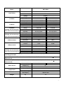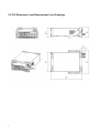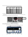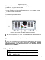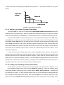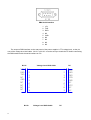
1
USER’S Guide
Programmable DC Electronic Load
Model M9711 M9712 M9712B M9712C M9712B30
ii
ContentUSER’S Guide.....................................................................................................................i
Programmable DC Electronic Load....................................................................................................i
Model M9712 M9712B M9712C M9712B30.....................................................................................i
Chapter 1 Overview...............................................................................................................................1
Chapter 2 Technical Specifications ........................................................................................................2
2.1 Main Technical Specifications .................................................................................................2
2.2 DC Electronic Load Dimensional Line Drawings...................................................................4
Chapter 3 Quick Reference ....................................................................................................................5
3.1 Power-onself-test......................................................................................................................5
3.2 In the Event of a Problem ........................................................................................................5
3.3 Front Panel Operation and Back Panel Operation................................................................6
3.4 Keypad Directions ....................................................................................................................7
3.5 Menu Operation ........................................................................................................................8
Chapter 4 Panel Operation ................................................................................................................... 11
4.1 Basic Operation Mode............................................................................................................ 11
4.1.1 Constant Current Operation Mode (CC) ....................................................................... 11
4.1.1.1 Setup a Standard Constant Current Mode...................................................................... 11
4.1.1.2 Loading and Unloading Constant Current Mode ........................................................... 12
4.1.1.3 Soft Start Constant Current Mode................................................................................. 13
4.1.1.4 Constant Current Mode Shifting into Constant Voltage Mode....................................... 13
4.1.2 Constant Resistance Operation Mode (CR) ............................................................. 14
4.1.2.1 Setting up a Standard Constant Resistance Mode ............................................... 15
4.1.2.2 Loading and Unloading Constant Resistance Mode............................................. 15
4.1.2.3 Shifting from Constant Resistance to Constant Voltage Mode............................ 16
4.1.3 Constant Voltage Operation Mode (CV).................................................................... 16
4.1.3.1 Setting Up Standard Constant Voltage Mode........................................................ 17
4.1.3.2 Loading and Unloading Constant Voltage Mode................................................... 17
4.1.3.3 SoftStart Constant Voltage Mode ........................................................................... 18
4.1.4 Constant Power Operation Mode (CW)..................................................................... 18
4.1.4.1 Setting up a Standard Constant Power Mode ....................................................... 19
4.1.4.2 Loading and Unloading Constant Power Mode..................................................... 19
4.2 Dynamic Testing Operation ................................................................................................... 20
4.2.1 Continuous Mode (CONTINUOUS) ........................................................................... 20
4.2.2 Pulsed Mode (PULSED) ............................................................................................. 20
4.2.3 Trigger Mode(TRIGGER)............................................................................................ 21
4.2.4 Setting up Dynamic test operational Parameters ..................................................... 21
4.2.5 Waveform Control........................................................................................................ 22
4.2.5.1 Square Wave ............................................................................................................ 22
4.2.5.2 Triangular Wave ....................................................................................................... 22
4.2.5.3 Trapezoidal Wave..................................................................................................... 22
4.2.6 Trigger Control ............................................................................................................. 22
4.2.7 List Function (Mode Sequence Steps) ...................................................................... 22
iii
4.2.7.1. List Operation........................................................................................................... 23
4.2.7.2 Executing List Function............................................................................................ 23
4.2.8 Automatic Testing Function ........................................................................................ 23
4.2.8.1 Automatic Test Operation........................................................................................ 24
4.2.8.2 Setting up Automatic Test Trigger Output Mode ................................................... 25
4.2.8.3 Executing Automatic Test Function ........................................................................ 25
4.3 Input Control............................................................................................................................ 26
4.3.1 Short Circuit Operation (SHORT)............................................................................... 26
4.3.2 Input On/Off Operation................................................................................................ 26
4.4 Electronic Load Operation Range......................................................................................... 26
4.5 Protection Functions............................................................................................................... 27
4.5.1 Over Voltage Protection (OV)..................................................................................... 27
4.5.2 Over Current Protection (OC)..................................................................................... 27
4.5.3 Over Power Protection (OW)...................................................................................... 28
4.5.4 Input Polarity Reversed............................................................................................... 28
4.5.5 Over Heat Protection(OH)........................................................................................... 28
4.6 Remote Measurement Function............................................................................................ 28
4.7 Battery Testing........................................................................................................................ 30
4.8 Communication protocol ........................................................................................................ 31
4.8.1 Introduction................................................................................................................... 31
4.8.2 Setup Baudrate ............................................................................................................ 32
4.8.3 Data............................................................................................................................... 32
4.8.4 Function Code.............................................................................................................. 32
4.8.5 Error checking (CRC) .................................................................................................. 32
4.8.6 Complete Command Frame Analysis........................................................................ 33
4.8.7 Coil With The Register Address Allocation ............................................................... 35
4.8.8 Definition Of The Command Register CMD.............................................................. 37
4.8.9 Common Operational Function Descriptions ............................................................ 38
4.9 Remote operation ................................................................................................................... 42
4.9.1 M-131 or M-133 Communication Cable..................................................................... 42
Quick Reminders ................................................................................................................................. 46
iv
Chapter 1 Overview
The new M97XX series programmable DC electronic load is a new generation product designed from
Maynuo Electronic Co.,Ltd. Incorporating high-performance chips, the M97XX series delivers high speed and
high accuracy with a resolution of 0.1 mV and 0.01 mA (basic accuracy is 0.03% and basic current rise speed is
2.5 A/μs). M97XX series have wide application from production lines for cell phone chargers, cell phone
batteries, electronic vehicle batteries, switching power supplies, linear power supplies, and LED drivers, to
research institute, automotive electronic, aeronautic and astronautic, maritime, solar celland fuel cell etc.test
and measurement applications.
FEATURES
•
Six high speed operation modes: CC,CR,CV,CW,CC+CV,CR+CV
•
Over current, over voltage, over power, over heating and polarity reversal protection
•
High-luminance vacuum fluorescent display (VFD) screen with two line, four channel display
•
Intelligent fan system will automatically activate based on changing ambient temperatures
•
Soft-start time setting, activating the power supply in accordance with the set voltage value
•
Battery test and short-circuit test functions
•
Capable of rising edge and falling edge dynamic testing
•
Supporting external triggeron either input or output
•
External current waveform monitor terminal output terminal
•
Supports remote voltage compensation and multi-data storage
•
Power-on-self-test, software calibration and standard rack mountable
•
Edits arbitrary waveforms in list function.
•
Available with RS232/RS485/USB serial interfaces.
1
Chapter 2 Technical Specifications
2.1 Main Technical Specifications
This User Manual covers only the M97XX programmable DC electronic loads. Please refer to the
following table that details the specific parameters of the150W-300W M97XX DC electronic loads.
Model
Input Raitng
M9712
M9712B
M9712C
150W
300W
300W
300W
Power
Current
0-30A
0-30A
0-15A
0-60A
Voltage
0-150V
0-150V
0-500V
0-150V
Range
0-3A
0-30A
0-3A
0-30A
0-3A
0-15A
0-6A
0-60A
Resolution
0.1mA
1mA
0.1mA
1mA
0.1mA
1mA
0.1mA
1mA
Accuracy
0.03%+0.05%FS
0.03%+0.05%FS
0.03%+0.05%FS
0.03%+0.05%FS
0.03%+0.05%FS
0.03%+0.05%FS
0.03%+0.05%FS
0.03%+0.05%FS
Range
0.1-19.999V
0.1-150V
0.1-19.999V
0.1-150V
0.1-19.999V
0.1-500V
0.1-19.999V
0.1-150V
Resolution
1mV
10mV
1mV
10mV
1mV
10mV
1mV
10mV
Accuracy
0.03%+0.02%FS
0.03%+0.02%FS
0.03%+0.02%FS
0.03%+0.02%FS
0.03%+0.02%FS
0.03%+0.02%FS
0.03%+0.02%FS
0.03%+0.02%FS
CR Mode
(Voltage and
current input
value ≥10% full
measument )
Range
0.03Ω-10K
0.03Ω-5K
0.03Ω-10K
0.03Ω-5K
0.3Ω-10K
0.3Ω-5K
0.03Ω-10K
0.03Ω-5K
Resolution
16bit
16bit
16bit
16bit
16bit
16bit
16bit
16bit
Accuracy
0.1%+0.1%FS
0.1%+0.1%FS
0.1%+0.1%FS
0.1%+0.1%FS
0.1%+0.1%FS
0.1%+0.1%FS
0.1%+0.1%FS
0.1%+0.1%FS
CW Mode
(Voltage and
current input
value ≥10% full
measument )
Range
0-150W
0-150W
0-300W
0-300W
0-300W
0-300W
0-300W
0-300W
Resolution
1mW
10mW
1mW
10mW
1mW
10mW
1mW
10mW
Accuracy
0.1%+0.1%FS
0.1%+0.1%FS
0.1%+0.1%FS
0.1%+0.1%FS
0.1%+0.1%FS
0.1%+0.1%FS
0.1%+0.1%FS
0.1%+0.1%FS
Voltage
0-19.999V
0-150V
0-19.999V
0-150V
0-19.999V
0-500V
0-19.999V
0-150V
Resolution
1mV
10mV
1mV
10mV
1mV
10mV
1mV
10mV
Accuracy
0.015%+0.03%FS
0.015%+0.03%FS
0.015%+0.02%FS
0.015%+0.03%FS
0.015%+0.03%FS
0.015%+0.05%FS
0.015%+0.03%FS
0.015%+0.03%FS
Current
0-3A
0-30A
0-3A
0-30A
0-3A
0-15A
0-6A
0-60A
Resolution
0.01mA
0.1mA
0.01mA
0.1mA
0.01mA
0.1mA
0.1mA
1mA
Accuracy
0.03%+0.05%FS
0.03%+0.08%FS
0.03%+0.05%FS
0.03%+0.08%FS
0.03%+0.05%FS
0.03%+0.08%FS
0.03%+0.05%FS
0.03%+0.08%FS
Watt
100W
150W
100W
300W
100W
300W
100W
300W
Resolution
1mW
10mW
1mW
10mW
1mW
10mW
1mW
10mW
Accuracy
0.1%+0.1%FS
0.1%+0.1%FS
0.1%+0.1%FS
0.1%+0.1%FS
0.1%+0.1%FS
0.1%+0.1%FS
0.1%+0.1%FS
0.1%+0.1%FS
CC Mode
CV Mode
V Measurement
I Measurement
W Measurement
(Voltage and
current input
value ≥10% full
measument )
Battery Measruement
Battery Input: 0.5-120V; Max. Measurement: Capacity=999/H; Resolution=0.1mA; Time Range=1S-16HS
Dynamic Measurement
Transition List: 0-25kHZ; 2.5A/uS; T1&T2:60uS-999S; Accuracy: + 15% offset+10% FS
CC soft-startup Time
1 mS; 2 mS; 5mS; 10mS; 20 mS; 50 mS; 100 mS; 200 mS Accuracy: + 15% offset+10% FS
Current(CC)
Short Circuit
Voltage(CV)
Weight
≒33A
0V
≒3.3A
≒33A
≒3.3A
≒18A
≒6.6A
66A
0V
0V
0V
≒55mΩ
≒35mΩ
≒300mΩ
≒25mΩ
Operating
0~40℃
0~40℃
0~40℃
0~40℃
–10℃~70℃
–10℃~70℃
–10℃~70℃
–10℃~70℃
Nonoperating
Dimension
≒3.3A
Resistance(C
R)
Temperature
2
M9711
W*H*D(mm)
Kg
108*214*365
3.5
Model
Input Rating
CC Mode
CV Mode
CR Mode
(Voltage and current input
value ≥10% full measument)
CW Mode
(Voltage and current input
value ≥10% full measument)
V Measurement
I Measurement
W Measurement
(Voltage and current input
value ≥10% full measument)
M9712B30
Power
300W
Current
0-30A
Voltage
0-500V
Range
0-3A
0-30A
Resolution
0.1mA
1mA
Accuracy
0.05%+0.05%FS
0.05%+0.08%FS
Range
0.1-19.999V
0.1-500V
Resolution
1mV
10mV
Accuracy
0.03%+0.02%FS
0.03%+0.05%FS
Range
0.3Ω-10K
0.3Ω-5K
Resolution
16 bit
16 bit
Accuracy
0.1%+0.1%FS
0.1%+0.1%FS
Range
0-300W
0-300W
Resolution
1mW
10mW
Accuracy
0.1%+0.1%FS
0.1%+0.1%FS
Voltage
0-19.999V
0-500V
Resolution
1mV
10mV
Accuracy
0.015%+0.03%FS
0.015%+0.05FS
Current
0-3A
0-30A
Resolution
0.01mA
0.1mA
Accuracy
0.05%+0.08%FS
0.08%+0.08%FS
Watt
100W
300W
Resolution
1mW
10mW
Accuracy
0.1%+0.1%FS
0.1%+0.1%FS
Battery Measurement Battery Input: 0.5-120V; Max. Measurement: Capacity=999/H; Resolution=0.1mA;
Time Range=1S-16HS
Dynamic Measurement Transition List: 0-25kHZ; 2.5A/uS; T1&T2:60uS-999S;
offset+10% FS
CC soft-startup Time 1 mS; 2 mS; 5mS; 10mS; 20 mS; 50 mS; 100 mS; 200 mS
offset+10% FS
Current(CC)
Short Circuit
Accuracy: + 15%
Accuracy: + 15%
≒3.3A
≒33A
Voltage(CV)
0V
Resistance(CR)
≒280mΩ
Operating
0~40℃
Nonoperating
–10℃~70℃
Dimension
W*H*D(mm)
108*214*365
Weight
Kg
3.5
Temperature
3
2.2 DC Electronic Load Dimensional Line Drawings
4
Chapter 3 Quick Reference
3.1 Power-onself-test
Verify that you have received the following items with yourXT 98XX DC Programmable Electronic
Load.. If anything is missing, contact your nearest XiTRON authorized Sales Representative's Office.
□ One power cord for your location/country
□ The M97xx User’s Manual
□ One CD (if you have purchased the optional communication accessories)
□ One communication cable (if you have purchased the optional communication accessories)
First, make sure the DC electronic load has been correctly connected and powered on. Please refer to the
following table for the detailed operational steps.
Procedure
Display
1. Power-up the DC
SYSTEM SELF TEST
electronic load
Explanation
Vxxx
The electronic load powers up and the VFD
panel displays the firmware revision level
#.
2. Wait for 1s after
EPROM ERROR
turning the DC
EEPROM damage or lost data at last power
off session.
electronic load on
ERROR CAL.DATA
EEPROM lost calibration data.
3. Wait another 2S
xxxxxxxV
Displays the actual input voltage and current
after ERROR has
xxxxxxxW
xxxxxxxA
xxxxxxxX
occurred
values and theactual power and reactant
setting values.
3.2 In the Event of a Problem
If the DC electronic load fails to power up, the following troubleshooting steps will help to determine the
problem.
1)
Make sure the power cord is connected properly and the Power switch has been pushed in to ON..
2)
Check the power voltage setting on the back panel.
There are two voltages that power the DC load: either 110V or 220V. Please make sure the right voltage
setting has been selected manually foryour area.
3)
Check the DC load's fuse..
5
If fuse is open, please replace it with another fuse that meets the following specifications.
Model
Fuse specification
Fuse specification
(110VAC)
(220VAC)
M9711
T0.5A 250V
T0.3A 250V
M9712
T0.5A 250V
T0.3A 250V
M9712B
T0.5A 250V
T0.3A 250V
M9712C
T0.5A 250V
T0.3A 250V
M9712B30
T0.5A 250V
T0.3A 250V
4).Replace the Fuse
Open the plastic cover on the rear panel of the DC electronic load with a flat screwdriver. (See table
3.1) and find the open fuse. Then replace the open fuse with a new one.
Fuse location
Diagram 3.1 Fuse Location
3.3 Front Panel Operation and Back Panel Operation
Please refer to Diagram 3.2 for the front panel of M97XX DC electronic load.
6
Diagram 3.2 Front panel
① The upper half is the black Vacuum Fluorescent Display (VFD) display screen.
② Robtary knob, Turn to adjust the setting values.
③ Numeric keys 0-9, ESC key, secondary key functions
④ Keypad: set up the current,voltage,power,resistance modes(I-set, V-set, P-set, R-set, Shift and
On-Off);Scroll through menus and options
⑤ Input terminals
⑥ Power switch to turn on/off the instrument
⑦ Up-Down keys, Enter key
Diagram 3.3 the back panel of the M97XX Series DC electronic load
1
BNC Out connector for 0-full range current, that corresponds to 0-10V output.An Oscilloscope
can be connected here to view dynamic waveforms.
2
Remote Measurement terminals and trigger for input/output interface
3
DB Sub 9 pin multifunctional communications interface for RS232, RS485 and USB serial buses
(with optional M133 D sub 9 to USB conversion cable). Do not connect an M131 cable with
standard RS-232 voltages on the cables connectors. Doing so may damage the instrument
and is not covered by WARRANTY.
3.4 Keypad Directions
1
~9
0-9 numeric keys
Esc
Esc key (enables exit from any working condition/mode)
I-Set
Switch to CC mode
7
Setting up a constant current
V-Set
Switch to CV mode
Setting up a constant voltage
P-Set
Switch to CW mode
Setting up a constant power
R-Set
Switch to CR mode
Setting up a constant resistance
Shift
Multi-purpose
Used in conjunction with other keys to perform diverse functions and
applications(for example: shift+0/Menu key will launch the menu
function)
On/Off
Turn DC electronic Load on/off
Scroll up menu choices
Scroll down menu choices
Enter
Confirmation of settings key
3.5 Menu Operation
Press the Shift+0/Menu keys in sequence to access the menu functions and theVFD screen
displays the menu choices: CONFIG, SYSTEM SET, LIST,AUTO TEST, SHORTCUT AND EXIT. . Select
the menu items by pressing the ▲ and ▼ cursor keys and then press the Enter key to open the menu
item you chose. Or press the Esc key to return to theout of the menu function.
MENU
CONFIG
INPUT RECALL
ON
Retains the same settings when the DC
electronic load is turned off
OFF
Sets the output to the OFF state when the DC
electronic load is powered on. The load will work
on CC mode
KEY PAD SOUND
SET-UP
Sets the keypad sounds
ON
Will activate abeep when any key is pressed.
OFF
Deactivates the beep when any key is pressed
CONNECT MODE
MAXTIDLEXING?
8
Resets the output to the same state as the last time
used when the load is turned off; or to the OFF state
when the DC electronic load is powered back on
Connect mode
Multi
SEPARATE
Single
BAUD RATE SET
Setting the modem Baud rate
2400 baud
9600 baud
14400 baud
28800 baud
57600 baud
115200 baud
COMM.PARITY
NONE
Setting Communications Parity mode
No Parity
EVEN
Even Parity
ODD
Odd Parity
ADDRESS SET
Setting an Address
1~200
The address is the input number (1-200).
KEY LOCK SET
Setting the password to unlock the keypad (when 0 or
null is set, there is no password set)
EXIT
SYSTEM SET
MAX CURRENT SET
Setting the maximum Current.
If the maximum current set is higher than 3A, the load
is in high range. Otherwise, it is in low range.
MAX VOLTAGE SET
Setting the maximum Voltage.
If the maximum voltage set is higher than 20V, the
load is in high range. Otherwise, it is in low range.
MAX POWER SET
Setting the Maximum Power.
TERMINAL SET
Selecting the input terminal
FRONT
Select the input terminal on the front panel
BACK
Select the input terminal on the back panel
EXIT
LIST
LOAD LIST
EDIT LIST
Choose list files, 1~8
Edit list files
MINIMUM TIME Edit minimum time(0.02~1310.7mS)
LIST MODE
List output mode
CONTINUOUS
Continuous mode
END HOLD
Retains the last output voltage level after
the entire sequence is successfully
completed
END RESET
Retains the load OFF state after the
entire sequence is successfully
9
completed
STEP LENGTH Step length(1~200)
STEP n
1~whole step length
CURRENT
Set current
TIME
Duration
EXIT
AUTO TEST
LOAD AUTO TEST
Select automatic test files 1~8
EDIT AUTO TEST
Edit automatic test files
STEP LENGTH
Set the entire step length
STEP n
WORK MODE
Load OFF mode
CC MODE
Constant Current mode
CV MODE
Constant Voltage mode
CP MODE
Constant Power mode
CR MODE
Constant Resistance
mode
SHORT MODE
Short circuit mode
TEST MODE
Qualification testing mode
TEST CURRENT
Test Current
TEST VOLTAGE
Test Voltage
TEST POWER
Test Power
TEST RESI
Test Resistance
DELAY TIME
Test delay time
between(0.2~25.5S)
INPUT xxxx
Input the parameters desired, for
example: CC mode, 1A
MINIMUM xxxx
Input the minimum lower limit
MAXIMUM xxxx
Input the maximum upper limit
LOAD OFF MODE
SET-UP AUTO TEST
TRIGGER
PASS
FAIL
TEST END
DISABLE
OUTPUT
PULSE
LEVEL
EXIT
EXIT
10
Trigger output selection
Trigger once when passing the
test
Trigger once when failing the test
Trigger output is initiated when
test ends
Disable trigger output
Output electrical characteristics selection
Pulse output
Voltage level output
Chapter 4 Panel Operation
4.1 Basic Operation Mode
There are four operation modes for the DC electronic load:
1. Constant Current (CC)
2. Constant Voltage (CV)
3. Constant Resistance (CR)
4. Constant Power (CW)
4.1.1 Constant Current Operation Mode (CC)
In this mode, the DC electronic load will synchronize with a current in accordance with the
programmed value regardless of the input voltage. Please refer to Diagram 4.1. If the maximum current
value of the power supply under test is lower than the constant current value set, the electronic load might
fail to automatically adjust to these levels. Accordingly, the constant current and voltage of the measured
power supply should be adjusted lower..
I
Current Set
Load current
Load voltage
V
Diagram 4.1 Constant Current Mode
4.1.1.1 Setup a Standard Constant Current Mode
Press the I-SET key and the VFD display will show STANDARD CURR=xxxxxxxxA, the present
constant current value. Press the numeric keys and decimal point key to enter the constant current value
desired, followed by pressing the Enter key to confirm the setting. - The DC Electronic Load load will
now be inthe standard constant current mode.
If the input state is in OFF state, then the word OFF will appear in upper right corner of the VFD
display. Press the On/Off key to change the load's input state to an ON state. Now CC or Unreg will
appear in the upper rightcorner of the VFD display. . Displaying CC means the load has been successfully
set with the expected constant current value; if Unreg is displayed,the load couldn’t adjust itself to the
constant current value that was entered. Please check to determine whether or notthe power supply under
test has the proper connections and has been turned on;also check to make sure that the desired constant
current value is within the range of the power supply under test.
11
If you want to fine tune the constant current value, rotate the encoder knob to adjust the value.
Rotating clockwise will increase the value and rotating it counter-clockwise will decrease the value. Note: if
the constant current value you want to set is beyond the maximum constant current value capability of the
DC load, the current value will stop increasing even if you continue to rotate the encoder knob clockwise.
At this point, the lower lower rightcorner of the VFD panel will display the constant current value you set.
Within this number sequence, if the cursor underlines one particular digit, that digit requires adjustment. If
users want to make adjustments to finetune the accuracy, depress the rotary encoder knob. Every time
the rotary encoder is pressedthe cursor will move forward to the previous digit.
4.1.1.2 Loading and Unloading Constant Current Mode
Loading and unloading CC mode can protect the power supply under test from damage. When the
voltage of the power supply under test starts to increase, the load will automatically adjust itself to the
open-circuit state, The load then carries the power supply being tested and adjusts itself to the current
value of the UUT set when the voltage of the UUT increased to the ONSET loading voltage level. When the
voltage of the power supply under test begins to decrease to the OFFSET unloading value, the load will
again automatically adjust itself to the open-circuit state. If the ONSET loading voltage value is higher than
the OFFSET unloading voltage, the load can avoid frequent carrying and unloading at the critical point of
unloading voltage; so the power supply under test willbe well protected.
U
ON SET
OFF SET
OFF
ON
OFF
T
Diagram 4.2 Loading and Unloading Mode
When in standard constant current mode, pressing the Shift+1(V_Level) keys in sequenceputs the
DC Electronic Load into the loading and unloading CC mode. When the VFD display shows ONSET
VOLT=xxxxxxxxV indicating the current loading voltage, use the numeric keys and decimal point key to
enter the loading voltage value desired, then press theEnter key to confirm the setting. Now the VFD panel
will display OFFSET VOLT=xxxxxxxxV indicating the current unloading voltage level. Press the numeric
keys and decimal point key to enter the unloading voltage value desired, followed by pressing the Enter
key to confirm the setting. Accordingly, the DC Electronic Load will enter into the loading and unloading
constant current mode between the two preset limits automatically
If the input state is OFF , then the upper right corner of the VFD panel will show the word OFF. Press
the - On/Off key to change the input state back toON . Then the upper right right corner of the VFD display
12
will show the word CC_UN or Unreg. CC_UN means the load was successfully set into the expected
constant current value; Unreg means the load could not adjust itself to the desired constant current value.
Please check thatthe power supply under test has been correctly connected and power switched on; make
sure thatthe voltage set is normal and the selected constant current value is within the range of the UUT.
While in loading and unloading CC mode, press the Shift+1(V_Level)keys in sequence and the DC
Electronic Load will revert back into the standard constant current mode.
4.1.1.3 Soft Start Constant Current Mode
The Soft Start CC mode enables the DC Electronic Load to functions as an inductive load, simulating
an inductance value which is in direct proportion with the rise time of the soft start. In this mode, the power
supply under test can avoid being damaged by a current strike .
I
Load current
Rising Time
T
Diagram 4.3 Soft Start Current Mode
When in standard CCmode, pressing the Shift+2(S_Start) keys in sequence places the load in the
soft start CCmode. When the VFD display shows Rising TM=xxxxxxxxvmS indicating the current rise
time, usethe numeric keys and decimal point key to enter the current rise time desired. Follow by pressing
the Enter keyto confirm the setting and the load will enter into the soft start CC mode.
If the input state is OFF, then the upper right corner of the VFD display will show the word OFF. Press
the On/Off key to change the input state to ON . Then the upper right corner of the VFD display will show
the word CC_S or Unreg. Showing CC_S means the load has been successfully set with the desired CC
value; Unreg on the display means the load couldn’t adjust itself to the desired CCvalue. Check to assure
that thepower supply under test has been correctly connected and powered on; make certain that the - CC
value selected is within the range of the UUT.When the Shift+2(S_Start) keys are pressed in sequence,
the loading and unloading CC mode, of the DC Electronic Load will revert back into the standard CC mode.
Note: The rise time is automatically regulated and set to a value of 20μS times a round number.
4.1.1.4 Constant Current Mode Shifting into Constant Voltage Mode
When the CC mode shifts into CV mode, damage to the power supply under test from current strike is
avoided.
13
I
Load input voltage
V
Diagram 4.4 Constant CurrentShift Mode back into Constant Voltage Mode
When in standard constant current mode, press the Shift+4(CC+CV) keys
to enter into the constant
current shiftto constant voltage mode. When the VFD display shows CC TO CV VOLT=xxxxxxxxV
indicating the current constant voltage value, press the numeric keys and decimal point key to enter the
constant voltage value desired followed by pressing the Enter key to confirm. Now the load will enter into
the constant current shift mode into constant voltage mode.
If the input state is in OFF , then the upper right corner of the VFD display will show the word OFF.
Press the On/Off key to change the input state into ON. The upper right corner of the VFD display will
show the combination ofCC+CV or Unreg. When CC+CV is displayed, the DC Electronic load has been
successfully set into the desired CC value; by displaying Unreg means the load could not adjust itself to
the selected CC value. Check that the unit under test has been connected correctly and powered on. Also,
assure that voltage level is normal.
When in the loading and unloading constant current mode, pressing the Shift+4(CC+CV)keys will
make the load revert back into the standard constant current mode.
4.1.2 Constant Resistance Operation Mode (CR)
In this mode, the DC Electronic Load will synchronize to a current linearly proportional to the input
voltage scaled to- the resistance programmed. Please refer to the Diagram 4.5.
Note: when the voltage of the unit under testis set too high and the resistance set is too low, either
the unit under test will consume the excess current and be shock damaged, or the DC Electronic Load will
fail to automatically adjust to the constant resistance and the load will suffer the shock damage from the
excess current.
I
Load current
Slop resistance set
Load input voltage
14
V
Diagram 4.5 Constant Resistance Mode
4.1.2.1 Setting up a Standard Constant Resistance Mode
By pressing the R-SET key the VFD display will show STANDARD RESI=xxxxxxxxΩ indicating the
presentconstant resistance. In order to place the DC Electronic Load into the standard constant resistance
mode, press the numeric keys and decimal point key to selct the desired values. Finally, after the values
are selected press the Enter key to confirm the setting.
When the input state is in OFF, the upper right corner of the VFD display will show the word OFF.
Press the On/Off key to change the input state to ON. Now the upper right corner of the VFD display will
show either CR or Unreg. -CR means the load has been successfully set into the expected constant
resistance value; Unreg means the load was unable adjust itself to the desired constant resistance value.
Verify that the unit under test is connected correctly and turned on; be sure the resistance value
selected is within the output current of the power supply under test so that it can source the expected
amount of resistance to drive the DC Load..
If you need to adjustthe constant resistance value,
rotate the encoder knob to change the value.
Rotating clockwise is increases the value while rotating counter-clockwise decreases the value.
Nowthelower rightcorner of the VFD display shows the constant resistance value set, but if under the vale
a cursor is blinking it means the number set, is in need of further adjustment. -When users want to
adjustorfine tune the accuracy, simply push in on the rotary encoder knob.. Each click the encoder is
rotated movesthe cursor left or right on the VFD screen.
4.1.2.2 Loading and Unloading Constant Resistance Mode
Figure4..1.1.2 illustratesthe CR loading and unloading mode theory of operation.
When in standard constant resistance mode, press the Shift+1(V_Level) keys to enter the CR loading
and unloading mode. When the VFD display shows ONSET VOLT=xxxxxxxxV, itindicates the current
load voltage state. Pressing the numeric keys and decimal point key will enter the load's desired voltage
setting.Pressing the Enter key will confirm the setting. Next the VFD will display OFFSET
VOLT=xxxxxxxxV indicating the need to set an offsetvoltage. Pressing the numeric keys and decimal
point key will set that desired offset voltage., Now press the Enter key to confirm the setting. Now the DC
Electronic Load will be in the CR load /unload mode.
If the input state showsOFF, then the upper right corner of the VFD panel will display OFF. Press the
On/Off key to change the input state to ON.. Now the upper right corner of the VFD display will show either
CR_UN or Unreg. CR_UN means the load has been successfully set into the desiredconstant resistance
value; Unreg means the load could not accept the constant resistance value set. Check to see the power
supply under test is correctly connected and turned on; make sure the voltage is normal and the output
current of the unit under test iswithin the range that the can drive DC Electronic Load.
From the loading and unloading CC mode, press the Shift+1(V_Level) keys and the DC Electronic
Load will the standard constant resistance mode.
15
4.1.2.3 Shifting from Constant Resistance to Constant Voltage Mode
I
U
Diagram 4.6 Shifting from Constant Resistance to Constant Voltage Mode
By shifting from constant resistance into constant voltage mode, the power supply under test can
avoid damage from a current strike..
From the standard constant current mode, press the Shift+5(CR+CV) keys to enter the constant
current shifting to constant voltage mode. When the VFD display shows CR TO CV VOLT=xxxxxxxxV it
indicates the current constant voltage value that is set. Press the numeric keys and decimal point key to
enter the constant voltage value desired,and press the Enter key to confirm the setting. In this mode, the
load will shift from the constant resistance to the constant voltage set.
If the input state is
OFF , then the upper right corner of the VFD display will show OFF. Press the
On/Off key to change the input state to ON. Then the upper right corner of the VFD display will show either
CR+CV or Unreg. CR+CV means the load has been successfully set with the selected constant resistance
value; Unreg means the DC Load could not accept the input constant resistance value. Please check that
the power supply under test has been correctly connected and turned on; make sure voltage is normal.
Pressing the Shift+5(CR+CV) keys in sequence while in the loading and unloading constant
resistance mode, will place the DC Load back into the standard constant resistance mode.
4.1.3 Constant Voltage Operation Mode (CV)
In this mode, the DC Electronic Load will attempt to generate sufficient current and synchronize to the
source voltage of the unit under test with the programmed value. Please refer to the Diagram at 4.7. Note:
When the voltage of the power supply under test is less than the voltage value set, or the input current is
beyond the maximum current that the DC load can withstand, the load will be unable to synchronize to the
voltage value set.
V
Load input
Voltage
Volt Set
Load current
16
I
Diagram4.7 Constant Voltage Mode
4.1.3.1 Setting Up Standard Constant Voltage Mode
Pressing the
V-SET key - will display
STANDARD VOLT=xxxxxxxxV indicating the current
constant voltage value set-up field. Here, enter the constant voltage value desired, followed by pressing
Enter. Now theDC load will be in standard constant voltage mode.
If the input state is OFF , then the upper right right corner of the VFD display will show
OFF. Press
the On/Off key to change the input state to ON . Now the upper right right corner of the VFD display will
show either CV or Unreg. CV means the DC load has been successfully set withthe desiredconstant
voltage value; Unreg means the load couldn’t accept the selected constant voltage value. Check that the
- LED driver has been correctly connected and is powered on; make sure that the voltage of the LED
driver is normal and that its output current is not beyond the maximum current that the DC electronic load
can accept.
In order to adjustthe constant voltage value,rotate the encoder knob at the upper right on the front
panel display to adjust the value settings. Rotating clockwise increases the value while rotating
counter-clockwise decreases the value. Note: if the constant voltage value you want to set is beyond the
maximum constant voltage capabilityof the DC load, the current value will stop at its top end and not
increase despite continued rotation of the encoder knob. Once a proper value is selected, the lower right
corner of the VFD display shows the constant voltage value that has been set. Should a blinking cursor
show up under one of the digits, it will require additional tweaking.. If users wish to adjust the accuracy,
pushing inthe encoder knob will effectuate the change. Each time the encoder knob is pressed,the cursor
will move to the next digit position, left or right.
4.1.3.2 Loading and Unloading Constant Voltage Mode
For the theory of operation on the loading and unloading of constant voltage mode , please refer to the
Diagram -4.1.1.2
From thestandard constant voltage mode, press the Shift+1(V_Level) keys to enter into the
constant loading and unloading CV mode. When the VFD display shows ONSET VOLT=xxxxxxxxV
indicating the current loading voltage, press the numeric keys and decimal point key to enter the loading
voltage value desired, and then press the Enter key to confirm. The-VFD now displays, OFFSET
VOLT=xxxxxxxxV indicating the current offsetvoltage. Press the numeric keys and decimal point key to
enter the offsetvoltage value desired, followed by pressing the Enter key to confirm. Nowthe DC
electronic load will enter the loading and unloading constant voltage mode.
If the input state is OFF, then the upper right corner of the VFD display will show OFF. Press the key
On/Off to change the input state to ON.Then the upper right corner of the VFD display will show either
CV_UN or Unreg. CV_UN means the load has been successfully set withthe desired constant voltage
value; Unreg means the load couldn’t accept the desiredconstant voltage value. Check the power supply
under test has been correctly connected and turned on; also make sure the voltage set is normal and that
17
the maximum output current of the unit under test does not exceedthe range of maximum current that the
DC load can absorb.
From the loading and unloading constant voltage mode, press the Shift+1(V_Level) keys, and the
load will go back to the standard constant voltage mode.
4.1.3.3 SoftStart Constant Voltage Mode
Softstart constant voltage mode enables the DC Electronic Load to function as a condensive load,
simulating electric capacity which is in direct proportion tothe rise time of the softstart. In this mode, the
LED driver under testwill avoid damage from a current strike.
U
VOLT
SETTING
T
RISING TIME
Diagram 4.8 SoftStart Constant Voltage Mode
When the Shift+2(S_Start) keys are pressed in standard constant voltage mode, the DC Load will
enter the soft start constant voltage mode. The VFD display will show RISING TM=xxxxxxxxvmS
indicating the current rise time set. Press the numeric keys and decimal point key to enter the rise
timedesired, and thenpress the Enter key to confirm the setting. Now the DC Load will be in the softstart
constant voltage mode.
If the input state is OFF, then the upper right corner of the VFD display will sayOFF. Press the On/Off
key to change the input state to ON.. Now the upper right corner of the VFD display will show either CV_S
or Unreg. CV_S means the load has been successfully set withthe desired constant voltage value; Unreg
means the DC load couldn’t accept the selected constant voltage value. Checkto see that the LED driver
under test has been correctly connected and turned on; also assure thatthe maximum output current of the
LED driver is within the range of the maximum current that the DC load can handle.
From theloading and unloading constant voltage mode, press the Shift+2(S_Start) keys andthe DC
Load will revert back to the standard constant voltage mode.
Note: The rise time that is set will be automatically regulated as value set rounded up to a whole
number multiplied by 20μS.
4.1.4 Constant Power Operation Mode (CW)
In this mode, the DC Electronic Loads will consume a set constant power. Please refer to the Diagram
4.9. Asthe load's input voltage value increases, the load input current will decrease
18
in linear increments. Accordingly, the equation ofload power(=V * I)will remain constant in the power
setting.
V
Load input
voltage
V2
Power set
V3
I2
I3
I
Load current
Diagram 4.9 Constant Power Mode
4.1.4.1 Setting up a Standard Constant Power Mode
Press the P-SET key, and the VFD panel displaysSTANDARD POWER=xxxxxxxxW indicating the
selection screen for constant power. Press the numeric keys and decimal point key to enter the constant
power value desiredthen press the Enter key. The DC load will now be in standard constant power mode.
If the input state is OFF, the upper right right corner of the VFD panelwill display the word OFF. Press
the On/Off key to change the input state to ON. Nowthe upper right corner of the VFD display will show
either CW or Unreg. CW means the DC load has been successfully set with the desired constant power
value; Unreg means the DC load couldn’t accept the selected constant power value. Check that the LED
driver under testhas been correctly connected and powered on; make sure the voltage of the LED driveris
normal and that its maximum output current is within the specified range of the DC Load or at an
undercurrent threshold.
In order to fine tune the constant power value, rotate the encoder knob to adjust the value desired.
Rotating clockwise increases the value while rotating counter-clockwise decreases the value desired. Now
the lower right corner of the VFD display shows the constant power value set. Should a blinking cursor
appear under any digit,more tweaking is needed. . To make additional changes/refinements, use the rotary
encoder knob. It also functions as an enter key for changes to DC Load settings. With each key press of
the rotary encoder the cursor will move forward to the next digit position..
4.1.4.2 Loading and Unloading Constant Power Mode
For the theory of operation to load and unload constant power mode , please refer to Diagram 4.1.1.2
From standard constant power mode, press the Shift+1(V_Level) key to enter the constant power
loading and unloading mode. When the VFD panel displays ONSET VOLT=xxxxxxxxV , it indicates the
DC Loads current voltage., To enter a different voltage load, use numeric selector keys and decimal point
key to change the load voltage value desired. Then press the Enter key to confirm the setting. The VFD
panel will next show OFFSET VOLT=xxxxxxxxV indicating the DC Load's present unload voltage. Press
19
the numeric selector keys and decimal point key to enter the unload voltage valuedesired, followed by
pressing the Enter key to confirm. Now the load will be in the loading and unloading constant power mode.
If the input state is OFF, then the upper right corner of the VFD display will show OFF. Press the
On/Off key to change the input state to ON. Now the upper right corner of the VFD panel will display either
CW_UN or Unreg. CW_UN means the DC Load has been successfully set with the desired constant
power value; Unreg means the DC Load did notaccept the desired constant power value. Please check
thatthe LED driver under test has been correctly connected and powered on; make sure that its voltage is
normal and that its output current is within the range ofcurrent that the DC Load'sselected power
canwithstand.
From the load and unload constant power mode, press the Shift+1(V_Level) keys, and the DCLoad
will revert back to the standard constant power mode.
4.2 Dynamic Testing Operation
Dynamic testing operation enables the DC electronic load to periodically switch between two pre-set
load levels. This function can be used to test the transient characteristics of the LED driver being tested.
Dynamic testing operation can be turned on and off by pressing the
Shift
+
Tran
keys on the
front panel. Before turning dynamic testing operation on, all of the parameters associated with dynamic
testing operation should be set by pressing the
Shift
+
S-Tran
, keys including: Value A, A pulse time ,
Rise time from value A to value B, Value B, B pulse time, Fall time from value B to value A and dynamic
testing operation mode. There are three modes of dynamic testing operation: continuous, pulsed and
triggered modes.
4.2.1 Continuous Mode (CONTINUOUS)
In this mode, when the dynamic test operation is turned on,the DC electronic load will periodically
switch between values A and B.
10A
5A
2.0ms
3.0ms
Diagram 4.10 Continuous Operation Mode
4.2.2 Pulsed Mode (PULSED)
In this mode, when the dynamic test operation is turned on, the DC electronic load will switch to value
B when receiving one triggered pulse signal , then capture the pulse time(TWD) of value B , after which the
DC Electronic Load will return to Value A .
20
10A
5A
TWD
10ms
TWD
10ms
TRIG
TRIG
Diagram 4.11 Pulse Operation Mode
4.2.3 Trigger Mode(TRIGGER)
In this mode, when the dynamic test operation is turned on, the DC electronic load will switch the state
between value A and value B afterreceiving a trigger signal.
10A
5A
TRG
TRG
Diagram 4.12 Trigger Operation Mode
4.2.4 Setting up Dynamic test operational Parameters
Press the Shift+6(S_Tran) keys, and the DC Electronic Load's VFD display shows LEVEL A
CURR=xxxxxxxxA indicating value A's current setting. Use the numeric keys and decimal point key to
select the current value desired, followed by pressing the key Enter to confirm the setting.
When the load VFD display shows WIDTH A TM=xxxxxxxxmS, it indicates the current duration time
of current set for value A.. Using the numeric keys and decimal point key, enter the duration time desired,
then press the Enter key to confirm.
When the DC Load's
display shows RISING TM=xxxxxxxxmS, it indicates the current rise time set
from value A to value B. Use the numeric and decimal point keys to enter the rise time desired, and press
the Enter key to confirm.
Next the DC Load's
display shows LEVEL B CURR=xxxxxxxxA that indicates the current value B
setting. Use both the numeric and decimal point keys to enter the current value desired, and press the
Enter key to confirm.
When WIDTH B TM=xxxxxxxxmS appears on the display panel it indicates the current duration
interval forvalue B that's set. To enter a different value for current, press the numeric and decimal point
keys to enter the duration period desired, followed by pressing the Enter key to confirm.
Next the DC Load'sVFD panel displays FALLING TM=xxxxxxxxmS which indicates the current falling
off time presently set between value B to value A. To change that value, use both the numeric and decimal
point keys to enter the falling off time desired, and press the Enter key to confirm.
After all of these parameters have been set, the DC Electronic Load's panel will display the set-up of
TRANMODE CONTINUOUS/ TRANMODE PULSE / TRNMODE TRIGGER indicating the unit is currently
21
ready for each of the 3 dynamic test operation modes. Select the dynamic operation mode desired by
pressing the up
or down
keys followed by pressing the Enter key to confirm.
4.2.5 Waveform Control
4.2.5.1 Square Wave
When set in the Continuous mode, with the rise time and fall time are both set tozero, the output wave
is a square wave. The output frequency will be the inverse of the pulse duration sum of both current A and
current B. Since the minimum accuracy of all the time interval is set at 20μS,the DC Electronic Load can
read the square wave with amaximum frequency of 25KHz at 50% duty cycle.
4.2.5.2 Triangular Wave
When set in the Continuous mode, with the interval time of current A and current B are both set to zero,
the output wave is a triangular wave. The output frequency will be the inverse of the sum of the rise and
fall times. Since the minimum accuracy of all the time interval is set at 20μS, the DC Electronic Load can
read the triangular wave with a maximum frequency of 25KHz. Since the rising edge and falling edge of the
triangular wave are all stepped within a 20μS interval, the ideal angle of the triangular wave will be in
inverse proportion to the its output frequency. In extreme situations, the triangular wave might function as a
square wave; there are 0-100 different accuracy steps scaled according to the different rising and falling
times set.
4.2.5.3 Trapezoidal Wave
When set in the Continuous mode of the dynamic test operation, and all four timing parameters that
need to be individually set are all greater than zero, theoutput wave is a trapezoidal wave. It has the same
frequency characteristics
as the triangular wave.
4.2.6 Trigger Control
In dynamic test operation mode trigger control is initiated when either pulse or trigger mode is set.The
three trigger modes are:
a、
Keypad trigger
Press the Shift+Trigger keys to trigger the DC Electronic load.
b、
TTL trigger
Send a high pulse with a constant time greater than 5msec to initiate the trigger-through
terminals on rear panel of the DC electronic load.
c、
PC soft control
trigger sends a command to the DC electronic load
4.2.7 List Function (Mode Sequence Steps)
The DC electronic load has a mode sequence list function. A maximum of 8 sequence steps can
be edited and 200 steps within each set of data can be changed Users can alter the duration of each step,
setting the minimum time of each step. Please note the minimum time setting must be a round number no
less than 0.02mS and ranging from 0.02mS to 1310.7mS. The duration of each step is linked to the
minimum time setting. If the minimum time is set at 0.02mS,then the duration of each step ranges from
22
0.02mS to1310.7mS; if the minimum time is set at 2mS,then the duration of each step ranges from 2mS to
131070mS.
4.2.7.1. List Operation
1) Press the Shift+0 keys to enter the menu operation, and then use the ▲ and ▼ keys to get to
MENU LIST, followed by keying Enter to confirm. Then press the ▲ and ▼ keys to reach EDIT LIST,
followed by pressing Enter to confirm. Then press the ▲ and ▼ keys to select the sequential code that
needs to be set, followed by pressing Enter to confirm.
2) When the display shows MINIMUM TM= xxxxxx mS , it indicates the minimum required time
setting. Since this value affects the fine tuning and operable length of all thewaveforms, please select the
suitable parameters carefully. Then press Enter to confirm. The electronic load will offerthe following three
output modes: LIST CONTINOUS, LIST END HOLD, and LIST END RESET. Press the ▲ and ▼ keys to
select the output mode desired, and pressEnter .
LIST CONTINOUS means continuous output mode.
LIST END HOLD means the electronic load will retain the last value set in the last step when all
the steps in one set of data have been successfully executed.
LIST END RESET means the electronic load will reset itself to load off mode when all the steps
set in one set of data have been successfully completed.
3)After pressing Enter to confirm, the VFD panel displays STEP LENG= xxx, indicating the
required step length that needs to be set. Press the numeric keys to input the step length desired, followed
by pressing Enter to confirm. Please note that the step length should be a round number between
1~200.
4)When the VFD display shows STEP 1 CURR=xxxxxA, it indicates the required current that needs
to be set in the first step. Use the numeric keys to input the current desired in the first step, and press
Enter to confirm. When the display shows STEP 1 TM=xxxxx mS, it indicates the current duration of the
first step. Press the numeric keys to input the current duration desiredin the first step, followed by pressing
Enter to confirm.
5)After all the setting steps have been entered, the VFD panel will display EDIT LIST,which means
exiting back to the beginning at list function. If all the setting steps have not been edited, the display will
show STEP n CURR=xxxxxA. This means that the value of the N step needs to be changed. Make the
required changes following the operating instructions in the previous step 4).
6)Since list function shares the same storage space as the automatic testing function; make sure that
the sequential code selected in the list function is the same as that in automatic testing function. If the
sequential code defined for the automatic testing function prior tonow is also the same entered for list
function, this sequential code of the automatic testing function of will be deleted and cannot be restored.
4.2.7.2 Executing List Function
Press the Shift+0 keys to enter menu configuration, and then press the ▲ and ▼ keys to
arrive at MENU LIS, and press Enter.. Now press the ▲ and ▼ keys to get to LOAD LIST, and press the
Enter.. Then press the ▲ and ▼ keys to set the sequential code of the list function you want to execute,
andpress Enter.
Since the list function shares the same storage space as theautomatic testing function, the
sequential code set for the automatic testing function will be automatically shielded from the sequential
codes chosen for the list function.
4.2.8 Automatic Testing Function
The DC electronic load provides an automatic testing function in which 8 data parameters can be set,
maximum, and 50 steps that can be changed within each set of data. Each step can be selected from
among the following six working modes: load off mode, constant current mode, constant voltage mode,
23
constant power mode, constant resistance mode, short circuit mode. Four comparison choices are
available: current comparison,voltage comparison, power comparison and resistance comparison.
Moreover, the delay time of each step can also bevaried. The delay time of each steprange from
0.1~25.5S, depending on the quickness and accuracy required. When each automatic test is over, the DC
electronic load will indicate a pass or a fail result.. The electronic load will sound an alarm when a UUT fails
a test. The trigger function of the electronic load can be set at the front-panel for TRIGGE IN for the
hardware voltage level in from the back-panel terminal connector, and TRIGER OUT for voltage level out
from the terminal connector on the back panel. The trigger mode can be set up as either voltage level
trigger or pulse trigger, and has 4 selection options of pass trigger, fail trigger, test completetrigger and
disable- trigger.
4.2.8.1 Automatic Test Operation
1)Press Shift+0 keys to enter menu configuration, and then use the ▲ and ▼ keys to reach
MENU AUTO TEST, and press Enter to confirm. Using press the ▲ and ▼ keys, go toEDIT AUTO TEST,
and press Enter.. Now use the ▲ and ▼ keys to select the sequence steps desired and then press Enter.
2) When STEP LENG= XX, appears, set the desired step length. Use the numeric keys to input
the step length, and press Enter. Note: step lengths should be a round number between1~50.
3) At STEP 1 xxxxx MODE, use the▲ and ▼ keys to select from the following six working
modes,
then press Enter.
Working
Mode
Promp Messages
Explanation
Load Off
Mode
LOAD OFF MODE”
Compares the voltages when in load off mode
CC Mode
“CC MODE”
Choose one of four comparison types: current,
voltage, power or resistance
CV Mode
“CV MODE”
Choose one of four comparison types: current,
voltage, power or resistance
CP Mode
“CP MODE”
Choose one of four comparison types: current,
voltage, power or resistance
CR Mode
“CR MODE”
Choose one of four comparison types: current,
voltage, power or resistance
Short Circuit
Mode
“SHORT MODE”
Compares the current when in short circuit mode
4) At STEP 1 TEST xxxx, there are four test types to select from: current, voltage, power and
resistance. Use the ▲ and ▼ keys to select one from the four test types, and Enter.If in the previous
step, if either load off mode or short circuit mode, was selected, then the electronic load will skip step over
this step 4).
5)At DELAY TM=xx.xS”,indicating the delay time input for each step, the valid range is between
0.1~25.5S. . The lower the value set, the shorter the duration of the test. Caution: in certain cases, if the
value set is too low, the test result might be compromised because the test was ended before the power
supply under test reaches its static state., To assure valid test results, select the delay time within optimal
duration for best results.The recommended delay time is 0.5S. Note: The upper range of 25.5S is pre-set
24
as a test suspended mode. Setting the delay time of any certain step at 25.5S, the load will stop and not
proceed to the next step until a trigger signal is provided to continue the test. The trigger signal can be
made either by the hardware on the back-panel, or by using the Shift+Trigger or the On/Off keys on the
VFD display panel.
6)WhenINPUT xxxx=xxxxxx, is displayed, it indicates the corresponding current, voltage, , power
and resistance values in the working mode that have been set. Use the numeric keys to enter these values,
and press Enter to confirm. Again, if in the prior step 3), load off mode or short circuit mode had been
selected, the DC electronic load will skip over this step 6).
7) When MINIMUM xxxx=xxxxxx, appears, it indicates the lower limit value of a valid test
comparison. Use the numeric keys to input the value, and press Enter to confirm. When the VFD display
shows MAXIMUM xxxx=xxxxxx, the upper limit value of a valid test comparison is shown. Use the
numeric keys to input the value, and press Enter to confirm.
When EDIT AUTO TEST is displayed on the screen, all the steps set requiring input values have
been completed., the The DC electronic load will exit back to the automatic testing function. But if all the
stepshave not been properly selected and values entered STEP n xxxxx MODE will be displayed
indicating that some data of the N step needs to be keyed in.
4.2.8.2 Setting up Automatic Test Trigger Output Mode
Press Shift+0 keys to enter the menu configuration mode, and using the ▲ and ▼ keys to get
to MENU AUTO TEST, and press Enter.Scroll the ▲ and ▼ keys to get to SETUP AUTO TEST, and
press Enter.The DC electronic load will be in automatic test trigger output mode.
There are 4 types of trigger output modes shown in the table below. Using the ▲ and ▼
keys,select the mode desired and press Enter.
Promp Messenges
Explanation
“TRIGGER WHEN PASS”
Test passed result
“TRIGGER WHEN FAIL”
Test failed result
“TRIGGER WHEN TEST END”
Test completed
“TRIGGER DISABLE”
Trigger disabled
Meanwhile, the Load will display the following trigger output electrical feature
Display
Description
“OUTPUT LEVEL”
Upon trigger, the output, voltage level will change from low to
high, until a key is pressed or a trigger input signal arrives, and
the voltage level then drops to low status.
“OUTPUT PLUSE”
Upon trigger the output voltage level changes from low to high
status, and after 5 seconds
automatically drops to a lower level
4.2.8.3 Executing Automatic Test Function
Using both the Shift+0 keys go to menu configuration, and then press the ▲ and ▼ keys to
get to MENU AUTO TEST, and press Enter. Scroll with the ▲ and ▼ keys and get to LOAD AUTO TEST,
and press Enter.. Use the ▲ and ▼ keys to select the sequential code for the automatic test function you
want to execute, then press the Enter The top right corner of the VFD two line display shows
AUT n, meaning the n automatic test in the list will be initiated. The bottom right of the VFD shows OFF D.
If all settings have been entered correctly, press the On/Off key to initiate the automatic test.
The automatic test can also be initiated by lowering the voltage level of TRIG IN port with a duration of
more than 5mS. When in testmode, the lower right corner of the VFD display will show WAIT or STAY,
25
meaning the DC electronic load is waiting for test initiation or remainingin the suspended mode
respectively. Please retrigger it so ttesting continues onward.
After each test is completed, the lower right corner of the VFD display will show either PASS or FAIL.
If failure occurs, the buzzer will sound. At this point, initiate the next trigger or press any key to free the load
from the pass or fail indication
Once the automated test is finished, press the ▲ and ▼ keys to initiate a manually operated test
mode. With each key press of the ▲ or the ▼ keys one time, the DC electronic load will resume the test of
the previous step or the next step in the sequence. Users can observe the actual state of every step. When
the ON/OFF key is pressed or a trigger is initiated, the DC electronic load will automatically exit from the
manuallyoperated test mode and return to the automatic test mode again.
4.3 Input Control
4.3.1 Short Circuit Operation (SHORT)
The DC Electronic Load can simulate a short circuit at the input end by turning the load on with
full-scale current. The short circuit function can be toggled on/off at the front panel by pressing the
Shift+9(Short) keys. Short circuit operation does not influence the current value set. When the short
circuit operation is in OFF state, the Load will return to its original setting state.
The actual current value that the load consumes in short circuit operation depends on the active
working mode and current range of the load.. In CC, CW and CR modes, the maximum short-circuit current
value is 1.2 times the current range. In CV mode, short-circuit operation is identical to setting constant
voltage to 0V.
4.3.2 Input On/Off Operation
When the load input state is ON, pressing the On/Off key will change the input state to OFF. Now top
right corner of the VFD display shows OFF. When the load input state is OFF, pressing the On/Off key will
change the input state to ON state. Now the upper right corner of the two line display shows SHORT
indicating the current working state.
4.4 Electronic Load Operation Range
The DC Electronic load operatesin the following range of Rated Current, Rated voltage and Rated
Power. Please refer to the Diagram 4-13 and Diagram 4-14.
V
Power Range
I
Diagram 4-13 Electronic Load Power Range
26
DC Electronic Load Mode Changes
Software Maximum
V
Power Set
Software Maximum
Current Set
I
Diagram 4-14 Software Maximum Setting Value
4.5 Protection Functions
The DC Electronic Load features the following protection functions.
4.5.1 Over Voltage Protection (OV)
If input voltage exceeds the maximum voltage range of the load, it will automatically shut down the
input. A buzzer will sound and the VFD panel displays the Over Volt message
The DC Electronic load's maximum voltage value can be set by pressing both Shift+0(Menu) keys.
When the VFD display shows MENU SYSTEM SET, press the Enter key to confirm. Now the VFD display
shows SYSTEM IMAX=xxxxxxxxA. Use the Up and Down keys to reachSYSTEM UMAX=xxxxxxxxV
setting input. Here the current maximum voltage limit value is displayed as 150V. Entering a different
voltage value can be done using both the numeric and decimal point keys. Pressing the ESC key exits
the Menu mode.
Note: The maximum acceptable input voltage of the M9712 DC electronic load is 150V. When any
value beyond 150V is input, the load will default back to 150V.
Besides, the maximum voltage value input is closely related tovoltage resolution. If the maximum
voltage value set is below 20V, the load's voltage resolution will be 0.1mV; if the maximum voltage value
set is above20V, then the load's voltage resolution will be only 1mV.
4.5.2 Over Current Protection (OC)
If input current exceeds the maximum current range of the load, it will automatically shut down the
input. A beep will sound and the VFD panel displays the OVER CUR message
The load's maximum curent value can be set by pressing both the Shift+0(Menu) keys. When the
VFD display shows MENU SYSTEM SET, press the Enter key to confirm. Now the VFD display shows
SYSTEM IMAX=xxxxxxxxA setting input. Here the current maximum current value is displayed as 30A.
Entering a different current value can be done using both the numeric and decimal point keys. Pressing
the ESC key exits the Menu mode.Note: The maximum acceptable input current of the M9712 DC
27
electronic load is 30A. When any value beyond 30A is input, the load will default back to 30A.Besides, the
maximum current value input is closely related to current resolution. If the maximum current value set is
below 3A, the load's current resolution will be 0.01mA; if the maximum current value set is above 3A, then
the load's current resolution will be only 0.1mA.
4.5.3 Over Power Protection (OW)
If input wattage exceeds the maximum wattage range of the load, it will automatically shut down the
input. A buzzer will sound and the VFD panel displays the OVER POW message
Press any key to get the load back ro normal operation. Note: if the current input state is
OFF , press
the ON/OFF key to make the load resume normal operation. If the over power problem is not solved, the
load will continue to display the OVER POW message.
The load's maximum wattage value can be set by pressing both the Shift+0(Menu) keys. When the
VFD display shows MENU SYSTEM SET, press the Enter key to confirm. Now the VFD display shows
SYSTEM PMAX=xxxxxxxxW setting input. Here the current maximum wattage value is displayed as
300W. Entering a different current value can be done using both the numeric and decimal point keys.
Pressing the ESC key exits the Menu mode.
Note: The maximum acceptable input wattage of the M9712 DC electronic load is 300W. When any
value beyond 300W is input, the load will default back to 300W.
4.5.4 Input Polarity Reversed
If the DC electronic load has its input polarity reversed , a buzzer will sound and the VFD display will show
REVERSE as a message
4.5.5 Over Heat Protection(OH)
When the temperature of internal power components exceeds 80°C℃, over heat protection will be
automatically initiated. The load will shut down input, a buzzer will sound and the VFD display will show the
OVERHEATmessage.
4.6 Remote Measurement Function
When in CV, CR and CP mode, if the DC electronic load consumes high current, the power supply
under test will have a voltage drop in the cables/wires connecting it to the load's BP terminals. In order to
assure measurement accuracy, there are remote measurement terminals installed on the rear-panel of the
DC electronic load. Users can measure the voltage at the output terminals of the power supply under test
by using these rear panel terminal connections.
The remote measurement function can be set up by pressing both the Shift+0(Menu) keys. Go to
MENU SYSTEM SET, and press Enter.The display will come up at SYSTEM IMAX=xxxxxxxxA. Use the
Up and Down keys and scroll to SYSTEM TERMINAL SEL and press Enter. There are only two options
for the remote measurement function, TERMINAL SELECT FRONT or TERMINAL SELECT BACK. Use
the Up and Down keys to make a selection. TERMINAL SELECT FRONT means the Binding Post (BP)
28
input terminals on the front panel of the DC electronic load. Selecting the BP will disable the remote
measurement function on the rear panel. TERMINAL SELECT BACK means the input terminals on the
rear panel of the load.
Selecting these back panel terminals will disable the remote measurement
function of the BPs on the load's front panel. After making the remote measurement selection, press the
key Esc to exit Menu mode.
Note: Either of the input terminals on the front panel or back panel can be initiated at any time.
However, it is impossible to initiate both sets of input terminals simultaneously. If the voltage of the load is
near to zero point and does not change in conjunction with the signal, please check that the wire mode
matches the parameters of the remote measurement function.
Please refer to the picture 4.4 for the trigger terminals and measurement terminals.
Photo 4.4 Remote Measurement Terminals
-S and +S are remote measurement terminals;
TRQ and TRI are trigger terminals, the last two terminals are ground terminals.
The output of power supply will be turned off when testing out the change in voltage level from high to low
from TRQ port which is under the latched mode of the remote control function. As a multifunction extended
port, TRI port is designed for future expanded.
The following diagram shows the remote sense terminals on the back panel of the instrument.
The following shows wiring diagram for the remote sensing:
29
4.7 Battery Testing
Experimentation has proven that the DC Electronic Load is the best way to confirm the operability of
most batteries.. With the correct load test set-up, the battery expectant life curve can be confirmed.The
electronic loads can currently be used to test about any type of the battery.
For batteries that are embedded in other equipment or placed in uninterrupted power service systems,
it is vital to use a DC electronic load for testing battery life status. Because batteries are among the lowest
reliability components in such systems, it should be tested periodically using a DC electronicload for
viability and utility.
Battery Life StabilityTest
In Constant Current mode the Serial electronic load can test battery life stability Set up the load to
control voltage level. When the voltage of the battery is too low, the serial electronic load will identify the
battery being on the threshold value set or at the margin of an insecure state and will stop testing
automatically. When the load is in test mode, you can see the battery's voltage, battery discharge current,
electronic, load power and battery capability that remains. If the load is connected through PC software,
then you can see the battery discharge curve.. This test can measure the reliability and remaining life of
the battery. So it is important to perform the test before the battery is re-charged, or swapped out for a
newer battery.
Operation:
1) In standard constant current mode, adjust the load's current value to the same discharge current
value of battery needed.
2) Press both Shift+8(Battery)keys. When VFD display shows END TEST VOLT= xxxxxxxxV,
input the shut-off voltage and press Enter to start the battery life stability test. When the battery's
voltage drops to the turn-off voltage set, the load will automatically shut off.
3) Press the On/Off
4)
30
keys to start or pause the battery capability test.
Press both the Shift+8(Battery) keys to exit the battery life stability test mode.
V
Battery Voltage
Min voltage
T
I
Load Sink Current
T
Diagram 4-16 Battery capacity calculation
4.8 Communication protocol
4.8.1 Introduction
M97 series programmable electronic loads work on the Modbus protocol. The data frame contains 4 parts
as follows:
Salve Address
Function Code
Data
Error
Checking(CRC)
To assure high reliability communications, the frame pitch set must be greater than 3.5 times the transient
time of a single bit byte. In other words, when the comm. rate is 9600 baud, the frame pitch time must be
set greater than 11*3.5/9600=0.004s.
M97 series programmable DC electronic loads are equipped with two way asynchronous communication,
with 1 bit fixed as the start bit, 8 data bits, and 1 stop bit. It supports Non parity check, Odd Parity check
and Even parity check. The communicationsrate is selectable at 2400, 9600, 14400, 28800, 57600,
115200 baud.
1) Setting upadditional addresses and communication parameters
The additional address is a single byte with 16 hexadecimal system data; the M97 series DC electronic
loads will only respond to the request data frame that has the same additional address.
2)Setup of the additional address
Press both Shift+0 keys in sequence, placing you in Main Menu mode., The DC electronic Load display
will be at MENU CONFIG.Press the key Enter to confirm. Using the CONFIG Menu, -up and down ▲ ▼
31
keys, scroll to CONFIG ADDRESS SET, then press Enter to confirm., Now the load will display ADDRESS
ADDR= xxx. Enter the new address using numeric keys, and press the Enter key again to confirm.
Note: Only whole numbers from 1 - 200 range will be accepted as valid additional addresses.
3)Selectingthe check mode
Press the Shift+0 keys in sequence, placing you in Main Menu mode. The XT 98XX DC Electronic Load
will now display MENU CONFIG. Press the Enter key to confirm.At CONFIG menu, use the up and down
▲ and ▼ keys, adnd scroll to CONFIG COMM.PARITY, and press Enter. The load will now display
COMM.PAR xxxxxThere are three choices, ODD, EVEN and NONE to select from. Enter the numeric
value for the parity mode using the keypad and press ENTER. Now the load has its parity mode set.
4.8.2 Setup Baudrate
Press the Shift+0 keys in sequence, placing it in Main Menu mode. The XT 98XX DC Electronic Load will
now display MENU CONFIG. Press the Enter key to confirm. At CONFIG menu, use the up and down ▲
and ▼ keys, and scroll to CONFIG BAUDRATE SET, then press Enter to confirm. The load will now
display BUADRATE xxxxx. The DC Load offers you six choices of baud rate to set. Use the use up
and down ▲ and ▼ keys to set the desired communications rate from 2400,9600,14400,28800,57600
and115200 baud.
4.8.3 Data
The M97 series loads operate in the Modbus protocol. Accordingly, in some data frames, the date length
is fixed, but in other data frames, the length is not fixed. According to this protocol, all the hexidecimal data
and the floating point number are fixed in the High Byte and the unfixed data length fields are in the Low
Byte. In addition,the output value of a force single coil must be either 0x0000 or 0xFF00. 0x0000 means
OFF, and 0xFF00 means ON. All other values are invalid and will not affect the coil.
4.8.4 Function Code
Function codes are single byte hex numbers; there are 4 functional modes as below:
Description
Function Code
0x01
Read Coil Status, read the data by each bit
0x05
Force Single Coil, write the data by each bit
0x03
Read Holding Registers, read the data by each word
0x10
Preset Multiple Registers, write the data by each word
4.8.5 Error checking (CRC)
The M97 series loads use the Cyclic Redundancy Check (CRC). The CRC field examines the contents of
the entire message. The CRC fileld is two bytes, containing a 16-bit binary value.When the CRC is
appended to the message, the low-order byte is appended first, followed by the high-order byte.
The discipline is as follows:
a) Set one hex CRC register, and give it the initial value as 0xFFFF.
b) Make bit xor the first byte of the frame date and the lower 8 bit of the CRC register. Save the bit
xor result into the CRC register.
c) Right move the CRC register for 1 byte, and make certain the lowest bit is set as1. Iif the lowest
bit is 1, then make the bit xor for the CRC register and the fixed data as 0xA001.
d) Repeat c) 8 times.
e) Repeat steps b,c andd, for the next byte of frame data until the last byte.
f) The last number of the CRC register is the last parity check result. Place it at the end of the frame
data, keeping the lower 8 bits in the latter and higher 8 bits in former.
32
4.8.6 Complete Command Frame Analysis
1. Read Coil Status (0x01)
Read Coil Status Example Query
Field Name
Byte length
Example Value
Slave Address
1
1~200
Function Code
1
0x01
Starting Address
2
0~0xFFFF
O. of Points
2
1~16
CRC Error Check
2
Read Coil Status Example for aLogical Response
Filed Name
Byte length
Example Value
Slave Address
1
1~200
Function Code
1
0x01
Byte Count
1
1~2
Data(Coil Status)
n
CRC Error Check
2
Read Coil Status Example in anIllogical Response
Field Name
Byte length
Example Value
Slave Address
1
1~200
Function Code
1
0x81
Abnormal Code
1
01~04
CRC Error Check
2
Example:
The following example reads the load input state (ISTATE) of the Coil of the slave device as address
0x01.
From table 4.8.7.1 below, we know that the ISTATE address is 0x0510.
Query: 0x01 0x01 0x05 0x10 0x00 0x01 0xFC 0xC3
The Corresponding Nomal Response: 0x01 0x01 0x01 0x48 0x51 0xBE, within which, 0x48 is the
read-back data and its lowest bit is 0 that means the input state ISTATE is OFF.
2. Force Single Coil (0x05)
Force Single Coil Example Query
Field Name
Byte length
Example Value
Slave Address
1
1~200
Function Code
1
0x05
Coil Address
2
0~0xFFFF
Force Data (Coil Status)
2
0x0000 or xFF00
CRC Error Check
2
Force Single Coil Example for a Logical Response
Field Name
Byte length
Example Value
Slave Address
1
1~200
Function Code
1
0x01
33
Coil Address
2
0~0xFFFF
Force Data (Coil Status)
2
0x0000 or 0xFF00
CRC Error Check
2
Force Single Coil Example in an Illogical Response
Field Name
Byte length
Example Value
Slave Address
1
1~200
Function Code
1
0x85
Abnormal Code
1
01~04
CRC Error Check
2
A value of 0xFF00 will force the coil to turn ON, and 0x0000 forces the coil to be turn OFF. All other values
are invalid and will not affect the coil status.
Example:
The following example places the load in remote control at slave device address of 0x01.
From table 4.8.7.1 below, we know that the PC1 remote address is 0x0510.
Query: 0x01 0x05 0x05 0x00 0xFF 0x00 0x8C 0xF6
The Correponding Response: 0x01 0x05 0x05 0x00 0xFF 0x00 0x8C 0xF6
3. Read Holding Registers (0x03)
Read Holding Registers Example Query
Field Name
Byte length
Example Value
Slave Address
1
1~200
Function Code
1
0x03
Starting Address
2
0~0xFFFF
No. of Points
2
n=1~32
CRC Error Check
2
Read Holding Registers Example for a Logical Response
Field Name
Byte length
Example Value
Slave Address
1
1~200
Function Code
1
0x03
Byte Count
1
2*n
Data
2*n
CRC Error Check
2
Read Holding Registers Example in an Illogical Response
Field Name
Byte length
Example Value
Slave Address
1
1~200
Function Code
1
0x83
Abnormal Code
1
01~04
CRC Error Check
2
Example:
The following example reads the present voltage value at the slave device as address 0x01.
34
From table 4.8.7.1 below, we know that the register address of the present voltage value is 0x0B00,
Query: 0x01 0x03 0x0B 0x00 0x00 0x02 0xC6 0x2F
The Corresponding Logical Response: 0x01 0x03 0x04 0x41 0x20 0x00 0x2A 0x6E 0x1A, within which,
0x41 0x20 0x00 0x2A is the read-back voltage valueand the corresponding floating point value is 10V.
4. Preset Multiple Registers (0x10)
Preset Multiple Registes Example Query
Field Name
Byte length
Example Value
Slave Address
1
1~200
Function Code
1
0x10
Starting Address
2
0~0xFFFF
No. of Registers
2
n=1~32
Byte count
1
2*n
Preset Data
2*n
CRC Error Check
2
Preset Multiple Registers Example for a Logical Response
Field Name
Byte length
Example Value
Slave Address
1
1~200
Function Code
1
0x10
Starting Address
2
0~0xFFFF
No. of Registers
2
N
CRC Error Check
2
Preset Multiple Registers Example in an Illogical
Response
Field Name
Byte length
Example Value
Slave Address
1
1~200
Function Code
1
0x90
Abnormal Code
1
01~04
CRC Error Check
2
Example:
The following example sets the load’s constant current IFIX as 2.3A at the slave device address of 0x01.
From table 4.8.7.1 below, we know that the IFIX register address is 0x0A01and the floating point takes up
a two-word length.
Query: 0x01 0x10 0x0A 0x01 0x00 0x02 0x04 0x40 0x13 0x33 0x33 0xFC 0x23
The Corresponding Logical Response: 0x01 0x10 0x0A 0x01 0x00 0x02 0x13 0xD0
4.8.7 Coil With The Register Address Allocation
Table 1: Coil-bit definition:
Name
Address
Bit
Property
Description
PC1
0x0500
1
W/R
When the remote control status bit is set to 1, the
front key panel is disabled
PC2
0x0501
1
W/R
When the local prohibition bit is set to 1, the
"Shift +7" keys on the front panel are disabled
TRIG
0x0502
1
W/R
Trigger tagged: triggered once by software
command
35
REMOTE
0x0503
1
W/R
1: remote input voltage
ISTATE
0x0510
1
R
Input status: 1= input ON, 0= intput OFF
TRACK
0x0511
1
R
Tracking status: 1=voltage tracking; 0=current
tracking
MEMORY
0x0512
1
R
1:input state memory
VOICEEN
0x0513
1
R
1: audible key sound ON/OFF
CONNECT
0x0514
1
R
1: multi 0= single
ATEST
0x0515
1
R
1: Automatic test mode
ATESTUN
0x0516
1
R
1: Automatic test pattern waiting to be triggered
ATESTPASS
0x0517
1
R
1: automatic test passed ,0: automatic test failed
IOVER
0x0520
1
R
1:over-current tag
UOVER
0x0521
1
R
1: over-voltage tag
POVER
0x0522
1
R
1: over- Power tag
HEAT
0x0523
1
R
1: over-heated tag
REVERSE
0x0524
1
R
1: reverse tag
UNREG
0x0525
1
R
1: registered parameter fail tag
ERREP
0x0526
1
R
1: EPPROM error tag
ERRCAL
0x0527
1
R
1: calibration data error tag
Table 2:
Register XRAM area definition
Name
Address
Bit
Property
Description
CMD
0x0A00
1
W/R
Command Register :lower 8 bits logical,high
8 bits illogical
IFIX
0x0A01
2
W/R
Constant current register: double-type
UFIX
0x0A03
2
W/R
Constant voltage register, double-type
PFIX
0x0A05
2
W/R
Constant power register,double-type
RFIX
0x0A07
2
W/R
Constant resistance register: double-type
TMCCS
0x0A09
2
W/R
Current soft-start rise time register , double
type
TMCVS
0x0A0B
2
W/R
Voltage soft-start rise time register , double
type
UCCONSET
0x0A0D
2
W/R
Constant
current
register :double-type
UCCOFFSET
0x0A0F
2
W/R
constant current unload voltage register ,
double-type
UCVONSET
0x0A11
2
W/R
Constant
voltage
register :double-type
UCVOFFSET
0x0A13
2
W/R
Constant voltage unloaded voltage register,
double-type
UCPONSET
0x0A15
2
W/R
Constant power load voltage register,doubletype
UCPOFFSET
0x0A17
2
W/R
Constant power unload voltage register ,
double-type
UCRONSET
0x0A19
2
W/R
Constant resistance load voltage register ,
double-type
UCROFFSET
0x0A1B
2
W/R
Constant resistance unload voltage register,
36
load
load
voltage
voltage
double type
UCCCV
0x0A1D
2
W/R
constant current shift
register:double type
UCRCV
0x0A1F
2
W/R
Constant resistance shift constant voltage
register, double type
IA
0x0A21
2
W/R
dynamic mode A phase current register,
double-type
IB
0x0A23
2
W/R
dynamic mode B phase current register,
double-type
TMAWD
0x0A25
2
W/R
dynamic mode
double-type
TMBWD
0x0A27
2
W/R
dynamic
mode
register ,double-type
TMTRANRIS
0x0A29
2
W/R
Dynamic mode
double-type
rising
TMTRANFAL
0x0A2B
2
W/R
Dynamic model
double-type
falling
MODETRAN
0x0A2D
1
W/R
Dynamic mode register,u16-type
UBATTEND
0x0A2E
2
W/R
Battery
Test
termination
register ,double type
BATT
0x0A30
2
W/R
Battery capacity register, double –type
SERLIST
0x0A32
1
W/R
LIST serial number register, u16 type
SERATEST
0x0A33
1
W/R
Automatic Test serial number register ,u16
type
IMAX
0x0A34
2
W/R
Current maximum register,double type
UMAX
0x0A36
2
W/R
Voltage maximum register,double type
PMAX
0x0A38
2
W/R
Power maximum register ,double type
ILCAL
0x0A3A
2
W/R
Calibration current low-end target value
double type
IHCAL
0x0A3C
2
W/R
Current high-end calibration target value ,
double type
ULCAL
0x0A3E
2
W/R
Voltage low-end calibration target value ,
double type
UHCAL
0x0A40
2
W/R
Voltage high-end calibration target value ,
double type
TAGSCAL
0x0A42
1
W/R
Calibration state tag,u16 type
U
0x0B00
2
R
Voltage Register ,double type
I
0x0B02
2
R
Current Register ,double type
SETMODE
0x0B04
1
R
Operation Mode register,u16e type
INPUTMODE
0x0B05
1
R
Input Status Register,u16 type
MODEL
0x0B06
1
R
Model Register ,u16 type
EDITION
0x0B07
1
R
software version number register,u16 type
A
constant
voltage
pulse-width
B
register,
pulse-width
time
register,r
time
register
voltage
4.8.8 Definition Of The Command Register CMD
Definition
CMD Value
CC
1
Description
37
CV
2
CW
3
CR
4
CC Soft Start
20
Dynamic Mode
25
Short Circuit Mode
26
List Mode
27
CC Loading And Unloading Mode
30
CV Loading And Unloading Mode
31
CW Loading
Mode
Unloading
32
CR Loading And Unloading Mode
33
CC Mode Switch To CV Mode
34
CR Mode Switch To CV Mode
36
Battery Test Mode
38
CV Soft Start
39
Changin System Parameters
41
Input ON
42
Input OFF
43
And
4.8.9 Common Operational Function Descriptions
Table 1. Remote Control Operation:
Operation
Register
Value
Description
Force Single Coil
1
mandatory
PC1
Table 2. Cancelling remote control operation:
Operation
Register
Value
Description
Force Single Coil
PC1
0
mandatory
Table 3. Local control override operation:
Operation
Register
Value
Description
Force Single Coil
PC2
1
mandatory
Table 4. Local control allows the operator to:
Operation
Register
Value
Description
Force Single Coil
PC2
0
mandatory
Table 5. Input ON operation:
Operation
Register
Value
Description
Preset
Multi-Registers
CMD
42
mandatory
Table 6. Input OFF operation:
Operation
Register
Value
Description
Preset
Multi-Registers
CMD
43
mandatory
38
Table 7. Short-circuit operation:
Operation
Register
Value
Description
Preset
Multi-Registers
CMD
26
mandatory
Table 8. CC mode operation:
Operation
Register
Value
Description
Preset
Multi-Registers
IFIX
Double
Optional
Preset
Multi-Registers
CMD
1
mandatory
Table 9. CV mode operation:
Operation
Register
Value
Description
Preset
Multi-Registers
UFIX
Double
Optional
Preset
Multi-Registers
CMD
2
mandatory
Table 10. CW mode operation:
Operation
Register
Value
Description
Preset
Multi-Registers
PFIX
Double
Optional
Preset
Multi-Registers
CMD
3
mandatory
Table 11. CR mode operation:
Operation
Register
Value
Description
Preset
Multi-Registers
RFIX
Double
Optional
Preset
Multi-Registers
CMD
4
mandatory
Table 12. CC mode soft-start:
Operation
Register
Value
Description
Preset
Multi-Registers
IFIX
Double
Optional
Preset
Multi-Registers
TMCCS
Double
Optional
Preset
Multi-Registers
CMD
20
mandatory
39
Table 13. CV mode soft-start:
Operation
Register
Value
Description
Preset
Multi-Registers
UFIX
Double
Optional
Preset
Multi-Registers
TMCVS
Double
Optional
Preset
Multi-Registers
CMD
39
mandatory
Table 14. CC loading and unloading mode:
Operation
Register
Value
Description
Preset
Multi-Registers
IFIX
Double
Optional
Preset
Multi-Registers
UCCONSET
Double
Optional
Preset
Multi-Registers
UCCOFFSET
Double
Optional
Preset
Multi-Registers
CMD
30
mandatory
Table 15. CV loading and unloading mode:
Operation
Register
Value
Description
Preset
Multi-Registers
UFIX
Double
Optional
Preset
Multi-Registers
UCVONSET
Double
Optional
Preset
Multi-Registers
UCVOFFSET
Double
Optional
Preset
Multi-Registers
CMD
31
mandatory
Table 16. CW loading and unloading mode:
Operation
Register
Value
Description
Preset
Multi-Registers
PFIX
Double
Optional
Preset
Multi-Registers
UCPONSET
Double
Optional
Preset
Multi-Registers
UCPOFFSET
Double
Optional
Preset
Multi-Registers
CMD
32
mandatory
Table 17. CR loading and unloading mode:
Operation
Register
Value
Description
Preset
Multi-Registers
RFIX
Double
Optional
40
Preset
Multi-Registers
UCRONSET
Double
Optional
Preset
Multi-Registers
UCROFFSET
Double
Optional
Preset
Multi-Registers
CMD
33
mandatory
Table 18. CC mode switch to CV mode:
Operation
Register
Value
Description
Preset
Multi-Registers
IFIX
Double
Optional
Preset
Multi-Registers
UCCCV
Double
Optional
Preset
Multi-Registers
CMD
34
mandatory
Table 19. CR mode switch to CR mode:
Operation
Register
Value
Description
Preset
Multi-Registers
RFIX
Double
Optional
Preset
Multi-Registers
UCRCV
Double
Optional
Preset
Multi-Registers
CMD
35
Must select
Table 20. Battery test mode:
Operation
Register
Value
Description
Preset
Multi-Registers
IFIX
Double
Optional
Preset
Multi-Registers
UBATTEND
Double
Optional
Preset
Multi-Registers
CMD
38
mandatory
Value
Description
Table 21. Dynamic Test Mode:
Operation
Register
Preset
Multi-Registers
IA
Double
Optional
Preset
Multi-Registers
IB
Double
Optional
Preset
Multi-Registers
TMAWD
Double
Optional
Preset
Multi-Registers
TMBWD
Double
Optional
41
Preset
Multi-Registers
TMTRANRIS
Double
Optional
Preset
Multi-Registers
TMTRANFAL
Double
Optional
Preset
Multi-Registers
MODETRAN
0~2
Optional
Preset
Multi-Registers
CMD
25
mandatory
Table 22. System parameter setting mode:
Operation
Register
Value
Description
Preset
Multi-Registers
IMAX
Double
Optional
Preset
Multi-Registers
UMAX
Double
Optional
Preset
Multi-Registers
PMAX
Double
Optional
Force Single Coil
REMOTE
0xFF00/0x0000
Optional
Preset
Multi-Registers
CMD
41
mandatory
4.9 Remote operation
4.9.1 M-131 or M-133 Communication Cable
The DB9 interface connector on the rear panel of the DC electronic load provides aTTL voltage level;
The communication cable (M-131 or M-133) can be used to connect the DB9 interface connector of the
electronic load and an RS-232 interface connector of a PC to enable remote operation/ communication.
Please refer to the following photos of the M-131 or M-133 interface cables.
Photo 4. 9.1 M-131(DB9 pin to RS-232)
42
Photo 4. 9.2 M-133 (DB 9 pin to USB)
Note:An industry standard RS-232 interface cable between the M97XX and a regular
PC will not facilitate communication between the devices. The dongle on the
M-133 provides the necessary switiching to enable proper communication.
1. RS232 Setting
Before using the remote operation mode, please insure that the baudrate and communication port
address of the DC electronic load are the same as that in the PC's softwareor the communication will fail.
You can change the baud rate and communication port address from the front panel of the load or and
match it to the PC in the computer set-up for new devices
(1) Baud rate: 9600(4800, 9600, 19200, 38400, which are selectable from the menu on the
front-panel.)
(2) Data bit: 8
(3) Stop bit: 1
(4) Parity: (none, even, odd)
2. DB9 Serial Interface
43
DB9 Serial Interface
1
2
3
4
5
6
7
8
9
+5V
TXD
RXD
NC
GND
NC
NC
NC
NC
The output of DB9 interface on the rear-panel of the power supplier is TTL voltage level, so the pin
outs of the voltage level shift cable(M-131 or M-133)must be set-up to match the PC before connecting
the DB9 interface with the serial interface on PC.
M-131
VCC
RXD
TXD
NC
GND
NC
NC
NC
NC
M-133
44
Voltage Level Shift Cable
PC
1
2
3
4
5
6
7
8
9
1
2
3
4
5
6
7
8
9
Voltage Level Shift Cable
PC
VCC
RXD
TXD
DTR
GND
NC
RTS
NC
NC
Note:An industry standard RS-232 interface cable between the M97XX and a
regular PC will not facilitate communication between the devices. The
dongle on the M-133 provides the necessary switiching to enable proper
communication.
45
Quick Reminders
Safety
Please do not install any spare parts or repair the instrument without contacting the factory for
authorization. In order to assure the works normally according to its speicification, have it repaired in the
service provider designated by the manufacturer.
Please review the following safety precautions before operating the equipment.
Safety Symbols
Please keep in mind the following items which could inflict serious bodily injuries.
Ground the unit properly using the wire recommended in the user manual.
High voltage danger (Only authorized service personnel should remove the cover and have
internal access to the instrument)
This symbol on an instrument indicates that the user should consult the operating Instructions in
the User Manual. Wear gloves when you start the operation and always beware of electric shock
hazard!. Don’t use the equipment without regard for personal safety.
Certification and Warranty
M97 Series Electrical Loads are warranted to meet its published technical specifications upon
shipment from the factory.
Warranty
This product is warranted against defects in material and workmanship for a period of one year from
date of shipment.
Maintenance Service
This product must be returned to a factory authorized service provider for repair. Customer shall
prepay shipping charges (and shall pay all duties and taxes) for products returned to the overseas supplier
for warranty repair.
Limitations of Warranty
The manufacturer's warranty shall not apply to
1. Defects resulting from improper or inadequate maintenance by the Customer,
2. Customer-supplied software or interfacing,
3. Unauthorized modification or misuse,
4. Operation beyond the environmental specifications of the product(s), or improper site preparation
and maintenance.
5. Defects resulting from client-installed circuits.
46
Disclaimer
Manufacturer reserves the right to make specification(s) changes to product(s) and its accompanying
documentation, at any time, and without previous notification to it's customers.
47